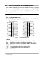
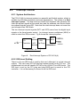
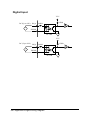
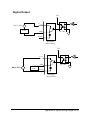
1
NuDAQ®
PCI-9114(A) DG/HG
Enhanced Multi-Functions
Data Acquisition Card
User′s Guide
Recycled Paper
©Copyright 1997~2003 ADLINK Technology Inc.;
All Rights Reserved.
Manual Rev. 1.40: April 28, 2003
Part No. 50-11114-202
The information in this document is subject to change without prior notice in
order to improve reliability, design and function and does not represent a
commitment on the part of the manufacturer.
In no event will the manufacturer be liable for direct, indirect, special,
incidental, or consequential damages arising out of the use or inability to
use the product or documentation, even if advised of the possibility of such
damages.
This document contains proprietary information protected by copyright. All
rights are reserved. No part of this manual may be reproduced by any
mechanical, electronic, or other means in any form without prior written
permission of the manufacturer.
Trademarks
NuDAQ®, NuIPC® are registered trademarks of ADLINK Technology Inc.
Other products names mentioned herein are used for identification
purposes only and may be trademarks and/or registered trademarks of their
respective companies.
Getting service from ADLINK
Customer Satisfaction is the most important priority for ADLINK Tech Inc. If
you need any help or service, please contact us.
ADLINK Technology Inc.
Web Site
http://www.adlinktech.com
Sales & Service
[email protected]
Technical
Support
NuDAQ + USBDAQ + PXI
[email protected]
Automation
[email protected]
NuIPC
[email protected]
NuPRO / EBC
[email protected]
TEL
+886-2-82265877
FAX
Address
9F, No. 166, Jian Yi Road, Chungho City, Taipei, 235 Taiwan.
+886-2-82265717
Please email or FAX us of your detailed information for a prompt,
satisfactory and constant service.
Detailed Company Information
Company/Organization
Contact Person
E-mail Address
Address
Country
TEL
FAX
Web Site
Questions
Product Model
Environment to Use
Detail Description
Suggestions to ADLINK
OS:
Computer Brand:
M/B:
CPU:
Chipset:
BIOS:
Video Card:
Network Interface Card:
Other:
Table of Contents
Chapter 1 Introduction ............................................................................ 1
1.1
Features .......................................................................................... 2
1.2
Applications..................................................................................... 2
1.3
Specifications .................................................................................. 3
1.4
Supporting Software........................................................................ 5
1.4.1 Programming Library ............................................................ 5
®
1.4.2 PCIS-LVIEW: LabVIEW Driver ........................................... 6
1.4.3 PCIS-VEE: HP-VEE Driver................................................... 6
1.4.4 DAQBenchTM: ActiveX Controls............................................ 6
1.4.5 DASYLabTM PRO................................................................ 6
1.4.6 PCIS-DDE: DDE Server and InTouchTM .............................. 6
1.4.7 PCIS-ISG: ISaGRAFTM driver ............................................... 6
1.4.8 PCIS-ICL: InControlTM Driver................................................ 7
1.4.9 PCIS-OPC: OPC Server....................................................... 7
Chapter 2 Installation .............................................................................. 8
2.1
What You Have ............................................................................... 8
2.2
Unpacking ....................................................................................... 9
2.3
PCB Layout of PCI-9114(A) .......................................................... 10
2.3.1 PCI-9114 Rev. B1............................................................... 10
2.3.2 PCI-9114 Rev. C2 and PCI-9114A Rev.A2 ........................ 10
2.4
Hardware Installation..................................................................... 11
2.4.1 PCI configuration ................................................................ 11
2.4.2 PCI slot selection................................................................ 11
2.4.3 Installation Procedures ....................................................... 11
2.5
Device Installation for Windows Systems ...................................... 12
2.6
Connector Pin Assignments .......................................................... 12
2.6.1 Pin Assignment of CN1 ...................................................... 12
2.6.2 Pin Assignments for CN2 & CN3 ........................................ 13
2.6.3 Pin Assignment for CN4 ..................................................... 14
2.7
Jumper Descriptions ..................................................................... 15
2.7.1 Analog Input Signal Type Selection (JP1) .......................... 15
2.7.2 Cold Junction Sensor Selection (JP2) ................................ 15
2.7.3 Counter #0 Function Selection (JP4).................................. 16
2.8
Termination Board Connection...................................................... 17
Table of Contents • i
Chapter 3 Registers ............................................................................... 18
3.1
PCI PnP Registers ........................................................................ 18
3.2
I/O Address Map ........................................................................... 19
3.3
A/D Data Registers ....................................................................... 20
3.4
A/D Channel Control Register ....................................................... 20
3.5
A/D Input Signal Range Control Register ...................................... 21
3.6
A/D Status Read-back Register .................................................... 21
3.7
Trigger Mode Control and Read-back Register ............................. 21
3.8
Interrupt Control and Read-back Register..................................... 23
3.9
Software Trigger Register ............................................................. 24
3.10 Hardware Interrupt Clear Registers............................................... 24
3.11 Timer/Counter Register ................................................................. 25
3.12 High Level Programming............................................................... 25
Chapter 4 Operation Theory ................................................................. 26
4.1
A/D Conversion ............................................................................. 26
4.1.1 A/D Conversion Procedure................................................. 27
4.1.2 A/D Signal Source Control.................................................. 27
4.1.3 A/D Trigger Source Control ................................................ 29
4.1.4 A/D Data Transfer Modes................................................... 30
4.1.5 Pre-Trigger Control............................................................. 32
4.1.6 A/D Data Format ................................................................ 34
4.2
Interrupt Control ............................................................................ 35
4.2.1 System Architecture ........................................................... 35
4.2.2 IRQ Level Setting ............................................................... 35
4.2.3 Dual Interrupt System......................................................... 36
4.2.4 Interrupt Source Control ..................................................... 36
4.3
Isolated Digital Input...................................................................... 37
4.4
Isolated Digital Output ................................................................... 38
4.5
Timer/Counter Operation............................................................... 40
4.5.1 Introduction......................................................................... 40
4.5.2 Pacer Trigger Source ......................................................... 40
Chapter 5 C/C++ Library........................................................................ 41
5.1
Libraries Installation ...................................................................... 41
5.2
Programming Guide ...................................................................... 42
5.2.1 Naming Convention ............................................................ 42
5.2.2 Data Types ......................................................................... 42
ii • Table of Contents
5.3
5.4
5.5
5.6
5.7
5.8
5.9
5.10
5.11
5.12
5.13
5.14
5.15
5.16
5.17
5.18
5.19
5.20
5.21
5.22
5.23
5.24
5.25
5.26
5.27
5.28
5.29
5.30
5.31
5.32
5.33
5.34
5.35
5.36
5.37
5.38
5.39
5.40
5.41
_9114_Initial.................................................................................. 43
_9114_Software_Reset................................................................. 43
_9114_DO..................................................................................... 44
_9114_DI....................................................................................... 44
_9114_AD_Read_Data ................................................................. 45
_9114_AD_Read_Data_Repeat.................................................... 46
_9114_AD_Read_Data_MUX ....................................................... 47
_9114_AD_Read_Data_Repeat_MUX.......................................... 48
_9114_AD_Set_Channel............................................................... 49
_9114_AD_Set_Range ................................................................. 50
_9114_AD_Get_Range ................................................................. 51
_9114_AD_Get_Status ................................................................. 52
_9114_AD_Set_Mode ................................................................... 53
_9114_AD_Get_Mode................................................................... 54
_9114_INT_Set_Reg .................................................................... 55
_9114_AD_Get_Reg ..................................................................... 56
_9114_Reset_FIFO....................................................................... 57
_9114_AD_Soft_Trigger................................................................ 58
_9114_Set_8254........................................................................... 58
_9114_Get_8254 .......................................................................... 59
_9114_AD_Timer .......................................................................... 60
_9114_Counter_Start .................................................................... 61
_9114_Counter_Read ................................................................... 62
_9114_Counter_Stop .................................................................... 63
_9114_INT_Source_Control.......................................................... 64
_9114_CLR_IRQ1......................................................................... 65
_9114_CLR_IRQ2......................................................................... 65
_9114_Get_IRQ_Channel............................................................. 66
_9114_Get_IRQ_Status ................................................................ 67
_9114_AD_FFHF_Polling ............................................................. 68
_9114_AD_FFHF_Polling_MUX.................................................... 69
_9114_AD_Aquire ......................................................................... 70
_9114_AD_Aquire_MUX ............................................................... 71
_9114_AD_INT_Start .................................................................... 72
_9114_AD_FFHF_INT_Start......................................................... 73
_9114_AD_INT_Status ................................................................. 75
_9114_AD_FFHF_INT_Status ...................................................... 76
_9114_AD_FFHF_INT_Restart..................................................... 77
_9114_AD_INT_Stop .................................................................... 78
Table of Contents • iii
Chapter 6 Calibration & Utilities ........................................................... 79
6.1
Calibration ..................................................................................... 79
6.1.1 What do you need? ............................................................ 79
6.1.2 VR Assignment................................................................... 80
6.1.3 A/D Adjustment .................................................................. 80
6.1.4 Software A/D Offset Calibration.......................................... 82
6.2
Utility ............................................................................................. 82
6.2.1 9114util (For PCI-9114 Rev. B2 Only) ................................ 82
6.2.2 9114AUtl............................................................................. 86
6.2.3 I_EEPROM......................................................................... 89
Appendix A. 8254 Programmable Interval Timer................................. 90
A.1 The 8254 Timer / Counter Chip..................................................... 90
A.2 The Control Byte ........................................................................... 91
Appendix B. Signal Wiring Diagrams................................................... 93
Warranty Policy...................................................................................... 96
iv • Table of Contents
Outline of Chapters
This manual is designed to help the user to understand and configure the
PCI-9114(A). The manual describes the programming functions and the
operation theory of the PCI-9114(A) card. It is divided into six chapters
Chapter 1,
“Introduction”, gives an overview of the product features,
applications, and specifications.
Chapter 2,
“Installation”, describes how to install the PCI-9114(A). The
layout of the PCI-9114(A) is shown, and the jumper settings for
analog input channel configurations are specified.
The
connector pin assignments and termination board connections
are described.
Chapter 3,
“Registers”, describes the details of the register structures of
the PCI-9114(A), this information can be useful for programmers
wanting to control the hardware using low-level programming.
Chapter 4, “Operation Theory”, describes how to operate the PCI-9114(A).
The A/D and timer/counter functions are introduced as well as
some programming concepts are specified in this chapter.
Chapter 5,
“C/C++ Library”, describes high-level programming interface in
C/C++ language. It will aid programmers with controlling the
PCI-9114(A) using high-level programming language
Chapter 6,
“Calibration”, describes how to calibrate the PCI-9114(A), for
accurate measurements.
vi • Outline of Chapters
1
Introduction
The PCI-9114(A) is an advanced data acquisition card based on the 32-bit PCI
Bus architecture. High performance design with state-of-the-art technology
makes this card ideal for data logging and signal analysis applications in areas
like medicine and process control. The following illustration shows the
fundamental function blocks of the PCI-9114(A).
PGA
32 SE/
16DI
MUX
Gain=1,10
100,1000
or 1,2,4,8
AD Controller
ASIC
Cold Junction
Sensor
8254
Timer
16 bits
AD
16 Channels
Isolated DI
1K FIFO
16 Channels
Isolated DO
PCI Controller
32 bits PCI Bus
Figure 1.
PCI-1114(A) Fundamental function block
Introduction • 1
1.1
Features
The PCI-9114(A) PCI-Bus Advanced Data Acquisition Card provides the
following advanced features:
•
32-bit PCI-Bus, Plug and Play
•
32 single-ended or 16 differential analog inputs channels
•
16-bits high resolution AD conversion
•
High amplification gain of 1, 10, 100, 1000 for PCI-9114(A) HG
•
Normal gain of 1, 2, 4, 8 for PCI-9114(A) DG
•
Single channel sampling rate up to 100 KHz for PCI-9114
•
Single channel sampling rate up to 250 KHz for PCI-9114A
•
Multi-AD trigger mode: software trigger, timer pacer trigger
•
On-board A/D 1K WORDS FIFO memory
•
Auto-scanning channel selection
•
One user configurable general purpose Timer/Counter (Only available in
PCI-9114A and PCI-9114 Rev. C2 or later)
•
16 Isolated Digital Input Channels
•
16 Isolated Digital Output Channels with high driving capability
•
5000 V rms high voltage isolation for DIO channels
1.2
Applications
•
Industrial process control
•
Transducer, thermocouple, RTD
•
Power monitor
•
Medical instrument
•
Biomedical measurement
2 • Introduction
1.3
Specifications
♦
Analog Input (A/D)
•
Converter: LTC1605 (LTC1606 for PCI-9114A) or equivalent,
successive approximation type
•
Resolution: 16 bits
•
Input channels: 32 single-ended or 16 differential input channels
•
Input Range: (Programmable)
•
•
9
Bipolar:10V, ±1V, ±100 mV, ±10 mV (PCI-9114(A) HG)
9
Bipolar:±10V, ±5V, ±2.5, ±1.25V (PCI-9114(A) DG)
Throughput:
9
Single channel 100 KHz max for PCI-9114
9
Single channel 250 KHz max for PCI-9114A
Over Voltage Protection for Analog inputs:
9
♦
Continuous ±35V maximum
•
Input Impedance: 10 MΩ
•
A/D Trigger Modes: Software and Timer pacer trigger
•
Data Transfer Mode: Pooling, EOC Interrupt, FIFO Half-full Interrupt
•
FIFO Buffer Size: 1024 samples
Isolated Digital Input (IDI)
•
Number of input channels: 16
•
Input voltage: 0~ 24 VDC
9
Logic L: 0~1.5V
9
Logic H: 3~24V
•
Input resistance: 4.7 KΩ @ 0.5W
•
Isolation voltage: 5000 V rms
•
Throughput: 10 KHz
Introduction • 3
♦
♦
Isolated Digital Output (IDO)
•
Number of output channels: 16 channels current source
•
Output type: open emitter 0.5 to 50 VDC
•
Source Current:
9
Single channel sources 500 mA maximum
9
8 channels source 60mA maximum simultaneously
•
Isolation voltage: 5000 V rms
•
Throughput: 10 KHz
General Specifications
•
Connector: 37-pin D-type connector
•
Operating Temperature: 0° C ~ 60° Cs
•
Storage Temperature: -20° C ~ 80° C
•
Humidity: 5 ~ 95%, non-condensing
•
Power Consumption:
•
9
+5 V @ 600 mA (typical)
9
+12 V @ 100 mA (typical)
Dimension:
9
Length:
7.88" (200 mm) for PCI-9114 Rev. B1
6.89" (175 mm) for PCI-9114 Rev. C2 and PCI-9114A
9
4 • Introduction
Width:4.18" (106 mm)(W)
1.4
Supporting Software
ADLINK provides versatile software drivers and packages for users’ different
approach to building a system. ADLINK not only provides programming
libraries such as DLL for most Windows based systems, but also provide
®
TM
drivers for other software packages such as LabVIEW , HP VEE ,
TM
TM
TM
TM
DASYLab , InTouch , InControl , ISaGRAF , and so on.
All software options are included in the ADLINK CD. Non-free software drivers
are protected with licensing codes. Without the software code, you can install
and run the demo version for two hours for trial/demonstration purposes.
Please contact ADLINK dealers to purchase the formal license
1.4.1 Programming Library
For customers who are writing their own programs, we provide function
libraries for many different operating systems, including:
•
DOS Library: Borland C/C++ and Microsoft C++. Functional descriptions
are included in this user’s guide.
•
Windows 95 DLL: For VB, VC++, Delphi, and BC5. Functional
descriptions are included in this user’s guide.
•
PCIS-DASK: Include device drivers and DLL for Windows 98, Windows
NT and Windows 2000. DLL is binary compatible across Windows 98,
Windows NT and Windows 2000. That means all applications developed
with PCIS-DASK are compatible across Windows 98, Windows NT and
Windows 2000. The developing environment can be VB, VC++, Delphi,
BC5, or any Windows programming language that allows calls to a DLL.
The user’s guide and function reference manual of PCIS-DASK are in the
CD.
Please
refer
the
PDF
manual
files
under
\\Manual_PDF\Software\PCIS-DASK
•
PCIS-DASK/X: Include device drivers and shared libraries for Linux. The
developing environment can be Gnu C/C++ or any programming language
that allows linking to a shared library. The user’s guide and function
reference manual of PCIS-DASK/X are in the CD. Please refer the PDF
manual files under. (\Manual_PDF\Software\PCIS-DASK-X.)
The above software drivers are shipped with the board. Please refer to the
“Software Installation Guide” for installation procedures.
Introduction • 5
1.4.2 PCIS-LVIEW: LabVIEW® Driver
®
PCIS-LVIEW contains the VIs, which is used to interface with NI’s LabVIEW
software package. The PCIS-LVIEW supports Windows 95/98/NT/2000. The
®
LabVIEW drivers is shipped free with the board. You can install and use them
without a license. For more information about PCIS-LVIEW, please refer to the
user’s guide in the CD. (\\Manual_PDF\Software\PCIS-LVIEW)
1.4.3 PCIS-VEE: HP-VEE Driver
The PCIS-VEE includes user objects, which are used to interface with HP’s
VEE software package. PCIS-VEE supports Windows 95/98/NT. The HP-VEE
drivers are shipped free with the board. You can install and use them without a
license. For more information about PCIS-VEE, please refer to the user’s
guide in the CD. (\\Manual_PDF\Software\PCIS-VEE)
1.4.4 DAQBenchTM: ActiveX Controls
We suggest customers who are familiar with ActiveX controls and VB/VC++
TM
programming use the DAQBench ActiveX Control component library for
TM
developing applications. The DAQBench is designed under Windows NT/98.
For more information about DAQBench, please refer to the user’s guide in the
CD. (\\Manual_PDF\Software\DAQBench\DAQBench Manual.PDF)
1.4.5 DASYLabTM PRO
DASYLab is an easy-to-use software package, which provides easy-setup
instrument functions such as FFT analysis. Please contact ADLINK to
purchase a copy of DASYLab PRO, which includes DASYLab and ADLINK
hardware drivers.
1.4.6 PCIS-DDE: DDE Server and InTouchTM
DDE stands for Dynamic Data Exchange. The PCIS-DDE includes the PCI
cards’ DDE server. The PCIS-DDE server is included in the ADLINK CD. It
needs a license. The DDE server can be used in conjunction with any DDE
client under Windows NT.
1.4.7 PCIS-ISG: ISaGRAFTM driver
The ISaGRAF WorkBench is an IEC1131-3 SoftPLC control program
development environment. The PCIS-ISG includes ADLINK product drivers
for ISaGRAF under Windows NT environment. The PCIS-ISG is included in
the ADLINK CD. A license is needed to use the drivers.
6 • Introduction
1.4.8 PCIS-ICL: InControlTM Driver
PCIS-ICL is the InControl driver, which supports Windows NT. The PCIS-ICL
is included in the ADLINK CD. A license is needed to use the drivers.
1.4.9 PCIS-OPC: OPC Server
PCIS-OPC is an OPC Server, which can link with OPC clients. There are
several software packages on the market, which can provide the OPC clients.
The PCIS-OPC supports Windows NT and requires a license to operate.
Introduction • 7
2
Installation
This chapter describes how to install the PCI-9114(A). Follow the steps
carefully.
•
Check what you have (section 2.1)
•
Unpacking (section 2.2)
•
Check the PCB and jumper location (section 2.3)
•
Install the hardware and setup and jumpers (section 2.4, 2.7)
•
Install the software drivers and run utility to test (section 2.5)
•
Cabling with external devices (section 2.6, 2.8)
2.1
What You Have
In addition to this user's guide, the package should include the following items:
•
PCI-9114(A) Enhanced Multi-function Data Acquisition Card
•
ADLINK CD
•
Software Installation Guide
If any of these items are missing or damaged, contact the dealer from whom
you purchased the product. Save the shipping materials and carton in case you
want to ship or store the product in the future.
8 • Installation
2.2
Unpacking
The card contains electro-static sensitive components that can be easily be
damaged by static electricity.
Therefore, the card should be handled on a grounded anti-static mat. The
operator should be wearing an anti-static wristband, grounded at the same
point as the anti-static mat.
Inspect the card module carton for obvious damages. Shipping and handling
may cause damage to your module. Be sure there are no shipping and
handling damages on the modules carton before continuing.
After opening the card module carton, extract the system module and place it
only on a grounded anti-static surface with component side up.
Again, inspect the module for damages. Press down on all the socketed IC's to
make sure that they are properly seated. Do this only with the module place on
a firm flat surface.
Note: DO NOT ATTEMPT TO INSTALL A DAMAGED BOARD IN THE
COMPUTER.
You are now ready to install your card.
Installation • 9
2.3
PCB Layout of PCI-9114(A)
2.3.1 PCI-9114 Rev. B1
Figure 2.
PCB Layout of PCI-9114 Rev. B1
2.3.2 PCI-9114 Rev. C2 and PCI-9114A Rev.A2
Figure 3.
10 • Installation
PCB Layout of PCI-9114 Rev. C2 and PCI-9114A Rev.A2
2.4
Hardware Installation
2.4.1 PCI configuration
The PCI cards (or CompactPCI cards) are equipped with plug and play PCI
controllers, it can request base addresses and interrupts according to PCI
standards. The system BIOS will install the system resources based on the PCI
cards’ configuration registers and system parameters (which are set by the
system BIOS). Interrupt assignment and memory usage (I/O port locations) of
the PCI cards can only be assigned by system BIOS. These system resource
assignments are done on a board-by-board basis. It is not suggested to assign
the system resource by any other methods.
2.4.2 PCI slot selection
The PCI card can be inserted into any PCI slot without any configuration
modification to the system resources. Please note that the PCI system board
and slot must provide bus-mastering capability to operate at its optimum level.
2.4.3 Installation Procedures
1.
Turn off your computer.
2.
Turn off all accessories (printer, modem, monitor, etc.) connected to your
computer.
3.
Remove the cover from your computer.
4.
Setup jumpers on the PCI or CompactPCI card.
5.
Select a 32-bit PCI slot. PCI slot are shorter than ISA or EISA slots, and
are usually white or ivory.
6.
Before handling the PCI cards, discharge any static buildup on your body
by touching the metal case of the computer. Hold the edge and do not
touch the components.
7.
Position the board into the PCI slot you have selected.
8.
Secure the card in place at the rear panel of the system.
Installation • 11
2.5
Device Installation for Windows Systems
Once Windows 95/98/2000 has started, the Plug and Play function of Windows
will find the new NuDAQ/NuIPC cards. If this is the first time the NuDAQ/NuIPC
cards are running on your Windows system, you will be prompted to input the
device information source. Please refer to the “Software Installation Guide”
for step-by-step installation procedures.
2.6
Connector Pin Assignments
2.6.1 Pin Assignment of CN1
The PCI-9114(A) comes equipped with a 37-pin D-type connector (CN1). The
pin assignment for CN1 is illustrated in Figure 4.
CN1 (for Single-Ended Input)
AI0
AI1
AI2
AI3
AI4
AI5
AI6
AI7
AGND
AI8
AI9
AI10
AI11
AI12
AI13
AI14
AI15
-12V
+12V
19
18
17
16
15
14
13
12
11
10
9
8
7
6
5
4
3
2
1
37
36
35
34
33
32
31
30
29
28
27
26
25
24
23
22
21
20
AI16
AI17
AI18
AI19
AI20
AI21
AI22
AI23
AGND
AI24
AI25
AI26
AI27
AI28
AI29
AI30
AI31
GND
Figure 4.
CN1 (for Differential Input mode)
AI0H
AI1H
AI2H
AI3H
AI4H
AI5H
AI6H
AI7H
AGND
AI8H
AI9H
AI10H
AI11H
AI12H
AI13H
AI14H
AI15H
-12V
+12V
19
18
17
16
15
14
13
12
11
10
9
8
7
6
5
4
3
2
1
37
36
35
34
33
32
31
30
29
28
27
26
25
24
23
22
21
20
AI0L
AI1L
AI2L
AI3L
AI4L
AI5L
AI6L
AI7L
AGND
AI8L
AI9L
AI10L
AI11L
AI12L
AI13L
AI14L
AI15L
GND
Pin Assignment of CN1
Legend:
AIn:
AIxH:
AixL:
AGND:
+12V:
-12V:
GND:
Analog Input Channel #n (for single-ended mode, n=0~15)
Analog Input Channel #x (for differential positive input, x=0-31)
Analog Input Channel #x (for differential negative input, x=0-31)
Ground plane for analog signals
+12V power supply output (with fuse protection)
-12V power supply output (with fuse protection)
Ground Plane
12 • Installation
2.6.2 Pin Assignments for CN2 & CN3
CN2 and CN3 are used for Isolated Digital input and output signals respectively.
The pin assignment for CN2 and CN3 is illustrated in Figure 5.
CN3 (for Isolation Digital Output)
Vpower
EOGND
DO_15
DO_14
DO_13
DO_12
20
18
16
14
12
10
DO_11
DO_10
DO_9
DO_8
8
6
4
2
19
17
15
13
11
9
7
5
3
1
Figure 5.
Vpower
EOGND
DO_7
DO_6
DO_5
DO_4
DO_3
DO_2
DO_1
DO_0
CN2 (for Isolation Digital Input)
EICOM4
19 EICOM2
20
EICOM3
18
17 EICOM1
DI_15
DI_7
16
15
DI_14
DI_6
14
13
DI_13
DI_5
12
11
DI_12
DI_4
10
9
DI_11
DI_3
8
7
DI_10
DI_9
DI_8
6
4
2
5
3
1
DI_2
DI_1
DI_0
Pin Assignments of CN2 & CN3
Legend:
Din:
Isolated Digital Input Channel #n (n=0~15)
EICOMx: Common plane for Isolated Input group #x (x=1~4)
Don:
Isolated Digital Output Channel #n
EOGND:
Isolated Output Signal Ground
Vpower:
Isolated Output Driver’s Power Supply
Installation • 13
2.6.3 Pin Assignment for CN4
N.C.
Ext_Trg
+5V
Clk_2M
N.C.
CN4 is only supported on PCI-9114A and PCI-9114 Rev. C2 or later. CN4 is
used for external signal connections. The pin assignment for CN4 is illustrated
in Figure 6
Figure 6.
PreTrg
GND
9
Cnt_Gate
1
Cnt_Out
10
Ext_Clk
2
Figure 2.3 Pin Assignment of CN4
Legend:
Ext_Clk:
External Clock for Counter #0
N.C.:
No Connection
Cnt_Out:
Output of Counter #0
Clk_2M:
Internal 2MHz Clock
Cnt_Gate:
External Gate Control Signal for Counter #0
+5V:
+5V power supply
GND:
Ground Plane
Ext_Trg:
External A/D Trigger Signal
PreTrg:
External Pre-trigger Signal
14 • Installation
2.7
Jumper Descriptions
2.7.1 Analog Input Signal Type Selection (JP1)
JP1 is only supported on PCI-9114A or PCI-9114 Rev. C2 and later. JP1 is
use to select the analog input signal type. It can be either Single-Ended or
Differential Input. The following diagram shows possible configurations.
DI
JP1: Single-Ended Input (Default)
SE
2.7.2 Cold Junction Sensor Selection (JP2)
JP2 is used to set the cold junction sensor. Note that JP2 is used in
conjunction with JP1. The following diagrams illustrate possible configurations.
•
C.J. Sensor Disabled (Default)
C.J. Senor Enabled
C.J. Sensor Disabled (Default)
•
Connecting the C.J. sensor to an AD Channel under Differential Input
mode. Note if JP1 is wrongly set as SE mode, the C.J sensor will be
connected to CH#0 and CH#16 is connected to the ground plane. The
following diagram illustrates the correct setting under D.I. mode with the
C.J. sensor enabled.
DI
JP1: Differential Input
SE
Enable C.J.
JP2: Enable C.J. Sensor
Disable
(Normal)
Installation • 15
•
Connecting the C.J. Sensor to an AD Channel under Single-Ended Input
mode. CH#16 is used as normal single-ended input.
DI
JP1: Single-Ended Input (Default)
SE
Enable C.J.
JP2: Enable C.J. Senor (S.E. mode)
Disable
(Normal)
2.7.3 Counter #0 Function Selection (JP4)
PreTrg
User
JP4 is only supported on PCI-9114A or PCI-9114 Rev. C2 and later. JP4 is
used to set the operation mode for Counter #0. Counter #0 can be set to either
a Pre-trigger controller or a user configurable Timer/Counter. When Counter
#0 is set as a user configurable Timer/Counter, the Clock input, Gate control
signal and the Counter Output of Counter #0 can be connected via CN4.
PreTrg
User
JP4: Set Counter #0 as a
Pre-Trigger Controller (Default)
JP4: Set Counter #0 as
a User Configurable
16 • Installation
2.8
Termination Board Connection
The PCI-9114(A) is equipped with a DB-37 connector.
termination boards include:
The available
Connection to ACLD-9137
The ACLD-9137 can be directly connected to the card, which is equipped with
a 37-pin D-sub connector. It is suitable for simple applications that do not need
complex signaling conditions before an A/D conversion is performed.
Connect with ACLD-9188
The ACLD-9188 is a general-purpose terminal board. It is equipped with a
37-pin D-sub connector. The ACLD-9138 contains LED indicators to indicate
the ON/OFF status of the computer system.
Connect with ACLD-9178
ACLD-9178 is a general purposed terminal board compatible with all cards,
which comes equipped with two 20-pin header connectors.
Connect with DIN-37D
DIN-37D is a general purposed 37-pin screw terminal with a DIN-socket. This
provides for easy installation. The DIN-37D is shipped with a 37-pin cable.
Installation • 17
3
Registers
The descriptions of the registers and structure of the CI-9114(A) are outlined in
this chapter. The information in this chapter will assist programmers wishing to
handle the card with low-level programs.
Therefore, the low level programming syntax is introduced. This information
can help assist in programming the card in the shortest possible time.
3.1
PCI PnP Registers
The PCI-9114(A) functions as a 32-bit PCI target device to any master on the
PCI bus. It supports burst transfer to memory space by using 32-bit data. All
data read and write is base on 32-bit data. There are three types of registers
on the PCI-9114(A): The PCI Configuration Registers (PCR), Local
Configuration Registers (LCR) and the 9111 registers.
The PCR is compliant to the PCI-bus specifications. It is initialized and
controlled by the plug & play (PnP) PCI BIOS. User can study the PCI BIOS
specification to understand the operation of the PCR. Please contact PCISIG
to acquire the specifications of the PCI interface.
The PCI bus controller (PCI-9050) is provided by PLX technology Inc.
(www.plxtech.com). For more detailed information of the LCR, please visit
PLX technology’s web site. It is not necessary for users to fully understand in
detail the LCR if the software library is used. The PCI PnP BIOS assigns the
base address of the LCR. The assigned address is located at 14h of PCR.
The PCI-9114(A) registers are shown in the next section. The base address,
which is also assigned by the PCI PnP BIOS, is located at an offset of 18h of
the PCR. Do not try to modify the base address and interrupt which is assigned
by the PCI PnP BIOS; it may cause resource conflicts in your system
18 • Registers
3.2
I/O Address Map
Most of the PCI-9114(A) registers are 16 bits. Users may access these
registers with 16-bit I/O instructions. There is one 32-bit register on the
PCI-9114(A). This 32-bit register occupies a LCR address space; its base
address is #2. The base address is allocated by the PCI BIOS and is located at
an offset 1Ch of the PCR. Users may read the PCR to obtain the LCR base
address and the two PCI-9114(A) base addresses by using the PCI BIOS
function call.
I/O Base
Address #1
Base + 00h
Base + 02h
Base + 04h
Base + 06h
Base + 08h
Base + 0Ah
Base + 0Ch
Base + 0Eh
Base + 20h
Base + 22h
Base + 24h
Base + 26h
I/O Base
Address #2
Write
Read
Isolated DO port
AD MUX channel no.
AD range control
AD trigger mode
Interrupt control
Software AD trigger
Clear H/W IRQ1
Clear H/W IRQ2
8254 Counter #0
8254 Counter #1
8254 Counter #2
8254 Control Registers
Isolated DI port
AD MUX channel no setting
AD range control read back
AD trigger mode read back
Interrupt control read back
FIFO status read back
--8254 Counter #0
8254 Counter #1
8254 Counter #2
8254 Status Registers
Write
Read
Base 2 + 40h
--
32 bits AD FIFO data and
channel number read
Table 1:
I/O Addresses
Registers • 19
3.3
A/D Data Registers
The PCI-9114(A) A/D data is stored in the FIFO buffer after conversion. The
data can be transferred to the host memory by software only. 16-bit input port
instructions can read the AD value. The A/D data can also be read back with
the channel number together. Users will know exactly the channel number of
the A/D data. However, it a 32-bit reading port instruction must be issued.
Address: BASE2 +40h
Attribute: read only
Data Format:
Bit
BASE2+40h
BASE2+41h
BASE2+42h
BASE2+43h
7
AD7
AD15
X
X
6
AD6
AD14
X
X
5
AD5
AD13
X
X
4
3
AD4 AD3
AD12 AD11
CH4 CH3
X
X
2
AD2
AD10
CH2
X
1
AD1
AD9
CH1
X
0
AD0
AD8
CH0
X
AD15~AD0: Analog to digital data. AD15 is the Most Significant Bit (MSB). AD0
is the Least Significant Bit (LSB). CH4~CH0: Channel number of the A/D data.
3.4
A/D Channel Control Register
The PCI-9114(A) provides 32 SE or 16 DI channels. The channel control
register is used to set the A/D channels to be converted. The 5 LSBs of this
register controls the channel number. Under non-auto scanning mode, the
register sets the channel number for conversion. Under auto-scanning mode,
the register sets the ending channel number. Note that the read back value is
the setting value and not the current selected AD channel number.
Address: BASE + 02h
Attribute: write and read
Data Format:
Bit
BASE+02h
BASE+03h
7
X
x
6
X
x
5
x
x
CNn: channel number of multiplexer.
CN4 is MSB, and CN0 is LSB.
20 • Registers
4
CN4
x
3
CN3
x
2
CN2
x
1
CN1
x
0
CN0
x
3.5
A/D Input Signal Range Control Register
The A/D range register is used to adjust the analog input ranges. This register
directly controls the PGA (programmable gain amplifier). When a different gain
value is set, the analog input range will be changed to its corresponding value
accordingly.
Address: BASE + 04h
Attribute: write and read
Data Format:
Bit
BASE+04h
BASE+05h
7
X
X
6
X
X
5
X
X
4
X
X
3
X
X
2
X
X
1
G1
X
0
G0
X
The relationship between the gain setting and its A/D range is listed in the
table below.
3.6
G1
G0
0
0
1
1
0
1
0
1
Gain
HG/ DG
1/1
10 / 2
100 / 4
1000 / 8
Analog Input Range
of PCI-9114(A)HG
±10V
±1V
±100 mV
±10 mV
Analog Input Range
of PCI-9114(A)DG
±10V
±5V
±2.5V
±1.25V
A/D Status Read-back Register
The A/D FIFO buffer status can be read back from this register.
Address: BASE + 0Ah
Attribute: read only
Data Format:
Bit
BASE+0Ah
BASE+0Bh
FF_EF:
FF_HF:
FF_FF:
AD_BUSY:
3.7
7
X
X
6
X
X
5
X
X
4
X
X
3
AD_BUSY
X
2
FF_FF
X
1
FF_HF
X
0
FF_EF
X
‘0’ means FIFO is empty
‘0’ means FIFO is half-full
‘0’ means FIFO is full, A/D data may have been loss
‘0’ means AD is busy, the A/D data has not been latched in FIFO
yet. If AD_BUSY changes from ‘0’ to ‘1’, A/D data is written into
FIFO.
Trigger Mode Control and Read-back Register
Registers • 21
This register is used to control or read back the A/D trigger control setting and
the AD range setting.
Address: BASE + 06h
Attribute: write and read
Data Format:
Bit
BASE+06h
BASE+07h
7
X
X
6
X
X
5
X
X
4
X
X
3
PTRG
X
2
EITS
X
1
TSSEL
X
0
ASCAN
X
PTRG: Pre-trigger ON/OFF control (Only available on PCI-9114A or
PCI-9114 Rev. C2 and later)
1: Pre-Trigger ON
0: Pre-Trigger OFF
EITS:
External / Internal Trigger Source (Only available on PCI-9114A or
PCI-9114 Rev. C2 and later)
1: External Trigger Source
0: Internal Trigger Source
TSSEL: Timer Pacer / Software Trigger
1: Timer Pacer Trigger
0: Software Trigger
ASCAN: Auto Scan Control
1: Auto Scan ON
0: Auto Scan OFF
The modes listed below applies to the PCI-9114(A) card only:
Bit 3
PTRG
0/1
0/1
0/1
22 • Registers
Bit 2
EITS
0
0
1
Bit 1
TPST
0
1
X
Bit 0
ASCAN
0/1
0/1
0/1
Mode Description
Software Trigger
Timer Pacer Trigger
External Trigger
3.8
Interrupt Control and Read-back Register
The PCI-9114(A) has a dual interrupt system, thus two interrupt sources can
be generated and be checked by the software. This register is used to select
the interrupt sources.
Address: BASE + 08h
Attribute: write and read
Data Format:
Bit
BASE+08h
ISC0:
7
X
6
X
5
X
4
X
3
MUX
2
FFEN
1
ISC1
0
ISC0
IRQ0 signal select
0: IRQ on the ending of the AD conversion (EOC)
1: IRQ when FIFO is half full
ISC1:
IRQ1 signal select (Timer Interrupt only)
FFEN:
FIFO enable pin
0: FIFO Enable (Power On default value)
1: FIFO Disable
(To reset FIFO, set FFEN sequence as 0 -> 1 -> 0)
MUX:
This is a read-only bit and it indicates the setting of JP1.
1: Single-ended
0: Differential-input
Registers • 23
3.9
Software Trigger Register
To generate a trigger pulse to the PCI-9114(A) to initiate a A/D conversion,
write any data to this register, this will trigger the A/D converter.
Address: BASE + 0Ah
Attribute: write only
Data Format:
Bit
BASE+0Ah
BASE+0Bh
3.10
7
X
X
6
X
X
5
X
X
4
X
X
3
X
X
2
X
X
1
X
X
0
X
X
Hardware Interrupt Clear Registers
Since the PCI interrupt signal is level triggered, the interrupt clear register must
be written to in order to clear the flag after processing an interrupt request
event; otherwise, any further interrupt request inserted will cause the software
to hang on processing the interrupt event.
There are two interrupt clear registers. The two registers are used to clear
IRQ1 and IRQ2 respectively.
Address: BASE + 0Ch
Attribute: write only
Data Format:
Bit
BASE+0Ch
7
X
6
X
5
X
4
X
3
X
2
X
1
X
0
X
6
X
5
X
4
X
3
X
2
X
1
X
0
X
Address: BASE + 0Eh
Attribute: write only
Data Format:
Bit
BASE+0Eh
24 • Registers
7
X
3.11
Timer/Counter Register
The 8254 chip occupies 4 I/O address locations in the PCI-9114(A) as shown
below. Refer to NEC’s or Intel's data sheet for full description of the 8254
features. Data sheets are available for download from the following web sites:
1.
http://support.intel.com/support/controllers/peripheral/231164.htm
2.
http://www.tundra.com
Address: BASE + 20h ~ BASE + 26h
Attribute: read / write
Data Format:
Base + 20h
Base + 22h
Base + 24h
Base + 26h
3.12
Counter 0 Register ( R/W)
Counter 1 Register ( R/W)
Counter 2 Register ( R/W)
8254 CONTROL BYTE (W)
High Level Programming
To operate the PCI-9114(A), the register structures can be bypassed, if
high-level application programming interface (API) is used to control the
PCI-9114(A) card. The software library including a DOS library for Borland
C/C++ is available in the All-in-one CD. Refer to chapter 5 for more
information.
Registers • 25
4
Operation Theory
The operation theory of the PCI-9114(A) card is described in this chapter. This
will help assist in understanding how to manipulate or to program the
PCI-9114(A).
4.1
A/D Conversion
Before programming the PCI-9114(A) to perform any A/D conversion, the
following topics need to be understood:
•
A/D conversion procedure
•
A/D signal source control
•
A/D trigger source control
•
A/D data transfer mode
•
Interrupt System (refer to section 4.2)
•
A/D data format
Note:
Since some A/D data transfer modes will use system interrupt
resources; an understanding of the interrupt system (section 4.2) is
required.
26 • Operation Theory
4.1.1 A/D Conversion Procedure
To use the A/D converter, the properties of the signal to be measured must first
be understood. A decision on which channels to use, to connect signals to
must be made. Refer to the chapter 2. In addition, the A/D signal sources,
including the A/D channel, A/D gain, and A/D signal types must also be defined.
Refer to section 4.1.2 for A/D signal source control information.
After deciding on the A/D signal source, the trigger source must be defined.
The A/D converter will start to convert signals to a digital value when a trigger
signal is on the rising edge. Refer to section 4.1.3 for details of the two
available trigger sources.
The A/D data is then transferred into the PC's memory for further processing.
The data can be read back using I/O instructions, which is handled by the
software or transferred to memory via the interrupt. Refer to section 4.1.4 for
information about multi-configurations of A/D data transfers.
To process the A/D data, an understanding of the A/D data format is required.
Refer to section 4.1.5 for details.
4.1.2 A/D Signal Source Control
To control the A/D signal source, the signal type, signal channel and signal
range must be considered.
Signal Type
The A/D signal sources of the PCI-9114(A) can be single ended (SE) or
differential input (DI). There are 32 SE or 16 DI A/D channels available. To
avoid ground loops and to obtain the most accurate measurement for the A/D
conversion, it is important to understand the signal source type.
Single-ended (SE) mode means the voltage of the signal to be measured is
relative to an isolated ground (IGND), therefore is suitable in conditions where
there is a floating signal source. A floating source means the signal source
have no connection to real ground or to the PC ground. Figure 7 illustrates a
single-ended Analog Input signal connection. Note that when more than two
floating sources are connected, the sources must have a common ground.
Differential input (DI) mode means the voltage of the signal to be measured is a
pair of signals, for example, AI3L and AI3H is a differential pair. The AD circuit
measures the voltage difference between the differential pair. Common mode
noise can be reduced under this mode. Note that the differential signal pair
must have a common ground. Figure 8 illustrates a differential analog signal
input connection. By using differential input mode, the common mode noise on
AIHn and AILn is reduced.
Operation Theory • 27
n = 0, ...,31
Floating
Signal
Sources
AIn
Analog Input
Multiplexer
Operational
Amplifier
To A/D Converter
...
V1
V2
Figure 7.
Signal sources and single-ended connection
n = 0, …, 8
A/Hn
To A/D
Converter
+
−
Grounded
Signal
Sources
A/Ln
GND
Vcm = VG1 − VG2
VG1
Figure 8.
VG2
Grounded source and differential input
Signal Channel Control
There are two ways to control the channel number. Either by software
programming or by auto channel scanning which is controlled by the ASCAN
bit in the AD trigger mode control register. When ASCAN is cleared (0), the
value of the AD Channel Control register defines the channel to be selected.
When ASCAN is set to 1, the value in the AD channel control register defines
the ending channel number for the auto-scanning operation. Under auto scan
mode, channels are scanned from channel 0 to the ending channel. Whenever
a trigger signal is on the rising edge, the channel number to be selected will
increase automatically. For example, if the ending channel number is 3, the
auto channel scanning sequence is 0,1,2,3,0,1,2,3, …, until the ASCAN bit is
cleared.
28 • Operation Theory
Signal Range
The proper setting for the signal range is important in data acquisition. e.g. the
input signal may be saturated if the A/D gain is too large or the resolution is to
small if the signal is at very low level. The maximum A/D signal range for the
PCI-9114(A) is +/− 10 volts when the programmable gain value is 1. The A/D
gain control register controls the maximum signal input range. The signal gain
is programmable with 4 different levels (1,10,100,1000) or (1,2,4,8). The signal
range for the 32 channels is the same for all channels. The available signal
polarity on the PCI-9114(A) is bi-polar only, however, the 16-bit high resolution
PCI-9114(A) can cover all 12-bit uni-polar applications.
4.1.3 A/D Trigger Source Control
An A⁄D conversion is initiated by a trigger source; the A⁄D converter will then
start to convert analog signals to a digital value. With the PCI-9114(A), two
internal sources can be selected: a software trigger or the timer pacer trigger.
The A/D operation mode is controlled by the A/D trigger mode register. In total
there are two trigger sources provided by the PCI-9114(A). Different trigger
conditions are specified below:
Software trigger (TSSEL=0)
The trigger source is software controlled in this mode. That is, the A/D
conversion is initiated when any value is written into the software trigger
register. This trigger mode is suitable for low speed A/D conversion. Under
this mode, the timing of the A/D conversion is fully controlled by the software.
However, it is difficult to control a fixed A/D conversion rate unless another
timer interrupt service routine is used to generate a fixed rate trigger. Refer to
the interrupt control section (section 4.2) for fixed rate timer interrupt operation.
Timer Pacer Trigger (TSSEL=1)
An on-board 8254-timer ⁄ counter chip is available and is able to provide a
trigger source for an A/D conversion at a fixed rate. The 2 counters of the 8254
chip are cascaded together to generate a trigger pulse at precise intervals.
Refer to section 4.3 for information about the 8254 architecture. This mode is
ideal for high speed A/D conversion. It can be combined with the FIFO half-full
interrupt or EOC interrupt to transfer data. It is also possible to use software
FIFO polling to transfer data. It's recommended that this mode be used if your
application needs a fixed and accurate A/D sampling rate.
Operation Theory • 29
External Trigger (EITS=1, TPST=don‘t care)
Through pin-4 of CN4 (ExtTrig), an A/D conversion can also be triggered by an
external signal. An A/D conversion starts when ExtTrig changes from high to
low. The conversion rate of this mode tends to be more flexible than the
previous two modes because external devices often are more flexible in
functions. An external trigger can be combined with FIFO half interrupt, EOC
interrupt or program FIFO polling for data tranfers.
4.1.4 A/D Data Transfer Modes
The A/D data are buffered in the FIFO memory. The FIFO size of the
PCI-9114(A) is 1024 (1K) words. If the sampling rate is 100 KHz, the FIFO can
buffer 10.24 ms of analog signals. After the FIFO is full, the lasting incoming
data will be lost. The software must read out the FIFO data before it becomes
full.
The data must be transferred to the host memory when the data is ready and
before the FIFO is full. With the PCI-9114(A), many data transfer modes can
be used. The different transfer modes are in the following section:
Software Data Polling
The software data polling is the easiest way to transfer A/D data. This mode
can be used with software A/D trigger mode. After the software triggers the A/D
conversion, the software polls the FF_EF bit of the A/D status register until it
becomes low.
If the FIFO is empty before the A/D starts, the FF_EF bit will be low. After the
A/D conversion is completed, the A/D data is written into FIFO buffer
immediately, thus the FF_EF becomes high. The FF_EF bit can be considered
to be a flag to indicate converted data ready status. That is, FF_EF is high
means the data is ready. Note that, while A/D is converted, the ADBUSY bit is
low. After A/D conversion, the ADBUSY becomes high to indicate not busy.
DO NOT use this bit to poll the AD data.
It is possible to read A/D converted data without polling. The A/D conversion
time will not exceed 10µs on the PCI-9114 card, and 4µs on PCI-9114A card.
Hence, after a software trigger, the software can wait for at least 10µs or 4µs
before reading the A/D register without polling.
The data polling transfer is suitable for applications that requires to process AD
data in real time. Especially, when combined with a timer interrupt, the timer
interrupt service routine can use the data polling method to get multi-channel
A/D data in real time and with a fixed data sampling rate.
30 • Operation Theory
FIFO Half-Full Polling
The FIFO half-full polling mode is the most powerful AD data transfer mode.
The 1K-word FIFO buffer can store up to 10.24 ms of analog data with a
100KHz-sampling rate (10.24ms = 1024 / 100KHz), or 4.096 ms of analog data
under a 250KHz-sampling rate (4.096ms = 1024 / 250KHz). Theoretically, the
software can poll the FIFO buffer every 10 or 4 ms.
It’s recommended that users check their system to find out the user software‘s
priority in special application. If the application software is at the highest
priority, polling the FIFO every 10 ms is suitable. However, the user‘s program
must check the FIFO if it is full or empty every time the data is read.
To avoid problems, the half-full polling method is used. If the A/D trigger rate is
100KHz, the FIFO will be half-full (512 words) in 5.12 ms. If the user‘s software
checks the FIFO for half full signals every 5 ms and the FIFO is not half-full, the
software does not read the data. When the FIFO is full, the AD FIFO is
overflowing. This means the sampling rate is higher than what the users’
expects or the polling rate is too slow. It is also possible due to system
occupation of CPU resources thus reducing the polling rate. When the FIFO is
half-full and not full, the software can read one “block” (512 words) of A/D data
without checking the FIFO status.
Usually, the timer trigger is used under this mode; therefore the sampling rate
is fixed. This method also utilizes the minimal CPU resources because it does
not necessary need to be the highest priority. The other benefit with this
method is it does not use any hardware interrupt resources. Therefore, the
interrupt is reserved for system clocks or emergency external interrupt
requests.
EOC Interrupt Transfer
The PCI-9114(A) provides traditional hardware end-of-conversion (EOC)
interrupt capabilities. Under this mode, an interrupt signal is generated when
the A/D conversion is ended and the data is ready to be read from the FIFO. It
is useful to combine the EOC interrupt transfer with the timer pacer trigger
mode. After an A/D conversion is completed, the hardware interrupt will be
inserted and its corresponding ISR (Interrupt Service Routine) will be invoked
and executed. The ISR program can read the converted data. This method is
most suitable for data processing applications under real-time and fixed
sampling rates.
Operation Theory • 31
FIFO Half-Full Interrupt Transfer
Sometimes, the applications do not need real-time processing, but the
foreground program is too busy to poll the FIFO data, then the FIFO half-full
interrupt transfer mode is useful. In addition, if an external A/D trigger source is
used, the sampling rate may not be easy to predict, then this method could be
applied because the CPU only be interrupted when the FIFO is half-full, thus
reserving the CPU load.
Under this mode, an interrupt signal is generated when FIFO become half-full,
that means there are 512 word data in the FIFO already. The ISR can read a
block of data at every interrupt occurring. This method is very convenient to
read A/D in size of a “block” (512 words) and it is benefit for software
programming.
4.1.5 Pre-Trigger Control
(Only available in PCI-9114A or PCI-9114 Rev.C2 and later)
In certain applications, the data acquisition is applied and stopped under
special hardware signals. Without Pre-Trigger functions, the software can start
the A/D at any time, but it is very difficult to stop the A/D in real-time using a
software application. Under “Pre-Trigger” mode, the pre-trigger (PTRG) signal
(pin-9 of CN4) and the 8254 counter are used to “STOP” the A/D sampling.
After setting up the Pre-Trigger mode, the hardware continuously acquires A/D
data and waits for the pre-trigger signal. Before the pre-trigger signal is
inserted, the software must read data from the FIFO buffer to prevent the FIFO
buffer from becoming full.
When the pre-trigger signal is inserted, the counter starts to count down from
the initial counter value N and counts the number of A/D conversion trigger
signals. The A/D trigger will be disabled automatically when the counter value
reaches zero. The value of N can be 1 to 65535 and the last A/D data is
sampled after the pre-trigger signal. The software must continuously read data
out from the FIFO buffer to prevent the FIFO from becoming full. The software
should also poll the counter value to check if the A/D sampling has stopped.
32 • Operation Theory
To set up Pre-Trigger mode, the following steps should be followed:
1.
Set Pre-Trigger Mode Off: PTRG = OFF.
2.
Set 8254 Counter #0 value N (N=1~65535). Note that the larger the
counter value, the more host memory buffer is needed.
3.
Set up A/D data acquire, including, A/D range, channel scan, data transfer
mode and so on.
4.
Set Pre-Trigger Mode On: PTRG = ON.
5.
Read A/D data into host PC memory using appropriate data transfer
method otherwise the FIFO can become full. At the same time, wait for the
pre-trigger signal and check if the 8254 Counter # 0 value is at zero.
6.
If the A/D is stopped, set the Pre-Trigger Mode off and process the data,
which is stored in the host memory.
7.
Go to Step 1 to set the Pre-Trigger mode and wait the next pre-trigger
event.
The Pre-Trigger timing is shown as following:
Set Pre-Trigger
mode
External Pre-Trigger
Signal is Inserted
Counter # 0 counting
from N down to 0
Acquire Infinite A/D data before
Pre-Trigger Signal is inserted
Acquire N A/D data after
Pre-trigger Signal is inserted
If the application acquires data after the pre-trigger signal, only the last N data
needs to be stored. The maximum value of N is 65535. If the application only
needs to acquire data before the pre-trigger signal, set N=1. Only one extra
data will be sampled after the pre-trigger signal.
Operation Theory • 33
4.1.6 A/D Data Format
The range for the A/D data read from the FIFO port is from -32768 to 32767. If
the A/D gain is 1, the A/D signal range is -10V ~ +10V. The relationship
between the voltage and its decimal value is shown in the following table:
A/D Data (Hex) Decimal Value
7FFF
4000
0001
0000
FFFF
C000
8001
8000
32767
16384
1
0
-1
-16385
-32767
-32768
Voltage (Volts)
±10V (Bipolar)
+9.9997
+5.0000
+0.0003
+0.0000
-0.0003
-5.0000
-9.9997
-10.0000
The formula between the A/D data and its analog value is:
Voltage = (AD_Data * 10) / (32768 * gain) --Bipolar
Where the gain is 1,10,100, 1000 for HG version and 1,2,4,8 for DG version.
34 • Operation Theory
4.2
Interrupt Control
4.2.1 System Architecture
The PCI-9114(A)‘s interrupt system is a powerful and flexible system, which is
suitable for A/D data acquisition and many applications. The system is a Dual
Interrupt System. The dual interrupt means the hardware can generate two
interrupt request signals at the same time and the software can service these
two request signals using ISR. Note that the dual interrupt does not mean the
card occupies two IRQ levels.
The two interrupt request signals (INT1 and INT2) come from the digital input
signals or the timer/counter output. An interrupt source multiplexer (MUX) is
used to select the IRQ sources. Fig 9 shows the interrupt system
INT1
INT #A
PCI
Controller
IRQ
INT2 Flip-Flops
INT1
MUX
Timer Pacer
AD EOC
FIFO
Half-full
Clear IRQ#1, #2
Figure 9.
Dual Interrupt System of PCI-9114(A)
4.2.2 IRQ Level Setting
There is only one IRQ level is used by this card, although it is a dual interrupt
system. This card uses INT #A interrupt request signal on the PCI bus. The
motherboard circuits will transfer INT #A to one of the AT bus IRQ levels. The
IRQ level is set by the PCI plug and play BIOS and is saved in the PCI
controller. It is not necessary for users to set the IRQ level.
Operation Theory • 35
4.2.3 Dual Interrupt System
The PCI controller of the PCI-9114 can receive two hardware IRQ sources.
However, a PCI controller can generate only one IRQ on the PCI bus, the two
IRQ sources must be distinguished by the ISR of the application software if the
two IRQ are both used.
The application software can use the “_9114_Get_Irq_Status” function to
distinguish which interrupt is inserted. After servicing an IRQ signal, users
must check if another IRQ is also asserted, then clear the current IRQ to allow
the next IRQ to occur.
The two IRQs are named as INT1 and INT2. INT1 comes from AD EOC or the
FIFO half-full flag. INT2 comes from timer‘s pacer output or the external
interrupt request. The sources of INT1 and INT2 are selective by the Interrupt
Control (ISC) Register.
Because the PCI-9114 is a dual interrupt system, you can use the FIFO half-full
and external interrupt at the same time if your software ISR can distinguish
these two events.
4.2.4 Interrupt Source Control
There are two bits to control the IRQ sources of INT1 and INT2. Refer to
section 4.9 for details of these bits. In addition, the PCI controller itself can also
control the usage of the interrupt. To manipulate the interrupt system more
easily,
ADLINK
recommend
you
to
use
the
function
_9114_INT_Source_Control to control the IRQ source so that you can disable
one or two of the IRQ sources.
Note that even if you disable both IRQ sources without changing the initial
condition of the PCI controller, the PCI BIOS will still assign an IRQ level to the
PCI card and it will still occupy the PC’s resources. It is not recommended that
the PCI cards initial condition be re-design with a users‘ application software. If
users want to disable the IRQ level, please use the ADLINK software utility to
change the interrupt settings
36 • Operation Theory
4.3
Isolated Digital Input
There are 16 Isolated Digital input signals. Each digital input signal is connect
to a photo isolator such that the signal is isolated from the ground or the power
plane of the host PC. Figure 10 illustrates a single digital input circuits.
DI_n
R=2.4K Ohm
to digital circuits
Photo Isolator
Figure 10. Isolated Input Circuits
The Isolated Digital input could be an AC input. The isolation voltage is 5000 V
rms. The input resistance is 1.2K Ohm.
Note that the 16 DI signals are partitioned into 4 groups. Each group is based
on a common plane. Every two groups are mutual isolated. Refer the Figure
11 and the Table 2 for the four groups.
Signal Names
ID_0~ID_3
ID_4~ID_7
ID_8~ID_11
ID_12~ID_15
Common Signal
EICOM1
EICOM2
EICOM3
EICOM4
Table 2: Digital input signals and ground plane
The common plane could be either common power or common ground. The
following diagram shows the EICOM as common ground. An external device
or circuit will provide the power source or current source.
I s o la t e d
In p u t
2 .4 K O h m
E IC O M
Figure 11. Common ground
Operation Theory • 37
The following diagram shows the EICOM as common power. An external
device or circuit will provide the power source and current sink. Most open
collector output devices can be connected to the PCI-9114(A) using this
configuration.
I s o la t e d
In p u t
2 .4 K O h m
E IC O M
Figure 12. Common power
4.4
Isolated Digital Output
There are 16 Isolated Digital output signals. Darlington transistors drive the
digital output signals. Figure 13 shows the output circuits.
Note that the 16 DO signals uses a common ground and common external
power source.
Vpower
From digital circuits
DO_n
EOGND
Figure 13. Digital output circuits
The EOGND pin is used via a (fly-wheel) diode, this will protect the driver if an
inductive load from such as a relay, motor or solenoid is present. If the loading
is resistive such as from resistors or LEDs, the connection to the fly-wheel
diode is not necessary.
38 • Operation Theory
The first step in connecting the output to an external device is to distinguish the
type of load. For example, if the load is a LED or a resistor, connection diagram
below can be used.
Vpower
Power
Supply
From digital circuits
DO_n
Load
EOGND
Figure 14. Opto-isolated output circuit for resistive loads
If the load is inductive such as from a relay, the diagram below can be used.
The power supply must be from an external source in order to form a fly-wheel
current loop.
Vpower
Power
Supply
From digital circuits
DO_n
Load
EOGND
Figure 15. Opto-isolated output circuit for inductive loads
Operation Theory • 39
4.5
Timer/Counter Operation
4.5.1 Introduction
One 8254 programmable timer/counter chip is integrated into the PCI-9114(A).
The 8254 chip supports 3 counters and can operate in 6 different operation
modes for each counter. The block diagram of the timer/counter system is
shown in the diagram below.
AD Trigger Signal
8254 Chip
(CN3 Pin#1)
C
(CN4 Pin#5)
Pre-Trigger Signal
(CN4 Pin#9)
Gate Control
Pre-Trigger
Controller
Internal 2 MHz Clock
G
C
'H' G
C
'H' G
Counter #0 O (CN4 Pin#3)
Timer #1
O
Timer #2
O
Internal Timer Pacer
Note: Counter #0 only available in PCI-9114A and PCI-9114 Rev. C2 or later
Figure 16. Timer/Counter system of PCI-9114(A).
4.5.2 Pacer Trigger Source
Timer #1 and #2 are cascaded together to generate the timer pacer trigger for
the A/D conversion. The frequency of the pacer trigger is software controllable.
The maximum pacer signal rate is 2MHz/4=500K, which exceeds the
maximum A/D conversion rate of the PCI-9114(A) (80KHz). The minimum
signal rate is 2MHz/65535/65535, which is a very slow frequency that may
never be used. The output of the programmable timer can be used as a pacer
interrupt source or a timer pacer trigger source for an A/D conversion. In the
software library, timer #1 and #2 is set as mode 2 (rate generator).
40 • Operation Theory
5
C/C++ Library
This chapter describes the software library that operates the PCI-9114. Only
functions in the DOS library and Windows 95 DLL are described. Refer to the
PCIS-DASK function reference manual, which is included in ADLINK CD, for
details of Windows 98/NT/2000 DLL functions.
The function prototypes and useful constants are defined in the header files in
the LIB (DOS) and INCLUDE (Windows 95) directories. For Windows 95 DLL,
the developing environment can be Visual Basic 4.0 or above, Visual C/C++
4.0 or above, Borland C++ 5.0 or above, Borland Delphi 2.x (32-bit) or above,
or any Windows programming language that allows calls to a DLL.
5.1
Libraries Installation
Refer to the “Software Installation Guide” for details about how to install the
software libraries for DOS, Windows 95 DLL, or PCIS-DASK for Windows
98/NT/2000.
The device drivers and DLL functions for Windows 98/NT/2000 are included in
the PCIS-DASK. Refer to the PCIS-DASK user’s guide and function reference,
which is included in the ADLINK CD, for detail programming information.
C/C++ Library • 41
5.2
Programming Guide
5.2.1 Naming Convention
The functions of the NuDAQ PCI or NuIPC CompactPCI card software drivers
uses full-names to represent the functions' real meaning. The naming
convention rules are:
Under a DOS Environment:
_{hardware_model}_{action_name}. e.g. _9114_Initial().
All functions in the PCI-9114(A) driver begin with 9114 as {hardware_model}
and can be used by the PCI-9114(A)DG and PCI-9114(A)HG models.
In order to recognize the difference between a DOS library and a Windows 95
library, a capital "W" is placed at the start of each function name for Windows 95
DLL drivers, e.g. W_9114_Initial().
5.2.2 Data Types
We have defined some data type in Pci_9114.h (DOS) and Acl_pci.h (Windows
95). These data types are used by the NuDAQ Card’s library. We suggest you
use these data types in your application programs. The following table shows
the data type names and their range.
Type Name
U8
I16
U16
I32
U32
F32
F64
Boolean
Description
8-bit ASCII character
16-bit signed integer
16-bit unsigned integer
32-bit signed integer
32-bit unsigned integer
32-bit single-precision
floating-point
64-bit double-precision
floating-point
Boolean logic value
42 • C/C++ Library
Range
0 to 255
-32768 to 32767
0 to 65535
-2147483648 to 2147483647
0 to 4294967295
-3.402823E38 to 3.402823E38
-1.797683134862315E308 to
1.797683134862315E309
TRUE, FALSE
5.3
_9114_Initial
@ Description
This function is used to initialize the PCI_9114(A). Each PCI_9114(A) card
must be initialized by this function before other function calls are permitted.
@ Syntax
C/C++ (DOS)
U16 _9114_Initial (U16 *existCards, PCI_INFO *info)
C/C++ (Windows 95)
U16 W_9114_Initial (U16 *existCards, PCI_INFO *info)
Visual Basic (Windows 95)
W_9114_Initial (existCards As Integer, info As PCI_INFO) As
Integer
@ Argument
existCards: numbers of existing PCI-9114(A) cards
info: relative information of the PCI-9114(A) cards
@ Return Code
ERR_NoError
ERR_BoardNoInit
ERR_PCIBiosNotExist
5.4
_9114_Software_Reset
@ Description
This function is used to reset the I/O port configuration. Note that this function
does not reset the PCI bus and the hardware setting won’t be changed.
@ Syntax
C/C++ (DOS)
void _9114_Software_Reset (U16 cardNo)
C/C++ (Windows 95)
void W_9114_Software_Reset (U16 cardNo)
Visual Basic (Windows 95)
W_9114_Software_Reset (ByVal cardNo As Integer)
@ Argument
cardNo: The card number of initialized PCI-9114(A) card
@ Return Code
None
C/C++ Library • 43
5.5
_9114_DO
@ Description
This function is used to write data to the digital output port. There are 16 digital
output channels supported by the PCI-9114(A).
@ Syntax
C/C++ (DOS)
U16
_9114_DO
(U16 cardNo, U16 DOData);
C/C++ (Windows 95)
U16 W_9114_DO
(U16 cardNo, U16 DOData)
Visual Basic (Windows 95)
W_9114_DO (ByVal cardNo As Integer, ByVal DOData As Integer)
As Integer
@ Argument
cardNo: The card number of initialized PCI-9114(A) card
DOData: The value will be written to digital output port
@ Return Code
ERR_NoError
5.6
_9114_DI
@ Description
This function is used to read data from the digital input port. There are 16 digital
input channels supported by the PCI-9114(A). The digital input status can be
accessed using this function.
@ Syntax
C/C++ (DOS)
U16 _9114_DI (U16 cardNo, U16 far *DIData )
C/C++ (Windows 95)
U16 W_9114_DI (U16 cardNo, U16 *DIData)
Visual Basic (Windows 95)
W_9114_DI (ByVal cardNo As Integer, DIData As Integer) As
Integer
@ Argument
cardNo: The card number of initialized PCI-9114(A) card
DIData: The value accessed from digital input port
@ Return Code
ERR_NoError
44 • C/C++ Library
5.7
_9114_AD_Read_Data
@ Description
This function is used to read AD converted data from the AD Data register. The
resolution of the A/D converted data is 16 bits.
@ Syntax
C/C++ (DOS)
U16 _9114_AD_Read_Data (U16 cardNo, U16 far *ADData)
C/C++ (Windows 95)
U16 W_9114_AD_Read_Data (U16 cardNo, U16 *ADData)
Visual Basic (Windows 95)
W_9114_AD_Read_Data (ByVal cardNo As Integer, ADData As
Integer) As Integer
@ Argument
cardNo: The card number of initialized PCI-9114(A) card
ADData: A/D converted value. Bit 0 is the LSB of A/D converted
data and bit 15 is the MSB of A/D converted data.
@ Return Code
ERR_NoError
C/C++ Library • 45
5.8
_9114_AD_Read_Data_Repeat
@ Description
This function is used to read AD converted data from the data register n times
continuously.
@ Syntax
C/C++ (DOS)
U16 _9114_AD_Read_Data_Repeat (U16 cardNo, I16 far *ADData,
U16 n)
C/C++ (Windows 95)
U16 W_9114_AD_Read_Data_Repeat (U16 cardNo, I16 *ADData, U16
n)
Visual Basic (Windows 95)
W_9114_AD_Read_Data_Repeat (ByVal cardNo As Integer, ADData
As Integer, ByVal n As Integer) As Integer
@ Argument
cardNo: The card number of PCI-9114(A) card initialized
ADData: A/D converted value. Bit 0 is the LSB of A/D converted
data and bit 15 is the MSB of A/D converted data.
n: The number of times to read the AD conversion data
@ Return Code
ERR_NoError
46 • C/C++ Library
5.9
_9114_AD_Read_Data_MUX
@ Description
This function is used to read data from the A/D Data Registers. The A/D Data
and Channel Number Register is a 32-bit register. Refer to section 4.2 for
descriptions of the A/D Data and Channel Number Register.
@ Syntax
C/C++ (DOS)
U16 _9114_AD_Read_Data_MUX (U16 cardNo, U32 far *ADData)
C/C++ (Windows 95)
U16 W_9114_AD_Read_Data_MUX (U16 cardNo, U32 *ADData)
Visual Basic (Windows 95)
W_9114_AD_Read_Data_MUX (ByVal cardNo As Integer, ADData As
Long) As Integer
@ Argument
cardNo: The card number of PCI-9114(A) card initialized
ADData: A/D converted value. The resolution of A/D conversion
data is 16-bit. The unsigned integer data format of ADData
is as follows:
bit 0∼15:A/D converted data
bit 16∼20:converted channel no.
@ Return Code
ERR_NoError
C/C++ Library • 47
5.10
_9114_AD_Read_Data_Repeat_MUX
@ Description
This function is used to read data from the A/D Data and Channel Number
Register n times continuously. The A/D Data and Channel Number Register is
a 32-bit register. Refer to section 4.2 for descriptions of the A/D Data and
Channel Number Register.
@ Syntax
C/C++ (DOS)
U16 _9114_AD_Read_Data_Repeat_MUX (U16 cardNo, U32 far
*ADData, U16 n)
C/C++ (Windows 95)
U16 W_9114_AD_Read_Data_Repeat_MUX (U16 cardNo, U32 *ADData,
U16 n)
C/C++ (Windows 95)
W_9114_AD_Read_Data_Repeat_MUX (ByVal cardNo As Integer,
ADData As Long, ByVal n As Integer) As Integer
@ Argument
cardNo: The card number of PCI-9114(A) card initialized
ADData: A/D converted value. The resolution of the AD
conversion data is 16-bit. The unsigned integer data format
of ADData is as follows:
bit 0∼15:A/D converted data
bit 16∼20:converted channel no.
n: The timer of times to read the AD conversion data.
@ Return Code
ERR_NoError
48 • C/C++ Library
5.11
_9114_AD_Set_Channel
@ Description
This function is used to set the AD channel by means of writing data to the
channel control register. There are 32 single-ended A/D channels supported by
the PCI-9114(A), therefore the channel number can be set between 0 and 31.
Under non-auto scan mode, the ADChannelNo stores the channel number
setting. Under auto-scan mode, the ADChannelNo records the channel
number of the ending channel.
@ Syntax
C/C++ (DOS)
U16 _9114_AD_Set_Channel (U16 cardNo, U16
ADChannelNo)
C/C++ (Windows 95)
U16 W_9114_AD_Set_Channel (U16 cardNo, U16
ADChannelNo)
Visual Basic (Windows 95)
W_9114_AD_Set_Channel (ByVal cardNo As Integer, ByVal
ADChannelNo As Integer) As Integer
@ Argument
cardNo: The card number of PCI-9114(A) card initialized.
ADChannelNo: The selected channel number or the ending
channel number to perform A/D conversion.
@ Return Code
ERR_NoError
C/C++ Library • 49
5.12
_9114_AD_Set_Range
@ Description
This function is used to set the A/D range by means of writing data to the AD
range control register. The initial value of the gain is '1' which is the default
setting for the PCI-9114(A) hardware. The following tables specify the
relationship between the gain and the input voltage range:
For PCI9114HG:
Input Range (V)
±10 V
±1 V
±100m V
±10m V
Gain
X1
X 10
X 100
X 1000
Gain Code
AD_B_10_V
AD_B_1_V
AD_B_0_1_V
AD_B_0_01_V
Gain
X1
X2
X4
X8
Gain Code
AD_B_10_V
AD_B_5_V
AD_B_2_5_V
AD_B_1_25_V
For PCI9114DG:
Input Range (V)
±10 V
±5 V
±2.5 V
±1.25 V
@ Syntax
C/C++ (DOS)
U16 _9114_AD_Set_Range (U16 cardNo, U16 ADRange)
C/C++ (Windows 95)
U16 W_9114_AD_Set_Range (U16 cardNo, U16 ADRange)
Visual Basic (Windows 95)
W_9114_AD_Set_Range (ByVal cardNo As Integer, ByVal ADRange
As Integer) As Integer
@ Argument
cardNo: The card number of PCI-9114(A) card initialized
ADRange: The programmable gain of A/D conversion, the
possible values are: AD_B_10_V, AD_B_1_V, AD_B_0_1_V,
AD_B_0_01_V, AD_B_5_V, AD_B_2_5_V, AD_B_1_25_V,
@ Return Code
ERR_NoError
50 • C/C++ Library
5.13
_9114_AD_Get_Range
@ Description
This function is used to obtain the A/D range from the AD range control register.
Refer to the previous section for possible ranges.
@ Syntax
C/C++ (DOS)
U16 _9114_AD_Get_Range (U16 cardNo, U16 *ADRange)
C/C++ (Windows 95)
U16 W_9114_AD_Get_Range (U16 cardNo, U16 *ADRange)
Visual Basic (Windows 95)
W_9114_AD_Get_Range (ByVal cardNo As Integer, ADRange As
Integer) As Integer
@ Argument
cardNo: The card number of PCI-9114(A) card initialized
ADRange: The programmable gain of A/D conversion, the
possible values are: AD_B_10_V, AD_B_1_V, AD_B_0_1_V,
AD_B_0_01_V, AD_B_5_V, AD_B_2_5_V, AD_B_1_25_V
@ Return Code
ERR_NoError
C/C++ Library • 51
5.14
_9114_AD_Get_Status
@ Description
This function is used to obtain the AD FIFO status from the status read back
register.
@ Syntax
C/C++ (DOS)
U16 _9114_AD_Get_Status (U16 cardNo, U16 *ADStatus)
C/C++ (Windows 95)
U16 W_9114_AD_Get_Status (U16 cardNo, U16 *ADStatus)
Visual Basic (Windows 95)
W_9114_AD_Get_Status (ByVal cardNo As Integer, ADStatus As
Integer) As Integer
@ Argument
cardNo: The card number of PCI-9114(A) card initialized
ADStatus: The status of AD FIFO. The AD FIFO status could be
one of the following:
ADSTS_FF_EF: FIFO is not empty
ADSTS_FF_HF: FIFO is not half-full
ADSTS_FF_FF: FIFO is not full
ADSTS_BUSY: AD is not busy
@ Return Code
ERR_NoError
52 • C/C++ Library
5.15
_9114_AD_Set_Mode
@ Description
This function is used to set the AD trigger mode. Refer to section 5.1.3 for
descriptions of the AD trigger modes.
@ Syntax
C/C++ (DOS)
U16 _9114_AD_Set_Mode (U16 cardNo, U16 ADMode)
C/C++ (Windows 95)
U16 W_9114_AD_Set_Mode (U16 cardNo, U16 ADMode)
Visual Basic (Windows 95)
W_9114_AD_Set_Mode (ByVal cardNo As Integer, ByVal ADMode As
Integer) As Integer
@ Argument
cardNo: The card number of PCI-9114(A) card initialized
ADMode: The value of AD mode.
The returned value could be one or a combination of the
following modes:
A_9114_AD_TimerTrig, A_9114_AD_SoftTrig
A_9114_AD_AutoScan
@ Return Code
ERR_NoError
C/C++ Library • 53
5.16
_9114_AD_Get_Mode
@ Description
This function is used to retrieve the AD mode from the AD trigger mode
control register. Refer to section 5.1.3 for details of the AD trigger modes.
@ Syntax
C/C++ (DOS)
U16 _9114_AD_Get_Mode (U16 cardNo, U16 *ADMode)
C/C++ (Windows 95)
U16 W_9114_AD_Get_Mode (U16 cardNo, U16 *ADMode)
Visual Basic (Windows 95)
W_9114_AD_Get_Mode (ByVal cardNo As Integer, ADMode As
Integer) As Integer
@ Argument
cardNo: The card number of PCI-9114(A) card initialized
ADMode: The value of AD mode
The returned value could be one or a combination of the
following modes:
A_9114_AD_TimerTrig, A_9114_AD_SoftTrig
A_9114_AD_AutoScan
@ Return Code
ERR_NoError
54 • C/C++ Library
5.17
_9114_INT_Set_Reg
@ Description
This function is used to select the interrupt sources by writing data to the
interrupt control register. Refer to section 4.9 for details of using the interrupt
control register.
@ Syntax
C/C++ (DOS)
U16 _9114_INT_Set_Reg (U16 cardNo, U16 INTC)
C/C++ (Windows 95)
U16 W_9114_INT_Set_Reg (U16 cardNo, U16 INTC)
Visual Basic (Windows 95)
W_9114_INT_Set_Reg (ByVal cardNo As Integer, ByVal INTC As
Integer) As Integer
@ Argument
cardNo: The card number of PCI-9114(A) card initialized
INTC:
The value written to the interrupt control register
@ Return Code
ERR_NoError
C/C++ Library • 55
5.18
_9114_AD_Get_Reg
@ Description
This function is used to retrieve the AD mode setting and interrupt control
setting by reading data from the Interrupt control read back register. The
settings returned are stored in INTC. Refer to section 4.7 and section 4.9 for
details of each bit of the returned data.
@ Syntax
C/C++ (DOS)
U16 _9114_INT_Get_Reg (U16 cardNo, U16 *INTC)
C/C++ (Windows 95)
U16 W_9114_INT_Get_Reg (U16 cardNo, U16 *INTC)
Visual Basic (Windows 95)
W_9114_INT_Get_Reg (ByVal cardNo As Integer, INTC As Integer)
As Integer
@ Argument
cardNo: The card number of PCI-9114(A) card initialized.
INTC:
The value returned from the interrupt control
register.
@ Return Code
ERR_NoError
56 • C/C++ Library
5.19
_9114_Reset_FIFO
@ Description
The PCI-9114(A)’s A/D data are stored in the FIFO buffer after conversion.
This function is used to reset the A/D FIFO buffer. This function should be
called before performing any A/D conversion to clear any old data stored in the
FIFO buffer.
@ Syntax
C/C++ (DOS)
U16 _9114_Reset_FIFO (U16 cardNo)
C/C++ (Windows 95)
U16 W_9114_Reset_FIFO (U16 cardNo)
Visual Basic (Windows 95)
W_9114_Reset_FIFO (ByVal cardNo As Integer) As Integer
@ Argument
cardNo: The card number of PCI-9114(A) card initialized.
@ Return Code
ERR_NoError
C/C++ Library • 57
5.20
_9114_AD_Soft_Trigger
@ Description
This function is used to trigger the A/D conversion using the software. When
this function is called, a trigger pulse will be generated and the converted data
will be stored in the data register.
@ Syntax
C/C++ (DOS)
U16 _9114_AD_Soft_Trigger (U16 cardNo)
C/C++ (Windows 95)
U16 W_9114_AD_Soft_Trigger (U16 cardNo)
Visual Basic (Windows 95)
W_9114_AD_Soft_Trigger (ByVal cardNo As Integer) As Integer
@ Argument
cardNo: The card number of PCI-9114(A) card initialized.
@ Return Code
ERR_NoError
5.21
_9114_Set_8254
@ Description
This function is used to write to the PCI-9114(A)’s 8254 Programmable Timer.
@ Syntax
C/C++ (DOS)
U16 _9114_Set_8254 (U16 cardNo, U16 tmr_ch, U8 count)
C/C++ (Windows 95)
U16 W_9114_Set_8254 (U16 cardNo, U16 tmr_ch, U8 count)
Visual Basic (Windows 95)
W_9114_Set_8254 (ByVal cardNo As Integer, ByVal tmr_ch As
Integer, ByVal count As Byte) As Integer
@ Argument
cardNo: The card number of PCI-9114(A) card initialized.
tmr_ch: Port of 8254 Timer, the value is within 0 to 2.
count: The counter value.
@ Return Code
ERR_NoError
58 • C/C++ Library
5.22
_9114_Get_8254
@ Description
This function is used to read the PCI-9114(A)’s 8254 Programmable Timer.
The read value is stored to the counter.
@ Syntax
C/C++ (DOS)
U16 _9114_Get_8254 (U16 cardNo, U16 tmr_ch, U8 *count)
C/C++ (Windows 95)
U16 W_9114_Get_8254 (U16 cardNo, U16 tmr_ch, U8 *count)
Visual Basic (Windows 95)
W_9114_Get_8254 (ByVal cardNo As Integer, ByVal tmr_ch As
Integer, count As Byte) As Integer
@ Argument
cardNo: The card number of PCI-9114(A) card initialized.
tmr_ch: Port of 8254 Timer, the value is within 0 to 2.
count: value read from 8254 programmable timer, only 8 LSBs
are effective
@ Return Code
ERR_NoError
C/C++ Library • 59
5.23
_9114_AD_Timer
@ Description
This function is used to set timers #1 and #2. These timers are used as
frequency dividers for generating constant A/D sampling rates. It is possible to
stop the pacer trigger by setting any one of the dividers as 0. Since the AD
conversion rate is limited due to the conversion time of the AD converter, the
highest sampling rate of the PCI-9114(A) can not be exceeded 100 KHz. Thus
the multiplication of the dividers must be larger than 20.
@ Syntax
C/C++ (DOS)
U16 _9114_AD_Timer (U16 cardNo, U16 c1, U16 c2)
C/C++ (Windows 95)
U16 W_9114_AD_Timer (U16 cardNo, U16 c1, U16 c2)
Visual Basic (Windows 95)
W_9114_AD_Timer (ByVal cardNo As Integer, ByVal c1 As Integer,
ByVal c2 As Integer) As Integer
@ Argument
cardNo: The card number of PCI-9114(A) card initialized.
c1: frequency divider of timer #1
c2: frequency divider of timer #2
@ Return Code
ERR_NoError
60 • C/C++ Library
5.24
_9114_Counter_Start
Only supported by the PCI-9114A or PCI-9114 Rev.C2 and later)
@ Description
Counter #0 of the PCI-9114(A) Timer/Counter chip is freely available for
programming. This function is used to program counter #0. This counter can
be used as a frequency generator if an internal clock is used. It can also be
used as an event counter if an external clock is used. All 8254 modes (six
operating modes) are available.
@ Syntax
C/C++ (DOS)
U16 _9114_Counter_Start (U16 cardNo, U16 mode, U16 c0)
C/C++ (Windows 95)
U16 W_9114_Counter_Start (U16 cardNo, U16 mode, U16 c0)
Visual Basic (Windows 95)
W_9114_Counter_Start (ByVal cardNo As Integer, ByVal mode As
Integer, ByVal c0 As Integer) As Integer
@ Argument
cardNo: The card number of PCI-9114(A) card initialized.
mode: the 8254 timer mode, the possible values are :
TIMER_MODE0, TIMER_MODE1,
TIMER_MODE2, TIMER_MODE3,
TIMER_MODE4, TIMER_MODE5.
Please refer to Counter/Timer 8254's reference
manual for more detailed information of timer mode.
c0: counter value of counter#0
@ Return Code
ERR_NoError
C/C++ Library • 61
5.25
_9114_Counter_Read
Only supported by the PCI-9114A or PCI-9114 Rev.C2 and later
@ Description
This function is used to read the counter value from Counter#0.
@ Syntax
C/C++ (DOS)
U16 _9114_Counter_Read (U16 cardNo, U16 *c0)
C/C++ (Windows 95)
U16 W_9114_Counter_Read (U16 cardNo, U16 *c0)
Visual Basic (Windows 95)
W_9114_Counter_Read (ByVal cardNo As Integer, c0 As Integer)
As Integer
@ Argument
cardNo: The card number of PCI-9114(A) card initialized.
c0: count value of counter#0
@ Return Code
ERR_NoError
62 • C/C++ Library
5.26
_9114_Counter_Stop
Only supported for the PCI-9114A and PCI-9114 Rev.C2 or later
@ Description
This function is used to stop the timers operation. The timer is set as a
“One-shot” mode with counter value ′0′. That is, the clock output signal will be
set as high after executing this function.
@ Syntax
C/C++ (DOS)
U16 _9114_Counter_Stop (U16 cardNo, U16 *c0)
C/C++ (Windows 95)
U16 W_9114_Counter_Stop (U16 cardNo, U16 *c0)
Visual Basic (Windows 95)
U16 W_9114_Counter_Stop (ByVal cardNo As Integer, c0 As
Integer) As Integer
@ Argument
cardNo: The card number of PCI-9114(A) card initialized.
c0: the current counter value of the Counter#0
@ Return Code
ERR_NoError
C/C++ Library • 63
5.27
_9114_INT_Source_Control
@ Description
The PCI-9114(A) has a dual-interrupt system, therefore, two interrupt sources
can be generated and be checked by the software. This function is used to
select and control the PCI-9114(A) interrupt sources by writing data to interrupt
control register. Refer to section 5.1.4 for details of the A/D data transfer
modes.
@ Syntax
C/C++ (DOS)
void _9114_INT_Source_Control (U16 cardNo, U16 int1Ctrl, U16
int2Ctrl)
C/C++ (Windows 95)
void W_9114_INT_Source_Control (U16 cardNo, U16 int1Ctrl,
U16 int2Ctrl)
Visual Basic (Windows 95)
W_9114_INT_Source_Control (ByVal cardNo As Integer, ByVal
int1Ctrl As Integer, ByVal int2Ctrl As Integer)
@ Argument
cardNo: the card number of PCI-9114(A) card initialized.
int1Ctrl: the value to control INT1, the value can be set and
the corresponding definition is the following:
0 : INT1 disable
1 : INT1 AD end of conversion (EOC) interrupt
2 : INT1 FIFO half full
int2Ctrl: the value to control INT2, the value can be set and
the corresponding definition is the following:
0 : INT2 disable
1 : INT2 timer pacer interrupt
@ Return Code
None
64 • C/C++ Library
5.28
_9114_CLR_IRQ1
@ Description
This function is used to clear the interrupt request that is requested by
PCI-9114_INT1. If an interrupt is used to transfer any A/D converted data, this
function must be used to clear the interrupt request status, otherwise the new
incoming interrupt will not be generated.
@ Syntax
C/C++ (DOS)
void _9114_CLR_IRQ1 (U16 cardNo)
C/C++ (Windows 95)
void W_9114_CLR_IRQ1 (U16 cardNo)
Visual (Windows 95)
W_9114_CLR_IRQ1 (ByVal cardNo As Integer)
@ Argument
None
@ Return Code
None
5.29
_9114_CLR_IRQ2
@ Description
This function is used to clear interrupt request that is requested by
PCI-9114_INT2. If an interrupt is used to transfer any A/D converted data, this
function must be used to clear the interrupt request status, otherwise the new
incoming interrupt will not be generated.
@ Syntax
C/C++ (DOS)
void _9114_CLR_IRQ2 (U16 cardNo)
C/C++ (Windows 95)
void W_9114_CLR_IRQ2 (U16 cardNo)
Visual (Windows 95)
W_9114_CLR_IRQ2 (ByVal cardNo As Integer)
@ Argument
None
@ Return Code
None
C/C++ Library • 65
5.30
_9114_Get_IRQ_Channel
@ Description
This function is used to retrieve the IRQ level of the PCI-9114(A) card currently
used.
@ Syntax
C/C++ (DOS)
void _9114_Get_IRQ_Channel (U16 cardNo, U16 *irq_no)
C/C++ (Windows 95)
void W_9114_Get_IRQ_Channel (U16 cardNo, U16 *irq_no)
Visual Basic (Windows 95)
W_9114_Get_IRQ_Channel (ByVal cardNo As Integer, irq_no As
Integer)
@ Argument
cardNo: The card number of PCI-9114(A) card initialized.
Irq_no: The IRQ level used to transfer A/D data for this card
@ Return Code
None
66 • C/C++ Library
5.31
_9114_Get_IRQ_Status
@ Description
This function is used to retrieve the status of the two IRQs (INT1 and INT2) in
the PCI-9114(A) card.
@ Syntax
C/C++ (DOS)
void _9114_Get_IRQ_Status (U16 cardNo, U16 *ch1, U16 *ch2)
C/C++ (Windows 95)
void W_9114_Get_IRQ_Status (U16 cardNo, U16 *ch1, U16 *ch2)
Visual Basic (Windows 95)
W_9114_Get_IRQ_Status (ByVal cardNo As Integer, ch1 As
Integer, ch2 As Integer)
@ Argument
cardNo: the card number of PCI-9114(A) card initialized.
ch1: the IRQ status of INT1
ch2: the IRQ status of INT2
@ Return Code
None
C/C++ Library • 67
5.32
_9114_AD_FFHF_Polling
@ Description
This function is used to perform an AD data transfer by applying the half-full
polling mode. This method checks the FIFO half-full signal each time this
function is called. Refer to section 5.1.4 for details of the half-full polling mode.
@ Syntax
C/C++ (DOS)
U16 _9114_AD_FFHF_Polling (U16 cardNo, I16 far *ad_buf)
C/C++ (Windows 95)
U16 W_9114_AD_FFHF_Polling (U16 cardNo, I16 *ad_buf)
Visual Basic (Windows 95)
W_9114_AD_FFHF_Polling (ByVal cardNo As Integer, ad_buf As
Integer) As Integer
@ Argument
cardNo: the card number of PCI-9114(A) card initialized.
ad_buf: the buffer stores the A/D converted value. The size
of ad_buf can not be smaller than 512 words. The data format
can be referred to section 5.1.5 for the details.
@ Return Code
ERR_NoError
ERR_FIFO_Half_NotReady
68 • C/C++ Library
5.33
_9114_AD_FFHF_Polling_MUX
@ Description
This function is used to perform an AD data transfer by applying the
half-full polling mode. This method checks the FIFO half full signal each
time this function is called. If the FIFO is not half-full, the software will not
read the data. The difference between this function and
9114_AD_FFHF_Polling is that the former reads data from a 16-bit
register and this function reads data from a 32-bit data register. Refer to
section 5.1.4 for the details of half-full polling mode.
@ Syntax
C/C++ (DOS)
U16 _9114_AD_FFHF_Polling_MUX (U16 cardNo, U32 far *ad_buf)
C/C++ (Windows 95)
U16 W_9114_AD_FFHF_Polling_MUX (U16 cardNo, U32 *ad_buf)
Visual Basic (Windows 95)
U16 W_9114_AD_FFHF_Polling_MUX (ByVal cardNo As Integer,
ad_buf As Long) As Integer
@ Argument
cardNo: The card number of PCI-9114(A) card initialized.
ad_buf: The 32bits A/D converted value. The data format can
be referred to section 5.1.5 for details.
@ Return Code
ERR_NoError
ERR_FIFO_Half_NotReady
C/C++ Library • 69
5.34
_9114_AD_Aquire
@ Description
This function is used to poll the A/D converted data using a software trigger. It
reads the A/D data when the data is ready.
@ Syntax
C/C++ (DOS)
U16 _9114_AD_Aquire (U16 cardNo, I16 far *ad_data)
C/C++ (Windows 95)
U16 W_9114_AD_Aquire (U16 cardNo, I16 *ad_data)
Visual Basic (Windows 95)
W_9114_AD_Aquire (ByVal cardNo As Integer, ad_data As
Integer) As Integer
@ Argument
cardNo: the card number of PCI-9114(A) card initialized.
ad_data: the 16bits A/D converted value. The bit 0 of ADData
is the LSB of A/D converted data and the bit 15 of ADData is
the MSB of A/D converted data. Please refer to section 5.1.5
for the relationship between the voltage and the value.
@ Return Code
ERR_NoError
ERR_AD_AquireTimeOut
70 • C/C++ Library
5.35
_9114_AD_Aquire_MUX
@ Description
This function is used to poll the A/D converted data. It reads the A/D data when
the data is ready.
@ Syntax
C/C++ (DOS)
U16 _9114_AD_Aquire_MUX ( U16 cardNo, U32
C/C++ (Windows 95)
U16 W_9114_AD_Aquire_MUX ( U16 cardNo, U32
far *ad_data )
far *ad_data )
Visual Basic (Windows 95)
W_9114_AD_Aquire_MUX (ByVal cardNo As Integer, ad_data As
Long) As Integer
@ Argument
cardNo: the card number of PCI-9114(A) card initialized.
ad_data: the 32bits A/D converted value. The resolution of
A/D conversion data is 16-bit. The unsigned integer data
format of ADData is as follows:
bit 0…15: A/D converted data
bit 16…20: converted channel no.
@ Return Code
ERR_NoError
ERR_FIFO_Half_NotReady
C/C++ Library • 71
5.36
_9114_AD_INT_Start
@ Description
This function is used to initiate and startup the AD EOC (end-of-conversion)
interrupt. This function can perform an A/D conversion N times using interrupt
data transfer and pacer trigger. It takes place in the background and will not
stop until the N-th conversion has been completed or your program executes
the _9114_AD_INT_Stop() function to stop the process.
After executing this function, it is necessary to check the status of the operation
by using the function _9114_AD_INT_Status(). This function can perform on a
single A/D channel (autoscan is disabled) or multiple A/D channels (autoscan
is enabled) with a fixed analog input range.
Note:
The interrupt mode provided in this function is from an internal timer
source; therefore you must specify c1 & c2 as calling this function. In
addition, this function in the DOS library supports just one
PCI-9114(A) card and provides only one ISR (interrupt service routine)
for processing the interrupt events.
@ Syntax
C/C++ (DOS)
U16 _9114_AD_INT_Start (U16 cardNo, U16 auto_scan, U16
ad_ch_no, U16 ad_gain, U16 count, U32 *ad_buffer, U16 c1, U16
c2)
C/C++ (Windows 95)
U16 W_9114_AD_INT_Start (U16 cardNo, U16 auto_scan, U16
ad_ch_no, U16 ad_gain, U16 count, U32 *ad_buffer, U16 c1, U16
c2)
Visual Basic (Windows 95)
W_9114_AD_INT_Start (ByVal cardNo As Integer, ByVal
auto_scan As Integer, ByVal ad_ch_no As Integer, ByVal
ad_gain As Integer, ByVal count As Integer, ad_buffer As Long,
ByVal c1 As Integer, ByVal c2 As Integer) As Integer
@ Argument
cardNo: the card number of PCI-9114(A) card initialized.
auto_scan:0: autoscan is disabled.
1: autoscan is enabled.
ad_ch_no: A/D channel number.
If the auto_scan is set as enabled, the selection sequence
of A/D channel is: 0, 1, 2, 3, ..., [ad_ch_no], 0, 1, 2,
3, [ad_ch_no], ...
If the auto_scan is set as disabled, only the data input
from [ad_ch_no] is converted.
ad_gain: A/D analog input range, the possible values are:
AD_B_10_V, AD_B_1_V, AD_B_0_1_V, AD_B_0_01_V,
AD_B_5_V, AD_B_2_5_V, AD_B_1_25_V
count: the number of A/D conversion
ad_buffer: the start address of the memory buffer to store
72 • C/C++ Library
the AD data. The buffer size must large than the number of
AD conversion. The unsigned integer data format in ad_buffer
is as follows:
bit 0…15: A/D converted data
bit 16…20: converted channel no.
c1: the frequency divider of Timer#1.
c2: the frequency divider of Timer#2.
@ Return Code
ERR_InvalidADChannel
ERR_AD_InvalidGain
ERR_InvalidTimerValue
ERR_NoError
5.37
_9114_AD_FFHF_INT_Start
@ Description
This function is used to initiate and startup the AD EOC (end-of-conversion)
interrupt by using AD FIFO Half-Full Interrupt Transfer Mode. This function can
perform an A/D conversion N times using interrupt data transfer and pacer
trigger. It takes place in the background and will not stop until the N-th
conversion has been completed or the program executes the
_9114_AD_INT_Stop() function to stop the process.
After executing this function, it is necessary to check the status of the operation
using the function _9114_AD_FFHF_INT_Status(). The function can be
performed on a single A/D channel (autoscan is disabled) or multiple A/D
channels (autoscan is enabled) with fixed analog input range.
Note:
The interrupt mode provided in this function is from an internal timer
source; therefore you must specify c1 & c2 as calling this function. In
addition, this function in the DOS library supports just one
PCI-9114(A) card and provides only one ISR (interrupt service routine)
for processing the interrupt events.
C/C++ Library • 73
@ Syntax
C/C++ (DOS)
U16 _9114_AD_FFHF_INT_Start (U16 cardNo, U16 auto_scan, U16
ad_ch_no, U16 ad_gain, U16 blockNo, U32 *ad_buffer, U16 c1,
U16 c2)
C/C++ (Windows 95)
U16 W_9114_AD_FFHF_INT_Start (U16 cardNo, U16 auto_scan, U16
ad_ch_no, U16 ad_gain, U16 blockNo, U32 *ad_buffer, U16 c1,
U16 c2)
Visual Basic (Windows 95)
W_9114_AD_FFHF_INT_Start (ByVal cardNo As Integer, ByVal
auto_scan As Integer, ByVal ad_ch_no As Integer, ByVal
ad_gain As Integer, ByVal blockNo As Integer, ad_buffer As
Long, ByVal c1 As Integer, ByVal c2 As Integer) As Integer
@ Argument
cardNo: the card number of PCI-9114(A) card initialized.
auto_scan:0: autoscan is disabled.
1: autoscan is enabled.
ad_ch_no: A/D channel number.
If the auto_scan is set as enable, the selection sequence
of A/D channel is: 0, 1, 2, 3, ..., [ad_ch_no], 0, 1, 2,
3, [ad_ch_no], ...
If the auto_scan is set as disable, only the data input from
[ad_ch_no] is converted.
ad_gain: A/D analog input range, the possible values are:
AD_B_10_V, AD_B_1_V, AD_B_0_1_V, AD_B_0_01_V,
AD_B_5_V, AD_B_2_5_V, AD_B_1_25_V.
blockNo: the number of blocks for performing A/D conversion,
one block of A/D conversion is 512 words.
ad_buffer: the start address of the memory buffer to store
the AD data. The buffer size must large than the number of
AD conversion. The unsigned integer data format in ad_buffer
is as follows:
bit 0…15: A/D converted data
bit 16…20: converted channel no.
c1: the frequency divider of Timer#1.
c2: the frequency divider of Timer#2.
74 • C/C++ Library
@ Return Code
ERR_InvalidADChannel
ERR_AD_InvalidGain
ERR_InvalidTimerValue
ERR_NoError
5.38
_9114_AD_INT_Status
@ Description
This function is used to check the status of the interrupt operation. The
_9114_AD_INT_Start() function is executed in the background.
@ Syntax
C/C++ (DOS)
U16 _9114_AD_INT_Status (U16 cardNo, U16 *status, U16
*count)
C/C++ (Windows 95)
U16 W_9114_AD_INT_Status (U16 cardNo, U16 *status, U16
*count)
Visual Basic (Windows 95)
W_9114_AD_INT_Status (ByVal cardNo As Integer, status As
Integer, count As Integer) As Integer
@ Argument
cardNo: the card number of PCI-9114(A) card initialized.
status: the status of the INT data transfer, the possible
values are:
AD_INT_RUN, AD_INT_STOP
count: the A/D conversion count number performed currently
@ Return Code
ERR_NoError
C/C++ Library • 75
5.39
_9114_AD_FFHF_INT_Status
@ Description
This function is used to check the status of the interrupt operation. The
_9114_AD_FFHF_INT_Start() is executed in the background.
@ Syntax
C/C++ (DOS)
U16 _9114_AD_FFHF_INT_Status (U16 cardNo, U16 *status, U16
*blockNo)
C/C++ (Windows 95)
U16 W_9114_AD_FFHF_INT_Status (U16 cardNo, U16 *status, U16
*blockNo)
Visual Basic (Windows 95)
W_9114_AD_FFHF_INT_Status (ByVal cardNo As Integer, status
As Integer, blockNo As Integer) As Integer
@ Argument
cardNo: the card number of PCI-9114(A) card initialized.
status: the status of the INT data transfer, the possible
values are:
AD_FFHF_INT_RUN, AD_FFHF_BLOCK_FULL
blockNo: the A/D conversion block number performed
currently.
@ Return Code
ERR_NoError
76 • C/C++ Library
5.40
_9114_AD_FFHF_INT_Restart
@ Description
After calling the _9114_AD_FFHF_INT_Start() function, the AD conversion
and transfer will not stop until the Nth block of the AD data is acquired, calling
this function can restart the FIFO half full interrupt transfer without re-initiating
all its relative registers. However, if the interrupt operation was stopped by
calling the _9114_AD_FFHF_INT_Stop() function, the program should use
_9114_AD_FFHF_INT_Start() to restart the interrupt transfer function.
@ Syntax
C/C++ (DOS)
U16 _9114_AD_FFHF_INT_Restart (U16 cardNo)
C/C++ (Windows 95)
U16 W_9114_AD_FFHF_INT_Restart (U16 cardNo)
Visual Basic (Windows 95)
W_9114_AD_FFHF_INT_Restart (ByVal cardNo As Integer) As
Integer
@ Argument
cardNo: the card number of PCI-9114(A) card initialized.
@ Return Code
ERR_NoError
C/C++ Library • 77
5.41
_9114_AD_INT_Stop
@ Description
This function is used to stop the interrupt data transfer function. After executing
this function, the internal AD trigger is disabled and the AD timer is stopped.
This function returns the number of data that has been transferred.
@ Syntax
C/C++ (DOS)
U16 _9114_AD_INT_Stop (U16 cardNo, U16 *count)
C/C++ (Windows 95)
U16 W_9114_AD_INT_Stop (U16 cardNo, U16 *count)
Visual Basic (Windows 95)
W_9114_AD_INT_Stop (ByVal cardNo As Integer, count As
Integer) As Integer
@ Argument
CardNo: the card number of PCI-9114(A) card initialized.
count: the number of A/D data which has been transferred.
@ Return Code
ERR_AD_INTNotSet
ERR_NoError
78 • C/C++ Library
6
Calibration & Utilities
In data acquisition processes, how to calibrate your measurement devices to
maintain its accuracy is very important. Users can calibrate the analog input
and output channels under the users' operating environment to maximize its
accuracy. This chapter will guide you though how to calibrate the PCI-9114(A).
The software CD provides two utility programs, the 9114util.exe and l-eeprom.
The 9114util.exe utility provides three basic functions for System Configuration,
Calibration, and Functional Testing, while the I_eeprom utility is used to enable
or disable the interrupts of the PCI-9114(A) board. The utility programs are
described in the following sections.
6.1
Calibration
6.1.1 What do you need?
Before calibrating your PCI-9114 card, you need to prepare the following
equipment’s and materials for the calibration process:
•
Calibration program: Once the program is executed, it will guide you to do
the calibration. This program is included in the delivered package.
•
A 5 1/2-digit multi-meter (a 6 1/2 is recommended)
•
An adjustable voltage calibrator or a very stable and noise free DC voltage
generator
Calibration & Utilities • 79
6.1.2 VR Assignment
There are five variable resistors (VR) on the PCI-9114(A) board that allow you
to make adjustments on the A/D channels. The function of each VR is specified
in Table 3.
VR1
VR2
VR3
VR4
VR5
A/D offset adjustment
A/D full scale adjustment
Programmable Gain Amplifier input offset adjustment
Cold junction sensor offset adjustment
Programmable Gain Amplifier output offset adjustment
(Only available in PCI-9114A and PCI-9114 Rev. C2 or later)
Table 3: Function of the VRs
6.1.3 A/D Adjustment
Analog input offset calibration (For PCI-9114 Rev. B2 Only)
1.
Set AD input signal type to single-ended (default) input.
2.
Short AD Channel 0 (CN1 pin 19) to ground (CN1 pin 11 or 29).
3.
Trim VR1 (post-gain offset) until the reading approaches to zero.
4.
Trim VR3 (pre-gain offset) until the reading approaches to zero.
5.
Repeat steps 3 and 4 until both post-gain offset and pre-gain offset are
steady at zero.
6.
Connect +5V to AD channel 1 (pin 18).
7.
Adjust VR2 to obtain a reading between 16383~16384.
PGA offset calibration (For PCI-9114A and PCI-9114 Rev. C2 or later)
1.
Set AD input signal type to single-ended (default) input.
2.
Adjust JP2 to set AD channel #16 to ground (D.I. mode, Refer to section
2.7.2.) and program the card to use AD ch#16.
3.
Use the multi-meter to measure the voltage between TP1 and TP2.
4.
Set the gain register to maximum gain (gain = 8 for PCI-9114(A) DG; gain
= 1000 for PCI-9114(A) HG).
5.
Adjust VR3 until the multi-meter value approaches to zero.
6.
Set gain register to minimum gain (gain = 1).
7.
Adjust VR5 until the multi-meter value approaches to zero.
80 • Calibration & Utilities
8.
Repeat steps 4~7 until the multi-meter value reads zero even after a gain
changed.
A/D offset calibration (For PCI-9114A and PCI-9114 Rev. C2 or later)
1.
Set the AD input signal type to single-ended (default) input.
2.
Adjust JP2 to set AD channel #16 to ground (D.I. mode, Refer to section
2.7.2.) and program the card to use AD ch#16.
3.
Set gain register to minimum gain (gain = 1).
4.
Adjust VR1 to obtain reading between -1~+1.
A/D full range calibration
1.
Set the AD input signal type to single-ended (default) input.
2.
Use the multi-meter to calibrate the reference voltage of an external power
supply unit to +10V.
3.
Connect the reference voltage to AD channel #0, and program the card to
use AD ch#0.
4.
Set gain register to minimum gain (gain = 1).
5.
Adjust VR2 to obtain a reading between 32766~32767.
Cold junction sensor calibration
1.
Set the C.J. sensor for operation under S.E. input mode. (Refer to section
2.7.2), and program the card to use AD ch#0.
2.
Set gain register to minimum gain (gain = 1).
3.
Measure the current temperature.
4.
Adjust VR4 until the read-out value equals the temperature value.
5.
The relationship between temperature and the read-out value is as
followed:
V (mV) = T (°K) x 10 (mV / °K)
T (°K) = V (mV) / 10(mV / °K)
T (°C) = T (°K) - 273 (°K)
For example:
If the temperature is 25 °C, user should calibrate the C.J. voltage to (25+273) x
10 = 2980 mV = 2.98 V
Calibration & Utilities • 81
6.1.4 Software A/D Offset Calibration
For more accurate calibration of the input offset signal, using a software utility
to calibrate the offset of the analog input signal is a good approach. Benefits in
using this method are that it is online and it eliminates any temperature drift.
For example, user’s can adjust JP2 to set AD channel #16 to ground (D.I.
mode, Refer to section 2.7.2.). Measuring the digital value of channel #16 can
retrieve the offset voltage of the AD channel. If the digital offset value is Voff,
user can modify any AD data by subtracting Voff from the AD data to obtain the
offset calibrated value. Note that the Voff may be different for each gain level.
Users should calibrate the offset value for each gain value.
6.2
Utility
6.2.1 9114util (For PCI-9114 Rev. B2 Only)
There are 3 functions provided by the 9114util.exe. It is used for system
configuration, calibration, and functional testing. This software utility is
designed with a menu-driven based Windows environment. It provides text
messages and graphical indicators for operating guidance.
Running 9114util.exe
After finishing the DOS installation, you can execute the utility by typing in the
following commands:
C> cd \ADLINK\9114\DOS\Util
C> 9114UTIL
82 • Calibration & Utilities
The following displayed will appear on your screen. The message at the bottom
of each window guides you through the selected item; follow the on screen
instructions to change/set a value.
****** PCI-9114 Utility Rev. 2.1 ******
Copyright © 2000-2004, ADLINK Technology Inc. All rights reserved.
<F1> : Configuration.
<F2> : Calibration.
<F3> : Function testing.
<Esc>: Quit.
>>> Select function key F1,F2,F3, or press <Esc> to quit. <<<
System Configuration
This function guides you through configuration of the PCI-9114 card to set the
correct hardware parameters. The configuration window shows the setting
items that you have to set before using the PCI-9114 card.
The following diagram will be displayed on the screen as you choose the
Configuration function from main menu.
****** Configuration of PCI-9114 ******
<1> Card Type
PCI9114HG
<2> AD Polarity setting
Bipolar
<3> AD Input Range
Gain=1 Bipolar(-10V~10V)
>>> <Up/Down>: Select Item, <PgUp/PgDn>: Change Setting <<<
Calibration & Utilities • 83
Calibration
This function is used to guide you through on how to calibrate the PCI-9114.
The calibration program serves as a useful test for the PCI-9114's A/D and D/A
functions and can aid in troubleshooting if problems arise.
Note: For an environment with frequently large changes in temperature and
vibration, a 3 months re-calibration interval is recommended. For
laboratory conditions, 6 months to 1 year is acceptable.
When you choose the calibration function from the main menu list, a calibration
sub-menu is displayed on the screen. After you select one of the calibration
items from the calibration sub-menu, a calibration window appears. The upper
window outlines procedures to be followed when calibrating the board. The
instructions guide you through the calibration process step by step.
****** PCI-9114 Calibration ******
<1> PGA Offset adjustment
<2> A/D Bipolar adjustment
<3> Cold junction sensor calibration
<Esc> Quit
Select 1 to 3 or <Esc> to quit calibration.
84 • Calibration & Utilities
Functional Testing
This function is used to test the functions of the PCI-9114. It includes the Digital
I/O testing, D/A testing, A/D polling testing, A/D Interrupt Testing, and A/D
FIFO Half-Full Interrupt testing.
When you choose one of the testing functions from the function menu, the
screen below is displayed.
****** PCI-9114 Function Testing ******
<1> : A/D with Polling Test
<2> : A/D with Interrupt Test
<3> : A/D with FIFO Half-Full Interrupt
<4> : DI/DO Test
<Esc>: Quit
Select 1 to 4 or (Esc) to quit function testing
Calibration & Utilities • 85
6.2.2 9114AUtl
(For PCI-9114A or PCI-9114 Rev. C2 and later)
There are three basic functions provided by the 9114Autl utility. They are
System Configuration, Calibration, and Functional Testing. This software utility
is designed as a menu-driven based windows environment. It provides text
messages and graphical indicators for operating guidance.
Running 9114util.exe
After finishing the DOS installation, you can execute the utility by typing in the
following command.
C> cd \ADLINK\9114\DOS\Util
C> 9114AUTL
The following displayed will appear on your screen. The message at the bottom
of each window guides you through the selected item; follow the on screen
instructions to change/set a value.
****** PCI-9114(A) Utility Rev. 2.0 ******
Copyright © 2001-2003, ADLink Technology Inc. All rights reserved.
<F1> : Configuration.
<F2> : Calibration.
<F3> : Function testing.
<Esc>: Quit.
>>> Select function key F1,F2,F3, or press <Esc> to quit. <<<
86 • Calibration & Utilities
System Configuration
This function guides you through configuration of the PCI-9114(A) card to set
the correct hardware parameters. The configuration window shows the setting
items that you have to set before using the PCI-9114(A) card.
The following diagram will be displayed on the screen as you choose the
Configuration function from main menu
****** Configuration of PCI-9114(A) ******
<1> Card Type
PCI9114(A) HG
<2> AD Polarity setting
Bipolar
<3> AD Input Range
Gain=1 Bipolar(-10V~10V)
>>> <Up/Down>: Select Item, <PgUp/PgDn>: Change Setting <<<
Calibration
This function is used to guide you through on how to calibrate the PCI-9114(A).
The calibration program serves as a useful test for the PCI-9114(A)'s A/D and
D/A functions and can aid in troubleshooting if problems arise.
Note:
For an environment with frequently large changes in temperature and
vibration, a 3 months re-calibration interval is recommended. For
laboratory conditions, 6 months to 1 year is acceptable.
When you choose the calibration function from the main menu list, a calibration
sub-menu is displayed on the screen. After you select one of the calibration
items from the calibration sub-menu, a calibration window appears. The upper
window outlines procedures to be followed when calibrating the board. The
instructions guide you through the calibration process step by step.
Calibration & Utilities • 87
****** PCI-9114(A) Calibration ******
<1> PGA Offset adjustment
<2> A/D Bipolar adjustment
<3> Cold junction sensor calibration
<Esc> Quit
Select 1 to 3 or <Esc> to quit calibration.
Functional Testing
This function is used to test the functions of the PCI-9114(A). It includes the
Digital I/O testing, D/A testing, A/D polling testing, A/D Interrupt Testing, and
A/D FIFO Half-Full Interrupt testing.
When you choose one of the testing functions from the function menu, the
screen below is displayed.
****** PCI-9114(A) Function Testing ******
<1> : A/D with Polling Test
<2> : A/D with Interrupt Test
<3> : A/D with FIFO Half-Full Interrupt
<4> : DI/DO Test
<Esc>: Quit
Select 1 to 4 or (Esc) to quit function testing
88 • Calibration & Utilities
6.2.3 I_EEPROM
This file is used to enable or disable the interrupts of the PCI-9114(A) board.
This software is a text-driven program. By default, the interrupts on the
PCI-9114(A) board is “on”; users wishing not to use the interrupt function can
use this utility to turn off the interrupts of the PCI-9114(A) board.
After finishing the DOS installation, you can execute the utility by typing in the
following command:
C> cd \ADLINK\DOS\9111\UTIL
C> I_eeprom
The program will prompt for an input of the card type – enter 9114(A). After
specifying the card type, the program displays a set of instructions to guide you
through to enable or disable the interrupts of the PCI-9114(A) board.
Calibration & Utilities • 89
Appendix A. 8254
Programmable Interval Timer
A.1
The 8254 Timer / Counter Chip
The Intel (NEC) 8254 contains three independent, programmable, multi-mode
16 bit counter/timers. The three independent 16 bit counters can be clocked at
rates from DC to 5 MHz. Each counter can be individually programmed with 6
different operating modes by appropriately formatted control words. The most
common uses for the 8254 in microprocessor-based systems are:
•
Programmable baud rate generator
•
Event counter
•
Binary rate multiplier
•
Real-time clock
•
Digital one-shot
•
Motor control
90 • Appendix b.8254 Programmable Interval Timer
A.2
The Control Byte
The 8254 occupy 4 I/O address locations in the PCI-9114(A) I/O map. As
shown in the following table:
Base + 20
Base + 22
Base + 24
Base + 26
LSB OR MSB OF COUNTER 0
LSB OR MSB OF COUNTER 1
LSB OR MSB OF COUNTER 2
CONTROL BYTE
Before loading or reading any of these individual counters, the control byte
(Base +26) must be loaded first. The format of the control byte is:
Control Byte:
Bit
7
6
SC1
SC0
5
RL1
4
RL0
3
M2
2
M1
1
M0
0
BCD
•
SC1 & SC1 - Select Counter (Bit7 & Bit 6)
SC1
SC0
COUNTER
0
0
0
0
1
1
1
0
2
1
1
ILLEGAL
•
RL1 & RL0 - Select Read/Load operation (Bit 5 & Bit 4)
RL1
RL0
OPERATION
0
0
COUNTER LATCH
0
1
READ/LOAD LSB
1
0
READ/LOAD MSB
1
1
READ/LOAD LSB FIRST, THEN MSB
•
M2, M1 & M0 - Select Operating Mode (Bit 3, Bit 2, & Bit 1)
M2
M1
M0
MODE
0
0
0
0
0
0
1
1
x
1
0
2
x
1
1
3
1
0
0
4
1
0
1
5
Appendix A.8254 Programmable Interval Timer • 91
•
BCD - Select Binary/BCD Counting (Bit 0)
0
1
Note
16-BITS BINARY COUNTER
BINARY CODED DECIMAL (BCD) COUNTER (4 DIGITAL)
The count of the binary counter is from 0 up to 65,535 and the
count of the BCD counter is from 0 up to 9,999
Mode Definitions
The 8254 support six operating modes that can be selected from. They are:
Mode 0: Interrupt on Terminal Count
Mode 1: Programmable One-Shot.
Mode 2: Rate Generator.
Mode 3: Square Wave Rate Generator.
Mode 4: Software Triggered Strobe.
Mode 5: Hardware Triggered Strobe.
Details of these modes can be found in Intel's data sheet available at the
following website:
(http://support.intel.com/support/controllers/peripheral/231164.htm).
92 • Appendix b.8254 Programmable Interval Timer
Appendix B. Signal Wiring
Diagrams
Analog Input
Single-Ended
Input
AI0~15
S.E or D.I.
Multiplexer (By JP1)
+
+
ADC
AI16~31
Differential
Input
A.GND
+
–
Multiplexer
A
(Channel 0 for CJC)
AI0
JP2
1 2
3 4
5 6
AI16
Multiplexer
A
Multiplexer
CJC
Appendix B.Signal Wiring Diagram • 93
Digital Input
VCC
DC (Up to 24V) IDI_n
4.7KΩ
2.4KΩ
+
EIGND
PC 3H4
VCC
DC (Up to 24V)
+
IDI_n
4.7KΩ
2.4KΩ
EIGND
PC 3H4
94 • Appendix B.Signal Wiring Diagram
Digital Output
V5V
Vpower
DC (5-35V) +
Resistive
Load
IDOn
PC 3H7
EOGN
Darlington
Source Driver
V5V
Vpower
IDOn
DC (5-35V)
+
Inductance
Load
PC 3H7
EOGN
Darlington
Source Driver
Appendix B.Signal Wiring Diagram • 95
Warranty Policy
Thank you for choosing ADLINK. To understand your rights and enjoy all the
after-sales services we offer, please read the following carefully.
1.
Before using ADLINK’s products please read the user manual and follow the
instructions exactly. When sending in damaged products for repair, please
attach an RMA application form which can be downloaded from:
http://rma.adlinktech.com/policy/.
2.
All ADLINK products come with a limited two-year warranty, one year for
products bought in China.
3.
•
The warranty period starts on the day the product is shipped from
ADLINK’s factory.
•
Peripherals and third-party products not manufactured by ADLINK
will be covered by the original manufacturers' warranty.
•
For products containing storage devices (hard drives, flash cards,
etc.), please back up your data before sending them for repair.
ADLINK is not responsible for any loss of data.
•
Please ensure the use of properly licensed software with our
systems. ADLINK does not condone the use of pirated software
and will not service systems using such software. ADLINK will not
be held legally responsible for products shipped with unlicensed
software installed by the user.
•
For general repairs, please do not include peripheral accessories. If
peripherals need to be included, be certain to specify which items
you sent on the RMA Request & Confirmation Form. ADLINK is not
responsible for items not listed on the RMA Request &
Confirmation Form.
Our repair service is not covered by ADLINK's guarantee in the following
situations:
•
Damage caused by not following instructions in the User's Manual.
•
Damage caused by carelessness on the user's part during product
transportation.
•
Damage caused by fire, earthquakes, floods, lightening, pollution,
other acts of God, and/or incorrect usage of voltage transformers.
•
Damage caused by inappropriate storage environments such as
with high temperatures, high humidity, or volatile chemicals.
•
Damage caused by leakage of battery fluid during or after change
of batteries by customer/user.
96 • Warranty Policy
4.
•
Damage from
technicians.
•
Products with altered and/or damaged serial numbers are not
entitled to our service.
•
This warranty is not transferable or extendible.
•
Other categories not protected under our warranty.
improper
repair
by
unauthorized
ADLINK
Customers are responsible for all fees necessary to transport damaged
products to ADLINK.
For further questions, please e-mail our FAE staff: [email protected]
Warranty Policy • 97