1
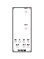
Oakley Sound Systems
Noise and Filter
Module
User’s Guide
V1.2
Tony Allgood B.Eng
Oakley Sound Systems
PENRITH
CA10 1HR
United Kingdom
e-mail: [email protected]
Introduction
The Noise and Filter module is used to generate non pitched sounds such as wind and surf
noises. It features two separate tunable filters, one high pass and one low pass, which may be
used separately to process other sources. Two types of noise output are provided. White noise
which when unfiltered sounds like gas escaping, and pink noise which sounds more like a big
waterfall. The module also gives a very low frequency output or infra-red signal. This can be
heard as a serious of random thumps when listened too, but it is actually a randomly varying
output voltage changing all the time, sometimes quickly and sometimes hardly at all.
Fascinating to watch when it controls an LED, but it comes into its own when controlling
filter cut-off on an other wise static sound.
The noise source is true analogue, a reverse biased NPN transistor. However, room is given
on the PCB for zeners and other devices should you decide to experiment.
The filters are one pole passive designs similar in topology to the later Moog modular. I have
used 47K reverse log pots as the variable element in both the high and low pass filters. These
pots have been especially made for Oakley Sound Systems by Omeg. One pole filters sound
particularly nice with audible noise, and give far more natural wind and surf sounds than the
usual 2 or 4 pole filters. They are not voltage controllable, although a one pole low pass filter
can be made from the Oakley MultiLadder module should you require this feature.
The module is designed to fit into a 2U MOTM style panel. It has only two knobs, which are
for the filters, but it does require seven sockets, hence the 2U width.
Of Pots and Power
There are just two main control pots on the PCB. These are the filter cut off frequencies. If
you use the specified pots and brackets, the PCB can be held firmly to the panel without any
additional mounting procedures. The pot spacing is on a 1.625” grid and is the same as the
vertical spacing on the MOTM modular synthesiser. The PCB has four mounting holes, one in
each corner should you require additional support which you probably won’t.
The design requires plus and minus 15V supplies. These should be adequately regulated. The
current consumption is about 20mA. Power is routed onto the PCB by a four way 0.156”
Molex type connector. Provision is made for the two ground system as used on all new
Oakley modular projects, and is compatible with the MOTM systems. See later for details.
This unit will run from a +/-12V supply with a slight reduction in dynamic range.
Circuit Description
The Noise and the two filter sections are essentially separate circuits that only share the same
power supply. Power is applied to them through the PSU 4-way Molex connector. F1 and F2,
small axial ferrite beads, provide some high frequency resistance, and along with C4, 9, 13 and
16, prevent the board from being effected by any noises on the power rails. They also help
keep any noises going the other way too.
We will consider the low pass filter section first. This is a very simple filter based around a
single capacitor, C8, and variable resistor, LPF. U1b buffers the input signal from the effects
of C8. R25 sets the input impedance, while R26 provides some protection for U1b should any
1
reasonable over voltage occur. The LPF pot with R21 and C8 combination form a simple RC
low pass filter. This one pole filter creates a roll off of around -6db/octave past its cut off
frequency. The cut off frequency is controlled by the resistance of LPF. The higher the
resistance the lower the cut off frequency. R21 sets the maximum cut-off frequency. To make
the cut-off frequency increase in a musical fashion as you turn the pot clockwise, the
resistance must vary in accordance with a reverse logarithmic law. In other words the
resistance increases fast at first then slows down as you reach the end of the turn.
The other half of U1 is another buffer or voltage follower which simply allows the voltage
across C8 to be sniffed and passed out to the output socket. If the voltage across C8 was
simply connected to the output, then output load would affect the final voltage level.
The high pass filter is a similar set up to the low pass filter, but there are a few important
differences. Firstly, the RC filter network is arranged differently. This network only allows AC
signals to pass. DC and low frequency signals are effectively blocked. The cut off frequency is
determined by the values of HPF, R5 and C19. R5 sets the upper frequency limit. A high pass
filter can be a very difficult load to drive. When set for a high cut-off frequency, R5 will be the
load on the op-amp for high frequency inputs. This may cause the output voltage of U3b to
buckle and distortion will result. So the input voltage is reduced to about a eleventh of its
value before being buffered by U3b. By reducing it to a lower value, we reduce the peak
current by that amount. The op-amp will be much happier supplying the smaller current and
our rising edges are preserved.
Of course, we must amplify our filtered signal to bring it back up to the levels required. U3a
does this job admirably, with a gain of +11.
The noise generator is Q1 and I will discuss choosing this device in more detail later in this
document. All devices produce noise of some sort. This is caused by the random movement of
charge carriers within the semiconductor (or electrons in metals) at temperatures above
absolute zero. At room temperatures, things are really shaking! Various devices can be utilised
for their noisy behaviour. Zener diodes are very noisy particularly around their reverse
breakdown voltage. Transistors also behave as zeners too, the base-emitter junction will have
a reverse breakdown potential, which we normally try to avoid like the plague. In this project
we embrace this point of the junction's V/I curve, and deliberately force the junction to
conduct the wrong way a little bit.
In normal operation, L1, a wire link, is fitted tying the base to ground. L12 is left open,
allowing the collector to float. The emitter is therefore made more positive than the base. R4
provides the reverse ‘emitter’ current. The positive end of R4 is a well decoupled (filtered)
version of the +15V supply rail. Any extraneous noise on the power supplies is not wanted
here. The base-emitter junction will effectively regulate the voltage at the emitter with respect
to ground, since it is behaving as a zener diode. However, this voltage is not that stable.
Superimposed on this ‘stable’ DC voltage is a tiny amount of random noise. Noise is a
wideband AC signal. It contains many different frequencies. In fact, white noise contains all
frequencies at the same average power. C10 allows this small AC signal through while
blocking the DC voltage. The next stage is a huge gain amplifier, with a massive amplification
of over a hundred. The noise signal is around 2mV or so, and this first stage of amplification
takes it up to around 200mV. It is very possible that DC errors at the input of the op-amp will
produce output offsets. Normally these are very small, but any offsets at the input will also be
amplified by the op-amp. C18 removes any DC from the output signal before the next gain
2
stage. This second stage of amplification should bring the noise level up to around +/-5V.
However, due to the variable nature of noise generators in general, the gain of this stage is
made variable. The LEVEL trimmer allows the user to set the output signal to a correct level
and account for any differences between noise making devices. It is important to set this level
correctly, otherwise performance of the infra red output will be impaired. The white noise
output is available from this second stage of amplification via a 1K resistor, R35.
Now, you maybe thinking, why do we need two stages to amplify? Surely, we could have just
used one big amplifier. However, although it is possible to make a single op-amp gain stage of
1000 or more, it has one major disadvantage. As an amplifier’s gain rises, we find its
bandwidth lowers accordingly. The measure of bandwidth of an amplifier is its ability to
amplify all input frequencies accordingly. A small bandwidth means a restriction in usable
frequency response. For example, it would be not very useful to have an amplifier with a gain
of 1000 but with a maximum frequency of 4KHz. By using two lower gain amplifiers in
cascade, each will have a bandwidth exceeding the audio band, so the overall frequency
response of both of our amplifiers will not effect the quality of the audible noise. Even so, I do
recommend that you use a good quality op-amp here. The LF412 is an excellent choice, and
gives less offset error than a TL072.
To make pink noise we need to create a signal that contains all frequencies as before, but with
equal power per octave. Without going into the mathematics of this, we need to filter our
white noise so that frequencies roll off at a rate of 3dB per octave. Now normal one pole RC
filters produce roll offs not exceeding -6dB/octave. So to make -3dB/octave we must get very
clever. Fortunately for me, other people have done all the difficult work and have published
their findings. This one I built many years ago from an original design in Wireless World. It
was used in an audio test set and produces a very good quality pink noise. Some synthesisers
use simpler methods, but this one sounds better to my ears so why not use it.
U4a provides some gain for the losses incurred within the RC network, and the pink noise
output is available via R36.
The infra red output is heavily inspired by the Polyfusion noise module. I have made only a
few changes to their design, since it works so well.
R2 and C5 provide further low pass filtering of the pink noise and prevent any unwanted
switching clicks from the next stage from leaking back into our pink noise output. The first
half of U5 is configured as a comparator. Pin 1, the output, will either be at around +14V or
-14V depending on the voltages present at its two inputs. Without R14, if the ‘+’ or
‘non-inverting’ input is at a higher voltage than the ‘-’ or ‘inverting input’, the opamp's output
will be positive. If it is lower, then the output is negative. But R14 provides a whole wedge of
hysteresis. This means the voltage at the inverting input must be substantially higher (or lower)
then the non-inverting input to get the op-amp to flip states. This prevents the opamp's output
from juddering when the two inputs are very close to each other. The signal we see at the
output of U5a is a rectangular one with random flips from positive to negative. We will talk
about R22 and the offset pot later.
The next stage is an interesting low pass filter arrangement. Not a traditional low pass filter, it
has two distinct cut-off frequencies at 0.2Hz and 0.04Hz. Suffice to say, its output will
respond very slowly to any changes at its input. The rapidly changing output of U1a is thus
turned into slow sluggish random movements by this ‘lag’ circuit. Further feedback is
provided by R22 which feeds back this slow moving output to the comparator. This increases
3
the randomness of the signal. I found experimenting with this value produced some
unexpected results. The Offset trimmer is provided to keep the overall output centred around
0V. Two things seem to affect the offset compensation. One; the offset of the op-amp. I have
chosen to use a 1458 as in the original design. This does not have the best offset
specifications, but does have a limited slew rate which will act as a further low pass filter and
prevent any fast edges to contaminate our clean analogue design. And two; the pink noise will
contain a certain degree of imbalance which this circuit is sensitive to. This seems to be
affected not by the DC offsets of the pink noise output amplifier but by the spectra of the
noise itself after filtering.
The output of U5b is typically around 3V peak. After further low pass filtering, the random
output is fed to an amplifier to boost up the signal to the required 10V peak for our Infra-red
output signal.
Components
Most of the parts are easily available form your local parts stockist. I use Rapid, RS
Components, Maplin and Farnell, here in the UK. In North America, companies called
Mouser, Newark and Digikey are very popular. In Germany, try Reichelt, and in Sweden you
can use Elfa. All companies have websites with their name in the URL.
The pots are Omeg Eco types with matching brackets. You could use any type you want, but
not all pots have the same pin spacing. Not a problem, of course, if you are not fitting them to
the board. The pots are 47K reverse log types. These are generally not available, so I have had
them especially made for you by Omeg. You can use ordinary linear types, but the ‘feel’ of the
pot is wrong. You cannot, contrary to some on-line reports, make a reverse log variable
resistor by using a linear pot and a resistor.
The resistors are generally ordinary types, but I would go for 1% 0.25W metal film resistors
throughout, since these are very cheap nowadays. For the UK builders, then Rapid offer 100
1% metal film resistors for less than 2p each!
For the capacitors, there are no set rules. All the electrolytics should be over 25V, except
where stated, and radially mounted. However, don’t chose too higher voltage either. The
higher the working voltage the larger in size the capacitor. A 220V capacitor will be too big to
fit on the board. 25V or 35V is a good value to go for.
The pitch spacing of the non-polar capacitors is 7.5mm (0.3”), except the low capacitance
(values in pF) ceramic which are 5mm (0.2”). For the non ceramic types I think polyester
types are fine for all decoupling, coupling and filter uses. I like the open frame Siemens
polyester layer types, because they are very compact and a rather nice colour! The PCB has
been laid out with these types in mind. Other types may not fit. They are also called poly-layer
and are available in many different working voltages. Use 63V for the big values above
1000nF. Use 100V for values between 100nF and 330nF. Use 400V for values below 100nF.
You could also use the Phillips C280 series (can you still get them?) and their modern
replacements, eg. BC-368 series. These are metalised polyester types, but again do be sure
you get low working voltages. Around 100 to 150V is best. Higher voltages are really
4
physically big. Do check the size and not just the pin spacing. In the UK, Farnell can supply all
the capacitors.
F1 and F2 are leaded ferrite beads. These are little axial components that look like little
blackened resistors. They are available from most of the mail order suppliers. Find them in the
EMC or Inductor section of the catalogues. Farnell sell them as part number: 108-267.
The two horizontal preset or trimmer resistors are just ordinary carbon types. No need to buy
the expensive cermet types. Carbon sealed units have more resistance to dust. Piher and
Spectrol make suitable types. Pin spacing is 0.2” at the base, with the wiper 0.4” away from
the base line.
Q1 is the noise transistor. I tried many different types of transistor. I found BC548s and
BC547s to be best. I have no idea why they should sound better then the BC549s or any other
I tried, but they did. I suggest buying five BC547s and try each one in turn. If you use a little
three way turned pin socket, then testing different types is simple. No need to unplug the
power supply, just plonk your different transistors in one at a time. Use your ears to hear
which ones sound the best. I found that the quieter ones tended to produce the best noise. I
linked out L1 but not L2. Some samples of transistors picked up hum with L2 omitted.
All ICs are dual in line (DIL or DIP) packages. These are generally, but not always, suffixed
with a CP or a CN in their part numbers. For example; TL072CP. Do not use SMD, SM or
surface mount packages. U2 should be a good quality dual op-amp like the LF412, you can
use a normal TL072 but your noise output will have a small offset voltage. U5 should be a
1458 since we are using its poor characteristics as a feature in this circuit. You can use the
high quality audio op-amp, the OP-275, for U1 and U3. This in theory will give you lower
noise, although chances are, you won’t notice any difference.
Finally, if you make a circuit change that makes the circuit better, do tell me so I can pass it on
to others.
5
Parts List
A quick note on European part descriptions. To prevent loss of the small ‘.’as the decimal
point, a convention of inserting the unit in its place is used. eg. 4R7 is a 4.7 ohm, 4K7 is a
4700 ohm resistor, 6n8 is a 6.8 nF capacitor.
Resistors
Resistors 1/4W, 5% or better.
22R
47R
100R
220R
330R
620R
1K
1K2
1K5
3K3
4K7
6K8
10K
18K
22K
47K
51K
100K
150K
470K
1M
R27, 28
R21
R3, 9
R5
R7
R42
R6, 26, 20, 32, 35, 36, 10, 37
R24
R31
R1
R34, 12, 17
R13
R8, 39
R14
R38
R25, 33, 11, 18
R22
R4, 2, 15
R30
R16, 29, 41
R19, 23, 40
Capacitors
22uF, 25V electrolytic
33nF, 400V polyester
100nF, 100V polyester
330nF, 100V polyester
1000nF, 63V polyester
2200nF, 63V polyester
470pF ceramic
C14, 17, 9, 4, 3
C12
C13, 16, 5, 21, 6, 7, 8, 19
C2
C10, 18, 1, 11
C20
C15
Semiconductors
TL072CP
LF412CN
1458
Q1
U1, 3, 4
U2
U5
BC547 *see text*
6
Other
4-way 0.156” Molex/MTA connector
PSU
47K reverse log single gang variable resistor LPF, HPF
Two pot brackets to suit
47K carbon trimmer (horizontal)
Offset, Level
Leaded or taped ferrite beads
F1, F2
1m of multistrand hook up wire
Two knobs
Seven decent quality jack sockets, eg. Switchcraft 112
You may well want to use sockets for the ICs and Q1. I would recommend low profile turned
pin types as these are the most reliable.
Building the Noise/Filter Module
Occasionally people have not been able to get their Oakley projects to work first time. Some
times the boards will end up back with me so that I can get them to work. To date this has
happened only four times across the whole range of Oakley PCBs. The most common error
with three of these was parts inserted into the wrong holes. Please double check every part
before you solder any part into place. Desoldering parts on a double sided board is a skill that
takes a while to master properly.
Paul Schreiber of SynthTech has won me over to water washable flux in solder. The quality of
results is remarkable. In Europe, Farnell sell Multicore’s Hydro-X, a very good value water
based product. You must wash the PCB at least once an hour while building. Wash the board
in warm water on both sides, and use a soft nail brush or washing up brush to make sure all of
the flux is removed. Make sure the board is dry before you continue to work on it or power it
up. It sounds like a bit of a hassle, but the end result is worth it. You will end up with bright
sparkling PCBs with no mess, and no fear of moisture build up which afflicts rosin based flux.
Most components can be washed in water, but do not wash a board with any trimmers,
switches or pots on it. These can be soldered in after the final wash with conventional solder
or the better new type of ‘no-clean’ solder.
All resistors should be flat against the board surface before soldering. It is a good idea to use a
‘lead bender’ to preform the leads before putting them into their places. I use my fingers to do
this job, but there are special tools available too. Once the part is in its holes, bend the leads
that stick out the bottom outwards to hold the part in place. This is called ‘cinching’. Solder
from the bottom of the board, applying the solder so that the hole is filled with enough to
spare to make a small cone around the wire lead. Don’t put too much solder on, and don’t put
too little on either. Clip the leads off with a pair of side cutters, trim level with the top of the
little cone of solder.
Once all the resistors have been soldered, check them ALL again. Make sure they are all
soldered and make sure the right values are in the right place.
7
The polylayer capacitors are little silver oblongs. Push the part into place up to the board’s
surface. Cinch and solder the leads as you would resistors.
IC sockets are to be recommended, especially if this is your first electronics project. Make
sure, if you need to wash your board, that you get water in and around these sockets.
Sometimes transistors come with the middle leg preformed away from the other two. This is
all right, the part will still fit into the board. However, if I get these parts, I tend to ‘straighten’
the legs out by squashing gently all the three of them flat with a pair of pliers. The flat surface
of the pliers parallel to the flat side of the transistor. I recommend using a 3-pin SIL socket for
the transistor. You can buy these as strips of ten turned pin sockets in one long line. Simply
cut the strip to the required length.
The ceramic capacitors are strange flat plates made from pot. Be careful with these and make
sure you have bought the ones with 0.2” lead spacing. Forcing the smaller 0.1” ones into these
larger pads will break them. Another thing to watch out for is the identification markings on
these capacitors. For example n47 is actually 470pF.
The smaller electrolytic capacitors are very often supplied with 0.1” lead spacing. My boards
have a hole spacing of 0.2”. This means that the underside of these radial capacitors will not
go flat onto the board. This is deliberate to allow the water wash to work, so don’t force the
part in too hard. The capacitors will be happy at around 0.2” above the board, with the legs
slightly splayed. Sometimes you will get electrolytic capacitors supplied with their legs
preformed for 0.2” (5mm) insertion. This is fine, just push them in until they stop. Cinch and
solder as before. Make sure you get them in the right way. Electrolytic capacitors are
polarised, and may explode if put in the wrong way. No joke. The PCB legend marks the
positive side with a ‘+’, and its the square solder pad. Most capacitors have the ‘-’ marked
with a stripe. Obviously, the side marked with a ‘-’ must go in the opposite hole to the one
marked with the ‘+’ sign. Most capacitors usually have a long lead to depict the positive end
as well.
I would make the board in the following order: resistors and ferrites, IC sockets, small
non-polar capacitors, and then electrolytic capacitors. Then the final water wash. You can
now fit the trimmers to the board with no-clean or ordinary ‘ersin’ flux solder. Do not fit the
pots at this stage. The mounting of the pots requires special attention. See the next section for
more details.
Important: Mounting the Omeg Pots
If you are using the recommended Eco pots, then they can support the PCB with specially
manufactured pot brackets. You will not normally need any further support for the board.
When constructing the board, fit the pot brackets to the pots by the nuts and washers supplied
with the pots. Now fit them into the appropriate holes in the PCB. But only solder the three
pins that connect to the pot. Do not solder the pot bracket at this stage. Now remove all the
nuts and washers from the pots and fit the board up to your front panel. Refit the washers and
tighten the nuts, but not too tight. Now carefully position the PCB at right angles to the panel.
8
The pot’s own pins will hold the PCB fairly rigid for now. Then you can solder each of the
brackets. This will give you a very strong support and not stress the pot connections.
The Omeg pots are labelled A, B or C. For example: 47KB or 100KA. Omeg uses the
European convention of A = Linear, B = logarithmic and C = Reverse logarithmic. So a 47KC
pot is a 47K reverse log pot.
The pots shafts may be cut down with a good pair of pliers, or a junior hack saw. Try not to
bend or rotate the shaft as you are cutting.
The pots are lubricated with a thick clear grease. This sometimes is visible along the screw
thread of the pot body. Try not to touch the grease as it consequently gets onto your panel
and PCB. It can be difficult to get off, although it can be removed with a little isopropyl
alcohol on cotton wool bud.
Connections
The power socket is 0.156” Molex/MTA 4-way header. Friction lock types are recommended.
This system is compatible with MOTM systems.
Power
Pin number
+15V
Module GND
Earth/PAN
-15V
1
2
3
4
The PAN pad on the PCB has been provided to allow the ground tags of the jack sockets to
be connected to the powers supply ground without using the module’s 0V supply. Earth loops
cannot occur through patch leads this way, although screening is maintained. Of course, this
can only work if all your modules follow this principle.
The ground tags of each socket can be all connected together with solid wire. A piece of
insulated wire can then be used to connect the tags to the PAN pad. Do not connect the
ground tags to any other ground.
If you have used Switchcraft 112 sockets you will see that they have three connections. One is
the earth tag. One is the signal tag which will be connected to the tip of the jack plug when it
is inserted. The third tag is the normalised tag, or NC (normally closed) tag. The NC tag is
internally connected to the signal tag when a jack is not connected. This connection is
automatically broken when you insert a jack.
Connect, with seven pieces of insulated wire, each signal tag to the respective pad on the
PCB. You should have LP-OUT, LP-IN, HP-OUT, HP-IN, WHITE, PINK and IR. I have
used slightly different names for the front panel sockets. The table below shows which is
connected to which:
9
PCB
Front Panel
LP-OUT
LP-IN
HP-OUT
HP-IN
WHITE
PINK
IR
LPF OUT
LPF IN
HPF OUT
HPF IN
WHITE
PINK
INFRA RED
Leave the NC tags unconnected on the LPF OUT, HPF OUT and INFRA-RED sockets.
Connect the NC tag on the HPF IN socket to the NC tag of the WHITE socket. This will
connect the high pass filter to the white noise output when no jacks are put into either the
WHITE or HPF IN sockets. Connect the NC tag on the LPF IN socket to the NC tag of the
PINK socket. This will connect the low pass filter to the pink noise output when no jacks are
put into either the PINK or LPF IN sockets. This is called normalising. It saves on patch leads
for the most useful and common connections.
At the rear of this user guide I have included a 1:1 drawing of the suggested front panel
layout. Actual panels can be obtained from Schaeffer-Apparatebau of Berlin, Germany. The
cost is about £25 per panel. All you need to do is e-mail the fpd file that is found on the
MultiLadder web page on my site to Schaeffer, and they do the rest. The panel is black with
white engraved legending. The panel itself is made from 2.5mm thick anodised aluminium.
The fpd panel can be edited with the Frontplatten Designer program available on the Schaeffer
web site.
Setting Up
There are just two trimmers to be set before you are finished. The LEVEL trimmer allows you
to trim the output of both the white and pink noise. Monitor the white noise with an
oscilloscope. Adjust LEVEL until the peak signal is around +/-6V. If you don’t have a ‘scope,
then just adjust it until you get the roughly the same volume as one as your modular’s VCOs.
The OFFSET control can be set in a variety of ways. What we need to do is to set the average
value of the IR output to zero. One way is to use a scope, on very slow sweeps, and try and
get equal swings either side of zero volts. Another way, is to use your MultiMix output LEDs.
Adjust until you get equal ‘green’ and ‘red’ times. If you have just a voltmeter, you can hook
up the IR output to it, and adjust OFFSET until the maximum positive swing equals the
maximum negative swing. Beware, the infra red output is very random and very slow. Be
prepared to spend around a minute in waiting for the output to settle to the new OFFSET
adjustment.
If you find you cannot get the IR output to get away from either supply rail, then please
re-adjust the LEVEL trimmer to give a higher level of noise to the IR circuitry. Too little pink
noise will mean you haven’t got enough signal to flip the comparator U5a.
10
Final Comments
I hope you enjoy building and using the Oakley Noise/Filter Module. If you cannot get your
project to work, do get in touch with me, and I will see what I can do. Alternatively try the
Oakley Synths mailing list on Yahoo-Groups. Sometimes, it can be the simplest things that can
lay out a project.
I do offer a get-you-working service. Send your completed non-working module back to me
and I will fix it for you at a rate of £10 per hour. You will also have to pay for the postage
both ways, and for any replacement parts needed. Make sure you wrap it carefully and include
a full description of the fault. If you are sending the item from outside the EU, then be sure to
say on the customs label ‘item being sent for repair only’.
Occasionally, there may be an error in the parts list. I have checked the documentation again
and again, but experience has taught me to expect some little error to creep past. The
schematic is always the correct version, since the parts list is taken from the schematic. So if
there is any problem, use the schematic as the guide. If you do notice any error, please get in
touch. You will be credited on the ‘Updates and Mods’ page, and you may get a free PCB if
its a real howler.
Please further any comments and questions back to me, your suggestions really do count. If
you have any suggestions for new projects, feel free to contact me. You can e-mail, write or
telephone me. If you telephone then it is best to do this on Monday to Friday, between 9 am
and 6 pm, British time.
Last but not least, can I say a big thank you to all of you who helped and inspired me. For this
module in particular, I would like to thank Steve Thomas for initial design testing, Steve
Ridley for inspiration and Tony Clark for having the Moog Modular schematics on line.
Thanks also to all those nice people on the synth-diy and MOTM mailing lists.
Tony Allgood. November 2002
Version. 1.2
Formatted on Lotus Word Pro
No part of this document may be copied by whatever means without my permission.
11