1
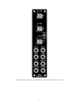
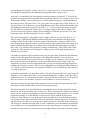
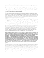
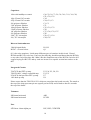
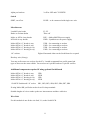
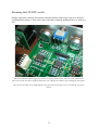
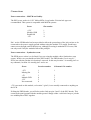
Oakley Sound Systems
5U Oakley Modular Series
Noise Generator and Dual Filter
PCB Issue 4
Builder’s Guide
V4.0.3
Tony Allgood
Oakley Sound Systems
CARLISLE
United Kingdom
The suggested panel layout for the MOTM format of the Oakley Noise/Filter module.
2
Introduction
This is the Project Builder's Guide for issue 4 of the Noise/Filter 5U module from Oakley
Sound.
This document contains a basic introduction to the board, a description of the schematic, a full
parts list for the components needed to populate the boards, and a list of the various
interconnections.
For the User Manual, which contains an overview of the operation of the unit, the history of
the various board issues, and all the calibration procedures, please visit the main project
webpage at:
http://www.oakleysound.com/noise.htm
For general information regarding where to get parts and suggested part numbers please see
our useful Parts Guide at the project webpage or http://www.oakleysound.com/parts.pdf.
For general information on how to build our modules, including circuit board population,
mounting front panel components and making up board interconnects please see our generic
Construction Guide at the project webpage or http://www.oakleysound.com/construct.pdf.
3
The Noise/Filter issue 4 PCB
The issue 4 PCB mounted behind a 1U MOTM format Schaeffer panel in natural finish. Note the use of
the Sock8 board to make easy the complicated socket wiring.
I have provided space for the three main control pots on the PCB. If you use the specified
16mm Alpha pots and matching brackets, the PCB can be held firmly to the panel without any
additional mounting procedures. The pot spacing is 1.625” and is the same as the vertical
spacing on the MOTM modular synthesiser and most of our other modules.
The design requires plus and minus 15V supplies. The power supply should be adequately
regulated. The current consumption is about 30mA for each rail. Power is routed onto the
PCB by a four way 0.156” MTA156 type connector or the special five way Synthesizers.com
MTA100 header. You could, of course, wire up the board by soldering on wires directly. The
four pins that are used on the four way header are +15V, ground, earth/panel ground, -15V.
The earth/panel connection allows you to connect the metal front panel to the power supply’s
ground without it sharing the modules’ ground line. More about this later.
The PCB has four mounting holes for M3 bolts, one near each corner. These are not required
if you are using the two 16mm pot brackets. The board size is 101 mm (high) x 116 mm
(deep).
The board has been laid out to accept connection to our Sock8 socket board. This small board
speeds up the wiring of the four sockets and reduces the chances of mistakes.
4
Circuit Description
The noise and the two filter sections are essentially separate circuits that only share the same
power supply. The power supply section is shown on page 2 of the schematics. Power is
applied to the board through the PSU, a 4-way MTA156 / Molex 0.156” connector, or PWR
a special five way MTA header. F1 and F2, small axial ferrite beads, provide some high
frequency resistance, and along with C24 and C25 prevent the board from being effected by
any noises on the power rails. They also help keep any unwanted noises going the other way
too.
Additional decoupling is also provided elsewhere on the board by eight other capacitors
shown above right of the power inlet circuitry. These capacitors keep the power supply clean
of noise, and provide a reservoir for the little bursts of current that the circuit takes in normal
operation.
Two grounds are provided, one for the circuit itself, and one for the earthing of the jack
sockets on the front panel.
The power supplies to each of the op-amp ICs are shown separately from the main schematics
to avoid cluttering the diagram.
Still on page 2 we will consider the two filter sections. These are actually identical circuits
even though one is used as a low pass filter and the other as a high pass filter. The only real
difference between the two circuits is from where in the circuit we take the output.
The filters are made from a circuit described as a state variable filter or SVF for short. Unlike
the Oakley SVF module this filter is only one pole. Only one active part actually controls the
cut-off frequency and not two like in the SVF module. The part that gives us control over the
cut-off point is an audio voltage controlled amplifier (VCA) made by the THAT Corporation,
part number 2180. These parts are normally used in gain control, but it is a simple matter to
allow them to work in filters too.
The precise mathematics of the one pole filter is beyond the scope of this User Guide, but a
more detailed account of its operation can be found in the THAT Design Note number 130
found on their website. www.thatcorp.com
Those of you who have built our VC-ADSR may recognise the circuitry involved in the one
pole filter as I used a similar circuit in the ADSR core. To explain how the circuit works we
will look at the low pass filter section in more detail. Two basic components make up the filter
circuitry. One is a differential amplifier, this is U5b (pins 5, 6, 7). The other is a more complex
circuit called an integrator, this is based around the VCA and U5a (pins 1, 2, 3).
An integrator is a charge storage device. Think of it like a bucket for electricity. It can be filled
up and drained at will, and the voltage output of the integrator is analogous to the amount of
water in our bucket. The speed at which the bucket can be drained or filled is controlled by the
VCA. To be more specific the VCA actually creates a current output that allows C2 to be
charged up by the op-amp U5. The VCA’s current output is dependant on two things; one, the
5
current through R15 and the voltage at the VCA’s control pin, pin 3. In fact, the current
through R15 is multiplied by the mathematical logarithm of the voltage at pin 3.
Now pin 3 is controlled by the front panel pot and any connected external CV. This way the
speed of the integrator can be manually and automatically adjusted. The voltage at pin 3 varies
from around +290mV (lowest frequency) to -90mV (highest frequency) when controlled by
the front pot alone. The gain of the VCA goes up the more negative the voltage. However, if
the gain of the VCA is allowed to go too high, then the whole filter will become unstable and
an oscillation is seen at the output of U6b (pins 5, 6, 7). The actions of the resistor network
R7, R4 and R3 in conjunction with D2 act as a voltage clamp on the control voltage. This
prevents excessively negative voltages from reaching pin 3 and thus prevent the VCA from
being opened too far and causing the circuit to oscillate.
The current through R15 is dependant on the voltage output of op-amp, U5b (pins 5, 6, 7).
This op-amp is a differential amplifier and this particular circuit subtracts the input signal,
coming into the circuit via R31, with the output of the integrator, coming in via R23. This
now means that the integrator has to respond to both the input signal and its own output. The
upshot of this is that the integrator’s output will try and follow the input signal, but only as
fast as the VCA will allow that capacitor to charge and discharge. This produces the classic
‘lag circuit’. This slowness of the integrator’s output to react to the input signal gives the
desired low-pass effect.
The high pass response from a similar circuit to the low pass filter. Indeed the only difference
is that we take the signal from the output of the differential amplifier. You may want to
consider this yourself in more detail. However, a simple way of looking at it is to consider that
this output is formed by the difference in the input signal and low pass output. If the low
frequencies are taken out of the input signal, then you are left with only the high frequencies,
and thus, the high pass response. There is one small addition to the high pass filter and that is
C14. This low value capacitance, in conjunction with R39, acts to stabilise the filter output at
very high frequencies.
It should be noted that a one pole filter creates a roll off of around -6db/octave past its cut off
frequency. So the effect of the filter is less pronounced than ones of higher orders like Moog
Ladders and so on. It is not possible to make a one pole filter have gain at its cut-off point, so
there is no chance of a resonance control or self-oscillation at its cut-off frequency.
Now let us look to the first page of the schematic. This covers the noise generator, the pink
noise filter and the unstable chaos of the infra-red output circuity.
The noise generator is Q1 and I will discuss choosing this device in more detail later in this
document. All devices produce noise of some sort. This is caused by the random movement of
charge carriers within a semiconductor or metal at temperatures above absolute zero. At room
temperatures things are really shaking! Various devices can be utilised for their noisy
behaviour. Zener diodes are very noisy particularly around their reverse breakdown voltage
but, because of their glass enclosures, tend to be affected by ambient light levels. Transistors
can also behave as zeners too when the base-emitter junction is connected up the wrong way.
The voltage in which the zenering affect is seen is called the reverse breakdown potential and
we normally try to avoid getting anywhere near it since it produces poor results in amplifiers
and other circuits. However, in this project we lovingly embrace this point of the base-emitter
6
junction's V/I curve and deliberately force the junction to conduct the wrong way just a little
bit.
The emitter is made more positive than the base via R40 and the resistor thus provides the
reverse ‘emitter’ current. The positive end of R40 is a well decoupled (filtered) version of the
+15V supply rail. Any extraneous noise on the power supplies is not wanted here and R38,
C13 and C16 filter the power supply accordingly.
The base-emitter junction of the transistor will effectively regulate the voltage at the emitter
with respect to ground, since it is behaving as a zener diode. However, this voltage is not that
stable. Superimposed on this ‘stable’ DC voltage is a tiny amount of random noise. Noise is a
wideband AC signal. It contains many different frequencies. In fact, white noise contains all
frequencies (within reason) at the same average power.
C17 allows this small AC signal through while blocking the larger DC voltage. The next stage
is a high gain amplifier, with a massive amplification of over a hundred. The noise signal is
around 2mV or so, and this first stage of amplification takes it up to around 200mV. It is very
possible that DC errors at the input of the op-amp U7a will produce output offsets. Normally
these are very small, but any offsets at the input will also be amplified by the op-amp. C26
removes any DC from the output signal before the next gain stage.
The second stage of amplification should bring the noise level up to around +/-5V. However,
due to the variable nature of noise generators in general, the gain of this stage is made
variable. The LEVEL trimmer allows the user to set the output signal to a correct level and
account for any differences between noise making devices. It is important to set this level
correctly, otherwise performance of the infra red output will be impaired. The white noise
output is available from this second stage of amplification via a 1K resistor, R62.
Now, you maybe thinking, why do we need two stages to amplify? Surely, we could have just
used one big amplifier. Although it is possible to make a single op-amp gain stage of 1000 or
more, it has one major disadvantage: As an amplifier’s gain rises, we find its bandwidth lowers
accordingly. The bandwidth of an amplifier is its ability to amplify all input frequencies
accordingly. A small bandwidth means a restriction in usable frequency response. For example,
it would be not very useful here to have an amplifier with a gain of 1000 but with a maximum
frequency of 4kHz. By using two lower gain amplifiers in cascade, each will have a bandwidth
exceeding the audio band, so the overall frequency response of both of our amplifiers will not
effect the quality of the audible noise. Even so, I do recommend that you use a good quality
fast op-amp here. The LF412 is an excellent choice, and also gives less offset error than a
TL072.
To make pink noise we need to create a signal that contains all frequencies as before, but this
time with equal power per octave. Without going into the mathematics of this, we need to
filter our white noise so that frequencies roll off at a rate of 3dB per octave. Now, normal one
pole RC filters produce roll off not exceeding -6dB/octave. So to make -3dB/octave we must
get very clever. Fortunately for me, other people have done all the difficult work and have
published their findings. This one I built many years ago from an original design in Wireless
World. It was used in an audio test set and produces a very good quality pink noise. Some
synthesisers use simpler methods, but this one sounds better to my ears so why not use it.
7
U9b (pins 5, 6, 7) provides some gain for the losses incurred within the RC network, and the
pink noise output is available via R52.
The infra red output is heavily inspired by the Polyfusion noise module. I have made only a
few changes to their design since it works so well.
R43 and C15 provide further low pass filtering of the pink noise and prevent any unwanted
switching clicks from the next stage from leaking back into our pink noise output. The first
half of U8a (pins 1, 2, 3) is configured as a comparator. Pin 1, the output, will either be at
around +14V or -14V depending on the voltages present at its two inputs. Without R49, if the
‘+’ or ‘non-inverting’ input is at a higher voltage than the ‘-’ or ‘inverting input’, the opamp's
output will be positive. If it is lower, then the output is negative. But R49 provides hysteresis.
This means the voltage at the inverting input must be substantially larger then the noninverting input to get the op-amp to flip states. This prevents the op-amp's output from
juddering when the two inputs are very close to each other. The signal we see at the output of
U8a is a rectangular one with random flips from positive to negative. We will talk about R41
and the ADJ pot later.
The next op-amp stage is an interesting low pass filter arrangement. This is not a traditional
low pass filter as it has two distinct cut-off frequencies at 0.2Hz and 0.04Hz. Suffice to say, its
output will respond very slowly to any changes at its input. The rapidly changing output of
U8a is thus turned into slow sluggish random movements by this ‘lag’ circuit. Furthermore,
feedback is provided by R47 which feeds back this slow moving output to the comparator.
This increases the randomness of the signal. I found experimenting with the value of R47
produced some unexpected results.
The ADJ trimmer adjusts the offset voltage applied to the comparator circuit. It is provided to
keep the overall output centred around 0V. Two things seem to affect the amount of offset
required. One; the offset specifications of the op-amp. I have chosen to use a 1458 as in the
original design. This does not have the best offset specifications, but does have a limited slew
rate (the speed the op-amp’s output stages can swing from one voltage to another) which will
act as a further low pass filter and prevent any fast edges to contaminate our clean analogue
design. And two; the pink noise will contain a certain degree of imbalance which this circuit is
sensitive to. This seems to be affected not by the DC offsets of the pink noise output amplifier
but by the spectra of the noise itself after filtering.
The output of U8b is typically around 5V to 10V peak. The value of which seems to depend
on the quality of the noise source. After further low pass filtering with R50 and C19, the
random output is fed to another op-amp to buffer the signal before the final output.
8
Issue 4 Noise/Filter Parts List
For general information regarding where to get parts and suggested part numbers please see
our useful Parts Guide at the project webpage or http://www.oakleysound.com/parts.pdf.
The components are grouped into values, the order of the component names is of no particular
consequence.
A quick note on European part descriptions. R is shorthand for ohm. K is shorthand for
kilohm. R is shorthand for ohm. So 22R is 22 ohm, 1K5 is 1,500 ohms or 1.5 kilohm. For
capacitors: 1uF = one microfarad = 1000nF = one thousand nanofarad.
To prevent loss of the small ‘.’ as the decimal point, a convention of inserting the unit in its
place is used. eg. 4R7 is a 4.7 ohm, 4K7 is a 4700 ohm resistor, 6n8 is a 6.8 nF capacitor.
Resistors
Resistors 1/4W, 5% or better.
22R
100R
220R
330R
620R
1K
1K2
1K5
2K2
3K3
4K7
5K1
6K8
10K
14K
18K
22K
36K
47K
51K
100K
150K
470K
1M
10M
R63, R48
R38, R68
R3, R2
R67
R50
R35, R44, R62, R51, R52, R39, R1, R4, R65
R45
R59
R36, R7
R64
R58
R9, R5, R8, R6
R61
R11, R30, R12, R41, R16
R26, R17
R49, R15, R13
R28
R10, R37
R18, R33, R21, R55, R32, R29, R14, R31, R34,
R22, R23, R27, R25
R47
R46, R43, R40, R24
R56
R60, R53, R42
R54, R57, R66
R19, R20
9
Capacitors
100n axial multilayer ceramic
100p 2.5mm C0G ceramic
470p 2.5mm C0G ceramic
2n2 polyester film box
33nF polyester film box
100n polyester film box
330nF polyester film box
1uF polyester film box
2u2 polyester film box
22uF, 35V electrolytic
2u2, 35V electrolytic
C4, C5, C6, C7, C8, C9, C10, C11, C16, C20,
C21, C22, C23
C14
C34, C12, C3
C1, C2
C31
C15, C19, C33
C30
C17, C26, C32, C27
C28
C29, C13, C18
C24, C25
Discrete Semiconductors
1N4148 signal diode
BC547 - see note below
D1, D2
Q1
Q1 is the noise transistor. I tried many different types of transistor in this circuit. I found
BC548s and BC547s to be best. I have no idea why they should sound better than the BC549s
or any other I tried, but they did. I didn’t like the sound from any of the BC550s I tried at all. I
suggest buying five BC547s and try each one in turn. See separate section later on how to do
this.
Integrated Circuits
TL072CP dual FET op-amp
THAT2180LC voltage controlled amp
LF412CN dual precision FET op-amp
1458 dual op-amp
U3, U4, U5, U6, U9
U1, U2
U7
U8
Please ensure that the THAT2180 VCA chips are seated into the board correctly. The notch at
the top of the chip represents pin one (square pad on PCB) and is fitted so that it is towards
the top of the board.
Trimmers
20K 6mm horizontal
50K 6mm horizontal
ADJ
LEVEL
Pots
47K linear 16mm Alpha pot
LPF, HPF, CVDEPTH
10
Alpha pot brackets
2 off for LPF and CV DEPTH
Switch
SPDT, on-off-on
LP/HP - to be connected with single core wire
Miscellaneous
Leaded Ferrite beads
Knobs to fit 6mm shafts
F1, F2
Three off
Molex or MTA 4 way header
MTA100 6-way header
PSU – Oakley/MOTM power supply
PWR – Synthesizers.com power supply
Molex/MTA 0.1” header 6-way
Molex/MTA 0.1” header 8-way
Molex/MTA 0.1” housing 6-way
Molex/MTA 0.1” housing 8-way
UPR – for connecting to sockets
LWR – for connecting to sockets
UPR – for connecting to sockets
LWR – for connecting to sockets
1/4” sockets
Eight off mounted either on the Sock8 board or on panel
Hook up wire (26awg).
You may well want to use sockets for the ICs. I would recommend low profile turned pin
types as these are the most reliable. You need seven 8-pin DIL and two 8-pin SIL sockets.
Additional components required if using optional Sock8 board
Molex/MTA 0.1” header 6-way
Molex/MTA 0.1” header 8-way
Molex/MTA 0.1” housing 6-way
Molex/MTA 0.1” housing 8-way
UPR
LWR
UPR
LWR
112APCX Switchcraft 1/4” socket
SK1, SK2, SK3, SK4, SK5, SK6, SK7, SK8
If using Molex KK you'll also need at least 28 crimp terminals.
Suitable lengths of wire to make up the two interconnects and three cable ties.
Wire Link
For this module do not fit the wire link, L1, on the Sock8 PCB.
11
Mounting the LPF/HPF switch
Simply connect the switch to the board so that the switch's solder tangs connect to the PCB
pad immediately below it. This can be done with either insulated multistrand wire or solid core
wire.
This is an APEM on-off-on toggle switch. Note the spring washer of the switch is on the inside of the
panel. The switch can then be tightened from the rear reducing the chances of scratching the front panel.
Note also the position of the THAT2180LC chip. The notch on the chip's case is towards the top of the
board.
12
Connections
Power connections – MOTM and Oakley
The PSU power socket is 0.156” Molex/MTA 4-way header. Friction lock types are
recommended. This system is compatible with MOTM systems.
Power
Pin number
+15V
Module GND
Earth/PAN
-15V
1
2
3
4
Pin 1 on the LWR header has been provided to allow the ground tags of the jack sockets to be
connected to the powers supply ground without using the module’s 0V supply. Earth loops
cannot occur through patch leads this way, although screening is maintained. Of course, this
can only work if all your modules follow this principle.
Power connections – Synthesizers.com
The PWR power socket is to be fitted if you are using the module with a Synthesizers.com
system. In this case you should not fit the PSU header. The PWR header is a six way 0.1”
MTA, but with the pin that is in location 2 removed. In this way location 3 is actually pin 2 on
my schematic, location 4 is actually pin 5 and so on.
Power
Location number
Schematic Pin number
+15V
Missing Pin
+5V
Module GND
-15V
Not connected
1
2
3
4
5
6
1
2
3
4
5
+5V is not used on this module, so location 3 (pin 2) is not actually connected to anything on
the PCB.
If fitting the PWR header, you will also need to link out pins 2 and 3 of the PSU header. This
connects the panel ground with the module ground. Simply solder a solid wire hoop to join the
two middle pads of PSU together.
13
Building the Noise/Filter module using the Sock8 board
This is the simplest way of connecting all the sockets to the main board. The Sock8 board
should be populated in the way described in our construction guide found on the project
webpage. There are only two headers, UPR (for upper) which is six way, and LWR (for
lower) which is eight way. Both headers are fitted to the bottom side of the board.
You need to make up two interconnects. The six way one should be made so that it is 80mm
long. The eight way should be made to be 130mm.
The prototype Noise/Filter module showing the detail of the board to board interconnects. Here I have
used the Molex KK 0.1” system to connect the Sock8 to the main PCB.
14
Building the Noise/Filter module by wiring the sockets manually
If you have bought Switchcraft 112A sockets you will see that they have three connections.
One is the earth or ground tag. One is the signal tag which will be connected to the tip of the
jack plug when it is inserted. The third tag is the normalised tag, or NC (normally closed) tag.
The NC tag is internally connected to the signal tag when a jack is not connected. This
connection is automatically broken when you insert a jack.
Once fitted to the front panel the ground tags of each socket can be all connected together
with solid wire. I use 0.91mm diameter tinned copper wire for this job. It is nice and stiff, so
retains its shape. A single piece of insulated wire can then be used to connect those connected
earth tags to pin 1 of LWR. Pin 1 is the square solder pad.
All the other connections are shown in the tables below:
UPPER
Pin
Pad name
Socket Connection
Lug Type
Pin 1
Pin 2
Pin 3
Pin 4
Pin 5
Pin 6
LP-OUT
Connect to LPF OUT
Not connected
Not connected
Connect to HPF OUT
Connect to HPF IN
Connect to HPF IN
Signal lug
HP-OUT
WHITE-OUT
HP-IN
Signal lug
NC lug
Signal lug
LOWER
Pin
Pad name
Socket Connection
Lug Type
Pin 1
Pin 2
Pin 3
Pin 4
Pin 5
Pin 6
Pin 7
Pin 8
Panel ground
PINK-OUT
WHITE-OUT
IR-OUT
PINK-OUT
LP-IN
module ground
CV-IN
Connects to all sockets
Connect to PINK NOISE
Connect to WHITE NOISE
Connect to INFRA RED
Connect to LPF IN
Connect to LPF IN
Connect to CV IN
Connect to CV IN
Ground lugs via wire frame
Signal lug
Signal lug
Signal lug
NC lug
Signal lug
NC lug
Signal lug
15
Testing, testing, 1, 2, 3...
Apply power to the unit making sure you are applying the power correctly. Reversal of the
power’s polarity will usually destroy all the op-amps in an instant.
If you can monitor current, check that it doesn’t exceed 30mA or so from each rail. If you
can’t check current directly, check with your finger that none of the op-amps or VCAs are
getting warm.
You will now need a audio VCO and an LFO of some sort. Some form of audio monitoring
will be needed too so you can hear the output of the Noise/Filter module.
Connect the audio output of the VCO to the IN socket of the low pass filter. A sawtooth
wave in the bass registers is best. Listen to the audio output from the OUT socket. Adjusting
the LPF FREQ pot you should notice the sound getting duller as you turn the pot anticlockwise. This should sound like simple filtering, which is exactly what it is. At the maximum
point the output of the filter should sound more or less the same as the input signal. The
minimum point should just let through a dull rumble.
Set up an LFO so that its frequency is at around 1Hz. Now attach the LFO’s sawtooth output
to the CV IN socket. Set the LPF FREQ pot to its middle position, click the switch to the
middle position and rotate the CV DEPTH pot to beyond the central position. The cut-off
frequency should now be being modulated with the LFO. Check that the minimum modulation
occurs in the middle position of the CV DEPTH pot. You should have a ‘dow, dow, dow’
sound with the pot in the ‘+’ position, and ‘yit, yit, yit’ in the ‘-’ position. Click the switch into
the HPF position and the modulation should stop.
Now we need to test the high pass filter. Repeat the above section to check whether the high
pass filter is working. This time as you increase the HPF FREQ pot the output should get
‘fizzier’ and lose all of its bass end. Check also the CV input for the high pass filter. Again,
check that the modulation is at its minimum when the CV DEPTH pot is in the middle
position.
If this is all correct you almost certainly have a working module. However, we can’t check the
noise section yet because we haven’t inserted the noisy transistor.
If you have found a fault, then the usual course of action is to try and find the wrong
component. It’ll usually be a wrong value resistor, like swapping a 100K resistor for a 100R.
Other things to check are the connections between the socket and main board. Make sure too
that your headers have been fitted the right way.
16
Selecting your transistor and final setting up
As soon as you know the filters are working the next thing you need to do once you have built
up your module is to fit the noise transistor. You should have a few BC547, BC548 or BC549
NPN transistors ready. You can try each one in turn into the Q1 position on the PCB and see
which one sounds best.
Connect your power supply up to the module, and attach your monitoring amplifier to the
white noise socket. Keep the volume levels fairly low, because as you remove and add the
transistors it will thump a bit.
For the each transistor match the flat side of the device with that shown on the PCB legend.
Push the transistor into place but don’t push too far. For now there is no need to solder it in
place. If you don't like the sound of just pushing the transistor into the unsoldered holes in the
board you can use a turned pin socket. I buy these as 20 or 32 way SIL sockets and then
simply cut them down to size.
Q1 fitted into a three way section of a SIL turned pin socket.
Sometimes transistors come with the middle leg preformed away from the other two. This is
all right, the part will still fit into the board. However, if I get these parts, I tend to ‘straighten’
the legs out by squashing gently all the three of them flat with a pair of pliers. The flat surface
of the pliers’ jaws is parallel to the flat side of the transistor.
Once the transistor is inserted the circuit will take time to settle. After a few seconds you
should hear the tell tale hiss of a reverse biased transistor junction.
You are listening out for the best quality noise sound. Don’t get too concerned with overall
loudness as some of the quieter ones can actually sound better. You may need to alter the
17
LEVEL trimmer so that you get an even tone. If the LEVEL trimmer is set to high then the
noise pre-amps may clip and that won’t sound very nice either. There’s no hard and fast rules
here, just enjoy the process. If you have a ‘scope then you can monitor what’s going on by
looking at the white noise output. You’ll find that the best noise sources are the ones with an
even voltage swing about 0V. Bad sounding devices tend to have more positive voltage
spikes. Once you have found a nice sounding transistor, switch off and solder the little chap in.
There are just two trimmers to be set before you are finished. As we have seen the LEVEL
trimmer allows you to trim the output of the white noise and also the pink noise. Monitor the
white noise with an oscilloscope. Adjust LEVEL until the peak signal is around +/-6V. If you
don’t have a ‘scope, then just adjust it until you get the roughly the same volume as one as
your modular’s VCOs.
The ADJ control can be set in a variety of ways. What we need to do is to set the average
value of the IR output to zero. One way is to use a ‘scope and try and get equal swings either
side of zero volts. Another way, is to use your Multimix output LEDs. Adjust until you get
equal ‘green’ and ‘red’ times. Beware, the infra red output is very random and very slow. Be
prepared to spend around a minute in waiting for the output to settle to the new ADJ position.
If you find you cannot get the IR output to get away from either supply rail, then please readjust the LEVEL trimmer to give a higher level of noise to the IR circuitry. Too little pink
noise will mean you haven’t got enough signal to flip the comparator U8a.
18
Final Comments
If you have any problems, an excellent source of support is the Oakley Sound Forum at
Muffwiggler.com. Paul Darlow and I are on this group, as well as many other users and
builders of Oakley modules.
If you can't get your project to work, then Oakley Sound Systems are able to offer a 'get you
working' service. If you wish to take up this service please e-mail me, Tony Allgood, at my
contact e-mail address found on the website. I can service either fully populated PCBs or
whole modules. You will be charged for all postage costs, any parts used and my time at
25GBP per hour. Most faults can be found and fixed within one hour, and I normally return
modules within a week. The minimum charge is 25GBP plus return postage costs.
If you have a comment about this builder's guide, or have a found a mistake in it, then please
do let me know. But please do not contact me or Paul Darlow directly with questions about
sourcing components or general fault finding. Honestly, we would love to help but we do not
have the time to help everyone individually by e-mail.
Last but not least, can I say a big thank you to all of you who helped and inspired me. Thanks
especially to all those nice people on the Synth-diy and Analogue Heaven mailing lists and
those at Muffwiggler.com.
Tony Allgood at Oakley Sound
Cumbria, UK
© November 2010 – updated March 2013
No part of this document may be copied by whatever means without my permission.
19