1
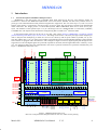
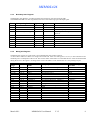
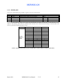
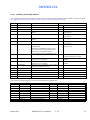
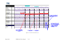
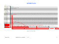
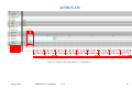
MIMOSA26 User Manual (Preliminary version) Institut Pluridisciplinaire Hubert Curien IN2P3-CNRS / UdS Strasbourg – France CEA Saclay DAPNIA/SEDI March 2011 MIMOSA26 User Manual V.1.5 1 MIMOSA26 Document history Version Date Description 1.0 1.1 1.2 1.3 1.4 1.5 Based on MIMOSA16 Version Different Minor Correction Different Minor Correction Correction description end of frame Scan discri mode Version for end users November 2008 February 2009 March 2009 1 April 2009 2 Juny 2009 March 2011 MIMOSA26 chip Version Date 1.0 March 2011 Description Comments Submitted November AMS 035 Opto Version, 576 x 1152 pixels Preliminary version 2008 MIMOSA26 User Manual V.1.5 2 MIMOSA26 1 2 3 4 5 Introduction ...................................................................................................................................... 4 1.1 General description of EUDET CMOS pixel sensor ............................................................... 4 1.2 DIGITAL PART (SUZE)......................................................................................................... 5 Control Interface .............................................................................................................................. 6 2.1 Introduction .............................................................................................................................. 6 2.2 JTAG Instruction Set................................................................................................................ 6 2.3 JTAG Register Set.................................................................................................................... 7 2.3.1 Instruction Register .......................................................................................................... 7 2.3.2 DEV_ID Register ............................................................................................................. 7 2.3.3 Boundary Scan Register ................................................................................................... 8 2.3.4 BIAS_DAC Register ........................................................................................................ 8 2.3.5 LINEPAT0_REG Register............................................................................................... 9 2.3.6 DIS_DISCRI Register ...................................................................................................... 9 2.3.7 SEQUENCER_PIX_REG Register................................................................................ 10 2.3.8 CONTROL_PIX_REG Register .................................................................................... 12 2.3.9 LINEPAT1_REG Register............................................................................................. 13 2.3.10 SEQUENCER_SUZE_REG .......................................................................................... 14 2.3.11 HEADER_REG.............................................................................................................. 15 2.3.12 CONTROL_SUZE_REG Register................................................................................. 16 2.3.13 RO_MODE0 Register .................................................................................................... 17 2.3.14 RO_MODE1 Register .................................................................................................... 17 2.3.15 BYPASS Register .......................................................................................................... 18 Running MIMOSA26..................................................................................................................... 19 3.1 After reset............................................................................................................................... 19 3.2 Biasing MIMOSA26 .............................................................................................................. 20 3.3 Setting the Readout Configuration Registers ......................................................................... 22 3.4 Readout................................................................................................................................... 22 3.5 Analogue and digital Data Format ......................................................................................... 23 3.5.1 Normal mode data format .............................................................................................. 23 3.5.2 Test mode ....................................................................................................................... 28 3.6 MIMOSA26 Chronograms..................................................................................................... 33 3.6.1 Normal Readout ............................................................................................................. 33 3.6.2 Readout synchronisation ................................................................................................ 34 3.6.3 Main Signal Specifications............................................................................................. 42 Index of the figures ........................................................................................................................ 50 Glossary, Abbreviations and acronyms tables. .............................................................................. 51 March 2011 MIMOSA26 User Manual V.1.5 3 MIMOSA26 1 Introduction 1.1 General description of EUDET CMOS pixel sensor MIMOSA26 is the final sensor chip of EUDET JRA1 beam telescope for the ILC vertex detector studies. Its architecture is based on the MIMOSA22 (Monolithic Active Pixel Sensor (MAPS) with fast binary readout) and on a prototype circuit named SUZE01 which performs integrated zero suppression. The size of the chip is 13,7 mm x 21,5 mm and the sensor matrix is composed by 576x1152 pixels of 18.4 µm pitch. The pixel design is based on self biased diode radtol architecture. The design process is Austria Mikrosysteme AMS-C35B4/OPTO which uses 4 metal- and 2 polylayers. The thickness of the epitaxial layer is 14 µm. The design tools are CADENCE DFII 5.1 with DIVA, ASSURA, CALIBRE rules. The chip has been submitted in an Engineering Run via CMP on 19th December 2008. In the EUDET beam telescope, the hit rate is less than 5 hits/ image. However, MIMOSA26 is suited for charged particles detecting with density up to 106 hits /cm²/s. The design of the sensor is driven by the high readout frequency in order to keep the track multiplicity per frame at a low level. It is done by read out pixel columns in parallel, row by row. The chip readout time is 115.2 µs. Each pixel includes an amplification and Correlated Double Sampling (CDS) and each end of column is equipped with a discriminator. After analogue to digital conversion, digital signals pass through the zero suppression circuits. The digital signals are processed in parallel on 18 banks, then arranged and stored in a memory row by row. Two memories banks have been implemented in the sensor to perform read and write operations simultaneously (see Figure 1 : MIMOSA26 functional view). vdda_test OutAnaDriver<0> OutAnaDriver<7> Analog Supplies Digital Supplies gnd! vdd! vdda ! gnd ! v_ clp! ...... Logical scan pix array AnaDriver<7:0> 0 … Pixel Array (576x1152) Column Column63 … … S15 Column 0 … … Bank17 Column63 S1 Column 0 S0 Column Column-63 63 Bank1 Column Column- 00 Rows Bank0 … … 575 Rows Address Register<0:575> Multiplexer Row Pix Test Pads 1151 Columns VDiscriClp … A/D A/D VDiscriRef1A VDiscriRef1B A/D A/D A/D … A/D A/D LINEPAT1_REG Register<0:1151> Priority Look-Ahead algorithm (PLA) PLA (0) … (N states) A/D … PLA (1) (N states) Bias Generators BIAS DAC Register<151:0> CONTROL_PIX_REG<39:0> BSR RoMode0 RoMode1 IDCODE SEQUENCER_PIX_REG<127:0> <9:0> <7:0> <7:0> Memory Management (Memory with M states storage and serial transmission) Power Supplies PLL SRAM 600x16 SRAM 600x16 SRAM 600x16 SRAM 600x16 LVDS Signals CLKPLL_n CLKPLL_p Fifoinitok WR selpimp Memory 2 SYNCRO Memory 1 aMem<15:0> CS Test1Pad Test2Pad Test3Pad Test4Pad ReadOut Controller CMOS Signals Analogue Signals SEQUENCER_SUZE_REG<159:0> START CLKC CLKL_n CLKL_p SPEAK CLKA MKA TCK RSTB TMS TDI JTAG Controller TDO TEMP (N states) Selection of M states among 18xN states for each row Current Refence CONTROL_SUZE_REG<47:0> Temp Probe PLA (17) MKD_p MKD_n CLKD_p CLKD_n DO0_p DO0_n DO1_p DO1_n Itest Vtest A/D A/D LINEPAT0_REG Register<0:1151> Ctrl Pixel + Discri VDiscriRef2C VDiscriRef2D … A/D A/D DIS_DISCRI Register<0:1151> VDiscriRef1C VDiscriRef1D VDiscriRef2A VDiscriRef2B … (1152 Discriminators) Figure 1 : MIMOSA26 functional view Does not correspond to the floorplan neither for the core, neither for the pad ring March 2011 MIMOSA26 User Manual V.1.5 4 MIMOSA26 1.2 DIGITAL PART (SUZE) The following synoptic shows the implementation of SUZE into MIMOSA 26. Figure 2: top view implementation of SUZE in MIMOSA 26 This digital part manages sequentially each line for the whole frame composed of 576 lines of 1152 columns. The main sequencer gives to the structure the address of lines and all synchronisations and controls signals. A JTAG controller brings the configuration information. (Table of configurations registers) A test structure simulates a matrix of pixel in order to check the functions of SUZE. These debugging tests are reserved for the IPHC/IRFU group. March 2011 MIMOSA26 User Manual V.1.5 5 MIMOSA26 2 Control Interface 2.1 Introduction The control interface of MIMOSA26 complies with Boundary Scan, JTAG, IEEE 1149.1 Rev1999 standard. It allows the access to the internal registers of the chip like the bias Register and the different registers control. On Power-On -Reset, an internal reset for the control interface is generated. The finite state machine of the Test Access Port (TAP) of the controller enters in the Test-Logic-Reset state and the ID register is selected. MIMOSA26 has been designed in order to be fully adjustable via the control interface. Nevertheless several voltages level can be set either via the control interface or via a pad. 2.2 JTAG Instruction Set The Instruction Register of the JTAG controller is loaded with the code of the desired operation to perform or with the code of the desired data register to access. Instruction 5 Bit Code16 Selected Register Notes EXTEST 01 BSR JTAG mandatory instruction HIGHZ 02 BYPASS JTAG mandatory instruction INTEST 03 BSR JTAG mandatory instruction CLAMP 04 BYPASS JTAG mandatory instruction SAMPLE_PRELOAD 05 BSR JTAG mandatory instruction ID_CODE 0E DEV_ID register User instruction BIAS_GEN 0F BIAS_DAC DATAREG0 LINE0_PATTERN_REG 10 LINE0PAT_REG DATAREG1 DIS_DISCRI 11 DIS_DISCRI DATAREG2 SEQ_PIX_REG 12 SEQUENCER_PIX_REG DATAREG3 CTRL_PIX_REG 13 CONTROLER_PIX_REG DATAREG4 LINE1_PATTERN_REG 14 LINE1PAT_REG DATAREG5 SEQ_SUZE_REG 15 SEQUENCER_SUZE_REG DATAREG6 HEADER_TRAILER_REG 16 HEADER_REG DATAREG7 CTRL_SUZE_REG 17 CONTROLER_SUZE_REG DATAREG8 CTRL_8b10b_REG0 18 CONTROLER_8b10b_REG0 DATAREG9 CTRL_8b10b_REG1 19 CONTROLER_8b10b_REG1 DATAREG10 NU1 1A DATAREG11 NU2 1B DATAREG12 NU3 1C DATAREG13 RO_MODE1 1D ReadOut Mode 1 DATAREG14 RO_MODE0 1E ReadOut Mode 0 DATAREG15 BYPASS 1F BYPASS JTAG mandatory instruction (1) Instruction codes implemented but not the corresponding registers. To be fixed in the next version. March 2011 MIMOSA26 User Manual V.1.5 6 2.3 JTAG Register Set JTAG registers are implemented with a Capture/Shift register and an Update register. JTAG standard imposes that the last significant bit of a register is downloaded/shifted first. Register Name Size Access Notes INSTRUCTION REG DEV_ID BSR BIAS_DAC LINE0PAT_REG DIS_DISCRI SEQUENCER_PIX_REG CONTROLER_PIX_REG LINE1PAT_REG SEQUENCER_SUZE_REG HEADER_REG CONTROLER_SUZE_REG CONTROLER_8b10b_REG0 CONTROLER_8b10b_REG1 NU1…..NU3 RO_MODE1 RO_MODE0 BYPASS 5 32 10 152 1152 1152 128 40 1152 160 64 48 144 312 0 8 8 1 R/W R Only R/W R/W R/W R/W R/W R/W R/W R/W R/W R/W R/W R Only Instruction Register 2.3.1 Boundary scan register Previous value shifted out during write Previous value shifted out during write Previous value shifted out during write Previous value shifted out during write Previous value shifted out during write Previous value shifted out during write Previous value shifted out during write Previous value shifted out during write Previous value shifted out during write Previous value shifted out during write Not implemented. For future use Previous value shifted out during write Previous value shifted out during write R/W R/W R Only Instruction Register The Instruction register is a part of the Test Access Port Controller defined by the IEEE 1149.1 standard. The Instruction register of MIMOSA26 is 5 bits long. On reset, it is set with the ID_CODE instruction. When it is read the 2 last significant bits are set with the markers specified by the standard, the remaining bits contain the current instruction. X 2.3.2 X X 1 0 DEV_ID Register The Device Identification register is implemented. It is 32 bits long and has fixed value hardwired into the chip. When selected by the ID_CODE instruction or after the fixed value is shifted via TDO, the JTAG serial output of the chip. MIMOSA26 ID_CODE register value is M26 + 0x4D323601. Bit # Bit Name Purpose Default value Code16 31-0 ID_CODE Device Identification register 4D323601 March 2011 MIMOSA26 User Manual V.1.5 ASCII ‘M’ ‘2’ ‘6’ <SOH> HEX 4D 32 36 01 7 MIMOSA26 2.3.3 Boundary Scan Register The Boundary Scan Register, according with the Jtag instructions, tests and set the IO pads. The MIMOSA26 BSR is 10 bits long and allows the test of the following input and outputs pads. Bit # Corresponding Pad Type Signal Notes 9 8 7 6 SPEAK CLKC START LVDS CLKL_n/CLKP_p Input Input Input Input SPEAK CkCMOS START ClkLvds Active Readout Marker & Clock CMOS Clock Readout : Input synchronisation Resulting CMOS signal after LVDS Receiver 5 4 3 2 1 0 No Used No Used No Used CLKA Test2Pad Test1Pad Ouput Ouput Ouput CLKA Tst2Pad Tst1Pad Readout Analogue Clock Readout Test Pad 2 Readout Test Pad 1 2.3.4 BIAS_DAC Register The BIAS_DAC register is 152 bit wide; it sets simultaneously the 19 DAC registers. As show bellow these 8-bit DACs set voltage and current bias. After reset the register is set to 0, a value which fixes the minimum power consumption of the circuit. The current values of the DACs are read while the new values are downloaded during the access to the register. An image of the value of each DAC can be measured on its corresponding test pad. Bit range DAC # DAC Internal Name DAC purpose Corresponding Test Pad 151-144 143-136 135-128 127-120 119-105 111-104 103-96 95-88 87-73 79-72 71-64 63-56 55-48 47-40 39-32 31-24 23-16 15-8 7-0 DAC18 DAC17 DAC16 DAC15 DAC14 DAC13 DAC12 DAC11 DAC10 DAC9 DAC8 DAC7 DAC6 DAC5 DAC4 DAC3 DAC2 DAC1 DAC0 IKIMO IPIX IDIS2 IDIS1 IVDREF2 IVDREF1A IVDREF1B IVDREF1C IVDREF1D IAnaBUF IVTST2 IVTST1 ILVDS ILVDSTX ID2PWRS ID1PWRS IBufBias IPwrSWBias ICLPDISC External circuit monitoring Pixel source follower bias Discriminator bias 2 Discriminator bias 1 Discriminator Reference 2 Discriminator Reference 1 (Bank A) Discriminator Reference 1 (Bank B) Discriminator Reference 1 (Bank C) Discriminator Reference 1 (Bank D) Analogue Buffer bias Test Level, emulates a pixel output IDEM LVDS PAD bias LVDS PAD bias Discriminator bias 2 (mode low consp.) Discriminator bias 1 (mode low consp.) Ref&Tst Buffer bias Discriminator Power Pulse bias Discriminator Clamping bias Vtest IPIX IDIS2 IDIS1 VDREF2 VDREF1A VDREF1B VDREF1C VDREF1D IAnaBUF March 2011 MIMOSA26 User Manual V.1.5 ILVDS ILVDSTX BUFBIAS PWRSWBIAS DISCLP 8 MIMOSA26 2.3.5 LINEPAT0_REG Register The LINEPAT0_REG register is 1152 bits large. The purpose of this register is to emulate discriminators outputs rows in En_LineMarker and Pattern_Only modes. When Pattern_Only is active, the values stored in the pixel matrix are ignored and the value of LINEPAT0_REG is sent to the output. This is a test mode which emulates the (digital) pixel response with the contents programmed into the LINEPAT0_REG register in order to verify the digital processing. The pattern is alternated with the contents of the LINEPAT1_REG. In the En_LineMarker mode, it adds two rows at the end of matrix for a readout chip and the LINEPATL0_REG register is read to emulate the discriminators outputs of these two supplementary rows. After the initialisation phase (reset), this register is preset to 0. Bit # Bit Name 0-1151 LinePatL0Reg Purpose Emulate discriminators rows (1) Example of pattern used in simulation. Basic configuration value Code16 AAAAAA_AAAAAAAA_AAAAAAAA_AAAAAA AA(1) In MIMOSA26, the LinePatL0Reg <0> is on the left hand side while LinePatL0Reg <1151> is on the right hand side. 2.3.6 DIS_DISCRI Register The DIS_DISCRI register is 1152 bits large. The purpose of this register is to disable the discriminator on a specific column if it is noisy, by gating Latch signal and setting the output discriminator at 0. The default value of the DIS_DISCRI register is 0; it means that all discriminators are activated. Setting a bit to 1 disables the corresponding discriminator. In MIMOSA26, the DisableLatch<0> is on the left hand side while DisableLatch<1151> is on the right hand side. 0 (Lsb) 1151 (Msb) DisableLatch<0> March 2011 DisableLatch<1151> MIMOSA26 User Manual V.1.5 9 MIMOSA26 2.3.7 SEQUENCER_PIX_REG Register The SEQUENCER_PIX_REG registers are 128 bits large; this register contains all parameters to generate readout pixel and discriminator sequence. Bit # Bit Name Purpose Basic configuration Signal Name value Code16 127-112 111-96 95-80 79-64 63-48 47-32 31-0 DataRdPix DataRst1 DataClp DataCalib DataRdDsc DataLatch DataPwrOn Connect pixel output to common column Set reference voltage for diode Set reference voltage for clamping Sample after clamping Sample before clamping Latch state of the discriminator Activate power supply for pixel FFFF 0040 01C0 3C00 001C 6000 FFFFFFFF Slct_Row_Int Rst Clamp Calib Read Latch Pwr_On (1) Example: Generation of Latch Signal Msb Lsb 15 14 13 12 11 10 9 8 7 6 5 4 3 2 1 0 0 1 1 0 0 0 0 0 0 0 0 0 0 0 0 0 Figure 3 : Example: Generation of Latch Signal Related timing with fclk=80 MHz (Read, Calib, Latch signals are used by the column readout circuitry). 200 ns Figure 4 : Simulation timing diagram for signals of SEQUENCER_PIX_REG (1) This is readout sequence of the pixel and discriminator for 2 successive rows of matrix. In the waveform, the indexation of internal signal vectors is reversed compared with the MIMOSA26 functional view (for example, the signal Pwr_On[575] corresponds to the row at the top of matrix). March 2011 MIMOSA26 User Manual V.1.5 10 MIMOSA26 Figure 5 : Simulation timing diagram for signals of SEQUENCER_PIX_REG (2) March 2011 MIMOSA26 User Manual V.1.5 11 MIMOSA26 2.3.8 CONTROL_PIX_REG Register The CONTROL_PIX_REG registers are 40 bits large; they allow setting parameters of the readout controller. These registers are reserved for sensor's debugging by the IPHC/IRFU group. A end user has to respect to the default values. Bit # Bit Name Purpose Basic configuration value Code16 39-36 35-33 32-30 29-20 NU SelPad1 SelPad2 RowMkLast 0 0 0 023F 19-10 RowMkd 9-0 RowMka Reserved, Not Used Selection bit of Test1Pad Selection bit of Test2Pad Row number of the frame. It depends of readout mode. When the En_HalfMatrx mode is active, the value is 0x013F otherwise 0x023F. When the En_LineMarker mode is active, add two rows at the end of matrix. Selection parameter of row for digital marker (MK_Test_D) Selection parameter of row for analogue marker (MK_Test_A) March 2011 MIMOSA26 User Manual 0 0 V.1.5 MK_Test_A signal MK_Test_D signal Normal mode, the number of row matrix is 576. Digital marker place is first row of matrix during the readout analogue marker place is first row of matrix during the readout 12 MIMOSA26 2.3.9 LINEPAT1_REG Register The LINEPAT1_REG register is 1152 bits large. The purpose of this register is to emulate discriminators outputs rows in En_LineMarker and Pattern_Only modes. When Pattern_Only is active, the values stored in the pixel matrix are ignored and the value of LINEPAT1_REG is sent to the output. This is a test mode which emulates the (digital) pixel response with the contents programmed into the LINEPAT0_REG register in order to verify the digital processing. The pattern is alternated with the contents of the LINEPAT1_REG. In the En_LineMarker mode, it adds two rows at the end of matrix for a readout chip and the LINEPATL1_REG register is read to emulate the discriminators outputs of these two supplementary rows. Bit # Bit Name 0-1151 LinePatL1Reg Purpose Emulate discriminators rows (1) Example of pattern used in simulation. Basic configuration value Code16 555555_55555555_55555555_55555555(1) In MIMOSA26, the LinePatL1Reg <0> is on the left hand side while LinePatL1Reg <1151> is on the right hand side. With Line1_PAT_REG together these two signals will form the elements of the simulated frame given to SUZE part. Figure 6 : Generation of the test frame pattern March 2011 MIMOSA26 User Manual V.1.5 13 MIMOSA26 2.3.10 SEQUENCER_SUZE_REG The SEQUENCER_SUZE_REG registers are 160 bits large; this register contains all parameters to generate readout zero suppression (SUZE) sequence. Bit # Bit Name Purpose Signal Name Basic configuration value Code16 159-144 dckreadpixmux 0555 CkReadPixMux 143-128 dcklatchhit 3000 CkLatch 127-112 dcklatchhitmem 1000 CkLatchMem 111-96 dckmemlatch 0555 CkMemLatch 95-80 dckreadpix5ns 82aa CkReadPix5ns 79-64 dckreadpix 0555 CkReadPix 63-48 dstartingline e001 debutligne 47-32 drstline 6000 RstLine 31-16 drstpix 0555 RstPix 15-0 drstframe Sample signal for multiplexer after Priority look ahead Synchronization signal every line for Priority Look Ahead Synchronization signal every line for memory management Synchronization signal every line for Priority Look Ahead Synchronization signal 6 times every line for memory management shifted of 5 ns compared with CkReadpix Synchronization signal 6 times every line for memory management Synchronization signal every line for memory management Synchronization signal every line for all SUZE part Reset signal 6 times every line for Priority Look Ahead Reset frame signal for memory management 2000 RstTrame Related timing with fclk=80 MHz (Theses signals are used by zero suppression circuit). Figure 7 : Simulation timing diagram for signals of SEQUENCER_SUZE_REG March 2011 MIMOSA26 User Manual V.1.5 14 MIMOSA26 2.3.11 HEADER_REG The register called Header_Reg includes 4 registers of 16 bits as shown below. Bit # Bit Name Purpose Basic configuration value 63-48 47-32 31-16 15-0 header0 header1 trailer0 trailer1 Synchronisation header for serial output0 Synchronisation header for serial output1 Synchronisation trailer serial output0 Synchronisation trailer serial output1 5555 5555 AAAA AAAA For both modes according to the register DUALCHANNEL the header and the trailer of each data frame can be different. The following table shows the possible Header and the Trailer which ensure the unicity in the data frame. The unicity is guaranteed without the Frame counter. Bits Possible Header or Trailer 0-3 (in hexa) 1 2 3 4 5 6 7 8 A B C D E F 4-14 X X X X X X X X X X X X X X 15 1 1 1 1 1 1 1 1 1 1 1 1 1 1 Table 1: possible Header and Trailer for mode 0 and 1 to ensure unicity (or mode 2 with 32 bits) March 2011 MIMOSA26 User Manual V.1.5 15 MIMOSA26 2.3.12 CONTROL_SUZE_REG Register The CONTROL_SUZE_REG registers are 48 bits large; they allow setting parameters of the readout controller for SUZE. We suggest an end user to only use default values except for data stream output parameters Bit # Bit Name Purpose Basic configuration value Code16 47-46 45-43 42-40 39 NU SelPad4 SelPad3 En_auto_scan_discri 0 0 0 0 38 En_scan Reserved, Not Used Selection bit of Test4Pad Selection bit of Test3Pad Enable mode scan test discriminators, all matrix Enable mode scan test 37 Test_after_mux 0 36 entestdatadisc Enable mode scan test for multiplexer of SUZE Enable mode scan test discriminators 35-26 RowLastSuze 023F 25-16 ScanLineTst Row number of the frame. It depends of readout mode. When the En_HalfMatrx mode is active, the value is 0x013F otherwise 0x023F. When the En_LineMarker mode is active, add two rows at the end of matrix. Selection parameter of row for digital 15 dualchannelout 0 14 clkrateout 13 jsupinitmem 12 11-9 8-6 5-3 2-0 disckgmodgate cfgwr cfgdata cfgcs cfgadr Determines the data stream on the channel or in one channel Determines the clock rate of the outputs channel or in one channel Authorizes the initialization test of the FIFO or not. High level active. Discriminator switched ON/Off Cf. cfg multiplexors configuration Idem Idem Idem 0 0 0 0 debutligne cklatchhit Debugging reserved for IPHC Cf. §3.5.2.2 Debugging reserved for IPHC Cf. §3.5.2.2 Debugging reserved for IPHC Debugging reserved for IPHC Cf. §3.5.2.2 Normal mode, the number of row matrix is 576. Digital marker place is first row of matrix during the readout Cf. explanation of the data stream output Cf. explanation of the data stream output 1 0 0 0 0 0 The internal following signals can be selected with SelPad3 and SelPad4 bits. SelPad3 Tst3Pad Purpose SelPad4 Tst4Pad 0 1 2 3 4 5 6 7 cklatchhit cklatchhitmem ckmemlatch ckreadpix ckreadpix5ns ckreadpixmux latch Clkdiv8 Cf; sequencer_SUZE_reg “ “ “ “ “ “ “ “ “ “ “ “ Main clock divided by 8 0 1 2 3 4 5 6 7 debutligne rstline debuttrame rsttrame rst_frame rstpix synmux seqrstb March 2011 MIMOSA26 User Manual V.1.5 Purpose 16 MIMOSA26 Data stream output clkrateout dualchannelout Config. Description 0 0 0 The data are sampled by the frequency output clock 40 MHz. 0 1 1 1 0 2 1 1 3 The data are sampled by the frequency output clock 80 MHz. The data stream is output on data line 1 only, Data line 0 stay to low level The data stream is output on both data line 0 and 1. The data stream is output on data line 1 only, Data line 0 stay to low level The data stream is output on both data line 0 and 1. 2.3.13 RO_MODE0 Register The RO_MODE0 registers are 8 bits large; they allow the user to select specific digital mode of the chip. Bit # 7 Bit Name EnVDiscriTestDigital Purpose Enable the internal injection of VTEST 6 En_HalfMatrx Set the row shift register to 320 in place of 576 bits. 5 4 DisLVDS En_LineMarker 3 MODE_SPEAK 2 Pattern_Only 1 En_ExtStart 0 JTAG_Start Disable LVDS and active clock CMOS. Add two rows at the end of matrix for a chip Readout: The LINEPAT_REG register is selected to emulate discriminators outputs. For analogue outputs, the 2 Test Levels, VTEST1 and VTEST2 are selected which emulate a pixel output. Select Marker signal or Readout Clock for digital and analogue data (MK_CLKA and MK_CLKD pads) Test Mode: Select LINEPAT_REG to emulate discriminators outputs Enable external START input synchronisation (1) Enable Jtag START input synchronisation (2) Basic configuration value 0 External injection of VTEST 0 Normal mode, 576 row shift register selected 0 LVDS selected 0 Normal mode 0 Marker signal active 0 Normal mode 0 Normal mode 0 (1) The minimum wide of asynchronous external START signal is 500 ns, and this signal is active at high level. (2) When En_ExtStart is disabled, it’s possible to generate internal START by accessing JTAG_Start bit. JTAG_Start signal is realized by three JTAG access: First step, this bit is set to 0, second step it is set to 1, and at last it is set to 0. 2.3.14 RO_MODE1 Register The RO_MODE1 registers are 8 bits large; they allow selecting specific analogue mode of the chip. Bit # Bit Name Purpose Basic configuration value 7 6 5 4 3 2 startframe EnTestAnalog EnAnaDriverScan DisBufRef EnPll EnDiscriAOP Reinitializes the frame counter to 0. Enable analog output Enable scan pixel mode Disable the internal reference Enable internal PLL Enable the Power pulse Amplifier 0 0 0 0 0 0 March 2011 MIMOSA26 User Manual V.1.5 Select Internal Buffer Normal mode 17 MIMOSA26 1 0 EnDiscriPwrSave EnTestDiscri Enable the discri power pulse mode Enable the discri. test mode 0 0 Normal mode Normal mode 2.3.15 BYPASS Register The Bypass register consists of a single bit scan register. It is selected when its code is loaded in the Instruction register, during some actions on the BSR and when the Instruction register contains an undefined instruction. March 2011 MIMOSA26 User Manual V.1.5 18 MIMOSA26 3 Running MIMOSA26 The following steps describe how to operate MIMOSA26 3.1 After reset On RSTB active low signal: All BIAS registers are set to the default value, i.e. 0 DIS_DISC is set to 0, i.e. all columns are selected RO_MODE0 is set to 0 RO_MODE1 is set to 0 CONTROL_PIX_REG is set to 0 CONTROL_SUZE_REG is set to 0 SEQUENCER_PIX_REG is set to 0 SEQUENCER_SUZE_REG is set to 0 HEADER_REG is set to 0 LINE0PAT_REG is set to 0 LINE1PAT_REG is set to 0 JTAG state machine is in the Test-Logic-Reset state JTAG ID_CODE instruction is selected Then the bias register has to be loaded. The same for the RO_MODE0, RO_MODE1, CONTROL_PIX_REG, CONTROL_SUZE_REG, SEQUENCER_PIX_REG, LINE0PAT_REG, LINE1PAT_REG, HEADER_REG and DIS_DISC registers if the running conditions differ from defaults. Finally the readout can be performed either in normal mode or in test mode. March 2011 MIMOSA26 User Manual V.1.5 19 MIMOSA26 3.2 Biasing MIMOSA26 The BIAS_DAC register has to be loaded before operating MIMOSA26. The 19 DACs constituting this register are built with the same 8 bits DAC current generator which has a 1 µA resolution. Specific interfaces like current mirror for current sourcing or sinking and resistors for voltages, customise each bias output. The following table shows the downloaded codes which set the nominal bias. Internal DAC Name Simulation Resolution Code16 - DacInternal Output Code10 current-µA value 64-100 100 1V 10 mV VKIMO 32-50 50 50 µA 1 µA IPIX 20-32 32 5 µA 156 nA IDIS2 20-32 32 10 µA 312 nA IDIS1 76-118 118 1.18 V 10 mV VDISREF2 80-128 128 1.18 V 250 µV VDISREF1A 80-128 128 1.18 V 250 µV VDISREF1B 80-128 128 1.18 V 250 µV VDISREF1C 80-128 128 1.18 V 250 µV VDISREF1D 32-50 50 500 µA 10 µA IAnaBUF 76-118 118 1.18 V 10 mV VTEST2 80-128 128 1.18 V 250 µV VTEST1 20-32 32 7 µA 218 nA ILVDS 28-40 40 40 µA 1 µA ILVDSTX A-10 10 100 nA 10 nA IDis2PwrS A-10 10 100 nA 10 nA IDis1PwrS A-10 10 10 µA 1 µA IBufBias A-10 10 10 µA 1 µA IPwrSWBias 64-100 100 2.1 V 10 mV VDISCLP (1) Referenced with respect to IVDREF2. The threshold voltage of (Vref1=Vref2+Vth). March 2011 MIMOSA26 User Manual Range Experimental Code16 Code10 From 0 up to 2.55 V From 0 up to 255 µA From 0 up to 255 µA From 0 up to 255 µA From 1 up to 1.5 V From -32 up to 32 mV (1) From -32 up to 32 mV (1) From -32 up to 32 mV (1) From -32 up to 32 mV (1) From 0 up to 255 µA From 1 up to 1.5 V From -32 up to 32 mV (1) From 0 up to 255 µA From 0 up to 255 µA From 0 up to 255 µA From 0 up to 255 µA From 0 up to 255 µA From 0 up to 255 µA From 1.2 up to 3.2 V the discriminators Vth is defined as Vref1-Vref2 V.1.5 20 MIMOSA26 Figure 8: Bias synthetic block diagram March 2011 MIMOSA26 User Manual V.1.5 21 MIMOSA26 3.3 Setting the Readout Configuration Registers If the desired operating mode does not correspond to the default one, set LINEPAT0_REG, SEQUENCER_PIX_REG, CONTROL_PIX_REG, LINEPAT1_REG, SEQUENCER_SUZE_REG, HEADER_REG, CONTROL_SUZE_REG, RO_MODE0, RO_MODE1 registers following the §2.3.5, §2.3.7, §2.3.8, §2.3.9, §2.3.10, §2.3.11, §2.3.12, §2.3.13, §2.3.14. 3.4 Readout 3.4.1 Signal protocol After JTAG registers have been loaded, the readout of MIMOSA26 can be initialized with following signal protocol: Start readout clock (CLKL); Set SPEAK signal to 0; Set START signal to 1 during 500 ns (minimum).The internal reset is created after 2 rising edge of CLKL. After this reset, CkDiv16 (input clock with 1/16 ratio) is generated; The readout controller starts at the first falling edge of CkDiv16 after START set to 0. Signal markers allow the readout monitoring and the data outputs (analogue and digital) sampling: CLKA, CLKD and MKD are running when readout controller starts. CLKA is signal which is generated by logic OR between Read and Calib signals. When SPEAK signal is active, marker of synchronisation for analogue outputs is generated on MKA pad. Marker of synchronisation for digital outputs is generated on MKD pad, this signal is shifted of 4 rising edge of CLKL to debuttrame signal, MKD is set during 4 clock’s rising edges of CLKD and is not depended of signal SPEAK. 3.4.2 Successive frames and resynchronisation Successive pixel frames are read until the readout clock is stopped. A frame resynchronisation can be performed at any time by setting up the “START” token again. Previous frame Current frame Next frame Last frame LastRow SPEAK LastRow LastRow MKA ( MODE_ SPEAK=’0') MKA ( MODE_ SPEAK=’1') Read Calib Figure 9: Successive frames and resynchronization timing diagram SPEAK signal allows to generate markers signals which are used by DAQ. When SPEAK signal is set to 1 during the current frame, analogue marker appears on MKA pad during next frame. In the MODE_SPEAK=’0’, the MKA marker corresponds to last row of the frame. In the MODE_SPEAK=’1’, MKA signal corresponds to a sampling clock for analogue outputs data (same as CLKA) which starts at the first row of frame. When SPEAK signal is set to 0, MKA is set to 0. March 2011 MIMOSA26 User Manual V.1.5 22 MIMOSA26 3.5 Analogue and digital Data Format Two Types of signal can be generated on analogue outputs: Normal pixel signal Test signal In concern to digital outputs, two types of signal can be generated: Digital pixel signal after zero suppression processing Test discriminator and test zero suppression logic: Digital pixel signal by discriminator Test pattern used by zero suppression logic, read to LINEPAT_REG register MIMOSA26 uses the pads at the bottom edge for all its operations, whatever is collecting data from the pixels (using the pixels and the discriminators) or in test mode (reproducing at the outputs the pre-programmed patterns). All the digital signals for the synchronization and the programming of the chip are necessary for successful operation. Analog outputs located on the top edge of the chip are not used for the normal operations. The main purpose is the characterization of the pixels or the checking of the dead pixels. Therefore measurements on these pads deal with normal pixel signals as well as test signals (but they still require the synchronization and the markers) and it is activated on demand by setting to 1 the EnTestAnalog bit in the RO_MODE1 register. 3.5.1 Normal mode data format 3.5.1.1 Introduction This chip is the combination between MIMOSA 22 and SUZE 1. The inputs are the main clock, the reset and an input synchronization (START) for initializing the readout control. The output data of the last frame are sparsified and are sent during the acquisition of the current frame. The outputs serializing the data of SUZE 1 with the same number of pads of MIMOSA 22 include: A clock (CLKD), Two data lines (DO0 and DO1), and A marker (MKD). The serial output has four configuration modes according to 2 registers clkrate and dualchannel (see §2.3.12). as shown later. All the words (16 bits) are read from the LSB to the MSB. The different part of the data frame is the Header, Frame counter, Data Length, States/Line, State, and Trailer. The 2 words elements (ie Header, Frame counter, Data Length and Trailer) are divided into two parts. For instance, the header includes Header0 (corresponds to the 16 bits LSB) and header1 (corresponds to the 16 bits MSB). The Header, the Trailer and the Marker signal could be used together to detect lose of synchronization. 3.5.1.2 The Clock The clock is always present even if the data transmission is finished. Its rate depends on the clkrate register. 80 MHz or 40 MHz 3.5.1.3 Marker The marker (MKD) is available in all modes. The Marker signal is set during 4 clock’s rising edges and may also be used to detect the beginning of a data transmission. 3.5.1.4 Header trailer The Header and the Trailer are composed of 2 x 16 bits (header0 –header1),(trailer0 –trailer1) and allows detecting the beginning and the end of a data transmission. The Header and the Trailer are totally configurable by JTAG (the header and the trailer of each data frame can be different). The Table 1 (see §2.3.11) shows the possible Header and Trailer values. 3.5.1.5 Frame counter Frame counter is the number of frame since the chip was reset. This counter (32 bits) is reset to 0 when the maximum is reached (FFFFFFFF in hexadecimal) and continues to work. The Frame counter when separated into 2 words is given in the Data line 0 (Frame counter 0) with the LSB’s and in the Data line 1 (Frame counter 1) the MSB’s. March 2011 MIMOSA26 User Manual V.1.5 23 MIMOSA26 3.5.1.6 Data Length Data Length is the number of word of 16 bits of the useful data. Data Length is written on 32 bits. In the case of one data line, the number of words is repeated 2 times. The sum determines the real value of the useful data In the case of no hit during a frame, Data Length 0 and Data Length 1 are set to zero. 3.5.1.7 Useful data (States/Line, State) The useful data is the daisy chain of States/Line and States. The maximum number of the useful data bits sends during one frame is (570 words of 16 bits) 9120. In some rare case, the number of data generated by the suppression of zeros exceeds the maximum bits capable to be sent, thus the data frame will be truncated. The data are periodically sent at the beginning of each new frame, and the number of bits which could be sent between two headers is variable and depends on the numbers of the words recorded during the last frame. Each data lines have the same number of bits. Consequently Data Length 0 and Data Length 1 are the same. States/Line and State have exactly the same meaning whatever the selected mode. The number of words sent in a data frame depends of the number of hits. If the number of words for the two data lines is odd the last Status of Data line 1 is false. This operating way allows having the same number of bits (Data length) in the both DO0 and DO1 in every case. During the treatment of the line, we consider the first word of 16 bits like a status line(n) following of n states, and this operation is done several times until the end of the communication. We propose to detect this false state (case number of words odd) to count the number of words (of 16 bits) for each new line. If a last word considered like a status line is the last word counted as the total number of words Data Length, then it is a false word that to be ignored. In the following example the data length is exactly the same but the total number of words can be odd or even. States/Line contains the address of the line which is hit, the number of State for this line (i.e. a number between one and nine), and an overflow flag. The following table describes the signification of the bits in Status/Line word. 0 1 2 Bit(0-3) number of States 3 4 5 Status/ line 6 7 8 9 10 11 12 13 14 Bit(0-10) The address of the line 15 OVF Table 2 : Description of States/line word State contains the address of the first hit pixel and the number of successive hit pixels as shown on the table below. State 0 1 2 3 4 5 6 7 8 9 10 11 12 13 14 15 Bit(0-1) Bit(0-10) number of hit pixels the address of the column not used Table 3 : Description of State word March 2011 MIMOSA26 User Manual V.1.5 24 MIMOSA26 The table below resumes the maximum length of the output frame according to the selected mode. Clk rate out Dual channel out Config. Out Header Cptframe Header0 & Header1 Header0 Header1 Cptframe0 & Cptframe1 Cptframe0 Cptframe1 Header0 & Header1 Header0 Header1 Cptframe0 & Cptframe1 Cptframe0 Cptframe1 D00 0 0 0 0 1 1 1 0 2 1 1 3 D01 D00 D01 D00 D01 D00 D01 Datalength Number of useful data (words of 16 bits) Unused = 0 Datalength0 278 & Datalength1 Datalength0 282 Datalength1 282 Unused = 0 Datalength0 564 & Datalength1 Datalength0 570 Datalength1 570 trailer Total words Nb of empty words Trailer0 & Trailer1 Trailer0 Trailer1 286 2 286 286 2 2 Trailer0 & Trailer1 Trailer0 Trailer1 572 4 574 574 2 2 The figure below describes the format of data send by MIMOSA 26 in the one data line mode. Figure 10: Detail of the beginning of a data frame March 2011 MIMOSA26 User Manual V.1.5 25 MIMOSA26 Mode 40 MHz Mono channel (clkrate= 0 and dualchannel = 0) The maximum number of data generated by the suppression of zeros is (278 x 16) bits for the output. After this overflow, the data frame will be truncated. This mode 0 giving too little information is irrelevant but can be used as test only. Figure 11: Format of the output Data of MIMOSA 26 Mono Channel and 40 MHz Mode 40 MHz Dual channel (clkrate= 0 and dualchannel = 1) The maximum number of data generated by the suppression of zeros is (282 x 16) bits for each output. After this overflow, the data frame will be truncated. Figure 12: Format of the output Data of MIMOSA 26 Dual Channel and 40 MHz March 2011 MIMOSA26 User Manual V.1.5 26 MIMOSA26 Mode 80 MHz Mono channel (clkrate= 1 and dualchannel = 0) The maximum number of data generated by the suppression of zeros is (564 x 16) bits for the output. After this overflow, the data frame will be truncated. Figure 13: Format of the output Data of MIMOSA 26 Mono Channel and 80 MHz Mode 80 MHz dualchannel (clkrate= 1 and dualchannel = 1) The maximum number of data generated by the suppression of zeros is (570 x 16) bits for each output. After this overflow, the data frame will be truncated. Figure 14: Format of the output data: Mode 80 MHz dual channel March 2011 MIMOSA26 User Manual V.1.5 27 3.5.2 Test mode 3.5.2.1 Analogue outputs, Normal pixel signal When EnTestAnalog bit is set to ‘1’ in the RO_MODE1 register, the rightmost 8 columns of pixels are connected to the analog outputs via a voltage follower and the signal is available on the pads. To start the analog test, the EnAnaDriverScan must be set to ‘1’ in the RO_MODE1. The scanning of the matrix now starts and stripes of 8 pixels are connected to the analog output. The analog test is performed considering a reduced size of the array (about 576 rows x 8 columns), therefore it takes 144 frame acquisitions to analyze the full matrix. Figure 26 shows how to do the analog characterization and which parts of the matrix are under test for each frame. 8 bits 8 bits 8 bits Frame N +1 Frame N 8 bits Frame N +2 8 bits Frame N +142 L0 Frame N +143 The MKA is the synchronization marker for the analog outputs, see When EnTestAnalog bit is set to ‘1’ it appears at the end of each frame, this signal is used to sample the analog channel of the new frame on the next raising edge of CLKA. Further when the EnAnaDriverScan must be set to ‘1’, this marker appears at the end of the frame for each submatrix. L575 Figure 15: Analog characterization of the pixel The matrix is divided in stripes of 8 columns and fully scanned at each frame, then swapped with the next block of 8 columns at right and so on until all the columns are analyzed. March 2011 MIMOSA26 User Manual V.1.5 28 MIMOSA26 Data Ana Row 575 Data Ana Row 0 First Row add second Row add Vtest1 Vtest2 Vtest1 Vtest2 Figure 16 – Mode scan for analog output March 2011 MIMOSA26 User Manual V.1.5 29 MIMOSA26 3.5.2.2 Transfer function of discriminator and pixel digital readout calibration This test readout mode allows obtaining the transfer function of discriminator and calibrating the digital readout (Pixel + discriminator). Transfer function of discriminator: During the test mode (when EnTestDiscri bit is set to ‘1’ in the RO_MODE1 register), the pixel matrix is not connected to discriminators. Instead of that, one test level Vtest2 is connected to discriminator input to emulate pixel base line. The Vtest2 voltage can be adjustable via DAC and has to be chosen close to the VDISREF2 voltage. The transfer function is obtained by varying the VDISREF1voltage (A, B, C and D corresponding to the four banks). Pixel digital readout calibration: During the test mode (when EnTestDiscri bit is set to ‘0’ in the RO_MODE1 register), the pixel is connected to discriminators. This mode allows obtaining pixel digital readout calibration. During one frame, one row is processed and the outputs of discriminators are serialized with falling edge of CLKD (CLKL/8) and send off chip via DO0 and DO1 pads. The synchronisation marker for digital outputs is generated on MKD pad and corresponding to first bit serialized. The pixel array calibration can be realized in automatic mode (when En_auto_scan_discri is set to 1, §2.3.11). In this mode, the scanning of the pixel array uses 576 frames and stop. Synoptic According to the synoptic, the whole line (1152 bits) is scanned and given to two shift register of 576 bits wide. Figure 17: discriminator test block diagram March 2011 MIMOSA26 User Manual V.1.5 30 MIMOSA26 Timing diagram Figure 18: timing diagram Sequence of the line reading The SCANLINETST of the CONTROL_SUZE_REG Register gives the row address into the frame. For both modes, the following bits of the CONTROL_SUZE_REG registers are set: Bit Name Value configuration En_scan Test_after_mux entestdatadisc 1 0 1 Two modes are defined: When En_auto_scan_discri is set to 0, we select one row defined into SCANLINETST(0 to 23F). When this mode is started, at each frame, the selected row is scanned (the readout process is continuous). To change the row address, we define other scan line into SCANLINETST and generate a new START signal. When En_auto_scan_discri is set to 1, we select the row automatic scanning (from line 0 to 575) and the process stops when last row is scanned (see the Figure below), but line 0 and line 573 are not scanned. START Frame 0 Frame 1 Frame 573 ... MKD Data discri Row 0 no scan Data discri Row 1 576 edge of CLKD DO0 Data (1152+8) edge of CLKD DO1 1152 edge of CLKD Data Frame 575 Frame 0 Frame 1 ... Data discri Row 573 no scan Frame 573 ... Data discri Row 575 Data discri Row 0 no scan 576 edge of CLKD Data discri Row 573 no scan 576 edge of CLKD Data 1152 edge of CLKD Data discri Row 1 Data (1152+8) edge of CLKD Data Frame 575 ... 1152 edge of CLKD Data Data discri Row 575 576 edge of CLKD Data 1152 edge of CLKD Data CLKD Figure 19: scanning automatic test of the Data discriminator (En_auto_scan_discri = 1) March 2011 MIMOSA26 User Manual V.1.5 31 MIMOSA26 3.5.2.3 PLA test structure The mode is reserved for IPHC group. 3.5.2.4 SUZE multiplexer test The mode is reserved for IPHC group. March 2011 MIMOSA26 User Manual V.1.5 32 MIMOSA26 3.6 MIMOSA26 Chronograms The following chronograms describe typical access to the chip; Reset, JTAG download sequence and then the readout. 3.6.1 Normal Readout Reset + Jtag access Successive row readouts Init 1rst row readout Figure 20: Data readout mode simulation timing diagram This figure shows the beginning of typical data readout mode. After Reset and JTAG setting, one can see the initialisation phase of the readout of the first pixel row. March 2011 MIMOSA26 User Manual V.1.5 33 MIMOSA26 3.6.2 Readout synchronisation Figure 21: zoom on the readout start simulation timing diagram After a latency of 5 CkDiv16 cycles, readout of matrix starts. Pattern_Only=’1',En_scan=’0', dualchannelout=’1' and clkrateout=’1' Data Ana. Row 0 Data Ana. Row 1 Data Ana. Row 2 Data Ana. Row 3 Data of Row0 after processinq is sampled by CkLatch signal befor the memory managment processing MKD is shifted of 4 rising edge of ClkL to debuttrame signal. MKD signal is set during 4 clock’s rising edges of CLKD Sample data discri. Row0 for the zero suppression processing Analog processing of Row 0 Data Discri. Row 0 PLA processing of Multiplexer processing of Memory managment data discri. Row0 after data discri. Row0 processing PLA Figure 22: Pipeline of the readout processing from analog to memory part simulation timing diagram March 2011 MIMOSA26 User Manual V.1.5 34 Figure 23: Test of the discriminator (1/2) March 2011 MIMOSA26 User Manual V.1.5 35 MIMOSA26 Figure 24: Test of the discriminator (2/2) Figure 25: Test of the PLA March 2011 MIMOSA26 User Manual V.1.5 36 MIMOSA26 Latch of the MUX states CLKD MKD DO0 1 0 0 1 1 1 0 1 0 0 0 00 0 0 1 1 0 0 1 0 0 0 0 0 0 0 00 0 0 0 1 0 0 1 1 0 0 0 9 DO1 (unused) B 0 8 Discriminator output here unused State0[15:0] 9 0 0 0 State1[15:0] 9 1 State2[15:0] Until State9[15:0] Figure 26: Test of the MUX March 2011 MIMOSA26 User Manual V.1.5 37 MIMOSA26 Figure 27: Normal working mode: Clkrate = 0 Dualchannel = 0 March 2011 MIMOSA26 User Manual V.1.5 38 MIMOSA26 5 times clock CLKD MKD DO0 (Unused) DO1 10101010101010100101 01010101 1011 5 5 5 Header1 5 A A A Header2 D 3 0 0 Cptframe[15:0] 0 0 0 0 Cptframe[31:16] 0 A 1 1 nml15:0] 0 A 1 1 nml15:0] nml[31:16] 0 Figure 28: Normal working mode: Clkrate = 1 Dualchannel = 0 March 2011 MIMOSA26 User Manual V.1.5 39 MIMOSA26 Figure 29: Normal working mode: Clkrate = 0 Dualchannel = 1 March 2011 MIMOSA26 User Manual V.1.5 40 MIMOSA26 Figure 30: Normal working mode: Clkrate = 1 Dualchannel = 1 March 2011 MIMOSA26 User Manual V.1.5 41 MIMOSA26 3.6.3 Main Signal Specifications Parameter INIT RSTB Pulse Width TCK Frequency JTAG TMS Setup/Hold Time TDI Setup/Hold Time READOUT CKRD Frequency CKRD Duty Cycle SYNC Setup/Hold Time Differential Current Buffer (1) Analogue Driver Input Dynamic range Rise time Fall time Bandwidth Transconductance gain Output Current Range Input Dynamic range Rise time Fall time Bandwidth Output Current Range Typical Value >1 S 10 MHz ~10 nS ~10 nS Up to 80 MHz 50% 5 nS 0.7 up to 1.2 V 5 nS 5 nS 200 MHz 5.8 mS -2.2; 2.2 mA Notes Active Low, Asynchronous Power on Reset Boundary Scan Clock Boundary Scan Control Signal Boundary Scan Serial Data In Readout Clock LVDS signal Chip Initialisation, CMOS signal. Starts after falling edge on 1rst CKRD sampling @ 10-90%, for fully input dynamic range Simulated with Zload = 2*100 Ohm and 2*5pF @ -3 dB Note 1: The differential current output buffer can be modeled as an ideal current source. Its performances in terms of raising and falling times are limited by its load’s time constant (Rload x Cload) Note 2: Simple source follower March 2011 MIMOSA26 User Manual V.1.5 42 MIMOSA26 4 Pad Ring The pad ring of MIMOSA26 is build with • Pads full custom designed for some of the analogue signals and power supplies • Pads from the AMS library for the digital signals and power supplies March 2011 MIMOSA26 User Manual V.1.5 43 MIMOSA26 4.1 MIMOSA26 Pad Ring and Floor Plan View 234 215 Test pads Pixels Array : 1152 Columns * 576 Rows 214 1152 Discriminators Zero Suppression Logic Dacs Controler+ JTAG 211 4 Memory Blocks pads 1 March 2011 210 MIMOSA26 User Manual V.1.5 44 MIMOSA26 4.2 Pad List The bonding of the power supply pads specified in red colour is mandatory Pad 1 2 3 4 5 6 7 8 9 10 11 12 13 14 15 16 17 18 19 20 21 22 23 24 25 26 27 28 29 30 31 32 33 34 35 36 37 38 39 40 41 42 43 44 45 46 47 Name TEMP gnda VDiscriRef1A gnda VDiscriRef1B vdda VDiscriRef1C vdda VDiscriRef1D gnda VDiscriRef2A gnda VDiscriRef2B vdda VDiscriRef2C vdda VDiscriRef2D gnda Vtest gnda Itest vdda vdda vdda gnda gnda gnda VDiscriClp CLKA Not Connected MKA Not Connected vdd TMS Not Connected TDI Not Connected TCK Not Connected TDO Not Connected vdd Test1Pad gnd Test2Pad gnd gnd March 2011 Pad ring segment 1 Description Cell Temperature sensor DIRECTPAD Analogue ground AGND3ALLP VDiscriRef1 (Bank A), bidir. test pad (1) APRIOP Analogue ground AGND3ALLP VDiscriRef1 (Bank B), bidir. test pad (1) APRIOP Analogue power AVDD3ALLP VDiscriRef1 (Bank C), bidir. test pad (1) APRIOP Analogue power AVDD3ALLP VDiscriRef1 (Bank D), bidir. test pad (1) APRIOP Analogue ground AGND3ALLP VDiscriRef2 (Bank A), bidir. test pad (1) APRIOP Analogue ground AGND3ALLP VDiscriRef2 (Bank B), bidir. test pad (1) APRIOP Analogue power AVDD3ALLP VDiscriRef2 (Bank C), bidir. test pad (1) APRIOP Analogue power AVDD3ALLP VDiscriRef2 (Bank D), bidir. test pad (1) APRIOP Analogue ground AGND3ALLP Voltage output of DAC, test pad APRIOP Analogue ground AGND3ALLP Current reference of DAC, test pad APRIOP Analogue Power AVDD3ALLP Analogue Power AVDD3ALLP Analogue Power AVDD3ALLP Analogue ground AGND3ALLP Analogue ground AGND3ALLP Analogue ground AGND3ALLP VDiscriClp, bidir. test pad (1) APRIOP Readout clock for analogue data BT4P Type Direct pad Power AIO 0 Ohm Power AIO 0 Ohm Power AIO 0 Ohm Power AIO 0 Ohm Power AIO 0 Ohm Power AIO 0 Ohm Power AIO 0 Ohm Power AIO 0 Ohm Power AIO 0 Ohm Power AIO 0 Ohm Power Power Power Power Power Power AIO 0 Ohm DO 3-state, 4 mA Marker and clock for analogue data BT4P DO 3-state, 4 mA Digital power JTAG mode state AVDD3ALLP ICUP Power DI-pullup JTAG data input ICUP DI-pullup JTAG clock ICCK2P DI - clockin JTAG data output BT4P DO 3-state, 4 mA Digital power Readout test pad 1 Digital ground Readout test pad 2 Digital ground Digital ground VDD3ALLP BT2P GND3ALLP BT2P GND3ALLP GND3ALLP Power DO 3-state, 2mA Power DO 3-state, 2mA Power Power MIMOSA26 User Manual V.1.5 45 MIMOSA26 48 49 50 51 52 53 54 55 56 57 58 59 60 61 62 63 64 65 66 67 68 69 70 71 72 73 74 75 76 77 78 79 80 81 82 83 84 85 86 87 88 89 90 91 92 93 94 95 96 97 98 99 100 101 102 103 104 Test3Pad vdd Test4Pad vdd vdd SPEAK Not Connected gnd gnd Not Connected CLKL_p CLKL_n Not Connected vdd vdd CLKC Not Connected START Not Connected RSTB Not Connected gnd gnd vdd vdd gnd gnd vdd_latch vdd_latch vdd_latch gnd_latch gnd_latch gnd_latch v_clp v_clp v_clp v_clp gnda gnda gnda gnda gnda gnda gnda gnda gnda gnda vdda vdda vdda vdda vdda vdda vdda vdda vdda vdda March 2011 Readout test pad 3 Digital power Readout test pad 4 Digital power Digital power Active readout marker and clock for analog. BT2P VDD3ALLP BT2P VDD3ALLP VDD3ALLP ICPD DO 3-state, 2mA Power DO 3-state, 2mA Power Power DI- pulldown Digital ground Digital ground GND3ALLP GND3ALLP Power Power Master clock, LVDS compatible Master clock, LVDS compatible LVDS-RX LVDS-RX DI LVDS DI LVDS Digital power Digital power Master clock, CMOS compatible VDD3ALLP VDD3ALLP ICCK2P Power Power DI clockin Synchronize the outputs ICPD DI- pulldown Asynchronous reset, active low ISUP DI – pullup, schmitt Digital ground Digital ground Digital power Digital power Digital ground Digital ground Digital latch power Digital latch power Digital latch power Digital latch ground Digital latch ground Digital latch ground Clamping voltage for pixels Clamping voltage for pixels Clamping voltage for pixels Clamping voltage for pixels Analogue ground Analogue ground Analogue ground Analogue ground Analogue ground Analogue ground Analogue ground Analogue ground Analogue ground Analogue ground Analogue power Analogue power Analogue power Analogue power Analogue power Analogue power Analogue power Analogue power Analogue power Analogue power GND3ALLP GND3ALLP VDD3ALLP VDD3ALLP GND3ALLP GND3ALLP VDD3ALLP VDD3ALLP VDD3ALLP GND3ALLP GND3ALLP GND3ALLP DIRECTPAD DIRECTPAD DIRECTPAD DIRECTPAD AGND3ALLP AGND3ALLP AGND3ALLP AGND3ALLP AGND3ALLP AGND3ALLP AGND3ALLP AGND3ALLP AGND3ALLP AGND3ALLP AVDD3ALLP AVDD3ALLP AVDD3ALLP AVDD3ALLP AVDD3ALLP AVDD3ALLP AVDD3ALLP AVDD3ALLP AVDD3ALLP AVDD3ALLP Power Power Power Power Power Power Power Power Power Power Power Power Direct pad Direct pad Direct pad Direct pad Power Power Power Power Power Power Power Power Power Power Power Power Power Power Power Power Power Power Power Power MIMOSA26 User Manual V.1.5 46 MIMOSA26 105 106 107 108 109 110 111 112 113 114 115 116 117 118 119 120 121 122 123 124 125 126 127 128 129 130 131 132 133 134 135 136 137 138 139 140 141 142 143 144 145 146 147 148 149 150 151 152 153 154 155 156 157 158 159 160 161 vdda vdda gnd_mem gnd_mem gnd_mem gnd_mem vdd_mem vdd_mem vdd_mem vdd_mem WR gnd Fifoinitok gnd Not Connected DO1_n DO1_p Not Connected gnd Not Connected DO0_n DO0_p Not Connected vdd Not Connected MKD_n MKD_p Not Connected gnd Not Connected CLKD_n CLKD_p Not Connected DataMem<0> gnd DataMem<1> gnd DataMem<2> vdd DataMem<3> vdd DataMem<4> vdd DataMem<5> vdd DataMem<6> vdd DataMem<7> vdd DataMem<8> vdd DataMem<9> vdd DataMem<10> vdd DataMem<11> vdd March 2011 Analogue power Analogue power Digital memory ground Digital memory ground Digital memory ground Digital memory ground Digital memory power Digital memory power Digital memory power Digital memory power Write signal of memory Digital ground FIFO initialization flag Digital ground AVDD3ALLP AVDD3ALLP GND3ALLP GND3ALLP GND3ALLP GND3ALLP VDD3ALLP VDD3ALLP VDD3ALLP VDD3ALLP BT2P GND3ALLP BT2P GND3ALLP Power Power Power Power Power Power Power Power Power Power DO 3-state, 2mA Power DO 3-state, 2mA Power Data output, channel 1 Data output, channel 1 LVDS-TX LVDS-TX DO LVDS DO LVDS Digital ground AGND3ALLP Power Data output, channel 0 Data output, channel 0 LVDS-TX LVDS-TX DO LVDS DO LVDS Digital power AVDD3ALLP Power Marker for digital data Marker for digital data LVDS-TX LVDS-TX DO LVDS DO LVDS Digital ground AGND3ALLP Power Readout clock for digital data Readout clock for digital data LVDS-TX LVDS-TX DO LVDS DO LVDS Data bus memory, bit 0 Digital ground Data bus memory, bit 1 Digital ground Data bus memory, bit 2 Digital power Data bus memory, bit 3 Digital power Data bus memory, bit 4 Digital power Data bus memory, bit 5 Digital power Data bus memory, bit 6 Digital power Data bus memory, bit 7 Digital power Data bus memory, bit 8 Digital power Data bus memory, bit 9 Digital power Data bus memory, bit 10 Digital power Data bus memory, bit 11 Digital power BT2P AGND3ALLP BT2P AGND3ALLP BT2P AVDD3ALLP BT2P AVDD3ALLP BT2P AVDD3ALLP BT2P AVDD3ALLP BT2P AVDD3ALLP BT2P AVDD3ALLP BT2P AVDD3ALLP BT2P AVDD3ALLP BT2P AVDD3ALLP BT2P AVDD3ALLP DO 3-state, 2mA Power DO 3-state, 2mA Power DO 3-state, 2mA Power DO 3-state, 2mA Power DO 3-state, 2mA Power DO 3-state, 2mA Power DO 3-state, 2mA Power DO 3-state, 2mA Power DO 3-state, 2mA Power DO 3-state, 2mA Power DO 3-state, 2mA Power DO 3-state, 2mA Power MIMOSA26 User Manual V.1.5 47 MIMOSA26 162 163 164 165 166 167 168 169 170 171 172 173 174 175 176 177 178 179 180 181 182 183 184 185 186 187 188 189 190 191 192 193 194 195 196 197 198 199 200 201 202 203 204 205 206 207 208 209 210 Pad 211 212 213 214 DataMem<12> vdd DataMem<13> gnd DataMem<14> gnd DataMem<15> gnd CS gnd selpimp gnd SYNCHRO gnd vdd_latch vdd_latch vdd_latch gnd_latch gnd_latch gnd_latch v_clp v_clp v_clp v_clp gnda gnda gnda gnda gnda vdda vdda vdda vdda vdda vdd gnd REFCLK gnda vdda gnda Dout_n Dout_p vdd Start_8b10b gnd gnd BitClock_p BitClock_n vdd Name gnd CLKPLL_n CLKPLL_p vdd March 2011 Data bus memory, bit 12 Digital power Data bus memory, bit 13 Digital ground Data bus memory, bit 14 Digital ground Data bus memory, bit 15 Digital ground Chip select Digital ground Internal signal for the test Digital ground Internal signal, synchro Digital ground Digital latch power Digital latch power Digital latch power Digital latch ground Digital latch ground Digital latch ground Clamping voltage for pixels Clamping voltage for pixels Clamping voltage for pixels Clamping voltage for pixels Analogue ground Analogue ground Analogue ground Analogue ground Analogue ground Analogue power Analogue power Analogue power Analogue power Analogue power Digital PLL power Digital PLL ground Clock reference for PLL Analogue PLL ground Analogue PLL power Analogue PLL ground Data output of 8b10b Data output of 8b10b Digital 8b10b power Synchronization of 8b10b output Digital 8b10b ground Digital 8b10b ground 8b10b input clock 8b10b input clock Digital 8b10b power BT2P VDD3ALLP BT2P GND3ALLP BT2P GND3ALLP BT2P GND3ALLP BT2P GND3ALLP BT2P GND3ALLP BT2P GND3ALLP VDD3ALLP VDD3ALLP VDD3ALLP GND3ALLP GND3ALLP GND3ALLP DIRECTPAD DIRECTPAD DIRECTPAD DIRECTPAD AGND3ALLP AGND3ALLP AGND3ALLP AGND3ALLP AGND3ALLP AVDD3ALLP AVDD3ALLP AVDD3ALLP AVDD3ALLP AVDD3ALLP VDD3ALLP GND3ALLP ICCK2P AGND3ALLP AVDD3ALLP AGND3ALLP LVDS-TX LVDS-TX VDD3ALLP ICP GND3ALLP GND3ALLP LVDS-RX LVDS-RX VDD3ALLP Pad ring segment 2 Description Cell Digital LVDS pad ground GND3ALLP PLL output clock LVDS-TX PLL output clock LVDS-TX Digital LVDS pad power VDD3ALLP MIMOSA26 User Manual V.1.5 DO 3-state, 2mA Power DO 3-state, 2mA Power DO 3-state, 2mA Power DO 3-state, 2mA Power DO 3-state, 2mA Power DO 3-state, 2mA Power DO 3-state, 2mA Power Power Power Power Power Power Power Direct pad Direct pad Direct pad Direct pad Power Power Power Power Power Power Power Power Power Power Power Power DI clockin Power Power Power DO LVDS DO LVDS Power DI Power Power DI LVDS DI LVDS Power Type Power DO LVDS DO LVDS Power 48 MIMOSA26 Pad 215 216 217 218 219 220 221 222 223 224 225 226 227 228 229 230 231 232 233 234 Name Not Connected gnda Not Connected vdda Not Connected OutAnaDriver<0> Not Connected OutAnaDriver<1> Not Connected OutAnaDriver<2> Not Connected OutAnaDriver<3> Not Connected OutAnaDriver<4> Not Connected OutAnaDriver<5> Not Connected OutAnaDriver<6> Not Connected OutAnaDriver<7> Description Pad ring segment 3 Cell Type Analogue test mode ground g_pad power Analogue test mode power g_pad power Analog output<0> test mode g_pad Test pad Analog output<1> test mode g_pad Test pad Analog output<2> test mode g_pad Test pad Analog output<3> test mode g_pad Test pad Analog output<4> test mode g_pad Test pad Analog output<5> test mode g_pad Test pad Analog output<6> test mode g_pad Test pad Analog output<7> test mode g_pad Test pad (1) The buffer could be disable by the bit name DisBufRef in the RO_MODE1 Register (see 2.3.14), consequently the pad can be used as an injection point. March 2011 MIMOSA26 User Manual V.1.5 49 MIMOSA26 4 Index of the figures Figure 1 : MIMOSA26 functional view................................................................................................... 4 Figure 2: top view implementation of SUZE in MIMOSA 26 ................................................................ 5 Figure 3: SUZE block diagram ..................................................................... Erreur ! Signet non défini. Figure 4: PLA block diagram........................................................................ Erreur ! Signet non défini. Figure 5: format of the PLA results .............................................................. Erreur ! Signet non défini. Figure 6: Synchronization signals for PLA timing diagram ......................... Erreur ! Signet non défini. Figure 7: Multiplexor top view ..................................................................... Erreur ! Signet non défini. Figure 8: Synchronization signals for MUX 6 x 9 9 top view.................. Erreur ! Signet non défini. Figure 9: Module 6 x 9 9 top view ........................................................... Erreur ! Signet non défini. Figure 10: Module 6 x 9 9 top view ......................................................... Erreur ! Signet non défini. Figure 11: format of the Mux results ............................................................ Erreur ! Signet non défini. Figure 12: Memory management top view ................................................... Erreur ! Signet non défini. Figure 13 : Example: Generation of Latch Signal................................................................................. 10 Figure 14 : Simulation timing diagram for signals of SEQUENCER_PIX_REG (1) .......................... 10 Figure 15 : Simulation timing diagram for signals of SEQUENCER_PIX_REG (2) .......................... 11 Figure 16 : Generation of the test frame pattern ................................................................................... 13 Figure 17 : Simulation timing diagram for signals of SEQUENCER_SUZE_REG............................. 14 Figure 18: Cfg multiplexors configuration................................................... Erreur ! Signet non défini. Figure 19: Bias synthetic block diagram................................................................................................ 21 Figure 20: Successive frames and resynchronization timing diagram................................................... 22 Figure 21: Detail of the beginning of a data frame ................................................................................ 25 Figure 22: Format of the output Data of MIMOSA 26 Mono Channel and 40 MHz ............................ 26 Figure 23: Format of the output Data of MIMOSA 26 Dual Channel and 40 MHz .............................. 26 Figure 24: Format of the output Data of MIMOSA 26 Mono Channel and 80 MHz ............................ 27 Figure 25: Format of the data: Mode 80 MHz dual channel .................................................................. 27 Figure 26: Analog characterization of the pixel..................................................................................... 28 Figure 27 – Mode scan for analog output .............................................................................................. 29 Figure 28: discriminator test block diagram .......................................................................................... 30 Figure 29: timing diagram Sequence of the line reading ....................................................................... 31 Figure 30: scanning automatic test of the Data discriminator (En_auto_scan_discri = 1) .................... 31 Figure 31: PLA test structure block diagram ................................................ Erreur ! Signet non défini. Figure 32: PLA Test timing diagram ............................................................ Erreur ! Signet non défini. Figure 33: Format of the PLA word Test...................................................... Erreur ! Signet non défini. Figure 34: MUX test structure block diagram .............................................. Erreur ! Signet non défini. Figure 35: Format of the MUX word Test .................................................... Erreur ! Signet non défini. Figure 36: Data readout mode simulation timing diagram .................................................................... 33 Figure 37: zoom on the readout start simulation timing diagram .......................................................... 34 Figure 38: Pipeline of the readout processing from analog to memory part simulation timing diagram ................................................................................................................................................................ 34 Figure 39: Test of the discriminator (1/2) .............................................................................................. 35 Figure 40: Test of the discriminator (2/2) .............................................................................................. 36 Figure 41: Test of the PLA..................................................................................................................... 36 Figure 42: Test of the MUX.................................................................................................................. 37 Figure 43: Normal working mode: Clkrate = 0 Dualchannel = 0 ...................................................... 38 Figure 44: Normal working mode: Clkrate = 1 Dualchannel = 0 ...................................................... 39 Figure 45: Normal working mode: Clkrate = 0 Dualchannel = 1 ...................................................... 40 Figure 46: Normal working mode: Clkrate = 1 Dualchannel = 1 ...................................................... 41 March 2011 MIMOSA26 User Manual V.1.5 50 MIMOSA26 5 Glossary, Abbreviations and acronyms tables. Abbreviation or acronym Meaning Description ETU Elementary Time Unit ETU 1timeclock SUZE Suppression of zeroes Address Data Test clock Test Management System Test Data Input Test Data Output Cf. JTAG interface IEEE 1149 Cf. JTAG interface IEEE 1149 AD D TCK TMS TDI TDO FIFO LVDS PLA MUX PLA Priority Look Ahead Multiplexer Priority Look Ahead 1 1 12.5ns main _ chip _ frequency 80 MHz Cf. JTAG interface IEEE 1149 Cf. JTAG interface IEEE 1149 Memory First In first Out, Low voltage differential signalling Asynchronous way to access from a hit to another hit. The next one has the priority Structure that catches only nine groups of pixels among 6 x 18 groups. The first 9 states are kept. Asynchronous way to access from a hit to another hit. The next one has the priority Word or locution Description or explanation Frame Line duration Frame duration The frame is a set of line, here compound of MaxAdrRow lines. In default mode, 200 ns i.e. 16 times the period of the main clock 80 MHz.(12.5 ns) = duration line x the content of the cycleMax register. March 2011 MIMOSA26 User Manual V.1.5 51