1
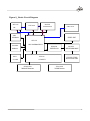
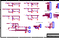
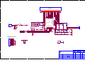
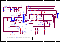
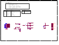
TDE-F61PM\62PM\63PM\66P\68P\80P
AVD-F61C
SERVICE MANUAL
1
Table of Contents
Table of Contents .................................................................................................................... 1
Figure 2. Basic Circuit Diagram ........................................................................................................... 2
Failure & Troubleshooting of Power Supply .......................................................................................... 3
Troubleshooting and service of Decoder part .........................................................................................4-6
Circuit diagram .................................................................................................................... ......Appendix
2
Figure 2 Basic Circuit Diagram
MT1336
BA5954
DVD
D
LO
VA
DDLOAD
RF
VIDEO LPF &
VIDEO
&
LPF
DRIVE
MOTOR DRIVE
MOTOR
DRIVE
2402
EEPROM
SPDIF
OUT
SPDIF OUT
MT1379
DECODER&SERVO
2*16Mbit
SDRAM
WM8746
D/A
AUDIO
AUDIO
D/A
1M*8
FLASH
PT6312
VFD/KEY
PT2222-001
REMOTE
HANDSET
REMOTE HANDSET
MC4558
AUDIO
AMP&LPF
AUDIO AMP&LPF
ECHO ECHO
PT2399
PT2399
MC4558 MIC AMP
AMP
MIC
TEA1523P
POWER SUPPLY
POWER
SUPPLY
3
1.Troubleshooting and service of the Power Supply Board
1.1Principle of Power Supply Operation
This appliance adopts a switched-mode power supply, which is assembled with the TEA1523P
power switch module from Philips and is capable of protecting itself from over-current, over-voltage,
over-heat and short-circuit. The circuit mainly stabilizes a t +3.3v and fluctuate within a permissible
range, such as +5V, +12V, -12V, +3.3V and -24V. Please pay attention to the high voltage inside
the white silkscreen with the mark
CAUTION on the PCB while repairing. When using an
oscillograph to check the circuit,an isolated transformer must be connected.
1.2Troubleshooting and Service
l+3.3V voltage varies out of the permissible range
Please check whether the sampling resistor R324 and R325 is eroded, and check if the voltage
of the first pin of the regulating fiducial IC U303 (TL431) is 2.5V. If the deviation is over 0.15V,
then TL431 is defected or eroded and needs to be replaced. When repairing, do not loop +3.3V
sampling circuit, that is, do not open-circuit D313, L306, R324, R325, R322, U302 (PC123Y) and
U303; otherwise, the output voltage will be too high and will damage the subsequent circuits.
lAll the output voltages are 0V and the voltage of the anode of capacitor C305 is over 150VCheck
whether +5V, +3.3V, +12V, -12V and -24V are short. Check if pin 3 of U301 has 100KHz vibrating
signal, if not, then U301 is eroded.
l+12V and +5V voltage are not normal, while other voltages are normalCheck whether D309,
R315, L303 and ZD303 are open or short, whether C315, C316 and C317 are short or
leak electricity. Any problem of these components will result in abnormal +12V and +5V voltage.
Open-circuit or short-circuit of D312, L305, ZD305, R319 and Q304, and electricity-leakage and
short-circuit of C324, C325, C326, C335 and C328 will result in abnormal +5V voltage.
l-24V and AC1-AC2 voltage are not normal, while other voltages are normalCheck whether R311,
D307, D308, R313, R312 and R314 are open or short, whether C312, C313 and C314 are short
or leak electricity.
lAll output voltages are under permissible range (refer to 2.2 of Chapter one)Check whether ZD
302, C308 and R303 are defected or eroded. If +3.3V output is normal and other voltages are
under range, check if the appliance is in standby mode. In standby mode, it is rational that all
voltages except +3.3V are not normal. If in playing mode, +3.3V output is normal, 5V output is
0V or too low, please check whether +5V is short-circuit and whether R320, Q305, ZD305, D312,
R319, C324, C325, C326, C328 and C335 are defected or eroded.
4
2. Troubleshooting and Service of the Loader
a. No running of loader
a). Check whether the 24P ribbon wire to loader is in good contact.
b). Check whether +5V voltage is normal.
c). Check whether laser voltage ( about 2V for VCD and 2.2V for DVD respectively ) exists at the C
pole of Q1 and Q2, and whether U2 and adjacent parts are damaged or weld falsely.
d). If the above parts are normal and no laser emits, replace the loader.
b. Read no disc
a). Check whether the ribbon wire from 24P to loader is in good contact.
b). Check whether the RFO signal of the 10th pin of CN6 is transmitted to the 96th pin of U1.
c). Check whether laser voltage (about 2V for VCD and 2.2V for DVD respectively) exists at the C
pole of Q1 and Q2, and whether the voltage is normal.
d) Check whether U1, U2 and adjacent parts are damaged or weld falsely.
e). If the above parts are normal, replace U1 or the loader.
c. Read DVD discs only or read other discs beyond DVD only
a). Check whether the ribbon wire from 24P to loader is in good contact.
b). Check whether laser voltage of 2V outputs at the C pole of Q2, and whether the 125th pin of U1
is at low level.
c). Check whether the pins from the 1st to the 38th of U1 and adjacent parts are weld falsely,
damaged or erode.
d). If the above parts are normal, replace U1 or the loader.
3. Troubleshooting and service of decoding part
a. No video, no audio, no display on VFD, and no operation of keys
a). Check whether the power sources of the decoder board are normal.
b). Check whether there is 27MHz signal output. If not, X1 crystal and adjacent parts are eroded or
damaged.
c). Check whether there is 81MHz signal output at R64. If not, check whether there is short circuit,
false welding or alien substance for audio D/A circuit U5 and SDRAM U8 and U9.
d). Check whether the reset circuit composed of C7, R37 and D1 is normal (constant 0V after tens
of milliseconds of high level). If it is at low level constantly, C7, R37 and D1 are damaged.
e). If the reset level is normal, check whether the chip selection signal, address and data of the 12th
pin of U5 are normal.
f). Check U10 that whether the data of pins from the 1st to the 8th, hsync and vsync signal of the
10th and 11th pins, and 27MHz signal of the 29th pin are normal, and whether C162 and R68 are
normal. If not, replace U10.
5
g). When U5 works normally, check the connection between U8, U9 and U3. If abnormal, replace U8
or U9.
h). Replace the main chip U3 after making sure no damage to the adjacent parts and no short circuit
or false welding for the circuit board.
4. Troubleshooting and service of video part
1). Normal sound, no video picture
Check U10 that whether the data of pins from the 1st to the 8th, hsync and vsync signal of the 10th and 11th
pins, and 27MHz signal of the 29th pin are normal, and whether C162 and R68 are normal. If not, replace U10.
2). Abnormal color of the video picture
a). If there are horizontal or vertical streaks, or improper color appears on the picture after reading a disc, the
U3 decoding servo chip on the decoder board or U6 EEPROM may be in problems.
b). Check board whether the 3.3V and 2.5V power sources are normal, whether the ripple factor is too high,
and whether the data wire of Y(0, 7) between U3 and U10 is normal.
c). Check whether the video filter network circuit on the decoder board works normally.
5. Troubleshooting and service of audio part
a. Normal picture, no sound
a). Firstly, check whether the +8V and -8V power sources for the operational amplifier IC U12~U14 are normal.
b). Check whether the C poles of muting tube Q14, Q15, Q22, Q23, Q21 and Q20 are at low level constantly.
If so, the above tubes are not in good conditions.
c). Check whether the output of C poles of Q18 and Q19 are at high levels constantly. If so, Q18 and Q19 have
been broken down, or C209 are short.
d). Check whether the six audio signal lines on the 20P ribbon wire from decoder board to output board are in
good contact. If abnormal, replace the ribbon wire. Check the signal reaching the input of U12~U14. If the input
is normal while the output is not, replace the operational amplifier IC.
e). Check whether the signals of the 17th, 19th, 21st, 23rd, 25th and 27th pins of U5 on the decoder board are
normal. If not, check the signals of the pins from the 2nd to the 7th. If the clock signals of ACLK, ABCK and
ALRCK output by U3 are normal after R130, RN2 and R131 are disconnected, replace U11.
b. Distorted audio and loud noise
a). Firstly, check whether the +8V and -8V power sources for the operational amplifier IC U12~14 are normal.
b). Check whether the muting tubes are in good conditions.
c). Check whether the signals of the 17th, 19th, 21st, 23rd, 25th and 27th pins of U11 on the decoder board are
normal. If not, check the signals of the pins from the 2nd to the 7th. If the clock signals of ACLK, ABCK and
ALRCK output by U1 are normal after R130, RN2 and R131 are disconnected, replace U5.
c. Pop noise during ON/OFF
Check whether the MUTE signal line on the output board is broken, then check whether Q18, Q19, muting tubes
and adjacent parts are damaged or eroded.
6
6. Troubleshooting and service of KARAOKE part
a. Microphone with sound but no echo
a). Check whether the level of the 1st pin of U1 on the KARAOKE board is +5V. If not, check whether JP1 is
damaged.
b). If the voltage is proper, check whether there is anything wrong with the adjacent parts of U1.
b. No sound of microphone
a). Check whether the microphone indicator on VFD lights. If the level of C pole of Q16 is low, the C and E poles
of Q16 are short.
b). Check whether the power source of U2 on the KARAOKE board is normal and with microphone signal output.
If not, check whether the parts of input circuit for microphone jack are damaged and check whether the
microphone jack is rusty or short.
c. The sound of microphone can not be turned off
Check whether Q16 and Q17 are open or not in good contact.
d. self-excitation once KARAOKE is turned on
Check whether the adjacent parts of U1 on the KARAOKE board are damaged.
7. Full
screen display or no display on VFD
a). Full screen display on VFD is often caused by abnormal -24V bias voltage. Check whether D5, C19 and R17
are disconnected.
b). If there is no display on VFD, firstly, check whether the filament lights in red. If not, and there is no 3.3V
voltage difference between AC1 and AC2, check whether D6, C9 and R21 are damaged. If the filament is not
red, while 3.3V voltage difference exists between AC1 and AC2, replace VFD.
c). If -24V and AC1-AC2 voltage are normal, check whether there are CS, DATA and CLK signals from CN301
on the front board. Then replace PT16312 (PT6554) under the condition that both of the above mentioned are
normal.
8. No operation of some keys on the front board, disordered display on VFD
Check whether the welding from the 12th, 13th, 15th pins of U301 to the 37th pin is in good conditions.
Check whether D301~D303 on the front board are damaged, whether circuit is disconnected, and whether R309,
R310 and R311 are open.
9. No sensitive remote reception, or no reception from the remote handset
Check whether the power source of the remote sensor is proper.
Check whether the remote handset is in good operation mode.
Use an oscillator to observe whether there is output wave from the 1st pin IR of the sensor after each pressing
of keys on the remote handset. If the remote handset is good, while no output from the sensor, the sensor is
damaged.
10. The machine can not be turned on or off
If the machine can not be turned on or off after pressing the STANDBY key on the remote handset and the
POWER key on the front board, replace the main chip U3.
Note: The above information is only for reference. If there is any mistake, please feel free to point out.
5
4
3
R106 18k
R105 10k
150p
+
2
3
C162
short
R109
0
A-R
NJM4580
SSOP8
R110
NC
R113 18k
R112 10k
10u
-12V
C166
+
10u
R114 10k
R115 3.3k
6
5
+
LMAIN
-
AGND
AGND
C168
short
R116
0
A-L
NJM4580
SSOP8
A_MUTE
R117
NC
8
C169
1500p
U12B
7
+
150p
C167
4
A_MUTE
[ 4 ] A_MUTE
C170
NC
+12V
CVBS
R119 18k
SY
SY
SC
[4]
R/V
CN7
B/U
R120 10k
10u
VCC
R121 3.3k
C174
1500p
2
A-L
3
U13A
1
C173
short
R122
0
A-SR
NJM4580
SSOP8
R124
NC
8
VCC
[ 1,3,4,5 ]
RREAR
G/Y
[ 4 ] B/U
[ 1,2,3,4 ]
150p
C172
[ 4 ] G/Y
C
-12V
C171
R/V
+
[4]
SC
4
CVBS
[4]
+
VSYN
[4]
R118 NC
VSYN
+
[3]
Q24
NC
HSYN
HSYN
-
[3]
D
R111 NC
+
C165
Q23
NC
A_MUTE
C164
NC
+12V
MICL
[ 1,2,3,4 ]
U12A
1
8
C163 3.3k
1500p
+
D
R108
R107 10k
10u
-
RMAIN
-P12V
+P12V
+12V
-12V
RMAIN
LMAIN
LFE
CENT
RREAR
LREAR
-12V
C160
C161
+
10u
4
MICR
[1]
-P12V
[1]
+P12V
[4]
+12V
[4]
-12V
[ 4 ] RMAIN
[4]
LMAIN
[4]
LFE
[4]
CENT
[ 4 ] RREAR
[ 4 ] LREAR
1
+
C159
2
VGND
VGND
Q25
NC
A_MUTE
C175
NC
+12V
R125 NC
1
2
3
4
5
6
7
8
9
10
11
12
13
14
15
16
17
18
19
20
A-R
A_MUTE
A-SL
A-SR
A-LFE
A-C
ASPDIF
VCC
MICD
[2]
MICON-
[2]
ASPDIF
G/Y
B/U
R/V
SC
CVBS
SY
HSYN
VSYN
R126 18k
MICON-12V
C176
ASPDIF
150p
6
5
U13B
7
C178
short
R131
0
A-SL
NJM4580
SSOP8
R132
NC
8
R130 3.3k
C179
1500p
+
R129 10k
10u
-
LREAR
+
C177
+
MICD
4
[2]
L20
C180
NC
con20(1.25)
Q26
NC
A_MUTE
+12V
C
R133 NC
+12V
+P12V
FB / 0805
C181
+C182
C183
C184
C185
0.1u
100u
0.1u
0.1u
0.1u
R134 18k
-12V
C186
2
-
3
+
LFE
+
C187
FB / 0805
C189
C191
C192
C193
0.1u
0.1u
0.1u
R135 10k
10u
100u
U14A
1
C188
short
R137
0
A-LFE
NJM4580
SSOP8
R138
NC
8
C190
+
0.1u
B
R136 3.3k
C194
1500p
+
150p
-12V
4
L21
-P12V
C195
NC
+12V
[ 1,2,3,5 ]
Q27
NC
A_MUTE
B
R139 NC
GND
GND
R140 18k
470
CENT
470
+
C197
MIC
R142 10k
10u
1K
MICON-
Q29
9014C
CN8
6PIN*2.5
U14B
7
C198
short
R146
0
A-C
NJM4580
SSOP8
R147
NC
C200
NC
R148 NC
MIC
R152
0 NC
A-R
R153
0
MIC/HL
Q28
NC
A_MUTE
0 NC
A-L
R151 0
1
2
3
4
5
6
5
+12V
R150
A
6
8
R149
R143 3.3k
C199
1500p
4
150p
470
+
R144
-12V
C196
MICL
R145
+
MICR
-
R141
A
MICD/HR
+12V
-12V
VCC
MICD
C203
0.1u
5
4
3
2
1
5
4
L12
[ 1,2,3,5 ]
GND
[ 1,5 ] +P12V
1
VCC
+5VA
FB / 0805
C133
0.1u
GND
C131
0.1u
+5VV
C132
100u
+5VV
C134
10u
C137
22p
R79
62R
+P12V
2
VCC
2
+5VA
VCC
[ 1,2,3,5 ]
3
D2
1N4148(NC)
CVBS
+5VA
RN2
1
3
5
7
ACLK
ABCK
ALRCK
ASDAT0
ASDAT1
ASDAT2
R82
R83
21
D
D3
CVBS
1N4148(NC)
SY
1
+5VA
SC
1
DVDD
11
SACLK
SBCLK
SLRCK
SDAT0
2
4
6
8
SDAT1
SDAT2
33
33
R80
20
24
GR0
GR1
GR2
26
22
18
LRCLK2
MCLK
BCLK
LRCLK
DIN0
DIN1
DIN2
C142
22p
VGND
OUT0L
25
OUT0R
27
RMAIN
OUT1L
21
LREAR
OUT1R
23
OUT2L
17
OUT2R
19
CAP
16
Q14
9012
C143
220p
C144
100p(NC)
VGND
[ 1,2,3,5 ]
[5]
[5]
RREAR
LFE
LFE
[5]
CENT
CENT
CENT
[5]
RREAR
RREAR [ 5 ]
LREAR
LREAR
A_MUTE
A_MUTE [ 5 ]
AGND
AGND
LFE
+5VV
+5VV
VQ
C145
22p
R86
62R
[5]
D6
1N4148
SC
10u
Q15
9012
L16
1.8uH
C147
220p
C148
100p(NC)
D8
[ 1,2,3,5 ]
C
1N4148
1
+5VV
VOUTL
9
VOUTR
6
+5VV
C149
22p
LMAIN
R90
62R
RMAIN
D10
1N4148(NC)
R/V
LRCIN
MCLK
BCKIN
DIN
Q18
9012
L17
1.8uH
C150
220p
C151
100p(NC)
VCC
D11
+5VV
L11
1N4148(NC)
L13
FB / 0805 NC
FB AXIAL
1
R92
150
Q11
8550
R96
62R
R154
1K
D7 1N4148
1
2
C135
0.1u
+C136
10u
+5VV
2
+5VV
C152
22p
R77 4.7K
RESET#
D13
Q12
9014C
1N4148(NC)
G/Y
+
10k
C146
470U
L18
1.8uH
C153
220p
C154
100p(NC)
B
D14
1N4148(NC)
1
Q16
9015
R100
150
21
Q21
9012
Y4
B
R87
[5]
D5
R76
10K
VCC
[5]
B/U
LMAIN
Y6
1
14
3
2
[5]
G/Y
RMAIN
C138
10u
SLRCK
SACLK
SBCLK
SDAT0
[5]
R/V
11
4
NC
NC
FORMAT
DEEMPH
MUTE
CAP
[5]
SC
LMAIN
R88
150
C137
0.1u
L15
1.8uH,DIP
U13
WM8726
13
12
10
5
SY
1N4148(NC)
Y1
VDD
GND
[5]
RMAIN
R85
150
C
8
7
CVBS
SY
Y2
C141
C194
OPEN
B/U
D4
1N4148(NC)
C140
0.1u
+5VA
G/Y
+5VV
R84
62R
LMAIN
MODE
OPEN 10
2
3
4
5
6
7
R/V
+5VV
LATCH/12S
SCLK/IWL
SDIN/DM0
MUTE
8
ALRCK
SACLK
SBCLK
SLRCK
SDAT0
SDAT1
SDAT2
AGND1
AGND2
DGND
12
13
14
9
33x4
AVDD1
AVDD2
15
28
2
[ 2 ] ASDAT0
[ 2 ] ASDAT1
[ 2 ] ASDAT2
ACLK
ABCK
ALRCK
ASDAT0
ASDAT1
ASDAT2
C139
100p(NC)
21
[ 2 ] ACLK
[ 2 ] ABCK
[ 2 ] ALRCK
R81
150
U11
WM8746
C138
220p
1
-12V
Q13
9012
2
[5]
Y3
-12V
21
+12V
2
[5]
L14
1.8uH
21
D
+12V
R89
10K NC
Q17
9012 NC
D9 1N4148(NC)
1
2
PMUTE
+5VV
2
+5VV
C156
22p
R103
62R
D16
1N4148(NC)
B/U
Y5
Q22
9012
R104
150
RESET#
[ 2 ] MUTE#
[ 2 ] Y[1..6]
C157
220p
C158
100p(NC)
D17
1N4148(NC)
PMUTE
1
PMUTE
L19
1.8uH
21
R91
10K NC
Q19
RESET#
9015
VCC
D12 1N4148
1
2
MUTE#
R93
4.7K
Y[1..6]
R94
3.3K
A_MUTE
MUTE#
R95
10K
Q20
GND
AGND
VCC
R97
0R
+P12V
R98
0R NC
9015
A
A
R99
100K
GND
VGND
2
D15 1N4148
1
R101
10k
-12V
R102 100K
C155
10uF/16V
MUTE CIRCUIT
5
4
3
2
1
5
4
3
2
1
U5
U6
D
[ 1,2,4,5 ]
VCC
VCC
[ 1,2, ]
DV33
DV33
[ 1,2,4,5 ]
GND
GND
L10
DV33
SD33
C117
0.1u
FB / 0805
+C118
47u
DMA0
DMA1
DMA2
DMA3
DMA4
DMA5
DMA6
DMA7
DMA8
DMA9
DMA10
DMA11
DBA0
DBA1
23
24
25
26
29
30
31
32
33
34
22
35
20
21
A0
A1
A2
A3
A4
A5
A6
A7
A8
A9
A10/AP
A11
BA0/A13
BA1/A12
SDCLK
SDCKE
38
37
CLK
CKE
19
18
17
16
CS
RAS
CAS
WE
RDQM0
RDQM1
15
39
DQML
DQMH
[ 2 ] DCLK
[ 2 ] DCKE
DCLK
DCKE
[2]
[2]
[2]
[2]
CAS#
RAS#
WE#
CS#
CAS#
RAS#
WE#
CS#
[ 2 ] MA[0..11]
[ 2 ] BA[0..1]
[ 2 ] DQ[0..31]
C
[ 2 ] DQM[0..3]
54
41
28
RDQ0
RDQ1
RDQ2
RDQ3
RDQ4
RDQ5
RDQ6
RDQ7
RDQ8
RDQ9
RDQ10
RDQ11
RDQ12
RDQ13
RDQ14
RDQ15
SD33
DCS#
DRAS#
DCAS#
DWE#
36
40
2
4
5
7
8
10
11
13
42
44
45
47
48
50
51
53
DQ0
DQ1
DQ2
DQ3
DQ4
DQ5
DQ6
DQ7
DQ8
DQ9
DQ10
DQ11
DQ12
DQ13
DQ14
DQ15
1
14
27
VCC
VCC
VCC
NC
NC
VSS
VSS
VSS
21
22
23
24
27
28
29
30
31
32
20
19
A0
A1
A2
A3
A4
A5
A6
A7
A8
A9
A10
BA/A11
SDCLK
SDCKE
35
34
CLK
CKE
DCS#
DRAS#
DCAS#
DWE#
18
17
16
15
CS
RAS
CAS
WE
SD33
VCCQ
VCCQ
VCCQ
VCCQ
3
9
43
49
VSSQ
VSSQ
VSSQ
VSSQ
6
12
46
52
U7
DMA0
DMA1
DMA2
DMA3
DMA4
DMA5
DMA6
DMA7
DMA8
DMA9
DMA10
DBA0
RDQM0
RDQM1
14
36
DQML
DQMH
33
37
NC
NC
26
50
VSS
VSS
SDRAM 1Mx16x4
EliteMT M12L64164A-5T
54-Pin TSOPII(400mil x 875mil)
DQ0
DQ1
DQ2
DQ3
DQ4
DQ5
DQ6
DQ7
DQ8
DQ9
DQ10
DQ11
DQ12
DQ13
DQ14
DQ15
2
3
5
6
8
9
11
12
39
40
42
43
45
46
48
49
VCC
VCC
1
25
VCCQ
VCCQ
VCCQ
VCCQ
7
13
38
44
VSSQ
VSSQ
VSSQ
VSSQ
4
10
41
47
RDQ0
RDQ1
RDQ2
RDQ3
RDQ4
RDQ5
RDQ6
RDQ7
RDQ8
RDQ9
RDQ10
RDQ11
RDQ12
RDQ13
RDQ14
RDQ15
SD33
SD33
DMA0
DMA1
DMA2
DMA3
DMA4
DMA5
DMA6
DMA7
DMA8
DMA9
DMA10
DBA0
21
22
23
24
27
28
29
30
31
32
20
19
A0
A1
A2
A3
A4
A5
A6
A7
A8
A9
A10
BA/A11
SDCLK
SDCKE
35
34
CLK
CKE
DCS#
DRAS#
DCAS#
DWE#
18
17
16
15
CS
RAS
CAS
WE
RDQM2
RDQM3
14
36
DQML
DQMH
33
37
NC
NC
26
50
VSS
VSS
DQ0
DQ1
DQ2
DQ3
DQ4
DQ5
DQ6
DQ7
DQ8
DQ9
DQ10
DQ11
DQ12
DQ13
DQ14
DQ15
2
3
5
6
8
9
11
12
39
40
42
43
45
46
48
49
VCC
VCC
1
25
VCCQ
VCCQ
VCCQ
VCCQ
7
13
38
44
VSSQ
VSSQ
VSSQ
VSSQ
4
10
41
47
RDQ16
RDQ17
RDQ18
RDQ19
RDQ20
RDQ21
RDQ22
RDQ23
RDQ24
RDQ25
RDQ26
RDQ27
RDQ28
RDQ29
RDQ30
RDQ31
SD33
SD33
SDRAM 512Kx16x2
SDRAM 512Kx16x2
ESMT M12L16161A-5T
50-PIN TSOP(II),
(400milx825mil, 0.8mm pin pitch)
ESMT M12L16161A-5T
50-PIN TSOP(II),
(400milx825mil, 0.8mm pin pitch)
[2]
AD[0..7]
[ 2,4 ]
[ 2,4 ]
SCL
SDA
DQ16
DQ17
DQ18
DQ19
DQ20
DQ21
DQ22
DQ23
DQ24
DQ25
DQ26
DQ27
DQ28
DQ29
DQ30
DQ31
RDQ16
RDQ17
RDQ18
RDQ19
RDQ20
RDQ21
RDQ22
RDQ23
RDQ24
RDQ25
RDQ26
RDQ27
RDQ28
RDQ29
RDQ30
RDQ31
RN1
D
33x4
1
3
5
7
DCS#
DRAS#
DCAS#
DWE#
2
4
6
8
DQ[0..31]
BA0
BA1
DQM[0..3]
C119
47u
A[0..19]
C120
0.1u
C121
0.1u
C122
0.1u
C123
0.1u
C124
0.1u
C125
0.1u
C126
0.1u
AD[0..7]
SCL
SDA
PCE#
PRD#
PWR#
DBA0
DBA1
R68
R69
DCLK
DCKE
PCE#
PRD#
PWR#
+
[ 2 ] A[0..19]
RDQ0
RDQ1
RDQ2
RDQ3
RDQ4
RDQ5
RDQ6
RDQ7
RDQ8
RDQ9
RDQ10
RDQ11
RDQ12
RDQ13
RDQ14
RDQ15
CS#
RAS#
CAS#
WE#
MA[0..11]
BA[0..1]
SD33
[ 2 ] PCE#
[ 2 ] PRD#
[ 2 ] PWR#
DQ0
DQ1
DQ2
DQ3
DQ4
DQ5
DQ6
DQ7
DQ8
DQ9
DQ10
DQ11
DQ12
DQ13
DQ14
DQ15
FCE#
FRD#
FWR#
C
SDCLK
SDCKE
33
33
MA0
MA1
MA2
MA3
MA4
MA5
MA6
MA7
MA8
MA9
MA10
MA11
DMA0
DMA1
DMA2
DMA3
DMA4
DMA5
DMA6
DMA7
DMA8
DMA9
DMA10
DMA11
DQM0
DQM1
DQM2
DQM3
RDQM0
RDQM1
RDQM2
RDQM3
FVCC
U9
U8
A1
A2
A3
A4
A5
A6
A7
A8
A9
A10
A11
A12
A13
A14
A15
A16
A17
A18
A19
B
VCC
DV33
FVCC
R70
FWR#
FRD#
FCE#
11
10
9
8
7
6
5
4
42
41
40
39
38
37
36
35
34
3
2
43
14
12
A0
A1
A2
A3
A4
A5
A6
A7
A8
A9
A10
A11
A12
A13
A14
A15
A16
A17
A18
WE
OE
CE
FVCC
Vcc
23
IO0
IO1
IO2
IO3
IO4
IO5
IO6
IO7
IO8
IO9
IO10
IO11
IO12
IO13
IO14
IO15
15
17
19
21
24
26
28
30
16
18
20
22
25
27
29
31
RESET
BYTE
44
33
GND
GND
13
32
C129
0.1u
AD0
AD1
AD2
AD3
AD4
AD5
AD6
AD7
A16
A15
A14
A13
A12
R159 A11
A10
A9
10K
PWR#
FVCC
A19
A18
A8
A7
A6
A5
A4
A3
A2
A0
1
2
3
4
5
6
7
8
9
10
11
12
13
14
15
16
17
18
19
20
21
22
23
24
A15
A14
A13
A12
A11
A10
A9
A8
NC1
NC2
WE
RESET
NC3
NC4
RYBY
A18
A17
A7
A6
A5
A4
A3
A2
A1
A16
BYTE
VSS2
DQ15/A-1
DQ7
DQ14
DQ6
DQ13
DQ5
DQ12
DQ4
VCC
DQ11
DQ3
DQ10
DQ2
DQ9
DQ1
DQ8
DQ0
OE
VSS1
CE
A0
48
47
46
45
44
43
42
41
40
39
38
37
36
35
34
33
32
31
30
29
28
27
26
25
A17
A0
AD7
1
2
3
4
AD5
FVCC
AD4
DC/NC
RST_/NC
WP/RST_
VSS
VCC
RST/WP
SCL
SDA
8
7
6
5
SCL
SDA
B
C130
0.1u
EEPROM 24C16, ST-SO8
AD3
AD2
AD1
C127
0.1u
+ C128
47u
AD0
PRD#
VCC
PCE#
A1
DV33
R72
R74
0
NC
R73
R75
1K
1K
SCL
SDA
MX29F800T(TSOP-48)
If use 5V I2C
bus, pull-high
to 5V
0
AT49F8192A, SOP
R71
DV33
U10
AD6
NC
A
A
5
4
3
2
1
5
4
3
R42
2
1
U3A
74HC04 NC
100k
DACV33A
RFRPC
R44
NC
HTRC
R45
0
1
2
R41
DV33
[2]
HTRC
[2]
RFRP
[2]
TEO
[2]
FEO
[2]
TRSO
[ 2 ] TROPEN
C82
C83
C84
0.1u
0.1u
0.1u
0.1u
C90
0.1u
-24V
F+
FPCON
+PS5V
VCC
RVCC
AVCC
[1]
[1]
[1]
[1]
[1]
[ 1,3,4,5 ]
[1]
[1]
C65
10u
AV33
V25
DV33
AV33
V25
DV33
[1]
[1]
[ 1,3, ]
GND
GND
[ 1,3,4,5 ]
SGND
SGND
[ 1,3,4,5 ]
DACV33C
C87
22p
C63
R49
+
R52
D
4.7
0.1u NC
C77
0.1u
C76
10u
1K
+
C93
0.1u
URST
C92
10u
VSYN
DMSO
HSYN
V2P8
BDO
R127
10
SDEN
R128
10
AV33
PWMOUT2
RFL
RFON
C94
1000p
RFIN
ADIN
RFOP
C95
1000p
RFIP
R53
4.7
HTRC
RFRP
TEO
+
C96
47u
FEO
C97
100p
C98
0.1u
C99
1u 0805
C100
10n
R54
TRSO
C101
TROPEN
8.2k
1
2
3
4
5
6
7
8
9
10
11
12
13
14
15
16
17
18
19
20
21
22
23
24
25
26
27
28
29
30
31
32
33
34
35
36
37
38
39
40
41
42
43
44
45
46
47
48
49
50
51
52
53
54
10n
C102 10n
C103 10n
C104 10n
C107 100p
R57
750k
FOSO
TRSO
TROPEN
R58
R59
20k
18k
PWMOUT2
R60
0
V25
DMSO
FMSO
R61
R63
10k
15k
GND
C108
0.1u
C109
0.015u
C110
330p
C111
330p
A8
A9
A10
A11
A12
A13
C112
NC
V1P4
GND
A14
A15
AD7
AD6
AD5
AD4
+PS5V
DV33
TO FRONT PANEL
CN5
1
2
3
4
5
6
7
8
9
10
11
12
13
CON13 2.0mm
AD3
AD2
AD1
AD0
A0
A1
R64
10
-24V
F+
F-
R157 0 NC
VSDA1
R158 0
GND
VFDVCC
V25
A2
A3
A4
A5
A6
A7
A16
A17
A18
A19
+
VCC
VSDA0
C113
100u
R159 10
VSCK
VSTB
R65
PCON
VFDVCC
PMUTE
10
IR
C114
100p
C201
100p
C116
AV33 R66
4.7
DV33
4
3
2
1
+
C88
10u
V1P4
B
-24V
F+
FPCON
+PS5V
VCC
RVCC
AVCC
4.7
DV33
SCLK
C
CN6
C86
1000p NC
+
C89
0.1u
R43
C66
0.1u
C85
22p
RFOP
V2P8
DACV33B
XO
27MHz
C78
0.1u
MICD
ADIN
C81
0.1u
10
Y6
Y5
GND
Y4
DACV33A
Y3
GND
Y2
DACV33B
Y1
GND
[2]
RFL
C80
0.1u
GND
MICON-
[2]
C79
RFON
V25
SDEN
AV33
FMSO
L9
4.7uH NC
GND
URST
XI
XO
DV33
[2]
[ 2 ] PWMOUT2
XI
DV33
R50
10u
V25
DV33
URST
10 NC
4
IREF
PLLVSS
LPIOP
LPION
LPFON
LPFIP
LPFIN
LPFOP
JITFO
JITFN
PLLVDD3
FOO
TRO
TROPENPWM
PWMOUT1
PWMOUT2
DVDD2
DMO
FMO
DVSS
FG
HIGHA0
HIGHA1
HIGHA2
HIGHA3
HIGHA4
HIGHA5
DVSS
HIGHA6
HIGHA7
AD7
AD6
AD5
AD4
DVDD3
AD3
AD2
AD1
AD0
IOA0
IOA1
DVDD2
IOA2
IOA3
IOA4
IOA5
IOA6
IOA7
A16
A17
IOA18
IOA19
IOA20
APLLVSS
MT1379_216
1u 0805
MUTE#
MUTE#
MICON-
MICON- [ 5 ]
RESET#
RESET# [ 5 ]
HSYN
HSYN
[6]
VSYN
VSYN
[6]
MICD
[6]
MICD
YUV0/CIN
FS
VREF
DACVDDC
ASDATA4
ASDATA3
ASDATA2
ASDATA1
ASDATA0
SPDIF
MC_DATA
ACLK
DVDD3
ALRCK
ABCK
RD16
RD17
DVSS
RD18
RD19
RD20
RD21
DVDD2
RD22
RD23
DQM2
DQM3
DVSS
RD24
RD25
RD26
RD27
DVDD3
RD28
RD29
RD30
RD31
DVSS
RA3
RA2
RA1
RA0
DVDD2
RA10
BA1
DQM0
DQM1
DVSS
RA4
RA5
RA6
DVDD3
RA7
DMVSS
R55
Y0
FS
VREF
DACV33C
RESET#
MUTE#
ASDAT2
ASDAT1
ASDAT0
ASPDIF
162
161
160
159
158
157
156
155
154
153
152
151
150
149
148
147
146
145
144
143
142
141
140
139
138
137
136
135
134
133
132
131
130
129
128
127
126
125
124
123
122
121
120
119
118
117
116
115
114
113
112
111
110
109
C105
NC
U4
MT1379E
LQFP216
[4]
URST
URST
[1]
Y[1..6]
Y[1..6]
[4]
PMUTE
PMUTE [ 5 ]
ASPDIF
ACLK
ALRCK
ABCK
ASDAT0
ASDAT1
ASDAT2
ASPDIF
ACLK
ALRCK
ABCK
ASDAT0
ASDAT1
ASDAT2
[5]
[4]
[4]
[4]
[4]
[4]
[4]
A[0..19]
A[0..19]
[3]
NC
R56
1.5K
ACLK
DV33
ALRCK
ABCK
DQ16
DQ17
GND
DQ18
DQ19
DQ20
DQ21
V25
DQ22
DQ23
DQM2
DQM3
GND
DQ24
DQ25
DQ26
DQ27
DV33
DQ28
DQ29
DQ30
DQ31
GND
MA3
MA2
MA1
MA0
V25
MA10
BA1
DQM0
DQM1
GND
MA4
MA5
MA6
DV33
MA7
C106
0.1uF
AD[0..7]
R62
1K
AD[0..7] [ 3 ]
PRD#
PWR#
PCE#
PRD#
PWR#
PCE#
MA[0..11]
BA[0..1]
MA[0..11] [ 3 ]
BA[0..1] [ 3 ]
DQ[0..31]
[3]
[3]
[3]
DQ[0..31] [ 3 ]
DQM[0..3]
DQM[0..3] [ 3 ]
RAS#
CAS#
CS#
WE#
RAS#
CAS#
CS#
WE#
[3]
[3]
[3]
[3]
DCLK
DCKE
DCLK
DCKE
[3]
[3]
SCL
SDA
C
SCL
SDA
[ 3,4 ]
[ 3,4 ]
B
C115
1u 0805
AV33
TxD
RxD
V25
DQ3
DQ2
DQ1
DQ0
WE#
CAS#
RAS#
CS#
BA0
GND
DQ15
DQ14
DQ13
DQ12
DV33
DQ11
DQ10
DQ9
DQ8
GND
DCLK
DCKE
MA11
MA9
MA8
[2]
SDATA
GND
DMSO
R48
3
DQ7
DQ6
DQ5
DQ4
BDO
[2]
100k
C62
10u
Y1
V25
[2]
C75
0.1u
RXD
TXD
V1P4
R47
18k
SCLK
[2]
0
R51
[2]
R46
XI
+ C74
ADIN
GND
BDO
SCLK
SDEN
SDATA
V2P8
V1P4
IR
[2]
0.1u
RFRP
RFOP
C73
0.1u
1000p
[2]
D
C72
0.1u
C91
RFON
C71
0.1u
RFL
FEO
CSO
TEO
FMSO
[2]
C70
0.1u
RFRPC
[2]
C69
0.1u
C64
0.1u
216
215
214
213
212
211
210
209
208
207
206
205
204
203
202
201
200
199
198
197
196
195
194
193
192
191
190
189
188
187
186
185
184
183
182
181
180
179
178
177
176
175
174
173
172
171
170
169
168
167
166
165
164
163
SDATA
C68
0.1u
CSO
RFIP
RFIN
RFDTSLVN
RFDTSLVP
ADCVDD3
PWM2VREF
PWMVREF
HRFZC
RFRP_AC
RFRP_DC
RFLEVEL
FEI
CSO
TEI
TEZISLV
RFSUBI
ADIN
ADCVSS
BDO
SLCK
SDEN
SDATA
WOBSI
UDGATE
DVDD3
IDGATE
VFO13
DVSS
PRST
XTALI
XTALO
DVDD3
SPBCK
SPLRCK
DVDD2
SPDATA
SPMCLK
HSYN
DVSS
YUV7
VSYN
BLANK#
ICE
YUV6/R
YUV5/B
DACVSSA
YUV4/G
DACVDDA
YUV3/CVBS
DACVSSB
YUV2/Y
DACVDDB
YUV1/C
DACVSSC
[2]
C67
FOSO
APLLVDD3
ALE
IOOE#
IOWR#
IOCS#
DVSS
UP1_2
UP1_3
UP1_4
UP1_5
UP1_6
DVDD3
UP1_7
UP3_0
UP3_1
INT0#
IR
DVDD2
UP3_4
UP3_5
UWR#
URD#
DVSS
RD7
RD6
RD5
RD4
DVDD2
RD3
RD2
RD1
RD0
RWE#
CAS#
RAS#
RCS#
BA0
DVSS
RD15
RD14
RD13
RD12
DVDD3
RD11
RD10
RD9
RD8
DVSS
CLK
CLE
RA11
RA9
RA8
DMVDD3
CSO
+
55
56
57
58
59
60
61
62
63
64
65
66
67
68
69
70
71
72
73
74
75
76
77
78
79
80
81
82
83
84
85
86
87
88
89
90
91
92
93
94
95
96
97
98
99
100
101
102
103
104
105
106
107
108
FOSO
[2]
4.7
U3B
74HC04 NC
PRD#
PWR#
PCE#
GND
VSDA1
VSCK
VSDA0
VSTB
SCL
DV33
SDA
[2]
RFZC
R67
4.7
R78
PCON
RS232/4P,2.0 m/m
NC
A
A
5
4
3
2
1
5
4
3
AVCC
RVCC
R3
0 0805
R4
0 0805
RVCCIN
RFVCC
R5
0 NC
DV33 L5
R6
0 NC
R38,R49,R61: FOR 5V
MT1336E
R7
0 NC
R46,R60,R63: FOR 3V
MT1336E
FB AXIAL NC
10K
R14
10K
R15
100K
IOA
2
C13
RVCCIN
0.1u
100u
C17
0.1u
0.1u
OPO
OPOP+
MDI1
MDI1
FB / 0805
MDI2
L7
V20
C22
10uH,DIP
0.1u
F
B
A
RFO
IOA
D
C
3
C28
Q5
8550
1
LDO2
C30
L8
C29
0.1u
0.1u
C31
2
+
CN2
0.1u
R18
10uH,DIP
22
47u
C38
120P
LDO_AVCC
R19
+
2
C41
0.1u
22
LDO1
1
C40
1u,0805
C44
1u,0805
C46
C43
C45
NC
1u,0805
1u,0805
DD
AA
BB
CC
C
B
Q6
8550
AGNDF
VCON
AVDDF
AGNDX
AVDDM
COSPHI
HALLCOS
REFCOS
AGNDM
HALLSIN
REFSIN
SINPHI
SW0
SW2
SW1
MOP
MON
AGNDX
AGNDX
CEON
CEOP
RFGCI
RFGCU
RFFGC
OSP
OSN
CDD
CDC
CDB
CDA
DVDRFIN
DVDRFIP
DVDD
DVDC
DVDB
DVDA
MA
MB
MT1336E
103
104
105
106
107
108
109
110
111
112
113
114
115
116
117
118
119
120
121
122
123
124
125
126
127
128
3
RFO
D
A
B
C
C42
47u
65
66
67
68
69
70
71
72
73
74
75
76
77
78
79
80
81
82
83
84
85
86
87
88
89
90
91
92
93
94
95
96
97
98
99
100
101
102
AVDDP
AGNDX
AGNDP
DPDMUTE
RST
SDATA
SDEN
GNDS
SCLK
XCK16M
VDDS
IOB
IOA
IO9
IO8
IO7
IO6
IO5
IO4
IO3
IO2
IO1
IO0
HDGATE
UDGATE
GND
64
63
62
61
60
59
58
57
56
55
54
53
52
51
50
49
48
47
46
45
44
43
42
41
40
39
FMSO
C18
L6
RVCCIN
U2
SL+
SL-
B
+PS5V
FMSO
R29
20k
TRSO
V1P4
STBY
C55
150p
R22
1,0805
15
16
17
18
19
20
21
29
VOTK+
VOTKVOLD+
VOLDPGND
VNFTK
PVCC2
GND
VOFC+
VOFCVOSL+
VOSLPGND
PVCC1
VCC
GND
14
13
12
11
10
9
8
30
22
23
24
25
26
27
28
PREGND
VINLD
CTK2
CTK1
VINTK
BIAS
STBY
VNFFC
VOSL
VINSLVINSL+
CF2
CF1
VINFC
7
6
5
4
3
2
1
C57
0.1u
VFO13
VDD
AGNDX
AGNDX
AGNDX
DPFO
DPFN
GNDP
HTRC
TRLP
TRLPA
CRTPLP
CRTP
HRFRP
LRFRP
DEFECT
VDDP
TEO
CSO
LVL
FEO
V20
VREFO
V2REFO
AVDDT
TM4
AGNDT
TM3
TM2
TM1
AGNDO
RFON
RFOP
AVDDO
AGNDX
AGNDX
WVDD
WOBSO
38
37
36
35
34
33
32
31
30
29
28
27
26
25
24
23
22
21
20
19
18
17
16
15
14
13
12
11
10
9
8
7
6
5
4
3
2
1
V2P8
SCLK
V1P4
R16
C19
27p
BDO
DMSO
C20
C21
0.015u
10p
URST
R17
100k
SDEN
C23
RFRP
390p
PWMOUT2
BDO
C25
0.1u
C24
390p
TEO
CSO
RFL
FEO
V20
V1P4
V2P8
C26
C27
RFL
470p
0.033u
ADIN
HTRC
RFRP
TEO
C34
C35
C36
+ C32 C37
+ C33
0.1u
0.1u
10u 0.1u
10u
0.1u
FEO
TRSO
C39
RFON
RFOP
0.1u
TROPEN
CSO
SDATA
FMSO
RFON
RFOP
V2P8
SCLK
V1P4
BDO
DMSO
URST
SDEN
PWMOUT2
RFL
ADIN
C
HTRC
RFRP
TEO
FEO
TRSO
TROPEN
RVCCIN
RVCCIN
+ C47
+PS5V
+PS5V
[1]
RVCC
RVCC
[1]
AVCC
AVCC
[1]
C48
DV33
DV33
[ 1,3, ]
0.1u
RVCC
RVCC
[1]
GND
GND
[ 1,3,4,5 ]
SGND
SGND
[ 1,3,4,5 ]
MT1336E
100u
+PS5V
C51
0.1u
R27
10K
R28
20k
C54
DMSO
20K
R30
C50
0.1u
C52
0.1u
R26
220
Q7
9012
R31
B
Q8
9012
C53
200P
27p
OPO
R32
FOSO
+PS5V
R25
220
V1P4
CN3
0
LOAD+
LOADTROUT
ADIN
1
2
3
4
5
750K
TRIN
OPOP+
C56
150p
5PIN 2.0
R34
330K
+
C58
47u
R33
750K
R35
330K
V1P4
R36 1,0805
R37
SP-
SP-SP+
LIMIT
C59
0.1u
27k
HTRC
R24
33k
+PS5V
GND
RFOP
FOSO
R23
1,0805
SPSP+
BA5954
RFON
C49
0.015u
F
E
R21
1,0805
C14
0.1u
U1
MDI2
MDI1
LDO1
LDO2
A
D
R20
1,0805
CSO
100u
+ C15
C16
0.1u
E
FOSO
RFVCC
C202
MC
MD
SA
SB
AGND
IR
AVDD
SC
SD
CDFOP
CDFON
SVDD
TPI
TNI
SGND
WGAND
AGC1
WAVDD
AGC2
AGC3
MDI2
MDI1
LDO1
LDO2
RFSUBO
WGND
2
3
3
AVCC
TOP SIDE CONTACTED
1
2
3
4
5
6
7
8
9
10
11
12
13
14
15
16
17
18
19
20
21
22
23
24
D
SDATA
Very Important
to reduce
Noise
1
Q4
2SK3018
SF-HD6AV/0.5mm,24P TOP
GND-LD
LD-DVD
NC
HFM
MD
LD-CD
VR-DVD
VR-CD
NC
E
VCC
VC
GND-PD
F
B
A
RF
CD/DVD
D
C
TT+
F+
F-
10k
10k
10k
10k
+
1
Q3
2SK3018
R8
R9
R10
R11
AVCC
SCLK
R13
TRCLOSE
IOA
ENDM
STBY
LIMIT
TROUT
TRIN
100K
PWMOUT2
URST
SDATA
SDEN
R12
Q2
9014C
C
TRCLOSE
TROPEN
ENDM
STBY
C12
0.1u
D
1
+PS5V
R2
0 0805
LDO_AVCC
2
SLSL+
1
2
3
4
5
6
Q9
9014C
390
Q10
9014C
R38
TROPEN
390
TRCLOSE
C61
R39
1K
C60
390P
390P
R40
1K
CN4
6P 2.0
A
A
5
4
3
2
1
4
3
2
RP2
10K
-
2
3
3
C24
4.7UF/16V
R8
15K
R5
2.2K
R27
47K
C4
104
C2
22UF/16V
C19
OPEN/103
R9
10K
R13
10K
R14
10K
R12
SHORT
R15
15K
C22
683
C20
561
14
15
LPF1-OUT
LPF1-IN
VA+
C21
332
R10
10K
C16
561
16
C15
332
1
C10
101
C9
22UF/16V
C17
4.7UF/16V
100UF/25V
C3
R7
10K
C23
683
9
1
2
VA-
1K
MOUT/R
OP1-OUT
1
R30
10K
R6
1K
LPF2-OUT
C8
104
R2
1.2K
-
R31
8.2K
R16
4.7UF
C18
RP1
10K
C7
101
MIC1
R11
12K
C14
4.7UF/16V
47K
R3
6
10
R26
47K
U2B
4558 C30
SHORT/1UF
7
OP1-IN
3
1
4
3
+
+
11
2
2
5
OP2-IN
3
2
12
1
OP2-OUT
1
U2A
4558
13
R28
10K
4
1
C1
104
8
R1
2.2K
8
C6
104
MIC2
1
C5
100UF/25V
VA+
LPF2-IN
5
D2
5.1V
CC0
8
CC1
7
VCO
6
CLK-O
5
DGND
4
10 OHM
10 OHM
R29
100 OHM
3
R33
R34
MOUT/R
VA+
VA-
2
10 OHM
1
R32
VCC
MOUT/L
1
2
3
4
5
6
REF
JP1
AGND
U1
PT2399
R17
13K
C29
104
C27
47UF/16V
C26
104
C25
104
C28
100UF/16V
2
5
4
2
3
2
1
5
4
3
2
1
CN101
C12
R18
+
RS
FL1
C11
100P
R27
10K
FL
10uF/16v
470R
10uF/16v
C6
100P
R19
MUTE
Q2
470R
9014C
470R
C13
FR1
R20
R14
FR
+
C16
SUB
+
SUB1
Cr/B
Cb/R
Y/G
GND
+5V
GND
SPDIF
CE1
SUB1
RS1
LS1
FR1
GND
FL1
MUTE
R13
MUTE
R24
10K
9014C
10uF/16v
470R
470R
C7
100P
10uF/16v
C10
100P
R28
10K
Q6
R21
R25
10K
470R
1
2
3
4
5
6
7
8
9
10
11
12
13
14
15
16
17
18
19
20
Svideo_C
Svideo_Y
CVBS
470R
Q5
D
VS
HS
R12
+
C15
RS1
Q3
CN2
SUB
FR
FL
LS
5.1CH
9014C
con20(1.25)
MUTE
470R
AUDIO OUT
AUDIO
C
C14
CE
SUB
LS
RS
FL
FR
R16
LS
+
LS1
C17
D
R15
MUTE
9014C
R22
CE
+
CE1
1
2
5
6
3
4
8
9
7
10
CE
RS
R1
0
R2
0
470R
10uF/16v
MIXL
MIXR
470R
C8
100P
10uF/16v
R29
10K
C9
100P
R26
10K
Q7
Q4
MUTE
R17
R23
PSCAN OUTPSCAN
1
2
3
4
5
6
7
8
9
10
11
12
Cr/R
Cb/B
Y/G
C21
100P
9014C
MUTE
9014C
470R
1
2
3
4
5
6
C22
C23
100P 100P
C
C0N9(2.0)
CON12
470R
L1
AXIAL
(S-)VIDEO OUT
+5V
B
Cb/R
Y/G
Cr/B
R5
1K
SV/V
1
2
3
4
5
6
7
+
C2
0.1UF
C1
47uF/16v
Q1
9014C
C4
104
C3
R8
L2
OHM)
SHORT(1000 330R
R6
2.2K
68 OHM
0.1UF
R7
1K
Svideo_C
Svideo_Y
CVBS
COAX
R10
R11
91 OHM
1
2
R3
OPEN(33ohm)
HS
VS
R4
OPEN(33ohm)
CON7
3
C5
OPEN(220P)
C18
100P
C19
100P
SPDIF
1
2
3
4
5
6
7
8
9
10
11
12
13
14
15
B
VGA(open)
C20
100P
OPT
R9
1
2
3
330 OHM
A
A
Title
<Title>
Size
B
Date:
5
4
3
2
Document Number
<Doc>
星期一, 十二月 15, 2003
Rev
<RevCode>
Sheet
1
1
of
1
5
4
3
2
1
VFD301
D
D
1
2
3
4
5
6
7
8
9
10
11
12
13
14
15
16
17
18
19
20
21
22
23
24
25
26
27
28
29
30
31
32
33
34
35
F1
F1
NP
6G
5G
4G
3G
NC
2G
1G
NC
P1
P2
P3
P4
NC
NC
P5
P6
P7
P8
NC
NC
P9
P10
P11
P12
NC
P13
P14
P15
P16
NP
F2
F2
HNV-06SS63T
AC2
AC1
VCCA
+
REM301
3
2
1
J1
SHORT
VCCA
IR
+
R308
51K
C308 C309
104
104
+5VP
R307
100 ohm
C310
47uF
REM
C306 C307
104
47uF
R304 R305 R306 VCCA
10K
10K
10K
U301
PT16312
SEG8
SEG7
SEG6/K6
SEG5/K5
SEG4/K4
SEG3/K3
SEG2/K2
SEG1/K1
VDD
KEY4
KEY3
D306(OPEN)
STANDBY
R325
R312
R301
R302
R303
C
+5VP
D301
1N4148
D303
1N4148
CON304
2
1
K301
K302
K303
R309 10K
10K
100 ohm
100 ohm
100 ohm
PRV
NEXT
K304
C311
100p
B
D302
1N4148
NOTE-STDBY
470(OPEN)
CS
CLK
DATA
22
21
20
19
18
17
16
15
14
13
12
1
2
3
4
5
6
7
8
9
10
11
VCC
GND
IR
G4
G3
G2
G1
VDD
LED4
LED3
LED2
LED1
GND
OSC
SW1
SW2
SW3
SW4
SDout
SDin
GND
SCLK
/CS
KEY1
KEY2
VCCA
C
34
35
36
37
38
POWOFF 39
40
41
42
43
44
G5
G6
SEG16
SEG15
SEG14
SEG13
VEE
SEG12
SEG11
SEG10
SEG9
33
32
31
30
29
28
27
26
25
24
23
-24V
PAUSE
K305
STOP
R310
10K
OPEN/CLOSE
R311
10K
K306
PLAY
FROM MAIN BOARD
B
CON301
-24V
AC1
AC2
GND
VCCA
DATA
CLK
CS
IR1
GND
PCON
+5VP
P_MUTE
-24V
K307
C303
47uF/35V
+
1
2
3
4
5
6
7
8
9
10
11
12
13
CON303
C302
104
2
1
POWER
CON13(2.0)
TCL王牌电子(深圳)有限公司
A
名
称
型
号
物料编号
5
4
3
2
序号 更改标记 数量 版本 更改说明 签字 日期
研发中心AV设计所
设 计
日 期
CIRCUIT DIAGRAM
审 核
日 期
图号
批 准
日 期
40-0TDF62-FBD
版 本
TD-F62
A4
1
第
页 共 页
A
5
4
3
1
D307
FR104
PAS
D
2
PAS
D
PAS
2
F301
T2A/250ac
+
+
D301
1N4007
CON301
AC INPUT
D303
1N4007
R311
1 1/4W
+ C312
100uF/25V
L301
50mH
PAS
1
R312
2
+
C301
0.1uF/250Vac
CON302
POWER SW
C302
NU
D302
1N4007
D304
1N4007
C305
47uF/400V
D308
FR104
R313
2.2
C314
10uF/50V
1
+
1K
+
+
PAS
T301
C306
103/1kV
R301
100K/2W
4
C307
0.1uF
R302
6.8k
C308
470p
R303
6.8k
4
REG
3
RC
1
2
Drain
8
Source
6
3.3uH
R315
2.2 1/4W
+
5
L302
0.6uH
D309
FR104
9
PAS
C
+
C315
100uF/25V
7
D305
1H8
12
11
10
9
8
7
6
5
4
3
2
1
L303
8
PAS
U301
TEA1523P
R314
51k
C316
100uF/25V
10
1
11
VCC
GND
AUX
+
R304
1.8 1/4W
D310
12
R305
0.33 1/2W
5
Q301
8050
6
13
CON303
HEADER 12x2.5
3.3uH
FR104
R319
D312
RU3YX
15
R306
100
C320
100uF/25V
L304
14
ZD301
BZX79C10V
R307
68k
R317
2.2
D311
C
+
C319
100uF/25V
FR104
-24V
VF2
VF1
+5V(STB)
PCON
GND
VAVA+
+5V
GND
+3.3V
GND
L305
330 1/4W
2
Q304
2655
10uH
+
R309
56 1/4W
D306
FR104
C323
4.7uF/100V
D313
RU3YX
+
C325
470uF/16V
+
C326
470uF/16V
ZD305
BZX79C5.6V
B
B
4
C309
10uF/50V
PAS
R322
220
L306
10uH
1
R310
220
+
U302
PC817
R328
NU
2
+
3
3
R323
6.8k
C311
222/400Vac
+
C329
10uF/16V
2
1
U303
AZ431LB
C332
470uF/16V
C330
0.1
+
R324
2.7k 1%
C333
470uF/16V
R325
1.5k 1%
PAS
A
A
* CAUTION :
THE PARTS MARKED WITH
PAS
ARE IMPORTANT PARTS ON THE SAFETY.
PLEASE USE THE PARTS HAVING THE DESIGNATED PARTS NUMBER WITHOUT FAIL.
5
4
3
2
1
5
4
3
2
1
TCL1379M6-11.1
C
INDEX & POWER, RESET
RF / SERVO
MPEG - MT1336E / MT1379E
MEMORY - SDRAM, FLASH/EEPROM
AUDIO - WM8746, VIDEO FILTER
AUDIO FILTER/OUT PUT
D
NAME
TYPE
DEVICE
NAME
TYPE
VCC
RVCC
AVCC
V33
DV33
AV33
V25
+5VA
+5VV
+12V
Digital 5V
Servo 5V
RF 5V
Digital 3.3V
Digital 3.3V
Servo 3.3V
Digital 2.5V
Audio 5V
Video 5V
Audio 12V
SUPPLY
MT1336E
PICKUP HEADER
SDRAM, Flash, VideoDAC
MT1379E
MT1379E
MT1379E
Audio DAC
Video FILTER
Audio filter
GND
SGND
AGND
VGND
Digital Ground
Servo Analog Ground
Audio Ground
Video Ground
C
AV33
CN1
CON12 2.5mm
1
2
3
4
5
6
7
8
9
10
11
12
1
2
3
4
5
6
7
8
9
10
11
12
13
14
15
MIC/HL
C1
0.1u
VCC
+
MIC/HR
C3
0.1u
+C5
10u
L1
FB / 0805
C4
220u
+P33V
L2
FB AXIAL
+P33V
DV33
+PS5V
+P12V
-P12V
+
C6
0.1u
PCON
VCC
FF+
-24V
DV33
AV33
C2
220u
DV33
URST
C7
220u
+PS5V
+P12V
-P12V
VCC
RVCC
AVCC
+PS5V
+P12V
-P12V
VCC
RVCC
AVCC
[2]
[5]
[5]
[ 2,3,4,5 ]
[2]
[2]
DV33
DV33
[ 2,3, ]
AV33
V25
AV33
V25
[2]
[2]
GND
SGND
URST
GND
SGND
URST
[ 2,3,4,5 ]
[ 2,3,4,5 ]
[2]
FF+
-24V
PCON
MIC/HL
MIC/HR
FF+
-24V
PCON
MIC/HL
MIC/HR
[2]
[2]
[2]
[2]
[ 5]
[5]
B
D1
AVCC
L3
FB / 0805
AVCC
R1
4.7k
1N4148
1
B
+
VCC
CN1
2
1
2
3
4
5
6
D
Q1
8050
L4
FB AXIAL
+PS5V
C8
0.1u
RVCC
GND
+
RVCC
CON15 2.5mm
SGND
V25
C9
100u
+
C11
220u
C10
0.1u
A
A
5
4
3
2
1