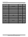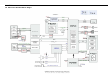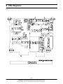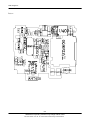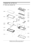
1
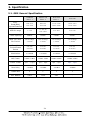
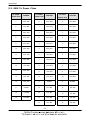
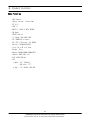
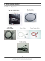
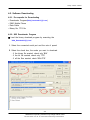
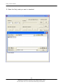
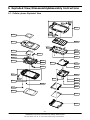
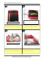
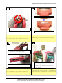
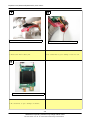
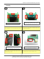
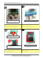
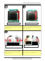
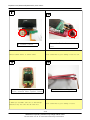
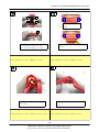
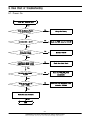
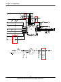
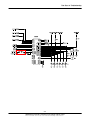
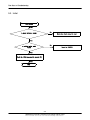
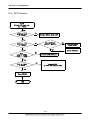
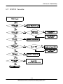
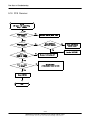
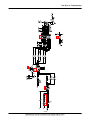
GSM TELEPHONE SGH-E690 GSM TELEPHONE CONTENTS 1. Safety Precautions 2. Specification 3. Product Function 4. Array course control 5. Exploded View/Disassembly and Assembly Instructions 6. MAIN Electrical Parts List 7. Block Diagrams 8. PCB Diagrams 9. Flow Chart of Troubleshooting 10. Reference data CONTENTS 1. Safety Precautions 1-1. Repair Precaution......................................................................................................1-1 1-2. ESD(Electrostatically Sensitive Devices) Precaution...............................................1-2 2. Specification 2-1. GSM General Specification.......................................................................................2-1 2-2. GSM Tx Power Class...............................................................................................2-2 3. Product Function 4. Array course control 4-1. Software Adjustments................................................................................................4-1 4-2. Software Downloading...............................................................................................4-3 5. Exploded View/Disassembly & Assembly Instructions 5-1. Cellular phone Exploded View..................................................................................5-1 5-2. Cellular phone Parts list............................................................................................5-2 5-3. Disassembly & Assembly Instructions......................................................................5-4 6. MAIN Electrical Parts List 7. Block Diagrams 8. PCB Diagrams CONTENTS 9. Flow Chart of Troubleshooting 9-1. Pown on.....................................................................................................................9-1 9-2. Initial...........................................................................................................................9-4 9-3. Charging Part.............................................................................................................9-7 9-4. SIM Part.....................................................................................................................9-8 9-5. Microphone Part.......................................................................................................9-10 9-6. Speaker Part............................................................................................................9-13 9-7. Key Data Input........................................................................................................9-16 9-8. Receiver Part...........................................................................................................9-18 9-9. LCD Part..................................................................................................................9-20 9-10. Camera Part...........................................................................................................9-23 9-11. Trans Flash Card Part..........................................................................................9-27 9-12. Bluetooth Part........................................................................................................9-30 9-13. Main Key LED Part...............................................................................................9-32 9-14. GSM900 Receiver..................................................................................................9-33 9-15. GSM900 Transmitter..............................................................................................9-34 9-16. DCS Receiver........................................................................................................9-35 9-17. DCS/PCS Transmitter............................................................................................9-36 9-18. PCS Receiver.........................................................................................................9-37 10. Reference data 1. Safety Precautions 1-1. Repair Precaution ● Repair in Shield Box, during detailed tuning. Take specially care of tuning or test, because specipicty of cellular phone is sensitive for surrounding interference(RF noise). ● Be careful to use a kind of magnetic object or tool, because performance of parts is damaged by the influence of magnetic force. ● Surely use a standard screwdriver when you disassemble this product, otherwise screw will be worn away. ● Use a thicken twisted wire when you measure level. A thicken twisted wire has low resistance, therefore error of measurement is few. ● Repair after separate Test Pack and Set because for short danger (for example an overcurrent and furious flames of parts etc) when you repair board in condition of connecting Test Pack and tuning on. ● Take specially care of soldering, because Land of PCB is small and weak in heat. ● Surely tune on/off while using AC power plug, because a repair of battery charger is dangerous when tuning ON/OFF PBA and Connector after disassembling charger. ● Don't use as you pleases after change other material than replacement registered on SEC System. Otherwise engineer in charge isn't charged with problem that you don't keep this rules. 1-1 SAMSUNG Proprietary-Contents may change without notice This Document can not be used without Samsung's authorization Safety Precautions 1-2. ESD(Electrostatically Sensitive Devices) Precaution Several semiconductor may be damaged easily by static electricity. Such parts are called by ESD (Electrostatically Sensitive Devices), for example IC,BGA chip etc. Read Precaution below. You can prevent from ESD damage by static electricity. ● Remove static electricity remained your body before you touch semiconductor or parts with semiconductor. There are ways that you touch an earthed place or wear static electricity prevention string on wrist. ● Use earthed soldering steel when you connect or disconnect ESD. ● Use soldering removing tool to break static electricity. , otherwise ESD will be damaged by static electricity. ● Don't unpack until you set up ESD on product. Because most of ESD are packed by box and aluminum plate to have conductive power,they are prevented from static electricity. ● You must maintain electric contact between ESD and place due to be set up until ESD is connected completely to the proper place or a circuit board. 1-2 SAMSUNG Proprietary-Contents may change without notice This Document can not be used without Samsung's authorization 2. Specification 2-1. GSM General Specification GSM900 Phase 1 E GS M 9 0 0 Phase 2 DCS1800 Phase 1 PCS1900 Fr eq. Band[MHz] Uplin k/Down link 890~915 935~960 880~915 925~960 1710~1785 1805~1880 1850~1910 1930~1990 ARF CN ra nge 1~124 0~124 & 975~1023 512~885 512~810 T x/Rx spacing 45MHz 45MHz 95MHz 80MHz Mo d. Bit r ate/ Bit Period 270.833kbps 3.692us 270.833kbps 3.692us 270.833kbps 3.692us 270.833kbps 3.692us Ti me Slo t Pe rio d/Fr am e Per iod 576.9us 4.615ms 576.9us 4.615ms 576.9us 4.615ms 576.9us 4.615ms Modula tion 0.3GMSK 0.3GMSK 0.3GMSK 0.3GMSK MS Power 33dBm~5dBm 33dBm~5dBm 30dBm~0dBm 30dBm~0dBm Powe r Class 5pcl ~ 19pcl 5pcl ~ 19pcl 0pcl ~ 15pcl 0pcl ~ 15pcl Se nsiti vity -102dBm -102dBm -100dBm -100dBm TDMA Mu x 8 8 8 8 Cell Radiu s 35Km 35Km 2Km - 2-1 Speclflcation 2-2. GSM Tx Power Class TX Power control level GSM900 TX Power control level DCS1800 TX Power control level PCS1900 5 33±2 dBm 0 30±3 dBm 0 30±3 dBm 6 31±2 dBm 1 28±3 dBm 1 28±3 dBm 7 29±2 dBm 2 26±3 dBm 2 26±3 dBm 8 27±2 dBm 3 24±3 dBm 3 24±3 dBm 9 25±2 dBm 4 22±3 dBm 4 22±3 dBm 10 23±2 dBm 5 20±3 dBm 5 20±3 dBm 11 21±2 dBm 6 18±3 dBm 6 18±3 dBm 12 19±2 dBm 7 16±3 dBm 7 16±3 dBm 13 17±2 dBm 8 14±3 dBm 8 14±3 dBm 14 15±2 dBm 9 12±4 dBm 9 12±4 dBm 15 13±2 dBm 10 10±4 dBm 10 10±4 dBm 16 11±3 dBm 11 8±4dBm 11 8±4dBm 17 9±3dBm 12 6±4 dBm 12 6±4 dBm 18 7±3 dBm 13 4±4 dBm 13 4±4 dBm 19 5±3 dBm 14 2±5 dBm 14 2±5 dBm 15 0±5 dBm 15 0±5 dBm 2-2 3. Product Function Main Function ― VGA Camera ― 64poly sw midi / Audio Amp ― BT V1.2 ― USB 1.1 ― WAP2.0, JAVA2.0, MP3, MPEG4 ― FM Radio ― EDGE Class 10 ― Tri-Band: 900/1800/1900 ― RF: PMB6272(infineon) ― BT: CSR / Discrete, Ant:SEMCO ― Battery: 800mAh(503442) ― Size: 94 x 48 x 15.9 mm ― Weight: 93 g ― Memory:256Mb+256Mb+128Mb(SEC) ― Camera: CMOS VGA, LSI ― B/E: MV3017(Mtek) ― LCD Main: 2.0" 128x160 65K color, TFT Sub : 1.0" 96x96, 65K STN 3-1 SAMSUNG Proprietary-Contents may change without notice This Document can not be used without Samsung's authorization Product Function 3-2 SAMSUNG Proprietary-Contents may change without notice This Document can not be used without Samsung's authorization 4. Array course control 4-1. Software Adjustments RF Test Cable (GH39-00397A) Test Jig (GH80-03306A) Test Cable (GH39-00499B) Serial Cable Power Supply Cable DATA CABLE (GH39-00482B] 4-1 SAMSUNG Proprietary-Contents may change without notice This Document can not be used without Samsung's authorization Array course control TA GH44-01362B (Malaysia,Singapore BLACK) GH44-01363B (the Republic of the Philippines,BLACK) GH44-01361B (South-East Asia,BLACK) GH44-01363A (the Republic of the Philippines,,SILVER) GH44-01362A (Malaysia,Singapore , SILVER) GH44-01361A (South-East Asia,SILVER) <BLACK> <SILVER> 4-2 SAMSUNG Proprietary-Contents may change without notice This Document can not be used without Samsung's authorization Array course control 4-2. Software Downloading 4-2-1. Pre-requsite for Downloading • Downloader Program(X690_DownloadeV1[1].0.exe) • E690 Mobile Phone • Data Cable • Binary file, TFS file 4-2-2. S/W Downloader Program ■ Load the binary download program by executing the “X690_DownloadeV1[1].0.exe” 1. Select the connected serial port and the rate of speed 2. Select the check box, the mode you want to download. - if the binary file wanted, check only 'BIN' - if the tfs file wanted, check only 'TFS' - if all the files wanted, check 'BIN+TFS' 4-3 SAMSUNG Proprietary-Contents may change without notice This Document can not be used without Samsung's authorization Array course control 3. Select the file(s) what you want to download 4-4 SAMSUNG Proprietary-Contents may change without notice This Document can not be used without Samsung's authorization 5. Exploded View/Disassembly&Assembly Instructions 5-1. Cellular phone Exploded View QIF01 QCK01 QFR01 QVO01 QWD01 QSD01 QKP01 QFU01 QSH01 QME01 QLR02 QMI01 QLR03 QLR01 QCR57 QCA01 QMO01 QLC01 QSP01 QMP01 QME03 QAN02 QCR03 QFL01 QRE01 QHI01 QRF01 QCR05 QCR05 QSC13 QSC06 QSC14 QBA01 QSC05 QMW01 QSC01 QBA00 5-1 SAMSUNG Proprietary-Contents may change without notice This Document can not be used without Samsung's authorization Exploded View/Disassembly&Assembly Instructions 5-2. Cellular phone Parts list Design LOC Description Sec Code QAN02 INTENNA-SGHX690 GH42-00935A QBA00 PMO-CASE BATTERY V2 GH72-34215A QBA01 INNER BATTERY PACK-800MAH, BLA GH43-02539A QCA01 UNIT-CAMERA GH59-02886A QCR03 SCREW-MACHINE 6001-001811 QCR03 SCREW-MACHINE 6001-001811 QCR05 SCREW-MACHINE 6001-001478 QCR05 SCREW-MACHINE 6001-001478 QCR57 SCREW-MACHINE 6001-002001 QFU01 ASSY CASE-FOLDER UPPER GH98-01644A QKP01 ASSY KEYPAD-MAIN(EU/BLK) GH98-01649A QLC01 ELA ETC-SGHX690 LCD MODULE GH96-02223A QLR01 RMO-RUBBER LCD UPPER 1 GH73-08644A QLR02 RMO-RUBBER LCD UPPER 2 GH73-08645A QLR03 RMO-RUBBER LCD LOWER GH73-08599A QME01 UNIT-MAIN KEY FPCB GH59-03410A QME03 UNIT-CON TO CON GH59-03404A QMI01 AS-MIC SVC GH81-05445A QMO01 MOTOR DC-SGHE690 GH31-00282A QMP01 PBA-MAIN-SGH-E690S GH92-02984A QMW01 ASSY COVER-WINDOW MAIN GH98-01647A QRE01 ASSY CASE-REAR GH98-02445A QRF01 PMO-RF CAP GH72-34826A QSC01 MPR-TAPE GH74-26708A QSC05 RMO-RUBBER SCREW CAP L GH73-08035A QSC06 RMO-RUBBER SCREW CAP R GH73-08036A QSC13 RMO-REAR SCREWCAP R GH73-08543A QSC14 RMO-REAR SCREWCAP L GH73-08546A QSH01 ASSY COVER-SHIELD GH98-03211A QSP01 MICRO SPEAKER 3001-002050 QWD01 PCT-WINDOW SUB GH72-34218A QFL01 ASSY CASE-FOLDER LOWER GH98-01645A QHI01 ASSY HINGE-FOLDER GH98-02958A QFR01 ASSY CASE-FRONT GH98-01646A QCK01 PMO-CAM KEY GH72-34217A QIF01 PMO-COVER IF EAR JACK V2 GH72-34824A QSD01 PMO-COVER MICRO SD V2 GH72-34825A QVO01 PMO-VOL KEY GH72-34216A 5-2 SAMSUNG Proprietary-Contents may change without notice This Document can not be used without Samsung's authorization Exploded View/Disassembly&Assembly Instructions Description Sec Code BAG PE 6902-000634 ADAPTOR-SGHE690,SIL,USA GH44-01363B UNIT-EARPHONE, EU, PINK, B-TYP GH59-03596B LABEL(P)-IMEI GH68-01335D LABEL(P)-WATER SOAK GH68-02026A LABEL(P)-WATER SOAK GH68-02026A LABEL(R)-MAIN(EU) GH68-11764A MANUAL USERS-FPT ENGLISH GH68-11806A BOX-UNIT(SEA) GH69-04193A CUSHION-CASE(1~2) GH69-04520A MPR-REMOVE TAPE LCD GH74-13804A MPR-TAPE SUB LCD INSUL GH74-18531A CONE-TAPE SUB LCD INSUL GH74-19756A MPR-INSU TAPE GH74-24458A MPR-GASK TAPE GH74-25025A MPR-VINYL BOHO UPPER OUT 2 GH74-25484A MPR-VINYL BOHO LOWER OUT GH74-25487A MPR-VINYL BOHO STA ELE SUB WIN GH74-25811A MPR-TAPE WINDOW GH74-26705A MPR-VINYL BOHO FPCB CONN GH74-26798A MPR-INSU TAPE MAIN BOARD GH74-27021A MPR-INSU TAPE ZIP CON GH74-27022A MPR-INSU TAPE GH74-27711A MPR-TAPE GH74-27712A MPR-TAPE GH74-27713A MPR-INSU TAPE GH74-28241A MPR-GASK TAPE GH74-28495A MPR-GASK TAPE GH74-28496A MPR-SPONGE LCD GH74-28759A 5-3 SAMSUNG Proprietary-Contents may change without notice This Document can not be used without Samsung's authorization Exploded View/Disassembly&Assembly Instructions 5-3. Disassembly&Assembly Instructions ― Disassembly 1 2 1) Remove SIM CARD and BATTERY. 1) Remove Screw Covers by a Pincette. 1) Be careful not to get a damage of Rear Case. 3 4 1)Lift up Rear Case softly and 1)Remove four points of twist it to the left after this, Rear Screw. remove it. 1) Be Careful not to get a damage of any Devices 1) Be careful not to get a damage of Hooks 5-4 SAMSUNG Proprietary-Contents may change without notice This Document can not be used without Samsung's authorization Exploded View/Disassembly&Assembly Instructions 5 6 1) Disjoint KEY Connector and Con 1) Remove two points of screw To Con Connector by a Pincette. which is used to fix a PCB. 1) Be Careful not to get a damage of FPCB. 1) Be Careful not to get a damage of PCB. 7 8 1)Disjoint a PBA in Front by 1) Remove black insulation TAPE that lifting up from down. 1) Be Careful not to get damage of Connector 2) Be Careful not to get a damage around Cases is attached to Shield Can by a Pincette. 1) Be Careful not to get damage of Con To Con. 5-5 SAMSUNG Proprietary-Contents may change without notice This Document can not be used without Samsung's authorization Exploded View/Disassembly&Assembly Instructions 10 9 1) Lift up Shield Can's upper side by a Pincette and Disjoint Shield Can from the 1) Remove Screws on Shield Can. 1) Be Careful not to get a damage around Cases SET. 1) Be Careful not to get damage of Con To Con 11 12 1) Disjoint Key Pad in Front. 1) Be Careful not to get a damage around Cases 1) Disassemble the Folder from Front Case 1) Be Careful not to get a damage. 5-6 SAMSUNG Proprietary-Contents may change without notice This Document can not be used without Samsung's authorization Exploded View/Disassembly&Assembly Instructions 14 13 1) Remove Screw Covers by a Pincette. 1) Separate the Folder From Front Case with carefully checking Con To Con 2) Remove Screws on Folder 1) Be Careful not to get damage of Con To Con 2) Be Careful not to get a damage around Cases 1) Be Careful not to get a damage around Cases 16 15 1) Open Hooker in the Upper Hinge decomposition groove by a pincette. 1)Separate the motor from lower case by a Pincette. 2) Disassemble the Side of Hookers by 2) Separate the speaker from lower case assembly stick by a Pincette. 1) Be careful not to get a damage of speaker&motor. 1) Be careful not to get a damage around cases. 2) Be careful not to separate non-woven fabric from speaker. 5-7 SAMSUNG Proprietary-Contents may change without notice This Document can not be used without Samsung's authorization Exploded View/Disassembly&Assembly Instructions 17 18 1) Bend Lower a little and separate LCD. 1) Don't touch LCD's Glass part. 1) Separate Con To Con from the Lower. 1) Be careful not to get a damage of Con To Con. 19 1) Dissolution Completion. 1) Be careful not to get a damage of window. 5-8 SAMSUNG Proprietary-Contents may change without notice This Document can not be used without Samsung's authorization Exploded View/Disassembly&Assembly Instructions ― Assembly 2 1 1)Attach electric conduction Tapes on the 1) clean dust on the ground pad by alcohol. 1) Be careful not to be covered any dust on LCD LCD's left, right,upper sides like picture. 1) Take care so that electric conduction Tape may not attach outside silk. 3 4 1) Attach electric conduction Tape on the 1) Remove Tape after attaching two faces LCD's left, right,upper sides like picture. Tape for fixing under ZIP Connector. 1) Press electric conduction Tape again so that TAPE may not get loose. 1) Attach two faces Tape according to silk. 5-9 SAMSUNG Proprietary-Contents may change without notice This Document can not be used without Samsung's authorization Exploded View/Disassembly&Assembly Instructions 6 5 2 1 1) Attach Tape for fixing a Connector. 1) Fix Connector after inserting Con To Con to the Zip Connector. 1) When inserting Con To Con to the Connector, be careful not to be inserted incompletely. 1) Attach Tape according to the base line. 7 8 1) Attact 0.3T electric conduction Tape on the Con To Con. 1) Attach Rubber like picture. 1) Attact 0.5T electric conduction Tape on where LCD's left,right electric conduction Tape are attached. 1) Attach electric conduction Tape so that it may not 1) Attach rubber so that it may not be projected to come out outside base line. outer block of PCB. 5-10 SAMSUNG Proprietary-Contents may change without notice This Document can not be used without Samsung's authorization Exploded View/Disassembly&Assembly Instructions 10 9 1) Attach Rubber like picture. 1) 1) Attach Sponge like picture. Attach rubber so that it may not be projected to outer block of PCB. 1) Take care so that Sponge may not infringe to the Sub LCD and rubber. 11 1) During Solder speaker and vibrator, 1) paint a little of adhesive on concern about polarity. soldering parts. 1) If some dust are covered on LCD, it should be removed by alcohol. 1) Be careful not to get a damage of cases. 5-11 SAMSUNG Proprietary-Contents may change without notice This Document can not be used without Samsung's authorization Exploded View/Disassembly&Assembly Instructions 9 10 1)Insert Con To Con first to the 1) Assemble Camera. Lower. 1)Press Camera until it is sonant "Click". 1) Be careful not to get a damage of Con To Con. 12 11 1)After checking up foreign substances of 1)Combine Lower and Upper. Window, assemble Motor, Speaker, Camera. 1) When you assemble, take care so that foreign substances may not come into the Main Lcd. 1) Be careful not to get a damage of cases. 5-12 SAMSUNG Proprietary-Contents may change without notice This Document can not be used without Samsung's authorization Exploded View/Disassembly&Assembly Instructions 13 14 1 1 2 2 1) Drive 2 screws on Folder. 3 1) Assemble Hooker by left, 2) Assemble 2 screw covers on right side and Hinge in order. Folder. 1) Be careful not to get a damage of cases. 1) Be careful not to get a damage of cases. 16 15 1) Insert the Con To Con to 1) Assemble the folder to Front front hole. case. 1) Be careful not to get a damage of Con To Con. 1) Be careful not to get a damage of Case. 5-13 SAMSUNG Proprietary-Contents may change without notice This Document can not be used without Samsung's authorization Exploded View/Disassembly&Assembly Instructions 17 18 1) Insert the Shield Can From lower part. 1) Insert the KeyPad From lower part. 2) Insert right side volume key first. 1) Confirm first whether volume and camera key has 1) Insert KeyPad according to the Front standard rib. attached. 2) Be careful not to get a damage of Case. 20 19 1) Tighten two Points of Screw 1) Insert Con To Con to the Shield Can on Shield Can. Hole before assembling the Shield Can. 1) Be Careful not to get damage of Con To Con 1) Be careful not to get a damage of Shield Can. 2) SCREW TORQUE : 0.7~ 0.9 kgf.cm 5-14 SAMSUNG Proprietary-Contents may change without notice This Document can not be used without Samsung's authorization Exploded View/Disassembly&Assembly Instructions 22 21 1 1)When attaching a black insulation Tape, insert left side upper part of the tape 1) Assemble a PBA after inserting first. upper side Boss hall of PBA first. 1) Take care so that Con To Con may not attach 1) Be Careful not to get damage of Connector Tape. (Con To Con must be flexible to the left and right.) 24 23 1) Thighten two Points of screw of the 1) Assemble two Connectors. PBA after inserting PBA and Intenna into the Front hall. 1) Be careful not to get a damage of case. 2) SCREW TORQUE : 1.0 ~ 1.2 kgf.cm 1) Be Careful not to get damage of Con To Con 5-15 SAMSUNG Proprietary-Contents may change without notice This Document can not be used without Samsung's authorization Exploded View/Disassembly&Assembly Instructions 26 25 1) Assemble Rear Case SET. 1) press bottom side of Rear Case with thumb and assemble it. 2) Be careful not to get a damage of Front case. 1) drive 4 screws on rear case. 1) Be careful not to get a damage of case. 2) SCREW TORQUE : 1.0 ~ 1.2 kgf.cm 27 1) Insert Screw Caps by pincette. 1) Be careful not to get a damage of case. 5-16 SAMSUNG Proprietary-Contents may change without notice This Document can not be used without Samsung's authorization 6. MAIN Electrical Parts List Design LOC Description SEC Code STATUS ANT600 BAT409 BTC600 C101 C102 C103 C104 C106 C107 C108 C109 C110 C111 C112 C113 C114 C115 C117 C118 C119 C120 C121 C122 C123 C124 C125 C126 C127 C129 C130 C131 C201 C202 C203 C204 C205 C206 C207 C208 C209 C210 C211 C212 C213 C218 C219 C221 C301 C302 C303 C306 C307 C308 ANTENNA-CHIP BATTERY-LI(2ND) CONNECTOR-BATTERY C-CER,CHIP C-CER,CHIP C-CER,CHIP C-CER,CHIP C-CER,CHIP C-CER,CHIP C-CER,CHIP C-CER,CHIP C-CER,CHIP C-CER,CHIP C-CER,CHIP C-CER,CHIP C-CER,CHIP C-CER,CHIP C-CER,CHIP C-CER,CHIP C-CER,CHIP C-CER,CHIP C-CER,CHIP C-CER,CHIP C-CER,CHIP C-CER,CHIP C-CER,CHIP C-CER,CHIP C-CER,CHIP C-CER,CHIP C-CER,CHIP C-CER,CHIP C-CER,CHIP C-CER,CHIP C-CER,CHIP C-CER,CHIP C-CER,CHIP C-CER,CHIP C-CER,CHIP C-CER,CHIP C-CER,CHIP C-CER,CHIP C-CER,CHIP C-CER,CHIP C-CER,CHIP C-CER,CHIP C-CER,CHIP C-CER,CHIP C-CER,CHIP C-CER,CHIP C-CER,CHIP C-CER,CHIP C-CER,CHIP C-CER,CHIP 4202-001225 4302-001180 3711-006003 2203-000812 2203-000812 2203-000278 2203-000278 2203-000278 2203-000254 2203-000812 2203-000278 2203-001432 2203-005482 2203-000438 2203-005482 2203-001432 2203-000812 2203-001432 2203-005482 2203-005482 2203-005482 2203-005482 2203-005968 2203-000530 2203-005234 2203-000233 2203-005061 2203-002668 2203-006399 2203-006399 2203-005234 2203-006194 2203-006423 2203-006423 2203-006423 2203-006423 2203-006423 2203-006423 2203-006423 2203-006423 2203-006562 2203-006423 2203-006423 2203-006423 2203-006048 2203-006423 2203-005682 2203-005482 2203-005482 2203-005482 2203-006141 2203-005482 2203-006053 SA SA SA SA SA SA SA SA SA SA SA SA SA SA SA SA SA SA SA SA SA SA SA SNA SA SA SA SA SA SA SA SA SA SA SA SA SA SA SA SA SA SA SA SA SA SA SA SA SA SA SA SA SA 6-1 SAMSUNG Proprietary-Contents may change without notice This Document can not be used without Samsung's authorization Main Electrical Parts List Design LOC Description SEC Code STATUS C309 C310 C311 C312 C313 C401 C402 C403 C404 C405 C406 C407 C408 C409 C410 C411 C412 C413 C415 C416 C417 C418 C419 C420 C421 C422 C425 C426 C427 C428 C429 C500 C501 C502 C503 C504 C506 C508 C510 C511 C512 C513 C514 C517 C518 C604 C605 C606 C608 C609 C610 C611 C612 C-CER,CHIP C-CER,CHIP C-CER,CHIP C-CER,CHIP C-CER,CHIP C-CER,CHIP C-CER,CHIP C-CER,CHIP C-CER,CHIP C-CER,CHIP C-CER,CHIP C-CER,CHIP C-CER,CHIP C-CER,CHIP C-CER,CHIP C-CER,CHIP C-CER,CHIP C-CER,CHIP C-CER,CHIP C-CER,CHIP C-CER,CHIP C-CER,CHIP C-TA,CHIP C-CER,CHIP C-CER,CHIP C-CER,CHIP C-CER,CHIP C-CER,CHIP C-CER,CHIP C-CER,CHIP C-CER,CHIP C-CER,CHIP C-CER,CHIP C-CER,CHIP C-CER,CHIP C-CER,CHIP C-CER,CHIP C-CER,CHIP C-CER,CHIP C-CER,CHIP C-CER,CHIP C-CER,CHIP C-CER,CHIP C-CER,CHIP C-CER,CHIP C-CER,CHIP C-CER,CHIP C-CER,CHIP C-CER,CHIP C-CER,CHIP C-CER,CHIP C-CER,CHIP C-CER,CHIP 2203-005482 2203-000233 2203-000995 2203-005482 2203-002443 2203-006562 2203-006562 2203-006708 2203-006824 2203-006562 2203-006562 2203-006890 2203-006190 2203-006824 2203-006048 2203-000425 2203-006257 2203-000425 2203-000233 2203-000812 2203-006824 2203-006824 2404-001381 2203-006257 2203-006824 2203-006048 2203-006208 2203-006257 2203-006257 2203-006562 2203-006257 2203-005395 2203-005482 2203-000330 2203-005482 2203-005395 2203-005482 2203-005482 2203-005482 2203-000254 2203-006260 2203-000254 2203-006260 2203-006257 2203-006257 2203-000254 2203-005061 2203-006423 2203-000386 2203-000386 2203-000386 2203-006194 2203-006681 SA SA SA SA SA SA SA SA SA SA SA SA SA SA SA SA SA SA SA SA SA SA SA SA SA SA SA SA SA SA SA SA SA SA SA SA SA SA SA SA SA SA SA SA SA SA SA SA SA SA SA SA SA 6-2 SAMSUNG Proprietary-Contents may change without notice This Document can not be used without Samsung's authorization Main Electrical Parts List Design LOC Description SEC Code STATUS C613 C614 C615 C616 C617 C618 C623 C624 C627 C628 C631 C632 C633 C634 C636 C637 C639 C640 C641 C642 C643 C644 D601 D602 F101 F301 F302 F303 F601 F602 HEA301 HEA302 IFC600 L100 L101 L103 L104 L105 L106 L107 L108 L109 L110 L111 L113 L114 L401 L402 L500 L501 L502 L503 L600 C-CER,CHIP C-CER,CHIP C-CER,CHIP C-CER,CHIP C-CER,CHIP C-CER,CHIP C-CER,CHIP C-CER,CHIP C-CER,CHIP C-CER,CHIP C-CER,CHIP C-CER,CHIP C-CER,CHIP C-CER,CHIP C-CER,CHIP C-CER,CHIP C-CER,CHIP C-CER,CHIP C-CER,CHIP C-CER,CHIP C-CER,CHIP C-CER,CHIP DIODE-SCHOTTKY DIODE-TVS FILTER-EMI SMD FILTER-EMI/ESD FILTER-EMI/ESD FILTER-EMI/ESD FILTER-LC FILTER-EMI/ESD HEADER-BOARD TO BOARD HEADER-BOARD TO BOARD SOCKET-INTERFACE INDUCTOR-SMD INDUCTOR-SMD INDUCTOR-SMD INDUCTOR-SMD INDUCTOR-SMD INDUCTOR-SMD INDUCTOR-SMD INDUCTOR-SMD INDUCTOR-SMD INDUCTOR-SMD INDUCTOR-SMD INDUCTOR-SMD INDUCTOR-SMD BEAD-SMD INDUCTOR-SMD BEAD-SMD BEAD-SMD INDUCTOR-SMD INDUCTOR-SMD BEAD-SMD 2203-000870 2203-006194 2203-006194 2203-005052 2203-000278 2203-000233 2203-006562 2203-000359 2203-000995 2203-000679 2203-005481 2203-006257 2203-006423 2203-006048 2203-005482 2203-006377 2203-006562 2203-005052 2203-006048 2203-000386 2203-006260 2203-006260 0404-001172 0406-001208 2901-001254 2901-001322 2901-001370 2901-001370 2909-001283 2901-001322 3711-005937 3711-005456 3710-002306 2703-001723 2703-002544 2703-002203 2703-002544 2703-002368 2703-002267 2703-002368 2703-002710 2703-001751 2703-002710 2703-002365 2703-001751 2703-001750 3301-001120 2703-002619 3301-001729 3301-001729 2703-002155 2703-002155 3301-001876 SA SA SA SA SA SA SA SA SA SA SA SA SA SA SA SA SA SA SA SA SA SA SA SA SA SA SA SA SA SA SA SA SA SA SA SA SA SA SA SA SA SA SA SA SA SA SA SA SA SA SA SA SA 6-3 SAMSUNG Proprietary-Contents may change without notice This Document can not be used without Samsung's authorization Main Electrical Parts List Design LOC Description SEC Code STATUS L601 L602 L603 L604 L605 L606 MODULE1 OSC400 OSC601 R102 R103 R104 R105 R106 R107 R108 R109 R110 R111 R112 R113 R200 R201 R203 R204 R205 R206 R207 R208 R209 R210 R211 R304 R305 R308 R309 R310 R311 R317 R318 R321 R350 R401 R402 R403 R404 R406 R407 R500 R501 R502 R503 R504 BEAD-SMD BEAD-SMD INDUCTOR-SMD INDUCTOR-SMD INDUCTOR-SMD INDUCTOR-SMD DUPLEXER-FEM CRYSTAL-SMD CRYSTAL-SMD R-CHIP R-CHIP R-CHIP R-CHIP R-CHIP R-CHIP R-CHIP R-CHIP R-CHIP R-CHIP R-CHIP R-CHIP R-CHIP R-CHIP R-CHIP R-CHIP R-CHIP R-CHIP R-CHIP R-CHIP R-CHIP R-CHIP R-CHIP R-CHIP R-CHIP R-CHIP R-CHIP R-CHIP R-CHIP R-CHIP R-CHIP R-CHIP R-CHIP R-CHIP R-CHIP R-CHIP R-CHIP R-CHIP R-CHIP R-CHIP R-CHIP R-CHIP R-CHIP R-CHIP 3301-001876 3301-001876 2703-002204 2703-001231 2703-001673 2703-001285 2911-000050 2801-004466 2801-004560 2007-000171 2007-000171 2007-001284 2007-000172 2007-001316 2007-000172 2007-000140 2007-000140 2007-000162 2007-000171 2007-000140 2007-000171 2007-000147 2007-008516 2007-008548 2007-008548 2007-000162 2007-000162 2007-000162 2007-008052 2007-000170 2007-000170 2007-000171 2007-000148 2007-000162 2007-001303 2007-007014 2007-008055 2007-007014 2007-000171 2007-000171 2007-000171 2007-000162 2007-007100 2007-007190 2007-000162 2007-000162 2007-000171 2007-000162 2007-007317 2007-000148 2007-007317 2007-007317 2007-007317 SA SA SA SNA SA SA SA SA SA SA SA SA SA SA SA SA SA SA SA SA SA SA SA SA SA SA SA SA SA SA SA SA SA SA SA SA SA SA SA SA SA SA SA SA SA SA SA SA SA SA SA SA SA 6-4 SAMSUNG Proprietary-Contents may change without notice This Document can not be used without Samsung's authorization Main Electrical Parts List Design LOC Description SEC Code STATUS R505 R506 R507 R508 R509 R510 R511 R512 R601 R602 R603 R604 R605 R606 R607 R608 R609 R610 R613 R614 R615 R616 R617 R618 R619 R620 R621 R622 R623 R624 R625 R626 R627 R628 R629 R632 R633 R635 R636 R637 R638 RFS100 SW1 T/SIM600 TA101 TA410 TA420 TA428 TA501 TA502 TCX100 TR201 U100 R-CHIP R-CHIP R-CHIP R-CHIP R-CHIP R-CHIP R-CHIP R-CHIP R-CHIP R-CHIP R-CHIP R-CHIP R-CHIP R-CHIP R-CHIP R-CHIP R-CHIP R-CHIP R-CHIP R-CHIP R-CHIP R-CHIP R-CHIP R-CHIP R-CHIP R-CHIP R-CHIP R-CHIP R-CHIP R-CHIP R-CHIP R-CHIP R-CHIP R-CHIP R-CHIP R-CHIP R-CHIP R-CHIP R-CHIP R-CHIP R-CHIP CONNECTOR-COAXIAL SWITCH-TACT CONNECTOR-CARD EDGE C-TA,CHIP C-TA,CHIP C-TA,CHIP C-TA,CHIP C-TA,CHIP C-TA,CHIP OSCILLATOR-VCTCXO FET-SILICON IC-POWER AMP 2007-000148 2007-000171 2007-000171 2007-000172 2007-000171 2007-000172 2007-000171 2007-000171 2007-000162 2007-007334 2007-001339 2007-001339 2007-000172 2007-000162 2007-007573 2007-000172 2007-000164 2007-003015 2007-008055 2007-007741 2007-008055 2007-009168 2007-008419 2007-008055 2007-008055 2007-007107 2007-007312 2007-000137 2007-007489 2007-000775 2007-000171 2007-001325 2007-008275 2007-007573 2007-007334 2007-008542 2007-007142 2007-007139 2007-008542 2007-000171 2007-000171 3705-001358 3404-001152 3709-001453 2404-001413 2404-001381 2404-001377 2404-001445 2404-001240 2404-001226 2809-001303 0505-001518 1201-002423 SA SA SA SA SA SA SA SA SA SA SA SA SA SA SA SA SA SA SA SA SA SA SA SA SA SA SA SA SA SA SA SA SA SA SA SA SA SA SA SA SA SA SA SA SA SA SA SA SA SA SA SA SA 6-5 SAMSUNG Proprietary-Contents may change without notice This Document can not be used without Samsung's authorization Main Electrical Parts List Design LOC Description SEC Code STATUS U101 U103 U202 U300 U302 U304 U400 U401 U402 U403 U404 U500 U601 U602 U603 U604 U605 U607 U610 UCP200 UME301 V400 V401 VR600 VR601 VR603 ZD301 ZD302 ZD303 ZD304 ZD305 ZD602 ZD603 ZD690 ZD691 IC-TRANSCEIVER IC-POSI.FIXED REG. FILTER-EMI SMD IC ASIC-SGHX670 IC-CMOS LOGIC IC-CMOS LOGIC IC-POWER SUPERVISOR IC-DC/DC CONVERTER IC-POSI.FIXED REG. IC-POSI.FIXED REG. IC-POSI.FIXED REG. IC-AUDIO AMP TR-DIGITAL IC-DATA COMM./GEN. IC-CMOS LOGIC IC-DEMODULATOR IC-BATTERY DIODE-TVS DIODE-TVS IC-COMM. CONTROLLER IC-MCP VARISTOR VARISTOR VARISTOR VARISTOR THERMISTOR-NTC DIODE-TVS DIODE-TVS DIODE-TVS DIODE-TVS DIODE-TVS DIODE-ZENER DIODE-TVS DIODE-TVS DIODE-TVS 1205-003057 1203-003767 2901-001316 GH13-00036A 0801-002237 0801-002922 1203-003882 1203-003545 1203-003737 1203-003737 1203-003737 1201-002356 0504-001151 1205-003064 0801-002237 1204-002688 1203-003742 0406-001200 0406-001201 1205-002757 1108-000080 1405-001082 1405-001082 1405-001082 1405-001082 1404-001221 0406-001201 0406-001201 0406-001190 0406-001190 0406-001201 0403-001547 0406-001201 0406-001201 0406-001201 SA SA SA SA SA SA SA SA SA SA SA SA SA SA SA SA SA SA SA SA SA SA SA SA SA SA SA SA SA SA SA SA SA SA SA 6-6 SAMSUNG Proprietary-Contents may change without notice This Document can not be used without Samsung's authorization 7. Block Diagrams 7-1. RF Solution Block Diagram 7-1 SAMSUNG Proprietary-Contents may change without notice This Document can not be used without Samsung's authorization Block Diagrams 7-2. Base Band Solution Block Diagram 7-2 SAMSUNG Proprietary-Contents may change without notice This Document can not be used without Samsung's authorization 8. PCB Diagrams Top 8-1 SAMSUNG Proprietary-Contents may change without notice This Document can not be used without Samsung's authorization PCB Diagrams Bottom 8-2 SAMSUNG Proprietary-Contents may change without notice This Document can not be used without Samsung's authorization 9. Flow Chart of Troubleshooting 9-1. Power On ' Power On ' does not work Yes Check the Battery Voltage is more than 3.4V No Change the Battery Yes No Check the PMU related to BAT409 C415(BAT409) = 2.7V? Yes Check the Clock at OSC400=32.768KHz No Resolder OSC400 Yes C426(VDD_IO_HIGH) =2.9V? C427(VDD_IO_LOW) =1.8V? No Check the related citcuit Yes C419(VDD_GSM_CORE) = 1.8V? No Check the VDD_GSM_CORE circuit(U401) Yes Check for the clock at C112= 26MHz No Check the clock generation circuit (related to TCX100) Yes Check the initial operation Yes END 9-1 SAMSUNG Proprietary-Contents may change without notice This Document can not be used without Samsung's authorization Flow Chart of Troubleshooting 9-2 SAMSUNG Proprietary-Contents may change without notice This Document can not be used without Samsung's authorization Flow Chart of Troubleshooting 9-3 SAMSUNG Proprietary-Contents may change without notice This Document can not be used without Samsung's authorization Flow Chart of Troubleshooting 9-2. Initial Initial Failure Yes No Is U400 RSTON is HIGH? Check the circuit related to reset Yes No Is UCP200 R203, R204 =2.8V? Check the UCP200 Yes Check the 16bit data signal & memory CE Yes END 9-4 SAMSUNG Proprietary-Contents may change without notice This Document can not be used without Samsung's authorization Flow Chart of Troubleshooting 9-5 SAMSUNG Proprietary-Contents may change without notice This Document can not be used without Samsung's authorization Flow Chart of Troubleshooting 9-6 SAMSUNG Proprietary-Contents may change without notice This Document can not be used without Samsung's authorization Flow Chart of Troubleshooting 9-3. Charging Part Abnormal charging part Yes No Check the U605 pin 1 > 4.9V Check the the circuit related to V_EXT_CHARGE Yes No U605 pin 5 = "L"? Resolder or replace U605 Yes No U605 pin 3 = "L"? Check the circuit related to AUX_ON signal Yes No Check the U605 pin 10 ≒ 4.2V Resolder or replace U605 Yes END 9-7 SAMSUNG Proprietary-Contents may change without notice This Document can not be used without Samsung's authorization Flow Chart of Troubleshooting 9-4. Sim Part Phone can't access SIM Card Yes No T/SIM600 pin 11,14 = "H"? Check the sim charge pump Yes No After Power ON, Check SIMCLK Signal on pin15 of T/SIM600 in a few second Check the clock Yes No After SIM card insert, T/SIM600 pin 13 = "H(SIM_RST)"? Replace PBA Yes Check the SIM Card Yes END 9-8 SAMSUNG Proprietary-Contents may change without notice This Document can not be used without Samsung's authorization Flow Chart of Troubleshooting 9-9 SAMSUNG Proprietary-Contents may change without notice This Document can not be used without Samsung's authorization Flow Chart of Troubleshooting 9-5. Microphone Part Microphone does not work Yes No Check the connection from MIC Resolder MIC Yes No Check the circuit from UCP200 to MIC Resolder the C506, C508, L502 and L503 Yes No Check the MIC Replace the MIC Yes END 9-10 SAMSUNG Proprietary-Contents may change without notice This Document can not be used without Samsung's authorization Flow Chart of Troubleshooting 9-11 SAMSUNG Proprietary-Contents may change without notice This Document can not be used without Samsung's authorization Flow Chart of Troubleshooting 9-12 SAMSUNG Proprietary-Contents may change without notice This Document can not be used without Samsung's authorization Flow Chart of Troubleshooting 9-6. Speaker Part(MP3/Spk) Speaker does not work Yes No Are the signal at C511,C513 pins OK? Check the supply voltage of UCP200 and main clock (26MHz) Yes No Check the signal at 15, 17 pins of U500 Check the supply voltage of U500 Yes No Check the signal at 45, 47 pins of LCD Connector on LCD module Replace con to con FPCB Yes No Check the Speaker contact pins Replace Speaker Yes END 9-13 SAMSUNG Proprietary-Contents may change without notice This Document can not be used without Samsung's authorization Flow Chart of Troubleshooting 9-14 SAMSUNG Proprietary-Contents may change without notice This Document can not be used without Samsung's authorization Flow Chart of Troubleshooting 9-15 SAMSUNG Proprietary-Contents may change without notice This Document can not be used without Samsung's authorization Flow Chart of Troubleshooting 9-7. Key Data Input Check Initial Operation Yes No When one of the keys is pushed, is it displayed on LCD? Check the Dome sheet & Key Pad Yes When one of the keys is pushed, KEY_ROW(0)~(4) KEY_COL(0)~(4) signal is OK? No Replace the PBA Yes END 9-16 SAMSUNG Proprietary-Contents may change without notice This Document can not be used without Samsung's authorization Flow Chart of Troubleshooting 9-17 SAMSUNG Proprietary-Contents may change without notice This Document can not be used without Samsung's authorization Flow Chart of Troubleshooting 9-8. Receiver Part Receiver does not work Yes Are the signal at C511,C513 pins OK? No Change the PBA Yes No Check the signal at 15, 17 pins of U500 Check the supply voltage of U500 Yes Check the signal at 45, 47 pins of LCD Connector on LCD module No Replace con to con FPCB Yes No Check the Speaker contact pins Replace Speaker Yes END 9-18 SAMSUNG Proprietary-Contents may change without notice This Document can not be used without Samsung's authorization Flow Chart of Troubleshooting 9-19 SAMSUNG Proprietary-Contents may change without notice This Document can not be used without Samsung's authorization Flow Chart of Troubleshooting 9-9. LCD Part LCD does not work Yes No GPIOA25 pin of UCP200 backlight is high Replace the LCD backlight IC Yes No Check soldering between the board pad and LCD pad ( HEA301 ) Rearrange the soldering pad (HEA301's connection) Yes No Check LCD Module Is it working? Yes END 9-20 SAMSUNG Proprietary-Contents may change without notice This Document can not be used without Samsung's authorization Flow Chart of Troubleshooting 9-21 SAMSUNG Proprietary-Contents may change without notice This Document can not be used without Samsung's authorization Flow Chart of Troubleshooting 9-22 SAMSUNG Proprietary-Contents may change without notice This Document can not be used without Samsung's authorization Flow Chart of Troubleshooting 9-10. Camera part "Camera" function does not work Yes No Check the Camera connector on LCD module Reconnect the camera module Yes No Check the voltage of 1 pin of Camera connector on LCD Module (2.8V) Check the CAM_LDO (U101) on LCD Module Yes No Check the 2,8 pins clock of Camera connector on LCD Module Check the related circuit of U300 Yes No Is it working? Change Camera Module Yes END 9-23 SAMSUNG Proprietary-Contents may change without notice This Document can not be used without Samsung's authorization Flow Chart of Troubleshooting 9-24 SAMSUNG Proprietary-Contents may change without notice This Document can not be used without Samsung's authorization Flow Chart of Troubleshooting 9-25 SAMSUNG Proprietary-Contents may change without notice This Document can not be used without Samsung's authorization Flow Chart of Troubleshooting 9-26 SAMSUNG Proprietary-Contents may change without notice This Document can not be used without Samsung's authorization Flow Chart of Troubleshooting 9-11. Trans Flash Card part T-Flash card does not work Yes No Check the 21 pin of U400 (2.8V) Change the PBA Yes No Check the clock at 4 pin of U603 Check the related circuit Yes No Check the 10 pin of T/SIM600 is high Check the related circuit Yes No Is it working? Change T-Flash Card Yes END 9-27 SAMSUNG Proprietary-Contents may change without notice This Document can not be used without Samsung's authorization Flow Chart of Troubleshooting 9-28 SAMSUNG Proprietary-Contents may change without notice This Document can not be used without Samsung's authorization Flow Chart of Troubleshooting 9-29 SAMSUNG Proprietary-Contents may change without notice This Document can not be used without Samsung's authorization Flow Chart of Troubleshooting 9-12. Bluetooth part Bluetooth does not work Yes No Check the BT_INT pin of U602 is high Change the U602 Yes No Check the contact of Bluetooth Intenna ANT600 Check the contact pin Yes No Is it working? Change the Bluetooth Module U602 Yes END 9-30 SAMSUNG Proprietary-Contents may change without notice This Document can not be used without Samsung's authorization Flow Chart of Troubleshooting 9-31 SAMSUNG Proprietary-Contents may change without notice This Document can not be used without Samsung's authorization Flow Chart of Troubleshooting 9-13. Main Key LED part Main key LED does not work Yes No Check the 6 pin of U404 is high Check the U404 Yes Is it working? Yes END 9-32 SAMSUNG Proprietary-Contents may change without notice This Document can not be used without Samsung's authorization Flow Chart of Troubleshooting 9-14. GSM900 Receiver RX ON RF input : CH center freq Amp : -50dBm Yes MODULE1 Pin10 >= -65dBm No Resolder RFS100, C102, L100 Yes MODULE1 pin3,4 >= -65dBm No Check MODULE1 pin13 = L, pin14= L No Yes Yes No U101 pin27 >= -70dBm pin28 >= -70dBm Resolder L101,L103,L104 Yes U103 pin 1,2,3,4 >= 500mV No Resolder U101 or Check pins related to U101 Yes Check UCP200 END 9-33 SAMSUNG Proprietary-Contents may change without notice This Document can not be used without Samsung's authorization Check ANT Switch control circuit Resoder MODULE1 Flow Chart of Troubleshooting 9-15. GSM900 Transmitter TX ON (5 Level) Yes MODULE1 pin10 <= 20dBm Yes Resolder RFS100, C102, L100 No MODULE1 pin15 <= 20dBm Yes Yes Check MODULE1 pin14 = H (2.68V), pin13 = L No Change or Resolder MODULE1 No Check ANT Switch control circuit Yes U100 pin9 <= 20dBm Resolder L114,C127,C128 No C107,C108 > 3 V, TA101, F101 > 3.5V Yes No Check VBAT Resolder or Change PAM100 No Yes No U100 pin 9 Resolder or Change U100 Yes U103 pin 1,2,3,4 >= 500mV Yes Resolder U101 or Check pins related to U101 No Check UCP200 END 9-34 SAMSUNG Proprietary-Contents may change without notice This Document can not be used without Samsung's authorization Check +VBAT or PAM control signal Flow Chart of Troubleshooting 9-16. DCS Receiver RX ON RF input : CH center freq Amp : -50dBm Yes MODULE1 Pin10 >= -65dBm No Resolder RFS100, C102, L100 Yes MODULE1 pin5,6 >= -65dBm No Check MODULE1 pin14 = L, pin13= L No Yes Yes U101 pin24 >= -70dBm pin25 >= -70dBm No Resolder L108,L109,L110 Yes No U101 pin 1,2,3,4 >= 500mV Resolder U101 or Check pins related to U101 Yes Check UCP200 END 9-35 SAMSUNG Proprietary-Contents may change without notice This Document can not be used without Samsung's authorization Check ANT Switch control circuit Resoder MODULE1 Flow Chart of Troubleshooting 9-17. DCS/PCS Transmitter TX ON (5 Level) Yes MODULE1 pin10 <= 13 dBm Yes Resolder RFS100, C102, L100 No MODULE1 pin12 <= 13 dBm Check MODULE1 pin14 = L , pin13 = H(2.68V) Yes No Yes Change or Resolder MODULE1 Check ANT Switch control circuit No Yes U100 pin10 <= 13 dBm Resolder L113,C131,C124 No C107,C108 > 3 V, TA101, F101 > 3.5V Yes No Check VBAT Resolder or Change U100 No Check +VBAT or PAM control signal Yes No U100 pin 10 >= -8dBm Resolder or Change U100 Yes U103 pin 1,2,3,4 >= 500mV Yes Resolder U101 or Check pins related to U101 No END 9-36 SAMSUNG Proprietary-Contents may change without notice This Document can not be used without Samsung's authorization Flow Chart of Troubleshooting 9-18. PCS Receiver RX ON RF input : CH center freq Amp : -50dBm Yes MODULE1 Pin10 >= -65dBm No Resolder RFS100, C102, L100 Yes MODULE1 pin7,8 >= -65dBm No Check MODULE1 pin14 = L, pin13= L No Check ANT Switch control circuit Yes Yes Resoder MODULE1 U101 pin22 >= -70dBm pin23 >= -70dBm No Resolder L105,L106,L107 Yes U101 pin 1,2,3,4 >= 500mV No Resolder U101 or Check pins related to U101 Yes Check UCP200 END 9-37 SAMSUNG Proprietary-Contents may change without notice This Document can not be used without Samsung's authorization Flow Chart of Troubleshooting 9-38 SAMSUNG Proprietary-Contents may change without notice This Document can not be used without Samsung's authorization 10. Reference data Reference Abbreviate ― AAC: Advanced Audio Coding. ― AVC : Advanced Video Coding. ― BER : Bit Error Rate ― BPSK: Binary Phase Shift Keying ― CA : Conditional Access ― CDM : Code Division Multiplexing ― C/I : Carrier to Interference ― DMB : Digital Multimedia Broadcasting ― EN : European Standard ― ES : Elementary Stream ― ETSI: European Telecommunications Standards Institute ― MPEG: Moving Picture Experts Group ― PN : Pseudo-random Noise ― PS : Pilot Symbol ― QPSK: Quadrature Phase Shift Keying ― RS : Reed-Solomon ― SI : Service Information ― TDM : Time Division Multiplexing ― TS : Transport Stream 10-1 SAMSUNG Proprietary-Contents may change without notice This Document can not be used without Samsung's authorization Reference data 10-2 SAMSUNG Proprietary-Contents may change without notice This Document can not be used without Samsung's authorization This Service Manual is a property of Samsung Electronics Co.,Ltd. Any unauthorized use of Manual can be punished under applicable International and/or domestic law. ⓒ Samsung Electronics Co.,Ltd. 2006. 11 Rev.1.0