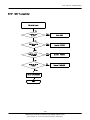
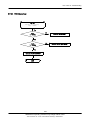
1
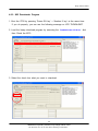
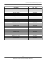
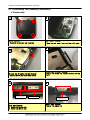
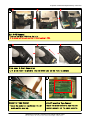
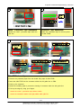
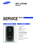
UMTS TELEPHONE
SGH-Z720
UMTS TELEPHONE
CONTENTS
1.
Safety Precautions
2.
Specification
3.
Product Function
4.
Array course control
5.
Exploded View/Disassembly
and Assembly Instructions
6.
MAIN Electrical Parts List
7.
Block Diagrams
8.
PCB Diagrams
9.
Flow Chart of Troubleshooting
10.
Reference data
CONTENTS
1. Safety Precautions
1-1. Repair Precaution ......................................................................................................1-1
1-2. ESD(Electrostatically Sensitive Devices) Precaution ...............................................1-2
2. Specification
2-1. GSM General Specification .......................................................................................2-1
2-2. GSM Tx Power Class ...............................................................................................2-2
3. Product Function
4. Array course control
4-1. Software Adjustments..................................................................................................4-1
4-2. Software Downloading.................................................................................................4-2
5. Exploded View and Parts List
5-1. Cellular phone Exploded View ..................................................................................5-1
5-2. Cellular phone Parts list ............................................................................................5-2
5-3. Disassembly and Assembly Instructions....................................................................5-4
6. MAIN Electrical Parts List
7. Block Diagrams
7-1. RF Solution Block Diagram........................................................................................7-1
7-2. Logic Block Diagram...................................................................................................7-2
8. PCB Diagrams
CONTENTS
9. Flow Chart of Troubleshooting
9-1. Power On..................................................................................................................9-1
9-2. Initial ..........................................................................................................................9-3
9-3. Charging Part ...........................................................................................................9-4
9-4. Sim Part....................................................................................................................9-6
9-5. Microphone Part-Phone MIC ...................................................................................9-8
9-6. Microphone Part-Earphone MIC.............................................................................9-10
9-7. Earphone Part.........................................................................................................9-12
9-8. Speak Part..............................................................................................................9-14
9-9. Key Data Input.......................................................................................................9-16
9-10. LCD Part...............................................................................................................9-17
9-11. Camera Part..........................................................................................................9-19
9-12. LCD Back Light.....................................................................................................9-21
9-13. Key Back Light.....................................................................................................9-23
9-14. GSM Receiver.......................................................................................................9-25
9-15. GSm Transmitter...................................................................................................9-27
9-16. DCS Receiver.......................................................................................................9-29
9-17. DCS Transmitter...................................................................................................9-31
9-18. PCS Receiver ......................................................................................................9-33
9-19. PCS Transmitter...................................................................................................9-35
9-20. WCDMA Receiver.................................................................................................9-37
9-21. WCDMA Transmitter.............................................................................................9-39
10. Reference data
1. Safety Precautions
1-1. Repair Precaution
― Repair in Shield Box, during detailed tuning.
Take specially care of tuning or test, because the specification of cellular phone is sensitive for
surrounding interference(RF noise).
― Be careful to use a kind of magnetic object or tool, because performance of parts is damaged by
the influence of magnetic force.
― Surely use a standard screwdriver when you disassemble this product, otherwise screw will be
worn away.
― Use a thicken twisted wire when you measure level.
A thicken twisted wire has low resistance, therefore error of measurement is few.
― Repair after separate Test Pack and Set because for short danger (for example an
overcurrent and furious flames of parts etc) when you repair board in condition of connecting Test
Pack and tuning on.
― Take specially care of soldering, because Land of PCB is small and weak in heat.
― Surely tune on/off while using AC power plug, because a repair of battery charger is dangerous
when tuning ON/OFF PBA and Connector after disassembling charger.
― Don't use as you pleases after change other material than replacement registered on SEC System.
Otherwise engineer in charge isn't charged with problem that you don't keep this rules.
1-1
SAMSUNG Proprietary-Contents may change without notice
This Document can not be used without Samsung's authorization
Safety Precautions
1-2. ESD(Electrostatically Sensitive Devices) Precaution
Several semiconductor may be damaged easily by static electricity. Such parts are called by ESD
(Electrostatically Sensitive Devices), for example IC,BGA chip etc. Read Precaution below.
You can prevent from ESD damage by static electricity.
― Remove static electricity remained your body before you touch semiconductor or parts with
semiconductor. There are ways that you touch an earthed place or wear static electricity prevention
string on wrist.
― Use earthed soldering steel when you connect or disconnect ESD.
― Use soldering removing tool to break static electricity. , otherwise ESD will be damaged by static
electricity.
― Don't unpack until you set up ESD on product. Because most of ESD are packed by box and
aluminum plate to have conductive power,they are prevented from static electricity.
― You must maintain electric contact between ESD and place due to be set up until ESD is
connected completely to the proper place or a circuit board.
1-2
SAMSUNG Proprietary-Contents may change without notice
This Document can not be used without Samsung's authorization
2. Specification
2-1. GSM General Specification
EG SM9 00
DCS1800
PCS1900
W-CDMA
Fr eq.
Band[MHz]
Uplin k/Down link
8 90~915
9 35~960
17 10~178 5
18 05~188 0
18 50~191 0
19 30~199 0
192 0~1980
211 0~2170
ARF CN ra nge
0~ 124 &
97 5~1023
5 12~885
5 12~810
UL:96 12~988 8
DL:105 62~108 38
T x/Rx spacing
45MHz
95MHz
80MHz
1 90MHz
Mo d. Bit r ate/
Bit Period
270 .833kb ps
3 .692u s
270 .833kb ps
3 .692u s
270 .833kb ps
3 .692u s
3.8 4Mcps
Ti me Slo t
Pe rio d/Fr am e
Per iod
5 76.9u s
4. 615ms
5 76.9u s
4. 615ms
5 76.9u s
4. 615ms
Fr ame len gth : 10ms
Modula tion
0 .3G M SK
0 .3G MSK
0 .3G M SK
Q PS K
HQPSK
MS Power
33d Bm~5dBm
30d Bm~0dBm
30d Bm~0dBm
24 dBm ~ - 50dBm
Powe r Class
4
(max +33dBm)
1
(max +30dBm)
1
(max +30dBm)
3
(max + 24dBm)
Se nsitivity
-10 2dBm
-10 0dBm
-10 0dBm
-1 06.7d Bm
TDMA Mu x
8
8
8
Cell Radiu s
35Km
2Km
2Km
2-1
SAMSUNG Proprietary-Contents may change without notice
This Document can not be used without Samsung's authorization
2Km
Specification
2-2. GSM TX power class
TX Power
control level
GSM900
TX Power
control level
DCS1800
TX Power
control level
PCS1800
5
33±2 dBm
0
30±3 dBm
0
30±3 dBm
6
31±2 dBm
1
28±3 dBm
1
28±3 dBm
7
29±2 dBm
2
26±3 dBm
2
26±3 dBm
8
27±2 dBm
3
24±3 dBm
3
24±3 dBm
9
25±2 dBm
4
22±3 dBm
4
22±3 dBm
10
23±2 dBm
5
20±3 dBm
5
20±3 dBm
11
21±2 dBm
6
18±3 dBm
6
18±3 dBm
12
19±2 dBm
7
16±3 dBm
7
16±3 dBm
13
17±2 dBm
8
14±3 dBm
8
14±3 dBm
14
15±2 dBm
9
12±4 dBm
9
12±4 dBm
15
13±2 dBm
10
10±4 dBm
10
10±4 dBm
16
11±3 dBm
11
8±4dBm
11
8±4dBm
17
9±3dBm
12
6±4 dBm
12
6±4 dBm
18
7±3 dBm
13
4±4 dBm
13
4±4 dBm
19
5±3 dBm
14
2±5 dBm
14
2±5 dBm
15
0±5 dBm
15
0±5 dBm
2-2
SAMSUNG Proprietary-Contents may change without notice
This Document can not be used without Samsung's authorization
3. Product Function
Main Function
― Built-in Digital Cameras( CMOS 3 Mega with Auto Focus, CMOS VGA )
― 2.1" LCD ( QVGA 262K TFT )
― Video Telephony / Streaming
― Bluetooth V2.0 Wireless Technology
― USB 1.1
― MP3 player
― Downloadable Game via JAVA
― Sending Photo & Video by MMS or E-Mail
― Supporting 64 Polyphonic Ring Tone
― WAP 2.0 Browser ( Including xHTML/WCSS MP, w/HTTP )
― External Memory Card Socket( T-flash )
― GSM 900MHz & DCS1800MHz & 1900MHz & WCDMA 2100MHz
― GPRS Class 10
― EGPRS Class E2
3-1
SAMSUNG Proprietary-Contents may change without notice
This Document can not be used without Samsung's authorization
Product Function
3-2
SAMSUNG Proprietary-Contents may change without notice
This Document can not be used without Samsung's authorization
4. Array course control
4-1. Software Adjustments
1
2
GH80-03308A
GH39-00397A
4
3
GH39-00478A
GH44-01361A
5
6
GH39-00444A
1.
2.
3.
4.
5.
6.
JIG: Download, Trace, Calibration, etc
RF test cable: RF test
Test cable: JIG to phone
TA (Travel Adaptor)
Data Link Cable : USB cable
Serial cable: PC to JIG
4-1
SAMSUNG Proprietary-Contents may change without notice
This Document can not be used without Samsung's authorization
Array course control
4-2. Software Downloading
4-2-1. Downloading Binary Files
• Four binary files for downloading Z720.
– amss.bin : Modem binary for communication function
& Mocha binary for user interface and various application
– Rsrc_Z720_○○○.rc1: Files need for each application
– Rsrc2_Z720(Low).rc2 : Power on/off animation
– FactoryFS_Z720_○○○.ffs : Default file system to be put into in initial production
4-2-2. Pre-requsite for Downloading
• Downloader Program( FastMultiLoader V3.28.exe )
• SGH-Z720 Mobile Phone
• USB Data Link Cable
• Binary files
4-2
SAMSUNG Proprietary-Contents may change without notice
This Document can not be used without Samsung's authorization
Array course control
4-2-3. S/W Downloader Program
1. Boot the Z720 by pressing ‘Power ON key’ + ‘Number 9 key’ at the same timeIf you do properly, you can see the following message on LCD “DOWNLOAD”
2. Load the binary download program by executing the “FastMultiLoader V3.28.exe”. And
then Check the 6275.
3. Select the check box what you want to download.
4-3
SAMSUNG Proprietary-Contents may change without notice
This Document can not be used without Samsung's authorization
Array course control
4. Select the binary file what you want to download
5. Now press the button ‘Port Search’
.
4-4
SAMSUNG Proprietary-Contents may change without notice
This Document can not be used without Samsung's authorization
Array course control
6. Now press the button ‘Download’
7. When downloading is complete, UE reboot automatically.
- If there is difference in FactoryFs.bin, UE will format file system
automatically.
4-5
SAMSUNG Proprietary-Contents may change without notice
This Document can not be used without Samsung's authorization
Array course control
4-6
SAMSUNG Proprietary-Contents may change without notice
This Document can not be used without Samsung's authorization
5. Exploded View/Disassembly&Assembly Instructions
5-1. Cellular Phone Exploded View
QIF01
QFR01
QMW01
QVO01
QCK02
QSD01
QBR03
QCR17
QKP01
QFU01
QME01
QKP02
QBR01
QME02
QCA01
QMP01
QLC01
QMI01
QAN02
QCR05
QME03
QCK01
QRE01
QFL01
QCR04
QCR04
QBA01
QSC05
QSC13
QSC14
QCR17
QRE05
QSC06
QHI01
QBA00
5-1
SAMSUNG Proprietary-Contents may change without notice
This Document can not be used without Samsung's authorization
Exploded View/Disassembly&Assembly Instructions
5-2. Cellular Phone Parts list
Design LOC
Description
SEC CODE
QAN02
INTENNA-SGH Z720
GH42-00963A
QBA00
ASSY COVER-BATTERY(XEC)
GH98-03330A
QBA01
INNER BATTERY PACK-900MAH, BLA
GH43-02544A
QBR01
ASSY BRACKET-MAIN KEY
GH98-01733A
ICT-BRACKET VOL KEY
GH70-01550A
QBR03
QCA01
UNIT-CAMERA
GH59-03414A
QCK02
PMO-SWITCH KEY
GH72-33032A
QCK01
PMO-CAMERA KEY
GH72-33031A
QCR04
SCREW-MACHINE
6001-001479
QCR04
SCREW-MACHINE
6001-001479
QCR05
SCREW-MACHINE
6001-001478
QCR17
SCREW-MACHINE
6001-001460
QFL01
ASSY CASE-SLIDE LOWER
GH98-01730A
QFU01
ASSY CASE-SLIDE UPPER
GH98-01729A
QHI01
ASSY ACCE-PUSH ROD
GH98-01237A
QKP01
ASSY KEYPAD-MAIN(EU/BLK)
GH98-02672A
QKP02
ASSY KEYPAD-SUB(EU/BLK)
GH98-02671A
QLC01
LCD-MAINSGH Z720
GH07-00963A
QME01
UNIT-KEY FPCB
GH59-03394A
QME02
UNIT-MODULE SPEAKER
GH59-03789A
QME03
MEA-SLIDE FPCB KIT
GH97-06865A
QMI01
MICROPHONE-ASSY-SGHE340
GH30-00199A
QMP01
PBA MAIN-SGH Z720
GH92-03107A
QMW01
ASSY COVER-MAIN WINDOW(XEC)
GH98-03250A
QRE01
ASSY CASE-REAR
GH98-01732A
QRE05
PMO-DECO REAR
GH72-33041A
QSC05
RMO-RUBBER SCREW LOWER L
GH73-07948A
QSC06
RMO-RUBBER SCREW LOWER R
GH73-07949A
QSC13
RMO-RUBBER SCREW REAR L
GH73-07940A
QSC14
RMO-RUBBER SCREW REAR R
GH73-07947A
QVO01
PMO-VOLUME KEY
GH72-33030A
QFR01
ASSY CASE-FRONT
GH98-01731A
QSD01
PMO-COVER MSD
GH72-33038A
QIF01
PMO-COVER IF
GH72-33039A
5-2
SAMSUNG Proprietary-Contents may change without notice
This Document can not be used without Samsung's authorization
Exploded View/Disassembly&Assembly Instructions
Description
SEC CODE
BAG PE
6902-000634
CBF INTERFACE-DATA LINK CABLE
GH39-00444A
ADAPTOR-SGHE690,BLK,EU,A_TYPE
GH44-01361A
S/W CD-PC STUDIO
GH46-00290A
UNIT-EARPHONE(BLK)
GH59-02541A
LABEL(P)-WATER SOAK
GH68-02026A
LABEL(P)-WATER SOAK
GH68-02026A
LABEL(R)-MAIN(EU)
GH68-12699A
MANUAL USERS-EU SPANISH
GH68-13029A
BOX-UNIT(XEC)
GH69-04521B
CUSHION-CASE(EU)
GH69-04522A
ICT-BRACKET VOL KEY
GH70-01550A
RMO-RUBBERMIC HOLDER
GH73-08696A
MPR-VINYL BOHO MAIN WINDOW V2
GH74-26156A
MPR-INSU TAPE
GH74-27529A
MPR-TAPE
GH74-27536A
MPR-TAPE
GH74-27537A
MPR-ELEC TAPE LCD CONN BOT
GH74-27539A
MPR-TAPE WIN MAIN
GH74-27546A
MPR-INSU TAPE
GH74-27610A
MPR-VINYL BOHO UPPER
GH74-27635A
MPR-SPONGE LCD
GH74-28793A
MPR-TAPE LCD ACRYL
GH74-28801A
MPR-GASK TAPE
GH74-29409A
AS-IC-MCP UMTS
GH81-05910A
AS-DOME SHEET SVC
GH81-05987A
5-3
SAMSUNG Proprietary-Contents may change without notice
This Document can not be used without Samsung's authorization
Exploded View/Disassembly&Assembly Instructions
5-3. Disassembly and Assembly Instructions
― Disassembly
1
2
Screw Removal
- Remove 2 screw caps and 4 screws
Rear cover Removal
- Open the rear cover from the lower with ease
4
3
Volume key Bracket Removal
Volume key Bracket Screw Removal
- Remove the volume key bracket screw
5
- Remove the volume key bracket without getting
bent.
6
Switch key
Volume key
Camera key
Side key Removal
Camera key Removal
1. Remove the volume key
2. Remove the Switch key
- Remove the camera key
5-4
SAMSUNG Proprietary-Contents may change without notice
This Document can not be used without Samsung's authorization
Exploded View/Disassembly&Assembly Instructions
7
8
Key connector Removal
- Detach the key Connector from the PBA
※ Be careful not to damage it When removing the
key Connector.
9
MAIN PBA Removal
- Separate the main PBA from the front by
lifting up.
※ Please handle the main PBA with care not too much
force on it.
Lifting up the connector with the
arrow direction
10
MAIN F-PCB Connector Removal
Front Conduction Tape Removal
- Lift up the main F-PCB connector with the arrow
direction like the picture.
※ Be careful not to rumple and tear it When
- Remove the front conduction Tape.
handling F-PCB.
11
12
Shield Cover Removal
3*4 Key Removal
- Remove the shield cover by lifting up.
※ Be careful not to rumple and tear the Gasket
When removing the shield cover.
- Remove 3*4 Key from the Front.
5-5
SAMSUNG Proprietary-Contents may change without notice
This Document can not be used without Samsung's authorization
Exploded View/Disassembly&Assembly Instructions
14
13
Front screw 2 point
Screw cover Removal
Slide Ass'y Screw Removal
- Remove the left and right screw covers.
1. Push up the slide a little bit.
2. Remove the slide Ass'y screw 2 points.
15
16
Slide Lower Screw Removal
Slide Ass'y & Front Unlocking
1. Slide up only half of 3*4 Key part like the
picture.
2. Remove two unconcealed screws
- Unlock the 4 locking points with an unlocking
stick.
18
17
Slide Ass'y & Front Separation
- Separate the slide upper and the slide lower
after unlocking.
Front Hole Adjustment
- Adjust the slide lower hole to the front hole
to draw out from the hole.
5-6
SAMSUNG Proprietary-Contents may change without notice
This Document can not be used without Samsung's authorization
Exploded View/Disassembly&Assembly Instructions
②
①
19
③
→
→
Main F-PCB Removal
- Draw out the main F-PCB from the hole.
※ Be careful not to rumple and tear it When handling F-PCB.
②
①
20
③
→
→
Slide Lower & Front Separation
- Lift up the lower like pictures when the slide lower and the front is combined.
21
22
Conduction Tape Removal
- Remove the conduction tape between the LCD
Untied-Prevention Tape Removal
- Remove the untied-prevention tape from the
speaker connector and the camera connector.
module and the menu key.
5-7
SAMSUNG Proprietary-Contents may change without notice
This Document can not be used without Samsung's authorization
Exploded View/Disassembly&Assembly Instructions
23
24
Speaker F-PCB Separation
Camera F-PCB Separation
- Open the speaker connector with the arrow
direction and then draw out the speaker F-PCB.
- Open the camera connector with an arrow
direction and then draw out the Camera F-PCB.
※ Be careful with the base tape drawing out
the camera F-PCB.
25
26
3 Mega Camera Module Separation
Speaker Module Separation
- Separate the speaker module from the slide
upper by lifting up with the arrow direction.
- Separate the 3M camera module from the slide
upper by lifting up with the arrow direction.
※ Be careful not to touch or damage the Camera
lens when pulling out the 3 Mega Camera.
27
28
VGA Camera Module Separation
Main F-PCB Separation
- Separate the VGA camera module from the slide
upper by lifting up with the arrow direction.
- Open the main F-PCB connector and then draw
out the main F-PCB with the arrow direction.
5-8
SAMSUNG Proprietary-Contents may change without notice
This Document can not be used without Samsung's authorization
Exploded View/Disassembly&Assembly Instructions
29
30
LCD Module Separation
Menu key PCB Separation
- Separate the menu key PCB from the upper like
the picture.
- Separate the LCD module from the upper like
the picture.
※ Be careful not to lift it up suddenly with
too much force!! That could cause LCD crack.
PBA & INTENNA Saperation
1
2
SCREW 1POINT
Intenna Screw Removal
- Remove the intenna screw from the PBA.
Re-soldering 2 point
Intenna Contact Re-soldering
- Solder the intenna contact points.
3
Intenna Removal
- Separate the intenna body from the PBA with
melting - lead state.
※ Be careful not to break or bend the intenna
contact.
Completely separated state.
5-9
SAMSUNG Proprietary-Contents may change without notice
This Document can not be used without Samsung's authorization
Exploded View/Disassembly&Assembly Instructions
― Assembly
1
( Remove the paper )
( Check three extraneous matters )
>
critical point
< 1. Remove the paper >
< 2. Attach the Key FPCB >
< 3. Check FPCB attachment >
Shield Can Check & Key FPCB Attachment
1. Remove the protection paper on the back side of Key FPCB.
2. Attach the Key PCB on the shield can set to the hole. -> Check the 3 extraneous matter before attaching the
shield can.
3. Check the position of volume key part FPCB properly.
3
2
< 1. Slide FPCB
< 1. LCD Sponge
>
Fixing Tape >
< 2. LCD Acrilic Tape>
LCD Sponge & LCD Acrylic Tape Attachment
1. Attach the LCD sponge to the width of LCD
FPCB.
2. Attach the LCD acrylic tape within the silk line.
< 2.Camera FPCB
Fixing Tape >
Slide/Camera FPCB Tape Attachment
1. Attach the fixing tape of slide FPCB within the
silk line.
2. Attach the fixing tape of camera FPCB within
the silk
line.
4
< Check Guide Line >
critical point
< Close the Locker >
< Assemble Camera/Speaker >
Camera/Speaker Assembly
1. Remove the protection paper of camera FPCB fixing tape.
2. Insert the FPCB up to the guide line With regard to the insertion direction of camera and then close the
locker.
3. Insert the FPCB up to the guide line With regard to the insertion direction of speaker and then close the
locker.
5-10
SAMSUNG Proprietary-Contents may change without notice
This Document can not be used without Samsung's authorization
Exploded View/Disassembly&Assembly Instructions
5
6
Guide
line
Conduction Tape
< Untied- Prevention Tape >
Untied - Prevention Tape Attachment
Conduction Tape Attachment
- Attach the untied - prevention tape within the
silk line.
- Attach the conduction tape on the two points
of slide FPCB.
7
Check the silk line
Remove the
paper
Attach the insulating tape
Lock the connector
Fold it up
Slide FPCB Assembly
1. Remove the protection paper from the double fixing tape of slide FPCB.
2. Insert the slide FPCB into the connector within the silk guide line on PBA.
3. Hook up the connector.
4. Attach the insulating tape to prevent the loosing of connector within the silk guide line.
5. Fold up the edge by using your fingers.
※ Attach the untied - prevention tape without bubble.
※ Attach the extraneous matters at the right position within guide line.
5-11
SAMSUNG Proprietary-Contents may change without notice
This Document can not be used without Samsung's authorization
Exploded View/Disassembly&Assembly Instructions
8
9
Start from the upper point
< Insert through Guide Hole >
< Remove Protection
< Attach MAIN WINDOW
< KEY PAD
paper and vinyl >
>
Assembly >
Removing protection tape and vinyl Sub
key pad assembly
MAIN WINDOW attachment
1.Remove the MEGA CAMERA fixing tape,
- Attach the MAIN WINDOW starting from the upper
point of the WINDOW.
protection tape and VGA CAMERA WINDOW
protection vinyl.
2.Place the SUB KEYPAD at the SLIDE UPPER.
10
11
< Attach conductive tape>
< HOOKER
assembly >
< Attach conductive Tape >
< Remove LENS
protection vinyl>
LCD Module Assembly
Attach LCD conductive TAPE
1.Remove VGA CAMERA LENS protection vinyl.
- Attach LCD conductive TAPE following the silk guide
2.Remove the LCD protection vinyl.
LINE.
3.Remove the Backside Window protection vinyl.
4.Place the LCD at SLIDE UPPER, then hook the SUB
PBA to the HOOKER and push the side part of SUB
PBA to assemble SLIDE UPPER.
5.Assemble 3MEGA CAMERA, VGA CAMERA
6.Assemble SPEAKER
7.Remove 3MEGA CAMERA LENS protection vinyl.
※ Assemble CAMERA prior to SPEAKER
assembly
5-12
SAMSUNG Proprietary-Contents may change without notice
This Document can not be used without Samsung's authorization
Exploded View/Disassembly&Assembly Instructions
12
Mind the
Fix the hinge by sliding
direction of
it toward the left
the hinge
Place the end of the hinge at the
assembly groove
Finish assembling by
sliding the lower to
the end
FRONT SLIDE Hinge Assembly
1.Locate the SLIDE hinge at the groove of the Front, then slide it toward the left to fix it.
2.Tilt the fixed SLIDE hinge to 45 degrees.
3.Move the SLIDE LOWER down to 1/2 position following the FRONT rail.
4.Slot the end of the hinge to the assembly groove of the LOWER, then bring Lower to the end to fix hinge
13
< Match insertion
<Critical point>
groove >
< Remove WINDOW
protection Vinyl>
※ caution
Check whether FPCB
is at right position
<right position>
< Assemble SLIDE ASS'Y >
<wrong position>
Removing 3Mega CAMERA WINDOW protection vinyl and SLIDE ASS'Y Assembly
1.Remove 3MEGA CAMERA WINDOW protection vinyl.
2.Match the FPCB insertion hole of both SLIDE LOWER and FRONT.
3.Insert the FPCB through insertion hole to assemble SLIDE UPPER and FRONT
4.Push FRONT up to where it was
5-13
SAMSUNG Proprietary-Contents may change without notice
This Document can not be used without Samsung's authorization
Exploded View/Disassembly&Assembly Instructions
14
15
Upper 2POINT
Be careful not
SIZE : 1.4*4.0*2.5
to damage FPCB
during assembly
Insert Left SCREW CAP
Insert Right SCREW CAP
Lower 2POINT
SIZE : 1.4*2.3*2.5
Screwing the screw
Screw Cap Insertion
1.Screw the upper 2 point of the SLIDE LOWER
using SCREW Assmebly JIG → SCREW
SIZE:1.4*4.0*2.5
2.Screw the lower 2 point of the SLIDE LOWER
using SCREW Assmebly JIG → SCREW
SIZW:1.4*2.3*2.5
1.Insert Left SCREW CAP.
2.Insert Right SCREW CAP.
3.Press the SCREW CAP with Screw Cap JIG
16
17
GUIDE PIN
EAR PHONE
MICRO SD CARD
COVER
COVER
Placing the Main key pad
1. Check the printed condition of the MAIN
KEYPAD.
2. Place the MAIN KEYPAD. View <Fig. 1>
Shield Can Assembly
- Assemble the Shield Can just like in the picture
above.
※ Be careful not to rumple and tear the Gasket
When assembling the shield cover.
18
19
Switch key
Volume key
<right position>
<wrong position >
Place VOLUME KEY, SWITCH KEY
VOL KEY BRACKET
-Place both VOLUME KEY and SWITCH KEY.
-Assemble VOL KEY BRACKET using SCREW JIG
→ SCREW SIZE:1.4*2.3*2.5
※ Be careful to assemble the BRACKET right
position.
5-14
SAMSUNG Proprietary-Contents may change without notice
This Document can not be used without Samsung's authorization
Exploded View/Disassembly&Assembly Instructions
20
21
< FPCB Connector Assembling >
< Conduction Tape >
Conduction Tape Attachment
PBA Assembly
- Attach the conduction tape like a picture.
1. Open the slide ASS'Y only half and then put
the PBA on the PBA JIG.
2. drive the slide FPCB connector.
22
23
Insert the Camera Key
< Close the Key-FPCB Connector >
< Camera Key Assembling >
Key F-PCB Assembly
1. Put the PBA on the FRONT.
2. Close the Key - FPCB connector.
Camera key Assembly
24
25
1
- Insert the camera key into the hole.
3
Insert the left
Insert the left
screw cap
screw cap
2
4
Assembling the Rear
Rear Screw Cap Insertion
- Put this on the screw JIG and then drive the
Screw in order.
→ SCREW SIZE:1.4*4.0*2.5
1.Insert the screw cap of left side.
2.Insert the screw cap of right side.
3. Press the screw caps by using screw cap JIG.
5-15
SAMSUNG Proprietary-Contents may change without notice
This Document can not be used without Samsung's authorization
Exploded View/Disassembly&Assembly Instructions
5-16
SAMSUNG Proprietary-Contents may change without notice
This Document can not be used without Samsung's authorization
6. MAIN Electrical Parts List
Design LOC
Description
SEC Code
STATUS
ANT102
BAT400
BTC600
C100
C103
C104
C107
C108
C109
C110
C111
C112
C113
C114
C115
C116
C117
C118
C119
C120
C121
C122
C123
C124
C125
C126
C127
C128
C129
C130
C131
C132
C133
C135
C136
C137
C140
C141
C142
C143
C144
C145
C146
C147
C148
C150
C151
C152
C153
C154
C155
C156
C157
ANTENNA-CHIP
BATTERY-LI(2ND)
HEADER-BATTERY
C-CER,CHIP
C-CER,CHIP
C-CER,CHIP
C-CER,CHIP
C-CER,CHIP
C-CER,CHIP
C-CER,CHIP
C-CER,CHIP
C-CER,CHIP
C-CER,CHIP
C-CER,CHIP
C-CER,CHIP
C-CER,CHIP
C-CER,CHIP
C-CER,CHIP
C-CER,CHIP
C-CER,CHIP
C-CER,CHIP
C-CER,CHIP
C-CER,CHIP
C-CER,CHIP
C-CER,CHIP
C-CER,CHIP
C-CER,CHIP
C-CER,CHIP
C-CER,CHIP
C-CER,CHIP
C-CER,CHIP
C-CER,CHIP
C-CER,CHIP
C-CER,CHIP
C-CER,CHIP
C-CER,CHIP
C-CER,CHIP
C-CER,CHIP
C-CER,CHIP
C-CER,CHIP
C-CER,CHIP
C-CER,CHIP
C-CER,CHIP
C-CER,CHIP
C-CER,CHIP
C-CER,CHIP
C-CER,CHIP
C-CER,CHIP
C-CER,CHIP
C-CER,CHIP
C-CER,CHIP
C-CER,CHIP
C-CER,CHIP
4202-001031
4302-001180
3711-006217
2203-006556
2203-006379
2203-006423
2203-005682
2203-000725
2203-005682
2203-000836
2203-006194
2203-006194
2203-005682
2203-005682
2203-005682
2203-005806
2203-005719
2203-006838
2203-006556
2203-005682
2203-005682
2203-006423
2203-006123
2203-005719
2203-005682
2203-005682
2203-005806
2203-006194
2203-005682
2203-005719
2203-006556
2203-006556
2203-006896
2203-002982
2203-001124
2203-005734
2203-005734
2203-006208
2203-005682
2203-005682
2203-005729
2203-006379
2203-005729
2203-005683
2203-006305
2203-006838
2203-001153
2203-002443
2203-006556
2203-000311
2203-006838
2203-006648
2203-001033
SA
SA
SA
SA
SA
SA
SA
SA
SA
SA
SA
SA
SA
SA
SA
SNA
SA
SA
SA
SA
SA
SA
SA
SA
SA
SA
SNA
SA
SA
SA
SA
SA
SA
SA
DNA
SA
SA
SA
SA
SA
SA
SA
SA
SA
SA
SA
SA
SA
SA
SA
SA
SA
SA
6-1
SAMSUNG Proprietary-Contents may change without notice
This Document can not be used without Samsung's authorization
Main Electrical Parts List
Design LOC
Description
SEC Code
STATUS
C158
C200
C201
C202
C203
C204
C205
C206
C208
C210
C211
C212
C213
C214
C215
C216
C217
C218
C219
C220
C221
C222
C223
C224
C225
C226
C227
C228
C229
C230
C231
C232
C233
C234
C235
C236
C237
C238
C239
C240
C241
C242
C300
C301
C302
C303
C304
C305
C310
C311
C312
C314
C315
C-CER,CHIP
C-CER,CHIP
C-CER,CHIP
C-CER,CHIP
C-CER,CHIP
C-CER,CHIP
C-CER,CHIP
C-CER,CHIP
C-CER,CHIP
C-CER,CHIP
C-CER,CHIP
C-CER,CHIP
C-CER,CHIP
C-CER,CHIP
C-CER,CHIP
C-CER,CHIP
C-CER,CHIP
C-CER,CHIP
C-CER,CHIP
C-CER,CHIP
C-CER,CHIP
C-CER,CHIP
C-CER,CHIP
C-CER,CHIP
C-CER,CHIP
C-CER,CHIP
C-CER,CHIP
C-CER,CHIP
C-CER,CHIP
C-CER,CHIP
C-CER,CHIP
C-CER,CHIP
C-CER,CHIP
C-CER,CHIP
C-CER,CHIP
C-CER,CHIP
C-CER,CHIP
C-CER,CHIP
C-CER,CHIP
C-CER,CHIP
C-CER,CHIP
C-CER,CHIP
C-CER,CHIP
C-CER,CHIP
C-CER,CHIP
C-CER,CHIP
C-CER,CHIP
C-CER,CHIP
C-CER,CHIP
C-CER,CHIP
C-CER,CHIP
C-CER,CHIP
C-CER,CHIP
2203-006838
2203-005736
2203-006194
2203-006423
2203-006194
2203-006194
2203-005682
2203-006423
2203-005727
2203-005727
2203-006194
2203-006423
2203-005736
2203-005682
2203-005806
2203-006846
2203-006423
2203-005740
2203-006194
2203-000330
2203-005736
2203-006838
2203-006846
2203-006426
2203-005736
2203-005736
2203-006423
2203-006838
2203-006426
2203-006846
2203-005736
2203-005736
2203-006120
2203-006120
2203-006423
2203-006305
2203-006423
2203-006305
2203-005682
2203-005682
2203-005682
2203-005682
2203-005725
2203-005725
2203-000489
2203-005480
2203-006194
2203-006423
2203-000254
2203-006423
2203-000812
2203-006194
2203-006194
SA
SA
SA
SA
SA
SA
SA
SA
SA
SA
SA
SA
SA
SA
SNA
SA
SA
SA
SA
SA
SA
SA
SA
SNA
SA
SA
SA
SA
SNA
SA
SA
SA
SA
SA
SA
SA
SA
SA
SA
SA
SA
SA
SA
SA
SA
SA
SA
SA
SA
SA
SA
SA
SA
6-2
SAMSUNG Proprietary-Contents may change without notice
This Document can not be used without Samsung's authorization
Main Electrical Parts List
Design LOC
Description
SEC Code
STATUS
C316
C317
C318
C319
C320
C321
C322
C323
C324
C325
C330
C331
C332
C333
C334
C335
C336
C337
C338
C339
C340
C341
C343
C344
C345
C346
C348
C349
C350
C351
C352
C353
C354
C355
C356
C357
C358
C359
C360
C362
C363
C364
C365
C367
C368
C369
C370
C371
C401
C402
C403
C404
C405
C-CER,CHIP
C-CER,CHIP
C-CER,CHIP
C-CER,CHIP
C-CER,CHIP
C-CER,CHIP
C-CER,CHIP
C-CER,CHIP
C-CER,CHIP
C-CER,CHIP
C-CER,CHIP
C-CER,CHIP
C-CER,CHIP
C-CER,CHIP
C-CER,CHIP
C-CER,CHIP
C-CER,CHIP
C-CER,CHIP
C-CER,CHIP
C-CER,CHIP
C-CER,CHIP
C-CER,CHIP
C-CER,CHIP
C-CER,CHIP
C-CER,CHIP
C-CER,CHIP
C-CER,CHIP
C-CER,CHIP
C-CER,CHIP
C-CER,CHIP
C-CER,CHIP
C-CER,CHIP
C-CER,CHIP
C-CER,CHIP
C-CER,CHIP
C-CER,CHIP
C-CER,CHIP
C-CER,CHIP
C-CER,CHIP
C-CER,CHIP
C-CER,CHIP
C-CER,CHIP
C-CER,CHIP
C-CER,CHIP
C-CER,CHIP
C-CER,CHIP
C-CER,CHIP
C-CER,CHIP
C-CER,CHIP
C-CER,CHIP
C-CER,CHIP
C-CER,CHIP
C-CER,CHIP
2203-006194
2203-006194
2203-006194
2203-006194
2203-000438
2203-000438
2203-006562
2203-000438
2203-000438
2203-000438
2203-006194
2203-006194
2203-006194
2203-006194
2203-006423
2203-006423
2203-006423
2203-006194
2203-006423
2203-006194
2203-006423
2203-006194
2203-006423
2203-006423
2203-006423
2203-006423
2203-006423
2203-006423
2203-006617
2203-006423
2203-006423
2203-006617
2203-006423
2203-006423
2203-005736
2203-005736
2203-006423
2203-006423
2203-006423
2203-006423
2203-006423
2203-006423
2203-006423
2203-006423
2203-006423
2203-005482
2203-006423
2203-006423
2203-006824
2203-006824
2203-006562
2203-006423
2203-005736
SA
SA
SA
SA
SA
SA
SA
SA
SA
SA
SA
SA
SA
SA
SA
SA
SA
SA
SA
SA
SA
SA
SA
SA
SA
SA
SA
SA
SA
SA
SA
SA
SA
SA
SA
SA
SA
SA
SA
SA
SA
SA
SA
SA
SA
SA
SA
SA
SA
SA
SA
SA
SA
6-3
SAMSUNG Proprietary-Contents may change without notice
This Document can not be used without Samsung's authorization
Main Electrical Parts List
Design LOC
Description
SEC Code
STATUS
C406
C407
C408
C409
C410
C411
C412
C413
C414
C415
C416
C417
C418
C419
C420
C421
C422
C423
C424
C425
C426
C427
C428
C429
C430
C431
C432
C433
C435
C436
C437
C438
C439
C440
C441
C442
C443
C444
C445
C446
C447
C500
C501
C502
C503
C504
C506
C507
C508
C509
C510
C512
C513
C-CER,CHIP
C-CER,CHIP
C-CER,CHIP
C-CER,CHIP
C-CER,CHIP
C-CER,CHIP
C-CER,CHIP
C-CER,CHIP
C-CER,CHIP
C-CER,CHIP
C-CER,CHIP
C-CER,CHIP
C-CER,CHIP
C-CER,CHIP
C-CER,CHIP
C-CER,CHIP
C-CER,CHIP
C-CER,CHIP
C-CER,CHIP
C-CER,CHIP
C-CER,CHIP
C-CER,CHIP
C-CER,CHIP
C-CER,CHIP
C-CER,CHIP
C-CER,CHIP
C-CER,CHIP
C-CER,CHIP
C-CER,CHIP
C-CER,CHIP
C-CER,CHIP
C-CER,CHIP
C-CER,CHIP
C-CER,CHIP
C-CER,CHIP
C-CER,CHIP
C-CER,CHIP
C-CER,CHIP
C-CER,CHIP
C-CER,CHIP
C-CER,CHIP
C-CER,CHIP
C-CER,CHIP
C-CER,CHIP
C-CER,CHIP
C-CER,CHIP
C-CER,CHIP
C-CER,CHIP
C-CER,CHIP
C-CER,CHIP
C-CER,CHIP
C-CER,CHIP
C-CER,CHIP
2203-005736
2203-000425
2203-000425
2203-006423
2203-006305
2203-006562
2203-006305
2203-006562
2203-006305
2203-006562
2203-006305
2203-006562
2203-006305
2203-006562
2203-006562
2203-006562
2203-006824
2203-006305
2203-006824
2203-006562
2203-006562
2203-006824
2203-000438
2203-006824
2203-000438
2203-006423
2203-005682
2203-005682
2203-000438
2203-006824
2203-006824
2203-006048
2203-006048
2203-006048
2203-006048
2203-006048
2203-006048
2203-006562
2203-006048
2203-006562
2203-006048
2203-006305
2203-005682
2203-005731
2203-005731
2203-000254
2203-006648
2203-000854
2203-006305
2203-000278
2203-006648
2203-000854
2203-000254
SA
SA
SA
SA
SA
SA
SA
SA
SA
SA
SA
SA
SA
SA
SA
SA
SA
SA
SA
SA
SA
SA
SA
SA
SA
SA
SA
SA
SA
SA
SA
SA
SA
SA
SA
SA
SA
SA
SA
SA
SA
SA
SA
SA
SA
SA
SA
SA
SA
SA
SA
SA
SA
6-4
SAMSUNG Proprietary-Contents may change without notice
This Document can not be used without Samsung's authorization
Main Electrical Parts List
Design LOC
Description
SEC Code
STATUS
C515
C517
C518
C519
C520
C523
C529
C530
C531
C533
C534
C535
C536
C537
C538
C543
C600
C601
C602
C603
C606
C607
C608
C609
C610
C611
C613
C614
C615
C616
C617
C700
CD700
D400
D600
DUF200
F100
F101
F102
F200
F201
F300
F602
F603
F604
F605
F700
HDC600
HDC700
IFC600
L101
L104
L105
C-CER,CHIP
C-CER,CHIP
C-CER,CHIP
C-CER,CHIP
C-CER,CHIP
C-CER,CHIP
C-CER,CHIP
C-CER,CHIP
C-CER,CHIP
C-CER,CHIP
C-CER,CHIP
C-CER,CHIP
C-CER,CHIP
C-CER,CHIP
C-CER,CHIP
C-CER,CHIP
C-CER,CHIP
C-CER,CHIP
C-CER,CHIP
C-CER,CHIP
C-CER,CHIP
C-CER,CHIP
C-CER,CHIP
C-CER,CHIP
C-CER,CHIP
C-CER,CHIP
C-CER,CHIP
C-CER,CHIP
C-CER,CHIP
C-CER,CHIP
C-CER,CHIP
C-CER,CHIP
CONNECTOR-CARD EDGE
DIODE-ARRAY
DIODE-ARRAY
DUPLEXER-SAW
FILTER-SAW
FILTER-SAW
FILTER-SAW
FILTER-SAW
FILTER-SAW
FILTER-EMI SMD
FILTER-EMI SMD
FILTER-EMI SMD
FILTER-EMI SMD
FILTER-EMI SMD
BEAD-SMD
HEADER-BOARD TO BOARD
HEADER-BOARD TO BOARD
SOCKET-INTERFACE
INDUCTOR-SMD
BEAD-SMD
INDUCTOR-SMD
2203-006648
2203-006305
2203-000812
2203-000278
2203-006648
2203-005482
2203-005725
2203-005725
2203-006257
2203-006423
2203-006194
2203-006260
2203-006194
2203-006648
2203-006260
2203-006648
2203-006562
2203-006562
2203-006562
2203-005683
2203-005682
2203-005682
2203-006562
2203-006562
2203-006562
2203-006562
2203-006562
2203-005682
2203-005717
2203-005717
2203-005717
2203-006562
3709-001344
0407-001002
0407-001002
2910-000010
2904-001635
2904-001634
2904-001628
2904-001658
2904-001623
2901-001283
2901-001413
2901-001413
2901-001413
2901-001413
3301-001534
3711-005367
3711-005976
3710-002306
2703-002955
3301-001756
2703-002901
SA
SA
SA
SA
SA
SA
SA
SA
SA
SA
SA
SA
SA
SA
SA
SA
SA
SA
SA
SA
SA
SA
SA
SA
SA
SA
SA
SA
SA
SA
SA
SA
SA
SA
SA
SA
SA
SA
SA
SA
SA
SA
SA
SA
SA
SA
SA
SA
SA
SA
SA
SA
SNA
6-5
SAMSUNG Proprietary-Contents may change without notice
This Document can not be used without Samsung's authorization
Main Electrical Parts List
Design LOC
Description
SEC Code
STATUS
L106
L107
L108
L109
L110
L111
L112
L113
L114
L115
L116
L117
L118
L119
L120
L121
L124
L125
L129
L130
L131
L133
L200
L201
L203
L204
L205
L206
L207
L208
L209
L210
L211
L213
L214
L215
L400
L401
L600
L601
L602
MOD100
OSC300
OSC400
PAM100
PAM200
R102
R104
R105
R106
R107
R108
R109
INDUCTOR-SMD
INDUCTOR-SMD
INDUCTOR-SMD
INDUCTOR-SMD
INDUCTOR-SMD
INDUCTOR-SMD
INDUCTOR-SMD
INDUCTOR-SMD
INDUCTOR-SMD
INDUCTOR-SMD
INDUCTOR-SMD
INDUCTOR-SMD
INDUCTOR-SMD
INDUCTOR-SMD
INDUCTOR-SMD
INDUCTOR-SMD
INDUCTOR-SMD
INDUCTOR-SMD
INDUCTOR-SMD
INDUCTOR-SMD
INDUCTOR-SMD
INDUCTOR-SMD
INDUCTOR-SMD
INDUCTOR-SMD
INDUCTOR-SMD
INDUCTOR-SMD
INDUCTOR-SMD
INDUCTOR-SMD
INDUCTOR-SMD
INDUCTOR-SMD
BEAD-SMD
INDUCTOR-SMD
INDUCTOR-SMD
INDUCTOR-SMD
INDUCTOR-SMD
INDUCTOR-SMD
INDUCTOR-SMD
INDUCTOR-SMD
BEAD-SMD
BEAD-SMD
BEAD-SMD
BLUETOOTH MODULE
RESONATOR-CERAMIC
CRYSTAL-SMD
IC-POWER AMP
IC-POWER AMP
R-CHIP
R-CHIP
R-CHIP
R-CHIP
R-CHIP
R-CHIP
R-CHIP
2703-002314
2703-002794
2703-002903
2703-002794
2703-002901
2703-002906
2703-002907
2703-002906
2703-002901
2703-002903
2703-002900
2703-002903
2703-002901
2703-002958
2703-002958
2703-002958
2703-002958
2703-002958
2703-003125
2703-002906
2703-002798
2703-002958
2703-003004
2703-002649
2703-002917
2703-003004
2703-002906
2703-002903
2703-002906
2703-002176
3301-001756
2703-002313
2703-002793
2703-002199
2703-003004
2703-003125
2703-002840
2703-002840
3301-001729
3301-001729
3301-001729
4709-001398
2802-001182
2801-004373
1201-002288
1201-002325
2007-008542
2007-008419
2007-008045
2007-008051
2007-000145
2007-008419
2007-008419
SA
SA
SA
SA
SNA
SA
SNA
SA
SNA
SA
SA
SA
SNA
SA
SA
SA
SA
SA
SA
SA
SNA
SA
SA
SNA
SA
SA
SA
SA
SA
SA
SA
SA
SA
SA
SA
SA
SA
SA
SA
SA
SA
SA
SA
SA
SA
SA
SA
SA
SA
SA
SA
SA
SA
6-6
SAMSUNG Proprietary-Contents may change without notice
This Document can not be used without Samsung's authorization
Main Electrical Parts List
Design LOC
Description
SEC Code
STATUS
R110
R111
R112
R113
R114
R115
R116
R117
R118
R119
R120
R121
R122
R123
R124
R125
R126
R127
R128
R130
R131
R132
R200
R201
R202
R203
R204
R205
R207
R300
R301
R302
R305
R308
R309
R310
R311
R312
R313
R314
R315
R319
R322
R323
R324
R325
R326
R327
R328
R400
R401
R402
R403
R-CHIP
R-CHIP
R-CHIP
R-CHIP
R-CHIP
R-CHIP
R-CHIP
R-CHIP
R-CHIP
R-CHIP
R-CHIP
R-CHIP
R-CHIP
R-CHIP
R-CHIP
R-CHIP
R-CHIP
R-CHIP
R-CHIP
R-CHIP
R-CHIP
R-CHIP
R-CHIP
R-CHIP
R-CHIP
R-CHIP
R-CHIP
R-CHIP
R-CHIP
R-CHIP
R-CHIP
R-CHIP
R-CHIP
R-CHIP
R-CHIP
R-CHIP
R-CHIP
R-CHIP
R-CHIP
R-CHIP
R-CHIP
R-CHIP
R-CHIP
R-CHIP
R-CHIP
R-CHIP
R-CHIP
R-CHIP
R-CHIP
R-CHIP
R-CHIP
R-CHIP
R-CHIP
2007-008419
2007-008531
2007-007491
2007-007136
2007-008052
2007-008785
2007-008045
2007-009201
2007-008581
2007-008581
2007-008579
2007-008579
2007-008045
2007-008588
2007-007306
2007-008806
2007-001292
2007-008542
2007-008542
2007-008542
2007-008055
2007-009171
2007-008045
2007-009212
2007-008043
2007-008045
2007-007491
2007-008531
2007-008531
2007-007741
2007-000137
2007-008419
2007-007318
2007-007314
2007-007135
2007-008052
2007-008483
2007-008483
2007-008483
2007-008483
2007-008483
2007-008055
2007-008055
2007-008478
2007-008478
2007-008516
2007-009170
2007-009170
2007-008516
2007-008055
2007-007586
2007-008483
2007-008516
SA
SA
SA
SA
SA
SNA
SA
SA
SNA
SNA
SA
SA
SA
SA
SA
SA
SA
SA
SA
SA
SA
SA
SA
SA
SA
SA
SA
SA
SA
SA
SA
SA
SA
SA
SA
SA
SA
SA
SA
SA
SA
SA
SA
SA
SA
SA
SA
SA
SA
SA
SA
SA
SA
6-7
SAMSUNG Proprietary-Contents may change without notice
This Document can not be used without Samsung's authorization
Main Electrical Parts List
Design LOC
Description
SEC Code
STATUS
R404
R405
R406
R407
R408
R409
R410
R411
R412
R413
R414
R415
R500
R501
R502
R503
R606
R607
R608
R609
R610
R611
R612
R700
R701
R702
R703
R704
R705
RFS100
SIM400
TA100
TA200
TA300
TA400
TA500
TA600
TA601
TA602
TA603
TA700
TAC700
TCX200
TR200
TR400
TR401
TR601
U100
U101
U200
U201
U301
U302
R-CHIP
R-CHIP
R-CHIP
R-CHIP
R-CHIP
R-CHIP
R-CHIP
R-CHIP
R-CHIP
R-CHIP
R-CHIP
R-CHIP
R-CHIP
R-CHIP
R-CHIP
R-CHIP
R-CHIP
R-CHIP
R-CHIP
R-CHIP
R-CHIP
R-CHIP
R-CHIP
R-CHIP
R-CHIP
R-CHIP
R-CHIP
R-CHIP
R-CHIP
CONNECTOR-COAXIAL
CONNECTOR-CARD EDGE
C-TA,CHIP
C-TA,CHIP
C-TA,CHIP
C-TA,CHIP
C-TA,CHIP
C-TA,CHIP
C-TA,CHIP
C-TA,CHIP
C-TA,CHIP
C-TA,CHIP
SWITCH-TACT
OSCILLATOR-VCTCXO
TR-DIGITAL
TR-DIGITAL
TR-DIGITAL
FET-SILICON
IC-SWITCH
IC-TRANSCEIVER
IC-DETECTOR
IC-RECEIVER
IC-CMOS LOGIC
IC-ANALOG MULTIPLEX
2007-007698
2007-008806
2007-007468
2007-008648
2007-007314
2007-007014
2007-008055
2007-008055
2007-008055
2007-007316
2007-007318
2007-007588
2007-008588
2007-007317
2007-008588
2007-007317
2007-008548
2007-008419
2007-008419
2007-000159
2007-008055
2007-008542
2007-008542
2007-008055
2007-008516
2007-008516
2007-008516
2007-000166
2007-008055
3705-001358
3709-001400
2404-001474
2404-001381
2404-001377
2404-001381
2404-001240
2404-001381
2404-001474
2404-001406
2404-001381
2404-001381
3404-001152
2809-001312
0504-001151
0504-000168
0504-000168
0505-001423
1205-002724
1205-002645
1209-001577
1205-002781
0801-003076
1001-001358
SA
SA
SA
SA
SA
SA
SA
SA
SA
SA
SA
SA
SA
SA
SA
SA
SA
SA
SA
SA
SA
SA
SA
SA
SA
SA
SA
SA
SA
SA
SA
SA
SA
SA
SA
SA
SA
SA
SA
SA
SA
SA
SA
SA
SA
SA
SA
SA
SA
SA
SA
SA
SA
6-8
SAMSUNG Proprietary-Contents may change without notice
This Document can not be used without Samsung's authorization
Main Electrical Parts List
Design LOC
Description
SEC Code
STATUS
U400
U401
U402
U403
U500
U501
U600
U601
U700
UCP300
UME300
VCO100
VR300
VR600
VR601
VR602
VR603
VR604
VR605
VR606
VR607
VR608
VR609
VR610
VR611
VR612
VR613
VR614
VR615
VR616
VR700
ZD500
ZD501
ZD600
ZD601
ZD603
ZD604
ZD605
ZD606
ZD700
ZD701
ZD702
IC-VOL. DETECTOR
IC-POWER SUPERVISOR
IC-SWITCH
IC-BATTERY
IC-AUDIO AMP
IC-ANALOG SWITCH
IC-MULTI REG.
IC-POSI.FIXED REG.
IC-ANALOG SWITCH
IC-MODEM
IC-MCP
OSCILLATOR-VCO
THERMISTOR-NTC
VARISTOR
VARISTOR
VARISTOR
VARISTOR
VARISTOR
VARISTOR
VARISTOR
VARISTOR
VARISTOR
VARISTOR
VARISTOR
VARISTOR
VARISTOR
VARISTOR
VARISTOR
VARISTOR
VARISTOR
VARISTOR
DIODE-TVS
DIODE-TVS
DIODE-TVS
DIODE-TVS
DIODE-TVS
DIODE-TVS
DIODE-ZENER
DIODE-ZENER
DIODE-TVS
DIODE-TVS
DIODE-TVS
1203-004045
1203-004102
1205-002874
1203-003823
1201-002492
1001-001336
1203-004330
1203-003523
1001-001336
1205-002790
1108-000061
2806-001380
1404-001224
1405-001177
1405-001177
1405-001177
1405-001177
1405-001177
1405-001177
1405-001177
1405-001177
1405-001177
1405-001177
1405-001177
1405-001177
1405-001177
1405-001177
1405-001177
1405-001177
1405-001177
1405-001177
0406-001254
0406-001254
0406-001254
0406-001254
0406-001208
0406-001208
0403-001427
0403-001547
0406-001208
0406-001208
0406-001215
SA
SA
SNA
SA
SA
SA
SA
SA
SA
SA
SA
SA
SA
SA
SA
SA
SA
SA
SA
SA
SA
SA
SA
SA
SA
SA
SA
SA
SA
SA
SA
SA
SA
SA
SA
SA
SA
SA
SA
SA
SA
SA
6-9
SAMSUNG Proprietary-Contents may change without notice
This Document can not be used without Samsung's authorization
Main Electrical Parts List
6-10
SAMSUNG Proprietary-Contents may change without notice
This Document can not be used without Samsung's authorization
7. Block Diagrams
7-1. RF Solution Block Diagram
7-1
SAMSUNG Proprietary-Contents may change without notice
This Document can not be used without Samsung's authorization
Block Diagrams
7-2. Logic Block Diagram
7-2
SAMSUNG Proprietary-Contents may change without notice
This Document can not be used without Samsung's authorization
8. PCB Diagrams
Top
8-1
PCB Diagrams
Bottom
8-2
9. Flow Chart of Troubleshooting
9-1. Power On
' Power On ' does not work
Yes
No
Check the Battery Voltage
is more than 3.4V
Change the Battery
Yes
No
U401 PIN57(PS_HOLD)
= 2.6V?
Check the PMU related to PS_HOLD
Yes
No
Check the Clock at
OSC400=32.768KHZ?
Resolder OSC400
Yes
No
Check the PMIC
L400(VREG_MSMC) =1.37V?
Yes
L401(VREG_MSME) = 1.8V?
No
C424(VREG_MSMP) = 2.6V?
Check the PMIC
C422(VREG_MSMA) = 2.6V?
C411(VREG_TCXO) = 2.8V?
Yes
No
Check for the clock at
C405= 19.2 MHz
Check the clock generation circuit
(TCX200)
Yes
Check the initial operation
Yes
END
9-1
SAMSUNG Proprietary-Contents may change without notice
This Document can not be used without Samsung's authorization
Flow Chart of Troubleshooting
Power On
9-2
SAMSUNG Proprietary-Contents may change without notice
This Document can not be used without Samsung's authorization
Flow Chart of Troubleshooting
9-2. Initial
Initial Failure
Yes
No
PON_RESET_N ="H"?
Check the circuit related to reset
Yes
Not OK
Is TP303~313
OK?
Check the circuit related to memory
OK
Check the circuit around
LCD & HDC600 (short or unsolder)
END
9-3
SAMSUNG Proprietary-Contents may change without notice
This Document can not be used without Samsung's authorization
Flow Chart of Troubleshooting
9-3. Charging Part
Abnormal charging part
Yes
No
C608 = 5V ?
Resolder IFC600
Yes
No
Replace U403
U403 pin6 = "L"?
Yes
Check the Battery & TA
Yes
END
9-4
SAMSUNG Proprietary-Contents may change without notice
This Document can not be used without Samsung's authorization
Flow Chart of Troubleshooting
9-5
SAMSUNG Proprietary-Contents may change without notice
This Document can not be used without Samsung's authorization
Flow Chart of Troubleshooting
9-4. SIM Part
Phone can't access SIM Card
Yes
No
R408 = "H"?
Check the SIM POWER
Yes
No
After Power ON,
Check SIM_CLK Signal on
SIM400 pin3 in a few second
Check the 32.768 kHz OSC
Yes
No
After SIM card insert,
SIM400 pin 2 = "H(SIM_RST)"?
Replace PBA
Yes
Check the SIM Card
OK
END
9-6
SAMSUNG Proprietary-Contents may change without notice
This Document can not be used without Samsung's authorization
Flow Chart of Troubleshooting
9-7
SAMSUNG Proprietary-Contents may change without notice
This Document can not be used without Samsung's authorization
Flow Chart of Troubleshooting
9-5. Microphone Part - Phone MIC
Microphone does not work
Yes
Not OK
Check the connection
from MIC
Resolder MIC
OK
Not OK
Check the circuit
from UCP300 to MIC
Resolder the R500
OK
Not OK
Check the MIC
Replace the MIC
OK
END
9-8
SAMSUNG Proprietary-Contents may change without notice
This Document can not be used without Samsung's authorization
Flow Chart of Troubleshooting
9-9
SAMSUNG Proprietary-Contents may change without notice
This Document can not be used without Samsung's authorization
Flow Chart of Troubleshooting
9-6 Microphone Part - Earphone MIC
Earphone mic. does not work
Yes
Not OK
Check the connection
from IFC600
Resolder IFC600 pin 3,4
OK
Check the circuit
from IFC300 pin 3,4
to UCP300
Not OK
Resolder R502, C515, C520
OK
No
Change a Earphone
Is Earphone MIC working?
Yes
END
9-10
SAMSUNG Proprietary-Contents may change without notice
This Document can not be used without Samsung's authorization
Flow Chart of Troubleshooting
9-11
SAMSUNG Proprietary-Contents may change without notice
This Document can not be used without Samsung's authorization
Flow Chart of Troubleshooting
9-7. Earphone Part
Earphone does not work
Yes
No
C535, C538 ≥ 100mV?
(When MP3 file is played)
Check UCP300
Yes
No
U501 pin 1A, 2A ≥ 100mV?
(When MP3 file is played)
Resolder
U501, C535, C538
Yes
No
U500 pin 5, 6 ≥ 200mV?
(When MP3 file is played)
Resolder U500
Yes
Check the circuit
from IFC600 pin 5, 6, 7
to U500
Not OK
Resolder L600, L601, L602
OK
No
Resolder IFC600
IFC600 pin 5, 7 short?
Yes
No
Replace the Earphone
Is Earphone working?
Yes
END
9-12
SAMSUNG Proprietary-Contents may change without notice
This Document can not be used without Samsung's authorization
Flow Chart of Troubleshooting
9-13
SAMSUNG Proprietary-Contents may change without notice
This Document can not be used without Samsung's authorization
Flow Chart of Troubleshooting
9-8. Speaker Part
Speaker does not work
Yes
No
C534, C536 ≥ 2V?
(When MP3 file is played)
Check UCP300
Yes
No
U501 Pin 1A, 2A ≥ 2V?
(When MP3 file is played)
Resolder U501, C534, C536
Yes
No
HDC600 Pin 56, 58 ≥ 2V?
(When MP3 file is played)
Resolder U500
Yes
No signal
Check the signals of
speaker input
Check the circuit related to
melody signal
OK
No
Is Speaker working?
Change the Speaker
Yes
END
9-14
SAMSUNG Proprietary-Contents may change without notice
This Document can not be used without Samsung's authorization
Flow Chart of Troubleshooting
9-15
SAMSUNG Proprietary-Contents may change without notice
This Document can not be used without Samsung's authorization
Flow Chart of Troubleshooting
9-9. Key Data Input
Check Initial Operation
Yes
No
When one of the main keys
is pushed,
is it displayed on LCD?
Check the Dome sheet and Key Fpcb
Yes
When one of the Navi keys
is pushed,
dose it work well?
No
Check the Dome sheet and LCD FPCB
Yes
END
9-16
SAMSUNG Proprietary-Contents may change without notice
This Document can not be used without Samsung's authorization
Flow Chart of Troubleshooting
9-10. LCD part
LCD does not work
Yes
No
Backlight & Navi key are
ok?
Replace Slide FPCB
Yes
Pin 16
No
LCD_VDD_2.8V at HDC600
Replace U601
is 2.8V?
Yes
No
LCD is always Black?
Check HDC600, F602, F603, F604, F605
Yes
Replace the LCD Module
OK
END
9-17
SAMSUNG Proprietary-Contents may change without notice
This Document can not be used without Samsung's authorization
Flow Chart of Troubleshooting
9-18
SAMSUNG Proprietary-Contents may change without notice
This Document can not be used without Samsung's authorization
Flow Chart of Troubleshooting
9-11. Camera part
"Camera" function does not work
Yes
No
Check the Camera
connector on LCD module
Connect the camera module
Yes
No
HDC600pin 12, 14 =
3.6~4.2V?
Check TR601
Yes
No
HDC600 Pin 10, 19, 43
="H"?
(for VGA)
Check UCP300, HDC600
Yes
No
HDC600 Pin 8, 43 = "H"?
(for 3MEGA)
Check UCP300, HDC600
Yes
Is there another problem?
Yes
Replace the camera module
END
9-19
SAMSUNG Proprietary-Contents may change without notice
This Document can not be used without Samsung's authorization
Flow Chart of Troubleshooting
9-20
SAMSUNG Proprietary-Contents may change without notice
This Document can not be used without Samsung's authorization
Flow Chart of Troubleshooting
9-12. LCD Back Light
Backlight does not work
Yes
No
Is BACKLIGHT set
AlwaysON in the Menu?
Set BACKLIGHT on AlwaysON
Yes
No
C600 ≥ 3.3V
Replace or Resolder TR601
Yes
No
HDC600 Pin41 ='H'?
Check UCP300, HDC600, Slide FPCB
Yes
Replace the LCD Module
Yes
END
9-21
SAMSUNG Proprietary-Contents may change without notice
This Document can not be used without Samsung's authorization
Flow Chart of Troubleshooting
9-22
SAMSUNG Proprietary-Contents may change without notice
This Document can not be used without Samsung's authorization
Flow Chart of Troubleshooting
9-13. Key Back Light
Key Backlight does not work
Yes
No
Is BACKLIGHT set
AlwaysON in the Menu?
Set BACKLIGHT on AlwaysON
Yes
No
Replace or Resolder U600
HDC700 pin 8 ≒ 3.3V?
Yes
Replace the Key FPCB
Yes
END
9-23
SAMSUNG Proprietary-Contents may change without notice
This Document can not be used without Samsung's authorization
Flow Chart of Troubleshooting
9-24
SAMSUNG Proprietary-Contents may change without notice
This Document can not be used without Samsung's authorization
Flow Chart of Troubleshooting
9-14. GSM Receiver
RX ON
RF input : CH center freq
Amp : -50dBm
Yes
C100
≥ -65dBm
No
Resolder RFS100
Yes
C130
≥ -65dBm
No
Resolder U100
Yes
L116
≥ -70dBm
No
Resolder F102
Yes
U101 pin
11,12,13,14
≥ 500mV
No
Resolder U101
or Check pins related to U101
Yes
Check U101
END
9-25
SAMSUNG Proprietary-Contents may change without notice
This Document can not be used without Samsung's authorization
Flow Chart of Troubleshooting
9-26
SAMSUNG Proprietary-Contents may change without notice
This Document can not be used without Samsung's authorization
Flow Chart of Troubleshooting
9-15. GSM Transmitter
TX ON (5 Level)
Yes
R126
≥2.5V
Yes
Cheak PMIC
No
VCO100 pin1
≥2dBm
Yes
Resolder VCO100
No
U100(ASM) pin13
<= 20dBm
Yes
Resolder PAM100
No
C100 ≥25dBm
No
Replace U100(ASM)
Yes
R124
≥0.2V
No
Check VCO100 & U101
Yes
Check UCP300(MSM)
END
9-27
SAMSUNG Proprietary-Contents may change without notice
This Document can not be used without Samsung's authorization
Flow Chart of Troubleshooting
9-28
SAMSUNG Proprietary-Contents may change without notice
This Document can not be used without Samsung's authorization
Flow Chart of Troubleshooting
9-16. DCS Receiver
RX ON
RF input : CH center freq
Amp : -50dBm
Yes
C124
≥ -60dBm
No
Resolder U100(ASM)
Yes
L112
≥ -65dBm
No
Resolder F101 (DCS SAW)
Yes
Resolder U101(RTR6250)
END
9-29
SAMSUNG Proprietary-Contents may change without notice
This Document can not be used without Samsung's authorization
Flow Chart of Troubleshooting
9-30
SAMSUNG Proprietary-Contents may change without notice
This Document can not be used without Samsung's authorization
Flow Chart of Troubleshooting
9-17. DCS Transmitter
TX ON (0 Level)
Yes
VCO100 pin7
≥ 2.5V
Yes
Cheak PMIC
No
VCO100 pin5 ≥
2dBm
Yes
Resolder VCO100
No
PAM100 pin15
≥ 15dBm
Yes
Resolder PAM100
No
U100 pin 22 ≥
20dBm
No
Replace U100(ASM)
Yes
Check UCP300(MSM)
END
9-31
SAMSUNG Proprietary-Contents may change without notice
This Document can not be used without Samsung's authorization
Flow Chart of Troubleshooting
9-32
SAMSUNG Proprietary-Contents may change without notice
This Document can not be used without Samsung's authorization
Flow Chart of Troubleshooting
9-18. PCS Receiver
RX ON
RF input : CH center freq
Amp : -50dBm
Yes
C117
≥ -60dBm
No
Resolder U100(ASM)
Yes
L108
≥ -65dBm
No
Resolder F100 (PCS SAW)
Yes
Resolder U101(RTR6250)
END
9-33
SAMSUNG Proprietary-Contents may change without notice
This Document can not be used without Samsung's authorization
Flow Chart of Troubleshooting
9-34
SAMSUNG Proprietary-Contents may change without notice
This Document can not be used without Samsung's authorization
Flow Chart of Troubleshooting
9-19. PCS Transmitter
TX ON (0 Level)
Yes
VCO100 pin7
≥ 1V
Yes
Cheak PMIC
No
VCO100
pin5≥2dBm
Yes
Resolder VCO100
No
PAM100 pin15
≥15dBm
Yes
Resolder PAM100
No
U100 pin 22≥
20dBm
No
Replace U100(ASM)
Yes
Check UCP300MSM)
END
9-35
SAMSUNG Proprietary-Contents may change without notice
This Document can not be used without Samsung's authorization
Flow Chart of Troubleshooting
9-36
SAMSUNG Proprietary-Contents may change without notice
This Document can not be used without Samsung's authorization
Flow Chart of Troubleshooting
9-20. WCDMA Receiver
RX ON
Yes
C208
≥ -65dBm
Yes
Cheak and resolder DUF200
No
C218 ≥ -55dBm
Yes
Cheak and resolder U201
(LNA)
No
C216 >= -60dBm
Yes
Resolder
F201 (SAW)
No
Replace U201 (RFR6250)
END
9-37
SAMSUNG Proprietary-Contents may change without notice
This Document can not be used without Samsung's authorization
Flow Chart of Troubleshooting
9-38
SAMSUNG Proprietary-Contents may change without notice
This Document can not be used without Samsung's authorization
Flow Chart of Troubleshooting
9-21. WCDMA Transmitter
TX ON (PDM for 23dBm)
Yes
C230 ≥ -5dBm
Yes
Cheak U101 (RTR6250)
No
L215 ≥ -5dBm
Yes
Resolder F200 (WTX SAW)
No
L203 ≥ 20dBm
Yes
Resolder PAM200
No
C205 ≥ 20dBm
No
Resolder DUF200
Yes
Check UCP300(MSM)
END
9-39
SAMSUNG Proprietary-Contents may change without notice
This Document can not be used without Samsung's authorization
Flow Chart of Troubleshooting
9-40
SAMSUNG Proprietary-Contents may change without notice
This Document can not be used without Samsung's authorization
10. Reference data
Reference Abbreviate
― AAC: Advanced Audio Coding.
― AVC : Advanced Video Coding.
― BER : Bit Error Rate
― BPSK: Binary Phase Shift Keying
― CA : Conditional Access
― CDM : Code Division Multiplexing
― C/I : Carrier to Interference
― DMB : Digital Multimedia Broadcasting
― EN : European Standard
― ES : Elementary Stream
― ETSI: European Telecommunications Standards Institute
― MPEG: Moving Picture Experts Group
― PN : Pseudo-random Noise
― PS : Pilot Symbol
― QPSK: Quadrature Phase Shift Keying
― RS : Reed-Solomon
― SI : Service Information
― TDM : Time Division Multiplexing
― TS : Transport Stream
10-1
SAMSUNG Proprietary-Contents may change without notice
This Document can not be used without Samsung's authorization
Reference data
10-2
SAMSUNG Proprietary-Contents may change without notice
This Document can not be used without Samsung's authorization
This Service Manual is a property of Samsung Electronics Co.,Ltd.
Any unauthorized use of Manual can be punished under applicable
International and/or domestic law.
ⓒ Samsung Electronics Co.,Ltd.
2006. 11. Rev.1.0