1
User’s Manual
R8C/LA6A Group, R8C/LA8A Group
16
User’s Manual: Hardware
RENESAS MCU
R8C Family / R8C/Lx Series
All information contained in these materials, including products and product specifications,
represents information on the product at the time of publication and is subject to change by
Renesas Electronics Corp. without notice. Please review the latest information published by
Renesas Electronics Corp. through various means, including the Renesas Electronics Corp.
website (http://www.renesas.com).
www.renesas.com
Rev.1.01
Jul 2010
Notice
1.
2.
3.
4.
5.
6.
7.
All information included in this document is current as of the date this document is issued. Such information, however, is
subject to change without any prior notice. Before purchasing or using any Renesas Electronics products listed herein, please
confirm the latest product information with a Renesas Electronics sales office. Also, please pay regular and careful attention to
additional and different information to be disclosed by Renesas Electronics such as that disclosed through our website.
Renesas Electronics does not assume any liability for infringement of patents, copyrights, or other intellectual property rights
of third parties by or arising from the use of Renesas Electronics products or technical information described in this document.
No license, express, implied or otherwise, is granted hereby under any patents, copyrights or other intellectual property rights
of Renesas Electronics or others.
You should not alter, modify, copy, or otherwise misappropriate any Renesas Electronics product, whether in whole or in part.
Descriptions of circuits, software and other related information in this document are provided only to illustrate the operation of
semiconductor products and application examples. You are fully responsible for the incorporation of these circuits, software,
and information in the design of your equipment. Renesas Electronics assumes no responsibility for any losses incurred by
you or third parties arising from the use of these circuits, software, or information.
When exporting the products or technology described in this document, you should comply with the applicable export control
laws and regulations and follow the procedures required by such laws and regulations. You should not use Renesas
Electronics products or the technology described in this document for any purpose relating to military applications or use by
the military, including but not limited to the development of weapons of mass destruction. Renesas Electronics products and
technology may not be used for or incorporated into any products or systems whose manufacture, use, or sale is prohibited
under any applicable domestic or foreign laws or regulations.
Renesas Electronics has used reasonable care in preparing the information included in this document, but Renesas Electronics
does not warrant that such information is error free. Renesas Electronics assumes no liability whatsoever for any damages
incurred by you resulting from errors in or omissions from the information included herein.
Renesas Electronics products are classified according to the following three quality grades: “Standard”, “High Quality”, and
“Specific”. The recommended applications for each Renesas Electronics product depends on the product’s quality grade, as
indicated below. You must check the quality grade of each Renesas Electronics product before using it in a particular
application. You may not use any Renesas Electronics product for any application categorized as “Specific” without the prior
written consent of Renesas Electronics. Further, you may not use any Renesas Electronics product for any application for
which it is not intended without the prior written consent of Renesas Electronics. Renesas Electronics shall not be in any way
liable for any damages or losses incurred by you or third parties arising from the use of any Renesas Electronics product for an
application categorized as “Specific” or for which the product is not intended where you have failed to obtain the prior written
consent of Renesas Electronics. The quality grade of each Renesas Electronics product is “Standard” unless otherwise
expressly specified in a Renesas Electronics data sheets or data books, etc.
“Standard”:
8.
9.
10.
11.
12.
Computers; office equipment; communications equipment; test and measurement equipment; audio and visual
equipment; home electronic appliances; machine tools; personal electronic equipment; and industrial robots.
“High Quality”: Transportation equipment (automobiles, trains, ships, etc.); traffic control systems; anti-disaster systems; anticrime systems; safety equipment; and medical equipment not specifically designed for life support.
“Specific”:
Aircraft; aerospace equipment; submersible repeaters; nuclear reactor control systems; medical equipment or
systems for life support (e.g. artificial life support devices or systems), surgical implantations, or healthcare
intervention (e.g. excision, etc.), and any other applications or purposes that pose a direct threat to human life.
You should use the Renesas Electronics products described in this document within the range specified by Renesas Electronics,
especially with respect to the maximum rating, operating supply voltage range, movement power voltage range, heat radiation
characteristics, installation and other product characteristics. Renesas Electronics shall have no liability for malfunctions or
damages arising out of the use of Renesas Electronics products beyond such specified ranges.
Although Renesas Electronics endeavors to improve the quality and reliability of its products, semiconductor products have
specific characteristics such as the occurrence of failure at a certain rate and malfunctions under certain use conditions. Further,
Renesas Electronics products are not subject to radiation resistance design. Please be sure to implement safety measures to
guard them against the possibility of physical injury, and injury or damage caused by fire in the event of the failure of a
Renesas Electronics product, such as safety design for hardware and software including but not limited to redundancy, fire
control and malfunction prevention, appropriate treatment for aging degradation or any other appropriate measures. Because
the evaluation of microcomputer software alone is very difficult, please evaluate the safety of the final products or system
manufactured by you.
Please contact a Renesas Electronics sales office for details as to environmental matters such as the environmental
compatibility of each Renesas Electronics product. Please use Renesas Electronics products in compliance with all applicable
laws and regulations that regulate the inclusion or use of controlled substances, including without limitation, the EU RoHS
Directive. Renesas Electronics assumes no liability for damages or losses occurring as a result of your noncompliance with
applicable laws and regulations.
This document may not be reproduced or duplicated, in any form, in whole or in part, without prior written consent of Renesas
Electronics.
Please contact a Renesas Electronics sales office if you have any questions regarding the information contained in this
document or Renesas Electronics products, or if you have any other inquiries.
(Note 1) “Renesas Electronics” as used in this document means Renesas Electronics Corporation and also includes its majorityowned subsidiaries.
(Note 2) “Renesas Electronics product(s)” means any product developed or manufactured by or for Renesas Electronics.
General Precautions in the Handling of MPU/MCU Products
The following usage notes are applicable to all MPU/MCU products from Renesas. For detailed usage notes
on the products covered by this manual, refer to the relevant sections of the manual. If the descriptions under
General Precautions in the Handling of MPU/MCU Products and in the body of the manual differ from each
other, the description in the body of the manual takes precedence.
1. Handling of Unused Pins
Handle unused pins in accord with the directions given under Handling of Unused Pins in the
manual.
The input pins of CMOS products are generally in the high-impedance state. In operation
with an unused pin in the open-circuit state, extra electromagnetic noise is induced in the
vicinity of LSI, an associated shoot-through current flows internally, and malfunctions occur
due to the false recognition of the pin state as an input signal become possible. Unused
pins should be handled as described under Handling of Unused Pins in the manual.
2. Processing at Power-on
The state of the product is undefined at the moment when power is supplied.
The states of internal circuits in the LSI are indeterminate and the states of register
settings and pins are undefined at the moment when power is supplied.
In a finished product where the reset signal is applied to the external reset pin, the states
of pins are not guaranteed from the moment when power is supplied until the reset
process is completed.
In a similar way, the states of pins in a product that is reset by an on-chip power-on reset
function are not guaranteed from the moment when power is supplied until the power
reaches the level at which resetting has been specified.
3. Prohibition of Access to Reserved Addresses
Access to reserved addresses is prohibited.
The reserved addresses are provided for the possible future expansion of functions. Do
not access these addresses; the correct operation of LSI is not guaranteed if they are
accessed.
4. Clock Signals
After applying a reset, only release the reset line after the operating clock signal has become
stable. When switching the clock signal during program execution, wait until the target clock
signal has stabilized.
When the clock signal is generated with an external resonator (or from an external
oscillator) during a reset, ensure that the reset line is only released after full stabilization of
the clock signal. Moreover, when switching to a clock signal produced with an external
resonator (or by an external oscillator) while program execution is in progress, wait until
the target clock signal is stable.
5. Differences between Products
Before changing from one product to another, i.e. to one with a different part number, confirm
that the change will not lead to problems.
The characteristics of MPU/MCU in the same group but having different part numbers may
differ because of the differences in internal memory capacity and layout pattern. When
changing to products of different part numbers, implement a system-evaluation test for
each of the products.
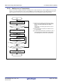
How to Use This Manual
1.
Purpose and Target Readers
This manual is designed to provide the user with an understanding of the hardware functions and electrical
characteristics of the MCU. It is intended for users designing application systems incorporating the MCU. A basic
knowledge of electric circuits, logical circuits, and MCUs is necessary in order to use this manual.
The manual comprises an overview of the product; descriptions of the CPU, system control functions, peripheral
functions, and electrical characteristics; and usage notes.
Particular attention should be paid to the precautionary notes when using the manual. These notes occur
within the body of the text, at the end of each section, and in the Usage Notes section.
The revision history summarizes the locations of revisions and additions. It does not list all revisions. Refer
to the text of the manual for details.
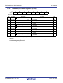
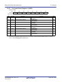
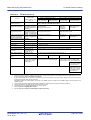
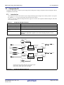
The following documents apply to the R8C/LA6A Group and R8C/LA8A Group. Make sure to refer to the latest
versions of these documents. The newest versions of the documents listed may be obtained from the Renesas
Electronics Web site.
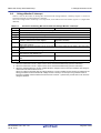
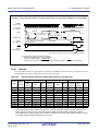
Document Type
Datasheet
Description
Hardware overview
User’s Manual:
Hardware
Hardware specifications (pin
assignments, memory maps,
peripheral function specifications,
electrical characteristics, timing
charts) and operation description
Note: Refer to the application notes
for details on using peripheral
functions.
Description of CPU instruction set
User’s Manual:
Software
Application note
Renesas technical
update
Information on using peripheral
functions and application examples
Sample programs
Information on writing programs in
assembly language and C
Product specifications, updates on
documents, etc.
Document Title
R8C/LA3A Group, R8C/LA5A Group,
R8C/LA6A Group, R8C/LA8A Group
Shortsheet
R8C/LA6A Group, R8C/LA8A Group
User’s Manual: Hardware
Document No.
REJ03B0305
This User’s
Manual
R8C/Tiny Series
REJ09B0001
User’s Manual: Software
Available from the Renesas Electronics Web site.
2.
Notation of Numbers and Symbols
The notation conventions for register names, bit names, numbers, and symbols used in this manual are described
below.
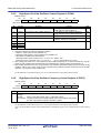
(1) Register Names, Bit Names, and Pin Names
Registers, bits, and pins are referred to in the text by symbols. The symbol is accompanied by the word “register,”
“bit,” or “pin” to distinguish the three categories.
Examples
the PM03 bit in the PM0 register
P3_5 pin, VCC pin
(2) Notation of Numbers
The indication “b” is appended to numeric values given in binary format. However, nothing is appended to the
values of single bits. The indication “h” is appended to numeric values given in hexadecimal format. Nothing is
appended to numeric values given in decimal format.
Examples
Binary: 11b
Hexadecimal: EFA0h
Decimal: 1234
3.
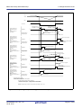
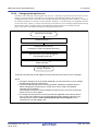
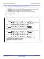
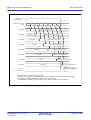
Register Notation
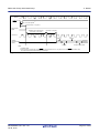
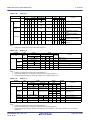
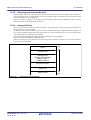
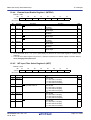
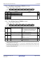
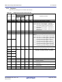
The symbols and terms used in register diagrams are described below.
x.x.x
XXX Register (Symbol)
Address XXXXh
Bit
b7
Symbol XXX7
After Reset
0
Bit
b0
b1
b2
b3
b4
b5
b6
b7
b6
XXX6
0
Symbol
XXX0 XXX bit
XXX1
—
—
XXX4
XXX5
XXX6
XXX7
b5
XXX5
0
b4
XXX4
0
b3
—
0
Bit Name
b2
—
0
b1
XXX1
0
b0
XXX0
0
Function
b1 b0
0 0: XXX
0 1: XXX
1 0: Do not set.
1 1: XXX
Nothing is assigned. If necessary, set to 0. When read, the content is undefined.
Reserved bit
Set to 0.
XXX bit
Function varies according to the operating mode.
XXX bit
0: XXX
1: XXX
*2
*1
R/W
R/W
R/W
—
R/W
R/W
W
R/W
R
*3
*1
R/W: Read and write.
R: Read only.
W: Write only.
−: Nothing is assigned.
*2
• Reserved bit
Reserved bit. Set to specified value.
*3
• Nothing is assigned.
Nothing is assigned to the bit. As the bit may be used for future functions, if necessary, set to 0.
• Do not set to a value.
Operation is not guaranteed when a value is set.
• Function varies according to the operating mode.
The function of the bit varies with the peripheral function mode. Refer to the register diagram for information
on the individual modes.
4.
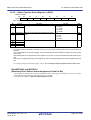
List of Abbreviations and Acronyms
Abbreviation
ACIA
bps
CRC
DMA
DMAC
GSM
Hi-Z
IEBus
I/O
IrDA
LSB
MSB
NC
PLL
PWM
SIM
UART
VCO
Full Form
Asynchronous Communication Interface Adapter
bits per second
Cyclic Redundancy Check
Direct Memory Access
Direct Memory Access Controller
Global System for Mobile Communications
High Impedance
Inter Equipment Bus
Input / Output
Infrared Data Association
Least Significant Bit
Most Significant Bit
Non-Connect
Phase Locked Loop
Pulse Width Modulation
Subscriber Identity Module
Universal Asynchronous Receiver / Transmitter
Voltage Controlled Oscillator
All trademarks and registered trademarks are the property of their respective owners.
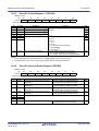
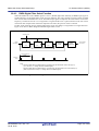
Table of Contents
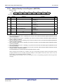
SFR Page Reference ........................................................................................................................... B - 1
1.
Overview ......................................................................................................................................... 1
1.1
1.1.1
1.1.2
1.1.3
1.2
1.3
1.4
1.5
2.
Features ..................................................................................................................................................... 1
Applications .......................................................................................................................................... 1
Differences between Groups ................................................................................................................. 2
Specifications ........................................................................................................................................ 4
Product Lists .............................................................................................................................................. 7
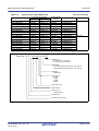
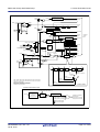
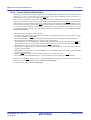
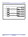
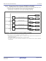
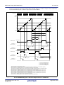
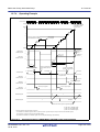
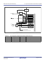
Block Diagrams ......................................................................................................................................... 9
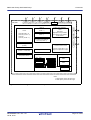
Pin Assignments ...................................................................................................................................... 11
Pin Functions ........................................................................................................................................... 16
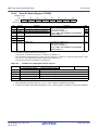
Central Processing Unit (CPU) ..................................................................................................... 18
2.1
2.2
2.3
2.4
2.5
2.6
2.7
2.8
2.8.1
2.8.2
2.8.3
2.8.4
2.8.5
2.8.6
2.8.7
2.8.8
2.8.9
2.8.10
Data Registers (R0, R1, R2, and R3) ......................................................................................................
Address Registers (A0 and A1) ...............................................................................................................
Frame Base Register (FB) .......................................................................................................................
Interrupt Table Register (INTB) ..............................................................................................................
Program Counter (PC) .............................................................................................................................
User Stack Pointer (USP) and Interrupt Stack Pointer (ISP) ..................................................................
Static Base Register (SB) ........................................................................................................................
Flag Register (FLG) ................................................................................................................................
Carry Flag (C) .....................................................................................................................................
Debug Flag (D) ...................................................................................................................................
Zero Flag (Z) .......................................................................................................................................
Sign Flag (S) .......................................................................................................................................
Register Bank Select Flag (B) ............................................................................................................
Overflow Flag (O) ..............................................................................................................................
Interrupt Enable Flag (I) .....................................................................................................................
Stack Pointer Select Flag (U) ..............................................................................................................
Processor Interrupt Priority Level (IPL) .............................................................................................
Reserved Bit ........................................................................................................................................
19
19
19
19
19
19
19
19
19
19
19
19
19
19
20
20
20
20
3.
Memory ......................................................................................................................................... 21
4.
Special Function Registers (SFRs) ............................................................................................... 22
5.
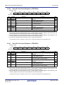
Resets ........................................................................................................................................... 32
5.1
5.1.1
5.1.2
5.1.3
5.1.4
5.2
5.2.1
5.2.2
5.3
5.4
5.5
5.6
Registers ..................................................................................................................................................
Processor Mode Register 0 (PM0) ......................................................................................................
Reset Source Determination Register (RSTFR) .................................................................................
Option Function Select Register (OFS) ..............................................................................................
Option Function Select Register 2 (OFS2) .........................................................................................
Hardware Reset .......................................................................................................................................
When Power Supply is Stable .............................................................................................................
Power On ............................................................................................................................................
Power-On Reset Function .......................................................................................................................
Voltage Monitor 0 Reset .........................................................................................................................
Watchdog Timer Reset ............................................................................................................................
Software Reset .........................................................................................................................................
A-1
35
35
35
36
37
38
38
38
40
41
42
42
5.7
5.8
6.
Cold Start-Up/Warm Start-Up Determination Function ......................................................................... 43
Reset Source Determination Function ..................................................................................................... 43
Voltage Detection Circuit .............................................................................................................. 44
6.1
6.2
6.2.1
6.2.2
6.2.3
6.2.4
6.2.5
6.2.6
6.2.7
6.2.8
6.2.9
6.3
6.3.1
6.3.2
6.3.3
6.4
6.5
6.6
7.
Introduction .............................................................................................................................................
Registers ..................................................................................................................................................
Voltage Monitor Circuit Control Register (CMPA) ...........................................................................
Voltage Monitor Circuit Edge Select Register (VCAC) ...................................................................
Voltage Detect Register 1 (VCA1) .....................................................................................................
Voltage Detect Register 2 (VCA2) .....................................................................................................
Voltage Detection 1 Level Select Register (VD1LS) .........................................................................
Voltage Monitor 0 Circuit Control Register (VW0C) ........................................................................
Voltage Monitor 1 Circuit Control Register (VW1C) ........................................................................
Voltage Monitor 2 Circuit Control Register (VW2C) ........................................................................
Option Function Select Register (OFS) ..............................................................................................
VCC Input Voltage ..................................................................................................................................
Monitoring Vdet0 ...............................................................................................................................
Monitoring Vdet1 ...............................................................................................................................
Monitoring Vdet2 ...............................................................................................................................
Voltage Monitor 0 Reset .........................................................................................................................
Voltage Monitor 1 Interrupt ....................................................................................................................
Voltage Monitor 2 Interrupt ....................................................................................................................
44
48
48
48
49
50
51
52
53
54
55
56
56
56
56
57
58
60
I/O Ports ........................................................................................................................................ 62
7.1
7.2
7.3
7.4
7.5
7.5.1
7.5.2
7.5.3
7.5.4
7.5.5
7.5.6
7.5.7
7.5.8
7.5.9
7.5.10
7.5.11
7.5.12
7.5.13
7.5.14
7.5.15
7.5.16
7.5.17
7.5.18
7.6
7.7
Introduction ............................................................................................................................................. 62
I/O Port Functions ................................................................................................................................... 64
Effect on Peripheral Functions ................................................................................................................ 64
Pins Other than I/O Ports ......................................................................................................................... 64
Registers .................................................................................................................................................. 71
Port Pi Direction Register (PDi) (i = 0 to 9) ....................................................................................... 71
Port Pi Register (Pi) (i = 0 to 9) .......................................................................................................... 72
Timer RJ Pin Select Register (TRJSR) ............................................................................................... 73
Timer RB Pin Select Register (TRBSR) ............................................................................................. 74
Timer RC Pin Select Register 0 (TRCPSR0) ..................................................................................... 75
Timer RC Pin Select Register 1 (TRCPSR1) ..................................................................................... 76
UART0 Pin Select Register (U0SR) ................................................................................................... 77
UART2 Pin Select Register 0 (U2SR0) .............................................................................................. 78
UART2 Pin Select Register 1 (U2SR1) .............................................................................................. 79
SSU/IIC Pin Select Register (SSUIICSR) .......................................................................................... 80
INT Interrupt Input Pin Select Register (INTSR) ............................................................................... 81
I/O Function Pin Select Register (PINSR) ......................................................................................... 82
Port Pi Pull-Up Control Register (PiPUR) (i = 0 to 9) ....................................................................... 82
Port P7 Drive Capacity Control Register (P7DRR) ............................................................................ 83
Port P8 Drive Capacity Control Register (P8DRR) ............................................................................ 83
Input Threshold Control Register 0 (VLT0) ....................................................................................... 84
Input Threshold Control Register 1 (VLT1) ....................................................................................... 85
Input Threshold Control Register 2 (VLT2) ....................................................................................... 86
Port Settings ............................................................................................................................................ 87
Unassigned Pin Handling ...................................................................................................................... 110
A-2
8.
Bus ............................................................................................................................................... 111
9.
Clock Generation Circuit .............................................................................................................. 113
9.1
9.2
9.2.1
9.2.2
9.2.3
9.2.4
9.2.5
9.2.6
9.2.7
9.2.8
9.2.9
9.2.10
9.3
9.4
9.4.1
9.4.2
9.5
9.6
9.6.1
9.6.2
9.6.3
9.6.4
9.6.5
9.6.6
9.6.7
9.6.8
9.6.9
9.6.10
9.6.11
9.6.12
9.7
9.7.1
9.8
9.8.1
9.8.2
9.8.3
10.
Introduction ...........................................................................................................................................
Registers ................................................................................................................................................
System Clock Control Register 0 (CM0) ..........................................................................................
System Clock Control Register 1 (CM1) ..........................................................................................
System Clock Control Register 3 (CM3) ..........................................................................................
Oscillation Stop Detection Register (OCD) ......................................................................................
High-Speed On-Chip Oscillator Control Register 0 (FRA0) ............................................................
High-Speed On-Chip Oscillator Frequency Control Register 0 (FRC0) ..........................................
High-Speed On-Chip Oscillator Control Register 2 (FRA2) ............................................................
High-Speed On-Chip Oscillator 18 MHz Set Value Register 0 (FR18S0) .......................................
High-Speed On-Chip Oscillator 18 MHz Set Value Register 1 (FR18S1) .......................................
High-Speed On-Chip Oscillator Control Register 1 (FRC1) ............................................................
XIN Clock .............................................................................................................................................
On-Chip Oscillator Clock ......................................................................................................................
Low-Speed On-Chip Oscillator Clock ..............................................................................................
High-Speed On-Chip Oscillator Clock .............................................................................................
XCIN Clock ...........................................................................................................................................
CPU Clock and Peripheral Function Clock ...........................................................................................
System Clock ....................................................................................................................................
CPU Clock ........................................................................................................................................
Peripheral Function Clock (f1, f2, f4, f8, f16, and f32) ....................................................................
fOCO .................................................................................................................................................
fOCO20M .........................................................................................................................................
fOCO-F .............................................................................................................................................
fOCO-S .............................................................................................................................................
fOCO128 ...........................................................................................................................................
fC-LCD .............................................................................................................................................
fC and fC32 .......................................................................................................................................
fOCO-WDT ......................................................................................................................................
fC-TRH .............................................................................................................................................
Oscillation Stop Detection Function .....................................................................................................
How to Use Oscillation Stop Detection Function .............................................................................
Notes on Clock Generation Circuit .......................................................................................................
Oscillation Stop Detection Function .................................................................................................
Oscillation Circuit Constants ............................................................................................................
XCIN Clock ......................................................................................................................................
113
116
116
117
118
119
120
120
121
122
122
122
123
124
124
124
125
126
126
126
126
126
126
126
127
127
127
127
127
127
128
128
130
130
130
130
Power Control ............................................................................................................................. 131
10.1
Introduction ...........................................................................................................................................
10.2
Registers ................................................................................................................................................
10.2.1 System Clock Control Register 0 (CM0) ..........................................................................................
10.2.2 System Clock Control Register 1 (CM1) ..........................................................................................
10.2.3 System Clock Control Register 3 (CM3) ..........................................................................................
10.2.4 Oscillation Stop Detection Register (OCD) ......................................................................................
10.2.5 High-Speed On-Chip Oscillator Control Register 0 (FRA0) ............................................................
10.2.6 Voltage Detect Register 2 (VCA2) ...................................................................................................
A-3
131
133
133
134
135
136
137
138
10.2.7 Power-Off Mode Control Register 0 (POMCR0) .............................................................................
10.3
Standard Operating Mode .....................................................................................................................
10.3.1 High-Speed Clock Mode ..................................................................................................................
10.3.2 Low-Speed Clock Mode ...................................................................................................................
10.3.3 High-Speed On-Chip Oscillator Mode .............................................................................................
10.3.4 Low-Speed On-Chip Oscillator Mode ..............................................................................................
10.4
Wait Mode .............................................................................................................................................
10.4.1 Peripheral Function Clock Stop Function .........................................................................................
10.4.2 Entering Wait Mode ..........................................................................................................................
10.4.3 Pin Status in Wait Mode ...................................................................................................................
10.4.4 Exiting Wait Mode ............................................................................................................................
10.5
Stop Mode .............................................................................................................................................
10.5.1 Entering Stop Mode ..........................................................................................................................
10.5.2 Pin Status in Stop Mode ....................................................................................................................
10.5.3 Exiting Stop Mode ............................................................................................................................
10.6
Power-Off 0 Mode .................................................................................................................................
10.6.1 Pin Handling in Power-Off 0 Mode ..................................................................................................
10.6.2 Entering Power-Off 0 Mode .............................................................................................................
10.6.3 Pin Status in Power-Off 0 Mode .......................................................................................................
10.6.4 Exiting Power-Off 0 Mode ...............................................................................................................
10.7
Power-off 2 Mode .................................................................................................................................
10.7.1 Entering Power-off 2 Mode ..............................................................................................................
10.7.2 Pin Status in Power-off 2 Mode ........................................................................................................
10.7.3 Exiting Power-off 2 Mode ................................................................................................................
10.8
Reducing Power Consumption ..............................................................................................................
10.8.1 Voltage Detection Circuit .................................................................................................................
10.8.2 Ports ..................................................................................................................................................
10.8.3 Clocks ...............................................................................................................................................
10.8.4 Wait Mode, Stop Mode, and Power-Off Mode ................................................................................
10.8.5 Stopping Peripheral Function Clocks ...............................................................................................
10.8.6 Timers ...............................................................................................................................................
10.8.7 A/D Converter ...................................................................................................................................
10.8.8 Clock Synchronous Serial Interface .................................................................................................
10.8.9 Reducing Internal Power Consumption ............................................................................................
10.8.10 Stopping Flash Memory ....................................................................................................................
10.8.11 Low-Current-Consumption Read Mode ...........................................................................................
10.9
Notes on Power Control ........................................................................................................................
10.9.1 Stop Mode .........................................................................................................................................
10.9.2 Wait Mode ........................................................................................................................................
10.9.3 Power-Off 0 Mode ............................................................................................................................
10.9.4 Power-Off 2 Mode ............................................................................................................................
11.
139
140
141
141
141
141
142
142
142
142
143
146
146
146
147
148
148
148
148
149
150
150
150
151
152
152
152
152
152
152
152
153
153
153
154
155
156
156
156
157
157
Protection .................................................................................................................................... 158
11.1
Register .................................................................................................................................................. 158
11.1.1 Protect Register (PRCR) ................................................................................................................... 158
12.
Interrupts ..................................................................................................................................... 159
12.1
Introduction ........................................................................................................................................... 159
12.1.1 Types of Interrupts ............................................................................................................................ 159
A-4
12.1.2 Software Interrupts ........................................................................................................................... 160
12.1.3 Special Interrupts .............................................................................................................................. 161
12.1.4 Peripheral Function Interrupts .......................................................................................................... 161
12.1.5 Interrupts and Interrupt Vectors ........................................................................................................ 162
12.2
Registers ................................................................................................................................................ 164
12.2.1 Interrupt Control Register
(S2TIC, S2RIC, KUPIC, ADIC, S0TIC, S0RIC, TRJ0IC, TRB1IC, TRB0IC, TRJ1IC, TRJ2IC,
U2BCNIC, LCDIC, VCMP1IC, VCMP2IC) .................................................................................... 164
12.2.2 Interrupt Control Register
(FMRDYIC, TRCIC, SSUIC/IICIC, TRHIC) ................................................................................... 165
12.2.3 INTi Interrupt Control Register (INTiIC) (i = 0 to 7) ....................................................................... 166
12.3
Interrupt Control .................................................................................................................................... 167
12.3.1 I Flag ................................................................................................................................................. 167
12.3.2 IR Bit ................................................................................................................................................. 167
12.3.3 Bits ILVL2 to ILVL0, IPL ................................................................................................................ 167
12.3.4 Interrupt Sequence ............................................................................................................................ 168
12.3.5 Interrupt Response Time ................................................................................................................... 169
12.3.6 IPL Change when Interrupt Request is Acknowledged .................................................................... 169
12.3.7 Saving Registers ............................................................................................................................... 170
12.3.8 Returning from Interrupt Routine ..................................................................................................... 172
12.3.9 Interrupt Priority ............................................................................................................................... 172
12.3.10 Interrupt Priority Level Selection Circuit ......................................................................................... 173
12.4
INT Interrupt ......................................................................................................................................... 174
12.4.1 INTi Interrupt (i = 0 to 7) .................................................................................................................. 174
12.4.2 INT Interrupt Input Pin Select Register (INTSR) ............................................................................. 175
12.4.3 External Input Enable Register 0 (INTEN) ...................................................................................... 176
12.4.4 External Input Enable Register 1 (INTEN1) .................................................................................... 177
12.4.5 INT Input Filter Select Register 0 (INTF) ........................................................................................ 177
12.4.6 INT Input Filter Select Register 1 (INTF1) ...................................................................................... 178
12.4.7
INTi Input Filter (i = 0 to 7) ............................................................................................................. 179
12.5
Key Input Interrupt ................................................................................................................................ 180
12.5.1 Key Input Enable Register 0 (KIEN) ................................................................................................ 182
12.5.2 Key Input Enable Register 1 (KIEN1) .............................................................................................. 183
12.6
Address Match Interrupt ........................................................................................................................ 184
12.6.1 Address Match Interrupt Enable Register i (AIERi) (i = 0 or 1) ...................................................... 185
12.6.2 Address Match Interrupt Register i (RMADi) (i = 0 or 1) ................................................................ 185
12.7
Interrupts of Timer RC, Timer RH, Synchronous Serial Communication Unit, I2C bus Interface, and Flash
Memory (Interrupts with Multiple Interrupt Request Sources).............................................................. 186
12.8
Notes on Interrupts ................................................................................................................................ 188
12.8.1 Reading Address 00000h .................................................................................................................. 188
12.8.2 SP Setting .......................................................................................................................................... 188
12.8.3 External Interrupt, Key Input Interrupt ............................................................................................. 188
12.8.4 Changing Interrupt Sources .............................................................................................................. 189
12.8.5 Rewriting Interrupt Control Register ................................................................................................ 190
13.
13.1
13.2
13.3
ID Code Areas ............................................................................................................................ 191
Introduction ........................................................................................................................................... 191
Functions ............................................................................................................................................... 192
Forced Erase Function ........................................................................................................................... 193
A-5
13.4
Standard Serial I/O Mode Disabled Function ....................................................................................... 193
13.5
Notes on ID Code Areas ........................................................................................................................ 194
13.5.1 Setting Example of ID Code Areas ................................................................................................... 194
14.
Option Function Select Area ....................................................................................................... 195
14.1
Introduction ...........................................................................................................................................
14.2
Registers ................................................................................................................................................
14.2.1 Option Function Select Register (OFS) ............................................................................................
14.2.2 Option Function Select Register 2 (OFS2) .......................................................................................
14.3
Notes on Option Function Select Area ..................................................................................................
14.3.1 Setting Example of Option Function Select Area .............................................................................
15.
195
196
196
197
198
198
Watchdog Timer .......................................................................................................................... 199
15.1
Introduction ........................................................................................................................................... 199
15.2
Registers ................................................................................................................................................ 201
15.2.1 Processor Mode Register 1 (PM1) .................................................................................................... 201
15.2.2 Watchdog Timer Reset Register (WDTR) ........................................................................................ 201
15.2.3 Watchdog Timer Start Register (WDTS) ......................................................................................... 201
15.2.4 Watchdog Timer Control Register (WDTC) .................................................................................... 202
15.2.5 Count Source Protection Mode Register (CSPR) ............................................................................. 202
15.2.6 Option Function Select Register (OFS) ............................................................................................ 203
15.2.7 Option Function Select Register 2 (OFS2) ....................................................................................... 204
15.3
Functional Description ......................................................................................................................... 205
15.3.1 Common Items for Multiple Modes ................................................................................................. 205
15.3.2 Count Source Protection Mode Disabled .......................................................................................... 206
15.3.3 Count Source Protection Mode Enabled ........................................................................................... 207
16.
Timers ......................................................................................................................................... 208
17.
Timer RB ...................................................................................................................................... 211
17.1
17.2
17.2.1
17.2.2
17.2.3
17.2.4
17.2.5
17.2.6
17.2.7
17.2.8
17.2.9
17.3
17.3.1
17.3.2
17.4
17.4.1
Introduction ........................................................................................................................................... 211
Registers ................................................................................................................................................ 213
Module Standby Control Register 1 (MSTCR1) .............................................................................. 213
Timer RBi Control Register (TRBiCR) (i = 0 or 1) ......................................................................... 214
Timer RBi One-Shot Control Register (TRBiOCR) (i = 0 or 1) ...................................................... 214
Timer RBi I/O Control Register (TRBiIOC) (i = 0 or 1) .................................................................. 215
Timer RBi Mode Register (TRBiMR) (i = 0 or 1) ........................................................................... 215
Timer RBi Prescaler Register (TRBiPRE) (i = 0 or 1) ..................................................................... 216
Timer RBi Secondary Register (TRBiSC) (i = 0 or 1) ..................................................................... 216
Timer RBi Primary Register (TRBiPR) (i = 0 or 1) ......................................................................... 217
Timer RB Pin Select Register (TRBSR) ........................................................................................... 217
Timer Mode ........................................................................................................................................... 218
Timer RBi I/O Control Register (TRBiIOC) (i = 0 or 1) in Timer Mode ........................................ 218
Timer Write Control during Count Operation .................................................................................. 219
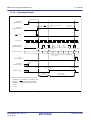
Programmable Waveform Generation Mode ........................................................................................ 221
Timer RBi I/O Control Register (TRBiIOC) (i = 0 or 1) in Programmable Waveform Generation Mode
........................................................................................................................................................... 222
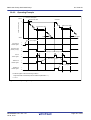
17.4.2 Operating Example ........................................................................................................................... 223
17.5
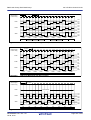
Programmable One-shot Generation Mode ........................................................................................... 224
A-6
17.5.1
17.5.2
17.5.3
17.6
17.6.1
17.6.2
17.7
17.7.1
17.7.2
17.7.3
17.7.4
18.
Timer RBi I/O Control Register (TRBiIOC) (i = 0 or 1) in Programmable One-Shot Generation Mode
........................................................................................................................................................... 225
Operating Example ........................................................................................................................... 226
One-Shot Trigger Selection .............................................................................................................. 227
Programmable Wait One-Shot Generation Mode ................................................................................. 228
Timer RBi I/O Control Register (TRBiIOC) (i = 0 or 1) in Programmable Wait One-Shot Generation
Mode .................................................................................................................................................. 229
Operating Example ........................................................................................................................... 230
Notes on Timer RB ................................................................................................................................ 231
Timer Mode ...................................................................................................................................... 231
Programmable Waveform Generation Mode .................................................................................... 231
Programmable One-Shot Generation Mode ..................................................................................... 232
Programmable Wait One-shot Generation Mode ............................................................................. 232
Timer RC ..................................................................................................................................... 233
18.1
Introduction ...........................................................................................................................................
18.2
Registers ................................................................................................................................................
18.2.1 Module Standby Control Register 0 (MSTCR0) ..............................................................................
18.2.2 Timer RC Mode Register (TRCMR) ................................................................................................
18.2.3 Timer RC Control Register 1 (TRCCR1) .........................................................................................
18.2.4 Timer RC Interrupt Enable Register (TRCIER) ...............................................................................
18.2.5 Timer RC Status Register (TRCSR) .................................................................................................
18.2.6 Timer RC I/O Control Register 0 (TRCIOR0) .................................................................................
18.2.7 Timer RC I/O Control Register 1 (TRCIOR1) .................................................................................
18.2.8 Timer RC Counter (TRC) .................................................................................................................
18.2.9 Timer RC General Registers A, B, C, and D (TRCGRA, TRCGRB, TRCGRC, TRCGRD) ..........
18.2.10 Timer RC Control Register 2 (TRCCR2) .........................................................................................
18.2.11 Timer RC Digital Filter Function Select Register (TRCDF) ............................................................
18.2.12 Timer RC Output Master Enable Register (TRCOER) ....................................................................
18.2.13 Timer RC Trigger Control Register (TRCADCR) ...........................................................................
18.2.14 Timer RC Pin Select Register 0 (TRCPSR0) ...................................................................................
18.2.15 Timer RC Pin Select Register 1 (TRCPSR1) ...................................................................................
18.3
Common Items for Multiple Modes ......................................................................................................
18.3.1 Count Source .....................................................................................................................................
18.3.2 Buffer Operation ...............................................................................................................................
18.3.3 Digital Filter ......................................................................................................................................
18.3.4 Forced Cutoff of Pulse Output ..........................................................................................................
18.4
Timer Mode (Input Capture Function) ..................................................................................................
18.4.1 Timer RC I/O Control Register 0 (TRCIOR0) in Timer Mode (Input Capture Function) ...............
18.4.2 Timer RC I/O Control Register 1 (TRCIOR1) in Timer Mode (Input Capture Function) ...............
18.4.3 Operating Example ...........................................................................................................................
18.5
Timer Mode (Output Compare Function) .............................................................................................
18.5.1 Timer RC Control Register 1 (TRCCR1) in Timer Mode (Output Compare Function) ..................
18.5.2 Timer RC I/O Control Register 0 (TRCIOR0) in Timer Mode (Output Compare Function) ..........
18.5.3 Timer RC I/O Control Register 1 (TRCIOR1) in Timer Mode (Output Compare Function) ..........
18.5.4 Timer RC Control Register 2 (TRCCR2) in Timer Mode (Output Compare Function) ..................
18.5.5 Operating Example ...........................................................................................................................
18.5.6 Changing Output Pins in Registers TRCGRC and TRCGRD ..........................................................
18.6
PWM Mode ...........................................................................................................................................
A-7
233
235
236
237
238
238
239
240
240
241
241
242
243
244
244
245
246
247
247
248
250
251
253
255
256
257
258
260
261
262
263
264
265
267
18.6.1 Timer RC Control Register 1 (TRCCR1) in PWM Mode ................................................................ 269
18.6.2 Timer RC Control Register 2 (TRCCR2) in PWM Mode ................................................................ 270
18.6.3 Operating Example ........................................................................................................................... 271
18.7
PWM2 Mode ......................................................................................................................................... 273
18.7.1 Timer RC Control Register 1 (TRCCR1) in PWM2 Mode .............................................................. 275
18.7.2 Timer RC Control Register 2 (TRCCR2) in PWM2 Mode .............................................................. 276
18.7.3 Timer RC Digital Filter Function Select Register (TRCDF) in PWM2 Mode ................................. 277
18.7.4 Operating Example ........................................................................................................................... 278
18.8
Timer RC Interrupt ................................................................................................................................ 281
18.9
Notes on Timer RC ................................................................................................................................ 282
18.9.1 TRC Register .................................................................................................................................... 282
18.9.2
TRCSR Register .............................................................................................................................. 282
18.9.3 TRCCR1 Register ............................................................................................................................. 282
18.9.4 Count Source Switching ................................................................................................................... 282
18.9.5 Input Capture Function ..................................................................................................................... 283
18.9.6 TRCMR Register in PWM2 Mode ................................................................................................... 283
19.
Timer RH ..................................................................................................................................... 284
19.1
Introduction ...........................................................................................................................................
19.2
Real-Time Clock Mode .........................................................................................................................
19.2.1 Module Standby Control Register 1 (MSTCR1) ..............................................................................
19.2.2 Timer RH Second Data Register (TRHSEC) in Real-Time Clock Mode ........................................
19.2.3 Timer RH Minute Data Register (TRHMIN) in Real-Time Clock Mode ........................................
19.2.4 Timer RH Hour Data Register (TRHHR) in Real-Time Clock Mode ..............................................
19.2.5 Timer RH Day-of-the-Week Data Register (TRHWK) in Real-Time Clock Mode .........................
19.2.6 Timer RH Date Data Register (TRHDY) in Real-Time Clock Mode ..............................................
19.2.7 Timer RH Month Data Register (TRHMON) in Real-Time Clock Mode .......................................
19.2.8 Timer RH Year Data Register (TRHYR) in Real-Time Clock Mode ..............................................
19.2.9 Timer RH Control Register (TRHCR) in Real-Time Clock Mode ..................................................
19.2.10 Timer RH Count Source Select Register (TRHCSR) in Real-Time Clock Mode ............................
19.2.11 Timer RH Clock Error Correction Register (TRHADJ) in Real-Time Clock Mode ........................
19.2.12 Timer RH Interrupt Flag Register (TRHIFR) in Real-Time Clock Mode ........................................
19.2.13 Timer RH Interrupt Enable Register (TRHIER) in Real-Time Clock Mode ...................................
19.2.14 Timer RH Alarm Minute Register (TRHAMN) in Real-Time Clock Mode ....................................
19.2.15 Timer RH Alarm Hour Register (TRHAHR) in Real-Time Clock Mode ........................................
19.2.16 Timer RH Alarm Day-of-Week Data Register (TRHAWK) in Real-Time Clock Mode .................
19.2.17 Timer RH Protect Register (TRHPRC) in Real-Time Clock Mode .................................................
19.2.18 Timer RH Second Interrupt Control Register (TRHICR) in Real-Time Clock ................................
19.2.19 Operating Example ...........................................................................................................................
19.2.20 Alarm Function .................................................................................................................................
19.2.21 Second Adjustment Function ............................................................................................................
19.2.22 Clock Error Correction Function ......................................................................................................
19.2.23 Clock Output .....................................................................................................................................
19.3
Output Compare Mode ..........................................................................................................................
19.3.1 Timer RH Counter Data Register (TRHSEC) in Output Compare Mode ........................................
19.3.2 Timer RH Compare Data Register (TRHMIN) in Output Compare Mode ......................................
19.3.3 Timer RH Control Register (TRHCR) in Output Compare Mode ...................................................
19.3.4 Timer RH Count Source Select Register (TRHCSR) in Output Compare Mode .............................
19.3.5 Timer RH Interrupt Flag Register (TRHIFR) in Output Compare Mode .........................................
A-8
284
285
287
288
289
290
291
292
293
294
295
298
299
300
301
302
303
304
305
306
308
311
313
315
318
319
320
320
321
322
324
19.3.6 Timer RH Interrupt Enable Register (TRHIER) in Output Compare Mode ....................................
19.3.7 Timer RH Protect Register (TRHPRC) in Output Compare Mode ..................................................
19.3.8 Operating Example ...........................................................................................................................
19.4
Notes on Timer RH ...............................................................................................................................
19.4.1 Reset ..................................................................................................................................................
19.4.2 Starting and Stopping Count .............................................................................................................
19.4.3 Register Setting .................................................................................................................................
19.4.4 Time Reading Procedure in Real-Time Clock Mode .......................................................................
20.
Timer RJ ..................................................................................................................................... 330
20.1
20.2
20.2.1
20.2.2
20.2.3
20.2.4
20.2.5
20.2.6
20.2.7
20.2.8
20.3
20.3.1
20.3.2
20.4
20.4.1
20.5
20.5.1
20.6
20.6.1
20.6.2
20.7
20.7.1
20.7.2
20.8
21.
325
325
326
328
328
328
328
329
Introduction ...........................................................................................................................................
Registers ................................................................................................................................................
Module Standby Control Register 1 (MSTCR1) ..............................................................................
Timer RJi Control Register (TRJiCR) (i = 0 to 2) ............................................................................
Timer RJi I/O Control Register (TRJiIOC) (i = 0 to 2) ....................................................................
Timer RJi Mode Register (TRJiMR) (i = 0 to 2) ..............................................................................
Timer RJi Event Pin Select Register (TRJiISR) (i = 0 to 2) .............................................................
Timer RJi Register (TRJi) (i = 0 to 2) ..............................................................................................
Timer RJ Pin Select Register (TRJSR) .............................................................................................
Timer RB Pin Select Register (TRBSR) ...........................................................................................
Timer Mode ...........................................................................................................................................
Timer RJi I/O Control Register (TRJiIOC) (i = 0 to 2) in Timer Mode ...........................................
Timer Write Control during Count Operation ..................................................................................
Pulse Output Mode ................................................................................................................................
Timer RJi I/O Control Register (TRJiIOC) (i = 0 to 2) in Pulse Output Mode ................................
Event Counter Mode .............................................................................................................................
Timer RJi I/O Control Register (TRJiIOC) (i = 0 to 2) in Event Counter Mode .............................
Pulse Width Measurement Mode ..........................................................................................................
Timer RJi I/O Control Register (TRJiIOC) (i = 0 to 2) in Pulse Width Measurement Mode ..........
Operating Example ...........................................................................................................................
Pulse Period Measurement Mode ..........................................................................................................
Timer RJi I/O Control Register (TRJiIOC) (i = 0 to 2) in Pulse Period Measurement Mode ..........
Operating Example ...........................................................................................................................
Notes on Timer RJ .................................................................................................................................
330
332
332
333
333
334
335
335
336
337
338
339
340
341
342
343
344
345
346
347
348
349
350
351
Serial Interface (UART0) ............................................................................................................ 352
21.1
Introduction ...........................................................................................................................................
21.2
Registers ................................................................................................................................................
21.2.1 Module Standby Control Register 0 (MSTCR0) ..............................................................................
21.2.2 UART0 Transmit/Receive Mode Register (U0MR) .........................................................................
21.2.3 UART0 Bit Rate Register (U0BRG) ................................................................................................
21.2.4 UART0 Transmit Buffer Register (U0TB) .......................................................................................
21.2.5 UART0 Transmit/Receive Control Register 0 (U0C0) ....................................................................
21.2.6 UART0 Transmit/Receive Control Register 1 (U0C1) ....................................................................
21.2.7 UART0 Receive Buffer Register (U0RB) ........................................................................................
21.2.8 UART0 Pin Select Register (U0SR) .................................................................................................
21.3
Clock Synchronous Serial I/O Mode .....................................................................................................
21.3.1 Measure for Dealing with Communication Errors ...........................................................................
21.3.2 Polarity Select Function ....................................................................................................................
A-9
352
354
354
355
355
356
357
357
358
359
360
364
365
21.3.3 LSB First/MSB First Select Function ...............................................................................................
21.3.4 Continuous Receive Mode ................................................................................................................
21.4
Clock Asynchronous Serial I/O (UART) Mode ....................................................................................
21.4.1 Bit Rate .............................................................................................................................................
21.4.2 Measure for Dealing with Communication Errors ...........................................................................
21.5
Notes on Serial Interface (UART0) .......................................................................................................
22.
365
366
367
372
373
374
Serial Interface (UART2) ............................................................................................................ 375
22.1
Introduction ...........................................................................................................................................
22.2
Registers ................................................................................................................................................
22.2.1 Module Standby Control Register 0 (MSTCR0) ..............................................................................
22.2.2 UART2 Transmit/Receive Mode Register (U2MR) .........................................................................
22.2.3 UART2 Bit Rate Register (U2BRG) ................................................................................................
22.2.4 UART2 Transmit Buffer Register (U2TB) .......................................................................................
22.2.5 UART2 Transmit/Receive Control Register 0 (U2C0) ....................................................................
22.2.6 UART2 Transmit/Receive Control Register 1 (U2C1) ....................................................................
22.2.7 UART2 Receive Buffer Register (U2RB) ........................................................................................
22.2.8 UART2 Digital Filter Function Select Register (URXDF) ..............................................................
22.2.9 UART2 Special Mode Register 5 (U2SMR5) ..................................................................................
22.2.10 UART2 Special Mode Register 4 (U2SMR4) ..................................................................................
22.2.11 UART2 Special Mode Register 3 (U2SMR3) ..................................................................................
22.2.12 UART2 Special Mode Register 2 (U2SMR2) ..................................................................................
22.2.13 UART2 Special Mode Register (U2SMR) .......................................................................................
22.2.14 UART2 Pin Select Register 0 (U2SR0) ............................................................................................
22.2.15 UART2 Pin Select Register 1 (U2SR1) ............................................................................................
22.3
Clock Synchronous Serial I/O Mode .....................................................................................................
22.3.1 Measure for Dealing with Communication Errors ...........................................................................
22.3.2 CLK Polarity Select Function ...........................................................................................................
22.3.3 LSB First/MSB First Select Function ...............................................................................................
22.3.4 Continuous Receive Mode ................................................................................................................
22.3.5 Serial Data Logic Switching Function ..............................................................................................
22.3.6 CTS/RTS Function ............................................................................................................................
22.4
Clock Asynchronous Serial I/O (UART) Mode ....................................................................................
22.4.1 Bit Rate .............................................................................................................................................
22.4.2 Measure for Dealing with Communication Errors ...........................................................................
22.4.3 LSB First/MSB First Select Function ...............................................................................................
22.4.4 Serial Data Logic Switching Function ..............................................................................................
22.4.5 TXD and RXD I/O Polarity Inverse Function ..................................................................................
22.4.6 CTS/RTS Function ............................................................................................................................
22.4.7 RXD2 Digital Filter Select Function ................................................................................................
22.5
Special Mode 1 (I2C Mode) ..................................................................................................................
22.5.1 Detection of Start and Stop Conditions ............................................................................................
22.5.2 Output of Start and Stop Conditions .................................................................................................
22.5.3 Transfer Clock ..................................................................................................................................
22.5.4 SDA Output ......................................................................................................................................
22.5.5 SDA Input .........................................................................................................................................
22.5.6 ACK and NACK ...............................................................................................................................
22.5.7 Initialization of Transmission/Reception ..........................................................................................
22.6
Multiprocessor Communication Function .............................................................................................
A - 10
375
377
377
378
378
379
380
381
382
383
383
384
385
385
386
386
387
388
392
392
393
393
394
394
395
399
400
400
401
401
402
402
403
409
410
411
411
412
412
412
413
22.6.1 Multiprocessor Transmission ............................................................................................................
22.6.2 Multiprocessor Reception .................................................................................................................
22.6.3 RXD2 Digital Filter Select Function ................................................................................................
22.7
Notes on Serial Interface (UART2) .......................................................................................................
22.7.1 Clock Synchronous Serial I/O Mode ................................................................................................
22.7.2 Special Mode 1 (I2C Mode) ..............................................................................................................
23.
23.1
24.
Clock Synchronous Serial Interface ............................................................................................ 421
Mode Selection ...................................................................................................................................... 421
Synchronous Serial Communication Unit (SSU) ........................................................................ 422
24.1
Introduction ...........................................................................................................................................
24.2
Registers ................................................................................................................................................
24.2.1 Module Standby Control Register 0 (MSTCR0) ..............................................................................
24.2.2 SSU/IIC Pin Select Register (SSUIICSR) ........................................................................................
24.2.3 SS Bit Counter Register (SSBR) ......................................................................................................
24.2.4 SS Transmit Data Register (SSTDR) ................................................................................................
24.2.5 SS Receive Data Register (SSRDR) .................................................................................................
24.2.6 SS Control Register H (SSCRH) ......................................................................................................
24.2.7 SS Control Register L (SSCRL) .......................................................................................................
24.2.8 SS Mode Register (SSMR) ...............................................................................................................
24.2.9 SS Enable Register (SSER) ..............................................................................................................
24.2.10 SS Status Register (SSSR) ................................................................................................................
24.2.11 SS Mode Register 2 (SSMR2) ..........................................................................................................
24.3
Common Items for Multiple Modes ......................................................................................................
24.3.1 Transfer Clock ..................................................................................................................................
24.3.2 SS Shift Register (SSTRSR) .............................................................................................................
24.3.3 Interrupt Requests .............................................................................................................................
24.3.4 Communication Modes and Pin Functions .......................................................................................
24.4
Clock Synchronous Communication Mode ..........................................................................................
24.4.1 Initialization in Clock Synchronous Communication Mode ............................................................
24.4.2 Data Transmission ............................................................................................................................
24.4.3 Data Reception ..................................................................................................................................
24.5
Operation in 4-Wire Bus Communication Mode ..................................................................................
24.5.1 Initialization in 4-Wire Bus Communication Mode .........................................................................
24.5.2 Data Transmission ............................................................................................................................
24.5.3 Data Reception ..................................................................................................................................
24.5.4 SCS Pin Control and Arbitration ......................................................................................................
24.6
Notes on Synchronous Serial Communication Unit (SSU) ...................................................................
25.
416
417
419
420
420
420
422
424
424
425
426
426
427
427
428
429
430
431
432
433
433
435
436
437
438
438
439
441
445
445
447
449
451
452
I2C bus Interface ......................................................................................................................... 453
25.1
Introduction ...........................................................................................................................................
25.2
Registers ................................................................................................................................................
25.2.1 Module Standby Control Register 0 (MSTCR0) ..............................................................................
25.2.2 SSU/IIC Pin Select Register (SSUIICSR) ........................................................................................
25.2.3 I/O Function Pin Select Register (PINSR) .......................................................................................
25.2.4 IIC bus Transmit Data Register (ICDRT) .........................................................................................
25.2.5 IIC bus Receive Data Register (ICDRR) ..........................................................................................
25.2.6 IIC bus Control Register 1 (ICCR1) .................................................................................................
A - 11
453
456
456
457
457
458
458
459
25.2.7 IIC bus Control Register 2 (ICCR2) .................................................................................................
25.2.8 IIC bus Mode Register (ICMR) ........................................................................................................
25.2.9 IIC bus Interrupt Enable Register (ICIER) .......................................................................................
25.2.10 IIC bus Status Register (ICSR) .........................................................................................................
25.2.11 Slave Address Register (SAR) ..........................................................................................................
25.2.12 IIC bus Shift Register (ICDRS) ........................................................................................................
25.3
Common Items for Multiple Modes ......................................................................................................
25.3.1 Transfer Clock ..................................................................................................................................
25.3.2 SDA Pin Digital Delay Selection ......................................................................................................
25.3.3 Interrupt Requests .............................................................................................................................
25.4
I2C bus Interface Mode .........................................................................................................................
25.4.1 I2C bus Format ..................................................................................................................................
25.4.2 Master Transmit Operation ...............................................................................................................
25.4.3 Master Receive Operation ................................................................................................................
25.4.4 Slave Transmit Operation .................................................................................................................
25.4.5 Slave Receive Operation ...................................................................................................................
25.5
Clock Synchronous Serial Mode ...........................................................................................................
25.5.1 Clock Synchronous Serial Format ....................................................................................................
25.5.2 Transmit Operation ...........................................................................................................................
25.5.3 Receive Operation .............................................................................................................................
25.6
Register Setting Examples .....................................................................................................................
25.7
Noise Canceller .....................................................................................................................................
25.8
Bit Synchronization Circuit ...................................................................................................................
25.9
Notes on I2C bus Interface ....................................................................................................................
25.9.1 Master Receive Mode .......................................................................................................................
25.9.2 The ICE Bit in the ICCR1 Register and the IICRST Bit in the ICCR2 Register .............................
26.
460
461
462
463
464
464
465
465
467
468
469
469
470
472
475
478
480
480
481
482
483
487
488
489
489
489
A/D Converter ............................................................................................................................. 490
26.1
26.2
26.2.1
26.2.2
26.2.3
26.2.4
26.2.5
26.2.6
26.2.7
26.2.8
26.3
26.3.1
26.3.2
26.3.3
26.3.4
26.3.5
26.3.6
26.3.7
26.4
26.5
26.6
Introduction ...........................................................................................................................................
Registers ................................................................................................................................................
Module Standby Control Register 0 (MSTCR0) ..............................................................................
On-Chip Reference Voltage Control Register (OCVREFCR) .........................................................
A/D Register i (ADi) (i = 0 to 7) ......................................................................................................
A/D Mode Register (ADMOD) ........................................................................................................
A/D Input Select Register (ADINSEL) ............................................................................................
A/D Control Register 0 (ADCON0) .................................................................................................
A/D Control Register 1 (ADCON1) .................................................................................................
A/D Control Register 2 (ADCON2) .................................................................................................
Common Items for Multiple Modes ......................................................................................................
Input/Output Pins ..............................................................................................................................
A/D Conversion Cycles ....................................................................................................................
A/D Conversion Start Conditions .....................................................................................................
A/D Conversion Result .....................................................................................................................
Low-Current-Consumption Function ...............................................................................................
On-Chip Reference Voltage (OCVREF) ..........................................................................................
A/D Open-Circuit Detection Assist Function ...................................................................................
One-Shot Mode .....................................................................................................................................
Repeat Mode 0 .......................................................................................................................................
Repeat Mode 1 .......................................................................................................................................
A - 12
490
492
492
493
494
495
496
497
498
499
500
500
500
502
504
504
504
504
506
507
508
26.7
Single Sweep Mode ...............................................................................................................................
26.8
Repeat Sweep Mode ..............................................................................................................................
26.9
Temperature Sensor ...............................................................................................................................
26.9.1 Temperature Sensor Setting Procedure .............................................................................................
26.10 Output Impedance of Sensor under A/D Conversion ............................................................................
26.11 Notes on A/D Converter ........................................................................................................................
26.11.1 A/D Converter ...................................................................................................................................
26.11.2 Temperature Sensor ..........................................................................................................................
27.
Comparator B ............................................................................................................................. 518
27.1
27.2
27.2.1
27.2.2
27.2.3
27.3
27.3.1
27.4
28.
510
512
514
515
516
517
517
517
Introduction ...........................................................................................................................................
Registers ................................................................................................................................................
Comparator B Control Register 0 (INTCMP) ..................................................................................
External Input Enable Register 0 (INTEN) ......................................................................................
INT Input Filter Select Register 0 (INTF) ........................................................................................
Functional Description ..........................................................................................................................
Comparator Bi Digital Filter (i = 1 or 3) ..........................................................................................
Comparator B1 and Comparator B3 Interrupts .....................................................................................
518
520
520
520
521
522
523
524
LCD Drive Control Circuit ........................................................................................................... 525
28.1
Introduction ...........................................................................................................................................
28.2
Registers ................................................................................................................................................
28.2.1 Module Standby Control Register 0 (MSTCR0) ..............................................................................
28.2.2 LCD Control Register (LCR0) .........................................................................................................
28.2.3 LCD Option Clock Control Register (LCR2) ...................................................................................
28.2.4 LCD Clock Control Register (LCR3) ...............................................................................................
28.2.5 LCD Display Control Register (LCR4) ............................................................................................
28.2.6 LCD Port Select Register 0 (LSE0) ..................................................................................................
28.2.7 LCD Port Select Register 1 (LSE1) ..................................................................................................
28.2.8 LCD Port Select Register 2 (LSE2) ..................................................................................................
28.2.9 LCD Port Select Register 3 (LSE3) ..................................................................................................
28.2.10 LCD Port Select Register 4 (LSE4) ..................................................................................................
28.2.11 LCD Port Select Register 5 (LSE5) ..................................................................................................
28.3
Data Registers ........................................................................................................................................
28.4
LCD Drive Control ................................................................................................................................
28.4.1 Segment Output Pin Selection ..........................................................................................................
28.4.2 LCD Clock Selection ........................................................................................................................
28.4.3 Bias Control ......................................................................................................................................
28.4.4 LCD Data Display ............................................................................................................................
28.4.5 Pin Status in Stop Mode and Power-Off 2 Mode .............................................................................
28.4.6 Pin Status in Power-Off 0 Mode .......................................................................................................
28.5
LCD Drive Waveform ...........................................................................................................................
28.5.1 Segment Panel Drive Waveform ......................................................................................................
28.5.2 Drive Waveform of Memory-Type Liquid Crystal Panel ................................................................
28.5.3 Interrupt Control Waveform .............................................................................................................
28.6
Notes on LCD Drive Control Circuit ....................................................................................................
28.6.1 When Division Resistors are Connected Externally .........................................................................
A - 13
525
528
528
529
529
530
530
531
531
532
532
533
533
534
535
537
537
537
538
538
538
539
539
543
544
545
545
29.
Flash Memory ............................................................................................................................. 546
29.1
Introduction ...........................................................................................................................................
29.2
Memory Map .........................................................................................................................................
29.3
Functions to Prevent Flash Memory from being Rewritten ..................................................................
29.3.1 ID Code Check Function ..................................................................................................................
29.3.2 ROM Code Protect Function ............................................................................................................
29.3.3 Option Function Select Register (OFS) ............................................................................................
29.4
CPU Rewrite Mode ..............................................................................................................................
29.4.1 Flash Memory Status Register (FST) ...............................................................................................
29.4.2 Flash Memory Control Register 0 (FMR0) ......................................................................................
29.4.3 Flash Memory Control Register 1 (FMR1) ......................................................................................
29.4.4 Flash Memory Control Register 2 (FMR2) ......................................................................................
29.4.5 EW0 Mode ........................................................................................................................................
29.4.6 EW1 Mode ........................................................................................................................................
29.4.7 Suspend Operation ............................................................................................................................
29.4.8 How to Set and Exit Each Mode .......................................................................................................
29.4.9 Data Protect Function .......................................................................................................................
29.4.10 Software Commands .........................................................................................................................
29.4.11 Full Status Check ..............................................................................................................................
29.5
Standard Serial I/O Mode ......................................................................................................................
29.5.1 ID Code Check Function ..................................................................................................................
29.6
Parallel I/O Mode ..................................................................................................................................
29.6.1 ROM Code Protect Function ............................................................................................................
29.7
Notes on Flash Memory ........................................................................................................................
29.7.1 CPU Rewrite Mode ...........................................................................................................................
30.
30.1
30.2
30.3
30.4
30.5
31.
546
547
549
549
550
550
551
552
554
557
558
559
559
560
562
563
564
577
579
579
582
582
583
583
Electrical Characteristics ............................................................................................................ 587
Absolute Maximum Ratings ..................................................................................................................
Recommended Operating Conditions ...................................................................................................
Peripheral Function Characteristics .......................................................................................................
DC Characteristics .................................................................................................................................
AC Characteristics .................................................................................................................................
587
588
590
597
603
Usage Notes ............................................................................................................................... 610
31.1
Notes on Clock Generation Circuit .......................................................................................................
31.1.1 Oscillation Stop Detection Function .................................................................................................
31.1.2 Oscillation Circuit Constants ............................................................................................................
31.1.3 XCIN Clock ......................................................................................................................................
31.2
Notes on Power Control ........................................................................................................................
31.2.1 Stop Mode .........................................................................................................................................
31.2.2 Wait Mode ........................................................................................................................................
31.2.3 Power-Off 0 Mode ............................................................................................................................
31.2.4 Power-Off 2 Mode ............................................................................................................................
31.3
Notes on Interrupts ................................................................................................................................
31.3.1 Reading Address 00000h ..................................................................................................................
31.3.2 SP Setting ..........................................................................................................................................
31.3.3 External Interrupt, Key Input Interrupt .............................................................................................
31.3.4 Changing Interrupt Sources ..............................................................................................................
31.3.5 Rewriting Interrupt Control Register ................................................................................................
A - 14
610
610
610
610
611
611
611
612
612
613
613
613
613
614
615
31.4
Notes on ID Code Areas ........................................................................................................................ 616
31.4.1 Setting Example of ID Code Areas ................................................................................................... 616
31.5
Notes on Option Function Select Area .................................................................................................. 616
31.5.1 Setting Example of Option Function Select Area ............................................................................. 616
31.6
Notes on Timer RB ................................................................................................................................ 617
31.6.1 Timer Mode ...................................................................................................................................... 617
31.6.2 Programmable Waveform Generation Mode .................................................................................... 617
31.6.3 Programmable One-Shot Generation Mode ..................................................................................... 618
31.6.4 Programmable Wait One-shot Generation Mode ............................................................................. 618
31.7
Notes on Timer RC ................................................................................................................................ 619
31.7.1 TRC Register .................................................................................................................................... 619
31.7.2
TRCSR Register .............................................................................................................................. 619
31.7.3 TRCCR1 Register ............................................................................................................................. 619
31.7.4 Count Source Switching ................................................................................................................... 619
31.7.5 Input Capture Function ..................................................................................................................... 620
31.7.6 TRCMR Register in PWM2 Mode ................................................................................................... 620
31.8
Notes on Timer RH ............................................................................................................................... 621
31.8.1 Reset .................................................................................................................................................. 621
31.8.2 Starting and Stopping Count ............................................................................................................. 621
31.8.3 Register Setting ................................................................................................................................. 621
31.8.4 Time Reading Procedure in Real-Time Clock Mode ....................................................................... 622
31.9
Notes on Timer RJ ................................................................................................................................. 623
31.10 Notes on Serial Interface (UART0) ....................................................................................................... 623
31.11 Notes on Serial Interface (UART2) ....................................................................................................... 624
31.11.1 Clock Synchronous Serial I/O Mode ................................................................................................ 624
31.11.2 Special Mode 1 (I2C Mode) .............................................................................................................. 624
31.12 Notes on Synchronous Serial Communication Unit (SSU) ................................................................... 624
31.13 Notes on I2C bus Interface .................................................................................................................... 625
31.13.1 Master Receive Mode ....................................................................................................................... 625
31.13.2 The ICE Bit in the ICCR1 Register and the IICRST Bit in the ICCR2 Register ............................. 625
31.14 Notes on A/D Converter ........................................................................................................................ 626
31.14.1 A/D Converter ................................................................................................................................... 626
31.14.2 Temperature Sensor .......................................................................................................................... 626
31.15 Notes on LCD Drive Control Circuit .................................................................................................... 626
31.15.1 When Division Resistors are Connected Externally ......................................................................... 626
31.16 Notes on Flash Memory ........................................................................................................................ 627
31.16.1 CPU Rewrite Mode ........................................................................................................................... 627
31.17
Notes on Noise ..................................................................................................................................... 631
31.17.1 Inserting Bypass Capacitor between Pins VCC and VSS as Countermeasure against Noise and Latch-up
........................................................................................................................................................... 631
31.17.2 Countermeasures against Noise Error of Port Control Registers ..................................................... 631
31.18 Note on Supply Voltage Fluctuation ..................................................................................................... 631
32.
Notes on On-Chip Debugger ...................................................................................................... 632
Appendix 1. Package Dimensions ........................................................................................................ 633
Appendix 2. Connection Examples with Serial Programmer ................................................................ 637
Appendix 3. Connection Examples with E8a Emulator ........................................................................ 639
Index ..................................................................................................................................................... 641
A - 15
SFR Page Reference
Address
0000h
Register
Symbol
Page
Address
0040h
Register
0001h
0041h
Flash Memory Ready Interrupt Control Register
FMRDYIC
165
0002h
0042h
0003h
Symbol
Page
0043h
INT7 Interrupt Control Register
INT7IC
166
0004h
Processor Mode Register 0
PM0
35
0044h
INT6 Interrupt Control Register
INT6IC
166
0005h
Processor Mode Register 1
PM1
201
0045h
INT5 Interrupt Control Register
INT5IC
166
0006h
System Clock Control Register 0
CM0
116, 133
0046h
INT4 Interrupt Control Register
INT4IC
166
0007h
System Clock Control Register 1
CM1
117, 134
0047h
Timer RC Interrupt Control Register
TRCIC
165
0008h
Module Standby Control Register 0
MSTCR0
0048h
0009h
System Clock Control Register 3
CM3
236, 354, 377,
424, 456, 492,
528
118, 135
004Ah
Timer RH Interrupt Control Register
TRHIC
165
000Ah
Protect Register
PRCR
158
004Bh
UART2 Transmit Interrupt Control Register
S2TIC
164
000Bh
Reset Source Determination Register
RSTFR
35
004Ch
UART2 Receive Interrupt Control Register
S2RIC
164
0049h
000Ch
Oscillation Stop Detection Register
OCD
119, 136
004Dh
Key Input Interrupt Control Register
KUPIC
164
000Dh
Watchdog Timer Reset Register
WDTR
201
004Eh
A/D Conversion Interrupt Control Register
ADIC
164
000Eh
Watchdog Timer Start Register
WDTS
201
004Fh
SSUIC/IICIC
165
000Fh
Watchdog Timer Control Register
WDTC
202
SSU Interrupt Control Register / IIC bus Interrupt
Control Register
0010h
Module Standby Control Register 1
MSTCR1
0051h
UART0 Transmit Interrupt Control Register
S0TIC
164
0052h
UART0 Receive Interrupt Control Register
S0RIC
164
213, 287, 332
0011h
0012h
0053h
0013h
0054h
0014h
0015h
0016h
0017h
0018h
0019h
001Ah
001Bh
001Ch
0050h
Count Source Protection Mode Register
CSPR
202
001Dh
0055h
INT2 Interrupt Control Register
INT2IC
166
0056h
Timer RJ0 Interrupt Control Register
TRJ0IC
164
0057h
Timer RB1 Interrupt Control Register
TRB1IC
164
0058h
Timer RB0 Interrupt Control Register
TRB0IC
164
0059h
INT1 Interrupt Control Register
INT1IC
166
005Ah
INT3 Interrupt Control Register
INT3IC
166
005Bh
Timer RJ1 Interrupt Control Register
TRJ1IC
164
005Ch
Timer RJ2 Interrupt Control Register
TRJ2IC
164
005Dh
INT0 Interrupt Control Register
INT0IC
166
005Eh
UART2 Bus Collision Detection Interrupt Control
Register
U2BCNIC
164
LCD Interrupt Control Register
LCDIC
164
0072h
Voltage monitor 1 Interrupt Control Register
VCMP1IC
164
0073h
Voltage monitor 2 Interrupt Control Register
VCMP2IC
164
001Eh
001Fh
0020h
005Fh
Power-Off Mode Control Register 0
POMCR0
139
0021h
0060h
0061h
0022h
0062h
0023h
High-Speed On-Chip Oscillator Control Register 0
FRA0
120, 137
0063h
0024h
FRC0
120
0064h
0025h
High-Speed On-Chip Oscillator Frequency
Control Register 0
High-Speed On-Chip Oscillator Control Register 2
FRA2
121
0026h
On-Chip Reference Voltage Control Register
OCVREFCR
493
0065h
0027h
002Ah
0067h
0068h
0028h
0029h
0066h
0069h
High-Speed On-Chip Oscillator 18 MHz Set
Value Register 0
High-Speed On-Chip Oscillator 18 MHz Set
Value Register 1
FR18S0
122
FR18S1
122
006Ah
006Bh
006Ch
002Bh
006Dh
002Ch
006Eh
002Dh
006Fh
002Eh
002Fh
0070h
FRC1
122
0030h
High-Speed On-Chip Oscillator Frequency
Control Register 1
Voltage Monitor Circuit Control Register
CMPA
48
0031h
Voltage Monitor Circuit Edge Select Register
VCAC
48
0033h
Voltage Detect Register 1
VCA1
49
0034h
Voltage Detect Register 2
VCA2
50, 138
Voltage Detection 1 Level Select Register
VD1LS
51
Voltage Monitor 0 Circuit Control Register
VW0C
52
0032h
0035h
0036h
0037h
0038h
0039h
Voltage Monitor 1 Circuit Control Register
VW1C
53
003Ah
Voltage Monitor 2 Circuit Control Register
VW2C
54
003Bh
003Ch
003Dh
0071h
0074h
0075h
0076h
0077h
0078h
0079h
007Ah
007Bh
007Ch
007Dh
007Eh
007Fh
003Eh
003Fh
Note:
1. Blank spaces are reserved. No access is allowed.
B-1
Address
0080h
Register
Timer RJ0 Control Register
Symbol
TRJ0CR
Page
333
Address
00C0h
0081h
Timer RJ0 I/O Control Register
TRJ0IOC
00C1h
0082h
Timer RJ0 Mode Register
TRJ0MR
333, 339, 342,
344, 346, 349
334
0083h
Timer RJ0 Event Pin Select Register
TRJ0ISR
335
0084h
Timer RJ0 Register
TRJ0
335
0085h
00C2h
Register
Symbol
AD0
Page
494
A/D Register 1
AD1
494
A/D Register 2
AD2
494
A/D Register 3
AD3
494
A/D Register 4
AD4
494
A/D Register 5
AD5
494
A/D Register 6
AD6
494
A/D Register 7
AD7
494
00C3h
00C4h
00C5h
00C6h
0086h
A/D Register 0
00C7h
0087h
00C8h
0088h
Timer RJ1 Control Register
TRJ1CR
333
0089h
Timer RJ1 I/O Control Register
TRJ1IOC
008Ah
Timer RJ1 Mode Register
TRJ1MR
333, 339, 342,
344, 346, 349
334
008Bh
Timer RJ1 Event Pin Select Register
TRJ1ISR
335
00CCh
008Ch
Timer RJ1 Register
TRJ1
335
00CDh
00C9h
00CAh
00CBh
008Dh
00CEh
008Eh
00CFh
00D0h
008Fh
0090h
Timer RJ2 Control Register
TRJ2CR
333
00D1h
0091h
Timer RJ2 I/O Control Register
TRJ2IOC
00D2h
0092h
Timer RJ2 Mode Register
TRJ2MR
333, 339, 342,
344, 346, 349
334
00D4h
A/D Mode Register
ADMOD
495
0093h
Timer RJ2 Event Pin Select Register
TRJ2ISR
335
00D5h
A/D Input Select Register
ADINSEL
496
0094h
Timer RJ2 Register
TRJ2
335
00D6h
A/D Control Register 0
ADCON0
497
0095h
00D7h
A/D Control Register 1
ADCON1
498
0096h
00D8h
A/D Control Register 2
ADCON2
499
00E0h
Port P0 Register
P0
72
00E1h
Port P1 Register
P1
72
00E2h
Port P0 Direction Register
PD0
71
00E3h
Port P1 Direction Register
PD1
71
00E4h
Port P2 Register
P2
72
00E5h
Port P3 Register
P3
72
00E6h
Port P2 Direction Register
PD2
71
00E7h
Port P3 Direction Register
PD3
71
00E8h
Port P4 Register
P4
72
00E9h
Port P5 Register
P5
72
00EAh
Port P4 Direction Register
PD4
71
0097h
0098h
00D3h
00D9h
Timer RB1 Control Register
TRB1CR
214
00DAh
0099h
Timer RB1 One-Shot Control Register
TRB1OCR
214
00DBh
009Ah
Timer RB1 I/O Control Register
TRB1IOC
00DCh
009Bh
Timer RB1 Mode Register
TRB1MR
215, 218, 222,
225, 229
215
009Ch
Timer RB1 Prescaler Register
TRB1PRE
216
009Dh
Timer RB1 Secondary Register
TRB1SC
216
009Eh
Timer RB1 Primary Register
TRB1PR
217
009Fh
00A0h
UART0 Transmit/Receive Mode Register
U0MR
355
00A1h
UART0 Bit Rate Register
U0BRG
355
00A2h
UART0 Transmit Buffer Register
U0TB
356
00A3h
00A4h
UART0 Transmit/Receive Control Register 0
U0C0
357
00A5h
UART0 Transmit/Receive Control Register 1
U0C1
357
00A6h
UART0 Receive Buffer Register
U0RB
358
00A7h
00A8h
UART2 Transmit/Receive Mode Register
U2MR
378
00A9h
UART2 Bit Rate Register
U2BRG
378
00AAh
UART2 Transmit Buffer Register
U2TB
379
00ABh
00ACh
UART2 Transmit/Receive Control Register 0
U2C0
380
00ADh
UART2 Transmit/Receive Control Register 1
U2C1
381
00AEh
UART2 Receive Buffer Register
U2RB
382
00AFh
00B0h
UART2 Digital Filter Function Select
Register
URXDF
383
00DDh
00DEh
00DFh
00EBh
Port P5 Direction Register
PD5
71
00ECh
Port P6 Register
P6
72
00EDh
Port P7 Register
P7
72
00EEh
Port P6 Direction Register
PD6
71
00EFh
Port P7 Direction Register
PD7
71
00F0h
Port P8 Register
P8
72
00F1h
Port P9 Register
P9
72
00F2h
Port P8 Direction Register
PD8
71
00F3h
Port P9 Direction Register
PD9
71
00B1h
00F4h
00B2h
00F5h
00B3h
00F6h
00B4h
00F7h
00B5h
00F8h
00B6h
00F9h
00B7h
00FAh
00B8h
00FBh
00B9h
00FCh
00FDh
00BAh
00BBh
UART2 Special Mode Register 5
U2SMR5
383
00FEh
00BCh
UART2 Special Mode Register 4
U2SMR4
384
00FFh
00BDh
UART2 Special Mode Register 3
U2SMR3
385
00BEh
UART2 Special Mode Register 2
U2SMR2
385
00BFh
UART2 Special Mode Register
U2SMR
386
Note:
1. Blank spaces are reserved. No access is allowed.
B-2
Address
0100h
Register
Symbol
Page
Address
0130h
Register
Timer RC Control Register 2
Symbol
TRCCR2
0131h
Timer RC Digital Filter Function Select Register
TRCDF
0132h
Timer RC Output Master Enable Register
TRCOER
244
0133h
Timer RC Trigger Control Register
TRCADCR
244
0101h
0102h
0103h
0104h
0134h
0105h
0135h
0106h
0136h
0107h
0108h
214
0137h
Timer RB0 Control Register
TRB0CR
0109h
Timer RB0 One-Shot Control Register
TRB0OCR
214
010Ah
Timer RB0 I/O Control Register
TRB0IOC
013Ah
0138h
0139h
010Bh
Timer RB0 Mode Register
TRB0MR
215, 218, 222,
225, 229
215
010Ch
Timer RB0 Prescaler Register
TRB0PRE
216
013Ch
010Dh
Timer RB0 Secondary Register
TRB0SC
216
013Dh
010Eh
Timer RB0 Primary Register
TRB0PR
217
013Eh
TRHSEC
288, 320
TRHMIN
289, 320
0112h
Timer RH Second Data Register / Counter
Data Register
Timer RH Minute Data Register / Compare
Data Register
Timer RH Hour Data Register
TRHHR
290
0143h
0113h
Timer RH Day-of-the-Week Data Register
TRHWK
291
0144h
0114h
Timer RH Date Data Register
TRHDY
292
0145h
0115h
Timer RH Month Data Register
TRHMON
293
0146h
0116h
Timer RH Year Data Register
TRHYR
294
0147h
0117h
Timer RH Control Register
TRHCR
295, 321
0148h
0118h
Timer RH Count Source Select Register
TRHCSR
298, 322
0149h
0119h
Timer RH Clock Error Correction Register
TRHADJ
299
014Ah
011Ah
Timer RH Interrupt Flag Register
TRHIFR
300, 324
014Bh
011Bh
Timer RH Interrupt Enable Register
TRHIER
301, 325
014Ch
011Ch
Timer RH Alarm Minute Register
TRHAMN
302
014Dh
011Dh
Timer RH Alarm Hour Register
TRHAHR
303
014Eh
011Eh
TRHAWK
304
014Fh
011Fh
Timer RH Alarm Day-of-the-Week
Register
Timer RH Protect Register
TRHPRC
305, 325
0151h
0120h
Timer RC Mode Register
TRCMR
237
0152h
0121h
Timer RC Control Register 1
TRCCR1
0153h
0122h
Timer RC Interrupt Enable Register
TRCIER
238, 260, 269,
275
238
0123h
Timer RC Status Register
TRCSR
0124h
Timer RC I/O Control Register 0
TRCIOR0
240, 255, 261
0125h
Timer RC I/O Control Register 1
TRCIOR1
240, 256, 262
0126h
Timer RC Counter
TRC
010Fh
0110h
0111h
013Fh
Timer RC General Register A
239
241
TRCGRA
241
Timer RC General Register B
TRCGRB
241
Timer RC General Register C
TRCGRC
241
Timer RC General Register D
TRCGRD
241
012Bh
012Ch
012Dh
012Eh
0142h
0150h
0129h
012Ah
0140h
0141h
0127h
0128h
013Bh
0154h
0155h
0156h
0157h
0158h
0159h
015Ah
015Bh
015Ch
015Dh
015Eh
015Fh
012Fh
Note:
1. Blank spaces are reserved. No access is allowed.
B-3
Page
242, 263,
270, 276
243, 277
Address
0160h
Register
Symbol
Page
Address
0190h
Register
Symbol
0161h
0191h
0162h
0192h
0163h
0193h
SS Bit Counter Register
SSBR
0164h
0194h
SS Transmit Data Register L / IIC bus
Transmit Data Register
SS Transmit Data Register H
SSTDR/ICDRT
0165h
0195h
0166h
0196h
0167h
0168h
0197h
0169h
0198h
016Ah
0199h
016Bh
016Ch
019Ah
016Dh
SSTDRH
SSRDR/ICDRR
427, 458
SSRDRH
SSCRH/ICCR1
427, 459
SSCRL/ICCR2
428, 460
SSMR/ICMR
429, 461
SSER/ICIER
430, 462
SSSR/ICSR
431, 463
SS Mode Register 2 / Slave Address
Register
SSMR2/SAR
432, 464
Flash Memory Status Register
FST
552
01B4h
Flash Memory Control Register 0
FMR0
554
01B5h
Flash Memory Control Register 1
FMR1
557
01B6h
Flash Memory Control Register 2
FMR2
558
Address Match Interrupt Register 0
RMAD0
185
01C3h
Address Match Interrupt Enable Register 0
AIER0
185
01C4h
Address Match Interrupt Register 1
RMAD1
185
Address Match Interrupt Enable Register 1
AIER1
185
016Fh
019Ch
0170h
019Dh
0171h
019Eh
0172h
019Fh
0173h
01A0h
0174h
01A1h
0175h
01A2h
0176h
01A3h
0177h
01A4h
0178h
01A5h
0179h
01A6h
017Ah
01A7h
017Bh
01A8h
017Ch
01A9h
017Dh
01AAh
017Eh
01ABh
017Fh
0180h
Timer RJ Pin Select Register
TRJSR
73, 336
0181h
Timer RB Pin Select Register
TRBSR
74, 217, 337
0182h
Timer RC Pin Select Register 0
TRCPSR0
75, 245
0183h
Timer RC Pin Select Register 1
TRCPSR1
76, 246
01ACh
01ADh
01AEh
01AFh
01B0h
0184h
01B1h
0185h
01B2h
0186h
01B3h
0187h
0188h
SS Control Register H / IIC bus Control
Register 1
SS Control Register L / IIC bus Control
Register 2
SS Mode Register / IIC bus Mode Register
426
426, 458
SS Enable Register / IIC bus Interrupt
Enable Register
SS Status Register / IIC bus Status Register
019Bh
016Eh
SS Receive Data Register L / IIC bus
Receive Data Register
SS Receive Data Register H
Page
UART0 Pin Select Register
U0SR
77, 359
0189h
018Ah
UART2 Pin Select Register 0
U2SR0
78, 386
018Bh
UART2 Pin Select Register 1
U2SR1
79, 387
018Ch
SSU/IIC Pin Select Register
SSUIICSR
018Dh
Timer RH Second Interrupt Control Register
TRHICR
018Eh
INT Interrupt Input Pin Select Register
INTSR
81, 175
018Fh
I/O Function Pin Select Register
PINSR
82, 457
80, 425, 457
306
01B7h
01B8h
01B9h
01BAh
01BBh
01BCh
Note:
1. Blank spaces are reserved. No access is allowed.
01BDh
01BEh
01BFh
01C0h
01C1h
01C2h
01C5h
01C6h
01C7h
01C8h
01C9h
01CAh
01CBh
01CCh
01CDh
01CEh
01CFh
B-4
Address
01D0h
Register
Symbol
Page
Address
0200h
Register
LCD Control Register
Symbol
LCR0
Page
529
01D1h
0201h
01D2h
0202h
LCD Option Clock Control Register
LCR2
01D3h
0203h
LCD Clock Control Register
LCR3
530
01D4h
0204h
LCD Display Control Register
LCR4
530
01D5h
0205h
01D6h
0206h
LCD Port Select Register 0
LSE0
531
01D7h
0207h
LCD Port Select Register 1
LSE1
531
01D8h
0208h
LCD Port Select Register 2
LSE2
532
01D9h
0209h
LCD Port Select Register 3
LSE3
532
01DAh
020Ah
LCD Port Select Register 4
LSE4
533
LCD Port Select Register 5
LSE5
533
LCD Display Data Register
LRA0L
534
01DBh
020Bh
01DCh
020Ch
01DDh
020Dh
01DEh
020Eh
529
020Fh
01DFh
01E0h
Port P0 Pull-Up Control Register
P0PUR
82
0210h
01E1h
Port P1 Pull-Up Control Register
P1PUR
82
0211h
LRA1L
534
01E2h
Port P2 Pull-Up Control Register
P2PUR
82
0212h
LRA2L
534
01E3h
Port P3 Pull-Up Control Register
P3PUR
82
0213h
LRA3L
534
01E4h
Port P4 Pull-Up Control Register
P4PUR
82
0214h
LRA4L
534
01E5h
Port P5 Pull-Up Control Register
P5PUR
82
0215h
LRA5L
534
01E6h
Port P6 Pull-Up Control Register
P6PUR
82
0216h
LRA6L
534
01E7h
Port P7 Pull-Up Control Register
P7PUR
82
0217h
LRA7L
534
01E8h
Port P8 Pull-Up Control Register
P8PUR
82
0218h
LRA8L
534
01E9h
Port P9 Pull-Up Control Register
P9PUR
82
0219h
LRA9L
534
01EAh
021Ah
LRA10L
534
01EBh
021Bh
LRA11L
534
01ECh
021Ch
LRA12L
534
01EDh
021Dh
LRA13L
534
01EEh
021Eh
LRA14L
534
01EFh
021Fh
LRA15L
534
01F0h
Port P7 Drive Capacity Control Register
P7DRR
83
0220h
LRA16L
534
01F1h
Port P8 Drive Capacity Control Register
P8DRR
83
0221h
LRA17L
534
01F2h
0222h
LRA18L
534
01F3h
0223h
LRA19L
534
01F4h
0224h
LRA20L
534
01F5h
Input Threshold Control Register 0
VLT0
84
0225h
LRA21L
534
01F6h
Input Threshold Control Register 1
VLT1
85
0226h
LRA22L
534
01F7h
Input Threshold Control Register 2
VLT2
86
0227h
LRA23L
534
01F8h
Comparator B Control Register 0
INTCMP
520
0228h
LRA24L
534
0229h
LRA25L
534
534
01F9h
01FAh
External Input Enable Register 0
INTEN
176, 520
022Ah
LRA26L
01FBh
External Input Enable Register 1
INTEN1
177
022Bh
LRA27L
534
01FCh
INT Input Filter Select Register 0
INTF
177, 521
022Ch
LRA28L
534
01FDh
INT Input Filter Select Register 1
INTF1
178
022Dh
LRA29L
534
01FEh
Key Input Enable Register 0
KIEN
182
022Eh
LRA30L
534
01FFh
Key Input Enable Register 1
KIEN1
183
022Fh
LRA31L
534
0230h
LRA32L
534
0231h
LRA33L
534
0232h
LRA34L
534
0233h
LRA35L
534
0234h
LRA36L
534
0235h
LRA37L
534
0236h
LRA38L
534
0237h
LRA39L
534
Note:
1. Blank spaces are reserved. No access is allowed.
:
FFDBh
Option Function Select Register 2
OFS2
37, 197,
204
Option Function Select Register
OFS
36, 55,
196, 203,
550
:
FFFFh
B-5
R8C/LA6A Group, R8C/LA8A Group
RENESAS MCU
1.
REJ09B0556-0101
Rev.1.01
Jul 08, 2010
Overview
1.1
Features
The R8C/LA6A Group and R8C/LA8A Group of single-chip MCUs incorporate the R8C CPU core, which
implements a powerful instruction set for a high level of efficiency and supports a 1 Mbyte address space, allowing
execution of instructions at high speed. In addition, the CPU core integrates a multiplier for high-speed operation
processing.
Power consumption is low, and the supported operating modes allow additional power control. These MCUs are
designed to maximize EMI/EMS performance.
Integration of many peripheral functions, including multifunction timer and serial interface, helps reduce the
number of system components.
The R8C/LA6A Group and R8C/LA8A Group have data flash (1 KB × 2 blocks).
1.1.1
Applications
Household appliances, office equipment, audio equipment, consumer products, etc.
REJ09B0556-0101 Rev.1.01
Jul 08, 2010
Page 1 of 642
R8C/LA6A Group, R8C/LA8A Group
1.1.2
1. Overview
Differences between Groups
Table 1.1 lists the differences between the groups, Table 1.2 lists the I/O ports provided for each group, and
Table 1.3 lists the LCD Display Function Pins Provided for Each Group. Figures 1.3 and 1.4 show the pin
assignment for each group, and Tables 1.7 and 1.8 list product information.
The explanations in the chapters which follow apply to the R8C/LA8A Group only. Note the differences shown
below.
Table 1.1
Differences between Groups
Item
I/O Ports
Timers
Function
Programmable I/O ports
High current drive ports
Timer RJ0 pins
Timer RJ1 pins
Timer RJ2 pins
Serial interface
A/D Converter
LCD Drive Control
Circuit
Packages
UART2
Analog input pins
Segment output pins
R8C/LA6A Group
56 pins
8 pins
1 pin
(I/O: 1, output: none)
1 pin
(I/O: 1, output: none)
None
None
8 pins
Max. 32 pins
R8C/LA8A Group
72 pins
10 pins
2 pins
(I/O: 1, output: 1)
2 pins
(I/O: 1, output: 1)
2 pins
(I/O: 1, output: 1)
1 pin
12 pins
Max. 40 pins
64-pin LQFP
80-pin LQFP
Note:
1. I/O ports are shared with I/O functions, such as interrupts or timers.
Refer to Tables 1.9 to 1.11, Pin Name Information by Pin Number, for details.
REJ09B0556-0101 Rev.1.01
Jul 08, 2010
Page 2 of 642
R8C/LA6A Group, R8C/LA8A Group
Table 1.2
Programmable
I/O Port
1. Overview
Programmable I/O Ports Provided for Each Group
R8C/LA6A Group
Total: 56 I/O pins
R8C/LA8A Group
Total: 72 I/O pins
bit
7
bit
6
bit
5
bit
4
bit
3
bit
2
bit
1
bit
0
bit
7
bit
6
bit
5
bit
4
bit
3
bit
2
bit
1
bit
0
3
P0
3
3
3
3
3
3
3
3
3
3
3
3
3
3
3
P1
3
3
3
3
3
3
—
—
3
3
3
3
3
3
3
3
P2
3
3
3
3
3
3
3
3
3
3
3
3
3
3
3
3
P3
3
3
3
3
3
3
3
3
3
3
3
3
3
3
3
3
P4
3
3
—
—
—
—
—
—
3
3
3
3
3
3
3
3
P5
—
3
3
3
3
3
3
3
—
3
3
3
3
3
3
3
P6
3
3
3
3
3
3
3
—
3
3
3
3
3
3
3
3
P7
—
—
—
—
—
—
—
—
—
3
3
3
3
3
3
3
P8
3
3
3
3
3
3
3
3
3
3
3
3
3
3
3
3
P9
—
—
—
—
—
—
3
3
—
—
—
—
—
—
3
3
Notes:
1. The symbol “3” indicates a programmable I/O port.
2. The symbol “—” indicates the settings should be made as follows:
- Set 1 to the corresponding PDi (i = 0 to 9) register. When read, the content is 1.
- Set 0 to the corresponding Pi (i = 0 to 9) register. When read, the content is 0.
- Set 0 to the corresponding P7DRR or P8DRR register. When read, the content is 0.
Table 1.3
LCD Display Function Pins Provided for Each Group
R8C/LA8A Group
Common output: Max. 4
Segment output: Max. 40
R8C/LA6A Group
Common output: Max. 4
Segment output: Max. 32
Shared I/O
Port
P0
SEG
7
SEG
6
SEG
5
SEG
4
SEG
3
SEG
2
SEG
1
SEG
0
SEG
7
SEG
6
SEG
5
SEG
4
SEG
3
SEG
2
SEG
1
SEG
0
P1
SEG
15
SEG
14
SEG
13
SEG
12
SEG
11
SEG
10
—
—
SEG
15
SEG
14
SEG
13
SEG
12
SEG
11
SEG
10
SEG
9
SEG
8
P2
SEG
23
SEG
22
SEG
21
SEG
20
SEG
19
SEG
18
SEG
17
SEG
16
SEG
23
SEG
22
SEG
21
SEG
20
SEG
19
SEG
18
SEG
17
SEG
16
P3
SEG
31
SEG
30
SEG
29
SEG
28
SEG
27
SEG
26
SEG
25
SEG
24
SEG
31
SEG
30
SEG
29
SEG
28
SEG
27
SEG
26
SEG
25
SEG
24
P4
SEG
39
SEG
38
—
—
—
—
—
—
SEG
39
SEG
38
SEG
37
SEG
36
SEG
35
SEG
34
SEG
33
SEG
32
P5
—
VL3(2) VL2(2) VL1(2)
COM COM COM COM
0
1
2
3
—
VL3(2) VL2(2) VL1(2)
COM COM COM COM
0
1
2
3
Notes:
1. The symbol “−” indicates there is no LCD display function. Set the corresponding bits to 0 by setting registers LSE0 to LSE5
for these pins.
2. When using the LCD drive control circuit, set the corresponding bit in the LSE5 register to 1.
REJ09B0556-0101 Rev.1.01
Jul 08, 2010
Page 3 of 642
R8C/LA6A Group, R8C/LA8A Group
1.1.3
1. Overview
Specifications
Tables 1.4 to 1.6 list the specifications.
Table 1.4
Specifications (1)
Item
CPU
Function
Central processing unit
Memory
ROM/RAM
Data flash
Voltage detection circuit
Power
Supply
Voltage
Detection
I/O Ports Programmable R8C/LA6A Group
I/O ports
R8C/LA8A Group
Clock
Clock generation circuits
Interrupts
Watchdog Timer
Specification
R8C CPU core
• Number of fundamental instructions: 89
• Minimum instruction execution time:
50 ns (f(XIN) = 20 MHz, VCC = 2.7 V to 5.5 V)
125 ns (f(XIN) = 8 MHz, VCC = 1.8 V to 5.5 V)
• Multiplier: 16 bits × 16 bits → 32 bits
• Multiply-accumulate instruction: 16 bits × 16 bits + 32 bits → 32 bits
• Operating mode: Single-chip mode (address space: 1 Mbyte)
Refer to Tables 1.7 to 1.8 Product Lists.
• Power-on reset
• Voltage detection 3 (detection level of voltage detection 0 and
voltage detection 1 selectable)
• CMOS I/O ports: 56, selectable pull-up resistor (1)
• High current drive ports: 8
• CMOS I/O ports: 72, selectable pull-up resistor (1)
• High current drive ports: 10
4 circuits: XIN clock oscillation circuit
XCIN clock oscillation circuit (32 kHz)
High-speed on-chip oscillator (with frequency adjustment function)
Low-speed on-chip oscillator
• Oscillation stop detection:
XIN clock oscillation stop detection function
• Frequency divider circuit:
Division ratio selectable from 1, 2, 4, 8, and 16
• Low-power-consumption modes:
Standard operating mode (high-speed clock, low-speed clock, highspeed on-chip oscillator, low-speed on-chip oscillator), wait mode,
stop mode, power-off mode
Real-time clock (timer RH)
• Number of interrupt vectors: 69
• External Interrupt: 16 (INT × 8, key input × 8)
• Priority levels: 7 levels
• 14 bits × 1 (with prescaler)
• Selectable reset start function
• Selectable low-speed on-chip oscillator for watchdog timer
Note:
1. No pull-up resistor is provided in the pins P5_4 to P5_6.
REJ09B0556-0101 Rev.1.01
Jul 08, 2010
Page 4 of 642
R8C/LA6A Group, R8C/LA8A Group
Table 1.5
Item
Timer
1. Overview
Specifications (2)
Function
Timer RB0
Timer RB1
Specification
8 bits × 2 (with 8-bit prescaler)
Timer mode (period timer), programmable waveform generation mode
(PWM output), programmable one-shot generation mode, programmable wait
one-shot generation mode
Timer RC
16 bits × 1 (with 4 capture/compare registers)
Timer mode (input capture function, output compare function),
PWM mode (output: 3 pins), PWM2 mode (PWM output: 1 pin)
Timer RH
Real-time clock mode (counting of seconds, minutes, hours, day of the week,
date, month, year), output compare mode
Timer RJ0 R8C/LA6A Timer RJ0, Timer RJ1
16 bits × 3
Timer RJ1 Group
Timer mode (period timer), pulse output mode
Timer RJ2 R8C/LA8A Timer RJ0, Timer RJ1,
(output level inverted every period), event
Group
Timer RJ2
counter mode, pulse width measurement mode,
pulse period measurement mode
Serial
UART0
1 channel
Interface
Clock synchronous serial I/O/UART
UART2
1 channel
Clock synchronous serial I/O/UART, I2C mode (I2C-bus), multiprocessor
communication function
Only the R8C/LA8A Group has UART2.
Synchronous Serial
1 (shared with I2C-bus)
Communication Unit (SSU)
1 (shared with SSU)
I2C bus
A/D Converter
R8C/LA6A 10-bit resolution × 8 channels, including sample and hold function, with sweep
Group
mode, temperature sensor included (measurement temperature range: −20 °C
to 85°C)
R8C/LA8A 10-bit resolution × 12 channels, including sample and hold function, with sweep
Group
mode, temperature sensor included (measurement temperature range: −20 °C
to 85°C)
Comparator B
2 circuits (comparator B1, comparator B3)
LCD Drive Control
R8C/LA6A Common output: Max. 4 pins
Circuit
Group
Segment output: Max. 32 pins • Bias: 1/2, 1/3
R8C/LA8A Common output: Max. 4 pins • Duty: static, 1/2, 1/3, 1/4
Group
Segment output: Max. 40 pins
REJ09B0556-0101 Rev.1.01
Jul 08, 2010
Page 5 of 642
R8C/LA6A Group, R8C/LA8A Group
Table 1.6
1. Overview
Specifications (3)
Item
Flash Memory
Specification
• Programming and erasure voltage: VCC = 1.8 V to 5.5 V (data flash VCC = 1.8 V to 5.5 V)
• Programming and erasure endurance: 10,000 times (data flash)
10,000 times (program ROM)
• Program security: ROM code protect, ID code check
• Debug functions: On-chip debug, on-board flash rewrite function
Operating Frequency/ f(XIN) = 20 MHz (VCC = 2.7 V to 5.5 V)
Supply Voltage
f(XIN) = 8 MHz (VCC = 1.8 V to 5.5 V)
Current Consumption 4.7 mA (VCC = 5.0 V, f(XIN) = 20 MHz)
2.3 mA (VCC = 3.0 V, f(XIN) = 10 MHz)
1.7 µA (VCC = 3.0 V, wait mode (f(XCIN) = 32 kHz))
0.5 µA (VCC = 3.0 V, stop mode)
1.5 µA (VCC = 3.0 V, power-off 2 mode, timer RH enabled)
0.01 µA (VCC = 3.0 V, power-off 0 mode, timer RH disabled)
Operating Ambient
−20 to 85°C (N version)
Temperature
−40 to 85°C (D version) (1)
Note:
1. Specify the D version if D version functions are to be used.
REJ09B0556-0101 Rev.1.01
Jul 08, 2010
Page 6 of 642
R8C/LA6A Group, R8C/LA8A Group
1.2
1. Overview
Product Lists
Tables 1.7 and 1.8 list product information for each group. Figures 1.1 and 1.2 show the Correspondence of Part
No., with Memory Size and Package for each group.
Table 1.7
Product List for R8C/LA6A Group
Part No.
R5F2LA64ANFP
R5F2LA64ANFA
R5F2LA66ANFP
R5F2LA66ANFA
R5F2LA67ANFP
R5F2LA67ANFA
R5F2LA68ANFP
R5F2LA68ANFA
R5F2LA64ADFP
R5F2LA64ADFA
R5F2LA66ADFP
R5F2LA66ADFA
R5F2LA67ADFP
R5F2LA67ADFA
R5F2LA68ADFP
R5F2LA68ADFA
Internal ROM Capacity
Program ROM
Data Flash
16 Kbytes
1 Kbyte × 2
16 Kbytes
1 Kbyte × 2
32 Kbytes
1 Kbyte × 2
32 Kbytes
1 Kbyte × 2
48 Kbytes
1 Kbyte × 2
48 Kbytes
1 Kbyte × 2
64 Kbytes
1 Kbyte × 2
64 Kbytes
1 Kbyte × 2
16 Kbytes
1 Kbyte × 2
16 Kbytes
1 Kbyte × 2
32 Kbytes
1 Kbyte × 2
32 Kbytes
1 Kbyte × 2
48 Kbytes
1 Kbyte × 2
48 Kbytes
1 Kbyte × 2
64 Kbytes
1 Kbyte × 2
64 Kbytes
1 Kbyte × 2
Current of Jul 2010
Internal RAM
Capacity
2 Kbytes
2 Kbytes
2 Kbytes
2 Kbytes
3.5 Kbytes
3.5 Kbytes
3.5 Kbytes
3.5 Kbytes
2 Kbytes
2 Kbytes
2 Kbytes
2 Kbytes
3.5 Kbytes
3.5 Kbytes
3.5 Kbytes
3.5 Kbytes
Package Type
PLQP0064KB-A
PLQP0064GA-A
PLQP0064KB-A
PLQP0064GA-A
PLQP0064KB-A
PLQP0064GA-A
PLQP0064KB-A
PLQP0064GA-A
PLQP0064KB-A
PLQP0064GA-A
PLQP0064KB-A
PLQP0064GA-A
PLQP0064KB-A
PLQP0064GA-A
PLQP0064KB-A
PLQP0064GA-A
Remarks
N Version
D Version
Part No. R 5 F 2L A6 8 A N FP
Package type:
FP: LQFP (0.5 mm pin-pitch)
FA: LQFP (0.8 mm pin-pitch)
Classification
N: Operating ambient temperature −20°C to 85°C
D: Operating ambient temperature −40°C to 85°C
DataFlash
A: DataFlash
ROM capacity
4: 16KB
6: 32KB
7: 48KB
8: 64KB
R8C/LA6A Group
R8C/Lx Series
Memory type
F: Flash memory
Renesas MCU
Renesas semiconductor
Figure 1.1
Correspondence of Part No., with Memory Size and Package of R8C/LA6A Group
REJ09B0556-0101 Rev.1.01
Jul 08, 2010
Page 7 of 642
R8C/LA6A Group, R8C/LA8A Group
Table 1.8
1. Overview
Product List for R8C/LA8A Group
Part No.
R5F2LA84ANFP
R5F2LA84ANFA
R5F2LA86ANFP
R5F2LA86ANFA
R5F2LA87ANFP
R5F2LA87ANFA
R5F2LA88ANFP
R5F2LA88ANFA
R5F2LA84ADFP
R5F2LA84ADFA
R5F2LA86ADFP
R5F2LA86ADFA
R5F2LA87ADFP
R5F2LA87ADFA
R5F2LA88ADFP
R5F2LA88ADFA
Internal ROM Capacity
Program ROM
Data Flash
16 Kbytes
1 Kbyte × 2
16 Kbytes
1 Kbyte × 2
32 Kbytes
1 Kbyte × 2
32 Kbytes
1 Kbyte × 2
48 Kbytes
1 Kbyte × 2
48 Kbytes
1 Kbyte × 2
64 Kbytes
1 Kbyte × 2
64 Kbytes
1 Kbyte × 2
16 Kbytes
1 Kbyte × 2
16 Kbytes
1 Kbyte × 2
32 Kbytes
1 Kbyte × 2
32 Kbytes
1 Kbyte × 2
48 Kbytes
1 Kbyte × 2
48 Kbytes
1 Kbyte × 2
64 Kbytes
1 Kbyte × 2
64 Kbytes
1 Kbyte × 2
Current of Jul 2010
Internal RAM
Capacity
2 Kbytes
2 Kbytes
2 Kbytes
2 Kbytes
3.5 Kbytes
3.5 Kbytes
3.5 Kbytes
3.5 Kbytes
2 Kbytes
2 Kbytes
2 Kbytes
2 Kbytes
3.5 Kbytes
3.5 Kbytes
3.5 Kbytes
3.5 Kbytes
Package Type
PLQP0080KB-A
PLQP0080JA-A
PLQP0080KB-A
PLQP0080JA-A
PLQP0080KB-A
PLQP0080JA-A
PLQP0080KB-A
PLQP0080JA-A
PLQP0080KB-A
PLQP0080JA-A
PLQP0080KB-A
PLQP0080JA-A
PLQP0080KB-A
PLQP0080JA-A
PLQP0080KB-A
PLQP0080JA-A
Remarks
N Version
D Version
Part No. R 5 F 2L A8 8 A N FP
Package type:
FP: LQFP (0.5 mm pin-pitch)
FA: LQFP (0.65 mm pin-pitch)
Classification
N: Operating ambient temperature −20°C to 85°C
D: Operating ambient temperature −40°C to 85°C
DataFlash
A: DataFlash
ROM capacity
4: 16KB
6: 32KB
7: 48KB
8: 64KB
R8C/LA8A Group
R8C/Lx Series
Memory type
F: Flash memory
Renesas MCU
Renesas semiconductor
Figure 1.2
Correspondence of Part No., with Memory Size and Package of R8C/LA8A Group
REJ09B0556-0101 Rev.1.01
Jul 08, 2010
Page 8 of 642
R8C/LA6A Group, R8C/LA8A Group
1.3
1. Overview
Block Diagrams
Figure 1.3 shows a Block Diagram of R8C/LA6A Group. Figure 1.4 shows a Block Diagram of R8C/LA8A Group.
I/O ports
8
6
8
8
2
7
7
Port P0
Port P1
Port P2
Port P3
Port P4
Port P5
Port P6
Peripheral functions
Timers
UART or
clock synchronous serial I/O
(8 bits × 1)
Watchdog timer
(14 bits)
A/D converter
(10 bits × 8 channels)
Temperature Sensor
LCD drive control circuit
Memory
R8C CPU core
R0L
R1L
A0
A1
FB
2
Common output: Max. 4 pins
Segment output: Max. 32 pins
Comparator B 2ch
R0H
R1H
R2
R3
8
Port P9
XIN-XOUT
High-speed on-chip oscillator
Low-speed on-chip oscillator
XCIN-XCOUT
I2C bus or SSU
(8 bits × 1)
Port P8
Timer RB (8 bits × 2)
Timer RC (16 bits × 1)
Timer RH
Timer RJ (16 bits × 2)
System clock generation
circuit
ROM (1)
SB
USP
ISP
INTB
PC
RAM (2)
FLG
Multiplier
Notes:
1. ROM capacity varies with MCU type.
2. RAM capacity varies with MCU type.
Figure 1.3
Block Diagram of R8C/LA6A Group
REJ09B0556-0101 Rev.1.01
Jul 08, 2010
Page 9 of 642
R8C/LA6A Group, R8C/LA8A Group
I/O ports
1. Overview
8
8
8
8
8
7
8
Port P0
Port P1
Port P2
Port P3
Port P4
Port P5
Port P6
Peripheral functions
I2C bus or SSU
(8 bits × 1)
UART,
clock synchronous serial I/O,
2
or I C bus (8 bits × 1)
Watchdog timer
(14 bits)
A/D converter
(10 bits × 12 channels)
Temperature Sensor
LCD drive control circuit
A0
A1
FB
2
Memory
R8C CPU core
R0L
R1L
8
Common output: Max. 4 pins
Segment output: Max. 40 pins
Comparator B 2ch
R0H
R1H
R2
R3
7
Port P9
XIN-XOUT
High-speed on-chip oscillator
Low-speed on-chip oscillator
XCIN-XCOUT
Port P8
Timer RB (8 bits × 2)
Timer RC (16 bits × 1)
Timer RH
Timer RJ (16 bits × 3)
System clock generation
circuit
Port P7
Timers
UART or
clock synchronous serial I/O
(8 bits × 1)
ROM (1)
SB
USP
ISP
INTB
PC
RAM (2)
FLG
Multiplier
Notes:
1. ROM capacity varies with MCU type.
2. RAM capacity varies with MCU type.
Figure 1.4
Block Diagram of R8C/LA8A Group
REJ09B0556-0101 Rev.1.01
Jul 08, 2010
Page 10 of 642
R8C/LA6A Group, R8C/LA8A Group
1.4
1. Overview
Pin Assignments
P1_2/SEG10/KI6
P1_3/SEG11/KI7
P1_4/SEG12/INT4
P1_5/SEG13/INT5
P1_6/SEG14/INT6
P1_7/SEG15
P2_0/SEG16
P2_1/SEG17
P2_2/SEG18
P2_3/SEG19
P2_4/SEG20
P2_5/SEG21
P2_6/SEG22
P2_7/SEG23
P3_0/SEG24(/INT0)
P3_1/SEG25(/INT1)
Figures 1.3 and 1.4 show pin assignments (top view). Tables 1.9 to 1.11 list the pin name information by pin
number.
48 47 46 45 44 43 42 41 40 39 38 37 36 35 34 33
P0_7/SEG7/TRHO/KI5
P0_6/SEG6/KI4
P0_5/SEG5/KI3
P0_4/SEG4/KI2
P0_3/SEG3/INT0/KI1
P0_2/SEG2(/TRCTRG)/KI0
P0_1/SEG1/INT7(/TRCCLK/TRCTRG)/ADTRG
P0_0/SEG0(/TRCIOA/TRCTRG)/AN11
P6_7(/TRCIOB)/AN10
P6_6(/TRCIOC/TRCIOB)/IVREF3(/TRB0O)/AN9
P6_5(/TRCIOD/TRCIOB)/IVREF1(/TRB1O)/AN8
P6_4(/SSO/SDA)/AN7
P6_3(/SSCK/SCL)/AN6
P6_2(/TRJ0IO/SSI)/AN5
P6_1(/TRJ1IO/SCS)/AN4
P8_7/TRB0O/INT2(/CTS2/RTS2)
49
32
50
31
51
30
52
29
53
28
54
27
R8C/LA6A Group
55
56
57
26
25
24
58
PLQP0064KB-A (64P6Q-A)
PLQP0064GA-A (64P6U-A)
(top view)
59
60
61
23
22
21
20
62
19
63
18
64
17
2
3
4
5
6
7
8
9 10 11 12 13 14 15 16
WKUP0
VREF
MODE
XCIN
XCOUT
RESET
P9_1/XOUT
VSS/AVSS
P9_0/XIN
VCC/AVCC
P8_6(/RXD0/RXD2/SCL2)
P8_5(/TXD0/TXD2/SDA2)
P8_4(/CLK0/CLK2)
P8_3/SSO/SDA(/TRJ0IO)
P8_2/SSCK/SCL(/TRJ1IO)
P8_1/SSI/IVCMP3/INT3
1
P3_2/SEG26(/INT2)
P3_3/SEG27(/INT3)
P3_4/SEG28(/INT4)
P3_5/SEG29(/INT5)
P3_6/SEG30(/INT6)
P3_7/SEG31(/INT7)
P4_6/SEG38
P4_7/SEG39/COMEXP
P5_0/COM3
P5_1/COM2
P5_2/COM1
P5_3/COM0
P5_4/VL1
P5_5/VL2
P5_6/VL3
P8_0/SCS/IVCMP1/INT1
Notes:
1. The pin in parentheses can be assigned by a program.
2. Confirm the pin 1 position on the package by referring to Appendix 1. Package Dimensions.
Figure 1.5
Pin Assignment (Top View) of PLQP0064KB-A and PLQP0064GA-A Packages
REJ09B0556-0101 Rev.1.01
Jul 08, 2010
Page 11 of 642
1. Overview
P0_7/SEG7/TRHO/KI5
P1_0/SEG8
P1_1/SEG9
P1_2/SEG10/KI6
P1_3/SEG11/KI7
P1_4/SEG12/INT4
P1_5/SEG13/INT5
P1_6/SEG14/INT6
P1_7/SEG15
P2_0/SEG16
P2_1/SEG17
P2_2/SEG18
P2_3/SEG19
P2_4/SEG20
P2_5/SEG21
P2_6/SEG22
P2_7/SEG23
P3_0/SEG24(/INT0)
P3_1/SEG25(/INT1)
P3_2/SEG26(/INT2)
R8C/LA6A Group, R8C/LA8A Group
60 59 58 57 56 55 54 53 52 51 50 49 48 47 46 45 44 43 42 41
P0_6/SEG6/KI4
P0_5/SEG5/KI3
P0_4/SEG4/KI2
P0_3/SEG3/INT0/KI1
P0_2/SEG2(/TRCTRG)/KI0
P0_1/SEG1/INT7(/TRCCLK/TRCTRG)/ADTRG
P0_0/SEG0(/TRCIOA/TRCTRG)/AN11
P6_7(/TRCIOB)/AN10
P6_6(/TRCIOC/TRCIOB)/IVREF3(/TRB0O)/AN9
P6_5(/TRCIOD/TRCIOB)/IVREF1(/TRB1O)/AN8
P6_4(/SSO/SDA)/AN7
P6_3(/SSCK/SCL)/AN6
P6_2(/TRJ0IO/SSI)/AN5
P6_1(/TRJ1IO/SCS)/AN4
P6_0(/TRJ2IO)/AN3
P7_6(/TRB0O)/AN2
P7_5/TRB1O/AN1
P7_4/AN0
P7_3(/CTS2/RTS2)
P7_2(/TXD2/SDA2/RXD2/SCL2)/TRJ0O
61
40
62
39
63
38
64
37
65
36
66
35
67
34
68
R8C/LA8A Group
69
70
33
32
31
71
30
72
PLQP0080KB-A (80P6Q-A)
PLQP0080JA-A (FP-80W/FP-80WV)
(top view)
73
74
75
29
28
27
26
76
25
77
24
78
23
79
22
80
21
2
3
4
5
6
7
8
9 10 11 12 13 14 15 16 17 18 19 20
P7_1(/TXD2/SDA2/RXD2/SCL2)/TRJ1O
P7_0(/CLK2)/TRJ2O/WKUP1
P8_7/TRB0O/INT2(/CTS2/RTS2)
WKUP0
VREF
MODE
XCIN
XCOUT
RESET
P9_1/XOUT
VSS/AVSS
P9_0/XIN
VCC/AVCC
P8_6(/RXD0/RXD2/SCL2)
P8_5(/TXD0/TXD2/SDA2)
P8_4(/CLK0/CLK2)
P8_3/SSO/SDA(/TRJ0IO)
P8_2/SSCK/SCL(/TRJ1IO)
P8_1/SSI/IVCMP3/INT3
P8_0/SCS/IVCMP1/INT1
1
P3_3/SEG27(/INT3)
P3_4/SEG28(/INT4)
P3_5/SEG29(/INT5)
P3_6/SEG30(/INT6)
P3_7/SEG31(/INT7)
P4_0/SEG32
P4_1/SEG33
P4_2/SEG34
P4_3/SEG35
P4_4/SEG36
P4_5/SEG37
P4_6/SEG38
P4_7/SEG39/COMEXP
P5_0/COM3
P5_1/COM2
P5_2/COM1
P5_3/COM0
P5_4/VL1
P5_5/VL2
P5_6/VL3
Notes:
1. The pin in parentheses can be assigned by a program.
2. Confirm the pin 1 position on the package by referring to Appendix 1. Package Dimensions.
Figure 1.6
Pin Assignment (Top View) of PLQP0080KB-A and PLQP0080JA-A Packages
REJ09B0556-0101 Rev.1.01
Jul 08, 2010
Page 12 of 642
R8C/LA6A Group, R8C/LA8A Group
Table 1.9
1. Overview
Pin Name Information by Pin Number (1)
Pin Number
LA8A
LA6A
Control
Pin
1
Port
Interrupt
P7_1
2
WKUP1
Timer
TRJ1O
P7_0
TRJ2O
P8_7
TRB0O
I/O Pin Functions for Peripheral Modules
A/D Converter,
Comparator B,
Serial Interface
SSU I2C bus
Voltage Detection
Circuit
(TXD2/SDA2/
RXD2/SCL2)
(CLK2)
3
64
4
1
5
6
7
8
9
2
3
4
5
6
10
11
7
8
12
13
9
10
14
11
P8_6
15
12
P8_5
16
17
18
19
13
14
15
16
P8_4
P8_3
P8_2
P8_1
INT3
SSO
SSCK
SSI
20
17
P8_0
INT1
SCS
21
22
23
24
25
26
27
28
18
19
20
21
22
23
24
25
P5_6
P5_5
P5_4
P5_3
P5_2
P5_1
P5_0
P4_7
29
30
26
P4_6
P4_5
INT2
LCD drive
control
circuit
(CTS2/RTS2)
WKUP0
VREF
MODE
XCIN
XCOUT
RESET
XOUT
VSS/
AVSS
XIN
VCC/
AVCC
P9_1
P9_0
(RXD0/RXD2/
SCL2)
(TXD0/TXD2/
SDA2)
(CLK0/CLK2)
(TRJ0IO)
(TRJ1IO)
SDA
SCL
IVCMP3
IVCMP1
VL3
VL2
VL1
COM0
COM1
COM2
COM3
SEG39/
COMEXP
SEG38
SEG37
Note:
1. The pin in parentheses can be assigned by a program.
REJ09B0556-0101 Rev.1.01
Jul 08, 2010
Page 13 of 642
R8C/LA6A Group, R8C/LA8A Group
Table 1.10
1. Overview
Pin Name Information by Pin Number (2)
Pin Number
LA8A
31
32
33
34
35
36
37
LA6A
Control
Pin
Port
Interrupt
Timer
I/O Pin Functions for Peripheral Modules
A/D Converter,
Comparator B,
Serial Interface SSU I2C bus
Voltage Detection
Circuit
LCD drive
control
circuit
27
P4_4
P4_3
P4_2
P4_1
P4_0
P3_7
(INT7)
SEG36
SEG35
SEG34
SEG33
SEG32
SEG31
28
P3_6
(INT6)
SEG30
38
29
P3_5
(INT5)
SEG29
39
30
P3_4
(INT4)
SEG28
40
31
P3_3
(INT3)
SEG27
41
32
P3_2
(INT2)
SEG26
42
33
P3_1
(INT1)
SEG25
43
34
P3_0
(INT0)
SEG24
44
45
46
47
48
49
50
51
52
53
35
36
37
38
39
40
41
42
43
44
P2_7
P2_6
P2_5
P2_4
P2_3
P2_2
P2_1
P2_0
P1_7
P1_6
INT6
SEG23
SEG22
SEG21
SEG20
SEG19
SEG18
SEG17
SEG16
SEG15
SEG14
54
45
P1_5
INT5
SEG13
55
46
P1_4
INT4
SEG12
56
47
P1_3
KI7
SEG11
57
48
P1_2
KI6
SEG10
58
59
60
49
P1_1
P1_0
P0_7
KI5
SEG9
SEG8
SEG7
61
50
P0_6
KI4
SEG6
62
51
P0_5
KI3
SEG5
63
52
P0_4
KI2
SEG4
64
53
P0_3
KI1
INT0
SEG3
KI0
(TRCTRG)
SEG2
INT7
(TRCTRG/
TRCCLK)
(TRCIOA/
TRCTRG)
(TRCIOB)
ADTRG
SEG1
AN11
SEG0
65
54
P0_2
66
55
P0_1
67
56
P0_0
68
57
P6_7
TRHO
AN10
Note:
1. The pin in parentheses can be assigned by a program.
REJ09B0556-0101 Rev.1.01
Jul 08, 2010
Page 14 of 642
R8C/LA6A Group, R8C/LA8A Group
Table 1.11
1. Overview
Pin Name Information by Pin Number (3)
Pin Number
Control
Pin
Port
LA8A
LA6A
69
58
P6_6
70
59
P6_5
71
72
73
74
60
61
62
63
P6_4
P6_3
P6_2
P6_1
Interrupt
Timer
(TRB0O/
TRCIOB/
TRCIOC)
(TRB1O/
TRCIOB/
TRCIOD)
I/O Pin Functions for Peripheral Modules
A/D Converter,
Comparator B,
Serial Interface
SSU I2C bus
Voltage Detection
Circuit
AN9/IVREF3
AN8/IVREF1
(SSO)
(SSCK)
(SSI)
(TRJ0IO)
(TRJ1IO)
75
76
77
78
79
P6_0
P7_6
P7_5
P7_4
P7_3
(TRJ2IO)
(TRB0O)
TRB1O
80
P7_2
TRJ0O
LCD drive
control
circuit
(SCS)
(SDA)
(SCL)
AN7
AN6/IVCMP1
AN5
AN4
AN3
AN2
AN1
AN0
(CTS2/RTS2)
(RXD2/SCL2/
TXD2/SDA2)
Note:
1. The pin in parentheses can be assigned by a program.
REJ09B0556-0101 Rev.1.01
Jul 08, 2010
Page 15 of 642
R8C/LA6A Group, R8C/LA8A Group
1.5
1. Overview
Pin Functions
Tables 1.12 and 1.13 list pin functions.
Table 1.12
Pin Functions (1)
Item
Pin Name
I/O Type
Description
Power supply input VCC, VSS
—
Apply 1.8 V to 5.5 V to the VCC pin.
Apply 0 V to the VSS pin.
Analog power
supply input
AVCC, AVSS
—
Power supply for the A/D converter.
Connect a capacitor between AVCC and AVSS.
Reset input
RESET
MODE
MODE
I
Connect this pin to VCC via a resistor.
WKUP0
I
This pin is provided for input to exit the mode used in power-off
0 mode. Connect to VSS when not using power-off 0 mode.
WKUP1
I
This pin is provided for input to exit the mode used in power-off
0 mode.
XIN clock input
XIN
I
XIN clock output
XOUT
O
These pins are provided for XIN clock generation circuit I/O.
Connect a ceramic oscillator or a crystal oscillator between pins
XIN and XOUT. (1) To use an external clock, input it to the XIN
pin and set XOUT as the I/O port P9_1. When the pin is not
used, treat it as an unassigned pin and use the appropriate
handling.
XCIN clock input
XCIN
I
XCIN clock output
XCOUT
O
INT interrupt input
Power-off 0 mode
exit input
I
Driving this pin low resets the MCU.
These pins are provided for XCIN clock generation circuit I/O.
Connect a crystal oscillator between pins XCIN and XCOUT. (1)
To use an external clock, input it to the XCIN pin and leave the
XCOUT pin open.
INT0 to INT7
I
INT interrupt input pins.
Key input interrupt
KI0 to KI7
I
Key input interrupt input pins
Timer RB
TRB0O, TRB1O
O
Timer RB output pin
Timer RC
TRCCLK
I
External clock input pin
TRCTRG
I
External trigger input pin
TRCIOA, TRCIOB,
TRCIOC, TRCIOD
I/O
Timer RC I/O pins
Timer RH
TRHO
O
Timer RH output pin
Timer RJ
TRJ0IO, TRJ1IO,
TRJ2IO
I/O
Timer RJ I/O pins
TRJ0IO, TRJ1IO,
TRJ2IO
O
Timer RJ output pins
CLK0, CLK2
I/O
Transfer clock I/O pins
Serial interface
RXD0, RXD2
I
Serial data input pins
TXD0, TXD2
O
Serial data output pins
CTS2
I
Transmission control input pin
RTS2
O
Reception control output pin
SCL2
I/O
I2C mode clock I/O pin
SDA2
I/O
I2C mode data I/O pin
I: Input
O: Output
I/O: Input and output
Note:
1. Contact the oscillator manufacturer for oscillation characteristics.
REJ09B0556-0101 Rev.1.01
Jul 08, 2010
Page 16 of 642
R8C/LA6A Group, R8C/LA8A Group
Table 1.13
Pin Functions (2)
Item
I2C
1. Overview
bus
SSU
Pin Name
I/O Type
Description
SCL
I/O
Clock I/O pin
SDA
I/O
Data I/O pin
SSI
I/O
Data I/O pin
SCS
I/O
Chip-select signal I/O pin
SSCK
I/O
Clock I/O pin
SSO
I/O
Reference voltage
input
VREF
I
Reference voltage input pin for the A/D converter
A/D converter
AN0 to AN11
I
A/D converter analog input pins
ADTRG
I
AD external trigger input pin
Comparator B
IVCMP1, IVCMP3
I
Comparator B analog voltage input pins
I
Comparator B reference voltage input pins
I/O ports
P0_0 to P0_7,
P1_0 to P1_7,
P2_0 to P2_7,
P3_0 to P3_7,
P4_0 to P4_7,
P5_0 to P5_6,
P6_0 to P6_7
P7_0 to P7_6,
P8_0 to P8_7,
P9_0, P9_1
I/O
CMOS I/O ports. Each port has an I/O select direction register,
allowing each pin in the port to be directed for input or output
individually.
Any port set to input can be set to use a pull-up resistor or not
by a program.
Ports P7_0, P7_1 and P8 can be used as LED drive ports.
Segment output
SEG0 to SEG39
O
LCD segment output pins
Common output
COM0 to COM3,
COMEXP
O
LCD common output pins
LCD power supply
VL1
I
Apply the following voltage: 1 V ≤ VL1 ≤ VCC and VL1 ≤ VL2.
VL2
I
Apply the following voltage: VL2 ≤ 5.5 V and VL1 ≤ VL2 ≤ VL3.
VL3
I
Apply the following voltage: VL3 ≤ 5.5 V and VL2 ≤ VL3.
IVREF1, IVREF3
Data I/O pin
I: Input
O: Output
I/O: Input and output
Note:
1. Contact the oscillator manufacturer for oscillation characteristics.
REJ09B0556-0101 Rev.1.01
Jul 08, 2010
Page 17 of 642
R8C/LA6A Group, R8C/LA8A Group
2.
2. Central Processing Unit (CPU)
Central Processing Unit (CPU)
Figure 2.1 shows the CPU Registers. The CPU contains 13 registers. R0, R1, R2, R3, A0, A1, and FB configure a
register bank. There are two sets of register banks.
b31
b15
R2
R3
b8b7
b0
R0H (high-order of R0) R0L (low-order of R0)
R1H (high-order of R1) R1L (low-order of R1)
Data registers (1)
R2
R3
A0
A1
FB
b19
b15
Address registers (1)
Frame base register (1)
b0
INTBH
Interrupt table register
INTBL
The 4 high-order bits of INTB are INTBH and
the 16 low-order bits of INTB are INTBL.
b19
b0
Program counter
PC
b15
b0
USP
User stack pointer
ISP
Interrupt stack pointer
SB
Static base register
b15
b0
FLG
b15
b8
IPL
b7
Flag register
b0
U I O B S Z D C
Carry flag
Debug flag
Zero flag
Sign flag
Register bank select flag
Overflow flag
Interrupt enable flag
Stack pointer select flag
Reserved bit
Processor interrupt priority level
Reserved bit
Note:
1. These registers configure a register bank.
There are two sets of register banks.
Figure 2.1
CPU Registers
REJ09B0556-0101 Rev.1.01
Jul 08, 2010
Page 18 of 642
R8C/LA6A Group, R8C/LA8A Group
2.1
2. Central Processing Unit (CPU)
Data Registers (R0, R1, R2, and R3)
R0 is a 16-bit register for transfer, arithmetic, and logic operations. The same applies to R1 to R3. R0 can be split
into high-order bits (R0H) and low-order bits (R0L) to be used separately as 8-bit data registers. R1H and R1L are
analogous to R0H and R0L. R2 can be combined with R0 and used as a 32-bit data register (R2R0). R3R1 is
analogous to R2R0.
2.2
Address Registers (A0 and A1)
A0 is a 16-bit register for address register indirect addressing and address register relative addressing. It is also
used for transfer, arithmetic, and logic operations. A1 is analogous to A0. A1 can be combined with A0 and as a 32bit address register (A1A0).
2.3
Frame Base Register (FB)
FB is a 16-bit register for FB relative addressing.
2.4
Interrupt Table Register (INTB)
INTB is a 20-bit register that indicates the starting address of an interrupt vector table.
2.5
Program Counter (PC)
PC is 20 bits wide and indicates the address of the next instruction to be executed.
2.6
User Stack Pointer (USP) and Interrupt Stack Pointer (ISP)
The stack pointers (SP), USP and ISP, are each 16 bits wide. The U flag of FLG is used to switch between
USP and ISP.
2.7
Static Base Register (SB)
SB is a 16-bit register for SB relative addressing.
2.8
Flag Register (FLG)
FLG is an 11-bit register indicating the CPU state.
2.8.1
Carry Flag (C)
The C flag retains carry, borrow, or shift-out bits that have been generated by the arithmetic and logic unit.
2.8.2
Debug Flag (D)
The D flag is for debugging only. Set it to 0.
2.8.3
Zero Flag (Z)
The Z flag is set to 1 when an arithmetic operation results in 0; otherwise to 0.
2.8.4
Sign Flag (S)
The S flag is set to 1 when an arithmetic operation results in a negative value; otherwise to 0.
2.8.5
Register Bank Select Flag (B)
Register bank 0 is selected when the B flag is 0. Register bank 1 is selected when this flag is set to 1.
2.8.6
Overflow Flag (O)
The O flag is set to 1 when an operation results in an overflow; otherwise to 0.
REJ09B0556-0101 Rev.1.01
Jul 08, 2010
Page 19 of 642
R8C/LA6A Group, R8C/LA8A Group
2.8.7
2. Central Processing Unit (CPU)
Interrupt Enable Flag (I)
The I flag enables maskable interrupts.
Interrupts are disabled when the I flag is set to 0, and are enabled when the I flag is set to 1. The I flag is set to 0
when an interrupt request is acknowledged.
2.8.8
Stack Pointer Select Flag (U)
ISP is selected when the U flag is set to 0; USP is selected when the U flag is set to 1.
The U flag is set to 0 when a hardware interrupt request is acknowledged or the INT instruction of software
interrupt numbers 0 to 31 is executed.
2.8.9
Processor Interrupt Priority Level (IPL)
IPL is 3 bits wide and assigns processor interrupt priority levels from level 0 to level 7.
If a requested interrupt has higher priority than IPL, the interrupt is enabled.
2.8.10
Reserved Bit
If necessary, set to 0. When read, the content is undefined.
REJ09B0556-0101 Rev.1.01
Jul 08, 2010
Page 20 of 642
R8C/LA6A Group, R8C/LA8A Group
3.
3. Memory
Memory
Figure 3.1 is a Memory Map of each group. Each group has a 1-Mbyte address space from addresses 00000h to
FFFFFh. The internal ROM (program ROM) is allocated lower addresses, beginning with address 0FFFFh. For
example, a 48-Kbyte internal ROM area is allocated addresses 04000h to 0FFFFh.
The fixed interrupt vector table is allocated addresses 0FFDCh to 0FFFFh. The starting address of each interrupt
routine is stored here.
The internal ROM (data flash) is allocated addresses 03000h to 037FFh.
The internal RAM is allocated higher addresses, beginning with address 00400h. For example, a 3.5-Kbyte internal
RAM area is allocated addresses 00400h to 011FFh. The internal RAM is used not only for data storage but also as a
stack area when a subroutine is called or when an interrupt request is acknowledged.
Special function registers (SFRs) are allocated addresses 00000h to 002FFh and 02C00h to 02FFFh. Peripheral
function control registers are allocated here. All unallocated spaces within the SFRs are reserved and cannot be
accessed by users.
00000h
SFR
(Refer to 4. Special
Function Registers
(SFRs))
002FFh
00400h
Internal RAM
0FFD8h
0XXXXh
02C00h
02FFFh
03000h
Reserved area
SFR
(Refer to 4. Special
Function Registers
(SFRs))
0FFDCh
Undefined instruction
Overflow
BRK instruction
Address match
Single step
Internal ROM
(data flash) (1)
037FFh
0YYYYh
Watchdog timer, oscillation stop detection, voltage monitor
Internal ROM
(program ROM)
Address break
(Reserved)
Reset
0FFFFh
0FFFFh
Internal ROM
(program ROM)
ZZZZZh
Notes:
1. Data flash indicates block A (1 Kbyte) and block B (1 Kbyte).
2. Blank spaces are reserved. No access is allowed.
FFFFFh
Internal ROM
Part Number
Internal RAM
Capacity
Address
0YYYYh
Address
ZZZZZh
Capacity
Address
0XXXXh
R5F2LA64ANFP, R5F2LA64ANFA, R5F2LA64ADFP, R5F2LA64ADFA,
R5F2LA84ANFP, R5F2LA84ANFA, R5F2LA84ADFP, R5F2LA84ADFA
16 Kbytes
0C000h
0FFFFh
2 Kbytes
00BFFh
R5F2LA66ANFP, R5F2LA66ANFA, R5F2LA66ADFP, R5F2LA66ADFA,
R5F2LA86ANFP, R5F2LA86ANFA, R5F2LA86ADFP, R5F2LA86ADFA
32 Kbytes
08000h
0FFFFh
2 Kbytes
00BFFh
R5F2LA67ANFP, R5F2LA67ANFA, R5F2LA67ADFP, R5F2LA67ADFA,
R5F2LA87ANFP, R5F2LA87ANFA, R5F2LA87ADFP, R5F2LA87ADFA
48 Kbytes
04000h
0FFFFh
3.5 Kbytes
011FFh
R5F2LA68ANFP, R5F2LA68ANFA, R5F2LA68ADFP, R5F2LA68ADFA,
R5F2LA88ANFP, R5F2LA88ANFA, R5F2LA88ADFP, R5F2LA88ADFA
64 Kbytes
04000h
13FFFh
3.5 Kbytes
011FFh
Figure 3.1
Data Flash
Available
Memory Map
REJ09B0556-0101 Rev.1.01
Jul 08, 2010
Page 21 of 642
R8C/LA6A Group, R8C/LA8A Group
4.
4. Special Function Registers (SFRs)
Special Function Registers (SFRs)
An SFR (special function register) is a control register for a peripheral function. Tables 4.1 to 4.9 list SFR information
and Table 4.10 lists the ID Code Areas and Option Function Select Area. The description offered in this chapter is
based on the R8C/LA8A Group.
Table 4.1
Address
0000h
0001h
0002h
0003h
0004h
0005h
SFR Information (1) (1)
Register
Symbol
After Reset
Processor Mode Register 0
Processor Mode Register 1
PM0
PM1
0006h
0007h
0008h
0009h
000Ah
000Bh
000Ch
System Clock Control Register 0
System Clock Control Register 1
Module Standby Control Register 0
System Clock Control Register 3
Protect Register
Reset Source Determination Register
Oscillation Stop Detection Register
CM0
CM1
MSTCR0
CM3
PRCR
RSTFR
OCD
000Dh
000Eh
000Fh
0010h
0011h
0012h
0013h
0014h
0015h
0016h
0017h
0018h
0019h
001Ah
001Bh
001Ch
Watchdog Timer Reset Register
Watchdog Timer Start Register
Watchdog Timer Control Register
Module Standby Control Register 1
WDTR
WDTS
WDTC
MSTCR1
Count Source Protection Mode Register
CSPR
00h
10000000b (5)
Power-Off Mode Control Register 0
POMCR0
XXXXXX00b
High-Speed On-Chip Oscillator Control Register 0
High-Speed On-Chip Oscillator Frequency Control Register 0
High-Speed On-Chip Oscillator Control Register 2
On-Chip Reference Voltage Control Register
FRA0
FRC0
FRA2
OCVREFCR
00h
When shipping
00h
00h
High-Speed On-Chip Oscillator 18 MHz Set Value Register 0
High-Speed On-Chip Oscillator 18 MHz Set Value Register 1
FR18S0
FR18S1
XXh
XXh
High-Speed On-Chip Oscillator Frequency Control Register 1
Voltage Monitor Circuit Control Register
Voltage Monitor Circuit Edge Select Register
FRC1
CMPA
VCAC
When shipping
00h
00h
Voltage Detect Register 1
Voltage Detect Register 2
VCA1
VCA2
00001000b
00h (6)
00100000b (7)
Voltage Detection 1 Level Select Register
VD1LS
00000111b
Voltage Monitor 0 Circuit Control Register
VW0C
1100X010b (6)
1100X011b (7)
10001010b
001Dh
001Eh
001Fh
0020h
0021h
0022h
0023h
0024h
0025h
0026h
0027h
0028h
0029h
002Ah
002Bh
002Ch
002Dh
002Eh
002Fh
0030h
0031h
0032h
0033h
0034h
0035h
0036h
0037h
0038h
00h
00h
00000100b (2)
00100000b
00100000b
00h
00h
00h
XXh (3)
00000100b (4)
00h (4)
XXh
XXh
00111111b
00h
0039h
Voltage Monitor 1 Circuit Control Register
VW1C
X: Undefined
Notes:
1. Blank spaces are reserved. No access is allowed.
2. The CSPRO bit in the CSPR register is set to 1.
3. The CWR bit in the RSTFR register is set to 0 after power-on, voltage monitor 0 reset, or exit from power-off 0 mode. Hardware reset, software reset,
or watchdog timer reset does not affect this bit.
4. The reset value differs depending on the mode.
5. The CSPROINI bit in the OFS register is set to 0.
6. The LVDAS bit in the OFS register is set to 1.
7. The LVDAS bit in the OFS register is set to 0.
REJ09B0556-0101 Rev.1.01
Jul 08, 2010
Page 22 of 642
R8C/LA6A Group, R8C/LA8A Group
4. Special Function Registers (SFRs)
Table 4.2
SFR Information (2) (1)
Address
003Ah
003Bh
003Ch
003Dh
003Eh
003Fh
0040h
0041h
0042h
0043h
0044h
0045h
0046h
0047h
0048h
0049h
004Ah
004Bh
004Ch
004Dh
004Eh
004Fh
0050h
0051h
0052h
0053h
0054h
0055h
0056h
0057h
0058h
0059h
005Ah
005Bh
005Ch
005Dh
005Eh
005Fh
0060h
0061h
0062h
0063h
0064h
0065h
0066h
0067h
0068h
0069h
006Ah
006Bh
006Ch
006Dh
006Eh
006Fh
0070h
0071h
0072h
0073h
0074h
0075h
0076h
0077h
0078h
0079h
007Ah
007Bh
007Ch
007Dh
007Eh
007Fh
Register
Voltage Monitor 2 Circuit Control Register
Symbol
VW2C
After Reset
10000010b
Flash Memory Ready Interrupt Control Register
FMRDYIC
XXXXX000b
INT7 Interrupt Control Register
INT6 Interrupt Control Register
INT5 Interrupt Control Register
INT4 Interrupt Control Register
Timer RC Interrupt Control Register
INT7IC
INT6IC
INT5IC
INT4IC
TRCIC
XX00X000b
XX00X000b
XX00X000b
XX00X000b
XXXXX000b
Timer RH Interrupt Control Register
UART2 Transmit Interrupt Control Register
UART2 Receive Interrupt Control Register
Key Input Interrupt Control Register
A/D Conversion Interrupt Control Register
SSU Interrupt Control Register / IIC bus Interrupt Control Register (2)
TRHIC
S2TIC
S2RIC
KUPIC
ADIC
SSUIC/IICIC
XXXXX000b
XXXXX000b
XXXXX000b
XXXXX000b
XXXXX000b
XXXXX000b
UART0 Transmit Interrupt Control Register
UART0 Receive Interrupt Control Register
S0TIC
S0RIC
XXXXX000b
XXXXX000b
INT2 Interrupt Control Register
Timer RJ0 Interrupt Control Register
Timer RB1 Interrupt Control Register
Timer RB0 Interrupt Control Register
INT1 Interrupt Control Register
INT3 Interrupt Control Register
Timer RJ1 Interrupt Control Register
Timer RJ2 Interrupt Control Register
INT0 Interrupt Control Register
UART2 Bus Collision Detection Interrupt Control Register
INT2IC
TRJ0IC
TRB1IC
TRB0IC
INT1IC
INT3IC
TRJ1IC
TRJ2IC
INT0IC
U2BCNIC
XX00X000b
XXXXX000b
XXXXX000b
XXXXX000b
XX00X000b
XX00X000b
XXXXX000b
XXXXX000b
XX00X000b
XXXXX000b
LCD Interrupt Control Register
LCDIC
XXXXX000b
Voltage monitor 1 Interrupt Control Register
Voltage monitor 2 Interrupt Control Register
VCMP1IC
VCMP2IC
XXXXX000b
XXXXX000b
X: Undefined
Notes:
1. Blank spaces are reserved. No access is allowed.
2. Selectable by the IICSEL bit in the SSUIICSR register.
REJ09B0556-0101 Rev.1.01
Jul 08, 2010
Page 23 of 642
R8C/LA6A Group, R8C/LA8A Group
4. Special Function Registers (SFRs)
Table 4.3
SFR Information (3) (1)
Address
0080h
0081h
0082h
0083h
0084h
0085h
0086h
0087h
0088h
0089h
008Ah
008Bh
008Ch
008Dh
008Eh
008Fh
0090h
0091h
0092h
0093h
0094h
0095h
0096h
0097h
0098h
0099h
009Ah
009Bh
009Ch
009Dh
009Eh
009Fh
00A0h
00A1h
00A2h
00A3h
00A4h
00A5h
00A6h
00A7h
00A8h
00A9h
00AAh
00ABh
00ACh
00ADh
00AEh
00AFh
00B0h
00B1h
00B2h
00B3h
00B4h
00B5h
00B6h
00B7h
00B8h
00B9h
00BAh
00BBh
00BCh
00BDh
00BEh
00BFh
Register
Timer RJ0 Control Register
Timer RJ0 I/O Control Register
Timer RJ0 Mode Register
Timer RJ0 Event Pin Select Register
Timer RJ0 Register
Symbol
TRJ0CR
TRJ0IOC
TRJ0MR
TRJ0ISR
TRJ0
Timer RJ1 Control Register
Timer RJ1 I/O Control Register
Timer RJ1 Mode Register
Timer RJ1 Event Pin Select Register
Timer RJ1 Register
TRJ1CR
TRJ1IOC
TRJ1MR
TRJ1ISR
TRJ1
00h
00h
00h
00h
FFh
FFh
Timer RJ2 Control Register
Timer RJ2 I/O Control Register
Timer RJ2 Mode Register
Timer RJ2 Event Pin Select Register
Timer RJ2 Register
TRJ2CR
TRJ2IOC
TRJ2MR
TRJ2ISR
TRJ2
00h
00h
00h
00h
FFh
FFh
Timer RB1 Control Register
Timer RB1 One-Shot Control Register
Timer RB1 I/O Control Register
Timer RB1 Mode Register
Timer RB1 Prescaler Register
Timer RB1 Secondary Register
Timer RB1 Primary Register
TRB1CR
TRB1OCR
TRB1IOC
TRB1MR
TRB1PRE
TRB1SC
TRB1PR
00h
00h
00h
00h
FFh
FFh
FFh
UART0 Transmit/Receive Mode Register
UART0 Bit Rate Register
UART0 Transmit Buffer Register
U0MR
U0BRG
U0TB
UART0 Transmit/Receive Control Register 0
UART0 Transmit/Receive Control Register 1
UART0 Receive Buffer Register
U0C0
U0C1
U0RB
UART2 Transmit/Receive Mode Register
UART2 Bit Rate Register
UART2 Transmit Buffer Register
U2MR
U2BRG
U2TB
UART2 Transmit/Receive Control Register 0
UART2 Transmit/Receive Control Register 1
UART2 Receive Buffer Register
U2C0
U2C1
U2RB
UART2 Digital Filter Function Select Register
URXDF
00h
XXh
XXh
XXh
00001000b
00000010b
XXh
XXh
00h
XXh
XXh
XXh
00001000b
00000010b
XXh
XXh
00h
UART2 Special Mode Register 5
UART2 Special Mode Register 4
UART2 Special Mode Register 3
UART2 Special Mode Register 2
UART2 Special Mode Register
U2SMR5
U2SMR4
U2SMR3
U2SMR2
U2SMR
00h
00h
000X0X0Xb
X0000000b
X0000000b
After Reset
00h
00h
00h
00h
FFh
FFh
X: Undefined
Note:
1. Blank spaces are reserved. No access is allowed.
REJ09B0556-0101 Rev.1.01
Jul 08, 2010
Page 24 of 642
R8C/LA6A Group, R8C/LA8A Group
Table 4.4
Address
00C0h
00C1h
00C2h
00C3h
00C4h
00C5h
00C6h
00C7h
00C8h
00C9h
00CAh
00CBh
00CCh
00CDh
00CEh
00CFh
00D0h
00D1h
00D2h
00D3h
00D4h
00D5h
00D6h
00D7h
00D8h
00D9h
00DAh
00DBh
00DCh
00DDh
00DEh
00DFh
00E0h
00E1h
00E2h
00E3h
00E4h
00E5h
00E6h
00E7h
00E8h
00E9h
00EAh
00EBh
00ECh
00EDh
00EEh
00EFh
00F0h
00F1h
00F2h
00F3h
00F4h
00F5h
00F6h
00F7h
00F8h
00F9h
00FAh
00FBh
00FCh
00FDh
00FEh
00FFh
4. Special Function Registers (SFRs)
SFR Information (4) (1)
Register
Symbol
After Reset
XXh
000000XXb
XXh
000000XXb
XXh
000000XXb
XXh
000000XXb
XXh
000000XXb
XXh
000000XXb
XXh
000000XXb
XXh
000000XXb
A/D Register 0
AD0
A/D Register 1
AD1
A/D Register 2
AD2
A/D Register 3
AD3
A/D Register 4
AD4
A/D Register 5
AD5
A/D Register 6
AD6
A/D Register 7
AD7
A/D Mode Register
A/D Input Select Register
A/D Control Register 0
A/D Control Register 1
ADMOD
ADINSEL
ADCON0
ADCON1
00h
11000000b
00h
00h
A/D Control Register 2
ADCON2
00h
Port P0 Register
Port P1 Register
Port P0 Direction Register
Port P1 Direction Register
Port P2 Register
Port P3 Register
Port P2 Direction Register
Port P3 Direction Register
Port P4 Register
Port P5 Register
Port P4 Direction Register
Port P5 Direction Register
Port P6 Register
Port P7 Register
Port P6 Direction Register
Port P7 Direction Register
Port P8 Register
Port P9 Register
Port P8 Direction Register
Port P9 Direction Register
P0
P1
PD0
PD1
P2
P3
PD2
PD3
P4
P5
PD4
PD5
P6
P7
PD6
PD7
P8
P9
PD8
PD9
XXh
XXh
00h
00h
XXh
XXh
00h
00h
XXh
XXh
00h
00h
XXh
XXh
00h
00h
XXh
XXh
00h
00h
X: Undefined
Note:
1. Blank spaces are reserved. No access is allowed.
REJ09B0556-0101 Rev.1.01
Jul 08, 2010
Page 25 of 642
R8C/LA6A Group, R8C/LA8A Group
Table 4.5
Address
0100h
0101h
0102h
0103h
0104h
0105h
0106h
0107h
0108h
0109h
010Ah
010Bh
010Ch
010Dh
010Eh
010Fh
0110h
4. Special Function Registers (SFRs)
SFR Information (5) (1)
Register
Symbol
After Reset
Timer RB0 Control Register
Timer RB0 One-Shot Control Register
Timer RB0 I/O Control Register
Timer RB0 Mode Register
Timer RB0 Prescaler Register
Timer RB0 Secondary Register
Timer RB0 Primary Register
TRB0CR
TRB0OCR
TRB0IOC
TRB0MR
TRB0PRE
TRB0SC
TRB0PR
00h
00h
00h
00h
FFh
FFh
FFh
Timer RH Second Data Register / Counter Data Register
TRHSEC
0111h
Timer RH Minute Data Register / Compare Data Register
TRHMIN
0112h
Timer RH Hour Data Register
TRHHR
0113h
Timer RH Day-of-the-Week Data Register
TRHWK
0114h
Timer RH Date Data Register
TRHDY
0115h
Timer RH Month Data Register
TRHMON
0116h
Timer RH Year Data Register
TRHYR
0117h
Timer RH Control Register
TRHCR
0118h
Timer RH Count Source Select Register
TRHCSR
0119h
Timer RH Clock Error Correction Register
TRHADJ
011Ah
Timer RH Interrupt Flag Register
TRHIFR
XXh
00h (2)
XXh
00h (2)
00XXXXXXb
00h (2)
00000XXXb
00h (2)
00XXXXXXb
00000001b (2)
000XXXXXb
00000001b (2)
XXh
00h (2)
XXX00X0Xb
000XX1X0b (2)
X0001000b
0XXXXXXXb (2)
XXh
00h (2)
00000XXXb
000XX000b (2)
XXh
00h (2)
XXh
00h (2)
XXh
00h (2)
X0000XXXb
00h (2)
00h
X0000000b (2)
01001000b
00h
01110000b
01110000b
10001000b
10001000b
00h
00h
FFh
FFh
FFh
FFh
FFh
FFh
FFh
FFh
00011000b
00h
01111111b
00h
011Bh
Timer RH Interrupt Enable Register
TRHIER
011Ch
Timer RH Alarm Minute Register
TRHAMN
011Dh
Timer RH Alarm Hour Register
TRHAHR
011Eh
Timer RH Alarm Day-of-the-Week Register
TRHAWK
011Fh
Timer RH Protect Register
TRHPRC
0120h
0121h
0122h
0123h
0124h
0125h
0126h
0127h
0128h
0129h
012Ah
012Bh
012Ch
012Dh
012Eh
012Fh
0130h
0131h
0132h
0133h
0134h
0135h
0136h
0137h
0138h
0139h
013Ah
013Bh
013Ch
013Dh
013Eh
013Fh
Timer RC Mode Register
Timer RC Control Register 1
Timer RC Interrupt Enable Register
Timer RC Status Register
Timer RC I/O Control Register 0
Timer RC I/O Control Register 1
Timer RC Counter
TRCMR
TRCCR1
TRCIER
TRCSR
TRCIOR0
TRCIOR1
TRC
Timer RC General Register A
TRCGRA
Timer RC General Register B
TRCGRB
Timer RC General Register C
TRCGRC
Timer RC General Register D
TRCGRD
Timer RC Control Register 2
Timer RC Digital Filter Function Select Register
Timer RC Output Master Enable Register
Timer RC Trigger Control Register
TRCCR2
TRCDF
TRCOER
TRCADCR
X: Undefined
Notes:
1. Blank spaces are reserved. No access is allowed.
2. This is the reset value after reset by RTCRST bit in TRHCR register.
REJ09B0556-0101 Rev.1.01
Jul 08, 2010
Page 26 of 642
R8C/LA6A Group, R8C/LA8A Group
Table 4.6
4. Special Function Registers (SFRs)
SFR Information (6) (1)
Address
0140h
0141h
0142h
0143h
0144h
0145h
0146h
0147h
0148h
0149h
014Ah
014Bh
014Ch
014Dh
014Eh
014Fh
0150h
0151h
0152h
0153h
0154h
0155h
0156h
0157h
0158h
0159h
015Ah
015Bh
015Ch
015Dh
015Eh
015Fh
0160h
0161h
0162h
0163h
0164h
0165h
0166h
0167h
0168h
0169h
016Ah
016Bh
016Ch
016Dh
016Eh
016Fh
0170h
0171h
0172h
0173h
0174h
0175h
0176h
0177h
0178h
0179h
017Ah
017Bh
017Ch
017Dh
017Eh
017Fh
Register
Symbol
After Reset
X: Undefined
Note:
1. Blank spaces are reserved. No access is allowed.
REJ09B0556-0101 Rev.1.01
Jul 08, 2010
Page 27 of 642
R8C/LA6A Group, R8C/LA8A Group
Table 4.7
Address
0180h
0181h
0182h
0183h
0184h
0185h
0186h
0187h
0188h
0189h
018Ah
018Bh
018Ch
018Dh
018Eh
018Fh
0190h
0191h
0192h
0193h
0194h
0195h
0196h
0197h
0198h
0199h
019Ah
019Bh
019Ch
019Dh
019Eh
019Fh
01A0h
01A1h
01A2h
01A3h
01A4h
01A5h
01A6h
01A7h
01A8h
01A9h
01AAh
01ABh
01ACh
01ADh
01AEh
01AFh
01B0h
01B1h
01B2h
01B3h
01B4h
01B5h
01B6h
01B7h
01B8h
01B9h
01BAh
01BBh
01BCh
01BDh
01BEh
01BFh
4. Special Function Registers (SFRs)
SFR Information (7) (1)
Timer RJ Pin Select Register
Timer RB Pin Select Register
Timer RC Pin Select Register 0
Timer RC Pin Select Register 1
Register
Symbol
TRJSR
TRBSR
TRCPSR0
TRCPSR1
00h
00h
00h
00h
After Reset
UART0 Pin Select Register
U0SR
00h
UART2 Pin Select Register 0
UART2 Pin Select Register 1
SSU/IIC Pin Select Register
Timer RH Second Interrupt Control Register
U2SR0
U2SR1
SSUIICSR
TRHICR
INT Interrupt Input Pin Select Register
I/O Function Pin Select Register
INTSR
PINSR
00h
00h
00h
X0XXXXXXb
00000001b (3)
00h
00h
SS Bit Counter Register
SS Transmit Data Register L / IIC bus Transmit Data Register (2)
SS Transmit Data Register H (2)
SS Receive Data Register L / IIC bus Receive Data Register (2)
SS Receive Data Register H (2)
SS Control Register H / IIC bus Control Register 1 (2)
SS Control Register L / IIC bus Control Register 2 (2)
SS Mode Register / IIC bus Mode Register (2)
SS Enable Register / IIC bus Interrupt Enable Register (2)
SS Status Register / IIC bus Status Register (2)
SS Mode Register 2 / Slave Address Register (2)
SSBR
SSTDR/ICDRT
SSTDRH
SSRDR/ICDRR
SSRDRH
SSCRH/ICCR1
SSCRL/ICCR2
SSMR/ICMR
SSER/ICIER
SSSR/ICSR
SSMR2/SAR
11111000b
FFh
FFh
FFh
FFh
00h
01111101b
00010000b/00011000b
00h
00h/0000X000b
00h
Flash Memory Status Register
FST
10000X00b
Flash Memory Control Register 0
Flash Memory Control Register 1
Flash Memory Control Register 2
FMR0
FMR1
FMR2
00h
000000X0b
00h
X: Undefined
Notes:
1. Blank spaces are reserved. No access is allowed.
2. Selectable by the IICSEL bit in the SSUIICSR register.
3. This is the reset value after reset by RTCRST bit in TRHCR register.
REJ09B0556-0101 Rev.1.01
Jul 08, 2010
Page 28 of 642
R8C/LA6A Group, R8C/LA8A Group
Table 4.8
Address
01C0h
01C1h
01C2h
01C3h
01C4h
01C5h
01C6h
01C7h
01C8h
01C9h
01CAh
01CBh
01CCh
01CDh
01CEh
01CFh
01D0h
01D1h
01D2h
01D3h
01D4h
01D5h
01D6h
01D7h
01D8h
01D9h
01DAh
01DBh
01DCh
01DDh
01DEh
01DFh
01E0h
01E1h
01E2h
01E3h
01E4h
01E5h
01E6h
01E7h
01E8h
01E9h
01EAh
01EBh
01ECh
01EDh
01EEh
01EFh
01F0h
01F1h
01F2h
01F3h
01F4h
01F5h
01F6h
01F7h
01F8h
01F9h
01FAh
01FBh
01FCh
01FDh
01FEh
01FFh
4. Special Function Registers (SFRs)
SFR Information (8) (1)
Address Match Interrupt Register 0
Register
Symbol
RMAD0
Address Match Interrupt Enable Register 0
Address Match Interrupt Register 1
AIER0
RMAD1
Address Match Interrupt Enable Register 1
AIER1
After Reset
XXh
XXh
0000XXXXb
00h
XXh
XXh
0000XXXXb
00h
Port P0 Pull-Up Control Register
Port P1 Pull-Up Control Register
Port P2 Pull-Up Control Register
Port P3 Pull-Up Control Register
Port P4 Pull-Up Control Register
Port P5 Pull-Up Control Register
Port P6 Pull-Up Control Register
Port P7 Pull-Up Control Register
Port P8 Pull-Up Control Register
Port P9 Pull-Up Control Register
P0PUR
P1PUR
P2PUR
P3PUR
P4PUR
P5PUR
P6PUR
P7PUR
P8PUR
P9PUR
00h
00h
00h
00h
00h
00h
00h
00h
00h
00h
Port P7 Drive Capacity Control Register
Port P8 Drive Capacity Control Register
P7DRR
P8DRR
00h
00h
Input Threshold Control Register 0
Input Threshold Control Register 1
Input Threshold Control Register 2
Comparator B Control Register 0
VLT0
VLT1
VLT2
INTCMP
00h
00h
00h
00h
External Input Enable Register 0
External Input Enable Register 1
INT Input Filter Select Register 0
INT Input Filter Select Register 1
Key Input Enable Register 0
Key Input Enable Register 1
INTEN
INTEN1
INTF
INTF1
KIEN
KIEN1
00h
00h
00h
00h
00h
00h
X: Undefined
Note:
1. Blank spaces are reserved. No access is allowed.
REJ09B0556-0101 Rev.1.01
Jul 08, 2010
Page 29 of 642
R8C/LA6A Group, R8C/LA8A Group
Table 4.9
Address
0200h
0201h
0202h
0203h
0204h
0205h
0206h
0207h
0208h
0209h
020Ah
020Bh
020Ch
020Dh
020Eh
020Fh
0210h
0211h
0212h
0213h
0214h
0215h
0216h
0217h
0218h
0219h
021Ah
021Bh
021Ch
021Dh
021Eh
021Fh
0220h
0221h
0222h
0223h
0224h
0225h
0226h
0227h
0228h
0229h
022Ah
022Bh
022Ch
022Dh
022Eh
022Fh
0230h
0231h
0232h
0233h
0234h
0235h
0236h
0237h
:
2FFFh
4. Special Function Registers (SFRs)
SFR Information (9) (1)
Register
Symbol
After Reset
LCD Control Register
LCR0
00h
LCD Option Clock Control Register
LCD Clock Control Register
LCD Display Control Register
LCR2
LCR3
LCR4
00h
00h
00h
LCD Port Select Register 0
LCD Port Select Register 1
LCD Port Select Register 2
LCD Port Select Register 3
LCD Port Select Register 4
LCD Port Select Register 5
LSE0
LSE1
LSE2
LSE3
LSE4
LSE5
00h
00h
00h
00h
00h
00h
LCD Display Data Register
LRA0L
LRA1L
LRA2L
LRA3L
LRA4L
LRA5L
LRA6L
LRA7L
LRA8L
LRA9L
LRA10L
LRA11L
LRA12L
LRA13L
LRA14L
LRA15L
LRA16L
LRA17L
LRA18L
LRA19L
LRA20L
LRA21L
LRA22L
LRA23L
LRA24L
LRA25L
LRA26L
LRA27L
LRA28L
LRA29L
LRA30L
LRA31L
LRA32L
LRA33L
LRA34L
LRA35L
LRA36L
LRA37L
LRA38L
LRA39L
XXh
XXh
XXh
XXh
XXh
XXh
XXh
XXh
XXh
XXh
XXh
XXh
XXh
XXh
XXh
XXh
XXh
XXh
XXh
XXh
XXh
XXh
XXh
XXh
XXh
XXh
XXh
XXh
XXh
XXh
XXh
XXh
XXh
XXh
XXh
XXh
XXh
XXh
XXh
XXh
X: Undefined
Note:
1. Blank spaces are reserved. No access is allowed.
REJ09B0556-0101 Rev.1.01
Jul 08, 2010
Page 30 of 642
R8C/LA6A Group, R8C/LA8A Group
4. Special Function Registers (SFRs)
Table 4.10
ID Code Areas and Option Function Select Area
Address
:
FFDBh
:
FFDFh
:
FFE3h
:
FFEBh
:
FFEFh
:
FFF3h
:
FFF7h
:
FFFBh
:
FFFFh
Area Name
Option Function Select Register 2
Symbol
OFS2
After Reset
(Note 1)
ID1
(Note 2)
ID2
(Note 2)
ID3
(Note 2)
ID4
(Note 2)
ID5
(Note 2)
ID6
(Note 2)
ID7
(Note 2)
Option Function Select Register
OFS
(Note 1)
Notes:
1. The option function select area is allocated in the flash memory, not in the SFRs. Set appropriate values as ROM data by a program.
Do not write additions to the option function select area. If the block including the option function select area is erased, the option function select
area is set to FFh.
When blank products are shipped, the option function select area is set to FFh. It is set to the written value after written by the user.
When factory-programming products are shipped, the value of the option function select area is the value programmed by the user.
2. The ID code areas are allocated in the flash memory, not in the SFRs. Set appropriate values as ROM data by a program.
Do not write additions to the ID code areas. If the block including the ID code areas is erased, the ID code areas are set to FFh.
When blank products are shipped, the ID code areas are set to FFh. They are set to the written value after written by the user.
When factory-programming products are shipped, the value of the ID code areas is the value programmed by the user.
REJ09B0556-0101 Rev.1.01
Jul 08, 2010
Page 31 of 642
R8C/LA6A Group, R8C/LA8A Group
5.
5. Resets
Resets
The following resets are available: hardware reset, power-on reset, voltage monitor 0 reset, watchdog timer reset, and
software reset.
Table 5.1 lists the Reset Names and Sources and Figure 5.1 shows the Reset Circuit Block Diagram.
Table 5.1
Reset Names and Sources
Reset Name
Hardware reset
Source
The input voltage to the RESET pin is held low.
VCC rises.
VCC falls. (Monitor voltage: Vdet0)
Underflow of the watchdog timer
Write 1 to the PM03 bit in the PM0 register.
Power-on reset
Voltage monitor 0 reset
Watchdog timer reset
Software reset
Hardware reset
RESET
VCC
Power-on reset
circuit
Voltage
detection
circuit
Watchdog
timer
Power-on reset
Voltage monitor 0 reset
Watchdog timer
reset
Pins, CPU, and SFRs (1)
CPU
Software reset
Note:
1. The CWR bit in the RSTFR register is set to 0 (cold start-up) after power-on, voltage monitor 0 reset, or
exit from power-off 0 mode. This bit remains unchanged at a hardware reset, software reset, or watchdog
timer reset.
Figure 5.1
Reset Circuit Block Diagram
REJ09B0556-0101 Rev.1.01
Jul 08, 2010
Page 32 of 642
R8C/LA6A Group, R8C/LA8A Group
5. Resets
Table 5.2 shows the Pin Status while RESET Pin Level is Low. Figure 5.2 shows the CPU Register Status after Reset
and Figure 5.3 shows the Reset Sequence.
Table 5.2
Pin Status while RESET Pin Level is Low
Pin Name
P0 to P4, P5_0 to P5_6,
P6, P7_0 to P7_6,
P8, P9_0 to P9_1
Pin Status
High impedance
High impedance
WKUP0
XCIN, XCOUT
VL1 to VL3
Undefined
High impedance
b15
b0
0000h
Data register (R0)
0000h
Data register (R1)
0000h
Data register (R2)
0000h
0000h
0000h
0000h
Data register (R3)
b19
Address register (A0)
Address register (A1)
Frame base register (FB)
b0
00000h
Content of addresses 0FFFEh to 0FFFCh
b15
b0
User stack pointer (USP)
0000h
Interrupt stack pointer (ISP)
0000h
Static base register (SB)
b0
Flag register (FLG)
0000h
b8
IPL
Figure 5.2
Program counter (PC)
0000h
b15
b15
Interrupt table register (INTB)
b7
b0
U I O B S Z D C
CPU Register Status after Reset
REJ09B0556-0101 Rev.1.01
Jul 08, 2010
Page 33 of 642
R8C/LA6A Group, R8C/LA8A Group
5. Resets
fOCO-S
RESET pin
10 µs or more required (1)
fOCO-S clock × 32 cycles (2)
Internal reset
signal
Activation time of flash memory
(CPU clock × 148 cycles)
CPU clock × 28 cycles
CPU clock
0FFFCh
0FFFEh
Address
(internal address
signal)
0FFFDh
Content of reset vector
Notes:
1. Hardware reset.
2. When the low-level input width of the RESET pin is set to fOCO-S clock × 32 cycles or more, the RESET pin is driven high
at the same time as the internal reset signal is held high.
Figure 5.3
Reset Sequence
REJ09B0556-0101 Rev.1.01
Jul 08, 2010
Page 34 of 642
R8C/LA6A Group, R8C/LA8A Group
5.1
5. Resets
Registers
5.1.1
Processor Mode Register 0 (PM0)
Address 0004h
Bit
b7
Symbol
—
After Reset
0
Bit
b0
b1
b2
b3
b6
—
0
b5
—
0
b4
—
0
Symbol
Bit Name
—
Reserved bits
—
—
PM03 Software reset bit
b4
b5
b6
b7
—
—
—
—
b3
PM03
0
b2
—
0
b1
—
0
b0
—
0
Function
R/W
R/W
Set to 0.
Setting this bit to 1 resets the MCU. When read, the
content is 0.
Nothing is assigned. If necessary, set to 0. When read, the content is 0.
R/W
—
Set the PRC1 bit in the PRCR register to 1 (write enabled) before rewriting the PM0 register.
5.1.2
Reset Source Determination Register (RSTFR)
Address 000Bh
Bit
b7
Symbol
—
After Reset
X
Bit
b0
b1
b6
—
X
b5
—
X
b4
—
X
Symbol
Bit Name
CWR Cold start-up/warm start-up
determine flag (2, 3)
HWR Hardware reset detect flag (4)
b2
SWR
Software reset detect flag
b3
WDR
Watchdog timer reset detect flag
b4
b5
b6
b7
—
—
—
—
Reserved bits
b3
WDR
X
b2
SWR
X
b1
HWR
X
b0
CWR
X
Function
0: Cold start-up
1: Warm start-up
0: Not detected
1: Detected
0: Not detected
1: Detected
0: Not detected
1: Detected
When read, the content is undefined.
(Note 1)
R/W
R/W
R
R
R
R
Notes:
1. The CWR bit is set to 0 (cold start-up) after power-on, voltage monitor 0 reset, or exit from power-off 0 mode.
This bit remains unchanged at a hardware reset, software reset, or watchdog timer reset.
2. When 1 is written to the CWR bit by a program, it is set to 1. (Writing 0 does not affect this bit.)
3. When the VW0C0 bit in the VW0C register is set to 0 (voltage monitor 0 reset disabled), the CWR bit value is
undefined.
4. A hardware reset or an exit from power-off 0 mode is detected.
REJ09B0556-0101 Rev.1.01
Jul 08, 2010
Page 35 of 642
R8C/LA6A Group, R8C/LA8A Group
5.1.3
5. Resets
Option Function Select Register (OFS)
Address 0FFFFh
Bit
b7
Symbol CSPROINI
After Reset
b6
LVDAS
b5
b4
b3
b2
VDSEL1 VDSEL0 ROMCP1 ROMCR
User setting value (Note 1)
Bit
b0
Symbol
Bit Name
WDTON Watchdog timer start select bit
b1
b2
—
Reserved bit
ROMCR ROM code protect disable bit
b3
ROMCP1 ROM code protect bit
b4
b5
VDSEL0 Voltage detection 0 level select bit (2)
VDSEL1
b6
b7
LVDAS
Voltage detection 0 circuit start bit (3)
CSPROINI Count source protection mode
after reset select bit
b1
—
b0
WDTON
Function
0: Watchdog timer automatically starts after reset
1: Watchdog timer is stopped after reset
Set to 1.
0: ROM code protect disabled
1: ROMCP1 bit enabled
0: ROM code protect enabled
1: ROM code protect disabled
R/W
R/W
R/W
R/W
R/W
R/W
0 0: 3.80 V selected (Vdet0_3)
R/W
0 1: 2.85 V selected (Vdet0_2)
1 0: 2.35 V selected (Vdet0_1)
1 1: 1.90 V selected (Vdet0_0)
0: Voltage monitor 0 reset enabled after reset
R/W
1: Voltage monitor 0 reset disabled after reset
0: Count source protection mode enabled after reset R/W
1: Count source protection mode disabled after reset
b5 b4
Notes:
1. The OFS register is allocated in the flash memory, not in the SFRs. Set appropriate values as ROM data by a
program.
Do not write additions to the OFS register. If the block including the OFS register is erased, the OFS register is
set to FFh.
When blank products are shipped, the OFS register is set to FFh. It is set to the written value after written by the
user.
When factory-programming products are shipped, the value of the OFS register is the value programmed by the
user.
2. The same level of the voltage detection 0 level selected by bits VDSEL0 and VDESL1 is set in both functions of
voltage monitor 0 reset and power-on reset.
3. To use power-on reset and voltage monitor 0 reset, set the LVDAS bit to 0 (voltage monitor 0 reset enabled after
reset).
For a setting example of the OFS register, refer to 14.3.1 Setting Example of Option Function Select Area.
LVDAS Bit (Voltage Detection 0 Circuit Start Bit)
The Vdet0 voltage to be monitored by the voltage detection 0 circuit is selected by bits VDSEL0 and VDSEL1.
REJ09B0556-0101 Rev.1.01
Jul 08, 2010
Page 36 of 642
R8C/LA6A Group, R8C/LA8A Group
5.1.4
5. Resets
Option Function Select Register 2 (OFS2)
Address 0FFDBh
Bit
b7
Symbol
—
After Reset
b6
—
b5
—
b4
b3
b2
b1
b0
—
WDTRCS1 WDTRCS0 WDTUFS1 WDTUFS0
User setting value (Note 1)
Bit
b0
b1
Symbol
Bit Name
WDTUFS0 Watchdog timer underflow period set bit
WDTUFS1
b2
b3
WDTRCS0 Watchdog timer refresh acknowledgement period
WDTRCS1 set bit
b4
b5
b6
b7
—
—
—
—
Reserved bits
Function
b1 b0
0 0: 03FFh
0 1: 0FFFh
1 0: 1FFFh
1 1: 3FFFh
b3 b2
0 0: 25%
0 1: 50%
1 0: 75%
1 1: 100%
Set to 1.
R/W
R/W
R/W
R/W
R/W
R/W
Note:
1. The OFS2 register is allocated in the flash memory, not in the SFRs. Set appropriate values as ROM data by a
program.
Do not write additions to the OFS2 register. If the block including the OFS2 register is erased, the OFS2 register
is set to FFh.
When blank products are shipped, the OFS2 register is set to FFh. It is set to the written value after written by the
user.
When factory-programming products are shipped, the value of the OFS2 register is the value programmed by the
user.
For a setting example of the OFS2 register, refer to 14.3.1 Setting Example of Option Function Select Area.
Bits WDTRCS0 and WDTRCS1
(Watchdog Timer Refresh Acknowledgement Period Set Bit)
Assuming that the period from when the watchdog timer starts counting until it underflows is 100%, the refresh
acknowledgement period for the watchdog timer can be selected.
For details, refer to 15.3.1.1 Refresh Acknowledgment Period.
REJ09B0556-0101 Rev.1.01
Jul 08, 2010
Page 37 of 642
R8C/LA6A Group, R8C/LA8A Group
5.2
5. Resets
Hardware Reset
A reset is applied using the RESET pin. When a low-level signal is applied to the RESET pin while the supply
voltage meets the recommended operating conditions, the pins, CPU, and SFRs are all reset (refer to Table 5.2 Pin
Status while RESET Pin Level is Low, Figure 5.2 CPU Register Status after Reset, and Table 4.1 to Table
4.10 SFR Information).
When the input level applied to the RESET pin changes from low to high, a program is executed beginning with the
address indicated by the reset vector. After reset, the low-speed on-chip oscillator clock with no division is
automatically selected as the CPU clock.
Refer to 4. Special Function Registers (SFRs) for the status of the SFRs after reset.
The internal RAM is not reset. If the RESET pin is pulled low while writing to the internal RAM is in progress, the
contents of internal RAM will be undefined.
Figure 5.4 shows an Example of Hardware Reset Circuit and Operation and Figure 5.5 shows an Example of
Hardware Reset Circuit (Usage Example of External Supply Voltage Detection Circuit) and Operation.
5.2.1
When Power Supply is Stable
(1) Apply a low-level signal to the RESET pin.
(2) Wait for 10 µs.
(3) Apply a high-level signal to the RESET pin.
5.2.2
Power On
(1) Apply a low-level signal to the RESET pin.
(2) Let the supply voltage increase until it meets the recommended operating conditions.
(3) Wait for td(P-R) or more to allow the internal power supply to stabilize (refer to 30. Electrical
Characteristics).
(4) Wait for 10 µs.
(5) Apply a high-level signal to the RESET pin.
REJ09B0556-0101 Rev.1.01
Jul 08, 2010
Page 38 of 642
R8C/LA6A Group, R8C/LA8A Group
5. Resets
VCC
1.8 V
VCC
0V
RESET
RESET
0.2 VCC or below
0V
td(P-R) + 10 µs or more
Note:
1. Refer to 30. Electrical Characteristics.
Figure 5.4
Example of Hardware Reset Circuit and Operation
Supply voltage
detection circuit
RESET
5V
VCC
1.8 V
VCC
0V
5V
RESET
0V
td(P-R) + 10 µs or more
Example when
VCC = 5 V
Note:
1. Refer to 30. Electrical Characteristics.
Figure 5.5
Example of Hardware Reset Circuit (Usage Example of External Supply Voltage
Detection Circuit) and Operation
REJ09B0556-0101 Rev.1.01
Jul 08, 2010
Page 39 of 642
R8C/LA6A Group, R8C/LA8A Group
5.3
5. Resets
Power-On Reset Function
When the RESET pin is connected to the VCC pin via a pull-up resistor, and the VCC pin voltage level rises, the
power-on reset function is enabled and the pins, CPU, and SFRs are reset. When a capacitor is connected to the
RESET pin, too, always keep the voltage to the RESET pin 0.8 VCC or above.
When the input voltage to the VCC pin reaches the Vdet0 level or above, the low-speed on-chip oscillator clock
starts counting. When the low-speed on-chip oscillator clock count reaches 32, the internal reset signal is held high
and the MCU enters the reset sequence (refer to Figure 5.3). The low-speed on-chip oscillator clock with no
division is automatically selected as the CPU clock after reset.
Refer to 4. Special Function Registers (SFRs) for the status of the SFRs after power-on reset.
To use the power-on reset function, enable voltage monitor 0 reset by setting the LVDAS bit in the OFS register to
0.
Figure 5.6 shows an Example of Power-On Reset Circuit and Operation.
VCC
4.7 kΩ
(reference)
RESET
Vdet0 (1)
External
Power VCC
0.5V
tw(por)
(2)
Internal
reset signal
1
× 32
fOCO-S
Notes:
1. Vdet0 indicates the voltage detection level of the voltage detection 0 circuit. Refer to
6. Voltage Detection Circuit for details.
2. tw(por) indicates the duration the external power VCC must be held below the valid
voltage (0.5 V) to enable a power-on reset. When turning on the power after it falls
with voltage monitor 0 reset disabled, maintain tw(por) for 1 ms or more.
3. To use the power-on reset function, enable voltage monitor 0 reset by setting the
LVDAS bit in the OFS register to 0.
Figure 5.6
Example of Power-On Reset Circuit and Operation
REJ09B0556-0101 Rev.1.01
Jul 08, 2010
Page 40 of 642
R8C/LA6A Group, R8C/LA8A Group
5.4
5. Resets
Voltage Monitor 0 Reset
A reset is applied using the on-chip voltage detection 0 circuit. The voltage detection 0 circuit monitors the input
voltage to the VCC pin. The voltage to monitor is Vdet0. To use voltage monitor 0 reset, set the LVDAS bit in the
OFS register to 0 (voltage monitor 0 reset enabled after reset). The Vdet0 voltage detection level can be changed by
the settings of bits VDSEL0 and VDSEL1 in the OFS register.
When the input voltage to the VCC pin reaches the Vdet0 level or below, the pins, CPU, and SFRs are reset.
When the input voltage to the VCC pin reaches the Vdet0 level or above, the low-speed on-chip oscillator clock
starts counting. When the low-speed on-chip oscillator clock count reaches 32, the internal reset signal is held high
and the MCU enters the reset sequence (refer to Figure 5.3). The low-speed on-chip oscillator clock with no
division is automatically selected as the CPU clock after a reset.
To use the power-on reset function, enable voltage monitor 0 reset by setting the LVDAS bit in the OFS register to
0.
Bits VDSEL0 to VDSEL1 and LVDAS cannot be changed by a program. To set these bits, write values to b4 to b6
of address 0FFFFh using a flash programmer.
Refer to 5.1.3 Option Function Select Register (OFS) for details of the OFS register.
Refer to 4. Special Function Registers (SFRs) for the status of the SFRs after voltage monitor 0 reset.
The internal RAM is not reset. When the input voltage to the VCC pin reaches the Vdet0 level or below while
writing to the internal RAM is in progress, the contents of internal RAM are undefined.
Refer to 6. Voltage Detection Circuit for details of voltage monitor 0 reset.
Figure 5.7 shows an Example of Voltage Monitor 0 Reset Circuit and Operation.
Vdet0
External
Power VCC
0.5V
Voltage detection 0
circuit response time
Internal reset signal
1
× 32
fOCO-S
Notes:
1. Vdet0 indicates the voltage detection level of the voltage detection 0 circuit. Refer to 6. Voltage
Detection Circuit for details.
2. To use the power-on reset function, enable voltage monitor 0 reset by setting the LVDAS bit in
the OFS register to 0.
Figure 5.7
Example of Voltage Monitor 0 Reset Circuit and Operation
REJ09B0556-0101 Rev.1.01
Jul 08, 2010
Page 41 of 642
R8C/LA6A Group, R8C/LA8A Group
5.5
5. Resets
Watchdog Timer Reset
When the PM12 bit in the PM1 register is set to 1 (reset when watchdog timer underflows), the MCU resets its pins,
CPU, and SFRs when the watchdog timer underflows. Then the program beginning with the address indicated by
the reset vector is executed. The low-speed on-chip oscillator clock with no division is automatically selected as the
CPU clock after reset.
Refer to 4. Special Function Registers (SFRs) for the status of the SFRs after watchdog timer reset.
The internal RAM is not reset. When the watchdog timer underflows while writing to the internal RAM is in
progress, the contents of internal RAM are undefined.
The underflow period and refresh acknowledge period for the watchdog timer can be set by bits WDTUFS0 and
WDTUFS1 and bits WDTRCS0 and WDTRCS1 in the OFS2 register, respectively.
Refer to 15. Watchdog Timer for details of the watchdog timer.
5.6
Software Reset
When the PM03 bit in the PM0 register is set to 1 (MCU reset), the MCU resets its pins, CPU, and SFRs. The
program beginning with the address indicated by the reset vector is executed. The low-speed on-chip oscillator
clock with no division is automatically selected for the CPU clock after reset.
Refer to 4. Special Function Registers (SFRs) for the status of the SFRs after software reset.
The internal RAM is not reset.
REJ09B0556-0101 Rev.1.01
Jul 08, 2010
Page 42 of 642
R8C/LA6A Group, R8C/LA8A Group
5.7
5. Resets
Cold Start-Up/Warm Start-Up Determination Function
The cold start-up/warm start-up determination function uses the CWR bit in the RSTFR register to determine cold
start-up (reset process) at power-on and warm start-up (reset process) when a reset occurred during operation.
The CWR bit is set to 0 (cold start-up) at power-on and also set to 0 at a voltage monitor 0 reset or an exit from
power-off 0 mode. When 1 is written to the CWR bit by a program, it is set to 1. This bit remains unchanged at a
hardware reset, software reset, or watchdog timer reset.
The cold start-up/warm start-up determination function uses voltage monitor 0 reset.
Figure 5.8 shows an Operating Example of Cold Start-Up/Warm Start-Up Function
5V
VCC
Vdet0
0V
Set to 1 by
a program.
Set to 1 by
a program.
CWR bit in RSTFR register
Voltage monitor 0 reset
Figure 5.8
5.8
Operating Example of Cold Start-Up/Warm Start-Up Function
Reset Source Determination Function
The RSTFR register can be used to detect whether a hardware reset, software reset, or watchdog timer reset has
occurred.
If a hardware reset or an exit from power-off 0 mode occurs, the HWR bit is set to 1 (detected).
If a software reset occurs, the SWR bit is set to 1 (detected).
If a watchdog timer reset occurs, the WDR bit is set to 1 (detected).
REJ09B0556-0101 Rev.1.01
Jul 08, 2010
Page 43 of 642
R8C/LA6A Group, R8C/LA8A Group
6.
6. Voltage Detection Circuit
Voltage Detection Circuit
The voltage detection circuit monitors the voltage input to the VCC pin. This circuit can be used to monitor the VCC
input voltage by a program.
6.1
Introduction
The detection voltage of voltage detection 0 can be selected among four levels using the OFS register.
The detection voltage of voltage detection 1 can be selected among 16 levels using the VD1LS register.
The voltage monitor 0 reset, and voltage monitor 1 interrupt and voltage monitor 2 interrupt can also be used.
Table 6.1
VCC
monitor
Voltage Detection Circuit Specifications
Item
Voltage to
monitor
Detection
target
Detection
voltage
Process at
voltage
detection
Voltage Monitor 0
Vdet0
Voltage Monitor 1
Vdet1
Voltage Monitor 2
Vdet2
Whether passing through
Vdet0 by falling
Selectable among
4 levels using the OFS
register.
Whether passing through
Vdet1 by rising or falling
Selectable among
16 levels using the VD1LS
register.
Whether passing through
Vdet2 by rising or falling
VCC
Monitor
None
The VW1C3 bit in
the VW1C register
Whether VCC is higher or
lower than Vdet1
Reset
Voltage monitor 0 reset
Reset at Vdet0 > VCC;
CPU operation restarts
at VCC > Vdet0
None
None
The VCA13 bit in
the VCA1 register
Whether VCC or LVCMP2
input voltage is higher or
lower than Vdet2
None
Voltage monitor 1 interrupt
Non-maskable or maskable
selectable
Interrupt request at:
Vdet1 > VCC
and/or
VCC > Vdet1
Supported
Voltage monitor 2 interrupt
Non-maskable or maskable
selectable
Interrupt request at:
Vdet2 > VCC
and/or
VCC > Vdet2
Supported
(fOCO-S divided by n) × 2
n: 1, 2, 4, and 8
(fOCO-S divided by n) × 2
n: 1, 2, 4, and 8
Interrupts
Digital filter
Switching
enable/
disable
Sampling
time
REJ09B0556-0101 Rev.1.01
Jul 08, 2010
No digital filter function
—
Page 44 of 642
R8C/LA6A Group, R8C/LA8A Group
6. Voltage Detection Circuit
VCC
VCA27
Voltage detection 2 signal
+
-
≥ Vdet2
VCA1 register
b3
VCA13 bit
VCA26
Level
selection
circuit
(16 levels)
Voltage detection 1 signal
+
-
≥ Vdet1
VW1C register
VD1S3 to VD1S0
b3
VW1C3 bit
VCA25
Level
selection
circuit
(4 levels)
Internal
reference
voltage
VDSEL1 to VDSEL0
Figure 6.1
Voltage detection 0 signal
+
-
≥ Vdet0
VCA13: Bit in VCA1 register
VCA24, VCA25, VCA26, VCA27: Bits in VCA2 register
VW1C3: Bit in VW1C register
VD1S0 to VD1S3: Bits in VD1LS register
VDSEL0, VDSEL1: Bits in OFS register
Block Diagram of Voltage Detection Circuit
REJ09B0556-0101 Rev.1.01
Jul 08, 2010
Page 45 of 642
R8C/LA6A Group, R8C/LA8A Group
6. Voltage Detection Circuit
Voltage detection 0 circuit
Voltage monitor 0 reset generation circuit
VCA25
Level selection
VCC
VDSEL1
to VDSEL0
+
Voltage
detection 0
signal
Internal reference voltage
Voltage monitor 0
reset signal
When VCA25 bit is set to 0 (disabled),
voltage detection 0 signal is driven high.
VW0C0
VW0C0: Bit in VW0C register
VCA25: Bit in VCA2 register
VDSEL0, VDSEL1: Bits in OFS register
Figure 6.2
Block Diagram of Voltage Monitor 0 Reset Generation Circuit
Voltage monitor 1 interrupt generation circuit
VW1F1 to VW1F0
= 00b
= 01b
= 10b
Voltage detection 1 circuit
fOCO-S
1/2
1/2
1/2
= 11b
VW1C2 bit is set to 0 (not detected) by writing 0 by a program.
When VCA26 bit is set to 0 (voltage detection 1 circuit disabled),
VW1C2 bit is set to 0.
VCA26
VW1C3
VCC
Level
selection
-
VD1S3
to VD1S0
Watchdog timer
interrupt signal
VW1C1 = 0
+
Digital filter
Voltage
detection 1
signal
Edge
selection
circuit
VW1C1 = 1
Internal reference voltage
VW1C2
Voltage monitor 1
interrupt signal
When VCA26 bit is set to 0 (disabled),
voltage detection 1 signal is driven high.
VCAC1
VW1C7
VW1C0
COMPSEL
IRQ1SEL
Non-maskable
interrupt signal
Maskable
interrupt signal
VW1C0 to VW1C3, VW1F0, VW1F1, VW1C6, VW1C7: Bits in VW1C register
VCA21, VCA22, VCA26: Bits in VCA2 register
VD1S0 to VD1S3: Bits in VD1LS register
COMPSEL, IRQ1SEL: Bits in CMPA register
VCA1C: Bit in VCAC register
Figure 6.3
Block Diagram of Voltage Monitor 1 Interrupt Generation Circuit
REJ09B0556-0101 Rev.1.01
Jul 08, 2010
Page 46 of 642
R8C/LA6A Group, R8C/LA8A Group
6. Voltage Detection Circuit
Voltage monitor 2 interrupt generation circuit
VW2F1 to VW2F0
= 00b
= 01b
Voltage detection 2 circuit
= 10b
1/2
fOCO-S
1/2
1/2
= 11b
VW2C2 bit is set to 0 (not detected) by writing 0 by a program.
When VCA27 bit is set to 0 (voltage detection 2 circuit disabled),
VW2C2 bit is set to 0.
VCA27
VCC
Level
change
VCA13
-
Watchdog timer
interrupt signal
VW2C1 = 0
+
Digital filter
Voltage
detection 2
signal
Edge
selection
circuit
VW2C1 = 1
Internal reference voltage
VW2C2
Voltage monitor 2
interrupt signal
When VCA27 bit is set to 0 (disabled),
voltage detection 2 signal is driven high.
VCAC2
VW2C7
VW2C0
Non-maskable
interrupt signal
Watchdog timer block
VW2C3
Watchdog timer underflow signal
VW2C3 bit is set to 0 (not detected)
by writing 0 by a program.
COMPSEL
IRQ2SEL
Maskable
interrupt signal
VW2C0 to VW2C3, VW2F0, VW2F1, VW2C6, VW2C7: Bits in VW2C
VCA13: Bit in VCA1 register
VCA23, VCA24, VCA27: Bits in VCA2 register
COMPSEL, IRQ2SEL: Bits in CMPA register
VCAC2: Bit in VCAC register
Figure 6.4
Block Diagram of Voltage Monitor 2 Interrupt Generation Circuit
REJ09B0556-0101 Rev.1.01
Jul 08, 2010
Page 47 of 642
R8C/LA6A Group, R8C/LA8A Group
6.2
6. Voltage Detection Circuit
Registers
6.2.1
Voltage Monitor Circuit Control Register (CMPA)
Address 0030h
Bit
b7
Symbol COMPSEL
After Reset
0
Bit
b0
b1
b2
b3
b4
b5
b6
b7
Symbol
—
—
—
—
IRQ1SEL
b6
—
0
b5
IRQ2SEL
0
b4
IRQ1SEL
0
Bit Name
Reserved bits
b3
—
0
b2
—
0
b1
—
0
Function
R/W
R/W
Set to 0.
Voltage monitor 1 interrupt type
select bit (1)
IRQ2SEL Voltage monitor 2 interrupt type
select bit (2)
—
Reserved bit
COMPSEL Voltage monitor interrupt type
selection enable bit (1, 2)
b0
—
0
0: Non-maskable interrupt
1: Maskable interrupt
0: Non-maskable interrupt
1: Maskable interrupt
Set to 0.
0: Bits IRQ1SEL and IRQ2SEL disabled
1: Bits IRQ1SEL and IRQ2SEL enabled
R/W
R/W
R/W
R/W
Notes:
1. When the VW1C0 bit in the VW1C register is set to 1 (enabled), do not set bits IRQ1SEL and COMPSEL
simultaneously (with one instruction).
2. When the VW2C0 bit in the VW2C register is set to 1 (enabled), do not set bits IRQ2SEL and COMPSEL
simultaneously (with one instruction).
6.2.2
Voltage Monitor Circuit Edge Select Register (VCAC)
Address 0031h
Bit
b7
Symbol
—
After Reset
0
Bit
b0
b1
b2
b3
b4
b5
b6
b7
b6
—
0
b5
—
0
b4
—
0
b3
—
0
b2
VCAC2
0
b1
VCAC1
0
Symbol
Bit Name
Function
—
Nothing is assigned. If necessary, set to 0. When read, the content is 0.
VCAC1 Voltage monitor 1 circuit edge select bit (1) 0: One edge
1: Both edges
VCAC2 Voltage monitor 2 circuit edge select bit (2) 0: One edge
1: Both edges
—
Nothing is assigned. If necessary, set to 0. When read, the content is 0.
—
—
—
—
b0
—
0
R/W
—
R/W
R/W
—
Notes:
1. When the VCAC1 bit is set to 0 (one edge), the VW1C7 bit in the VW1C register is enabled. Set the VW1C7 bit
after setting the VCAC1 bit to 0.
2. When the VCAC2 bit is set to 0 (one edge), the VW2C7 bit in the VW2C register is enabled. Set the VW2C7 bit
after setting the VCAC2 bit to 0.
REJ09B0556-0101 Rev.1.01
Jul 08, 2010
Page 48 of 642
R8C/LA6A Group, R8C/LA8A Group
6.2.3
Voltage Detect Register 1 (VCA1)
Address 0033h
Bit
b7
Symbol
—
After Reset
0
Bit
b0
b1
b2
b3
b4
b5
b6
b7
6. Voltage Detection Circuit
b6
—
0
b5
—
0
b4
—
0
b3
VCA13
1
b2
—
0
b1
—
0
b0
—
0
Symbol
Bit Name
Function
—
Reserved bits
Set to 0.
—
—
VCA13 Voltage detection 2 signal monitor flag (1) 0: VCC < Vdet2
1: VCC ≥ Vdet2
or voltage detection 2 circuit disabled
—
Reserved bits
Set to 0.
—
—
—
R/W
R/W
R
R/W
Note:
1. When the VCA27 bit in the VCA2 register is set to 1 (voltage detection 2 circuit enabled), the VCA13 bit is
enabled.
When the VCA27 bit in the VCA2 register is set to 0 (voltage detection 2 circuit disabled), the VCA13 bit is set to
1 (VCC ≥ Vdet2).
REJ09B0556-0101 Rev.1.01
Jul 08, 2010
Page 49 of 642
R8C/LA6A Group, R8C/LA8A Group
6.2.4
6. Voltage Detection Circuit
Voltage Detect Register 2 (VCA2)
Address 0034h
Bit
b7
b6
b5
b4
b3
b2
b1
Symbol VCA27
VCA26
VCA25
—
—
—
—
After Reset
0
0
0
0
0
0
0
The above applies when the LVDAS bit in the OFS register is set to 1.
After Reset
0
0
1
0
0
0
0
The above applies when the LVDAS bit in the OFS register is set to 0.
Bit
b0
b1
b2
b3
b4
b5
Symbol
Bit Name
VCA20 Internal power low consumption
enable bit (1)
—
Reserved bits
—
—
—
VCA25 Voltage detection 0 enable bit (3)
b6
VCA26
Voltage detection 1 enable bit (4)
b7
VCA27
Voltage detection 2 enable bit (5)
b0
VCA20
0
0
Function
0: Low consumption disabled
1: Low consumption enabled (2)
Set to 0.
R/W
R/W
0: Voltage detection 0 circuit disabled
1: Voltage detection 0 circuit enabled
0: Voltage detection 1 circuit disabled
1: Voltage detection 1 circuit enabled
0: Voltage detection 2 circuit disabled
1: Voltage detection 2 circuit enabled
R/W
R/W
R/W
R/W
Notes:
1. Use the VCA20 bit only when the MCU enters wait mode. To set the VCA20 bit, follow the procedure shown in
Figure 10.7 Handling Procedure for Reducing Internal Power Consumption Using VCA20 Bit.
2. When the VCA20 bit is set to 1 (low consumption enabled), do not set the CM10 bit in the CM1 register to 1.
3. When writing to the VCA25 bit, set a value after reset.
4. To use the voltage detection 1 interrupt or the VW1C3 bit in the VW1C register, set the VCA26 bit to 1.
After the VCA26 bit is set to 1 from 0, allow td(E-A) to elapse before the voltage detection 1 circuit starts
operation.
5. To use the voltage detection 2 interrupt or the VCA13 bit in the VCA1 register, set the VCA27 bit to 1.
After the VCA27 bit is set to 1 from 0, allow td(E-A) to elapse before the voltage detection 2 circuit starts
operation.
Set the PRC3 bit in the PRCR register to 1 (write enabled) before rewriting the VCA2 register.
REJ09B0556-0101 Rev.1.01
Jul 08, 2010
Page 50 of 642
R8C/LA6A Group, R8C/LA8A Group
6.2.5
Voltage Detection 1 Level Select Register (VD1LS)
Address 0036h
Bit
b7
Symbol
—
After Reset
0
Bit
b0
b1
b2
b3
b4
b5
b6
b7
6. Voltage Detection Circuit
b6
—
0
b5
—
0
b4
—
0
b3
VD1S3
0
Symbol
Bit Name
VD1S0 Voltage detection 1 level select bit
VD1S1 (Reference voltage when the voltage falls)
VD1S2
VD1S3
—
—
—
—
Reserved bits
b2
VD1S2
1
b1
VD1S1
1
b0
VD1S0
1
Function
b3 b2 b1 b0
0 0 0 0: 2.20 V (Vdet1_0)
0 0 0 1: 2.35 V (Vdet1_1)
0 0 1 0: 2.50 V (Vdet1_2)
0 0 1 1: 2.65 V (Vdet1_3)
0 1 0 0: 2.80 V (Vdet1_4)
0 1 0 1: 2.95 V (Vdet1_5)
0 1 1 0: 3.10 V (Vdet1_6)
0 1 1 1: 3.25 V (Vdet1_7)
1 0 0 0: 3.40 V (Vdet1_8)
1 0 0 1: 3.55 V (Vdet1_9)
1 0 1 0: 3.70 V (Vdet1_A)
1 0 1 1: 3.85 V (Vdet1_B)
1 1 0 0: 4.00 V (Vdet1_C)
1 1 0 1: 4.15 V (Vdet1_D)
1 1 1 0: 4.30 V (Vdet1_E)
1 1 1 1: 4.45 V (Vdet1_F)
Set to 0.
R/W
R/W
R/W
R/W
R/W
R/W
Set the PRC3 bit in the PRCR register to 1 (write enabled) before rewriting the VD1LS register.
REJ09B0556-0101 Rev.1.01
Jul 08, 2010
Page 51 of 642
R8C/LA6A Group, R8C/LA8A Group
6.2.6
6. Voltage Detection Circuit
Voltage Monitor 0 Circuit Control Register (VW0C)
Address 0038h
Bit
b7
b6
b5
b4
b3
b2
b1
Symbol
—
—
—
—
—
—
—
After Reset
1
1
0
0
X
0
1
The above applies when the LVDAS bit in the OFS register is set to 1.
After Reset
1
1
0
0
X
0
1
The above applies when the LVDAS bit in the OFS register is set to 0.
Bit
b0
b1
b2
b3
b4
b5
b6
b7
Symbol
Bit Name
VW0C0 Voltage monitor 0 reset enable bit (1)
—
—
—
—
—
—
—
b0
VW0C0
0
1
R/W
R/W
Reserved bit
Reserved bit
Reserved bit
Reserved bits
Function
0: Disabled
1: Enabled
Set to 1.
Set to 0.
When read, the content is undefined.
Set to 0.
Reserved bits
Set to 1.
R/W
R/W
R/W
R
R/W
Note:
1. The VW0C0 bit is enabled when the VCA25 bit in the VCA2 register is set to 1 (voltage detection 0 circuit
enabled). When writing to the VW0C0 bit, set a value after reset.
Set the PRC3 bit in the PRCR register to 1 (write enabled) before writing the VW0C register.
REJ09B0556-0101 Rev.1.01
Jul 08, 2010
Page 52 of 642
R8C/LA6A Group, R8C/LA8A Group
6.2.7
6. Voltage Detection Circuit
Voltage Monitor 1 Circuit Control Register (VW1C)
Address 0039h
Bit
b7
Symbol VW1C7
After Reset
1
b6
—
0
b5
VW1F1
0
b4
VW1F0
0
b3
VW1C3
1
b2
VW1C2
0
b1
VW1C1
1
b0
VW1C0
0
Bit
b0
Symbol
Bit Name
VW1C0 Voltage monitor 1 interrupt enable bit (1)
Function
0: Disabled
1: Enabled
Voltage monitor 1 digital filter
0: Digital filter enabled mode
(digital filter circuit enabled)
disable mode select bit (2, 6)
1: Digital filter disable mode
(digital filter circuit disabled)
0: Not detected
Voltage change detection flag (3, 4)
1: Vdet1 passing detected
Voltage detection 1 signal monitor flag (3) 0: VCC < Vdet1
1: VCC ≥ Vdet1
or voltage detection 1 circuit disabled
b5 b4
Sampling clock select bit (6)
0 0: fOCO-S divided by 1
0 1: fOCO-S divided by 2
1 0: fOCO-S divided by 4
1 1: fOCO-S divided by 8
Reserved bit
Set to 0.
Voltage monitor 1 interrupt
0: When VCC reaches Vdet1 or above.
1: When VCC reaches Vdet1 or below.
generation condition select bit (5)
R/W
R/W
b1
VW1C1
R/W
b2
VW1C2
b3
VW1C3
b4
b5
VW1F0
VW1F1
b6
b7
—
VW1C7
R/W
R
R/W
R/W
R/W
R/W
Notes:
1. The VW1C0 bit is enabled when the VCA26 bit in the VCA2 register is set to 1 (voltage detection 1 circuit
enabled). Set the VW1C0 bit to 0 (disabled) when the VCA26 bit is set to 0 (voltage detection 1 circuit disabled).
To set the VW0C0 bit to 1 (enabled), follow the procedure shown in Table 6.2 Procedure for Setting Bits
Associated with Voltage Monitor 1 Interrupt.
2. When using the digital filter (while the VW1C1 bit is 0), set the CM14 bit in the CM1 register to 0 (low-speed onchip oscillator on).
To use the voltage monitor 1 interrupt to exit stop mode, set the VW1C1 bit in the VW1C register to 1 (digital filter
disabled).
3. Bits VW1C2 and VW1C3 are enabled when the VCA26 bit in the VCA2 register is set to 1 (voltage detection 1
circuit enabled).
4. Set the VW1C2 bit to 0 by a program. When 0 is written by a program, this bit is set to 0 (and remains unchanged
even if 1 is written to it).
5. The VW1C7 bit is enabled when the VCAC1 bit in the VCAC register is set to 0 (one edge). After setting the
VCAC1 bit to 0, set the VW1C7 bit.
6. When the VW1C0 bit is set to 1 (enabled), do not set the VW1C1 bit and bits VW1F1 and VW1F0 simultaneously
(with one instruction).
Set the PRC3 bit in the PRCR register to 1 (write enabled) before writing the VW1C register.
Rewriting the VW1C register may set the VW1C2 bit to 1. Set the VW1C2 bit to 0 after rewriting the VW1C
register.
REJ09B0556-0101 Rev.1.01
Jul 08, 2010
Page 53 of 642
R8C/LA6A Group, R8C/LA8A Group
6.2.8
Voltage Monitor 2 Circuit Control Register (VW2C)
Address 003Ah
Bit
b7
Symbol VW2C7
After Reset
1
Bit
b0
b1
b2
b3
b4
b5
b6
b7
6. Voltage Detection Circuit
b6
—
0
b5
VW2F1
0
b4
VW2F0
0
b3
VW2C3
0
b2
VW2C2
0
b1
VW2C1
1
b0
VW2C0
0
Symbol
Bit Name
Function
VW2C0 Voltage monitor 2 interrupt enable bit (1) 0: Disabled
1: Enabled
VW2C1 Voltage monitor 2 digital filter
0: Digital filter enable mode
(digital filter circuit enabled)
disable mode select bit (2, 6)
1: Digital filter disable mode
(digital filter circuit disabled)
VW2C2 Voltage change detection flag (3, 4)
0: Not detected
1: Vdet2 passing detected
VW2C3 WDT detection monitor flag (4)
0: Not detected
1: Detected
b5 b4
VW2F0 Sampling clock select bit (6)
0 0: fOCO-S divided by 1
VW2F1
0 1: fOCO-S divided by 2
1 0: fOCO-S divided by 4
1 1: fOCO-S divided by 8
—
Reserved bit
Set to 0.
VW2C7 Voltage monitor 2 interrupt
0: When VCC reaches Vdet2 or above.
1: When VCC reaches Vdet2 or below.
generation condition select bit (5)
R/W
R/W
R/W
R/W
R/W
R/W
R/W
R/W
R/W
Notes:
1. The VW2C0 bit is enabled when the VCA27 bit in the VCA2 register is set to 1 (voltage detection 2 circuit
enabled). Set the VW2C0 bit to 0 (disabled) when the VCA27 bit is set to 0 (voltage detection 2 circuit disabled).
To set the VW2C0 bit to 1 (enabled), follow the procedure shown in Table 6.3 Procedure for Setting Bits
Associated with Voltage Monitor 2 Interrupt.
2. When using the digital filter (while the VW2C1 bit is 0), set the CM14 bit in the CM1 register to 0 (low-speed onchip oscillator on).
To use the voltage monitor 2 interrupt to exit stop mode, set the VW2C1 bit in the VW2C register to 1 (digital filter
disabled).
3. The VW2C2 bit is enabled when the VCA27 bit in the VCA2 register is set to 1 (voltage detection 2 circuit
enabled).
4. Set this bit to 0 by a program. When 0 is written by a program, this bit is set to 0 (and remains unchanged even if
1 is written to it).
5. The VW2C7 bit is enabled when the VCAC2 bit in the VCAC register is set to 0 (one edge). After setting the
VCAC2 bit to 0, set the VW2C7 bit.
6. When the VW2C0 bit is set to 1 (enabled), do not set the VW2C1 bit and bits VW2F1 and VW2F0 simultaneously
(with one instruction).
Set the PRC3 bit in the PRCR register to 1 (write enabled) before rewriting the VW2C register.
Rewriting the VW2C register may set the VW2C2 bit to 1. After rewriting this register, set the VW2C2 bit to 0.
REJ09B0556-0101 Rev.1.01
Jul 08, 2010
Page 54 of 642
R8C/LA6A Group, R8C/LA8A Group
6.2.9
6. Voltage Detection Circuit
Option Function Select Register (OFS)
Address 0FFFFh
Bit
b7
Symbol CSPROINI
After Reset
b6
LVDAS
b5
b4
b3
b2
VDSEL1 VDSEL0 ROMCP1 ROMCR
User setting value (Note 1)
Bit
b0
Symbol
Bit Name
WDTON Watchdog timer start select bit
b1
b2
—
Reserved bit
ROMCR ROM code protect disable bit
b3
ROMCP1 ROM code protect bit
b4
b5
VDSEL0 Voltage detection 0 level select bit (2)
VDSEL1
b6
b7
LVDAS
Voltage detection 0 circuit start bit (3)
CSPROINI Count source protection mode
after reset select bit
b1
—
b0
WDTON
Function
0: Watchdog timer automatically starts after reset
1: Watchdog timer is stopped after reset
Set to 1.
0: ROM code protect disabled
1: ROMCP1 bit enabled
0: ROM code protect enabled
1: ROM code protect disabled
R/W
R/W
R/W
R/W
R/W
R/W
0 0: 3.80 V selected (Vdet0_3)
R/W
0 1: 2.85 V selected (Vdet0_2)
1 0: 2.35 V selected (Vdet0_1)
1 1: 1.90 V selected (Vdet0_0)
0: Voltage monitor 0 reset enabled after reset
R/W
1: Voltage monitor 0 reset disabled after reset
0: Count source protection mode enabled after reset R/W
1: Count source protection mode disabled after reset
b5 b4
Notes:
1. The OFS register is allocated in the flash memory, not in the SFRs. Set appropriate values as ROM data by a
program.
Do not write additions to the OFS register. If the block including the OFS register is erased, the OFS register is
set to FFh.
When blank products are shipped, the OFS register is set to FFh. It is set to the written value after written by the
user.
When factory-programming products are shipped, the value of the OFS register is the value programmed by the
user.
2. The same level of the voltage detection 0 level selected by bits VDSEL0 and VDESL1 is set in both functions of
voltage monitor 0 reset and power-on reset.
3. To use power-on reset and voltage monitor 0 reset, set the LVDAS bit to 0 (voltage monitor 0 reset enabled after
reset).
For a setting example of the OFS register, refer to 14.3.1 Setting Example of Option Function Select Area.
LVDAS Bit (Voltage Detection 0 Circuit Start Bit)
The Vdet0 voltage to be monitored by the voltage detection 0 circuit is selected by bits VDSEL0 and VDSEL1.
REJ09B0556-0101 Rev.1.01
Jul 08, 2010
Page 55 of 642
R8C/LA6A Group, R8C/LA8A Group
6.3
6. Voltage Detection Circuit
VCC Input Voltage
6.3.1
Monitoring Vdet0
Vdet0 cannot be monitored.
6.3.2
Monitoring Vdet1
Once the following settings are made, the comparison result of voltage monitor 1 can be monitored by the
VW1C3 bit in the VW1C register after td(E-A) has elapsed (refer to 30. Electrical Characteristics).
(1) Set bits VD1S3 to VD1S0 in the VD1LS register (voltage detection 1 detection voltage).
(2) Set the VCA26 bit in the VCA2 register to 1 (voltage detection 1 circuit enabled).
6.3.3
Monitoring Vdet2
Once the following settings are made, the comparison result of voltage monitor 2 can be monitored by the
VCA13 bit in the VCA1 register after td(E-A) has elapsed (refer to 30. Electrical Characteristics).
• Set the VCA27 bit in the VCA2 register to 1 (voltage detection 2 circuit enabled).
REJ09B0556-0101 Rev.1.01
Jul 08, 2010
Page 56 of 642
R8C/LA6A Group, R8C/LA8A Group
6.4
6. Voltage Detection Circuit
Voltage Monitor 0 Reset
To use voltage monitor 0 reset, set the LVDAS bit in the OFS register to 0 (voltage monitor 0 reset enabled after
reset).
Figure 6.5 shows an Operating Example of Voltage Monitor 0 Reset.
VCC
Vdet0
1
× 32
fOCO-S
Internal reset signal
When the internal reset signal is driven low, the pins, CPU, and SFRs are initialized.
When the internal reset signal level changes from low to high, a program is executed
beginning with the address indicated by the reset vector.
Refer to 4. Special Function Registers (SFRs) for the states of the SFRs after reset.
Figure 6.5
Operating Example of Voltage Monitor 0 Reset
REJ09B0556-0101 Rev.1.01
Jul 08, 2010
Page 57 of 642
R8C/LA6A Group, R8C/LA8A Group
6.5
6. Voltage Detection Circuit
Voltage Monitor 1 Interrupt
Table 6.2 lists the Procedure for Setting Bits Associated with Voltage Monitor 1 Interrupt. Figure 6.6 shows an
Operating Example of Voltage Monitor 1 Interrupt.
To use the voltage monitor 1 interrupt to exit stop mode, set the VW1C1 bit in the VW1C register to 1 (digital filter
disabled).
Table 6.2
Step
1
2
3
4
5 (1)
6
7 (2)
8
9
10
11
12 (3)
Procedure for Setting Bits Associated with Voltage Monitor 1 Interrupt
When Using Digital Filter
When Using No Digital Filter
Select the voltage detection 1 detection voltage by bits VD1S3 to VD1S0 in the VD1LS register.
Set the VCA26 bit in the VCA2 register to 1 (voltage detection 1 circuit enabled).
Wait for td (E-A).
Set the COMPSEL bit in the CMPA register to 1.
Select the interrupt type by the IRQ1SEL bit in the CMPA register.
Select the sampling clock of the digital filter by bits Set the VW1C1 bit in the VW1C register to 1 (digital
VW1F1 to VW1F0 in the VW1C register.
filter disabled).
Set the VW1C1 bit in the VW1C register to 0 (digital —
filter enabled).
Select the interrupt request timing by the VCAC1 bit in the VCAC register and the VW1C7 bit in the VW1C
register.
Set the VW1C2 bit in the VW1C register to 0.
Set the CM14 bit in the CM1 register to 0
—
(low-speed on-chip oscillator on)
Wait for 2 cycles of the sampling clock of
— (No wait time required)
the digital filter
Set the VW1C0 bit in the VW1C register to 1 (voltage monitor 1 interrupt enabled)
Notes:
1. When the VW1C0 bit is set to 0, steps 4 and 5 can be executed simultaneously (with one instruction).
2. When the VW1C0 bit is set to 0, steps 6 and 7 can be executed simultaneously (with one instruction).
3. When the voltage detection 1 circuit is enabled while the voltage monitor 1 interrupt is disabled, low voltage is
detected and the VW1C2 bit becomes 1.
When low voltage is detected after the voltage detection 1 circuit is enabled until an interrupt is enabled for the
setting procedure of bits associated with voltage monitor 1 interrupt, an interrupt is not generated. After an
interrupt is enabled, read the VW1C2 bit. When the bit is read as 1, perform the process that occurs when low
voltage is detected.
REJ09B0556-0101 Rev.1.01
Jul 08, 2010
Page 58 of 642
R8C/LA6A Group, R8C/LA8A Group
6. Voltage Detection Circuit
VCC
Vdet1
1.8 V (1)
1
VW1C3 bit
0
Sampling clock of
digital filter × 2 cycles
Sampling clock of
digital filter × 2 cycles
1
VW1C2 bit
VW1C1 bit is set to 0
(digital filter enabled)
and
VCAC1 bit is set to 1
(both edges)
0
Set to 0 by a program.
Set to 0 when an interrupt request
is acknowledged.
Voltage monitor 1
interrupt request
VW1C1 bit is set to 0
(digital filter enabled),
VCAC1 bit is set to 0
(one edge),
and
VW1C7 bit is set to 0
(when VCC reaches Vdet1
or above)
VW1C1 bit is set to 0
(digital filter enabled),
VCAC1 bit is set to 0
(one edge),
and
VW1C7 bit is set to 1
(when VCC reaches Vdet1
or below)
Set to 0 by a program.
1
VW1C2 bit
0
Set to 0 when an interrupt request
is acknowledged.
Voltage monitor 1
interrupt request
Set to 0 by a program.
1
VW1C2 bit
0
Set to 0 when an interrupt request
is acknowledged.
Voltage monitor 1
interrupt request
Set to 0 by a program.
1
VW1C2 bit
VW1C1 bit is set to 1
(digital filter disabled)
and
VCAC1 bit is set to 1
(both edges)
0
Set to 0 when an interrupt request
is acknowledged.
Voltage monitor 1
interrupt request
Set to 0 by a program.
VW1C1 bit is set to 1
(digital filter disabled),
VCAC1 bit is set to 0
(one edge),
and
VW1C7 bit is set to 0
(when VCC reaches Vdet1
or above)
VW1C1 bit is set to 1
(digital filter disabled),
VCAC1 bit is set to 0
(one edge),
and
VW1C7 bit is set to 1
(when VCC reaches Vdet1
or below)
1
VW1C2 bit
0
Set to 0 when an interrupt request
is acknowledged.
Voltage monitor 1
interrupt request
Set to 0 by a program.
1
VW1C2 bit
0
Voltage monitor 1
interrupt request
Set to 0 when an interrupt request
is acknowledged.
VW1C1, VW1C2, VW1C3, VW1C7: Bits in VW1C register
VCAC1: Bit in VCAC register
The above applies under the following conditions:
• VCA26 bit in VCA2 register = 1 (voltage detection 1 circuit enabled)
• VW1C0 bit in VW1C register = 1 (voltage monitor 1 interrupt enabled)
Note:
1. When voltage monitor 0 reset is not used, set the power supply to VCC ≥ 1.8 V.
Figure 6.6
Operating Example of Voltage Monitor 1 Interrupt
REJ09B0556-0101 Rev.1.01
Jul 08, 2010
Page 59 of 642
R8C/LA6A Group, R8C/LA8A Group
6.6
6. Voltage Detection Circuit
Voltage Monitor 2 Interrupt
Table 6.3 lists the Procedure for Setting Bits Associated with Voltage Monitor 2 Interrupt. Figure 6.7 shows an
Operating Example of Voltage Monitor 2 Interrupt.
To use the voltage monitor 2 interrupt to exit stop mode, set the VW2C1 bit in the VW2C register to 1 (digital filter
disabled).
Table 6.3
Step
1
2
3
4 (1)
5
6 (2)
7
8
9
10
11 (3)
Procedure for Setting Bits Associated with Voltage Monitor 2 Interrupt
When Using Digital Filter
When Using No Digital Filter
Set the VCA27 bit in the VCA2 register to 1 (voltage detection 2 circuit enabled).
Wait for td(E-A).
Set the COMPSEL bit in the CMPA register to 1.
Select the interrupt type by the IRQ2SEL bit in the CMPA register.
Select the sampling clock of the digital filter by bits Set the VW2C1 bit in the VW2C register to 1
VW2F0 to VW2F1 in the VW2C register.
(digital filter disabled).
Set the VW2C1 bit in the VW2C register to 0
—
(digital filter enabled).
Select the interrupt request timing by the VCAC2 bit in the VCAC register and the VW2C7 bit in the VW2C
register.
Set the VW2C2 bit in the VW2C register to 0.
Set the CM14 bit in the CM1 register to 0
—
(low-speed on-chip oscillator on).
Wait for 2 cycles of the sampling clock of the digital — (No wait time required)
filter.
Set the VW2C0 bit in the VW2C register to 1 (voltage monitor 2 interrupt enabled).
Notes:
1. When the VW2C0 bit is set to 0, steps 3 and 4 can be executed simultaneously (with one instruction).
2. When the VW2C0 bit is set to 0, steps 5 and 6 can be executed simultaneously (with one instruction).
3. When the voltage detection 2 circuit is enabled while the voltage monitor 2 interrupt is disabled, low voltage is
detected and the VW2C2 bit becomes 1.
When low voltage is detected after the voltage detection 2 circuit is enabled until an interrupt is enabled for the
setting procedure of bits associated with voltage monitor 2 interrupt, an interrupt is not generated. After an
interrupt is enabled, read the VW2C2 bit. When the bit is read as 1, perform the process that occurs when low
voltage is detected.
REJ09B0556-0101 Rev.1.01
Jul 08, 2010
Page 60 of 642
R8C/LA6A Group, R8C/LA8A Group
6. Voltage Detection Circuit
VCC
Vdet2
1.8 V (1)
1
VCA13 bit
0
Sampling clock of
digital filter × 2 cycles
Sampling clock of
digital filter × 2 cycles
1
VW2C1 bit is set to 0
(digital filter enabled)
and
VCAC2 bit is set to 1
(both edges)
VW2C2 bit
0
Set to 0 by a program.
Set to 0 when an interrupt request
is acknowledged.
Voltage monitor 2
interrupt request
VW2C1 bit is set to 0
(digital filter enabled),
VCAC2 bit is set to 0
(one edge),
and
VW2C7 bit is set to 0
(when VCC reaches Vdet2 or
above)
VW2C1 bit is set to 0
(digital filter enabled),
VCAC2 bit is set to 0
(one edge),
and
VW2C7 bit is set to 1
(when VCC reaches Vdet2 or
below)
Set to 0 by a program.
1
VW2C2 bit
0
Set to 0 when an interrupt request
is acknowledged.
Voltage monitor 2
interrupt request
Set to 0 by a program.
1
VW2C2 bit
0
Set to 0 when an interrupt request
is acknowledged.
Voltage monitor 2
interrupt request
Set to 0 by a program.
1
VW2C1 bit is set to 1
(digital filter disabled)
and
VCAC2 bit is set to 1
(both edges)
VW2C2 bit
0
Set to 0 when an interrupt request
is acknowledged.
Voltage monitor 2
interrupt request
VW2C1 bit is set to 1
(digital filter disabled),
VCAC2 bit is set to 0
(one edge),
and
VW2C7 bit is set to 0
(when VCC reaches Vdet2 or
above)
VW2C1 bit is set to 1
(digital filter disabled),
VCAC2 bit is set to 0
(one edge),
and
VW2C7 bit is set to 1
(when VCC reaches Vdet2 or
below)
Set to 0 by a program.
1
VW2C2 bit
0
Set to 0 when an interrupt request
is acknowledged.
Voltage monitor 2
interrupt request
1
Set to 0 by a program.
VW2C2 bit
0
Voltage monitor 2
interrupt request
Set to 0 when an interrupt request
is acknowledged.
VCA13: Bit in VCA1 register
VW2C1, VW2C2, VW2C7: Bits in VW2C register
VCAC2: Bit in VCAC register
The above applies under the following conditions:
• VCA27 bit in VCA2 register = 1 (voltage detection 2 circuit enabled)
• VW2C0 bit in VW2C register = 1 (voltage monitor 2 interrupt enabled)
Note:
1. When voltage monitor 0 reset is not used, set the power supply to VCC ≥ 1.8 V.
Figure 6.7
Operating Example of Voltage Monitor 2 Interrupt
REJ09B0556-0101 Rev.1.01
Jul 08, 2010
Page 61 of 642
R8C/LA6A Group, R8C/LA8A Group
7.
7. I/O Ports
I/O Ports
Note
The description offered in this chapter is based on the R8C/LA8A Group.
For other groups, refer to 1.1.2 Differences between Groups.
7.1
Introduction
I/O ports are shared with the LCD ports for the LCD dive control waveform output and the I/O functions for the
oscillation circuits, timers, and A/D converter. When these functions are not used, pins can be used as I/O ports.
Table 7.1 lists the Overview of I/O Ports.
Table 7.1
Overview of I/O Ports
P0 to P4
P5_0 to P5_3
P5_4 to P5_6
P6
I/O CMOS3 state
I/O CMOS3 state
I/O CMOS3 state
I/O CMOS3 state
Set in 1-bit units.
Set in 1-bit units.
Set in 1-bit units.
Set in 1-bit units.
Internal Pull-Up
Resister (1)
Set in 1-bit units.
Set in 1-bit units.
None
Set in 1-bit units.
P7_0 to P7_1
P7_2 to P7_6
P8
P9_0 to P9_1
I/O CMOS3 state
I/O CMOS3 state
I/O CMOS3 state
I/O CMOS3 state
Set in 1-bit units.
Set in 1-bit units.
Set in 1-bit units.
Set in 1-bit units.
Set in 1-bit units.
Set in 1-bit units.
Set in 1-bit units.
Set in 1-bit units.
Port
I/O Format
I/O Setting
Drive Capacity
Switch (2)
None
None
None
None
Set in 1-bit units.
None
Set in 1-bit units.
None
Input Level
Switch (3)
Set in 8-bit units.
Set in 7-bit units.
Set in 8-bit units.
Set in 8-bit units.
Set in 8-bit units.
Set in 2-bit units.
Notes:
1. In input mode, whether an internal pull-up resistor is connected or not can be selected by registers P0PUR to
and P9PUR.
2. Whether the drive capacity of the output transistor is set to low or high can be selected by registers P7DRR and
P8DRR.
3. The input threshold value can be selected among three voltage levels (0.35 VCC, 0.50 VCC, and 0.70 VCC)
using registers VLT0 and VLT1.
REJ09B0556-0101 Rev.1.01
Jul 08, 2010
Page 62 of 642
R8C/LA6A Group, R8C/LA8A Group
Table 7.2
Programmable
I/O Port
P0
P1
P2
P3
P4
P5
P6
P7
P8
P9
7. I/O Ports
Programmable I/O Ports Provided for Each Group
R8C/LA6A Group
Total: 56 I/O pins
bit
bit
bit
bit
5
4
3
2
bit
7
bit
6
bit
1
3
3
3
3
3
3
3
3
3
3
3
3
3
3
3
3
3
3
3
3
3
3
3
3
3
3
3
—
—
—
—
—
3
3
3
3
3
3
3
3
3
3
—
—
—
—
3
3
3
3
—
—
—
—
R8C/LA8A Group
Total: 72 I/O pins
bit
bit
bit
bit
5
4
3
2
bit
0
bit
7
bit
6
bit
1
bit
0
3
3
3
3
3
3
3
—
—
3
3
3
3
3
3
3
3
3
3
3
3
3
3
3
3
3
3
3
3
3
3
3
3
3
—
—
3
3
3
3
3
3
3
3
3
3
3
3
3
3
—
3
3
3
3
3
3
3
3
3
3
3
—
—
—
—
—
3
3
3
3
3
3
3
—
3
3
3
3
3
3
3
3
3
3
3
3
3
3
3
3
3
3
3
—
—
3
3
—
—
—
—
—
—
3
3
Notes:
1. The symbol “3” indicates a programmable I/O port.
2. The symbol “—” indicates the settings should be made as follows:
- Set 1 to the corresponding PDi (i = 0 to 9) register. When read, the content is 1.
- Set 0 to the corresponding Pi (i = 0 to 9) register. When read, the content is 0.
- Set 0 to the corresponding P7DRR or P8DRR register. When read, the content is 0.
REJ09B0556-0101 Rev.1.01
Jul 08, 2010
Page 63 of 642
R8C/LA6A Group, R8C/LA8A Group
7.2
7. I/O Ports
I/O Port Functions
The PDi_j (j = 0 to 7) bit in the PDi (i = 0 to 9) register controls the input/output of ports P0 to P9. The Pi register
consists of a port latch to retain output data and a circuit to read the pin status.
Figures 7.1 to 7.4 show the I/O Port Configurations, and Table 7.3 lists the I/O Port Functions.
Table 7.3
I/O Port Functions
Operation When
Value of PDi_j Bit in PDi Register (1)
Accessing
When PDi_j Bit is Set to 0 (Input Mode) When PDi_j Bit is Set to 1 (Output Mode)
Pi Register
Read
Read the pin input level.
Read the port latch.
Write to the port latch. The value written to
Write
Write to the port latch.
the port latch is output from the pin.
Note:
1. i = 0 to 9; j = 0 to 7
7.3
Effect on Peripheral Functions
I/O ports function as I/O ports for peripheral functions (refer to Tables 1.9 to 1.11 Pin Name Information by Pin
Number).
Table 7.4 lists the Setting of PDi_j Bit when Functioning as I/O Ports for Peripheral Functions (i = 0 to 9; j = 0 to
7). Refer to the description of each function for information on how to set peripheral functions.
Table 7.4
Setting of PDi_j Bit when Functioning as I/O Ports for Peripheral Functions
(i = 0 to 9; j = 0 to 7)
I/O of Peripheral Function
PDi_j Bit Settings for Shared Pin Function
Input
Set this bit to 0 (input mode).
Output
This bit can be set to either 0 or 1 (output regardless of the port setting).
7.4
Pins Other than I/O Ports
Figure 7.6 shows the Pin Configuration.
REJ09B0556-0101 Rev.1.01
Jul 08, 2010
Page 64 of 642
R8C/LA6A Group, R8C/LA8A Group
7. I/O Ports
P0_4 to P0_6, P1_2 to P1_6, P3
Pull-up selection
Direction
register
LCD port select
IOINSEL
Data bus
Port latch
(Note 1)
Input level
switch function
Input to individual
peripheral function
Pin select register
VL3
VL2
VL1
VSS
P0_0 to P0_3, P0_7
Pull-up selection
LCD port select
Direction
register
1
Pin select register
IOINSEL
Output from individual
peripheral function
Data bus
Port latch
(Note 1)
Input level
switch function
Input to individual
peripheral function
Pin select register
VL3
VL2
VL1
VSS
A/D converter input
P0_0 only
Note:
1.
symbolizes a parasitic diode.
IOINSEL: Bit in PINSR register
Figure 7.1
I/O Port Configuration (1)
REJ09B0556-0101 Rev.1.01
Jul 08, 2010
Page 65 of 642
R8C/LA6A Group, R8C/LA8A Group
7. I/O Ports
P7_0 to P7_1, P8
Pull-up selection
Drive capacity selection
1
Direction
register
Pin select register
(Note 2)
IOINSEL
Output from individual
peripheral function
Data bus
Port latch
(Note 1)
Input level
switch function
Pin select register
Input to individual
peripheral function
Analog input of comparator B
P8_0, P8_1 only
P1_0, P1_1, P1_7, P2, P4, P5_0 to P5_3
Pull-up selection
Direction
register
LCD port select
IOINSEL
Data bus
Port latch
(Note 1)
Input level
switch function
VL3
VL2
VL1
Notes:
1.
2.
symbolizes a parasitic diode.
VSS
symbolizes a parasitic diode.
Ensure the input voltage to each port does not exceed VCC.
IOINSEL: Bit in PINSR register
Figure 7.2
I/O Port Configuration (2)
REJ09B0556-0101 Rev.1.01
Jul 08, 2010
Page 66 of 642
R8C/LA6A Group, R8C/LA8A Group
7. I/O Ports
P5_4
Direction
register
VL port select
IOINSEL
Data bus
Port latch
(Note 1)
Input level
switch function
VL1
P5_5
Direction
register
VL port select
IOINSEL
Data bus
Port latch
(Note 1)
Input level
switch function
VL2
P5_6
Direction
register
VL port select
IOINSEL
Data bus
Port latch
(Note 1)
Input level
switch function
Note:
1.
VL3
symbolizes a parasitic diode.
IOINSEL: Bit in PINSR register
Figure 7.3
I/O Port Configuration (3)
REJ09B0556-0101 Rev.1.01
Jul 08, 2010
Page 67 of 642
R8C/LA6A Group, R8C/LA8A Group
7. I/O Ports
P6, P7_2 to 7_6
Pull-up selection
Direction
register
1
Pin select register
(Note 2)
IOINSEL
Output from individual
peripheral function
Data bus
Port latch
(Note 1)
Input level
switch function
Input to individual
peripheral function
Pin select register
Analog input of comparator B
P6_3, P6_5 to P6_6, P7_6 only
A/D converter input
P6_0 to P6_2, P6_7, P7_4 to P7_5 only
Notes:
1.
2.
symbolizes a parasitic diode.
symbolizes a parasitic diode.
Ensure the input voltage to each port does not exceed VCC.
IOINSEL: Bit in PINSR register
Figure 7.4
I/O Port Configuration (4)
REJ09B0556-0101 Rev.1.01
Jul 08, 2010
Page 68 of 642
R8C/LA6A Group, R8C/LA8A Group
7. I/O Ports
P9_0/XIN
Pull-up selection
Direction
register
(Note 2)
IOINSEL
Data bus
Port latch
(Note 1)
Input level
switch function
CM05
CM07
Stop mode
CM13=0
RfXIN
Input to XIN clock
CM13=1
CM05
Stop mode
CM11
CM13
P9_1/XOUT
Pull-up selection
Direction
register
(Note 2)
IOINSEL
Data bus
Port latch
(Note 1)
Input level
switch function
Notes:
1.
2.
symbolizes a parasitic diode.
symbolizes a parasitic diode.
Ensure the input voltage to each port does not exceed VCC.
IOINSEL: Bit in PINSR register
Figure 7.5
CM05, CM07: Bit in CM0 register
CM11, CM13: Bit in CM1 register
I/O Port Configuration (5)
REJ09B0556-0101 Rev.1.01
Jul 08, 2010
Page 69 of 642
R8C/LA6A Group, R8C/LA8A Group
7. I/O Ports
XCIN/XCOUT
Stop mode
(Note 2)
CM03
XCOUT
(Note 2)
XCIN
(Note 1)
(Note 1)
RfXCIN
Input to XCIN clock
Stop mode
CM12
VREF
(Note 2)
A/D converter VREF
(Note 1)
WKUP0
Power-off 0 mode input signal
(Note 1)
MODE
MODE input signal
(Note 1)
RESET
RESET input signal
(Note 1)
Notes:
1.
2.
symbolizes a parasitic diode.
symbolizes a parasitic diode.
Ensure the input voltage to each port does not exceed VCC.
Figure 7.6
CM03: Bit in CM0 register
CM12: Bit in CM1 register
Pin Configuration
REJ09B0556-0101 Rev.1.01
Jul 08, 2010
Page 70 of 642
R8C/LA6A Group, R8C/LA8A Group
7.5
7. I/O Ports
Registers
7.5.1
Port Pi Direction Register (PDi) (i = 0 to 9)
Address 00E2h (PD0), 00E3h (PD1), 00E6h (PD2), 00E7h (PD3),
00EAh (PD4), 00EBh (PD5 (1)), 00EEh (PD6), 00EFh (PD7(2)),
00F2h (PD8), 00F3h (PD9(3))
Bit
b7
b6
b5
b4
b3
b2
Symbol PDi_7
PDi_6
PDi_5
PDi_4
PDi_3
PDi_2
After Reset
0
0
0
0
0
0
Bit
b0
b1
b2
b3
b4
b5
b6
b7
Symbol
PDi_0
PDi_1
PDi_2
PDi_3
PDi_4
PDi_5
PDi_6
PDi_7
Bit Name
Port Pi_0 direction bit
Port Pi_1 direction bit
Port Pi_2 direction bit
Port Pi_3 direction bit
Port Pi_4 direction bit
Port Pi_5 direction bit
Port Pi_6 direction bit
Port Pi_7 direction bit
b1
PDi_1
0
b0
PDi_0
0
Function
0: Input mode (function as an input port)
1: Output mode (function as an output port)
R/W
R/W
R/W
R/W
R/W
R/W
R/W
R/W
R/W
Notes:
1. PD5_7 bit in the PD5 register are unavailable on this MCU.
Set PD5_7 bit to 1. When read, the content is 1.
2. PD7_7 bit in the PD7 register are unavailable on this MCU.
Set PD7_7 bit to 1. When read, the content is 1.
3. Bits PD9_2 to PD9_7 in the PD9 register are unavailable on this MCU.
Set bits PD9_2 to PD9_7 to 1. When read, the content is 1.
The PDi register selects whether I/O ports are used for input or output. Each bit in the PDi register corresponds
to one port.
To use the peripheral function as output, set the direction register to 1 (output mode).
REJ09B0556-0101 Rev.1.01
Jul 08, 2010
Page 71 of 642
R8C/LA6A Group, R8C/LA8A Group
7.5.2
7. I/O Ports
Port Pi Register (Pi) (i = 0 to 9)
Address 00E0h (P0), 00E1h (P1), 00E4h (P2), 00E5h (P3),
00E8h (P4), 00E9h (P5 (1)), 00ECh(P6), 00EDh (P7(2)),
00F0h (P8), 00F1h (P9(3))
Bit
b7
b6
b5
b4
b3
b2
Symbol
Pi_7
Pi_6
Pi_5
Pi_4
Pi_3
Pi_2
After Reset
X
X
X
X
X
X
Bit
b0
b1
b2
b3
b4
b5
b6
b7
Symbol
Pi_0
Pi_1
Pi_2
Pi_3
Pi_4
Pi_5
Pi_6
Pi_7
Bit Name
Port Pi_0 bit
Port Pi_1 bit
Port Pi_2 bit
Port Pi_3 bit
Port Pi_4 bit
Port Pi_5 bit
Port Pi_6 bit
Port Pi_7 bit
b1
Pi_1
X
Function
0: Low level
1: High level
b0
Pi_0
X
R/W
R/W
R/W
R/W
R/W
R/W
R/W
R/W
R/W
Notes:
1. P5_7 bit in the P5 register are unavailable on this MCU.
Set P5_7 bit to 0. When read, the content is 0.
2. P7_7 bit in the P7 register are unavailable on this MCU.
Set P7_7 bit to 0. When read, the content is 0.
3. Bits P9_2 to P9_7 in the P9 register are unavailable on this MCU.
Set bits P9_2 to P9_7 to 0. When read, the content is 0.
Data input and output to and from external devices are accomplished by reading and writing to the Pi register.
The Pi register consists of a port latch to retain output data and a circuit to read the pin status. The value written
in the port latch is output from the pin. Each bit in the Pi register corresponds to one port.
Pi_j Bit (i = 0 to 9, j = 0 to 7) (Port Pi_0 Bit)
The pin level of any I/O port which is set to input mode can be read by reading the corresponding bit in this
register. The pin level of any I/O port which is set to output mode can be controlled by writing to the
corresponding bit in this register.
REJ09B0556-0101 Rev.1.01
Jul 08, 2010
Page 72 of 642
R8C/LA6A Group, R8C/LA8A Group
7.5.3
7. I/O Ports
Timer RJ Pin Select Register (TRJSR)
Address 0180h
Bit
b7
Symbol
—
After Reset
0
b6
—
0
b5
b4
TRJ1IOSEL1 TRJ1IOSEL0
0
0
Bit
b0
b1
Symbol
Bit Name
TRJ0IOSEL0 TRJ0IO pin select bit
TRJ0IOSEL1
b2
b3
b4
b5
—
Reserved bits
—
TRJ1IOSEL0 TRJ1IO pin select bit
TRJ1IOSEL1
b6
b7
—
—
Reserved bits
b3
—
0
b2
—
0
b1
b0
TRJ0IOSEL1 TRJ0IOSEL0
0
0
Function
b1 b0
0 0: TRJ0IO pin not used
0 1: P6_2 assigned
1 0: P8_3 assigned
1 1: Do not set.
Set to 0.
b5 b4
0 0: TRJ1IO pin not used
0 1: P6_1 assigned
1 0: P8_2 assigned
1 1: Do not set.
Set to 0.
R/W
R/W
R/W
R/W
R/W
R/W
R/W
To use the I/O pins for timer RJi, set the TRJSR register.
Set this register before setting the timer RJi associated registers. Also, do not change the setting value of this
register during timer RJi operation.
REJ09B0556-0101 Rev.1.01
Jul 08, 2010
Page 73 of 642
R8C/LA6A Group, R8C/LA8A Group
7.5.4
7. I/O Ports
Timer RB Pin Select Register (TRBSR)
Address 0181h
Bit
b7
b6
b5
b4
Symbol TRB1OSEL1 TRB1OSEL0 TRB0OSEL1 TRB0OSEL0
After Reset
0
0
0
0
Bit
b0
b1
Symbol
Bit Name
TRJ2IOSEL0 TRJ2IO pin select bit
TRJ2IOSEL1
b2
b3
b4
b5
—
Reserved bits
—
TRB0OSEL0 TRB0O pin select bit
TRB0OSEL1
b6
b7
TRB1OSEL0 TRB1O pin select bit
TRB1OSEL1
b3
—
0
b2
—
0
b1
b0
TRJ2IOSEL1 TRJ2IOSEL0
0
0
Function
b1 b0
0 0: TRJ2IO pin not used
0 1: P6_0 assigned
1 0: Do not set.
1 1: Do not set.
Set to 0.
b5 b4
0 0: P8_7 assigned
0 1: P7_6 assigned
1 0: P6_6 assigned
1 1: Do not set.
b7 b6
0 0: P7_5 assigned
0 1: P6_5 assigned
1 0: Do not set.
1 1: Do not set.
R/W
R/W
R/W
R/W
R/W
R/W
R/W
R/W
To use the output pins for timer RJi, set the TRBSR register.
Set this register before setting the timer RJi associated registers. Also, do not change the setting value of this
register during timer RJi operation.
REJ09B0556-0101 Rev.1.01
Jul 08, 2010
Page 74 of 642
R8C/LA6A Group, R8C/LA8A Group
7.5.5
7. I/O Ports
Timer RC Pin Select Register 0 (TRCPSR0)
Address 0182h
Bit
b7
Symbol
—
After Reset
0
b6
—
0
b5
b4
b3
b2
TRCIOBSEL1 TRCIOBSEL0 TRCIOASEL1 TRCIOASEL0
0
0
0
0
b1
—
0
b0
TRCCLKSEL0
0
Bit
b0
Symbol
Bit Name
TRCCLKSEL0 TRCCLK pin select bit (1)
Function
0: TRCCLK pin not used
1: P0_1 assigned
Nothing is assigned. If necessary, set to 0. When read, the content is 0.
b3 b2
TRCIOA/TRCTRG pin select bit
0 0: TRCIOA/TRCTRG pin not used
0 1: TRCIOA/TRCTRG pin assigned to P0_0
1 0: TRCTRG pin assigned to P0_1 (1)
1 1: TRCTRG pin assigned to P0_2
b5 b4
TRCIOB pin select bit
0 0: TRCIOB pin not used
0 1: P6_7 assigned
1 0: P6_6 assigned (2)
1 1: P6_5 assigned (3)
Nothing is assigned. If necessary, set to 0. When read, the content is 0.
R/W
R/W
b1
b2
b3
—
TRCIOASEL0
TRCIOASEL1
—
R/W
R/W
b4
b5
TRCIOBSEL0
TRCIOBSEL1
b6
b7
—
—
R/W
R/W
—
Notes:
1. Pins TRCCLK and TRCTRG cannot be assigned to P0_1 at the same time.
2. When the TRCIOCSEL0 bit in the TRCPSR1 register is set to 1 (TRCIOC pin assigned to P6_6), P6_6 functions
as the TRCIOC pin regardless of the content of bits TRCIOBSEL1 to TRCIOBSEL0.
3. When the TRCIODSEL0 bit in the TRCPSR1 register is set to 1 (TRCIOD pin assigned to P6_5), P6_5 functions
as the TRCIOD pin regardless of the content of bits TRCIOBSEL1 to TRCIOBSEL0.
The TRCPSR0 register selects whether to use the timer RC input. To use the input pins for timer RC, set this
register.
Set the TRCPSR0 register before setting the timer RC associated registers. Also, do not change the setting value
of this register during timer RC operation. If the assignment of the timer RC pins is changed, an edge may occur
depending on the changed pin level, causing the TRC register to be set to 0000h.
REJ09B0556-0101 Rev.1.01
Jul 08, 2010
Page 75 of 642
R8C/LA6A Group, R8C/LA8A Group
7.5.6
Timer RC Pin Select Register 1 (TRCPSR1)
Address 0183h
Bit
b7
Symbol
—
After Reset
0
Bit
b0
b1
b2
b3
b4
b5
b6
b7
7. I/O Ports
b6
—
0
b5
—
0
Symbol
Bit Name
TRCIOCSEL0 TRCIOC pin select bit
b4
—
0
b3
—
0
b2
TRCIODSEL0
0
b1
—
0
Function
0: TRCIOC pin not used
1: P6_6 assigned
—
Nothing is assigned. If necessary, set to 0. When read, the content is 0.
TRCIODSEL0 TRCIOD pin select bit
0: TRCIOD pin not used
1: P6_5 assigned
—
Reserved bits
Set to 0.
—
—
—
—
b0
TRCIOCSEL0
0
R/W
R/W
—
R/W
R/W
The TRCPSR1 register selects whether to use the timer RC input. To use the input pins for timer RC, set this
register.
Set the TRCPSR1 register before setting the timer RC associated registers. Also, do not change the setting value
of this register during timer RC operation.
REJ09B0556-0101 Rev.1.01
Jul 08, 2010
Page 76 of 642
R8C/LA6A Group, R8C/LA8A Group
7.5.7
7. I/O Ports
UART0 Pin Select Register (U0SR)
Address 0188h
Bit
b7
Symbol
—
After Reset
0
b6
—
0
b5
b4
b3
b2
b1
b0
CLK0SEL1 CLK0SEL0 RXD0SEL1 RXD0SEL0 TXD0SEL1 TXD0SEL0
0
0
0
0
0
0
Bit
b0
b1
Symbol
Bit Name
TXD0SEL0 TXD0 pin select bit
TXD0SEL1
b2
b3
RXD0SEL0 RXD0 pin select bit
RXD0SEL1
b3 b2
b4
b5
CLK0SEL0 CLK0 pin select bit
CLK0SEL1
b5 b4
b6
b7
—
—
Function
b1 b0
0 0: TXD0 pin not used
0 1: P8_5 assigned
1 0: Do not set.
1 1: Do not set.
0 0: RXD0 pin not used
0 1: P8_6 assigned
1 0: Do not set.
1 1: Do not set.
0 0: CLK0 pin not used
0 1: P8_4 assigned
1 0: Do not set.
1 1: Do not set.
Nothing is assigned. If necessary, set to 0. When read, the content is 0.
R/W
R/W
R/W
R/W
R/W
R/W
R/W
R/W
R/W
The U0SR register selects which pin is assigned as the UART0 input/output. To use the I/O pins for UART0,
set this register.
Set the U0SR register before setting the UART0 associated registers. Also, do not change the setting value of
this register during UART0 operation.
REJ09B0556-0101 Rev.1.01
Jul 08, 2010
Page 77 of 642
R8C/LA6A Group, R8C/LA8A Group
7.5.8
7. I/O Ports
UART2 Pin Select Register 0 (U2SR0)
Address 018Ah
Bit
b7
Symbol
—
After Reset
0
b6
—
0
b5
b4
RXD2SEL1 RXD2SEL0
0
0
Bit
b0
b1
Symbol
Bit Name
TXD2SEL0 TXD2/SDA2 pin select bit
TXD2SEL1
b2
b3
b4
b5
—
—
RXD2SEL0 RXD2/SCL2 pin select bit
RXD2SEL1
b6
b7
b3
—
0
b2
—
0
b1
b0
TXD2SEL1 TXD2SEL0
0
0
Function
b1 b0
0 0: TXD2/SDA2 pin not used
0 1: P7_1 assigned
1 0: P7_2 assigned
1 1: P8_5 assigned
Nothing is assigned. If necessary, set to 0. When read, the content is 0.
—
—
b5 b4
0 0: RXD2/SCL2 pin not used
0 1: P7_2 assigned
1 0: P7_1 assigned
1 1: P8_6 assigned
Nothing is assigned. If necessary, set to 0. When read, the content is 0.
R/W
R/W
R/W
—
R/W
R/W
—
The U2SR0 register selects which pin is assigned as the UART2 input/output. To use the I/O pins for UART2,
set this register.
Set the U2SR0 register before setting the UART2 associated registers. Also, do not change the setting value of
this register during UART2 operation.
REJ09B0556-0101 Rev.1.01
Jul 08, 2010
Page 78 of 642
R8C/LA6A Group, R8C/LA8A Group
7.5.9
7. I/O Ports
UART2 Pin Select Register 1 (U2SR1)
Address 018Bh
Bit
b7
Symbol
—
After Reset
0
b6
—
0
b5
b4
CTS2SEL1 CTS2SEL0
0
0
Bit
b0
b1
Symbol
Bit Name
CLK2SEL0 CLK2 pin select bit
CLK2SEL1
b2
b3
b4
b5
—
—
CTS2SEL0 CTS2/RTS2 pin select bit
CTS2SEL1
b6
b7
b3
—
0
b2
—
0
b1
b0
CLK2SEL1 CLK2SEL0
0
0
Function
b1 b0
0 0: CLK2 pin not used
0 1: P7_0 assigned
1 0: P8_4 assigned
1 1: Do not set.
Nothing is assigned. If necessary, set to 0. When read, the content is 0.
—
—
b5 b4
0 0: CTS2/RTS2 pin not used
0 1: P7_3 assigned
1 0: P8_7 assigned
1 1: Do not set.
Nothing is assigned. If necessary, set to 0. When read, the content is 0.
R/W
R/W
R/W
—
R/W
R/W
—
The U2SR1 register selects which pin is assigned as the UART2 input/output. To use the I/O pins for UART2,
set this register.
Set the U2SR1 register before setting the UART2 associated registers. Also, do not change the setting value of
this register during UART2 operation.
REJ09B0556-0101 Rev.1.01
Jul 08, 2010
Page 79 of 642
R8C/LA6A Group, R8C/LA8A Group
7.5.10
7. I/O Ports
SSU/IIC Pin Select Register (SSUIICSR)
Address 018Ch
Bit
b7
b6
b5
b4
Symbol SSOSEL0 SCSSEL0 SSCKSEL0 SSISEL0
After Reset
0
0
0
0
Bit
b0
Symbol
IICSEL
b1
b2
b3
b4
—
—
—
SSISEL0
b5
Bit Name
SSU/I2C bus switch bit
Reserved bits
SSI pin select bit
SSCKSEL0 SSCK/SCL pin select bit
b6
SCSSEL0
SCS pin select bit
b7
SSOSEL0
SSO/SDA pin select bit
REJ09B0556-0101 Rev.1.01
Jul 08, 2010
b3
—
0
b2
—
0
b1
—
0
b0
IICSEL
0
Function
0: SSU function selected
1: I2C bus function selected
Set to 0.
R/W
R/W
0: P8_1 assigned
1: P6_2 assigned
0: P8_2 assigned
1: P6_3 assigned
0: P8_0 assigned
1: P6_1 assigned
0: P8_3 assigned
1: P6_4 assigned
R/W
—
R/W
R/W
R/W
Page 80 of 642
R8C/LA6A Group, R8C/LA8A Group
7.5.11
7. I/O Ports
INT Interrupt Input Pin Select Register (INTSR)
Address 018Eh
Bit
b7
b6
b5
b4
b3
b2
b1
b0
Symbol INT7SEL0 INT6SEL0 INT5SEL0 INT4SEL0 INT3SEL0 INT2SEL0 INT1SEL0 INT0SEL0
After Reset
0
0
0
0
0
0
0
0
Bit
b0
Symbol
Bit Name
INT0SEL0 INT0 pin select bit
b1
INT1SEL0 INT1 pin select bit
b2
INT2SEL0 INT2 pin select bit
b3
INT3SEL0 INT3 pin select bit
b4
INT4SEL0 INT4 pin select bit
b5
INT5SEL0 INT5 pin select bit
b6
INT6SEL0 INT6 pin select bit
b7
INT7SEL0 INT7 pin select bit
Function
0: P0_3 assigned
1: P3_0 assigned
0: P8_0 assigned
1: P3_1 assigned
0: P8_7 assigned
1: P3_2 assigned
0: P8_1 assigned
1: P3_3 assigned
0: P1_4 assigned
1: P3_4 assigned
0: P1_5 assigned
1: P3_5 assigned
0: P1_6 assigned
1: P3_6 assigned
0: P0_1 assigned
1: P3_7 assigned
R/W
R/W
R/W
R/W
R/W
R/W
R/W
R/W
R/W
The INTSR register selects which pin is assigned as the INTi (i = 0 to 7) input. To use the INTi, set this register.
Set the INTSR register before setting the INTi associated registers. Also, do not change the setting values in this
register during INTi operation.
REJ09B0556-0101 Rev.1.01
Jul 08, 2010
Page 81 of 642
R8C/LA6A Group, R8C/LA8A Group
7.5.12
7. I/O Ports
I/O Function Pin Select Register (PINSR)
Address 018Fh
Bit
b7
b6
b5
b4
b3
Symbol SDADLY1 SDADLY0 IICTCHALF IICTCTWI IOINSEL
After Reset
0
0
0
0
0
Bit
b0
b1
b2
b3
Symbol
—
—
—
IOINSEL
b4
IICTCTWI
b5
IICTCHALF
b6
b7
SDADLY0
SDADLY1
7.5.13
Bit Name
Reserved bits
b2
—
0
b1
—
0
Function
R/W
R/W
Set to 0.
I/O port input function select bit
0: The I/O port input function depends on the PDi (i =
0 to 9) register.
When the PDi_j (j = 0 to 7) bit in the PDi register is
set to 0 (input mode), the pin input level is read.
When the PDi_j bit in the PDi register is set to 1
(output mode), the port latch is read.
1: The I/O port input function reads the pin input level
regardless of the PDi register.
I2C double transfer rate select bit 0: Transfer rate is the same as the value set with bits
CKS0 to CKS3 in the ICCR1 register
1: Transfer rate is twice the value set with bits CKS0
to CKS3 in the ICCR1 register
2
0:
Transfer rate is the same as the value set with bits
I C half transfer rate select bit
CKS0 to CKS3 in the ICCR1 register
1: Transfer rate is half the value set with bits CKS0 to
CKS3 in the ICCR1 register
b7 b6
SDA digital delay select bit
0 0: Digital delay of 3 × f1 cycles
0 1: Digital delay of 11 × f1 cycles
1 0: Digital delay of 19 × f1 cycles
1 1: Do not set.
R/W
R/W
R/W
R/W
R/W
Port Pi Pull-Up Control Register (PiPUR) (i = 0 to 9)
Address 01E0h (P0PUR), 01E1h (P1PUR), 01E2h (P2PUR), 01E3h (P3PUR),
01E4h (P4PUR), 01E5h (P5PUR(2)), 01E6h (P6PUR), 01E7h (P7PUR(3))
01E8h (P8PUR), 01E9h (P9PUR(4))
Bit
b7
b6
b5
b4
b3
b2
b1
Symbol
PUi7
PUi6
PUi5
PUi4
PUi3
PUi2
PUi1
After Reset
0
0
0
0
0
0
0
Bit
b0
b1
b2
b3
b4
b5
b6
b7
b0
—
0
Symbol
PUi0
PUi1
PUi2
PUi3
PUi4
PUi5
PUi6
PUi7
Bit Name
Port Pi_0 pull-up
Port Pi_1 pull-up
Port Pi_2 pull-up
Port Pi_3 pull-up
Port Pi_4 pull-up
Port Pi_5 pull-up
Port Pi_6 pull-up
Port Pi_7 pull-up
b0
PUi0
0
Function
R/W
R/W
R/W
R/W
R/W
R/W
R/W
R/W
R/W
0: Not pulled up
1: Pulled up (1)
Notes:
1. When this bit is set to 1 (pulled up), the pin whose port direction bit is set to 0 (input mode) is pulled up.
2. Bits PU54 to PU57 in the P5PUR register is reserved. When read, the content is 0.
3. The PU77 bit in the P7PUR register is reserved. When read, the content is 0.
4. Bits PU92 to PU97 in the P9PUR register are unavailable on this MCU.
Set bits PU92 to PU97 to 0. When read, the content is 0.
For pins used as input, the setting values in the PiPUR register are valid.
REJ09B0556-0101 Rev.1.01
Jul 08, 2010
Page 82 of 642
R8C/LA6A Group, R8C/LA8A Group
7.5.14
Port P7 Drive Capacity Control Register (P7DRR)
Address 01F0h
Bit
b7
Symbol
—
After Reset
0
Bit
b0
b1
b2
b3
b4
b5
b6
b7
7. I/O Ports
b6
—
0
b5
—
0
b4
—
0
b3
—
0
b2
—
0
b1
b0
P7DRR1 P7DRR0
0
0
Symbol
Bit Name
Function
P7DRR0 P7_0 drive capacity
0: Low
P7DRR1 P7_1 drive capacity
1: High (1)
—
Nothing is assigned. If necessary, set to 0. When read, the content is 0.
—
—
—
—
—
R/W
R/W
R/W
—
Note:
1. Both high-level output and low-level output are set to high drive capacity.
The P7DRR register selects whether the drive capacity of the P7 output transistor is set to low or high.
The P7DRRi bit (i = 0 and 1) is used to select whether the drive capacity of the output transistor is set to low or
high for each pin.
For pins used as output, the setting values in the P7DRR register are valid.
7.5.15
Port P8 Drive Capacity Control Register (P8DRR)
Address 01F1h
Bit
b7
b6
b5
b4
b3
b2
b1
b0
Symbol P8DRR7 P8DRR6 P8DRR5 P8DRR4 P8DRR3 P8DRR2 P8DRR1 P8DRR0
After Reset
0
0
0
0
0
0
0
0
Bit
b0
b1
b2
b3
b4
b5
b6
b7
Symbol
P8DRR0
P8DRR1
P8DRR2
P8DRR3
P8DRR4
P8DRR5
P8DRR6
P8DRR7
Bit Name
P8_0 drive capacity
P8_1 drive capacity
P8_2 drive capacity
P8_3 drive capacity
P8_4 drive capacity
P8_5 drive capacity
P8_6 drive capacity
P8_7 drive capacity
Function
0: Low
1: High (1)
R/W
R/W
R/W
R/W
R/W
R/W
R/W
R/W
R/W
Note:
1. Both high-level output and low-level output are set to high drive capacity.
The P8DRR register selects whether the drive capacity of the P8 output transistor is set to low or high. The
P8DRRi bit (i = 0 to 7) is used to select whether the drive capacity of the output transistor is set to low or high
for each pin.
For pins used as output, the setting values in the P8DRR register are valid.
REJ09B0556-0101 Rev.1.01
Jul 08, 2010
Page 83 of 642
R8C/LA6A Group, R8C/LA8A Group
7.5.16
7. I/O Ports
Input Threshold Control Register 0 (VLT0)
Address 01F5h
Bit
b7
Symbol VLT07
After Reset
0
b6
VLT06
0
b5
VLT05
0
b4
VLT04
0
b3
VLT03
0
Bit
b0
b1
Symbol
Bit Name
VLT00 P0 input level select bit
VLT01
b2
b3
VLT02
VLT03
P1 input level select bit
b3 b2
b4
b5
VLT04
VLT05
P2 input level select bit
b5 b4
b6
b7
VLT06
VLT07
P3 input level select bit
b7 b6
b2
VLT02
0
b1
VLT01
0
Function
b1 b0
0 0: 0.50 × VCC
0 1: 0.35 × VCC
1 0: 0.70 × VCC
1 1: Do not set.
0 0: 0.50 × VCC
0 1: 0.35 × VCC
1 0: 0.70 × VCC
1 1: Do not set.
0 0: 0.50 × VCC
0 1: 0.35 × VCC
1 0: 0.70 × VCC
1 1: Do not set.
0 0: 0.50 × VCC
0 1: 0.35 × VCC
1 0: 0.70 × VCC
1 1: Do not set.
b0
VLT00
0
R/W
R/W
R/W
R/W
R/W
R/W
R/W
R/W
R/W
The VLT0 register selects the voltage level of the input threshold values for ports P0 to P3. Bits VLT00 to
VLT07 are used to select the input threshold values among three voltage levels (0.35 VCC, 0.50 VCC, and 0.70
VCC).
REJ09B0556-0101 Rev.1.01
Jul 08, 2010
Page 84 of 642
R8C/LA6A Group, R8C/LA8A Group
7.5.17
7. I/O Ports
Input Threshold Control Register 1 (VLT1)
Address 01F6h
Bit
b7
Symbol VLT17
After Reset
0
b6
VLT16
0
b5
VLT15
0
b4
VLT14
0
b3
VLT13
0
Bit
b0
b1
Symbol
Bit Name
VLT10 P4 input level select bit
VLT11
b2
b3
VLT12
VLT13
P5 input level select bit
b3 b2
b4
b5
VLT14
VLT15
P6 input level select bit
b5 b4
b6
b7
VLT16
VLT17
P7 input level select bit
b7 b6
b2
VLT12
0
b1
VLT11
0
Function
b1 b0
0 0: 0.50 × VCC
0 1: 0.35 × VCC
1 0: 0.70 × VCC
1 1: Do not set.
0 0: 0.50 × VCC
0 1: 0.35 × VCC
1 0: 0.70 × VCC
1 1: Do not set.
0 0: 0.50 × VCC
0 1: 0.35 × VCC
1 0: 0.70 × VCC
1 1: Do not set.
0 0: 0.50 × VCC
0 1: 0.35 × VCC
1 0: 0.70 × VCC
1 1: Do not set.
b0
VLT10
0
R/W
R/W
R/W
R/W
R/W
R/W
R/W
R/W
R/W
The VLT1 register selects the voltage level of the input threshold values for ports P4 to P7. Bits VLT10 to
VLT17 are used to select the input threshold values among three voltage levels (0.35 VCC, 0.50 VCC, and 0.70
VCC).
REJ09B0556-0101 Rev.1.01
Jul 08, 2010
Page 85 of 642
R8C/LA6A Group, R8C/LA8A Group
7.5.18
7. I/O Ports
Input Threshold Control Register 2 (VLT2)
Address 01F7h
Bit
b7
Symbol
—
After Reset
0
b6
—
0
b5
—
0
Bit
b0
b1
Symbol
Bit Name
VLT20 P8 input level select bit
VLT21
b2
b3
VLT22
VLT23
b4
b5
b6
b7
—
—
—
—
P9 input level select bit
Reserved bits
b4
—
0
b3
VLT23
0
b2
VLT22
0
b1
VLT21
0
Function
b1 b0
0 0: 0.50 × VCC
0 1: 0.35 × VCC
1 0: 0.70 × VCC
1 1: Do not set.
b3 b2
0 0: 0.50 × VCC
0 1: 0.35 × VCC
1 0: 0.70 × VCC
1 1: Do not set.
Set to 0.
b0
VLT20
0
R/W
R/W
R/W
R/W
R/W
—
The VLT2 register selects the voltage level of the input threshold values for ports P8 and P9. Bits VLT20 to
VLT23 are used to select the input threshold values among three voltage levels (0.35 VCC, 0.50 VCC, and 0.70
VCC).
REJ09B0556-0101 Rev.1.01
Jul 08, 2010
Page 86 of 642
R8C/LA6A Group, R8C/LA8A Group
7.6
7. I/O Ports
Port Settings
Tables 7.5 to 7.76 list the port settings.
Table 7.5
Port P0_0
Register
PD0
LSE0
Bit
PD0_0
LSE00
ADINSEL
TRCPSR0
2
1
0
ADG
SEL
1 0
CH
TRCIOA
SEL
1
0
Other
than 01b
Other
than 01b
Other
than 01b
PWM
2
IOA
TCEG
2
1
0
1
0
Function
X
X
X
X
X
Input port (1)
X
X
X
X
X
X
X
Output port
X
X
X
X
X
X
X
LCD drive control output
1
0
1
0
0
X
Timer waveform output
(output compare function)
1
X
1
1
1
X
X
0
X
0
0
1
0
1
X
X
Timer mode
(input capture function)(1)
0
1
X
0
X
X
X
0
1
1
X
PWM2 mode
(TRCTRG input)
X
X
X
X
X
X
X
A/D converter input
(AN11)(1)
X
X
X
X
X
1
0
X
X
X
X
X
X
1
X
X
X
X
X
X
0
X
X
X
X
X
0
0
0
X
X
X
X
X
(TRCTRG)
0
0
X
X
X
X
X
AN11
0
0
0
1
1
0
1
Pin
EA
TRCIOR0 TRCCR2
X
0
(SEG0)
TRC
MR
X
0
P0_0
TRC
OER
(TRCIOA)
Other
than 01b
X: 0 or 1
Note:
1. Pulled up by setting the PU00 bit in the P0PUR register to 1.
Table 7.6
Port P0_1
Register
PD0
Bit
PD0_1
ADM
OD
ADC
LSE01 AP
1 0
LSE0
0
0
X X
1
0
X X
SEG1
X
1
X X
INT7
0
0
X X
(TRCCLK)
0
X
X X
(TRCTRG)
0
0
X X
ADTRG
0
0
1
P0_1
Pin
1
TRCPSR0
TRCIOA
SEL
1
0
Other
than 10b
Other
than 10b
Other
than 10b
Other
than 10b
Other
than 10b
1
0
Other
than 10b
TRC
MR
TRC
CR2
TRCCR1
INTEN
TCEG
TCK
TRCCLK
PWM2
SEL0
1 0 2 1 0
INT7EN
Function
0
X
X
X
X
X
X
X
Input port (1)
0
X
X
X
X
X
X
X
Output port
0
X
X
X
X
X
X
X
LCD drive control output
0
X
X
X
X
X
X
1
INT7 input (1)
1
X
X
X
1
0
1
X
TRCCLK input (1)
0
0
0
1
1
X
X
X
X
X
PWM2 mode
(TRCTRG input) (1)
0
X
X
X
X
X
X
X
ADTRG input (1)
X: 0 or 1
Note:
1. Pulled up by setting the PU01 bit in the P0PUR register to 1.
REJ09B0556-0101 Rev.1.01
Jul 08, 2010
Page 87 of 642
R8C/LA6A Group, R8C/LA8A Group
Table 7.7
7. I/O Ports
Port P0_2
Register
PD0
Bit
LSE0
PD0_2 LSE02
TRCPSR0
TRCIOASEL
1
0
TRCMR TRCCR2
PWM2
TCEG
1
0
KI0EN
Function
0
0
Other than 11b
X
X
X
X
SEG2
1
X
0
1
Other than 11b
Other than 11b
X
X
0
0
X
X
1
X
X
X
(TRCTRG)
X
X
0
1
Input port (1)
Output port
LCD drive control output
X
PWM2 mode TRCTRG input (1)
KI0
0
0
X
X
1
KI0 input (1)
P0_2
Pin
1
1
0
Other than 11b
X
X: 0 or 1
Note:
1. Pulled up by setting the PU02 bit in the P0PUR register to 1.
Table 7.8
Port P0_3
Register
Bit
PD0
PD0_3
LSE0
LSE03
INTSR
INT0SEL0
INTEN
INT0EN
KIEN
KI1EN
0
0
X
X
X
SEG3
1
X
0
1
X
X
X
X
X
X
Input port (1)
Output port
LCD drive control output
INT0
0
0
0
1
X
INT0 input (1)
KI1
0
0
X
X
1
KI1 input (1)
P0_3
Pin
Function
X: 0 or 1
Note:
1. Pulled up by setting the PU03 bit in the P0PUR register to 1.
Table 7.9
Port P0_4
Register
Bit
PD0
PD0_4
LSE0
LSE04
KIEN
KI2EN
0
0
X
SEG4
1
X
0
1
X
X
Input port (1)
Output port
LCD drive control output
KI2
0
0
1
KI2 input (1)
P0_4
Pin
Function
X: 0 or 1
Note:
1. Pulled up by setting the PU04 bit in the P0PUR register to 1.
Table 7.10
Register
Bit
PD0
PD0_5
LSE0
LSE05
KIEN
KI3EN
0
0
X
SEG5
1
X
0
1
X
X
Input port (1)
Output port
LCD drive control output
KI3
0
0
1
KI3 input (1)
P0_5
Pin
Port P0_5
Function
X: 0 or 1
Note:
1. Pulled up by setting the PU05 bit in the P0PUR register to 1.
REJ09B0556-0101 Rev.1.01
Jul 08, 2010
Page 88 of 642
R8C/LA6A Group, R8C/LA8A Group
Table 7.11
Port P0_6
Register
Bit
PD0
PD0_6
LSE0
LSE06
KIEN1
KI4EN1
0
0
X
SEG6
1
X
0
1
X
X
Input port (1)
Output port
LCD drive control output
KI4
0
0
1
KI4 input (1)
P0_6
Pin
7. I/O Ports
Function
X: 0 or 1
Note:
1. Pulled up by setting the PU06 bit in the P0PUR register to 1.
Table 7.12
Port P0_7
Register
Bit
PD0
PD0_7
LSE0
LSE07
0
0
X
0
SEG7
TRHO
1
X
X
0
1
0
X
X
X
0
0
1
Input port (1)
Output port
LCD drive control output
Timer waveform output
KI5
0
0
1
0
KI5 input (1)
P0_7
Pin
KIEN1 TRHCR
KI5EN1 TRHOE
Function
X: 0 or 1
Note:
1. Pulled up by setting the PU07 bit in the P0PUR register to 1.
Table 7.13
Port P1_0
Register
Bit
Pin
PD1
PD1_0
P1_0
SEG8
LSE1
LSE08
0
0
1
X
0
1
Function
Input port (1)
Output port
LCD drive control output
X: 0 or 1
Note:
1. Pulled up by setting the PU10 bit in the P1PUR register to 1.
Table 7.14
Port P1_1
Register
Bit
Pin
P1_1
SEG9
PD1
PD1_1
LSE1
LSE09
0
0
1
X
0
1
Function
Input port (1)
Output port
LCD drive control output
X: 0 or 1
Note:
1. Pulled up by setting the PU11 bit in the P1PUR register to 1.
Table 7.15
Port P1_2
Register
Bit
LSE1
LSE10
KIEN1
KI6EN1
Function
0
0
X
SEG10
1
X
0
1
X
X
Input port (1)
Output port
LCD drive control output
KI6
0
0
1
KI6 input (1)
P1_2
Pin
PD1
PD1_2
X: 0 or 1
Note:
1. Pulled up by setting the PU12 bit in the P1PUR register to 1.
REJ09B0556-0101 Rev.1.01
Jul 08, 2010
Page 89 of 642
R8C/LA6A Group, R8C/LA8A Group
Table 7.16
Port P1_3
Register
Bit
PD1
PD1_3
LSE1
LSE11
KIEN1
KI7EN1
0
0
X
SEG11
1
X
0
1
X
X
Input port (1)
Output port
LCD drive control output
KI7
0
0
1
KI7 input (1)
P1_3
Pin
7. I/O Ports
Function
X: 0 or 1
Note:
1. Pulled up by setting the PU13 bit in the P1PUR register to 1.
Table 7.17
Port P1_4
Register
Bit
PD1
PD1_4
INTSR
INT4SEL0
INTEN1
INT4EN
Function
0
0
X
X
SEG12
1
X
0
1
X
X
X
X
Input port (1)
Output port
LCD drive control output
INT4
0
0
0
1
INT4 input (1)
P1_4
Pin
LSE1
LSE14
X: 0 or 1
Note:
1. Pulled up by setting the PU14 bit in the P1PUR register to 1.
Table 7.18
Port P1_5
Register
Bit
PD1
PD1_5
INTSR
INT5SEL0
INTEN1
INT5EN
Function
0
0
X
X
SEG13
1
X
0
1
X
X
X
X
Input port (1)
Output port
LCD drive control output
INT5
0
0
0
1
INT5 input (1)
P1_5
Pin
LSE1
LSE15
X: 0 or 1
Note:
1. Pulled up by setting the PU15 bit in the P1PUR register to 1.
Table 7.19
Port P1_6
Register
Bit
PD1
PD1_6
LSE2
LSE16
INTSR
INT6SEL0
INTEN1
INT6EN
0
0
X
X
SEG14
1
X
0
1
X
X
X
X
Input port (1)
Output port
LCD drive control output
INT6
0
0
0
1
INT6 input (1)
P1_6
Pin
Function
X: 0 or 1
Note:
1. Pulled up by setting the PU16 bit in the P1PUR register to 1.
Table 7.20
Port P1_7
Register
Bit
LSE2
LSE17
INTSR
INT7SEL0
INTEN1
INT7EN
Function
0
0
X
X
SEG15
1
X
0
1
X
X
X
X
Input port (1)
Output port
LCD drive control output
INT7
0
0
0
1
INT7 input (1)
P1_7
Pin
PD1
PD1_7
X: 0 or 1
Note:
1. Pulled up by setting the PU17 bit in the P1PUR register to 1.
REJ09B0556-0101 Rev.1.01
Jul 08, 2010
Page 90 of 642
R8C/LA6A Group, R8C/LA8A Group
Table 7.21
Port P2_0
Register
Bit
Pin
7. I/O Ports
P2_0
SEG16
PD2
PD2_0
LSE2
LSE20
0
0
1
X
0
1
Function
Input port (1)
Output port
LCD drive control output
X: 0 or 1
Note:
1. Pulled up by setting the PU20 bit in the P2PUR register to 1.
Table 7.22
Port P2_1
Register
Bit
Pin
P2_1
SEG17
PD2
PD2_1
LSE2
LSE21
0
0
1
X
0
1
Function
Input port (1)
Output port
LCD drive control output
X: 0 or 1
Note:
1. Pulled up by setting the PU21 bit in the P2PUR register to 1.
Table 7.23
Port P2_2
Register
Bit
Pin
P2_2
SEG18
PD2
PD2_2
LSE2
LSE22
0
0
1
X
0
1
Function
Input port (1)
Output port
LCD drive control output
X: 0 or 1
Note:
1. Pulled up by setting the PU22 bit in the P2PUR register to 1.
Table 7.24
Port P2_3
Register
Bit
Pin
P2_3
SEG19
PD2
PD2_3
LSE2
LSE23
0
0
1
X
0
1
Function
Input port (1)
Output port
LCD drive control output
X: 0 or 1
Note:
1. Pulled up by setting the PU23 bit in the P2PUR register to 1.
Table 7.25
Port P2_4
Register
Bit
Pin
P2_4
SEG20
PD2
PD2_4
LSE2
LSE24
0
0
1
X
0
1
Function
Input port (1)
Output port
LCD drive control output
X: 0 or 1
Note:
1. Pulled up by setting the PU24 bit in the P2PUR register to 1.
REJ09B0556-0101 Rev.1.01
Jul 08, 2010
Page 91 of 642
R8C/LA6A Group, R8C/LA8A Group
Table 7.26
Port P2_5
Register
Bit
Pin
7. I/O Ports
P2_5
SEG21
PD2
PD2_5
LSE2
LSE25
0
0
1
X
0
1
Function
Input port (1)
Output port
LCD drive control output
X: 0 or 1
Note:
1. Pulled up by setting the PU25 bit in the P2PUR register to 1.
Table 7.27
Port P2_6
Register
Bit
Pin
PD2
PD2_6
P2_6
SEG22
LSE2
LSE26
0
0
1
X
0
1
Function
Input port (1)
Output port
LCD drive control output
X: 0 or 1
Note:
1. Pulled up by setting the PU26 bit in the P2PUR register to 1.
Table 7.28
Port P2_7
Register
Bit
Pin
PD2
PD2_7
P2_7
SEG23
LSE2
LSE27
0
0
1
X
0
1
Function
Input port (1)
Output port
LCD drive control output
X: 0 or 1
Note:
1. Pulled up by setting the PU27 bit in the P2PUR register to 1.
Table 7.29
Port P3_0
Register
Bit
PD3
PD3_0
LSE3
LSE24
INTSR
INT0SEL0
INTEN
INT0EN
0
0
X
X
SEG24
1
X
0
1
X
X
X
X
Input port (1)
Output port
LCD drive control output
(INT0)
0
0
1
1
INT0 input (1)
P3_0
Pin
Function
X: 0 or 1
Note:
1. Pulled up by setting the PU30 bit in the P3PUR register to 1.
Table 7.30
Port P3_1
Register
Bit
PD3
PD3_1
LSE3
LSE25
INTSR
INT1SEL0
INTEN
INT1EN
0
0
X
X
SEG25
1
X
0
1
X
X
X
X
Input port (1)
Output port
LCD drive control output
(INT1)
0
0
1
1
INT1 input (1)
P3_1
Pin
Function
X: 0 or 1
Note:
1. Pulled up by setting the PU31 bit in the P3PUR register to 1.
REJ09B0556-0101 Rev.1.01
Jul 08, 2010
Page 92 of 642
R8C/LA6A Group, R8C/LA8A Group
Table 7.31
Port P3_2
Register
Bit
PD3
PD3_2
LSE3
LSE26
INTSR
INT2SEL0
INTEN
INT2EN
0
0
X
X
SEG26
1
X
0
1
X
X
X
X
Input port (1)
Output port
LCD drive control output
(INT2)
0
0
1
1
INT2 input (1)
P3_2
Pin
7. I/O Ports
Function
X: 0 or 1
Note:
1. Pulled up by setting the PU32 bit in the P3PUR register to 1.
Table 7.32
Port P3_3
Register
Bit
PD3
PD3_3
INTSR
INT3SEL0
INTEN
INT3EN
Function
0
0
X
X
SEG27
1
X
0
1
X
X
X
X
Input port (1)
Output port
LCD drive control output
(INT3)
0
0
1
1
INT3 input (1)
P3_3
Pin
LSE3
LSE27
X: 0 or 1
Note:
1. Pulled up by setting the PU33 bit in the P3PUR register to 1.
Table 7.33
Port P3_4
Register
Bit
PD3
PD3_4
INTSR
INT4SEL0
INTEN
INT4EN
Function
0
0
X
X
SEG28
1
X
0
1
X
X
X
X
Input port (1)
Output port
LCD drive control output
(INT4)
0
0
1
1
INT4 input (1)
P3_4
Pin
LSE3
LSE28
X: 0 or 1
Note:
1. Pulled up by setting the PU34 bit in the P3PUR register to 1.
Table 7.34
Port P3_5
Register
Bit
PD3
PD3_5
LSE3
LSE29
INTSR
INT5SEL0
INTEN
INT5EN
0
0
X
X
SEG29
1
X
0
1
X
X
X
X
Input port (1)
Output port
LCD drive control output
(INT5)
0
0
1
1
INT5 input (1)
P3_5
Pin
Function
X: 0 or 1
Note:
1. Pulled up by setting the PU35 bit in the P3PUR register to 1.
Table 7.35
Port P3_6
Register
Bit
LSE3
LSE30
INTSR
INT6SEL0
INTEN
INT6EN
Function
0
0
X
X
SEG30
1
X
0
1
X
X
X
X
Input port (1)
Output port
LCD drive control output
(INT6)
0
0
1
1
INT6 input (1)
P3_6
Pin
PD3
PD3_6
X: 0 or 1
Note:
1. Pulled up by setting the PU36 bit in the P3PUR register to 1.
REJ09B0556-0101 Rev.1.01
Jul 08, 2010
Page 93 of 642
R8C/LA6A Group, R8C/LA8A Group
Table 7.36
Port P3_7
Register
Bit
PD3
PD3_7
LSE3
LSE31
INTSR
INT7SEL0
INTEN
INT7EN
0
0
X
X
SEG31
1
X
0
1
X
X
X
X
Input port (1)
Output port
LCD drive control output
(INT7)
0
0
1
1
INT7 input (1)
P3_7
Pin
7. I/O Ports
Function
X: 0 or 1
Note:
1. Pulled up by setting the PU37 bit in the P3PUR register to 1.
Table 7.37
Port P4_0
Register
Bit
Pin
PD4
PD4_0
P4_0
SEG32
LSE4
LSE32
0
0
1
X
0
1
Function
Input port (1)
Output port
LCD drive control output
X: 0 or 1
Note:
1. Pulled up by setting the PU40 bit in the P4PUR register to 1.
Table 7.38
Port P4_1
Register
Bit
Pin
PD4
PD4_1
P4_1
SEG33
LSE4
LSE33
0
0
1
X
0
1
Function
Input port (1)
Output port
LCD drive control output
X: 0 or 1
Note:
1. Pulled up by setting the PU41 bit in the P4PUR register to 1.
Table 7.39
Port P4_2
Register
Bit
Pin
P4_2
SEG34
PD4
PD4_2
LSE4
LSE34
0
0
1
X
0
1
Function
Input port (1)
Output port
LCD drive control output
X: 0 or 1
Note:
1. Pulled up by setting the PU42 bit in the P4PUR register to 1.
Table 7.40
Port P4_3
Register
Bit
Pin
P4_3
SEG35
PD4
PD4_3
LSE4
LSE35
0
0
1
X
0
1
Function
Input port (1)
Output port
LCD drive control output
X: 0 or 1
Note:
1. Pulled up by setting the PU43 bit in the P4PUR register to 1.
REJ09B0556-0101 Rev.1.01
Jul 08, 2010
Page 94 of 642
R8C/LA6A Group, R8C/LA8A Group
Table 7.41
Port P4_4
Register
Bit
Pin
7. I/O Ports
P4_4
SEG36
PD4
PD4_4
LSE4
LSE36
0
0
1
X
0
1
Function
Input port (1)
Output port
LCD drive control output
X: 0 or 1
Note:
1. Pulled up by setting the PU44 bit in the P4PUR register to 1.
Table 7.42
Port P4_5
Register
Bit
Pin
PD4
PD4_5
P4_5
SEG37
LSE4
LSE37
0
0
1
X
0
1
Function
Input port (1)
Output port
LCD drive control output
X: 0 or 1
Note:
1. Pulled up by setting the PU45 bit in the P4PUR register to 1.
Table 7.43
Port P4_6
Register
Bit
Pin
PD4
PD4_6
P4_6
SEG38
LSE4
LSE38
0
0
1
X
0
1
Function
Input port (1)
Output port
LCD drive control output
X: 0 or 1
Note:
1. Pulled up by setting the PU46 bit in the P4PUR register to 1.
Table 7.44
Port P4_7
Register
Bit
PD4
PD4_7
LSE
LSE39
0
0
X
X
SEG39
1
X
0
1
X
0
X
0
COMEXP
X
1
1
1
P4_7
Pin
LCR4
LCTZS
COMEXP
Function
Input port (1)
Output port
LCD drive control output
LCD drive control output
(memory-type liquid crystal panel)
X: 0 or 1
Note:
1. Pulled up by setting the PU47 bit in the P4PUR register to 1.
Table 7.45
Port P5_0
Register
Bit
Pin
P5_0
COM0
PD5
LSE5
PD5_0 LCOM0
0
0
1
X
0
1
Function
Input port (1)
Output port
LCD drive control output
X: 0 or 1
Note:
1. Pulled up by setting the PU50 bit in the P5PUR register to 1.
REJ09B0556-0101 Rev.1.01
Jul 08, 2010
Page 95 of 642
R8C/LA6A Group, R8C/LA8A Group
Table 7.46
Port P5_1
Register
Bit
Pin
7. I/O Ports
PD5
LSE5
PD5_1 LCOM1
P5_1
COM1
0
0
1
X
0
1
Function
Input port (1)
Output port
LCD drive control output
X: 0 or 1
Note:
1. Pulled up by setting the PU51 bit in the P5PUR register to 1.
Table 7.47
Port P5_2
Register
Bit
Pin
PD5
LSE5
PD5_2 LCOM2
P5_2
COM2
0
0
1
X
0
1
Function
Input port (1)
Output port
LCD drive control output
X: 0 or 1
Note:
1. Pulled up by setting the PU52 bit in the P5PUR register to 1.
Table 7.48
Port P5_3
Register
Bit
Pin
PD5
LSE5
PD5_3 LCOM3
P5_3
COM3
0
0
1
X
0
1
Function
Input port (1)
Output port
LCD drive control output
X: 0 or 1
Note:
1. Pulled up by setting the PU53 bit in the P5PUR register to 1.
Table 7.49
Register
Bit
Pin
P5_4
VL1
Port P5_4
PD5
PD5_4
LSE5
LVLP1
0
0
1
X
0
1
Function
Input port (1)
Output port
VL voltage input
X: 0 or 1
Note:
1. Pulled up by setting the PU54 bit in the P5PUR register to 1.
Table 7.50
Register
Bit
Pin
P5_5
VL2
Port P5_5
PD5
PD5_5
LSE5
LVLP2
0
0
1
X
0
1
Function
Input port (1)
Output port
VL voltage input
X: 0 or 1
Note:
1. Pulled up by setting the PU55 bit in the P5PUR register to 1.
REJ09B0556-0101 Rev.1.01
Jul 08, 2010
Page 96 of 642
R8C/LA6A Group, R8C/LA8A Group
Table 7.51
Port P5_6
Register
Bit
PD5
PD5_6
LSE5
LVLP3
0
0
1
X
0
1
P5_6
Pin
7. I/O Ports
VL3
Function
Input port (1)
Output port
VL voltage input
X: 0 or 1
Note:
1. Pulled up by setting the PU56 bit in the P5PUR register to 1.
Table 7.52
Port P6_0
Register
Pin
PD6
ADINSEL
TRBSR
TRJ2IOC TRJ2MR
CH
ADGSEL TRJ2IOSEL
TMOD
Bit
PD6_0
TOPCR
2 1 0
1
0
1
0
2 1 0
Other than
0
X X X X
X
1
X X X
01b
P6_0
Other than
1
X X X X
X
1
X X X
01b
Other than
AN3
0
0 1 1
0
0
1
X X X
01b
0
0 0 1
0
0 1 0
(TRJ2IO)
X
X X X X
X
0
1
0
0 1 1
0
1 0 0
Function
Input port (1)
Output port
A/D converter input (AN3)(1)
Pulse output mode
Event counter mode
Pulse width measurement mode
Pulse period measurement mode
X: 0 or 1
Note:
1. Pulled up by setting the PU60 bit in the P6PUR register to 1.
Table 7.53
Port P6_1
Register
PD6
Bit
PD6_1
ADINSEL
CH
ADGSEL
2 1 0
1
0
0
X
X
X
X
X
1
X
X
X
X
X
0
1
0
0
0
0
P6_1
AN4
TRJSR
TRJ1IOSEL
1
0
Other than
01b
Other than
01b
Other than
01b
Pin
(TRJ1IO)
X
X
X
X
X
X
0
1
TRJ1IOC
TOPCR
TRJ1MR
TMOD
2 1 0
SSUIICSR SSMR2
CSS
SCSSEL0
1
0
Function
1
X
X
X
0
0
0
Input port (1)
1
X
X
X
0
0
0
Output port
1
X
X
X
0
0
0
0
0
0
0
0
1
1
0
0
0
1
1
0
0
0
0
1
0
0
A/D converter input
(AN4) (1)
Pulse output mode
Event counter mode
Pulse width
measurement mode
Pulse period
measurement mode
0
X
X
X
X
X
X
X
1
X
X
X
1
0
1
SCS input (1)
0
X
X
X
X
X
X
X
1
X
X
X
1
1
X
SCS output (2)
(SCS)
X: 0 or 1
Notes:
1. Pulled up by setting the PU61 bit in the P6PUR register to 1.
2. N-channel open-drain output by setting the CSOS bit in the SSMR2 register to 1.
REJ09B0556-0101 Rev.1.01
Jul 08, 2010
Page 97 of 642
R8C/LA6A Group, R8C/LA8A Group
Table 7.54
Register
Port P6_2
PD6
ADINSEL
CH
Bit
7. I/O Ports
PD6_2
TRJSR
ADG
SEL
TRJ0IO
SEL
1
2
1
0
1
0
0
X
X
X
X
X
1
X
X
X
X
X
0
1
0
1
0
0
TOPCR
0
Other
than 01b
Pin
(TRJ0IO)
X
X
X
X
X
X
0
X
X
X
X
X
X
X
X
X
X
X
0
1
Other
than 01b
Other
than 01b
(SSI)
TRJ0MR
TMOD
Other
than 01b
Other
than 01b
P6_2
AN5
TRJ0IOC
SSUIICSR
SSI
SEL0
IIC
SEL
SSU
Associated
Register (3)
Function
SSI
Output Input
control control
2
1
0
1
X
X
X
0
X
0
0
Input port (1)
1
X
X
X
0
X
0
0
Output port
1
X
X
X
0
X
0
0
0
0
0
0
0
1
1
0
0
0
1
1
0
X
0
0
0
1
0
0
1
X
X
X
1
0
0
1
SSI input (1)
1
X
X
X
1
0
1
0
SSI output (2)
A/D converter input
(AN5) (1)
Pulse output mode
Event counter mode
Pulse width
measurement mode
Pulse period
measurement mode
X: 0 or 1
Notes:
1. Pulled up by setting the PU62 bit in the P6PUR register to 1.
2. N-channel open-drain output by setting the SOOS bit in the SSMR2 register to 1 (N-channel open-drain output) and setting
the BIDE bit to 0 (standard mode).
3. Synchronous serial communication unit (refer to Table 24.4 Association between Communication Modes and I/O Pins).
Table 7.55
Port P6_3
Register
PD6
Bit
PD6_3
ADINSEL
CH
SSUIICSR
ADGSEL
SSCKSEL0
2
1
0
1
0
0
X
X
X
X
X
0
1
X
X
X
X
X
0
AN6
0
1
1
0
0
0
0
(SCL)
0
X
X
X
X
X
0
X
X
X
X
X
0
X
X
X
X
X
(SSCK)
IICSEL
SCKS
SSU Associated
Register (3)
SSCK
Output
Input
control
control
0
0
X
X
0
0
X
X
0
0
X
X
1
X
Function
1
0
1
0
1
0
1
1
0
1
0
1
0
1
SSCK input (1)
1
0
1
1
0
SSCK output (2)
P6_3
Pin
SSMR2
0
0
0
Input port (1)
Output port
A/D converter input
(AN6) (1)
SCL input/output
X: 0 or 1
Notes:
1. Pulled up by setting the PU63 bit in the P6PUR register to 1.
2. N-channel open-drain output by setting the SCKDS bit in the SSMR2 register to 1. At this time, set the PD6_3 bit in the PD6
register to 0.
3. Synchronous serial communication unit (refer to Table 24.4 Association between Communication Modes and I/O Pins).
REJ09B0556-0101 Rev.1.01
Jul 08, 2010
Page 98 of 642
R8C/LA6A Group, R8C/LA8A Group
Table 7.56
7. I/O Ports
Port P6_4
Register
PD6
Bit
PD6_4
ADINSEL
CH
SSUIICSR
ADGSEL
SSOSEL0
2
1
0
1
0
0
X
X
X
X
X
0
1
X
X
X
X
X
0
0
1
1
1
0
0
0
P6_4
Pin
AN7
(SDA)
(SSO)
0
X
X
X
X
X
1
0
X
X
X
X
X
1
0
X
X
X
X
X
1
IICSEL
1
0
1
0
1
0
1
0
SSU Associated
Register (3)
SSI
Output
Input
control
control
X
X
0
0
X
X
0
0
X
X
0
0
X
X
Function
Input port (1)
Output port
A/D converter input (AN7) (1)
SDA input/output
0
1
SSO input (1)
1
0
SSO output (2)
X: 0 or 1
Notes:
1. Pulled up by setting the PU64 bit in the P6PUR register to 1.
2. N-channel open-drain output by setting the SOOS bit in the SSMR2 register to 1 (N-channel open-drain output) and setting
the BIDE bit to 0 (standard mode)
3. Synchronous serial communication unit (refer to Table 24.4 Association between Communication Modes and I/O Pins).
REJ09B0556-0101 Rev.1.01
Jul 08, 2010
Page 99 of 642
R8C/LA6A Group, R8C/LA8A Group
Table 7.57
Port P6_5
Register
PD6
ADINSEL
Bit
PD
6_5
CH
2
0
P6_5
1
0
TRC
PSR0
ADG
SEL
TRC
IOB
SEL
1
1
0
0
Other
X X X X X than
TRC
PSR1
TRC
IOD
SEL0
0
TRC
OER
EB
TRCMR
TRC
IOR0
TRC
IOR1
INT TRB
CMP 1IOC
PWM
IOB
IOD
INT1
CP0
ED
2
X
X
B D 2
1
0
2
1
TOC
NT
0
X X X X X X X X X
1
0
Other
X X X X X than
X
X
0
0
0
1
Other
than
0
X
X
X X X X X X X X X
X
1
X X X X X
1
1
TRB1
OSEL
TM
OD
0
1
X X X X X
1
1
X
X
X X X X X X X X X
Other 0 0
Output port
than
01b
X X
X
X
Other
converter
than 0 0 input (AN8)
01b
0
0
X
0
X X X X X X X X
0
0
X
1
1
X X X X X X X
X
(1)
X
Other
PWM2 mode
than 0 0 waveform
X
Other
PWM mode
than 0 0 waveform
output
X
output
01b
0
(TRCIOB)
X
0
X
X X X X X
X X X X X
X X X X X
1
1
1
1
X
0
0
1
0
X
X
X
X
0
1
1
1
0
0
X
X
X
1
0
1
0
1
1
X
0
X
1
0
Timer
X X X
X
X
Other
waveform
than 0 0 output (output
compare
function)
01b
X X X
X
X
Timer mode
Other
than 0 0 (input capture
function) (1)
01b
X X X X X X
X
X
Other
PWM mode
than 0 0 waveform
X
Other
than
output
01b
Pin
0
(TRCIOD)
X
X X X X X
X
0
Other
than 0 0 Input port (1)
01b
X
Function
A/D
0
11b
X
TRB
1MR
01b
X
11b
0
TRB
SR
1
11b
X
AN8
7. I/O Ports
1
X
0
1
X
0
0
1
X
01b
X X X
0
1
X
X
0
Timer
waveform
0 output (output
compare
function)
X
Other
than
X
Timer mode
Other
than 0 0 (input capture
01b
0
X X X X X
X
1
X
X
1
X
0
X X X
1
X X
X
function) (1)
01b
IVREF1
0
X X X X X
Other
than
0
X
X
X X X X X X X X X
1
X
11b
X
Other
X X X X X than
Other
than 0
01b
X
X
X
X X X X X X X X X
X
0
0
1
0
Programmable
waveform
1 generation
mode (pulse
output)
1
Programmable
one-shot
0 waveform
generation
mode
1
Programmable
wait one-shot
1 waveform
generation
mode
11b
(TRB1O)
X
Other
X X X X X than
X
X
X
X X X X X X X X X
X
0
0
1
11b
X
Other
X X X X X than
X
X
X
X X X X X X X X X
11b
X
0
0
1
Comparator
B1 reference
0
voltage input
(IVREF1)
X: 0 or 1
Note:
1. Pulled up by setting the PU65 bit in the P6PUR register to 1.
REJ09B0556-0101 Rev.1.01
Jul 08, 2010
Page 100 of 642
R8C/LA6A Group, R8C/LA8A Group
Table 7.58
Port P6_6
Register
PD6
ADINSEL
Bit
PD
6_6
CH
2
0
P6_6
1
0
TRC
PSR0
ADG
SEL
TRC
IOB
SEL
1
1
0
0
Other
X X X X X than
TRC
PSR1
TRC
IOCS
EL0
0
TRC
OER
EB
TRCMR
TRC
IOR0
TRC
IOR1
INT TRB
CMP 0IOC
PWM
IOB
IOD
INT1
CP0
ED
2
X
X
B D 2
1
0
2
1
TOC
NT
0
X X X X X X X X X
1
0
Other
X X X X X than
X
X
0
1
0
1
Other
than
0
X
X
X X X X X X X X X
X
0
X
X
X X X X X X X X X
X
1
X
10b
X
X X X X X
1
0
TRB
0MR
TRB0
OSEL
TM
OD
0
1
X X X X X
1
0
Other 0 0
Output port
than
10b
X X
Other
A/D converter
than 0 0 input (AN9) (1)
10b
0
0
X
0
X X X X X X X X
0
0
X
1
1
X X X X X X X
X
X
Other
PWM2 mode
than 0 0 waveform
output
X
X
Other
PWM mode
than 0 0 waveform
output
10b
0
(TRCIOB)
X
0
X
X X X X X
X X X X X
X X X X X
1
0
1
0
X
0
0
1
0
X
X
X
X
0
1
1
1
0
0
X
X
X
1
0
1
0
1
1
X
0
X
1
0
Timer
X X X
X
X
Other
waveform
than 0 0 output (output
compare
function)
10b
X X X
X
X
Timer mode
Other
than 0 0 (input capture
function) (1)
10b
X X X X X X
X
X
Other
PWM mode
than 0 0 waveform
output
10b
Pin
0
(TRCIOC)
X
0
X X X X X
X X X X X
X
X
1
1
X
X
0
X
1
1
X
X
0
0
X X X
X X X
0
1
0
1
X
1
X X
Timer
X
X
Other
waveform
than 0 0 output (output
compare
function)
10b
X
X
Timer mode
Other
than 0 0 (input capture
function) (1)
10b
IVREF3
0
X X X X X
Other
than
0
X
X
X X X X X X X X X
1
X
10b
X
Other
X X X X X than
Other
than 0
10b
X
X
X
X X X X X X X X X
X
0
1
0
(TRB0O)
X
X
X
X
X X X X X X X X X
X
0
1
0
0
1
Programmable
one-shot
0 waveform
generation
mode
1
Programmable
wait one-shot
1 waveform
generation
mode
10b
X
Other
X X X X X than
X
X
X
X X X X X X X X X
10b
X
0
1
0
Comparator
B1 reference
0
voltage input
(IVREF3)
Programmable
waveform
1 generation
mode (pulse
output)
10b
Other
X X X X X than
0
Other
than 0 0 Input port (1)
10b
X
Function
10b
X
10b
0
TRB
SR
1
10b
X
AN9
7. I/O Ports
X: 0 or 1
Note:
1. Pulled up by setting the PU66 bit in the P6PUR register to 1.
REJ09B0556-0101 Rev.1.01
Jul 08, 2010
Page 101 of 642
R8C/LA6A Group, R8C/LA8A Group
Table 7.59
7. I/O Ports
Port P6_7
Register
PD6
Bit
PD6_7
ADINSEL
CH
ADGSEL
2 1 0
1
0
0
X
X
X
X
X
1
X
X
X
X
X
0
0
1
0
0
1
TRCPSR0
TRCIOBSEL
1
0
Other than
10b
Other than
10b
P6_7
AN10
Pin
TRCOER
EB
Other than
10b
TRCMR TRCIOR0
PWM
IOB
2 B D 2 1 0
Function
X
X
X
X
X
X
X Input port (1)
X
X
X
X
X
X
X Output port
X
X
X
X
X
X
X
X
X
X
X
X
X
0
1
0
0
X
X
X
X
X
X
X
X
X
X
0
1
0
1
1
X
X
X
X
X
X
X
X
X
0
1
0
1
0
X
0
0
0
X
X
X
X
X
0
1
X
1
0
X
1
0
1
0
1
(TRCIOB)
A/D converter input (AN10)
(1)
PWM2 mode waveform
X
output
PWM mode waveform
X
output
1 Timer waveform output
X (output compare function)
X Timer mode (input capture
0 function) (1)
X: 0 or 1
Note:
1. Pulled up by setting the PU67 bit in the P6PUR register to 1.
Table 7.60
Port P7_0
Register
PD7
Bit
PD7_0
P7_0
Pin
(CLK2)
U2SR1
CLK2SEL
1
0
2
U2MR
SMD
1
0
Function
CKDIR
0
Other than 01b
X
X
X
X
1
Other than 01b
Input port (1)
X
X
X
X
Output port (2)
0
0
1
X
X
X
1
CLK2 input (1)
0
0
1
0
0
1
0
CLK2 output (2, 3)
TRJ2O
X
Other than 01b
X
X
X
X
Pulse output mode (2)
WKUP1
0
Other than 01b
X
X
X
X
WKUP1 input (1)
X: 0 or 1
Notes:
1. Pulled up by setting the PU70 bit in the P7PUR register to 1.
2. Output drive capacity high by setting the P7DRR0 bit in the P7DRR register to 1.
3. N-channel open-drain output by setting the NODC bit in the U2SMR3 register to 1.
Table 7.61
Port P7_1
Register
Bit
P7_1
PD7
U2SR0
2
U2MR
SMD
1
0
Other than 10b
X
X
X
X
Input port (1)
Other than 10b
X
X
X
X
Output port (2)
Other than 10b
0
1
1
0
0
1
1
X
0
0
TXD2 output (2, 3)
X
X
X
0
RXD2 input (2)
0
1
0
1
SDA2 input/output (2, 3)
0
1
0
1
SCL2 input/output (2, 3)
X
X
X
X
Pulse output mode (2)
PD7_1
TXD2SEL
1
0
RXD2SEL
1
0
0
Other than 01b
1
Other than 01b
(TXD2)
X
(RXD2)
0
0
1
Pin
Other than 01b
(SDA2)
0
(SCL2)
0
Other than 01b
0
1
TRJ1O
X
Other than 01b
1
0
Other than 10b
1
0
Other than 10b
U2SMR
IICM
Function
X: 0 or 1
Notes:
1. Pulled up by setting the PU71 bit in the P7PUR register to 1.
2. Output drive capacity high by setting the P7DRR1 bit in the P7DRR register to 1.
3. N-channel open-drain output by setting the NCH bit in the U2C0 register to 1. At this time, set the PD7_1 bit in the PD7
register to 0.
REJ09B0556-0101 Rev.1.01
Jul 08, 2010
Page 102 of 642
R8C/LA6A Group, R8C/LA8A Group
Table 7.62
Port P7_2
Register
PD7
Bit
PD7_2
0
P7_2
1
Pin
7. I/O Ports
(TXD2)
X
(RXD2)
0
(SDA2)
0
(SCL2)
0
TRJ0O
X
U2SR0
TXD2SEL
RXD2SEL
1
0
1
0
Other than
Other than
10b
01b
Other than
Other than
10b
01b
1
0
Other than
10b
1
0
Other than
10b
Other than
10b
Other than
01b
1
0
Other than
01b
0
1
Other than
01b
2
U2MR
SMD
1
U2SMR
0
X
X
X
X
Input port (1)
X
X
X
X
Output port
0
1
1
0
0
1
1
X
0
0
TXD2 output (2)
X
X
X
0
RXD2 input (1)
0
1
0
1
SDA2 input/output (2)
0
1
0
1
SCL2 input/output (2)
X
X
X
X
Pulse output mode
Function
IICM
X: 0 or 1
Notes:
1. Pulled up by setting the PU72 bit in the P7PUR register to 1.
2. N-channel open-drain output by setting the NCH bit in the U2C0 register to 1. At this time, set the PD7_2 bit in the PD7
register to 0.
Table 7.63
Port P7_3
Register
PD7
U2C0
Bit
PD7_3
CRS
CRD
0
X
X
1
X
X
(CTS2)
0
0
0
0
1
Other than 000b
CTS2 input (1)
(RTS2)
0
1
0
0
1
Other than 000b
RTS2 output
P7_3
Pin
U2SR1
CTS2SEL
1
0
Other than
01b
Other than
01b
2
U2MR
SMD
1
0
X
X
X
Input port (1)
X
X
X
Output port
Function
X: 0 or 1
Note:
1. Pulled up by setting the PU73 bit in the P7PUR register to 1.
Table 7.64
Pin
Port P7_4
Register
PD7
Bit
PD7_4
P7_4
AN0
2
ADINSEL
CH
1
ADGSEL
0
0
X
X
1
X
X
0
0
0
Function
1
0
X
X
X
X
X
X
Input port (1)
Output port
0
0
0
A/D converter input (AN0) (1)
X: 0 or 1
Note:
1. Pulled up by setting the PU74 bit in the P7PUR register to 1.
REJ09B0556-0101 Rev.1.01
Jul 08, 2010
Page 103 of 642
R8C/LA6A Group, R8C/LA8A Group
Table 7.65
Port P7_5
Register
PD7
Bit
PD7_5
P7_5
AN1
7. I/O Ports
ADINSEL
TRB1IOC
CH
ADGSEL
TOCNT
1
0
1
0
2
TRBSR
TRB1OSEL
1
0
Other than
00b
TRB1O
Function
0
0
Input port (1)
Other than
00b
0
0
Output port
Other than
00b
0
0
A/D converter input (AN1) (1)
0
0
1
0
0
1
0
0
0
1
1
0
X
X
X
X
X
X
1
X
X
X
X
X
X
X
1
0
0
0
1
0
0
X
X
X
X
X
X
X
0
0
X
X
X
X
X
X
0
X
X
X
X
X
X
0
Pin
TRB1MR
TMOD
1
0
Programmable waveform
generation mode (pulse output)
Programmable one-shot
waveform generation mode
Programmable wait one-shot
waveform generation mode
X: 0 or 1
Note:
1. Pulled up by setting the PU75 bit in the P7PUR register to 1.
Table 7.66
Port P7_6
Register
PD7
Bit
PD7_6
P7_6
AN2
ADINSEL
CH
ADGSEL
2 1 0
1
0
VCA2
TRB1IOC
VCA24
TOCNT
TRBSR
TRB0OSEL
1
0
Other than
01b
(TRB0O)
Function
0
0
Input port (1)
Other than
01b
0
0
Output port
Other than
01b
0
0
A/D converter input (AN2) (1)
1
0
1
0
1
1
0
0
1
1
1
0
X
X
X
X
X
X
X
1
X
X
X
X
X
X
X
X
1
0
0
1
0
0
0
X
X
X
X
X
X
X
X
X
0
0
X
X
X
X
X
X
X
0
X
X
X
X
X
X
X
0
Pin
TRB1MR
TMOD
1
0
Programmable waveform
generation mode (pulse output)
Programmable one-shot
waveform generation mode
Programmable wait one-shot
waveform generation mode
X: 0 or 1
Note:
1. Pulled up by setting the PU76 bit in the P7PUR register to 1.
Table 7.67
PD8
INTSR
INTEN
INTCMP
SSUIICSR
Bit
PD8_0
INT1SEL0
INT1EN
INT1CP0
SCSSEL0
0
X
X
X
1
0
0
Input port (1)
1
X
X
X
1
0
0
Output port (2)
0
X
X
X
0
0
1
SCS input (1)
0
X
X
X
0
1
X
SCS output (1, 2, 3)
INT1
0
0
1
0
1
0
0
IVCMP1
0
X
X
1
1
0
0
INT1 input (1)
Comparator B1 input (IVCMP1)
P8_0
Pin
Port P8_0
Register
SSMR2
CSS
1
0
Function
SCS
X: 0 or 1
Notes:
1. Pulled up by setting the PU80 bit in the P8PUR register to 1.
2. Output drive capacity high by setting the P8DRR0 bit in the P8DRR register to 1.
3. N-channel open-drain output by setting the CSOS bit in the SSMR2 register to 1.
REJ09B0556-0101 Rev.1.01
Jul 08, 2010
Page 104 of 642
R8C/LA6A Group, R8C/LA8A Group
Table 7.68
Register
Bit
P8_1
Pin
7. I/O Ports
Port P8_1
PD8
INTSR
PD8_1 INT3SEL0
0
X
INTEN
INTCMP
INT3EN
INT3CP0
SSISEL0
IICSEL
X
X
1
X
SSU Associated
Register (4)
SSI
Output
Input
control
control
SSUIICSR
0
0
Function
Input port (1)
1
X
X
X
1
X
0
0
Output port (2)
0
X
X
X
0
0
0
1
SSI input (1)
X
X
X
X
0
0
1
0
SSI output (1, 2, 3)
INT3
0
0
1
0
1
X
0
0
IVCMP3
0
X
X
1
1
X
0
0
INT3 input (1)
Comparator B1 input
(IVCMP3)
SSI
X: 0 or 1
Notes:
1. Pulled up by setting the PU81 bit in the P8PUR register to 1.
2. Output drive capacity high by setting the P8DRR1 bit in the P8DRR register to 1.
3. N-channel open-drain output by setting the SOOS bit in the SSMR2 register to 1 (N-channel open-drain output) and setting
the BIDE bit to 0 (standard mode).
4. Synchronous serial communication unit (refer to Table 24.4 Association between Communication Modes and I/O Pins).
Table 7.69
Port P8_2
Register
PD8
Bit
PD8_2
TRJSR
TRJ1IOC
TRJ1MR
TRJ1OSEL
2
1
0
SSCK
IICSEL
SEL0
SCKS
0
1
0
1
SSU
Associated
Register (4)
Function
SSCK
Output Input
control control
0
0
Input port (1)
X
X
0
0
Output port (2)
X
X
Other than
10b
1
X
X
X
1
1
Other than
10b
1
X
X
X
1
1
X
X
X
0
1
0
X
X
SCL input/output (1, 2)
0
0
1
0
1
SSCK input (1)
1
X
X
X
0
0
1
1
0
SSCK output (1, 2, 3)
0
X
0
X
0
X
0
X
0
X
0
X
0
X
0
X
0
0
SSCK
0
Pin
0
SSMR2
0
P8_2
SCL
1
TMOD
TOPCR
SSUIICSR
Other than
10b
Other than
10b
Other than
10b
X
1
0
0
0
0
1
1
X
1
0
0
0
1
0
1
X
1
0
0
0
1
1
1
X
1
0
0
1
0
0
1
(TRJ1IO)
0
1
0
1
0
1
0
1
0
0
0
0
0
0
Pulse output mode (1, 2)
Event counter mode
Pulse width
measurement mode
Pulse period
measurement mode
X: 0 or 1
Notes:
1. Pulled up by setting the PU82 bit in the P8PUR register to 1.
2. Output drive capacity high by setting the P8DRR2 bit in the P8DRR register to 1.
3. N-channel open-drain output by setting the SOOS bit in the SSMR2 register to 1. At this time, set the PD8_2 bit in the PD8
register to 0.
4. Synchronous serial communication unit (refer to Table 24.4 Association between Communication Modes and I/O Pins).
REJ09B0556-0101 Rev.1.01
Jul 08, 2010
Page 105 of 642
R8C/LA6A Group, R8C/LA8A Group
Table 7.70
7. I/O Ports
Port P8_3
Register
PD8
Bit
PD8_3
TRJSR
TRJ0IOC
TRJ0MR
TRJ0OSEL
2
1
0
SSO
SEL0
IICSEL
SCKS
1
0
1
0
SSU
Associated
Register (4)
Function
SSI
Output Input
control control
X
X
Input port (1)
0
0
X
X
Output port (2)
0
0
Other than
10b
1
X
X
X
1
1
Other than
10b
1
X
X
X
1
1
X
X
X
0
1
0
X
X
SDA input/output (1, 2)
0
0
1
0
1
SSO input (1)
0
0
1
1
0
SSO output (1, 2, 3)
0
X
0
X
0
X
0
X
0
X
0
X
0
X
0
X
Other than
10b
Other than
10b
Other than
10b
0
0
SSO
0
Pin
0
SSMR2
0
P8_3
SDA
1
TMOD
TOPCR
SSUIICSR
1
X
X
0
0
X
X
1
0
0
0
0
1
1
X
1
0
0
0
1
0
1
X
1
0
0
0
1
1
1
X
1
0
0
1
0
0
1
0
1
0
1
0
1
0
1
TRJ0IO
0
0
0
0
Pulse output mode (1, 2)
Event counter mode
Pulse width
measurement mode
Pulse period
measurement mode
X: 0 or 1
Notes:
1. Pulled up by setting the PU83 bit in the P8PUR register to 1.
2. Output drive capacity high by setting the P8DRR3 bit in the P8DRR register to 1.
3. N-channel open-drain output by setting the SOOS bit in the SSMR2 register to 1 (N-channel open-drain output) and setting
the BIDE bit to 0 (standard mode).
4. Synchronous serial communication unit (refer to Table 24.4 Association between Communication Modes and I/O Pins).
Table 7.71
Port P8_4
Register
PD8
Bit
PD8_4
0
P8_4
1
Pin
U0SR
CLK0SEL
1
0
Other than
01b
Other than
01b
U0MR
SMD
CKDIR
2 1 0
X
X
X
X
X
X
X
X
U2SR1
CLK2SEL
1
0
Other than
10b
Other than
10b
Other than
10b
Other than
10b
U2MR
SMD
CKDIR
2 1 0
Function
X
X
X
X
Input port (1)
X
X
X
X
Output port (2)
X
X
X
X
CLK0 (external clock input) (1)
X
X
X
X
CLK0 (internal clock output) (2)
0
0
1
X
X
X
1
X
0
1
0
0
1
0
X
X
X
X
1
0
X
X
X
1
CLK2 (external clock input) (1)
X
X
X
X
1
0
0
0
1
0
CLK2 (internal clock output) (2, 3)
CLK0
0
CLK2
X
Other than
01b
Other than
01b
X: 0 or 1
Notes:
1. Pulled up by setting the PU84 bit in the P8PUR register to 1.
2. Output drive capacity high by setting the P8DRR4 bit in the P8DRR register to 1.
3. N-channel open-drain output by setting the NODC bit in the U2SMR3 register to 1. At this time, set the PD8_4 bit in the PD8
register to 0.
REJ09B0556-0101 Rev.1.01
Jul 08, 2010
Page 106 of 642
R8C/LA6A Group, R8C/LA8A Group
Table 7.72
Port P8_5
Register
PD8
Bit
PD8_5
0
P8_5
1
Pin
7. I/O Ports
U0SR
TXD0SEL
1
0
Other than
01b
Other than
01b
0
U0MR
SMD
2
1
0
1
X
X
X
X
X
X
0
1
1
0
0
1
1
X
0
U2SR0
TXD2SEL
1
0
Other than
11b
Other than
11b
U2MR
SMD
2
1
0
Other than
11b
U2SMR
Function
IICM
X
X
X
X
Input port (1)
X
X
X
X
Output port (2)
X
X
X
X
TXD0 output (2)
(TXD0)
X
0
1
X
Other than
01b
0
(TXD2)
X
X
X
1
1
1
1
0
1
X
0
0
TXD2 output (2, 3)
(SDA2)
0
Other than
01b
X
X
X
1
1
0
1
0
1
SDA2 input/output (2, 3)
X: 0 or 1
Notes:
1. Pulled up by setting the PU85 bit in the P8PUR register to 1.
2. Output drive capacity high by setting the P8DRR5 bit in the P8DRR register to 1.
3. N-channel open-drain output by setting the NCH bit in the U2C0 register to 1. At this time, set the PD8_5 bit in the PD8
register to 0.
Table 7.73
Port P8_6
Register
PD8
Bit
PD8_6
P8_6
Pin
U0SR
RXD0SEL
1
0
U2SR0
RXD2SEL
1
0
0
Other than 01b
Other than 11b
X
X
X
X
Input port (1)
1
Other than 01b
Other than 11b
X
X
X
X
Output port (2)
Other than 11b
X
X
X
X
RXD0 input (2)
0
1
U2MR
SMD
2
1
0
U2SMR
Function
IICM
(RXD0)
0
(RXD2)
0
Other than 01b
1
1
X
X
X
1
RXD2 input (2)
(SCL2)
0
Other than 01b
1
1
0
1
0
1
SCL2 input/output (3)
X: 0 or 1
Notes:
1. Pulled up by setting the PU86 bit in the P8PUR register to 1.
2. Output drive capacity high by setting the P8DRR6 bit in the P8DRR register to 1.
3. N-channel open-drain output by setting the NCH bit in the U2C0 register to 1. At this time, set the PD8_6 bit in the PD8
register to 0.
REJ09B0556-0101 Rev.1.01
Jul 08, 2010
Page 107 of 642
R8C/LA6A Group, R8C/LA8A Group
Table 7.74
Port P8_7
Register
PD8
TRB0
IOC
Bit
PD8_7
TOC
NT
0
X
1
X
X
1
P8_7
TRB0O
7. I/O Ports
TRBSR
TRB0MR INTSR INTEN
TRB0OSEL
1
0
Other than
00b
Other than
00b
TMOD
1
0
INT2
SEL0
INT2
EN
U2C0
CRS CRD
U2SR1
U2MR
CTSSEL
1
0
Other
than 10b
SMD
2 1 0
X
X
X Input port (1)
X
X
X Output port (2)
0
0
X
X
X
X
0
0
X
X
X
X
Other
than 10b
X
X
X
X
X
0
0
0
0
1
X
X
X
X
Other
than 10b
X
0
0
0
1
0
X
X
X
X
Other
than 10b
Function
Pin
Programmable
waveform
X
generation mode
(pulse output) (2)
Programmable
one-shot
X waveform
generation mode
(2)
X
0
0
0
1
1
X
X
X
Other
than 10b
X
X
X
Programmable
wait one-shot
X waveform
generation mode
(2)
INT2
0
X
(CTS2)
0
X
(RTS2)
0
X
Other than
00b
Other than
00b
Other than
00b
Other
than 10b
0
0
0
1
X
X
0
0
X
X
0
0
1
0
0
0
X
X
1
0
1
0
X
X
X INT2 input (1)
Other
CTS2 input (1)
than 000b
Other
RTS2 output (2)
than 000b
X: 0 or 1
Notes:
1. Pulled up by setting the PU87 bit in the P8PUR register to 1.
2. Output drive capacity high by setting the P8DRR7 bit in the P8DRR register to 1.
Table 7.75
Register
Bit
P9_0
Port P9_0
PD9
CM0
CM1
PD9_0 CM05 CM07 CM10 CM11 CM13
Circuit Specifications
Feedback
Oscillation
resistor
buffer
0
OFF
OFF
1
0
OFF
OFF
Input port (1)
Output port
1
0
ON
ON
XIN clock input (1)
1
0
ON
ON
0
0
1
ON
ON
0
0
1
1
ON
OFF
1
0
0
0
1
OFF
ON
0
1
0
0
1
1
OFF
OFF
0
0
0
1
X
1
OFF
OFF
XIN clock input stop (STOP mode)(1)
XIN-XOUT oscillation
(on-chip feedback resistor enabled)
XIN-XOUT oscillation
(on-chip feedback resistor disabled)
XIN-XOUT oscillation stop
(on-chip feedback resistor enabled)
XIN-XOUT oscillation stop
(on-chip feedback resistor disabled)
Oscillation stop (STOP mode)
0
1
X
0
1
1
X
0
0
0
0
0
0
0
0
1
0
0
0
0
0
0
1
Pin
XIN
Function
X: 0 or 1
Note:
1. Pulled up by setting the PU90 bit in the P9PUR register to 1.
REJ09B0556-0101 Rev.1.01
Jul 08, 2010
Page 108 of 642
R8C/LA6A Group, R8C/LA8A Group
Table 7.76
Register
Bit
P9_1
Pin
XOUT
7. I/O Ports
Port P9_1
PD9
CM0
CM1
PD9_1 CM05 CM07 CM10 CM11 CM13
Circuit Specifications
Feedback
Oscillation
resistor
buffer
0
X
X
0
1
0
OFF
OFF
1
X
X
0
1
0
OFF
OFF
0
0
0
0
0
1
ON
ON
0
0
0
0
1
1
ON
OFF
0
1
0
0
0
1
OFF
ON
0
1
0
0
1
1
OFF
OFF
0
0
0
1
X
1
OFF
OFF
Function
Input port (1)
Output port
XIN-XOUT oscillation (on-chip
feedback resistor enabled)
XIN-XOUT oscillation (on-chip
feedback resistor disabled)
XIN-XOUT oscillation stop (on-chip
feedback resistor enabled)
XIN-XOUT oscillation stop (on-chip
feedback resistor disabled)
Oscillation stop (STOP mode)
X: 0 or 1
Note:
1. Pulled up by setting the PU91 bit in the P9PUR register to 1.
REJ09B0556-0101 Rev.1.01
Jul 08, 2010
Page 109 of 642
R8C/LA6A Group, R8C/LA8A Group
7.7
7. I/O Ports
Unassigned Pin Handling
Table 7.77 lists Unassigned Pin Handling.
Table 7.77
Unassigned Pin Handling
Pin Name
Ports P0 to P4, P5_0 to P5_6,
Ports P6, P7_0 to P7_6, P8,
P9_0, P9_1
Connection
• After setting to input mode, connect each pin to VSS via a resistor
(pull-down) or connect each pin to VCC via a resistor (pull-up). (2)
• After setting to output mode, leave these pins open. (1, 2)
Open
XCOUT
XCIN, VL1
VREF, VL2, VL3
Connect to VCC via a pull-up resistor. (2)
Connect to VCC.
WKUP0 (3)
Connect to VSS. (3)
RESET (4)
Connect to VCC via a pull-up resistor. (4)
Notes:
1. If these ports are set to output mode and left open, they remain in input mode until they are switched
to output mode by a program. The voltage level of these pins may be undefined and the power
current may increase while the ports remain in input mode.
The content of the direction registers may change due to noise or program runaway caused by
noise. In order to enhance program reliability, the program should periodically repeat the setting of
the direction registers.
2. Connect these unassigned pins to the MCU using the shortest wire length (2 cm or less) possible.
3. When power-off 0 mode is not used.
4. When the power-on reset function is used.
MCU
Ports P0 to P4
Ports P5_0 to P5_6
Ports P6
Ports P7_0 to P7_6
Ports P8
Ports P9_0 to P9_1
(Input mode)
:
:
(Input mode)
(Output mode)
XCOUT
:
:
Open
Open
XCIN, VL1
WKUP0(2)
RESET(1)
VREF, VL2 to VL3
Notes:
1. When the power-on reset function is used.
2. When power-off 0 mode is not used.
Figure 7.7
Unassigned Pin Handling
REJ09B0556-0101 Rev.1.01
Jul 08, 2010
Page 110 of 642
R8C/LA6A Group, R8C/LA8A Group
8.
8. Bus
Bus
The bus cycles differ when accessing ROM/RAM and when accessing SFR.
Table 8.1 lists the Bus Cycles by Access Area.
ROM/RAM and SFR are connected to the CPU by an 8-bit bus. When accessing in word (16-bit) units, these areas are
accessed twice in 8-bit units.
Table 8.2 shows Access Units and Bus Operations.
Table 8.1
Bus Cycles by Access Area
Access Area
SFR/Data flash
Program ROM/RAM
Table 8.2
Bus Cycle
2 cycles of CPU clock
1 cycle of CPU clock
Access Units and Bus Operations
SFR, Data flash
Area
Even address
Byte access
CPU clock
CPU clock
Address
Even
Data
Odd address
Byte access
Odd
Address
Data
CPU clock
Address
Data
Data
REJ09B0556-0101 Rev.1.01
Jul 08, 2010
Data
Data
Odd
Data
CPU clock
Even
Data
Even + 1
Data
Address
Data
Even
Data
Even + 1
Data
CPU clock
CPU clock
Address
Data
Even
CPU clock
CPU clock
Data
Odd address
Word access
Address
Data
Address
Even address
Word access
ROM (program ROM), RAM
Odd
Data
Odd + 1
Data
Address
Data
Odd
Data
Odd + 1
Data
Page 111 of 642
R8C/LA6A Group, R8C/LA8A Group
8. Bus
However, only the following SFRs are connected with the 16-bit bus:
Interrupts: Each interrupt control register
Timer RC: Registers TRC, TRCGRA, TRCGRB, TRCGRC, and TRCGRD
Timer RJ: TRJi Registers (i = 0 to 2)
SSU: Registers SSTDR, SSTDRH, SSRDR, and SSRDRH
UART2: Registers U2MR, U2BRG, U2TB, U2C0, U2C1, U2RB, U2SMR5, U2SMR4, U2SMR3, U2SMR2,
and U2SMR
A/D converter: Registers AD0, AD1, AD2, AD3, AD4, AD5, AD6, AD7, ADMOD, ADINSEL, ADCON0,
and ADCON1
Address match interrupt: Registers RMAD0, AIER0, RMAD1, and AIER1
Therefore, they are accessed once in 16-bit units. The bus operation is the same as “Area: SFR, Data flash, Even
address Byte Access” in Table 8.2 Access Units and Bus Operations, and 16-bit data is accessed at a time.
REJ09B0556-0101 Rev.1.01
Jul 08, 2010
Page 112 of 642
R8C/LA6A Group, R8C/LA8A Group
9.
9. Clock Generation Circuit
Clock Generation Circuit
The following five circuits are incorporated in the clock generation circuit:
• XIN clock oscillation circuit
• XCIN clock oscillation circuit
• Low-speed on-chip oscillator
• High-speed on-chip oscillator
• Low-speed on-chip oscillator for the watchdog timer
9.1
Introduction
Table 9.1 lists the Specification Overview of Clock Generation Circuit. Figure 9.1 shows the Clock Generation
Circuit and Figure 9.2 shows the Peripheral Function Clock.
Table 9.1
Specification Overview of Clock Generation Circuit
Low-Speed
On-Chip Oscillator
High-Speed
Low-Speed
for Watchdog
On-Chip Oscillator On-Chip Oscillator
Timer
• CPU clock
• CPU clock
• Watchdog timer
source
source
clock source
• Peripheral
• Peripheral
function clock
function clock
source
source
• CPU and
• CPU and
peripheral
peripheral
function clock
function clock
source when XIN source when XIN
clock stops
clock stops
oscillating
oscillating
(2)
Approx.
125 kHz Approx. 125 kHz
Approx. 20 MHz
–
–
–
On-Chip Oscillator
Item
Applications
XIN Clock
XCIN Clock
Oscillation Circuit Oscillation Circuit
• CPU clock
source
• Peripheral
function clock
source
• CPU clock
source
• Peripheral
function clock
source
Clock frequency 0 to 20 MHz
32.768 kHz
Connectable
oscillator
• Crystal
oscillator
• Ceramic
resonator
• Crystal
oscillator
Oscillator
XIN, XOUT (1)
connect pins
Oscillation stop, Usable
restart function
Oscillator status Stop
after reset
Others
Externally
generated clock
can be input
XCIN, XCOUT
– (1)
– (1)
–
Usable
Usable
Usable
Usable
Oscillate
Stop
Oscillate
Stop (2)
Oscillate (3)
–
• Externally
–
generated clock
can be input
• On-chip
feedback
resistor Rf
(connected/
not connected
selectable)
–
Notes:
1. These pins can be used as P9_0 and P9_1 when using the on-chip oscillator clock as the CPU clock while the
XIN clock oscillation circuit is not used.
The P9_0 pin is shared with the XIN pin, and the P9_1 pin is shared with the XOUT pin. These pins cannot be
used as I/O ports when using the on-chip oscillation circuit.
2. This applies when the CSPROINI bit in the OFS register is set to 1 (count source protection mode disabled after
reset).
3. This applies when the CSPROINI bit in the OFS register is set to 0 (count source protection mode enabled after
reset).
REJ09B0556-0101 Rev.1.01
Jul 08, 2010
Page 113 of 642
R8C/LA6A Group, R8C/LA8A Group
9. Clock Generation Circuit
CM02
Low-speed on-chip oscillator
for watchdog timer
CSPRO
CM01
CM03
fOCO-WDT
fC-LCD
fC
CM04=1
fC-TRH
fC
CM04=0
CM02
CM12
CM03
CM04
1/2
1/2
FRC0 register, FRC1 register
High-speed
on-chip oscillator
FRA00
1/8
fC32
Frequency adjustable
fOCO20M
FRA2 register
Divider
XCIN
XCOUT
fOCO
FRA03=1
FRA01=0
Divider (1/128)
FRA03=0
Low-speed
on-chip
oscillator
CM14
CM10=1 (stop mode)
SQ
Power-on reset circuit
Voltage detection circuit
fOCO-S
XIN clock
SQ
b
Oscillation
stop
detection
f1
c
f2
d
System clock
WAIT instruction
CM30
fOCO128
fOCO-S
R
RESET
Power-on reset
Software reset
Voltage monitor 0 reset
Interrupt request
f4
e
R
f8
f
f32
CM07=0
a
OCD2=0
CM13=1
f16
g
OCD2=1
CM13=0
CM05
Peripheral
function
clock
fOCO-F
On-chip oscillator clock
FRA01=1
Divider
h
CPU clock
CM07=1
fC
CM13
CM02
CM01
CM05
CM13
CM11
XOUT
XIN
c
b
d
1/2
a
1/2
e
g
f
1/2
1/2
1/2
CM06=0
CM17 to CM16=11b
CM06=1
CM06=0
CM17 to CM16=10b
h
CM06=0
CM17 to CM16=01b
CM01, CM02, CM03, CM04, CM05, CM06, CM07: Bits in CM0 register
CM10, CM11, CM12, CM13, CM14, CM16, CM17: Bits in CM1 register
CM30: Bit in CM3 register
OCD0, OCD1, OCD2: Bits in OCD register
FRA00, FRA01, FRA03: Bits in FRA0 register
CSPRO: Bit in CSPR register
CM06=0
CM17 to CM16=00b
Detail of divider
Oscillation Stop Detection Circuit
Forcible discharge when OCD0 = 0
XIN clock
Pulse generation
circuit for
clock edge detection
and charge/
discharge control
Charge/
discharge
circuit
OCD1
Oscillation stop detection
Interrupt generation circuit
Watchdog timer interrupt
Voltage monitor 1 interrupt
Voltage monitor 2 interrupt
Oscillation stop detection,
watchdog timer,
voltage monitor 1 interrupt,
voltage monitor 2 interrupt
OCD2 bit switch signal
CM14 bit switch signal
Figure 9.1
Clock Generation Circuit
REJ09B0556-0101 Rev.1.01
Jul 08, 2010
Page 114 of 642
R8C/LA6A Group, R8C/LA8A Group
9. Clock Generation Circuit
fC-LCD
fC
fC-TRH
fC32
fOCO20M
fOCO128
fOCO
fOCO-F
Watchdog
timer
fOCO-WDT
i=0 to 7
INTi
Timer RJ
Timer RB
Timer RC
Timer RH
A/D
converter
UART2
UART0
LCD
SSU/
I2C bus
f1
f2
f4
f8
f16
f32
CPU clock
Figure 9.2
CPU
Peripheral Function Clock
REJ09B0556-0101 Rev.1.01
Jul 08, 2010
Page 115 of 642
R8C/LA6A Group, R8C/LA8A Group
9.2
9. Clock Generation Circuit
Registers
9.2.1
System Clock Control Register 0 (CM0)
Address 0006h
Bit
b7
Symbol CM07
After Reset
0
Bit
b0
b1
b2
b3
b4
b5
b6
b7
b6
CM06
0
b5
CM05
1
b4
CM04
0
b3
CM03
0
b2
CM02
0
b1
CM01
0
b0
CM00
0
Symbol
Bit Name
Function
CM00 Power-off 2 mode transition enable 0: Disabled
bit
1: Enabled
CM01 Peripheral function clock stop bit in b1 b0
0 0: Peripheral function clock does not stop in
CM02 wait mode (6)
wait mode
0 1: Clocks f1 to f32 stop in wait mode
1 0: Clocks f1 to f32 and fC stop in wait mode
1 1: Clocks f1 to f32, fC, and fC-LCD stop in wait mode
CM03 XCIN clock stop bit (5, 7)
0: XCIN clock oscillates
1: XCIN clock stops
CM04 XCIN external clock input enable bit 0: External clock input disabled
1: External clock input enabled
CM05 XIN clock (XIN-XOUT) stop bit (1, 2) 0: XIN clock oscillates
1: XIN clock stops
CM06 CPU clock division select bit 0 (3)
0: Bits CM16 and CM17 in CM1 register enabled
1: Divide-by-8 mode
CM07 System clock select bit (4)
0: XIN clock or on-chip oscillator clock
1: XCIN clock
R/W
R/W
R/W
R/W
R/W
R/W
R/W
R/W
R/W
Notes:
1. The CM05 bit can be used to stop the XIN clock when the system clock is other than the XIN clock. This bit
cannot be used to detect whether the XIN clock has stopped. To stop the XIN clock, set the bits in the following
order:
(a) Set bits OCD1 to OCD0 in the OCD register to 00b.
(b) Set the OCD2 bit to 1 (on-chip oscillator clock selected).
2. Only when the CM05 bit to 1 (XIN clock stops) and the CM13 bit is set to 0 (I/O ports), P9_0 and P9_1 can be
used as I/O ports.
The P9_0 pin is shared with the XIN pin, and the P9_1 pin is shared with the XOUT pin. These pins cannot be
used as I/O ports when using the on-chip oscillation circuit.
3. When the MCU enters stop mode, the CM06 bit is set to 1 (divide-by-8 mode).
4. Set the CM07 bit to 1 (XCIN clock) from 0 after allowing the XCIN clock oscillation to stabilize.
5. To use the XCIN clock, set the CM03 bit to 1 once and then set it to 0 (XCIN clock oscillates) after turning on the
power and exiting power-off 0.
6. When setting the CM00 bit to 1, set bits CM02 to CM01 to 11b.
7. When inputting an external clock, set the CM03 bit to 0 (XCIN clock oscillates).
Set the PRC0 bit in the PRCR register to 1 (write enabled) before rewriting the CM0 register.
REJ09B0556-0101 Rev.1.01
Jul 08, 2010
Page 116 of 642
R8C/LA6A Group, R8C/LA8A Group
9.2.2
System Clock Control Register 1 (CM1)
Address 0007h
Bit
b7
Symbol CM17
After Reset
0
Bit
b0
9. Clock Generation Circuit
b6
CM16
0
b5
—
1
b4
CM14
0
b3
CM13
0
b2
CM12
0
b1
CM11
0
b0
CM10
0
Symbol
Bit Name
CM10 All clock stop control bit (2, 7, 8)
b1
CM11
b2
CM12
b3
CM13
b4
CM14
b5
b6
b7
—
CM16
CM17
Function
0: Clock oscillates
1: All clocks stop (stop mode/power-off 2 mode)
XIN-XOUT on-chip feedback resistor 0: On-chip feedback resistor enabled
select bit
1: On-chip feedback resistor disabled
XCIN-XCOUT on-chip feedback
0: On-chip feedback resistor enabled
resistor select bit
1: On-chip feedback resistor disabled
0: I/O ports P9_0 and P9_1
Port/XIN-XOUT switch bit (5, 6)
1: XIN-XOUT pin
Low-speed on-chip oscillator
0: Low-speed on-chip oscillator on
1: Low-speed on-chip oscillator off
oscillation stop bit (3, 4)
Reserved bit
Set to 1.
b7 b6
CPU clock division select bit 1 (1)
0 0: No division mode
0 1: Divide-by-2 mode
1 0: Divide-by-4 mode
1 1: Divide-by-16 mode
R/W
R/W
R/W
R/W
R/W
R/W
R/W
R/W
R/W
Notes:
1. When the CM06 bit is set to 0, bits CM16 and CM17 are enabled.
2. When the CM10 bit is set to 1, the on-chip feedback resistor is disabled.
3. When the OCD2 bit is set to 0 (XIN clock selected), the CM14 bit can be set to 1 (low-speed on-chip oscillator
off). When the OCD2 bit is set to 1 (on-chip oscillator clock selected), the CM14 bit is set to 0 (low-speed on-chip
oscillator on). It remains unchanged even if 1 is written to it.
4. To use the voltage monitor 1 interrupt or voltage monitor 2 interrupt (when the digital filter is used), set the CM14
bit to 0 (low-speed on-chip oscillator on).
5. To use P9_0 and P9_1 as input ports, set the CM13 bit to 0 (I/O ports) and the CM05 bit in the CM0 register to 1
(XIN clock stops).
To use as external clock input, set the CM13 bit to 0 (I/O ports), the CM05 bit to 0 (XIN clock oscillates), and the
CM11 bit to 1 (on-chip feedback resistor disabled). When the PD9_0 bit in the PD9 register is further set to 0
(input mode), an external clock can be input. Set XOUT as the I/O port P9_1 at this time. When the pin is not
used, treat it as an unassigned pin and use the appropriate handling.
The P9_0 pin is shared with the XIN pin, and the P9_1 pin is shared with the XOUT pin. These pins cannot be
used as I/O ports when using the on-chip oscillation circuit.
6. Once the CM13 bit is set to 1 by a program, it cannot be set to 0.
7. Do not set the CM10 bit to 1 when the VCA20 bit in the VCA2 register to 1 (low consumption enabled).
8. When the CM00 bit in the CM0 register is 1 (enabled), the MCU enters power-off 2 mode.
Set the PRC0 bit in the PRCR register to 1 (write enabled) before rewriting the CM1 register.
REJ09B0556-0101 Rev.1.01
Jul 08, 2010
Page 117 of 642
R8C/LA6A Group, R8C/LA8A Group
9.2.3
System Clock Control Register 3 (CM3)
Address 0009h
Bit
b7
Symbol CM37
After Reset
0
Bit
b0
9. Clock Generation Circuit
b6
CM36
0
b5
CM35
0
b4
—
0
b3
—
0
b2
—
0
b1
—
0
b0
CM30
0
Symbol
Bit Name
CM30 Wait control bit (1)
b1
b2
b3
b4
b5
—
—
—
—
CM35
b6
b7
CM36
CM37
Function
0: Other than wait mode
1: MCU enters wait mode
Nothing is assigned. If necessary, set to 0. When read, the content is 0.
Reserved bits
Set to 0.
R/W
R/W
CPU clock division ratio select bit
when exiting wait mode (2)
R/W
—
R/W
0: Following settings are enabled:
CM06 bit in CM0 register
Bits CM16 and CM17 in CM1 register
1: No division (2)
System clock select bit when exiting b7 b6
0 0: MCU exits with the CPU clock used
wait, stop, or power-off 2 mode
immediately before entering wait, stop, or
power-off 2 mode
0 1: Do not set.
1 0: High-speed on-chip oscillator clock selected (3)
1 1: XIN clock selected (4)
R/W
R/W
Notes:
1. When the MCU exits wait mode by a peripheral function interrupt, the CM30 bit is set to 0 (other than wait mode).
2. Set the CM35 bit to 0 in stop mode or power-off 2 mode. When the MCU enters wait mode, if the CM35 bit is set
to 1 (no division), the CM06 bit in the CM0 register is set to 0 (bits CM16 and CM17 enabled) and bits CM17 and
CM16 in the CM1 register is set to 00b (no division mode).
3. When bits CM37 to CM36 are set to 10b (high-speed on-chip oscillator clock selected), the following will be set
when the MCU exits wait mode, stop mode, or power-off 2 mode:
• OCD2 bit in OCD register = 1 (on-chip oscillator selected)
• FRA00 bit in FRA0 register = 1 (high-speed on-chip oscillator on)
• FRA01 bit in FRA0 register = 1 (high-speed on-chip oscillator selected)
4. When bits CM37 to CM36 are set to 11b (XIN clock selected), the following will be set when the MCU exits wait
mode, stop mode, or power-off 2 mode.
• OM05 bit in OM0 register = 1 (XIN clock oscillates)
• OM13 bit in OM1 register = 1 (XIN-XOUT pin)
• OCD2 bit in OCD register = 0 (XIN clock selected)
When the MCU enters wait mode while the CM05 bit in the CM0 register is 1 (XIN clock stops), if the XIN clock is
selected as the CPU clock when exiting wait mode, set the CM06 bit to 1 (divide-by-8 mode) and the CM35 bit to 0.
However, if an externally generated clock is used as the XIN clock, do not set bits CM37 to CM36 to 11b (XIN
clock selected).
CM30 bit (Wait Control Bit)
When the CM30 bit is set to 1 (MCU enters wait mode), the CPU clock stops (wait mode). Since the XIN clock,
XCIN clock, and the on-chip oscillator clock do not stop, the peripheral functions using these clocks continue
operating. To set the CM30 bit to 1, set the I flag to 0 (maskable interrupt disabled).
The MCU exits wait mode by a reset or peripheral function interrupt. When the MCU exits wait mode by a
peripheral function interrupt, it resumes executing the instruction immediately after the instruction to set the
CM30 bit to 1.
When the MCU enters wait mode with the WAIT instruction, make sure to set the I flag to 1 (maskable interrupt
enabled). With this setting, interrupt handling is performed by the CPU when the MCU exits wait mode.
REJ09B0556-0101 Rev.1.01
Jul 08, 2010
Page 118 of 642
R8C/LA6A Group, R8C/LA8A Group
9.2.4
Oscillation Stop Detection Register (OCD)
Address 000Ch
Bit
b7
Symbol
—
After Reset
0
Bit
b0
b1
b2
b3
b4
b5
b6
b7
9. Clock Generation Circuit
b6
—
0
b5
—
0
b4
—
0
b3
OCD3
0
b2
OCD2
1
b1
OCD1
0
b0
OCD0
0
Symbol
Bit Name
Function
OCD0 Oscillation stop detection enable bit (6) 0: Oscillation stop detection function disabled (1)
1: Oscillation stop detection function enabled
OCD1 Oscillation stop detection interrupt
0: Disabled (1)
enable bit
1: Enabled
OCD2 On-chip oscillator clock select bit (3)
0: XIN clock selected (6)
1: On-chip oscillator clock selected (2)
0: XIN clock oscillates
OCD3 Clock monitor bit (4, 5)
1: XIN clock stops
—
Reserved bits
Set to 0.
—
—
—
R/W
R/W
R/W
R/W
R
R/W
Notes:
1. Set bits OCD1 to OCD0 to 00b before the MCU enters stop mode, high-speed on-chip oscillator mode, or lowspeed on-chip oscillator mode (XIN clock stops).
2. When the OCD2 bit is set to 1 (on-chip oscillator clock selected), the CM14 bit is set to 0 (low-speed on-chip
oscillator on).
3. The OCD2 bit is automatically set to 1 (on-chip oscillator clock selected) when the XIN clock oscillation stop is
detected while bits OCD1 to OCD0 are set to 11b. When the OCD3 bit is set to 1 (XIN clock stops), the OCD2 bit
remains unchanged even if 0 (XIN clock selected) is written to it.
4. The OCD3 bit is enabled when the OCD0 bit is set to 1 (oscillation stop detection function enabled).
5. The OCD3 bit remains 0 (XIN clock oscillates) when bits OCD1 to OCD0 are set to 00b.
6. Refer to 9.7.1 How to Use Oscillation Stop Detection Function for the switching procedure when the XIN
clock re-oscillates after detecting an oscillation stop.
Set the PRC0 bit in the PRCR register to 1 (write enabled) before rewriting the OCD register.
REJ09B0556-0101 Rev.1.01
Jul 08, 2010
Page 119 of 642
R8C/LA6A Group, R8C/LA8A Group
9.2.5
9. Clock Generation Circuit
High-Speed On-Chip Oscillator Control Register 0 (FRA0)
Address 0023h
Bit
b7
Symbol
—
After Reset
0
b6
—
0
b5
—
0
b4
—
0
b3
FRA03
0
b2
—
0
b1
FRA01
0
b0
FRA00
0
Bit
b0
Symbol
Bit Name
FRA00 High-speed on-chip oscillator enable bit
Function
0: High-speed on-chip oscillator off
1: High-speed on-chip oscillator on
High-speed on-chip oscillator select bit (1) 0: Low-speed on-chip oscillator selected (2)
1: High-speed on-chip oscillator selected (3)
Reserved bit
Set to 0.
fOCO128 clock select bit
0: fOCO-S divided by 128 selected
1: fOCO-F divided by 128 selected
Nothing is assigned. If necessary, set to 0. When read, the content is 0.
R/W
R/W
b1
FRA01
R/W
b2
b3
—
FRA03
b4
b5
b6
b7
—
—
—
—
R/W
R/W
—
Notes:
1. Change the FRA01 bit under the following conditions.
• FRA00 = 1 (high-speed on-chip oscillator on)
• CM14 bit in CM1 register = 0 (low-speed on-chip oscillator on)
• Bits FRA22 to FRA20 in the FRA2 register:
All division mode can be set when VCC = 2.7 V to 5.5 V 000b to 111b
Divide ratio of 4 or more when VCC = 1.8 V to 5.5 V
011b to 111b (divide-by-4 or more)
2. When setting the FRA01 bit to 0 (low-speed on-chip oscillator selected), do not set the FRA00 bit to 0 (highspeed on-chip oscillator off) at the same time. Set the FRA01 bit to 0 before setting the FRA00 bit to 0.
3. When setting the FRA01 bit to be 1 (high-speed on-chip oscillator selected) and stopping the low-speed on-chip
oscillator, wait for one or more cycles of the low-speed on-chip oscillator and then set the CM14 bit in the CM1
register to 1 (low-speed on-chip oscillator off).
Set the PRC0 bit in the PRCR register to 1 (write enabled) before rewriting the FRA0 register.
9.2.6
High-Speed On-Chip Oscillator Frequency Control Register 0 (FRC0)
Address 0024h
Bit
b7
Symbol
—
After Reset
b6
—
b5
—
b4
b3
—
—
When shipping
b2
—
b1
—
b0
—
Bit
Function
b7-b0 The frequency of the high-speed on-chip oscillator can be changed by the following
settings.
20 MHz:
FRC0 = value after a reset, FRC1 = value after a reset
18.432 MHz: Transfer the data of the FR18S0 register to the FRC0 register, and transfer
the data of the FR18S1 register to the FRC1 register.
R/W
R/W
Set the PRC0 bit in the PRCR register to 1 (write enabled) before rewriting the FRC0 register.
Also, rewrite the FRC0 register when the FRA00 bit in the FRA0 register is set 0 (high-speed on-chip oscillator
off).
REJ09B0556-0101 Rev.1.01
Jul 08, 2010
Page 120 of 642
R8C/LA6A Group, R8C/LA8A Group
9.2.7
High-Speed On-Chip Oscillator Control Register 2 (FRA2)
Address 0025h
Bit
b7
Symbol
—
After Reset
0
Bit
b0
b1
b2
9. Clock Generation Circuit
b6
—
0
b5
—
0
b4
—
0
Symbol
Bit Name
FRA20 High-speed on-chip oscillator frequency
FRA21 switch bit
FRA22
b3
—
0
b2
FRA22
0
b1
FRA21
0
b0
FRA20
0
Function
Division ratio selection
These bits select the division ratio for the highspeed on-chip oscillator clock.
R/W
R/W
R/W
R/W
b2 b1 b0
b3
b4
b5
b6
b7
—
—
—
—
—
Reserved bits
0 0 0: Divide-by-1 mode
0 0 1: Divide-by-2 mode
0 1 0: Divide-by-3 mode
0 1 1: Divide-by-4 mode
1 0 0: Divide-by-5 mode
1 0 1: Divide-by-6 mode
1 1 0: Divide-by-7 mode
1 1 1: Divide-by-8 mode
Set to 0.
R/W
Set the PRC0 bit in the PRCR register to 1 (write enabled) before rewriting the FRA2 register.
REJ09B0556-0101 Rev.1.01
Jul 08, 2010
Page 121 of 642
R8C/LA6A Group, R8C/LA8A Group
9.2.8
9. Clock Generation Circuit
High-Speed On-Chip Oscillator 18 MHz Set Value Register 0 (FR18S0)
Address 0029h
Bit
b7
Symbol
—
After Reset
X
b6
—
X
b5
—
X
b4
—
X
b3
—
X
b2
—
X
b1
—
X
b0
—
X
Bit
Function
b7-b0 18.432 MHz frequency correction data is stored.
The frequency can be adjusted by transferring this value to the FRC0 register and
by transferring the correction value of the FR18S1 register to the FRC1 register.
9.2.9
R/W
R
High-Speed On-Chip Oscillator 18 MHz Set Value Register 1 (FR18S1)
Address 002Ah
Bit
b7
Symbol
—
After Reset
X
b6
—
X
b5
—
X
b4
—
X
b3
—
X
b2
—
X
b1
—
X
b0
—
X
Bit
Function
b7-b0 18.432 MHz frequency correction data is stored.
The frequency can be adjusted by transferring this value to the FRC1 register and
by transferring the correction value of the FR18S0 register to the FRC0 register.
9.2.10
R/W
R
High-Speed On-Chip Oscillator Control Register 1 (FRC1)
Address 002Fh
Bit
b7
Symbol
—
After Reset
b6
—
b5
—
b4
b3
—
—
When shipping
b2
—
b1
—
b0
—
Bit
Function
b7-b0 The frequency of the high-speed on-chip oscillator can be adjusted by setting as follows:
20 MHz:
FRC0 = value after a reset, FRC1 = value after a reset
18.432 MHz: Transfer the value in the FRC0 register to the FRC1 register and the value in
the FR18S1 register to the FRC1 register.
R/W
R/W
Set the PRC0 bit in the PRCR register to 1 (write enabled) before rewriting the FRC1 register.
Also, rewrite the FRC1 register when the FRA00 bit in the FRA0 register is set 0 (high-speed on-chip oscillator
off).
REJ09B0556-0101 Rev.1.01
Jul 08, 2010
Page 122 of 642
R8C/LA6A Group, R8C/LA8A Group
9. Clock Generation Circuit
The clocks generated by the clock generation circuits are described below.
9.3
XIN Clock
The XIN clock is supplied by the XIN clock oscillation circuit. This clock is used as the clock source for the CPU
and peripheral function clocks. The XIN clock oscillation circuit is configured by connecting a oscillator between
pins XIN and XOUT. The XIN clock oscillation circuit includes an on-chip feedback resistor, which is
disconnected from the oscillation circuit in stop mode in order to reduce the amount of power consumed by the
chip. The XIN clock oscillation circuit may also be configured by feeding an externally generated clock to the XIN
pin.
Figure 9.3 shows Examples of XIN Clock Connection Circuit.
During and after reset, the XIN clock stops.
After setting the CM13 bit in the CM1 register to 1 (XIN-XOUT pin), the XIN clock starts oscillating when the
CM05 bit in the CM0 register is set to 0 (XIN clock oscillates).
After the XIN clock oscillation stabilizes, the XIN clock is used as the CPU clock source by setting the OCD2 bit in
the OCD register to 0 (XIN clock selected).
The power consumption can be reduced by setting the CM05 bit in the CM0 register to 1 (XIN clock stops) by
setting the OCD2 bit is to 1 (on-chip oscillator clock selected).
When switching the XIN clock to an externally generated clock, or an externally generated clock to the XIN clock,
set the CM05 bit to 1 (XIN clock stops).
In stop mode, all clocks including the XIN clock stop. Refer to 10. Power Control for details.
• When CM05 bit in CM0 register is 0 (XIN clock oscillates)
and CM13 bit in CM1 register is 1 (XIN-XOUT pin)
MCU
(on-chip feedback resistor)
XIN
• When CM05 bit in CM0 register is 0 (XIN clock oscillates),
CM13 bit in CM1 register is 0 (I/O ports P9_0 and P9_1),
and PD9_0 bit in PD9 register is 0 (input mode)
MCU
(on-chip feedback resistor disabled)
P9_1
XIN
XOUT
(2)
Rf (1)
CIN
Rd (1)
COUT
Externally generated clock
VCC
VSS
Ceramic resonator external circuit
External clock input circuit
Notes:
1. Insert a damping resistor if required. The resistance will vary depending on the oscillator and
the oscillation drive capacity settings. Use the values recommended by the oscillator manufacturer.
If the oscillator manufacturer’s datasheet specifies that a feedback resistor be added to the chip externally,
insert a feedback resistor between XIN and XOUT following the instructions.
2. Set XOUT as the I/O port P9_1. When the pin is not used, treat it as an unassigned pin and use the
appropriate handling. (refer to 7.7 Unassigned Pin Handling).
3. When the CM07 bit in the CM0 register is set to 0 (XIN clock), the OCD2 bit in the OCD register is set to 0
(XIN clock selected) under the above settings, the XIN clock is used as the clock source for the CPU.
Figure 9.3
Examples of XIN Clock Connection Circuit
REJ09B0556-0101 Rev.1.01
Jul 08, 2010
Page 123 of 642
R8C/LA6A Group, R8C/LA8A Group
9.4
9. Clock Generation Circuit
On-Chip Oscillator Clock
The on-chip oscillator clock is supplied by the on-chip oscillator (high-speed on-chip oscillator or low-speed onchip oscillator). This clock is selected by the FRA01 bit in the FRA0 register.
9.4.1
Low-Speed On-Chip Oscillator Clock
The clock generated by the low-speed on-chip oscillator is used as the clock source for the CPU clock, and
peripheral function clock (fOCO, fOCO-S, and fOCO128).
After a reset, the on-chip oscillator clock generated by the low-speed on-chip oscillator divided by 1 (no
division) is selected as the CPU clock.
If the XIN clock stops oscillating when bits OCD1 to OCD0 in the OCD register are set to 11b, the low-speed
on-chip oscillator automatically starts operating and supplies the necessary clock for the MCU.
The frequency of the low-speed on-chip oscillator varies depending on the supply voltage and the operating
ambient temperature. Application products must be designed with sufficient margin to allow for frequency
changes.
9.4.2
High-Speed On-Chip Oscillator Clock
The clock generated by the high-speed on-chip oscillator is used as the clock source for the CPU clock, and
peripheral function clock (fOCO, fOCO-F, fOCO20M, and fOCO128).
To use the high-speed on-chip oscillator clock as the clock source for the CPU clock, peripheral clock, fOCO,
and fOCO-F, set bits FRA20 to FRA22 in the FRA2 register as follows:
• All division mode can be set when VCC = 2.7 V to 5.5 V
000b to 111b
• Divide ratio of 4 or more when VCC = 1.8 V to 5.5 V
011b to 111b (divide by 4 or more)
After a reset, the on-chip oscillator clock generated by the high-speed on-chip oscillator stops. Oscillation is
started by setting the FRA00 bit in the FRA0 register to 1 (high-speed on-chip oscillator on).
Frequency correction data is stored in registers FR18S0 and FR18S1.
To adjust the frequency of the high-speed on-chip oscillator clock to 18.432 MHz, first transfer the correction
value of the FR18S0 register to the FRC0 register and the correction value of the FR18S1 register to the FRC1
register before using the values. This enables the bit rates such as 9,600 bps and 38,400 bps to be used when the
serial interface is used in UART mode (refer to Table 21.8 and Table 22.8 Bit Rate Setting Example in
UART Mode (Internal Clock Selected)).
REJ09B0556-0101 Rev.1.01
Jul 08, 2010
Page 124 of 642
R8C/LA6A Group, R8C/LA8A Group
9.5
9. Clock Generation Circuit
XCIN Clock
The XCIN clock is supplied by the XCIN clock oscillation circuit. This clock is used as the clock source for the
CPU and peripheral function clocks. The XCIN clock oscillation circuit is configured by connecting a crystal
oscillator between pins XCIN and XCOUT. The XCIN clock oscillation circuit includes an on-chip a feedback
resistor, which is disconnected from the oscillation circuit in stop mode in order to reduce the amount of power
consumed by the chip. The XCIN clock oscillation circuit may also be configured by feeding an externally
generated clock to the XCIN pin.
Figure 9.4 shows Examples of XCIN Clock Connection Circuits.
Bits CM04 to CM03 in the CM0 register are set to 00b (external clock input disabled, XCIN clock oscillates) by
reset and the XCIN clock starts oscillating (with the on-chip feedback resistor enabled). After the XCIN clock
oscillation stabilizes following reset, the XCIN clock is used as the CPU clock source by setting the CM07 bit in
the CM07 register to 1 (XCIN clock).
When the CM03 bit is set to 1 (XCIN clock stops), the XCIN clock stops.
When bits CM04 to CM03 are set to 10b (external clock input enabled, XCIN clock oscillates), an externally
generated clock can also be input to the XCIN pin. Leave the XCOUT pin open at this time.
This MCU has an on-chip feedback resistor, which can be disabled/enabled by the CM12 bit in the CM1 register.
To use the XCIN clock, set the CM03 bit to 1 once and then set it to 0 (XCIN clock oscillates).
When the XCIN clock is not used, set bits CM04 to CM03 to 01b (external clock input disabled, XCIN clock stops)
and the CM12 bit to 1 (on-chip feedback resistor disabled).
In stop mode, all clocks including the XCIN clock stop. Refer to 10. Power Control for details.
• When CM03 bit in CM0 register is 0 (XCIN clock oscillates)
and CM04 bit is 0 (external clock input disabled)
• When CM03 bit in CM0 register is 1 (XCIN clock stops)
and CM04 bit is 1 (external clock input enabled)
MCU
(on-chip feedback resistor)
MCU
(on-chip feedback resistor disabled)
XCIN
XCOUT
XCIN
XCOUT
Open
Rf (1)
CIN
Rd (1)
COUT
Externally generated clock
VCC
VSS
External crystal oscillator circuit
External clock input circuit
Notes:
1. Insert a damping resistor and a feedback resistor if required. The resistance will vary depending on
the crystal oscillator and the crystal oscillation drive capacity settings. Use the value recommended
by the crystal oscillator manufacturer.
If the crystal oscillator manufacturer's datasheet specifies that a feedback resistor be added to the
chip externally, insert a feedback resistor between XCIN and XCOUT following the instructions.
2. When the CM07 bit in the CM0 register is set to 1 (XCIN clock) under the above settings, the XCIN
clock is used as the clock source for the CPU.
Figure 9.4
Examples of XCIN Clock Connection Circuits
REJ09B0556-0101 Rev.1.01
Jul 08, 2010
Page 125 of 642
R8C/LA6A Group, R8C/LA8A Group
9.6
9. Clock Generation Circuit
CPU Clock and Peripheral Function Clock
There are a CPU clock to operate the CPU and a peripheral function clock to operate the peripheral functions.
(Refer to Figure 9.1 Clock Generation Circuit.)
9.6.1
System Clock
The system clock is the clock source for the CPU and peripheral function clocks. The XIN clock, XCIN clock,
or on-chip oscillator clock can be selected.
9.6.2
CPU Clock
The CPU clock is an operating clock for the CPU and the watchdog timer.
The system clock divided by 1 (no division), 2, 4, 8, or 16 is used as the CPU clock. The division ratio can be
selected by the CM06 bit in the CM0 register and bits CM16 and CM17 in the CM1 register.
Use the XCIN clock while the XCIN clock oscillation stabilizes.
After a reset, the low-speed on-chip oscillator clock divided by 1 (no division) is used as the CPU clock.
When the MCU enters stop mode, the CM06 bit is set to 1 (divide-by-8 mode). To enter stop mode, set the
CM35 bit in the CM3 register to 0 (settings of CM06 in CM0 register and bits CM16 and CM17 in CM1
register enabled).
9.6.3
Peripheral Function Clock (f1, f2, f4, f8, f16, and f32)
The peripheral function clock is an operating clock for the peripheral functions.
The fi (i = 1, 2, 4, 8, 16, and 32) clock is generated by the system clock divided by i. It is used for timers RJ, RB,
RC, RH, the serial interface, the A/D converter, and the LCD waveform control circuit.
When the MCU enters wait mode after bits CM02 to CM01 in the CM0 register are set to 01, 10, or 11, the fi
clock stops.
9.6.4
fOCO
fOCO is an operating clock for the peripheral functions.
This clock runs at the same frequency as the on-chip oscillator clock and can be used as the source for timer RJ.
In wait mode, the fOCO clock does not stop.
9.6.5
fOCO20M
fOCO20M is used as the count source for timer RC.
This clock is generated by the high-speed on-chip oscillator and supplied by setting the FRA00 bit to 1.
In wait mode, the fOCO20M clock does not stop.
This clock can be used with supply voltage VCC = 3.0 to 5.5 V.
9.6.6
fOCO-F
fOCO-F is used as the count source for timers RC and RD, and the A/D converter.
This clock is generated by the high-speed on-chip oscillator, divided by i (i = 1, 2, 3, 4, 5, 6, 7, or 8; division
ratio selected by the FRA2 register). It is supplied by setting the FRA00 bit to 1.
In wait mode, the fOCO-F clock does not stop.
REJ09B0556-0101 Rev.1.01
Jul 08, 2010
Page 126 of 642
R8C/LA6A Group, R8C/LA8A Group
9.6.7
9. Clock Generation Circuit
fOCO-S
fOCO-S is an operating clock for the voltage detection circuit.
This clock is generated by the low-speed on-chip oscillator and supplied by setting the CM14 bit to 0 (lowspeed on-chip oscillator on).
In wait mode, the fOCO-S clock does not stop.
9.6.8
fOCO128
fOCO128 clock is generated by fOCO-S or fOCO-F divided by 128. fOCO-S divided by 128 is selected by
setting the FRA03 bit to 0 and fOCO-F divided by 128 is selected by setting the FRA03 bit to 1.
fOCO128 is configured as the capture signal used in the TRCGRA register for timer RC.
9.6.9
fC-LCD
fC-LCD is used in the LCD waveform control circuit.
Use this clock only while the XCIN clock oscillation stabilizes.
9.6.10
fC and fC32
fC and fC32 are used for timers RJ, RH and the serial interface.
Use theses clocks while the XCIN clock oscillation stabilizes.
9.6.11
fOCO-WDT
fOCO-WDT is an operating clock for the watchdog timer.
This clock is generated by the low-speed on-chip oscillator for the watchdog timer and supplied by setting the
CSPRO bit in the CSPR register to 1 (count source protection mode enabled).
In count source protection mode for the watchdog timer, the fOCO-WDT clock does not stop.
9.6.12
fC-TRH
fC-TRH is used as the count source for timer RH.
Use this clock while the XCIN clock oscillation stabilizes.
REJ09B0556-0101 Rev.1.01
Jul 08, 2010
Page 127 of 642
R8C/LA6A Group, R8C/LA8A Group
9.7
9. Clock Generation Circuit
Oscillation Stop Detection Function
The oscillation stop detection function detects the stop of the XIN clock oscillating circuit.
The oscillation stop detection function can be enabled and disabled by the OCD0 bit in the OCD register.
Table 9.2 lists the Specifications of Oscillation Stop Detection Function.
When the XIN clock is the CPU clock source and bits OCD1 to OCD0 are set to 11b, the MCU is placed in the
following states if the XIN clock stops.
• OCD2 bit in OCD register = 1 (on-chip oscillator clock selected)
• OCD3 bit in OCD register = 1 (XIN clock stops)
• CM14 bit in CM1 register = 0 (low-speed on-chip oscillator on)
• Oscillation stop detection interrupt request is generated
Table 9.2
Specifications of Oscillation Stop Detection Function
Item
Oscillation stop detection clock and frequency bandwidth
Condition for enabling the oscillation stop detection function
Operation at oscillation stop detection
9.7.1
Specification
f(XIN) ≥ 2 MHz
Bits OCD1 to OCD0 are set to 11b.
Oscillation stop detection interrupt generation
How to Use Oscillation Stop Detection Function
• The oscillation stop detection interrupt shares a vector with the voltage monitor 1 interrupt, the voltage
•
•
•
•
•
monitor 2 interrupt, and the watchdog timer interrupt. To use the oscillation stop detection interrupt and
watchdog timer interrupt, the interrupt source needs to be determined.
Table 9.3 lists the Determination of Interrupt Sources for Oscillation Stop Detection, Watchdog Timer,
Voltage Monitor 1, or Voltage Monitor 2 Interrupt. Figure 9.6 shows an Example of Determining Interrupt
Sources for Oscillation Stop Detection, Watchdog Timer, Voltage Monitor 1, or Voltage Monitor 2 Interrupt.
When the XIN clock restarts after oscillation stop, switch the XIN clock to the clock source for the CPU clock
and the peripheral functions by a program.
Figure 9.5 shows the Procedure for Switching Low-Speed On-Chip Oscillator to XIN Clock.
To enter wait mode while the oscillation stop detection function is used, set bits CM02 to CM1 to 00
(peripheral function clock does not stop in wait mode).
Since the oscillation stop detection function is a function for cases where the XIN clock is stopped by an
external cause, set bits OCD1 to OCD0 to 00b to stop or start the XIN clock by a program (select stop mode or
change the CM05 bit).
This function cannot be used when the XIN clock frequency is below 2 MHz. In this case, set bits OCD1 to
OCD0 to 00b.
To use the low-speed on-chip oscillator clock as the clock source for the CPU clock and the peripheral
functions after detecting the oscillation stop, set the FRA01 bit in the FRA0 register to 0 (low-speed on-chip
oscillator selected) and then bits OCD1 to OCD0 to 11b.
To use the high-speed on-chip oscillator clock as the clock source for the CPU clock and the peripheral
functions after detecting the oscillation stop, first set the FRA00 bit to 1 (high-speed on-chip oscillator on)
and the FRA01 bit to 1 (high-speed on-chip oscillator selected). Then set bits OCD1 to OCD0 to 11b.
Table 9.3
Determination of Interrupt Sources for Oscillation Stop Detection, Watchdog Timer,
Voltage Monitor 1, or Voltage Monitor 2 Interrupt
Generated Interrupt Source
Oscillation stop detection
(when (a) or (b))
Watchdog timer
Voltage monitor 1
Voltage monitor 2
REJ09B0556-0101 Rev.1.01
Jul 08, 2010
Bit Indicating Interrupt Source
(a) OCD3 bit in OCD register = 1
(b) Bits OCD1 to OCD0 in OCD register = 11b and OCD2 bit = 1
VW2C3 bit in VW2C register = 1
VW1C2 bit in VW1C register = 1
VW2C2 bit in VW2C register = 1
Page 128 of 642
R8C/LA6A Group, R8C/LA8A Group
9. Clock Generation Circuit
Switch to XIN clock
NO
Check several times
whether OCD3 bit is set to 0
(XIN clock oscillates)
YES
Set bits OCD1 to OCD0 to 00b
Set OCD2 bit to 0
(XIN clock selected)
End
OCD3 to OCD0: Bits in OCD register
Figure 9.5
Procedure for Switching Low-Speed On-Chip Oscillator to XIN Clock
Determination of
interrupt sources
OCD3 = 1?
(XIN clock stops)
YES
NO
OCD1 = 1
(oscillation stop detection
interrupt enabled) and OCD2 = 1
(on-chip oscillator clock
selected as the system clock)?
NO
YES
VW2C3 = 1?
(watchdog timer underflow)
NO
YES
VW2C2 = 1?
(Vdet2 passed)
NO
YES
Set OCD1 bit to 0
(oscillation stop detection
interrupt disabled) (1)
To oscillation stop detection
interrupt routine
To watchdog timer
interrupt routine
To voltage monitor 2
interrupt routine
To voltage monitor 1
interrupt routine
Note:
1. This disables multiple oscillation stop detection interrupts.
OCD1 to OCD3: Bits in OCD register
VW2C2, VW2C3: Bits in VW2C register
Figure 9.6
Example of Determining Interrupt Sources for Oscillation Stop Detection, Watchdog
Timer, Voltage Monitor 1, or Voltage Monitor 2 Interrupt
REJ09B0556-0101 Rev.1.01
Jul 08, 2010
Page 129 of 642
R8C/LA6A Group, R8C/LA8A Group
9.8
9. Clock Generation Circuit
Notes on Clock Generation Circuit
9.8.1
Oscillation Stop Detection Function
Since the oscillation stop detection function cannot be used when the XIN clock frequency is below 2 MHz, set
bits OCD1 to OCD0 to 00b.
9.8.2
Oscillation Circuit Constants
Consult the oscillator manufacturer to determine the optimal oscillation circuit constants for the user system.
9.8.3
XCIN Clock
To use the XCIN clock, set the CM03 bit to 1 once and then set it to 0 (XCIN clock oscillates).
REJ09B0556-0101 Rev.1.01
Jul 08, 2010
Page 130 of 642
R8C/LA6A Group, R8C/LA8A Group
10. Power Control
10. Power Control
10.1
Introduction
There are four power control modes. The states other than wait mode, stop mode, power-off 0 mode, and power-off
2 mode are referred to as standard operating mode here.
Table 10.1 lists each mode. Figure 10.1 shows the State Transitions in Power Control Mode.
Table 10.1
Power Control
Standard operating
mode
Mode
High-speed clock
High-speed on-chip oscillator
Low-speed clock
Low-speed on-chip oscillator
Wait mode
Stop mode
Power-off 0 mode
Power-off 2 mode
REJ09B0556-0101 Rev.1.01
Jul 08, 2010
Operation
The CPU and peripheral functions operate.
The CPU and peripheral functions operate.
The CPU stops and peripheral functions operate.
The CPU stops and peripheral functions other than the
watchdog timer stop (oscillation off).
The CPU stops and all peripheral functions stop (oscillation
off), the contents of RAM and SFRs are not retained.
The CPU stops and peripheral functions other than the
watchdog timer and timer RH stop, the contents of RAM and
SFRs are retained.
Page 131 of 642
R8C/LA6A Group, R8C/LA8A Group
10. Power Control
State Transitions in Power Control Mode
Power-off 0 mode
Reset
WKUP0, WKUP1
Successive write to
POMCR0 register
Standard operating mode
Low-speed on-chip oscillator mode
CM07 = 0
CM14 = 0
OCD2 = 1
FRA01 = 0
CM14 = 0
OCD2 = 1
FRA01 = 0
CM07 = 1
CM05 = 0 or 1
CM13 = 1
OCD2 = 0
FRA00 = 1
FRA01 = 1
CM04 = 0 or 1
CM03 = 0
CM07 = 1
High-speed clock mode
Low-speed clock mode
CM05 = 0 or 1
CM07 = 0
CM13 = 1
OCD2 = 0
CM04 = 0 or 1
CM07 = 1
CM03 = 0
CM05 = 0
CM07 = 0
CM13 = 1
OCD2 = 0
CM14 = 0
FRA01 = 0
OCD2 = 1
FRA00 = 1
FRA01 = 1
CM05 = 0 or 1
CM13 = 1
OCD2 = 0
CM07 = 1
High-speed on-chip oscillator mode
CM07 = 0
OCD2 = 1
FRA00 = 1
FRA01 = 1
WAIT instruction
CM30 = 1
Interrupt
CM07 = 0
CM14 = 0
OCD2 = 1
FRA01 = 0
Wait mode
CPU operation stops
CM10 = 1
Interrupt
Stop mode
CM07 = 0
OCD2 = 1
FRA00 = 1
FRA01 = 1
Interrupt
CM00 = 1
CM01 = 1
CM02 = 1
CM10 = 1
Power-off 2 mode
All oscillators stop
CM00 to CM02, CM04, CM05, CM07: Bits in CM0 register
CM10, CM13, CM14: Bits in CM1 register
CM30: Bit in CM3 register
OCD2: Bit in OCD register
FRA00, FRA01: Bits in FRA0 register
Figure 10.1
State Transitions in Power Control Mode
REJ09B0556-0101 Rev.1.01
Jul 08, 2010
Page 132 of 642
R8C/LA6A Group, R8C/LA8A Group
10.2
Registers
10.2.1
System Clock Control Register 0 (CM0)
Address 0006h
Bit
b7
Symbol CM07
After Reset
0
Bit
b0
b1
b2
b3
b4
b5
b6
b7
10. Power Control
b6
CM06
0
b5
CM05
1
b4
CM04
0
b3
CM03
0
b2
CM02
0
b1
CM01
0
b0
CM00
0
Symbol
Bit Name
Function
CM00 Power-off 2 mode transition enable 0: Disabled
bit
1: Enabled
CM01 Peripheral function clock stop bit in b1 b0
0 0: Peripheral function clock does not stop in
CM02 wait mode (6)
wait mode
0 1: Clocks f1 to f32 stop in wait mode
1 0: Clocks f1 to f32 and fC stop in wait mode
1 1: Clocks f1 to f32, fC, and fC-LCD stop in wait mode
CM03 XCIN clock stop bit (5, 7)
0: XCIN clock oscillates
1: XCIN clock stops
CM04 XCIN external clock input enable bit 0: External clock input disabled
1: External clock input enabled
CM05 XIN clock (XIN-XOUT) stop bit (1, 2) 0: XIN clock oscillates
1: XIN clock stops
CM06 CPU clock division select bit 0 (3)
0: Bits CM16 and CM17 in CM1 register enabled
1: Divide-by-8 mode
CM07 System clock select bit (4)
0: XIN clock or on-chip oscillator clock
1: XCIN clock
R/W
R/W
R/W
R/W
R/W
R/W
R/W
R/W
R/W
Notes:
1. The CM05 bit can be used to stop the XIN clock when the system clock is other than the XIN clock. This bit
cannot be used to detect whether the XIN clock has stopped. To stop the XIN clock, set the bits in the following
order:
(a) Set bits OCD1 to OCD0 in the OCD register to 00b.
(b) Set the OCD2 bit to 1 (on-chip oscillator clock selected).
2. Only when the CM05 bit to 1 (XIN clock stops) and the CM13 bit is set to 0 (I/O ports), P9_0 and P9_1 can be
used as I/O ports.
The P9_0 pin is shared with the XIN pin, and the P9_1 pin is shared with the XOUT pin. These pins cannot be
used as I/O ports when using the on-chip oscillation circuit.
3. When the MCU enters stop mode, the CM06 bit is set to 1 (divide-by-8 mode).
4. Set the CM07 bit to 1 (XCIN clock) from 0 after allowing the XCIN clock oscillation to stabilize.
5. To use the XCIN clock, set the CM03 bit to 1 once and then set it to 0 (XCIN clock oscillates) after turning on the
power and exiting power-off 0.
6. When setting the CM00 bit to 1, set bits CM02 to CM01 to 11b.
7. When inputting an external clock, set the CM03 bit to 0 (XCIN clock oscillates).
Set the PRC0 bit in the PRCR register to 1 (write enabled) before rewriting the CM0 register.
REJ09B0556-0101 Rev.1.01
Jul 08, 2010
Page 133 of 642
R8C/LA6A Group, R8C/LA8A Group
10.2.2
System Clock Control Register 1 (CM1)
Address 0007h
Bit
b7
Symbol CM17
After Reset
0
Bit
b0
10. Power Control
b6
CM16
0
b5
—
1
b4
CM14
0
b3
CM13
0
b2
CM12
0
b1
CM11
0
b0
CM10
0
Symbol
Bit Name
CM10 All clock stop control bit (2, 7, 8)
b1
CM11
b2
CM12
b3
CM13
b4
CM14
b5
b6
b7
—
CM16
CM17
Function
0: Clock oscillates
1: All clocks stop (stop mode/power-off 2 mode)
XIN-XOUT on-chip feedback resistor 0: On-chip feedback resistor enabled
select bit
1: On-chip feedback resistor disabled
XCIN-XCOUT on-chip feedback
0: On-chip feedback resistor enabled
resistor select bit
1: On-chip feedback resistor disabled
0: I/O ports P9_0 and P9_1
Port/XIN-XOUT switch bit (5, 6)
1: XIN-XOUT pin
Low-speed on-chip oscillator
0: Low-speed on-chip oscillator on
1: Low-speed on-chip oscillator off
oscillation stop bit (3, 4)
Reserved bit
Set to 1.
b7 b6
CPU clock division select bit 1 (1)
0 0: No division mode
0 1: Divide-by-2 mode
1 0: Divide-by-4 mode
1 1: Divide-by-16 mode
R/W
R/W
R/W
R/W
R/W
R/W
R/W
R/W
R/W
Notes:
1. When the CM06 bit is set to 0, bits CM16 and CM17 are enabled.
2. When the CM10 bit is set to 1, the on-chip feedback resistor is disabled.
3. When the OCD2 bit is set to 0 (XIN clock selected), the CM14 bit can be set to 1 (low-speed on-chip oscillator
off). When the OCD2 bit is set to 1 (on-chip oscillator clock selected), the CM14 bit is set to 0 (low-speed on-chip
oscillator on). It remains unchanged even if 1 is written to it.
4. To use the voltage monitor 1 interrupt or voltage monitor 2 interrupt (when the digital filter is used), set the CM14
bit to 0 (low-speed on-chip oscillator on).
5. To use P9_0 and P9_1 as input ports, set the CM13 bit to 0 (I/O ports) and the CM05 bit in the CM0 register to 1
(XIN clock stops).
To use as external clock input, set the CM13 bit to 0 (I/O ports), the CM05 bit to 0 (XIN clock oscillates), and the
CM11 bit to 1 (on-chip feedback resistor disabled). When the PD9_0 bit in the PD9 register is further set to 0
(input mode), an external clock can be input. Set XOUT as the I/O port P9_1 at this time. When the pin is not
used, treat it as an unassigned pin and use the appropriate handling.
The P9_0 pin is shared with the XIN pin, and the P9_1 pin is shared with the XOUT pin. These pins cannot be
used as I/O ports when using the on-chip oscillation circuit.
6. Once the CM13 bit is set to 1 by a program, it cannot be set to 0.
7. Do not set the CM10 bit to 1 when the VCA20 bit in the VCA2 register to 1 (low consumption enabled).
8. When the CM00 bit in the CM0 register is 1 (enabled), the MCU enters power-off 2 mode.
Set the PRC0 bit in the PRCR register to 1 (write enabled) before rewriting the CM1 register.
REJ09B0556-0101 Rev.1.01
Jul 08, 2010
Page 134 of 642
R8C/LA6A Group, R8C/LA8A Group
10.2.3
System Clock Control Register 3 (CM3)
Address 0009h
Bit
b7
Symbol CM37
After Reset
0
Bit
b0
10. Power Control
b6
CM36
0
b5
CM35
0
b4
—
0
b3
—
0
b2
—
0
b1
—
0
b0
CM30
0
Symbol
Bit Name
CM30 Wait control bit (1)
b1
b2
b3
b4
b5
—
—
—
—
CM35
b6
b7
CM36
CM37
Function
0: Other than wait mode
1: MCU enters wait mode
Nothing is assigned. If necessary, set to 0. When read, the content is 0.
Reserved bits
Set to 0.
R/W
R/W
CPU clock division ratio select bit
when exiting wait mode (2)
R/W
—
R/W
0: Following settings are enabled:
CM06 bit in CM0 register
Bits CM16 and CM17 in CM1 register
1: No division (2)
System clock select bit when exiting b7 b6
0 0: MCU exits with the CPU clock used
wait, stop, or power-off 2 mode
immediately before entering wait, stop, or
power-off 2 mode
0 1: Do not set.
1 0: High-speed on-chip oscillator clock selected (3)
1 1: XIN clock selected (4)
R/W
R/W
Notes:
1. When the MCU exits wait mode by a peripheral function interrupt, the CM30 bit is set to 0 (other than wait mode).
2. Set the CM35 bit to 0 in stop mode or power-off 2 mode. When the MCU enters wait mode, if the CM35 bit is set
to 1 (no division), the CM06 bit in the CM0 register is set to 0 (bits CM16 and CM17 enabled) and bits CM17 and
CM16 in the CM1 register is set to 00b (no division mode).
3. When bits CM37 to CM36 are set to 10b (high-speed on-chip oscillator clock selected), the following will be set
when the MCU exits wait mode, stop mode, or power-off 2 mode:
• OCD2 bit in OCD register = 1 (on-chip oscillator selected)
• FRA00 bit in FRA0 register = 1 (high-speed on-chip oscillator on)
• FRA01 bit in FRA0 register = 1 (high-speed on-chip oscillator selected)
4. When bits CM37 to CM36 are set to 11b (XIN clock selected), the following will be set when the MCU exits wait
mode, stop mode, or power-off 2 mode.
• OM05 bit in OM0 register = 1 (XIN clock oscillates)
• OM13 bit in OM1 register = 1 (XIN-XOUT pin)
• OCD2 bit in OCD register = 0 (XIN clock selected)
When the MCU enters wait mode while the CM05 bit in the CM0 register is 1 (XIN clock stops), if the XIN clock is
selected as the CPU clock when exiting wait mode, set the CM06 bit to 1 (divide-by-8 mode) and the CM35 bit to 0.
However, if an externally generated clock is used as the XIN clock, do not set bits CM37 to CM36 to 11b (XIN
clock selected).
CM30 bit (Wait Control Bit)
When the CM30 bit is set to 1 (MCU enters wait mode), the CPU clock stops (wait mode). Since the XIN clock,
XCIN clock, and the on-chip oscillator clock do not stop, the peripheral functions using these clocks continue
operating. To set the CM30 bit to 1, set the I flag to 0 (maskable interrupt disabled).
The MCU exits wait mode by a reset or peripheral function interrupt. When the MCU exits wait mode by a
peripheral function interrupt, it resumes executing the instruction immediately after the instruction to set the
CM30 bit to 1.
When the MCU enters wait mode with the WAIT instruction, make sure to set the I flag to 1 (maskable interrupt
enabled). With this setting, interrupt handling is performed by the CPU when the MCU exits wait mode.
REJ09B0556-0101 Rev.1.01
Jul 08, 2010
Page 135 of 642
R8C/LA6A Group, R8C/LA8A Group
10.2.4
Oscillation Stop Detection Register (OCD)
Address 000Ch
Bit
b7
Symbol
—
After Reset
0
Bit
b0
b1
b2
b3
b4
b5
b6
b7
10. Power Control
b6
—
0
b5
—
0
b4
—
0
b3
OCD3
0
b2
OCD2
1
b1
OCD1
0
b0
OCD0
0
Symbol
Bit Name
Function
OCD0 Oscillation stop detection enable bit (6) 0: Oscillation stop detection function disabled (1)
1: Oscillation stop detection function enabled
OCD1 Oscillation stop detection interrupt
0: Disabled (1)
enable bit
1: Enabled
OCD2 On-chip oscillator clock select bit (3)
0: XIN clock selected (6)
1: On-chip oscillator clock selected (2)
0: XIN clock oscillates
OCD3 Clock monitor bit (4, 5)
1: XIN clock stops
—
Reserved bits
Set to 0.
—
—
—
R/W
R/W
R/W
R/W
R
R/W
Notes:
1. Set bits OCD1 to OCD0 to 00b before the MCU enters stop mode, high-speed on-chip oscillator mode, or lowspeed on-chip oscillator mode (XIN clock stops).
2. When the OCD2 bit is set to 1 (on-chip oscillator clock selected), the CM14 bit is set to 0 (low-speed on-chip
oscillator on).
3. The OCD2 bit is automatically set to 1 (on-chip oscillator clock selected) when the XIN clock oscillation stop is
detected while bits OCD1 to OCD0 are set to 11b. When the OCD3 bit is set to 1 (XIN clock stops), the OCD2 bit
remains unchanged even if 0 (XIN clock selected) is written to it.
4. The OCD3 bit is enabled when the OCD0 bit is set to 1 (oscillation stop detection function enabled).
5. The OCD3 bit remains 0 (XIN clock oscillates) when bits OCD1 to OCD0 are set to 00b.
6. Refer to 9.7.1 How to Use Oscillation Stop Detection Function for the switching procedure when the XIN
clock re-oscillates after detecting an oscillation stop.
Set the PRC0 bit in the PRCR register to 1 (write enabled) before rewriting the OCD register.
REJ09B0556-0101 Rev.1.01
Jul 08, 2010
Page 136 of 642
R8C/LA6A Group, R8C/LA8A Group
10.2.5
10. Power Control
High-Speed On-Chip Oscillator Control Register 0 (FRA0)
Address 0023h
Bit
b7
Symbol
—
After Reset
0
b6
—
0
b5
—
0
b4
—
0
b3
FRA03
0
b2
—
0
b1
FRA01
0
b0
FRA00
0
Bit
b0
Symbol
Bit Name
FRA00 High-speed on-chip oscillator enable bit
Function
0: High-speed on-chip oscillator off
1: High-speed on-chip oscillator on
High-speed on-chip oscillator select bit (1) 0: Low-speed on-chip oscillator selected (2)
1: High-speed on-chip oscillator selected (3)
Reserved bit
Set to 0.
fOCO128 clock select bit
0: fOCO-S divided by 128 selected
1: fOCO-F divided by 128 selected
Nothing is assigned. If necessary, set to 0. When read, the content is 0.
R/W
R/W
b1
FRA01
R/W
b2
b3
—
FRA03
b4
b5
b6
b7
—
—
—
—
R/W
R/W
—
Notes:
1. Change the FRA01 bit under the following conditions.
• FRA00 = 1 (high-speed on-chip oscillator on)
• CM14 bit in CM1 register = 0 (low-speed on-chip oscillator on)
• Bits FRA22 to FRA20 in the FRA2 register:
All division mode can be set when VCC = 2.7 V to 5.5 V 000b to 111b
Divide ratio of 4 or more when VCC = 1.8 V to 5.5 V
011b to 111b (divide-by-4 or more)
2. When setting the FRA01 bit to 0 (low-speed on-chip oscillator selected), do not set the FRA00 bit to 0 (highspeed on-chip oscillator off) at the same time. Set the FRA01 bit to 0 before setting the FRA00 bit to 0.
3. When setting the FRA01 bit to be 1 (high-speed on-chip oscillator selected) and stopping the low-speed on-chip
oscillator, wait for one or more cycles of the low-speed on-chip oscillator and then set the CM14 bit in the CM1
register to 1 (low-speed on-chip oscillator off).
Set the PRC0 bit in the PRCR register to 1 (write enabled) before rewriting the FRA0 register.
REJ09B0556-0101 Rev.1.01
Jul 08, 2010
Page 137 of 642
R8C/LA6A Group, R8C/LA8A Group
10.2.6
10. Power Control
Voltage Detect Register 2 (VCA2)
Address 0034h
Bit
b7
b6
b5
b4
b3
b2
b1
Symbol VCA27
VCA26
VCA25
—
—
—
—
After Reset
0
0
0
0
0
0
0
The above applies when the LVDAS bit in the OFS register is set to 1.
After Reset
0
0
1
0
0
0
0
The above applies when the LVDAS bit in the OFS register is set to 0.
Bit
b0
b1
b2
b3
b4
b5
Symbol
Bit Name
VCA20 Internal power low consumption
enable bit (1)
—
Reserved bits
—
—
—
VCA25 Voltage detection 0 enable bit (3)
b6
VCA26
Voltage detection 1 enable bit (4)
b7
VCA27
Voltage detection 2 enable bit (5)
b0
VCA20
0
0
Function
0: Low consumption disabled
1: Low consumption enabled (2)
Set to 0.
R/W
R/W
0: Voltage detection 0 circuit disabled
1: Voltage detection 0 circuit enabled
0: Voltage detection 1 circuit disabled
1: Voltage detection 1 circuit enabled
0: Voltage detection 2 circuit disabled
1: Voltage detection 2 circuit enabled
R/W
R/W
R/W
R/W
Notes:
1. Use the VCA20 bit only when the MCU enters wait mode. To set the VCA20 bit, follow the procedure shown in
Figure 10.7 Handling Procedure for Reducing Internal Power Consumption Using VCA20 Bit.
2. When the VCA20 bit is set to 1 (low consumption enabled), do not set the CM10 bit in the CM1 register to 1.
3. When writing to the VCA25 bit, set a value after reset.
4. To use the voltage detection 1 interrupt or the VW1C3 bit in the VW1C register, set the VCA26 bit to 1.
After the VCA26 bit is set to 1 from 0, allow td(E-A) to elapse before the voltage detection 1 circuit starts
operation.
5. To use the voltage detection 2 interrupt or the VCA13 bit in the VCA1 register, set the VCA27 bit to 1.
After the VCA27 bit is set to 1 from 0, allow td(E-A) to elapse before the voltage detection 2 circuit starts
operation.
Set the PRC3 bit in the PRCR register to 1 (write enabled) before rewriting the VCA2 register.
REJ09B0556-0101 Rev.1.01
Jul 08, 2010
Page 138 of 642
R8C/LA6A Group, R8C/LA8A Group
10.2.7
10. Power Control
Power-Off Mode Control Register 0 (POMCR0)
Address 0020h
Bit
b7
Symbol POM07
After Reset
X
b6
POM06
X
b5
POM05
X
b4
POM04
X
b3
POM03
X
b2
POM02
X
Initial write: Setting the input pin to exit the mode in power-off 0 mode
Bit
Symbol
Bit Name
b0
POM00 Reserved bit
Set to 0.
b1
POM01 WKUP1 input enable bit
0: Input disabled
b2
b3
b4
b5
b6
b7
b1
POM01
0
b0
POM00
0
Function
R/W
W
W
1: Input enabled
Set to 0.
POM02 Reserved bits
POM03
POM04
POM05
POM06
POM07
W
Second to fifth write: Entering power-off 0 mode
Bit
Function
b7 to b0
Write 88h, 15h, 92h, and 25h successively.
Read
Bit
b0
Symbol
Bit Name
POM00 WKUP0 source power-off 0 exit flag
b1
POM01 WKUP1 source power-off 0 exit flag
b2
b3
b4
b5
b6
b7
—
—
—
—
—
—
R/W
W
Function
R/W
R
0: Undetected
1: Detected
R
0: Undetected
1: Detected
Nothing is assigned. When read, the content is undefined.
—
Note:
1. Write to the POMCR0 register five times successively to enter power-off 0 mode.
Table 10.2
POMCR0 Register Values After Exiting Power-Off 0 Mode
Power-off 0 mode exit source
WKUP0 source
POM07
X
POM06
X
POM05
X
POM04
X
POM03
X
POM02
X
POM01
0
POM00
1
WKUP1 source
X
X
X
X
X
X
1
0
REJ09B0556-0101 Rev.1.01
Jul 08, 2010
Page 139 of 642
R8C/LA6A Group, R8C/LA8A Group
10.3
10. Power Control
Standard Operating Mode
Table 10.3 lists the Clock Selection in Standard Operating Mode.
In standard operating mode, the CPU and peripheral function clocks are supplied to operate the CPU and the
peripheral functions. Power control is enabled by controlling the CPU clock frequency. The higher the CPU clock
frequency, the more processing power increases. The lower the CPU clock frequency, the more power
consumption decreases. If unnecessary oscillator circuits stop, power consumption is further reduced.
Before the clock sources for the CPU clock can be switched over, the new clock source needs to be oscillating and
stable. Allow sufficient wait time in a program until oscillation stabilizes before switching the clock.
Table 10.3
Clock Selection in Standard Operating Mode
Modes
High-speed
clock mode
Low-speed
clock mode
High-speed
on-chip
oscillator
mode
Low-speed
on-chip
oscillator
mode
OCD
Register
CM1 Register
CM0 Register
FRA0 Register
OCD2
CM17
CM16
CM14
No division
0
0
0
—
CM13 CM07 CM06 CM05 CM04 CM03 FRA01 FRA00
1
0
0
0 or 1
—
—
—
—
Divide-by-2
0
0
1
—
1
0
0
0 or 1
—
—
—
—
Divide-by-4
0
1
0
—
1
0
0
0 or 1
—
—
—
—
Divide-by-8
0
—
—
—
1
0
1
0 or 1
—
—
—
—
Divide-by-16
0
1
1
—
1
0
0
0 or 1
—
—
—
—
No division
—
0
0
—
—
1
0
—
0 or 1
0
—
—
Divide-by-2
—
0
1
—
—
1
0
—
0 or 1
0
—
—
Divide-by-4
—
1
0
—
—
1
0
—
0 or 1
0
—
—
Divide-by-8
—
—
—
—
—
1
1
—
0 or 1
0
—
—
Divide-by-16
—
1
1
—
—
1
0
—
0 or 1
0
—
—
No division
1
0
0
—
—
0
0
—
—
—
1
1
Divide-by-2
1
0
1
—
—
0
0
—
—
—
1
1
Divide-by-4
1
1
0
—
—
0
0
—
—
—
1
1
Divide-by-8
1
—
—
—
—
0
1
—
—
—
1
1
Divide-by-16
1
1
1
—
—
0
0
—
—
—
1
1
No division
1
0
0
0
—
0
0
—
—
—
0
—
Divide-by-2
1
0
1
0
—
0
0
—
—
—
0
—
Divide-by-4
1
1
0
0
—
0
0
—
—
—
0
—
Divide-by-8
1
—
—
0
—
0
1
—
—
—
0
—
Divide-by-16
—
1
1
0
—
0
0
—
—
—
0
—
—: Indicates that either 0 or 1 can be set.
REJ09B0556-0101 Rev.1.01
Jul 08, 2010
Page 140 of 642
R8C/LA6A Group, R8C/LA8A Group
10.3.1
10. Power Control
High-Speed Clock Mode
The XIN clock divided by 1 (no division), 2, 4, 8, or 16 is used as the CPU clock. When the CM14 bit is set to
0 (low-speed on-chip oscillator on) or the FRA00 bit in the FRA0 register is set to 1 (high-speed on-chip
oscillator on), fOCO can be used for timer RJ.
Also, when the FRA00 bit is set to 1, fOCO20M can be used for timer RC.
When the CM14 bit is set to 0 (low-speed on-chip oscillator on), fOCO-S can be used for the voltage detection
circuit.
10.3.2
Low-Speed Clock Mode
The XCIN clock divided by 1 (no division), 2, 4, 8, or 16 is used as the CPU clock.
In this mode, low consumption operation is enabled by stopping the XIN clock and the high-speed on-chip
oscillator, and by setting the FMR27 bit in the FMR2 register to 1 (low-current-consumption read mode
enabled). When the CPU clock is set to the XCIN clock divided by 1 (no division), 2, 4, or 8, low-currentconsumption read mode can be used. However, do not use low-current-consumption read mode when the
frequency of the selected CPU clock is 3 kHz or below. After setting the divide ratio of the CPU clock, set the
FMR27 bit to 1.
Also, if the FRA00 bit is set to 1, fOCO20M can be used for timer RC.
When the CM14 bit is set to 0 (low-speed on-chip oscillator on), fOCO-S can be used for the voltage detection
circuit.
To enter wait mode from low-speed clock mode, lower consumption current in wait mode is enabled by setting
the VCA20 bit in the VCA2 register to 1 (internal power low consumption enabled).
To reduce the power consumption, refer to 10.8 Reducing Power Consumption.
10.3.3
High-Speed On-Chip Oscillator Mode
The high-speed on-chip oscillator is used as the on-chip oscillator clock when the FRA00 bit in the FRA0
register is set to 1 (high-speed on-chip oscillator on) and the FRA01 bit in the FRA0 register is set to 1. The onchip oscillator divided by 1 (no division), 2, 4, 8, or 16 is used as the CPU clock. When the FRA00 bit is set to
1, fOCO20M can be used for timer RC.
Also, when the CM14 bit is set to 0 (low-speed on-chip oscillator on), fOCO-S can be used for the voltage
detection circuit.
10.3.4
Low-Speed On-Chip Oscillator Mode
If the CM14 bit in the CM1 register is set to 0 (low-speed on-chip oscillator on) and the FRA01 bit in the FRA0
register is set to 0, the low-speed on-chip oscillator is used as the on-chip oscillator clock. At this time, the onchip oscillator clock divided by 1 (no division), 2, 4, 8 or 16 is used as the CPU clock. The on-chip oscillator
clock is also the clock source for the peripheral function clocks. When the FRA00 bit is set to 1, fOCO20M can
be used for timer RC.
Also, When the CM14 bit is set to 0 (low-speed on-chip oscillator on), fOCO-S can be used for the voltage
detection circuit.
In this mode, low consumption operation is enabled by stopping the XIN clock and the high-speed on-chip
oscillator, and by setting the FMR27 bit in the FMR2 register to 1 (low-current-consumption read mode
enabled). When the CPU clock is set to the low-speed on-chip oscillator clock divided by 4, 8, or 16, lowcurrent-consumption read mode can be used. After setting the divide ratio of the CPU clock, set the FMR27 bit
to 1.
To enter wait mode from low-speed clock mode, lower consumption current in wait mode can be further
reduced by setting the VCA20 bit in the VCA2 register to 1 (internal power low consumption enabled).
To reduce the power consumption, refer to 10.8 Reducing Power Consumption.
REJ09B0556-0101 Rev.1.01
Jul 08, 2010
Page 141 of 642
R8C/LA6A Group, R8C/LA8A Group
10.4
10. Power Control
Wait Mode
Since the CPU clock stops in wait mode, CPU operation using the CPU clock and watchdog timer operation with
count source protection mode disabled are halted. However, the XIN clock, XCIN clock, and on-chip oscillator
clock do not stop, so peripheral functions using these clocks continue operating.
10.4.1
Peripheral Function Clock Stop Function
The peripheral function clock to stop in wait mode can be selected by setting bits CM01 and CM02 in the CM0
register (peripheral function clock stop bits in wait mode). This controls power consumption according to
applications.
10.4.2
Entering Wait Mode
The MCU enters wait mode by executing the WAIT instruction or setting the CM30 bit in the CM3 register to 1
(MCU enters wait mode).
When the OCD2 bit in the OCD register is set to 1 (on-chip oscillator selected as system clock), set the OCD1
bit in the OCD register to 0 (oscillation stop detection interrupt disabled) before executing the WAIT
instruction or setting the CM30 bit in the CM3 register to 1 (MCU enters wait mode).
If the MCU enters wait mode while the OCD1 bit is set to 1 (oscillation stop detection interrupt enabled),
current consumption is not reduced because the CPU clock does not stop.
Enter wait mode after setting the FMR27 bit to 0 (low-current-consumption read mode disabled). Do not enter
wait mode while the FMR27 bit is 1 (low-current-consumption read mode enabled).
10.4.3
Pin Status in Wait Mode
Each I/O port retains its states immediately before the MCU enters wait mode.
REJ09B0556-0101 Rev.1.01
Jul 08, 2010
Page 142 of 642
R8C/LA6A Group, R8C/LA8A Group
10.4.4
10. Power Control
Exiting Wait Mode
The MCU exits wait mode by a reset or peripheral function interrupt. The peripheral function interrupts are
affected by bits CM01 and CM02.
Table 10.4
Interrupts to Exit Wait Mode and Usage Conditions
CM02 to CM01 = 00b
CM02 to CM01 = 01b
CM02 to CM01 = 10b
CM02 to CM01 = 11b
Serial interface interrupt
Interrupt
Usable when operating
with an internal or
external clock.
Usable when operating
with fC or an external
clock.
Usable when operating
with an external clock.
Usable when operating
with an external clock.
Synchronous serial
communication unit
interrupt/I2C bus
interface interrupt
Usable in all modes.
(Do not use.)
(Do not use.)
(Do not use.)
Key input interrupt
Usable
Usable
Usable
Usable
A/D conversion interrupt
(Do not use.)
(Do not use.)
(Do not use.)
(Do not use.)
Timer RJ interrupt
Usable in all modes.
Usable if there is no filter
in event counter mode.
Usable by selecting
fOCO, fC, or fC32 as the
count source.
Usable if there is no filter
in event counter mode.
Usable by selecting
fOCO as the count
source.
Usable if there is no filter
in event counter mode.
Usable by selecting
fOCO as the count
source.
Timer RB interrupt
Usable in all modes.
(Do not use.)
Usable by selecting
fOCO as timer RJ count
source and timer RJ
underflow as timer RB
count source
Usable by selecting
fOCO as timer RJ count
source and timer RJ
underflow as timer RB
count source
Timer RC interrupt
Usable in all modes.
(Do not use.)
(Do not use.)
(Do not use.)
Timer RH interrupt
Usable in all modes.
Usable when operating
in real time clock mode.
Usable when operating
in real time clock mode.
Usable when operating
in real time clock mode.
INT interrupt
Usable
Usable if there is no
filter.
Usable if there is no
filter.
Usable if there is no
filter.
Voltage monitor 1
interrupt
Usable
Usable
Usable
Usable
Voltage monitor 2
interrupt
Usable
Usable
Usable
Usable
Oscillation stop
detection interrupt
Usable
(Do not use.)
(Do not use.)
(Do not use.)
The following interrupts can be used to exit wait mode:
• When bits CM02 to CM01 are set to 00b (peripheral function clock does not stop in wait mode), peripheral
function interrupts other than A/D conversion interrupts.
• When bits CM02 to CM01 are set to 01b (clocks f1 to f32 stop in wait mode), the interrupts of the peripheral
functions operating with external signals, the on-chip oscillator clock, or clocks fC1 to f32.
• When bits CM02 to CM01 are set to 10b (clocks f1 to f32 and fC stop in wait mode), the interrupts of the
peripheral functions operating with external signals or the on-chip oscillator clock.
• When bits CM02 to CM01 are set to 11b (clocks f1 to f32, fC, and fC-LCD stop in wait mode), the same
applies when bits CM02 to CM01 are set to 10b.
Table 10.4 lists Interrupts to Exit Wait Mode and Usage Conditions.
REJ09B0556-0101 Rev.1.01
Jul 08, 2010
Page 143 of 642
R8C/LA6A Group, R8C/LA8A Group
10. Power Control
Figure 10.2 shows the Time from Wait Mode to First Instruction Execution following Exit after CM30 Bit in
CM3 Register is Set to 1 (MCU Enters Wait Mode).
To use a peripheral function interrupt to exit wait mode, set up the following before setting the CM30 bit to 1.
(1) Set the I flag to 0 (maskable interrupt disabled)
(2) Set the interrupt priority level in bits ILVL2 to ILVL0 in the interrupt control registers of the peripheral
function interrupts to be used for exiting wait mode. Set bits ILVL2 to ILVL0 of the peripheral function
interrupts that are not to be used for exiting wait mode to 000b (interrupt disabled).
(3) Operate the peripheral function to be used for exiting wait mode.
When the MCU exits by a peripheral function interrupt, the time (number of cycles) between interrupt request
generation and interrupt routine execution is determined by the settings of the FMSTP bit in the FMR0 register
and the VCA20 bit in the VCA2 register, as shown in Figure 10.2.
The clock set by bits CM35, CM36, and CM37 in the CM3 register is used as the CPU clock when the MCU
exits wait mode by a peripheral function interrupt. At this time, the CM06 bit in the CM0 register and bits
CM16 and CM17 in the CM1 register automatically change.
FMR0 Register
VCA2 Register
FMSTP Bit
VCA20 Bit
0
(flash memory
operates)
1
(flash memory
stops)
Internal Power
Stabilization Time
(T0)
0
(internal power
low consumption disabled)
100 µs (max.)
1
(internal power
low consumption enabled)
100 µs (max.)
0
(internal power
low consumption disabled
0 µs
1
(internal power
low consumption enabled)
Wait mode
Time until
Flash Memory
Activation (T1)
Time until
CPU Clock
Supply (T2)
Remarks
Period of system clock Period of CPU clock
× 1 cycle
× 2 cycles
The total of T0 to
T2 is the time
from wait mode to
first instruction
execution
following exit.
Same as above
Same as above
T0
T1
T2
Internal power
stabilization time
Flash memory
activation sequence
CPU clock
restart sequence
100 µs (max.)
100 µs (max.)
Interrupt request generation
Figure 10.2
Time from Wait Mode to First Instruction Execution following Exit after CM30 Bit in
CM3 Register is Set to 1 (MCU Enters Wait Mode)
REJ09B0556-0101 Rev.1.01
Jul 08, 2010
Page 144 of 642
R8C/LA6A Group, R8C/LA8A Group
10. Power Control
Figure 10.3 shows the Time from Wait Mode to Interrupt Routine Execution after WAIT instruction is
Executed.
To use a peripheral function interrupt to exit wait mode, set up the following before executing the WAIT
instruction.
(1) Set the interrupt priority level in bits ILVL2 to ILVL0 of the peripheral function interrupts to be used for
exiting stop mode. Set bits ILVL2 to ILVL0 of the peripheral function interrupts that are not to be used for
exiting stop mode to 000b (interrupt disabled).
(2) Set the I flag to 1.
(3) Operate the peripheral function to be used for exiting stop mode.
When the MCU exits by a peripheral function interrupt, the time (number of cycles) between interrupt request
generation and interrupt routine execution is determined by the settings of the FMSTP bit in the FMR0 register
and the VCA20 bit in the VCA2 register, as shown in Figure 10.3.
The clock set by bits CM35, CM36, and CM37 in the CM3 register is used as the CPU clock when the MCU
exits wait mode by a peripheral function interrupt. At this time, the CM06 bit in the CM0 register and bits
CM16 and CM17 in the CM1 register automatically change.
FMR0 Register
VCA2 Register
FMSTP Bit
VCA20 Bit
0
(flash memory
operates)
1
(flash memory
stops)
Internal Power
Stabilization Time
(T0)
0
(internal power
low consumption disabled)
100 µs (max.)
1
(internal power
low consumption enabled)
100 µs (max.)
0
(internal power
low consumption disabled
0 µs
1
(internal power
low consumption enabled)
Wait mode
Time until
Flash Memory
Activation (T1)
Time until
CPU Clock
Supply (T2)
Time for
Interrupt
Sequence (T3)
Remarks
Period of system clock Period of CPU clock Period of CPU clock
× 1 cycle
× 2 cycles
× 20 cycles
The total of T0 to T3 is
the time from wait mode
until an interrupt routine
is executed.
Same as above
Same as above
Same as above
T0
T1
T2
T3
Internal power
stabilization time
Flash memory
activation sequence
100 µs (max.)
CPU clock
restart sequence
Interrupt sequence
100 µs (max.)
Interrupt request generation
Figure 10.3
Time from Wait Mode to Interrupt Routine Execution after WAIT instruction is
Executed
REJ09B0556-0101 Rev.1.01
Jul 08, 2010
Page 145 of 642
R8C/LA6A Group, R8C/LA8A Group
10.5
10. Power Control
Stop Mode
All oscillator circuits except fOCO-WDT stop in stop mode. Since the CPU clock and the peripheral function clock
stop, CPU operation and peripheral function operation using these clocks are halted. If the voltage applied to the
VCC pin is VRAM or more, the content of internal RAM is retained.
The peripheral functions clocked by external signals continue operating.
Table 10.5 lists Interrupts to Exit Stop Mode and Usage Conditions.
Table 10.5
Interrupts to Exit Stop Mode and Usage Conditions
Interrupt
Key input interrupt
INT0 to INT7 interrupt
Timer RJ interrupt
Serial interface interrupt
Voltage monitor 1 interrupt
Voltage monitor 2 interrupt
10.5.1
Usage Conditions
Usable
Usable if there is no filter.
Usable if there is no filter when an external pulse is counted in event counter mode.
When an external clock is selected.
Usable in digital filter disabled mode (the VW1C1 bit in the VW1C register is set to 1).
Usable in digital filter disabled mode (the VW2C1 bit in the VW2C register is set to 1).
Entering Stop Mode
The MCU enters stop mode when the CM10 bit in the CM1 register is set to 1 after the CM00 bit in the CM0
register is set to 0. At the same time, the CM06 bit in the CM0 register is set to 1 (divide-by-8 mode).
To use stop mode, set the following before the MCU enters stop mode:
• Bits OCD1 to OCD0 in the OCD register = 00b
• CM35 bit in CM3 register = 0 (settings of CM06 bit in CM0 register and bits CM16 and CM17 in CM1
register enabled)
Enter stop mode after setting the FMR27 bit to 0 (low-current-consumption read mode disabled). Do not enter
stop mode while the FMR27 bit is 1 (low-current-consumption read mode enabled).
10.5.2
Pin Status in Stop Mode
Each I/O port retains its state before the MCU enters stop mode.
However, when the CM13 bit in the CM1 register is set to 1 (XIN-XOUT pin), the XOUT (P9_1) pin is held
high.
REJ09B0556-0101 Rev.1.01
Jul 08, 2010
Page 146 of 642
R8C/LA6A Group, R8C/LA8A Group
10.5.3
10. Power Control
Exiting Stop Mode
The MCU exits stop mode by a reset or peripheral function interrupt.
Figure 10.4 shows the Time from Stop Mode to Interrupt Routine Execution.
To use a peripheral function interrupt to exit stop mode, set up the following before setting the CM10 bit to 1.
(1) Set the interrupt priority level in bits ILVL2 to ILVL0 of the peripheral function interrupts to be used for
exiting stop mode. Set bits ILVL2 to ILVL0 of the peripheral function interrupts that are not to be used for
exiting stop mode to 000b (interrupt disabled).
(2) Set the I flag to 1.
(3) Operate the peripheral function to be used for exiting stop mode.
When the MCU exits stop mode by a peripheral function interrupt, the interrupt sequence is executed when
an interrupt request is generated and the CPU clock supply starts.
The clock used immediately before stop mode divided by 8 is used as the CPU clock when the MCU exits stop
mode by a peripheral function interrupt. To enter stop mode, set the CM35 bit in the CM3 register to 0 (settings
of CM06 bit in CM0 register and bits CM16 and CM17 in CM1 register enabled).
FMR0 Register
Internal Power
Stabilization Time (T0)
Time until
Flash Memory
Activation (T2)
Time until
CPU Clock
Supply (T3)
Time for
Interrupt
Sequence (T4)
0
(flash memory operates)
100 µs (max.)
Period of system clock
× 1 cycle
Period of CPU clock
× 2 cycles
Period of CPU clock
× 20 cycles
1
(flash memory stops)
100 µs (max.)
Same as above
Same as above
Same as above
FMSTP Bit
Stop mode
Remarks
The total of T0 to T4 is
the time from stop mode
until an interrupt routine
is executed.
T0
T1
T2
T3
T4
Internal power
stabilization time
Oscillation time of CPU clock
source used immediately
before stop mode
Flash memory
activation sequence
CPU clock
restart sequence
Interrupt sequence
100 µs (max.)
Interrupt request generation
Figure 10.4
Time from Stop Mode to Interrupt Routine Execution
REJ09B0556-0101 Rev.1.01
Jul 08, 2010
Page 147 of 642
R8C/LA6A Group, R8C/LA8A Group
10.6
10. Power Control
Power-Off 0 Mode
All oscillator circuits including fOCO-WDT and fOCO-S stop in power-off 0 mode. Since the CPU clock stops, the
CPU and all the peripheral functions using this clock are halted.
The least power is consumed in this mode.
10.6.1
Pin Handling in Power-Off 0 Mode
Figure 10.5 shows Pin Handling in Power-Off 0 Mode. The hardware reset must be used in this mode.
The power-on reset cannot be used. For details of resets, refer to 5. Resets.
10.6.2
Entering Power-Off 0 Mode
Table 10.6 lists the Entering Power-Off 0 Mode and Exit Methods.
(1) Set the FMR01 bit to 0 (CPU rewrite mode disabled).
(2) Set the input pin to exit the mode in power-off 0 mode by the initial write to the POMCR0 register.
(3) When 88h, 15h, 92h, and 25h are written successively to the POMCR0 register, the MCU enters power-off
0 mode.
10.6.3
Pin Status in Power-Off 0 Mode
Table 10.7 lists the Pin Status in Power-Off 0 Mode.
When the MCU enters power-off 0 mode, the contents of RAM and SFRs are not retained.
Save the data needs to be retained to the data flash before entering power-off 0 mode.
(1) When power-off 0 mode is used
(2) When power-off 0 mode is not used
Connect WKUP0 to VSS.
(Example using the power-on reset)
Always pull up WKUP0.
Pull up WKUP1 when selected as the exit source.
Input a low-level signal to exit the mode.
MCU
MCU
VCC
VCC
WKUP0
4.7 kΩ
(Reference value)
WKUP0
WKUP1
RESET
Use the hardware reset as reset.
The power-on reset cannot be used.
Figure 10.5
RESET
The hardware reset or power-on reset can be
used as reset.
Pin Handling in Power-Off 0 Mode
REJ09B0556-0101 Rev.1.01
Jul 08, 2010
Page 148 of 642
R8C/LA6A Group, R8C/LA8A Group
10.6.4
10. Power Control
Exiting Power-Off 0 Mode
To exit the mode, input a low-level pulse to the RESET, WKUP0, or WKUP1 pin (when input is enabled).
• RESET pin: The low-level input width must be 2 ms or more.
• Pins WKUP0 and WKUP1: The low-level input width must be 10 µs or more.
After exiting power-off 0 mode, the operation is the same as a normal reset sequence.
When power-off 0 mode is exited, the exit source can be identified by reading the flags in the POMCR0
register. The values of these flags are undefined after power-on and set to 0 by writing to the POMCR0 register.
If multiple exit sources coincide, multiple flags are set.
Figure 10.6 show the Time from Power-Off 0 Mode to Reset Vector Address Read Execution.
Table 10.6
Entering Power-Off 0 Mode and Exit Methods
Entering Power-Off 0 Mode
Write the pin state and the exit method to
the POMCR0 register (1) in power-off 0
mode.
Then, write 88h,15h, 92h, and 25h
successively.
Status
All peripheral functions stop, the
contents of RAM and SFRs are not
retained.
Exit Method
RESET input, WKUP0 input,
or WKUP1 input (1)
Note:
1. To use WKUP1 to exit power-off mode, set the POM01 bit to 1 (input enabled) by the initial write to the
POMCR0 register.
Table 10.7
Pin Status in Power-Off 0 Mode
Pin Name
Ports P0 to P4,
P5_0 to P5_6
Status
The states of registers LSE0 to LSE5 before entering power-off 0 mode are retained. When
LCD ports are selected by these registers, low-level output. When ports are selected, the
pins are placed in the high-impedance state.
Ports P6, P7_0 to P7_6, High impedance
P8, P9_0 to P9_1
WKUP0 input
Oscillation is off (high impedance)
High impedance
WKUP0
XCIN, XCOUT
VL1 to VL3
Internal Power
Stabilization Time (T0)
Internal Reset Time (T1)
Time until
Flash Memory Activation (T2)
Max. 2 ms
256 µs
(fOCO-S clock × 32 cycles)
Max. 1,424 µs
CPU clock × 108 to 178 cycles
Power-off 0 mode
Idling Time (T3)
224 µs
CPU clock × 28 cycles
Remarks
The total of T0 to T3 is
the time from power-off 0
mode until a reset vector
address is read.
T0
T1
T2
T3
Internal power
stabilization time
Internal reset time
Flash memory
activation sequence
Idling time
Power-off 0 exit source generation
Note:
1. If the low-level input width of the RESET pin exceeds the internal power stabilization time and internal reset time (T0 + T1), the excess is
added to the time until a reset vector address is read.
(The low-level input width must be 2 ms for the RESET pin, and 10 µs or more for pins WKUP0 and WKUP1).
Figure 10.6
Time from Power-Off 0 Mode to Reset Vector Address Read Execution
REJ09B0556-0101 Rev.1.01
Jul 08, 2010
Page 149 of 642
R8C/LA6A Group, R8C/LA8A Group
10.7
10. Power Control
Power-off 2 Mode
All oscillator circuits except fOCO-WDT and fC-TRH stop in power-off 2 mode. Since the CPU clock stops, the
CPU and the peripheral functions (other than the watchdog timer and timer RH) using this clock are halted. If the
voltage applied to the VCC pin is VRAM or more, the content of internal RAM is retained.
The peripheral functions clocked by external signals continue operating.
Table 10.8 lists Interrupts to Exit Power-off 2 Mode and Usage Conditions.
Table 10.8
Interrupts to Exit Power-off 2 Mode and Usage Conditions
Interrupt
Key input interrupt
INT0 to INT7 interrupt
Timer RH interrupt
10.7.1
Usage Conditions
Usable
Usable if there is no filter.
Usable if in real-time clock mode.
Entering Power-off 2 Mode
The MCU enters stop mode when the CM10 bit in the CM1 register is set to 1 after the CM00 bit in the CM0
register is set to 0. At the same time, the CM06 bit in the CM0 register is set to 1 (divide-by-8 mode).
To use power-off 2 mode, set the following before the MCU enters power-off 2 mode:
• Bits OCD1 to OCD0 in the OCD register = 00b
• CM35 bit in CM3 register = 0 (settings of CM06 bit in CM0 register and bits CM16 and CM17 in CM1
register enabled)
Enter power-off 2 mode after setting the FMR27 bit to 0 (low-current-consumption read mode disabled). Do not
enter power-off 2 mode while the FMR27 bit is 1 (low-current-consumption read mode enabled).
10.7.2
Pin Status in Power-off 2 Mode
Each I/O port retains its state before the MCU enters power-off 2 mode.
However, when the CM13 bit in the CM1 register is set to 1 (XIN-XOUT pin), the XOUT (P9_1) pin is held
high.
REJ09B0556-0101 Rev.1.01
Jul 08, 2010
Page 150 of 642
R8C/LA6A Group, R8C/LA8A Group
10.7.3
10. Power Control
Exiting Power-off 2 Mode
The MCU exits power-off 2 mode by a reset or peripheral function interrupt.
Figure 10.7 shows the Time from Power-off 2 Mode to Interrupt Routine Execution.
To use a peripheral function interrupt to exit power-off 2 mode, set up the following before setting the CM10 bit
to 1.
(1) Set the interrupt priority level in bits ILVL2 to ILVL0 of the peripheral function interrupts to be used for
exiting power-off 2 mode. Set bits ILVL2 to ILVL0 of the peripheral function interrupts that are not to be
used for exiting power-off 2 mode to 000b (interrupt disabled).
(2) Set the I flag to 1.
(3) Operate the peripheral function to be used for exiting power-off 2 mode.
When the MCU exits power-off 2 mode by a peripheral function interrupt, the interrupt sequence is executed
when an interrupt request is generated and the CPU clock supply starts.
The clock used immediately before power-off 2 mode divided by 8 is used as the CPU clock when the MCU
exits power-off 2 mode by a peripheral function interrupt. To enter power-off 2 mode, set the CM35 bit in the
CM3 register to 0 (settings of CM06 bit in CM0 register and bits CM16 and CM17 in CM1 register enabled).
FMR0 Register
Internal Power
Stabilization Time (T0)
Time until
Flash Memory
Activation (T2)
Time until
CPU Clock
Supply (T3)
Time for
Interrupt
Sequence (T4)
0
(flash memory operates)
100 µs (max.)
Period of system clock
× 1 cycle
Period of CPU clock
× 2 cycles
Period of CPU clock
× 20 cycles
1
(flash memory stops)
100 µs (max.)
Same as above
Same as above
Same as above
FMSTP Bit
Power-off 2
mode
Remarks
The total of T0 to T4 is
the time from power-off
2 mode until an interrupt
routine is executed.
T0
T1
T2
T3
T4
Internal power
stabilization time
Oscillation time of CPU clock
source used immediately
before power-off 2 mode
Flash memory
activation sequence
CPU clock
restart sequence
Interrupt sequence
100 µs (max.)
Interrupt request generation
Figure 10.7
Time from Power-off 2 Mode to Interrupt Routine Execution
REJ09B0556-0101 Rev.1.01
Jul 08, 2010
Page 151 of 642
R8C/LA6A Group, R8C/LA8A Group
10.8
10. Power Control
Reducing Power Consumption
This section describes key points and processing methods for reducing power consumption. They should be
referred to when designing a system or creating a program.
10.8.1
Voltage Detection Circuit
When voltage monitor 1 is not used, set the VCA26 bit in the VCA2 register to 0 (voltage detection 1 circuit
disabled). When voltage monitor 2 is not used, set the VCA27 bit in the VCA2 register to 0 (voltage detection 2
circuit disabled).
When power-on reset and voltage monitor 0 reset are not used, set the VCA25 bit in the VCA2 register to 0
(voltage detection 0 circuit disabled).
10.8.2
Ports
Even after the MCU enters wait mode, stop mode, or power-off 2 mode, the states of the I/O ports are retained.
Current flows into the output ports in the active state, and shoot-through current flows into the input ports in the
high-impedance state. Unnecessary ports should be set to output. When setting them to input, fix to a stable
electric potential before the MCU enters wait mode, stop mode, or power-off 2 mode.
10.8.3
Clocks
Power consumption generally depends on the number of the operating clocks and their frequencies. The fewer
the number of operating clocks or the lower their frequencies, the more power consumption decreases.
Unnecessary clocks should be stopped accordingly.
Stopping the low-speed on-chip oscillator oscillation: CM14 bit in CM1 register
Stopping the high-speed on-chip oscillator oscillation: FRA00 bit in FRA0 register
10.8.4
Wait Mode, Stop Mode, and Power-Off Mode
Power consumption can be reduced in wait mode, stop mode, and power-off mode.
10.8.5
Stopping Peripheral Function Clocks
When peripheral function clocks are not necessary in wait mode, set bits CM01 and CM02 bit in the CM0
register to stop the clock.
10.8.6
Timers
When timer RJ is not used, set the TCKCUT bit in the TRJiMR register to 1 (count source cutoff).
When timer RB is not used, set the TCKCUT bit in the TRBMR register to 1 (count source cutoff).
When timer RC is not used, set the MSTTRC bit in the MSTCR0 register to 1 (standby).
REJ09B0556-0101 Rev.1.01
Jul 08, 2010
Page 152 of 642
R8C/LA6A Group, R8C/LA8A Group
10.8.7
10. Power Control
A/D Converter
When the A/D converter is not used, power consumption can be reduced by setting the ADSTBY bit in the
ADCON1 register to 0 (A/D operation stops (standby)) to shut off any analog circuit current flow.
10.8.8
Clock Synchronous Serial Interface
When the SSU or I2C bus is not used, set the MSTIIC bit in the MSTCR0 register to 1 (standby).
10.8.9
Reducing Internal Power Consumption
When the MCU enters wait mode using low-speed clock mode or low-speed on-chip oscillator mode, internal
power consumption can be reduced by using the VCA20 bit in the VCA2 register. Figure 10.8 shows the
Handling Procedure for Reducing Internal Power Consumption Using VCA20 Bit. To enable reduced internal
power consumption by the VCA20 bit, follow this procedure.
Exit wait mode by interrupt
Procedure for enabling reduced internal
power consumption using the VCA20 bit
(Note 1)
In the interrupt routine
Step (1)
Enter low-speed clock mode or
low-speed on-chip oscillator mode
Step (5)
Step (2)
Stop the XIN clock and
the high-speed on-chip oscillator clock
Step (6)
Start the XIN clock
or the high-speed on-chip oscillator clock
Step (3)
VCA20 ← 1
(internal power low consumption enabled) (2, 3)
Step (7)
(Wait until the XIN clock or the high-speed
on-chip oscillator clock oscillation stabilizes)
Step (4)
Enter wait mode (4)
Step (8)
Enter high-speed clock mode or
high-speed on-chip oscillator mode
Step (5)
VCA20 ← 0
(internal power low consumption disabled) (2)
Start the XIN clock or
the high-speed on-chip oscillator clock
Step (1)
Step (6)
(Wait until the XIN clock or the high-speed
on-chip oscillator clock oscillation stabilizes)
Step (2)
Step (7)
Stop the XIN clock and
the high-speed on-chip oscillator clock
Enter high-speed clock mode or
high-speed on-chip oscillator mode
Step (3)
Step (8)
VCA20 ← 1
(internal power low consumption enabled) (2, 3)
VCA20 ← 0
(internal power low consumption disabled)
(2)
If it is necessary to start
the high-speed clock or
high-speed on-chip oscillator
during the interrupt routine,
execute steps (6) and (7)
in the routine.
Interrupt handling
Enter low-speed clock mode or
low-speed on-chip oscillator mode
If the high-speed clock or
high-speed on-chip oscillator
starts during the interrupt
routine, execute steps (1) to
(3) at the end of the routine.
Interrupt handling completed
Notes:
1. Execute this routine to handle all interrupts generated in wait mode.
However, this does not apply if it is not necessary to start the high-speed clock or high-speed on-chip oscillator during the interrupt routine.
2. Do not set the VCA20 bit to 0 with the instruction immediately after setting the VCA20 bit to 1. Also, do not do the opposite.
3. When the VCA20 bit is set to 1, do not set the CM10 bit to 1.
4. When the MCU enters wait mode, follow 10.4 Wait Mode.
VCA20: Bit in VCA2 register
Figure 10.8
Handling Procedure for Reducing Internal Power Consumption Using VCA20 Bit
REJ09B0556-0101 Rev.1.01
Jul 08, 2010
Page 153 of 642
R8C/LA6A Group, R8C/LA8A Group
10. Power Control
10.8.10 Stopping Flash Memory
In low-speed on-chip oscillator mode and low-speed clock mode, power consumption can be further reduced by
stopping the flash memory using the FMSTP bit in the FMR0 register.
Access to the flash memory is disabled by setting the FMSTP bit to 1 (flash memory stops). The FMSTP bit
must be written to by a program transferred to RAM.
When the MUC enters stop mode, wait mode, or power-off 2 mode while CPU rewrite mode is disabled, the
power for the flash memory is automatically turned off. It is turned back on again after the MCU exits stop
mode or wait mode. This eliminates the need to set the FMR0 register.
Do not use the settings of FMR27 = 1 (low-current-consumption read mode enabled) and FMSTP = 1 (flash
memory stops) at the same time.
Figure 10.9 shows the Handling Procedure Example for Reducing Power Consumption Using FMSTP Bit.
FMSTP bit setting program
Transfer the FMSTP bit setting program to RAM
After writing 0 to the FMR01 bit,
write 1 (CPU rewrite mode enabled)
Write 1 to the FMSTP bit (flash memory stops.
low power consumption state) (1)
Jump to the FMSTP bit setting program
(The subsequent processing is executed by
the program in the RAM)
Enter low-speed clock mode or
low-speed on-chip oscillator mode
Stop the high-speed on-chip oscillator
Process in low-speed clock mode or
low-speed on-chip oscillator mode
Switch the clock source for the CPU clock
(2)
Write 0 to the FMSTP bit
(flash memory operates)
Write 0 to the FMR01 bit
(CPU rewrite mode disabled)
Notes:
1. After setting the FMR01 bit to 1 (CPU rewrite mode enabled),
set the FMSTP bit to 1 (flash memory stops).
2. Before switching the CPU clock source, make sure the designated
clock is stable.
3. Provide a wait time by a program until the FST7 bit is set to 1 (ready).
Do not access the flash memory during this wait time.
Wait until the flash memory circuit stabilizes
(FST7 bit) (3)
Jump to the specified address in the flash memory
FMR01, FMSTP: Bits in FMR0 register
Figure 10.9
Handling Procedure Example for Reducing Power Consumption Using FMSTP Bit
REJ09B0556-0101 Rev.1.01
Jul 08, 2010
Page 154 of 642
R8C/LA6A Group, R8C/LA8A Group
10. Power Control
10.8.11 Low-Current-Consumption Read Mode
In low-speed clock mode and low-speed on-chip oscillator mode, the current consumption when reading the
flash memory can be reduced by setting the FMR27 bit in the FMR2 register to 1 (low-current-consumption
read mode enabled).
Low-current-consumption read mode can be used when the CPU clock is set to either of the following:
• The CPU clock is set to the low-speed on-chip oscillator clock divided by 4, 8, or 16.
• The CPU clock is set to the XCIN clock divided by 1 (no division), 2, 4, or 8.
However, do not use low-current-consumption read mode when the frequency of the selected CPU clock is 3 kHz
or below.
After setting the divide ratio of the CPU clock, set the FMR27 bit to 1 (low-current-consumption read mode
enabled).
Enter wait mode, stop mode, or power-off 2 mode after setting the FMR27 bit to 0 (low-current-consumption
read mode disabled).
Do not enter wait mode or stop mode while the FMR27 bit is 1 (low-current-consumption read mode enabled).
Do not use the settings of FMR27 = 1 (low-current-consumption read mode enabled) and FMSTP = 1 (flash
memory stops) at the same time.
Figure 10.10 shows the Handling Procedure Example of Low-Current-Consumption Read Mode.
Handling procedure for enabling
low-current-consumption read mode
by the FMR27 bit
Step (1)
Enter low-speed clock mode or
low-speed on-chip oscillator mode
Step (2)
Stop the high-speed on-chip oscillator clock
Step (3)
FMR27 ← 1
(low-current-consumption read mode enabled) (1)
Step (4)
Enter low-current-consumption read mode (2)
Step (5)
FMR27 ← 0
(low-current-consumption read mode disabled)
Step (6)
Start the high-speed on-chip oscillator clock
Step (7)
(Wait until the high-speed on-chip oscillator clock
oscillation stabilizes)
Step (8)
Enter high-speed on-chip oscillator mode
Notes:
1. To set the FMR27 bit to 1, first write 0 and then write 1 immediately.
Disable interrupts between writing 0 and writing 1.
2. In low-current-consumption read mode, set the FMR01 bit in the FMR0 register to 0 (CPU rewrite mode disabled).
Enter wait mode, stop mode, or power-off 2 mode after setting the FMR27 bit to 0 (low-current-consumption read mode disabled).
Do not enter wait mode, stop mode, or power-off 2 mode while the FMR27 bit is 1 (low-current-consumption read mode enabled).
FMR27: Bit in FMR2 register
Figure 10.10
Handling Procedure Example of Low-Current-Consumption Read Mode
REJ09B0556-0101 Rev.1.01
Jul 08, 2010
Page 155 of 642
R8C/LA6A Group, R8C/LA8A Group
10.9
10. Power Control
Notes on Power Control
10.9.1
Stop Mode
To enter stop mode, set the FMR01 bit in the FMR0 register to 0 (CPU rewrite mode disabled) first and then set
the CM00 bit in the CM0 register to 0 and the CM10 bit in the CM1 register to 1. An instruction queue prereads 4 bytes from the instruction which sets the CM10 bit to 1 and the program stops.
Insert at least four NOP instructions following the JMP.B instruction after the instruction which sets the CM10
bit to 1.
• Program example to enter stop mode
BCLR
BCLR
BSET
FSET
BLCR
BSET
JMP.B
LABEL_001:
NOP
NOP
NOP
NOP
10.9.2
1,FMR0
7,FMR2
0,PRCR
I
0,CM0
0,CM1
LABEL_001
; CPU rewrite mode disabled
; Low-current-consumption read mode disabled
; Writing to registers CM0 and CM1 enabled
; Interrupt enabled
; Stop mode selected
; Stop mode
Wait Mode
To enter wait mode by setting the CM30 bit to 1, set the FMR01 bit in the FMR0 register to 0 (CPU rewrite
mode disabled) before setting the CM30 bit to 1.
To enter wait mode with the WAIT instruction, set the FMR01 bit in the FMR0 register to 0 (CPU rewrite mode
disabled) and then execute the WAIT instruction. An instruction queue pre-reads 4 bytes from the instruction to
set the CM30 bit to 1 (MCU enters wait mode) or the WAIT instruction, and then the program stops. Insert at
least four NOP instructions after the instruction to set the CM30 bit to 1 (MCU enters wait mode) or the WAIT
instruction.
• Program example to execute the WAIT instruction
BCLR
1,FMR0
BCLR
7,FMR2
FSET
I
WAIT
NOP
NOP
NOP
NOP
; CPU rewrite mode disabled
; Low-current-consumption read mode disabled
; Interrupt enabled
; Wait mode
• Program example to execute the instruction to set the CM30 bit to 1
BCLR
1, FMR0
; CPU rewrite mode disabled
BCLR
7, FMR2
; Low-current-consumption read mode disabled
BSET
0, PRCR
; Writing to CM3 register enabled
FCLR
I
; Interrupt disabled
BSET
0, CM3
; Wait mode
NOP
NOP
NOP
NOP
BCLR
0, PRCR
; Writing to CM3 register disabled
FSET
I
; Interrupt enabled
REJ09B0556-0101 Rev.1.01
Jul 08, 2010
Page 156 of 642
R8C/LA6A Group, R8C/LA8A Group
10.9.3
10. Power Control
Power-Off 0 Mode
To enter power-off mode, set the FMR01 bit in the FMR0 register to 0 (CPU rewrite mode disabled) and then
access the POMCR0 register. A period of a few microseconds is required between accessing the POMCR0
register and entering power-off 0 mode. As the CPU continues to operate during this period, insert the NOP and
the WAIT instructions to stop the program.
• Program example to enter power-off 0 mode
BCLR
MOV.B
MOV.B
MOV.B
MOV.B
MOV.B
NOP;
NOP;
NOP;
NOP
WAIT
10.9.4
1, FMR0
#02H, POMCR0
#88H, POMCR0
#15H, POMCR0
#92H, POMCR0
#25H, POMCR0
; CPU rewrite mode disabled
; Fixed value
; Fixed value
; Fixed value
; Fixed value
; Fixed value
; Enter power-off 0 mode
; Wait mode
Power-Off 2 Mode
To enter power-off 2 mode, set the FMR01 bit in the FMR0 register to 0 (CPU rewrite mode disabled) first, and
set the CM00 bit in the CM0 register to 1 and bits CM02 to CM01 to 11b, and then set the CM10 bit in the CM1
register to 1. An instruction queue pre-reads 4 bytes from the instruction which sets the CM10 bit to 1 and the
program stops.
Insert at least four NOP instructions following the JMP.B instruction after the instruction which sets the CM10
bit to 1.
• Program example to enter power-off 2 mode
BCLR
BCLR
BSET
FSET
BSET
BSET
BSET
BSET
JMP.B
LABEL_001
NOP
NOP
NOP
NOP
REJ09B0556-0101 Rev.1.01
Jul 08, 2010
1,FMR0
7,FMR2
0,PRCR
I
0,CM0
1,CM0
2,CM0
0,CM1
LABEL_001
; CPU rewrite mode disabled
; Low-current-consumption read mode disabled
; Writing to registers CM0 and CM1 enabled
; Interrupt enabled
; Power-off 2 mode selected
;
;
; Power-off 2 mode
Page 157 of 642
R8C/LA6A Group, R8C/LA8A Group
11. Protection
11. Protection
The protection function protects important registers from being easily overwritten if a program runs out of control.
The registers protected by the PRCR register are as follows:
• Registers protected by PRC0 bit: Registers CM0, CM1, CM3, OCD, FRA0, FRC0, FRA2, and FRC1
• Registers protected by PRC1 bit: Registers PM0 and PM1
• Registers protected by PRC3 bit: Registers OCVREFCR, VCA2, VD1LS, VW0C, VW1C, and VW2C
11.1
11.1.1
Register
Protect Register (PRCR)
Address 000Ah
Bit
b7
Symbol
—
After Reset
0
Bit
b0
b6
—
0
Symbol
Bit Name
PRC0 Protect bit 0
b1
PRC1
Protect bit 1
b2
b3
—
PRC3
Reserved bit
Protect bit 3
b4
b5
b6
b7
—
—
—
—
Reserved bits
b5
—
0
b4
—
0
b3
PRC3
0
b2
—
0
b1
PRC1
0
b0
PRC0
0
Function
Enables writing to registers CM0, CM1, CM3, OCD, FRA0,
FRC0, FRA2, and FRC1.
0: Write disabled
1: Write enabled (2)
Enables writing to registers PM0 and PM1.
0: Write disabled
1: Write enabled (2)
Set to 0.
Enables writing to registers OCVREFCR, VCA2, VD1LS,
VW0C, VW1C, and VW2C.
0: Write disabled
1: Write enabled (2)
Set to 0.
Nothing is assigned. If necessary, set to 0. When read, the content is 0.
R/W
R/W
R/W
R/W
R/W
R/W
—
Notes:
1. The PRC2 bit is set to 0 after setting it to 1 (write enabled) and writing to the SFR area. Change the register
protected by the PRC2 bit with the next instruction after that used to set the PRC2 bit to 1. Do not allow interrupts
between the instruction to set to the PRC2 bit to 1 and the next instruction.
2. Bits PRC0, PRC1, and PRC3 are not set to 0 even after setting them to 1 (write enabled) and writing to the SFR
areas. Set these bits to 0 by a program.
REJ09B0556-0101 Rev.1.01
Jul 08, 2010
Page 158 of 642
R8C/LA6A Group, R8C/LA8A Group
12. Interrupts
12. Interrupts
Note
The description offered in this chapter is based on the R8C/LA8A Group.
For other groups, refer to 1.1.2 Differences between Groups.
12.1
Introduction
12.1.1
Types of Interrupts
Figure 12.1 shows the Types of Interrupts.
Software
(non-maskable interrupts)
Interrupts
Special
(non-maskable interrupts)
Hardware
Peripheral function (1)
(maskable interrupts)
Undefined instruction (UND instruction)
Overflow (INTO instruction)
BRK instruction
INT instruction
Watchdog timer
Oscillation stop detection
Voltage monitor 1 (3)
Voltage monitor 2 (3)
Single step (2)
Address break (2)
Address match
Notes:
1. A peripheral function interrupt is generated by a peripheral function in the MCU.
2. Do not use these interrupts. These are provided exclusively for use by development tools.
3. A non-maskable or maskable interrupt can be selected by bits IREQ1SEL and IREQ2SEL in the CMPA register.
Figure 12.1
Types of Interrupts
• Maskable interrupts:
• Non-maskable interrupts:
REJ09B0556-0101 Rev.1.01
Jul 08, 2010
These interrupts are enabled or disabled by the interrupt enable flag (I flag).
The interrupt priority can be changed based on the interrupt priority level.
These interrupts are not enabled or disabled by the interrupt enable flag (I flag).
The interrupt priority cannot be changed based on the interrupt priority level.
Page 159 of 642
R8C/LA6A Group, R8C/LA8A Group
12.1.2
12. Interrupts
Software Interrupts
A software interrupt is generated when an instruction is executed. Software interrupts are non-maskable.
12.1.2.1
Undefined Instruction Interrupt
An undefined instruction interrupt is generated when the UND instruction is executed.
12.1.2.2
Overflow Interrupt
An overflow interrupt is generated when the O flag is set to 1 (arithmetic operation overflow) and the INTO
instruction is executed. Instructions that set the O flag are as follows:
ABS, ADC, ADCF, ADD, CMP, DIV, DIVU, DIVX, NEG, RMPA, SBB, SHA, and SUB.
12.1.2.3
BRK Interrupt
A BRK interrupt is generated when the BRK instruction is executed.
12.1.2.4
INT Instruction Interrupt
An INT instruction interrupt is generated when the INT instruction is executed. Software interrupt numbers 0 to
63 can be specified with the INT instruction. Because software interrupt numbers are assigned to peripheral
function interrupts, the same interrupt routine as for peripheral function interrupts can be executed by executing
the INT instruction.
For software interrupt numbers 0 to 31, the U flag is saved on the stack during instruction execution and the U
flag is set to 0 (ISP selected) before the interrupt sequence is executed. The U flag is restored from the stack
when returning from the interrupt routine. For software interrupt numbers 32 to 63, the U flag does not change
state during instruction execution, and the selected SP is used.
REJ09B0556-0101 Rev.1.01
Jul 08, 2010
Page 160 of 642
R8C/LA6A Group, R8C/LA8A Group
12.1.3
12. Interrupts
Special Interrupts
Special interrupts are non-maskable.
12.1.3.1
Watchdog Timer Interrupt
A watchdog timer interrupt is generated by the watchdog timer. For details, refer to 15. Watchdog Timer.
12.1.3.2
Oscillation Stop Detection Interrupt
An oscillation stop detection interrupt is generated by the oscillation stop detection function. For details of the
oscillation stop detection function, refer to 9. Clock Generation Circuit.
12.1.3.3
Voltage Monitor 1 Interrupt
A voltage monitor 1 interrupt is generated by the voltage detection circuit. A non-maskable or maskable
interrupt can be selected by IRQ1SEL bit in the CMPA register. For details of the voltage detection circuit,
refer to 6. Voltage Detection Circuit.
12.1.3.4
Voltage Monitor 2 Interrupt
A voltage monitor 2 interrupt is generated by the voltage detection circuit. A non-maskable or maskable
interrupt can be selected by IRQ2SEL bit in the CMPA register. For details of the voltage detection circuit,
refer to 6. Voltage Detection Circuit.
12.1.3.5
Single-Step Interrupt, Address Break Interrupt
Do not use these interrupts. They are provided exclusively for use by development tools.
12.1.3.6
Address Match Interrupt
An address match interrupt is generated immediately before executing an instruction that is stored at an address
indicated by registers RMAD0 to RMAD1 if the AIER00 bit in the AIER0 register or AIER10 bit in the AIER1
register is set to 1 (address match interrupt enabled).
For details of the address match interrupt, refer to 12.6 Address Match Interrupt.
12.1.4
Peripheral Function Interrupts
A peripheral function interrupt is generated by a peripheral function in the MCU. Peripheral function interrupts
are maskable. Refer to Table 12.2 Relocatable Vector Tables for sources of the corresponding peripheral
function interrupt. For details of peripheral functions, refer to the descriptions of individual peripheral
functions.
REJ09B0556-0101 Rev.1.01
Jul 08, 2010
Page 161 of 642
R8C/LA6A Group, R8C/LA8A Group
12.1.5
12. Interrupts
Interrupts and Interrupt Vectors
There are 4 bytes in each vector. Set the starting address of an interrupt routine in each interrupt vector. When
an interrupt request is acknowledged, the CPU branches to the address set in the corresponding interrupt vector.
Figure 12.2 shows an Interrupt Vector.
MSB
LSB
Vector address (L)
Low-order address
Middle-order address
Vector address (H)
Figure 12.2
12.1.5.1
0000
High-order address
0000
0000
Interrupt Vector
Fixed Vector Tables
The fixed vector tables are allocated addresses 0FFDCh to 0FFFFh.
Table 12.1 lists the Fixed Vector Tables. The vector addresses (H) of fixed vectors are used by the ID code
check function. For details, refer to 29.3 Functions to Prevent Flash Memory from being Rewritten.
Table 12.1
Fixed Vector Tables
Undefined instruction
Vector Addresses
Address (L) to (H)
0FFDCh to 0FFDFh
Overflow
0FFE0h to 0FFE3h
BRK instruction
0FFE4h to 0FFE7h
Address match
0FFE8h to 0FFEBh
0FFECh to 0FFEFh
12.6 Address Match Interrupt
0FFF0h to 0FFF3h
15. Watchdog Timer,
9. Clock Generation Circuit,
6. Voltage Detection Circuit
Interrupt Source
Single step (1)
Watchdog timer,
Oscillation stop detection,
Voltage monitor 1,
Voltage monitor 2
Address break (1)
(Reserved)
Reset
Remarks
Interrupt with
UND instruction
Interrupt with
INTO instruction
If the content of address
0FFE6h is FFh, program
execution starts from the
address shown by the
vector in the relocatable
vector table.
Reference
R8C/Tiny Series
User’s Manual: Software
0FFF4h to 0FFF7h
0FFF8h to 0FFFBh
0FFFCh to 0FFFFh
5. Resets
Note:
1. Do not use these interrupts. They are provided exclusively for use by development tools.
REJ09B0556-0101 Rev.1.01
Jul 08, 2010
Page 162 of 642
R8C/LA6A Group, R8C/LA8A Group
12.1.5.2
12. Interrupts
Relocatable Vector Tables
The relocatable vector tables occupy 256 bytes beginning from the starting address set in the INTB register.
Table 12.2 lists the Relocatable Vector Tables.
Table 12.2
Relocatable Vector Tables
Interrupt Source
Vector Addresses (1)
Address (L) to Address (H)
BRK instruction (3)
+0 to +3 (0000h to 0003h)
Flash memory ready
(Reserved)
+4 to +7 (0004h to 0007h)
INT7
Software Interrupt
Interrupt
Control
Number
Register
0
—
Reference
R8C/Tiny Series
User’s Manual: Software
29. Flash Memory
—
+12 to +15 (000Ch to 000Fh)
1
2
3
FMRDYIC
—
INT7IC
INT6
+16 to +19 (0010h to 0013h)
4
INT6IC
12.4 INT Interrupt
INT5
+20 to +23 (0014h to 0017h)
5
INT5IC
12.4 INT Interrupt
INT4
Timer RC
(Reserved)
(Reserved)
Timer RH
UART2 transmit/NACK2
UART2 receive/ACK2
Key input
A/D conversion
Synchronous serial
communication unit/
I2C bus interface (2)
(Reserved)
UART0 transmit
UART0 receive
(Reserved)
(Reserved)
+24 to +27 (0018h to 001Bh)
6
INT4IC
+28 to +31 (001Ch to 001Fh)
7
8
9
10
11
12
13
14
15
TRCIC
—
—
TRHIC
S2TIC
S2RIC
KUPIC
ADIC
SSUIC/
IICIC
12.4 INT Interrupt
18. Timer RC
—
+84 to +87 (0054h to 0057h)
16
17
18
19
20
21
—
S0TIC
S0RIC
—
—
INT2IC
+88 to +91 (0058h to 005Bh)
+92 to +95 (005Ch to 005Fh)
+96 to +99 (0060h to 0063h)
+100 to +103 (0064h to 0067h)
22
23
24
25
TRJ0IC
TRB1IC
TRB0IC
INT1IC
+104 to +107 (0068h to 006Bh)
26
INT3IC
+108 to +111 (006Ch to 006Fh)
+112 to +115 (0070h to 0073h)
+116 to +119 (0074h to 0077h)
27
28
29
TRJ1IC
TRJ2IC
INT0IC
+120 to +123 (0078h to 007Bh)
30
31
32 to 41
U2BCNIC
—
—
42
43
44 to 49
50
51
52 to 55
56 to 63
LCDIC
—
—
VCMP1IC
VCMP2IC
—
—
INT2
Timer RJ0
Timer RB1
Timer RB0
INT1
INT3
Timer RJ1
Timer RJ2
INT0
UART2 bus collision detection
(Reserved)
Software (3)
LCD
(Reserved)
(Reserved)
Voltage monitor 1
Voltage monitor 2
(Reserved)
Software (3)
+40 to +43 (0028h to 002Bh)
+44 to +47 (002Ch to 002Fh)
+48 to +51 (0030h to 0033h)
+52 to +55 (0034h to 0037h)
+56 to +59 (0038h to 003Bh)
+60 to +63 (003Ch to 003Fh)
+68 to +71 (0044h to 0047h)
+72 to +75 (0048h to 004Bh)
+128 to +131 (0080h to 0083h) to
+164 to +167 (00A4h to 00A7h)
+168 to +171 (00A8h to 00ABh)
+200 to +203 (00C8h to 00CBh)
+204 to +207 (00CCh to 00CFh)
+224 to +227 (00E0h to 00E3h) to
+252 to +255 (00FCh to 00FFh)
12.4 INT Interrupt
19. Timer RH
22. Serial Interface (UART2)
12.5 Key Input Interrupt
26. A/D Converter
24. Synchronous Serial
Communication Unit (SSU),
25. I2C bus Interface
—
21. Serial Interface (UART0)
—
12.4 INT Interrupt
20. Timer RJ
17. Timer RB
17. Timer RB
12.4 INT Interrupt
20. Timer RJ
20. Timer RJ
12.4 INT Interrupt
22. Serial Interface (UART2)
—
R8C/Tiny Series
User’s Manual: Software
28. LCD Drive Control Circuit
—
—
6. Voltage Detection Circuit
—
R8C/Tiny Series
User’s Manual: Software
Notes:
1. These addresses are relative to those in the INTB register.
2. Selectable by the IICSEL bit in the SSUIICSR register.
3. These interrupts are not disabled by the I flag.
REJ09B0556-0101 Rev.1.01
Jul 08, 2010
Page 163 of 642
R8C/LA6A Group, R8C/LA8A Group
12.2
12. Interrupts
Registers
12.2.1
Interrupt Control Register
(S2TIC, S2RIC, KUPIC, ADIC, S0TIC, S0RIC, TRJ0IC, TRB1IC, TRB0IC,
TRJ1IC, TRJ2IC, U2BCNIC, LCDIC, VCMP1IC, VCMP2IC)
Address 004Bh (S2TIC), 004Ch (S2RIC), 004Dh (KUPIC), 004Eh (ADIC),
0051h (S0TIC), 0052h (S0RIC), 0056h (TRJ0IC), 0057h (TRB1IC),
0058h (TRB0IC), 005Bh (TRJ1IC), 005Ch (TRJ2IC), 005Eh (U2BCNIC),
006Ah (LCDIC), 0072h (VCMP1IC), 0073h (VCMP2IC)
Bit
b7
b6
b5
b4
b3
b2
b1
Symbol
—
—
—
—
IR
ILVL2
ILVL1
After Reset
X
X
X
X
X
0
0
Bit
b0
b1
b2
Symbol
Bit Name
ILVL0 Interrupt priority level select bit
ILVL1
ILVL2
b3
IR
b4
b5
b6
b7
—
—
—
—
b0
ILVL0
0
Function
b2 b1 b0
0 0 0: Level 0 (interrupt disabled)
0 0 1: Level 1
0 1 0: Level 2
0 1 1: Level 3
1 0 0: Level 4
1 0 1: Level 5
1 1 0: Level 6
1 1 1: Level 7
Interrupt request bit
0: No interrupt requested
1: Interrupt requested
Nothing is assigned. If necessary, set to 0. When read, the content is undefined.
R/W
R/W
R/W
R/W
R/W
(1)
—
Note:
1. Only 0 can be written to the IR bit. Do not write 1 to this bit.
Rewrite the interrupt control register when an interrupt request corresponding to the register is not generated.
Refer to 12.8.5 Rewriting Interrupt Control Register.
REJ09B0556-0101 Rev.1.01
Jul 08, 2010
Page 164 of 642
R8C/LA6A Group, R8C/LA8A Group
12.2.2
12. Interrupts
Interrupt Control Register
(FMRDYIC, TRCIC, SSUIC/IICIC, TRHIC)
Address 0041h (FMRDYIC), 0047h (TRCIC), 004Ah (TRHIC),
004Fh (SSUIC/IICIC (1))
Bit
b7
b6
b5
b4
b3
Symbol
—
—
—
—
IR
After Reset
X
X
X
X
X
Bit
b0
b1
b2
Symbol
Bit Name
ILVL0 Interrupt priority level select bit
ILVL1
ILVL2
b3
IR
b4
b5
b6
b7
—
—
—
—
b2
ILVL2
0
b1
ILVL1
0
b0
ILVL0
0
Function
b2 b1 b0
0 0 0: Level 0 (interrupt disabled)
0 0 1: Level 1
0 1 0: Level 2
0 1 1: Level 3
1 0 0: Level 4
1 0 1: Level 5
1 1 0: Level 6
1 1 1: Level 7
Interrupt request bit
0: No interrupt requested
1: Interrupt requested
Nothing is assigned. If necessary, set to 0. When read, the content is undefined.
R/W
R/W
R/W
R/W
R
—
Note:
1. Selectable by the IICSEL bit in the SSUIICSR register.
Rewrite the interrupt control register when an interrupt request corresponding to the register is not generated.
Refer to 12.8.5 Rewriting Interrupt Control Register.
REJ09B0556-0101 Rev.1.01
Jul 08, 2010
Page 165 of 642
R8C/LA6A Group, R8C/LA8A Group
12.2.3
12. Interrupts
INTi Interrupt Control Register (INTiIC) (i = 0 to 7)
Address 0043h (INT7IC), 0044h (INT6IC), 0045h (INT5IC), 0046h (INT4IC),
0055h (INT2IC), 0059h (INT1IC), 005Ah (INT3IC), 005Dh (INT0IC)
Bit
b7
b6
b5
b4
b3
b2
b1
Symbol
—
—
—
POL
IR
ILVL2
ILVL1
After Reset
X
X
0
0
X
0
0
Bit
b0
b1
b2
b3
Symbol
Bit Name
ILVL0 Interrupt priority level select bit
ILVL1
ILVL2
IR
b4
POL
b5
b6
b7
—
—
—
b0
ILVL0
0
Function
b2 b1 b0
0 0 0: Level 0 (interrupt disabled)
0 0 1: Level 1
0 1 0: Level 2
0 1 1: Level 3
1 0 0: Level 4
1 0 1: Level 5
1 1 0: Level 6
1 1 1: Level 7
Interrupt request bit
0: No interrupt requested
1: Interrupt requested
(3)
0: Falling edge selected
Polarity switch bit
1: Rising edge selected (2)
Reserved bit
Set to 0.
Nothing is assigned. If necessary, set to 0. When read, the content is undefined.
R/W
R/W
R/W
R/W
R/W
(1)
R/W
R/W
—
Notes:
1. Only 0 can be written to the IR bit. Do not write 1 to this bit.
2. When the INTiPL bit in the INTEN register is set to 1 (both edges), set the POL bit to 0 (falling edge selected).
3. The IR bit may be set to 1 (interrupt requested) when the POL bit is rewritten. Refer to 12.8.4 Changing
Interrupt Sources.
Rewrite the interrupt control register when an interrupt request corresponding to the register is not generated.
Refer to 12.8.5 Rewriting Interrupt Control Register.
REJ09B0556-0101 Rev.1.01
Jul 08, 2010
Page 166 of 642
R8C/LA6A Group, R8C/LA8A Group
12.3
12. Interrupts
Interrupt Control
The following describes enabling and disabling maskable interrupts and setting the acknowledgement priority.
This description does not apply to non-maskable interrupts.
Use the I flag in the FLG register, IPL, and bits ILVL2 to ILVL0 in the corresponding interrupt control register
to enable or disable a maskable interrupt. Whether an interrupt is requested or not is indicated by the IR bit in
the corresponding interrupt control register.
12.3.1
I Flag
The I flag enables or disables maskable interrupts. Setting the I flag to 1 (enabled) enables maskable interrupts.
Setting the I flag to 0 (disabled) disables all maskable interrupts.
12.3.2
IR Bit
The IR bit is set to 1 (interrupt requested) when an interrupt request is generated. After the interrupt request is
acknowledged and the CPU branches to the corresponding interrupt vector, the IR bit is set to 0 (no interrupt
requested).
The IR bit can be set to 0 by a program. Do not write 1 to this bit.
However, the IR bit operations of the timer RC interrupt, the synchronous serial communication unit interrupt
the I2C bus interface interrupt, and the flash memory interrupt are different. Refer to 12.7 Interrupts of Timer
RC, Timer RH, Synchronous Serial Communication Unit, I 2 C bus Interface, and Flash Memory
(Interrupts with Multiple Interrupt Request Sources).
12.3.3
Bits ILVL2 to ILVL0, IPL
Interrupt priority levels can be set using bits ILVL2 to ILVL0.
Table 12.3 lists the Settings of Interrupt Priority Levels and Table 12.4 lists the Interrupt Priority Levels
Enabled by IPL.
The following are the conditions when an interrupt is acknowledged:
• I flag = 1
• IR bit = 1
• Interrupt priority level > IPL
The I flag, IR bit, bits ILVL2 to ILVL0, and IPL are independent of each other. They do not affect one another.
Table 12.3
Bits ILVL2 to
ILVL0
000b
001b
010b
011b
100b
101b
110b
111b
Settings of Interrupt Priority
Levels
Interrupt Priority Level
Priority
Level 0 (interrupt disabled)
Level 1
Level 2
Level 3
Level 4
Level 5
Level 6
Level 7
—
Low
REJ09B0556-0101 Rev.1.01
Jul 08, 2010
Table 12.4
IPL
000b
001b
010b
011b
100b
101b
110b
111b
Interrupt Priority Levels Enabled by
IPL
Enabled Interrupt Priority Level
Interrupt level 1 and above
Interrupt level 2 and above
Interrupt level 3 and above
Interrupt level 4 and above
Interrupt level 5 and above
Interrupt level 6 and above
Interrupt level 7 and above
All maskable interrupts disabled
High
Page 167 of 642
R8C/LA6A Group, R8C/LA8A Group
12.3.4
12. Interrupts
Interrupt Sequence
The following describes an interrupt sequence which is performed from when an interrupt request is
acknowledged until the interrupt routine is executed.
When an interrupt request is generated while an instruction is being executed, the CPU determines its interrupt
priority level after the instruction is completed. The CPU starts the interrupt sequence from the following cycle.
However, for the SMOVB, SMOVF, SSTR, or RMPA instruction, if an interrupt request is generated while the
instruction is being executed, the MCU suspends the instruction to start the interrupt sequence. The interrupt
sequence is performed as indicated below.
Figure 12.3 shows the Time Required for Executing Interrupt Sequence.
(1) The CPU obtains interrupt information (interrupt number and interrupt request level) by reading address
00000h. The IR bit for the corresponding interrupt is set to 0 (no interrupt requested). (2)
(2) The FLG register is saved to a temporary register (1) in the CPU immediately before entering the interrupt
sequence.
(3) The I, D and U flags in the FLG register are set as follows:
The I flag is set to 0 (interrupts disabled).
The D flag is set to 0 (single-step interrupt disabled).
The U flag is set to 0 (ISP selected).
However, the U flag does not change state if an INT instruction for software interrupt number 32 to 63 is
executed.
(4) The CPU internal temporary register (1) is saved on the stack.
(5) The PC is saved on the stack.
(6) The interrupt priority level of the acknowledged interrupt is set in the IPL.
(7) The starting address of the interrupt routine set in the interrupt vector is stored in the PC.
After the interrupt sequence is completed, instructions are executed from the starting address of the interrupt
routine.
1
2
3
4
5
6
7
8
9
10
11
SP-2
SP-1
SP-4
12
13
14
15
16
17
18
19
20
CPU Clock
Address Bus
Data Bus
Address
0000h
Interrupt
information
RD
Undefined
Undefined
SP-2
content
SP-1
content
SP-4
content
SP-3
SP-3
content
VEC
VEC
content
VEC+1
VEC+1
content
VEC+2
PC
VEC+2
content
Undefined
WR
Note:
1. The indeterminate state depends on the instruction queue buffer.
A read cycle occurs when the instruction queue buffer is ready to accept instructions.
Figure 12.3
Time Required for Executing Interrupt Sequence
Notes:
1. These registers cannot be accessed by the user.
2. Refer to 12.7 Interrupts of Timer RC, Timer RH, Synchronous Serial Communication Unit, I2C
bus Interface, and Flash Memory (Interrupts with Multiple Interrupt Request Sources) for the IR
bit operations of the above interrupts.
REJ09B0556-0101 Rev.1.01
Jul 08, 2010
Page 168 of 642
R8C/LA6A Group, R8C/LA8A Group
12.3.5
12. Interrupts
Interrupt Response Time
Figure 12.4 shows the Interrupt Response Time. The interrupt response time is the period from when an
interrupt request is generated until the first instruction in the interrupt routine is executed. The interrupt
response time includes the period from when an interrupt request is generated until the currently executing
instruction is completed (refer to (a) in Figure 12.4) and the period required for executing the interrupt sequence
(20 cycles, refer to (b) in Figure 12.4).
Interrupt request generation
Interrupt request acknowledgement
Time
Instruction
Interrupt sequence
(a)
Instruction in
interrupt routine
20 cycles (b)
Interrupt response time
(a) The period from when an interrupt request is generated until the currently executing instruction is completed.
The length of time varies depending on the instruction being executed. The DIVX instruction requires
the longest time, 30 cycles (no wait states if the divisor is a register).
(b) 21 cycles for address match and single-step interrupts.
Figure 12.4
12.3.6
Interrupt Response Time
IPL Change when Interrupt Request is Acknowledged
When a maskable interrupt request is acknowledged, the interrupt priority level of the acknowledged interrupt
is set in the IPL.
When a software interrupt or special interrupt request is acknowledged, the level listed in Table 12.5 is set in
the IPL.
Table 12.5 lists the IPL Value When Software or Special Interrupt is Acknowledged.
Table 12.5
IPL Value When Software or Special Interrupt is Acknowledged
Interrupt Source without Interrupt Priority Level
Watchdog timer, oscillation stop detection, voltage monitor 1, voltage monitor 2,
address break
Software, address match, single-step
REJ09B0556-0101 Rev.1.01
Jul 08, 2010
Value Set in IPL
7
No change
Page 169 of 642
R8C/LA6A Group, R8C/LA8A Group
12.3.7
12. Interrupts
Saving Registers
In the interrupt sequence, the FLG register and PC are saved on the stack.
After an extended 16 bits, 4 high-order bits in the PC and 4 high-order (IPL) and 8 low-order bits in the FLG
register, are saved on the stack, the 16 low-order bits in the PC are saved.
Figure 12.5 shows the Stack State Before and After Acknowledgement of Interrupt Request.
The other necessary registers should be saved by a program at the beginning of the interrupt routine. The
PUSHM instruction can save several registers in the register bank being currently used (1) with a single
instruction.
Note:
1. Selectable from registers R0, R1, R2, R3, A0, A1, SB, and FB.
Stack
Address
MSB
Stack
Address
LSB
MSB
LSB
m−4
m−4
PCL
m−3
m−3
PCM
m−2
m−2
FLGL
m−1
m−1
m
Previous stack contents
m+1
Previous stack contents
[SP]
SP value before
interrupt request
acknowledgement (1)
Stack state before interrupt request acknowledgement
m
m+1
FLGH
[SP]
New SP value (1)
PCH
Previous stack contents
Previous stack contents
PCL
PCM
PCH
FLGL
FLGH
: 8 low-order bits of PC
: 8 middle-order bits of PC
: 4 high-order bits of PC
: 8 low-order bits of FLG
: 4 high-order bits of FLG
Stack state after interrupt request acknowledgement
Note:
1. When an INT instruction for software numbers 32 to 63 has been executed,
this SP is indicated by the U flag. Otherwise it is ISP.
Figure 12.5
Stack State Before and After Acknowledgement of Interrupt Request
REJ09B0556-0101 Rev.1.01
Jul 08, 2010
Page 170 of 642
R8C/LA6A Group, R8C/LA8A Group
12. Interrupts
The register saving operation, which is performed as part of the interrupt sequence, saved in 8 bits at a time in
four steps.
Figure 12.6 shows the Register Saving Operation.
Stack
Address
Saving sequence
[SP]−5
[SP]−4
PCL
(3)
[SP]−3
PCM
(4)
[SP]−2
FLGL
(1)
Saved, 8 bits at a time
[SP]−1
FLGH
PCH
(2)
[SP]
Completed saving registers
in four operations
PCL
PCM
PCH
FLGL
FLGH
: 8 low-order bits of PC
: 8 middle-order bits of PC
: 4 high-order bits of PC
: 8 low-order bits of FLG
: 4 high-order bits of FLG
Note:
1. [SP] indicates the SP initial value when an interrupt request is acknowledged.
After registers are saved, the SP content is [SP] minus 4.
When an INT instruction for software numbers 32 to 63 has been executed,
this SP is indicated by the U flag. Otherwise it is ISP.
Figure 12.6
Register Saving Operation
REJ09B0556-0101 Rev.1.01
Jul 08, 2010
Page 171 of 642
R8C/LA6A Group, R8C/LA8A Group
12.3.8
12. Interrupts
Returning from Interrupt Routine
When the REIT instruction is executed at the end of an interrupt routine, the FLG register and PC, which have
been saved on the stack, are automatically restored. The program, that was running before the interrupt request
was acknowledged, starts running again.
Registers saved by a program in an interrupt routine should be saved using the POPM instruction or a similar
instruction before executing the REIT instruction.
12.3.9
Interrupt Priority
If two or more interrupt requests are generated while a single instruction is being executed, the interrupt with
the higher priority is acknowledged.
Set bits ILVL2 to ILVL0 to select any priority level for maskable interrupts (peripheral function). However, if
two or more maskable interrupts have the same priority level, their interrupt priority is resolved by hardware,
with the higher priority interrupts acknowledged.
The priority of the watchdog timer and other special interrupts is set by hardware.
Figure 12.7 shows the Hardware Interrupt Priority.
Software interrupts are not affected by the interrupt priority. When an instruction is executed, the MCU
executes the interrupt routine.
Reset
High
Address break
Watchdog timer
Oscillation stop detection
Voltage monitor 1
Voltage monitor 2
Peripheral function
Single step
Address match
Figure 12.7
Low
Hardware Interrupt Priority
REJ09B0556-0101 Rev.1.01
Jul 08, 2010
Page 172 of 642
R8C/LA6A Group, R8C/LA8A Group
12. Interrupts
12.3.10 Interrupt Priority Level Selection Circuit
The interrupt priority level selection circuit is used to select the highest priority interrupt.
Figure 12.8 shows the Interrupt Priority Level Selection Circuit.
Level 0 (initial value)
Priority level of interrupts
Priority level of interrupts
Highest
Voltage monitor 1
Timer RC
UART2 bus collision detection
INT5
Voltage monitor 2
INT7
INT2
UART0 reception
Timer RJ2
A/D conversion
INT3
UART2 reception/ACK2
Timer RB0
Timer RH
Peripheral function interrupt priority
(if priority levels are same)
Timer RJ0
UART0 transmission
INT4
SSU / I2C bus (1)
INT6
Key input
INT0
UART2 transmission/NACK2
Timer RJ1
Flash memory ready
INT1
IPL
Lowest
Timer RB1
I flag
Interrupt request level
select output signal
Interrupt request
acknowledgement
Address match
Watchdog timer
Oscillation stop detection
Voltage monitor 1
Voltage monitor 2
Note:
1. Selectable by the IICSEL bit in the SSUIICSR register.
Figure 12.8
Interrupt Priority Level Selection Circuit
REJ09B0556-0101 Rev.1.01
Jul 08, 2010
Page 173 of 642
R8C/LA6A Group, R8C/LA8A Group
12.4
12. Interrupts
INT Interrupt
12.4.1
INTi Interrupt (i = 0 to 7)
The INTi interrupt is generated by an INTi input. To use the INTi interrupt, set the INTiEN bit in the INTEN
register is to 1 (enabled). The edge polarity is selected using the INTiPL bit in the INTEN register and the POL
bit in the INTiIC register. The input pin used as the INTi input can be selected.
Also, inputs can be passed through a digital filter with three different sampling clocks.
The INT0 pin is shared with the pulse output forced cutoff input of timer RC, and the external trigger input of
timer RB0.
The INT2 pin is shared with the event input of timer RJ.
The INT5 pin is shared with the external trigger input of timer RB1.
Table 12.6 lists the Pin Configuration of INT Interrupt.
Table 12.6
Pin Name
Pin Configuration of INT Interrupt
INT0
P0_3 or P3_0
I/O
Input
INT1
P8_0 or P3_1
Input
INT1 interrupt input
P8_7 or P3_2
Input
INT2 interrupt input, timer RJ event control
P8_1 or P3_3
Input
INT3 interrupt input
P1_4 or P3_4
Input
INT4 interrupt input
P1_5 or P3_5
Input
INT5 interrupt input, timer RB1 external trigger input
P1_6 or P3_6
Input
INT6 interrupt input
P0_1 or P3_7
Input
INT7 interrupt input
INT2
INT3
INT4
INT5
INT6
INT7
Assigned Pin
REJ09B0556-0101 Rev.1.01
Jul 08, 2010
Function
INT0 interrupt input, timer RB0 external trigger input, timer
RC pulse output forced cutoff input
Page 174 of 642
R8C/LA6A Group, R8C/LA8A Group
12.4.2
12. Interrupts
INT Interrupt Input Pin Select Register (INTSR)
Address 018Eh
Bit
b7
b6
b5
b4
b3
b2
b1
b0
Symbol INT7SEL0 INT6SEL0 INT5SEL0 INT4SEL0 INT3SEL0 INT2SEL0 INT1SEL0 INT0SEL0
After Reset
0
0
0
0
0
0
0
0
Bit
b0
Symbol
Bit Name
INT0SEL0 INT0 pin select bit
b1
INT1SEL0 INT1 pin select bit
b2
INT2SEL0 INT2 pin select bit
b3
INT3SEL0 INT3 pin select bit
b4
INT4SEL0 INT4 pin select bit
b5
INT5SEL0 INT5 pin select bit
b6
INT6SEL0 INT6 pin select bit
b7
INT7SEL0 INT7 pin select bit
Function
0: P0_3 assigned
1: P3_0 assigned
0: P8_0 assigned
1: P3_1 assigned
0: P8_7 assigned
1: P3_2 assigned
0: P8_1 assigned
1: P3_3 assigned
0: P1_4 assigned
1: P3_4 assigned
0: P1_5 assigned
1: P3_5 assigned
0: P1_6 assigned
1: P3_6 assigned
0: P0_1 assigned
1: P3_7 assigned
R/W
R/W
R/W
R/W
R/W
R/W
R/W
R/W
R/W
The INTSR register selects which pin is assigned as the INTi (i = 0 to 7) input. To use the INTi, set this register.
Set the INTSR register before setting the INTi associated registers. Also, do not change the setting values in this
register during INTi operation.
REJ09B0556-0101 Rev.1.01
Jul 08, 2010
Page 175 of 642
R8C/LA6A Group, R8C/LA8A Group
12.4.3
12. Interrupts
External Input Enable Register 0 (INTEN)
Address 01FAh
Bit
b7
Symbol INT3PL
After Reset
0
b6
INT3EN
0
b5
INT2PL
0
b4
INT2EN
0
Bit
b0
Symbol
Bit Name
INT0EN INT0 input enable bit
b1
INT0PL INT0 input polarity select bit (1, 2)
b2
INT1EN INT1 input enable bit
b3
INT1PL INT1 input polarity select bit (1, 2)
b4
INT2EN INT2 input enable bit
b5
INT2PL INT2 input polarity select bit (1, 2)
b6
INT3EN INT3 input enable bit
b7
INT3PL INT3 input polarity select bit (1, 2)
b3
INT1PL
0
b2
INT1EN
0
b1
INT0PL
0
Function
0: Disabled
1: Enabled
0: One edge
1: Both edges
0: Disabled
1: Enabled
0: One edge
1: Both edges
0: Disabled
1: Enabled
0: One edge
1: Both edges
0: Disabled
1: Enabled
0: One edge
1: Both edges
b0
INT0EN
0
R/W
R/W
R/W
R/W
R/W
R/W
R/W
R/W
R/W
Notes:
1. To set the INTiPL bit (i = 0 to 3) to 1 (both edges), set the POL bit in the INTiIC register to 0 (falling edge
selected).
2. The IR bit in the INTiIC register may be set to 1 (interrupt requested) if the INTEN register is rewritten. Refer to
12.8.4 Changing Interrupt Sources.
REJ09B0556-0101 Rev.1.01
Jul 08, 2010
Page 176 of 642
R8C/LA6A Group, R8C/LA8A Group
12.4.4
12. Interrupts
External Input Enable Register 1 (INTEN1)
Address 01FBh
Bit
b7
Symbol INT7PL
After Reset
0
b6
INT7EN
0
b5
INT6PL
0
b4
INT6EN
0
Bit
b0
Symbol
Bit Name
INT4EN INT4 input enable bit
b1
INT4PL INT4 input polarity select bit (1, 2)
b2
INT5EN INT5 input enable bit
b3
INT5PL INT5 input polarity select bit (1, 2)
b4
INT6EN INT6 input enable bit
b5
INT6PL INT6 input polarity select bit (1, 2)
b6
INT7EN INT7 input enable bit
b7
INT7PL INT7 input polarity select bit (1, 2)
b3
INT5PL
0
b2
INT5EN
0
b1
INT4PL
0
b0
INT4EN
0
Function
R/W
R/W
0: Disabled
1: Enabled
0: One edge
1: Both edges
0: Disabled
1: Enabled
0: One edge
1: Both edges
0: Disabled
1: Enabled
0: One edge
1: Both edges
0: Disabled
1: Enabled
0: One edge
1: Both edges
R/W
R/W
R/W
R/W
R/W
R/W
R/W
Notes:
1. To set the INTiPL bit (i = 4 to 7) to 1 (both edges), set the POL bit in the INTiIC register to 0 (falling edge
selected).
2. The IR bit in the INTiIC register may be set to 1 (interrupt requested) if the INTEN1 register is rewritten. Refer to
12.8.4 Changing Interrupt Sources.
12.4.5
INT Input Filter Select Register 0 (INTF)
Address 01FCh
Bit
b7
Symbol INT3F1
After Reset
0
b6
INT3F0
0
b5
INT2F1
0
b4
INT2F0
0
b3
INT1F1
0
Bit
b0
b1
Symbol
Bit Name
INT0F0 INT0 input filter select bit
INT0F1
b2
b3
INT1F0 INT1 input filter select bit
INT1F1
b3 b2
b4
b5
INT2F0 INT2 input filter select bit
INT2F1
b5 b4
b6
b7
INT3F0 INT3 input filter select bit
INT3F1
b7 b6
REJ09B0556-0101 Rev.1.01
Jul 08, 2010
b2
INT1F0
0
b1
INT0F1
0
Function
b1 b0
0 0: No filter
0 1: Filter with f1 sampling
1 0: Filter with f8 sampling
1 1: Filter with f32 sampling
0 0: No filter
0 1: Filter with f1 sampling
1 0: Filter with f8 sampling
1 1: Filter with f32 sampling
0 0: No filter
0 1: Filter with f1 sampling
1 0: Filter with f8 sampling
1 1: Filter with f32 sampling
0 0: No filter
0 1: Filter with f1 sampling
1 0: Filter with f8 sampling
1 1: Filter with f32 sampling
b0
INT0F0
0
R/W
R/W
R/W
R/W
R/W
R/W
R/W
R/W
R/W
Page 177 of 642
R8C/LA6A Group, R8C/LA8A Group
12.4.6
12. Interrupts
INT Input Filter Select Register 1 (INTF1)
Address 01FDh
Bit
b7
Symbol INT7F1
After Reset
0
b6
INT7F0
0
b5
INT6F1
0
b4
INT6F0
0
b3
INT5F1
0
Bit
b0
b1
Symbol
Bit Name
INT4F0 INT4 input filter select bit
INT4F1
b2
b3
INT5F0 INT5 input filter select bit
INT5F1
b3 b2
b4
b5
INT6F0 INT6 input filter select bit
INT6F1
b5 b4
b6
b7
INT7F0 INT7 input filter select bit
INT7F1
b7 b6
REJ09B0556-0101 Rev.1.01
Jul 08, 2010
b2
INT5F0
0
b1
INT4F1
0
Function
b1 b0
0 0: No filter
0 1: Filter with f1 sampling
1 0: Filter with f8 sampling
1 1: Filter with f32 sampling
0 0: No filter
0 1: Filter with f1 sampling
1 0: Filter with f8 sampling
1 1: Filter with f32 sampling
0 0: No filter
0 1: Filter with f1 sampling
1 0: Filter with f8 sampling
1 1: Filter with f32 sampling
0 0: No filter
0 1: Filter with f1 sampling
1 0: Filter with f8 sampling
1 1: Filter with f32 sampling
b0
INT4F0
0
R/W
R/W
R/W
R/W
R/W
R/W
R/W
R/W
R/W
Page 178 of 642
R8C/LA6A Group, R8C/LA8A Group
12.4.7
12. Interrupts
INTi Input Filter (i = 0 to 7)
The INTi input contains a digital filter. The sampling clock is selected using bits INTiF0 and INTiF1 in
registers INTF and INTF1. The INTi level is sampled every sampling clock cycle and if the sampled input level
matches three times, the IR bit in the INTiIC register is set to 1 (interrupt requested).
Figure 12.9 shows the INTi Input Filter Configuration. Figure 12.10 shows an Operating Example of INTi Input
Filter.
INTiF1 to INTiF0
f1
f8
f32
= 01b
= 10b
Sampling clock
= 11b
INTiEN
INTiF1 to INTiF0
= other than 00b
Digital filter
(matches
3 times)
INTi
= 00b
INTi interrupt
INTiPL = 0
Both-edge
detection
INTiPL = 1
circuit
i = 0 to 7
INTiF0, INTiF1: Bits in registers INTF, INTF1
INTiEN, INTiPL: Bits in registers INTEN, INTEN1
Figure 12.9
INTi Input Filter Configuration
INTi input
Sampling
timing
IR bit in
INTiIC register
Set to 0 by a program.
Note:
1. This is an operating example when bits INTiF1 to INTiF0 in registers INTF and INTF1 are set to 01b, 10b, or 11b
(digital filter enabled).
i = 0 to 7
Figure 12.10
Operating Example of INTi Input Filter
REJ09B0556-0101 Rev.1.01
Jul 08, 2010
Page 179 of 642
R8C/LA6A Group, R8C/LA8A Group
12.5
12. Interrupts
Key Input Interrupt
A key input interrupt request is generated by one of the input edges of pins K10 to K17. The key input interrupt can
be used as a key-on wake-up function to exit wait or stop mode.
The KIiEN bit (i = 0 to 7) in the KIEN register is be used to select whether or not the pins are used as the KIi input.
The KIiPL bit in the KIEN register is also be used to select the input polarity.
When inputting a low signal to the KIi pin, which sets the KIiPL bit to 0 (falling edge), the input to the other pins
K10 to K17 is not detected as interrupts. When inputting a high signal to the KIi pin, which sets the KIiPL bit to 1
(rising edge), the input to the other pins K10 to K17 is also not detected as interrupts.
Figure 12.11 shows a Block Diagram of Key Input Interrupt. Table 12.7 lists the Key Input Interrupt Pin
Configuration.
Pull-up control register value for the corresponding port
KUPIC register
Pull-up
transistor
Direction register value for the corresponding port
KI7PL = 0
KI7EN bit
KI7
KI7PL = 1
Pull-up
transistor
KI6PL = 0
KI6EN bit
KI6
Interrupt control circuit
KI6PL = 1
Key input
interrupt request
Pull-up
transistor
KI5PL = 0
KI5EN bit
KI5
KI5PL = 1
Pull-up
transistor
KI4PL = 0
KI4EN bit
KI4
KI4PL = 1
Pull-up
transistor
KI3PL = 0
KI3EN bit
KI3
KI3PL = 1
Pull-up
transistor
KI2PL = 0
KI2EN bit
KI2
KI2PL = 1
Pull-up
transistor
KI1PL = 0
KI1EN bit
KI1
KI1PL = 1
Pull-up
transistor
KI0PL = 0
KI0EN bit
KI0
i = 0 to 7
KIiEN, KIiPL: Bits in KIEN or KIEN1 register
KI0PL = 1
Figure 12.11
Block Diagram of Key Input Interrupt
REJ09B0556-0101 Rev.1.01
Jul 08, 2010
Page 180 of 642
R8C/LA6A Group, R8C/LA8A Group
Table 12.7
Pin Name
12. Interrupts
Key Input Interrupt Pin Configuration
KI0
I/O
Input
KI0 interrupt input
KI1
Input
KI1 interrupt input
KI2
Input
KI2 interrupt input
KI3
Input
KI3 interrupt input
KI4
Input
KI4 interrupt input
KI5
Input
KI5 interrupt input
KI6
Input
KI6 interrupt input
KI7
Input
KI7 interrupt input
REJ09B0556-0101 Rev.1.01
Jul 08, 2010
Function
Page 181 of 642
R8C/LA6A Group, R8C/LA8A Group
12.5.1
Key Input Enable Register 0 (KIEN)
Address 01FEh
Bit
b7
Symbol KI3PL
After Reset
0
Bit
b0
12. Interrupts
b6
KI3EN
0
b5
KI2PL
0
Symbol
Bit Name
KI0EN KI0 input enable bit
b1
KI0PL
KI0 input polarity select bit
b2
KI1EN
KI1 input enable bit
b3
KI1PL
KI1 input polarity select bit
b4
KI2EN
KI2 input enable bit
b5
KI2PL
KI2 input polarity select bit
b6
KI3EN
KI3 input enable bit
b7
KI3PL
KI3 input polarity select bit
b4
KI2EN
0
b3
KI1PL
0
b2
KI1EN
0
b1
KI0PL
0
Function
0: Disabled
1: Enabled
0: Falling edge
1: Rising edge
0: Disabled
1: Enabled
0: Falling edge
1: Rising edge
0: Disabled
1: Enabled
0: Falling edge
1: Rising edge
0: Disabled
1: Enabled
0: Falling edge
1: Rising edge
b0
KI0EN
0
R/W
R/W
R/W
R/W
R/W
R/W
R/W
R/W
R/W
The IR bit in the KUPIC register may be set to 1 (interrupt requested) when the KIEN register is rewritten.
Refer to 12.8.4 Changing Interrupt Sources.
REJ09B0556-0101 Rev.1.01
Jul 08, 2010
Page 182 of 642
R8C/LA6A Group, R8C/LA8A Group
12.5.2
Key Input Enable Register 1 (KIEN1)
Address 01FFh
Bit
b7
Symbol KI7PL
After Reset
0
Bit
b0
12. Interrupts
b6
KI7EN
0
b5
KI6PL
0
Symbol
Bit Name
KI4EN KI4 input enable bit
b1
KI4PL
KI4 input polarity select bit
b2
KI5EN
KI5 input enable bit
b3
KI5PL
KI5 input polarity select bit
b4
KI6EN
KI6 input enable bit
b5
KI6PL
KI6 input polarity select bit
b6
KI7EN
KI7 input enable bit
b7
KI7PL
KI7 input polarity select bit
b4
KI6EN
0
b3
KI5PL
0
b2
KI5EN
0
b1
KI4PL
0
Function
0: Disabled
1: Enabled
0: Falling edge
1: Rising edge
0: Disabled
1: Enabled
0: Falling edge
1: Rising edge
0: Disabled
1: Enabled
0: Falling edge
1: Rising edge
0: Disabled
1: Enabled
0: Falling edge
1: Rising edge
b0
KI4EN
0
R/W
R/W
R/W
R/W
R/W
R/W
R/W
R/W
R/W
The IR bit in the KUPIC register may be set to 1 (interrupt requested) when the KIEN1 register is rewritten.
Refer to 12.8.4 Changing Interrupt Sources.
REJ09B0556-0101 Rev.1.01
Jul 08, 2010
Page 183 of 642
R8C/LA6A Group, R8C/LA8A Group
12.6
12. Interrupts
Address Match Interrupt
An address match interrupt request is generated immediately before execution of the instruction at the address
indicated by the RMADi (i = 0 or 1) register. This interrupt is used as a break function by the debugger. When the
on-chip debugger is used, do not set an address match interrupt (registers AIER0, AIER1, RMAD0, and RMAD1,
and fixed vector tables) in the user system.
Set the starting address of any instruction in the RMADi (i = 0 or 1) register. The AIERi bit in the AIERi register
can be used to select the interrupt enabled or disabled. The address match interrupt is not affected by the I flag and
IPL.
The PC value (refer to 12.3.7 Saving Registers) which is saved on the stack when an address match interrupt
request is acknowledged varies depending on the instruction at the address indicated by the RMADi register. (The
appropriate return address is not saved on the stack.) When returning from the address match interrupt, follow one
of the following means:
• Rewrite the contents of the stack and use the REIT instruction to return.
• Use an instruction such as POP to restore the stack to its previous state before the interrupt request was
acknowledged. Then use a jump instruction to return.
Table 12.8 lists the PC Value Saved on Stack When Address Match Interrupt Request is Acknowledged.
Table 12.8
PC Value Saved on Stack When Address Match Interrupt Request is Acknowledged
Address Indicated by RMADi Register (i = 0 or 1)
PC Value Saved (1)
Address indicated by
RMADi register + 2
(2)
• Instruction with 2-byte operation code
• Instruction with 1-byte operation code (2)
ADD.B:S
#IMM8,dest SUB.B:S
#IMM8,dest AND.B:S
OR.B:S
#IMM8,dest MOV.B:S
#IMM8,dest STZ
STNZ
#IMM8,dest STZX
#IMM81,#IMM82,dest
CMP.B:S
#IMM8,dest PUSHM
src
POPM
JMPS
#IMM8
JSRS
#IMM8
MOV.B:S
#IMM,dest (however, dest = A0 or A1)
• Instructions other than listed above
#IMM8,dest
#IMM8,dest
dest
Address indicated by
RMADi register + 1
Notes:
1. Refer to the 12.3.7 Saving Registers.
2. Operation code: Refer to the R8C/Tiny Series User’s Manual: Software (REJ09B0001).
Chapter 4. Instruction Code/Number of Cycles contains diagrams showing operation code
below each syntax. Operation code is shown in the bold frame in the diagrams.
Table 12.9
Correspondence Between Address Match Interrupt Sources and Associated Registers
Address Match Interrupt Source
Address match interrupt 0
Address match interrupt 1
REJ09B0556-0101 Rev.1.01
Jul 08, 2010
Address Match Interrupt Enable Bit
AIER00
AIER10
Address Match Interrupt Register
RMAD0
RMAD1
Page 184 of 642
R8C/LA6A Group, R8C/LA8A Group
12.6.1
12. Interrupts
Address Match Interrupt Enable Register i (AIERi) (i = 0 or 1)
Address 01C3h (AIER0), 01C7h (AIER1)
Bit
b7
b6
b5
Symbol
—
—
—
After Reset
0
0
0
b4
—
0
b3
—
0
b2
—
0
b1
—
0
b0
AIER00 AIER0 register
0
Symbol
After Reset
—
0
—
0
—
0
—
0
AIER10 AIER1 register
0
Bit
b0
b1
b2
b3
b4
b5
b6
b7
12.6.2
—
0
—
0
—
0
Symbol
Bit Name
AIERi0 Address match interrupt i enable bit
—
—
—
—
—
—
—
Function
0: Disabled
1: Enabled
Nothing is assigned. If necessary, set to 0. When read, the content is 0.
R/W
R/W
—
Address Match Interrupt Register i (RMADi) (i = 0 or 1)
Address 01C2h to 01C0h (RMAD0), 01C6h to 01C4h (RMAD1)
Bit
b7
b6
b5
b4
b3
b2
b1
b0
Symbol
After Reset
—
X
—
X
—
X
—
X
—
X
—
X
—
X
—
X
Bit
Symbol
After Reset
b15
—
X
b14
—
X
b13
—
X
b12
—
X
b11
—
X
b10
—
X
b9
—
X
b8
—
X
Bit
Symbol
After Reset
b23
—
0
b22
—
0
b21
—
0
b20
—
0
b19
—
X
b18
—
X
b17
—
X
b16
—
X
Bit
Symbol
Function
Setting Range
b19 to b0
—
Address setting register for address match interrupt
00000h to FFFFFh
b20
—
Nothing is assigned. If necessary, set to 0. When read, the content is 0.
b21
—
b22
—
b23
—
REJ09B0556-0101 Rev.1.01
Jul 08, 2010
R/W
R/W
—
Page 185 of 642
R8C/LA6A Group, R8C/LA8A Group
12.7
12. Interrupts
Interrupts of Timer RC, Timer RH, Synchronous Serial Communication Unit,
I 2 C bus Interface, and Flash Memory (Interrupts with Multiple Interrupt
Request Sources)
The interrupts of timer RC, timer RH, the synchronous serial communication unit, the I2C bus interface, and the
flash memory each have multiple interrupt request sources. An interrupt request is generated by the logical OR of
several interrupt request sources and is reflected in the IR bit in the corresponding interrupt control register.
Therefore, each of these peripheral functions has its own interrupt request source status register (status register) and
interrupt request source enable register (enable register) to control the generation of interrupt requests (change of
the IR bit in the interrupt control register). Table 12.10 lists the Registers Associated with Interrupts of Timer RC,
Timer RH, Synchronous Serial Communication Unit, I2C bus Interface, and Flash Memory.
Table 12.10
Registers Associated with Interrupts of Timer RC, Timer RH, Synchronous Serial
Communication Unit, I2C bus Interface, and Flash Memory
Peripheral Function Name
Timer RC
Timer RH
Synchronous serial
communication unit
I2C bus interface
Flash memory
Status Register of Interrupt Enable Register of Interrupt
Interrupt Control Register
Request Source
Request Source
TRCSR
TRCIER
TRCIC
(1)
TRHIC
ALIF (bit 0 of TRHIFR) , TRHIER
RTCF (bit 1 of TRHIFR) (1), SLINT
(bit 5 of TRHICR)
INTF (bit 7 of TRHICR),
CMIF (bit 0 of TRHIFR) (2), ALIE
OVIF (bit 1 of TRHIFR) (2) (bit 2 of TRHIFR)
SSSR
SSER
SSUIC
ICSR
ICIER
IICIC
RDYSTI (bit 0 of FST)
RDYSTIE
(bit 7 of FMR0)
BSYAEIE
(bit 6 of FMR0)
CMDERIE
(bit 5 of FMR0)
FMRDYIC
BSYAEI (bit 1 of FST)
Notes:
1. In real-time clock mode.
2. In output compare mode.
REJ09B0556-0101 Rev.1.01
Jul 08, 2010
Page 186 of 642
R8C/LA6A Group, R8C/LA8A Group
12. Interrupts
As with other maskable interrupts, the interrupts of timer RC, timer RH, the synchronous serial communication
unit, the I2C bus interface, and the flash memory are controlled by the combination of the I flag, IR bit, bits ILVL0
to ILVL2, and IPL. However, since each interrupt source is generated by a combination of multiple interrupt
request sources, the following differences from other maskable interrupts apply:
• When bits in the enable register are set to 1 and the corresponding bits in the status register are set to 1 (interrupt
enabled), the IR bit in the interrupt control register is set to 1 (interrupt requested).
• When either bits in the status register or the corresponding bits in the enable register, or both are set to 0, the IR
bit is set to 0 (no interrupt requested).
That is, even if the interrupt is not acknowledged after the IR bit is set to 1, the interrupt request will not be
retained.
Also, the IR bit is not set to 0 even if 0 is written to this bit.
• Individual bits in the status register are not automatically set to 0 even if the interrupt is acknowledged.
The IR bit is also not automatically set to 0 when the interrupt is acknowledged.
Set individual bits in the status register to 0 in the interrupt routine. Refer to the status register figure for how to
set individual bits in the status register to 0.
• When multiple bits in the enable register are set to 1 and other request sources are generated after the IR bit is set
to 1, the IR bit remains 1.
• When multiple bits in the enable register are set to 1, use the status register to determine which request source
causes an interrupt.
Refer to chapters of the individual peripheral functions (18. Timer RC, 19. Timer RH, 24. Synchronous Serial
Communication Unit (SSU), 25. I2C bus Interface, and 29. Flash Memory) for the status register and enable
register.
For the interrupt control register, refer to 12.3 Interrupt Control.
REJ09B0556-0101 Rev.1.01
Jul 08, 2010
Page 187 of 642
R8C/LA6A Group, R8C/LA8A Group
12.8
12. Interrupts
Notes on Interrupts
12.8.1
Reading Address 00000h
Do not read address 00000h by a program. When a maskable interrupt request is acknowledged, the CPU reads
interrupt information (interrupt number and interrupt request level) from 00000h in the interrupt sequence. At
this time, the IR bit for the acknowledged interrupt is set to 0.
If address 00000h is read by a program, the IR bit for the interrupt which has the highest priority among the
enabled interrupts is set to 0. This may cause the interrupt to be canceled, or an unexpected interrupt to be
generated.
12.8.2
SP Setting
Set a value in the SP before an interrupt is acknowledged. The SP is set to 0000h after a reset. If an interrupt is
acknowledged before setting a value in the SP, the program may run out of control.
12.8.3
External Interrupt, Key Input Interrupt
Either the low-level width or high-level width shown in the Electrical Characteristics is required for the signal
input to pins INT0 to INT7 and pins KI0 to KI7, regardless of the CPU clock.
For details, refer to Table 30.28 Timing Requirements of External Interrupt INTi (i = 0 to 7) and Key
Input Interrupt KIi (i = 0 to 7).
REJ09B0556-0101 Rev.1.01
Jul 08, 2010
Page 188 of 642
R8C/LA6A Group, R8C/LA8A Group
12.8.4
12. Interrupts
Changing Interrupt Sources
The IR bit in the interrupt control register may be set to 1 (interrupt requested) when the interrupt source
changes. To use an interrupt, set the IR bit to 0 (no interrupt requested) after changing interrupt sources.
Changing interrupt sources as referred to here includes all factors that change the source, polarity, or timing of
the interrupt assigned to a software interrupt number. Therefore, if a mode change of a peripheral function
involves the source, polarity, or timing of an interrupt, set the IR bit to 0 (no interrupt requested) after making
these changes. Refer to the descriptions of the individual peripheral functions for related interrupts.
Figure 12.12 shows a Procedure Example for Changing Interrupt Sources.
Interrupt source change
Disable interrupts
(2, 3)
Change interrupt sources
(including the mode of peripheral functions)
Set the IR bit to 0 (no interrupt request)
using the MOV instruction (3)
Enable interrupts
(2, 3)
Change completed
IR bit: Bit in the interrupt control register bit for the interrupt whose source is to be changed
Notes:
1. The above settings must be executed individually. Do not execute two or more settings
simultaneously (using one instruction).
2. To prevent interrupt requests from being generated, disable the peripheral function
before changing the interrupt source. In this case, use the I flag if all maskable
interrupts can be disabled.
If all maskable interrupts cannot be disabled, use bits ILVL0 to ILVL2 for the interrupt
whose source is to be changed.
3. To change the interrupt source to the input with the digital filter used, wait for three or
more cycles of the sampling clock of the digital filter before setting the IR bit to 0 (no
interrupt request). Refer to 12.8.5 Rewriting Interrupt Control Register for the
instructions to use and related notes.
Figure 12.12
Procedure Example for Changing Interrupt Sources
REJ09B0556-0101 Rev.1.01
Jul 08, 2010
Page 189 of 642
R8C/LA6A Group, R8C/LA8A Group
12.8.5
12. Interrupts
Rewriting Interrupt Control Register
(a) The contents of the interrupt control register can be rewritten only while no interrupt requests
corresponding to that register are generated. If an interrupt request may be generated, disable the interrupt
before rewriting the contents of the interrupt control register.
(b) When rewriting the contents of the interrupt control register after disabling the interrupt, be careful to
choose appropriate instructions.
Changing any bit other than the IR bit
If an interrupt request corresponding to the register is generated while executing the instruction, the IR bit
may not be set to 1 (interrupt requested), and the interrupt may be ignored. If this causes a problem, use one
of the following instructions to rewrite the contents of the register:
AND, OR, BCLR, and BSET.
Changing the IR bit
Depending on the instruction used, the IR bit may not be set to 0 (no interrupt requested).
Use the MOV instruction to set the IR bit to 0.
(c) When using the I flag to disable an interrupt, set the I flag as shown in the sample programs below.
Refer to (b) regarding rewriting the contents of interrupt control registers using the sample programs.
Examples 1 to 3 shows how to prevent the I flag from being set to 1 (interrupts enabled) before the contents of
the interrupt control register are rewritten for the effects of the internal bus and the instruction queue buffer.
Example 1: Use the NOP instructions to pause program until the interrupt control register is rewritten
INT_SWITCH1:
FCLR
I
; Disable interrupts
AND.B #00H,0056H
; Set the TRJ0IC register to 00h
NOP
;
NOP
FSET
I
; Enable interrupts
Example 2: Use a dummy read to delay the FSET instruction
INT_SWITCH2:
FCLR
I
; Disable interrupts
AND.B #00H,0056H
; Set the TRJ0IC register to 00h
MOV.W MEM,R0
; Dummy read
FSET
I
; Enable interrupts
Example 3: Use the POPC instruction to change the I flag
INT_SWITCH3:
PUSHC FLG
FCLR
I
; Disable interrupts
AND.B #00H,0056H
; Set the TRJ0IC register to 00h
POPC
FLG
; Enable interrupts
REJ09B0556-0101 Rev.1.01
Jul 08, 2010
Page 190 of 642
R8C/LA6A Group, R8C/LA8A Group
13. ID Code Areas
13. ID Code Areas
The ID code areas are used to implement a function that prevents the flash memory from being rewritten in standard
serial I/O mode. This function prevents the flash memory from being read, rewritten, or erased.
13.1
Introduction
The ID code areas are assigned to 0FFDFh, 0FFE3h, 0FFEBh, 0FFEFh, 0FFF3h, 0FFF7h, and 0FFFBh of the
respective vector highest-order addresses of the fixed vector table. Figure 13.1 shows the ID Code Areas.
ID code areas
Address
0FFDFh to 0FFDCh
ID1
Undefined instruction vector
0FFE3h to 0FFE0h
ID2
Overflow vector
BRK instruction vector
0FFE7h to 0FFE4h
0FFEBh to 0FFE8h
ID3
Address match vector
0FFEFh to 0FFECh
ID4
Single step vector
0FFF3h to 0FFF0h
ID5
Watchdog timer, oscillation stop detection,
voltage monitor 1, voltage monitor 2
0FFF7h to 0FFF4h
ID6
Address break vector
0FFFBh to 0FFF8h
ID7
0FFFFh to 0FFFCh
OFS
(Reserved)
Reset vector
4 bytes
Figure 13.1
ID Code Areas
REJ09B0556-0101 Rev.1.01
Jul 08, 2010
Page 191 of 642
R8C/LA6A Group, R8C/LA8A Group
13.2
13. ID Code Areas
Functions
The ID code areas are used in standard serial I/O mode. Unless 3 bytes (addresses 0FFFCh to 0FFFEh) of the reset
vector are set to FFFFFFh, the ID codes stored in the ID code areas and the ID codes sent from the serial
programmer or the on-chip debugging emulator are checked to see if they match. If the ID codes match, the
commands sent from the serial programmer or the on-chip debugging emulator are acknowledged. If the ID codes
do not match, the commands are not acknowledged. To use the serial programmer or the on-chip debugging
emulator, first write predetermined ID codes to the ID code areas.
If 3 bytes (addresses 0FFFCh to 0FFFEh) of the reset vector are set to FFFFFFh, the ID codes are not checked and
all commands are accepted.
The ID code areas are allocated in the flash memory, not in the SFRs. Set appropriate values as ROM data by a
program.
The character sequence of the ASCII codes “ALeRASE” is the reserved word used for the forced erase function.
The character sequence of the ASCII codes “Protect” is the reserved word used for the standard serial I/O mode
disabled function. Table 13.1 shows the ID Code Reserved Word. The reserved word is a set of reserved characters
when all the addresses and data in the ID code storage addresses sequentially match Table 13.1. When the forced
erase function or standard serial I/O mode disabled function is not used, use another character sequence of the
ASCII codes.
Table 13.1
ID Code Reserved Word
ID Code Storage Address
0FFDFh
0FFE3h
0FFEBh
0FFEFh
0FFF3h
0FFF7h
0FFFBh
ID1
ID2
ID3
ID4
ID5
ID6
ID7
lD Code Reserved Word (ASCII) (1)
ALeRASE
Protect
41h (upper-case “A”)
50h (upper-case “P”)
4Ch (upper-case “L”)
72h (lower-case “r”)
65h (lower-case “e”)
6Fh (lower-case “o”)
52h (upper-case “R”)
74h (lower-case “t”)
41h (upper-case “A”)
65h (lower-case “e”)
53h (upper-case “S”)
63h (lower-case “c”)
45h (upper-case “E”)
74h (lower-case “t”)
Note:
1. Reserve word:
A set of characters when all the addresses and data in the ID code storage addresses sequentially match Table
13.1.
REJ09B0556-0101 Rev.1.01
Jul 08, 2010
Page 192 of 642
R8C/LA6A Group, R8C/LA8A Group
13.3
13. ID Code Areas
Forced Erase Function
This function is used in standard serial I/O mode. When the ID codes sent from the serial programmer or the onchip debugging emulator are “ALeRASE” in ASCII code, the content of the user ROM area will be erased at once.
However, if the contents of the ID code addresses are set to other than “ALeRASE” (other than Table 13.1 ID
Code Reserved Word) when the ROMCR bit in the OFS register is set to 1 and the ROMCP1 bit is set to 0 (ROM
code protect enabled), forced erasure is not executed and the ID codes are checked with the ID code check function.
Table 13.2 lists the Conditions and Operations of Forced Erase Function.
When the contents of the ID code addresses are set to “ALeRASE” in ASCII code, if the ID codes sent from the
serial programmer or the on-chip debugging emulator are “ALeRASE”, the content of the user ROM area will be
erased. If the ID codes sent from the serial programmer are other than “ALeRASE”, the ID codes do not match and
no command is acknowledged, thus the user ROM area remains protected.
Table 13.2
Conditions and Operations of Forced Erase Function
Condition
ID code from serial
programmer or
on-chip debugging
emulator
ALeRASE
ALeRASE
ALeRASE
–
Other than 01b
(ROM code protect disabled)
01b
(ROM code protect enabled)
–
Other than ALeRASE (1)
–
Other than ALeRASE (1)
Other than ALeRASE
Bits
ROMCP1 and ROMCR
in OFS register
ID code in
ID code storage address
Operation
All erasure of user ROM area
(forced erase function)
ID code check
(ID code check function)
ID code check
(ID code check function.
No ID code match)
ID code check
(ID code check function)
Note:
1. For “Protect”, refer to 13.4 Standard Serial I/O Mode Disabled Function.
13.4
Standard Serial I/O Mode Disabled Function
This function is used in standard serial I/O mode. When the I/D codes in the ID code storage addresses are set to the
reserved character sequence of the ASCII codes “Protect” (refer to Table 13.1 ID Code Reserved Word),
communication with the serial programmer or the on-chip debugging emulator is not performed. This does not
allow the flash memory to be read, rewritten, or erased using the serial programmer or the on-chip debugging
emulator.
Also, if the ID codes are also set to the reserved character sequence of the ASCII codes “Protect” when the
ROMCR bit in the OFS register is set to 1 and the ROMCP1 bit is set to 0 (ROM code protect enabled), ROM code
protection cannot be disabled using the serial programmer or the on-chip debugging emulator. This prevents the
flash memory from being read, rewritten, or erased using the serial programmer, the on-chip debugging emulator,
or the parallel programmer.
REJ09B0556-0101 Rev.1.01
Jul 08, 2010
Page 193 of 642
R8C/LA6A Group, R8C/LA8A Group
13.5
13. ID Code Areas
Notes on ID Code Areas
13.5.1
Setting Example of ID Code Areas
The ID code areas are allocated in the flash memory, not in the SFRs. Set appropriate values as ROM data by a
program. The following shows a setting example.
• To set 55h in all of the ID code areas
.org 00FFDCH
.lword dummy | (55000000h) ; UND
.lword dummy | (55000000h) ; INTO
.lword dummy ; BREAK
.lword dummy | (55000000h) ; ADDRESS MATCH
.lword dummy | (55000000h) ; SET SINGLE STEP
.lword dummy | (55000000h) ; WDT
.lword dummy | (55000000h) ; ADDRESS BREAK
.lword dummy | (55000000h) ; RESERVE
(Programming formats vary depending on the compiler. Check the compiler manual.)
REJ09B0556-0101 Rev.1.01
Jul 08, 2010
Page 194 of 642
R8C/LA6A Group, R8C/LA8A Group
14. Option Function Select Area
14. Option Function Select Area
14.1
Introduction
The option function select area is used to select the MCU state after a reset, the function to prevent rewriting in
parallel I/O mode, or the watchdog timer operation. The reset vector highest-order-addresses, 0FFFFh and
0FFDBh, are assigned as the option function select area. Figure 14.1 shows the Option Function Select Area.
Option function select area
Address
0FFDBh to 0FFD8h
OFS2
Reserved area
0FFFFh to 0FFFCh
OFS
Reset vector
4 bytes
Figure 14.1
Option Function Select Area
REJ09B0556-0101 Rev.1.01
Jul 08, 2010
Page 195 of 642
R8C/LA6A Group, R8C/LA8A Group
14.2
14. Option Function Select Area
Registers
Registers OFS and OFS2 are used to select the MCU state after a reset, the function to prevent rewriting in parallel
I/O mode, or the watchdog timer operation.
14.2.1
Option Function Select Register (OFS)
Address 0FFFFh
Bit
b7
Symbol CSPROINI
After Reset
b6
LVDAS
b5
b4
b3
b2
VDSEL1 VDSEL0 ROMCP1 ROMCR
User setting value (Note 1)
Bit
b0
Symbol
Bit Name
WDTON Watchdog timer start select bit
b1
b2
—
Reserved bit
ROMCR ROM code protect disable bit
b3
ROMCP1 ROM code protect bit
b4
b5
VDSEL0 Voltage detection 0 level select bit (2)
VDSEL1
b6
b7
LVDAS
Voltage detection 0 circuit start bit (3)
CSPROINI Count source protection mode
after reset select bit
b1
—
b0
WDTON
Function
0: Watchdog timer automatically starts after reset
1: Watchdog timer is stopped after reset
Set to 1.
0: ROM code protect disabled
1: ROMCP1 bit enabled
0: ROM code protect enabled
1: ROM code protect disabled
R/W
R/W
R/W
R/W
R/W
R/W
0 0: 3.80 V selected (Vdet0_3)
R/W
0 1: 2.85 V selected (Vdet0_2)
1 0: 2.35 V selected (Vdet0_1)
1 1: 1.90 V selected (Vdet0_0)
0: Voltage monitor 0 reset enabled after reset
R/W
1: Voltage monitor 0 reset disabled after reset
0: Count source protection mode enabled after reset R/W
1: Count source protection mode disabled after reset
b5 b4
Notes:
1. The OFS register is allocated in the flash memory, not in the SFRs. Set appropriate values as ROM data by a
program.
Do not write additions to the OFS register. If the block including the OFS register is erased, the OFS register is
set to FFh.
When blank products are shipped, the OFS register is set to FFh. It is set to the written value after written by the
user.
When factory-programming products are shipped, the value of the OFS register is the value programmed by the
user.
2. The same level of the voltage detection 0 level selected by bits VDSEL0 and VDESL1 is set in both functions of
voltage monitor 0 reset and power-on reset.
3. To use power-on reset and voltage monitor 0 reset, set the LVDAS bit to 0 (voltage monitor 0 reset enabled after
reset).
For a setting example of the OFS register, refer to 14.3.1 Setting Example of Option Function Select Area.
LVDAS Bit (Voltage Detection 0 Circuit Start Bit)
The Vdet0 voltage to be monitored by the voltage detection 0 circuit is selected by bits VDSEL0 and VDSEL1.
REJ09B0556-0101 Rev.1.01
Jul 08, 2010
Page 196 of 642
R8C/LA6A Group, R8C/LA8A Group
14.2.2
14. Option Function Select Area
Option Function Select Register 2 (OFS2)
Address 0FFDBh
Bit
b7
Symbol
—
After Reset
b6
—
b5
—
b4
b3
b2
b1
b0
—
WDTRCS1 WDTRCS0 WDTUFS1 WDTUFS0
User setting value (Note 1)
Bit
b0
b1
Symbol
Bit Name
WDTUFS0 Watchdog timer underflow period set bit
WDTUFS1
b2
b3
WDTRCS0 Watchdog timer refresh acknowledgement period
WDTRCS1 set bit
b4
b5
b6
b7
—
—
—
—
Reserved bits
Function
b1 b0
0 0: 03FFh
0 1: 0FFFh
1 0: 1FFFh
1 1: 3FFFh
b3 b2
0 0: 25%
0 1: 50%
1 0: 75%
1 1: 100%
Set to 1.
R/W
R/W
R/W
R/W
R/W
R/W
Note:
1. The OFS2 register is allocated in the flash memory, not in the SFRs. Set appropriate values as ROM data by a
program.
Do not write additions to the OFS2 register. If the block including the OFS2 register is erased, the OFS2 register
is set to FFh.
When blank products are shipped, the OFS2 register is set to FFh. It is set to the written value after written by the
user.
When factory-programming products are shipped, the value of the OFS2 register is the value programmed by the
user.
For a setting example of the OFS2 register, refer to 14.3.1 Setting Example of Option Function Select Area.
Bits WDTRCS0 and WDTRCS1
(Watchdog Timer Refresh Acknowledgement Period Set Bit)
Assuming that the period from when the watchdog timer starts counting until it underflows is 100%, the refresh
acknowledgement period for the watchdog timer can be selected.
For details, refer to 15.3.1.1 Refresh Acknowledgment Period.
REJ09B0556-0101 Rev.1.01
Jul 08, 2010
Page 197 of 642
R8C/LA6A Group, R8C/LA8A Group
14.3
14. Option Function Select Area
Notes on Option Function Select Area
14.3.1
Setting Example of Option Function Select Area
The option function select area is allocated in the flash memory, not in the SFRs. Set appropriate values as
ROM data by a program. The following shows a setting example.
• To set FFh in the OFS register
.org 00FFFCH
.lword reset | (0FF000000h) ; RESET
(Programming formats vary depending on the compiler. Check the compiler manual.)
• To set FFh in the OFS2 register
.org 00FFDBH
.byte 0FFh
(Programming formats vary depending on the compiler. Check the compiler manual.)
REJ09B0556-0101 Rev.1.01
Jul 08, 2010
Page 198 of 642
R8C/LA6A Group, R8C/LA8A Group
15. Watchdog Timer
15. Watchdog Timer
The watchdog timer is a function that detects when a program is out of control. Use of the watchdog timer is
recommended to improve the reliability of the system.
15.1
Introduction
The watchdog timer contains a 14-bit counter and allows selection of count source protection mode enable or
disable.
Table 15.1 lists the Watchdog Timer Specifications.
Refer to 5.5 Watchdog Timer Reset for details of the watchdog timer reset.
Figure 15.1 shows the Watchdog Timer Block Diagram.
Table 15.1
Watchdog Timer Specifications
Item
Count source
Count Source Protection Mode Disabled
CPU clock
Count operation
Count start condition
Decrement
Either of the following can be selected:
• After a reset, count starts automatically.
• Count starts by writing to the WDTS register.
Stop mode, wait mode
None
• Reset
• Write 00h and then FFh to the WDTR register (with acknowledgement period setting). (1)
• Underflow
Watchdog timer interrupt
Watchdog timer reset
or watchdog timer reset
• Division ratio of the prescaler
Selectable by the WDTC7 bit in the WDTC register or the CM07 bit in
the CM0 register.
• Count source protection mode
Whether count source protection mode is enabled or disabled after a reset can be
selected by the CSPROINI bit in the OFS register (flash memory).
If count source protection mode is disabled after a reset, it can be enabled or disabled
by the CSPRO bit in the CSPR register (program).
• Start or stop of the watchdog timer after a reset
Selectable by the WDTON bit in the OFS register (flash memory).
• Initial value of the watchdog timer
Selectable by bits WDTUFS0 and WDTUFS1 in the OFS2 register.
• Refresh acknowledgement period for the watchdog timer
Selectable by bits WDTRCS0 and WDTRCS1 in the OFS2 register.
Count stop condition
Watchdog timer
initialization conditions
Operations at underflow
Selectable functions
Count Source Protection Mode Enabled
Low-speed on-chip oscillator clock
for the watchdog timer
Note:
1. Write the WDTR register during the count operation of the watchdog timer.
REJ09B0556-0101 Rev.1.01
Jul 08, 2010
Page 199 of 642
R8C/LA6A Group, R8C/LA8A Group
15. Watchdog Timer
Prescaler
1/16
CM07 = 0,
WDC7 = 0
CSPRO = 0
1/128
CPU clock
CM07 = 0,
WDC7 = 1
PM12 = 0
Watchdog timer
interrupt request
Watchdog timer
1/2
CM07 = 1
(Note 1)
CSPRO = 1
PM12 = 1
Watchdog
timer reset
Low-speed on-chip oscillator
for watchdog timer
Oscillation starts
when CSPRO = 1
Internal reset signal
(Low active)
Bits WDTRCS0 and WDTRCS1
Write to WDTR register
Refresh period
control circuit
CSPRO: Bit in CSPR register
WDTC7: Bit in WDTC register
PM12: Bit in PM1 register
CM07: Bit in CM0 register
WDTUFS0, WDTUFS1, WDTRCS0, WDTRCS1: Bits in OFS2 register
Note:
1. A value set by bits WDTUFS0 and WDTUFS1 is set in the watchdog timer (value when shipping: 3FFFh).
Figure 15.1
Watchdog Timer Block Diagram
REJ09B0556-0101 Rev.1.01
Jul 08, 2010
Page 200 of 642
R8C/LA6A Group, R8C/LA8A Group
15.2
15. Watchdog Timer
Registers
15.2.1
Processor Mode Register 1 (PM1)
Address 0005h
Bit
b7
Symbol
—
After Reset
0
Bit
b0
b1
b2
b6
—
0
b5
—
0
b4
—
0
Symbol
Bit Name
—
Reserved bits
—
PM12 WDT interrupt/reset switch bit
b3
b4
b5
b6
b7
—
—
—
—
—
b3
—
0
b2
PM12
0
b1
—
0
b0
—
0
Function
R/W
R/W
Set to 0.
0: Watchdog timer interrupt
1: Watchdog timer reset (1)
Nothing is assigned. If necessary, set to 0. When read, the content is 0.
R/W
Reserved bit
R/W
—
Set to 0.
Note:
1. The PM12 bit is set to 1 when 1 is written by a program (and remains unchanged even if 0 is written to it).
This bit is automatically set to 1 when the CSPRO bit in the CSPR register is set to 1 (count source protection
mode enabled).
Set the PRC1 bit in the PRCR register to 1 (write enabled) before rewriting the PM1 register.
15.2.2
Watchdog Timer Reset Register (WDTR)
Address 000Dh
Bit
b7
Symbol
—
After Reset
X
b6
—
X
b5
—
X
b4
—
X
b3
—
X
b2
—
X
b1
—
X
b0
—
X
Bit
Function
b7 to b0 Writing 00h and then FFh into this register initializes the watchdog timer.
The initial value of the watchdog timer is specified by bits WDTUFS0 and WDTUF1 in the OFS2
register. (1)
R/W
W
Note:
1. Write the WDTR register during the count operation of the watchdog timer.
15.2.3
Watchdog Timer Start Register (WDTS)
Address 000Eh
Bit
b7
Symbol
—
After Reset
X
b6
—
b5
—
b4
—
b3
—
b2
—
b1
—
b0
—
X
X
X
X
X
X
X
Bit
Function
b7 to b0 A write instruction to this register starts the watchdog timer.
REJ09B0556-0101 Rev.1.01
Jul 08, 2010
R/W
W
Page 201 of 642
R8C/LA6A Group, R8C/LA8A Group
15.2.4
Watchdog Timer Control Register (WDTC)
Address 000Fh
Bit
b7
Symbol WDTC7
After Reset
0
Bit
b0
b1
b2
b3
b4
b5
b6
b7
15.2.5
15. Watchdog Timer
Symbol
—
—
—
—
—
—
—
WDTC7
b6
—
0
b5
—
1
b4
—
1
b3
—
1
b2
—
1
b1
—
1
Bit Name
Function
The following bits of the watchdog timer can be read.
When bits WDTUFS1 to WDTUFS0 in the OFS2 register are
00b (03FFh): b5 to b0
01b (0FFFh): b7 to b2
10b (1FFFh): b8 to b3
11b (3FFFh): b9 to b4
Reserved bit
Prescaler select bit
R/W
R
R
R
R
R
R
R
R/W
When read, the content is 0.
0: Divide-by-16
1: Divide-by-128
Count Source Protection Mode Register (CSPR)
Address 001Ch
Bit
b7
b6
b5
b4
b3
b2
b1
Symbol CSPRO
—
—
—
—
—
—
After Reset
0
0
0
0
0
0
0
The above applies when the CSPROINI bit in the OFS register is set to 1.
After Reset
1
0
0
0
0
0
0
The above applies when the CSPROINI bit in the OFS register is set to 0.
Bit
b0
b1
b2
b3
b4
b5
b6
b7
b0
—
1
b0
—
0
0
Symbol
Bit Name
Function
—
Reserved bits
Set to 0.
—
—
—
—
—
—
CSPRO Count source protection mode select bit (1) 0: Count source protection mode disabled
1: Count source protection mode selected
R/W
R/W
R/W
Note:
1. To set the CSPRO bit to 1, write 0 and then 1 to it. This bit cannot be set to 0 by a program. Disable interrupts
between writing 0 and writing 1.
REJ09B0556-0101 Rev.1.01
Jul 08, 2010
Page 202 of 642
R8C/LA6A Group, R8C/LA8A Group
15.2.6
15. Watchdog Timer
Option Function Select Register (OFS)
Address 0FFFFh
Bit
b7
Symbol CSPROINI
After Reset
b6
LVDAS
b5
b4
b3
b2
VDSEL1 VDSEL0 ROMCP1 ROMCR
User setting value (Note 1)
Bit
b0
Symbol
Bit Name
WDTON Watchdog timer start select bit
b1
b2
—
Reserved bit
ROMCR ROM code protect disable bit
b3
ROMCP1 ROM code protect bit
b4
b5
VDSEL0 Voltage detection 0 level select bit (2)
VDSEL1
b6
b7
LVDAS
Voltage detection 0 circuit start bit (3)
CSPROINI Count source protection mode
after reset select bit
b1
—
b0
WDTON
Function
0: Watchdog timer automatically starts after reset
1: Watchdog timer is stopped after reset
Set to 1.
0: ROM code protect disabled
1: ROMCP1 bit enabled
0: ROM code protect enabled
1: ROM code protect disabled
R/W
R/W
R/W
R/W
R/W
R/W
0 0: 3.80 V selected (Vdet0_3)
R/W
0 1: 2.85 V selected (Vdet0_2)
1 0: 2.35 V selected (Vdet0_1)
1 1: 1.90 V selected (Vdet0_0)
0: Voltage monitor 0 reset enabled after reset
R/W
1: Voltage monitor 0 reset disabled after reset
0: Count source protection mode enabled after reset R/W
1: Count source protection mode disabled after reset
b5 b4
Notes:
1. The OFS register is allocated in the flash memory, not in the SFRs. Set appropriate values as ROM data by a
program.
Do not write additions to the OFS register. If the block including the OFS register is erased, the OFS register is
set to FFh.
When blank products are shipped, the OFS register is set to FFh. It is set to the written value after written by the
user.
When factory-programming products are shipped, the value of the OFS register is the value programmed by the
user.
2. The same level of the voltage detection 0 level selected by bits VDSEL0 and VDESL1 is set in both functions of
voltage monitor 0 reset and power-on reset.
3. To use power-on reset and voltage monitor 0 reset, set the LVDAS bit to 0 (voltage monitor 0 reset enabled after
reset).
For a setting example of the OFS register, refer to 14.3.1 Setting Example of Option Function Select Area.
LVDAS Bit (Voltage Detection 0 Circuit Start Bit)
The Vdet0 voltage to be monitored by the voltage detection 0 circuit is selected by bits VDSEL0 and VDSEL1.
REJ09B0556-0101 Rev.1.01
Jul 08, 2010
Page 203 of 642
R8C/LA6A Group, R8C/LA8A Group
15.2.7
15. Watchdog Timer
Option Function Select Register 2 (OFS2)
Address 0FFDBh
Bit
b7
Symbol
—
After Reset
b6
—
b5
—
b4
b3
b2
b1
b0
—
WDTRCS1 WDTRCS0 WDTUFS1 WDTUFS0
User setting value (Note 1)
Bit
b0
b1
Symbol
Bit Name
WDTUFS0 Watchdog timer underflow period set bit
WDTUFS1
b2
b3
WDTRCS0 Watchdog timer refresh acknowledgement period
WDTRCS1 set bit
b4
b5
b6
b7
—
—
—
—
Reserved bits
Function
b1 b0
0 0: 03FFh
0 1: 0FFFh
1 0: 1FFFh
1 1: 3FFFh
b3 b2
0 0: 25%
0 1: 50%
1 0: 75%
1 1: 100%
Set to 1.
R/W
R/W
R/W
R/W
R/W
R/W
Note:
1. The OFS2 register is allocated in the flash memory, not in the SFRs. Set appropriate values as ROM data by a
program.
Do not write additions to the OFS2 register. If the block including the OFS2 register is erased, the OFS2 register
is set to FFh.
When blank products are shipped, the OFS2 register is set to FFh. It is set to the written value after written by the
user.
When factory-programming products are shipped, the value of the OFS2 register is the value programmed by the
user.
For a setting example of the OFS2 register, refer to 14.3.1 Setting Example of Option Function Select Area.
Bits WDTRCS0 and WDTRCS1
(Watchdog Timer Refresh Acknowledgement Period Set Bit)
Assuming that the period from when the watchdog timer starts counting until it underflows is 100%, the refresh
acknowledgement period for the watchdog timer can be selected.
For details, refer to 15.3.1.1 Refresh Acknowledgment Period.
REJ09B0556-0101 Rev.1.01
Jul 08, 2010
Page 204 of 642
R8C/LA6A Group, R8C/LA8A Group
15.3
15. Watchdog Timer
Functional Description
15.3.1
Common Items for Multiple Modes
15.3.1.1
Refresh Acknowledgment Period
The period for acknowledging refreshment operation to the watchdog timer (write to the WDTR register) can
be selected by bits WDTRCS0 and WDTRCS1 in the OFS2 register. Figure 15.2 shows the Refresh
Acknowledgement Period for Watchdog Timer.
Assuming that the period from when the watchdog timer starts counting until it underflows is 100%, a refresh
operation executed during the refresh acknowledgement period is acknowledged. Any refresh operation
executed during the period other than the above is processed as an incorrect write, and a watchdog timer
interrupt or watchdog timer reset (selectable by the PM12 bit in the PM1 register) is generated.
Do not execute any refresh operation while the count operation of the watchdog timer is stopped.
Watchdog timer period
Count starts
Underflow
Refresh can be acknowledged
Processed as
incorrect write (1)
Refresh acknowledge period
100% (WDTRCS1 to WDTRCS0 = 11b)
Refresh can be acknowledged
75% (WDTRCS1 to WDTRCS0 = 10b)
Processed as incorrect write (1) Refresh can be acknowledged
50% (WDTRCS1 to WDTRCS0 = 01b)
Refresh can be
acknowledged
25% (WDTRCS1 to WDTRCS0 = 00b)
Processed as incorrect write (1)
0%
25%
50%
75%
100%
WDTRCS0, WDTRCS1: Bits in OFS2 register
Note:
1. A watchdog timer interrupt or watchdog timer reset is generated.
Figure 15.2
Refresh Acknowledgement Period for Watchdog Timer
REJ09B0556-0101 Rev.1.01
Jul 08, 2010
Page 205 of 642
R8C/LA6A Group, R8C/LA8A Group
15.3.2
15. Watchdog Timer
Count Source Protection Mode Disabled
The count source for the watchdog timer is the CPU clock when count source protection mode is disabled.
Table 15.2 lists the Watchdog Timer Specifications (Count Source Protection Mode Disabled).
Table 15.2
Watchdog Timer Specifications (Count Source Protection Mode Disabled)
Item
Count source
Count operation
Period
Watchdog timer
initialization conditions
Count start conditions
Count stop condition
Operations at underflow
Specification
CPU clock
Decrement
Division ratio of prescaler (n) × count value of watchdog timer (m) (1)
CPU clock
n: 16 or 128 (selected by the WDTC7 bit in the WDTC register), or
2 when the low-speed clock is selected (CM07 bit in CM0 register = 1)
m: Value set by bits WDTUFS0 and WDTUFS1 in the OFS2 register
Example:
The period is approximately 13.1 ms when:
- The CPU clock frequency is set to 20 MHz.
- The prescaler is divided by 16.
- Bits WDTUFS1 to WDTUFS0 are set to 11b (3FFFh).
• Reset
• Write 00h and then FFh to the WDTR register. (3)
• Underflow
The operation of the watchdog timer after a reset is selected by
the WDTON bit (2) in the OFS register (address 0FFFFh).
• When the WDTON bit is set to 1 (watchdog timer is stopped after reset).
The watchdog timer and prescaler are stopped after a reset and
start counting when the WDTS register is written to.
• When the WDTON bit is set to 0 (watchdog timer starts automatically after reset).
The watchdog timer and prescaler start counting automatically after a reset.
Stop mode, wait mode (Count resumes from the retained value after exiting.)
• When the PM12 bit in the PM1 register is set to 0.
Watchdog timer interrupt
• When the PM12 bit in the PM1 register is set to 1.
Watchdog timer reset (refer to 5.5 Watchdog Timer Reset)
Notes:
1. The watchdog timer is initialized when 00h and then FFh is written to the WDTR register. The prescaler is
initialized after a reset. This may cause some errors due to the prescaler during the watchdog timer period.
2. The WDTON bit cannot be changed by a program. To set this bit, write 0 to bit 0 of address 0FFFFh with a flash
programmer.
3. Write the WDTR register during the count operation of the watchdog timer.
REJ09B0556-0101 Rev.1.01
Jul 08, 2010
Page 206 of 642
R8C/LA6A Group, R8C/LA8A Group
15.3.3
15. Watchdog Timer
Count Source Protection Mode Enabled
The count source for the watchdog timer is the low-speed on-chip oscillator clock for the watchdog timer when
count source protection mode is enabled. If the CPU clock stops when a program is out of control, the clock can
still be supplied to the watchdog timer.
Table 15.3 lists the Watchdog Timer Specifications (Count Source Protection Mode Enabled).
Table 15.3
Watchdog Timer Specifications (Count Source Protection Mode Enabled)
Item
Count source
Count operation
Period
Watchdog timer
initialization conditions
Count start conditions
Count stop condition
Operation at underflow
Registers, bits
Specification
Low-speed on-chip oscillator clock
Decrement
Count value of watchdog timer (m)
Low-speed on-chip oscillator clock for the watchdog timer
m: Value set by bits WDTUFS0 and WDTUFS1 in the OFS2 register
Example:
The period is approximately 8.2 ms when:
- The on-chip oscillator clock for the watchdog timer is set to 125 kHz.
- Bits WDTUFS1 to WDTUFS0 are set to 00b (03FFh).
• Reset
• Write 00h and then FFh to the WDTR register. (3)
• Underflow
The operation of the watchdog timer after a reset is selected by
the WDTON bit (1) in the OFS register (address 0FFFFh).
• When the WDTON bit is set to 1 (watchdog timer is stopped after reset).
The watchdog timer and prescaler are stopped after a reset and
start counting when the WDTS register is written to.
• When the WDTON bit is set to 0 (watchdog timer starts automatically after reset).
The watchdog timer and prescaler start counting automatically after a reset.
None (Count does not stop even in wait mode and stop mode once it starts.)
Watchdog timer reset (Refer to 5.5 Watchdog Timer Reset.)
• When the CSPRO bit in the CSPR register is set to 1 (count source protection mode
enabled) (2), the following are set automatically:
- The low-speed on-chip oscillator for the watchdog timer is on.
- The PM12 bit in the PM1 register is set to 1 (watchdog timer reset when the
watchdog timer underflows).
Notes:
1. The WDTON bit cannot be changed by a program. To set this bit, write 0 to bit 0 of address 0FFFFh with a flash
programmer.
2. Even if 0 is written to the CSPROINI bit in the OFS register, the CSPRO bit is set to 1. The CSPROINI bit
cannot be changed by a program. To set this bit, write 0 to bit 7 of address 0FFFFh with a flash programmer.
3. Write the WDTR register during the count operation of the watchdog timer.
REJ09B0556-0101 Rev.1.01
Jul 08, 2010
Page 207 of 642
R8C/LA6A Group, R8C/LA8A Group
16. Timers
16. Timers
The following four types of seven timers are available:
• Timer RB: Two 8-bit timer with an 8-bit prescalers
• Timer RC: 16-bit timer
• Timer RH: 3-bit counter, 4-bit counter and 8-bit counter
• Timer RJ: Three 16-bit timers
All these timers operate independently.
REJ09B0556-0101 Rev.1.01
Jul 08, 2010
Page 208 of 642
R8C/LA6A Group, R8C/LA8A Group
Table 16.1
16. Timers
Functional Comparison of Timers (1)
Timer RJ(0)
16-bit timer
(with reload
register)
Timer RJ(1)
16-bit timer
(with reload
register)
Timer RJ(2)
16-bit timer
(with reload
register)
Count
Decrement
Decrement
Decrement
Count sources
•
•
•
•
•
•
•
•
•
•
•
•
•
•
•
•
•
•
•
•
Function
Item
Configuration
Count of the
internal count
source
Count of the
external count
source
External pulse
width/period
measurement
PWM output
f1
f2
f8
fOCO
fC32
fC
f1
f2
f8
fOCO
fC32
fC
Timer RJ(0)
underflow
f1
f2
f8
fOCO
fC32
fC
Timer RJ(1)
underflow
Timer RB(1)
8-bit timer with
8-bit prescaler
(with reload
register)
Decrement
•
•
•
•
•
•
•
•
f1
f2
f8
Timer RJ(0)
underflow
f1
f2
f8
Timer RJ(1)
underflow
Timer mode
Timer mode
Timer mode
Timer mode
Timer mode
Event counter
mode
Event counter
mode
Event counter
mode
—
—
Pulse width
measurement
mode, pulse
period
measurement
mode
Pulse output
mode (1)
Event counter
mode (1)
Pulse width
measurement
mode, pulse
period
measurement
mode
Pulse output
mode (1)
Event counter
mode (1)
Pulse width
measurement
mode, pulse
period
measurement
mode
Pulse output
mode (1)
Event counter
mode (1)
—
—
Programmable
waveform
generation
mode
Programmable
waveform
generation
mode
One-shot
waveform
output
—
—
—
Three-phase
waveforms
output
Timer
—
—
—
Timer mode
(only fC32
count)
Timer mode
(only fC32
count)
Timer mode
(only fC32
count)
Note:
1.
Timer RB(0)
8-bit timer with
8-bit prescaler
(with reload
register)
Decrement
Programmable
one-shot
generation
mode
Programmable
wait one-shot
generation
mode
—
Programmable
one-shot
generation
mode
Programmable
wait one-shot
generation
mode
—
—
—
Timer RC
16-bit timer
(with input
capture and
output compare)
Increment/
Decrement
• f1
• f2
• f4
• f8
• f32
• fOCO8M
• fOCO-F
• TRCCLK
Timer RH
3-bit counter
4-bit counter
8-bit counter
Increment
• f8
• f32
• f128
• f256
• f512
• f2048
• f4096
• f8192
• fC-TRH
—
Timer mode
(output compare
function)
Timer mode
—
(output compare
function)
Timer mode
—
(input capture
function; 4 pins)
Output compare
Timer mode
(output compare mode
function; 4 pins)
(1)
PWM mode
(3 pins)
PWM2 mode
(1 pin)
PWM mode
(3 pins)
—
—
—
—
Real-time clock
mode
Rectangular waves are output in these modes. Since the waves are inverted at each overflow, the “H” and “L” level widths of the pulses are the
same.
REJ09B0556-0101 Rev.1.01
Jul 08, 2010
Page 209 of 642
R8C/LA6A Group, R8C/LA8A Group
Table 16.2
16. Timers
Functional Comparison of Timers (2)
Item
Input pin
Timer RJ(0)
RJ0IO
Timer RJ(1)
TRJ1IO
Timer RJ(2)
TRJ2IO
Output pin
TRJ0O
TRJ0IO
TRJ1O
TRJ1IO
Related interrupt
Timer RJ0
interrupt
Timer stop
Provided
REJ09B0556-0101 Rev.1.01
Jul 08, 2010
Timer RB(0)
Timer RB(1)
INT0
INT5
TRJ2O
TRJ2IO
TRB0O
TRB1O
Timer RJ1
interrupt
Timer RJ2
interrupt
Timer RB0
interrupt,
INT0 interrupt
Timer RB1
interrupt,
INT5 interrupt
Provided
Provided
Provided
Provided
Timer RC
Timer RH
INT0, TRCCLK,
TRCTRG,
TRCIOA,
TRCIOB,
TRCIOC,
TRCIOD
TRCIOA,
TRCIOB,
TRCIOC,
TRCIOD
Compare
match/input
capture A to D
interrupt,
Overflow
interrupt,
INT0 interrupt
Provided
—
TRHO
Timer RH
interrupt
Provided
Page 210 of 642
R8C/LA6A Group, R8C/LA8A Group
17. Timer RB
17. Timer RB
17.1
Introduction
Timer RB has two timers (RB0 and RB1).
Timer RB0 and timer RB1 are 8-bit timers with an 8-bit prescaler.
Timer RB has two 8-bit timers (timer RB0 and timer RB1) with an 8-bit prescaler.
The prescaler and timer each consist of a reload register and counter (refer to Tables 17.3 to 17.6 for the
Specifications of Each Mode for accessing the reload register and counter). Timer RBi (i = 0 or 1) has timer RBi
primary and timer RBi secondary as reload registers.
The count source for timer RB is the operating clock that regulates the timing of timer operations such as counting
and reloading.
Figure 17.1 shows the Timer RBi Block Diagram. Table 17.1 lists the Timer RBi Pin Configuration.
Timer RB supports the four operating modes:
• Timer mode:
• Programmable waveform generation mode:
• Programmable one-shot generation mode:
• Programmable wait one-shot generation mode:
Reload
register
Bits TCK1 to TCK0
f1
f8
Timer RJi underflow
f2
= 00b
The timer counts an internal count source (peripheral
function clock or timer RJi underflows).
The timer outputs pulses of a given width successively.
The timer outputs a one-shot pulse.
The timer outputs a delayed one-shot pulse.
Data bus
TRBiSC
register
Reload
register
TRBiPR
register
Reload
register
TCKCUT bit
= 01b
= 10b
= 11b
Counter
TRBiPRE register
(prescaler)
Timer RBi interrupt
Counter (timer RBi)
(timer)
Bits TMOD1 to TMOD0
= 10b or 11b
TSTART bit
TOSSTF bit
INTj interrupt
Digital filter
INTj pin
Input polarity
switched to be one
edge or both edge
Polarity
selection
INTjPL bit
Bits TMOD1 to TMOD0
= 01b, 10b, 11b
INTjEN bit
INOSEG bit
TOPL = 1
TOCNT = 0
TRBiO pin (1)
TOCNT = 1
When i = 0
P6_6 bit in P6 register
P7_6 bit in P7 register
P8_7 bit in P8 register
When i = 1
P6_5 bit in P6 register
P7_5 bit in P7 register
INOSTG bit
TOPL = 0
Q
Toggle
flip-flop
Q
CLR
CK
TSTOP bit
Bits TMOD1 to TMOD0
= 01b, 10b, 11b
TSTART, TCSTF: Bits in TRBiCR register
TOSSTF: Bit in TRBiOCR register
TOPL, TOCNT, INOSTG, INOSEG: Bits in TRBiIOC register
TMOD0, TMOD1, TCK0, TCK1, TCKCUT: Bits in TRBiMR register
Note:
1. Bits TRB0OSEL0 and TRB0OSEL1 and bits TRB1OSEL0 and TRB1OSEL1 in
the TRBSR register are used to select which pin is assigned.
i = 0 or 1
j = 0 or 5
Figure 17.1
Timer RBi Block Diagram
REJ09B0556-0101 Rev.1.01
Jul 08, 2010
Page 211 of 642
R8C/LA6A Group, R8C/LA8A Group
Table 17.1
Timer RBi Pin Configuration
Pin Name
TRBO
TRB1O
Table 17.2
17. Timer RB
Assigned Pin
P6_6, P7_6, P8_7
P6_5, P7_5
I/O
Output
Function
Pulse output (programmable waveform generation mode,
programmable one-shot generation mode, programmable
wait one-shot generation mode)
Assigned INTj Pin and Internal Count Source for Each Timer RBi Channel
(i = 0 or 1, j = 0 or 5)
Channel
INTj pin
Timer RB0
INT0 pin
Internal count source
(Underflow)
Timer RJ0
Timer RB1
INT5 pin
Timer RJ1
REJ09B0556-0101 Rev.1.01
Jul 08, 2010
Page 212 of 642
R8C/LA6A Group, R8C/LA8A Group
17.2
17. Timer RB
Registers
17.2.1
Module Standby Control Register 1 (MSTCR1)
Address 0010h
Bit
b7
Symbol
—
After Reset
0
b6
—
0
b5
b4
b3
MSTTRJ2 MSTTRJ1 MSTTRJ0
0
0
0
Bit
b0
Symbol
Bit Name
MSTTRB0 Timer RB0 standby bit
b1
MSTTRB1 Timer RB1 standby bit
b2
MSTTRH Timer RH standby bit
b3
MSTTRJ0 Timer RJ0 standby bit
b4
MSTTRJ1 Timer RJ1 standby bit
b5
MSTTRJ2 Timer RJ2 standby bit
b6
b7
—
—
Reserved bits
b2
b1
b0
MSTTRH MSTTRB1 MSTTRB0
0
0
0
Function
0: Active
1: Standby (1)
0: Active
1: Standby (2)
0: Active
1: Standby (3)
0: Active
1: Standby (4)
0: Active
1: Standby (5)
0: Active
1: Standby (6)
Set to 0.
R/W
R/W
R/W
R/W
R/W
R/W
R/W
R/W
Notes:
1. When the MSTTRB0 bit is set to 1 (standby), any access to the timer RB0 associated registers (addresses
0108h to 010Eh) is disabled.
2. When the MSTTRB1 bit is set to 1 (standby), any access to the timer RB1 associated registers (addresses
0098h to 009Eh) is disabled.
3. When the MSTTRH bit is set to 1 (standby), any access to the timer RH associated registers (addresses 0110h
to 011Fh) is disabled.
4. When the MSTTRJ0 bit is set to 1 (standby), any access to the timer RJ0 associated registers (addresses 0080h
to 0086h) is disabled.
5. When the MSTTRJ1 bit is set to 1 (standby), any access to the timer RJ1 associated registers (addresses 0088h
to 008Eh) is disabled.
6. When the MSTTRJ2 bit is set to 1 (standby), any access to the timer RJ2 associated registers (addresses 0090h
to 0096h) is disabled.
When changing each standby bit to standby, stop the corresponding peripheral function beforehand. When
peripheral functions are set to standby using each standby bit, their registers cannot be read or written. Also, the
clock supply to the peripheral functions is stopped.
When changing from standby to active, set the registers of the corresponding peripheral function again after
changing.
REJ09B0556-0101 Rev.1.01
Jul 08, 2010
Page 213 of 642
R8C/LA6A Group, R8C/LA8A Group
17.2.2
17. Timer RB
Timer RBi Control Register (TRBiCR) (i = 0 or 1)
Address 0108h (TRB0CR), 0098h (TRB1CR)
Bit
b7
b6
b5
b4
Symbol
—
—
—
—
After Reset
0
0
0
0
Bit
b0
Symbol
Bit Name
TSTART Timer RBi count start bit (1)
b1
TCSTF
b2
TSTOP
b3
b4
b5
b6
b7
—
—
—
—
—
b3
—
0
b2
TSTOP
0
b1
TCSTF
0
b0
TSTART
0
Function
0: Count stops
1: Count starts
0: Count stops
Timer RBi count status flag (1)
1: During count operation (3)
(1,
2)
When this bit is set to 1, the count is forcibly
Timer RBi count forcible stop bit
stopped. When read, the content is 0.
Nothing is assigned. If necessary, set to 0. When read, the content is 0.
R/W
R/W
R
R/W
—
Notes:
1. Refer to 17.7 Notes on Timer RB for precautions regarding bits TSTART, TCSTF and TSTOP.
2. When 1 is written to the TSTOP bit, registers TRBiPRE, TRBiSC, TRBiPR, and bits TSTART and TCSTF, and
the TOSSTF bit in the TRBiOCR register are set to values after a reset.
3. Indicates that count operation is in progress in timer mode or programmable waveform mode. In programmable
one-shot generation mode or programmable wait one-shot generation mode, it indicates that a one-shot pulse
trigger has been acknowledged.
17.2.3
Timer RBi One-Shot Control Register (TRBiOCR) (i = 0 or 1)
Address 0109h (TRB0OCR), 0099h (TRB1OCR),
Bit
b7
b6
b5
b4
Symbol
—
—
—
—
After Reset
0
0
0
0
Bit
b0
b1
b2
b3
b4
b5
b6
b7
Symbol
TOSST
b3
—
0
b2
TOSSTF
0
b1
TOSSP
0
b0
TOSST
0
Bit Name
Timer RBi one-shot start bit
Function
When this bit is set to 1, one-shot trigger
generated. When read, the content is 0.
TOSSP Timer RBi one-shot stop bit
When this bit is set to 1, counting of one-shot
pulses (including programmable wait one-shot
pulses) stops. When read, the content is 0.
TOSSTF Timer RBi one-shot status flag (1)
0: One-shot stopped
1: One-shot operating (including wait period)
—
Nothing is assigned. If necessary, set to 0. When read, the content is 0.
—
—
—
—
R/W
R/W
R/W
R
—
Note:
1. When 1 is written to the TSTOP bit in the TRBiCR register, the TOSSTF bit is set to 0.
The TRBiOCR register is enabled when bits TMOD1 to TMOD0 in the TRBiMR register is set to 10b
(programmable one-shot generation mode) or 11b (programmable wait one-shot generation mode).
REJ09B0556-0101 Rev.1.01
Jul 08, 2010
Page 214 of 642
R8C/LA6A Group, R8C/LA8A Group
17.2.4
Timer RBi I/O Control Register (TRBiIOC) (i = 0 or 1)
Address 010Ah (TRB0IOC), 009Ah (TRB1IOC)
Bit
b7
b6
b5
b4
Symbol
—
—
—
—
After Reset
0
0
0
0
Bit
b0
b1
b2
b3
b4
b5
b6
b7
17.2.5
Symbol
TOPL
TOCNT
INOSTG
INOSEG
—
—
—
—
b2
b3
b4
b5
b6
b7
b3
b2
INOSEG INOSTG
0
0
b1
TOCNT
0
b0
TOPL
0
Bit Name
Function
Timer RBi output level select bit
Function varies according to the operating mode.
Timer RBi output enable/disable bit
One-shot trigger control bit
One-shot trigger polarity select bit
Nothing is assigned. If necessary, set to 0. When read, the content is 0.
R/W
R/W
R/W
R/W
R/W
—
Timer RBi Mode Register (TRBiMR) (i = 0 or 1)
Address 010Bh (TRB0MR), 009Bh (TRB1MR)
Bit
b7
b6
b5
b4
Symbol TCKCUT
—
TCK1
TCK0
After Reset
0
0
0
0
Bit
b0
b1
17. Timer RB
Symbol
Bit Name
TMOD0 Timer RBi operating mode select bit
TMOD1 (1)
b3
TWRC
0
b2
—
0
b1
TMOD1
0
b0
TMOD0
0
Function
b1 b0
0 0: Timer mode
0 1: Programmable waveform generation mode
1 0: Programmable one-shot generation mode
1 1: Programmable wait one-shot generation
mode
—
Nothing is assigned. If necessary, set to 0. When read, the content is 0.
TWRC Timer RBi write control bit (2)
0: Write to reload register and counter
1: Write to reload register only
TCK0 Timer RBi count source select bit (1) b5 b4
0 0: f1
TCK1
0 1: f8
1 0: Timer RJi underflow (3)
1 1: f2
—
Nothing is assigned. If necessary, set to 0. When read, the content is 0.
TCKCUT Timer RBi count source cutoff bit (1)
0: Count source provided
1: Count source cut off
R/W
R/W
R/W
—
R/W
R/W
R/W
—
R/W
Notes:
1. Change bits TMOD0 and TMOD1, TCK0 and TCK1, and TCKCUT when both the TSTART and TCSTF bits in the
TRBiCR register set to 0 (count stops).
2. The TWRC bit can be set to either 0 or 1 in timer mode. In programmable waveform generation mode,
programmable one-shot generation mode, or programmable wait one-shot generation mode, the TWRC bit must
be set to 1 (write to reload register only).
3. To use the underflow signal of timer RJi as the count source for timer RB, set timer RJi in timer mode, pulse
output mode, or event counter mode.
REJ09B0556-0101 Rev.1.01
Jul 08, 2010
Page 215 of 642
R8C/LA6A Group, R8C/LA8A Group
17.2.6
17. Timer RB
Timer RBi Prescaler Register (TRBiPRE) (i = 0 or 1)
Address 010Ch (TRB0PRE), 009Ch (TRB1PRE)
Bit
b7
b6
b5
b4
Symbol
—
—
—
—
After Reset
1
1
1
1
Bit
Mode
b7 to b0 Timer mode
Programmable waveform generation
mode
Programmable one-shot generation
mode
Programmable wait one-shot
generation mode
b3
—
1
b2
—
1
b1
—
1
Function
Counts an internal count source or
timer RJi underflows.
b0
—
1
Setting Range
00h to FFh
00h to FFh
R/W
R/W
R/W
00h to FFh
R/W
00h to FFh
R/W
When 1 is written to the TSTOP bit in the TRBiCR register, the TRBiPRE register is set to FFh.
17.2.7
Timer RBi Secondary Register (TRBiSC) (i = 0 or 1)
Address 010Dh (TRB0SC), 009Dh (TRB1SC)
Bit
b7
b6
b5
b4
Symbol
—
—
—
—
After Reset
1
1
1
1
Bit
Mode
b7 to b0 Timer mode
Programmable waveform generation
mode
Programmable one-shot generation
mode
Programmable wait one-shot
generation mode
b3
—
1
b2
—
1
b1
—
1
Function
Disabled
Counts timer RBi prescaler underflows
b0
—
1
Setting Range
00h to FFh
00h to FFh
R/W
—
W (2)
(1)
Disabled
00h to FFh
—
Counts timer RBi prescaler underflows
(one-shot width is counted)
00h to FFh
W (2)
Notes:
1. The values of registers TRBiPR and TRBiSC are reloaded to the counter alternately and counted.
2. The count value can be read by reading the TRBiPR register even when the secondary period is being counted.
When 1 is written to the TSTOP bit in the TRBiCR register, the TRBiSC register is set to FFh.
To write to the TRBiSC register, perform the following steps.
(1) Write the value into the TRBiSC register.
(2) Write the value into the TRBiPR register. (If the value does not change, write the same value second time.)
REJ09B0556-0101 Rev.1.01
Jul 08, 2010
Page 216 of 642
R8C/LA6A Group, R8C/LA8A Group
17.2.8
17. Timer RB
Timer RBi Primary Register (TRBiPR) (i = 0 or 1)
Address 010Eh (TRB0PR), 009Eh (TRB1PR)
Bit
b7
b6
b5
b4
Symbol
—
—
—
—
After Reset
1
1
1
1
Bit
Mode
b7 to b0 Timer mode
Programmable waveform generation
mode
Programmable one-shot generation
mode
Programmable wait one-shot
generation mode
b3
—
1
b2
—
1
b1
—
1
b0
—
1
Function
Setting Range
Counts timer RBi prescaler underflows.
00h to FFh
Counts timer RBi prescaler underflows. (1) 00h to FFh
R/W
R/W
R/W
Counts timer RBi prescaler underflows
(one-shot width is counted)
Counts timer RBi prescaler underflows
(wait period width is counted)
00h to FFh
R/W
00h to FFh
R/W
Note:
1. The values of registers TRBiPR and TRBiSC are reloaded to the counter alternately and counted.
When 1 is written to the TSTOP bit in the TRBiCR register, the TRBiPR register is set to FFh.
17.2.9
Timer RB Pin Select Register (TRBSR)
Address 0181h
Bit
b7
b6
b5
b4
Symbol TRB1OSEL1 TRB1OSEL0 TRB0OSEL1 TRB0OSEL0
After Reset
0
0
0
0
Bit
b0
b1
Symbol
Bit Name
TRJ2IOSEL0 TRJ2IO pin select bit
TRJ2IOSEL1
b2
b3
b4
b5
—
Reserved bits
—
TRB0OSEL0 TRB0O pin select bit
TRB0OSEL1
b6
b7
TRB1OSEL0 TRB1O pin select bit
TRB1OSEL1
b3
—
0
b2
—
0
b1
b0
TRJ2IOSEL1 TRJ2IOSEL0
0
0
Function
b1 b0
0 0: TRJ2IO pin not used
0 1: P6_0 assigned
1 0: Do not set.
1 1: Do not set.
Set to 0.
b5 b4
0 0: P8_7 assigned
0 1: P7_6 assigned
1 0: P6_6 assigned
1 1: Do not set.
b7 b6
0 0: P7_5 assigned
0 1: P6_5 assigned
1 0: Do not set.
1 1: Do not set.
R/W
R/W
R/W
R/W
R/W
R/W
R/W
R/W
To use the output pins for timer RJi, set the TRBSR register.
Set this register before setting the timer RJi associated registers. Also, do not change the setting value of this
register during timer RJi operation.
REJ09B0556-0101 Rev.1.01
Jul 08, 2010
Page 217 of 642
R8C/LA6A Group, R8C/LA8A Group
17.3
17. Timer RB
Timer Mode
In timer mode, a internally generated count source or timer RJi (i = 0 or 1) underflows are counted (refer to Table
17.3). Registers TRBiOCR and TRBiSC are not used in this mode.
Table 17.3
Timer Mode Specifications
Item
Count sources
Count operations
Specification
Division ratio
Count start condition
Count stop conditions
Interrupt request
generation timing
TRBiO pin function
INTi pin function
Read from timer
Write to timer
f1, f2, f8, timer RJi underflow
• Decrement
• When the timer underflows, it reloads the reload register content before the
count continues (when timer RBi underflows, the content of timer RBi primary
reload register is reloaded).
1/(n+1)(m+1)
n: Value set in TRBiPRE register, m: Value set in TRBiPR register
1 (count starts) is written to the TSTART bit in the TRBiCR register.
• 0 (count stops) is written to the TSTART bit in the TRBiCR register.
• 1 (count forcibly stops) is written to the TSTOP bit in the TRBiCR register.
When timer RBi underflows [timer RBi interrupt].
Programmable I/O port
Programmable I/O port or INTi interrupt input
The count value can be read out by reading registers TRBiPR and TRBiPRE.
• When registers TRBiPRE and TRBiPR are written while the count is stopped,
values are written to both the reload register and counter.
• When registers TRBiPRE and TRBiPR are written during count operation:
If the TWRC bit in the TRBiMR register is set to 0, the value is written to both
the reload register and the counter.
If the TWRC bit is set to 1, the value is written to the reload register only.
(Refer to 17.3.2 Timer Write Control during Count Operation.)
i = 0 or 1, j = 0 or 5
17.3.1
Timer RBi I/O Control Register (TRBiIOC) (i = 0 or 1) in Timer Mode
Address 010Ah
Bit
b7
Symbol
—
After Reset
0
Bit
b0
b1
b2
b3
b4
b5
b6
b7
Symbol
TOPL
TOCNT
INOSTG
INOSEG
—
—
—
—
b6
—
0
b5
—
0
b4
—
0
b3
b2
INOSEG INOSTG
0
0
b1
TOCNT
0
Bit Name
Function
Timer RBi output level select bit
Set to 0 in timer mode.
Timer RBi output enable/disable bit
One-shot trigger control bit
One-shot trigger polarity select bit
Nothing is assigned. If necessary, set to 0. When read, the content is 0.
REJ09B0556-0101 Rev.1.01
Jul 08, 2010
b0
TOPL
0
R/W
R/W
R/W
R/W
R/W
—
Page 218 of 642
R8C/LA6A Group, R8C/LA8A Group
17.3.2
17. Timer RB
Timer Write Control during Count Operation
Timer RBi (i = 0 or 1) has a prescaler and a timer (which counts the prescaler underflows). The prescaler and
timer each consist of a reload register and a counter. In timer mode, the TWRC bit in the TRBiMR register can
be used to select whether writing to the prescaler or timer during count operation is performed to both the reload
register and counter or only to the reload register.
However, values are transferred from the reload register to the counter of the prescaler in synchronization with
the count source. In addition, values are transferred from the reload register to the counter of the timer in
synchronization with prescaler underflows. Therefore, even if the TWRC bit is set for writing to both the reload
register and counter, the counter value is not updated immediately after the WRITE instruction is executed. If
the TWRC bit is set for writing to the reload register only, the synchronization of the writing will be shifted
when the prescaler value changes. Figure 17.2 shows an Operating Example of Timer RBi when Counter Value
is Rewritten during Count Operation.
REJ09B0556-0101 Rev.1.01
Jul 08, 2010
Page 219 of 642
R8C/LA6A Group, R8C/LA8A Group
17. Timer RB
When the TWRC bit is set to 0 (write to reload register and counter)
Write 01h into the TRBiPRE register and
25h into the TRBiPR register by a program.
Count source
After writing, the reload register is written
with the first count source.
Reloads register of
timer RBi prescaler
Previous value
Counter of
timer RBi prescaler
06h
05h
New value (01h)
04h
Reload with
the second
count source
Reload at
underflow
01h
01h
00h
00h
01h
00h
01h
00h
After writing, the reload register is written
at the first underflow.
Reloads register of
timer RBi
Previous value
New value (25h)
Reload at the second
underflow
Counter of timer RBi
IR bit in
TRBiIC register
03h
02h
25h
24h
0
The IR bit remains unchanged until underflow
is generated by a new value.
When the TWRC bit is set to 1 (write to reload register only)
Write 01h into the TRBiPRE register and
25h into the TRBiPR register by a program.
Count source
After writing, the reload register is written
with the first count source.
Reloads register of
timer RBi prescaler
Previous value
New value (01h)
Reload at
underflow
Counter of
timer RBi prescaler
06h
05h
04h
03h
02h
01h
00h
01h
00h
01h
00h
01h
00h
01h
After writing, the reload register is written
at the first underflow.
Reloads register of
timer RBi
Previous value
New value (25h)
Reload at
underflow
Counter of timer RBi
IR bit in
TRBiIC register
03h
02h
01h
00h
25h
0
Only the prescaler values are updated,
extending the duration until timer RBi
underflows.
The above applies under the following condition:
Both the TSTART and TCSTF bits in the TRBiCR register are set to 1 (during count operation).
i = 0 or 1
Figure 17.2
Operating Example of Timer RBi when Counter Value is Rewritten during Count
Operation
REJ09B0556-0101 Rev.1.01
Jul 08, 2010
Page 220 of 642
R8C/LA6A Group, R8C/LA8A Group
17.4
17. Timer RB
Programmable Waveform Generation Mode
In programmable waveform generation mode, the signal output from the TRBiO pin is inverted each time the
counter underflows, while the values in registers TRBiPR (i = 0 or 1) and TRBiSC are counted alternately (refer to
Table 17.4). Counting starts by counting the setting value of the TRBiPR register. The TRBiOCR register is
unused in this mode.
Figure 17.3 shows an Operating Example in Timer RBi in Programmable Waveform Generation Mode.
Table 17.4
Programmable Waveform Generation Mode Specifications
Item
Count sources
Count operations
Width and period of
output waveform
Count start condition
Count stop conditions
Interrupt request
generation timing
TRBiO pin function
INTj pin function
Read from timer
Write to timer
Selectable function
Specification
f1, f2, f8, timer RJi underflow
• Decrement
• When the timer underflows, it reloads the contents of the primary reload and secondary
reload registers alternately before the count continues.
Primary period: (n+1)(m+1)/fi
Secondary period: (n+1)(p+1)/fi
Period: (n+1){(m+1)+(p+1)}/fi
fi: Frequency of count source
n: Value set in TRBiPRE register
m: Value set in TRBiPR register
p: Value set in TRBiSC register
1 (count starts) is written to the TSTART bit in the TRBiCR register.
• 0 (count stops) is written to the TSTART bit in the TRBiCR register.
• 1 (count forcibly stops) is written to the TSTOP bit in the TRBiCR register.
In half a cycle of the count source, after timer RBi underflows during the secondary period
(at the same time as the TRBiO output change) [timer RBi interrupt]
Programmable output port or pulse output
Programmable I/O port or INTj interrupt input
The count value can be read out by reading registers TRBiPR and TRBiPRE (1).
• When registers TRBiPRE, TRBiSC, and TRBiPR are written while the count is stopped,
values are written to both the reload register and counter.
• When registers TRBiPRE, TRBiSC, and TRBiPR are written to during count operation,
values are written to the reload registers only. (2)
• Output level select function
The output level during primary and secondary periods is selected by the TOPL bit in
the TRBiIOC register.
• Waveform output enable/disable function
The timer RB waveform output enabled or disabled is selected by the TOCNT bit in the
TRBiIOC register. (3)
Notes:
1. Even when the secondary period is being counted, the TRBiPR register may be read.
2. The set values are reflected in the waveform output beginning with the following primary period after writing to
the TRBiPR register.
3. The value written to the TOCNT bit is enabled by the following.
• When count starts.
• When a timer RBi interrupt request is generated.
The contents after the TOCNT bit is changed are reflected from the output of the following primary
period.
i = 0 or 1, j = 0 or 5
REJ09B0556-0101 Rev.1.01
Jul 08, 2010
Page 221 of 642
R8C/LA6A Group, R8C/LA8A Group
17.4.1
Timer RBi I/O Control Register (TRBiIOC) (i = 0 or 1) in Programmable
Waveform Generation Mode
Address 010Ah (TRB0IOC), 009Ah (TRB1IOC)
Bit
b7
b6
b5
b4
Symbol
—
—
—
—
After Reset
0
0
0
0
Bit
b0
b1
b2
b3
b4
b5
b6
b7
17. Timer RB
Symbol
TOPL
Bit Name
Timer RBi output level select bit
b3
b2
INOSEG INOSTG
0
0
b1
TOCNT
0
b0
TOPL
0
Function
0: High-level output for the primary period,
low-level output for the secondary period
Low-level output when the timer is stopped
1: Low-level output for the primary period,
high-level output for the secondary period
High-level output when the timer is stopped
TOCNT Timer RBi output enable/disable bit
0: Timer RB waveform output enabled
1: Timer RB waveform output disabled
INOSTG One-shot trigger control bit
Set to 0 in programmable waveform generation
mode.
INOSEG One-shot trigger polarity select bit
—
Nothing is assigned. If necessary, set to 0. When read, the content is 0.
—
—
—
REJ09B0556-0101 Rev.1.01
Jul 08, 2010
R/W
R/W
R/W
R/W
R/W
—
Page 222 of 642
R8C/LA6A Group, R8C/LA8A Group
17.4.2
17. Timer RB
Operating Example
Set to 1 by a program.
TSTART bit
in TRBiCR register
1
0
Count source
Underflow signal of
Timer RBi prescaler
Timer RBi secondary reload
Counter of timer RBi
01h
00h
02h
01h
Timer RBi primary reload
00h
01h
00h
02h
Set to 0 when an interrupt
request is acknowledged
or by a program.
IR bit in
TRBiIC register
1
0
Set to 0 by a program.
TOPL bit in
TRBiIO register
1
0
Waveform output starts Waveform output inverted
Waveform output starts
1
TRBiO pin output
0
The initial output is the same level
as during the secondary period.
Primary period
Secondary period
Primary period
The above applies under the following conditions:
TRBiPRE = 01h, TRBiPR = 01h, TRBiSC = 02h
TOCNT in TRBiIOC register = 0 (timer RBi waveform output from the TRBiO pin)
i = 0 or 1
Figure 17.3
Operating Example in Timer RBi in Programmable Waveform Generation Mode
REJ09B0556-0101 Rev.1.01
Jul 08, 2010
Page 223 of 642
R8C/LA6A Group, R8C/LA8A Group
17.5
17. Timer RB
Programmable One-shot Generation Mode
In programmable one-shot generation mode, a one-shot pulse is output from the TRBiO (i = 0 or 1) pin by a
program or an external trigger input (input to the INTj (j = 0 or 5) pin) (refer to Table 17.5). When a trigger is
generated, the timer starts operating from the point only once for a given period equal to the set value in the
TRBiPR register. The TRBiSC register is not used in this mode.
Figure 17.4 shows an Operating Example in Programmable One-Shot Generation Mode.
Table 17.5
Programmable One-Shot Generation Mode Specifications
Item
Count sources
Count operations
Specification
f1, f2, f8, timer RJi underflow
• The setting value of the TRBiPR register is decremented.
• When the timer underflows, it reloads the contents of the reload register before
the count completes and the TOSSTF bit is set to 0 (one-shot stops).
• When the count stops, the timer reloads the content of the reload register before
it stops.
One-shot pulse
(n+1)(m+1)/fi
output time
fi: Frequency of count source
n: Value set in TRBiPRE register, m: Value set in TRBiPR register
Count start conditions • The TSTART bit in the TRBiCR register is set to 1 (count starts) and the next
trigger is generated.
• 1 (one-shot starts) is written to the TOSST bit in the TRBiOCR register.
• Trigger input to the INTj pin
Count stop conditions • When reloading completes after timer RBi underflows during the primary period
• 1 (one-shot stops) is written to the TOSSP bit in the TRBiOCR register.
• 0 (count stops) is written to the TSTART bit in the TRBiCR register.
• 1 (count forcibly stops) is written to the TSTOP bit in the TRBiCR register.
Interrupt request
In half a cycle of the count source, after the timer underflows (at the same time as
generation timing
the waveform output from the TRBiO pin ends) [timer RBi interrupt]
TRBiO pin function
Pulse output
INTj pin functions
Read from timer
Write to timer
Selectable functions
• When the INOSTG bit in the TRBiIOC register is set to 0 (INTj one-shot trigger
disabled): programmable I/O port or INTj (j = 0 or 5) interrupt input
• When the INOSTG bit in the TRBiIOC register is set to 1 (INTj one-shot trigger
enabled): external trigger (INTj interrupt input)
The count value can be read out by reading registers TRBiPR and TRBiPRE.
• When registers TRBiPRE and TRBiPR are written while the count is stopped,
values are written to both the reload register and counter.
• When registers TRBiPRE and TRBiPR are written during count operation,
values are written to the reload register only (1).
• Output level select function
The output level of the one-shot pulse waveform is selected by the TOPL bit
in the TRBiIOC register.
• One-shot trigger select function
Refer to 17.5.3 One-Shot Trigger Selection.
Note:
1. The set value is reflected at the following one-shot pulse after writing to the TRBiPR register.
i = 0 or 1, j = 0 or 5
REJ09B0556-0101 Rev.1.01
Jul 08, 2010
Page 224 of 642
R8C/LA6A Group, R8C/LA8A Group
17.5.1
Timer RBi I/O Control Register (TRBiIOC) (i = 0 or 1) in Programmable
One-Shot Generation Mode
Address 010Ah (TRB0IOC), 009Ah (TRB1IOC)
Bit
b7
b6
b5
b4
Symbol
—
—
—
—
After Reset
0
0
0
0
Bit
b0
Symbol
TOPL
b1
TOCNT Timer RBi output enable/disable bit
b2
INOSTG One-shot trigger control bit (1)
b3
b4
b5
b6
b7
17. Timer RB
Bit Name
Timer RBi output level select bit
b3
b2
INOSEG INOSTG
0
0
b1
TOCNT
0
b0
TOPL
0
Function
0: High-level output of a one-shot pulse,
low-level output when the timer is stopped
1: Low-level output of a one-shot pulse,
high-level output when the timer is stopped
Set to 0 in programmable one-shot generation
mode.
0: INTj (j = 0 or 5) pin one-shot trigger disabled (2)
1: INTj (j = 0 or 5) pin one-shot trigger enabled (2)
INOSEG One-shot trigger polarity select bit (1) 0: Falling edge trigger
1: Rising edge trigger
—
Nothing is assigned. If necessary, set to 0. When read, the content is 0.
—
—
—
R/W
R/W
R/W
R/W
R/W
—
Note:
1. Refer to 17.5.3 One-Shot Trigger Selection.
2. A one-shot trigger is input from the INT0 pin for timer RB0 and the INT5 pin for timer RB1.
REJ09B0556-0101 Rev.1.01
Jul 08, 2010
Page 225 of 642
R8C/LA6A Group, R8C/LA8A Group
17.5.2
17. Timer RB
Operating Example
Set to 1 by a program.
TSTART bit in
TRBiCR register
1
0
Set to 1 by setting 1 to TOSST
bit in TRBiOCR register.
TOSSTF bit in
TRBiOCR register
Set to 0 when
count ends.
Set to 1 by INTj pin
input trigger
1
0
INTj pin input
Count source
Underflow signal of
timer RBi prescaler
Count starts
Counter of timer RBi
01h
Timer RBi primary reload
00h
Count starts
01h
Timer RBi primary reload
00h
01h
Set to 0 when an interrupt request
is acknowledged or by a program.
IR bit in
TRBiIC register
1
TOPL bit in
TRBiIOC register
1
0
Set to 0 by a program.
0
Waveform output starts
Waveform output ends
Waveform output starts
Waveform output ends
1
TRBiIO pin output
0
The above applies under the following conditions:
TRBiPRE = 01h, TRBiPR = 01h
TOPL in TRBiIOC register = 0, TOCNT = 0
INOSTG = 1 (INTj one-shot trigger enabled)
INOSEG = 1 (edge trigger at the rising edge)
i = 0 or 1
j = 0 or 5
Figure 17.4
Operating Example in Programmable One-Shot Generation Mode
REJ09B0556-0101 Rev.1.01
Jul 08, 2010
Page 226 of 642
R8C/LA6A Group, R8C/LA8A Group
17.5.3
17. Timer RB
One-Shot Trigger Selection
In programmable one-shot generation mode and programmable wait one-shot generation mode, operation starts
when a one-shot trigger is generated while the TCSTF bit in the TRBiCR register is set to 1 (count starts).
A one-shot trigger can be generated by either of the following causes:
• 1 is written to the TOSST bit in the TRBiOCR register by a program.
• Trigger input from the INTj (j = 0 or 5) pin.
When a one-shot trigger occurs, the TOSSTF bit in the TRBiOCR register is set to 1 (one-shot operation in
progress) after one or two cycles of the count source have elapsed. Then, in programmable one-shot generation
mode, count operation begins and one-shot waveform output starts. (In programmable wait one-shot generation
mode, count operation starts for the wait period.) If a one-shot trigger occurs while the TOSSTF bit is set to 1,
no retriggering occurs.
To use trigger input from the INTj pin, input the trigger after making the following settings:
(1) When i = INT0
• Select either P0_3 or P3_0 to be assigned as the INT0 input with the INT0SEL0 bit in the INTSR register.
• Set the port direction bit in the port direction register corresponding to the pin assigned as the INT0 input to 0
(input mode).
• Select the INT0 digital filter with bits INT0F0 and INT0F1 in the INTF register.
• Set the INT0PL bit in the INTEN register to 0 (one edge) and set the POL bit in the INT0IC register to 0
(falling edge). Furthermore, set the INOSEG bit in the TRB0IOC register to select a falling or rising edge.
• Set the INT0EN bit in the INTEN register to 1 (enabled).
• After completing the above, set the INOSTG bit in the TRB0IOC register to 1 (INT0 pin one-shot trigger
enabled).
(2) When i = INT5
• Select either P1_5 or P3_5 to be assigned as the INT5 input with the INT5SEL0 bit in the INTSR register.
• Set the port direction bit in the port direction register corresponding to the pin assigned as the INT5 input to 0
(input mode).
• Select the INT5 digital filter with bits INT5F0 and INT5F1 in the INTF1 register.
• Set the INT5PL bit in the INTEN1 register to 0 (one edge) and set in the POL bit in the INT5IC register to 0
(falling edge). Furthermore, set the INOSEG bit in the TRB1IOC register to select a falling or rising edge.
• Set the INT5EN bit in the INTEN1 register to 0 (enabled).
• After completing the above, set the INOSTG bit in the TRB1IOC register to 1 (INT5 pin one-shot trigger
enabled).
Note the following points with regard to generating interrupt requests by trigger input from the INTj pin.
• Processing to handle the interrupts is required. Refer to 12. Interrupts, for details.
• If a one-shot trigger occurs while the TOSSTF bit is set to 1, timer RB operation is not affected, but the value
of the IR bit in the INTjIC register changes.
REJ09B0556-0101 Rev.1.01
Jul 08, 2010
Page 227 of 642
R8C/LA6A Group, R8C/LA8A Group
17.6
17. Timer RB
Programmable Wait One-Shot Generation Mode
In programmable wait one-shot generation mode, a one-shot pulse is output from the TRBiO (i = 0 or 1) pin by a
program or an external trigger input (input to the INTj (j = 0 or 5) pin) (refer to Table 17.6). When a trigger is
generated from that point, the timer outputs a pulse only once for a given length of time equal to the setting value of
the TRBiSC register after waiting for a given length of time equal to the setting value of the TRBiPR register.
Figure 17.5 shows an Operating Example in Programmable Wait One-Shot Generation Mode.
Table 17.6
Programmable Wait One-Shot Generation Mode Specifications
Item
Count sources
Count operations
Wait time
One-shot pulse output time
Count start conditions
Count stop conditions
Interrupt request
generation timing
TRBiO pin function
INTj pin functions
Read from timer
Write to timer
Selectable functions
Specification
f1, f2, f8, timer RJi underflow
• The setting value of the timer RBi primary is decremented.
• When a count of the timer RBi primary underflows, the timer reloads the contents of
timer RBi secondary before the count continues.
• When a count of the timer RBi secondary underflows, the timer reloads the
contents of timer RBi primary before the count completes and the TOSSTF bit is
set to 0 (one-shot stops).
• When the count stops, the timer reloads the content of the reload register before it
stops.
(n+1)(m+1)/fi
fi: Frequency of count source
n: Value set in TRBiPRE register, m: Value set in TRBiPR register
(n+1)(p+1)/fi
fi: Frequency of count source
n: Value set in TRBiPRE register, p: Value set in TRBiSC register
• The TSTART bit in the TRBiCR register is set to 1 (count starts) and the next
trigger is generated.
• 1 (one-shot starts) is written to the TOSST bit in the TRBiOCR register.
• Trigger input to the INTj pin
• When reloading completes after timer RBi underflows during the secondary period.
• 1 (one-shot stops) is written to the TOSSP bit in the TRBiOCR register.
• 0 (count stops) is written to the TSTART bit in the TRBiCR register.
• 1 (count forcibly stops) is written to the TSTOP bit in the TRBiCR register.
In half a cycle of the count source after timer RBi underflows during secondary
period (at the same time as the waveform output from the TRBiO pin ends) [timer
RBi interrupt].
Pulse output
• When the INOSTG bit in the TRBiIOC register is set to 0 (INTj one-shot trigger
disabled): programmable I/O port or INTj interrupt input
• When the INOSTG bit in the TRBiIOC register is set to 1 (INTj one-shot trigger
enabled): external trigger (INTj interrupt input)
The count value can be read out by reading registers TRBiPR and TRBiPRE.
• When registers TRBiPRE, TRBiSC, and TRBiPR are written while the count is
stopped, values are written to both the reload register and counter.
• When registers TRBiPRE, TRBiSC, and TRBiPR are written during count
operation, values are written to the reload registers only. (1)
• Output level select function
The output level of the one-shot pulse waveform is selected by the TOPL bit in
the TRBiIOC register.
• One-shot trigger select function
Refer to 17.5.3 One-Shot Trigger Selection.
Note:
1. The set value is reflected at the following one-shot pulse after writing to registers TRBiSC and TRBiPR.
i = 0 or 1, j = 0 or 5
REJ09B0556-0101 Rev.1.01
Jul 08, 2010
Page 228 of 642
R8C/LA6A Group, R8C/LA8A Group
17.6.1
Timer RBi I/O Control Register (TRBiIOC) (i = 0 or 1) in Programmable
Wait One-Shot Generation Mode
Address 010Ah (TRB0IOC), 009Ah (TRB1IOC)
Bit
b7
b6
b5
b4
Symbol
—
—
—
—
After Reset
0
0
0
0
Bit
b0
Symbol
TOPL
b1
TOCNT Timer RBi output enable/disable bit
b2
INOSTG One-shot trigger control bit (1)
b3
b4
b5
b6
b7
17. Timer RB
Bit Name
Timer RBi output level select bit
b3
b2
INOSEG INOSTG
0
0
b1
TOCNT
0
b0
TOPL
0
Function
0: High-level output of a one-shot pulse,
low-level output when the timer stops or during
wait
1: Low-level output of a one-shot pulse,
low-level output when the timer stops or during
wait
Set to 0 in programmable wait one-shot generation
mode.
0: INTj (j = 0 or 5) pin one-shot trigger disabled (2)
1: INTj (j = 0 or 5) pin one-shot trigger enabled (2)
INOSEG One-shot trigger polarity select bit (1) 0: Falling edge trigger
1: Rising edge trigger
—
Nothing is assigned. If necessary, set to 0. When read, the content is 0.
—
—
—
R/W
R/W
R/W
R/W
R/W
—
Note:
1. Refer to 17.5.3 One-Shot Trigger Selection.
2. A one-shot trigger is input from the INT0 pin for timer RB0 and the INT5 pin for timer RB1.
REJ09B0556-0101 Rev.1.01
Jul 08, 2010
Page 229 of 642
R8C/LA6A Group, R8C/LA8A Group
17.6.2
17. Timer RB
Operating Example
Set to 1 by a program.
TSTART bit
in TRBiCR register
1
0
Set to 1 by setting 1 to the TOSST bit in the TRBiOCR
register, or INTj pin input trigger.
TOSSTF bit
in TRBiOCR register
Set to 0 when
count ends.
1
0
INTj pin input
Count source
Underflow signal of
Timer RBi prescaler
Count starts
01h
Counter of timer RBi
Timer RB secondary reload
00h
04h
Timer RB primary reload
03h
02h
01h
00h
01h
Set to 0 when an interrupt request is acknowledged
or by an program.
IR bit in
TRBiIC register
1
TOPL bit in
TRBiIOC register
1
0
Set to 0 by a program.
0
Wait starts
Waveform output starts
Waveform output ends
1
TRBiIO pin output
0
Wait
(primary period)
One-shot pulse
(secondary period)
The above applies under the following conditions:
TRBiPRE = 01h, TRBiPR = 01h, TRBiSC = 04h
INOSTG = 1 (INTj one-shot trigger enabled)
INOSEG = 1 (edge trigger at the rising edge)
i = 0 or 1
j = 0 or 5
Figure 17.5
Operating Example in Programmable Wait One-Shot Generation Mode
REJ09B0556-0101 Rev.1.01
Jul 08, 2010
Page 230 of 642
R8C/LA6A Group, R8C/LA8A Group
17.7
17. Timer RB
Notes on Timer RB
• Timer RBi stops counting after a reset. Set the values in the timer RBi and timer RBi prescalers before the count
starts.
• Even if the prescaler and timer RBi is read out in 16-bit units, these registers are read 1 byte at a time in the MCU.
Consequently, the timer value may be updated during the period when these two registers are being read.
• In programmable one-shot generation mode and programmable wait one-shot generation mode, when setting the
TSTART bit in the TRBiCR register to 0 (count stops) or setting the TOSSP bit in the TRBiOCR register to 1
(one-shot stops), the timer reloads the value of reload register and stops. Therefore, in programmable one-shot
generation mode and programmable wait one-shot generation mode, read the timer count value before the timer
stops.
• The TCSTF bit remains 0 (count stops) for one or two cycles of the count source after setting the TSTART bit to
1 (count starts) while the count is stopped.
During this time, do not access registers associated with timer RBi (1) other than the TCSTF bit. Timer RB starts
counting at the first active edge of the count source after the TCSTF bit is set to 1 (during count operation).
The TCSTF bit remains 1 for one or two cycles of the count source after setting the TSTART bit to 0 (count
stops) while the count is in progress. Timer RBi counting is stopped when the TCSTF bit is set to 0.
During this time, do not access registers associated with timer RBi (1) other than the TCSTF bit.
Note:
1. Registers associated with timer RBi:
TRBiCR, TRBiOCR, TRBiIOC, TRBiMR, TRBiPRE, TRBiSC, and TRBiPR
• When the TSTOP bit in the TRBiCR register is set to 1 during timer operation, timer RBi stops immediately.
• When 1 is written to the TOSST or TOSSP bit in the TRBiOCR register, the value of the TOSSTF bit changes
after one or two cycles of the count source have elapsed. When 1 is written to the TOSSP bit during the period
between when 1 is written to the TOSST bit and when the TOSSTF bit is set to 1, the TOSSTF bit may be set to
either 0 or 1 depending on the content state. Likewise, when 1 is written to the TOSST bit during the period
between when 1 is written to the TOSSP bit and when the TOSSTF bit is set to 0, the TOSSTF bit may be set to
either 0 or 1.
• To use the underflow signal of timer RJi as the count source for timer RB, set timer RJi in timer mode, pulse
output mode, or event counter mode.
17.7.1
Timer Mode
To write to registers TRBiPRE and TRBiPR during count operation (TCSTF bit in the TRBiCR register (i = 0
or 1) is set to 1), note the following:
• When the TRBiPRE register is written continuously, allow three or more cycles of the count source for each
write interval.
• When the TRBiPR register is written continuously, allow three or more cycles of the prescaler underflow for
each write interval.
17.7.2
Programmable Waveform Generation Mode
To write to registers TRBiPRE and TRBiPR during count operation (TCSTF bit in the TRBiCR (i = 0 or 1)
register is set to 1), note the following:
• When the TRBiPRE register is written continuously, allow three or more cycles of the count source for each
write interval.
• When the TRBiPR register is written continuously, allow three or more cycles of the prescaler underflow for
each write interval.
REJ09B0556-0101 Rev.1.01
Jul 08, 2010
Page 231 of 642
R8C/LA6A Group, R8C/LA8A Group
17.7.3
17. Timer RB
Programmable One-Shot Generation Mode
To write to registers TRBiPRE and TRBiPR during count operation (TCSTF bit in the TRBiCR (i = 0 or 1)
register is set to 1), note the following:
• When the TRBiPRE register is written continuously during count operation, allow three or more cycles of the
count source for each write interval.
• When the TRBiPR register is written continuously during count operation, allow three or more cycles of the
prescaler underflow for each write interval.
17.7.4
Programmable Wait One-shot Generation Mode
To write to registers TRBiPRE and TRBiPR during count operation (TCSTF bit in the TRBiCR (i = 0 or 1)
register is set to 1), note the following:
• When the TRBiPRE register is written continuously, allow three or more cycles of the count source for each
write interval.
• When the TRBiPR register is written continuously, allow three or more cycles of the prescaler underflow for
each write interval.
REJ09B0556-0101 Rev.1.01
Jul 08, 2010
Page 232 of 642
R8C/LA6A Group, R8C/LA8A Group
18. Timer RC
18. Timer RC
Timer RC is a 16-bit timer with four I/O pins.
18.1
Introduction
Timer RC uses either f1, fOCO20M or fOCO-F as its operating clock. Table 18.1 lists the Timer RC Operating
Clocks.
Table 18.1
Timer RC Operating Clocks
Condition
Timer RC Operating Clock
The count source is f1, f2, f4, f8, f32, or TRCCLK input.
f1
(Bits TCK2 to TCK0 in the TRCCR1 register are set to 000b to 101b.)
The count source is fOCO20M.
fOCO20M
(Bits TCK2 to TCK0 in the TRCCR1 register are set to 110b.)
Count source is fOCO-F (bits TCK2 to TCK0 in TRCCR1 register are set to fOCO-F
111b)
Table 18.2 lists the Timer RC Pin Configuration. Figure 18.1 shows the Timer RC Block Diagram.
Timer RC supports the following three modes:
• Timer mode
- Input capture function
The counter value is captured to a register, using an external signal as the trigger.
- Output compare function
A match between the values of a counter and a register is detected.
(Pin output can be changed at detection.)
The following two modes use the output compare function:
• PWM mode
Pulses of a given width are output continuously.
• PWM2 mode
A one-shot waveform or PWM waveform is output following the trigger after the
wait time has elapsed.
For the input capture function, the output compare function, and in PWM mode, settings may be selected
independently for each pin.
In PWM2 mode, waveforms are output based on a combination of the counter or the register.
REJ09B0556-0101 Rev.1.01
Jul 08, 2010
Page 233 of 642
R8C/LA6A Group, R8C/LA8A Group
18. Timer RC
f1, f2, f4, f8, f32,
fOCO20M, fOCO-F
MSTCR0 register
TRCMR register
TRCCR1 register
TRCIER register
INT0
Count source
select circuit
TRCSR register
TRCCLK
TRCIOR0 register
TRCIOA/TRCTRG
TRCIOR1 register
TRCIOB
Timer RC control circuit
Data bus
TRC register
TRCIOC
TRCGRA register
TRCIOD
TRCGRB register
TRCGRC register
TRCGRD register
TRCCR2 register
TRCDF register
Timer RC interrupt
request
TRCOER register
TRCADCR register
TRCPSR0 register
TRCPSR1 register
Figure 18.1
Table 18.2
Timer RC Block Diagram
Timer RC Pin Configuration
Pin Name
Assigned Pin
I/O
TRCIOA
P0_0
TRCIOB
P6_7, P6_6, or P6_5
TRCIOC
P6_6
TRCIOD
P6_5
TRCCLK
P0_1
Input
External clock input
TRCTRG
P0_0, P0_1, or P0_2
Input
PWM2 mode external trigger input
REJ09B0556-0101 Rev.1.01
Jul 08, 2010
I/O
Function
Function differs according to the mode.
Refer to descriptions of individual modes
for details.
Page 234 of 642
R8C/LA6A Group, R8C/LA8A Group
18.2
18. Timer RC
Registers
Table 18.3 lists the Registers Associated with Timer RC.
Table 18.3
Registers Associated with Timer RC
Mode
Timer
Address Symbol
Input
Output
PWM
Capture Compare
Function Function
0008h
MSTCR0 Valid
Valid
Valid
0120h
TRCMR Valid
Valid
Valid
0121h
TRCCR1 Valid
Valid
Valid
Valid
Valid
Valid
0122h
0123h
0124h
TRCIER Valid
TRCSR
Valid
TRCIOR0 Valid
0125h
TRCIOR1
0126h
0127h
0128h
0129h
012Ah
012Bh
012Ch
012Dh
012Eh
012Fh
0130h
0131h
TRC
PWM2
Related Information
18.2.1 Module Standby Control Register 0 (MSTCR0)
18.2.2 Timer RC Mode Register (TRCMR)
Timer RC control register 1
18.2.3 Timer RC Control Register 1 (TRCCR1)
18.5.1 Timer RC Control Register 1 (TRCCR1) in
Timer Mode (Output Compare Function)
18.6.1 Timer RC Control Register 1 (TRCCR1) in
PWM Mode
18.7.1 Timer RC Control Register 1 (TRCCR1) in
PWM2 Mode
18.2.4 Timer RC Interrupt Enable Register (TRCIER)
18.2.5 Timer RC Status Register (TRCSR)
Timer RC I/O control register 0, timer RC I/O control
register 1
18.2.6 Timer RC I/O Control Register 0 (TRCIOR0)
18.2.7 Timer RC I/O Control Register 1 (TRCIOR1)
18.4.1 Timer RC I/O Control Register 0 (TRCIOR0)
in Timer Mode (Input Capture Function)
18.4.2 Timer RC I/O Control Register 1 (TRCIOR1)
in Timer Mode (Input Capture Function)
18.5.2 Timer RC I/O Control Register 0 (TRCIOR0)
in Timer Mode (Output Compare Function)
18.5.3 Timer RC I/O Control Register 1 (TRCIOR1)
in Timer Mode (Output Compare Function)
18.2.8 Timer RC Counter (TRC)
Valid
Valid
Valid
Valid
Valid
−
Valid
Valid
−
Valid
Valid
Valid
Valid
TRCGRA Valid
Valid
Valid
Valid
18.2.9 Timer RC General Registers A, B, C, and D
(TRCGRA, TRCGRB, TRCGRC, TRCGRD)
TRCCR2 −
TRCDF
Valid
Valid
−
Valid
−
Valid
Valid
0132h
TRCOER −
Valid
Valid
Valid
0133h
TRCADCR −
Valid
Valid
Valid
0182h
0183h
TRCPSR0 Valid
TRCPSR1 Valid
Valid
Valid
Valid
Valid
Valid
Valid
18.2.10 Timer RC Control Register 2 (TRCCR2)
18.2.11 Timer RC Digital Filter Function Select
Register (TRCDF)
18.2.12 Timer RC Output Master Enable Register
(TRCOER)
18.2.13 Timer RC Trigger Control Register
(TRCADCR)
18.2.14 Timer RC Pin Select Register 0 (TRCPSR0)
18.2.15 Timer RC Pin Select Register 1 (TRCPSR1)
TRCGRB
TRCGRC
TRCGRD
−: Invalid
REJ09B0556-0101 Rev.1.01
Jul 08, 2010
Page 235 of 642
R8C/LA6A Group, R8C/LA8A Group
18.2.1
18. Timer RC
Module Standby Control Register 0 (MSTCR0)
Address 0008h
Bit
b7
Symbol MSTADC
After Reset
0
b6
—
0
b5
b4
b3
b2
b1
MSTTRC MSTLCD MSTIIC MSTURT2 MSTURT0
0
0
0
0
0
Bit
b0
b1
Symbol
Bit Name
—
Reseved bit
MSTURT0 UART0 standby bit
b2
MSTURT2 UART2 standby bit
b3
MSTIIC
SSU, I2C bus standby bit
b4
MSTLCD LCD standby bit
b5
MSTTRC Timer RC standby bit
b6
b7
—
Reseved bit
MSTADC A/D standby bit (6)
Function
Set to 0.
0: Active
1: Standby (1)
0: Active
1: Standby (2)
0: Active
1: Standby (3)
0: Active
1: Standby (4)
0: Active
1: Standby (5)
Set to 0.
0: Active
1: Standby
b0
—
0
R/W
R/W
R/W
R/W
R/W
R/W
R/W
R/W
R/W
Notes:
1. When the MSTURT0 bit is set to 1 (standby), any access to the UART0 associated registers (addresses 00A0h
to 00A7h) is disabled.
2. When the MSTURT2 bit is set to 1 (standby), any access to the timer UART2 associated registers (addresses
00A8h to 00BFh) is disabled.
3. When the MSTIIC bit is set to 1 (standby), any access to the SSU or the I2C bus associated registers (addresses
0193h to 019Dh) is disabled.
4. When the MSTLCD bit is set to 1 (standby), any access to the timer LCD associated registers (addresses 0200h
to 0237h) is disabled.
5. When the MSTTRC bit is set to 1 (standby), any access to the timer RC associated registers (addresses 0120h
to 0133h) is disabled.
6. When the MSTADC bit is set to 1 (standby), any access to the timer A/D associated registers (addresses 00C0h
to 00D9h, 00DCh to 00DFh) is disabled.
Set the MSTADC bit to 0 (active) when the temperature sensor is used.
When changing each standby bit to standby, stop the corresponding peripheral function beforehand. When
peripheral functions are set to standby using each standby bit, their registers cannot be read or written. Also, the
clock supply to the peripheral functions is stopped.
When changing from standby to active, set the registers of the corresponding peripheral function again after
changing.
REJ09B0556-0101 Rev.1.01
Jul 08, 2010
Page 236 of 642
R8C/LA6A Group, R8C/LA8A Group
18.2.2
Timer RC Mode Register (TRCMR)
Address 0120h
Bit
b7
Symbol TSTART
After Reset
0
Bit
b0
b1
b2
b3
b4
b5
b6
b7
18. Timer RC
Symbol
PWMB
b6
—
1
b5
BFD
0
b4
BFC
0
b3
PWM2
1
b2
PWMD
0
b1
PWMC
0
b0
PWMB
0
Bit Name
PWM mode of TRCIOB select bit (1)
Function
0: Timer mode
1: PWM mode
PWMC PWM mode of TRCIOC select bit (1)
0: Timer mode
1: PWM mode
PWMD PWM mode of TRCIOD select bit (1)
0: Timer mode
1: PWM mode
PWM2 PWM2 mode select bit
0: PWM 2 mode
1: Timer mode or PWM mode
BFC
TRCGRC register function select bit (2) 0: General register
1: Buffer register of TRCGRA register
BFD
TRCGRD register function select bit
0: General register
1: Buffer register of TRCGRB register
—
Nothing is assigned. If necessary, set to 0. When read, the content is 1.
TSTART TRC count start bit
0: Count stops
1: Count starts
R/W
R/W
R/W
R/W
R/W
R/W
R/W
—
R/W
Notes:
1. These bits are enabled when the PWM2 bit is set to 1 (timer mode or PWM mode).
2. Set the BFC bit to 0 (general register) in PWM2 mode.
For notes on the TRCMR register in PWM2 mode, refer to 18.9.6 TRCMR Register in PWM2 Mode.
REJ09B0556-0101 Rev.1.01
Jul 08, 2010
Page 237 of 642
R8C/LA6A Group, R8C/LA8A Group
18.2.3
18. Timer RC
Timer RC Control Register 1 (TRCCR1)
Address 0121h
Bit
b7
Symbol CCLR
After Reset
0
Bit
b0
b1
b2
b3
b4
b5
b6
Symbol
TOA
TOB
TOC
TOD
TCK0
TCK1
TCK2
b7
CCLR
b6
TCK2
0
b5
TCK1
0
b4
TCK0
0
Bit Name
TRCIOA output level select bit (1)
TRCIOB output level select bit (1)
TRCIOC output level select bit (1)
TRCIOD output level select bit (1)
Count source select bit (1)
TRC counter clear select bit
b3
TOD
0
b2
TOC
0
b1
TOB
0
b0
TOA
0
Function
Function varies according to the operating mode
(function).
b6 b5 b4
0 0 0: f1
0 0 1: f2
0 1 0: f4
0 1 1: f8
1 0 0: f32
1 0 1: TRCCLK input rising edge
1 1 0: fOCO20M
1 1 1: fOCO-F (2)
0: Clear disabled (free-running operation)
1: TRC counter cleared by input capture or
by compare match with the TRCGRA register
R/W
R/W
R/W
R/W
R/W
R/W
R/W
R/W
R/W
Notes:
1. Set to these bits when the TSTART bit in the TRCMR register is set to 0 (count stops).
2. To select fOCO-F, set it to the clock frequency higher than the CPU clock frequency.
18.2.4
Timer RC Interrupt Enable Register (TRCIER)
Address 0122h
Bit
b7
Symbol
OVIE
After Reset
0
Bit
b0
Symbol
IMIEA
b1
IMIEB
b2
IMIEC
b3
IMIED
b4
b5
b6
b7
—
—
—
OVIE
b6
—
1
b5
—
1
b4
—
1
b3
IMIED
0
b2
IMIEC
0
b1
IMIEB
0
b0
IMIEA
0
Bit Name
Function
Input-capture/compare-match interrupt
0: Interrupt (IMIA) by IMFA bit disabled
enable bit A
1: Interrupt (IMIA) by IMFA bit enabled
Input-capture/compare-match interrupt
0: Interrupt (IMIB) by IMFB bit disabled
enable bit B
1: Interrupt (IMIB) by IMFB bit enabled
Input-capture/compare-match interrupt
0: Interrupt (IMIC) by IMFC bit disabled
enable bit C
1: Interrupt (IMIC) by IMFC bit enabled
Input-capture/compare-match interrupt
0: Interrupt (IMID) by IMFD bit disabled
enable bit D
1: Interrupt (IMID) by IMFD bit enabled
Nothing is assigned. If necessary, set to 0. When read, the content is 1.
R/W
R/W
Overflow interrupt enable bit
R/W
REJ09B0556-0101 Rev.1.01
Jul 08, 2010
0: Interrupt (OVI) by OVF bit disabled
1: Interrupt (OVI) by OVF bit enabled
R/W
R/W
R/W
—
Page 238 of 642
R8C/LA6A Group, R8C/LA8A Group
18.2.5
18. Timer RC
Timer RC Status Register (TRCSR)
Address 0123h
Bit
b7
Symbol
OVF
After Reset
0
Bit
b0
b1
b2
b3
Symbol
IMFA
IMFB
IMFC
IMFD
b4
b5
b6
b7
—
—
—
OVF
b6
—
1
b5
—
1
b4
—
1
b3
IMFD
0
b2
IMFC
0
b1
IMFB
0
b0
IMFA
0
Bit Name
Input-capture/compare-match flag A
Input-capture/compare-match flag B
Input-capture/compare-match flag C
Input-capture/compare-match flag D
Function
[Condition for setting to 0]
Write 0 after reading. (1)
[Condition for setting to 1]
Refer to Table 18.4 Conditions for Setting Bit
of Each Flag to 1.
Nothing is assigned. If necessary, set to 0. When read, the content is 1.
R/W
R/W
R/W
R/W
R/W
Overflow flag
R/W
[Condition for setting to 0]
Write 0 after reading. (1)
[Condition for setting to 1]
Refer to Table 18.4 Conditions for Setting Bit
of Each Flag to 1.
—
Note:
1. The results of writing to these bits are as follows:
• The bit is set to 0 when it is first read as 1 and then 0 is written to it.
• The bit remains unchanged even if it is first read as 0 and then 0 is written to it. (The bit’s value remains 1 even
if it is set to 1 from 0 after being read as 0 and having 0 written to it.)
• The bit’s value remains unchanged if 1 is written to it.
Table 18.4
Conditions for Setting Bit of Each Flag to 1
IMFA
Timer Mode
PWM Mode
PWM2 Mode
Input capture Function
Output Compare Function
When the values of registers TRC and TRCGRA match.
TRCIOA pin input edge (1)
IMFB
TRCIOB pin input edge (1)
When the values of registers TRC and TRCGRB match.
IMFC
TRCIOC pin input edge (1)
When the values of registers TRC and TRCGRC match. (2)
IMFD
OVF
(1)
Bit Symbol
TRCIOD pin input edge
When the values of registers TRC and TRCGRD match. (2)
When the TRC register overflows.
Notes:
1. Edge selected by bits IOj0 and IOj1 (j = A, B, C, or D) in registers TRCIOR0 and TRCIOR1.
2. Includes the condition that bits BFC and BFD are set to 1 (buffer registers of registers TRCGRA and TRCGRB).
REJ09B0556-0101 Rev.1.01
Jul 08, 2010
Page 239 of 642
R8C/LA6A Group, R8C/LA8A Group
18.2.6
Timer RC I/O Control Register 0 (TRCIOR0)
Address 0124h
Bit
b7
Symbol
—
After Reset
1
Bit
b0
b1
b2
18. Timer RC
b6
IOB2
0
b5
IOB1
0
b4
IOB0
0
b3
IOA3
1
b2
IOA2
0
b1
IOA1
0
b0
IOA0
0
Symbol
Bit Name
IOA0 TRCGRA control bit
IOA1
IOA2 TRCGRA mode select bit (1)
b3
IOA3
b4
b5
b6
IOB0
IOB1
IOB2
b7
—
Function
Function varies according to the operating mode
(function).
0: Output compare function
1: Input capture function
TRCGRA input capture input switch
0: fOCO128 signal
1: TRCIOA input pin
bit (3)
TRCGRB control bit
Function varies according to the operating mode
(function).
(2)
0: Output compare function
TRCGRB mode select bit
1: Input capture function
Nothing is assigned. If necessary, set to 0. When read, the content is 1.
R/W
R/W
R/W
R/W
R/W
R/W
R/W
R/W
—
Notes:
1. When the BFC bit in the TRCMR register is set to 1 (buffer register of TRCGRA register), set the IOC2 bit in the
TRCIOR1 register to the same value as the IOA2 bit in the TRCIOR0 register.
2. When the BFD bit in the TRCMR register is set to 1 (buffer register of TRCGRB register), set the IOD2 bit in the
TRCIOR1 register to the same value as the IOB2 bit in the TRCIOR0 register.
3. The IOA3 bit is enabled when the IOA2 bit is set to 1 (input capture function).
The TRCIOR0 register is enabled in timer mode. It is disabled in PWM mode and PWM2 mode.
18.2.7
Timer RC I/O Control Register 1 (TRCIOR1)
Address 0125h
Bit
b7
Symbol
IOD3
After Reset
1
Bit
b0
b1
b2
b6
IOD2
0
b5
IOD1
0
b4
IOD0
0
Symbol
Bit Name
IOC0 TRCGRC control bit
IOC1
IOC2 TRCGRC mode select bit (1)
b3
IOC3
TRCGRC register function select bit
b4
b5
b6
IOD0
IOD1
IOD2
TRCGRD control bit
TRCGRD mode select bit (2)
b7
IOD3
TRCGRD register function select bit
b3
IOC3
1
b2
IOC2
0
b1
IOC1
0
b0
IOC0
0
Function
Function varies according to the operating mode
(function).
0: Output compare function
1: Input capture function
0: TRCIOA output register
1: General register or buffer register
Function varies according to the operating mode
(function).
0: Output compare function
1: Input capture function
0: TRCIOB output register
1: General register or buffer register
R/W
R/W
R/W
R/W
R/W
R/W
R/W
R/W
R/W
Notes:
1. When the BFC bit in the TRCMR register is set to 1 (buffer register of TRCGRA register), set the IOC2 bit in the
TRCIOR1 register to the same value as the IOA2 bit in the TRCIOR0 register.
2. When the BFD bit in the TRCMR register is set to 1 (buffer register of TRCGRB register), set the IOD2 bit in the
TRCIOR1 register to the same value as the IOB2 bit in the TRCIOR0 register.
The TRCIOR1 register is enabled in timer mode. It is disabled in PWM mode and PWM2 mode.
REJ09B0556-0101 Rev.1.01
Jul 08, 2010
Page 240 of 642
R8C/LA6A Group, R8C/LA8A Group
18.2.8
18. Timer RC
Timer RC Counter (TRC)
Address 0127h to 0126h
Bit
b7
b6
Symbol
—
—
After Reset
0
0
b5
—
0
b4
—
0
b3
—
0
b2
—
0
b1
—
0
b0
—
0
Bit
Symbol
After Reset
b13
—
0
b12
—
0
b11
—
0
b10
—
0
b9
—
0
b8
—
0
b15
—
0
b14
—
0
Bit
Function
b15 to b0 Counts a count source. Count operation is increment.
When an overflow occurs, the OVF bit in the TRCSR register is set to 1.
Setting Range
0000h to FFFFh
R/W
R/W
Access the TRC register in 16-bit units. Do not access it in 8-bit units.
18.2.9
Timer RC General Registers A, B, C, and D (TRCGRA, TRCGRB, TRCGRC,
TRCGRD)
Address 0129h to 0128h (TRCGRA), 012Bh to 012Ah (TRCGRB),
012Dh to 012Ch (TRCGRC), 012Fh to 012Eh (TRCGRD)
Bit
b7
b6
b5
b4
b3
b2
Symbol
—
—
—
—
—
—
After Reset
1
1
1
1
1
1
b1
—
1
b0
—
1
Bit
Symbol
After Reset
b9
—
1
b8
—
1
b15
—
1
b14
—
1
b13
—
1
b12
—
1
b11
—
1
b10
—
1
Bit
Function
b15 to b0 Function varies according to the operating mode.
R/W
R/W
Access registers TRCGRA to TRCGRD in 16-bit units. Do not access them in 8-bit units.
REJ09B0556-0101 Rev.1.01
Jul 08, 2010
Page 241 of 642
R8C/LA6A Group, R8C/LA8A Group
18. Timer RC
18.2.10 Timer RC Control Register 2 (TRCCR2)
Address 0130h
Bit
b7
Symbol TCEG1
After Reset
0
Bit
b0
b1
b2
b3
b4
b5
b6
b7
b6
TCEG0
0
b5
CSEL
0
b4
—
1
b3
—
1
b2
POLD
0
b1
POLC
0
b0
POLB
0
Symbol
Bit Name
Function
0: TRCIOB output level selected as low active
POLB PWM mode output level
1: TRCIOB output level selected as high active
control bit B (1)
POLC PWM mode output level
0: TRCIOC output level selected as low active
1: TRCIOC output level selected as high active
control bit C (1)
POLD PWM mode output level
0: TRCIOD output level selected as low active
1: TRCIOD output level selected as high active
control bit D (1)
—
Nothing is assigned. If necessary, set to 0. When read, the content is 1.
—
CSEL TRC count operation select bit (2)
0: Count continues at compare match with
the TRCGRA register
1: Count stops at compare match with
the TRCGRA register
b7 b6
TCEG0 TRCTRG input edge select bit (3)
0 0: Trigger input from the TRCTRG pin disabled
TCEG1
0 1: Rising edge selected
1 0: Falling edge selected
1 1: Both edges selected
R/W
R/W
R/W
R/W
—
R/W
R/W
R/W
Notes:
1. Enabled when in PWM mode.
2. Enabled when in output compare function, PWM mode, or PWM2 mode. For notes on PWM2 mode, refer to
18.9.6 TRCMR Register in PWM2 Mode.
3. Enabled when in PWM2 mode.
REJ09B0556-0101 Rev.1.01
Jul 08, 2010
Page 242 of 642
R8C/LA6A Group, R8C/LA8A Group
18. Timer RC
18.2.11 Timer RC Digital Filter Function Select Register (TRCDF)
Address 0131h
Bit
b7
Symbol DFCK1
After Reset
0
Bit
b0
b1
b2
b3
b4
b5
b6
b7
b6
DFCK0
0
b5
—
0
b4
DFTRG
0
b3
DFD
0
b2
DFC
0
b1
DFB
0
b0
DFA
0
Symbol
Bit Name
Function
DFA TRCIOA pin digital filter function select bit (1) 0: Function is not used
1: Function is used
DFB TRCIOB pin digital filter function select bit (1) 0: Function is not used
1: Function is used
DFC TRCIOC pin digital filter function select bit (1) 0: Function is not used
1: Function is used
DFD TRCIOD pin digital filter function select bit (1) 0: Function is not used
1: Function is used
DFTRG TRCTRG pin digital filter function select bit (2) 0: Function is not used
1: Function is used
—
Nothing is assigned. If necessary, set to 0. When read, the content is 0.
b7 b6
DFCK0 Digital filter function clock select bit (1, 2)
0 0: f32
DFCK1
0 1: f8
1 0: f1
1 1: Count source (clock selected by bits
TCK0 to TCK2 in the TRCCR1 register)
R/W
R/W
R/W
R/W
R/W
R/W
—
R/W
R/W
Notes:
1. These bits are enabled for the input capture function.
2. These bits are enabled when in PWM2 mode and bits TCEG1 to TCEG0 in the TRCCR2 register are set to 01b,
10b, or 11b (TRCTRG trigger input enabled).
REJ09B0556-0101 Rev.1.01
Jul 08, 2010
Page 243 of 642
R8C/LA6A Group, R8C/LA8A Group
18. Timer RC
18.2.12 Timer RC Output Master Enable Register (TRCOER)
Address 0132h
Bit
b7
Symbol
PTO
After Reset
0
Bit
b0
b6
—
1
b5
—
1
b4
—
1
b3
ED
1
b2
EC
1
b1
EB
1
b0
EA
1
Symbol
Bit Name
EA
TRCIOA output disable bit (1)
b1
EB
b2
EC
b3
ED
b4
b5
b6
b7
—
—
—
PTO
Function
0: Output enabled
1: Output disabled
(TRCIOA pin functions as a programmable I/O port)
(1)
0:
Output
enabled
TRCIOB output disable bit
1: Output disabled
(TRCIOB pin functions as a programmable I/O port)
0: Output enabled
TRCIOC output disable bit (1)
1: Output disabled
(TRCIOC pin functions as a programmable I/O port)
(1)
0:
Output
enabled
TRCIOD output disable bit
1: Output disabled
(TRCIOD pin functions as a programmable I/O port)
Nothing is assigned. If necessary, set to 0. When read, the content is 1.
INT0 of pulse output forced cutoff
signal input enabled bit
0: Pulse output forced cutoff input disabled
1: Pulse output forced cutoff input enabled
(Bits EA, EB, EC, and ED are set to 1
(output disabled) when a low or high-level signal is
applied to the INT0 pin depending on POL bit in
INT0IC register.)
R/W
R/W
R/W
R/W
R/W
—
R/W
Note:
1. These bits are disabled for pins set as input-capture input.
18.2.13 Timer RC Trigger Control Register (TRCADCR)
Address 0133h
Bit
b7
Symbol
—
After Reset
0
Bit
b0
b1
b2
b3
b4
b5
b6
b7
b6
—
0
b5
—
0
Symbol
Bit Name
ADTRGAE A/D trigger A enable bit
b4
—
0
b3
b2
b1
b0
ADTRGDE ADTRGCE ADTRGBE ADTRGAE
0
0
0
0
Function
0: A/D trigger disabled
1: A/D trigger generated at compare match
between registers TRC and TRCGRA
ADTRGBE A/D trigger B enable bit
0: A/D trigger disabled
1: A/D trigger generated at compare match
between registers TRC and TRCGRB
ADTRGCE A/D trigger C enable bit
0: A/D trigger disabled
1: A/D trigger generated at compare match
between registers TRC and TRCGRC
ADTRGDE A/D trigger D enable bit
0: A/D trigger disabled
1: A/D trigger generated at compare match
between registers TRC and TRCGRD
—
Nothing is assigned. If necessary, set to 0. When read, the content is 0.
—
—
—
REJ09B0556-0101 Rev.1.01
Jul 08, 2010
R/W
R/W
R/W
R/W
R/W
—
Page 244 of 642
R8C/LA6A Group, R8C/LA8A Group
18. Timer RC
18.2.14 Timer RC Pin Select Register 0 (TRCPSR0)
Address 0182h
Bit
b7
Symbol
—
After Reset
0
b6
—
0
b5
b4
b3
b2
TRCIOBSEL1 TRCIOBSEL0 TRCIOASEL1 TRCIOASEL0
0
0
0
0
b1
—
0
b0
TRCCLKSEL0
0
Bit
b0
Symbol
Bit Name
TRCCLKSEL0 TRCCLK pin select bit (1)
Function
0: TRCCLK pin not used
1: P0_1 assigned
Nothing is assigned. If necessary, set to 0. When read, the content is 0.
b3 b2
TRCIOA/TRCTRG pin select bit
0 0: TRCIOA/TRCTRG pin not used
0 1: TRCIOA/TRCTRG pin assigned to P0_0
1 0: TRCTRG pin assigned to P0_1 (1)
1 1: TRCTRG pin assigned to P0_2
b5 b4
TRCIOB pin select bit
0 0: TRCIOB pin not used
0 1: P6_7 assigned
1 0: P6_6 assigned (2)
1 1: P6_5 assigned (3)
Nothing is assigned. If necessary, set to 0. When read, the content is 0.
R/W
R/W
b1
b2
b3
—
TRCIOASEL0
TRCIOASEL1
—
R/W
R/W
b4
b5
TRCIOBSEL0
TRCIOBSEL1
b6
b7
—
—
R/W
R/W
—
Notes:
1. Pins TRCCLK and TRCTRG cannot be assigned to P0_1 at the same time.
2. When the TRCIOCSEL0 bit in the TRCPSR1 register is set to 1 (TRCIOC pin assigned to P6_6), P6_6 functions
as the TRCIOC pin regardless of the content of bits TRCIOBSEL1 to TRCIOBSEL0.
3. When the TRCIODSEL0 bit in the TRCPSR1 register is set to 1 (TRCIOD pin assigned to P6_5), P6_5 functions
as the TRCIOD pin regardless of the content of bits TRCIOBSEL1 to TRCIOBSEL0.
The TRCPSR0 register selects whether to use the timer RC input. To use the input pins for timer RC, set this
register.
Set the TRCPSR0 register before setting the timer RC associated registers. Also, do not change the setting value
of this register during timer RC operation. If the assignment of the timer RC pins is changed, an edge may occur
depending on the changed pin level, causing the TRC register to be set to 0000h.
REJ09B0556-0101 Rev.1.01
Jul 08, 2010
Page 245 of 642
R8C/LA6A Group, R8C/LA8A Group
18. Timer RC
18.2.15 Timer RC Pin Select Register 1 (TRCPSR1)
Address 0183h
Bit
b7
Symbol
—
After Reset
0
Bit
b0
b1
b2
b3
b4
b5
b6
b7
b6
—
0
b5
—
0
Symbol
Bit Name
TRCIOCSEL0 TRCIOC pin select bit
b4
—
0
b3
—
0
b2
TRCIODSEL0
0
b1
—
0
Function
0: TRCIOC pin not used
1: P6_6 assigned
—
Nothing is assigned. If necessary, set to 0. When read, the content is 0.
TRCIODSEL0 TRCIOD pin select bit
0: TRCIOD pin not used
1: P6_5 assigned
—
Reserved bits
Set to 0.
—
—
—
—
b0
TRCIOCSEL0
0
R/W
R/W
—
R/W
R/W
The TRCPSR1 register selects whether to use the timer RC input. To use the input pins for timer RC, set this
register.
Set the TRCPSR1 register before setting the timer RC associated registers. Also, do not change the setting value
of this register during timer RC operation.
REJ09B0556-0101 Rev.1.01
Jul 08, 2010
Page 246 of 642
R8C/LA6A Group, R8C/LA8A Group
18.3
18. Timer RC
Common Items for Multiple Modes
18.3.1
Count Source
The method of selecting the count source is common to all modes.
Table 18.5 lists the Count Source Selection, and Figure 18.2 shows the Count Source Block Diagram.
Table 18.5
Count Source Selection
Count Source
f1, f2, f4, f8, f32
fOCO20M
fOCO-F
Selection Method
The count source is selected by bits TCK2 to TCK0 in TRCCR1 register
- The FRA00 bit in the FRA0 register set to 1 (high-speed on-chip oscillator on).
- Bits TCK2 to TCK0 in the TRCCR1 register are set to 110b (fOCO20M).
- Bits TCK2 to TCK0 in TRCCR1 register are set to 111b (fOCO-F)
External signal input - Bits TCK2 to TCK0 in TRCCR1 register are set to 101b (count source is rising
to TRCCLK pin
edge of external clock)
- The corresponding direction bit in the direction register is set is set to 0 (input
mode)
TCK2 to TCK0
f1
= 000b
= 001b
f2
= 010b
f4
Count source
= 011b
f8
TRC register
= 100b
f32
= 101b
TRCCLK
= 110b
fOCO20M
= 111b
fOCO-F
TCK2 to TCK0: Bits in TRCCR1 register
Figure 18.2
Count Source Block Diagram
The pulse width of the external clock input to the TRCCLK pin should be set to three cycles or more of the
timer RC operation clock. (See Table 18.1 Timer RC Operating Clocks.)
To select fOCO20M or fOCO-F as the count source, set the FRA00 bit in the FRA0 register set to 1 (high-speed
on-chip oscillator on), and then set bits TCK2 to TCK0 in the TRCCR1 register to 110b (fOCO20M) or 111b
(fOCO-F).
REJ09B0556-0101 Rev.1.01
Jul 08, 2010
Page 247 of 642
R8C/LA6A Group, R8C/LA8A Group
18.3.2
18. Timer RC
Buffer Operation
Bits BFC and BFD in the TRCMR register are used to select the TRCGRC or TRCGRD register as the buffer
register of the TRCGRA or TRCGRB register.
• Buffer register of TRCGRA register: TRCGRC register
• Buffer register of TRCGRB register: TRCGRD register
Buffer operation differs depending on the mode.
Table 18.6 lists the Buffer Operation in Each Mode, Figure 18.3 shows the Buffer Operation of Input Capture
Function, and Figure 18.4 shows the Buffer Operation of Output Compare Function.
Table 18.6
Buffer Operation in Each Mode
Function, Mode
Input capture function
Transfer Timing
Input capture signal input
Transfer Destination Register
The content of the TRCGRA
(TRCGRB) register is transferred to
the buffer register.
The content of the buffer register is
Output compare function Compare match between the TRC
register and the TRCGRA (TRCGRB) transferred to the TRCGRA
PWM mode
(TRCGRB) register.
register
The content of the buffer register
PWM2 mode
• Compare match between the TRC
register and the TRCGRA register
(TRCGRD) is transferred to the
• TRCTRG pin trigger input
TRCGRB register.
TRCIOA input
(input capture signal)
TRCGRC
register
TRCGRA
register
TRC
TRCIOA input
TRC register
n
n-1
n+1
Transfer
TRCGRA register
m
n
Transfer
TRCGRC register
(buffer)
m
The above applies under the following conditions:
• The BFC bit in the TRCMR register is set to 1 (TRCGRC register is used as the buffer register of the TRCGRA register).
• Bits IOA2 to IOA0 in the TRCIOR0 register are set to 100b (input capture at the rising edge).
Figure 18.3
Buffer Operation of Input Capture Function
REJ09B0556-0101 Rev.1.01
Jul 08, 2010
Page 248 of 642
R8C/LA6A Group, R8C/LA8A Group
18. Timer RC
Compare match signal
TRCGRC
register
TRC register
TRCGRA register
TRCGRA
register
Comparator
m
m-1
TRC
m+1
m
n
Transfer
TRCGRC register
(buffer)
n
TRCIOA output
The above applies under the following conditions:
• The BFC bit in the TRCMR register is set to 1 (TRCGRC register is used as the buffer register of the TRCGRA register).
• Bits IOA2 to IOA0 in the TRCIOR0 register are set to 001b (low-level output at compare match).
Figure 18.4
Buffer Operation of Output Compare Function
Make the following settings in timer mode.
• To use the TRCGRC register as the buffer register of the TRCGRA register:
Set the IOC2 bit in the TRCIOR1 register to the same value as the IOA2 bit in the TRCIOR0 register.
• To use the TRCGRD register as the buffer register of the TRCGRB register:
Set the IOD2 bit in the TRCIOR1 register to the same value as the IOB2 bit in the TRCIOR0 register.
When the TRCGRC or TRCGRD register is also used as the buffer register for the output compare function, in
PWM mode, or PWM2 mode, the IMFC or IMFD bit in the TRCSR register is set to 1 by a compare match with
the TRC register.
When the TRCGRC register or TRCGRD register is also used as the buffer register for the input capture
function, the IMFC or IMFD bit in the TRCSR register is set to 1 at the input edge of a signal input to the
TRCIOC or TRCIOD pin.
REJ09B0556-0101 Rev.1.01
Jul 08, 2010
Page 249 of 642
R8C/LA6A Group, R8C/LA8A Group
18.3.3
18. Timer RC
Digital Filter
The input to TRCTRG or TRCIOj (j = A, B, C, or D) is sampled, and the level is determined when three
matches occur. The digital filter function and sampling clock can be selected using the TRCDF register.
Figure 18.5 shows a Block Diagram of Digital Filter.
TCK2 to TCK0
f1
f2
f4
f8
f32
TRCCLK
fOCO20M
DFCK1 to DFCK0
= 000b
= 00b
f32
= 001b
= 01b
f8
= 010b
= 10b
f1
= 011b
= 11b
Count source
= 100b
= 101b
IOA2 to IOA0
IOB2 to IOB0
IOC2 to IOC0
IOD2 to IOD0
(or TCEG1 to TCEG0)
= 110b
= 111b
fOCO-F
Sampling clock
DFj (or DFTRG)
C
TRCIOj input signal
(or TRCTRG input
signal)
D
C
Q
Latch
D
C
Q
Latch
D
1
C
Q
Latch
D
Q
Match detect
circuit
Edge detect
circuit
Latch
0
Timer RC operating clock
f1 or fOCO20M
C
D
Q
Latch
Clock cycle selected by
TCK2 to TCK0
(or DFCK1 to DFCK0)
Sampling clock
TRCIOj input signal
(or TRCTRG input signal)
Three matches occur and
a signal change is confirmed.
Input signal after
passing through
digital filter
Maximum signal transmission
delay is five sampling clocks.
If fewer than three matches occur,
the matches are recognized as noise
and no transmission is performed.
j = A, B, C, or D
TCK0 to TCK2: Bits in TRCCR1 register
DFTRG, DFCK0, DFCK1, DFj: Bits in TRCDF register
IOA0 to IOA2, IOB0 to IOB2: Bits in TRCIOR0 register
IOC0 to IOC2, IOD0 to IOD2: Bits in TRCIOR1 register
TCEG0, TCEG1: Bits in TRCCR2 register
Figure 18.5
Block Diagram of Digital Filter
REJ09B0556-0101 Rev.1.01
Jul 08, 2010
Page 250 of 642
R8C/LA6A Group, R8C/LA8A Group
18.3.4
18. Timer RC
Forced Cutoff of Pulse Output
When using the timer mode’s output compare function, PWM mode, or PWM2 mode, pulse output from the
TRCIOj (j = A, B, C, or D) output pin can be forcibly cut off and the TRCIOj pin set to function as a
programmable I/O port by means of input to the INT0 pin.
A pin used for output by the timer mode’s output compare function, PWM mode, or PWM2 mode can be set to
function as the timer RC output pin by setting the Ej bit in the TRCOER register to 0 (timer RC output enabled).
When the PTO bit in the TRCOER register is 1 (pulse output forced cutoff signal input INT0 enabled), if a lowlevel (or high-level) signal is input to the INT0 pin, bits EA, EB, EC, and ED in the TRCOER register are all set
to 1 (timer RC output disabled, TRCIOj output pin functions as a programmable I/O port) after one or two
cycles of the timer RC operating clock. For details of the timer RC operating clock, refer to Table 18.1 Timer
RC Operating Clocks.
Make the following settings to use this function.
• Set the pin state following forced cutoff of pulse output (high impedance (input), low-level output, or highlevel output). (Refer to 7. I/O Ports.)
• Set the INT0EN bit to 1 (INT0 input enabled) and the INT0PL bit to 0 (one edge) in the INTEN register.
• Set the POL bit in the INT0IC register to select a rising or falling edge.
When the POL bit is set to 0 (falling edge), the pulse output is forcibly cut off at the falling edge of the INT0 pin.
When the POL bit is set to 1 (rising edge), the pulse output is forcibly cut off at the rising edge of the INT0 pin.
• Set the direction registers for the I/O ports selected as INT0 to input mode:
When INT0 is assigned to P3_0 by the INT0SEL0 bit in the INTSR register, set the PD3_0 bit in the PD3
register to 0 (input mode).
When INT0 is assigned to P0_3 by the INT0SEL0 bit in the INTSR register, set the PD0_3 bit in the PD0
register to 0 (input mode).
• Select the INT0 digital filter with bits INT0F0 and INT0F1 in the INTF register.
• Set the PTO bit in the TRCOER register to 1 (pulse output forced cutoff signal input INT0 enabled).
The IR bit in the INT0IC register is set to 1 (interrupt requested) in accordance with the setting of the POL bit
and a change in the INT0 pin input (refer to 12.8 Notes on Interrupts).
For details on interrupts, refer to 12. Interrupts.
REJ09B0556-0101 Rev.1.01
Jul 08, 2010
Page 251 of 642
R8C/LA6A Group, R8C/LA8A Group
18. Timer RC
EA bit
write value
INT0 input
EA
D Q
S
Timer RC
output data
TRCIOA
Timer RC
output data
TRCIOB
Timer RC
output data
TRCIOC
Timer RC
output data
TRCIOD
PTO
EB bit
write value
EB
D Q
S
EC bit
write value
EC
D Q
S
ED bit
write value
ED
D Q
S
EA, EB, EC, ED, PTO: Bits in TRCOER register
Figure 18.6
Forced Cutoff of Pulse Output
REJ09B0556-0101 Rev.1.01
Jul 08, 2010
Page 252 of 642
R8C/LA6A Group, R8C/LA8A Group
18.4
18. Timer RC
Timer Mode (Input Capture Function)
This function measures the width or period of an external signal. An external signal input to the TRCIOj (j = A, B,
C, or D) pin acts as a trigger for transferring the content of the TRC register (counter) to the TRCGRj register
(input capture). The input capture function, or any other mode or function, can be selected for each individual pin.
Table 18.7 lists the Input Capture Function Specifications, Figure 18.7 shows a Block Diagram of Input Capture
Function, Table 18.8 lists the Functions of TRCGRj Register when Using Input Capture Function, and Figure 18.8
shows an Operating Example of Input Capture Function.
Table 18.7
Input Capture Function Specifications
Item
Count sources
Count operation
Count period
Count start condition
Count stop condition
Interrupt request
generation timing
TRCIOA, TRCIOB, TRCIOC,
and TRCIOD pins function
INT0 pin function
Read from timer
Write to timer
Selectable functions
Specification
f1, f2, f4, f8, f32, fOCO20M, fOCO-F, or
external signal (rising edge) input to the TRCCLK pin
Increment
• The CCLR bit in the TRCCR1 register is set to 0 (free-running operation):
1/fk × 65,536
fk: Frequency of count source
• The CCLR bit in the TRCCR1 register is set to 1 (TRC register is set to
0000h by TRCGRA compare match):
1/fk × (n + 1)
n: Value set in TRCGRA register
1 (count starts) is written to the TSTART bit in the TRCMR register.
0 (count stops) is written to the TSTART bit in the TRCMR register.
The TRC register retains a value before the count stops.
• Input capture (active edge of the TRCIOj input)
• TRC register overflows
Programmable I/O port or input capture input
(selectable for each individual pin)
Programmable I/O port or INT0 interrupt input
The count value can be read by reading TRC register.
The TRC register can be written to.
• Input-capture input pin selection
One or more of pins TRCIOA, TRCIOB, TRCIOC, and TRCIOD
• Input-capture input active edge selection
Rising edge, falling edge, or both rising and falling edges
• Buffer operation (Refer to 18.3.2 Buffer Operation.)
• Digital filter (Refer to 18.3.3 Digital Filter.)
• Timing for setting the TRC register to 0000h
Overflow or input capture
j = A, B, C, or D
REJ09B0556-0101 Rev.1.01
Jul 08, 2010
Page 253 of 642
R8C/LA6A Group, R8C/LA8A Group
fOCO-S or
fOCO-F
Divided
by 128
18. Timer RC
fOCO128
IOA3 = 0
(Note 3)
TRCIOA
Edge
selection
Input capture signal (3)
IOA3 = 1
(Note 1)
TRCGRA
register
TRC register
TRCGRC
register
TRCIOC
TRCIOB
Edge
selection
Input capture signal
Input capture signal
Edge
selection
(Note 2)
TRCGRB
register
TRCGRD
register
TRCIOD
Edge
selection
Input capture signal
IOA3: Bit in TRCIOR0 register
Notes:
1. The BFC bit in the TRCMR register is set to 1 (TRCGRC register functions as the buffer register for the TRCGRA register)
2. The BFD bit in the TRCMR register is set to 1 (TRCGRD register functions as the buffer register for the TRCGRB register)
3. The trigger input of the TRCGRA register can select the TRCIOA pin input or fOCO128 signal.
Figure 18.7
Block Diagram of Input Capture Function
REJ09B0556-0101 Rev.1.01
Jul 08, 2010
Page 254 of 642
R8C/LA6A Group, R8C/LA8A Group
18.4.1
Timer RC I/O Control Register 0 (TRCIOR0) in Timer Mode (Input Capture
Function)
Address 0124h
Bit
b7
Symbol
—
After Reset
1
Bit
b0
b1
18. Timer RC
b6
IOB2
0
b5
IOB1
0
Symbol
Bit Name
IOA0 TRCGRA control bit
IOA1
b2
b3
IOA2
IOA3
b4
b5
IOB0
IOB1
b6
b7
IOB2
—
b4
IOB0
0
b3
IOA3
1
b2
IOA2
0
b1
IOA1
0
Function
b1 b0
b0
IOA0
0
R/W
R/W
R/W
0 0: Input capture to the TRCGRA register at the
rising edge
0 1: Input capture to the TRCGRA register at the
falling edge
1 0: Input capture to the TRCGRA register at both
edges
1 1: Do not set.
Set to 1 (input capture) for the input capture function. R/W
TRCGRA mode select bit (1)
0: fOCO128 signal
R/W
TRCGRA input-capture input
1: TRCIOA pin input
switch bit (3)
b5 b4
TRCGRB control bit
R/W
0 0: Input capture to the TRCGRB register at the
R/W
rising edge
0 1: Input capture to the TRCGRB register at the
falling edge
1 0: Input capture to the TRCGRB register at both
edges
1 1: Do not set.
Set to 1 (input capture) for the input capture function. R/W
TRCGRB mode select bit (2)
Nothing is assigned. If necessary, set to 0. When read, the content is 1.
—
Notes:
1. When the BFC bit in the TRCMR register is set to 1 (buffer register of TRCGRA register), set the IOC2 bit in the
TRCIOR1 register to the same value as the IOA2 bit in the TRCIOR0 register.
2. When the BFD bit in the TRCMR register is set to 1 (buffer register of TRCGRB register), set the IOD2 bit in the
TRCIOR1 register to the same value as the IOB2 bit in the TRCIOR0 register.
3. The IOA3 bit is enabled when the IOA2 bit is set to 1 (input capture function).
REJ09B0556-0101 Rev.1.01
Jul 08, 2010
Page 255 of 642
R8C/LA6A Group, R8C/LA8A Group
18.4.2
Timer RC I/O Control Register 1 (TRCIOR1) in Timer Mode (Input Capture
Function)
Address 0125h
Bit
b7
Symbol
IOD3
After Reset
1
Bit
b0
b1
18. Timer RC
b6
IOD2
0
b5
IOD1
0
Symbol
Bit Name
IOC0 TRCGRC control bit
IOC1
b2
b3
IOC2
IOC3
b4
b5
IOD0
IOD1
b6
b7
IOD2
IOD3
TRCGRC mode select bit (1)
TRCGRC register function
select bit
TRCGRD control bit
TRCGRD mode select bit (2)
TRCGRD register function
select bit
b4
IOD0
0
b3
IOC3
1
b2
IOC2
0
b1
IOC1
0
b0
IOC0
0
Function
b1 b0
0 0: Input capture to the TRCGRC register at the rising
edge
0 1: Input capture to the TRCGRC register at the
falling edge
1 0: Input capture to the TRCGRC register at both
edges
1 1: Do not set.
Set to 1 (input capture) for the input capture function.
Set to 1.
b5 b4
0 0: Input capture to the TRCGRD register at the rising
edge
0 1: Input capture to the TRCGRD register at the
falling edge
1 0: Input capture to the TRCGRD register at both
edges
1 1: Do not set.
Set to 1 (input capture) for the input capture function.
Set to 1.
R/W
R/W
R/W
R/W
R/W
R/W
R/W
R/W
R/W
Notes:
1. When the BFC bit in the TRCMR register is set to 1 (buffer register of TRCGRA register), set the IOC2 bit in the
TRCIOR1 register to the same value as the IOA2 bit in the TRCIOR0 register.
2. When the BFD bit in the TRCMR register is set to 1 (buffer register of TRCGRB register), set the IOD2 bit in the
TRCIOR1 register to the same value as the IOB2 bit in the TRCIOR0 register.
Table 18.8
Functions of TRCGRj Register when Using Input Capture Function
Register
TRCGRA
TRCGRB
TRCGRC
TRCGRD
TRCGRC
TRCGRD
Setting
−
BFC = 0
BFD = 0
BFC = 1
BFD = 1
Input Capture
Input Pin
General register. Can be used to read the TRC register value TRCIOA
at input capture.
TRCIOB
General register. Can be used to read the TRC register value TRCIOC
at input capture.
TRCIOD
TRCIOA
Buffer registers. Can be used to retain the transferred value
from the general register. (Refer to 18.3.2 Buffer Operation.) TRCIOB
Register Function
j = A, B, C, or D
BFC, BFD: Bits in TRCMR register
REJ09B0556-0101 Rev.1.01
Jul 08, 2010
Page 256 of 642
R8C/LA6A Group, R8C/LA8A Group
18.4.3
18. Timer RC
Operating Example
TRCCLK input
count source
TRC register
count value
FFFFh
0009h
0006h
0000h
TSTART bit in
TRCMR register
1
0
65,536
TRCIOA input
TRCGRA register
0006h
Transfer
TRCGRC register
0009h
Transfer
0006h
IMFA bit in
TRCSR register
1
OVF bit in
TRCSR register
1
0
Set to 0 by a program.
0
The above applies under the following conditions:
• The CCLR bit in the TRCCR1 register is set to 1 (TRC counter cleared by input capture).
• Bits TCK2 to TCK0 in the TRCCR1 register are set to 101b (TRCCLK input selected as the count source).
• Bits IOA2 to IOA0 in the TRCIORA register are set to 101b (input capture at the falling edge of the TRCIOA input).
• The BFC bit in the TRCMR register is set to 1 (TRCGRC register functions as the buffer register of the TRCGRA register).
Figure 18.8
Operating Example of Input Capture Function
REJ09B0556-0101 Rev.1.01
Jul 08, 2010
Page 257 of 642
R8C/LA6A Group, R8C/LA8A Group
18.5
18. Timer RC
Timer Mode (Output Compare Function)
This function detects when the contents of the TRC register (counter) and the TRCGRj register (j = A, B, C, or D)
match (compare match). When a match occurs, a signal is output from the TRCIOj pin at a given level. The output
compare function, or other mode or function, can be selected for each individual pin.
Table 18.9 lists the Output Compare Function Specifications, Figure 18.9 shows a Block Diagram of Output
Compare Function, Table 18.10 lists the Functions of TRCGRj Register when Using Output Compare Function,
and Figure 18.10 shows an Operating Example of Output Compare Function.
Table 18.9
Output Compare Function Specifications
Item
Count sources
Count operation
Count periods
Waveform output timing
Count start condition
Count stop condition
Interrupt request
generation timing
TRCIOA, TRCIOB, TRCIOC, and
TRCIOD pins function
Specification
f1, f2, f4, f8, f32, fOCO20M, fOCO-F, or
external signal input to the TRCCLK pin (rising edge)
Increment
• The CCLR bit in the TRCCR1 register is set to 0 (free-running operation):
1/fk × 65,536
fk: Frequency of count source
• The CCLR bit in the TRCCR1 register is set to 1 (TRC register is set to 0000h
by TRCGRA compare match):
1/fk × (n + 1)
n: Value set in TRCGRA register
Compare match
1 (count starts) is written to the TSTART bit in the TRCMR register.
• When the CSEL bit in the TRCCR2 register is set to 0 (count continues after
compare match with the TRCGRA register).
0 (count stops) is written to the TSTART bit in the TRCMR register.
The output compare output pin retains the output level before the count stops,
the TRC register retains a value before the count stops.
• When the CSEL bit in the TRCCR2 register is set to 1 (count stops at compare
match with the TRCGRA register).
The count stops at a compare match with the TRCGRA register. The outputcompare output pin retains the level after the output is changed by the compare
match.
• Compare match (the contents of the TRC register and the TRCGRj register
match.)
• TRC register overflow
Programmable I/O port or output compare output
(selectable for each individual pin)
INT0 pin function
Programmable I/O port, pulse output forced cutoff signal input, or INT0 interrupt
input
Read from timer
Write to timer
Selectable functions
The count value can be read by reading the TRC register.
The TRC register can be written to.
• Output-compare output pin selection
One or more of pins TRCIOA, TRCIOB, TRCIOC, and TRCIOD
• Output level selection at the compare match
Low-level output, High-level output, or toggle output
• Initial output level selection
Selectable output level for the period from the count start to the compare match
• Timing for setting the TRC register to 0000h
Overflow or compare match with the TRCGRA register
• Buffer operation (Refer to 18.3.2 Buffer Operation.)
• Pulse output forced cutoff signal input (Refer to 18.3.4 Forced Cutoff of Pulse
Output.)
• Timer RC can be used as an internal timer by disabling the timer RC output
• Changing output pins for registers TRCGRC and TRCGRD
TRCGRC can be used for output control of the TRCIOA pin and TRCGRD can
be used for output control of the TRCIOB pin.
• A/D trigger generation
j = A, B, C, or D
REJ09B0556-0101 Rev.1.01
Jul 08, 2010
Page 258 of 642
R8C/LA6A Group, R8C/LA8A Group
18. Timer RC
TRC
TRCIOA
TRCIOC
TRCIOB
TRCIOD
Figure 18.9
Output
control
Output
control
Output
control
Output
control
Compare match signal
Comparator
TRCGRA
Comparator
TRCGRC
Comparator
TRCGRB
Comparator
TRCGRD
Compare match signal
Compare match signal
Compare match signal
Block Diagram of Output Compare Function
REJ09B0556-0101 Rev.1.01
Jul 08, 2010
Page 259 of 642
R8C/LA6A Group, R8C/LA8A Group
18.5.1
18. Timer RC
Timer RC Control Register 1 (TRCCR1) in Timer Mode (Output Compare
Function)
Address 0121h
Bit
b7
Symbol CCLR
After Reset
0
Bit
b0
b1
b2
b3
b4
b5
b6
Symbol
TOA
TOB
TOC
TOD
TCK0
TCK1
TCK2
b7
CCLR
b6
TCK2
0
b5
TCK1
0
b4
TCK0
0
b3
TOD
0
b2
TOC
0
b1
TOB
0
b0
TOA
0
Bit Name
Function
(1,
2)
0:
Initial
output
at
low
TRCIOA output level select bit
TRCIOB output level select bit (1, 2) 1: Initial output at high
TRCIOC output level select bit (1, 2)
TRCIOD output level select bit (1, 2)
b6 b5 b4
Count source select bit (1)
0 0 0: f1
0 0 1: f2
0 1 0: f4
0 1 1: f8
1 0 0: f32
1 0 1: TRCCLK input rising edge
1 1 0: fOCO20M
1 1 1: fOCO-F (3)
TRC counter clear select bit
0: Clear disabled (free-running operation)
1: Clear by compare match with the TRCGRA register
R/W
R/W
R/W
R/W
R/W
R/W
R/W
R/W
R/W
Notes:
1. Set to these bits when the TSTART bit in the TRCMR register is set to 0 (count stops).
2. If the pin function is set for waveform output (refer to 7.6 Port Settings), the initial output level is output when the
TRCCR1 register is set.
3. To select fOCO-F, set it to the clock frequency higher than the CPU clock frequency.
Table 18.10
Functions of TRCGRj Register when Using Output Compare Function
Register
TRCGRA
TRCGRB
TRCGRC
TRCGRD
TRCGRC
TRCGRD
Setting
Register Function
−
General register. Write a compare value to one of these
registers.
BFC = 0
BFD = 0
BFC = 1
BFD = 1
General register. Write a compare value to one of these
registers.
Buffer register. Write the next compare value to one of
these registers. (Refer to 18.3.2 Buffer Operation.)
Output Compare
Output Pin
TRCIOA
TRCIOB
TRCIOC
TRCIOD
TRCIOA
TRCIOB
j = A, B, C, or D
BFC, BFD: Bits in TRCMR register
REJ09B0556-0101 Rev.1.01
Jul 08, 2010
Page 260 of 642
R8C/LA6A Group, R8C/LA8A Group
18.5.2
Timer RC I/O Control Register 0 (TRCIOR0) in Timer Mode (Output
Compare Function)
Address 0124h
Bit
b7
Symbol
—
After Reset
1
Bit
b0
b1
18. Timer RC
b6
IOB2
0
b5
IOB1
0
Symbol
Bit Name
IOA0 TRCGRA control bit
IOA1
b2
IOA2
TRCGRA mode select bit (1)
b3
IOA3
b4
b5
IOB0
IOB1
TRCGRA input capture input
switch bit
TRCGRB control bit
b6
IOB2
b7
—
b4
IOB0
0
b3
IOA3
1
b2
IOA2
0
b1
IOA1
0
b0
IOA0
0
Function
b1 b0
0 0: Pin output by compare match is disabled
(TRCIOA pin functions as a programmable I/O port)
0 1: Low-level output at compare match with
the TRCGRA register
1 0: High-level output at compare match with
the TRCGRA register
1 1: Toggle output at compare match with
the TRCGRA register
Set to 0 (output compare) for the output compare
function.
Set to 1.
b5 b4
0 0: Pin output by compare match is disabled
(TRCIOB pin functions as a programmable I/O port)
0 1: Low-level output at compare match with
the TRCGRB register
1 0: High-level output at compare match with
the TRCGRB register
1 1: Toggle output at compare match with
the TRCGRB register
Set to 0 (output compare) for the output compare
TRCGRB mode select bit (2)
function.
Nothing is assigned. If necessary, set to 0. When read, the content is 1.
R/W
R/W
R/W
R/W
R/W
R/W
R/W
R/W
—
Notes:
1. When the BFC bit in the TRCMR register is set to 1 (buffer register of TRCGRA register), set the IOC2 bit in the
TRCIOR1 register to the same value as the IOA2 bit in the TRCIOR0 register.
2. When the BFD bit in the TRCMR register is set to 1 (buffer register of TRCGRB register), set the IOD2 bit in the
TRCIOR1 register to the same value as the IOB2 bit in the TRCIOR0 register.
REJ09B0556-0101 Rev.1.01
Jul 08, 2010
Page 261 of 642
R8C/LA6A Group, R8C/LA8A Group
18.5.3
Timer RC I/O Control Register 1 (TRCIOR1) in Timer Mode (Output
Compare Function)
Address 0125h
Bit
b7
Symbol
IOD3
After Reset
1
Bit
b0
b1
18. Timer RC
b6
IOD2
0
b5
IOD1
0
Symbol
Bit Name
IOC0 TRCGRC control bit
IOC1
b2
IOC2
TRCGRC mode select bit (1)
b3
IOC3
b4
b5
IOD0
IOD1
TRCGRC register function
select bit
TRCGRD control bit
b6
IOD2
TRCGRD mode select bit (2)
b7
IOD3
TRCGRD register function
select bit
b4
IOD0
0
b3
IOC3
1
b2
IOC2
0
b1
IOC1
0
b0
IOC0
0
Function
b1 b0
0 0: Pin output by compare match is disabled
0 1: Low-level output at compare match with
the TRCGRC register
1 0: High-level output at compare match with
the TRCGRC register
1 1: Toggle output at compare match with
the TRCGRC register
Set to 0 (output compare) for the output compare
function.
0: TRCIOA output register
1: General register or buffer register
b5 b4
0 0: Pin output by compare match is disabled
0 1: Low-level output at compare match with
the TRCGRD register
1 0: High-level output at compare match with
the TRCGRD register
1 1: Toggle output at compare match with
the TRCGRD register
Set to 0 (output compare) for the output compare
function.
0: TRCIOB output register
1: General register or buffer register
R/W
R/W
R/W
R/W
R/W
R/W
R/W
R/W
R/W
Notes:
1. When the BFC bit in the TRCMR register is set to 1 (buffer register of TRCGRA register), set the IOC2 bit in
theTRCIOR1 register to the same value as the IOA2 bit in the TRCIOR0 register.
2. When the BFD bit in the TRCMR register is set to 1 (buffer register of TRCGRB register), set the IOD2 bit in
theTRCIOR1 register to the same value as the IOB2 bit in the TRCIOR0 register.
REJ09B0556-0101 Rev.1.01
Jul 08, 2010
Page 262 of 642
R8C/LA6A Group, R8C/LA8A Group
18.5.4
Timer RC Control Register 2 (TRCCR2) in Timer Mode (Output Compare
Function)
Address 0130h
Bit
b7
Symbol TCEG1
After Reset
0
Bit
b0
b1
b2
b3
b4
b5
b6
b7
18. Timer RC
b6
TCEG0
0
b5
CSEL
0
b4
—
1
b3
—
1
b2
POLD
0
b1
POLC
0
b0
POLB
0
Symbol
Bit Name
Function
0: TRCIOB output level selected as low active
POLB PWM mode output level
1: TRCIOB output level selected as high active
control bit B (1)
POLC PWM mode output level
0: TRCIOC output level selected as low active
1: TRCIOC output level selected as high active
control bit C (1)
POLD PWM mode output level
0: TRCIOD output level selected as low active
1: TRCIOD output level selected as high active
control bit D (1)
—
Nothing is assigned. If necessary, set to 0. When read, the content is 1.
—
CSEL TRC count operation select bit (2)
0: Count continues at compare match with
the TRCGRA register
1: Count stops at compare match with
the TRCGRA register
b7 b6
TCEG0 TRCTRG input edge select bit (3)
0 0: Trigger input from the TRCTRG pin disabled
TCEG1
0 1: Rising edge selected
1 0: Falling edge selected
1 1: Both edges selected
R/W
R/W
R/W
R/W
—
R/W
R/W
R/W
Notes:
1. Enabled when in PWM mode.
2. Enabled when in output compare function, PWM mode, or PWM2 mode. For notes on PWM2 mode, refer to
18.9.6 TRCMR Register in PWM2 Mode.
3. Enabled when in PWM2 mode.
REJ09B0556-0101 Rev.1.01
Jul 08, 2010
Page 263 of 642
R8C/LA6A Group, R8C/LA8A Group
18.5.5
18. Timer RC
Operating Example
Count source
TRC register value
m
n
p
Count
restarts
Count
stops
TSTART bit in
TRCMR register
1
0
m+1
m+1
Output level held
TRCIOA output
Output inverted at
compare match
Initial output “L”
IMFA bit in
TRCSR register
1
0
Set to 0 by a program.
Output level held
n+1
TRCIOB output
“H” output at
compare match
Initial output “L”
IMFB bit in
TRCSR register
1
0
Set to 0 by a program.
P+1
Output level held
“L” output at compare match
TRCIOC output
Initial output “H”
IMFC bit in
TRCSR register
1
0
Set to 0 by a program.
m: Value set in TRCGRA register
n: Value set in TRCGRB register
p: Value set in TRCGRC register
The above applies under the following conditions:
• Bits BFC and BFD in the TRCMR register are set to 0 (registers TRCGRC and TRCGRD are not used as buffer registers).
• Bits EA, EB, and EC in the TRCOER register are set to 0 (TRCIOA, TRCIOB, and TRCIOC pin output enabled).
• The CCLR bit in the TRCCR1 register is set to 1 (TRC register is set to 0000h by compare match with TRCGRA register ).
• Bits TOA and TOB in the TRCCR1 register are are set to 0 (initial output at low until compare match) and
the TOC bit is set to 1 (initial output at high until compare match).
• Bits IOA2 to IOA0 in the TRCIOR0 register are set to 011b (TRCIOA output inverted by TRCGRA compare match).
• Bits IOB2 to IOB0 in the TRCIOR0 register are set to 010b (TRCIOB high-level output at TRCGRB compare match).
• Bits IOC2 to IOC2 in the TRCIOR1 register are set to 001b (TRCIOC low-level output at TRCGRC compare match).
• The CSEL bit in the TRCCR2 register is set to 0 (TRC count continues after TRCGRA compare match).
Figure 18.10
Operating Example of Output Compare Function
REJ09B0556-0101 Rev.1.01
Jul 08, 2010
Page 264 of 642
R8C/LA6A Group, R8C/LA8A Group
18.5.6
18. Timer RC
Changing Output Pins in Registers TRCGRC and TRCGRD
The TRCGRC register can be used for output control of the TRCIOA pin, and the TRCGRD register can be
used for output control of the TRCIOB pin. Each pin output can be controlled as follows:
• TRCIOA output is controlled by the values of registers TRCGRA and TRCGRC.
• TRCIOB output is controlled by the values of registers TRCGRB and TRCGRD.
TRC
TRCIOA
TRCIOC
TRCIOB
TRCIOD
Figure 18.11
Output
control
Output
control
Output
control
Output
control
Compare match signal
Comparator
TRCGRA
Comparator
TRCGRC
Comparator
TRCGRB
Comparator
TRCGRD
Compare match signal
Compare match signal
Compare match signal
Changing Output Pins in Registers TRCGRC and TRCGRD
Change output pins in registers TRCGRC and TRCGRD as follows:
• Set the IOC3 bit in the TRCIOR1 register to 0 (TRCIOA output register) and set the IOD3 bit to 0
(TRCIOB output register).
• Set bits BFC and BFD in the TRCMR register to 0 (general register).
• Set different values in registers TRCGRC and TRCGRA. Also, set different values in registers TRCGRD
and TRCGRB.
REJ09B0556-0101 Rev.1.01
Jul 08, 2010
Page 265 of 642
R8C/LA6A Group, R8C/LA8A Group
18. Timer RC
Figure 18.12 shows an Operating Example When TRCGRC Register is Used for Output Control of TRCIOA
Pin and TRCGRD Register is Used for Output Control of TRCIOB Pin.
Count source
TRC register value
FFFFh
m
n
p
q
0000h
m+1
n+1
m-n
p+1
q+1
p-q
Initial output “L”
TRCIOA output
Output inverted by compare match
IMFA bit in
TRCSR register
1
IMFC bit in
TRCSR register
1
0
Set to 0 by a program.
Set to 0 by a program.
0
Initial output “L”
TRCIOB output
Output inverted by compare match
IMFB bit in
TRCSR register
1
IMFD bit in
TRCSR register
1
0
Set to 0 by a program.
Set to 0 by a program.
0
m: Value set in TRCGRA register
n: Value set in TRCGRC register
p: Value set in TRCGRB register
q: Value set in TRCGRD register
The above applies under the following conditions:
Bits BFC and BFD in the TRCMR register are set to 0 (registers TRCGRC and TRCGRD are not used as buffer registers).
Bits EA and EB in the TRCOER register are set to 0 (TRCIOA and TRCIOB pin output enabled).
The CCLR bit in the TRCCR1 register are set to 1 (TRC register is set to 0000h by compare match with the TRCGRA register).
Bits TOA and TOB in the TRCCR1 register are set to 0 (initial output at low until compare match).
Bits IOA2 to IOA0 in the TRCIOR0 register are set to 011b (TRCIOA output inverted by TRCGRA register compare match).
Bits IOB2 to IOB0 in the TRCIOR0 register are set to 011b (TRCIOB output inverted by TRCGRB register compare match).
Bits IOC2 to IOC0 in the TRCIOR1 register are set to 011b (TRCIOA output inverted by TRCGRC register compare match).
The IOC3 bit in the TRCIOR1 register are set to 0 (TRCIOA output register).
Bits IOD2 to IOD0 in the TRCIOR1 register are set to 011b (TRCIOB output inverted by TRCGRD register compare match).
The IOD3 bit in the TRCIOR1 register are set to 0 (TRCIOB output register).
The CSEL bit in the TRCCR2 register are set to 0 (TRC count continues after compare match).
Figure 18.12
Operating Example When TRCGRC Register is Used for Output Control of TRCIOA
Pin and TRCGRD Register is Used for Output Control of TRCIOB Pin
REJ09B0556-0101 Rev.1.01
Jul 08, 2010
Page 266 of 642
R8C/LA6A Group, R8C/LA8A Group
18.6
18. Timer RC
PWM Mode
This mode outputs PWM waveforms. A maximum of three PWM waveforms with the same period are output.
PWM mode or timer mode can be selected for each individual pin. (However, the TRCGRA register cannot be used
for timer mode since the register is used when using any pin for PWM mode.)
Table 18.11 lists the PWM Mode Specifications, Figure 18.13 shows a Block Diagram of PWM Mode, Table 18.12
lists the Functions of TRCGRh Register in PWM Mode, and Figures 18.14 and 18.15 show Operating Examples in
PWM Mode.
Table 18.11
PWM Mode Specifications
Item
Count source
Count operation
PWM waveform
Specification
f1, f2, f4, f8, f32, fOCO20M, fOCO-F, or
external signal (rising edge) input to the TRCCLK pin
Increment
PWM period: 1/fk × (m + 1)
Active level width: 1/fk × (m - n)
Inactive width: 1/fk × (n + 1)
fk: Frequency of count source
m: Value set in TRCGRA register
n: Value set in TRCGRj register
m+1
n+1
Count start condition
Count stop condition
Interrupt request
generation timing
TRCIOA pin function
TRCIOB, TRCIOC, and
TRCIOD pins function
INT0 pin function
Read from timer
Write to timer
Selectable functions
m-n
(Active level is low)
1 (count starts) is written to the TSTART bit in the TRCMR register.
• When the CSEL bit in the TRCCR2 register is set to 0 (count continues
after compare match with the TRCGRA register).
0 (count stops) is written to the TSTART bit in the TRCMR register.
The PWM output pin retains the output level before the count stops,
The TRC register retains a value before the count stops.
• When the CSEL bit in the TRCCR2 register is set to 1 (count stops at
compare match with the TRCGRA register).
The count stops at a compare match with the TRCGRA register. The
PWM output pin retains the level after the output is changed by the
compare match.
• Compare match (the contents of the TRC register and the TRCGRj
register match)
• TRC register overflow
Programmable I/O port
Programmable I/O port or PWM output
(selectable for each individual pin)
Programmable I/O port, pulse output forced cutoff signal input, or INT0
interrupt input
The count value can be read by reading the TRC register.
The TRC register can be written to.
• One to three pins selectable as PWM pins
One or more of pins TRCIOB, TRCIOC, and TRCIOD
• Active level selectable for each individual pin
• Initial level selectable for each individual pin
• Buffer operation (Refer to 18.3.2 Buffer Operation.)
• Pulse output forced cutoff signal input (Refer to 18.3.4 Forced Cutoff
of Pulse Output.)
• A/D trigger generation
j = B, C, or D
h = A, B, C, or D
REJ09B0556-0101 Rev.1.01
Jul 08, 2010
Page 267 of 642
R8C/LA6A Group, R8C/LA8A Group
18. Timer RC
TRC
Compare match signal
Comparator
TRCIOB
TRCGRA
Compare match signal
(Note 1)
TRCIOC
Output
control
Comparator
TRCGRB
Comparator
TRCGRC
Compare match signal
TRCIOD
(Note 2)
Compare match signal
Comparator
TRCGRD
Notes:
1. The BFC bit in the TRCMR register is set to 1 (TRCGRC register is used as the buffer register of the TRCGRA register).
2. The BFD bit in the TRCMR register is set to 1 (TRCGRD register is used as the buffer register of the TRCGRB register).
Figure 18.13
Block Diagram of PWM Mode
REJ09B0556-0101 Rev.1.01
Jul 08, 2010
Page 268 of 642
R8C/LA6A Group, R8C/LA8A Group
18.6.1
18. Timer RC
Timer RC Control Register 1 (TRCCR1) in PWM Mode
Address 0121h
Bit
b7
Symbol CCLR
After Reset
0
Bit
b0
b1
b2
b3
b4
b5
b6
Symbol
TOA
TOB
TOC
TOD
TCK0
TCK1
TCK2
b7
CCLR
b6
TCK2
0
b5
TCK1
0
b4
TCK0
0
Bit Name
TRCIOA output level select bit (1)
TRCIOB output level select bit (1, 2)
TRCIOC output level select bit (1, 2)
TRCIOD output level select bit (1, 2)
Count source select bit (1)
TRC counter clear select bit
b3
TOD
0
b2
TOC
0
b1
TOB
0
b0
TOA
0
Function
Disabled in PWM mode.
0: Initial output selected as non-active level
1: Initial output selected as active level
b6 b5 b4
R/W
R/W
R/W
R/W
R/W
R/W
R/W
R/W
0 0 0: f1
0 0 1: f2
0 1 0: f4
0 1 1: f8
1 0 0: f32
1 0 1: TRCCLK input rising edge
1 1 0: fOCO20M
1 1 1: fOCO-F (3)
0: Clear disabled (free-running operation)
R/W
1: Clear by compare match with the TRCGRA register
Notes:
1. Set to these bits when the TSTART bit in the TRCMR register is set to 0 (count stops).
2. If the pin function is set for waveform output (refer to 7.6 Port Settings), the initial output level is output when the
TRCCR1 register is set.
3. To select fOCO-F, set it to the clock frequency higher than the CPU clock frequency.
REJ09B0556-0101 Rev.1.01
Jul 08, 2010
Page 269 of 642
R8C/LA6A Group, R8C/LA8A Group
18.6.2
Timer RC Control Register 2 (TRCCR2) in PWM Mode
Address 0130h
Bit
b7
Symbol TCEG1
After Reset
0
Bit
b0
b1
b2
b3
b4
b5
b6
b7
18. Timer RC
b6
TCEG0
0
b5
CSEL
0
b4
—
1
b3
—
1
b2
POLD
0
b1
POLC
0
b0
POLB
0
Symbol
Bit Name
Function
0: TRCIOB output level selected as low active
POLB PWM mode output level
1: TRCIOB output level selected as high active
control bit B (1)
POLC PWM mode output level
0: TRCIOC output level selected as low active
1: TRCIOC output level selected as high active
control bit C (1)
POLD PWM mode output level
0: TRCIOD output level selected as low active
1: TRCIOD output level selected as high active
control bit D (1)
—
Nothing is assigned. If necessary, set to 0. When read, the content is 1.
—
CSEL TRC count operation select bit (2) 0: Count continues at compare match with
the TRCGRA register
1: Count stops at compare match with
the TRCGRA register
TCEG0 TRCTRG input edge select bit (3) b7 b6
0 0: Trigger input from the TRCTRG pin disabled
TCEG1
0 1: Rising edge selected
1 0: Falling edge selected
1 1: Both edges selected
R/W
R/W
R/W
R/W
—
R/W
R/W
R/W
Notes:
1. Enabled when in PWM mode.
2. Enabled when in output compare function, PWM mode, or PWM2 mode. For notes on PWM2 mode, refer to
18.9.6 TRCMR Register in PWM2 Mode.
3. Enabled when in PWM2 mode.
Table 18.12
Functions of TRCGRh Register in PWM Mode
Register
TRCGRA
TRCGRB
TRCGRC
TRCGRD
TRCGRC
Setting
−
−
BFC = 0
BFD = 0
BFC = 1
TRCGRD
BFD = 1
Register Function
General register. Set the PWM period.
General register. Set the PWM output change point.
General register. Set the PWM output change point.
PWM Output Pin
−
TRCIOB
TRCIOC
TRCIOD
Buffer register. Set the next PWM period. (Refer to 18.3.2 Buffer −
Operation.)
Buffer register. Set the next PWM output change point. (Refer to TRCIOB
18.3.2 Buffer Operation.)
h = A, B, C, or D
BFC, BFD: Bits in TRCMR register
Note:
1. The output level does not change even if a compare match occurs when the TRCGRA register value (PWM
period) is the same as the TRCGRB, TRCGRC, or TRCGRD register value.
REJ09B0556-0101 Rev.1.01
Jul 08, 2010
Page 270 of 642
R8C/LA6A Group, R8C/LA8A Group
18.6.3
18. Timer RC
Operating Example
Count source
TRC register value
m
n
p
q
m+1
n+1
m-n
Active level “H”
Initial output “L”
until compare match
TRCIOB output
Inactive level “L”
p+1
TRCIOC output
Initial output “H”
until compare match
m-p
Inactive level “H”
q+1
m-q
Active level “L”
TRCIOD output
Initial output “L”
utnil compare match
IMFA bit in
TRCSR register
1
IMFB bit in
TRCSR register
1
IMFC bit in
TRCSR register
1
IMFD bit in
TRCSR register
1
0
Set to 0 by a program.
Set to 0 by a program.
0
0
Set to 0 by a program.
Set to 0 by a program.
0
m: Value set in TRCGRA register
n: Value set in TRCGRB register
p: Value set in TRCGRC register
q: Value set in TRCGRD register
The above applies under the following conditions:
• Bits BFC and BFD in the TRCMR register are set to 0 (registers TRCGRC and TRCGRD are not used as buffer registers).
• Bits EB, EC, and ED in the TRCOER register are set to 0 (TRCIOB, TRCIOC, and TRCIOD pin output enabled).
• Bits TOB and TOC in the TRCCR1 register are set to 0 (inactive level) and the TOD bit is set to 1 (active level).
• The POLB bit in the TRCCR2 register is set to 1 (high active), bits POLC and POLD are set to 0 (low active).
Figure 18.14
Operating Example in PWM Mode
REJ09B0556-0101 Rev.1.01
Jul 08, 2010
Page 271 of 642
R8C/LA6A Group, R8C/LA8A Group
18. Timer RC
TRC register value
p
m
q
n
0000h
1
TSTART bit in
TRCMR register
TRCIOB output does not switch to “L” because
no compare match with the TRCGRB register
has occurred.
0
Duty 0%
TRCIOB output
n
TRCGRB register
q
p (p>m)
Rewrite by a program.
IMFA bit in
TRCSR register
1
IMFB bit in
TRCSR register
1
0
Set to 0 by a program.
Set to 0 by a program.
0
TRC register value
m
p
n
0000h
TSTART bit in
TRCMR register
1
If compare matches occur simultaneously with registers TRCGRA and
TRCGRB, the compare match with the TRCGRB register has priority.
TRCIOB output switches to “L” (i.e. no change).
0
Duty 100%
TRCIOB output
TRCIOB output switches to “L” at compare match
with the TRCGRB register (i.e. no change).
TRCGRB register
n
IMFA bit in
TRCSR register
1
IMFB bit in
TRCSR register
1
m
p
Rewrite by a
program.
0
Set to 0 by a program.
Set to 0 by a program.
0
m: Value set in TRCGRA register
The above applies under the following conditions:
• The EB bit in the TRCOER register is set to 0 (TRCIOB pin output enabled).
• The POLB bit in the TRCCR2 register is set to 0 (low active).
Figure 18.15
Operating Example in PWM Mode (Duty 0% and Duty 100%)
REJ09B0556-0101 Rev.1.01
Jul 08, 2010
Page 272 of 642
R8C/LA6A Group, R8C/LA8A Group
18.7
18. Timer RC
PWM2 Mode
This mode outputs a single PWM waveform. After a given wait time has elapsed following the trigger, the pin
output switches to active level. Then, after a given duration, the output switches back to inactive level.
Furthermore, the counter stops at the same time the output returns to inactive level, making it possible to use
PWM2 mode to output a programmable wait one-shot waveform.
Since timer RC uses multiple general registers in PWM2 mode, other modes cannot be used in conjunction with it.
Figure 18.16 shows a Block Diagram of PWM2 Mode, Table 18.13 lists the PWM2 Mode Specifications, Table
18.14 lists the Functions of TRCGRj Register in PWM2 Mode, and Figures 18.17 to 18.19 show Operating
Examples in PWM2 Mode.
Trigger signal
Compare match signal
TRCTRG
TRCIOB
Input
control
Count clear signal
TRC
(Note 1)
Comparator
TRCGRA
Comparator
TRCGRB
Comparator
TRCGRC
TRCGRD
register
Output
control
Note:
1. The BFD bit in the TRCMR register is set to 1 (TRCGRD register is used as the buffer register of the TRCGRB register).
Figure 18.16
Block Diagram of PWM2 Mode
REJ09B0556-0101 Rev.1.01
Jul 08, 2010
Page 273 of 642
R8C/LA6A Group, R8C/LA8A Group
Table 18.13
18. Timer RC
PWM2 Mode Specifications
Item
Count source
Count operation
PWM waveform
Specification
f1, f2, f4, f8, f32, fOCO20M, fOCO-F, or
external signal input to TRCCLK pin (rising edge)
TRC register increment
PWM period: 1/fk × (m + 1) (no TRCTRG input)
Active level width: 1/fk × (n - p)
Wait time from count start or trigger: 1/fk × (p + 1)
fk: Frequency of count source
m: Value set in TRCGRA register
n: Value set in TRCGRB register
p: Value set in TRCGRC register
TRCTRG input
m+1
n+1
n+1
p+1
p+1
TRCIOB output
n-p
n-p
(TRCTRG: Rising edge, active level is high)
Count start conditions
Count stop conditions
Interrupt request
generation timing
TRCIOA/TRCTRG pins
function
TRCIOB pin function
TRCIOC/TRCIOD pins
function
INT0 pin function
Read from timer
Write to timer
Selectable functions
• Bits TCEG1 to TCEG0 in the TRCCR2 register are set to 00b (TRCTRG trigger
disabled) or the CSEL bit in the TRCCR2 register is set to 0 (count continues).
1 (count starts) is written to the TSTART bit in the TRCMR register.
• Bits TCEG1 to TCEG0 in the TRCCR2 register are set to 01b, 10b, or 11b (TRCTRG
trigger enabled) and the TSTART bit in the TRCMR register is set to 1 (count starts).
A trigger is input to the TRCTRG pin.
• 0 (count stops) is written to the TSTART bit in the TRCMR register while the CSEL bit in
the TRCCR2 register is set to 0 or 1.
The TRCIOB pin outputs the initial level in accordance with the value of the TOB bit in
the TRCCR1 register. The TRC register retains the value before the count stops.
• The count stops at a compare match with TRCGRA while the CSEL bit in the TRCCR2
register is set to 1
The TRCIOB pin outputs the initial level. The TRC register retains the value before the
count stops when the CCLR bit in the TRCCR1 register is set to 0. The TRC register is
set to 0000h when the CCLR bit in the TRCCR1 register is set to 1.
• Compare match (the contents of the TRC register and the TRCGRj register match.)
• TRC register overflow
Programmable I/O port or TRCTRG input
PWM output
Programmable I/O port
Programmable I/O port, pulse output forced cutoff signal input, or INT0 interrupt input
The count value can be read by reading the TRC register.
The TRC register can be written to.
• External trigger and active edge selection
The edge or edges of the signal input to the TRCTRG pin can be used as the PWM
output trigger: rising edge, falling edge, or both rising and falling edges
• Buffer operation (Refer to 18.3.2 Buffer Operation.)
• Pulse output forced cutoff signal input (Refer to 18.3.4 Forced Cutoff of Pulse
Output.)
• Digital filter (Refer to 18.3.3 Digital Filter.)
• A/D trigger generation
j = A, B, C, or D
REJ09B0556-0101 Rev.1.01
Jul 08, 2010
Page 274 of 642
R8C/LA6A Group, R8C/LA8A Group
18.7.1
Timer RC Control Register 1 (TRCCR1) in PWM2 Mode
Address 0121h
Bit
b7
Symbol CCLR
After Reset
0
Bit
b0
b1
b2
b3
b4
b5
b6
b7
18. Timer RC
b6
TCK2
0
b5
TCK1
0
b4
TCK0
0
b3
TOD
0
b2
TOC
0
b1
TOB
0
b0
TOA
0
Symbol
Bit Name
Function
TOA
TRCIOA output level select bit (1) Disabled in PWM2 mode.
TOB
TRCIOB output level select bit (1, 2) 0: Active level is high
(Initial output at low
High-level output at compare match with
the TRCGRC register
Low-level output at compare match with
the TRCGRB register)
1: Active level is low
(Initial output at high
Low-level output at compare match with
the TRCGRC register
High-level output at compare match with
the TRCGRB register)
(1)
Disabled
in PWM2 mode.
TOC
TRCIOC output level select bit
(1)
TOD
TRCIOD output level select bit
b6 b5 b4
TCK0 Count source select bit (1)
0 0 0: f1
TCK1
0 0 1: f2
TCK2
0 1 0: f4
0 1 1: f8
1 0 0: f32
1 0 1: TRCCLK input rising edge
1 1 0: fOCO20M
1 1 1: fOCO-F (3)
CCLR TRC counter clear select bit
0: Clear disabled (free-running operation)
1: Clear by compare match with the TRCGRA register
R/W
R/W
R/W
R/W
R/W
R/W
R/W
R/W
R/W
Notes:
1. Set to these bits when the TSTART bit in the TRCMR register is set to 0 (count stops).
2. If the pin function is set for waveform output (refer to 7.6 Port Settings), the initial output level is output when the
TRCCR1 register is set.
3. To select fOCO-F, set it to the clock frequency higher than the CPU clock frequency.
REJ09B0556-0101 Rev.1.01
Jul 08, 2010
Page 275 of 642
R8C/LA6A Group, R8C/LA8A Group
18.7.2
Timer RC Control Register 2 (TRCCR2) in PWM2 Mode
Address 0130h
Bit
b7
Symbol TCEG1
After Reset
0
Bit
b0
b1
b2
b3
b4
b5
b6
b7
18. Timer RC
b6
TCEG0
0
b5
CSEL
0
b4
—
1
b3
—
1
b2
POLD
0
b1
POLC
0
b0
POLB
0
Symbol
Bit Name
Function
0: TRCIOB output level selected as low active
POLB PWM mode output level
1: TRCIOB output level selected as high active
control bit B (1)
POLC PWM mode output level
0: TRCIOC output level selected as low active
1: TRCIOC output level selected as high active
control bit C (1)
POLD PWM mode output level
0: TRCIOD output level selected as low active
1: TRCIOD output level selected as high active
control bit D (1)
—
Nothing is assigned. If necessary, set to 0. When read, the content is 1.
—
CSEL TRC count operation select bit (2)
0: Count continues at compare match with
the TRCGRA register
1: Count stops at compare match with
the TRCGRA register
b7 b6
TCEG0 TRCTRG input edge select bit (3)
0 0: Trigger input from the TRCTRG pin disabled
TCEG1
0 1: Rising edge selected
1 0: Falling edge selected
1 1: Both edges selected
R/W
R/W
R/W
R/W
—
R/W
R/W
R/W
Notes:
1. Enabled when in PWM mode.
2. Enabled when in output compare function, PWM mode, or PWM2 mode. For notes on PWM2 mode, refer to
18.9.6 TRCMR Register in PWM2 Mode.
3. Enabled when in PWM2 mode.
REJ09B0556-0101 Rev.1.01
Jul 08, 2010
Page 276 of 642
R8C/LA6A Group, R8C/LA8A Group
18.7.3
Timer RC Digital Filter Function Select Register (TRCDF) in PWM2 Mode
Address 0131h
Bit
b7
Symbol DFCK1
After Reset
0
Bit
b0
b1
b2
b3
b4
b5
b6
b7
18. Timer RC
b6
DFCK0
0
b5
—
0
b4
DFTRG
0
b3
DFD
0
b2
DFC
0
b1
DFB
0
b0
DFA
0
Symbol
Bit Name
Function
DFA TRCIOA pin digital filter function select bit (1) 0: Function is not used
1: Function is used
DFB TRCIOB pin digital filter function select bit (1) 0: Function is not used
1: Function is used
DFC TRCIOC pin digital filter function select bit (1) 0: Function is not used
1: Function is used
DFD TRCIOD pin digital filter function select bit (1) 0: Function is not used
1: Function is used
DFTRG TRCTRG pin digital filter function select bit (2) 0: Function is not used
1: Function is used
—
Nothing is assigned. If necessary, set to 0. When read, the content is 0.
b7 b6
DFCK0 Digital filter function clock select bit (1, 2)
0 0: f32
DFCK1
0 1: f8
1 0: f1
1 1: Count source (clock selected by bits
TCK0 to TCK2 in the TRCCR1 register)
R/W
R/W
R/W
R/W
R/W
R/W
—
R/W
R/W
Notes:
1. These bits are enabled for the input capture function.
2. These bits are enabled when in PWM2 mode and bits TCEG1 to TCEG0 in the TRCCR2 register are set to 01b,
10b, or 11b (TRCTRG trigger input enabled).
Table 18.14
Register
TRCGRA
Functions of TRCGRj Register in PWM2 Mode
Setting
TRCGRB (1)
−
−
TRCGRC (1)
BFC = 0
TRCGRD
TRCGRD
BFD = 0
BFD = 1
Register Function
General register. Set the PWM period.
General register. Set the PWM output change point.
General register. Set the PWM output change point (wait time
after trigger).
(Not used in PWM2 mode.)
Buffer register. Set the next PWM output change point. (Refer to
18.3.2 Buffer Operation.)
PWM2 Output Pin
TRCIOB pin
−
TRCIOB pin
j = A, B, C, or D
BFC, BFD: Bits in TRCMR register
Note:
1. Do not set registers TRCGRB and TRCGRC to the same value.
REJ09B0556-0101 Rev.1.01
Jul 08, 2010
Page 277 of 642
R8C/LA6A Group, R8C/LA8A Group
18.7.4
18. Timer RC
Operating Example
Count source
TRC register value
TRC register is cleared
by TRCGRA register
compare match
FFFFh
m
n
Previous value is retained
whenTSTART bit is set to
0.
Set to 0000h
by a program.
p
0000h
TSTART bit in
TRCMR register
Count stops
because
CSEL bit is
set to 1.
1
0
Set to 1 by
a program.
CSEL bit in
TRCCR2 register
TSTART bit
is set to 0.
1
0
m+1
n+1
p+1
“H” output at TRCGRC
register compare match
p+1
Return to initial output
when TSTART bit is set
to 0.
“L” initial output
TRCIOB output
“L” output at TRCGRB
register compare match
No change
No change
“H” output at TRCGRC register
compare match
IMFA bit in
TRCSR register
1
IMFB bit in
TRCSR register
1
IMFC bit in
TRCSR register
1
0
Set to 0 by a program.
0
Set to 0 by a program.
Set to 0 by a program.
0
TRCGRB register
n
Transfer
TRCGRD register
n
Transfer
Next data
Transfer from buffer register to general register
m: Value set in TRCGRA register
n: Value set in TRCGRB register
p: Value set in TRCGRC register
The above applies under the following conditions:
• The TOB bit in the TRCCR1 register is set to 0 (initial level is low, high-level output at compare match with the TRCGRC register,
low-level output at compare match with the TRCGRB register).
• Bits TCEG1 and TCEG0 in the TRCCR2 register are set to 00b (TRCTRG trigger input disabled).
Figure 18.17
Operating Example in PWM2 Mode (TRCTRG Trigger Input Disabled)
REJ09B0556-0101 Rev.1.01
Jul 08, 2010
Page 278 of 642
R8C/LA6A Group, R8C/LA8A Group
18. Timer RC
Count source
TRC register value
TRC register is cleared
by TRCGRA register
compare match.
FFFFh
m
TRC register (counter) is cleared
by TRCTRG pin trigger input.
Previous value
is retained
when TSTART
bit is set to 0.
n
Set to 0000h
by a program.
p
0000h
TRCTRG input
Count starts
when TSTART
bit is set to 1.
TSTART bit in
TRCMR register
1
CSEL bit in
TRCCR2 register
1
Count stops
because
CSEL bit is
set to 1.
Count starts at
TRCTRG pin
trigger input.
Change by a program.
TSTART bit
is set to 0.
0
Set to 1 by
a program.
0
m+1
n+1
n+1
p+1
p+1
“H” output at
TRCGRC register
compare match
“L” output at
TRCGRB register
compare match
“L” initial output
TRCIOB output
IMFA bit in
TRCSR register
1
IMFB bit in
TRCSR register
1
IMFC bit in
TRCSR register
1
TRCGRB register
p+1
Inactive level so
TRCTRG input is
enabled.
Return to initial value
when TSTART bit is set to
0.
Active level so TRCTRG
input is disabled.
0
Set to 0 by
a program.
0
Set to 0 by
a program.
Set to 0 by
a program.
Set to 0 by
a program.
0
n
n
Transfer
TRCGRD register
n
n
Transfer
Transfer
Transfer
Next data
n
Transfer from buffer register to general register
Transfer from buffer register to general register
m: Value set in TRCGRA register
n: Value set in TRCGRB register
p: Value set in TRCGRC register
The above applies under the following conditions:
• The TOB bit in the TRCCR1 register is set to 0 (initial level is low, high-level output at compare match with the TRCGRC register,
low-level output at compare match with the TRCGRB register).
• Bits TCEG1 and TCEG0 in the TRCCR2 register are set to 11b (trigger at both rising and falling edges of TRCTRG input).
Figure 18.18
Operating Example in PWM2 Mode (TRCTRG Trigger Input Enabled)
REJ09B0556-0101 Rev.1.01
Jul 08, 2010
Page 279 of 642
R8C/LA6A Group, R8C/LA8A Group
18. Timer RC
• TRCGRB register setting value greater than
TRCGRA register setting value
TRC register value
• TRCGRC register setting value greater than
TRCGRA register setting value
TRC register value
n
p
m
m
n
p
0000h
0000h
TSTART bit in
TRCMR register
1
TSTART bit in
TRCMR register
0
n+1
m+1
m+1
TRCIOB output
“H” output at TRCGRC register
compare match
1
IMFB bit in
TRCSR register
1
IMFC bit in
TRCSR register
0
p+1
No compare match with
TRCGRB register, so
“H” output continues.
IMFA bit in
TRCSR register
1
“L” initial
output
0
0
1
0
No compare match
with TRCGRC register,
so “L” output continues.
TRCIOB output
IMFA bit in
TRCSR register
1
IMFB bit in
TRCSR register
1
IMFC bit in
TRCSR register
1
Set to 0 by a
program.
“L” output at
TRCGRB register
compare match
(i.e. no change)
“L” initial
output
0
0
0
m: Value set in TRCGRA register
n: Value set in TRCGRB register
p: Value set in TRCGRC register
The above applies under the following conditions:
• The TOB bit in the TRCCR1 register is set to 0 (initial level is low, high-level output at compare match with the TRCGRC register,
low-level output at compare match with the TRCGRB register).
• Bits TCEG1 and TCEG0 in the TRCCR2 register are set to 00b (TRCTRG trigger input disabled).
Figure 18.19
Operating Example in PWM2 Mode (Duty 0% and Duty 100%)
REJ09B0556-0101 Rev.1.01
Jul 08, 2010
Page 280 of 642
R8C/LA6A Group, R8C/LA8A Group
18.8
18. Timer RC
Timer RC Interrupt
Timer RC generates a timer RC interrupt request from five sources. The timer RC interrupt uses the single TRCIC
register (bits IR and ILVL0 to ILVL2) and a single vector.
Table 18.15 lists the Registers Associated with Timer RC Interrupt and Figure 18.20 shows a Block Diagram of
Timer RC Interrupt.
Table 18.15
Registers Associated with Timer RC Interrupt
Timer RC
Status Register
TRCSR
Timer RC
Interrupt Enable Register
TRCIER
Timer RC
Interrupt Control Register
TRCIC
IMFA bit
IMIEA bit
Timer RC interrupt request
(IR bit in TRCIC register)
IMFB bit
IMIEB bit
IMFC bit
IMIEC bit
IMFD bit
IMIED bit
OVF bit
OVIE bit
IMFA, IMFB, IMFC, IMFD, OVF: Bits in TRCSR register
IMIEA, IMIEB, IMIEC, IMIED, OVIE: Bits in TRCIER register
Figure 18.20
Block Diagram of Timer RC Interrupt
Like other maskable interrupts, the timer RC interrupt is controlled by the combination of the I flag, IR bit, bits
ILVL0 to ILVL2, and IPL. However, it differs from other maskable interrupts in the following respects because
a single interrupt source (timer RC interrupt) is generated from multiple interrupt request sources.
• The IR bit in the TRCIC register is set to 1 (interrupt requested) when a bit in the TRCSR register is set to 1
and the corresponding bit in the TRCIER register is also set to 1 (interrupt enabled).
• The IR bit is set to 0 (no interrupt requested) when the bit in the TRCSR register or the corresponding bit in
the TRCIER register is set to 0, or both are set to 0. In other words, the interrupt request is not maintained if
the IR bit is once set to 1 but the interrupt is not acknowledged.
• If another interrupt source is triggered after the IR bit is set to 1, the IR bit remains set to 1 and does not
change.
• If multiple bits in the TRCIER register are set to 1, use the TRCSR register to determine the source of the
interrupt request.
• The bits in the TRCSR register are not automatically set to 0 when an interrupt is acknowledged. Set them to
0 within the interrupt routine. Refer to 18.2.5 Timer RC Status Register (TRCSR), for the procedure for
setting these bits to 0.
Refer to 18.2.4 Timer RC Interrupt Enable Register (TRCIER), for details of the TRCIER register.
Refer to 12.3 Interrupt Control, for details of the TRCIC register and 12.1.5.2 Relocatable Vector Tables,
for information on interrupt vectors.
REJ09B0556-0101 Rev.1.01
Jul 08, 2010
Page 281 of 642
R8C/LA6A Group, R8C/LA8A Group
18.9
18. Timer RC
Notes on Timer RC
18.9.1
TRC Register
• The following note applies when the CCLR bit in the TRCCR1 register is set to 1 (TRC register cleared by
compare match with TRCGRA register).
When using a program to write a value to the TRC register while the TSTART bit in the TRCMR register is
set to 1 (count starts), ensure that the write does not overlap with the timing with which the TRC register is set
to 0000h.
If the timing of the write to the TRC register and the setting of the TRC register to 0000h coincide, the write
value will not be written to the TRC register and the TRC register will be set to 0000h.
• Reading from the TRC register immediately after writing to it can result in the value previous to the write
being read out. To prevent this, execute the JMP.B instruction between the read and the write instructions.
Program Example
MOV.W
#XXXXh, TRC
;Write
JMP.B
L1
;JMP.B instruction
L1:
MOV.W
TRC,DATA
;Read
18.9.2
TRCSR Register
Reading from the TRCSR register immediately after writing to it can result in the value previous to the write
being read out. To prevent this, execute the JMP.B instruction between the read and the write instructions.
Program Example
MOV.B
#XXh, TRCSR
;Write
JMP.B
L1
;JMP.B instruction
L1:
MOV.B
TRCSR,DATA
;Read
18.9.3
TRCCR1 Register
To set bits TCK2 to TCK0 in the TRCCR1 register to 111b (fOCO-F), set fOCO-F to the clock frequency
higher than the CPU clock frequency.
18.9.4
Count Source Switching
• Stop the count before switching the count source.
Switching procedure
(1) Set the TSTART bit in the TRCMR register to 0 (count stops).
(2) Change the settings of bits TCK2 to TCK0 in the TRCCR1 register.
• After switching the count source from fOCO20M to another clock, allow two or more cycles of f1 to elapse
after changing the clock setting before stopping fOCO20M.
Switching procedure
(1) Set the TSTART bit in the TRCMR register to 0 (count stops).
(2) Change the settings of bits TCK2 to TCK0 in the TRCCR1 register.
(3) Wait for two or more cycles of f1.
(4) Set the FRA00 bit in the FRA0 register to 0 (high-speed on-chip oscillator off).
• After switching the count source from fOCO-F to a clock other than fOCO20M, allow a minimum of one
cycle of fOCO-F + fOCO20M to elapse after changing the clock setting before stopping fOCO-F.
Switching procedure
(1) Set the TSTART bit in the TRCMR register to 0 (count stops).
(2) Change the settings of bits TCK2 to TCK0 in the TRCCR1 register.
(3) Wait for a minimum of one cycle of fOCO-F + fOCO20M.
(4) Set the FRA00 bit in the FRA0 register to 0 (high-speed on-chip oscillator off).
REJ09B0556-0101 Rev.1.01
Jul 08, 2010
Page 282 of 642
R8C/LA6A Group, R8C/LA8A Group
18.9.5
18. Timer RC
Input Capture Function
• Set the pulse width of the input capture signal as follows:
[When the digital filter is not used]
Three or more cycles of the timer RC operation clock (refer to Table 18.1 Timer RC Operating Clocks)
[When the digital filter is used]
Five cycles of the digital filter sampling clock + three cycles of the timer RC operating clock, minimum (refer
to Figure 18.5 Block Diagram of Digital Filter)
• The value of the TRC register is transferred to the TRCGRj register one or two cycles of the timer RC
operation clock after the input capture signal is input to the TRCIOj (j = A, B, C, or D) pin (when the digital
filter function is not used).
18.9.6
TRCMR Register in PWM2 Mode
When the CSEL bit in the TRCCR2 register is set to 1 (count stops at compare match with the TRCGRA
register), do not set the TRCMR register at compare match timing of registers TRC and TRCGRA.
REJ09B0556-0101 Rev.1.01
Jul 08, 2010
Page 283 of 642
R8C/LA6A Group, R8C/LA8A Group
19. Timer RH
19. Timer RH
19.1
Introduction
Timer RH has a 3-bit counter, 4-bit counter, and 8-bit counter.
Timer RH supports the following two modes:
• Real-time clock mode
A one-second signal is generated from fC-TRH and seconds, minutes, hours, a day of the week, a date, a month,
and a year (supporting leap years from 2000 to 2099) are counted.
• Output compare mode
A count source is counted and compare matches are detected.
The count source for timer RH is the operating clock that regulates the timing of timer operations.
Table 19.1 lists the Timer RH Pin Configuration.
Table 19.1
Pin Name
TRHO
Timer RH Pin Configuration
Assigned Pin
P0_7
REJ09B0556-0101 Rev.1.01
Jul 08, 2010
I/O
Output
Function
Function differs according to the mode.
Refer to descriptions of individual modes for details.
Page 284 of 642
R8C/LA6A Group, R8C/LA8A Group
19.2
19. Timer RH
Real-Time Clock Mode
In real-time clock mode, a one-second signal is generated from fC-TRH using a 3-bit counter, 4-bit counter, or
8-bit counter, and used to count seconds, minutes, hours, a day of the week, a date, a month, and a year.
Matches with specified minutes, hours, a day of the week are also detected. Figure 19.1 shows a Block Diagram
of Real-Time Clock Mode and Table 19.2 lists the Real-Time Clock Mode Specifications.
OS2 to OS0
f4
fC-TRH
(1/256)
(1/8)
3-bit
counter
fC-TRH
(1/16)
8-bit
counter
f8
1Hz
One-second overflow
4-bit
counter
f16
0.5-second overflow
64Hz
0.25-second overflow
f32
= 000b
= 001b
= 010b
= 011b
TRHO pin
TRHOE
= 100b
= 101b
= 110b
TRHAMN
Comparison
circuit
Match
ENBMN
APM bit
TRHAHR
Comparison Match
circuit
Match
Comparison
circuit
ENBHR
TRHAWK
Control
circuit
Comparison
circuit
Match
ENBWK
Data bus
Overflow
TRHAWK
register
RSTADJ
bit
Overflow
Overflow
Overflow
TRHSEC
register
TRHMIN
register
ADJ30S
bit
TRHHR
register
TRHDY
register
PM
bit
HR24 bit
TRHADJ
register
Overflow
TRHMON
register
TRHYR
register
AADJE
bit
AADJM
bit
YRIE
ALIF
bit
MOIE
DYIE
HRIE
ALIE
MNIE
BSY
BSY
bit
SLINT = 0
SEIE
Timing
control
circuit
Timer RH
interrupt
SLINT = 1
RTCF
bit
SEIE05
SEIE025
INTF
bit
Specified second interrupt
(update every first digit
of second)
BSY: Bit in TRHSEC register
Bits SDAREG3 to SDAREG0
Specified second interrupt
HR24, PM, TRHOE, AADJE: Bits in TRHCR register
(update every second
AADJM, OS2 to OS0: Bits in TRHCSR register
digit of second)
RSTADJ, ADJ30S, ALIE, RTCF, ALIF: Bits in TRHIFR register
YRIE, MOIE, DYIE, HRIE, MNIE, SEIE, SEIE05, SEIE025: Bits in TRHIER register
ENBMN: Bit in TRHAMN register
ENBHR, APM: Bits in TRHAHR register
ENBWK: Bit in TRHAWK register
INTF, SLINT, SLCNS: Bits in TRHICR register
Note:
1. Set the PROTECT bit in the TRHPRC register to 1 to enable writing to the following registers or bit:
• TRHSEC register
• TRHMIN register
• TRHHR register
• TRHWK register
• TRHDY register
• TRHMON register
• TRHYR register
• PM bit in TRHCR register
Figure 19.1
SLCNS = 0
SLCNS = 1
Block Diagram of Real-Time Clock Mode
REJ09B0556-0101 Rev.1.01
Jul 08, 2010
Page 285 of 642
R8C/LA6A Group, R8C/LA8A Group
Table 19.2
19. Timer RH
Real-Time Clock Mode Specifications
Item
Count source
Count operation
Count start condition
Count stop condition
Interrupt request
generation timing
TRHO pin function
Read from timer
Write to timer
Selectable functions
Specification
fC-TRH (32.768 kHz)
Increment
1 (count starts) is written to the RUN bit in the TRHCR register.
0 (count stops) is written to the RUN bit in the TRHCR register.
Periodic interrupt
Select one of the following:
• 0.25-second period
• 0.5-second period
• Update of second data
• Update of minute data
• Update of hour data
• Update of day data
• Update of month data
• Update of year data
Alarm interrupt
When time data and alarm data match
Update of the specified second set by the TRHICR register
Programmable I/O port or output of f4, f8, f16, f32, 1 Hz, 64 Hz, or fC-TRH
When reading timer RH data registers (1), the count values can be read.
The values read from the timer RH data registers (1) except TRHWK are represented by
the BCD code.
When the PROTECT bit in the TRHPRC register is set to 1 (write enabled) and the RUN bit
in the TRHCR register is set to 0 (count stops), the value can be written to timer RH data
registers (1) and the PM bit in the TRHCR register.
The values written to the timer RH data registers (1) except TRHWK are represented by the
BCD code.
• 12-hour mode/24-hour mode switch function
• Alarm function
Either of following is detected:
- Minutes, hours, or the day of the week
- Any combination of these
• Second adjustment function
• Time error correction function
Automatic correction function or correction by software
• Clock output
Note:
1. Timer RH data registers: TRHSEC, TRHMIN, TRHHR, TRHWK, TRHDY, TRHMON, and TRHYR registers
REJ09B0556-0101 Rev.1.01
Jul 08, 2010
Page 286 of 642
R8C/LA6A Group, R8C/LA8A Group
19.2.1
19. Timer RH
Module Standby Control Register 1 (MSTCR1)
Address 0010h
Bit
b7
Symbol
—
After Reset
0
b6
—
0
b5
b4
b3
MSTTRJ2 MSTTRJ1 MSTTRJ0
0
0
0
Bit
b0
Symbol
Bit Name
MSTTRB0 Timer RB0 standby bit
b1
MSTTRB1 Timer RB1 standby bit
b2
MSTTRH Timer RH standby bit
b3
MSTTRJ0 Timer RJ0 standby bit
b4
MSTTRJ1 Timer RJ1 standby bit
b5
MSTTRJ2 Timer RJ2 standby bit
b6
b7
—
—
Reserved bits
b2
b1
b0
MSTTRH MSTTRB1 MSTTRB0
0
0
0
Function
0: Active
1: Standby (1)
0: Active
1: Standby (2)
0: Active
1: Standby (3)
0: Active
1: Standby (4)
0: Active
1: Standby (5)
0: Active
1: Standby (6)
Set to 0.
R/W
R/W
R/W
R/W
R/W
R/W
R/W
R/W
Notes:
1. When the MSTTRB0 bit is set to 1 (standby), any access to the timer RB0 associated registers (addresses
0108h to 010Eh) is disabled.
2. When the MSTTRB1 bit is set to 1 (standby), any access to the timer RB1 associated registers (addresses
0098h to 009Eh) is disabled.
3. When the MSTTRH bit is set to 1 (standby), any access to the timer RH associated registers (addresses 0110h
to 011Fh) is disabled.
4. When the MSTTRJ0 bit is set to 1 (standby), any access to the timer RJ0 associated registers (addresses 0080h
to 0086h) is disabled.
5. When the MSTTRJ1 bit is set to 1 (standby), any access to the timer RJ1 associated registers (addresses 0088h
to 008Eh) is disabled.
6. When the MSTTRJ2 bit is set to 1 (standby), any access to the timer RJ2 associated registers (addresses 0090h
to 0096h) is disabled.
When changing each standby bit to standby, stop the corresponding peripheral function beforehand. When
peripheral functions are set to standby using each standby bit, their registers cannot be read or written. Also, the
clock supply to the peripheral functions is stopped.
When changing from standby to active, set the registers of the corresponding peripheral function again after
changing.
REJ09B0556-0101 Rev.1.01
Jul 08, 2010
Page 287 of 642
R8C/LA6A Group, R8C/LA8A Group
19.2.2
Timer RH Second Data Register (TRHSEC) in Real-Time Clock Mode
Address 0110h
Bit
b7
Symbol
BSY
After Reset
X
After Reset by
0
RTCRST Bit in
TRHCR Register
Bit
b0
b1
b2
b3
b4
b5
b6
b7
19. Timer RH
Symbol
SC00
SC01
SC02
SC03
SC10
SC11
SC12
BSY
b6
SC12
X
0
b5
SC11
X
0
b4
SC10
X
0
b3
SC03
X
0
b2
SC02
X
0
b1
SC01
X
0
b0
SC00
X
0
Bit Name
First digit of second count bit
Function
Count 0 to 9 every second.
When the digit increments, 1 is added to
the second digit of second.
Setting Range
0 to 9
(BCD code)
Second digit of second count
bit
When counting 0 to 5, 60 seconds are
counted.
0 to 5
(BCD code)
Timer RH busy flag
This bit is set to 1 while timer RH data registers (1) or the
PM in the TRHCR register is updated.
R/W
R/W
R/W
R/W
R/W
R/W
R/W
R/W
R
Note:
1. Timer RH data registers: TRHSEC, TRHMIN, TRHHR, TRHWK, TRHDY, TRHMON, and TRHYR
Set the PROTECT bit in the TRHPRC register to 1 (write enabled) before rewriting this register.
Bits SC03 to SC00 (First Digit of Second Count Bit)
Bits SC12 to SC10 (Second Digit of Second Count Bit)
Set values between 00 to 59 by the BCD code.
Write to these bits when the RUN bit in the TRHCR register is set to 0 (count stops).
Read these bits when the BSY bit is set to 0 (not while data is updated).
BSY Bit (Timer RH Busy Flag)
This bit is set to 1 while data is updated. Read the following registers or bit when this bit set to is 0 (not while
data is updated).
• Timer RH data registers (1)
• The PM bit in the TRHCR register
Write to the following registers or bits when the BSY bit is set to 0 (not while data is not updated).
• Timer RH data registers (1)
• Timer RH alarm registers (2)
• Bits PM and HR24 in the TRHCR register
• Registers and bits associated with correction (3)
Notes:
1. Timer RH data registers: TRHSEC, TRHMIN, TRHHR, TRHWK, TRHDY, TRHMON, and TRHYR
2. Timer RH alarm registers: TRHAMN, TRHAHR, and TRHAWK
3. Registers and bits associated with correction: TRHADJ, AADJM in TRHCSR, and AADJE in TRHCR
REJ09B0556-0101 Rev.1.01
Jul 08, 2010
Page 288 of 642
R8C/LA6A Group, R8C/LA8A Group
19.2.3
Timer RH Minute Data Register (TRHMIN) in Real-Time Clock Mode
Address 0111h
Bit
b7
Symbol
MN7
After Reset
X
After Reset by
0
RTCRST Bit in
TRHCR Register
Bit
b0
b1
b2
b3
b4
b5
b6
b7
19. Timer RH
Symbol
MN00
MN01
MN02
MN03
MN10
MN11
MN12
MN7
b6
MN12
X
0
b5
MN11
X
0
b4
MN10
X
0
b3
MN03
X
0
b2
MN02
X
0
b1
MN01
X
0
b0
MN00
X
0
Bit Name
First digit of minute count bit
Function
Count 0 to 9 every minute.
When the digit increments, 1 is added to
the second digit of minute.
Setting Range
0 to 9
(BCD code)
Second digit of minute count
bit
When counting 0 to 5, 60 minutes are
counted.
0 to 5
(BCD code)
Set to 0 in real-time clock mode.
R/W
R/W
R/W
R/W
R/W
R/W
R/W
R/W
R/W
Set the PROTECT bit in the TRHPRC register to 1 (write enabled) before rewriting this register.
Bits MN03 to MN00 (First Digit of Minute Count Bit)
Bits MN12 to MN10 (Second Digit of Minute Count Bit)
Set values between 00 to 59 by the BCD code.
When the digit increments from the TRHSEC register, 1 is added.
Write to these bits when the RUN bit in the TRHCR register is set to 0 (count stops).
Read these bits when the BSY bit in the TRHSEC register is set to 0 (not while data is updated).
REJ09B0556-0101 Rev.1.01
Jul 08, 2010
Page 289 of 642
R8C/LA6A Group, R8C/LA8A Group
19.2.4
Timer RH Hour Data Register (TRHHR) in Real-Time Clock Mode
Address 0112h
Bit
b7
Symbol
—
After Reset
0
After Reset by
0
RTCRST Bit in
TRHCR Register
Bit
b0
b1
b2
b3
b4
b5
b6
b7
19. Timer RH
b6
—
0
0
b5
HR11
X
0
Symbol
Bit Name
HR00 First digit of hour count bit
HR01
HR02
HR03
HR10 Second digit of hour count
HR11 bit
—
—
b4
HR10
X
0
b3
HR03
X
0
b2
HR02
X
0
b1
HR01
X
0
Function
Count 0 to 9 every hour.
When the digit increments, 1 is added to
the second digit of hour.
Count 0 to 1 when the HR24 bit in the
TRHCR register is set to 0 (12-hour mode).
Count 0 to 2 when the HR24 bit is set to 1
(24-hour mode).
Nothing is assigned. If necessary, set to 0. When read, the content is 0.
b0
HR00
X
0
Setting Range
0 to 9
(BCD code)
0 to 2
(BCD code)
R/W
R/W
R/W
R/W
R/W
R/W
R/W
—
Set the PROTECT bit in the TRHPRC register to 1 (write enabled) before rewriting this register.
Bits HR03 to HR00 (First Digit of Hour Count Bit)
Bits HR11 to HR10 (Second Digit of Hour Count Bit)
Set values between 00 to 11 by the BCD code when the HR24 bit in the TRHCR register is set to 0 (12-hour
mode). Set values between 00 to 23 by the BCD code when the HR24 bit is set to 1 (24-hour mode).
When the digit increments from the TRHMIN register, 1 is added.
Write to these bits when the RUN bit in the TRHCR register is set to 0 (count stops).
Read these bits when the BSY bit in the TRHSEC register is set to 0 (not while data is updated).
REJ09B0556-0101 Rev.1.01
Jul 08, 2010
Page 290 of 642
R8C/LA6A Group, R8C/LA8A Group
19.2.5
Timer RH Day-of-the-Week Data Register (TRHWK) in Real-Time Clock
Mode
Address 0113h
Bit
b7
Symbol
—
After Reset
0
After Reset by
0
RTCRST Bit in
TRHCR Register
Bit
b0
b1
b2
b3
b4
b5
b6
b7
19. Timer RH
b6
—
0
0
b5
—
0
0
Symbol
Bit Name
WK0
Day-of-the-week count bit
WK1
WK2
—
—
—
—
—
b4
—
0
0
b3
—
0
0
b2
WK2
X
0
b1
WK1
X
0
b0
WK0
X
0
Function
R/W
R/W
R/W
R/W
b2 b1 b0
0 0 0: Sunday
0 0 1: Monday
0 1 0: Tuesday
0 1 1: Wednesday
1 0 0: Thursday
1 0 1: Friday
1 1 0: Saturday
1 1 1: Do not set.
Nothing is assigned. If necessary, set to 0. When read, the content is 0.
—
Set the PROTECT bit in the TRHPRC register to 1 (write enabled) before rewriting this register.
Bits WK2 to WK0 (Day-of-Week Count Bit)
A week is counted by counting from 000b (Sunday) to 110b (Saturday) repeatedly. Do not set to 111b.
When the digit increments from the TRHHR register, 1 is added.
Write to these bits when the RUN bit in the TRHCR register is 0 (count stops).
Read these bits when the BSY bit in the TRHSEC register is 0 (not while data is updated).
REJ09B0556-0101 Rev.1.01
Jul 08, 2010
Page 291 of 642
R8C/LA6A Group, R8C/LA8A Group
19.2.6
Timer RH Date Data Register (TRHDY) in Real-Time Clock Mode
Address 0114h
Bit
b7
Symbol
—
After Reset
0
After Reset by
0
RTCRST Bit in
TRHCR Register
Bit
b0
b1
b2
b3
b4
b5
b6
b7
19. Timer RH
Symbol
DY00
DY01
DY02
DY03
DY10
DY11
—
—
b6
—
0
0
b5
DY11
X
0
Bit Name
First digit of date count bit
b4
DY10
X
0
b3
DY03
X
0
b2
DY02
X
0
b1
DY01
X
0
Function
Count 0 to 9 every day.
When the digit increments, 1 is added to
the second digit of date.
Second digit of date count Count 0 to 3.
bit
Nothing is assigned. If necessary, set to 0. When read, the content is 0.
b0
DY00
X
1
Setting Range
0 to 9
(BCD code)
0 to 3
(BCD code)
R/W
R/W
R/W
R/W
R/W
R/W
R/W
—
Set the PROTECT bit in the TRHPRC register to 1 (write enabled) before rewriting this register.
Bits DY03 to DY00 (First Digit of Date Count Bit)
Bits DY11 to DY10 (Second Digit of Date Count Bit)
Set values between 01 and 31 by the BCD code.
When the digit increments from the TRHHR register, 1 is added.
The number of days (28 to 31) in each month including February in a leap year are counted from 2000 to 2099.
Write to these bits when the RUN bit in the TRHCTR register is set to 0 (count stops).
Read these bits when the BSY bit in the TRHSEC register is set to 0 (not while data is updated).
REJ09B0556-0101 Rev.1.01
Jul 08, 2010
Page 292 of 642
R8C/LA6A Group, R8C/LA8A Group
19.2.7
Timer RH Month Data Register (TRHMON) in Real-Time Clock Mode
Address 0115h
Bit
b7
Symbol
—
After Reset
0
After Reset by
0
RTCRST Bit in
TRHCR Register
Bit
b0
b1
b2
b3
b4
b5
b6
b7
19. Timer RH
b6
—
0
0
b5
—
0
0
b4
MO10
X
0
b3
MO03
X
0
b2
MO02
X
0
b1
MO01
X
0
Symbol
Bit Name
Function
MO00 First digit of month count bit Count 0 to 9 every hour.
When the digit increments, 1 is added to
MO01
the second digit of month.
MO02
MO03
MO10 Second digit of month
Count 0 to 1.
count bit
—
Nothing is assigned. If necessary, set to 0. When read, the content is 0.
—
—
b0
MO00
X
1
Setting Range
0 to 9
(BCD code)
0 to 1
(BCD code)
R/W
R/W
R/W
R/W
R/W
R/W
—
Set the PROTECT bit in the TRHPRC register to 1 (write enabled) before rewriting this register.
Bits MO03 to MO00 (First Digit of Month Count Bit)
MO10 Bit (Second Digit of Month Count Bit)
Set values between 01 and 12 by the BCD code.
When the digit increments from the TRHDY register, 1 is added.
Write to these bits when the RUN bit in the TRHCR register is set to 0 (count stops).
Read these bits when the BSY bit in the TRHSEC register is set to 0 (not while data is updated).
REJ09B0556-0101 Rev.1.01
Jul 08, 2010
Page 293 of 642
R8C/LA6A Group, R8C/LA8A Group
19.2.8
Timer RH Year Data Register (TRHYR) in Real-Time Clock Mode
Address 0116h
Bit
b7
Symbol YR13
After Reset
X
After Reset by
0
RTCRST Bit in
TRHCR Register
Bit
b0
b1
b2
b3
b4
b5
b6
b7
19. Timer RH
b6
YR12
X
0
b5
YR11
X
0
Symbol
Bit Name
YR00 First digit of year count bit
YR01
YR02
YR03
YR10 Second digit of year count
YR11 bit
YR12
YR13
b4
YR10
X
0
b3
YR03
X
0
b2
YR02
X
0
b1
YR01
X
0
b0
YR00
X
0
Function
Count 0 to 9 every hour.
When the digit increments, 1 is added to
the second digit of year.
Setting Range
0 to 9
(BCD code)
Count 0 to 9.
0 to 9
(BCD code)
R/W
R/W
R/W
R/W
R/W
R/W
R/W
R/W
R/W
Set the PROTECT bit in the TRHPRC register to 1 (write enabled) before rewriting this register.
Bits YR03 to YR00 (First Digit of Year Count Bit)
Bits YR13 to YR10 (Second Digit of Year Count Bit)
Set values between 00 and 99 by the BCD code. Fourth digit and third digit of the year are fixed to 20.
When the digit increments from the TRHMON register, 1 is added.
Write to these bits when the RUN bit in the TRHCR register is set to 0 (count stops).
Read these bits when the BSY bit in the TRHSEC register is set to 0 (not while data is updated).
REJ09B0556-0101 Rev.1.01
Jul 08, 2010
Page 294 of 642
R8C/LA6A Group, R8C/LA8A Group
19.2.9
19. Timer RH
Timer RH Control Register (TRHCR) in Real-Time Clock Mode
Address 0117h
Bit
b7
Symbol RUN
After Reset
X
After Reset by
0
RTCRST Bit in
TRHCR Register
b6
HR24
X
0
b5
PM
X
0
Bit
b0
Symbol
AADJE
Bit Name
Timer RH automatic correction
function enable bit
b1
TRHOE
Timer RH output enable bit
b2
LFLAG
Leap year flag(1)
b3
b4
CCLR
RTCRST
b5
PM
b6
HR24
Operating mode select bit
b7
RUN
Timer RH operation start bit
b4
RTCRST
0
X
Set to 0 in real-time clock mode.
Timer RH reset bit (2)
a.m./p.m. bit
b3
CCLR
0
X
b2
LFLAG
X
1
b1
TRHOE
0
X
b0
AADJE
X
0
Function
0: Automatic correction function disabled
(correction function by software enabled)
1: Automatic correction function enabled
(correction function by software disabled)
0: TRHO output disabled
1: TRHO output enabled
0: Common year
1: Leap year
R/W
R/W
R/W
R
When this bit is set to 1, the target registers and
bits are initialized to the reset values and the timer
RH control circuit is initialized.
0: a.m.
1: p.m.
0: 12-hour mode
1: 24-hour mode
0: Count stops
1: Count starts
R/W
R/W
R/W
R/W
R/W
Notes:
1. When the RTCRST bit is set to 1, the TRHYR register is reset to 00h.
As year 2000 is a leap year, the initial value of the LFLAG bit is 1.
2. Set the RTCRST bit to 0 after setting it to 1.
AADJE Bit
Rewrite this bit when the BSY bit in the TRHSEC register is set to 0 (not while data is updated).
TRHOE Bit (Timer RH Output Enable Bit)
Rewrite this bit when the RUN bit is set to 0 (count stops).
LFLAG Bit (Leap Year Flag)
This bit is set to 1 (leap year) when the values of the TRHYR register are 00 or the multiples of four.
When this bit is set to 1, the number of days in February becomes 29.
REJ09B0556-0101 Rev.1.01
Jul 08, 2010
Page 295 of 642
R8C/LA6A Group, R8C/LA8A Group
19. Timer RH
RTCRST Bit (Timer RH Reset Bit)
When the RTCRST bit set to 1, the registers and bits listed in Table 19.3 are initialized to the reset values and
the timer RH control circuit is initialized. Always set the RTCRST bit to 0 after setting it to 1.
Table 19.3
Registers and Bits (1) Initialized by RTCRST Bit
Register
Timer RH data register (2)
Timer RH alarm register (3)
TRHCR
TRHCSR
TRHADJ
TRHIFR
TRHIER
TRHPRC
TRHICR
Bit to be Initialized
Bit 0 to bit 7
Bit 0 to bit 7
AADJE, LFLAG, PM, HR24, RUN
Bit 7
Bit 0 to bit 7
Bit 0 to bit 2
Bit 0 to bit 7
Bit 0 to bit 7
Bit 0 to bit 7
Bit to Retain Setting Value
—
—
TRHOE, CCLR, RTCRST
Bit 0 to bit 6
—
Bit 3 to bit 7
—
—
—
Notes:
1. For the reset values, refer to each register’s values reset by the RTCRST bit.
2. Timer RH data registers: TRHSEC, TRHMIN, TRHHR, TRHWK, TRHDY, TRHMON, and TRHYR
3. Timer RH alarm registers: TRHAMN, TRHAHR, and TRHAWK
REJ09B0556-0101 Rev.1.01
Jul 08, 2010
Page 296 of 642
R8C/LA6A Group, R8C/LA8A Group
19. Timer RH
PM Bit (a.m./p.m. Bit)
Write to this bit when the RUN bit in the TRHCR register is 0 (count stops). Set the PROTECT bit in the
TRHPRC register to 1 (write enabled) before rewriting this bit.
Read this bit when the BSY bit in the TRHSEC register is set to 0 (not while data is updated).
This bit is enabled when the HR24 bit is set to 0 (12-hour mode).
This bit changes as follows while counting.
• Changes to 0 when this bit is 1 (p.m.) and the clock increments from 11:59:59 to 00:00:00.
• Changes to 1 when this bit is 0 (a.m.) and the clock increments from 11:59:59 to 00:00:00.
Figure 19.2 shows the Definition of Time Representation.
< When count starts from 0 a.m. of Saturday on January 1, 2000 >
Noon
HR24 bit = 1
(24-hour mode)
HR24 bit = 0
(12-hour mode)
TRHHR register
1 ⋅⋅⋅ 10
0
HR24 bit = 0
(12-hour mode)
13 ⋅⋅⋅ 22
23
PM bit
TRHHR register
1 ⋅⋅⋅ 10
0
PM bit
TRHHR register
11
0
1
0 (a.m.)
⋅⋅⋅ 10
11
PM bit
TRHWK register
TRHDY register
TRHMON register
TRHYR register
LFLAG bit
1
2
⋅⋅⋅
21
22 23
0
1
2
0
1
2
⋅⋅⋅
9
11 11
0
1
2
0 (a.m.)
⋅⋅⋅
1 (p.m.)
1 (p.m.)
0 (a.m.)
000 (Sun.) ⋅⋅⋅ 001 (Mon.)
Day 2 ⋅⋅⋅ Day 31
110 (Sat.)
Day 1
010 (Tue.)
Day 1
February
January
Year 2000
1
3
4
5
⋅⋅⋅
21
22 23
0
1
2
PM bit
TRHHR register
0
0
TRHWK register
TRHDY register
TRHMON register
TRHYR register
LFLAG bit
HR24 bit = 1
(24-hour mode)
11 12
⋅⋅⋅
21
22 23
0
1
2
⋅⋅⋅
⋅⋅⋅
9
10 11
0
1
2
⋅⋅⋅
0
3
4
5
⋅⋅⋅
0 (a.m.)
⋅⋅⋅
010 (Tue.)
Day 1
⋅⋅⋅
21
10 11
1 (p.m.)
0
1
2
0 (a.m.)
010 (Tue.) 011 (Wed.)
Day 29
Day 1
⋅⋅⋅
March
February
Year 2000
1
⋅⋅⋅
⋅⋅⋅
⋅⋅⋅
⋅⋅⋅
1 (p.m.)
0 (a.m.)
000 (Sun.) 001 (Mon.)
Day 31
Day 1
December January
Year 2001
0
⋅⋅⋅
⋅⋅⋅
⋅⋅⋅
⋅⋅⋅
⋅⋅⋅
⋅⋅⋅
LFLAG, PM, HR24: Bits in TRHCR register
Figure 19.2
Definition of Time Representation
HR24 Bit (Operating Mode Select Bit)
When this bit is set to 0, the TRHHR register counts 0 to 11. When this bit is set to 1, the register counts 0 to 23.
Write to this bit when the RUN bit is set to 0 (counter stops).
REJ09B0556-0101 Rev.1.01
Jul 08, 2010
Page 297 of 642
R8C/LA6A Group, R8C/LA8A Group
19. Timer RH
19.2.10 Timer RH Count Source Select Register (TRHCSR) in Real-Time Clock
Mode
Address 0118h
Bit
b7
Symbol AADJM
After Reset
X
After Reset by
0
RTCRST Bit in
TRHCR Register
Bit
b0
b1
b2
b3
b4
b5
b6
Symbol
CS0
CS1
CS2
CS3
OS0
OS1
OS2
b7
AADJM
b6
OS2
0
X
b5
OS1
0
X
b4
OS0
0
X
b3
CS3
1
X
b2
CS2
0
X
b1
CS1
0
X
b0
CS0
0
X
Bit Name
Count source select bit
Function
Set to 1000b (fC-TRH) in real-time clock mode
(CS3 bit = 1).
Timer RH output select bit
b6 b5 b4
0 0 0: f4
0 0 1: fC-TRH
0 1 0: f8
0 1 1: 1 Hz (1, 3)
1 0 0: f16
1 0 1: 64 Hz (2, 3)
1 1 0: f32
1 1 1: Do not set.
Automatic correction mode select bit 0: Correct every minute
1: Correct every 10 seconds
R/W
R/W
R/W
R/W
R/W
R/W
R/W
R/W
R/W
Notes:
1. When fC-TRH = 32.768 kHz
When fC-TRH ≠ 32.768 kHz, the output frequency may vary from 1 Hz.
2. When fC-TRH = 32.768 kHz
When fC-TRH ≠ 32.768 kHz, the output frequency may vary from 64 Hz.
3. When the second adjustment or clock error correction is used, the output frequency may vary depending on the
timing.
Bits CS3 to CS0 (Count Source Select Bit)
Rewrite these bits when the RUN bit in the TRHCR register is set to 0 (count stops).
Bits OS2 to OS0 (Timer RH Output Select Bit)
Rewrite these bits when the RUN bit in the TRHCR register is set to 0 (count stops).
These bits are enabled when the TRHOE bit in the TRHCR register is set to 1 (TRHO output enabled).
AADJM Bit (Automatic Correction Mode Select Bit)
This bit is enabled when the AADJE bit in the TRHCR register is set to 1 (automatic correction function
enabled).
Rewrite this bit when the BSY bit in the TRHSEC register is set to 0 (not while data is updated).
REJ09B0556-0101 Rev.1.01
Jul 08, 2010
Page 298 of 642
R8C/LA6A Group, R8C/LA8A Group
19. Timer RH
19.2.11 Timer RH Clock Error Correction Register (TRHADJ) in Real-Time Clock
Mode
Address 0119h
Bit
b7
Symbol PLUS
After Reset
X
After Reset by
0
RTCRST Bit in
TRHCR Register
Bit
b0
b1
b2
b3
b4
b5
b6
b7
Symbol
ADJ0
ADJ1
ADJ2
ADJ3
ADJ4
ADJ5
MINUS
PLUS
b6
MINUS
X
0
b5
ADJ5
X
0
b4
ADJ4
X
0
b3
ADJ3
X
0
b2
ADJ2
X
0
b1
ADJ1
X
0
Bit Name
Correction value set bit
Function
Setting range: 00h to 3Fh (00 to 63)
Correction counter bit
b7 b6
b0
ADJ0
X
0
R/W
R/W
R/W
R/W
R/W
R/W
R/W
R/W
R/W
0 0: Not corrected
0 1: Corrected to the minus side
1 0: Corrected to the plus side
1 1: Do not set.
Rewrite this register when the BSY bit in the TRHSEC register is set to 0 (not while data is updated).
Bits MINUS and PLUS (Correction Counter Bit)
The one-second counter is changed depending on the values of bits ADJ0 to ADJ5.
When the PLUS bit is set to 0 and the MINUS bit is set to 1, the internal counter is corrected to the minus side.
The clock can be set back when it gains time.
When the PLUS bit is set to 1 and the MINUS bit is set to 0, the internal counter is corrected to the plus side.
The clock can be set ahead when it loses time.
REJ09B0556-0101 Rev.1.01
Jul 08, 2010
Page 299 of 642
R8C/LA6A Group, R8C/LA8A Group
19. Timer RH
19.2.12 Timer RH Interrupt Flag Register (TRHIFR) in Real-Time Clock Mode
Address 011Ah
Bit
b7
Symbol
—
After Reset
0
After Reset by
0
RTCRST Bit in
TRHCR Register
Bit
b0
b1
b2
b3
b4
b5
b6
b7
Symbol
ALIF
b6
—
0
0
b5
—
0
0
b4
b3
RSTADJ ADJ30S
0
0
X
X
Bit Name
Alarm interrupt flag
b2
ALIE
X
0
b1
RTCF
X
0
b0
ALIF
X
0
Function
0: No interrupt requested
1: Interrupt requested
RTCF
RTC periodic interrupt flag
0: No interrupt requested
1: Interrupt requested
ALIE
Alarm interrupt enable bit
0: Alarm interrupt disabled
1: Alarm interrupt enabled
ADJ30S 30 seconds adjust bit
When 1 is written to this bit, the values of the TRHSEC
register are as follows:
When the TRHSEC register values ≤ 29: TRHSEC ← 00
When the TRHSEC register values ≥ 30: TRHSEC ← 00,
TRHSEC ← TRHMIN + 1
When read, the content is 0.
RSTADJ Second counter reset adjust When setting this bit is set to 1, the values of the
bit
TRHSEC register are set to 00, and the internal counter is
initialized.
When read, the content is 0.
—
Nothing is assigned. If necessary, set to 0. When read, the content is 0.
—
—
R/W
R/W
R/W
R/W
W
W
—
ALIF Bit (Alarm Interrupt Flag)
[Condition for setting to 0]
Write 0 after reading this bit. When writing 0 to this bit if the read value is 1, this bit is set to 0.
[Condition for setting to 1]
The contents of timer RH alarm registers (1) match the contents of timer RH data registers (2) (refer to 19.2.20
Alarm Function).
When writing 0 to this bit if the read value is 0, this bit remains unchanged (if this bit changes from 0 to 1 after
reading this bit, this bit remains 1 even if writing 0). Writing 1 has no effect.
To confirm the match, set an ENB bit in the timer RH alarm registers (1) to 1.
Notes:
1. Timer RH alarm registers: TRHAMN, TRHAHR, and TRHAWK
2. Timer RH data registers: TRHSEC, TRHMIN, TRHHR, TRHWK, TRHDY, TRHMON, and TRHYR
RTCF Bit (RTC Periodic Interrupt Flag)
[Condition for setting to 0]
Write 0 after reading this bit. When writing 0 to this bit if the read value is 1, this bit is set to 0.
[Condition for setting to 1]
An interrupt source enabled in the TRHIER register is generated.
When writing 0 to this bit if the read value is 0, this bit remains unchanged (if this bit changes from 0 to 1 after
reading this bit, this bit remains 1 even if writing 0). Writing 1 has no effect.
REJ09B0556-0101 Rev.1.01
Jul 08, 2010
Page 300 of 642
R8C/LA6A Group, R8C/LA8A Group
19. Timer RH
19.2.13 Timer RH Interrupt Enable Register (TRHIER) in Real-Time Clock Mode
Address 011Bh
Bit
b7
Symbol YRIE
After Reset
X
After Reset by
0
RTCRST Bit in
TRHCR Register
Bit
b0
b1
b2
b3
b4
b5
b6
b7
b6
MOIE
X
0
b5
DYIE
X
0
b4
HRIE
X
0
b3
MNIE
X
0
b2
SEIE
X
0
b1
SEIE05
X
0
b0
SEIE025
X
0
Symbol
Bit Name
Function
SEIE025 Periodic interrupt triggered every 0: Periodic interrupt triggered every 0.25 seconds
0.25 seconds enable bit
disabled
1: Periodic interrupt triggered every 0.25 seconds
enabled
SEIE05 Periodic interrupt triggered every 0: Periodic interrupt triggered every 0.5 seconds
0.5 seconds enable bit
disabled
1: Periodic interrupt triggered every 0.5 seconds
enabled
SEIE Periodic interrupt triggered every 0: Periodic interrupt triggered every second disabled
second enable bit
1: Periodic interrupt triggered every second enabled
MNIE Periodic interrupt triggered every 0: Periodic interrupt triggered every minute disabled
minute enable bit
1: Periodic interrupt triggered every minute enabled
HRIE Periodic interrupt triggered every 0: Periodic interrupt triggered every hour disabled
hour enable bit
1: Periodic interrupt triggered every hour enabled
DYIE Periodic interrupt triggered every 0: Periodic interrupt triggered every day disabled
day enable bit
1: Periodic interrupt triggered every day enabled
MOIE Periodic interrupt triggered every 0: Periodic interrupt triggered every month disabled
month enable bit
1: Periodic interrupt triggered every month enabled
YRIE Periodic interrupt triggered every 0: Periodic interrupt triggered every year disabled
year enable bit
1: Periodic interrupt triggered every year enabled
R/W
R/W
R/W
R/W
R/W
R/W
R/W
R/W
R/W
Write to this register when the RUN bit in the TRHCR register is set to 0 (count stops).
An interrupt request can be generated every 0.25 seconds, 0.5 seconds, one second, minute, hour, day, month,
or year. To generate an interrupt request, set one of the following bits to 1 (interrupt enabled): SEIE025,
SEIE05, SEIE, MNIE, HRIE, DYIE, MOIE, and YRIE (be sure to set only one bit to 1). Table 19.4 lists RTC
Periodic Interrupt Sources.
Table 19.4
RTC Periodic Interrupt Sources
Source
Periodic interrupt triggered
every year
Periodic interrupt triggered
every month
Periodic interrupt triggered
every day
Periodic interrupt triggered
every hour
Periodic interrupt triggered
every minute
Periodic interrupt triggered
every second
Periodic interrupt triggered
every 0.5 seconds
Periodic interrupt triggered
every 0.25 seconds
Interrupt Source
The TRHYR register is updated (one-year period)
Interrupt Enable Bit
YRIE
The TRHMON register is updated (one-month period)
MOIE
The TRHDY register is updated (one-day period).
DYIE
The TRHHR register is updated (one-hour period).
HRIE
The TRHMIN register is updated (one-minute period).
MNIE
The TRHSEC register is updated (one-second period).
SEIE
0.5-second period
SEIE05
0.25-second period
SEIE025
When the interrupt is enabled by the above bits, the following occurs when the periodic interrupt is generated:
• The RTCF bit in the TRHIFR register is set to 1 (periodic interrupt requested).
• The IR bit in the TRHIC register is set to 1 (interrupt requested).
REJ09B0556-0101 Rev.1.01
Jul 08, 2010
Page 301 of 642
R8C/LA6A Group, R8C/LA8A Group
19. Timer RH
19.2.14 Timer RH Alarm Minute Register (TRHAMN) in Real-Time Clock Mode
Address 011Ch
Bit
b7
Symbol ENBMN
After Reset
X
After Reset by
0
RTCRST Bit in
TRHCR Register
Bit
b0
b1
b2
b3
b4
b5
b6
b7
Symbol
AMN0
AMN1
AMN2
AMN3
AMN4
AMN5
AMN6
ENBMN
b6
AMN6
X
0
b5
AMN5
X
0
b4
AMN4
X
0
b3
AMN3
X
0
b2
AMN2
X
0
b1
AMN1
X
0
b0
AMN0
X
0
Bit Name
Function
First digit of minute alarm Store alarm data
data bit
Setting Range
0 to 9
(BCD code)
Second digit of minute
alarm data bit
Store alarm data
0 to 5
(BCD code)
Minute alarm enable bit
0: Minute alarm disabled (not compared with the TRHMIN
register)
1: Minute alarm enabled (compared with the TRHMIN register)
R/W
R/W
R/W
R/W
R/W
R/W
R/W
R/W
R/W
Write to this register when the BSY bit in the TRHSEC register is set to 0 (not while data is updated).
Bits AMN3 to AMN0 (First Digit of Minute Alarm Data Bit)
Bits AMN6 to AMN4 (Second Digit of Minute Alarm Data Bit)
Set values between 00 and 59 by the BCD code.
REJ09B0556-0101 Rev.1.01
Jul 08, 2010
Page 302 of 642
R8C/LA6A Group, R8C/LA8A Group
19. Timer RH
19.2.15 Timer RH Alarm Hour Register (TRHAHR) in Real-Time Clock Mode
Address 011Dh
Bit
b7
Symbol ENBHR
After Reset
X
After Reset by
0
RTCRST Bit in
TRHCR Register
b6
APM
X
0
Bit
b0
b1
b2
b3
b4
b5
b6
Symbol
AHR0
AHR1
AHR2
AHR3
AHR4
AHR5
APM
b7
ENBHR Hour alarm enable bit
b5
AHR5
X
0
Bit Name
First digit of hour alarm
data bit
Second digit of hour alarm
data bit
a.m./p.m. alarm data bit
b4
AHR4
X
0
b3
AHR3
X
0
b2
AHR2
X
0
Function
Store alarm data
Store alarm data
b1
AHR1
X
0
b0
AHR0
X
0
Setting Range
0 to 9
(BCD code)
0 to 2
(BCD code)
0: a.m.
1: p.m.
0: Hour alarm disabled (not compared with the TRHHR
register)
1: Hour alarm enabled (compared with the TRHHR register)
R/W
R/W
R/W
R/W
R/W
R/W
R/W
R/W
R/W
Write to this register when the BSY bit in the TRHSEC register is set to 0 (not while data is updated).
Bits AHR3 to AHR0 (First Digit of Hour Alarm Data Bit)
Bits AHR5 to AHR4 (Second Digit of Hour Alarm Data Bit)
When the HR24 bit in the TRHCR register is set to 0 (12-hour mode), set values between 00 and 11 by the BCD
code. When the HR24 bit is set to 1 (24-hour mode), set values between 00 and 23 by the BCD code.
APM Bit (a.m./p.m. Alarm Data Bit)
This bit is disabled when the HR24 bit in the TRHCR register is set to 1 (24-hour mode).
REJ09B0556-0101 Rev.1.01
Jul 08, 2010
Page 303 of 642
R8C/LA6A Group, R8C/LA8A Group
19. Timer RH
19.2.16 Timer RH Alarm Day-of-Week Data Register (TRHAWK) in Real-Time Clock
Mode
Address 011Eh
Bit
b7
Symbol ENBWK
After Reset
X
After Reset by
0
RTCRST Bit in
TRHCR Register
b6
—
0
0
Bit
b0
b1
b2
Symbol
AWK0
AWK1
AWK2
b3
b4
b5
b6
b7
—
—
—
—
ENBWK Day-of-week alarm
enable bit
b5
—
0
0
Bit Name
Day-of-week alarm data
bit
b4
—
0
0
b3
—
0
0
b2
AWK2
X
0
b1
AWK1
X
0
Function
b0
AWK0
X
0
R/W
Bit
R/W
R/W
R/W
b2 b1 b0
0 0 0: Sunday
0 0 1: Monday
0 1 0: Tuesday
0 1 1: Wednesday
1 0 0: Thursday
1 0 1: Friday
1 1 0: Saturday
1 1 1: Do not set.
Nothing is assigned. If necessary, set to 0. When read, the content is 0.
—
0: Day-of-week alarm disabled (not compared with the TRHWK
register)
1: Day-of-week alarm enabled (compared with the TRHWK
register)
—
Write to this register when the BSY bit in the TRHSEC register is set to 0 (not while data is updated).
Bits AWK2 to AWK0 (Day-of-Week Alarm Data Bit)
Set 000b (Sunday) to 110b (Saturday).
REJ09B0556-0101 Rev.1.01
Jul 08, 2010
Page 304 of 642
R8C/LA6A Group, R8C/LA8A Group
19. Timer RH
19.2.17 Timer RH Protect Register (TRHPRC) in Real-Time Clock Mode
Address 011Fh
Bit
b7
Symbol PROTECT
After Reset
0
After Reset by
X
RTCRST Bit in
TRHCR Register
Bit
b0
b1
b2
b3
b4
b5
b6
b7
b6
—
0
0
b5
—
0
0
b4
—
0
0
b3
—
0
0
b2
—
0
0
b1
—
0
0
b0
—
0
0
Symbol
Bit Name
Function
—
Nothing is assigned. If necessary, set to 0. When read, the content is 0.
—
—
—
—
—
—
PROTECT Protect bit
Write to time data registers enabled/disabled
0: Write disabled
1: Write enabled
R/W
—
R/W
PROTECT Bit (Protect Bit)
The following registers and bit can be changed when this bit is set to 1 (write enabled):
Timer RH data registers (1) and the PM bit in the TRHCR register
When writing 1 to this bit by a program, this bit stays 1. Change the registers protected by this bit as follows:
(1) Write 1 to this bit.
(2) Write a value to the register protected by this bit.
(3) Write 0 (write disabled) to this bit.
Note:
1. Timer RH data registers: TRHSEC, TRHMIN, TRHHR, TRHWK, TRHDY, TRHMON, and TRHYR
REJ09B0556-0101 Rev.1.01
Jul 08, 2010
Page 305 of 642
R8C/LA6A Group, R8C/LA8A Group
19. Timer RH
19.2.18 Timer RH Second Interrupt Control Register (TRHICR) in Real-Time Clock
Address 018Dh
Bit
b7
Symbol INTF
After Reset
X
After Reset by
0
RTCRST Bit in
TRHCR Register
Bit
b0
b1
b2
b3
b6
—
0
0
b5
SLINT
X
0
Symbol
Bit Name
SDAREG0 Specified second interrupt
SDAREG1 value set bit
SDAREG2
SDAREG3
b4
SLCNS
b5
SLINT
b6
b7
—
INTF
b4
b3
b2
b1
b0
SLCNS SDAREG3 SDAREG2 SDAREG1 SDAREG0
X
X
X
X
X
0
0
0
0
1
Function
b3 b2 b1 b0
< SLCNS = 0 >
R/W
R/W
R/W
R/W
R/W
< SLCNS = 1 >
0 0 0 0: Do not set.
0 0 0 1: 1 second
10 seconds
0 0 1 0: 2 seconds 20 seconds
0 0 1 1: 3 seconds 30 seconds
0 1 0 0: 4 seconds 40 seconds
0 1 0 1: 5 seconds 50 seconds
0 1 1 0: 6 seconds 60 seconds
0 1 1 1: 7 seconds 70 seconds
1 0 0 0: 8 seconds 80 seconds
1 0 0 1: 9 seconds 90 seconds
1 0 1 0: 10 seconds 100 seconds
1 0 1 1: 11 seconds 110 seconds
1 1 0 0: 12 seconds 120 seconds
1 1 0 1: 13 seconds 130 seconds
1 1 1 0: 14 seconds 140 seconds
1 1 1 1: 15 seconds 150 seconds
Count source select bit
0: Update of the first digit of second
1: Update of the second digit of second
0: RTC periodic interrupt
Interrupt select bit (1)
1: Specified second interrupt
Nothing is assigned. If necessary, set to 0. When read, the content is 0.
Specified second interrupt
0: Interrupt requested
1: No interrupt requested
flag (2)
R/W
R/W
—
R/W
Notes:
1. When not using a specified second interrupt after setting the INTF flag to 0, set the SLINT bit to 0.
2. The INTF flag is not automatically set to 0 even if an interrupt is accepted. Write 0 to this flag.
3. When the TRHICR register is written, bits SDAREG0 to SDAREG3 are reloaded to the counter.
Use this register while the RTC periodic interrupt is disabled (the TRHIER register is 00h).
Bits SDAREG3 to SDAREG0 (Specified Second Interrupt Value Set Bit)
Set the time to generate an interrupt request. Select either update of the first digit or the second digit of second
in the TRHSEC register as the count source by the SLCNS bit.
When writing to the TRHICR register while the RUN bit in the TRHCR register is 1, the count starts with the
contents of bits SDAREG3 to SDAREG0 and SLICNS. When writing to the TRHICR register while the RUN
bit is 0, the count starts when the RUN bit is set to 1.
REJ09B0556-0101 Rev.1.01
Jul 08, 2010
Page 306 of 642
R8C/LA6A Group, R8C/LA8A Group
19. Timer RH
INTF Bit (Specified Second Interrupt Flag)
[Condition for setting to 0]
Write 0 after reading this bit. Note a maximum of 0.04 ms is required before the INTF bit is set to 0. When
writing 0 to this bit is the read value is 1, this bit is set to 0.
[Condition for setting to 1]
When the value set in bits SDAREG3 to SDAREG0 is decremented and changes to 0.
When writing 0 to this bit if the read value is 0, this bit remains unchanged (if this bit changes from 0 to 1 after
reading this bit, this bit remains 1 even if writing 0). Writing 1 has no effect.
When using a specified second interrupt, confirm the state of the INTF bit.
When the first digit of second (or the second digit of second) is updated while the RUN bit in the TRHCR
register is 1 (count starts), the INTF bit may be set to 1 because count operation is performed. Once the INTF
bit is set to 1, this bit remains as 1 until it is set to 0 or initialized by the RTCRST bit in the TRHCR register.
The INTF bit is set to 1 within about 0.04 ms after the BSY bit is changed from 1 (while data is updated) to 0
(not while data is updated). Adjust the timing when setting the INTF bit to 0 while the RUN bit is 1.
REJ09B0556-0101 Rev.1.01
Jul 08, 2010
Page 307 of 642
R8C/LA6A Group, R8C/LA8A Group
19. Timer RH
19.2.19 Operating Example
(1)
Approx.
15.6 ms
1s
0.5 s
BSY bit
Bits SC12 to SC00
58
Bits MN12 to MN00
03
Bits AMN6 to AMN0
04
Bits HR11 to HR00
(No change)
Bits WK2 to WK0
(No change)
Bits DY11 to DY00
(No change)
Bits MO10 to MO00
(No change)
Bits YR13 to YR00
(No change)
When SEIE05 bit is set to 1
(periodic interrupt triggered
every 0.5 seconds enabled)
59
00
04
When the corresponding interrupt flag is set to 0, the IR bit is also set to 0.
IR bit
RTCF bit
When SEIE bit is set to 1
(periodic interrupt triggered
every second enabled)
Set to 0 by a program
after reading as 1.
IR bit
RTCF bit
When MNIE bit is set to 1
(periodic interrupt triggered
every minute enabled)
Set to 0 by a program
after reading as 1.
IR bit
RTCF bit
When ALIE bit is set to 1
(alarm interrupt enabled) and
ENBMN bit is set to 1
(minute alarm enabled)
Set to 0 by a program
after reading as 1.
IR bit
ALIF bit
BSY, SC00 to SC12: Bits in TRHSEC register
MN00 to MN12: Bits in TRHMIN register
ENBHN, AMN0 to AMN6: Bits in TRHAMN register
HR00 to HR11: Bits in TRHHR register
WK0 to WK2: Bits in TRHWK register
DY00 to DY11: Bits in TRHDY register
MO00 to MO10: Bits in TRHMON register
YR00 to YR13: Bits in TRHYR register
SEIE05, SEIE, MNIE: Bits in TRHIER register
RTCF, ALIEF, ALIE: Bits in TRHIFR register
IR: Bit in TRHIC register
Figure 19.3
Note:
1. The BSY bit is set to 1 while data is updated.
Read the following registers or bit when the BSY bit is set to 0
(not while data is updated).
• Timer RH data registers
• PM bit in TRHCR register
Operating Example in Real-Time Clock Mode
REJ09B0556-0101 Rev.1.01
Jul 08, 2010
Page 308 of 642
R8C/LA6A Group, R8C/LA8A Group
Write to TRHICR register
TRHSEC register
(SC12 to SC10,
SC03 to SC00)
Update of one second
(count source)
Update of 10 seconds
(count source)
19. Timer RH
5s
20
21
3s
22
23
24
25
26
7s
27
28
29
30
31
32
5s
33
34
35
36
37
38
39
40
41
Setting value of
SDAREG3 to SDAREG0
in TRHICR register
Write to SDAREG3 to
SDAREG0
0000b
Set to 0 by a program
after reading as 1.
Time
INTF bit in
TRHICR register
IR bit in
TRHIC register
When the INTF bit is set to 0, the IR bit is also set to 0. (Maximum 0.04 ms is required)
The above applies under the following conditions:
SLCNS bit in TRHICR register = 0 (update of the first digit of second is selected as the count source )
SLINT bit in TRHICR register = 1 (specified second interrupt)
All enable bits in TRHIER register = 0 (RTC periodic interrupt disabled)
SDAREG0 to SDAREG3, INTF, SLCNS, SLINT: Bits in TRHICR register
Figure 19.4
Operating Example in Real-Time Clock Mode When Using Specified Second Interrupt
REJ09B0556-0101 Rev.1.01
Jul 08, 2010
Page 309 of 642
R8C/LA6A Group, R8C/LA8A Group
RUN in TRHCR = 0
TRHOE in TRHCR = 0
19. Timer RH
Stop timer RH operation
Disable the timer RH clock output
(when necessary)
TRHIC ← 00h
(timer RH interrupt disabled)
CS3 to CS0 in TRHCSR = 1000b
Set to real-time clock mode
RTCRST in TRHCR = 1
Initialize timer RH registers and bits (refer to Table 19. 2)
and the timer RH control circuit
RTCRST in TRHCR = 0
Set OS0 to OS2 in TRHCSR
Set HR24 in TRHCR
PROTECT in TRHPRC = 1
Timer RH data registers and
PM in TRHCR
PROTECT in TRHPRC = 0
Set TRHIER, ALIE in TRHIFR,
TRHICR
Select the timer RH output
Select 12-hour or 24-hour operating mode
Enable writing to timer RH data registers
Set seconds, minutes, hours, a day of the week, days, months, years,
a.m./p.m., and interrupt timing
Disable writing to timer RH data registers
Select the interrupt source
Set TRHIC
(select interrupt priority level)
TRHOE in TRHCR = 1
RUN in TRHCR = 1
Enable the timer RH clock output
(when necessary)
Start timer RH operation
Timer RH data registers: TRHSEC, TRHMIN, TRHHR, TRHWK,
TRHDY, TRHMON, and TRHYR
Figure 19.5
Setting Example in Real-Time Clock Mode
REJ09B0556-0101 Rev.1.01
Jul 08, 2010
Page 310 of 642
R8C/LA6A Group, R8C/LA8A Group
19. Timer RH
19.2.20 Alarm Function
Time data (1) and alarm data (2) are compared, and a compare match is detected.
An alarm can be generated by minutes, hours, or day of the week, or any combination of these. Set an ENB bit
in the corresponding alarm register to 1. Hour is a.m. or p.m.
When the comparison result matches, the following occurs:
• The ALIF bit in the TRHIFR register is set to 1 (alarm interrupt requested).
• When the ALIE bit in the TRHIFR register is 1 (alarm interrupt enabled), the IR bit in the TRHIC register is
set to 1 (alarm interrupt requested).
Notes:
1. Bits for time data are as follows:
Bits MN12 to MN10 and MN03 to MN00 in the TRHMIN register
Bits HR11 to HR10 and HR03 to HR00 in the TRHHR register
The PM bit in the TRHCR register
Bits WK2 to WK0 in the TRHWK register
2. Bits for alarm data are as follows:
Bits AMN6 to AMN4 and AMN3 to AMN0 in the TRHAMN register
Bits AHR5 to AHR4 and AHR3 to AHR0 in the TRHAHR register
The APM bit in the TRHAHR register
Bits AWK2 to AWK0 in the TRHAWK register
Figure 19.6 shows the Alarm Time Setting Procedure.
Alarm time change
TRHIC ← 00h
Disable the alarm interrupt
ALIE bit in TRHIFR ← 0
Set TRHAMN, TRHAHR, and
TRHAWK
Set the alarm time, select the alarm source
ALIF bit in TRHIFR ← 0
ALIE bit in TRHIFR ← 1
Set TRHIC (IR bit ← 0,
select interrupt priority level)
Disable the alarm interrupt
(when using the alarm interrupt)
End
Execute the above processing when the BSY bit in the TRHSEC register is se to 0 (not while data is updated).
Figure 19.6
Alarm Time Setting Procedure
REJ09B0556-0101 Rev.1.01
Jul 08, 2010
Page 311 of 642
R8C/LA6A Group, R8C/LA8A Group
19. Timer RH
(1)
BSY bit
TRHMIN
22
23
TRHHR
1
PM bit
0
ALIF bit in
TRHIFR register
IR bit in
TRHIC register
Set to 0 by a program.
When the ALIF bit is set to 0, the IR bit is also set to 0.
Bits ALIF and IR are set to 1 after one cycle of the count source
when the BSY bit is set to 0.
The above applies under the following conditions:
• HR24 bit in TRHCR register = 0 (12-hour mode)
• ENBMN bit in TRHAMN register = 1 (minute alarm enabled),
bits AMN6 to AMN4 = 2, and bits AMN3 to AMN0 = 3 (23 minutes)
• ENBHR bit in TRHAHR register = 1 (hour alarm enabled), APM bit = 0 (a.m.),
bits AHR5 to AHR4 = 0, and bits AHR3 to AHR0 = 1 (1 o’clock)
• ENBWK bit in TRHAWK register = 0 (day-of-week alarm disabled)
• ALIE bit in TRHIFR register = 1 (alarm interrupt enabled)
BSY: Bit in TRHSEC register
TRHMIN: Bits MN12 to MN10 and MN03 to MN00 in TRHMIN register
TRHHR: Bits HR11 to HR10 and HR03 to HR00 in TRHHR register
PM: Bit in TRHCR register
Note:
1. The BSY bit is set to 1 while data is updated.
Read the following registers or bit when the BSY bit is set to 0 (not while data is updated).
• Timer RH data registers
• PM bit in TRHCR register
Figure 19.7
Alarm Function
REJ09B0556-0101 Rev.1.01
Jul 08, 2010
Page 312 of 642
R8C/LA6A Group, R8C/LA8A Group
19. Timer RH
19.2.21 Second Adjustment Function
Two functions are available as the second adjustment function: reset adjustment and 30 seconds adjustment.
19.2.21.1 Reset Adjustment Function
The reset adjustment function initializes the TRHSEC register and the internal counters (3-bit, 4-bit, and 8-bit
counters). When 1 is written to the RSTADJ bit in the TRHIFR register while the BSY bit in the TRHSEC
register is 0 (not while data is updated), the TRHSEC register is set to 00h and the internal counter is initialized
and the count restarts after about 0.1 ms. When 1 is written to the RSTADJ bit while the BSY bit is 1 (while
data is updated), the TRHSEC register is set to 00h and the internal counter is initialized and the count restarts
when the data is updated.
The other timer RH data registers are not affected. After the RSTADJ bit is set to 1, wait for about 0.2 ms or
more to write to the TRHSEC register.
1s
BSY bit
RSTADJ bit 1
0
Internal counter
Registers TRHSEC + TRHMIN
Count operation
03 min 47 s
Initialized and count restarts
03 min 48 s
03 min 00 s
03 min 01 s
0.1 ms
BSY: Bit in TRHSEC register
RSTADJ: Bit in TRHIFR register
Figure 19.8
Reset adjustment operation
TRHSEC is set to 00h
The internal counter is initialized and restarts
BSY calculation result
TRHSEC register + 1
Reset Adjustment Generation While BSY Bit = 0
1s
BSY bit
RSTADJ bit
Internal counter
Registers TRHSEC + TRHMIN
Count operation
Initialized and count restarts
03 min 48 s
Reset adjustment operation
03 min 00 s
TRHSEC is set to 00h
The internal counter is
initialized and restarts
03 min 01 s
BSY calculation result
TRHSEC register + 1
BSY: Bit in TRHSEC register
RSTADJ: Bit in TRHIFR register
Figure 19.9
Reset Adjustment Generation While BSY Bit = 1
REJ09B0556-0101 Rev.1.01
Jul 08, 2010
Page 313 of 642
R8C/LA6A Group, R8C/LA8A Group
19. Timer RH
19.2.21.2 30 Seconds Adjustment Function
The 30 seconds adjustment function rounds 29 seconds or less to 00 and 30 seconds or more to 00.
When 1 is written to the 30SADJ bit in the TRHIFR register while the BSY bit is 0 (not while data is updated),
the TRHSEC register is adjusted by 30 seconds when the data is updated. When 1 is written to the 30SADJ bit
while the BSY bit is 1 (while data is updated), the TRHSEC register is adjusted by 30 seconds when the data is
updated next time. The other timer RH data register are not affected during 30 seconds adjustment.
1s
BSY bit
30SADJ bit
Registers TRHSEC + TRHMIN
03 min 47 s
03 min 48 s
BSY: Bit in TRHSEC register
30SADJ: Bit in TRHIFR register
Figure 19.10
04 min 00 s
30 seconds adjustment operation
30 seconds adjustment result
Initialize TRHSEC to 00h
TRHMIN register + 1
30 Seconds Adjustment Generation (Second Data ≥ 30) While BSY Bit = 0
1s
BSY bit
30SADJ bit
Registers TRHSEC + TRHMIN
BSY: Bit in TRHSEC register
30SADJ: Bit in TRHIFR register
Figure 19.11
03 min 48 s
30 seconds
adjustment
operation
03 min 49 s
BSY
calculation
result
04 min 00 s
30 seconds adjustment result
Initialize TRHSEC to 00h
TRHMIN register + 1
30 Seconds Adjustment Generation (Second Data ≥ 30) While BSY Bit = 1
REJ09B0556-0101 Rev.1.01
Jul 08, 2010
Page 314 of 642
R8C/LA6A Group, R8C/LA8A Group
19. Timer RH
19.2.22 Clock Error Correction Function
This function corrects a frequency error of fC-TRH. As shown in the basic operation in Figure 19.12, the
internal counter of the one-second generation circuit counts 32.768 kHz 32768 times. When fC-TRH is larger
or smaller than 32.768 kHz, it can be corrected by increasing or decreasing the number of count.
Select automatic correction or correction by software by the AADJE bit in the TRHCR register.
Basic operation
fC-TRH = 32768 Hz
1/32768 s
← One cycle
1
2
32767
32768
1/32768 s × 32768 = 1 s → reference 1 s
Ex. 1)
fC-TRH = 32767 Hz
1/32767 s
1/32767 s
← One cycle
1
2
32766
32767
32767
32768
32768
1/32767 s × 32768 → 1 s
After
correction
1/32767 s
1
2
32766
1/32767 s × (32768 - 1) = 1 s
Plus correction
Ex. 2)
fC-TRH = 32769 Hz
1/32769 s
1
1/32769 s
← One cycle
2
32768
1/32769 s × 32768 → 1 s
After
correction
Minus correction
1
1
2
32768
1/32769 s × (32768 + 1) = 1 s
Figure 19.12
Clock Error Correction Overview
REJ09B0556-0101 Rev.1.01
Jul 08, 2010
Page 315 of 642
R8C/LA6A Group, R8C/LA8A Group
19. Timer RH
19.2.22.1 Automatic Correction Function
When the AADJE bit in the TRHCR register is set to 1, an automatic correction function is enabled.
Select a correction timing by the AADJM bit in the TRHCSR register. Set a correction value and correction
content (add/subtract) to the TRHADJ register. The correction value is automatically added or subtracted at the
selected correction timing. However, during automatic correction, do no rewrite the registers and bits associated
correction while the BSY bit is 1 (about 15. 6 ms) and after 2 ms when the BSY bit is changed from 1 to 0.
Registers and bits associated with correction: TRHADJ, AADJM in TRHCSR, and AADJE in TRHCR
Examples are as follows:
Approx. 15.6 ms
BSY bit
2 ms
Approx. 17.6 ms
Figure 19.13
Rewrite disabled period in automatic correction mode
Ex. 1) fC-TRH = 32767 Hz
1. Example of Correction Procedure
One cycle to make one second is 32767 Hz (= 1/32767 s). Thus, counting 32768 times makes the second
longer than the reference one second, causing the clock to lose time.
The clock needs to be set forward to correct this error. It can be corrected to the reference one second
(counts: 32767 times) by setting the correction value 1 to the plus side.
Set the correction value 60 to the plus side to perform automatic correction every minute.
Register setting
• The AADJM bit in the TRHCSR register: 0 (corrected every minute)
• Bits PLUS and MINUS in the TRHADJ register: 10b (corrected to the plus side)
• Bits ADJ5 to ADJ0 in the TRHADJ register: 3Ch (60)
Ex. 2) fC-TRH = 32769 Hz
2. Example of Correction Procedure
One cycle to make a one second is 32769 Hz (= 1/32769 s). Thus, counting 32768 times makes the second
shorter than the reference one second, causing the clock to gain time.
The clock needs to be set backward to correct this error. It can be corrected to the reference one second
(counts: 32769 times) by setting the correction value 1 to the minus side.
Set the correction value 10 to the minus side to perform an automatic correction every 10 seconds.
Register setting
• The AADJM bit in the TRHCSR register: 1 (corrected every 10 seconds)
• Bits PLUS and MINUS in the TRHADJ register: 01b (corrected to the minus side)
• Bits ADJ5 to ADJ0 in the TRHADJ register: 0Ah (10)
REJ09B0556-0101 Rev.1.01
Jul 08, 2010
Page 316 of 642
R8C/LA6A Group, R8C/LA8A Group
19. Timer RH
19.2.22.2 Correction by Software
When the AADJE bit in the TRHCR register is set to 0, correction by software is enabled. Write a correction
value and correction content (add/subtract) to the TRHADJ register at an arbitrary timing. Correction is
performed when the write instruction is executed.
However, after correction by software is set once, wait for about 62.6 ms or more to rewrite the registers and
bits associated with correction.
Ex. 1) fC-TRH = 32769 Hz
How to correct
One cycle to make one second is 32769 Hz (= 1/32769 s). Thus, counting 32768 times makes the second shorter
than the reference one second, causing the clock to gain time.
The clock needs to be set backward to correct this error. It can be corrected to the reference one second (counts:
32769 times) by setting the correction value to minus 1.
Set the correction value 1 to the minus side every second by software.
Register setting
• Bits PLUS and MINUS in the TRHADJ register: 01b (corrected to the minus side)
• Bits ADJ5 to ADJ0 in the TRHADJ register: 01h (01)
• Write to the TRHADJ register every second.
REJ09B0556-0101 Rev.1.01
Jul 08, 2010
Page 317 of 642
R8C/LA6A Group, R8C/LA8A Group
19. Timer RH
19.2.22.3 Correction Mode Change Procedure
Change correction mode following the procedure shown below:
(1) When changing from correction by software to automatic correction:
Do not rewrite the registers and bits associated with correction for about 62.6 ms after correction by
software is set once. Also, do not rewrite the above registers and bits while the BSY bit is 1 (while data is
updated).
Registers and bits associated with correction: TRHADJ, AADJM in TRHCSR, and AADJE in TRHCR
Correction operation by software
Set AADJM in TRHCSR
Set AADJE in TRHCR = 1
Set TRHADJ
Set automatic correction mode
Enable the automatic correction function
Set addition or subtraction and the correction amount
(automatic correction)
Automatic correction operation
Figure 19.14
Procedure for Changing from Correction by Software to Automatic Correction
(2) When changing from automatic correction to correction by software:
Do not rewrite the registers and bits associated with correction while the BSY bit is 1 (while data is
updated).
Do not rewrite the above registers and bits for 2 ms after the BSY bit is changed from 1 (while data is
updated) to 0 (not while data is updated). Refer to Figure 19.13.
Registers and bits associated with correction: TRHADJ, AADJM in TRHCSR, and AADJE in TRHCR
Automatic correction operation
Set AADJE in TRHCR = 0
Set TRHADJ
Enable the software correction function
Set addition or subtraction and the correction amount
(software correction)
Correction operation by software
Figure 19.15
Procedure for Changing from Automatic Correction to Correction by Software
19.2.23 Clock Output
When the TRHOE bit in the TRHCR register is set to 1 (TRHO output enabled), a clock is output from the
TRHO pin. Select the clock by bits OS2 to OS0 in the TRHCSR register.
REJ09B0556-0101 Rev.1.01
Jul 08, 2010
Page 318 of 642
R8C/LA6A Group, R8C/LA8A Group
19.3
19. Timer RH
Output Compare Mode
In output compare mode, the count source is counted using the 8-bit counter and a compare value match is detected
with the counter. Figure 19.16 shows a Block Diagram of Output Compare Mode and Table 19.5 lists the Output
Compare Mode Specifications.
f8
f32
CS3 to CS0
= 0000b
f4
OVIF
bit
= 0001b
f128
f256
f512
f2048
f4096
f8192
= 0010b
= 0011b
(1/256)
= 0100b
8-bit
counter
Overflow
T Q
= 0101b
OS2 to OS0
= 000b
fC-TRH
= 001b
f8
= 010b
f16
= 100b
f32
= 110b
TRHOE
TRHO pin
Toggle output = 111b
R
= 0110b
Reset
(OS2 to OS0 = 111b)
= 0111b
OVIE
Match signal
CCLR
Comparison
circuit
Match signal
Timing
control
circuit
Timer RH
interrupt
CMIE
Clear signal
TRHMIN
register
TRHSEC
register
CCLR, TRHOE: Bits in TRHCR register
CS3 to CS0, OS2 to OS0: Bits in TRHCSR register
OVIF, CMIF: Bits in TRHIFR register
OVIE, CMIE: Bits in TRHIER register
CMIF
bit
Data bus
Notes:
1. Set the PROTECT bit in the TRHPRC register to 1 to enable writing to the TRHMIN register.
2. Refer to Table 19.6 for the combinations of count sources and system clocks.
Figure 19.16
Table 19.5
Block Diagram of Output Compare Mode
Output Compare Mode Specifications
Item
Count sources
Count operations
Count period
Count start condition
Count stop condition
Interrupt request generation
timing
TRHO pin function
Read from timer
Write to timer
Selectable functions
REJ09B0556-0101 Rev.1.01
Jul 08, 2010
Specification
f8, f32, f128, f256, f512, f2048, f4096, f8192
Increment
• The CCLR bit in the TRHCR register is set to 0 (free-running operation):
1/fi × 65,536
fi: Frequency of count source
• The CCLR bit in the TRHCR register is set to 1 (TRC register is set to 00h
by TRHMIN register compare match):
1/fi × (n + 1)
n: Value set in TRHMIN register
1 (count starts) is written to the RUN bit in the TRHCR register.
0 (count stops) is written to the RUN bit in the TRHCR register.
• When the contents of the 8-bit counter and the TRHMIN register match.
• When the 8-bit counter overflows.
Select either one of the following
• Programmable I/O port
• Output of f4, f8, fC-TRH, f16, f32
• Toggle output at every compare match
When the TRHSEC register is read, the 8-bit counter value can be read.
When the TRHMIN register is read, the compare value can be read.
Writing to the TRHSEC register is disabled.
When the PROTECT bit in the TRHPRC register is set to 1 (write enabled) and the
RUN bit in the TRHCR register is set to 0 (count stops), writing to the TRHMIN
register is enabled.
• Toggle output function (TRHO output polarity is inverted)
• Timing for setting the TRHSEC register to 00h
When the CCLR bit in the TRHCR register is set to 0, overflow.
When the CCLR bit in the TRHCR register is set to 1, compare match with the
TRHMIN register.
• When 111b is written to bits OS2 to OS0 in the TRHCSR register, the output
level is initialized to 0.
Page 319 of 642
R8C/LA6A Group, R8C/LA8A Group
19.3.1
19. Timer RH
Timer RH Counter Data Register (TRHSEC) in Output Compare Mode
Address 0110h
Bit
b7
Symbol
—
After Reset
X
After Reset by
0
RTCRST Bit in
TRHCR Register
b6
—
X
0
b5
—
X
0
b4
—
X
0
b3
—
X
0
b2
—
X
0
b1
—
X
0
b0
—
X
0
Bit
Function
b7 to b0 8-bit counter data can be read.
Even if timer RH stops counting, the count value is retained.
When the CCLR bit in the TRHCR register is set to 0, even if a compare match occurs, the count
continues. When the CCLR bit is set to 1, the TRHSEC register is set to 00h.
19.3.2
Timer RH Compare Data Register (TRHMIN) in Output Compare Mode
Address 0111h
Bit
b7
Symbol MN7
After Reset
X
After Reset by
0
RTCRST Bit in
TRHCR Register
Bit
b0
b1
b2
b3
b4
b5
b6
b7
R/W
R
Symbol
MN0
MN1
MN2
MN3
MN4
MN5
MN6
MN7
b6
MN6
X
0
Bit Name
Compare data bit 0
Compare data bit 1
Compare data bit 2
Compare data bit 3
Compare data bit 4
Compare data bit 5
Compare data bit 6
Compare data bit 7
b5
MN5
X
0
b4
MN4
X
0
b3
MN3
X
0
b2
MN2
X
0
b1
MN1
X
0
b0
MN0
X
0
Function
8-bit compare data is stored.
Write the compare value.
R/W
R/W
R/W
R/W
R/W
R/W
R/W
R/W
R/W
Do not write 00h to the TRHMIN register when the CCLR bit in the TRHCR register is set to 1.
REJ09B0556-0101 Rev.1.01
Jul 08, 2010
Page 320 of 642
R8C/LA6A Group, R8C/LA8A Group
19.3.3
19. Timer RH
Timer RH Control Register (TRHCR) in Output Compare Mode
Address 0117h
Bit
b7
Symbol RUN
After Reset
X
After Reset by
0
RTCRST Bit in
TRHCR Register
b6
HR24
X
0
b5
PM
X
0
b4
RTCRST
0
X
Bit
b0
b1
Symbol
AADJE
TRHOE
Bit Name
Set to 0 in output compare mode.
Timer RH output enable bit
b2
b3
LFLAG
CCLR
Set to 0 in output compare mode.
Counter clear enable bit
b4
RTCRST
b5
b6
b7
PM
HR24
RUN
Timer RH reset bit (1)
b3
CCLR
0
X
b1
TRHOE
0
X
b0
AADJE
X
0
Function
R/W
R/W
R/W
0: Output disabled
1: Output enabled
0: TRHSEC register initialization by compare
match disabled
1: TRHSEC register initialization by compare
match enabled
0: Normal operation
1: Timer RH reset
Set to 0 in output compare mode.
Timer RH operation start bit
b2
LFLAG
X
1
0: Count stops
1: Count starts
R
R/W
R/W
R/W
R/W
R/W
Note:
1. Set the RTCRST bit to 0 after setting it to 1.
TRHOE Bit (Timer RH Output Enable Bit)
Rewrite this bit when the RUN bit is set to 0 (count stops).
CCLR Bit (Count Clear Enable Bit)
Rewrite this bit when the RUN bit is set to 0 (count stops).
Set this bit to select whether to reset the TRHSEC register at the compare match between registers TRHSEC
and TRHMIN. This bit is enabled only when the CS3 bit in the TRHCSR register is set to 0.
RTCRST Bit (Timer RH Reset Bit)
When this bit is set to 1, the registers and bits listed in Table 19.3 are initialized to the values after reset, and the
timer RH control circuit is initialized.
REJ09B0556-0101 Rev.1.01
Jul 08, 2010
Page 321 of 642
R8C/LA6A Group, R8C/LA8A Group
19.3.4
19. Timer RH
Timer RH Count Source Select Register (TRHCSR) in Output Compare
Mode
Address 0118h
Bit
b7
Symbol AADJM
After Reset
X
After Reset by
0
RTCRST Bit in
TRHCR Register
b6
OS2
0
X
b5
OS1
0
X
Bit
b0
b1
b2
b3
Symbol
CS0
CS1
CS2
CS3
Bit Name
Count source select bit (1)
b4
b5
b6
OS0
OS1
OS2
Timer RH output select bit
b7
b4
OS0
0
X
b3
CS3
1
X
b2
CS2
0
X
b1
CS1
0
X
b0
CS0
0
X
Function
In output compare mode (CS3 bit = 0), set to the
following:
b3 b2 b1 b0
0 0 0 0: f8
0 0 0 1: f32
0 0 1 0: f128
0 0 1 1: f256
0 1 0 0: f512
0 1 0 1: f2048
0 1 1 0: f4096
0 1 1 1: f8192
1 X X X: Do not set.
b6 b5 b4
0 0 0: f4
0 0 1: fC-TRH
0 1 0: f8
0 1 1: Do not set.
1 0 0: f16
1 0 1: Do not set.
1 1 0: f32
1 1 1: Toggle output at the compare match
When writing 111b to bits OS2 to OS0,
the internal output level is initialized to “L”.
AADJM Set to 0 in output compare mode.
R/W
R/W
R/W
R/W
R/W
R/W
R/W
R/W
R/W
X: 0 or 1
Note:
1. When f8 is used as the count source, do not use f4, f8, or f16 as the system clock.
When f32 is used as the count source, do not use f16 as the system clock.
Refer to Table 19.6 for details.
Bits CS3 to CS0 (Count Source Select Bit)
Rewrite these bits when the RUN bit in the TRHCR register is set to 0 (count stops).
Bits OS2 to OS0 (Timer RH Output Select Bit)
Rewrite these bits when the RUN bit in the TRHCR register is set to 0 (count stops).
These bits are enabled when the TRHOE bit in the TRHCR register is set to 1 (TRHO output enabled).
REJ09B0556-0101 Rev.1.01
Jul 08, 2010
Page 322 of 642
R8C/LA6A Group, R8C/LA8A Group
Table 19.6
19. Timer RH
Combinations of Count Sources and System Clocks
System Clocks
Count Sources
f8
f32
f128
f256
f512
f2048
f4096
f8192
REJ09B0556-0101 Rev.1.01
Jul 08, 2010
f1
f2
f4
f8
f16
Enabled
Enabled
Enabled
Enabled
Enabled
Enabled
Enabled
Enabled
Enabled
Enabled
Enabled
Enabled
Enabled
Enabled
Enabled
Enabled
Disabled
Enabled
Enabled
Enabled
Enabled
Enabled
Enabled
Enabled
Disabled
Enabled
Enabled
Enabled
Enabled
Enabled
Enabled
Enabled
Disabled
Disabled
Enabled
Enabled
Enabled
Enabled
Enabled
Enabled
Page 323 of 642
R8C/LA6A Group, R8C/LA8A Group
19.3.5
Timer RH Interrupt Flag Register (TRHIFR) in Output Compare Mode
Address 011Ah
Bit
b7
Symbol
—
After Reset
0
After Reset by
0
RTCRST Bit in
TRHCR Register
Bit
b0
Symbol
CMIF
b1
OVIF
b2
b3
b4
b5
b6
b7
19. Timer RH
b6
—
0
0
b5
—
0
0
b4
b3
RSTADJ ADJ30S
0
0
X
X
Bit Name
Compare match interrupt flag
Overflow interrupt flag
b2
ALIE
X
0
b1
OVIF
X
0
Function
0: No interrupt requested
1: Interrupt requested
0: No interrupt requested
1: Interrupt requested
ALIE
Set to 0 in output compare mode.
ADJ30S
RSTADJ
—
Nothing is assigned. If necessary, set to 0. When read, the content is 0.
—
—
b0
CMIF
X
0
R/W
R/W
R/W
R/W
W
W
—
CMIF Bit (Compare Match Interrupt Flag)
[Condition for setting to 0]
Write 0 after reading this bit. When writing 0 to this bit if the read value is 1, this bit is set to 0.
[Condition for setting to 1]
The contents of registers TRHSEC and TRHMIN match.
When writing 0 to this bit if the read value is 0, this bit remains unchanged (if this bit changes from 0 to 1 after
reading this bit, this bit remains 1 even if writing 0). Writing 1 has no effect.
OVIF Flag (Overflow Interrupt Flag)
[Condition for setting to 0]
Write 0 after reading this bit. When writing 0 to this bit if the read value is 1, this bit is set to 0.
[Condition for setting to 1]
The 8-bit counter overflows.
When writing 0 to this bit if the read value is 0, this bit remains unchanged (if this bit changes from 0 to 1 after
reading this bit, this bit remains 1 even if writing 0). Writing 1 has no effect.
REJ09B0556-0101 Rev.1.01
Jul 08, 2010
Page 324 of 642
R8C/LA6A Group, R8C/LA8A Group
19.3.6
Timer RH Interrupt Enable Register (TRHIER) in Output Compare Mode
Address 011Bh
Bit
b7
Symbol YRIE
After Reset
X
After Reset by
0
RTCRST Bit in
TRHCR Register
Bit
b0
19. Timer RH
b6
MOIE
X
0
b5
DYIE
X
0
b4
HRIE
X
0
b3
MNIE
X
0
b2
SEIE
X
0
b1
OVIE
X
0
b0
CMIE
X
0
Symbol
Bit Name
Function
CMIE Compare match interrupt enable bit 0: Compare match interrupt disabled
1: Compare match interrupt enabled
OVIE Overflow interrupt enable bit
0: Overflow interrupt disabled
1: Overflow interrupt enabled
SEIE Set to 0 in output compare mode.
MNIE
HRIE
DYIE
MOIE
YRIE
b1
b2
b3
b4
b5
b6
b7
R/W
R/W
R/W
R/W
R/W
R/W
R/W
R/W
R/W
Write to this register when the RUN bit in the TRHCR register is 0 (count stops).
19.3.7
Timer RH Protect Register (TRHPRC) in Output Compare Mode
Address 011Fh
Bit
b7
Symbol PROTECT
After Reset
0
After Reset by
X
RTCRST Bit in
TRHCR Register
Bit
b0
b1
b2
b3
b4
b5
b6
b7
b6
—
0
0
b5
—
0
0
b4
—
0
0
b3
—
0
0
b2
—
0
0
b1
—
0
0
Symbol
Bit Name
Function
—
Nothing is assigned. If necessary, set to 0. When read, the content is 0.
—
—
—
—
—
—
PROTECT Protect bit
Write to TRHMIN register enabled/disabled
0: Write disabled
1: Write enabled
b0
—
0
0
R/W
—
R/W
PROTECT Bit (Protect Bit)
TRHMIN register can be changed when this bit is set to 1 (write enabled):
When writing 1 to this bit by a program, this bit stays 1. Change the registers protected by this bit as follows:
(1) Write 1 to this bit.
(2) Write a value to the register protected by this bit.
(3) Write 0 (write disabled) to this bit.
REJ09B0556-0101 Rev.1.01
Jul 08, 2010
Page 325 of 642
R8C/LA6A Group, R8C/LA8A Group
19.3.8
19. Timer RH
Operating Example
8-bit counter content
(hexadecimal number)
Count starts
Match
Match
Match
TRHMIN register
setting value
00h
Time
Set to 1 by a program.
RUN bit in
TRHCR register
Maximum 2 cycles of count source
When the CMIF bit is set to 0, the IR bit is also set to 0.
IR bit in
TRHIC register
Set to 1 by a program after reading as 1.
CMIF bit in
TRHIFR register
TRHO output
The output polarity is inverted at the compare match.
The above applies under the following conditions:
CCLR bit in TRHCR register = 1 (TRHSEC register initialization by compare match enabled)
TRHOE bit in TRHCR register = 1 (timer RH output enabled)
CMIE bit in TRHIER register = 1 (compare match interrupt enabled)
Bits OS2 to OS0 in TRHCSR register = 11b (toggle output)
Figure 19.17
Operating Example in Output Compare Mode
REJ09B0556-0101 Rev.1.01
Jul 08, 2010
Page 326 of 642
R8C/LA6A Group, R8C/LA8A Group
RUN in TRHCR = 0
TRHOE in TRHCR = 0
19. Timer RH
Stop timer RH operation
Disable the timer RH clock output
(when necessary)
TRHIC ← 00h
(timer RH interrupt disabled)
CS3 to CS0 in TRHCSR = 0XXXb
(X: 0 or 1)
Set to output compare mode
Select the count source
RTCRST in TRHCR = 1
Initialize timer RH registers and bits (refer to Table 19. 2)
and the timer RH control circuit
RTCRST in TRHCR = 0
Set OS0 to OS2 in TRHCR
Set CCLR in TRHCR
PROTECT in TRHPRC =1
Set TRHMIN
PROTECT in TRHPRC = 0
Set TRHIER
Select the timer RH output
Set the TRHSEC register reset by compare match
Enable writing to TRHMIN register
Set compare data
Disable writing to TRHMIN register
Select the interrupt source
Set TRHIC
(select interrupt priority level)
TRHOE in TRHCR = 1
RUN in TRHCR = 1
Figure 19.18
Enable the timer RH clock output
(when necessary)
Start timer RH operation
Setting Example in Output Mode
REJ09B0556-0101 Rev.1.01
Jul 08, 2010
Page 327 of 642
R8C/LA6A Group, R8C/LA8A Group
19.4
19. Timer RH
Notes on Timer RH
19.4.1
Reset
A reset input does not reset the timer RH registers that store data of seconds, minutes, hours, days of the week,
dates, months, years, 12-hour/24-hour operating mode, a.m./p.m., alarms, interrupts, error correction. This
requires the initial setting of all registers after power on.
19.4.2
Starting and Stopping Count
Timer RH uses the RUN bit in the TRHCR register to instruct the count to start or stop.
When the RUN bit is set to 1 (count starts), timer RH starts counting. It takes the time for up to two cycles of the
count source until the 15-bit counter starts counting. During this time, do not access registers associated with
timer RH (1).
Similarly, when the RUN bit is set to 0 (count stops), timer RH stops counting. It takes the time for up to two
cycles of the count source until the 15-bit counter stops counting. During this time, do not access registers
associated with timer RH (1).
Note:
1. Registers associated with timer RH:MSTCR1, TRHSEC, TRHMIN, TRHHR, TRHWK, TRHDY,
TRHMON, TRHYR, TRHCR, TRHCSR, TRHADJ, TRHIFR,
TRHIER, TRHAMIN, TRHAHR, TRHWK, TRHPRC, and TRHICR
19.4.3
Register Setting
Write to the following registers or bits when the RUN bit in the TRHCR register is set to 0 (count stops).
• Timer TRH data registers (1)
• The TRHIER register
• Bits TRHOE, HR24, PM, and CCLR in the TRHCR register
• Bits CS0 to CS3 and OS0 to OS2 in the TRHCSR register
Set the TRHIER register after setting other registers and bits mentioned above (immediately before timer RH
count starts).
Figure 19.5 shows a Setting Example in Real-Time Clock Mode.
Note:
1.Timer RH data registers: TRHSEC, TRHMIN, TRHHR, TRHWK, TRHDY, TRHMON, and TRHYR
REJ09B0556-0101 Rev.1.01
Jul 08, 2010
Page 328 of 642
R8C/LA6A Group, R8C/LA8A Group
19.4.4
19. Timer RH
Time Reading Procedure in Real-Time Clock Mode
In real-time clock mode, read timer RH data registers (1) and bits HR24 and PM in the TRHCR register when
the BSY bit in the TRHSEC is set to 0 (not while data is updated).
When reading several registers, an incorrect time will be read if data is updated before another register is read
after reading any register.
In order to prevent this, use the reading procedure shown below:
• Using an interrupt
Read necessary contents of timer RH data registers (1) and bits HR24 and PM in the TRHCR register in the
timer RH interrupt routine.
• Monitoring with a program 1
Monitor the IR bit in the TRHIC register with a program and read necessary contents of timer RH data
registers (1) and bits HR24 and PM in the TRHCR register after the IR bit is set to 1 (timer RH interrupt
request generated).
• Monitoring with a program 2
(1) Monitor the BSY bit.
(2) Monitor until the BSY bit is set to 0 after it is set to 1 (approximately 15.6 ms while the BSY bit is 1).
(3) Read necessary contents of timer RH data registers (1) and bits HR24 and PM in the TRHCR register after
the BSY bit is set to 0.
• Using read results if they are the same value twice
(1) Read necessary contents of timer RH data registers (1) and bits HR24 and PM in the TRHCR register
(2) Read the same register as (1) and compare the contents.
(3) Recognize as the correct value if the contents match. If the contents do not match, repeat until the read
contents match the previous contents.
Also, when reading several registers, read them as continuously as possible.
Note:
1.Timer RH data registers: TRHSEC, TRHMIN, TRHHR, TRHWK, TRHDY, TRHMON, and TRHYR
REJ09B0556-0101 Rev.1.01
Jul 08, 2010
Page 329 of 642
R8C/LA6A Group, R8C/LA8A Group
20. Timer RJ
20. Timer RJ
Note
The description offered in this chapter is based on the R8C/LA8A Group.
For other groups, refer to 1.1.2 Differences between Groups.
20.1
Introduction
Timer RJ has three timers (RJ0, RJ1, and RJ2).
Timer RJ0, timer RJ1, and timer RJ2 are 16-bit timers.
Timer RJ has three 16-bit timers (timer RJ0, timer RJ1, and timer RJ2).
Timer RJi (i = 0 to 2) has two input and output pins.
The timers each consist of a reload register and counter. The reload register and counter are allocated at the same
address, and can be accessed when accessing the TRJi register (refer to Tables 20.2 to 20.6 for details of the
specifications of each mode).
The count source for timer RJ is the operating clock that regulates the timing of timer operations such as counting
and reloading.
Figure 20.1 shows the Timer RJi Block Diagram. Table 20.1 lists the Timer RJi Pin Configuration.
Timer RJi supports the following five operating modes:
• Timer mode:
The timer counts an internal count source.
• Pulse output mode:
The timer counts an internal count source and outputs pulses which invert
the polarity by underflow of the timer.
• Event counter mode:
The timer counts external pulses.
• Pulse width measurement mode:
The timer measures the pulse width of an external pulse.
• Pulse period measurement mode:
The timer measures the pulse period of an external pulse.
Bits TCK2 to TCK0
f1
f8
fOCO
f2
fC32
fC
Timer RJ underflow (1)
= 000b
= 001b
= 010b
= 011b
= 100b
= 110b
= 111b
Bits TMOD2 to TMOD0
Data bus
= other than 010b
Bits TIOGT1 to TIOGT0
= 00b
TCKCUT TCSTF
bit
bit
Event input always enabled
= 01b
Event input enabled at INT2 level (2)
= 10b
Event input enabled at level of timer RC compare match signal (5)
= 11b
Event input enabled for “H” period of timer RB output (3)
16-bit
reload register
Underflow signal
16-bit counter
TRJi register
(timer)
Bits TMOD2 to TMOD0
= 010b
Timer RJi interrupt
Bits TIPF1 to TIPF0
= 01b
f1
= 10b
f8
= 11b
f32
Bits TIPF1 to TIPF0
Bits TMOD2 to TMOD0
= 011b or 100b
= other than 00b
Digital filter
(matches 3 times)
= 00b
One edge/both
edges polarity
selection
TEDGPL bit
Polarity
switching
Count control
circuit
Measurement end signal
TRDGSEL bit
Bits TMOD2 to TMOD0 = 001b
TOPCR bit
TRJiIO pin (4)
TOENA bit
TEDGSEL = 1
TEDGSEL = 0
Q
Toggle
flip-flop
Q
CLR
CK
Write to TRJiMR register
Write 1 to TSTOP bit
i = 0 to 2
TCSTF, TSTOP: Bits in TRJiCR register
TEDGSEL, TOPCR, TOENA, TIPF1, TIPF0, TIOGT1, TIOGT0: Bits in TRJiIOC register
TEDGPL, TMOD2 to TMOD0, TCK2 to TCK0, TCKCUT: Bits in TRJiMR register
TRJiO pin
Notes:
1. Cascade connection can be made in the order of TRJ0, TRJ1, and TRJ2.
2. The POL bit in the INT2IC register is used to select the INT2 level when the event input is enabled.
3. In timer RJ, the event input is enabled for the high-level period of the corresponding timer RB output. Timer RJ0 corresponds
to timer RB0, timer RJ1 to timer RB1, and timer RJ2 to timer RB0, respectively.
4. Bits TRJ0IOSEL0 and TRJ0IOSEL1 and bits TRJ1IOSEL0 and TRJ1IOSEL1 in the TRJSR register, and bits TRJ2IOSEL0
and TRJ2IOSEL1 in the TRBSR register can be used to select which pin is assigned.
5. In timer RJ, the event input of the corresponding timer RC compare match signal (TRCIOA, TRCIOB, TRCIOC, or TRCIOD)
is enabled.
Figure 20.1
Timer RJi Block Diagram
REJ09B0556-0101 Rev.1.01
Jul 08, 2010
Page 330 of 642
R8C/LA6A Group, R8C/LA8A Group
Table 20.1
Pin Name
TRJ0IO
TRJ0O
TRJ1IO
TRJ1O
TRJ2IO
TRJ2O
20. Timer RJ
Timer RJi Pin Configuration
Assigned Pin
P6_2, P8_3
P7_2
P6_1, P8_2
P7_1
P6_0
P7_0
REJ09B0556-0101 Rev.1.01
Jul 08, 2010
I/O
I/O
Output
I/O
Output
I/O
Output
Function
Function differs according to the mode.
Refer to descriptions of individual modes for details.
Page 331 of 642
R8C/LA6A Group, R8C/LA8A Group
20.2
20. Timer RJ
Registers
20.2.1
Module Standby Control Register 1 (MSTCR1)
Address 0010h
Bit
b7
Symbol
—
After Reset
0
b6
—
0
b5
b4
b3
MSTTRJ2 MSTTRJ1 MSTTRJ0
0
0
0
Bit
b0
Symbol
Bit Name
MSTTRB0 Timer RB0 standby bit
b1
MSTTRB1 Timer RB1 standby bit
b2
MSTTRH Timer RH standby bit
b3
MSTTRJ0 Timer RJ0 standby bit
b4
MSTTRJ1 Timer RJ1 standby bit
b5
MSTTRJ2 Timer RJ2 standby bit
b6
b7
—
—
Reserved bits
b2
b1
b0
MSTTRH MSTTRB1 MSTTRB0
0
0
0
Function
0: Active
1: Standby (1)
0: Active
1: Standby (2)
0: Active
1: Standby (3)
0: Active
1: Standby (4)
0: Active
1: Standby (5)
0: Active
1: Standby (6)
Set to 0.
R/W
R/W
R/W
R/W
R/W
R/W
R/W
R/W
Notes:
1. When the MSTTRB0 bit is set to 1 (standby), any access to the timer RB0 associated registers (addresses
0108h to 010Eh) is disabled.
2. When the MSTTRB1 bit is set to 1 (standby), any access to the timer RB1 associated registers (addresses
0098h to 009Eh) is disabled.
3. When the MSTTRH bit is set to 1 (standby), any access to the timer RH associated registers (addresses 0110h
to 011Fh) is disabled.
4. When the MSTTRJ0 bit is set to 1 (standby), any access to the timer RJ0 associated registers (addresses 0080h
to 0086h) is disabled.
5. When the MSTTRJ1 bit is set to 1 (standby), any access to the timer RJ1 associated registers (addresses 0088h
to 008Eh) is disabled.
6. When the MSTTRJ2 bit is set to 1 (standby), any access to the timer RJ2 associated registers (addresses 0090h
to 0096h) is disabled.
When changing each standby bit to standby, stop the corresponding peripheral function beforehand. When
peripheral functions are set to standby using each standby bit, their registers cannot be read or written. Also, the
clock supply to the peripheral functions is stopped.
When changing from standby to active, set the registers of the corresponding peripheral function again after
changing.
REJ09B0556-0101 Rev.1.01
Jul 08, 2010
Page 332 of 642
R8C/LA6A Group, R8C/LA8A Group
20.2.2
Timer RJi Control Register (TRJiCR) (i = 0 to 2)
Address 0080h (TRJ0CR), 0088h (TRJ1CR), 0090h (TRJ2CR)
Bit
b7
b6
b5
b4
b3
b2
Symbol
—
—
TUNDF TEDGF
—
TSTOP
After Reset
0
0
0
0
0
0
Bit
b0
20. Timer RJ
b1
TCSTF
0
b0
TSTART
0
Symbol
Bit Name
TSTART Timer RJi count start bit (1)
Function
0: Count stops
1: Count starts
TCSTF Timer RJi count status flag (1)
0: Count stops
1: During count operation
TSTOP Timer RJi count forcible stop bit (2) When this bit is set to 1, the count is forcibly stopped.
When read, the content is 0.
—
Nothing is assigned. If necessary, set to 0. When read, the content is 0.
TEDGF Active edge judgment flag (3, 4)
0: Active edge not received
1: Active edge received (end of measurement period)
TUNDF Timer RJi underflow flag (3, 4)
0: No underflow
1: Underflow
—
Nothing is assigned. If necessary, set to 0. When read, the content is 0.
—
b1
b2
b3
b4
b5
b6
b7
R/W
R/W
R
R/W
—
R/W
R/W
—
Notes:
1. Refer to 20.8 Notes on Timer RJ for notes regarding bits TSTART and TCSTF.
2. When 1 is written to the TSTOP bit, bits TSTART and TCSTF and the TRJi register are set to the values after a
reset.
3. Bits TEDGF and TUNDF can be set to 0 by writing 0 to these bits by a program. However, their value remains
unchanged when 1 is written.
4. Set to 0 in timer mode, pulse output mode, and event counter mode.
In pulse width measurement mode and pulse period measurement mode, use the MOV instruction to set the
TRJiCR register. If it is necessary to avoid changing the values of bits TEDGF and TUNDF, write 1 to them.
20.2.3
Timer RJi I/O Control Register (TRJiIOC) (i = 0 to 2)
Address 0081h (TRJ0IOC), 0089h (TRJ1IOC), 0091h (TRJ2IOC)
Bit
b7
b6
b5
b4
b3
b2
Symbol TIOGT1 TIOGT0
TIPF1
TIPF0
—
TOENA
After Reset
0
0
0
0
0
0
Bit
b0
b1
b2
b3
b4
b5
b6
b7
Symbol
TEDGSEL
TOPCR
TOENA
—
TIPF0
TIPF1
TIOGT0
TIOGT1
b1
b0
TOPCR TEDGSEL
0
0
Bit Name
Function
TRJiIO polarity switch bit
Function varies according to the operating mode.
TRJiIO output control bit
TRJiO output enable bit
Nothing is assigned. If necessary, set to 0. When read, the content is 0.
TRJiIO input filter select bit
Function varies according to the operating mode.
TRJiIO event input control bit
REJ09B0556-0101 Rev.1.01
Jul 08, 2010
R/W
R/W
R/W
R/W
—
R/W
R/W
R/W
R/W
Page 333 of 642
R8C/LA6A Group, R8C/LA8A Group
20.2.4
20. Timer RJ
Timer RJi Mode Register (TRJiMR) (i = 0 to 2)
Address 0082h (TRJ0MR), 008Ah (TRJ1MR), 0092h (TRJ2MR)
Bit
b7
b6
b5
b4
b3
b2
Symbol TCKCUT TCK2
TCK1
TCK0 TEDGPL TMOD2
After Reset
0
0
0
0
0
0
Bit
b0
b1
b2
Symbol
Bit Name
TMOD0 Timer RJi operating mode select bit
TMOD1
TMOD2
b3
TEDGPL TRJiO input polarity select bit
b4
b5
b6
b7
TCK0
TCK1
TCK2
Timer RJi count source select bit (2)
TCKCUT Timer RJi count source cut off bit
b1
TMOD1
0
b0
TMOD0
0
Function
R/W
R/W
R/W
R/W
b2 b1 b0
0 0 0: Timer mode
0 0 1: Pulse output mode
0 1 0: Event counter mode
0 1 1: Pulse width measurement mode
1 0 0: Pulse period measurement mode
1 0 1: Do not set.
1 1 0: Do not set.
1 1 1: Do not set.
0: One edge
1: Both edges (1)
R/W
b6 b5 b4
0 0 0: f1
0 0 1: f8
0 1 0: fOCO
0 1 1: f2
1 0 0: fC32
1 0 1: Do not set.
1 1 0: fC
1 1 1: Timer RJ0 underflow (TRJ1MR register)
Timer RJ1 underflow (TRJ2MR register)
0: Count source provided
1: Count source cut off
R/W
R/W
R/W
R/W
Notes:
1. When setting the TEDGPL bit to 1 (both edges), set the TEDGSEL bit in the TRJiIOC register to 0 (count on
rising edge). The setting of both edges can be used only in event counter mode.
2. Do not set bits TCK2 to TCK0 in the TRJ0MR register to 111b.
When both the TSTART and TCSTF bits in the TRJiCR register are set to 0 (count stops), rewrite the TRJiMR
register.
REJ09B0556-0101 Rev.1.01
Jul 08, 2010
Page 334 of 642
R8C/LA6A Group, R8C/LA8A Group
20.2.5
20. Timer RJ
Timer RJi Event Pin Select Register (TRJiISR) (i = 0 to 2)
Address 0083h (TRJ0ISR), 008Bh (TRJ1ISR), 0093h (TRJ2ISR)
Bit
b7
b6
b5
b4
b3
b2
b1
b0
Symbol
—
—
—
—
—
RCCPSEL2 RCCPSEL1 RCCPSEL0
After Reset
0
0
0
0
0
0
0
0
Bit
b0
b1
b2
b3
b4
b5
b6
b7
Symbol
Bit Name
RCCPSEL0 Timer RC compare input event
RCCPSEL1 select bit (1)
Function
b1 b0
0 0: TRCIOD output used
0 1: TRCIOC output used
1 0: TRCIOB output used
1 1: TRCIOA output used
RCCPSEL2 Timer RC compare event
0: Low-level period of the compare match signal is
invert bit
counted
1: High-level period of the compare match signal is
counted
—
Nothing is assigned. If necessary, set to 0. When read, the content is 0.
—
—
—
—
R/W
R/W
R/W
R/W
—
Note:
1. Bits RCCPSEL0 and RCCPSEL1 in the TRJiISR register are used to select the compare output from timer RC.
20.2.6
Timer RJi Register (TRJi) (i = 0 to 2)
Address 0084h to 0085h (TRJ0), 008Ch to 008Dh (TRJ1), 0094h to 0095h (TRJ2)
Bit
b7
b6
b5
b4
b3
b2
b1
Symbol
—
—
—
—
—
—
—
After Reset
1
1
1
1
1
1
1
b0
—
1
(Note 1)
Bit
Symbol
After Reset
b8
—
1
(Note 1)
b15
—
1
b14
—
1
b13
—
1
Bit
Mode
b15 to b0 Timer mode
Pulse output mode
Event counter mode
Pulse width measurement mode
b12
—
1
b11
—
1
b10
—
1
b9
—
1
Function
Counts an internal count source.
Counts an external count source.
Measures the pulse width of input pulses
from external (counts an internal count
source).
Pulse period measurement mode Measures the pulse period of input pulses
from external (counts an internal count
source).
Setting Range
0000h to FFFFh
0000h to FFFFh
0000h to FFFFh
0001h to FFFFh (3)
R/W
R/W
R/W
R/W
R/W
0001h to FFFFh (3) R/W
Notes:
1. When 1 is written to the TSTOP bit in the TRJiCR register, the TRJi register is set to FFFFh.
2. Access the TRJi register in 16-bit units. Do not access this register in 8-bit units.
3. Do not set 0000h in pulse width measurement mode and pulse period measurement mode.
REJ09B0556-0101 Rev.1.01
Jul 08, 2010
Page 335 of 642
R8C/LA6A Group, R8C/LA8A Group
20.2.7
20. Timer RJ
Timer RJ Pin Select Register (TRJSR)
Address 0180h
Bit
b7
Symbol
—
After Reset
0
b6
—
0
b5
b4
TRJ1IOSEL1 TRJ1IOSEL0
0
0
Bit
b0
b1
Symbol
Bit Name
TRJ0IOSEL0 TRJ0IO pin select bit
TRJ0IOSEL1
b2
b3
b4
b5
—
Reserved bits
—
TRJ1IOSEL0 TRJ1IO pin select bit
TRJ1IOSEL1
b6
b7
—
—
Reserved bits
b3
—
0
b2
—
0
b1
b0
TRJ0IOSEL1 TRJ0IOSEL0
0
0
Function
b1 b0
0 0: TRJ0IO pin not used
0 1: P6_2 assigned
1 0: P8_3 assigned
1 1: Do not set.
Set to 0.
b5 b4
0 0: TRJ1IO pin not used
0 1: P6_1 assigned
1 0: P8_2 assigned
1 1: Do not set.
Set to 0.
R/W
R/W
R/W
R/W
R/W
R/W
R/W
To use the I/O pins for timer RJi, set the TRJSR register.
Set this register before setting the timer RJi associated registers. Also, do not change the setting value of this
register during timer RJi operation.
REJ09B0556-0101 Rev.1.01
Jul 08, 2010
Page 336 of 642
R8C/LA6A Group, R8C/LA8A Group
20.2.8
20. Timer RJ
Timer RB Pin Select Register (TRBSR)
Address 0181h
Bit
b7
b6
b5
b4
Symbol TRB1OSEL1 TRB1OSEL0 TRB0OSEL1 TRB0OSEL0
After Reset
0
0
0
0
Bit
b0
b1
Symbol
Bit Name
TRJ2IOSEL0 TRJ2IO pin select bit
TRJ2IOSEL1
b2
b3
b4
b5
—
Reserved bits
—
TRB0OSEL0 TRB0O pin select bit
TRB0OSEL1
b6
b7
TRB1OSEL0 TRB1O pin select bit
TRB1OSEL1
b3
—
0
b2
—
0
b1
b0
TRJ2IOSEL1 TRJ2IOSEL0
0
0
Function
b1 b0
0 0: TRJ2IO pin not used
0 1: P6_0 assigned
1 0: Do not set.
1 1: Do not set.
Set to 0.
b5 b4
0 0: P8_7 assigned
0 1: P7_6 assigned
1 0: P6_6 assigned
1 1: Do not set.
b7 b6
0 0: P7_5 assigned
0 1: P6_5 assigned
1 0: Do not set.
1 1: Do not set.
R/W
R/W
R/W
R/W
R/W
R/W
R/W
R/W
To use the output pins for timer RJi, set the TRBSR register.
Set this register before setting the timer RJi associated registers. Also, do not change the setting value of this
register during timer RJi operation.
REJ09B0556-0101 Rev.1.01
Jul 08, 2010
Page 337 of 642
R8C/LA6A Group, R8C/LA8A Group
20.3
20. Timer RJ
Timer Mode
In this mode, the timer counts an internally generated count source (refer to Table 20.2).
Table 20.2
Timer Mode Specifications
Item
Count sources
Count operations
Division ratio
Count start condition
Count stop conditions
Interrupt request
generation timing
TRJiIO pin function
TRJiO pin function
Read from timer
Write to timer
Specification
f1, f2, f8, fOCO, fC32, fC, timer RJ0 underflow for timer RJ1, timer RJ1 underflow for timer
RJ2 (1)
• Decrement
• When the timer underflows, the contents of the reload register are reloaded and the
count is continued.
1/(m+1)
m: Value set in TRJi register
1 (count starts) is written to the TSTART bit in the TRJiCR register.
• 0 (count stops) is written to the TSTART bit in the TRJiCR register.
• 1 (count forcibly stops) is written to the TSTOP bit in the TRJiCR register.
When timer RJi underflows [timer RJi interrupt].
Programmable I/O port
Programmable I/O port
The count value can be read out by reading the TRJi register.
• When the TRJi register is written while the count is stopped, values written to both the
reload register and counter.
• When the TRJi register is written during count operation, values are written to the reload
register and counter (refer to 20.3.2 Timer Write Control during Count Operation).
Note:
1. Underflow cannot be selected for timer RJ0.
i = 0 to 2
REJ09B0556-0101 Rev.1.01
Jul 08, 2010
Page 338 of 642
R8C/LA6A Group, R8C/LA8A Group
20.3.1
Timer RJi I/O Control Register (TRJiIOC) (i = 0 to 2) in Timer Mode
Address 0081h (TRJ0IOC), 0089h (TRJ1IOC), 0091h (TRJ2IOC)
Bit
b7
b6
b5
b4
b3
b2
Symbol TIOGT1 TIOGT0
TIPF1
TIPF0
—
TOENA
After Reset
0
0
0
0
0
0
Bit
b0
b1
b2
b3
b4
b5
b6
b7
20. Timer RJ
Symbol
TEDGSEL
TOPCR
TOENA
—
TIPF0
TIPF1
TIOGT0
TIOGT1
b1
b0
TOPCR TEDGSEL
0
0
Bit Name
Function
TRJiIO polarity switch bit
Set to 0 in timer mode.
TRJiIO output control bit
TRJiO output enable bit
Nothing is assigned. If necessary, set to 0. When read, the content is 0.
TRJiIO input filter select bit
Set to 0 in timer mode.
TRJiIO event input control bit
REJ09B0556-0101 Rev.1.01
Jul 08, 2010
R/W
R/W
R/W
R/W
—
R/W
R/W
R/W
R/W
Page 339 of 642
R8C/LA6A Group, R8C/LA8A Group
20.3.2
20. Timer RJ
Timer Write Control during Count Operation
Timer RJi has a reload register and a counter. When writing to the timer, values are written to both the reload
register and counter.
Figure 20.2 shows an Operating Example of Timer RJi when Counter Value is Rewritten during Count
Operation.
Write 2501h to the TRJi register by a program.
Count source
After writing, the reload register is
written with the first count source.
Lower 8 bits in
timer RJi reload register
Previous value
New value (01h)
Reload with
the second
count source.
Lower 8 bits in
timer RJi counter
06h
05h
04h
01h
00h
Increment
from FF at
underflow.
FFh
FEh
FDh
00h
FFh
00h
01h
After writing, the reload register is
written with the first count source.
Higher 8 bits in
timer RJi reload register
Previous value
New value (25h)
Reload with
the second
count source.
Higher 8 bits in
timer RJi counter
IR bit in
TRJiIC register
03h
25h
24h
23h
00h
25h
0
The IR bit remains unchanged until underflow is generated by a new value.
The above applies under the following condition:
Both the TSTART and TCSTF bits in the TRJiCR register are set to 1 (during count operation).
i = 0 to 2
Figure 20.2
Operating Example of Timer RJi when Counter Value is Rewritten during Count
Operation
REJ09B0556-0101 Rev.1.01
Jul 08, 2010
Page 340 of 642
R8C/LA6A Group, R8C/LA8A Group
20.4
20. Timer RJ
Pulse Output Mode
In pulse output mode, an internally generated count source is counted, and a pulse with inverted polarity is output
from the TRJiIO pin each time the timer underflows (refer to Table 20.3).
Table 20.3
Pulse Output Mode Specifications
Item
Count sources
Count operations
Division ratio
Count start condition
Count stop conditions
Interrupt request
generation timing
TRJiIO pin function
TRJiO pin function
Read from timer
Write to timer
Selectable functions
Specification
f1, f2, f8, fOCO, fC32, fC, timer RJ0 underflow for timer RJ1, timer RJ1 underflow for timer
RJ2 (1)
• Decrement
• When the timer underflows, the contents of the reload register are reloaded and the count
is continued.
1/(m+1)
m: Value set in TRJi register
1 (count starts) is written to the TSTART bit in the TRJiCR register.
• 0 (count stops) is written to the TSTART bit in the TRJiCR register.
• 1 (count forcibly stops) is written to the TSTOP bit in the TRJiCR register.
When timer RJi underflows [timer RJi interrupt].
Pulse output or programmable output port
Programmable I/O port or inverted output of TRJiIO output
The count value can be read out by reading the TRJi register.
• When the TRJi register is written while the count is stopped, values are written to both the
reload register and counter.
• When the TRJi register is written during count operation, values are written to the reload
register and counter (refer to 20.3.2 Timer Write Control during Count Operation).
• TRJiIO output polarity switch function
The level when the pulse output starts is selected by the TEDGSEL bit in the TRJiIOC
register. (2)
• TRJiO output function
Pulses inverted from the TRJiIO output polarity can be output from the TRJiO pin
(selected by the TOENA bit in the TRJiIOC register).
• Pulse output stop function
Output from the TRJiIO pin is stopped by the TOPCR bit in the TRJiIOC register.
• TRJiIO pin select function
Use of the TRJiIO pin is selected by bits TRJiIOSEL0 and TRJiIOSEL1 in the TRJSR
register.
Notes:
1. Underflow cannot be selected for timer RJ0.
2. By writing to the TRJiMR register, the output pulse is set to the level when the pulse output starts.
i = 0 to 2
REJ09B0556-0101 Rev.1.01
Jul 08, 2010
Page 341 of 642
R8C/LA6A Group, R8C/LA8A Group
20.4.1
Timer RJi I/O Control Register (TRJiIOC) (i = 0 to 2) in Pulse Output Mode
Address 0081h (TRJ0IOC), 0089h (TRJ1IOC), 0091h (TRJ2IOC)
Bit
b7
b6
b5
b4
b3
b2
Symbol TIOGT1 TIOGT0
TIPF1
TIPF0
—
TOENA
After Reset
0
0
0
0
0
0
Bit
b0
20. Timer RJ
Symbol
Bit Name
TEDGSEL TRJiIO polarity switch bit
b1
TOPCR
b2
TOENA
b3
b4
b5
b6
b7
—
TIPF0
TIPF1
TIOGT0
TIOGT1
b1
b0
TOPCR TEDGSEL
0
0
Function
0: TRJiIO output starts at high
1: TRJiIO output starts at low
TRJiIO output control bit
0: TRJiIO output
1: I/O port
TRJiO output enable bit
0: TRJiO output disabled
1: TRJiO output enabled
(inverted TRJiIO output is output from each port)
Nothing is assigned. If necessary, set to 0. When read, the content is 0.
TRJiIO input filter select bit
Set to 0 in pulse output mode.
TRJiIO event input control bit
REJ09B0556-0101 Rev.1.01
Jul 08, 2010
R/W
R/W
R/W
R/W
—
R/W
R/W
R/W
R/W
Page 342 of 642
R8C/LA6A Group, R8C/LA8A Group
20.5
20. Timer RJ
Event Counter Mode
In event counter mode, external signal inputs to the TRJiIO pin are counted (refer to Table 20.4).
Table 20.4
Event Counter Mode Specifications
Item
Count source
Count operations
Division ratio
Count start condition
Count stop conditions
Interrupt request
generation timing
TRJiIO pin function
TRJiO pin function
Read from timer
Write to timer
Selectable functions
Specification
External signal input to the TRJiIO pin (active edge selectable by a program)
• Decrement
• When the timer underflows, the contents of the reload register are reloaded and the
count is continued.
1/(m+1)
m: Value set in TRJi register
1 (count starts) is written to the TSTART bit in the TRJiCR register.
• 0 (count stops) is written to the TSTART bit in the TRJiCR register.
• 1 (count forcibly stops) is written to the TSTOP bit in the TRJiCR register.
When timer RJi underflows [timer RJi interrupt].
Count source input
Programmable I/O port or pulse output (1)
The count value can be read out by reading the TRJi register.
• When the TRJi register is written while the count is stopped, values are written to both
the reload register and counter.
• When the TRJi register is written during count operation, values are written to the reload
register and counter (refer to 20.3.2 Timer Write Control during Count Operation).
• TRJiIO input polarity switch function
The active edge of the count source is selected by the TEDGSEL bit in the TRJiIOC
register.
• Count source input pin select function
Use of the TRJiIO pin is selected by bits TRJiIOSEL0 and TRJiIOSEL1 in the TRJSR
register.
• Pulse output function
Pulses of inverted polarity can be output from the TRJiO pin each time the timer
underflows (selected by the TOENA bit in the TRJiIOC register). (1)
• Digital filter function
Whether enabling or disabling the digital filter and the sampling frequency is selected by
bits TIPF0 and TIPF1 in the TRJiIOC register.
• Event input control function
The enabled period for the event input to the TRJiIO pin is selected by bits TIOGT0 and
TIOGT1 in the TRJiIOC register.
Note:
1. By writing to the TRJiMR register, the output pulse is set to the level when the pulse output starts.
i = 0 to 2
REJ09B0556-0101 Rev.1.01
Jul 08, 2010
Page 343 of 642
R8C/LA6A Group, R8C/LA8A Group
20.5.1
Timer RJi I/O Control Register (TRJiIOC) (i = 0 to 2) in Event Counter Mode
Address 0081h (TRJ0IOC), 0089h (TRJ1IOC), 0091h (TRJ2IOC)
Bit
b7
b6
b5
b4
b3
b2
Symbol TIOGT1 TIOGT0
TIPF1
TIPF0
—
TOENA
After Reset
0
0
0
0
0
0
Bit
b0
20. Timer RJ
Symbol
Bit Name
TEDGSEL TRJiIO polarity switch bit (1)
b1
b2
TOPCR
TOENA
b3
b4
b5
—
TIPF0
TIPF1
b6
b7
TIOGT0
TIOGT1
b1
b0
TOPCR TEDGSEL
0
0
Function
0: Count at the rising edge of TRJiIO input and
TRJiO output starts at low
1: Count at the falling edge of TRJiIO input and
TRJiO output starts at high
TRJiIO output control bit
Set to 0 in event counter mode.
TRJiO output enable bit
0: TRJiO output disabled
1: TRJiO output enabled
Nothing is assigned. If necessary, set to 0. When read, the content is 0.
b5 b4
TRJiIO input filter select bit (2)
0 0: No filter
0 1: Filter with f1 sampling
1 0: Filter with f8 sampling
1 1: Filter with f32 sampling
b7 b6
TRJiIO event input control bit
0 0: Event input always enabled
0 1: Event input enabled at INT2 level (3)
1 0: Event input enabled at level of timer RC compare
match signal (5)
1 1: Event input enabled for high-level period of timer
RB output (4)
R/W
R/W
R/W
R/W
—
R/W
R/W
R/W
R/W
Notes:
1. Do not change the setting value of the TEDGSEL bit during count operation.
2. When the same value from the TRJiIO pin is sampled three times continuously, the input is determined.
3. Set the INT2PL bit in the INTEN register to 0 (one edge).
When the POL bit in the INT2IC register is set to 0 (falling edge selected), the event input for the INT2 high-level
period is enabled. When the POL bit is set to 1 (rising edge selected), the event input for the INT2 low-level
period is enabled.
4. In timer RJ, the event input is enabled for the high-level period of the corresponding timer RB output. Timer RJ0
corresponds to timer RB0, timer RJ1 to timer RB1, and timer RJ2 to timer RB0, respectively.
5. In timer RJ, the event input of the corresponding timer RC compare match signal (TRCIOA, TRCIOB, TRCIOC,
or TRCIOD) is enabled. Bits RCCPSEL0 and RCCPSEL1 in the TRJiISR register can be used to select the
compare output from timer RC, and the RCCPSEL2 bit can be used to select the level of the timer RC compare
match signal.
REJ09B0556-0101 Rev.1.01
Jul 08, 2010
Page 344 of 642
R8C/LA6A Group, R8C/LA8A Group
20.6
20. Timer RJ
Pulse Width Measurement Mode
In pulse width measurement mode, the pulse width of an external signal input to the TRJiIO pin is measured (refer
to Table 20.5).
Figure 20.3 shows an Operating Example in Pulse Width Measurement Mode.
Table 20.5
Pulse Width Measurement Mode Specifications
Item
Count sources
Count operations
Count start condition
Count stop conditions
Interrupt request
generation timing
TRJiIO pin function
TRJiO pin function
Read from timer
Write to timer
Selectable functions
Specification
f1, f2, f8, fOCO, f32, fC, timer RJ0 underflow for timer RJ1, timer RJ1 underflow for timer
RJ2 (1)
• Decrement
• The count is continued only while the measured pulse is high or low level.
• When the timer underflows, the contents of the reload register are reloaded and the
count is continued.
1 (count starts) is written to the TSTART bit in the TRJiCR register.
• 0 (count stops) is written to the TSTART bit in the TRJiCR register.
• 1 (count forcibly stops) is written to the TSTOP bit in the TRJiCR register.
• When timer RJi underflows [timer RJi interrupt].
• Rising or falling of the TRJiIO input (end of measurement period)
[timer RJi interrupt]
Measured pulse input
Programmable I/O port
The count value can be read out by reading the TRJi register.
• When the TRJi register is written while the count is stopped, values are written to both
the reload register and counter.
• When the TRJi register is written during count operation, values are written to the reload
register and counter (refer to 20.3.2 Timer Write Control during Count Operation).
• Measurement level setting
A high-level or low-level period is selected by the TEDGSEL bit in the TRJiIOC register.
• Measured pulse input pin select function
Use of the TRJiIO pin is selected by bits TRJiIOSEL0 and TRJiIOSEL1 in the TRJSR
register.
• Digital filter function
Whether enabling or disabling the digital filter and the sampling frequency is selected by
bits TIPF0 and TIPF1 in the TRJiIOC register.
Note:
1. Underflow cannot be selected for timer RJ0.
i = 0 to 2
REJ09B0556-0101 Rev.1.01
Jul 08, 2010
Page 345 of 642
R8C/LA6A Group, R8C/LA8A Group
20.6.1
20. Timer RJ
Timer RJi I/O Control Register (TRJiIOC) (i = 0 to 2) in Pulse Width
Measurement Mode
Address 0081h (TRJ0IOC), 0089h (TRJ1IOC), 0091h (TRJ2IOC)
Bit
b7
b6
b5
b4
b3
b2
Symbol TIOGT1 TIOGT0
TIPF1
TIPF0
—
TOENA
After Reset
0
0
0
0
0
0
Bit
b0
Symbol
Bit Name
TEDGSEL TRJiIO polarity switch bit
b1
b2
b3
b4
b5
TOPCR
TOENA
—
TIPF0
TIPF1
b6
b7
TIOGT0
TIOGT1
b1
b0
TOPCR TEDGSEL
0
0
Function
0: Low-level width of TRJiIO input is measured
1: High-level width of TRJiIO input is measured
Set to 0 in pulse width measurement mode.
TRJiIO output control bit
TRJiO output enable bit
Nothing is assigned. If necessary, set to 0. When read, the content is 0.
b5 b4
TRJiIO input filter select bit (1)
0 0: No filter
0 1: Filter with f1 sampling
1 0: Filter with f8 sampling
1 1: Filter with f32 sampling
TRJiIO event input control bit
Set to 0 in pulse width measurement mode.
R/W
R/W
R/W
R/W
—
R/W
R/W
R/W
R/W
Note:
1. When the same value from the TRJiIO pin is sampled three times continuously, the input is determined.
REJ09B0556-0101 Rev.1.01
Jul 08, 2010
Page 346 of 642
R8C/LA6A Group, R8C/LA8A Group
20.6.2
20. Timer RJ
Operating Example
n = content of TRJi register
FFFFh
Measurement starts
Underflow
Content of counter (hex)
n
Measurement stops
Measurement stops
Measurement starts
Measurement starts
0000h
Period
Set to 1 by a program.
TSTART bit in
TRJiCR register
1
0
Measured pulse
(TRJiIO pin input)
1
0
Set to 0 when an interrupt request is acknowledged or by a program.
IR bit in
TRJiIC register
1
0
Set to 0 by a program.
TEDGF bit in
TRJiCR register
1
0
Set to 0 by a program.
TUNDF bit in
TRJiCR register
1
0
The above applies under the following condition:
• High-level width of measured pulse is measured (TEDGSEL = 1)
i = 0 to 2
Figure 20.3
Operating Example in Pulse Width Measurement Mode
REJ09B0556-0101 Rev.1.01
Jul 08, 2010
Page 347 of 642
R8C/LA6A Group, R8C/LA8A Group
20.7
20. Timer RJ
Pulse Period Measurement Mode
In pulse period measurement mode, the pulse period of an external signal input to the TRJiIO pin is measured (refer
to Table 20.6).
Figure 20.4 shows an Operating Example in Pulse Period Measurement Mode.
Table 20.6
Pulse Period Measurement Mode Specifications
Item
Count sources
Count operations
Count start condition
Count stop conditions
Interrupt request
generation timing
TRJiIO pin function
TRJiO pin function
Read from timer
Write to timer
Selectable functions
Specification
f1, f2, f8, fOCO, fC32, fC, timer RJ0 underflow for timer RJ1, timer RJ1 underflow for timer
RJ2 (1)
• Decrement
• After the active edge of the measured pulse is input, the contents of the read-out buffer
are retained at the first underflow of timer RJi. Then timer RJi reloads the contents of the
reload register at the second underflow and continues counting.
1 (count starts) is written to the TSTART bit in the TRJiCR register.
• 0 (count stops) is written to TSTART bit in the TRJiCR register.
• 1 (count forcibly stops) is written to the TSTOP bit in the TRJiCR register.
• When timer RJi underflows or reloads [timer RJi interrupt].
• Rising or falling of the TRJiIO input (end of measurement period)
[timer RJi interrupt]
Measured pulse input
Programmable I/O port
The count value can be read out by reading the TRJi register.
• When the TRJi register is written while the count is stopped, values are written to both
the reload register and counter.
• When the TRJi register is written during count operation, values are written to the reload
register and counter (refer to 20.3.2 Timer Write Control during Count Operation).
• Measurement period selection
The measurement period of the input pulse is selected by the TEDGSEL bit in the
TRJiIOC register.
• Measured pulse input pin select function
Use of the TRJiIO pin is selected by bits TRJiIOSEL0 and TRJiIOSEL1 in the TRJSR
register.
• Digital filter function
Whether enabling or disabling the digital filter and the sampling frequency is selected by
bits TIPF0 and TIPF1 in the TRJiIOC register.
Note:
1. Underflow cannot be selected for timer RJ0.
i = 0 to 2
REJ09B0556-0101 Rev.1.01
Jul 08, 2010
Page 348 of 642
R8C/LA6A Group, R8C/LA8A Group
20.7.1
20. Timer RJ
Timer RJi I/O Control Register (TRJiIOC) (i = 0 to 2) in Pulse Period
Measurement Mode
Address 0081h (TRJ0IOC), 0089h (TRJ1IOC), 0091h (TRJ2IOC)
Bit
b7
b6
b5
b4
b3
b2
Symbol TIOGT1 TIOGT0
TIPF1
TIPF0
—
TOENA
After Reset
0
0
0
0
0
0
Bit
b0
Symbol
Bit Name
TEDGSEL TRJiIO polarity switch bit
b1
b2
b3
b4
b5
TOPCR
TOENA
—
TIPF0
TIPF1
b6
b7
TIOGT0
TIOGT1
b1
b0
TOPCR TEDGSEL
0
0
Function
0: Period from one rising edge to next rising edge
of measured pulse is measured
1: Period from one falling edge to next falling edge
of measured pulse is measured
Set to 0 in pulse period measurement mode.
TRJiIO output control bit
TRJiO output enable bit
Nothing is assigned. If necessary, set to 0. When read, the content is 0.
b5 b4
TRJiIO input filter select bit (1)
0 0: No filter
0 1: Filter with f1 sampling
1 0: Filter with f8 sampling
1 1: Filter with f32 sampling
TRJiIO event input control bit
Set to 0 in pulse period measurement mode.
R/W
R/W
R/W
R/W
—
R/W
R/W
R/W
R/W
Note:
1. When the same value from the TRJiIO pin is sampled three times continuously, the input is determined.
REJ09B0556-0101 Rev.1.01
Jul 08, 2010
Page 349 of 642
R8C/LA6A Group, R8C/LA8A Group
20.7.2
20. Timer RJ
Operating Example
Count source
CPU clock
Set to 1 by a program.
TSTART bit in 1
TRJiCR register 0
Count starts
1
Measured pulse
(TRJiIO pin input) 0
TRJi reload
TRJi reload
Contents of TRJi
010Fh
01 01 01 01 01 01 01 01 01 01 01 01
0Eh 0Dh 0Fh 0Eh 0Dh 0Ch 0Bh 0Ah 09h 0Fh 0Eh 0Dh
Retained
Contents of
read-out buffer (1)
010Fh
01
0Eh
00 00 01 01
01h 00h 0Fh 0Eh
Underflow
Retained
01 01
0Bh 0Ah
010Dh
TRJi read
(2)
01
0Dh
0109h
00 00 01 01
01h 00h 0Fh 0Eh
(3)
(2)
TEDGF bit in 1
TRJiCR register 0
(4)
(4)
Set to 0 by a program.
(6)
TUNDF bit in 1
TRJiCR register 0
Set to 0 by a program.
(5)
IR bit in 1
TRJiIC register 0
Set to 0 when an interrupt request is acknowledged or by a program.
The above applies when the initial value in the TRJi register is set to 010Fh and the period from one rising edge to the next rising edge of the
measurement pulse is measured (TEDGSEL = 0).
Notes:
1. The content of the read-out buffer can be read by reading the TRJi register in pulse period measurement mode.
2. After the active edge of the measurement pulse is input, a TRJi reload occurs at the second rising edge of the count source. Then the TEDGF bit
in the TRJiCR register is set to 1 (active edge received) at the second rising edge of the CPU clock.
3. The TRJi register should be read before the next active edge is input after the TEDGF bit is set to 1 (active edge received).
The contents of the read-out buffer are retained until the TRJi register is read. If the TRJi register is not read before the next active edge is input,
the measured result of the previous period is retained.
4. To set to 0 by a program, use a MOV instruction to write 0 to the TEDGF bit in the TRJiCR register.
At the same time, write 1 to the TUNDF bit.
5. To set to 0 by a program, use a MOV instruction to write 0 to the TUNDF bit in the TRJiCR register.
At the same time, write 1 to the TEDGF bit.
6. When timer RJi underflows and reloads at the input of an active edge simultaneously, bits TUNDF and TEDGF are set to 1 at the second rising
edge of the system clock after the underflow.
If not, the TUNDF bit is set to 1 at the second rising edge of the CPU clock after the underflow.
i = 0 to 2
Figure 20.4
Operating Example in Pulse Period Measurement Mode
REJ09B0556-0101 Rev.1.01
Jul 08, 2010
Page 350 of 642
R8C/LA6A Group, R8C/LA8A Group
20.8
20. Timer RJ
Notes on Timer RJ
• Timer RJi stops counting after a reset. Set the values in the timer before the count starts.
• Read the timer in 16-bit units.
• In pulse width measurement mode and pulse period measurement mode, bits TEDGF and TUNDF in the TRJiCR
register can be set to 0 by writing 0 to these bits by a program. However, these bits remain unchanged if 1 is
written. When using the READ-MODIFY-WRITE instruction for the TRJiCR register, the TEDGF or TUNDF
bit may be set to 0 although these bits are set to 1 while the instruction is being executed. In this case, write 1 to
the TEDGF or TUNDF bit which is not supposed to be set to 0 with the MOV instruction.
• When changing to pulse period measurement mode from another mode, the contents of bits TEDGF and TUNDF
are undefined. Write 0 to bits TEDGF and TUNDF before the count starts.
• The TEDGF bit may be set to 1 by the first timer RJi underflow signal generated after the count starts.
• When using pulse period measurement mode, leave two or more periods of the timer RJi register immediately
after the count starts, then set the TEDGF bit to 0.
• The TCSTF bit remains 0 (count stops) for zero or one cycle of the count source after setting the TSTART bit to
1 (count starts) while the count is stopped.
During this time, do not access registers associated with timer RJi (1) other than the TCSTF bit.
Timer RJi starts counting at the first active edge of the count source after the TCSTF bit is set to 1 (during count
operation).
The TCSTF bit remains 1 for zero or one cycle of the count source after setting the TSTART bit to 0 (count stops)
while the count is in progress. Timer RJi counting is stopped when the TCSTF bit is set to 0.
During this time, do not access registers associated with timer RJi (1) other than the TCSTF bit.
Note:
1. Registers associated with timer RJi: TRJiCR, TRJiIOC, TRJiMR, and TRJi
• When the TRJi register is continuously written during count operation (TCSTF bit is set to 1), allow three or
more cycles of the count source for each write interval.
REJ09B0556-0101 Rev.1.01
Jul 08, 2010
Page 351 of 642
R8C/LA6A Group, R8C/LA8A Group
21. Serial Interface (UART0)
21. Serial Interface (UART0)
The serial interface consists of two channels, UART0 and UART2. This chapter describes UART0.
21.1
Introduction
UART0 has a dedicated timer to generate a transfer clock. Clock synchronous serial I/O mode and clock asynchronous
serial I/O mode (UART mode) are supported.
Figure 21.1 shows a Block Diagram of UART0. Figure 21.2 shows a Block Diagram of UART0 Transmit/Receive
Unit. Table 21.1 lists the Pin Configuration of UART0.
UART0
RXD0
TXD0
1/16
CLK1 to CLK0
= 00b
f1
f8
f32
fC
CKDIR = 0
Internal
= 01b
= 10b
Clock synchronous type
U0BRG register
1/(n0+1)
External
CKDIR = 1
Clock synchronous type
(internal clock selected)
Reception
control circuit
UART transmission
1/16
= 11b
1/2
CLK0
UART reception
Clock synchronous type
Clock synchronous type
(internal clock selected)
Transmission
control circuit
Receive clock
Transmit clock
Transmit/
receive
unit
CKDIR = 0
Clock synchronous type
(external clock selected)
CKDIR = 1
CLK polarity
switch
circuit
CKDIR: Bit in U0MR register
CLK0, CLK1: Bits in U0C0 register
Figure 21.1
Block Diagram of UART0
REJ09B0556-0101 Rev.1.01
Jul 08, 2010
Page 352 of 642
R8C/LA6A Group, R8C/LA8A Group
SP
SP
Clock
synchronous
type
PRYE = 0
PAR
Clock
disabled synchronous
type
1SP
STPS = 0
RXD0
21. Serial Interface (UART0)
UART (7 bits)
UART (8 bits)
UART (7 bits)
UART0 receive register
PAR
PAR enabled UART
PRYE = 1
STPS = 1
2SP
UART (9 bits)
Clock
synchronous
type
UART (8 bits)
UART (9 bits)
0
0
0
0
0
0
0
D8
D7
D6
D5
D4
D3
D2
D1
D0 U0RB register
MSB/LSB conversion circuit
Data bus high-order bits
Data bus low-order bits
MSB/LSB conversion circuit
D8
2SP
STPS = 1
SP
SP
PRYE = 1
PAR enabled
UART (9 bits)
UART
Pin Name
TXD0
RXD0
CLK0
D5
D4
D3
D2
D1
D0 U0TB register
UART (8 bits)
UART (9 bits)
Clock
synchronous
type
TXD0
Clock
PAR
disabled synchronous
PRYE = 0 type
0
Table 21.1
D6
PAR
STPS = 0
1SP
Figure 21.2
D7
UART (7 bits)
UART (8 bits)
UART (7 bits)
UART0 transmit register
SP: Stop bit
PAR: Parity bit
STPS, PRYE: Bits in U0MR register
Clock
synchronous
type
Block Diagram of UART0 Transmit/Receive Unit
Pin Configuration of UART0
Assigned Pin
P8_5
P8_6
P8_4
REJ09B0556-0101 Rev.1.01
Jul 08, 2010
I/O
Output
Input
I/O
Function
Serial data output
Serial data input
Transfer clock I/O
Page 353 of 642
R8C/LA6A Group, R8C/LA8A Group
21.2
21. Serial Interface (UART0)
Registers
21.2.1
Module Standby Control Register 0 (MSTCR0)
Address 0008h
Bit
b7
Symbol MSTADC
After Reset
0
b6
—
0
b5
b4
b3
b2
b1
MSTTRC MSTLCD MSTIIC MSTURT2 MSTURT0
0
0
0
0
0
Bit
b0
b1
Symbol
Bit Name
—
Reseved bit
MSTURT0 UART0 standby bit
b2
MSTURT2 UART2 standby bit
b3
MSTIIC
SSU, I2C bus standby bit
b4
MSTLCD LCD standby bit
b5
MSTTRC Timer RC standby bit
b6
b7
—
Reseved bit
MSTADC A/D standby bit (6)
Function
Set to 0.
0: Active
1: Standby (1)
0: Active
1: Standby (2)
0: Active
1: Standby (3)
0: Active
1: Standby (4)
0: Active
1: Standby (5)
Set to 0.
0: Active
1: Standby
b0
—
0
R/W
R/W
R/W
R/W
R/W
R/W
R/W
R/W
R/W
Notes:
1. When the MSTURT0 bit is set to 1 (standby), any access to the UART0 associated registers (addresses 00A0h
to 00A7h) is disabled.
2. When the MSTURT2 bit is set to 1 (standby), any access to the timer UART2 associated registers (addresses
00A8h to 00BFh) is disabled.
3. When the MSTIIC bit is set to 1 (standby), any access to the SSU or the I2C bus associated registers (addresses
0193h to 019Dh) is disabled.
4. When the MSTLCD bit is set to 1 (standby), any access to the timer LCD associated registers (addresses 0200h
to 0237h) is disabled.
5. When the MSTTRC bit is set to 1 (standby), any access to the timer RC associated registers (addresses 0120h
to 0133h) is disabled.
6. When the MSTADC bit is set to 1 (standby), any access to the timer A/D associated registers (addresses 00C0h
to 00D9h, 00DCh to 00DFh) is disabled.
Set the MSTADC bit to 0 (active) when the temperature sensor is used.
When changing each standby bit to standby, stop the corresponding peripheral function beforehand. When
peripheral functions are set to standby using each standby bit, their registers cannot be read or written. Also, the
clock supply to the peripheral functions is stopped.
When changing from standby to active, set the registers of the corresponding peripheral function again after
changing.
REJ09B0556-0101 Rev.1.01
Jul 08, 2010
Page 354 of 642
R8C/LA6A Group, R8C/LA8A Group
21.2.2
21. Serial Interface (UART0)
UART0 Transmit/Receive Mode Register (U0MR)
Address 00A0h
Bit
b7
Symbol
—
After Reset
0
b6
PRYE
0
b5
PRY
0
b4
STPS
0
Bit
b0
b1
b2
Symbol
SMD0
SMD1
SMD2
Bit Name
Serial I/O mode select bit (1, 2)
b3
CKDIR
Internal/external clock select bit
b4
STPS
Stop bit length select bit
b5
PRY
Odd/even parity select bit
b6
PRYE
b7
—
b3
CKDIR
0
b2
SMD2
0
b1
SMD1
0
b0
SMD0
0
Function
b2 b1 b0
Parity enable bit
Reserved bit
0 0 0: Serial interface disabled
0 0 1: Clock synchronous serial I/O mode
1 0 0: UART mode, transfer data 7 bits long
1 0 1: UART mode, transfer data 8 bits long
1 1 0: UART mode, transfer data 9 bits long
Other than above: Do not set.
0: Internal clock
1: External clock
0: One stop bit
1: Two stop bits
Enabled when PRYE = 1
0: Odd parity
1: Even parity
0: Parity disabled
1: Parity enabled
Set to 0.
R/W
R/W
R/W
R/W
R/W
R/W
R/W
R/W
R/W
Notes:
1. When setting bits SMD2 to SMD0 to 000b (serial interface disabled), set the TE bit in the U0C1 register to 0
(transmission disabled) and the RE bit to 0 (reception disabled).
2. When bits SMD2 to SMD0 are set to 001b (clock synchronous serial I/O mode), the error flags (bits FER, PER,
and SUM) in the U0RB register are disabled. When these bits are read, the values are undefined.
21.2.3
UART0 Bit Rate Register (U0BRG)
Address 00A1h
Bit
b7
Symbol
—
After Reset
X
b6
—
X
b5
—
X
b4
—
X
b3
—
X
b2
—
X
Bit
Function
b7 to b0 If the setting value is n, U0BRG divides the count source by n+1.
b1
—
X
b0
—
X
Setting Range
00h to FFh
R/W
W
Write to the U0BRG register while transmission and reception stop.
Use the MOV instruction to write to this register.
Set bits CLK0 and CLK1 in the U0C0 register before writing to the U0BRG register.
REJ09B0556-0101 Rev.1.01
Jul 08, 2010
Page 355 of 642
R8C/LA6A Group, R8C/LA8A Group
21.2.4
21. Serial Interface (UART0)
UART0 Transmit Buffer Register (U0TB)
Address 00A3h to 00A2h
Bit
b7
b6
Symbol
—
—
After Reset
X
X
b5
—
X
b4
—
X
b3
—
X
b2
—
X
b1
—
X
b0
—
X
Bit
Symbol
After Reset
b13
—
X
b12
—
X
b11
—
X
b10
—
X
b9
—
X
b8
—
X
Bit
b0
b1
b2
b3
b4
b5
b6
b7
b8
b9
b10
b11
b12
b13
b14
b15
b15
—
X
b14
—
X
Symbol
Function
—
Transmit data (D8 to D0)
—
—
—
—
—
—
—
—
—
Nothing is assigned. If necessary, set to 0. When read, the content is undefined.
—
—
—
—
—
—
R/W
W
—
When the transfer data is 9 bits long, write data to the high-order byte first, then low-order byte of the U0TB
register.
Use the MOV instruction to write to this register.
REJ09B0556-0101 Rev.1.01
Jul 08, 2010
Page 356 of 642
R8C/LA6A Group, R8C/LA8A Group
21.2.5
UART0 Transmit/Receive Control Register 0 (U0C0)
Address 00A4h
Bit
b7
Symbol UFORM
After Reset
0
Bit
b0
b1
b2
b3
b4
b5
b6
b7
21. Serial Interface (UART0)
Symbol
CLK0
CLK1
b6
CKPOL
0
b5
NCH
0
b4
—
0
Bit Name
BRG count source select bit (1)
b3
TXEPT
1
b2
—
0
b1
CLK1
0
b0
CLK0
0
Function
b1 b0
0 0: f1 selected
0 1: f8 selected
1 0: f32 selected
1 1: fC selected
—
Reserved bit
Set to 0.
TXEPT Transmit register empty flag
0: Data in the transmit register
(transmission in progress)
1: No data in the transmit register
(transmission completed)
—
Nothing is assigned. If necessary, set to 0. When read, the content is 0.
NCH
Data output select bit
0: TXD0 pin set as CMOS output
1: TXD0 pin set as N-channel open-drain output
CKPOL CLK polarity select bit
0: Transmit data output at the falling edge and receive
data input at the rising edge of the transfer clock
1: Transmit data output at the rising edge and receive
data input at the falling edge of the transfer clock
UFORM Transfer format select bit
0: LSB first
1: MSB first
R/W
R/W
R/W
R/W
R
—
R/W
R/W
R/W
Note:
1. If the BRG count source is switched, set the U0BRG register again.
21.2.6
UART0 Transmit/Receive Control Register 1 (U0C1)
Address 00A5h
Bit
b7
Symbol
—
After Reset
0
Bit
b0
b1
b2
b3
b4
b5
b6
b7
Symbol
TE
b6
—
0
b5
U0RRM
0
b4
U0IRS
0
b3
RI
0
b2
RE
0
Bit Name
Transmission enable bit
b1
TI
1
b0
TE
0
Function
0: Transmission disabled
1: Transmission enabled
TI
Transmit buffer empty flag
0: Data in the U0TB register
1: No data in the U0TB register
RE
Reception enable bit
0: Reception disabled
1: Reception enabled
RI
0: No data in the U0RB register
Reception complete flag (1)
1: Data in the U0RB register
U0IRS UART0 transmit interrupt source
0: Transmit buffer empty (TI = 1)
select bit
1: Transmission completed (TXEPT = 1)
U0RRM UART0 continuous receive mode
0: Continuous receive mode disabled
1: Continuous receive mode enabled
enable bit (2)
—
Nothing is assigned. If necessary, set to 0. When read, the content is 0.
—
R/W
R/W
R
R/W
R
R/W
R/W
—
Notes:
1. The RI bit is set to 0 when the higher byte of the U0RB register is read.
2. In UART mode, set the U0RRM bit to 0 (continuous receive mode disabled).
REJ09B0556-0101 Rev.1.01
Jul 08, 2010
Page 357 of 642
R8C/LA6A Group, R8C/LA8A Group
21.2.7
21. Serial Interface (UART0)
UART0 Receive Buffer Register (U0RB)
Address 00A7h to 00A6h
Bit
b7
b6
Symbol
—
—
After Reset
X
X
Bit
Symbol
After Reset
b15
SUM
X
b14
PER
X
b5
—
X
b4
—
X
b3
—
X
b2
—
X
b1
—
X
b0
—
X
b13
FER
X
b12
OER
X
b11
—
X
b10
—
X
b9
—
X
b8
—
X
Bit
b0
b1
b2
b3
b4
b5
b6
b7
b8
b9
b10
b11
b12
Symbol
—
—
—
—
—
—
—
—
—
—
—
—
OER
Bit Name
b13
FER
Framing error flag (1, 2)
b14
PER
Parity error flag (1, 2)
b15
SUM
Error sum flag (1, 2)
—
Function
Receive data (D7 to D0)
—
Receive data (D8)
Nothing is assigned. If necessary, set to 0. When read, the content is undefined.
Overrun error flag (1)
0: No overrun error
1: Overrun error
0: No framing error
1: Framing error
0: No parity error
1: Parity error
0: No error
1: Error
R/W
R
R
—
R
R
R
R
Notes:
1. Bits SUM, PER, FER, and OER are set to 0 (no error) when either of the following is set:
- Bits SMD2 to SMD0 in the U0MR register are set to 000b (serial interface disabled).
- The RE bit in the U0C1 register is set to 0 (reception disabled).
The SUM bit is set to 0 (no error) when all of bits PER, FER, and OER are set to 0 (no error).
Bits PER and FER are also set to 0 when the high-order byte of the U0RB register is read.
When setting bits SMD2 to SMD0 in the UiMR register to 000b, set the TE bit in the UiC1 register to 0
(transmission disabled) and the RE bit to 0 (reception disabled).
2. These error flags are invalid when bits SMD2 to SMD0 in the UiMR register are set to 001b (clock synchronous
serial I/O mode). When read, the content is undefined.
Always read the U0RB register in 16-bit units.
REJ09B0556-0101 Rev.1.01
Jul 08, 2010
Page 358 of 642
R8C/LA6A Group, R8C/LA8A Group
21.2.8
21. Serial Interface (UART0)
UART0 Pin Select Register (U0SR)
Address 0188h
Bit
b7
Symbol
—
After Reset
0
b6
—
0
b5
b4
b3
b2
b1
b0
CLK0SEL1 CLK0SEL0 RXD0SEL1 RXD0SEL0 TXD0SEL1 TXD0SEL0
0
0
0
0
0
0
Bit
b0
b1
Symbol
Bit Name
TXD0SEL0 TXD0 pin select bit
TXD0SEL1
b2
b3
RXD0SEL0 RXD0 pin select bit
RXD0SEL1
b3 b2
b4
b5
CLK0SEL0 CLK0 pin select bit
CLK0SEL1
b5 b4
b6
b7
—
—
Function
b1 b0
0 0: TXD0 pin not used
0 1: P8_5 assigned
1 0: Do not set.
1 1: Do not set.
0 0: RXD0 pin not used
0 1: P8_6 assigned
1 0: Do not set.
1 1: Do not set.
0 0: CLK0 pin not used
0 1: P8_4 assigned
1 0: Do not set.
1 1: Do not set.
Nothing is assigned. If necessary, set to 0. When read, the content is 0.
R/W
R/W
R/W
R/W
R/W
R/W
R/W
R/W
R/W
The U0SR register selects which pin is assigned as the UART0 input/output. To use the I/O pins for UART0,
set this register.
Set the U0SR register before setting the UART0 associated registers. Also, do not change the setting value of
this register during UART0 operation.
REJ09B0556-0101 Rev.1.01
Jul 08, 2010
Page 359 of 642
R8C/LA6A Group, R8C/LA8A Group
21.3
21. Serial Interface (UART0)
Clock Synchronous Serial I/O Mode
In clock synchronous serial I/O mode, data is transmitted and received using a transfer clock.
Table 21.2 lists the Clock Synchronous Serial I/O Mode Specifications. Table 21.3 lists the Registers Used and
Settings in Clock Synchronous Serial I/O Mode.
Table 21.2
Clock Synchronous Serial I/O Mode Specifications
Item
Transfer data format
Transfer clocks
Specification
• Transfer data length: 8 bits
• The CKDIR bit in the U0MR register is set to 0 (internal clock): fi/(2(n+1))
fi = f1, f8, f32, fC n = Value set in U0BRG register: 00h to FFh
• The CKDIR bit is set to 1 (external clock): Input from the CLK0 pin
Transmit start conditions
• To start transmission, the following requirements must be met: (1)
- The TE bit in the U0C1 register is set to 1 (transmission enabled).
- The TI bit in the U0C1 register is set to 0 (data in the U0TB register).
Receive start conditions
• To start reception, the following requirements must be met: (1)
- The RE bit in the U0C1 register is set to 1 (reception enabled).
- The TE bit in the U0C1 register is set to 1 (transmission enabled).
- The TI bit in the U0C1 register is set to 0 (data in the U0TB register).
• For transmission, one of the following can be selected.
- The U0IRS bit is set to 0 (transmit buffer empty):
When data is transferred from the U0TB register to the UART0 transmit register (at
start of transmission).
- The U0IRS bit is set to 1 (transmission completed):
When data transmission from the UART0 transmit register is completed.
• For reception
When data is transferred from the UART0 receive register to the U0RB register (at
completion of reception).
Interrupt request generation
timing
Error detection
Selectable functions
• Overrun error (2)
This error occurs if the serial interface starts receiving the next unit of data before
reading the U0RB register and receives the 7th bit of the next unit of data.
• CLK polarity selection
Transfer data input/output can be selected to occur synchronously with the rising or
the falling edge of the transfer clock.
• LSB first, MSB first selection
Whether data transmission/reception begins with bit 0 or begins with bit 7 can be
selected.
• Continuous receive mode selection
Reception is enabled immediately by reading the U0RB register.
Notes:
1. When an external clock is selected, the requirements must be met in either of the following states:
- The external clock is held high when the CKPOL bit in the U0C0 register is set to 0 (transmit data output at
the falling edge and receive data input at the rising edge of the transfer clock)
- The external clock is held low when the CKPOL bit in the U0C0 register is set to 1 (transmit data output at the
rising edge and receive data input at the falling edge of the transfer clock)
2. If an overrun error occurs, the receive data (b0 to b8) in the U0RB register will be undefined.
REJ09B0556-0101 Rev.1.01
Jul 08, 2010
Page 360 of 642
R8C/LA6A Group, R8C/LA8A Group
Table 21.3
Register
U0TB
U0RB
U0BRG
U0MR
U0C0
U0C1
21. Serial Interface (UART0)
Registers Used and Settings in Clock Synchronous Serial I/O Mode(1)
Bit
b0 to b7
b0 to b7
OER
b0 to b7
SMD2 to SMD0
CKDIR
CLK0, CLK1
TXEPT
NCH
CKPOL
UFORM
TE
TI
RE
RI
U0IRS
U0RRM
Function
Set data transmission.
Receive data can be read.
Overrun error flag
Set the transfer rate.
Set to 001b.
Select an internal clock or external clock.
Select the count source for the U0BRG register.
Transmit register empty flag
Select the output format of the TXD0 pin.
Select the transfer clock polarity.
Select LSB first or MSB first.
Set to 1 to enable transmission/reception
Transmit buffer empty flag
Set to 1 to enable reception.
Reception complete flag
Select the UART0 transmit interrupt source.
Set to 1 to use continuous receive mode.
Note:
1. Set the bits not listed in this table to 0 when writing to the above registers in clock synchronous serial I/O mode.
REJ09B0556-0101 Rev.1.01
Jul 08, 2010
Page 361 of 642
R8C/LA6A Group, R8C/LA8A Group
21. Serial Interface (UART0)
Table 21.4 lists the I/O Pin Functions in Clock Synchronous Serial I/O Mode.
After UART0 operating mode is selected, the TXD0 pin outputs a high-level signal until transfer starts. (When the
NCH bit is set to 1 (N-channel open-drain output), this pin is in the high-impedance state.)
Table 21.4
I/O Pin Functions in Clock Synchronous Serial I/O Mode
Pin Name
TXD0 (P8_5)
Function
Serial data output
RXD0 (P8_6)
Serial data input
CLK0 (P8_4)
Transfer clock output
Transfer clock input
REJ09B0556-0101 Rev.1.01
Jul 08, 2010
Selection Method
Bits TXD0SEL1 to TXD0SEL0 in U0SR register = 01b
When N-channel open-drain output is selected,
PD8_5 bit in PD8 register = 0
For reception only:
P8_5 can be used as a port by setting TXD0SEL1 to TXD0SEL0 bit =
00b.
Bits RXD0SEL1 to RXD0SEL0 in U0SR register = 01b
PD8_6 bit in PD8 register = 0
For transmission only:
P8_6 can be used as a port by setting bits RXD0SEL1 to RXD0SEL0 =
00b.
Bits CLK0SEL1 to CLK0SEL0 in U0SR register = 01b
CKDIR bit in U0MR register = 0
Bits CLK0SEL1 to CLK0SEL0 in U0SR register = 01b
CKDIR bit in U0MR register = 1
PD8_4 bit in PD8 register = 0
Page 362 of 642
R8C/LA6A Group, R8C/LA8A Group
21. Serial Interface (UART0)
• Transmit Timing Example (Internal Clock Selected)
TC
Transfer clock
TE bit in
U0C1 register
1
0
TI bit in
U0C1 register
1
0
Data set in U0TB register
Data transfer from U0TB register to UART0 transmit register
TCLK
Pulsing stops because TE bit is set to 0.
CLK0
D0
TXD0
TXEPT bit in
U0C0 register
1
0
IR bit in
S0TIC register
1
0
D1
D2
D3
D4
D5
D6
D7
D0
D1
D2
D3
D4
D5
D6
D7
D0 D1
D2
D3
D4
D5
D6
D7
Set to 0 when an interrupt request is acknowledged or by a program.
The above applies under the following conditions:
TC = TCLK = 2(n+1)/fi
• CKDIR bit in U0MR register = 0 (internal clock)
fi: Frequency of U0BRG count source (f1, f8, f32, fC)
• CKPOL bit in U0C0 register = 0
n: Value set in U0BRG register
(transmit data output at the falling edge and receive data input at the rising edge of the transfer clock)
• U0IRS bit in U0C1 register = 0
(interrupt request generation when the transmit buffer is empty)
• Receive Timing Example (External Clock Selected)
RE bit in
U0C1 register
1
0
TE bit in
U0C1 register
1
0
TI bit in
U0C1 register
1
0
Dummy data set in U0TB register
Data transfer from U0TB register to UART0 transmit register
1/fEXT
CLK0
Received data capture
D0
RXD0
RI bit in
U0C1 register
1
0
IR bit in
S0RIC register
1
0
D1
D2
D3
D4
D5
D6
Data transfer from UART0 receive register
to U0RB register
D7
D0 D1
D2
D3
D4
D5
Data read from U0RB register
Set to 0 when an interrupt request is acknowledged or by a program.
The above applies under the following conditions:
• CKDIR bit in U0MR register = 1 (external clock)
• CKPOL bit in U0C0 register = 0
(transmit data output at the falling edge and receive data input at the rising edge of the transfer clock)
The following should be met when a high-level is applied to the CLK0 pin before receiving data:
• TE bit in U0C1 register = 1 (transmission enabled)
• RE bit in U0C1 register = 1 (reception enabled)
• Dummy data write to the U0TB register
fEXT: Frequency of external clock
Figure 21.3
Transmit and Receive Timing in Clock Synchronous Serial I/O Mode
REJ09B0556-0101 Rev.1.01
Jul 08, 2010
Page 363 of 642
R8C/LA6A Group, R8C/LA8A Group
21.3.1
21. Serial Interface (UART0)
Measure for Dealing with Communication Errors
If communication is aborted or a communication error occurs while transmitting or receiving in clock
synchronous serial I/O mode, follow the procedures below:
(1)
(2)
(3)
(4)
Set the TE bit in the U0C1 register to 0 (transmission disabled) and the RE bit to 0 (reception disabled).
Set bits SMD2 to SMD0 in the U0MR register to 000b (serial interface disabled).
Set bits SMD2 to SMD0 in the U0MR register to 001b (clock synchronous serial I/O mode).
Set the TE bit in the U0C1 register to 1 (transmission enabled) and the RE bit to 1 (reception enabled).
REJ09B0556-0101 Rev.1.01
Jul 08, 2010
Page 364 of 642
R8C/LA6A Group, R8C/LA8A Group
21.3.2
21. Serial Interface (UART0)
Polarity Select Function
Figure 21.4 shows the Transfer Clock Polarity. The CKPOL bit in the U0C0 register can be used to select the
transfer clock polarity.
• CKPOL bit in U0C0 register = 0 (transmit data output at the falling edge and
receive data input at the rising edge of the transfer clock)
CLK0 (1)
TXD0
D0
D1
D2
D3
D4
D5
D6
D7
RXD0
D0
D1
D2
D3
D4
D5
D6
D7
• CKPOL bit in U0C0 register = 1 (transmit data output at the rising edge and
receive data input at the falling edge of the transfer clock)
CLK0 (2)
TXD0
D0
D1
D2
D3
D4
D5
D6
D7
RXD0
D0
D1
D2
D3
D4
D5
D6
D7
Notes:
1. The CLK0 pin level is high during no transfer.
2. The CLK0 pin level is low during no transfer.
Figure 21.4
21.3.3
Transfer Clock Polarity
LSB First/MSB First Select Function
Figure 21.5 shows the Transfer Format. The UFORM bit in the U0C0 register can be used to select the transfer
format.
• UFORM bit in U0C0 register = 0 (LSB first) (1)
CLK0
TXD0
D0
D1
D2
D3
D4
D5
D6
D7
RXD0
D0
D1
D2
D3
D4
D5
D6
D7
• UFORM bit in U0C0 register = 1 (MSB first) (1)
CLK0
TXD0
D7
D6
D5
D4
D3
D2
D1
D0
RXD0
D7
D6
D5
D4
D3
D2
D1
D0
Note:
1. The above applies under the following condition:
CKPOL bit in U0C0 register = 0 (transmit data output at the falling edge and
receive data input at the rising edge of the transfer clock).
Figure 21.5
Transfer Format
REJ09B0556-0101 Rev.1.01
Jul 08, 2010
Page 365 of 642
R8C/LA6A Group, R8C/LA8A Group
21.3.4
21. Serial Interface (UART0)
Continuous Receive Mode
Continuous receive mode is selected by setting the U0RRM bit in the U0C1 register to 1 (continuous receive
mode enabled). In this mode, reading the U0RB register sets the TI bit in the U0C1 register to 0 (data in the
U0TB register). When the U0RRM bit is set to 1, do not write dummy data to the U0TB register by a program.
REJ09B0556-0101 Rev.1.01
Jul 08, 2010
Page 366 of 642
R8C/LA6A Group, R8C/LA8A Group
21.4
21. Serial Interface (UART0)
Clock Asynchronous Serial I/O (UART) Mode
The UART mode allows data transmission and reception after setting the desired transfer rate and transfer data
format.
Table 21.5 lists the UART Mode Specifications, and Table 21.6 lists the Registers Used and Settings in UART
Mode.
Table 21.5
UART Mode Specifications
Item
Transfer data formats
Transfer clocks
Transmit start conditions
Receive start conditions
Interrupt request generation
timing
Error detection
Specification
• Character bits (transfer data): Selectable from 7, 8 or 9 bits
• Start bit: 1 bit
• Parity bit: Selectable from odd, even, or none
• Stop bits: Selectable from 1 or 2 bits
• The CKDIR bit in the U0MR register is set to 0 (internal clock): fj/(16(n+1))
fj = f1, f8, f32, fC n = Value set in U0BRG register: 00h to FFh
• The CKDIR bit is set to 1 (external clock): fEXT/(16(n+1))
fEXT: Input from CLK0 pin,
n = Value set in U0BRG register: 00h to FFh
• To start transmission, the following requirements must be met:
- The TE bit in the U0C1 register is set to 1 (transmission enabled).
- The TI bit in the U0C1 register is set to 0 (data in the U0TB register).
• To start reception, the following requirements must be met:
- The RE bit in the U0C1 register is set to 1 (reception enabled).
- Start bit detection
• For transmission, one of the following can be selected.
- The U0IRS bit is set to 0 (transmit buffer empty):
When data is transferred from the U0TB register to the UART0 transmit register
(at start of transmission).
- The U0IRS bit is set to 1 (transfer completed):
When data transmission from the UART0 transmit register is completed.
• For reception
When data is transferred from the UART0 receive register to the U0RB register (at
completion of reception).
• Overrun error (1)
This error occurs if the serial interface starts receiving the next unit of data before
reading the U0RB register and receive the bit one before the last stop bit of the
next unit of data.
• Framing error
This error occurs when the set number of stop bits is not detected.
• Parity error
This error occurs when parity is enabled, and the number of 1’s in the parity and
character bits do not match the set number of 1’s. (2)
• Error sum flag
This flag is set to 1 if an overrun, framing, or parity error occurs.
Notes:
1. If an overrun error occurs, the receive data (b0 to b8) in the U0RB register will be undefined.
2. The framing error flag and the parity error flag are set to 1 when data is transferred from the UART0 receive
register to the U0RB register.
REJ09B0556-0101 Rev.1.01
Jul 08, 2010
Page 367 of 642
R8C/LA6A Group, R8C/LA8A Group
Table 21.6
21. Serial Interface (UART0)
Registers Used and Settings in UART Mode
Register
U0TB
b0 to b8
Set transmit data. (1)
U0RB
b0 to b8
U0BRG
U0MR
OER, FER, PER, SUM
b0 to b7
SMD2 to SMD0
Receive data can be read. (2)
Error flag
Set the transfer rate.
Set to 100b when transfer data is 7 bits long.
Set to 101b when transfer data is 8 bits long.
Set to 110b when transfer data is 9 bits long.
Select an internal clock or external clock.
Select the stop bit(s).
Select whether parity is included and whether odd or even.
Select the count source for the U0BRG register.
Transmit register empty flag
Select the output format of the TXD0 pin.
Set to 0.
Select LSB first or MSB first when transfer data is 8 bits long.
Set to 0 when transfer data is 7 bits or 9 bits long.
Set to 1 to enable transmission.
Transmit buffer empty flag
Set to 1 to enable reception.
Reception complete flag
Select the UART0 transmit interrupt source.
Set to 0.
U0C0
U0C1
Bit
CKDIR
STPS
PRY, PRYE
CLK0, CLK1
TXEPT
NCH
CKPOL
UFORM
TE
TI
RE
RI
U0IRS
U0RRM
Function
Notes:
1. The bits used for transmission/receive data are as follows:
- Bits b0 to b6 when transfer data is 7 bits long
- Bits b0 to b7 when transfer data is 8 bits long
- Bits b0 to b8 when transfer data is 9 bits long
2. The contents of the following are undefined:
- Bits b7 and b8 when the transfer data is 7 bits long
- Bit b8 when the transfer data is 8 bits long
REJ09B0556-0101 Rev.1.01
Jul 08, 2010
Page 368 of 642
R8C/LA6A Group, R8C/LA8A Group
21. Serial Interface (UART0)
Table 21.7 lists the I/O Pin Functions in UART Mode.
After the UART0 operating mode is selected, the TXD0 pin outputs a high-level signal until transfer starts. (When
the NCH bit is set to 1 (N-channel open-drain output), this pin is in the high-impedance state.)
Table 21.7
I/O Pin Functions in UART Mode
Pin name
TXD0 (P8_5)
Function
Serial data output
RXD0 (P8_6)
Serial data input
CLK0 (P8_4)
Programmable I/O port
Transfer clock input
REJ09B0556-0101 Rev.1.01
Jul 08, 2010
Selection Method
Bits TXD0SEL1 to TXD0SEL0 in U0SR register = 01b
When N-channel open-drain output is selected,
PD8_5 bit in PD8 register = 0
For reception only:
P8_5 can be used as a port by setting bits TXD0SEL1 to TXD0SEL0 =
00b.
Bits RXD1SEL1 to RXD0SEL0 in U0SR register = 01b
PD8_6 bit in PD8 register = 0
For transmission only:
P8_6 can be used as a port by setting bits RXD0SEL1 to RXD0SEL0 =
00b.
Bits CLK0SEL1 to CLK0SEL0 in U0SR register = 00b
(CLK0 pin not used)
Bits CLK0SEL1 to CLK0SEL0 in U0SR register = 01b
CKDIR bit in U0MR register = 1
PD8_4 bit in PD8 register = 0
Page 369 of 642
R8C/LA6A Group, R8C/LA8A Group
21. Serial Interface (UART0)
• Transmit Timing Example When Transfer Data 8 Bits is Long (Parity Enabled, One Stop Bit)
TC
Transfer clock
TE bit in 1
U0C1 register 0
Data set in U0TB register
TI bit in 1
U0C1 register 0
Data transfer from U0TB register to
UART0 transmit register
Pulsing stops because TE bit is set to 0.
Start
bit
TXD0
ST
Parity Stop
bit
bit
D0
D1
D2
D3
D4
D5
D6
D7
P
SP
ST
D0
D1
D2
D3
D4
D5
D6
D7
P
SP
ST
D0
D1
TXEPT bit in 1
U0C0 register 0
IR bit in 1
S0TIC register 0
Set to 0 when an interrupt request is acknowledged or by a program.
The above applies under the following conditions:
• PRYE bit in U0MR register = 1 (parity enabled)
• STPS bit in U0MR register = 0 (one stop bit)
• U0IRS bit in U0C1 register = 1
(interrupt request generation when transmission is completed)
TC = 16 (n + 1) / fj or 16 (n + 1) / fEXT
fj: Frequency of U0BRG count source (f1, f8, f32, fC)
fEXT: Frequency of U0BRG count source (external clock)
n: Value set in U0BRG register
• Transmit Timing Example When Transfer Data is 9 Bits Long (Parity Disabled, Two Stop Bits)
TC
Transfer clock
TE bit in
U0C1 register
1
0
TI bit in
U0C1 register
1
0
Data set in U0TB register
Data transfer from U0TB register to
UART0 transmit register
Stop Stop
bit
bit
Start
bit
TXD0
TXEPT bit in
U0C0 register
ST
D0
D1
D2
D3
D4
D5
D6
D7
D8
SP SP
ST
D0
D1
D2
D3
D4
D5
D6
D7
D8
SP SP
ST
D0
D1
1
0
IR bit in 1
S0TIC register 0
Set to 0 when an interrupt request is acknowledged or by a program.
The above applies under the following conditions:
• PRYE bit in U0MR register = 0 (parity disabled)
• STPS bit in U0MR register = 1 (two stop bits)
• U0IRS bit in U0C1 register = 0
(interrupt request generation when the transmit buffer is empty)
Figure 21.6
TC = 16 (n + 1) / fj or 16 (n + 1) / fEXT
fj: Frequency of U0BRG count source (f1, f8, f32, fC)
fEXT: Frequency of U0BRG count source (external clock)
n: Value set in U0BRG register
Transmit Timing in UART Mode
REJ09B0556-0101 Rev.1.01
Jul 08, 2010
Page 370 of 642
R8C/LA6A Group, R8C/LA8A Group
21. Serial Interface (UART0)
• Receive Timing Example When Transfer Data is 8 Bits Long (Parity Disabled, One Stop Bit)
U0BRG output
RE bit in
U0C1 register
1
0
Stop bit
Start bit
RXD0
“L” is determined.
D0
D1
D7
Received data capture
Transfer clock
Reception starts when a transfer clock is
generated at the falling edge of the start bit.
RI bit in
U0C1 register
1
0
IR bit in
S0RIC register
1
0
Data transfer from UART0 receive register to
U0RB register
Set to 0 when an interrupt request is acknowledged or by a program.
The above applies under the following conditions:
• PRYE bit in U0MR register = 0 (parity disabled)
• STPS bit in U0MR register = 0 (one stop bit)
Figure 21.7
Receive Timing in UART Mode
REJ09B0556-0101 Rev.1.01
Jul 08, 2010
Page 371 of 642
R8C/LA6A Group, R8C/LA8A Group
21.4.1
21. Serial Interface (UART0)
Bit Rate
In UART mode, the bit rate is the frequency (divided by the U0BRG register) divided by 16.
UART mode
• Internal clock selected
Setting value of U0BRG register =
fj
Bit rate × 16
−1
fj: Count source frequency of U0BRG register (f1, f8, f32, or fC)
• External clock selected
Setting value of U0BRG register =
fEXT
Bit rate × 16
−1
fEXT: Count source frequency of U0BRG register (external clock)
Figure 21.8
Formula for Calculating Setting Value of U0BRG Register
Table 21.8
Bit Rate Setting Example in UART Mode (Internal Clock Selected)
Bit Rate
(bps)
U0BRG
Count
Source
1200
2400
4800
9600
14400
19200
28800
38400
57600
115200
f8
f8
f8
f1
f1
f1
f1
f1
f1
f1
System Clock = 20 MHz
System Clock = 18.432 MHz (1)
U0BRG
Setting U0BRG
Setting
Actual Time
Actual Time
Setting
Error
Setting
Error
(bps)
(bps)
Value
(%)
Value
(%)
129 (81h)
1201.92
0.16 119 (77h)
1200.00
0.00
64 (40h)
2403.85
0.16 59 (3Bh)
2400.00
0.00
32 (20h)
4734.85 -1.36 29 (1Dh)
4800.00
0.00
129 (81h)
9615.38
0.16 119 (77h)
9600.00
0.00
86 (56h)
14367.82 -0.22 79 (4Fh)
14400.00
0.00
64 (40h)
19230.77
0.16 59 (3Bh)
19200.00
0.00
42 (2Ah)
29069.77
0.94 39 (27h)
28800.00
0.00
32 (20h)
37878.79 -1.36 29 (1Dh)
38400.00
0.00
21 (15h)
56818.18 -1.36 19 (13h)
57600.00
0.00
10 (0Ah)
113636.36 -1.36 9 (09h)
115200.00
0.00
System Clock = 8 MHz
U0BRG
Setting
Value
51 (33h)
25 (19h)
12 (0Ch)
51 (33h)
34 (22h)
25 (19h)
16 (10h)
12 (0Ch)
8 (08h)
—
Actual Setting
Time
Error
(bps)
(%)
1201.92
0.16
2403.85
0.16
4807.69
0.16
9615.38
0.16
14285.71 -0.79
19230.77
0.16
29411.76
2.12
38461.54
0.16
55555.56 -3.55
—
—
Note:
1. For the high-speed on-chip oscillator, the correction value of the FR18S0 register should be written into the
FRC0 register and the correction value of the FR18S1 register should be written into the FRC1 register.
This applies when the high-speed on-chip oscillator is selected as the system clock and bits FRA22 to FRA20
in the FRA2 register are set to 000b (divide-by-1 mode).
REJ09B0556-0101 Rev.1.01
Jul 08, 2010
Page 372 of 642
R8C/LA6A Group, R8C/LA8A Group
21.4.2
21. Serial Interface (UART0)
Measure for Dealing with Communication Errors
If communication is aborted or a communication error occurs while transmitting or receiving in UART mode,
follow the procedures below:
(1) Set the TE bit in the U0C1 register to 0 (transmission disabled) and the RE bit to 0 (reception disabled).
(2) Set bits SMD2 to SMD0 in the U0MR register to 000b (serial interface disabled).
(3) Set bits SMD2 to SMD0 in the U0MR register to 100b (UART mode, transfer data 7 bits long), 101b
(UART mode, transfer data 8 bits long), or 110b (UART mode, transfer data 9 bits long).
(4) Set the TE bit in the U0C1 register to 1 (transmission enabled) and the RE bit to 1 (reception enabled).
REJ09B0556-0101 Rev.1.01
Jul 08, 2010
Page 373 of 642
R8C/LA6A Group, R8C/LA8A Group
21.5
21. Serial Interface (UART0)
Notes on Serial Interface (UART0)
• When reading data from the U0RB register either in clock synchronous serial I/O mode or in clock asynchronous
serial I/O mode, always read data in 16-bit units.
When the high-order byte of the U0RB register is read, bits PER and FER in the U0RB register and the RI bit in
the U0C1 register are set to 0.
To check receive errors, read the U0RB register and then use the read data.
Program example to read the receive buffer register:
MOV.W
00A6H,R0
; Read the U0RB register
• When writing data to the U0TB register in clock asynchronous serial I/O mode with 9-bit transfer data length,
write data to the high-order byte first and then the low-order byte, in 8-bit units.
Program example to write to the transmit buffer register:
MOV.B
#XXH,00A3H ; Write to the high-order byte of the U0TB register
MOV.B
#XXH,00A2H ; Write to the low-order byte of the U0TB register
REJ09B0556-0101 Rev.1.01
Jul 08, 2010
Page 374 of 642
R8C/LA6A Group, R8C/LA8A Group
22. Serial Interface (UART2)
22. Serial Interface (UART2)
Note
The description offered in this chapter is based on the R8C/LA8A Group.
For other groups, refer to 1.1.2 Differences between Groups.
The serial interface consists of two channels, UART0 and UART2. This chapter describes UART2.
22.1
Introduction
UART2 has a dedicated timer to generate a transfer clock.
Figure 22.1 shows a Block Diagram of UART2. Figure 22.2 shows a Block Diagram of UART2 Transmit/Receive
Unit. Table 22.1 lists the UART 2 Pin Configuration.
UART2 supports the following modes:
•
•
•
•
Clock synchronous serial I/O mode
Clock asynchronous serial I/O mode (UART mode)
Special mode 1 (I2C mode)
Multiprocessor communication function
DF2EN = 1
Digital filter
RXD2
DF2EN = 0
TXD
polarity
switch
circuit
RXD polarity
switching circuit
= 010b, 100b, 101b, 110b
Clock source selection
= 001b
CLK1 to CLK0
f1
f8
f32
fC
CKDIR
CKDIR internal
=0
= 00b
= 01b
= 10b
= 11b
SMD2 to SMD0
UART reception
1/16
Receive
clock
Clock synchronous type
U2BRG
register
1/(n+1)
CKDIR
=1
Reception
control circuit
UART transmission
1/16
= 100b, 101b, 110b
= 001b, 010b
CKDIR
external
Transmission
control circuit
TXD2
Transmit/
receive
unit
Transmit
clock
Clock synchronous type
Clock synchronous type
(internal clock selected)
CKDIR = 0
1/2
CKDIR = 1
CKPOL
Clock synchronous type
(internal clock selected)
Clock synchronous type
(external clock selected)
CLK
CLK2
polarity
switch
circuit
CTS/RTS disabled
CTS/RTS selected
CTS2/RTS2
RTS2
CRS = 1
CRS = 0
CTS/RTS disabled
CRD = 0
CTS2
CRD = 1
VSS
SMD0 to SMD2, CKDIR: Bits in U2MR register
CLK0, CLK1, CKPOL, CRD, CRS: Bits in U2C0 register
DF2EN: Bit in URXDF register
Figure 22.1
n: Value set in U2BRG register
Block Diagram of UART2
REJ09B0556-0101 Rev.1.01
Jul 08, 2010
Page 375 of 642
R8C/LA6A Group, R8C/LA8A Group
22. Serial Interface (UART2)
Not inverted
RXD2
IOPOL = 0
RXD data
inversion circuit
IOPOL = 1
Inverted
Clock
synchronous type
UART
(7 bits)
UART
(8 bits)
I2 C
PAR
Clock
disabled
synchronous
PRYE = 0 type
1SP
STPS = 0
SP
SP
UART (7 bits)
UART2 receive register
PAR
PRYE = 1
PAR
enabled
STPS = 1
2SP
UART
I2 C
Clock
synchronous
type UART
I2C
UART
(9 bits)
(8 bits)
UART
(9 bits)
0
0
0
0
0
0
0
D8
D7
D6
D5
D4
D3
D2
D1
D0
U2RB
register
Logic inversion circuit + MSB/LSB conversion circuit
Data bus high-order bits
Data bus low-order bits
Logic inversion circuit + MSB/LSB conversion circuit
D7
D8
D6
D5
D4
D3
D2
D1
D0
U2TB
register
UART
(8 bits)
UART
(9 bits)
I2 C
PAR
enabled
UART
PRYE = 1 SMD = 1
2SP
STPS = 1
SP
SP
PAR
STPS = 0
1SP
SMD = 0
PRYE = 0
I2 C
PAR
Clock
disabled
synchronous
type
UART
(9 bits)
I2 C
Clock
synchronous type
UART2 transmit register
UART
(7 bits)
UART
(8 bits)
Clock
synchronous type
SP: Stop bit
PAR: Parity bit
SMD0 to SMD2, STPS, PRYE, IOPOL, CKDIR: Bits in U2MR register
CLK0, CLK1, CKPOL, CRD, CRS: Bits in U2C0 register
U2ERE: Bit in U2C1 register
Figure 22.2
Table 22.1
UART (7 bits)
Error signal output disabled
Not inverted
IOPOL = 0
U2ERE = 0
Error signal
output
circuit
U2ERE = 1
IOPOL = 1
Inverted
Error signal output enabled
TXD2
TXD data
inversion
circuit
Block Diagram of UART2 Transmit/Receive Unit
UART 2 Pin Configuration
Pin Name
Assigned Pin
TXD2
P7_1, P7_2, or P8_5
RXD2
P7_1, P7_2, or P8_6
CLK2
P7_0, P8_4
P7_3,
P8_7
CTS2
I/O
Output
Input
I/O
Input
Function
Serial data output
Serial data input
Transfer clock I/O
Transmission control input
Output
Reception control input
RTS2
SCL2
P7_3, P8_7
P7_1, P7_2, or P8_6
I/O
I2C mode clock I/O
SDA2
P7_1, P7_2, or P8_5
I/O
I2C mode data I/O
REJ09B0556-0101 Rev.1.01
Jul 08, 2010
Page 376 of 642
R8C/LA6A Group, R8C/LA8A Group
22.2
22. Serial Interface (UART2)
Registers
22.2.1
Module Standby Control Register 0 (MSTCR0)
Address 0008h
Bit
b7
Symbol MSTADC
After Reset
0
b6
—
0
b5
b4
b3
b2
b1
MSTTRC MSTLCD MSTIIC MSTURT2 MSTURT0
0
0
0
0
0
Bit
b0
b1
Symbol
Bit Name
—
Reseved bit
MSTURT0 UART0 standby bit
b2
MSTURT2 UART2 standby bit
b3
MSTIIC
SSU, I2C bus standby bit
b4
MSTLCD LCD standby bit
b5
MSTTRC Timer RC standby bit
b6
b7
—
Reseved bit
MSTADC A/D standby bit (6)
Function
Set to 0.
0: Active
1: Standby (1)
0: Active
1: Standby (2)
0: Active
1: Standby (3)
0: Active
1: Standby (4)
0: Active
1: Standby (5)
Set to 0.
0: Active
1: Standby
b0
—
0
R/W
R/W
R/W
R/W
R/W
R/W
R/W
R/W
R/W
Notes:
1. When the MSTURT0 bit is set to 1 (standby), any access to the UART0 associated registers (addresses 00A0h
to 00A7h) is disabled.
2. When the MSTURT2 bit is set to 1 (standby), any access to the timer UART2 associated registers (addresses
00A8h to 00BFh) is disabled.
3. When the MSTIIC bit is set to 1 (standby), any access to the SSU or the I2C bus associated registers (addresses
0193h to 019Dh) is disabled.
4. When the MSTLCD bit is set to 1 (standby), any access to the timer LCD associated registers (addresses 0200h
to 0237h) is disabled.
5. When the MSTTRC bit is set to 1 (standby), any access to the timer RC associated registers (addresses 0120h
to 0133h) is disabled.
6. When the MSTADC bit is set to 1 (standby), any access to the timer A/D associated registers (addresses 00C0h
to 00D9h, 00DCh to 00DFh) is disabled.
Set the MSTADC bit to 0 (active) when the temperature sensor is used.
When changing each standby bit to standby, stop the corresponding peripheral function beforehand. When
peripheral functions are set to standby using each standby bit, their registers cannot be read or written. Also, the
clock supply to the peripheral functions is stopped.
When changing from standby to active, set the registers of the corresponding peripheral function again after
changing.
REJ09B0556-0101 Rev.1.01
Jul 08, 2010
Page 377 of 642
R8C/LA6A Group, R8C/LA8A Group
22.2.2
22. Serial Interface (UART2)
UART2 Transmit/Receive Mode Register (U2MR)
Address 00A8h
Bit
b7
Symbol IOPOL
After Reset
0
b6
PRYE
0
b5
PRY
0
b4
STPS
0
Bit
b0
b1
b2
Symbol
SMD0
SMD1
SMD2
Bit Name
Serial I/O mode select bit (1, 2)
b3
CKDIR
Internal/external clock select bit
b4
STPS
Stop bit length select bit
b5
PRY
Odd/even parity select bit
b6
PRYE
Parity enable bit
b7
IOPOL
TXD, RXD I/O polarity switch bit
b3
CKDIR
0
b2
SMD2
0
b1
SMD1
0
b0
SMD0
0
Function
b2 b1 b0
0 0 0: Serial interface disabled
0 0 1: Clock synchronous serial I/O mode
0 1 0: I2C mode
1 0 0: UART mode, transfer data 7 bits long
1 0 1: UART mode, transfer data 8 bits long
1 1 0: UART mode, transfer data 9 bits long
Other than above: Do not set.
0: Internal clock
1: External clock
0: One stop bit
1: Two stop bits
Enabled when PRYE = 1
0: Odd parity
1: Even parity
0: Parity disabled
1: Parity enabled
0: Not inverted
1: Inverted
R/W
R/W
R/W
R/W
R/W
R/W
R/W
R/W
R/W
Notes:
1. When setting bits SMD2 to SMD0 to 000b (serial interface disabled), set the TE bit in the U2C1 register to 0
(transmission disabled) and the RE bit to 0 (reception disabled).
2. When bits SMD2 to SMD0 are set to 001b (clock synchronous serial I/O mode), the error flags (bits FER, PER,
and SUM) in the U2RB register are disabled. When these bits are read, the values are undefined.
22.2.3
UART2 Bit Rate Register (U2BRG)
Address 00A9h
Bit
b7
Symbol
—
After Reset
X
b6
—
X
b5
—
X
b4
—
X
b3
—
X
b2
—
X
Bit
Function
b7 to b0 If the setting value is n, U2BRG divides the count source by n+1.
b1
—
X
b0
—
X
Setting Range
00h to FFh
R/W
W
Write to the U2BRG register while transmission and reception stop.
Use the MOV instruction to write to this register.
Set bits CLK1 to CLK0 in the U2C0 register before writing to the U2BRG register.
REJ09B0556-0101 Rev.1.01
Jul 08, 2010
Page 378 of 642
R8C/LA6A Group, R8C/LA8A Group
22.2.4
22. Serial Interface (UART2)
UART2 Transmit Buffer Register (U2TB)
Address 00ABh to 00AAh
Bit
b7
b6
Symbol
—
—
After Reset
X
X
b5
—
X
b4
—
X
b3
—
X
b2
—
X
b1
—
X
b0
—
X
Bit
Symbol
After Reset
b13
—
X
b12
—
X
b11
—
X
b10
—
X
b9
—
X
b8
MPTB
X
b15
—
X
Bit
b0
b1
b2
b3
b4
b5
b6
b7
b8
Symbol
—
—
—
—
—
—
—
—
MPTB
b9
b10
b11
b12
b13
b14
b15
—
—
—
—
—
—
—
b14
—
X
Function
Transmit data (D7 to D0)
Transmit data (D8) (1)
[When the multiprocessor communication function is not used]
Transmit data (D8)
[When the multiprocessor communication function is used]
• To transfer an ID, set the MPTB bit to 1.
• To transfer data, set the MPTB bit to 0.
Nothing is assigned. If necessary, set to 0. When read, the content is 0.
R/W
W
W
—
Note:
1. Set bits b0 to b7 after setting the MPTB bit.
REJ09B0556-0101 Rev.1.01
Jul 08, 2010
Page 379 of 642
R8C/LA6A Group, R8C/LA8A Group
22.2.5
22. Serial Interface (UART2)
UART2 Transmit/Receive Control Register 0 (U2C0)
Address 00ACh
Bit
b7
Symbol UFORM
After Reset
0
b6
CKPOL
0
b5
NCH
0
Bit
b0
b1
Symbol
CLK0
CLK1
Bit Name
U2BRG count source
select bit (1)
b2
CRS
CTS/RTS function select bit
b3
TXEPT
Transmit register empty flag
b4
CRD
CTS/RTS disable bit
b5
NCH
Data output select bit
b6
CKPOL CLK polarity select bit
b7
UFORM Transfer format select bit (2)
b4
CRD
0
b3
TXEPT
1
b2
CRS
0
b1
CLK1
0
b0
CLK0
0
Function
R/W
R/W
R/W
b1 b0
0 0: f1 selected
0 1: f8 selected
1 0: f32 selected
1 1: fC selected
Enabled when CRD = 0
0: CTS function selected
1: RTS function selected
0: Data in the transmit register
(transmission in progress)
1: No data in the transmit register
(transmission completed)
R/W
R
0: CTS/RTS function enabled
1: CTS/RTS function disabled
0: Pins TXD2/SDA2, SCL2 set as CMOS output
1: Pins TXD2/SDA2, SCL2 set as N-channel open-drain
output
0: Transmit data output at the falling edge and receive
data input at the rising edge of the transfer clock
1: Transmit data output at the rising edge and receive
data input at the falling edge of the transfer clock
0: LSB first
1: MSB first
R/W
R/W
R/W
R/W
Notes:
1. If bits CLK1 to CLK0 are switched, set the U2BRG register again.
2. The UFORM bit is enabled when bits SMD2 to SMD0 in the U2MR register are set to 001b (clock synchronous
serial I/O mode), or set to 101b (UART mode, transfer data 8 bits long).
Set the UFORM bit to 1 when bits SMD2 to SMD0 are set to 010b (I2C mode), and to 0 when bits SMD2 to SMD0
are set to 100b (UART mode, transfer data 7 bits long) or 110b (UART mode, transfer data 9 bits long).
REJ09B0556-0101 Rev.1.01
Jul 08, 2010
Page 380 of 642
R8C/LA6A Group, R8C/LA8A Group
22.2.6
22. Serial Interface (UART2)
UART2 Transmit/Receive Control Register 1 (U2C1)
Address 00ADh
Bit
b7
Symbol U2ERE
After Reset
0
b6
U2LCH
0
b5
U2RRM
0
Bit
b0
Symbol
TE
b1
TI
Transmit buffer empty flag
b2
RE
Reception enable bit
b3
RI
Reception complete flag
b4
U2IRS
b4
U2IRS
0
Bit Name
Transmission enable bit
b6
UART2 transmit interrupt source
select bit
U2RRM UART2 continuous receive mode
enable bit
U2LCH Data logic select bit (1)
b7
U2ERE
b5
Error signal output enable bit
b3
RI
0
b2
RE
0
b1
TI
1
b0
TE
0
Function
0: Transmission disabled
1: Transmission enabled
0: Data in the U2TB register
1: No data in the U2TB register
0: Reception disabled
1: Reception enabled
0: No data in the U2RB register
1: Data in the U2RB register
0: Transmit buffer empty (TI = 1)
1: Transmission completed (TXEPT = 1)
0: Continuous receive mode disabled
1: Continuous receive mode enabled
0: Not inverted
1: Inverted
0: Output disabled
1: Output enabled
R/W
R/W
R
R/W
R
R/W
R/W
R/W
R/W
Note:
1. The U2LCH bit is enabled when bits SMD2 to SMD0 in the U2MR register are set to 001b (clock synchronous
serial I/O mode), 100b (UART mode, transfer data 7 bits long), or 101b (UART mode, transfer data 8 bits long).
Set the U2LCH bit to 0 when bits SMD2 to SMD0 are set to 010b (I2C mode) or 110b (UART mode, transfer data
9 bits long).
REJ09B0556-0101 Rev.1.01
Jul 08, 2010
Page 381 of 642
R8C/LA6A Group, R8C/LA8A Group
22.2.7
22. Serial Interface (UART2)
UART2 Receive Buffer Register (U2RB)
Address 00AFh to 00AEh
Bit
b7
b6
Symbol
—
—
After Reset
X
X
Bit
Symbol
After Reset
b15
SUM
X
b14
PER
X
b5
—
X
b4
—
X
b3
—
X
b2
—
X
b1
—
X
b0
—
X
b13
FER
X
b12
OER
X
b11
—
X
b10
—
X
b9
—
X
b8
MPRB
X
Bit
b0
b1
b2
b3
b4
b5
b6
b7
b8
Symbol
—
—
—
—
—
—
—
—
MPRB
Bit Name
b9
b10
b11
b12
—
—
—
OER
Reserved bit
Overrun error flag (1)
b13
FER
Framing error flag (1, 2)
b14
PER
Parity error flag (1, 2)
b15
SUM
Error sum flag (1, 2)
—
Function
R/W
R
Receive data (D7 to D0)
—
Receive data (D8) (1)
[When the multiprocessor communication function is not
used]
Receive data (D8)
[When the multiprocessor communication function is used]
• When the MPRB bit is set to 0, received D0 to D7 are
data fields.
• When the MPRB bit is set to 1, received D0 to D7 are ID
fields.
Nothing is assigned. If necessary, set to 0. When read, the content is undefined.
Set to 0.
0: No overrun error
1: Overrun error
0: No framing error
1: Framing error
0: No parity error
1: Parity error
0: No error
1: Error
R
—
R/W
R
R
R
R
Notes:
1. When bits SMD2 to SMD0 in the U2MR register are set to 000b (serial interface disabled) or the RE bit in the
U2C1 register is set to 0 (reception disabled), all of bits SUM, PER, FER, and OER are set to 0 (no error). The
SUM bit is set to 0 (no error) when all of bits PER, FER, and OER are set to 0 (no error). Bits PER and FER are
set to 0 by reading the lower byte of the U2RB register.
When setting bits SMD2 to SMD0 in the U2MR register to 000b, set the TE bit in the U2C1 register to 0
(transmission disabled) and the RE bit to 0 (reception disabled).
2. These error flags are disabled when bits SMD2 to SMD0 in the U2MR register are set to 001b (clock
synchronous serial I/O mode) or to 010b (I2C mode). When read, the contents are undefined.
REJ09B0556-0101 Rev.1.01
Jul 08, 2010
Page 382 of 642
R8C/LA6A Group, R8C/LA8A Group
22.2.8
UART2 Digital Filter Function Select Register (URXDF)
Address 00B0h
Bit
b7
Symbol
—
After Reset
0
Bit
b0
b1
b2
b3
b4
b5
b6
b7
22. Serial Interface (UART2)
b6
—
0
b5
—
0
b4
—
0
b3
—
0
b2
DF2EN
0
b1
—
0
b0
—
0
Symbol
Bit Name
Function
—
Nothing is assigned. If necessary, set to 0. When read, the content is 0.
—
DF2EN RXD2 digital filter enable bit (1)
0: RXD2 digital filter disabled
1: RXD2 digital filter enabled
—
Nothing is assigned. If necessary, set to 0. When read, the content is 0.
—
—
—
—
R/W
—
R/W
—
Note:
1. The RXD2 digital filter can be used only in clock asynchronous serial I/O (UART) mode. When bits SMD2 to
SMD0 in the U2MR register are set to 001b (clock synchronous serial I/O mode) or 010b (I2C mode), set the
DF2EN bit to 0 (RXD2 digital filter disabled).
22.2.9
UART2 Special Mode Register 5 (U2SMR5)
Address 00BBh
Bit
b7
Symbol
—
After Reset
0
Bit
b0
b1
b2
b3
b4
b5
b6
b7
b6
—
0
b5
—
0
b4
MPIE
0
b3
—
0
b2
—
0
b1
—
0
b0
MP
0
Symbol
Bit Name
Function
MP
Multiprocessor communication
0: Multiprocessor communication disabled
enable bit
1: Multiprocessor communication enabled (1)
—
Nothing is assigned. If necessary, set to 0. When read, the content is 0.
—
—
MPIE Multiprocessor communication
When the MP bit is set to 1 (multiprocessor
control bit
communication enabled), this bit is enabled.
When the MPIE bit is set to 1, the following will
result:
• Receive data in which the multiprocessor bit is 0
is ignored. The settings of the RI bit in the U2C1
register and bits OER and FER in the U2RB
register to 1 are disabled.
• On receiving receive data in which the
multiprocessor bit is 1, the MPIE bit is set to 0 and
receive operation other than multiprocessor
communication is performed.
—
Nothing is assigned. If necessary, set to 0. When read, the content is 0.
—
—
Reserved bit
Set to 0.
R/W
R/W
—
R/W
—
R/W
Note:
1. When the MP bit is set to 1 (multiprocessor communication enabled), the settings of bits PRY and PRYE in the
U2MR register are disabled. If bits SMD2 to SMD0 in the U2MR register are set to 001b (clock synchronous
serial I/O mode), set the MP bit to 0 (multiprocessor communication disabled).
REJ09B0556-0101 Rev.1.01
Jul 08, 2010
Page 383 of 642
R8C/LA6A Group, R8C/LA8A Group
22. Serial Interface (UART2)
22.2.10 UART2 Special Mode Register 4 (U2SMR4)
Address 00BCh
Bit
b7
Symbol SWC9
After Reset
0
Bit
b0
b1
b6
SCLHI
0
b5
ACKC
0
b4
ACKD
0
Symbol
Bit Name
STAREQ Start condition generate bit (1)
RSTAREQ Restart condition generate bit (1)
b2
STPREQ Stop condition generate bit (1)
b3
STSPSEL SCL, SDA output select bit
b4
ACKD
ACK data bit
b5
ACKC
ACK data output enable bit
b6
SCLHI
SCL output stop enable bit
b7
SWC9
SCL wait bit 3
b3
b2
b1
b0
STSPSEL STPREQ RSTAREQ STAREQ
0
0
0
0
Function
0: Clear
1: Start
0: Clear
1: Start
0: Clear
1: Start
0: Start and stop conditions not output
1: Start and stop conditions output
0: ACK
1: NACK
0: Serial interface data output
1: ACK data output
0: Disabled
1: Enabled
0: SCL hold low disabled
1: SCL hold low enabled
R/W
R/W
R/W
R/W
R/W
R/W
R/W
R/W
R/W
Note:
1. This bit is set to 0 when the condition is generated.
REJ09B0556-0101 Rev.1.01
Jul 08, 2010
Page 384 of 642
R8C/LA6A Group, R8C/LA8A Group
22. Serial Interface (UART2)
22.2.11 UART2 Special Mode Register 3 (U2SMR3)
Address 00BDh
Bit
b7
Symbol
DL2
After Reset
0
Bit
b0
b1
b2
b3
b4
b5
b6
b7
b6
DL1
0
b5
DL0
0
b4
—
X
b3
NODC
0
b2
—
X
b1
CKPH
0
b0
—
X
Symbol
Bit Name
Function
—
Nothing is assigned. If necessary, set to 0. When read, the content is undefined.
CKPH Clock phase set bit
0: No clock delay
1: With clock delay
—
Nothing is assigned. If necessary, set to 0. When read, the content is undefined.
NODC Clock output select bit
0: CLK2 set as CMOS output
1: CLK2 set as N-channel open-drain output
—
Nothing is assigned. If necessary, set to 0. When read, the content is undefined.
b7 b6 b5
DL0
SDA2 digital delay setup bit (1, 2)
0 0 0: No delay
DL1
0 0 1: 1 or 2 cycles of U2BRG count source
DL2
0 1 0: 2 or 3 cycles of U2BRG count source
0 1 1: 3 or 4 cycles of U2BRG count source
1 0 0: 4 or 5 cycles of U2BRG count source
1 0 1: 5 or6 cycles of U2BRG count source
1 1 0: 6 or 7 cycles of U2BRG count source
1 1 1: 7 or 8 cycles of U2BRG count source
R/W
—
R/W
—
R/W
—
R/W
R/W
R/W
Notes:
1. Bits DL2 to DL0 are used to generate a delay in SDA2 output digitally in I2C mode. In other than I2C mode, set
these bits to 000b (no delay).
2. The amount of delay varies with the load on pins SCL2 and SDA2. When an external clock is used, the amount
of delay increases by about 100 ns.
22.2.12 UART2 Special Mode Register 2 (U2SMR2)
Address 00BEh
Bit
b7
Symbol
—
After Reset
X
Bit
b0
b1
b6
SDHI
0
b5
SWC2
0
Symbol
Bit Name
IICM2 I2C mode select bit 2
CSC
Clock synchronization bit
b2
SWC
b3
b4
—
STAC
b5
SWC2
b6
SDHI
b7
—
b4
STAC
0
b3
—
0
b2
SWC
0
b1
CSC
0
b0
IICM2
0
Function
Refer to Table 22.12 I2C Mode Functions.
0: Disabled
1: Enabled
SCL wait output bit
0: Disabled
1: Enabled
Reserved bit
Set to 0.
UART2 initialization bit
0: Disabled
1: Enabled
SCL wait output bit 2
0: Transfer clock
1: Low-level output
SDA output disable bit
0: Enabled
1: Disabled (high impedance)
Nothing is assigned. If necessary, set to 0. When read, the content is undefined.
REJ09B0556-0101 Rev.1.01
Jul 08, 2010
R/W
R/W
R/W
R/W
R/W
R/W
R/W
R/W
—
Page 385 of 642
R8C/LA6A Group, R8C/LA8A Group
22. Serial Interface (UART2)
22.2.13 UART2 Special Mode Register (U2SMR)
Address 00BFh
Bit
b7
Symbol
—
After Reset
X
Bit
b0
b6
—
0
b5
—
0
Symbol
Bit Name
IICM
I2C mode select bit
b1
b2
—
BBS
b3
b4
b5
b6
b7
—
—
—
—
—
Reserved bit
Bus busy flag (1)
Reserved bits
b4
—
0
b3
—
0
b2
BBS
0
b1
—
0
b0
IICM
0
Function
0: Other than I2C mode
1: I2C mode
Set to 0.
0: Stop condition detected
1: Start condition detected (busy)
Set to 0.
R/W
R/W
R/W
R/W
R/W
Nothing is assigned. If necessary, set to 0. When read, the content is 0.
—
Note:
1. The BBS bit is set to 0 by writing 0 by a program (Writing 1 has no effect).
22.2.14 UART2 Pin Select Register 0 (U2SR0)
Address 018Ah
Bit
b7
Symbol
—
After Reset
0
b6
—
0
b5
b4
RXD2SEL1 RXD2SEL0
0
0
Bit
b0
b1
Symbol
Bit Name
TXD2SEL0 TXD2/SDA2 pin select bit
TXD2SEL1
b2
b3
b4
b5
—
—
RXD2SEL0 RXD2/SCL2 pin select bit
RXD2SEL1
b6
b7
b3
—
0
b2
—
0
b1
b0
TXD2SEL1 TXD2SEL0
0
0
Function
b1 b0
0 0: TXD2/SDA2 pin not used
0 1: P7_1 assigned
1 0: P7_2 assigned
1 1: P8_5 assigned
Nothing is assigned. If necessary, set to 0. When read, the content is 0.
—
—
b5 b4
0 0: RXD2/SCL2 pin not used
0 1: P7_2 assigned
1 0: P7_1 assigned
1 1: P8_6 assigned
Nothing is assigned. If necessary, set to 0. When read, the content is 0.
R/W
R/W
R/W
—
R/W
R/W
—
The U2SR0 register selects which pin is assigned as the UART2 input/output. To use the I/O pins for UART2,
set this register.
Set the U2SR0 register before setting the UART2 associated registers. Also, do not change the setting value of
this register during UART2 operation.
REJ09B0556-0101 Rev.1.01
Jul 08, 2010
Page 386 of 642
R8C/LA6A Group, R8C/LA8A Group
22. Serial Interface (UART2)
22.2.15 UART2 Pin Select Register 1 (U2SR1)
Address 018Bh
Bit
b7
Symbol
—
After Reset
0
b6
—
0
b5
b4
CTS2SEL1 CTS2SEL0
0
0
Bit
b0
b1
Symbol
Bit Name
CLK2SEL0 CLK2 pin select bit
CLK2SEL1
b2
b3
b4
b5
—
—
CTS2SEL0 CTS2/RTS2 pin select bit
CTS2SEL1
b6
b7
b3
—
0
b2
—
0
b1
b0
CLK2SEL1 CLK2SEL0
0
0
Function
b1 b0
0 0: CLK2 pin not used
0 1: P7_0 assigned
1 0: P8_4 assigned
1 1: Do not set.
Nothing is assigned. If necessary, set to 0. When read, the content is 0.
—
—
b5 b4
0 0: CTS2/RTS2 pin not used
0 1: P7_3 assigned
1 0: P8_7 assigned
1 1: Do not set.
Nothing is assigned. If necessary, set to 0. When read, the content is 0.
R/W
R/W
R/W
—
R/W
R/W
—
The U2SR1 register selects which pin is assigned as the UART2 input/output. To use the I/O pins for UART2,
set this register.
Set the U2SR1 register before setting the UART2 associated registers. Also, do not change the setting value of
this register during UART2 operation.
REJ09B0556-0101 Rev.1.01
Jul 08, 2010
Page 387 of 642
R8C/LA6A Group, R8C/LA8A Group
22.3
22. Serial Interface (UART2)
Clock Synchronous Serial I/O Mode
In clock synchronous serial I/O mode, data is transmitted and received using a transfer clock.
Table 22.2 lists the Clock Synchronous Serial I/O Mode Specifications. Table 22.3 lists the Registers Used and
Settings in Clock Synchronous Serial I/O Mode.
Table 22.2
Clock Synchronous Serial I/O Mode Specifications
Item
Transfer data format
Transfer clock
Specification
Transfer data length: 8 bits
• The CKDIR bit in the U2MR register is set to 0 (internal clock): fj/(2(n+1))
fj = f1, f8, f32, fC n = Value set in U2BRG register: 00h to FFh
• The CKDIR bit is set to 1 (external clock): Input from the CLK2 pin
Transmission/reception
control
Transmit start conditions
Selectable from the CTS function, RTS function, or CTS/RTS function disabled.
Receive start conditions
Interrupt request generation
timing
Error detection
Selectable functions
To start transmission, the following requirements must be met: (1)
• The TE bit in the U2C1 register is set to 1 (transmission enabled)
• The TI bit in the U2C1 register is set to 0 (data in the U2TB register)
• If the CTS function is selected, input to the CTS2 pin is low.
To start reception, the following requirements must be met: (1)
• The RE bit in the U2C1 register is set to 1 (reception enabled).
• The TE bit in the U2C1 register is set to 1 (transmission enabled).
• The TI bit in the U2C1 register is set to 0 (data in the U2TB register).
For transmission, one of the following conditions can be selected.
• The U2IRS bit in the U2C1 register is set to 0 (transmit buffer empty):
When data is transferred from the U2TB register to the UART2 transmit register
(at start of transmission).
• The U2IRS bit is set to 1 (transmission completed):
When data transmission from the UART2 transmit register is completed.
For reception
• When data is transferred from the UART2 receive register to the U2RB register
(at completion of reception).
Overrun error (2)
This error occurs if the serial interface starts receiving the next unit of data before
reading the U2RB register and receives the 7th bit of the next unit of data.
• CLK polarity selection
Transfer data I/O can be selected to occur synchronously with the rising or falling
edge of the transfer clock.
• LSB first, MSB first selection
Whether data transmission/reception begins with bit 0 or begins with bit 7 can be
selected.
• Continuous receive mode selection
Receive operation is enabled immediately by reading the U2RB register.
• Serial data logic switching
This function inverts the logic value of transmit/receive data.
Notes:
1. If an external clock is selected, the requirements must be met in either of the following states:
- The external clock is held high when the CKPOL bit in the U2C0 register is set to 0 (transmit data output
at the falling edge and receive data input at the rising edge of the transfer clock)
- The external clock is held low when the CKPOL bit in the U2C0 register is set to 1 (transmit data output
at the rising edge and receive data input at the falling edge of the transfer clock)
2. If an overrun error occurs, the receive data in the U2RB register will be undefined.
REJ09B0556-0101 Rev.1.01
Jul 08, 2010
Page 388 of 642
R8C/LA6A Group, R8C/LA8A Group
Table 22.3
22. Serial Interface (UART2)
Registers Used and Settings in Clock Synchronous Serial I/O Mode
Register
Bit
Function
U2TB (1)
b0 to b7
Set transmit data.
U2RB (1)
b0 to b7
OER
b0 to b7
SMD2 to SMD0
CKDIR
IOPOL
CLK0, CLK1
CRS
Receive data can be read.
Overrun error flag
Set the transfer rate.
Set to 001b.
Select an internal clock or external clock.
Set to 0.
Select the count source for the U2BRG register.
U2BRG
U2MR (1)
U2C0
TXEPT
CRD
U2C1
U2SMR
U2SMR2
U2SMR3
U2SMR4
URXDF
U2SMR5
NCH
CKPOL
UFORM
TE
TI
RE
RI
U2IRS
U2RRM
U2LCH
U2ERE
b0 to b7
b0 to b7
b0 to b2
NODC
b4 to b7
b0 to b7
DF2EN
MP
Select either CTS or RTS to use the function.
Transmit register empty flag
Select the CTS or RTS function enabled or disabled.
Select the output format of the TXD2 pin.
Select the transfer clock polarity.
Select LSB first or MSB first.
Set to 1 to enable transmission/reception.
Transmit buffer empty flag
Set to 1 to enable reception.
Reception complete flag
Select the UART2 transmit interrupt source
Set to 1 to use continuous receive mode.
Set to 1 to use inverted data logic.
Set to 0.
Set to 0.
Set to 0.
Set to 0.
Select the clock output format.
Set to 0.
Set to 0.
Set to 0.
Set to 0.
Note:
1. Set the bits not listed in this table to 0 when writing to the above registers in clock synchronous serial I/O mode.
Table 22.4 lists the Pin Functions in Clock Synchronous Serial I/O Mode (Multiple Transfer Clock Output Pin
Function Not Selected).
After UART2 operating mode is selected, the TXD2 pin outputs a high-level signal until transfer starts.
(When N-channel open-drain output is selected, this pin is in the high-impedance state.)
Figure 22.3 shows the Transmit and Receive Timing in Clock Synchronous Serial I/O Mode.
REJ09B0556-0101 Rev.1.01
Jul 08, 2010
Page 389 of 642
R8C/LA6A Group, R8C/LA8A Group
Table 22.4
Pin Functions in Clock Synchronous Serial I/O Mode
(Multiple Transfer Clock Output Pin Function Not Selected)
Pin Name
Function
TXD2
Serial data output
(P7_1, P7_2, or P8_5)
RXD2
Serial data input
(P7_1, P7_2, or P8_6)
CLK2
(P7_0 or P8_4)
Transfer clock output
Transfer clock input
CTS2/RTS2
(P7_3 or P8_7)
22. Serial Interface (UART2)
Selection Method
• When TXD2 (P7_1)
Bits TXD2SEL1 to TXD2SEL0 in U2SR0 register = 01b (P7_1)
When N-channel open-drain output is selected, PD7_1 bit in PD7 register = 0
• When TXD2 (P7_2)
Bits TXD2SEL1 to TXD2SEL0 in U2SR0 register = 10b (P7_2)
When N-channel open-drain output is selected, PD7_2 bit in PD7 register = 0
• When TXD2 (P8_5)
Bits TXD2SEL1 to TXD2SEL0 in U2SR0 register = 11b (P8_5)
When N-channel open-drain output is selected, PD8_5 bit in PD8 register = 0
• For reception only:
P7_1, P7_2 and P8_5 can be used as ports by setting TXD2SEL1 to
TXD2SEL0 to 00b.
• When RXD2 (P7_1)
Bits RXD2SEL1 to RXD2SEL0 in U2SR0 register = 01b (P7_1)
Bit PD7_1 in PD7 register = 0
• When RXD2 (P7_2)
Bits RXD2SEL1 to RXD2SEL0 in U2SR0 register = 10b (P7_2)
Bit PD7_2 in PD7 register = 0
• When RXD2 (P8_6)
Bits RXD2SEL1 to RXD2SEL0 in U2SR0 register = 11b (P8_6)
Bit PD8_6 in PD8 register = 0
• For transmission only:
P7_1, P7_2 and P8_6 can be used as ports by setting RXD2SEL1 to
RXD2SEL0 to 00b.
• When CLK2 (P7_0)
Bits CLK2SEL1 to CLK2SEL0 in U2SR1 register = 01b (P7_1)
Bit CKDIR in U2MR register = 0
When N-channel open-drain output is selected, PD7_0 bit in PD7 register = 0
• When CLK2 (P8_4)
Bits CLK2SEL1 to CLK2SEL0 in U2SR1 register = 10b (P8_4)
Bit CKDIR in U2MR register = 0
When N-channel open-drain output is selected, PD8_4 bit in PD8 register = 0
• When CLK2 (P7_0)
Bits CLK2SEL1 to CLK2SEL0 in U2SR1 register = 01b (P7_0)
Bit CKDIR in U2MR register = 1
Bit PD7_0 in PD7 register = 0
• When CLK2 (P8_4)
Bits CLK2SEL1 to CLK2SEL0 in U2SR1 register = 10b (P8_4)
Bit CKDIR in U2MR register = 1
Bit PD8_4 in PD8 register = 0
CTS input
• When CTS2 (P7_3)
Bits CTS2SEL1 to CTS2SEL0 in U2SR1 register = 01b (P7_3)
Bit CRD in U2C0 register = 0
Bit CRS in U2C0 register = 0
Bit PD7_3 in PD7 register = 0
• When CTS2 (P8_7)
Bits CTS2SEL1 to CTS2SEL0 in U2SR1 register = 10b (P8_7)
Bit CRD in U2C0 register = 0
Bit CRS in U2C0 register = 0
Bit PD8_7 in PD8 register = 0
RTS output
• When RTS2 (P7_3)
Bits CTS2SEL1 to CTS2SEL0 in U2SR1 register = 01b (P7_3)
Bit CRD in U2C0 register = 0
Bit CRS in U2C0 register = 1
• When RTS2 (P8_7)
Bits CTS2SEL1 to CTS2SEL1 in U2SR1 register = 10b (P8_7)
Bit CRD in U2C0 register = 0
Bit CRS in U2C0 register = 1
Bits CTS2SEL1 to CTS2SEL0 to U2SR1 register = 00b
I/O port
REJ09B0556-0101 Rev.1.01
Jul 08, 2010
Page 390 of 642
R8C/LA6A Group, R8C/LA8A Group
22. Serial Interface (UART2)
(1) Transmit Timing Example (Internal Clock Selected)
TC
Transfer clock
TE bit in
U2C1 register
1
TI bit in
U2C1 register
1
CTS2
0
Data set in U2TB register
0
Data transfer from U2TB register to UART2 transmit register
“H”
TCLK
“L”
Pulsing stops because CTS2 is “H”.
Pulsing stops because TE bit is set to 0.
CLK2
TXD2
TXEPT flag in
U2C0 register
1
IR bit in
S2TIC register
1
D0 D1 D2 D3 D4 D5 D6 D7
D0 D1 D2 D3 D4 D5 D6 D7
D0 D1 D2 D3 D4 D5 D6 D7
0
0
Set to 0 when an interrupt request is acknowledged or by a program.
The above applies under the following conditions:
• CKDIR bit in U2MR register = 0 (internal clock)
• CRD bit in U2C0 register = 0 (CTS/RTS function enabled), CRS bit = 0 (CTS function selected)
• CKPOL bit in U2C0 register = 0
(transmit data output at the falling edge and receive data input at the rising edge of the transfer clock)
• U2IRS bit in U2C1 register = 0 (interrupt request generation when the U2TB register is empty)
TC = TCLK = 2(n+1)/fj
fj: Frequency of U2BRG count source
(f1, f8, f32, fC)
n: Value set in U2BRG register
(2) Receive Timing Example (External Clock Selected)
RE bit in
U2C1 register
1
TE bit in
U2C1 register
1
TI bit in
U2C1 register
1
0
Dummy data set in U2TB register
0
0
Data transfer from U2TB register to UART2 transmit register
“H”
RTS2
“L”
1/fEXT
“L” by reading U2RB register
CLK2
Received data capture
RXD2
RI bit in
U2C1 register
D0 D1 D2 D3 D4 D5 D6 D7
Data transfer from UART2 receive register
1 to U2RB register
D0 D1 D2 D3 D4 D5 D6
D0 D1 D2 D3 D4 D5 D6
D7
Data read from U2RB register
0
IR bit in
S2RIC register
1
OER flag in
U2RB register
1
0
Set to 0 when an interrupt request is acknowledged or by a program.
0
The above applies under the following conditions:
• CKDIR bit in U2MR register = 1 (external clock)
• CRD bit in U2C0 register = 0 (CTS/RTS function enabled), CRS bit = 1 (RTS function selected)
• CKPOL bit in U2C0 register = 0
(transmit data output at the falling edge and receive data input at the rising edge of the transfer clock)
Make sure the following conditions are met when
the CLK2 pin input is high before receiving data:
• TE bit in U2C0 register = 1 (transmission enabled)
• RE bit in U2C1 register = 1 (reception enabled)
• Dummy data write to the U2TB register
fEXT: Frequency of external clock
Figure 22.3
Transmit and Receive Timing in Clock Synchronous Serial I/O Mode
REJ09B0556-0101 Rev.1.01
Jul 08, 2010
Page 391 of 642
R8C/LA6A Group, R8C/LA8A Group
22.3.1
22. Serial Interface (UART2)
Measure for Dealing with Communication Errors
If communication is aborted or a communication error occurs while transmitting or receiving in clock
synchronous serial I/O mode, follow the procedures below:
(1)
(2)
(3)
(4)
Set the TE bit in the U2C1 register to 0 (transmission disabled) and the RE bit to 0 (reception disabled).
Set bits SMD2 to SMD0 in the U2MR register to 000b (serial interface disabled).
Set bits SMD2 to SMD0 in the U2MR register to 001b (clock synchronous serial I/O mode).
Set the TE bit in the U2C1 register to 1 (transmission enabled) and the RE bit to 1 (reception enabled).
22.3.2
CLK Polarity Select Function
The CKPOL bit in the U2C0 register can be used to select the transfer clock polarity. Figure 22.4 shows the
Transfer Clock Polarity.
(1) CKPOL bit in U2C0 register = 0 (transmit data output at the falling edge and
receive data input at the rising edge of the transfer clock)
CLK2
High-level output from the CLK2 pin
during no transfer
TXD2
D0
D1
D2
D3
D4
D5
D6
D7
RXD2
D0
D1
D2
D3
D4
D5
D6
D7
(2) CKPOL bit in U2C0 register = 1 (transmit data output at the rising edge and
receive data input at the falling edge of the transfer clock)
Low-level output from the CLK2 pin
during no transfer
CLK2
TXD2
D0
D1
D2
D3
D4
D5
D6
D7
RXD2
D0
D1
D2
D3
D4
D5
D6
D7
The above applies under the following conditions:
• UFORM bit in U2C0 register = 0 (LSB first)
• U2LCH bit in U2C1 register = 0 (not inverted)
Figure 22.4
Transfer Clock Polarity
REJ09B0556-0101 Rev.1.01
Jul 08, 2010
Page 392 of 642
R8C/LA6A Group, R8C/LA8A Group
22.3.3
22. Serial Interface (UART2)
LSB First/MSB First Select Function
The UFORM bit in the U2C0 register can be used to select the transfer format. Figure 22.5 shows the Transfer
Format.
(1) UFORM Bit in U2C0 Register = 0 (LSB first)
CLK2
TXD2
D0
D1
D2
D3
D4
D5
D6
D7
RXD2
D0
D1
D2
D3
D4
D5
D6
D7
(2) UFORM Bit in U2C0 Register = 1 (MSB first)
CLK2
TXD2
D7
D6
D5
D4
D3
D2
D1
D0
RXD2
D7
D6
D5
D4
D3
D2
D1
D0
The above applies under the following conditions:
• CKPOL bit in U2C0 register = 0
(transmit data output at the falling edge and receive data input
at the rising edge of the transfer clock)
• U2LCH bit in U2C1 register = 0 (not inverted)
Figure 22.5
22.3.4
Transfer Format
Continuous Receive Mode
In continuous receive mode, receive operation is enabled by reading the receive buffer register. If this mode is
selected, writing dummy data to the transmit buffer register is not required to enable receive operation.
However, a dummy reading of the receive buffer register is required when starting transmission.
When the U2RRM bit in the U2C1 register is set to 1 (continuous receive mode), the TI bit in the U2C1 register
is set to 0 (data in the U2TB register) by reading the U2RB register. When the U2RRM bit is set to 1, do not
write dummy data to the U2TB register by a program.
REJ09B0556-0101 Rev.1.01
Jul 08, 2010
Page 393 of 642
R8C/LA6A Group, R8C/LA8A Group
22.3.5
22. Serial Interface (UART2)
Serial Data Logic Switching Function
When the U2LCH bit in the U2C1 register is set to 1 (inverted), the data written to the U2TB register has its
logic inverted before being transmitted. Similarly, the received data has its logic inverted when read from the
U2RB register. Figure 22.6 shows the Serial Data Logic Switching.
(1) U2LCH Bit in U2C1 Register = 0 (not inverted)
Transfer Clock
“H”
“L”
TXD2
(not inverted)
“H”
“L”
D0
D1
D2
D3
D4
D5
D6
D7
D4
D5
D6
D7
(2) U2LCH Bit in U2C1 Register = 1 (inverted)
Transfer Clock
“H”
“L”
TXD2
(inverted)
“H”
“L”
D0
D1
D2
D3
The above applies under the following conditions:
• CKPOL bit in U2C0 register = 0 (transmit data output at the falling edge of the transfer clock)
• UFORM bit in U2C0 register = 0 (LSB first)
Figure 22.6
22.3.6
Serial Data Logic Switching
CTS/RTS Function
The CTS function is used to start transmit and receive operation when a low-level signal is applied to the
CTS2/RTS2 pin. Transmit and receive operation begins when the CTS2/RTS2 pin is held low. If the input level
is switched to high during a transmit or receive operation, the operation stops before the next data.
For the RTS function, the CTS2/RTS2 pin outputs a low-level signal when the MCU is ready for a receive
operation. The output level goes high at the first falling edge of the CLK2 pin.
• The CRD bit in the U2C0 register = 1 (CTS/RTS function disabled)
The CTS2/RTS2 pin operates as the programmable I/O function.
• The CRD bit = 0, CRS bit = 0 (CTS function selected)
The CTS2/RTS2 pin operates as the CTS function.
• The CRD bit = 0, CRS bit = 1 (RTS function selected)
The CTS2/RTS2 pin operates as the RTS function.
REJ09B0556-0101 Rev.1.01
Jul 08, 2010
Page 394 of 642
R8C/LA6A Group, R8C/LA8A Group
22.4
22. Serial Interface (UART2)
Clock Asynchronous Serial I/O (UART) Mode
In UART mode, data is transmitted and received after setting the desired transfer rate and transfer data format.
Table 22.5 lists the UART Mode Specifications. Table 22.6 lists the Registers Used and Settings in UART Mode.
Table 22.5
UART Mode Specifications
Item
Transfer data format
Transfer clock
Specification
• Character bits (transfer data): Selectable from 7, 8, or 9 bits
• Start bit:1 bit
• Parity bit: Selectable from odd, even, or none
• Stop bits: Selectable from 1 bit or 2 bits
• The CKDIR bit in the U2MR register is set to 0 (internal clock): fj/(16(n + 1))
fj = f1, f8, f32, fC n = Value set in U2BRG register: 00h to FFh
• The CKDIR bit is set to 1 (external clock): fEXT/(16(n + 1))
fEXT: Input from CLK2 pin n: Value set in U2BRG register: 00h to FFh
Transmission/reception control Selectable from the CTS function, RTS function, or CTS/RTS function disabled.
Transmit start conditions
To start transmission, the following requirements must be met:
• The TE bit in the U2C1 register is set to 1 (transmission enabled).
• The TI bit in the U2C1 register is set to 0 (data in the U2TB register).
• If the CTS function is selected, input to the CTS2 pin is low.
Receive start conditions
To start reception, the following requirements must be met:
• The RE bit in the U2C1 register is set to 1 (reception enabled).
• Start bit detection
Interrupt request generation
For transmission, one of the following conditions can be selected.
timing
• The U2IRS bit in the U2C1 register is set to 0 (transmit buffer empty):
When data is transferred from the U2TB register to the UART2 transmit register
(at start of transmission).
• The U2IRS bit is set to 1 (transmission completed):
When data transmission from the UART2 transmit register is completed.
For reception
• When data is transferred from the UART2 receive register to the U2RB register
(at completion of reception).
Error detection
• Overrun error (1)
This error occurs if the serial interface starts receiving the next unit of data before
reading the U2RB register and receives the bit one before the last stop bit of the
next unit of data.
• Framing error (2)
This error occurs when the set number of stop bits is not detected.
• Parity error (2)
This error occurs when if parity is enabled, the number of 1’s in the parity and
character bits does not match the set number of 1’s.
• Error sum flag
This flag is set to 1 if an overrun, framing, or parity error occurs.
Selectable functions
• LSB first, MSB first selection
Whether data transmission/reception begins with bit 0 or begins with bit 7 can be
selected.
• Serial data logic switching
This function inverts the logic of transmit/receive data. Start and stop bits are not
inverted.
• TXD, RXD I/O polarity switching
This function inverts the polarities of the TXD pin output and RXD pin input. The
logic levels of all I/O data are inverted.
• RAD2 digital filter selection
The digital filter for the RXD2 input signal can be enabled or disabled.
Notes:
1. If an overrun error occurs, the receive data in the U2RB register will be undefined.
2. The framing error flag and the parity error flag are set to 1 when data is transferred from the UART2 receive
register to the U2RB register.
REJ09B0556-0101 Rev.1.01
Jul 08, 2010
Page 395 of 642
R8C/LA6A Group, R8C/LA8A Group
Table 22.6
22. Serial Interface (UART2)
Registers Used and Settings in UART Mode
Register
U2TB
b0 to b8
Set transmit data. (1)
U2RB
b0 to b8
U2BRG
U2MR
OER, FER, PER, SUM
b0 to b7
SMD2 to SMD0
Receive data can be read. (1, 2)
Error flag
Set the transfer rate.
Set to 100b when transfer data is 7 bits long.
Set to 101b when transfer data is 8 bits long.
Set to 110b when transfer data is 9 bits long.
Select an internal clock or external clock.
Select the stop bit(s).
Select whether parity is included and whether odd or even.
Select the polarities of the TXD/RXD input/output.
Select the count source for the U2BRG register.
U2C0
Bit
CKDIR
STPS
PRY, PRYE
IOPOL
CLK0, CLK1
CRS
TXEPT
CRD
NCH
CKPOL
UFORM
U2C1
U2SMR
U2SMR2
U2SMR3
U2SMR4
URXDF
U2SMR5
TE
TI
RE
RI
U2IRS
U2RRM
U2LCH
U2ERE
b0 to b7
b0 to b7
b0 to b7
b0 to b7
DF2EN
MP
Function
Select CTS or RTS to use the function.
Transmit register empty flag
Select the CTS or RTS function enabled or disabled.
Select the output format of the TXD2 pin.
Set to 0.
Select LSB first or MSB first when transfer data is 8 bits long.
Set to 0 when transfer data is 7 or 9 bits long.
Set to 1 to enable transmission.
Transmit buffer empty flag
Set to 1 to enable reception.
Reception complete flag
Select the UART2 transmit interrupt source.
Set to 0.
Set to 1 to use inverted data logic.
Set to 0.
Set to 0.
Set to 0.
Set to 0.
Set to 0.
Select the digital filter disabled or enabled.
Set to 0.
Notes:
1. The bits used for transmit/receive data are as follows:
- Bits b0 to b6 when transfer data is 7 bits long
- Bits b0 to b7 when transfer data is 8 bits long
- Bits b0 to b8 when transfer data is 9 bits long
2. The contents of the following are undefined:
- Bits b7 and b8 when transfer data is 7 bits long
- Bit b8 when transfer data is 8 bits long
REJ09B0556-0101 Rev.1.01
Jul 08, 2010
Page 396 of 642
R8C/LA6A Group, R8C/LA8A Group
22. Serial Interface (UART2)
Table 22.7 lists the I/O Pin Functions in UART Mode.
After UART2 operating mode is selected, the TXD2 pin outputs a high-level signal until transfer starts. (When Nchannel open-drain output is selected, this pin is in the high-impedance state.)
Figure 22.7 shows the Transmit Timing in UART Mode. Figure 22.8 shows the Receive Timing in UART Mode.
Table 22.7
I/O Pin Functions in UART Mode
Pin Name
Function
TXD2
Serial data output
(P7_1, P7_2, or P8_5)
RXD2
Serial data input
(P7_1, P7_2, or P8_6)
Selection Method
• When TXD2 (P7_1)
Bits TXD2SEL1 to TXD2SEL0 in U2SR0 register = 01b (P7_1)
When N-channel open-drain output is selected,
PD7_1 bit in PD7 register = 0
• When TXD2 (P7_2)
Bits TXD2SEL1 to TXD2SEL0 in U2SR0 register = 10b (P7_2)
When N-channel open-drain output is selected,
PD7_2 bit in PD7 register = 0
• When TXD2 (P8_5)
Bits TXD2SEL1 to TXD2SEL0 in U2SR0 register = 11b (P8_5)
When N-channel open-drain output is selected,
PD8_5 bit in PD8 register = 0
• For reception only:
P7_1, P7_2 and P8_5 can be used as ports by setting TXD2SEL1 to
TXD2SEL0 to 00b.
• When RXD2 (P7_1)
Bits RXD2SEL1 to RXD2SEL0 in U2SR0 register = 01b (P7_1)
Bit PD7_1 in PD7 register = 0
RXD2 (P7_1, P7_2 or P8_6)
• When RXD2 (P7_2)
Bits RXD2SEL1 to RXD2SEL0 in U2SR0 register = 10b (P7_2)
Bit PD7_2 in PD7 register = 0
• When RXD2 (P8_6)
Bits RXD2SEL1 to RXD2SEL0 in U2SR0 register = 11b (P8_6)
Bit PD8_6 in PD8 register = 0
• For transmission only:
P7_1, P7_2 and P8_6 can be used as ports by setting RXD2SEL1 to
RXD2SEL0 to 00b.
Bits CLK2SEL1 to CLK2SEL0 to U2SR1 register = 00b
• When CLK2 (P7_0)
Bits CLK2SEL1 to CLK2SEL0 in U2SR1 register = 01b(P7_0)
Bit CKDIR in U2MR register = 1
Bit PD7_0 in PD7 register = 0
• When CLK2 (P8_4)
Bits CLK2SEL1 to CLK2SEL0 in U2SR1 register = 10b (P8_4)
Bit CKDIR in U2MR register = 1
Bit PD8_4 in PD8 register = 0
CLK2
(P7_0 or P8_4)
I/O port
Transfer clock input
CTS2/RTS2
(P7_3 or P8_7)
CTS input
• When CTS2 (P7_3)
Bits CTS2SEL1 to CTS2SEL0 in U2SR1 register = 01b (P7_3)
Bit CRD in U2C0 register = 0
Bit CRS in U2C0 register = 0
Bit PD7_3 in PD7 register = 0
• When CTS2 (P8_7)
Bits CTS2SEL1 to CTS2SEL0 in U2SR1 register = 10b (P8_7)
Bit CRD in U2C0 register = 0
Bit CRS in U2C0 register = 0
Bit PD8_7 in PD8 register = 0
RTS output
• When RTS2 (P7_3)
Bits CTS2SEL1 to CTS2SEL0 register in U2SR1 register = 01b (P7_3)
Bit CRD in U2C0 register = 0
Bit CRS in U2C0 register = 1
• When RTS2 (P8_7)
Bits CTS2SEL1 to CTS2SEL0 register in U2SR1 register = 10b (P8_7)
Bit CRD in U2C0 register = 0
Bit CRS in U2C0 register = 1
Bits CTS2SEL1 to CTS2SEL0 in U2SR1 register = 00b
I/O port
REJ09B0556-0101 Rev.1.01
Jul 08, 2010
Page 397 of 642
R8C/LA6A Group, R8C/LA8A Group
22. Serial Interface (UART2)
(1) Transmit Timing Example When Transfer Data 8 Bits is Long (Parity Enabled, One Stop Bit)
The transfer clock stops once because the CTS pin is “H” when the stop bit is verified.
The transfer clock resumes running immediately after the CTS pin is verified to be “L”.
TC
Transfer clock
TE bit in
U2C1 register
Data set in U2TB register
TI bit in
U2C1 register
Data transfer from U2TB register to
UART2 transmit register
CTS2
Parity
bit
Start
bit
TXD2
ST
D0
D1
D2
D3
D4
D5
D6
D7
P
Pulsing stops because TE bit is set to 0.
Stop
bit
SP
ST
D0
D1
D2
D3
D4
D5
D6
D7
P
ST
SP
D0
D1
TXEPT bit in
U2C0 register
IR bit in
S2TIC register
Set to 0 when an interrupt request is acknowledged or by a program.
The above applies under the following conditions:
• PRYE bit in U2MR register = 1 (parity enabled)
• STPS bit in U2MR register = 0 (one stop bit)
• CRD bit in U2C0 register = 0 (CTS/RTS function enabled), CRS bit = 0 (CTS function selected)
• U2IRS bit in U2C1 register = 1 (interrupt request generation when transmission is completed)
TC = 16(n + 1)/fj or 16(n + 1)/fEXT
fj: Frequency of U2BRG count source (f1, f8, f32, fC)
fEXT: Frequency of U2BRG count source (external clock)
n: Value set in U2BRG register
(2) Transmit Timing Example When Transfer Data 9 Bits is Long (Parity Disabled, Two Stop Bits)
TC
Transfer clock
TE bit in
U2C1 register
Data is set in U2TB register.
TI bit in
U2C1 register
Data transfer from U2TB register
to UART2 transmit register
Stop
bit
Start bit
TXD2
ST
D0
D1
D2
D3
D4
D5
D6
D7
D8
SP SP
Stop
bit
ST
D0
D1
D2
D3
D4
D5
D6
D7
D8
SP SP
ST
D0
D1
TXEPT bit in
U2C0 register
IR bit in
S2TIC register
Set to 0 when an interrupt request is acknowledged or by a program.
The above applies under the following conditions:
• PRYE bit in U2MR register = 0 (parity disabled)
• STPS bit in U2MR register = 1 (two stop bits)
• CRD bit in U2C0 register = 1 (CTS/RTS function disabled)
• U2IRS bit in U2C1 register = 0 (interrupt request generation when the transmit buffer is empty)
Figure 22.7
TC = 16(n + 1)/fj or 16(n + 1)/fEXT
fj: Frequency of U2BRG count source (f1, f8, f32, fC)
fEXT: Frequency of U2BRG count source (external clock)
n: Value set in U2BRG register
Transmit Timing in UART Mode
REJ09B0556-0101 Rev.1.01
Jul 08, 2010
Page 398 of 642
R8C/LA6A Group, R8C/LA8A Group
22. Serial Interface (UART2)
Receive Timing Example When Transfer Data 8 Bits is Long (Parity Disabled, One Stop Bit)
U2BRG
count source
RE bit in
U2C1 register
1
0
Stop bit
Start bit
RXD2
D0
D1
D7
“L” is determined.
Received data capture
Transfer clock
RI bit in
U2C1 register
RTS2
IR bit in
S2RIC register
Reception starts when a transfer clock Data transfer from UART2 receive register to
is generated at the falling edge
U2RB register
of the start bit.
1
0
“H”
“L”
1
0
Set to 0 when an interrupt request is acknowledged or by a program.
The above applies under the following conditions:
• PRYE bit in U2MR register = 0 (parity disabled)
• STPS bit in U2MR register = 0 (one stop bit)
• CRD bit in U2C0 register = 0 (CTS2/RTS2 function enabled), CRS bit = 1 (RTS2 function selected)
Figure 22.8
22.4.1
Receive Timing in UART Mode
Bit Rate
In UART mode, the bit rate is the frequency divided by the U2BRG register divided by 16. Table 22.8 lists the
Bit Rate Setting Example in UART Mode (Internal Clock Selected).
Table 22.8
Bit Rate Setting Example in UART Mode (Internal Clock Selected)
U2BRG
Bit Rate
Count
(bps)
Source
1200
2400
4800
9600
14400
19200
28800
38400
57600
115200
f8
f8
f8
f1
f1
f1
f1
f1
f1
f1
System Clock = 20 MHz
U2BRG
Setting
Actual Time
Setting
Error
(bps)
Value
(%)
129 (81h)
1201.92
0.16
64 (40h)
2403.85
0.16
32 (20h)
4734.85
-1.36
129 (81h)
9615.38
0.16
86 (56h)
14367.82
-0.22
64 (40h)
19230.77
0.16
42 (2Ah)
29069.77
0.94
32 (20h)
37878.79
-1.36
21 (15h)
56818.18
-1.36
10 (0Ah)
113636.36
-1.36
System Clock = 18.432 MHz (1)
U2BRG
Setting
Actual Time
Setting
Error
(bps)
Value
(%)
119 (77h)
1200.00
0.00
59 (3Bh)
2400.00
0.00
29 (1Dh)
4800.00
0.00
119 (77h)
9600.00
0.00
79 (4Fh)
14400.00
0.00
59 (3Bh)
19200.00
0.00
39 (27h)
28800.00
0.00
29 (1Dh)
38400.00
0.00
19 (13h)
57600.00
0.00
9 (09h)
115200.00
0.00
System Clock = 8 MHz
U2BRG
Setting
Value
51 (33h)
25 (19h)
12 (0Ch)
51 (33h)
34 (22h)
25 (19h)
16 (10h)
12 (0Ch)
8 (08h)
—
Actual Setting
Time
Error
(bps)
(%)
1201.92
0.16
2403.85
0.16
4807.69
0.16
9615.38
0.16
14285.71
-0.79
19230.77
0.16
29411.76
2.12
38461.54
0.16
55555.56
-3.55
—
—
Note:
1. For the high-speed on-chip oscillator, the correction value of the FR18S0 register should be written into the
FRC0 register and the correction value of the FR18S1 register should be written into the FRC1 register.
This applies when the high-speed on-chip oscillator is selected as the system clock and bits FRA22 to FRA20
in the FRA2 register are set to 001b (divide-by-2 mode).
REJ09B0556-0101 Rev.1.01
Jul 08, 2010
Page 399 of 642
R8C/LA6A Group, R8C/LA8A Group
22.4.2
22. Serial Interface (UART2)
Measure for Dealing with Communication Errors
If communication is aborted or a communication error occurs while transmitting or receiving in UART mode,
follow the procedures below:
(1) Set the TE bit in the U2C1 register to 0 (transmission disabled) and the RE bit to 0 (reception disabled).
(2) Set bits SMD2 to SMD0 in the U2MR register to 000b (serial interface disabled).
(3) Set bits SMD2 to SMD0 in the U2MR register to 100b (UART mode, transfer data 7 bits long), 101b
(UART mode, transfer data 8 bits long), or 110b (UART mode, transfer data 9 bits long).
(4) Set the TE bit in the U2C1 register to 1 (transmission enabled) and the RE bit to 1 (reception enabled).
22.4.3
LSB First/MSB First Select Function
As shown in Figure 22.9, the UFORM bit in the U2C0 register can be used to select the transfer format. This
function is enabled when transfer data is 8 bits long. Figure 22.9 shows the Transfer Format.
(1) UFORM Bit in U2C0 Register = 0 (LSB first)
CLK2
TXD2
ST
D0
D1
D2
D3
D4
D5
D6
D7
P
SP
RXD2
ST
D0
D1
D2
D3
D4
D5
D6
D7
P
SP
(2) UFORM Bit in U2C0 Register = 1 (MSB first)
CLK2
TXD2
ST
D7
D6
D5
D4
D3
D2
D1
D0
P
SP
RXD2
ST
D7
D6
D5
D4
D3
D2
D1
D0
P
SP
ST: Start bit
P: Parity bit
SP: Stop bit
The above applies under the following conditions:
• CKPOL bit in U2C0 register = 0
(transmit data output at the falling edge and receive data input at the rising edge of the transfer clock)
• U2LCH bit in U2C1 register = 0 (not inverted)
• STPS bit in U2MR register = 0 (one stop bit)
• PRYE bit in U2MR register = 1 (parity enabled)
Figure 22.9
Transfer Format
REJ09B0556-0101 Rev.1.01
Jul 08, 2010
Page 400 of 642
R8C/LA6A Group, R8C/LA8A Group
22.4.4
22. Serial Interface (UART2)
Serial Data Logic Switching Function
The data written to the U2TB register has its logic inverted before being transmitted. Similarly, the received
data has its logic inverted when read from the U2RB register. Figure 22.10 shows the Serial Data Logic
Switching.
(1) U2LCH bit in U2C1 Register = 0 (not inverted)
Transfer clock
“H”
“L”
TXD2
(not inverted)
“H”
ST
“L”
D0
D1
D2
D3
D4
D5
D6
D7
P
SP
D5
D6
D7
P
SP
(2) U2LCH Bit in U2C1 Register = 1 (inverted)
Transfer clock
“H”
TXD2
(inverted)
“H”
“L”
ST
“L”
D0
D1
D2
D3
D4
ST: Start bit
P: Parity bit
SP: Stop bit
The above applies under the following conditions:
• CKPOL bit in U2C0 register = 0 (transmit data output at the falling edge of the transfer clock)
• UFORM bit in U2C0 register = 0 (LSB first)
• STPS bit in U2MR register = 0 (one stop bit)
• PRYE bit in U2MR register = 1 (parity enabled)
Figure 22.10
22.4.5
Serial Data Logic Switching
TXD and RXD I/O Polarity Inverse Function
This function inverts the polarities of the TXD2 pin output and RXD2 pin input. The logic levels of all I/O data
(including bits for start, stop, and parity) are inverted. Figure 22.11 shows the TXD and RXD I/O Inversion.
(1) IOPOL Bit in U2MR Register = 0 (not inverted)
Transfer clock
“H”
TXD2
(not inverted)
“H”
RXD2
(not inverted)
“H”
“L”
“L”
“L”
ST
D0
D1
D2
D3
D4
D5
D6
D7
P
SP
ST
D0
D1
D2
D3
D4
D5
D6
D7
P
SP
(2) IOPOL Bit in U2MR Register = 1 (inverted)
Transfer clock
“H”
TXD2
(inverted)
RXD2
(inverted)
“H”
“L”
“L”
“H”
“L”
ST
D0
D1
D2
D3
D4
D5
D6
D7
P
SP
ST
D0
D1
D2
D3
D4
D5
D6
D7
P
SP
The above applies under the following conditions:
• UFORM bit in U2C0 register = 0 (LSB first)
• STPS bit in U2MR register = 0 (one stop bit)
• PRYE bit in U2MR register = 1 (parity enabled)
Figure 22.11
ST: Start bit
P: Parity bit
SP: Stop bit
TXD and RXD I/O Inversion
REJ09B0556-0101 Rev.1.01
Jul 08, 2010
Page 401 of 642
R8C/LA6A Group, R8C/LA8A Group
22.4.6
22. Serial Interface (UART2)
CTS/RTS Function
The CTS function is used to start transmit operation when a low-level signal is applied to the CTS2/RTS2 pin.
Transmit operation begins when the CTS2/RTS2 pin is held low. If the input level is switched to high during a
transmit operation, the operation stops before the next data.
When the RTS function is used, the CTS2/RTS2 pin outputs a low-level signal when the MCU is ready for a
receive operation.
• The CRD bit in the U2C0 register = 1 (CTS/RTS function disabled)
The CTS2/RTS2 pin operates as the programmable I/O function.
• The CRD bit = 0, CRS bit = 0 (CTS function selected)
The CTS2/RTS2 pin operates as the CTS function.
• The CRD bit = 0, CRS bit = 1 (RTS function selected)
The CTS2/RTS2 pin operates as the RTS function.
22.4.7
RXD2 Digital Filter Select Function
When the DF2EN bit in the URXDF register is set to 1 (RXD2 digital filer enabled), the RXD2 input signal is
loaded internally via the digital filter circuit for noise reduction. The noise canceller consists of three cascaded
latch circuits and a match detection circuit. The RXD2 input signal is sampled on the basic clock with a
frequency 16 times the bit rate. It is recognized as a signal and the level is passed forward to the next circuit
when three latch outputs match. When the outputs do not match, the previous value is retained.
In other words, when the level is changed within three clocks, the change is recognized as not a signal but noise.
Figure 22.12 shows a Block Diagram of RXD2 Digital Filter Circuit.
Sampling clock
C
RXD2
input signal
D
C
Q
Latch
D
C
Q
Latch
D
Q
Latch
Match
detection
circuit
URXDF
register
(DF2EN bit)
Internal RXD2
input signal
Internal basic clock
period (1)
Sampling
clock
Note:
1. When the CKDIR bit in the U2MR register is 0 (internal clock), the internal basic clock is set to fj/(n+1)
(fj = f1, f8, f32, fC; n = setting value in the U2BRG register).
When the CKDIR bit in the U2MR register is 1 (external clock), the internal basic clock is set to fEXT/(n+1)
(fEXT is input from the CLK2 pin. n = setting value in the U2BRG register).
Figure 22.12
Block Diagram of RXD2 Digital Filter Circuit
REJ09B0556-0101 Rev.1.01
Jul 08, 2010
Page 402 of 642
R8C/LA6A Group, R8C/LA8A Group
22.5
22. Serial Interface (UART2)
Special Mode 1 (I2C Mode)
I2 C mode is provided for use as a simplified I2C interface compatible mode. Table 22.9 lists the I2C Mode
Specifications. Tables 22.10 and 22.11 list the registers used in I2C mode and the settings. Table 22.12 lists the I2C
Mode Functions, Figure 22.13 shows a Block Diagram of I2C Mode, and Figure 22.14 shows the Transfer to U2RB
Register and Interrupt Timing.
As shown in Table 22.12, the MCU is placed in I2C mode by setting bits SMD2 to SMD0 to 010b and the IICM bit
to 1. Because SDA2 transmit output has a delay circuit attached, SDA2 output does not change state until SCL2
goes low and remains stably low.
Table 22.9
I2C Mode Specifications
Item
Transfer data format
Transfer clock
Specification
Transfer data length: 8 bits
• Master mode
The CKDIR bit in the U2MR register is set to 0 (internal clock): fj/(2(n+1))
fj = f1, f8, f32, fC n = Value set in U2BRG register: 00h to FFh
• Slave mode
The CKDIR bit is set to 1 (external clock): Input from the SCL2 pin
Transmit start conditions
To start transmission, the following requirements must be met: (1)
• The TE bit in the U2C1 register is set to 1 (transmission enabled).
• The TI bit in the U2C1 register is set to 0 (data in the U2TB register).
Receive start conditions
To start reception, the following requirements must be met: (1)
• The RE bit in the U2C1 register is set to 1 (reception enabled).
• The TE bit in the U2C1 register is set to 1 (transmission enabled).
• The TI bit in the U2C1 register is set to 0 (data in the U2TB register).
Start/stop condition detection, no acknowledgement detection, or acknowledgement
detection
Interrupt request generation
timing
Error detection
Selectable functions
Overrun error (2)
This error occurs if the serial interface starts receiving the next unit of data before
reading the U2RB register and receives the 8th bit of the next unit of data.
• SDA2 digital delay
No digital delay or a delay of 2 to 8 U2BRG count source clock cycles
can be selected.
• Clock phase setting
With or without clock delay can be selected.
Notes:
1. If an external clock is selected, the requirements must be met while the external clock is held high.
2. If an overrun error occurs, the received data in the U2RB register will be undefined. The IR bit in the S2RIC
register remains unchanged.
REJ09B0556-0101 Rev.1.01
Jul 08, 2010
Page 403 of 642
R8C/LA6A Group, R8C/LA8A Group
22. Serial Interface (UART2)
SDA2
Start/stop condition generation block
STSPSEL = 1
Delay
circuit
ACKC = 1
SDA (STSP)
SCL (STSP)
STSPSEL = 0
IICM2 = 1
UART2 transmit/NACK
interrupt request
Transmit
register
ACKC = 0
IICM = 1 and
IICM2 = 0
UART2
SDHI
ACKD bit
Noise
filter
IICM2 = 1
Receive
register
UART2 receive/ACK
interrupt request
UART2
IICM = 1 and
IICM2 = 0
Start condition
detection
S
R
Q
Bus
busy
Stop condition
detection
NACK
D Q
T
SCL2
R
IICM = 0
I/O port
UART2
STSPSEL
IICM = 1
=1
ACK
9th bit
Q
STSPSEL = 0
Noise
filter
D Q
T
Port register (1)
Internal clock
SWC2
External
clock
R
S
Start/stop condition detection
interrupt request
CLK
control
UART2
9th bit falling edge
SWC
IICM: Bit in U2SMR register
IICM2, SWC, SWC2, SDHI: Bits in U2SMR2 register
STSPSEL, ACKD, ACKC: Bits in U2SMR4 register
The above applies when:
• Bits SMD2 to SMD0 in U2MR register = 010b
• IICM bit in U2SMR register = 1
Note:
1. When the IICM bit is set to 1, the pin level can be read even if the port direction bit corresponding to the SCL2 pin is set to 1 (output mode).
Figure 22.13
Block Diagram of I2C Mode
REJ09B0556-0101 Rev.1.01
Jul 08, 2010
Page 404 of 642
R8C/LA6A Group, R8C/LA8A Group
Table 22.10
Registers Used and Settings in I2C Mode (1)
Register
U2TB
(1)
22. Serial Interface (UART2)
Function
Bit
b0 to b7
b0 to b7
b8
OER
U2BRG
b0 to b7
U2MR (1) SMD2 to SMD0
CKDIR
IOPOL
U2C0
CLK0, CLK1
U2RB (1)
CRS
TXEPT
CRD
NCH
CKPOL
UFORM
U2C1
TE
TI
RE
RI
U2IRS
U2RRM,
U2LCH, U2ERE
U2SMR
IICM
BBS
b3 to b7
U2SMR2 IICM2
CSC
SWC
STAC
SWC2
SDHI
b7
U2SMR3 b0, b2, b4,
NODC
CKPH
DL0 to DL2
Master
Slave
Set transmit data.
Set transmit data.
Receive data can be read.
ACK or NACK is set in this bit.
Overrun error flag
Set the transfer rate.
Set to 010b.
Set to 0.
Set to 0.
Select the count source for the U2BRG
register.
Disabled because CRD = 1.
Transmit register empty flag
Set to 1.
Set to 1.
Set to 0.
Set to 1.
Set to 1 to enable transmission.
Transmit buffer empty flag
Set to 1 to enable reception.
Reception complete flag
Set to 1.
Set to 0.
Receive data can be read.
ACK or NACK is set in this bit.
Overrun error flag
Disabled
Set to 010b.
Set to 1.
Set to 0.
Disabled
Set to 1.
Bus busy flag
Set to 0.
Set to 1.
Bus busy flag
Set to 0.
Refer to Table 22.12 I2C Mode
Functions.
Set to 1 to enable clock synchronization.
Set to 1 to fix SCL2 output low at the falling
edge of the 9th bit of clock.
Set to 0.
Set to 1 to forcibly pull SCL2 output low.
Set to 1 to disable SDA2 output.
Set to 0.
Set to 0.
Refer to Table 22.12 I2C Mode
Functions.
Set to 0.
Set to 1 to fix SCL2 output low at the falling
edge of the 9th bit of clock.
Set to 1 to initialize UART2 at start
condition detection.
Set to 1 to forcibly pull SCL2 output low.
Set to 1 to disable SDA2 output.
Set to 0.
Set to 0.
Refer to Table 22.12 I2C Mode
Functions.
Set the amount of SDA2 digital delay.
Refer to Table 22.12 I2C Mode
Functions.
Set the amount of SDA2 digital delay.
Disabled because CRD = 1.
Transmit register empty flag
Set to 1.
Set to 1.
Set to 0.
Set to 1.
Set to 1 to enable transmission.
Transmit buffer empty flag
Set to 1 to enable reception.
Reception complete flag
Set to 1.
Set to 0.
Note:
1. Set the bits not listed in this table to 0 when writing to the above registers in I2C mode.
REJ09B0556-0101 Rev.1.01
Jul 08, 2010
Page 405 of 642
R8C/LA6A Group, R8C/LA8A Group
Table 22.11
22. Serial Interface (UART2)
Registers Used and Settings in I2C Mode (2)
Register
Bit
U2SMR4 STAREQ
RSTAREQ
STPREQ
STSPSEL
ACKD
ACKC
SCLHI
SWC9
URXDF DF2EN
U2SMR5 MP
REJ09B0556-0101 Rev.1.01
Jul 08, 2010
Function
Master
Slave
Set to 1 to generate a start condition.
Set to 0.
Set to 1 to generate a restart condition.
Set to 0.
Set to 1 to generate a stop condition.
Set to 0.
Set to 1 to output each condition.
Set to 0.
Select ACK or NACK.
Select ACK or NACK.
Set to 1 to output ACK data.
Set to 1 to output ACK data.
Set to 1 to stop SCL2 output when a stop Set to 0.
condition is detected.
Set to 0.
Set to 1 to hold SCL2 low at the falling
edge of the 9th bit of clock.
Set to 0.
Set to 0.
Set to 0.
Set to 0.
Page 406 of 642
R8C/LA6A Group, R8C/LA8A Group
Table 22.12
22. Serial Interface (UART2)
I2C Mode Functions
Function
Clock Synchronous
Serial I/O Mode
(SMD2 to SMD0 = 001b,
IICM = 0)
I2C Mode (SMD2 to SMD0 = 010b, IICM = 1)
IICM2 = 0 (NACK/ACK interrupt)
CKPH = 0
(No Clock Delay)
CKPH = 1
(With Clock Delay)
IICM2 = 1 (UART transmit/receive interrupt)
CKPH = 0
(No Clock Delay)
Source of UART2 bus
collision interrupt (1, 5)
—
Start condition detection or stop condition detection
(Refer to Table 22.13 STSPSEL Bit Functions)
Source of UART2
transmit/ NACK2 interrupt
UART2 transmission
Transmission started or
completed (selectable by
U2IRS bit)
No acknowledgment
detection (NACK)
Rising edge of SCL2 9th bit
(1, 6)
UART2
transmission
Rising edge of
SCL2 9th bit
CKPH = 1
(With Clock Delay)
UART2 transmission
Falling edge of SCL2
next to 9th bit
UART2 reception
Acknowledgment detection (ACK)
When 8th bit received
Rising edge of SCL2 9th bit
CKPOL = 0 (rising edge)
CKPOL = 1 (falling edge)
UART2 reception
Falling edge of SCL2 9th bit
Timing for transferring data
from UART receive shift
register to U2RB register
CKPOL = 0 (rising edge) Rising edge of SCL2 9th bit
CKPOL = 1 (falling edge)
Falling edge of
SCL2 9th bit
UART2 transmission output
delay
No delay
With delay
TXD2/SDA2 functions
TXD2 output
SDA2 I/O
RXD2/SCL2 functions
RXD2 input
SCL2 I/O
CLK2 function
CLK2 input or output port
selected
— (Usable in I2C mode.)
Source of UART2
receive/ACK2 interrupt
(1, 6)
Falling and rising edges
of SCL2 9th bit
Noise filter width
15 ns
200 ns
Read of RXD2 and SCL2
pin levels
Enabled when the
corresponding port
direction bit = 0
Enabled regardless of the content of the corresponding port direction bit.
Initial value of TXD2 and
SDA2 outputs
CKPOL = 0 (high)
CKPOL = 1 (low)
The value set in the port register before setting I2C mode. (2)
Initial and end values of
SCL2
—
High
Storage of receive data
The 1st to 8th bits of the
received data are stored
in bits b0 to b7 in the
U2RB register.
The 1st to 8th bits of the received data are
stored in bits b7 to b0 in the U2RB register.
Read of receive data
Notes:
1.
2.
3.
4.
5.
6.
The U2RB register status is read.
Low
High
Low
The 1st to 7th bits of the received data are
stored in bits b6 to b0 in the U2RB register.
8th bit is stored in bit b8 in the U2RB register.
The 1st to 8th bits are
stored in bits b7 to b0 in
the U2RB register. (3)
Bits b6 to b0 in the
U2RB register are read
as bits b7 to b1. Bit b8
in the U2RB register is
read as bit b0. (4)
If the source of any interrupt is changed, the IR bit in the interrupt control register for the changed interrupt may inadvertently be set to 1
(interrupt requested). (Refer to 12.8 Notes on Interrupts.)
If one of the bits listed below is changed, the interrupt source, the interrupt timing, and others change. Always be sure to set the IR bit to 0
(interrupt not requested) after changing these bits:
Bits SMD2 to SMD0 in the U2MR register, the IICM bit in the U2SMR register, the IICM2 bit in the U2SMR2 register, and the CKPH bit in the
U2SMR3 register.
Set the initial value of SDA2 output while bits SMD2 to SMD0 in the U2MR register are 000b (serial interface disabled).
Second data transfer to the U2RB register (rising edge of SCL2 9th bit)
First data transfer to the U2RB register (falling edge of SCL2 9th bit)
Refer to Figure 22.16 STSPSEL Bit Functions.
Refer to Figure 22.14 Transfer to U2RB Register and Interrupt Timing.
REJ09B0556-0101 Rev.1.01
Jul 08, 2010
Page 407 of 642
R8C/LA6A Group, R8C/LA8A Group
22. Serial Interface (UART2)
(1) IICM2 = 0 (ACK and NACK interrupts), CKPH = 0 (no clock delay)
1st bit
2nd bit
3rd bit
4th bit
5th bit
6th bit
7th bit
8th bit
9th bit
SCL2
SDA2
D7
D6
D5
D4
D3
D2
D1
D0
D8 (ACK, NACK)
ACK interrupt,
NACK interrupt
Transfer to U2RB register
b15
b9
...
b8
b7
D8
D7
b0
D6
D5
D4
D3
D2
D1
D0
U2RB register contents
(2) IICM2 = 0, CKPH = 1 (with clock delay)
1st bit
2nd bit
3rd bit
4th bit
5th bit
6th bit
7th bit
8th bit
9th bit
SCL2
SDA2
D7
D6
D5
D4
D3
D2
D1
D0
D8 (ACK, NACK)
ACK interrupt,
NACK interrupt
Transfer to U2RB register
b15
b9
...
b8
b7
D8
D7
b0
D6
D5
D4
D3
D2
D1
D0
U2RB register contents
(3) IICM2 = 1 (UART transmit/receive interrupt), CKPH = 0
1st bit
2nd bit
3rd bit
4th bit
5th bit
6th bit
7th bit
8th bit
9th bit
SCL2
SDA2
D7
D6
D5
D4
D3
D2
D1
D0
D8 (ACK, NACK)
Receive interrupt
Transmit interrupt
Transfer to U2RB register
b15
b9
...
b8
b7
D0
b0
D7
D6
D5
D4
D3
D2
D1
U2RB register contents
(4) IICM2 = 1, CKPH = 1
1st bit
2nd bit
3rd bit
4th bit
5th bit
6th bit
7th bit
8th bit
9th bit
SCL2
SDA2
D7
D6
D5
D4
D3
D2
D1
D0
D8 (ACK, NACK)
Receive interrupt
b15
b9
...
Transmit interrupt
Transfer to U2RB register
Transfer to U2RB register
b8
b15
D0
b7
b0
D7
D6
D5
D4
D3
D2
U2RB register contents
D1
b9
...
b8
b7
D8
D7
b0
D6
D5
D4
D3
D2
D1
D0
U2RB register contents
The above applies under the following condition:
• CKDIR bit in U2MR register = 0 (master selected)
Figure 22.14
Transfer to U2RB Register and Interrupt Timing
REJ09B0556-0101 Rev.1.01
Jul 08, 2010
Page 408 of 642
R8C/LA6A Group, R8C/LA8A Group
22.5.1
22. Serial Interface (UART2)
Detection of Start and Stop Conditions
Whether a start or a stop condition has been detected is determined.
A start condition detect interrupt request is generated when the SDA2 pin changes state from high to low while
the SCL2 pin is in the high state. A stop condition detect interrupt request is generated when the SDA2 pin
changes state from low to high while the SCL2 pin is in the high state.
Because the start and stop condition detect interrupts share an interrupt control register and vector, check the
BBS bit in the U2SMR register to determine which interrupt source is requesting the interrupt.
Figure 22.15 shows the Detection of Start and Stop Conditions.
5 cycles of f1 < Setting up duration
5 cycles of f1 < Holding duration
Setting up
duration
Holding
duration
SCL2
SDA2
(Start condition)
SDA2
(Stop condition)
Figure 22.15
Detection of Start and Stop Conditions
REJ09B0556-0101 Rev.1.01
Jul 08, 2010
Page 409 of 642
R8C/LA6A Group, R8C/LA8A Group
22.5.2
22. Serial Interface (UART2)
Output of Start and Stop Conditions
A start condition is generated by setting the STAREQ bit in the U2SMR4 register to 1 (start).
A restart condition is generated by setting the RSTAREQ bit in the U2SMR4 register to 1 (start).
A stop condition is generated by setting the STPREQ bit in the U2SMR4 register to 1 (start).
The output procedure is as follows:
(1) Set the STAREQ, RSTAREQ, or STPREQ bit to 1 (start).
(2) Set the STSPSEL bit in the U2SMR4 register to 1 (output).
Table 22.13 lists the STSPSEL Bit Functions. Figure 22.16 shows the STSPSEL Bit Functions.
Table 22.13
STSPSEL Bit Functions
Function
SCL2/SDA2 pin output
STSPSEL = 0
Output of a transfer clock and data.
Output of start/stop conditions is
accomplished by a program using ports (no
automatic generation by hardware)
Generation of start/stop conditions
Start/stop condition
interrupt request
generation timing
STSPSEL = 1
Output of start/stop conditions according
to bits STAREQ, RSTAREQ, and
STPREQ
Completion of start/stop condition
generation
(1) Slave Mode
CKDIR = 1 (external clock)
STSPSEL bit
0
1st 2nd 3rd 4th 5th 6th 7th 8th 9th bit
SCL2
SDA2
Start condition
detection interrupt
Stop condition
detection interrupt
(2) Master Mode
CKDIR = 0 (internal clock), CKPH = 1 (with clock delay)
STSPSEL bit
Set to 1 by Set to 0 by
a program. a program.
Set to 1 by
a program.
Set to 0 by
a program.
1st 2nd 3rd 4th 5th 6th 7th 8th 9th bit
SCL2
SDA2
Set STAREQ = 1
(start)
Figure 22.16
Start condition detection
interrupt
Set STPREQ = 1
(start) Stop condition detection
interrupt
STSPSEL Bit Functions
REJ09B0556-0101 Rev.1.01
Jul 08, 2010
Page 410 of 642
R8C/LA6A Group, R8C/LA8A Group
22.5.3
22. Serial Interface (UART2)
Transfer Clock
The transfer clock is used to transmit and receive data as is shown in Figure 22.14 Transfer to U2RB Register
and Interrupt Timing.
The CSC bit in the U2SMR2 register is used to synchronize an internally generated clock (internal SCL2) and
an external clock supplied to the SCL2 pin. When the CSC bit is set to 1 (clock synchronization enabled), if a
falling edge on the SCL2 pin is detected while the internal SCL2 is high, the internal SCL2 goes low. The value
of the U2BRG register is reloaded and counting of the low-level intervals starts. When the internal SCL2
changes state from low to high while the SCL2 pin is low, counting stops. When the SCL2 pin goes high,
counting restarts. In this way, the UART2 transfer clock is equivalent to AND of the internal SCL2 and the
clock signal applied to the SCL2 pin. The transfer clock works from a half cycle before the falling edge of the
internal SCL2 1st bit to the rising edge of the 9th bit. To use this function, select an internal clock for the
transfer clock.
The SWC bit in the U2SMR2 register can be used to select whether the SCL2 pin is fixed low or freed from
low-level output at the falling edge of the 9th clock pulse.
If the SCLHI bit in the U2SMR4 register is set to 1 (enabled), SCL2 output is turned off (placed in the high
impedance state) when a stop condition is detected.
Setting the SWC2 bit in the U2SMR2 register to 1 (low-level output) allows a low-level signal to be forcibly
output from the SCL2 pin even during transmission or reception. Setting the SWC2 bit to 0 (transfer clock)
allows the transfer clock to be output from or supplied to the SCL2 pin, instead of outputting a low-level signal.
If the SWC9 bit in the U2SMR4 register is set to 1 (SCL hold low enabled) when the CKPH bit in the U2SMR3
register is 1, the SCL2 pin is fixed low at the falling edge of the clock pulse next to the 9th. Setting the SWC9
bit to 0 (SCL hold low disabled) frees the SCL2 pin from low-level output.
22.5.4
SDA Output
The data written to bits b7 to b0 (D7 to D0) in the U2TB register is output in descending order from D7.
The 9th bit (D8) is ACK or NACK.
Set the initial value of SDA2 transmit output when IICM is set to 1 (I2C mode) and bits SMD2 to SMD0 in the
U2MR register are set to 000b (serial interface disabled).
Bits DL2 to DL0 in the U2SMR3 register allow addition of no delays or a delay of two to eight U2BRG count
source clock cycles to the SDA2 output.
Setting the SDHI bit in the U2SMR2 register to 1 (SDA output disabled) forcibly places the SDA2 pin in the
high impedance state. Do not write to the SDHI bit at the rising edge of the UART2 transfer clock.
REJ09B0556-0101 Rev.1.01
Jul 08, 2010
Page 411 of 642
R8C/LA6A Group, R8C/LA8A Group
22.5.5
22. Serial Interface (UART2)
SDA Input
When the IICM2 bit is set to 0, the 1st to 8th bits (D7 to D0) of received data are stored in bits b7 to b0 in the
U2RB register. The 9th bit (D8) is ACK or NACK.
When the IICM2 bit is set to 1, the 1st to 7th bits (D7 to D1) of received data are stored in bits b6 to b0 in the
U2RB register and the 8th bit (D0) is stored in bit b8 in the U2RB register. Even when the IICM2 bit is set to 1,
if the CKPH bit is 1, the same data as when the IICM2 bit is 0 can be read by reading the U2RB register after
the rising edge of the 9th bit of the clock.
22.5.6
ACK and NACK
When the STSPSEL bit in the U2SMR4 register is set to 0 (start and stop conditions not output) and the ACKC
bit in the U2SMR4 register is set to 1 (ACK data output), the value of the ACKD bit in the U2SMR4 register is
output from the SDA2 pin.
When the IICM2 bit is set to 0, a NACK interrupt request is generated if the SDA2 pin remains high at the
rising edge of the 9th bit of the transmit clock. An ACK interrupt request is generated if the SDA2 pin is low at
the rising edge of the 9th bit of the transmit clock.
22.5.7
Initialization of Transmission/Reception
When a start condition is detected while the STAC bit is set to 1 (UART2 initialization enabled), the serial
interface operates as described below.
• The transmit shift register is initialized, and the contents of the U2TB register are transferred to the transmit
shift register. In this way, the serial interface starts sending data when the next clock pulse is applied.
However, the UART2 output value does not change state and remains the same as when a start condition was
detected until the first bit of data is output in synchronization with the input clock.
• The receive shift register is initialized, and the serial interface starts receiving data when the next clock pulse
is applied.
• The SWC bit is set to 1 (SCL wait output enabled). Consequently, the SCL2 pin is pulled low at the falling
edge of the 9th clock.
Note that when UART2 transmission/reception is started using this function, the TI bit does not change state.
Select the external clock as the transfer clock to start UART2 transmission/reception with this setting.
REJ09B0556-0101 Rev.1.01
Jul 08, 2010
Page 412 of 642
R8C/LA6A Group, R8C/LA8A Group
22.6
22. Serial Interface (UART2)
Multiprocessor Communication Function
When the multiprocessor communication function is used, data transmission/reception can be performed between a
number of processors sharing communication lines by asynchronous serial communication, in which a
multiprocessor bit is added to the data. For multiprocessor communication, each receiving station is addressed by a
unique ID code. The serial communication cycle consists of two component cycles; an ID transmission cycle for
specifying the receiving station, and a data transmission cycle for the specified receiving station. The
multiprocessor bit is used to differentiate between the ID transmission cycle and the data transmission cycle. When
the multiprocessor bit is set to 1, the cycle is an ID transmission cycle; when the multiprocessor bit is set to 0, the
cycle is a data transmission cycle. Figure 22.17 shows a Multiprocessor Communication Example Using
Multiprocessor Format (Data AAh Transmission to Receiving Station A).
The transmitting station first sends the ID code of the receiving station to perform communication as
communication data with a 1 multiprocessor bit added. It then sends transmit data as communication data with a 0
multiprocessor bit added.
When communication data in which the multiprocessor bit is 1 is received, the receiving station compares that data
with its own ID. If they match, the data to be sent next is received. If they do not match, the receive station
continues to skip communication data until data in which the multiprocessor bit is 1 is again received.
UART2 uses the MPIE bit in the U2SMR5 register to implement this function. When the MPIE bit is set to 1, data
transfer from the UART2 receive register to the U2RB register, receive error detection, and the settings of the
status flags, the RI bit in the U2C1 register, bits FER and OER in the U2RB register, are disabled until data in
which the multiprocessor bit is 1 is received. On receiving a receive character in which the multiprocessor bit is 1,
the MPRB bit in the U2RB register is set to 1 and the MPIE in the U2SMR5 register bit is set to 0, thus normal
reception is resumed.
When the multiprocessor format is specified, the parity bit specification is invalid. All other bit settings are the
same as those in normal asynchronous mode (UART mode). The clock used for multiprocessor communication is
the same as that in normal asynchronous mode (UART mode).
Figure 22.18 shows a Block Diagram of Multiprocessor Communication Function.
Table 22.14 lists the Registers and Settings for Multiprocessor Communication Function.
Transmitting
station
Communication line
Receiving
station A
Receiving
station B
Receiving
station C
Receiving
station D
(ID = 01)
(ID = 02)
(ID = 03)
(ID = 04)
Serial data
01h
AAh
(MPRB = 1)
(MPRB = 0)
ID transmission cycle
= receiving station
specification
Data transmission cycle
= data transmission to
receiving station
specified by ID
MPRB: Multiprocessor bit
Figure 22.17
Multiprocessor Communication Example Using Multiprocessor Format
(Data AAh Transmission to Receiving Station A)
REJ09B0556-0101 Rev.1.01
Jul 08, 2010
Page 413 of 642
R8C/LA6A Group, R8C/LA8A Group
22. Serial Interface (UART2)
Reception
(5)
1SP
DF2EN = 0
SP
SP
PRYE = 0 Clock
PAR
synchronous
disabled
type
PAR
enabled
PRYE = 1
Digital
filter
UART
UART
(9 bits)
(1)
(2)
RXD2
UART
(7 bits)
UART2 receive register
PAR
2SP
DF2EN = 1
Clock
synchronous type
UART (7 bits)
UART (8 bits)
0
0
0
0
0
0
0
MPRB
Clock
synchronous
type
UART (8 bits)
UART (9 bits)
D7
D6
D5
D4
D3
D2
D1
D0 U2RB
register
MSB/LSB conversion circuit
Data bus high-order bits
Data bus low-order bits
MSB/LSB conversion circuit
MPTB
Transmission
PAR
enabled
PRYE = 1
2SP
SP
SP
(4) UART
(9 bits)
UART
(3)
D7
D6
D5
D4
D3
D2
D1
U2TB
D0 register
UART (8 bits)
UART (9 bits)
Clock
synchronous
type
TXD2
PAR
1SP
(5)
Clock
PAR
synchronous
disabled
PRYE = 0 type
0
UART (7 bits)
UART
UART (8 bits)
(7 bits)
Clock
synchronous type
[Multiprocessor mode reception when MP = 1 (multiprocessor communication enabled)]
(1) Clock asynchronous (7 bits): Received D7 is transferred to b8 in the U2RB register.
(2) Clock asynchronous (8 bits): Received D8 is transferred to b8 in the U2RB register.
UART2 transmit register
SP: Stop bit
PAR: Parity bit
PRYE: Bit in U2MR register
DF2EN: Bit in URXDF register
MP: Bit in U2SMR5 register
[Multiprocessor mode transmission when MP = 1 (multiprocessor communication enabled)]
(3) Clock asynchronous (7 bits): b8 in the U2TB register is transferred externally as transfer data D7.
(4) Clock asynchronous (8 bits): b8 in the U2TB register is transferred externally as transfer data D8.
[Multiprocessor mode transmission/reception]
(5) PAR is disabled.
Figure 22.18
Block Diagram of Multiprocessor Communication Function
REJ09B0556-0101 Rev.1.01
Jul 08, 2010
Page 414 of 642
R8C/LA6A Group, R8C/LA8A Group
Table 22.14
Register
U2TB (1)
U2RB (2)
U2BRG
U2MR
U2C0
U2C1
U2SMR
U2SMR2
U2SMR3
U2SMR4
U2SMR5
URXDF
22. Serial Interface (UART2)
Registers and Settings for Multiprocessor Communication Function
Bit
b0 to b7
MPTB
b0 to b7
MPRB
OER, FER, SUM
b0 to b7
SMD2 to SMD0
CKDIR
STPS
PRY, PRYE
IOPOL
CLK0, CLK1
CRS
TXEPT
CRD
NCH
CKPOL
UFORM
TE
TI
RE
RI
U2IRS
U2LCH
U2ERE
b0 to b7
b0 to b7
b0 to b7
b0 to b7
MP
MPIE
DF2EN
Function
Set transmit data.
Set to 0 or 1.
Receive data can be read.
Multiprocessor bit
Error flag
Set the transfer rate.
Set to 100b when transfer data is 7 bits long.
Set to 101b when transfer data is 8 bits long.
Select an internal clock or external clock.
Select the stop bit(s).
Parity detection function disabled
Set to 0.
Select the U2BRG count source.
Function disabled because CRD = 1
Transmit register empty flag
Set to 1.
Select the output format of the TXD2 pin.
Set to 0.
Set to 0.
Set to 1 to enable transmission.
Transmit buffer empty flag
Set to 1 to enable reception.
Reception complete flag
Select the UART2 transmit interrupt source.
Set to 0.
Set to 0.
Set to 0.
Set to 0.
Set to 0.
Set to 0.
Set to 1.
Set to 1.
Select the digital filter enabled or disabled.
Notes:
1. Set the MPTB bit to 1 when the ID data frame is transmitted. Set this bit to 0 when the data frame is transmitted.
2. When the MPRB bit is set to 1, received D7 to D0 are ID fields. When this bit is set to 0, received D7 to D0 are
data fields.
REJ09B0556-0101 Rev.1.01
Jul 08, 2010
Page 415 of 642
R8C/LA6A Group, R8C/LA8A Group
22.6.1
22. Serial Interface (UART2)
Multiprocessor Transmission
Figure 22.19 shows a Sample Flowchart of Multiprocessor Data Transmission. Set the MPBT bit in the U2TB
register to 1 for ID transmission cycles. Set the MPBT bit in the U2TB register to 0 for data transmission cycles.
Other operations are the same as in universal asynchronous receiver/transmitter mode (UART mode).
Start
(1)
Read the TI bit in the U2C1 register
No
TI = 1?
(1) Read the U2C1 register to confirm that the TI bit is
set to 1. Then set the MPBT bit in the U2TB register
to 0 or 1 and write transmit data to the U2TB
register.
Writing data to the U2TB register sets the TI bit to 0
automatically.
(2) When transmission completes, the TXEPT bit is set
to 1 automatically.
Yes
Set the MPBT bit in the U2TB register
(3) To continue data transmission, read that the TI bit is 1
and write data tot the U2TB register. Writing data to
the U2TB register sets the TI bit to 0 automatically.
Write transmit data to
the U2TB register
Read the TXEPT bit
in the U2C0 register
TXEPT = 1?
(2)
No
Yes
Continue
data transmission?
(3)
Yes
No
Set the TE bit
in the U2C1 register to 0
End
Figure 22.19
Sample Flowchart of Multiprocessor Data Transmission
REJ09B0556-0101 Rev.1.01
Jul 08, 2010
Page 416 of 642
R8C/LA6A Group, R8C/LA8A Group
22.6.2
22. Serial Interface (UART2)
Multiprocessor Reception
Figure 22.20 shows a Sample Flowchart of Multiprocessor Data Reception. When the MPIE bit in the U2SMR5
register is set to 1, communication data is ignored until data in which the multiprocessor bit is 1 is received.
Communication data with a 1 multiprocessor bit added is transferred to the U2RB register as receive data. At this time,
a reception complete interrupt request is generated. Other operations are the same as in universal asynchronous
receiver/transmitter mode (UART mode). Figure 22.21 shows a Receive Operation Example during Multiprocessor
Communication (with 8-Bit Data/Multiprocessor Bit/One Stop Bit).
Start
Set the MPIE bit
in the U2SMR5 register to 1
(1)
(1) Set the MPIE bit in the U2SMR5 register to 1.
Read the RI bit in the U2C1 register
RI = 1?
(2)
No
(3) When the data matches the own station ID, the
next data reception starts. When the data does
not match the ID, set the MPIE bit to 1 and the
MCU enters the idle state.
Yes
Read data
in the receive shift register
Yes
Own station ID?
(3)
No
RI = 1?
(4) Read the U2C1 register to confirm that the RI
bit is set to 1. Then read data in the receive
shift register.
(5) To discontinue reception, set the RE bit in the
U2C0 register to 0 to complete reception.
To continue reception, restart the procedure
from step (1).
Read the RI bit in the U2C1 register
(4)
(2) When the MPRB bit is detected to be 1, the
MPIE bit is set to 0 and a reception complete
interrupt request can be generated.
Read the U2C1 register to confirm that the RI
bit is set to 1. If the RI bit is 1, read data in the
receive shift register and compare the data with
its own station ID. Reading data in the U2RB
register sets the RI bit to 0 automatically.
No
Yes
Read receive data
in the U2RB register
(5)
Continue
data reception?
Yes
No
Set the RE bit
in the U2C1 register to 0
End
Figure 22.20
Sample Flowchart of Multiprocessor Data Reception
REJ09B0556-0101 Rev.1.01
Jul 08, 2010
Page 417 of 642
R8C/LA6A Group, R8C/LA8A Group
22. Serial Interface (UART2)
Receive
data (ID1)
Start
bit
1
Serial data
0
D0
D1
MPRB
Stop
bit
1
1
D7
Receive
data (DATA1)
0
D0
1 frame
MP bit in
U2SMR5 register
1
MPIE bit in
U2SMR5 register
1
RI bit in
U2C1 register
1
D1
Marked state
(Idle state)
MPRB
D7
0
1
1
1 frame
0
0
ID1
U2RB register
Detect the MPRB bit and A reception complete
interrupt request is
set the MPIE bit to 0.
generated.
MCU operation
No reception complete
interrupt request is
generated.
The U2RB register retains
its state.
Set the RI bit to 0.
Read data in
the U2RB register.
User processing
If data does not match
own station ID, set the
MPIE bit to 1 again.
(a) When Data Does Not Match Own Station ID
Receive
data (ID2)
Start
bit
1
Serial data
0
D0
D1
D7
MPRB
Stop
bit
1
1
Receive
data (DATA2)
0
D0
1 frame
MP bit in
U2SMR5 register
1
MPIE bit in
U2SMR5 register
1
RI bit in
U2C1 register
1
User processing
D7
0
1
1
1 frame
0
0
ID1
U2RB register
MCU operation
D1
Marked state
(Idle state)
MPRB
ID2
DATA2
Detect the MPRB bit and A reception
Set the RI bit to 0.
A reception
Set the RI bit to 0.
complete
set the MPIE bit to 0.
complete
interrupt request
interrupt request
Read data in
If data matches own is generated.
Read data in
Set the MPIE bit
is generated.
the U2RB register. station ID, continue
the U2RB register. to 1 again.
reception without any
setting changes.
(b) When Data Matches Own Station ID
MPRB: Bit in U2RB register
MPIE: Bit in U2SMR5 register
Figure 22.21
Receive Operation Example during Multiprocessor Communication
(with 8-Bit Data/Multiprocessor Bit/One Stop Bit)
REJ09B0556-0101 Rev.1.01
Jul 08, 2010
Page 418 of 642
R8C/LA6A Group, R8C/LA8A Group
22.6.3
22. Serial Interface (UART2)
RXD2 Digital Filter Select Function
When the DF2EN bit in the URXDF register is set to 1 (RXD2 digital filer enabled), the RXD2 input signal is
loaded internally via the digital filter circuit for noise reduction. The noise canceller consists of three cascaded
latch circuits and a match detection circuit. The RXD2 input signal is sampled on the internal basic clock with a
frequency 16 times the bit rate. It is recognized as a signal and the level is passed forward to the next circuit
when three latch outputs match. When the outputs do not match, the previous value is retained.
In other words, when the level is changed within three clocks, the change is recognized as not a signal but noise.
Figure 22.12 shows a Block Diagram of RXD2 Digital Filter Circuit.
Sampling clock
C
RXD2
input signal
D
C
Q
Latch
D
C
Q
Latch
D
Q
Latch
Match
detection
circuit
URXDF
register
(DF2EN bit)
Internal RXD2
input signal
Internal basic clock
period (1)
Sampling
clock
Note:
1. When the CKDIR bit in the U2MR register is 0 (internal clock), the internal basic clock is set to fj/(n+1)
(fj = f1, f8, f32, fC; n = setting value in the U2BRG register).
When the CKDIR bit in the U2MR register is 1 (external clock), the internal basic clock is set to fEXT/(n+1)
(fEXT is input from the CLK2 pin. n = setting value in the U2BRG register).
Figure 22.22
Block Diagram of RXD2 Digital Filter Circuit
REJ09B0556-0101 Rev.1.01
Jul 08, 2010
Page 419 of 642
R8C/LA6A Group, R8C/LA8A Group
22.7
22. Serial Interface (UART2)
Notes on Serial Interface (UART2)
22.7.1
Clock Synchronous Serial I/O Mode
22.7.1.1
Transmission/Reception
When the RTS function is used with an external clock, the RTS2 pin outputs a low-level signal, which informs
the transmitting side that the MCU is ready for a receive operation. The RTS2 pin outputs a high-level signal
when a receive operation starts. Therefore, the transmit timing and receive timing can be synchronized by
connecting the RTS2 pin to the CTS2 pin of the transmitting side. The RTS function is disabled when an
internal clock is selected.
22.7.1.2
Transmission
If an external clock is selected, the following conditions must be met while the external clock is held high when
the CKPOL bit in the U2C0 register is set to 0 (transmit data output at the falling edge and receive data input at
the rising edge of the transfer clock), or while the external clock is held low when the CKPOL bit is set to 1
(transmit data output at the rising edge and receive data input at the falling edge of the transfer clock).
• The TE bit in the U2C1 register is set to 1 (transmission enabled).
• The TI bit in the U2C1 register is set to 0 (data in the U2TB register).
• If the CTS function is selected, input to the CTS2 pin is low.
22.7.1.3
Reception
In clock synchronous serial I/O mode, the shift clock is generated by activating the transmitter. Set the UART2associated registers for transmission even if the MCU is used for reception only. Dummy data is output from the
TXD2 pin during reception.
When an internal clock is selected, the shift clock is generated by setting the TE bit in the U2C1 register to 1
(transmission enabled) and setting dummy data in the U2TB register. When an external clock is selected, the
shift clock is generated by setting the TE bit to 1 (transmission enabled), setting dummy data in the U2TB
register, and inputting an external clock.
If data is received consecutively, an overrun error occurs when the RE bit in the U2C1 register is set to 1 (data
in the U2RB register) and the next receive data is received in the UART2 receive register. Then, the OER bit in
the U2RB register is set to 1 (overrun error). At this time, the U2RB register value is undefined. If an overrun
error occurs, the IR bit in the S2RIC register remains unchanged.
To receive data consecutively, set dummy data in the low-order byte in the U2TB register per each receive
operation.
If an external clock is selected, the following conditions must be met while the external clock is held high when
the CKPOL bit is set to 0, or while the external clock is held low when the CKPOL bit is set to 1.
• The RE bit in the U2C1 register is set to 1 (reception enabled).
• The TE bit in the U2C1 register is set to 1 (transmission enabled).
• The TI bit in the U2C1 register is set to 0 (data in the U2TB register).
22.7.2
Special Mode 1 (I2C Mode)
To generate start, stop, and restart conditions, set the STSPSEL bit in the U2SMR4 register to 0 and wait for
more than half cycle of the transfer clock before changing each condition generation bit (STAREQ, RSTAREQ,
and STPREQ) from 0 to 1.
REJ09B0556-0101 Rev.1.01
Jul 08, 2010
Page 420 of 642
R8C/LA6A Group, R8C/LA8A Group
23. Clock Synchronous Serial Interface
23. Clock Synchronous Serial Interface
The clock synchronous serial interface is configured as follows.
Clock synchronous serial interface
Synchronous serial communication unit (SSU)
Clock synchronous communication mode
4-wire bus communication mode
I2C bus Interface
I2C bus interface mode
Clock synchronous serial mode
The clock synchronous serial interface uses the registers at addresses 0193h to 019Dh. Registers, bits, symbols, and
functions vary even for the same addresses depending on the mode. Refer to the registers of each function for details.
Also, the differences between clock synchronous communication mode and clock synchronous serial mode are the
options of the transfer clock, clock output format, and data output format.
23.1
Mode Selection
The clock synchronous serial interface supports four modes.
Table 23.1 lists the Mode Selections. Refer to 24. Synchronous Serial Communication Unit (SSU), 25. I2C bus
Interface and the sections that follow for details of each mode.
Table 23.1
Mode Selections
IICSEL Bit
in SSUIICSR
Register
Bit 7 in 0198h
(ICE Bit in
ICCR1 Register)
0
0
Bit 0 in 019Dh
(SSUMS Bit
in SSMR2 Register,
FS Bit
in SAR Register)
0
0
1
0
1
1
0
1
1
1
REJ09B0556-0101 Rev.1.01
Jul 08, 2010
Function
Mode
Synchronous serial
communication unit
Clock synchronous
communication mode
4-wire bus communication mode
I2C bus interface
I2C bus interface mode
Clock synchronous serial mode
Page 421 of 642
R8C/LA6A Group, R8C/LA8A Group
24. Synchronous Serial Communication Unit (SSU)
24. Synchronous Serial Communication Unit (SSU)
The synchronous serial communication unit (SSU) supports clock synchronous serial data communication.
24.1
Introduction
Table 24.1 shows the Synchronous Serial Communication Unit Specifications. Figure 24.1 shows a Block Diagram
of Synchronous Serial Communication Unit.
Table 24.1
Synchronous Serial Communication Unit Specifications
Item
Transfer data format
Specification
• Transfer data length: 8 to 16 bits
Continuous transmission and reception of serial data are enabled since both
transmitter and receiver have buffer structures.
Operating modes
• Clock synchronous communication mode
• 4-wire bus communication mode (including bidirectional communication)
Master/slave device
Selectable
I/O pins
SSCK (I/O): Clock I/O pin
SSI (I/O): Data I/O pin
SSO (I/O): Data I/O pin
SCS (I/O): Chip-select I/O pin
Transfer clocks
• When the MSS bit in the SSCRH register is set to 0 (operation as a slave device), an
external clock is selected (input from the SSCK pin).
• When the MSS bit in the SSCRH register is set to 1 (operation as the master device),
an internal clock (selectable among f1/256, f1/128, f1/64, f1/32, f1/16, f1/8 and f1/4,
output from the SSCK pin) is selected.
• The clock polarity and the phase of SSCK can be selected.
Receive error detection
• Overrun error
An overrun error occurs during reception and completes in error. While the RDRF bit in
the SSSR register is set to 1 (data in the SSRDR register) and when the next serial
data reception is completed, the ORER bit is set to 1.
Multimaster error detection • Conflict error
When the SSUMS bit in the SSMR2 register is set to 1 (4-wire bus communication
mode) and the MSS bit in the SSCRH register is set to 1 (operation as the master
device) and when starting a serial communication, the CE bit in the SSSR register is
set to 1 if a low-level signal applies to the SCS pin input. When the SSUMS bit in the
SSMR2 register is set to 1 (4-wire bus communication mode), the MSS bit in the
SSCRH register is set to 0 (operation as a slave device) and the SCS pin input
changes state from low to high, the CE bit in the SSSR register is set to 1.
Interrupt requests
5 interrupt requests (transmit end, transmit data empty, receive data full, overrun error,
and conflict error) (1).
Selectable functions
• Data transfer direction
Selectable MSB first or LSB first
• SSCK clock polarity
Selectable a low or high level when the clock stops
• SSCK clock phase
Selectable edges for data change and data download
Note:
1. All sources use a single interrupt vector table for the synchronous serial communication unit.
REJ09B0556-0101 Rev.1.01
Jul 08, 2010
Page 422 of 642
R8C/LA6A Group, R8C/LA8A Group
24. Synchronous Serial Communication Unit (SSU)
f1
Internal clock (f1/i)
Internal clock
generation
circuit
Multiplexer
SSCK
SSMR register
SSCRL register
SSCRH register
Transmit/receive
control circuit
SCS
SSER register
SSMR2 register
SSTDR register
SSO
Data bus
SSSR register
SSTRSR register
Selector
SSI
SSRDR register
Interrupt requests
(TXI, TEI, RXI, OEI, and CEI)
i = 4, 8, 16, 32, 64, 128, or 256
Figure 24.1
Table 24.2
Pin Name
SSI
SCS
SSCK
SSO
Block Diagram of Synchronous Serial Communication Unit
Pin Configuration of Synchronous Serial Communication Unit
Assigned Pin
P8_1, P6_2
P8_0, P6_1
I/O
I/O
I/O
Data I/O
Chip-select signal I/O
P8_2, P6_3
P8_3, P6_4
I/O
I/O
Clock I/O
Data I/O
REJ09B0556-0101 Rev.1.01
Jul 08, 2010
Function
Page 423 of 642
R8C/LA6A Group, R8C/LA8A Group
24.2
24. Synchronous Serial Communication Unit (SSU)
Registers
24.2.1
Module Standby Control Register 0 (MSTCR0)
Address 0008h
Bit
b7
Symbol MSTADC
After Reset
0
b6
—
0
b5
b4
b3
b2
b1
MSTTRC MSTLCD MSTIIC MSTURT2 MSTURT0
0
0
0
0
0
Bit
b0
b1
Symbol
Bit Name
—
Reseved bit
MSTURT0 UART0 standby bit
b2
MSTURT2 UART2 standby bit
b3
MSTIIC
SSU, I2C bus standby bit
b4
MSTLCD LCD standby bit
b5
MSTTRC Timer RC standby bit
b6
b7
—
Reseved bit
MSTADC A/D standby bit (6)
Function
Set to 0.
0: Active
1: Standby (1)
0: Active
1: Standby (2)
0: Active
1: Standby (3)
0: Active
1: Standby (4)
0: Active
1: Standby (5)
Set to 0.
0: Active
1: Standby
b0
—
0
R/W
R/W
R/W
R/W
R/W
R/W
R/W
R/W
R/W
Notes:
1. When the MSTURT0 bit is set to 1 (standby), any access to the UART0 associated registers (addresses 00A0h
to 00A7h) is disabled.
2. When the MSTURT2 bit is set to 1 (standby), any access to the timer UART2 associated registers (addresses
00A8h to 00BFh) is disabled.
3. When the MSTIIC bit is set to 1 (standby), any access to the SSU or the I2C bus associated registers (addresses
0193h to 019Dh) is disabled.
4. When the MSTLCD bit is set to 1 (standby), any access to the timer LCD associated registers (addresses 0200h
to 0237h) is disabled.
5. When the MSTTRC bit is set to 1 (standby), any access to the timer RC associated registers (addresses 0120h
to 0133h) is disabled.
6. When the MSTADC bit is set to 1 (standby), any access to the timer A/D associated registers (addresses 00C0h
to 00D9h, 00DCh to 00DFh) is disabled.
Set the MSTADC bit to 0 (active) when the temperature sensor is used.
When changing each standby bit to standby, stop the corresponding peripheral function beforehand. When
peripheral functions are set to standby using each standby bit, their registers cannot be read or written. Also, the
clock supply to the peripheral functions is stopped.
When changing from standby to active, set the registers of the corresponding peripheral function again after
changing.
REJ09B0556-0101 Rev.1.01
Jul 08, 2010
Page 424 of 642
R8C/LA6A Group, R8C/LA8A Group
24.2.2
24. Synchronous Serial Communication Unit (SSU)
SSU/IIC Pin Select Register (SSUIICSR)
Address 018Ch
Bit
b7
b6
b5
b4
Symbol SSOSEL0 SCSSEL0 SSCKSEL0 SSISEL0
After Reset
0
0
0
0
Bit
b0
Symbol
IICSEL
b1
b2
b3
b4
—
—
—
SSISEL0
b5
Bit Name
SSU/I2C bus switch bit
Reserved bits
SSI pin select bit
SSCKSEL0 SSCK/SCL pin select bit
b6
SCSSEL0
SCS pin select bit
b7
SSOSEL0
SSO/SDA pin select bit
REJ09B0556-0101 Rev.1.01
Jul 08, 2010
b3
—
0
b2
—
0
b1
—
0
b0
IICSEL
0
Function
0: SSU function selected
1: I2C bus function selected
Set to 0.
R/W
R/W
0: P8_1 assigned
1: P6_2 assigned
0: P8_2 assigned
1: P6_3 assigned
0: P8_0 assigned
1: P6_1 assigned
0: P8_3 assigned
1: P6_4 assigned
R/W
—
R/W
R/W
R/W
Page 425 of 642
R8C/LA6A Group, R8C/LA8A Group
24.2.3
SS Bit Counter Register (SSBR)
Address 0193h
Bit
b7
Symbol
—
After Reset
1
Bit
b0
b1
b2
b3
24. Synchronous Serial Communication Unit (SSU)
b6
—
1
b5
—
1
b4
—
1
Symbol
Bit Name
BS0
SSU data transfer length set bit (1)
BS1
BS2
BS3
b4
b5
b6
b7
—
—
—
—
b3
BS3
1
b2
BS2
0
b1
BS1
0
b0
BS0
0
Function
R/W
R/W
R/W
R/W
R/W
b3 b2 b1 b0
0 0 0 0: 16 bits
1 0 0 0: 8 bits
1 0 0 1: 9 bits
1 0 1 0: 10 bits
1 0 1 1: 11 bits
1 1 0 0: 12 bits
1 1 0 1: 13 bits
1 1 1 0: 14 bits
1 1 1 1: 15 bits
Nothing is assigned. If necessary, set to 0. When read, the content is 1.
—
Note:
1. Do not write to bits BS0 to BS3 during SSU operation.
To set the SSBR register, set the RE bit in the SSER register to 0 (reception disabled) and the TE bit to 0
(transmission disabled).
Bits BS0 to BS3 (SSU Data Transfer Length Set Bit)
From 8 to 16 bits can be used as the SSU data transfer length.
24.2.4
SS Transmit Data Register (SSTDR)
Address 0195h to 0194h
Bit
b7
b6
Symbol
—
—
After Reset
1
1
Bit
Symbol
After Reset
b5
—
1
b4
—
1
b3
—
1
b2
—
1
b1
—
1
b0
—
1
b15
b14
b13
b12
b11
b10
b9
b8
—
1
—
1
—
1
—
1
—
1
—
1
—
1
—
1
Bit
Symbol
Function
R/W
(1)
b15 to b0
—
R/W
This register stores transmit data.
When the SSTRSR register is detected as empty, the stored transmit data is transferred
to the SSTRSR register and transmission starts.
When the next transmit data is written to the SSTDR register during the data
transmission from the SSTRSR register, continuous transmission is enabled.
When the MLS bit in the SSMR register is set to 1 (transfer data with LSB first), the MSBLSB inverted data is read after writing to the SSTDR register.
Note:
1. When the SSU data transfer length is set to 9 bits or more with the SSBR register, access the SSTDR register in
16-bit units.
REJ09B0556-0101 Rev.1.01
Jul 08, 2010
Page 426 of 642
R8C/LA6A Group, R8C/LA8A Group
24.2.5
24. Synchronous Serial Communication Unit (SSU)
SS Receive Data Register (SSRDR)
Address 0197h to 0196h
Bit
b7
b6
Symbol
—
—
After Reset
1
1
b5
—
1
b4
—
1
b3
—
1
b2
—
1
b1
—
1
b0
—
1
Bit
Symbol
After Reset
b13
—
1
b12
—
1
b11
—
1
b10
—
1
b9
—
1
b8
—
1
b15
—
1
b14
—
1
Bit
Symbol
Function
(1,
2)
b15 to b0
—
This register stores receive data.
The receive data is transferred to the SSRDR register and the receive operation is
completed when 1 byte of data has been received by the SSTRSR register. At this time,
the next reception is enabled.
Continuous reception is enabled using registers SSTRSR and SSRDR.
R/W
R
Notes:
1. When the ORER bit in the SSSR register is set to 1 (overrun error), the SSRDR register retains the data received
before an overrun error occurs. When an overrun error occurs, the receive data is discarded.
2. When the SSU data transfer length is set to 9 bits or more with the SSBR register, access the SSRDR register in
16-bit units.
24.2.6
SS Control Register H (SSCRH)
Address 0198h
Bit
b7
Symbol
—
After Reset
0
Bit
b0
b1
b2
b3
b4
b5
b6
b7
b6
RSSTP
0
b5
MSS
0
b4
—
0
Symbol
Bit Name
CKS0 Transfer clock select bit (1)
CKS1
CKS2
—
—
MSS
b3
—
0
b2
CKS2
0
b1
CKS1
0
b0
CKS0
0
Function
R/W
R/W
R/W
R/W
b2 b1 b0
0 0 0: f1/256
0 0 1: f1/128
0 1 0: f1/64
0 1 1: f1/32
1 0 0: f1/16
1 0 1: f1/8
1 1 0: f1/4
1 1 1: Do not set.
Nothing is assigned. If necessary, set to 0. When read, the content is 0.
—
0: Operation as a slave device
1: Operation as the master device
RSSTP Receive single stop bit (3)
0: Receive operation is continued after receiving 1 byte
of data
1: Receive operation is completed after receiving 1
byte of data
—
Nothing is assigned. If necessary, set to 0. When read, the content is 0.
Master/slave device select bit (2)
R/W
R/W
—
Notes:
1. The set clock is used when the MSS bit is set to 1 (operates as master device).
2. The SSCK pin functions as the transfer clock output pin when the MSS bit is set to 1 (operation as the master
device). The MSS bit is set to 0 (operation as a slave device) when the CE bit in the SSSR register is set to 1
(conflict error occurs).
3. The RSSTP bit is disabled when the MSS bit is set to 0 (operation as a slave device).
REJ09B0556-0101 Rev.1.01
Jul 08, 2010
Page 427 of 642
R8C/LA6A Group, R8C/LA8A Group
24.2.7
SS Control Register L (SSCRL)
Address 0199h
Bit
b7
Symbol
—
After Reset
0
Bit
b0
b1
b2
b3
b4
b5
b6
b7
24. Synchronous Serial Communication Unit (SSU)
b6
—
1
b5
SOL
1
b4
SOLP
1
b3
—
1
b2
—
1
b1
SRES
0
b0
—
1
Symbol
Bit Name
Function
—
Nothing is assigned. If necessary, set to 0. When read, the content is 1.
SRES SSU control unit reset bit
When 1 is written to this bit, the SSU control unit and
the SSTRSR register are reset.
The value of the SSU internal register (1) is retained.
—
Nothing is assigned. If necessary, set to 0. When read, the content is 1.
—
SOLP SOL write protect bit (2)
When 0 is written to this bit, the output level can be
changed by the SOL bit.
The SOLP bit remains unchanged even if 1 is written
to it. When read, the content is 1.
SOL
Serial data output value setting bit When read
0: Serial data output is low
1: Serial data output is high
When written (2, 3)
0: Data output is low
1: Data output is high
—
Nothing is assigned. If necessary, set to 0. When read, the content is 1.
—
Nothing is assigned. If necessary, set to 0. When read, the content is 0.
R/W
—
R/W
—
R/W
R/W
—
—
Notes:
1. Registers SSBR, SSCRH, SSCRL, SSMR, SSER, SSSR, SSMR2, SSTDR, and SSRDR.
2. For the data output after serial data transmission, the last bit value of the transmitted serial data is retained.
If the content of the SOL bit is rewritten before or after serial data transmission, the change is immediately
reflected in the data output.
When writing to the SOL bit, set the SOLP bit to 0 and the SOL bit to 0 or 1 simultaneously by the MOV
instruction.
3. Do not write to the SOL bit during data transfer.
REJ09B0556-0101 Rev.1.01
Jul 08, 2010
Page 428 of 642
R8C/LA6A Group, R8C/LA8A Group
24.2.8
24. Synchronous Serial Communication Unit (SSU)
SS Mode Register (SSMR)
Address 019Ah
Bit
b7
Symbol
MLS
After Reset
0
b6
CPOS
0
b5
CPHS
0
Bit
b0
b1
b2
b3
Symbol
Bit Name
BC0
Bit counter 3 to 0
BC1
BC2
BC3
b4
b5
—
CPHS
b6
CPOS
b7
MLS
b4
—
1
b3
BC3
0
b2
BC2
0
b1
BC1
0
b0
BC0
0
Function
b3 b2 b1 b0
0 0 0 0: 16 bits left
0 0 0 1: 1 bit left
0 0 1 0: 2 bits left
0 0 1 1: 3 bits left
0 1 0 0: 4 bits left
0 1 0 1: 5 bits left
0 1 1 0: 6 bits left
0 1 1 1: 7 bits left
1 0 0 0: 8 bits left
1 0 0 1: 9 bits left
1 0 1 0: 10 bits left
1 0 1 1: 11 bits left
1 1 0 0: 12 bits left
1 1 0 1: 13 bits left
1 1 1 0: 14 bits left
1 1 1 1: 15 bits left
Nothing is assigned. If necessary, set to 0. When read, the content is 1.
0: Data change at odd edges
SSCK clock phase select bit (1)
(Data download at even edges)
1: Data change at even edges
(Data download at odd edges)
0: High when clock stops
SSCK clock polarity select bit (1)
1: Low when clock stops
MSB first/LSB first select bit
0: Transfer data with MSB first
1: Transfer data with LSB first
R/W
R
R
R
R
—
R/W
R/W
R/W
Note:
1. Refer to 24.3.1.1 Association between Transfer Clock Polarity, Phase, and Data for the settings of bits
CPHS and CPOS.
When the SSUMS bit in the SSMR2 register is set to 0 (clock synchronous communication mode), set the CPHS
bit to 0 and the CPOS bit to 0.
REJ09B0556-0101 Rev.1.01
Jul 08, 2010
Page 429 of 642
R8C/LA6A Group, R8C/LA8A Group
24.2.9
SS Enable Register (SSER)
Address 019Bh
Bit
b7
Symbol
TIE
After Reset
0
Bit
b0
b1
b2
b3
b4
b5
b6
b7
24. Synchronous Serial Communication Unit (SSU)
b6
TEIE
0
b5
RIE
0
b4
TE
0
b3
RE
0
b2
—
0
b1
—
0
b0
CEIE
0
Symbol
Bit Name
Function
CEIE Conflict error interrupt enable bit 0: Conflict error interrupt request disabled
1: Conflict error interrupt request enabled
—
Nothing is assigned. If necessary, set to 0. When read, the content is 0.
—
RE
Reception enable bit
0: Reception disabled
1: Reception enabled
TE
Transmission enable bit
0: Transmission disabled
1: Transmission enabled
RIE
Receive interrupt enable bit
0: Receive data full and overrun error interrupt requests
disabled
1: Receive data full and overrun error interrupt requests
enabled
TEIE Transmit end interrupt enable bit 0: Transmit end interrupt request disabled
1: Transmit end interrupt request enabled
TIE
Transmit interrupt enable bit
0: Transmit data empty interrupt request disabled
1: Transmit data empty interrupt request enabled
REJ09B0556-0101 Rev.1.01
Jul 08, 2010
R/W
R/W
—
R/W
R/W
R/W
R/W
R/W
Page 430 of 642
R8C/LA6A Group, R8C/LA8A Group
24. Synchronous Serial Communication Unit (SSU)
24.2.10 SS Status Register (SSSR)
Address 019Ch
Bit
b7
Symbol TDRE
After Reset
0
b6
TEND
0
b5
RDRF
0
b4
—
0
b3
—
0
b2
ORER
0
b1
—
0
b0
CE
0
Bit
b0
Symbol
Bit Name
CE
Conflict error flag (1)
R/W
R/W
b1
b2
—
ORER
—
R/W
b3
b4
b5
—
—
RDRF
Function
0: No conflict error
1: Conflict error (2)
Nothing is assigned. If necessary, set to 0. When read, the content is 0.
0: No overrun error
Overrun error flag (1)
1: Overrun error (3)
Nothing is assigned. If necessary, set to 0. When read, the content is 0.
R/W
b6
TEND
b7
TDRE
Receive data register full flag (1, 4) 0: No data in the SSRDR register
1: Data in the SSRDR register
0: TDRE bit is set to 0 when transmitting the last bit of
Transmit end flag (1, 5)
transmit data
1: TDRE bit is set to 1 when transmitting the last bit of
transmit data
0: No data transferred from registers SSTDR to
Transmit data empty flag (1, 5, 6)
SSTRSR
1: Data transferred from registers SSTDR to SSTRSR
—
R/W
R/W
Notes:
1. Writing 1 to the CE, ORER, RDRF, TEND, or TDRE bit is disabled. To set any of these bits to 0, first read 1 then
write 0.
2. When the serial communication is started while the SSUMS bit in the SSMR2 register is set to 1 (4-wire bus
communication mode) and the MSS bit in the SSCRH register is set to 1 (operation as the master device), the
CE bit is set to 1 if a low-level signal is applied to the SCS pin input. Refer to 24.5.4 SCS Pin Control and
Arbitration for more information.
When the SSUMS bit in the SSMR2 register is set to 1 (4-wire bus communication mode), the MSS bit in the
SSCRH register is set to 0 (operation as a slave device) and the SCS pin input changes the level from low to
high during transfer, the CE bit is set to 1.
3. Indicates when an overrun error occurs during reception and completes in error. If the next serial data receive
operation is completed while the RDRF bit is set to 1 (data in the SSRDR register), the ORER bit is set to 1.
After the ORER bit is set to 1 (overrun error), receive operation is disabled while the bit remains 1. Transmit
operation is also disabled while the MSS bit is set to 1 (operation as the master device).
4. The RDRF bit is set to 0 when reading the data from the SSRDR register.
5. Bits TEND and TDRE are set to 0 when writing data to the SSTDR register.
6. The TDRE bit is set to 1 when the TE bit in the SSER register is set to 1 (transmission enabled).
To access the SSSR register successively, insert one or more NOP instructions between the instructions used for
access.
REJ09B0556-0101 Rev.1.01
Jul 08, 2010
Page 431 of 642
R8C/LA6A Group, R8C/LA8A Group
24. Synchronous Serial Communication Unit (SSU)
24.2.11 SS Mode Register 2 (SSMR2)
Address 019Dh
Bit
b7
Symbol
BIDE
After Reset
0
Bit
b0
b1
b2
b3
b4
b5
b6
SCKS
0
b5
CSS1
0
b4
CSS0
0
Symbol
Bit Name
SSUMS SSU mode select bit (1)
CSOS
SCS pin open-drain output
select bit
SOOS Serial data open-drain output
select bit (1)
SCKOS SSCK pin open-drain output
select bit
CSS0 SCS pin select bit (2)
CSS1
b6
SCKS
b7
BIDE
b3
SCKOS
0
b2
SOOS
0
b1
CSOS
0
b0
SSUMS
0
Function
0: Clock synchronous communication mode
1: 4-wire bus communication mode
0: CMOS output
1: N-channel open-drain output
R/W
R/W
0: CMOS output (5)
1: N-channel open-drain output
0: CMOS output
1: N-channel open-drain output
R/W
R/W
R/W
b5 b4
0 0: Function as a port
0 1: Function as the SCS input pin
1 0: Function as the SCS output pin (3)
1 1: Function as the SCS output pin (3)
SSCK pin select bit
0: Function as a port
1: Function as the serial clock pin
Bidirectional mode enable bit (1, 4) 0: Standard mode (communication using 2 pins of data
input and data output)
1: Bidirectional mode (communication using 1 pin of
data input and data output)
R/W
R/W
R/W
R/W
Notes:
1. Refer to 24.3.2.1 Association between Data I/O Pins and SS Shift Register for information on the
combinations of data I/O pins.
2. The SCS pin functions as a port, regardless of the values of bits CSS0 and CSS1 when the SSUMS bit is set to
0 (clock synchronous communication mode).
3. This bit functions as the SCS input pin before starting transfer.
4. The BIDE bit is disabled when the SSUMS bit is set to 0 (clock synchronous communication mode).
5. When the SOOS bit is set to 0 (CMOS output), set the port direction register bits corresponding to pins SSI and
SSO to 0 (input mode).
REJ09B0556-0101 Rev.1.01
Jul 08, 2010
Page 432 of 642
R8C/LA6A Group, R8C/LA8A Group
24.3
24. Synchronous Serial Communication Unit (SSU)
Common Items for Multiple Modes
24.3.1
Transfer Clock
The transfer clock can be selected from among seven internal clocks (f1/256, f1/128, f1/64, f1/32, f1/16, f1/8,
and f1/4) and an external clock.
To use the synchronous serial communication unit, set the SCKS bit in the SSMR2 register to 1 and select the
SSCK pin as the serial clock pin.
When the MSS bit in the SSCRH register is set to 1 (operation as the master device), an internal clock can be
selected and the SSCK pin functions as output. When transfer is started, the SSCK pin outputs a clock at the
transfer rate selected by bits CKS0 to CKS2 in the SSCRH register.
When the MSS bit in the SSCRH register is set to 0 (operation as a slave device), an external clock can be
selected and the SSCK pin functions as input.
24.3.1.1
Association between Transfer Clock Polarity, Phase, and Data
The association between the transfer clock polarity, phase, and data changes according to the combination of
the SSUMS bit in the SSMR2 register and bits CPHS and CPOS in the SSMR register.
Figure 24.2 shows the Association between Transfer Clock Polarity, Phase, and Transfer Data.
Also, the MSB-first transfer or LSB-first transfer can be selected by setting the MLS bit in the SSMR register.
When the MLS bit is set to 1, transfer is started from the LSB and proceeds to the MSB. When the MLS bit is
set to 0, transfer is started from the MSB and proceeds to the LSB.
REJ09B0556-0101 Rev.1.01
Jul 08, 2010
Page 433 of 642
R8C/LA6A Group, R8C/LA8A Group
24. Synchronous Serial Communication Unit (SSU)
• SSUMS = 0 (clock synchronous communication mode), CPHS bit = 0 (data change at odd edges),
and CPOS bit = 0 (“H” when clock stops)
SSCK
b0
SSO, SSI
b1
b2
b3
b4
b5
b6
b7
• SSUMS = 1 (4-wire bus communication mode) and CPHS = 0 (data change at odd edges)
SSCK
CPOS = 0
(“H” when clock stops)
SSCK
CPOS = 1
(“L” when clock stops)
SSO, SSI
b0
b1
b2
b3
b4
b5
b6
b7
SCS
• SSUMS = 1 (4-wire bus communication mode) and CPHS = 1 (data download at odd edges)
SSCK
CPOS = 0
(“H” when clock stops)
SSCK
CPOS = 1
(“L” when clock stops)
SSO, SSI
b0
b1
b2
b3
b4
b5
b6
b7
SCS
CPHS, CPOS: Bits in SSMR register
SSUMS: Bit in SSMR2 register
Figure 24.2
Association between Transfer Clock Polarity, Phase, and Transfer Data
REJ09B0556-0101 Rev.1.01
Jul 08, 2010
Page 434 of 642
R8C/LA6A Group, R8C/LA8A Group
24.3.2
24. Synchronous Serial Communication Unit (SSU)
SS Shift Register (SSTRSR)
The SSTRSR register is a shift register for transmitting and receiving serial data.
When transmit data is transferred from the SSTDR register to the SSTRSR register and the MLS bit in the
SSMR register is set to 0 (MSB first), bit 0 in the SSTDR register is transferred to bit 0 in the SSTRSR register.
When the MLS bit is set to 1 (LSB first), bit 7 in the SSTDR register is transferred to bit 0 in the SSTRSR
register.
24.3.2.1
Association between Data I/O Pins and SS Shift Register
The connection between the data I/O pins and the SSTRSR register (SS shift register) changes according to a
combination of the MSS bit in the SSCRH register and the SSUMS bit in the SSMR2 register. The connection
also changes according to the BIDE bit in the SSMR2 register.
Figure 24.3 shows the Association between Data I/O Pins and SSTRSR Register.
• SSUMS = 0 (clock synchronous communication mode)
SSTRSR register
SSO
• SSUMS = 1 (4-wire bus communication mode),
BIDE = 0 (standard mode), and
MSS = 1 (operation as the master device)
SSTRSR register
SSI
SSI
• SSUMS = 1 (4-wire bus communication mode) and
BIDE = 1 (bidirectional mode)
• SSUMS = 1 (4-wire bus communication mode),
BIDE = 0 (standard mode), and
MSS = 0 (operation as a slave device)
SSTRSR register
SSO
SSTRSR register
SSI
Figure 24.3
SSO
SSO
SSI
Association between Data I/O Pins and SSTRSR Register
REJ09B0556-0101 Rev.1.01
Jul 08, 2010
Page 435 of 642
R8C/LA6A Group, R8C/LA8A Group
24.3.3
24. Synchronous Serial Communication Unit (SSU)
Interrupt Requests
The synchronous serial communication unit has five interrupt requests: transmit data empty, transmit end,
receive data full, overrun error, and conflict error. Since these interrupt requests are assigned to the synchronous
serial communication unit interrupt vector table, determining interrupt sources by flags is required.
Table 24.3 shows the Interrupt Requests of Synchronous Serial Communication Unit.
Table 24.3
Interrupt Requests of Synchronous Serial Communication Unit
Interrupt Request
Transmit data empty
Transmit end
Receive data full
Overrun error
Conflict error
Abbreviation
TXI
TEI
RXI
OEI
CEI
Generation Condition
TIE = 1 and TDRE = 1
TEIE = 1 and TEND = 1
RIE = 1 and RDRF = 1
RIE = 1 and ORER = 1
CEIE = 1 and CE = 1
CEIE, RIE, TEIE, TIE: Bits in SSER register
ORER, RDRF, TEND, TDRE: Bits in SSSR register
If the generation conditions in Table 24.3 are met, an interrupt request of the synchronous serial communication
unit is generated. Set each interrupt source to 0 by the synchronous serial communication unit interrupt routine.
However, bits TDRE and TEND are automatically set to 0 by writing transmit data to the SSTDR register and
the RDRF bit is automatically set to 0 by reading the SSRDR register. In particular, the TDRE bit is set to 1
(data transferred from registers SSTDR to SSTRSR) at the same time transmit data is written to the SSTDR
register. If the TDRE bit is further set to 0 (data not transferred from registers SSTDR to SSTRSR), additional 1
byte may be transmitted.
REJ09B0556-0101 Rev.1.01
Jul 08, 2010
Page 436 of 642
R8C/LA6A Group, R8C/LA8A Group
24.3.4
24. Synchronous Serial Communication Unit (SSU)
Communication Modes and Pin Functions
The synchronous serial communication unit switches the functions of the I/O pins in each communication mode
according to the setting of the MSS bit in the SSCRH register and bits RE and TE in the SSER register.
Table 24.4 shows the Association between Communication Modes and I/O Pins.
Table 24.4
Association between Communication Modes and I/O Pins
Communication Mode
Clock synchronous
communication mode
SSUMS
0
BIDE
Disabled
Bit Setting
MSS
0
1
4-wire bus communication
mode
1
0
0
1
4-wire bus (bidirectional)
communication mode (2)
1
1
0
1
TE
0
RE
1
SSI
Input
1
0
0
1
1
— (1)
Input
Input
1
0
0
1
1
1
0
— (1)
Output
0
1
1
Output
Input
1
0
0
1
1
— (1)
Input
—
1
— (1)
Input
Pin State
SSO
(1)
—
Output
Output
SSCK
Input
Input
Input
Output
— (1)
Output
Output
Output
Input
Output
Input
— (1)
Input
Input
(1)
Input
Output
—
Output
Output
(1)
Output
Input
Output
Input
0
— (1)
Output
Input
0
1
—
(1)
1
0
— (1)
Input
Output
Output
Output
Notes:
1. This pin can be used as a programmable I/O port.
2. Do not set both bits TE and RE to 1 in 4-wire bus (bidirectional) communication mode.
SSUMS, BIDE: Bits in SSMR2 register
MSS: Bit in SSCRH register
TE, RE: Bits in SSER register
REJ09B0556-0101 Rev.1.01
Jul 08, 2010
Page 437 of 642
R8C/LA6A Group, R8C/LA8A Group
24.4
24. Synchronous Serial Communication Unit (SSU)
Clock Synchronous Communication Mode
24.4.1
Initialization in Clock Synchronous Communication Mode
Figure 24.4 shows Initialization in Clock Synchronous Communication Mode. Before data transmission or
reception, set the TE bit in the SSER register to 0 (transmission disabled) and the RE bit to 0 (reception
disabled), and initialize the synchronous serial communication unit.
Set the TE bit to 0 and the RE bit to 0 before changing the communication mode or format.
Setting the RE bit to 0 does not change the contents of flags RDRF and ORER or the contents of the SSRDR
register.
Start
RE bit ← 0
TE bit ← 0
SSER register
SSMR2 register
CPHS bit ← 0
CPOS bit ← 0
Set the MLS bit
SSMR register
SSCRH register
Set bits CKS0 to CKS2
Set the RSSTP bit
SSSR register
SSER register
Set the MSS bit
SCKS bit ← 1
Set the SOOS bit
SSMR2 register
SSCRH register
SSUMS bit ← 0
ORER bit ← 0 (1)
RE bit ← 1 (receive)
TE bit ← 1 (transmit)
Set bits RIE, TEIE, and TIE
End
Note:
1. Write 0 after reading 1 to set the ORER bit to 0.
Figure 24.4
Initialization in Clock Synchronous Communication Mode
REJ09B0556-0101 Rev.1.01
Jul 08, 2010
Page 438 of 642
R8C/LA6A Group, R8C/LA8A Group
24.4.2
24. Synchronous Serial Communication Unit (SSU)
Data Transmission
Figure 24.5 shows an Example of Synchronous Serial Communication Unit Operation during Data
Transmission (Clock Synchronous Communication Mode, 8-Bit SSU Data Transfer Length). During data
transmission, the synchronous serial communication unit operates as described below (the data transfer length
can be set from 8 to 16 bits using the SSBR register).
When the synchronous serial communication unit is set as the master device, it outputs a synchronous clock and
data. When the synchronous serial communication unit is set as a slave device, it outputs data synchronized
with the input clock.
When the TE bit is set to 1 (transmission enabled) before writing the transmit data to the SSTDR register, the
TDRE bit is automatically set to 0 (data not transferred from registers SSTDR to SSTRSR) and the data is
transferred from registers SSTDR to SSTRSR. After the TDRE bit is set to 1 (data transferred from registers
SSTDR to SSTRSR), transmission starts. When the TIE bit in the SSER register is set to 1 at this time, a TXI
interrupt request is generated.
When one frame of data is transferred while the TDRE bit is set to 0, data is transferred from registers SSTDR
to SSTRSR and transmission of the next frame is started. If the 8th bit is transmitted while the TDRE bit is set
to 1, the TEND bit in the SSSR register is set to 1 (TDRE bit is set to 1 when the last bit of the transmit data is
transmitted) and the state is retained. When the TEIE bit in the SSER register is set to 1 (transmit-end interrupt
request enabled) at this time, a TEI interrupt request is generated. The SSCK pin is fixed high after transmitend.
Transmission cannot be performed while the ORER bit in the SSSR register is set to 1 (overrun error). Confirm
that the ORER bit is set to 0 before transmission.
Figure 24.6 shows a Sample Flowchart of Data Transmission (Clock Synchronous Communication Mode).
• SSUMS = 0 (clock synchronous communication mode), CPHS = 0 (data change at odd edges),
CPOS = 0 (“H” when clock stops), and BS3 to BS0 = 1000b (8 bits)
SSCK
b0
SSO
b1
b7
1 frame
TDRE bit in
SSSR register
1
TEND bit in
SSSR register
1
Program
processing
Figure 24.5
b0
b1
b7
1 frame
TEI interrupt request
generation
0
TXI interrupt request generation
0
Write data to the SSTDR register.
BS0 to BS3: Bits in SSBR register
CPHS, CPOS: Bits in SSMR register
SSUMS: Bit in SSMR2 register
Example of Synchronous Serial Communication Unit Operation during Data
Transmission (Clock Synchronous Communication Mode, 8-Bit SSU Data Transfer
Length)
REJ09B0556-0101 Rev.1.01
Jul 08, 2010
Page 439 of 642
R8C/LA6A Group, R8C/LA8A Group
24. Synchronous Serial Communication Unit (SSU)
Start
Initialization
(1)
Read the TDRE bit in the SSSR register
TDRE = 1?
No
(1) After reading the SSSR register and confirming
that the TDRE bit is set to 1, write the transmit
data to the SSTDR register. When the transmit
data is written to the SSTDR register, the TDRE
bit is automatically set to 0.
Yes
Write transmit data to the SSTDR register
Data
transmission
continues?
(2)
Yes
(2) Determine whether data transmission continues.
No
(3)
Read the TEND bit in the SSSR register
TEND = 1?
(3) When data transmission is completed, the TEND
bit is set to 1. Set the TEND bit to 0 and the TE bit
to 0 and end transmit mode.
No
Yes
SSSR register
TEND bit ← 0 (1)
SSER register
TE bit ← 0
End
Note:
1. Write 0 after reading 1 to set the TEND bit to 0.
Figure 24.6
Sample Flowchart of Data Transmission (Clock Synchronous Communication Mode)
REJ09B0556-0101 Rev.1.01
Jul 08, 2010
Page 440 of 642
R8C/LA6A Group, R8C/LA8A Group
24.4.3
24. Synchronous Serial Communication Unit (SSU)
Data Reception
Figure 24.7 shows an Example of Synchronous Serial Communication Unit Operation during Data Reception
(Clock Synchronous Communication Mode, 8-Bit SSU Data Transfer Length). During data reception, the
synchronous serial communication unit operates as described below (the data transfer length can be set from 8
to 16 bits using the SSBR register).
When the synchronous serial communication unit is set as the master device, it outputs a synchronous clock and
inputs data. When the synchronous serial communication unit is set as a slave device, it inputs data
synchronized with the input clock.
When the synchronous serial communication unit is set as the master device, it outputs a receive clock and
starts receiving by performing dummy read from the SSRDR register.
After 8 bits of data are received, the RDRF bit in the SSSR register is set to 1 (data in the SSRDR register) and
receive data is stored in the SSRDR register. When the RIE bit in the SSER register is set to 1 (RXI and OEI
interrupt requests enabled) at this time, an RXI interrupt request is generated. If the SSDR register is read, the
RDRF bit is automatically set to 0 (no data in the SSRDR register).
Read the receive data after setting the RSSTP bit in the SSCRH register to 1 (receive operation is completed
after receiving 1 byte of data). The synchronous serial communication unit outputs a clock for receiving 8 bits
of data and stops. After that, set the RE bit in the SSER register to 0 (reception disabled) and the RSSTP bit to 0
(receive operation is continued after receiving the 1 byte of data) and read the receive data. If the SSRDR
register is read while the RE bit is set to 1 (reception enabled), a receive clock is output again.
When the 8th clock rises while the RDRF bit is set to 1, the ORER bit in the SSSR register is set to 1 (overrun
error: OEI) and the operation is stopped. When the ORER bit is set to 1, reception cannot be performed.
Confirm that the ORER bit is set to 0 before restarting reception.
Figure 24.8 shows a Sample Flowchart of Data Reception (MSS = 1) (Clock Synchronous Communication
Mode).
• SSUMS = 0 (clock synchronous communication mode), CPHS = 0 (data download at even edges),
CPOS bit = 0 (“H” when clock stops), and BS3 to BS0 = 1000b (8 bits)
SSCK
b7
b0
SSI
b0
b7
1
RSSTP bit in
SSCRH register
1
Program
processing
b7
1 frame
1 frame
RDRF bit in
SSSR register
b0
0
RXI interrupt request
generation
RXI interrupt request
generation
RXI interrupt request
generation
0
Dummy read
the SSRDR register.
Read data from
the SSRDR register.
Set the RSSTP bit to 1.
Read data from
the SSRDR register.
BS0 to BS3: Bits in SSBR register
CPHS, CPOS: Bits in SSMR register
SSUMS: Bit in SSMR2 register
Figure 24.7
Example of Synchronous Serial Communication Unit Operation during Data
Reception (Clock Synchronous Communication Mode, 8-Bit SSU Data Transfer
Length)
REJ09B0556-0101 Rev.1.01
Jul 08, 2010
Page 441 of 642
R8C/LA6A Group, R8C/LA8A Group
24. Synchronous Serial Communication Unit (SSU)
Start
Initialization
(1)
Dummy read the SSRDR register
(2)
Last data
received?
Yes
(1) After setting each register in the synchronous serial
communication unit register, a dummy read from
the SSRDR register is performed and the receive
operation is started.
(2) Determine whether it is the last 1 byte of data to be
received. If so, set to stop after the data is received.
No
Read the ORER bit in the SSSR register
Yes
ORER = 1?
(3)
No
(3) If a receive error occurs, perform error processing
(6) after reading the ORER bit.
Then set the ORER bit to 0.
Transmission/reception cannot be restarted
while the ORER bit is set to 1.
Read the RDRF bit in the SSSR register
(4)
No
(4) Confirm that the RDRF bit is set to 1.
If the RDRF bit is set to 1, read the receive data in
the SSRDR register. When the SSRDR register is
read, the RDRF bit is automatically set to 0.
RDRF = 1?
Yes
Read receive data in the SSRDR register
(5)
SSCRH register
RSSTP bit ← 1
(5) Before the last 1 byte of data is received,
set the RSSTP bit to 1 and stop after the data
is received.
Read the ORER bit in the SSSR register
ORER = 1?
(6)
Yes
No
Read the RDRF in the SSSR register
No
RDRF = 1?
(7)
Yes
SSCRH register
RSSTP bit ← 0
SSER register
RE bit ← 0
(7) Confirm that the RDRF bit is set to 1.
When the receive operation is completed,
set the RSSTP bit to 0 and the RE bit to 0
before reading the last 1 byte of data.
If the SSRDR register is read before setting
the RE bit to 0, the receive operation is
restarted again.
Overrun
error
processing
Read receive data in the SSRDR register
End
Figure 24.8
Sample Flowchart of Data Reception (MSS = 1) (Clock Synchronous Communication
Mode)
REJ09B0556-0101 Rev.1.01
Jul 08, 2010
Page 442 of 642
R8C/LA6A Group, R8C/LA8A Group
24.4.3.1
24. Synchronous Serial Communication Unit (SSU)
Data Transmission/Reception
Data transmission/reception is an operation combining data transmission and reception which were described
earlier. Transmission/reception is started by writing data to the SSTDR register.
When the last transfer clock (the data transfer length can be set from 8 to 16 bits using the SSBR register) rises
or the ORER bit is set to 1 (overrun error) while the TDRE bit is set to 1 (data transferred from registers SSTDR
to SSTRSR), the transmit/receive operation is stopped.
Before switching from transmit mode (TE = 1) or receive mode (RE = 1) to transmit/receive mode (TE = RE =
1), set the TE bit to 0 and RE bit to 0 once. After confirming that the TEND bit is set to 0 (TDRE bit is set to 0
when the last bit of the transmit data is transmitted), the RDRF bit is set to 0 (no data in the SSRDR register),
and the ORER bit is set to 0 (no overrun error), set bits TE and RE to 1.
Figure 24.9 shows a Sample Flowchart of Data Transmission/Reception (Clock Synchronous Communication
Mode).
When exiting transmit/receive mode after this mode is used (TE = RE = 1), a clock may be output if
transmit/receive mode is exited after reading the SSRDR register. To avoid any clock outputs, perform either of
the following:
- First set the RE bit to 0, and then set the TE bit to 0.
- Set bits TE and RE at the same time.
When subsequently switching to receive mode (TE = 0 and RE = 1), first set the SRES bit to 1, and set this bit
to 0 to reset the SSU control unit and the SSTRSR register. Then, set the RE bit to 1.
REJ09B0556-0101 Rev.1.01
Jul 08, 2010
Page 443 of 642
R8C/LA6A Group, R8C/LA8A Group
24. Synchronous Serial Communication Unit (SSU)
Start
Initialization
(1)
Read the TDRE bit in the SSSR register
TDRE = 1?
No
(1) After reading the SSSR register and confirming
that the TDRE bit is set to 1, write the transmit
data to the SSTDR register. When the transmit
data is written to the SSTDR register, the TDRE
bit is automatically set to 0.
Yes
Write transmit data to the SSTDR register
(2)
Read the RDRF bit in the SSSR register
No
RDRF = 1?
(2) Confirm that the RDRF bit is set to 1.
If the RDRF bit is set to 1, read receive data in
the SSRDR register. When the SSRDR register
is read, the RDRF bit is automatically set to 0.
Yes
Read receive data from the SSRDR register
Data
transmission
continues?
(3)
Yes
(3) Determine whether data transmission continues.
No
(4)
Read the TEND bit in the SSSR register
TEND = 1?
(4) When the data transmission is completed,
the TEND bit in the SSSR register is set to 1.
No
Yes
(5)
(6)
SSSR register
TEND bit ← 0 (1)
SSER register
RE bit ← 0
TE bit ← 0
(5) Set the TEND bit to 0, and bits RE and TE
(6) in the SSER register to 0 before ending
transmit/receive mode.
End
Note:
1. Write 0 after reading 1 to set the TEND bit to 0.
Figure 24.9
Sample Flowchart of Data Transmission/Reception (Clock Synchronous
Communication Mode)
REJ09B0556-0101 Rev.1.01
Jul 08, 2010
Page 444 of 642
R8C/LA6A Group, R8C/LA8A Group
24.5
24. Synchronous Serial Communication Unit (SSU)
Operation in 4-Wire Bus Communication Mode
In 4-wire bus communication mode, a 4-wire bus consisting of a clock line, a data input line, a data output line, and
a chip select line is used for communication. This mode includes bidirectional mode in which the data input line
and data output line function as a single pin.
The data input line and output line change according to the settings of the MSS bit in the SSCRH register and the
BIDE bit in the SSMR2 register. For details, refer to 24.3.2.1 Association between Data I/O Pins and SS Shift
Register. In this mode, the clock polarity, phase, and data settings are performed by using bits CPOS and CPHS in
the SSMR register. For details, refer to 24.3.1.1 Association between Transfer Clock Polarity, Phase, and Data.
When this MCU is set as the master device, the chip select line controls output. When the synchronous serial
communication unit is set as a slave device, the chip select line controls input. When it is set as the master device,
the chip select line controls output of the SCS pin or controls output of a general port according to the setting of the
CSS1 bit in the SSMR2 register. When the MCU is set as a slave device, the chip select line sets the SCS pin as
input by setting bits CSS1 and CSS0 in the SSMR2 register to 01b.
In 4-wire bus communication mode, the MLS bit in the SSMR register is set to 0 and communication is performed
MSB first.
24.5.1
Initialization in 4-Wire Bus Communication Mode
Figure 24.10 shows Initialization in 4-Wire Bus Communication Mode. Before the data transit/receive
operation, set the TE bit in the SSER register to 0 (transmission disabled), the RE bit in the SSER register to 0
(reception disabled), and initialize the synchronous serial communication unit.
Set the TE bit to 0 and the RE bit to 0 before changing the communication mode or format.
Setting the RE bit to 0 does not change the settings of flags RDRF and ORER or the contents of the SSRDR
register.
REJ09B0556-0101 Rev.1.01
Jul 08, 2010
Page 445 of 642
R8C/LA6A Group, R8C/LA8A Group
24. Synchronous Serial Communication Unit (SSU)
Start
RE bit ← 0
TE bit ← 0
SSER register
SSUMS bit ← 1
SSMR2 register
(1)
SSMR register
Set bits CPHS and CPOS
MLS bits ← 0
SSCRH register
SSMR2 register
(2)
SSCRH register
SSSR register
SSER register
(1) The MLS bit is set to 0 for MSB-first transfer.
The clock polarity and phase are set by bits
CPHS and CPOS.
Set the MSS bit
SCKS bit ← 1
Set bits SOOS, CSS0 to
CSS1, and BIDE
(2) Set the BIDE bit to 1 in bidirectional mode and
set the I/O of the SCS pin by bits CSS0 and
CSS1.
Set bits CKS0 to CKS2
Set the RSSTP bit
ORER bit ← 0 (1)
RE bit ← 1 (receive)
TE bit ← 1 (transmit)
Set bits RIE, TEIE, and TIE
End
Note:
1. Write 0 after reading 1 to set the ORER bit to 0.
Figure 24.10
Initialization in 4-Wire Bus Communication Mode
REJ09B0556-0101 Rev.1.01
Jul 08, 2010
Page 446 of 642
R8C/LA6A Group, R8C/LA8A Group
24.5.2
24. Synchronous Serial Communication Unit (SSU)
Data Transmission
Figure 24.11 shows an Example of Synchronous Serial Communication Unit Operation during Data
Transmission (4-Wire Bus Communication Mode, 8-Bit SSU Data Transfer Length). During the data transmit
operation, the synchronous serial communication unit operates as described below (the data transfer length can
be set from 8 to 16 bits using the SSBR register).
When the MCU is set as the master device, it outputs a synchronous clock and data. When the MCU is set as a
slave device, it outputs data in synchronization with the input clock while the SCS pin is low-input state.
When the transmit data is written to the SSTDR register after setting the TE bit to 1 (transmission enabled), the
TDRE bit is automatically set to 0 (data not transferred from registers SSTDR to SSTRSR) and the data is
transferred from registers SSTDR to SSTRSR. After the TDRE bit is set to 1 (data transferred from registers
SSTDR to SSTRSR), transmission starts. When the TIE bit in the SSER register is set to 1 at this time, the TXI
interrupt request is generated.
After one frame of data is transferred while the TDRE bit is set to 0, the data is transferred from registers
SSTDR to SSTRSR and transmission of the next frame is started. If the 8th bit is transmitted while TDRE is set
to 1, TEND in the SSSR register is set to 1 (when the last bit of the transmit data is transmitted, the TDRE bit is
set to 1) and the state is retained. When the TEIE bit in the SSER register is set to 1 (transmit-end interrupt
request enabled) at this time, the TEI interrupt request is generated. The SSCK pin remains high after transmitend and the SCS pin is held high. When transmitting continuously while the SCS pin is held low, write the next
transmit data to the SSTDR register before transmitting the 8th bit.
Transmission cannot be performed while the ORER bit in the SSSR register is set to 1 (overrun error). Confirm
that the ORER bit is set to 0 before transmission.
In contrast to the clock synchronous communication mode, the SSO pin is placed in high-impedance state while
the SCS pin is placed in high-impedance state when operating as the master device. The SSI pin is placed in
high-impedance state while the SCS pin is high-input state when operating as a slave device.
The sample flowchart is the same as that for the clock synchronous communication mode (refer to Figure 24.6
Sample Flowchart of Data Transmission (Clock Synchronous Communication Mode)).
REJ09B0556-0101 Rev.1.01
Jul 08, 2010
Page 447 of 642
R8C/LA6A Group, R8C/LA8A Group
24. Synchronous Serial Communication Unit (SSU)
• CPHS bit = 0 (data change at odd edges), CPOS bit = 0 (“H” when clock stops), and
BS3 to BS0 = 1000b (8 bits)
High-impedance
SCS
(output)
SSCK
SSO
b6
b7
b7
b0
b6
1 frame
TDRE bit in
SSSR register
1
TEND bit in
SSSR register
1
b0
1 frame
TEI interrupt request
generation
0
TXI interrupt request
generation
TXI interrupt request
generation
0
Write data to the SSTDR register.
Program
processing
• CPHS bit = 1 (data change at even edges). CPOS bit = 0 (“H” when clock stops), and
BS3 to BS0 = 1000b (8 bits)
High-impedance
SCS
(output)
SSCK
b7
SSO
b6
1 frame
TDRE bit in
SSSR register
1
TEND bit in
SSSR register
1
Program
processing
b0
b7
b6
b0
1 frame
TEI interrupt request
generation
0
TXI interrupt request
generation
TXI interrupt request
generation
0
Write data to the SSTDR register.
BS0 to BS3: Bits in SSBR register
CPHS, CPOS: Bits in SSMR register
Figure 24.11
Example of Synchronous Serial Communication Unit Operation during Data
Transmission (4-Wire Bus Communication Mode, 8-Bit SSU Data Transfer Length)
REJ09B0556-0101 Rev.1.01
Jul 08, 2010
Page 448 of 642
R8C/LA6A Group, R8C/LA8A Group
24.5.3
24. Synchronous Serial Communication Unit (SSU)
Data Reception
Figure 24.12 shows an Example of Synchronous Serial Communication Unit Operation during Data Reception
(4-Wire Bus Communication Mode, 8-Bit SSU Data Transfer Length). During data reception, the synchronous
serial communication unit operates as described below (the data transfer length can be set from 8 to 16 bits
using the SSBR register).
When the MCU is set as the master device, it outputs a synchronous clock and inputs data. When the MCU is
set as a slave device, it outputs data synchronized with the input clock while the SCS pin is low-input state.
When the MCU is set as the master device, it outputs a receive clock and starts receiving by performing a
dummy read from the SSRDR register.
After 8 bits of data are received, the RDRF bit in the SSSR register is set to 1 (data in the SSRDR register) and
receive data is stored in the SSRDR register. When the RIE bit in the SSER register is set to 1 (RXI and OEI
interrupt requests enabled) at this time, an RXI interrupt request is generated. When the SSRDR register is read,
the RDRF bit is automatically set to 0 (no data in the SSRDR register).
Read the receive data after setting the RSSTP bit in the SSCRH register to 1 (receive operation is completed
after receiving 1-byte data). The synchronous serial communication unit outputs a clock for receiving 8 bits of
data and stops. After that, set the RE bit in the SSER register to 0 (reception disabled) and the RSSTP bit to 0
(receive operation is continued after receiving 1-byte data) and read the receive data. When the SSRDR register
is read while the RE bit is set to 1 (reception enabled), a receive clock is output again.
When the 8th clock rises while the RDRF bit is set to 1, the ORER bit in the SSSR register is set to 1 (overrun
error: OEI) and the operation is stopped. When the ORER bit is set to 1, reception cannot be performed.
Confirm that the ORER bit is set to 0 before restarting reception.
The timing at which bits RDRF and ORER are set to 1 varies depending on the setting of the CPHS bit in the
SSMR register. Figure 24.12 shows when bits RDRF and ORER are set to 1.
When the CPHS bit is set to 1 (data download at odd edges), bits RDRF and ORER are set to 1 at some point
during the frame.
The sample flowchart is the same as that for the clock synchronous communication mode (refer to Figure 24.8
Sample Flowchart of Data Reception (MSS = 1) (Clock Synchronous Communication Mode)).
REJ09B0556-0101 Rev.1.01
Jul 08, 2010
Page 449 of 642
R8C/LA6A Group, R8C/LA8A Group
24. Synchronous Serial Communication Unit (SSU)
• CPHS bit = 0 (data download at even edges), CPOS bit = 0 (“H” when clock stops), and
BS3 to BS0 = 1000b (8 bits)
High-impedance
SCS
(output)
SSCK
b7
SSI
b7
b0
1 frame
RDRF bit in
SSSR register
1
RSSTP bit in
SSCRH register
1
b7
b0
b0
1 frame
0
RXI interrupt request
generation
RXI interrupt request
generation
0
Read data from
the SSRDR register.
Dummy read
the SSRDR register.
Program
processing
Set the RSSTP bit to 1.
RXI interrupt request
generation
Read data from
the SSRDR register.
• CPHS bit = 1 (data download at odd edges), CPOS bit = 0 (“H” when clock stops), and BS3 to
BS0 = 1000b (8 bits)
High-impedance
SCS
(output)
SSCK
b7
SSI
b0
b7
1 frame
RDRF bit in
SSSR register
1
RSSTP bit in
SSCRH register
1
Program
processing
b0
b7
b0
1 frame
0
RXI interrupt request
generation
0
Dummy read
the SSRDR register.
Read data from
the SSRDR register.
RXI interrupt request
generation
Set the RSSTP bit to 1.
RXI interrupt request
generation
Read data from
the SSRDR register.
BS0 to BS3: Bits in SSBR register
CPHS, CPOS: Bits in SSMR register
Figure 24.12
Example of Synchronous Serial Communication Unit Operation during Data
Reception (4-Wire Bus Communication Mode, 8-Bit SSU Data Transfer Length)
REJ09B0556-0101 Rev.1.01
Jul 08, 2010
Page 450 of 642
R8C/LA6A Group, R8C/LA8A Group
24.5.4
24. Synchronous Serial Communication Unit (SSU)
SCS Pin Control and Arbitration
When the SSUMS bit in the SSMR2 register is set to 1 (4-wire bus communication mode) and the CSS1 bit is
set to 1 (function as the SCS output pin), set the MSS bit in the SSCRH register to 1 (operation as the master
device) and check the arbitration of the SCS pin before starting serial transfer. If the synchronous serial
communication unit detects that the synchronized internal SCS signal is held low in this period, the CE bit in
the SSSR register is set to 1 (conflict error) and the MSS bit is automatically set to 0 (operation as a slave
device).
Figure 24.13 shows the Arbitration Check Timing.
Future transmit operations are not performed while the CE bit is set to 1. Set the CE bit to 0 (no conflict error)
before starting transmission.
SCS input
Internal SCS
(synchronization)
MSS bit in
SSCRH register
1
0
Transfer start
CE
Write data to
the SSTDR register.
High-impedance
SCS output
Maximum time of SCS internal
synchronization
During arbitration detection
Figure 24.13
Arbitration Check Timing
REJ09B0556-0101 Rev.1.01
Jul 08, 2010
Page 451 of 642
R8C/LA6A Group, R8C/LA8A Group
24.6
24. Synchronous Serial Communication Unit (SSU)
Notes on Synchronous Serial Communication Unit (SSU)
To use the synchronous serial communication unit, set the IICSEL bit in the SSUIICSR register to 0 (SSU function
selected).
REJ09B0556-0101 Rev.1.01
Jul 08, 2010
Page 452 of 642
25. I2C bus Interface
R8C/LA6A Group, R8C/LA8A Group
25. I2C bus Interface
The I2C bus interface is the circuit that performs serial communication based on the data transfer format of the Philips
I2C bus.
25.1
Introduction
Table 25.1 lists the I2C bus Interface Specifications. Figure 25.1 shows a Block Diagram of I2C bus interface, and
Figure 25.2 shows the External Circuit Connection Example of Pins SCL and SDA. Table 25.2 lists the I2C bus
Interface Pin Configuration.
* I2C bus is a trademark of Koninklijke Philips Electronics N. V.
Table 25.1
I2C bus Interface Specifications
Item
Communication formats
I/O pins
Transfer clocks
Receive error detection
Specification
• I2C bus format
- Selectable as master/slave device
- Continuous transmit/receive operation (because the shift register, transmit data
register, and receive data register are independent)
- Start/stop conditions are automatically generated in master mode.
- Automatic loading of the acknowledge bit during transmission
- Bit synchronization/wait function (In master mode, the state of the SCL signal is
monitored per bit and the timing is synchronized automatically. If the transfer is not
possible yet, the SCL signal goes low and the interface stands by.)
- Support for direct drive of pins SCL and SDA (N-channel open-drain output)
• Clock synchronous serial format
Continuous transmit/receive operation (because the shift register, transmit data
register, and receive data register are independent)
SCL (I/O): Serial clock I/O pin
SDA (I/O): Serial data I/O pin
• When the MST bit in the ICCR1 register is set to 0
• External clock (input from the SCL pin)
• When the MST bit in the ICCR1 register is set to 1
• Internal clock selected by bits CKS0 to CKS3 in the ICCR1 register and bits IICTCTWI
and IICTCHALF in the PINSR register (output from the SCL pin)
• Overrun error detection (clock synchronous serial format)
• Indicates an overrun error during reception. When the last bit of the next unit of data is
received while the RDRF bit in the ICSR register is set to 1 (data in the ICDRR
register), the AL bit is set to 1.
Interrupt sources
• I2C bus format ......................................... 6 sources (1)
• Transmit data empty (including when slave address matches), transmit end, receive
data full (including when slave address matches), arbitration lost, NACK detection, and
stop condition detection
• Clock synchronous serial format ............. 4 sources (1)
• Transmit data empty, transmit end, receive data full, and overrun error
Selectable functions
• I2C bus format
Selectable output level for the acknowledge signal during reception
• Clock synchronous serial format
Selectable MSB first or LSB first as the data transfer direction
• SDA digital delay
Digital delay value for the SDA pin selectable by bits SDADLY0 to SDADLY1 in the
PINSR register.
Note:
1. All sources use a single interrupt vector table for the I2C bus interface.
REJ09B0556-0101 Rev.1.01
Jul 08, 2010
Page 453 of 642
25. I2C bus Interface
R8C/LA6A Group, R8C/LA8A Group
f1
Transfer clock
generation
circuit
SCL
Output
control
ICCR1 register
Transmit/receive
control circuit
Noise
canceller
ICCR2 register
ICMR register
ICDRT register
SAR register
Output
control
ICDRS register
Noise
canceller
Address
comparison circuit
Data bus
SDA
ICDRR register
Bus state
determination circuit
Arbitration
determination circuit
ICSR register
ICIER register
Interrupt
generation circuit
Interrupt request
(TXI, TEI, RXI, STPI, NAKI)
Figure 25.1
Block Diagram of I2C bus interface
Table 25.2
I2C bus Interface Pin Configuration
Pin Name
SCL
SDA
Assigned Pin
P8_2, P6_3
P8_3, P6_4
REJ09B0556-0101 Rev.1.01
Jul 08, 2010
Function
Clock I/O
Data I/O
Page 454 of 642
25. I2C bus Interface
R8C/LA6A Group, R8C/LA8A Group
VCC
VCC
SCL
SCL
SDA
SDA
SCL input
SCL output
SDA input
SDA output
SCL
(Master)
SCL
SCL input
SCL input
SCL output
SCL output
SDA
SDA input
SDA output
SDA output
(Slave 1)
Figure 25.2
SDA
SDA input
(Slave 2)
External Circuit Connection Example of Pins SCL and SDA
REJ09B0556-0101 Rev.1.01
Jul 08, 2010
Page 455 of 642
25. I2C bus Interface
R8C/LA6A Group, R8C/LA8A Group
25.2
Registers
25.2.1
Module Standby Control Register 0 (MSTCR0)
Address 0008h
Bit
b7
Symbol MSTADC
After Reset
0
b6
—
0
b5
b4
b3
b2
b1
MSTTRC MSTLCD MSTIIC MSTURT2 MSTURT0
0
0
0
0
0
Bit
b0
b1
Symbol
Bit Name
—
Reseved bit
MSTURT0 UART0 standby bit
b2
MSTURT2 UART2 standby bit
b3
MSTIIC
SSU, I2C bus standby bit
b4
MSTLCD LCD standby bit
b5
MSTTRC Timer RC standby bit
b6
b7
—
Reseved bit
MSTADC A/D standby bit (6)
Function
Set to 0.
0: Active
1: Standby (1)
0: Active
1: Standby (2)
0: Active
1: Standby (3)
0: Active
1: Standby (4)
0: Active
1: Standby (5)
Set to 0.
0: Active
1: Standby
b0
—
0
R/W
R/W
R/W
R/W
R/W
R/W
R/W
R/W
R/W
Notes:
1. When the MSTURT0 bit is set to 1 (standby), any access to the UART0 associated registers (addresses 00A0h
to 00A7h) is disabled.
2. When the MSTURT2 bit is set to 1 (standby), any access to the timer UART2 associated registers (addresses
00A8h to 00BFh) is disabled.
3. When the MSTIIC bit is set to 1 (standby), any access to the SSU or the I2C bus associated registers (addresses
0193h to 019Dh) is disabled.
4. When the MSTLCD bit is set to 1 (standby), any access to the timer LCD associated registers (addresses 0200h
to 0237h) is disabled.
5. When the MSTTRC bit is set to 1 (standby), any access to the timer RC associated registers (addresses 0120h
to 0133h) is disabled.
6. When the MSTADC bit is set to 1 (standby), any access to the timer A/D associated registers (addresses 00C0h
to 00D9h, 00DCh to 00DFh) is disabled.
Set the MSTADC bit to 0 (active) when the temperature sensor is used.
When changing each standby bit to standby, stop the corresponding peripheral function beforehand. When
peripheral functions are set to standby using each standby bit, their registers cannot be read or written. Also, the
clock supply to the peripheral functions is stopped.
When changing from standby to active, set the registers of the corresponding peripheral function again after
changing.
REJ09B0556-0101 Rev.1.01
Jul 08, 2010
Page 456 of 642
25. I2C bus Interface
R8C/LA6A Group, R8C/LA8A Group
25.2.2
SSU/IIC Pin Select Register (SSUIICSR)
Address 018Ch
Bit
b7
b6
b5
b4
Symbol SSOSEL0 SCSSEL0 SSCKSEL0 SSISEL0
After Reset
0
0
0
0
Bit
b0
Symbol
IICSEL
b1
b2
b3
b4
—
—
—
SSISEL0
b5
Bit Name
SSU/I2C bus switch bit
Reserved bits
SSI pin select bit
SSCKSEL0 SSCK/SCL pin select bit
b6
SCSSEL0
SCS pin select bit
b7
SSOSEL0
SSO/SDA pin select bit
25.2.3
b3
—
0
b2
—
0
b1
—
0
b0
IICSEL
0
Function
0: SSU function selected
1: I2C bus function selected
Set to 0.
R/W
R/W
0: P8_1 assigned
1: P6_2 assigned
0: P8_2 assigned
1: P6_3 assigned
0: P8_0 assigned
1: P6_1 assigned
0: P8_3 assigned
1: P6_4 assigned
R/W
—
R/W
R/W
R/W
I/O Function Pin Select Register (PINSR)
Address 018Fh
Bit
b7
b6
b5
b4
b3
Symbol SDADLY1 SDADLY0 IICTCHALF IICTCTWI IOINSEL
After Reset
0
0
0
0
0
Bit
b0
b1
b2
b3
Symbol
—
—
—
IOINSEL
b4
IICTCTWI
b5
IICTCHALF
b6
b7
SDADLY0
SDADLY1
Bit Name
Reserved bits
I/O port input function select bit
b2
—
0
b1
—
0
b0
—
0
Function
R/W
R/W
Set to 0.
0: The I/O port input function depends on the PDi (i =
0 to 9) register.
When the PDi_j (j = 0 to 7) bit in the PDi register is
set to 0 (input mode), the pin input level is read.
When the PDi_j bit in the PDi register is set to 1
(output mode), the port latch is read.
1: The I/O port input function reads the pin input level
regardless of the PDi register.
I2C double transfer rate select bit 0: Transfer rate is the same as the value set with bits
CKS0 to CKS3 in the ICCR1 register
1: Transfer rate is twice the value set with bits CKS0
to CKS3 in the ICCR1 register
2
0:
Transfer rate is the same as the value set with bits
I C half transfer rate select bit
CKS0 to CKS3 in the ICCR1 register
1: Transfer rate is half the value set with bits CKS0 to
CKS3 in the ICCR1 register
b7 b6
SDA digital delay select bit
0 0: Digital delay of 3 × f1 cycles
0 1: Digital delay of 11 × f1 cycles
1 0: Digital delay of 19 × f1 cycles
1 1: Do not set.
REJ09B0556-0101 Rev.1.01
Jul 08, 2010
R/W
R/W
R/W
R/W
R/W
Page 457 of 642
25. I2C bus Interface
R8C/LA6A Group, R8C/LA8A Group
25.2.4
IIC bus Transmit Data Register (ICDRT)
Address 0194h
Bit
b7
Symbol
—
After Reset
1
Bit
b7 to b0
25.2.5
b5
—
1
b4
—
1
b3
—
1
b2
—
1
b1
—
1
b0
—
1
Function
This register stores transmit data.
When the ICDRS register is detected as empty, the stored transmit data is transferred to the ICDRS
register and transmission starts.
When the next transmit data is written to the ICDRT register during the data transmission from the
ICDRS register, continuous transmission is enabled.
When the MLS bit in the ICMR register is set to 1 (data transfer with LSB first), the MSB-LSB
inverted data is read after writing to the ICDRT register.
R/W
R/W
IIC bus Receive Data Register (ICDRR)
Address 0196h
Bit
b7
Symbol
—
After Reset
1
Bit
b7 to b0
b6
—
1
b6
—
1
b5
—
1
b4
—
1
b3
—
1
b2
—
1
b1
—
1
b0
—
1
Function
This register stores receive data.
When the ICDRS register receives 1 byte of data, the receive data is transferred to the ICDRR
register and the next receive operation is enabled.
REJ09B0556-0101 Rev.1.01
Jul 08, 2010
R/W
R
Page 458 of 642
25. I2C bus Interface
R8C/LA6A Group, R8C/LA8A Group
25.2.6
IIC bus Control Register 1 (ICCR1)
Address 0198h
Bit
b7
Symbol
ICE
After Reset
0
Bit
b0
b1
b2
b3
b6
RCVD
0
b5
MST
0
b4
TRS
0
Symbol
Bit Name
CKS0 Transmit clock select bit 3 to 0 (1)
CKS1
CKS2
CKS3
b4
TRS
b5
MST
b6
RCVD
b7
ICE
Transmission/reception
select bit (2, 3, 6)
Master/slave select bit (5, 6)
Reception disable bit
I2C bus interface enable bit (7)
b3
CKS3
0
b2
CKS2
0
b1
CKS1
0
b0
CKS0
0
Function
R/W
R/W
R/W
R/W
R/W
b3 b2 b1 b0
0 0 0 0: f1/28
0 0 0 1: f1/40
0 0 1 0: f1/48
0 0 1 1: f1/64
0 1 0 0: f1/80
0 1 0 1: f1/100
0 1 1 0: f1/112
0 1 1 1: f1/128
1 0 0 0: f1/56
1 0 0 1: f1/80
1 0 1 0: f1/96
1 0 1 1: f1/128
1 1 0 0: f1/160
1 1 0 1: f1/200
1 1 1 0: f1/224
1 1 1 1: f1/256
b5 b4
0 0: Slave Receive Mode (4)
0 1: Slave Transmit Mode
1 0: Master Receive Mode
1 1: Master Transmit Mode
After reading the ICDRR register while the TRS bit is
set to 0,
0: Next receive operation continues
1: Next receive operation disabled
0: This module is halted
(Pins SCL and SDA are set to the port function)
1: This module is enabled for transfer operations
(Pins SCL and SDA are in the bus drive state)
R/W
R/W
R/W
R/W
Notes:
1. Set according to the necessary transfer rate in master mode. Refer to Table 25.3 Transfer Rate Examples and
Table 25.4 Transfer Rate Examples (2) for the transfer rate. This bit is used for maintaining the setup time in
transmit mode of slave mode. The time is 10Tcyc when the CKS3 bit is set to 0 and 20Tcyc when the CKS3 bit is
set to 1. (1Tcyc = 1/f1(s))
2. Rewrite the TRS bit between transfer frames.
3. When the first 7 bits after the start condition in slave receive mode match the slave address set in the SAR
register and the 8th bit is set to 1, the TRS bit is set to 1.
4. In master mode with the I2C bus format, if arbitration is lost, bits MST and TRS are set to 0 and the IIC enters
slave receive mode.
5. When an overrun error occurs in master receive mode with the clock synchronous serial format, the MST bit is
set to 0 and the I2C bus enters slave receive mode.
6. In multimaster operation, use the MOV instruction to set bits TRS and MST.
7. When writing 0 to the ICE bit or 1 to the IICRST bit in the ICCR2 register during an I2C bus interface operation,
the BBSY bit in the ICCR2 register and the STOP bit in the ICSR register may become undefined. Refer to 25.9
Notes on I2C bus Interface.
REJ09B0556-0101 Rev.1.01
Jul 08, 2010
Page 459 of 642
25. I2C bus Interface
R8C/LA6A Group, R8C/LA8A Group
25.2.7
IIC bus Control Register 2 (ICCR2)
Address 0199h
Bit
b7
Symbol BBSY
After Reset
0
Bit
b0
b1
b2
b3
b4
b5
b6
b7
b6
SCP
1
b5
SDAO
1
b4
SDAOP
1
b3
SCLO
1
b2
—
1
b1
IICRST
0
b0
—
1
Symbol
Bit Name
Function
—
Nothing is assigned. If necessary, set to 0. When read, the content is 1.
IICRST I2C bus control block reset
When hang-up occurs due to communication failure during
the I2C bus interface operation, writing 1 resets the control
bit (5)
block of the I2C bus interface without setting ports or
initializing registers.
—
Nothing is assigned. If necessary, set to 0. When read, the content is 1.
SCLO SCL monitor flag
0: SCL pin is set to low
1: SCL pin is set to high
SDAOP SDAO write protect bit
When rewriting the SDAO bit, write 0 simultaneously (1).
When read, the content is 1.
SDAO SDA output value control bit
When read
0: SDA pin output is held low
1: SDA pin output is held high
When written (1, 2)
0: SDA pin output is changed to low
1: SDA pin output is changed to high-impedance
(High-level output via an external pull-up resistor)
SCP
Start/stop condition generation When writing to the to BBSY bit, write 0 simultaneously (3).
disable bit
When read, the content is 1.
Writing 1 is invalid.
BBSY Bus busy bit (4, 5)
When read:
0: Bus is released
(SDA signal changes from low to high
while SCL signal is held high)
1: Bus is occupied
(SDA signal changes from high to low
while SCL signal is held high)
When written (3):
0: Stop condition generated
1: Start condition generated
R/W
—
R/W
—
R
R/W
R/W
R/W
R/W
Notes:
1. When rewriting the SDAO bit, write 0 to the SDAOP bit simultaneously using the MOV instruction.
2. Do not write to the SDAO bit during a transfer operation.
3. Enabled in master mode. When writing to the BBSY bit, write 0 to the SCP bit simultaneously using the MOV
instruction. Execute the same way when a start condition is regenerated.
4. Disabled when the clock synchronous serial format is used.
5. When writing 0 to the ICE bit in the ICCR1 register or 1 to the IICRST bit during an I2C bus interface operation,
the BBSY bit and the STOP bit in the ICSR register may become undefined. Refer to 25.9 Notes on I2C bus
Interface.
REJ09B0556-0101 Rev.1.01
Jul 08, 2010
Page 460 of 642
25. I2C bus Interface
R8C/LA6A Group, R8C/LA8A Group
25.2.8
IIC bus Mode Register (ICMR)
Address 019Ah
Bit
b7
Symbol
MLS
After Reset
0
Bit
b0
b1
b2
b6
WAIT
0
Symbol
Bit Name
BC0
Bit counter 2 to 0
BC1
BC2
b5
—
0
b4
—
1
b3
BCWP
1
b2
BC2
0
b1
BC1
0
b0
BC0
0
Function
I2C bus format
(Read: Number of remaining transfer bits;
Write: Number of next transfer data bits). (1, 2)
R/W
R/W
R/W
R/W
b2 b1 b0
0 0 0: 9 bits (3)
0 0 1: 2 bits
0 1 0: 3 bits
0 1 1: 4 bits
1 0 0: 5 bits
1 0 1: 6 bits
1 1 0: 7 bits
1 1 1: 8 bits
Clock synchronous serial format
(Read: Number of remaining transfer bits;
Write: Always 000b).
b2 b1 b0
b3
BCWP
b4
b5
b6
—
—
WAIT
b7
MLS
0 0 0: 8 bits
0 0 1: 1 bit
0 1 0: 2 bits
0 1 1: 3 bits
1 0 0: 4 bits
1 0 1: 5 bits
1 1 0: 6 bits
1 1 1: 7 bits
BC write protect bit
When rewriting bits BC0 to BC2, write 0 simultaneously. (2, 4)
When read, the content is 1.
Nothing is assigned. If necessary, set to 0. When read, the content is 1.
Reserved bit
Set to 0.
0: No wait states
Wait insertion bit (5)
(Data and the acknowledge bit are transferred successively)
1: Wait state
(After the clock of the last data bit falls, a low-level period is
extended for two transfer clocks)
MSB first/LSB first select 0: Data transfer with MSB first (6)
bit
1: Data transfer with LSB first
R/W
—
R/W
R/W
R/W
Notes:
1. Rewrite between transfer frames. When writing values other than 000b, write when the SCL signal is low.
2. When writing to bits BC0 to BC2, write 0 to the BCWP bit simultaneously using the MOV instruction.
3. After data including the acknowledge bit is transferred, these bits are automatically set to 000b. When a start
condition is detected, these bits are automatically set to 000b.
4. Do not rewrite when the clock synchronous serial format is used.
5. The setting value is valid in master mode with the I2C bus format. It is invalid in slave mode with the I2C bus
format or when the clock synchronous serial format is used.
6. Set to 0 when the I2C bus format is used.
REJ09B0556-0101 Rev.1.01
Jul 08, 2010
Page 461 of 642
25. I2C bus Interface
R8C/LA6A Group, R8C/LA8A Group
25.2.9
IIC bus Interrupt Enable Register (ICIER)
Address 019Bh
Bit
b7
Symbol
TIE
After Reset
0
Bit
b0
b1
b6
TEIE
0
b5
RIE
0
Symbol
Bit Name
ACKBT Transmit acknowledge
select bit
ACKBR Receive acknowledge bit
b2
ACKE
Acknowledge bit detection
select bit
b3
STIE
b4
NAKIE
Stop condition detection
interrupt enable bit
NACK receive interrupt
enable bit
b5
RIE
Receive interrupt enable bit
b6
TEIE
b7
TIE
Transmit end interrupt
enable bit
Transmit interrupt enable bit
b4
NAKIE
0
b3
STIE
0
b2
ACKE
0
b1
ACKBR
0
b0
ACKBT
0
Function
0: In receive mode, 0 is transmitted as the acknowledge bit.
1: In receive mode, 1 is transmitted as the acknowledge bit.
0: In transmit mode, the acknowledge bit received from
the receive device is set to 0.
1: In transmit mode, the acknowledge bit received from
the receive device is set to 1.
0: Content of the receive acknowledge bit is ignored and
continuous transfer is performed.
1: When the receive acknowledge bit is set to 1,
continuous transfer is halted.
0: Stop condition detection interrupt request disabled
1: Stop condition detection interrupt request enabled (2)
0: NACK receive interrupt request and arbitration lost/
overrun error interrupt request disabled
1: NACK receive interrupt request and arbitration lost/
overrun error interrupt request (1)
0: Receive data full and overrun error interrupt request
disabled
1: Receive data full and overrun error interrupt request
enabled (1)
0: Transmit end interrupt request disabled
1: Transmit end interrupt request enabled
0: Transmit data empty interrupt request disabled
1: Transmit data empty interrupt request enabled
R/W
R/W
R
R/W
R/W
R/W
R/W
R/W
R/W
Notes:
1. An overrun error interrupt request is generated when the clock synchronous format is used.
2. Set the STIE bit to 1 (stop condition detection interrupt request enabled) when the STOP bit in the ICSR register
is set to 0.
REJ09B0556-0101 Rev.1.01
Jul 08, 2010
Page 462 of 642
25. I2C bus Interface
R8C/LA6A Group, R8C/LA8A Group
25.2.10 IIC bus Status Register (ICSR)
Address 019Ch
Bit
b7
Symbol TDRE
After Reset
0
Bit
b0
b1
AL
b3
STOP
b5
b5
RDRF
0
b4
NACKF
0
Symbol
Bit Name
ADZ
General call address
recognition flag (1, 2)
AAS
Slave address
recognition flag (1)
b2
b4
b6
TEND
0
Arbitration lost flag/
overrun error flag (1)
Stop condition detection
flag (1, 7)
NACKF No acknowledge
detection flag (1, 4)
RDRF Receive data register full flag
(1, 5)
b6
TEND
Transmit end flag (1, 6)
b7
TDRE
Transmit data empty flag (1, 6)
b3
STOP
X
b2
AL
0
b1
AAS
0
b0
ADZ
0
Function
This flag is set to 1 when a general call address is
detected.
This flag is set to 1 when the first frame immediately after
the start condition matches bits SVA0 to SVA6 in the SAR
register in slave receive mode (slave address detection
and general call address detection).
I2C bus format:
This flag indicates that arbitration has been lost
in master mode.
This flag is set to 1 (3) when:
• The internal SDA signal and SDA pin level do not
match at the rising edge of the SCL signal in master
transmit mode
• The SDA pin is held high at start condition detection in
master transmit/receive mode
Clock synchronous format:
This flag indicates an overrun error.
This flag is set to 1 when:
• The last bit of the next unit of data is received
while the RDRF bit is set to 1
This flag is set to 1 when a stop condition is detected
after the frame is transferred.
This flag is set to 1 when no ACKnowledge is detected
from the receive device after transmission.
This flag is set to 1 when receive data is transferred from
registers ICDRS to ICDRR.
I2C bus format:
This flag is set to 1 at the rising edge of the 9th clock cycle
of the SCL signal while the TDRE bit is set to 1.
Clock synchronous format:
This flag is set to 1 when the last bit of the transmit frame
is transmitted.
This flag is set to 1 when:
• Data is transferred from registers ICDRT to ICDRS and
the CDRT register is empty
• The TRS bit in the ICCR1 register is set to 1 (transmit
mode)
• A start condition is generated (including retransmission)
• Slave receive mode is changed to slave transmit mode
R/W
R/W
R/W
R/W
R/W
R/W
R/W
R/W
R/W
Notes:
1. Each bit is set to 0 by reading 1 before writing 0.
2. This flag is enabled in slave receive mode with the I2C bus format.
3. When two or more master devices attempt to occupy the bus at nearly the same time, if the I2C bus Interface
monitors the SDA pin and the data which the I2C bus Interface transmits is different, the AL flag is set to 1 and
the bus is occupied by another master.
4. The NACKF bit is enabled when the ACKE bit in the ICIER register is set to 1 (when the receive acknowledge bit
is set to 1, transfer is halted).
5. The RDRF bit is set to 0 when data is read from the ICDRR register.
6. Bits TEND and TDRE are set to 0 when data is written to the ICDRT register.
7. When writing 0 to the ICE bit in the ICCR1 register or 1 to the IICRST bit in the ICCR2 register during an I2C bus
interface operation, the BBSY bit in the ICCR2 register and the STOP bit may become undefined. Refer to 25.9
Notes on I2C bus Interface.
When accessing the ICSR register successively, insert one or more NOP instructions between the instructions
used for access.
REJ09B0556-0101 Rev.1.01
Jul 08, 2010
Page 463 of 642
25. I2C bus Interface
R8C/LA6A Group, R8C/LA8A Group
25.2.11 Slave Address Register (SAR)
Address 019Dh
Bit
b7
Symbol SVA6
After Reset
0
Bit
b0
b6
SVA5
0
b5
SVA4
0
b4
SVA3
0
Symbol
Bit Name
FS
Format select bit
b1
b2
b3
b4
b5
b6
b7
SVA0
SVA1
SVA2
SVA3
SVA4
SVA5
SVA6
b3
SVA2
0
b2
SVA1
0
b1
SVA0
0
b0
FS
0
Function
0: I2C bus format
1: Clock synchronous serial format
Set an address different from that of the other slave
devices connected to the I2C bus.
When the 7 high-order bits of the first frame
transmitted after the start condition match bits
SVA0 to SVA6 in slave mode of the I2C bus format,
the MCU operates as a slave device.
Slave address 6 to 0
R/W
R/W
R/W
R/W
R/W
R/W
R/W
R/W
R/W
25.2.12 IIC bus Shift Register (ICDRS)
Bit
Symbol
Bit
b7 to b0
b7
—
b6
—
b5
—
b4
—
b3
—
b2
—
b1
—
b0
—
Function
This register transmits and receives data.
During transmission, data is transferred from registers ICRDT to ICDRS and transmitted from the
SDA pin.
During reception, data is transferred from registers ICDRS to the ICDRR after 1 byte of data is
received.
REJ09B0556-0101 Rev.1.01
Jul 08, 2010
R/W
—
Page 464 of 642
25. I2C bus Interface
R8C/LA6A Group, R8C/LA8A Group
25.3
Common Items for Multiple Modes
25.3.1
Transfer Clock
When the MST bit in the ICCR1 register is set to 0, the transfer clock is the external clock input from the SCL
pin.
When the MST bit in the ICCR1 register is set to 1, the transfer clock is the internal clock selected by bits CKS0
to CKS3 in the ICCR1 register and the transfer clock is output from the SCL pin.
Tables 25.3 and 25.4 list Transfer Rate Examples.
Table 25.3
Transfer Rate Examples(1)
PINSR Register
ICCR1 Register
Transfer
IICTCHALF IICTCTWI CKS3 CKS2 CKS1 CKS0 Clock f1 = 5 MHz
0
0
0
0
0
0
f1/28
179 kHz
1
f1/40
125 kHz
1
0
f1/48
104 kHz
1
f1/64
78.1 kHz
1
0
0
f1/80
62.5 kHz
1
f1/100 50.0 kHz
1
0
f1/112 44.6 kHz
1
f1/128 39.1 kHz
1
0
0
0
f1/56
89.3 kHz
1
f1/80
62.5 kHz
1
0
f1/96
52.1 kHz
1
f1/128 39.1 kHz
1
0
0
f1/160 31.3 kHz
1
f1/200 25.0 kHz
1
0
f1/224 22.3 kHz
1
f1/256 19.5 kHz
REJ09B0556-0101 Rev.1.01
Jul 08, 2010
f1 = 8 MHz
286 kHz
200 kHz
167 kHz
125 kHz
100 kHz
80.0 kHz
71.4 kHz
62.5 kHz
143 kHz
100 kHz
83.3 kHz
62.5 kHz
50.0 kHz
40.0 kHz
35.7 kHz
31.3 kHz
Transfer Rate
f1 = 10 MHz f1 = 16 MHz f1 = 20 MHz
357 kHz
571 kHz
714 kHz
250 kHz
400 kHz
500 kHz
208 kHz
333 kHz
417 kHz
156 kHz
250 kHz
313 kHz
125 kHz
200 kHz
250 kHz
100 kHz
160 kHz
200 kHz
89.3 kHz 143 kHz
179 kHz
78.1 kHz 125 kHz
156 kHz
179 kHz
286 kHz
357 kHz
125 kHz
200 kHz
250 kHz
104 kHz
167 kHz
208 kHz
78.1 kHz 125 kHz
156 kHz
62.5 kHz 100 kHz
125 kHz
50.0 kHz 80.0 kHz 100 kHz
44.6 kHz 71.4 kHz 89.3 kHz
39.1 kHz 62.5 kHz 78.1 kHz
Page 465 of 642
25. I2C bus Interface
R8C/LA6A Group, R8C/LA8A Group
Table 25.4
Transfer Rate Examples (2)
PINSR Register
ICCR1 Register
Transfer
IICTCHALF IICTCTWI CKS3 CKS2 CKS1 CKS0 Clock
f1 = 5 MHz
0
1
0
0
0
0
f1/28
358 kHz
1
f1/40
250 kHz
1
0
f1/48
208 kHz
1
f1/64
156 kHz
1
0
0
f1/80
125 kHz
1
f1/100 100 kHz
1
0
f1/112
89 kHz
1
f1/128
78 kHz
1
0
0
0
f1/56
179 kHz
1
f1/80
125 kHz
1
0
f1/96
104 kHz
1
f1/128
78 kHz
1
0
0
f1/160
63 kHz
1
f1/200
50 kHz
1
0
f1/224
45 kHz
1
f1/256
39 kHz
1
0
0
0
0
0
f1/28
90 kHz
1
f1/40
63 kHz
1
0
f1/48
52 kHz
1
f1/64
39 kHz
1
0
0
f1/80
31 kHz
1
f1/100
25 kHz
1
0
f1/112
22 kHz
1
f1/128
20 kHz
1
0
0
0
f1/56
45 kHz
1
f1/80
31 kHz
1
0
f1/96
26 kHz
1
f1/128
20 kHz
1
0
0
f1/160
16 kHz
1
f1/200
13 kHz
1
0
f1/224
11 kHz
1
f1/256
10 kHz
REJ09B0556-0101 Rev.1.01
Jul 08, 2010
f1 = 8 MHz
572 kHz
400 kHz
334 kHz
250 kHz
200 kHz
160 kHz
143 kHz
125 kHz
286 kHz
200 kHz
167 kHz
125 kHz
100 kHz
80 kHz
71 kHz
63 kHz
143 kHz
100 kHz
84 kHz
63 kHz
50 kHz
40 kHz
36 kHz
31 kHz
72 kHz
50 kHz
42 kHz
31 kHz
25 kHz
20 kHz
18 kHz
16 kHz
Transfer Rate
f1 = 10 MHz f1 = 16 MHz f1 = 20 MHz
714 kHz 1142 kHz 1428 kHz
500 kHz
800 kHz 1000 kHz
416 kHz
666 kHz
834 kHz
312 kHz
500 kHz
626 kHz
250 kHz
400 kHz
500 kHz
200 kHz
320 kHz
400 kHz
179 kHz
286 kHz
358 kHz
156 kHz
250 kHz
312 kHz
358 kHz
572 kHz
714 kHz
250 kHz
400 kHz
500 kHz
208 kHz
334 kHz
416 kHz
156 kHz
250 kHz
312 kHz
125 kHz
200 kHz
250 kHz
100 kHz
160 kHz
200 kHz
89 kHz
143 kHz
179 kHz
78 kHz
125 kHz
156 kHz
179 kHz
286 kHz
357 kHz
125 kHz
200 kHz
250 kHz
104 kHz
167 kHz
209 kHz
78 kHz
125 kHz
157 kHz
63 kHz
100 kHz
125 kHz
50 kHz
80 kHz
100 kHz
45 kHz
72 kHz
90 kHz
39 kHz
63 kHz
78 kHz
90 kHz
143 kHz
179 kHz
63 kHz
100 kHz
125 kHz
52 kHz
84 kHz
104 kHz
39 kHz
63 kHz
78 kHz
31 kHz
50 kHz
63 kHz
25 kHz
40 kHz
50 kHz
22 kHz
36 kHz
45 kHz
20 kHz
31 kHz
39 kHz
Page 466 of 642
25. I2C bus Interface
R8C/LA6A Group, R8C/LA8A Group
25.3.2
SDA Pin Digital Delay Selection
The digital delay value for the SDA pin can be selected by bits SDADLY0 to SDADLY1 in the PINSR register.
Figure 25.3 shows the Operating Example of Digital Delay for SDA Pin.
• SDADLY1 to SDADLY0 = 00b
(3 × f1 cycles)
SCL
20 µs (Transfer Rate = 50 kHz)
“H”
“L”
SDA
“H”
“L”
3 × f1 cycles
300 ns (f1 = 10 MHz)
11 × f1 cycles
1.1 µs (f1 = 10 MHz)
19 × f1 cycles
0.95 µs (f1 = 20 MHz)
• SDADLY1 to SDADLY0 = 01b
(11 × f1 cycles)
SDA
“H”
“L”
• SDADLY1 to SDADLY0 = 10b
(19 × f1 cycles)
SDA
“H”
“L”
SDADLY0 to SDADLY1: Bits in PINSR register
Figure 25.3
Operating Example of Digital Delay for SDA Pin
REJ09B0556-0101 Rev.1.01
Jul 08, 2010
Page 467 of 642
25. I2C bus Interface
R8C/LA6A Group, R8C/LA8A Group
25.3.3
Interrupt Requests
I2 C
The
bus interface has six interrupt requests when the I2C bus format is used and four interrupt requests
when the clock synchronous serial format is used.
Table 25.5 lists the Interrupt Requests of I2C bus Interface.
Because these interrupt requests are allocated at the I2C bus interface interrupt vector table, the source must be
determined bit by bit.
Table 25.5
Interrupt Requests of I2C bus Interface
Format
Interrupt Request
Transmit data empty
Transmit end
Receive data full
Stop condition detection
NACK detection
Arbitration lost/overrun error
Generation Condition
TXI
TEI
RXI
STPI
NAKI
TIE = 1 and TDRE = 1
TEIE = 1 and TEND = 1
RIE = 1 and RDRF = 1
STIE = 1 and STOP = 1
NAKIE = 1 and AL = 1
(or NAKIE = 1 and NACKF = 1)
I2C bus
Enabled
Enabled
Enabled
Enabled
Enabled
Enabled
Clock
Synchronous
Serial
Enabled
Enabled
Enabled
Disabled
Disabled
Enabled
STIE, NAKIE, RIE, TEIE, TIE: Bits in ICIER register
AL, STOP, NACKF, RDRF, TEND, TDRE: Bits in ICSR register
When generation conditions listed in Table 25.5 are met, an interrupt request of the I2C bus interface is
generated. Set the interrupt generation conditions to 0 by the I2C bus interface interrupt routine.
However, bits TDRE and TEND are automatically set to 0 by writing transmit data to the ICDRT register and
the RDRF bit is automatically set to 0 by reading the ICDRR register. In particular, the TDRE bit is set to 0
when transmit data is written to the ICDRT register and set to 1 when data is transferred from the ICDRT
register to the ICDRS register. If the TDRE bit is further set to 0, additional 1 byte may be transmitted.
Also, set the STIE bit to 1 (stop condition detection interrupt request enabled) when the STOP bit is set to 0.
REJ09B0556-0101 Rev.1.01
Jul 08, 2010
Page 468 of 642
25. I2C bus Interface
R8C/LA6A Group, R8C/LA8A Group
I2C bus Interface Mode
25.4
I2C bus Format
25.4.1
When the FS bit in the SAR register is set to 0, the I2C bus format is used for communication.
Figure 25.4 shows the I2C bus Format and Bus Timing. The first frame following the start condition consists of
8 bits.
(1) I2C bus format
(a) I2C bus format (FS = 0)
S
SLA
R/W
A
DATA
A
A/A
P
1
7
1
1
n
1
1
1
Number of transfer bits (n = 1 to 8)
1
m
Number of transfer frames (m = 1 or more)
(b) I2C bus format When Start Condition is Retransmitted (FS = 0)
S
SLA
R/W
A
DATA
A/A
S
SLA
R/W
A
DATA
A/A
P
1
7
1
1
n1
1
1
7
1
1
n2
1
1
1
1
m1
m2
Upper: Number of transfer bits (n1, n2 = 1 to 8)
Lower: Number of transfer frames (m1, m2 = 1 or more)
(2) I2C bus timing
SDA
SCL
1 to 7
8
9
1 to 7
8
9
S
SLA
R/W
A
DATA
A
Legend:
S
: Start condition
The master device changes the SDA signal from high to low while the SCL signal is held high.
SLA : Slave address
R/W : Indicates the direction of data transmission/reception
Data is transmitted when:
R/W value is 1: From the slave device to the master device
R/W value is 0: From the master device to the slave device
A
: Acknowledge
The receive device sets the SDA signal to low.
DATA : Transmit/receive data
P
: Stop condition
The master device changes the SDA signal from low to high while the SCL signal is held high.
Figure 25.4
1 to 7
8
DATA
9
A
P
I2C bus Format and Bus Timing
REJ09B0556-0101 Rev.1.01
Jul 08, 2010
Page 469 of 642
R8C/LA6A Group, R8C/LA8A Group
25.4.2
25. I2C bus Interface
Master Transmit Operation
In master transmit mode, the master device outputs the transmit clock and data, and the slave device returns an
acknowledge signal. Figures 25.5 and 25.6 show the Operating Timing in Master Transmit Mode (I2C bus
Interface Mode).
The transmit procedure and operation in master transmit mode are as follows:
(1) Set the STOP bit in the ICSR register to 0 for initialization, and set the ICE bit in the ICCR1 register to 1
(transfer operation enabled). Then, set bits WAIT and MLS in the ICMR register and bits CKS0 to CKS3 in
the ICCR1 register (initial setting).
(2) After confirming that the bus is released by reading the BBSY bit in the ICCR2 register, set bits TRS and
MST in the ICCR1 register to master transmit mode. Then, write 1 to the BBSY bit and 0 to the SCP bit
with the MOV instruction (start condition generated). This will generate a start condition.
(3) After confirming that the TDRE bit in the ICSR register is set to 1 (data is transferred from registers ICDRT
to ICDRS), write transmit data to the ICDRT register (data in which a slave address and R/W are indicated
in the 1st byte). At this time, the TDRE bit is automatically set to 0. When data is transferred from registers
ICDRT to ICDRS, the TDRE bit is set to 1 again.
(4) When 1 byte of data transmission is completed while the TDRE bit is set to 1, the TEND bit in the ICSR
register is set to 1 at the rising edge of the 9th clock cycle of the transmit clock. After confirming that the
slave device is selected by reading the ACKBR bit in the ICIER register, write the 2nd byte of data to the
ICDRT register. Since the slave device is not acknowledged when the ACKBR bit is set to 1, generate a
stop condition. Stop condition generation is enabled by writing 0 to the BBSY bit and 0 to the SCP bit with
the MOV instruction. The SCL signal is fixed low until data is ready or a stop condition is generated.
(5) Write the transmit data after the 2nd byte to the ICDRT register every time the TDRE bit is set to 1.
(6) When the number of bytes to be transmitted is written to the ICDRT register, wait until the TEND bit is set
to 1 while the TDRE bit is set to 1. Or wait for NACK (NACKF bit in ICSR register = 1) from the receive
device while the ACKE bit in the ICIER register is set to 1 (when the receive acknowledge bit is set to 1,
transfer is halted). Then, generate a stop condition before setting the TEND bit or the NACKF bit to 0.
(7) When the STOP bit in the ICSR register is set to 1, return to slave receive mode.
REJ09B0556-0101 Rev.1.01
Jul 08, 2010
Page 470 of 642
25. I2C bus Interface
R8C/LA6A Group, R8C/LA8A Group
SCL
(master output)
1
2
3
4
5
6
7
8
SDA
(master output)
b7
b6
b5
b4
b3
b2
b1
b0
Slave address
9
2
b7
b6
R/W
SDA
(slave output)
TDRE bit in
ICSR register
1
A
1
0
TEND bit in
ICSR register
1
0
ICDRT register
Address + R/W
ICDRS register
Program processing (2) Instruction for
start condition
generation
Figure 25.5
Data 1
Address + R/W
Data 2
Data 1
(4) Write data to the ICDRT register (5) Write data to the ICDRT register
(3rd byte).
(2nd byte).
(3) Write data to the ICDRT register
(1st byte).
Operating Timing in Master Transmit Mode (I2C bus Interface Mode) (1)
SCL
(master output)
9
SDA
(master output)
SDA
(slave output)
TDRE bit in
ICSR register
1
2
3
4
5
6
7
8
b7
b6
b5
b4
b3
b2
b1
b0
A
9
A/A
1
0
TEND bit in
ICSR register
1
0
ICDRT register
Data n
ICDRS register
Program processing
Figure 25.6
Data n
(3) Write data to the ICDRT register.
(6) Generate a stop condition
and set the TEND bit to 0.
(7) Set to slave receive mode.
Operating Timing in Master Transmit Mode (I2C bus Interface Mode) (2)
REJ09B0556-0101 Rev.1.01
Jul 08, 2010
Page 471 of 642
R8C/LA6A Group, R8C/LA8A Group
25.4.3
25. I2C bus Interface
Master Receive Operation
In master receive mode, the master device outputs the receive clock, receives data from the slave device, and
returns an acknowledge signal. Figures 25.7 and 25.8 show the Operating Timing in Master Receive Mode (I2C
bus Interface Mode).
The receive procedure and operation in master receive mode are as follows:
(1) After setting the TEND bit in the ICSR register to 0, set the TRS bit in the ICCR1 register to 0 to switch
from master transmit mode to master receive mode. Then set the TDRE bit in the ICSR register to 0.
(2) Dummy reading the ICDRR register starts receive operation. The receive clock is output in synchronization
with the internal clock and data is received. The master device outputs the level set by the ACKBT bit in
the ICIER register to the SDA pin at the rising edge of the 9th clock cycle of the receive clock.
(3) When one frame of data reception is completed, the RDRF bit in the ICSR register is set to 1 at the rising
edge of the 9th clock cycle of the receive clock. If the ICDRR register is read at this time, the received data
can be read and the RDRF bit is set to 0 simultaneously.
(4) Continuous receive operation is enabled by reading the ICDRR register every time the RDRF bit is set to 1.
If reading the ICDRR register is delayed by another process and the 8th clock cycle falls while the RDRF
bit is set to 1, the SCL signal is fixed low until the ICDRR register is read.
(5) If the next frame is the last receive frame and the RCVD bit in the ICCR1 register is set to 1 (next receive
operation disabled) before reading the ICDRR register, stop condition generation is enabled after the next
receive operation.
(6) When the RDRF bit is set to 1 at the rising edge of the 9th clock cycle of the receive clock, generate a stop
condition. When a stop condition generation or a start condition regeneration overlaps with the falling edge
of the ninth clock cycle of SCL, an additional cycle is output after the ninth clock cycle. Refer to 25.9
Notes on I2C bus Interface.
(7) When the STOP bit in the ICSR register is set to 1, read the ICDRR register and set the RCVD bit to 0 (next
receive operation continues).
(8) Return to slave receive mode.
REJ09B0556-0101 Rev.1.01
Jul 08, 2010
Page 472 of 642
25. I2C bus Interface
R8C/LA6A Group, R8C/LA8A Group
Master transmit mode
Master receive mode
SCL
(master output)
9
1
2
3
4
5
6
7
8
SDA
(master output)
1
A
SDA
(slave output)
TDRE bit in
ICSR register
9
A
b7
b6
b5
b4
b3
b2
b1
b0
b7
1
0
TEND bit in
ICSR register
1
0
TRS bit in
ICCR1 register
RDRF bit in
ICSR register
1
0
1
0
ICDRS register
Data 1
ICDRR register
Data 1
Program processing
Figure 25.7
(1) Set the TDRE bit to 0 after
setting bits TEND and TRS to 0.
(2) Read the ICDRR register.
(3) Read the ICDRR register.
Operating Timing in Master Receive Mode (I2C bus Interface Mode) (1)
REJ09B0556-0101 Rev.1.01
Jul 08, 2010
Page 473 of 642
25. I2C bus Interface
R8C/LA6A Group, R8C/LA8A Group
SCL
(master output)
9
SDA
(master output)
A
SDA
(slave output)
RDRF bit in
ICSR register
RCVD bit in
ICCR1 register
1
2
3
4
5
6
7
8
9
A/A
b7
b6
b5
b4
b3
b2
b1
b0
1
0
1
0
Data n-1
ICDRS register
Data n
Data n-1
ICDRR register
Program processing
(6) Generate a stop condition.
(5) Read the ICDRR register
after setting the RCVD bit to 1.
Data n
(7) Set the RCVD bit to 0
after reading the ICDRR register.
(8) Set to slave receive mode.
Figure 25.8
Operating Timing in Master Receive Mode (I2C bus Interface Mode) (2)
REJ09B0556-0101 Rev.1.01
Jul 08, 2010
Page 474 of 642
R8C/LA6A Group, R8C/LA8A Group
25.4.4
25. I2C bus Interface
Slave Transmit Operation
In slave transmit mode, the slave device outputs the transmit data while the master device outputs the receive
clock and returns an acknowledge signal.
Figures 25.9 and 25.10 show the Operating Timing in Slave Transmit Mode (I2C bus Interface Mode).
The transmit procedure and operation in slave transmit mode are as follows.
(1) Set the ICE bit in the ICCR1 register to 1 (transfer operation enabled), and set bits WAIT and MLS in the
ICMR register and bits CKS0 to CKS3 in the ICCR1 register (initial setting). Then, set bits TRS and MST
in the ICCR1 register to 0 and wait until the slave address matches in slave receive mode.
(2) When the slave address matches at the first frame after detecting the start condition, the slave device
outputs the level set by the ACKBT bit in the ICIER register to the SDA pin at the rising edge of the 9th
clock cycle. If the 8th bit of data (R/W) is 1 at this time, bits TRS and TDRE in the ICSR register are set to
1, and the mode is switched to slave transmit mode automatically. Continuous transmission is enabled by
writing transmit data to the ICDRT register every time the TDRE bit is set to 1.
(3) When the TDRE bit in the ICDRT register is set to 1 after the last transmit data is written to the ICDRT
register, wait until the TEND bit in the ICSR register is set to 1 while the TDRE bit is set to 1. When the
TEND bit is set to 1, set the TEND bit to 0.
(4) Set the TRS bit to 0 and dummy read the ICDRR register to end the process. This will release the SCL
signal.
(5) Set the TDRE bit to 0.
REJ09B0556-0101 Rev.1.01
Jul 08, 2010
Page 475 of 642
25. I2C bus Interface
R8C/LA6A Group, R8C/LA8A Group
Slave receive mode
Slave transmit mode
SCL
(master output)
9
1
2
3
4
5
6
7
8
SDA
(master output)
9
1
A
SCL
(slave output)
SDA
(slave output)
TDRE bit in
ICSR register
A
b7
b6
b5
b4
b3
b2
b1
b0
b7
1
0
TEND bit in
ICSR register
1
0
TRS bit in
ICCR1 register
1
0
ICDRT register
Data 1
ICDRS register
Data 3
Data 2
Data 2
Data 1
ICDRR register
Program processing
Figure 25.9
(1) Write data to the ICDRT register
(data 1).
(2) Write data to the ICDRT register
(data 2).
(2) Write data to the ICDRT register
(data 3).
Operating Timing in Slave Transmit Mode (I2C bus Interface Mode) (1)
REJ09B0556-0101 Rev.1.01
Jul 08, 2010
Page 476 of 642
25. I2C bus Interface
R8C/LA6A Group, R8C/LA8A Group
Slave receive
mode
Slave transmit mode
SCL
(master output)
9
SDA
(master output)
A
1
2
3
4
5
6
7
8
9
A
SCL
(slave output)
SDA
(slave output)
TDRE bit in
ICSR register
b7
b6
b5
b4
b3
b2
b1
b0
1
0
TEND bit in
ICSR register
1
0
TRS bit in
ICCR1 register
1
0
Data n
ICDRT register
Data n
ICDRS register
ICDRR register
Program processing
Figure 25.10
(3) Set the TEND bit to 0.
(4) Dummy read the ICDRR register
after setting the TRS bit to 0.
(5) Set the TDRE bit to 0.
Operating Timing in Slave Transmit Mode (I2C bus Interface Mode) (2)
REJ09B0556-0101 Rev.1.01
Jul 08, 2010
Page 477 of 642
R8C/LA6A Group, R8C/LA8A Group
25.4.5
25. I2C bus Interface
Slave Receive Operation
In slave receive mode, the master device outputs the transmit clock and data, and the slave device returns an
acknowledge signal. Figures 25.11 and 25.12 show the Operating Timing in Slave Receive Mode (I2C bus
Interface Mode).
The receive procedure and operation in slave receive mode are as follows:
(1) Set the ICE bit in the ICCR1 register to 1 (transfer operation enabled), and set bits WAIT and MLS in the
ICMR register and bits CKS0 to CKS3 in the ICCR1 register (initial setting). Then, set bits TRS and MST
in the ICCR1 register to 0 and wait until the slave address matches in slave receive mode.
(2) When the slave address matches at the first frame after detecting the start condition, the slave device
outputs the level set by the ACKBT bit in the ICIER register to the SDA pin at the rising edge of the 9th
clock cycle. Since the RDRF bit in the ICSR register is set to 1 simultaneously, dummy read the ICDRR
register (the read data is unnecessary because it indicates the slave address and R/W).
(3) Read the ICDRR register every time the RDRF bit is set to 1. If the 8th clock cycle falls while the RDRF bit
is set to 1, the SCL signal is fixed low until the ICDRR register is read. The setting change of the
acknowledge signal returned to the master device before reading the ICDRR register takes affect from the
following transfer frame.
(4) Reading the last byte is also performed by reading the ICDRR register.
REJ09B0556-0101 Rev.1.01
Jul 08, 2010
Page 478 of 642
25. I2C bus Interface
R8C/LA6A Group, R8C/LA8A Group
SCL
(master output)
9
1
SDA
(master output)
2
3
b6
b7
4
5
b4
b5
6
7
b2
b3
8
9
b7
b0
b1
1
SCL
(slave output)
SDA
(slave output)
A
A
1
RDRF bit in
ICSR register
0
ICDRS register
Data 2
Data 1
ICDRR register
Program processing
Figure 25.11
Data 1
(2) Read the ICDRR register.
(2) Dummy read the ICDRR register.
Operating Timing in Slave Receive Mode (I2C bus Interface Mode) (1)
SCL
(master output)
1
9
SDA
(master output)
b7
2
b6
3
b5
4
b4
5
b3
6
b2
7
b1
8
9
b0
SCL
(slave output)
SDA
(slave output)
RDRF bit in
ICSR register
A
A
1
0
ICDRS register
Data 2
Data 1
ICDRR register
Program processing
Figure 25.12
Data 1
(3) Set the ACKBT bit to 1.
(3) Read the ICDRR register.
(4) Read the ICDRR register.
Operating Timing in Slave Receive Mode (I2C bus Interface Mode) (2)
REJ09B0556-0101 Rev.1.01
Jul 08, 2010
Page 479 of 642
25. I2C bus Interface
R8C/LA6A Group, R8C/LA8A Group
25.5
Clock Synchronous Serial Mode
25.5.1
Clock Synchronous Serial Format
When the FS bit in the SAR register is set to 1, the clock synchronous serial format is used for communication.
Figure 25.13 shows the Transfer Format of Clock Synchronous Serial Format.
When the MST bit in the ICCR1 register is set to 1, the transfer clock is output from the SCL pin. When the
MST bit is set to 0, the external clock is input.
The transfer data is output between successive falling edges of the SCL clock, and data is determined at the
rising edge of the SCL clock. MSB first or LSB first can be selected as the order of the data transfer by setting
the MLS bit in the ICMR register. The SDA output level can be changed by the SDAO bit in the ICCR2 register
during transfer standby.
SCL
SDA
Figure 25.13
b0
b1
b2
b3
b4
b5
b6
b7
Transfer Format of Clock Synchronous Serial Format
REJ09B0556-0101 Rev.1.01
Jul 08, 2010
Page 480 of 642
25. I2C bus Interface
R8C/LA6A Group, R8C/LA8A Group
25.5.2
Transmit Operation
In transmit mode, transmit data is output from the SDA pin in synchronization with the falling edge of the
transfer clock. The transfer clock is output when the MST bit in the ICCR1 register is set to 1 and input when
the MST bit is set to 0.
Figure 25.14 shows the Operating Timing in Transmit Mode (Clock Synchronous Serial Mode).
The transmit procedure and operation in transmit mode are as follows:
(1) Set the ICE bit in the ICCR1 register to 1 (transfer operation enabled). Then set bits CKS0 to CKS3 in the
ICCR1 register and the MST bit (initial setting).
(2) Set the TRS bit in the ICCR1 register to 1 to select transmit mode. This will set the TDRE bit in the ICSR
register is to 1.
(3) After confirming that the TDRE bit is set to 1, write transmit data to the ICDRT register. Data is transferred
from registers ICDRT to ICDRS and the TDRE bit is automatically set to 1. Continuous transmission is
enabled by writing data to the ICDRT register every time the TDRE bit is set to 1. To switch from transmit
to receive mode, set the TRS bit to 0 while the TDRE bit is set to 1.
SCL
1
SDA
(output)
TRS bit in
ICCR1 register
TDRE bit in
ICSR register
b0
2
b1
7
b6
8
b7
1
b0
7
b6
8
b7
1
b0
1
0
1
0
ICDRT register
Data 1
ICDRS register
Program processing
Data 2
Data 1
(3) Write data to
the ICDRT register.
Data 3
Data 2
(3) Write data to
the ICDRT register.
Data 3
(3) Write data to
(3) Write data to
the ICDRT register.
the ICDRT register.
(2) Set the TRS bit to 1.
Figure 25.14
Operating Timing in Transmit Mode (Clock Synchronous Serial Mode)
REJ09B0556-0101 Rev.1.01
Jul 08, 2010
Page 481 of 642
25. I2C bus Interface
R8C/LA6A Group, R8C/LA8A Group
25.5.3
Receive Operation
In receive mode, data is latched at the rising edge of the transfer clock. The transfer clock is output when the
MST bit in the ICCR1 register is set to 1 and input when the MST bit is set to 0.
Figure 25.15 shows the Operating Timing in Receive Mode (Clock Synchronous Serial Mode).
The receive procedure and operation in receive mode are as follows:
(1) Set the ICE bit in the ICCR1 register to 1 (transfer operation enabled). Then set bits CKS0 to CKS3 in the
ICCR1 register and the MST bit (initial setting).
(2) Set the MST bit to 1 while the transfer clock is being output. This will start the output of the receive clock.
(3) When the receive operation is completed, data is transferred from registers ICDRS to ICDRR and the
RDRF bit in the ICSR register is set to 1. When the MST bit is set to 1, the clock is output continuously
since the next byte of data is enabled for reception. Continuous receive operation is enabled by reading the
ICDRR register every time the RDRF bit is set to 1. If the 8th clock cycle falls while the RDRF bit is set to
1, an overrun is detected and the AL bit in the ICSR register is set to 1. At this time, the last receive data is
retained in the ICDRR register.
(4) When the MST bit is set to 1, set the RCVD bit in the ICCR1 register to 1 (next receive operation disabled)
and read the ICDRR register. The SCL signal is fixed high after the following byte of data reception is
completed.
SCL
1
SDA
(input)
b0
MST bit in
ICCR1 register
TRS bit in
ICCR1 register
2
b1
7
b6
8
b7
1
b0
7
b6
8
1
b7
2
b0
1
0
1
0
1
RDRF bit in
ICSR register
0
Data 1
ICDRS register
Data 1
ICDRR register
Program processing
Figure 25.15
Data 2
(2) Set the MST bit to 1
(when the transfer clock is output).
(3) Read the ICDRR register.
Data 3
Data 2
(3) Read the ICDRR register.
Operating Timing in Receive Mode (Clock Synchronous Serial Mode)
REJ09B0556-0101 Rev.1.01
Jul 08, 2010
Page 482 of 642
25. I2C bus Interface
R8C/LA6A Group, R8C/LA8A Group
25.6
Register Setting Examples
Figures 25.16 to 25.19 show Register Setting Examples when using I2C bus interface.
Start
• Set the STOP bit in the ICSR register to 0.
• Set the IICSEL bit in the SSUIICSR register to 1.
• Set the MSTIIC bit in the MSTCR0 register to 0.
Initial setting
(1) Determine the states of the SCL and SDA lines.
Read the BBSY bit in the ICCR2 register
(2) Set to master transmit mode.
(1)
No
BBSY = 0?
(3) Generate a start condition.
Yes
(4) Set the transmit data of the 1st byte
(slave address + R/W).
ICCR1 register
ICCR2 register
TRS bit ← 1
MST bit ← 1
(2)
(5) Wait until 1 byte of data is transmitted.
SCP bit ← 0
BBSY bit ← 1
(3)
(6) Determine the ACKBR bit from the specified
slave device.
(4)
(7) Set the transmit data after 2nd byte
(except the last byte).
Write transmit data to the ICDRT register
(8) Wait until the ICRDT register is empty.
Read the TEND bit in the ICSR register
(9) Set the transmit data of the last byte.
(5)
No
(10) Wait until the last byte is transmitted.
TEND = 1?
(11) Set the TEND bit to 0.
Yes
Read the ACKBR bit in the ICIER register
ACKBR = 0?
No
(12) Set the STOP bit to 0.
(6)
(14) Wait until a stop condition is generated.
(15) Set to slave receive mode.
Set the TDRE bit to 0.
Yes
Transmit
mode?
(13) Generate a stop condition.
No
Master receive mode
Yes
Write transmit data to the ICDRT register
(7)
Read the TDRE bit in the ICSR register
No
(8)
TDRE = 1?
Yes
No
Last byte?
(9)
Yes
Write transmit data to the ICDRT register
Read the TEND bit in the ICSR register
No
(10)
TEND = 1?
Yes
ICSR register
TEND bit ← 0
(11)
ICSR register
STOP bit ← 0
(12)
ICCR2 register
SCP bit ← 0
BBSY bit ← 0
(13)
Read the STOP bit in the ICSR register
No
(14)
STOP = 1?
Yes
ICCR1 register
TRS bit ← 0
MST bit ← 0
(15)
ICSR register
TDRE bit ← 0
End
Figure 25.16
Register Setting Example in Master Transmit Mode (I2C bus Interface Mode)
REJ09B0556-0101 Rev.1.01
Jul 08, 2010
Page 483 of 642
25. I2C bus Interface
R8C/LA6A Group, R8C/LA8A Group
Master receive mode
TEND bit ← 0
ICSR register
TRS bit ← 0
ICCR1 register
ICSR register
TDRE bit ← 0
ICIER register
ACKBT bit ← 0
Dummy read the ICDRR register
(1) Set the TEND bit to 0 and set to master receive mode.
Set the TDRE bit to 0. (1,2)
(1)
(2) Set the ACKBT bit to the transmit device.
(1)
(3) Dummy read the ICDRR register. (1)
(2)
(3)
(4) Wait until 1 byte is received.
(5) Determine (last receive - 1).
(6) Read the receive data.
(7) Set the ACKBT bit of the last byte and set continuous
receive operation to disable (RCVD = 1). (2)
Read the RDRF bit in the ICSR register
(4)
No
(8) Read the receive data of (last byte - 1).
RDRF = 1?
(9) Wait until the last byte is received.
Yes
(10) Set the STOP bit to 0.
Yes
Last receive - 1?
(5)
(12) Wait until a stop condition is generated.
No
Read the ICDRR register
(11) Generate a stop condition.
(6)
(13) Read the receive data of the last byte.
(14) Set the RCVD bit to 0.
ACKBT bit ← 1
ICIER register
(15) Set to slave receive mode.
(7)
ICCR1 register
RCVD bit ← 1
Read the ICDRR register
(8)
Read the RDRF bit in the ICSR register
No
(9)
RDRF = 1?
Yes
STOP bit ← 0
ICSR register
SCP bit ← 0
BBSY bit ← 0
ICCR2 register
(10)
(11)
Read the STOP bit in the ICSR register
(12)
No
STOP = 1?
Yes
Read the ICDRR register
(13)
ICCR1 register
RCVD bit ← 0
(14)
ICCR1 register
MST bit ← 0
(15)
End
Notes:
1. Do not generate interrupts while processing steps (1) to (3).
2. For 1 byte of data reception, skip steps (2) to (6) after step (1) and jump to process step (7).
Process step (8) is a dummy read from the ICDRR register.
Figure 25.17
Register Setting Example in Master Receive Mode (I2C bus Interface Mode)
REJ09B0556-0101 Rev.1.01
Jul 08, 2010
Page 484 of 642
25. I2C bus Interface
R8C/LA6A Group, R8C/LA8A Group
Slave transmit mode
AAS bit ← 0
ICSR register
(1) Set the AAS bit to 0.
(1)
(2) Set the transmit data (except the last byte).
Write transmit data to the ICDRT register
(2)
(3) Wait until the ICRDT register is empty.
(4) Set the transmit data of the last byte.
Read the TDRE bit in the ICSR register
(5) Wait until the last byte is transmitted.
No
TDRE = 1?
(3)
(7) Set to slave receive mode.
Yes
No
(6) Set the TEND bit to 0.
(8) Dummy read the ICDRR register to release
the SCL signal.
Last byte?
(4)
Yes
(9) Set the TDRE bit to 0.
Write transmit data to the ICDRT register
Read the TEND bit in the ICSR register
No
TEND = 1?
ICSR register
ICCR1 register
Yes
TEND bit ← 0
(6)
TRS bit ← 0
(7)
Dummy read the ICDRR register
ICSR register
(5)
TDRE bit ← 0
(8)
(9)
End
Figure 25.18
Register Setting Example in Slave Transmit Mode (I2C bus Interface Mode)
REJ09B0556-0101 Rev.1.01
Jul 08, 2010
Page 485 of 642
25. I2C bus Interface
R8C/LA6A Group, R8C/LA8A Group
Slave receive mode
AAS bit ← 0
(1)
ICIER register ACKBT bit ← 0
(2)
ICSR register
(1) Set the AAS bit to 0.
(1)
(2) Set the ACKBT bit to the transmit device.
(3) Dummy read the ICDRR register.
Dummy read the ICDRR register
(3)
(4) Wait until 1 byte is received.
(5) Determine (last receive - 1).
Read the RDRF bit in the ICSR register
(6) Read the receive data.
(4)
No
(7) Set the ACKBT bit of the last byte. (1)
RDRF = 1?
(8) Read the receive data of (last byte - 1).
Yes
(9) Wait until the last byte is received.
Yes
Last receive - 1?
(5)
(10) Read the receive data of the last byte.
No
Read the ICDRR register
ACKBT bit ← 1
ICIER register
Read the ICDRR register
(6)
(7)
(8)
Read the RDRF bit in the ICSR register
No
(9)
RDRF = 1?
Yes
Read the ICDRR register
(10)
End
Note:
1. For 1 byte of data reception, skip steps (2) to (6) after (1) and jump to process step (7).
Process step (8) is a dummy read from the ICDRR register.
Figure 25.19
Register Setting Example in Slave Receive Mode (I2C bus Interface Mode)
REJ09B0556-0101 Rev.1.01
Jul 08, 2010
Page 486 of 642
25. I2C bus Interface
R8C/LA6A Group, R8C/LA8A Group
25.7
Noise Canceller
The states of pins SCL and SDA are routed through the noise canceller before being latched internally.
Figure 25.20 shows a Block Diagram of Noise Canceller.
The noise canceller consists of two cascaded latch and match detector circuits. When the SCL pin input signal (or
SDA pin input signal) is sampled on f1 and two latch outputs match, the level is passed forward to the next circuit.
When they do not match, the former value is retained.
f1 (sampling clock)
C
SCL or SDA
input signal
D
C
Q
D
Latch
Q
Latch
Match
detection
circuit
Internal SCL
or SDA signal
f1 period
f1 (sampling clock)
Figure 25.20
Block Diagram of Noise Canceller
REJ09B0556-0101 Rev.1.01
Jul 08, 2010
Page 487 of 642
25. I2C bus Interface
R8C/LA6A Group, R8C/LA8A Group
25.8
Bit Synchronization Circuit
When the I2C bus interface is set to master mode, the high-level period may become shorter if:
• The SCL signal is held low by a slave device.
• The rise speed of the SCL signal is reduced by a load (load capacity or pull-up resistor) on the SCL line.
Therefore, the SCL signal is monitored and communication is synchronized bit by bit.
Figure 25.21 shows the Bit Synchronization Circuit Timing and Table 25.6 lists the Time between Changing SCL
Signal from Low-Level Output to High-Impedance and Monitoring SCL Signal.
Reference clock of
SCL monitor timing
SCL
VIH
Internal SCL
Figure 25.21
Table 25.6
Bit Synchronization Circuit Timing
Time between Changing SCL Signal from Low-Level Output to High-Impedance and
Monitoring SCL Signal
ICCR1 Register
CKS3
0
1
CKS2
0
1
0
1
SCL Monitoring Time
7.5Tcyc
19.5Tcyc
17.5Tcyc
41.5Tcyc
1Tcyc = 1/f1(s)
REJ09B0556-0101 Rev.1.01
Jul 08, 2010
Page 488 of 642
R8C/LA6A Group, R8C/LA8A Group
25. I2C bus Interface
Notes on I2C bus Interface
25.9
To use the I2C bus interface, set the IICSEL bit in the SSUIICSR register to 1 (I2C bus interface function
selected).
25.9.1
Master Receive Mode
After a master receive operation is completed, when a stop condition generation or a start condition
regeneration overlaps with the falling edge of the ninth clock cycle of SCL, an additional cycle is output after
the ninth clock cycle.
25.9.1.1
Countermeasure
After a master receive operation is completed, confirm the falling edge of the ninth clock cycle of SCL and
generate a stop condition or regenerate a start condition.
Confirm the falling edge of the ninth clock cycle of SCL as follows: Confirm the SCLO bit in the ICCR2
register (SCL monitor flag) becomes 0 (SCL pin is low) after confirming the RDRF bit in the ICSR register
(receive data register full flag) becomes 1.
25.9.2
The ICE Bit in the ICCR1 Register and the IICRST Bit in the ICCR2 Register
When writing 0 to the ICE bit or 1 to the IICRST bit during an I2C bus interface operation, the BBSY bit in the
ICCR2 register and the STOP bit in the ICSR register may become undefined.
25.9.2.1
•
•
•
•
Conditions When Bits Become Undefined
When this module occupies the bus in master transmit mode (bits MST and TRS in the ICCR1 register are 1).
When this module occupies the bus in master receive mode (the MST bit is 1 and the TRS bit is 0).
When this module transmits data in slave transmit mode (the MST bit is 0 and the TRS bit is 1).
When this module transmits an acknowledge in slave receive mode (bits MST and TRS are 0).
25.9.2.2
Countermeasures
• When the start condition (the SDA falling edge when SCL is high) is input, the BBSY bit becomes 1.
• When the stop condition (the SDA rising edge when SCL is high) is input, the BBSY bit becomes 0.
• When writing 1 to the BBSY bit, 0 to the SCP bit, and the start condition (the SDA falling edge when SCL is
high) is output while SCL and SDA are high in master transmit mode, the BBSY bit becomes 1.
• When writing 0 to bits BBSY and SCP, the stop condition (the SDA rising edge when SCL is high) is output
while SDA is low, and this is the only module that holds SCL low in master transmit mode or master receive
mode, the BBSY bit becomes 0.
• When writing 1 to the FS bit in the SAR register, the BBSY bit becomes 0.
25.9.2.3
Additional Descriptions Regarding the IICRST Bit
• When writing 1 to the IICRST bit, bits SDAO and SCLO in the ICCR2 register become 1.
• When writing 1 to the IICRST bit in master transmit mode and slave transmit mode, the TDRE bit in the ICSR
register becomes 1.
• While the control block of the I2C bus interface is reset by setting the IICRST bit to 1, writing to bits BBSY,
SCP, and SDAO is disabled. Write 0 to the IICRST bit before writing to the BBSY bit, SCP bit, or SDAO bit.
• Even when writing 1 to the IICRST bit, the BBSY bit does not become 0. However, the stop condition (the
SDA rising edge when SCL is high) may be generated depending on the states of SCL and SDA and the
BBSY bit may become 0. There may also be a similar effect on other bits.
• While the control block of the I2C bus interface is reset by setting the IICRST bit to 1, data transmission/
reception is stopped. However, the function to detect the start condition, stop condition, or arbitration lost
operates. The values in the ICCR1 register, ICCR2 register, or ICSR register may be updated depending on
the signals applied to pins SCL and SDA.
REJ09B0556-0101 Rev.1.01
Jul 08, 2010
Page 489 of 642
R8C/LA6A Group, R8C/LA8A Group
26. A/D Converter
26. A/D Converter
Note
The description offered in this chapter is based on the R8C/LA8A Group.
For other groups, refer to 1.1.2 Differences between Groups.
The A/D converter consists of one 10-bit successive approximation A/D converter circuit with a capacitive coupling
amplifier. The analog input shares pins P0_0, P6, and P7_4 to P7_6.
As an extended function, the output voltage from the temperature sensor can be A/D converted.
For details of the temperature sensor, refer to 26.9 Temperature Sensor.
26.1
Introduction
Table 26.1 lists the A/D Converter Performance. Figure 26.1 shows the A/D Converter Block Diagram.
Table 26.1
A/D Converter Performance
Item
A/D conversion method
Analog input voltage (1)
Performance
Successive approximation (with capacitive coupling amplifier)
0 V to AVCC
Gain amplifier selection (4)
Gain 1, 2, 4, 6, or 8 can be selected
Operating clock
φAD (2)
Resolution
Absolute accuracy
Operating modes
Analog input pins
A/D conversion
start conditions
Conversion rate per pin (3)
(φAD = fAD)
fAD, fAD divided by 2, fAD divided by 4, fAD divided by 8
(fAD = f1 or fOCO-F)
8 bits or 10 bits selectable
AVCC = Vref = 5 V, φAD = 20 MHz
• 8-bit resolution±2 LSB
• 10-bit resolution±3 LSB
AVCC = Vref = 3.0 V, φAD = 10 MHz
• 8-bit resolution ±2 LSB
• 10-bit resolution ±5 LSB
One-shot mode, repeat mode 0, repeat mode 1, single sweep mode, and repeat
sweep mode
12 pins (AN0 to AN11)
• Software trigger
• Timer RH
• Timer RC
• External trigger
• (Refer to 26.3.3 A/D Conversion Start Conditions.)
Minimum 44 φAD cycles
Notes:
1. When the analog input voltage is over the reference voltage, the A/D conversion result will be 3FFh in 10-bit
mode and FFh in 8-bit mode.
2. Refer to Table 30.3 A/D Converter Characteristics for the operating clock φAD.
3. The conversion rate per pin is minimum 44 φAD cycles for 8-bit and 10-bit resolution.
4. Due to the characteristics of the gain amplifier, the A/D conversion result at around VSS to VSS + 0.2 V and
VCC to VCC - 0.4 V will be undefined. The gain amplifier has an offset. This offset increases with the
multiplication factor of the gain.
REJ09B0556-0101 Rev.1.01
Jul 08, 2010
Page 490 of 642
R8C/LA6A Group, R8C/LA8A Group
26. A/D Converter
CKS2=1
fAD
fOCO-F
1/2
f1
VREF
1/2
CKS2=0
ADSTBY=0
CKS1 to CKS0
=00b
=01b
=10b
=11b
φAD
Analog circuit
ADSTBY=1
AVSS
Software trigger
ADCAP1 to ADCAP0
=00b
Timer RH trigger
=01b
Timer RC trigger
=10b
ADTRG
1/2
Successive conversion register
Trigger
AD0 register
AD1 register
AD2 register
AD3 register
AD4 register
AD5 register
AD6 register
AD7 register
=11b
SCAN1 to SCAN0
CH2 to CH0
Decoder
Vref
ADGSEL1 to ADGSEL0
Comparator
Vin
Data bus
CH2 to CH0=000b
CH2 to CH0=001b
CH2 to CH0=010b
CH2 to CH0=011b
CH2 to CH0=100b
CH2 to CH0=101b
CH2 to CH0=110b
CH2 to CH0=111b
P7_4/AN0
P7_5/AN1
P7_6/AN2
P6_0/AN3
P6_1/AN4
P6_2/AN5
P6_3/AN6
P6_4/AN7
ADGSEL1 to ADGSEL0
=00b
ADTSEX = 1
CH2 to CH0=000b
CH2 to CH0=001b
CH2 to CH0=010b
CH2 to CH0=011b
P6_5/AN8
P6_6/AN9
P6_7/AN10
P0_0/AN11
ADTSEL = 0
=01b
Temperature sensor
output voltage (VTMP)
Gain
amplifier
× 1 to 8
ADTSEL = 1
ADTSEX = 0
ADEX0 = 0
ADEX0 = 1
OCVREFAN=0
On-chip reference voltage
(OCVREF)
OCVREFAN=1
(Note 1)
ADDDAEL
ADDDAEN=0
ADDDAEN=1
CKS0 to CKS2, ADCAP0, ADCAP1: Bits in ADMOD register
CH0 to CH2, SCAN0, SCAN1, ADGSEL0, ADGSEL1: Bits in ADINSEL register
ADEX0, ADSTBY, ADDDAEN, ADDDAEL: Bits in ADCON1 register
ADTSEX, ADTSEL: Bits in ADCON2 register
OCVREFAN: Bit in OCVREFCR register
Note:
1. When the on-chip reference voltage is used as analog input, first set the ADEX0 bit to 1 (on-chip reference voltage selected)
and then set the OCVREFAN bit to 1 (on-chip reference voltage and analog input are connected).
When the on-chip reference voltage is not used as analog input, first set the OCVREFAN bit to 0 (on-chip reference voltage
and analog input are cut off) and then set the ADEX0 bit to 0 (on-chip reference voltage not selected).
Figure 26.1
A/D Converter Block Diagram
REJ09B0556-0101 Rev.1.01
Jul 08, 2010
Page 491 of 642
R8C/LA6A Group, R8C/LA8A Group
26.2
26. A/D Converter
Registers
26.2.1
Module Standby Control Register 0 (MSTCR0)
Address 0008h
Bit
b7
Symbol MSTADC
After Reset
0
b6
—
0
b5
b4
b3
b2
b1
MSTTRC MSTLCD MSTIIC MSTURT2 MSTURT0
0
0
0
0
0
Bit
b0
b1
Symbol
Bit Name
—
Reseved bit
MSTURT0 UART0 standby bit
b2
MSTURT2 UART2 standby bit
b3
MSTIIC
SSU, I2C bus standby bit
b4
MSTLCD LCD standby bit
b5
MSTTRC Timer RC standby bit
b6
b7
—
Reseved bit
MSTADC A/D standby bit (6)
Function
Set to 0.
0: Active
1: Standby (1)
0: Active
1: Standby (2)
0: Active
1: Standby (3)
0: Active
1: Standby (4)
0: Active
1: Standby (5)
Set to 0.
0: Active
1: Standby
b0
—
0
R/W
R/W
R/W
R/W
R/W
R/W
R/W
R/W
R/W
Notes:
1. When the MSTURT0 bit is set to 1 (standby), any access to the UART0 associated registers (addresses 00A0h
to 00A7h) is disabled.
2. When the MSTURT2 bit is set to 1 (standby), any access to the timer UART2 associated registers (addresses
00A8h to 00BFh) is disabled.
3. When the MSTIIC bit is set to 1 (standby), any access to the SSU or the I2C bus associated registers (addresses
0193h to 019Dh) is disabled.
4. When the MSTLCD bit is set to 1 (standby), any access to the timer LCD associated registers (addresses 0200h
to 0237h) is disabled.
5. When the MSTTRC bit is set to 1 (standby), any access to the timer RC associated registers (addresses 0120h
to 0133h) is disabled.
6. When the MSTADC bit is set to 1 (standby), any access to the timer A/D associated registers (addresses 00C0h
to 00D9h, 00DCh to 00DFh) is disabled.
Set the MSTADC bit to 0 (active) when the temperature sensor is used.
When changing each standby bit to standby, stop the corresponding peripheral function beforehand. When
peripheral functions are set to standby using each standby bit, their registers cannot be read or written. Also, the
clock supply to the peripheral functions is stopped.
When changing from standby to active, set the registers of the corresponding peripheral function again after
changing.
REJ09B0556-0101 Rev.1.01
Jul 08, 2010
Page 492 of 642
R8C/LA6A Group, R8C/LA8A Group
26.2.2
On-Chip Reference Voltage Control Register (OCVREFCR)
Address 0026h
Bit
b7
Symbol
—
After Reset
0
Bit
b0
b1
b2
b3
b4
b5
b6
b7
26. A/D Converter
b6
—
0
b5
—
0
b4
—
0
b3
—
0
b2
—
0
b1
—
0
b0
OCVREFAN
0
Symbol
Bit Name
Function
R/W
OCVREFAN On-chip reference voltage to 0: On-chip reference voltage and analog input are cut off R/W
1: On-chip reference voltage and analog input are
analog input connect bit (1)
connected
—
Reserved bits
Set to 0.
R/W
—
—
—
—
—
—
Note:
1. When the on-chip reference voltage is used as analog input, first set the ADEX0 bit in the ADCON1 register to 1
(on-chip reference voltage selected) and then set the OCVREFAN bit to 1 (on-chip reference voltage and analog
input are connected).
When the on-chip reference voltage is not used as analog input, first set the OCVREFAN bit to 0 (on-chip
reference voltage and analog input are cut off) and then set the ADEX0 bit to 0 (extended analog input not
selected).
Set the OCVREFAN bit to 0 (on-chip reference voltage and analog input are cut off) when the temperature
sensor is used.
Set the PRC3 bit in the PRCR register to 1 (write enabled) before rewriting the OCVREFCR register.
If the content of the OCVREFCR register is rewritten during A/D conversion, the conversion result is
undefined.
REJ09B0556-0101 Rev.1.01
Jul 08, 2010
Page 493 of 642
R8C/LA6A Group, R8C/LA8A Group
26.2.3
26. A/D Converter
A/D Register i (ADi) (i = 0 to 7)
Address 00C1h to 00C0h (AD0), 00C3h to 00C2h (AD1), 00C5h to 00C4h (AD2),
00C7h to 00C6h (AD3), 00C9h to 00C8h (AD4), 00CBh to 00CAh (AD5),
00CDh to 00CCh (AD6), 00CFh to 00CEh (AD7)
Bit
b7
b6
b5
b4
b3
b2
b1
Symbol
—
—
—
—
—
—
—
After Reset
X
X
X
X
X
X
X
b0
—
X
Bit
Symbol
After Reset
b8
—
X
b15
—
0
b14
—
0
b13
—
0
b12
—
0
b11
—
0
b10
—
0
b9
—
X
Function
Bit
b0
b1
b2
b3
b4
b5
b6
b7
b8
b9
b10
b11
b12
b13
b14
b15
10-bit mode
(BITS bit in ADCON1 register = 1)
8 low-order bits in A/D conversion result
8-bit mode
(BITS bit in ADCON1 register = 0)
A/D conversion result
2 high-order bits in A/D conversion result
When read, the content is 0.
R/W
R
R
Nothing is assigned. If necessary, set to 0. When read, the content is 0.
—
Reserved bit
R
When read, the content is undefined.
If the contents of the ADCON1, ADMOD, ADINSEL, or OCVREFCR register are written during A/D
conversion, the conversion result is undefined.
When using the A/D converter in 10-bit mode, repeat mode 0, repeat mode 1, or repeat sweep mode, access the
ADi register in 16-bit units. Do not access it in 8-bit units.
Wait for one cycle or more to read the conversion result after A/D conversion is completed.
REJ09B0556-0101 Rev.1.01
Jul 08, 2010
Page 494 of 642
R8C/LA6A Group, R8C/LA8A Group
26.2.4
A/D Mode Register (ADMOD)
Address 00D4h
Bit
b7
b6
Symbol ADCAP1 ADCAP0
After Reset
0
0
Bit
b0
b1
26. A/D Converter
b5
MD2
0
Symbol
Bit Name
CKS0 Division select bit
CKS1
b2
CKS2
Clock source select bit (1)
b3
b4
b5
MD0
MD1
MD2
A/D operating mode
select bit (2)
b6
b7
ADCAP0 A/D conversion trigger
ADCAP1 select bit
b4
MD1
0
b3
MD0
0
b2
CKS2
0
b1
CKS1
0
b0
CKS0
0
Function
R/W
R/W
R/W
b1 b0
0 0: fAD divided by 8
0 1: fAD divided by 4
1 0: fAD divided by 2
1 1: fAD divided by 1 (no division)
0: f1 selected
1: fOCO-F selected
R/W
R/W
R/W
R/W
b5 b4 b3
0 0 0: One-shot mode
0 0 1: Do not set.
0 1 0: Repeat mode 0
0 1 1: Repeat mode 1
1 0 0: Single sweep mode
1 0 1: Do not set.
1 1 0: Repeat sweep mode
1 1 1: Do not set.
b7 b6
0 0: A/D conversion starts by software trigger (ADST bit in
ADCON0 register)
0 1: A/D conversion starts by conversion trigger from timer RH
1 0: A/D conversion starts by conversion trigger from timer RC
1 1: A/D conversion starts by external trigger (ADTRG)
R/W
R/W
Notes:
1. When the CKS2 bit is changed, wait for three φAD cycles or more before starting A/D conversion.
2. Use the temperature sensor only in one-shot mode, repeat mode 0, or repeat mode 1.
Do not select single sweep mode and repeat sweep mode.
If the content of the ADMOD register is rewritten during A/D conversion, the conversion result is undefined.
REJ09B0556-0101 Rev.1.01
Jul 08, 2010
Page 495 of 642
R8C/LA6A Group, R8C/LA8A Group
26.2.5
A/D Input Select Register (ADINSEL)
Address 00D5h
Bit
b7
b6
b5
Symbol ADGSEL1 ADGSEL0 SCAN1
After Reset
1
1
0
Bit
b0
b1
b2
b3
b4
b5
b6
b7
26. A/D Converter
b4
SCAN0
0
Symbol
Bit Name
CH0
Analog input pin select bit
CH1
CH2
—
Reserved bit
SCAN0 A/D sweep pin count select bit
SCAN1
ADGSEL0 A/D input group select bit
ADGSEL1
b3
—
0
b2
CH2
0
b1
CH1
0
b0
CH0
0
Function
Refer to Table 26.2 Analog Input Pin Selection
Set to 0.
b5 b4
0 0: 2 pins
0 1: 4 pins
1 0: 6 pins
1 1: 8 pins
b7 b6
0 0: AN0 to AN7 selected
0 1: AN8 to AN11 selected
1 0: Do not set.
1 1: Do not set.
R/W
R/W
R/W
R/W
R/W
R/W
R/W
R/W
R/W
If the content of the ADINSEL register is rewritten during A/D conversion, the conversion result is undefined.
Table 26.2
Analog Input Pin Selection
Bits CH2 to CH0
000b
001b
010b
011b
100b
101b
110b
111b
Bits ADGSEL1 to ADGSEL0 = 00b
AN0
AN1
AN2
AN3
AN4
AN5
AN6
AN7
REJ09B0556-0101 Rev.1.01
Jul 08, 2010
Bits ADGSEL1 to ADGSEL0 = 01b
AN8
AN9
AN10
AN11
Do not set.
Page 496 of 642
R8C/LA6A Group, R8C/LA8A Group
26.2.6
A/D Control Register 0 (ADCON0)
Address 00D6h
Bit
b7
Symbol
—
After Reset
0
Bit
b0
b1
b2
b3
b4
b5
b6
b7
26. A/D Converter
b6
—
0
b5
—
0
b4
—
0
b3
—
0
b2
—
0
b1
—
0
b0
ADST
0
Symbol
Bit Name
ADST A/D conversion start flag
—
—
—
—
—
—
—
Function
0: A/D conversion stops
1: A/D conversion starts
Nothing is assigned. If necessary, set to 0. When read, the content is 0.
R/W
R/W
—
ADST Bit (A/D Conversion Start Flag)
[Conditions for setting to 1] When A/D conversion starts and while A/D conversion is in progress.
[Condition for setting to 0] When A/D conversion stops.
REJ09B0556-0101 Rev.1.01
Jul 08, 2010
Page 497 of 642
R8C/LA6A Group, R8C/LA8A Group
26.2.7
A/D Control Register 1 (ADCON1)
Address 00D7h
Bit
b7
b6
b5
Symbol ADDDAEL ADDDAEN ADSTBY
After Reset
0
0
0
Bit
b0
Symbol
ADEX0
b1
b2
b3
b4
—
—
—
BITS
b5
b6
b7
26. A/D Converter
b4
BITS
0
b3
—
0
b2
—
0
b1
—
0
b0
ADEX0
0
Bit Name
Function
On-chip reference voltage select bit (1) 0: On-chip reference voltage not selected
1: On-chip reference voltage selected (2, 5, 6)
Reserved bits
Set to 0.
R/W
R/W
8-/10-bit mode select bit
R/W
ADSTBY A/D standby bit (3)
ADDDAEN A/D open-circuit detection assist
function enable bit (4, 6)
ADDDAEL A/D open-circuit detection assist
method select bit (4)
0: 8-bit mode
1: 10-bit mode
0: A/D operation stops (standby)
1: A/D operation enabled
0: Disabled
1: Enabled
0: Discharge before conversion
1: Precharge before conversion
R/W
R/W
R/W
R/W
Notes:
1. When the on-chip reference voltage is used as analog input, first set the ADEX0 bit to 1 (on-chip reference
voltage selected) and then set the OCVREFAN bit in the OCVREFCR register to 1 (on-chip reference voltage
and analog input are connected).
When the on-chip reference voltage is not used as analog input, first set the OCVREFAN bit to 0 (on-chip
reference voltage and analog input are cut off) and then set the ADEX0 bit to 0 (on-chip reference voltage not
selected).
Set the ADEX0 bit to 0 (on-chip reference voltage not selected) when the temperature sensor is used.
2. Do not set in single sweep mode or repeat sweep mode.
3. When the ADSTBY bit is changed from 0 (A/D operation stops) to 1 (A/D operation enabled), wait for one φAD
cycle or more before starting A/D conversion.
4. To enable the A/D open-circuit detection assist function, select the conversion start state with the ADDDAEL bit
after setting the ADDDAEN bit to 1 (enabled).
The conversion result for an open circuit varies with external circuits. Careful evaluation should be performed
according to the system before using this function.
5. When on-chip reference voltage is used (ADEX0 = 1), set bits CH2 to CH0 in the ADINSEL register to 000b.
6. When on-chip reference voltage is used (ADEX0 = 1), set the ADDDAEN bit to 0 (A/D open-circuit detection
assist function disabled).
If the content of the ADCON1 register is rewritten during A/D conversion, the conversion result is undefined.
REJ09B0556-0101 Rev.1.01
Jul 08, 2010
Page 498 of 642
R8C/LA6A Group, R8C/LA8A Group
26.2.8
26. A/D Converter
A/D Control Register 2 (ADCON2)
Address 00DDh
Bit
b7
Symbol ADTSEL
After Reset
0
b6
ADTSEN
0
b5
—
0
b4
—
0
b3
b2
b1
b0
ADTSEX ADTSG2 ADTSG1 ADTSG0
0
0
0
0
Bit
b0
b1
b2
Symbol
Bit Name
ADTSG0 Gain select bit (5)
ADTSG1
ADTSG2
b3
ADTSEX Gain amplifier input switch bit
b4
b5
b6
—
Reserved bits
—
ADTSEN Gain amplifier operation start bit (1, 2, 3) 0: Operation stops
1: Operation starts
ADTSEL Analog input switch bit (4)
0: Analog input pin
1: Gain amplifier output
b7
Function
b2 b1 b0
0 0 0: Gain 1
0 0 1: Gain 2
0 1 0: Gain 4
0 1 1: Gain 6
1 0 0: Gain 8
1 0 1: Do not select.
1 1 0: Do not select.
1 1 1: Do not select.
0: Internal temperature sensor (3)
1: Analog input pin
Set to 0.
R/W
R/W
R/W
R/W
R/W
R/W
R/W
R/W
Notes:
1. When the gain amplifier is not used, set the ADTSEN bit to 0 to reduce current consumption.
2. When the ADTSEN bit is set to 1 (operation starts), the gain amplifier starts operation. The voltage will stabilize
maximum 200 µ s after the setting to start operation. Wait until the voltage stabilizes before starting A/D
conversion.
3. When the ADTSEX bit is set to 0 (internal temperature sensor) and the ADTSEN bit is set to 1 (operation starts),
the temperature sensor starts operation. After the setting to start operation, wait until the voltage stabilizes a
maximum of 200 µs before starting A/D conversion.
4. Set the ADTSEL bit to 1 (gain amplifier output) when the temperature sensor is used.
5. Ensure the amplified value does not exceed VCC.
If the content of the ADCON2 register is rewritten during A/D conversion, the conversion result is undefined.
Due to the characteristics of the gain amplifier, the A/D conversion result at around VSS to VSS + 0.2 V and
VCC to VCC − 0.4 V will be undefined. The gain amplifier has an offset. This offset increases with the
multiplication factor of the gain.
REJ09B0556-0101 Rev.1.01
Jul 08, 2010
Page 499 of 642
R8C/LA6A Group, R8C/LA8A Group
26.3
26. A/D Converter
Common Items for Multiple Modes
26.3.1
Input/Output Pins
The analog input shares pins P0_0, P6, and P7_4 to P7_6 in AN0 to AN11.
To use the ANi (i = 0 to 11) pin as input, set the corresponding port direction bit to 0 (input mode).
After changing the A/D operating mode, select an analog input pin again.
26.3.2
A/D Conversion Cycles
Figure 26.2 shows the Timing Diagram of A/D Conversion. Figure 26.3 shows the A/D Conversion Cycles
(φAD = fAD).
A/D conversion execution time
Start process
Open-circuit
detection
Start
process
Open-circuit
detection
Charging time
Conversion time of 1st bit
Sampling time
16 φAD cycles
2nd bit
Comparison
time
End process
Comparison Comparison
time
time
……
Comparison
End process
time
* Repeat until conversion ends
Figure 26.2
Timing Diagram of A/D Conversion
A/D conversion execution time
Start process
Open-circuit
detection
Conversion time
(Minimum) (1)
Start process
(Minimum)
Open-circuit
detection
Charging time
44 φAD
1 φAD
Disabled: 0 φAD
Enabled: 2 φAD
Conversion time
at the 2nd bit and
the follows
End process
Comparison
time
Comparison
time
End process
(Minimum)
2.5 φAD
2.5 φAD
2 φAD
Conversion time at the 1st bit
Sampling time
16 φAD
Note:
1. The conversion time (minimum) is 44 φAD for 8-bit and 10-bit resolution.
Figure 26.3
A/D Conversion Cycles (φAD = fAD)
REJ09B0556-0101 Rev.1.01
Jul 08, 2010
Page 500 of 642
R8C/LA6A Group, R8C/LA8A Group
26. A/D Converter
Table 26.3 shows the Number of Cycles for A/D Conversion Items. The A/D conversion time is defined as
follows:
The start process time varies depending on which φAD is selected.
When 1 (A/D conversion starts) is written to the ADST bit in the ADCON0 register, an A/D conversion starts
after the start process time has elapsed. Reading the ADST bit before the A/D conversion returns 0 (A/D
conversion stops).
In the modes where an A/D conversion is performed on multiple pins or multiple times, the between-execution
process time is inserted between the A/D conversion execution time for one pin and the next A/D conversion
time.
In one-shot mode and single sweep mode, the ADST bit is set to 0 during the end process time and the last A/D
conversion result is stored in the ADi register.
• In on-shot mode
Start process time + A/D conversion execution time + end process time
• When two pins are selected in single sweep mode
Start process time + (A/D conversion execution time + between-execution process time + A/D conversion
execution time) + end process time
Table 26.3
Number of Cycles for A/D Conversion Items
A/D Conversion Item
φAD = fAD
φAD = fAD divided by 2
φAD = fAD divided by 4
φAD = fAD divided by 8
A/D conversion
Open-circuit detection disabled
execution time
Open-circuit detection enabled
Between-execution process time
End process time
Start process time
REJ09B0556-0101 Rev.1.01
Jul 08, 2010
Number of Cycles
1 or 2 fAD cycles
2 or 3 fAD cycles
3 or 4 fAD cycles
5 or 6 fAD cycles
40 φAD cycles + 1 to 3 fAD cycles
42 φAD cycles + 1 to 3 fAD cycles
1 φAD cycle
2 or 3 fAD cycles
Page 501 of 642
R8C/LA6A Group, R8C/LA8A Group
26.3.3
26. A/D Converter
A/D Conversion Start Conditions
A software trigger, trigger from timer RH interrupt request, trigger from timer RC, and external trigger are used
as A/D conversion start triggers.
Figure 26.4 shows the Block Diagram of A/D Conversion Start Control Unit.
ADCAP1 to ADCAP0
=00b
Interrupt flag
(TRHIFR and TRHICR registers)
ADST
Interrupt enable bit
(TRHIFR and TRHIER registers)
IMFj
(TRCSR register)
=01b
=10b
A/D conversion start trigger
=11b
ADTRGjE
ADTRG pin
PD0_1
INT7EN
j=A, B, C, D
ADCAP1 to ADCAP0: Bits in ADMOD register
ADST: Bit in ADCON0 register
ADTRGjE: Bit in TRCADCR register
INT7EN: Bit in INTEN1 register
IMFj: Bit in TRCSR register
PD0_1: Bit in PD0
Figure 26.4
26.3.3.1
Block Diagram of A/D Conversion Start Control Unit
Software Trigger
A software trigger is selected when bits ADCAP1 to ADCAP0 in the ADMOD register are set to 00b (software
trigger).
The A/D conversion starts when the ADST bit in the ADCON0 register is set to 1 (A/D conversion starts).
26.3.3.2
Trigger from Timer RH
This trigger is selected when bits ADCAP1 to ADCAP0 in the ADMOD register are set to 01b (timer RH).
To use this function, make sure the following conditions are met:
•
•
•
•
•
Bits ILVL0 to ILVL2 in the TRHIC register are set to 000b (interrupt disabled).
Bits ADCAP1 to ADCAP0 in the ADMOD register are set to 01b (timer RH).
Timer RH is used.
The corresponding interrupt enable bit in the TRHIER register is set to 1.
The ADST bit in the ADCON0 register is set to 1 (A/D conversion starts).
When the corresponding interrupt flag in the TRHIFR or TRHICR register is changed from 0 to 1 under the
above conditions, A/D conversion starts.
Refer to 12. Interrupts and 19. Timer RH for details of timer RH interrupt request.
REJ09B0556-0101 Rev.1.01
Jul 08, 2010
Page 502 of 642
R8C/LA6A Group, R8C/LA8A Group
26.3.3.3
26. A/D Converter
Trigger from Timer RC
This trigger is selected when bits ADCAP1 to ADCAP0 in the ADMOD register are set to 10b (timer RC).
To use this function, make sure the following conditions are met:
• Bits ADCAP1 to ADCAP0 in the ADMOD register are set to 10b (timer RC).
• Timer RC is used in the output compare function (timer mode, PWM mode, and PWM2 mode).
• The ADTRGjE bit (j = A, B, C, D) in the TRCADCR register is set to 1 (A/D trigger occurs at compare match
with TRCGRj register).
• The ADST bit in the ADCON0 register is set to 1 (A/D conversion starts).
When the IMFj bit in the TRCSR register is changed from 0 to 1 under the above conditions, A/D conversion
starts.
Refer to 18. Timer RC, 18.5 Timer Mode (Output Compare Function), 18.6 PWM Mode, 18.7 PWM2
Mode for the details of timer RC and the output compare function (timer mode, PWM mode, and PWM2
mode).
26.3.3.4
External Trigger
This trigger is selected when bits ADCAP1 to ADCAP0 in the ADMOD register are set to 11b (external trigger
(ADTRG)).
To use this function, make sure the following conditions are met:
• Bits ADCAP1 to ADCAP0 in the ADMOD register are set to 11b (external trigger (ADTRG)).
• The INT7EN bit in the INTEN1 register is set to 1 ((INT7 input enabled)).
• The port direction register is set to input:
When the INT7SEL0 bit in the INTSR register is 0, the PD0_1 bit in the PD0 register is set to 0 (input mode).
When the INT7SEL0 bit in the INTSR register is 1, the PD3_7 bit in the PD3 register is set to 0 (input mode).
• Select the INT7 digital filter by bits INT7F1 to INT7F0 in the INTF1 register.
• The ADST bit in the ADCON0 register is set to 1 (A/D conversion starts).
The IR bit in the INT7IC register is set to 1 (interrupt requested) in accordance with the setting of the POL bit in
the INT7IC register and the INT7PL bit in the INTEN1 register and a change in the ADTRG pin input (refer to
12.8 Notes on Interrupts).
Refer to 12. Interrupts for details of interrupts.
When the ADTRG pin input is changed from high to low under the above conditions, A/D conversion starts.
REJ09B0556-0101 Rev.1.01
Jul 08, 2010
Page 503 of 642
R8C/LA6A Group, R8C/LA8A Group
26.3.4
26. A/D Converter
A/D Conversion Result
The A/D conversion result is stored in the ADi register (i = 0 to 7). Wait for one cycle or more to read the
conversion result after A/D conversion is completed. The register where the result is stored varies depending on
the A/D operating mode used. The contents of the ADi register are undefined after reset. Values cannot be
written to the ADi register.
In repeat mode 0, no interrupt request is generated. After the first AD conversion is completed, determine if the
A/D conversion time has elapsed by a program.
In one-shot mode, repeat mode 1, single sweep mode, and repeat sweep mode, an interrupt request is generated
at certain times, such as when an A/D conversion completes (the IR bit in the ADIC register is set to 1).
However, in repeat mode 1 and repeat sweep mode, A/D conversion continues after an interrupt request is
generated. Read the ADi register before the next A/D conversion is completed, since at completion the ADi
register is rewritten with the new value.
In one-shot mode and single sweep mode, when bits ADCAP1 to ADCAP0 in the ADMOD register is set to
00b (software trigger), the ADST bit in the ADCON0 register is used to determine whether the A/D conversion
or sweep has completed.
During an A/D conversion operation, if the ADST bit in the ADCON0 register is set to 0 (A/D conversion
stops) by a program to forcibly terminate A/D conversion, the conversion result of the A/D converter is
undefined and no interrupt is generated. The value of the ADi register before A/D conversion may also be
undefined.
If the ADST bit is set to 0 by a program, do not use the value of all the ADi register.
26.3.5
Low-Current-Consumption Function
When the A/D converter is not used, power consumption can be reduced by setting the ADSTBY bit in the
ADCON1 register to 0 (A/D operation stops (standby)) to shut off any analog circuit current flow.
To use the A/D converter, set the ADSTBY bit to 1 (A/D operation enabled) and wait for one φAD cycle or
more before setting the ADST bit in the ADCON0 register to 1 (A/D conversion starts). Do not write 1 to bits
ADST and ADSTBY at the same time.
Also, do not set the ADSTBY bit to 0 (A/D operation stops (standby)) during the A/D conversion.
26.3.6
On-Chip Reference Voltage (OCVREF)
In one-shot mode, repeat mode 0, and repeat mode 1, the on-chip reference voltage (OCVREF) can be used as
analog input.
Any variation in VREF can be confirmed using the on-chip reference voltage. Use the ADEX0 bit in the
ADCON1 register and the OCVREFAN bit in the OCVREFCR register to select the on-chip reference voltage.
The A/D conversion result of the on-chip reference voltage in one-shot mode or in repeat mode 0 is stored in the
AD0 register.
26.3.7
A/D Open-Circuit Detection Assist Function
To suppress influences of the analog input voltage leakage from the previously converted channel during A/D
conversion operation, a function is incorporated to fix the electric charge on the chopper amp capacitor to the
predetermined state (AVCC or GND) before starting conversion.
This function enables more reliable detection of an open circuit in the wiring connected to the analog input pins.
Figure 26.5 shows the A/D Open-Circuit Detection Example on AVCC Side (Precharge before Conversion
Selected) and Figure 26.6 shows the A/D Open-Circuit Detection Example on AVSS Side (Discharge before
Conversion Selected).
REJ09B0556-0101 Rev.1.01
Jul 08, 2010
Page 504 of 642
R8C/LA6A Group, R8C/LA8A Group
26. A/D Converter
ON
Precharge
control signal
OFF
Discharge
control signal
Precharge
External circuit example (1)
ADDDAEN
R
Analog input
ANi
i = 0 to 11
Open
Chopper amp capacitor
C
Note:
1. The conversion result for an open circuit varies with external circuits. Careful evaluation should be
performed before using this function.
Figure 26.5
A/D Open-Circuit Detection Example on AVCC Side (Precharge before Conversion
Selected)
ADDDAEN
OFF
Precharge
control signal
ON
Discharge
control signal
External circuit example (1)
Analog input
ANi
i = 0 to 11
Open
R
Discharge
Chopper amp capacitor
C
Note:
1. The conversion result for an open circuit varies with external circuits. Careful evaluation should be
performed before using this function.
Figure 26.6
A/D Open-Circuit Detection Example on AVSS Side (Discharge before Conversion
Selected)
REJ09B0556-0101 Rev.1.01
Jul 08, 2010
Page 505 of 642
R8C/LA6A Group, R8C/LA8A Group
26.4
26. A/D Converter
One-Shot Mode
In one-shot mode, the input voltage to one pin selected from among AN0 to AN11, OCVREF, or the temperature
sensor output voltage (VTMP) is A/D converted once.
Table 26.4 lists the One-Shot Mode Specifications.
Table 26.4
One-Shot Mode Specifications
Item
Function
Resolution
A/D conversion
start conditions
A/D conversion
stop conditions
Interrupt request
generation timing
Analog input pin
Storage resisters for
A/D conversion result
Reading of
A/D conversion result
Specification
The input voltage to the pin selected by bits CH2 to CH0 and bits ADGSEL1 to
ADGSEL0 in the ADINSEL register, bits ADTSEX and ADTSEL in the ADCON2
register, or the ADEX0 bit in the ADCON1 register is A/D converted once.
8 bits or 10 bits
• Software trigger
• Timer RH
• Timer RC
• External trigger
(Refer to 26.3.3 A/D Conversion Start Conditions)
• A/D conversion completes (when bits ADCAP1 to ADCAP0 in the ADMOD register
are set to 00b (software trigger), the ADST bit in the ADCON0 register is set to 0.)
• Set the ADST bit to 0.
When A/D conversion completes.
One pin is selectable from among AN0 to AN11, OCVREF, or VTMP.
AD0 register: AN0, AN8, OCVREF, VTMP (1)
AD1 register: AN1, AN9, VTMP (1)
AD2 register: AN2, AN10, VTMP (1)
AD3 register: AN3, AN11, VTMP (1)
AD4 register: AN4, VTMP (1)
AD5 register: AN5, VTMP (1)
AD6 register: AN6, VTMP (1)
AD7 register: AN7, VTMP (1)
Read the register among AD0 to AD7 corresponding to the selected pin.
Note:
1. The A/D conversion result of the temperature sensor output voltage is stored in registers AD0 to AD7
corresponding to the pin selected by bits CH0 to CH2 and bits ADGSEL1 to ADGSEL0 in the ADINSEL
register.
REJ09B0556-0101 Rev.1.01
Jul 08, 2010
Page 506 of 642
R8C/LA6A Group, R8C/LA8A Group
26.5
26. A/D Converter
Repeat Mode 0
In repeat mode 0, the input voltage to one pin selected from among AN0 to AN11, OCVREF, or the temperature
sensor output voltage (VTMP) is A/D converted repeatedly.
Table 26.5 lists the Repeat Mode 0 Specifications.
Table 26.5
Repeat Mode 0 Specifications
Item
Function
Resolution
A/D conversion
start conditions
A/D conversion
stop conditions
Interrupt request
generation timing
Analog input pin
Storage resisters for
A/D conversion result
Reading of
A/D conversion result
Specification
The input voltage to the pin selected by bits CH2 to CH0 and bits ADGSEL1 to
ADGSEL0 in the ADINSEL register, bits ADTSEX and ADTSEL in the ADCON2
register, or the ADEX0 bit in the ADCON1 register is A/D converted repeatedly.
8 bits or 10 bits
• Software trigger
• Timer RH
• Timer RC
• External trigger
(Refer to 26.3.3 A/D Conversion Start Conditions)
Set the ADST bit in the ADCON0 register to 0
Not generated
One pin is selectable from among AN0 to AN11, OCVREF, or VTMP.
AD0 register: AN0, AN8, OCVREF, VTMP (1)
AD1 register: AN1, AN9, VTMP (1)
AD2 register: AN2, AN10, VTMP (1)
AD3 register: AN3, AN11, VTMP (1)
AD4 register: AN4, VTMP (1)
AD5 register: AN5, VTMP (1)
AD6 register: AN6, VTMP (1)
AD7 register: AN7, VTMP (1)
Read the register among AD0 to AD7 corresponding to the selected pin.
Note:
1. The A/D conversion result of the temperature sensor output voltage is stored in registers AD0 to AD7
corresponding to the pin selected by bits CH0 to CH2 and bits ADGSEL1 to ADGSEL0 in the ADINSEL
register.
REJ09B0556-0101 Rev.1.01
Jul 08, 2010
Page 507 of 642
R8C/LA6A Group, R8C/LA8A Group
26.6
26. A/D Converter
Repeat Mode 1
In repeat mode 1, the input voltage to one pin selected from among AN0 to AN11, OCVREF, or the temperature
sensor output voltage (VTMP) is A/D converted repeatedly.
Table 26.6 lists the Repeat Mode 1 Specifications. Figure 26.7 shows an Operating Example in Repeat Mode 1.
Table 26.6
Repeat Mode 1 Specifications
Item
Function
Resolution
A/D conversion
start conditions
A/D conversion
stop condition
Interrupt request
generation timing
Analog input pin
Storage resisters for
A/D conversion result
Reading of
A/D conversion result
REJ09B0556-0101 Rev.1.01
Jul 08, 2010
Specification
The input voltage to the pin selected by bits CH2 to CH0 and bits ADGSEL1 to
ADGSEL0 in the ADINSEL register, bits ADTSEX and ADTSEL in the ADCON2
register, or the ADEX0 bit in the ADCON1 register is A/D converted repeatedly.
8 bits or 10 bits
• Software trigger
• Timer RH
• Timer RC
• External trigger
(Refer to 26.3.3 A/D Conversion Start Conditions)
Set the ADST bit in the ADCON0 register to 0.
When the A/D conversion result is stored in the AD7 register.
One pin is selectable from among AN0 to AN11, OCVREF, or VTMP.
AD0 register: 1st A/D conversion result, 9th A/D conversion result...
AD1 register: 2nd A/D conversion result, 10th A/D conversion result...
AD2 register: 3rd A/D conversion result, 11th A/D conversion result...
AD3 register: 4th A/D conversion result, 12th A/D conversion result...
AD4 register: 5th A/D conversion result, 13th A/D conversion result...
AD5 register: 6th A/D conversion result, 14th A/D conversion result...
AD6 register: 7th A/D conversion result, 15th A/D conversion result...
AD7 register: 8th A/D conversion result, 16th A/D conversion result...
Read registers AD0 to AD7.
Page 508 of 642
R8C/LA6A Group, R8C/LA8A Group
ADST bit in
ADCON0 register
1
0
Successive conversion
register
AD0 register
1st
2nd
3rd
4th
Undefined
AD1 register
AD2 register
AD3 register
AD4 register
AD5 register
AD6 register
AD7 register
IR bit in
ADIC register
26. A/D Converter
5th
6th
7th
8th
9th
1st A/D conversion result
Undefined
9th A/D conversion result
2nd A/D conversion result
Undefined
3rd A/D conversion result
Undefined
4th A/D conversion result
Undefined
5th A/D conversion result
Undefined
Undefined
Undefined
1
6th A/D conversion result
7th A/D conversion result
8th A/D conversion result
Set to 0 when an interrupt
request is acknowledged,
or set by a program.
0
The above applies under the following condition:
Bits ADCAP1 to ADCAP0 in the ADMOD register are set to 00b (A/D conversion starts by software trigger).
Figure 26.7
Operating Example in Repeat Mode 1
REJ09B0556-0101 Rev.1.01
Jul 08, 2010
Page 509 of 642
R8C/LA6A Group, R8C/LA8A Group
26.7
26. A/D Converter
Single Sweep Mode
In single sweep mode, the input voltage to two, four, six, or eight pins selected from among AN0 to AN11 are A/D
converted one-by-one.
Table 26.7 lists the Single Sweep Mode Specifications. Figure 26.8 shows an Operating Example in Single Sweep
Mode.
Table 26.7
Single Sweep Mode Specifications
Item
Function
Resolution
A/D conversion
start conditions
A/D conversion
stop conditions
Interrupt request
generation timing
Analog input pins
Storage resisters for
A/D conversion result
Reading of
A/D conversion result
REJ09B0556-0101 Rev.1.01
Jul 08, 2010
Specification
The input voltage to the pin selected by bits ADGSEL1 to ADGSEL0 and bits SCAN1 to
SCAN0 in the ADINSEL register is A/D converted one-by-one.
8 bits or 10 bits
• Software trigger
• Timer RH
• Timer RC
• External trigger
(Refer to 26.3.3 A/D Conversion Start Conditions)
• If 2 pins are selected, when A/D conversion of the 2 selected pins completes.
(The ADST bit in the ADCON0 register is set to 0.)
• If 4 pins are selected, when A/D conversion of the 4 selected pins completes.
(The ADST bit is set to 0.)
• If 6 pins are selected, when A/D conversion of the 6 selected pins completes.
(The ADST bit is set to 0.)
• If 8 pins are selected, when A/D conversion of the 8 selected pins completes.
(The ADST bit is set to 0.)
• Set the ADST bit to 0.
• If 2 pins are selected, when A/D conversion of the 2 selected pins completes.
• If 4 pins are selected, when A/D conversion of the 4 selected pins completes.
• If 6 pins are selected, when A/D conversion of the 6 selected pins completes.
• If 8 pins are selected, when A/D conversion of the 8 selected pins completes.
AN0 and AN1 (2 pins), AN8 and AN9 (2 pins)
AN0 to AN3 (4 pins), AN8 to AN11 (4 pins)
AN0 to AN5 (6 pins)
AN0 to AN7 (8 pins)
(Selectable by bits SCAN1 to SCAN0 and bits ADGSEL1 to ADGSEL0.)
AD0 register: AN0, AN8
AD1 register: AN1, AN9
AD2 register: AN2, AN10
AD3 register: AN3, AN11
AD4 register: AN4
AD5 register: AN5
AD6 register: AN6
AD7 register: AN7
Read the register among AD0 to AD7 corresponding to the selected pin.
Page 510 of 642
R8C/LA6A Group, R8C/LA8A Group
ADST bit in
ADCON0 register
1
0
Successive conversion
register
AD0 register
AN0
AN1
AN2
Undefined
AD1 register
AD2 register
AD3 register
AD4 register
AD5 register
AD6 register
AD7 register
IR bit in
ADIC register
26. A/D Converter
AN3
AN4
AN5
AN6
AN7
AN0 in A/D conversion result
Undefined
AN1 in A/D conversion result
Undefined
AN2 in A/D conversion result
Undefined
AN3 in A/D conversion result
Undefined
AN4 in A/D conversion result
Undefined
Undefined
Undefined
1
AN5 in A/D conversion result
AN6 in A/D conversion result
AN7 in A/D conversion result
Set to 0 when an interrupt
request is acknowledged,
or set by a program.
0
The above applies under the following conditions:
• Bits ADCAP1 to ADCAP0 in the ADMOD register are set to 00b (A/D conversion starts by software trigger).
• Bits SCAN1 to SCAN0 in the ADINSEL register are set to 11b (8 pins),
bits ADGSEL1 to ADGSEL0 are set to 00b (AN0, AN1, AN2, AN3, AN4, AN5, AN6, and AN7).
Figure 26.8
Operating Example in Single Sweep Mode
REJ09B0556-0101 Rev.1.01
Jul 08, 2010
Page 511 of 642
R8C/LA6A Group, R8C/LA8A Group
26.8
26. A/D Converter
Repeat Sweep Mode
In repeat sweep mode, the input voltage to two, four, six, or eight pins selected from among AN0 to AN11 are A/D
converted repeatedly.
Table 26.8 lists the Repeat Sweep Mode Specifications. Figure 26.9 shows an Operating Example in Repeat Sweep
Mode.
Table 26.8
Repeat Sweep Mode Specifications
Item
Function
Resolution
A/D conversion
start conditions
A/D conversion
stop condition
Interrupt request
generation timing
Analog input pins
Storage resisters for
A/D conversion result
Reading of
A/D conversion result
REJ09B0556-0101 Rev.1.01
Jul 08, 2010
Specification
The input voltage to the pin selected by bits ADGSEL1 to ADGSEL0 and bits SCAN1 to
SCAN0 in the ADINSEL register is A/D converted repeatedly.
8 bits or 10 bits
• Software trigger
• Timer RH
• Timer RC
• External trigger
(Refer to 26.3.3 A/D Conversion Start Conditions)
Set the ADST bit in the ADCON0 register to 0
• If 2 pins are selected, when A/D conversion of the 2 selected pins completes.
• If 4 pins are selected, when A/D conversion of the 4 selected pins completes.
• If 6 pins are selected, when A/D conversion of the 6 selected pins completes.
• If 8 pins are selected, when A/D conversion of the 8 selected pins completes.
AN0 and AN1 (2 pins), AN8 and AN9 (2 pins)
AN0 to AN3 (4 pins), AN8 to AN11 (4 pins)
AN0 to AN5 (6 pins)
AN0 to AN7 (8 pins)
(Selectable by bits SCAN1 to SCAN0 and bits ADGSEL1 to ADGSEL0.)
AD0 register: AN0, AN8
AD1 register: AN1, AN9
AD2 register: AN2, AN10
AD3 register: AN3, AN11
AD4 register: AN4
AD5 register: AN5
AD6 register: AN6
AD7 register: AN7
Read the register among AD0 to AD7 corresponding to the selected pin.
Page 512 of 642
R8C/LA6A Group, R8C/LA8A Group
ADST bit in
ADCON0 register
1
0
Successive conversion
register
AD0 register
AD1 register
AN0
AN1
AN2
Undefined
AN3
AD3 register
AD4 register
AD5 register
AD6 register
AD7 register
AN4
AN5
AN6
AN7
AN0
AN0 in A/D conversion result
Undefined
AD2 register
IR bit in
ADIC register
26. A/D Converter
AN0 in A/D conversion result
AN1 in A/D conversion result
Undefined
AN2 in A/D conversion result
Undefined
AN3 in A/D conversion result
Undefined
AN4 in A/D conversion result
Undefined
Undefined
Undefined
1
AN5 in A/D conversion result
AN6 in A/D conversion result
AN7 in A/D conversion result
Set to 0 when an interrupt
request is acknowledged,
or set by a program.
0
The above applies under the following conditions:
• Bits ADCAP1 to ADCAP0 in the ADMOD register are set to 00b (A/D conversion starts by software trigger).
• Bits SCAN1 to SCAN0 in the ADINSEL register are set to 11b (8 pins),
bits ADGSEL1 to ADGSEL0 are set to 00b (AN0, AN1, AN2, AN3, AN4, AN5, AN6, and AN7).
Figure 26.9
Operating Example in Repeat Sweep Mode
REJ09B0556-0101 Rev.1.01
Jul 08, 2010
Page 513 of 642
R8C/LA6A Group, R8C/LA8A Group
26.9
26. A/D Converter
Temperature Sensor
A temperature sensor circuit is provided to generate a voltage (typical temperature-coefficient value: −2.1 mV/°C)
which decreases in proportion to temperature. The temperature sensor output voltage can be A/D converted
through the gain amplifier.
Table 26.9 lists the Temperature Sensor Performance, and Figure 26.10 shows the Temperature Characteristics of
Temperature Sensor Output Voltage (Typical Characteristics).
Table 26.9
Temperature Sensor Performance
Item
Guaranteed temperature range
Temperature coefficient of temperature sensor
output voltage
Normal temperature characteristics of temperature
sensor output voltage
Gain amplifier selection
A/D conversion voltage/frequency conditions
Start-up time
Resolution
Absolute accuracy
Operating modes
A/D conversion start conditions
A/D conversion result
Performance
−20 to 85 °C
Typical value: −2.1 mV/°C
Typical value: 600 mV (Topr = 27 °C)
Gain 1, 2, 4, 6, or 8 can be selected (1)
1.8 V ≤ Vref = AVCC ≤ 5.5 V
φAD: 1 MHz to 5 MHz
Max. 200 µs
8 bits or 10 bits selectable
Refer to Table 30.3 A/D Converter Characteristics.
One-shot mode, repeat mode 0, and repeat mode 1
Refer to Table 26.1 A/D Converter Performance.
Refer to 26.3.4 A/D Conversion Result.
Note:
1. Ensure the amplified value does not exceed VCC.
Temperature sensor output voltage (mV)
800
700
600
500
400
300
−40
−20
0
20
40
60
80
100
Temperature Topr (°C)
Figure 26.10
Temperature Characteristics of Temperature Sensor Output Voltage
(Typical Characteristics)
REJ09B0556-0101 Rev.1.01
Jul 08, 2010
Page 514 of 642
R8C/LA6A Group, R8C/LA8A Group
26.9.1
26. A/D Converter
Temperature Sensor Setting Procedure
Figure 26.11 shows the Temperature Sensor Setting Procedure Example before A/D conversion starts.
Temperature Sensor Setting Procedure
MSTADC bit in MSTCR0 register ← 1 (AD converter active)
OCVREFAN bit in OCVREFCR register ← 0
(on-chip reference voltage and analog input are cut off)
ADMOD register setting (1)
(clock source selected, mode selected, A/D conversion trigger selected)
ADINSEL register setting
(The A/D conversion result of the temperature sensor output voltage is stored
in registers AD0 to AD7 corresponding to the pin selected by bits CH0 to CH2
and bits ADGSEL1 to ADGSEL0 in the ADINSEL register.)
ADCON1 register setting
The following settings are required:
• ADEX0 bit ← 0 (on-chip reference voltage not selected)
• ADSTBY bit ← 1 (A/D operation enabled)
• ADDDAEN bit ← 0 (A/D open-circuit detection assist function disabled)
ADCON2 register setting (2)
The following settings are required:
• ADTSEX bit ← 0 (internal temperature sensor)
• ADTSEN bit ← 1 (gain amplifier operation starts)
• ADTSEL bit ← 0 (gain amplifier output)
ADST bit in ADCON register ← 1 (A/D conversion starts) (2)
Notes:
1. Use the temperature sensor only in one-shot mode, repeat mode 0, or repeat
mode 1. Do not select single sweep mode and repeat sweep mode.
2. When the ADTSEN bit is set to 1 (operation starts), the temperature sensor
starts operation. After the setting to start operation, wait until the voltage
stabilizes a maximum of 200 µs before starting A/D conversion.
Figure 26.11
Temperature Sensor Setting Procedure Example
REJ09B0556-0101 Rev.1.01
Jul 08, 2010
Page 515 of 642
R8C/LA6A Group, R8C/LA8A Group
26. A/D Converter
26.10 Output Impedance of Sensor under A/D Conversion
To carry out A/D conversion properly, charging the internal capacitor C shown in Figure 26.12 has to be completed
within a specified period of time. T (sampling time) as the specified time. Let output impedance of sensor
equivalent circuit be R0, internal resistance of microcomputer be R, precision (error) of the A/D converter be X,
and the resolution of A/D converter be Y (Y is 1024 in the 10-bit mode, and 256 in the 8-bit mode).
VC is generally
And when t = T,
1
– -------------------------
C ( R0 + R )
VC = VIN 1 – e
t
X
X
VC = VIN – ---- VIN = VIN 1 – ----
Y
Y
1
– --------------------------T
C
R0
+ R) = X
(
---e
Y
1
– -------------------------- T = ln X
---C ( R0 + R )
Y
Hence,
T
R0 = – ------------------- – R
C • ln X
---Y
Figure 26.12 shows the Analog Input Pin and External Sensor Equivalent Circuit. When the difference between
VIN and VC becomes 0.1LSB, we find impedance R0 when voltage between pins VC changes from 0 to VIN(0.1/1024) VIN in time T. (0.1/1024) means that A/D precision drop due to insufficient capacitor charge is held to
0.1LSB at time of A/D conversion in the 10-bit mode. Actual error however is the value of absolute precision
added to 0.1LSB.
T = 0.75 µs when φAD = 20 MHz. Output impedance R0 for sufficiently charging capacitor C within time T is
determined as follows.
T = 0.75 µs, R = 10 kΩ, C = 6.0 pF, X = 0.1, and Y = 1024. Hence,
3
3
0.75 × 10 – 6
R0 = – --------------------------------------------------- – 10 ×10 ≈ 3.5 ×10
0.1
– 12
6.0 × 10
• ln -----------1024
Thus, the allowable output impedance of the sensor equivalent circuit, making the precision (error) 0.1LSB or less,
is approximately 3.5 kΩ. maximum.
MCU
Sensor equivalent
circuit
R0
R (10 kΩ)
VIN
C (6.0 pF)
VC
Figure 26.12
Analog Input Pin and External Sensor Equivalent Circuit
REJ09B0556-0101 Rev.1.01
Jul 08, 2010
Page 516 of 642
R8C/LA6A Group, R8C/LA8A Group
26. A/D Converter
26.11 Notes on A/D Converter
26.11.1 A/D Converter
• Write to the ADMOD, ADINSEL, ADCON0 (other than the ADST bit), ADCON1, or OCVREFCR register
must be performed while A/D conversion is stopped (before a trigger occurs).
• To use the A/D converter in repeat mode 0, repeat mode 1, or repeat sweep mode, select the frequency of the
A/D converter operating clock φAD or more for the CPU clock during A/D conversion.
Do not select fOCO-F as φAD.
• Connect 0.1 µF capacitor between pins VREF and AVSS.
• Do not enter stop mode during A/D conversion.
• Do not enter wait mode during A/D conversion regardless of the state of the CM02 bit in the CM0 register (1:
Peripheral function clock stops in wait mode or 0: Peripheral function clock does not stop in wait mode).
• Do not set the FMSTP bit in the FMR0 register to 1 (flash memory stops) or the FMR27 bit to 1 (low-currentconsumption read mode enabled) during A/D conversion. Otherwise, the A/D conversion result will be
undefined.
• Do not change the CKS2 bit in the ADMOD register while fOCO-F is stopped.
• During an A/D conversion operation, if the ADST bit in the ADCON0 register is set to 0 (A/D conversion
stops) by a program to forcibly terminate A/D conversion, the conversion result of the A/D converter is
undefined and no interrupt is generated. The value of the ADi register before A/D conversion may also be
undefined.
If the ADST bit is set to 0 by a program, do not use the value of all the ADi register.
• When using the A/D converter, it is recommended that the average of the conversion results be taken.
26.11.2 Temperature Sensor
• When the ADTSEN bit is set to 1 (operation starts), the temperature sensor starts operation. After the setting
to start operation, wait until the voltage stabilizes a maximum of 200 µs before starting A/D conversion.
• The A/D conversion result of the temperature sensor output voltage will include fluctuations in the output
voltage and errors in the A/D converter absolute accuracy. This may cause discrepancies in the Temperature
Sensor Performance (refer to Table 26.9) or the Temperature Characteristics (Typical Characteristics) of
Temperature Sensor Output Voltage (refer to Figure 26.10).
• Depending on the environment surrounding the MCU, the thermal conductivity from the measured object to
the temperature sensor circuit varies, affecting the response time and accuracy of the temperature sensor
output voltage. Careful evaluation should be performed for the system before use.
• If the temperature sensor output voltage amplified by the gain amplifier exceeds the reference voltage, A/D
conversion cannot be performed correctly.
• The temperature sensor output voltage cannot be output from the pins.
REJ09B0556-0101 Rev.1.01
Jul 08, 2010
Page 517 of 642
R8C/LA6A Group, R8C/LA8A Group
27. Comparator B
27. Comparator B
Comparator B compares a reference input voltage and an analog input voltage. Comparator B1 and comparator B3 are
independent of each other.
27.1
Introduction
The comparison result of the reference input voltage and analog input voltage can be read by software. An input to
the IVREFi (i = 1 or 3) pin can be used as the reference input voltage.
Table 27.1 lists the Comparator B Specifications, Figure 27.1 shows the Comparator B Block Diagram, and Table
27.2 lists the I/O Pins.
Table 27.1
Comparator B Specifications
Item
Analog input voltage
Reference input voltage
Comparison result
Interrupt request generation
timing
Selectable function
Specification
Input voltage to the IVCMPi pin
Input voltage to the IVREFi pin
Read from the INTiCOUT bit in the INTCMP register
When the comparison result changes.
• Digital filter function
Whether the digital filter is applied or not and the sampling frequency can be
selected.
i = 1 or 3
INT3F1 to INT3F0
f1 = 01b
Sampling clock
f8 = 10b
f32 = 11b
INT3EN
INT3
INT3CP0 = 0
IVCMP3
+
IVREF3
-
IVCMP1
+
IVREF1
-
Digital filter
(matches
3 times)
INT3CP0 = 1
INT3PL = 0
= 00b
INT3PL = 1
Both edge
detection
circuit
Monitor flag
Monitor flag
INT1EN
INT1CP0 = 1
Digital filter
(matches
3 times)
INT1CP0 = 0
INT1
To INT3 interrupt
INT3F1 to INT3F0
= other than 00b
To INT1 interrupt
INT1F1 to INT1F0
= other than 00b
INT1PL = 0
= 00b
INT1PL = 1
INT1F1 to INT1F0
f1 =01b
f8 =10b
Sampling clock
f32 =11b
Both edge
detection
circuit
INT1CP0, INT1COUT, INT3CP0, INT3COUT: Bits in INTCMP register
INT1EN, INT1PL, INT3EN, INT3PL: Bits in INTEN register
INT1F0, INT1F1, INT3F0, INT3F1: Bits in INTF register
Figure 27.1
Comparator B Block Diagram
REJ09B0556-0101 Rev.1.01
Jul 08, 2010
Page 518 of 642
R8C/LA6A Group, R8C/LA8A Group
Table 27.2
27. Comparator B
I/O Pins
Pin Name
IVCMP1
IVREF1
IVCMP3
IVREF3
REJ09B0556-0101 Rev.1.01
Jul 08, 2010
I/O
Input
Input
Input
Input
Function
Comparator B1 analog pin
Comparator B1 reference voltage pin
Comparator B3 analog pin
Comparator B3 reference voltage pin
Page 519 of 642
R8C/LA6A Group, R8C/LA8A Group
27.2
27.2.1
Registers
Comparator B Control Register 0 (INTCMP)
Address 01F8h
Bit
b7
Symbol INT3COUT
After Reset
0
Bit
b0
b1
b2
b3
b4
b5
b6
b7
27.2.2
27. Comparator B
Symbol
INT1CP0
b6
—
0
b5
—
0
b4
b3
INT3CP0 INT1COUT
0
0
b2
—
0
b1
—
0
b0
INT1CP0
0
Bit Name
Function
Comparator B1 operation enable bit 0: Comparator B1 operation disabled
1: Comparator B1 operation enabled
Reserved bits
Set to 0.
—
—
INT1COUT Comparator B1 monitor flag
INT3CP0
0: IVCMP1 < IVREF1
or comparator B1 operation disabled
1: IVCMP1 > IVREF1
Comparator B3 operation enable bit 0: Comparator B3 operation disabled
1: Comparator B3 operation enabled
Reserved bits
Set to 0.
—
—
INT3COUT Comparator B3 monitor flag
0: IVCMP3 < IVREF3
or comparator B3 operation disabled
1: IVCMP3 > IVREF3
R/W
R/W
R/W
R
R/W
R/W
R
External Input Enable Register 0 (INTEN)
Address 01FAh
Bit
b7
Symbol INT3PL
After Reset
0
b6
INT3EN
0
b5
INT2PL
0
b4
INT2EN
0
Bit
b0
Symbol
Bit Name
INT0EN INT0 input enable bit
b1
INT0PL INT0 input polarity select bit (1, 2)
b2
INT1EN INT1 input enable bit
b3
INT1PL INT1 input polarity select bit (1, 2)
b4
INT2EN INT2 input enable bit
b5
INT2PL INT2 input polarity select bit (1, 2)
b6
INT3EN INT3 input enable bit
b7
INT3PL INT3 input polarity select bit (1, 2)
b3
INT1PL
0
b2
INT1EN
0
b1
INT0PL
0
Function
0: Disabled
1: Enabled
0: One edge
1: Both edges
0: Disabled
1: Enabled
0: One edge
1: Both edges
0: Disabled
1: Enabled
0: One edge
1: Both edges
0: Disabled
1: Enabled
0: One edge
1: Both edges
b0
INT0EN
0
R/W
R/W
R/W
R/W
R/W
R/W
R/W
R/W
R/W
Notes:
1. To set the INTiPL bit (i = 0 to 3) to 1 (both edges), set the POL bit in the INTiIC register to 0 (falling edge
selected).
2. The IR bit in the INTiIC register may be set to 1 (interrupt requested) if the INTEN register is rewritten. Refer to
12.8.4 Changing Interrupt Sources.
REJ09B0556-0101 Rev.1.01
Jul 08, 2010
Page 520 of 642
R8C/LA6A Group, R8C/LA8A Group
27.2.3
27. Comparator B
INT Input Filter Select Register 0 (INTF)
Address 01FCh
Bit
b7
Symbol INT3F1
After Reset
0
b6
INT3F0
0
b5
INT2F1
0
b4
INT2F0
0
b3
INT1F1
0
Bit
b0
b1
Symbol
Bit Name
INT0F0 INT0 input filter select bit
INT0F1
b2
b3
INT1F0 INT1 input filter select bit
INT1F1
b3 b2
b4
b5
INT2F0 INT2 input filter select bit
INT2F1
b5 b4
b6
b7
INT3F0 INT3 input filter select bit
INT3F1
b7 b6
REJ09B0556-0101 Rev.1.01
Jul 08, 2010
b2
INT1F0
0
b1
INT0F1
0
Function
b1 b0
0 0: No filter
0 1: Filter with f1 sampling
1 0: Filter with f8 sampling
1 1: Filter with f32 sampling
0 0: No filter
0 1: Filter with f1 sampling
1 0: Filter with f8 sampling
1 1: Filter with f32 sampling
0 0: No filter
0 1: Filter with f1 sampling
1 0: Filter with f8 sampling
1 1: Filter with f32 sampling
0 0: No filter
0 1: Filter with f1 sampling
1 0: Filter with f8 sampling
1 1: Filter with f32 sampling
b0
INT0F0
0
R/W
R/W
R/W
R/W
R/W
R/W
R/W
R/W
R/W
Page 521 of 642
R8C/LA6A Group, R8C/LA8A Group
27.3
27. Comparator B
Functional Description
Comparator B1 and comparator B3 operate independently. Their operations are the same.
Table 27.3 lists the Procedure for Setting Registers Associated with Comparator B.
Table 27.3
Procedure for Setting Registers Associated with Comparator B
Step
Register
Bit
Setting Value
1
Select the function of pins IVCMPi and IVREFi. Refer to 7.6 Port Settings.
However, set registers and bits other than listed in step 2 and the following steps.
2
INTF
Select whether to enable or disable the filter.
Select the sampling clock.
3
INTCMP
INTiCP0
1 (operation enabled)
4
Wait for comparator stability time (100 µs max.)
5
INTEN
INTiEN
When using an interrupt: 1 (interrupt enabled)
INTiPL
When using an interrupt: Select the input polarity.
6
INTiIC
ILVL0 to ILVL2
When using an interrupt: Select the interrupt priority level.
IR
When using an interrupt: 0 (no interrupt requested: initialization)
i = 1 or 3
Figure 27.2 shows an Operating Example of Comparator Bi (i = 1 or 3).
If the analog input voltage is higher than the reference input voltage, the INTiCOUT bit in the INTCMP register is
set to 1. If the analog input voltage is lower than the reference input voltage, the INTiCOUT bit is set to 0. To use
the comparator Bi interrupt, set the INTiEN bit in the INTEN register to 1 (interrupt enabled). If the comparison
result changes at this time, a comparator Bi interrupt request is generated. Refer to 27.4 Comparator B1 and
Comparator B3 Interrupts for details of interrupts.
Analog input voltage (V)
Reference input voltage
0
INTiCOUT bit in
INTCMP register
1
0
Set to 0 by a program.
IR bit in
INTiIC register
1
0
The above applies under the following conditions:
Bits INTiF1 to INTiF0 in INTF register = 00b (no filter)
INTiPL bit in INTEN register = 0 (both edges)
i = 1 or 3
Figure 27.2
Operating Example of Comparator Bi (i = 1 or 3)
REJ09B0556-0101 Rev.1.01
Jul 08, 2010
Page 522 of 642
R8C/LA6A Group, R8C/LA8A Group
27.3.1
27. Comparator B
Comparator Bi Digital Filter (i = 1 or 3)
Comparator Bi can use the same digital filter as the INTi input. The sampling clock can be selected by bits
INTiF0 and INTiF1 in the INTF register. The INTiCOUT signal output from comparator Bi is sampled every
sampling clock. When the level matches three times, the IR bit in the INTiIC register is set to 1 (interrupt
requested).
Figure 27.3 shows the Configuration of Comparator Bi Digital Filter, and Figure 27.4 shows an Operating
Example of Comparator Bi Digital Filter.
INTiF1 to INTiF0
f1
f8
f32
= 01b
= 10b
Sampling clock
= 11b
INTiEN
INTiCP0 = 0
Digital filter
(matches
3 times)
INTi
INTiCP0 = 1
INTiF1 to INTiF0
= other than 00b
= 00b
INTiCOUT
IVCMPi
+
IVREFi
-
To INTi interrupt
INTiPL = 0
Both edge
detection
circuit
INTiPL = 1
INTiCP0, INTiCOUT: Bits in INTCMP register
INTiF0, INTiF1: Bits in INTF register
INTiEN, INTiPL: Bits in INTEN register
i = 1 or 3
Figure 27.3
Configuration of Comparator Bi Digital Filter
INTiCOUT signal
Sampling timing
IR bit in
INTiIC register
Set to 0 by a program.
Note:
1. The above applies when:
Bits INTiF1 to INTiF0 in the INTiF register are set to 01b, 10b, or 11b (digital filter used).
i =1 or 3
Figure 27.4
Operating Example of Comparator Bi Digital Filter
REJ09B0556-0101 Rev.1.01
Jul 08, 2010
Page 523 of 642
R8C/LA6A Group, R8C/LA8A Group
27.4
27. Comparator B
Comparator B1 and Comparator B3 Interrupts
Comparator B generates an interrupt request from two sources, comparator B1 and comparator B3. The comparator
Bi (i = 1 or 3) interrupt uses the same INTiIC register (bits IR and ILVL0 to ILVL2) as the INTi (i = 1 or 3) and a
single vector.
To use the comparator Bi interrupt, set the INTiEN bit in the INTEN register to 1 (interrupt enabled). In addition,
the polarity can be selected by the INTiPL bit in the INTEN register and the POL bit in the INTiIC register.
Inputs can also be passed through the digital filter with three different sampling clocks.
REJ09B0556-0101 Rev.1.01
Jul 08, 2010
Page 524 of 642
R8C/LA6A Group, R8C/LA8A Group
28. LCD Drive Control Circuit
28. LCD Drive Control Circuit
Note
The description offered in this chapter is based on the R8C/LA8A Group.
For other groups, refer to 1.1.2 Differences between Groups.
28.1
Introduction
This circuit is a drive control circuit for a liquid crystal display (LCD).
A maximum of 40 pins can be used for segment output and 4 pins for common output. Up to 160 pixels of an LCD
display can be controlled.
Segment output pins, common output pins, and the LCD power supply input pins are shared with the I/O port
functions.
When the LCD display function is not used, these pins are used as I/O ports.
The number of these LCD display function pins varies for each group. Table 28.1 lists the LCD Display Function
Pins Provided for Each Group.
The following description applies to the R8C/LA8A Group, which have the maximum number of LCD display
function pins. For other groups, note that only the pins listed in Table 28.1 are provided.
Table 28.1
LCD Display Function Pins Provided for Each Group
Shared I/O
Port
P0
P1
P2
P3
P4
P5
SEG
7
SEG
15
SEG
23
SEG
31
SEG
39
—
SEG
6
SEG
14
SEG
22
SEG
30
SEG
38
R8C/LA6A Group
Common output: Max. 4
Segment output: Max. 32
SEG SEG SEG SEG
5
4
3
2
SEG SEG SEG SEG
13
12
11
10
SEG SEG SEG SEG
21
20
19
18
SEG SEG SEG SEG
29
28
27
26
—
—
VL3(2) VL2(2) VL1(2)
—
—
SEG
1
SEG
0
—
—
SEG
17
SEG
25
SEG
16
SEG
24
—
—
COM COM COM COM
0
1
2
3
SEG
7
SEG
15
SEG
23
SEG
31
SEG
39
—
SEG
6
SEG
14
SEG
22
SEG
30
SEG
38
R8C/LA8A Group
Common output: Max. 4
Segment output: Max. 40
SEG SEG SEG SEG
5
4
3
2
SEG SEG SEG SEG
13
12
11
10
SEG SEG SEG SEG
21
20
19
18
SEG SEG SEG SEG
29
28
27
26
SEG SEG SEG SEG
37
36
35
34
VL3(2) VL2(2) VL1(2)
SEG
1
SEG
9
SEG
17
SEG
25
SEG
33
SEG
0
SEG
8
SEG
16
SEG
24
SEG
32
COM COM COM COM
0
1
2
3
Notes:
1. The symbol “−” indicates there is no LCD display function. Set the corresponding bits to 0 by setting registers LSE0 to LSE5
for these pins.
2. When using the LCD drive control circuit, set the corresponding bit in the LSE5 register to 1.
REJ09B0556-0101 Rev.1.01
Jul 08, 2010
Page 525 of 642
R8C/LA6A Group, R8C/LA8A Group
28. LCD Drive Control Circuit
Table 28.2 lists the Specification Overview of LCD Drive Control Circuit. Figure 28.1 shows a Block Diagram of
LCD Drive Control Circuit.
Table 28.2
Specification Overview of LCD Drive Control Circuit (1)
Item
Segment output
Common output
LCD power supply
input pins
Specification
Max. 40 pins (SEG0 to SEG39)
Pins can be individually controlled for use as an I/O port or a segment output pin by setting
bits LSE00 to LSE39 in registers LSE0 to LSE4.
Max. 4 pins (COM0 to COM3)
The common output pins can be selected by setting bits LDTY0 and LDTY1 in the LCR0
register.
Pins can be controlled for use as an I/O port or a common output pin by setting bits LCOM0
to LCOM3 in the LSE5 register.
Pins can be controlled for use as an I/O port or LCD power supply input pin by setting bits
LVLP1 to LVLP3 in the LSE5 register. However, make the settings of pins VL1 to VL3 at the
same time.
Maximum number of
display pixels
LCR0 Register
LDTY1 LDTY0
0
0
0
1
1
0
1
1
Duty
Static
1/2
1/3
1/4
Common Pin
COM0
COM0 to COM1
COM0 to COM2
COM0 to COM3
Maximum Number of Display Pixels
40 dots or 8-segment LCD 5 digits
80 dots or 8-segment LCD 10 digits
120 dots or 8-segment LCD 15 digits
160 dots or 8-segment LCD 20 digits
LCD drive timing
The frequency of the internal signal LCDCK for determining the LCD drive timing:
Frequency of LCD clock source
f(LCDCK) =
n × division ratio
Notes:
n = 32 when f32 is selected
n = 4 when fC-LCD is selected
The frequency of the internal signal LCDCK when the OTPCK bit of the LCR2 register is 1 (valid):
Frequency of LCD clock source
f(LCDCK) =
4 × division ratio × option clock division ratio
Frame frequency:
f(LCDCK) × duty
f(FR) =
2
Bias control
The bias can be controlled by using external division resistors.
• The LCD drive voltage is applied to the LD power supply pins VL1 to VL3 by using external
division resistors.
• The following voltage values are applied to VL1 to VL3 according to the bias values set by
the LBAS0 bit in the LCR0 register.
Bias Value
1/3 bias
1/2 bias
Voltage Value
VL3 = VLCD
VL2 = 2/3 VLCD
VL1 = 1/3 VLCD
VL3 = VLCD
VL2 = VL1 = 1/2 VLCD
VLCD: LCD power supply voltage
Common output data corresponding to each segment output is written to bits COM0 to
COM3 in registers LRA0L to LRA39L.
40 bytes
When a bit is set to 1, the corresponding segment is turned on.
When a bit is set to 0, the corresponding segment is turned off.
Interrupt according to
• An interrupt is enabled by setting the LINTE bit in the LCR4 register.
the LCD display period • The interrupt generation timing can be selected by setting the LINTS0 bit in the LCR4 register.
When LINTS0 is set to 0, an interrupt is generated at the falling edge of each frame.
When LINTS0 is set to 1, an interrupt is generated at the falling edge of LCDCK.
• While the memory-type liquid crystal panel is driven, a frame interrupt is generated after
two frames are completed.
Pin status after reset
SEG0 to SEG39: High impedance
COM0 to COM3: High impedance
VL1 to VL3: High impedance
LCD display data
register
REJ09B0556-0101 Rev.1.01
Jul 08, 2010
Page 526 of 642
R8C/LA6A Group, R8C/LA8A Group
28. LCD Drive Control Circuit
Data bus
Divide-by-32
f32
OTPCK = 1 (Valid)
OTPCK1 to OTPCK3
Divide-by-4
LPSC0 to LPSC2
Divider
Divider
00b
OTPCK = 0 (Invalid)
Divide-by-4
fC-LCD
01b
LCKS0 to LCKS1
LCR2
LCR3
Common driver
COM0
Common driver
COM1
Common driver
COM2
Common driver
COM3
Segment driver
SEG39
Segment driver
SEG38
Segment driver
SEG0
LCR4
Common voltage
control circuit
f(LCDCK)
LCR0
LRA0L
LRA1L
LRA2L
LRA0
LRA1
LCD display
LRA2data
register
Segment voltage
control circuit
LRA39L
LSTAT=0
LSE0 to LSE4
LCD drive voltage control circuit
LSTAT=1
VL3
VL2
VL1
OTPCK: Bit in LCR2 register
LPSC0 to LPSC2, LCKS0 to LCKS1: Bits in LCR3 register
LSTAT: Bit in LCR0 register
Figure 28.1
Block Diagram of LCD Drive Control Circuit
REJ09B0556-0101 Rev.1.01
Jul 08, 2010
Page 527 of 642
R8C/LA6A Group, R8C/LA8A Group
28.2
28. LCD Drive Control Circuit
Registers
28.2.1
Module Standby Control Register 0 (MSTCR0)
Address 0008h
Bit
b7
Symbol MSTADC
After Reset
0
b6
—
0
b5
b4
b3
b2
b1
MSTTRC MSTLCD MSTIIC MSTURT2 MSTURT0
0
0
0
0
0
Bit
b0
b1
Symbol
Bit Name
—
Reseved bit
MSTURT0 UART0 standby bit
b2
MSTURT2 UART2 standby bit
b3
MSTIIC
SSU, I2C bus standby bit
b4
MSTLCD LCD standby bit
b5
MSTTRC Timer RC standby bit
b6
b7
—
Reseved bit
MSTADC A/D standby bit (6)
Function
Set to 0.
0: Active
1: Standby (1)
0: Active
1: Standby (2)
0: Active
1: Standby (3)
0: Active
1: Standby (4)
0: Active
1: Standby (5)
Set to 0.
0: Active
1: Standby
b0
—
0
R/W
R/W
R/W
R/W
R/W
R/W
R/W
R/W
R/W
Notes:
1. When the MSTURT0 bit is set to 1 (standby), any access to the UART0 associated registers (addresses 00A0h
to 00A7h) is disabled.
2. When the MSTURT2 bit is set to 1 (standby), any access to the timer UART2 associated registers (addresses
00A8h to 00BFh) is disabled.
3. When the MSTIIC bit is set to 1 (standby), any access to the SSU or the I2C bus associated registers (addresses
0193h to 019Dh) is disabled.
4. When the MSTLCD bit is set to 1 (standby), any access to the timer LCD associated registers (addresses 0200h
to 0237h) is disabled.
5. When the MSTTRC bit is set to 1 (standby), any access to the timer RC associated registers (addresses 0120h
to 0133h) is disabled.
6. When the MSTADC bit is set to 1 (standby), any access to the timer A/D associated registers (addresses 00C0h
to 00D9h, 00DCh to 00DFh) is disabled.
Set the MSTADC bit to 0 (active) when the temperature sensor is used.
When changing each standby bit to standby, stop the corresponding peripheral function beforehand. When
peripheral functions are set to standby using each standby bit, their registers cannot be read or written. Also, the
clock supply to the peripheral functions is stopped.
When changing from standby to active, set the registers of the corresponding peripheral function again after
changing.
REJ09B0556-0101 Rev.1.01
Jul 08, 2010
Page 528 of 642
R8C/LA6A Group, R8C/LA8A Group
28.2.2
28. LCD Drive Control Circuit
LCD Control Register (LCR0)
Address 0200h
Bit
b7
Symbol LSTAT
After Reset
0
b6
LDSPE
0
b5
—
0
Bit
b0
b1
Symbol
LDTY0
LDTY1
Bit Name
Duty Select Bit
b2
b3
b4
—
—
LBAS0
Reserved bits
b5
b6
—
LDSPE
Reserved bit
LCD display enable bit
b7
LSTAT
LCD control start bit
b4
LBAS0
0
b3
—
0
b2
—
0
b1
LDTY1
0
b0
LDTY0
0
Function
b1 b0
0 0: Static (COM0 used)
0 1: 1/2 duty (COM0 and COM1 used)
1 0: 1/3 duty (COM0 to COM2 used)
1 1: 1/4 duty (COM0 to COM3 used)
Set to 0.
LCD Bias select bit
0: 1/2 bias
1: 1/3 bias
Set to 0.
0: LCD panel turned off
1: LCD panel turned on
0: LCD control stops
1: LCD control starts (1)
R/W
R/W
R/W
R/W
R/W
R/W
R/W
R/W
Note:
1. When the LCTZS bit in the LCR4 register is set to 1, the LSTAT bit is automatically set to 0 after the display ends.
28.2.3
LCD Option Clock Control Register (LCR2)
Address 0202h
Bit
b7
Symbol
—
After Reset
0
b6
—
0
b5
—
0
Bit
b0
Symbol
Bit Name
OTPCK Option clock select bit
b1
b2
b3
OTPCK1 Option clock divide bit (1)
OTPCK2
OTPCK3
b4
b5
b6
b7
—
—
—
—
Reserved bits
b4
—
0
b3
b2
b1
OTPCK3 OTPCK2 OTPCK1
0
0
0
Function
0: Invalid
1: Valid
b3 b2 b1
0 0 0: Divide-by-2
0 0 1: Divide-by-3
0 1 0: Divide-by-4
0 1 1: Divide-by-5
1 0 0: Divide-by-6
1 0 1: Divide-by-7
1 1 0: Divide-by-8
1 1 1: Divide-by-9
Set to 0.
b0
OTPCK
0
R/W
R/W
R/W
R/W
R/W
R/W
Note:
1. Valid when the OTPCK bit is set to 1.
The LCR2 register is used to optimize the LCD drive waveform of memory-type liquid crystal panels
manufactured by Citizen Seimitsu Co., LTD.
The frequency of the internal signal LCDCK when the OTPCK bit is 1 (valid)
f(LCDCK) =
REJ09B0556-0101 Rev.1.01
Jul 08, 2010
Frequency of LCD clock source
4 × division ratio × option clock division ratio
Page 529 of 642
R8C/LA6A Group, R8C/LA8A Group
28.2.4
28. LCD Drive Control Circuit
LCD Clock Control Register (LCR3)
Address 0203h
Bit
b7
Symbol LCKS1
After Reset
0
b6
LCKS0
0
b5
—
0
b4
—
0
b3
—
0
b2
LPSC2
0
Bit
b0
b1
b2
Symbol
LPSC0
LPSC1
LPSC2
Bit Name
Division ratio select bit
b3
b4
b5
b6
b7
—
—
—
LCKS0
LCKS1
Reserved bits
0 0 0: No division
0 0 1: Divide-by-2
0 1 0: Divide-by-4
0 1 1: Divide-by-8
1 0 0: Divide-by-16
1 0 1: Divide-by-32
1 1 0: Divide-by-64
1 1 1: Divide-by-128
Set to 0.
LCD clock source select bit
b7 b6
28.2.5
b1
LPSC1
0
b0
LPSC0
0
Function
R/W
R/W
R/W
R/W
b2 b1 b0
R/W
R/W
R/W
0 0: f32
0 1: fC-LCD
1 0: Do not set.
1 1: Do not set.
LCD Display Control Register (LCR4)
Address 0204h
Bit
b7
Symbol
—
After Reset
0
b6
—
0
b5
COMEXP
0
Bit
b0
Symbol
LINTS0
Bit Name
Interrupt timing select bit
b1
b2
b3
—
—
LINTE
Reserved bits
b4
LCTZS
Display waveform switch bit (1)
b5
COMEXP
b6
b7
—
—
Counter interrupt enable bit
Memory-type liquid crystal panel
COM output set bit
Reserved bits
b4
LCTZS
0
b3
LINTE
0
b2
—
0
b1
—
0
b0
LINTS0
0
Function
R/W
R/W
0: Frame interrupt
1: LCDCK interrupt
Set to 0.
R/W
0: Disabled
1: Enabled
0: LCD drive waveform of segment panel
1: LCD drive waveform of memory-type liquid
crystal panel (1)
0: P4_7 is set to SEG39
1: P4_7 is set to COMEXP waveform
Set to 0.
R/W
R/W
R/W
R/W
Note:
1. The LCTZS bit is used to optimize the LCD drive waveform of memory-type liquid crystal panels manufactured
by Citizen Seimitsu Co., LTD.
Do not change the value set in the LCTZS bit while the LCD is driven.
REJ09B0556-0101 Rev.1.01
Jul 08, 2010
Page 530 of 642
R8C/LA6A Group, R8C/LA8A Group
28.2.6
28. LCD Drive Control Circuit
LCD Port Select Register 0 (LSE0)
Address 0206h
Bit
b7
Symbol LSE07
After Reset
0
b6
LSE06
0
b5
LSE05
0
Bit
b0
Symbol
LSE00
Bit Name
LCD port select bit 0
b1
LSE01
LCD port select bit 1
b2
LSE02
LCD port select bit 2
b3
LSE03
LCD port select bit 3
b4
LSE04
LCD port select bit 4
b5
LSE05
LCD port select bit 5
b6
LSE06
LCD port select bit 6
b7
LSE07
LCD port select bit 7
28.2.7
b4
LSE04
0
b3
LSE03
0
b2
LSE02
0
b1
LSE01
0
b0
LSE00
0
Function
R/W
R/W
0: Port P0_0
1: SEG0
0: Port P0_1
1: SEG1
0: Port P0_2
1: SEG2
0: Port P0_3
1: SEG3
0: Port P0_4
1: SEG4
0: Port P0_5
1: SEG5
0: Port P0_6
1: SEG6
0: Port P0_7
1: SEG7
R/W
R/W
R/W
R/W
R/W
R/W
R/W
LCD Port Select Register 1 (LSE1)
Address 0207h
Bit
b7
Symbol LSE15
After Reset
0
b6
LSE14
0
b5
LSE13
0
Bit
b0
Symbol
LSE08
Bit Name
LCD port select bit 8
b1
LSE09
LCD port select bit 9
b2
LSE10
LCD port select bit 10
b3
LSE11
LCD port select bit 11
b4
LSE12
LCD port select bit 12
b5
LSE13
LCD port select bit 13
b6
LSE14
LCD port select bit 14
b7
LSE15
LCD port select bit 15
REJ09B0556-0101 Rev.1.01
Jul 08, 2010
b4
LSE12
0
b3
LSE11
0
b2
LSE10
0
b1
LSE09
0
Function
0: Port P1_0
1: SEG8
0: Port P1_1
1: SEG9
0: Port P1_2
1: SEG10
0: Port P1_3
1: SEG11
0: Port P1_4
1: SEG12
0: Port P1_5
1: SEG13
0: Port P1_6
1: SEG14
0: Port P1_7
1: SEG15
b0
LSE08
0
R/W
R/W
R/W
R/W
R/W
R/W
R/W
R/W
R/W
Page 531 of 642
R8C/LA6A Group, R8C/LA8A Group
28.2.8
28. LCD Drive Control Circuit
LCD Port Select Register 2 (LSE2)
Address 0208h
Bit
b7
Symbol LSE23
After Reset
0
b6
LSE22
0
b5
LSE21
0
Bit
b0
Symbol
LSE16
Bit Name
LCD port select bit 16
b1
LSE17
LCD port select bit 17
b2
LSE18
LCD port select bit 18
b3
LSE19
LCD port select bit 19
b4
LSE20
LCD port select bit 20
b5
LSE21
LCD port select bit 21
b6
LSE22
LCD port select bit 22
b7
LSE23
LCD port select bit 23
28.2.9
b4
LSE20
0
b3
LSE19
0
b2
LSE18
0
b1
LSE17
0
b0
LSE16
0
Function
R/W
R/W
0: Port P2_0
1: SEG16
0: Port P2_1
1: SEG17
0: Port P2_2
1: SEG18
0: Port P2_3
1: SEG19
0: Port P2_4
1: SEG20
0: Port P2_5
1: SEG21
0: Port P2_6
1: SEG22
0: Port P2_7
1: SEG23
R/W
R/W
R/W
R/W
R/W
R/W
R/W
LCD Port Select Register 3 (LSE3)
Address 0209h
Bit
b7
Symbol LSE31
After Reset
0
b6
LSE30
0
b5
LSE29
0
Bit
b0
Symbol
LSE24
Bit Name
LCD port select bit 24
b1
LSE25
LCD port select bit 25
b2
LSE26
LCD port select bit 26
b3
LSE27
LCD port select bit 27
b4
LSE28
LCD port select bit 28
b5
LSE29
LCD port select bit 29
b6
LSE30
LCD port select bit 30
b7
LSE31
LCD port select bit 31
REJ09B0556-0101 Rev.1.01
Jul 08, 2010
b4
LSE28
0
b3
LSE27
0
b2
LSE26
0
b1
LSE25
0
Function
0: Port P3_0
1: SEG24
0: Port P3_1
1: SEG25
0: Port P3_2
1: SEG26
0: Port P3_3
1: SEG27
0: Port P3_4
1: SEG28
0: Port P3_5
1: SEG29
0: Port P3_6
1: SEG30
0: Port P3_7
1: SEG31
b0
LSE24
0
R/W
R/W
R/W
R/W
R/W
R/W
R/W
R/W
R/W
Page 532 of 642
R8C/LA6A Group, R8C/LA8A Group
28. LCD Drive Control Circuit
28.2.10 LCD Port Select Register 4 (LSE4)
Address 020Ah
Bit
b7
Symbol LSE39
After Reset
0
b6
LSE38
0
b5
LSE37
0
Bit
b0
Symbol
LSE32
Bit Name
LCD port select bit 32
b1
LSE33
LCD port select bit 33
b2
LSE34
LCD port select bit 34
b3
LSE35
LCD port select bit 35
b4
LSE36
LCD port select bit 36
b5
LSE37
LCD port select bit 37
b6
LSE38
LCD port select bit 38
b7
LSE39
LCD port select bit 39
b4
LSE36
0
b3
LSE35
0
b2
LSE34
0
b1
LSE33
0
b0
LSE32
0
Function
0: Port P4_0
1: SEG32
0: Port P4_1
1: SEG33
0: Port P4_2
1: SEG34
0: Port P4_3
1: SEG35
0: Port P4_4
1: SEG36
0: Port P4_5
1: SEG37
0: Port P4_6
1: SEG38
0: Port P4_7
1: SEG39/COMEXP (1)
R/W
R/W
R/W
R/W
R/W
R/W
R/W
R/W
R/W
Note:
1. Pins SEG39 and COMEXP can be selected by the COMEXP bit in the LCR4 register.
The COMEXP pin is a LCD common output pin for the memory-type liquid crystal panel.
This pin is used as a common signal for non pixels depending on the specifications of the memory-type liquid
crystal panel.
28.2.11 LCD Port Select Register 5 (LSE5)
Address 020Bh
Bit
b7
Symbol
—
After Reset
0
b6
LVLP3
0
b5
LVLP2
0
Bit
b0
Symbol
Bit Name
LCOM0 LCDCOM port select bit 0
b1
LCOM1 LCDCOM port select bit 1
b2
LCOM2 LCDCOM port select bit 2
b3
LCOM3 LCDCOM port select bit 3
b4
LVLP1
LCDVL port select bit 1 (1)
b5
LVLP2
LCDVL port select bit 2 (1)
b6
LVLP3
LCDVL port select bit 3 (1)
b7
—
Reserved bit
b4
LVLP1
0
b3
LCOM3
0
b2
LCOM2
0
b1
LCOM1
0
b0
LCOM0
0
Function
0: Port P5_0
1: COM3
0: Port P5_1
1: COM2
0: Port P5_2
1: COM1
0: Port P5_3
1: COM0
0: Port P5_4
1: VL1
0: Port P5_5
1: VL2
0: Port P5_6
1: VL3
Set to 0.
R/W
R/W
R/W
R/W
R/W
R/W
R/W
R/W
R/W
Note:
1. When using the LCD drive control circuit, set the corresponding bit in the LSE5 register to 1.
REJ09B0556-0101 Rev.1.01
Jul 08, 2010
Page 533 of 642
R8C/LA6A Group, R8C/LA8A Group
28.3
28. LCD Drive Control Circuit
Data Registers
When 1 is written to a bit in the LCD display data register, the corresponding segment of the LCD panel is turned
on. When 0 is written to a bit, the corresponding segment is turned off.
bit7
Symbol
Address
LRA0L
LRA1L
LRA2L
LRA3L
LRA4L
LRA5L
LRA6L
LRA7L
LRA8L
LRA9L
LRA10L
LRA11L
LRA12L
LRA13L
LRA14L
LRA15L
LRA16L
LRA17L
LRA18L
LRA19L
LRA20L
LRA21L
LRA22L
LRA23L
LRA24L
LRA25L
LRA26L
LRA27L
LRA28L
LRA29L
LRA30L
LRA31L
LRA32L
LRA33L
LRA34L
LRA35L
LRA36L
LRA37L
LRA38L
LRA39L
Figure 28.2
bit6
bit5
bit4
bit3
bit2
bit1
bit0
COM7 COM6 COM5 COM4 COM3 COM2 COM1 COM0
0210h
0211h
0212h
0213h
0214h
0215h
0216h
0217h
0218h
0219h
021Ah
021Bh
021Ch
021Dh
021Eh
021Fh
0220h
0221h
0222h
0223h
0224h
0225h
0226h
0227h
0228h
0229h
022Ah
022Bh
022Ch
022Dh
022Eh
022Fh
0230h
0231h
0232h
0233h
0234h
0235h
0236h
0237h
Do not set.
SEG0
SEG1
SEG2
SEG3
SEG4
SEG5
SEG6
SEG7
SEG8
SEG9
SEG10
SEG11
SEG12
SEG13
SEG14
SEG15
SEG16
SEG17
SEG18
SEG19
SEG20
SEG21
SEG22
SEG23
SEG24
SEG25
SEG26
SEG27
SEG28
SEG29
SEG30
SEG31
SEG32
SEG33
SEG34
SEG35
SEG36
SEG37
SEG38
SEG39
LCD Display Data Register
REJ09B0556-0101 Rev.1.01
Jul 08, 2010
Page 534 of 642
R8C/LA6A Group, R8C/LA8A Group
28.4
28. LCD Drive Control Circuit
LCD Drive Control
Table 28.3 and Table 28.4 show outlines of the LCD drive control procedure.
Table 28.3
LCD Drive Control Procedure and Status of Segment and Common Pins (Normal)
Procedure
Reset
LSE0 to LSE5 register setting
• Select segment output pins, common output pins, and the
LCD power supply input pins
Status of Segment and Common Pins
• I/O port (input)
• High-impedance state
(Depending on the pull-up control registers)
• High-impedance
LRA0L to LRA39L register initial setting
• Set the initial value for the data output from the SEG pins
LCR3 register setting
• Bits LCKS0 and LCKS1: Select the LCD clock source
• Bits LPSC0 to LPSC2: Select the division ratio
LCR0 register setting
• LSTAT bit: Start LCD control
• LDSPE bit: Enable LCD display
• LBAS0 bit: Select the bias
• Bits LDTY0 and LDTY1: Select the duty
At start of LCD control
• The content of the PiPUR register
(i = 0 to 5) is invalid.
• When the LDSPE bit is set to 0, the
segment output and common output
pins output a low-level signal.
• When the LDSPE bit is set to 1, the
segment output and common output
pins output the content of the LCD
display data register.
LRA0L to LRA39L register setting
• Set the data output from the SEG pins
REJ09B0556-0101 Rev.1.01
Jul 08, 2010
Page 535 of 642
R8C/LA6A Group, R8C/LA8A Group
Table 28.4
28. LCD Drive Control Circuit
LCD Drive Control Procedure and Status of Segment and Common Pins
(Memory-Type Liquid Crystal Panel)
Procedure
Reset
LSE0 to LSE5 register setting
• Select segment output pins, common output pins, and the
LCD power supply input pins
Status of Segment and Common Pins
• I/O port (input)
• High-impedance state
(Depending on the pull-up control registers)
• High-impedance
LRA0L to LRA39L register initial setting
• Set the initial value for the data output from the SEG pins
LCR2 register setting
• OTPCK bit: Select the option clock
• Bits OTPCK1 to OTPCK3: Select the division
LCR3 register setting
• Bits LCKS0 and LCKS1: Select the LCD clock source
• Bits LPSC0 to LPSC2: Select the division ratio
LCR4 register setting
• LCTZS bit: Select the LCD drive waveform memory-type
liquid crystal panel
• COMEXP bit: Select the COMEXP waveform for P4_7
LCR0 register setting
• LBAS0 bit: Select the bias
• Bits LDTY0 and LDTY1: Select the duty
LRA0L to LRA39L register setting
• Set the data output from the SEG pins
At start of LCD control
• The content of the PiPUR register
(i = 0 to 5) is invalid.
• When the LDSPE bit is set to 0, the
segment output and common output
pins output a low-level signal.
• When the LDSPE bit is set to 1, the
segment output and common output
pins output the content of the LCD
display data register.
LCR0 register setting
• LSTAT bit: Start LCD control
• LDSPE bit: Enable LCD display
REJ09B0556-0101 Rev.1.01
Jul 08, 2010
Page 536 of 642
R8C/LA6A Group, R8C/LA8A Group
28.4.1
28. LCD Drive Control Circuit
Segment Output Pin Selection
All of the segment output pins SEG0 to SEG39, common output pins COM0 to COM3, and LCD power supply
pins VL1 to VL3 are shared with I/O ports. All these pins function as I/O ports after a reset. Thus, set the
corresponding LSEi (i = 00 to 39), LCOMj (j = 0 to 3), or LVLPk (k = 1 to 3) bit to 1 for the pins to be used as
segment output, common output, or LCD power supply for LCD displays. Set the corresponding LSEi, LCOMj,
or LVLPk bit to 0 (I/O port) for the pins not to be used as segment output, common output, or LCD power
supply. If these pins are not used as I/O ports, perform unassigned pin handling for I/O ports (refer to Table 7.77
Unassigned Pin Handling).
28.4.2
LCD Clock Selection
Either f32 or fC-LCD is selected as the LCD clock source by setting bits LCKS0 and LCKS1. The division ratio
is selected from a range of no division to divide-by-128 by setting bits LPSC0 to LPSC2.
28.4.3
Bias Control
The LCD drive voltage is applied to the LCD power supply input pins VL1 to VL3 by connecting division
resistors. Figure 28.3 shows the Pin Connection and Voltage Levels when External Division Resistors are Used.
Contrast adjustment
Contrast adjustment
VLDC
VLDC
VL3
VL3
R2
R3
VL2
2/3 VLDC
VL2
1/3 VLDC
VL1
R2
VL1
R1
1/3 bias selected
1/2 VLDC
R1
1/2 bias selected
Notes:
1. Apply the LCD drive voltage to the LCD power supply pins VL1 to VL3 by using external division resistors.
2. Be sure to connect a smoothing capacitor to pins VL1 to VL3. (Recommended value: 0.2 µF to 0.4 µF)
Figure 28.3
Pin Connection and Voltage Levels when External Division Resistors are Used
REJ09B0556-0101 Rev.1.01
Jul 08, 2010
Page 537 of 642
R8C/LA6A Group, R8C/LA8A Group
28.4.4
28. LCD Drive Control Circuit
LCD Data Display
The bias is selected by setting the LBAS0 bit in the LCR0 register, and the duty is selected by setting bits
LDTY0 and LDTY1. An LCD display is enabled by setting the LDSPE bit to 1, and the display is started by
setting the LSTAT bit to 1.
The LCD display content is changed by rewriting the content of the LCD display data register.
Do not change the content of the LCD display data register while the memory-type liquid crystal panel is
driven.
28.4.5
Pin Status in Stop Mode and Power-Off 2 Mode
In stop mode and power-off 2 mode, the status of the LCD display function pins selected by bits LSE00 to
LSE39 in registers LSE0 to LSE5, bits LCOM0 to LCOM3, and bits LVLP1 to LVLP3 will be as shown in
Table 28.5. LCD control is restarted by means of the same operation as that used to make LCR0 register
settings, as shown the LCD drive control procedure in Table 28.3.
Table 28.5
LCD Display Function Pin Status in Stop Mode and Power-Off 2 Mode
Pin Name
SEG0 to SEG39
COM0 to COM3
VL1 to VL3
28.4.6
Pin Status
Outputs a low-level signal.
Outputs a low-level signal.
High-impedance state
Pin Status in Power-Off 0 Mode
In power-off 0 mode, the status of the LCD display function pins selected by bits LSE00 to