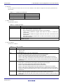
1
User’s Manual
w
E8a Emulator
Additional Document for User's Manual
(Notes on Connection)
Supported Devices:
R8C Family / R8C/3x Series
R8C Family / R8C/Lx Series
Notes on R5F213MCQ have been added in the following pages of this document.
Page 17 "5.3 [Firmware Location] tab"
Page 28 "Table 7.6 Program Area for the E8a Emulator (R8C/3xQ)"
All information contained in these materials, including products and product specifications,
represents information on the product at the time of publication and is subject to change by
Renesas Electronics Corporation without notice. Please review the latest information published
by Renesas Electronics Corporation through various means, including the Renesas Electronics
Corporation website (http://www.renesas.com).
www.renesas.com
Rev.4.02
Dec 2011
Notice
1.
2.
3.
4.
5.
6.
7.
All information included in this document is current as of the date this document is issued. Such information, however, is
subject to change without any prior notice. Before purchasing or using any Renesas Electronics products listed herein, please
confirm the latest product information with a Renesas Electronics sales office. Also, please pay regular and careful attention to
additional and different information to be disclosed by Renesas Electronics such as that disclosed through our website.
Renesas Electronics does not assume any liability for infringement of patents, copyrights, or other intellectual property rights
of third parties by or arising from the use of Renesas Electronics products or technical information described in this document.
No license, express, implied or otherwise, is granted hereby under any patents, copyrights or other intellectual property rights
of Renesas Electronics or others.
You should not alter, modify, copy, or otherwise misappropriate any Renesas Electronics product, whether in whole or in part.
Descriptions of circuits, software and other related information in this document are provided only to illustrate the operation of
semiconductor products and application examples. You are fully responsible for the incorporation of these circuits, software,
and information in the design of your equipment. Renesas Electronics assumes no responsibility for any losses incurred by
you or third parties arising from the use of these circuits, software, or information.
When exporting the products or technology described in this document, you should comply with the applicable export control
laws and regulations and follow the procedures required by such laws and regulations. You should not use Renesas
Electronics products or the technology described in this document for any purpose relating to military applications or use by
the military, including but not limited to the development of weapons of mass destruction. Renesas Electronics products and
technology may not be used for or incorporated into any products or systems whose manufacture, use, or sale is prohibited
under any applicable domestic or foreign laws or regulations.
Renesas Electronics has used reasonable care in preparing the information included in this document, but Renesas Electronics
does not warrant that such information is error free. Renesas Electronics assumes no liability whatsoever for any damages
incurred by you resulting from errors in or omissions from the information included herein.
Renesas Electronics products are classified according to the following three quality grades: “Standard”, “High Quality”, and
“Specific”. The recommended applications for each Renesas Electronics product depends on the product’s quality grade, as
indicated below. You must check the quality grade of each Renesas Electronics product before using it in a particular
application. You may not use any Renesas Electronics product for any application categorized as “Specific” without the prior
written consent of Renesas Electronics. Further, you may not use any Renesas Electronics product for any application for
which it is not intended without the prior written consent of Renesas Electronics. Renesas Electronics shall not be in any way
liable for any damages or losses incurred by you or third parties arising from the use of any Renesas Electronics product for an
application categorized as “Specific” or for which the product is not intended where you have failed to obtain the prior written
consent of Renesas Electronics. The quality grade of each Renesas Electronics product is “Standard” unless otherwise
expressly specified in a Renesas Electronics data sheets or data books, etc.
“Standard”:
8.
9.
10.
11.
12.
Computers; office equipment; communications equipment; test and measurement equipment; audio and visual
equipment; home electronic appliances; machine tools; personal electronic equipment; and industrial robots.
“High Quality”: Transportation equipment (automobiles, trains, ships, etc.); traffic control systems; anti-disaster systems; anticrime systems; safety equipment; and medical equipment not specifically designed for life support.
“Specific”:
Aircraft; aerospace equipment; submersible repeaters; nuclear reactor control systems; medical equipment or
systems for life support (e.g. artificial life support devices or systems), surgical implantations, or healthcare
intervention (e.g. excision, etc.), and any other applications or purposes that pose a direct threat to human life.
You should use the Renesas Electronics products described in this document within the range specified by Renesas Electronics,
especially with respect to the maximum rating, operating supply voltage range, movement power voltage range, heat radiation
characteristics, installation and other product characteristics. Renesas Electronics shall have no liability for malfunctions or
damages arising out of the use of Renesas Electronics products beyond such specified ranges.
Although Renesas Electronics endeavors to improve the quality and reliability of its products, semiconductor products have
specific characteristics such as the occurrence of failure at a certain rate and malfunctions under certain use conditions. Further,
Renesas Electronics products are not subject to radiation resistance design. Please be sure to implement safety measures to
guard them against the possibility of physical injury, and injury or damage caused by fire in the event of the failure of a
Renesas Electronics product, such as safety design for hardware and software including but not limited to redundancy, fire
control and malfunction prevention, appropriate treatment for aging degradation or any other appropriate measures. Because
the evaluation of microcomputer software alone is very difficult, please evaluate the safety of the final products or system
manufactured by you.
Please contact a Renesas Electronics sales office for details as to environmental matters such as the environmental
compatibility of each Renesas Electronics product. Please use Renesas Electronics products in compliance with all applicable
laws and regulations that regulate the inclusion or use of controlled substances, including without limitation, the EU RoHS
Directive. Renesas Electronics assumes no liability for damages or losses occurring as a result of your noncompliance with
applicable laws and regulations.
This document may not be reproduced or duplicated, in any form, in whole or in part, without prior written consent of Renesas
Electronics.
Please contact a Renesas Electronics sales office if you have any questions regarding the information contained in this
document or Renesas Electronics products, or if you have any other inquiries.
(Note 1) “Renesas Electronics” as used in this document means Renesas Electronics Corporation and also includes its majorityowned subsidiaries.
(Note 2) “Renesas Electronics product(s)” means any product developed or manufactured by or for Renesas Electronics.
E8a Emulator
Contents
Contents
Page
1. Inside the E8a Emulator User’s Manual ...................................................................................................................4
2. E8a Emulator Specifications.....................................................................................................................................5
2.1 Target MCUs.......................................................................................................................................................5
2.2 Emulator specifications .......................................................................................................................................5
2.3 Applicable tool chain and third-party products ....................................................................................................7
3. Connecting the E8a Emulator to the User System ...................................................................................................9
3.1 Connector for connecting the E8a emulator and the user system......................................................................9
4. Examples of Pin Handling for Connecting the E8a.................................................................................................11
4.1 Examples of pin handling for connecting the E8a.............................................................................................11
4.2 Interface circuit in the E8a emulator .................................................................................................................13
5. Emulator Debugger Setting ....................................................................................................................................14
5.1 [Emulator Setting] dialog box ............................................................................................................................14
5.2 [Emulator mode] tab..........................................................................................................................................15
5.3 [Firmware Location] tab.....................................................................................................................................17
5.4 [Communication Baud Rate] tab .......................................................................................................................18
6. E8a Emulator Functions (Supplement on the User’s Manual) ...............................................................................19
6.1 E8a emulator functions .....................................................................................................................................19
6.2 Eventcondition tab of the Eventpoints window..................................................................................................20
6.3 Event Setting dialog box ...................................................................................................................................21
6.4 Display contents of the Trace window ..............................................................................................................23
6.5 Notes on the event settings of the access break and trace function ................................................................24
7. Notes on Using the E8a Emulator ..........................................................................................................................25
7.1 MCU resources used by the E8a emulator .......................................................................................................25
7.2 Internal ROM area (flash memory) ...................................................................................................................38
7.2.1 Notes on debugging in CPU rewrite mode .................................................................................................38
7.2.2 Note on rewriting flash memory by the E8a emulator ................................................................................39
7.2.3 Note on flash memory during user program execution ..............................................................................39
7.2.4 MCUs used for debugging..........................................................................................................................39
7.2.5 Flash memory ID code ...............................................................................................................................40
7.3 Debugging during a watchdog timer operation .................................................................................................41
7.4 Power supply.....................................................................................................................................................42
7.5 Operation during a user program halt ...............................................................................................................42
7.6 Notes on using the CAN module (applicable for the R8C/3xE, R8C/3xF, R8C/3xW and R8C/3xX only)......................................43
7.6.1 Notes on CAN module in operation............................................................................................................43
7.6.2 Operation during a user program halt ........................................................................................................43
7.7 Debug functions ................................................................................................................................................44
R20UT0542EJ0402 Rev.4.02
Dec 06, 2011
Page 3 of 49
E8a Emulator
1. Inside the E8a Emulator User’s Manual
1. Inside the E8a Emulator User’s Manual
The E8a manual consists of two documents: the E8a User’s Manual and the E8a Additional Document for User’s
Manual (this document). Be sure to read BOTH documents before using the E8a emulator.
In this user’s manual, the symbol # is used to show active LOW. (e.g. RESET#)
(1) E8a Emulator User’s Manual
The E8a Emulator User’s Manual describes the hardware specifications and how to use the emulator debugger.
-
E8a emulator hardware specifications
Connecting the E8a emulator to the host computer or user system
Operating the E8a emulator debugger
Tutorial: From starting up the E8a emulator debugger to debugging
(2) E8a Additional Document for User’s Manual
The E8a Additional Document for User’s Manual describes content dependent on the MCUs and precautionary
notes.
-
MCU resources used by the E8a emulator
Example of the E8a emulator connection or interface circuit necessary for designing the hardware
Notes on using the E8a emulator
Setting the E8a emulator debugger during startup
Note:
For the specifications and supported MCUs of the optional FDT, please check the Flash Development Tool
Kit page of our website (http://www.renesas.com/tools).
FDT stands for the Flash Development Toolkit.
Trademarks
Microsoft, MS-DOS, Visual SourceSafe, Windows and Windows Vista are either registered trademarks or
trademarks of Microsoft Corporation in the United States and/or other countries.
All other company or product names are the trademarks or registered trademarks of their respective owners.
R20UT0542EJ0402 Rev.4.02
Dec 06, 2011
Page 4 of 49
E8a Emulator
2. E8a Emulator Specifications
2. E8a Emulator Specifications
2.1 Target MCUs
Table 2.1 shows the target MCUs covered in this user’s manual.
Table 2.1 Target MCUs
Item
Description
Target MCUs
R8C Family R8C/3x Series
Remark
R8C/3xA: R8C/32A, R8C/33A, R8C/35A, R8C/36A, R8C/38A, R8C/3GA and R8C/3JA
Groups
General-purpose
R8C/3xC: R8C/32C, R8C/33C, R8C/34C, R8C/35C, R8C/36C, R8C/38C, R8C/3GC and
R8C/3JC Groups
R8C/3xM: R8C/32M, R8C/33M, R8C/34M, R8C/35M, R8C/36M, R8C/38M, R8C/3GM and
R8C/3JM Groups
R8C/3xT:
R8C/33T, R8C/3JT and R8C/3NT Groups
Touch key control
R8C/3xK: R8C/34K and R8C/3MK Groups
USB control
R8C/3xU: R8C/34U and R8C/3MU Groups
R8C/3xQ: R8C/3MQ Groups
Communications
R8C/3xE: R8C/34E, R8C/36E and R8C/38E Groups
In-vehicle
R8C/3xF:
R8C/34F, R8C/36F and R8C/38F Groups
R8C/3xG: R8C/34G, R8C/36G and R8C/38G Groups
R8C/3xH: R8C/34H, R8C/36H and R8C/38H Groups
R8C/3xW: R8C/34W, R8C/36W and R8C/38W Groups
R8C/3xX: R8C/34X, R8C/36X and R8C/38X Groups
R8C/3xY: R8C/34Y, R8C/36Y and R8C/38Y Groups
R8C/3xZ:
R8C/34Z, R8C/36Z and R8C/38Z Groups
R8C/3xGHPR: R8C/32G, R8C/32H, R8C/33G, R8C/33H, R8C/34P and R8C/34R Groups
R8C Family R8C/Lx Series
R8C/L3xA: R8C/L35A, R8C/L36A, R8C/L38A and R8C/L3AA Groups
Built-in LCD
controller
R8C/L3xB: R8C/L35B, R8C/L36B, R8C/L38B and R8C/L3AB Groups
R8C/L3xC: R8C/L35C, R8C/L36C, R8C/L38C and R8C/L3AC Groups
R8C/L3xM: R8C/L35M, R8C/L36M, R8C/L38M and R8C/L3AM Groups
R8C/LAxA: R8C/LA3A, R8C/LA5A, R8C/LA6A and R8C/LA8A Groups
R8C/LAxS : R8C/LAPS Group
Available operating
modes
Remote controller
Single-chip mode
2.2 Emulator specifications
Table 2.2 shows the specifications of the emulator supported by the R8C E8a Emulator Debugger. Table 2.3 shows the E8a
emulator specifications when using the target MCU.
Table 2.2
E8a Emulator Specifications
Item
Description
Emulator power supply
Unnecessary (USB bus powered, power supplied from the host machine)
Applicable emulator debugger
R8C E8a Emulator Debugger V.1.05.01 or later
Operating Environment
Temperatures
Humidity
Vibrations
Ambient gases
R20UT0542EJ0402 Rev.4.02
Dec 06, 2011
Active
: 10°C to 35°C
Inactive
: –10°C to 50°C
Active
: 35% RH to 80% RH, no condensation
Inactive
: 35% RH to 80% RH, no condensation
Active
: maximum 2.45 m/s
2
2
Inactive
: maximum 4.9 m/s
Transportation
: maximum 14.7 m/s
2
No corrosive gases
Page 5 of 49
E8a Emulator
Table 2.3
2. E8a Emulator Specifications
E8a Emulator Specifications when Using the Target MCU
Item
Description
Power voltages
1.8 - 5.5 V [*1]
Break functions
- Address match break, 8 points
For details, refer to the hardware manual of the MCU.
- Data access break, 2 points
- Event A: Comparison with the address/data mask, and access condition (R, W, R/W) can be set.
- Event B: Comparison with the address mask, and access condition (R, W, R/W) can be set.
- PC break points (maximum 255 points)
- Forced break
Trace functions
4 branch instructions (branch source/destination PC)
or
Up to 8 data cycles can be specified.
Flash memory
function
programming
Available (when selecting the ‘Program Flash’ mode)
User interface
1-line clock asynchronous serial interface (communication via MODE pin)
MCU resources to be used
- ROM size: 2 KB (for some products, see ”7.1 MCU resources used by the E8a emulator” on page 25.)
- Stack 8 bytes
- Address match interrupt
Interface with host machine
USB (USB 1.1, full speed)*
* Also connectable to host computers that support USB 2.0
* Operation with all combinations of host machine, USB device and USB hub is not guaranteed for the
USB interface.
Power supply function
Can supply 3.3 V or 5.0 V to the user system (maximum 300 mA) [*2] [*3]
Notes:
[*1]
For rewriting the flash memory, set the power voltage within the programming and erasure voltage range specified
in the hardware manual of the MCU.
For details, refer to “7.7 (4) Note on debugging at less than 2.7V” on page 44.
[*2]
Do not use the power-supply function of the emulator when it is being used to program flash memory as part of a
mass-production process. Separately supply power from the user system in accord with the specifications of the
MCU.
Use FDT when you need to program flash memory during mass-production, etc.
Voltage supplied from the E8a emulator depends on the quality of the USB power supply of the host computer, and
as such, precision is not guaranteed.
[*3]
The power supply options may be grayed out depending on the specifications of the MCU to be debugged.
R20UT0542EJ0402 Rev.4.02
Dec 06, 2011
Page 6 of 49
E8a Emulator
2. E8a Emulator Specifications
2.3 Applicable tool chain and third-party products
You can debug a module created by the inhouse tool chain and third-party products listed in Table 2.4 below.
Table 2.4
Applicable Tool Chain and Third-party Products
Tool chain
M3T-NC30WA V.5.20 Release 01 or later
Third-party products
TASKING M16C C/C++/EC++ Compiler V.2.3r1 or later [*1]
IAR EWM16C V.2.12 or later
Note:
If the load module was created in ELF/DWARF2 format using TASKING M16C C/C++/EC++ compiler V3.0r1, the
[*1]
precautionary note described below must be observed when displaying member variables of the base class in the
watch window.
Precautionary Note:
If any class object with a base class is defined, the following problems may occur:
Case 1: Member variables of the base class cannot be referenced directly from the class object (*1).
=>Use indirect references from the class object to refer to member variables of the base class (*2) (*3).
Case 2: If the PC value resides in any member function of a derived class, member variables of the base class cannot
be referenced directly (*4).
=> Use indirect references from “this” pointer to refer to member variables of the base class (*5) (*6).
Figure 2.1 shows a code example, and Figure 2.2 shows a [Watch] window registration example.
R20UT0542EJ0402 Rev.4.02
Dec 06, 2011
Page 7 of 49
E8a Emulator
2. E8a Emulator Specifications
/////////////////////////////////////////////////////////
*.h
class BaseClass
{
public:
int m_iBase;
public:
BaseClass() {
m_iBase = 0;
}
void BaseFunc(void);
};
class DerivedClass : public BaseClass
{
public:
int m_iDerive;
public:
DerivedClass() {
m_iDerive
= 0;
}
void DerivedFunc(void);
};
*.cpp
main()
{
class DerivedClass ClassObj;
ClassObj.DerivedFunc();
return;
}
void BaseClass::BaseFunc(void)
{
m_iBase = 0x1234;
}
void DerivedClass::DerivedFunc(void)
{
BaseFunc();
m_iDerive
= 0x1234;
}
/////////////////////////////////////////////////////////
Figure 2.1 Example Code
/////////////////////////////////////////////////////////
Case 1: If the PC value resides in the main() function
(1)"ClassObj.m_iBase"
: Cannot be referenced (*1)
(2)"ClassObj.__b_BaseClass.m_iBase"
: Can be referenced (*2)
(3)"ClassObj"
-"__b_BaseClass"
-"m_iBase"
: Can be referenced (*3)
-"m_iDerive"
-: Expansion symbol
Case 2: If the PC value resides in the DerivedClass::DerivedFunc() function
(1)"m_iBase"
: Cannot be referenced (*4)
(2)"this->__b_BaseClass.m_iBase"
: Can be referenced (*5)
(3)"__b_BaseClass.m_iBase"
: Can be referenced (*5)
(4)"this"
-"*"
-"__b_BaseClass"
-"m_iBase"
: Can be referenced (*6)
-"m_iDerive"
(5)"__b_BaseClass"
-"m_iBase"
: Can be referenced (*6)
/////////////////////////////////////////////////////////
Figure 2.2
Watch Window Registration Example
R20UT0542EJ0402 Rev.4.02
Dec 06, 2011
Page 8 of 49
E8a Emulator
3. Connecting the E8a Emulator to the User System
3. Connecting the E8a Emulator to the User System
3.1 Connector for connecting the E8a emulator and the user system
Before connecting the E8a emulator to the user system, a connector must be installed in the user system so a user system
interface cable can be connected. Table 3.1 shows the recommended connector for the E8a emulator and Figure 3.2
shows E8a connecting connector pin assignments.
When designing the user system, refer to Figure 3.2 “E8a Connecting Connector Pin Assignments” and Section 3
“Connecting the E8a Emulator to the User System”.
Before designing the user system, be sure to read the E8a Emulator User’s Manual and related device hardware manuals.
Table 3.1
Recommended Connector
Type Number
2514-6002
7614-6002
14-pin connector
Manufacturer
3M Limited
3M Limited
Specification
14-pin straight type (for use outside Japan)
14-pin straight type (for use in Japan)
User system interface cable
Connector
User system
Pin 2
Pin 1
Figure 3.1
Connecting the User System Interface Cable with an E8a Connecting Connector
Notes:
Do not place any components within 3 mm area of the connector.
When using the E8a emulator as a programmer, connect it to the user system in the same way.
Connect E8a connecting connector pins 2, 4, 6, 10, 12 and 14 firmly to the GND on the user system board. These
pins are used as an electric GND and monitor the connection of the user system connector.
When inserting or removing the user system interface cable from the connector section of the user system, be sure to
hold the connector cover at the head of the cable. Removal by pulling the cable portion instead of grasping the cover
causes breakage of the cable connection.
R20UT0542EJ0402 Rev.4.02
Dec 06, 2011
Page 9 of 49
E8a Emulator
3. Connecting the E8a Emulator to the User System
Pin 1 mark
Connector
Pin2
Pin 14
Pin1
Pin 13
Pin 1 mark
Figure 3.2
Pin NO
1
2
3
4
5
6
7
8
9
10
11
12
13
14
MCU Signals
N.C.
Vss
N.C.
Vss
N.C.
Vss
MODE
Vcc
N.C.
Vss
N.C.
Vss
RESET#
Vss
E8a Connecting Connector Pin Assignments
Notes:
Pin 14 is used for checking the connection between the E8a and the user system, and is not directly connected to the
Vss inside the E8a. Make sure pins 2, 4, 6, 10, 12 and 14 are all connected to the Vss.
Note the pin assignments for the user system connector.
Do not connect anything to the N.C. pin.
R20UT0542EJ0402 Rev.4.02
Dec 06, 2011
Page 10 of 49
E8a Emulator
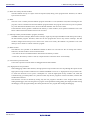
4. Examples of Pin Handling for Connecting the E8a
4. Examples of Pin Handling for Connecting the E8a
4.1 Examples of pin handling for connecting the E8a
Figure 4.1 shows an example of pin handling when connecting the E8a.
When using the E8a as a programmer, the connection specification between the E8a and the MCUs is the same as shown
in Figure 4.1.
Vcc
Vcc
Pulled up at 4.7kΩ ± 10%
Vcc
MODE
MODE
Vcc
User
logic
MCU
MCU
*1
RESET#
RESET#
Vss
Pulled up at 4.7kΩ or more
E8a connecting
connector
*1
Open-collector buffer
User system
Figure 4.1
Example of an E8a Connection
Notes:
When adjacent resistors are used for pull-up, they may be affected by noise from other pins. In particular, separate
the resistor for MODE from the other resistors.
Wiring patterns between the connector and the MCU must be as short as possible (within 50 mm is recommended).
Do not connect the signal lines between the connector and MCU to other signal lines.
For the handling of pins while the E8a emulator is not in use, refer to the hardware manual for the MCU.
R20UT0542EJ0402 Rev.4.02
Dec 06, 2011
Page 11 of 49
E8a Emulator
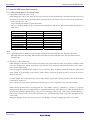
4. Examples of Pin Handling for Connecting the E8a
(1) MODE pin
The E8a emulator uses the MODE pin for MCU control and forced break control. Pull up the E8a emulator and
MCU pins and connect the E8a emulator. Do not connect a capacitor etc. to this pin.
Vcc
Pulled up at 4.7kΩ ± 10%
E8a connecting
connector
MODE
Figure 4.2
7
MODE
MCU
E8a Emulator and MODE Pin Connection
(2) RESET# pin
The RESET# pin is used by the E8a emulator. Therefore, use an open-collector output buffer or a CR reset circuit
as the reset circuit for the user system. The recommended pull-up value is 4.7 kΩ or more. The MCU can be reset
by outputting “L” from the E8a emulator. However, if the reset IC output is “H”, the user system reset circuit
cannot be set to “L”. As such, the E8a emulator will not operate normally.
E8a connecting
connector
RESET#
Vcc
User
logic
*
13
RESET#
MCU
Pulled up at 4.7kΩ or more
* : Open-collector buffer
Figure 4.3
Example of a Reset Circuit
(3) Other pins
- Connect Vss and Vcc to the Vss and Vcc of the MCU, respectively.
- The amount of voltage input to Vcc must be within the specified range of the MCU.
- Pin 14 is used for checking the connection between the E8a and the user system, and pins 4, 6 and 10 are
connected to the internal circuit. These pins are not directly connected to the Vss inside the E8a.
- Make sure pins 2, 4, 6, 10, 12 and 14 are all connected to the Vss.
- Do not connect anything to the N.C. pin.
WARNING
About Power Supply Circuit of the User System:
When supplying power, ensure that there are no short circuits between Vcc and GND. Only connect the E8a
emulator after confirming that there are no mismatches in pin assignments of the E8a connecting connector.
Incorrect connection will result in the host computer, the emulator, and the user system emitting smoke or
catching fire.
R20UT0542EJ0402 Rev.4.02
Dec 06, 2011
Page 12 of 49
E8a Emulator
4. Examples of Pin Handling for Connecting the E8a
4.2 Interface circuit in the E8a emulator
Figure 4.4 shows the interface circuit in the E8a emulator. Use this figure as a reference when determining the pull-up
resistance value.
User system connector
Vcc
8
22Ω
MODE
7
22Ω
RESET#
Power supply circuit
(use only with power supply mode)
74LVC125
Emulator control circuit
[*1]
3.3V
74LVC2T45
[*1]
13
3.3V
2SC2462
10kΩ
[*1] Power for 74LVC125 is supplied from Vcc in the user system connector or power supply circuit (in power supply mode).
Figure 4.4
Interface Circuit inside the E8a Emulator (For Reference)
R20UT0542EJ0402 Rev.4.02
Dec 06, 2011
Page 13 of 49
E8a Emulator
5. Emulator Debugger Setting
5. Emulator Debugger Setting
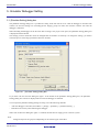
5.1 [Emulator Setting] dialog box
The [Emulator Setting] dialog box is provided for setting items that need to be set when the debugger is launched. The
contents set from this dialog box (excluding [Power Supply] group box items) also become valid the next time the
debugger is launched.
When launching the debugger for the first time after creating a new project work space, the [Emulator Setting] dialog box
is displayed with the Wizard.
The settings you have made here cannot be changed after the emulator is booted up. To change the settings, you need to
cancel the process of booting-up and then reboot the emulator.
Figure 5.1
[Emulator Setting] Dialog Box
If you check “Do not show this dialog box again.” at the bottom of the [Emulator Setting] dialog box, the [Emulator
Setting] dialog box will not be displayed the next time the debugger is launched.
You can open the [Emulator Setting] dialog box using one of the following methods:
- After the debugger is launched, select Menu -> [Setup] -> [Emulator] -> [Emulator Setting...].
- Hold down the Ctrl key while launching the debugger.
When “Do not show this dialog box again.” is checked, the E8a does not supply power to the user system.
Note:
Unsupported options are grayed out depending on the selected types of the MCU.
R20UT0542EJ0402 Rev.4.02
Dec 06, 2011
Page 14 of 49
E8a Emulator
5. Emulator Debugger Setting
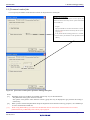
5.2 [Emulator mode] tab
Device selection, mode specification and power supply setting are made from the [Emulator mode] tab of the [Emulator
Setting] dialog box.
[MCU Group]
Select the name of the MCU group to be used
from the [MCU Group] drop-down list.
[Device]
Select the type of MCU to be used from the
[Device] drop-down list.
(See “7.1 MCU resources used by the E8a
emulator” on page 25 for the list of applicable
MCUs.)
[Mode]
Select the mode to be used.
For details, see “5.2 (1) Selecting the Mode”
(p.16).
[Power supply]
Select the power supply to the user system.
- When supplying power to the user system from
the E8a, click the [Power Target from
Emulator. (MAX 300mA)] checkbox and
select either 3.3V or 5.5V [*1]
Figure 5.2 [Emulator mode] Tab of [Emulator Setting] Dialog Box
Note:
[*1]
Only one power supply option is available depending on the selected types of the MCU. For the information of the
operating supply voltage of the MCU, refer to the hardware manual of the MCU used.
R20UT0542EJ0402 Rev.4.02
Dec 06, 2011
Page 15 of 49
E8a Emulator
5. Emulator Debugger Setting
(1) Selecting the Mode
Table 5.1 Selecting the Mode
Mode
Usage
Description
When starting the debugger, the E8a emulator erases the Flash memory data for the
MCUs and simultaneously writes the area for the E8a emulator program and the
Erase Flash and Connect [*2]
vector area used by the E8a emulator. The emulator rewrites the OFS, OFS2 and ID
Debugging
only [*1]
code areas.
When launching the debugger, the E8a emulator retains the Flash memory data for
the MCUs. Note that the area for the E8a emulator program and the vector area used
Keep Flash and Connect [*2]
by the E8a emulator will change. The emulator rewrites the OFS, OFS2 and ID code
areas.
The E8a emulator starts as a simple programmer. When downloaded, the E8a writes
only the user program (E8a emulator program is not written).
Therefore, in this mode, you can only download the program. You cannot change the
Program Flash [*2]
Simple
programmer
memory contents by using the fill command, etc.
When [Execute the user program after ending the debugger.] is selected, with the
E8a emulator connected to the user system, the user program is executed at the
same time the debugger is terminated. This check box setting is available only when
the [Program Flash] mode is selected.
Be sure to select this setting when debugging the program which rewrites the CPU.
In this mode, the following debug operation which rewrites the Flash memory cannot
be executed.
- Setting the PC break points
Debugging of CPU rewrite mode
[*2] [*3]
Debugging
- Changing the memory contents in the Flash memory area
only [*1]
In this mode, when starting the debugger, the E8a emulator erases the Flash memory
data for the MCUs and simultaneously writes the area for the E8a emulator program
and the vector area used by the E8a emulator. The emulator rewrites the OFS, OFS2
and ID code areas.
Notes:
[*1]
In this mode, vector addresses are used by the E8a emulator program. After a program has been downloaded, you
cannot disconnect the emulator and operate the user system as a stand-alone unit. (Programs written in this mode
cannot be executed from the MCU.) If you want to execute a program from the MCU, use [Program Flash] mode.
[*2]
When starting up in these modes, lock bits in all the blocks of the flash memory will be unlocked. Note that the lock
bits of the downloaded blocks will be unlocked after downloading the user program.
[*3]
When debugging a program in CPU rewrite mode, memory reference or modification functions can be used.
However, do not use these functions in the following condition.
- While write instruction is being executed to the register which requires continuous writing (ex. FMR13 bit)
The MCU does not recognize the writing is continuously executed if the write instruction is interrupted by the
memory reference or modification process.
R20UT0542EJ0402 Rev.4.02
Dec 06, 2011
Page 16 of 49
E8a Emulator
5. Emulator Debugger Setting
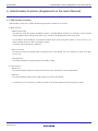
5.3 [Firmware Location] tab
You can specify the address of the firmware location in the [Firmware Location] tab.
[Firmware Location]
Select the area in which the firmware is located. Specify the
address that will not be used by the user system in the ROM
area or RAM area.
- Program
Specify the ROM area in which the firmware is located.
Specify 2k bytes that will not be used by the user system.
[*1] [*2] [*3]
If the [Enable advanced setting] check box is checked,
the area used by the emulator can be specified with the
address.]
Figure 5.3 [Firmware Location] tab of [Emulator Setting] Dialog Box
Notes:
[*1]
Depending on the type of MCU, the available options may vary as described below.
- The [Data Flash Area] option cannot be selected.
- The options in the [Please select firmware location.] group box may be displayed in gray because this setting is
unnecessary.
[*2]
When you have selected the [Data Flash Area] for the [Please select firmware location.] group box, use a 250000 bps
or lower communication baud rate.
[*3]
When using R5F213MCQ, you cannot use the data flash area for the location of the firmware. Do not select
[Data Flash Area]. Additionally refer to Note [*2] on page 28.
R20UT0542EJ0402 Rev.4.02
Dec 06, 2011
Page 17 of 49
E8a Emulator
5. Emulator Debugger Setting
5.4 [Communication Baud Rate] tab
Select communication baud rate between the E8a and MCU in the [Communication Baud Rate] tab.
500000 bps (default setting) should be selected during normal use. [*1] [*2]
Figure 5.4 [Communication Baud Rate] Tab
Notes:
[*1]
Depending on the wired length of the MODE signal and how it is wired on the user system, communication at the
selected baud rate may not be performed. Reducing this baud rate may help to solve the problem.
Also, the communication information you set here cannot be changed after the emulator debugger has started. To
change the communication baud rate, you need to disconnect the emulator and the MCU temporarily and then
reconnect.
[*2]
The baud rate of 57600 bps or below is designated for checking purpose in case there is a failure in the connection
with the emulator. With such a low baud rate, it takes a long time to write into the flash memory of the target MCU,
and the emulator debugger may appear to be giving no response.
Also note if the data of 1024 bytes or larger is handled when displaying the memory contents or in memory fill
function, a time-out error may occur because the communication takes up much time.
R20UT0542EJ0402 Rev.4.02
Dec 06, 2011
Page 18 of 49
E8a Emulator
6. E8a Emulator Functions (Supplement on the User’s Manual)
6. E8a Emulator Functions (Supplement on the User’s Manual)
6.1 E8a emulator functions
With the MCUs in this user’s manual, the following functions in the device can be used.
(1) Break Function
- Address match break
This function breaks the program immediately before a specified address instruction is executed. It can be realized
using the address match interrupt of the MCU. Up to 8 points of the address match break can be used.
Set the address match breakpoint in the Break condition sheet of the Eventpoints window. You can also set it by
double-clicking the Event column in the Editor window.
For details, refer to the E8a User’s Manual.
- Data access break
This function breaks the program when a specified event is encountered. You can combine two points of the data
access event.
- Trace full break
This function breaks the program when the trace buffer is filled
(2) Trace Function
- Branch trace
This function displays addresses, mnemonics and source lines of the branch source and destination.
- Data trace
This function displays data accesses when a data access event is encountered.
For the data access event and trace condition, set them in the Eventcondition tab of the Eventpoints window.
R20UT0542EJ0402 Rev.4.02
Dec 06, 2011
Page 19 of 49
E8a Emulator
6. E8a Emulator Functions (Supplement on the User’s Manual)
6.2 Eventcondition tab of the Eventpoints window
Set the contents of the data access event, break condition and trace condition.
Double-clicking each item in this window will open the Event Setting dialog box to change the conditions. The items
displayed in the sheet are shown in Table 6.1.
Figure 6.1
Eventpoints Window (Eventcondition tab)
Table 6.1
Display Contents of the Eventcondition Tab
Item
Type
State
Condition
Action
Description
Displays the event types.
- Event A
- Event B
- Break Condition
- Trace Condition
Shows the event is enable or disable.
- Enable
- Disable
Displays the set condition.
For the Event A and Event B, the access types are displayed.
- R/W: READ or WRITE
- READ
- WRITE
For the Break Condition and Trace Condition, Break/Trace is always displayed.
R20UT0542EJ0402 Rev.4.02
Dec 06, 2011
Page 20 of 49
E8a Emulator
6. E8a Emulator Functions (Supplement on the User’s Manual)
6.3 Event Setting dialog box
The conditions in the Event condition sheet can be set.
Figure 6.2
Event Setting Dialog box
(1) Event A
Set the contents of the Event A. You can set the conditions of the address comparison with mask specification and
data comparison with mask specification for the Event A.
Table 6.2
Contents of the Event A
Option
Address (with mask specification)
Data (with mask specification)
Access Size
Access Type
R20UT0542EJ0402 Rev.4.02
Dec 06, 2011
Description
Specify an address to detect the data access. Specify the bit number to set
the address mask. The specified lower bits of the specified address are
masked.
If you compare data, specify the data and data mask. When selecting BYTE
for the Access Size, you can specify to FF. When selecting WORD for the
Access Size, you can specify to FFFF. If you do not compare data, leave the
Data item empty or enter 0 in the Mask. If you do not use the data mask,
leave the Mask item empty.
Select one from BYTE, WORD or Not specify for the Access Size. If a data
access which does not match the specified access size occurs, the event is
not encountered. When specifying WORD for the Access Size, specify the
even address for the Address item.
Select an access type.
- R/W: READ or WRITE
- READ
- WRITE
Page 21 of 49
E8a Emulator
6. E8a Emulator Functions (Supplement on the User’s Manual)
(2) Event B
Set the contents of the Event B. You can set the conditions of the address comparison with mask specification for
the Event B.
Table 6.3
Contents of the Event B
Option
Address (with mask specification)
Access Size
Access Type
Description
Same as the Event A.
Same as the Event A.
Same as the Event A.
(3) Break Condition
Set the break condition.
Table 6.4
Break Condition
Option
Break
Break at Trace Full
Description
Select a break condition.
- None: None specified. (No break by event)
- Event A: Breaks the program when the Event A is encountered.
- Event A or B: Breaks the program when either the Event A or Event B is
encountered.
- Event A and B: Breaks the program when both the Event A and Event B are
encountered.
- Event B->A: Breaks the program when an event is encountered in the order of the
Event B and Event A.
Check it to break the program when the trace buffer is filled. It can be set with the break
condition by event.
(4) Trace Condition
Set the trace condition.
Table 6.5
Option
Type
Start
Stop
Pick up
Trace Condition
Description
Select a trace type.
- Branch Trace
- Data Trace
Select a start condition for the trace measurement.
- Go: Starts a measurement when starting executing the target program.
- Event A: Starts a measurement when the Event A is encountered.
- Event A or B: Starts a measurement when either the Event A or Event B is encountered.
- Event A and B: Starts a measurement when both the Event A and Event B are encountered.
- Event B->A: Starts a measurement when an event is encountered in the order of the Event B
and Event A.
Select a stop condition for the trace measurement.
- Break: Stops a measurement when stopping executing the target program.
- Trace FULL: Stops a measurement when the trace data is filled.
- Event A: Stops a measurement when the Event A is encountered.
- Event A or B: Stops a measurement when either the Event A or Event B is encountered.
- Event A and B: Stops a measurement when both the Event A and Event B are encountered.
- Event B->A: Stops a measurement when an event is encountered in the order of the Event B
and Event A.
Select an event to record when tracing data.
- Event A: Records only data access which encounters the condition of the Event A.
- Event A or B: Records only data access which encounters the condition of either the Event A
or Event B.
R20UT0542EJ0402 Rev.4.02
Dec 06, 2011
Page 22 of 49
E8a Emulator
6. E8a Emulator Functions (Supplement on the User’s Manual)
6.4 Display contents of the Trace window
To display the trace results, open the Trace window.
For each function of the popup menu, refer to the E8a User’s Manual. The items displayed in the sheet are shown in
Table 6.6.
Figure 6.3
Table 6.6
Trace Window
Trace Display
Item
PTR
IP
Type
Address
Data
Instruction
Source
Label
Description
Displays the pointer numbers in the trace buffer. Displays them in ascending order with the trace end
position as 0.
Displays the instruction pointer.
Displays the type of trace information. When the branch trace is set, BRANCH/DESTINATION is displayed.
When the data trace is set, READ/WRITE is displayed.
When the branch trace is set, an address of the branch source and destination is displayed. When the data
trace is set, an address or address range set for the encountered event is displayed.
When the data trace is set, the accessed value is displayed. When the branch trace is set, nothing is
displayed.
When the branch trace is set, the mnemonic of the address is displayed. When the data trace is set, nothing
is displayed.
“*** EML ***” may be displayed in the Instruction column. This shows that the target program accessed the
area of emulator use to control breaks, etc. It is not an error.
If there is a source line information correspondent to the Instruction, the correspondent source line is
displayed. When the data trace is set, nothing is displayed.
If there is a label correspondent to an address in the Instruction, the correspondent label is displayed. When
the data trace is set, nothing is displayed.
R20UT0542EJ0402 Rev.4.02
Dec 06, 2011
Page 23 of 49
E8a Emulator
6. E8a Emulator Functions (Supplement on the User’s Manual)
6.5 Notes on the event settings of the access break and trace function
When setting the Event A or Event B for the access break and trace function, set the address, access size and access type
referring to Table 6.7 below.
Table 6.7
Availability of the Event Setting
Event setting condition
Availability of event
setting
Byte read to even address
Available
Byte write to even address
Available
Word read to even address
Available
Word write to even address
Available
Byte read to odd address
Available
Byte write to odd address
Available
Word read to odd address
Available
Word write to odd address
Available
Example of Event Setting dialog box
Address: 400h
Access size: BYTE
Access type: READ or R/W
Address: 400h
Access size: BYTE
Access type: WRITE or R/W
Address: 400h
Access size: WORD
Access type: READ or R/W
Address: 400h
Access size: WORD
Access type: WRITE or R/W
Address: 401h
Access size: BYTE
Access type: READ or R/W
Address: 401h
Access size: BYTE
Access type: WRITE or R/W
Address: 401h
Access size: BYTE [*1]
Access type: READ or R/W
Address: 401h
Access size: BYTE [*1]
Access type: WRITE or R/W
Notes:
[*1] For the access size, specify "BYTE". In this condition, the lower one byte data can be compared.
[*2] Note on the trace start condition
When setting an event (other than “Go”) for the trace start condition, a data when the event is encountered is not
recorded to the trace data. The data of the event which is encountered the next time is recorded.
[*3] Notes on the trace stop condition
When the trace start and trace stop conditions occur simultaneously, the trace stop condition becomes invalid.
When setting other than “Break” for the trace stop condition, the display contents of the Trace window will not be
updated until the user program stops even after a trace stop condition is encountered.
[*4] Note on setting the Event A
When setting an event for the Event A, you cannot specify a mask for an address and data simultaneously. If you
mask them simultaneously, an event will not be encountered.
[*5] Note on setting an event
Do not specify the following addresses as the address of the event. Otherwise, an unauthorized break may occur.
- Address in the interrupt vector table
- Address set in the interrupt vector table (interrupt routine start address)
- Branch address of the branch instruction
Both fixed vector table and variable vector table are included with the interrupt vector table above.
R20UT0542EJ0402 Rev.4.02
Dec 06, 2011
Page 24 of 49
E8a Emulator
7. Notes on Using the E8a Emulator
7. Notes on Using the E8a Emulator
7.1 MCU resources used by the E8a emulator
(1) Program area for the E8a emulator
Table 7.1 through Table 7.21 list the program area for the E8a emulator. Do not change this area, otherwise the E8a
emulator will not control the MCU. In this case, disconnect the debugger and then reconnect it.
Table 7.1
Group
Program Area for the E8a Emulator (R8C/3xA)
ROM Size
Part No.
Program ROM
R8C/32A
R8C/33A
R8C/35A
R8C/36A
R8C/38A
R8C/3GA
R8C/3JA
Program Area for E8a Emulator
Data Flash
Vector Area
ROM Area
R5F21321A
4 KB
R5F21322A
8 KB
-
R5F21324A
16 KB
-
R5F21331A
4 KB
-
R5F21332A
8 KB
-
R5F21334A
16 KB
-
R5F21335A
24 KB
-
R5F21336A
32 KB
2 KB of the ROM area [*1]
R5F21354A
16 KB
-
R5F21355A
24 KB
-
R5F21356A
32 KB
2 KB of the ROM area [*1]
R5F21357A
48 KB
-
R5F21358A
64 KB
-
R5F2135AA
96 KB
-
R5F2135CA
128 KB
R5F21364A
16 KB
FFE4h - FFE7h,
-
R5F21365A
24 KB
FFE8h - FFEBh,
-
R5F21366A
32 KB
FFECh - FFEFh,
-
R5F21367A
48 KB
FFF4h - FFF7h,
-
2 KB of the ROM area [*1]
1 KB
(4 blocks)
R5F21368A
64 KB
R5F2136AA
96 KB
-
R5F2136CA
128 KB
2 KB of the ROM area [*1]
R5F21386A
32 KB
-
R5F21387A
48 KB
-
R5F21388A
64 KB
-
R5F2138AA
96 KB
-
R5F2138CA
128 KB
2 KB of the ROM area [*1]
R5F213G2A
8 KB
-
R5F213G4A
16 KB
-
R5F213G5A
24 KB
-
R5F213G6A
32 KB
2 KB of the ROM area [*1]
R5F213J2A
8 KB
-
R5F213J4A
16 KB
-
R5F213J5A
24 KB
-
R5F213J6A
32 KB
2 KB of the ROM area [*1]
FFFCh - FFFFh
-
Note:
[*1] When starting the debugger, the [Emulator Setting] dialog box is displayed. Specify the area which will not be used
by the user system. For details, see 5.3 [Firmware Location] tab.
R20UT0542EJ0402 Rev.4.02
Dec 06, 2011
Page 25 of 49
E8a Emulator
Table 7.2
Group
7. Notes on Using the E8a Emulator
Program Area for the E8a Emulator (R8C/3xC)
ROM Size
Part No.
Program ROM
R8C/32C
R8C/33C
R8C/34C
R8C/35C
R8C/36C
R8C/38C
R8C/3GC
R8C/3JC
R5F21321C
4 KB
R5F21322C
8 KB
Program Area for E8a Emulator
Data Flash
Vector Area
ROM Area
-
R5F21324C
16 KB
-
R5F21331C
4 KB
-
R5F21332C
8 KB
-
R5F21334C
16 KB
-
R5F21335C
24 KB
-
R5F21336C
32 KB
2 KB of the ROM area [*1]
R5F21344C
16 KB
-
R5F21345C
24 KB
-
R5F21346C
32 KB
2 KB of the ROM area [*1]
R5F21354C
16 KB
-
R5F21355C
24 KB
-
R5F21356C
32 KB
2 KB of the ROM area [*1]
R5F21357C
48 KB
-
R5F21358C
64 KB
-
R5F2135AC
96 KB
-
R5F2135CC
128 KB
FFE4h - FFE7h,
2 KB of the ROM area [*1]
R5F21364C
16 KB
FFE8h - FFEBh,
-
R5F21365C
24 KB
FFECh - FFEFh,
-
R5F21366C
32 KB
FFF4h - FFF7h,
-
R5F21367C
48 KB
FFFCh - FFFFh
-
R5F21368C
64 KB
-
R5F2136AC
96 KB
-
R5F2136CC
128 KB
2 KB of the ROM area [*1]
R5F21386C
32 KB
-
R5F21387C
48 KB
-
R5F21388C
64 KB
-
R5F2138AC
96 KB
-
1 KB
(4 blocks)
R5F2138CC
128 KB
2 KB of the ROM area [*1]
R5F213G1C
4 KB
-
R5F213G2C
8 KB
-
R5F213G4C
16 KB
-
R5F213G5C
24 KB
-
R5F213G6C
32 KB
2 KB of the ROM area [*1]
R5F213J2C
8 KB
-
R5F213J4C
16 KB
-
R5F213J5C
24 KB
-
R5F213J6C
32 KB
2 KB of the ROM area [*1]
Note:
[*1] When starting the debugger, the [Emulator Setting] dialog box is displayed. Specify the area which will not be used
by the user system. For details, see 5.3 [Firmware Location] tab.
R20UT0542EJ0402 Rev.4.02
Dec 06, 2011
Page 26 of 49
E8a Emulator
Table 7.3
Group
7. Notes on Using the E8a Emulator
Program Area for the E8a Emulator (R8C/3xM)
R5F21321M
R8C/32M
R8C/33M
R8C/34M
R8C/35M
R8C/36M
R8C/38M
R8C/3GM
R8C/3JM
ROM Size
Part No.
Program ROM
4 KB
Program Area for E8a Emulator
Data Flash
Vector Area
ROM Area
-
R5F21322M
8 KB
R5F21324M
16 KB
-
R5F21331M
4 KB
-
R5F21332M
8 KB
-
R5F21334M
16 KB
-
R5F21335M
24 KB
-
R5F21336M
32 KB
2 KB of the ROM area [*1]
R5F21344M
16 KB
-
R5F21345M
24 KB
-
R5F21346M
32 KB
2 KB of the ROM area [*1]
R5F21354M
16 KB
-
R5F21355M
24 KB
-
R5F21356M
32 KB
2 KB of the ROM area [*1]
R5F21357M
48 KB
-
R5F21358M
64 KB
-
R5F2135AM
96 KB
-
R5F2135CM
128 KB
R5F21364M
16 KB
1 KB
R5F21365M
24 KB
(4 blocks)
R5F21366M
32 KB
R5F21367M
48 KB
R5F21368M
64 KB
-
R5F2136AM
96 KB
-
R5F2136CM
128 KB
2 KB of the ROM area [*1]
R5F21386M
32 KB
-
R5F21387M
48 KB
-
R5F21388M
64 KB
-
R5F2138AM
96 KB
-
FFE4h - FFE7h,
FFE8h - FFEBh,
FFECh - FFEFh,
FFF4h - FFF7h,
FFFCh - FFFEh
2 KB of the ROM area [*1]
-
R5F2138CM
128 KB
2 KB of the ROM area [*1]
R5F213G2M
8 KB
-
R5F213G4M
16 KB
-
R5F213G5M
24 KB
-
R5F213G6M
32 KB
2 KB of the ROM area [*1]
R5F213J2M
8 KB
-
R5F213J4M
16 KB
-
R5F213J5M
24 KB
-
R5F213J6M
32 KB
2 KB of the ROM area [*1]
Note:
[*1] When starting the debugger, the [Emulator Setting] dialog box is displayed. Specify the area which will not be used
by the user system. For details, see 5.3 [Firmware Location] tab.
R20UT0542EJ0402 Rev.4.02
Dec 06, 2011
Page 27 of 49
E8a Emulator
Table 7.4
Group
7. Notes on Using the E8a Emulator
Program Area for the E8a Emulator (R8C/3xT)
ROM Size
Part No.
Program ROM
R8C/33T
R8C/3JT
R8C/3NT
Table 7.5
Group
R5F21334T
16 KB
R5F21335T
24 KB
R8C/34K
R8C/3MU
R8C/34U
Table 7.6
Group
R5F21336T
32 KB
R5F213J4T
16 KB
Vector Area
R5F213J5T
24 KB
1 KB
(4 blocks)
FFE4h - FFE7h,
ROM Area
FFE8h - FFEBh,
FFECh - FFEFh,
2 KB of the ROM area [*1]
-
R5F213J6T
32 KB
R5F213N7T
48 KB
R5F213N8T
64 KB
R5F213NAT
96 KB
-
R5F213NCT
128 KB
2 KB of the ROM area [*1]
FFF4h - FFF7h,
FFFCh - FFFEh
2 KB of the ROM area [*1]
-
Program Area for the E8a Emulator (R8C/3xK, R8C/3xU)
ROM Size
Part No.
Program Area for E8a Emulator
Data Flash
Vector Area
ROM Area
R5F213M8K
64 KB
-
R5F213MCK
128 KB
2 KB of the ROM area [*1]
R5F21348K
64 KB
R5F2134CK
128 KB
1 KB
R5F213M6U
32 KB
(4 blocks)
R5F213M8U
64 KB
R5F21346U
32 KB
R5F21348U
64 KB
FFE4h - FFE7h,
FFE8h - FFEBh,
FFECh - FFEFh,
FFF4h - FFF7h,
FFFCh - FFFFh
2 KB of the ROM area [*1]
-
Program Area for the E8a Emulator (R8C/3xQ)
ROM Size
Part No.
Program ROM
R8C/3MQ
Data Flash
-
Program ROM
R8C/3MK
Program Area for E8a Emulator
R5F213M6Q
32 KB
R5F213M7Q
48 KB
R5F213M8Q
64 KB
R5F213MAQ
96 KB
R5F213MCQ
128 KB
Program Area for E8a Emulator
Data Flash
1 KB
(4 blocks)
Vector Area
ROM Area
FFE4h - FFE7h,
-
FFE8h - FFEBh,
-
FFECh - FFEFh,
-
FFF4h - FFF7h,
-
FFFCh - FFFFh
2 KB of the ROM area [*1]
112 KB [*2]
Table 7.7
Group
Program Area for the E8a Emulator (R8C/3xE)
ROM Size
Part No.
Program ROM
R8C/34E
R8C/36E
R8C/38E
Program Area for E8a Emulator
Data Flash
Vector Area
ROM Area
R5F21346E
32 KB
-
R5F21347E
48 KB
-
R5F21348E
64 KB
R5F2134AE
96 KB
R5F2134CE
128 KB
R5F21368E
64 KB
R5F2136AE
96 KB
R5F2136CE
128 KB
-
1 KB
(4 blocks)
FFE4h - FFE7h,
-
FFE8h - FFEBh,
2 KB of the ROM area [*1]
FFECh - FFEFh,
-
FFF4h - FFF7h,
-
FFFCh - FFFFh
2 KB of the ROM area [*1]
R5F21388E
64 KB
R5F2138AE
96 KB
-
R5F2138CE
128 KB
2 KB of the ROM area [*1]
Note:
[*1] When starting the debugger, the [Emulator Setting] dialog box is displayed. Specify the area which will not be used
by the user system. For details, see 5.3 [Firmware Location] tab.
[*2]
R20UT0542EJ0402 Rev.4.02
Dec 06, 2011
Page 28 of 49
E8a Emulator
Table 7.8
Group
7. Notes on Using the E8a Emulator
Program Area for the E8a Emulator (R8C/3xF)
ROM Size
Part No.
Data Flash
Program ROM
R8C/34F
R8C/36F
R8C/38F
Table 7.9
Group
R8C/36G
R8C/38G
Table 7.10
Group
R8C/36H
R8C/38H
ROM Area
32 KB
-
R5F21347F
48 KB
-
R5F21348F
64 KB
R5F2134AF
96 KB
FFE4h - FFE7h,
-
R5F2134CF
128 KB
FFE8h - FFEBh,
2 KB of the ROM area [*1]
-
-
R5F21368F
64 KB
FFECh - FFEFh,
-
R5F2136AF
96 KB
FFF4h - FFF7h,
-
R5F2136CF
128 KB
FFFCh - FFFFh
2 KB of the ROM area [*1]
R5F21388F
64 KB
R5F2138AF
96 KB
-
R5F2138CF
128 KB
2 KB of the ROM area [*1]
-
Program Area for the E8a Emulator (R8C/3xG)
ROM Size
Part No.
Program Area for E8a Emulator
Data Flash
Vector Area
ROM Area
R5F21346G
32 KB
-
R5F21347G
48 KB
-
R5F21348G
64 KB
-
R5F2134AG
96 KB
FFE4h - FFE7h,
-
R5F2134CG
128 KB
FFE8h - FFEBh,
2 KB of the ROM area [*1]
R5F21368G
64 KB
R5F2136AG
96 KB
R5F2136CG
128 KB
R5F21388G
64 KB
-
R5F2138AG
96 KB
-
R5F2138CG
128 KB
2 KB of the ROM area [*1]
1 KB
(4 blocks)
FFECh - FFEFh,
-
FFF4h - FFF7h,
-
FFFCh - FFFFh
2 KB of the ROM area [*1]
Program Area for the E8a Emulator (R8C/3xH)
ROM Size
Part No.
Program ROM
R8C/34H
Vector Area
R5F21346F
Program ROM
R8C/34G
Program Area for E8a Emulator
Program Area for E8a Emulator
Data Flash
R5F21346H
32 KB
-
R5F21347H
48 KB
-
R5F21348H
64 KB
R5F2134AH
96 KB
FFE4h - FFE7h,
-
R5F2134CH
128 KB
FFE8h - FFEBh,
2 KB of the ROM area [*1]
R5F21368H
64 KB
FFECh - FFEFh,
-
R5F2136AH
96 KB
FFF4h - FFF7h,
-
R5F2136CH
128 KB
FFFCh - FFFFh
2 KB of the ROM area [*1]
R5F21388H
64 KB
-
R5F2138AH
96 KB
-
R5F2138CH
128 KB
2 KB of the ROM area [*1]
-
-
Note:
[*1] When starting the debugger, the [Emulator Setting] dialog box is displayed. Specify the area which will not be used
by the user system. For details, see 5.3 [Firmware Location] tab.
R20UT0542EJ0402 Rev.4.02
Dec 06, 2011
Page 29 of 49
E8a Emulator
Table 7.11
Group
7. Notes on Using the E8a Emulator
Program Area for the E8a Emulator (R8C/3xG, R8C/3xH, R8C/3xP and R8C/3xR)
ROM Size
Part No.
Data Flash
Program ROM
R8C/32G
R8C/33G
R8C/32H
R8C/33H
R8C/34P
R8C/34R
Table 7.12
Group
R5F21324G
16 KB
R5F21326G
32 KB
1 KB
(4 blocks)
R5F21334G
16 KB
R5F21336G
32 KB
R5F21324H
16 KB
R5F21326H
32 KB
R5F21334H
16 KB
R5F21336H
32 KB
R5F21344P
16 KB
R5F21346P
32 KB
R5F21344R
16 KB
R5F21346R
32 KB
R8C/36W
R8C/38W
Table 7.13
Group
R8C/36X
R8C/38X
ROM Area
2 KB of the ROM area [*1]
-
FFE4h - FFE7h,
FFE8h - FFEBh,
-
FFECh - FFEFh,
FFF4h - FFF7h,
1 KB
FFFCh - FFFFh
2 KB of the ROM area [*1]
2 KB of the ROM area [*1]
2 KB of the ROM area [*1]
2 KB of the ROM area [*1]
(4 blocks)
-
2 KB of the ROM area [*1]
Program Area for the E8a Emulator (R8C/3xW)
ROM Size
Part No.
Program Area for E8a Emulator
Data Flash
Vector Area
ROM Area
R5F21346W
32 KB
-
R5F21347W
48 KB
-
R5F21348W
64 KB
R5F2134AW
96 KB
R5F2134CW
128 KB
R5F21368W
64 KB
R5F2136AW
96 KB
R5F2136CW
128 KB
R5F21388W
64 KB
-
R5F2138AW
96 KB
-
R5F2138CW
128 KB
2 KB of the ROM area [*1]
-
1 KB
(4 blocks)
FFE4h - FFE7h,
-
FFE8h - FFEBh,
2 KB of the ROM area [*1]
FFECh - FFEFh,
-
FFF4h - FFF7h,
-
FFFCh - FFFEh
2 KB of the ROM area [*1]
Program Area for the E8a Emulator (R8C/3xX)
ROM Size
Part No.
Program ROM
R8C/34X
Vector Area
-
Program ROM
R8C/34W
Program Area for E8a Emulator
Program Area for E8a Emulator
Data Flash
Vector Area
ROM Area
R5F21346X
32 KB
-
R5F21347X
48 KB
-
R5F21348X
64 KB
-
R5F2134AX
96 KB
FFE4h - FFE7h,
-
R5F2134CX
128 KB
FFE8h - FFEBh,
2 KB of the ROM area [*1]
FFECh - FFEFh,
-
R5F21368X
64 KB
R5F2136AX
96 KB
R5F2136CX
128 KB
R5F21388X
64 KB
R5F2138AX
96 KB
-
R5F2138CX
128 KB
2 KB of the ROM area [*1]
-
FFF4h - FFF7h,
-
FFFCh - FFFEh
2 KB of the ROM area [*1]
-
Note:
[*1] When starting the debugger, the [Emulator Setting] dialog box is displayed. Specify the area which will not be used
by the user system. For details, see 5.3 [Firmware Location] tab.
R20UT0542EJ0402 Rev.4.02
Dec 06, 2011
Page 30 of 49
E8a Emulator
Table 7.14
Group
7. Notes on Using the E8a Emulator
Program Area for the E8a Emulator (R8C/3xY)
ROM Size
Part No.
Program ROM
R8C/34Y
R8C/36Y
R8C/38Y
Table 7.15
Group
R8C/36Z
R8C/38Z
Data Flash
Vector Area
ROM Area
R5F21346Y
32 KB
-
R5F21347Y
48 KB
-
R5F21348Y
64 KB
R5F2134AY
96 KB
R5F2134CY
128 KB
R5F21368Y
64 KB
R5F2136AY
96 KB
R5F2136CY
128 KB
R5F21388Y
64 KB
-
R5F2138AY
96 KB
-
R5F2138CY
128 KB
2 KB of the ROM area [*1]
-
1 KB
(4 blocks)
FFE4h - FFE7h,
-
FFE8h - FFEBh,
2 KB of the ROM area [*1]
FFECh - FFEFh,
-
FFF4h - FFF7h,
-
FFFCh - FFFEh
2 KB of the ROM area [*1]
Program Area for the E8a Emulator (R8C/3xZ)
ROM Size
Part No.
Program ROM
R8C/34Z
Program Area for E8a Emulator
Program Area for E8a Emulator
Data Flash
Vector Area
ROM Area
R5F21346Z
32 KB
-
R5F21347Z
48 KB
-
R5F21348Z
64 KB
-
R5F2134AZ
96 KB
FFE4h - FFE7h,
-
R5F2134CZ
128 KB
FFE8h - FFEBh,
2 KB of the ROM area [*1]
FFECh - FFEFh,
-
R5F21368Z
64 KB
R5F2136AZ
96 KB
R5F2136CZ
128 KB
R5F21388Z
64 KB
R5F2138AZ
96 KB
-
R5F2138CZ
128 KB
2 KB of the ROM area [*1]
-
FFF4h - FFF7h,
-
FFFCh - FFFEh
2 KB of the ROM area [*1]
-
Note:
[*1] When starting the debugger, the [Emulator Setting] dialog box is displayed. Specify the area which will not be used
by the user system. For details, see 5.3 [Firmware Location] tab.
R20UT0542EJ0402 Rev.4.02
Dec 06, 2011
Page 31 of 49
E8a Emulator
Table 7.16
Group
7. Notes on Using the E8a Emulator
Program Area for the E8a Emulator (R8C/L3xA)
ROM Size
Part No.
Program ROM
R8C/L35A
R8C/L36A
R8C/L38A
R8C/L3AA
Table 7.17
Group
R8C/L36B
R8C/L38B
R8C/L3AB
Data Flash
Vector Area
ROM Area
R5F2L357A
48 KB
R5F2L358A
64 KB
-
R5F2L35AA
96 KB
-
R5F2L35CA
128 KB
2 KB of the ROM area [*1]
R5F2L367A
48 KB
-
R5F2L368A
64 KB
R5F2L36AA
96 KB
R5F2L36CA
128 KB
1 KB
R5F2L387A
48 KB
(4 blocks)
R5F2L388A
64 KB
R5F2L38AA
96 KB
R5F2L38CA
128 KB
2 KB of the ROM area [*1]
R5F2L3A7A
48 KB
-
R5F2L3A8A
64 KB
-
R5F2L3AAA
96 KB
-
R5F2L3ACA
128 KB
2 KB of the ROM area [*1]
FFE4h - FFE7h,
FFE8h - FFEBh,
FFECh - FFEFh,
FFF4h - FFF7h,
FFFCh - FFFFh
2 KB of the ROM area [*1]
-
Program Area for the E8a Emulator (R8C/L3xB)
ROM Size
Part No.
Program ROM
R8C/L35B
Program Area for E8a Emulator
Program Area for E8a Emulator
Data Flash
Vector Area
ROM Area
R5F2L357B
48 KB
-
R5F2L358B
64 KB
-
R5F2L35AB
96 KB
-
R5F2L35CB
128 KB
2 KB of the ROM area [*1]
R5F2L367B
48 KB
-
R5F2L368B
64 KB
FFE4h - FFE7h,
-
R5F2L36AB
96KB
R5F2L36CB
128 KB
R5F2L387B
48 KB
R5F2L388B
64 KB
R5F2L38AB
96 KB
R5F2L38CB
128 KB
2 KB of the ROM area [*1]
R5F2L3A7B
48 KB
-
R5F2L3A8B
64 KB
-
FFE8h - FFEBh,
-
FFECh - FFEFh,
FFF4h - FFF7h,
FFFCh - FFFFh
2 KB of the ROM area [*1]
-
R5F2L3AAB
96 KB
-
R5F2L3ACB
128 KB
2 KB of the ROM area [*1]
Note:
[*1] When starting the debugger, the [Emulator Setting] dialog box is displayed. Specify the area which will not be used
by the user system. For details, see 5.3 [Firmware Location] tab.
R20UT0542EJ0402 Rev.4.02
Dec 06, 2011
Page 32 of 49
E8a Emulator
Table 7.18
Group
7. Notes on Using the E8a Emulator
Program Area for the E8a Emulator (R8C/L3xC)
ROM Size
Part No.
Program ROM
R8C/L35C
R8C/L36C
R8C/L38C
R8C/L3AC
Table 7.19
Group
64 KB
-
R5F2L35AC
96 KB
-
R5F2L35CC
128 KB
2 KB of the ROM area [*1]
R5F2L367C
48 KB
-
R5F2L368C
64 KB
R5F2L36AC
96 KB
R5F2L36CC
128 KB
1 KB
R5F2L387C
48 KB
(4 blocks)
R5F2L388C
64 KB
R5F2L38AC
96 KB
R5F2L38CC
128 KB
2 KB of the ROM area [*1]
R5F2L3A7C
48 KB
-
R5F2L3A8C
64 KB
-
R5F2L3AAC
96 KB
-
R5F2L3ACC
128 KB
2 KB of the ROM area [*1]
-
FFE4h - FFE7h,
FFE8h - FFEBh,
FFECh - FFEFh,
FFF4h - FFF7h,
FFFCh - FFFFh
2 KB of the ROM area [*1]
-
Program Area for the E8a Emulator (R8C/L3xM)
ROM Size
Part No.
R5F2L358M
R5F2L35AM
R5F2L367M
R5F2L368M
R5F2L36AM
R5F2L36CM
R5F2L387M
R5F2L388M
R5F2L38AM
R5F2L38CM
R5F2L3A7M
R8C/L3AM
ROM Area
R5F2L358C
R5F2L35CM
R8C/L38M
Vector Area
48 KB
Program ROM
R8C/L36M
Data Flash
R5F2L357C
R5F2L357M
R8C/L35M
Program Area for E8a Emulator
R5F2L3A8M
R5F2L3AAM
R5F2L3ACM
48 KB
64 KB
96 KB
128 KB
48 KB
64 KB
96 KB
128 KB
48 KB
64 KB
96 KB
128 KB
48 KB
64 KB
96 KB
128 KB
Program Area for E8a Emulator
Data Flash
Vector Area
ROM Area
2 KB of the ROM area [*1]
-
FFE4h - FFE7h,
1 KB
(4 blocks)
FFE8h - FFEBh,
FFECh - FFEFh,
FFF4h - FFF7h,
FFFCh - FFFFh
2 KB of the ROM area [*1]
2 KB of the ROM area [*1]
2 KB of the ROM area [*1]
Note:
[*1] When starting the debugger, the [Emulator Setting] dialog box is displayed. Specify the area which will not be used
by the user system. For details, see 5.3 [Firmware Location] tab.
R20UT0542EJ0402 Rev.4.02
Dec 06, 2011
Page 33 of 49
E8a Emulator
Table 7.20
Group
7. Notes on Using the E8a Emulator
Program Area for the E8a Emulator (R8C/LAxA)
ROM Size
Part No.
Program ROM
R8C/LA3A
R8C/LA5A
R8C/LA6A
R8C/LA8A
Table 7.21
Group
Data Flash
Vector Area
ROM Area
R5F2LA32A
8 KB
-
R5F2LA34A
16 KB
-
R5F2LA36A
32 KB
-
R5F2LA38A
64 KB
2 KB of the ROM area [*1]
R5F2LA52A
8 KB
-
R5F2LA54A
16 KB
1 KB
-
R5F2LA56A
32 KB
(2 blocks)
-
R5F2LA58A
64 KB
R5F2LA64A
16 KB
2 KB of the ROM area [*1]
R5F2LA66A
32 KB
FFE8h - FFEBh,
R5F2LA67A
48 KB
FFECh - FFEFh,
-
R5F2LA68A
64 KB
FFF4h - FFF7h,
2 KB of the ROM area [*1]
R5F2LA6AA
96 KB
2 KB
FFFCh - FFFFh
-
R5F2LA6CA
R5F2LA84A
128 KB
16 KB
(2 blocks)
R5F2LA86A
32 KB
1 KB
R5F2LA87A
48 KB
(2 blocks)
R5F2LA88A
64 KB
FFE4h - FFE7h,
-
2 KB of the ROM area [*1]
2 KB of the ROM area [*1]
R5F2LA8AA
96 KB
2 KB
-
R5F2LA8CA
128 KB
(2 blocks)
2 KB of the ROM area [*1]
Program Area for the E8a Emulator (R8C/LAxS)
ROM Size
Part No.
Program ROM
R8C/LAPS
Program Area for E8a Emulator
R5F2LAP6S
32 KB
R5F2LAP7S
48 KB
R5F2LAP8S
64 KB
Program Area for E8a Emulator
Data Flash
2 KB
(2 blocks)
Vector Area
ROM Area
FFE4h - FFE7h,
-
FFE8h - FFEBh,
-
FFECh - FFEFh,
-
R5F2LAPAS
96 KB
FFF4h - FFF7h,
-
R5F2LAPCS
128 KB
FFFCh - FFFFh
2 KB of the ROM area [*1]
Note:
[*1] When starting the debugger, the [Emulator Setting] dialog box is displayed. Specify the area which will not be used
by the user system. For details, see 5.3 [Firmware Location] tab.
R20UT0542EJ0402 Rev.4.02
Dec 06, 2011
Page 34 of 49
E8a Emulator
7. Notes on Using the E8a Emulator
(2) Pins used by the E8a emulator
The E8a emulator controls the MCUs by using the following pins depending on the usage.
- For debugging/programming: RESET# pin and MODE pin
(3) Registers initialized by the E8a emulator
When the system is launched, the E8a emulator initializes the general registers and some of the flag registers as
shown in Table 7.22.
Table 7.22
E8a Emulator Register Initial Values
Status
Register
Initial Value
E8a Emulator
Activation
PC
Reset vector value in the vector address table
R0 to R3 (bank 0, 1)
0000h
A0, A1 (bank 0, 1)
0000h
FB (bank 0, 1)
0000h
INTB
R20UT0542EJ0402 Rev.4.02
Dec 06, 2011
00000h
USP
0000h
ISP
05FFh (differs from the specification of the MCU)
SB
0000h
FLG
0000h
Page 35 of 49
E8a Emulator
7. Notes on Using the E8a Emulator
(4) SFRs used by the E8a emulator program
The SFRs listed in Table 7.23 are used by the E8a emulator program as well as the user program.
- Do not change the value in the memory window, etc., by other than the user program.
- Note that although the SFRs can be changed during user program execution, the changed value cannot be read at the
break.
The SFRs listed in Table 7.24 are used by the E8a emulator program, not the user program.
- Do not change the registers, otherwise the E8a cannot control the MCU.
- The SFRs listed in Table 7.23 and Table 7.24 are not initialized by selecting [Debug] -> [Reset CPU] or by using the
RESET command. If register contents are referred to, a value that has been set in the E8a emulator program will be
read out.
Table 7.23
SFRs Used by the E8a Emulator Program (1)
Address
000Ah
0023h
0080h
Table 7.24
Register
Protect register
High-speed on-chip oscillator control register 0
DTC Activation Control Register
Symbol
PRCR
FRA0
DTCTL
Bit
Bit 0
Bit 0 [*1]
Bit 0 [*2]
Symbol
PM0
RMAD0
AIER0
RMAD1
AIER1
Bit 0 [*3]
All bits
All bits
All bits
All bits
SFRs Used by the E8a Emulator Program (2)
Address
0004h
01C0h - 01C2h
01C3h
01C4h - 01C6h
01C7h
Register
Processor mode register 0
Address match interrupt register 0
Address match interrupt enable register 0
Address match interrupt register 1
Address match interrupt enable register 1
Bit
Notes:
[*1]
When debugging with the E8a emulator, the high-speed on-chip oscillator does not stop although the options for the
high-speed on-chip oscillator enable bit are available and FRA00 can be set to “high-speed on-chip oscillator off”.
To check the functions of low power consumption etc. with the high-speed on-chip oscillator off, make the
evaluation using your final products or system for which only the user program is written to the MCU, with the E8a
emulator disconnected.
The functions can also be checked by writing only the user program to the MCU, ending the debugger, then
executing the user program. To write only the user program to the MCU, select [Program Flash] in the [Emulator
Setting] dialog box displayed when starting the debugger.
If the high-speed on-chip oscillator frequency or the frequency control register needs to be changed, be sure to do
that change in the user program. If such changes are made in the memory window, etc., the E8a emulator will
become uncontrollable.
[*2]
Not applicable for the R8C/LA3A, R8C/LA5A, R8C/LA6A, R8C/LA8A and R8C/LAPS.
[*3]
Only applicable for the R8C/L3xA, R8C/L3xB, R8C/L3xC and R8C/L3xM. The bit value is always “1” when the
register is used by the E8a emulator.
R20UT0542EJ0402 Rev.4.02
Dec 06, 2011
Page 36 of 49
E8a Emulator
7. Notes on Using the E8a Emulator
(5) Stack area used by the E8a emulator
The E8a emulator uses up to 8 bytes of the stack pointer (ISP) during a user program break. Therefore, set aside 8
bytes for the stack area.
(6) Reset
The reset vector is used by the E8a emulator program. If the MCU is reset (hardware reset) while executing the user
program, control is transferred to the E8a emulator program and the user program is forced to stop. Do not perform
any reset other than the hardware reset, otherwise the E8a emulator will run out of control.
If the automatic memory update is enabled in the memory or watch window, do not perform a hardware reset to the
MCU. Otherwise the E8a emulator will run out of control.
(7) Interrupts used by the E8a emulator program (unusable)
The BRK instruction interrupt, address match interrupt, single-step interrupt and address break interrupt are used by
the E8a emulator program. Therefore, make sure the user program does not use any of these interrupts. The E8a
emulator changes these interrupt vector values to the values to be used by the emulator. No problems occur if the
interrupt vector values are written in the user program.
(8) Reserved area
The addresses not specified in the Hardware Manual of MCUs are reserved area. Do not change the contents.
Otherwise, the E8a emulator cannot control the MCU.
- The value of this area is undefined when referenced in the memory window.
- In this area, the memory window’s search, compare and move functions do not work normally.
(9) Count source protection mode
Count source protection mode cannot be debugged with the E8a emulator.
(10) High-speed on-chip oscillator
When debugging with the E8a emulator, the high-speed on-chip oscillator does not stop although the options for the
high-speed on-chip oscillator enable bit are available and FRA00 can be set to “high-speed on-chip oscillator off”.
To check the functions of low power consumption etc. with the high-speed on-chip oscillator off, make the
evaluation using your final products or system for which only the user program is written to the MCU, with the E8a
emulator disconnected.
The functions can also be checked by writing only the user program to the MCU in the ‘Program Flash’ mode,
ending the debugger, then executing the user program. In the [Emulator Setting] dialog box displayed when starting
the debugger, select [Program Flash], then check [Execute the user program after ending the debugger].
R20UT0542EJ0402 Rev.4.02
Dec 06, 2011
Page 37 of 49
E8a Emulator
7. Notes on Using the E8a Emulator
7.2 Internal ROM area (flash memory)
7.2.1 Notes on debugging in CPU rewrite mode
(1) Unrewritable area in CPU rewrite mode
When debugging in CPU rewrite mode, do not rewrite CPU for the internal ROM areas containing the following areas. If
these areas are rewritten, the E8a emulator will not control the MCU. CPU rewrite can be executed only for the data area.
- Fixed interrupt vector area
- Area containing the emulator program for the E8a
- Block 3 in program ROM (except for the R8C/LA3A, R8C/LA5A, R8C/LA6A, R8C/LA8A and R8C/LAPS. See the
table below.)
MCUs
Applicable areas
4 KB ROM version
-
8 KB ROM version
-
16 KB ROM version
-
24 KB ROM version
Block 3: 0A000h-0BFFFh
32 KB ROM version
Block 3: 08000h-0BFFFh
48 KB ROM version
Block 3: 08000h-0BFFFh
64 KB ROM version
Block 3: 08000h-0BFFFh
96 KB ROM version
-
128 KB ROM version
-
Remark
[*1]
Note:
[*1] Applicable for the 32 KB ROM versions of R8C/36A, R8C/36C, R8C/36M, R8C/38A, R8C/38C, R8C/38M,
R8C/3MU, R8C/34U, R8C/3MQ, R8C/34E, R8C/34F, R8C/34G, R8C/34H, R8C/34W, R8C/34X, R8C/34Y and
R8C/34Z only.
(2) Operation in CPU rewrite mode
When debugging in the CPU rewrite mode, do not halt the user program while the CPU rewrite mode is enabled or while
in the erase suspend state. And do not perform a step execution of the instruction which enables a CPU rewrite mode or
enters an erase-suspend state.
If the user program is halted, the E8a emulator may not control the MCU. In addition, disable the automatic update in the
watch window or fix the display in the memory window before running the program so memory accesses do not occur
during an execution.
To check the data after executing the CPU rewrite mode, halt the program after releasing the CPU rewrite mode and refer
to the memory window, etc.
If CPU rewrite can be executed for the data area, and erase process can be suspended, do not use software breaks.
When rewriting the Flash memory in the program area, select Menu -> [Setup] -> [Emulator] -> [System...] to open the
[Configuration] dialog box in the High-performance Embedded Workshop. In this dialog box, change the [Flash memory
synchronization] setting to [Flash memory to PC] and set the debugger cache to OFF. In this setting, the Flash memory is
read whenever a break occurs, which takes some time. Use it with the [Disable] setting except when debugging in CPU
rewrite mode.
Setting the debugger cache to OFF is not necessary if the debugger is started in ‘Debugging of CPU rewrite mode’.
R20UT0542EJ0402 Rev.4.02
Dec 06, 2011
Page 38 of 49
E8a Emulator
7. Notes on Using the E8a Emulator
7.2.2 Note on rewriting flash memory by the E8a emulator
(1) Do not reset nor execute debugging operations to the MCU while the internal ROM (flash memory) is being written by
the E8a emulator.
Flash memory rewrite ends when the “Flash memory write end” is displayed in the output window of the Highperformance Embedded Workshop.
If the MCU is reset or debugged when rewriting the flash memory, the user program or the E8a emulator program may be
disrupted.
Flash memory rewrite occurs:
- When downloading the user program
- After setting PC breaks in the flash memory and executing the user program
- After canceling PC breaks in the flash memory and executing the user program
- After rewriting the value of the flash memory in the memory window or from the command line and executing
the user program
7.2.3 Note on flash memory during user program execution
Modification of the internal ROM area (program ROM) attempted except from the user program (such as from the
memory window) while the user program is being executed is always made to the internal cache of the E8a
emulator. Actual access to the flash memory is executed before the user program restarts and immediately after it
has stopped.
7.2.4 MCUs used for debugging
When debugging, the Flash memory is frequently rewritten by the E8a emulator. Therefore, do not use an MCU
that has been used for debugging in products. Also, as the E8a emulator program is written to the MCU while
debugging, do not save the contents of the MCU Flash memory which were used for debugging nor use them as the
ROM data for products.
R20UT0542EJ0402 Rev.4.02
Dec 06, 2011
Page 39 of 49
E8a Emulator
7. Notes on Using the E8a Emulator
7.2.5 Flash memory ID code
This MCU function prevents the Flash memory from being read out by anyone other than the user.
The ID code in Table 7.25 written to the flash memory of the MCU must match the ID code displayed in Figure 7.1
[ID Code verification] Dialog Box at debugger startup, otherwise the debugger cannot be launched. Note that when
the ID code is FFh, FFh, FFh, FFh, FFh, FFh, FFh, the ID code is regarded as undefined. In this case, the ID code is
automatically authenticated and the [ID Code verification] dialog box is not displayed.
The values written into the ID code area differs depending on the mode.
- ‘Program Flash’ mode [*1]:
Contents of the user program
- Modes other than ‘Program Flash’ mode [*2]:
FFh, FFh, FFh, FFh, FFh, FFh, FFh
(regardless of the contents of the downloaded user program)
Table 7.25
ID Code Storage Area
Address
Description
FFDFh
First byte of ID code
FFE3h
Second byte of ID code
FFEBh
Third byte of ID code
FFEFh
Fourth byte of ID code
FFF3h
Fifth byte of ID code
FFF7h
Sixth byte of ID code
FFFBh
Seventh byte of ID code
Figure 7.1 [ID Code verification] Dialog Box
Notes:
[*1]
Notes on ‘Program Flash’ mode:
When the ID code is specified by the -ID option of the lmc30, download the MOT file or HEX file.
When the X30 file is downloaded, the ID code is not valid. When downloading the X30 file, specify the ID code
using an assembler directive command such as “.BYTE”.
The file to which the ID code specified by the assembler directive command “.ID” is output varies depending on the
version of the assembler. For details, refer to the Assembler User’s Manual.
[*2]
If the ID code written to the ID code area of the MCU matches the one entered for the [ID Code] box in the [ID
Code verification] dialog displayed at emulator debugger startup, the E8a emulator writes FFh, FFh, FFh, FFh, FFh,
FFh, FFh to the ID code area. Therefore, the [ID Code verification] dialog will not be displayed the next time the
debugger starts up.
R20UT0542EJ0402 Rev.4.02
Dec 06, 2011
Page 40 of 49
E8a Emulator
7. Notes on Using the E8a Emulator
7.3 Debugging during a watchdog timer operation
When running the E8a emulator program, the program refreshes the watchdog timer.
If memory access is executed through memory reference or modification, the watchdog timer will be refreshed by
the E8a emulator program. Note that this timing will differ from the actual operational timing.
The R8C E8a Emulator Debugger sets the lower 4 bits of the option function select register 2 (OFS2: 0FFDBh) to
1111b. For the bits other than the lower 4 bits (bit 4 to bit 7), the values of the register can be rewritten and the
changed values can be referred to in the memory window, etc., but for the lower 4 bits (bit 0 to bit 3), the changed
values are invalid.
- b1, b0: Watchdog timer underflow period set bit
- b3, b2: Watchdog timer refresh acknowledgement period set bit
11: 3FFFh
11: 100%
Also, when the R8C E8a Emulator Debugger is started, it sets the option function select register (OFS: 0FFFFh) to
FFh.
The later settings of the OFS register differ according to the MCU.
1) R8C/L3xA and R8C/L3xB
The R8C E8a Emulator Debugger always sets the bit 2 of the OFS register to 1b (except in the ‘Program Flash’
mode). For the bits other than the bit 2 (bit 0, bit 1, and bit 3 to bit 7), the values of the register can be rewritten
and the changed values can be referred to in the memory window, etc., but for the bit 2, the changed value is
invalid.
- b2: ROM code protect disable bit
1: ROMCP1 bit enabled
2) Other than R8C/L3xA and R8C/L3xB
The R8C E8a Emulator Debugger operates the OFS register only at startup.
Notes:
[*1]
During the user program halt, the E8a emulator program refreshes the watchdog timer.
Note that if the user program uses the watchdog timer, the watchdog timer will be refreshed by the E8a emulator
program during the user program halt, making the refresh timing differ from the actual operational timing.
Also, note that the watchdog timer is not refreshed during the execution of the user program.
[*2]
If the reset circuit of the user system has a watchdog timer, disable it when using the emulator.
R20UT0542EJ0402 Rev.4.02
Dec 06, 2011
Page 41 of 49
E8a Emulator
7. Notes on Using the E8a Emulator
7.4 Power supply
(1) Consumption current
When the E8a emulator does not supply power to the user system, it consumes the power voltage of the user system
from several mA to more than 10 mA. This is because the user power supply drives 74LVC125, 74LVC1T45 and
74LVC2T45 to make the communication signal level match the user system power supply voltage.
(2) E8a emulator power supply
When writing a program with the E8a emulator for mass production processes, the program requires reliability, so
do not use the E8a emulator power supply function. Supply power separately to the user system according to the
allowable voltage for MCU writing. Voltage supplied from the E8a emulator depends on the quality of the USB
power supply of the PC, and as such, precision is not guaranteed.
7.5 Operation during a user program halt
(1) Operation clock during a user program halt
When the user program halts, the emulator changes the CPU clock to the internal high-speed on-chip oscillator
clock to operate. However, the peripheral features operate with the clock specified by the user program.
(2) Peripheral I/Os during a user program halt
During a user program halt, the maskable interrupt request cannot be accepted, because the emulator disables
interrupts. However, since peripheral I/Os continue to run, the interrupt request is accepted immediately after the
user program execution is started.
For example, a timer interrupt is not accepted although the timer continues to count when a user program is stopped
by a break after the timer started.
(3) Notes on accessing the SFR areas
You can reference or set the contents of the SFR areas in the memory window or the IO window. Note the
followings.
a) When accessing the special registers
You may not be able to access some special registers successfully during the user program halt. [*1] [*2]
These registers include:
- Access prohibited addresses
- Registers for which access order is specified from high-order byte to low-order byte
- Registers that can be accessed only by a specific instruction
- Registers whose bus width specification does not match the bus width set in the [Memory] window
- Registers that can be accessed on conditions (one of which is that fOCO-F must be faster than the CPU clock to
access the register)
Notes:
[*1]
Follow the instructions in the hardware manual of the target MCU to access to the SFR areas.
[*2]
Also, when the user program halts, the following registers may not be overwritten in some cases (applicable for
R8C/35C, R8C/36C and R8C/38C only).
- DTMF control register: 016Ch
- DTMF count register 0: 016Eh
- DTMF count register 1: 016Fh
- Timer RC counter:
0126h, 0127h
- Timer RD counter:
0156h, 0157h
- Timer RG counter:
0176h, 0177h
R20UT0542EJ0402 Rev.4.02
Dec 06, 2011
Page 42 of 49
E8a Emulator
7. Notes on Using the E8a Emulator
7.6 Notes on using the CAN module (applicable for the R8C/3xE, R8C/3xF, R8C/3xW and R8C/3xX only)
7.6.1 Notes on CAN module in operation
(1) When using the CAN module [*1] and if BCLK (CPU clock) is used as the CAN clock source (fCAN), the CPU clock
should be used at 4 MHz or more. If the CPU clock is used at less than 4 MHz in this case, a communication error may
occur.
(2) Do not activate the CAN module from the memory window, etc., except from the user program.
(3) When using the CAN module [*1], do not shift into stop mode. Otherwise, a communication error may occur.
(4) Note on PC break point
If the MCU’s operation clock speed is low, setting or removing PC breaks may take time.
In this case, use address match breaks prior to the PC breaks.
7.6.2 Operation during a user program halt
(1) Operation clock during a user program halt
When the user program halts, the operation clock differs depending on the status of the CAN module (status of the CAN
sleep status flag).
a) In CAN sleep mode (SLPST = 1)
The emulator changes the CPU clock to the internal high-speed on-chip oscillator clock.
However, the peripheral features operate with the clock specified by the user program.
b) Not in CAN sleep mode (SLPST = 0)
The clock specified by the user program is used as the operation clock. [*1]
Note:
[*1]
The CAN module is recognized as being used in the following status (other than in CAN sleep mode)
Bit 2 (SLPST: CAN sleep status flag) of the CAN0 status register C0STR (2F42h - 2F43h)
0: Not in CAN sleep mode
R20UT0542EJ0402 Rev.4.02
Dec 06, 2011
Page 43 of 49
E8a Emulator
7. Notes on Using the E8a Emulator
7.7 Debug functions
(1) PC break point
When downloading a user program after modifying it, the set address of PC break may not be corrected normally
depending on the modification. Therefore, break points other than the set PC breaks may shift. After downloading a
user program, check the setting of PC breaks in the event point window and reset it.
(2) “Go to cursor” function
The “Go to cursor” function is actualized using an address match break. Therefore, when you execute the “Go to
cursor” command, all the address match breaks and hardware breaks you set become invalid, while all the PC
breaks remain valid.
(3) Debugging in stop mode or wait mode
When debugging in stop mode or wait mode, do not operate windows until the program stops at the breakpoint by
setting the breakpoint at the line of the program which will be executed after the stop mode or wait mode is
cancelled.
In addition, disable the automatic update in the memory window or watch window or fix the display in the memory
window before running the program, and do not make refresh operations during an execution so memory accesses
do not occur during user program execution.
When the program is forcibly stopped or when the memory is referred to or modified in stop mode or wait mode,
these modes will be cancelled, and the memory reference or modification may not be performed properly.
When debugging the program which enters stop mode immediately after it changes the high-speed on-chip
oscillator frequency, a communication error may occur. In order to avoid this problem, either of the following
measures must be taken. [*1]
a) Breaking the program immediately before entering stop mode
After the high-speed on-chip oscillator frequency is changed on the user program and the oscillation is stabilized,
yet before the program enters stop mode, break the program. If you wish to use a data access break, set the break
point so no instruction which shifts the program into stop mode should be executed. [*1]
b) Changing the time until when stop mode is entered
Allow approximately two or more seconds from when the high-speed on-chip oscillator frequency is changed on the
user program until when stop mode is entered. [*1]
Note:
[*1]
The same applies to wait mode for the R8C/3x Series.
The same applies to wait mode and power-off 2 mode for the R8C/Lx Series.
(4) Note on debugging at less than 2.7V (not applicable for the R8C/LAxx)
The minimum voltage for writing into or erasing the flash memory is 2.7V according to the specification of the
MCU to be used. As flash rewrite occurs when the operations below are executed, if the supply voltage of the MCU
is less than 2.7V, the emulator cannot be used:
- Downloading the user program
- Setting and canceling PC breaks (Setting/canceling event breaks are available)
- Rewriting the value of the Flash memory in the memory window
- Connecting the emulator to the MCU at emulator debugger startup
(5) Note on the CPU clock
Do not use the CPU clock at less than 15.6 kHz (low-speed OCO divided by 8). (Excluding when operating CAN.
See Section 7.6 .)
R20UT0542EJ0402 Rev.4.02
Dec 06, 2011
Page 44 of 49
E8a Emulator
7. Notes on Using the E8a Emulator
(6) Low-current-consumption read mode
When debugging in low-current-consumption read mode or the state that the flash memory is stopped, do not
operate windows until the program stops at the breakpoint by setting the breakpoint at the line of the program which
will be executed after each mode or state is cancelled.
(7) Exceptional step execution
a) Software interrupt instruction
Step execution cannot be performed in the internal processing of instructions (undefined, overflow, BRK and INT)
which generate a software interrupt continuously in the program (see Figure 7.2).
NOP
NOP
INT#3
Passes through if the STEP execution is carried out.
NOP
JMP MAIN
INT_3:
NOP
Program should be stopped at this address.
NOP
NOP
REIT
Figure 7.2
Example of Software Interrupt Instruction
b) INT instruction
To debug the user program with the INT instruction, set a PC break for the internal processing of the INT instruction
and execute the program with the GO command (see Figure 7.3).
NOP
INT #3
NOP
JMP MAIN
Execute using GO command.
INT_3:
NOP Break
NOP
REIT
Figure 7.3
Example of INT Instruction
c) Other: Flag manipulating instructions
The following instructions, when single-stepped, only manipulate a flag in the E8a emulator, with no MCU operations
involved. Therefore, when these instructions are executed, be aware that the Start/Stop function does not work.
LDC
src, FLG
STC
FLG, dest
LDINTB
src
R20UT0542EJ0402 Rev.4.02
Dec 06, 2011
Page 45 of 49
(8) DTC during a user program halt
When the user program halts, or when the memory is referred to or modified while the user program is running,
data transfer using DTC is prohibited.
However, the DTC interrupt request itself does not stop. Therefore, the DTC interrupt request occurred during the
user program halt will be executed when the user program is restarted.
(9) Note on using automatic memory update
When the automatic memory update is enabled in the memory or watch window, do not execute Step Out or
Multiple-step. Otherwise, it will take longer to update memory data and the operation will be delayed.
(10) Note on internal power low consumption
Make sure that bit 0 of voltage detect register 2 (VCA2) for the E8a emulator is set to “0: Low consumption
disabled”. If “1” is selected, the E8a emulator will not control the MCU.
R20UT0542EJ0402 Rev.4.02
Dec 06, 2011
Page 46 of 49
E8a Emulator (R0E00008AKCE00)
Additional Document for User's Manual (Notes on Connection)
Publication Date:
Dec 06, 2011
Rev.4.02
Published by:
Renesas Electronics Corporation
Edited by:
Microcomputer Tool Development Department 2
Renesas Solutions Corp.
http://www.renesas.com
SALES OFFICES
Refer to "http://www.renesas.com/" for the latest and detailed information.
Renesas Electronics America Inc.
2880 Scott Boulevard Santa Clara, CA 95050-2554, U.S.A.
Tel: +1-408-588-6000, Fax: +1-408-588-6130
Renesas Electronics Canada Limited
1101 Nicholson Road, Newmarket, Ontario L3Y 9C3, Canada
Tel: +1-905-898-5441, Fax: +1-905-898-3220
Renesas Electronics Europe Limited
Dukes Meadow, Millboard Road, Bourne End, Buckinghamshire, SL8 5FH, U.K
Tel: +44-1628-585-100, Fax: +44-1628-585-900
Renesas Electronics Europe GmbH
Arcadiastrasse 10, 40472 Düsseldorf, Germany
Tel: +49-211-65030, Fax: +49-211-6503-1327
Renesas Electronics (China) Co., Ltd.
7th Floor, Quantum Plaza, No.27 ZhiChunLu Haidian District, Beijing 100083, P.R.China
Tel: +86-10-8235-1155, Fax: +86-10-8235-7679
Renesas Electronics (Shanghai) Co., Ltd.
Unit 204, 205, AZIA Center, No.1233 Lujiazui Ring Rd., Pudong District, Shanghai 200120, China
Tel: +86-21-5877-1818, Fax: +86-21-6887-7858 / -7898
Renesas Electronics Hong Kong Limited
Unit 1601-1613, 16/F., Tower 2, Grand Century Place, 193 Prince Edward Road West, Mongkok, Kowloon, Hong Kong
Tel: +852-2886-9318, Fax: +852 2886-9022/9044
Renesas Electronics Taiwan Co., Ltd.
7F, No. 363 Fu Shing North Road Taipei, Taiwan
Tel: +886-2-8175-9600, Fax: +886 2-8175-9670
Renesas Electronics Singapore Pte. Ltd.
1 harbourFront Avenue, #06-10, keppel Bay Tower, Singapore 098632
Tel: +65-6213-0200, Fax: +65-6278-8001
Renesas Electronics Malaysia Sdn.Bhd.
Unit 906, Block B, Menara Amcorp, Amcorp Trade Centre, No. 18, Jln Persiaran Barat, 46050 Petaling Jaya, Selangor Darul Ehsan, Malaysia
Tel: +60-3-7955-9390, Fax: +60-3-7955-9510
Renesas Electronics Korea Co., Ltd.
11F., Samik Lavied' or Bldg., 720-2 Yeoksam-Dong, Kangnam-Ku, Seoul 135-080, Korea
Tel: +82-2-558-3737, Fax: +82-2-558-5141
© 2011 Renesas Electronics Corporation and Renesas Solutions Corp. All rights reserved.
Colophon 1.0
E8a Emulator
Additional Document for User's Manual
(Notes on Connection)
R20UT0542EJ0402