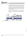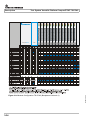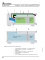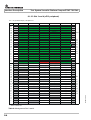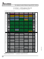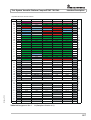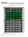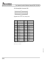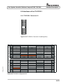
1
USER MANUAL
Test System Versatile Platform CompactTSVP
TS-PCA3
User Manual
for ROHDE & SCHWARZ Test System Versatile Platform CompactTSVP
5th Issue / 11.05 / D 1152.3908.12
All rights, also translation into foreign languages, are reserved. No part of this manual is permitted
to be reproduced in any form (print, photocopy or any other method), also not for the preparation of
lectures, or processed, reproduced or made available using electronic systems without written permission from ROHDE & SCHWARZ.
© The passing on to third parties and the reproduction of this documentation, utilisation and communication of its contents is not permitted unless specifically approved. Infringements will incur claims
for damages. All rights reserved in the case of the award of a patent or registration of a design.
We draw to your attention that the names of software and hardware used in the User Manual, and
the brand names of the respective companies are, in general, the subject of protection as trademarks, or under proprietary rights, or patent law.
ROHDE & SCHWARZGmbH & Co. KG
Corporate Headquarters
Mühldorfstr. 15
D-81671 München
Telephone:
Fax:
...49 (0)89/4129-13774
...49 (0)89/4129-13777
Printed in the Federal Republic of Germany. Errors excepted, subject to technical change without notice.
Safety Instructions
This unit has been designed and tested in accordance with the EC Certificate of Conformity and has left the
manufacturer’s plant in a condition fully complying with safety standards.
To maintain this condition and to ensure safe operation, the user must observe all instructions and warnings
given in this operating manual.
Safety-related symbols used on equipment and documentation from R&S:
Observe
operating
instructions
1.
Weight
indication for
units >18 kg
PE terminal
Ground
terminal
The unit may be used only in the operating conditions and positions specified by the manufacturer. Unless otherwise agreed, the following
applies to R&S products:
Danger!
Shock hazard
7.
2.
8.
For measurements in circuits with voltages Vrms
> 30 V, suitable measures should be taken to
avoid any hazards.
(using, for example, appropriate measuring
equipment, fusing, current limiting, electrical
separation, insulation).
3.
4.
5.
If the unit is to be permanently wired, the PE
terminal of the unit must first be connected to
the PE conductor on site before any other connections are made. Installation and cabling of
the unit to be performed only by qualified technical personnel.
For permanently installed units without built-in
fuses, circuit breakers or similar protective devices, the supply circuit must be fused such as
to provide suitable protection for the users and
equipment.
Prior to switching on the unit, it must be ensured
that the nominal voltage set on the unit matches
the nominal voltage of the AC supply network.
If a different voltage is to be set, the power fuse
of the unit may have to be changed accordingly.
6.
Units of protection class I with disconnectible
AC supply cable and appliance connector may
be operated only from a power socket with
grounding contact and with the PE conductor
con- nected.
Ground
Attention!
Electrostatic
sensitive devices require
special care
It is not permissible to interrupt the PE conductor intentionally, neither in the incoming cable
nor on the unit itself as this may cause the unit
to become electrically hazardous.
Any extension lines or multiple socket outlets
used must be checked for compliance with
relevant safety standards at regular intervals.
IP degree of protection 2X, Pollution severity 2,
overvoltage category 2, altitude max. 2000 m.
The unit may be operated only from AC supply
mains fused with max. 16 A.
Warning! Hot
surfaces
If the unit has no power switch for disconnection
from the AC supply, the plug of the connecting
cable is regarded as the disconnecting device.
In such cases it must be ensured that the power
plug is easily reachable and accessible at all
times (length of connecting cable approx. 2 m).
Functional or electronic switches are not suitable for providing disconnection from the AC
supply.
If units without power switches are integrated in
racks or systems, a disconnecting device must
be provided at system level.
9.
Applicable local or national safety regulations
and rules for the prevention of accidents must
be observed in all work performed.
Prior to performing any work on the unit or
opening the unit, the latter must be disconnected from the supply network.
Any adjustments, replacements of parts, maintenance or repair may be carried out only by
authorized R&S technical personnel.
Only original parts may be used for replacing
parts relevant to safety (e.g. power switches,
power transformers, fuses). A safety test must
be performed after each replacement of parts
relevant to safety.
(visual inspection, PE conductor test, insulationresistance, leakage-current measurement, functional test).
continued overleaf
095.1000 Bl.15
Safety Instructions
10. Ensure that the connections with information
technology equipment comply with IEC950 /
EN60950.
11. Lithium batteries must not be exposed to high
temperatures or fire.
Keep batteries away from children.
If the battery is replaced improperly, there is
danger of explosion. Only replace the battery by
R&S type (see spare part list).
Lithium batteries are suitable for environmentally
friendly disposal or specialized recycling.
Dispose of them in appropriate containers only.
Do not short-circuit the battery.
12. Equipment returned or sent in for repair must be
packed in the original packing or in packing with
electrostatic and mechanical protection.
13. Electrostatics via the connectors may damage
the equipment. For the safe handling and
operation of the equipment, appropriate
measures against electrostatics should be
implemented.
14. The outside of the instrument is suitably cleaned
using a soft, lint-free dustcloth. Never use
solvents such as thinners, acetone or similar, as
they may damage the front panel labeling or
plastic parts.
15. Any additional safety instructions given in this
manual are also to be observed.
Additional safety instructions:
• Any alteration to the basic equipment is prohibited, unless carried out by persons authorized to do
so according to section 9 of these safety instructions.
• In case that a module is inserted which is specified for an analog bus operation < 60 VDC, then
this limit is also restrictively valid for the total system.
• The voltage limits for exposed voltage-carrying parts under DIN EN61010-1/6.3 must on no
account be exceeded.
If the use of higher voltages is required, this may be done only after consultation with R&S.
• The total power which may be drawn from the secondary side depends on the format of the
relevant backplane segment (typically 250VA).
• When installing in racks, the ventilation of the system must be such that the specified data sheet
values of 0 ... 50 °C are adhered to.
095.1000 Bl.16
Support Center
Telephone Europe:
+49 180 512 42 42
Telephone worldwide: +49 89 4129 13774
Fax:
+49 89 4129 13777
e-mail: [email protected]
If you have any technical queries about this Rohde &
Schwarz equipment, our Hotline at the Support Center of
Rohde & Schwarz Vertriebs-GmbH will be glad to help.
Our team will discuss your queries and look for solutions to
your problems.
The Hotline is open Mondays to Fridays from 08.00 to 17.00
hrs.
For queries outside office hours, you can leave a message
or send a note via fax or email. We will then get back to you
as soon as possible.
Test System Versatile Platform CompactTSVP TS-PCA3
Contents
Contents
1
2
5th Issue 11.05
3
User Information
1-1
1.1
Foreword
1-1
1.2
Related Documentation
1-2
1.3
Purpose of the User Manual
1-3
1.4
Explanation of Symbols
1-4
Safety
2-1
2.1
General
2-1
2.2
Safety Instructions
2-1
Description
3-1
3.1
3-1
Usage
3.1.1
General
3-1
3.1.2
Explanation of Terms
3-2
3.1.3
System Information
3-3
3.2
Views
3-5
3.3
Construction
3-7
3.3.1
Case
3-7
3.3.2
3.3.2.1
3.3.2.2
Slot Layout
Plan View
Side View
3-8
3-8
3-9
3.3.3
3.3.3.1
3.3.3.2
3.3.3.3
Backplanes
cPCI Backplane
Analog Bus Backplane
Power Backplane
3-9
3-10
3-15
3-18
3.3.4
Ground Concept
3-18
3.3.5
Geographical Addressing of the Slots with GA0 ... GA4
3-19
3.3.6
CAN Bus
3-20
3.3.7
Configurations with several Frames
3-21
3.3.8
Switching the PSU
3-22
3.3.9
System Controller
3-22
3.3.10
Line Connection and Power Switch
3-23
3.3.11
Cooling
3-23
System Module TS-PSYS1
3-25
3.4
3.4.1
General
3-25
3.4.2
Characteristics
3-25
3.4.3
Circuit Diagram of the TS-PSYS1
3-26
1
Contents
3-26
3.4.5
3.4.5.1
3.4.5.2
3.4.5.3
3.4.5.4
3.4.5.5
Functional Description of the TS-PSYS1
Control
System Functions
System Clock
Signal Looping
Local Signal Outputs
3-28
3-28
3-28
3-29
3-30
3-30
3.4.6
Driver Software
3-31
3.4.7
Self-Test
3-31
Function Description
3-31
3.6
Permitted Module Configurations
3-32
Commissioning
4-1
4.1
Safety Instructions
4-1
4.2
Setting Up
4-1
4.2.1
Requirements for Repeatable Measurements
4-1
4.2.2
Rack Mounting
4-1
4.2.3
Desktop Setup
4-2
4.4
4.5
2
Structure of the TS-PSYS1
3.5
4.3
5
3.4.4
Installation
4-3
4.3.1
Safety Instructions
4-3
4.3.2
Compatibility
4-3
4.3.3
Module Installation
4-4
4.3.4
Driver Installation
4-4
Connections
4-5
4.4.1
Line Inlet
4-5
4.4.2
Connections at the Rear
4-5
4.4.3
Connections at the Front
4-6
Cabling
4-7
4.5.1
Concept
4-7
4.5.2
Analog Bus
4-9
4.5.3
PXI Trigger Bus
4-10
4.5.4
Internal Cabling of Short cPCI Modules
4-10
4.5.5
External Cabling
4-11
4.5.6
Opening the Case
4-12
Operation
5-1
5.1
General
5-1
5.2
Powering the Unit ON and OFF
5-1
5.3
Self-Test
5-3
5th Issue 11.05
4
Test System Versatile Platform CompactTSVP TS-PCA3
Test System Versatile Platform CompactTSVP TS-PCA3
6
7
8
Maintenance
6-1
6.1
Important User Information
6-1
6.2
Cleaning
6-1
6.3
Fuse Replacement
6-2
Plug-In Modules
7-1
7.1
General
7-1
7.2
Configuration Instructions
7-3
7.2.1
General information
7-3
7.2.2
7.2.2.1
7.2.2.2
7.2.2.3
Effects of the TS-PCA3 backplane redesign V4.0
Reason
Steps taken
Effects
7-3
7-3
7-4
7-4
Interface Description
8-1
8.1
cPCI Backplane
8-1
8.1.1
Position of Interfaces
8-1
8.1.2
8.1.2.1
8.1.2.2
8.1.2.3
8.1.2.4
8.1.2.5
8.1.2.6
cPCI Connectors
General
Slot 1 (System)
Slot 3 and 4 (cPCI peripheral)
Slot 5 ... 14 (PXI peripheral / Rear I/O)
Slot 15 (PXI peripheral / Rear I/O for PSYS)
Slot 16 (PXI peripheral / Rear I/O)
8-2
8-2
8-3
8-4
8-6
8-8
8-10
8.1.3
Connector X0 (P47)
8-11
8.1.4
ATX Connectors
8-13
8.1.5
Fan Connectors X90, X91, X92, X93
8-13
8.1.6
Expansion Connector X80
8-14
8.1.7
Jumper Field
8-14
8.1.8
IPMB0
8-14
8.2
5th Issue 11.05
Contents
8.3
Analog Bus Backplane
8-15
8.2.1
Position of Interfaces
8-15
8.2.2
Analog Bus Connectors X1 ... X16
8-16
8.2.3
Analog Bus Connector X21
8-17
8.2.4
Analog Bus Connector X22
8-18
Power Backplane (Option)
8-19
8.3.1
Position of Interfaces
8-19
8.3.2
Power Backplane Utility Connector X13
8-19
8.3.3
Power Backplane ATX Connector X12
8-20
8.3.4
Power Backplane Connector X16
8-20
8.3.5
Connector X1 (P47)
8-21
3
Contents
8.4
8.5
Test System Versatile Platform CompactTSVP TS-PCA3
Interfaces of the TS-PSYS1
8.4.1
TS-PSYS1 Connector X1
8-23
8.4.2
TS-PSYS1 Connector X20
8-24
8.4.3
TS-PSYS1 Connector X30
8-25
8.4.4
TS-PSYS1 Jumper Field X40
8-26
8.4.5
TS-PSYS1 Jumper JP2
8-26
8.4.6
TS-PSYS1 Jumper JP6 and JP7
8-26
8.4.7
TS-PSYS1 Jumper JP8
8-27
External Analog Interface
8.5.1
9
Analog Bus Connector X2
8-28
8-28
Technical Data
9-1
9.1
Specification
9-1
9.2
General Data
9-2
9.3
Dimensions and Weight of the TS-PSYS1
9-3
Appendix
A-1
A.1
A-1
TS-PCA3 Backplane Versions
A.1.1
Effects of the TS-PCA3 backplane redesign
A-1
A.1.2
A.1.2.1
A.1.2.2
A.1.2.3
Effects of the TS-PCA3 backplane redesign V4.0
Reason
Steps taken
Effects
A-1
A-1
A-2
A-3
A.1.3
A.1.3.1
A.1.3.2
Effects of the versions on individual modules
Can be used in slots 5 to 14 without any restrictions
Version-dependent effects
A-4
A-4
A-5
5th Issue 11.05
A
8-23
4
Test System Versatile Platform CompactTSVP TS-PCA3
Figures
5th Issue 11.05
Figures
Figure 3-1
Configuration of the CompactTSVP.................................................3-3
Figure 3-2
Front View ..........................................................................................3-5
Figure 3-3
Rear View............................................................................................3-5
Figure 3-4
Adapter Interface ...............................................................................3-6
Figure 3-5
BW 2000 Case ....................................................................................3-7
Figure 3-6
Plan View (Example)..........................................................................3-8
Figure 3-7
Side View ............................................................................................3-9
Figure 3-8
Backplanes and Bus Systems..........................................................3-9
Figure 3-9
CAN Bus Termination......................................................................3-11
Figure 3-10
Wiring CAN bus ...............................................................................3-12
Figure 3-11
Mountable Threaded Studs on the cPCI Backplane.....................3-13
Figure 3-12
Connecting the current rail to AUX signals ..................................3-14
Figure 3-13
Principle of the Analog Bus............................................................3-15
Figure 3-14
Use of the Analog Bus in the CompactTSVP (Example)..............3-17
Figure 3-15
Ground Concept ..............................................................................3-19
Figure 3-16
Configuration example TS-PCA3 und TS-PWA3...........................3-21
Figure 3-17
Layout of Fans in the Frame...........................................................3-24
Figure 3-18
Circuit diagram of the TS-PSYS1 ...................................................3-26
Figure 3-19
Connectors and Jumpers on the TS-PSYS1 .................................3-27
Figure 3-20
Module Configuration TS-PCA3
(Backplane Version 2.1 and 3.x).....................................................3-33
Figure 3-21
Module Configuration TS-PCA3 (Backplane Version 4.0)............3-34
Figure 4-1
Rear Connections ..............................................................................4-5
Figure 4-2
Front Connections.............................................................................4-6
Figure 4-3
Inner and Internal Cabling Variants .................................................4-8
Figure 4-4
Adaption of a Short PXI Module to the Adapter Interface
(Example)..........................................................................................4-11
Figure 4-5
CompactTSVP Rear View................................................................4-12
Figure 6-1
CompactTSVP Rear View..................................................................6-2
Figure 7-1
Plug-in modules in the CompactTSVP ...........................................7-1
Figure 8-1
cPCI Backplane (Front View) ............................................................8-1
Figure 8-2
Connectors P1 and P20 Front (Mating Side)...................................8-1
5
Figures
Test System Versatile Platform CompactTSVP TS-PCA3
cPCI Backplane (Rear View) .............................................................8-2
Figure 8-4
Connectors P1 and P20 Rear (Mating Side) ....................................8-2
Figure 8-5
Connector X0 (P47)..........................................................................8-11
Figure 8-6
Analog Bus Backplane (Front View) ..............................................8-15
Figure 8-7
Analog Bus Backplane (Rear View) ...............................................8-15
Figure 8-8
Connectors X1 ... X16 (Mating Side)...............................................8-16
Figure 8-9
Connector X21 (Mating Side) ..........................................................8-17
Figure 8-10
Connector X22 (Mating Side) ..........................................................8-18
Figure 8-11
Power Backplane .............................................................................8-19
Figure 8-12
Connector X1 (P47) (Mating Side) ..................................................8-21
Figure 8-13
TS-PSYS1 Connector X1 (Mating Side)..........................................8-23
Figure 8-14
TS-PSYS1 Connector X20 (Mating Side)........................................8-24
Figure 8-15
TS-PSYS1 Connector X30 (Mating Side)........................................8-25
Figure 8-16
Signals at the TS-PSYS1 Jumper Field X40 ..................................8-26
Figure 8-17
Signals at the TS-PSYS1 Jumper JP2............................................8-26
Figure 8-18
TS-PSYS1 Jumper JP6 and JP7 .....................................................8-26
Figure 8-19
Signal at the TS-PSYS1 Jumper JP8..............................................8-27
Figure 8-20
Analog Bus Connector X2 (Mating Side) .......................................8-28
5th Issue 11.05
Figure 8-3
6
Test System Versatile Platform CompactTSVP TS-PCA3
Tables
5th Issue 11.05
Tables
Table 3-1
Software Standards ...........................................................................3-4
Table 3-2
Other Characteristics ........................................................................3-4
Table 3-3
Features of the BW 2000 Case .........................................................3-7
Table 3-4
CAN Bus ...........................................................................................3-11
Table 3-5
External Additional Signals ............................................................3-13
Table 3-6
CAN Bus Termination......................................................................3-21
Table 3-7
Device Addressing ..........................................................................3-22
Table 3-8
Recommendations for Selecting the System Controller .............3-23
Table 3-9
Characteristics of the TS-PSYS1....................................................3-25
Table 3-10
Connectors on the TS-PSYS1.........................................................3-27
Tabelle 5-1
PCI Configuration CompactTSVP (Example) ..................................5-2
Tabelle 5-2
Rohde & Schwarz ID Numbers .........................................................5-2
Table 8-1
Assignment Slot 1 .............................................................................8-3
Table 8-2
Assignment Slot 3 and 4 ...................................................................8-4
Table 8-3
Assignment Slot 5 ... 14 (Backplane Version 2.0 to 3.X) ................8-6
Table 8-4
Assignment Slot 5 ... 14 (Backplane Version 4.X) ..........................8-7
Table 8-5
Assignment Slot 15 (Backplane Version 2.0 to 3.X) .......................8-8
Table 8-6
Assignment Slot 15 (Backplane Version 4.X) .................................8-9
Table 8-7
Assignment Slot 16 .........................................................................8-10
Table 8-8
Assignment X0 (P47) .......................................................................8-11
Table 8-9
ATX Connector Assignment ...........................................................8-13
Table 8-10
Assignment of X90 ... X93 ...............................................................8-13
Table 8-11
Assignment of X80 ..........................................................................8-14
Table 8-12
Jumper Field Assignment...............................................................8-14
Table 8-13
IPMBO Assignment .........................................................................8-14
Table 8-14
Assignment of X1... X16 ..................................................................8-16
Table 8-15
Assignment of X21 ..........................................................................8-17
Table 8-16
Assignment of X22 ..........................................................................8-18
Table 8-17
Assignment of X13 ..........................................................................8-19
Table 8-18
Assignment of X12 ..........................................................................8-20
Table 8-19
Assignment of X16 ..........................................................................8-20
7
Tables
Test System Versatile Platform CompactTSVP TS-PCA3
Assignment of X1 (P47)...................................................................8-21
Table 8-21
TS-PSYS1 Assignment X1...............................................................8-23
Table 8-22
TS-PSYS1 Assignment X20.............................................................8-24
Table 8-23
TS-PSYS1 Assignment X30.............................................................8-25
Table 8-24
Assignment of X2.............................................................................8-28
5th Issue 11.05
Table 8-20
8
Test System Versatile Platform CompactTSVP TS-PCA3
User Information
1 User Information
1.1 Foreword
We congratulate you on your purchase of a ROHDE & SCHWARZ Test
System Versatile Platform CompactTSVP.
We would emphasize that only attendance at one of our regular inhouse
training seminars can ensure your successful operation of the Test
System Versatile Platform in the long term.
Please do not hesitate to contact us should you have any queries whilst
working with the Test System Versatile Platform.
We look forward to working with you
5th Issue 11.05
GmbH & Co. KG
1-1
User Information
Test System Versatile Platform CompactTSVP TS-PCA3
1.2 Related Documentation
Comprehensive documentation is supplied to enable you to use the
Test System Versatile Platform CompactTSVP efficiently. The operating manual comprises the following sections:
•
User Information
•
Safety
•
Description
•
Commissioning
•
Operation
•
Maintenance
•
Plug-in modules
•
Interface description
•
Technical Data
The Appendices contain:
•
Declaration of Conformity
NOTE:
5th Issue 11.05
In the event of any discrepancies between data in this manual and
the technical data in the data sheet, the data sheet takes precedence.
1-2
Test System Versatile Platform CompactTSVP TS-PCA3
User Information
1.3 Purpose of the User Manual
This User Manual provides the information that is necessary for
•
the commissioning and
•
the proper and safe operation
of the Test System Versatile Platform CompactTSVP.
This User Manual must be carefully read by the operator/engineer who
is responsible for working with the CompactTSVP before it is powered
up for the first time.
As well as the operating instructions and the health and safety instructions which apply at the site where the system is used, the applicable
technical standards and regulations for safe and proper working must
be complied with.
The operating instructions must be available at or near the CompactTSVP at all times.
5th Issue 11.05
The owner must supplement the operating instructions with national accident prevention and environmental protection regulations as appropriate.
1-3
User Information
Test System Versatile Platform CompactTSVP TS-PCA3
1.4 Explanation of Symbols
The Test System Versatile Platform CompactTSVP has been manufactured in accordance with accepted engineering practice and the latest
scientific and technical findings.
Nevertheless there are certain risks which cannot be designed out of
equipment.
Additional safety instructions have been developed to provide adequate safety for the personnel working on the CompactTSVP.
A satisfactory level of safety when using the CompactTSVP cannot be
guaranteed unless these instructions are followed.
Certain sections of text are specially highlighted. These sections have
the following meaning:
DANGER!
Failure to follow instructions can result in personal injury!
ELECTROCUTION HAZARD!
Failure to follow instructions can result in personal injury!
WARNING!
Failure to following instructions can cause damage to the Test
System Versatile Platform CompactTSVP.
CAUTION!
Failure to follow instructions can result in incorrect measurements.
Highlights important details to which special attention must be
paid and that make work easier.
1-4
5th Issue 11.05
NOTE:
Test System Versatile Platform CompactTSVP TS-PCA3
Safety
2 Safety
2.1 General
The Test System Versatile Platform must be operated in accordance
with the safety regulations which apply in the owner's country.
NOTE:
Safety risks created by an application that is based on the Test
System Versatile Platform must be eliminated by suitable additional arrangements (e.g. integration in the Emergency Stop circuit).
NOTE:
Failure to observe the safety regulations governing the operation
of the Test System Versatile Platform shall void any liability or
guarantee claims against ROHDE & SCHWARZ GmbH & Co. KG.
2.2 Safety Instructions
ELECTROCUTION HAZARD!
The Test System Versatile Platform may only be opened by suitably trained technical personnel! The appropriate regulations
governing work carried out on electrical equipment must be
complied with.
The CompactTSVP must be isolated from the electrical supply before
work commences.
WARNING!
5th Issue 11.05
Never link out defective fuses. Always replace defective fuses with
fuses of the same rating.
The electrical equipment fitted to the CompactTSVP must be checked
at regular intervals. Defects such as loose connections, scorched cables etc. must be rectified immediately.
The enclosed safety sheet must be complied with.
2-1
Test System Versatile Platform CompactTSVP TS-PCA3
5th Issue 11.05
Safety
2-2
Test System Versatile Platform CompactTSVP TS-PCA3
Description
3 Description
3.1 Usage
3.1.1 General
The Test System Versatile Platform CompactTSVP is a standardized modular platform for the program-controlled testing of modules
and terminals in the factory or laboratory. With its flexible configuration
and the use of worldwide standards, it can be perfectly adapted to suit
the needs of the user.
Larger ATE (Automatic Test Equipment) systems can be created by
combining CompactTSVP (TS-PCA3) and PowerTSVP (TS-PWA3).
The production test platform is intended for use with a control processor which performs the test on the test devices by means of peripheral
modules. This control processor is known as the system controller
and should preferably be in the CompactTSVP. However a standard
PC can also be used running across a suitable interface with the controller. The system controller executes user-created sequences that
define the test procedures and specification limits.
The modules plugged into the CompactTSVP can be used for the creation of test and control signals and for the measuring related evaluation of the response from the UUT. For this purpose they are able to
pass signals between each other and select signals under program
control and pass them to external measuring systems.
5th Issue 11.05
The peripheral modules can be quickly and flexibly adapted to the test
devices by preceding the CompactTSVP with an adapter frame which
connects the signals securely and with a low rate of wear.
If the production test requires switching functions with a large number
of channels or the switching of high currents, then the CompactTSVP
can be supplemented with up to four PowerTSVP's. The Power-TSVP
is controlled via the CAN-Bus of the CompactTSVP by the system controller. A second CompactTSVP can also be triggered.
3-1
Description
Test System Versatile Platform CompactTSVP TS-PCA3
3.1.2 Explanation of Terms
The following terms and standards are used in this manual:
CompactPCI (abbreviated to “cPCI” in this document) is an open standard of the PICMG (PCI Industrial Manufacturers Group) that adapts the
PCI standard for industrial applications. It uses high-grade connection
techniques and mechanical components, and applies the same electrical
specifications as the PCI standard. This makes it possible to use inexpensive components and existing PCI developments even under industrial conditions. Other features include a high integration density, the option of a 19" installation and shielding for the plug-in modules. Its definition as an open standard means that a large, worldwide variety of cards
is available.
PXI (PCI eXtensions for Instrumentation) is a standard defined by National Instruments which expands the CompactPCI, using its mechanical specifications and the connection with the system controller. The
PXI standard is fully compatible and also defines a number of additional
signals which are useful for measuring applications, such as the PXI
Triggerbus.
PCI-PCI bridges are used to connect a number of cPCI or PXI segments, thereby increasing the number of peripheral slots in cPCI or PXI
systems.
CAN (Controller Area Network) is a serial bus system whose high system and configuration flexibility is achieved by a content-oriented addressing scheme, i.e. it defines so-called “message identifiers“ and not
device addresses. Systems can be added to an existing network without the need for hardware or software modifications. The CAN protocol
is defined in ISO 11898.
5th Issue 11.05
Rear I/O is the name given to a design that allows input and output lines
of the cPCI connectors P1 and P2 to be accessed from the rear of a
backplane. Pluggable Rear I/O modules can be used for this purpose
in the CompactTSVP and the PowerTSVP.
3-2
Test System Versatile Platform CompactTSVP TS-PCA3
Description
3.1.3 System Information
The CompactTSVP has a modular structure that allows a range of system configurations tailored to the specific needs of the user.
Up to 13 cPCI/PXI modules can be fitted in addition to the system controller (slot 1). A further slot (slot 16) is provided for special R&S plugin modules (without J1 connector). Slots A3, A4 are fitted with a PSU
as standard. An optional PSU can be fitted to slots A1, A2. Slots 1 to
16 provide access to the analog bus. The CAN bus is available at slots
5 to 16 (starting with backplane version V4.x in slots 3 and 4 as well).
There is space for rear I/O modules in the rear section of the CompactTSVP .
The configuration of the CompactTSVP is shown in Figure 3-1.
CPU
Bus
Slot
A1 A2 A3 A4 1 2 3 4 5 6 7 8 9 10 11 12 13 14 15 16
CompactPCI
PXI
CAN
X X
Analog Bus
Rear I/O
5th Issue 11.05
DC/DC, Rear I/O
Power Supplies
Figure 3-1 Configuration of the CompactTSVP
X with Backplane Version V4.x
Starting with backplane version V4.x, some changes have been made
to details to avoid incompatibilities with some third-party modules. The
effects on the configurability of modules are described in Section 7.2.
3-3
Description
Test System Versatile Platform CompactTSVP TS-PCA3
The use of standard industrial PC's as system controllers makes it possible to run a wide range of software packages from the PC sector.
Software Standards
Operating system: Windows NT(™) / Windows 2000(™) / Windows XP(™)
Test software: LabWindows/CVI(™), Visual C++(r), TestStand(™)
Card drivers : Drivers based on VISA/IVI
Table 3-1 Software Standards
Table 3-2 summarizes some further characteristics of the CompactTSVP that are important for a Test System Versatile Platform.
Other Characteristics
Powerful cPCI PSU for 250 W (expandable to 500 W)
Slot CPU's of different power classes can be used
The internal analog bus facilitates the distribution of measurement/stimuli signals between the cPCI plug-in modules without additional cabling.
Optional: Front mounted adapter interface on the CompactTSVP
that uses spring contacts to facilitate rapid and high-pole contacting
with the test devices (see Figure 3-4 ).
System serviceability is monitored by a built-in self-test capability
and system monitor (operating voltages, temperature)
5th Issue 11.05
Table 3-2 Other Characteristics
3-4
Test System Versatile Platform CompactTSVP TS-PCA3
Description
3.2 Views
Figure 3-2 and Figure 3-3 show the CompactTSVP with slots covered.
Test System Versatile Platform
CompactTSVP
Figure 3-2 Front View
X4
X3
X2
ANALOG
BUS
X1
1
5th Issue 11.05
0
Figure 3-3 Rear View
3-5
Description
Test System Versatile Platform CompactTSVP TS-PCA3
The CompactTSVP can be operated with an adapter interface (optional) which is flange-mounted to the front panel (see Figure 3-4)
5th Issue 11.05
Figure 3-4 Adapter Interface
3-6
Test System Versatile Platform CompactTSVP TS-PCA3
Description
3.3 Construction
3.3.1 Case
The CompactTSVP uses the standard ROHDE & SCHWARZ case of
the “Design 2000” (see Figure 3-5). The characteristics of the case are
summarized in the Table 3-3.
Figure 3-5 BW 2000 Case
HF-immune case to Rohde & Schwarz “Design 2000”
Dimensions: 19", height 4U, 430 mm deep
Use as desktop unit or rack-mounted case
Mounted in 19" rack using the telescopic slide set or on support rails
Side case handles that remain on the unit when mounted in the rack.
Four rugged detachable rubber feet provide rear protection.
Unused slots can be covered by front sub-panels that maintain the integrity of the HF-immunity. Contact springs are mounted between the
individual front sub-panels for this purpose.
5th Issue 11.05
The case is suitable for 3U high plug-in boards.
The remaining space in the case can be used for adaption to the
standard UUT connector or for concealed (cross) cabling.
Table 3-3 Features of the BW 2000 Case
3-7
Description
Test System Versatile Platform CompactTSVP TS-PCA3
3.3.2 Slot Layout
3.3.2.1 Plan View
5th Issue 11.05
Figure 3-6 Plan View (Example)
3-8
Test System Versatile Platform CompactTSVP TS-PCA3
Description
3.3.2.2 Side View
cPCI Backplane
Fan
Analog Bus
Rear I/O
Figure 3-7 Side View
3.3.3 Backplanes
The CompactTSVP contains the following backplanes:
•
cPCI backplane with PICMG Power Interface and Rear I/O support
•
Analog bus backplane
•
Power backplane with PICMG Power Interface (optional)
Figure 3-8 shows the backplanes with the bus systems. The assignment of the connectors is detailed in Section 8.
P20
5th Issue 11.05
P1
R&S Analog bus
Slot 1
2
PXI Sync-Bus
3
4
5
6
Auxiliary
7
8
9
I2C
10
11
12
CAN
13
14
15
16
Figure 3-8 Backplanes and Bus Systems
3-9
Description
Test System Versatile Platform CompactTSVP TS-PCA3
3.3.3.1 cPCI Backplane
The cPCI backplane is implemented as follows:
•
3U
•
72HP
•
32 bit
•
33 MHz
•
V I/O = 5 V
The backplane fulfils the Hot-Swap capability according to Standard
PICMG 2.1 Rev. 2.0 for the exchange of measuring and control cards
during operation. The 32 bit area conforms to PICMG 2.0 Rev. 3.0. It
should be noted that ROHDE & SCHWARZ TSVP modules (TS-XXX)
are not capable of hot swapping.
Connector X0 (P47) serves as a power interface for a cPCI standard
PSU. An additional PSU can be plugged onto an optional power backplane, in which case the connection with the cPCI backplane is made
with an ATX power supply cable.
Slots 1 to 8 are the first bus segment. Slots 9 to 15 form the second bus
segment that is connected to the first with a PCI-PCI bridge.
Slot 15 with its rear exit for the P1 signals is designed to control the system module.
The Rear I/O conforms to IEEE 1101.11-1998. The P20 connectors at
slots 3 and 4 are manufactured to cPCI standard, 32 bit with Rear I/O.
Voltages up to 125 VDC can be applied at pins provided in the Rear I/O
area.
Signals PXI_TRIG0 ... 7 and PXI_CLK10 according to standard PXI
R2.0 are available at the P20 connections in slots 5 to 16.
The PXI local bus is not implemented. If necessary, wiring can be created between adjacent slots by plugging in a customer-specific connection board (plugged into the backplane).
3-10
5th Issue 11.05
Local bus
Test System Versatile Platform CompactTSVP TS-PCA3
Description
CAN-Bus
The CAN bus *[1] is integrated as a further system bus in addition to
the IPMB0 (slots 3 to 14) according to System Management Specification PICMG 2.9 R1.0, and is available at slots 5 to 16 (starting with
backplane version V4.x in slots 3 and 4 as well). Signals CAN_L and
CAN_H can be terminated at the bus end with a jumper and 120 Ohm
resistor ( Figure 3-9 ). Alternatively the bus can be extended externally
with an X80 expansion connector.
*[1] to standard CAN 2.0b (1Mbit)
Figure 3-9 CAN Bus Termination
Number
Lines
2
Umax
(VDC)
5
Pin
CAN_H: P20/C1
CAN_L: P20/D1
Table 3-4 CAN Bus
5th Issue 11.05
In the old design V1.0 - V3.0, the CAN bus is bussed directly, guided
via PXI local bus lines LBL10 and LBL11. In the most unfavourable
case, this resulted in conflicts with other PXI modules that were using
the lines in a different way.
In the new design V4.0, the CAN bus is switched by PSYS1 to Slot15
and is directed to the other slots 3-14. The two signals are only
switched by PhotoMOS relays on the backplane to the pins of a slot if
a CAN module is detected in that slot. In that case the switch behaves
like an isolating relay and does not affect the signals of the LBxx. It is
able to isolate voltages up to ±60 V DC.
PCI slots 3 + 4 now have this switch in the backplane and are thus
CAN-capable. The CAN bus is continuously connected on slots 15 + 16
without switching.
3-11
Description
Test System Versatile Platform CompactTSVP TS-PCA3
A 330-Ohm pull-up resistor between P2/D18 and +5 V on each module
is responsible for detecting a CAN module and activating the CAN bus.
Normal cPCI or PXI modules according to specification apply this pin to
GND or leave it open. This ensures the CAN bus is never in conflict with
analogue voltages of the local bus.
Measurement Module
+5V
330R
P2/D18
P2/D18
Backplane
100R
1/2*AQS225
CAN_H
P2/C1
CAN_L
P2/D1
5th Issue 11.05
Figure 3-10 Wiring CAN bus
3-12
Test System Versatile Platform CompactTSVP TS-PCA3
Description
External additional signals (AUX)
Two additional external signals (for example power supply voltages)
can be fed into a module via J20 on slots 5 through 16. The signals can
be fed in in the area of the CPCI power pack by the CPCI power supply,
an internal AC/DC module or another external signal sources. This can
be used to provide a primary voltage to generate local supply voltages
(DC/DC converter), etc.
Number
Lines
2
Umax
(VDC)
60
Imax/Slot(A
DC)
2
Pin
Input for ext. signals:
J20: AUX1 B20, E19
J20: AUX2 A20, D19
Table 3-5 External Additional Signals
+5-V and +12-V lines from the P47 connector are routed on the screw
bolts above slot 4. This makes it easy to connect AUX1 with +5 V and
AUX2 with +12 V via current rail or cable (see Figure 3-11 ).
+12V
+5V
X0
5th Issue 11.05
5
4
3
2
Slot 1
Figure 3-11 Mountable Threaded Studs on the cPCI Backplane
The AUX pins assigned to slots 5 - 16 make it possible to direct two
voltages from the current rail on the upper backplane if a screw there
connects the backplane signals with the current rail. Currently in backplanes V1.1 through V3.0 two pins are hard connected to carry a higher
current.
3-13
Description
Test System Versatile Platform CompactTSVP TS-PCA3
This is changed in backplane V4.0 so the two pins are not connected
in normal state. One pin (for example AUX1L) on the solder side is directed to the current rail and one pin (AUX1R) on the module side is
directed to the current rail as well. The connection is not made until a
screw with a nut is screwed in and connects the current rail and the two
copper rings in the layout. It may be preferably to insert a toothed washer to ensure better contact.
Functionally this is no different than the previous version. The PXI
specification is observed except for the lack of a local bus daisy chain.
Full current must not be drawn unless the two pins are connected in
parallel.
5th Issue 11.05
Figure 3-12 Connecting the current rail to AUX signals
3-14
Test System Versatile Platform CompactTSVP TS-PCA3
Description
3.3.3.2 Analog Bus Backplane
To simplify cabling, the CompactTSVP contains an analog bus with 8
signals. The analog bus backplane is located in the front above the
cPCI backplane. A special layout meets the need for high crosstalk
damping and low capacitance of the signal lines to GND.
The C module (2 mm connector system) is used as the connectors
(X1...X16). Plug-in modules with no analog bus connector access the
analog bus via a 26-pin connector (X22) and R&S switch modules. Signals IL1_x and IL2_x (Instrument Line) are passed from slots 5 to 16 to
connector X22.
The analog bus signals pass from connector X21 to connector X2 at the
back of the CompactTSVP (see Section 4/4/2).
The electrical characteristics of the analog lines are:
•
Voltage 125 VDC max.
•
Current 1 A max.
3.3.3.2.1 Concept of the Analog Bus
Analogbus
UUT
5th Issue 11.05
Instrument-Pins
UUT-Pins
I/O-Channels
Figure 3-13 Principle of the Analog Bus
The analog bus in the CompactTSVP connects I/O channels of different plug-in modules to each other. These I/O channels may be connections of instruments (measuring and stimuli devices) and connections
3-15
Description
Test System Versatile Platform CompactTSVP TS-PCA3
of the test device. Up to 8 signals can be connected simultaneously
(see Figure 3-13 ).
The analog bus can be used flexibly with the ROHDE & SCHWARZspecific plug-in modules. 8 equivalent lines are basically available
(ABa1, ABa2, ABb1, ABb2, ABc1, ABc2, ABd1, ABd2). External instruments are usually connected to the CompactTSVP with a rear I/O connection. The signals for the test device are made available at the frontend connector of the various plug-in modules on the CompactTSVP.
The analog bus can be used in different ways:
•
as 1 bus with 8 lines
•
in 2 part-buses with 4 lines each
The split of the analog bus into part-buses depends on the plug-in modules which are used.
The analog bus concept of the CompactTSVP fully meets the requirements that are frequently made in metrology:
•
A small number of buses for a high number of I/O channels (e.g.
In-Circuit-Test with 3 to 6 buses.)
•
As many signals as possible simultaneously for a moderate
number of I/O channels (e.g. function test with 8 buses of 50 to 100
I/O channels).
•
Parallel test with split analog bus.
5th Issue 11.05
Line paths or higher-frequency signals are usually connected locally by
special switching modules and not via the analog bus.
3-16
Test System Versatile Platform CompactTSVP TS-PCA3
Description
3.3.3.2.2 Typical Use of the Analog Bus
The use of the analog bus and individual bus lines is illustrated with
available R&S modules and standard modules (see Figure 3-14 ).
Modular Measurement Module
Internal Access to Analog
Bus or Switching (X22)
Analog Bus Connector
(rear) for Monitoring
cP
TS-PSAM
An
alo
PXI-Module
gB
us
CI
B
ac
k
pla
ne
Rear-I/O-Access
to Analog Bus for
External Instruments
External
Instrument
Modular Switching Modules
Matrix
Instrument Lines
UUT
Matrix
ATE Module TS-PMB
5th Issue 11.05
Figure 3-14 Use of the Analog Bus in the CompactTSVP (Example)
3-17
Description
Test System Versatile Platform CompactTSVP TS-PCA3
3.3.3.3 Power Backplane
The use of a second cPCI PSU in slots A1, A2 requires the optional
Power Backplane (conforms to standard PICMG 2.0). From the Power
Backplane, a cable with three connectors leads to a 24-pin ATX connector on the cPCI backplane. The three connectors are as follows
(see also Section 8, Interface Description):
•
X12, 20-pin
•
X13, 10-pin
•
X16, 4-pin
The second PSU can be used to boost the power of the standard PSU
when connected in parallel. Alternatively it can be used to supply the
device on test.
3.3.4 Ground Concept
An electrically conductive CHA-GND (chassis GND) pad in the mounting area on the cPCI backplane provides an impedance grounding to
the chassis. Screw connections and a busbar on the cPCI backplane
are used to make a low-resistance connection for GND and CHA-GND,
while a star connection between GND and CHA-GND using a busbar
prevents unwanted ground loops.
A capacitor creates the HF connection between GND and CHA-GND at
each slot. A 1 MOhm resistor discharges the capacitors and dissipates
static.
A 3-pin connector provides the 230 VAC supply for the cPCI PSU on
the cPCI backplane (at X0).
The optional power backplane is supplied with AC voltage parallel to
the cPCI backplane.
The GND signal of the analog bus backplane is connected by a cable
and screw terminal to the GND on the cPCI backplane. This prevents
the large induction loops that would occur if a return via chassis were
to be used.
3-18
5th Issue 11.05
The PE conductor must be bonded to the case with a grounding cable.
Test System Versatile Platform CompactTSVP TS-PCA3
Description
The ground screen of the analog bus between two basic CompactTSVP units is connected to CHA-GND (chassis). An alternative
screen can also be made with GND, but the first option offers better
screening performance.
In the second CompactTSVP CHA-GND must not be connected to
GND to prevent ground loops. The connections are indicated in
Figure 3-15.
GND sense of +5 V and +3.3 V (of the second PSU as well) are connected to GND at the grounding star point.
AC Input PE N L
Analog bus
Analog bus
Power Filter
PE
N
GND
L
GND
Screen
CHA-GND
Power
Backplane
CHA-GND
GND
cPCI-Backplane
CompactTSVP
GND
cPCI-Backplane
Rack connection
CompactTSVP
Figure 3-15 Ground Concept
5th Issue 11.05
3.3.5 Geographical Addressing of the Slots with GA0 ... GA4
The physical slot addresses are coded by the signals GA0 ... GA4 of
the P20 connector (see the cPCI specification). These signals are either connected to GND or remain open. In order to distinguish two interconnected CompactTSVP , GA4 is defined by Jumper 1. The jumper
is closed for the first Compact-TSVP (see jumper field in Section 8).
3-19
Description
Test System Versatile Platform CompactTSVP TS-PCA3
The coding for slot recognition is carried out with GA0 ... GA3 as follows:
Slot
1
2
3
4
5
6
7
8
9
10
11
12
13
14
15
16
Code
0001
0010
0011
0100
0101
0110
0111
1000
1001
1010
1011
1100
1101
1110
1111
Note:
0: Pin connected to GND via resistor
1: Pin open
3.3.6 CAN Bus
For controlling of the switch modules TS-PMB and TS-PSM1 as well as
the control modules TS-PSYS1 and TS-PSYS2, the CAN bus is used
in TS-PCA3 and TS-PWA3. The CAN bus numbering results from the
following scheme:
u = Board Number
v = Controller Number
w = Device Number
x = Slot Number
Board Number and Controller Number are always 0. The Device
Number of the frame is determined by the settings of the jumpers on
the backplane (see Section 3.3.7). For Rear-I/O modules like TSPSYS1 and TS-PSYS2, a 4 has to be added to the Device Number.
3-20
5th Issue 11.05
CANu::v::w::x
Test System Versatile Platform CompactTSVP TS-PCA3
Description
Example: CAN0::0::5::15
Board Number: 0
Controller Number: 0
Device Number: 5 (Device 1, Rear-I/O)
Slot Number: 15
The following table shows the jumper configuration for the bus terminations CAN1 (System) und CAN2 (User).
Modul
CAN-Bus
offen
terminiert
TS-PCA3
CAN1 (System)
Jumper J3 and
Jumper J4 open
Jumper J3 and Jumper J4
geschlossen
TS-PWA3
CAN1 (System)
Jumper J4 and
Jumper J5 open
Jumper J4 and Jumper J5
closed
TS-PSYS1, TS-PSYS2
CAN1 (System)
Jumper JP6 open
Jumper JP6 closed
TS-PSYS1, TS-PSYS2
CAN2 (User)
Jumper JP7 open
Jumper JP7 closed
Table 3-6 CAN Bus Termination
3.3.7 Configurations with several Frames
In the following figure, the terminating resistors are depicted in yellow.
J3, J4 closed
CompactTSVP TS-PCA3
JP6 open
TS-PSYS1
JP7 closed
J4, J5 closed
5th Issue 11.05
PowerTSVP TS-PWA3
TS-PSYS2
JP6 open
Figure 3-16 Configuration example TS-PCA3 und TS-PWA3
3-21
Description
Test System Versatile Platform CompactTSVP TS-PCA3
CAN1 (System) is being connected between the two frames via cable
TS-PK02 (option). The termination is carried out on both backplanes.
The jumpers on the system modules TS-PSYS1 and TS-PSYS2 have
to be left open.
According to Section 3.3.5, the jumpers for device addressing must be
set as follows:
TS-PCA3: J1 set → Device 1
TS-PWA3: J1 set, J2 not set → Device 2
J1 (GA4)
J2 (GA5)
Device
set
set
1
set
not set
2
not set
set
3
not set
not set
4
Table 3-7 Device Addressing
3.3.8 Switching the PSU
Signal PS-ON is used to switch the PSU outputs on and off. This is
done by removing Jumper 2 (see jumper field in Section 8) and replacing it by an external switch. Signal PS-ON is available at expansion
connector X80.
3.3.9 System Controller
5th Issue 11.05
Operating the CompactTSVP requires the use of a system controller.
This is fitted to slot 1. The CompactTSVP allows the use of standard
cPCI or PXI system controllers (e.g. PEP CP304).
3-22
Test System Versatile Platform CompactTSVP TS-PCA3
Description
Alternatively an external PC can be used, and suitable PCI-to-cPCI interfaces are available on the market. Table 3-8 lists basic data which a
system controller should meet for the practical operation of the Test
System Versatile Platform .
cPCI Interface
Specification
Processor
1 GHz Pentium III or faster, passive cooling
L2 Cache
256 Kbytes
RAM
Min. 256 MB SDRAM
Front Side Bus
Min. 100 MHz
Hard drive
2.5", Min. 20 GB
VGA
Onboard
Ethernet
10 Base-T / 100 Base-TX, RJ45 Connector
Serial Port
COM1, Front Panel
Keyboard Connector
PS/2, Front Panel, USB
Mouse Connector
PS/2, Front Panel, USB
USB
USB Interface
EIDE
HDD
Temperature
0 ... 60 °C
Humidity
0 ... 95%
Table 3-8 Recommendations for Selecting the System Controller
3.3.10 Line Connection and Power Switch
The line inlet and power switch are at the back of the CompactTSVP
(see Figure 3-3 ).
3.3.11 Cooling
5th Issue 11.05
The CompactTSVP features a powerful cooling concept.
The slots at the front (optional in the Rear I/O area) are cooled by a vertical flow of air. The four fans are located above the slots (see
Figure 3-17 ) and are connected by inline contact connectors to the
backplane. The fan speed is regulated by the internal temperature.
Fans for the Rear I/O area can be retrofitted if required. The supply for
these fans can be taken off expansion connector X80.
3-23
Description
Test System Versatile Platform CompactTSVP TS-PCA3
WARNING!
Adequate space for air inlet and outlet should be allowed when the
case is rack mounted, with at least half a height unit (22 mm) being
left above and below the chassis!
For desktop mounting, ensure that the case is not covered over!
5th Issue 11.05
Figure 3-17 Layout of Fans in the Frame
3-24
Test System Versatile Platform CompactTSVP TS-PCA3
Description
3.4 System Module TS-PSYS1
3.4.1 General
The TS-PSYS1 is in the Rear I/O slot 15 of the CompactTSVP. It acts
primarily as a cPCI-to-CAN interface and therefore as an interface for
communication with R&S CAN modules in the CompactTSVP and
PowerTSVP.
Additional system functions such as voltage and temperature monitoring, trigger signals and optocoupler interface are used to integrate the
CompactTSVP and PowerTSVP in a complete system.
3.4.2 Characteristics
TS-PSYS1
RTM type with cPCI interface
2 independent CAN interfaces (2.0 A/B, 1 Mb/s)
System functions via CAN node (microcontroller)
- Voltage monitor
- Temperature measuring (internal)
- Enable of the PXI trigger signals to the exterior
- 4 optocoupler outputs
- 4 optocoupler inputs
- 2 switchable, short-circuit proof output voltages
- System identification
Manual selection of the local or external system clock, and its buffering
with jumper
5th Issue 11.05
Table 3-9 Characteristics of the TS-PSYS1
3-25
Description
Test System Versatile Platform CompactTSVP TS-PCA3
3.4.3 Circuit Diagram of the TS-PSYS1
Figure 3-18 shows the circuit diagram of the TS-PSYS1
Buffer
DC_SYNC
J
P
2
Buffer
Buffer
CLK 10MHz
CPCI Rear I/O X20
AUX1..6
6
X
4
0
IL1..3
SYNC_OUT
GA0..4
+3.3/+5V
+12/-12V
Voltage
Temperature
uC
+
Flash
+
CAN
+
A/D
4
PhotoMos
Output
8
4
Optocoupler
Input
8
AUX
2
8
PXI_TRIG
8
Pull-Ups
Protect.
FET Bus Switch
+5V
LDO
+12V
8 TRIG
Front Connector X30
PXI_CLK10
Buffer JP8 CLK10_OUT
CLK10_IN
+4.5V
+11.5V
CPCI Rear I/O X1
LDO
Buffer
CAN1(System)
Transceiver
CPCI
Interface
PLX9050
uC
+
CAN Controller
CAN2(User)
Transceiver
TEMP_OUT
JP6
Term.
JP7
Term.
3.4.4 Structure of the TS-PSYS1
The TS-PSYS1 is the size of a standard cPCI-RTM (Rear Transmission
Module) and is mounted in slot 15 at the rear of the TSVP chassis.
3-26
5th Issue 11.05
Figure 3-18 Circuit diagram of the TS-PSYS1
Test System Versatile Platform CompactTSVP TS-PCA3
Description
Connectors X1 and X20 are used to make the connections to the Rear
I/O side of the cPCI backplane in the CompactTSVP. Connector X30 is
a 44-pin D-sub socket (High Density). Jumper field X40 as well as the
Jumpers JP2, JP6, JP7and JP8 are placed on the circuit board.
Figure 3-19 Connectors and Jumpers on the TS-PSYS1
5th Issue 11.05
Symbol
Use
X1
cPCI Rear I/O (P1)
X20
cPCI Rear I/O (P2)
X30
Front Connector
X40
Jumper field Rear I/O signals
Table 3-10 Connectors on the TS-PSYS1
3-27
Description
Test System Versatile Platform CompactTSVP TS-PCA3
3.4.5 Functional Description of the TS-PSYS1
(see also Figure 3-18 )
3.4.5.1 Control
The TS-PSYS1 is controlled via the cPCI interface. It provides two CAN
bus channels (type 2.0 A/B to ISO 11898):
•
CAN1: Internal connection, for controlling the R&S modules
•
CAN2: General Usage
The CAN lines are terminated manually with a jumper on the TSPSYS1 (see Section 8.4)
3.4.5.2 System Functions
The system functions are implemented by an 8 bit microcontroller
which operates at a 10 MHz system speed. It communicates with the
system controller in the CompactTSVP or PC across the CAN1 port.
The following functions are available:
•
8 x enable of PXI trigger signals to the outside (e.g. PowerTSVP)
•
4 x optocoupler outputs (for PLC or handling systems)
•
4 x optocoupler inputs (for PLC or handling systems)
•
2 x enable for additional supply voltages (+4.5 V / +11.5 V)
•
4 x measurement of the cPCI supply voltages
•
1 x measurement of the internal temperature
3.4.5.2.1 PXI Trigger
3.4.5.2.2 Floating Outputs
4 PhotoMos relays (with internal current limiter) are triggered by a µC
port. The signals are available at connector X30.
3-28
5th Issue 11.05
The input/output of trigger signals (X20) is controlled separately for
each signal. On the output side the signals are terminated by pullup resistors and protected by self-healing fuses and d.c. clamp diodes. The
external trigger lines are available at connector X30.
Test System Versatile Platform CompactTSVP TS-PCA3
Description
3.4.5.2.3 Floating Inputs
A µC port reads the status of 4 optocoupler inputs (2 x 2-pin). The current at the inputs is limited so that inputs signals can be fed in unconditioned within a wide voltage range. These inputs are available at connector X30.
3.4.5.2.4 Output Voltages
Two voltage regulators with output-enable control generate switchable,
short-circuit proof voltages of +4.5 V and +11.5 V at X30. These voltages can be used to supply external components (e.g. signal lamps).
3.4.5.2.5 Measuring the cPCI Supply Voltages
The supply voltages present at connector X20 (+3.3 V / +5 V / +12 V /
-12 V) are measured with the A/D ports of the µC.
3.4.5.2.6 Temperature Measurement
An A/D port of the µC is used to measure the ambient temperature of
the plug-in module. A temperature-to-voltage converter is used as the
sensor. The temperature-proportional analog voltage is also output at
connector X30 for monitoring purposes (TEMP_OUT).
3.4.5.2.7 Geographical Addressing
According to the cPCI specification, each slot is assigned its own digital
slot code (GA code). This code is used internally to directly address the
µC.
3.4.5.3 System Clock
5th Issue 11.05
A local quartz crystal generates the 10 MHz system pulse for the PXI
system (PXI_CLK10). Alternatively a very accurate reference pulse can
be fed in across X30. Jumper JP2 is used to select an internal or external clock source. The jumper functions are shown in Section 8.4.
3-29
Description
Test System Versatile Platform CompactTSVP TS-PCA3
3.4.5.4 Signal Looping
A number of signal lines are looped from connector X30 to connector
X20. These are used to input/output Rear I/O signals (e.g. for the R&S
switching modules TS-PMB, TS-PSAM)
Number
Lines
2
4
Signal Name
AUX1 ... 2
AUX3 ... 6
Current Carrying Capacity
3A
1.5 A
3.4.5.5 Local Signal Outputs
Special signals of the CompactTSVP can be connected to connector
X20 (Rear I/O) with the help of jumper field X40. The jumper functions
are described in Section 8.4.
WARNING!
Jumpers only permitted when system voltages are < 60 VDC
Number
Lines
Signal Name
Current Carrying
Capacity
AUX4 ... 6
1.5 A
3 (6)
IL1 ... 3
1.5 A
2
CAN2
5th Issue 11.05
3
3-30
Test System Versatile Platform CompactTSVP TS-PCA3
Description
3.4.6 Driver Software
The TS-PSYS1 is triggered by a universal driver software. The local microcontroller is triggered by the CAN1 bus and the R&S-specific protocol.
The following software modules are installed during driver installation:
•
RSCAN
•
RSPSYS
3.4.7 Self-Test
The TS-PSYS1 has no built-in self-test capability. The function of the
internal CAN bus can be checked with the local CAN node. .
3.5 Function Description
The functionality of the CompactTSVP depends essentially on the installed plug-in modules and the related software. The CompactTSVP
is basically suitable for all types of production tests.
5th Issue 11.05
An adapter interface can be flange-mounted to the front of the CompactTSVP for the rapid and high-pole adaption of test devices (see
Figure 3-4 )
3-31
Description
Test System Versatile Platform CompactTSVP TS-PCA3
3.6 Permitted Module Configurations
Because of the different properties of plug-in modules, for example
•
control bus
•
power supply
•
rear-I/O module required
•
controller function
•
power pack
•
trigger bus required
there are restrictions on the use of plug-in slots.
5th Issue 11.05
Figure 3-20 and Figure 3-21 shows an overview of which modules can
be operated in which plug-in slots.
3-32
Test System Versatile Platform CompactTSVP TS-PCA3
Description
Test System Versatile Platform
CompactTSVP
CP
5th Issue 11.05
Figure 3-20 Module Configuration TS-PCA3 (Backplane Version 2.1 and 3.x)
3-33
Description
Test System Versatile Platform CompactTSVP TS-PCA3
Test System Versatile Platform
CP
Figure 3-21 Module Configuration TS-PCA3 (Backplane Version 4.0)
3-34
5th Issue 11.05
CompactTSVP
Test System Versatile Platform CompactTSVP TS-PCA3
Commissioning
4 Commissioning
4.1 Safety Instructions
When commissioning the Test System Versatile Platform CompactTSVP the safety instructions in Section 2 must be followed.
4.2 Setting Up
4.2.1 Requirements for Repeatable Measurements
The ambient conditions listed below are recommended for the installation site of a Test System Versatile Platform with CompactTSVP:
•
Temperature variance within 24 hours not to exceed approx. 3 °C.
•
Maximum temperature variance within one hour not to exceed approx. 0.5 °C.
•
Extreme vibrations from mechanical or dynamic sources such as
presses, power punches etc. must be avoided.
•
The TSVP should be warmed up for approx. 15 minutes before
measurements commence. This time will depend on the type of
measuring modules and can be longer.
Compliance with these guidelines will ensure accurate and repeatable measurements.
4.2.2 Rack Mounting
The rack mounting kit supplied by ROHDE & SCHWARZ must be used
for rack mounting the TSVP.
5th Issue 11.05
WARNING!
A minimum clearance of half a height unit should be allowed
above and below the CompactTSVP !
This space can be used to fit filter mats.
4-1
Commissioning
Test System Versatile Platform CompactTSVP TS-PCA3
The TSVP is installed in six steps:
•
Unscrew the four case feet from the base.
•
Screw the “19 inch brackets” contained in the rack mounting kit under the side handles, replacing the old screws with the longer
screws.
•
Remove the four rubber tips from the unit's feet.
WARNING!
Do not unscrew the rear four feet as this will loosen the body of
the case!
•
Affix the self-adhesive plastic slide rails.
•
Place the unit into the rack on prepared aluminum rails.
•
Fix the CompactTSVP by screwing the “19 inch side brackets” to
the rack.
NOTE:
Check the position of the locknuts in the rack before sliding in
the CompactTSVP.
•
If required, insert and attach filter mats above and below the
TSVP.
An optional telescopic rail set is also available. The telescopic rails
are fitted to the side of the “BW 2000” case. The CompactTSVP can
then be pushed into the prepared support in the rack.
4.2.3 Desktop Setup
When the CompactTSVP is set up on a desktop, the minimum gap under the unit is provided by the feet on the “BW 2000” case.
Do not obscure the ventilation louvers on the top of the unit!
The minimum clearance of half a height unit must be ensured!
4-2
5th Issue 11.05
WARNING!
Test System Versatile Platform CompactTSVP TS-PCA3
Commissioning
4.3 Installation
4.3.1 Safety Instructions
WARNING!
Comply with ESD regulations (Electrostatically Sensitive Device)
when fitting plug-in modules.
4.3.2 Compatibility
The following plug-in modules can be used in the CompactTSVP:
•
32 bit standard cPCI system controller in slot 1
•
all 32 bit standard cPCI modules (without J2 connector).
•
all 32 bit standard cPCI modules (with/without Rear I/O and J2
connector) in slot 3 and 4.
•
all 32 bit PXI modules in slots 5 to 14. At slot 15 the signal compatibility should be checked against the interface description (see
Section 8), as only parts of the PXI concepts are supported (see
Section 3/3/03.1).
Star Trigger and the local bus of the PXI specification are not supported.
WARNING!
The plug-in module or the CompactTSVP can be damaged if signals are not compatible.
all new ROHDE & SCHWARZ- specific cPCI modules with cPCI
interface (with J1 connector) in slots 5 to 15.
•
ROHDE & SCHWARZ- plug-in module only with J20 connectors in
slots 5 to 16 (CAN module)
5th Issue 11.05
•
4-3
Commissioning
Test System Versatile Platform CompactTSVP TS-PCA3
4.3.3 Module Installation
To install an R&S plug-in module, proceed as follows:
•
Run down and power off the CompactTSVP.
•
Select a suitable slot (see Section 4.3.2 )
•
Remove the appropriate front panel by slackening off the screws
WARNING!
Check backplane connectors for bent pins! Any bent pins must be
straightened!
Failure to do this may permanently damage the backplane!
•
Push in the plug-in module using moderate pressure
•
The top snap pin on the module must locate in the right-hand and
the bottom pin in the left-hand hole on the TSVP chassis
WARNING!
Use both hands to guide the module and carefully plug it into the
backplane connectors
•
The module is correctly located when a distinct 'stop' can be felt
WARNING!
When short and long modules are mounted into adjacent slots, the
front panel of the short module may cause short circuits on the
long module, so please ensure adequate clearance!
•
Tighten the top and bottom screws on the front panel of the plugin module
The drivers to be installed for the plug-in modules will depend on the
operating system and the module itself, and you should therefore consult the documentation supplied by the module manufacturer.
4-4
5th Issue 11.05
4.3.4 Driver Installation
Test System Versatile Platform CompactTSVP TS-PCA3
Commissioning
4.4 Connections
4.4.1 Line Inlet
The CompactTSVP requires a supply within the range of 110 VAC / 60
Hz or 230 VAC / 50 Hz. Fuse protection for the line inlet must not exceed a rating of 16 A.
The PSU used in the CompactTSVP has automatic voltage selection
between 100 and 240 Volt AC (see Section 9, Technical Data).
4.4.2 Connections at the Rear
1
1
X4
1
2
X2
X3
ANALOG
BUS
X1
1
0
5
4
3
5th Issue 11.05
Figure 4-1 Rear Connections
1
2
3
4
5
Knockouts for system and user-specific connections
Analog bus connections
Power connection
Slots for Rear I/O modules
System module
4-5
Commissioning
Test System Versatile Platform CompactTSVP TS-PCA3
In its basic configuration, the CompactTSVP only has the power connection (3), the analog bus connection (2) and the connector for the
system module (5). All other connections are system and user-specific.
System-specific connectors (e.g. D-sub) can be installed at the back of
the CompactTSVP (1). You will find more details in Section 4.5, Cabling.
4.4.3 Connections at the Front
Test System Versatile Platform
CompactTSVP
1
Figure 4-2 Front Connections
1
Slots (16)
5th Issue 11.05
The Test System Versatile Platform CompactTSVP has no connections
in its basic configuration. The existing slots can be fitted with system
and user-specific plug-in modules and connections.
4-6
Test System Versatile Platform CompactTSVP TS-PCA3
Commissioning
4.5 Cabling
4.5.1 Concept
The Test System Versatile Platform CompactTSVP offers comprehensive opportunities for inner, internal and external cabling:
•
Inner cabling: Cabling by bus systems permanently installed in
the CompactTSVP.
– PXI Trigger Bus
– CAN Bus
– Analog bus on separate backplane
•
Internal cabling: Cabling inside the case of the CompactTSVP.
Here, plug-in modules are connected with connectors used in the
CompactTSVP case:
–
–
–
–
External cabling: Cabling outside the case.
5th Issue 11.05
•
Cabling of the analog bus
Cabling of cPCI/PXI modules to the adapter interface
Cabling of cPCI/PXI modules to rear connectors
Cabling of special cPCI/PXI modules to each other
4-7
Commissioning
Test System Versatile Platform CompactTSVP TS-PCA3
1
2
3
4
5
6
Standard
Rear I/O
Module
Standard CompactPCI
or PXI Module
7
3
Extended Compact TSVP
ATE Module
6
DC / DC
Rear I/O
Module
1
2
3
4
5
6
7
4-8
Cabling of short cPCI modules to the adapter interface
Cabling of short cPCI modules to the analog bus
Analog bus
Cabling of short cPCI modules to rear connectors
Cabling analog bus to rear connectors
PXI Local Bus
Cross-wiring of short cPCI modules to each other at the front
5th Issue 11.05
Figure 4-3 Inner and Internal Cabling Variants
Test System Versatile Platform CompactTSVP TS-PCA3
Commissioning
These various cabling options provide a number of benefits:
•
Separating the adapter side (front) from the infeed of external devices (rear) creates a clear signal concept with no cross-wiring outside the case.
•
Wiring is kept safe from inadvertent changes.
•
The simple inner cabling concept means that modules can be
quickly replaced during servicing. Bus connections are used instead of cable connections.
•
System-specific connectors (e.g. D-sub) can be installed at the
rear, from where signals are connected to the analog bus or the
adapter interface. HF signals can also be carried in this way because there is ample space for suitable connectors.
4.5.2 Analog Bus
The analog bus is available at all slots of the CompactTSVP with its
own backplane. Access for plug-in modules is implemented by connectors X1 ... X16 at the various slots and is described in Section 3 “Construction”.
The following are available
•
8 bus-structured lines for user-defined signal paths up to max.
125 VDC (1 A) between ROHDE & SCHWARZ- specific plug-in
modules.
NOTE:
Only the Rohde & Schwarz plug-in modules use the analog bus directly. However external access to the analog bus is possible using the analog bus connector at the back of the unit.
5th Issue 11.05
Connections via the analog bus are used by matrix and relay modules.
Signal injection is generally software controlled.
4-9
Commissioning
Test System Versatile Platform CompactTSVP TS-PCA3
4.5.3 PXI Trigger Bus
Plug-in modules can be synchronized with the PXI trigger bus. The external output of the signals is provided by the system module.
The following signals are available
•
Trigger bus with 8 lines (PXI_TRIG0 ...7)
4.5.4 Internal Cabling of Short cPCI Modules
Either short or long plug-in modules can be fitted to the front of the
CompactTSVP. The long modules (manufacturer: ROHDE &
SCHWARZ) use the entire space between the backplane and the
adapter interface and finish flush with the CompactTSVP front. The
short modules leave space for wiring free up to the front panel.
The wiring space can be used as follows:
•
Cabling between short cPCI modules
•
Adapting the signals of a short cPCI module to the standard connector of the adapter interface (e.g. a DIN rail) in the same slot.
This can be done using either loose wiring or an adapter board.
•
Transition cables or plugs from short cPCI plug-in modules with
unsuitable plugs to interfaces suitable for testing.
5th Issue 11.05
Figure 4-4 shows the adaption of a short PXI module to the DIN rail of
the adapter interface using loose wiring.
4-10
Test System Versatile Platform CompactTSVP TS-PCA3
Commissioning
Figure 4-4 Adaption of a Short PXI Module to the Adapter Interface (Example)
4.5.5 External Cabling
External cabling is used to connect measuring and stimuli devices as
well as the UUT to the CompactTSVP.
5th Issue 11.05
We recommend the following concept:
•
The cabling to UUT is at the front of the CompactTSVP. The
UUT adapter is located here; an adapter interface can also be
flange mounted if required.
•
The cabling to measuring and stimuli devices is at the rear of
the TSVP. System and user-specific terminals and plug and socket connectors can be fitted in the back for this purpose (see
Figure 4-1 and Figure 4-3).
This concept ensures a high degree of clarity, rapid adaption to different test tasks and allows the simple replacement of plug-in modules.
4-11
Commissioning
Test System Versatile Platform CompactTSVP TS-PCA3
4.5.6 Opening the Case
ELECTROCUTION HAZARD!
•
The case of the Test System Versatile Platform CompactTSVP should only be opened by qualified engineers!
•
Before opening the case, the CompactTSVP must be powered off and isolated from the power supply!
WARNING!
The ESD (electrostatic discharge) regulations must be complied
with when opening the case of the CompactTSVP.
2
2
1
X4
X2
X3
ANALOG
BUS
X1
1
0
2
2
1
2
4-12
Case body
Rear case feet (4)
5th Issue 11.05
Figure 4-5 CompactTSVP Rear View
Test System Versatile Platform CompactTSVP TS-PCA3
Commissioning
The case of the CompactTSVP must be opened for internal cabling
purposes. To do this, proceed as follows:
1.
Disconnect all connections at the front and rear of the CompactTSVP.
2.
Unscrew the four feet at the back of the CompactTSVP.
3.
Set the CompactTSVP on its front handles and carefully pull down
the case body from the CompactTSVP.
5th Issue 11.05
The CompactTSVP is now accessible from all sides. The case is closed
in reverse order of opening.
4-13
Test System Versatile Platform CompactTSVP TS-PCA3
5th Issue 11.05
Commissioning
4-14
Test System Versatile Platform CompactTSVP TS-PCA3
Operation
5 Operation
5.1 General
The CompactTSVP does not have any controls - all operation is performed by the software.
HINWEIS:
Please refer to the appropriate documentation for details of software operation.
5.2 Powering the Unit ON and OFF
The CompactTSVP is powered on and off with the power switch at the
rear.
HINWEIS:
Please refer to the appropriate documentation for details of how to
launch and close the operating software.
When the CompactTSVP is powered up and before the software is
launched, the PCI segments built into the TSVP are initialized with their
links and plug-in modules. This task is performed by the BIOS on the
system controller. The system controller logs the initialization steps on
the screen. It creates a listing showing the configuration of the
CompactTSVP.
5th Issue 11.05
The listing depends on the type and revision of the system controller. A
typical „PCI device listing“ shows Tabelle 5-1:
5-1
Operation
Test System Versatile Platform CompactTSVP TS-PCA3
PCI device listing ...
Bus No.
Device No.
Func No.
Vendor ID
Device ID
Device Class
IRQ
0
7
1
0006
7111
IDE Controller
14
0
7
2
0006
7112
Serial Bus Controller
11
0
18
0
0006
1229
Network Controller
11
1
0
0
102C
00C0
Display Controller
NA
2
13
0
1093
C021
Simple COMM. Controller
10
2
14
0
15B8
7003
Simple COMM. Controller
5
2
15
0
1093
C821
Simple COMM. Controller
11
3
13
0
10E8
80FC
Unknown PCI Device
11
4
14
0
10E8
80FC
Unknown PCI Device
10
Tabelle 5-1 PCI Configuration CompactTSVP (Example)
One screen line is written for every found PCI device. As well as the
module identity (Device ID), the manufacturer identity (Vendor ID) and
the assigned interrupt, the localization of the PCI device must also be
read:
The Bus Number and Device Number fields are responsible for this.
The Bus Number is a sequential numbering of the PCI segments and
depends on the strategy of the BIOS installed in the system controller.
The Device Number depends on the cPCI or PXI slot.
The ID numbers for some Rohde & Schwarz-plug-in modules is shown
in Tabelle 5-2 :
Vendor ID
Rohde & Schwarz
0x162F
Device ID
TS-PSAM
0x1113
TS-PAM
0x1116
Tabelle 5-2 Rohde & Schwarz ID Numbers
5-2
Value
5th Issue 11.05
ID
Test System Versatile Platform CompactTSVP TS-PCA3
Operation
5.3 Self-Test
The system self-test of the Test System Versatile Platform CompactTSVP consists of:
•
Self-test of the CompactTSVP and the R&S plug-in modules
•
System self-test, including connections between the individual devices
•
With rack-mounting, there is a self-test of the built-in devices, where supplied (GPIB devices, PSU etc.)
The system self-test is expandable. The self-test can also be called by
remote control.
HINWEIS:
The call of the system self-test depends on the software that is
used.
To self-test Rohde & Schwarz plug-in modules, a TS-PSAM (Source and Measurement Module) must be installed in the TSVP.
5th Issue 11.05
This contacts the installed Rohde & Schwarz plug-in modules in sequence via the analog measurement bus, and tests all connections and
relay contacts for volume resistance and insulation, for example.
5-3
Test System Versatile Platform CompactTSVP TS-PCA3
5th Issue 11.05
Operation
5-4
Test System Versatile Platform CompactTSVP TS-PCA3
Maintenance
6 Maintenance
6.1 Important User Information
NOTE:
The Test System Versatile Platform CompactTSVP is maintenance free.
DANGER!
Only clean the CompactTSVP when it is powered down.
WARNING!
Electrical interfaces must not be cleaned with liquid products
such as contact spray.
6.2 Cleaning
The following equipment and materials are recommended for cleaning
the Test System Versatile Platform CompactTSVP:
•
Vacuum cleaner
•
Brush
•
Soft, lint-free cloths
WARNING!
Never use aggressive products to clean the CompactTSVP.
5th Issue 11.05
Depending on the environmental conditions, it may be necessary to remove the individual plug-in modules from the CompactTSVP and clean
them with a vacuum cleaner.
WARNING!
Comply with ESD (electrostatic discharge) regulations when working on the plug-in modules of the CompactTSVP.
6-1
Maintenance
Test System Versatile Platform CompactTSVP TS-PCA3
6.3 Fuse Replacement
The power supply to the CompactTSVP is protected by fuses. These
are located in the built-in plug at the rear of the CompactTSVP.
X4
X2
X3
ANALOG
BUS
X1
1
0
1
Figure 6-1 CompactTSVP Rear View
1
Built-in plug with fuses (2 x IEC 127-T6.3H/250V)
A blown fuse is replaced as follows:
1.
Power off the CompactTSVP.
2.
Isolate the CompactTSVP from the power supply (built-in plug).
3.
Remove the fuseholder from the built-in plug.
4.
Replace the blown fuses.
You may be able to tell a blown fuse just by looking at it. In case of
doubt, test the fuse with a multimeter.
6-2
5th Issue 11.05
NOTE:
Test System Versatile Platform CompactTSVP TS-PCA3
Maintenance
WARNING!
You should identify the cause of the problem and rectify it before
replacing the fuse.
5th Issue 11.05
Fuses are fitted in reverse order of removal.
6-3
Test System Versatile Platform CompactTSVP TS-PCA3
5th Issue 11.05
Maintenance
6-4
Test System Versatile Platform CompactTSVP TS-PCA3
Plug-In Modules
7 Plug-In Modules
7.1 General
The CompactTSVP is suitable for a wide range of plug-in modules
based on the CompactPCI and PXI standards. The concept also
meets the particular demands made on a modern production test platform. This also includes the analog bus.
5th Issue 11.05
Figure 7-1 Plug-in modules in the CompactTSVP
7-1
Plug-In Modules
Test System Versatile Platform CompactTSVP TS-PCA3
The following types of plug-in modules can be used:
•
Standard CompactPCI or PXI modules
•
Standard Rear I/O modules
•
Extended CompactTSVP ATE modules (fitted depth 300 mm)
•
DC/DC Rear I/O modules
Connectors and connector shells to DIN 41612 suitable for the front
connectors of the plug-in modules are available from a number of suppliers including
Siemens, with the following reference numbers
Case
C42334-Z61-C2
Locking lever, left
C42334-Z61-C11
Locking lever, right
C42334-Z61-C12
Round cable insert
C42334-Z61-C16
96-way connector block,
type R
V42254-B1240-R960 (WireWrap pins)
Other suppliers include Harting (shells and connectors), Erni and Panduit (connectors only).
NOTE:
With adapters, remember that the count sequence at connectors
P1 and P20 on the back of the cPCI backplane is the mirror image
of the front.
NOTE:
5th Issue 11.05
The plug-in modules used in the CompactTSVP are described in
separate documents.
7-2
Test System Versatile Platform CompactTSVP TS-PCA3
Plug-In Modules
7.2 Configuration Instructions
7.2.1 General information
•
When mixing short and long modules, if possible the shorter ones
should be configured in the vicinity of the controller and the longer
ones further to the right
•
Care must be taken to observe EMC regulations. Sufficient shielding can only be achieved with sectional front plates and shield
springs on the inner and outer fastening level. The two levels can
be connected with option TS-PSK1 (HF shield wall kit). One slot is
lost in this process.
•
If long cards are plugged in next to short ones, care must be taken
to ensure the sectional front plate of the short card cannot touch
the lines of the adjacent module (risk of short circuit).
•
The in-circuit measuring unit, consisting of TS-PSAM and
TS-PICT, should preferably be connected to slots 8 and 9. This is
the only way to achieve even residues.
•
To achieve even dissipation of heat, modules with TS-PDC should
not be fitted immediately next to each other if possible. This makes
it easier to cool the TS-PDCs, which can become quite hot.
•
TS-PSM1 should be connected to slot 16 so that signals from the
power plug can be better directed to the back. If an additional
TS-PSM1 is required, it should be connected to slot 15.
7.2.2 Effects of the TS-PCA3 backplane redesign V4.0
7.2.2.1 Reason
5th Issue 11.05
Incompatibility with some PXI modules from third-party suppliers that
use the PXI local bus have been eliminated.
The local bus is not supported by TSVP, but there was a possibility of
damage to third-party modules here because TSVP +5 V or ±12 V was
present on local bus leads. On the other hand, the third-party module
was also able to interfere with CAN communication to TSVP modules
in the frame.
7-3
Plug-In Modules
Test System Versatile Platform CompactTSVP TS-PCA3
7.2.2.2 Steps taken
All local bus pins were completely isolated to the front on all PXI slots
in the V4.0 redesign. There are no more 5 V or ±12 V power supplies.
The CAN bus is only activated if a control signal enables activation.
±12 V has already been removed from the front of the backplane V2.1.
7.2.2.3 Effects
•
All PXI modules can be connected to slots 5-14 without any restrictions.
The PXI local bus was not previously and is not now supported.
•
CAN modules can be operated in slots 3 and 4 as well (except for
TS-PSM1).
Caution: In the case of slot 3 there is a danger of contact with the
shield springs of the embedded PCs. It may be necessary to apply
isolating material here as well.
•
No more ±12 V voltages on connector J2, either in front or back.
•
No more +5 V voltage on the front of the J2 connector.
•
TS-PSM1 can only be operated in slots 15 and 16 now.
•
Starting with V3.0, TS-PMB can be operated on all of slots 3 to 16.
The change status can be seen on the second cPCI connector.
7-4
•
TS-PDC is required starting with Ver. 1.1. (Starting with serial
number 100193) older TS-PDCs can be brought up to this state
simply by rewiring.
•
AUX signals are broken down into individual signals so they will
not cause a short circuit with PXI modules. Now they can be used
individually or in pairs to increase current carrying capacity. If they
are used in pairs (AUX1L with AUX1R and AUX2L with AUX2R),
there is no difference compared to older backplanes. The connection is made on the interface pins and with the screw on the backplane with which current rails are applied to AUX.
•
Slot 15 has +5 V, ±12 V and CAN bus permanently on local bus
pins and therefore can only be used with R&S modules (cPCI or
CAN) and only after a detailed test with third-party modules (no
change)
5th Issue 11.05
Older modules with V2.x can be operated on slots 5 to 16, but they
each require a TS-PRIO rear IO module in slots 5 to 14. TS-PRIOs
are available through Product Marketing.
Test System Versatile Platform CompactTSVP TS-PCA3
Plug-In Modules
•
Slot16 can only be used with CAN modules (no change), in other
words switching modules TS-PMB, TS-PSM1, TS-PSM2. The
modules TS-PSU and TS-PIO2 cannot be used here because
there is no place for the RIO module.
•
Standard CPUs with RIO module can be used on the controller slot
(along with those that were changed because of the "yellow undertone" display) as well as TS-PSC0 Starfab-Bridge. (Unchanged as
in V3.x)
•
For system providers that have developed special hardware:
There is no more ±12 V in the J2 area, either in front or back; the
+5-V power supply is available in the rear on other pins. Details of
assignment available on request.
5th Issue 11.05
The Annex A gives a detailed overview of the different versions.
7-5
Test System Versatile Platform CompactTSVP TS-PCA3
5th Issue 11.05
Plug-In Modules
7-6
Test System Versatile Platform CompactTSVP TS-PCA3
Interface Description
8 Interface Description
8.1 cPCI Backplane
8.1.1 Position of Interfaces
1
1
1
GND
X93
X92
X90
X91
Fan Connectors
1
X0
P20
P1
(P47)
Slot1
2
3
4
5
6
7
8
9
10
11
12
13
14
15
16
Figure 8-1 cPCI Backplane (Front View)
25
22
5th Issue 11.05
ZAB C D E F
ZAB C D E F
Figure 8-2 Connectors P1 and P20 Front (Mating Side)
8-1
Interface Description
Test System Versatile Platform CompactTSVP TS-PCA3
1
X80
J1J2 J3 J4
CHA-GND
2
Jumper
GND
P20
P1
ATX
24
1
1
IPMB0
Connectors for
PCI-PCI Bridge
Figure 8-3 cPCI Backplane (Rear View)
22
25
F E D C BAZ
F E D C BAZ
Figure 8-4 Connectors P1 and P20 Rear (Mating Side)
Note: The count sequence is the mirror image of the front.
8.1.2.1 General
The following tables for the P20 connectors give two signal names for
some signals. The right hand column indicates the R&S signal assignment.
8-2
5th Issue 11.05
8.1.2 cPCI Connectors
Test System Versatile Platform CompactTSVP TS-PCA3
Interface Description
8.1.2.2 Slot 1 (System)
BPIO = Backpanel I/O
5th Issue 11.05
compatible with 32 bit cPCI CPU's
Pin
22
21
20
19
18
17
16
15
14
13
12
11
10
9
8
7
6
5
4
3
2
1
25
24
23
22
21
20
19
18
17
16
15
12..14
11
10
9
8
7
6
5
4
3
2
1
Z
GND
GND
GND
GND
GND
GND
GND
GND
GND
GND
GND
GND
GND
GND
GND
GND
GND
GND
GND
GND
GND
GND
GND
GND
GND
GND
GND
GND
GND
GND
GND
GND
GND
A
B
C
D
E
GA4
GA3
GA2
GA1
GA0
CLK6
GND
BPIO
BPIO
BPIO
CLK5
GND
BPIO
GND
BPIO
BPIO
GND
GND
BPIO
BPIO
BPIO
BPIO
BPIO
BPIO
BPIO
BPIO
BPIO
PRST#
REQ6#
GNT6#
BPIO
BPIO
DEG#
GND
BPIO
BPIO
BPIO
FAL#
REQ5#
GNT5#
BPIO
BPIO
BPIO
BPIO
BPIO
BPIO
BPIO
BPIO
BPIO
BPIO
BPIO
BPIO
BPIO
BPIO
BPIO
BPIO
BPIO*
BPIO
BPIO
BPIO
BPIO
BPIO
BPIO
BPIO
BPIO
BPIO
BPIO
BPIO
BPIO
BPIO
BPIO
BPIO
BPIO
GND
BPIO
BPIO
BPIO
BPIO
BPIO
BPIO
BPIO
BPIO
BPIO
BPIO
BPIO
BPIO
GND
BPIO
BPIO
BPIO
V(I/O)
BPIO
BPIO
GND
BPIO
CLK4
GND
GNT3#
REQ4#
GNT4#
CLK2
CLK3
SYSEN#
GNT2#
REQ3#
CLK1
GND
REQ1#
GNT1#
REQ2#
5V
REQ64#
ENUM#
3.3V
5V
AD[1]
5V
V(I/O)
AD[0]
ACK64#
AD[2]
3.3V
AD[4]
AD[3]
5V
AD[7]
GND
3.3V
AD[6]
AD[5]
3.3V
AD[9]
AD[8]
M66EN
C/BE[0]#
AD[12]
GND
V(I/O)
AD[11]
AD[10]
3.3V
AD[15]
AD[14]
GND
AD[13]
SERR#
GND
3.3V
PAR
C/BE[1]#
3.3V
IPMB_SCL
IPMB_SDA
GND
PERR#
DEVSEL#
GND
V(I/O)
STOP#
LOCK#
3.3V
FRAME#
IRDY#
BD_SEL#
TRDY#
F
GND
GND
GND
GND
GND
GND
GND
GND
GND
GND
GND
GND
GND
GND
GND
GND
GND
GND
GND
GND
GND
GND
GND
GND
GND
GND
GND
GND
GND
GND
GND
GND
GND
Key Area
GND
GND
GND
GND
GND
GND
GND
GND
GND
GND
GND
AD[18]
AD[17]
AD[16]
GND
C/BE[2]#
AD[21]
GND
3.3V
AD[20]
AD[19]
C/BE[3]#
IDSEL
AD[23]
GND
AD[22]
AD[26]
GND
V(I/O)
AD[25]
AD[24]
AD[30]
AD[29]
AD[28]
GND
AD[27]
REQ0#
GND
3.3V
CLK
AD[31]
BSRSV
BSRSV
RST#
GND
GNT0#
IPMB_PWR
HEALTHY#
V(I/O)
INTP
INTS
INTA#
INTB#
INTC#
5V
INTD#
TCK
5V
TMS
TDO
TDI
5V
-12V
TRST#
+12V
5V
GND
GND
GND
GND
GND
GND
GND
GND
GND
GND
GND
P20
C
O
N
N
E
C
T
O
R
P1
C
O
N
N
E
C
T
O
R
* GND at Version V2.x
Table 8-1 Assignment Slot 1
8-3
Interface Description
Test System Versatile Platform CompactTSVP TS-PCA3
8.1.2.3 Slot 3 and 4 (cPCI peripheral)
Pin
Z
22 GND
21 GND
20 GND
19 GND
18 GND
17 GND
16 GND
15 GND
14 NC
13 NC
12 NP
11 NP
10 NC
9 NC
8 NC
7 NC
6 NC
5 NC
4 NC
3 GND
2 GND
1 GND
25 GND
24 GND
23 GND
22 GND
21 GND
20 GND
19 GND
18 GND
17 GND
16 GND
15 GND
12..14
11 GND
10 GND
9 GND
8 GND
7 GND
6 GND
5 GND
4 GND
3 GND
2 GND
1 GND
A
B
C
D
E
GA4
GA3
GA2
GA1
GA0
BP(I/O)
BP(I/O)
BP(I/O)
BP(I/O)
BP(I/O)
BP(I/O)
BP(I/O)
BP(I/O)
BP(I/O)
BP(I/O)
BP(I/O)
BP(I/O)
BP(I/O)
BP(I/O)
BP(I/O)
BP(I/O)
BP(I/O)
BP(I/O)
BP(I/O)
CAN_EN_I *
BP(I/O)
BP(I/O)
BP(I/O)
BP(I/O)
BP(I/O)
BP(I/O)
BP(I/O)
BP(I/O)
BP(I/O)
BP(I/O)
BP(I/O)
BP(I/O)
BP(I/O)
BP(I/O)
BP(I/O)
BP(I/O)
BP(I/O)
BP(I/O)
BP(I/O)
BP(I/O)
BP(I/O)
BP(I/O)
BP(I/O)
BP(I/O)
BP(I/O)
BP(I/O)
BP(I/O)
BP(I/O)
BP(I/O)
BP(I/O)
BP(I/O)
BP(I/O)
BP(I/O)
BP(I/O)
BP(I/O)
BP(I/O)
BP(I/O)
BP(I/O)
BP(I/O)
BP(I/O)
BP(I/O)
BP(I/O)
BP(I/O)
BP(I/O)
BP(I/O)
BP(I/O)
BP(I/O)
BP(I/O)
BP(I/O)
BP(I/O)
BP(I/O)
BP(I/O)
BP(I/O)
BP(I/O)
BP(I/O)
BP(I/O)
BP(I/O)
BP(I/O)
BP(I/O)
BP(I/O)
BP(I/O)
BP(I/O)
BP(I/O)
BP(I/O)
BP(I/O)
BP(I/O)
BP(I/O)
BP(I/O)
BP(I/O)
BP(I/O)
BP(I/O)
BP(I/O)
BP(I/O)
BP(I/O)
BP(I/O)
BP(I/O)
BP(I/O)
BP(I/O)
BP(I/O)
BP(I/O)
BP(I/O)
BP(I/O)
SWCAN_H_I *
SWCAN_L_I *
BP(I/O)
5V
REQ64#
ENUM#
3.3V
5V
AD[1]
5V
V(I/O)
AD[0]
ACK64#
AD[2]
3.3V
AD[4]
AD[3]
5V
AD[7]
GND
3.3V
AD[6]
AD[5]
3.3V
AD[9]
AD[8]
M66EN
C/BE[0]#
AD[12]
GND
V(I/O)
AD[11]
AD[10]
3.3V
AD[15]
AD[14]
GND
AD[13]
SERR#
GND
3.3V
PAR
C/BE[1]#
3.3V
IPMB_SCL
IPMB_SDA
GND
PERR#
DEVSEL#
GND
V(I/O)
STOP#
LOCK#
3.3V
FRAME#
IRDY#
BD_SEL#
TRDY#
Key Area
AD[18]
AD[17]
AD[16]
GND
C/BE[2]#
AD[21]
GND
3.3V
AD[20]
AD[19]
C/BE[3]#
IDSEL
AD[23]
GND
AD[22]
AD[26]
GND
V(I/O)
AD[25]
AD[24]
AD[30]
AD[29]
AD[28]
GND
AD[27]
REQ#
GND
3.3V
CLK
AD[31]
BSRSV
BSRSV
RST#
GND
GNT#
IPMB_PWR
HEALTHY#
V(I/O)
INTP
INTS
INTA#
INTB#
INTC#
5V
INTD#
TCK
5V
TMS
TDO
TDI
5V
-12V
TRST#
+12V
5V
* GND in Version V2.x
Table 8-2 Assignment Slot 3 and 4
8-4
F
GND
GND
GND
GND
GND P20
GND
GND
GND
NC
C
NC
O
NP
N
NP
N
NC
E
NC
C
NC
T
NC
O
NC
R
NC
NC
GND
GND
GND
GND
GND
GND
GND
GND
GND
GND
GND P1
GND
GND C
GND O
N
GND N
GND E
GND C
GND T
GND O
GND R
GND
GND
GND
GND
GND
5th Issue 11.05
NP = not populated, BP(I/O) = Backpanel I/O
Test System Versatile Platform CompactTSVP TS-PCA3
*
Interface Description
Backplane V2.x and 3.x:
BPIO
Backplane starting with
SWCAN_H_I and SWCAN_L_I (pins C1 and D1) act like
V4.0:
BP(I/O) when turned off;
The CAN bus is turned on with CAN_EN_I via pull-up.
5th Issue 11.05
CAN_EN_I is normally on GND or remains open.
8-5
Interface Description
Test System Versatile Platform CompactTSVP TS-PCA3
8.1.2.4 Slot 5 ... 14 (PXI peripheral / Rear I/O)
NC = not connected, NP = not populated, BPIO = Backpanel I/O
compatible with 32 bit cPCI/PXI modules
Z
GND
GND
GND
GND
GND
GND
GND
GND
A
B
C
D
E
GA4
GA3
GA2
GA1
GA0
BPIO
BPIO
GND
BPIO
BPIO
AUX2
AUX1
+5V*
GND
+5V*
-12V*
GND
+5V*
AUX2
AUX1
PXI_TRIG3
PXI_TRIG4
PXI_TRIG5
GND
PXI_TRIG6
PXI_TRIG2
GND
AUX3
AUX4
PXI_CLK10
PXI_TRIG1
PXI_TRIG0
AUX5
GND
PXI_TRIG7
PXI_BRSVA15
GND
AUX6
+5V
BPIO
NC
BPIO
BPIO
BPIO
BPIO
BPIO
NC
NC
BPIO
BPIO
BPIO
BPIO
BPIO
NC
NP
BPIO
BPIO
BPIO
BPIO
BPIO
NP
NP
BPIO
BPIO
BPIO
BPIO
BPIO
NP
NC
BPIO
BPIO
BPIO
BPIO
BPIO
NC
NC
BPIO
BPIO
BPIO
BPIO
BPIO
NC
NC
BPIO
BPIO
BPIO
BPIO
BPIO
NC
NC
BPIO
BPIO
BPIO
BPIO
BPIO
NC
NC
BPIO
BPIO
BPIO
BPIO
BPIO
NC
NC
BPIO
BPIO
BPIO
BPIO
BPIO
NC
NC
BPIO
PXI-BRSVB4
BPIO
BPIO
BPIO
RSDO
GND
BPIO
RRST#
RSA0
RSCLK
RSA2
RSA1
RSDI
+12V*
RCS#
GND
CAN_H
CAN_L
+5V
GND
GND
GND
GND
GND
GND
GND
GND
GND
GND
GND
GND
GND
GND
5V
REQ64#
ENUM#
3.3V
5V
AD[1]
5V
V(I/O)
AD[0]
ACK64#
3.3V
AD[4]
AD[3]
5V
AD[2]
AD[7]
GND
3.3V
AD[6]
AD[5]
3.3V
AD[9]
AD[8]
M66EN
C/BE[0]#
AD[12]
GND
V(I/O)
AD[11]
AD[10]
3.3V
AD[15]
AD[14]
GND
AD[13]
SERR#
GND
3.3V
PAR
C/BE[1]#
3.3V
IPMB_SCL
IPMB_SDA
GND
PERR#
DEVSEL#
GND
V(I/O)
STOP#
LOCK#
3.3V
FRAME#
IRDY#
BD_SEL#
TRDY#
GND
GND
GND
GND
GND
GND
GND
GND
GND
GND
GND
AD[18]
AD[17]
AD[16]
GND
C/BE[2]#
AD[21]
GND
3.3V
AD[20]
AD[19]
C/BE[3]#
IDSEL
AD[23]
GND
AD[22]
AD[26]
GND
V(I/O)
AD[25]
AD[24]
AD[30]
AD[29]
AD[28]
GND
AD[27]
REQ#
GND
3.3V
CLK
AD[31]
BSRSV
BSRSV
RST#
GND
GNT#
IPMB_PWR
HEALTHY#
V(I/O)
INTP
INTS
INTA#
INTB#
INTC#
5V
INTD#
TCK
5V
TMS
TDO
TDI
5V
-12V
TRST#
+12V
5V
Table 8-3 Assignment Slot 5 ... 14 (Backplane Version 2.0 to 3.X)
P20
C
O
N
N
E
C
T
O
R
NC
GND
GND
GND
GND
GND
GND
GND
GND
GND
GND
GND
GND
GND
GND
Key Area
* Change starting with Backplane Version 2.1: ±12 V and +5 V on front removed, isolated
8-6
F
GND
GND
GND
GND
GND
GND
GND
GND
GND
GND
GND
GND
GND
GND
GND
GND
GND
GND
GND
P1
C
O
N
N
E
C
T
O
R
5th Issue 11.05
Pin
22
21
20
19
18
17
16
15
14
13
12
11
10
9
8
7
6
5
4
3
2
1
25
24
23
22
21
20
19
18
17
16
15
12..14
11
10
9
8
7
6
5
4
3
2
1
Test System Versatile Platform CompactTSVP TS-PCA3
Interface Description
5th Issue 11.05
compatible with 32 bit cPCI/PXI modules
Pin
22
21
20
19
18
17
16
15
14
13
12
11
10
9
8
7
6
5
4
3
2
1
25
24
23
22
21
20
19
18
17
16
15
12..14
11
10
9
8
7
6
5
4
3
2
1
Pin
Z
GND
GND
GND
GND
GND
GND
GND
GND
A
B
C
D
E
GA4
GA3
GA2
GA1
GA0
BPIO
GND
BPIO
BPIO
BPIO
AUX2R
AUX1R
BPIO
GND
BPIO
BPIO
GND
BPIO
AUX2L
AUX1L
PXI_TRIG3
PXI_TRIG4
PXI_TRIG5
CAN_EN_i
PXI_TRIG6
PXI_TRIG2
GND
+5V-Rear
+5V-Rear
PXI_CLK10
F
GND
GND
GND
GND
GND
GND
GND
GND
PXI_TRIG1
PXI_TRIG0
+5V-Rear
GND
PXI_TRIG7
PXI_BRSVA15
GND
+5V-Rear
BPIO
BPIO
NC
BPIO
BPIO
BPIO
BPIO
BPIO
NC
NC
BPIO
BPIO
BPIO
BPIO
BPIO
NC
NP
NP
BPIO
BPIO
BPIO
BPIO
BPIO
NP
BPIO
BPIO
BPIO
BPIO
BPIO
NP
NC
BPIO
BPIO
BPIO
BPIO
BPIO
NC
NC
BPIO
BPIO
BPIO
BPIO
BPIO
NC
NC
BPIO
BPIO
BPIO
BPIO
BPIO
NC
NC
BPIO
BPIO
BPIO
BPIO
BPIO
NC
NC
BPIO
BPIO
BPIO
BPIO
BPIO
NC
NC
BPIO
BPIO
BPIO
BPIO
BPIO
NC
NC
BPIO
PXI-BRSVB4
BPIO
BPIO
BPIO
RSDO
GND
BPIO
RRST#
RSA0
RSCLK
RSA2
RSA1
RSDI
BPIO
RCS#
GND
SWCAN_H_i
SWCAN_L_i
BPIO
GND
GND
GND
GND
GND
GND
GND
GND
GND
GND
GND
GND
GND
GND
5V
REQ64#
ENUM#
3.3V
5V
AD[1]
5V
V(I/O)
AD[0]
ACK64#
AD[2]
3.3V
AD[4]
AD[3]
5V
AD[7]
GND
3.3V
AD[6]
AD[5]
3.3V
AD[9]
AD[8]
M66EN
C/BE[0]#
AD[12]
GND
V(I/O)
AD[11]
AD[10]
3.3V
AD[15]
AD[14]
GND
AD[13]
SERR#
GND
3.3V
PAR
C/BE[1]#
3.3V
IPMB_SCL
IPMB_SDA
GND
PERR#
DEVSEL#
GND
V(I/O)
STOP#
LOCK#
3.3V
FRAME#
IRDY#
BD_SEL#
TRDY#
AD[18]
AD[17]
AD[16]
GND
C/BE[2]#
AD[21]
GND
3.3V
AD[20]
AD[19]
C/BE[3]#
IDSEL
AD[23]
GND
AD[22]
AD[26]
GND
V(I/O)
AD[25]
AD[24]
AD[30]
AD[29]
AD[28]
GND
AD[27]
REQ#
GND
3.3V
CLK
AD[31]
BSRSV
BSRSV
RST#
GND
GNT#
IPMB_PWR
HEALTHY#
V(I/O)
INTP
INTS
INTA#
INTB#
INTC#
5V
INTD#
TCK
5V
TMS
TDO
TDI
5V
-12V
TRST#
+12V
5V
A
B
C
D
E
C
O
N
N
E
C
T
O
R
NC
GND
GND
GND
GND
GND
GND
GND
GND
GND
GND
GND
GND
GND
GND
Key Area
GND
GND
GND
GND
GND
GND
GND
GND
GND
GND
GND
Z
P20
GND
GND
GND
GND
GND
GND
GND
GND
GND
GND
GND
F
P1
C
O
N
N
E
C
T
O
R
Table 8-4 Assignment Slot 5 ... 14 (Backplane Version 4.X)
8-7
Interface Description
Test System Versatile Platform CompactTSVP TS-PCA3
8.1.2.5 Slot 15 (PXI peripheral / Rear I/O for PSYS)
NC = not connected, NP = not populated, BPIO = Backpanel I/O
All signals are output at the back. REQ7#, GNT7# and CLK7 to P1 also. IDSEL_AD21 (P20/B4) is used by the PSYS.
Z
GND
GND
GND
GND
GND
GND
GND
GND
A
B
C
D
E
GA4
GA3
GA2
GA1
GA0
BPIO
BPIO
BPIO
BPIO
GND
AUX2
AUX1
-12V*
GND
+5V*
PXI_TRIG3
PXI_TRIG4
PXI_TRIG5
GND
PXI_TRIG6
PXI_TRIG2
GND
AUX3
AUX4
PXI_CLK10
GND
+5V*
AUX2
AUX1
PXI_TRIG1
PXI_TRIG0
AUX5
GND
PXI_TRIG7
PXI_BRSVA15
GND
AUX6
+5V
BPIO
NC
BPIO
BPIO
BPIO
BPIO
BPIO
NC
NC
BPIO
BPIO
BPIO
BPIO
BPIO
NC
NP
BPIO
BPIO
BPIO
BPIO
BPIO
NP
NP
BPIO
BPIO
BPIO
BPIO
BPIO
NP
NC
BPIO
BPIO
BPIO
BPIO
BPIO
NC
NC
BPIO
BPIO
BPIO
BPIO
BPIO
NC
NC
BPIO
BPIO
BPIO
BPIO
BPIO
NC
NC
BPIO
BPIO
BPIO
BPIO
BPIO
NC
NC
BPIO
BPIO
BPIO
BPIO
BPIO
NC
NC
BPIO
BPIO
BPIO
BPIO
BPIO
NC
NC
BPIO
PXI_BRSVB4
BPIO
BPIO
BPIO
RSDO
GND
BPIO
RRST#
RSA0
RSCLK
RSA2
RSA1
RSDI
+12V*
RCS#
GND
CAN_H
CAN_L
+5V
GND
GND
GND
GND
GND
GND
GND
GND
GND
GND
GND
GND
GND
GND
5V
REQ64#
ENUM#
3.3V
5V
AD[1]
5V
V(I/O)
AD[0]
ACK64#
AD[2]
3.3V
AD[4]
AD[3]
5V
AD[7]
GND
3.3V
AD[6]
AD[5]
3.3V
AD[9]
AD[8]
M66EN
C/BE[0]#
AD[12]
GND
V(I/O)
AD[11]
AD[10]
3.3V
AD[15]
AD[14]
GND
AD[13]
SERR#
GND
3.3V
PAR
C/BE[1]#
3.3V
REQ7#
GNT7#
GND
PERR#
DEVSEL#
GND
V(I/O)
STOP#
LOCK#
3.3V
FRAME#
IRDY#
BD_SEL#
TRDY#
GND
GND
GND
GND
GND
GND
GND
GND
GND
GND
GND
AD[18]
AD[17]
AD[16]
GND
C/BE[2]#
AD[21]
GND
3.3V
AD[20]
AD[19]
C/BE[3]#
IDSEL
AD[23]
GND
AD[22]
AD[26]
GND
V(I/O)
AD[25]
AD[24]
AD[30]
AD[29]
AD[28]
GND
AD[27]
REQ#
GND
3.3V
CLK
AD[31]
BSRSV
BSRSV
RST#
GND
GNT#
CLK7
HEALTHY#
V(I/O)
INTP
INTS
INTA#
INTB#
INTC#
5V
INTD#
TCK
5V
TMS
TDO
TDI
5V
-12V
TRST#
+12V
5V
Table 8-5 Assignment Slot 15 (Backplane Version 2.0 to 3.X)
P20
C
O
N
N
E
C
T
O
R
NC
GND
GND
GND
GND
GND
GND
GND
GND
GND
GND
GND
GND
GND
GND
Key Area
* Change starting with Backplane Version 2.1: ±12 V and +5 V on front removed, isolated
8-8
F
GND
GND
GND
GND
GND
GND
GND
GND
GND
GND
GND
GND
GND
GND
GND
GND
GND
GND
GND
P1
C
O
N
N
E
C
T
O
R
5th Issue 11.05
Pin
22
21
20
19
18
17
16
15
14
13
12
11
10
9
8
7
6
5
4
3
2
1
25
24
23
22
21
20
19
18
17
16
15
12..14
11
10
9
8
7
6
5
4
3
2
1
5th Issue 11.05
Test System Versatile Platform CompactTSVP TS-PCA3
Interface Description
Pin
22
21
20
19
18
17
16
15
14
13
12
11
10
9
8
7
6
5
4
3
2
1
25
24
23
22
21
20
19
18
17
16
15
12..14
11
10
9
8
7
6
5
4
3
2
1
Pin
E
Z
GND
GND
GND
GND
GND
GND
GND
GND
PXI_TRIG1
PXI_TRIG0
NC
GND
PXI_TRIG7
PXI_BRSVA15
GND
NC
+5V
BPIO
F
GND
GND
GND
GND
GND
GND
GND
GND
NC
BPIO
BPIO
BPIO
BPIO
BPIO
NC
NC
BPIO
BPIO
BPIO
BPIO
BPIO
NC
A
B
C
D
GA4
GA3
GA2
GA1
GA0
BPIO
GND
BPIO
BPIO
BPIO
AUX2R
AUX1R
+5V
GND
+5V
-12V
GND
+5V
AUX2L
AUX1L
PXI_TRIG3
PXI_TRIG4
PXI_TRIG5
GND
PXI_TRIG6
PXI_TRIG2
GND
NC
NC
PXI_CLK10
NC
BPIO
BPIO
BPIO
BPIO
BPIO
NC
NP
BPIO
BPIO
BPIO
BPIO
BPIO
NP
NP
BPIO
BPIO
BPIO
BPIO
BPIO
NP
NC
BPIO
BPIO
BPIO
BPIO
BPIO
NC
NC
BPIO
BPIO
BPIO
BPIO
BPIO
NC
NC
BPIO
BPIO
BPIO
BPIO
BPIO
NC
NC
BPIO
BPIO
BPIO
BPIO
BPIO
NC
NC
BPIO
BPIO
BPIO
BPIO
BPIO
NC
NC
BPIO
PXI_BRSVB4
BPIO
BPIO
BPIO
NC
RSDO
GND
BPIO
RRST#
RSA0
RSCLK
RSA2
RSA1
RSDI
+12V
RCS#
GND
CAN_H
CAN_L
+5V
GND
GND
GND
GND
GND
GND
GND
GND
GND
GND
GND
GND
GND
GND
GND
GND
GND
GND
GND
GND
GND
GND
GND
GND
GND
GND
GND
GND
5V
REQ64#
ENUM#
3.3V
5V
AD[1]
5V
V(I/O)
AD[0]
ACK64#
AD[2]
3.3V
AD[4]
AD[3]
5V
AD[7]
GND
3.3V
AD[6]
AD[5]
3.3V
AD[9]
AD[8]
M66EN
C/BE[0]#
AD[12]
GND
V(I/O)
AD[11]
AD[10]
3.3V
AD[15]
AD[14]
GND
AD[13]
SERR#
GND
3.3V
PAR
C/BE[1]#
3.3V
REQ7#
GNT7#
GND
PERR#
DEVSEL#
GND
V(I/O)
STOP#
LOCK#
3.3V
FRAME#
IRDY#
BD_SEL#
TRDY#
AD[18]
AD[17]
AD[16]
GND
C/BE[2]#
AD[21]
GND
3.3V
AD[20]
AD[19]
C/BE[3]#
IDSEL
AD[23]
GND
AD[22]
Key Area
GND
GND
GND
GND
GND
GND
GND
GND
GND
GND
GND
Z
AD[26]
GND
V(I/O)
AD[25]
AD[24]
AD[30]
AD[29]
AD[28]
GND
AD[27]
REQ#
GND
3.3V
CLK
AD[31]
BSRSV
BSRSV
RST#
GND
GNT#
CLK7
HEALTHY#
V(I/O)
INTP
INTS
INTA#
INTB#
INTC#
5V
INTD#
TCK
5V
TMS
TDO
TDI
5V
-12V
TRST#
+12V
5V
A
B
C
D
E
GND
GND
GND
GND
GND
GND
GND
GND
GND
GND
GND
F
P20
C
O
N
N
E
C
T
O
R
P1
C
O
N
N
E
C
T
O
R
Table 8-6 Assignment Slot 15 (Backplane Version 4.X)
8-9
Interface Description
Test System Versatile Platform CompactTSVP TS-PCA3
8.1.2.6 Slot 16 (PXI peripheral / Rear I/O)
NC = not connected, NP = not populated, BPIO = Backpanel I/O
compatible with 32 bit cPCI/PXI modules
Pin
22
21
20
19
18
17
16
15
14
13
12
11
10
9
8
7
6
5
4
3
2
1
Z
GND
GND
GND
GND
GND
GND
GND
GND
NC
A
B
C
D
E
GA4
GA3
GA2
GA1
GA0
BPIO
F
GND
GND
GND
GND
GND P20
GND
GND
GND
NC
C
NC
O
NP
N
NP
N
NC
E
NC
C
NC
T
NC
O
NC
R
BPIO
GND
BPIO
BPIO
AUX2
AUX1
+5V
GND
+5V
-12V
GND
+5V
AUX2
AUX1
PXI_TRIG3
PXI_TRIG4
PXI_TRIG5
GND
PXI_TRIG6
PXI_TRIG2
GND
AUX3
AUX4
PXI_CLK10
PXI_TRIG1
PXI_TRIG0
AUX5
GND
PXI_TRIG7
PXI_BRSVA15
GND
AUX6
+5V
BPIO
BPIO
BPIO
BPIO
BPIO
BPIO
NC
BPIO
BPIO
BPIO
BPIO
BPIO
NP
BPIO
BPIO
BPIO
BPIO
BPIO
NP
BPIO
BPIO
BPIO
BPIO
BPIO
NC
BPIO
BPIO
BPIO
BPIO
BPIO
NC
BPIO
BPIO
BPIO
BPIO
BPIO
NC
BPIO
BPIO
BPIO
BPIO
BPIO
NC
BPIO
BPIO
BPIO
BPIO
BPIO
NC
BPIO
BPIO
BPIO
BPIO
BPIO
NC
BPIO
BPIO
BPIO
BPIO
BPIO
NC
BPIO
PXI_BRSVB4
BPIO
BPIO
BPIO
NC
GND
GND
GND
RSDO
GND
BPIO
RINH
RSA0
RSCLK
RSA2
RSA1
RSDI
+12V
RCS#
GND
CAN_H
CAN_L
+5V
GND
GND
GND
NC
5th Issue 11.05
Table 8-7 Assignment Slot 16
8-10
Test System Versatile Platform CompactTSVP TS-PCA3
Interface Description
8.1.3 Connector X0 (P47)
47
46
45
44
42
23
20
21
19
2
1
Figure 8-5 Connector X0 (P47)
5th Issue 11.05
Pin 1
2
Signal Name
Description
1-4
M
V1
V1 Output
5-12
M
RTN
V1 and V2 Return
13-18
M
V2
V2 Output
19
M
RTN
V3 Return
20
M
V3
V3 Output
21
M
V4
V4 Output
22
M
RTN
Signal Return
23
M
Reserved
Reserved
24
M
RTN
V4 Return
25
M
Reserved 3
26
M
Reserved
Reserved
27
S
EN#
Enable
28
M
Reserved 3
29
M
NC
Not connected
30
M
V1SENSE
V1 Remote Sense
31
M
Reserved 3
32
N
NC
Not connected
33
M
V2SENSE
V2 Remote Sense
34
M
S RTN
Sense Return
35
M
V1SHARE
V1 Current Share
Table 8-8 Assignment X0 (P47)
8-11
Interface Description
Test System Versatile Platform CompactTSVP TS-PCA3
Pin 1
2
Signal Name
Description
36
M
V3SENSE
V3 Remote Sense
37
M
Reserved 3
38
M
DEG#
Degrade Signal
39
M
INH#
Inhibit
40
M
Reserved 3
41
M
V2SHARE
V2 Current Share
42
M
FAL#
Fail Signal
43
M
Reserved 3
44
M
V3SHARE
V3 Current Share
45
L
CGND
Chassis Ground
46
M
CAN
AC Input Neutral
47
M
ACL
AC Input Line
Table 8-8 Assignment X0 (P47)
Pin numbers illustrated are of the female backplane connector
2
L=long length pins, M=medium length pins, S=short length pins
3
For future options
5th Issue 11.05
1
8-12
Test System Versatile Platform CompactTSVP TS-PCA3
Interface Description
8.1.4 ATX Connectors
Pin
Signal
Signal
Pin
12
V3 Current Share
V2 Current Share
24
11
5 V Sense
3.3 V Sense
23
10
+12 V
+5 V
22
9
FAL-
V1 Current Share
21
8
PW-OK
PRST-
20
7
GND Sense
GND
19
6
+5 V
GND
18
5
GND
GND
17
4
+5 V
PS-ON
16
3
GND
GND
15
2
+3.3 V
-12 V
14
1
+3.3 V
+3.3 V
13
Table 8-9 ATX Connector Assignment
8.1.5 Fan Connectors X90, X91, X92, X93
Pin
Signal
4
FANCTRL
3
+12 V
2
NC
1
GND
5th Issue 11.05
Table 8-10 Assignment of X90 ... X93
8-13
Interface Description
Test System Versatile Platform CompactTSVP TS-PCA3
8.1.6 Expansion Connector X80
Pin
Signal
Signal
Pin
1
PS-ON
GND
2
3
PW OK
GND
4
5
RESERVED
GND
6
7
CAN_H
CAN_L
8
9
IPMB_SCL(I2C)
IPMB_SDA(I2C)
10
11
+3.3 V
GND
12
13
+5V
GND
14
15
-12V
GND
16
17
+12V
GND
18
19
+12V
GND
20
Table 8-11 Assignment of X80
8.1.7 Jumper Field
J1
GA4
J2
PS-ON
J3
TERM_CAN_H
J4
TERM_CAN_L
Table 8-12 Jumper Field Assignment
8.1.8 IPMB0
Signal
1
IPMB_SCL
2
GND
3
IPMB_SDA
4
IPMB_PWR
5
SMB RSV
Table 8-13 IPMBO Assignment
8-14
5th Issue 11.05
Pin
Test System Versatile Platform CompactTSVP TS-PCA3
Interface Description
8.2 Analog Bus Backplane
8.2.1 Position of Interfaces
Slot 1
2
3
4
5
6
7
8
9
10
11
12
13
14
X1
15
16
X16
Figure 8-6 Analog Bus Backplane (Front View)
to Analog Bus Connector X2
16
15
14
13
12
11
10
9
X22
GND
X21
8
7
6
5
4
3
2
Slot1
5th Issue 11.05
Figure 8-7 Analog Bus Backplane (Rear View)
8-15
Interface Description
Test System Versatile Platform CompactTSVP TS-PCA3
8.2.2 Analog Bus Connectors X1 ... X16
Figure 8-8 Connectors X1 ... X16 (Mating Side)
Pin
7
A
E
IL2_x
ABa1
ABc1
ABb1
ABb2
2
1
D
GND
4
3
C
IL1_x
6
5
B
ABc2
ABa2
ABd1
ABd2
Table 8-14 Assignment of X1... X16
5th Issue 11.05
Note: IL1_x = IL1 of the slot
8-16
Test System Versatile Platform CompactTSVP TS-PCA3
Interface Description
8.2.3 Analog Bus Connector X21
Figure 8-9 Connector X21 (Mating Side)
Pin
Signal
Pin
Signal
1
GND
2
GND
3
ABc1
4
ABa1
5
ABc2
6
ABb1
7
ABa2
8
ABb2
9
ABd2
10
ABd1
5th Issue 11.05
Table 8-15 Assignment of X21
8-17
Interface Description
Test System Versatile Platform CompactTSVP TS-PCA3
8.2.4 Analog Bus Connector X22
Figure 8-10 Connector X22 (Mating Side)
Pin
Signal
Pin
Signal
1
IL1_5
2
IL2_5
3
IL1_6
4
IL2_6
5
IL1_7
6
IL2_7
7
IL1_8
8
IL2_8
9
IL1_9
10
IL2_9
11
IL1_10
12
IL2_10
13
IL1_11
14
IL2_11
15
IL1_12
16
IL2_12
17
IL1_13
18
IL2_13
19
IL1_14
20
IL2_14
21
IL1_15
22
IL2_15
23
IL1_16
24
IL2_16
25
GND
26
GND
Table 8-16 Assignment of X22
5th Issue 11.05
Note: IL1_5 = IL1 of slot 5
8-18
Test System Versatile Platform CompactTSVP TS-PCA3
Interface Description
8.3 Power Backplane (Option)
8.3.1 Position of Interfaces
Top View
Bottom View
X13
X1
X16
X12
Figure 8-11 Power Backplane
8.3.2 Power Backplane Utility Connector X13
5th Issue 11.05
Pin
Signal
Signal
Pin
1
PRST-
FAL-
6
2
DEG-
+3.3 V Sense
7
3
+3.3 V
GND Sense (3.3V)
8
4
+5V
+5V Sense
9
5
GND
GND Sense (5V)
10
Table 8-17 Assignment of X13
8-19
Interface Description
Test System Versatile Platform CompactTSVP TS-PCA3
8.3.3 Power Backplane ATX Connector X12
Pin
Signal
Signal
Pin
10
+12 V
+5 V
20
9
NC
+5 V
19
8
PW-OK
NC
18
7
GND
GND
17
6
+5 V
GND
16
5
GND
GND
15
4
+5 V
PS-ON
14
3
GND
GND
13
2
+3.3 V
-12 V
12
1
+3.3 V
+3.3 V
11
Table 8-18 Assignment of X12
8.3.4 Power Backplane Connector X16
Pin
Signal
1
V1 Current Share
2
V2 Current Share
3
V3 Current Share
4
NC
5th Issue 11.05
Table 8-19 Assignment of X16
8-20
Test System Versatile Platform CompactTSVP TS-PCA3
Interface Description
8.3.5 Connector X1 (P47)
47
46
45
44
42
23
20
21
19
2
1
Figure 8-12 Connector X1 (P47) (Mating Side)
5th Issue 11.05
Pin 1
2
Signal Name
Description
1-4
M
V1
V1 Output
5-12
M
RTN
V1 and V2 Return
13-18
M
V2
V2 Output
19
M
RTN
V3 Return
20
M
V3
V3 Output
21
M
V4
V4 Output
22
M
RTN
Signal Return
23
M
Reserved
Reserved
24
M
RTN
V4 Return
25
M
Reserved 3
26
M
Reserved
Reserved
27
S
EN#
Enable
28
M
Reserved 3
29
M
NC
Not connected
30
M
V1SENSE
V1 Remote Sense
31
M
Reserved 3
32
N
NC
Not connected
33
M
V2SENSE
V2 Remote Sense
34
M
S RTN
Sense Return
35
M
V1SHARE
V1 Current Share
Table 8-20 Assignment of X1 (P47)
8-21
Interface Description
Test System Versatile Platform CompactTSVP TS-PCA3
Pin 1
2
Signal Name
Description
36
M
V3SENSE
V3 Remote Sense
37
M
Reserved 3
38
M
DEG#
Degrade Signal
39
M
INH#
Inhibit
40
M
Reserved 3
41
M
V2SHARE
V2 Current Share
42
M
FAL#
Fail Signal
43
M
Reserved 3
44
M
V3SHARE
V3 Current Share
45
L
CGND
Chassis Ground
46
M
CAN
AC Input Neutral
47
M
ACL
AC Input Line
Table 8-20 Assignment of X1 (P47)
Pin numbers illustrated are of the female backplane connector
2
L=long length pins, M=medium length pins, S=short length pins
3
For future options
5th Issue 11.05
1
8-22
Test System Versatile Platform CompactTSVP TS-PCA3
Interface Description
8.4 Interfaces of the TS-PSYS1
8.4.1 TS-PSYS1 Connector X1
25
ZAB C D E F
5th Issue 11.05
Figure 8-13 TS-PSYS1 Connector X1 (Mating Side)
Pin
Z
25 GND
24 GND
23 GND
22 GND
21 GND
20 GND
19 GND
18 GND
17 GND
16 GND
15 GND
12..14
11 GND
10 GND
9 GND
8 GND
7 GND
6 GND
5 GND
4 GND
3 GND
2 GND
1 GND
A
B
C
D
E
5V
REQ64#
ENUM#
3.3V
5V
AD[1]
5V
V(I/O)
AD[0]
ACK64#
3.3V
AD[4]
AD[3]
5V
AD[2]
AD[7]
GND
3.3V
AD[6]
AD[5]
3.3V
AD[9]
AD[8]
M66EN
C/BE[0]#
AD[12]
GND
V(I/O)
AD[11]
AD[10]
3.3V
AD[15]
AD[14]
GND
AD[13]
SERR#
GND
3.3V
PAR
C/BE[1]#
3.3V
REQ_PSYS
GNT_PSYS
GND
PERR#
DEVSEL#
GND
V(I/O)
STOP#
LOCK#
3.3V
FRAME#
IRDY#
BD_SEL#
TRDY#
Key Area
AD[18]
AD[17]
AD[16]
GND
C/BE[2]#
AD[21]
GND
3.3V
AD[20]
AD[19]
C/BE[3]#
IDSEL
AD[23]
GND
AD[22]
AD[26]
GND
V(I/O)
AD[25]
AD[24]
AD[30]
AD[29]
AD[28]
GND
AD[27]
REQ#
GND
3.3V
CLK
AD[31]
BSRSV
BSRSV
RST#
GND
GNT#
CLK_PSYS
HEALTHY#
V(I/O)
INTP
INTS
INTA#
INTB#
INTC#
5V
INTD#
TCK
5V
TMS
TDO
TDI
5V
-12V
TRST#
+12V
5V
F
GND
GND
GND
GND
GND
GND X1
GND
GND C
GND O
GND N
GND N
E
GND C
GND T
GND O
GND R
GND
GND
GND
GND
GND
GND
GND
Table 8-21 TS-PSYS1 Assignment X1
8-23
Interface Description
Test System Versatile Platform CompactTSVP TS-PCA3
8.4.2 TS-PSYS1 Connector X20
22
ZAB C D E F
Figure 8-14 TS-PSYS1 Connector X20 (Mating Side)
NC = not connected, NP = not populated
Pin
22
21
20
19
18
17
16
15
14
13
12
11
10
9
8
7
6
5
4
3
2
1
Z
GND
GND
GND
GND
GND
GND
GND
GND
A
B
C
D
E
GA4
GA3
GA2
GA1
GA0
PXI_LBR0
GA5
PXI_LBR1
PXI_LBR2
PXI_LBR3
AUX2
AUX1
+5 V
GND
+5 V
-12 V
GND
+5 V
AUX2
AUX1
PXI_TRIG3
PXI_TRIG4
PXI_TRIG5
GND
PXI_TRIG6
PXI_TRIG2
GND
AUX3
AUX4
PXI_CLK10
PXI_TRIG1
PXI_TRIG0
AUX5
GND
PXI_TRIG7
DC_SYNC
GND
AUX6
+5 V
NC
NC
NP
NP
IL1
NC
NC
IL3
NC
NC
IL2
F
GND
GND
GND
GND
GND
GND X20
GND
GND C
NC
O
NC
N
NP
N
NP
E
NC
C
NC
T
NC
O
NC
R
NC
NC
NC
NC
NC
GND
GND
GND
NC
GND
+12 V
GND
CAN1_H
CAN1_L
+5 V
GND
GND
GND
5th Issue 11.05
Table 8-22 TS-PSYS1 Assignment X20
8-24
Test System Versatile Platform CompactTSVP TS-PCA3
Interface Description
8.4.3 TS-PSYS1 Connector X30
Figure 8-15 TS-PSYS1 Connector X30 (Mating Side)
5th Issue 11.05
Pin
Signal
Pin
Signal
Pin
Signal
1
AUX1
16
CLK10_IN
31
TRIG0
2
AUX2
17
CLK10_OUT
32
TRIG1
3
AUX3
18
Reserved
33
TRIG2
4
AUX4
19
GND
34
TRIG3
5
AUX5
20
+4.5 V
35
TRIG4
6
AUX6
21
+11.5 V
36
TRIG5
7
TEMP_OUT
22
GND
37
TRIG6
8
OUT1_COM
23
OUT1_NO
38
TRIG7
9
OUT2_COM
24
OUT2_NO
39
CAN2_H
10
OUT3_COM
25
OUT3_NO
40
CAN2_L
11
OUT4_COM
26
OUT4_NO
41
CAN1_H
12
IN1_H
27
IN1_L
42
CAN1_L
13
IN2_H
28
IN2_L
43
GND
14
IN3_H
29
IN3_L
44
CHA-GND
15
IN4_H
30
IN4_L
Table 8-23 TS-PSYS1 Assignment X30
8-25
Interface Description
Test System Versatile Platform CompactTSVP TS-PCA3
8.4.4 TS-PSYS1 Jumper Field X40
Figure 8-16 Signals at the TS-PSYS1 Jumper Field X40
8.4.5 TS-PSYS1 Jumper JP2
Figure 8-17 Signals at the TS-PSYS1 Jumper JP2
8.4.6 TS-PSYS1 Jumper JP6 and JP7
X20
R43
X30
JP6
120
CAN1_H
CAN1_L
CAN2
Transceiver
R42
120
42
JP7
CAN2_H
CAN2_L
X40
Figure 8-18 TS-PSYS1 Jumper JP6 and JP7
8-26
41
39
40
5th Issue 11.05
CAN1
Transceiver
Test System Versatile Platform CompactTSVP TS-PCA3
Interface Description
8.4.7 TS-PSYS1 Jumper JP8
CLK10_OUT
X30/17
5th Issue 11.05
Figure 8-19 Signal at the TS-PSYS1 Jumper JP8
8-27
Interface Description
Test System Versatile Platform CompactTSVP TS-PCA3
8.5 External Analog Interface
8.5.1 Analog Bus Connector X2
The analog bus connector X2 is located at the back of the CompactTSVP and is connected to analog bus connector X21 on the analog bus backplane.
Figure 8-20 Analog Bus Connector X2 (Mating Side)
Signal
1
GND
2
ABc1
3
GND
4
ABc2
5
GND
6
ABa2
7
GND
8
ABd2
9
GND
10
ABa1
11
GND
12
ABb1
13
GND
14
ABb2
15
ABd1
Table 8-24 Assignment of X2
8-28
5th Issue 11.05
Pin
Test System Versatile Platform CompactTSVP TS-PCA3
Technical Data
9 Technical Data
NOTE:
In the event of any discrepancies between data in this manual and
the technical data in the data sheet, the data sheet takes precedence.
9.1 Specification
5th Issue 11.05
cPCI Backplane
Bus Systems
CompactPCI/PXI, 32 bit (64 bit tolerant), 33 MHz,
according to PICMG2.0 Rev. 3.0
CAN 2.0b, 1 Mbit
PXI Trigger bus, 8 signals
Slots
1 x CPU CompactPCI, CPU Rear I/O module (opt.)
2 x Peripheral CompactPCI, cPCI Rear I/O module (opt.)
11 x Peripheral CompactPCI/PXI, R&S Rear I/O module (opt.)
1 x Peripheral CAN, Rear I/O with wiring
1 x PSU CompactPCI, P47 Connector
1 x expansion, e.g. for redundant PSU
(UUT supply)
System Module
Rear I/O interface CompactPCI according to CAN Bus (2 x CAN
2.0b)
Local CAN node ATMEL 89C51CC01:
4 x outputs, PhotoMos relays 42 Vrms
4 x inputs, optocouplers, 2.4 V ... 42 Vrms, 5 mA
2 x switchable ext. voltage 4.5 V at 1 A; 11.5 V at 1 A
8 x switchable ext. trigger input/outputs
5 x monitoring: temperature; 3,3 V; 5 V; +12 V; -12 V
buffered PXI clock 10 MHz, 2 ppm, 1 ppm/year
Analog Bus Backplane
Analog Bus Lines
8 (connectors at the back)
Voltage
125 Vrms max.
Current
1 A max.
Bandwidth
40 MHz min. (3 dB)
9-1
Technical Data
Test System Versatile Platform CompactTSVP TS-PCA3
Crosstalk (typical) without
plug-in modules
<-60 dB (100 kHz)
<-45 dB (1 MHz)
<-26 dB (10 MHz)
9.2 General Data
Nominal temperature range
+5 °C ... +40 °C
Operating temperature range
0 °C ... +50 °C
Storage temperature range
-40 °C ... +70 °C
Humidity
+40 C, 95% rel. humidity, non condensing
Cooling
4 fans, low-noise, temperature controlled
EMC
according to EMC Directive 89/336/EEC and Standard
EN61326
9-2
Vibration, sinusoidal
according to ICE1010-1, EN611010, MIL-T-28800 D class 5,
5 Hz ... 150 Hz, max. 2 g at 55 Hz,
55 Hz ... 150 Hz, 0.5 g constant
Vibration, optional
according to DIN IEC60068-2-64, 10 Hz ... 30 Hz, acceleration
1.2 g
Shock
according to MIL-STD 810D
40 g shock spectrum
Electrical Safety
CE, DIN EN6010-1
PSU (AC)
Standard CompactPCI PSU, 250 W, P47 connector
Input voltage
100 V ... 240 V 10 % (AC)
Input frequency
50 Hz ... 60 Hz 5 %
Current consumption
250 VA max.
Output voltages
3.3 V at 40 A max.
5.0 V at 40 A max.
+12 V at 5.5 A max.
-12 V at 1.5 A max.
5th Issue 11.05
Mechanical Data (non-operating state)
Test System Versatile Platform CompactTSVP TS-PCA3
Dimensions
465 mm x 193 mm x 517 mm (19", 4U)
Rack mounting set
Standard mounting BW2000
Technical Data
Weight
Basic unit
10.1 kg
9.3 Dimensions and Weight of the TS-PSYS1
Dimensions
100 mm (3U) board height, 4U front plate
Width
18 mm
Length
board length approx. 80 mm
Weight
200 g
5th Issue 11.05
Height
9-3
Test System Versatile Platform CompactTSVP TS-PCA3
5th Issue 11.05
Technical Data
9-4
Test System Versatile Platform TSVP
Appendix
A Appendix
A.1 TS-PCA3 Backplane Versions
A.1.1 Effects of the TS-PCA3 backplane redesign
V1.x
Basic version; has some local bus connections, bussed 10-MHz
clock.
V2.x
Improved 10-MHz clocking (single driver), local bus connections isolated; TS-PSC0 can be used.
V2.1
±12-V pins and some 5-V pins on front of X20 isolated because of incompatibility with some third-party modules.
V3.1
Improved EMC. clocking, PSC4 undertone eliminated, ±12-V pins and
some 5-V pins on the front of X20 eliminated as for V2.1; backplane
has serial number;
serial No. TS-PCA3 100063 and 100077 to 100108
V4.0
Full compatibility with additional purchase modules for X20 by isolating ±12 V, +5 V front, on the rear no more ±12 V; +5 V on other noncritical pins on the rear side; CAN bus can only be switched for CAN
modules, external modules can no longer block CAN bus on other
slots; AUX signals isolated; local bus pins completely free; slots 3 and
4 can also be used for CAN/TS-PMB V3;
starting at serial No. TS-PCA3 100109.
NOTE:
The results are related mostly to connector X20, which is designated as J2 or X20 depending on the standard or document.
5th Issue 11.05
A.1.2 Effects of the TS-PCA3 backplane redesign V4.0
A.1.2.1 Reason
Incompatibilities with some new PXI modules from third-party suppliers
with PXI local bus were eliminated.
Deviations from the PXI regulations for third-party modules as well as
for the CompactTSVP presented a possibility for damage to third-part
modules as well as a fault in CAN communication between the modules
A-1
Appendix
Test System Versatile Platform TSVP
CompactTSVP modules built into the frame.
Since the CompactTSVP explicitly does not the PXI local bus and thirdparty modules are only permitted to enable the outputs of the PXI local
bus if support is provided, the free pins were used in the old backplane
versions for supply voltages (+5 V or ±12 V) of intelligent rear/IO modules. Deviations of other manufacturers from guidelines resulting in a
possibility of damage to third-party modules. A third-party module was
also able to block the CAN bus.
A.1.2.2 Steps taken
5th Issue 11.05
To eliminate the incompatibility described above, the backplane the
pins used for the local bus were completely isolated forward for all
available PXI slots of the CompactTSVP. This will prevent any further
damage from occurring to third-party modules due to power supply voltages. To secure CAN communication of CompactTSVP modules, the
CAN bus is now only activated on the PXI slots if a control signal (pullup resistor, 330 Ω) enables it on pin X20/D18 on the module.
A-2
Test System Versatile Platform TSVP
Appendix
A.1.2.3 Effects
General effects
•
•
•
•
•
•
Slot 1 and 2
•
5th Issue 11.05
•
Still no support for the PXI local bus
No more ±12-V voltage on connector X20
(for details see pin assignment)
No more +5-V voltage on the front of the X20 connector, only on
the back (for details see pin assignment)
The old TS-PDC V1.0 (serial No.100000 to 100192) must be
brought up to the level of V1.1 manually to work with the new backplane V4.0 by rewiring to V1.1 state, since the +5-V power supply
on the back of the backplane was moved to another pin. For information on the change see TS-PDC V1_1.doc
The AUX signals present on the backplane were broken down into
individual signals. Now they can be used individually or in pairs to
increase current carrying capacity. When paired connected AUX
signals are used (AUX1L with AUX1R and AUX2L with AUX2R),
there is no difference compared to older backplane versions. The
connection can be made on the pins of the interface and in connection with a screw on the backplane with which the current rails
are applied to AUX.
CAN bus only enabled via pull-up on X20/D18.
Slot 1 and covered slot 2 are still suitable for standard CPUs with
RIO module. Conversion of old CPUs because of colour errors
("yellow undertone" display) is no longer necessary.
A TS-PSC0 (RIO module) can be used on the back of slot 1; if it
is, the computer on the front must be removed.
Slot 3 and 4
•
All CAN modules can be operated in slots 3 and with the exception
of TS-PSM1.
(please note: danger of touching the shield springs of the embedded CPU with the module circuit board in slot 3).
Slot 5 to 14
•
All PXI modules can operate in slots 5 to 14 without any limitations.
All TSVP-CPCI modules can also be used with no restrictions.
There are some restrictions for CAN modules TS-PMB and
TS-PSM1 (see description of modules).
A-3
Appendix
Test System Versatile Platform TSVP
Slot 15
•
The change described above was not performed for slot 15. As a
result +5 V and ±12 V as well as the CAN bus are still wired on the
pins of the PXI local bus. Therefore only R&S modules may be operated here. For mechanical reasons, only modules that do not require any rear I/O module can be considered.
Slot 16
•
Slot 16 is still only suitable for use of R&S switching modules with
CAN control (TS-PMB, TS-PSM1, TS-PSM2). TS-PIO2 and TSPSU cannot be used in this slot, since a rear I/O module is required, and for mechanical reasons it cannot be operated in this
slot.
A.1.3 Effects of the versions on individual modules
A.1.3.1 Can be used in slots 5 to 14 without any restrictions
TS-PSAM (Slot 8 recommended)
TS-PICT (Slot 9 recommended)
TS-PFG
TS-PAM
TS-PDFT
TS-PSU
TS-PSM2
5th Issue 11.05
TS-PIO2
A-4
Test System Versatile Platform TSVP
Appendix
A.1.3.2 Version-dependent effects
TS-PDC
Can only be fitted to rear slots of modules designed for the use of a
TS-PDC.
The old TS-PDC V1.0 (serial No.100001 to 100192) must be brought
up to the level of V1.1 manually to work with the new backplane V4.x
by rewiring to V1.1 state, since the +5-V power supply on the back of
the backplane was moved to another pin. For information on the
change see "TS-PDC V1_1.doc"
CAN bus is disabled in backplane V4.x, although this can only affect
a special application.
TS-PMB V2.x (has only one cPCI connector, X20), serial No. to 100182
Can be connected up to backplane V3.x in slots 5 to 16.
In V4.0 can only be plugged directly into slots 15 and 16. Modules
must be upgraded to revision index 1.14 in order to be operated in
slots 5 to 14, and a TS-PRIO module must be connected on the rear
side.
Only V3.x is delivered in new deliveries.
TS-PMB V3.x (has 2 cPCI connector), serial No. starting at 100183
5th Issue 11.05
Can be connected to slots 5 through 16 in all versions, and in slots 3
and 4 as well for V4.x (higher pin configurations possible with ICT).
Can also be used in slots 3 and 4 in backplane V4.x; (caution: danger
of slot 3 touching the shield springs of the embedded CPU with the
module circuit board in slot 3)
TS-PSM1
Can be used in backplane V1.x to V3.x on slots 3 to 16.
Starting with V4.x, can only be used in slots 15 and 16.
Because external signals can be supplied from the rear, we recommend operating TS-PSM1 in slot 16 or possibly in slot 15.
TS-PIO1
Can be used in backplane V1.x to V3.x on slots 5 to 16. Starting with
V2.1, ±12 V is no longer available.
Starting with V4.x, can only be used in slots 15 and 16. Starting with
serial No. 100160 can also be used in slots 5 to 14 if TS-PRIO is connected to the rear side; provided no ±12 V is present.
A-5
A-6
Test System Versatile Platform TSVP
PXI third-party modules
In backplane version V2.0 there are power supply voltages on some
local bus leads. There is a potential danger of destroying the third-party module here.
±12 V and some +5-V pins have been removed on local bus.
Can be used starting with V4.0 on all PXI slots 5 through 14 without
any restrictions; no power supply voltages in the X20 connector.
TS-PSC0
Can be used starting with V2.0; must be connected in the rear to slot
1; slot in front must remain free, so no controller must be fitted in the
front slots..
TS-PSC3
(=CP304) can be used in all backplane versions; must only be connected to slot 1 in front. The RIO module associated with CP304 must
only be connected to slot 1 in the rear
TS-PSC4
(=CP306) can be used starting with V3.0;
soldering jobs are required for V2.x on the computer and RIO board
(reconfiguring resistances). The RIO module associated with CP306
must only be connected to slot 1 in the rear. RIO modules of CP304
and 306 are not interchangeable.
TS-PIO2
Can be used in all versions on slots 5 to 14, in backplane V4.x also in
slots 3 and 4.
Caution: Danger of making contact with front plate slot 2.
TS-PSU
Can be used in all versions on slots 5 to 14, in backplane V4.x also in
slots 3 and 4.
Caution: Danger of making contact with front plate slot 2. Because of
cooling considerations, do not place more than one TS-PSU next to
each other or next to other temperature-sensitive modules.
TS-PSM2
Can be used in all versions on slots 5 to 16, in backplane V4.x also in
slots 3 and 4.
Caution: Danger of making contact with front plate slot 2.
5th Issue 11.05
Appendix
Test System Versatile Platform TSVP
Appendix
Rear I/O and customer-specific adjustments:
5th Issue 11.05
Backplane versions up to 3.x have power supply voltages +5 V and
±12 V on the rear of the PXI bus (connector X2 or X20) on slots 3
through 14 in the area of the local bus, which introduce the danger of
conflicts/damage to PXI modules. On the other hand, it was possible
to use the voltages to supply power to the modules. Starting with V2.1,
±12 V and part of the 5-V pins are isolated on the front.
Starting with V4.0 these voltages are completely lacking on the front
of the X20. +5 V is still available on the rear on other pins non-critical
pins from PXI. Customer-specific modules may have a problem here
if the access the +5 V or ±12 V power supply. +5 V is possible in the
rear with additional wiring on the RIO module to the new pins. ±12 V
is no longer available on X20 for safety reasons. They can be moved
to the back, however, in a bridge is welded on the front module between connectors X1 and X20 to the earlier ±12-V pins.
A-7
Test System Versatile Platform TSVP
5th Issue 11.05
Appendix
A-8