1
NOTICE
The drivers and utilities for Octagon products, previously provided
on a CD, are now in a self-extracting zip file located at the Octagon
Systems web site on the product-specific page. Download this file to a
separate directory on your hard drive, then double click on it to extract
the files. All references in this manual to files and directories on the CD
now refer to files in the Utilities zip file.
OCTAGON SYSTEMS
Embedded PCs For Extreme Environments
2040 PC/104 CPU
User’s Manual
5167 (1099)
DiskOnChip® is a registered trademark of M–Systems. LynxOS® is a registered
trademark of Lynx Real–Time Systems, Inc. Micro PC™, PC SmartLink™, Octagon
Systems Corporation®, the Octagon logo and the Micro PC logo are trademarks of
Octagon Systems Corporation. PICO FA™ is a trademark of Phoenix Technologies
Ltd. QuickBASIC® is a registered trademark of Microsoft Corporation. QNX® is a
registered trademark of QNX Software Systems Ltd. ROM–DOS™ is a trademark of
Datalight. Windows 98™, Windows NT™, and Windows CE™ are trademarks of
Microsoft Corporation.
Copyright 1999—Octagon Systems Corporation. All rights reserved. However, any part
of this document may be reproduced, provided that Octagon Systems Corporation is
cited as the source. The contents of this manual and the specifications herein may
change without notice.
The information contained in this manual is believed to be correct. However, Octagon
assumes no responsibility for any of the circuits described herein, conveys no license
under any patent or other right, and makes no representations that the circuits are free
from patent infringement. Octagon makes no representation or warranty that such
applications will be suitable for the use specified without further testing or modification.
Octagon Systems Corporation general policy does not recommend the use of its products
in life support applications where the failure or malfunction of a component may directly
threaten life or injury. It is a Condition of Sale that the user of Octagon products in life
support applications assumes all the risk of such use and indemnifies Octagon against
all damage.
R
Westminster, CO
Technical support: 303–426–4521
Telephone: 303–430–1500
FAX: 303–426–8126
Web site: www.octagonsystems.com
2040 PC/104 CPU user’s manual
Notice to user
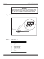
IMPORTANT!
Please read the following section before installing your product:
Octagon’s products are designed to be high in performance while consuming
very little power. In order to maintain this advantage, CMOS circuitry is
used.
CMOS chips have specific needs and some special requirements that the user
must be aware of. Read the following to help avoid damage to your card from
the use of CMOS chips.
≡ Using CMOS circuitry in industrial control
Industrial computers originally used LSTTL circuits. Because many PC
components are used in laptop computers, IC manufacturers are exclusively using CMOS technology. Both TTL and CMOS have failure
mechanisms, but they are different. Described below are some of the
failures which are common to all manufacturers of CMOS equipment.
However, much of the information has been put in the context of the
Micro PC.
Octagon has developed a reliable database of customer–induced, field
failures. The average MTBF of Micro PC cards exceeds 11 years, yet
there are failures. Most failures have been identified as customer–
induced, but there is a small percentage that cannot be identified. As
expected, virtually all the failures occur when bringing up the first
system. On subsequent systems, the failure rate drops dramatically.
n Approximately 20% of the returned cards are problem–free. These
cards, typically, have the wrong jumper settings or the customer has
problems with the software. This causes frustration for the customer
and incurs a testing charge from Octagon.
n Of the remaining 80% of the cards, 90% of these cards fail due to
customer misuse and accident. Customers often cannot pinpoint the
cause of the misuse.
n Therefore, 72% of the returned cards are damaged through some
type of misuse. Of the remaining 8%, Octagon is unable to determine
the cause of the failure and repairs these cards at no charge if they
are under warranty.
Notice to user
2040 PC/104 CPU user’s manual
The most common failures on CPU cards are over voltage of the power
supply, static discharge, and damage to the serial and parallel ports. On
expansion cards, the most common failures are static discharge, over
voltage of inputs, over current of outputs, and misuse of the CMOS
circuitry with regards to power supply sequencing. In the case of the
video cards, the most common failure is to miswire the card to the flat
panel display. Miswiring can damage both the card and an expensive
display.
n Multiple component failures: The chance of a random component failure is very rare since the average MTBF of an Octagon card
is greater than 11 years. In a 7 year study, Octagon has never found
a single case where multiple IC failures were not caused by misuse
or accident. It is very probable that multiple component failures
indicate that they were user–induced.
n Testing “dead” cards: For a card that is “completely nonfunctional”, there is a simple test to determine accidental over voltage,
reverse voltage or other “forced” current situations. Unplug the card
from the bus and remove all cables. Using an ordinary digital ohmmeter on the 2,000 ohm scale, measure the resistance between
power and ground. Record this number. Reverse the ohmmeter leads
and measure the resistance again. If the ratio of the resistances is
2:1 or greater, fault conditions most likely have occurred. A common
cause is miswiring the power supply.
n Improper power causes catastrophic failure: If a card has had
reverse polarity or high voltage applied, replacing a failed component is not an adequate fix. Other components probably have been
partially damaged or a failure mechanism has been induced. Therefore, a failure will probably occur in the future. For such cards,
Octagon highly recommends that these cards be replaced.
n Other over–voltage symptoms: In over–voltage situations, the
programmable logic devices, EPROMs and CPU chips, usually fail in
this order. The failed device may be hot to the touch. It is usually the
case that only one IC will be overheated at a time.
n Power sequencing: The major failure of I/O chips is caused by the
external application of input voltage while the Micro PC power is off.
If you apply 5V to the input of a TTL chip with the power off, nothing will happen. Applying a 5V input to a CMOS card will cause the
current to flow through the input and out the 5V power pin. This
current attempts to power up the card. Most inputs are rated at
25 mA maximum. When this is exceeded, the chip may be damaged.
n Failure on powerup: Even when there is not enough current to
destroy an input described above, the chip may be destroyed when
the power to the card is applied. This is due to the fact that the input
current biases the IC so that it acts as a forward biased diode on
powerup. This type of failure is typical on serial interface chips.
2040 PC/104 CPU user’s manual
Notice to user
n Hot insertion: Plugging cards into the card cage with the power on
will usually not cause a problem. (Octagon urges that you do not
do this!) However, the card may be damaged if the right sequence
of pins contacts as the card is pushed into the socket. This usually
damages bus driver chips and they may become hot when the power
is applied. This is one of the most common failures of expansion
cards.
n Terminated backplanes: Some customers try to use Micro PC
cards in backplanes that have resistor/capacitor termination networks. CMOS cards cannot be used with termination networks.
Generally, the cards will function erratically or the bus drivers may
fail due to excessive output currents.
n Excessive signal lead lengths: Another source of failure that was
identified years ago at Octagon was excessive lead lengths on digital
inputs. Long leads act as an antenna to pick up noise. They can also
act as unterminated transmission lines. When 5V is switched onto
a line, it creates a transient waveform. Octagon has seen
submicrosecond pulses of 8V or more. The solution is to place a
capacitor, for example 0.1 µF, across the switch contact. This will
also eliminate radio frequency and other high frequency pickup.
≡ Avoiding damage to the heatsink/CPU
WARNING!
When handling any Octagon CPU card, extreme care must be taken
not to strike the heatsink (if installed) against another object, such
as a table edge. Also, be careful not to drop the CPU card, since this
may cause damage to the heatsink/CPU as well.
Note
Any physical damage to the CPU control card is not covered under
warranty.
Notice to user
2040 PC/104 CPU user’s manual
2040 PC/104 CPU user’s manual
Contents
Contents
Abbreviations and terms used in this manual ........................................... xiii
Conventions used in this manual .................................................................. xiv
Notes and warnings ....................................................................................... xiv
Command format and procedures ................................................................. xiv
About this manual
Overview:
Section 1 – Installation
Chapter 1:
Overview .................................................................................... 1-1
Description .................................................................................................... 1-1
2040 PC/104 CPU major hardware features ............................................... 1-1
CPU ....................................................................................................... 1-1
Solid–state disks .................................................................................. 1-1
SSD0 ............................................................................................ 1-1
SSD1 ............................................................................................ 1-1
SSD2 ............................................................................................ 1-1
RAM ...................................................................................................... 1-2
Serial ports protected against ESD ..................................................... 1-2
Multifunctional printer port ................................................................ 1-2
Watchdog timer added for safety ......................................................... 1-2
Real time calendar/clock with battery–backup .................................. 1-3
Keypad and LCD display support for low cost operator
interface .......................................................................................... 1-3
Speaker, keyboard, and mouse ............................................................ 1-3
PC/104 16–bit interface ....................................................................... 1-3
Hardware reset ..................................................................................... 1-3
5 Volt operation lowers system cost .................................................... 1-3
2040 PC/104 CPU major software features ................................................ 1-4
Diagnostic software verifies system integrity automatically ............ 1-4
SETUP information stored in EEPROM for high reliability ............. 1-4
Phoenix BIOS ....................................................................................... 1-4
Boot sequence ....................................................................................... 1-4
Fast boot ............................................................................................... 1-4
Specifications ................................................................................................. 1-5
Rugged environmental operation ........................................................ 1-5
Size ........................................................................................................ 1-5
Chapter 2:
Quick start ................................................................................
Equipment required ......................................................................................
Configuration jumpers ..................................................................................
Installing the 2040 PC/104 CPU board.......................................................
Mounting on a flat surface ...................................................................
Connecting to a PC/104 interface ........................................................
Power supply .................................................................................................
Bootable disks ...............................................................................................
Serial console .................................................................................................
Floppy drive ...................................................................................................
2-1
2-1
2-2
2-4
2-4
2-4
2-5
2-7
2-8
2-9
iii
Contents
2040 PC/104 CPU user’s manual
Configuring setup ................................................................................. 2-9
Installing a floppy disk drive ............................................................. 2-10
Creating a boot disk ........................................................................... 2-11
Copying files ................................................................................................ 2-11
Chapter 3:
SETUP program ....................................................................... 3-1
Running SETUP over the console port ............................................... 3-4
SETUP example ................................................................................... 3-5
Chapter 4:
Save and run programs .......................................................... 4-1
Save and run your programs on the 2040 PC/104 CPU ............................. 4-1
Adding your application ....................................................................... 4-1
Overriding the autoexecution of your application .............................. 4-2
Option 1 ....................................................................................... 4-2
Option 2 ....................................................................................... 4-2
Option 3 ....................................................................................... 4-2
Overview: Section 2 – Hardware
Chapter 5:
Serial ports ................................................................................
Description ....................................................................................................
Serial port configurations .............................................................................
COM1 ....................................................................................................
COM2 ....................................................................................................
Function and use of serial ports ...................................................................
COM1 as the serial console device ......................................................
COM1 and COM2 as RS–232 I/O .......................................................
5-1
5-1
5-2
5-2
5-2
5-3
5-3
5-4
Chapter 6:
LPT1 parallel port ...................................................................
LPT1 parallel port ........................................................................................
Printer ...........................................................................................................
Floppy drive ...................................................................................................
Display ...........................................................................................................
Keypad ...........................................................................................................
Opto rack .......................................................................................................
6-1
6-1
6-1
6-2
6-2
6-3
6-4
Chapter 7:
Console devices ........................................................................ 7-1
Description .................................................................................................... 7-1
Selecting console devices .............................................................................. 7-1
COM1 as serial console device ............................................................. 7-2
Keyboard, speaker, and mouse ............................................................ 7-4
Transferring files between the 2040 PC/104 CPU and your PC ................ 7-5
ROM–DOS operating system .............................................................. 7-5
MS–DOS operating system ................................................................. 7-5
Transferring files to the 2040 PC/104 CPU ................................................ 7-6
Transferring files from the 2040 PC/104 CPU ............................................ 7-7
Downloading files to the 2040 PC/104 CPU using PC SmartLINK .......... 7-8
iv
2040 PC/104 CPU user’s manual
Contents
Chapter 8:
SSDs, DRAM, and battery backup ....................................... 8-1
Description .................................................................................................... 8-1
Booting ........................................................................................................... 8-1
SSD0 .............................................................................................................. 8-1
SSD1 socket/M–Systems DiskOnChip......................................................... 8-1
SSD2 .............................................................................................................. 8-3
SSD2 socket .......................................................................................... 8-4
Accessing SRAM on the 2040 .............................................................. 8-4
DRAM ............................................................................................................ 8-6
Battery backup for SSD2 SRAM and real time calendar clock .................. 8-6
Chapter 9:
External drives .........................................................................
Description ....................................................................................................
Floppy disk controller ...................................................................................
Power requirements .............................................................................
Installing a floppy disk drive ...............................................................
Hard disk controller ......................................................................................
9-1
9-1
9-1
9-1
9-2
9-3
Chapter 10: Interpreting “beep” codes ................................................... 10-1
Description .................................................................................................. 10-1
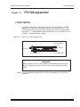
Chapter 11: PC/104 expansion ................................................................... 11-1
Description .................................................................................................. 11-1
Overview: Section 3 – System management
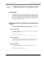
Chapter 12: Watchdog timer and hardware reset ................................ 12-1
Description .................................................................................................. 12-1
Watchdog function definitions using Borland C code ................................ 12-1
Enable watchdog ................................................................................ 12-1
Strobe watchdog ................................................................................. 12-1
Disable watchdog ............................................................................... 12-1
Watchdog function definitions using enhanced INT 17h handler ............ 12-2
Enable watchdog ................................................................................ 12-2
Strobe watchdog ................................................................................. 12-2
Disable watchdog ............................................................................... 12-3
Set WDTimer ...................................................................................... 12-4
IncrementWDTimer ........................................................................... 12-5
Hardware reset ........................................................................................... 12-6
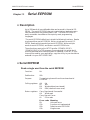
Chapter 13: Serial EEPROM ...................................................................... 13-1
Description .................................................................................................. 13-1
Serial EEPROM .......................................................................................... 13-1
Read a single word from the serial EEPROM .................................. 13-1
Write a single word to the serial EEPROM ...................................... 13-2
Read multiple words from the serial EEPROM ............................... 13-3
Write multiple words to the serial EEPROM ................................... 13-3
Return serial EEPROM size .............................................................. 13-4
Check CMOS battery ......................................................................... 13-5
v
Contents
2040 PC/104 CPU user’s manual
Chapter 14: Troubleshooting ..................................................................... 14-1
No screen activity – checking console serial communications ......... 14-1
Garbled serial console screen activity ............................................... 14-1
System generates a BIOS message but locks up when booting from
SSD1 ............................................................................................. 14-2
System will not recognize hard drive ................................................ 14-2
System locks up after powerdown/powerup ..................................... 14-2
Technical assistance.................................................................................... 14-2
Overview: Section 4 – Appendices
Appendix A: Technical data .......................................................................... A-1
Technical specifications ................................................................................ A-1
Connector pinouts ......................................................................................... A-5
Appendix B: Software utilities ..................................................................... B-1
Introduction ................................................................................................... B-1
COM1CON.EXE ............................................................................................ B-2
I17HNDLR.EXE ........................................................................................... B-2
LPT1CON.COM ............................................................................................ B-3
PGMBIOS.EXE ............................................................................................. B-4
RESET.COM .................................................................................................. B-5
SETUP.COM ................................................................................................. B-5
SCONSOLE.EXE .......................................................................................... B-7
Appendix C: Accessories ................................................................................ C-1
Index
Warranty
vi
2040 PC/104 CPU user’s manual
Contents
List of Figures
Figure 2–1
Figure 2–2
Figure 2–3
Figure 2–4
Figure 2–5
Figure 5–1
Figure 5-2
Figure 6–1
Figure 6–2
Figure 6–3
Figure 7–1
Figure 7–2
Figure 7–3
Figure
Figure
Figure
Figure
Component locations and mounting dimensions ................. 2-3
Power connector ..................................................................... 2-6
M–Systems pin alignment with the 2040 SSD1 socket ...... 2-7
Serial console connections ..................................................... 2-8
LPT1 and a Floppy Drive ................................................... 2-10
Custom null modem adapter with RTS and RI connected .. 5-3
2040 PC/104 CPU serial devices .......................................... 5-4
LPT1 as a printer port .......................................................... 6-1
LPT1 as a display or keypad port ........................................ 6-3
LPT1 and an opto rack .......................................................... 6-4
Custom null modem adapter with RTS and RI connected .. 7-2
The 2040 PC/104 CPU and a serial console ........................ 7-3
Downloading files using PC SmartLINK and
TRANSFER.EXE ................................................................... 7-8
8–1 SSD socket locations ............................................................. 8-2
8–2 M–Systems pin alignment with the 2040 SSD1 socket ...... 8-2
9–1 LPT1 and a Floppy Drive ..................................................... 9-2
11–1 Typical PC/104 module stack ............................................. 11-1
vii
Contents
2040 PC/104 CPU user’s manual
List of Tables
Table
Table
Table
Table
Table
Table
Table
Table
Table
Table
Table
Table
Table
Table
Table
Table
Table
Table
Table
Table
Table
Table
Table
Table
viii
2–1
2–2
3-1
5–1
7–1
8–1
8–2
8–3
10–1
10–1
10–2
A–1
A–2
A–3
A–4
A–5
A–6
A–7
A–8
A–9
C–1
C–2
C–3
C–4
SETUP: W1 ........................................................................... 2-2
Power pinout: J7 ................................................................... 2-6
SETUP Jumpers: W1 ........................................................... 3-1
COM1 and COM2 pinouts (J3 and J9 connectors) .............. 5-2
Speaker, battery, keyboard, and reset: J5 ........................... 7-4
Connector J5 pinout .............................................................. 8-3
System control register ......................................................... 8-5
Speaker, battery, keyboard, and reset: J5 ........................... 8-6
Phoenix BIOS beep codes .................................................... 10-2
Phoenix BIOS beep codes (cont’d) ....................................... 10-3
Additional error codes for Phoenix BIOS ........................... 10-4
2040 PC/104 CPU memory map........................................... A-3
2040 PC/104 CPU I/O map ................................................... A-3
DMA map ............................................................................... A-4
Interrupt map ........................................................................ A-4
Available LPT1 port addresses ............................................. A-4
PC/104 signal assignments ................................................... A-5
Speaker, battery, keyboard, and reset: J5 ........................... A-6
Power: J7 ............................................................................... A-6
LPT1 printer connector: J4 .................................................. A-7
Cables and terminal board ................................................... C-1
LCD displays and keypads ................................................... C-1
Opto rack and modules ......................................................... C-2
Miscellaneous part numbers ................................................. C-2
2040 PC/104 CPU user’s manual
Abbreviations and terms used in this manual
Abbreviations and terms used in this
manual
Throughout this manual, the following symbols and terms are used:
Autoexecution
Automatic execution of a program on powerup or
reset.
BIOS
Basic Input Output System.
Console port
Video card or COM1 where BIOS and DOS messages
appear and keyboard input is available.
DRAM
Dynamic Random Access Memory devices.
Expansion card
The expansion cards add I/O functions to the
PC/104 system, such as analog input/output, digital
input/output, motion control, and display.
Flash
Electrically erasable PROM which allows at least
100,000 write cycles.
h
The suffix “h” denotes a hexadecimal number. A
decimal number has no prefix or suffix. For example,
1000h and 4096 are equivalent.
KB
Kilobyte (1,024 8–bit bytes).
MB
Megabyte (1,048,576 8–bit bytes).
Memory device
The type of static RAM, DRAM, flash memory, or
EPROM specified for either volatile or nonvolatile
memory.
PC/104
expansion
An expansion bus used for holding 8– and 16–bit
expansion cards.
PC SmartLINK
A serial communications software package designed
by Octagon for use with the 2040 PC/104 CPU.
Solid–state disk
(SSD)
A simulated disk which uses a high speed solid–state
memory device. For example, flash memory,
EEPROM, or static RAM.
SRAM
Static Random Access Memory.
TTL compatible
Transistor transistor logic compatible; 0–5V logic
levels.
W[ – ]
Denotes a jumper block and the pins to connect.
XMODEM
A communications protocol which allows transfer of
files between two computers.
ix
Conventions used in this manual
2040 PC/104 CPU user’s manual
Conventions used in this manual
≡ Notes and warnings
Note
A note is supplementary or background information. At other times,
it is a hint or reminder that makes a task easier or quicker.
WARNING!
A warning gives vital information. Failure to heed a warning may
cause system failure, equipment damage, or bodily harm to the
system operator.
≡ Command format and procedures
Commands must be entered in a specific format. To indicate the
format, this manual uses the conventions below. The conventions
cover the rules for issuing all commands, including the most complex
ones. The command format looks like this:
command [type_this | or_ this] input {optional_input}
Follow these rules and conventions:
n Information which appears on your screen is shown in a different
type face, for example:
PhoenixBIOS(TM) A486 Version 1.03
Copyright (C) 1985-1994 Phoenix Technologies, Ltd.
All Rights Reserved
Octagon Systems Corp.
n Commands that you must key in are shown in Courier Bold, for
example:
C:> RESET
n Italicized refers to information that is specific to your particular
system or program, e.g.,
Enter filename means enter the name of your file.
n Paired angle brackets are used to indicate a specific key on your
keyboard, e.g., <ESC> means the escape key; <CTRL> means the
control key; <F1> means the F1 function key.
n All addresses are given in hexadecimal, for example, 328h.
x
2040 PC/104 CPU user’s manual
About this manual
About this manual
The 2040 PC/104 CPU user’s manual provides information about
installing and configuring the 2040 PC/104 CPU. This manual is
divided into four sections:
n Section 1 — Installation
Chapter 1:
Overview
Chapter 2:
Quick start
Chapter 3:
SETUP programs
Chapter 4:
Save and run programs
n Section 2 — Hardware
Chapter 5:
Serial ports
Chapter 6:
LPT1 parallel port
Chapter 7:
Console devices
Chapter 8:
SSDs, DRAM, and battery backup
Chapter 9:
External drives
Chapter 10:
Interpreting “beep” codes
Chapter 11:
PC/104 expansion
n Section 3 — System management
Chapter 12:
Watchdog timer and hardware reset
Chapter 13:
Serial EEPROM
Chapter 14:
Troubleshooting
n Section 4 — Appendices
Appendix A: Technical data
Appendix B: Software utilities
Appendix C: Accessories
About this manual
2040 PC/104 CPU user’s manual
2040 PC/104 CPU user’s manual
Overview:
Overview of Section 1
Section 1 – Installation
Section 1 provides installation and programming instructions, startup
options, and system configuration program examples. The following
chapters are included:
Chapter 1:
Chapter 2:
Chapter 3:
Chapter 4:
Overview
Quick start
SETUP programs
Save and run programs
Overview of Section 1
2040 PC/104 CPU user’s manual
2040 PC/104 CPU user’s manual
Overview
Overview
Chapter 1:
≡ Description
The 2040 is a rugged and reliable PC/104 CPU with a low–power
386SX 40 MHz CPU. The 2040 PC/104 CPU integrates serial communications, a multifunctional parallel port, a solid–state disk, keyboard
and speaker ports, and a PC/104 interface.
≡ 2040 PC/104 CPU major hardware features
CPU
The CPU is a low–power 386SX with a clock speed of 40 MHz.
Solid–state disks
SSD0
The 2040 PC/104 CPU has an on–board 512 KB flash which contains
the BIOS and software extensions.
SSD1
A 32–pin DIP socket accepts an M–Systems DiskOnChip®. The socket
exhibits high retention force and affords a gas tight contact.
SSD2
A 32–pin DIP socket accepts either a 128 KB or a 512 KB SRAM.
SRAM is automatically backed up when an AT battery is connected.
The socket exhibits high retention force and affords a gas tight contact.
RAM
The 2040 PC/104 CPU has 4 MB DRAM on board.
1–1
Overview
2040 PC/104 CPU user’s manual
Serial ports protected against ESD
The 2040 PC/104 CPU has two serial ports for 8–wire RS–232C interfaces. COM1 can also be used as a console interface. These serial
ports have the following common specifications:
n IEC1000, level 3, ESD protection specification
— Contact discharge ±6 kV
— Air–gap discharge ±8 kV
n Backdrive protection
n 16C550 compatible
n Up to 115.2K baud
n 16–byte FIFO buffers
n Enabled and disabled in SETUP
Multifunctional printer port
The 2040 PC/104 CPU incorporates the latest enhanced parallel port.
It includes the following features:
n
n
n
n
n
n
Unidirectional
Bidirectional
IEEE 1284, ECP and EPP modes
14 mA of drive current
Backdrive protection
Floppy drive mode
The following represent applications in the multifunctional parallel
port:
n
n
n
n
n
LPT1 for PC compatible printers
17 general purpose digital I/O lines
Up to a 4 x 4 matrix keypad
4–line alphanumeric display
MPB–16PC, 16–position opto–module rack
Watchdog timer added for safety
The watchdog timer resets the system or generates an NMI
(nonmaskable interrupt) if the program stops unexpectedly. The
watchdog is enabled, disabled and strobed under software control.
The time–out period is 1.6 seconds typical, 1.00 seconds minimum to
2.25 seconds maximum. The watchdog timer can be strobed by the
I17HNDLR.EXE utility (a TSR program) to extend the timeout up to a
maximum of 60 hours.
1–2
2040 PC/104 CPU user’s manual
Overview
Real time calendar/clock with battery–backup
The real time clock is fully AT compatible and uses the standard DOS
calls. An optional off–card battery powers the real time clock when
the 5 volt supply is removed.
Keypad and LCD display support for low cost operator
interface
For embedded applications, the parallel printer port can interface
with a 16–key matrix keypad and a 2– or 4–line LCD display. The
2040 PC/104 CPU is supplied with software that provides keypad
scanning and display operation. Supplied display and keypad drivers
in C and Basic support these devices.
Speaker, keyboard, and mouse
A speaker and keyboard can be connected to the utility port. If a
mouse is needed, it can be connected to a COM port. The keyboard
controller accepts an AT style keyboard. Alternately, COM1 can be
used as a console port, and all keyboard and video information is
redirected through COM1. Neither the keyboard nor the mouse are
required for operation.
PC/104 16–bit interface
The PC/104 interface accepts an 8– or 16–bit PC/104 expansion board.
PC/104 expansion boards are available from several manufacturers.
As many as three PC/104 expansion boards may be stacked on the
2040 PC/104 CPU.
Hardware reset
A hardware reset ensures complete reset of the system and all attached peripherals. A hardware reset can be done by any of the following methods:
n An expired watchdog timer cycle
n Cycling power
n Momentarily pulling the master reset line to ground (pin 3, connector J5)
5 Volt operation lowers system cost
The 2040 PC/104 CPU operates from a single 5V ±5% supply.
n 5V ±5%, 800 mA maximum
n +12V, –12V, and –5V supplied to PC/104 connector; not required
for 2040 PC/104 CPU operation
1–3
Overview
2040 PC/104 CPU user’s manual
≡ 2040 PC/104 CPU major software features
Diagnostic software verifies system integrity automatically
The 2040 PC/104 CPU has built–in diagnostic software that can be
used to verify on–card I/O and memory functions. On powerup, a
series of tests is performed. If a problem occurs, the failed test can be
identified by a series of beeps. The test is performed automatically
every time the system is reset or powered up. Memory verification
does not require software, test equipment, monitor, keyboard, disks,
or test fixtures. See the Interpreting “beep” codes chapter for a complete listing of tests and failures and their descriptions.
SETUP information stored in EEPROM for high reliability
Loss of SETUP data is serious in industrial applications. Most PCs
store SETUP information in battery–backed CMOS RAM. If the battery fails or is replaced during routine maintenance, this information
is lost. Without a keyboard and monitor in embedded applications,
time consuming re–initialization is required.
The 2040 PC/104 CPU stores the SETUP information in EEPROM. If a
backup battery should fail, only the system date and time are lost.
Phoenix BIOS
The 2040 PC/104 CPU has a Phoenix AT BIOS with Octagon BIOS
extensions.
Boot sequence
A 2040 PC/104 CPU can be configured to boot from an on–card, solid–
state disk, an external floppy, or a hard disk.
Fast boot
You can speed up the BIOS portion of the boot process to approximately five seconds by disabling the “Power on memory test” in Setup.
This deletes the memory test and rearranges some of the other test
sequences, decreasing the boot time by about 65%.
1–4
2040 PC/104 CPU user’s manual
Overview
≡ Specifications
Rugged environmental operation
n
n
n
n
n
n
Operating temperature
Nonoperating temperature
Relative humidity
Altitude
Shock
Vibration
–40° to 70°C
–55° to 90°C, nonoperating
5% to 95% noncondensing
–100m to 10,000m
40g, 3 axis
6g, 3 axis
Size
3.8" x 3.6"
1–5
Overview
1–6
2040 PC/104 CPU user’s manual
2040 PC/104 CPU user’s manual
Quick start
Quick start
Chapter 2:
This chapter covers the basics of setting up a 2040 PC/104 CPU system and tells you:
n
n
n
n
n
How
How
How
How
How
to set the configuration jumpers on the 2040 PC/104 CPU
to install the 2040 PC/104 CPU
to connect a power supply
to install a bootable disk
to use a serial console
WARNING!
The 2040 PC/104 CPU contains static sensitive CMOS components. Do the following to avoid damaging your card and its
components:
n Ground yourself before handling the 2040 PC/104 CPU card
n Disconnect power before removing or inserting a PC/104
expansion board
n When programming a memory device, place the device in
the socket before applying power.
≡ Equipment required
There are several options for installing a bootable disk and loading
your applications. This chapter provides procedures for installing an
M–Systems DiskOnChip and using a floppy disk drive to transfer
files to the DOC. The following equipment is required:
n +5V power supply
n VTC–9F, FCA–12, and null modem cables
n floppy disk drive
n M–Systems DiskOnChip, preformatted and loaded with an operating system
2–1
Quick start
2040 PC/104 CPU user’s manual
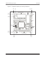
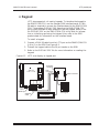
≡ Configuration jumpers
Before you continue with the installation of your 2040 PC/104 CPU,
review the following table for a list of jumper configurations to ensure you have the correct configuration.
The 2040 PC/104 CPU component diagram is on the following page.
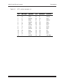
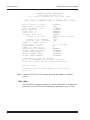
Table 2–1
SETUP: W1
Pins
1–2
Description
(N)MI: Watchdog time–out connected to NMI
3–4*
(R)eset: Watchdog time–out connected to reset
5–6*
(S)etup: Use SETUP information:
On* = on–board EEPROM; Off = BIOS default
* = default
Note
2–2
When the “N” jumper W1[1–2] is on instead of the default “R” jumper
W1[3–4] , the system will not reset after SETUP is run. A power cycle
reset is required.
2040 PC/104 CPU user’s manual
Quick start
3.350
3.050
0.150
-0.200
Figure 2–1 Component locations and mounting dimensions
SSD2 SRAM
SSD1 DiskOnChip
3.575
COM1
3.375
COM2
LPT1
W1:
SETUP
Keyboard
Speaker
Battery
Reset
0.000
-0.200
3.350
PC/104 Interface
3.150
0.000
-0.200
Power
2–3
Quick start
2040 PC/104 CPU user’s manual
≡ Installing the 2040 PC/104 CPU board
The 2040 PC/104 CPU can be installed two ways – mounted on a flat
surface, or connected to a PC/104 interface. The following equipment
is included with the 2040:
n
n
n
n
4
4
4
4
threaded hex stainless steel standoffs (4–40 x 3/8")
screws (4–40 x 1/4")
KEP nuts (4–40)
internal star lock washers (4–40)
Mounting on a flat surface
To mount the 2040 PC/104 CPU on a flat surface, use the #4 standoffs,
washers, and screws and place them in the four holes on the
2040 PC/104 CPU board. Refer to Figure 2–1 for the center–to–center
mounting hole dimensions and for the location of the designated holes
used for mounting the hardware. Fasten the board securely to the
mounting surface.
WARNING!
Before the 2040 PC/104 CPU is powered on for bench testing, all
four standoffs, screws and washers should be secured to the board.
The standoff pieces will ensure full support of the 2040 PC/104
CPU board. These hardware pieces will reduce the circuit board
flex when a PC/104 expansion board and/or the SSD are inserted.
Flexing of the 2040 PC/104 CPU board should be avoided, since it
can cause problems with the copper circuit traces, keyboard,
monitor, and surface mounted components.
Connecting to a PC/104 interface
The 2040 PC/104 CPU can be connected to an existing PC/104 system.
Use the #4 standoffs, washers, and screws and place them in the four
holes on the 2040 PC/104 CPU board, with the male end of the standoff
facing down. Align the PC/104 pins with the connectors below, and the
standoffs with the mounting holes below, then firmly press the boards
together. Secure the boards together with the KEP nuts.
2–4
2040 PC/104 CPU user’s manual
Quick start
≡ Power supply
The 2040 PC/104 CPU requires 5V ±5%, 800 mA maximum. It is designed to operate from a single +5 VDC supply, typically supplied at
connector J7. In some configurations where the 2040 is connected to
another PC/104 system, the power required by the 2040 can be drawn
from the system through the PC/104 connector. If you are using the
PC/104 interface, you may also require ±12 VDC. Make sure that you
utilize both +5 VDC conductors and both ground conductors. Refer to
Figure 2–2 and Table 2–2.
WARNING!
Accidently crossing the wires, i.e., plugging +5V wires into the
ground connector or the ground wires into the +5V connector will
damage the 2040 PC/104 CPU.
It is important that a quality power supply be used with the 2040 PC/
104 CPU. For example, when a particular application calls for a
custom power supply, there are several internal issues to consider
such as current capacity, line and load regulation, maximum ripple,
hold up time, efficiency, and current limiting. You should also consider the power devices and equipment such as the power cable
conductor gauge, number and length of conductors, mating connectors, and the power supply to external PC/104 devices.
Octagon supplies are designed to ramp up fast (less than 50 ms),
discharge fast on power down and to regulate properly under a no
load condition.
Most desktop PC switching supplies are rated at 5V at 20A or more.
Switching supplies usually requires a 20% load to operate properly,
that is, 4A or more. Since a typical Micro PC system takes less than
2A, the desktop PC supply does not regulate properly. Output drift
up to 6-7V and/or 7-8 voltage spikes have been reported. If the power
supply comes up slowly (that is, longer than 50 ms), the sequencing of
ICs on the board may be out of sync, thus, causing the system to lock
up.
If large output capacitors are used, powering the system down and
then up may lock up the Micro PC. If the power supply does not
drain below 0.7V, the CMOS components on the Micro PC will act like
diodes and forward bias.
If using a non-Octagon supply, select a supply that has a low or no
minimum load requirement, comes up in less than 50 ms and discharges quickly on power down.
2–5
Quick start
2040 PC/104 CPU user’s manual
WARNING!
Make sure the power supply is OFF when connecting the power
cable to the 2040 PC/104 CPU board. Damage to the 2040 PC/104
CPU may occur if the power is ON when connecting the power
cable.
Figure 2–2 Power connector
Pin 2
Pin 1
J7
Power header
Table 2–2
Power pinout: J7
Pin
1
2
3
4
5
6
7
8
2–6
Function
Gnd
+5 VDC
NC
+12 VDC to PC/104
–5 VDC to PC/104
–12 VDC to PC/104
Gnd
+5 VDC
2040 PC/104 CPU user’s manual
Quick start
≡ Bootable disks
The 2040 PC/104 CPU has an on–board 512 KB flash which contains
the BIOS and software extensions. It does not contain an operating
system or a bootable disk.
The 2040 PC/104 CPU is fully compatible with several operating
systems, including MS-DOS and ROM-DOS. You can download a trial
version of ROM-DOS from www.datalight.com/rom-dos.htm.
There are three choices for supplying a bootable disk: a floppy drive
(through LPT1 or a PC/104 card), a PC/104 hard drive, or an
M–Systems DiskOnChip (DOC). The example in this chapter shows
how to use a DOC to boot your system and a floppy drive connected
to LPT1 to install your applications.
The memory address for an M–Systems DiskOnChip is at E8000–
EBFFFh. This memory address is not bank switchable and cannot be
disabled.
When ordering an M–Systems DiskOnChip, you can specify that you
want it preformatted and with an operating system already installed.
This simplifies your startup procedures. Refer to your M–Systems
utility disk for more information on using DiskOnChip.
Before installing the DOC, remove power from the 2040. Align pin 1
of the DiskOnChip with pin 1 of the SSD1 socket, then firmly press
the chip into the socket. Refer to Figure 2–3 for correct SSD alignment.
SSD socket
M
–S
ys
te
m
s
Di
sk
O
nC
hi
pÒ
Figure 2–3 M–Systems pin alignment with the 2040 SSD1 socket
Pin 1 of M–Systems
DiskOnChip or SRAM
2–7
Quick start
2040 PC/104 CPU user’s manual
≡ Serial console
COM1 can serve as a console device, allowing you to use your desktop
PC to communicate with the 2040. The default configuration stored in
the BIOS SETUP is for COM1 to be a console device. Use the figure
below to connect a desktop computer to the 2040 as a console device.
This connection requires a VTC–9F cable and a null modem adapter.
It also requires PC SmartLINK, available from Octagon, or an equivalent terminal emulator.
Note
When interfacing the 2040 PC/104 CPU to your desktop PC, you must
use a null modem adapter.
Figure 2–4 Serial console connections
2040
PC/104
Null
modem
adapter
PC SmartLINK
COM
Port
(COM1)
Desktop PC
VTC-9F cable
Power up the 2040. You should see the BIOS sign–on messages for the
2040 on your monitor. If the boot process completes and the C:\>
prompt appears, you have a bootable disk. Go to the Floppy disk
section for information on transferring files.
If the message “press C to try again or S for setup” appears, the boot
did not complete. The most likely reason is that the DOC does not
have an operating system installed. Press S to enter Setup, then
configure LPT1 as a floppy drive, number of floppy drives to 1, and
floppy drive size to the size of the floppy you will be installing. Save
the Setup changes, then power off the 2040. Ensure that the S jumper
is on so that the next time the 2040 is powered, it will use the parameters from the Setup stored in EEPROM. Proceed to the next section,
Floppy drive.
2–8
2040 PC/104 CPU user’s manual
Quick start
≡ Floppy drive
This section describes how to install a floppy drive. The floppy drive
can be used as a boot device, or to transfer programs to a DOC.
Note
If you have a DOC installed on the 2040 and have booted, you may
have the utilities TRANSFER.EXE or REMDISK/REMSERVE (ROM
DOS) or INTERLINK/INTERSVR (MS DOS) on the DOC. You can use
these utilities to transfer files from your host computer to the 2040
over the serial console. Refer to the documentation included with
your operating system for information on how to use these utilities.
Configuring setup
The default in the BIOS SETUP is for LPT1 in bidirectional mode. If
you have previously run SETUP and changed the settings for LPT1 to
floppy drive, and saved those settings, ensure that the SETUP jumper
is on so that the BIOS uses the settings from the EEPROM.
You can enter SETUP by pressing the “backspace” key followed by the
“S” key during BIOS POST sequence (this occurs between the memory
test and boot). Configure LPT1 as a floppy drive, number of floppy
drives to 1, and floppy drive size to the size of the floppy you will be
installing. Save the Setup changes, then power off the 2040. Ensure
that the SETUP jumper is on so that the BIOS uses the settings from
the EEPROM during the next boot.
2–9
Quick start
2040 PC/104 CPU user’s manual
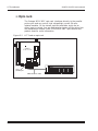
Installing a floppy disk drive
1. Disconnect power to the 2040 PC/104 CPU.
2. Insert one end of an Octagon FCA–12 cable into the rear of the
floppy drive. Make sure pin 1 on the cable is connected to pin 1 on
the drive.
3. Insert the other end of the cable into J4 on the 2040 PC/104 CPU.
4. Connect power to the floppy drive.
5. Power up the system. If you have a bootable disk in SSD1, the system should boot up. If you do not have a bootable disk in SSD1, you
will need to insert a boot disk into the floppy disk drive. Refer to
the next section for information on creating a boot disk.
Figure 2–5 LPT1 and a Floppy Drive
2040
PC/104
Floppy
Drive
LPT1 Parallel
Port
External Power
for Floppy Drive
FCA-12 LPT1 to
floppy cable
2–10
2040 PC/104 CPU user’s manual
Quick start
Creating a boot disk
You can create a floppy boot disk on any PC that has DOS installed.
This floppy can then be inserted in the floppy disk drive connected to
the 2040 and used to boot the system.
To create a boot disk, insert a blank, formatted floppy into the floppy
drive of your PC. If you are running Windows on your PC, exit Windows and open up the DOS shell. Type the command SYS A:, then
press Enter.
The SYS command copies three files to the floppy disk. Two of the
files are hidden (not shown by the DIR command), and the third file is
COMMAND.COM. These three files are sufficient to boot the system.
Insert the boot disk in the 2040 floppy drive, then power on the
system. The console monitor should return the A:\ prompt. Type
C: to change to the C drive (if you have installed a DiskOnChip).
Type DIR then press Enter.
If the C: or DIR commands return the message “No drive found” or
“Abort Retry Fail”, the DiskOnChip is probably not formatted. Refer
to your M–Systems documentation for information on how to format
the DOC.
If the DIR command returns a list of files from the DOC, and the list
does not contain the file COMMAND.COM, then the DOC most likely
does not contain an operating system. Return to the A: drive, type the
command SYS C:, then press Enter. This should copy the boot files to
the DOC. Remove the floppy disk from the floppy disk drive and cycle
power to the 2040. The 2040 should boot from the DOC.
≡ Copying files
Once you have a bootable disk in SSD1, or a bootable PC/104 hard
drive, you can use the floppy disk drive to transfer files to the
bootable disk. Use the COPY command to copy files (such as, COPY
MYPRGRM.COM C:\). Once the files are copied, you can remove the
floppy disk drive.
When DOS starts up, it processes the files CONFIG.SYS and
AUTOEXEC.BAT. If you add the command line for your application
to the AUTOEXEC.BAT file, your application will automatically start
when the system boots. Refer to your operating system documentation for information on modifying these two files.
2–11
Quick start
2–12
2040 PC/104 CPU user’s manual
2040 PC/104 CPU user’s manual
SETUP program
SETUP program
Chapter 3:
The SETUP program defines the 2040 PC/104 CPU system parameters. This program is shipped with default configuration parameters
stored in the serial EEPROM. Changes are made by running the
SETUP program. The SETUP program is stored on the 2040 utility
disk.
SETUP can be entered in one of two ways:
n Run SETUP.COM. To run SETUP.COM, this program must be
resident on either the floppy disk drive and/or hard drive, or on a
flash device such as the M–Systems DiskOnChip. SETUP.COM is
on the 2040 utility disk.
n Press the “backspace” key followed by the “S” key during BIOS
POST sequence (this occurs between the memory test and boot).
The system will display the 2040 setup parameters and available
options. Select the option by pressing the space bar until the correct
information appears, then press <ENTER>. Press <ESC> twice if you
want to exit setup without saving your responses.
By removing the SETUP jumper from the “S” position at
W1[5–6], you force the setup to revert to the defaults stored in BIOS.
The default settings allow you to restart the system in a known
configuration.
Table 3-1
SETUP Jumpers: W1
Pins
1–2
Description
(N)MI: Watchdog time–out connected to NMI
3–4*
(R)eset: Watchdog time–out connected to reset
5–6*
(S)etup: Use SETUP information:
On* = on–board EEPROM; Off = BIOS default
* = default
Note
Options having an * are default settings.
n
Note
Serial Console on COM1:
Enabled*
Disabled
When this option is disabled, it may be overridden by connecting the
COM1 RTS line to the COM1 RI line.
3–1
SETUP program
2040 PC/104 CPU user’s manual
n
COM1 Console Baud Rate:
1200
2400
4800
9600*
14400
19200
28800
38400
57600
115200
n
Power on memory test:
Enabled*
Disabled
Disabling this option speeds up the BIOS boot process to about five
seconds (Octagon’s “fast boot” feature). It disables the memory test
and rearranges the sequence of other power-on tests. Note that this
feature only speeds up the Octagon BIOS portion of the boot process.
It does not affect the time required to load various operating systems.
You may also press the space bar to cancel the memory test while in
progress.
n
Note
Note
The M–Systems DiskOnChip software typically overrides the “C:
Only” option.
n
Serial Port A:
Enabled*
Disabled
n
Serial Port B:
Enabled*
Disabled
n
Parallel (LPT) Port:
Enabled*
Disabled
n
Parallel Port Mode:
Bidirectional mode*
EPP mode
ECP mode
Floppy disk mode
Standard (Unidirectional) mode
Standard mode is provided for compatibility only. We recommend the
use of bidirectional mode. EPP and ECP modes are provided for
equipment that has the capability to operate in these modes for enhanced performance.
n
3–2
Boot Sequence:
C: Only*
A: Then C:
Parallel Port Address:
378h*
278h
3BCh
2040 PC/104 CPU user’s manual
n
Parallel Port Interrupt:
IRQ5
IRQ7*
n
Number of floppy drives:
0*, 1, 2
n
Floppy drive 1 size:
5.25", 360KB
5.25", 1.2 MB
3.5", 720KB
3.5", 1.44 MB*
n
Floppy drive 2 size:
5.25", 360KB
5.25", 1.2 MB
3.5", 720KB
3.5", 1.44 MB*
n
Swap drives A and B:
Yes, No*
n
Number of hard drives:
0*, 1, 2
n
Auto drive configuration:
Enabled*
Disabled
n
Drive 0 parameters:
Cylinders (xxx):
Heads (x):
Sectors (xx):
n
Drive 1 parameters:
Cylinders (xxx):
Heads (x):
Sectors (xx):
n
Setup entry via hotkey:
Enabled*
Disabled
n
Shadow video BIOS:
Enabled
Disabled*
n
Shadow C8000H - CFFFFH
Disabled*
Enabled
n
Shadow D0000H - D7FFFH
Disabled*
Enabled
n
Shadow D8000H - DFFFFH
Disabled*
Enabled
SETUP program
3–3
SETUP program
2040 PC/104 CPU user’s manual
Press ENTER to SAVE the changes or
Press ESC to EXIT without saving the changes.
Saving options.
Options saved.
Depending on the options you have selected, the system may display
the following message:
You must reset for these options to take effect.
If you entered SETUP with the hotkeys (i.e., “backspace” and “S”
keys), the system will reboot automatically. However, if the watchdog
jumper is set to NMI, then the I/O parity check error appears and the
board will halt. A power cycle reset is then required.
Running SETUP over the console port
1. To run SETUP make sure you have established a communications link
between a keyboard and monitor (via a PC/104 video card) with the
2040 PC/104 CPU or a serial communications link between the 2040
PC/104 CPU and your PC. See the Console devices chapter for more
information on these two communication links. Ensure the
SETUP.EXE file has been copied from the 2040 utility disk to the boot
drive, or that a floppy drive is connected to the system.
2. Enter:
C:\> SETUP
Note
If you are not booting from the SSD1 drive, the drive designator may
differ.
Note
You may also enter SETUP after the memory test and before the
system has booted by pressing the “backspace” key followed by the “S”
key.
3. The system will display the 2040 PC/104 CPU setup parameters and
available options. Select the option by pressing the space bar until the
correct information appears, then press <ENTER>. Press <ESC>
twice if you want to exit SETUP without saving your responses.
3–4
2040 PC/104 CPU user’s manual
SETUP program
SETUP example
The following example configures a system with no memory test, 9600
baud, printer at 378h, and booting from C:
OCTAGON SYSTEMS CORPORATION
2040 PC/104 CPU SETUP UTILITY Vx.x
(c) Phoenix Technologies, Ltd. 1985, 1995
_________________________________________________
(Press SPACE to CHANGE, ENTER to ACCEPT, ESC to EXIT)
Serial Console on COM1:
COM1 Console Baud Rate:
Power on memory test:
Boot Sequence:
Serial Port A:
Serial Port B:
Parallel (LPT) Port:
Parallel Port Mode:
Parallel Port Address:
Parallel Port Interrupt:
Number of floppy drives:
Floppy drive 1 size:
Swap drives A and B:
Number of hard drives:
SETUP Entry via Hotkey:
Shadow Video BIOS area:
Shadow C8000h–CFFFFh:
Shadow D0000h–D7FFFh:
Shadow D8000h–DFFFFh:
Enabled
9600
DISABLED
C: ONLY
ENABLED
ENABLED
ENABLED
Bidirectional Printer
Port
378h
IRQ7
1
3.5", 1.44 MB
No
0
ENABLED
DISABLED
DISABLED
DISABLED
DISABLED
Press ENTER to SAVE the changes
Press R to RESTART with original values or
Press ESC to EXIT without saving the changes:
Options Saved.
You must reset for these options to take effect.
2040 C:\>
Note
Executing SETUP /D will change all setup parameters to default
values.
3–5
SETUP program
3–6
2040 PC/104 CPU user’s manual
2040 PC/104 CPU user’s manual
Chapter 4:
Save and run programs
Save and run programs
≡ Save and run your programs on the
2040 PC/104 CPU
Once you have written, tested and debugged your application, you can
then save it in SSD1 if you have a DOC, or to a PC/104 hard disk.
When you reboot the 2040 PC/104 CPU, your program can automatically load into DOS memory and execute. This assumes SSD1 contains
a bootable DOS.
This chapter describes the following:
n Saving an application program
n Autoexecuting the program from the 2040 PC/104 CPU
n Overriding autoexecution of your program
The information in this chapter assumes you are using ROM–DOS or
MS–DOS in your application. Some Microsoft programs make undocumented DOS calls. With ROM–DOS, an error returns when an undocumented DOS call is made, causing your program to operate
erratically.
Adding your application
To add your application to your SSD or hard disk, do the following:
1. Depending on the operating system you have installed, you may have
the utilities TRANSFER.EXE or REMDISK/REMSERVE (ROM–DOS)
or INTERLINK/INTERSVR (MS–DOS) on the DOC. You can use these
utilities to transfer files from your host computer to the 2040 over a
serial console. Refer to the documentation included with your operating system for information on how to use these utilities.
From a floppy drive on the 2040 PC/104 CPU, issue the COPY command.
2. Add or remove any device drivers for your application. You may want
to do the same for the CONFIG.SYS file on your bootable drive.
3. To autoexecute your application, add your application name to the
AUTOEXEC.BAT file.
4–1
Save and run programs
2040 PC/104 CPU user’s manual
Overriding the autoexecution of your application
You may stop the autoexecution of your application by doing one of
the following options:
Option 1
1. Press F5 or F8 on a local keyboard (connected to the 2040). For
more information, see your ROM–DOS or MS–DOS manual.
Option 2
1. Press Ctrl-C when the system is first starting. This halts all batch
files.
2. Change AUTOEXEC.BAT and/or CONFIG.SYS to not call out
your program.
Option 3
1. Install a floppy.
2. Change SETUP option “Boot Sequence” to “A: THEN C:”
3. Change SETUP to enable the floppy.
4. Boot from floppy.
5. Change AUTOEXEC.BAT on C:.
4–2
2040 PC/104 CPU user’s manual
Overview:
Overview of Section 2
Section 2 – Hardware
Section 2 discusses usage, functions, and system configurations of the
2040’s major hardware features. The following chapters are
included:
Chapter
Chapter
Chapter
Chapter
Chapter
Chapter
Chapter
5:
6:
7:
8:
9:
10:
11:
Serial ports
LPT1 parallel port
Console devices
SSDs, DRAM, and battery backup
External drives
Interpreting “beep” codes
PC/104 expansion
Overview of Section 2
2040 PC/104 CPU user’s manual
2040 PC/104 CPU user’s manual
Chapter 5:
Serial ports
Serial ports
≡ Description
The 2040 PC/104 CPU has two serial ports, COM1 and COM2. These
serial ports interface to a printer, terminal, or other serial device.
Both ports support 5–, 6–, 7–, or 8–bit word lengths, 1, 1.5, or 2 stop
bits, and baud rates up to 115.2K. COM1 can be used as a serial console or an 8–wire RS–232; COM2 is a dedicated 8–wire RS–232.
The serial ports have the following specifications:
n 16C550 compatible
n 16–byte FIFO buffers
n IEC 1000, level 3, ESD protection
— Contact discharge ±6 kV
— Air–gap discharge ±8 kV
n Backdrive protection
n Up to 115.2K baud operation
The following sections describe these ports in more detail.
5–1
Serial ports
2040 PC/104 CPU user’s manual
≡ Serial port configurations
COM1
COM1 is a full 8–wire RS–232. The I/O address for COM1 is 3F8h.
IRQ4 is dedicated to COM1. If COM1 is not used under interrupt
control, IRQ4 may be used by other resources. If COM1 is the console,
COM1 uses IRQ4. COM1 can be used for console I/O or RS–232 I/O.
COM1 uses the J3, 10–pin header.
When a video card is not connected to the PC/104, COM1 can be used
as the console port. All video and keyboard information is redirected
through the console port.
COM1 can be enabled as a serial console by two methods. SETUP
allows you to select COM1 as a serial console. This is the default
configuration stored in the BIOS. Also, when COM1 RTS is connected
to COM1 RI the serial console on COM1 is enabled. This hardware
configuration overrides the COM1 setting in SETUP. Figure 5–1
shows a custom null modem cable that performs this configuration.
Table 5–1 shows the pinout for COM1 and COM2.
COM2
COM2 is a dedicated full 8–wire RS–232 configuration. The I/O address for COM2 is 2F8h. IRQ3 is dedicated to COM2. If COM2 is not
used under interrupt control, IRQ3 may be used by other resources.
COM2 uses the J9, 10–pin header.
Table 5–1 shows the pinout for COM1 and COM2.
Note
Table 5–1
See the Accessories appendix for mating information on COM1 and
COM2.
COM1 and COM2 pinouts (J3 and J9 connectors)
Pin
1
3
5
7
9
5–2
Signal
DCD
RxD
TxD
DTR
Gnd
Pin
2
4
6
8
10
Signal
DSR
RTS
CTS
RI
Gnd
2040 PC/104 CPU user’s manual
Serial ports
≡ Function and use of serial ports
COM1 as the serial console device
Instead of using a PC/104 video card to connect a monitor, you can use
COM1 as a console device. COM1 can be enabled as a serial console
by two methods. SETUP allows you to select COM1 as a serial console. This is the default configuration stored in BIOS. Also, when
COM1 RTS is connected to COM1 RI the serial console on COM1 is
enabled. This hardware configuration overrides the COM1 setting in
SETUP. Figure 5–1 shows a custom null modem cable that performs
this configuration.
Note
Figure 5–1
When interfacing the 2040 PC/104 CPU to your desktop PC, you must
use a null modem cable. Commercial null modem adapters do not
connect RI to RTS; they can be used if COM1 is enabled as a serial
console in SETUP. The custom null modem below configures COM1
as a serial console regardless of the settings in SETUP. You also need
PC SmartLINK, available from Octagon, or an equivalent terminal
emulator.
Custom null modem adapter with RTS and RI connected
2040
COM1 port
DCD
1
1 DCD DB-9
DSR
2
2 RxD
RxD
3
3 TxD
RTS
4
4 DTR
TxD
5
5 GND
CTS
6
6 DSR
DTR
7
7 RTS
RI
8
8 CTS
GND
9
9 RI
GND
10
5–3
Serial ports
2040 PC/104 CPU user’s manual
COM1 and COM2 as RS–232 I/O
COM1 and COM2 can be used as RS–232 serial ports. COM1 and
COM2 support 8–wire RS–232 configurations. Use a VTC–9F or
VTC–9M cable to interface from the 2040 PC/104 CPU to the serial
device.
Figure 5-2
2040 PC/104 CPU serial devices
COM2
2040
PC/104
Serial device
Serial device
COM1
5–4
2040 PC/104 CPU user’s manual
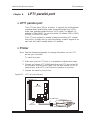
Chapter 6:
LPT1 parallel port
LPT1 parallel port
≡ LPT1 parallel port
The LPT1 port has a 26–pin connector. It supports the unidirectional
standard mode, bidirectional mode, enhanced parallel port (EPP)
mode, and extended capabilities port (ECP) mode. The default I/O
address is 378h (IRQ7). You can also select I/O address 278h or 3BCh,
or IRQ5, in the SETUP menu.
The LPT1 port supports a number of devices including a PC compatible printer, a floppy drive, a multiline display, a matrix keypad or an
opto rack with opto–isolated digital I/O modules.
≡ Printer
Note
See the Accessories appendix for mating information on the LPT1
printer port connector.
To install a printer:
1. Make sure that the LPT1 port is in standard or bidirectional mode.
2. Connect an Octagon VTC–5/IBM cable from the LPT1 port to the 25–
pin connector on your printer cable. You can also connect a PCA–36
cable directly from LPT1 to a Centronics interface on a printer.
3. Connect the cable to your printer.
Figure 6–1
LPT1 as a printer port
2040
PC/104
VTC-5/IBM cable
LPT1
parallel port
Printer cable
6–1
LPT1 parallel port
2040 PC/104 CPU user’s manual
≡ Floppy drive
The LPT1 parallel port can be used as a floppy disk drive port. Refer
to the External Drives chapter for connection information.
≡ Display
The LPT1 port supports either a 4 x 20 or a 4 x 40 liquid crystal
display (LCD). To interface the displays to the 2040 PC/104 CPU, use
the Octagon 2010 interface board. A CMA–26 cable is required to
connect the interface board to the 2040 PC/104 CPU. The program
DISPLAY.EXE (found on the 2040 PC/104 CPU utility disk) provides
an easy method to use the display. Refer to the file DISPLAY.DOC on
the 2040 PC/104 CPU utility disk for information on initializing and
using the display. Also, refer to the 2010 product sheet for more
information on the interface board.
To install a display:
1. Connect a CMA–26 cable from the LPT1 port on the 2040 PC/104 CPU
(J4) to J1 on the 2010. See Figure 6–2 (next page).
2. Connect the display cable to either the 14–pin or 16–pin header on
the 2010. The size of the display will determine which header to use.
3. Refer to the file DISPLAY.DOC for more information on initializing
and using the display.
6–2
2040 PC/104 CPU user’s manual
LPT1 parallel port
≡ Keypad
LPT1 also supports 4 x 4 matrix keypads. To interface the keypad to
the 2040 PC/104 CPU, use the Octagon 2010 interface board. A CMA–
26 cable is required to connect the interface board to the 2040 PC/104
CPU. The program DISPLAY.EXE (found on the 2040 PC/104 CPU
utility disk) provides an easy method to use the keypad. Refer to the
file DISPLAY.DOC on the 2040 PC/104 CPU utility disk for information on initializing and using the keypad. Also, refer to the 2010
product sheet for information on the interface board.
To install a keypad:
1. Connect a CMA–26 cable from the LPT1 port on the 2040 PC/104 CPU
(J4) to J1 on the 2010. See Figure 6–2.
2. Connect the keypad cable to the 10–pin header on the 2010.
3. Refer to the DISPLAY.DOC file for more information on reading the
keypad.
Figure 6–2
LPT1 as a display or keypad port
Keyboard
connector
2040
PC/104
LCD
connectors
J1
Power connector
LPT1
parallel port
CMA-26
cable
2010 Interface
4x4 Keypad
LCD display
6–3
LPT1 parallel port
2040 PC/104 CPU user’s manual
≡ Opto rack
The Octagon MPB–16PC opto rack interfaces directly to the parallel
printer port and can control high voltage/high current G4 opto–
isolated modules. Of the sixteen positions available, eight can be
either input or output, four are dedicated as inputs and the other four
are dedicated as outputs. Refer to the MPB–16PC opto module rack
product sheet for more information.
Figure 6–3
LPT1 and an opto rack
2040
PC/104
1
2
3
4
5
6
7
8
9
10
11
12
13
14
15
16
17
18
19
20
21
22
23
24
25 26
27
28
29
30
31
32
J2
LOGIC
+
–
CMA-26 ribbon cable
6–4
P8
J1
J2
LPT1
parallel port
0
1
2
3
4
5
6
8
9
10
11
12
MPB-16PC opto rack
13
14
15
16
2040 PC/104 CPU user’s manual
Chapter 7:
Console devices
Console devices
≡ Description
The 2040 PC/104 CPU has three console options. You can use a
PC/104 video card with a monitor and a keyboard as your console.
You can also use COM1 as the console, or you can run the system
without a console device.
≡ Selecting console devices
The following represent the 2040 PC/104 CPU’s three options for
console devices:
n A standard PC/104 video card, such as an Octagon 2430 SVGA
card, and a keyboard.
n Serial console from COM1. A serial cable/null modem adapter
plugged into a host PC running SmartLINK provides both input
and output. The local keyboard also allows input.
n No console device means no video output, either from a PC/104
card or the serial console. The local keyboard allows input.
7–1
Console devices
2040 PC/104 CPU user’s manual
COM1 as serial console device
Instead of using a PC/104 video card to connect a monitor, you can use
COM1 as a console device. COM1 can be enabled as a serial console by
two methods. SETUP allows you to select COM1 as a serial console.
This is the default configuration stored in BIOS. Also, when COM1
RTS is connected to COM1 RI the serial console on COM1 is enabled.
This hardware configuration overrides the COM1 setting in SETUP.
Figure 7–1 shows a custom null modem cable that performs this
configuration.
Note
Figure 7–1
When interfacing the 2040 PC/104 CPU to your desktop PC, you must
use a null modem cable. Commercial null modem adapters do not
connect RI to RTS; they can be used if COM1 is enabled as a serial
console in SETUP. The custom null modem below configures COM1 as
a serial console regardless of the settings in SETUP. You also need
PC SmartLINK, available from Octagon, or an equivalent terminal
emulator.
Custom null modem adapter with RTS and RI connected
2040
COM1 port
DCD
1
1 DCD DB-9
DSR
2
2 RxD
RxD
3
3 TxD
RTS
4
4 DTR
TxD
5
5 GND
CTS
6
6 DSR
DTR
7
7 RTS
RI
8
8 CTS
GND
9
9 RI
GND
10
You can use a commercial null modem adapter instead of the custom
null modem adapter shown above if the SETUP option “Serial Console on COM1” is enabled (default configuration). If this option is
disabled in SETUP, you can get the serial console back by any of the
following:
1. Using the custom null modem adapter shown above.
2. Removing the “S” jumper W1[5-6] and rebooting. This causes the
2040 to use the default SETUP settings from the BIOS.
3. Installing a PC/104 video card/keyboard to run SETUP and enable
the serial console.
7–2
2040 PC/104 CPU user’s manual
Figure 7–2
Console devices
The 2040 PC/104 CPU and a serial console
2040
PC/104
Custom null
modem
adapter
PC SmartLINK
COM
Port
(COM1)
Desktop PC
VTC-9F cable
7–3
Console devices
2040 PC/104 CPU user’s manual
Keyboard, speaker, and mouse
You can add a keyboard and a local speaker with any of the console
options listed above in the Selecting console devices section. Interface
the keyboard and speaker via the 10–pin connector at J5. You may use
any external speaker from 8–50 ohms. Table 7–1 shows the pinout for
connector J5.
If your application requires a mouse, you can connect a serial mouse
to COM1 or COM2, and load a mouse driver. The 2040 PC/104 CPU
does not require a keyboard, speaker, or mouse for operation.
Table 7–1
7–4
Speaker, battery, keyboard, and reset: J5
Pin
1
2
Signal
+Speaker
GND
Function
+5V in series with 33 Ω
3.6V external battery, negative
3
4
5
Reset SW
KBD SW
KBD Data
External reset
Inhibit switch to disable keyboard
Keyboard data
6
KBD CLK
Keyboard clock
7
8
9
Ground
KBD PWR
BATV+
Signal and power ground
+5V for keyboard
3.6V external battery, positive
10
PWR good
Power good input
2040 PC/104 CPU user’s manual
Console devices
≡ Transferring files between the 2040 PC/104 CPU
and your PC
Once you have established communications between your PC and the
2040 PC/104 CPU, you can serially download files to any read/write
drive used by the 2040 PC/104 CPU. You can also upload files from
the 2040 PC/104 CPU to your desktop PC for editing and debugging.
There are two methods to download files through the serial port to
the 2040 PC/104 CPU. Depending on the operating system you have
installed, you may have the utilities TRANSFER.EXE or REMDISK/
REMSERVE (ROM–DOS) or INTERLINK/INTERSVR (MS–DOS) on
the DOC. You can use these utilities to transfer files from your host
computer to the 2040 over a serial console. Refer to the documentation included with your operating system for additional information
on how to use these utilities.
ROM–DOS operating system
The TRANSFER utility is used to download files, one at a time, to the
2040 PC/104 CPU using the XMODEM protocol. TRANSFER.EXE is
used to send or receive files via the serial port (e.g., COM1).
TRANSFER.EXE uses the XMODEM protocol, as does PC
SmartLINK. (See the note below on XMODEM).
Note
XMODEM only transfers files in which the file size is exactly on a
128–byte boundary. If the file size does not fall exactly on the boundary, XMODEM automatically rounds the file size up to the next
128–byte boundary with padding characters. For example, a file with
a size of 10,000 bytes, will be rounded up to 10,112 bytes, transferred,
and written with the new file size. In most cases, this is not a concern, but in some instances the XMODEM padding causes problems.
The padding problems become apparent when an application program is expecting a specific file size or is expecting characters other
than the padding characters to be at the end of the file.
REMDISK/REMSERV utilities allow access to all of the files on a
remote disk drive. Once these programs are executed, single or
multiple files can then be transferred to and from the 2040 PC/104
CPU using DOS COPY or XCOPY commands.
MS–DOS operating system
For information on using INTERLINK/INTERSVR utilities, refer to
the documentation included with your operating system.
7–5
Console devices
2040 PC/104 CPU user’s manual
≡ Transferring files to the 2040 PC/104 CPU
The following steps detail the procedures for transferring files from
your PC to a virtual drive on the 2040 PC/104 CPU. This procedure
assumes you are using ROM–DOS, and have the TRANSFER utility
available. In order to transfer files from your PC to the 2040 PC/104
CPU, you must execute the TRANSFER program from both the 2040
PC/104 CPU and your PC.
1. Connect a 9-pin serial cable with a null modem adapter between
COM1 of your PC to COM1 of the 2040 PC/104 CPU, using a VTC–9F
cable.
2. Execute the TRANSFER program from the 2040 PC/104 CPU to
receive a file from your PC.
TRANSFER /COM1 /R /V <drive>filename.ext
<drive> is the drive on the 2040 PC/104 CPU where the file will be
transferred.
/R specifies to receive a file (default).
filename.ext is the name of the file on the 2040 PC/104 CPU which
you are receiving from your PC.
COM1 specifies the serial port on the 2040 PC/104 CPU.
/V enables “R” characters upon receiving a block and “T” upon transferring a block. Do not use /V when using a serial console.
3. Execute the TRANSFER program from your PC to send a file to the
2040 PC/104 CPU. /S specifies send to file.
TRANSFER /COM1 /S /V <drive><path>filename.ext
filename.ext is the name of the file on the PC which you are sending to the 2040 PC/104 CPU.
Note
An alternate method of transferring a file is to press <ALT><D>,
when you use PC SmartLINK.
Note
Transfer will time-out if the program has not been started after
approximately 40 seconds. It displays the following message:
Failed to receive <drive>filename.ext
Deleting <drive>filename.ext
Also, you may speed up the transfer using the /Bnnnn switch to
increase the baud rate. Example: /B57600. When you use a serial
console, do not use the /B option on the 2040 PC/104 CPU. Instead,
change the serial console baud rate in SETUP.
7–6
2040 PC/104 CPU user’s manual
Console devices
≡ Transferring files from the 2040 PC/104 CPU
This procedure assumes you are using ROM–DOS, and have the
TRANSFER utility available. In order to transfer files from your PC
to the 2040 PC/104 CPU, you must execute the TRANSFER program
from both the 2040 PC/104 CPU and your PC.
1. Connect a 9-pin serial cable with a null modem adapter between
COM1 of your PC to COM1 of the 2040 PC/104 CPU, using a VTC–9F
cable.
2. Execute the TRANSFER program from the 2040 PC/104 CPU to send
a file to your PC.
TRANSFER /COM1 /S /V filename.ext
filename.ext is the name of the file on the 2040 PC/104 CPU which
you are sending to your PC.
/V enables “R” characters on receiving a block and “T” on transferring
a block.
/COM1 /S /V: Send in verbose mode
3. Execute the TRANSFER program from your PC to receive a file from
the 2040 PC/104 CPU.
TRANSFER /COM1 /R /V filename.ext
filename.ext is the name of the file on the PC which you are receiving from the 2040 PC/104 CPU.
/COM1 /R /V: Receive in verbose mode
Note
Transfer will time-out if the program has not been started after
approximately 40 seconds. It displays the following message:
Failed to receive <drive>filename.ext
Deleting <drive>filename.ext
Also, you may speed up the transfer using the /Bnnnn switch to increase the baud rate. Example: /B57600. When you use a serial console, do not use the /B option on the 2040 PC/104 CPU. Instead,
change the serial console baud rate in SETUP.
7–7
Console devices
2040 PC/104 CPU user’s manual
≡ Downloading files to the 2040 PC/104 CPU using PC
SmartLINK
This procedure assumes you are using ROM–DOS, and have the
TRANSFER utility available. The following information shows how to
download files between the 2040 PC/104 CPU and your PC using
Octagon’s PC SmartLINK. For other communication programs, refer
to those program instructions for performing Xmodem file transfer to
a target system. The hardware and software requirements are:
n Desktop PC, running PC SmartLINK, connected by a VTC–9F
cable and a null modem adapter to COM1 of the 2040 PC/104 CPU.
n 2040 PC/104 CPU with ROM–DOS operating system.
1. Connect the equipment according to the following diagram:
Figure 7–3
Downloading files using PC SmartLINK and TRANSFER.EXE
2040
PC/104
Custom null
modem
adapter
PC SmartLINK
COM
Port
(COM1)
Desktop PC
VTC-9F cable
2. Start PC SmartLINK and power on the 2040 PC/104 CPU.
Note
PC SmartLINK is a DOS application. File transfer problems will
occur when running in Windows. If you are using Windows on your
PC, restart the PC in DOS mode before running SmartLINK.
3. Execute the TRANSFER.EXE program from the 2040 PC/104 CPU by
entering:
C:\> TRANSFER filename.ext
filename.ext is the name of the file on your PC which you are
sending to 2040 PC/104 CPU.
The following message is displayed from the 2040 PC/104 CPU:
Receiving filename.ext . . .
7–8
2040 PC/104 CPU user’s manual
Console devices
4. Execute the following steps using PC SmartLINK:
n Press <ALT><D> to enter the download screen.
n
Type in the name of the file to transfer, e.g.:
C:\MPC\DEMO\filename.ext
n To begin the transfer:
— either press ENTER (default download START);
— tab to START;
— click on the START button in the download screen.
n When the file transfer is completed, press <ESC> twice to return
to the main PC SmartLINK screen.
Note
TRANSFER.EXE will time-out if the program has not been started
after approximately 40 seconds. If the time-out occurs, the following
message from the 2040 PC/104 CPU is displayed:
Failed to receive filename.ext!
Deleting filename.ext
6. When the file transfer is complete, type the following DOS command
to view the drive directory and confirm that your file has been transferred to the 2040 PC/104 CPU:
C:\> DIR
The system will display the contents of drive contents:
Volume in drive is <label>
Directory of <drive>:\
filename ext
27264 06-07-96
2:57p
1 file(s) 27264 bytes
7–9
Console devices
7–10
2040 PC/104 CPU user’s manual
2040 PC/104 CPU user’s manual
SSDs, DRAM, and battery backup
SSDs, DRAM, and battery backup
Chapter 8:
≡ Description
The 2040 PC/104 CPU contains one solid–state disk, a socket for a
second solid–state disk, and a socket for SRAM modules.
≡ Booting
The 2040 PC/104 CPU can boot from an external drive such as a floppy
connected to LPT1 or a PC/104 hard drive, or from an M–Systems
DiskOnChip (DOC) in SSD1. For an external drive, the boot sequence
is specified in SETUP. For an M–Systems DOC, the BIOS in SSD0
automatically looks for BIOS extensions in the DOC during the boot
process.
≡ SSD0
SSD0 contains an on–board 512 KB flash. 128 KB contains the BIOS
drive and power management. 384 KB is unused, but is not
accessable.
≡ SSD1 socket/M–Systems DiskOnChip
SSD1 is a 32–pin DIP socket for an M–Systems DiskOnChip (DOC). If
a DOC is installed in SSD1 it can be programmed as a boot drive. The
socket exhibits high retention force and affords a gas tight contact.
The memory address for a DOC is at E8000–EBFFFh. This memory
address is not bank switchable and cannot be disabled.
Before installing M–Systems DOC, align pin 1 of the DOC with pin 1
of the SSD1 socket. Refer to Figure 8–1 for the location of the SSD1
socket, and refer to Figure 8–2 for correct SSD alignment.
8–1
SSDs, DRAM, and battery backup
Figure 8–1
2040 PC/104 CPU user’s manual
SSD socket locations
2040
PC/104
SSD1
Disk-On-Chip
SSD2
SRAM
M–Systems pin alignment with the 2040 SSD1 socket
SSD socket
M
–S
ys
te
m
s
Di
sk
O
nC
hi
pÒ
Figure 8–2
Pin 1 of M–Systems
DiskOnChip or SRAM
WARNING!
Incorrect installation of an SSD1 device will destroy the chip. To
install a device in SSD1, be sure to match the notch in the device
with the notch in the SSD1 marked silkscreen on the 2040.
8–2
2040 PC/104 CPU user’s manual
SSDs, DRAM, and battery backup
≡ SSD2
SSD2 is a 32–pin DIP socket for a 128 KB or 512 KB SRAM module.
The SRAM is automatically backed up by a user–supplied battery
installed at J5. Table 8–1 shows the pinout for connector J5. The
socket exhibits high retention force and affords a gas tight contact.
Table 8–1
Note
Connector J5 pinout
Pin
1
Signal
+Speaker
Function
+5V in series with 33 Ω
2
GND
3.6V external battery, negative
3
Reset SW
External reset
4
5
KBD SW
KBD Data
Inhibit switch to disable keyboard
Keyboard data
6
KBD CLK
Keyboard clock
7
8
9
10
Ground
KBD PWR
BATV+
PWR good
Signal and power ground
+5V for keyboard
3.6V external battery, positive
Power good input
SRAM contents are sometimes affected by system noise. Therefore,
the use of SRAM is not recommended in electrically noisy environments, especially when systems are critical. Also note that SRAM
devices require a battery to back up the SRAM files (see “Battery
backup for SSD2 SRAM and real time calendar clock” in this chapter.
8–3
SSDs, DRAM, and battery backup
2040 PC/104 CPU user’s manual
SSD2 socket
SSD2 resides in memory window EC000–EFFFFh. The SSD2 can
contain either 128KB or 512KB of SRAM. The upper address lines are
set via I/O port 1EC.
Accessing SRAM on the 2040
The System Control Register accesses the SRAM on the 2040. The
System Control Register is accessed (read/write) at address 1ECH and
is reset on power up. When you access the SRAM memory, you must
first select the specific bank within the SRAM. After you select the
bank number through the System Control Register, the bank of SRAM
is available at addresses EC000H–EFFFFH.
Bits 5 and 6 are read only bits and should not be changed. Bit 7 is the
watchdog control bit and should not be changed unless a change in the
watchdog state is desired. Based on the state of SSD A14 – SSD A18,
the lower bits select a binary addressable bank of memory in the
SRAM. Refer to Table 8–2 and also to the TESTSRAM.CPP program
on the 2040 utility disk in the examples directory.
The following is an example in C++, which accesses bank 2 of a 512k
SRAM using C++:
SystemControlRegister = (inportb(0x1EC) & 0xE0);
// Read bits 5, 6 and 7 of the control register.
Bank2 = 0x02; // 0x02 = 00010 for bank 2
outportb(SystemControlRegister | Bank2);
// Set bank 2 without changing bits 5, 6 & 7.
If you were using a 128K SRAM device the only difference would be
Bank2 = 0x0A. This would set Bit 3 as is required for 128K SRAM
devices. Refer to the TESTSRAM.CPP example on the 2040 utility
disk.
8–4
2040 PC/104 CPU user’s manual
Table 8–2
SSDs, DRAM, and battery backup
System control register
Register
WD
EEPROM Usesetup
0x1EC
Enable**
Data
Jumper A18 A17 A16 A15 A14
Memory
Bit 7
Bit 6
Bit 5
Bit 4 Bit 3* Bit 2 Bit 1 Bit 0
Select
Bank 0
x
x
x
0
0
0
0
0
Bank 1
x
x
x
0
0
0
0
1
Bank 2
x
x
x
0
0
0
1
0
Bank 3
x
x
x
0
0
0
1
1
Bank 4
x
x
x
0
0
1
0
0
Bank 5
x
x
x
0
0
1
0
1
Bank 6
x
x
x
0
0
1
1
0
Bank 7
x
x
x
0
0
1
1
1
Bank 8
x
x
x
0
1
0
0
0
Bank 9
x
x
x
0
1
0
0
1
Bank 10
x
x
x
0
1
0
1
0
Bank 11
x
x
x
0
1
0
1
1
Bank 12
x
x
x
0
1
1
0
0
Bank 13
x
x
x
0
1
1
0
1
Bank 14
x
x
x
0
1
1
1
0
Bank 15
x
x
x
1
1
1
1
1
Bank 16
x
x
1
1
0
0
0
0
Bank 17
x
x
1
1
0
0
0
1
Bank 18
x
x
1
1
0
0
1
0
Bank 19
x
x
1
1
0
0
1
1
Bank 20
x
x
1
1
0
1
0
0
Bank 21
x
x
1
1
0
1
0
1
Bank 22
x
x
1
1
0
1
1
0
Bank 23
x
x
1
1
0
1
1
1
Bank 24
x
x
1
1
1
0
0
0
Bank 25
x
x
1
1
1
0
0
1
Bank 26
x
x
1
1
1
0
1
0
Bank 27
x
x
1
1
1
0
1
1
Bank 28
x
x
1
1
1
1
0
0
Bank 29
x
x
1
1
1
1
0
1
Bank 30
x
x
1
1
1
1
1
0
Bank 31
x
x
1
1
1
1
1
1
* A17 must be set to 1 when accessing 128K SRAM devices.
** WD Enable, Bit 7 = 0; WD Disable, Bit 7 = 1.
8–5
SSDs, DRAM, and battery backup
2040 PC/104 CPU user’s manual
≡ DRAM
The 2040 PC/104 CPU is shipped with 4 MB of DRAM on–card.
≡ Battery backup for SSD2 SRAM and real time
calendar clock
If SRAM is used in SSD2 you need an AT battery for battery backup of
the SRAM files. An AT battery also backs up the CMOS real time
clock. The 2040 PC/104 CPU does not have a battery installed when it
is shipped. To install a battery:
1. Power off the 2040 PC/104 CPU.
2. Install the 3.6V AT clock battery at the J5 connector. Refer to the
component diagram in the Quick start chapter for the location of J5.
Table 8–3
8–6
Speaker, battery, keyboard, and reset: J5
Pin
1
2
Signal
+Speaker
GND
Function
+5V in series with 33 Ω
3.6V external battery, negative
3
4
Reset SW
KBD SW
External reset
Inhibit switch to disable keyboard
5
6
7
KBD Data
KBD CLK
Ground
Keyboard data
Keyboard clock
Signal and power ground
8
KBD PWR
+5V for keyboard
9
10
BATV+
PWR good
3.6V external battery, positive
Power good input
2040 PC/104 CPU user’s manual
Chapter 9:
External drives
External drives
≡ Description
The LPT1 parallel port can be used as a floppy disk drive port. The
2040 PC/104 CPU is compatible with all common floppy disk drives
used on desktop PCs. It can also be used with a PC/104 floppy controller. The floppy drives use DMA channel 2.
The 2040 PC/104 CPU can also interface with any standard IDE or
EIDE hard drives that have a PC/104 interface.
≡ Floppy disk controller
The 2040 PC/104 CPU uses an Octagon FCA–12 cable to connect
directly to one or two 3.5 in. or 5.25 in. floppy drives via the LPT1
connector at J4.
Note
See the Accessories appendix for mating information on the floppy
disk connector.
Note
If you wish to add a second floppy drive to your system, you must use
a floppy drive cable which has two connectors.
Power requirements
You must supply power to the floppy drive(s) through an external
source. Refer to your floppy drive manual for specific instructions.
9–1
External drives
2040 PC/104 CPU user’s manual
Installing a floppy disk drive
You can connect a floppy disk drive to LPT1, or use a PC/104 floppy
disk controller card. This procedure shows how to connect a floppy
disk drive to LPT1.
1. Disconnect power to the 2040 PC/104 CPU.
2. Insert one end of an Octagon FCA–12 cable into the rear of the floppy
drive. Make sure pin 1 on the cable is connected to pin 1 on the drive.
3. Insert the other end of the cable into J4 on the 2040 PC/104 CPU.
4. Connect power to the floppy drive.
5. Run SETUP in the \UTILS subdirectory to set up the floppy drive.
You can execute this program either by pressing <BACKSPACE><S>
during system bootup or by executing the file SETUP.EXE. The
system steps you through the configuration. Also, refer to the SETUP
programs chapter for more information on the AT BIOS SETUP
program. Reboot the system after running BIOS SETUP.
Note
Figure 9–1
Ensure that the Setup jumper (W1[5–6]) is installed so that the system will use the Setup settings in EEPROM when the system is
rebooted.
LPT1 and a Floppy Drive
2040
PC/104
Floppy
Drive
LPT1 Parallel
Port
External Power
for Floppy Drive
FCA-12 LPT1 to
floppy cable
9–2
2040 PC/104 CPU user’s manual
External drives
≡ Hard disk controller
The 2040 PC/104 CPU will drive two PC/104 hard drives that have
16–bit IDE interfaces.
To install a hard drive:
1. Disconnect power to the 2040 PC/104 CPU.
2. Connect the PC/104 hard drive to the PC/104 connector on the 2040.
Refer to the instructions included with the hard drive.
4. Execute the SETUP program to configure your system for a hard
drive. You can execute this program either by pressing <BACK–
SPACE><S> during system bootup or by executing the file
SETUP.COM. This file is found on the 2040 PC/104 utility disk. The
system steps you through the configuration. Also, refer to the SETUP
programs chapter for more information on the BIOS SETUP program. Reboot the system after running BIOS SETUP.
Note
Ensure that the Setup jumper (W1[5–6]) is installed so that the
system will use the Setup settings in EEPROM when the system is
rebooted.
5. Run FDISK on the hard drive. This partitions the hard drive, and
assigns a drive letter. By default, it will assign the drive letter which
is subsequent to your currently installed drives. When FDISK is
finished, reboot the system.
Note
Some hard drives are shipped from the factory pre–fdisked, and some
are pre–formatted. Refer to the documentation included with your
hard drive.
6. Format the hard drive using the DOS FORMAT command. When the
drive is formatted, reboot the system.
7. If you want to boot the system from the hard drive, run the SYS
command. The system copies COMMAND.COM as well as hidden
files to the hard drive.
8. Reboot the system.
9–3
External drives
9–4
2040 PC/104 CPU user’s manual
2040 PC/104 CPU user’s manual
Chapter 10:
Interpreting “beep” codes
Interpreting “beep” codes
≡ Description
The 2040 PC/104 CPU BIOS generates system status codes during
POST. If a speaker is installed at J5, the beep codes are audible. The
following table interprets these beep codes.
10–1
Interpreting “beep” codes
Table 10–1
2040 PC/104 user’s manual
Phoenix BIOS beep codes
Diagnostic Beep
port output codes Description of test or failure
01h
80286 register test in-progress
02h
1-1-3
CMOS write/read test in-progress
03h
1-1-4
BIOS ROM checksum in-progress
04h
1-2-1
Programmable interval timer test in-progress or failure
05h
1-2-2
DMA initialization in-progress or failure
06h
1-2-3
DMA page register write/read test in-progress or
failure
08h
1-3-1
RAM refresh verification in-progress or failure
09h
10–2
1st 64K RAM test in-progress
0Ah
1-3-3
1st 64K RAM chip or data line failure multi-bit
0Bh
1-3-4
1st 64K RAM odd/even logic failure
0Ch
1-4-1
1st 64K RAM address line failure
0Dh
1-4-2
1st 64K RAM parity test in-progress or failure
10h
2-1-1
1st 64K RAM chip or data line failure-bit 0
11h
2-1-2
1st 64K RAM chip or data line failure-bit 1
12h
2-1-3
1st 64K RAM chip or data line failure-bit 2
13h
2-1-4
1st 64K RAM chip or data line failure-bit 3
14h
2-2-1
1st 64K RAM chip or data line failure-bit 4
15h
2-2-2
1st 64K RAM chip or data line failure-bit 5
16h
2-2-3
1st 64K RAM chip or data line failure-bit 6
17h
2-2-4
1st 64K RAM chip or data line failure-bit 7
18h
2-3-1
1st 64K RAM chip or data line failure-bit 8
19h
2-3-2
1st 64K RAM chip or data line failure-bit 9
1Ah
2-3-3
1st 64K RAM chip or data line failure-bit A
1Bh
2-3-4
1st 64K RAM chip or data line failure-bit B
1Ch
2-4-1
1st 64K RAM chip or data line failure-bit C
1Dh
2-4-2
1st 64K RAM chip or data line failure-bit D
1Eh
2-4-3
1st 64K RAM chip or data line failure-bit E
1Fh
2-4-4
1st 64K RAM chip or data line failure-bit F
20h
3-1-1
Slave DMA register test in-progress or failure
21h
3-1-2
Master DMA register test in-progress or failure
22h
3-1-3
Master interrupt mask reg. test in-progress or failure
23h
3-1-4
Slave interrupt mask reg. test in-progress or failure
25h
N/A
Interrupt vector loading in-progress
27h
3-2-4
Keyboard controller test in-progress or failure
2040 PC/104 CPU user’s manual
Table 10–1
Interpreting “beep” codes
Phoenix BIOS beep codes (cont’d)
Diagnostic Beep
port output codes Description of test or failure
28h
N/A
CMOS power-fail and checksum checks in-progress
29h
N/A
CMOS config info. validation in-progress
2Bh
3-3-4
Screen memory test in-progress or failure
2Ch
3-4-1
Screen initialization in-progress or failure
2Dh
3-4-2
Screen retrace tests in-progress or failure
2Eh
N/A
Search for video ROM in-progress
30h
N/A
Screen believed operable:
30h
N/A
Screen believed running w/video ROM
31h
N/A
Monochromatic screen believed operable
32h
N/A
40-column color screen believed operable
33h
N/A
80-column color screen believed operable
34h
4-2-1
Timer tick interrupt test in-progress or failure
35h
4-2-2
Shutdown test in-progress or failure
36h
4-2-3
Gate A20 failure
37h
4-2-4
Unexpected interrupt in protected mode
38h
4-3-1
RAM test in-progress or failure above address 0FFFFh
3Ah
4-3-3
Interval timer channel 2 test in-progress or failure
3Bh
4-3-4
Time-of-day clock test in-progress or failure
3Ch
4-4-1
Serial port test in-progress or failure
3Dh
4-4-2
Parallel port test in-progress or failure
3Eh
4-4-3
Math coprocessor test in-progress or failure
50h
N/A
Beginning of CSET_INIT
51h
N/A
Loading the RCM table
52h
N/A
Loading the FCM table, doing DMC
53h
N/A
Entering CSET_BFR_VIDROM (before video ROM)
54h
N/A
Entering CSET_BFR_SIZMEM (before memory sizing)
55h
N/A
Entering CSET_AFT_MTEST (before memory test)
56h
N/A
Entering CSET_AFT_CMCFG (before CMOS
configuration check)
57h
N/A
Entering CSET_BFR_OPROM (before option ROM
scan)
10–3
Interpreting “beep” codes
Table 10–2
10–4
2040 PC/104 user’s manual
Additional error codes for Phoenix BIOS
Diagnostic
port output
C0h
Beep
codes
N/A
Description of test or failure
Entry to power management initialization
C1h
N/A
Return from power management initialization
C2h
C3h
N/A
N/A
Entry to cache initialization
Return from cache initialization
D7h
N/A
Using defaults from ROM
D9h
DFh
E0h
E1h
N/A
N/A
N/A
N/A
Using EEPROM values
Exit CMOS initialization
Reset
BIOS determined it is an actual reset
E7h
E8h
E9h
N/A
N/A
N/A
Going to CMOS initialization
Returned from CMOS initialization
Entry to chipset initialization
EAh
N/A
Exit from chipset initialization
F0h
F1h
F3h
F4h
N/A
N/A
N/A
N/A
Loading chipset from EEPROM or defaults
Completed chipset load
Loading mvb specific values
Completed mvb load
F9h
FAh
N/A
N/A
Starting memory autosizing
Completed memory autosizing
2040 PC/104 CPU user’s manual
Chapter 11:
PC/104 expansion
PC/104 expansion
≡ Description
The 2040 PC/104 CPU can interface to up to three additional PC/104
modules including A/D converters, digital I/O, serial ports, etc. The
2133 supports 8– and 16–bit cards and provides ±12V from the power
supply at J7. These modules can be stacked on top of the 2040 to form
a highly integrated control system.
Figure 11–1 Typical PC/104 module stack
PC/104 expansion
Standoff
Standoff
PC/104 Connectors
2133 PC/104 CPU
WARNING!
When installing any PC/104 module, avoid excessively flexing the
board. Mate pins correctly and use the required mounting hardware.
Note
See the Accessories appendix for mating information on the PC/104
connector.
11-1
PC/104 expansion
11-2
2040 PC/104 CPU user’s manual
2040 PC/104 CPU user’s manual
Overview:
Overview of Section 3
Section 3 – System management
Section 3 provides information on managing the 2040 in the areas of
internal control and troubleshooting. The following chapters are
included:
Chapter 12:
Chapter 13:
Chapter 14:
Watchdog timer and hardware reset
Serial EEPROM
Troubleshooting
Overview of Section 3
2040 PC/104 CPU user’s manual
2040 PC/104 CPU user’s manual
Watchdog timer and hardware reset
Watchdog timer and hardware reset
Chapter 12:
≡ Description
The watchdog timer is a fail–safe against program crashes or processor lockups. It times out every 1.6 seconds (1.6 sec. typical, 1.00 sec.
min., 2.25 sec. max.) unless reset by the software, or extended by the
INT17 functions setWDTimer or incWDTimer. The watchdog timer is
software controlled. It can be controlled through the enhanced INT
17h handler (I17HNDLER.EXE).
≡ Watchdog function definitions using Borland C
code
This section provides definitions for the following functions: Enable
watchdog, Strobe watchdog, and Disable watchdog.
Enable watchdog
To “enable” the watchdog timer, clear bit 7 of port IEC in the following Borland C code:
int portIEC;
portIEC = inportb(0xIEC)
outportb(0xIEC,port20c & 0x7F); // Enable watchdog
Strobe watchdog
The watchdog must be strobed before the timeout period expires. To
“strobe” the watchdog timer use the following Borland C code:
inportb(0xIEC)
Disable watchdog
To “disable” the watchdog use the following Borland C code:
int portIEC;
portIEC = inportb(0xIEC)
outportb(0x20C,port20C & 0x80)
12–1
Watchdog timer and hardware reset
2040 PC/104 CPU user’s manual
≡ Watchdog function definitions using enhanced
INT 17h handler
This section provides definitions for the watchdog functions using the
Int17 handler (I17HNDLR.EXE). I17HNDLR.EXE is a TSR program.
Once executed it is active, but it must be executed each time the
system is rebooted. If the Int17 functions will be used by your application, copy the utility to your hard drive and add it to your
AUTOEXEC.BAT.
Enable watchdog
Function:
fdh
Subfunction:
01h
Purpose:
To enable the watchdog.
Calling registers: AH
AL
DX
fdh
01h
ffffh
Return registers: None
Comments:
This function enables the watchdog. Once the
watchdog is enabled, it has to be strobed at a
period of not less than 1.6 seconds or until the
watchdog is disabled. Otherwise, a system reset
will occur.
Programming example:
/* Inline assembly code for Borland C++ 3.1 */
asm {
mov ax,0fd01h
mov dx,0ffffh
int 17h
}
Strobe watchdog
Function:
fdh
Subfunction:
02h
Purpose:
To strobe the watchdog.
Calling registers: AH
AL
DX
fdh
02h
ffffh
Return registers: None
Comments:
12–2
This function strobes the watchdog. Once the
2040 PC/104 CPU user’s manual
Watchdog timer and hardware reset
watchdog is enabled, it has to be strobed at a
period of not less than 1.6 seconds or until the
watchdog is disabled. Otherwise, a system reset
will occur.
Programming example:
/* Inline assembly code for Borland C++ 3.1 */
asm {
mov ax,0fd02h
mov dx,0ffffh
int 17h
}
The watchdog timer can also be strobed by reading address 1ECh.
This may be faster than strobing the watchdog timer with an interrupts function call, for example:
A=INP(0x1EC)
Disable watchdog
Function:
fdh
Subfunction:
03h
Purpose:
To disable the watchdog.
Calling registers: AH
AL
DX
fdh
03h
ffffh
Return registers: None
Comments:
This function disables the watchdog. Once the
watchdog is enabled, it has to be strobed at a
period of not less than 1.6 seconds or until the
watchdog is disabled. Otherwise, a system reset
will occur.
Programming example:
/* Inline assembly code for Borland C++ 3.1 */
asm {
mov ax,0fd03h
mov dx,0ffffh
int 17h
}
12–3
Watchdog timer and hardware reset
2040 PC/104 CPU user’s manual
Set WDTimer
Function:
fdh
Subfunction:
04h
Purpose:
To set the watchdog timer timeout period.
Calling registers: AH
AL
BX
DX
fdh
04h
count in ticks
ffffh
Return registers: BX
remaining count
Comments:
This function sets the counter for the software/
watchdog timer. The software/watchdog strobe
interrupt handler is installed in the user timer
tick interrupt (INT 1C) chain. At each tick (approximately 54 ms or 18.2 times per second) the
handler wakes up and checks the counter. If the
counter is not zero, it decrements the counter.
Every eight ticks of the counter (or a little less
than 1/2 second), the handler strobes the watchdog.
Once the counter is down to 0, no further strobing
occurs, until a new count is set. If the counter is
set to 182, the handler will then strobe the watch
dog automatically every 8 ticks for about 10
seconds (18.2 * 10) when the counter has
decremented to 0. If no other strobing is done, the
watchdog will reset in about 1 second after that.
A typical application would enable the watchdog
and then do manual strobing with SetWDTimer.
Before calling functions such as the flash write
procedure (which may take longer than 1.2 seconds), the subroutine would increase the counter
for that subroutine using IncrementWDTimer.
Notes:
1. The application is responsible for enabling the
watchdog before using these functions.
2. The application may continue to strobe the
watchdog manually. While the counter is not zero,
strobing will occur from both places.
3. Setting the counter to 0 disables the automatic
strobing.
4. If interrupts such as IRQ0 are disabled for a
period longer than 1/2 second, the handler might
not strobe the watchdog before the system resets.
5. If the period of IRQ0 is changed, this may
change the INT 1C frequency, thereby changing the
watchdog strobe frequency.
12–4
2040 PC/104 CPU user’s manual
Watchdog timer and hardware reset
Programming example:
/* Inline assembly code for Borland C++ 3.1 */
asm {
mov ax,0fd04h
mov dx,0ffffh
; 10 seconds = 18.2*10
mov bx,182
int 17h
; set counter to 10 seconds
}
Additional example
asm {
mov
mov
mov
int
ax, 0fd04h
dx,0ffffh
bx,0
17h
; 0 disables counter
; disable counter
}
IncrementWDTimer
Function:
fdh
Subfunction:
05h
Purpose:
To increment the watchdog timer timeout period.
Calling registers: AH
AL
BX
DX
fdh
05h
increment count in ticks
ffffh
Return registers: BX
remaining count
Comments:
See SetWDTimer comments
Programming example:
/* Inline assembly code for Borland C++ 3.1 */
asm {
mov ax,0fd05h
mov dx,0ffffh
mov bx,91
; 5 seconds = 18.2*5
int 17h
; increment counter by 5s
}
12–5
Watchdog timer and hardware reset
2040 PC/104 CPU user’s manual
≡ Hardware reset
The 2040 PC/104 CPU does not have a reset button. However, pin 3 on
connector J5 can be connected to a switch which momentarily pulls
the pin to ground, causing a hardware reset. Also, the RESET command accomplishes the same thing as a reset button. This provides a
more complete reset than the <CTRL><ALT><DEL> method.
WARNING!
When using COM1 as the console, the <CTRL><ALT> <DEL>
commands on the host system keyboard only reset the host system. Use the RESET command to issue a hardware reset on the
2040.
12–6
2040 PC/104 CPU user’s manual
Chapter 13:
Serial EEPROM
Serial EEPROM
≡ Description
Up to 768 words of user-definable data can be saved in the serial EEPROM. The serial EEPROM does not require battery backup to maintain the data when the system power is off. The serial EEPROM is
easily accessible via software interrupts by most programming
languages.
The serial EEPROM definitions include the following functions: Read a
single word from serial EEPROM, Write a single word to serial EEPROM, Read multiple words from serial EEPROM, Write multiple
words to serial EEPROM, and Return serial EEPROM size.
These functions require the INT17 handler (I17HNDLR.EXE).
I17HNDLR.EXE is a TSR program. Once executed it is active, but it
must be executed each time the system is rebooted. If the INT17 functions will be used by your application, copy the utility to your hard drive
and add it to your AUTOEXEC.BAT.
≡ Serial EEPROM
Read a single word from the serial EEPROM
Function:
fch
Subfunction:
00h
Purpose:
To read a single word from the on-board serial
EEPROM.
Calling registers:
AH
AL
BX
DX
Return registers:
Carry flag cleared if successful
AX
Word read
Carry flag set if error
AL
Error code
fch
00h
Word address (zero based)
ffffh (relative to user area)
Error code Meaning
ffh
Unknown error
01h
Function not implemented
02h
Defective serial EEPROM
03h
Illegal access
13-1
Serial EEPROM
2040 PC/104 CPU user’s manual
Comments:
This function reads a word from the user area of the
serial EEPROM.
Programming example:
/* Read word 2 */
unsigned int seeData;
/* Inline assembly code for Borland C++ 3.1 */
asm {
mov ax,0fc00h
mov bx,02h
/* Read word 2 */
mov dx,0ffffh
int 17h
mov seeData,ax /* store data in c environment */
}
Write a single word to the serial EEPROM
Function:
fch
Subfunction:
01h
Purpose:
To write a single word to the on-board serial
EEPROM.
Calling registers:
AH
AL
BX
CX
DX
Return registers:
Carry flag cleared if successful
Carry flag set if error
AL
Error code
fch
01h
Word address (zero based)
Data word to write
ffffh (relative to user area)
Error code Meaning
ffh
Unknown error
01h
Function not implemented
02h
Defective serial EEPROM
03h
Illegal access
Comments:
This function writes a word to the user area of the
serial EEPROM.
Programming example:
/* Write 0x1234 to word 3*/
unsigned int seeData = 0x1234;
/* Inline assembly code for Borland C++ 3.1 */
asm {
mov ax,0fc01h
mov bx,03h
/* Write word 3 */
mov cx,seeData /* Get write data from
c environment */
mov dx,0ffffh
int 17h
}
13-2
2040 PC/104 CPU user’s manual
Serial EEPROM
Read multiple words from the serial EEPROM
Function:
fch
Subfunction:
02h
Purpose:
To read multiple words from the on-board serial
EEPROM.
Calling registers:
AH
AL
BX
CX
DX
ES:DI
Return registers:
Carry flag cleared if successful
AX
Word read
Carry flag set if error
AL
Error code
fch
02h
Word address (zero based)
Word count
ffffh (relative to user area)
Destination pointer
Error Code Meaning
ffh
Unknown error
01h
Function not implemented
02h
Defective serial EEPROM
03h
Illegal access
Comments:
This function reads multiple words from the user
area of the serial EEPROM.
Programming example:
/* Read 10 words starting at word 5 */
unsigned int far *seeDataPtr = new unsigned int[10];
/* Allocate storage*/
/* Inline assembly code for Borland C++ 3.1 */
asm {
mov ax,0fc02h
mov bx,05h
/* Read starts at word 5 */
mov cx,10
/* Read 10 words */
mov
dx,0ffffh
les
int
}
di,seeDataPtr
17h
Write multiple words to the serial EEPROM
Function:
fch
Subfunction:
03h
Purpose:
To write multiple words to the on-board serial
EEPROM.
Calling registers:
AH
AL
BX
fch
03h
Word address (zero based)
13-3
Serial EEPROM
2040 PC/104 CPU user’s manual
CX
Word count
DX
ffffh (user area relative address)
DS:SI Source pointer
Return registers:
Carry flag cleared if successful
Carry flag set if error
AL
Error code
Error Code Meaning
ffh
Unknown error
01h
Function not implemented
02h
Defective serial EEPROM
03h
Illegal access
Comments:
This function writes multiple words to the user area
of the serial EEPROM.
Programming example:
/* Write 8 words starting at word 6*/
unsigned int far *seeDataPtr = new unsigned int[8];
/* Allocate storage*/
unsigned int far* tmpPtr = seeDataPtr;
for(int i=0;i<8;i++)
*seeDataPtr = i;/* initialize data */
/* Inline assembly code for Borland C++ 3.1 */
asm {
push ds
mov ax,0fc03h
mov bx,06h
/* Write starts at word 6 */
mov cx,8
/* Write 8 words */
mov dx,0ffffh
lds si,seeDataPtr
int 17h
pop ds
}
Return serial EEPROM size
13-4
Function:
fch
Subfunction:
04h
Purpose:
To obtain the size of the on-board serial EEPROM.
Calling registers:
AH
AL
DX
Return registers:
Carry flag cleared if successful
AX
Size of the serial EEPROM (in words)
BX
Size available to user (in words)
Carry flag set if error
AL
Error code
fch
04h
ffffh
2040 PC/104 CPU user’s manual
Serial EEPROM
Error code Meaning
ffh
Unknown error
01h
Function not implemented
02h
Defective serial EEPROM
03h
Illegal access
Comments:
This function returns the size (in words) of the serial
EEPROM. Since the user cannot access all of the
serial EEPROM, this function determines how much
space is available to the user. This avoids the user
from accessing unavailable addresses.
Programming example:
unsigned int seeUserSize;
/* Inline assembly code for Borland C++ 3.1 */
asm {
mov ax,0fc04h
mov dx,0ffffh
int 17h
mov seeUserSize,bx
}
Check CMOS battery
Function:
fbh
Subfunction:
08h
Purpose:
To check CMOS battery condition.
Calling registers:
AH
AL
DX
Return registers:
Carry flag cleared if successful
ZF set = battery okay, ZF clear = battery bad
AL copy of CMOS register 0Eh at powerup time
Carry flag set if error
AL
Error code
fbh
08h
ffffh
Error Code Meaning
ffh
Unknown error
01h
Function not implemented
02h
Defective serial EEPROM
03h
Illegal access
Comments:
This function reports the condition of the CMOS
battery. This is useful to determine if extended
CMOS data (contents) should be relied upon or
refreshed from EEPROM.
13-5
Serial EEPROM
2040 PC/104 CPU user’s manual
Programming example:
/* Reports the condition of the CMOS battery */
unsigned int cmosflag;
/* Inline assembly code for Borland C++ 3.1 */
asm {
mov ax,0fb08h
mov dx,0ffffh
int 17h
mov cmosflag,al
}
printf("The CMOS byte 0E at powerup time = %02x\n",
cmosflag)
13-6
2040 PC/104 CPU user’s manual
Chapter 14:
Troubleshooting
Troubleshooting
If your system is not working properly, check the following items:
No screen activity – checking console serial communications
If you do not get the sign-on message after bootup:
1. Make sure all PC/104 expansion cards are removed from the
2040 PC/104 CPU. This ensures that other cards are not interacting
with the 2040 PC/104 CPU.
2. The VTC-9F serial cable turns the 2040 PC/104 CPU serial port into a
9-pin AT serial port. Make sure a null modem adapter is installed on
the other end, and that the assembly is inserted into the proper serial
port on the PC. Make sure the VTC-9F serial cable is connected to J3
of the 2040 PC/104 CPU. Ensure that the SETUP jumper (W1 [5:6]) is
removed, so that the 2040 is using the BIOS default settings. (The
SETUP default settings specify COM1 as a serial console).
3. Make sure your power module provides +5V (+/-0.25V) and at least
1.5A of current.
4. After verifying the above conditions, you can monitor voltage levels
by connecting an oscilloscope between the TxD* line on J3 (pin 5) and
ground. After powerup, you should see a burst of activity on the
oscilloscope screen. The voltage level should switch between +/-8V.
This test verifies that the CPU is active and that the transmit from
COM1 is functional.
Garbled serial console screen activity
If you do get activity on your console screen but the message is
garbled, check the following:
1. Remove SETUP W1[5:6] to force 9600, N, 8, 1 for COM1.
2. If you are using PC SmartLINK, make sure you have configured the
software for 9600 baud and have selected the correct serial port for
communicating with your PC. Refer to the PC SmartLINK manual for
information on selecting the baud rate.
3. If you are using communications software other than PC SmartLINK,
Octagon cannot guarantee the operation. Make sure that the software parameters are set to match those of the 2040 PC/104 CPU:
9600 baud, 8 bits, 1 stop bit, no parity.
14-1
Troubleshooting
2040 PC/104 CPU user’s manual
System generates a BIOS message but locks up when
booting from SSD1
If the message “press C to try again or S for setup” appears, the boot
did not complete. The most likely reason is that the DOC does not
have an operating system installed.
Press S to enter Setup, then configure LPT1 as a floppy drive, number
of floppy drives to 1, and floppy drive size to the size of the floppy you
will be installing. Save the Setup changes, then power off the 2040.
Ensure that the S jumper is on so that the next time the 2040 is
powered, it will use the parameters from the Setup stored in EEPROM. Install a floppy disk drive on LPT1, insert a boot disk in the
floppy disk drive, then reboot.
Refer to you DOC manual for information on how to load an operating
system on the DOC.
System will not recognize hard drive
1. Run SETUP. Change Primary Master Fixed Disk to User and specify
Heads, Sectors, and Cylinders.
2. Check hard drive Master/Slave jumpers.
System locks up after powerdown/powerup
If the power supply does not drain below 0.7V, the CMOS components
on the card will act like diodes and forward bias. This is typically
caused by using power supplies that have large output capacitors.
Either use a different power supply that discharges faster, leave the
power off until the supply has adequate time to discharge or place a
100 ohm, large wattage resistor across the output capacitor.
≡ Technical assistance
Carefully recheck your system before calling Technical Support. Run
as many tests as possible; the more information you can provide, the
easier it will be for the Technical Support staff to help you solve the
problem. For additional technical assistance, try the following:
14-2
Technical Support telephone:
303-426-4521
E-mail Technical Support:
[email protected]
Applications Notes (via web):
http://www.octagonsystems.com
FAQ (via web):
http://www.octagonsystems.com
2040 PC/104 CPU user’s manual
Overview:
Overview of Section 4
Section 4 – Appendices
Section 4 contains a series of appendices which provides additional
information about the 2040.
Appendix A:
Appendix B:
Appendix C:
Technical data
Software utilities
Accessories
Overview of Section 4
2040 PC/104 CPU user’s manual
2040 PC/104 CPU user’s manual
Appendix A:
Technical data
Technical data
≡ Technical specifications
CPU
40 MHz 386SX
BIOS
AT compatible with industrial extensions. The BIOS has a "fast boot"
feature which when selected allows the BIOS to boot in approximately five seconds.
DRAM
4 MB installed on–board
Floppy drive
Floppy drive support via the LPT1 port or off–card floppy controller
Hard drive
Hard drive support via PC/104 hard drive
SSD0
On–board 512 KB flash
SSD1
Supports an M–Systems DiskOnChip
SSD2
Supports a 128K or 512K SRAM
ROM–DOS
None supplied
Serial I/O
COM1 and COM2 are 16550 compatible, with 16–byte FIFO
Parallel port
LPT1 is PC compatible with multifunctional capability
Supports bi–directional, unidirectional, ECP, and EPP modes
A–1
Technical data
2040 PC/104 CPU user’s manual
Battery backup
AT style battery (not included)
Power requirements
5V ±0.25V, 800 mA maximum
Voltage supervisor
Reset threshold: +5V supply > 4.65V typical
Environmental specifications
–40° to 70° C operating
–55° to 90° C nonoperating
RH 5% to 95%, noncondensing
40G shock, 6G vibration
Size
3.8" x 3.6"
Watchdog timer
Default time-out is typically 1.6 seconds (1.0 seconds minimum) software enabled and strobed. Disabled on powerup and reset.
Bus mastering
Bus mastering is supported
A–2
2040 PC/104 CPU user’s manual
Table A–1
Technical data
2040 PC/104 CPU memory map
Hex range
00000h—9FFFFh
A0000h—BFFFFh
C0000h—C7FFFh
C8000h—CFFFFh
D0000h—DFFFFh
E0000h—E7FFFh
E8000h—EBFFFh
EC000h–EFFFFh
F0000h—FFFFFh
100000h—3FFFFFFh
Function
System memory (640KB base RAM).
Off–card memory (Normally reserved for video
memory).
Off–card memory. Reserved for video BIOS.
Shadow enable/disable* option in SETUP.
Off–card memory. Shadow enable/disable* option
in SETUP.
Off–card memory. Shadow enable/disable* option
in SETUP.
Off–card memory.
SSD1/DiskOnChip. Shadow always disabled.
SSD2/SRAM. 16KB SSD2 memory paging
window. Shadow always disabled.
64KB BIOS area. Shadow always enabled.
63MB addressable extended memory
* = default
Table A–2
2040 PC/104 CPU I/O map
Hex range
000h–0FFh
100h–1EBh
1ECh
1EDh
1EEh
1EFh
1F0h–277h
278h–27Bh
27Ch–2F7h
2F8h–2FFh
300h–377h
378h–37Bh
37Ch–3BBh
3BCh–3BFh
3C0h–3F7h
3F8h–3FFh
Function
System I/O functions
Off–card I/O space
System control register 0 (Refer to tables 1 and 13)
System control register 1 EEPROM clock
System control register 2 EEPROM chip select
System control register 3 EEPROM data in
Off–card I/O space
Optional bi–directional parallel port address*
Off–card I/O space
COM2
Off–card I/O space
Bi–directional parallel port (LPT1)
Off–card I/O space
Optional bi–directional parallel port address*
Off–card I/O space
COM1
* These areas can be optionally assigned to the on–board, bi–directional
parallel port in SETUP.
A–3
Technical data
Table A–3
Table A–4
2040 PC/104 CPU user’s manual
DMA map
Channel
Channel 0
Function
Reserved for bus memory refresh
Channel 1
Reserved for ECP parallel port
Channel 2
Channel 3
Channel 4
Reserved for floppy drive
Available
Slave
Channel 5
Available
Channel 6
Channel 7
Available (16 bit)
Available (16 bit)
Interrupt map
Interrupt
IRQ0
Function
System timer*
IRQ1
Keyboard*
IRQ2
Cascade*
IRQ3
COM2
IRQ4
COM1
IRQ5
Parallel port secondary IRQ
IRQ6
Free (normally reserved for the floppy drive)
IRQ7
Parallel port primary IRQ
IRQ8
RTC alarm
IRQ9
Free
IRQ10
Free
IRQ11
Free
IRQ12
Free (Normally reserved for the mouse port)
IRQ13
Floating point unit*
IRQ14
Free (Normally rerserved for hard disk drive)
IRQ15
Free
* = default
Table A–5
Available LPT1 port addresses
LPT1 port addresses
278h
378h*
3BCh
* = default
A–4
2040 PC/104 CPU user’s manual
Technical data
≡ Connector pinouts
Table A–6
PC/104 signal assignments
Pin
0
1
2
3
4
5
6
7
8
9
10
11
12
13
14
15
16
17
18
19
20
21
22
23
24
25
26
27
28
29
30
31
32
Row A
—
IOCHK*
SD7
SD6
SD5
SD4
SD3
SD2
SD1
SD0
IOCHRDY
AEN
SA19
SA18
SA17
SA16
SA15
SA14
SA13
SA12
SA11
SA10
SA9
SA8
SA7
SA6
SA5
SA4
SA3
SA2
SA1
SA0
Gnd
Row B
—
Gnd
RESETDRV
+5V
IRQ9
–5V
DRQ2
–12V
0 WS**
+12VDC
Key
SMEMW*
SMEMR*
IOW*
IOR*
DACK3*
DRQ3
DACK1*
DRQ1
Refresh*
SYSCLK
IRQ7
IRQ6
IRQ5
IRQ4
IRQ3
DACK2*
TC
Bale
+5V
14 MHz
Gnd
Gnd
Row C
Gnd
SBHE*
LA23
LA22
LA21
LA20
LA19
LA18
LA17
MEMR*
MEMW*
SD8
SD9
SD10
SD11
SD12
SD13
SD14
SD15
Key
—
—
—
—
—
—
—
—
—
—
—
—
—
Row D
Gnd
MEMCS16*
IOCS16*
IRQ10
IRQ11
IRQ12
IRQ15
IRQ14
DACK0*
DRQ0
DACK5*
DRQ5
DACK6*
DRQ6
DACK7*
DRQ7
+5V
Master*
Gnd
Gnd
—
—
—
—
—
—
—
—
—
—
—
—
—
* = active low; ** = wait state
A–5
Technical data
Table A–7
Table A–8
A–6
2040 PC/104 CPU user’s manual
Speaker, battery, keyboard, and reset: J5
Pin
1
Signal
+Speaker
Function
+5V in series with 33 Ω
2
GND
3.6V external battery, negative
3
4
Reset SW
KBD SW
External reset
Inhibit switch to disable keyboard
5
KBD Data
Keyboard data
6
KBD CLK
Keyboard clock
7
8
Ground
KBD PWR
Signal and power ground
+5V for keyboard
9
10
BATV+
PWR good
3.6V external battery, positive
Power good input
Power: J7
Pin
Function
1
2
Gnd
+5 VDC
3
4
5
6
NC
+12 VDC to PC/104
–5 VDC to PC/104
–12 VDC to PC/104
7
8
Gnd
+5 VDC
2040 PC/104 CPU user’s manual
Table A–9
Technical data
LPT1 printer connector: J4
Pin
DB-25 pin
Function
Pin
DB-25 pin
Function
1
1
STB*
14
20
Gnd
2
14
AFD*
15
8
DATA6
3
2
DATA0
16
21
Gnd
4
5
15
3
ERR*
DATA1
17
18
9
22
DATA7
Gnd
6
16
INIT*
19
10
ACK*
7
4
DATA2
20
23
Gnd
8
9
17
5
SLIN*
DATA3
21
22
11
24
BUSY
Gnd
10
18
Gnd
23
12
PE
11
12
13
6
19
7
DATA4
Gnd
DATA5
24
25
26
25
13
NC
Gnd
SLCT
+5V Safe
* = active low
A–7
Technical data
A–8
2040 PC/104 CPU user’s manual
2040 PC/104 CPU user’s manual
Appendix B:
≡
Software utilities
Software utilities
Introduction
The 2040 PC/104 CPU Software Utility Disk comes with the utilities
listed below. This appendix describes the utilities and their use.
Support commands:
n
n
n
n
n
n
n
COM1CON.EXE
I17HNDLR.EXE
LPT1CON.COM
PGMBIOS.EXE
RESET.COM
SETUP.COM
SCONSOLE.COM
Display commands:
In addition to the system support utilities, there are utilities to
handle displays and keypads. These are located in the Display directory. Refer to Display.txt for information on these utilities.
n
n
n
n
n
n
n
DISPLAY.EXE
KPTEST.EXE
DSPTEST.EXE
DSQBTEST.EXE
KPQBTEST.EXE
KPOFF.COM
KPON.COM
B–1
Software utilities
2040 PC/104 CPU user’s manual
≡ COM1CON.EXE
Purpose
This support command enables COM1 as the console device when the
system uses a video card.
Syntax
COM1CON.EXE
Parameter
/Ux specifies to revert to the video card.
Remarks
The memory for COM1CON is not released using the /U parameter.
Only the interrupt vectors are restored to the previous state.
≡ I17HNDLR.EXE
Purpose
This support command allows the system to use the INT 17 functions.
Syntax
I17HNDLR
Remarks
The I17HNDLR allows the system to use the INT 17 functions.
I17HNDLR is a TSR program. If you are using it, add the command to
your AUTOEXEC.BAT file.
B–2
2040 PC/104 CPU user’s manual
Software utilities
≡ LPT1CON.COM
Purpose
This support command redirects the video to the LPT1 port.
Syntax
LPT1CON
Remarks
If you have a 2010 interface board and an LCD display connected to
the LPT1 port, executing the DISPLAY.EXE and LPT1CON.COM
programs allow you to use the display as the system console. You must
reset your system to change the video to the original parameters.
B–3
Software utilities
2040 PC/104 CPU user’s manual
≡ PGMBIOS.EXE
Purpose
This support command programs a new system BIOS into the
2040 PC/104 CPU.
Syntax
PGMBIOS [filename] [/Y] [/C] [/?]
Parameters
n filename specifies the BIOS .DAT file to program into flash.
n /Y specifies to perform the programming without first prompting
“Are you sure?”.
n /C specifies PGMBIOS is to allow programming even when the
checksum is bad.
n /? requests a help menu.
Example
To program the BIOSFILE.BIN files into the SSD0 BIOS area, enter:
PGMBIOS BIOSFILE.BIN /Y
B–4
2040 PC/104 CPU user’s manual
Software utilities
≡ RESET.COM
Purpose
This support command enables the watchdog timer and allows time–
out to expire, thus restarting the system.
Syntax
RESET
Remarks
The RESET command also restarts all the expansion I/O cards on the
bus. This differs from a <CTRL><ALT><DEL> reboot of the system
which only restarts the system but not the expansion cards.
≡ SETUP.COM
Purpose
This support command configures various system parameters, including serial ports, a parallel port, and a floppy and hard drive.
Syntax
SETUP [/D]
Parameter
n /D returns all setup values to default values.
Remarks
From the directory where this utility file is located, enter:
SETUP
After the copyright message displays, the main menu appears:
B–5
Software utilities
2040 PC/104 CPU user’s manual
OCTAGON SYSTEMS CORPORATION
2040 SETUP UTILITY Vx.x
(c) Phoenix Technologies, Ltd. 1985, 1995
_________________________________________________
(Press SPACE to CHANGE, ENTER to ACCEPT, ESC to EXIT)
Serial Console on COM1:
COM1 Console Baud Rate:
Power on memory test:
Boot Sequence:
Serial Port A:
Serial Port B:
Parallel (LPT) Port:
Parallel Port Mode:
Parallel Port Address:
Parallel Port Interrupt:
Number of floppy drives:
Floppy drive 1 size:
Swap drives A and B:
Number of hard drives:
SETUP Entry via Hotkey:
Shadow Video BIOS area:
Shadow C8000h–CFFFFh:
Shadow D0000h–D7FFFh:
Shadow D8000h–DFFFFh:
Enabled
9600
DISABLED
C: ONLY
ENABLED
ENABLED
ENABLED
Bidirectional Printer
Port
378h
IRQ7
1
3.5", 1.44 MB
No
0
ENABLED
DISABLED
DISABLED
DISABLED
DISABLED
Press ENTER to SAVE the changes
Press R to RESTART with original values or
Press ESC to EXIT without saving the changes:
Options Saved.
You must reset for these options to take effect.
2040 C:\>
Note
Executing SETUP /D will change all setup parameters to default
values.
See also
See the SETUP programs chapter for more information. You may also
enter SETUP at post time by entering the “backspace” and “s” keys.
B–6
2040 PC/104 CPU user’s manual
Software utilities
≡ SCONSOLE.EXE
Purpose
This support command checks whether the system is running on a
serial console.
Syntax
SCONSOLE
Remarks
This command is useful in batch programs to detect if the serial
console is in use. It returns an error level of 0 if the serial console is
enabled, allowing a DOS batch file to “react” to the serial console
being enabled.
B–7
Software utilities
B–8
2040 PC/104 CPU user’s manual
2040 PC/104 CPU user’s manual
Appendix C:
Table C–1
Table C–2
Accessories
Accessories
Cables and terminal board
Product
Description
Octagon part number
VTC-9F
Serial cable - Female
2746
VTC-9M
Serial cable - Male
2472
Null modem
adapter
9-pin to 9-pin
2470
FCA-12
LPT1 to floppy cable
4809
VTC-5/IBM
LPT1 to DB25 printer
cable
1237
PCA-36
LPT1 to Centronics printer
cable
4808
CMA-26-12
12" cable for LPT1 port
2776
CMA-26-24
24" cable for LPT1 port
1257
STB-26
Terminal board,
26-position
2905
LCD displays and keypads
Product
Description
Octagon part number
LCD–4 x 20
LCD display w/cable,
40 character
2783
LCD–4 x 40
LCD display w/cable,
80 character
2784
2010
LCD display/keypad interface
3909
KP-1
Keypad w/cable, 16-key,
low cost
1218
KP-2-16
Keypad w/cable, 16-key,
relegendable
1736
KP-3
Keypad w/cable, 16-key, NEMA
2 rated
1737
C–1
Accessories
Table C–3
Table C–4
C–2
2040 PC/104 CPU user’s manual
Opto rack and modules
Product
Description
Octagon part number
MPB-16PC
PC opto rack, 16-position
3389
G4-IAC5
AC input, 90-140 VAC
2395
G4-IAC5A
AC input, 180-280 VAC
2396
G4-IDC5
DC input, 15-32 VDC
2397
G4-IDC5B
DC input, 4-16 VDC
2511
G4-IDC5D
DC input, 2.5-28 VDC
2529
G4-OAC5
AC output, 12-140 VAC
2398
G4-OAC5A
AC output, 12-280 VAC
2399
G4-ODC5
DC output, 5-60 VDC
2400
G4-ODC5A
DC output, 5-200 VDC
2503
G4-ODC5R
DC output, dry contact
output
3013
Miscellaneous part numbers
Octagon part
number
Product
Description
AT battery
Calendar/clock battery
backup
3186
PC SmartLINK IV
Terminal emulation
software
3447
CAMBASIC
Multitasking, industrial
control programming
language
4059
2040 PC/104 CPU user’s manual
Index
Index
Parallel port interface 6-2
H
Hard disk drive 9-3
Hardware reset 12-6
A
Accessories C-1
Applications
Installing 4-1
Autoexecution 4-2
B
Battery backup 8-6, 13-5, A-2
Beep codes 10-1
BIOS 1-3, 8-1, A-1
Board diagram 2-3
Boot disk 2-11
Boot sequence 1-3
Bootable disks 2-7
Booting 8-1
Bus mastering A-2
I
I/O map A-3
I17HNDLR.EXE B-2
Installation 2-4
INT 17h handler
Used for serial EEPROM 13-1
Used for watchdog timer 12-2
Interrupt map A-4
J
Jumpers
2-2
K
Keyboard 7-4
Keypad 6-3
C
L
Cables C-1
CMOS battery 13-5
COM ports. See Serial ports
COM1CON.EXE B-2
Component locations 2-3
Connector locations 2-3
Connector pinouts
J5 7-4
J7 2-6
Parallel port A-7
PC/104 interface A-5
CPU A-1
LCD display 6-2
LCD displays and keypads
LPT1. See Parallel port
LPT1CON.COM B-3
D
Device drivers
Adding 4-1
Diagnostics 10-1
Display 6-2
Options 7-1
DMA map A-4
DRAM 8-6, A-1
F
File transfer 7-5
Floppy drive
Installation 9-1
C-1
M
M–Systems DOC 8-1
Configuration 2-7
Installation 8-1
Memory map A-3
Memory modules 8-6
Mouse 7-4
O
Opto rack 6-4
Opto rack and modules C-2
Opto–isolated modules 6-4
P
Parallel port A-1
Addresses 6-1, A-4
As floppy drive interface
Configurations 6-1
PC/104
Adding cards 11-1
PGMBIOS.EXE B-4
6-2
I–1
Index
2040 PC/104 CPU user’s manual
Power
Requirements A-2
Power supply
Connecting 2-5
Requirements 2-5
Printer
Connecting 6-1
R
RAM 1-2, A-1
Real time clock 8-6
Reset 12-6
RESET.COM B-5
RS-232
cables 5-4
COM1 configuration
I–2
5-2
SRAM 8-1, 8-3
Battery backup 8-3, 8-6
Sizes 8-3
SSD0 8-1, A-1
SSD1 8-1, 8-3, A-1
Memory address 8-1
Socket 8-1
Socket location 8-2
SSD2 8-3
Accessing 8-4
Address 8-4
Battery backup 8-6
Socket 8-4
Socket location 8-2
System Control Register 8-4
System diagnostics 10-1
S
T
SCONSOLE.EXE B-7
Serial console 2-8, 5-3, 7-1
Enabled using custom null modem 5-3
Enabled using SETUP 5-3
Null modem cable 5-3
Serial EEPROM 13-1
Serial ports 5-1
COM1 address 5-2
COM1 as serial console 5-3
COM2 address 5-2
COM2 configurations 5-2
Configurations 5-2
Overview 5-1
Specifications 5-1
Uses 5-1
SETUP
Example 3-5
Options 3-1, 3-2
Running SETUP 3-4
SETUP jumper 2-2
SETUP.COM B-5
Size A-2
Software utilities B-1
COM1CON.EXE B-2
I17HNDLR.EXE B-2
LPT1CON.COM B-3
PGMBIOS.EXE B-4
RESET.COM B-5
SCONSOLE.EXE B-7
SETUP.COM B-5
Solid–state disks. See SSD
Overview 8-1
Speaker 7-4
Transferring files 7-5
W
Watchdog timer 12-1
Disable 12-1, 12-3
Enable 12-1, 12-2
IncrementWDTimer 12-5
Set WDTimer 12-4
Strobe 12-1, 12-2
Using INT17 handler 12-2
2040 PC/104 CPU user’s manual
Warranty
Warranty
Octagon Systems Corporation (Octagon), warrants that its standard
hardware products will be free from defects in materials and workmanship under normal use and service for the current established warranty
period. Octagon’s obligation under this warranty shall not arise until
Buyer returns the defective product, freight prepaid to Octagon’s facility
or another specified location. Octagon’s only responsibility under this
warranty is, at its option, to replace or repair, free of charge, any defective component part of such products.
Limitations on warranty
The warranty set forth above does not extend to and shall not apply to:
1. Products, including software, which have been repaired or altered by
other than Octagon personnel, unless Buyer has properly altered or
repaired the products in accordance with procedures previously approved in writing by Octagon.
2. Products which have been subject to power supply reversal, misuse,
neglect, accident, or improper installation.
3. The design, capability, capacity, or suitability for use of the Software.
Software is licensed on an “AS IS” basis without warranty.
The warranty and remedies set forth above are in lieu of all other
warranties expressed or implied, oral or written, either in fact or by
operation of law, statutory or otherwise, including warranties of merchantability and fitness for a particular purpose, which Octagon specifically disclaims. Octagon neither assumes nor authorizes any other
liability in connection with the sale, installation or use of its products.
Octagon shall have no liability for incidental or consequential damages
of any kind arising out of the sale, delay in delivery, installation, or use
of its products.
Service policy
1. If a product should fail during the warranty period, it will be repaired
free of charge. For out of warranty repairs, the customer will be invoiced for repair charges at current standard labor and materials rates.
2. Customers that return products for repairs, within the warranty period,
and the product is found to be free of defect, may be liable for the minimum current repair charge.
Warranty
2040 PC/104 CPU user’s manual
Returning a product for repair
Upon determining that repair services are required, the customer must:
1. Obtain an RMA (Return Material Authorization) number from the
Customer Service Department, 303-430–1500.
2. If the request is for an out of warranty repair, a purchase order number
or other acceptable information must be supplied by the customer.
3. Include a list of problems encountered along with your name, address,
telephone, and RMA number.
4. Carefully package the product in an antistatic bag. (Failure to package
in antistatic material will VOID all warranties.) Then package in a safe
container for shipping.
5. Write RMA number on the outside of the box.
6. For products under warranty, the customer pays for shipping to Octagon. Octagon pays for shipping back to customer.
7. Other conditions and limitations may apply to international shipments.
Note
PRODUCTS RETURNED TO OCTAGON FREIGHT COLLECT OR
WITHOUT AN RMA NUMBER CANNOT BE ACCEPTED AND WILL
BE RETURNED FREIGHT COLLECT.
Returns
There will be a 15% restocking charge on returned product that is
unopened and unused, if Octagon accepts such a return. Returns will
not be accepted 30 days after purchase. Opened and/or used products,
non-standard products, software and printed materials are not returnable without prior written agreement.
Governing law
This agreement is made in, governed by and shall be construed in
accordance with the laws of the State of Colorado.
The information in this manual is provided for reference only. Octagon
does not assume any liability arising out of the application or use of the
information or products described in this manual. This manual may
contain or reference information and products protected by copyrights or
patents. No license is conveyed under the rights of Octagon or others.