1
Part Number 440CPU
Revision 1.09 – March 13, 2008
Title Page
440
Preliminary User’s Manual
PPC440 Processor
PPC440 Processor
User’s Manual
AMCC Proprietary
1
440 – PPC440 Processor
Revision 1.09 – March 13, 2008
Preliminary User’s Manual
Printed in the United States of America, March 2008
The following are trademarks of AMCC in the United States, or other countries, or both:
AMCC
Other company, product, and service names may be trademarks or service marks of others.
Applied Micro Circuits Corporation
215 Moffett Park Drive, Sunnyvale, CA 94089
Phone: (858) 450-9333 — (408) 755-2622 — Fax: (858) 450-9885
http://www.amcc.com
AMCC reserves the right to make changes to its products, its data sheets, or related documentation, without notice and warrants its products solely pursuant to its terms and conditions of sale, only to substantially comply with the latest available
data sheet. Please consult AMCC’s Term and Conditions of Sale for its warranties and other terms, conditions and limitations. AMCC may discontinue any semiconductor product or service without notice, and advises its customers to obtain the
latest version of relevant information to verify, before placing orders, that the information is current. AMCC does not assume
any liability arising out of the application or use of any product or circuit described herein, neither does it convey any license
under its patent rights nor the rights of others. AMCC reserves the right to ship devices of higher grade in place of those of
lower grade.
AMCC SEMICONDUCTOR PRODUCTS ARE NOT DESIGNED, INTENDED, AUTHORIZED, OR WARRANTED TO BE
SUITABLE FOR USE IN LIFE-SUPPORT APPLICATIONS, DEVICES OR SYSTEMS OR OTHER CRITICAL
APPLICATIONS.
AMCC is a registered Trademark of Applied Micro Circuits Corporation. Copyright © 2007 Applied Micro Circuits
Corporation.
2
AMCC Proprietary
Revision 1.09 – March 13, 2008
440 – PPC440 Processor
Preliminary User’s Manual
Contents
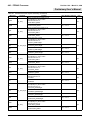
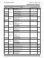
Figures .......................................................................................................................................... 11
Tables ........................................................................................................................................... 13
About This Book .......................................................................................................................... 17
1. Overview .................................................................................................................................. 21
1.1 PPC440 Processor Core Features ..................................................................................................
1.2 The PPC440 Processor as a PowerPC Implementation .................................................................
1.3 PPC440 Organization ......................................................................................................................
1.3.1 Superscalar Instruction Unit ...................................................................................................
1.3.2 Execution Pipelines ................................................................................................................
1.3.3 Instruction and Data Cache Controllers .................................................................................
1.3.4 Memory Management Unit (MMU) .........................................................................................
1.3.5 Interrupts and Exceptions ......................................................................................................
1.3.6 Timers ....................................................................................................................................
1.3.7 Debug Facilities ......................................................................................................................
1.4 Core Interfaces ................................................................................................................................
1.4.1 Processor Local Bus (PLB) ....................................................................................................
1.4.2 Device Control Register (DCR) Interface ...............................................................................
1.4.3 Auxiliary Processor Unit (APU) Interface ...............................................................................
1.4.4 JTAG Port ..............................................................................................................................
21
23
23
24
24
25
25
25
26
26
26
27
27
27
28
2. Programming Model ............................................................................................................... 29
2.1 Storage Addressing .........................................................................................................................
2.1.1 Storage Operands ..................................................................................................................
2.1.2 Effective Address Calculation ................................................................................................
2.1.2.1 Data Storage Addressing Modes ....................................................................................
2.1.2.2 Instruction Storage Addressing Modes ...........................................................................
2.1.3 Byte Ordering .........................................................................................................................
2.1.3.1 Structure Mapping Examples ..........................................................................................
2.1.3.2 Instruction Byte Ordering ................................................................................................
2.1.3.3 Data Byte Ordering .........................................................................................................
2.1.3.4 Byte-Reverse Instructions ...............................................................................................
2.2 Registers .........................................................................................................................................
2.2.1 Register Types .......................................................................................................................
2.2.1.1 General Purpose Registers ............................................................................................
2.2.1.2 Special Purpose Registers .............................................................................................
2.2.1.3 Condition Register ..........................................................................................................
2.2.1.4 Machine State Register ..................................................................................................
2.2.1.5 Device Control Registers ................................................................................................
2.2.1.6 Memory Mapped Registers .............................................................................................
2.3 Instruction Classes ..........................................................................................................................
2.3.1 Defined Instruction Class .......................................................................................................
2.3.2 Allocated Instruction Class .....................................................................................................
2.3.3 Preserved Instruction Class ...................................................................................................
2.3.4 Reserved Instruction Class ....................................................................................................
2.4 Implemented Instruction Set Summary ...........................................................................................
2.4.1 Integer Instructions .................................................................................................................
2.4.1.1 Integer Storage Access Instructions ...............................................................................
2.4.1.2 Integer Arithmetic Instructions ........................................................................................
AMCC Proprietary
29
29
31
31
31
32
33
34
34
35
36
40
40
40
41
41
41
41
41
41
42
43
43
44
45
45
46
3
440 – PPC440 Processor
Revision 1.09 – March 13, 2008
Preliminary User’s Manual
2.4.1.3 Integer Logical Instructions .............................................................................................
2.4.1.4 Integer Compare Instructions ..........................................................................................
2.4.1.5 Integer Trap Instructions .................................................................................................
2.4.1.6 Integer Rotate Instructions ..............................................................................................
2.4.1.7 Integer Shift Instructions .................................................................................................
2.4.1.8 Integer Select Instruction ................................................................................................
2.4.2 Branch Instructions .................................................................................................................
2.4.3 Processor Control Instructions ...............................................................................................
2.4.3.1 Condition Register Logical Instructions ...........................................................................
2.4.3.2 Register Management Instructions .................................................................................
2.4.3.3 System Linkage Instructions ...........................................................................................
2.4.3.4 Processor Synchronization Instruction ............................................................................
2.4.4 Storage Control Instructions ...................................................................................................
2.4.4.1 Cache Management Instructions ....................................................................................
2.4.4.2 TLB Management Instructions ........................................................................................
2.4.4.3 Storage Synchronization Instructions .............................................................................
2.4.5 Allocated Instructions .............................................................................................................
2.5 Branch Processing ...........................................................................................................................
2.5.1 Branch Addressing .................................................................................................................
2.5.2 Branch Instruction BI Field .....................................................................................................
2.5.3 Branch Instruction BO Field ...................................................................................................
2.5.4 Branch Prediction ...................................................................................................................
2.5.5 Branch Control Registers .......................................................................................................
2.5.5.1 Link Register (LR) ...........................................................................................................
2.5.5.2 Count Register (CTR) .....................................................................................................
2.5.5.3 Condition Register (CR) ..................................................................................................
2.6 Integer Processing ..........................................................................................................................
2.6.1 General Purpose Registers (GPRs) .......................................................................................
2.6.2 Integer Exception Register (XER) .........................................................................................
2.6.2.1 Summary Overflow (SO) Field ........................................................................................
2.6.2.2 Overflow (OV) Field ........................................................................................................
2.6.2.3 Carry (CA) Field ..............................................................................................................
2.7 Processor Control ............................................................................................................................
2.7.1 Special Purpose Registers General (USPRG0, SPRG0:SPRG7) ..........................................
2.7.2 Processor Version Register (PVR) .........................................................................................
2.7.3 Processor Identification Register (PIR) ..................................................................................
2.7.4 Core Configuration Register 0 (CCR0) ...................................................................................
2.7.5 Core Configuration Register 1 (CCR1) ...................................................................................
2.7.6 Reset Configuration (RSTCFG) .............................................................................................
2.8 User and Supervisor Modes ............................................................................................................
2.8.1 Privileged Instructions ............................................................................................................
2.8.2 Privileged SPRs .....................................................................................................................
2.9 Speculative Accesses ......................................................................................................................
2.10 Synchronization .............................................................................................................................
2.10.1 Context Synchronization ......................................................................................................
2.10.2 Execution Synchronization ...................................................................................................
2.10.3 Storage Ordering and Synchronization ................................................................................
46
46
47
47
47
47
47
48
48
48
48
49
49
49
49
50
50
51
51
51
51
52
53
53
54
54
57
57
57
59
59
59
60
60
60
61
61
63
65
65
66
66
66
67
67
68
68
3. Instruction and Data Caches ................................................................................................. 71
3.1 Cache Array Organization and Operation ........................................................................................ 71
3.1.1 Cache Line Replacement Policy ............................................................................................ 72
3.1.2 Cache Locking and Transient Mechanism ............................................................................. 73
4
AMCC Proprietary
Revision 1.09 – March 13, 2008
440 – PPC440 Processor
Preliminary User’s Manual
3.2 Instruction Cache Controller ............................................................................................................ 77
3.2.1 ICC Operations ...................................................................................................................... 78
3.2.2 Speculative Prefetch Mechanism ........................................................................................... 79
3.2.3 Instruction Cache Coherency ................................................................................................. 80
3.2.3.1 Self-Modifying Code ....................................................................................................... 80
3.2.3.2 Instruction Cache Synonyms .......................................................................................... 80
3.2.4 Instruction Cache Control and Debug .................................................................................... 82
3.2.4.1 Instruction Cache Management and Debug Instruction Summary ................................. 82
3.2.4.2 Core Configuration Register 0 (CCR0) ........................................................................... 83
3.2.4.3 Core Configuration Register 1 (CCR1) ....................................................................... 83
3.2.4.4 icbt Operation .............................................................................................................. 83
3.2.4.5 icread Operation ............................................................................................................. 83
3.2.4.6 Instruction Cache Parity Operations ............................................................................... 85
3.2.4.7 Simulating Instruction Cache Parity Errors for Software Testing .................................... 85
3.3 Data Cache Controller ..................................................................................................................... 86
3.3.1 DCC Operations ..................................................................................................................... 87
3.3.1.1 Load and Store Alignment .............................................................................................. 88
3.3.1.2 Load Operations ............................................................................................................. 88
3.3.1.3 Store Operations ............................................................................................................. 89
3.3.1.4 Line Flush Operations ..................................................................................................... 91
3.3.1.5 Data Read PLB Interface Requests ................................................................................ 92
3.3.1.6 Data Write PLB Interface Requests ................................................................................ 92
3.3.1.7 Storage Access Ordering ................................................................................................ 93
3.3.2 Data Cache Coherency .......................................................................................................... 94
3.3.3 Data Cache Control and Debug ............................................................................................. 94
3.3.3.1 Data Cache Management and Debug Instruction Summary .......................................... 94
3.3.3.2 Core Configuration Register 0 (CCR0) ........................................................................... 95
3.3.3.3 Core Configuration Register 1 (CCR1) ........................................................................... 95
3.3.3.4 dcbt and dcbtst Operation ............................................................................................... 95
3.3.3.5 dcread Operation ............................................................................................................ 96
3.3.3.6 Data Cache Parity Operations ........................................................................................ 98
3.3.3.7 D-Cache Parity Error Recovery Algorithm ...................................................................... 99
3.3.3.8 Simulating Data Cache Parity Errors for Software Testing ........................................... 100
4. Memory Management ........................................................................................................... 103
4.1 MMU Overview ..............................................................................................................................
4.1.1 Support for PowerPC Book-E MMU Architecture .................................................................
4.2 Translation Look Aside Buffer .......................................................................................................
4.3 Page Identification .........................................................................................................................
4.3.1 Virtual Address Formation ....................................................................................................
4.3.2 Address Space Identifier Convention ...................................................................................
4.3.3 TLB Match Process ..............................................................................................................
4.4 Address Translation .......................................................................................................................
4.5 Access Control ..............................................................................................................................
4.5.1 Execute Access ....................................................................................................................
4.5.2 Write Access ........................................................................................................................
4.5.3 Read Access ........................................................................................................................
4.5.4 Access Control Applied to Cache Management Instructions ...............................................
4.6 Storage Attributes ..........................................................................................................................
4.6.1 Write-Through (W) ...............................................................................................................
4.6.2 Caching Inhibited (I) .............................................................................................................
4.6.3 Memory Coherence Required (M) ........................................................................................
4.6.4 Guarded (G) .........................................................................................................................
AMCC Proprietary
103
103
104
107
108
108
108
110
111
112
112
112
113
114
114
115
115
115
5
440 – PPC440 Processor
Revision 1.09 – March 13, 2008
Preliminary User’s Manual
4.6.5 Endian (E) ............................................................................................................................
4.6.6 User-Definable (U0–U3) .......................................................................................................
4.6.7 Supported Storage Attribute Combinations ..........................................................................
4.7 Storage Control Registers .............................................................................................................
4.7.1 Memory Management Unit Control Register (MMUCR) .......................................................
Store Without Allocate (SWOA) Field 117
4.7.2 Process ID (PID) ..................................................................................................................
4.8 Shadow TLB Arrays .......................................................................................................................
4.9 TLB Management Instructions .......................................................................................................
4.9.1 TLB Search Instruction (tlbsx[.]) ..........................................................................................
4.9.2 TLB Read/Write Instructions (tlbre/tlbwe) .............................................................................
4.9.3 TLB Sync Instruction (tlbsync) ..............................................................................................
4.10 Page Reference and Change Status Management .....................................................................
4.11 TLB Parity Operations .................................................................................................................
4.11.1 Reading TLB Parity Bits with tlbre ......................................................................................
4.11.2 Simulating TLB Parity Errors for Software Testing .............................................................
116
116
116
116
117
120
120
121
121
122
122
123
123
124
125
5. Interrupts and Exceptions .................................................................................................... 127
5.1 Overview ........................................................................................................................................
5.2 Interrupt Classes ............................................................................................................................
5.2.1 Asynchronous Interrupts ......................................................................................................
5.2.2 Synchronous Interrupts ........................................................................................................
5.2.2.1 Synchronous, Precise Interrupts ...................................................................................
5.2.2.2 Synchronous, Imprecise Interrupts ...............................................................................
5.2.3 Critical and Non-Critical Interrupts .......................................................................................
5.2.4 Machine Check Interrupts ....................................................................................................
5.3 Interrupt Processing .......................................................................................................................
5.3.1 Partially Executed Instructions .............................................................................................
5.4 Interrupt Processing Registers ......................................................................................................
5.4.1 Machine State Register (MSR) .............................................................................................
5.4.2 Save/Restore Register 0 (SRR0) .........................................................................................
5.4.3 Save/Restore Register 1 (SRR1) .........................................................................................
5.4.4 Critical Save/Restore Register 0 (CSRR0) ...........................................................................
5.4.5 Critical Save/Restore Register 1 (CSRR1) ...........................................................................
5.4.6 Machine Check Save/Restore Register 0 (MCSRR0) .........................................................
5.4.7 Machine Check Save/Restore Register 1 (MCSRR1) .........................................................
5.4.8 Data Exception Address Register (DEAR) .........................................................................
5.4.9 Interrupt Vector Offset Registers (IVOR0:IVOR15) ..............................................................
5.4.10 Interrupt Vector Prefix Register (IVPR) ..............................................................................
5.4.11 Exception Syndrome Register (ESR) .................................................................................
5.4.12 Machine Check Status Register (MCSR) ...........................................................................
5.5 Interrupt Definitions ........................................................................................................................
5.5.1 Critical Input Interrupt ...........................................................................................................
5.5.2 Machine Check Interrupt ......................................................................................................
5.5.3 Data Storage Interrupt ..........................................................................................................
5.5.4 Instruction Storage Interrupt .................................................................................................
5.5.5 External Input Interrupt .........................................................................................................
5.5.6 Alignment Interrupt ...............................................................................................................
5.5.7 Program Interrupt .................................................................................................................
5.5.8 Floating-Point Unavailable Interrupt .....................................................................................
5.5.9 System Call Interrupt ............................................................................................................
5.5.10 Auxiliary Processor Unavailable Interrupt ..........................................................................
6
127
127
127
127
128
128
129
129
130
131
133
133
134
134
135
135
135
136
136
137
138
138
140
141
143
144
146
149
150
150
151
154
154
155
AMCC Proprietary
Revision 1.09 – March 13, 2008
440 – PPC440 Processor
Preliminary User’s Manual
5.5.11 Decrementer Interrupt ........................................................................................................
5.5.12 Fixed-Interval Timer Interrupt .............................................................................................
5.5.13 Watchdog Timer Interrupt ..................................................................................................
5.5.14 Data TLB Error Interrupt .....................................................................................................
5.5.15 Instruction TLB Error Interrupt ............................................................................................
5.5.16 Debug Interrupt ..................................................................................................................
5.6 Interrupt Ordering and Masking .....................................................................................................
5.6.1 Interrupt Ordering Software Requirements ..........................................................................
5.6.2 Interrupt Order ......................................................................................................................
5.7 Exception Priorities ........................................................................................................................
5.7.1 Exception Priorities for Integer Load, Store, and Cache Management Instructions .............
5.7.2 Exception Priorities for Floating-Point Load and Store Instructions .....................................
5.7.3 Exception Priorities for Allocated Load and Store Instructions ............................................
5.7.4 Exception Priorities for Floating-Point Instructions (Other) ..................................................
5.7.5 Exception Priorities for Allocated Instructions (Other) ..........................................................
5.7.6 Exception Priorities for Privileged Instructions .....................................................................
5.7.7 Exception Priorities for Trap Instructions .............................................................................
5.7.8 Exception Priorities for System Call Instruction ...................................................................
5.7.9 Exception Priorities for Branch Instructions .........................................................................
5.7.10 Exception Priorities for Return From Interrupt Instructions ................................................
5.7.11 Exception Priorities for Preserved Instructions ..................................................................
5.7.12 Exception Priorities for Reserved Instructions ...................................................................
5.7.13 Exception Priorities for All Other Instructions .....................................................................
155
156
156
157
158
159
162
163
164
165
166
166
167
167
168
168
169
169
169
170
170
170
171
6. Timer Facilities ...................................................................................................................... 173
6.1 Time Base .....................................................................................................................................
6.1.1 Reading the Time Base ........................................................................................................
6.1.2 Writing the Time Base ..........................................................................................................
6.2 Decrementer (DEC) .......................................................................................................................
6.3 Fixed Interval Timer (FIT) ..............................................................................................................
6.4 Watchdog Timer ............................................................................................................................
6.5 Timer Control Register (TCR) ........................................................................................................
6.6 Timer Status Register (TSR) .........................................................................................................
6.7 Freezing the Timer Facilities .........................................................................................................
6.8 Selection of the Timer Clock Source .............................................................................................
174
174
174
175
176
176
178
179
180
180
7. Debug Facilities .................................................................................................................... 181
7.1 Support for Development Tools .....................................................................................................
7.2 Debug Interfaces ...........................................................................................................................
7.2.1 IEEE 1149.1 Test Access Port (JTAG Debug Port) .............................................................
7.2.1.1 JTAG Connector ...........................................................................................................
7.2.1.2 JTAG Instructions .........................................................................................................
7.2.1.3 JTAG Boundary Scan ...................................................................................................
7.2.1.4 JTAG Register (SDR0_JTAGID) .................................................................................
7.2.2 Trace Port ............................................................................................................................
7.3 Debug Modes ................................................................................................................................
7.3.1 Internal Debug Mode ............................................................................................................
7.3.2 External Debug Mode ..........................................................................................................
7.3.3 Debug Wait Mode ................................................................................................................
7.3.4 Trace Debug Mode ..............................................................................................................
7.4 Debug Events ................................................................................................................................
7.4.1 Instruction Address Compare (IAC) Debug Event ...............................................................
AMCC Proprietary
181
181
181
181
182
182
183
183
183
184
184
184
185
185
186
7
440 – PPC440 Processor
Revision 1.09 – March 13, 2008
Preliminary User’s Manual
7.4.1.1 IAC Debug Event Fields ................................................................................................
7.4.1.2 IAC Debug Event Processing .......................................................................................
7.4.2 Data Address Compare (DAC) Debug Event .......................................................................
7.4.2.1 DAC Debug Event Fields ..............................................................................................
7.4.2.2 DAC Debug Event Processing ......................................................................................
7.4.2.3 DAC Debug Events Applied to Instructions that Result in Multiple Storage Accesses .
7.4.2.4 DAC Debug Events Applied to Various Instruction Types ...........................................
7.4.3 Data Value Compare (DVC) Debug Event ...........................................................................
7.4.3.1 DVC Debug Event Fields ..............................................................................................
7.4.3.2 DVC Debug Event Processing ......................................................................................
7.4.3.3 DVC Debug Events Applied to Instructions that Result in Multiple Storage Accesses .
7.4.3.4 DVC Debug Events Applied to Various Instruction Types ...........................................
7.4.4 Branch Taken (BRT) Debug Event .......................................................................................
7.4.5 Trap (TRAP) Debug Event ...................................................................................................
7.4.6 Return (RET) Debug Event ..................................................................................................
7.4.7 Instruction Complete (ICMP) Debug Event ..........................................................................
7.4.8 Interrupt (IRPT) Debug Event ...............................................................................................
7.4.9 Unconditional Debug Event (UDE) .......................................................................................
7.4.10 Debug Event Summary ......................................................................................................
7.5 Debug Reset ..................................................................................................................................
7.6 Debug Timer Freeze ......................................................................................................................
7.7 Debug Registers ............................................................................................................................
7.7.1 Debug Control Register 0 (DBCR0) .....................................................................................
7.7.2 Debug Control Register 1 (DBCR1) .....................................................................................
7.7.3 Debug Control Register 2 (DBCR2) .....................................................................................
7.7.4 Debug Status Register (DBSR) ...........................................................................................
7.7.5 Instruction Address Compare Registers (IAC1:IAC4) ..........................................................
7.7.6 Data Address Compare Registers (DAC1:DAC2) ................................................................
7.7.7 Data Value Compare Registers (DVC1:DVC2) ....................................................................
7.7.8 Debug Data Register (DBDR) ..............................................................................................
186
189
189
190
192
193
193
194
195
196
196
196
196
197
197
198
198
199
200
200
200
200
201
202
204
205
206
206
206
207
8. Instruction Set ....................................................................................................................... 209
8.1 Instruction Set Portability ...............................................................................................................
8.2 Instruction Formats ........................................................................................................................
8.3 Pseudocode ...................................................................................................................................
8.3.1 Operator Precedence ...........................................................................................................
8.4 Register Usage ..............................................................................................................................
8.5 Alphabetical Instruction Listing ......................................................................................................
210
210
211
213
213
213
9. Register Summary ................................................................................................................ 403
9.1 Register Categories ....................................................................................................................... 403
9.2 Reserved Fields ............................................................................................................................. 406
9.3 Alphabetical Listing of Processor Core Registers .......................................................................... 406
Appendix A. Instruction Summary .......................................................................................... 411
A.1 Instruction Formats .......................................................................................................................
A.1.1 Instruction Fields .................................................................................................................
A.1.2 Instruction Format Diagrams ...............................................................................................
A.1.2.1 I-Form ..........................................................................................................................
A.1.2.2 B-Form .........................................................................................................................
A.1.2.3 SC-Form ......................................................................................................................
A.1.2.4 D-Form ........................................................................................................................
A.1.2.5 X-Form .........................................................................................................................
8
411
411
413
414
414
414
414
415
AMCC Proprietary
Revision 1.09 – March 13, 2008
440 – PPC440 Processor
Preliminary User’s Manual
A.1.2.6 XL-Form .......................................................................................................................
A.1.2.7 XFX-Form .....................................................................................................................
A.1.2.8 XO-Form .......................................................................................................................
A.1.2.9 M-Form .........................................................................................................................
A.2 Alphabetical Summary of Implemented Instructions .....................................................................
A.3 Allocated Instruction Opcodes ......................................................................................................
A.4 Preserved Instruction Opcodes .....................................................................................................
A.5 Reserved Instruction Opcodes ......................................................................................................
A.6 Implemented Instructions Sorted by Opcode ................................................................................
416
416
416
416
416
445
445
446
446
Appendix B. PPC440 Compiler Optimizations ....................................................................... 455
Index ........................................................................................................................................... 457
Revision Log .............................................................................................................................. 473
AMCC Proprietary
9
440 – PPC440 Processor
Revision 1.09 – March 13, 2008
Preliminary User’s Manual
10
AMCC Proprietary
Revision 1.09 – March 13, 2008
440 – PPC440 Processor
Preliminary User’s Manual
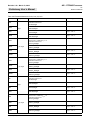
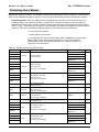
Figures
Figure 1-1.
PPC440 Core Block Diagram ...............................................................................................24
Figure 2-1.
User Programming Model Registers .....................................................................................37
Figure 2-2.
Supervisor Programming Model Registers ...........................................................................38
Figure 2-3.
Link Register (LR) .................................................................................................................53
Figure 2-4.
Count Register (CTR) ...........................................................................................................54
Figure 2-5.
Condition Register (CR) ........................................................................................................54
Figure 2-6.
General Purpose Registers (R0-R31) ...................................................................................57
Figure 2-7.
Integer Exception Register (XER) .........................................................................................58
Figure 2-8.
Special Purpose Registers General (USPRG0, SPRG0:SPRG7) ........................................60
Figure 2-9.
Processor Version Register (PVR) .......................................................................................61
Figure 2-10.
Processor Identification Register (PIR) .................................................................................61
Figure 2-11.
Core Configuration Register 0 (CCR0) .................................................................................61
Figure 2-12.
Core Configuration Register 1 (CCR1) .................................................................................64
Figure 2-13.
Reset Configuration (RSTCFG) ............................................................................................65
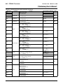
Figure 3-1.
Victim Registers (INV0:INV3) (ITV0:ITV3) (DNV0:DNV3) (DTV0:DTV3) ..............................72
Figure 3-2.
Instruction Cache Victim Limit (IVLIM) and Data Cache Victim Limit (DVLIM) Registers .....74
Figure 3-3.
Cache Locking and Transient Mechanism (Example 1) .......................................................76
Figure 3-4.
Cache Locking and Transient Mechanism (Example 2) .......................................................77
Figure 3-5.
Instruction Cache Debug Data Register (ICDBDR) ..............................................................84
Figure 3-6.
Instruction Cache Debug Tag Register High (ICDBTRH) .....................................................84
Figure 3-7.
Instruction Cache Debug Tag Register Low (ICDBTRL) ......................................................85
Figure 3-8.
Data Cache Debug Tag Register High (DCDBTRH) ............................................................97
Figure 3-9.
Data Cache Debug Tag Register Low (DCDBTRL) ..............................................................97
Figure 4-1.
Virtual Address to TLB Entry Match Process ......................................................................109
Figure 4-2.
Effective-to-Real Address Translation Flow ........................................................................111
Figure 4-3.
Memory Management Unit Control Register (MMUCR) .....................................................117
Figure 4-4.
Process ID (PID) .................................................................................................................120
Figure 4-5.
TLB Entry Word Definitions .................................................................................................122
Figure 5-1.
Machine State Register (MSR) ...........................................................................................133
Figure 5-2.
Save/Restore Register 0 (SRR0) ........................................................................................134
Figure 5-3.
Save/Restore Register 1 (SRR1) ........................................................................................135
Figure 5-4.
Critical Save/Restore Register 0 (CSRR0) .........................................................................135
Figure 5-5.
Critical Save/Restore Register 1 (CSRR1) .........................................................................135
Figure 5-6.
Machine Check Save/Restore Register 0 (MCSRR0) ........................................................136
Figure 5-7.
Machine Check Save/Restore Register 1 (MCSRR1) ........................................................136
Figure 5-8.
Data Exception Address Register (DEAR) ..........................................................................136
Figure 5-9.
Interrupt Vector Offset Registers (IVOR0:IVOR15) ............................................................137
Figure 5-10.
Interrupt Vector Prefix Register (IVPR) ...............................................................................138
Figure 5-11.
Exception Syndrome Register (ESR) ..................................................................................138
Figure 5-12.
Machine Check Status Register (MCSR) ............................................................................140
AMCC Proprietary
11
440 – PPC440 Processor
Revision 1.09 – March 13, 2008
Preliminary User’s Manual
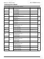
Figure 6-1.
Relationship of Timer Facilities to the Time Base .............................................................. 173
Figure 6-2.
Time Base Lower (TBL) ..................................................................................................... 174
Figure 6-3.
Time Base Upper (TBU) ..................................................................................................... 174
Figure 6-4.
Decrementer (DEC) ........................................................................................................... 175
Figure 6-5.
Decrementer Auto-Reload (DECAR) ................................................................................. 175
Figure 6-6.
Watchdog State Machine ................................................................................................... 178
Figure 6-7.
Timer Control Register (TCR) ............................................................................................ 179
Figure 6-8.
Timer Status Register (TSR) .............................................................................................. 180
Figure 7-1.
JTAG ID Register (SDR0_JTAGID) ................................................................................... 183
Figure 7-2.
Debug Control Register 0 (DBCR0) ................................................................................... 201
Figure 7-3.
Debug Control Register 1 (DBCR1) ................................................................................... 202
Figure 7-4.
Debug Control Register 2 (DBCR2) ................................................................................... 204
Figure 7-5.
Debug Status Register (DBSR) .......................................................................................... 205
Figure 7-6.
Instruction Address Compare Registers (IAC1:IAC4) ........................................................ 206
Figure 7-7.
Data Address Compare Registers (DAC1:DAC2) .............................................................. 206
Figure 7-8.
Data Value Compare Registers (DVC1:DVC2) .................................................................. 207
Figure 7-9.
Debug Data Register (DBDR) ............................................................................................ 207
Figure A-1.
I Instruction Format .............................................................................................................. 414
Figure A-2.
B Instruction Format ............................................................................................................. 414
Figure A-3.
SC Instruction Format .......................................................................................................... 414
Figure A-4.
D Instruction Format ............................................................................................................ 414
Figure A-5.
X Instruction Format ............................................................................................................. 415
Figure A-6.
XL Instruction Format ........................................................................................................... 416
Figure A-7.
XFX Instruction Format ........................................................................................................ 416
Figure A-8.
XO Instruction Format .......................................................................................................... 416
Figure A-9.
M Instruction Format ............................................................................................................ 416
12
AMCC Proprietary
Revision 1.09 – March 13, 2008
440 – PPC440 Processor
Preliminary User’s Manual
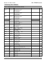
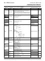
Tables
Table 2-1.
Data Operand Definitions .......................................................................................................30
Table 2-2.
Alignment Effects for Storage Access Instructions .................................................................30
Table 2-3.
Register Categories ................................................................................................................39
Table 2-4.
Instruction Categories .............................................................................................................44
Table 2-5.
Integer Storage Access Instructions .......................................................................................45
Table 2-6.
Integer Arithmetic Instructions ................................................................................................46
Table 2-7.
Integer Logical Instructions .....................................................................................................46
Table 2-8.
Integer Compare Instructions .................................................................................................46
Table 2-9.
Integer Trap Instructions .........................................................................................................47
Table 2-10.
Integer Rotate Instructions .....................................................................................................47
Table 2-11.
Integer Shift Instructions .........................................................................................................47
Table 2-12.
Integer Select Instruction ........................................................................................................47
Table 2-13.
Branch Instructions .................................................................................................................48
Table 2-14.
Condition Register Logical Instructions ..................................................................................48
Table 2-15.
Register Management Instructions .........................................................................................48
Table 2-16.
System Linkage Instructions ...................................................................................................49
Table 2-17.
Processor Synchronization Instruction ...................................................................................49
Table 2-18.
Cache Management Instructions ............................................................................................49
Table 2-19.
TLB Management Instructions ................................................................................................50
Table 2-20.
Storage Synchronization Instructions .....................................................................................50
Table 2-21.
Allocated Instructions .............................................................................................................50
Table 2-22.
BO Field Definition ..................................................................................................................52
Table 2-23.
BO Field Examples .................................................................................................................52
Table 2-24.
CR Updating Instructions ........................................................................................................55
Table 2-25.
XER[SO,OV] Updating Instructions ........................................................................................58
Table 2-26.
XER[CA] Updating Instructions ..............................................................................................58
Table 2-27.
Privileged Instructions ............................................................................................................66
Table 3-1.
Instruction and Data Cache Array Organization .....................................................................71
Table 3-2.
Victim Index Field Selection ...................................................................................................73
Table 3-3.
Data Cache Behavior on Store Accesses ..............................................................................91
Table 4-1.
TLB Entry Fields ...................................................................................................................105
Table 4-2.
Page Size and Effective Address to EPN Comparison ........................................................110
Table 4-3.
Page Size and Real Address Formation ..............................................................................111
Table 4-4.
Access Control Applied to Cache Management Instructions ................................................114
Table 5-1.
Interrupt Types Associated with each IVOR .........................................................................137
Table 5-2.
Interrupt and Exception Types ..............................................................................................141
Table 6-1.
Fixed Interval Timer Period Selection ...................................................................................176
Table 6-2.
Watchdog Timer Period Selection ........................................................................................177
Table 6-3.
Watchdog Timer Exception Behavior ...................................................................................177
Table 7-1.
JTAG Instructions .................................................................................................................182
AMCC Proprietary
13
440 – PPC440 Processor
Revision 1.09 – March 13, 2008
Preliminary User’s Manual
Table 7-2.
Debug Events ...................................................................................................................... 185
Table 7-3.
IAC Range Mode Auto-Toggle Summary ............................................................................ 188
Table 7-4.
Debug Event Summary ........................................................................................................ 200
Table 8-1.
Instruction Categories .......................................................................................................... 209
Table 8-2.
Allocated Instructions ........................................................................................................... 210
Table 8-3.
Operator Precedence ........................................................................................................... 213
Table 8-4.
Extended Mnemonics for addi ............................................................................................. 217
Table 8-5.
Extended Mnemonics for addic ............................................................................................ 218
Table 8-6.
Extended Mnemonics for addic. ........................................................................................... 219
Table 8-7.
Extended Mnemonics for addis ............................................................................................ 220
Table 8-8.
Extended Mnemonics for bc, bca, bcl, bcla ......................................................................... 229
Table 8-9.
Extended Mnemonics for bcctr, bcctrl .................................................................................. 233
Table 8-10.
Extended Mnemonics for bclr, bclrl ...................................................................................... 236
Table 8-11.
Extended Mnemonics for cmp ............................................................................................. 240
Table 8-12.
Extended Mnemonics for cmpi ............................................................................................. 241
Table 8-13.
Extended Mnemonics for cmpl ............................................................................................. 242
Table 8-14.
Extended Mnemonics for cmpli ............................................................................................ 243
Table 8-15.
Extended Mnemonics for creqv ........................................................................................... 247
Table 8-16.
Extended Mnemonics for crnor ............................................................................................ 249
Table 8-17.
Extended Mnemonics for cror .............................................................................................. 250
Table 8-18.
Extended Mnemonics for crxor ............................................................................................ 252
Table 8-19.
Extended Mnemonics for mbar ............................................................................................ 313
Table 8-20.
Extended Mnemonics for mfspr ........................................................................................... 320
Table 8-21.
FXM Bit Field Correspondence ............................................................................................ 323
Table 8-22.
Extended Mnemonics for mtcrf ............................................................................................ 323
Table 8-23.
Extended Mnemonics for mtspr ........................................................................................... 327
Table 8-24.
Extended Mnemonics for nor, nor. ....................................................................................... 347
Table 8-25.
Extended Mnemonics for or, or. ........................................................................................... 348
Table 8-26.
Extended Mnemonics for ori ................................................................................................ 350
Table 8-27.
Extended Mnemonics for rlwimi, rlwimi. .............................................................................. 355
Table 8-28.
Extended Mnemonics for rlwinm, rlwinm. ............................................................................ 356
Table 8-29.
Extended Mnemonics for rlwnm, rlwnm. ............................................................................. 358
Table 8-30.
Extended Mnemonics for subf, subf., subfo, subfo. ............................................................. 383
Table 8-31.
Extended Mnemonics for subfc, subfc., subfco, subfco. ...................................................... 384
Table 8-32.
Extended Mnemonics for tw ................................................................................................. 395
Table 8-33.
Extended Mnemonics for twi ................................................................................................ 397
Table 9-1.
Special Purpose Registers Sorted by SPR Number ............................................................ 403
Table 9-2.
Alphabetical Listing of Processor Core Registers ................................................................ 406
Table A-1.
PPC440 Instruction Syntax Summary .................................................................................. 417
Table A-2.
Allocated Opcodes ............................................................................................................... 445
Table A-3.
Preserved Opcodes ............................................................................................................. 445
14
AMCC Proprietary
Revision 1.09 – March 13, 2008
440 – PPC440 Processor
Preliminary User’s Manual
Table A-4.
Reserved-nop Opcodes ........................................................................................................446
Table A-5.
PPC440 Instructions by Opcode ..........................................................................................447
AMCC Proprietary
15
440 – PPC440 Processor
Revision 1.09 – March 13, 2008
Preliminary User’s Manual
16
AMCC Proprietary
Revision 1.09 – March 13, 2008
440 – PPC440 Processor
Preliminary User’s Manual
About This Book
This user’s manual provides the architectural overview, programming model, and detailed information about the
registers, the instruction set, and operations of the AMCC™ PowerPC™ 440 (PPC440™) 32-bit RISC processor
core.
The PPC440 RISC processor features:
• Book-E Enhanced PowerPC Architecture™
• JTAG support for board level testing
• Extensive development tool support
Who Should Use This Book
This book is for system hardware and software developers, and for application developers who need to understand
the PPC440. The audience should understand embedded processor design, embedded system design, operating
systems, RISC processing, and design for testability.
How to Use This Book
This book describes the PPC440 device architecture (including instructions and registers), processor core
functions, and system operations. The book is organized as follows:
• Overview on page 21
• Programming Model on page 29
• Instruction and Data Caches on page 71
• Memory Management on page 103
• Interrupts and Exceptions on page 127
• Timer Facilities on page 173
• Debug Facilities on page 181
• Instruction Set on page 209
• Register Summary on page 403
This book also contains the following appendixes:
• Instruction Summary on page 411
• PPC440 Compiler Optimizations on page 455
To help readers find material in these sections, the book contains:
• Contents on page 3
• Figures on page 11
• Tables on page 13
• Index on page 457
AMCC Proprietary
17
440 – PPC440 Processor
Revision 1.09 – March 13, 2008
Preliminary User’s Manual
Conventions
The following is a list of notational conventions frequently used in this manual.
ActiveLow
An overbar indicates an active-low signal.
n
A decimal number
0xn
A hexadecimal number
0bn
A binary number
=
Assignment
∧
AND logical operator
¬
NOT logical operator
∨
OR logical operator
⊕
Exclusive-OR (XOR) logical operator
+
Twos complement addition
–
Twos complement subtraction, unary minus
×
Multiplication
÷
Division yielding a quotient
%
Remainder of an integer division; (33 % 32) = 1.
||
Concatenation
=, ≠
Equal, not equal relations
<, >
Signed comparison relations
u
u
<, >
Unsigned comparison relations
if...then...else...
Conditional execution; if condition then a else b, where a and b represent one or
more pseudocode statements. Indenting indicates the ranges of a and b. If b is
null, the else does not appear.
do
Do loop. “to” and “by” clauses specify incrementing an iteration variable; “while”
and “until” clauses specify terminating conditions. Indenting indicates the scope of
a loop.
leave
Leave innermost do loop or do loop specified in a leave statement.
FLD
An instruction or register field
FLDb
A bit in a named instruction or register field
FLDb:b
A range of bits in a named instruction or register field
FLDb,b, . . .
A list of bits, by number or name, in a named instruction or register field
REGb
A bit in a named register
REGb:b
A range of bits in a named register
REGb,b, . . .
A list of bits, by number or name, in a named register
REG[FLD]
A field in a named register
REG[FLD, FLD . . .]
A list of fields in a named register
REG[FLD:FLD]
A range of fields in a named register
GPR(r)
General Purpose Register (GPR) r, where 0 ≤ r ≤ 31.
(GPR(r))
The contents of GPR r, where 0 ≤ r ≤ 31.
18
AMCC Proprietary
Revision 1.09 – March 13, 2008
440 – PPC440 Processor
Preliminary User’s Manual
DCR(DCRN)
A Device Control Register (DCR) specified by the DCRF field in an mfdcr or
mtdcr instruction
SPR(SPRN)
An SPR specified by the SPRF field in an mfspr or mtspr instruction
TBR(TBRN)
A Time Base Register (TBR) specified by the TBRF field in an mftb instruction
GPRs
RA, RB, . . .
(Rx)
The contents of a GPR, where x is A, B, S, or T
(RA|0)
The contents of the register RA or 0, if the RA field is 0.
CRFLD
The field in the condition register pointed to by a field of an instruction.
c0:3
A 4-bit object used to store condition results in compare instructions.
n
The bit or bit value b is replicated n times.
b
xx
Bit positions which are don’t-cares.
CEIL(x)
Least integer ≥ x.
EXTS(x)
The result of extending x on the left with sign bits.
PC
Program counter.
RESERVE
Reserve bit; indicates whether a process has reserved a block of storage.
CIA
Current instruction address; the 32-bit address of the instruction being described
by a sequence of pseudocode. This address is used to set the next instruction
address (NIA). Does not correspond to any architected register.
NIA
Next instruction address; the 32-bit address of the next instruction to be executed.
In pseudocode, a successful branch is indicated by assigning a value to NIA. For
instructions that do not branch, the NIA is CIA +4.
MS(addr, n)
The number of bytes represented by n at the location in main storage represented
by addr.
EA
Effective address; the 32-bit address, derived by applying indexing or indirect
addressing rules to the specified operand, that specifies a location in main
storage.
EAb
A bit in an effective address.
EAb:b
A range of bits in an effective address.
ROTL((RS),n)
Rotate left; the contents of RS are shifted left the number of bits specified by n.
MASK(MB,ME)
Mask having 1s in positions MB through ME (wrapping if MB > ME) and 0s
elsewhere.
instruction(EA)
An instruction operating on a data or instruction cache block associated with an
EA.
AMCC Proprietary
19
440 – PPC440 Processor
Revision 1.09 – March 13, 2008
Preliminary User’s Manual
20
AMCC Proprietary
Revision 1.09 – March 13, 2008
440 – PPC440 Processor
Preliminary User’s Manual
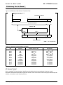
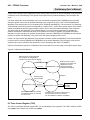
1. Overview
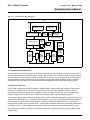
The PowerPC™ 440 32-bit processor core, referred to as the PPC440 core, implements the Book-E Enhanced
PowerPC Architecture.
This section describes:
• PPC440 core features
• The PPC440 core as an implementation of the Book-E Enhanced PowerPC Architecture
• The organization of the PPC440 core, including a block diagram and descriptions of the functional units
• PPC440 core interfaces
1.1 PPC440 Processor Core Features
The PPC440 core is a high-performance, low-power consumption engine that implements the flexible and powerful
Book-E Enhanced PowerPC Architecture.
The PPC440 contains a dual-issue, superscalar, pipelined processing unit, along with other functional elements
required by embedded ASIC product specifications. These other functions include memory management, cache
control, timers, and debug facilities. Interfaces for custom co-processors and floating point functions are provided,
along with separate instruction and data cache array interfaces which can be configured to various sizes
(optimized for 32KB). The processor local bus (PLB) system interface has been extended to 128 bits and is fully
compatible with the IBM® CoreConnect on-chip system architecture, providing the framework to efficiently support
system-on-a-chip (SOC) designs.
In addition, the PPC440 core is a member of the PowerPC 400 Series of advanced embedded processors cores,
which is supported by the PowerPC Embedded Tools Program. In this program, AMCC and many third party
vendors offer a full range of robust development tools for embedded applications. Among these are compilers,
debuggers, real-time operating systems, and logic analyzers.
• High performance, dual-issue, superscalar 32-bit RISC CPU
• Superscalar implementation of the Book-E Enhanced PowerPC Architecture
• Seven stage, highly-pipelined micro-architecture
• Dual instruction fetch, decode, and out-of-order issue
• Out-of-order execution and completion
• High-accuracy dynamic branch prediction utilizing a Branch History Table (BHT)
• Reduced branch latency using Branch Target Address Cache (BTAC)
• Four independent pipelines
• Combined complex integer, system, and branch pipeline
• Simple integer pipeline
• Load/store pipeline
• Floating point unit which is connected in parallel with the other pipelines via the APU.
• Single-cycle multiply
• Single-cycle multiply-accumulate (new DSP instruction set extensions)
• Two replicated 6-port (3 read, 3 write) 32x32-bit general purpose register (GPR) files
• Hardware support for all CPU misaligned accesses
• Full support for both big- and little-endian byte order
AMCC Proprietary
21
440 – PPC440 Processor
Revision 1.09 – March 13, 2008
Preliminary User’s Manual
• Extensive power management designed into core for maximum performance/power efficiency
• Primary caches
• 32KB configurable instruction and data cache arrays
• Single-cycle access
• 32-byte (eight word) line size
• Highly associative (64-way for 32KB)
• Write-back and write-through operation
• Control over whether stores will allocate or write-through on cache miss
• Extensive load/store queues and multiple line fill/flush buffers
• Non-blocking with up to four outstanding load misses
• Cache line locking supported
• Caches can be partitioned to provide separate regions for “transient” instructions and data
• High associativity permits efficient allocation of cache memory
• Critical word-first data access and forwarding
• Instruction cache parity
• Word-wide (32-bit) parity on instruction data
• Instruction tag address parity
• Always recoverable
• Ability to force I-cache parity exceptions through software, for testing interrupt handlers
• Data cache parity
• Byte-wide parity on data
• Data tag address parity
• Dirty bit and user bit parity
• Parity detection on cast outs in write-back mode
• Recoverable and semi-recoverable operation modes
• Ability to force D-cache parity exceptions through software, for testing interrupt handlers
• D-cache full-line flush capability
• Whole-line castouts, as opposed to sublines, depending on the memory slave design
• Memory management unit
• Separate 4KB instruction and 8KB data micro-TLBs
• Sixty-four entry, fully associative unified TLB array
• Variable page sizes (1KB–256MB), simultaneously resident in TLB
• Four-bit extended real address for 36-bit (64GB) addressability
• Flexible TLB management with software page table search
• Storage attribute controls for write-through, caching inhibited, guarded, and byte order (endianness)
• Four user-definable storage attribute controls
• UTLB parity
• Word-wide (41-bit and 15-bit) parity on data
22
AMCC Proprietary
Revision 1.09 – March 13, 2008
440 – PPC440 Processor
Preliminary User’s Manual
• Tag address parity
• Ability to force UTLB parity exceptions through software, for testing interrupt handlers
• Debug facilities
• Extensive hardware debug facilities incorporated into the IEEE 1149.1 JTAG port
• Multiple instruction and data address break points (including range)
• Data value compare
• Single-step, branch, trap, and other debug events
• Non-invasive real-time software trace interface
• Timer facilities
• 64-bit time base
• Decrementer with auto-reload capability
• Fixed interval timer (FIT)
• Watchdog timer with critical interrupt and/or auto-reset
1.2 The PPC440 Processor as a PowerPC Implementation
The PPC440 implements the full, 32-bit fixed-point subset of the Book-E Enhanced PowerPC Architecture.
Although it fully complies with these architectural specifications, the 64-bit operations of the architecture are not
supported, nor the floating point operations. Within the RISC core, the 64-bit operations and the floating point
operations are trapped, and the floating point operations can be emulated using software.The PPC440 RISC
processor core is a high-performance, low-cost, low-power engine that implements the flexible and powerful BookE Enhanced PowerPC Architecture.
See Appendix A of the Book-E Enhanced PowerPC Architecture specification for more information on 32-bit subset
implementations of the architecture.
The PPC440 also provides a number of optimizations and extensions to the lower layers of the Book-E Enhanced
PowerPC Architecture. Some of the specific implementation features of the PPC440 are simply extensions of the
Book-E Enhanced PowerPC Architecture. These features are included to enhance performance, integrate
functionality, and reduce system complexity in embedded control applications.
Note: This document differs from the Book-E architecture specification in the use of bit numbering for architected
registers. Specifically, Book-E defines the full, 64-bit instruction set architecture, and thus all registers are shown
as having bit numbers from 0 to 63, with bit 63 being the least significant. On the other hand, this document
describes the PPC440, which is a 32-bit subset implementation of the architecture. Accordingly, all architected
registers are described as being 32 bits in length, with the bits numbered from 0 to 31, and with bit 31 being the
least significant. Therefore, when this document makes reference to register bit numbers from 0 to 31, they actually
correspond to bits 32 to 63 of the same register in the Book-E architecture specification.
1.3 PPC440 Organization
The PPC440 includes a seven-stage pipelined PowerPC processor, which consists of a three-stage, dual-issue
instruction fetch and decode unit with attached branch unit, together with three independent, four-stage pipelines
for complex integer, simple integer, and load/store operations, respectively. It also includes a memory management unit (MMU), separate instruction and data cache units, JTAG, debug, trace logic, and timer facilities.
AMCC Proprietary
23
440 – PPC440 Processor
Revision 1.09 – March 13, 2008
Preliminary User’s Manual
Figure 1-1. PPC440 Core Block Diagram
I-Cache Controller ITLB
Data Cache
MMU
64-entry
DTLB
128
Instruction Cache
128
128
PLB
Load/Store
Queues
D-Cache Controller
Instruction Unit
Issue 0
Issue 1
Branch
Unit
BHT
4K
DCR Bus
JTAG
Debug
Trace
BTAC
Interrupts
and
Timers
Complex
Integer
Pipeline
GPR
Simple
Integer
Pipeline
GPR
Load
Store
Pipeline
Clocks
and
Pwr Mgmt
1.3.1 Superscalar Instruction Unit
The instruction unit of the PPC440 fetches, decodes, and issues two instructions per cycle to any combination of
the three execution pipelines and/or the APU interface. The instruction unit includes a branch unit which provides
dynamic branch prediction using a branch history table (BHT), as well as a branch target address cache (BTAC).
These mechanisms greatly improve the branch prediction accuracy and reduce the latency of taken branches,
such that the target of a branch can usually be executed immediately after the branch itself, with no penalty.
1.3.2 Execution Pipelines
The PPC440 contains three execution pipelines: complex integer, simple integer, and load/store. Each pipeline
consists of four stages and can access the nine-ported (six read, three write) GPR file. In order to improve
performance and avoid contention for the GPR file, there are two identical copies of it. One is dedicated to the
complex integer pipeline, while the other is shared by the simple integer and the load/store pipelines.
The complex integer pipeline handles all arithmetic, logical, branch, and system management instructions (such as
interrupt and TLB management, move to/from system registers, and so on). This pipeline also handles multiply and
divide operations, and 24 instructions that perform a variety of multiply-accumulate operations. The complex
integer pipeline multiply unit can perform 32-bit × 32-bit multiply operations with single-cycle throughput and threecycle latency;16-bit × 32-bit multiply operations have only two-cycle latency. Divide operations take 33 cycles.
The simple integer pipeline can handle most arithmetic and logical operations which do not update the Condition
Register (CR).
24
AMCC Proprietary
Revision 1.09 – March 13, 2008
440 – PPC440 Processor
Preliminary User’s Manual
The load/store pipeline handles all load, store, and cache management instructions. All misaligned operations are
handled in hardware, with no penalty on any operation which is contained within an aligned 16-byte region. The
load/store pipeline supports all operations to both Big Endian and Little Endian data regions.
See PPC440 Compiler Optimizations on page 455 .
1.3.3 Instruction and Data Cache Controllers
The PPC440 provides separate instruction and data cache controllers and arrays, which allow concurrent access
and minimize pipeline stalls. The storage capacity of the cache arrays, which can range from 8KB to 32KB each,
depends upon the implementation. Both cache controllers have 32-byte lines, and both are highly-associative, with
64-way set-associativity for 32KB and 16KB sizes, and 32-way set-associativity for the 8KB size. Both caches
support parity checking on the tags and data in the memory arrays, to protect against soft errors. If a parity error is
detected, the CPU will cause a machine check exception.
The PowerPC instruction set provides a rich set of cache management instructions for software-enforced
coherency. The PPC440 core implementation also provides special debug instructions that can directly read the
tag and data arrays.
The cache controllers connect through the PLB to the IBM CoreConnect system-on-a-chip environment.
See Instruction and Data Caches on page 71.
1.3.4 Memory Management Unit (MMU)
The PPC440 supports a flat, 36-bit (64GB) real (physical) address space. This 36-bit real address is generated by
the MMU, as part of the translation process from the 32-bit effective address, which is calculated by the processor
core as an instruction fetch or load/store address.
The MMU provides address translation, access protection, and storage attribute control for embedded
applications. The MMU supports demand paged virtual memory and other management schemes that require
precise control of logical to physical address mapping and flexible memory protection. Working with appropriate
system level software, the MMU provides the following functions:
• Translation of the 32-bit effective address space into the 36-bit real address space
• Page level read, write, and execute access control
• Storage attributes for cache policy, byte order (endianness), and speculative memory access
• Software control of page replacement strategy
See Memory Management on page 103.
1.3.5 Interrupts and Exceptions
An interrupt is the action in which the processor saves its old context (Machine State Register (MSR) and next
instruction address) and begins execution at a pre-determined interrupt-handler address, with a modified MSR.
Exceptions are the events that may cause the processor to take an interrupt, if the corresponding interrupt type is
enabled.
Exceptions may be generated by the execution of instructions, or by signals from devices external to the PPC440,
the internal timer facilities, debug events, or error conditions.
See Interrupts and Exceptions on page 127.
AMCC Proprietary
25
440 – PPC440 Processor
Revision 1.09 – March 13, 2008
Preliminary User’s Manual
1.3.6 Timers
The PPC440 contains a Time Base and three timers: a Decrementer (DEC), a Fixed Interval Timer (FIT), and a
Watchdog Timer. The Time Base is a 64-bit counter which is incremented at a frequency either equal to the
processor core clock rate or as controlled by a separate, asynchronous timer clock input to the core. No interrupt is
generated as a result of the Time Base wrapping back to zero.
The DEC is a 32-bit register that is decremented at the same rate at which the Time Base is incremented. The user
loads the DEC register with a value to create the desired interval. When the register is decremented to zero, a
number of actions occur: The DEC stops decrementing, a status bit is set in the Timer Status Register (TSR), and
a Decrementer exception is reported to the interrupt mechanism of the PPC440. Optionally, the DEC can be
programmed to reload automatically the value contained in the Decrementer Auto-Reload register (DECAR), after
which the DEC resumes decrementing. The Timer Control Register (TCR) contains the interrupt enable for the
Decrementer interrupt.
The FIT generates periodic interrupts based on the transition of a selected bit from the Time Base. Users can
select one of four intervals for the FIT period by setting a control field in the TCR to select the appropriate bit from
the Time Base. When the selected Time Base bit changes from 0 to 1, a status bit is set in the TSR and a FIT
exception is reported to the interrupt mechanism of the PPC440. The FIT interrupt enable is contained in the TCR.
In a manner similar to the FIT, the Watchdog Timer also generates a periodic interrupt based on the transition of a
selected bit from the Time Base. Users can select one of four intervals for the watchdog period, again by setting a
control field in the TCR to select the appropriate bit from the Time Base. Upon the first change from 0 to 1 of the
selected Time Base bit, a status bit is set in the TSR and a Watchdog Timer exception is reported to the interrupt
mechanism of the PPC440. The Watchdog Timer can also be configured to initiate a hardware reset if a second
transition of the selected Time Base bit occurs prior to the first Watchdog exception being serviced. This capability
provides an extra measure of recoverability from potential system lock-ups.
See Timer Facilities on page 173..
1.3.7 Debug Facilities
The debug facilities of the PPC440 include support for several debug modes for debugging during hardware and
software development, as well as debug events that allow developers to control the debug process. Debug
registers control the modes and events. The debug registers may be accessed either through software running on
the processor or through the JTAG debug port of the PPC440. Access to the debug facilities through the JTAG
debug port is typically provided by a debug tool such as the RISCWatch™ development tool. A trace port, which
enables the tracing of code running in real time, is also provided.
See Debug Facilities on page 181
1.4 Core Interfaces
Several interfaces to the PPC440x5 core support the IBM CoreConnect on-chip system architecture, which
simplifies the attachment of on-chip devices. These interfaces include:
• Processor local bus (PLB)
• Device configuration register (DCR) interface
• Auxiliary processor unit (APU) port
• JTAG, debug, and trace ports
• Interrupt interface
• Clock and power management interface
Several of these interfaces are described briefly in the following sections.
26
AMCC Proprietary
Revision 1.09 – March 13, 2008
440 – PPC440 Processor
Preliminary User’s Manual
1.4.1 Processor Local Bus (PLB)
There are three independent 128-bit PLB interfaces to the PPC440x5 core. Each of these interfaces includes a 36bit address bus and a 128-bit data bus. One PLB interface supports instruction cache reads, while the other two
support data cache reads and writes, respectively. The frequency of each PLB interface can be independently
specified, allowing an IBM CoreConnect system in which the interfaces are not all connected as part of the same
PLB and in which each PLB subsystem operates at its own frequency. Each PLB interface frequency can be
configured to any value such that the ratio of the processor core frequency to the PLB (core:PLB) is n:1, n:2, or n:3,
where n is any integer greater than or equal to the denominator of the ratio.
Each of the PLB interfaces supports connection to a PLB subsystem of either 32, 64, or 128 bits. The instruction
and data cache controllers handle any dynamic data bus resizing which is required when the subsystem data width
is less than the 128 bits of the PPC440x5 core PLB interfaces.
The data cache PLB interfaces make requests for 32-byte lines, as well as for 1 – 15 bytes within a 16-byte
(quadword) aligned region. A 16-byte line request is used for quadword APU load operations to caching inhibited
pages, and for quadword APU store operations to caching inhibited, write-through, or “without allocate” pages.
The instruction cache controller makes 32-byte line read requests, and also presents quadword burst read
requests for up to three 32-byte lines (six quadwords), as part of its speculative line fill mechanism.
Each of the PLB interfaces fully supports the address pipelining capabilities of the PLB, and in fact can go beyond
the pipeline depth and minimum latency which the PLB supports. Specifically, each interface supports up to three
pipelined request/acknowledge sequences prior to performing the data transfers associated with the first request.
For the data cache, if each of the requests must themselves be broken into three separate transactions (for
example, for a misaligned doubleword request to a 32-bit PLB slave), then the interface actually supports up to
nine outstanding request/acknowledge sequences prior to the first data transfer. Furthermore, each PLB interface
tolerates a zero-cycle latency between the request and the address and data acknowledge (that is, the request,
address acknowledge, and data acknowledge may all occur in the same cycle).
1.4.2 Device Control Register (DCR) Interface
The DCR interface provides a mechanism for the PPC440 core to setup other on-chip facilities. For example,
programmable resources in an external bus interface unit may be configured for usage with various memory
devices according to their transfer characteristics and address assignments. DCRs are accessed through the use
of the PowerPC mfdcr and mtdcr instructions.
The interface is interlocked with control signals such that it may be connected to peripheral units that may be
clocked at different frequencies from the processor core. The design allows for future expansion of the non-core
facilities without changing the I/O on either the PPC440 core or the ASIC peripherals.
The DCR interface also allows the PPC440 core to communicate with peripheral devices without using the PLB
interface, thereby avoiding the impact to the primary system bus bandwidth, and without additional segmentation of
the useable address map.
1.4.3 Auxiliary Processor Unit (APU) Interface
The APU interface provides the PPC440 processor with the flexibility for attaching a tightly-coupled coprocessortype macro incorporating instructions which go beyond those provided within the processor core itself. The APU
port provides sufficient functionality for attachment of various coprocessor functions such as a fully-compliant
PowerPC floating point unit (single or double precision), multimedia engine, DSP, or other custom function
implementing algorithms appropriate for specific system applications. The APU interface supports dual-issue
AMCC Proprietary
27
440 – PPC440 Processor
Revision 1.09 – March 13, 2008
Preliminary User’s Manual
pipeline designs, and can be used with macros that contain their own register files, or with simpler macros which
use the CPU GPR file for source and target operands. APU load and store instructions can directly access the
PPC440 data cache, with operands of up to a quadword (16B) in length.
The APU interface provides the capability for a coprocessor to execute concurrently with the PPC440 core
instructions that are not part of the PowerPC instruction set. Accordingly, areas have been reserved within the
architected instruction space to allow for these customer-specific or application-specific APU instruction set
extensions.
1.4.4 JTAG Port
The PPC440 JTAG port is enhanced to support the attachment of a debug tool such as the RISCWatch product.
Through the JTAG port, and using the debug facilities designed into the PPC440 core, a debug workstation can
single-step the processor and interrogate the internal processor state to facilitate hardware and software
debugging. The enhancements comply with the IEEE 1149.1 specification for vendor-specific extensions, and are
compatible with standard JTAG hardware for boundaryscan system testing.
28
AMCC Proprietary
Revision 1.09 – March 13, 2008
440 – PPC440 Processor
Preliminary User’s Manual
2. Programming Model
The programming model describes how the following features and operations of the processor core appear to
programmers:
• Storage addressing (including data types and byte ordering), starting on page 29
• Registers, starting on page 36
• Instruction classes, starting on page 41
• Instruction set, starting on page 44
• Branch processing, starting on page 51
• Integer processing, starting on page 57
• Processor control, starting on page 60
• User and supervisor state, starting on page 65
• Speculative access, starting on page 66
• Synchronization, starting on page 67
2.1 Storage Addressing
As a 32-bit implementation of the Book-E Enhanced PowerPC Architecture, the PPC440 implements a uniform 32bit effective address (EA) space. Effective addresses are expanded into virtual addresses and then translated to
36-bit (64GB) real addresses by the memory management unit (see Memory Management on page 103 for more
information on the translation process).
The PPC440 generates an effective address whenever it executes a storage access, branch, cache management,
or translation look aside buffer (TLB) management instruction, or when it fetches the next sequential instruction.
2.1.1 Storage Operands
Bytes in storage are numbered consecutively starting with 0. Each number is the address of the corresponding
byte.
Data storage operands accessed by the integer load/store instructions may be bytes, halfwords, words, or—for
load/store multiple and string instructions—a sequence of words or bytes, respectively. The address of a storage
operand is the address of its first byte (that is, of its lowest-numbered byte). Byte ordering can be either big endian
or little endian, as controlled by the endian storage attribute (see Byte Ordering on page 32; also see Endian (E) on
page 116 for more information on the endian storage attribute).
Operand length is implicit for each scalar storage access instruction type (that is, each storage access instruction
type other than the load/store multiple and string instructions). The operand of such a scalar storage access
instruction has a “natural” alignment boundary equal to the operand length. In other words, the ‘natural’ address of
an operand is an integral multiple of the operand length. A storage operand is said to be aligned if it is aligned at its
natural boundary: otherwise it is said to be unaligned.
AMCC Proprietary
29
440 – PPC440 Processor
Revision 1.09 – March 13, 2008
Preliminary User’s Manual
Data storage operands for storage access instructions have the following characteristics.
Table 2-1. Data Operand Definitions
Storage Access Instruction Type
Operand Length
Addr[28:31] if aligned
Byte (or String)
8 bits
0bxxxx
Halfword
2 bytes
0bxxx0
Word (or Multiple)
4 bytes
0bxx00
Double word (AP only)
8 bytes
0bx000
Quad word (AP only)
16 bytes
0b0000
Note: An “x” in an address bit position indicates that the bit can be 0 or 1 independent of the state of other bits in the address.
The alignment of the operand effective address of some storage access instructions may affect performance, and
in some cases may cause an Alignment exception to occur. For such storage access instructions, the best
performance is obtained when the storage operands are aligned. Table 2-2 summarizes the effects of alignment on
those storage access instruction types for which such effects exist. If an instruction type is not shown in the table,
then there are no alignment effects for that instruction type.
Table 2-2. Alignment Effects for Storage Access Instructions
Storage Access
Instruction Type
Alignment Effects
Integer load/store halfword
Broken into two byte accesses if crosses 16-byte boundary (EA[28:31] = 0b1111); otherwise no
effect
Integer load/store word
Broken into two accesses if crosses 16-byte boundary (EA[28:31] > 0b1100); otherwise no effect
Integer load/store multiple or string
Broken into a series of 4-byte accesses until the last byte is accessed or a 16-byte boundary is
reached, whichever occurs first. If bytes remain past a 16-byte boundary, resume accessing 4
bytes at a time until the last byte is accessed or the next 16-byte boundary is reached, whichever
occurs first; repeat.
AP load/store halfword
Alignment exception if crosses 16-byte boundary (EA[28:31] = 0b1111); otherwise no effect (see
note)
AP load/store word
Alignment exception if crosses 16-byte boundary (EA[28:31] > 0b1100); otherwise no effect (see
note)
AP load/store doubleword
Alignment exception if crosses 16-byte boundary (EA[28:31] > 0b1000); otherwise no effect (see
note)
AP load/store quadword
Alignment exception if crosses 16-byte boundary (EA[28:31] ≠ 0b0000); otherwise no effect
Note: An auxiliary processor can specify that the EA for a given AP load/store instruction must be aligned at the
operand-size boundary, or alternatively, at a word boundary. If the AP so indicates this requirement and the
calculated EA fails to meet it, the PPC440 generates an Alignment exception. Alternatively, an auxiliary
processor can specify that the EA for a given AP load/store instruction should be “forced” to be aligned, by
ignoring the appropriate number of low-order EA bits and processing the AP load/store as if those bits were 0.
Byte, halfword, word, doubleword, and quadword AP load/store instructions would ignore 0, 1, 2, 3, and 4 loworder EA bits, respectively.
Cache management instructions access cache block operands, and for the PPC440 the cache block size is 32
bytes. However, the effective addresses calculated by cache management instructions are not required to be
aligned on cache block boundaries. Instead, the architecture specifies that the associated low-order effective
address bits (bits 27:31 for PPC440) are ignored during the execution of these instructions.
30
AMCC Proprietary
Revision 1.09 – March 13, 2008
440 – PPC440 Processor
Preliminary User’s Manual
Similarly, the TLB management instructions access page operands, and—as determined by the page size—the
associated low-order effective address bits are ignored during the execution of these instructions.
Instruction storage operands, on the other hand, are always four bytes long, and the effective addresses calculated
by Branch instructions are therefore always word-aligned.
2.1.2 Effective Address Calculation
For a storage access instruction, if the sum of the effective address and the operand length exceeds the maximum
effective address of 232–1 (that is, the storage operand itself crosses the maximum address boundary), the result
of the operation is undefined, as specified by the architecture. The PPC440 performs the operation as if the
storage operand wrapped around from the maximum effective address to effective address 0. Software, however,
should not depend upon this behavior, so that it may be ported to other implementations that do not handle this
scenario in the same fashion. Accordingly, software should ensure that no data storage operands cross the
maximum address boundary.
Note that since instructions are words and since the effective addresses of instructions are always implicitly on
word boundaries, it is not possible for an instruction storage operand to cross any word boundary, including the
maximum address boundary.
Effective address arithmetic, which calculates the starting address for storage operands, wraps around from the
maximum address to address 0, for all effective address computations except next sequential instruction fetching.
See Instruction Storage Addressing Modes on page 31 for more information on next sequential instruction fetching
at the maximum address boundary.
2.1.2.1 Data Storage Addressing Modes
There are two data storage addressing modes supported by the PPC440:
• Base + displacement (D-mode) addressing mode:
The 16-bit D field is sign-extended and added to the contents of the GPR designated by RA or to zero if
RA = 0; the low-order 32 bits of the sum form the effective address of the data storage operand.
• Base + index (X-mode) addressing mode:
The contents of the GPR designated by RB (or the value 0 for lswi and stswi) are added to the contents of the
GPR designated by RA, or to 0 if RA = 0; the low-order 32 bits of the sum form the effective address of the data
storage operand.
2.1.2.2 Instruction Storage Addressing Modes
There are four instruction storage addressing modes supported by the PPC440:
• I-form branch instructions (unconditional):
The 24-bit LI field is concatenated on the right with 0b00, sign-extended, and then added to either the address
of the branch instruction if AA=0, or to 0 if AA=1; the low-order 32 bits of the sum form the effective address of
the next instruction.
• Taken B-form branch instructions:
The 14-bit BD field is concatenated on the right with 0b00, sign-extended, and then added to either the
address of the branch instruction if AA=0, or to 0 if AA=1; the low-order 32 bits of the sum form the effective
address of the next instruction.
• Taken XL-form branch instructions:
AMCC Proprietary
31
440 – PPC440 Processor
Revision 1.09 – March 13, 2008
Preliminary User’s Manual
The contents of bits 0:29 of the Link Register (LR) or the Count Register (CTR) are concatenated on the right
with 0b00 to form the 32-bit effective address of the next instruction.
• Next sequential instruction fetching (including non-taken branch instructions):
The value 4 is added to the address of the current instruction to form the 32-bit effective address of the next
instruction. If the address of the current instruction is 0xFFFFFFFC, the PPC440 wraps the next sequential
instruction address back to address 0. This behavior is not required by the architecture, which specifies that
the next sequential instruction address is undefined under these circumstances. Therefore, software should
not depend upon this behavior, so that it may be ported to other implementations that do not handle this scenario in the same fashion. Accordingly, if software wishes to execute across this maximum address boundary
and wrap back to address 0, it should place an unconditional branch at the boundary, with a displacement of 4.
In addition to the above four instruction storage addressing modes, the following behavior applies to branch
instructions:
• Any branch instruction with LK=1:
The value 4 is added to the address of the current instruction and the low-order 32 bits of the result are placed
into the LR. As for the similar scenario for next sequential instruction fetching, if the address of the branch
instruction is 0xFFFF FFFC, the result placed into the LR is architecturally undefined, although once again the
PPC440 wraps the LR update value back to address 0. Again, however, software should not depend on this
behavior, in order that it may be ported to implementations which do not handle this scenario in the same fashion.
2.1.3 Byte Ordering
If scalars (individual data items and instructions) were indivisible, there would be no such concept as “byte
ordering.” It is meaningless to consider the order of bits or groups of bits within the smallest addressable unit of
storage, because nothing can be observed about such order. Only when scalars, which the programmer and
processor regard as indivisible quantities, can comprise more than one addressable unit of storage does the
question of order arise.
For a machine in which the smallest addressable unit of storage is the 64-bit doubleword, there is no question of
the ordering of bytes within doublewords. All transfers of individual scalars between registers and storage are of
doublewords, and the address of the byte containing the high-order eight bits of a scalar is no different from the
address of a byte containing any other part of the scalar.
For the Book-E Enhanced PowerPC Architecture, as for most current computer architectures, the smallest
addressable unit of storage is the 8-bit byte. Many scalars are halfwords, words, or doublewords, which consist of
groups of bytes. When a word-length scalar is moved from a register to storage, the scalar occupies four
consecutive byte addresses. It thus becomes meaningful to discuss the order of the byte addresses with respect to
the value of the scalar: which byte contains the highest-order eight bits of the scalar, which byte contains the nexthighest-order eight bits, and so on.
Given a scalar that contains multiple bytes, the choice of byte ordering is essentially arbitrary. There are 4! = 24
ways to specify the ordering of four bytes within a word, but only two of these orderings are sensible:
• The ordering that assigns the lowest address to the highest-order (“left-most”) eight bits of the scalar, the next
sequential address to the next-highest-order eight bits, and so on.
This ordering is called big endian because the “big end” (most-significant end) of the scalar, considered as a
binary number, comes first in storage. IBM RISC System/6000, IBM System/390, and Motorola 680x0 are
examples of computer architectures using this byte ordering.
• The ordering that assigns the lowest address to the lowest-order (“right-most”) eight bits of the scalar, the next
sequential address to the next-lowest-order eight bits, and so on.
32
AMCC Proprietary
440 – PPC440 Processor
Revision 1.09 – March 13, 2008
Preliminary User’s Manual
This ordering is called little endian because the “little end” (least-significant end) of the scalar, considered as a
binary number, comes first in storage. The Intel x86 is an example of a processor architecture using this byte
ordering.
PowerPC Book-E supports both big endian and little endian byte ordering, for both instruction and data storage
accesses. Which byte ordering is used is controlled on a memory page basis by the endian (E) storage attribute,
which is a field within the TLB entry for the page. The endian storage attribute is set to 0 for a big endian page, and
is set to 1 for a little endian page. See Memory Management on page 103 for more information on memory pages,
the TLB, and storage attributes, including the endian storage attribute.
2.1.3.1 Structure Mapping Examples
The following C language structure, s, contains an assortment of scalars and a character string. The comments
show the value assumed to be in each structure element; these values show how the bytes comprising each
structure element are mapped into storage.
struct {
int a;
long long b;
char *c;
char d[7];
short e;
int f;
/* 0x1112_1314 word */
/* 0x2122_2324_2526_2728 doubleword */
/* 0x3132_3334 word */
/* 'A','B','C','D','E','F','G' array of bytes */
/* 0x5152 halfword */
/* 0x6162_6364 word */
} s;
C structure mapping rules permit the use of padding (skipped bytes) to align scalars on desirable boundaries. The
structure mapping examples below show each scalar aligned at its natural boundary. This alignment introduces
padding of four bytes between a and b, one byte between d and e, and two bytes between e and f. The same
amount of padding is present in both big endian and little endian mappings.
Big Endian Mapping
The big endian mapping of structure s follows (the data is highlighted in the structure mappings). Addresses, in
hexadecimal, are below the data stored at the address. The contents of each byte, as defined in structure s, is
shown as a (hexadecimal) number or character (for the string elements). The shaded cells correspond to padded
bytes.
AMCC Proprietary
11
12
13
14
0x00
0x01
0x02
0x03
0x04
0x05
0x06
0x07
21
22
23
24
25
26
27
28
0x08
0x09
0x0A
0x0B
0x0C
0x0D
0x0E
0x0F
31
32
33
34
'A'
'B'
'C'
'D'
0x10
0x11
0x12
0x13
0x14
0x15
0x16
0x17
'E'
'F'
'G'
51
52
0x18
0x19
0x1A
0x1C
0x1D
0x1E
0x1F
0x24
0x25
0x26
0x27
0x1B
61
62
63
64
0x20
0x21
0x22
0x23
33
440 – PPC440 Processor
Revision 1.09 – March 13, 2008
Preliminary User’s Manual
Little Endian Mapping
Structure s is shown mapped little endian.
14
13
12
11
0x00
0x01
0x02
0x03
0x04
0x05
0x06
0x07
28
27
26
25
24
23
22
21
0x08
0x09
0x0A
0x0B
0x0C
0x0D
0x0E
0x0F
34
33
32
31
'A'
'B'
'C'
'D'
0x10
0x11
0x12
0x13
0x14
0x15
0x16
0x17
'E'
'F'
'G'
52
51
0x18
0x19
0x1A
0x1C
0x1D
0x1E
0x1F
0x24
0x25
0x26
0x27
0x1B
64
63
62
61
0x20
0x21
0x22
0x23
2.1.3.2 Instruction Byte Ordering
PowerPC Book-E defines instructions as aligned words (four bytes) in memory. As such, instructions in a big
endian program image are arranged with the most-significant byte (MSB) of the instruction word at the lowestnumbered address.
Consider the big endian mapping of instruction p at address 0x00, where, for example, p = add r7, r7, r4:
MSB
0x00
LSB
0x01
0x02
0x03
On the other hand, in a little endian mapping the same instruction is arranged with the least-significant byte (LSB)
of the instruction word at the lowest-numbered address:
LSB
0x00
MSB
0x01
0x02
0x03
By the definition of PowerPC Book-E bit numbering, the most-significant byte of an instruction is the byte
containing bits 0:7 of the instruction. As depicted in the instruction format diagrams (see Instruction Formats on
page 210), this most-significant byte is the one which contains the primary opcode field (bits 0:5). Due to this
difference in byte orderings, the processor must perform whatever byte reversal is required (depending on the
particular byte ordering in use) in order to correctly deliver the opcode field to the instruction decoder. In the
PPC440, this reversal is performed between the memory interface and the instruction cache, according to the
value of the endian storage attribute for each memory page, such that the bytes in the instruction cache are always
correctly arranged for delivery directly to the instruction decoder.
If the endian storage attribute for a memory page is reprogrammed from one byte ordering to the other, the
contents of the memory page must be reloaded with program and data structures that are in the appropriate byte
ordering. Furthermore, anytime the contents of instruction memory change, the instruction cache must be made
coherent with the updates by invalidating the instruction cache and refetching the updated memory contents with
the new byte ordering.
2.1.3.3 Data Byte Ordering
Unlike instruction fetches, data accesses cannot be byte-reversed between memory and the data cache. Data byte
ordering in memory depends upon the data type (byte, halfword, word, and so on) of a specific data item. It is only
when moving a data item of a specific type from or to an architected register (as directed by the execution of a
34
AMCC Proprietary
Revision 1.09 – March 13, 2008
440 – PPC440 Processor
Preliminary User’s Manual
particular storage access instruction) that it becomes known what kind of byte reversal may be required due to the
byte ordering of the memory page containing the data item. Therefore, byte reversal during load or store accesses
is performed between data cache (or memory, on a data cache miss, for example) and the load register target or
store register source, depending on the specific type of load or store instruction (that is, byte, halfword, word, and
so on).
Comparing the big endian and little endian mappings of structure s, as shown in Structure Mapping Examples on
page 33, the differences between the byte locations of any data item in the structure depends upon the size of the
particular data item. For example (again referring to the big endian and little endian mappings of structure s):
• The word a has its four bytes reversed within the word spanning addresses 0x00 – 0x03.
• The halfword e has its two bytes reversed within the halfword spanning addresses 0x1C – 0x1D.
Note that the array of bytes d, where each data item is a byte, is not reversed when the big endian and little endian
mappings are compared. For example, the character 'A' is located at address 0x14 in both the big endian and little
endian mappings.
The size of the data item being loaded or stored must be known before the processor can decide whether, and if
so, how to reorder the bytes when moving them between a register and the data cache (or memory).
• For byte loads and stores, including strings, no reordering of bytes occurs, regardless of byte ordering.
• For halfword loads and stores, bytes are reversed within the halfword, for one byte order with respect to the
other.
• For word loads and stores (including load/store multiple), bytes are reversed within the word, for one byte order
with respect to the other.
• For doubleword loads and stores (AP loads/stores only), bytes are reversed within the doubleword, for one
byte order with respect to the other.
• For quadword loads and stores (AP loads/stores only), bytes are reversed within the quadword, for one byte
order with respect to the other.
Note that this mechanism applies independent of the alignment of data. In other words, when loading a multi-byte
data operand with a scalar load instruction, bytes are accessed from the data cache (or memory) starting with the
byte at the calculated effective address and continuing with consecutively higher-numbered bytes until the required
number of bytes have been retrieved. Then, the bytes are arranged such that either the byte from the highestnumbered address (for big endian storage regions) or the lowest-numbered address (for little endian storage
regions) is placed into the least-significant byte of the register. The rest of the register is filled in corresponding
order with the rest of the accessed bytes. An analogous procedure is followed for scalar store instructions.
For load/store multiple instructions, each group of four bytes is transferred between memory and the register
according to the procedure for a scalar load word instruction.
For load/store string instructions, the most-significant byte of the first register is transferred to or from memory at
the starting (lowest-numbered) effective address, regardless of byte ordering. Subsequent register bytes (from
most-significant to least-significant, and then moving into the next register, starting with the most-significant byte,
and so on) are transferred to or from memory at sequentially higher-numbered addresses. This behavior for byte
strings ensures that if two strings are loaded into registers and then compared, the first bytes of the strings are
treated as most significant with respect to the comparison.
2.1.3.4 Byte-Reverse Instructions
PowerPC Book-E defines load/store byte-reverse instructions which can access storage which is specified as
being of one byte ordering in the same manner that a regular (that is, non-byte-reverse) load/store instruction
would access storage which is specified as being of the opposite byte ordering. In other words, a load/store bytereverse instruction to a big endian memory page transfers data between the data cache (or memory) and the
register in the same manner that a normal load/store would transfer the data to or from a little endian memory
AMCC Proprietary
35
440 – PPC440 Processor
Revision 1.09 – March 13, 2008
Preliminary User’s Manual
page. Similarly, a load/store byte-reverse instruction to a little endian memory page transfers data between the
data cache (or memory) and the register in the same manner that a normal load/store would transfer the data to or
from a big endian memory page.
The function of the load/store byte-reverse instructions is useful when a particular memory page contains a
combination of data with both big endian and little endian byte ordering. In such an environment, the Endian
storage attribute for the memory page would be set according to the predominant byte ordering for the page, and
the normal load/store instructions would be used to access data operands which used this predominant byte
ordering. Conversely, the load/store byte-reverse instructions would be used to access the data operands which
were of the other (less prevalent) byte ordering.
Software compilers cannot typically make general use of the load/store byte-reverse instructions, so they are
ordinarily used only in special, hand-coded device drivers.
2.2 Registers
This section provides an overview of the register categories and types provided by the PPC440. Detailed
descriptions of each of the registers are provided within the chapters covering the functions with which they are
associated (for example, the cache control and cache debug registers are described in Instruction and Data
Caches on page 71). An alphabetical summary of all registers is provided in Register Summary on page 403
All registers in the PPC440 are 32 bits wide, although certain bits in some registers are reserved and thus not
necessarily implemented. For all registers with fields marked as reserved, these reserved fields should be written
as 0 and read as undefined. The recommended coding practice is to perform the initial write to a register with
reserved fields set to 0, and to perform all subsequent writes to the register using a read-modify-write strategy:
read the register; use logical instructions to alter defined fields, leaving reserved fields unmodified; and write the
register.
All of the registers are grouped into categories according to the processor functions with which they are
associated. In addition, each register is classified as being of a particular type, as characterized by the specific
instructions which are used to read and write registers of that type. Finally, most of the registers contained within
the PPC440 are defined by the Book-E Enhanced PowerPC Architecture, although some registers are
implementation-specific and unique to the PPC440.
Figure 2-1 illustrates the PPC440 registers contained in the user programming model, that is, those registers to
which access is non-privileged and which are available to both user and supervisor programs.
36
AMCC Proprietary
440 – PPC440 Processor
Revision 1.09 – March 13, 2008
Preliminary User’s Manual
Figure 2-1. User Programming Model Registers
Integer Processing
Branch Control
General Purpose
Condition Register
GPR0
CR
GPR1
Count Register
GPR2
CTR
•
•
•
Link Register
LR
GPR31
Processor Control
Integer Exception Register
XER
Timer
Time Base
SPR General 4–7
SPRG4
SPRG5
SPRG5
TBL
TBU
SPRG7
User SPR General 0
USPRG0
Figure 2-2 on page 38 illustrates the PPC440 registers contained in the supervisor programming model, to which
access is privileged and which are available to supervisor programs only. See User and Supervisor Modes on
page 65 for more information on privileged instructions and register access, and the user and supervisor
programming models.
AMCC Proprietary
37
440 – PPC440 Processor
Revision 1.09 – March 13, 2008
Preliminary User’s Manual
Figure 2-2. Supervisor Programming Model Registers
Processor Control
Machine State Register
Timer
Time Base
Storage Control
Process ID
PID
MSR
TBU
Processor Version Register
TBL
PVR
Timer Control Register
Processor ID Register
TCR
PIR
Timer Status Register
Debug
Debug Status Register
Core Configuration Registers
CCR0
CCR1
Reset Configuration
RSTCFG
SPR General
SPRG0
•
•
•
SPRG7
Interrupt Processing
Exception Syndrome Register
ESR
Machine Check Syndrome Register
MCSR
Data Exception Address Register
TSR
DBSR
Debug Data Register
DEC
DBDR
Decrementer Auto-Reload
Critical Save/Restore Registers
CSRR0
CSRR1
Machine Check Save/Restore Registers
MCSRR0
MCSRR1
Interrupt Vector Prefix Register
DBCR0
Cache Control
Instruction Cache Victim Limit
DBCR1
IVLIM
Instruction Cache Normal Victim
IVOR0
•
•
•
IVOR15
38
DBCR2
Data Address Compares
DAC1
INV0
DAC2
INV1
INV2
INV3
Instruction Cache Transient Victim
Data Value Compares
DVC1
DVC2
ITV0
Instruction Address Compares
ITV1
IAC1
ITV2
IAC2
ITV3
IAC3
Data Cache Victim Limit
IAC4
DVLIM
Cache Debug
Data Cache Normal Victim
Instruction Cache Debug Data Register
DNV0
ICDBDR
DNV1
Instruction Cache Debug Tag Registers
DNV2
DNV3
Data Cache Transient Victim
IVPR
Interrupt Vector Offset Registers
Debug Control Registers
DECAR
Save/Restore Registers
SRR1
MMUCR
Decrementer
DEAR
SRR0
MMU Control Register
DTV0
DTV1
ICDBTRH
ICDBTRL
Data Cache Debug Tag Registers
DCDBTRH
DCDBTRL
DTV2
DTV3
AMCC Proprietary
440 – PPC440 Processor
Revision 1.09 – March 13, 2008
Preliminary User’s Manual
Table 2-3 lists each register category and the registers that belong to each category, along with their types and a
cross-reference to the section of this document which describes them more fully. Registers that are not part of
PowerPC Book-E, and are thus specific to the PPC440, are shown in italics in Table 2-3. Unless otherwise
indicated, all registers have read/write access.
Table 2-3. Register Categories
Register Category
Branch Control
Register(s)
Model and Access
Type
Page
CR
User
CR
54
CTR
User
SPR
54
LR
User
SPR
53
DNV0–DNV3
Supervisor
SPR
72
DTV0–DTV3
Supervisor
SPR
72
DVLIM
Supervisor
SPR
74
INV0–INV3
Supervisor
SPR
72
ITV0–ITV3
Supervisor
SPR
72
IVLIM
Supervisor
SPR
74
DCDBTRH, DCDBTRL
Supervisor, read-only
SPR
96
ICDBDR, ICDBTRH, ICDBTRL
Supervisor, read-only
SPR
83
DAC1–DAC2
Supervisor
SPR
206
DBCR0–DBCR2
Supervisor
SPR
201
DBDR
Supervisor
SPR
207
DBSR
Supervisor
SPR
205
DVC1–DVC2
Supervisor
SPR
206
IAC1–IAC4
Supervisor
SPR
206
Implemented outside core
Supervisor
DCR
41
GPR0–GPR31
User
GPR
57
XER
User
SPR
57
CSRR0–CSRR1
Supervisor
SPR
135
DEAR
Supervisor
SPR
136
ESR
Supervisor
SPR
138
IVOR0–IVOR15
Supervisor
SPR
137
IVPR
Supervisor
SPR
138
MCSR
Supervisor
SPR
140
MCSRR0-MCSRR1
Supervisor
SPR
135
SRR0–SRR1
Supervisor
SPR
134
Cache Control
Cache Debug
Debug
Device Control
Integer Processing
Interrupt Processing
AMCC Proprietary
39
440 – PPC440 Processor
Revision 1.09 – March 13, 2008
Preliminary User’s Manual
Table 2-3. Register Categories (continued)
Register Category
Register(s)
Model and Access
Type
Page
CCR0
Supervisor
SPR
83
CCR1
Supervisor
SPR
83
MSR
Supervisor
MSR
133
PIR, PVR
Supervisor, read-only
SPR
60
RSTCFG
Supervisor, read-only
SPR
65
SPRG0–SPRG3
Supervisor
SPR
60
SPRG4–SPRG7
User, read-only; Supervisor
SPR
60
USPRG0
User
SPR
60
MMUCR
Supervisor
SPR
117
PID
Supervisor
SPR
120
DEC
Supervisor
SPR
175
DECAR
Supervisor, write-only
SPR
175
TBL, TBU
User read, Supervisor write
SPR
174
TCR
Supervisor
SPR
178
TSR
Supervisor
SPR
179
Processor Control
Storage Control
Timer
2.2.1 Register Types
There are five register types contained within and/or supported by the PPC440. Each register type is characterized
by the instructions which are used to read and write the registers of that type. The following subsections provide an
overview of each of the register types and the instructions associated with them.
2.2.1.1 General Purpose Registers
The PPC440 contains 32 integer general purpose registers (GPRs); each contains 32 bits. Data from the data
cache or memory can be loaded into GPRs using integer load instructions; the contents of GPRs can be stored to
the data cache or memory using integer store instructions. Most of the integer instructions reference GPRs. The
GPRs are also used as targets and sources for most of the instructions which read and write the other register
types.
Integer Processing on page 57 provides more information on integer operations and the use of GPRs.
2.2.1.2 Special Purpose Registers
Special Purpose Registers (SPRs) are directly accessed using the mtspr and mfspr instructions. In addition,
certain SPRs may be updated as a side-effect of the execution of various instructions. For example, the Integer
Exception Register (XER) (see Integer Exception Register (XER) on page 57) is an SPR which is updated with
arithmetic status (such as carry and overflow) upon execution of certain forms of integer arithmetic instructions.
SPRs control the use of the debug facilities, timers, interrupts, memory management, caches, and other
architected processor resources. Table 9-1 on page 403 shows the mnemonic, name, and number for each SPR,
in order by SPR number. Each of the SPRs is described in more detail within the section or chapter covering the
function with which it is associated. See Table 2-3 on page 39 for a cross-reference to the associated document
section for each register.
40
AMCC Proprietary
Revision 1.09 – March 13, 2008
440 – PPC440 Processor
Preliminary User’s Manual
2.2.1.3 Condition Register
The Condition Register (CR) is a 32-bit register of its own unique type and is divided up into eight, independent 4bit fields (CR0–CR7). The CR may be used to record certain conditional results of various arithmetic and logical
operations. Subsequently, conditional branch instructions may designate a bit of the CR as one of the branch
conditions (see Branch Processing on page 51). Instructions are also provided for performing logical bit operations
and for moving fields within the CR.
See Condition Register (CR) on page 54 for more information on the various instructions which can update the CR.
2.2.1.4 Machine State Register
The Machine State Register (MSR) is a register of its own unique type that controls important chip functions, such
as the enabling or disabling of various interrupt types.
The MSR can be written from a GPR using the mtmsr instruction. The contents of the MSR can be read into a
GPR using the mfmsr instruction. The MSR[EE] bit can be set or cleared atomically using the wrtee or wrteei
instructions. The MSR contents are also automatically saved, altered, and restored by the interrupt-handling
mechanism. See Machine State Register (MSR) on page 133 for more detailed information on the MSR and the
function of each of its bits.
2.2.1.5 Device Control Registers
DCRs may be used to control various on-chip system functions, such as the operation of on-chip buses,
peripherals, and certain processor core behaviors. The DCR access instructions are mtdcr (move to device control
register) and mfdcr (move from device control register), which move data between GPRs and the DCRs.
Some DCRs are directly accessed, that is, they are accessed using their DCR numbers. Other DCRs are indirectly
accessed. Such DCRs are accessed by writing an offset to a directly accessed DCR and then reading the data at
the offset in another directly accessed DCR.
2.2.1.6 Memory Mapped Registers
Some registers associated with on-chip peripherals are memory-mapped input/output (MMIO) registers. Such
registers are mapped into the system memory space and are accessed using load/store instructions that
contain the register addresses.
2.3 Instruction Classes
PowerPC Book-E architecture defines all instructions as falling into exactly one of the following four classes, as
determined by the primary opcode (and the extended opcode, if any):
1. Defined
2. Allocated
3. Preserved
4. Reserved (illegal or nop)
2.3.1 Defined Instruction Class
This class of instructions consists of all the instructions defined in PowerPC Book-E. In general, defined
instructions are guaranteed to be supported within a PowerPC Book-E system as specified by the architecture,
either within the processor implementation itself or within emulation software supported by the system operating
software.
AMCC Proprietary
41
440 – PPC440 Processor
Revision 1.09 – March 13, 2008
Preliminary User’s Manual
One exception to this is that, for implementations (such as the PPC440) that only provide the 32-bit subset of
PowerPC Book-E, it is not expected (and likely not even possible) that emulation of the 64-bit behavior of the
defined instructions will be provided by the system.
As defined by PowerPC Book-E, any attempt to execute a defined instruction will:
• Cause an Illegal Instruction exception type Program interrupt, if the instruction is not recognized by the implementation; or
• Cause an Unimplemented Instruction exception type Program interrupt, if the instruction is recognized by the
implementation and is not a floating-point instruction, but is not supported by the implementation; or
• Cause a Floating-Point Unavailable interrupt if the instruction is recognized as a floating-point instruction, but
floating-point processing is disabled; or
• Cause an Unimplemented Instruction exception type Program interrupt, if the instruction is recognized as a
floating-point instruction and floating-point processing is enabled, but the instruction is not supported by the
implementation; or
• Perform the actions described in the rest of this document, if the instruction is recognized and supported by the
implementation. The architected behavior may cause other exceptions.
The PPC440 recognizes and fully supports all of the instructions in the defined class, with a few exceptions. First,
because the PPC440 is a 32-bit implementation, those operations which are defined specifically for 64-bit
operation are not supported at all, and will always cause an Illegal Instruction exception type Program interrupt.
Second, instructions that are defined for floating-point processing may be implemented within an auxiliary
processor and attached to the core using the AP interface. If no such auxiliary processor is attached, attempting to
execute any floating-point instructions will cause an Illegal Instruction exception type Program interrupt. If an
auxiliary processor which supports the floating-point instructions is attached, the behavior of these instructions is
as defined above and as determined by the implementation details of the floating-point auxiliary processor.
Finally, there are two other defined instructions which are not supported within the PPC440. One is a TLB
management instruction (tlbiva, TLB Invalidate Virtual Address) that is specifically intended for coherent
multiprocessor systems. The other is mfapidi (Move From Auxiliary Processor ID Indirect), which is a special
instruction intended to assist with identification of the auxiliary processors which may be attached to a particular
processor implementation. Since the PPC440 does not support mfapidi, the means of identifying the auxiliary
processors in a PPC440-based system are implementation-dependent. Execution of either tlbiva or mfapidi will
cause an Illegal Instruction exception type Program interrupt.
2.3.2 Allocated Instruction Class
This class of instructions contains a set of primary opcodes, as well as extended opcodes for certain primary
opcodes. The specific opcodes are listed in Appendix A.3 on page 445.
Allocated instructions are provided for purposes that are outside the scope of PowerPC Book-E, and are for
implementation-dependent and application-specific use, including use within auxiliary processors.
PowerPC Book-E declares that any attempt to execute an allocated instruction results in one of the following
effects:
• Causes an Illegal Instruction exception type Program interrupt, if the instruction is not recognized by the implementation
• Causes an Auxiliary Processor Unavailable interrupt if the instruction is recognized by the implementation, but
allocated instruction processing is disabled
• Causes an Unimplemented Instruction exception type Program interrupt, if the instruction is recognized and
allocated instruction processing is enabled, but the instruction is not supported by the implementation
42
AMCC Proprietary
Revision 1.09 – March 13, 2008
440 – PPC440 Processor
Preliminary User’s Manual
• Perform the actions described for the particular implementation of the allocated instruction. The implementation-dependent behavior may cause other exceptions.
In addition to supporting the defined instructions of PowerPC Book-E, the PPC440 also implements a number of
instructions which use the allocated instruction opcodes, and thus are not part of the PowerPC Book-E
architecture. Table 2-21 on page 50 identifies the allocated instructions that are implemented within the PPC440.
All of these instructions are always enabled and supported, and thus they always perform the functions defined for
them within this document, and never cause Illegal Instruction, Auxiliary Processor Unavailable, nor
Unimplemented Instruction exceptions.
The PPC440 also supports the use of any of the allocated opcodes by an attached auxiliary processor, except for
those allocated opcodes which have been implemented within the PPC440, as mentioned above. Also, there is
one other allocated opcode (primary opcode 31, secondary opcode 262) that has been implemented within the
PPC440 and is thus not available for use by an attached auxiliary processor. This is the opcode which was used on
previous PowerPC 400 Series embedded controllers for the icbt (Instruction Cache Block Touch) instruction. The
icbt instruction is now part of the defined instruction class for PowerPC Book-E, and uses a new opcode (primary
opcode 31, secondary opcode 22). The PPC440 implements the new defined opcode, but also continues to
support the previous opcode, in order to support legacy software written for earlier PowerPC 400 Series
implementations. The icbt instruction description in Instruction Set on page 209 only identifies the defined opcode,
although Appendix A Instruction Summary on page 411 includes both the defined and the allocated opcode in the
table which lists all the instructions by opcode. In order to ensure portability between the PPC440 and future
PowerPC Book-E implementations, software should take care to only use the defined opcode for icbt, and avoid
usage of the previous opcode which is now in the allocated class.
2.3.3 Preserved Instruction Class
The preserved instruction class is provided to support backward compatibility with the PowerPC Architecture,
and/or earlier versions of the PowerPC Book-E architecture. This instruction class includes opcodes which were
defined for these previous architectures, but which are no longer defined for PowerPC Book-E.
Any attempt to execute a preserved instruction results in one of the following effects:
• Performs the actions described in the previous version of the architecture, if the instruction is recognized by the
implementation
• Causes an Illegal Instruction exception type Program interrupt, if the instruction is not recognized by the implementation.
The only preserved instruction recognized and supported by the PPC440 is the mftb (Move From Time Base)
opcode. This instruction was used in the PowerPC Architecture to read the Time Base Upper (TBU) and Time
Base Lower (TBL) registers. PowerPC Book-E architecture instead defines TBU and TBL as Special Purpose
Registers (SPRs), and thus the mfspr (Move From Special Purpose Register) instruction is used to read them. In
order to enable legacy time base management software to be run on the PPC440, the processor core also
supports the preserved opcode of mftb. However, the mftb instruction is not included in the various sections of this
document that describe the implemented instructions, and software should take care to use the currently
architected mechanism of mfspr to read the time base registers, in order to guarantee portability between the
PPC440 and future implementations of PowerPC Book-E.
On the other hand, Appendix A Instruction Summary on page 411 does identify the mftb instruction as an
implemented preserved opcode in the table which lists all the instructions by opcode.
2.3.4 Reserved Instruction Class
This class of instructions consists of all instruction primary opcodes (and associated extended opcodes, if
applicable) which do not belong to either the defined, allocated, or preserved instruction classes.
AMCC Proprietary
43
440 – PPC440 Processor
Revision 1.09 – March 13, 2008
Preliminary User’s Manual
Reserved instructions are available for future versions of PowerPC Book-E architecture. That is, future versions of
PowerPC Book-E may define any of these instructions to perform new functions or make them available for
implementation-dependent use as allocated instructions. There are two types of reserved instructions: reservedillegal and reserved-nop.
Any attempt to execute a reserved-illegal instruction will cause an Illegal Instruction exception type Program
interrupt. Reserved-illegal instructions are, therefore, available for future extensions to PowerPC Book-E that
would affect architected state. Such extensions might include new forms of integer or floating-point arithmetic
instructions, or new forms of load or store instructions that affect architected registers or the contents of memory.
Any attempt to execute a reserved-nop instruction, on the other hand, either has no effect (that is, is treated as a
no-operation instruction), or causes an Illegal Instruction exception type Program interrupt. Because
implementations are typically expected to treat reserved-nop instructions as true no-ops, these instruction opcodes
are thus available for future extensions to PowerPC Book-E which have no effect on architected state. Such
extensions might include performance-enhancing hints, such as new forms of cache touch instructions. Software
would be able to take advantage of the functionality offered by the new instructions, and still remain backwardscompatible with implementations of previous versions of PowerPC Book-E.
The PPC440 implements all of the reserved-nop instruction opcodes as true no-ops. The specific reserved-nop
opcodes are listed in Appendix A.5 on page 446
2.4 Implemented Instruction Set Summary
This section provides an overview of the various types and categories of instructions implemented within the
PPC440. In addition, Instruction Set on page 209 provides a complete alphabetical listing of every implemented
instruction, including its register transfer language (RTL) and a detailed description of its operation. Also,
Appendix A Instruction Summary on page 411 lists each implemented instruction alphabetically (and by opcode)
along with a short-form description and its extended mnemonic(s).
Table 2-4 summarizes the PPC440 instruction set by category. Instructions within each category are described in
subsequent sections.
Table 2-4. Instruction Categories
Category
Subcategory
Integer
Branch
44
Instruction Types
Integer Storage Access
load, store
Integer Arithmetic
add, subtract, multiply, divide, negate
Integer Logical
and, andc, or, orc, xor, nand, nor, xnor, extend sign, count leading
zeros
Integer Compare
compare, compare logical
Integer Select
select operand
Integer Trap
trap
Integer Rotate
rotate and insert, rotate and mask
Integer Shift
shift left, shift right, shift right algebraic
branch, branch conditional, branch to link, branch to count
AMCC Proprietary
440 – PPC440 Processor
Revision 1.09 – March 13, 2008
Preliminary User’s Manual
Table 2-4. Instruction Categories (continued)
Category
Subcategory
Instruction Types
Condition Register Logical
crand, crandc, cror, crorc, crnand, crnor, crxor, crxnor
Register Management
move to/from SPR, move to/from DCR, move to/from MSR, write to
external interrupt enable bit, move to/from CR
System Linkage
system call, return from interrupt, return from critical interrupt,
return from machine check interrupt
Processor Synchronization
instruction synchronize
Cache Management
data allocate, data invalidate, data touch, data zero, data flush,
data store, instruction invalidate, instruction touch
TLB Management
read, write, search, synchronize
Storage Synchronization
memory synchronize, memory barrier
Allocated Arithmetic
multiply-accumulate, negative multiply-accumulate, multiply halfword
Allocated Logical
detect left-most zero byte
Allocated Cache Management
data congruence-class invalidate, instruction congruence-class
invalidate
Allocated Cache Debug
data read, instruction read
Processor Control
Storage Control
Allocated
2.4.1 Integer Instructions
Integer instructions transfer data between memory and the GPRs, and perform various operations on the GPRs.
This category of instructions is further divided into seven sub-categories, described below.
2.4.1.1 Integer Storage Access Instructions
Integer storage access instructions load and store data between memory and the GPRs. These instructions
operate on bytes, halfwords, and words. Integer storage access instructions also support loading and storing
multiple registers, character strings, and byte-reversed data, and loading data with sign-extension.
Table 2-5 shows the integer storage access instructions in the PPC440. In the table, the syntax “[u]” indicates that
the instruction has both an “update” form (in which the RA addressing register is updated with the calculated
address) and a “non-update” form. Similarly, the syntax “[x]” indicates that the instruction has both an “indexed”
form (in which the address is formed by adding the contents of the RA and RB GPRs) and a “base + displacement”
form (in which the address is formed by adding a 16-bit signed immediate value (specified as part of the
instruction) to the contents of GPR RA. See the detailed instruction descriptions in Instruction Set on page 209.
Table 2-5. Integer Storage Access Instructions
Loads
Byte
lbz[u][x]
Halfword
lha[u][x]
lhbrx
lhz[u][x]
AMCC Proprietary
Word
lwarx
lwbrx
lwz[u][x]
Stores
Multiple/String
lmw
lswi
lswx
Byte
stb[u][x]
Halfword
sth[u][x]
sthbrx
Word
stw[u][x]
stwbrx
stwcx.
Multiple/String
stmw
stswi
stswx
45
440 – PPC440 Processor
Revision 1.09 – March 13, 2008
Preliminary User’s Manual
2.4.1.2 Integer Arithmetic Instructions
Arithmetic operations are performed on integer or ordinal operands stored in registers. Instructions that perform
operations on two operands are defined in a three-operand format; an operation is performed on the operands,
which are stored in two registers. The result is placed in a third register. Instructions that perform operations on one
operand are defined in a two-operand format; the operation is performed on the operand in a register and the result
is placed in another register. Several instructions also have immediate formats in which one of the source
operands is a field in the instruction.
Most integer arithmetic instructions have versions that can update CR[CR0] and/or XER[SO, OV] (Summary
Overflow, Overflow), based on the result of the instruction. Some integer arithmetic instructions also update
XER[CA] (Carry) implicitly. See Integer Processing on page 57 for more information on how these instructions
update the CR and/or the XER.
Table 2-6 lists the integer arithmetic instructions in the PPC440. In the table, the syntax “[o]” indicates that the
instruction has both an “o” form (which updates the XER[SO,OV] fields) and a “non-o” form. Similarly, the syntax
“[.]” indicates that the instruction has both a “record” form (which updates CR[CR0]) and a “non-record” form.
Table 2-6. Integer Arithmetic Instructions
Add
Subtract
add[o][.]
addc[o][.]
adde[o][.]
addi
addic[.]
addis
addme[o][.]
addze[o][.]
subf[o][.]
subfc[o][.]
subfe[o][.]
subfic
subfme[o][.]
subfze[o][.]
Multiply
mulhw[.]
mulhwu[.]
mulli
mullw[o][.]
Divide
divw[o][.]
divwu[o][.]
Negate
neg[o][.]
2.4.1.3 Integer Logical Instructions
Table 2-7 lists the integer logical instructions in the PPC440. See Integer Arithmetic Instructions on page 46 for an
explanation of the “[.]” syntax.
Table 2-7. Integer Logical Instructions
And
and[.]
andi.
andis.
And with
complement
andc[.]
Nand
nand[.]
Or
or[.]
ori
oris
Or with
complement
orc[.]
Nor
Xor
nor[.]
xor[.]
xori
xoris
Equivalence
eqv[.]
Extend sign
extsb[.]
extsh[.]
Count
Leading
zeros
cntlzw[.]
2.4.1.4 Integer Compare Instructions
These instructions perform arithmetic or logical comparisons between two operands and update the CR with the
result of the comparison.
Table 2-8 lists the integer compare instructions in the PPC440.
Table 2-8. Integer Compare Instructions
Arithmetic
cmp
cmpi
46
Logical
cmpl
cmpli
AMCC Proprietary
Revision 1.09 – March 13, 2008
440 – PPC440 Processor
Preliminary User’s Manual
2.4.1.5 Integer Trap Instructions
Table 2-9 lists the integer trap instructions in the PPC440.
Table 2-9. Integer Trap Instructions
Trap
tw
twi
2.4.1.6 Integer Rotate Instructions
These instructions rotate operands stored in the GPRs. Rotate instructions can also mask rotated operands.
Table 2-10 lists the rotate instructions in the PPC440. See Integer Arithmetic Instructions on page 46 for an
explanation of the “[.]” syntax.
Table 2-10. Integer Rotate Instructions
Rotate and Insert
Rotate and Mask
rlwinm[.]
rlwnm[.]
rlwimi[.]
2.4.1.7 Integer Shift Instructions
Table 2-11 lists the integer shift instructions in the PPC440. Note that the shift right algebraic instructions implicitly
update the XER[CA] field. See Integer Arithmetic Instructions on page 46 for an explanation of the “[.]” syntax.
Table 2-11. Integer Shift Instructions
Shift Left
slw[.]
Shift Right
srw[.]
Shift Right Algebraic
sraw[.]
srawi[.]
2.4.1.8 Integer Select Instruction
Table 2-12 lists the integer select instruction in the PPC440. The RA operand is 0 if the RA field of the instruction is
0, or is the contents of GPR[RA] otherwise.
Table 2-12. Integer Select Instruction
Integer Select
isel
2.4.2 Branch Instructions
These instructions unconditionally or conditionally branch to an address. Conditional branch instructions can test
condition codes set in the CR by a previous instruction and branch accordingly. Conditional branch instructions can
also decrement and test the Count Register (CTR) as part of branch determination, and can save the return
address in the Link Register (LR). The target address for a branch can be a displacement from the current
instruction address or an absolute address, or contained in the LR or CTR.
See Branch Processing on page 51 for more information on branch operations.
AMCC Proprietary
47
440 – PPC440 Processor
Revision 1.09 – March 13, 2008
Preliminary User’s Manual
Table 2-13 lists the branch instructions in the PPC440. In the table, the syntax “[l]” indicates that the instruction has
both a “link update” form (which updates LR with the address of the instruction after the branch) and a “non-link
update” form. Similarly, the syntax “[a]” indicates that the instruction has both an “absolute address” form (in which
the target address is formed directly using the immediate field specified as part of the instruction) and a “relative”
form (in which the target address is formed by adding the specified immediate field to the address of the branch
instruction).
Table 2-13. Branch Instructions
Branch
b[l][a]
bc[l][a]
bcctr[l]
bclr[l]
2.4.3 Processor Control Instructions
Processor control instructions manipulate system registers, perform system software linkage, and synchronize
processor operations. The instructions in these three sub-categories of processor control instructions are
described below.
2.4.3.1 Condition Register Logical Instructions
These instructions perform logical operations on a specified pair of bits in the CR, placing the result in another
specified bit. The benefit of these instructions is that they can logically combine the results of several comparison
operations without incurring the overhead of conditional branching between each one. Software performance can
significantly improve if multiple conditions are tested at once as part of a branch decision.
Table 2-14 lists the condition register logical instructions in the PPC440.
Table 2-14. Condition Register Logical Instructions
crand
crandc
creqv
crnand
crnor
cror
crorc
crxor
2.4.3.2 Register Management Instructions
These instructions move data between the GPRs and control registers in the PPC440.
Table 2-15 lists the register management instructions in the PPC440.
Table 2-15. Register Management Instructions
CR
mcrf
mcrxr
mfcr
mtcrf
DCR
mfdcr
mtdcr
MSR
mfmsr
mtmsr
wrtee
wrteei
SPR
mfspr
mtspr
2.4.3.3 System Linkage Instructions
These instructions invoke supervisor software level for system services, and return from interrupts.
48
AMCC Proprietary
Revision 1.09 – March 13, 2008
440 – PPC440 Processor
Preliminary User’s Manual
Table 2-16 lists the system linkage instructions in the PPC440.
Table 2-16. System Linkage Instructions
rfi
rfci
rfmci
sc
2.4.3.4 Processor Synchronization Instruction
The processor synchronization instruction, isync, forces the processor to complete all instructions preceding the
isync before allowing any context changes as a result of any instructions that follow the isync. Additionally, all
instructions that follow the isync will execute within the context established by the completion of all the instructions
that precede the isync. See Synchronization on page 67 for more information on the synchronizing effect of isync.
Table 2-17 shows the processor synchronization instruction in the PPC440.
Table 2-17. Processor Synchronization Instruction
isync
2.4.4 Storage Control Instructions
These instructions manage the instruction and data caches and the TLB of the PPC440. Instructions are also
provided to synchronize and order storage accesses. The instructions in these three sub-categories of storage
control instructions are described below.
2.4.4.1 Cache Management Instructions
These instructions control the operation of the data and instruction caches. Instructions are provided to fill, flush,
invalidate, or zero data cache blocks, where a block is defined as a 32-byte cache line. instructions are also
provided to fill or invalidate instruction cache blocks.
Table 2-18 lists the cache management instructions in the PPC440.
Table 2-18. Cache Management Instructions
Data Cache
dcba
dcbf
dcbi
dcbst
dcbt
dcbtst
dcbz
Instruction Cache
icbi
icbt
2.4.4.2 TLB Management Instructions
The TLB management instructions read and write entries of the TLB array, and search the TLB array for an entry
which will translate a given virtual address. There is also an instruction for synchronizing TLB updates with other
processors, but since the PPC440 is intended for use in uni-processor environments, this instruction performs no
operation on the PPC440.
AMCC Proprietary
49
440 – PPC440 Processor
Revision 1.09 – March 13, 2008
Preliminary User’s Manual
Table 2-19 lists the TLB management instructions in the PPC440. See Integer Arithmetic Instructions on page 46
for an explanation of the “[.]” syntax.
Table 2-19. TLB Management Instructions
tlbre
tlbsx[.]
tlbsync
tlbwe
2.4.4.3 Storage Synchronization Instructions
The storage synchronization instructions allow software to enforce ordering amongst the storage accesses caused
by load and store instructions, which by default are “weakly-ordered” by the processor. “Weakly-ordered” means
that the processor is architecturally permitted to perform loads and stores generally out-of-order with respect to
their sequence within the instruction stream, with some exceptions. However, if a storage synchronization
instruction is executed, then all storage accesses prompted by instructions preceding the synchronizing instruction
must be performed before any storage accesses prompted by instructions which come after the synchronizing
instruction. See Synchronization on page 67 for more information on storage synchronization.
Table 2-17 shows the storage synchronization instructions in the PPC440.
Table 2-20. Storage Synchronization Instructions
msync
mbar
2.4.5 Allocated Instructions
These instructions are not part of the PowerPC Book-E architecture, but they are included as part of the PPC440.
Architecturally, they are considered allocated instructions, as they use opcodes which are within the allocated
class of instructions, which the PowerPC Book-E architecture identifies as being available for implementationdependent and/or application-specific purposes. However, all of the allocated instructions which are implemented
within the PPC440 are “standard” for the family of PowerPC embedded controllers, and are not unique to the
PPC440.
The allocated instructions implemented within the PPC440 are divided into four sub-categories, and are shown in
Table 2-21. See Integer Arithmetic Instructions on page 46 for an explanation of the “[.]” and “[o]” syntax.
Table 2-21. Allocated Instructions
Arithmetic
Multiply-Accumulate
macchw[o][.]
macchws[o][.]
macchwsu[o][.]
macchwu[o][.]
machhw[o][.]
machhws[o][.]
machhwsu[o][.]
machhwu[o][.]
maclhw[o][.]
maclhws[o][.]
maclhwsu[o][.]
maclhwu[o][.]
50
Negative
Multiply-Accumulate
nmacchw[o][.]
nmacchws[o][.]
nmachhw[o][.]
nmachhws[o][.]
nmaclhw[o][.]
nmaclhws[o][.]
Logical
Cache
Management
Cache
Debug
Multiply Halfword
mulchw[.]
mulchwu[.]
mulhhw[.]
mulhhwu[.]
mullhw[.]
mullhwu[.]
dlmzb[.]
dccci
iccci
dcread
icread
AMCC Proprietary
Revision 1.09 – March 13, 2008
440 – PPC440 Processor
Preliminary User’s Manual
2.5 Branch Processing
The four branch instructions provided by PPC440 are summarized in Table 2.4.2 on page 47. In addition, each of
these instructions is described in detail in Instruction Set on page 209. The following sections provide additional
information on branch addressing, instruction fields, prediction, and registers.
2.5.1 Branch Addressing
The branch instruction (b[l][a]) specifies the displacement of the branch target address as a 26-bit value (the 24-bit
LI field right-extended with 0b00). This displacement is regarded as a signed 26-bit number covering an address
range of ±32MB. Similarly, the branch conditional instruction (bc[l][a]) specifies the displacement as a 16-bit value
(the 14-bit BD field right-extended with 0b00). This displacement covers an address range of ±32KB.
For the relative form of the branch and branch conditional instructions (b[l] and bc[l], with instruction field AA = 0),
the target address is the address of the branch instruction itself (the Current Instruction Address, or CIA) plus the
signed displacement. This address calculation is defined to “wrap around” from the maximum effective address
(0xFFFFFFFF) to 0x0000 0000, and vice-versa.
For the absolute form of the branch and branch conditional instructions (ba[l] and bca[l], with instruction field
AA = 1), the target address is the sign-extended displacement. This means that with absolute forms of the branch
and branch conditional instructions, the branch target can be within the first or last 32MB or 32KB of the address
space, respectively.
The other two branch instructions, bclr (branch conditional to LR) and bcctr (branch conditional to CTR), do not
use absolute nor relative addressing. Instead, they use indirect addressing, in which the target of the branch is
specified indirectly as the contents of the LR or CTR.
2.5.2 Branch Instruction BI Field
Conditional branch instructions can optionally test one bit of the CR, as indicated by instruction field BO[0] (see BO
field description below). The value of instruction field BI specifies the CR bit to be tested (0-31). The BI field is
ignored if BO[0] = 1. The branch (b[l][a]) instruction is by definition unconditional, and hence does not have a BI
instruction field. Instead, the position of this field is part of the LI displacement field.
2.5.3 Branch Instruction BO Field
The BO field specifies the condition under which a conditional branch is taken, and whether the branch decrements
the CTR. The branch (b[l][a]) instruction is by definition unconditional, and hence does not have a BO instruction
field. Instead, the position of this field is part of the LI displacement field.
Conditional branch instructions can optionally test one bit in the CR. This option is selected when BO[0] = 0; if
BO[0] = 1, the CR does not participate in the branch condition test. If the CR condition option is selected, the
condition is satisfied (branch can occur) if the CR bit selected by the BI instruction field matches BO[1].
Conditional branch instructions can also optionally decrement the CTR by one, and test whether the decremented
value is 0. This option is selected when BO[2] = 0; if BO[2] = 1, the CTR is not decremented and does not
participate in the branch condition test. If CTR decrement option is selected, BO[3] specifies the condition that
must be satisfied to allow the branch to be taken. If BO[3] = 0, CTR ≠ 0 is required for the branch to occur. If
BO[3] = 1, CTR = 0 is required for the branch to occur.
AMCC Proprietary
51
440 – PPC440 Processor
Revision 1.09 – March 13, 2008
Preliminary User’s Manual
Table 2-22 summarizes the usage of the bits of the BO field. BO[4] is further discussed in Branch Prediction on
page 52
Table 2-22. BO Field Definition
BO Bit
Description
BO[0]
CR Test Control
0 Test CR bit specified by BI field for value specified by BO[1]
1 Do not test CR
BO[1]
CR Test Value
0 If BO[0] = 0, test for CR[BI] = 0.
1 If BO[0] = 0, test for CR[BI] = 1.
BO[2]
CTR Decrement and Test Control
0 Decrement CTR by one and test whether the decremented CTR satisfies the condition specified by BO[3].
1 Do not decrement CTR, do not test CTR.
BO[3]
CTR Test Value
0 If BO[2] = 0, test for decremented CTR ≠ 0.
1 If BO[2] = 0, test for decremented CTR = 0.
BO[4]
Branch Prediction Reversal
0 Apply standard branch prediction.
1 Reverse the standard branch prediction.
Table 2-23 lists specific BO field contents, and the resulting actions; z represents a mandatory value of zero, and y
is a branch prediction option discussed in Branch Prediction on page 52
Table 2-23. BO Field Examples
BO Value
Description
0000y
Decrement the CTR, then branch if the decremented CTR ≠ 0 and CR[BI]=0.
0001y
Decrement the CTR, then branch if the decremented CTR = 0 and CR[BI] = 0.
001zy
Branch if CR[BI] = 0.
0100y
Decrement the CTR, then branch if the decremented CTR ≠ 0 and CR[BI] = 1.
0101y
Decrement the CTR, then branch if the decremented CTR=0 and CR[BI] = 1.
011zy
Branch if CR[BI] = 1.
1z00y
Decrement the CTR, then branch if the decremented CTR ≠ 0.
1z01y
Decrement the CTR, then branch if the decremented CTR = 0.
1z1zz
Branch always.
2.5.4 Branch Prediction
Conditional branches might be taken or not taken; if taken, instruction fetching is re-directed to the target address.
If the branch is not taken, instruction fetching simply falls through to the next sequential instruction. The PPC440
attempts to predict whether or not a branch is taken before all information necessary to determine the branch
direction is available. This action is called branch prediction. The processor core can then prefetch instructions
down the predicted path. If the prediction is correct, performance is improved because the branch target instruction
is available immediately, instead of having to wait until the branch conditions are resolved. If the prediction is
incorrect, then the prefetched instructions (which were fetched from addresses down the “wrong” path of the
branch) must be discarded, and new instructions fetched from the correct path.
The PPC440 combines the static prediction mechanism defined by PowerPC Book-E, together with a dynamic
branch prediction mechanism, in order to provide correct branch prediction as often as possible. The dynamic
branch prediction mechanism is an implementation optimization, and is not part of the architecture, nor is it visible
to the programming model. Appendix B PPC440 Compiler Optimizations on page 455 provides additional
information on the dynamic branch prediction mechanism.
52
AMCC Proprietary
440 – PPC440 Processor
Revision 1.09 – March 13, 2008
Preliminary User’s Manual
The static branch prediction mechanism enables software to designate the “preferred” branch prediction via bits in
the instruction encoding. The “default” static branch prediction for conditional branches is as follows:
Predict that the branch is to be taken if ((BO[0] ∧ BO[2]) ∨ s) = 1
where s is bit 16 of the instruction (the sign bit of the displacement for all bc forms, and zero for all bclr and bcctr
forms). In other words, conditional branches are predicted taken if they are “unconditional” (i.e., they do not test the
CR nor the CTR decrement, and are always taken), or if their branch displacement is “negative” (i.e., the branch is
branching “backwards” from the current instruction address). The standard prediction for this case derives from
considering the relative form of bc, often used at the end of loops to control the number of times that a loop is
executed. The branch is taken each time the loop is executed except the last, so it is best if the branch is predicted
taken. The branch target is the beginning of the loop, so the branch displacement is negative and s = 1. Because
this situation is most common, a branch is taken if s = 1.
If branch displacements are positive, s = 0, then the branch is predicted not taken. Also, if the branch instruction is
any form of bclr or bcctr except the “unconditional” form, then s = 0, and the branch is predicted not taken.
There is a peculiar consequence of this prediction algorithm for the absolute forms of bc (bca and bcla). As
described in Branch Addressing on page 51, if s = 1, the branch target is in high memory. If s = 0, the branch target
is in low memory. Because these are absolute-addressing forms, there is no reason to treat high and low memory
differently. Nevertheless, for the high memory case the standard prediction is taken, and for the low memory case
the standard prediction is not taken.
Another bit in the BO field allows software further control over branch prediction. Specifically, BO[4] is the
prediction reversal bit. If BO[4] = 0, the default prediction is applied. If BO[4] = 1, the reverse of the default
prediction is applied. For the cases in Table 2-23 where BO[4] = y, software can reverse the default prediction by
setting y to 1. This should only be done when the default prediction is likely to be wrong. Note that for the “branch
always” condition, reversal of the default prediction is not allowed, as BO[4] is designated as z for this case,
meaning the bit must be set to 0 or the instruction form is invalid.
2.5.5 Branch Control Registers
There are three registers in the PPC440 which are associated with branch processing, and they are described in
the following sections.
2.5.5.1 Link Register (LR)
The LR is written from a GPR using mtspr, and can be read into a GPR using mfspr. The LR can also be updated
by the “link update” form of branch instructions (instruction field LK = 1). Such branch instructions load the LR with
the address of the instruction following the branch instruction (4 + address of the branch instruction). Thus, the LR
contents can be used as a return address for a subroutine that was entered using a link update form of branch. The
bclr instruction uses the LR in this fashion, enabling indirect branching to any address.
When being used as a return address by a bclr instruction, bits 30:31 of the LR are ignored, since all instruction
addresses are on word boundaries.
Access to the LR is non-privileged.
Figure 2-3. Link Register (LR)
0:31
AMCC Proprietary
Link Register contents
Target address of bclr instruction
53
440 – PPC440 Processor
Revision 1.09 – March 13, 2008
Preliminary User’s Manual
2.5.5.2 Count Register (CTR)
The CTR is written from a GPR using mtspr, and can be read into a GPR using mfspr. The CTR contents can be
used as a loop count that gets decremented and tested by conditional branch instructions that specify count
decrement as one of their branch conditions (instruction field BO[2] = 0). Alternatively, the CTR contents can
specify a target address for the bcctr instruction, enabling indirect branching to any address.
Access to the CTR is non-privileged.
Figure 2-4. Count Register (CTR)
0:31
Count
Used as count for branch conditional with decrement instructions, or as target address for bcctr
instructions
2.5.5.3 Condition Register (CR)
The CR is used to record certain information (“conditions”) related to the results of the various instructions which
are enabled to update the CR. A bit in the CR may also be selected to be tested as part of the condition of a
conditional branch instruction.
The CR is organized into eight 4-bit fields (CR0–CR7), as shown in Figure 2-5. Table 2-24 lists the instructions
which update the CR.
Access to the CR is non-privileged.
Figure 2-5. Condition Register (CR)
54
0:3
CR0
Condition Register Field 0
4:7
CR1
Condition Register Field 1
8:11
CR2
Condition Register Field 2
12:15
CR3
Condition Register Field 3
16:19
CR4
Condition Register Field 4
20:23
CR5
Condition Register Field 5
24:27
CR6
Condition Register Field 6
28:31
CR7
Condition Register Field 7
AMCC Proprietary
440 – PPC440 Processor
Revision 1.09 – March 13, 2008
Preliminary User’s Manual
Table 2-24. CR Updating Instructions
Integer
Storage
Access
Arithmetic
add.[o]
addc.[o]
adde.[o]
addic.
addme.[o]
addze.[o]
Logical
Compare
Rotate
Shift
stwcx.
mulhw.
mulhwu.
mullw.[o]
divw.[o]
divwu.[o]
neg.[o]
Storage
Control
CR-Logical
and Register
Management
TLB
Mgmt.
andc.
or.
orc.
nor.
xor.
cmp
cmpi
cmpl
cmpli
slw.
rlwimi.
srw.
rlwinm.
rlwnm.
sraw.
srawi.
eqv.
crand
crandc
creqv
crnand
crnor
cror
crorc
crxor
Logical
macchw.[o]
macchws.[o]
macchwsu.[o]
macchwu.[o]
machhw.[o]
machhws.[o]
machhwsu.[o]
machhwu.[o]
maclhw.[o]
maclhws.[o]
maclhwsu.[o]
maclhwu.[o]
and.
andi.
andis.
nand.
subf.[o]
subfc.[o]
subfe.[o]
subfme.[o]
subfze.[o]
Processor
Control
tlbsx.
mcrf
mcrxr
mtcrf
extsb.
extsh.
cntlzw.
nmacchw.[o]
nmacchws.[o]
nmachhw.[o]
nmachhws.[o]
nmaclhw.[o]
nmaclhws.[o]
mulchw.
mulchwu.
mulhhw.
mulhhwu.
mullhw.
mullhwu.
dlmzb.
Instruction Set on page 209, provides detailed information on how each of these instructions updates the CR. To
summarize, the CR can be accessed in any of the following ways:
• mfcr reads the CR into a GPR. Note that this instruction does not update the CR and is therefore not listed in
Table 2-24.
• Conditional branch instructions can designate a CR bit to be used as a branch condition. Note that these
instructions do not update the CR and are therefore not listed in Table 2-24.
• mtcrf sets specified CR fields by writing to the CR from a GPR, under control of a mask field specified as part
of the instruction.
• mcrf updates a specified CR field by copying another specified CR field into it.
• mcrxr copies certain bits of the XER into a specified CR field, and clears the corresponding XER bits.
• Integer compare instructions update a specified CR field.
• CR-logical instructions update a specified CR bit with the result of any one of eight logical operations on a
specified pair of CR bits.
• Certain forms of various integer instructions (the “.” forms) implicitly update CR[CR0], as do certain forms of the
auxiliary processor instructions implemented within the PPC440.
AMCC Proprietary
55
440 – PPC440 Processor
Revision 1.09 – March 13, 2008
Preliminary User’s Manual
• Auxiliary processor instructions may in general update a specified CR field in an implementation-specified
manner. In addition, if an auxiliary processor implements the floating-point operations specified by PowerPC
Book-E, then those instructions update the CR in the manner defined by the architecture. See Book E: PowerPC Architecture Enhanced for Embedded Applications for details.
CR[CR0] Implicit Update By Integer Instructions
Most of the CR-updating instructions listed in Table 2-24 implicitly update the CR0 field. These are the various
“dot-form” instructions, indicated by a “.” in the instruction mnemonic. Most of these instructions update CR[CR0]
according to an arithmetic comparison of 0 with the 32-bit result which the instruction writes to the GPR file. That is,
after performing the operation defined for the instruction, the 32-bit result which is written to the GPR file is
compared to 0 using a signed comparison, independent of whether the actual operation being performed by the
instruction is considered “signed” or not. For example, logical instructions such as and., or., and nor. update
CR[CR0] according to this signed comparison to 0, even though the result of such a logical operation is not
typically interpreted as a signed value. For each of these dot-form instructions, the individual bits in CR[CR0] are
updated as follows:
CR[CR0]0 — LT
Less than 0; set if the most-significant bit of the 32-bit result is 1.
CR[CR0]1 — GT
Greater than 0; set if the 32-bit result is non-zero and the most-significant bit
of the result is 0.
CR[CR0]2 — EQ
Equal to 0; set if the 32-bit result is 0.
CR[CR0]3 — SO
Summary overflow; a copy of XER[SO] at the completion of the instruction
(including any XER[SO] update being performed the instruction itself.
Note that if an arithmetic overflow occurs, the “sign” of an instruction result indicated in CR[CR0] might not
represent the “true” (infinitely precise) algebraic result of the instruction that set CR0. For example, if an add.
instruction adds two large positive numbers and the magnitude of the result cannot be represented as a twoscomplement number in a 32-bit register, an overflow occurs and CR[CR0]0 is set, even though the infinitely precise
result of the add is positive.
Similarly, adding the largest 32-bit twos-complement negative number (0x80000000) to itself results in an
arithmetic overflow and 0x0000 0000 is recorded in the target register. CR[CR0]2 is set, indicating a result of 0, but
the infinitely precise result is negative.
CR[CR0]3 is a copy of XER[SO] at the completion of the instruction, whether or not the instruction which is
updating CR[CR0] is also updating XER[SO]. Note that if an instruction causes an arithmetic overflow but is not of
the form which actually updates XER[SO], then the value placed in CR[CR0]3 does not reflect the arithmetic
overflow which occurred on the instruction (it is merely a copy of the value of XER[SO] which was already in the
XER before the execution of the instruction updating CR[CR0]).
There are a few dot-form instructions which do not update CR[CR0] in the fashion described above. These
instructions are: stwcx., tlbsx., and dlmzb. See the instruction descriptions in Instruction Set on page 209 for
details on how these instructions update CR[CR0].
CR Update By Integer Compare Instructions
Integer compare instructions update a specified CR field with the result of a comparison of two 32-bit numbers, the
first of which is from a GPR and the second of which is either an immediate value or from another GPR. There are
two types of integer compare instructions, arithmetic and logical, and they are distinguished by the interpretation
given to the 32-bit numbers being compared. For arithmetic compares, the numbers are considered to be signed,
whereas for logical compares, the numbers are considered to be unsigned. As an example, consider the
comparison of 0 with 0xFFFFFFFF. In an arithmetic compare, 0 is larger; in a logical compare, 0xFFFFFFFF is
larger.
56
AMCC Proprietary
Revision 1.09 – March 13, 2008
440 – PPC440 Processor
Preliminary User’s Manual
A compare instruction can direct its result to any CR field. The BF field (bits 6:8) of the instruction specifies the CR
field to be updated. After a compare, the specified CR field is interpreted as follows:
CR[(BF)]0 — LT
The first operand is less than the second operand.
CR[(BF)]1 — GT
The first operand is greater than the second operand.
CR[(BF)]2 — EQ
The first operand is equal to the second operand.
CR[(BF)]3 — SO
Summary overflow; a copy of XER[SO].
2.6 Integer Processing
Integer processing includes loading and storing data between memory and GPRs, as well as performing various
operations on the values in GPRs and other registers (the categories of integer instructions are summarized in
Table 2-4 on page 44). The sections which follow describe the registers which are used for integer processing, and
how they are updated by various instructions. In addition, Condition Register (CR) on page 54 provides more
information on the CR updates caused by integer instructions. Finally, Instruction Set on page 209 also provides
details on the various register updates performed by integer instructions.
2.6.1 General Purpose Registers (GPRs)
The PPC440 contains 32 GPRs. The contents of these registers can be transferred to and from memory using
integer storage access instructions. Operations are performed on GPRs by most other instructions.
Access to the GPRs is non-privileged.
Figure 2-6. General Purpose Registers (R0-R31)
0:31
General Purpose Register data
2.6.2 Integer Exception Register (XER)
The XER records overflow and carry indications from integer arithmetic and shift instructions. It also provides a
byte count for string indexed integer storage access instructions (lswx and stswx). Note that the term exception in
the name of this register does not refer to exceptions as they relate to interrupts, but rather to the arithmetic
exceptions of carry and overflow.
Figure 2-7 illustrates the fields of the XER, while Table 2-25 and Table 2-26 list the instructions which update
XER[SO,OV] and the XER[CA] fields, respectively. The sections which follow the figure and tables describe the
fields of the XER in more detail.
Access to the XER is non-privileged.
AMCC Proprietary
57
440 – PPC440 Processor
Revision 1.09 – March 13, 2008
Preliminary User’s Manual
Figure 2-7. Integer Exception Register (XER)
SO
Summary Overflow
0 No overflow has occurred.
1 Overflow has occurred.
Can be set by mtspr or by integer or auxiliary
processor instructions with the [o] option; can be
reset by mtspr or by mcrxr.
1
OV
Overflow
0 No overflow has occurred.
1 Overflow has occurred.
Can be set by mtspr or by integer or allocated
instructions with the [o] option; can be reset by
mtspr, by mcrxr, or by integer or allocated
instructions with the [o] option.
2
CA
Carry
0 Carry has not occurred.
1 Carry has occurred.
Can be set by mtspr or by certain integer arithmetic and shift instructions; can be reset by
mtspr, by mcrxr, or by certain integer arithmetic
and shift instructions.
0
3:24
25:31
Reserved
TBC
Used as a byte count by lswx and stswx; written
by dlmzb[.] and by mtspr.
Transfer Byte Count
Table 2-25. XER[SO,OV] Updating Instructions
Integer Arithmetic
Add
addo[.]
addco[.]
addeo[.]
addmeo[.]
addzeo[.]
Subtract
subfo[.]
subfco[.]
subfeo[.]
subfmeo[.]
subfzeo[.]
Multiply
mullwo[.]
Processor Control
Divide
divwo[.]
divwuo[.]
Negate
nego[.]
MultiplyAccumulate
macchwo[.]
macchwso[.]
macchwsuo[.]
macchwuo[.]
machhwo[.]
machhwso[.]
machhwsuo[.]
machhwuo[.]
maclhwo[.]
maclhwso[.]
maclhwsuo[.]
maclhwuo[.]
Negative MultiplyAccumulate
nmacchwo[.]
nmacchwso[.]
nmachhwo[.]
nmachhwso[.]
nmaclhwo[.]
nmaclhwso[.]
Register
Management
mtspr
mcrxr
Table 2-26. XER[CA] Updating Instructions
Integer Arithmetic
Add
Subtract
addc[o][.]
adde[o][.]
addic[.]
addme[o][.]
addze[o][.]
subfc[o][.]
subfe[o][.]
subfic
subfme[o][.]
subfze[o][.]
58
sraw[.]
srawi[.]
Integer Shift
Processor Control
Shift Right Algebraic
Register
Management
mtspr
mcrxr
AMCC Proprietary
Revision 1.09 – March 13, 2008
440 – PPC440 Processor
Preliminary User’s Manual
2.6.2.1 Summary Overflow (SO) Field
This field is set to 1 when an instruction is executed that causes XER[OV] to be set to 1, except for the case of
mtspr(XER), which writes XER[SO,OV] with the values in (RS)0:1, respectively. Once set, XER[SO] is not reset
until either an mtspr(XER) is executed with data that explicitly writes 0 to XER[SO], or until an mcrxr instruction is
executed. The mcrxr instruction sets XER[SO] (as well as XER[OV,CA]) to 0 after copying all three fields into
CR[CR0]0:2 (and setting CR[CR0]3 to 0).
Given this behavior, XER[SO] does not necessarily indicate that an overflow occurred on the most recent integer
arithmetic operation, but rather that one occurred at some time subsequent to the last clearing of XER[SO] by
mtspr(XER) or mcrxr.
XER[SO] is read (along with the rest of the XER) into a GPR by mfspr(XER). In addition, various integer
instructions copy XER[SO] into CR[CR0]3 (see Condition Register (CR) on page 54).
2.6.2.2 Overflow (OV) Field
This field is updated by certain integer arithmetic instructions to indicate whether the infinitely precise result of the
operation can be represented in 32 bits. For those integer arithmetic instructions that update XER[OV] and produce
signed results, XER[OV] = 1 if the result is greater than 231 – 1 or less than –231; otherwise, XER[OV] = 0. For
those integer arithmetic instructions that update XER[OV] and produce unsigned results (certain integer divide
instructions and multiply-accumulate instructions), XER[OV] = 1 if the result is greater than 232–1; otherwise,
XER[OV] = 0. See the instruction descriptions in Instruction Set on page 209 for more details on the conditions
under which the integer divide instructions set XER[OV] to 1.
The mtspr(XER) and mcrxr instructions also update XER[OV]. Specifically, mcrxr sets XER[OV] (and
XER[SO,CA]) to 0 after copying all three fields into CR[CR0]0:2 (and setting CR[CR0]3 to 0), while mtspr(XER)
writes XER[OV] with the value in (RS)1.
XER[OV] is read (along with the rest of the XER) into a GPR by mfspr(XER).
2.6.2.3 Carry (CA) Field
This field is updated by certain integer arithmetic instructions (the “carrying” and “extended” versions of add and
subtract) to indicate whether or not there is a carry-out of the most-significant bit of the 32-bit result. XER[CA] = 1
indicates a carry. The integer shift right algebraic instructions update XER[CA] to indicate whether or not any 1-bits
were shifted out of the least significant bit of the result, if the source operand was negative (see the instruction
descriptions in Instruction Set on page 209 for more details).
The mtspr(XER) and mcrxr instructions also update XER[CA]. Specifically, mcrxr sets XER[CA] (as well as
XER[SO,OV]) to 0 after copying all three fields into CR[CR0]0:2 (and setting CR[CR0]3 to 0), while mtspr(XER)
writes XER[CA] with the value in (RS)2.
XER[CA] is read (along with the rest of the XER) into a GPR by mfspr(XER). In addition, the “extended” versions
of the add and subtract integer arithmetic instructions use XER[CA] as a source operand for their arithmetic
operations.
Transfer Byte Count (TBC) Field
The TBC field is used by the string indexed integer storage access instructions (lswx and stswx) as a byte count.
The TBC field is updated by the dlmzb[.] instruction with a value indicating the number of bytes up to and including
the zero byte detected by the instruction (see the instruction description for dlmzb in Instruction Set on page 209
for more details). The TBC field is also written by mtspr(XER) with the value in (RS)25:31.
XER[TBC] is read (along with the rest of the XER) into a GPR by mfspr(XER).
AMCC Proprietary
59
440 – PPC440 Processor
Revision 1.09 – March 13, 2008
Preliminary User’s Manual
2.7 Processor Control
The PPC440 provides several registers for general processor control and status. These include:
• Machine State Register (MSR)
Controls interrupts and other processor functions
• Special Purpose Registers General (SPRGs)
SPRs for general purpose software use
• Processor Version Register (PVR)
Indicates the specific implementation of a processor
• Processor Identification Register (PIR)
Indicates the specific instance of a processor in a multi-processor system
• Core Configuration Register 0 (CCR0)
Controls specific processor functions, such as instruction prefetch
• Reset Configuration (RSTCFG)
Reports the values of certain fields of the TLB as supplied at reset
Except for the MSR, each of these registers is described in more detail in the following sections. The MSR is
described in more detail in Interrupts and Exceptions on page 127.
2.7.1 Special Purpose Registers General (USPRG0, SPRG0:SPRG7)
USPRG0 and SPRG0:SPRG7 are provided for general purpose, system-dependent software use. One common
system usage of these registers is as temporary storage locations. For example, a routine might save the contents
of a GPR to an SPRG, and later restore the GPR from it. This is faster than a save/restore to a memory location.
These registers are written using mtspr and read using mfspr.
Access to USPRG0 is non-privileged for both read and write.
Access to SPRG4:SPRG7 is non-privileged for read but privileged for write, and hence different SPR numbers are
used for reading than for writing.
Access to SPRG0:SPRG3 is privileged for both read and write.
Figure 2-8. Special Purpose Registers General (USPRG0, SPRG0:SPRG7)
0:31
General data
Software value; no hardware usage.
2.7.2 Processor Version Register (PVR)
The PVR is a read-only register typically used to identify a specific processor core and chip implementation.
Software can read the PVR to determine processor core and chip hardware features. The PVR can be read into a
GPR using mfspr instruction.
Refer to the chip data sheet for the PVR value for a particular chip.
Access to the PVR is privileged.
60
AMCC Proprietary
Revision 1.09 – March 13, 2008
440 – PPC440 Processor
Preliminary User’s Manual
Figure 2-9. Processor Version Register (PVR)
0:31
Processor Version
Refer to the chip data sheet for the PVR value for a
particular chip.
2.7.3 Processor Identification Register (PIR)
The PIR is a read-only register that uniquely identifies a specific instance of a processor core, within a multiprocessor configuration, enabling software to determine exactly which processor it is running on. This capability is
important for operating system software within multiprocessor configurations. The PIR can be read into a GPR
using mfspr.
Because the PPC440 is a uniprocessor, PIR[PIN] = 0b0000.
Access to the PIR is privileged.
Figure 2-10. Processor Identification Register (PIR)
0:27
Reserved
28:31
PIN
Processor Identification Number (PIN)
2.7.4 Core Configuration Register 0 (CCR0)
The CCR0 controls a number of special chip functions, including data cache and auxiliary processor operation,
speculative instruction fetching, trace, and the operation of the cache block touch instructions. The CCR0 is written
from a GPR using mtspr, and can be read into a GPR using mfspr. Figure 2-11 illustrates the fields of the CCR0,
and gives a brief description of their functions. A cross reference after the bit-field description indicates the section
of this document which describes each field in more detail.
Access to the CCR0 is privileged.
Figure 2-11. Core Configuration Register 0 (CCR0)
0
Reserved
1
Parity Recovery Enable
0 Semi-recoverable parity mode enabled for data
cache
1 Fully recoverable parity mode enabled for data
cache
PRE
2:3
4
Must be set to 1 to guarantee full recovery from
MMU and data cache parity errors.
Reserved
CRPE
Cache Read Parity Enable
0 Disable parity information reads
1 Enable parity information reads
5:9
Reserved
10
Disable Store Gathering
0 Enabled; stores to contiguous addresses may be
gathered into a single transfer
1 Disabled; all stores to memory will be performed
independently
DSTG
AMCC Proprietary
When enabled, execution of icread, dcread, or
tlbre loads parity information into the ICDBTRH,
DCDBTRL, or target GPR, respectively.
See Store Gathering on page 90.
61
440 – PPC440 Processor
Revision 1.09 – March 13, 2008
Preliminary User’s Manual
11
DAPUIB
This mechanism is provided as a means of reducing power consumption when an auxiliary processor is not attached and/or is not being used.
See Reset and Initialization in the chip user’s
manual.
12:15
Reserved
16
DTB
Disable Trace Broadcast
0 Enabled.
1 Disabled; no trace information is broadcast.
This mechanism is provided as a means of reducing power consumption when instruction tracing is
not needed.
See Reset and Initialization in the chip user’s
manual.
GICBT
Guaranteed Instruction Cache Block Touch
0 icbt may be abandoned without having filled
cache line if instruction pipeline stalls.
1 icbt is guaranteed to fill cache line even if
instruction pipeline stalls.
See
GDCBT
Guaranteed Data Cache Block Touch
0 dcbt/dcbtst may be abandoned without
having filled cache line if load/store pipeline
stalls.
1 dcbt/dcbtst are guaranteed to fill cache line
even if load/store pipeline stalls.
See Data Cache Control and Debug on page 94.
17
18
19:22
Reserved
23
Force Load/Store Alignment
0 No Alignment exception on integer storage
access instructions, regardless of alignment
1 An alignment exception occurs on integer
storage access instructions if data address is not
on an operand boundary.
FLSTA
24
25
28:29
30:31
icbt Operation on page 83.
See Load and Store Alignment on page 88.
Reserved
DBTAC
26:27
62
Disable APU Instruction Broadcast
0 Enabled.
1 Disabled; instructions not broadcast to APU for
decoding
Disable the Branch Target Address Cache (BTAC)
0 Enabled
1 Disabled
Reserved
ICSLC
ICSLT
Instruction Cache Speculative Line Count
Number of additional lines (0–3) to fill on instruction fetch miss.
See Speculative Prefetch Mechanism on
page 79.
Instruction Cache Speculative Line Threshold
Number of doublewords that must have already
been filled in order that the current speculative
line fill is not abandoned on a redirection of the
instruction stream.
See Speculative Prefetch Mechanism on
page 79.
AMCC Proprietary
Revision 1.09 – March 13, 2008
440 – PPC440 Processor
Preliminary User’s Manual
2.7.5 Core Configuration Register 1 (CCR1)
Bits 0:19 of CCR1 can cause all possible parity error exceptions to verify correct machine check exception handler
operation. Other CCR1 bits can force a full-line data cache flush, or select a CPU timer clock input other than
CPUClock. The CCR1 is written from a GPR using mtspr, and can be read into a GPR using mfspr. Figure 2-11
illustrates the fields of the CCR1, and gives a brief description of their functions.
Access to the CCR1 is privileged.
AMCC Proprietary
63
440 – PPC440 Processor
Revision 1.09 – March 13, 2008
Preliminary User’s Manual
Figure 2-12. Core Configuration Register 1 (CCR1)
0:7
ICDPEI
Instruction Cache Data Parity Error Insert
0 record even parity (normal)
1 record odd parity (simulate parity error)
Controls inversion of parity bits recorded when the
instruction cache is filled. Each of the 8 bits corresponds to one of the instruction words in the line.
8:9
ICTPEI
Instruction Cache Tag Parity Error Insert
0 record even parity (normal)
1 record odd parity (simulate parity error)
Controls inversion of parity bits recorded for the tag
field in the instruction cache.
10:11
DCTPEI
Data Cache Tag Parity Error Insert
0 record even parity (normal)
1 record odd parity (simulate parity error)
Controls inversion of parity bits recorded for the tag
field in the data cache.
12
DCDPEI
Data Cache Data Parity Error Insert
0 record even parity (normal)
1 record odd parity (simulate parity error)
Controls inversion of parity bits recorded for the
data field in the data cache.
13
DCUPEI
Data Cache U-bit Parity Error Insert
0 record even parity (normal)
1 record odd parity (simulate parity error)
Controls inversion of parity bit recorded for the U
fields in the data cache.
14
DCMPEI
Data Cache Modified-bit Parity Error Insert
0 record even parity (normal)
1 record odd parity (simulate parity error)
Controls inversion of parity bits recorded for the
modified (dirty) field in the data cache.
Force icbt, dcbt, dcbtst, dcbst, dcbf, dcbi, and
dcbz to appear to miss the caches. The intended
use is with icbt and dcbt only, which will fill a duplicate line and allow testing of multi-hit parity errors.
See Section 3.2.4.7 Simulating Instruction Cache
Parity Errors for Software Testing on page 85 and
Figure 3.3.3.8 on page 100.
15
FCOM
Force Cache Operation Miss
0 normal operation
1 cache ops appear to miss the cache
16:19
MMUPEI
Memory Management Unit Parity Error Insert
0 record even parity (normal)
1 record odd parity (simulate parity error)
20
FFF
21:22
23
24
25:31
64
Force Full-line Flush
0 flush only as much data as necessary.
1 always flush entire cache lines
Controls inversion of parity bits recorded for the tag
field in the MMU.
When flushing 32-byte (8-word) lines from the data
cache, normal operation is to write nothing, a double word, quad word, or the entire 8-word block to
the memory as required by the dirty bits. This bit
ensures that none or all dirty bits are set so that
either nothing or the entire 8-word block is written
to memory when flushing a line from the data
cache. Refer to Section 3.3.1.4 Line Flush Operations on page 91.
Reserved
DPC
Disable Parity Checking
0 Disable Parity Checking is disabled
1 Disable Parity Checking is enabled
DPC = 1 eliminates possibility of false parity errors.
TCS
Timer Clock Select
0 CPU timer advances by one at each rising edge
of the CPU input clock (CPUCoreClk).
1 CPU timer advances by one for each rising edge
of the CPU timer clock (TmrClk).
When TCS = 1, CPU timer clock input can toggle
at up to half of the CPU clock frequency.
Reserved
AMCC Proprietary
Revision 1.09 – March 13, 2008
440 – PPC440 Processor
Preliminary User’s Manual
2.7.6 Reset Configuration (RSTCFG)
The read-only RSTCFG register reports the values of certain fields of TLB as supplied at reset.
Access to RSTCFG is privileged.
Figure 2-13. Reset Configuration (RSTCFG)
0:15
Reserved
U0
U0 Storage Attribute
0 U0 storage attribute is disabled
1 U0 storage attribute is enabled
U1
U1 Storage Attribute
0 Memory page contains normal instructions and
data
1 Memory page contains transient instructions or
data
18
U2
U2 Storage Attribute
0 A storage miss does not cause a line to be
allocated in the data cache
1 A storage miss causes a line to be allocated in
the data cache
19
U3
U3 Storage Attribute
0 U3 storage attribute is disabled
1 U3 storage attribute is enabled
16
17
20:23
24
U3 has no effect in the PPC440.
Reserved
E
25:27
28:31
U0 has no effect in the PPC440.
E Storage Attribute
0 Accesses to the page are big endian.
1 Accesses to the page are little endian.
Reserved
ERPN
Extended Real Page Number
The ERPN is set to 0b0000 on reset. The reset
vector is 0x0FFFFFFFC for all boot configurations.
2.8 User and Supervisor Modes
PowerPC Book-E architecture defines two operating “states” or “modes,” supervisor (privileged), and user (nonprivileged). Which mode the processor is operating in is controlled by MSR[PR]. When MSR[PR] is 0, the
processor is in supervisor mode, and can execute all instructions and access all registers, including privileged
ones. When MSR[PR] is 1, the processor is in user mode, and can only execute non-privileged instructions and
access non-privileged registers. An attempt to execute a privileged instruction or to access a privileged register
while in user mode causes a Privileged Instruction exception type Program interrupt to occur.
Note that the name “PR” for the MSR field refers to an historical alternative name for user mode, which is “problem
state.” Hence the value 1 in the field indicates “problem state,” and not “privileged” as one might expect.
AMCC Proprietary
65
440 – PPC440 Processor
Revision 1.09 – March 13, 2008
Preliminary User’s Manual
2.8.1 Privileged Instructions
The following instructions are privileged and cannot be executed in user mode:
Table 2-27. Privileged Instructions
dcbi
dccci
dcread
iccci
icread
mfdcr
mfmsr
mfspr
For any SPR Number with SPRN5 = 1. See Privileged SPRs on page 66.
mtdcr
mtmsr
mtspr
For any SPR Number with SPRN5 = 1. See Privileged SPRs on page 66.
rfci
rfi
rfmci
tlbre
tlbsx
tlbsync
tlbwe
wrtee
wrteei
2.8.2 Privileged SPRs
Most SPRs are privileged. The only defined non-privileged SPRs are the LR, CTR, XER, USPRG0, SPRG4–7
(read access only), TBU (read access only), and TBL (read access only). The PPC440 also treats all SPR numbers
with a 1 in bit 5 of the SPRN field as privileged, whether the particular SPR number is defined or not. Thus the
processor core causes a Privileged Instruction exception type Program interrupt on any attempt to access such an
SPR number while in user mode. In addition, the processor core causes an Illegal Instruction exception type
Program interrupt on any attempt to access while in user mode an undefined SPR number with a 0 in SPRN5. On
the other hand, the result of attempting to access an undefined SPR number in supervisor mode is undefined,
regardless of the value in SPRN5.
2.9 Speculative Accesses
The PowerPC Book-E Architecture permits implementations to perform speculative accesses to memory, either for
instruction fetching, or for data loads. A speculative access is defined as any access that is not required by the
sequential execution model (SEM).
For example, the PPC440 speculatively prefetches instructions down the predicted path of a conditional branch; if
the branch is later determined to not go in the predicted direction, the fetching of the instructions from the predicted
path is not required by the SEM and thus is speculative. Similarly, the PPC440 executes load instructions out-oforder, and may read data from memory for a load instruction that is past an undetermined branch.
66
AMCC Proprietary
Revision 1.09 – March 13, 2008
440 – PPC440 Processor
Preliminary User’s Manual
Sometimes speculative accesses are inappropriate, however. For example, attempting to access data at
addresses to which I/O devices are mapped can cause problems. If the I/O device is a serial port, reading it
speculatively could cause data to be lost.
The architecture provides two mechanisms for protecting against errant accesses to such “non-well-behaved”
memory addresses. The first is the guarded (G) storage attribute, and protects against speculative data accesses.
The second is the execute permission mechanism, and protects against speculative instruction fetches. Both of
these mechanisms are described in Memory Management on page 103
2.10 Synchronization
The PPC440 supports the synchronization operations of the PowerPC Book-E architecture. There are three kinds
of synchronization defined by the architecture, each of which is described in the following sections.
2.10.1 Context Synchronization
The context of a program is the environment in which the program executes. For example, the mode (user or
supervisor) is part of the context, as are the address translation space and storage attributes of the memory pages
being accessed by the program. Context is controlled by the contents of certain registers and other resources,
such as the MSR and the translation look aside buffer (TLB).
Under certain circumstances, it is necessary for the hardware or software to force the synchronization of a
program’s context. Context synchronizing operations include all interrupts except Machine Check, as well as the
isync, sc, rfi, rfci, and rfmci instructions. Context synchronizing operations satisfy the following requirements:
1. The operation is not initiated until all instructions preceding the operation have completed to the point at which
they have reported any and all exceptions that they will cause.
2. All instructions preceding the operation must complete in the context in which they were initiated. That is, they
must not be affected by any context changes caused by the context synchronizing operation, or any instructions after the context synchronizing operation.
3. If the operation is the sc instruction (which causes a System Call interrupt) or is itself an interrupt, then the
operation is not initiated until no higher priority interrupt is pending (see Interrupts and Exceptions on
page 127).
4. All instructions that follow the operation must be re-fetched and executed in the context that is established by
the completion of the context synchronizing operation and all of the instructions which preceded it.
Note that context synchronizing operations do not force the completion of storage accesses, nor do they enforce
any ordering amongst accesses before and/or after the context synchronizing operation. If such behavior is
required, then a storage synchronizing instruction must be used (see Storage Ordering and Synchronization on
page 68).
Also note that architecturally Machine Check interrupts are not context synchronizing. Therefore, an instruction that
precedes a context synchronizing operation can cause a Machine Check interrupt after the context synchronizing
operation occurs and additional instructions have completed. For the PPC440, this can only occur with Data
Machine Check exceptions, and not Instruction Machine Check exceptions.
The following scenarios use pseudocode examples to illustrate the effects of context synchronization. Subsequent
text explains how software can further guarantee “storage ordering.”
1. Consider the following self-modifying code instruction sequence:
stw XYZ
isync
XYZ
AMCC Proprietary
Store to caching inhibited address XYZ
fetch and execute the instruction at address XYZ
67
440 – PPC440 Processor
Revision 1.09 – March 13, 2008
Preliminary User’s Manual
In this sequence, the isync instruction does not guarantee that the XYZ instruction is fetched after the store
has occurred to memory. There is no guarantee which XYZ instruction will execute; either the old version or
the new (stored) version might.
2. Now consider the required self-modifying code sequence:
stw
dcbst
msync
icbi
msync
isync
Write new instruction to data cache
Push the new instruction from the data cache to memory
Guarantee that dcbst completes before subsequent instructions begin
Invalidate old copy of instruction in instruction cache
Guarantee that icbi completes before subsequent instructions begin
Force context synchronization, discarded instructions and re-fetch, fetch of stored instruction
guaranteed to get new value
3. This final example illustrates the use of isync with context changes to the debug facilities
mtdbcr0
isync
XYZ
Enable the instruction address compare (IAC) debug event
Wait for the new Debug Control Register 0 (DBCR0) context to be established
This instruction is at the IAC address; an isync is necessary to guarantee that the IAC event
is recognized on the execution of this instruction; without the isync, the XYZ instruction may
be prefetched and dispatched to execution before recognizing that the IAC event has been
enabled.
2.10.2 Execution Synchronization
Execution synchronization is a subset of context synchronization. An execution synchronizing operation satisfies
the first two requirements of context synchronizing operations, but not the latter two. That is, execution
synchronizing operations guarantee that preceding instructions execute in the “old” context, but do not guarantee
that subsequent instructions operate in the “new” context. An example of a scenario requiring execution
synchronization would be just before the execution of a TLB-updating instructions (such as tlbwe). An execution
synchronizing instruction should be executed to guarantee that all preceding storage access instructions have
performed their address translations before executing tlbwe to invalidate an entry which might be used by those
preceding instructions.
There are four execution synchronizing instructions: mtmsr, wrtee, wrteei, and msync. Of course, all context
synchronizing instruction are also implicitly execution synchronizing, since context synchronization is a superset of
execution synchronization.
Note that PowerPC Book-E imposes additional requirements on updates to MSR[EE] (the external interrupt enable
bit). Specifically, if a mtmsr, wrtee, or wrteei instruction sets MSR[EE] = 1, and an External Input, Decrementer, or
Fixed Interval Timer exception is pending, the interrupt must be taken before the instruction that follows the
MSR[EE]-updating is executed. In this sense, these MSR[EE]-updating instructions can be thought of as being
context synchronizing with respect to the MSR[EE] bit, in that it guarantees that subsequent instructions execute
(or are prevented from executing and an interrupt taken) according to the new context of MSR[EE].
2.10.3 Storage Ordering and Synchronization
Storage synchronization enforces ordering between storage access instructions executed by the PPC440. There
are two storage synchronizing instructions: msync and mbar. PowerPC Book-E architecture defines different
ordering requirements for these two instructions, but the PPC440 implements them in an identical fashion.
Architecturally, msync is the “stronger” of the two, and is also execution synchronizing, whereas mbar is not.
68
AMCC Proprietary
Revision 1.09 – March 13, 2008
440 – PPC440 Processor
Preliminary User’s Manual
The instruction mbar acts as a “barrier” between all storage access instructions executed before the mbar and all
those executed after the mbar. That is, mbar ensures that all of the storage accesses initiated by instructions
before the mbar are performed with respect to the memory subsystem before any of the accesses initiated by
instructions after the mbar. However, mbar does not prevent subsequent instructions from executing (nor even
from completing) before the completion of the storage accesses initiated by instructions before the mbar.
msync, on the other hand, does guarantee that all preceding storage accesses have actually been performed with
respect to the memory subsystem before the execution of any instruction after the msync. Note that this
requirement goes beyond the requirements of mere execution synchronization, in that execution synchronization
doesn’t require the completion of preceding storage accesses.
The following two examples illustrate the distinctive use of mbar vs. msync.
stw
msync
mtdcr
Store data to an I/O device
Wait for store to actually complete
Reconfigure the I/O device
In this example, the mtdcr is reconfiguring the I/O device in a manner which would cause the preceding store
instruction to fail, were the mtdcr to change the device before the completion of the store. Since mtdcr is not a
storage access instruction, the use of mbar instead of msync would not guarantee that the store is performed
before letting the mtdcr reconfigure the device. It only guarantees that subsequent storage accesses are not
performed to memory or any device before the earlier store.
Now consider this next example:
stb X
mbar
lbz Y
Store data to an I/O device at address X, causing a status bit at address Y to be reset
Guarantee preceding store is performed to the device before any subsequent
storage accesses are performed
Load status from the I/O device at address Y
Here, mbar is appropriate instead of msync, because all that is required is that the store to the I/O device happens
before the load does, but not that other instructions subsequent to the mbar won’t get executed before the store.
AMCC Proprietary
69
440 – PPC440 Processor
Revision 1.09 – March 13, 2008
Preliminary User’s Manual
70
AMCC Proprietary
440 – PPC440 Processor
Revision 1.09 – March 13, 2008
Preliminary User’s Manual
3. Instruction and Data Caches
The PPC440 provides separate instruction and data cache controllers and arrays, which allow concurrent access
and minimize pipeline stalls. The storage capacity of both cache arrays is 32KB. Both cache controllers have 32byte lines, and both are highly associative, having 64-way set-associativity. The PowerPC instruction set provides
a rich set of cache management instructions for software-enforced coherency. The PPC440 implementation also
provides special debug instructions that can directly read the tag and data arrays. The cache controllers interface
to the processor local bus (PLB) for connection to the IBM CoreConnect system-on-a-chip environment.
Both the data and instruction caches are parity protected against soft errors. If such errors are detected, the CPU
will vector to the machine check interrupt handler, where software can take appropriate action. The details of
suggested interrupt handling are described below in Section 3.2 Instruction Cache Controller and in Section 3.3
Data Cache Controller
The rest of this chapter provides more detailed information about the operation of the instruction and data cache
controllers and arrays.
3.1 Cache Array Organization and Operation
The instruction and data cache arrays are organized identically, although the fields of the tag and data portions of
the arrays are slightly different because the functions of the arrays differ, and because the instruction cache is
virtually tagged while the data cache has real tags.
The organization of the cache into “ways” and “sets” is as follows. There are 64 ways in each set, with a set
consisting of all 64 lines (one line from each way) at which a given memory location can reside. Conversely, there
are 16 sets in each way, with a way consisting of 16 lines (one from each set).
Table 3-1 illustrates the ways and sets of the cache arrays. The tag field for each line in each way holds the highorder address bits associated with the line that currently resides in that way. The middle-order address bits form an
index to select a specific set of the cache, while the five lowest-order address bits form a byte-offset to choose a
specific byte (or bytes, depending on the size of the operation) from the 32-byte cache line.
Table 3-1. Instruction and Data Cache Array Organization
Way 0
Way 1
•••
Way 62
Way 63
Set 0
Line 0
Line 16
•••
Line 992
Line 1008
Set 1
Line 1
Line 17
•••
Line 993
Line 1009
•
•
•
•
•
•
•
•
•
•
•
•
•
•
•
•
•
•
Set 14
Line 14
Line 30
•••
Line 1006
Line 1022
Set 15
Line 15
Line 31
•••
Line 1007
Line 1023
In the cache array, an effective address (EA) is divided into three parts: tag, set, and byte offset. See Figure 3-6
and Figure 3-7 on page 85 for instruction cache tag address bits, and Figure 3-8 and Figure 3-9 on page 97 for
data cache tag address bits. Also, see Instruction Cache Synonyms on page 80 for details on instruction cache
synonyms associated with the use of virtual tags for the instruction cache. A23:26 are the set address bits, and
A27:31 are the byte offset address bits.
AMCC Proprietary
71
440 – PPC440 Processor
Revision 1.09 – March 13, 2008
Preliminary User’s Manual
3.1.1 Cache Line Replacement Policy
Memory addresses are specified as being cacheable or caching inhibited on a page basis, using the caching
inhibited (I) storage attribute (see Caching Inhibited (I) on page 115). When a program references a cacheable
memory location and that location is not already in the cache (a cache miss), the line may be brought into the
cache (a cache line fill operation) and placed into any one of the ways within the set selected by the middle portion
of the address (address bits EA23:26 select the set). If the particular way within the set already contains a valid line
from some other address, the existing line is removed and replaced by the newly referenced line from memory.
The line being replaced is referred to as the victim.
The way selected to be the victim for replacement is controlled by a field within a Special Purpose Register (SPR).
There is a separate “victim index field” for each set within the cache.
The following register figure shows the format for each of the four of the Victim Registers (VR):
• Instruction Cache Normal VR (INV0:INV3)
• Instruction Cache Transient VR (ITV0:ITV3)
• Data Cache Normal VR (DNV0:DNV3)
• Data Cache Transient VR (DTV0:DTV3)
Figure 3-1. Victim Registers (INV0:INV3) (ITV0:ITV3) (DNV0:DNV3) (DTV0:DTV3)
0:1
2:7
Reserved
VNDXA
8:9
10:15
Reserved
VNDXB
16:17
18:23
Victim Index B (for cache lines with EA[25:26] =
0b01)
Reserved
VNDXC
24:25
26:31
Victim Index A (for cache lines with EA[25:26] =
0b00)
Victim Index C (for cache lines with EA[25:26] =
0b10)
Reserved
VNDXD
Victim Index D (for cache lines with EA[25:26] =
0b11)
Note: Each of the victim index fields consist of six bits, as there are 64 ways in 32KB cache. Unused bits of the
victim selection registers are reserved.
Each of the 16 SPRs illustrated in Figure 3-1 can be written from a GPR using mtspr, and can be read into a GPR
using mfspr. In general, however, these registers are initialized by software once at startup, and then are
managed automatically by hardware after that. Specifically, every time a new cache line is placed into the cache,
the appropriate victim index field (as controlled by the type of access and the particular cache set being updated) is
first referenced to determine which way within that set should be replaced. Then, that same field is incriminated
such that the ways within that set are replaced in a round-robin fashion as each new line is brought into that set.
When the victim index field value reaches the index of the last way (according to the size of the cache and the type
of access being performed), the value is wrapped back to the index of the first way for that type of access. The first
and last ways for the different types of accesses are controlled by fields in a pair of victim limit SPRs, one for each
cache (see Cache Locking and Transient Mechanism on page 73 for more information).
The victim index field that is used varies according to the type of access and the address of the cache line.
Table 3-2 describes the correlation between the victim index fields and different access types, and addresses.
72
AMCC Proprietary
440 – PPC440 Processor
Revision 1.09 – March 13, 2008
Preliminary User’s Manual
Table 3-2. Victim Index Field Selection
Address23:26
Victim Index Field
0
xxV0[VNDXA]
1
xxV0[VNDXB]
2
xxV0[VNDXC]
3
xxV0[VNDXD]
4
xxV1[VNDXA]
5
xxV1[VNDXB]
6
xxV1[VNDXC]
7
xxV1[VNDXD]
8
xxV2[VNDXA]
9
xxV2[VNDXB]
10
xxV2[VNDXC]
11
xxV2[VNDXD]
12
xxV3[VNDXA]
13
xxV3[VNDXB]
14
xxV3[VNDXC]
15
xxV3[VNDXD]
Note: “xx” refers to “IN”, “IT”, “DN”, or “DT”, depending on whether the access is to the
instruction or data cache, and whether the access is “normal” or “transient.” (See Cache
Locking and Transient Mechanism on page 73)
3.1.2 Cache Locking and Transient Mechanism
Both caches support locking, at a “way” granularity. Any number of ways can be locked, from 0 ways to 63. At least
one way must always be left unlocked, for use by cacheable line fills.
In addition, a portion of each cache can be designated as a “transient” region, by specifying that only a limited
number of ways are used for cache lines from memory pages that are identified as being transient in nature by a
storage attribute from the MMU (see Memory Management on page 103). For the instruction cache, such memory
pages can be used for code sequences that are unlikely to be reused once the processor moves on to the next
series of instruction lines. Thus, performance may be improved by preventing each series of instruction lines from
overwriting the rest of the “regular” code in the instruction cache. Similarly, for the data cache, transient pages can
be used for large “streaming” data structures, such as multimedia data. As each piece of the data stream is
processed and written back to memory, the next piece can be brought in, overwriting the previous (now obsolete)
cache lines instead of displacing other areas of the cache, which may contain other data that should remain in the
cache.
A set of fields in a pair of victim limit registers specifies which ways of the cache are used for normal accesses
and/or transient accesses, as well as which ways are locked. These registers, Instruction Cache Victim Limit
(IVLIM) and Data Cache Victim Limit (DVLIM), are illustrated in Figure 3-2. They can be written from a GPR using
mtspr, and can be read into a GPR using mfspr.
AMCC Proprietary
73
440 – PPC440 Processor
Revision 1.09 – March 13, 2008
Preliminary User’s Manual
Figure 3-2. Instruction Cache Victim Limit (IVLIM) and Data Cache Victim Limit (DVLIM) Registers
0:3
4:9
Reserved
TFLOOR
10:14
15:20
Reserved
TCEILING
21:25
26:31
Transient Floor
Transient Ceiling
Reserved
NFLOOR
Normal Floor
When a cache line fill occurs as the result of a normal memory access (that is, one not marked as transient using
the U1 storage attribute from the MMU; see Memory Management on page 103), the cache line to be replaced is
selected by the corresponding victim index field from one of the normal victim index registers (INV0–INV3 for
instruction cache lines, DNV0–DNV3 for data cache lines). As the processor increments any of these normal victim
index fields according to the round-robin mechanism described in Cache Line Replacement Policy on page 72, the
values of the fields are constrained to lie within the range specified by the NFLOOR field of the corresponding
victim limit register, and the last way of the cache. That is, when one of the normal victim index fields is
incremented past the last way of the cache, it wraps back to the value of the NFLOOR field of the associated victim
limit register.
Similarly, when a cache line fill occurs as the result of a transient memory access, the cache line to be replaced is
selected by the corresponding victim index field from one of the transient victim index registers (ITV0–ITV3 for
instruction cache lines, DTV0–DTV3 for data cache lines). As the processor core increments any of these transient
victim index fields according to the round-robin replacement mechanism, the values of the fields are constrained to
lie within the range specified by the TFLOOR and the TCEILING fields of the corresponding victim limit register.
That is, when one of the transient victim index fields is incremented past the TCEILING value of the associated
victim limit register, it wraps back to the value of the TFLOOR field of that victim limit register.
Given the operation of this mechanism, if both the NFLOOR and TFLOOR fields are set to 0, and the TCEILING is
set to the index of the last way of the cache, then all cache line fills—both normal and transient—are permitted to
use the entire cache, and nothing is locked. Alternatively, if both the NFLOOR and TFLOOR fields are set to values
greater than 0, the lines in those ways of the cache whose indexes are between 0 and the lower of the two floor
values are effectively locked, as no cache line fills (neither normal nor transient) will be allowed to replace the lines
in those ways. Yet another example is when the TFLOOR is lower than the NFLOOR, and the TCEILING is lower
than the last way of the cache. In this scenario, the ways between the TFLOOR and the NFLOOR contain only
transient lines, while the ways between the NFLOOR and the TCEILING may contain either normal or transient
lines, and the ways from the TCEILING to the last way of the cache contain only normal lines.
Programming Note: It is a programming error for software to program the TCEILING field to a value lower
than that of the TFLOOR field. Furthermore, software must initialize each of the normal and transient victim
index fields to values that are between the ranges designated by the respective victim limit fields, prior to
performing any cacheable accesses intended to utilize these ranges.
In order to setup a locked area within the data cache, software must perform the following steps (the procedure for
the instruction cache is similar, with icbt instructions substituting for dcbt instructions):
1. Execute msync and then isync to guarantee all previous cache operation have completed.
2. Mark all TLB entries associated with memory pages which are being used to perform the locking function as
caching-inhibited. Leave the TLB entries associated with the memory pages containing the data which is to be
locked into the data cache marked as cacheable, however.
3. Execute msync and then isync again, to cause the new TLB entry values to take effect.
74
AMCC Proprietary
Revision 1.09 – March 13, 2008
440 – PPC440 Processor
Preliminary User’s Manual
4. Set both the NFLOOR and the TFLOOR values to the index of the first way which should be locked, and set
the TCEILING value to the last way of the cache.
5. Set each of the normal and transient victim index fields to the same value as the NFLOOR and TFLOOR.
6. Execute dcbt instructions to the cache lines within the cacheable memory pages which contain the data which
is to be locked in the data cache. The number of dcbt instructions executed to any given set should not exceed
the number of ways which will exist in the locked region (otherwise not all of the lines will be able to be simultaneously locked in the data cache). Remember that when a series of dcbt instructions are executed to sequentially increasing addresses (with the address increment being the size of a cache block -- 32 bytes), it takes
sixteen such dcbt operations (one for each set) before the next way of the initial set will be targeted again.
7. Execute msync and then isync again, to guarantee that all of the dcbt operations have completed and
updated the corresponding victim index fields.
8. Set the NFLOOR, TFLOOR, and TCEILING values to the desired indices for the operating normal and transient regions of the cache. Both the NFLOOR and the TFLOOR values should be set higher than the highest
locked way of the data cache; otherwise, subsequent normal and/or transient accesses could overwrite a way
containing a line which was to be locked.
9. Set each of the normal and transient victim index fields to the value of the NFLOOR and TFLOOR, respectively.
10. Restore the cacheability of the memory pages which were used to perform the locking function to the desired
operating values, by clearing the caching-inhibited attribute of the TLB entries which were updated in step 2.
11. Execute msync and then isync again, to cause the new TLB entry values to take effect.
The ways of the data cache whose indices are below the lower of the NFLOOR and TFLOOR values will now be
locked.
AMCC Proprietary
75
440 – PPC440 Processor
Revision 1.09 – March 13, 2008
Preliminary User’s Manual
Figure 3-3 and Figure 3-4 illustrate two examples of the use of the locking and transient mechanisms. Other
configurations are possible, given the ability to program each of the victim limit fields to different relative values.
Some configurations are not necessarily useful or practical.
Figure 3-3. Cache Locking and Transient Mechanism (Example 1)
Cache Set n
Way 63
NORMAL LINES
Way NFLOOR
Way TCEILING
TRANSIENT LINES
Way TFLOOR
Way TFLOOR – 1
LOCKED LINES
Way 0
Note: This example illustrates partitioning of the cache into locked, transient, and normal regions
with no overlap. The figure illustrates a single set, but all sets of the cache are partitioned according to the same victim limit values.
76
AMCC Proprietary
440 – PPC440 Processor
Revision 1.09 – March 13, 2008
Preliminary User’s Manual
Figure 3-4. Cache Locking and Transient Mechanism (Example 2)
Cache Set n
Way 63
NORMAL LINES
Way TCEILING+1
Way TCEILING
NORMAL/TRANSIENT LINES
Way NFLOOR
Way NFLOOR-1
TRANSIENT LINES
Way TFLOOR
Way TFLOOR-1
LOCKED LINES
Way 0
Note: This example illustrates partitioning of the cache into locked, transient, and normal regions
where the transient and normal regions partially overlap. The figure illustrates a single set, but all
sets of the cache are partitioned according to the same victim limit values.
3.2 Instruction Cache Controller
The instruction cache controller (ICC) delivers two instructions per cycle to the instruction unit of the PPC440. The
ICC interfaces to the PLB using a 128-bit read interface. The ICC handles frequency synchronization between the
PPC440 and the PLB, and can operate at any ratio of n:1, n:2, and n:3, where n is an integer greater than the
corresponding denominator.
The ICC provides a speculative prefetch mechanism which can be configured to automatically prefetch a burst of
up to three additional lines upon any fetch request which misses in the instruction cache.
AMCC Proprietary
77
440 – PPC440 Processor
Revision 1.09 – March 13, 2008
Preliminary User’s Manual
The ICC also handles the execution of the PowerPC instruction cache management instructions, for touching
(prefetching) or invalidating cache lines, or for flash invalidation of the entire cache. Resources for controlling and
debugging the instruction cache operation are also provided.
3.2.1 ICC Operations
When the ICC receives an instruction fetch request from the instruction unit of the PPC440, the ICC simultaneously
searches the instruction cache array for the cache line associated with the virtual address of the fetch request, and
translates the virtual address into a real address (see Memory Management on page 103 for information about
address translation). If the requested cache line is found in the array (a cache hit), the pair of instructions at the
requested address are returned to the instruction unit. If the requested cache line is not found in the array (a cache
miss), the ICC sends a request for the entire cache line (32 bytes) to the instruction PLB interface, using the real
address. Note that the entire 32-byte cache line is requested, even if the caching inhibited (I) storage attribute is
set for the memory page containing that cache line (see Caching Inhibited (I) on page 115). Also note that the
request to the instruction PLB interface is sent using the specific instruction address requested by the instruction
unit, so that the memory subsystem may read the cache line target word first and supply the requested instructions
before retrieving the rest of the cache line.
As the ICC receives each portion of the cache line from the instruction PLB interface, it is placed into the instruction
cache line fill data (ICLFD) buffer. Instructions from this buffer may be bypassed to the instruction unit as
requested, without waiting for the entire cache line to be filled. Once the entire cache line has been filled into the
buffer, and assuming that the memory page containing that line is cacheable, it is written into the instruction cache.
If the memory page containing the line is caching inhibited, the line will remain in the ICLFD until it is displaced by
a subsequent request for another cache line (either cacheable or caching inhibited).
If a memory subsystem error (such as an address time-out, invalid address, or some other type of hardware error
external to the PPC440) occurs during the filling of the cache line, the line will not be written into the instruction
cache, although instructions from the line may still be forwarded to the instruction unit from the ICLFD. Later, if
execution of an instruction from that line is attempted, an Instruction Machine Check exception will be reported,
and a Machine Check interrupt (if enabled) will result. See Machine Check Interrupt on page 144 for more
information on Machine Check interrupts.
Once a request for a cache line read has been requested on the instruction PLB interface, the entire line read will
be performed and the line will be written into the instruction cache (assuming no error occurs on the read),
regardless of whether or not the instruction stream branches (or is interrupted) away from the line being read. This
behavior is due to the nature of the PLB architecture, and the fact that once started, a cache line read request type
cannot be abandoned. This does not mean, however, that the ICC will wait for this cache line read to complete
before responding to a new request from the instruction unit (due, perhaps, to a branch redirection, or an interrupt).
Instead, the ICC will immediately access the cache to determine if the cache line at the new address requested by
the instruction unit is already in the cache. If so, the requested pair of instructions from this line will immediately be
forwarded to the instruction unit, while the ICC in parallel continues to fill the previously requested cache line. In
other words, the instruction cache is completely non-blocking.
If the newly requested cache line is instead a miss in the instruction cache, the ICC will immediately attempt to
cancel the previous cache line read request. If the previous cache line read request has not yet been requested on
the PLB bus, the old request will be cancelled and the new request will be made. If the previous cache line read
request has already been requested, then as previously stated it cannot be abandoned, but the ICC will
immediately present the request for the new cache line, such that it may be serviced immediately after the previous
cache line read is completed. The ICC never aborts any PLB request once it has been made, except when a
processor reset occurs while the PLB request is being made.
78
AMCC Proprietary
Revision 1.09 – March 13, 2008
440 – PPC440 Processor
Preliminary User’s Manual
Programming Note:
It is a programming error for an instruction fetch request to reference a valid cache line in the
instruction cache if the caching inhibited storage attribute is set for the memory page containing the
cache line. The result of attempting to execute an instruction from such an access is undefined. After
processor reset, hardware automatically sets the caching inhibited storage attribute for the memory
page containing the reset address, and also automatically flash invalidates the instruction cache.
Subsequently, lines will not be placed into the instruction cache unless they are accessed by reference
to a memory page for which the caching inhibited attribute has been turned off. If software
subsequently turns on the caching inhibited storage attribute for such a page, software must make
sure that no lines from that page remain valid in the instruction cache, before attempting to fetch and
execute instructions from the (now caching inhibited) page.
3.2.2 Speculative Prefetch Mechanism
The ICC can be configured to automatically prefetch up to three more cache lines upon (in addition to the line being
requested by the instruction unit) in response to a cache miss. This speculative prefetch only occurs on requests
for lines from cacheable memory pages, and then only if enabled by the setting of certain fields in the Core
Configuration Register 0 (CCR0) (see Figure 2-11 on page 61).
CCR0[ICSLC] specifies the number of additional cache lines (from 0 to 3) to speculatively prefetch upon an
instruction cache miss. If this field is non-zero, upon an instruction cache miss, the ICC will first check the cache to
see whether the additional lines are themselves already in the cache. If not, then the ICC will present a fixed-length
burst request to the instruction PLB interface, requesting the additional cache line(s). The burst request is
presented after the cache line request for the initial cache line requested by the instruction unit is presented and
acknowledged on the PLB.
The speculative line fill mechanism will not request lines past the end of the minimum memory page size, which is
1KB. That is, if the line requested by the instruction unit is at or near the end of an aligned 1KB boundary, the
speculative prefetch mechanism will only request those additional lines specified by the CCR0[ICSLC] field that are
also within the same 1KB page of memory. This allows the speculative prefetch mechanism to operate without
having to access the Memory Management Unit (MMU) for a translation for the next page address.
Another field in the CCR0 register, CCR0[ICSLT], specifies a threshold value that is used to determine whether the
speculative burst request should be abandoned prior to completion, as a result of a change in direction in the
instruction stream (such as a branch or interrupt). If the instruction unit requests a new cache line and the new
request is a hit in the instruction cache, both the original line fill request and any speculative burst request
associated with it will be unaffected. Furthermore, if the new cache line requested by the instruction unit is a miss
in the instruction cache, any prior request which has not yet been requested on the PLB interface will be cancelled,
regardless of the value of CCR0[ICSLT]. However, if a prior speculative burst request has already been requested
on the PLB interface, the value of CCR0[ICSLT] determines if and when the speculative burst request will be
abandoned. CCR0[ICSLT] specifies the number of double words (8-byte units) of the current cache line which must
already have been received by the ICC, in order that the filling of the current cache line will not be abandoned (note
that in this context, the term “current” refers to the cache line with which the next PLB data transfer is associated, at
the time that the ICC determines that it needs to request a new line). That is, if the ICC has already received the
number of double words indicated by CCR0[ICSLT], the ICC will not terminate the burst until it has received that
entire cache line. All additional lines beyond the one in progress at the time that the ICC determines that it needs to
request a new line will be abandoned. For example, if CCR0[ICSLC] is set to 3, and the ICC is in the middle of
receiving the data for the first of the three speculative lines at the time that the new instruction cache miss request
is received from the instruction unit, the second and third lines of the speculative burst will be abandoned, and
whether the first of the speculative lines is abandoned is controlled by CCR0[ICSLT].
AMCC Proprietary
79
440 – PPC440 Processor
Revision 1.09 – March 13, 2008
Preliminary User’s Manual
Since cache lines contain 32 bytes, there are four double words in each cache line. Thus, CCR0[ICSLT] can be set
to a value from 0 to 3. If CCR0[ICSLT] = 0, the current line fill will be completed regardless of how many double
words have already been received. Similarly, if CCR0[ICSLT] = 3, the current line fill will be abandoned if only two
or fewer double words have been received by the ICC.
If at the time that the ICC determines that it needs to request a new line and abandon a speculative burst request,
the ICC has still not received all of the data associated with the initial cache line request which prompted the
speculative burst request, then this initial cache line is considered the “current” line, and the speculative burst
request will be abandoned without filling any of the speculative lines, regardless of the setting of CCR0[ICSLT].
The filling of the initial cache line will be completed, however, as the PLB protocol does not provide for the
abandonment of the cache line (non-burst) request type.
Regardless of the value of CCR0[ICSLT], any time that a cache line fill is abandoned such that all of the data for
that cache line is not received, the line may still be used to bypass instructions to the instruction unit, but it will not
be written into the instruction cache, and it will be overwritten in the ICLFD buffer as soon as instructions for a new
line begin arriving from the PLB.
3.2.3 Instruction Cache Coherency
In general, the PPC440 does not automatically enforce coherency between the instruction cache, data cache, and
memory. If the contents of memory location are changed, either within the data cache or within memory itself, and
whether by the PPC440 through the execution of store instructions or by some other mechanism in the system
writing to memory, software must use cache management instructions to ensure that the instruction cache is made
coherent with these changes. This involves invalidating any obsolete copies of these memory locations within the
instruction cache, so that they will be reread from memory the next time they are referenced by program execution.
3.2.3.1 Self-Modifying Code
To illustrate the use of the cache management instructions to enforce instruction cache coherency, consider the
example of self-modifying code, whereby the program executing on the PPC440 stores new data to memory, with
the intention of later branching to and executing this new “data,” which are actually instructions.
The following code example illustrates the required sequence for software to use when writing self-modifying code.
This example assumes that addr1 references a cacheable memory page.
stw
regN, addr1
# store the data (an instruction) in regN to addr1 in the data cache
dcbst
addr1
# write the new instruction from the data cache to memory
msync
# wait until the data actually reaches the memory
icbi
addr1
# invalidate addr1 in the instruction cache if it exists
msync
addr1
# wait for the instruction cache invalidation to take effect
isync
# flush any prefetched instructions within the ICC and instruction
# unit and re-fetch them (an older copy of the instruction at addr1
# may have already been fetched)
At this point, software may begin executing the instruction at addr1 and be guaranteed that the new instruction will
be recognized.
3.2.3.2 Instruction Cache Synonyms
A synonym is a cache line that is associated with the same real address as another cache line that is in the cache
array at the same time. Such synonyms can occur when different virtual addresses are mapped to the same real
address, and the virtual address is used either as an index to the cache array (a virtually-indexed cache) or as the
cache line tag (a virtually-tagged cache).
80
AMCC Proprietary
Revision 1.09 – March 13, 2008
440 – PPC440 Processor
Preliminary User’s Manual
The instruction cache on the PPC440 is real-indexed but virtually-tagged and thus it is possible for synonyms to
exist in the cache. (The data cache on the other hand is both real-indexed and real-tagged, and thus cannot have
any synonyms.) Because of this, special care must be taken when managing instruction cache coherency and
attempting to invalidate lines in the cache.
As explained in Memory Management on page 103, the virtual address (VA) consists of the 32-bit effective
address (EA; for instruction fetches, this is the address calculated by the instruction unit and sent to the ICC)
combined with the 8-bit Process ID (PID) and the 1-bit address space (MSR[IS] for instruction fetches). As
described in Table 3-2 on page 73, VA27:31 chooses the byte offset within the cache line, while VA23:26 is used as
the index to select a set, and then the rest of the virtual address is used as the tag. The tag thus consists of EA0:22,
the PID, and MSR[IS] (for instruction fetches; for cache management instructions such as icbi, MSR[DS] is used to
specify the address space; see the instruction descriptions for the instruction cache management instructions for
more information). The tag portion of the VA is compared against the corresponding tag fields of each cache line
within the way selected by VA23:26.
Note that the address translation architecture of PowerPC Book-E is such that the low-order address bits 22:31 are
always the same for the EA, VA, and real address (RA), because these bits are never translated due to the
minimum page size being 1KB (these low-order 10 bits are always used for the byte offset within the page). As the
page size increases, more and more low-order bits are used for the byte offset within the page, and thus fewer and
fewer bits are translated between the VA and the RA (see Table 4-3 on page 111). Synonyms only become
possible when the system-level memory management software establishes multiple mappings to the same real
page, which by definition involves different virtual addresses (either through differences in the higher-order EA bits
which make up the VA, or through different process IDs, or different address spaces, or some combination of these
three portions of the VA).
A further requirement for synonyms to exist in the instruction cache is for more than one of the virtual pages which
map to a given real page to have execute permission, and for these pages to be cacheable (cache lines associated
with pages without execute permission, or for which the caching inhibited storage attribute is set, cannot be placed
in the instruction cache).
If the system-level memory management software permits instruction cache synonyms to be created, then extra
care must be taken when attempting to invalidate instruction cache lines associated with a particular address. If
software desires to invalidate only the cache line which is associated with a specific VA, then only a single icbi
instruction need be executed, specifying that VA. If, however, software wishes to invalidate all instruction cache
lines which are associated with a particular RA, then software must issue an icbi instruction for each VA which has
a mapping to that particular RA and for which a line might exist in the instruction cache. In order to do this, the
memory management software must keep track of which mappings to a given RA exist (or ever existed, if a
mapping has been removed but cache lines associated with it might still exist), so that icbi instructions can be
executed using the necessary VAs.
Alternatively, software can execute an iccci instruction, which flash invalidates the entire instruction cache without
regard to the addresses with which the cache lines are associated.
AMCC Proprietary
81
440 – PPC440 Processor
Revision 1.09 – March 13, 2008
Preliminary User’s Manual
3.2.4 Instruction Cache Control and Debug
The PPC440 provides various registers and instructions to control instruction cache operation and to help debug
instruction cache problems.
3.2.4.1 Instruction Cache Management and Debug Instruction Summary
For detailed descriptions of the instructions summarized in this section, see Instruction Set on page 209 Also, see
Instruction Cache Coherency on page 80 for more information on how these instructions are used to manage
coherency in the instruction cache.
In the instruction descriptions, the term “block” describes the unit of storage operated on by the cache block
instructions. For the PPC440, this is the same as a cache line.
The following instructions are used by software to manage the instruction cache:
icbi
Instruction Cache Block Invalidate
Invalidates a cache block.
icbt
Instruction Cache Block Touch
Initiates a block fill, enabling a program to begin a cache block fetch before the program needs
an instruction in the block. The program can subsequently branch to the instruction address
and fetch the instruction without incurring a cache miss.
See
iccci
icbt Operation on page 83.
Instruction Cache Congruence Class Invalidate
Flash invalidates the entire instruction cache. Execution of this instruction is privileged.
icread
Instruction Cache Read
Reads a cache line (tag and data) from a specified index of the instruction cache, into a set of
SPRs. Execution of this instruction is privileged.
See icread Operation on page 83.
82
AMCC Proprietary
Revision 1.09 – March 13, 2008
440 – PPC440 Processor
Preliminary User’s Manual
3.2.4.2 Core Configuration Register 0 (CCR0)
The CCR0 register controls the speculative prefetch mechanism and the behavior of the icbt instruction. The
CCR0 register also controls various other functions within the PPC440 that are unrelated to the instruction cache.
Each of the these functions is discussed in more detail in the related sections of this manual. See Figure 2-11 on
page 61 for the detailed bit assignment of the CCR0 register.
3.2.4.3
Core Configuration Register 1 (CCR1)
The CCR1 register controls parity error insertion for software testing, one option for line flush behavior in the Dcache, and a control bit that selects the timer input clock. Each of the these functions is discussed in more detail in
the related sections of this manual. See Figure 2-12 on page 64 for the detailed bit assignment of the CCR1
register.
3.2.4.4
icbt Operation
The icbt instruction is typically used as a “hint” to the processor that a particular block of instructions is likely to be
executed in the near future. Thus the processor can begin filling that block into the instruction cache, so that when
the executing program eventually branches there the instructions will already be present in the cache, thereby
improving performance.
Of course, it would not typically be advantageous if the filling of the cache line requested by the icbt itself caused a
delay in the fetching of instructions needed by the currently executing program. For this reason, the default
behavior of the icbt instruction is for it to have the lowest priority for sending a request to the PLB. If a subsequent
instruction cache miss occurs due to a request from the instruction unit, then the line fill for the icbt will be
abandoned (if it has not already been acknowledged on the PLB).
On the other hand, the icbt instruction can also be used as a convenient mechanism for setting up a fixed, known
environment within the instruction cache. This is useful for establishing contents for cache line locking, or for
deterministic performance on a particular sequence of code, or even for debugging of low-level hardware and
software problems.
When being used for these latter purposes, it is important that the icbt instruction deliver a deterministic result,
namely the guaranteed establishment in the cache of the specified line. Accordingly, the PPC440 provides a field
in the CCR0 register that can be used to cause the icbt instruction to operate in this manner. Specifically, when the
CCR0 [GICBT] field is set, the execution of icbt is guaranteed to establish the specified cache line in the instruction
cache (assuming that a TLB entry for the referenced memory page exists and has both read and execute
permission, and that the caching inhibited storage attribute is not set). The cache line fill associated with such a
guaranteed icbt will not be abandoned due to subsequent instruction cache misses.
Operation of the icbt instruction is affected by the CCR1[FCOM] bit, which forces the icbt to appear to miss the
cache, even if it should really be a hit. This causes two copies of the line to be established in the cache, simulating
a multi-hit parity error. See Simulating Instruction Cache Parity Errors for Software Testing on page 85.
3.2.4.5 icread Operation
The icread instruction can be used to directly read both the tag and instruction information of a specified word in a
specified entry of the instruction cache. The instruction information is read into the Instruction Cache Debug Data
Register (ICDBDR), while the tag information is read into a pair of SPRs, the Instruction Cache Debug Tag
Register High (ICDBTRH) and Instruction Cache Debug Tag Register Low (ICDBTRL). From there, the information
can subsequently be moved into GPRs using mfspr instructions.
AMCC Proprietary
83
440 – PPC440 Processor
Revision 1.09 – March 13, 2008
Preliminary User’s Manual
The execution of the icread instruction generates the equivalent of an EA, which is then broken down and used to
select a specific instruction word from a specific cache line. EA0:16 are ignored, EA17:22 select the way, EA23:26
select the set, and EA27:29 select the word.
The EA generated by the icread instruction must be word-aligned (that is, EA30:31 must be 0); otherwise, it is a
programming error and the result is undefined.
If the CCR0[CRPE] bit is set, execution of the icread instruction also loads parity information into the ICBDTRH.
Execution of the icread instruction is privileged, and is intended for use for debugging purposes only.
Programming Note:
The PPC440 does not automatically synchronize context between an icread instruction and the
subsequent mfspr instructions which read the results of the icread instruction into GPRs. In order to
guarantee that the mfspr instructions obtain the results of the icread instruction, a sequence such as
the following must be used:
icread
regA,regB
isync
mficdbdr
mficdbtrh
mficdbtrl
regC
regD
regE
# read cache information (the contents of GPR A and GPR B are
# added and the result used to specify a cache line index to be read)
# ensure icread completes before attempting to read results
# move instruction information into GPR C
# move high portion of tag into GPR D
# move low portion of tag into GPR E
The following figures illustrate the ICDBDR, ICDBTRH, and ICDBTRL registers.
Figure 3-5. Instruction Cache Debug Data Register (ICDBDR)
0:31
Instruction machine code from instruction cache
Figure 3-6. Instruction Cache Debug Tag Register High (ICDBTRH)
0:23
Bits 0:23 of the 32-bit effective address associated
with the cache line read by icread.
24
V
Cache Line Valid
0 Cache line is not valid.
1 Cache line is valid.
The valid indicator for the cache line read by
icread.
25:26
TPAR
Tag Parity
The parity bits for the address tag for the cache line
read by icread, if CCR0[CRPE] is set.
27
DAPAR
Instruction Data parity
The parity bit for the instruction word at the 32-bit
effective address specified in the icread instruction, if CCR0[CRPE] is set.
28:31
84
Tag Effective Address
Reserved
AMCC Proprietary
440 – PPC440 Processor
Revision 1.09 – March 13, 2008
Preliminary User’s Manual
Figure 3-7. Instruction Cache Debug Tag Register Low (ICDBTRL)
0:21
Reserved
22
TS
Translation Space
The address space portion of the virtual address
associated with the cache line read by icread.
23
TD
Translation ID (TID) Disable
0 TID enable
1 TID disable
TID Disable field for the memory page associated
with the cache line read by icread.
24:31
TID
Translation ID
TID field portion of the virtual address associated
with the cache line read by icread.
3.2.4.6 Instruction Cache Parity Operations
The instruction cache contains parity bits and multi-hit detection hardware to protect against soft data errors. Both
the instruction tags and data are protected. Instruction cache lines consist of a tag field, 256 bits of data, and 10
parity bits. The tag field is stored in CAM (Content Addressable Memory) cells, while the data and parity bits are
stored in normal RAM cells. The instruction cache is real-indexed but virtually-tagged, so the tag field contains a
TID field that is compared to the PID value, a TD bit that can be set to disable the TID comparison for shared
pages, and the effective address bits to be compared to the fetch request. The exact number of effective address
bits depends on the specific cache size.
Two types of errors may be detected by the instruction cache parity logic. In the first type, the parity bits stored in
the RAM array are checked against the appropriate data in the instruction cache line when the RAM line is read for
an instruction fetch. Note that a parity error will not be signaled as a result of an icread instruction.
The second type of parity error that may be detected is a multi-hit, sometimes referred to as an MHIT. This type of
error may occur when a tag address bit is corrupted, leaving two tags in the instruction cache array that match the
same input address. Multi-hit errors may be detected on any instruction fetch. No parity errors of any kind are
detected on speculative fetch lookups or icbt lookups, Rather, such lookups are treated as cache hits and cause
no further action until an instruction fetch lookup at the offending address causes an error to be detected.
If a parity error is detected, and the MSR[ME] is asserted, (i.e., Machine Check interrupts are enabled), the
processor vectors to the Machine Check interrupt handler. As is the case for any Machine Check interrupt, after
vectoring to the machine check handler, the MCSRR0 contains the value of the oldest “uncommitted” instruction in
the pipeline at the time of the exception and MCSRR1 contains the old Machine Status Register (MSR) context.
The interrupt handler is able to query Machine Check Status Register (MCSR) to find out that it was called due to a
instruction cache parity error, and is then expected to invalidate the I-cache (using iccci). The handler returns to
the interrupted process using the rfmci instruction.
As long as parity checking and machine check interrupts are enabled, instruction cache parity errors are always
recoverable. That is, they are detected and cause a machine check interrupt before the parity error can cause the
machine to update the architectural state with corrupt data. Also note that the machine check interrupt is
asynchronous; that is, the return address in the MCSRR0 does not point at the instruction address that contains
the parity error. Rather, the Machine Check interrupt is taken as soon as the parity error is detected, and some
instructions in progress will get flushed and re-executed after the interrupt, just as if the machine were responding
to an external interrupt.
3.2.4.7 Simulating Instruction Cache Parity Errors for Software Testing
Because parity errors occur in the cache infrequently and unpredictably, it is desirable to provide users with a way
to simulate the effect of an instruction cache parity error so that interrupt handling software may be exercised. This
is exactly the purpose of the CCR1[ICDPEI], CCR1[ICTPEI], and CCR1[FCOM] fields.
AMCC Proprietary
85
440 – PPC440 Processor
Revision 1.09 – March 13, 2008
Preliminary User’s Manual
There are 10 parity bits stored in the RAM cells of each instruction cache line. Two of those bits hold the parity for
the tag information, and the remaining 8 bits hold the parity for each of the 8 32-bit instruction words in the line.
(There are two parity bits for the tag data because the parity is calculated for alternating bits of the tag field, to
guard against a single particle strike event that upsets two adjacent bits. The instruction data bits are physically
interleaved in such a way as to allow the use of a single parity bit per instruction word.) The parity bits are
calculated and stored as the line is filled into the cache. Usually parity is calculated as the even parity for each set
of bits to be protected, which the checking hardware expects. However, if any of the CCR1[ICTPEI] bits are set, the
calculated parity for the corresponding bits of the tag are inverted and stored as odd parity. Similarly, if any of the
CCR1[ICDPEI] bits are set, the parity for the corresponding instruction word is set to odd parity. Then, when the
instructions stored with odd parity are fetched, they will cause a Parity exception type Machine Check interrupt and
exercise the interrupt handling software. The following pseudo-code is an example of how to use the
CCR1[ICDPEI] field to simulate a parity error on word 0 of a target cache line:
; make sure all this code in the cache before execution
icbi <target line address>
; get the target line out of the cache
msync
; wait for the icbi
mtspr CCR1, 0x80000000
; Set CCR1[ICDPEI0]
isync
; wait for the CCR1 context to update
icbt <target line address>
; this line fills and sets odd parity for word 0
msync
; wait for the fill to finish
mtspr CCR1, 0x0
; Reset CCR1[ICDPEI0]
isync
; wait for the CCR1 context to update
br <word 0 of target line>
; fetching the target of the branch causes interrupt
Note that any instruction lines filled while bits are set in the CCR1[ICDPEI] or CCR1[ICTPEI] field will be affected,
so users must code carefully to affect only the intended addresses.
The CCR1[FCOM] (Force Cache Operation Miss) bit enables the simulation of a multi-hit parity error. When set, it
will cause an icbt to appear to be a miss, initiating a line fill, even if the line is really already in the cache. Thus, this
bit allows the same line to be filled to the cache multiple times, which will generate a multi-hit parity error when an
attempt is made to fetch an instruction from those cache lines. The following pseudo-code is an example of how to
use the CCR1[FCOM] field to simulate a multi-hit parity error in the instruction cache:
; make sure all this code is cached and the “target line” is also
; in the cache before execution (use icbt as necessary)
mtspr CCR1, 0x00010000
; Set CCR1[FCOM]
isync
; wait for the CCR1 context to update
icbt <target line address>
; this line fills a second copy of the target line
msync
; wait for the fill to finish
mtspr CCR1, 0x0
; Reset CCR1[FCOM]
isync
; wait for the CCR1 context to update
br <word 0 of target line>
; fetching the target of the branch causes interrupt
3.3 Data Cache Controller
The data cache controller (DCC) handles the execution of the storage access instructions, moving data between
memory, the data cache, and the PPC440 GPR file. The DCC interfaces to the PLB using two independent 128-bit
interfaces, one for read operations and one for writes. The DCC handles frequency synchronization between the
PPC440 and the PLB, and can operate at any ratio of n:1, n:2, and n:3, where n is an integer greater than the
corresponding denominator.
The DCC also handles the execution of the PowerPC data cache management instructions, for touching
(prefetching), flushing, invalidating, or zeroing cache lines, or for flash invalidation of the entire cache. Resources
for controlling and debugging the data cache operation are also provided.
86
AMCC Proprietary
Revision 1.09 – March 13, 2008
440 – PPC440 Processor
Preliminary User’s Manual
Extensive load, store, and flush queues are also provided, such that up to three outstanding line fills, up to four
outstanding load misses, and up to two outstanding line flushes can be pending, with the DCC continuing to
service subsequent load and store hits in an out-of-order fashion.
The rest of this section describes each of these functions in more detail.
3.3.1 DCC Operations
When the DCC executes a load, store, or data cache management instruction, the DCC first translates the
effective address specified by the instruction into a real address (see Memory Management on page 103 for more
information on address translation). Next, the DCC searches the data cache array for the cache line associated
with the real address of the requested data. If the cache line is found in the array (a cache hit), that cache line is
used to satisfy the request, according to the type of operation (load, store, and so on).
If the cache line is not found in the array (a cache miss), the next action depends upon the type of instruction being
executed, as well as the storage attributes of the memory page containing the data being accessed. For most
operations, and assuming the memory page is cacheable (see Caching Inhibited (I) on page 115), the DCC will
send a request for the entire cache line (32 bytes) to the data read PLB interface. The request to the data read PLB
interface is sent using the specific byte address requested by the instruction, so that the memory subsystem may
read the cache line target word first (if it supports such operation) and supply the specific byte[s] requested before
retrieving the rest of the cache line.
While the DCC is waiting for a cache line read to complete, it can continue to process subsequent instructions, and
handle those accesses that hit in the data cache. That is, the data cache is completely non-blocking.
As the DCC receives each portion of the cache line from the data read PLB interface, it is placed into one of three
data cache line fill data (DCLFD) buffers. Data from these buffers may be bypassed to the GPR file to satisfy load
instructions, without waiting for the entire cache line to be filled. Once the entire cache line has been filled into the
buffer, it will be written into the data cache at the first opportunity (either when the data cache is otherwise idle, or
when subsequent operations require that the DCLFD buffer be written to the data cache).
If a memory subsystem error (such as an address time-out, invalid address, or some other type of hardware error
external to the PPC440) occurs during the filling of the cache line, the line will still be written into the data cache,
and data from the line may still be delivered to the GPR file for load instructions. However, the DCC will also report
a Data Machine Check exception to the instruction unit of the PPC440, and a Machine Check interrupt (if enabled)
will result. See Machine Check Interrupt on page 144 for more information on Machine Check interrupts.
Once a data cache line read request has been made, the entire line read will be performed and the line will be
written into the data cache, regardless of whether or not the instruction stream branches (or is interrupted) away
from the instruction which prompted the initial line read request. That is, if a data cache line read is initiated
speculatively, before knowing whether or not a given instruction execution is really required (for example, on a load
instruction which is after an unresolved branch), that line read will be completed, even if it is later determined that
the cache line is not really needed. The DCC never aborts any PLB request once it has been made, except when a
processor reset occurs while the PLB request is being made.
In general, the DCC will initiate memory read requests without waiting to determine whether the access is actually
required by the sequential execution model (SEM). That is, the request will be initiated speculatively, even if the
instruction causing the request might be abandoned due to a branch, interrupt, or other change in the instruction
flow. Of course, write requests to memory cannot be initiated speculatively, although a line fill request in response
to a cacheable store access which misses in the data cache could be.
AMCC Proprietary
87
440 – PPC440 Processor
Revision 1.09 – March 13, 2008
Preliminary User’s Manual
On the other hand, if the guarded storage attribute is set for the memory page being accessed, then the memory
request will not be initiated until it is guaranteed that the access is required by the SEM. Once initiated, the access
will not be abandoned, and the instruction is guaranteed to complete, prior to any change in the instruction stream.
That is, if the instruction stream is interrupted, then upon return the instruction execution will resume after the
instruction which accessed guarded storage, such that the guarded storage access will not be re-executed.
See Guarded (G) on page 115 for more information on accessing guarded storage.
Programming Note:
It is a programming error for a load, store, or dcbz instruction to reference a valid cache line in the data
cache if the caching inhibited storage attribute is set for the memory page containing the cache line.
The result of such an access is undefined. After processor reset, hardware automatically sets the
caching inhibited storage attribute for the memory page containing the reset address, and software
should flash invalidate the data cache (using dccci; see Data Cache Management and Debug
Instruction Summary on page 94) before executing any load, store, or dcbz instructions.
Subsequently, lines will not be placed into the data cache unless they are accessed by reference to a
memory page for which the caching inhibited attribute has been turned off. If software subsequently
turns on the caching inhibited storage attribute for such a page, software must make sure that no lines
from that page remain valid in the data cache (typically by using the dcbf instruction), before
attempting to access the (now caching inhibited) page with load, store, or dcbz instructions.
The only instructions that are permitted to reference a caching inhibited line which is a hit in the data
cache are the cache management instructions dcbst, dcbf, dcbi, dccci, and dcread. The dcbt and
dcbtst instructions have no effect if they reference a caching inhibited address, regardless of whether
the line exists in the data cache.
3.3.1.1 Load and Store Alignment
The DCC implements all of the integer load and store instructions defined for 32-bit implementations by the
PowerPC Book-E architecture. These include byte, half word, and word loads and stores, as well as load and store
string (0 to 127 bytes) and load and store multiple (1 to 32 registers) instructions. Integer byte, half word, and word
loads and stores are performed with a single access to memory if the entire data operand is contained within an
aligned 16-byte (quad word) block of memory, regardless of the actual operand alignment within that block. If the
data operand crosses a quad word boundary, the load or store is performed using two accesses to memory.
The load and store string and multiple instructions are performed using one memory access for each four bytes,
unless and until an access would cross an aligned quad word boundary. The access that would cross the boundary
is shortened to access just the number of bytes left within the current quad word block, and then the accesses are
resumed with four bytes per access, starting at the beginning of the next quad word block, until the end of the load
or store string or multiple is reached.
The DCC handles all misaligned integer load and store accesses in hardware, without causing an Alignment
exception. However, the control bit CCR0[FLSTA] can be set to force all misaligned storage access instructions to
cause an Alignment exception (see Figure 2-11 on page 61). When this bit is set, all integer storage accesses
must be aligned on an operand-size boundary, or an Alignment exception will result. Load and store multiple
instructions must be aligned on a 4-byte boundary, while load and store string instructions can be aligned on any
boundary (these instructions are considered to reference byte strings, and hence the operand size is a byte).
3.3.1.2 Load Operations
Load instructions that reference cacheable memory pages and miss in the data cache result in cache line read
requests being presented to the data read PLB interface. Load operations to caching inhibited memory pages,
however, will only access the bytes specifically requested, according to the type of load instruction. This behavior
(of only accessing the requested bytes) is only architecturally required when the guarded storage attribute is also
88
AMCC Proprietary
Revision 1.09 – March 13, 2008
440 – PPC440 Processor
Preliminary User’s Manual
set, but the DCC will enforce this requirement on any load to a caching inhibited memory page. Subsequent load
operations to the same caching inhibited locations will cause new requests to be sent to the data read PLB
interface (data from caching inhibited locations will not be reused from the DCLFD buffer).
The DCC includes three DCLFD buffers, such that a total of three independent data cache line fill requests can be
in progress at one time. The DCC can continue to process subsequent load and store accesses while these line
fills are in progress.
The DCC also includes a 4-entry load miss queue (LMQ), which holds up to four outstanding load instructions that
have either missed in the data cache or access caching inhibited memory pages. Collectively, any LMQ entries
which reference cacheable memory pages can reference no more than three different cache lines, since there are
only three DCLFD buffers. A load instruction in the LMQ remains there until the requested data arrives in the
DCLFD buffer, at which time the data is delivered to the register file and the instruction is removed from the LMQ.
3.3.1.3 Store Operations
The processing of store instructions in the DCC is affected by several factors, including the caching inhibited (I),
write-through (W), and guarded (G) storage attributes, as well as whether or not the allocation of data cache lines
is enabled for cacheable store misses. There are three different behaviors to consider:
• Whether a data cache line is allocated (if the line is not already in the data cache)
• Whether the data is written directly to memory or only into the data cache
• Whether the store data can be gathered with store data from previous or subsequent store instructions before
being written to memory
Allocation of Data Cache Line on Store Miss
Of course, if the caching inhibited attribute is set for the memory page being referenced by the store instruction, no
data cache line will be allocated. For cacheable store accesses, allocation is controlled by one of two mechanisms:
either by a “global” control bit in the Memory Management Unit Control Register (MMUCR), which is applied to all
cacheable store accesses regardless of address; or by the U2 storage attribute for the memory page being
accessed. See Memory Management Unit Control Register (MMUCR) on page 117 for more information on how
store miss cache line allocation is controlled.
Regardless of which mechanism is controlling the allocation, if the corresponding bit is set, the cacheable store
miss is handled as a store without allocate (SWOA). That is, if SWOA is indicated, then if the access misses in the
data cache, then the line will not be allocated (read from memory), and instead the byte[s] being stored will be
written directly to memory. Of course, if the cache line has already been allocated and is being read into a DCLFD
buffer (due perhaps to a previous cacheable load access), then the SWOA indication is ignored and the access is
treated as if it were a store with allocate. Similarly, if SWOA is not indicated, the cache line will be allocated and the
cacheable store miss will result in the cache line being read from memory.
Direct Write to Memory
Of course, if the caching inhibited attribute is set for the memory page being referenced by the store instruction, the
data must be written directly to memory. For cacheable store accesses that are also write-through, the store data
will also be written directly to memory, regardless of whether the access hits in the data cache, and independent of
the SWOA mechanism. For cacheable store accesses that are not write through, whether the data is written
directly to memory depends on both whether the access hits or misses in the data cache, and the SWOA
mechanism. If the access is either a hit in the data cache, or if SWOA is not indicated, then the data will only be
written to the data cache, and not to memory. Conversely, if the cacheable store access is both a miss in the data
cache and SWOA is indicated, the access will be treated as if it were caching inhibited and the data will be written
directly to memory and not to the data cache (since the data cache line is neither there already nor will it be
allocated).
AMCC Proprietary
89
440 – PPC440 Processor
Revision 1.09 – March 13, 2008
Preliminary User’s Manual
Store Gathering
In general, memory write operations caused by separate store instructions that specify locations in either writethrough or caching inhibited storage may be gathered into one simultaneous access to memory. Similarly, store
accesses that are handled as if they were caching inhibited (due to their being both a miss in the data cache and
being indicated as SWOA) may be gathered. Store accesses that are only written into the data cache do not need
to be gathered, because there is no performance penalty associated with the separate accesses to the array.
A given sequence of two store operations may only be gathered together if the targeted bytes are contained within
the same aligned quad word of memory, and if they are contiguous with respect to each other. Subsequent store
operations may continue to be gathered with the previously gathered sequence, subject to the same two rules
(same aligned quad word and contiguous with the collection of previously gathered bytes). For example, a
sequence of three store word operations to addresses 4, 8, and 0 may all be gathered together, as the first two are
contiguous with each other, and the third (store word to address 0) is contiguous with the gathered combination of
the previous two.
An additional requirement for store gathering applies to stores which target caching inhibited memory pages.
Specifically, a given store to a caching inhibited page can only be gathered with previous store operations if the
bytes targeted by the given store do not overlap with any of the previously gathered bytes. In other words, a store
to a caching inhibited page must be both contiguous and non-overlapping with the previous store operation(s) with
which it is being gathered. This ensures that the multiple write operations associated with a sequence of store
instructions which each target a common caching inhibited location will each be performed independently on that
target location.
Finally, a given store operation will not be gathered with an earlier store operation if it is separated from the earlier
store operation by an msync or an mbar instruction, or if either of the two store operations reference a memory
page which is both guarded and caching inhibited, or if store gathering is disabled altogether by CCR0[DSTG] (see
Figure 2-11 on page 61).
90
AMCC Proprietary
440 – PPC440 Processor
Revision 1.09 – March 13, 2008
Preliminary User’s Manual
Table 3-3 summarizes how the various storage attributes and other circumstances affect the DCC behavior on
store accesses.
Table 3-3. Data Cache Behavior on Store Accesses
Store Access Attributes
DCC Actions
Caching
Inhibited
(I)
Hit/Miss
SWOA
Write
through
(W)
Guarded
(G)
Write
Cache?
Write
Memory?
Gather?1
0
Hit
—
0
—
Yes
No
N/A
0
Hit
—
1
0
Yes
Yes
Yes
0
Hit
—
1
1
Yes
Yes
No
0
Miss
0
0
—
Yes
No
N/A
0
Miss
0
1
0
Yes
Yes
Yes
0
Miss
0
1
1
Yes
Yes
No
0
Miss
1
—
0
No
Yes
Yes
0
Miss
1
—
1
No
Yes
No
1
—2
—
—3
0
No
Yes
Yes4
1
—2
—
—3
1
No
Yes
No
Note 1:
If store gathering is disabled altogether (by setting CCR0[DSTG] to 1), then such gathering will not occur, regardless of the
indication in this table. Furthermore, where this table indicates that store gathering may occur it is presumed that the operations
being gathered are targeting the same aligned quad word of memory, and are contiguous with respect to each other.
Note 2:
It is a programming error for a data cache hit to occur on a store access to a caching inhibited page. The result of such an
access is undefined.
Note 3:
It is programming error for the write-through storage attribute to be set for a page which also has the caching inhibited storage
attribute set. The result of an access to such a page is undefined.
Note 4:
Stores to caching inhibited memory locations may only be gathered with previous store operations if none of the targeted bytes
overlap with the bytes targeted by the previous store operations.
3.3.1.4 Line Flush Operations
When a store operation (or the dcbz instruction) writes data into the data cache without also writing the data to
main memory, the cache line is said to become dirty, meaning that the data in the cache is the current value,
whereas the value in memory is obsolete. Of course, when such a dirty cache line is replaced (due, for example, to
a new cache line fill overwriting the existing line in the cache), the data in the cache line must be copied to memory.
Otherwise, the results of the previous store operation[s] that caused the cache line to be marked as dirty would be
lost. The operation of copying a dirty cache line to memory is referred to as a cache line flush. Cache lines are
flushed either due to being replaced when a new cache line is filled, or in response to an explicit software flush
request associated with the execution of a dcbst or dcbf instruction.
The DCC implements four dirty bits per cache line, one for each aligned double word within the cache line.
Whenever any byte of a given double word is stored into a data cache line without also writing that same byte to
memory, the corresponding dirty bit for that cache line is set (if CCR1[FFF] is set, then all four dirty bits are set
instead of just the one corresponding dirty bit). When a data cache line is flushed, the type of request made to the
data write PLB interface depends upon which dirty bits associated with the line are set, and the state of the
CCR1[FFF] bit. If the CCR1[FFF] bit is set, the request will always be for an entire 32-byte line. Most users will
leave the CCR1[FFF] reset to zero, in which case the controller minimizes the size of the transfer by the following
algorithm. If only one dirty bit is set, the request type will be for a single double word write. If only two dirty bits are
set, and they are in the same quad word, then the request type will be for a 16-byte line write. If two or more dirty
AMCC Proprietary
91
440 – PPC440 Processor
Revision 1.09 – March 13, 2008
Preliminary User’s Manual
bits are set, and they are in different quad words, the request type will be for an entire 32-byte line write.
Regardless of the type of request generated by a cache line flush, the address is always specified as the first byte
of the request.
If a store access occurs to a cache line in a memory page for which the write-through storage attribute is set, the
dirty bits for that cache line do not get updated, since such a store access will be written directly to memory (and
into the data cache as well, if the access is either a hit or if the cache line is allocated upon a miss).
On the other hand, it is permissible for there to exist multiple TLB entries that map to the same real memory page,
but specify different values for the write-through storage attribute. In this case, it is possible for a store operation to
a virtual page which is marked as non-write-through to have caused the cache line to be marked as dirty, so that a
subsequent store operation to a different virtual page mapped to the same real page but marked as write-through
encounters a dirty line in the data cache. If this happens, the store to the write-through page will write the data for
the store to both the data cache and to memory, but it will not modify the dirty bits for the cache line.
3.3.1.5 Data Read PLB Interface Requests
When a PLB read request results from an access to a cacheable memory location, the request is always for a 32byte line read, regardless of the type and size of the access that prompted the request. The address presented will
be for the first byte of the target of the access.
On the other hand, when a PLB read request results from an access to a caching-inhibited memory location, only
the byte[s] specifically accessed will be requested from the PLB, according to the type of instruction prompting the
access. The following types of PLB read requests can occur due to caching inhibited requests:
• 1-byte read (any byte address 0–15 within a quad word)
• 2-byte read (any byte address 0–14 within a quad word)
• 3-byte read (any byte address 0–13 within a quad word)
• 4-byte read (any byte address 0–12 within a quad word)
• 8-byte read (any byte address 0–8 within a quad word)
This request can only occur due to a double word floating-point or AP load instruction
• 16-byte line fill (must be for byte address 0 of a quad word)
This request can only occur due to a quad word AP load instruction
3.3.1.6 Data Write PLB Interface Requests
When a PLB write request results from a data cache line flush, the specific type and size of the request is as
described in Line Flush Operations on page 91.
When a PLB write request results from store operations to caching-inhibited, write-through, and/or store without
allocate (SWOA) memory locations, the type and size of the request can be any one of the following (this list
includes the possible effects of store gathering; see Store Gathering on page 90):
• 1-byte write request (any byte address 0–15 within a quad word)
• 2-byte write request (any byte address 0–14 within a quad word)
• 3-byte write request (any byte address 0–13 within a quad word)
• 4-byte write request (any byte address 0–12 within a quad word)
• 5-byte write request (any byte address 0–11 within a quad word)
Only possible due to store gathering
92
AMCC Proprietary
Revision 1.09 – March 13, 2008
440 – PPC440 Processor
Preliminary User’s Manual
• 6-byte write request (any byte address 0–10 within a quad word)
Only possible due to store gathering
• 7-byte write request (any byte address 0–9 within a quad word)
Only possible due to store gathering
• 8-byte write request (any byte address 0–8 within a quad word)
Only possible due to store gathering, or due to a floating-point or AP doubleword store
• 9-byte write request (any byte address 0–7 within a quad word)
Only possible due to store gathering
• 10-byte write request (any byte address 0–6 within a quad word)
Only possible due to store gathering
• 11-byte write request (any byte address 0–5 within a quad word)
Only possible due to store gathering
• 12-byte write request (any byte address 0–4 within a quad word)
Only possible due to store gathering
• 13-byte write request (any byte address 0–3 within a quad word)
Only possible due to store gathering
• 14-byte write request (any byte address 0–2 within a quad word)
Only possible due to store gathering
• 15-byte write request (any byte address 0–1 within a quad word)
Only possible due to store gathering
• 16-byte line write request (must be to byte address 0 of a quad word)
Only possible due to store gathering, or due to an AP quad word store
3.3.1.7 Storage Access Ordering
In general, the DCC can perform load and store operations out-of-order with respect to the instruction stream. That
is, the memory accesses associated with a sequence of load and store instructions may be performed in memory
in an order different from that implied by the order of the instructions. For example, loads can be processed ahead
of earlier stores, or stores can be processed ahead of earlier loads. Also, later loads and stores that hit in the data
cache may be processed before earlier loads and stores that miss in the data cache.
The DCC does enforce the requirements of the SEM, such that the net result of a sequence of load and store
operations is the same as that implied by the order of the instructions. This means, for example, that if a later load
reads the same address written by an earlier store, the DCC guarantees that the load will use the data written by
the store, and not the older “pre-store” data. But the memory subsystem could still see a read access associated
with an even later load before it sees the write access associated with the earlier store.
If the DCC needs to make a read request to the data read PLB interface, and this request conflicts with (that is,
references one or more of the same bytes as) an earlier write request which is being made to the data write PLB
interface, the DCC will withhold the read request from the data read PLB interface until the write request has been
AMCC Proprietary
93
440 – PPC440 Processor
Revision 1.09 – March 13, 2008
Preliminary User’s Manual
acknowledged on the data write PLB interface. Once the earlier write request has been acknowledged, the read
request will be presented, and it is the responsibility of the PLB subsystem to ensure that the data returned for the
read request reflects the value of the data written by the write operation.
Conversely, if a write request conflicts with an earlier read request, the DCC will withhold the write request until the
read request has been acknowledged, at which point it is the responsibility of the PLB subsystem to ensure that the
data returned for the read request does not reflect the newer data being written by the write request.
The PPC440 provides storage synchronization instructions to enable software to control the order in which the
memory accesses associated with a sequence of instructions are performed. See Storage Ordering and
Synchronization on page 68 for more information on the use of these instructions.
3.3.2 Data Cache Coherency
The PPC440 does not enforce the coherency of the data cache with respect to alterations of memory performed by
entities other than the PPC440. Similarly, if entities other than the PPC440 attempt to read memory locations which
currently exist within the PPC440 data cache and in a modified state, the PPC440 does not recognize such
accesses and thus will not respond to such accesses with the modified data from the cache. In other words, the
data cache on the PPC440 is not a snooping data cache, and there is no hardware enforcement of data cache
coherency with memory with respect to other entities in the system which access memory.
It is the responsibility of software to manage this coherency through the appropriate use of the caching inhibited
storage attribute, the write-through storage attribute, and/or the data cache management instructions.
3.3.3 Data Cache Control and Debug
The PPC440 provides various registers and instructions to control data cache operation and to help debug data
cache problems.
3.3.3.1 Data Cache Management and Debug Instruction Summary
For detailed descriptions of the instructions summarized in this section, see Instruction Set on page 209
In the instruction descriptions, the term “block” describes the unit of storage operated on by the cache block
instructions. For the PPC440, this is the same as a cache line.
The following instructions are used by software to manage the data cache.
dcba
Data Cache Block Allocate
This instruction is implemented as a nop on the PPC440.
dcbf
Data Cache Block Flush
Writes a cache block to memory (if the block has been modified) and then invalidates the block.
dcbi
Data Cache Block Invalidate
Invalidates a cache block. Any modified data is discarded and not flushed to memory.
Execution of this instruction is privileged.
dcbst
Data Cache Block Store
Writes a cache block to memory (if the block has been modified) and leaves the block valid but
marked as unmodified.
94
AMCC Proprietary
Revision 1.09 – March 13, 2008
440 – PPC440 Processor
Preliminary User’s Manual
dcbt
Data Cache Block Touch
Initiates a cache block fill, enabling the fill to begin prior to the executing program requiring any
data in the block. The program can subsequently access the data in the block without incurring
a cache miss.
dcbtst
Data Cache Block Touch for Store
Implemented identically to the dcbt instruction.
dcbz
Data Cache Block Set to Zero
Establishes a cache line in the data cache and sets the line to all zeros, without first reading the
previous contents of the cache block from memory, thereby improving performance. All four
doublewords in the line are marked as dirty.
dccci
Data Cache Congruence Class Invalidate
Flash invalidates the entire data cache. Execution of this instruction is privileged.
dcread
Data Cache Read
Reads a cache line (tag and data) from a specified index of the data cache, into a GPR and a
pair of SPRs. Execution of this instruction is privileged.
See dcread Operation on page 96.
3.3.3.2 Core Configuration Register 0 (CCR0)
The CCR0 register controls the behavior of the dcbt instruction, the handling of misaligned memory accesses, and
the store gathering mechanism. The CCR0 register also controls various other functions within the PPC440 that
are unrelated to the data cache. Each of these functions is discussed in more detail in the related sections of this
manual.
Figure 2-11 on page 61 illustrates the fields of the CCR0 register.
3.3.3.3 Core Configuration Register 1 (CCR1)
The CCR1 register controls the behavior of the line flushes in response to cast-outs or dcbf or dcbst instructions.
It also contains bits to control the artificial injection of parity errors for software testing purposes. Some of those bits
affect the data cache, while other control the MMU or instruction cache. Each of these functions is discussed in
more detail in the related sections of this manual.
Figure 2-12 on page 64 illustrates the fields of the CCR1 register.
3.3.3.4 dcbt and dcbtst Operation
The dcbt instruction is typically used as a “hint” to the processor that a particular block of data is likely to be
referenced by the executing program in the near future. Thus the processor can begin filling that block into the data
cache, so that when the executing program eventually performs a load from the block it will already be present in
the cache, thereby improving performance.
The dcbtst instruction is typically used for a similar purpose, but specifically for cases where the executing
program is likely to store to the referenced block in the near future. The differentiation in the purpose of the dcbtst
instruction relative to the dcbt instruction is only relevant within shared-memory systems with hardware-enforced
support for cache coherency. In such systems, the dcbtst instruction would attempt to establish the block within
the data cache in such a fashion that the processor would most readily be able to subsequently write to the block
(for example, in a processor with a MESI-protocol cache subsystem, the block might be obtained in Exclusive
AMCC Proprietary
95
440 – PPC440 Processor
Revision 1.09 – March 13, 2008
Preliminary User’s Manual
state). However, because the PPC440 does not provide support for hardware-enforced cache coherency, the
dcbtst instruction is handled in an identical fashion to the dcbt instruction. The rest of this section thus makes
reference only to the dcbt instruction, but in all cases the information applies to dcbtst as well.
Of course, it would not typically be advantageous if the filling of the cache line requested by the dcbt itself caused
a delay in the reading of data needed by the currently executing program. For this reason, the default behavior of
the dcbt instruction is for it to be ignored if the filling of the requested cache block cannot be immediately
commenced and waiting for such commencement would result in the DCC execution pipeline being stalled. For
example, the dcbt instruction will be ignored if all three DCLFD buffers are already in use, and execution of
subsequent storage access instructions is pending.
On the other hand, the dcbt instruction can also be used as a convenient mechanism for setting up a fixed, known
environment within the data cache. This is useful for establishing contents for cache line locking, or for
deterministic performance on a particular sequence of code, or even for debugging of low-level hardware and
software problems.
When being used for these latter purposes, it is important that the dcbt instruction deliver a deterministic result,
namely the guaranteed establishment in the cache of the specified line. Accordingly, the PPC440 provides a field
in the CCR0 register which can be used to cause the dcbt instruction to operate in this manner. Specifically, when
the CCR0 [GDCBT] field is set, the execution of dcbt is guaranteed to establish the specified cache line in the data
cache (assuming that a TLB entry for the referenced memory page exists and has read permission, and that the
caching inhibited storage attribute is not set). The cache line fill associated with such a guaranteed dcbt will occur
regardless of any potential instruction execution-stalling circumstances within the DCC.
Operation of the dcbt instruction is affected by the CCR1[FCOM] bit, which forces the dcbt to appear to miss the
cache, even if it should really be a hit. This causes two copies of the line to be established in the cache, simulating
a multi-hit parity error. See Simulating Data Cache Parity Errors for Software Testing on page 100.
3.3.3.5 dcread Operation
The dcread instruction can be used to directly read both the tag information and a specified data word in a
specified entry of the data cache. The data word is read into the target GPR specified in the instruction encoding,
while the tag information is read into a pair of SPRs, Data Cache Debug Tag Register High (DCDBTRH) and Data
Cache Debug Tag Register Low (DCDBTRL). The tag information can subsequently be moved into GPRs using
mfspr instructions.
The execution of the dcread instruction generates the equivalent of an EA, which is then broken down and used to
select a specific data word from a specific cache line. EA0:16 are ignored, EA17:22 select the way, EA23:26 select
the set, and EA27:29 select the word.
The EA generated by the dcread instruction must be word-aligned (that is, EA30:31 must be 0); otherwise, it is a
programming error and the result is undefined.
If the CCR0[CRPE] bit is set, execution of the dcread instruction also loads parity information into the DCDBTRL.
Note that the DCDBTRL[DPAR] field, unlike all the other parity fields, loads the check values of the parity, instead
of the raw parity values. That is, the DPAR field will always load with zeros unless a parity error has occurred, or
been inserted intentionally using the appropriate bits in the CCR1. This behavior is an artifact of the hardware
design of the parity checking logic.
Execution of the dcread instruction is privileged, and is intended for use for debugging purposes only.
Programming Note:
The PPC440 does not support the use of the dcread instruction when the DCC is still in the process of
performing cache operations associated with previously executed instructions (such as line fills and
line flushes). Also, the PPC440 does not automatically synchronize context between a dcread
96
AMCC Proprietary
440 – PPC440 Processor
Revision 1.09 – March 13, 2008
Preliminary User’s Manual
instruction and the subsequent mfspr instructions that read the results of the dcread instruction into
GPRs. In order to guarantee that the dcread instruction operates correctly, and that the mfspr
instructions obtain the results of the dcread instruction, a sequence such as the following must be
used:
msync
dcread
# ensure that all previous cache operations have completed
regT,regA,regB # read cache information; the contents of GPR A and GPR B are
# added and the result used to specify a cache line index to be read;
# the data word is moved into GPR T and the tag information is read
# into DCDBTRH and DCDBTRL
isync
# ensure dcread completes before attempting to read results
mfdcdbtrh regD
# move high portion of tag into GPR D
mfdcdbtrl regE
# move low portion of tag into GPR E
Figure 3-8. Data Cache Debug Tag Register High (DCDBTRH)
0:23
TRA
Tag Real Address
Bits 0:23 of the lower 32 bits of the 36-bit real
address associated with the cache line read by
dcread.
24
V
Cache Line Valid
0 Cache line is not valid.
1 Cache line is valid.
The valid indicator for the cache line read by
dcread.
25:27
Reserved
28:31
TERA
Tag Extended Real Address
Upper 4 bits of the 36-bit real address associated
with the cache line read by dcread.
Figure 3-9. Data Cache Debug Tag Register Low (DCDBTRL)
0:12
13
14:15
16:19
20:23
Reserved
U bit parity
UPAR = U0 XOR U1 XOR U2 XOR U3
The parity for the U0-U3 bits in the cache line read
by dcread if CCR0[CRPE] = 1, otherwise 0.
TPAR
Tag parity
Bit 14 - XOR of odd address bits
Bit 15 - XOR of even address bits
The parity for the tag bits in the cache line read by
dcread if CCR0[CRPE] = 1, otherwise 0.
TPAR bit 14 = XOR(DCDBTRH[TERA29,31],
DCDBTRH[TRA1,3...21, 23])
TPAR bit 15 = XOR(DCDBTRH[TERA28,30],
DCDBTRH[TRA0,2...20, 22])
DPAR
Data parity
Bit 16 - Data Parity of Doubleword 0
Bit 17 - Data Parity of Doubleword 1
Bit 18 - Data Parity of Doubleword 2
Bit 19 - Data Parity of Doubleword 3
The parity check values for the data bytes in the
word read by dcread if CCR0[CRPE] = 1, otherwise 0.
Doubleword 0 - Address 0xXXXXXX00
Doubleword 1 - Address 0xXXXXXX08
Doubleword 2 - Address 0xXXXXXX10
Doubleword 3 - Address 0xXXXXXX18
MPAR
Modified (dirty) parity
Bit 20 - Dirty bit Parity for Doubleword 0
Bit 21 - Dirty bit Parity for Doubleword 1
Bit 22 - Dirty bit Parity for Doubleword 2
Bit 23 - Dirty bit Parity for Doubleword 3
The parity for the modified (dirty) indicators for
each of the four double words in the cache line
read by dcread if CCR0[CRPE] = 1, otherwise 0.
UPAR
AMCC Proprietary
97
440 – PPC440 Processor
Revision 1.09 – March 13, 2008
Preliminary User’s Manual
24:27
D
Dirty Indicators
Bit 24 - Dirty bit for Doubleword 0
Bit 25 - Dirty bit for Doubleword 1
Bit 26 - Dirty bit for Doubleword 2
Bit 27 - Dirty bit for Doubleword 3
28
U0
U0 Storage Attribute
The U0 storage attribute for the memory page
associated with this cache line read by dcread.
29
U1
U1 Storage Attribute
The U1 storage attribute for the memory page
associated with this cache line read by dcread.
30
U2
U2 Storage Attribute
The U2 storage attribute for the memory page
associated with this cache line read by dcread.
31
U3
U3 Storage Attribute
The U3 storage attribute for the memory page
associated with this cache line read by dcread.
The “dirty” (modified) indicators for each of the four
double words in the cache line read by dcread.
3.3.3.6 Data Cache Parity Operations
The data cache contains parity bits and multi-hit detection hardware to protect against soft data errors. Both the
data cache tags and data are protected. Data cache lines consist of a tag field, 256 bits of data, 4 modified (dirty)
bits, 4 user attribute (U) bits, and 39 parity bits. The tag field is stored in CAM (Content Addressable Memory) cells,
while the data and parity bits are stored in normal RAM cells. The data cache is physically tagged and indexed, so
the tag field contains a real address that is compared to the real address produced by the translation hardware
when a load, store, or other cache operation is executed. The exact number of effective address bits depends on
the specific cache size.
Two types of errors are detected by the data cache parity logic. In the first type, the parity bits stored in the RAM
array are checked against the appropriate data in the RAM line any time the RAM line is read. The RAM data may
be read by an indexed operation such as a reload dump (RLD), or by a CAM lookup that matches the tag address,
such as a load, dcbf, dcbi, or dcbst. If a line is to be cast out of the cache due to replacement or in response to a
dcbf, dcbi, or dcbst, and is determined to have a parity error of this type, no effort is made to prevent the
erroneous data from being written onto the PLB. However, the write data on the PLB interface is accompanied by a
signal indicating that the data has a parity error.
The second type of parity error that may be detected is a multi-hit, also referred to as an MHIT. This type of error
may occur when a tag address bit is corrupted, leaving two tags in the memory array that match the same input.
This type of error may be detected on any CAM lookup cycle, such as for stores, loads, dcbf, dcbi, dcbst, dcbt,
dcbtst, or dcbz instructions. Note that a parity error will not be signaled as a result of an dcread instruction.
If a parity error is detected and the MSR[ME] is asserted, (i.e. Machine Check interrupts are enabled), the
processor vectors to the Machine Check interrupt handler. As is the case for any machine check interrupt, after
vectoring to the machine check handler, the MCSRR0 contains the value of the oldest “uncommitted” instruction in
the pipeline at the time of the exception and MCSRR1 contains the old (MSR) context. The interrupt handler is able
to query Machine Check Status Register (MCSR) to find out that it was called due to a D-cache parity error, and is
then expected to either invalidate the data cache (using dccci), or to invoke the OS to abort the process or reset
the processor, as appropriate. The handler returns to the interrupted process using the rfmci instruction.
If the interrupt handler is executed before a parity error is allowed to corrupt the state of the machine, the executing
process is recoverable, and the interrupt handler can just invalidate the data cache and resume the process. In
order to guarantee that all parity errors are recoverable, user code must have two characteristics: first, it must mark
all cacheable data pages as “write-through” instead of “copy-back.” Second, the software-settable bit (CCR0[PRE])
must be set. This bit forces all load instructions to stall in the last stage of the load/store pipeline for one cycle, but
only if needed to ensure that parity errors are recoverable. The pipeline stall guarantees that any parity error is
detected and the resulting Machine Check interrupt taken before the load instruction completes and the target GPR
98
AMCC Proprietary
Revision 1.09 – March 13, 2008
440 – PPC440 Processor
Preliminary User’s Manual
is corrupted. Setting CCR0[PRE] degrades overall application performance. However, if the state of the load/store
pipeline is such that a load instruction stalls in the last stage for some reason unrelated to parity recovery, then
CCR0[PRE] does not cause an additional cycle stall.
Note that the Parity exception type Machine Check interrupt is asynchronous; that is, the return address in the
MCSRR0 does not necessarily point at the instruction address that detected the parity error in the data cache.
Rather, the Machine Check interrupt is taken as soon as the parity error is detected, and some instructions in
progress may get flushed and re-executed after the interrupt, just as if the machine were responding to an external
interrupt.
MCSR[DCSP] and MCSR[DCFP] indicate what type of data cache operation caused a parity exception. One of the
two bits will be set if a parity error is detected in the data cache, along with MCSR[MCS]. See Machine Check
Interrupts on page 129.
MCSR[DCSP] is set if a parity error is detected during these search operations:
1. Multi-hit parity errors on any instruction that does a CAM lookup
2. Tag or data parity errors on load instructions
3. Tag parity errors on dcbf, dcbi, or dcbst instructions
MCSR[DCFP] is set if a parity error is detected during these flush operations:
1. Data, dirty, or user parity errors on dcbf or dcbst instructions
2. Tag, data, dirty, or user parity errors on a line that is cast out for replacement
2. Tag, data, dirty, or user parity errors on a line that is cast out for replacement
3.3.3.7 D-Cache Parity Error Recovery Algorithm
The following recovery algorithm assumes the D-Cache is configured for write-back and CCR0[PRE]=1. When the
D-Cache is configured for write-through and CCR0[PRE]=1, this algorithm is not needed.
Step 1. Using the DCDBTRL search the content of the D-Cache to find the parity error.
Step 2. Determine the best way to recover from the parity error. The DCDBTRL[ UPAR, TPAR, MPAR, DPAR, D]
bitfields indicate where in the cache line the error occurred and if the data is dirty. When the data is dirty, the
system may not be able to recover depending on the location of the error. If the data is not dirty, it is often possible
to recover by writing the known good data back to cached memory.
AMCC Proprietary
99
440 – PPC440 Processor
Revision 1.09 – March 13, 2008
Preliminary User’s Manual
if( (TPAR>0 AND D>0 ) OR (DPAR AND D)>0 ) {
reboot
}
else if (TPAR>0 AND D==0) {
Let the cache line age out of the cache or set this cache line to be the next victim in the DNV0-DNV3
registers.
}
else if (MPAR>0 AND DPAR==0) OR (UPAR > 0 AND ((DPAR AND D)==0)) ) {
Copy any modified double words to scratch memory/registers Use dcbi to invalidate the cache line.
Store the salvaged data to the original address.
}
3.3.3.8 Simulating Data Cache Parity Errors for Software Testing
Because parity errors occur in the cache infrequently and unpredictably, it is desirable to provide users with a way
to simulate the effect of an data cache parity error so that interrupt handling software may be exercised. This is
exactly the purpose of the CCR1[DCDPEI], CCR1[DCTPEI], CCR1[DCUPEI], CCR1[DCMPEI],and CCR1[FCOM]
fields.
The 39 data cache parity bits in each cache line contain one parity bit per data byte (i.e. 32 parity bits per 32 byte
line), plus 2 parity bits for the address tag (note that the valid (V) bit, is not included in the parity bit calculation for
the tag), plus 1 parity bit for the 4-bit U field on the line, plus a parity bit for each of the 4 modified (dirty) bits on the
line. (There are two parity bits for the tag data because the parity is calculated for alternating bits of the tag field, to
guard against a single particle strike event that upsets two adjacent bits. The other data bits are physically
interleaved in such a way as to allow the use of a single parity bit per data byte or other field.) All parity bits are
calculated and stored as the line is initially filled into the cache. In addition, the data and modified (dirty) parity bits
(but not the tag and user parity bits) are updated as the line is updated as the result of executing a store instruction
or dcbz.
Usually parity is calculated as the even parity for each set of bits to be protected, which the checking hardware
expects. However, if any of the CCR1[DCTPEI] bits are set, the calculated parity for the corresponding bits of the
tag are inverted and stored as odd parity. Likewise, if the CCR1[DCUPEI] bit is set, the calculated parity for the
user bits is inverted and stored as odd parity. Similarly, if the CCR1[DCDPEI] bit is set, the parity for any data bytes
that are written, either during the process of a line fill or by execution of a store instruction, is set to odd parity.
Then, when the data stored with odd parity is subsequently loaded, it will cause a Parity exception type Machine
Check interrupt and exercise the interrupt handling software. The following pseudocode is an example of how to
use the CCR1[DCDPEI] field to simulate a parity error on byte 0 of a target cache line:
dcbt <target line address>
; get the target line into the cache
msync
; wait for the dcbt
mtspr CCR1, Rx
; Set CCR1[DCDPEI]
isync
; wait for the CCR1 context to update
stb <target byte address>
; store some data at byte 0 of the target line
msync
; wait for the store to finish
mtspr CCR1, Rz
; Reset CCR1[ICDPEI0]
isync
; wait for the CCR1 context to update
lb <byte 0 of target line>
; load byte causes interrupt
100
AMCC Proprietary
Revision 1.09 – March 13, 2008
440 – PPC440 Processor
Preliminary User’s Manual
If the CCR1[DCMPEI] bit is set, the parity for any modified (dirty) bits that are written, either during the process of a
line fill or by execution of a store instruction or dcbz, is set to odd parity. If the CCR1[FFF] bit is also set in addition
to CCR1[DCMPEI], then the parity for all four modified (dirty) bits is set to odd parity. Store access to a cache line
that is already in the cache and in a memory page for which the write-through storage attribute is set does not
update the modified (dirty bits) nor the modified (dirty) parity bits, so for these accesses the CCR1[DCMPEI] setting
has no effect.
The CCR1[FCOM] (Force Cache Operation Miss) bit enables the simulation of a multi-hit parity error. When set, it
will cause an dcbt to appear to be a miss, initiating a line fill, even if the line is really already in the cache. Thus,
this bit allows the same line to be filled to the cache multiple times, which will generate a multi-hit parity error when
an attempt is made to read data from those cache lines. The following pseudocode is an example of how to use the
CCR1[FCOM] field to simulate a multi-hit parity error in the data cache:
mtspr CCR0, Rx
; set CCR0[GDCBT]
dcbt <target line address>
; this dcbt fills a first copy of the target line, if necessary
msync
; wait for the fill to finish
mtspr CCR1, Ry
; set CCR1[FCOM]
isync
; wait for the CCR1 context to update
dcbt <target line address>
; fill a second copy of the target line
msync
; wait for the fill to finish
mtspr CCR1, Rz
; reset CCR1[FCOM]
isync
; wait for the CCR1 context to update
br <byte 0 of target line>
; load byte causes interrupt
AMCC Proprietary
101
440 – PPC440 Processor
Revision 1.09 – March 13, 2008
Preliminary User’s Manual
102
AMCC Proprietary
Revision 1.09 – March 13, 2008
440 – PPC440 Processor
Preliminary User’s Manual
4. Memory Management
The PPC440 supports a uniform, 4GB effective address (EA) space, and a 64GB (36-bit) real address (RA) space.
The PPC440 memory management unit (MMU) performs address translation between effective and real
addresses, as well as protection functions. With appropriate system software, the MMU supports:
• Translation of effective addresses into real addresses
• Software control of the page replacement strategy
• Page-level access control for instruction and data accesses
• Page-level storage attribute control
4.1 MMU Overview
The PPC440 generates effective addresses for instruction fetches and data accesses. An effective address is a
32-bit address formed by adding an index or displacement to a base address (see Effective Address Calculation on
page 31). Instruction effective addresses are for sequential instruction fetches, and for fetches caused by changes
in program flow (branches and interrupts). Data effective addresses are for load, store and cache management
instructions. The MMU expands effective addresses into virtual addresses (VAs) and then translates them into real
addresses (RAs); the instruction and data caches use real addresses to access memory.
The PPC440 MMU supports demand-paged virtual memory and other management schemes that depend on
precise control of effective to real address mapping and flexible memory protection. Translation misses and
protection faults cause precise interrupts. The hardware provides sufficient information to correct the fault and
restart the faulting instruction.
The MMU divides storage into pages. The page represents the granularity of address translation, access control,
and storage attribute control. PowerPC Book-E architecture defines 16 page sizes. Different PPC440 MMUs
support different numbers and sizes of page sizes. The various page sizes supported are supported
simultaneously. A valid entry for a page referenced by an effective address must be in the translation look aside
buffer (TLB) in order for the address to be accessed. An attempt to access an address for which no TLB entry
exists causes an Instruction or Data TLB Error interrupt, depending on the type of access (instruction or data). See
Interrupts and Exceptions on page 127 for more information on these and other interrupt types.
The TLB is parity protected against soft errors. If such errors are detected, the CPU can be configured to vector to
the machine check interrupt handler, where software can take appropriate action. The details of parity checking
and suggested interrupt handling are described below.
4.1.1 Support for PowerPC Book-E MMU Architecture
The Book-E Enhanced PowerPC Architecture defines specific requirements for MMU implementations, but also
leaves the details of several features implementation-dependent. The PPC440 is fully compliant with the required
MMU mechanisms defined by PowerPC Book-E, but a few optional mechanisms are not supported. These are:
• Memory coherence required (M) storage attribute
Because the PPC440 does not provide hardware support for multiprocessor coherence, the memory coherence required storage attribute has no effect. If a TLB entry is created with M = 1, then any memory transactions for the page associated with that TLB entry will be indicated as being memory coherence required via a
corresponding transfer attribute interface signal, but the setting will have no effect on the operation within the
PPC440.
AMCC Proprietary
103
440 – PPC440 Processor
Revision 1.09 – March 13, 2008
Preliminary User’s Manual
• TLB Invalidate virtual address (tlbiva) instruction
The tlbiva instruction is used to support the invalidation of TLB entries in a multiprocessor environment with
hardware-enforced coherency, which is not supported by the PPC440. Consequently, the attempted execution
of this instruction will cause an Illegal Instruction exception type Program interrupt. The tlbwe instruction may
be used to invalidate TLB entries in a uniprocessor environment.
• TLB Synchronize (tlbsync) instruction
The tlbsync instruction is used to synchronize software TLB management operations in a multiprocessor environment with hardware-enforced coherency, which is not supported by the PPC440. Consequently, this
instruction is treated as a no-op.
• Page Sizes
PowerPC Book-E defines sixteen different page sizes, but does not require that an implementation support all
of them. Furthermore, some of the page sizes are only applicable to 64-bit implementations, as they are larger
than a 32-bit effective address space can support (4GB). Accordingly, the PPC440 supports eight of the sixteen page sizes, from 1KB up to 256MB, as mentioned above and as listed in Table 4-2 Page Size and Effective Address to EPN Comparison on page 110.
• Address Space
Since the PPC440 is a 32-bit implementation of the 64-bit PowerPC Book-E architecture, there are differences
in the sizes of some of the TLB fields. First, the Effective Page Number (EPN) field varies from 4 to 22 bits,
depending on page size. Second, the page number portion of the real address is made up of a concatenation
of two TLB fields, rather than a single Real Page Number (RPN) field as described in PowerPC Book-E. These
fields are the RPN field (which can vary from 4 to 22 bits, depending on page size), and the Extended Real
Page Number (ERPN) field, which is 4 bits, for a total of 36 bits of real address, when combined with the page
offset portion of the real address. See Address Translation on page 110 for a more detailed explanation of
these fields and the formation of the real address.
4.2 Translation Look Aside Buffer
The Translation Look Aside Buffer (TLB) is the hardware resource that controls translation, protection, and storage
attributes. A single unified 64-entry, fully-associative TLB is used for both instruction and data accesses. In
addition, the PPC440 implements two separate, smaller “shadow” TLB arrays, one for instruction fetch accesses
and one for data accesses. These shadow TLBs improve performance by lowering the latency for address
translation, and by reducing contention for the main unified TLB between instruction fetching and data storage
accesses. See Shadow TLB Arrays on page 120 for additional information on the operation of the shadow TLB
arrays.
Maintenance of TLB entries is under software control. System software determines the TLB entry replacement
strategy and the format and use of any page table information. A TLB entry contains all of the information required
to identify the page, to specify the address translation, to control the access permissions, and to designate the
storage attributes.
A TLB entry is written by copying information from a GPR and the MMUCR[STID] field, using a series of three
tlbwe instructions. A TLB entry is read by copying the information into a GPR and the MMUCR[STID] field, using a
series of three tlbre instructions. Software can also search for specific TLB entries using the tlbsx[.] instruction.
See TLB Management Instructions on page 121 for more information on these instructions.
104
AMCC Proprietary
440 – PPC440 Processor
Revision 1.09 – March 13, 2008
Preliminary User’s Manual
Each TLB entry identifies a page and defines its translation, access controls, and storage attributes. Accordingly,
fields in the TLB entry fall into four categories:
• Page identification fields (information required to identify the page to the hardware translation mechanism).
• Address translation fields
• Access control fields
• Storage attribute fields
Table 4-1 summarizes the TLB entry fields for each of the categories.
Table 4-1. TLB Entry Fields
TLB Word
Bit
Field
Description
Page Identification Fields
0
0:21
EPN
Effective Page Number (variable size, from 4 - 22 bits)
Bits 0:n–1 of the EPN field are compared to bits 0:n–1 of the effective address (EA) of the storage
access (where n = 32–log2(page size in bytes) and page size is specified by the SIZE field of the TLB
entry). See Table 4-2 on page 110.
0
22
V
Valid (1 bit)
This bit indicates that this TLB entry is valid and may be used for translation. The Valid bit for a given
entry can be set or cleared with a tlbwe instruction.
Translation Address Space (1 bit)
This bit indicates the address space this TLB entry is associated with. For instruction fetch accesses,
MSR[IS] must match the value of TS in the TLB entry for that TLB entry to provide the translation.
Likewise, for data storage accesses (including instruction cache management operations), MSR[DS]
must match the value of TS in the TLB entry. For the tlbsx[.] instruction, the MMUCR[STS] field must
match the value of TS.
0
23
TS
0
24:27
SIZE
Page Size (4 bits)
The SIZE field specifies the size of the page associated with the TLB entry as 4SIZEKB, where
SIZE ∈ {0, 1, 2, 3, 4, 5, 7, 9}. See Table 4-2 on page 110.
0
28:31
TPAR
Tag Parity (4 bits)
The TPAR field reads the parity bits associated with TLB word 0. These bits will be loaded into a
GPR as a result of a tlbre, but are ignored when executing a tlbwe, since the parity to be written is
calculated by the processor hardware.
0
32:39
TID
Translation ID (8 bits)
Field used to identify a globally shared page (TID=0) or the process ID of the owner of a private page
(TID<>0). See Page Identification on page 107.
Address Translation Fields
1
0:21
RPN
Real Page Number (variable size, from 4 - 22 bits)
Bits 0:n–1 of the RPN field are used to replace bits 0:n–1 of the effective address to produce a portion of the real address for the storage access (where n = 32–log2(page size in bytes) and page size
is specified by the SIZE field of the TLB entry). Software must set unused low-order RPN bits (that is,
bits n:21) to 0. See Address Translation on page 110 and Table 4-3 on page 111.
1
22:23
PAR1
Parity for TLB word 1 (2 bits)
The PAR1 field reads the parity bits associated with TLB word 1. These bits will be loaded into a
GPR as a result of a tlbre, but are ignored when executing a tlbwe, since the parity to be written is
calculated by the processor hardware.
1
28:31
ERPN
Extended Real Page Number (4 bits)
The 4-bit ERPN field are prepended to the rest of the translated address to form a total of a 36-bit (64
GB) real address. See Address Translation on page 110 and Table 4-3 on page 111.
AMCC Proprietary
105
440 – PPC440 Processor
Revision 1.09 – March 13, 2008
Preliminary User’s Manual
Table 4-1. TLB Entry Fields (continued)
TLB Word
Bit
Field
Description
Storage Attribute Fields
2
0:1
PAR2
Parity for TLB word 2 (2 bits)
The PAR2 field reads the parity bits associated with TLB word 2. These bits will be loaded into a
GPR as a result of a tlbre, but are ignored when executing a tlbwe, since the parity to be written is
calculated by the processor hardware.
2
16
U0
User-Definable Storage Attribute 0 (1 bit) See User-Definable (U0–U3) on page 116.
Specifies the U0 storage attribute for the page associated with the TLB entry. The function of this
storage attribute is system-dependent, and has no effect within the PPC440.
U1
User-Definable Storage Attribute 1 (1 bit) See User-Definable (U0–U3) on page 116.
Specifies the U1 storage attribute for the page associated with the TLB entry. The function of this
storage attribute is system-dependent, but the PPC440 can be programmed to use this attribute to
designate a memory page as containing transient data and/or instructions (see Instruction and Data
Caches on page 71).
2
17
2
18
U2
User-Definable Storage Attribute 2 (1 bit) See User-Definable (U0–U3) on page 116.
Specifies the U2 storage attribute for the page associated with the TLB entry. The function of this
storage attribute is system-dependent, but the PPC440 can be programmed to use this attribute to
specify whether or not stores that miss in the data cache should allocate the line in the data cache
(see Instruction and Data Caches on page 71).
2
19
U3
User-Definable Storage Attribute 3 (1 bit) See User-Definable (U0–U3) on page 116.
Specifies the U3 storage attribute for the page associated with the TLB entry. The function of this
storage attribute is system-dependent, and has no effect within the PPC440.
Write-Through (1 bit) See Write-Through (W) on page 114.
2
20
W
0
The page is not write-through (that is, the page is copy-back).
1
The page is write-through.
Caching Inhibited (1 bit)
2
21
I
See Caching Inhibited (I) on page 115.
0
The page is not caching inhibited (that is, the page is cacheable).
1
The page is caching inhibited.
Memory Coherence Required (1 bit) See Memory Coherence Required (M) on page 115.
2
22
M
0
The page is not memory coherence required.
1
The page is memory coherence required.
Note that the PPC440 does not support multiprocessing, and thus all storage accesses will behave
as if M=0. Setting M=1 in a TLB entry has no effect other than to cause any system interface transactions to the corresponding page to be indicated as memory coherence required via the “transfer
attributes” interface signals.
Guarded (1 bit)
2
23
G
0
The page is not guarded.
1
The page is guarded.
Endian (1 bit)
2
106
24
See Guarded (G) on page 115.
See Endian (E) on page 116.
0
All accesses to the page are performed with big-endian byte ordering, which means that the
byte at the effective address is considered the most-significant byte of a multi-byte scalar (see
Byte Ordering on page 32).
1
All accesses to the page are performed with little-endian byte ordering, which means that the
byte at the effective address is considered the least-significant byte of a multi-byte scalar (see
Byte Ordering on page 32).
E
AMCC Proprietary
440 – PPC440 Processor
Revision 1.09 – March 13, 2008
Preliminary User’s Manual
Table 4-1. TLB Entry Fields (continued)
TLB Word
Bit
Field
Description
Access Control Fields
User State Execute Enable (1 bit)
2
26
UX
See Execute Access on page 112.
0
Instruction fetch is not permitted from this page while MSR[PR]=1 and the attempt to execute
an instruction from this page while MSR[PR] =1 will cause an Execute Access Control exception type Instruction Storage interrupt.
1
Instruction fetch and execution is permitted from this page while MSR[PR]=1.
User State Write Enable (1 bit) See Write Access on page 112.
2
27
UW
0
Store operations and the dcbz instruction are not permitted to this page when MSR[PR]=1
and will cause a Write Access Control exception type Data Storage interrupt.
1
Store operations and the dcbz instruction are permitted to this page when MSR[PR]=1.
User State Read Enable (1 bit)
2
28
UR
See Read Access on page 112.
0
Load operations and the dcbt, dcbtst, dcbst, dcbf, icbt, and icbi instructions are not permitted from this page when MSR[PR]=1 and will cause a Read Access Control exception. Except
for the dcbt, dcbtst, and icbt instructions, a Data Storage interrupt will occur (see Table 4-4
on page 114).
1
Load operations and the dcbt, dcbtst, dcbst, dcbf, icbt, and icbi instructions are permitted
from this page when MSR[PR]=1.
Supervisor State Execute Enable (1 bit)
2
29
SX
0
Instruction fetch is not permitted from this page while MSR[PR]=0 and the attempt to execute
an instruction from this page while MSR[PR] =0 will cause an Execute Access Control exception type Instruction Storage interrupt.
1
Instruction fetch and execution is permitted from this page while MSR[PR]=0.
Supervisor State Write Enable (1 bit)
2
30
SW
31
SR
See Write Access on page 112.
0
Store operations and the dcbz and dcbi instructions are not permitted to this page when
MSR[PR]=0 and will cause a Write Access Control exception type Data Storage interrupt.
1
Store operations and the dcbz and dcbi instructions are permitted to this page when
MSR[PR]=0.
Supervisor State Read Enable (1 bit)
2
See Execute Access on page 112.
See Read Access on page 112.
0
Load operations and the dcbt, dcbtst, dcbst, dcbf, icbt, and icbi instructions are not permitted from this page when MSR[PR]=0 and will cause a Read Access Control exception. Except
for the dcbt, dcbtst, and icbt instructions, a Data Storage interrupt will occur (see Table 4-4
on page 114).
1
Load operations and the dcbt, dcbtst, dcbst, dcbf, icbt, and icbi instructions are permitted
from this page when MSR[PR]=0.
4.3 Page Identification
The Valid (V), Effective Page Number (EPN), Translation Space Identifier (TS), Page Size (SIZE), and Translation
ID (TID) fields of a particular TLB entry identify the page associated with that TLB entry. Except as noted, all
comparisons must succeed to validate this entry for subsequent translation and access control processing. Failure
to locate a matching TLB entry based on this criteria for instruction fetches will result in a TLB Miss exception type
Instruction TLB Error interrupt. Failure to locate a matching TLB entry based on this criteria for data storage
accesses will result in a TLB Miss exception which may result in a Data TLB Error interrupt, depending on the type
of data storage access (certain cache management instructions do not result in an interrupt if they cause an
exception; they simply no-op).
AMCC Proprietary
107
440 – PPC440 Processor
Revision 1.09 – March 13, 2008
Preliminary User’s Manual
4.3.1 Virtual Address Formation
The first step in page identification is the expansion of the effective address into a virtual address. Again, the
effective address is the 32-bit address calculated by a load, store, or cache management instruction, or as part of
an instruction fetch. The virtual address is formed by prepending the effective address with a 1-bit address space
identifier and an 8-bit process identifier. The process identifier is contained in the Process ID (PID) register. The
address space identifier is provided by MSR[IS] for instruction fetches, and by MSR[DS] for data storage accesses
and cache management operations, including instruction cache management operations. The resulting 41-bit
value forms the virtual address, which is then compared to the virtual addresses contained in the TLB entries.
Note that the tlbsx[.] instruction also forms a virtual address, for software controlled search of the TLB. This
instruction calculates the effective address in the same manner as a data access instruction, but the process
identifier and address space identifier are provided by fields in the MMUCR, rather than by the PID and MSR,
respectively (see TLB Search Instruction (tlbsx[.]) on page 121).
4.3.2 Address Space Identifier Convention
The address space identifier differentiates between two distinct virtual address spaces, one generally associated
with interrupt-handling and other system-level code and/or data, and the other generally associated with
application-level code and/or data.
Typically, user mode programs will run with MSR[IS,DS] both set to 1, allowing access to application-level code
and data memory pages. Then, on an interrupt, MSR[IS,DS] are both automatically cleared to 0, so that the
interrupt handler code and data areas may be accessed using system-level TLB entries (that is, TLB entries with
the TS field = 0). It is also possible that an operating system could set up certain system-level code and data areas
(and corresponding TLB entries with the TS field = 1) in the application-level address space, allowing user mode
programs running with MSR[IS,DS] set to 1 to access them (system library routines, for example, which may be
shared by multiple user mode and/or supervisor mode programs). System-level code wishing to use these areas
would have to first set the corresponding MSR[IS,DS] field in order to use the application-level TLB entries, or there
would have to be alternative system-level TLB entries set up.
The net of this is that the notion of application-level code running with MSR[IS,DS] set to 1 and using
corresponding TLB entries with the TS=1, and conversely system-level code running with MSR[IS,DS] set to 0 and
using corresponding TLB entries with TS=0, is by convention. It is possible to run in user mode with MSR[IS,DS]
set to 0, and conversely to run in supervisor mode with MSR[IS,DS] set to 1, with the corresponding TLB entries
being used. The only fixed requirement in this regard is the fact that MSR[IS,DS] are cleared on an interrupt, and
thus there must be a TLB entry for the system-level interrupt handler code with TS=0 in order to be able to fetch
and execute the interrupt handler itself. Whether or not other system-level code switches MSR[IS,DS] and creates
corresponding system-level TLB entries depends upon the operating system environment.
Programming Note: Software must ensure that there is always a valid TLB entry with TS=0 and with
supervisor mode execute access permission (SX=1) corresponding to the effective address of the interrupt
handlers. Otherwise, an Instruction TLB Error interrupt could result upon the fetch of the interrupt handler for
some other interrupt type, and the registers holding the state of the routine which was executing at the time of
the original interrupt (SRR0/SRR1) could be corrupted. See Interrupts and Exceptions on page 127 for more
information.
4.3.3 TLB Match Process
This virtual address is used to locate the associated entry in the TLB. The address space identifier, the process
identifier, and a portion of the effective address of the storage access are compared to the TS, TID, and EPN fields,
respectively, of each TLB entry.
108
AMCC Proprietary
440 – PPC440 Processor
Revision 1.09 – March 13, 2008
Preliminary User’s Manual
The virtual address matches a TLB entry if:
• The valid (V) field of the TLB entry is 1, and
• The value of the address space identifier is equal to the value of the TS field of the TLB entry, and
• Either the value of the process identifier is equal to the value of the TID field of the TLB entry (private page), or
the value of the TID field is 0 (globally shared page), and
• The value of bits 0:n–1 of the effective address is equal to the value of bits 0:n-1 of the EPN field of the TLB
entry (where n = 32–log2 (page size in bytes) and page size is specified by the value of the SIZE field of the
TLB entry). See Table 4-2 Page Size and Effective Address to EPN Comparison on page 110.
A TLB Miss exception occurs if there is no matching entry in the TLB for the page specified by the virtual address
(except for the tlbsx[.] instruction, which simply returns an undefined value to the GPR file and (for tlbsx.) sets
CR[CR0]2 to 0). See TLB Search Instruction (tlbsx[.]) on page 121.
Programming Note: Although it is possible for software to create multiple TLB entries that match the same
virtual address, doing so is a programming error and the results are undefined.
Figure 4-1 illustrates the criteria for a virtual address to match a specific TLB entry, while Table 4-2 defines the
page sizes associated with each SIZE field value, and the associated comparison (==) of the effective address to
the EPN field.
Figure 4-1. Virtual Address to TLB Entry Match Process
TLBentry[V]
TLB entry matches virtual address
TLBentry[TS]
==
AS
Process ID
==
TLBentry[TID]
TLBentry[EPN]0:N-1
EA0:N-1
==0
==
private page
shared page
Legend:
{
EA
effective address
Process ID
N-1
AMCC Proprietary
MSR[IS] for instruction fetches, or
MSR[DS] for data storage accesses, or
MMUCR[STS] for tlbsx[.]
AS
{
PID register for storage accesses
MMUCR[STID] for tlbsx[.]
31 – log2(page size)
109
440 – PPC440 Processor
Revision 1.09 – March 13, 2008
Preliminary User’s Manual
Table 4-2. Page Size and Effective Address to EPN Comparison
Size
Page Size
EA to EPN Comparison
0b0000
0b0001
0b0010
0b0011
0b0100
0b0101
0b0110
0b0111
0b1000
0b1001
0b1010
0b1011
0b1100
0b1101
0b1110
0b1111
1KB
4KB
16KB
64KB
256KB
1MB
not supported
16MB
not supported
256MB
not supported
not supported
not supported
not supported
not supported
not supported
EPN0:21 == EA0:21
EPN0:19 == EA0:19
EPN0:17 == EA0:17
EPN0:15 == EA0:15
EPN0:13 == EA0:13
EPN0:11 == EA0:11
not supported
EPN0:7 == EA0:7
not supported
EPN0:3 == EA0:3
not supported
not supported
not supported
not supported
not supported
not supported
4.4 Address Translation
Once a TLB entry is found which matches the virtual address associated with a given storage access, as described
in “Page Identification” on page 107, the virtual address is translated to a real address according to the procedures
described in this section.
The Real Page Number (RPN) and Extended Real Page Number (ERPN) fields of the matching TLB entry provide
the page number portion of the real address. Let n=32–log2(page size in bytes) where page size is specified by the
SIZE field of the matching TLB entry. Bits n:31 of the effective address (the “page offset”) are appended to bits 0:n–
1 of the RPN field, and bits 0:3 of the ERPN field are prepended to this value to produce the 36-bit real address
(that is, RA = ERPN0:3 || RPN0:n–1 || EAn:31).
Figure 4-2 illustrates the address translation process, while Table 4-3 defines the relationship between the different
page sizes and the real address formation.
110
AMCC Proprietary
440 – PPC440 Processor
Revision 1.09 – March 13, 2008
Preliminary User’s Manual
Figure 4-2. Effective-to-Real Address Translation Flow
MSR[DS] for data storage accesses
MSR[IS] for instruction fetch
32-bit Effective Address
AS
PID
0
Effective Page Number (EPN)
0
7
Offset
n–1 n
31
41-bit Virtual Address
64-entry TLB
RPN0:n-1
ERPN0:3
Extended
RPN
0
Offset
Real Page Number (RPN)
3
0
n–1 n
31
36-bit Real Address
NOTE: n = 32–log2(page size)
Table 4-3. Page Size and Real Address Formation
Size
Page Size
RPN bits required to be 0
Real Address
0b0000
0b0001
0b0010
0b0011
0b0100
0b0101
0b0110
0b0111
0b1000
0b1001
0b1010
0b1011
0b1100
0b1101
0b1110
0b1111
1KB
4KB
16KB
64KB
256KB
1MB
not supported
16MB
not supported
256MB
not supported
not supported
not supported
not supported
not supported
not supported
none
RPN20:21=0
RPN18:21=0
RPN16:21=0
RPN14:21=0
RPN12:21=0
not supported
RPN8:21=0
not supported
RPN4:21=0
not supported
not supported
not supported
not supported
not supported
not supported
RPN0:21 || EA22:31
RPN0:19 || EA20:31
RPN0:17 || EA18:31
RPN0:15 || EA16:31
RPN0:13 || EA14:31
RPN0:11 || EA12:31
not supported
RPN0:7 || EA8:31
not supported
RPN0:3 || EA4:31
not supported
not supported
not supported
not supported
not supported
not supported
4.5 Access Control
Once a matching TLB entry has been identified and the address has been translated, the access control
mechanism determines whether the program has execute, read, and/or write access to the page referenced by the
address, as described in the following sections.
AMCC Proprietary
111
440 – PPC440 Processor
Revision 1.09 – March 13, 2008
Preliminary User’s Manual
4.5.1 Execute Access
The UX or SX bit of a TLB entry controls execute access to a page of storage, depending on the operating mode,
user or supervisor, of the processor.
Instructions may be fetched and executed from a page in storage while in supervisor mode if the SX access control
bit for that page is equal to 1. If the SX access control bit is equal to 0, then instructions from that page will not be
fetched, and will not be placed into any cache as the result of a fetch request to that page while in supervisor mode.
Furthermore, if the sequential execution model calls for the execution in supervisor mode of an instruction from a
page that is not enabled for execution in supervisor mode (that is, SX=0 when MSR[PR]=0), an Execute Access
Control exception type Instruction Storage interrupt is taken (See “Interrupts and Exceptions” on page 127 for more
information).
4.5.2 Write Access
The UW or SW bit of a TLB entry controls write access to a page, depending on the operating mode (user or
supervisor) of the processor.
• User mode (MSR[PR] = 1)
Store operations (including the store-class cache management instruction dcbz) are permitted to a page in
storage while in user mode if the UW access control bit for that page is equal to 1. If execution of a store operation is attempted in user mode to a page for which the UW access control bit is 0, then a Write Access Control
exception occurs. If the instruction is an stswx with string length 0, then no interrupt is taken and no operation
is performed (see “Access Control Applied to Cache Management Instructions” on page 113). For all other
store operations, execution of the instruction is suppressed and a Data Storage interrupt is taken.
Note that although the dcbi cache management instruction is a store-class instruction, its execution is privileged and thus will not cause a Data Storage interrupt if execution of it is attempted in user mode (a Privileged
Instruction exception type Program interrupt will occur instead).
• Supervisor mode (MSR[PR] = 0)
Store operations (including the store-class cache management instructions dcbz and dcbi) are permitted to a
page in storage while in supervisor mode if the SW access control bit for that page is equal to 1. If execution of
a store operation is attempted in supervisor mode to a page for which the SW access control bit is 0, then a
Write Access Control exception occurs. If the instruction is an stswx with string length 0, then no interrupt is
taken and no operation is performed (see Access Control Applied to Cache Management Instructions on
page 113). For all other store operations, execution of the instruction is suppressed and a Data Storage interrupt is taken.
4.5.3 Read Access
The UR or SR bit of a TLB entry controls read access to a page, depending on the operating mode (user or
supervisor) of the processor.
• User mode (MSR[PR] = 1)
Load operations (including the load-class cache management instructions dcbst, dcbf, dcbt, dcbtst, icbi, and
icbt) are permitted from a page in storage while in user mode if the UR access control bit for that page is equal
to 1. If execution of a load operation is attempted in user mode to a page for which the UR access control bit is
0, then a Read Access Control exception occurs. If the instruction is a load (not including lswx with string
length 0) or is a dcbst, dcbf, or icbi, then execution of the instruction is suppressed and a Data Storage interrupt is taken. On the other hand, if the instruction is an lswx with string length 0, or is a dcbt, dcbtst, or icbt,
112
AMCC Proprietary
Revision 1.09 – March 13, 2008
440 – PPC440 Processor
Preliminary User’s Manual
then no interrupt is taken and no operation is performed (see Access Control Applied to Cache Management
Instructions below).
• Supervisor mode (MSR[PR] = 0)
Load operations (including the load-class cache management instructions dcbst, dcbf, dcbt, dcbtst, icbi, and
icbt) are permitted from a page in storage while in supervisor mode if the SR access control bit for that page is
equal to 1. If execution of a load operation is attempted in supervisor mode to a page for which the SR access
control bit is 0, then a Read Access Control exception occurs. If the instruction is a load (not including lswx
with string length 0) or is a dcbst, dcbf, or icbi, then execution of the instruction is suppressed and a Data
Storage interrupt is taken. On the other hand, if the instruction is an lswx with string length 0, or is a dcbt,
dcbtst, or icbt, then no interrupt is taken and no operation is performed (see Access Control Applied to Cache
Management Instructions below).
4.5.4 Access Control Applied to Cache Management Instructions
This section summarizes how each of the cache management instructions is affected by the access control
mechanism.
• dcbz instructions are treated as stores with respect to access control since they actually change the data in a
cache block. As such, they can cause Write Access Control exception type Data Storage interrupts.
• dcbi instructions are treated as stores with respect to access control since they can change the value of a storage location by invalidating the “current” copy of the location in the data cache, effectively “restoring” the value
of the location to the “former” value which is contained in memory. As such, they can cause Write Access Control exception type Data Storage interrupts.
• dcba instructions are treated as no-ops by the PPC440 under all circumstances, and thus can not cause any
form of Data Storage interrupt.
• icbi instructions are treated as loads with respect to access control. As such, they can cause Read Access
Control exception type Data Storage interrupts. Note that this instruction may cause a Data Storage interrupt
(and not an Instruction Storage interrupt), even though it otherwise would perform its operation on the instruction cache. Instruction storage interrupts are associated with exceptions which occur upon the fetch of an
instruction, whereas Data storage interrupts are associated with exceptions which occur upon the execution of
a storage access or cache management instruction.
• dcbt, dcbtst, and icbt instructions are treated as loads with respect to access control. As such, they can
cause Read Access Control exceptions. However, because these instructions are intended to act merely as
“hints” that the specified cache block will likely be accessed by the processor in the near future, such exceptions will not result in a Data Storage interrupt. Instead, if a Read Access Control exception occurs, the instruction is treated as a no-op.
• dcbf and dcbst instructions are treated as loads with respect to access control. As such, they can cause Read
Access Control exception type Data Storage interrupts. Flushing or storing a dirty line from the cache is not
considered a store since an earlier store operation has already updated the cache line, and the dcbf or dcbst
instruction is simply causing the results of that earlier store operation to be propagated to memory.
• dccci and iccci instructions do not even generate an address, nor are they affected by the access control
mechanism. They are privileged instructions, and if executed in supervisor mode they will flash invalidate the
entire associated cache.
AMCC Proprietary
113
440 – PPC440 Processor
Revision 1.09 – March 13, 2008
Preliminary User’s Manual
Table 4-4 summarizes the effect of access control on each of the cache management instructions.
Table 4-4. Access Control Applied to Cache Management Instructions
Instruction
Read Protection Violation Exception
Write Protection Violation Exception
dcba
No
No
dcbf
Yes
No
dcbi
No
Yes
dcbst
Yes
No
dcbt
Yes1
No
dcbtst
Yes1
No
dcbz
No
Yes
dccci
No
No
icbi
Yes
No
icbt
Yes1
No
iccci
No
No
Note: dcbt, dcbtst, or icbt may cause a Read Access Control exception but will not result in a Data
Storage interrupt
4.6 Storage Attributes
Each TLB entry specifies a number of storage attributes for the memory page with which it is associated. Storage
attributes affect the manner in which storage accesses to a given page are performed. The storage attributes (and
their corresponding TLB entry fields) are:
• Write-through (W)
• Caching inhibited (I)
• Memory coherence required (M)
• Guarded (G)
• Endianness (E)
• User-definable (U0, U1, U2, U3)
All combinations of these attributes are supported except combinations which simultaneously specify a region as
write-through and caching inhibited.
4.6.1 Write-Through (W)
If a memory page is marked as write-through (W=1), then the data for all store operations to that page are written
to memory, as opposed to only being written into the data cache. If the referenced line also exists in the data cache
(that is, the store operation is a “hit”), then the data will also be written into the data cache, although the cache line
will not be marked as having been modified (that is, the “dirty” bit(s) will not be set).
See Instruction and Data Caches on page 71 for more information on the handling of accesses to write-through
storage.
114
AMCC Proprietary
Revision 1.09 – March 13, 2008
440 – PPC440 Processor
Preliminary User’s Manual
4.6.2 Caching Inhibited (I)
If a memory page is marked as caching inhibited (I=1), then all load, store, and instruction fetch operations perform
their access in memory, as opposed to in the respective cache. If I=0, then the page is cacheable and the
operations may be performed in the cache.
It is a programming error for the target location of a load, store, dcbz, or fetch access to caching inhibited storage
to be in the respective cache; the results of such an access are undefined. It is not a programming error for the
target locations of the other cache management instructions to be in the cache when the caching inhibited storage
attribute is set. The behavior of these instructions is defined for both I=0 and I=1 storage. See the instruction
descriptions in Instruction Set on page 209 for more information.
See Instruction and Data Caches on page 71 for more information on the handling of accesses to caching inhibited
storage.
4.6.3 Memory Coherence Required (M)
The memory coherence required (M) storage attribute is defined by the architecture to support cache and memory
coherency within multiprocessor shared memory systems. Because the PPC440 does not provide hardware
support for multiprocessor coherence, the memory coherence required storage attribute has no effect. If a TLB
entry is created with M = 1, any storage accesses to the page associated with that TLB entry are indicated, using
the corresponding internal transfer attribute interface signal, as being memory coherence required, but the setting
has no effect on the operation within the PPC440.
4.6.4 Guarded (G)
The guarded storage attribute is provided to control “speculative” access to “non-well-behaved” memory locations.
Storage is said to be “well-behaved” if the corresponding real storage exists and is not defective, and if the effects
of a single access to it are indistinguishable from the effects of multiple identical accesses to it. As such, data and
instructions can be fetched out-of-order from well-behaved storage without causing undesired side effects.
In general, storage that is not well-behaved should be marked as guarded. Because such storage may represent a
control register on an I/O device or may include locations that do not exist, an out-of-order access to such storage
may cause an I/O device to perform unintended operations or may result in a Machine Check exception. For
example, if the input buffer of a serial I/O device is memory-mapped, then an out-of-order or speculative access to
that location could result in the loss of an item of data from the input buffer, if the instruction execution is interrupted
and later re-attempted.
A data access to a guarded storage location is performed only if either the access is caused by an instruction that
is known to be required by the sequential execution model, or the access is a load and the storage location is
already in the data cache. Once a guarded data storage access is initiated, if the storage is also caching inhibited
then only the bytes specifically requested are accessed in memory, according to the operand size for the
instruction type. Data storage accesses to guarded storage which is marked as cacheable may access the entire
cache block, either in the cache itself or in memory.
Instruction fetch is not affected by guarded storage. While the architecture does not prohibit instruction fetching
from guarded storage, system software should generally prevent such instruction fetching by marking all guarded
pages as “no-execute” (UX/SX = 0). Then, if an instruction fetch is attempted from such a page, the memory
access will not occur and an Execute Access Control exception type Instruction Storage interrupt will result if and
when execution is attempted for an instruction at any address within the page.
See Section 3 Instruction and Data Caches on page 71 for more information on the handling of accesses to
guarded storage. Also see Partially Executed Instructions on page 131 for information on the relationship between
the guarded storage attribute and instruction restart and partially executed instructions.
AMCC Proprietary
115
440 – PPC440 Processor
Revision 1.09 – March 13, 2008
Preliminary User’s Manual
4.6.5 Endian (E)
The endian (E) storage attribute controls the byte ordering with which load, store, and fetch operations are
performed. Byte ordering refers to the order in which the individual bytes of a multiple-byte scalar operand are
arranged in memory. The operands in a memory page with E=0 are arranged with big-endian byte ordering, which
means that the bytes are arranged with the most-significant byte at the lowest-numbered memory address. The
operands in a memory page with E=1 are arranged with little-endian byte ordering, which means that the bytes are
arranged with the least-significant byte at the lowest-numbered address.
See Byte Ordering on page 32 for a more detailed explanation of big-endian and little-endian byte ordering.
4.6.6 User-Definable (U0–U3)
The PPC440 provides four user-definable (U0–U3) storage attributes which can be used to control systemdependent behavior of the storage system. By default, these storage attributes do not have any effect on the
operation of the PPC440, although all storage accesses indicate to the memory subsystem the values of U0–U3
using the corresponding transfer attribute interface signals. The specific system design may then take advantage
of these attributes to control some system-level behaviors. As an example, one of the user-definable storage
attributes could be used to enable code compression using the IBM CodePack core, if this function is included
within a specific implementation incorporating the PPC440.
On the other hand, the PPC440 can be programmed to make specific use of two of the four user-definable storage
attributes. Specifically, by enabling the function using a control bit in the MMUCR (see Memory Management Unit
Control Register (MMUCR) on page 117), the U1 storage attribute can be used to designate whether storage
accesses to the associated memory page should use the “normal” or “transient” region of the respective cache.
Similarly, another control bit in the MMUCR can be set to enable the U2 storage attribute to be used to control
whether or not store accesses to the associated memory page which miss in the data cache should allocate the
line in the cache. The U1 or U2 storage attributes do not affect PPC440 operation unless they are enabled using
the MMUCR to perform these specific functions. See Instruction and Data Caches on page 71 for more information
on the mechanisms that can be controlled by the U1 and U2 storage attributes.
The U0 and U3 storage attributes have no such mechanism that enables them to control any specific function
within the PPC440.
4.6.7 Supported Storage Attribute Combinations
Storage modes where both W = 1 and I = 1 (which would represent write-through but caching inhibited storage)
are not supported. For all supported combinations of the W and I storage attributes, the G, E, and U0-U3 storage
attributes may used in any combination.
4.7 Storage Control Registers
In addition to the two registers described below, the MSR[IS,DS] bits specify which of the two address spaces the
respective instruction or data storage accesses are directed towards. Also, the MSR[PR] bit is used by the access
control mechanism. See Machine State Register (MSR) on page 133 for more detailed information on the MSR
and the function of each of its bits.
116
AMCC Proprietary
440 – PPC440 Processor
Revision 1.09 – March 13, 2008
Preliminary User’s Manual
4.7.1 Memory Management Unit Control Register (MMUCR)
The MMUCR is written from a GPR using mtspr, and can be read into a GPR using mfspr. In addition, the
MMUCR[STID] is updated with the TID field of the selected TLB entry when a tlbre instruction is executed.
Conversely, the TID field of the selected TLB entry is updated with the value of the MMUCR[STID] field when a
tlbwe instruction is executed. Other functions associated with the STID and other fields of the MMUCR are
described in more detail in the sections that follow.
Figure 4-3. Memory Management Unit Control Register (MMUCR)
0:6
Reserved
7
Store Without Allocate
0 Cacheable store misses allocate a line in the
data cache.
1 Cacheable store misses do not allocate a line
in the data cache.
SWOA
8
Reserved
9
U1TE
U1 Transient Enable
0 Disable U1 storage attribute as transient
storage attribute.
1 Enable U1 storage attribute as transient
storage attribute.
U2SWOAE
U2 Store without Allocate Enable
0 Disable U2 storage attribute control of store
without allocate.
1 Enable U2 storage attribute control of store
without allocate.
10
11
If MMUCR[U2SWOAE] = 1, this field is ignored.
If MMUCR[U2SWOAE] = 1, the U2 storage
attribute overrides MMUCR[SWOA].
Reserved
12
DULXE
Data Cache Unlock Exception Enable
0 Data cache unlock exception is disabled.
1 Data cache unlock exception is enabled.
dcbf in user mode will cause Cache Locking
exception type Data Storage interrupt when
MMUCR[DULXE] is 1.
13
IULXE
Instruction Cache Unlock Exception Enable
0 Instruction cache unlock exception is disabled.
1 Instruction cache unlock exception is enabled.
icbi in user mode will cause Cache Locking
exception type Data Storage interrupt when
MMUCR[IULXE] is 1.
14
15
Reserved
STS
Specifies the value of the translation space (TS)
field for the tlbsx[.] instruction
Reserved
16:23
24:31
Search Translation Space
STID
Search Translation ID
Specifies the value of the process identifier to be
compared against the TLB entry’s TID field for
the tlbsx[.] instruction; also used to transfer a
TLB entry’s TID value for the tlbre and tlbwe
instructions.
Store Without Allocate (SWOA) Field
Performance for certain applications can be affected by the allocation of cache lines on store misses. If the store
accesses for a particular application are distributed sparsely in memory, and if the data is typically not re-used after
having been stored, then performance may be improved by avoiding the latency and bus bandwidth associated
with filling the entire cache line containing the bytes being stored. On the other hand, if an application typically
stores to contiguous locations, or tends to store repeatedly to the same locations or to re-access data after it has
been stored, then performance would likely be improved by allocating the line in the cache upon the first miss so
that subsequent accesses will hit in the cache.
AMCC Proprietary
117
440 – PPC440 Processor
Revision 1.09 – March 13, 2008
Preliminary User’s Manual
The SWOA field is one of two MMUCR fields which can control the allocation of cache lines upon store misses.
The other is the U2SWOAE field, and if U2SWOAE is 1 then the U2 storage attribute controls the allocation and the
SWOA field is ignored (see User-Definable (U0–U3) on page 116). However, if the U2SWOAE field is 0, then the
SWOA field controls cache line allocation for all cacheable store misses. Specifically, if a cacheable store access
misses in the data cache, then if SWOA is 0, then the cache line will be filled into the data cache, and the store
data will be written into the cache (as well as to memory if the associated memory page is also marked as writethrough; see Write-Through (W) on page 114). Conversely, if SWOA is 1, then cacheable store misses will not
allocate the line in the data cache, and the store data will be written to memory only, whether or not the writethrough attribute is set.
See Instruction and Data Caches on page 71 for more information on cache line allocation on store misses.
U1 Transient Enable (U1TE) Field
When U1TE is 1, then the U1 storage attribute is enabled to control the transient mechanism of the instruction and
data caches (see “User-Definable (U0–U3)” on page 116). If the U1 field of the TLB entry for the memory page
being accessed is 0, then the access will use the normal portion of the cache. If the U1 field is 1, then the transient
portion of cache will be used.
If the U1TE field is 0, then the transient cache mechanism is disabled and all accesses use the normal portion of
the cache.
See Instruction and Data Caches on page 71 for more information on the transient cache mechanism.
U2 Store Without Allocate Enable (U2SWOAE) Field
An explanation of the allocation of cache lines on store misses is provided in the section on the SWOA field above.
The U2SWOAE field is the other mechanism which can control such allocation. If U2SWOAE is 0, then the SWOA
field determines whether or not a cache line is allocated on a store miss.
When U2SWOAE is 1, then the U2 storage attribute is enabled to control the allocation on a memory page basis,
and the SWOA field is ignored (see “User-Definable (U0–U3)” on page 116). If the U2 field of the TLB entry for the
memory page containing the bytes being stored is 0, then the cache line will be allocated in the data cache on a
store miss. If the U2 field is 0, then the cache line will not be allocated.
See Instruction and Data Caches on page 71 for more information on cache line allocation on store misses.
Data Cache Unlock Exception Enable (DULXE) Field
The DULXE field can be used to force a Cache Locking exception type Data Storage interrupt to occur if a dcbf
instruction is executed in user mode (MSR[PR]=1). Since dcbf can be executed in user mode and since it causes
a cache line to be flushed from the data cache, it has the potential for allowing an application program to remove a
locked line from the cache. The locking and unlocking of cache lines is generally a supervisor mode function, as
the supervisor has access to the various mechanisms which control the cache locking mechanism (e.g., the Data
Cache Victim Limit (DVLIM) and Instruction Cache Victim Limit (IVLIM) registers, and the MMUCR). Therefore, the
DULXE field provides a means to prevent any dcbf instructions executed while in user mode from flushing any
cache lines.
Note that with the PPC440, the Cache Locking exception occurs independent of whether the target line is truly
locked or not. This behavior is necessary because the instruction execution pipeline is such that the exception
determination must be made before it is determined whether or not the target line is actually locked (or whether it is
even a hit).
Software at the Data Storage interrupt handler can determine whether the target line is locked, and if so whether or
not the application should be allowed to unlock it.
118
AMCC Proprietary
Revision 1.09 – March 13, 2008
440 – PPC440 Processor
Preliminary User’s Manual
If DULXE is 0, or if dcbf is executed while in supervisor mode, then the instruction execution is allowed to proceed
and flush the target line, independent of whether it is locked or not.
See Instruction and Data Caches on page 71 for more information on cache locking.
Instruction Cache Unlock Exception Enable (IULXE) Field
The IULXE field can be used to force a Cache Locking exception type Data Storage interrupt to occur if an icbi
instruction is executed in user mode (MSR[PR]=1). Since icbi can be executed in user mode and since it causes a
cache line to be removed from the instruction cache, it has the potential for allowing an application program to
remove a locked line from the cache. The locking and unlocking of cache lines is generally a supervisor mode
function, as the supervisor has access to the various mechanisms which control the cache locking mechanism
(e.g., the DVLIM and IVLIM registers, and the MMUCR). Therefore, the IULXE field provides a means to prevent
any icbi instructions executed while in user mode from flushing any cache lines.
Note that with the PPC440, the Cache Locking exception occurs independent of whether the target line is truly
locked or not. This behavior is necessary because the instruction execution pipeline is such that the exception
determination must be made before it is determined whether or not the target line is actually locked (or whether it is
even a hit).
Software at the Data Storage interrupt handler can determine whether the target line is locked, and if so whether or
not the application should be allowed to unlock it.
If IULXE is 0, or if icbi is executed while in supervisor mode, then the instruction execution is allowed to proceed
and flush the target line, independent of whether it is locked or not.
See Instruction and Data Caches on page 71 for more information on cache locking.
Search Translation Space (STS) Field
The STS field is used by the tlbsx[.] instruction to designate the value against which the TS field of the TLB entries
is to be matched. For instruction fetch and data storage accesses, the TS field of the TLB entries is compared with
the MSR[IS] bit or the MSR[DS] bit, respectively. For tlbsx[.] however, the MMUCR[STS] field is used, allowing the
TLB to be searched for entries with a TS field which is references an address space other than the one being used
by the currently executing process.
See “Address Space Identifier Convention” on page 108 for more information on the TLB entry TS field.
Search Translation ID (STID) Field
The STID field is used by the tlbsx[.] instruction to designate the process identifier value to be compared with the
TID field of the TLB entries. For instruction fetch and data storage accesses and cache management operations,
the TID field of the TLB entries is compared with the value in the PID register (see “Process ID (PID)” on
page 120). For tlbsx[.] however, the MMUCR[STID] field is used, allowing the TLB to be searched for entries with
a TID field which does not match the Process ID of the currently executing process.
The MMUCR[STID] field is also used to transfer the TLB entry’s TID field on tlbre and tlbwe instructions which
target TLB word 0, as there are not enough bits in the GPR used for transferring the other fields such that it could
hold this field as well.
See “TLB Match Process” on page 108 for more information on the TLB entry TID field and the address matching
process. Also see “TLB Read/Write Instructions (tlbre/tlbwe)” on page 122 for more information on how the
MMUCR[STID] field is used by these instructions.
AMCC Proprietary
119
440 – PPC440 Processor
Revision 1.09 – March 13, 2008
Preliminary User’s Manual
4.7.2 Process ID (PID)
The Process ID (PID) is a 32-bit register, although only the lower 8 bits are defined in the PPC440. The 8-bit PID
value is used as a portion of the virtual address for accessing storage (see “Virtual Address Formation” on
page 108). The PID value is compared against the TID field of a TLB entry to determine whether or not the entry
corresponds to a given virtual address. If an entry’s TID field is 0 (signifying that the entry defines a “global” as
opposed to “private” page), then the PID value is ignored when determining whether the entry corresponds to a
given virtual address. See “TLB Match Process” on page 108 for a more detailed description of the use of the PID
value in the TLB match process.
The PID is written from a GPR using mtspr, and can be read into a GPR using mfspr.
Figure 4-4. Process ID (PID)
0:23
24:31
Reserved
PID
Process ID
4.8 Shadow TLB Arrays
The PPC440 implements two shadow TLB arrays, one for instruction fetches and one for data accesses. These
arrays “shadow” the value of a subset of the entries in the main, unified TLB (the UTLB in the context of this
discussion). The purpose of the shadow TLB arrays is to reduce the latency of the address translation operation,
and to avoid contention for the UTLB array between instruction fetches and data accesses.
The instruction shadow TLB (ITLB) contains four entries, while the data shadow TLB (DTLB) contains eight. There
is no latency associated with accessing the shadow TLB arrays, and instruction execution continues in a pipelined
fashion as long as the requested address is found in the shadow TLB. If the requested address is not found in the
shadow TLB, the instruction fetch or data storage access is automatically stalled while the address is looked up in
the UTLB. If the address is found in the UTLB, the penalty associated with the miss in the shadow array is three
cycles. If the address is also a miss in the UTLB, then an Instruction or Data TLB Miss exception is reported.
The replacement of entries in the shadow TLB’s is managed by hardware, in a round-robin fashion. Upon a
shadow TLB miss which leads to a UTLB hit, the hardware will automatically cast-out the oldest entry in the
shadow TLB and replace it with the new translation.
The hardware will also automatically invalidate all of the entries in both of the shadow TLB’s upon any context
synchronization (see “Context Synchronization” on page 67). Context synchronizing operations include the
following:
• Any interrupt (including Machine Check)
• Execution of isync
• Execution of rfi, rfci, or rfmci
• Execution of sc
Note that there are other “context changing” operations which do not cause automatic context synchronization in
the hardware. For example, execution of a tlbwe instruction changes the UTLB contents but does not cause a
context synchronization and thus does not invalidate or otherwise update the shadow TLB entries. In order for
changes to the entries in the UTLB (or to other address-related resources such as the PID) to be reflected in the
shadow TLB’s, software must ensure that a context synchronizing operation occurs prior to any attempt to use any
120
AMCC Proprietary
Revision 1.09 – March 13, 2008
440 – PPC440 Processor
Preliminary User’s Manual
address associated with the updated UTLB entries (either the old or new contents of those entries). By invalidating
the shadow TLB arrays, a context synchronizing operation forces the hardware to refresh the shadow TLB entries
with the updated information in the UTLB as each memory page is accessed.
Note: Of the items in the preceding list of shadow TLB invalidating operations, the Machine Check interrupt is not
architecturally required to be context synchronizing, and thus is not guaranteed to cause invalidation of any
shadow TLB arrays on implementations other than those using the PPC440 processor. Consequently, software
which is intended to be portable to other implementations should not depend on this behavior, and should insert
the appropriate architecturally-defined context synchronizing operation as necessary for desired operation.
4.9 TLB Management Instructions
The processor does not imply any format for the page tables or the page table entries. Software has significant
flexibility in organizing the size, location, and format of the page table, and in implementing a custom TLB entry
replacement strategy. For example, software can “lock” TLB entries that correspond to frequently used storage, so
that those entries are never cast out of the TLB, and TLB Miss exceptions to those pages never occur.
In order to enable software to manage the TLB, a set of TLB management instructions is implemented within the
PPC440. These instructions are described briefly in the sections which follow, and in detail in Instruction Set on
page 209 In addition, the interrupt mechanism provides resources to assist with software handling of TLB-related
exceptions. One such resource is Save/Restore Register 0 (SRR0), which provides the exception-causing address
for Instruction TLB Error and Instruction Storage interrupts. Another resource is the Data Exception Address
Register (DEAR), which provides the exception-causing address for Data TLB Error and Data Storage interrupts.
Finally, the Exception Syndrome Register (ESR) provides bits to differentiate amongst the various exception types
which may cause a particular interrupt type. See Interrupts and Exceptions on page 127 for more information on
these mechanisms.
All of the TLB management instructions are privileged, in order to prevent user mode programs from affecting the
address translation and access control mechanisms.
4.9.1 TLB Search Instruction (tlbsx[.])
The tlbsx[.] instruction can be used to locate an entry in the TLB which is associated with a particular virtual
address. This instruction forms an effective address for which the TLB is to be searched, in the same manner by
which data storage access instructions perform their address calculation, by adding the contents of registers RA
(or the value 0 if RA=0) and RB together. The MMUCR[STID] and MMUCR[STS] fields then provide the process ID
and address space portions of the virtual address, respectively. Next, the TLB is searched for this virtual address,
with the searching process including the notion of disabling the comparison to the process ID if the TID field of a
given TLB entry is 0 (see “TLB Match Process” on page 108). Finally, the TLB index of the matching entry is written
into the target register (RT). This index value can then serve as the source value for a subsequent tlbre or tlbwe
instruction, to read or update the entry. If no matching entry is found, then the target register contents are
undefined.
The “record form” of the instruction (tlbsx.) updates CR[CR0]2 with the result of the search: if a match is found,
then CR[CR0]2 is set to 1; otherwise it is set to 0.
When the TLB is searched using a tlbsx instruction, if a matching entry is found, the parity calculated for the tag is
compared to the parity stored in the TPAR field. A mismatch causes a parity error exception. Parity errors in words
1 and 2 of the entry will not cause parity error exceptions when executing a tlbsx instruction.
AMCC Proprietary
121
440 – PPC440 Processor
Revision 1.09 – March 13, 2008
Preliminary User’s Manual
4.9.2 TLB Read/Write Instructions (tlbre/tlbwe)
TLB entries can be read and written by the tlbre and tlbwe instructions, respectively. Since a TLB entry contains
more than 32 bits, multiple tlbre/tlbwe instructions must be executed in order to transfer all of the TLB entry
information. A TLB entry is divided into three portions, TLB word 0, TLB word 1, and TLB word 2. The RA field of
the tlbre and tlbwe instructions designates a GPR from which the low-order six bits are used to specify the TLB
index of the TLB entry to be read or written. An immediate field (WS) designates which word of the TLB entry is to
be transferred (that is, WS=0 specifies TLB word 0, and so on). Finally, the contents of the selected TLB word are
transferred to or from a designated target or source GPR (and the MMUCR[STID] field, for TLB word 0; see below),
respectively.
The fields in each TLB word are illustrated in Figure 4-5. The bit numbers indicate which bits of the target/source
GPR correspond to each TLB field. Note that the TID field of TLB word 0 is transferred to/from the MMUCR[STID]
field, rather than to/from the target/source GPR.
When executing a tlbre, the parity fields (TPAR, PAR1, and PAR2) are loaded if and only if the CCR0[CRPE] bit is
set. Otherwise those fields are loaded with zeros. When the tlbre is executed, If the parity bits stored for the
particular word that is read by the tlbre indicate a parity error, the parity error exception will be generated
regardless of the state of the CCR0[CRPE] bit.
When executing a tlbwe, bits in the source GPR that correspond to the parity fields are ignored, as the hardware
calculates the parity to be recorded in those fields of the entry.
Figure 4-5. TLB Entry Word Definitions
TLB Word 0 (WS=0)
0
21 22
EPN
V
23 24
TS
27 28
SIZE
39
31 32
TID
TPAR
TLB Word 1 (WS=1)
21 22 23 24
0
27 28
PAR1
RPN
31
ERPN
TLB Word 2 (WS=2)
0
1
PAR2
15 16
2
14
0
17
18
19
20
21
22
23 24
U0 U1 U2 U3
W
I
M
G
E
25 26
27
28 29
30
31
UX UW UR SX SW SR
4.9.3 TLB Sync Instruction (tlbsync)
The tlbsync instruction is used to synchronize software TLB management operations in a multiprocessor
environment with hardware-enforced coherency, which is not supported by the PPC440. Consequently, this
instruction is treated as a no-op. It is provided in support of software compatibility between PowerPC-based
systems.
122
AMCC Proprietary
Revision 1.09 – March 13, 2008
440 – PPC440 Processor
Preliminary User’s Manual
4.10 Page Reference and Change Status Management
When performing page management, it is useful to know whether a given memory page has been referenced, and
whether its contents have been modified. Note that this may be more involved than determining whether a given
TLB entry has been used to reference or change memory, since multiple TLB entries may translate to the same
memory page. If it is necessary to replace the contents of some memory page with other contents, a page which
has been referenced (accessed for any purpose) is more likely to be maintained than a page which has never been
referenced. If the contents of a given memory page are to be replaced and the contents of that page have been
changed, then the current contents of that page must be written to backup physical storage (such as a hard disk)
before replacement.
Similarly, when performing TLB management, it is useful to know whether a given TLB entry has been referenced.
When making a decision about which entry of the TLB to replace in order to make room for a new entry, an entry
which has never been referenced is a more likely candidate to be replaced.
The PPC440 does not automatically record references or changes to a page or TLB entry. Instead, the interrupt
mechanism may be used by system software to maintain reference and change information for TLB entries and
their associated pages, respectively.
Execute, Read and Write Access Control exceptions may be used to allow software to maintain reference and
change information for a TLB entry and for its associated memory page. The following description explains one
way in which system software can maintain such reference and change information.
The TLB entry is originally written into the TLB with its access control bits (UX, SX, UR, SR, UW, and SW) off. The
first attempt of application code to use the page will therefore cause an Access Control exception and a
corresponding Instruction or Data Storage interrupt. The interrupt handler records the reference to the TLB entry
and to the associated memory page in a software table, and then turns on the appropriate access control bit,
thereby indicating that the particular TLB entry has been referenced. An initial read from the page is handled by
only turning on the appropriate UR or SR access control bit, leaving the page “read-only”. Subsequent read
accesses to the page via that TLB entry will proceed normally.
If a write access is later attempted, a Write Access Control exception type Data Storage interrupt will occur. The
interrupt handler records the change status to the memory page in a software table, and then turns on the
appropriate UW or SW access control bit, thereby indicating that the memory page associated with the particular
TLB entry has been changed. Subsequent write accesses to the page via that TLB entry will proceed normally.
4.11 TLB Parity Operations
The TLB is parity protected against soft errors in the TLB memory array that are caused by alpha particle impacts.
If such errors are detected, the CPU can be configured to vector to the machine check interrupt handler,
which can restore the corrupted state of the TLB from the page tables in system memory.
The TLB is a 64-entry CAM/RAM with 40 tag bits, 41 data bits, and 8 parity bits per entry. Tag and data bits are
parity protected with four parity bits for the 40-bit tag, two parity bits for 26 bits of data (i.e. those read and written
as word 1 by the tlbre and tlbwe instructions), and two more parity bits for the remaining 15 bits of data (i.e. word
2). The parity bits are stored in the TLB entries in fields named TPAR, PAR1, and PAR2, respectively. See Figure
4-5 TLB Entry Word Definitions
Unlike the instruction and data cache CAM/RAMs, the TLB does not detect multiple hits due to parity errors in the
tags. The TLB is a relatively small memory array, and the reduction in Soft Error Rate (SER) provided by adding
multi-hit detection to the circuit is small, and so, not worth the expense of the feature.
AMCC Proprietary
123
440 – PPC440 Processor
Revision 1.09 – March 13, 2008
Preliminary User’s Manual
TLB parity bits are set any time the TLB is updated, which is always done via a tlbwe instruction. TLB parity is
checked each time the TLB is searched or read, whether to re-fill the ITLB or DTLB, or as a result of a tlbsx or
tlbre instruction. When executing an ITLB or DTLB refill, parity is checked for the tag and both data words. When
executing a tlbsx, data output is not enabled for the translation and protection outputs of the TLB, so only the tag
parity is checked. When executing a tlbre, parity is checked only for the word specified in the WS field of the tlbre
instruction. Detection of a parity error causes a machine check exception. If MSR[ME] is set (which is the usual
case), the processor takes a machine check interrupt.
4.11.1 Reading TLB Parity Bits with tlbre
If CCR0[CRPE] is set, execution of a tlbre instruction updates the target register with parity values as well as the
tag or other data from the TLB. However, since a tlbre that detects a parity error will cause a machine check
exception, the target register can only be updated with a “bad” parity value if the MSR[ME] bit is cleared,
preventing the machine check interrupt. Thus the usual flow of code that detects a parity error in the TLB and then
finds out which entry is erroneous would proceed as:
1. A tlbre instruction is executed from normal OS code, resulting in a parity exception. The exception sets
MCSR[TLBE] and MCSR[MCS].
2. MSR[ME] = 1, so the CPU vectors to the machine check handler (i.e., takes the machine check interrupt) and
resets the MSR[ME] bit. Note that even though the parity error causes an asynchronous interrupt, that interrupt
is guaranteed to be taken before the tlbre instruction completes if the CCR0[PRE] (Parity Recovery Enable) is
set, and so the target register (RT) of the tlbre will not be updated.
3. The Machine Check handler code includes a series of tlbre instructions to query the state of the TLB and find
the erroneous entry. When a tlbre encounters an erroneous entry and MSR[ME] = 0, the parity exception still
happens, setting the MCSR[MCS] and MCSR[TLBE] bits. Additionally, since MSR[ME] = 0, MCSR[IMCE] is
set, indicating that an imprecise machine check was detected. Finally, the instruction completes, (since no
interrupt is taken because MSR[ME} = 0), updating the target register with data from the TLB, including the
parity information.
Note that the tlbre causes an exception when it detects a parity error, but the icread and dcread instructions do
not. This inconsistency is explained because OS code commonly uses a sequence of tlbsx and tlbre instructions
to update the “changed” bit in the page table entries (see Page Reference and Change Status Management on
page 123). Forcing the software to check the parity manually for each tlbre would be a performance limitation. No
such functional use exists for the icread and dcread instructions; they are used only in debugging contexts with no
significant performance requirements.
As is the case for any machine check interrupt, after vectoring to the machine check handler, the MCSRR0
contains the value of the oldest “uncommitted” instruction in the pipeline at the time of the exception and MCSRR1
contains the old (MSR) context. The interrupt handler is able to query Machine Check Status Register (MCSR) to
find out that it was called due to a TLB parity exception, and then use tlbre instructions to find the error in the TLB
and restore it from a known good copy in main memory.
Note: A parity error on the TLB entry which maps the machine check exception handler code prevents
recovery. In effect, one of the 64 TLB entries is unprotected, in that the machine cannot recover from an
error in that entry. It is possible to add logic to get around this problem, but the reduction in SER achieved
by protecting 63 out of 64 TLB entries is sufficient. Further, the software technique of simply dedicating a
TLB entry to the page that contains the machine check handler and periodically refreshing that entry from
a known good copy can reduce the probability that the entry will be used with a parity error to near zero.
As mentioned above, any tlbre or tlbsx instruction that causes a machine check interrupt will be flushed from the
pipeline before it completes. Further, any instruction that causes a DTLB or ITLB refill which causes a TLB parity
error will be flushed before it completes.
124
AMCC Proprietary
Revision 1.09 – March 13, 2008
440 – PPC440 Processor
Preliminary User’s Manual
4.11.2 Simulating TLB Parity Errors for Software Testing
Because parity errors occur in the TLB infrequently and unpredictably, it is desirable to provide users with a way to
simulate the effect of a TLB parity error so that interrupt handling software may be exercised. This is exactly the
purpose of the 4-bit CCR1[MMUPEI] field.
Usually, parity is calculated as the even parity for each set of bits to be protected, which the checking hardware
expects. This calculation is done as the TLB data is stored with a tlbwe instruction. However, if any of the
CCR1[MMUPEI] bits are set, the calculated parity for the corresponding bits of the data being stored are inverted
and stored as odd parity. Then, when the data stored with odd parity is subsequently used to refill the DTLB or
ITLB, or by a tlbsx or tlbre instruction, it will cause a Parity exception type Machine Check interrupt and exercise
the interrupt handling software. The following pseudo-code is an example of how to use the CCR1[MMUPEI] field
to simulate a parity error on a TLB entry:
mtspr CCR1, Rx
; Set some CCR1[MMUPEI] bits
isync
; wait for the CCR1 context to update
tlbwe Rs,Ra,0
; write some data to the TLB with bad parity
tlbwe Rs,Ra,1
; write some data to the TLB with bad parity
tlbwe Rs,Ra,2
; write some data to the TLB with bad parity
isync
; wait for the tlbwe(s) to finish
mtspr CCR1, Rz
; Reset CCR1[MMUPEI]
isync
; wait for the CCR1 context to update
tlbre RT,RA,WS
; tlbre with bad parity causes interrupt
AMCC Proprietary
125
440 – PPC440 Processor
Revision 1.09 – March 13, 2008
Preliminary User’s Manual
126
AMCC Proprietary
Revision 1.09 – March 13, 2008
440 – PPC440 Processor
Preliminary User’s Manual
5. Interrupts and Exceptions
This chapter begins by defining the terminology and classification of interrupts and exceptions in Overview and
Interrupt Classes.
Interrupt Processing on page 130 explains in general how interrupts are processed, including the requirements for
partial execution of instructions.
Several registers support interrupt handling and control. Interrupt Processing Registers on page 133 describes
these registers.
Table 5-2 Interrupt and Exception Types on page 141 lists the interrupts and exceptions handled by the PPC405,
in the order of Interrupt Vector Offset Register (IVOR) usage. Detailed descriptions of each interrupt type follow, in
the same order.
Finally, Interrupt Ordering and Masking on page 162 and Exception Priorities on page 165 define the priority order
for the processing of simultaneous interrupts and exceptions.
5.1 Overview
An interrupt is the action in which the processor saves its old context (Machine State Register (MSR) and next
instruction address) and begins execution at a pre-determined interrupt-handler address, with a modified MSR.
Exceptions are the events that may cause the processor to take an interrupt, if the corresponding interrupt type is
enabled.
Exceptions may be generated by the execution of instructions, or by signals from devices external to the PPC440,
the internal timer facilities, debug events, or error conditions.
5.2 Interrupt Classes
All interrupts, except for Machine Check, can be categorized according to two independent characteristics of the
interrupt:
• Asynchronous or synchronous
• Critical or non-critical
5.2.1 Asynchronous Interrupts
Asynchronous interrupts are caused by events that are independent of instruction execution. For asynchronous
interrupts, the address reported to the interrupt handling routine is the address of the instruction that would have
executed next, had the asynchronous interrupt not occurred.
5.2.2 Synchronous Interrupts
Synchronous interrupts are those that are caused directly by the execution (or attempted execution) of instructions,
and are further divided into two classes, precise and imprecise.
Synchronous, precise interrupts are those that precisely indicate the address of the instruction causing the
exception that generated the interrupt; or, for certain synchronous, precise interrupt types, the address of the
immediately following instruction.
AMCC Proprietary
127
440 – PPC440 Processor
Revision 1.09 – March 13, 2008
Preliminary User’s Manual
Synchronous, imprecise interrupts are those that may indicate the address of the instruction which caused the
exception that generated the interrupt, or the address of some instruction after the one which caused the
exception.
5.2.2.1 Synchronous, Precise Interrupts
When the execution or attempted execution of an instruction causes a synchronous, precise interrupt, the following
conditions exist when the associated interrupt handler begins execution:
• SRR0 (see Save/Restore Register 0 (SRR0) on page 134) or CSRR0 (see Critical Save/Restore Register 0
(CSRR0) on page 135) addresses either the instruction which caused the exception that generated the interrupt, or the instruction immediately following this instruction. Which instruction is addressed can be determined
from a combination of the interrupt type and the setting of certain fields of the ESR (see Exception Syndrome
Register (ESR) on page 138).
• The interrupt is generated such that all instructions preceding the instruction which caused the exception
appear to have completed with respect to the executing processor. However, some storage accesses associated with these preceding instructions may not have been performed with respect to other processors and
mechanisms.
• The instruction which caused the exception may appear not to have begun execution (except for having
caused the exception), may have been partially executed, or may have completed, depending on the interrupt
type (see Partially Executed Instructions on page 131).
• Architecturally, no instruction beyond the one which caused the exception has executed.
5.2.2.2 Synchronous, Imprecise Interrupts
When the execution or attempted execution of an instruction causes a synchronous, imprecise interrupt, the
following conditions exist when the associated interrupt handler begins execution:
• SRR0 or CSRR0 addresses either the instruction which caused the exception that generated the interrupt, or
some instruction following this instruction.
• The interrupt is generated such that all instructions preceding the instruction addressed by SRR0 or CSRR0
appear to have completed with respect to the executing processor.
• If the imprecise interrupt is forced by the context synchronizing mechanism, due to an instruction that causes
another exception that generates an interrupt (for example, Alignment, Data Storage), then SRR0 addresses
the interrupt-forcing instruction, and the interrupt-forcing instruction may have been partially executed (see
Partially Executed Instructions on page 131).
• If the imprecise interrupt is forced by the execution synchronizing mechanism, due to executing an execution
synchronizing instruction other than msync or isync, then SRR0 or CSRR0 addresses the interrupt-forcing
instruction, and the interrupt-forcing instruction appears not to have begun execution (except for its forcing the
imprecise interrupt). If the imprecise interrupt is forced by an msync or isync instruction, then SRR0 or
CSRR0 may address either the msync or isync instruction, or the following instruction.
• If the imprecise interrupt is not forced by either the context synchronizing mechanism or the execution synchronizing mechanism, then the instruction addressed by SRR0 or CSRR0 may have been partially executed (see
Partially Executed Instructions on page 131).
• No instruction following the instruction addressed by SRR0 or CSRR0 has executed.
The only synchronous, imprecise interrupts in the PPC440 are the “special cases” of “delayed” interrupts, which
can result when certain kinds of exceptions occur while the corresponding interrupt type is disabled. The first of
these is the Floating-Point Enabled exception type Program interrupt. For this type of interrupt to occur, a floatingpoint unit must be attached to the auxiliary processor interface of the PPC440, and the Floating-point Enabled
Exception Summary bit of the Floating-Point Status and Control Register (FPSCR[FEX]) must be set while
128
AMCC Proprietary
Revision 1.09 – March 13, 2008
440 – PPC440 Processor
Preliminary User’s Manual
Floating-point Enabled exception type Program interrupts are disabled due to MSR[FE0,FE1] both being 0. If and
when such interrupts are subsequently enabled, by setting one or the other (or both) of MSR[FE0,FE1] to 1 while
FPSCR[FEX] is still 1, then a synchronous, imprecise form of Floating-Point Enabled exception type Program
interrupt will occur, and SRR0 will be set to the address of the instruction which would have executed next (that is,
the instruction after the one which updated MSR[FE0,FE1]). If the MSR was updated by an rfi, rfci, or rfmci
instruction, then SRR0 will be set to the address to which the rfi, rfci, or rfmci was returning, and not to the
instruction address which is sequentially after the rfi, rfci, or rfmci.
The second type of delayed interrupt which may be handled as a synchronous, imprecise interrupt is the Debug
interrupt. Similar to the Floating-Point Enabled exception type Program interrupt, the Debug interrupt can be
temporarily disabled by an MSR bit, MSR[DE]. Accordingly, certain kinds of Debug exceptions may occur and be
recorded in the DBSR while MSR[DE] is 0, and later lead to a delayed Debug interrupt if MSR[DE] is set to 1 while
a Debug exception is still set in the DBSR. If and when this occurs, the interrupt will either be synchronous and
imprecise, or it will be asynchronous, depending on the type of Debug exception causing the interrupt. In either
case, CSRR0 is set to the address of the instruction which would have executed next (that is, the instruction after
the one which set MSR[DE] to 1). If MSR[DE] is set to 1 by rfi, rfci, or rfmci, then CSRR0 is set to the address to
which the rfi, rfci, or rfmci was returning, and not to the address of the instruction which was sequentially after the
rfi, rfci, or rfmci.
Besides these special cases of Program and Debug interrupts, all other synchronous interrupts are handled
precisely by the PPC440, including FP Enabled exception type Program interrupts even when the processor is
operating in one of the architecturally-defined imprecise modes (MSR[FE0,FE1] = 0b01 or 0b10).
See Program Interrupt on page 151 and Debug Interrupt on page 159 for a more detailed description of these
interrupt types, including both the precise and imprecise cases.
5.2.3 Critical and Non-Critical Interrupts
Interrupts can also be classified as critical or noncritical interrupts. Certain interrupt types demand immediate
attention, even if other interrupt types are currently being processed and have not yet had the opportunity to save
the state of the machine (that is, return address and captured state of the MSR). To enable taking a critical interrupt
immediately after a non-critical interrupt has occurred (that is, before the state of the machine has been saved),
two sets of Save/Restore Register pairs are provided. Critical interrupts use the Save/Restore Register pair
CSRR0/CSRR1. Non-Critical interrupts use Save/Restore Register pair SRR0/SRR1.
5.2.4 Machine Check Interrupts
Machine Check interrupts are a special case. They are typically caused by some kind of hardware or storage
subsystem failure, or by an attempt to access an invalid address. A Machine Check may be caused indirectly by
the execution of an instruction, but not be recognized and/or reported until after the processor has executed past
the instruction that caused the Machine Check. As such, Machine Check interrupts cannot be classified as either
synchronous or asynchronous, nor as precise or imprecise. They also do not belong to either the critical or the noncritical interrupt class, but instead have associated with them a unique pair of save/restore registers, Machine
Check Save/Restore Registers 0/1 (MCSRR0/1).
Architecturally, the following general rules apply for Machine Check interrupts:
1. No instruction after the one whose address is reported to the Machine Check interrupt handler in MCSRR0 has
begun execution.
2. The instruction whose address is reported to the Machine Check interrupt handler in MCSRR0, and all prior
instructions, may or may not have completed successfully. All those instructions that are ever going to complete appear to have done so already, and have done so within the context existing prior to the Machine Check
interrupt. No further interrupt (other than possible additional Machine Check interrupts) will occur as a result of
those instructions.
AMCC Proprietary
129
440 – PPC440 Processor
Revision 1.09 – March 13, 2008
Preliminary User’s Manual
With the PPC440, Machine Check interrupts can be caused by Machine Check exceptions on a memory access for
an instruction fetch, for a data access, or for a TLB access. Some of the interrupts generated behave as
synchronous, precise interrupts, while other are handled in an asynchronous fashion.
In the case of an Instruction Synchronous Machine Check exception, the PPC440 will handle the interrupt as a
synchronous, precise interrupt, assuming Machine Check interrupts are enabled (MSR[ME] = 1). That is, if a
Machine Check exception is detected during an instruction fetch, the exception will not be reported to the interrupt
mechanism unless and until execution is attempted for the instruction address at which the Machine Check
exception occurred. If, for example, the direction of the instruction stream is changed (perhaps due to a branch
instruction), such that the instruction at the address associated with the Machine Check exception will not be
executed, then the exception will not be reported and no interrupt will occur. If and when an Instruction Machine
Check exception is reported, and if Machine Check interrupts are enabled at the time of the reporting of the
exception, then the interrupt will be synchronous and precise and MCSRR0 will be set to the instruction address
which led to the exception. If Machine Check interrupts are not enabled at the time of the reporting of an Instruction
Machine Check exception, then a Machine Check interrupt will not be generated (ever, even if and when MSR[ME]
is subsequently set to 1), although the ESR[MCI] field will be set to 1 to indicate that the exception has occurred
and that the instruction associated with the exception has been executed.
Instruction Asynchronous Machine Check, Data Asynchronous Machine Check, and TLB Asynchronous Machine
Check exceptions, on the other hand, are handled in an “asynchronous” fashion. That is, the address reported in
MCSRR0 may not be related to the instruction which prompted the access which led, directly or indirectly, to the
Machine Check exception. The address may be that of an instruction before or after the exception-causing
instruction, or it may reference the exception causing instruction, depending on the nature of the access, the type
of error encountered, and the circumstances of the instruction’s execution within the processor pipeline. If
MSR[ME] is 0 at the time of a Machine Check exception that is handled in this asynchronous way, a Machine
Check interrupt will subsequently occur if and when MSR[ME] is set to 1.
See Machine Check Interrupt on page 144 for more detailed information on Machine Check interrupts.
5.3 Interrupt Processing
Associated with each kind of interrupt is an interrupt vector, that is, the address of the initial instruction that is
executed when the corresponding interrupt occurs.
Interrupt processing consists of saving a small part of the processor state in certain registers, identifying the cause
of the interrupt in another register, and continuing execution at the corresponding interrupt vector location. When
an exception exists and the corresponding interrupt type is enabled, the following actions are performed, in order:
1. SRR0 (for non-critical class interrupts) or CSRR0 (for critical class interrupts) or MCSRR0 (for Machine Check
interrupts) is loaded with an instruction address that depends on the type of interrupt; see the specific interrupt
description for details.
2. The ESR is loaded with information specific to the exception type. Note that many interrupt types can only be
caused by a single type of exception, and thus do not need nor use an ESR setting to indicate the cause of the
interrupt. Machine Check interrupts load the MCSR
3. SRR1 (for non-critical class interrupts) or CSRR1 (for critical class interrupts) or MCSRR1 (for Machine Check
interrupts) is loaded with a copy of the contents of the MSR.
130
AMCC Proprietary
Revision 1.09 – March 13, 2008
440 – PPC440 Processor
Preliminary User’s Manual
4. The MSR is updated as described below. The new values take effect beginning with the first instruction following the interrupt.
• MSR[WE,EE,PR,FP,FE0,DWE,FE1,IS,DS] are set to 0 by all interrupts.
• MSR[CE,DE] are set to 0 by all critical class interrupts and left unchanged by all non-critical class interrupts.
• MSR[ME] is set to 0 by Machine Check interrupts and left unchanged by all other interrupts.
See Machine State Register (MSR) on page 133 for more detail on the definition of the MSR.
5. Instruction fetching and execution resumes, using the new MSR value, at the interrupt vector address, which is
specific to the interrupt type, and is determined as follows:
IVPR0:15 || IVORn16:27 || 0b0000
where n specifies the IVOR register to be used for a particular interrupt type (see Interrupt Vector Offset Registers (IVOR0:IVOR15) on page 137).
At the end of a non-critical interrupt handling routine, execution of an rfi causes the MSR to be restored from the
contents of SRR1 and instruction execution to resume at the address contained in SRR0. Likewise, execution of an
rfci performs the same function at the end of a critical interrupt handling routine, using CSRR0 instead of SRR0
and CSRR1 instead of SRR1. rfmci uses MCSRR0 and MCSRR1 in the same manner.
Programming Note: In general, at process switch, due to possible process interlocks and possible
data availability requirements, the operating system needs to consider
executing the following instructions.
• stwcx., to clear the reservation if one is outstanding, to ensure that a lwarx in the
“old” process is not paired with a stwcx. in the “new” process. See the instruction
descriptions for lwarx and stwcx. in Instruction Set on page 209 for more
information on storage reservations.
• msync, to ensure that all storage operations of an interrupted process are complete
with respect to other processors before that process begins executing on another
processor.
• isync, rfi, rfci, or rfmci, to ensure that the instructions in the “new” process execute
in the “new” context.
5.3.1 Partially Executed Instructions
In general, the architecture permits load and store instructions to be partially executed, interrupted, and then to be
restarted from the beginning upon return from the interrupt. In order to guarantee that a particular load or store
instruction will complete without being interrupted and restarted, software must mark the storage being referred to
as Guarded, and must use an elementary (not a string or multiple) load or store that is aligned on an operand-sized
boundary.
In order to guarantee that load and store instructions can, in general, be restarted and completed correctly without
software intervention, the following rules apply when an instruction is partially executed and then interrupted:
• For an elementary load, no part of the target register (GPR(RT), FPR(FRT), or auxiliary processor register) will
have been altered.
• For the “update” forms of load and store instructions, the update register, GPR(RA), will not have been altered.
AMCC Proprietary
131
440 – PPC440 Processor
Revision 1.09 – March 13, 2008
Preliminary User’s Manual
On the other hand, the following effects are permissible when certain instructions are partially executed and then
restarted:
• For any store instruction, some of the bytes at the addressed storage location may have been accessed and/or
updated (if write access to that page in which bytes were altered is permitted by the access control mechanism). In addition, for the stwcx. instruction, if the address is not aligned on a word boundary, then the value in
CR[CR0] is undefined, as is whether or not the reservation (if one existed) has been cleared.
• For any load, some of the bytes at the addressed storage location may have been accessed (if read access to
that page in which bytes were accessed is permitted by the access control mechanism). In addition, for the
lwarx instruction, if the address is not aligned on a word boundary, it is undefined whether or not a reservation
has been set.
• For load multiple and load string instructions, some of the registers in the range to be loaded may have been
altered. Including the addressing registers (GPR(RA), and possibly GPR(RB)) in the range to be loaded is an
invalid form of these instructions (and a programming error), and thus the rules for partial execution do not protect against overwriting of these registers. Such possible overwriting of the addressing registers makes these
invalid forms of load multiple and load strings inherently non-restartable.
In no case will access control be violated.
As previously stated, the only load or store instructions that are guaranteed to not be interrupted after being
partially executed are elementary, aligned, guarded loads and stores. All others may be interrupted after being
partially executed. The following list identifies the specific instruction types for which interruption after partial
execution may occur, as well as the specific interrupt types that could cause the interruption:
1. Any load or store (except elementary, aligned, guarded):
Critical Input
Machine Check
External Input
Program (Imprecise Mode Floating-Point Enabled)
Note that this type of interrupt can lead to partial execution of a load or store instruction under the architectural definition only; the PPC440 handles the imprecise modes of the Floating-Point Enabled exceptions
precisely, and hence this type of interrupt will not lead to partial execution.
Decrementer
Fixed-Interval Timer
Watchdog Timer
Debug (Unconditional Debug Event)
2. Unaligned elementary load or store, or any load or store multiple or string:
All of the above listed under item 1, plus the following:
Alignment
Data Storage (if the access crosses a memory page boundary)
Debug (Data Address Compare, Data Value Compare)
132
AMCC Proprietary
Revision 1.09 – March 13, 2008
440 – PPC440 Processor
Preliminary User’s Manual
5.4 Interrupt Processing Registers
The interrupt processing registers include the Save/Restore Registers (SRR0–SRR1), Critical Save/Restore
Registers (CSRR0–CSRR1), Data Exception Address Register (DEAR), Interrupt Vector Offset Registers
(IVOR0–IVOR15), Interrupt Vector Prefix Register (IVPR), and Exception Syndrome Register (ESR). Also
described in this section is the Machine State Register (MSR), which belongs to the category of processor control
registers.
5.4.1 Machine State Register (MSR)
The MSR is a register of its own unique type that controls important chip functions, such as the enabling or
disabling of various interrupt types.
The MSR can be written from a GPR using the mtmsr instruction. The contents of the MSR can be read into a
GPR using the mfmsr instruction. The MSR[EE] bit can be set or cleared atomically using the wrtee or wrteei
instructions. The MSR contents are also automatically saved, altered, and restored by the interrupt-handling
mechanism.
Figure 5-1. Machine State Register (MSR)
0:12
13
14
Reserved
WE
Wait State Enable
0 The processor is not in the wait state.
1 The processor is in the wait state.
CE
Critical Interrupt Enable
0 Critical Input and Watchdog Timer interrupts are
disabled.
1 Critical Input and Watchdog Timer interrupts are
enabled.
15
Reserved
16
EE
External Interrupt Enable
0 External Input, Decrementer, and Fixed Interval
Timer interrupts are disabled.
1 External Input, Decrementer, and Fixed Interval
Timer interrupts are enabled.
PR
Problem State
0 Supervisor state (privileged instructions can be
executed)
1 Problem state (privileged instructions can not be
executed)
18
FP
Floating Point Available
0 The processor cannot execute floating-point
instructions
1 The processor can execute floating-point
instructions
19
ME
Machine Check Enable
0 Machine Check interrupts are disabled
1 Machine Check interrupts are enabled.
FE0
Floating-point exception mode 0
0 If MSR[FE1] = 0, ignore exceptions mode; if
MSR[FE1] = 1, imprecise nonrecoverable mode
1 If MSR[FE1] = 0, imprecise recoverable mode; if
MSR[FE1] = 1, precise mode
17
20
AMCC Proprietary
If MSR[WE] = 1, the processor remains in the wait
state until an interrupt is taken, a reset occurs, or
an external debug tool clears WE.
133
440 – PPC440 Processor
Revision 1.09 – March 13, 2008
Preliminary User’s Manual
21
DWE
Debug Wait Enable
0 Disable debug wait mode.
1 Enable debug wait mode.
22
DE
Debug interrupt Enable
0 Debug interrupts are disabled.
1 Debug interrupts are enabled.
FE1
Floating-point exception mode 1
0 If MSR[FE0] = 0, ignore exceptions mode; if
MSR[FE0] = 1, imprecise recoverable mode
1 If MSR[FE0] = 0, imprecise non-recoverable
mode; if MSR[FE0] = 1, precise mode
23
24:25
Reserved
26
IS
Instruction Address Space
0 All instruction storage accesses are directed to
address space 0 (TS = 0 in the relevant TLB
entry).
1 All instruction storage accesses are directed to
address space 1 (TS = 1 in the relevant TLB
entry).
DS
Data Address Space
0 All data storage accesses are directed to
address space 0 (TS = 0 in the relevant TLB
entry).
1 All data storage accesses are directed to
address space 1 (TS = 1 in the relevant TLB
entry).
27
28:31
Reserved
5.4.2 Save/Restore Register 0 (SRR0)
SRR0 is an SPR that is used to save machine state on non-critical interrupts, and to restore machine state when
an rfi is executed. When a non-critical interrupt occurs, SRR0 is set to an address associated with the process
which was executing at the time. When rfi is executed, instruction execution returns to the address in SRR0.
In general, SRR0 contains the address of the instruction that caused the non-critical interrupt, or the address of the
instruction to return to after a non-critical interrupt is serviced. See the individual descriptions under Interrupt
Definitions on page 141 for an explanation of the precise address recorded in SRR0 for each non-critical interrupt
type.
SRR0 can be written from a GPR using mtspr, and can be read into a GPR using mfspr.
Figure 5-2. Save/Restore Register 0 (SRR0)
0:29
Return address for non-critical interrupts
30:31
Reserved
5.4.3 Save/Restore Register 1 (SRR1)
SRR1 is an SPR that is used to save machine state on non-critical interrupts, and to restore machine state when
an rfi is executed. When a non-critical interrupt is taken, the contents of the MSR (prior to the MSR being cleared
by the interrupt) are placed into SRR1. When rfi is executed, the MSR is restored with the contents of SRR1.
Bits of SRR1 that correspond to reserved bits in the MSR are also reserved.
134
AMCC Proprietary
Revision 1.09 – March 13, 2008
440 – PPC440 Processor
Preliminary User’s Manual
Programming Note: An MSR bit that is reserved may be altered by rfi, consistent with the value
being restored from SRR1.
SRR1 can be written from a GPR using mtspr, and can be read into a GPR using mfspr.
Figure 5-3. Save/Restore Register 1 (SRR1)
0:31
Copy of the MSR at the time of a non-critical interrupt.
5.4.4 Critical Save/Restore Register 0 (CSRR0)
CSRR0 is an SPR that is used to save machine state on critical interrupts, and to restore machine state when an
rfci is executed. When a critical interrupt occurs, CSRR0 is set to an address associated with the process which
was executing at the time. When rfci is executed, instruction execution returns to the address in CSRR0.
In general, CSRR0 contains the address of the instruction that caused the critical interrupt, or the address of the
instruction to return to after a critical interrupt is serviced. See the individual descriptions under Interrupt Definitions
on page 141 for an explanation of the precise address recorded in CSRR0 for each critical interrupt type.
CSRR0 can be written from a GPR using mtspr, and can be read into a GPR using mfspr.
Figure 5-4. Critical Save/Restore Register 0 (CSRR0)
0:29
Return address for critical interrupts
30:31
Reserved
5.4.5 Critical Save/Restore Register 1 (CSRR1)
CSRR1 is an SPR that is used to save machine state on critical interrupts, and to restore machine state when an
rfci is executed. When a critical interrupt is taken, the contents of the MSR (prior to the MSR being cleared by the
interrupt) are placed into CSRR1. When rfci is executed, the MSR is restored with the contents of CSRR1.
Bits of CSRR1 that correspond to reserved bits in the MSR are also reserved.
Programming Note: An MSR bit that is reserved may be altered by rfci, consistent with the value
being restored from CSRR1.
CSRR1 can be written from a GPR using mtspr, and can be read into a GPR using mfspr.
Figure 5-5. Critical Save/Restore Register 1 (CSRR1)
0:31
Copy of the MSR when a critical interrupt is taken
5.4.6 Machine Check Save/Restore Register 0 (MCSRR0)
MCSRR0 is an SPR that is used to save machine state on Machine Check interrupts, and to restore machine state
when an rfmci is executed. When a machine check interrupt occurs, MCSRR0 is set to an address associated with
the process which was executing at the time. When rfmci is executed, instruction execution returns to the address
in MCSRR0.
AMCC Proprietary
135
440 – PPC440 Processor
Revision 1.09 – March 13, 2008
Preliminary User’s Manual
In general, MCSRR0 contains the address of the instruction that caused the Machine Check interrupt, or the
address of the instruction to return to after a machine check interrupt is serviced. See the individual descriptions
under Interrupt Definitions on page 141 for an explanation of the precise address recorded in MCSRR0 for each
Machine Check interrupt type.
MCSRR0 can be written from a GPR using mtspr, and can be read into a GPR using mfspr.
Figure 5-6. Machine Check Save/Restore Register 0 (MCSRR0)
0:29
Return address for machine check interrupts
30:31
Reserved
5.4.7 Machine Check Save/Restore Register 1 (MCSRR1)
MCSRR1 is an SPR that is used to save machine state on Machine Check interrupts, and to restore machine state
when an rfmci is executed. When a machine check interrupt is taken, the contents of the MSR (prior to the MSR
being cleared by the interrupt) are placed into MCSRR1. When rfmci is executed, the MSR is restored with the
contents of MCSRR1.
Bits of MCSRR1 that correspond to reserved bits in the MSR are also reserved.
Programming Note: An MSR bit that is reserved may be altered by rfmci, consistent with the value
being restored from MCSRR1.
MCSRR1 can be written from a GPR using mtspr, and can be read into a GPR using mfspr.
Figure 5-7. Machine Check Save/Restore Register 1 (MCSRR1)
0:31
Copy of the MSR at the time of a machine check interrupt.
5.4.8 Data Exception Address Register (DEAR)
The DEAR contains the address that was referenced by a load, store, or cache management instruction that
caused an Alignment, Data TLB Miss, or Data Storage exception.
The DEAR can be written from a GPR using mtspr, and can be read into a GPR using mfspr.
Figure 5-8. Data Exception Address Register (DEAR)
0:31
136
Address of data exception for Data Storage, Alignment, and Data TLB Error interrupts
AMCC Proprietary
Revision 1.09 – March 13, 2008
440 – PPC440 Processor
Preliminary User’s Manual
5.4.9 Interrupt Vector Offset Registers (IVOR0:IVOR15)
An IVOR specifies the quad word (16 byte)-aligned interrupt vector offset from the base address provided by the
IVPR (see Interrupt Vector Prefix Register (IVPR) on page 138) for its respective interrupt type. IVOR0:IVOR15 are
provided for the defined interrupt types. The interrupt vector effective address is formed as follows:
IVPR0:15 || IVORn16:27 || 0b0000
where n specifies the IVOR register to be used for the particular interrupt type.
Any IVOR can be written from a GPR using mtspr, and can be read into a GPR using mfspr.
The following figure shows the IVOR field definitions, while Table 5-1 identifies the specific IVOR register
associated with each interrupt type.
Figure 5-9. Interrupt Vector Offset Registers (IVOR0:IVOR15)
0:15
Reserved
16:27
IVO
28:31
Interrupt Vector Offset
Reserved
Table 5-1. Interrupt Types Associated with each IVOR
IVOR
Interrupt Type
IVOR0
Critical Input
IVOR1
Machine Check
IVOR2
Data Storage
IVOR3
Instruction Storage
IVOR4
External Input
IVOR5
Alignment
IVOR6
Program
IVOR7
Floating Point Unavailable
IVOR8
System Call
IVOR9
Auxiliary Processor Unavailable
IVOR10
Decrementer
IVOR11
Fixed Interval Timer
IVOR12
Watchdog Timer
IVOR13
Data TLB Error
IVOR14
Instruction TLB Error
IVOR15
Debug
AMCC Proprietary
137
440 – PPC440 Processor
Revision 1.09 – March 13, 2008
Preliminary User’s Manual
5.4.10 Interrupt Vector Prefix Register (IVPR)
The IVPR provides the high-order 16 bits of the effective address of the interrupt vectors, for all interrupt types. The
interrupt vector effective address is formed as follows:
IVPR0:15 || IVORn16:27 || 0b0000
where n specifies the IVOR register to be used for the particular interrupt type.
The IVPR can be written from a GPR using mtspr, and can be read into a GPR using mfspr.
Figure 5-10. Interrupt Vector Prefix Register (IVPR)
0:15
IVP
16:31
Interrupt Vector Prefix
Reserved
5.4.11 Exception Syndrome Register (ESR)
The ESR provides a syndrome to differentiate between the different kinds of exceptions that can generate the
same interrupt type. Upon the generation of one of these types of interrupt, the bit or bits corresponding to the
specific exception that generated the interrupt is set, and all other ESR bits are cleared. Other interrupt types do
not affect the contents of the ESR. Figure 5-11 provides a summary of the fields of the ESR along with their
definitions. See the individual interrupt descriptions under “Interrupt Definitions” on page 141 for an explanation of
the ESR settings for each interrupt type, as well as a more detailed explanation of the function of certain ESR
fields.
The ESR can be written from a GPR using mtspr, and can be read into a GPR using mfspr.
Figure 5-11. Exception Syndrome Register (ESR)
0
MCI
1:3
This is an implementation-dependent field of the
ESR and is not part of the PowerPC Book-E Architecture.
Reserved
4
PIL
Program Interrupt—Illegal Instruction Exception
0 Illegal Instruction exception did not occur.
1 Illegal Instruction exception occurred.
5
PPR
Program Interrupt—Privileged Instruction Exception
0 Privileged Instruction exception did not occur.
1 Privileged Instruction exception occurred.
6
PTR
Program Interrupt—Trap Exception
0 Trap exception did not occur.
1 Trap exception occurred.
FP
Floating Point Operation
0 Exception was not caused by a floating point
instruction.
1 Exception was caused by a floating point
instruction.
7
138
Machine Check—Instruction Fetch Exception
0 Instruction Machine Check exception did not
occur.
1 Instruction Machine Check exception occurred.
AMCC Proprietary
Revision 1.09 – March 13, 2008
440 – PPC440 Processor
Preliminary User’s Manual
8
ST
9
Store Operation
0 Exception was not caused by a store-type
storage access or cache management
instruction.
1 Exception was caused by a store-type storage
access or cache management instruction.
Reserved
Data Storage Interrupt—Locking Exception
00 Locking exception did not occur.
10:11
DLK
01 Locking exception was caused by dcbf.
10 Locking exception was caused by icbi.
11 Reserved
AP
AP Operation
0 Exception was not caused by an auxiliary
processor instruction.
1 Exception was caused by an auxiliary processor
instruction.
13
PUO
Program Interrupt—Unimplemented Operation
Exception
0 Unimplemented Operation exception did not
occur.
1 Unimplemented Operation exception occurred.
14
BO
Byte Ordering Exception
0 Byte Ordering exception did not occur.
1 Byte Ordering exception occurred.
PIE
Program Interrupt—Imprecise Exception
0 Exception occurred precisely; SRR0 contains
the address of the instruction that caused the
exception.
1 Exception occurred imprecisely; SRR0 contains
the address of an instruction after the one which
caused the exception.
12
15
16:26
Reserved
27
Program Interrupt—Condition Register Enable
0 Instruction which caused the exception is not a
floating-point CR-updating instruction.
1 Instruction which caused the exception is a
floating-point CR-updating instruction.
28
29:31
AMCC Proprietary
PCRE
PCMP
PCRF
Program Interrupt—Compare
0 Instruction which caused the exception is not a
floating-point compare type instruction
1 Instruction which caused the exception is a
floating-point compare type instruction.
Program Interrupt—Condition Register Field
If ESR[PCRE]=1, this field indicates which CR field
was to be updated by the floating-point instruction
which caused the exception.
This field is only set for a Floating-Point Enabled
exception type Program interrupt, and then only
when the interrupt occurs imprecisely due to
MSR[FE0,FE1] being set to a non-zero value when
an attached floating-point unit is already signaling
the Floating-Point Enabled exception (that is,
FPSCR[FEX] is already 1).
This is an implementation-dependent field of the
ESR and is not part of the PowerPC Book-E Architecture.
This field is only defined for a Floating-Point
Enabled exception type Program interrupt, and
then only when ESR[PIE] is 0.
This is an implementation-dependent field of the
ESR and is not part of the PowerPC Book-E Architecture.
This field is only defined for a Floating-Point
Enabled exception type Program interrupt, and
then only when ESR[PIE] is 0.
This is an implementation-dependent field of the
ESR and is not part of the PowerPC Book-E Architecture.
This field is only defined for a Floating-Point
Enabled exception type Program interrupt, and
then only when ESR[PIE] is 0.
139
440 – PPC440 Processor
Revision 1.09 – March 13, 2008
Preliminary User’s Manual
5.4.12 Machine Check Status Register (MCSR)
The MCSR contains status to allow the Machine Check interrupt handler software to determine the cause of a
machine check exception. Any Machine Check exception that is handled as an asynchronous interrupt sets
MCSR[MCS] and other appropriate bits of the MCSR. If MSR[ME] and MCSR[MCS] are both set, the machine will
take a Machine Check interrupt. See Machine Check Interrupt on page 144.
The MCSR is read into a GPR using mfspr. Clearing the MCSR is performed using mtspr by placing a 1 in the
GPR source register in all bit positions which are to be cleared in the MCSR, and a 0 in all other bit positions. The
data written from the GPR to the MCSR is not direct data, but a mask. A 1 clears the bit and a 0 leaves the
corresponding MCSR bit unchanged.
Figure 5-12. Machine Check Status Register (MCSR)
MCS
IB
Instruction PLB Error
0 Exception not caused by Instruction Read PLB
interrupt request (IRQ)
1 Exception caused by Instruction Read PLB interrupt
request (IRQ)
DRB
Data Read PLB Error
0 Exception not caused by Data Read PLB interrupt
request (IRQ)
1 Exception caused by Data Read PLB interrupt
request (IRQ)
3
DWB
Data Write PLB Error
0 Exception not caused by Data Write PLB interrupt
request (IRQ)
1 Exception caused by Data Write PLB interrupt
request (IRQ)
4
TLBP
Translation Look Aside Buffer Parity Error
0 Exception not caused by TLB parity error
1 Exception caused by TLB parity error
5
ICP
Instruction Cache Parity Error
0 Exception not caused by I-cache parity error
1 Exception caused by I-cache parity error
DCSP
Data Cache Search Parity Error
0 Exception not caused by DCU Search parity error
1 Exception caused by DCU Search parity error
Set if and only If the DCU parity error was discovered during a DCU Search operation.
See Data Cache Parity Operations on
page 98.
7
DCFP
Data Cache Flush Parity Error
0 Exception not caused by DCU Flush parity error
1 Exception caused by DCU Flush parity error
Set if and only If the DCU parity error was discovered during a DCU Flush operation.
See Data Cache Parity Operations on
page 98.
8
IMPE
Imprecise Machine Check Exception
0 No imprecise machine check exception occurred.
1 Imprecise machine check exception occurred.
Set if a machine check exception occurs that
sets MCSR[MCS] (or would if it were not
already set) and MSR[ME] = 0.
0
1
2
6
9:31
140
Set when a machine check exception occurs
that is handled in the asynchronous fashion.
One of MCSR bits 1:7 will be set simultaneously to indicate the exception type. When
MSR[ME] and this bit are both set, Machine
Check interrupt is taken.
Machine Check Summary
0 No asynchronous machine check exception pending
1 Asynchronous machine check exception pending
Reserved
AMCC Proprietary
440 – PPC440 Processor
Revision 1.09 – March 13, 2008
Preliminary User’s Manual
5.5 Interrupt Definitions
Table 5-2 provides a summary of each interrupt type, in the order corresponding to their associated IVOR register.
The table also summarizes the various exception types that may cause that interrupt type; the classification of the
interrupt; which ESR bit(s) can be set, if any; and which mask bit(s) can mask the interrupt type, if any.
Detailed descriptions of each of the interrupt types follow the table.
.
IVOR0
Critical Input
Critical Input
x
IVOR2
IVOR3
Machine Check
Notes
DBCR0/TCR Mask Bit
MSR Mask Bit(s)
ESR
(See Note 4)
x
CE
1
ME
2
Data Machine Check
ME
2
TLB Machine Check
ME
2
Instruction Machine Check
IVOR1
Critical
Exception Type
Synchronous, Imprecise
Interrupt Type
Synchronous, Precise
IVOR
Asynchronous
Table 5-2. Interrupt and Exception Types
[MCI]
Read Access Control
x
[FP,AP]
Write Access Control
x
ST,[FP,AP]
Cache Locking
x
{DLK0,DLK1}
Byte Ordering
x
BO,[ST],[FP,AP]
5
Execute Access Control
x
Byte Ordering
x
BO
6
Data Storage
Instruction Storage
IVOR4
External Input
External Input
IVOR5
Alignment
Alignment
x
[ST],[FP,AP]
Illegal Instruction
x
PIL
Privileged Instruction
x
PPR,[AP]
Trap
x
PTR
FP Enabled
x
AP Enabled
x
AP
8
Unimplemented Operations
x
PUO,[FP,AP]
7
IVOR6
x
Program
x
FP,[PIE],[PCRE]
{PCMP,PCRF}
EE
1
FE0
FE1
8
IVOR7
FP Unavailable
FP Unavailable
x
IVOR8
System Call
System Call
x
IVOR9
AP Unavailable
AP Unavailable
x
IVOR10
Decrementer
Decrementer
x
EE
DIE
IVOR11
Fixed Interval Timer
Fixed Interval Timer
x
EE
FIE
AMCC Proprietary
8
8
141
440 – PPC440 Processor
Revision 1.09 – March 13, 2008
Preliminary User’s Manual
DBCR0/TCR Mask Bit
WIE
x
DE
IDM
3
x
x
DE
IDM
3
Watchdog Timer
Watchdog Timer
IVOR13
Data TLB Error
Data TLB Miss
x
IVOR14
Instruction TLB Error
Instruction TLB Miss
x
Trap
x
x
Instruction Address Compare
x
IVOR15
142
Debug
x
ESR
(See Note 4)
x
Notes
MSR Mask Bit(s)
CE
IVOR12
Critical
Exception Type
Synchronous, Imprecise
Interrupt Type
Synchronous, Precise
IVOR
Asynchronous
Table 5-2. Interrupt and Exception Types (continued)
[ST],[FP,AP]
Data Address Compare
x
x
x
x
DE
IDM
3
Data Value Compare
x
x
x
x
DE
IDM
3
Instruction Complete
x
x
x
DE
IDM
3
Branch Taken
x
x
DE
IDM
3
Return
x
x
DE
IDM
3
x
Interrupt
x
x
DE
IDM
Unconditional
x
x
DE
IDM
AMCC Proprietary
440 – PPC440 Processor
Revision 1.09 – March 13, 2008
Preliminary User’s Manual
Notes
DBCR0/TCR Mask Bit
ESR
(See Note 4)
MSR Mask Bit(s)
Critical
Exception Type
Synchronous, Imprecise
Interrupt Type
Synchronous, Precise
IVOR
Asynchronous
Table 5-2. Interrupt and Exception Types (continued)
Table Notes
1. Although it is not specified as part of Book E, it is common for system implementations to provide, as part of the interrupt controller,
independent mask and status bits for the various sources of Critical Input and External Input interrupts.
2. Machine Check interrupts are not classified as asynchronous nor synchronous. They are also not classified as critical or noncritical, because they use their own unique set to Save/Restore Registers, MCSRR0/1. See Machine Check Interrupts on
page 129, and Machine Check Interrupt on page 144.
3. Debug exceptions have special rules regarding their interrupt classification (synchronous or asynchronous, and precise or
imprecise), depending on the particular debug mode being used and other conditions (see Debug Interrupt on page 159).
4. In general, when an interrupt causes a particular ESR bit or bits to be set as indicated in the table, it also causes all other ESR
bits to be cleared. Special rules apply to the ESR[MCI] field; see Machine Check Interrupt on page 144. If no ESR setting is
indicated for any of the exception types within a given interrupt type, then the ESR is unchanged for that interrupt type.
The syntax for the ESR setting indication is as follows:
[xxx] means ESR[xxx] may be set
[xxx,yyy,zzz] means any one (or none) of ESR[xxx] or ESR[yyy] or ESR[zzz] may be set, but never more than one
{xxx,yyy,zzz} means that any combination of ESR[xxx], ESR[yyy], and ESR[zzz] may be set, including all or none
xxx means ESR[xxx] will be set
5. Byte Ordering exception type Data Storage interrupts can only occur when the PPC440 is connected to a floating-point unit or
auxiliary processor, and then only when executing FP or AP load or store instructions. See Data Storage Interrupt on page 146
for more detailed information on these kinds of exceptions.
6. Byte Ordering exception type Instruction Storage interrupts are defined by the PowerPC Book-E architecture, but cannot occur
within the PPC440. The core is capable of executing instructions from both big endian and little endian code pages.
7. Unimplemented Operation exception type Program interrupts can only occur when the PPC440 is connected to a floating-point
unit or auxiliary processor, and then only when executing instruction opcodes which are recognized by the floating-point unit or
auxiliary processor but are not implemented within the hardware.
8. Floating-Point Unavailable and Auxiliary Processor Unavailable interrupts, as well as Floating-Point Enabled and Auxiliary
Processor Enabled exception type Program interrupts, can only occur when the PPC440 is connected to a floating-point unit
or auxiliary processor, and then only when executing instruction opcodes which are recognized by the floating-point unit or
auxiliary processor, respectively.
5.5.1 Critical Input Interrupt
A Critical Input interrupt occurs when no higher priority exception exists, a Critical Input exception is presented to
the interrupt mechanism, and MSR[CE] = 1. A Critical Input exception is caused by the activation of an
asynchronous input to the PPC440. Although the only mask for this interrupt type within the core is the MSR[CE]
bit, system implementations typically provide an alternative means for independently masking the interrupt
requests from the various devices which collectively may activate the processor core Critical Input interrupt request
input.
Note: MSR[CE] also enables the Watchdog Timer interrupt.
When a Critical Input interrupt occurs, the interrupt processing registers are updated as indicated below (all
registers not listed are unchanged), and instruction execution resumes at address IVPR[IVP] || IVOR0[IVO] ||
0b0000.
AMCC Proprietary
143
440 – PPC440 Processor
Revision 1.09 – March 13, 2008
Preliminary User’s Manual
Critical Save/Restore Register 0 (CSRR0): Set to the effective address of the next instruction to be executed.
Critical Save/Restore Register 1 (CSRR1): Set to the contents of the MSR at the time of the interrupt.
Machine State Register (MSR): ME: Unchanged. All other MSR bits set to 0.
Programming Note: Software is responsible for taking any action(s) that are required by the
implementation in order to clear any Critical Input exception status (such that
the Critical Input interrupt request input signal is deasserted) before reenabling
MSR[CE], in order to avoid another, redundant Critical Input interrupt.
5.5.2 Machine Check Interrupt
A Machine Check interrupt occurs when no higher priority exception exists, a Machine Check exception is
presented to the interrupt mechanism, and MSR[ME] = 1. The PowerPC architecture specifies Machine Check
interrupts as neither synchronous nor asynchronous, and indeed the exact causes and details of handling such
interrupts are implementation dependent. Regardless, for this particular processor core, it is useful to describe the
handling of interrupts caused by various types of Machine Check exceptions in those terms. The processor core
includes four types of Machine Check exceptions. They are:
Instruction Synchronous Machine Check exception
An Instruction Synchronous Machine Check exception is caused when timeout or read error is signaled on the instruction read PLB interface during an instruction fetch operation.
Such an exception is not presented to the interrupt handling mechanism, however, unless and until
such time as the execution is attempted of an instruction at an address associated with the instruction
fetch for which the Instruction Machine Check exception was asserted. When the exception is presented, the ESR[MCI] bit will be set to indicated the type of exception, regardless of the state of the
MSR[ME] bit.
If MSR[ME] is 1 when the Instruction Machine Check exception is presented to the interrupt mechanism, then execution of the instruction associated with the exception will be suppressed, a Machine
Check interrupt will occur, and the interrupt processing registers will be updated as described on
page 145. If MSR[ME] is 0, however, then the instruction associated with the exception will be processed as though the exception did not exist and a Machine Check interrupt will not occur (ever, even
if and when MSR[ME] is subsequently set to 1), although the ESR will still be updated as described on
page 145.
Instruction Asynchronous Machine Check exception
An Instruction Asynchronous Machine Check exception is caused when either:
• an instruction cache parity error is detected
• the read interrupt request is asserted on the instruction read PLB interface.
Data Asynchronous Machine Check exception
A Data Asynchronous Machine Check exception is caused when one of the following occurs:
• a timeout, read error, or read interrupt request is signaled on the data read PLB interface, during a data
read operation
• a timeout, write error, or write interrupt request is signaled on the data write PLB interface, during a data
write operation
• a parity error is detected on an access to the data cache.
144
AMCC Proprietary
Revision 1.09 – March 13, 2008
440 – PPC440 Processor
Preliminary User’s Manual
TLB Asynchronous Machine Check exception
A TLB Asynchronous Machine Check exception is caused when a parity error is detected on an access to the
TLB.
When any Machine Check exception which is handled as an asynchronous interrupt occurs, it is immediately
presented to the interrupt handling mechanism. MCSR[MCS] is set, as are other bits of the MCSR as appropriate. A Machine Check interrupt will occur immediately if MSR[ME] is 1, and the interrupt processing registers
will be updated as described below. If MSR[ME] is 0, however, then the exception will be “recorded” by the setting of the MCSR[MCS] bit, and deferred until such time as MSR[ME] is subsequently set to 1. Any time the
MCSR[MCS] and MSR[ME] are both set to 1, the Machine Check interrupt will be taken. Therefore,
MCSR[MCS] must be cleared by software in the Machine Check interrupt handler before executing an rfmci to
return to processing with MSR[ME] set to 1.
When a Machine Check interrupt occurs, the interrupt processing registers are updated as indicated below (all
registers not listed are unchanged), and instruction execution resumes at address IVPR[IVP] || IVOR1[IVO] ||
0b0000.
Machine Check Save/Restore Register 0 (MCSRR0)
For an Instruction Synchronous Machine Check exception, set to the effective address of the instruction presenting the exception. For an Instruction Asynchronous Machine Check, Data Asynchronous
Machine Check, or TLB Asynchronous Machine Check exception, set to the effective address of the
next instruction to be executed.
Machine Check Save/Restore Register 1 (MCSRR1)
Set to the contents of the MSR at the time of the interrupt.
Machine State Register (MSR)
All MSR bits set to 0.
Exception Syndrome Register (ESR)
MCI
Set to 1 for an Instruction Machine Check exception; otherwise left unchanged.
All other defined ESR bits are set to 0 for an Instruction Machine Check exception; otherwise they are
left unchanged.
Programming Note: If an Instruction Synchronous Machine Check exception is associated with an
instruction, and execution of that instruction is attempted while MSR[ME] is 0,
then no Machine Check interrupt will occur, but ESR[MCI] will still be set to 1
when the instruction actually executes. Once set, ESR[MCI] cannot be cleared
except by software, using the mtspr instruction. When processing a Machine
Check interrupt handler, software should query ESR[MCI] to determine the type
of Machine Check exception, and then clear ESR[MCI]. Then, prior to reenabling Machine Check interrupts by setting MSR[ME] to 1, software should
query the status of ESR[MCI] again to determine whether any additional
Instruction Machine Check exceptions have occurred while MSR[ME] was
disabled.
Machine Check Status Register (MCSR)
The MCSR collects status for the Machine Check exceptions that are handled as asynchronous interrupts. MCSR[MCS] is set by any Instruction Asynchronous Machine Check exception, Data
Asynchronous Machine Check exception, or TLB Asynchronous Machine Check exception. Other bits
AMCC Proprietary
145
440 – PPC440 Processor
Revision 1.09 – March 13, 2008
Preliminary User’s Manual
in the MCSR are set to indicate the exact type of Machine Check exception.
MCS
Set to 1.
IB
Set to 1 if Instruction Read PLB Interrupt Request (IRQ) is asserted; otherwise set to 0.
DRB
Set to 1 if Data Read PLB Interrupt Request (IRQ) is asserted; otherwise set to 0.
DWB
Set to 1 if Data Write PLB Interrupt Request (IRQ) is asserted; otherwise set to 0.
TLBP
Set to 1 if the exception is a TLB parity error; otherwise set to 0.
ICP
Set to 1 if the exception is an instruction cache parity error; otherwise set to 0.
DCSP
Set to 1 if the exception is a data cache parity error that resulted during a DCU Search
operation; otherwise set to 0. See Data Cache Parity Operations on page 98.
DCFP
Set to 1 if the exception is a data cache parity error that resulted during a DCU Flush
operation; otherwise set to 0. See Data Cache Parity Operations on page 98.
IMPE
Set to 1 if MCSR[MCS] is set (or would be, if it were not already set) and MSR[ME] = 0;
otherwise set to 0. When set, this bit indicates that a Machine Check exception happened
while Machine Check interrupts were disabled.
See “Machine Check Interrupts” on page 129 for more information on the handling of Machine Check
interrupts within the PPC440.
Programming Note: If an Instruction Synchronous Machine Check exception occurs (i.e. an error
occurs on the PLB transfer that is intended to fill a line in the instruction cache,
any data associated with the exception will not be placed into the instruction
cache. On the other hand, if a Data Asynchronous Machine Check exception
occurs due to a PLB error during a cacheable read operation, the data
associated with the exception will be placed into the data cache, and could
subsequently be loaded into a register. Similarly, if a Data Asynchronous
Machine Check exception due to a PLB error occurs during a caching inhibited
read operation, the data associated with the exception will be read into a
register. Data Asynchronous Machine Check exceptions resulting from parity
errors may or may not corrupt a GPR value, depending on the setting of the
CCR0[PRE] field. See Data Cache Parity Operations on page 98.
Since a dcbz instruction establishes a real address in the data cache without actually
reading the block of data from memory, it is possible for a delayed Data Machine Check
exception to occur if and when a line established by a dcbz instruction is cast-out of the
data cache and written to memory, if the address of the cache line is not valid within the
system implementation.
5.5.3 Data Storage Interrupt
A Data Storage interrupt may occur when no higher priority exception exists and a Data Storage exception is
presented to the interrupt mechanism. The PPC440 includes four types of Data Storage exception. They are:
Read Access Control exception
A Read Access Control exception is caused by one of the following:
• While in user mode (MSR[PR] = 1), a load, icbi, icbt, dcbst, dcbf, dcbt, or dcbtst instruction attempts to
access a location in storage that is not enabled for read access in user mode (that is, the TLB entry associated with the memory page being accessed has UR=0).
• While in supervisor mode (MSR[PR] = 0), a load, icbi, icbt, dcbst, dcbf, dcbt, or dcbtst instruction
attempts to access a location in storage that is not enabled for read access in supervisor mode (that is, the
TLB entry associated with the memory page being accessed has SR=0).
146
AMCC Proprietary
Revision 1.09 – March 13, 2008
440 – PPC440 Processor
Preliminary User’s Manual
Programming Note: The instruction cache management instructions icbi and icbt are treated as
“loads” from the addressed byte with respect to address translation and
protection. These instruction cache management instructions use MSR[DS]
rather than MSR[IS] to determine translation for their target effective address.
Similarly, they use the read access control field (UR or SR) rather than the
execute access control field (UX or SX) of the TLB entry to determine whether
a Data Storage exception should occur. Instruction Storage exceptions and
Instruction TLB Miss exceptions are associated with the fetching of instructions
not with the execution of instructions. Data Storage exceptions and Data TLB
Miss exceptions are associated with the execution of instruction cache
management instructions, as well as with the execution of load, store, and data
cache management instructions.
Write Access Control exception
A Write Access Control exception is caused by one of the following:
• While in user mode (MSR[PR] = 1), a store, dcbz, or dcbi instruction attempts to access a location in storage that is not enabled for write access in user mode (that is, the TLB entry associated with the memory
page being accessed has UW=0).
• While in supervisor mode (MSR[PR] = 0), a store, dcbz, or dcbi instruction attempts to access a location
in storage that is not enabled for write access in supervisor mode (that is, the TLB entry associated with
the memory page being accessed has SW=0).
Byte Ordering exception
A Byte Ordering exception will occur when a floating-point unit or auxiliary processor is attached to the
PPC440, and a floating-point or auxiliary processor load or store instruction attempts to access a memory page with a byte order which is not supported by the attached processor. Whether or not a given
load or store instruction type is supported for a given byte order is dependent on the implementation of
the floating-point or auxiliary processor. All integer load and store instructions supported by the
PPC440 are supported for both big endian and little endian memory pages.
Cache Locking exception
A Cache Locking exception is caused by one of the following:
• While in user mode (MSR[PR] = 1) with MMUCR[IULXE]=1, execution of an icbi instruction is attempted.
The exception occurs whether or not the cache line targeted by the icbi instruction is actually locked in the
instruction cache.
• While in user mode (MSR[PR] = 1) with MMUCR[DULXE]=1, execution of a dcbf instruction is attempted.
The exception occurs whether or not the cache line targeted by the dcbf instruction is actually locked in
the data cache.
See Instruction and Data Caches on page 71 and Memory Management Unit Control Register
(MMUCR) on page 117 for more information on cache locking and Cache Locking exceptions,
respectively.
If a stwcx. instruction causes a Write Access Control exception, but the processor does not have the reservation
from a lwarx instruction, then a Data Storage interrupt does not occur and the instruction completes, updating
CR[CR0] to indicate the failure of the store due to the lost reservation.
AMCC Proprietary
147
440 – PPC440 Processor
Revision 1.09 – March 13, 2008
Preliminary User’s Manual
If a Data Storage exception occurs on any of the following instructions, then the instruction is treated as a no-op,
and a Data Storage interrupt does not occur.
• lswx or stswx with a length of zero (although the target register of lswx will still be undefined, as it is whether
or not a Data Storage exception occurs)
• icbt
• dcbt
• dcbtst
For all other instructions, if a Data Storage exception occurs, then execution of the instruction causing the
exception is suppressed, a Data Storage interrupt is generated, the interrupt processing registers are updated as
indicated below (all registers not listed are unchanged), and instruction execution resumes at address IVPR[IVP] ||
IVOR2[IVO] || 0b0000.
Save/Restore Register 0 (SRR0)
Set to the effective address of the instruction causing the Data Storage interrupt.
Save/Restore Register 1 (SRR1)
Set to the contents of the MSR at the time of the interrupt.
Machine State Register (MSR)
CE, ME, DE
Unchanged.
All other MSR bits set to 0.
Data Exception Address Register (DEAR)
If the instruction causing the Data Storage exception does so with respect to the memory page targeted by the initial effective address calculated by the instruction, then the DEAR is set to this
calculated effective address. On the other hand, if the Data Storage exception only occurs due to the
instruction causing the exception crossing a memory page boundary, in that the exception is with
respect to the attributes of the page accessed after crossing the boundary, then the DEAR is set to the
address of the first byte within that page.
For example, consider a misaligned load word instruction that targets effective address 0x00000FFF,
and that the page containing that address is a 4KB page. The load word will thus cross the page
boundary, and access the next page starting at address 0x00001000. If a Read Access Control exception exists within the first page (because the Read Access Control field for that page is 0), the DEAR
will be set to 0x00000FFF. On the other hand, if the Read Access Control field of the first page is 1, but
the same field is 0 for the next page, then the Read Access Control exception exists only for the second page and the DEAR will be set to 0x00001000. Furthermore, the load word instruction in this latter
scenario will have been partially executed (see “Partially Executed Instructions” on page 131).
Exception Syndrome Register (ESR)
FP
Set to 1 if the instruction causing the interrupt is a floating-point load or store; otherwise set to
0.
ST
Set to 1 if the instruction causing the interrupt is a store, dcbz, or dcbi instruction; otherwise
set to 0.
DLK0:1 Set to 0b10 if an icbi instruction caused a Cache Locking exception; set to 0b01 if a dcbf
instruction caused a Cache Locking exception; otherwise set to 0b00. Note that a Read
Access Control exception may occur in combination with a Cache Locking exception, in which
case software would need to examine the TLB entry associated with the address reported in
the DEAR to determine whether both exceptions had occurred, or just a Cache Locking
148
AMCC Proprietary
Revision 1.09 – March 13, 2008
440 – PPC440 Processor
Preliminary User’s Manual
exception.
AP
Set to 1 if the instruction causing the interrupt is an auxiliary processor load or store;
otherwise set to 0.
BO
Set to 1 if the instruction caused a Byte Ordering exception; otherwise set to 0. Note that a
Read or Write Access Control exception may occur in combination with a Byte Ordering
exception, in which case software would need to examine the TLB entry associated with the
address reported in the DEAR to determine whether both exceptions had occurred, or just a
Byte Ordering exception.
MCI
Unchanged.
All other defined ESR bits are set to 0.
5.5.4 Instruction Storage Interrupt
An Instruction Storage interrupt occurs when no higher priority exception exists and an Instruction Storage
exception is presented to the interrupt mechanism. Note that although an Instruction Storage exception may occur
during an attempt to fetch an instruction, such an exception is not actually presented to the interrupt mechanism
until an attempt is made to execute that instruction. The PPC440 includes one type of Instruction Storage
exception. That is:
Execute Access Control exception
An Execute Access Control exception is caused by one of the following:
• While in user mode (MSR[PR] = 1), an instruction fetch attempts to access a location in storage that is not
enabled for execute access in user mode (that is, the TLB entry associated with the memory page being
accessed has UX = 0).
• While in supervisor mode (MSR[PR] = 0), an instruction fetch attempts to access a location in storage that
is not enabled for execute access in supervisor mode (that is, the TLB entry associated with the memory
page being accessed has SX = 0).
Architecture Note:
The PowerPC Book-E architecture defines an additional Instruction Storage
exception -- the Byte Ordering exception. This exception is defined to assist
implementations that cannot support dynamically switching byte ordering
between consecutive instruction fetches and/or cannot support a given byte
order at all. The PPC440 however supports instruction fetching from both big
endian and little endian memory pages, so this exception cannot occur.
When an Instruction Storage interrupt occurs, the processor suppresses the execution of the instruction causing
the Instruction Storage exception, the interrupt processing registers are updated as indicated below (all registers
not listed are unchanged), and instruction execution resumes at address IVPR[IVP] || IVOR3[IVO] || 0b0000.
Save/Restore Register 0 (SRR0)
Set to the effective address of the instruction causing the Instruction Storage interrupt.
Save/Restore Register 1 (SRR1)
Set to the contents of the MSR at the time of the interrupt.
Machine State Register (MSR)
CE, ME, DE
Unchanged.
All other MSR bits set to 0.
AMCC Proprietary
149
440 – PPC440 Processor
Revision 1.09 – March 13, 2008
Preliminary User’s Manual
Exception Syndrome Register (ESR)
BO
Set to 0.
MCI
Unchanged.
All other defined ESR bits are set to 0.
5.5.5 External Input Interrupt
An External Input interrupt occurs when no higher priority exception exists, an External Input exception is
presented to the interrupt mechanism, and MSR[EE] = 1. An External Input exception is caused by the activation of
an asynchronous input to the PPC440. Although the only mask for this interrupt type within the core is the
MSR[EE] bit, system implementations typically provide an alternative means for independently masking the
interrupt requests from the various devices which collectively may activate the core’s External Input interrupt
request input.
Note: MSR[EE] also enables the External Input and Fixed-Interval Timer interrupts.
When an External Input interrupt occurs, the interrupt processing registers are updated as indicated below (all
registers not listed are unchanged), and instruction execution resumes at address IVPR[IVP] || IVOR4[IVO] ||
0b0000.
Save/Restore Register 0 (SRR0)
Set to the effective address of the next instruction to be executed.
Save/Restore Register 1 (SRR1)
Set to the contents of the MSR at the time of the interrupt.
Machine State Register (MSR)
CE, ME, DE
Unchanged.
All other MSR bits set to 0.
Programming Note: Software is responsible for taking any action(s) that are required by the
implementation in order to clear any External Input exception status (such that
the External Input interrupt request input signal is deasserted) before
reenabling MSR[EE], in order to avoid another, redundant External Input
interrupt.
5.5.6 Alignment Interrupt
An Alignment interrupt occurs when no higher priority exception exists and an Alignment exception is presented to
the interrupt mechanism. An Alignment exception occurs if execution of any of the following is attempted:
• An integer load or store instruction that references a data storage operand that is not aligned on an operandsized boundary, when CCR0[FLSTA] is 1. Load and store multiple instructions are considered to reference
word operands, and hence word-alignment is required for the target address of these instructions when
CCR0[FLSTA] is 1. Load and store string instructions are considered to reference byte operands, and hence
they cannot cause an Alignment exception due to CCR0[FLSTA] being 1, regardless of the target address
alignment.
• A floating-point or auxiliary processor load or store instruction that references a data storage operand that
crosses a quad word (16 byte) boundary.
• A floating-point or auxiliary processor load or store instruction that references a data storage operand that is
not aligned on an operand-sized boundary, when the attached processing unit indicates to the PPC440 that the
instruction requires operand-alignment.
150
AMCC Proprietary
Revision 1.09 – March 13, 2008
440 – PPC440 Processor
Preliminary User’s Manual
• A floating-point or auxiliary processor load or store instruction that references a data storage operand that is
not aligned on a word boundary, when the attached processing unit indicates to the PPC440 that the instruction requires word-alignment.
• A dcbz instruction that targets a memory page that is either write-through required or caching inhibited.
If a stwcx. instruction causes an Alignment exception, and the processor does not have the reservation from a
lwarx instruction, then an Alignment interrupt still occurs.
Programming Note: The architecture does not support the use of an unaligned effective address by
the lwarx and stwcx. instructions. If an Alignment interrupt occurs due to the
attempted execution of one of these instructions, the Alignment interrupt
handler must not attempt to emulate the instruction, but instead should treat the
instruction as a programming error.
When an Alignment interrupt occurs, the processor suppresses the execution of the instruction causing the
Alignment exception, the interrupt processing registers are updated as indicated below (all registers not listed are
unchanged), and instruction execution resumes at address IVPR[IVP] || IVOR5[IVO] || 0b0000.
Save/Restore Register 0 (SRR0)
Set to the effective address of the instruction causing the Alignment interrupt.
Save/Restore Register 1 (SRR1)
Set to the contents of the MSR at the time of the interrupt.
Machine State Register (MSR)
CE, ME, DE
Unchanged.
All other MSR bits set to 0.
Data Exception Address Register (DEAR)
Set to the effective address of the target data operand as calculated by the instruction causing the
Alignment exception. Note that for dcbz, this effective address is not necessarily the address of the
first byte of the targeted cache block, but could be the address of any byte within the block (it will be
the address calculated by the dcbz instruction).
Exception Syndrome Register (ESR)
FP
Set to 1 if the instruction causing the interrupt is a floating-point load or store; otherwise set
to 0.
ST
Set to 1 if the instruction causing the interrupt is a store, dcbz, or dcbi instruction; otherwise
set to 0.
AP
Set to 1 if the instruction causing the interrupt is an auxiliary processor load or store;
otherwise set to 0.
All other defined ESR bits are set to 0.
5.5.7 Program Interrupt
A Program interrupt occurs when no higher priority exception exists, a Program exception is presented to the
interrupt mechanism, and -- for the Floating-Point Enabled form of Program exception only -- MSR[FE0,FE1] is
non-zero. The PPC440 includes six types of Program exception. They are:
AMCC Proprietary
151
440 – PPC440 Processor
Revision 1.09 – March 13, 2008
Preliminary User’s Manual
Illegal Instruction exception
An Illegal Instruction exception occurs when execution is attempted of any of the following kinds of
instructions:
• A reserved-illegal instruction
• When MSR[PR] = 1 (user mode), an mtspr or mfspr that specifies an SPRN value with SPRN5 = 0 (usermode accessible) that represents an unimplemented Special Purpose Register. For mtspr, this includes
any SPR number other than the XER, LR, CTR, or USPRG0. For mfspr, this includes any SPR number
other than the ones listed for mtspr, plus SPRG4-7, TBH, and TBL.
• A defined instruction which is not implemented within the PPC440, and which is not a floating-point instruction. This includes all instructions that are defined for 64-bit implementations only, as well as tlbiva and
mfapidi (see the PowerPC Book-E specification)
• A defined floating-point instruction that is not recognized by an attached floating-point unit (or when no
such floating-point unit is attached)
• An allocated instruction that is not implemented within the PPC440 and which is not recognized by an
attached auxiliary processor (or when no such auxiliary processor is attached)
See Instruction Classes on page 41 for more information on the PPC440’s support for defined and allocated instructions.
Privileged Instruction exception
A Privileged Instruction exception occurs when MSR[PR] = 1 and execution is attempted of any of the
following kinds of instructions:
• a privileged instruction
• an mtspr or mfspr instruction that specifies an SPRN value with SPRN5 = 1 (a Privileged Instruction
exception occurs regardless of whether or not the SPR referenced by the SPRN value is defined)
Trap exception
A Trap exception occurs when any of the conditions specified in a tw or twi instruction are met. However, if Trap debug events are enabled (DBCR0[TRAP]=1), internal debug mode is enabled
(DBCR0[IDM]=1), and Debug interrupts are enabled (MSR[DE]=1), then a Trap exception will cause a
Debug interrupt to occur, rather than a Program interrupt.
See Debug Facilities on page 181 for more information on Trap debug events.
Unimplemented Operation exception
An Unimplemented Operation exception occurs when execution is attempted of any of the following
kinds of instructions:
• a defined floating-point instruction that is recognized but not supported by an attached floating-point unit,
when floating-point instruction processing is enabled (MSR[FP]=1).
• an allocated instruction that is not implemented within the PPC440, and is recognized but not supported by
an attached auxiliary processor, when auxiliary processor instruction processing is enabled. The enabling
of auxiliary processor instruction processing is implementation-dependent.
Floating-Point Enabled exception
A Floating-Point Enabled exception occurs when the execution or attempted execution of a defined
floating-point instruction causes FPSCR[FEX] to be set to 1, in an attached floating-point unit.
FPSCR[FEX] is the Floating-Point Status and Control Register Floating-Point Enabled Exception Summary bit (see the user’s manual for the floating-point unit implementation for more details).
If MSR[FE0,FE1] is non-zero when the Floating-Point Enabled exception is presented to the interrupt
mechanism, then a Program interrupt will occur, and the interrupt processing registers will be updated
152
AMCC Proprietary
Revision 1.09 – March 13, 2008
440 – PPC440 Processor
Preliminary User’s Manual
as described below. If MSR[FE0,FE1] are both 0, however, then a Program interrupt will not occur and
the instruction associated with the exception will execute according to the definition of the floating-point
unit (see the user’s manual for the floating-point unit implementation). If and when MSR[FE0,FE1] are
subsequently set to a non-zero value, and the Floating-Point Enabled exception is still being presented to the interrupt mechanism (that is, FPSCR[FEX] is still set), then a “delayed” Program interrupt
will occur, updating the interrupt processing registers as described below.
See “Synchronous, Imprecise Interrupts” on page 128 for more information on this special form of
“delayed” Floating-Point Enabled exception.
Auxiliary Processor Enabled exception
An Auxiliary Processor Enabled exception may occur due to the execution or attempted execution of
an allocated instruction that is not implemented within the PPC440, but is recognized and supported by
an attached auxiliary processor. The cause of such an exception is implementation-dependent. See the
user’s manual for the auxiliary processor implementation for more details.
When a Program interrupt occurs, the processor suppresses the execution of the instruction causing
the Program exception (for all cases except the “delayed” form of Floating-Point Enabled exception
described above), the interrupt processing registers are updated as indicated below (all registers not
listed are unchanged), and instruction execution resumes at address IVPR[IVP] || IVOR6[IVO] ||
0b0000.
Save/Restore Register 0 (SRR0)
Set to the effective address of the instruction causing the Program interrupt, for all cases except the
“delayed” form of Floating-Point Enabled exception described above.
For the special case of the delayed Floating-Point Enabled exception, where the exception was already
being presented to the interrupt mechanism at the time MSR[FE0,FE1] was changed from 0 to a nonzero value, SRR0 is set to the address of the instruction that would have executed after the MSRchanging instruction. If the instruction which set MSR[FE0,FE1] was rfi, rfci, or rfmci, then CSRR0 is
set to the address to which the rfi, rfci, or rfmci was returning, and not to the address of the instruction which was sequentially after the rfi, rfci, or rfmci.
Save/Restore Register 1 (SRR1)
Set to the contents of the MSR at the time of the interrupt.
Machine State Register (MSR)
CE, ME, DE
Unchanged.
All other MSR bits set to 0.
Exception Syndrome Register (ESR)
PIL
Set to 1 for an Illegal Instruction exception; otherwise set to 0
PPR
Set to 1 for a Privileged Instruction exception; otherwise set to 0
PTR
Set to 1 for a Trap exception; otherwise set to 0
PUO
Set to 1 for an Unimplemented Operation exception; otherwise set to 0
FP
Set to 1 if the instruction causing the interrupt is a floating-point instruction; otherwise set to 0.
AP
Set to 1 if the instruction causing the interrupt is an auxiliary processor instruction; otherwise
set to 0.
PIE
Set to 1 if a “delayed” form of Floating-point Enabled exception type Program interrupt;
otherwise set to 0. The setting of ESR[PIE] to 1 indicates to the Program interrupt handler that
the interrupt was imprecise due to being caused by the changing of MSR[FE0,FE1] and not
directly by the execution of the floating-point instruction which caused the exception by setting
AMCC Proprietary
153
440 – PPC440 Processor
Revision 1.09 – March 13, 2008
Preliminary User’s Manual
FPSCR[FEX]. Thus the Program interrupt handler can recognize that SRR0 contains the
address of the instruction after the MSR-changing instruction, and not the address of the
instruction that caused the Floating-Point Enabled exception.
PCRE
Set to 1 if a Floating-Point Enabled exception and the floating-point instruction which caused
the exception was a CR-updating instruction. Note that ESR[PCRE] is undefined if ESR[PIE]
is 1.
PCMP
Set to 1 if a Floating-Point Enabled exception and the instruction which caused the exception
was a floating-point compare instruction. Note that ESR[PCMP] is undefined if ESR[PIE] is 1.
PCRF
Set to the number of the CR field (0 - 7) which was to be updated, if a Floating-Point Enabled
exception and the floating-point instruction which caused the exception was a CR-updating
instruction. Note that ESR[PCRF] is undefined if ESR[PIE] is 1.
All other defined ESR bits are set to 0.
Programming Note: The ESR[PCRE,PCMP,PCRF] fields are provided to assist the Program
interrupt handler with the emulation of part of the function of the various
floating-point CR-updating instructions, when any of these instructions cause a
precise (“non-delayed”) Floating-Point Enabled exception type Program
interrupt. The PowerPC Book-E floating-point architecture defines that when
such exceptions occur, the CR is to be updated even though the rest of the
instruction execution may be suppressed. The PPC440, however, does not
support such CR updates when the instruction which is supposed to cause the
update is being suppressed due to the occurrence of a synchronous, precise
interrupt. Instead, the PPC440 records in the ESR[PCRE,PCMP,PCRF] fields
information about the instruction causing the interrupt, to assist the Program
interrupt handler software in performing the appropriate CR update manually.
5.5.8 Floating-Point Unavailable Interrupt
A Floating-Point Unavailable interrupt occurs when no higher priority exception exists, an attempt is made to
execute a floating-point instruction which is recognized by an attached floating-point unit, and MSR[FP]=0.
When a Floating-Point Unavailable interrupt occurs, the processor suppresses the execution of the instruction
causing the Floating-Point Unavailable exception, the interrupt processing registers are updated as indicated
below (all registers not listed are unchanged), and instruction execution resumes at address IVPR[IVP] ||
IVOR7[IVO] || 0b0000.
Save/Restore Register 0 (SRR0)
Set to the effective address of the next instruction causing the Floating-Point Unavailable interrupt.
Save/Restore Register 1 (SRR1)
Set to the contents of the MSR at the time of the interrupt.
Machine State Register (MSR)
CE, ME, DE
Unchanged.
All other MSR bits set to 0.
5.5.9 System Call Interrupt
A System Call interrupt occurs when no higher priority exception exists and a system call (sc) instruction is
executed.
154
AMCC Proprietary
Revision 1.09 – March 13, 2008
440 – PPC440 Processor
Preliminary User’s Manual
When a System Call interrupt occurs, the interrupt processing registers are updated as indicated below (all
registers not listed are unchanged), and instruction execution resumes at address IVPR[IVP] || IVOR8[IVO] ||
0b0000.
Save/Restore Register 0 (SRR0)
Set to the effective address of the instruction after the system call instruction.
Save/Restore Register 1 (SRR1)
Set to the contents of the MSR at the time of the interrupt.
Machine State Register (MSR)
CE, ME, DE
Unchanged.
All other MSR bits set to 0.
5.5.10 Auxiliary Processor Unavailable Interrupt
An Auxiliary Processor Unavailable interrupt occurs when no higher priority exception exists, an attempt is made to
execute an auxiliary processor instruction which is not implemented within the PPC440 but which is recognized by
an attached auxiliary processor, and auxiliary processor instruction processing is not enabled. The enabling of
auxiliary processor instruction processing is implementation-dependent. See the user’s manual for the attached
auxiliary processor.
When an Auxiliary Processor Unavailable interrupt occurs, the processor suppresses the execution of the
instruction causing the Auxiliary Processor Unavailable exception, the interrupt processing registers are updated
as indicated below (all registers not listed are unchanged), and instruction execution resumes at address
IVPR[IVP] || IVOR9[IVO] || 0b0000.
Save/Restore Register 0 (SRR0)
Set to the effective address of the next instruction causing the Auxiliary Processor Unavailable
interrupt.
Save/Restore Register 1 (SRR1)
Set to the contents of the MSR at the time of the interrupt.
Machine State Register (MSR)
CE, ME, DE
Unchanged.
All other MSR bits set to 0.
5.5.11 Decrementer Interrupt
A Decrementer interrupt occurs when no higher priority exception exists, a Decrementer exception exists
(TSR[DIS] = 1), and the interrupt is enabled (TCR[DIE] = 1 and MSR[EE] = 1). See Timer Facilities on page 173
for more information on Decrementer exceptions.
Note: MSR[EE] also enables the External Input and Fixed-Interval Timer interrupts.
When a Decrementer interrupt occurs, the interrupt processing registers are updated as indicated below (all
registers not listed are unchanged), and instruction execution resumes at address IVPR[IVP] || IVOR10[IVO] ||
0b0000.
AMCC Proprietary
155
440 – PPC440 Processor
Revision 1.09 – March 13, 2008
Preliminary User’s Manual
Save/Restore Register 0 (SRR0)
Set to the effective address of the next instruction to be executed.
Save/Restore Register 1 (SRR1)
Set to the contents of the MSR at the time of the interrupt.
Machine State Register (MSR)
CE, ME, DE
Unchanged.
All other MSR bits set to 0.
Programming Note: Software is responsible for clearing the Decrementer exception status by
writing to TSR[DIS], prior to reenabling MSR[EE], in order to avoid another,
redundant Decrementer interrupt.
5.5.12 Fixed-Interval Timer Interrupt
A Fixed-Interval Timer interrupt occurs when no higher priority exception exists, a Fixed-Interval Timer exception
exists (TSR[FIS] = 1), and the interrupt is enabled (TCR[FIE] = 1 and MSR[EE]=1). See Timer Facilities on
page 173 for more information on Fixed Interval Timer exceptions.
Note: MSR[EE] also enables the External Input and Decrementer interrupts.
When a Fixed interval Timer interrupt occurs, the interrupt processing registers are updated as indicated below (all
registers not listed are unchanged), and instruction execution resumes at address IVPR[IVP] || IVOR11[IVO] ||
0b0000.
Save/Restore Register 0 (SRR0)
Set to the effective address of the next instruction to be executed.
Save/Restore Register 1 (SRR1)
Set to the contents of the MSR at the time of the interrupt.
Machine State Register (MSR)
CE, ME, DE
Unchanged.
All other MSR bits set to 0.
Programming Note: Software is responsible for clearing the Fixed Interval Timer exception status by
writing to TSR[FIS], prior to reenabling MSR[EE], in order to avoid another,
redundant Fixed Interval Timer interrupt.
5.5.13 Watchdog Timer Interrupt
A Watchdog Timer interrupt occurs when no higher priority exception exists, a Watchdog Timer exception exists
(TSR[WIS] = 1), and the interrupt is enabled (TCR[WIE] = 1 and MSR[CE] = 1). See Timer Facilities on page 173
for more information on Watchdog Timer exceptions.
Note: MSR[CE] also enables the Critical Input interrupt.
When a Watchdog Timer interrupt occurs, the interrupt processing registers are updated as indicated below (all
registers not listed are unchanged), and instruction execution resumes at address IVPR[IVP] || IVOR12[IVO] ||
0b0000.
156
AMCC Proprietary
Revision 1.09 – March 13, 2008
440 – PPC440 Processor
Preliminary User’s Manual
Critical Save/Restore Register 0 (CSRR0)
Set to the effective address of the next instruction to be executed.
Critical Save/Restore Register 1 (CSRR1)
Set to the contents of the MSR at the time of the interrupt.
Machine State Register (MSR)
ME
Unchanged.
All other MSR bits set to 0.
Programming Note: Software is responsible for clearing the Watchdog Timer exception status by
writing to TSR[WIS], prior to reenabling MSR[CE], in order to avoid another,
redundant Watchdog Timer interrupt.
5.5.14 Data TLB Error Interrupt
A Data TLB Error interrupt may occur when no higher priority exception exists and a Data TLB Miss exception is
presented to the interrupt mechanism. A Data TLB Miss exception occurs when a load, store, icbi, icbt, dcbst,
dcbf, dcbz, dcbi, dcbt, or dcbtst instruction attempts to access a virtual address for which a valid TLB entry does
not exist. See Memory Management on page 103 for more information on the TLB.
Programming Note: The instruction cache management instructions icbi and icbt are treated as
“loads” from the addressed byte with respect to address translation and
protection, and therefore use MSR[DS] rather than MSR[IS] as part of the
calculated virtual address when searching the TLB to determine translation for
their target storage address. Instruction TLB Miss exceptions are associated
with the fetching of instructions not with the execution of instructions. Data TLB
Miss exceptions are associated with the execution of instruction cache
management instructions, as well as with the execution of load, store, and data
cache management instructions.
If a stwcx. instruction causes a Data TLB Miss exception, and the processor does not have the reservation from a
lwarx instruction, then a Data TLB Error interrupt still occurs.
If a Data TLB Miss exception occurs on any of the following instructions, then the instruction is treated as a no-op,
and a Data TLB Error interrupt does not occur.
• lswx or stswx with a length of zero (although the target register of lswx will be undefined)
• icbt
• dcbt
• dcbtst
For all other instructions, if a Data TLB Miss exception occurs, then execution of the instruction causing the
exception is suppressed, a Data TLB Error interrupt is generated, the interrupt processing registers are updated as
indicated below (all registers not listed are unchanged), and instruction execution resumes at address IVPR[IVP] ||
IVOR13[IVO] || 0b0000.
Save/Restore Register 0 (SRR0)
Set to the effective address of the instruction causing the Data TLB Error interrupt.
Save/Restore Register 1 (SRR1)
Set to the contents of the MSR at the time of the interrupt.
AMCC Proprietary
157
440 – PPC440 Processor
Revision 1.09 – March 13, 2008
Preliminary User’s Manual
Machine State Register (MSR)
CE, ME, DE
Unchanged.
All other MSR bits set to 0.
Data Exception Address Register (DEAR)
If the instruction causing the Data TLB Miss exception does so with respect to the memory page targeted by the initial effective address calculated by the instruction, then the DEAR is set to this
calculated effective address. On the other hand, if the Data TLB Miss exception only occurs due to the
instruction causing the exception crossing a memory page boundary, in that the missing TLB entry is
for the page accessed after crossing the boundary, then the DEAR is set to the address of the first byte
within that page.
As an example, consider a misaligned load word instruction that targets effective address
0x00000FFF, and that the page containing that address is a 4KB page. The load word will thus cross
the page boundary, and attempt to access the next page starting at address 0x00001000. If a valid
TLB entry does not exist for the first page, then the DEAR will be set to 0x00000FFF. On the other
hand, if a valid TLB entry does exist for the first page, but not for the second, then the DEAR will be set
to 0x00001000. Furthermore, the load word instruction in this latter scenario will have been partially
executed (see “Partially Executed Instructions” on page 131).
Exception Syndrome Register (ESR)
FP
Set to 1 if the instruction causing the interrupt is a floating-point load or store; otherwise set to
0.
ST
Set to 1 if the instruction causing the interrupt is a store, dcbz, or dcbi instruction; otherwise
set to 0.
AP
Set to 1 if the instruction causing the interrupt is an auxiliary processor load or store;
otherwise set to 0.
MCI
Unchanged.
All other defined ESR bits are set to 0.
5.5.15 Instruction TLB Error Interrupt
An Instruction TLB Error interrupt occurs when no higher priority exception exists and an Instruction TLB Miss
exception is presented to the interrupt mechanism. Note that although an Instruction TLB Miss exception may
occur during an attempt to fetch an instruction, such an exception is not actually presented to the interrupt
mechanism until an attempt is made to execute that instruction. An Instruction TLB Miss exception occurs when an
instruction fetch attempts to access a virtual address for which a valid TLB entry does not exist. See Memory
Management on page 103 for more information on the TLB.
When an Instruction TLB Error interrupt occurs, the processor suppresses the execution of the instruction causing
the Instruction TLB Miss exception, the interrupt processing registers are updated as indicated below (all registers
not listed are unchanged), and instruction execution resumes at address IVPR[IVP] || IVOR14[IVO] || 0b0000.
Save/Restore Register 0 (SRR0)
Set to the effective address of the instruction causing the Instruction TLB Error interrupt.
Save/Restore Register 1 (SRR1)
Set to the contents of the MSR at the time of the interrupt.
158
AMCC Proprietary
Revision 1.09 – March 13, 2008
440 – PPC440 Processor
Preliminary User’s Manual
Machine State Register (MSR)
CE, ME, DE
Unchanged.
All other MSR bits set to 0.
5.5.16 Debug Interrupt
A Debug interrupt occurs when no higher priority exception exists, a Debug exception exists in the Debug Status
Register (DBSR), the processor is in internal debug mode (DBCR0[IDM]=1), and Debug interrupts are enabled
(MSR[DE] = 1). A Debug exception occurs when a debug event causes a corresponding bit in the DBSR to be set.
There are several types of Debug exception, as follows:
Instruction Address Compare (IAC) exception
An IAC Debug exception occurs when execution is attempted of an instruction whose address matches
the IAC conditions specified by the various debug facility registers. This exception can occur regardless of debug mode, and regardless of the value of MSR[DE].
Data Address Compare (DAC) exception
A DAC Debug exception occurs when the DVC mechanism is not enabled, and execution is attempted
of a load, store, icbi, icbt, dcbst, dcbf, dcbz, dcbi, dcbt, or dcbtst instruction whose target storage
operand address matches the DAC conditions specified by the various debug facility registers. This
exception can occur regardless of debug mode, and regardless of the value of MSR[DE].
Programming Note: The instruction cache management instructions icbi and icbt are treated as
“loads” from the addressed byte with respect to Debug exceptions. IAC Debug
exceptions are associated with the fetching of instructions not with the
execution of instructions. DAC Debug exceptions are associated with the
execution of instruction cache management instructions, as well as with the
execution of load, store, and data cache management instructions.
Data Value Compare (DVC) exception
A DVC Debug exception occurs when execution is attempted of a load, store, or dcbz instruction
whose target storage operand address matches the DAC and DVC conditions specified by the various
debug facility registers. This exception can occur regardless of debug mode, and regardless of the
value of MSR[DE].
Branch Taken (BRT) exception
A BRT Debug exception occurs when BRT debug events are enabled (DBCR0[BRT]=1) and execution
is attempted of a branch instruction for which the branch conditions are met. This exception cannot
occur in internal debug mode when MSR[DE]=0, unless external debug mode or debug wait mode is
also enabled.
Trap (TRAP) exception
A TRAP Debug exception occurs when TRAP debug events are enabled (DBCR0[TRAP]=1) and execution is attempted of a tw or twi instruction that matches any of the specified trap conditions. This
exception can occur regardless of debug mode, and regardless of the value of MSR[DE].
AMCC Proprietary
159
440 – PPC440 Processor
Revision 1.09 – March 13, 2008
Preliminary User’s Manual
Return (RET) exception
A RET Debug exception occurs when RET debug events are enabled (DBCR0[RET]=1) and execution
is attempted of an rfi, rfci, or rfmci instruction. For rfi, the RET Debug exception can occur regardless
of debug mode and regardless of the value of MSR[DE]. For rfci or rfmci, the RET Debug exception
cannot occur in internal debug mode when MSR[DE]=0, unless external debug mode or debug wait
mode is also enabled.
Instruction Complete (ICMP) exception
An ICMP Debug exception occurs when ICMP debug events are enabled (DBCR0[ICMP]=1) and execution of any instruction is completed. This exception cannot occur in internal debug mode when
MSR[DE]=0, unless external debug mode or debug wait mode is also enabled.
Interrupt (IRPT) exception
An IRPT Debug exception occurs when IRPT debug events are enabled (DBCR0[IRPT]=1) and an
interrupt occurs. For non-critical class interrupt types, the IRPT Debug exception can occur regardless
of debug mode and regardless of the value of MSR[DE]. For critical class interrupt types, the IRPT
Debug exception cannot occur in internal debug mode (regardless of the value of MSR[DE]), unless
external debug mode or debug wait mode is also enabled.
Unconditional Debug Event (UDE) exception
A UDE Debug exception occurs when an Unconditional Debug Event is signaled over the JTAG interface to the PPC440. This exception can occur regardless of debug mode, and regardless of the value
of MSR[DE].
There are four debug modes supported by the PPC440. They are: internal debug mode, external debug mode,
debug wait mode, and trace mode. Debug exceptions and interrupts are affected by the debug mode(s) which are
enabled at the time of the Debug exception. Debug interrupts occur only when internal debug mode is enabled,
although it is possible for external debug mode and/or debug wait mode to be enabled as well. The remainder of
this section assumes that internal debug mode is enabled and that external debug mode and debug wait mode are
not enabled, at the time of a Debug exception.
See Debug Facilities on page 181 for more information on the different debug modes and the behavior of each of
the Debug exception types when operating in each of the modes.
Programming Note: It is a programming error for software to enable internal debug mode (by setting
DBCR0[IDM] to 1) while Debug exceptions are already present in the DBSR.
Software must first clear all DBSR Debug exception status (that is, all fields
except IDE, MRR, IAC12ATS, and IAC34ATS) before setting DBCR0[IDM] to 1.
If a stwcx. instruction causes a DAC or DVC Debug exception, but the processor does not have the reservation
from a lwarx instruction, then the Debug exception is not recorded in the DBSR and a Debug interrupt does not
occur. Instead, the instruction completes and updates CR[CR0] to indicate the failure of the store due to the lost
reservation.
If a DAC exception occurs on an lswx or stswx with a length of zero, then the instruction is treated as a no-op, the
Debug exception is not recorded in the DBSR, and a Debug interrupt does not occur.
If a DAC exception occurs on an icbt, dcbt, or dcbtst instruction which is being no-op’ed due to some other
reason (either the referenced cache block is in a caching inhibited memory page, or a Data Storage or Data TLB
Miss exception occurs), then the Debug exception is not recorded in the DBSR and a Debug interrupt does not
occur. On the other hand, if the icbt, dcbt, or dcbtst instruction is not being no-op’ed for one of these other
reasons, the DAC Debug exception does occur and is handled in the same fashion as other DAC Debug
exceptions (see below).
160
AMCC Proprietary
Revision 1.09 – March 13, 2008
440 – PPC440 Processor
Preliminary User’s Manual
For all other cases, when a Debug exception occurs, it is immediately presented to the interrupt handling
mechanism. A Debug interrupt will occur immediately if MSR[DE] is 1, and the interrupt processing registers will be
updated as described below. If MSR[DE] is 0, however, then the exception condition remains set in the DBSR. If
and when MSR[DE] is subsequently set to 1, and the exception condition is still present in the DBSR, a “delayed”
Debug interrupt will then occur either as a synchronous, imprecise interrupt, or as an asynchronous interrupt,
depending on the type of Debug exception.
When a Debug interrupt occurs, the interrupt processing registers are updated as indicated below (all registers not
listed are unchanged) and instruction execution resumes at address IVPR[IVP] || IVOR15[IVO] || 0b0000.
Critical Save/Restore Register 0 (CSRR0)
For Debug exceptions that occur while Debug interrupts are enabled (MSR[DE] = 1), CSRR0 is set as
follows:
• For IAC, BRT, TRAP, and RET Debug exceptions, set to the address of the instruction causing the Debug
interrupt. Execution of the instruction causing the Debug exception is suppressed, and the interrupt is synchronous and precise.
• For DAC and DVC Debug exceptions, if DBCR2[DAC12A] is 0, set to the address of the instruction causing the Debug interrupt. Execution of the instruction causing the Debug exception is suppressed, and the
interrupt is synchronous and precise.
If DBCR2[DAC12A] is 1, however, then DAC and DVC Debug exceptions are handled asynchronously,
and CSRR0 is set to the address of the instruction that would have executed next had the Debug interrupt
not occurred. This could either be the address of the instruction causing the DAC or DVC Debug exception, or the address of a subsequent instruction.
• For ICMP Debug exceptions, set to the address of the next instruction to be executed (the instruction after
the one whose completion caused the ICMP Debug exception). The interrupt is synchronous and precise.
Since the ICMP Debug exception does not suppress the execution of the instruction causing the exception, but rather allows it to complete before causing the interrupt, the behavior of the interrupt is different in
the special case where the instruction causing the ICMP Debug exception is itself setting MSR[DE] to 0. In
this case, the interrupt will be delayed and will occur if and when MSR[DE] is again set to 1, assuming
DBSR[ICMP] is still set. If the Debug interrupt occurs in this fashion, it will be synchronous and imprecise,
and CSRR0 will be set to the address of the instruction after the one which set MSR[DE] to 1 (not the one
which originally caused the ICMP Debug exception and in so doing set MSR[DE] to 0). If the instruction
which set MSR[DE] to 1 was rfi, rfci, or rfmci, then CSRR0 is set to the address to which the rfi, rfci, or
rfmci was returning, and not to the address of the instruction which was sequentially after the rfi, rfci, or
rfmci.
• For IRPT Debug exceptions, set to the address of the first instruction in the interrupt handler associated
with the interrupt type that caused the IRPT Debug exception. The interrupt is asynchronous.
• For UDE Debug exceptions, set to the address of the instruction that would have executed next if the
Debug interrupt had not occurred. The interrupt is asynchronous.
For all Debug exceptions that occur while Debug interrupts are disabled (MSR[DE] = 0), the Debug interrupt
will be delayed and will occur if and when MSR[DE] is again set to 1, assuming the Debug exception status is
still set in the DBSR. If the Debug interrupt occurs in this fashion, CSRR0 is set to the address of the instruction
after the one which set MSR[DE]. If the instruction which set MSR[DE] was rfi, rfci, or rfmci, then CSRR0 is
set to the address to which the rfi, rfci, or rfmci was returning, and not to the address of the instruction which
was sequentially after the rfi, rfci, or rfmci. The interrupt is either synchronous and imprecise, or asynchronous, depending on the type of Debug exception, as follows:
• For IAC and RET Debug exceptions, the interrupt is synchronous and imprecise.
AMCC Proprietary
161
440 – PPC440 Processor
Revision 1.09 – March 13, 2008
Preliminary User’s Manual
• For BRT Debug exceptions, this scenario cannot occur. BRT Debug exceptions are not recognized when
MSR[DE]=0 if operating in internal debug mode.
• For TRAP Debug exceptions, the Debug interrupt is synchronous and imprecise. However, under these
conditions (TRAP Debug exception occurring while MSR[DE] is 0), the attempted execution of the trap
instruction for which one or more of the trap conditions is met will itself lead to a Trap exception type Program interrupt. The corresponding Debug interrupt which will occur later if and when Debug interrupts are
enabled will be in addition to the Program interrupt.
• For DAC and DVC Debug exceptions, if DBCR2[DAC12A] is 0, then the interrupt is synchronous and
imprecise. If DBCR2[DAC12A] is 1, then the interrupt is asynchronous.
• For ICMP Debug exceptions, this scenario cannot occur in this fashion. ICMP Debug exceptions are not
recognized when MSR[DE]=0 if operating in internal debug mode. However, a similar scenario can occur
when MSR[DE] is 1 at the time of the ICMP Debug exception, but the instruction whose completion is
causing the exception is itself setting MSR[DE] to 0. This scenario is described above in the subsection on
the ICMP Debug exception for which MSR[DE] is 1 at the time of the exception. In that scenario, the interrupt is synchronous and imprecise.
• For IRPT and UDE Debug exceptions, the interrupt is asynchronous.
Critical Save/Restore Register 1 (CSRR1)
Set to the contents of the MSR at the time of the interrupt.
Machine State Register (MSR)
ME
Unchanged.
All other MSR bits set to 0.
5.6 Interrupt Ordering and Masking
It is possible for multiple exceptions to exist simultaneously, each of which could cause the generation of an
interrupt. Furthermore, the PowerPC Book-E architecture does not provide for the generation of more than one
interrupt of the same class (critical or non-critical) at a time. Therefore, the architecture defines that interrupts are
ordered with respect to each other, and provides a masking mechanism for certain persistent interrupt types.
When an interrupt type is masked (disabled), and an event causes an exception that would normally generate an
interrupt of that type, the exception persists as a status bit in a register (which register depends upon the exception
type). However, no interrupt is generated. Later, if the interrupt type is enabled (unmasked), and the exception
status has not been cleared by software, the interrupt due to the original exception event will then finally be
generated.
All asynchronous interrupt types can be masked. Machine Check interrupts can be masked, as well. In addition,
certain synchronous interrupt types can be masked. The two synchronous interrupt types which can be masked
are the Floating-Point Enabled exception type Program interrupt (masked by MSR[FE0,FE1), and the IAC, DAC,
DVC, RET, and ICMP exception type Debug interrupts (masked by MSR[DE]).
Architecture Note:
When an otherwise synchronous, precise interrupt type is “delayed” in this
fashion via masking, and the interrupt type is later enabled, the interrupt that is
then generated due to the exception event that occurred while the interrupt
type was disabled is then considered a synchronous, imprecise class of
interrupt.
In order to prevent a subsequent interrupt from causing the state information (saved in SRR0/SRR1,
CSRR0/CSRR1, or MCSRR0/MCSRR1) from a previous interrupt to be overwritten and lost, the PPC440 performs
certain functions. As a first step, upon any non-critical class interrupt, the processor automatically disables any
162
AMCC Proprietary
Revision 1.09 – March 13, 2008
440 – PPC440 Processor
Preliminary User’s Manual
further asynchronous, non-critical class interrupts (External Input, Decrementer, and Fixed Interval Timer) by
clearing MSR[EE]. Likewise, upon any critical class interrupt, hardware automatically disables any further
asynchronous interrupts of either class (critical and non-critical) by clearing MSR[CE] and MSR[DE], in addition to
MSR[EE]. The additional interrupt types that are disabled by the clearing of MSR[CE,DE] are the Critical Input,
Watchdog Timer, and Debug interrupts. For machine check interrupts, the processor automatically disables all
maskable interrupts by clearing MSR[ME] as well as MSR[EE,CE,DE].
This first step of clearing MSR[EE] (and MSR[CE,DE] for critical class interrupts, and MSR[ME] for machine
checks) prevents any subsequent asynchronous interrupts from overwriting the relevant save/restore registers
(SRR0/SRR1, CSRR0/CSRR1, or MCSRR0/MCSRR1), prior to software being able to save their contents. The
processor also automatically clears, on any interrupt, MSR[WE,PR,FP,FE0,FE1,IS,DS]. The clearing of these bits
assists in the avoidance of subsequent interrupts of certain other types. However, guaranteeing that these interrupt
types do not occur and thus do not overwrite the save/restore registers also requires the cooperation of system
software. Specifically, system software must avoid the execution of instructions that could cause (or enable) a
subsequent interrupt, if the contents of the save/restore registers have not yet been saved.
5.6.1 Interrupt Ordering Software Requirements
The following list identifies the actions that system software must avoid, prior to having saved the save/restore
registers’ contents:
• Reenabling of MSR[EE] (or MSR[CE,DE] in critical class interrupt handlers)
This prevents any asynchronous interrupts, as well as (in the case of MSR[DE]) any Debug interrupts (which
include both synchronous and asynchronous types).
• Branching (or sequential execution) to addresses not mapped by the TLB, or mapped without execute access
permission
This prevents Instruction Storage and Instruction TLB Error interrupts.
• Load, store, or cache management instructions to addresses not mapped by the TLB or not having the necessary access permission (read or write)
This prevents Data Storage and Data TLB Error interrupts.
• Execution of system call (sc) or trap (tw, twi) instructions
This prevents System Call and Trap exception type Program interrupts.
• Execution of any floating-point instructions
This prevents Floating-Point Unavailable interrupts. Note that this interrupt would occur upon the execution of
any floating-point instruction, due to the automatic clearing of MSR[FP]. However, even if software were to reenable MSR[FP], floating-point instructions must still be avoided in order to prevent Program interrupts due to
the possibility of Floating-Point Enabled and/or Unimplemented Operation exceptions.
• Reenabling of MSR[PR]
This prevents Privileged Instruction exception type Program interrupts. Alternatively, software could re-enable
MSR[PR], but avoid the execution of any privileged instructions.
• Execution of any Auxiliary Processor instructions that are not implemented in the PPC440
This prevents Auxiliary Processor Unavailable interrupts, as well as Auxiliary Processor Enabled and Unimplemented Operation exception type Program interrupts. Note that the auxiliary processor instructions that are
implemented within the PPC440 do not cause any of these types of exceptions, and can therefore be executed
prior to software having saved the save/restore registers’ contents.
AMCC Proprietary
163
440 – PPC440 Processor
Revision 1.09 – March 13, 2008
Preliminary User’s Manual
• Execution of any illegal instructions, or any defined instructions not implemented within the PPC440 (64-bit
instructions, tlbiva, mfapidi)
This prevents Illegal Instruction exception type Program interrupts.
• Execution of any instruction that could cause an Alignment interrupt
This prevents Alignment interrupts. See “Alignment Interrupt” on page 150 for a complete list of instructions
that may cause Alignment interrupts.
• In the Machine Check handler, use of the caches and TLBs until any detected parity errors have been corrected.
This will avoid additional parity errors.
It is not necessary for hardware or software to avoid critical class interrupts from within non-critical class interrupt
handlers (and hence the processor does not automatically clear MSR[CE,ME,DE] upon a non-critical interrupt),
since the two classes of interrupts use different pairs of save/restore registers to save the instruction address and
MSR. The converse, however, is not true. That is, hardware and software must cooperate in the avoidance of both
critical and non-critical class interrupts from within critical class interrupt handlers, even though the two classes of
interrupts use different save/restore register pairs. This is because the critical class interrupt may have occurred
from within a non-critical class interrupt handler, prior to the non-critical class interrupt handler having saved SRR0
and SRR1. Therefore, within the critical class interrupt handler, both pairs of save/restore registers may contain
data that is necessary to the system software.
Similarly, the Machine Check handler must avoid further machine checks, as well as both critical and non-critical
interrupts, since the machine check handler may have been called from within a critical or non-critical interrupt
handler.
5.6.2 Interrupt Order
The following is a prioritized listing of the various enabled interrupt types for which exceptions might exist
simultaneously:
1. Synchronous (non-debug) interrupts:
1. Data Storage
2. Instruction Storage
3. Alignment
4. Program
5. Floating-Point Unavailable
6. System Call
7. Auxiliary Processor Unavailable
8. Data TLB Error
9. Instruction TLB Error
Only one of the above types of synchronous interrupts may have an existing exception generating it at any
given time. This is guaranteed by the exception priority mechanism (see “Exception Priorities” on page 165)
and the requirements of the sequential execution model defined by the PowerPC Book-E architecture.
2. Machine Check
3. Debug
4. Critical Input
164
AMCC Proprietary
Revision 1.09 – March 13, 2008
440 – PPC440 Processor
Preliminary User’s Manual
5. Watchdog Timer
6. External Input
7. Fixed-Interval Timer
8. Decrementer
Even though, as indicated above, the non-critical, synchronous exception types listed under item 1 are generated
with higher priority than the critical interrupt types listed in items 2-5, the fact is that these non-critical interrupts will
immediately be followed by the highest priority existing critical interrupt type, without executing any instructions at
the non-critical interrupt handler. This is because the non-critical interrupt types do not automatically clear
MSR[ME,DE,CE] and hence do not automatically disable the critical interrupt types. In all other cases, a particular
interrupt type from the above list will automatically disable any subsequent interrupts of the same type, as well as
all other interrupt types that are listed below it in the priority order.
5.7 Exception Priorities
PowerPC Book-E requires all synchronous (precise and imprecise) interrupts to be reported in program order, as
implied by the sequential execution model. The one exception to this rule is the case of multiple synchronous
imprecise interrupts. Upon a synchronizing event, all previously executed instructions are required to report any
synchronous imprecise interrupt-generating exceptions, and the interrupt(s) will then be generated according to the
general interrupt ordering rules outlined in “Interrupt Order” on page 164. For example, if a mtmsr instruction
causes MSR[FE0,FE1,DE] to all be set, it is possible that a previous Floating-Point Enabled exception and a
previous Debug exception both are still being presented (in the FPSCR and DBSR, respectively). In such a
scenario, a Floating-Point Enabled exception type Program interrupt will occur first, followed immediately by a
Debug interrupt.
For any single instruction attempting to cause multiple exceptions for which the corresponding synchronous
interrupt types are enabled, this section defines the priority order by which the instruction will be permitted to cause
a single enabled exception, thus generating a particular synchronous interrupt. Note that it is this exception priority
mechanism, along with the requirement that synchronous interrupts be generated in program order, that
guarantees that at any given time there exists for consideration only one of the synchronous interrupt types listed in
item 1 of “Interrupt Order” on page 164. The exception priority mechanism also prevents certain debug exceptions
from existing in combination with certain other synchronous interrupt-generating exceptions.
This section does not define the permitted setting of multiple exceptions for which the corresponding interrupt types
are disabled. The generation of exceptions for which the corresponding interrupt types are disabled will have no
effect on the generation of other exceptions for which the corresponding interrupt types are enabled. Conversely, if
a particular exception for which the corresponding interrupt type is enabled is shown in the following sections to be
of a higher priority than another exception, the occurrence of that enabled higher priority exception will prevent the
setting of the other exception, independent of whether that other exception’s corresponding interrupt type is
enabled or disabled.
Except as specifically noted below, only one of the exception types listed for a given instruction type will be
permitted to be generated at any given time, assuming the corresponding interrupt type is enabled. The priority of
the exception types are listed in the following sections ranging from highest to lowest, within each instruction type.
Finally, note that Machine Check exceptions are defined by the PowerPC architecture to be neither synchronous
nor asynchronous. As such, Machine Check exceptions are not considered in the remainder of this section, which
is specifically addressing the priority of synchronous interrupts.
AMCC Proprietary
165
440 – PPC440 Processor
Revision 1.09 – March 13, 2008
Preliminary User’s Manual
5.7.1 Exception Priorities for Integer Load, Store, and Cache Management Instructions
The following list identifies the priority order of the exception types that may occur within the PPC440 as the result
of the attempted execution of any integer load, store, or cache management instruction. Included in this category is
the former opcode for the icbt instruction, which is an allocated opcode still supported by the PPC440.
1. Debug (IAC exception)
2. Instruction TLB Error (Instruction TLB Miss exception)
3. Instruction Storage (Execute Access Control exception)
4. Program (Illegal Instruction exception)
Only applies to the defined 64-bit load, store, and cache management instructions, which are not recognized
by the PPC440.
5. Program (Privileged Instruction)
Only applies to the dcbi instruction, and only occurs if MSR[PR]=1.
6. Data TLB Error (Data TLB Miss exception)
7. Data Storage (all exception types except Byte Ordering exception)
8. Alignment (Alignment exception)
9. Debug (DAC or DVC exception)
10. Debug (ICMP exception)
5.7.2 Exception Priorities for Floating-Point Load and Store Instructions
The following list identifies the priority order of the exception types that may occur within the PPC440 as the result
of the attempted execution of any floating-point load or store instruction.
1. Debug (IAC exception)
2. Instruction TLB Error (Instruction TLB Miss exception)
3. Instruction Storage (Execute Access Control exception)
4. Program (Illegal Instruction exception)
This exception will occur if no floating-point unit is attached to the PPC440, or if the particular floating-point
load or store instruction is not recognized by the attached floating-point unit.
5. Floating-Point Unavailable (Floating-Point Unavailable exception)
This exception will occur if an attached floating-point unit recognizes the instruction, but floating-point instruction processing is disabled (MSR[FP]=0).
6. Program (Unimplemented Operation exception)
This exception will occur if an attached floating-point unit recognizes but does not support the instruction, and
floating-point instruction processing is enabled (MSR[FP]=1).
7. Data TLB Error (Data TLB Miss exception)
8. Data Storage (all exception types except Cache Locking exception)
9. Alignment (Alignment exception)
10. Debug (DAC or DVC exception)
11. Debug (ICMP exception)
166
AMCC Proprietary
Revision 1.09 – March 13, 2008
440 – PPC440 Processor
Preliminary User’s Manual
5.7.3 Exception Priorities for Allocated Load and Store Instructions
The following list identifies the priority order of the exception types that may occur within the PPC440 as the result
of the attempted execution of any allocated load or store instruction.
1. Debug (IAC exception)
2. Instruction TLB Error (Instruction TLB Miss exception)
3. Instruction Storage (Execute Access Control exception)
4. Program (Illegal Instruction exception)
This exception will occur if no auxiliary processor unit is attached to the PPC440, or if the particular allocated
load or store instruction is not recognized by the attached auxiliary processor.
5. Program (Privileged Instruction exception)
This exception will occur if an attached auxiliary processor unit recognizes the instruction and indicates that the
instruction is privileged, but MSR[PR]=1.
6. Auxiliary Processor Unavailable (Auxiliary Processor Unavailable exception)
This exception will occur if an attached auxiliary processor recognizes the instruction, but indicates that auxiliary processor instruction processing is disabled (whether or not auxiliary processor instruction processing is
enabled is implementation-dependent).
7. Program (Unimplemented Operation exception)
This exception will occur if an attached auxiliary processor recognizes but does not support the instruction, and
also indicates that auxiliary processor instruction processing is enabled (whether or not auxiliary processor
instruction processing is enabled is implementation-dependent).
8. Data TLB Error (Data TLB Miss exception)
9. Data Storage (all exception types except Cache Locking exception)
10. Alignment (Alignment exception)
11. Debug (DAC or DVC exception)
12. Debug (ICMP exception)
5.7.4 Exception Priorities for Floating-Point Instructions (Other)
The following list identifies the priority order of the exception types that may occur within the PPC440 as the result
of the attempted execution of any floating-point instruction other than a load or store.
1. Debug (IAC exception)
2. Instruction TLB Error (Instruction TLB Miss exception)
3. Instruction Storage (Execute Access Control exception)
4. Program (Illegal Instruction exception)
This exception will occur if no floating-point unit is attached to the PPC440, or if the particular floating-point
instruction is not recognized by the attached floating-point unit.
5. Floating-Point Unavailable (Floating-Point Unavailable exception)
This exception will occur if an attached floating-point unit recognizes the instruction, but floating-point instruction processing is disabled (MSR[FP]=0).
6. Program (Unimplemented Operation exception)
AMCC Proprietary
167
440 – PPC440 Processor
Revision 1.09 – March 13, 2008
Preliminary User’s Manual
This exception will occur if an attached floating-point unit recognizes but does not support the instruction, and
floating-point instruction processing is enabled (MSR[FP]=1).
7. Program (Floating-Point Enabled exception)
This exception will occur if an attached floating-point unit recognizes and supports the instruction, floating-point
instruction processing is enabled (MSR[FP]=1), and the instruction sets FPSCR[FEX] to 1.
8. Debug (ICMP exception)
5.7.5 Exception Priorities for Allocated Instructions (Other)
The following list identifies the priority order of the exception types that may occur within the PPC440 as the result
of the attempted execution of any allocated instruction other than a load or store, and which is not one of the
allocated instructions implemented within the PPC440.
1. Debug (IAC exception)
2. Instruction TLB Error (Instruction TLB Miss exception)
3. Instruction Storage (Execute Access Control exception)
4. Program (Illegal Instruction exception)
This exception will occur if no auxiliary processor unit is attached to the PPC440, or if the particular allocated
instruction is not recognized by the attached auxiliary processor and is not one of the allocated instructions
implemented within the PPC440.
5. Program (Privileged Instruction exception)
This exception will occur if an attached auxiliary processor unit recognizes the instruction and indicates that the
instruction is privileged, but MSR[PR]=1.
6. Auxiliary Processor Unavailable (Auxiliary Processor Unavailable exception)
This exception will occur if an attached auxiliary processor recognizes the instruction, but indicates that auxiliary processor instruction processing is disabled (whether or not auxiliary processor instruction processing is
enabled is implementation-dependent).
7. Program (Unimplemented Operation exception)
This exception will occur if an attached auxiliary processor recognizes but does not support the instruction, and
also indicates that auxiliary processor instruction processing is enabled (whether or not auxiliary processor
instruction processing is enabled is implementation-dependent).
8. Program (Auxiliary Processor Enabled exception)
This exception will occur if an attached auxiliary processor recognizes and supports the instruction, indicates
that auxiliary processor instruction processing is enabled, and the instruction execution results in an Auxiliary
Processor Enabled exception. Whether or not auxiliary processor instruction processing is enabled is implementation-dependent, as is whether or not a given auxiliary processor instruction results in an Auxiliary Processor Enabled exception.
9. Debug (ICMP exception)
5.7.6 Exception Priorities for Privileged Instructions
The following list identifies the priority order of the exception types that may occur within the PPC440 as the result
of the attempted execution of any privileged instruction other than dcbi, rfi, rfci, rfmci, or any allocated instruction
not implemented within the PPC440 (all of which are covered elsewhere). This list does cover, however, the dccci,
168
AMCC Proprietary
Revision 1.09 – March 13, 2008
440 – PPC440 Processor
Preliminary User’s Manual
dcread, iccci, and icread instructions, which are privileged, allocated instructions that are implemented within the
PPC440. This list also covers the defined 64-bit privileged instructions, the tlbiva instruction, and the mfapidi
instruction, all of which are not implemented by the PPC440.
1. Debug (IAC exception)
2. Instruction TLB Error (Instruction TLB Miss exception)
3. Instruction Storage (Execute Access Control exception)
4. Program (Illegal Instruction exception)
Only applies to the defined 64-bit privileged instructions, the tlbiva instruction, and the mfapidi instruction.
5. Program (Privileged Instruction exception)
Does not apply to the defined 64-bit privileged instructions, the tlbiva instruction, nor the mfapidi instruction.
6. Debug (ICMP exception)
Does not apply to the defined 64-bit privileged instructions, the tlbiva instruction, nor the mfapidi instruction.
5.7.7 Exception Priorities for Trap Instructions
The following list identifies the priority order of the exception types that may occur within the PPC440 as the result
of the attempted execution of a trap (tw, twi) instruction.
1. Debug (IAC exception)
2. Instruction TLB Error (Instruction TLB Miss exception)
3. Instruction Storage (Execute Access Control exception)
4. Debug (TRAP exception)
5. Program (Trap exception)
6. Debug (ICMP exception)
5.7.8 Exception Priorities for System Call Instruction
The following list identifies the priority order of the exception types that may occur within the PPC440 as the result
of the attempted execution of a system call (sc) instruction.
1. Debug (IAC exception)
2. Instruction TLB Error (Instruction TLB Miss exception)
3. Instruction Storage (Execute Access Control exception)
4. System Call (System Call exception)
5. Debug (ICMP exception)
Since the System Call exception does not suppress the execution of the sc instruction, but rather the exception
occurs once the instruction has completed, it is possible for an sc instruction to cause both a System Call
exception and an ICMP Debug exception at the same time. In such a case, the associated interrupts will occur in
the order indicated in “Interrupt Order” on page 164.
5.7.9 Exception Priorities for Branch Instructions
The following list identifies the priority order of the exception types that may occur within the PPC440 as the result
of the attempted execution of a branch instruction.
AMCC Proprietary
169
440 – PPC440 Processor
Revision 1.09 – March 13, 2008
Preliminary User’s Manual
1. Debug (IAC exception)
2. Instruction TLB Error (Instruction TLB Miss exception)
3. Instruction Storage (Execute Access Control exception)
4. Debug (BRT exception)
5. Debug (ICMP exception)
5.7.10 Exception Priorities for Return From Interrupt Instructions
The following list identifies the priority order of the exception types that may occur within the PPC440 as the result
of the attempted execution of an rfi, rfci, or rfmci instruction.
1. Debug (IAC exception)
2. Instruction TLB Error (Instruction TLB Miss exception)
3. Instruction Storage (Execute Access Control exception)
4. Debug (RET exception)
5. Debug (ICMP exception)
5.7.11 Exception Priorities for Preserved Instructions
The following list identifies the priority order of the exception types that may occur within the PPC440 as the result
of the attempted execution of a preserved instruction.
1. Debug (IAC exception)
2. Instruction TLB Error (Instruction TLB Miss exception)
3. Instruction Storage (Execute Access Control exception)
4. Program (Illegal Instruction exception)
Applies to all preserved instructions except the mftb instruction, which is the only preserved class instruction
implemented within the PPC440.
5. Debug (ICMP exception)
Only applies to the mftb instruction, which is the only preserved class instruction implemented within the
PPC440.
5.7.12 Exception Priorities for Reserved Instructions
The following list identifies the priority order of the exception types that may occur within the PPC440 as the result
of the attempted execution of a reserved instruction.
1. Debug (IAC exception)
2. Instruction TLB Error (Instruction TLB Miss exception)
3. Instruction Storage (Execute Access Control exception)
4. Program (Illegal Instruction exception)
Applies to all reserved instruction opcodes except the reserved-nop instruction opcodes.
5. Debug (ICMP exception)
Only applies to the reserved-nop instruction opcodes.
170
AMCC Proprietary
Revision 1.09 – March 13, 2008
440 – PPC440 Processor
Preliminary User’s Manual
5.7.13 Exception Priorities for All Other Instructions
The following list identifies the priority order of the exception types that may occur within the PPC440 as the result
of the attempted execution of all other instructions (that is, those not covered by one of the sections 5.7.1 through
5.7.12). This includes both defined instructions and allocated instructions implemented within the PPC440.
1. Debug (IAC exception)
2. Instruction TLB Error (Instruction TLB Miss exception)
3. Instruction Storage (Execute Access Control exception)
4. Program (Illegal Instruction exception)
Applies only to the defined 64-bit instructions, as these are not implemented within the PPC440.
5. Debug (ICMP exception)
Does not apply to the defined 64-bit instructions, as these are not implemented by the PPC440.
AMCC Proprietary
171
440 – PPC440 Processor
Revision 1.09 – March 13, 2008
Preliminary User’s Manual
172
AMCC Proprietary
440 – PPC440 Processor
Revision 1.09 – March 13, 2008
Preliminary User’s Manual
6. Timer Facilities
The PPC440 provides four timer facilities: a time base, a Decrementer (DEC), a Fixed Interval Timer (FIT), and a
Watchdog Timer. These facilities, which share the same source clock frequency, can support:
• Time-of-day functions
• General software timing functions
• Peripherals requiring periodic service
• General system maintenance
• System error recovery
Figure 6-1 shows the relationship between these facilities and the clock source.
Figure 6-1. Relationship of Timer Facilities to the Time Base
Time Base (Incrementer)
TBU (32 bits)
0
TBL (32 bits)
31
0
31
Reference
Clock
Source
TBU31 (233 clocks)
TBL3 (229 clocks)
TBL7 (225 clocks)
Watchdog Timer
Period
TBL11 (221 clocks)
TBL7 (225 clocks)
TBL11 (221 clocks)
TBL15 (217 clocks)
Fixed Interval Timer
Period
TBL19 (213 clocks)
DEC (Decrementer)
(32 bits)
0
31
Zero Detect
Decrementer exception
Note: CCR1[TCS] selects the Reference Clock Source. When TCS = 0, the internal CPU Clock
is the clock source. When TSC = 1, the external timer clock (TmrClk) is the clock source.
AMCC Proprietary
173
440 – PPC440 Processor
Revision 1.09 – March 13, 2008
Preliminary User’s Manual
6.1 Time Base
The time base is a 64-bit register which increments once during each period of the source clock, and provides a
time reference. Access to the time base is via two Special Purpose Registers (SPRs). The Time Base Upper (TBU)
SPR contains the high-order 32 bits of the time base, while the Time Base Lower (TBL) SPR contains the loworder 32 bits.
Software access to TBU and TBL is non-privileged for read but privileged for write, and hence different SPR
numbers are used for reading than for writing. TBU and TBL are written using mtspr and read using mfspr.
The period of the 64-bit time base is approximately 5849 years for a 100MHz clock source. The time base value
itself does not generate any exceptions, even when it wraps. For most applications, the time base is set once at
system reset and only read thereafter. Note that Fixed Interval Timer and Watchdog Timer exceptions (discussed
below) are caused by 0→1 transitions of selected bits from the time base. Transitions of these bits caused by
software alteration of the time base have the same effect as transitions caused by normal incrementing of the time
base
Figure 6-2. Time Base Lower (TBL)
0:31
Time Base Lower
Low-order 32 bits of time base.
Figure 6-3. Time Base Upper (TBU)
0:31
Time Base Upper
High-order 32 bits of time base.
6.1.1 Reading the Time Base
The following code provides an example of reading the time base.
loop:
mfsprRx,TBU# read TBU into GPR Rx
mfsprRy,TBL# read TBL into GPR Ry
mfsprRz,TBU# read TBU again, this time into GPR Rz
cmpwRz, Rx# see if old = new
bneloop# loop/reread if rollover occurred
The comparison and loop ensure that a consistent pair of values is obtained.
6.1.2 Writing the Time Base
The following code provides an example of writing the time base.
lwz
Rx, upper
# load 64-bit time base value into GPRs Rx and Ry
lwz
Ry, lower
li
Rz, 0
# set GPR Rz to 0
mtspr TBL,Rz
# force TBL to 0 (thereby preventing wrap into TBU)
mtspr TBU,Rx
# set TBU to initial value
mtspr TBL,Ry
# set TBL to initial value
174
AMCC Proprietary
Revision 1.09 – March 13, 2008
440 – PPC440 Processor
Preliminary User’s Manual
6.2 Decrementer (DEC)
The DEC is a 32-bit privileged SPR that decrements at the same rate that the time base increments. The DEC is
read and written using mfspr and mtspr, respectively. When a non-zero value is written to the DEC, it begins to
decrement with the next time base clock. A Decrementer exception is signalled when a decrement occurs on a
DEC count of 1, and the Decrementer Interrupt Status field of the Timer Status Register (TSR[DIS]; see page 179)
is set. A Decrementer interrupt will occur if it is enabled by both the Decrementer Interrupt Enable field of the Timer
Control Register (TCR[DIE]; see page 178) and by the External Interrupt Enable field of the Machine State
Register (MSR[EE]; see “Machine State Register (MSR)” on page 133). “Interrupts and Exceptions” on page 127
provides more information on the handling of Decrementer interrupts.
The Decrementer interrupt handler software should clear TSR[DIS] before re-enabling MSR[EE], in order to avoid
another Decrementer interrupt due to the same exception (unless TCR[DIE] is cleared instead).
The behavior of the DEC itself upon a decrement from a DEC value of 1 depends on which of two modes it is
operating in -- normal, or auto-reload. The mode is controlled by the Auto-Reload Enable (ARE) field of the TCR.
When operating in normal mode (TCR[ARE]=0), the DEC simply decrements to the value 0 and then stops
decrementing until it is re-initialized by software.
When operating in auto-reload mode (TCR[ARE]=1), however, instead of decrementing to the value 0, the DEC is
reloaded with the value in the Decrementer Auto-Reload (DECAR) register (see Figure 6-5), and continues to
decrement with the next time base clock (assuming the DECAR value was non-zero). The DECAR register is a 32bit privileged, write-only SPR, and is written using mtspr.
The auto-reload feature of the DEC is disabled upon reset, and must be enabled by software.
Figure 6-4. Decrementer (DEC)
0:31
Decrement value
Figure 6-5. Decrementer Auto-Reload (DECAR)
0:31
Decrementer auto-reload value
Copied to DEC at next time base clock when
DEC = 1 and auto-reload is enabled
(TCR[ARE] = 1).
Using mtspr to force the DEC to 0 does not cause a Decrementer exception and thus does not cause TSR[DIS] to
be set. However, if a time base clock causes a decrement from a DEC value of 1 to occur simultaneously with the
writing of the DEC by a mtspr instruction, then the Decrementer exception will occur, TSR[DIS] will be set, and the
DEC will be written with the value from the mtspr.
In order for software to quiesce the activity of the DEC and eliminate all DEC exceptions, the following procedure
should be followed:
AMCC Proprietary
175
440 – PPC440 Processor
Revision 1.09 – March 13, 2008
Preliminary User’s Manual
1. Write 0 to TCR[DIE]. This prevents a Decrementer exception from causing a Decrementer interrupt.
2. Write 0 to TCR[ARE]. This disables the DEC auto-reload feature.
3. Write 0 to the DEC to halt decrementing. Although this action does not itself cause a Decrementer exception, it
is possible that a decrement from a DEC value of 1 has occurred since the last time that TSR[DIS] was
cleared.
4. Write 1 to TSR[DIS] (DEC Interrupt Status bit). This clears the Decrementer exception by setting TSR[DIS] to
0. Because the DEC is no longer decrementing (due to having been written with 0 in step 3), no further Decrementer exceptions are possible.
6.3 Fixed Interval Timer (FIT)
The FIT provides a mechanism for causing periodic exceptions with a regular period. The FIT would typically be
used by system software to invoke a periodic system maintenance function, executed by the Fixed Interval Timer
interrupt handler.
A Fixed Interval Timer exception occurs on a 0→1 transition of a selected bit from the time base. Note that a Fixed
Interval Timer exception will also occur if the selected time base bit transitions from 0→1 due to a mtspr
instruction that writes 1 to that time base bit when its previous value was 0.
The Fixed Interval Timer Period (FP) field of the TCR selects one of four bits from the time base, as shown in
Table 6-1.
Table 6-1. Fixed Interval Timer Period Selection
TCR[FP]
Time Base Bit
0b00
TBL19
Period (Time Base Clocks)
2
clocks
20.48 μs
17
clocks
327.68 μs
0b01
TBL15
2
0b10
TBL11
221 clocks
0b11
TBL7
Period (400 Mhz Clock)
13
2
25
clocks
5.2 ms
83.9 ms
When a Fixed Interval Timer exception occurs, the exception status is recorded by setting the Fixed interval Timer
Interrupt Status (FIS) field of the TSR to 1. A Fixed Interval Timer interrupt will occur if it is enabled by both the
Fixed Interval Timer Interrupt Enable (FIE) field of the TCR and by MSR[EE]. “Fixed-Interval Timer Interrupt” on
page 156 provides more information on the handling of Fixed Interval Timer interrupts.
The Fixed Interval Timer interrupt handler software should clear TSR[FIS] before re-enabling MSR[EE], in order to
avoid another Fixed Interval Timer interrupt due to the same exception (unless TCR[FIE] is cleared instead).
6.4 Watchdog Timer
The Watchdog Timer provides a mechanism for system error recovery in the event that the program running on the
PPC440 has stalled and cannot be interrupted by the normal interrupt mechanism. The Watchdog Timer can be
configured to cause a critical-class Watchdog Timer interrupt upon the expiration of a single period of the
Watchdog Timer. It can also be configured to invoke a processor-initiated reset upon the expiration of a second
period of the Watchdog Timer.
A Watchdog Timer exception occurs on a 0→1 transition of a selected bit from the time base. Note that a
Watchdog Timer exception will also occur if the selected time base bit transitions from 0→1 due to a mtspr
instruction that writes 1 to that time base bit when its previous value was 0.
176
AMCC Proprietary
440 – PPC440 Processor
Revision 1.09 – March 13, 2008
Preliminary User’s Manual
The Watchdog Timer Period (WP) field of the TCR selects one of four bits from the time base, as shown in
Table 6-2.
Table 6-2. Watchdog Timer Period Selection
TCR[WP]
Time Base Bit
Period (Time Base Clocks)
21
Period (400 MHz Clock)
0b00
TBL11
2
clocks
5.2 ms
0b01
TBL7
225 clocks
83.9 ms
0b10
TBL3
229 clocks
1.34 s
0b11
TBU31
2
33
clocks
21.47 s
The action taken upon a Watchdog Timer exception depends upon the status of the Enable Next Watchdog (ENW)
and Watchdog Timer Interrupt Status (WIS) fields of the TSR at the time of the exception. When TSR[ENW] = 0,
the next Watchdog Timer exception is “disabled”, and the only action to be taken upon the exception is to set
TSR[ENW] to 1. By clearing TSR[ENW], software can guarantee that the time until the next enabled Watchdog
Timer exception will be at least one full Watchdog Timer period (and a maximum of two full Watchdog Timer
periods).
When TSR[ENW] = 1, the next Watchdog Timer exception is enabled, and the action to be taken upon the
exception depends on the value of TSR[WIS] at the time of the exception. If TSR[WIS] = 0, then the action is to set
TSR[WIS] to 1, at which time a Watchdog Timer interrupt will occur if enabled by both the Watchdog Timer
Interrupt Enable (WIE) field of the TCR and by the Critical Interrupt Enable (CE) field of the MSR. The Watchdog
Timer interrupt handler software should clear TSR[WIS] before re-enabling MSR[CE], in order to avoid another
Watchdog Timer interrupt due to the same exception (unless TCR[WIE] is cleared instead). “Watchdog Timer
Interrupt” on page 156 provides more information on the handling of Watchdog Timer interrupts.
If TSR[WIS] is already 1 at the time of the next Watchdog Timer exception, then the action to take depends on the
value of the Watchdog Reset Control (TRC) field of the TCR. If TCR[WRC] is non-zero, then the value of the
TCR[WRC] field will be copied into TSR[WRS], TCR[WRC] will be cleared, and a core reset will occur (see
Processor Core State After Reset in the chip user’s manual for more information on core behavior when reset).
Note that once software has set TCR[WRC] to a non-zero value, it cannot be reset by software; this feature
prevents errant software from disabling the Watchdog Timer reset capability.
Table 6-3 summarizes the action to be taken upon a Watchdog Timer exception according to the values of
TSR[ENW] and TSR[WIS].
Table 6-3. Watchdog Timer Exception Behavior
TSR[ENW]
TSR[WIS]
Action upon Watchdog Timer exception
0
0
Set TSR[ENW] to 1
0
1
Set TSR[ENW] to 1
1
0
Set TSR[WIS] to 1. If Watchdog Timer interrupts are enabled (TCR[WIE]=1 and MSR[CE]=1), then
interrupt.
1
1
Cause Watchdog Timer reset action specified by TCR[WRC].
Reset will copy pre-reset TCR[WRC] into TSR[WRS], then clear TCR[WRC].
A typical system usage of the Watchdog Timer function is to enable the Watchdog Timer interrupt and the
Watchdog Timer reset function in the TCR (and MSR), and to start out with both TSR[ENW] and TSR[WIS] clear.
Then, a recurring software loop of reliable duration (or perhaps the interrupt handler for a periodic interrupt such as
the Fixed Interval Timer interrupt) performs a periodic check of system integrity. Upon successful completion of the
AMCC Proprietary
177
440 – PPC440 Processor
Revision 1.09 – March 13, 2008
Preliminary User’s Manual
system check, software clears TSR[ENW], thereby ensuring that a minimum of one full Watchdog Timer period and
a maximum of two full Watchdog Timer periods must expire before an enabled Watchdog Timer exception will
occur.
If for some reason the recurring software loop is not successfully completed (and TSR[ENW] thus not cleared)
during this period of time, then an enabled Watchdog Timer exception will occur. This will set TSR[WIS] and a
Watchdog Timer interrupt will occur (if enabled by both TCR[WIE] and MSR[CE]). The occurrence of a Watchdog
Timer interrupt in this kind of system is interpreted as a “system error”, insofar as the system was for some reason
unable to complete the periodic system integrity check in time to avoid the enabled Watchdog Timer exception.
The action taken by the Watchdog Timer interrupt handler is of course system-dependent, but typically the
software will attempt to determine the nature of the problem and correct it if possible. If and when the system
attempts to resume operation, the software would typically clear both TSR[WIS] and TSR[ENW], thus providing a
minimum of another full Watchdog Timer period for a new system integrity check to occur.
Finally, if for some reason the Watchdog Timer interrupt is disabled, and/or the Watchdog Timer interrupt handler
is unsuccessful in clearing TSR[WIS] and TSR[ENW] prior to another Watchdog Timer exception, then the next
exception will cause a processor reset operation to occur, according to the value of TCR[WRC].
Figure 6-6 illustrates the sequence of Watchdog Timer events which occurs according to this typical system usage.
Figure 6-6. Watchdog State Machine
Watchdog Timer exception disabled;
next exception sets TSR[ENW] so
subsequent exception will set TSR[WIS].
Exception
SW Loop
TSR[ENW,WIS] = 0b00
Watchdog Timer exception
enabled; next exception sets
TSR[WIS] and causes
TSR[ENW,WIS] = 0b10 interrupt if enabled by
TCR[WIE] and MSR[CE].
Exception
Watchdog Timer
interrupt handler
TSR[ENW,WIS} = 0b01
Exception
Watchdog Timer exception disabled
but TSR[WIS] already set; this state
should not occur.
TSR[ENW,WIS] = 0b11
Exception If TCR[WRC] ≠ 0b00,
then RESET;
else nothing.
Watchdog Timer exception enabled and first
exception status still set; next exception
will cause RESET if enabled by TCR[WRC].
6.5 Timer Control Register (TCR)
The TCR is a privileged SPR that controls DEC, FIT, and Watchdog Timer operation. The TCR is read into a GPR
using mfspr, and is written from a GPR using mtspr.
178
AMCC Proprietary
Revision 1.09 – March 13, 2008
440 – PPC440 Processor
Preliminary User’s Manual
The Watchdog Timer Reset Control (WRC) field of the TCR is cleared to 0 by processor reset (see Reset and
Initialization in the chip user’s manual). Each bit of this 2-bit field is set only by software and is cleared only by
hardware. For each bit of the field, once software has written it to 1, that bit remains 1 until processor reset occurs.
This is to prevent errant code from disabling the Watchdog Timer reset function.
The Auto-Reload Enable (ARE) field of the TCR is also cleared to zero by processor reset. This disables the
auto-reload feature of the DEC.
Figure 6-7. Timer Control Register (TCR)
WP
Watchdog Timer Period
00 221 time base clocks
01 225 time base clocks
10 229 time base clocks
11 233 time base clocks
2:3
WRC
Watchdog Timer Reset Control
00 No Watchdog Timer reset will occur.
01 Core reset
10 Chip reset
11 System reset
4
WIE
Watchdog Timer Interrupt Enable
0 Disable Watchdog Timer interrupt.
1 Enable Watchdog Timer interrupt.
0:1
DIE
5
Decrementer Interrupt Enable
0 Disable Decrementer interrupt.
1 Enable Decrementer interrupt.
6:7
FP
Fixed Interval Timer (FIT) Period
00 213 time base clocks
01 217 time base clocks
10 221 time base clocks
11 225 time base clocks
8
FIE
FIT Interrupt Enable
0 Disable Fixed Interval Timer interrupt.
1 Enable Fixed Interval Timer interrupt.
9
ARE
Auto-Reload Enable
0 Disable auto reload.
1 Enable auto reload.
10:31
TCR[WRC] resets to 0b00.
Type of reset to cause upon Watchdog Timer
exception with TSR[ENW,WIS]=0b11.
This field can be set by software, but cannot be
cleared by software, except by a software-induced
reset.
TCR[ARE] resets to 0b0.
Reserved
6.6 Timer Status Register (TSR)
The TSR is a privileged SPR that records the status of DEC, FIT, and Watchdog Timer events. The fields of the
TSR are generally set to 1 only by hardware and cleared to 0 only by software. Hardware cannot clear any fields in
the TSR, nor can software set any fields. Software can read the TSR into a GPR using mfspr. Clearing the TSR is
performed using mtspr by placing a 1 in the GPR source register in all bit positions which are to be cleared in the
TSR, and a 0 in all other bit positions. The data written from the GPR to the TSR is not direct data, but a mask. A 1
clears the bit and a 0 leaves the corresponding TSR bit unchanged.
AMCC Proprietary
179
440 – PPC440 Processor
Revision 1.09 – March 13, 2008
Preliminary User’s Manual
Figure 6-8. Timer Status Register (TSR)
0
ENW
Enable Next Watchdog Timer Exception
0 Action on next Watchdog Timer exception is to set
TSR[ENW] = 1.
1 Action on next Watchdog Timer exception is governed
by TSR[WIS].
1
WIS
Watchdog Timer Interrupt Status
0 Watchdog Timer exception has not occurred.
1 Watchdog Timer exception has occurred.
2:3
WRS
Watchdog Timer Reset Status
00 No Watchdog Timer reset has occurred.
01 Core reset was forced by Watchdog Timer.
10 Chip reset was forced by Watchdog Timer.
11 System reset was forced by Watchdog Timer.
4
DIS
Decrementer Interrupt Status
0 Decrementer exception has not occurred.
1 Decrementer exception has occurred.
5
FIS
Fixed Interval Timer (FIT) Interrupt Status
0 Fixed Interval Timer exception has not occurred.
1 Fixed Interval Timer exception has occurred.
6:31
Reserved
6.7 Freezing the Timer Facilities
The debug mechanism provides a means for temporarily “freezing” the timers upon a debug exception.
Specifically, the time base and Decrementer can be prevented from incrementing and decrementing, respectively,
whenever a debug exception is recorded in the Debug Status Register (DBSR). This allows a debugger to simulate
the appearance of “real time”, even though the application has been temporarily “halted” to service the debug
event.
See Debug Facilities on page 181 for more information on freezing the timers.
6.8 Selection of the Timer Clock Source
The source clock of the timers is selected by the Timer Clock Select (TCS) field of the Core Configuration Register
1 (CCR1). When set to zero, CCR1[TCS] selects the CPU clock. This is the highest frequency timer clock source.
When set to one, CCR1[TCS] selects an input to the CPU core as the timer clock (TmrClk).
180
AMCC Proprietary
Revision 1.09 – March 13, 2008
440 – PPC440 Processor
Preliminary User’s Manual
7. Debug Facilities
The debug facilities of the PPC440 include support for several debug modes for debugging during hardware and
software development, as well as debug events that allow developers to control the debug process. Debug
registers control these debug modes and debug events. The debug registers may be accessed either through
software running on the processor or through the JTAG debug port of the PPC440. Access to the debug facilities
through the JTAG debug port is typically provided by a debug tool such as the RISCWatch™ development tool. A
trace port, which enables the tracing of code running in real time, is also provided.
7.1 Support for Development Tools
The RISCWatch product is an example of a development tool that uses external debug mode, debug events, and
the JTAG debug port to implement a hardware and software development tool. The RISCTrace™ feature of
RISCWatch is an example of a development tool that uses the real-time instruction trace capability of the PPC440.
7.2 Debug Interfaces
The PPC440 provides JTAG and trace interfaces to support hardware and software test and debug. Typically, the
JTAG interface connects to a debug port external to the PPC440; the JTAG debug port is typically connected to a
JTAG connector on a processor board. The trace interface connects to a trace port external to the PPC440; the
trace port is typically connected to a trace connector on a processor board.
7.2.1 IEEE 1149.1 Test Access Port (JTAG Debug Port)
The IEEE 1149.1 Test Access Port (TAP), commonly called the JTAG (Joint Test Action Group) debug port, is an
architectural standard described in IEEE Standard 1149.1–1990, IEEE Standard Test Access Port and
Boundary Scan Architecture. The standard describes a method for accessing internal chip facilities using a fouror five-signal interface.
The JTAG debug port, originally designed to support scan-based board testing, is enhanced to support the
attachment of debug tools. The enhancements, which comply with the IEEE 1149.1 specifications for vendorspecific extensions, are compatible with standard JTAG hardware for boundary-scan system testing.
JTAG Signals
The JTAG debug port implements the four required JTAG signals: TCK,
TMS, TDI, and TDO, and the optional TRST signal.
JTAG Clock
Requirements
The frequency of the TCK signal can range from DC to one-half of the
internal chip clock frequency.
JTAG Reset
Requirements
The JTAG debug port logic is reset at the same time as a system reset.
Upon receiving TRST, the JTAG debug port returns to the Test-Logic Reset
state.
7.2.1.1 JTAG Connector
The PPC440 implements a JTAG interface to support system debugging. The interface enables the connection of
an external debug tool, such as RISCWatch. Detailed information on JTAG capabilities and how to connect an
external debug tool is available in RISCWatch Debugger User’s Guide.
AMCC Proprietary
181
440 – PPC440 Processor
Revision 1.09 – March 13, 2008
Preliminary User’s Manual
7.2.1.2 JTAG Instructions
The JTAG debug port provides the standard extest, idcode, sample/preload, and bypass instructions and the
optional highz and clamp instructions. Invalid instructions behave as the bypass instruction.
Table 7-1. JTAG Instructions
Instruction
Extest
Code
Comments
11110000
IEEE 1149.1 standard
11111001
Reserved
Sample/Preload
11110010
IEEE 1149.1 standard
IDCode
11110011
IEEE 1149.1 standard
Private
xxxx0100
Private instructions
HighZ
11110101
IEEE 1149.1a-1993 optional
Clamp
11110110
IEEE 1149.1a-1993 optional
Bypass
11111111
IEEE 1149.1 standard
11111011
Reserved
7.2.1.3 JTAG Boundary Scan
Boundary Scan Description Language (BSDL), IEEE 1149.1b-1994, is a supplement to IEEE 1149.1-1990 and
IEEE 1149.1a-1993 Standard Test Access Port and Boundary-Scan Architecture. BSDL, a subset of the IEEE
1076-1993 Standard VHSIC Hardware Description Language (VHDL), allows a rigorous description of testability
features in components which comply with the standard. BSDL is used by automated test pattern generation tools
for package interconnect tests and by electronic design automation (EDA) tools for synthesized test logic and
verification. BSDL supports robust extensions that can be used for internal test generation and to write software for
hardware debug and diagnostics.
The primary components of BSDL include the logical port description, the physical pin map, the instruction set, and
the boundary register description.
The logical port description assigns symbolic names to the pins of a chip. Each pin has a logical type of in, out,
inout, buffer, or linkage that defines the logical direction of signal flow.
The physical pin map correlates the logical ports of the chip to the physical pins of a specific package. A BSDL
description can have several physical pin maps; each map is given a unique name.
Instruction set statements describe the bit patterns that must be shifted into the Instruction Register to place the
chip in the various test modes defined by the standard. Instruction set statements also support descriptions of
instructions that are unique to the chip.
The boundary register description lists each cell or shift stage of the Boundary Register. Each cell has a unique
number: the cell numbered 0 is the closest to the Test Data Out (TDO) pin; the cell with the highest number is
closest to the Test Data In (TDI) pin. Each cell contains additional information, including: cell type, logical port
associated with the cell, logical function of the cell, safe value, control cell number, disable value, and result value.
182
AMCC Proprietary
Revision 1.09 – March 13, 2008
440 – PPC440 Processor
Preliminary User’s Manual
7.2.1.4 JTAG Register (SDR0_JTAGID)
SDR0_JTAGID is a Device Control Register that enables manufacturing, part number, and version information to
be determined through the TAP. The mfdcr instruction is used to read this register.
Refer to PPC440 Embedded Processor Data Sheet for the values of the SDR0_JTAGID fields.
Figure 7-1. JTAG ID Register (SDR0_JTAGID)
0:3
VERS
Version: 0x2
4:7
LOC
Developer Location: 0xA
8:19
PART
Part Number: 0x950
20:31
MANF
Manufacturer Identifier: 0x049
7.2.2 Trace Port
The PPC440 implements a trace status interface to support the tracing of code running in real time. This interface
enables the connection of an external trace tool, such as RISCWatch, and allows for user-extended trace
functions. A software tool with trace capability, such as RISCWatch with RISCTrace, can use the data collected
from this port to trace code running on the processor. The result is a trace of the code executed, including code
executed out of the instruction cache if it was enabled. Information on trace capabilities, how trace works, and how
to connect the external trace tool is available in RISCWatch Debugger User’s Guide.
7.3 Debug Modes
The following sections describe the various debug modes supported by the PPC440. Each of these debug modes
supports a particular type of debug tool or debug task commonly used in embedded systems development. For all
debug modes, the various debug event types are enabled by the setting of corresponding fields in Debug Control
Register 0 (DBCR0), and upon their occurrence are recorded in the Debug Status Register (DBSR).
There are four debug modes:
• Internal debug mode
• External debug mode
• Debug wait mode
• Trace debug mode
The PowerPC Book-E architecture specification deals only with internal debug mode, and the relationship of
Debug interrupts to the rest of the interrupt architecture. Internal debug mode is the mode which involves debug
software running on the processor itself, typically in the form of the Debug interrupt handler. The other debug
modes, on the other hand, are outside the scope of the architecture, and involve special-purpose debug hardware
external to the PPC440 core, connected either to the JTAG interface (for external debug mode and debug wait
mode) or the trace interface (for trace debug mode). Details of these interfaces and their operation are beyond the
scope of this manual.
AMCC Proprietary
183
440 – PPC440 Processor
Revision 1.09 – March 13, 2008
Preliminary User’s Manual
7.3.1 Internal Debug Mode
Internal debug mode provides access to architected processor resources and supports setting hardware and
software breakpoints and monitoring processor status. In this mode, debug events are considered exceptions,
which, in addition to recording their status in the DBSR, generate Debug interrupts if and when such interrupts are
enabled (Machine State Register (MSR) DE field is 1; see Interrupts and Exceptions on page 127 for a description
of the MSR and Debug interrupts). When a Debug interrupt occurs, special debugger software at the interrupt
handler can check processor status and other conditions related to the debug event, as well as alter processor
resources using all of the instructions defined for the PPC440.
Internal debug mode relies on this interrupt handling software at the Debug interrupt vector to debug software
problems. This mode, used while the processor executes instructions, enables debugging of both application
programs and operating system software, including all of the non-critical class interrupt handlers.
In this mode, the debugger software can communicate with the outside world through a communications port, such
as a serial port, external to the processor core.
To enable internal debug mode, the IDM field of DBCR0 must be set to 1 (DBCR0[IDM] = 1). This mode can be
enabled in combination with external debug mode (see External Debug Mode below) and/or debug wait mode (see
Debug Wait Mode on page 184).
7.3.2 External Debug Mode
External debug mode provides access to architected processor resources and supports stopping, starting, and
stepping the processor, setting hardware and software breakpoints, and monitoring processor status. In this mode,
debug events record their status in the DBSR and then cause the processor to enter the stop state, in which normal
instruction execution stops and architected processor resources and memory can be accessed and altered via the
JTAG interface. While in the stop state, interrupts are temporarily disabled.
Storage access control by a memory management unit (MMU) remains in effect while in external debug mode; the
debugger may need to modify MSR or TLB values to access protected memory.
External debug mode relies only on internal processor resources, and no Debug interrupt handling software, so it
can be used to debug both system hardware and software problems. This mode can also be used for software
development on systems without a control program, or to debug control program problems, including problems
within the Debug interrupt handler itself, or within any other critical class interrupt handlers.
External debug mode is enabled by setting DBCR0[EDM] to 1. This mode can be enabled in combination with
internal debug mode (see Internal Debug Mode on page 184) and/or debug wait mode (see Debug Wait Mode
below). External debug mode takes precedence over internal debug mode however, in that debug events will first
cause the processor to enter stop state rather than generating a Debug interrupt, although a Debug interrupt may
be pending while the processor is in the stop state.
7.3.3 Debug Wait Mode
Debug wait mode is similar to external debug mode in that debug events cause the processor to enter the stop
state. However, interrupts are still enabled while in debug wait mode, such that if and when an exception occurs for
which the associated interrupt type is enabled, the processor will leave the stop state and generate the interrupt.
This mode is useful for real-time hardware environments which cannot tolerate interrupts being disabled for an
extended period of time. In such environments, if external debug mode were to be used, various I/O devices could
operate incorrectly due to not being serviced in a timely fashion when they assert an interrupt request to the
processor, if the processor happened to be in stop state at the time of the interrupt request.
When in debug wait mode, as with external debug mode, access to the architected processor resources and
memory is via the JTAG interface.
184
AMCC Proprietary
440 – PPC440 Processor
Revision 1.09 – March 13, 2008
Preliminary User’s Manual
Debug wait mode is enabled by setting both MSR[DWE] and the debug wait mode enable within the JTAG
controller to 1. Since MSR[DWE] is automatically cleared upon any interrupt, debug wait mode is temporarily
disabled upon an interrupt, and then can be automatically re-enabled when returning from the interrupt due to the
restoration of the MSR value upon the execution of an rfi, rfci, or rfmci instruction.
While debug wait mode can be enabled in combination with external debug mode, external debug mode takes
precedence and interrupts are temporarily disabled, thereby effectively nullifying the effect of debug wait mode.
Similarly, debug wait mode can be enabled in combination with internal debug mode. However, if Debug interrupts
are enabled (MSR[DE] is 1), then any debug event will lead to an exception and a corresponding Debug interrupt,
which takes precedence over the stop state associated with debug wait mode. On the other hand, if Debug
interrupts are disabled (MSR[DE] is 0), then debug wait mode will take effect and a debug event will cause the
processor to enter stop state.
7.3.4 Trace Debug Mode
Trace debug mode is simply the absence of each of the other modes. That is, if internal debug mode, external
debug mode, and debug wait mode are all disabled, then the processor is in trace debug mode. While in trace
debug mode, all debug events are simply recorded in the DBSR, and are indicated over the trace interface from the
PPC440 core. The processor does not enter the stop state, nor does a Debug interrupt occur.
7.4 Debug Events
There are several different kinds of debug events, each of which is enabled by a field in DBCR0 (except for the
Unconditional debug event) and recorded in the DBSR. Debug Modes on page 183 describes the operation that
results when a debug event occurs while operating in any of the debug modes.
Table 7-2 lists the various debug events recognized by the PPC440. Detailed explanations of each debug event
type follow the table.
Table 7-2. Debug Events
Event
Description
Instruction Address Compare (IAC)
Caused by the attempted execution of an instruction for which the address matches the
conditions specified by DBCR0, DBCR1, and the IAC1–IAC4 registers.
Data Address Compare (DAC)
Caused by the attempted execution of a load, store, or cache management instruction for
which the data storage address matches the conditions specified by DBCR0, DBCR2, and
the DAC1–DAC2 registers.
Data Value Compare (DVC)
Caused by the attempted execution of a load, store, or cache management instruction for
which the data storage address matches the conditions specified by DBCR0, DBCR2, and
the DAC1–DAC2 registers, and for which the referenced data matches the value specified
by the DVC1–DVC2 registers.
Branch Taken (BRT)
Caused by the attempted execution of a branch instruction for which the branch conditions
are met (that is, for a branch instruction that results in the re-direction of the instruction
stream).
Trap (TRAP)
Caused by the attempted execution of a tw or twi instruction for which the trap conditions
are met.
Return (RET)
Caused by the attempted execution of an rfi, rfci, or rfmci instruction.
Instruction Complete (ICMP)
Caused by the successful completion of the execution of any instruction.
Interrupt (IRPT)
Caused by the generation of an interrupt.
Unconditional (UDE)
Caused by the assertion of an unconditional debug event request from the JTAG interface
to the PPC440.
AMCC Proprietary
185
440 – PPC440 Processor
Revision 1.09 – March 13, 2008
Preliminary User’s Manual
7.4.1 Instruction Address Compare (IAC) Debug Event
IAC debug events occur when execution is attempted of an instruction for which the instruction address and other
parameters match the IAC conditions specified by DBCR0, DBCR1, and the IAC registers. There are four IAC
registers on the PPC440, IAC1–IAC4. Depending on the IAC mode specified by DBCR1, these IAC registers can
be used to specify four independent, exact IAC addresses, or they can be configured in pairs (IAC1/IAC2 and
IAC3/IAC4) in order to specify ranges of instruction addresses for which IAC debug events should occur.
7.4.1.1 IAC Debug Event Fields
There are several fields in DBCR0 and DBCR1 which are used to specify the IAC conditions, as follows:
IAC Event Enable Field
DBCR0[IAC1, IAC2, IAC3, IAC4] are the individual IAC event enables for each of the four IAC events:
IAC1, IAC2, IAC3, and IAC4. For a given IAC event to occur, the corresponding IAC event enable bit in
DBCR0 must be set. When a given IAC event occurs, the corresponding DBSR[IAC1, IAC2, IAC3,
IAC4] bit is set.
IAC Mode Field
DBCR1[IAC12M, IAC34M] control the comparison mode for the IAC1/IAC2 and IAC3/IAC4 events,
respectively. There are three comparison modes supported by the PPC440:
• Exact comparison mode (DBCR1[IAC12M/IAC34M] = 0b00)
In this mode, the instruction address is compared to the value in the corresponding IAC register, and the
IAC event occurs only if the comparison is an exact match.
• Range inclusive comparison mode (DBCR1[IAC12M/IAC34M] = 0b10)
In this mode, the IAC1 or IAC2 event occurs only if the instruction address is within the range defined by
the IAC1 and IAC2 register values, as follows: IAC1 ≤ address < IAC2. Similarly, the IAC3 or IAC4 event
occurs only if the instruction address is within the range defined by the IAC3 and IAC4 register values, as
follows: IAC3 ≤ address < IAC4.
For a given IAC1/IAC2 or IAC3/IAC4 pair, when the instruction address falls within the specified range,
either one or both of the corresponding IAC debug event bits will be set in the DBSR, as determined by
which of the two corresponding IAC event enable bits are set in DBCR0. For example, when the
IAC1/IAC2 pair are set to range inclusive comparison mode, and the instruction address falls within the
defined range, then DBCR1[IAC1, IAC2] will determine whether one or the other or both of DBSR[IAC1,
IAC2] are set. It is a programming error to set either of the IAC pairs to a range comparison mode (either
inclusive or exclusive) without also enabling at least one of the corresponding IAC event enable bits in
DBCR0.
Note that the IAC range auto-toggle mechanism can “switch” the IAC range mode from inclusive to exclusive, and vice-versa. See IAC Range Mode Auto-Toggle Field on page 187.
• Range exclusive comparison mode (DBCR1[IAC12M/IAC34M] = 0b11)
In this mode, the IAC1 or IAC2 event occurs only if the instruction address is outside the range defined by
the IAC1 and IAC2 register values, as follows: address < IAC1 or address ≥ IAC2. Similarly, the IAC3 or
IAC4 event occurs only if the instruction address is outside the range defined by the IAC3 and IAC4 register values, as follows: address < IAC3 or address ≥ IAC4.
For a given IAC1/IAC2 or IAC3/IAC4 pair, when the instruction address falls outside the specified range,
either one or both of the corresponding IAC debug event bits will be set in the DBSR, as determined by
which of the two corresponding IAC event enable bits are set in DBCR0. For example, when the
186
AMCC Proprietary
Revision 1.09 – March 13, 2008
440 – PPC440 Processor
Preliminary User’s Manual
IAC1/IAC2 pair are set to range exclusive comparison mode, and the instruction address falls outside the
defined range, then DBCR1[IAC1, IAC2] will determine whether one or the other or both of DBSR[IAC1,
IAC2] are set. It is a programming error to set either of the IAC pairs to a range comparison mode (either
inclusive or exclusive) without also enabling at least one of the corresponding IAC event enable bits in
DBCR0.
Note that the IAC range auto-toggle mechanism can “switch” the IAC range mode from inclusive to exclusive, and vice-versa. See IAC Range Mode Auto-Toggle Field on page 187.
The PowerPC Book-E architecture defines DBCR1[IAC12M/IAC34M] = 0b01 as IAC address bit mask
mode, but that mode is not supported by the PPC440, and that value of the IAC12M/IAC34M fields is
reserved.
IAC User/Supervisor Field
DBCR1[IAC1US, IAC2US, IAC3US, IAC4US] are the individual IAC user/supervisor fields for each of
the four IAC events. The IAC user/supervisor fields specify what operating mode the processor must
be in order for the corresponding IAC event to occur. The operating mode is determined by the
Problem State field of the Machine State Register (MSR[PR]; see User and Supervisor Modes on
page 65). When the IAC user/supervisor field is 0b00, the operating mode does not matter; the IAC
debug event may occur independent of the state of MSR[PR]. When this field is 0b10, the processor
must be operating in supervisor mode (MSR[PR] = 0). When this field is 0b11, the processor must be
operating in user mode (MSR[PR] = 1). The IAC user/supervisor field value of 0b01 is reserved.
If a pair of IAC events (IAC1/IAC2 or IAC3/IAC4) are operating in range inclusive or range exclusive
mode, it is a programming error (and the results of any instruction address comparison are undefined)
if the corresponding pair of IAC user/supervisor fields are not set to the same value. For example, if
IAC1/IAC2 are operating in one of the range modes, then both DBCR1[IAC1US] and DBCR1[IAC2US]
must be set to the same value.
IAC Effective/Real Address Field
DBCR1[IAC1ER, IAC2ER, IAC3ER, IAC4ER] are the individual IAC effective/real address fields for
each of the four IAC events. The IAC effective/real address fields specify whether the instruction
address comparison should be performed using the effective, virtual, or real address (see Memory
Management on page 103) for an explanation of these different types of addresses). When the IAC
effective/real address field is 0b00, the comparison is performed using the effective address only—the
IAC debug event may occur independent of the instruction address space (MSR[IS]). When this field is
0b10, the IAC debug event occurs only if the effective address matches the IAC conditions and is in
virtual address space 0 (MSR[IS] = 0). Similarly, when this field is 0b11, the IAC debug event occurs
only if the effective address matches the IAC conditions and is in virtual address space 1
(MSR[IS] = 1). Note that in these latter two modes, in which the virtual address space of the instruction
is considered, it is not the entire virtual address which is considered. The Process ID, which forms the
final part of the virtual address, is not considered. Finally, the IAC effective/real address field value of
0b01 is reserved, and corresponds to the PowerPC Book-E architected real address comparison
mode, which is not supported by the PPC440.
If a pair of IAC events (IAC1/IAC2 or IAC3/IAC4) are operating in range inclusive or range exclusive
mode, it is a programming error (and the results of any instruction address comparison are undefined)
if the corresponding pair of IAC effective/real address fields are not set to the same value. For
example, if IAC1/IAC2 are operating in one of the range modes, then both DBCR1[IAC1ER] and
DBCR1[IAC2ER] must be set to the same value.
IAC Range Mode Auto-Toggle Field
DBCR1[IAC12AT, IAC34AT] control the auto-toggle mechanism for the IAC1/IAC2 and IAC3/IAC4
events, respectively. When the IAC mode for one of the pairs of IAC debug events is set to one of the
range modes (either range inclusive or range exclusive), then the IAC range mode auto-toggle field
AMCC Proprietary
187
440 – PPC440 Processor
Revision 1.09 – March 13, 2008
Preliminary User’s Manual
corresponding to that pair of IAC debug events controls whether or not the range mode will
automatically “toggle” from inclusive to exclusive, and vice-versa. When the IAC range mode autotoggle field is set to 1, this automatic toggling is enabled; otherwise it is disabled. It is a programming
error (and the results of any instruction address comparison are undefined) if an IAC range mode autotoggle field is set to 1 without the corresponding IAC mode field being set to one of the range modes.
When auto-toggle is enabled for a pair of IAC debug events, then upon each occurrence of an IAC
debug event within that pair the value of the corresponding auto-toggle status field in the DBSR
(DBSR[IAC12ATS, IAC34ATS]) is reversed. That is, if the auto-toggle status field is 0 before the
occurrence of the IAC debug event, then it will be changed to 1 at the same time that the IAC debug
event is recorded in the DBSR. Conversely, if the auto-toggle status field is 1 before the occurrence of
the IAC debug event, then it will be changed to 0 at the same time that the IAC debug event is
recorded in the DBSR.
Furthermore, when auto-toggle is enabled, the auto-toggle status field of the DBSR affects the
interpretation of the IAC mode field of DBCR1. If the auto-toggle status field is 0, then the IAC mode
field is interpreted in the normal fashion, as defined in IAC Mode Field on page 186. That is, the IAC
mode field value of 0b10 selects range inclusive mode, whereas the value of 0b11 selects range
exclusive mode. On the other hand, when the auto-toggle status field is 1, then the interpretation of the
IAC mode field is “reversed”. That is, the IAC mode field value of 0b10 selects range exclusive mode,
whereas the value of 0b11 selects range inclusive mode.
The relationship of the IAC mode, IAC range mode auto-toggle, and IAC range mode auto-toggle
status fields is summarized in Table 7-3.
Table 7-3. IAC Range Mode Auto-Toggle Summary
DBCR1
DBCR1
DBSR
IAC12M/IAC34M
IAC12AT/IAC34AT
IAC12ATS/IAC34ATS
0b10
0
—
Range Inclusive
0b10
1
0
Range Inclusive
0b10
1
1
Range Exclusive
0b11
0
—
Range Exclusive
0b11
1
0
Range Exclusive
0b11
1
1
Range Inclusive
IAC Mode
The affect of the auto-toggle mechanism is to cause the IAC mode to switch back and forth between
range inclusive mode and range exclusive mode, as each IAC range mode debug event occurs. For
example, if the IAC mode is set to range inclusive, and auto-toggle is enabled, and the auto-toggle
status field is 0, then the first IAC debug event will be a range inclusive event. Upon that event, the
DBSR auto-toggle status field will be set to 1, and the next IAC debug event will then be a range
exclusive event. Upon this next event, the DBSR auto-toggle status field will be set back to 0, such that
the next IAC debug event will again be a range inclusive event.
This auto-toggling between range inclusive and range exclusive IAC modes is particularly helpful when
enabling IAC range mode debug events in trace debug mode. A common debug operation is to detect
when the instruction stream enters a particular region of the instruction address space (range inclusive
mode). Once having entered the region of interest (a range inclusive event), it is common for the
debugger to then want to be informed when that region is exited (a range exclusive event). By
automatically toggling to range exclusive mode upon the occurrence of the range inclusive IAC debug
event, this particular debug operation is facilitated. Furthermore, by not remaining in range inclusive
mode upon entry to the region of interest, the debugger avoids a continuous stream of range inclusive
188
AMCC Proprietary
Revision 1.09 – March 13, 2008
440 – PPC440 Processor
Preliminary User’s Manual
IAC debug events while the processor continues to execute instructions within that region, which can
often be for a very long series of instructions.
7.4.1.2 IAC Debug Event Processing
When operating in external debug mode or debug wait mode, the occurrence of an IAC debug event is recorded in
the corresponding bit of the DBSR and causes the instruction execution to be suppressed. The processor then
enters the stop state and ceases the processing of instructions. The program counter will contain the address of
the instruction which caused the IAC debug event. Similarly, when operating in internal debug mode with Debug
interrupts enabled (MSR[DE] = 1), the occurrence of an IAC debug event is recorded in the DBSR and causes the
instruction execution to be suppressed. A Debug interrupt then occurs with Critical Save/Restore Register 0
(CSRR0) set to the address of the instruction which caused the IAC debug event.
When operating in internal debug mode (and not also in external debug mode nor debug wait mode) with Debug
interrupts disabled (MSR[DE] = 0), the behavior of IAC debug events depends on the IAC mode. If the IAC mode is
set to exact comparison, then an IAC debug event can occur and will set the corresponding IAC field of the DBSR,
along with the Imprecise Debug Event (IDE) field of the DBSR. The instruction execution is not suppressed, as no
Debug interrupt will occur immediately. Instead, instruction execution continues, and a Debug interrupt will occur if
and when MSR[DE] is set to 1, thereby enabling Debug interrupts, assuming software has not cleared the IAC
debug event status from the DBSR in the meantime. Upon such a “delayed” interrupt, the Debug interrupt handler
software may query the DBSR[IDE] field to determine that the Debug interrupt has occurred imprecisely. On the
other hand, if the IAC mode is set to either range inclusive or range exclusive mode, then IAC debug events cannot
occur when operating in internal debug mode with MSR[DE] = 0, unless external debug mode and/or debug wait
mode is also enabled.
When operating in trace mode, the occurrence of an IAC debug event simply sets the corresponding IAC field of
the DBSR and is indicated over the trace interface, and instruction execution continues.
7.4.2 Data Address Compare (DAC) Debug Event
DAC debug events occur when execution is attempted of a load, store, or cache management instruction for which
the data storage address and other parameters match the DAC conditions specified by DBCR0, DBCR2, and the
DAC registers. There are two DAC registers on the PPC440, DAC1 and DAC2. Depending on the DAC mode
specified by DBCR2, these DAC registers can be used to specify two independent, exact DAC addresses, or they
can be configured to operate as a pair. When operating as a pair, then can specify either a range of data storage
addresses for which DAC debug events should occur, or a combination of an address and an address bit mask for
selective comparison with the data storage address.
Note that for integer load and store instructions, and for cache management instructions, the address that is used
in the DAC comparison is the starting data address calculated as part of the instruction execution. As explained in
the instruction definitions for the cache management instructions, the target operand of these instructions is an
aligned cache block, which on the PPC440 is 32 bytes. Therefore, the storage reference for these instructions
effectively ignores the low-order five bits of the calculated data address, and the entire aligned 32-byte cache
block—which starts at the calculated data address as modified with the low-order five bits set to 0b00000—is
accessed. However, the DAC comparison does not take into account this implicit 32-byte alignment of the storage
reference of a cache management instruction, and instead the DAC comparison considers the entire data address,
as calculated according to the instruction definition.
On the other hand, for auxiliary processor load and store instructions, the AP interface can specify that the PPC440
should force the storage access to be aligned on an operand-size boundary, by zeroing the appropriate number of
low-order address bits. In such a case, the DAC comparison is performed against this modified, alignment-forced
address, rather than the original address as calculated according to the instruction definition.
AMCC Proprietary
189
440 – PPC440 Processor
Revision 1.09 – March 13, 2008
Preliminary User’s Manual
7.4.2.1 DAC Debug Event Fields
There are several fields in DBCR0 and DBCR2 which are used to specify the DAC conditions, as follows:
DAC Event Enable Field
DBCR0[DAC1R, DAC1W, DAC2R, DAC2W] are the individual DAC event enables for the two DAC
events DAC1 and DAC2. For each of the two DAC events, there is one enable for DAC read events,
and another for DAC write events. Load, dcbt, dcbtst, icbi, and icbt instructions may cause DAC read
events, while store, dcbst, dcbf, dcbi, and dcbz instructions may cause DAC write events (see DAC
Debug Events Applied to Various Instruction Types on page 193 for more information on these
instructions and the types of DAC debug events they may cause). For a given DAC event to occur, the
corresponding DAC event enable bit in DBCR0 for the particular operation type must be set. When a
DAC event occurs, the corresponding DBSR[DAC1R, DAC1W, DAC2R, DAC2W] bit is set. These
same DBSR bits are shared by DVC debug events (see Data Value Compare (DVC) Debug Event on
page 194).
DAC Mode Field
DBCR2[DAC12M] controls the comparison mode for the DAC1 and DAC2 events. There are four
comparison modes supported by the PPC440:
• Exact comparison mode (DBCR2[DAC12M] = 0b00)
In this mode, the data address is compared to the value in the corresponding DAC register, and the DAC
event occurs only if the comparison is an exact match.
• Address bit mask mode (DBCR2[DAC12M] = 0b01)
In this mode, the DAC1 or DAC2 event occurs only if the data address matches the value in the DAC1 register, as masked by the value in the DAC2 register. That is, the DAC1 register specifies an address value,
and the DAC2 register specifies an address bit mask which determines which bit of the data address
should participate in the comparison to the DAC1 value. For every bit set to 1 in the DAC2 register, the corresponding data address bit must match the value of the same bit position in the DAC1 register. For every
bit set to 0 in the DAC2 register, the corresponding address bit comparison does not affect the result of the
DAC event determination.
This comparison mode is useful for detecting accesses to a particular byte address, when the accesses
may be of various sizes. For example, if the debugger is interested in detecting accesses to byte address
0x00000003, then these accesses may occur due to a byte access to that specific address, or due to a half
word access to address 0x00000002, or due to a word access to address 0x00000000. By using address
bit mask mode and specifying that the low-order two bits of the address should be ignored (that is, setting
the address bit mask in DAC2 to 0xFFFFFFFC), the debugger can detect each of these types of access to
byte address 0x00000003.
When the data address matches the address bit mask mode conditions, either one or both of the DAC
debug event bits corresponding to the operation type (read or write) will be set in the DBSR, as determined
by which of the corresponding two DAC event enable bits are set in DBCR0. That is, when an address bit
mask mode DAC debug event occurs, the setting of DBCR2[DAC1R, DAC1W, DAC2R, DAC2W] will
determine whether one or the other or both of the DBSR[DAC1R, DAC1W, DAC2R, DAC2W] bits corresponding to the operation type are set. It is a programming error to set the DAC mode field to address bit
mask mode without also enabling at least one of the four DAC event enable bits in DBCR0.
• Range inclusive comparison mode (DBCR2[DAC12M] = 0b10)
In this mode, the DAC1 or DAC2 event occurs only if the data address is within the range defined by the
DAC1 and DAC2 register values, as follows: DAC1 ≤ address < DAC2.
190
AMCC Proprietary
Revision 1.09 – March 13, 2008
440 – PPC440 Processor
Preliminary User’s Manual
When the data address falls within the specified range, either one or both of the DAC debug event bits corresponding to the operation type (read or write) will be set in the DBSR, as determined by which of the corresponding two DAC event enable bits are set in DBCR0. That is, when a range inclusive mode DAC
debug event occurs, the setting of DBCR2[DAC1R, DAC1W, DAC2R, DAC2W] will determine whether one
or the other or both of the DBSR[DAC1R, DAC1W, DAC2R, DAC2W] bits corresponding to the operation
type are set. It is a programming error to set the DAC mode field to a range comparison mode (either inclusive or exclusive) without also enabling at least one of the four DAC event enable bits in DBCR0.
• Range exclusive comparison mode (DBCR2[DAC12M] = 0b11)
In this mode, the DAC1 or DAC2 event occurs only if the data address is outside the range defined by the
DAC1 and DAC2 register values, as follows: address < DAC1 or address ≥ DAC2.
When the data address falls outside the specified range, either one or both of the DAC debug event bits
corresponding to the operation type (read or write) will be set in the DBSR, as determined by which of the
corresponding two DAC event enable bits are set in DBCR0. That is, when a range exclusive mode DAC
debug event occurs, the setting of DBCR2[DAC1R, DAC1W, DAC2R, DAC2W] will determine whether one
or the other or both of the DBSR[DAC1R, DAC1W, DAC2R, DAC2W] bits corresponding to the operation
type are set. It is a programming error to set the DAC mode field to a range comparison mode (either inclusive or exclusive) without also enabling at least one of the four DAC event enable bits in DBCR0.
DAC User/Supervisor Field
DBCR2[DAC1US, DAC2US] are the individual DAC user/supervisor fields for the two DAC events. The
DAC user/supervisor fields specify what operating mode the processor must be in order for the
corresponding DAC event to occur. The operating mode is determined by the Problem State field of the
Machine State Register (MSR[PR]; see User and Supervisor Modes on page 65). When the DAC
user/supervisor field is 0b00, the operating mode does not matter—the DAC debug event may occur
independent of the state of MSR[PR]. When this field is 0b10, the processor must be operating in
supervisor mode (MSR[PR] = 0). When this field is 0b11, the processor must be operating in user
mode (MSR[PR] = 1). The DAC user/supervisor field value of 0b01 is reserved.
If the DAC mode is set to one of the “paired” modes (address bit mask mode, or one of the two range
modes), it is a programming error (and the results of any data address comparison are undefined) if
DBCR2[DAC1US] and DBCR2[DAC2US] are not set to the same value.
DAC Effective/Real Address Field
DBCR2[DAC1ER, DAC2ER] are the individual DAC effective/real address fields for the two DAC
events. The DAC effective/real address fields specify whether the instruction address comparison
should be performed using the effective, virtual, or real address (see Memory Management on
page 103) for an explanation of these different types of addresses). When the DAC effective/real
address field is 0b00, the comparison is performed using the effective address only; the DAC debug
event may occur independent of the data address space (MSR[DS]). When this field is 0b10, the DAC
debug event occurs only if the effective address matches the DAC conditions and is in virtual address
space 0 (MSR[DS] = 0). Similarly, when this field is 0b11, the DAC debug event occurs only if the
effective address matches the DAC conditions and is in virtual address space 1 (MSR[DS] = 1). Note
that in these latter two modes, in which the virtual address space of the data is considered, it is not the
entire virtual address which is considered. The Process ID, which forms the final part of the virtual
address, is not considered. Finally, the DAC effective/real address field value of 0b01 is reserved, and
corresponds to the PowerPC Book-E architected real address comparison mode, which is not
supported by the PPC440.
If the DAC mode is set to one of the “paired” modes (address bit mask mode, or one of the two range
modes), it is a programming error (and the results of any data address comparison are undefined) if
DBCR2[DAC1ER] and DBCR2[DAC2ER] are not set to the same value.
AMCC Proprietary
191
440 – PPC440 Processor
Revision 1.09 – March 13, 2008
Preliminary User’s Manual
DVC Byte Enable Field
DBCR2[DVC1BE, DVC2BE] are the individual data value compare (DVC) byte enable fields for the two
DVC events. These fields must be disabled (by being set to 4b0000) in order for the corresponding
DAC debug event to be enabled. In other words, when any of the DVC byte enable field bits for a given
DVC event are set to 1, the corresponding DAC event is disabled, and the various DAC field conditions
are used in conjunction with the DVC field conditions to determine whether a DVC event should occur.
See Data Value Compare (DVC) Debug Event on page 194 for more information on DVC events.
7.4.2.2 DAC Debug Event Processing
The behavior of the PPC440 upon a DAC debug event depends on the setting of DBCR2[DAC12A]. This field of
DBCR2 controls whether DAC debug events are processed in a synchronous (DBCR2[DAC12A] = 0) or an
asynchronous (DBCR2[DAC12A] = 1) fashion.
DBCR2[DAC12A] = 0 (Synchronous Mode)
When operating in external debug mode or debug wait mode, the occurrence of a DAC debug event is
recorded in the corresponding bit of the DBSR and causes the instruction execution to be suppressed.
The processor then enters the stop state and ceases the processing of instructions. The program
counter will contain the address of the instruction which caused the DAC debug event. Similarly, when
operating in internal debug mode with Debug interrupts enabled (MSR[DE] = 1), the occurrence of a
DAC debug event is recorded in the DBSR and causes the instruction execution to be suppressed. A
Debug interrupt will occur with CSRR0 set to the address of the instruction which caused the DAC
debug event.
When operating in internal debug mode (and not also in external debug mode nor debug wait mode)
with Debug interrupts disabled (MSR[DE] = 0), then a DAC debug event will set the corresponding
DAC field of the DBSR, along with the Imprecise Debug Event (IDE) field of the DBSR. The instruction
execution is not suppressed, as no Debug interrupt will occur immediately. Instead, instruction
execution continues, and a Debug interrupt will occur if and when MSR[DE] is set to 1, thereby
enabling Debug interrupts, assuming software has not cleared the DAC debug event status from the
DBSR in the meantime. Upon such a “delayed” interrupt, the Debug interrupt handler software may
query the DBSR[IDE] field to determine that the Debug interrupt has occurred imprecisely.
When operating in trace mode, the occurrence of a DAC debug event simply sets the corresponding
DAC field of the DBSR and is indicated over the trace interface, and instruction execution continues.
DBCR2[DAC12A] does not affect the processing of DAC debug events when operating in trace mode.
Engineering Note:
When DAC debug events are enabled in any debug mode other than trace
mode, and DBCR2[DAC12A] is set to 0 (synchronous mode), in order for the
PPC440 to deal with a DAC-related Debug interrupt in a synchronous fashion,
the processing of all potential DAC debug event-causing instructions (loads,
stores, and cache management instructions) is impacted by one processor
cycle. This one cycle impact occurs whether or not the instruction is actually
causing a DAC debug event. Overall processor performance is thus
significantly impacted if synchronous mode DAC debug events are enabled. In
order to maintain normal processor performance while DAC debug events are
enabled and in the absence of any actual DAC debug events, software should
set DBCR2[DAC12A] to 1.
DBCR2[DAC12A] = 1 (Asynchronous Mode)
When operating in external debug mode or debug wait mode, the occurrence of a DAC debug event is
recorded in the corresponding bit of the DBSR and causes the processor to enter stop state and cease
processing instructions. However, the determination and processing of the DAC debug event is not
192
AMCC Proprietary
Revision 1.09 – March 13, 2008
440 – PPC440 Processor
Preliminary User’s Manual
handled synchronously with respect to the instruction execution. That is, the processor may process
the DAC debug event and enter the stop state either before or after the completion of the instruction
causing the event. If the DAC debug event is processed before the completion of the instruction
causing the event, then upon entering the stop state the program counter will contain the address of
that instruction, and that instruction’s execution will have been suppressed. Conversely, if the DAC
debug event is processed after the completion of the instruction causing the event, then the program
counter will contain the address of some instruction after the one which caused the event. Whether or
not the DAC debug event processing occurs before or after the completion of the instruction depends
on the particular circumstances surrounding the instruction’s execution, the details of which are
generally beyond the scope of this document.
Similarly, when operating in internal debug mode with Debug interrupts enabled (MSR[DE] = 1), the
occurrence of a DAC debug event is recorded in the DBSR and will generate a Debug interrupt with
CSRR0 set to the address of the instruction which caused the DAC debug event, or to the address of
some subsequent instruction, depending upon whether the event is processed before or after the
instruction completes.
When operating in internal debug mode (and not also in external debug mode nor debug wait mode)
with Debug interrupts disabled (MSR[DE] = 0), then a DAC debug event will set the corresponding
DAC field of the DBSR, along with the Imprecise Debug Event (IDE) field of the DBSR. Instruction
execution continues, and a Debug interrupt will occur if and when MSR[DE] is set to 1, thereby
enabling Debug interrupts, assuming software has not cleared the DAC debug event status from the
DBSR in the meantime. Upon such a “delayed” interrupt, the Debug interrupt handler software may
query the DBSR[IDE] field to determine that the Debug interrupt has occurred imprecisely.
When operating in trace mode, the occurrence of a DAC debug event simply sets the corresponding
DAC field of the DBSR and is indicated over the trace interface, and instruction execution continues.
DBCR2[DAC12A] does not affect the processing of DAC debug events when operating in trace mode.
7.4.2.3 DAC Debug Events Applied to Instructions that Result in Multiple Storage Accesses
Certain misaligned load and store instructions are handled by making multiple, independent storage accesses.
Similarly, load and store multiple and string instructions which access more than one register result in more than
one storage access. Load and Store Alignment on page 88 provides a detailed description of the circumstances
that lead to such multiple storage accesses being made as the result of the execution of a single instruction.
Whenever the execution of a given instruction results in multiple storage accesses, the data address of each
access is independently considered for whether or not it will cause a DAC debug event.
7.4.2.4 DAC Debug Events Applied to Various Instruction Types
Various special cases apply to the cache management instructions, the store word conditional indexed (stwcx.)
instruction, and the load and store string indexed (lswx, stswx) instructions, with regards to DAC debug events.
These special cases are as follows:
dcbz, dcbi
The dcbz and dcbi instructions are considered “stores” with respect to both storage access control
and DAC debug events. The dcbz instruction directly changes the contents of a given storage location,
whereas the dcbi instruction can indirectly change the contents of a given storage location by
invalidating data which has been modified within the data cache, thereby “restoring” the value of the
location to the “old” contents of memory. As “store” operations, they may cause DAC write debug
events.
dcbst, dcbf
The dcbst and dcbf instructions are considered “loads” with respect to storage access control, since
AMCC Proprietary
193
440 – PPC440 Processor
Revision 1.09 – March 13, 2008
Preliminary User’s Manual
they do not change the contents of a given storage location. They may merely cause the data at that
storage location to be moved from the data cache out to memory. However, in a debug environment,
the fact that these instructions may lead to write operations on the external interface is typically the
event of interest. Therefore, these instructions are considered “stores” with respect to DAC debug
events, and may cause DAC write debug events.
dcbt, dcbtst, icbt
The touch instructions are considered “loads” with respect to both storage access control and
DAC debug events. However, these instructions are treated as no-ops if they reference caching
inhibited storage locations, or if they cause Data Storage or Data TLB Miss exceptions.
Consequently, if a touch instruction is being treated as a no-op for one of these reasons, then it
does not cause a DAC read debug event. However, if a touch instruction is not being treated as a
no-op for one of these reasons, it may cause a DAC read debug event.
dcba
The dcba instruction is treated as a no-op by the PPC440, and thus will not cause a DAC debug
event.
icbi
The icbi instruction is considered a “load” with respect to both storage access control and DAC debug
events, and thus may cause a DAC read debug event.
dccci, dcread, iccci, icread
The dccci and iccci instructions do not generate an address, but rather they affect the entire data
and instruction cache, respectively. Similarly, the dcread and icread instructions do not generate
an address, but rather an “index” which is used to select a particular location in the respective
cache, without regard to the storage address represented by that location. Therefore, none of
these instructions cause DAC debug events.
stwcx.
If the execution of a stwcx. instruction would otherwise have caused a DAC write debug event, but the
processor does not have the reservation from a lwarx instruction, then the DAC write debug event
does not occur since the storage location does not get written.
lswx, stswx
DAC debug events do not occur for lswx or stswx instructions with a length of 0 (XER[TBC] = 0),
since these instructions do not actually access storage.
7.4.3 Data Value Compare (DVC) Debug Event
DVC debug events occur when execution is attempted of a load, store, or dcbz instruction for which the data
storage address and other parameters match the DAC conditions specified by DBCR0, DBCR2, and the DAC
registers, and for which the data accessed matches the DVC conditions specified by DBCR2 and the DVC
registers. In other words, in order for a DVC debug event to occur, the conditions for a DAC debug event must first
be met, and then the data must also match the DVC conditions. Data Address Compare (DAC) Debug Event on
page 189 describes the DAC conditions. In addition to the DAC conditions, there are two DVC registers on the
PPC440, DVC1 and DVC2. The DVC registers can be used to specify two independent, 4-byte data values, which
are selectively compared against the data being accessed by a given load, store, or cache management
instruction.
194
AMCC Proprietary
Revision 1.09 – March 13, 2008
440 – PPC440 Processor
Preliminary User’s Manual
When a DVC event occurs, the corresponding DBSR[DAC1R, DAC1W, DAC2R, DAC2W] bit is set. These same
DBSR bits are shared by DAC debug events.
7.4.3.1 DVC Debug Event Fields
In addition to the DAC debug event fields described in DAC Debug Event Fields on page 190, and the DVC
registers themselves, there are two fields in DBCR2 which are used to specify the DVC conditions, as follows:
DVC Byte Enable Field
DBCR2[DVC1BE, DVC2BE] are the individual DVC byte enable fields for the two DVC events. When
one or the other (or both) of these fields is disabled (by being set to 4b0000), the corresponding DVC
debug event is disabled (the corresponding DAC debug event may still be enabled, as determined by
the DAC debug event enable field of DBCR0). When either one or both of these fields is enabled (by
being set to a non-zero value), then the corresponding DVC debug event is enabled.
Each bit of a given DVC byte enable field corresponds to a byte position within an aligned word of
memory. For a given aligned word of memory, the byte offsets (or “byte lanes”) within that word are
numbered 0, 1, 2, and 3, starting from the left-most (most significant) byte of the word. Accordingly, bits
0:3 of a given DVC byte enable field correspond to bytes 0:3 of an aligned word of memory being
accessed.
For an access to “match” the DVC conditions for a given byte, the access must be actually transferring
data on that given byte position and the data must match the corresponding byte value within the DVC
register.
For each storage access, the DVC comparison is made against the bytes that are being accessed
within the aligned word of memory containing the starting byte of the transfer. For example, consider a
load word instruction with a starting data address of x01. The four bytes from memory are located at
addresses 0x01–0x04, but the aligned word of memory containing the starting byte consists of
addresses 0x00–0x03. Thus the only bytes being accessed within the aligned word of memory
containing the starting byte are the bytes at addresses 0x01–0x03, and only these bytes are
considered in the DVC comparison. The byte transferred from address 0x04 is not considered.
DVC Mode Field
DBCR2[DVC1M, DVC2M] are the individual DVC mode fields for the two DVC events. Each one of
these fields specifies the particular data value comparison mode for the corresponding DVC debug
event. There are three comparison modes supported by the PPC440:
• AND comparison mode (DBCR2[DVC1M, DVC2M] = 0b01)
In this mode, all data byte lanes enabled by a DVC byte enable field must be being accessed and must
match the corresponding byte data value in the corresponding DVC1 or DVC2 register.
• OR comparison mode (DBCR2[DVC1M, DVC2M] = 0b10)
In this mode, at least one data byte lane that is enabled by a DVC byte enable field must be being
accessed and must match the corresponding byte data value in the corresponding DVC1 or DVC2 register.
• AND-OR comparison mode (DBCR2[DVC1M, DVC2M] = 0b11)
In this mode, the four byte lanes of an aligned word are divided into two pairs, with byte lanes 0 and 1
being in one pair, and byte lanes 2 and 3 in the other pair. The DVC comparison mode for each pair of byte
lanes operates in AND mode, and then the results of these two AND mode comparisons are ORed
together to determine whether a DVC debug event occurs. In other words, a DVC debug event occurs if
either one or both of the pairs of byte lanes satisfy the AND mode comparison requirements.
AMCC Proprietary
195
440 – PPC440 Processor
Revision 1.09 – March 13, 2008
Preliminary User’s Manual
This mode may be used to cause a DVC debug event upon an access of a particular half word data value
in either of the two half words of a word in memory.
7.4.3.2 DVC Debug Event Processing
The behavior of the PPC440 upon a DVC debug event depends on the setting of DBCR2[DAC12A]. This field of
DBCR2 controls whether DVC debug events are processed in a synchronous (DBCR2[DAC12A] = 0) or an
asynchronous (DBCR2[DAC12A] = 1) fashion. The processing of DVC debug events is the same as it is for DAC
debug events. See DAC Debug Event Processing on page 192 for more information.
7.4.3.3 DVC Debug Events Applied to Instructions that Result in Multiple Storage Accesses
Certain misaligned load and store instructions are handled by making multiple, independent storage accesses.
Similarly, load and store multiple and string instructions which access more than one register result in more than
one storage access. Load and Store Alignment on page 88 provides a detailed description of the circumstances
that lead to such multiple storage accesses being made as the result of the execution of a single instruction.
Whenever the execution of a given instruction results in multiple storage accesses, the address and data of each
access is independently considered for whether or not it will cause a DVC debug event.
7.4.3.4 DVC Debug Events Applied to Various Instruction Types
Various special cases apply to the cache management instructions, the store word conditional indexed (stwcx.)
instruction, and the load and store string indexed (lswx, stswx) instructions, with regards to DVC debug events.
These special cases are as follows:
dcbz
The dcbz instruction is the only cache management instruction which can cause a DVC debug event.
dcbz is the only such instruction which actually writes new data to a storage location (in this case, an
entire 32-byte data cache line is written to zeroes).
stwcx.
If the execution of a stwcx. instruction would otherwise have caused a DVC write debug event, but the
processor does not have the reservation from a lwarx instruction, then the DVC write debug event
does not occur since the storage location does not get written.
lswx, stswx
DVC debug events do not occur for lswx or stswx instructions with a length of 0 (XER[TBC] = 0),
since these instructions do not actually access storage.
7.4.4 Branch Taken (BRT) Debug Event
BRT debug events occur when BRT debug events are enabled (DBCR0[BRT] = 1) and execution is attempted of a
branch instruction for which the branch condition(s) are satisfied, such that the instruction stream will be redirected
to the target address of the branch.
When operating in external debug mode or debug wait mode, the occurrence of a BRT debug event is recorded in
DBSR[BRT] and causes the instruction execution to be suppressed. The processor then enters the stop state and
ceases the processing of instructions. The program counter will contain the address of the branch instruction which
caused the BRT debug event. Similarly, when operating in internal debug mode with Debug interrupts enabled
196
AMCC Proprietary
Revision 1.09 – March 13, 2008
440 – PPC440 Processor
Preliminary User’s Manual
(MSR[DE] = 1), the occurrence of a BRT debug event is recorded in DBSR[BRT] and causes the instruction
execution to be suppressed. A Debug interrupt will occur with CSRR0 set to the address of the branch instruction
which caused the BRT debug event.
When operating in internal debug mode (and not also in external debug mode nor debug wait mode) with Debug
interrupts disabled (MSR[DE] = 0), then BRT debug events cannot occur. Since taken branches are a very
common operation and thus likely to be frequently executed within the critical class interrupt handlers (which
typically have MSR[DE] set to 0), allowing BRT debug events under these conditions would lead to an undesirable
number of delayed (and hence imprecise) Debug interrupts.
When operating in trace mode, the occurrence of a BRT debug event is simply recorded in DBSR[BRT] and is
indicated over the trace interface, and instruction execution continues.
7.4.5 Trap (TRAP) Debug Event
TRAP debug events occur when TRAP debug events are enabled (DBCR0[TRAP] = 1) and execution is attempted
of a trap (tw, twi) instruction for which the trap condition is satisfied.
When operating in external debug mode or debug wait mode, the occurrence of a TRAP debug event is recorded
in DBSR[TRAP] and causes the instruction execution to be suppressed. The processor then enters the stop state
and ceases the processing of instructions. The program counter will contain the address of the trap instruction
which caused the TRAP debug event. Similarly, when operating in internal debug mode with Debug interrupts
enabled (MSR[DE] = 1), the occurrence of a TRAP debug event is recorded in DBSR[TRAP] and causes the
instruction execution to be suppressed. A Debug interrupt will occur with CSRR0 set to the address of the trap
instruction which caused the TRAP debug event.
When operating in internal debug mode (and not also in external debug mode nor debug wait mode) with Debug
interrupts disabled (MSR[DE] = 0), the occurrence of a TRAP debug event will set DBSR[TRAP], along with the
Imprecise Debug Event (IDE) field of the DBSR. Although a Debug interrupt will not occur immediately, the
instruction execution is suppressed as a Trap exception type Program interrupt will occur instead. A Debug
interrupt will also occur later, if and when MSR[DE] is set to 1, thereby enabling Debug interrupts, assuming
software has not cleared the TRAP debug event status from the DBSR in the meantime. Upon such a “delayed”
interrupt, the Debug interrupt handler software may query the DBSR[IDE] field to determine that the Debug
interrupt has occurred imprecisely.
When operating in trace mode, the occurrence of a TRAP debug event is simply recorded in DBSR[TRAP] and is
indicated over the trace interface, and instruction execution continues.
7.4.6 Return (RET) Debug Event
RET debug events occur when RET debug events are enabled (DBCR0[RET] = 1) and execution is attempted of a
return (rfi, rfci, or rfmci) instruction.
When operating in external debug mode or debug wait mode, the occurrence of a RET debug event is recorded in
DBSR[RET] and causes the instruction execution to be suppressed. The processor then enters the stop state and
ceases the processing of instructions. The program counter will contain the address of the return instruction which
caused the RET debug event. Similarly, when operating in internal debug mode with Debug interrupts enabled
(MSR[DE] = 1), the occurrence of a RET debug event is recorded in DBSR[RET] and causes the instruction
execution to be suppressed. A Debug interrupt will occur with CSRR0 set to the address of the return instruction
which caused the RET debug event.
When operating in internal debug mode (and not also in external debug mode nor debug wait mode) with Debug
interrupts disabled (MSR[DE] = 0), then RET debug events can occur only for rfi instructions, and not for rfci or
rfmci instructions. Since the rfci or rfmci instruction is typically used to return from a critical class interrupt handler
AMCC Proprietary
197
440 – PPC440 Processor
Revision 1.09 – March 13, 2008
Preliminary User’s Manual
(including the Debug interrupt itself), and MSR[DE] is typically 0 at the time of the return, the rfci or rfmci must not
be allowed to cause a RET debug event under these conditions, or else it would not be possible to return from the
critical class interrupts.
For the rfi instruction only, if a RET debug event occurs under these conditions (internal debug mode enabled,
external debug mode and debug wait mode disabled, and MSR[DE] = 0), then DBSR[RET] is set, along with the
Imprecise Debug Event (IDE) field of the DBSR. The instruction execution is not suppressed, as no Debug
interrupt will occur immediately. Instead, instruction execution continues, and a Debug interrupt will occur if and
when MSR[DE] is set to 1, thereby enabling Debug interrupts, assuming software has not cleared the RET debug
event status from the DBSR in the meantime. Upon such a “delayed” interrupt, the Debug interrupt handler
software may query the DBSR[IDE] field to determine that the Debug interrupt has occurred imprecisely.
When operating in trace mode, the occurrence of a RET debug event is simply recorded in DBSR[RET] and is
indicated over the trace interface, and instruction execution continues.
7.4.7 Instruction Complete (ICMP) Debug Event
ICMP debug events occur when ICMP debug events are enabled (DBCR0[ICMP] = 1) and the PPC440 completes
the execution of any instruction.
When operating in external debug mode or debug wait mode, the occurrence of an ICMP debug event is recorded
in DBSR[ICMP] and causes the processor to enter the stop state and cease processing instructions. The program
counter will contain the address of the instruction which would have executed next, had the ICMP debug event not
occurred. Note that if the instruction whose completion caused the ICMP debug event was a branch instruction
(and the branch conditions were satisfied), then upon entering the stop state the program counter will contain the
target of the branch, and not the address of the instruction that is sequentially after the branch. Similarly, if the
ICMP debug event is caused by the execution of a return (rfi, rfci, or rfmci) instruction, then upon entering the stop
state the program counter will contain the address being returned to, and not the address of the instruction which is
sequentially after the return instruction.
When operating in internal debug mode with Debug interrupts enabled (MSR[DE] = 1), the occurrence of an ICMP
debug event is recorded in DBSR[ICMP] and a Debug interrupt will occur with CSRR0 set to the address of the
instruction which would have executed next, had the ICMP debug event not occurred. Note that there is a special
case of MSR[DE] = 1 at the time of the execution of the instruction causing the ICMP debug event, but that
instruction itself sets MSR[DE] to 0. This special case is described in more detail in Debug Interrupt on page 159,
in the subsection on the setting of CSRR0.
When operating in internal debug mode (and not also in external debug mode nor debug wait mode) with Debug
interrupts disabled (MSR[DE] = 0), then ICMP debug events cannot occur. Since the code at the beginning of the
critical class interrupt handlers (including the Debug interrupt itself) must execute at least temporarily with
MSR[DE] = 0, there would be no way to avoid causing additional ICMP debug events and setting DBSR[IDE], if
ICMP debug events were allowed to occur under these conditions.
The PPC440 does not support the use of the ICMP debug event when operating in trace mode. Software must not
enable ICMP debug events unless one of the other debug modes is enabled as well.
7.4.8 Interrupt (IRPT) Debug Event
IRPT debug events occur when IRPT debug events are enabled (DBCR0[IRPT] = 1) and an interrupt occurs.
198
AMCC Proprietary
Revision 1.09 – March 13, 2008
440 – PPC440 Processor
Preliminary User’s Manual
When operating in external debug mode or debug wait mode, the occurrence of an IRPT debug event is recorded
in DBSR[IRPT] and causes the processor to enter the stop state and cease processing instructions. The program
counter will contain the address of the instruction which would have executed next, had the IRPT debug event not
occurred. Since the IRPT debug event is caused by the occurrence of an interrupt, by definition this address is that
of the first instruction of the interrupt handler for the interrupt type which caused the IRPT debug event.
When operating in internal debug mode with external debug mode and debug wait mode both disabled (and
regardless of the value of MSR[DE]), an IRPT debug event can only occur due to a non-critical class interrupt.
Critical class interrupts (Machine Check, Critical Input, Watchdog Timer, and Debug interrupts) cannot cause IRPT
debug events in internal debug mode (unless also in external debug mode or debug wait mode), as otherwise the
Debug interrupt which would occur as the result of the IRPT debug event would by necessity always be imprecise,
since the critical class interrupt which would be causing the IRPT debug event would itself be causing MSR[DE] to
be set to 0.
For a non-critical class interrupt which is causing an IRPT debug event while internal debug mode is enabled and
external debug mode and debug wait mode are both disabled, the occurrence of the IRPT debug event is recorded
in DBSR[IRPT]. If MSR[DE] is 1 at the time of the IRPT debug event, then a Debug interrupt occurs with CSRR0
set to the address of the instruction which would have executed next, had the IRPT debug event not occurred.
Since the IRPT debug event is caused by the occurrence of some other interrupt, by definition this address is that
of the first instruction of the interrupt handler for the interrupt type which caused the IRPT debug event. If MSR[DE]
is 0 at the time of the IRPT debug event, then the Imprecise Debug Event (IDE) field of the DBSR is also set and a
Debug interrupt does not occur immediately. Instead, instruction execution continues, and a Debug interrupt will
occur if and when MSR[DE] is set to 1, thereby enabling Debug interrupts, assuming software has not cleared the
IRPT debug event status from the DBSR in the meantime. Upon such a “delayed” interrupt, the Debug interrupt
handler software may query the DBSR[IDE] field to determine that the Debug interrupt has occurred imprecisely.
When operating in trace mode, the occurrence of an IRPT debug event is simply recorded in DBSR[IRPT] and is
indicated over the trace interface, and instruction execution continues.
7.4.9 Unconditional Debug Event (UDE)
UDE debug events occur when a debug tool asserts the unconditional debug event request via the JTAG interface.
The UDE debug event is the only event which does not have a corresponding enable field in DBCR0.
When operating in external debug mode or debug wait mode, the occurrence of a UDE debug event is recorded in
DBSR[UDE] and causes the processor to enter the stop state and cease processing instructions. The program
counter will contain the address of the instruction which would have executed next, had the UDE debug event not
occurred. Similarly, when operating in internal debug mode with Debug interrupts enabled (MSR[DE] = 1), the
occurrence of a UDE debug event is recorded in DBSR[UDE] and a Debug interrupt will occur with CSRR0 set to
the address of the instruction which would have executed next, had the UDE debug event not occurred.
When operating in internal debug mode (and not also in external debug mode nor debug wait mode) with Debug
interrupts disabled (MSR[DE] = 0), the occurrence of a UDE debug event will set DBSR[UDE], along with the
Imprecise Debug Event (IDE) field of the DBSR. The Debug interrupt will not occur immediately. Instead,
instruction execution continues, and a Debug interrupt will occur if and when MSR[DE] is set to 1, thereby enabling
Debug interrupts, assuming software has not cleared the UDE debug event status from the DBSR in the meantime.
Upon such a “delayed” interrupt, the Debug interrupt handler software may query the DBSR[IDE] field to determine
that the Debug interrupt has occurred imprecisely.
When operating in trace mode, the occurrence of a UDE debug event simply sets DBSR[UDE] and is indicated
over the trace interface, and instruction execution continues.
AMCC Proprietary
199
440 – PPC440 Processor
Revision 1.09 – March 13, 2008
Preliminary User’s Manual
7.4.10 Debug Event Summary
Table 7-4 summarizes each of the debug event types, and the effect of debug mode and MSR[DE] on their
occurrence.
Table 7-4. Debug Event Summary
External
Debug
Mode
Debug
Wait
Mode
Internal
Debug
Mode
MSR
DE
Enabled
—
—
—
Enabled
Disabled
Debug Events
IAC
DAC
DVC
BRT
TRAP
RET
ICMP
IRPT
UDE
—
Yes
Yes
Yes
Yes
Yes
Yes
Yes
Yes
Yes
—
—
Yes
Yes
Yes
Yes
Yes
Yes
Yes
Yes
Yes
Disabled
Enabled
1
Yes
Yes
Yes
Yes
Yes
Yes
Yes
Note 1
Yes
Disabled
Disabled
Enabled
0
Note 2
Yes
Yes
No
Yes
Note 3
No
Note 1
Yes
Disabled
Disabled
Disabled
—
Yes
Yes
Yes
Yes
Yes
Yes
Note 4
yes
Yes
Table Notes
1. IRPT debug events may only occur for non-critical class interrupts when operating in internal debug mode with
external debug mode and debug wait mode both disabled.
2. IAC debug events may not occur in internal debug mode with MSR[DE] = 0 and with external debug mode
and debug wait mode both disabled, and the IAC mode set to range inclusive or range exclusive. They may
occur if the IAC mode is set to exact.
3. RET debug events may not occur for rfci or rfmci instructions when operating in internal debug mode with
MSR[DE] = 0 and with external debug mode and debug wait mode both disabled. They may only occur in
this mode for the rfi instruction.
4. ICMP debug events are not permitted when operating in trace debug mode. Software must not enable
ICMP debug events unless one of the other debug modes is enabled.
7.5 Debug Reset
Software can initiate an immediate reset operation by setting DBCR0[RST] to a non-zero value. The results of a
reset operation within the PPC440 core are described in Reset and Initialization in the chip user’s manual. The
results of a reset operation on the rest of the chip and/or system is dependent on the particular type of reset
operation (core, chip, or system reset), and on the particular chip and system implementation. See the chip user’s
manual for details.
7.6 Debug Timer Freeze
In order to maintain the semblance of “real time” operation while a system is being debugged, DBCR0[FT] can be
set to 1, which will cause all of the timers within the PPC440 core to stop incrementing or decrementing for as long
as a debug event bit is set in the DBSR, or until DBCR0[FT] is set to 0. See Timer Facilities on page 173 for more
information on the operation of the PPC440 core timers.
7.7 Debug Registers
Various Special Purpose Registers (SPRs) are used to enable the debug modes, to configure and record debug
events, and to communicate with debug tool hardware and software. These debug registers may be accessed
either through software running on the processor or through the JTAG debug port of the PPC440.
200
AMCC Proprietary
Revision 1.09 – March 13, 2008
440 – PPC440 Processor
Preliminary User’s Manual
Programming Note: It is the responsibility of software to synchronize the context of any changes to
the debug facility registers. Specifically, when changing the contents of any of
the debug facility registers, software must execute an isync instruction both
before and after the changes to these registers, to ensure that all preceding
instructions use the old values of the registers, and that all succeeding
instructions use the new values. In addition, when changing any of the debug
facility register fields related to the DAC and/or DVC debug events, software
must execute an msync instruction before making the changes, to ensure that
all storage accesses complete using the old context of these register fields.
7.7.1 Debug Control Register 0 (DBCR0)
DBCR0 is an SPR that is used to enable debug modes and events, reset the processor, and control timer
operation when debugging. DBCR0 can be written from a GPR using mtspr, and can be read into a GPR using
mfspr.
Figure 7-2. Debug Control Register 0 (DBCR0)
0
EDM
External Debug Mode
0 Disable external debug mode.
1 Enable external debug mode.
1
IDM
Internal Debug Mode
0 Disable internal debug mode.
1 Enable internal debug mode.
RST
Reset
00 No action
01 Core reset
10 Chip reset
11 System reset
Attention: Writing 01, 10, or 11 to this
field causes a processor reset to occur.
ICMP
Instruction Completion Debug Event
0 Disable instruction completion debug event.
1 Enable instruction completion debug event.
Instruction completions do not cause
instruction completion debug events if
MSR[DE] = 0 in internal debug mode,
unless also in external debug mode or
debug wait mode.
5
BRT
Branch Taken Debug Event
0 Disable branch taken debug event.
1 Enable branch taken debug event.
Taken branches do not cause branch
taken debug events if MSR[DE] = 0 in
internal debug mode, unless also in
external debug mode or debug wait
mode.
6
IRPT
Interrupt Debug Event
0 Disable interrupt debug event.
1 Enable interrupt debug event.
Critical interrupts do not cause interrupt
debug events in internal debug mode,
unless also in external debug mode or
debug wait mode.
7
TRAP
Trap Debug Event
0 Disable trap debug event.
1 Enable trap debug event.
8
IAC1
Instruction Address Compare (IAC) 1 Debug Event
0 Disable IAC 1 debug event.
1 Enable IAC 1 debug event.
9
IAC2
IAC 2 Debug Event
0 Disable IAC 2 debug event.
1 Enable IAC 2 debug event.
10
IAC3
IAC 3 Debug Event
0 Disable IAC 3 debug event.
1 Enable IAC 3 debug event.
2:3
4
AMCC Proprietary
201
440 – PPC440 Processor
Revision 1.09 – March 13, 2008
Preliminary User’s Manual
11
IAC4
IAC 4 Debug Event
0 Disable IAC 4 debug event.
1 Enable IAC 4 debug event.
12
DAC1R
Data Address Compare (DAC) 1 Read Debug Event
0 Disable DAC 1 read debug event.
1 Enable DAC 1 read debug event.
13
DAC1W
DAC 1 Write Debug Event
0 Disable DAC 1 write debug event.
1 Enable DAC 1 write debug event.
14
DAC2R
DAC 2 Read Debug Event
0 Disable DAC 2 read debug event.
1 Enable DAC 2 read debug event.
15
DAC2W
DAC 2 Write Debug Event
0 Disable DAC 2 write debug event.
1 Enable DAC 2 write debug event.
RET
Return Debug Event
0 Disable return (rfi/rfci/rfmci) debug event.
1 Enable return (rfi/rfci/rfmci) debug event.
16
17:30
Reserved
31
Freeze timers on debug event
0 Timers are not frozen.
1 Freeze timers if a DBSR field associated with a debug event
is set.
FT
rfci/rfmci does not cause a return
debug event if MSR[DE] = 0 in internal
debug mode, unless also in external
debug mode or debug wait mode.
7.7.2 Debug Control Register 1 (DBCR1)
DBCR1 is an SPR that is used to configure IAC debug events. DBCR1 can be written from a GPR using mtspr,
and can be read into a GPR using mfspr.
Figure 7-3. Debug Control Register 1 (DBCR1)
0:1
2:3
4:5
6:7
202
IAC1US
Instruction Address Compare (IAC) 1 User/Supervisor
00 Both
01 Reserved
10 Supervisor only (MSR[PR] = 0)
11 User only (MSR[PR] = 1)
IAC1ER
IAC 1 Effective/Real
00 Effective (MSR[IS] = don’t care)
01 Reserved
10 Virtual (MSR[IS] = 0)
11 Virtual (MSR[IS] = 1)
IAC2US
IAC 2 User/Supervisor
00 Both
01 Reserved
10 Supervisor only (MSR[PR] = 0)
11 User only (MSR[PR] = 1)
IAC2ER
IAC 2 Effective/Real
00 Effective (MSR[IS] = don’t care)
01 Reserved
10 Virtual (MSR[IS] = 0)
11 Virtual (MSR[IS] = 1)
AMCC Proprietary
Revision 1.09 – March 13, 2008
440 – PPC440 Processor
Preliminary User’s Manual
IAC 1/2 Mode
00 Exact match
8:9
IAC12M
16:17
18:19
20:21
22:23
IAC12AT
IAC 1/2 Auto-Toggle Enable
0 Disable IAC 1/2 auto-toggle
1 Enable IAC 1/2 auto-toggle
IAC3US
IAC 3 User/Supervisor
00 Both
01 Reserved
10 Supervisor only (MSR[PR] = 0)
11 User only (MSR[PR] = 1)
IAC3ER
IAC 3 Effective/Real
00 Effective (MSR[IS] = don’t care)
01 Reserved
10 Virtual (MSR[IS] = 0)
11 Virtual (MSR[IS] = 1)
IAC4US
IAC 4 User/Supervisor
00 Both
01 Reserved
10 Supervisor only (MSR[PR] = 0)
11 User only (MSR[PR] = 1)
IAC4ER
IAC 4 Effective/Real
00 Effective (MSR[IS] = don’t care)
01 Reserved
10 Virtual (MSR[IS] = 0)
11 Virtual (MSR[IS] = 1)
IAC 3/4 Mode
00 Exact match
24:25
IAC34M
≥ IAC2
01 Reserved
10 Range inclusive
11 Range exclusive
Match if address[0:29] = IAC 3/4[0:29]; two independent compares
Match if IAC3 ≤ address < IAC4
Match if address < IAC3 OR address ≥ IAC4
Reserved
26:30
31
Match if IAC1 ≤ address < IAC2
Match if address < IAC1 OR address
Reserved
10:14
15
01 Reserved
10 Range inclusive
11 Range exclusive
Match if address[0:29] = IAC 1/2[0:29]; two independent compares
IAC34AT
AMCC Proprietary
IAC3/4 Auto-Toggle Enable
0 Disable IAC 3/4 auto-toggle
1 Enable IAC 3/4 auto-toggle
203
440 – PPC440 Processor
Revision 1.09 – March 13, 2008
Preliminary User’s Manual
7.7.3 Debug Control Register 2 (DBCR2)
DBCR2 is an SPR that is used to configure DAC and DVC debug events. DBCR2 can be written from a GPR using
mtspr, and can be read into a GPR using mfspr.
Figure 7-4. Debug Control Register 2 (DBCR2)
0:1
2:3
4:5
6:7
DAC1US
Data Address Compare (DAC) 1 User/Supervisor
00 Both
01 Reserved
10 Supervisor only (MSR[PR] = 0)
11 User only (MSR[PR] = 1)
DAC1ER
DAC 1 Effective/Real
00 Effective (MSR[DS] = don’t care)
01 Reserved
10 Virtual (MSR[DS] = 0)
11 Virtual (MSR[DS] = 1)
DAC2US
DAC 2 User/Supervisor
00 Both
01 Reserved
10 Supervisor only (MSR[PR] = 0)
11 User only (MSR[PR] = 1)
DAC2ER
DAC 2 Effective/Real
00 Effective (MSR[DS] = don’t care)
01 Reserved
10 Virtual (MSR[DS] = 0)
11 Virtual (MSR[DS] = 1)
DAC 1/2 Mode
00 Exact match
8:9
DAC12M
01 Address bit mask
10 Range inclusive
11 Range exclusive
10
DAC12A
DAC 1/2 Asynchronous
0 Debug interrupt caused by DAC1/2 exception
will be synchronous
1 Debug interrupt caused by DAC1/2 exception
will be asynchronous
11
Reserved
12:13
Data Value Compare (DVC) 1 Mode
00 Reserved
01 AND all bytes enabled by DVC1BE
10 OR all bytes enabled by DVC1BE
11 AND-OR pairs of bytes enabled by DVC1BE
(0 AND 1) OR (2 AND 3)
DVC 2 Mode
00 Reserved
01 AND all bytes enabled by DVC2BE
10 OR all bytes enabled by DVC2BE
11 AND-OR pairs of bytes enabled by DVC2BE
(0 AND 1) OR (2 AND 3)
14:15
DVC1M
DVC2M
16:19
20:23
Reserved
DVC1BE
24:27
28:31
204
Match if address[0:31] = DAC 1/2[0:31]; two independent compares
Match if address = DAC1; only compare bits corresponding to 1 bits in DAC2
Match if DAC1 ≤ address < DAC2
Match if address < DAC1 OR address ≥ DAC2
DVC 1 Byte Enables 0:3
Reserved
DVC2BE
DVC 2 Byte Enables 0:3
AMCC Proprietary
Revision 1.09 – March 13, 2008
440 – PPC440 Processor
Preliminary User’s Manual
7.7.4 Debug Status Register (DBSR)
The DBSR contains status on debug events as well as information on the type of the most recent reset. The status
bits are set by the occurrence of debug events, while the reset type information is updated upon the occurrence of
any of the three reset types.
The DBSR is read into a GPR using mfspr. Clearing the DBSR is performed using mtspr by placing a 1 in the
GPR source register in all bit positions which are to be cleared in the DBSR, and a 0 in all other bit positions. The
data written from the GPR to the DBSR is not direct data, but a mask. A 1 clears the bit and a 0 leaves the
corresponding DBSR bit unchanged.
Figure 7-5. Debug Status Register (DBSR)
0
IDE
Imprecise Debug Event
0 Debug event occurred while MSR[DE] = 1
1 Debug event occurred while MSR[DE] = 0
1
UDE
Unconditional Debug Event
0 Event didn’t occur
1 Event occurred
2:3
MRR
Most Recent Reset
00 No reset has occurred since this field was last
cleared by software.
01 Core reset
For synchronous debug events in internal debug
mode, this field indicates whether the corresponding Debug interrupt occurs precisely or imprecisely
This field is set upon any processor reset to a
value indicating the type of reset.
10 Chip reset
11 System reset
4
ICMP
Instruction Completion Debug Event
0 Event didn’t occur
1 Event occurred
5
BRT
Branch Taken Debug Event
0 Event didn’t occur
1 Event occurred
6
IRPT
Interrupt Debug Event
0 Event didn’t occur
1 Event occurred
7
TRAP
Trap Debug Event
0 Event didn’t occur
1 Event occurred
8
IAC1
IAC 1 Debug Event
0 Event didn’t occur
1 Event occurred
9
IAC2
IAC 2 Debug Event
0 Event didn’t occur
1 Event occurred
10
IAC3
IAC 3 Debug Event
0 Event didn’t occur
1 Event occurred
11
IAC4
IAC 4 Debug Event
0 Event didn’t occur
1 Event occurred
12
DAC1R
DAC 1 Read Debug Event
0 Event didn’t occur
1 Event occurred
AMCC Proprietary
205
440 – PPC440 Processor
Revision 1.09 – March 13, 2008
Preliminary User’s Manual
13
DAC1W
DAC 1 Write Debug Event
0 Event didn’t occur
1 Event occurred
14
DAC2R
DAC 2 Read Debug Event
0 Event didn’t occur
1 Event occurred
15
DAC2W
DAC 2 Write Debug Event
0 Event didn’t occur
1 Event occurred
16
RET
Return Debug Event
0 Event didn’t occur
1 Event occurred
17:29
Reserved
30
IAC12ATS
IAC 1/2 Auto-Toggle Status
0 Range is not reversed from value specified in
DBCR1[IAC12M]
1 Range is reversed from value specified in
DBCR1[IAC12M]
IAC34ATS
IAC 3/4 Auto-Toggle Status
0 Range is not reversed from value specified in
DBCR1[IAC34M]
1 Range is reversed from value specified in
DBCR1[IAC34M]
31
7.7.5 Instruction Address Compare Registers (IAC1:IAC4)
The four IAC registers specify the addresses upon which IAC debug events should occur. Each of the IAC registers
can be written from a GPR using mtspr, and can be read into a GPR using mfspr.
Figure 7-6. Instruction Address Compare Registers (IAC1:IAC4)
0:29
Instruction Address Compare (IAC) word address
30:31
Reserved
7.7.6 Data Address Compare Registers (DAC1:DAC2)
The two DAC registers specify the addresses upon which DAC (and/or DVC) debug events should occur. Each of
the DAC registers can be written from a GPR using mtspr, and can be read into a GPR using mfspr.
Figure 7-7. Data Address Compare Registers (DAC1:DAC2)
0:31
Data Address Compare (DAC) byte address
7.7.7 Data Value Compare Registers (DVC1:DVC2)
The DVC registers specify the data values upon which DVC debug events should occur. Each of the DVC registers
can be written from a GPR using mtspr, and can be read into a GPR using mfspr.
206
AMCC Proprietary
Revision 1.09 – March 13, 2008
440 – PPC440 Processor
Preliminary User’s Manual
Figure 7-8. Data Value Compare Registers (DVC1:DVC2)
0:31
Data value to compare
7.7.8 Debug Data Register (DBDR)
The DBDR can be used for communication between software running on the processor and debug tool hardware
and software. The DBDR can be written from a GPR using mtspr, and can be read into a GPR using mfspr.
Figure 7-9. Debug Data Register (DBDR)
0:31
AMCC Proprietary
Debug Data
207
440 – PPC440 Processor
Revision 1.09 – March 13, 2008
Preliminary User’s Manual
208
AMCC Proprietary
440 – PPC440 Processor
Revision 1.09 – March 13, 2008
Preliminary User’s Manual
8. Instruction Set
Descriptions of the PPC440 instructions follow. Each description contains the following elements:
• Instruction names (mnemonic and full)
• Instruction syntax
• Instruction format diagram
• Pseudocode description
• Prose description
• Registers altered
Where appropriate, instruction descriptions list invalid instruction forms and exceptions, and provide programming
notes.
Table 8-1 summarizes the PPC440 instruction set by category.
Table 8-1. Instruction Categories
Category
Sub-Category
Integer
Instruction Types
Integer Storage Access
load, store
Integer Arithmetic
add, subtract, multiply, divide, negate
Integer Logical
and, andc, or, orc, xor, nand, nor, xnor, extend sign, count leading
zeros
Integer Compare
compare, compare logical
Integer Trap
trap
Integer Rotate
rotate and insert, rotate and mask
Integer Shift
shift left, shift right, shift right algebraic
Integer Select
select operand
branch, branch conditional, branch to link, branch to count
Branch
Condition Register Logical
crand, crandc, cror, crorc, crnand, crnor, crxor, crxnor
Register Management
move to/from SPR, move to/from DCR, move to/from MSR, write to
external interrupt enable bit, move to/from CR
System Linkage
system call, return from interrupt, return from critical interrupt,
return from machine check interrupt
Processor Synchronization
instruction synchronize
Cache Management
data allocate, data invalidate, data touch, data zero, data flush,
data store, instruction invalidate, instruction touch
TLB Management
read, write, search, synchronize
Storage Synchronization
memory synchronize, memory barrier
Allocated Arithmetic
multiply-accumulate, negative multiply-accumulate, multiply half
word
Allocated Logical
detect left-most zero byte
Allocated Cache Management
data congruence-class invalidate, instruction congruence-class
invalidate
Allocated Cache Debug
data read, instruction read
Processor Control
Storage Control
Allocated
AMCC Proprietary
209
440 – PPC440 Processor
Revision 1.09 – March 13, 2008
Preliminary User’s Manual
8.1 Instruction Set Portability
To support embedded real-time applications, the PPC440 implements the defined instruction set of the Book-E
Enhanced PowerPC Architecture, with the exception of those operations which are defined for 64-bit
implementations only, and those which are defined as floating-point operations. Support for the floating-point
operations is provided via the auxiliary processor interface, while the 64-bit operations are not supported at all. See
Instruction Classes on page 41 for more information on the support for defined instructions within the PPC440.
The PPC440 also implements a number of instructions that are not part of PowerPC Book-E architecture, but are
included as part of the PPC440. Architecturally, they are considered allocated instructions, as they use opcodes
which are within the allocated class of instructions, which the PowerPC Book-E architecture identifies as being
available for implementation-dependent and/or application-specific purposes. However, all of the allocated
instructions which are implemented within the PPC440 are “standard” for PowerPC 400 Series family of embedded
controllers, and are not unique to the PPC440.
The allocated instructions implemented within the PPC440 are divided into four sub-categories, and are shown in
Table 8-2. Programs using these instructions may not be portable to other PowerPC Book-E implementations.
Table 8-2. Allocated Instructions
Arithmetic
Negative
Multiply-Accumulate
Multiply-Accumulate
macchw[o][.]
macchws[o][.]
macchwsu[o][.]
macchwu[o][.]
machhw[o][.]
machhws[o][.]
machhwsu[o][.]
machhwu[o][.]
maclhw[o][.]
maclhws[o][.]
maclhwsu[o][.]
maclhwu[o][.]
nmacchw[o][.]
nmacchws[o][.]
nmachhw[o][.]
nmachhws[o][.]
nmaclhw[o][.]
nmaclhws[o][.]
Multiply Half word
mulchw[.]
mulchwu[.]
mulhhw[.]
mulhhwu[.]
mullhw[.]
mullhwu[.]
Logical
dlmzb[.]
Cache
Management
dccci
iccci
Cache
Debug
dcread
icread
8.2 Instruction Formats
For more detailed information about instruction formats, including a summary of instruction field usage and
instruction format diagrams for the PPC440, see Section A.1 Instruction Formats on page 411.
Instructions are four bytes long. Instruction addresses are always word-aligned.
Instruction bits 0 through 5 always contain the primary opcode. Many instructions have an extended opcode field
as well. The remaining instruction bits contain additional fields. All instruction fields belong to one of the following
categories:
• Defined
These instruction fields contain values, such as opcodes, that cannot be altered. The instruction format diagrams specify the values of defined fields.
• Variable
These fields contain operands, such as general purpose register specifiers and immediate values, each of
which may contain any one of a number of values. The instruction format diagrams specify the field names of
variable fields.
210
AMCC Proprietary
Revision 1.09 – March 13, 2008
440 – PPC440 Processor
Preliminary User’s Manual
• Reserved
Bits in a reserved field should be set to 0. In the instruction format diagrams, reserved fields are shaded.
If any bit in a defined field does not contain the specified value, the instruction is illegal and an Illegal Instruction
exception type Program interrupt occurs. If any bit in a reserved field does not contain 0, the instruction form is
invalid and its result is architecturally undefined. Unless otherwise noted, the PPC440 will execute all invalid
instruction forms without causing an Illegal Instruction exception.
8.3 Pseudocode
The pseudocode that appears in the instruction descriptions provides a semi-formal language for describing
instruction operations.
The pseudocode uses the following notation:
+
Twos complement addition
%
u
Remainder of an integer division; (33 % 32) = 1.
u
<, >
Unsigned comparison relations
(GPR(r))
The contents of GPR r, where 0 ≤ r ≤ 31.
(RA|0)
The contents of the register RA or 0, if the RA field is 0.
(Rx)
The contents of a GPR, where x is A, B, S, or T
0bn
A binary number
0xn
A hexadecimal number
<, >
Signed comparison relations
=
Assignment
=, ≠
Equal, not equal relations
CEIL(x)
Least integer ≥ x.
CIA
Current instruction address; the 32-bit address of the instruction being described by a sequence
of pseudocode. This address is used to set the next instruction address (NIA). Does not
correspond to any architected register.
DCR(DCRN)
A Device Control Register (DCR) specified by the DCRF field in an mfdcr or mtdcr
instruction
EA
Effective address; the 32-bit address, derived by applying indexing or indirect addressing rules
to the specified operand, that specifies an location in main storage.
EXTS(x)
The result of extending x on the left with sign bits.
FLD
An instruction or register field
FLDb
A bit in a named instruction or register field
FLDb,b, . . .
A list of bits, by number or name, in a named instruction or register field
FLDb:b
A range of bits in a named instruction or register field
GPR(r)
General Purpose Register (GPR) r, where 0 ≤ r ≤ 31.
GPRs
RA, RB, . . .
MASK(MB,ME)
Mask having 1s in positions MB through ME (wrapping if MB > ME) and 0s elsewhere.
MS(addr, n)
The number of bytes represented by n at the location in main storage represented by addr.
AMCC Proprietary
211
440 – PPC440 Processor
Revision 1.09 – March 13, 2008
Preliminary User’s Manual
NIA
Next instruction address; the 32-bit address of the next instruction to be executed. In
pseudocode, a successful branch is indicated by assigning a value to NIA. For instructions that
do not branch, the NIA is CIA +4.
PC
Program counter.
REG[FLD, FLD . . .]
A list of fields in a named register
REG[FLD:FLD]
A range of fields in a named register
REG[FLD]
A field in a named register
REGb
A bit in a named register
REGb,b, . . .
A list of bits, by number or name, in a named register
REGb:b
A range of bits in a named register
RESERVE
Reserve bit; indicates whether a process has reserved a block of storage.
ROTL((RS),n)
Rotate left; the contents of RS are shifted left the number of bits specified by n.
SPR(SPRN)
A Special Purpose Register (SPR) specified by the SPRF field in an mfspr or mtspr
instruction
c0:3
A four-bit object used to store condition results in compare instructions.
do
Do loop. “to” and “by” clauses specify incrementing an iteration variable; “while” and “until”
clauses specify terminating conditions. Indenting indicates the scope of a loop.
if...then...else...
Conditional execution; if condition then a else b, where a and b represent one or more
pseudocode statements. Indenting indicates the ranges of a and b. If b is null, the else does not
appear.
instruction(EA)
An instruction operating on a data or instruction cache block associated with an EA.
leave
Leave innermost do loop or do loop specified in a leave statement.
n
A decimal number
nb
The bit or bit value b is replicated n times.
xx
Bit positions which are don’t-cares.
||
Concatenation
×
Multiplication
÷
Division yielding a quotient
⊕
Exclusive-OR (XOR) logical operator
–
Twos complement subtraction, unary minus
¬
NOT logical operator
∧
AND logical operator
∨
OR logical operator
212
AMCC Proprietary
440 – PPC440 Processor
Revision 1.09 – March 13, 2008
Preliminary User’s Manual
8.3.1 Operator Precedence
Table 8-3 lists the pseudocode operators and their associativity in descending order of precedence:
Table 8-3. Operator Precedence
Operators
REGb, REG[FLD], function evaluation
n
b
Associativity
Left to right
Right to left
¬, – (unary minus)
Right to left
×, ÷
Left to right
+, –
Left to right
||
Left to right
=, ≠, <, >, <, >
Left to right
∧, ⊕
Left to right
∨
Left to right
←
None
u
u
8.4 Register Usage
Each instruction description lists the registers altered by the instruction. Some register changes are explicitly
detailed in the instruction description (for example, the target register of a load instruction). Some instructions also
change other registers, but the details of the changes are not included in the instruction descriptions. Common
examples of these kinds of register changes include the Condition Register (CR) and the Integer Exception
Register (XER). For discussion of the CR, see Condition Register (CR) on page 54. For discussion of the XER, see
Integer Exception Register (XER) on page 57.
8.5 Alphabetical Instruction Listing
The following pages list the instructions, both defined and allocated, which are implemented within the PPC440.
AMCC Proprietary
213
440 – PPC440 Processor
Revision 1.09 – March 13, 2008
add
Preliminary User’s Manual
Add
add
Add
add
add.
addo
addo.
RT, RA, RB
OE= 0, Rc= 0
RT, RA, RB
OE= 0, Rc= 1
RT, RA, RB
OE= 1, Rc= 0
RT, RA, RB
OE= 1, Rc= 1
31
0
RT
6
RA
11
RB
16
OE
266
21 22
Rc
31
(RT) ← (RA) + (RB)
The sum of the contents of register RA and the contents of register RB is placed into register RT.
Registers Altered
• RT
• CR[CR0] if Rc contains 1
• XER[SO, OV] if OE contains 1
214
AMCC Proprietary
440 – PPC440 Processor
Revision 1.09 – March 13, 2008
addc
Preliminary User’s Manual
Add Carrying
addc
Add Carrying
addc
addc.
addco
addco.
RT, RA, RB
OE= 0, Rc= 0
RT, RA, RB
OE= 0, Rc= 1
RT, RA, RB
OE= 1, Rc= 0
RT, RA, RB
OE= 1, Rc= 1
31
0
RT
6
RA
11
RB
16
OE
10
21 22
Rc
31
(RT) ← (RA) + (RB)
if (RA) + (RB) >u 232 – 1 then
XER[CA] ← 1
else
XER[CA] ← 0
The sum of the contents of register RA and register RB is placed into register RT.
XER[CA] is set to a value determined by the unsigned magnitude of the result of the add operation.
Registers Altered
• RT
• XER[CA]
• CR[CR0] if Rc contains 1
• XER[SO, OV] if OE contains 1
AMCC Proprietary
215
440 – PPC440 Processor
Revision 1.09 – March 13, 2008
adde
Preliminary User’s Manual
Add Extended
adde
Add Extended
adde
adde.
addeo
addeo.
RT, RA, RB
OE= 0, Rc= 0
RT, RA, RB
OE= 0, Rc= 1
RT, RA, RB
OE= 1, Rc= 0
RT, RA, RB
OE =1, Rc=1
31
0
RT
6
RA
11
RB
16
OE
138
21 22
Rc
31
(RT) ← (RA) + (RB) + XER[CA]
if (RA) + (RB) + XER[CA] >u 232 – 1 then
XER[CA] ← 1
else
XER[CA] ← 0
The sum of the contents of register RA, register RB, and XER[CA] is placed into register RT.
XER[CA] is set to a value determined by the unsigned magnitude of the result of the add operation.
Registers Altered
• RT
• XER[CA]
• CR[CR0] if Rc contains 1
• XER[SO, OV] if OE contains 1
216
AMCC Proprietary
440 – PPC440 Processor
Revision 1.09 – March 13, 2008
addi
Preliminary User’s Manual
Add Immediate
addi
Add Immediate
RT, RA, IM
addi
14
RT
0
6
RA
IM
11
16
31
(RT) ← (RA|0) + EXTS(IM)
If the RA field is 0, the IM field, sign-extended to 32 bits, is placed into register RT.
If the RA field is nonzero, the sum of the contents of register RA and the contents of the IM field, sign-extended to
32 bits, is placed into register RT.
Registers Altered
• RT
Programming Note
To place an immediate, sign-extended value into the GPR specified by RT, set RA = 0.
Table 8-4. Extended Mnemonics for addi
Mnemonic
Operands
Function
la
RT, D(RA)
Load address (RA ≠ 0); D is an offset from a base address that is
assumed to be (RA).
(RT) ← (RA) + EXTS(D)
Extended mnemonic for
addi RT,RA,D
li
RT, IM
Load immediate.
(RT) ← EXTS(IM)
Extended mnemonic for
addi RT,0,IM
RT, RA, IM
Subtract EXTS(IM) from (RA|0).
Place result in RT.
Extended mnemonic for
addi RT,RA,−IM
subi
AMCC Proprietary
Other Registers Altered
217
440 – PPC440 Processor
Revision 1.09 – March 13, 2008
addic
Preliminary User’s Manual
Add Immediate Carrying
addic
Add Immediate Carrying
addic
RT, RA, IM
12
RT
0
6
RA
11
IM
16
31
(RT) ← (RA) + EXTS(IM)
if (RA) + EXTS(IM) >u 232 – 1 then
XER[CA] ← 1
else
XER[CA] ← 0
The sum of the contents of register RA and the contents of the IM field, sign-extended to 32 bits, is placed into
register RT.
XER[CA] is set to a value determined by the unsigned magnitude of the result of the add operation.
Registers Altered
• RT
• XER[CA]
Table 8-5. Extended Mnemonics for addic
Mnemonic
subic
218
Operands
RT, RA, IM
Function
Other Registers Altered
Subtract EXTS(IM) from (RA)
Place result in RT; place carry-out in XER[CA].
Extended mnemonic for
addic RT,RA,−IM
AMCC Proprietary
440 – PPC440 Processor
Revision 1.09 – March 13, 2008
addic.
Preliminary User’s Manual
Add Immediate Carrying and Record
addic.
Add Immediate Carrying and Record
addic.
RT, RA, IM
13
RT
0
6
RA
11
IM
16
31
(RT) ← (RA) + EXTS(IM)
if (RA) + EXTS(IM) >u 232 – 1 then
XER[CA] ← 1
else
XER[CA] ← 0
The sum of the contents of register RA and the contents of the IM field, sign-extended to 32 bits, is placed into
register RT.
XER[CA] is set to a value determined by the unsigned magnitude of the result of the add operation.
Registers Altered
• RT
• XER[CA]
• CR[CR0]
Programming Note
addic. is one of three instructions that implicitly update CR[CR0] without having an Rc field. The other instructions
are andi. and andis..
Table 8-6. Extended Mnemonics for addic.
Mnemonic
subic.
Operands
RT, RA, IM
AMCC Proprietary
Function
Subtract EXTS(IM) from (RA).
Place result in RT; place carry-out in XER[CA].
Extended mnemonic for
addic. RT,RA,−IM
Other Registers Altered
CR[CR0]
219
440 – PPC440 Processor
Revision 1.09 – March 13, 2008
addis
Preliminary User’s Manual
Add Immediate Shifted
addis
Add Immediate Shifted
addis
RT, RA, IM
15
RT
0
6
RA
IM
11
16
31
(RT) ← (RA|0) + (IM || 160)
If the RA field is 0, the IM field is concatenated on its right with sixteen 0-bits and placed into register RT.
If the RA field is nonzero, the contents of register RA are added to the contents of the extended IM field. The sum
is stored into register RT.
Registers Altered
• RT
Programming Note
An addi instruction stores a sign-extended 16-bit value in a GPR. An addis instruction followed by an ori
instruction stores an arbitrary 32-bit value in a GPR, as shown in the following example:
addis
RT, 0, high 16 bits of value
ori
RT, RT, low 16 bits of value
Table 8-7. Extended Mnemonics for addis
Mnemonic
lis
subis
220
Operands
Function
RT, IM
Load immediate shifted.
(RT) ← (IM || 160)
Extended mnemonic for
addis RT,0,IM
RT, RA, IM
16
Subtract (IM ||
0) from (RA|0).
Place result in RT.
Extended mnemonic for
addis RT,RA,−IM
Other Registers Altered
AMCC Proprietary
440 – PPC440 Processor
Revision 1.09 – March 13, 2008
addme
Preliminary User’s Manual
Add to Minus One Extended
addme
Add to Minus One Extended
addme
addme.
addmeo
addmeo.
RT, RA
OE= 0, Rc= 0
RT, RA
OE= 0, Rc= 1
RT, RA
OE=1, Rc= 0
RT, RA
OE =1, Rc=1
31
0
RT
6
OE
RA
11
16
234
21 22
Rc
31
(RT) ← (RA) + XER[CA] + (–1)
if (RA) + XER[CA] + 0xFFFF FFFF >u 232 – 1 then
XER[CA] ← 1
else
XER[CA] ← 0
The sum of the contents of register RA, XER[CA], and –1 is placed into register RT.
XER[CA] is set to a value determined by the unsigned magnitude of the result of the add operation.
Registers Altered
• RT
• XER[CA]
• CR[CR0] if Rc contains 1
• XER[SO, OV] if OE contains 1
Invalid Instruction Forms
• Reserved fields
AMCC Proprietary
221
440 – PPC440 Processor
Revision 1.09 – March 13, 2008
addze
Preliminary User’s Manual
Add to Zero Extended
addze
Add to Zero Extended
addze
addze.
addzeo
addzeo.
RT, RA
OE=0, Rc=0
RT, RA
OE=0, Rc=1
RT, RA
OE=1, Rc=0
RT, RA
OE=1, Rc=1
31
0
RT
6
OE
RA
11
16
202
21 22
Rc
31
(RT) ← (RA) + XER[CA]
if (RA) + XER[CA] >u 232 – 1 then
XER[CA] ← 1
else
XER[CA] ← 0
The sum of the contents of register RA and XER[CA] is placed into register RT.
XER[CA] is set to a value determined by the unsigned magnitude of the result of the add operation.
Registers Altered
• RT
• XER[CA]
• CR[CR0] if Rc contains 1
• XER[SO, OV] if OE contains 1
Invalid Instruction Forms
• Reserved fields
222
AMCC Proprietary
440 – PPC440 Processor
Revision 1.09 – March 13, 2008
and
Preliminary User’s Manual
AND
and
AND
and
and.
RA, RS, RB
Rc=0
RA, RS, RB
Rc=1
31
0
RS
6
RA
11
RB
16
28
21
Rc
31
(RA) ← (RS) ∧ (RB)
The contents of register RS are ANDed with the contents of register RB; the result is placed into register RA.
Registers Altered
• RA
• CR[CR0] if Rc contains 1
AMCC Proprietary
223
440 – PPC440 Processor
Revision 1.09 – March 13, 2008
andc
Preliminary User’s Manual
AND with Complement
andc
AND with Complement
andc
andc.
RA,RS,RB
Rc=0
RA,RS,RB
Rc=1
31
0
RS
6
RA
11
RB
16
60
21
2
Rc
31
(RA) ← (RS) ∧ ¬(RB)
The contents of register RS are ANDed with the ones complement of the contents of register RB; the result is
placed into register RA.
Registers Altered
• RA
• CR[CR0] if Rc contains 1
224
AMCC Proprietary
440 – PPC440 Processor
Revision 1.09 – March 13, 2008
andi.
Preliminary User’s Manual
AND Immediate
andi.
AND Immediate
andi.
RA, RS, IM
28
0
RS
6
RA
11
IM
16
31
(RA) ← (RS) ∧ (160 || IM)
The IM field is extended to 32 bits by concatenating 16 0-bits on its left. The contents of register RS is ANDed with
the extended IM field; the result is placed into register RA.
Registers Altered
• RA
• CR[CR0]
Programming Note
The andi. instruction can test whether any of the 16 least-significant bits in a GPR are 1-bits.
andi. is one of three instructions that implicitly update CR[CR0] without having an Rc field. The other instructions
are addic. and andis..
AMCC Proprietary
225
440 – PPC440 Processor
Revision 1.09 – March 13, 2008
andis.
Preliminary User’s Manual
AND Immediate Shifted
andis.
AND Immediate Shifted
andis.
RA, RS, IM
29
0
RS
6
RA
11
IM
16
31
(RA) ← (RS) ∧ (IM || 160)
The IM field is extended to 32 bits by concatenating 16 0-bits on its right. The contents of register RS are ANDed
with the extended IM field; the result is placed into register RA.
Registers Altered
• RA
• CR[CR0]
Programming Note
The andis. instruction can test whether any of the 16 most-significant bits in a GPR are 1-bits.
andis. is one of three instructions that implicitly update CR[CR0] without having an Rc field. The other instructions
are addic. and andi..
226
AMCC Proprietary
440 – PPC440 Processor
Revision 1.09 – March 13, 2008
b
Preliminary User’s Manual
Branch
b
Branch
b
ba
bl
bla
target
AA=0, LK=0
target
AA=1, LK=0
target
AA=0, LK=1
target
AA=1, LK=1
18
0
LI
6
AA LK
30 31
If AA = 1 then
LI ← target6:29
NIA ← EXTS(LI || 20)
else
LI ← (target – CIA)6:29
NIA ← CIA + EXTS(LI || 20)
if LK = 1 then
(LR) ← CIA + 4
PC ← NIA
The next instruction address (NIA) is the effective address of the branch target. The NIA is formed by adding a
displacement to a base address. The displacement is obtained by concatenating two 0-bits to the right of the LI
field and sign-extending the result to 32 bits.
If the AA field contains 0, the base address is the address of the branch instruction, which is the current instruction
address (CIA). If the AA field contains 1, the base address is 0.
Instruction execution resumes with the instruction at the NIA.
If the LK field contains 1, then (CIA + 4) is placed into the LR.
Registers Altered
• LR if LK contains 1
AMCC Proprietary
227
440 – PPC440 Processor
Revision 1.09 – March 13, 2008
bc
Preliminary User’s Manual
Branch Conditional
bc
Branch Conditional
bc
bca
bcl
bcla
BO, BI, target
AA=0, LK= 0
BO, BI, target
AA =1, LK= 0
BO, BI, target
AA= 0, LK=1
BO, BI, target
AA =1, LK=1
16
0
BO
6
BI
11
BD
16
AA LK
30 31
if BO2 = 0 then
CTR ← CTR – 1
if (BO2 = 1 ∨ ((CTR = 0) = BO3)) ∧ (BO0 = 1 ∨ (CRBI = BO1)) then
if AA = 1 then
BD ← target16:29
NIA ← EXTS(BD || 20)
else
BD ← (target – CIA)16:29
NIA ← CIA + EXTS(BD || 20)
else
NIA ← CIA + 4
if LK = 1 then
(LR) ← CIA + 4
PC ← NIA
If BO2 contains 0, the CTR decrements, and the decremented value is tested for 0 as part of the branch condition.
In this case, BO3 indicates whether the test for 0 must be true or false in order for the branch to be taken. If BO2
contains 1, then the CTR is neither decremented nor tested as part of the branch condition.
If BO0 contains 0, then the CR bit specified by the BI field is compared to BO1 as part of the branch condition. If
BO0 contains 1, then the CR is not tested as part of the branch condition, and the BI field is ignored.
The next instruction address (NIA) is either the effective address of the branch target, or the address of the
instruction after the branch, depending on whether the branch is taken or not. The branch target address is formed
by adding a displacement to a base address. The displacement is obtained by concatenating two 0-bits to the right
of the BD field and sign-extending the result to 32 bits.
If the AA field contains 0, the base address is the address of the branch instruction, which is the current instruction
address (CIA). If the AA field contains 1, the base address is 0.
BO4 affects branch prediction, a performance-improvement feature. See Branch Prediction on page 52 for a
complete discussion.
Instruction execution resumes with the instruction at the NIA.
If the LK field contains 1, then (CIA + 4) is placed into the LR.
Registers Altered
• CTR if BO2 contains 0
• LR if LK contains 1
228
AMCC Proprietary
440 – PPC440 Processor
Revision 1.09 – March 13, 2008
bc
Preliminary User’s Manual
Branch Conditional
Table 8-8. Extended Mnemonics for bc, bca, bcl, bcla
Mnemonic
Operands
Function
Other Registers Altered
Decrement CTR; branch if CTR ≠ 0.
Extended mnemonic for
bc 16,0,target
bdnz
bdnza
target
Extended mnemonic for
bca 16,0,target
bdnzl
Extended mnemonic for
bcl 16,0,target
(LR)
← CIA + 4.
bdnzla
Extended mnemonic for
bcla 16,0,target
(LR)
← CIA + 4.
Decrement CTR.
Branch if CTR ≠ 0 AND CRcr_bit = 0.
Extended mnemonic for
bc 0,cr_bit,target
bdnzf
bdnzfa
cr_bit, target
Extended mnemonic for
bca 0,cr_bit,target
bdnzfl
Extended mnemonic for
bcl 0,cr_bit,target
(LR)
← CIA + 4.
bdnzfla
Extended mnemonic for
bcla 0,cr_bit,target
(LR)
← CIA + 4.
Decrement CTR.
Branch if CTR ≠ 0 AND CRcr_bit = 1.
Extended mnemonic for
bc 8,cr_bit,target
bdnzt
bdnzta
cr_bit, target
Extended mnemonic for
bca 8,cr_bit,target
bdnztl
Extended mnemonic for
bcl 8,cr_bit,target
(LR)
← CIA + 4.
bdnztla
Extended mnemonic for
bcla 8,cr_bit,target
(LR)
← CIA + 4.
Decrement CTR; branch if CTR = 0.
Extended mnemonic for
bc 18,0,target
bdz
bdza
target
Extended mnemonic for
bca 18,0,target
bdzl
Extended mnemonic for
bcl 18,0,target
(LR)
← CIA + 4.
bdzla
Extended mnemonic for
bcla 18,0,target
(LR)
← CIA + 4.
Decrement CTR
Branch if CTR = 0 AND CRcr_bit = 0.
Extended mnemonic for
bc 2,cr_bit,target
bdzf
bdzfa
cr_bit, target
Extended mnemonic for
bca 2,cr_bit,target
bdzfl
Extended mnemonic for
bcl 2,cr_bit,target
(LR)
← CIA + 4.
bdzfla
Extended mnemonic for
bcla 2,cr_bit,target
(LR)
← CIA + 4.
AMCC Proprietary
229
440 – PPC440 Processor
Revision 1.09 – March 13, 2008
bc
Preliminary User’s Manual
Branch Conditional
Table 8-8. Extended Mnemonics for bc, bca, bcl, bcla (continued)
Mnemonic
Operands
Other Registers Altered
Decrement CTR.
Branch if CTR = 0 AND CRcr_bit = 1.
Extended mnemonic for
bc 10,cr_bit,target
bdzt
bdzta
Function
cr_bit, target
Extended mnemonic for
bca 10,cr_bit,target
bdztl
Extended mnemonic for
bcl 10,cr_bit,target
(LR)
← CIA + 4.
bdztla
Extended mnemonic for
bcla 10,cr_bit,target
(LR)
← CIA + 4.
Branch if equal.
Use CR0 if cr_field is omitted.
Extended mnemonic for
bc 12,4∗cr_field+2,target
beq
beqa
[cr_field,] target
Extended mnemonic for
bca 12,4∗cr_field+2,target
beql
Extended mnemonic for
bcl 12,4∗cr_field+2,target
(LR)
← CIA + 4.
beqla
Extended mnemonic for
bcla 12,4∗cr_field+2,target
(LR)
← CIA + 4.
Branch if CRcr_bit = 0.
Extended mnemonic for
bc 4,cr_bit,target
bf
bfa
cr_bit, target
Extended mnemonic for
bca 4,cr_bit,target
bfl
Extended mnemonic for
bcl 4,cr_bit,target
LR
bfla
Extended mnemonic for
bcla 4,cr_bit,target
LR
Branch if greater than or equal.
Use CR0 if cr_field is omitted.
Extended mnemonic for
bc 4,4∗cr_field+0,target
bge
bgea
[cr_field,] target
Extended mnemonic for
bca 4,4∗cr_field+0,target
bgel
Extended mnemonic for
bcl 4,4∗cr_field+0,target
LR
bgela
Extended mnemonic for
bcla 4,4∗cr_field+0,target
LR
Branch if greater than.
Use CR0 if cr_field is omitted.
Extended mnemonic for
bc 12,4∗cr_field+1,target
bgt
bgta
[cr_field,] target
Extended mnemonic for
bca 12,4∗cr_field+1,target
bgtl
Extended mnemonic for
bcl 12,4∗cr_field+1,target
LR
bgtla
Extended mnemonic for
bcla 12,4∗cr_field+1,target
LR
230
AMCC Proprietary
440 – PPC440 Processor
Revision 1.09 – March 13, 2008
bc
Preliminary User’s Manual
Branch Conditional
Table 8-8. Extended Mnemonics for bc, bca, bcl, bcla (continued)
Mnemonic
Operands
Other Registers Altered
Branch if less than or equal.
Use CR0 if cr_field is omitted.
Extended mnemonic for
bc 4,4∗cr_field+1,target
ble
blea
Function
[cr_field,] target
Extended mnemonic for
bca 4,4∗cr_field+1,target
blel
Extended mnemonic for
bcl 4,4∗cr_field+1,target
LR
blela
Extended mnemonic for
bcla 4,4∗cr_field+1,target
LR
Branch if less than
Use CR0 if cr_field is omitted.
Extended mnemonic for
bc 12,4∗cr_field+0,target
blt
blta
[cr_field,] target
Extended mnemonic for
bca 12,4∗cr_field+0,target
bltl
Extended mnemonic for
bcl 12,4∗cr_field+0,target
(LR)
← CIA + 4.
bltla
Extended mnemonic for
bcla 12,4∗cr_field+0,target
(LR)
← CIA + 4.
bne
Branch if not equal.
Use CR0 if cr_field is omitted.
Extended mnemonic for
bc 4,4∗cr_field+2,target
bnea
[cr_field,] target
Extended mnemonic for
bca 4,4∗cr_field+2,target
bnel
Extended mnemonic for
bcl 4,4∗cr_field+2,target
(LR)
← CIA + 4.
bnela
Extended mnemonic for
bcla 4,4∗cr_field+2,target
(LR)
← CIA + 4.
Branch if not greater than.
Use CR0 if cr_field is omitted.
Extended mnemonic for
bc 4,4∗cr_field+1,target
bng
bnga
[cr_field,] target
Extended mnemonic for
bca 4,4∗cr_field+1,target
bngl
Extended mnemonic for
bcl 4,4∗cr_field+1,target
(LR)
← CIA + 4.
bngla
Extended mnemonic for
bcla 4,4∗cr_field+1,target
(LR)
← CIA + 4.
Branch if not less than; use CR0 if cr_field is omitted.
Extended mnemonic for
bc 4,4∗cr_field+0,target
bnl
bnla
[cr_field,] target
Extended mnemonic for
bca 4,4∗cr_field+0,target
bnll
Extended mnemonic for
bcl 4,4∗cr_field+0,target
(LR)
← CIA + 4.
bnlla
Extended mnemonic for
bcla 4,4∗cr_field+0,target
(LR)
← CIA + 4.
AMCC Proprietary
231
440 – PPC440 Processor
Revision 1.09 – March 13, 2008
bc
Preliminary User’s Manual
Branch Conditional
Table 8-8. Extended Mnemonics for bc, bca, bcl, bcla (continued)
Mnemonic
Operands
Other Registers Altered
Branch if not summary overflow.
Use CR0 if cr_field is omitted.
Extended mnemonic for
bc 4,4∗cr_field+3,target
bns
bnsa
Function
[cr_field,] target
Extended mnemonic for
bca 4,4∗cr_field+3,target
bnsl
Extended mnemonic for
bcl 4,4∗cr_field+3,target
(LR)
← CIA + 4.
bnsla
Extended mnemonic for
bcla 4,4∗cr_field+3,target
(LR)
← CIA + 4.
Branch if not unordered.
Use CR0 if cr_field is omitted.
Extended mnemonic for
bc 4,4∗cr_field+3,target
bnu
bnua
[cr_field,] target
Extended mnemonic for
bca 4,4∗cr_field+3,target
bnul
Extended mnemonic for
bcl 4,4∗cr_field+3,target
(LR)
← CIA + 4.
bnula
Extended mnemonic for
bcla 4,4∗cr_field+3,target
(LR)
← CIA + 4.
Branch if summary overflow.
Use CR0 if cr_field is omitted.
Extended mnemonic for
bc 12,4∗cr_field+3,target
bso
bsoa
[cr_field,] target
Extended mnemonic for
bca 12,4∗cr_field+3,target
bsol
Extended mnemonic for
bcl 12,4∗cr_field+3,target
(LR)
← CIA + 4.
bsola
Extended mnemonic for
bcla 12,4∗cr_field+3,target
(LR)
← CIA + 4.
Branch if CRcr_bit = 1.
Extended mnemonic for
bc 12,cr_bit,target
bt
bta
cr_bit, target
Extended mnemonic for
bca 12,cr_bit,target
btl
Extended mnemonic for
bcl 12,cr_bit,target
(LR)
← CIA + 4.
btla
Extended mnemonic for
bcla 12,cr_bit,target
(LR)
← CIA + 4.
Branch if unordered.
Use CR0 if cr_field is omitted.
Extended mnemonic for
bc 12,4∗cr_field+3,target
bun
buna
[cr_field], target
Extended mnemonic for
bca 12,4∗cr_field+3,target
bunl
Extended mnemonic for
bcl 12,4∗cr_field+3,target
(LR)
← CIA + 4.
bunla
Extended mnemonic for
bcla 12,4∗cr_field+3,target
(LR)
← CIA + 4.
232
AMCC Proprietary
440 – PPC440 Processor
Revision 1.09 – March 13, 2008
bcctr
Preliminary User’s Manual
Branch Conditional to Count Register
bcctr
Branch Conditional to Count Register
bcctr
bcctrl
BO, BI
LK = 0
BO, BI
LK =1
19
BO
0
6
528
BI
11
16
LK
21
31
if (BO0 = 1 ∨ (CRBI = BO1)) then
NIA ← CTR0:29 || 20
else
NIA ← CIA + 4
if LK = 1 then
(LR) ← CIA + 4
PC ← NIA
If BO0 contains 0, then the CR bit specified by the BI field is compared to BO1 as part of the branch condition. If
BO0 contains 1, then the CR is not tested as part of the branch condition, and the BI field is ignored.
The next instruction address (NIA) is either the effective address of the branch target, or the address of the
instruction after the branch, depending on whether the branch is taken or not. The branch target address is formed
by concatenating two 0-bits to the right of the 30 most significant bits of the CTR.
BO4 affects branch prediction, a performance-improvement feature. See Branch Prediction on page 52 for a
complete discussion.
Instruction execution resumes with the instruction at the NIA.
If the LK field contains 1, then (CIA + 4) is placed into the LR.
Registers Altered
• LR if LK contains 1
Invalid Instruction Forms
• Reserved fields
• If BO2 contains 0, the instruction form is invalid, and the result of the instruction (in particular, the branch target
address and whether or not the branch is taken) is undefined. The architecture does not permit the combination of decrementing the CTR as part of the branch condition, together with using the CTR as the branch target
address.
Table 8-9. Extended Mnemonics for bcctr, bcctrl
Mnemonic
bctr
bctrl
AMCC Proprietary
Operands
Function
Other Registers Altered
Branch unconditionally to address in CTR.
Extended mnemonic for
bcctr 20,0
Extended mnemonic for
bcctrl 20,0
(LR)
← CIA + 4.
233
440 – PPC440 Processor
Revision 1.09 – March 13, 2008
bcctr
Preliminary User’s Manual
Branch Conditional to Count Register
Table 8-9. Extended Mnemonics for bcctr, bcctrl (continued)
Mnemonic
Operands
beqctr
[cr_field]
bfctr
cr_bit
bgectr
[cr_field]
bgtctr
[cr_field]
blectr
[cr_field]
bltctr
[cr_field]
bnectr
[cr_field]
bngctr
[cr_field]
234
← CIA + 4.
(LR)
← CIA + 4.
(LR)
← CIA + 4.
(LR)
← CIA + 4.
(LR)
← CIA + 4.
(LR)
← CIA + 4.
Branch, if not equal, to address in CTR.
Use CR0 if cr_field is omitted.
Extended mnemonic for
bcctr 4,4∗cr_field+2
Extended mnemonic for
bcctrl 4,4∗cr_field+2
bnectrl
(LR)
Branch, if less than, to address in CTR.
Use CR0 if cr_field is omitted.
Extended mnemonic for
bcctr 12,4∗cr_field+0
Extended mnemonic for
bcctrl 12,4∗cr_field+0
bltctrl
← CIA + 4.
Branch, if less than or equal, to address in CTR.
Use CR0 if cr_field is omitted.
Extended mnemonic for
bcctr 4,4∗cr_field+1
Extended mnemonic for
bcctrl 4,4∗cr_field+1
blectrl
(LR)
Branch, if greater than, to address in CTR.
Use CR0 if cr_field is omitted.
Extended mnemonic for
bcctr 12,4∗cr_field+1
Extended mnemonic for
bcctrl 12,4∗cr_field+1
bgtctrl
← CIA + 4.
Branch, if greater than or equal, to address in CTR. Use CR0 if cr_field
is omitted.
Extended mnemonic for
bcctr 4,4∗cr_field+0
Extended mnemonic for
bcctrl 4,4∗cr_field+0
bgectrl
(LR)
Branch, if CRcr_bit = 0, to address in CTR.
Extended mnemonic for
bcctr 4,cr_bit
Extended mnemonic for
bcctrl 4,cr_bit
bfctrl
Other Registers Altered
Branch, if equal, to address in CTR
Use CR0 if cr_field is omitted.
Extended mnemonic for
bcctr 12,4∗cr_field+2
Extended mnemonic for
bcctrl 12,4∗cr_field+2
beqctrl
bngctrl
Function
Branch, if not greater than, to address in CTR.
Use CR0 if cr_field is omitted.
Extended mnemonic for
bcctr 4,4∗cr_field+1
Extended mnemonic for
bcctrl 4,4∗cr_field+1
AMCC Proprietary
440 – PPC440 Processor
Revision 1.09 – March 13, 2008
bcctr
Preliminary User’s Manual
Branch Conditional to Count Register
Table 8-9. Extended Mnemonics for bcctr, bcctrl (continued)
Mnemonic
Operands
bnlctr
[cr_field]
bnsctr
[cr_field]
bnuctr
[cr_field]
bsoctr
[cr_field]
btctr
cr_bit
bunctr
[cr_field]
AMCC Proprietary
← CIA + 4.
(LR)
← CIA + 4.
(LR)
← CIA + 4.
(LR)
← CIA + 4.
(LR)
← CIA + 4.
Branch if CRcr_bit = 1 to address in CTR.
Extended mnemonic for
bcctr 12,cr_bit
Extended mnemonic for
bcctrl 12,cr_bit
btctrl
(LR)
Branch, if summary overflow, to address in CTR.
Use CR0 if cr_field is omitted.
Extended mnemonic for
bcctr 12,4∗cr_field+3
Extended mnemonic for
bcctrl 12,4∗cr_field+3
bsoctrl
← CIA + 4.
Branch, if not unordered, to address in CTR; use CR0 if cr_field is omitted.
Extended mnemonic for
bcctr 4,4∗cr_field+3
Extended mnemonic for
bcctrl 4,4∗cr_field+3
bnuctrl
(LR)
Branch, if not summary overflow, to address in CTR.
Use CR0 if cr_field is omitted.
Extended mnemonic for
bcctr 4,4∗cr_field+3
Extended mnemonic for
bcctrl 4,4∗cr_field+3
bnsctrl
Other Registers Altered
Branch, if not less than, to address in CTR.
Use CR0 if cr_field is omitted.
Extended mnemonic for
bcctr 4,4∗cr_field+0
Extended mnemonic for
bcctrl 4,4∗cr_field+0
bnlctrl
bunctrl
Function
Branch if unordered to address in CTR.
Use CR0 if cr_field is omitted.
Extended mnemonic for
bcctr 12,4∗cr_field+3
Extended mnemonic for
bcctrl 12,4∗cr_field+3
235
440 – PPC440 Processor
Revision 1.09 – March 13, 2008
bclr
Preliminary User’s Manual
Branch Conditional to Link Register
bclr
Branch Conditional to Link Register
bclr
bclrl
BO, BI
LK = 0
BO, BI
LK =1
19
BO
0
6
16
BI
11
16
LK
21
31
if BO2 = 0 then
CTR ← CTR – 1
if (BO2 = 1 ∨ ((CTR = 0) = BO3)) ∧ (BO0 = 1 ∨ (CRBI = BO1)) then
NIA ← LR0:29 || 20
else
NIA ← CIA + 4
if LK = 1 then
(LR) ← CIA + 4
PC ← NIA
If BO2 contains 0, the CTR decrements, and the decremented value is tested for 0 as part of the branch condition.
In this case, BO3 indicates whether the test for 0 must be true or false in order for the branch to be taken. If BO2
contains 1, then the CTR is neither decremented nor tested as part of the branch condition.
If BO0 contains 0, then the CR bit specified by the BI field is compared to BO1 as part of the branch condition. If
BO0 contains 1, then the CR is not tested as part of the branch condition, and the BI field is ignored.
The next instruction address (NIA) is either the effective address of the branch target, or the address of the
instruction after the branch, depending on whether the branch is taken or not. The branch target address is formed
by concatenating two 0-bits to the right of the 30 most significant bits of the LR.
BO4 affects branch prediction, a performance-improvement feature. See Branch Prediction on page 52 for a
complete discussion.
Instruction execution resumes with the instruction at the NIA.
If the LK field contains 1, then (CIA + 4) is placed into the LR.
Registers Altered
• CTR if BO2 contains 0
• LR if LK contains 1
Invalid Instruction Forms
• Reserved fields
Table 8-10. Extended Mnemonics for bclr, bclrl
Mnemonic
blr
blrl
236
Operands
Function
Other Registers Altered
Branch unconditionally to address in LR.
Extended mnemonic for
bclr 20,0
Extended mnemonic for
bclrl 20,0
(LR)
← CIA + 4.
AMCC Proprietary
440 – PPC440 Processor
Revision 1.09 – March 13, 2008
bclr
Preliminary User’s Manual
Branch Conditional to Link Register
Table 8-10. Extended Mnemonics for bclr, bclrl (continued)
Mnemonic
Operands
Extended mnemonic for
bclrl 16,0
bdnzlrl
bdnzflr
cr_bit
bdnztlr
cr_bit
← CIA + 4.
(LR)
← CIA + 4.
(LR)
← CIA + 4.
(LR)
← CIA + 4.
(LR)
← CIA + 4.
(LR)
← CIA + 4.
(LR)
← CIA + 4.
(LR)
← CIA + 4.
Decrement CTR.
Branch if CTR ≠ 0 AND CRcr_bit = 1 to address in LR.
Extended mnemonic for
bclr 8,cr_bit
Extended mnemonic for
bclrl 8,cr_bit
bdnztlrl
(LR)
Decrement CTR.
Branch if CTR ≠ 0 AND CRcr_bit = 0 to address in LR.
Extended mnemonic for
bclr 0,cr_bit
Extended mnemonic for
bclrl 0,cr_bit
bdnzflrl
Decrement CTR.
Branch if CTR = 0 to address in LR.
Extended mnemonic for
bclr 18,0
bdzlr
Extended mnemonic for
bclrl 18,0
bdzlrl
bdzflr
cr_bit
Decrement CTR.
Branch if CTR = 0 AND CRcr_bit = 0 to address in LR.
Extended mnemonic for
bclr 2,cr_bit
Extended mnemonic for
bclrl 2,cr_bit
bdzflrl
bdztlr
cr_bit
Decrement CTR.
Branch if CTR = 0 AND CRcr_bit = 1 to address in LR.
Extended mnemonic for
bclr 10,cr_bit
Extended mnemonic for
bclrl 10,cr_bit
bdztlrl
beqlr
[cr_field]
Branch if equal to address in LR.
Use CR0 if cr_field is omitted.
Extended mnemonic for
bclr 12,4∗cr_field+2
Extended mnemonic for
bclrl 12,4∗cr_field+2
beqlrl
bflr
cr_bit
AMCC Proprietary
Other Registers Altered
Decrement CTR.
Branch if CTR ≠ 0 to address in LR.
Extended mnemonic for
bclr 16,0
bdnzlr
bflrl
Function
Branch if CRcr_bit = 0 to address in LR.
Extended mnemonic for
bclr 4,cr_bit
Extended mnemonic for
bclrl 4,cr_bit
237
440 – PPC440 Processor
Revision 1.09 – March 13, 2008
bclr
Preliminary User’s Manual
Branch Conditional to Link Register
Table 8-10. Extended Mnemonics for bclr, bclrl (continued)
Mnemonic
Operands
bgelr
[cr_field]
bgtlr
[cr_field]
blelr
[cr_field]
bltlr
[cr_field]
bnelr
[cr_field]
bnglr
[cr_field]
bnllr
[cr_field]
bnslr
[cr_field]
238
← CIA + 4.
(LR)
← CIA + 4.
(LR)
← CIA + 4.
(LR)
← CIA + 4.
(LR)
← CIA + 4.
(LR)
← CIA + 4.
Branch, if not less than, to address in LR.
Use CR0 if cr_field is omitted.
Extended mnemonic for
bclr 4,4∗cr_field+0
Extended mnemonic for
bclrl 4,4∗cr_field+0
bnllrl
(LR)
Branch, if not greater than, to address in LR.
Use CR0 if cr_field is omitted.
Extended mnemonic for
bclr 4,4∗cr_field+1
Extended mnemonic for
bclrl 4,4∗cr_field+1
bnglrl
← CIA + 4.
Branch, if not equal, to address in LR.
Use CR0 if cr_field is omitted.
Extended mnemonic for
bclr 4,4∗cr_field+2
Extended mnemonic for
bclrl 4,4∗cr_field+2
bnelrl
(LR)
Branch, if less than, to address in LR.
Use CR0 if cr_field is omitted.
Extended mnemonic for
bclr 12,4∗cr_field+0
Extended mnemonic for
bclrl 12,4∗cr_field+0
bltlrl
← CIA + 4.
Branch, if less than or equal, to address in LR.
Use CR0 if cr_field is omitted.
Extended mnemonic for
bclr 4,4∗cr_field+1
Extended mnemonic for
bclrl 4,4∗cr_field+1
blelrl
(LR)
Branch, if greater than, to address in LR.
Use CR0 if cr_field is omitted.
Extended mnemonic for
bclr 12,4∗cr_field+1
Extended mnemonic for
bclrl 12,4∗cr_field+1
bgtlrl
Other Registers Altered
Branch, if greater than or equal, to address in LR.
Use CR0 if cr_field is omitted.
Extended mnemonic for
bclr 4,4∗cr_field+0
Extended mnemonic for
bclrl 4,4∗cr_field+0
bgelrl
bnslrl
Function
Branch if not summary overflow to address in LR.
Use CR0 if cr_field is omitted.
Extended mnemonic for
bclr 4,4∗cr_field+3
Extended mnemonic for
bclrl 4,4∗cr_field+3
AMCC Proprietary
440 – PPC440 Processor
Revision 1.09 – March 13, 2008
bclr
Preliminary User’s Manual
Branch Conditional to Link Register
Table 8-10. Extended Mnemonics for bclr, bclrl (continued)
Mnemonic
Operands
bnulr
[cr_field]
bsolr
[cr_field]
btlr
cr_bit
bunlr
[cr_field]
AMCC Proprietary
← CIA + 4.
(LR)
← CIA + 4.
(LR)
← CIA + 4.
(LR)
← CIA + 4.
Branch if CRcr_bit = 1 to address in LR.
Extended mnemonic for
bclr 12,cr_bit
Extended mnemonic for
bclrl 12,cr_bit
btlrl
(LR)
Branch if summary overflow to address in LR.
Use CR0 if cr_field is omitted.
Extended mnemonic for
bclr 12,4∗cr_field+3
Extended mnemonic for
bclrl 12,4∗cr_field+3
bsolrl
Other Registers Altered
Branch if not unordered to address in LR.
Use CR0 if cr_field is omitted.
Extended mnemonic for
bclr 4,4∗cr_field+3
Extended mnemonic for
bclrl 4,4∗cr_field+3
bnulrl
bunlrl
Function
Branch if unordered to address in LR.
Use CR0 if cr_field is omitted.
Extended mnemonic for
bclr 12,4∗cr_field+3
Extended mnemonic for
bclrl 12,4∗cr_field+3
239
440 – PPC440 Processor
Revision 1.09 – March 13, 2008
cmp
Preliminary User’s Manual
Compare
cmp
Compare
cmp
BF, 0, RA, RB
31
RA
BF
0
6
9
11
RB
16
0
21
31
c0:3 ← 40
if (RA) < (RB) then c0 ← 1
if (RA) > (RB) then c1 ← 1
if (RA) = (RB) then c2 ← 1
c3 ← XER[SO]
n ← BF
CR[CRn] ← c0:3
The contents of register RA are compared with the contents of register RB using a 32-bit signed compare.
The CR field specified by the BF field is updated to reflect the results of the compare and the value of XER[SO] is
placed into the same CR field.
If instruction bit 31 contains 1, the contents of CR[CR0] are undefined.
Registers Altered
• CR[CRn] where n is specified by the BF field
Invalid Instruction Forms
• Reserved fields
Programming Note
PowerPC Book-E architecture defines this instruction as cmp BF,L,RA,RB, where L selects operand size for 64bit implementations. For all 32-bit implementations, L = 0 is required (L = 1 is an invalid form); hence for the
PPC440, use of the extended mnemonic cmpw BF,RA,RB is recommended.
Table 8-11. Extended Mnemonics for cmp
Mnemonic
cmpw
240
Operands
[BF,] RA, RB
Function
Other Registers Altered
Compare Word; use CR0 if BF is omitted.
Extended mnemonic for
cmp BF,0,RA,RB
AMCC Proprietary
440 – PPC440 Processor
Revision 1.09 – March 13, 2008
cmpi
Preliminary User’s Manual
Compare Immediate
cmpi
Compare Immediate
cmpi
BF, 0, RA, IM
11
RA
BF
0
6
9
11
IM
16
31
c0:3 ← 40
if (RA) < EXTS(IM) then c0 ← 1
if (RA) > EXTS(IM) then c1 ← 1
if (RA) = EXTS(IM) then c2 ← 1
c3 ← XER[SO]
n ← BF
CR[CRn] ← c0:3
The IM field is sign-extended to 32 bits. The contents of register RA are compared with the extended IM field, using
a 32-bit signed compare.
The CR field specified by the BF field is updated to reflect the results of the compare and the value of XER[SO] is
placed into the same CR field.
Registers Altered
• CR[CRn] where n is specified by the BF field
Invalid Instruction Forms
• Reserved fields
Programming Note
PowerPC Book-E Architecture defines this instruction as cmpi BF,L,RA,IM, where L selects operand size for 64bit implementations. For all 32-bit implementations, L = 0 is required (L = 1 is an invalid form); hence for the
PPC440, use of the extended mnemonic cmpwi BF,RA,IM is recommended.
Table 8-12. Extended Mnemonics for cmpi
Mnemonic
cmpwi
AMCC Proprietary
Operands
[BF,] RA, IM
Function
Other Registers Altered
Compare Word Immediate.
Use CR0 if BF is omitted.
Extended mnemonic for
cmpi BF,0,RA,IM
241
440 – PPC440 Processor
Revision 1.09 – March 13, 2008
cmpl
Preliminary User’s Manual
Compare Logical
cmpl
Compare Logical
cmpl
BF, 0, RA, RB
31
RA
BF
0
6
9
11
RB
16
32
21
31
c0:3 ← 40
u
if (RA) < (RB) then c0 ← 1
u
if (RA) > (RB) then c1 ← 1
if (RA) = (RB) then c2 ← 1
c3 ← XER[SO]
n ← BF
CR[CRn] ← c0:3
The contents of register RA are compared with the contents of register RB, using a 32-bit unsigned compare.
The CR field specified by the BF field is updated to reflect the results of the compare and the value of XER[SO] is
placed into the same CR field.
If instruction bit 31 contains 1, the contents of CR[CR0] are undefined.
Registers Altered
• CR[CRn] where n is specified by the BF field
Invalid Instruction Forms
• Reserved fields
Programming Notes
PowerPC Book-E Architecture defines this instruction as cmpl BF,L,RA,RB, where L selects operand size for 64bit implementations. For all 32-bit implementations, L = 0 is required (L = 1 is an invalid form); hence for PPC440,
use of the extended mnemonic cmplw BF,RA,RB is recommended.
Table 8-13. Extended Mnemonics for cmpl
Mnemonic
cmplw
242
Operands
[BF,] RA, RB
Function
Other Registers Altered
Compare Logical Word.
Use CR0 if BF is omitted.
Extended mnemonic for
cmpl BF,0,RA,RB
AMCC Proprietary
440 – PPC440 Processor
Revision 1.09 – March 13, 2008
cmpli
Preliminary User’s Manual
Compare Logical Immediate
cmpli
Compare Logical Immediate
cmpli
BF, 0, RA, IM
10
RA
BF
0
6
9
11
IM
16
31
c0:3 ← 40
u
if (RA) < (160 || IM) then c0 ← 1
u
if (RA) > (160 || IM) then c1 ← 1
if (RA) = (160 || IM) then c2 ← 1
c3 ← XER[SO]
n ← BF
CR[CRn] ← c0:3
The IM field is extended to 32 bits by concatenating 16 0-bits to its left. The contents of register RA are compared
with IM using a 32-bit unsigned compare.
The CR field specified by the BF field is updated to reflect the results of the compare and the value of XER[SO] is
placed into the same CR field.
Registers Altered
• CR[CRn] where n is specified by the BF field
Invalid Instruction Forms
• Reserved fields
Programming Note
PowerPC Book-E Architecture defines this instruction as cmpli BF,L,RA,IM, where L selects operand size for 64bit implementations. For all 32-bit implementations, L = 0 is required (L = 1 is an invalid form); hence for the
PPC440, use of the extended mnemonic cmplwi BF,RA,IM is recommended.
Table 8-14. Extended Mnemonics for cmpli
Mnemonic
cmplwi
AMCC Proprietary
Operands
[BF,] RA, IM
Function
Other Registers Changed
Compare Logical Word Immediate.
Use CR0 if BF is omitted.
Extended mnemonic for
cmpli BF,0,RA,IM
243
440 – PPC440 Processor
Revision 1.09 – March 13, 2008
cntlzw
Preliminary User’s Manual
Count Leading Zeros Word
cntlzw
Count Leading Zeros Word
cntlzw
cntlzw.
RA, RS
Rc=0
RA, RS
Rc=1
31
0
RS
6
26
RA
11
16
21
Rc
31
n ← 0
do while n < 32
if (RS)n = 1 then leave
n ← n + 1
(RA) ← n
The consecutive leading 0 bits in register RS are counted; the count is placed into register RA.
The count ranges from 0 through 32, inclusive.
Registers Altered
• RA
• CR[CR0] if Rc contains 1
Invalid Instruction Forms
• Reserved fields
244
AMCC Proprietary
440 – PPC440 Processor
Revision 1.09 – March 13, 2008
crand
Preliminary User’s Manual
Condition Register AND
crand
Condition Register AND
crand
BT, BA, BB
19
0
BT
6
BA
11
BB
16
257
21
31
CRBT ← CRBA ∧ CRBB
The CR bit specified by the BA field is ANDed with the CR bit specified by the BB field; the result is placed into the
CR bit specified by the BT field.
If instruction bit 31 contains 1, the contents of CR[CR0] are undefined.
Registers Altered
• CRBT
Invalid Instruction Forms
• Reserved fields
AMCC Proprietary
245
440 – PPC440 Processor
Revision 1.09 – March 13, 2008
crandc
Preliminary User’s Manual
Condition Register AND with Complement
crandc
Condition Register AND with Complement
crandc
BT, BA, BB
19
0
BT
6
BA
11
BB
16
129
21
31
CRBT ← CRBA ∧ ¬CRBB
The CR bit specified by the BA field is ANDed with the ones complement of the CR bit specified by the BB field; the
result is placed into the CR bit specified by the BT field.
If instruction bit 31 contains 1, the contents of CR[CR0] are undefined.
Registers Altered
• CRBT
Invalid Instruction Forms
• Reserved fields
246
AMCC Proprietary
440 – PPC440 Processor
Revision 1.09 – March 13, 2008
creqv
Preliminary User’s Manual
Condition Register Equivalent
creqv
Condition Register Equivalent
creqv
BT, BA, BB
19
BT
0
6
BA
11
BB
16
289
21
31
CRBT ← ¬(CRBA ⊕ CRBB)
The CR bit specified by the BA field is XORed with the CR bit specified by the BB field; the ones complement of the
result is placed into the CR bit specified by the BT field.
If instruction bit 31 contains 1, the contents of CR[CR0] are undefined.
Registers Altered
• CRBT
Invalid Instruction Forms
• Reserved fields
Table 8-15. Extended Mnemonics for creqv
Mnemonic
crset
AMCC Proprietary
Operands
bx
Function
Other Registers Altered
CR set.
Extended mnemonic for
creqv bx,bx,bx
247
440 – PPC440 Processor
Revision 1.09 – March 13, 2008
crnand
Preliminary User’s Manual
Condition Register NAND
crnand
Condition Register NAND
crnand
BT, BA, BB
19
0
BT
6
BA
11
BB
16
225
21
31
CRBT ← ¬(CRBA ∧ CRBB)
The CR bit specified by the BA field is ANDed with the CR bit specified by the BB field; the ones complement of the
result is placed into the CR bit specified by the BT field.
If instruction bit 31 contains 1, the contents of CR[CR0] are undefined.
Registers Altered
• CRBT
Invalid Instruction Forms
• Reserved fields
248
AMCC Proprietary
440 – PPC440 Processor
Revision 1.09 – March 13, 2008
crnor
Preliminary User’s Manual
Condition Register NOR
crnor
Condition Register NOR
crnor
BT, BA, BB
19
BT
0
6
BA
11
BB
16
33
21
31
CRBT ← ¬(CRBA ∨ CRBB)
The CR bit specified by the BA field is ORed with the CR bit specified by the BB field; the ones complement of the
result is placed into the CR bit specified by the BT field.
If instruction bit 31 contains 1, the contents of CR[CR0] are undefined.
Registers Altered
• CRBT
Invalid Instruction Forms
• Reserved fields
Table 8-16. Extended Mnemonics for crnor
Mnemonic
crnot
AMCC Proprietary
Operands
bx, by
Function
Other Registers Altered
CR not.
Extended mnemonic for
crnor bx,by,by
249
440 – PPC440 Processor
Revision 1.09 – March 13, 2008
cror
Preliminary User’s Manual
Condition Register OR
cror
Condition Register OR
cror
BT, BA, BB
19
BT
0
6
BA
11
BB
16
449
21
31
CRBT ← CRBA ∨ CRBB
The CR bit specified by the BA field is ORed with the CR bit specified by the BB field; the result is placed into the
CR bit specified by the BT field.
If instruction bit 31 contains 1, the contents of CR[CR0] are undefined.
Registers Altered
• CRBT
Invalid Instruction Forms
• Reserved fields
Table 8-17. Extended Mnemonics for cror
Mnemonic
crmove
250
Operands
bx, by
Function
Other Registers Altered
CR move.
Extended mnemonic for
cror bx,by,by
AMCC Proprietary
440 – PPC440 Processor
Revision 1.09 – March 13, 2008
crorc
Preliminary User’s Manual
Condition Register OR with Complement
crorc
Condition Register OR with Complement
crorc
BT, BA, BB
19
0
BT
6
BA
11
BB
16
417
21
31
CRBT ← CRBA ∨ ¬CRBB
The condition register (CR) bit specified by the BA field is ORed with the ones complement of the CR bit specified
by the BB field; the result is placed into the CR bit specified by the BT field.
If instruction bit 31 contains 1, the contents of CR[CR0] are undefined.
Registers Altered
• CRBT
Invalid Instruction Forms
• Reserved fields
AMCC Proprietary
251
440 – PPC440 Processor
Revision 1.09 – March 13, 2008
crxor
Preliminary User’s Manual
Condition Register XOR
crxor
Condition Register XOR
crxor
BT, BA, BB
19
BT
0
6
BA
11
BB
16
193
21
31
CRBT ← CRBA ⊕ CRBB
The CR bit specified by the BA field is XORed with the CR bit specified by the BB field; the result is placed into the
CR bit specified by the BT field.
If instruction bit 31 contains 1, the contents of CR[CR0] are undefined.
Registers Altered
• CRBT
Invalid Instruction Forms
• Reserved fields
Table 8-18. Extended Mnemonics for crxor
Mnemonic
crclr
252
Operands
bx
Function
Other Registers Altered
Condition register clear.
Extended mnemonic for
crxor bx,bx,bx
AMCC Proprietary
440 – PPC440 Processor
Revision 1.09 – March 13, 2008
dcba
Preliminary User’s Manual
Data Cache Block Allocate
dcba
Data Cache Block Allocate
dcba
RA, RB
RA
31
0
6
11
RB
16
758
21
31
dcba is treated as a no-op by the PPC440.
AMCC Proprietary
253
440 – PPC440 Processor
Revision 1.09 – March 13, 2008
dcbf
Preliminary User’s Manual
Data Cache Block Flush
dcbf
Data Cache Block Flush
dcbf
RA, RB
RA
31
0
6
11
RB
16
86
21
31
EA ← (RA|0) + (RB)
DCBF(EA)
An effective address (EA) is formed by adding an index to a base address. The index is the contents of register RB.
The base address is 0 if the RA field is 0 and is the contents of register RA otherwise.
If the data block corresponding to the EA is in the data cache and marked as modified (stored into), the data block
is copied back to main storage and then marked invalid in the data cache. If the data block is not marked as
modified, it is simply marked invalid in the data cache. The operation is performed whether or not the memory page
referenced by the EA is marked as cacheable.
If the data block at the EA is not in the data cache, no operation is performed.
If instruction bit 31 contains 1, the contents of CR[CR0] are undefined.
Registers Altered
• None
Invalid Instruction Forms
• Reserved fields
Exceptions
This instruction is considered a “load” with respect to Data Storage exceptions. See Data Storage Interrupt on
page 146 for more information.
This instruction is considered a “store” with respect to data address compare (DAC) Debug exceptions. See Debug
Interrupt on page 159 for more information.
This instruction may cause a Cache Locking type of Data Storage exception. See Data Storage Interrupt on
page 146 for more information.
254
AMCC Proprietary
440 – PPC440 Processor
Revision 1.09 – March 13, 2008
dcbi
Preliminary User’s Manual
Data Cache Block Invalidate
dcbi
Data Cache Block Invalidate
dcbi
RA, RB
RA
31
0
6
11
RB
16
470
21
31
EA ← (RA|0) + (RB)
DCBI(EA)
An effective address (EA) is formed by adding an index to a base address. The index is the contents of register RB.
The base address is 0 if the RA field is 0 and is the contents of register RA otherwise.
If the data block at the EA is in the data cache, the data block is marked invalid, regardless of whether or not the
memory page referenced by the EA is marked as cacheable. If modified data existed in the data block prior to the
operation of this instruction, that data is lost.
If the data block at the EA is not in the data cache, no operation is performed.
If instruction bit 31 contains 1, the contents of CR[CR0] are undefined.
Registers Altered
• None
Invalid Instruction Forms
• Reserved fields
Programming Notes
Execution of this instruction is privileged.
Exceptions
This instruction is considered a “store” with respect to Data Storage exceptions. See Data Storage Interrupt on
page 146 for more information.
This instruction is considered a “store” with respect to data address compare (DAC) Debug exceptions. See Debug
Interrupt on page 159 for more information.
AMCC Proprietary
255
440 – PPC440 Processor
Revision 1.09 – March 13, 2008
dcbst
Preliminary User’s Manual
Data Cache Block Store
dcbst
Data Cache Block Store
dcbst
RA, RB
RA
31
0
6
11
RB
16
54
21
31
EA ← (RA|0) + (RB)
DCBST(EA)
An effective address (EA) is formed by adding an index to a base address. The index is the contents of register RB.
The base address is 0 if the RA field is 0, and is the contents of register RA otherwise.
If the data block at the EA is in the data cache and marked as modified, the data block is copied back to main
storage and marked as unmodified in the data cache.
If the data block at the EA is in the data cache, and is not marked as modified, or if the data block at the EA is not
in the data cache, no operation is performed.
The operation specified by this instruction is performed whether or not the memory page referenced by the EA is
marked as cacheable.
If instruction bit 31 contains 1, the contents of CR[CR0] are undefined.
Registers Altered
• None
Invalid Instruction Forms
• Reserved fields
Exceptions
This instruction is considered a “load” with respect to Data Storage exceptions. See Data Storage Interrupt on
page 146 for more information.
This instruction is considered a “store” with respect to data address compare (DAC) Debug exceptions. See Debug
Interrupt on page 159 for more information.
256
AMCC Proprietary
440 – PPC440 Processor
Revision 1.09 – March 13, 2008
dcbt
Preliminary User’s Manual
Data Cache Block Touch
dcbt
Data Cache Block Touch
dcbt
RA, RB
RA
31
0
6
11
RB
16
278
21
31
EA ← (RA|0) + (RB)
DCBT(EA)
An effective address (EA) is formed by adding an index to a base address. The index is the contents of register RB.
The base address is 0 when the RA field is 0, and is the contents of register RA otherwise.
If the data block at the EA is not in the data cache and the memory page referenced by the EA is marked as
cacheable, the block is read from main storage into the data cache.
If the data block at the EA is in the data cache, or if the memory page referenced by the EA is marked as caching
inhibited, no operation is performed.
This instruction is not allowed to cause Data Storage interrupts nor Data TLB Error interrupts. If execution of the
instruction causes either of these types of exception, then no operation is performed, and no interrupt occurs.
If instruction bit 31 contains 1, the contents of CR[CR0] are undefined.
Registers Altered
• None
Invalid Instruction Forms
• Reserved fields
Programming Notes
The dcbt instruction allows a program to begin a cache block fetch from main storage before the program needs
the data. The program can later load data from the cache into registers without incurring the latency of a cache
miss.
Exceptions
This instruction is considered a “load” with respect to Data Storage exceptions. See Data Storage Interrupt on
page 146 for more information.
This instruction is considered a “load” with respect to data address compare (DAC) Debug exceptions. See Debug
Interrupt on page 159 for more information.
AMCC Proprietary
257
440 – PPC440 Processor
Revision 1.09 – March 13, 2008
dcbtst
Preliminary User’s Manual
Data Cache Block Touch for Store
dcbtst
Data Cache Block Touch for Store
dcbtst
RA, RB
RA
31
0
6
11
RB
16
246
21
31
EA ← (RA|0) + (RB)
DCBTST(EA)
An effective address (EA) is formed by adding an index to a base address. The index is the contents of register RB.
The base address is 0 if the RA field is 0 and is the contents of register RA otherwise.
If the data block at the EA is not in the data cache and the memory page referenced by the EA address is marked
as cacheable, the data block is loaded into the data cache.
If the data block at the EA is in the data cache, or if the memory page referenced by the EA is marked as caching
inhibited, no operation is performed.
This instruction is not allowed to cause Data Storage interrupts nor Data TLB Error interrupts. If execution of the
instruction causes either of these types of exception, then no operation is performed, and no interrupt occurs.
If instruction bit 31 contains 1, the contents of CR[CR0] are undefined.
Registers Altered
• None
Invalid Instruction Forms
• Reserved fields
Programming Notes
The dcbtst instruction allows a program to begin a cache block fetch from main storage before the program needs
the data. The program can later store data from GPRs into the cache block, without incurring the latency of a cache
miss.
Architecturally, dcbtst is intended to bring a cache block into the data cache in a manner which will permit future
instructions to store to that block efficiently. For example, in an implementation which supports the “MESI” cache
coherency protocol, the block would be brought into the cache in “Exclusive” mode, allowing the block to be stored
to without having to broadcast any coherency operations on the system bus. However, since the PPC440 does not
support hardware-enforcement of multiprocessor coherency, there is no distinction between a block being brought
in for a read or a write, and hence the implementation of the dcbtst instruction is identical to the implementation of
the dcbt instruction.
Exceptions
This instruction is considered a “load” with respect to Data Storage exceptions. See Data Storage Interrupt on
page 146 for more information.
This instruction is considered a “load” with respect to data address compare (DAC) Debug exceptions. See Debug
Interrupt on page 159 for more information.
258
AMCC Proprietary
440 – PPC440 Processor
Revision 1.09 – March 13, 2008
dcbz
Preliminary User’s Manual
Data Cache Block Set to Zero
dcbz
Data Cache Block Set to Zero
dcbz
RA, RB
RA
31
0
6
11
RB
16
1014
21
31
EA ← (RA|0) + (RB)
DCBZ(EA)
An effective address (EA) is formed by adding an index to a base address. The index is the contents of register RB.
The base address is 0 if the RA field is 0 and is the contents of register RA otherwise.
If the data block at the EA is in the data cache and the memory page referenced by the EA is marked as cacheable
and non-write-through, the data in the cache block is set to 0 and marked as dirty (modified).
If the data block at the EA is not in the data cache and the memory page referenced by the EA is marked as
cacheable and non-write-through, a cache block is established and set to 0 and marked as dirty. Note that nothing
is read from main storage, as described in the programming note.
If the memory page referenced by the EA is marked as either write-through or as caching inhibited, an Alignment
exception occurs.
If instruction bit 31 contains 1, the contents of CR[CR0] are undefined.
Registers Altered
• None
Invalid Instruction Forms
• Reserved fields
Programming Notes
Because dcbz can establish an address in the data cache without copying the contents of that address from main
storage, the address established may be invalid with respect to the storage subsystem. A subsequent operation
may cause the address to be copied back to main storage, for example, to make room for a new cache block; a
Data Machine Check exception could occur under these circumstances.
If dcbz is attempted to an EA in a memory page which is marked as caching inhibited or as write-through, the
software alignment exception handler should emulate the instruction by storing zeros to the block referenced by
the EA. The store instructions in the emulation software will cause main storage to be updated (and possibly the
cache, if the EA is in a page marked as write-through).
Exceptions
An alignment exception occurs if the EA is marked as caching inhibited or as write-through.
This instruction is considered a “store” with respect to Data Storage exceptions. See Data Storage Interrupt on
page 146 for more information.
This instruction is considered a “store” with respect to data address compare (DAC) Debug exceptions. See Debug
Interrupt on page 159 for more information.
AMCC Proprietary
259
440 – PPC440 Processor
Revision 1.09 – March 13, 2008
dccci
Preliminary User’s Manual
Data Cache Congruence Class Invalidate
dccci
Data Cache Congruence Class Invalidate
dccci
RA, RB
RA
31
0
6
11
RB
16
454
21
31
DCCCI
This instruction flash invalidates the entire data cache array. The RA and RB operands are not used; previous
implementations used these operands to calculate an effective address (EA) which specified the particular block or
blocks to be invalidated. The instruction form (including the specification of RA and RB operands) is maintained for
software and tool compatibility.
Registers Altered
• None
Invalid Instruction Forms
• Reserved fields
Programming Notes
Execution of this instruction is privileged.
This instruction is intended for use in the power-on reset routine to invalidate the entire data cache array before
caching is enabled.
Architecture Note
This instruction is implementation-specific and programs which use this instruction may not be portable to other
PowerPC Book-E implementations. See Instruction Set Portability on page 210.
260
AMCC Proprietary
440 – PPC440 Processor
Revision 1.09 – March 13, 2008
dcread
Preliminary User’s Manual
Data Cache Read
dcread
Data Cache Read
dcread
RT, RA, RB
31
RT
0
RA
6
11
RB
16
486
21
31
EA ← (RA|0) + (RB)
INDEX ← EA17:26
WORD ← EA27:29
(RT) ← (data cache data)[INDEX,WORD]
DCDBTRH ← (data cache tag high)[INDEX]
DCDBTRL ← (data cache tag low)[INDEX]
An effective address (EA) is formed by adding an index to a base address. The index is the contents of register RB.
The base address is 0 if the RA field is 0 and is the contents of register RA otherwise.
EA17:26 selects a line of tag and data from the data cache. EA27:29 selects a word from the 8-word data portion of
the selected cache line, and this word is read into register RT. EA30:31 must be 0b00; if not, the value placed in
register RT is undefined.
The tag portion of the selected cache line is read into the DCDBTRH and DCDBTRL registers, as follows:
Register[bit(s)]
Tag
Field
Name
DCDBTRH[0:23]
TRA
Tag Real Address
Bits 0:23 of the lower 32 bits of the 36-bit real
address associated with this cache line
DCDBTRH[24]
V
Valid
The valid indicator for the cache line (1 indicates
valid)
reserved
Reserved fields are read as 0s
Tag Extended Real Address
Upper 4 bits of the 36-bit real address associated
with this cache line
reserved
Reserved fields are read as 0s
DCDBTRH[25:27]
DCDBTRH[28:31]
TERA
DCDBTRL[0:23]
DCDBTRL[24:27]
D
Dirty Indicators
The “dirty” (modified) indicators for each of the four
doublewords in the cache line
DCDBTRL[28]
U0
U0 Storage Attribute
The U0 storage attribute for the memory page associated with this cache line
DCDBTRL[29]
U1
U1 Storage Attribute
The U0 storage attribute for the memory page associated with this cache line
DCDBTRL[30]
U2
U2 Storage Attribute
The U0 storage attribute for the memory page associated with this cache line
DCDBTRL[31]
U3
U3 Storage Attribute
The U0 storage attribute for the memory page associated with this cache line
This instruction can be used by a debug tool to determine the contents of the data cache, without knowing the
specific addresses of the lines which are currently contained within the cache.
If instruction bit 31 contains 1, the contents of CR[CR0] are undefined.
AMCC Proprietary
261
440 – PPC440 Processor
dcread
Data Cache Read
Revision 1.09 – March 13, 2008
Preliminary User’s Manual
Registers Altered
• RT
• DCDBTRH
• DCDBTRL
Invalid Instruction Forms
• Reserved fields
Programming Note
Execution of this instruction is privileged.
The PPC440 does not support the use of the dcread instruction when the data cache controller is still in the
process of performing cache operations associated with previously executed instructions (such as line fills and line
flushes). Also, the PPC440 does not automatically synchronize context between a dcread instruction and the
subsequent mfspr instructions that read the results of the dcread instruction into GPRs. In order to guarantee that
the dcread instruction operates correctly, and that the mfspr instructions obtain the results of the dcread
instruction, a sequence such as the following must be used:
msync
# ensure that all previous cache operations have completed
dcread
regT,regA,regB # read cache information; the contents of GPR A and GPR B are
# added and the result used to specify a cache line index to be read;
# the data word is moved into GPR T and the tag information is read
# into DCDBTRH and DCDBTRL
isync
# ensure dcread completes before attempting to read results
mfdcdbtrh regD
# move high portion of tag into GPR D
mfdcdbtrl regE
# move low portion of tag into GPR E
Architecture Note
This instruction is implementation-specific and programs which use this instruction may not be portable to other
PowerPC Book-E implementations. See Instruction Set Portability on page 210.
262
AMCC Proprietary
440 – PPC440 Processor
Revision 1.09 – March 13, 2008
divw
Preliminary User’s Manual
Divide Word
divw
Divide Word
divw
divw.
divwo
divwo.
RT, RA, RB
OE=0, Rc=0
RT, RA, RB
OE=0, Rc=1
RT, RA, RB
OE=1, Rc=0
RT, RA, RB
OE=1, Rc=1
31
0
RT
6
RA
11
RB
16
OE
491
21 22
Rc
31
(RT) ← (RA) ÷ (RB)
The contents of register RA are divided by the contents of register RB. The quotient is placed into register RT.
Both the dividend and the divisor are interpreted as signed integers. The quotient is the unique signed integer that
satisfies:
dividend = (quotient × divisor) + remainder
where the remainder has the same sign as the dividend and its magnitude is less than that of the divisor.
If an attempt is made to perform (0x8000 0000 ÷ –1) or (n ÷ 0), the contents of register RT are undefined; if the Rc
field also contains 1, the contents of CR[CR0]0:2 are undefined. Either invalid division operation sets XER[OV, SO]
(and CR[CR0]3 if Rc contains 1) to 1 if the OE field contains 1.
Registers Altered
• RT
• CR[CR0] if Rc contains 1
• XER[OV, SO] if OE contains 1
Programming Note
The 32-bit remainder can be calculated using the following sequence of instructions:
divw
RT,RA,RB
# RT = quotient
mullw
RT,RT,RB
# RT = quotient × divisor
subf
RT,RT,RA
# RT = remainder
The sequence does not calculate correct results for the invalid divide operations.
AMCC Proprietary
263
440 – PPC440 Processor
Revision 1.09 – March 13, 2008
divwu
Preliminary User’s Manual
Divide Word Unsigned
divwu
Divide Word Unsigned
divwu
divwu.
divwuo
divwuo.
RT, RA, RB
OE=0, Rc=0
RT, RA, RB
OE=0, Rc=1
RT, RA, RB
OE=1, Rc=0
RT, RA, RB
OE=1, Rc=1
31
0
RT
6
RA
11
RB
16
OE
21 22
459
Rc
31
(RT) ← (RA) ÷ (RB)
The contents of register RA are divided by the contents of register RB. The quotient is placed into register RT.
The dividend and the divisor are interpreted as unsigned integers. The quotient is the unique unsigned integer that
satisfies:
dividend = (quotient × divisor) + remainder
If an attempt is made to perform (n ÷ 0), the contents of register RT are undefined; if the Rc also contains 1, the
contents of CR[CR0]0:2 are also undefined. The invalid division operation also sets XER[OV, SO] (and CR[CR0]3 if
Rc contains 1) to 1 if the OE field contains 1.
Registers Altered
• RT
• CR[CR0] if Rc contains 1
• XER[OV, SO] if OE contains 1
Programming Note
The 32-bit remainder can be calculated using the following sequence of instructions
divwu
RT,RA,RB
# RT = quotient
mullw
RT,RT,RB
# RT = quotient × divisor
subf
RT,RT,RA
# RT = remainder
This sequence does not calculate the correct result if the divisor is 0.
264
AMCC Proprietary
440 – PPC440 Processor
Revision 1.09 – March 13, 2008
dlmzb
Preliminary User’s Manual
Determine Leftmost Zero Byte
dlmzb
determine left most zero byte
dlmzb
dlmzb.
RA, RS, RB
Rc=0
RA, RS, RB
Rc=1
31
0
RS
6
RA
11
RB
16
78
21
Rc
31
d ← (RS) || (RB)
i, x, y ← 0
do while (x < 8) ∧ (y = 0)
x←x+1
if di:i + 7 = 0 then
y←1
else
i←i+8
(RA) ← x
XER[TBC] ← x
if Rc = 1 then
CR[CR0]3 ←XER[SO]
if y = 1 then
if x < 5 then
CR[CR0]0:2 ← 0b010
else
CR[CR0]0:2 ← 0b100
else
CR[CR0]0:2 ← 0b001
The contents of registers RS and RB are concatenated to form an 8-byte operand. The operand is searched for the
leftmost byte in which each bit is 0 (a 0-byte).
Bytes in the operand are numbered from left to right starting with 1. If a 0-byte is found, its byte number is placed
into XER[TBC] and register RA. Otherwise, the number 8 is placed into XER[TBC] and register RA.
If the Rc field contains 1, XER[SO] is copied to CR[CR0]3 and CR[CR0]0:2 are updated as follows:
• If no 0-byte is found, CR[CR0]0:2 is set to 0b001.
• If the leftmost 0-byte is in the first 4 bytes (in the RS register), CR[CR0]0:2 is set to 0b010.
• If the leftmost 0-byte is in the last 4 bytes (in the RB register), CR[CR0]0:2 is set to 0b100.
Registers Altered
• XER[TBC]
• RA
• CR[CR0] if Rc contains 1
Architecture Note
This instruction is implementation-specific and programs which use this instruction may not be portable to other
PowerPC Book-E implementations. See Instruction Set Portability on page 210.
AMCC Proprietary
265
440 – PPC440 Processor
Revision 1.09 – March 13, 2008
eqv
Preliminary User’s Manual
Equivalent
eqv
Equivalent
eqv
eqv.
RA, RS, RB
Rc=0
RA, RS, RB
Rc=1
31
0
RS
6
RA
11
RB
16
284
21
Rc
31
(RA) ← ¬((RS) ⊕ (RB))
The contents of register RS are XORed with the contents of register RB; the ones complement of the result is
placed into register RA.
Registers Altered
• RA
• CR[CR0] if Rc contains 1
266
AMCC Proprietary
440 – PPC440 Processor
Revision 1.09 – March 13, 2008
extsb
Preliminary User’s Manual
Extend Sign Byte
extsb
Extend Sign Byte
extsb
extsb.
RA, RS
Rc=0
RA, RS
Rc=1
31
0
RS
6
954
RA
11
16
21
Rc
31
(RA) ← EXTS(RS)24:31
The least significant byte of register RS is sign-extended to 32 bits by replicating bit 24 of the register into bits 0
through 23 of the result. The result is placed into register RA.
Registers Altered
• RA
• CR[CR0] if Rc contains 1
Invalid Instruction Forms
• Reserved fields
AMCC Proprietary
267
440 – PPC440 Processor
Revision 1.09 – March 13, 2008
extsh
Preliminary User’s Manual
Extend Sign Halfword
extsh
Extend Sign Halfword
extsh
extsh.
RA, RS
Rc=0
RA, RS
Rc=1
31
0
RS
6
922
RA
11
16
21
Rc
31
(RA) ← EXTS(RS)16:31
The least significant halfword of register RS is sign-extended to 32 bits by replicating bit 16 of the register into bits
0 through 15 of the result. The result is placed into register RA.
Registers Altered
• RA
• CR[CR0] if Rc contains 1
Invalid Instruction Forms
• Reserved fields
268
AMCC Proprietary
440 – PPC440 Processor
Revision 1.09 – March 13, 2008
icbi
Preliminary User’s Manual
Instruction Cache Block Invalidate
icbi
Instruction Cache Block Invalidate
icbi
RA, RB
RA
31
0
6
11
RB
16
982
21
31
EA ← (RA|0) + (RB)
ICBI(EA)
An effective address (EA) is formed by adding an index to a base address. The index is the contents of register RB.
The base address is 0 if the RA field is 0 and is the contents of register RA otherwise.
If the instruction block at the EA is in the instruction cache, the cache block is marked invalid.
If the instruction block at the EA is not in the instruction cache, no additional operation is performed.
The operation specified by this instruction is performed whether or not the EA is marked as cacheable.
If instruction bit 31 contains 1, the contents of CR[CR0] are undefined.
Registers Altered
• None
Invalid Instruction Forms
• Reserved fields
Programming Note
Instruction cache management instructions use MSR[DS], not MSR[IS], as part of the virtual address. Also, the
instruction cache on the PPC440 is “virtually-tagged”, which means that the EA is converted to a virtual address
(VA), and the VA is compared against the cache tag field. See Instruction Cache Synonyms on page 80 for more
information on the ramifications of virtual tagging on software.
Exceptions
Instruction Storage interrupts and Instruction TLB Error interrupts are associated with exceptions which occur
during instruction fetching, not during instruction execution. Execution of instruction cache management
instructions may cause Data Storage or Data TLB Error exceptions.
This instruction is considered a “load” with respect to Data Storage exceptions. See Data Storage Interrupt on
page 146 for more information.
This instruction is considered a “load” with respect to data address compare (DAC) Debug exceptions. See Debug
Interrupt on page 159 for more information.
This instruction may cause a Cache Locking type of Data Storage exception. See Data Storage Interrupt on
page 146 for more information.
AMCC Proprietary
269
440 – PPC440 Processor
Revision 1.09 – March 13, 2008
icbt
Preliminary User’s Manual
Instruction Cache Block Touch
icbt
Instruction Cache Block Touch
icbt
RA, RB
31
0
RA
6
11
RB
16
22
21
31
EA← (RA|0) + (RB)
ICBT(EA)
An effective address (EA) is formed by adding an index to a base address. The index is the contents of register RB.
The base address is 0 if the RA field is 0 and is the contents of register RA otherwise.
If the instruction block at the EA is not in the instruction cache and the memory page referenced by the EA is
marked as cacheable, the instruction block is fetched into the instruction cache.
If the instruction block at the EA is in the instruction cache, or if the memory page referenced by the EA is marked
as caching inhibited, no operation is performed.
If the memory page referenced by the EA is marked as “no-execute” for the current operating mode (user mode or
supervisor mode, as specified by MSR[PR]), no operation is performed.
This instruction is not allowed to cause Data Storage interrupts nor Data TLB Error interrupts. If execution of the
instruction causes either of these types of exception, then no operation is performed, and no interrupt occurs.
If instruction bit 31 contains 1, the contents of CR[CR0] are undefined.
Registers Altered
• None
Invalid Instruction Forms
• Reserved fields
Programming Notes
This instruction allows a program to begin a cache block fetch from main storage before the program needs the
instruction. The program can later branch to the instruction address and fetch the instruction from the cache
without incurring the latency of a cache miss.
Instruction cache management instructions use MSR[DS], not MSR[IS], as part of the virtual address. Also, the
instruction cache on the PPC440 is “virtually-tagged”, which means that the EA is converted to a virtual address
(VA), and the VA is compared against the cache tag field. See Instruction Cache Synonyms on page 80 for more
information on the ramifications of virtual tagging on software.
Exceptions
Instruction Storage interrupts and Instruction TLB Error interrupts are associated with exceptions which occur
during instruction fetching, not during instruction execution. Execution of instruction cache management
instructions may cause Data Storage or Data TLB Error exceptions, but are not allowed to cause the associated
interrupt. Instead, if such an exception occurs, then no operation is performed.
This instruction is considered a “load” with respect to Data Storage exceptions. See Data Storage Interrupt on
page 146 for more information.
270
AMCC Proprietary
Revision 1.09 – March 13, 2008
Preliminary User’s Manual
440 – PPC440 Processor
icbt
Instruction Cache Block Touch
This instruction is considered a “load” with respect to data address compare (DAC) Debug exceptions. See Debug
Interrupt on page 159 for more information.
AMCC Proprietary
271
440 – PPC440 Processor
Revision 1.09 – March 13, 2008
iccci
Preliminary User’s Manual
Instruction Cache Congruence Class Invalidate
iccci
Instruction Cache Congruence Class Invalidate
iccci
RA, RB
31
0
RA
6
11
RB
16
966
21
31
ICCCI
This instruction flash invalidates the entire instruction cache array. The RA and RB operands are not used;
previous implementations used these operands to calculate an effective address (EA) which specified the
particular block or blocks to be invalidated. The instruction form (including the specification of RA and RB
operands) is maintained for software and tool compatibility.
Registers Altered
• None
Invalid Instruction Forms
• Reserved fields
Programming Notes
Execution of this instruction is privileged.
This instruction is intended for use in the power-on reset routine to invalidate the entire instruction cache array
before caching is enabled.
Architecture Note
This instruction is implementation-specific and programs which use this instruction may not be portable to other
PowerPC Book-E implementations. See Instruction Set Portability on page 210.
272
AMCC Proprietary
440 – PPC440 Processor
Revision 1.09 – March 13, 2008
icread
Preliminary User’s Manual
Instruction Cache Read
icread
Instruction Cache Read
icread
RA, RB
RA
31
0
6
11
RB
16
998
21
31
EA ← (RA|0) + (RB)
INDEX ← EA17:26
WORD ← EA27:29
ICDBDR ← (instruction cache data)[INDEX,WORD]
ICDBTRH ← (instruction cache tag high)[INDEX]
ICDBTRL ← (instruction cache tag low)[INDEX]
An effective address (EA) is formed by adding an index to a base address. The index is the contents of register RB.
The base address is 0 if the RA field is 0 and is the contents of register RA otherwise.
EA17:26 selects a line of tag and data (instructions) from the instruction cache. EA27:29 selects a 32-bit instruction
from the 8-instruction data portion of the selected cache line, and this instruction is read into the ICDBDR. EA30:31
are ignored, as are EA0:16.
The tag portion of the selected cache line is read into the ICDBTRH and ICDBTRL registers, as follows:
Tag
Field
Register[bit(s)]
Name
ICDBTRH[0:23]
TEA
Tag Effective Address
Bits 0:23 of the 32-bit effective address associated
with this cache line
ICDBTRH[24]
V
Valid
The valid indicator for the cache line (1 indicates
valid)
ICDBTRH[25:31]
reserved
Reserved fields are read as 0s
ICDBTRL[0:21]
reserved
Reserved fields are read as 0s
ICDBTRL[22]
TS
Translation Space
The address space portion of the virtual address
associated with this cache line.
ICDBTRL[23]
TD
Translation ID (TID) Disable
TID Disable field for the memory page associated
with this cache line
ICDBTRL[24:31]
TID
Translation ID
TID field portion of the virtual address associated
with this cache line
The instruction cache on PPC440 is “virtually-tagged”, which means that the tag field contains the virtual address,
which consists of the TEA, TS, and TID fields. See Memory Management on page 103 for more information on the
function of the TS, TD, and TID fields.
This instruction can be used by a debug tool to determine the contents of the instruction cache, without knowing
the specific addresses of the lines which are currently contained within the cache.
If instruction bit 31 contains 1, the contents of CR[CR0] are undefined.
Registers Altered
• ICDBDR
• ICDBTRH
AMCC Proprietary
273
440 – PPC440 Processor
icread
Instruction Cache Read
Revision 1.09 – March 13, 2008
Preliminary User’s Manual
• ICDBTRL
Invalid Instruction Forms
• Reserved fields
Programming Note
Execution of this instruction is privileged.
The PPC440 does not automatically synchronize context between an icread instruction and the subsequent mfspr
instructions which read the results of the icread instruction into GPRs. In order to guarantee that the mfspr
instructions obtain the results of the icread instruction, a sequence such as the following must be used:
icread
regA,regB
# read cache information (the contents of GPR A and GPR B are
# added and the result used to specify a cache line index to be read)
isync
# ensure icread completes before attempting to read results
mficdbdr regC
# move instruction information into GPR C
mficdbtrh regD
# move high portion of tag into GPR D
mficdbtrl regE
# move low portion of tag into GPR E
Architecture Note
This instruction is implementation-specific and programs which use this instruction may not be portable to other
PowerPC Book-E implementations. See Instruction Set Portability on page 210.
274
AMCC Proprietary
440 – PPC440 Processor
Revision 1.09 – March 13, 2008
isel
Preliminary User’s Manual
Integer Select
isel
Add Immediate
RT, RA, RB, CRb
isel
31
0
RT
6
RA
11
RB
16
CRb
21
15
26
31
if CR[CRb] = 1 then
(RT) ← (RA|0)
else
(RT) ← (RB)
If CR[CRb] = 0, register RT is written with the contents of register RB.
If CR[CRb] = 1 and RA ≠ 0, register RT is written with the contents of register RA.
If CR[CRb] = 1 and RA = 0, register RT is written with 0.
Registers Altered
• RT
AMCC Proprietary
275
440 – PPC440 Processor
isync
Revision 1.09 – March 13, 2008
Preliminary User’s Manual
Instruction Synchronize
isync
Instruction Synchronize
isync
19
0
150
6
21
31
The isync instruction is a context synchronizing instruction.
isync provides an ordering function for the effects of all instructions executed by the processor. Executing isync
insures that all instructions preceding the isync instruction execute before isync completes, except that storage
accesses caused by those instructions need not have completed. Furthermore, all instructions preceding the isync
are guaranteed to be unaffected by any context changes initiated by instructions after the isync.
No subsequent instructions are initiated by the processor until isync completes. Finally, execution of isync causes
the processor to discard any prefetched instructions (prefetched from the cache, not instructions that are in the
cache or on their way into the cache), with the effect that subsequent instructions are fetched and executed in the
context established by the instructions preceding isync.
isync causes any caching inhibited instruction fetches from memory to be aborted and any data associated with
them to be discarded. Cacheable instruction fetches from memory are not aborted however, as these should be
handled by the icbi instructions which must precede the isync if software wishes to invalidate any cached
instructions.
If instruction bit 31 contains 1, the contents of CR[CR0] are undefined.
Registers Altered
• None
Invalid Instruction Forms
• Reserved fields
Programming Note
See the discussion of context synchronizing instructions in Synchronization on page 67.
The following code example illustrates the necessary steps for self-modifying code. This example assumes that
addr1 is both data and instruction cacheable.
stw
regN, addr1
# data in regN is to become an instruction at addr1
dcbst
addr1
# forces data from the data cache to memory
msync
# wait until the data actually reaches the memory
icbi
addr1
# invalidate the instruction if it is in the cache (or in the # process
of being fetched into the cache)
msync
# wait until the icbi completes
isync
# discard and refetch any instructions (including
# possibly the instruction at addr1) which may have
# already been fetched from the cache and be in the
# pipeline after the isync
276
AMCC Proprietary
440 – PPC440 Processor
Revision 1.09 – March 13, 2008
lbz
Preliminary User’s Manual
Load Byte and Zero
lbz
Load Byte and Zero
lbz
RT, D(RA)
34
0
RT
6
RA
11
D
16
31
EA ← (RA|0) + EXTS(D)
(RT) ← 240 || MS(EA,1)
An effective address (EA) is formed by adding a displacement to a base address. The displacement is obtained by
sign-extending the 16-bit D field to 32 bits. The base address is 0 if the RA field is 0 and is the contents of register
RA otherwise.
The byte at the EA is extended to 32 bits by concatenating 24 0-bits to its left. The result is placed into register RT.
Registers Altered
• RT
AMCC Proprietary
277
440 – PPC440 Processor
Revision 1.09 – March 13, 2008
lbzu
Preliminary User’s Manual
Load Byte and Zero with Update
lbzu
Load Byte and Zero with Update
lbzu
RT, D(RA)
35
0
RT
6
RA
11
D
16
31
EA ← (RA|0) + EXTS(D)
(RA) ← EA
(RT) ← 240 || MS(EA,1)
An effective address (EA) is formed by adding a displacement to a base address. The displacement is obtained by
sign-extending the 16-bit D field to 32 bits. The base address is 0 if the RA field is 0 and is the contents of register
RA otherwise. The EA is placed into register RA.
The byte at the EA is extended to 32 bits by concatenating 24 0-bits to its left. The result is placed into register RT.
Registers Altered
• RA
• RT
Invalid Instruction Forms
• RA = RT
• RA = 0
278
AMCC Proprietary
440 – PPC440 Processor
Revision 1.09 – March 13, 2008
lbzux
Preliminary User’s Manual
Load Byte and Zero with Update Indexed
lbzux
Load Byte and Zero with Update Indexed
lbzux
RT, RA, RB
31
0
RT
6
RA
11
RB
16
119
21
31
EA ← (RA|0) + (RB)
(RA) ← EA
(RT) ← 240 || MS(EA,1)
An effective address (EA) is formed by adding an index to a base address. The index is the contents of register RB.
The base address is 0 if the RA field is 0 and is the contents of register RA otherwise. The EA is placed into
register RA.
The byte at the EA is extended to 32 bits by concatenating 24 0-bits to its left. The result is placed into register RT.
If instruction bit 31 contains 1, the contents of CR[CR0] are undefined.
Registers Altered
• RA
• RT
Invalid Instruction Forms
• Reserved fields
• RA = RT
• RA = 0
AMCC Proprietary
279
440 – PPC440 Processor
Revision 1.09 – March 13, 2008
lbzx
Preliminary User’s Manual
Load Byte and Zero Indexed
lbzx
Load Byte and Zero Indexed
lbzx
RT,RA, RB
31
0
RT
6
RA
11
RB
16
87
21
31
EA ← (RA|0) + (RB)
(RT) ← 240 || MS(EA,1)
An effective address (EA) is formed by adding an index to a base address. The index is the contents of register RB.
The base address is 0 if the RA field is 0 and is the contents of register RA otherwise.
The byte at the EA is extended to 32 bits by concatenating 24 0-bits to its left. The result is placed into register RT.
If instruction bit 31 contains 1, the contents of CR[CR0] are undefined.
Registers Altered
• RT
Invalid Instruction Forms
• Reserved fields
280
AMCC Proprietary
440 – PPC440 Processor
Revision 1.09 – March 13, 2008
lha
Preliminary User’s Manual
Load Halfword Algebraic
lha
Load Halfword Algebraic
lha
RT, D(RA)
42
0
RT
6
RA
11
D
16
31
EA ← (RA|0) + EXTS(D)
(RT) ← EXTS(MS(EA,2))
An effective address (EA) is formed by adding a displacement to a base address. The displacement is obtained by
sign-extending the 16-bit D field to 32 bits. The base address is 0 if the RA field is 0 and is the contents of register
RA otherwise.
The halfword at the EA is sign-extended to 32 bits and placed into register RT.
Registers Altered
• RT
AMCC Proprietary
281
440 – PPC440 Processor
Revision 1.09 – March 13, 2008
lhau
Preliminary User’s Manual
Load Halfword Algebraic with Update
lhau
Load Halfword Algebraic with Update
lhau
RT, D(RA)
43
0
RT
6
RA
11
D
16
31
EA ← (RA|0) + EXTS(D)
(RA) ← EA
(RT) ← EXTS(MS(EA,2))
An effective address (EA) is formed by adding a displacement to a base address. The displacement is obtained by
sign-extending the 16-bit D field to 32 bits. The base address is 0 when the RA field is 0 and is the contents of
register RA otherwise. The EA is placed into register RA.
The halfword at the EA is sign-extended to 32 bits and placed into register RT.
Registers Altered
• RA
• RT
Invalid Instruction Forms
• RA = RT
• RA = 0
282
AMCC Proprietary
440 – PPC440 Processor
Revision 1.09 – March 13, 2008
lhaux
Preliminary User’s Manual
Load Halfword Algebraic with Update Indexed
lhaux
Load Halfword Algebraic with Update Indexed
lhaux
RT, RA, RB
31
0
RT
6
RA
11
RB
16
375
21
31
EA ← (RA|0) + (RB)
(RA) ← EA
(RT) ← EXTS(MS(EA,2))
An effective address (EA) is formed by adding an index to a base address. The index is the contents of register RB.
The base address is 0 if the RA field is 0 and is the contents of register RA otherwise. The EA is placed into
register RA.
The halfword at the EA is sign-extended to 32 bits and placed into register RT.
If instruction bit 31 contains 1, the contents of CR[CR0] are undefined.
Registers Altered
• RA
• RT
Invalid Instruction Forms
• Reserved fields
• RA = RT
• RA = 0
AMCC Proprietary
283
440 – PPC440 Processor
Revision 1.09 – March 13, 2008
lhax
Preliminary User’s Manual
Load Halfword Algebraic Indexed
lhax
Load Halfword Algebraic Indexed
lhax
RT, RA, RB
31
0
RT
6
RA
11
RB
16
343
21
31
EA ← (RA|0) + (RB)
(RT) ← EXTS(MS(EA,2))
An effective address (EA) is formed by adding an index to a base address. The index is the contents of register RB.
The base address is 0 if the RA field is 0 and is the contents of register RA otherwise.
The halfword at the EA is sign-extended to 32 bits and placed into register RT.
If instruction bit 31 contains 1, the contents of CR[CR0] are undefined.
Registers Altered
• RT
Invalid Instruction Forms
• Reserved fields
284
AMCC Proprietary
440 – PPC440 Processor
Revision 1.09 – March 13, 2008
lhbrx
Preliminary User’s Manual
Load Halfword Byte-Reverse Indexed
lhbrx
Load Halfword Byte-Reverse Indexed
lhbrx
RT, RA, RB
31
0
RT
6
RA
11
RB
16
790
21
31
EA ← (RA|0) + (RB)
(RT) ← 160 || BYTE_REVERSE(MS(EA,2))
An effective address (EA) is formed by adding an index to a base address. The index is the contents of register RB.
The base address is 0 if the RA field is 0 and is the contents of register RA otherwise.
The halfword at the EA is byte-reversed from the default byte ordering for the memory page referenced by the EA.
The resulting halfword is extended to 32 bits by concatenating 16 0-bits to its left. The result is placed into register
RT.
If instruction bit 31 contains 1, the contents of CR[CR0] are undefined.
Registers Altered
• RT
Invalid Instruction Forms
• Reserved fields
Programming Note
Byte ordering is generally controlled by the Endian (E) storage attribute (see Memory Management on page 103).
The load byte reverse instructions provide a mechanism for data to be loaded from a memory page using the
opposite byte ordering from that specified by the Endian storage attribute.
AMCC Proprietary
285
440 – PPC440 Processor
Revision 1.09 – March 13, 2008
lhz
Preliminary User’s Manual
Load Halfword and Zero
lhz
Load Halfword and Zero
lhz
RT, D(RA)
40
0
RT
6
RA
11
D
16
31
EA ← (RA|0) + EXTS(D)
(RT) ← 160 || MS(EA,2)
An effective address (EA) is formed by adding a displacement to a base address. The displacement is obtained by
sign-extending the 16-bit D field to 32 bits. The base address is 0 if the RA field is 0 and is the contents of register
RA otherwise.
The halfword at the EA is extended to 32 bits by concatenating 16 0-bits to its left. The result is placed into register
RT.
Registers Altered
• RT
286
AMCC Proprietary
440 – PPC440 Processor
Revision 1.09 – March 13, 2008
lhzu
Preliminary User’s Manual
Load Halfword and Zero with Update
lhzu
Load Halfword and Zero with Update
lhzu
RT, D(RA)
41
0
RT
6
RA
11
D
16
31
EA ← (RA|0) + EXTS(D)
(RA) ← EA
(RT) ← 160 || MS(EA,2)
An effective address (EA) is formed by adding a displacement to a base address. The displacement is obtained by
sign-extending the 16-bit D field to 32 bits. The base address is 0 if the RA field is 0 and is the contents of register
RA otherwise. The EA is placed into register RA.
The halfword at the EA is extended to 32 bits by concatenating 16 0-bits to its left. The result is placed into register
RT.
Registers Altered
• RA
• RT
Invalid Instruction Forms
• RA = RT
• RA = 0
AMCC Proprietary
287
440 – PPC440 Processor
Revision 1.09 – March 13, 2008
lhzux
Preliminary User’s Manual
Load Halfword and Zero with Update Indexed
lhzux
Load Halfword and Zero with Update Indexed
lhzux
RT, RA, RB
31
0
RT
6
RA
11
RB
16
311
21
31
EA ← (RA|0) + (RB)
(RA) ← EA
(RT) ← 160 || MS(EA,2)
An effective address (EA) is formed by adding an index to a base address. The index is the contents of register RB.
The base address is 0 if the RA field is 0 and is the contents of register RA otherwise. The EA is placed into
register RA.
The halfword at the EA is extended to 32 bits by concatenating 16 0-bits to its left. The result is placed into register
RT.
If instruction bit 31 contains 1, the contents of CR[CR0] are undefined.
Registers Altered
• RA
• RT
Invalid Instruction Forms
• Reserved fields
• RA = RT
• RA = 0
288
AMCC Proprietary
440 – PPC440 Processor
Revision 1.09 – March 13, 2008
lhzx
Preliminary User’s Manual
Load Halfword and Zero Indexed
lhzx
Load Halfword and Zero Indexed
lhzx
RT, RA, RB
31
0
RT
6
RA
11
RB
16
279
21
31
EA ← (RA|0) + (RB)
(RT) ← 160 || MS(EA,2)
An effective address (EA) is formed by adding an index to a base address. The index is the contents of register RB.
The base address is 0 if the RA field is 0 and is the contents of register RA otherwise.
The halfword at the EA is extended to 32 bits by concatenating 16 0-bits to its left. The result is placed into register
RT.
If instruction bit 31 contains 1, the contents of CR[CR0] are undefined.
Registers Altered
• RT
Invalid Instruction Forms
• Reserved fields
AMCC Proprietary
289
440 – PPC440 Processor
Revision 1.09 – March 13, 2008
lmw
Preliminary User’s Manual
Load Multiple Word
lmw
Load Multiple Word
lmw
RT, D(RA)
46
0
RT
6
RA
11
D
16
31
EA ← (RA|0) + EXTS(D)
r ← RT
do while r ≤ 31
GPR(r)) ← MS(EA,4)
r ← r + 1
EA ← EA + 4
An effective address (EA) is formed by adding a displacement to a base address. The displacement is obtained by
sign-extending the 16-bit D field in the instruction to 32 bits. The base address is 0 if the RA field is 0 and is the
contents of register RA otherwise.
A series of consecutive words starting at the EA are loaded into a set of consecutive GPRs, starting with register
RT and continuing to and including GPR(31).
Registers Altered
• RT through GPR(31).
Invalid Instruction Forms
• RA is in the range of registers to be loaded, including the case RA = RT = 0.
Programming Note
This instruction can be restarted, meaning that it could be interrupted after having already updated some of the
target registers, and then re-executed from the beginning (after returning from the interrupt), in which case the
registers which had already been loaded prior to the interrupt will be loaded a second time. Note that if RA is in the
range of registers to be loaded (an invalid form; see above) and is also one of the registers which is loaded prior to
the interrupt, then when the instruction is restarted the re-calculated EA will be incorrect, since RA will no longer
contain the original base address. Hence the definition of this as an invalid form which software must avoid.
290
AMCC Proprietary
440 – PPC440 Processor
Revision 1.09 – March 13, 2008
lswi
Preliminary User’s Manual
Load String Word Immediate
lswi
Load String Word Immediate
lswi
RT, RA, NB
31
0
RT
6
RA
11
NB
16
597
21
31
EA ← (RA|0)
if NB = 0 then
CNT ← 32
else
CNT ← NB
n ← CNT
RFINAL ← ((RT + CEIL(CNT/4) – 1) % 32)
r ← RT – 1
i ← 0
do while n > 0
if i = 0 then
r ← r + 1
if r = 32 then
r ← 0
GPR(r)) ← 0
GPR(r)i:i+7) ← MS(EA,1)
i ← i + 8
if i = 32 then
i ← 0
EA ← EA + 1
n ← n – 1
An effective address (EA) is determined by the RA field. If the RA field contains 0, the EA is 0. Otherwise, the EA is
the contents of register RA.
The NB field specifies the byte count CNT. If the NB field contains 0, the byte count is CNT = 32. Otherwise, the
byte count is CNT = NB.
A series of CNT consecutive bytes in main storage, starting at the EA, are loaded into CEIL(CNT/4) consecutive
GPRs, four bytes per GPR, until the byte count is exhausted. Bytes are loaded into GPRs; the byte at the lowest
address is loaded into the most significant byte. Bits to the right of the last byte loaded into the last GPR are set to
0.
The set of loaded GPRs starts at register RT, continues consecutively through GPR(31), and wraps to register 0,
loading until the byte count is exhausted, which occurs in register RFINAL.
If instruction bit 31 contains 1, the contents of CR[CR0] are undefined.
Registers Altered
• RT and subsequent GPRs as described above.
Invalid Instruction Forms
• Reserved fields
• RA is in the range of registers to be loaded
• RA = RT = 0
AMCC Proprietary
291
440 – PPC440 Processor
lswi
Load String Word Immediate
Revision 1.09 – March 13, 2008
Preliminary User’s Manual
Programming Note
This instruction can be restarted, meaning that it could be interrupted after having already updated some of the
target registers, and then re-executed from the beginning (after returning from the interrupt), in which case the
registers which had already been loaded prior to the interrupt will be loaded a second time. Note that if RA is in the
range of registers to be loaded (an invalid form; see above) and is also one of the registers which is loaded prior to
the interrupt, then when the instruction is restarted the re-calculated EA will be incorrect, since RA will no longer
contain the original base address. Hence the definition of this as an invalid form which software must avoid.
292
AMCC Proprietary
440 – PPC440 Processor
Revision 1.09 – March 13, 2008
lswx
Preliminary User’s Manual
Load String Word Indexed
lswx
Load String Word Indexed
lswx
RT, RA, RB
31
0
RT
6
RA
11
RB
16
533
21
31
EA ← (RA|0) + (RB)
CNT ← XER[TBC]
n ← CNT
RFINAL ← ((RT + CEIL(CNT/4) – 1) % 32)
r ← RT – 1
i ← 0
do while n > 0
if i = 0 then
r ← r + 1
if r = 32 then
r ← 0
GPR(r)) ← 0
GPR(r)i:i+7) ← MS(EA,1)
i ← i + 8
if i = 32 then
i ← 0
EA ← EA + 1
n ← n – 1
An effective address (EA) is formed by adding an index to a base address. The index is the contents of register RB.
The base address is 0 if the RA field is 0 and is the contents of register RA otherwise.
A byte count CNT is obtained from XER[TBC].
A series of CNT consecutive bytes in main storage, starting at the EA, are loaded into CEIL(CNT/4) consecutive
GPRs, four bytes per GPR, until the byte count is exhausted. Bytes are loaded into GPRs; the byte having the
lowest address is loaded into the most significant byte. Bits to the right of the last byte loaded in the last GPR used
are set to 0.
The set of consecutive GPRs loaded starts at register RT, continues through GPR(31), and wraps to register 0,
loading until the byte count is exhausted, which occurs in register RFINAL.
If XER[TBC] is 0, the byte count is 0 and the contents of register RT are undefined.
If instruction bit 31 contains 1, the contents of CR[CR0] are undefined.
Registers Altered
• RT and subsequent GPRs as described above.
Invalid Instruction Forms
• Reserved fields
• RA or RB is in the range of registers to be loaded.
• RA = RT = 0
AMCC Proprietary
293
440 – PPC440 Processor
lswx
Load String Word Indexed
Revision 1.09 – March 13, 2008
Preliminary User’s Manual
Programming Note
This instruction can be restarted, meaning that it could be interrupted after having already updated some of the
target registers, and then re-executed from the beginning (after returning from the interrupt), in which case the
registers which had already been loaded prior to the interrupt will be loaded a second time. Note that if RA or RB is
in the range of registers to be loaded (an invalid form; see above) and is also one of the registers which is loaded
prior to the interrupt, then when the instruction is restarted the re-calculated EA will be incorrect, since the affected
register will no longer contain the original base address or index. Hence the definition of these as invalid forms
which software must avoid.
If XER[TBC] = 0, the contents of register RT are undefined and lswx is treated as a no-op. Furthermore, if the EA
is such that a Data Storage, Data TLB Error, or Data Address Compare Debug exception occurs, lswx is treated
as a no-op and no interrupt occurs as a result of the exception.
294
AMCC Proprietary
440 – PPC440 Processor
Revision 1.09 – March 13, 2008
lwarx
Preliminary User’s Manual
Load Word and Reserve Indexed
lwarx
Load Word and Reserve Indexed
lwarx
RT, RA, RB
31
0
RT
6
RA
11
RB
16
20
21
31
EA ← (RA|0) + (RB)
RESERVE ← 1
(RT) ← MS(EA,4)
An effective address (EA) is formed by adding an index to a base address. The index is the contents of register RB.
The base address is 0 if the RA field is 0 and is the contents of register RA otherwise.
The word at the EA is placed into register RT.
If instruction bit 31 contains 1, the contents of CR[CR0] are undefined.
Execution of the lwarx instruction sets the reservation bit.
Registers Altered
• RT
Invalid Instruction Forms
• Reserved fields
Programming Note
The lwarx and stwcx. instructions are typically paired in a loop, as shown in the following example, to create the
effect of an atomic operation to a memory area used as a semaphore between multiple processes. Only lwarx can
set the reservation bit to 1. stwcx. sets the reservation bit to 0 upon its completion, whether or not stwcx. actually
stored (RS) to memory. CR[CR0]2 must be examined to determine whether (RS) was sent to memory.
loop: lwarx
# read the semaphore from memory; set reservation
“alter”
# change the semaphore bits in the register as required
stwcx.
# attempt to store the semaphore; reset reservation
bne loop
# some other process intervened and cleared the reservation prior to the above
# stwcx.; try again
The PowerPC Book-E architecture specifies that the EA for the lwarx instruction must be word-aligned (that is, a
multiple of 4 bytes); otherwise, the result is undefined. Although the PPC440 will execute lwarx regardless of the
EA alignment, in order for the operation of the pairing of lwarx and stwcx. to produce the desired result, software
must ensure that the EA for both instructions is word-aligned. This requirement is due to the manner in which
misaligned storage accesses may be broken up into separate, aligned accesses by the PPC440.
AMCC Proprietary
295
440 – PPC440 Processor
Revision 1.09 – March 13, 2008
lwbrx
Preliminary User’s Manual
Load Word Byte-Reverse Indexed
lwbrx
Load Word Byte-Reverse Indexed
lwbrx
RT, RA, RB
31
0
RT
6
RA
11
RB
16
534
21
31
EA ← (RA|0) + (RB)
(RT) ← BYTE_REVERSE(MS(EA,4))
An effective address (EA) is formed by adding an index to a base address. The index is the contents of register RB.
The base address is 0 if the RA field is 0 and is the contents of register RA otherwise.
The word at the EA is byte-reversed from the default byte ordering for the memory page referenced by the EA. The
result is placed into register RT.
If instruction bit 31 contains 1, the contents of CR[CR0] are undefined.
Registers Altered
• RT
Invalid Instruction Forms
• Reserved fields
Programming Note
Byte ordering is generally controlled by the Endian (E) storage attribute (see Memory Management on page 103).
The load byte reverse instructions provide a mechanism for data to be loaded from a memory page using the
opposite byte ordering from that specified by the Endian storage attribute.
296
AMCC Proprietary
440 – PPC440 Processor
Revision 1.09 – March 13, 2008
lwz
Preliminary User’s Manual
Load Word and Zero
lwz
Load Word and Zero
lwz
RT, D(RA)
32
0
RT
6
RA
11
D
16
31
EA ← (RA|0) + EXTS(D)
(RT) ← MS(EA,4)
An effective address (EA) is formed by adding a displacement to a base address. The displacement is obtained by
sign-extending the 16-bit D field to 32 bits. The base address is 0 if the RA field is 0 and is the contents of register
RA otherwise.
The word at the EA is placed into register RT.
Registers Altered
• RT
AMCC Proprietary
297
440 – PPC440 Processor
Revision 1.09 – March 13, 2008
lwzu
Preliminary User’s Manual
Load Word and Zero with Update
lwzu
Load Word and Zero with Update
lwzu
RT, D(RA)
33
0
RT
6
RA
11
D
16
31
EA ← (RA|0) + EXTS(D)
(RA) ← EA
(RT) ← MS(EA,4)
An effective address (EA) is formed by adding a displacement to a base address. The displacement is obtained by
sign-extending the 16-bit D field to 32 bits. The base address is 0 if the RA field is 0 and is the contents of register
RA otherwise. The EA is placed into register RA.
The word at the EA is placed into register RT.
Registers Altered
• RA
• RT
Invalid Instruction Forms
• RA = RT
• RA = 0
298
AMCC Proprietary
440 – PPC440 Processor
Revision 1.09 – March 13, 2008
lwzux
Preliminary User’s Manual
Load Word and Zero with Update Indexed
lwzux
Load Word and Zero with Update Indexed
lwzux
RT, RA, RB
31
0
RT
6
RA
11
RB
16
55
21
31
EA ← (RA|0) + (RB)
(RA) ← EA
(RT) ← MS(EA,4)
An effective address (EA) is formed by adding an index to a base address. The index is the contents of register RB.
The base address is 0 if the RA field is 0 and is the contents of register RA otherwise. The EA is placed into
register RA.
The word at the EA is placed into register RT.
If instruction bit 31 contains 1, the contents of CR[CR0] are undefined.
Registers Altered
• RA
• RT
Invalid Instruction Forms
• Reserved fields
• RA = RT
• RA = 0
AMCC Proprietary
299
440 – PPC440 Processor
Revision 1.09 – March 13, 2008
lwzx
Preliminary User’s Manual
Load Word and Zero Indexed
lwzx
Load Word and Zero Indexed
lwzx
RT, RA, RB
31
0
RT
6
RA
11
RB
16
23
21
31
EA ← (RA|0) + (RB)
(RT) ← MS(EA,4)
An effective address (EA) is formed by adding an index to a base address. The index is the contents of register RB.
The base address is 0 if the RA field is 0 and is the contents of register RA otherwise.
The word at the EA is placed into register RT.
If instruction bit 31 contains 1, the contents of CR[CR0] are undefined.
Registers Altered
• RT
Invalid Instruction Forms
• Reserved fields
300
AMCC Proprietary
440 – PPC440 Processor
Revision 1.09 – March 13, 2008
macchw
Preliminary User’s Manual
Multiply Accumulate Cross Halfword to Word Modulo Signed
macchw
Multiply Accumulate Cross Halfword to Word Modulo Signed
macchw
macchw.
macchwo
macchwo.
RT, RA, RB
OE=0, Rc=0
RT, RA, RB
OE=0, Rc=1
RT, RA, RB
OE=1, Rc=0
RT, RA, RB
OE=1, Rc=1
4
0
RT
6
RA
11
RB
16
OE
21 22
172
Rc
31
prod0:31 ← (RA)16:31 × (RB)0:15 signed
temp0:32 ← prod0:31 + (RT)
(RT) ← temp1:32
The low-order halfword of RA is multiplied by the high-order halfword of RB. The signed product is summed with
the contents of RT and RT is updated with the low-order 32 bits of the signed sum.
Registers Altered
• RT
• CR[CR0] if Rc contains 1
• XER[SO, OV] if OE contains 1
Architecture Note
This instruction is implementation-specific and programs which use this instruction may not be portable to other
PowerPC Book-E implementations. See Instruction Set Portability on page 210.
AMCC Proprietary
301
440 – PPC440 Processor
Revision 1.09 – March 13, 2008
macchws
Preliminary User’s Manual
Multiply Accumulate Cross Halfword to Word Saturate Signed
macchws
Multiply Accumulate Cross Halfword to Word Saturate Signed
macchws
macchws.
macchwso
macchwso.
RT, RA, RB
OE=0, Rc=0
RT, RA, RB
OE=0, Rc=1
RT, RA, RB
OE=1, Rc=0
RT, RA, RB
OE=1, Rc=1
4
0
RT
6
RA
11
RB
16
OE
21 22
236
Rc
31
prod0:31 ← (RA)16:31 × (RB)0:15 signed
temp0:32 ← prod0:31 + (RT)
if ((prod0 = RT0) ∧ (RT0 ≠ temp1)) then (RT) ← (RT0 || 31(¬RT0))
else (RT) ← temp1:32
The low-order halfword of RA is multiplied by the high-order halfword of RB. The signed product is summed with
the contents of RT.
If the signed sum can be represented in 32 bits, then RT is updated with the low-order 32 bits of the signed sum.
If the signed sum cannot be represented in 32 bits, then RT is updated with a value which is “saturated” to the
nearest representable value. That is, if the signed sum is less than –231, then RT is updated with –231. Likewise, if
the signed sum is greater than 231 – 1, then RT is updated with 231 – 1.
Registers Altered
• RT
• CR[CR0] if Rc contains 1
• XER[SO, OV] if OE contains 1
Architecture Note
This instruction is implementation-specific and programs which use this instruction may not be portable to other
PowerPC Book-E implementations. See Instruction Set Portability on page 210.
302
AMCC Proprietary
440 – PPC440 Processor
Revision 1.09 – March 13, 2008
macchwsu
Preliminary User’s Manual
Multiply Accumulate Cross Halfword to Word Saturate Unsigned
macchwsu
Multiply Accumulate Cross Halfword to Word Saturate Unsigned
macchwsu
macchwsu.
macchwsuo
macchwsuo.
RT, RA, RB
OE=0, Rc=0
RT, RA, RB
OE=0, Rc=1
RT, RA, RB
OE=1, Rc=0
RT, RA, RB
OE=1, Rc=1
4
0
RT
6
RA
11
RB
16
OE
21 22
204
Rc
31
prod0:31 ← (RA)16:31 × (RB)0:15 unsigned
temp0:32 ← prod0:31 + (RT)
(RT) ← (temp1:32 ∨ 32temp0)
The low-order halfword of RA is multiplied by the high-order halfword of RB. The unsigned product is summed with
the contents of RT.
If the unsigned sum can be represented in 32 bits, then RT is updated with the low-order 32 bits of the unsigned
sum.
If the unsigned sum cannot be represented in 32 bits, then RT is updated with a value which is “saturated” to the
maximum representable value of 232 – 1.
Registers Altered
• RT
• CR[CR0] if Rc contains 1
• XER[SO, OV] if OE contains 1
Architecture Note
This instruction is implementation-specific and programs which use this instruction may not be portable to other
PowerPC Book-E implementations. See Instruction Set Portability on page 210.
AMCC Proprietary
303
440 – PPC440 Processor
Revision 1.09 – March 13, 2008
macchwu
Preliminary User’s Manual
Multiply Accumulate Cross Halfword to Word Modulo Unsigned
macchwu
Multiply Accumulate Cross Halfword to Word Modulo Unsigned
macchwu
macchwu.
macchwuo
macchwuo.
RT, RA, RB
OE=0, Rc=0
RT, RA, RB
OE=0, Rc=1
RT, RA, RB
OE=1, Rc=0
RT, RA, RB
OE=1, Rc=1
4
0
RT
6
RA
11
RB
16
OE
21 22
140
Rc
31
prod0:31 ← (RA)16:31 × (RB)0:15 unsigned
temp0:32 ← prod0:31 + (RT)
(RT) ← temp1:32
The low-order halfword of RA is multiplied by the high-order halfword of RB. The unsigned product is summed with
the contents of RT and RT is updated with the low-order 32 bits of the unsigned sum.
Registers Altered
• RT
• CR[CR0] if Rc contains 1
• XER[SO, OV] if OE contains 1
Architecture Note
This instruction is implementation-specific and programs which use this instruction may not be portable to other
PowerPC Book-E implementations. See Instruction Set Portability on page 210.
304
AMCC Proprietary
440 – PPC440 Processor
Revision 1.09 – March 13, 2008
machhw
Preliminary User’s Manual
Multiply Accumulate High Halfword to Word Modulo Signed
machhw
Multiply Accumulate High Halfword to Word Modulo Signed
machhw
machhw.
machhwo
machhwo.
RT, RA, RB
OE=0, Rc=0
RT, RA, RB
OE=0, Rc=1
RT, RA, RB
OE=1, Rc=0
RT, RA, RB
OE=1, Rc=1
4
0
RT
6
RA
11
RB
16
OE
21 22
44
Rc
31
prod0:31 ← (RA)0:15 × (RB)0:15 signed
temp0:32 ← prod0:31 + (RT)
(RT) ← temp1:32
The high-order halfword of RA is multiplied by the high-order halfword of RB. The signed product is summed with
the contents of RT and RT is updated with the low-order 32 bits of the signed sum.
Registers Altered
• RT
• CR[CR0] if Rc contains 1
• XER[SO, OV] if OE contains 1
Architecture Note
This instruction is implementation-specific and programs which use this instruction may not be portable to other
PowerPC Book-E implementations. See Instruction Set Portability on page 210.
AMCC Proprietary
305
440 – PPC440 Processor
Revision 1.09 – March 13, 2008
machhws
Preliminary User’s Manual
Multiply Accumulate High Halfword to Word Saturate Signed
machhws
Multiply Accumulate High Halfword to Word Saturate Signed
machhws
machhws.
machhwso
machhwso.
RT, RA, RB
OE=0, Rc=0
RT, RA, RB
OE=0, Rc=1
RT, RA, RB
OE=1, Rc=0
RT, RA, RB
OE=1, Rc=1
4
0
RT
6
RA
11
RB
16
OE
21 22
108
Rc
31
prod0:31 ← (RA)0:15 × (RB)0:15 signed
temp0:32 ← prod0:31 + (RT)
if ((prod0 = RT0) ∧ (RT0 ≠ temp1)) then (RT) ← (RT0 || 31(¬RT0))
else (RT) ← temp1:32
The high-order halfword of RA is multiplied by the high-order halfword of RB. The signed product is summed with
the contents of RT.
If the signed sum can be represented in 32 bits, then RT is updated with the low-order 32 bits of the signed sum.
If the signed sum cannot be represented in 32 bits, then RT is updated with a value which is “saturated” to the
nearest representable value. That is, if the signed sum is less than –231, then RT is updated with –231. Likewise, if
the signed sum is greater than 231 – 1, then RT is updated with 231 – 1.
Registers Altered
• RT
• CR[CR0] if Rc contains 1
• XER[SO, OV] if OE contains 1
Architecture Note
This instruction is implementation-specific and programs which use this instruction may not be portable to other
PowerPC Book-E implementations. See Instruction Set Portability on page 210.
306
AMCC Proprietary
440 – PPC440 Processor
Revision 1.09 – March 13, 2008
machhwsu
Preliminary User’s Manual
Multiply Accumulate High Halfword to Word Saturate Unsigned
machhwsu
Multiply Accumulate High Halfword to Word Saturate Unsigned
machhwsu
machhwsu.
machhwsuo
machhwsuo.
RT, RA, RB
OE=0, Rc=0
RT, RA, RB
OE=0, Rc=1
RT, RA, RB
OE=1, Rc=0
RT, RA, RB
OE=1, Rc=1
4
0
RT
6
RA
11
RB
16
OE
21 22
76
Rc
31
prod0:31 ← (RA)0:15 × (RB)0:15 unsigned
temp0:32 ← prod0:31 + (RT)
(RT) ← (temp1:32 ∨ 32temp0)
The high-order halfword of RA is multiplied by the high-order halfword of RB. The unsigned product is summed
with the contents of RT.
If the unsigned sum can be represented in 32 bits, then RT is updated with the low-order 32 bits of the unsigned
sum.
If the unsigned sum cannot be represented in 32 bits, then RT is updated with a value which is “saturated” to the
maximum representable value of 232 – 1.
Registers Altered
• RT
• CR[CR0] if Rc contains 1
• XER[SO, OV] if OE contains 1
Architecture Note
This instruction is implementation-specific and programs which use this instruction may not be portable to other
PowerPC Book-E implementations. See Instruction Set Portability on page 210.
AMCC Proprietary
307
440 – PPC440 Processor
Revision 1.09 – March 13, 2008
machhwu
Preliminary User’s Manual
Multiply Accumulate High Halfword to Word Modulo Unsigned
machhwu
Multiply Accumulate High Halfword to Word Modulo Unsigned
machhwu
machhwu.
machhwuo
machhwuo.
RT, RA, RB
OE=0, Rc=0
RT, RA, RB
OE=0, Rc=1
RT, RA, RB
OE=1, Rc=0
RT, RA, RB
OE=1, Rc=1
4
0
RT
6
RA
11
RB
16
OE
21 22
12
Rc
31
prod0:31 ← (RA)0:15 × (RB)0:15 unsigned
temp0:32 ← prod0:31 + (RT)
(RT) ← temp1:32
The high-order halfword of RA is multiplied by the high-order halfword of RB. The unsigned product is summed
with the contents of RT and RT is updated with the low-order 32 bits of the unsigned sum.
Registers Altered
• RT
• CR[CR0] if Rc contains 1
• XER[SO, OV] if OE contains 1
Architecture Note
This instruction is implementation-specific and programs which use this instruction may not be portable to other
PowerPC Book-E implementations. See Instruction Set Portability on page 210.
308
AMCC Proprietary
440 – PPC440 Processor
Revision 1.09 – March 13, 2008
maclhw
Preliminary User’s Manual
Multiply Accumulate Low Halfword to Word Modulo Signed
maclhw
Multiply Accumulate Low Halfword to Word Modulo Signed
maclhw
maclhw.
maclhwo
maclhwo.
RT, RA, RB
OE=0, Rc=0
RT, RA, RB
OE=0, Rc=1
RT, RA, RB
OE=1, Rc=0
RT, RA, RB
OE=1, Rc=1
4
0
RT
6
RA
11
RB
16
OE
21 22
428
Rc
31
prod0:31 ← (RA)16:31 × (RB)16:31 signed
temp0:32 ← prod0:31 + (RT)
(RT) ← temp1:32
The low-order halfword of RA is multiplied by the low-order halfword of RB. The signed product is summed with the
contents of RT and RT is updated with the low-order 32 bits of the signed sum.
Registers Altered
• RT
• CR[CR0] if Rc contains 1
• XER[SO, OV] if OE contains 1
Architecture Note
This instruction is implementation-specific and programs which use this instruction may not be portable to other
PowerPC Book-E implementations. See Instruction Set Portability on page 210.
AMCC Proprietary
309
440 – PPC440 Processor
Revision 1.09 – March 13, 2008
maclhws
Preliminary User’s Manual
Multiply Accumulate Low Halfword to Word Saturate Signed
maclhws
Multiply Accumulate Low Halfword to Word Saturate Signed
maclhws
maclhws.
maclhwso
maclhwso.
RT, RA, RB
OE=0, Rc=0
RT, RA, RB
OE=0, Rc=1
RT, RA, RB
OE=1, Rc=0
RT, RA, RB
OE=1, Rc=1
4
0
RT
6
RA
11
RB
16
OE
21 22
492
Rc
31
prod0:31 ← (RA)16:31 × (RB)16:31 signed
temp0:32 ← prod0:31 + (RT)
if ((prod0 = RT0) ∧ (RT0 ≠ temp1)) then (RT) ← (RT0 || 31(¬RT0))
else (RT) ← temp1:32
The low-order halfword of RA is multiplied by the low-order halfword of RB. The signed product is summed with the
contents of RT.
If the signed sum can be represented in 32 bits, then RT is updated with the low-order 32 bits of the signed sum.
If the signed sum cannot be represented in 32 bits, then RT is updated with a value which is “saturated” to the
nearest representable value. That is, if the signed sum is less than –231, then RT is updated with –231. Likewise, if
the signed sum is greater than 231 – 1, then RT is updated with 231 – 1.
Registers Altered
• RT
• CR[CR0] if Rc contains 1
• XER[SO, OV] if OE contains 1
Architecture Note
This instruction is implementation-specific and programs which use this instruction may not be portable to other
PowerPC Book-E implementations. See Instruction Set Portability on page 210.
310
AMCC Proprietary
440 – PPC440 Processor
Revision 1.09 – March 13, 2008
maclhwsu
Preliminary User’s Manual
Multiply Accumulate Low Halfword to Word Saturate Unsigned
maclhwsu
Multiply Accumulate Low Halfword to Word Saturate Unsigned
maclhwsu
maclhwsu.
maclhwsuo
maclhwsuo.
RT, RA, RB
OE=0, Rc=0
RT, RA, RB
OE=0, Rc=1
RT, RA, RB
OE=1, Rc=0
RT, RA, RB
OE=1, Rc=1
4
0
RT
6
RA
11
RB
16
OE
21 22
460
Rc
31
prod0:31 ← (RA)16:31 × (RB)16:31 unsigned
temp0:32 ← prod0:31 + (RT)
(RT) ← (temp1:32 ∨ 32temp0)
The low-order halfword of RA is multiplied by the low-order halfword of RB. The unsigned product is summed with
the contents of RT.
If the unsigned sum can be represented in 32 bits, then RT is updated with the low-order 32 bits of the unsigned
sum.
If the unsigned sum cannot be represented in 32 bits, then RT is updated with a value which is “saturated” to the
maximum representable value of 232 – 1.
Registers Altered
• RT
• CR[CR0] if Rc contains 1
• XER[SO, OV] if OE contains 1
Architecture Note
This instruction is implementation-specific and programs which use this instruction may not be portable to other
PowerPC Book-E implementations. See Instruction Set Portability on page 210.
AMCC Proprietary
311
440 – PPC440 Processor
Revision 1.09 – March 13, 2008
maclhwu
Preliminary User’s Manual
Multiply Accumulate Low Halfword to Word Modulo Unsigned
maclhwu
Multiply Accumulate Low Halfword to Word Modulo Unsigned
maclhwu
maclhwu.
maclhwuo
maclhwuo.
RT, RA, RB
OE=0, Rc=0
RT, RA, RB
OE=0, Rc=1
RT, RA, RB
OE=1, Rc=0
RT, RA, RB
OE=1, Rc=1
4
0
RT
6
RA
11
RB
16
OE
21 22
396
Rc
31
prod0:31 ← (RA)16:31 × (RB)16:31 unsigned
temp0:32 ← prod0:31 + (RT)
(RT) ← temp1:32
The low-order halfword of RA is multiplied by the low-order halfword of RB. The unsigned product is summed with
the contents of RT and RT is updated with the low-order 32 bits of the unsigned sum.
Registers Altered
• RT
• CR[CR0] if Rc contains 1
• XER[SO, OV] if OE contains 1
Architecture Note
This instruction is implementation-specific and programs which use this instruction may not be portable to other
PowerPC Book-E implementations. See Instruction Set Portability on page 210.
312
AMCC Proprietary
440 – PPC440 Processor
Revision 1.09 – March 13, 2008
mbar
Preliminary User’s Manual
Memory Barrier
mbar
Memory Barrier
mbar
31
MO
0
6
854
11
21
31
The mbar instruction ensures that all loads and stores preceding mbar complete with respect to main storage
before any loads and stores following mbar access main storage. As implemented in the PPC440, the MO field of
mbar is ignored and treated as 0, providing a storage ordering function for all storage access instructions executed
by the processor. Other processors implementing the mbar instruction may support one or more non-zero MO
settings, specifying different subsets of storage accesses to be ordered by the mbar instruction in those
implementations.
If instruction bit 31 contains 1, the contents of CR[CR0] are undefined.
Registers Altered
• None
Invalid Instruction Forms
• Reserved fields
Programming Note
Architecturally, mbar merely orders storage accesses, and does not perform execution nor context
synchronization (see Synchronization on page 67). Therefore, non-storage access instructions after mbar could
complete before the storage access instructions which were executed prior to mbar have actually completed their
storage accesses. The msync instruction, on the other hand, is execution synchronizing, and does guarantee that
all storage accesses initiated by instructions executed prior to the msync have completed before any instructions
after the msync begin execution. However, the PPC440 implements the mbar instruction identically to the msync
instruction, and thus both are execution synchronizing.
Software should nevertheless use the correct instruction (mbar or msync) as called for by the specific ordering
and synchronizing requirements of the application, in order to guarantee portability to other implementations.
See Storage Ordering and Synchronization on page 68 for additional information on the use of the msync and
mbar instructions.
Table 8-19. Extended Mnemonics for mbar
Mnemonic
mbar
Operands
None
Function
Other Registers Altered
Memory Barrier.
Extended mnemonic for
mbar 0
Architecture Note
mbar replaces the PowerPC eieio instruction. mbar uses the same opcode as eieio; PowerPC applications which
used eieio will get the function of mbar when executed on a PowerPC Book-E implementation. mbar is
architecturally “stronger” than eieio, in that eieio forced separate ordering amongst different categories of storage
accesses, while mbar forces such ordering amongst all storage accesses as a single category.
AMCC Proprietary
313
440 – PPC440 Processor
Revision 1.09 – March 13, 2008
mcrf
Preliminary User’s Manual
Move Condition Register Field
mcrf
Move Condition Register Field
mcrf
BF, BFA
19
0
BFA
BF
6
9
11
0
14
21
31
m ← BFA
n ← BF
(CR[CRn]) ← (CR[CRm])
The contents of the CR field specified by the BFA field are placed into the CR field specified by the BF field.
Registers Altered
• CR[CRn] where n is specified by the BF field.
Invalid Instruction Forms
• Reserved fields
314
AMCC Proprietary
440 – PPC440 Processor
Revision 1.09 – March 13, 2008
mcrxr
Preliminary User’s Manual
Move to Condition Register from XER
mcrxr
Move to Condition Register from XER
mcrxr
BF
31
0
512
BF
6
9
21
31
n ← BF
(CR[CRn]) ← XER0:3
XER0:3 ← 40
The contents of XER0:3 are placed into the CR field specified by the BF field. XER0:3 are then set to 0.
If instruction bit 31 contains 1, the contents of CR[CR0] are undefined.
Registers Altered
• CR[CRn] where n is specified by the BF field.
• XER[SO, OV, CA]
Invalid Instruction Forms
• Reserved fields
AMCC Proprietary
315
440 – PPC440 Processor
Revision 1.09 – March 13, 2008
mfcr
Preliminary User’s Manual
Move From Condition Register
mfcr
Move From Condition Register
mfcr
RT
31
0
19
RT
6
11
21
31
(RT) ← (CR)
The contents of the CR are placed into register RT.
If instruction bit 31 contains 1, the contents of CR[CR0] are undefined.
Registers Altered
• RT
Invalid Instruction Forms
• Reserved fields
316
AMCC Proprietary
440 – PPC440 Processor
Revision 1.09 – March 13, 2008
mfdcr
Preliminary User’s Manual
Move from Device Control Register
mfdcr
Move from Device Control Register
mfdcr
RT, DCRN
31
0
RT
6
DCRF
11
323
21
31
DCRN ← DCRF5:9 || DCRF0:4
(RT) ← (DCR(DCRN))
The contents of the DCR specified by the DCRF field are placed into register RT.
If instruction bit 31 contains 1, the contents of CR[CR0] are undefined.
Registers Altered
• RT
Invalid Instruction Forms
• Reserved fields
Programming Notes
Execution of this instruction is privileged.
The DCR number (DCRN) specified in the assembler language coding of the mfdcr instruction refers to a DCR
number. The assembler handles the unusual register number encoding to generate the DCRF field.
Architecture Note
The specific numbers and definitions of any DCRs are outside the scope of both the PowerPC Book-E architecture
and the PPC440. Any DCRs are defined as part of the chip-level product incorporating the PPC440.
AMCC Proprietary
317
440 – PPC440 Processor
Revision 1.09 – March 13, 2008
mfmsr
Preliminary User’s Manual
Move From Machine State Register
mfmsr
Move From Machine State Register
mfmsr
RT
31
0
83
RT
6
11
21
31
(RT) ← (MSR)
The contents of the MSR are placed into register RT.
If instruction bit 31 contains 1, the contents of CR[CR0] are undefined.
Registers Altered
• RT
Invalid Instruction Forms
• Reserved fields
Programming Note
Execution of this instruction is privileged.
318
AMCC Proprietary
440 – PPC440 Processor
Revision 1.09 – March 13, 2008
mfspr
Preliminary User’s Manual
Move From Special Purpose Register
mfspr
Move From Special Purpose Register
mfspr
RT, SPRN
31
0
RT
6
SPRF
11
339
21
31
SPRN ← SPRF5:9 || SPRF0:4
(RT) ← (SPR(SPRN))
The contents of the SPR specified by the SPRF field are placed into register RT. See Special Purpose Registers
Sorted by SPR Number on page 403 for a listing of SPR mnemonics and corresponding SPRN values.
If instruction bit 31 contains 1, the contents of CR[CR0] are undefined.
Registers Altered
• RT
Invalid Instruction Forms
• Reserved fields
• Invalid SPRF values
Programming Note
Execution of this instruction is privileged if instruction bit 11 contains 1. See Privileged SPRs on page 66 for a list of
privileged SPRs.
The SPR number (SPRN) specified in the assembler language coding of the mfspr instruction refers to an SPR
number. The assembler handles the unusual register number encoding to generate the SPRF field.
AMCC Proprietary
319
440 – PPC440 Processor
Revision 1.09 – March 13, 2008
mfspr
Preliminary User’s Manual
Move From Special Purpose Register
Table 8-20. Extended Mnemonics for mfspr
Mnemonic
mfccr0
mfccr1
mfcsrr0
mfcsrr1
mfctr
mfdac1
mfdac2
mfdbcr0
mfdbcr1
mfdbcr2
mfdbdr
mfdbsr
mfdcdbtrh
mfdcdbtrl
mfdear
mfdec
mfdnv0
mfdnv1
mfdnv2
mfdnv3
mfdtv0
mfdtv1
mfdtv2
mfdtv3
mfdvc1
mfdvc2
mfdvlim
mfesr
mfiac1
mfiac2
mfiac3
mfiac4
mficdbdr
mficdbtrh
mficdbtrl
mfinv0
mfinv1
mfinv2
mfinv3
mfitv0
mfitv1
mfitv2
mfitv3
mfivlim
mfivor0
mfivor1
mfivor2
mfivor3
mfivor4
mfivor5
mfivor6
mfivor7
mfivor8
mfivor9
mfivor10
mfivor11
mfivor12
mfivor13
mfivor14
mfivor15
mfivpr
mflr
mfmcsr
mfmcsrr0
mfmcsrr1
mfmmucr
320
Operands
RT
Function
Move from special purpose register SPRN.
Extended mnemonic for
mfspr RT,SPRN
See Special Purpose Registers Sorted by SPR Number on page 403 for a list of valid
SPRN values.
AMCC Proprietary
440 – PPC440 Processor
Revision 1.09 – March 13, 2008
mfspr
Preliminary User’s Manual
Move From Special Purpose Register
Table 8-20. Extended Mnemonics for mfspr (continued)
Mnemonic
Operands
Function
mfpid
mfpir
mfpvr
mfsprg0
mfsprg1
mfsprg2
mfsprg3
mfsprg4
mfsprg5
mfsprg6
mfsprg7
mfsrr0
mfsrr1
mftbl
mftbu
mftcr
mftsr
mfusprg0
mfxer
AMCC Proprietary
321
440 – PPC440 Processor
msync
Revision 1.09 – March 13, 2008
Preliminary User’s Manual
Memory Synchronize
msync
Memory Synchronize
msync
31
0
598
6
21
31
The msync instruction guarantees that all instructions initiated by the processor preceding msync will complete
before msync completes, and that no subsequent instructions will be initiated by the processor until after msync
completes. msync also will not complete until all storage accesses associated with instructions preceding msync
have completed.
If instruction bit 31 contains 1, the contents of CR[CR0] are undefined.
Registers Altered
• None.
Invalid Instruction Forms
• Reserved fields
Programming Notes
The msync instruction is execution synchronizing (see Execution Synchronization on page 68), and guarantees
that all storage accesses initiated by instructions executed prior to the msync have completed before any
instructions after the msync begin execution. On the other hand, architecturally the mbar instruction merely orders
storage accesses, and does not perform execution synchronization. Therefore, non-storage access instructions
after mbar could complete before the storage access instructions which were executed prior to mbar have actually
completed their storage accesses. However, the PPC440 implements the mbar instruction identically to the
msync instruction, and thus both are execution synchronizing.
Software should nevertheless use the correct instruction (mbar or msync) as called for by the specific ordering
and synchronizing requirements of the application, in order to guarantee portability to other implementations.
See Storage Ordering and Synchronization on page 68 for additional information on the use of the msync and
mbar instructions.
Architecture Note
mbar replaces the PowerPC eieio instruction. mbar uses the same opcode as eieio; PowerPC applications which
used eieio will get the function of mbar when executed on a PowerPC Book-E implementation. mbar is
architecturally “stronger” than eieio, in that eieio forced separate ordering amongst different categories of storage
accesses, while mbar forces such ordering amongst all storage accesses as a single category.
msync replaces the PowerPC sync instruction. msync uses the same opcode as sync; PowerPC applications
which used sync get the function of msync when executed on a PowerPC Book-E implementation. msync is
architecturally identical to the version of sync specified by an earlier version of the PowerPC architecture.
322
AMCC Proprietary
440 – PPC440 Processor
Revision 1.09 – March 13, 2008
mtcrf
Preliminary User’s Manual
Move to Condition Register Fields
mtcrf
Move to Condition Register Fields
mtcrf
FXM, RS
31
FXM
RS
0
6
11 12
144
20 21
31
mask ← 4(FXM0) || 4(FXM1) || ... || 4(FXM6) || 4(FXM7)
(CR) ← ((RS) ∧ mask) ∨ ((CR) ∧ ¬mask)
Some or all of the contents of register RS are placed into the CR as specified by the FXM field.
Each bit in the FXM field controls the copying of 4 bits in register RS into the corresponding bits in the CR. The
correspondence between the bits in the FXM field and the bit copying operation is shown in the following table:
Table 8-21. FXM Bit Field Correspondence
FXM Bit Number
CR Bits Affected
0
0:3
1
4:7
2
8:11
3
12:15
4
16:19
5
20:23
6
24:27
7
28:31
If instruction bit 31 contains 1, the contents of CR[CR0] are undefined.
Registers Altered
• CR
Invalid Instruction Forms
• Reserved fields
Table 8-22. Extended Mnemonics for mtcrf
Mnemonic
mtcr
AMCC Proprietary
Operands
RS
Function
Move to CR.
Extended mnemonic for
mtcrf 0xFF,RS
323
440 – PPC440 Processor
Revision 1.09 – March 13, 2008
mtdcr
Preliminary User’s Manual
Move To Device Control Register
mtdcr
Move To Device Control Register
mtdcr
DCRN, RS
31
0
RS
6
DCRF
11
451
21
31
DCRN ← DCRF5:9 || DCRF0:4
(DCR(DCRN)) ← (RS)
The contents of register RS are placed into the DCR specified by the DCRF field.
If instruction bit 31 contains 1, the contents of CR[CR0] are undefined.
Registers Altered
• DCR(DCRN)
Invalid Instruction Forms
• Reserved fields
Programming Note
Execution of this instruction is privileged.
The DCR number (DCRN) specified in the assembler language coding of the mtdcr instruction refers to a DCR
number. The assembler handles the unusual register number encoding to generate the DCRF field.
Architecture Note
The specific numbers and definitions of any DCRs are outside the scope of both the PowerPC Book-E architecture
and the PPC440. Any DCRs are defined as part of the chip-level product incorporating the PPC440.
324
AMCC Proprietary
440 – PPC440 Processor
Revision 1.09 – March 13, 2008
mtmsr
Preliminary User’s Manual
Move To Machine State Register
mtmsr
Move To Machine State Register
mtmsr
RS
31
0
146
RS
6
11
21
31
(MSR) ← (RS)
The contents of register RS are placed into the MSR.
If instruction bit 31 contains 1, the contents of CR[CR0] are undefined.
Registers Altered
• MSR
Invalid Instruction Forms
• Reserved fields
Programming Note
The mtmsr instruction is privileged and execution synchronizing (see Execution Synchronization on page 68).
AMCC Proprietary
325
440 – PPC440 Processor
Revision 1.09 – March 13, 2008
mtspr
Preliminary User’s Manual
Move To Special Purpose Register
mtspr
Move To Special Purpose Register
mtspr
SPRN, RS
31
0
RS
6
SPRF
11
467
21
31
SPRN ← SPRF5:9 || SPRF0:4
(SPR(SPRN)) ← (RS)
The contents of register RS are placed into register RT. See Special Purpose Registers Sorted by SPR Number on
page 403 for a listing of SPR mnemonics and corresponding SPRN values.
If instruction bit 31 contains 1, the contents of CR[CR0] are undefined.
Registers Altered
• SPR (SPRN)
Invalid Instruction Forms
• Reserved fields
• Invalid SPRF values
Programming Note
Execution of this instruction is privileged if instruction bit 11 contains 1. See Privileged SPRs on page 66 for a list of
privileged SPRs.
The SPR number (SPRN) specified in the assembler language coding of the mtspr instruction refers to an SPR
number. The assembler handles the unusual register number encoding to generate the SPRF field.
326
AMCC Proprietary
440 – PPC440 Processor
Revision 1.09 – March 13, 2008
mtspr
Preliminary User’s Manual
Move To Special Purpose Register
Table 8-23. Extended Mnemonics for mtspr
Mnemonic
mtccr0
mtccr1
mtcsrr0
mtcsrr1
mtctr
mtdac1
mtdac2
mtdbcr0
mtdbcr1
mtdbcr2
mtdbdr
mtdbsr
mtdear
mtdec
mtdecar
mtdnv0
mtdnv1
mtdnv2
mtdnv3
mtdtv0
mtdtv1
mtdtv2
mtdtv3
mtdvc1
mtdvc2
mtdvlim
mtesr
mtiac1
mtiac2
mtiac3
mtiac4
mtinv0
mtinv1
mtinv2
mtinv3
mtitv0
mtitv1
mtitv2
mtitv3
mtivlim
mtivor0
mtivor1
mtivor2
mtivor3
mtivor4
mtivor5
mtivor6
mtivor7
mtivor8
mtivor9
mtivor10
mtivor11
mtivor12
mtivor13
mtivor14
mtivor15
mtivpr
mtlr
mtmcsr
mtmcsrr0
mtmcsrr1
mtmmucr
mtpid
AMCC Proprietary
Operands
RT
Function
Move to special purpose register SPRN.
Extended mnemonic for
mtspr RT,SPRN
See Special Purpose Registers Sorted by SPR Number on page 403 for a list of valid SPRN
values.
327
440 – PPC440 Processor
mtspr
Move To Special Purpose Register
Revision 1.09 – March 13, 2008
Preliminary User’s Manual
Table 8-23. Extended Mnemonics for mtspr (continued)
Mnemonic
Operands
Function
mtsprg0
mtsprg1
mtsprg2
mtsprg3
mtsprg4
mtsprg5
mtsprg6
mtsprg7
mtsrr0
mtsrr1
mttbl
mttbu
mttcr
mttsr
mtusprg0
mtxer
328
AMCC Proprietary
440 – PPC440 Processor
Revision 1.09 – March 13, 2008
mulchw
Preliminary User’s Manual
Multiply Cross Halfword to Word Signed
mulchw
Multiply Cross Halfword to Word Signed
mulchw
mulchw.
RT, RA, RB
Rc=0
RT, RA, RB
Rc=1
4
0
RT
6
RA
11
RB
16
168
21
Rc
31
(RT)0:31 ← (RA)16:31 × (RB)0:15 signed
The low-order halfword of RA is multiplied by the high-order halfword of RB, considering both source operands as
signed integers. The 32-bit result is placed into register RT.
Registers Altered
• RT
• CR[CR0] if Rc contains 1
Architecture Note
This instruction is implementation-specific and programs which use this instruction may not be portable to other
PowerPC Book-E implementations. See Instruction Set Portability on page 210.
AMCC Proprietary
329
440 – PPC440 Processor
Revision 1.09 – March 13, 2008
mulchwu
Preliminary User’s Manual
Multiply Cross Halfword to Word Unsigned
mulchwu
Multiply Cross Halfword to Word Unsigned
mulchwu
mulchwu.
RT, RA, RB
Rc=0
RT, RA, RB
Rc=1
4
0
RT
6
RA
11
RB
16
136
21
Rc
31
(RT)0:31 ← (RA)16:31 × (RB)0:15 unsigned
The low-order halfword of RA is multiplied by the high-order halfword of RB, considering both source operands as
unsigned integers. The 32-bit result is placed into register RT.
Registers Altered
• RT
• CR[CR0] if Rc contains 1
Architecture Note
This instruction is implementation-specific and programs which use this instruction may not be portable to other
PowerPC Book-E implementations. See Instruction Set Portability on page 210.
330
AMCC Proprietary
440 – PPC440 Processor
Revision 1.09 – March 13, 2008
mulhhw
Preliminary User’s Manual
Multiply High Halfword to Word Signed
mulhhw
Multiply High Halfword to Word Signed
mulhhw
mulhhw.
RT, RA, RB
Rc=0
RT, RA, RB
Rc=1
4
0
RT
6
RA
11
RB
16
40
21
Rc
31
(RT)0:31 ← (RA)0:15 × (RB)0:15 signed
The high-order halfword of RA is multiplied by the high-order halfword of RB, considering both source operands as
signed integers. The 32-bit result is placed into register RT.
Registers Altered
• RT
• CR[CR0] if Rc contains 1
Architecture Note
This instruction is implementation-specific and programs which use this instruction may not be portable to other
PowerPC Book-E implementations. See Instruction Set Portability on page 210.
AMCC Proprietary
331
440 – PPC440 Processor
Revision 1.09 – March 13, 2008
mulhhwu
Preliminary User’s Manual
Multiply High Halfword to Word Unsigned
mulhhwu
Multiply High Halfword to Word Unsigned
mulhhwu
mulhhwu.
RT, RA, RB
Rc=0
RT, RA, RB
Rc=1
4
0
RT
6
RA
11
RB
16
8
21
Rc
31
(RT)0:31 ← (RA)0:15 × (RB)0:15 unsigned
The high-order halfword of RA is multiplied by the high-order halfword of RB, considering both source operands as
unsigned integers. The 32-bit result is placed into register RT.
Registers Altered
• RT
• CR[CR0] if Rc contains 1
Architecture Note
This instruction is implementation-specific and programs which use this instruction may not be portable to other
PowerPC Book-E implementations. See Instruction Set Portability on page 210.
332
AMCC Proprietary
440 – PPC440 Processor
Revision 1.09 – March 13, 2008
mulhw
Preliminary User’s Manual
Multiply High Word
mulhw
Multiply High Word
mulhw
mulhw.
RT, RA, RB
Rc=0
RT, RA, RB
Rc=1
31
0
RT
6
RA
11
75
RB
16
21 22
Rc
31
prod0:63 ← (RA) × (RB) signed
(RT) ← prod0:31
The 64-bit signed product of registers RA and RB is formed. The most significant 32 bits of the result is placed into
register RT.
Registers Altered
• RT
• CR[CR0] if Rc contains 1
Programming Note
The most significant 32 bits of the product, unlike the least significant 32 bits, may differ depending on whether the
registers RA and RB are interpreted as signed or unsigned quantities. mulhw generates the correct result when
these operands are interpreted as signed quantities. mulhwu generates the correct result when these operands
are interpreted as unsigned quantities.
Invalid Instruction Forms
• Reserved fields
AMCC Proprietary
333
440 – PPC440 Processor
Revision 1.09 – March 13, 2008
mulhwu
Preliminary User’s Manual
Multiply High Word Unsigned
mulhwu
Multiply High Word Unsigned
mulhwu
mulhwu.
RT, RA, RB
Rc=0
RT, RA, RB
Rc=1
31
0
RT
6
RA
11
11
RB
16
21 22
Rc
31
prod0:63 ← (RA) × (RB) unsigned
(RT) ← prod0:31
The 64-bit unsigned product of registers RA and RB is formed. The most significant 32 bits of the result are placed
into register RT.
Registers Altered
• RT
• CR[CR0] if Rc contains 1
Programming Note
The most significant 32 bits of the product, unlike the least significant 32 bits, may differ depending on whether the
registers RA and RB are interpreted as signed or unsigned quantities. The mulhw instruction generates the correct
result when these operands are interpreted as signed quantities. The mulhwu instruction generates the correct
result when these operands are interpreted as unsigned quantities.
Invalid Instruction Forms
• Reserved fields
334
AMCC Proprietary
440 – PPC440 Processor
Revision 1.09 – March 13, 2008
mullhw
Preliminary User’s Manual
Multiply Low Halfword to Word Signed
mullhw
Multiply High Halfword to Word Signed
mullhw
mullhw.
RT, RA, RB
Rc=0
RT, RA, RB
Rc=1
4
0
RT
6
RA
11
RB
16
424
21
Rc
31
(RT)0:31 ← (RA)16:31 × (RB)16:31 signed
The low-order halfword of RA is multiplied by the low-order halfword of RB, considering both source operands as
signed integers. The 32-bit result is placed into register RT.
Registers Altered
• RT
• CR[CR0] if Rc contains 1
Architecture Note
This instruction is implementation-specific and programs which use this instruction may not be portable to other
PowerPC Book-E implementations. See Instruction Set Portability on page 210.
AMCC Proprietary
335
440 – PPC440 Processor
Revision 1.09 – March 13, 2008
mullhwu
Preliminary User’s Manual
Multiply Low Halfword to Word Unsigned
mullhwu
Multiply High Halfword to Word Unsigned
mullhwu
mullhwu.
RT, RA, RB
Rc=0
RT, RA, RB
Rc=1
4
0
RT
6
RA
11
RB
16
392
21
Rc
31
(RT)0:31 ← (RA)16:31 × (RB)16:31 unsigned
The low-order halfword of RA is multiplied by the low-order halfword of RB, considering both source operands as
unsigned integers. The 32-bit result is placed into register RT.
Registers Altered
• RT
• CR[CR0] if Rc contains 1
Architecture Note
This instruction is implementation-specific and programs which use this instruction may not be portable to other
PowerPC Book-E implementations. See Instruction Set Portability on page 210.
336
AMCC Proprietary
440 – PPC440 Processor
Revision 1.09 – March 13, 2008
mulli
Preliminary User’s Manual
Multiply Low Immediate
mulli
Multiply Low Immediate
mulli
RT, RA, IM
7
0
RT
6
RA
11
IM
16
31
prod0:47 ← (RA) × IM
(RT) ← prod16:47
The 48-bit product of register RA and the 16-bit IM field is formed. The least significant 32 bits of the product are
placed into register RT.
Registers Altered
• RT
Programming Note
The least significant 32 bits of the product are correct, regardless of whether register RA and field IM are
interpreted as signed or unsigned numbers.
AMCC Proprietary
337
440 – PPC440 Processor
Revision 1.09 – March 13, 2008
mullw
Preliminary User’s Manual
Multiply Low Word
mullw
Multiply Low Word
mullw
mullw.
mullwo
mullwo.
RT, RA, RB
OE=0, Rc=0
RT, RA, RB
OE=0, Rc=1
RT, RA, RB
OE=1, Rc=0
RT, RA, RB
OE=1, Rc=1
31
0
RT
6
RA
11
RB
16
OE
235
21 22
Rc
31
prod0:63 ← (RA) × (RB) signed
(RT) ← prod32:63
The 64-bit signed product of register RA and register RB is formed. The least significant 32 bits of the result is
placed into register RT.
If the signed product cannot be represented in 32 bits and OE=1, XER[SO, OV] are set to 1.
Registers Altered
• RT
• CR[CR0] if Rc contains 1
• XER[SO, OV] if OE=1
Programming Note
The least significant 32 bits of the product are correct, regardless of whether register RA and register RB are
interpreted as signed or unsigned numbers. The overflow indication, however, is calculated specifically for a 64-bit
signed product, and is dependent upon interpretation of the source operands as signed numbers.
338
AMCC Proprietary
440 – PPC440 Processor
Revision 1.09 – March 13, 2008
nand
Preliminary User’s Manual
NAND
nand
NAND
nand
nand.
RA, RS, RB
Rc=0
RA, RS, RB
Rc=1
31
0
RT
6
RA
11
RB
16
476
21
Rc
31
(RA) ← ¬((RS) ∧ (RB))
The contents of register RS is ANDed with the contents of register RB; the ones complement of the result is placed
into register RA.
Registers Altered
• RA
• CR[CR0] if Rc contains 1
AMCC Proprietary
339
440 – PPC440 Processor
Revision 1.09 – March 13, 2008
neg
Preliminary User’s Manual
Negate
neg
Negate
neg
neg.
nego
nego.
RT, RA
OE=0, Rc=0
RT, RA
OE=0, Rc=1
RT, RA
OE=1, Rc=0
RT, RA
OE=1, Rc=1
31
0
RT
6
OE
RA
11
16
21 22
104
Rc
31
(RT) ← ¬(RA) + 1
The twos complement of the contents of register RA are placed into register RT.
Registers Altered
• RT
• CR[CR0] if Rc contains 1
• XER[SO, OV] if OE=1
Invalid Instruction Forms
• Reserved fields
340
AMCC Proprietary
440 – PPC440 Processor
Revision 1.09 – March 13, 2008
nmacchw
Preliminary User’s Manual
Negative Multiply Accumulate Cross Halfword to Word Modulo
nmacchw
Negative Multiply Accumulate Cross Halfword to Word Modulo Signed
nmacchw
nmacchw.
nmacchwo
nmacchwo.
RT, RA, RB
OE=0, Rc=0
RT, RA, RB
OE=0, Rc=1
RT, RA, RB
OE=1, Rc=0
RT, RA, RB
OE=1, Rc=1
4
0
RT
6
RA
11
RB
16
OE
21 22
174
Rc
31
nprod0:31 ← –((RA)16:31 × (RB)0:15) signed
temp0:32 ← nprod0:31 + (RT)
(RT) ← temp1:32
The low-order halfword of RA is multiplied by the high-order halfword of RB. The signed product is subtracted from
the contents of RT and RT is updated with the low-order 32 bits of the result.
Registers Altered
• RT
• CR[CR0] if Rc contains 1
• XER[SO, OV] if OE contains 1
Architecture Note
This instruction is implementation-specific and programs which use this instruction may not be portable to other
PowerPC Book-E implementations. See Instruction Set Portability on page 210.
AMCC Proprietary
341
440 – PPC440 Processor
Revision 1.09 – March 13, 2008
nmacchws
Preliminary User’s Manual
Negative Multiply Accumulate Cross Halfword to Word Saturate
nmacchws
Negative Multiply Accumulate High Halfword to Word Saturate Signed
nmacchws
nmacchws.
nmacchwso
nmacchwso.
RT, RA, RB
OE=0, Rc=0
RT, RA, RB
OE=0, Rc=1
RT, RA, RB
OE=1, Rc=0
RT, RA, RB
OE=1, Rc=1
4
0
RT
6
RA
11
RB
16
OE
21 22
238
Rc
31
nprod0:31 ← –((RA)16:31 × (RB)0:15 signed
temp0:32 ← nprod0:31 + (RT)
if ((nprod0 = RT0) ∧ (RT0 ≠ temp1)) then (RT) ← (RT0 || 31(¬RT0))
else (RT) ← temp1:32
The low-order halfword of RA is multiplied by the high-order halfword of RB. The signed product is subtracted from
the contents of RT.
If the result of the subtraction can be represented in 32 bits, then RT is updated with the low-order 32 bits of the
result.
If the result of the subtraction cannot be represented in 32 bits, then RT is updated with a value which is “saturated”
to the nearest representable value. That is, if the result is less than –231, then RT is updated with –231. Likewise, if
the result is greater than 231 – 1, then RT is updated with 231 – 1.
Registers Altered
• RT
• CR[CR0] if Rc contains 1
• XER[SO, OV] if OE contains 1
Architecture Note
This instruction is implementation-specific and programs which use this instruction may not be portable to other
PowerPC Book-E implementations. See Instruction Set Portability on page 210.
342
AMCC Proprietary
440 – PPC440 Processor
Revision 1.09 – March 13, 2008
nmachhw
Preliminary User’s Manual
Negative Multiply Accumulate High Halfword to Word Modulo
nmachhw
Negative Multiply Accumulate High Halfword to Word Modulo Signed
nmachhw
nmachhw.
nmachhwo
nmachhwo.
RT, RA, RB
OE=0, Rc=0
RT, RA, RB
OE=0, Rc=1
RT, RA, RB
OE=1, Rc=0
RT, RA, RB
OE=1, Rc=1
4
0
RT
6
RA
11
RB
16
OE
21 22
46
Rc
31
nprod0:31 ← –((RA)0:15 × (RB)0:15) signed
temp0:32 ← nprod0:31 + (RT)
(RT) ← temp1:32
The high-order halfword of RA is multiplied by the high-order halfword of RB. The signed product is subtracted from
the contents of RT and RT is updated with the low-order 32 bits of the result.
Registers Altered
• RT
• CR[CR0] if Rc contains 1
• XER[SO, OV] if OE contains 1
Architecture Note
This instruction is implementation-specific and programs which use this instruction may not be portable to other
PowerPC Book-E implementations. See Instruction Set Portability on page 210.
AMCC Proprietary
343
440 – PPC440 Processor
Revision 1.09 – March 13, 2008
nmachhws
Preliminary User’s Manual
Negative Multiply Accumulate High Halfword to Word Saturate
nmachhws
Negative Multiply Accumulate High Halfword to Word Saturate Signed
nmachhws
nmachhws.
nmachhwso
nmachhwso.
RT, RA, RB
OE=0, Rc=0
RT, RA, RB
OE=0, Rc=1
RT, RA, RB
OE=1, Rc=0
RT, RA, RB
OE=1, Rc=1
4
0
RT
6
RA
11
RB
16
OE
21 22
110
Rc
31
nprod0:31 ← –((RA)0:15 × (RB)0:15) signed
temp0:32 ← nprod0:31 + (RT)
if ((nprod0 = RT0) ∧ (RT0 ≠ temp1)) then (RT) ← (RT0 || 31(¬RT0))
else (RT) ← temp1:32
The high-order halfword of RA is multiplied by the high-order halfword of RB. The signed product is subtracted from
the contents of RT.
If the result of the subtraction can be represented in 32 bits, then RT is updated with the low-order 32 bits of the
result.
If the result of the subtraction cannot be represented in 32 bits, then RT is updated with a value which is “saturated”
to the nearest representable value. That is, if the result is less than –231, then RT is updated with –231. Likewise, if
the result is greater than 231 – 1, then RT is updated with 231 – 1.
Registers Altered
• RT
• CR[CR0] if Rc contains 1
• XER[SO, OV] if OE contains 1
Architecture Note
This instruction is implementation-specific and programs which use this instruction may not be portable to other
PowerPC Book-E implementations. See Instruction Set Portability on page 210.
344
AMCC Proprietary
440 – PPC440 Processor
Revision 1.09 – March 13, 2008
nmaclhw
Preliminary User’s Manual
Negative Multiply Accumulate Low Halfword to Word Modulo Signed
nmaclhw
Negative Multiply Accumulate Low Halfword to Word Modulo Signed
nmaclhw
nmaclhw.
nmaclhwo
nmaclhwo.
RT, RA, RB
OE=0, Rc=0
RT, RA, RB
OE=0, Rc=1
RT, RA, RB
OE=1, Rc=0
RT, RA, RB
OE=1, Rc=1
4
0
RT
6
RA
11
RB
16
OE
21 22
430
Rc
31
nprod0:31 ← –((RA)16:31 × (RB)16:31) signed
temp0:32 ← nprod0:31 + (RT)
(RT) ← temp1:32
The low-order halfword of RA is multiplied by the low-order halfword of RB. The signed product is subtracted from
the contents of RT and RT is updated with the low-order 32 bits of the result.
Registers Altered
• RT
• CR[CR0] if Rc contains 1
• XER[SO, OV] if OE contains 1
Architecture Note
This instruction is implementation-specific and programs which use this instruction may not be portable to other
PowerPC Book-E implementations. See Instruction Set Portability on page 210.
AMCC Proprietary
345
440 – PPC440 Processor
Revision 1.09 – March 13, 2008
nmaclhws
Preliminary User’s Manual
Negative Multiply Accumulate High Halfword to Word Saturate
nmaclhws
Negative Multiply Accumulate Low Halfword to Word Saturate Signed
nmaclhws
nmaclhws.
nmaclhwso
nmaclhwso.
RT, RA, RB
OE=0, Rc=0
RT, RA, RB
OE=0, Rc=1
RT, RA, RB
OE=1, Rc=0
RT, RA, RB
OE=1, Rc=1
4
0
RT
6
RA
11
RB
16
OE
21 22
494
Rc
31
nprod0:31 ← –((RA)16:31 × (RB)16:31) signed
temp0:32 ← nprod0:31 + (RT)
if ((nprod0 = RT0) ∧ (RT0 ≠ temp1)) then (RT) ← (RT0 || 31(¬RT0))
else (RT) ← temp1:32
The low-order halfword of RA is multiplied by the low-order halfword of RB. The signed product is subtracted from
the contents of RT.
If the result of the subtraction can be represented in 32 bits, then RT is updated with the low-order 32 bits of the
result.
If the result of the subtraction cannot be represented in 32 bits, then RT is updated with a value which is “saturated”
to the nearest representable value. That is, if the result is less than –231, then RT is updated with –231. Likewise, if
the result is greater than 231 – 1, then RT is updated with 231 – 1.
Registers Altered
• RT
• CR[CR0] if Rc contains 1
• XER[SO, OV] if OE contains 1
Architecture Note
This instruction is implementation-specific and programs which use this instruction may not be portable to other
PowerPC Book-E implementations. See Instruction Set Portability on page 210.
346
AMCC Proprietary
440 – PPC440 Processor
Revision 1.09 – March 13, 2008
nor
Preliminary User’s Manual
NOR
nor
NOR
nor
nor.
RA, RS, RB
Rc=0
RA, RS, RB
Rc=1
31
RT
0
6
RA
11
RB
16
124
21
Rc
31
(RA) ← ¬((RS) ∨ (RB))
The contents of register RS is ORed with the contents of register RB; the ones complement of the result is placed
into register RA.
Registers Altered
• RA
• CR[CR0] if Rc contains 1
Table 8-24. Extended Mnemonics for nor, nor.
Mnemonic
Operands
not
RA, RS
not.
AMCC Proprietary
Function
Other Registers Altered
Complement register.
(RA) ← ¬(RS)
Extended mnemonic for
nor RA,RS,RS
Extended mnemonic for
nor. RA,RS,RS
CR[CR0]
347
440 – PPC440 Processor
Revision 1.09 – March 13, 2008
or
Preliminary User’s Manual
OR
or
OR
or
or.
RA, RS, RB
Rc=0
RA, RS, RB
Rc=1
31
RS
0
6
RA
11
RB
16
444
Rc
21
31
(RA) ← (RS) ∨ (RB)
The contents of register RS is ORed with the contents of register RB; the result is placed into register RA.
Registers Altered
• RA
• CR[CR0] if Rc contains 1
Table 8-25. Extended Mnemonics for or, or.
Mnemonic
Operands
mr
RT, RS
mr.
348
Function
Other Registers Altered
Move register.
(RT) ← (RS)
Extended mnemonic for
or RT,RS,RS
Extended mnemonic for
or. RT,RS,RS
CR[CR0]
AMCC Proprietary
440 – PPC440 Processor
Revision 1.09 – March 13, 2008
orc
Preliminary User’s Manual
OR with Complement
orc
OR with Complement
orc
orc.
RA, RS, RB
Rc=0
RA, RS, RB
Rc=1
31
0
RT
6
RA
11
RB
16
412
21
Rc
31
(RA) ← (RS) ∨ ¬(RB)
The contents of register RS is ORed with the ones complement of the contents of register RB; the result is placed
into register RA.
Registers Altered
• RA
• CR[CR0] if Rc contains 1
AMCC Proprietary
349
440 – PPC440 Processor
Revision 1.09 – March 13, 2008
ori
Preliminary User’s Manual
OR Immediate
ori
OR Immediate
ori
RA, RS, IM
24
RS
0
6
RA
11
IM
16
31
(RA) ← (RS) ∨ (160 || IM)
The IM field is extended to 32 bits by concatenating 16 0-bits on the left. Register RS is ORed with the extended IM
field; the result is placed into register RA.
Registers Altered
• RA
Table 8-26. Extended Mnemonics for ori
Mnemonic
nop
350
Operands
Function
Other Registers Altered
Preferred no-op; triggers optimizations based on no-ops.
Extended mnemonic for
ori 0,0,0
AMCC Proprietary
440 – PPC440 Processor
Revision 1.09 – March 13, 2008
oris
Preliminary User’s Manual
OR Immediate Shifted
oris
OR Immediate Shifted
oris
RA, RS, IM
25
0
RS
6
RA
11
IM
16
31
(RA) ← (RS) ∨ (IM || 160)
The IM Field is extended to 32 bits by concatenating 16 0-bits on the right. Register RS is ORed with the extended
IM field and the result is placed into register RA.
Registers Altered
• RA
AMCC Proprietary
351
440 – PPC440 Processor
rfci
Return From Critical Interrupt
Revision 1.09 – March 13, 2008
Preliminary User’s Manual
rfci
Return From Critical Interrupt
rfci
19
0
51
6
21
31
(PC) ← (CSRR0)
(MSR) ← (CSRR1)
This instruction is used to return from a critical interrupt.
The program counter (PC) is restored with the contents of CSRR0 and the MSR is restored with the contents of
CSRR1.
Instruction execution returns to the address contained in the PC.
Registers Altered
• MSR
Programming Note
Execution of this instruction is privileged and context-synchronizing (see Context Synchronization on page 67).
352
AMCC Proprietary
440 – PPC440 Processor
Revision 1.09 – March 13, 2008
rfi
Preliminary User’s Manual
Return From Interrupt
rfi
Return From Interrupt
rfi
19
0
50
6
21
31
(PC) ← (SRR0)
(MSR) ← (SRR1)
This instruction is used to return from a non-critical interrupt.
The program counter (PC) is restored with the contents of SRR0 and the MSR is restored with the contents of
SRR1.
Instruction execution returns to the address contained in the PC.
Registers Altered
• MSR
Invalid Instruction Forms
• Reserved fields
Programming Note
Execution of this instruction is privileged and context-synchronizing (see Context Synchronization on page 67).
AMCC Proprietary
353
440 – PPC440 Processor
rfmci
Return From Machine Check Interrupt
Revision 1.09 – March 13, 2008
Preliminary User’s Manual
rfmci
Return From Critical Interrupt
rfmci
19
0
38
6
21
31
(PC) ← (MCSRR0)
(MSR) ← (MCSRR1)
This instruction is used to return from a machine check interrupt.
The program counter (PC) is restored with the contents of MCSRR0 and the MSR is restored with the contents of
MCSRR1.
Instruction execution returns to the address contained in the PC.
Registers Altered
• MSR
Programming Note
Execution of this instruction is privileged and context-synchronizing (see “Context Synchronization” on page 67).
354
AMCC Proprietary
440 – PPC440 Processor
Revision 1.09 – March 13, 2008
rlwimi
Preliminary User’s Manual
Rotate Left Word Immediate then Mask Insert
rlwimi
Rotate Left Word Immediate then Mask Insert
rlwimi
rlwimi.
RA, RS, SH, MB, ME
Rc=0
RA, RS, SH, MB, ME
Rc=1
20
RS
0
6
RA
SH
11
16
MB
21
ME
26
Rc
31
r ← ROTL((RS), SH)
m ← MASK(MB, ME)
(RA) ← (r ∧ m) ∨ ((RA) ∧ ¬m)
The contents of register RS are rotated left by the number of bit positions specified in the SH field. A mask is
generated, having 1-bits starting at the bit position specified in the MB field and ending in the bit position specified
by the ME field, with 0-bits elsewhere.
If the starting point of the mask is at a higher bit position than the ending point, the 1-bits portion of the mask wraps
from the highest bit position back around to the lowest. The rotated data is inserted into register RA, in positions
corresponding to the bit positions in the mask that contain a 1-bit.
Registers Altered
• RA
• CR[CR0] if Rc contains 1
Table 8-27. Extended Mnemonics for rlwimi, rlwimi.
Mnemonic
Operands
inslwi
RA, RS, n, b
insrwi
RA, RS, n, b
AMCC Proprietary
Other Registers Altered
Insert from left immediate (n > 0).
(RA)b:b+n-1 ← (RS)0:n-1
Extended mnemonic for
rlwimi RA,RS,32−b,b,b+n−1
Extended mnemonic for
rlwimi. RA,RS,32−b,b,b+n−1
inslwi.
insrwi.
Function
CR[CR0]
Insert from right immediate. (n > 0)
(RA)b:b+n-1 ← (RS)32-n:31
Extended mnemonic for
rlwimi RA,RS,32−b−n,b,b+n−1
Extended mnemonic for
rlwimi. RA,RS,32−b−n,b,b+n−1
CR[CR0]
355
440 – PPC440 Processor
Revision 1.09 – March 13, 2008
rlwinm
Preliminary User’s Manual
Rotate Left Word Immediate then AND with Mask
rlwinm
Rotate Left Word Immediate then AND with Mask
rlwinm
rlwinm.
RA, RS, SH, MB, ME
Rc=0
RA, RS, SH, MB, ME
Rc=1
21
RS
0
6
RA
SH
11
16
MB
21
ME
26
Rc
31
r ← ROTL((RS), SH)
m ← MASK(MB, ME)
(RA) ← r ∧ m
The contents of register RS are rotated left by the number of bit positions specified in the SH field. A mask is
generated, having 1-bits starting at the bit position specified in the MB field and ending in the bit position specified
by the ME field with 0-bits elsewhere.
If the starting point of the mask is at a higher bit position than the ending point, the 1-bits portion of the mask wraps
from the highest bit position back around to the lowest. The rotated data is ANDed with the generated mask; the
result is placed into register RA.
Registers Altered
• RA
• CR[CR0] if Rc contains 1
Table 8-28. Extended Mnemonics for rlwinm, rlwinm.
Mnemonic
Operands
clrlwi
RA, RS, n
clrlslwi
RA, RS, b, n
clrrwi
RA, RS, n
356
CR[CR0]
Clear left and shift left immediate.
(n ≤ b < 32)
(RA)b-n:31-n ← (RS)b:31
n
(RA)32-n:31 ← 0
b-n
(RA)0:b-n-1 ←
0
Extended mnemonic for
rlwinm RA,RS,n,b−n,31−n
Extended mnemonic for
rlwinm. RA,RS,n,b−n,31−n
clrlslwi.
Other Registers Altered
Clear left immediate. (n < 32)
(RA)0:n-1 ← n0
Extended mnemonic for
rlwinm RA,RS,0,n,31
Extended mnemonic for
rlwinm. RA,RS,0,n,31
clrlwi.
clrrwi.
Function
CR[CR0]
Clear right immediate. (n < 32)
n
(RA)32-n:31 ← 0
Extended mnemonic for
rlwinm RA,RS,0,0,31−n
Extended mnemonic for
rlwinm. RA,RS,0,0,31−n
CR[CR0]
AMCC Proprietary
440 – PPC440 Processor
Revision 1.09 – March 13, 2008
rlwinm
Preliminary User’s Manual
Rotate Left Word Immediate then AND with Mask
Table 8-28. Extended Mnemonics for rlwinm, rlwinm. (continued)
Mnemonic
Operands
extlwi
RA, RS, n, b
Function
Extract and left justify immediate. (n > 0)
(RA)0:n-1 ← (RS)b:b+n-1
32-n
0
(RA)n:31 ←
Extended mnemonic for
rlwinm RA,RS,b,0,n−1
Extended mnemonic for
rlwinm. RA,RS,b,0,n−1
extlwi.
extrwi
RA, RS, n, b
rotlwi
RA, RS, n
rotrwi
RA, RS, n
slwi
RA, RS, n
Extended mnemonic for
rlwinm. RA,RS,n,0,31−n
srwi
Shift right immediate. (n < 32)
(RA)n:31 ← (RS)0:31-n
n
(RA)0:n-1 ← 0
Extended mnemonic for
rlwinm RA,RS,32−n,n,31
srwi.
AMCC Proprietary
CR[CR0]
Shift left immediate. (n < 32)
(RA)0:31-n ← (RS)n:31
n
(RA)32-n:31 ← 0
Extended mnemonic for
rlwinm RA,RS,n,0,31−n
slwi.
RA, RS, n
CR[CR0]
Rotate right immediate.
(RA) ← ROTL((RS), 32−n)
Extended mnemonic for
rlwinm RA,RS,32−n,0,31
Extended mnemonic for
rlwinm. RA,RS,32−n,0,31
rotrwi.
CR[CR0]
Rotate left immediate.
(RA) ← ROTL((RS), n)
Extended mnemonic for
rlwinm RA,RS,n,0,31
Extended mnemonic for
rlwinm. RA,RS,n,0,31
rotlwi.
CR[CR0]
Extract and right justify immediate. (n > 0)
(RA)32-n:31 ← (RS)b:b+n-1
32-n
0
(RA)0:31-n ←
Extended mnemonic for
rlwinm RA,RS,b+n,32−n,31
Extended mnemonic for
rlwinm. RA,RS,b+n,32−n,31
extrwi.
Other Registers Altered
Extended mnemonic for
rlwinm. RA,RS,32−n,n,31
CR[CR0]
CR[CR0]
357
440 – PPC440 Processor
Revision 1.09 – March 13, 2008
rlwnm
Preliminary User’s Manual
Rotate Left Word then AND with Mask
rlwnm
Rotate Left Word then AND with Mask
rlwnm
rlwnm.
RA, RS, RB, MB, ME
Rc=0
RA, RS, RB, MB, ME
Rc=1
23
RS
0
6
RA
11
RB
16
MB
21
ME
26
Rc
31
r ← ROTL((RS), (RB)27:31)
m ← MASK(MB, ME)
(RA) ← r ∧ m
The contents of register RS are rotated left by the number of bit positions specified by the contents of register
RB27:31. A mask is generated, having 1-bits starting at the bit position specified in the MB field and ending in the bit
position specified by the ME field with 0-bits elsewhere.
If the starting point of the mask is at a higher bit position than the ending point, the ones portion of the mask wraps
from the highest bit position back to the lowest. The rotated data is ANDed with the generated mask and the result
is placed into register RA.
Registers Altered
• RA
• CR[CR0] if Rc contains 1
Table 8-29. Extended Mnemonics for rlwnm, rlwnm.
Mnemonic
Operands
rotlw
RA, RS, RB
rotlw.
358
Function
Other Registers Altered
Rotate left.
(RA) ← ROTL((RS), (RB)27:31)
Extended mnemonic for
rlwnm RA,RS,RB,0,31
Extended mnemonic for
rlwnm. RA,RS,RB,0,31
CR[CR0]
AMCC Proprietary
Revision 1.09 – March 13, 2008
440 – PPC440 Processor
Preliminary User’s Manual
sc
System Call
sc
System Call
sc
17
0
1
6
30 31
SRR1 ← MSR
SRR0 ← 4 + address of sc instruction
PC ← IVPR0:15 || IVOR816:27 || 40
MSR[WE, EE, PR, FP, FE0, FE1, DWE, DS, IS] ← 90
A System Call exception is generated, and a System Call interrupt occurs (see System Call Interrupt on page 154
for more information on System Call interrupts). The contents of the MSR are copied into SRR1 and (4 + address
of sc instruction) is placed into SRR0.
The program counter (PC) is then loaded with the interrupt vector address. The interrupt vector address is formed
by concatenating the high halfword of the Interrupt Vector Prefix Register (IVPR), bits 16:27 of the Interrupt Vector
Offset Register 8 (IVOR8), and 0b0000.
The MSR[WE, EE, PR, FP, FE0, FE1, DWE, DS, IS] bits are set to 0.
Program execution continues at the new address in the PC.
Registers Altered
• SRR0
• SRR1
• MSR[WE, EE, PR, FP, FE0, FE1, DWE, DS, IS]
Invalid Instruction Forms
• Reserved fields
Programming Note
Execution of this instruction is context-synchronizing (see Context Synchronization on page 67).
AMCC Proprietary
359
440 – PPC440 Processor
Revision 1.09 – March 13, 2008
slw
Preliminary User’s Manual
Shift Left Word
slw
Shift Left Word
slw
slw.
RA, RS, RB
Rc=0
RA, RS, RB
Rc=1
31
0
RS
6
RA
11
RB
16
24
21
Rc
31
n ← (RB)26:31
r ← ROTL((RS), n)
if n < 32 then
m ← MASK(0, 31 – n)
else
m ← 320
(RA) ← r ∧ m
The contents of register RS are shifted left by the number of bits specified by the contents of register RB26:31. Bits
shifted left out of the most significant bit are lost, and 0-bits fill vacated bit positions on the right. The result is
placed into register RA.
Note that if RB26 = 1, then the shift amount is 32 bits or more, and thus all bits are shifted out such that register RA
is set to zero.
Registers Altered
• RA
• CR[CR0] if Rc contains 1
360
AMCC Proprietary
440 – PPC440 Processor
Revision 1.09 – March 13, 2008
sraw
Preliminary User’s Manual
Shift Right Algebraic Word
sraw
Shift Right Algebraic Word
sraw
sraw.
RA, RS, RB
Rc=0
RA, RS, RB
Rc=1
31
0
RS
6
RA
11
RB
16
792
21
Rc
31
n ← (RB)26:31
r ← ROTL((RS), 32 – n)
if n < 32 then
m ← MASK(n, 31)
else
m ← 320
s ← (RS)0
(RA) ← (r ∧ m) ∨ (32s ∧ ¬m)
XER[CA] ← s ∧ ((r ∧ ¬m) ≠ 0)
The contents of register RS are shifted right by the number of bits specified the contents of register RB26:31. Bits
shifted out of the least significant bit are lost. Bit 0 of Register RS is replicated to fill the vacated positions on the
left. The result is placed into register RA.
If register RS contains a negative number and any 1-bits were shifted out of the least significant bit position,
XER[CA] is set to 1; otherwise, it is set to 0.
Note that if RB26 = 1, then the shift amount is 32 bits or more, and thus all bits are shifted out such that register RA
and XER[CA] are set to bit 0 of register RS.
Registers Altered
• RA
• XER[CA]
• CR[CR0] if Rc contains 1
AMCC Proprietary
361
440 – PPC440 Processor
Revision 1.09 – March 13, 2008
srawi
Preliminary User’s Manual
Shift Right Algebraic Word Immediate
srawi
Shift Right Algebraic Word Immediate
srawi
srawi.
RA, RS, SH
Rc=0
RA, RS, SH
Rc=1
31
0
RS
6
RA
11
SH
16
824
21
Rc
31
n ← SH
r ← ROTL((RS), 32 – n)
m ← MASK(n, 31)
s ← (RS)0
(RA) ← (r ∧ m) ∨ (32s ∧ ¬m)
XER[CA] ← s ∧ ((r ∧ ¬m)≠0)
The contents of register RS are shifted right by the number of bits specified in the SH field. Bits shifted out of the
least significant bit are lost. Bit RS0 is replicated to fill the vacated positions on the left. The result is placed into
register RA.
If register RS contains a negative number and any 1-bits were shifted out of the least significant bit position,
XER[CA] is set to 1; otherwise, it is set to 0.
Registers Altered
• RA
• XER[CA]
• CR[CR0] if Rc contains 1
362
AMCC Proprietary
440 – PPC440 Processor
Revision 1.09 – March 13, 2008
srw
Preliminary User’s Manual
Shift Right Word
srw
Shift Right Word
srw
srw.
RA, RS, RB
Rc=0
RA, RS, RB
Rc=1
31
0
RS
6
RA
11
RB
16
536
21
Rc
31
n ← (RB)26:31
r ← ROTL((RS), 32 – n)
if n < 32 then
m ← MASK(n, 31)
else
m ← 320
(RA) ← r ∧ m
The contents of register RS are shifted right by the number of bits specified the contents of register RB26:31. Bits
shifted right out of the least significant bit are lost, and 0-bits fill the vacated bit positions on the left. The result is
placed into register RA.
Note that if RB26 = 1, then the shift amount is 32 bits or more, and thus all bits are shifted out such that register RA
is set to zero.
Registers Altered
• RA
• CR[CR0] if Rc contains 1
AMCC Proprietary
363
440 – PPC440 Processor
Revision 1.09 – March 13, 2008
stb
Preliminary User’s Manual
Store Byte
stb
Store Byte
stb
RS, D(RA)
38
0
RS
6
RA
11
D
16
31
EA ← (RA|0) + EXTS(D)
MS(EA, 1) ← (RS)24:31
An effective address (EA) is formed by adding a displacement to a base address. The displacement is obtained by
sign-extending the 16-bit D field to 32 bits. The base address is 0 when the RA field is 0, and is the contents of
register RA otherwise.
The least significant byte of register RS is stored into the byte at the EA.
Registers Altered
• None
364
AMCC Proprietary
440 – PPC440 Processor
Revision 1.09 – March 13, 2008
stbu
Preliminary User’s Manual
Store Byte with Update
stbu
Store Byte with Update
stbu
RS, D(RA)
39
0
RS
6
RA
11
D
16
31
EA ← (RA|0) + EXTS(D)
MS(EA, 1) ← (RS)24:31
(RA) ← EA
An effective address (EA) is formed by adding a displacement to a base address. The displacement is obtained by
sign-extending the 16-bit D field to 32 bits. The base address is 0 when the RA field is 0, and is the contents of
register RA otherwise.
The least significant byte of register RS is stored into the byte at the EA.
The EA is placed into register RA.
Registers Altered
• RA
Invalid Instruction Forms
RA = 0
AMCC Proprietary
365
440 – PPC440 Processor
Revision 1.09 – March 13, 2008
stbux
Preliminary User’s Manual
Store Byte with Update Indexed
stbux
Store Byte with Update Indexed
stbux
RS, RA, RB
31
0
RS
6
RA
11
RB
16
247
21
31
EA ← (RA|0) + (RB)
MS(EA, 1) ← (RS)24:31
(RA) ← EA
An effective address (EA) is formed by adding an index to a base address. The index is the contents of register RB.
The base address is 0 when the RA field is 0, and is the contents of register RA otherwise.
The least significant byte of register RS is stored into the byte at the EA.
The EA is placed into register RA.
If instruction bit 31 contains 1, the contents of CR[CR0] are undefined.
Registers Altered
• RA
Invalid Instruction Forms
• Reserved fields
RA = 0
366
AMCC Proprietary
440 – PPC440 Processor
Revision 1.09 – March 13, 2008
stbx
Preliminary User’s Manual
Store Byte Indexed
stbx
Store Byte Indexed
stbx
RS, RA, RB
31
0
RS
6
RA
11
RB
16
215
21
31
EA ← (RA|0) + (RB)
MS(EA, 1) ← (RS)24:31
An effective address (EA) is formed by adding an index to a base address. The index is the contents of register RB.
The base address is 0 when the RA field is 0, and is the contents of register RA otherwise.
The least significant byte of register RS is stored into the byte at the EA.
If instruction bit 31 contains 1, the contents of CR[CR0] are undefined.
Registers Altered
• None
Invalid Instruction Forms
• Reserved fields
AMCC Proprietary
367
440 – PPC440 Processor
Revision 1.09 – March 13, 2008
sth
Preliminary User’s Manual
Store Halfword
sth
Store Halfword
sth
RS, D(RA)
44
0
RS
6
RA
11
D
16
31
EA ← (RA|0) + EXTS(D)
MS(EA, 2) ← (RS)16:31
An effective address (EA) is formed by adding a displacement to a base address. The displacement is obtained by
sign-extending the 16-bit D field to 32 bits. The base address is 0 when the RA field is 0 and is the contents of
register RA otherwise.
The least significant halfword of register RS is stored into the halfword at the EA in main storage.
Registers Altered
• None
368
AMCC Proprietary
440 – PPC440 Processor
Revision 1.09 – March 13, 2008
sthbrx
Preliminary User’s Manual
Store Halfword Byte-Reverse Indexed
sthbrx
Store Halfword Byte-Reverse Indexed
sthbrx
RS, RA, RB
31
0
RS
6
RA
11
RB
16
918
21
31
EA ← (RA|0) + (RB)
MS(EA, 2) ← BYTE_REVERSE((RS)16:31)
An effective address (EA) is formed by adding an index to a base address. The index is the contents of register RB.
The base address is 0 when the RA field is 0 and is the contents of register RA otherwise.
The least significant halfword of register RS is byte-reversed from the default byte ordering for the memory page
referenced by the EA. The resulting halfword is stored at the EA.
If instruction bit 31 contains 1, the contents of CR[CR0] are undefined.
Registers Altered
• None
Invalid Instruction Forms
• Reserved fields
Programming Note
Byte ordering is generally controlled by the Endian (E) storage attribute (see Memory Management on page 103).
The store byte reverse instructions provide a mechanism for data to be stored to a memory page using the
opposite byte ordering from that specified by the Endian storage attribute.
AMCC Proprietary
369
440 – PPC440 Processor
Revision 1.09 – March 13, 2008
sthu
Preliminary User’s Manual
Store Halfword with Update
sthu
Store Halfword with Update
sthu
RS, D(RA)
45
0
RS
6
RA
11
D
16
31
EA ← (RA|0) + EXTS(D)
MS(EA, 2) ← (RS)16:31
(RA) ← EA
An effective address (EA) is formed by adding a displacement to a base address. The displacement is obtained by
sign-extending the 16-bit D field to 32 bits. The base address is 0 when the RA field is 0, and is the contents of
register RA otherwise.
The least significant halfword of register RS is stored into the halfword at the EA.
The EA is placed into register RA.
Registers Altered
• RA
Invalid Instruction Forms
RA = 0
370
AMCC Proprietary
440 – PPC440 Processor
Revision 1.09 – March 13, 2008
sthux
Preliminary User’s Manual
Store Halfword with Update Indexed
sthux
Store Halfword with Update Indexed
sthux
RS, RA, RB
31
0
RS
6
RA
11
RB
16
439
21
31
EA ← (RA|0) + (RB)
MS(EA, 2) ← (RS)16:31
(RA) ← EA
An effective address (EA) is formed by adding an index to a base address. The index is the contents of register RB.
The base address is 0 when the RA field is 0, and is the contents of register RA otherwise.
The least significant halfword of register RS is stored into the halfword at the EA.
The EA is placed into register RA.
If instruction bit 31 contains 1, the contents of CR[CR0] are undefined.
Registers Altered
• RA
Invalid Instruction Forms
• Reserved fields
• RA = 0
AMCC Proprietary
371
440 – PPC440 Processor
Revision 1.09 – March 13, 2008
sthx
Preliminary User’s Manual
Store Halfword Indexed
sthx
Store Halfword Indexed
sthx
RS, RA, RB
31
0
RS
6
RA
11
RB
16
407
21
31
EA ← (RA|0) + (RB)
MS(EA, 2) ← (RS)16:31
An effective address (EA) is formed by adding an index to a base address. The index is the contents of register RB.
The base address is 0 when the RA field is 0, and is the contents of register RA otherwise.
The least significant halfword of register RS is stored into the halfword at the EA.
If instruction bit 31 contains 1, the contents of CR[CR0] are undefined.
Registers Altered
• None
Invalid Instruction Forms
• Reserved fields
372
AMCC Proprietary
440 – PPC440 Processor
Revision 1.09 – March 13, 2008
stmw
Preliminary User’s Manual
Store Multiple Word
stmw
Store Multiple Word
stmw
RS, D(RA)
47
0
RS
6
RA
11
D
16
31
EA ← (RA|0) + EXTS(D)
r ← RS
do while r ≤ 31
MS(EA, 4) ← (GPR(r))
r ← r + 1
EA ← EA + 4
An effective address (EA) is formed by adding a displacement to a base address. The displacement is obtained by
sign-extending the 16-bit D field to 32 bits. The base address is 0 when the RA field is 0, and is the contents of
register RA otherwise.
The contents of a series of consecutive registers, starting with register RS and continuing through GPR(31), are
stored into consecutive words starting at the EA.
Registers Altered
• None
Programming Note
This instruction can be restarted, meaning that it could be interrupted after having already stored some of the
register values to memory, and then re-executed from the beginning (after returning from the interrupt), in which
case the registers which had already been stored prior to the interrupt will be stored a second time.
AMCC Proprietary
373
440 – PPC440 Processor
Revision 1.09 – March 13, 2008
stswi
Preliminary User’s Manual
Store String Word Immediate
stswi
Store String Word Immediate
stswi
RS, RA, NB
31
0
RS
6
RA
11
NB
16
725
21
31
EA ← (RA|0)
if NB = 0 then
n ← 32
else
n ← NB
r ← RS – 1
i ← 0
do while n > 0
if i = 0 then
r ← r + 1
if r = 32 then
r ← 0
MS(EA,1) ← (GPR(r)i:i+7)
i ← i + 8
if i = 32 then
i ← 0
EA ← EA + 1
n ← n – 1
An effective address (EA) is determined by the RA field. If the RA field contains 0, the EA is 0; otherwise, the EA is
the contents of register RA.
A byte count is determined by the NB field. If the NB field contains 0, the byte count is 32; otherwise, the byte count
is the contents of the NB field.
The contents of a series of consecutive GPRs (starting with register RS, continuing through GPR(31) and wrapping
to GPR(0) as necessary, and continuing to the final byte count) are stored, starting at the EA. The bytes in each
GPR are accessed starting with the most significant byte. The byte count determines the number of transferred
bytes.
If instruction bit 31 contains 1, the contents of CR[CR0] are undefined.
Registers Altered
• None
Invalid Instruction Forms
• Reserved fields
Programming Note
This instruction can be restarted, meaning that it could be interrupted after having already stored some of the
register values to memory, and then re-executed from the beginning (after returning from the interrupt), in which
case the registers which had already been stored prior to the interrupt will be stored a second time.
374
AMCC Proprietary
440 – PPC440 Processor
Revision 1.09 – March 13, 2008
stswx
Preliminary User’s Manual
Store String Word Indexed
stswx
Store String Word Indexed
stswx
RS, RA, RB
31
0
RS
6
RA
11
RB
16
661
21
31
EA ← (RA|0) + (RB)
n ← XER[TBC]
r ← RS – 1
i ← 0
do while n > 0
if i = 0 then
r ← r + 1
if r = 32 then
r ← 0
MS(EA, 1) ← (GPR(r)i:i+7)
i ← i + 8
if i = 32 then
i ← 0
EA ← EA + 1
n ← n – 1
An effective address (EA) is formed by adding an index to a base address. The index is the contents of register RB.
The base address is 0 when the RA field is 0, and is the contents of register RA otherwise.
A byte count is contained in XER[TBC].
The contents of a series of consecutive GPRs (starting with register RS, continuing through GPR(31) and wrapping
to GPR(0) as necessary, and continuing to the final byte count) are stored, starting at the EA. The bytes in each
GPR are accessed starting with the most significant byte. The byte count determines the number of transferred
bytes.
If instruction bit 31 contains 1, the contents of CR[CR0] are undefined.
Registers Altered
• None
Invalid Instruction Forms
• Reserved fields
Programming Note
This instruction can be restarted, meaning that it could be interrupted after having already stored some of the
register values to memory, and then re-executed from the beginning (after returning from the interrupt), in which
case the registers which had already been stored prior to the interrupt will be stored a second time.
If XER[TBC] = 0, no GPRs are stored to memory, and stswx is treated as a no-op. Furthermore, if the EA is such
that a Data Storage, Data TLB Error, or Data Address Compare Debug exception occurs, stswx is treated as a noop and no interrupt occurs as a result of the exception.
AMCC Proprietary
375
440 – PPC440 Processor
Revision 1.09 – March 13, 2008
stw
Preliminary User’s Manual
Store Word
stw
Store Word
stw
RS, D(RA)
36
0
RS
6
RA
11
D
16
31
EA ← (RA|0) + EXTS(D)
MS(EA, 4) ← (RS)
An effective address (EA) is formed by adding a displacement to a base address. The displacement is obtained by
sign-extending the 16-bit D field to 32 bits. The base address is 0 when the RA field is 0, and is the contents of
register RA otherwise.
The contents of register RS are stored at the EA.
Registers Altered
• None
376
AMCC Proprietary
440 – PPC440 Processor
Revision 1.09 – March 13, 2008
stwbrx
Preliminary User’s Manual
Store Word Byte-Reverse Indexed
stwbrx
Store Word Byte-Reverse Indexed
stwbrx
RS, RA, RB
31
0
RS
6
RA
11
RB
16
662
21
31
EA ← (RA|0) + (RB)
MS(EA, 4) ← BYTE_REVERSE((RS)0:31)
An effective address (EA) is formed by adding an index to a base address. The index is the contents of register RB.
The base address is 0 when the RA field is 0 and is the contents of register RA otherwise.
The word in register RS is byte-reversed from the default byte ordering for the memory page referenced by the EA.
The resulting word is stored at the EA.
If instruction bit 31 contains 1, the contents of CR[CR0] are undefined.
Registers Altered
• None
Invalid Instruction Forms
• Reserved fields
Programming Note
Byte ordering is generally controlled by the Endian (E) storage attribute (see Memory Management on page 103).
The store byte reverse instructions provide a mechanism for data to be stored to a memory page using the
opposite byte ordering from that specified by the Endian storage attribute.
AMCC Proprietary
377
440 – PPC440 Processor
Revision 1.09 – March 13, 2008
stwcx.
Preliminary User’s Manual
Store Word Conditional Indexed
stwcx.
Store Word Conditional Indexed
stwcx.
RS, RA, RB
31
0
RS
6
RA
11
RB
16
150
21
1
31
EA ← (RA|0) + (RB)
if RESERVE = 1 then
MS(EA, 4) ← (RS)
RESERVE ← 0
(CR[CR0]) ← 20 || 1 || XER[SO]
else
(CR[CR0]) ← 20 || 0 || XER[SO]
An effective address (EA) is formed by adding an index to a base address. The index is the contents of register RB.
The base address is 0 when the RA field is 0, and is the contents of register RA otherwise.
If the reservation bit contains 1 when the instruction is executed, the contents of register RS are stored into the
word at the EA and the reservation bit is cleared. If the reservation bit contains 0 when the instruction is executed,
no store operation is performed.
CR[CR0] is set as follows:
• CR[CR0]0:1 are cleared
• CR[CR0]2 is set to indicate whether or not the store was performed (1 indicates that it was)
• CR[CR0]3 is set to the contents of the XER[SO] bit
Registers Altered
• CR[CR0]
Programming Notes
The lwarx and stwcx. instructions are typically paired in a loop, as shown in the following example, to create the
effect of an atomic operation to a memory area used as a semaphore between multiple processes. Only lwarx can
set the reservation bit to 1. stwcx. sets the reservation bit to 0 upon its completion, whether or not stwcx. actually
stored (RS) to memory. CR[CR0]2 must be examined to determine whether (RS) was sent to memory.
loop: lwarx
# read the semaphore from memory; set reservation
“alter”
# change the semaphore bits in the register as required
stwcx.
# attempt to store the semaphore; reset reservation
bne loop
# some other process intervened and cleared the reservation prior to the above
# stwcx.; try again
The PowerPC Book-E architecture specifies that the EA for the lwarx instruction must be word-aligned (that is, a
multiple of 4 bytes); otherwise, the result is undefined. Although the PPC440 will execute stwcx. regardless of the
EA alignment, in order for the operation of the pairing of lwarx and stwcx. to produce the desired result, software
must ensure that the EA for both instructions is word-aligned. This requirement is due to the manner in which
misaligned storage accesses may be broken up into separate, aligned accesses by the PPC440.
The PowerPC Book-E architecture also specifies that it is implementation-dependent as to whether a Data
Storage, Data TLB Error, Alignment, or Debug interrupt occurs when the reservation bit is off at the time of
execution of an stwcx. instruction, and when the conditions are such that a non-stwcx. store-type storage access
instruction would have resulted in such an interrupt. The PPC440 implements stwcx. such that Data Storage and
378
AMCC Proprietary
Revision 1.09 – March 13, 2008
Preliminary User’s Manual
440 – PPC440 Processor
stwcx.
Store Word Conditional Indexed
Debug (DAC and/or DVC exception type) interrupts do not occur when the reservation bit is off at the time of
execution of the stwcx. Instead, the stwcx. instruction completes without causing the interrupt and without storing
to memory, and CR[CR0] is updated to indicate the failure of the stwcx.
On the other hand, the PPC440 causes a Data TLB Error interrupt if a Data TLB Miss exception occurs during due
to the execution of a stwcx. instruction, regardless of the state of the reservation. Similarly, the PPC440 causes
an Alignment interrupt if the EA of the stwcx. operand is not word-aligned when CCR0[FLSTA] is 1, regardless of
the state of the reservation (see Core Configuration Register 0 (CCR0) on page 83 for more information on the
Force Load/Store Alignment function).
AMCC Proprietary
379
440 – PPC440 Processor
Revision 1.09 – March 13, 2008
stwu
Preliminary User’s Manual
Store Word with Update
stwu
Store Word with Update
stwu
RS, D(RA)
37
0
RS
6
RA
11
D
16
31
EA ← (RA|0) + EXTS(D)
MS(EA, 4) ← (RS)
(RA) ← EA
An effective address (EA) is formed by adding a displacement to a base address. The displacement is obtained by
sign-extending the 16-bit D field to 32 bits. The base address is 0 when the RA field is 0, and is the contents of
register RA otherwise.
The contents of register RS are stored into the word at the EA.
The EA is placed into register RA.
Registers Altered
• RA
Invalid Instruction Forms
RA = 0
380
AMCC Proprietary
440 – PPC440 Processor
Revision 1.09 – March 13, 2008
stwux
Preliminary User’s Manual
Store Word with Update Indexed
stwux
Store Word with Update Indexed
stwux
RS, RA, RB
31
0
RS
6
RA
11
RB
16
183
21
31
EA ← (RA|0) + (RB)
MS(EA, 4) ← (RS)
(RA) ← EA
An effective address (EA) is formed by adding an index to a base address. The index is the contents of register RB.
The base address is 0 when the RA field is 0, and is the contents of register RA otherwise.
The contents of register RS are stored into the word at the EA.
The EA is placed into register RA.
If instruction bit 31 contains 1, the contents of CR[CR0] are undefined.
Registers Altered
• RA
Invalid Instruction Forms
• Reserved fields
• RA = 0
AMCC Proprietary
381
440 – PPC440 Processor
Revision 1.09 – March 13, 2008
stwx
Preliminary User’s Manual
Store Word Indexed
stwx
Store Word Indexed
stwx
RS, RA, RB
31
0
RS
6
RA
11
RB
16
151
21
31
EA ← (RA|0) + (RB)
MS(EA,4) ← (RS)
An effective address (EA) is formed by adding an index to a base address. The index is the contents of register RB.
The base address is 0 when the RA field is 0, and is the contents of register RA otherwise.
The contents of register RS are stored into the word at the EA.
If instruction bit 31 contains 1, the contents of CR[CR0] are undefined.
Registers Altered
• None
Invalid Instruction Forms
• Reserved fields
382
AMCC Proprietary
440 – PPC440 Processor
Revision 1.09 – March 13, 2008
subf
Preliminary User’s Manual
Subtract From
subf
Subtract From
subf
subf.
subfo
subfo.
RT, RA, RB
OE=0, Rc=0
RT, RA, RB
OE=0, Rc=1
RT, RA, RB
OE=1, Rc=0
RT, RA, RB
OE=1, Rc=1
31
RT
0
6
RA
11
RB
16
OE
40
21 22
Rc
31
(RT) ← ¬(RA) + (RB) + 1
The sum of the ones complement of register RA, register RB, and 1 is stored into register RT.
Registers Altered
• RT
• CR[CR0] if Rc contains 1
• XER[SO, OV] if OE contains 1
Table 8-30. Extended Mnemonics for subf, subf., subfo, subfo.
Mnemonic
Operands
Function
Other Registers Altered
Subtract (RB) from (RA).
(RT) ← ¬(RB) + (RA) + 1.
Extended mnemonic for
subf RT,RB,RA
sub
Extended mnemonic for
subf. RT,RB,RA
CR[CR0]
subo
Extended mnemonic for
subfo RT,RB,RA
XER[SO, OV]
subo.
Extended mnemonic for
subfo. RT,RB,RA
CR[CR0]
XER[SO, OV]
sub.
AMCC Proprietary
RT, RA, RB
383
440 – PPC440 Processor
Revision 1.09 – March 13, 2008
subfc
Preliminary User’s Manual
Subtract From Carrying
subfc
Subtract From Carrying
subfc
subfc.
subfco
subfco.
RT, RA, RB
OE=0, Rc=0
RT, RA, RB
OE=0, Rc=1
RT, RA, RB
OE=1, Rc=0
RT, RA, RB
OE=1, Rc=1
31
RT
0
6
RA
11
RB
16
OE
8
Rc
21 22
31
(RT) ← ¬(RA) + (RB) + 1
if ¬(RA) + (RB) + 1 >u 232 – 1 then
XER[CA] ← 1
else
XER[CA] ← 0
The sum of the ones complement of register RA, register RB, and 1 is stored into register RT.
XER[CA] is set to a value determined by the unsigned magnitude of the result of the subtract operation.
Registers Altered
•
•
•
•
RT
XER[CA]
CR[CR0] if Rc contains 1
XER[SO, OV] if OE contains 1
Table 8-31. Extended Mnemonics for subfc, subfc., subfco, subfco.
Mnemonic
Operands
Function
Other Registers Altered
Subtract (RB) from (RA).
(RT) ← ¬(RB) + (RA) + 1.
Place carry-out in XER[CA].
Extended mnemonic for
subfc RT,RB,RA
subc
Extended mnemonic for
subfc. RT,RB,RA
CR[CR0]
subco
Extended mnemonic for
subfco RT,RB,RA
XER[SO, OV]
subco.
Extended mnemonic for
subfco. RT,RB,RA
CR[CR0]
XER[SO, OV]
subc.
384
RT, RA, RB
AMCC Proprietary
440 – PPC440 Processor
Revision 1.09 – March 13, 2008
subfe
Preliminary User’s Manual
Subtract From Extended
subfe
Subtract From Extended
subfe
subfe.
subfeo
subfeo.
RT, RA, RB
OE=0, Rc=0
RT, RA, RB
OE=0, Rc=1
RT, RA, RB
OE=1, Rc=0
RT, RA, RB
OE=1, Rc=1
31
0
RT
6
RA
11
RB
16
OE
136
21 22
Rc
31
(RT) ← ¬(RA) + (RB) + XER[CA]
if ¬(RA) + (RB) + XER[CA] >u 232 – 1 then
XER[CA] ← 1
else
XER[CA] ← 0
The sum of the ones complement of register RA, register RB, and XER[CA] is placed into register RT.
XER[CA] is set to a value determined by the unsigned magnitude of the result of the subtract operation.
Registers Altered
•
•
•
•
RT
XER[CA]
CR[CR0] if Rc contains 1
XER[SO, OV] if OE contains 1
AMCC Proprietary
385
440 – PPC440 Processor
Revision 1.09 – March 13, 2008
subfic
Preliminary User’s Manual
Subtract From Immediate Carrying
subfic
Subtract From Immediate Carrying
subfic
RT, RA, IM
8
0
RT
6
RA
11
IM
16
31
(RT) ← ¬(RA) + EXTS(IM) + 1
if ¬(RA) + EXTS(IM) + 1 >u 232 – 1 then
XER[CA] ← 1
else
XER[CA] ← 0
The sum of the ones complement of RA, the IM field sign-extended to 32 bits, and 1 is placed into register RT.
XER[CA] is set to a value determined by the unsigned magnitude of the result of the subtract operation.
Registers Altered
• RT
• XER[CA]
386
AMCC Proprietary
440 – PPC440 Processor
Revision 1.09 – March 13, 2008
subfme
Preliminary User’s Manual
Subtract from Minus One Extended
subfme
Subtract from Minus One Extended
subfme
subfme.
subfmeo
subfmeo.
RT, RA
OE=0, Rc=0
RT, RA
OE=0, Rc=1
RT, RA
OE=1, Rc=0
RT, RA
OE=1, Rc=1
31
0
RT
6
OE
RA
11
16
232
21 22
Rc
31
(RT) ← ¬(RA) – 1 + XER[CA]
if ¬(RA) + 0xFFFF FFFF + XER[CA] >u 232 – 1 then
XER[CA] ← 1
else
XER[CA] ← 0
The sum of the ones complement of register RA, –1, and XER[CA] is placed into register RT.
XER[CA] is set to a value determined by the unsigned magnitude of the result of the subtract operation.
Registers Altered
•
•
•
•
RT
CR[CR0] if Rc contains 1
XER[SO, OV] if OE contains 1
XER[CA]
Invalid Instruction Forms
• Reserved fields
AMCC Proprietary
387
440 – PPC440 Processor
Revision 1.09 – March 13, 2008
subfze
Preliminary User’s Manual
Subtract from Zero Extended
subfze
Subtract from Zero Extended
subfze
subfze.
subfzeo
subfzeo.
RT, RA
OE=0, Rc=0
RT, RA
OE=0, Rc=1
RT, RA
OE=1, Rc=0
RT, RA
OE=1, Rc=1
31
0
RT
6
OE
RA
11
16
200
Rc
21 22
31
(RT) ← ¬(RA) + XER[CA]
if ¬(RA) + XER[CA] >u 232 – 1 then
XER[CA] ← 1
else
XER[CA] ← 0
The sum of the ones complement of register RA and XER[CA] is stored into register RT.
XER[CA] is set to a value determined by the unsigned magnitude of the result of the subtract operation.
Registers Altered
•
•
•
•
RT
XER[CA]
CR[CR0] if Rc contains 1
XER[SO, OV] if OE contains 1
Invalid Instruction Forms
• Reserved fields
388
AMCC Proprietary
440 – PPC440 Processor
Revision 1.09 – March 13, 2008
tlbre
Preliminary User’s Manual
TLB Read Entry
tlbre
TLB Read Entry
tlbre
RT, RA, WS
31
0
RT
6
RA
11
WS
16
946
21
31
tlbentry ← TLB[(RA)26:31]
if WS =0
(RT)0:27 ← tlbentry[EPN,V,TS,SIZE]
if CCR0[CRPE] = 0
(RT)28:31 ← 40
else
(RT)28:31 ← TPAR
MMUCR[STID] ← tlbentry[TID]
else if WS = 1
(RT)0:21 ← tlbentry[RPN]
if CCR0[CRPE] = 0
(RT)22:23 ← 20
else
(RT)22:23 ← PAR1
(RT)24:27 ← 40
(RT)28:31 ← tlbentry[ERPN]
else if WS = 2
if CCR0[CRPE] = 0
(RT)0:1 ← 20
else
(RT)0:1 ← PAR2
(RT)2:15 ← 140
(RT)16:24 ← tlbentry[U0,U1,U2,U3,W,I,M,G,E]
(RT)25 ← 0
(RT)26:31 ← tlbentry[UX,UW,UR,SX,SW,SR]
else (RT), MMUCR[STID] ← undefined
The contents of the specified portion of the selected TLB entry are placed into register RT (and also MMUCR[STID]
if WS = 0).
The parity bits in the TLB entry (TPAR, PAR1, and PAR2) are placed into the register RT if and only if the Cache
Read Parity Enable bit, CCR0[CRPE], is set to 1.
The contents of RA are used as an index into the TLB. If this value is greater than the index of the highest
numbered TLB entry (63), the results are undefined.
The WS field specifies which portion of the TLB entry is placed into RT. If WS = 0, the TID field of the selected TLB
entry is read into MMUCR[STID]. See Memory Management on page 103 for descriptions of the TLB entry fields.
If the value of the WS field is greater than 2, the instruction form is invalid and the result is undefined.
If instruction bit 31 contains 1, the contents of CR[CR0] are undefined.
Registers Altered
• RT
• MMUCR[STID] (if WS = 0)
AMCC Proprietary
389
440 – PPC440 Processor
tlbre
TLB Read Entry
Revision 1.09 – March 13, 2008
Preliminary User’s Manual
Invalid Instruction Forms
• Reserved fields
• Invalid WS value
Programming Notes
Execution of this instruction is privileged.
The PPC440 does not automatically synchronize the context of the MMUCR[STID] field between a tlbre instruction
which updates the field, and a tlbsx[.] instruction which uses it as a source operand. Therefore, software must
execute an isync instruction between the execution of a tlbre instruction and a subsequent tlbsx[.] instruction to
ensure that the tlbsx[.] instruction will use the new value of MMUCR[STID]. On the other hand, the PPC440 does
automatically synchronize the context of MMUCR[STID] between tlbre and tlbwe, as well as between tlbre and
mfspr which specifies the MMUCR as the source SPR, so no isync is required in these cases.
390
AMCC Proprietary
440 – PPC440 Processor
Revision 1.09 – March 13, 2008
tlbsx
Preliminary User’s Manual
TLB Search Indexed
tlbsx
TLB Search Indexed
tlbsx
tlbsx.
RT, RA, RB
Rc=0
RT, RA, RB
Rc=1
31
0
RT
6
RA
11
RB
16
914
21
Rc
31
EA ← (RA|0) + (RB)
if Rc = 1
CR[CR0]0 ← 0
CR[CR0]1 ← 0
CR[CR0]3 ← XER[SO}
if Valid TLB entry matching EA and MMUCR[STID,STS] is in the TLB then
(RT) ← Index of matching TLB Entry
if Rc = 1
CR[CR0]2 ← 1
else
(RT) ← Undefined
if Rc = 1
CR[CR0]2 ← 0
An effective address is formed by adding an index to a base address. The index is the contents of register RB. The
base address is 0 if the RA field is 0 and is the contents of register RA otherwise.
The TLB is searched for a valid entry which translates EA and MMUCR[STID,STS]. See Memory Management on
page 103 for descriptions of the TLB fields and how they participate in the determination of a match. If a matching
entry is found, its index (0 - 63) is placed into bits 26:31 of RT, and bits 0:25 are set to 0. If no match is found, the
contents of RT are undefined.
The record bit (Rc) specifies whether the results of the search will affect CR[CR0] as shown above, such that
CR[CR0]2 can be tested if there is a possibility that the search may fail.
Registers Altered
• CR[CR0] if Rc contains 1
Invalid Instruction Forms
• None
Programming Notes
Execution of this instruction is privileged.
The PPC440 does not automatically synchronize the context of the MMUCR[STID] field between a tlbre instruction
which updates the field, and a tlbsx[.] instruction which uses it as a source operand. Therefore, software must
execute an isync instruction between the execution of a tlbre instruction and a subsequent tlbsx[.] instruction to
ensure that the tlbsx[.] instruction will use the new value of MMUCR[STID]. On the other hand, the PPC440 does
automatically synchronize the context of MMUCR[STID] between tlbre and tlbwe, as well as between tlbre and
mfspr which specifies the MMUCR as the source SPR, so no isync is required in these cases.
AMCC Proprietary
391
440 – PPC440 Processor
tlbsync
Revision 1.09 – March 13, 2008
Preliminary User’s Manual
TLB Synchronize
tlbsync
TLB Synchronize
tlbsync
31
0
566
6
21
31
The tlbsync instruction is provided by the PowerPC Book-E architecture to support synchronization of TLB
operations between processors in a coherent multi-processor system. Since the PPC440 does not support
coherent multi-processing, this instruction performs no operation, and is provided only to facilitate code portability.
If instruction bit 31 contains 1, the contents of CR[CR0] are undefined.
Registers Altered
• None
Invalid Instruction Forms
• Reserved fields
Programming Note
This instruction is privileged. Translation is not required to be active during the execution of this instruction.
Since the PPC440 does not support tightly-coupled multiprocessor systems, tlbsync performs no operation.
392
AMCC Proprietary
440 – PPC440 Processor
Revision 1.09 – March 13, 2008
tlbwe
Preliminary User’s Manual
TLB Write Entry
tlbwe
TLB Write Entry
tlbwe
RS, RA, WS
31
0
RS
6
RA
11
WS
16
978
21
31
tlbentry ← TLB[(RA)26:31]
if WS = 0
tlbentry[EPN,V,TS,SIZE] ← (RS)0:27
tlbentry[TID] ← MMUCR[STID]
else if WS = 1
tlbentry[RPN] ← (RS)0:21
tlbentry[ERPN] ← (RS)28:31
else if WS = 2
tlbentry[U0,U1,U2,U3,W,I,M,G,E] ← (RS)16:24
tlbentry[UX,UW,UR,SX,SW,SR] ← (RS)26:31
else tlbentry ← undefined
The contents of the specified portion of the selected TLB entry are replaced with the contents of register RS (and
also MMUCR[STID] if WS = 0).
Parity check bits are automatically calculated and stored in the TLB entry as the tlbwe is executed. The contents of
the RS register in the TPAR, PAR1, and PAR2 fields (for WS=0,1,or 2, respectively) is ignored by tlbwe; the parity
is calculated from the other data bits being written to the TLB entry.
The contents of RA are used as an index into the TLB. If this value is greater than the index of the highest
numbered TLB entry (63), the results are undefined.
The WS field specifies which portion of the TLB entry is replaced by the contents of RS. If WS = 0, the TID field of
the selected TLB entry is replaced by the value in MMUCR[STID]. See Memory Management on page 103 for
descriptions of the TLB entry fields.
If the value of the WS field is greater than 2, the instruction form is invalid and the result is undefined.
If instruction bit 31 contains 1, the contents of CR[CR0] are undefined.
Registers Altered
• None
Invalid Instruction Forms
• Reserved fields
• Invalid WS value
Programming Note
Execution of this instruction is privileged.
AMCC Proprietary
393
440 – PPC440 Processor
Revision 1.09 – March 13, 2008
tw
Preliminary User’s Manual
Trap Word
tw
Trap Word
tw
TO, RA, RB
31
0
TO
6
RA
11
RB
16
4
21
31
((RA) < (RB) ∧ TO0 = 1) ∨
((RA) > (RB) ∧ TO1 = 1) ∨
((RA) = (RB) ∧ TO2 = 1) ∨
u
((RA) < (RB) ∧ TO3 = 1) ∨
((RA) >u (RB) ∧ TO4 = 1) )
SRR0 ← address of tw instruction
SRR1 ← MSR
ESR[PTR] ← 1 (other bits cleared)
MSR[WE, EE, PR, FP, FE0, FE1, DWE, DS, IS]) ← 90
PC ← IVPR0:15 || IVOR616:27 || 40
else no operation
if (
Register RA is compared with register RB. If any comparison condition enabled by the TO field is true, a Trap
exception type Program interrupt occurs as follows (see Program Interrupt on page 151 for more information on
Program interrupts). The contents of the MSR are copied into SRR1 and the address of the tw instruction) is
placed into SRR0. ESR[PTR] is set to 1 and the other bits ESR bits cleared to indicate the type of exception
causing the Program interrupt.
The program counter (PC) is then loaded with the interrupt vector address. The interrupt vector address is formed
by concatenating the high halfword of the Interrupt Vector Prefix Register (IVPR), bits 16:27 of the Interrupt Vector
Offset Register 6 (IVOR6), and 0b0000.
MSR[WE, EE, PR, FP, FE0, FE1, DWE, DS, IS] are set to 0.
Program execution continues at the new address in the PC.
If instruction bit 31 contains 1, the contents of CR[CR0] are undefined.
Registers Altered
•
•
•
•
SRR0 (if trap condition is met)
SRR1 (if trap condition is met)
MSR[WE, EE, PR, FP, FE0, FE1, DWE, DS, IS] (if trap condition is met)
ESR (if trap condition is met)
Invalid Instruction Forms
• Reserved fields
Programming Notes
This instruction can be inserted into the execution stream by a debugger to implement breakpoints, and is not
typically used by application code.
The enabling of trap debug events may affect the interrupt type caused by the execution of tw instruction.
Specifically, trap instructions may be enabled to cause Debug interrupts instead of Program interrupts. See Trap
(TRAP) Debug Event on page 197 for more details.
394
AMCC Proprietary
440 – PPC440 Processor
Revision 1.09 – March 13, 2008
tw
Preliminary User’s Manual
Trap Word
Table 8-32. Extended Mnemonics for tw
Mnemonic
Operands
Function
Trap unconditionally.
Extended mnemonic for
tw 31,0,0
trap
tweq
RA, RB
Trap if (RA) equal to (RB).
Extended mnemonic for
tw 4,RA,RB
twge
RA, RB
Trap if (RA) greater than or equal to (RB).
Extended mnemonic for
tw 12,RA,RB
twgt
RA, RB
Trap if (RA) greater than (RB).
Extended mnemonic for
tw 8,RA,RB
twle
RA, RB
Trap if (RA) less than or equal to (RB).
Extended mnemonic for
tw 20,RA,RB
twlge
RA, RB
Trap if (RA) logically greater than or equal to (RB).
Extended mnemonic for
tw 5,RA,RB
twlgt
RA, RB
Trap if (RA) logically greater than (RB).
Extended mnemonic for
tw 1,RA,RB
twlle
RA, RB
Trap if (RA) logically less than or equal to (RB).
Extended mnemonic for
tw 6,RA,RB
twllt
RA, RB
Trap if (RA) logically less than (RB).
Extended mnemonic for
tw 2,RA,RB
twlng
RA, RB
Trap if (RA) logically not greater than (RB).
Extended mnemonic for
tw 6,RA,RB
twlnl
RA, RB
Trap if (RA) logically not less than (RB).
Extended mnemonic for
tw 5,RA,RB
twlt
RA, RB
Trap if (RA) less than (RB).
Extended mnemonic for
tw 16,RA,RB
twne
RA, RB
Trap if (RA) not equal to (RB).
Extended mnemonic for
tw 24,RA,RB
twng
RA, RB
Trap if (RA) not greater than (RB).
Extended mnemonic for
tw 20,RA,RB
twnl
RA, RB
Trap if (RA) not less than (RB).
Extended mnemonic for
tw 12,RA,RB
AMCC Proprietary
Other Registers Altered
395
440 – PPC440 Processor
Revision 1.09 – March 13, 2008
twi
Preliminary User’s Manual
Trap Word Immediate
twi
Trap Word Immediate
twi
TO, RA, IM
3
0
TO
6
RA
11
IM
16
31
((RA) < EXTS(IM) ∧ TO0 = 1) ∨
((RA) > EXTS(IM) ∧ TO1 = 1) ∨
((RA) = EXTS(IM) ∧ TO2 = 1) ∨
u
((RA) < EXTS(IM) ∧ TO3 = 1) ∨
u
((RA) > EXTS(IM) ∧ TO4 = 1) )
SRR0 ← address of twi instruction
SRR1 ← MSR
ESR[PTR] ← 1 (other bits cleared)
MSR[WE, EE, PR, FP, FE0, FE1, DWE, DS, IS]) ← 90
PC ← IVPR0:15 || IVOR616:27 || 40
else no operation
if (
Register RA is compared with the sign-extended IM field. If any comparison condition selected by the TO field is
true, a Trap exception type Program interrupt occurs as follows (see Program Interrupt on page 151 for more
information on Program interrupts). The contents of the MSR are copied into SRR1 and the address of the twi
instruction) is placed into SRR0. ESR[PTR] is set to 1 and the other bits ESR bits cleared to indicate the type of
exception causing the Program interrupt.
The program counter (PC) is then loaded with the interrupt vector address. The interrupt vector address is formed
by concatenating the high halfword of the Interrupt Vector Prefix Register (IVPR), bits 16:27 of the Interrupt Vector
Offset Register 6 (IVOR6), and 0b0000.
MSR[WE, EE, PR, FP, FE0, FE1, DWE, DS, IS] are set to 0.
Program execution continues at the new address in the PC.
If instruction bit 31 contains 1, the contents of CR[CR0] are undefined.
Registers Altered
•
•
•
•
SRR0 (if trap condition is met)
SRR1 (if trap condition is met)
MSR[WE, EE, PR, FP, FE0, FE1, DWE, DS, IS] (if trap condition is met)
ESR (if trap condition is met)
Invalid Instruction Forms
• Reserved fields
Programming Notes
This instruction can be inserted into the execution stream by a debugger to implement breakpoints, and is not
typically used by application code.
The enabling of trap debug events may affect the interrupt type caused by the execution of tw instruction.
Specifically, trap instructions may be enabled to cause Debug interrupts instead of Program interrupts. See Trap
(TRAP) Debug Event on page 197 for more details.
396
AMCC Proprietary
440 – PPC440 Processor
Revision 1.09 – March 13, 2008
twi
Preliminary User’s Manual
Trap Word Immediate
Table 8-33. Extended Mnemonics for twi
Mnemonic
Operands
Function
tweqi
RA, IM
Trap if (RA) equal to EXTS(IM).
Extended mnemonic for
twi 4,RA,IM
twgei
RA, IM
Trap if (RA) greater than or equal to EXTS(IM).
Extended mnemonic for
twi 12,RA,IM
twgti
RA, IM
Trap if (RA) greater than EXTS(IM).
Extended mnemonic for
twi 8,RA,IM
twlei
RA, IM
Trap if (RA) less than or equal to EXTS(IM).
Extended mnemonic for
twi 20,RA,IM
twlgei
RA, IM
Trap if (RA) logically greater than or equal to EXTS(IM).
Extended mnemonic for
twi 5,RA,IM
twlgti
RA, IM
Trap if (RA) logically greater than EXTS(IM).
Extended mnemonic for
twi 1,RA,IM
twllei
RA, IM
Trap if (RA) logically less than or equal to EXTS(IM).
Extended mnemonic for
twi 6,RA,IM
twllti
RA, IM
Trap if (RA) logically less than EXTS(IM).
Extended mnemonic for
twi 2,RA,IM
twlngi
RA, IM
Trap if (RA) logically not greater than EXTS(IM).
Extended mnemonic for
twi 6,RA,IM
twlnli
RA, IM
Trap if (RA) logically not less than EXTS(IM).
Extended mnemonic for
twi 5,RA,IM
twlti
RA, IM
Trap if (RA) less than EXTS(IM).
Extended mnemonic for
twi 16,RA,IM
twnei
RA, IM
Trap if (RA) not equal to EXTS(IM).
Extended mnemonic for
twi 24,RA,IM
twngi
RA, IM
Trap if (RA) not greater than EXTS(IM).
Extended mnemonic for
twi 20,RA,IM
twnli
RA, IM
Trap if (RA) not less than EXTS(IM).
Extended mnemonic for
twi 12,RA,IM
AMCC Proprietary
Other Registers Altered
397
440 – PPC440 Processor
Revision 1.09 – March 13, 2008
wrtee
Preliminary User’s Manual
Write External Enable
wrtee
Write External Enable
wrtee
RS
31
0
131
RS
6
11
21
31
MSR[EE] ← (RS)16
MSR[EE] is set to the value specified by bit 16 of register RS.
If instruction bit 31 contains 1, the contents of CR[CR0] are undefined.
Registers Altered
• MSR[EE]
Invalid Instruction Forms:
• Reserved fields
Programming Notes
Execution of this instruction is privileged.
This instruction is typically used as part of a code sequence which can provide the equivalent of an atomic readmodify-write of the MSR, as follows:
mfmsr Rn
#save EE in Rn[16]
wrteei 0
#Turn off EE (leaving other bits unchanged)
•
#Code with EE disabled
•
•
wrtee Rn
#restore EE without affecting any MSR changes that occurred in the disabled code
398
AMCC Proprietary
440 – PPC440 Processor
Revision 1.09 – March 13, 2008
wrteei
Preliminary User’s Manual
Write External Enable Immediate
wrteei
Write External Enable Immediate
wrteei
E
E
31
0
6
16 17
163
21
31
MSR[EE] ← E
MSR[EE] is set to the value specified by the E field.
If instruction bit 31 contains 1, the contents of CR[CR0] are undefined.
Registers Altered
• MSR[EE]
Invalid Instruction Forms:
• Reserved fields
Programming Notes
Execution of this instruction is privileged.
This instruction is typically used as part of a code sequence which can provide the equivalent of an atomic readmodify-write of the MSR, as follows:
mfmsr Rn
#save EE in Rn[16]
wrteei 0
#Turn off EE (leaving other bits unchanged)
•
#Code with EE disabled
•
•
wrtee Rn
#restore EE without affecting any MSR changes that occurred in the disabled code
AMCC Proprietary
399
440 – PPC440 Processor
Revision 1.09 – March 13, 2008
xor
Preliminary User’s Manual
XOR
xor
XOR
xor
xor.
RA, RS, RB
Rc=0
RA, RS, RB
Rc=1
31
0
RS
6
RA
11
RB
16
316
21
Rc
31
(RA) ← (RS) ⊕ (RB)
The contents of register RS are XORed with the contents of register RB; the result is placed into register RA.
Registers Altered
• RA
• CR[CR0] if Rc contains 1
400
AMCC Proprietary
440 – PPC440 Processor
Revision 1.09 – March 13, 2008
xori
Preliminary User’s Manual
XOR Immediate
xori
XOR Immediate
xori
RA, RS, IM
26
0
RS
6
RA
11
IM
16
31
(RA) ← (RS) ⊕ (160 || IM)
The IM field is extended to 32 bits by concatenating 16 0-bits on the left. The contents of register RS are XORed
with the extended IM field; the result is placed into register RA.
Registers Altered
• RA
AMCC Proprietary
401
440 – PPC440 Processor
Revision 1.09 – March 13, 2008
xoris
Preliminary User’s Manual
XOR Immediate Shifted
xoris
XOR Immediate Shifted
xoris
RA, RS, IM
27
0
RS
6
RA
11
IM
16
31
(RA) ← (RS) ⊕ (IM || 160)
The IM field is extended to 32 bits by concatenating 16 0-bits on the right. The contents of register RS are XORed
with the extended IM field; the result is placed into register RA.
Registers Altered
• RA
402
AMCC Proprietary
440 – PPC440 Processor
Revision 1.09 – March 13, 2008
Preliminary User’s Manual
9. Register Summary
This chapter provides an alphabetical listing and bit definitions for the registers contained in the PPC440.
The registers, of five types, are grouped into several functional categories according to the processor functions
with which they are associated. More information about the registers and register categories is provided in
Section 2.2 Registers on page 36, and in the chapters describing the processor functions with which each register
category is associated.
9.1 Register Categories
Table 2-3 on page 39 summarizes the register categories and the registers contained in each category. Italicized
register names are implementation-specific. All other registers are defined by the Book-E Enhanced PowerPC
Architecture.
Table 9-1, lists the Special Purpose Registers (SPRs) in order by SPR number (SPRN). The table provides
mnemonics, names, SPR numbers, model (user or supervisor), and access. All SPR numbers not listed are
reserved, and should be neither read nor written.
Note that three registers, DBSR, MCSR, and TSR, are indicated as having the access type of Read/Clear. These
three registers are status registers, and as such behave differently than other SPRs when written. The term
Read/Clear does not mean that these registers are automatically cleared upon being read. Clear refers to their
behavior when being written. Instead of simply overwriting the SPR with the data in the source GPR, the status
SPR is updated by zeroing those bit positions corresponding to 1 values in the source GPR, with those bit positions
corresponding to 0 values in the source GPR being left unchanged. In this fashion, it is possible for software to
read one of these status SPRs, and then write to it using the same data which was read. Any bits which were read
as 1 will then be cleared, and any bits which were not yet set at the time the SPR was read will be left unchanged.
If any of these previously clear bits happen to be set between the time the SPR is read and when it is written, then
when the SPR is later read again, software will observe any newly set bits. If it were not for this behavior, then software could erroneously clear bits which it had not yet observed as having been set, and overlook the occurrence of
certain exceptions.
Table 9-1. Special Purpose Registers Sorted by SPR Number
Mnemonic
Register Name
SPRN
Model
Access
XER
Integer Exception Register
0x001
User
Read/Write
LR
Link Register
0x008
User
Read/Write
CTR
Count Register
0x009
User
Read/Write
DEC
Decrementer
0x016
Supervisor
Read/Write
SRR0
Save/Restore Register 0
0x01A
Supervisor
Read/Write
SRR1
Save/Restore Register 1
0x01B
Supervisor
Read/Write
PID
Process ID
0x030
Supervisor
Read/Write
DECAR
Decrementer Auto-Reload
0x036
Supervisor
Write-only
CSRR0
Critical Save/Restore Register 0
0x03A
Supervisor
Read/Write
CSRR1
Critical Save/Restore Register 1
0x03B
Supervisor
Read/Write
DEAR
Data Exception Address Register
0x03D
Supervisor
Read/Write
ESR
Exception Syndrome Register
0x03E
Supervisor
Read/Write
IVPR
Interrupt Vector Prefix Register
0x03F
Supervisor
Read/Write
USPRG0
User Special Purpose Register General 0
0x100
User
Read/Write
AMCC Proprietary
403
440 – PPC440 Processor
Revision 1.09 – March 13, 2008
Preliminary User’s Manual
Table 9-1. Special Purpose Registers Sorted by SPR Number (continued)
Mnemonic
Register Name
SPRN
Model
Access
SPRG4
Special Purpose Register General 4
0x104
User
Read-only
SPRG5
Special Purpose Register General 5
0x105
User
Read-only
SPRG6
Special Purpose Register General 6
0x106
User
Read-only
SPRG7
Special Purpose Register General 7
0x107
User
Read-only
TBL
Time Base Lower
0x10C
User
Read-only
TBU
Time Base Upper
0x10D
User
Read-only
SPRG0
Special Purpose Register General 0
0x110
Supervisor
Read/Write
SPRG1
Special Purpose Register General 1
0x111
Supervisor
Read/Write
SPRG2
Special Purpose Register General 2
0x112
Supervisor
Read/Write
SPRG3
Special Purpose Register General 3
0x113
Supervisor
Read/Write
SPRG4
Special Purpose Register General 4
0x114
Supervisor
Write-only
SPRG5
Special Purpose Register General 5
0x115
Supervisor
Write-only
SPRG6
Special Purpose Register General 6
0x116
Supervisor
Write-only
SPRG7
Special Purpose Register General 7
0x117
Supervisor
Write-only
TBL
Time Base Lower
0x11C
Supervisor
Write-only
TBU
Time Base Upper
0x11D
Supervisor
Write-only
PIR
Processor ID Register
0x11E
Supervisor
Read-only
PVR
Processor Version Register
0x11F
Supervisor
Read-only
DBSR
Debug Status Register
0x130
Supervisor
Read/Clear
DBCR0
Debug Control Register 0
0x134
Supervisor
Read/Write
DBCR1
Debug Control Register 1
0x135
Supervisor
Read/Write
DBCR2
Debug Control Register 2
0x136
Supervisor
Read/Write
IAC1
Instruction Address Compare 1
0x138
Supervisor
Read/Write
IAC2
Instruction Address Compare 2
0x139
Supervisor
Read/Write
IAC3
Instruction Address Compare 3
0x13A
Supervisor
Read/Write
IAC4
Instruction Address Compare 4
0x13B
Supervisor
Read/Write
DAC1
Data Address Compare 1
0x13C
Supervisor
Read/Write
DAC2
Data Address Compare 2
0x13D
Supervisor
Read/Write
DVC1
Data Value Compare 1
0x13E
Supervisor
Read/Write
DVC2
Data Value Compare 2
0x13F
Supervisor
Read/Write
TSR
Timer Status Register
0x150
Supervisor
Read/Clear
TCR
Timer Control Register
0x154
Supervisor
Read/Write
IVOR0
Interrupt Vector Offset Register 0
0x190
Supervisor
Read/Write
IVOR1
Interrupt Vector Offset Register 1
0x191
Supervisor
Read/Write
IVOR2
Interrupt Vector Offset Register 2
0x192
Supervisor
Read/Write
IVOR3
Interrupt Vector Offset Register 3
0x193
Supervisor
Read/Write
IVOR4
Interrupt Vector Offset Register 4
0x194
Supervisor
Read/Write
IVOR5
Interrupt Vector Offset Register 5
0x195
Supervisor
Read/Write
404
AMCC Proprietary
440 – PPC440 Processor
Revision 1.09 – March 13, 2008
Preliminary User’s Manual
Table 9-1. Special Purpose Registers Sorted by SPR Number (continued)
Mnemonic
Register Name
SPRN
Model
Access
IVOR6
Interrupt Vector Offset Register 6
0x196
Supervisor
Read/Write
IVOR7
Interrupt Vector Offset Register 7
0x197
Supervisor
Read/Write
IVOR8
Interrupt Vector Offset Register 8
0x198
Supervisor
Read/Write
IVOR9
Interrupt Vector Offset Register 9
0x199
Supervisor
Read/Write
IVOR10
Interrupt Vector Offset Register 10
0x19A
Supervisor
Read/Write
IVOR11
Interrupt Vector Offset Register 11
0x19B
Supervisor
Read/Write
IVOR12
Interrupt Vector Offset Register 12
0x19C
Supervisor
Read/Write
IVOR13
Interrupt Vector Offset Register 13
0x19D
Supervisor
Read/Write
IVOR14
Interrupt Vector Offset Register 14
0x19E
Supervisor
Read/Write
IVOR15
Interrupt Vector Offset Register 15
0x19F
Supervisor
Read/Write
MCSRR0
Machine Check Save Restore Register 0
0x23A
Supervisor
Read/Write
MCSRR1
Machine Check Save Restore Register 1
0x23B
Supervisor
Read/Write
MCSR
Machine Check Status Register
0x23C
Supervisor
Read/Write
INV0
Instruction Cache Normal Victim 0
0x370
Supervisor
Read/Write
INV1
Instruction Cache Normal Victim 1
0x371
Supervisor
Read/Write
INV2
Instruction Cache Normal Victim 2
0x372
Supervisor
Read/Write
INV3
Instruction Cache Normal Victim 3
0x373
Supervisor
Read/Write
ITV0
Instruction Cache Transient Victim 0
0x374
Supervisor
Read/Write
ITV1
Instruction Cache Transient Victim 1
0x375
Supervisor
Read/Write
ITV2
Instruction Cache Transient Victim 2
0x376
Supervisor
Read/Write
ITV3
Instruction Cache Transient Victim 3
0x377
Supervisor
Read/Write
CCR1
Core Configuration Register 1
0x378
Supervisor
Read/Write
DNV0
Data Cache Normal Victim 0
0x390
Supervisor
Read/Write
DNV1
Data Cache Normal Victim 1
0x391
Supervisor
Read/Write
DNV2
Data Cache Normal Victim 2
0x392
Supervisor
Read/Write
DNV3
Data Cache Normal Victim 3
0x393
Supervisor
Read/Write
DTV0
Data Cache Transient Victim 0
0x394
Supervisor
Read/Write
DTV1
Data Cache Transient Victim 1
0x395
Supervisor
Read/Write
DTV2
Data Cache Transient Victim 2
0x396
Supervisor
Read/Write
DTV3
Data Cache Transient Victim 3
0x397
Supervisor
Read/Write
DVLIM
Data Cache Victim Limit
0x398
Supervisor
Read/Write
IVLIM
Instruction Cache Victim Limit
0x399
Supervisor
Read/Write
RSTCFG
Reset Configuration
0x39B
Supervisor
Read-only
DCDBTRL
Data Cache Debug Tag Register Low
0x39C
Supervisor
Read-only
DCDBTRH
Data Cache Debug Tag Register High
0x39D
Supervisor
Read-only
ICDBTRL
Instruction Cache Debug Tag Register Low
0x39E
Supervisor
Read-only
ICDBTRH
Instruction Cache Debug Tag Register High
0x39F
Supervisor
Read-only
MMUCR
Memory Management Unit Control Register
0x3B2
Supervisor
Read/Write
AMCC Proprietary
405
440 – PPC440 Processor
Revision 1.09 – March 13, 2008
Preliminary User’s Manual
Table 9-1. Special Purpose Registers Sorted by SPR Number (continued)
Mnemonic
Register Name
SPRN
Model
Access
CCR0
Core Configuration Register 0
0x3B3
Supervisor
Read/Write
ICDBDR
Instruction Cache Debug Data Register
0x3D3
Supervisor
Read-only
DBDR
Debug Data Register
0x3F3
Supervisor
Read/Write
9.2 Reserved Fields
For all registers with fields marked as reserved, the reserved fields should be written as zero and read as undefined. That is, when writing to a reserved field, write a zero to that field. When reading from a reserved field, ignore
that field.
The recommended coding practice is to perform the initial write to a register with reserved fields as described in the
preceding paragraph, and to perform all subsequent writes to the register using a read-modify-write strategy: read
the register, alter desired fields with logical instructions, and then write the register.
9.3 Alphabetical Listing of Processor Core Registers
The following table lists the processor core registers available in the PPC440. For each register, the following
information is supplied:
• Register mnemonic.
Note: Note that these registers, unlike those associated with functional units outside the processor core, have
no prefix.
• Register type.
• Register description.
• Register number or address.
• Register programming model (User or Supervisor).
• Access (Read/Clear, Read-Only, Read/Write, Write-Only).
• Cross reference to detailed register information.
Table 9-2. Alphabetical Listing of Processor Core Registers
Register
Type
Description
Address
Model
Access
See page
CCR0
SPR
Core Configuration Register 0
0x3B3
Supervisor
R/W
61
CCR1
SPR
Core Configuration Register 1
0x378
Supervisor
R/W
63
CR
CR
Condition Register
NA
User
R/W
54
CSRR0
SPR
Critical Save/Restore Register 0
0x03A
Supervisor
R/W
135
CSRR1
SPR
Critical Save/Restore Register 1
0x03B
Supervisor
R/W
135
CTR
SPR
Count Register
0x009
User
R/W
54
DAC1
SPR
Data Address Compare 1
0x13C
Supervisor
R/W
206
DAC2
SPR
Data Address Compare 2
0x13D
Supervisor
R/W
206
DBCR0
SPR
Debug Control Register 0
0x134
Supervisor
R/W
201
406
AMCC Proprietary
440 – PPC440 Processor
Revision 1.09 – March 13, 2008
Preliminary User’s Manual
Table 9-2. Alphabetical Listing of Processor Core Registers (continued)
Register
Type
Description
Address
Model
Access
See page
DBCR1
SPR
Debug Control Register 1
0x135
Supervisor
R/W
202
DBCR2
SPR
Debug Control Register 2
0x136
Supervisor
R/W
204
DBDR
SPR
Debug Data Register
0x3F3
Supervisor
R/W
207
DBSR
SPR
Debug Status Register
0x130
Supervisor
Read/Clear
205
DCDBTRH
SPR
Data Cache Debug Tag Register High
0x39D
Supervisor
Read-only
96
DCDBTRL
SPR
Data Cache Debug Tag Register Low
0x39C
Supervisor
Read-only
96
DEAR
SPR
Data Exception Address Register
0x03D
Supervisor
R/W
136
DEC
SPR
Decrementer
0x016
Supervisor
R/W
175
DECAR
SPR
Decrementer Auto-Reload
0x036
Supervisor
Write-only
175
DNV0
SPR
Data Cache Normal Victim 0
0x390
Supervisor
R/W
72
DNV1
SPR
Data Cache Normal Victim 1
0x391
Supervisor
R/W
72
DNV2
SPR
Data Cache Normal Victim 2
0x392
Supervisor
R/W
72
DNV3
SPR
Data Cache Normal Victim 3
0x393
Supervisor
R/W
72
DTV0
SPR
Data Cache Transient Victim 0
0x394
Supervisor
R/W
72
DTV1
SPR
Data Cache Transient Victim 1
0x395
Supervisor
R/W
72
DTV2
SPR
Data Cache Transient Victim 2
0x396
Supervisor
R/W
72
DTV3
SPR
Data Cache Transient Victim 3
0x397
Supervisor
R/W
72
DVC1
SPR
Data Value Compare 1
0x13E
Supervisor
R/W
206
DVC2
SPR
Data Value Compare 2
0x13F
Supervisor
R/W
206
DVLIM
SPR
Data Cache Victim Limit
0x398
Supervisor
R/W
73
ESR
SPR
Exception Syndrome Register
0x03E
Supervisor
R/W
138
GPR (R0:R31) GPR
General Purpose Registers
NA
User
R/W
57
IAC1
SPR
Instruction Address Compare 1
0x138
Supervisor
R/W
206
IAC2
SPR
Instruction Address Compare 2
0x139
Supervisor
R/W
206
IAC3
SPR
Instruction Address Compare 3
0x13A
Supervisor
R/W
206
IAC4
SPR
Instruction Address Compare 4
0x13B
Supervisor
R/W
206
ICDBDR
SPR
Instruction Cache Debug Data Register
0x3D3
Supervisor
Read-only
83
ICDBTRH
SPR
Instruction Cache Debug Tag Register High
0x39F
Supervisor
Read-only
83
ICDBTRL
SPR
Instruction Cache Debug Tag Register Low
0x39E
Supervisor
Read-only
83
INV0
SPR
Instruction Cache Normal Victim 0
0x370
Supervisor
R/W
72
INV1
SPR
Instruction Cache Normal Victim 1
0x371
Supervisor
R/W
72
INV2
SPR
Instruction Cache Normal Victim 2
0x372
Supervisor
R/W
72
INV3
SPR
Instruction Cache Normal Victim 3
0x373
Supervisor
R/W
72
ITV0
SPR
Instruction Cache Transient Victim 0
0x374
Supervisor
R/W
72
ITV1
SPR
Instruction Cache Transient Victim 1
0x375
Supervisor
R/W
72
ITV2
SPR
Instruction Cache Transient Victim 2
0x376
Supervisor
R/W
72
ITV3
SPR
Instruction Cache Transient Victim 3
0x377
Supervisor
R/W
72
IVLIM
SPR
Instruction Cache Victim Limit
0x399
Supervisor
R/W
73
AMCC Proprietary
407
440 – PPC440 Processor
Revision 1.09 – March 13, 2008
Preliminary User’s Manual
Table 9-2. Alphabetical Listing of Processor Core Registers (continued)
Register
Type
Description
Address
Model
Access
See page
IVOR0
SPR
Interrupt Vector Offset Register 0
0x190
Supervisor
R/W
137
IVOR1
SPR
Interrupt Vector Offset Register 1
0x191
Supervisor
R/W
137
IVOR2
SPR
Interrupt Vector Offset Register 2
0x192
Supervisor
R/W
137
IVOR3
SPR
Interrupt Vector Offset Register 3
0x193
Supervisor
R/W
137
IVOR4
SPR
Interrupt Vector Offset Register 4
0x194
Supervisor
R/W
137
IVOR5
SPR
Interrupt Vector Offset Register 5
0x195
Supervisor
R/W
137
IVOR6
SPR
Interrupt Vector Offset Register 6
0x196
Supervisor
R/W
137
IVOR7
SPR
Interrupt Vector Offset Register 7
0x197
Supervisor
R/W
137
IVOR8
SPR
Interrupt Vector Offset Register 8
0x198
Supervisor
R/W
137
IVOR9
SPR
Interrupt Vector Offset Register 9
0x199
Supervisor
R/W
137
IVOR10
SPR
Interrupt Vector Offset Register 10
0x19A
Supervisor
R/W
137
IVOR11
SPR
Interrupt Vector Offset Register 11
0x19B
Supervisor
R/W
137
IVOR12
SPR
Interrupt Vector Offset Register 12
0x19C
Supervisor
R/W
137
IVOR13
SPR
Interrupt Vector Offset Register 13
0x19D
Supervisor
R/W
137
IVOR14
SPR
Interrupt Vector Offset Register 14
0x19E
Supervisor
R/W
137
IVOR15
SPR
Interrupt Vector Offset Register 15
0x19F
Supervisor
R/W
137
IVPR
SPR
Interrupt Vector Prefix Register
0x03F
Supervisor
R/W
138
LR
SPR
Link Register
0x008
User
R/W
53
MCSR
SPR
Machine Check Status Register
0x23C
Supervisor
R/W
140
MCSRR0
SPR
Machine Check Save Restore Register 0
0x23A
Supervisor
R/W
135
MCSRR1
SPR
Machine Check Save Restore Register 1
0x23B
Supervisor
R/W
136
MMUCR
SPR
Memory Management Unit Control Register
0x3B2
Supervisor
R/W
117
MSR
MSR
Machine State Register
NA
Supervisor
R/W
133
PID
SPR
Process ID
0x030
Supervisor
R/W
120
PIR
SPR
Processor ID Register
0x11E
Supervisor
Read-only
61
PVR
SPR
Processor Version Register
0x11F
Supervisor
Read-only
60
RSTCFG
SPR
Reset Configuration
0x39B
Supervisor
Read-only
65
SPRG0
SPR
Special Purpose Register General 0
0x110
Supervisor
R/W
60
SPRG1
SPR
Special Purpose Register General 1
0x111
Supervisor
R/W
60
SPRG2
SPR
Special Purpose Register General 2
0x112
Supervisor
R/W
60
SPRG3
SPR
Special Purpose Register General 3
0x113
Supervisor
R/W
60
SPRG4
SPR
Special Purpose Register General 4
0x104
User
Read-only
60
SPRG4
SPR
Special Purpose Register General 4
0x114
Supervisor
Write-only
60
SPRG5
SPR
Special Purpose Register General 5
0x105
User
Read-only
60
SPRG5
SPR
Special Purpose Register General 5
0x115
Supervisor
Write-only
60
SPRG6
SPR
Special Purpose Register General 6
0x106
User
Read-only
60
SPRG6
SPR
Special Purpose Register General 6
0x116
Supervisor
Write-only
60
SPRG7
SPR
Special Purpose Register General 7
0x107
User
Read-only
60
408
AMCC Proprietary
440 – PPC440 Processor
Revision 1.09 – March 13, 2008
Preliminary User’s Manual
Table 9-2. Alphabetical Listing of Processor Core Registers (continued)
Register
Type
Description
Address
Model
Access
See page
SPRG7
SPR
Special Purpose Register General 7
0x117
Supervisor
Write-only
60
SRR0
SPR
Save/Restore Register 0
0x01A
Supervisor
R/W
134
SRR1
SPR
Save/Restore Register 1
0x01B
Supervisor
R/W
134
TBL
SPR
Time Base Lower
0x10C
User
Read-only
174
TBL
SPR
Time Base Lower
0x11C
Supervisor
Write-only
174
TBU
SPR
Time Base Upper
0x10D
User
Read-only
174
TBU
SPR
Time Base Upper
0x11D
Supervisor
Write-only
174
TCR
SPR
Timer Control Register
0x154
Supervisor
R/W
178
TSR
SPR
Timer Status Register
0x150
Supervisor
Read/Clear
179
USPRG0
SPR
User Special Purpose Register General 0
0x100
User
R/W
60
XER
SPR
Integer Exception Register
0x001
User
R/W
57
AMCC Proprietary
409
440 – PPC440 Processor
Revision 1.09 – March 13, 2008
Preliminary User’s Manual
410
AMCC Proprietary
Revision 1.09 – March 13, 2008
440 – PPC440 Processor
Preliminary User’s Manual
Appendix A. Instruction Summary
This appendix describes the various instruction formats, and lists all of the PPC440 instructions summarized
alphabetically and by opcode.
Appendix A.1 on page 411 illustrates the PPC440 instruction forms (allowed arrangements of fields within
instructions).
Appendix A.2 on page 416 lists all PPC440 mnemonics, including extended mnemonics. A short functional
description is included for each mnemonic.
Appendix A.3 on page 445 identifies those opcodes which are allocated by PowerPC Book-E for implementationdependent usage, including auxiliary processors.
Appendix A.4 on page 445 identifies those opcodes which are identified by PowerPC Book-E as “preserved” for
compatibility with previous versions of the architecture.
Appendix A.5 on page 446 indentifies those opcodes which are “reserved” for use by future versions of the
architecture.
Appendix A.6 on page 446, lists all instructions implemented within the PPC440, sorted by primary and secondary
opcodes. Extended mnemonics are not included in the opcode list, but allocated, preserved, and reserved-nop
opcodes are included.
A.1 Instruction Formats
Instructions are four bytes long. Instruction addresses are always word-aligned.
Instruction bits 0 through 5 always contain the primary opcode. Many instructions have an extended opcode in
another field. Remaining instruction bits contain additional fields. All instruction fields belong to one of the following
categories:
• Defined
These instructions contain values, such as opcodes, that cannot be altered. The instruction format diagrams
specify the values of defined fields.
• Variable
These fields contain operands, such as GPR selectors and immediate values, that can vary from execution to
execution. The instruction format diagrams specify the operands in the variable fields.
• Reserved
Bits in reserved fields should be set to 0. In the instruction format diagrams, /, //, or /// indicate reserved fields.
If any bit in a defined field does not contain the expected value, the instruction is illegal and an illegal instruction
exception occurs. If any bit in a reserved field does not contain 0, the instruction form is invalid; its result is
architecturally undefined. The PPC440 executes all invalid instruction forms without causing an illegal instruction
exception.
A.1.1 Instruction Fields
PPC440 instructions contain various combinations of the following fields, as indicated in the instruction format
diagrams that follow the field definitions. Numbers, enclosed in parentheses, that follow the field names indicate bit
positions; bit fields are indicated by starting and stopping bit positions separated by colons.
AMCC Proprietary
411
440 – PPC440 Processor
Revision 1.09 – March 13, 2008
Preliminary User’s Manual
AA (30)
Absolute address bit.
0 The immediate field represents an address relative to the current instruction address (CIA).
The effective address (EA) of the branch is either the sum of the LI field sign-extended to 32
bits and the branch instruction address, or the sum of the BD field sign-extended to 32 bits and
the branch instruction address.
1 The immediate field represents an absolute address. The EA of the branch is either the LI field
or the BD field, sign-extended to 32 bits.
BA (11:15)
Specifies a bit in the CR used as a source of a CR-logical instruction.
BB (16:20)
Specifies a bit in the CR used as a source of a CR-logical instruction.
BD (16:29)
An immediate field specifying a 14-bit signed twos complement branch displacement. This field is
concatenated on the right with 0b00 and sign-extended to 32 bits.
BF (6:8)
Specifies a field in the CR used as a target in a compare or mcrf instruction.
BFA (11:13)
Specifies a field in the CR used as a source in a mcrf instruction.
BI (11:15)
Specifies a bit in the CR used as a source for the condition of a conditional branch instruction.
BO (6:10)
Specifies options for conditional branch instructions. See “Branch Instruction BO Field” on
page 51.
BT (6:10)
Specifies a bit in the CR used as a target as the result of a CR-Logical instruction.
D (16:31)
Specifies a 16-bit signed two’s-complement integer displacement for load/store instructions.
DCRF (11:20)
Specifies a device control register (DCR). This field represents the DCR Number (DCRN) with the
upper and lower five bits reversed (that is, DCRF = DCRN[5:9] || DCRN[0:4]).
FXM (12:19)
Field mask used to identify CR fields to be updated by the mtcrf instruction.
IM (16:31)
An immediate field used to specify a 16-bit value (either signed integer or unsigned).
LI (6:29)
An immediate field specifying a 24-bit signed twos complement branch displacement; this field is
concatenated on the right with b'00' and sign-extended to 32 bits.
LK (31)
Link bit.
0 Do not update the link register (LR).
1 Update the LR with the address of the next instruction.
MB (21:25)
Mask begin.
Used in rotate-and-mask instructions to specify the beginning bit of a mask.
ME (26:30)
Mask end.
Used in rotate-and-mask instructions to specify the ending bit of a mask.
MO (6:10)
Memory Ordering.
Provides a storage ordering function for storage accesses executing prior to an mbar instruction.
MO is ignored and treated as 0 in the PPC440 CPU core.
NB (16:20)
Specifies the number of bytes to move in an immediate string load or store.
OPCD (0:5)
Primary opcode. Primary opcodes, in decimal, appear in the instruction format diagrams
presented with individual instructions. The OPCD field name does not appear in instruction
descriptions.
OE (21)
Enables setting the OV and SO fields in the fixed-point exception register (XER) for extended
arithmetic.
RA (11:15)
A GPR used as a source or target.
RB (16:20)
A GPR used as a source.
412
AMCC Proprietary
Revision 1.09 – March 13, 2008
440 – PPC440 Processor
Preliminary User’s Manual
Rc (31)
Record bit.
0 Do not set the CR.
1 Set the CR to reflect the result of an operation.
See “Condition Register (CR)” on page 54 for a further discussion of how the CR bits are set.
RS (6:10)
A GPR used as a source.
RT (6:10)
A GPR used as a target.
SH (16:20)
Specifies a shift amount.
SPRF (11:20)
Specifies a special purpose register (SPR). This field represents the SPR Number (SPRN) with the
upper and lower five bits reversed (that is, SPRF = SPRN[5:9] || SPRN[0:4]).
TO (6:10)
Specifies the conditions on which to trap, as described under tw and twi instructions.
WS (16:20)
Specifies the portion of a TLB entry to be read/written by tlbre/tlbwe.
XO (21:30)
Extended opcode for instructions without an OE field. Extended opcodes, in decimal, appear in the
instruction format diagrams presented with individual instructions. The XO field name does not
appear in instruction descriptions.
XO (22:30)
Extended opcode for instructions with an OE field. Extended opcodes, in decimal, appear in the
instruction format diagrams presented with individual instructions. The XO field name does not
appear in instruction descriptions.
A.1.2 Instruction Format Diagrams
The instruction formats (also called “forms”) illustrated in Figure A-1 through Figure A-9 are valid combinations of
instruction fields. Table A-5 on page 447 indicates which “form” is utilized by each PPC440 opcode. Fields
indicated by slashes (/, //, or ///) are reserved. The figures are adapted from the PowerPC User Instruction Set
Architecture.
AMCC Proprietary
413
440 – PPC440 Processor
Revision 1.09 – March 13, 2008
Preliminary User’s Manual
A.1.2.1 I-Form
Figure A-1. I Instruction Format
OPCD
0
LI
6
31
A.1.2.2 B-Form
Figure A-2. B Instruction Format
OPCD
0
BO
BI
6
11
BD
AA LK
16
30 31
A.1.2.3 SC-Form
Figure A-3. SC Instruction Format
OPCD
0
///
///
6
11
///
1
16
/
30 31
A.1.2.4 D-Form
Figure A-4. D Instruction Format
OPCD
RT
RA
D
OPCD
RS
RA
SI
OPCD
RS
RA
D
OPCD
RS
RA
UI
OPCD
BF
/
L
RA
SI
OPCD
BF
/
L
RA
UI
RA
SI
OPCD
0
414
TO
6
11
16
31
AMCC Proprietary
440 – PPC440 Processor
Revision 1.09 – March 13, 2008
Preliminary User’s Manual
A.1.2.5 X-Form
Figure A-5. X Instruction Format
OPCD
RT
RA
RB
XO
Rc
OPCD
RT
RA
RB
XO
/
OPCD
RT
RA
NB
XO
/
OPCD
RT
RA
WS
XO
/
OPCD
RT
///
RB
XO
/
OPCD
RT
///
///
XO
/
OPCD
RS
RA
RB
XO
Rc
OPCD
RS
RA
RB
XO
1
OPCD
RS
RA
RB
XO
/
OPCD
RS
RA
NB
XO
/
OPCD
RS
RA
WS
XO
/
OPCD
RS
RA
SH
XO
Rc
OPCD
RS
RA
///
XO
Rc
OPCD
RS
///
RB
XO
/
OPCD
RS
///
///
XO
/
RA
RB
XO
/
///
XO
Rc
OPCD
BF
/
L
OPCD
BF
//
OPCD
BF
//
///
///
XO
/
OPCD
BF
//
///
U
XO
Rc
OPCD
BF
//
///
///
XO
/
BFA
//
OPCD
TO
RA
RB
XO
/
OPCD
BT
///
///
XO
Rc
OPCD
MO
///
///
XO
/
OPCD
///
RA
RB
XO
/
OPCD
///
///
///
XO
/
OPCD
///
///
XO
/
0
AMCC Proprietary
6
11
E
16
//
21
31
415
440 – PPC440 Processor
Revision 1.09 – March 13, 2008
Preliminary User’s Manual
A.1.2.6 XL-Form
Figure A-6. XL Instruction Format
OPCD
BT
BA
BB
XO
/
OPCD
BC
BI
///
XO
LK
///
XO
/
///
XO
/
OPCD
BF
OPCD
0
//
BFA
///
6
//
///
11
16
21
31
A.1.2.7 XFX-Form
Figure A-7. XFX Instruction Format
OPCD
RT
SPRF
XO
/
OPCD
RT
DCRF
XO
/
OPCD
RT
XO
/
OPCD
RS
SPRF
XO
/
OPCD
RS
DCRF
XO
/
0
6
/
FXM
11
/
16
21
31
A.1.2.8 XO-Form
Figure A-8. XO Instruction Format
OPCD
RT
RA
RB
OE
XO
Rc
OPCD
RT
RA
RB
OE
XO
Rc
OPCD
RT
RA
///
/
XO
Rc
0
6
11
16
21 22
31
A.1.2.9 M-Form
Figure A-9. M Instruction Format
0
OPCD
RS
RA
RB
MB
ME
Rc
OPCD
RS
RA
SH
MB
ME
Rc
6
11
16
21
26
31
A.2 Alphabetical Summary of Implemented Instructions
Table A-1 summarizes the PPC440 instruction set, including required extended mnemonics. All mnemonics are
listed alphabetically, without regard to whether the mnemonic is realized in hardware or software. When an
instruction supports multiple hardware mnemonics (for example, b, ba, bl, bla are all forms of b), the instruction is
416
AMCC Proprietary
440 – PPC440 Processor
Revision 1.09 – March 13, 2008
Preliminary User’s Manual
alphabetized under the root form. The hardware instructions are described in detail in Chapter 8, “Instruction Set,”
which is also alphabetized under the root form. Section 8 also describes the instruction operands and notation.
Programming Note: Bit 4 of the BO instruction field provides a hint about the most likely outcome of a
conditional branch. (See “Branch Prediction” on page 52 for a detailed description of branch prediction.)
Assemblers should set BO4 = 0 unless a specific reason exists otherwise. In the BO field values specified in
Table A-1, BO4 = 0 has always been assumed. The assembler must enable the programmer to specify branch
prediction. To do this, the assembler supports suffixes for the conditional branch mnemonics:
+ Predict branch to be taken.
– Predict branch not to be taken.
For example, bc also could be coded as bc+ or bc–, and bne also could be coded
bne+ or bne–. These alternate codings set BO4 = 1 only if the requested
prediction differs from the standard prediction. See “Branch Prediction” on
page 52 for more information.
Table A-1. PPC440 Instruction Syntax Summary
Mnemonic
Operands
Function
Other Registers Changed
Page
add
add.
addo
RT, RA, RB
Add (RA) to (RB).
Place result in RT.
CR[CR0]
XER[SO, OV]
214
CR[CR0]
XER[SO, OV]
addo.
addc
addc.
addco
RT, RA, RB
Add (RA) to (RB).
Place result in RT.
Place carry-out in XER[CA].
CR[CR0]
Add XER[CA], (RA), (RB).
Place result in RT.
Place carry-out in XER[CA].
CR[CR0]
addco.
XER[SO, OV]
215
CR[CR0]
XER[SO, OV]
adde
adde.
addeo
RT, RA, RB
addeo.
XER[SO, OV]
216
CR[CR0]
XER[SO, OV]
addi
RT, RA, IM
Add EXTS(IM) to (RA|0).
Place result in RT.
217
addic
RT, RA, IM
Add EXTS(IM) to (RA|0).
Place result in RT.
Place carry-out in XER[CA].
218
addic.
RT, RA, IM
Add EXTS(IM) to (RA|0).
Place result in RT.
Place carry-out in XER[CA].
addis
RT, RA, IM
Add (IM || 160) to (RA|0).
Place result in RT.
Add XER[CA], (RA), (-1).
Place result in RT.
Place carry-out in XER[CA].
CR[CR0]
RT, RA
Add XER[CA] to (RA).
Place result in RT.
Place carry-out in XER[CA].
CR[CR0]
CR[CR0]
219
220
addme
addme.
addmeo
addmeo.
XER[SO, OV]
221
CR[CR0]
XER[SO, OV]
addze
addze.
addzeo
addzeo.
AMCC Proprietary
RT, RA
XER[SO, OV]
222
CR[CR0]
XER[SO, OV]
417
440 – PPC440 Processor
Revision 1.09 – March 13, 2008
Preliminary User’s Manual
Table A-1. PPC440 Instruction Syntax Summary (continued)
Mnemonic
and
Operands
Function
Other Registers Changed
Page
RA, RS, RB
AND (RS) with (RB).
Place result in RA.
CR[CR0]
RA, RS, RB
AND (RS) with ¬(RB).
Place result in RA.
CR[CR0]
andi.
RA, RS, IM
AND (RS) with (160 || IM).
Place result in RA.
CR[CR0]
225
andis.
RA, RS, IM
AND (RS) with (IM || 160).
Place result in RA.
CR[CR0]
226
and.
andc
andc.
b
Branch unconditional relative.
LI ← (target – CIA)6:29
NIA ← CIA + EXTS(LI || 20)
ba
Branch unconditional absolute.
LI ← target6:29
NIA ← EXTS(LI || 20)
target
bl
(LR) ← CIA + 4
bla
Branch unconditional absolute.
LI ← target6:29
NIA ← EXTS(LI || 20)
(LR) ← CIA + 4
bc
Branch conditional relative.
BD ← (target – CIA)16:29
NIA ← CIA + EXTS(BD || 20)
CTR if BO2 = 0
bca
Branch conditional absolute.
BD ← target16:29
NIA ← EXTS(BD || 20)
CTR if BO2 = 0
bcl
Branch conditional relative.
BD ← (target – CIA)16:29
NIA ← CIA + EXTS(BD || 20)
CTR if BO2 = 0
(LR) ← CIA + 4
bcla
Branch conditional absolute.
BD ← target16:29
NIA ← EXTS(BD || 20)
CTR if BO2 = 0
(LR) ← CIA + 4
bcctr
bcctrl
BO, BI
Branch conditional to address in CTR.
Using (CTR) at exit from instruction,
NIA ← CTR0:29 || 20
BO, BI
Branch conditional to address in LR.
Using (LR) at entry to instruction,
NIA ← LR0:29 || 20
bclr
bclrl
bctr
Branch unconditionally to address in CTR.
Extended mnemonic for
bcctr 20,0
bctrl
Extended mnemonic for
bcctrl 20,0
bdnz
Decrement CTR.
Branch if CTR ≠ 0
Extended mnemonic for
bc 16,0,target
bdnza
target
228
CTR if BO2 = 0
CTR if BO2 = 0
(LR) ← CIA + 4
233
CTR if BO2 = 0
CTR if BO2 = 0
(LR) ← CIA + 4
236
233
(LR) ← CIA + 4
Extended mnemonic for
bca 16,0,target
228
bdnzl
Extended mnemonic for
bcl 16,0,target
(LR) ← CIA + 4
bdnzla
Extended mnemonic for
bcla 16,0,target
(LR) ← CIA + 4
418
224
227
Branch unconditional relative.
LI ← (target – CIA)6:29
NIA ← CIA + EXTS(LI || 20)
BO, BI, target
223
AMCC Proprietary
440 – PPC440 Processor
Revision 1.09 – March 13, 2008
Preliminary User’s Manual
Table A-1. PPC440 Instruction Syntax Summary (continued)
Mnemonic
Operands
Function
bdnzlr
bdnzlrl
Extended mnemonic for
bclrl 16,0
bdnzf
Decrement CTR.
Branch if CTR ≠ 0 AND CRcr_bit = 0
Extended mnemonic for
bc 0,cr_bit,target
bdnzfa
Other Registers Changed
Decrement CTR.
Branch if CTR ≠ 0 to address in LR.
Extended mnemonic for
bclr 16,0
cr_bit, target
236
(LR) ← CIA + 4
Extended mnemonic for
bca 0,cr_bit,target
228
bdnzfl
Extended mnemonic for
bcl 0,cr_bit,target
(LR) ← CIA + 4
bdnzfla
Extended mnemonic for
bcla 0,cr_bit,target
(LR) ← CIA + 4
bdnzflr
Decrement CTR.
Branch if CTR ≠ 0 AND CRcr_bit = 0 to address in LR.
Extended mnemonic for
bclr 0,cr_bit
cr_bit
bdnzflrl
Extended mnemonic for
bclrl 0,cr_bit
bdnzt
Decrement CTR.
Branch if CTR ≠ 0 AND CRcr_bit = 1.
Extended mnemonic for
bc 8,cr_bit,target
bdnzta
cr_bit, target
236
(LR) ← CIA + 4
Extended mnemonic for
bca 8,cr_bit,target
228
bdnztl
Extended mnemonic for
bcl 8,cr_bit,target
(LR) ← CIA + 4
bdnztla
Extended mnemonic for
bcla 8,cr_bit,target
(LR) ← CIA + 4
bdnztlr
Decrement CTR.
Branch if CTR ≠ 0 AND CRcr_bit = 1 to address in LR.
Extended mnemonic for
bclr 8,cr_bit
cr_bit
bdnztlrl
Extended mnemonic for
bclrl 8,cr_bit
bdz
Decrement CTR.
Branch if CTR = 0
Extended mnemonic for
bc 18,0,target
bdza
target
236
(LR) ← CIA + 4
Extended mnemonic for
bca 18,0,target
228
bdzl
Extended mnemonic for
bcl 18,0,target
(LR) ← CIA + 4
bdzla
Extended mnemonic for
bcla 18,0,target
(LR) ← CIA + 4
bdzlr
Decrement CTR.
Branch if CTR = 0 to address in LR.
Extended mnemonic for
bclr 18,0
bdzlrl
AMCC Proprietary
Extended mnemonic for
bclrl 18,0
Page
236
(LR) ← CIA + 4
419
440 – PPC440 Processor
Revision 1.09 – March 13, 2008
Preliminary User’s Manual
Table A-1. PPC440 Instruction Syntax Summary (continued)
Mnemonic
Operands
Other Registers Changed
cr_bit, target
Extended mnemonic for
bca 2,cr_bit,target
228
bdzfl
Extended mnemonic for
bcl 2,cr_bit,target
(LR) ← CIA + 4
bdzfla
Extended mnemonic for
bcla 2,cr_bit,target
(LR) ← CIA + 4
bdzflr
Decrement CTR.
Branch if CTR = 0 AND CRcr_bit = 0 to address in LR.
Extended mnemonic for
bclr 2,cr_bit
cr_bit
bdzflrl
Extended mnemonic for
bclrl 2,cr_bit
bdzt
Decrement CTR.
Branch if CTR = 0 AND CRcr_bit = 1.
Extended mnemonic for
bc 10,cr_bit,target
bdzta
cr_bit, target
236
(LR) ← CIA + 4
Extended mnemonic for
bca 10,cr_bit,target
228
bdztl
Extended mnemonic for
bcl 10,cr_bit,target
(LR) ← CIA + 4
bdztla
Extended mnemonic for
bcla 10,cr_bit,target
(LR) ← CIA + 4
bdztlr
Decrement CTR.
Branch if CTR = 0 AND CRcr_bit = 1to address in LR.
Extended mnemonic for
bclr 10,cr_bit
cr_bit
bdztlrl
Extended mnemonic for
bclrl 10,cr_bit
beq
Branch if equal.
UseCR[CR0] if cr_field is omitted.
Extended mnemonic for
bc 12,4*cr_field+2,target
beqa
[cr_field], target
236
(LR) ← CIA + 4
Extended mnemonic for
bca 12,4*cr_field+2,target
228
beql
Extended mnemonic for
bcl 12,4*cr_field+2,target
(LR) ← CIA + 4
beqla
Extended mnemonic for
bcla 12,4*cr_field+2,target
(LR) ← CIA + 4
beqctr
Branch if equal to address in CTR.
UseCR[CR0] if cr_field is omitted.
Extended mnemonic for
bcctr 12,4*cr_field+2
[cr_field]
beqctrl
Extended mnemonic for
bcctrl 12,4*cr_field+2
beqlr
Branch if equal to address in LR.
UseCR[CR0] if cr_field is omitted.
Extended mnemonic for
bclr 12,4*cr_field+2
[cr_field]
beqlrl
420
Page
Decrement CTR.
Branch if CTR = 0 AND CRcr_bit = 0
Extended mnemonic for
bc 2,cr_bit,target
bdzf
bdzfa
Function
Extended mnemonic for
bclrl 12,4*cr_field+2
233
(LR) ← CIA + 4
236
(LR) ← CIA + 4
AMCC Proprietary
440 – PPC440 Processor
Revision 1.09 – March 13, 2008
Preliminary User’s Manual
Table A-1. PPC440 Instruction Syntax Summary (continued)
Mnemonic
Operands
bf
bfa
Function
Other Registers Changed
cr_bit, target
Extended mnemonic for
bca 4,cr_bit,target
228
bfl
Extended mnemonic for
bcl 4,cr_bit,target
(LR) ← CIA + 4
bfla
Extended mnemonic for
bcla 4,cr_bit,target
(LR) ← CIA + 4
bfctr
Branch if CRcr_bit = 0 to address in CTR.
Extended mnemonic for
bcctr 4,cr_bit
cr_bit
bfctrl
Extended mnemonic for
bcctrl 4,cr_bit
bflr
Branch if CRcr_bit = 0 to address in LR.
Extended mnemonic for
bclr 4,cr_bit
cr_bit
bflrl
Extended mnemonic for
bclrl 4,cr_bit
bge
Branch if greater than or equal.
Use CR[CR0] if cr_field is omitted.
Extended mnemonic for
bc 4,4∗cr_field+0,target
bgea
[cr_field], target
233
(LR) ← CIA + 4
236
(LR) ← CIA + 4
Extended mnemonic for
bca 4,4∗cr_field+0,target
228
bgel
Extended mnemonic for
bcl 4,4∗cr_field+0,target
(LR) ← CIA + 4
bgela
Extended mnemonic for
bcla 4,4∗cr_field+0,target
(LR) ← CIA + 4
bgectr
Branch if greater than or equal to address in CTR.
Use CR[CR0] if cr_field is omitted.
Extended mnemonic for
bcctr 4,4∗cr_field+0
[cr_field]
bgectrl
Extended mnemonic for
bcctrl 4,4∗cr_field+0
bgelr
Branch if greater than or equal to address in LR.
Use CR[CR0] if cr_field is omitted.
Extended mnemonic for
bclr 4,4∗cr_field+0
[cr_field]
bgelrl
Extended mnemonic for
bclrl 4,4∗cr_field+0
bgt
Branch if greater than.
Use CR[CR0] if cr_field is omitted.
Extended mnemonic for
bc 12,4∗cr_field+1,target
bgta
[cr_field], target
233
(LR) ← CIA + 4
236
(LR) ← CIA + 4
Extended mnemonic for
bca 12,4∗cr_field+1,target
228
bgtl
Extended mnemonic for
bcl 12,4∗cr_field+1,target
(LR) ← CIA + 4
bgtla
Extended mnemonic for
bcla 12,4∗cr_field+1,target
(LR) ← CIA + 4
AMCC Proprietary
Page
Branch if CRcr_bit = 0.
Extended mnemonic for
bc 4,cr_bit,target
421
440 – PPC440 Processor
Revision 1.09 – March 13, 2008
Preliminary User’s Manual
Table A-1. PPC440 Instruction Syntax Summary (continued)
Mnemonic
Operands
bgtctr
[cr_field]
Function
Branch if greater than to address in CTR.
Use CR[CR0] if cr_field is omitted.
Extended mnemonic for
bcctr 12,4∗cr_field+1
bgtctrl
Extended mnemonic for
bcctrl 12,4∗cr_field+1
bgtlr
Branch if greater than to address in LR.
Use CR[CR0] if cr_field is omitted.
Extended mnemonic for
bclr 12,4∗cr_field+1
[cr_field]
bgtlrl
Extended mnemonic for
bclrl 12,4∗cr_field+1
ble
Branch if less than or equal.
Use CR[CR0] if cr_field is omitted.
Extended mnemonic for
bc 4,4∗cr_field+1,target
blea
[cr_field], target
Other Registers Changed
233
(LR) ← CIA + 4
236
(LR) ← CIA + 4
Extended mnemonic for
bca 4,4∗cr_field+1,target
228
blel
Extended mnemonic for
bcl 4,4∗cr_field+1,target
(LR) ← CIA + 4
blela
Extended mnemonic for
bcla 4,4*cr_field+1,target
(LR) ← CIA + 4
blectr
Branch if less than or equal to address in CTR.
Use CR[CR0] if cr_field is omitted.
Extended mnemonic for
bcctr 4,4*cr_field+1
[cr_field]
blectrl
Extended mnemonic for
bcctrl 4,4*cr_field+1
blelr
Branch if less than or equal to address in LR.
Use CR[CR0] if cr_field is omitted.
Extended mnemonic for
bclr 4,4∗cr_field+1
[cr_field]
blelrl
Extended mnemonic for
bclrl 4,4∗cr_field+1
blr
Branch unconditionally to address in LR.
Extended mnemonic for
bclr 20,0
blrl
Extended mnemonic for
bclrl 20,0
blt
Branch if less than.
Use CR[CR0] if cr_field is omitted.
Extended mnemonic for
bc 12,4*cr_field+0,target
blta
[cr_field], target
233
(LR) ← CIA + 4
236
(LR) ← CIA + 4
236
(LR) ← CIA + 4
Extended mnemonic for
bca 12,4*cr_field+0,target
228
bltl
Extended mnemonic for
bcl 12,4*cr_field+0,target
(LR) ← CIA + 4
bltla
Extended mnemonic for
bcla 12,4*cr_field+0,target
(LR) ← CIA + 4
bltctr
Branch if less than to address in CTR.
Use CR[CR0] if cr_field is omitted.
Extended mnemonic for
bcctr 12,4*cr_field+0
[cr_field]
bltctrl
422
Extended mnemonic for
bcctrl 12,4*cr_field+0
Page
233
(LR) ← CIA + 4
AMCC Proprietary
440 – PPC440 Processor
Revision 1.09 – March 13, 2008
Preliminary User’s Manual
Table A-1. PPC440 Instruction Syntax Summary (continued)
Mnemonic
Operands
bltlr
[cr_field]
Function
bltlrl
Extended mnemonic for
bclrl 12,4*cr_field+0
bne
Branch if not equal.
Use CR[CR0] if cr_field is omitted.
Extended mnemonic for
bc 4,4*cr_field+2,target
bnea
[cr_field], target
Other Registers Changed
Branch if less than to address in LR.
Use CR[CR0] if cr_field is omitted.
Extended mnemonic for
bclr 12,4*cr_field+0
236
(LR) ← CIA + 4
Extended mnemonic for
bca 4,4*cr_field+2,target
228
bnel
Extended mnemonic for
bcl 4,4*cr_field+2,target
(LR) ← CIA + 4
bnela
Extended mnemonic for
bcla 4,4*cr_field+2,target
(LR) ← CIA + 4
bnectr
Branch if not equal to address in CTR.
Use CR[CR0] if cr_field is omitted.
Extended mnemonic for
bcctr 4,4*cr_field+2
[cr_field]
bnectrl
Extended mnemonic for
bcctrl 4,4*cr_field+2
bnelr
Branch if not equal to address in LR.
Use CR[CR0] if cr_field is omitted.
Extended mnemonic for
bclr 4,4*cr_field+2
[cr_field]
bnelrl
Extended mnemonic for
bclrl 4,4*cr_field+2
bng
Branch if not greater than.
Use CR[CR0] if cr_field is omitted.
Extended mnemonic for
bc 4,4*cr_field+1,target
bnga
[cr_field], target
233
(LR) ← CIA + 4
236
(LR) ← CIA + 4
Extended mnemonic for
bca 4,4*cr_field+1,target
228
bngl
Extended mnemonic for
bcl 4,4*cr_field+1,target
(LR) ← CIA + 4
bngla
Extended mnemonic for
bcla 4,4*cr_field+1,target
(LR) ← CIA + 4
bngctr
Branch if not greater than to address in CTR.
Use CR[CR0] if cr_field is omitted.
Extended mnemonic for
bcctr 4,4*cr_field+1
[cr_field]
bngctrl
Extended mnemonic for
bcctrl 4,4*cr_field+1
bnglr
Branch if not greater than to address in LR.
Use CR[CR0] if cr_field is omitted.
Extended mnemonic for
bclr 4,4*cr_field+1
[cr_field]
bnglrl
AMCC Proprietary
Extended mnemonic for
bclrl 4,4*cr_field+1
Page
233
(LR) ← CIA + 4
236
(LR) ← CIA + 4
423
440 – PPC440 Processor
Revision 1.09 – March 13, 2008
Preliminary User’s Manual
Table A-1. PPC440 Instruction Syntax Summary (continued)
Mnemonic
Operands
Other Registers Changed
[cr_field], target
Extended mnemonic for
bca 4,4*cr_field+0,target
228
bnll
Extended mnemonic for
bcl 4,4*cr_field+0,target
(LR) ← CIA + 4
bnlla
Extended mnemonic for
bcla 4,4*cr_field+0,target
(LR) ← CIA + 4
bnlctr
Branch if not less than to address in CTR.
Use CR[CR0] if cr_field is omitted.
Extended mnemonic for
bcctr 4,4*cr_field+0
[cr_field]
bnlctrl
Extended mnemonic for
bcctrl 4,4*cr_field+0
bnllr
Branch if not less than to address in LR.
Use CR[CR0] if cr_field is omitted.
Extended mnemonic for
bclr 4,4*cr_field+0
[cr_field]
bnllrl
Extended mnemonic for
bclrl 4,4*cr_field+0
bns
Branch if not summary overflow.
Use CR[CR0] if cr_field is omitted.
Extended mnemonic for
bc 4,4*cr_field+3,target
bnsa
[cr_field], target
233
(LR) ← CIA + 4
236
(LR) ← CIA + 4
Extended mnemonic for
bca 4,4*cr_field+3,target
228
bnsl
Extended mnemonic for
bcl 4,4*cr_field+3,target
(LR) ← CIA + 4
bnsla
Extended mnemonic for
bcla 4,4*cr_field+3,target
(LR) ← CIA + 4
bnsctr
Branch if not summary overflow to address in CTR.
Use CR[CR0] if cr_field is omitted.
Extended mnemonic for
bcctr 4,4*cr_field+3
[cr_field]
bnsctrl
Extended mnemonic for
bcctrl 4,4*cr_field+3
bnslr
Branch if not summary overflow to address in LR.
Use CR[CR0] if cr_field is omitted.
Extended mnemonic for
bclr 4,4*cr_field+3
[cr_field]
bnslrl
Extended mnemonic for
bclrl 4,4*cr_field+3
bnu
Branch if not unordered.
Use CR[CR0] if cr_field is omitted.
Extended mnemonic for
bc 4,4*cr_field+3,target
bnua
bnul
bnula
424
Page
Branch if not less than.
Use CR[CR0] if cr_field is omitted.
Extended mnemonic for
bc 4,4*cr_field+0,target
bnl
bnla
Function
[cr_field], target
233
(LR) ← CIA + 4
236
(LR) ← CIA + 4
Extended mnemonic for
bca 4,4*cr_field+3,target
Extended mnemonic for
bcl 4,4*cr_field+3,target
Extended mnemonic for
bcla 4,4*cr_field+3,target
228
(LR) ← CIA + 4
(LR) ← CIA + 4
AMCC Proprietary
440 – PPC440 Processor
Revision 1.09 – March 13, 2008
Preliminary User’s Manual
Table A-1. PPC440 Instruction Syntax Summary (continued)
Mnemonic
Operands
bnuctr
[cr_field]
Function
bnuctrl
Extended mnemonic for
bcctrl 4,4*cr_field+3
bnulr
Branch if not unordered to address in LR.
Use CR[CR0] if cr_field is omitted.
Extended mnemonic for
bclr 4,4*cr_field+3
[cr_field]
bnulrl
Extended mnemonic for
bclrl 4,4*cr_field+3
bso
Branch if summary overflow.
Use CR[CR0] if cr_field is omitted.
Extended mnemonic for
bc 12,4*cr_field+3,target
bsoa
[cr_field], target
Other Registers Changed
Branch if not unordered to address in CTR.
Use CR[CR0] if cr_field is omitted.
Extended mnemonic for
bcctr 4,4*cr_field+3
233
(LR) ← CIA + 4
236
(LR) ← CIA + 4
Extended mnemonic for
bca 12,4*cr_field+3,target
228
bsol
Extended mnemonic for
bcl 12,4*cr_field+3,target
(LR) ← CIA + 4
bsola
Extended mnemonic for
bcla 12,4*cr_field+3,target
(LR) ← CIA + 4
bsoctr
Branch if summary overflow to address in CTR.
UseCR[CR0] if cr_field is omitted.
Extended mnemonic for
bcctr 12,4*cr_field+3
[cr_field]
bsoctrl
Extended mnemonic for
bcctrl 12,4*cr_field+3
bsolr
Branch if summary overflow to address in LR.
UseCR[CR0] if cr_field is omitted.
Extended mnemonic for
bclr 12,4*cr_field+3
[cr_field]
bsolrl
Extended mnemonic for
bclrl 12,4*cr_field+3
bt
Branch if CRcr_bit = 1.
Extended mnemonic for
bc 12,cr_bit,target
bta
cr_bit, target
233
(LR) ← CIA + 4
236
(LR) ← CIA + 4
Extended mnemonic for
bca 12,cr_bit,target
228
btl
Extended mnemonic for
bcl 12,cr_bit,target
(LR) ← CIA + 4
btla
Extended mnemonic for
bcla 12,cr_bit,target
(LR) ← CIA + 4
btctr
Branch if CRcr_bit = 1 to address in CTR.
Extended mnemonic for
bcctr 12,cr_bit
cr_bit
btctrl
Extended mnemonic for
bcctrl 12,cr_bit
btlr
Branch if CRcr_bit = 1,
to address in LR.
Extended mnemonic for
bclr 12,cr_bit
cr_bit
btlrl
AMCC Proprietary
Extended mnemonic for
bclrl 12,cr_bit
Page
233
(LR) ← CIA + 4
236
(LR) ← CIA + 4
425
440 – PPC440 Processor
Revision 1.09 – March 13, 2008
Preliminary User’s Manual
Table A-1. PPC440 Instruction Syntax Summary (continued)
Mnemonic
Operands
Other Registers Changed
Page
Branch if unordered.
Use CR[CR0] if cr_field is omitted.
Extended mnemonic for
bc 12,4*cr_field+3,target
bun
buna
Function
[cr_field], target
Extended mnemonic for
bca 12,4*cr_field+3,target
228
bunl
Extended mnemonic for
bcl 12,4*cr_field+3,target
(LR) ← CIA + 4
bunla
Extended mnemonic for
bcla 12,4*cr_field+3,target
(LR) ← CIA + 4
bunctr
Branch if unordered to address in CTR.
Use CR[CR0] if cr_field is omitted.
Extended mnemonic for
bcctr 12,4*cr_field+3
[cr_field]
bunctrl
Extended mnemonic for
bcctrl 12,4*cr_field+3
bunlr
Branch if unordered,
to address in LR.
Use CR[CR0] if cr_field is omitted.
Extended mnemonic for
bclr 12,4*cr_field+3
[cr_field]
bunlrl
Extended mnemonic for
bclrl 12,4*cr_field+3
clrlwi
Clear left immediate. (n < 32)
(RA)0:n-1 ← n0
Extended mnemonic for
rlwinm RA,RS,0,n,31
RA, RS, n
clrlwi.
Extended mnemonic for
rlwinm. RA,RS,0,n,31
clrlslwi
Clear left and shift left immediate.
(n ≤ b < 32)
(RA)b–n:31–n ← (RS)b:31
(RA)32–n:31 ← n0
(RA)0:b–n–1 ← b–n0
Extended mnemonic for
rlwinm RA,RS,n,b-n,31-n
RA, RS, b, n
clrlslwi.
Extended mnemonic for
rlwinm. RA,RS,n,b−n,31−n
clrrwi
Clear right immediate. (n < 32)
(RA)32–n:31 ← n0
Extended mnemonic for
rlwinm RA,RS,0,0,31−n
RA, RS, n
Extended mnemonic for
rlwinm. RA,RS,0,0,31−n
clrrwi.
233
(LR) ← CIA + 4
236
(LR) ← CIA + 4
356
CR[CR0]
356
CR[CR0]
356
CR[CR0]
cmp
BF, 0, RA, RB
Compare (RA) to (RB), signed.
Results in CR[CRn], where n = BF.
240
cmpi
BF, 0, RA, IM
Compare (RA) to EXTS(IM), signed.
Results in CR[CRn], where n = BF.
241
cmpl
BF, 0, RA, RB
Compare (RA) to (RB), unsigned.
Results in CR[CRn], where n = BF.
242
cmpli
BF, 0, RA, IM
Compare (RA) to (160 || IM), unsigned.
Results in CR[CRn], where n = BF.
243
[BF,] RA, RB
Compare Logical Word.
UseCR[CR0] if BF is omitted.
Extended mnemonic for
cmpl BF,0,RA,RB
242
cmplw
426
AMCC Proprietary
440 – PPC440 Processor
Revision 1.09 – March 13, 2008
Preliminary User’s Manual
Table A-1. PPC440 Instruction Syntax Summary (continued)
Mnemonic
Operands
Function
Other Registers Changed
Page
[BF,] RA, IM
Compare Logical Word Immediate.
UseCR[CR0] if BF is omitted.
Extended mnemonic for
cmpli BF,0,RA,IM
243
[BF,] RA, RB
Compare Word.
UseCR[CR0] if BF is omitted.
Extended mnemonic for
cmp BF,0,RA,RB
240
[BF,] RA, IM
Compare Word Immediate.
UseCR[CR0] if BF is omitted.
Extended mnemonic for
cmpi BF,0,RA,IM
241
RA, RS
Count leading zeros in RS.
Place result in RA.
crand
BT, BA, BB
AND bit (CRBA) with (CRBB).
Place result in CRBT.
245
crandc
BT, BA, BB
AND bit (CRBA) with ¬(CRBB).
Place result in CRBT.
246
crclr
bx
Condition register clear.
Extended mnemonic for
crxor bx,bx,bx
252
creqv
BT, BA, BB
Equivalence of bit CRBA with CRBB.
CRBT ← ¬(CRBA ⊕ CRBB)
247
crmove
bx, by
Condition register move.
Extended mnemonic for
cror bx,by,by
250
crnand
BT, BA, BB
NAND bit (CRBA) with (CRBB).
Place result in CRBT.
248
crnor
BT, BA, BB
NOR bit (CRBA) with (CRBB).
Place result in CRBT.
249
crnot
bx, by
Condition register not.
Extended mnemonic for
crnor bx,by,by
249
cror
BT, BA, BB
OR bit (CRBA) with (CRBB).
Place result in CRBT.
250
crorc
BT, BA, BB
OR bit (CRBA) with ¬(CRBB).
Place result in CRBT.
251
crset
bx
Condition register set.
Extended mnemonic for
creqv bx,bx,bx
247
crxor
BT, BA, BB
XOR bit (CRBA) with (CRBB).
Place result in CRBT.
252
dcba
RA, RB
Treated as a no-op.
253
dcbf
RA, RB
Flush (store, then invalidate) the data cache block which contains the effective address (RA|0) + (RB).
254
dcbi
RA, RB
Invalidate the data cache block which contains the effective
address (RA|0) + (RB).
255
dcbst
RA, RB
Store the data cache block which contains the effective
address (RA|0) + (RB).
256
dcbt
RA, RB
Load the data cache block which contains the effective address
(RA|0) + (RB).
257
dcbtst
RA,RB
Load the data cache block which contains the effective address
(RA|0) + (RB).
258
dcbz
RA, RB
Zero the data cache block which contains the effective address
(RA|0) + (RB).
259
cmplwi
cmpw
cmpwi
cntlzw
cntlzw.
AMCC Proprietary
CR[CR0]
244
427
440 – PPC440 Processor
Revision 1.09 – March 13, 2008
Preliminary User’s Manual
Table A-1. PPC440 Instruction Syntax Summary (continued)
Mnemonic
dccci
dcread
Operands
Function
Other Registers Changed
Page
RA, RB
Invalidate the data cache array.
260
RT, RA, RB
Read tag and data information from the data cache line
selected using effective address bits 17:26. The effective
address is calculated by (RA|0) + (RB).
Place the data word selected by effective address bits 27:29 in
GPR RT; place the tag information in DCDBTRH and DCDBTRL.
261
RT, RA, RB
Divide (RA) by (RB), signed.
Place result in RT.
divw
divw.
divwo
CR[CR0]
263
XER[SO, OV]
CR[CR0]
XER[SO, OV]
divwo.
divwu
divwu.
divwuo
RT, RA, RB
Divide (RA) by (RB), unsigned.
Place result in RT.
RA, RS, RB
d ← (RS) || (RB)
i, x, y ← 0
do while (x < 8) ∧ (y = 0)
x←x+1
if di:i + 7 = 0 then
y←1
else
i←i+8
(RA) ← x
XER[TBC] ← x
if Rc = 1 then
CR[CR0]3 ←XER[SO]
if y = 1 then
if x < 5 then
CR[CR0]0:2 ← 0b010
else
CR[CR0]0:2 ← 0b100
else
CR[CR0]0:2 ← 0b001
RA, RS, RB
Equivalence of (RS) with (RB).
(RA) ← ¬((RS) ⊕ (RB))
dlmzb
eqv
eqv.
extlwi
RA, RS, n, b
Extended mnemonic for
rlwinm. RA,RS,b,0,n−1
extrwi
Extract and right justify immediate. (n > 0)
(RA)32–n:31 ← (RS)b:b+n–1
–
(RA)0:31–n ← 32 n0
Extended mnemonic for
rlwinm RA,RS,b+n,32−n,31
RA, RS, n, b
Extended mnemonic for
rlwinm. RA,RS,b+n,32−n,31
extrwi.
extsb
extsh
extsh.
icbi
428
XER[TBC], RA
XER[TBC], RA, CR[CR0]
CR[CR0]
Extract and left justify immediate. (n > 0)
(RA)0:n–1 ← (RS)b:b+n–1
–
(RA)n:31 ← 32 n0
Extended mnemonic for
rlwinm RA,RS,b,0,n−1
extlwi.
extsb.
264
XER[SO, OV]
CR[CR0]
XER[SO, OV]
divwuo.
dlmzb.
CR[CR0]
265
266
356
CR[CR0]
356
CR[CR0]
RA, RS
Extend the sign of byte (RS)24:31.
Place the result in RA.
CR[CR0]
RA, RS
Extend the sign of halfword (RS)16:31.
Place the result in RA.
CR[CR0]
RA, RB
Invalidate the instruction cache block which contains the effective address (RA|0) + (RB).
267
268
269
AMCC Proprietary
440 – PPC440 Processor
Revision 1.09 – March 13, 2008
Preliminary User’s Manual
Table A-1. PPC440 Instruction Syntax Summary (continued)
Mnemonic
Operands
Function
Other Registers Changed
Page
icbt
RA, RB
Load the instruction cache block which contains the effective
address (RA|0) + (RB).
iccci
RA, RB
Invalidate the instruction cache array.
272
RA, RB
Read tag and data information from the instruction cache line
selected using effective address bits 17:26. The effective
address is calculated by (RA|0) + (RB).
Place the instruction selected by effective address bits 27:29 in
ICDBDR; place the tag information in ICDBTRH and ICDBTRL.
273
icread
inslwi
RA, RS, n, b
Insert from left immediate. (n > 0)
(RA)b:b+n–1 ← (RS)0:n–1
Extended mnemonic for
rlwimi RA,RS,32−b,b,b+n−1
inslwi.
Extended mnemonic for
rlwimi. RA,RS,32−b,b,b+n−1
insrwi
Insert from right immediate. (n > 0)
(RA)b:b+n–1 ← (RS)32–n:31
Extended mnemonic for
rlwimi RA,RS,32−b−n,b,b+n−1
RA, RS, n, b
Extended mnemonic for
rlwimi. RA,RS,32−b−n,b,b+n−1
insrwi.
RT, RA, RB,
CRb
267
355
CR[CR0]
355
CR[CR0]
RT ← (RA|0) if CRb = 1, else RT ← (RB)
275
isync
Synchronize execution context by flushing the prefetch queue.
276
la
RT, D(RA)
Load address. (RA ≠ 0)
D is an offset from a base address that is assumed to be (RA).
(RT) ← (RA) + EXTS(D)
Extended mnemonic for
addi RT,RA,D
217
lbz
RT, D(RA)
Load byte from EA = (RA|0) + EXTS(D) and pad left with
zeroes,
(RT) ← 240 || MS(EA,1).
277
RT, D(RA)
Load byte from EA = (RA|0) + EXTS(D) and pad left with
zeroes,
(RT) ← 240 || MS(EA,1).
Update the base address,
(RA) ← EA.
278
lbzux
RT, RA, RB
Load byte from EA = (RA|0) + (RB) and pad left with zeroes,
(RT) ← 240 || MS(EA,1).
Update the base address,
(RA) ← EA.
279
lbzx
RT, RA, RB
Load byte from EA = (RA|0) + (RB) and pad left with zeroes,
(RT) ← 240 || MS(EA,1).
280
lha
RT, D(RA)
Load halfword from EA = (RA|0) + EXTS(D) and sign extend,
(RT) ← EXTS(MS(EA,2)).
281
RT, D(RA)
Load halfword from EA = (RA|0) + EXTS(D) and sign extend,
(RT) ← EXTS(MS(EA,2)).
Update the base address,
(RA) ← EA.
282
lhaux
RT, RA, RB
Load halfword from EA = (RA|0) + (RB) and sign extend,
(RT) ← EXTS(MS(EA,2)).
Update the base address,
(RA) ← EA.
283
lhax
RT, RA, RB
Load halfword from EA = (RA|0) + (RB) and sign extend,
(RT) ← EXTS(MS(EA,2)).
284
isel
lbzu
lhau
AMCC Proprietary
429
440 – PPC440 Processor
Revision 1.09 – March 13, 2008
Preliminary User’s Manual
Table A-1. PPC440 Instruction Syntax Summary (continued)
Mnemonic
Operands
Function
Other Registers Changed
Page
lhbrx
RT, RA, RB
Load halfword from EA = (RA|0) + (RB), then reverse byte
order and pad left with zeroes,
(RT) ← 160 || MS(EA+1,1) || MS(EA,1).
285
lhz
RT, D(RA)
Load halfword from EA = (RA|0) + EXTS(D) and pad left with
zeroes,
(RT) ← 160 || MS(EA,2).
286
RT, D(RA)
Load halfword from EA = (RA|0) + EXTS(D) and pad left with
zeroes,
(RT) ← 160 || MS(EA,2).
Update the base address,
(RA) ← EA.
287
lhzux
RT, RA, RB
Load halfword from EA = (RA|0) + (RB) and pad left with
zeroes,
(RT) ← 160 || MS(EA,2).
Update the base address,
(RA) ← EA.
288
lhzx
RT, RA, RB
Load halfword from EA = (RA|0) + (RB) and pad left with
zeroes,
(RT) ← 160 || MS(EA,2).
289
li
RT, IM
Load immediate.
(RT) ← EXTS(IM)
Extended mnemonic for
addi RT,0,value
217
lis
RT, IM
Load immediate shifted.
(RT) ← (IM || 160)
Extended mnemonic for
addis RT,0,value
220
lmw
RT, D(RA)
Load multiple words starting from EA = (RA|0) + EXTS(D).
Place into consecutive registers RT through GPR(31).
RA is not altered unless RA = GPR(31).
290
RT, RA, NB
Load consecutive bytes from EA=(RA|0).
Number of bytes n=32 if NB=0, else n=NB.
Stack bytes into words in CEIL(n/4)
consecutive registers starting with RT, to
RFINAL ← ((RT + CEIL(n/4) – 1) % 32).
GPR(0) is consecutive to GPR(31).
RA is not altered unless RA = RFINAL.
291
lswx
RT, RA, RB
Load consecutive bytes from EA=(RA|0)+(RB).
Number of bytes n=XER[TBC].
Stack bytes into words in CEIL(n/4)
consecutive registers starting with RT, to
RFINAL ← ((RT + CEIL(n/4) – 1) % 32).
GPR(0) is consecutive to GPR(31).
RA is not altered unless RA = RFINAL.
RB is not altered unless RB = RFINAL.
If n=0, content of RT is undefined.
293
lwarx
RT, RA, RB
Load word from EA = (RA|0) + (RB) and place in RT,
(RT) ← MS(EA,4).
Set the Reservation bit.
295
lwbrx
RT, RA, RB
Load word from EA = (RA|0) + (RB) then reverse byte order,
(RT) ← MS(EA+3,1) || MS(EA+2,1) ||
MS(EA+1,1) || MS(EA,1).
296
lwz
RT, D(RA)
Load word from EA = (RA|0) + EXTS(D) and place in RT,
(RT) ← MS(EA,4).
297
lhzu
lswi
430
AMCC Proprietary
440 – PPC440 Processor
Revision 1.09 – March 13, 2008
Preliminary User’s Manual
Table A-1. PPC440 Instruction Syntax Summary (continued)
Mnemonic
Operands
Function
Other Registers Changed
Page
RT, D(RA)
Load word from EA = (RA|0) + EXTS(D) and place in RT,
(RT) ← MS(EA,4).
Update the base address,
(RA) ← EA.
298
lwzux
RT, RA, RB
Load word from EA = (RA|0) + (RB) and place in RT,
(RT) ← MS(EA,4).
Update the base address,
(RA) ← EA.
299
lwzx
RT, RA, RB
Load word from EA = (RA|0) + (RB) and place in RT,
(RT) ← MS(EA,4).
300
prod0:31 ← (RA)16:31 × (RB)0:15
temp0:32 ← prod0:31 + (RT)
(RT) ← temp1:32
CR[CR0]
RT, RA, RB
prod0:31 ← (RA)16:31 × (RB)0:15
temp0:32 ← prod0:31 + (RT)
(RT) ← temp1:32
CR[CR0]
lwzu
macchw
macchw.
macchwo
macchwo.
XER[SO, OV]
macchwu
304
macchwu.
macchwuo
RT, RA, RB
macchwuo.
macchws
macchws.
macchwso
301
CR[CR0]
XER[SO, OV]
RT, RA, RB
macchwso.
prod0:31 ← (RA)16:31 × (RB)0:15
temp0:32 ← prod0:31 + (RT)
if ((prod0 = RT0) ∧ (RT0 ≠ temp1)) then
(RT) ← (RT0 ∨ 31(¬RT0))
else (RT) ← temp1:32
XER[SO, OV]
CR[CR0]
XER[SO, OV]
CR[CR0]
XER[SO, OV]
302
CR[CR0]
XER[SO, OV]
macchwsu
macchwsu.
macchwsuo
RT, RA, RB
macchwsuo.
prod0:31 ← (RA)16:31 × (RB)0:15
temp0:32 ← prod0:31 + (RT)
(RT) ← (temp1:32 ∨ 31temp0)
CR[CR0]
prod0:31 ← (RA)16:31 × (RB)0:15
temp0:32 ← prod0:31 + (RT)
(RT) ← temp1:32
CR[CR0]
prod0:31 ← (RA)16:31 × (RB)0:15
temp0:32 ← prod0:31 + (RT)
(RT) ← temp1:32
CR[CR0]
XER[SO, OV]
303
CR[CR0]
XER[SO, OV]
machhw
machhw.
machhwo
RT, RA, RB
machhwo.
XER[SO, OV]
308
machhwu
machhwu.
machhwuo
RT, RA, RB
machhwuo.
machhws
machhws.
machhwso
305
CR[CR0]
XER[SO, OV]
RT, RA, RB
machhwso.
prod0:31 ← (RA)16:31 × (RB)0:15
temp0:32 ← prod0:31 + (RT)
if ((prod0 = RT0) ∧ (RT0 ≠ temp1)) then
(RT) ← (RT0 ∨ 31(¬RT0))
else (RT) ← temp1:32
XER[SO, OV]
CR[CR0]
XER[SO, OV]
CR[CR0]
XER[SO, OV]
306
CR[CR0]
XER[SO, OV]
machhwsu
machhwsu.
machhwsuo
machhwsuo.
AMCC Proprietary
RT, RA, RB
prod0:31 ← (RA)16:31 × (RB)0:15
temp0:32 ← prod0:31 + (RT)
(RT) ← (temp1:32 ∨ 31temp0)
CR[CR0]
XER[SO, OV]
307
CR[CR0]
XER[SO, OV]
431
440 – PPC440 Processor
Revision 1.09 – March 13, 2008
Preliminary User’s Manual
Table A-1. PPC440 Instruction Syntax Summary (continued)
Mnemonic
Operands
Function
Other Registers Changed
Page
maclhw
maclhw.
maclhwo
RT, RA, RB
maclhwo.
prod0:31 ← (RA)16:31 × (RB)0:15
temp0:32 ← prod0:31 + (RT)
(RT) ← temp1:32
CR[CR0]
XER[SO, OV]
312
maclhwu
maclhwu.
maclhwuo
RT, RA, RB
maclhwuo.
maclhws
maclhws.
maclhwso
309
CR[CR0]
XER[SO, OV]
RT, RA, RB
maclhwso.
prod0:31 ← (RA)16:31 × (RB)0:15
temp0:32 ← prod0:31 + (RT)
(RT) ← temp1:32
prod0:31 ← (RA)16:31 × (RB)0:15
temp0:32 ← prod0:31 + (RT)
if ((prod0 = RT0) ∧ (RT0 ≠ temp1)) then
(RT) ← (RT0 ∨ 31(¬RT0))
else (RT) ← temp1:32
CR[CR0]
XER[SO, OV]
CR[CR0]
XER[SO, OV]
CR[CR0]
XER[SO, OV]
310
CR[CR0]
XER[SO, OV]
maclhwsu
maclhwsu.
maclhwsuo
RT, RA, RB
maclhwsuo.
mbar
prod0:31 ← (RA)16:31 × (RB)0:15
temp0:32 ← prod0:31 + (RT)
(RT) ← (temp1:32 ∨ 31temp0)
CR[CR0]
XER[SO, OV]
311
CR[CR0]
XER[SO, OV]
Storage synchronization. All loads and stores that precede the
mbar instruction complete before any loads and stores that follow the instruction access main storage.
313
mcrf
BF, BFA
Move CR field, (CR[CRn]) ← (CR[CRm])
where m ← BFA and n ← BF
314
mcrxr
BF
Move XER[0:3] into field CRn, where n←BF.
CR[CRn] ← (XER[SO, OV, CA])
(XER[SO, OV, CA]) ← 30
315
mfcr
RT
Move from CR to RT,
(RT) ← (CR).
316
mfdcr
RT, DCRN
Move from DCR to RT,
(RT) ← (DCR(DCRN)).
317
mfmsr
RT
Move from MSR to RT,
(RT) ← (MSR).
318
432
AMCC Proprietary
440 – PPC440 Processor
Revision 1.09 – March 13, 2008
Preliminary User’s Manual
Table A-1. PPC440 Instruction Syntax Summary (continued)
Mnemonic
mfccr0
mfccr1
mfcsrr0
mfcsrr1
mfctr
mfdac1
mfdac2
mfdbcr0
mfdbcr1
mfdbcr2
mfdbdr
mfdbsr
mfdcdbtrh
mfdcdbtrl
mfdear
mfdec
mfdnv0
mfdnv1
mfdnv2
mfdnv3
mfdtv0
mfdtv1
mfdtv2
mfdtv3
mfdvc1
mfdvc2
mfdvlim
mfesr
mfiac1
mfiac2
mfiac3
mfiac4
mficdbdr
mficdbtrh
mficdbtrl
mfinv0
mfinv1
mfinv2
mfinv3
mfitv0
mfitv1
mfitv2
mfitv3
mfivlim
mfivor0
mfivor1
mfivor2
mfivor3
mfivor4
mfivor5
mfivor6
mfivor7
mfivor8
mfivor9
mfivor10
mfivor11
mfivor12
mfivor13
mfivor14
mfivor15
mfivpr
mflr
mfmcsr
mfmcsrr0
mfmcsrr1
mfmmucr
AMCC Proprietary
Operands
RT
Function
Move from special purpose register (SPR) SPRN.
Extended mnemonic for
mfspr RT,SPRN
Other Registers Changed
Page
319
See Table 9-1 Special Purpose Registers Sorted by SPR Number on page 403 for listing of valid SPRN values.
433
440 – PPC440 Processor
Revision 1.09 – March 13, 2008
Preliminary User’s Manual
Table A-1. PPC440 Instruction Syntax Summary (continued)
Mnemonic
Operands
mfpid
mfpir
mfpvr
mfsprg0
mfsprg1
mfsprg2
mfsprg3
mfsprg4
mfsprg5
mfsprg6
mfsprg7
mfsrr0
mfsrr1
mftbl
mftbu
mftcr
mftsr
mfusprg0
mfxer
mfspr
Function
Other Registers Changed
Page
Move from special purpose register (SPR) SPRN.
Extended mnemonic for
mfspr RT,SPRN
See Table 9-1 Special Purpose Registers Sorted by SPR Number on page 403 for listing of valid SPRN values.
RT, SPRN
mr
RT, RS
Move from SPR to RT,
(RT) ← (SPR(SPRN)).
319
Move register.
(RT) ← (RS)
Extended mnemonic for
or RT,RS,RS
348
mr.
Extended mnemonic for
or. RT,RS,RS
msync
Synchronization. All instructions that precede msync complete
before any instructions that follow msync begin.
When msync completes, all storage accesses initiated prior to
msync will have completed.
322
RS
Move to Condition Register.
Extended mnemonic for
mtcrf 0xFF,RS
323
mtcrf
FXM, RS
Move some or all of the contents of RS into CR as specified by
FXM field,
mask ← 4(FXM0) || 4(FXM1) || ... ||
4
(FXM6) || 4(FXM7).
(CR)←((RS) ∧ mask) ∨ (CR) ∧ ¬mask).
323
mtdcr
DCRN, RS
Move to DCR from RS,
(DCR(DCRN)) ← (RS).
324
mtmsr
RS
Move to MSR from RS,
(MSR) ← (RS).
325
mtcr
434
CR[CR0]
AMCC Proprietary
440 – PPC440 Processor
Revision 1.09 – March 13, 2008
Preliminary User’s Manual
Table A-1. PPC440 Instruction Syntax Summary (continued)
Mnemonic
mtccr0
mtccr1
mtcsrr0
mtcsrr1
mtctr
mtdac1
mtdac2
mtdbcr0
mtdbcr1
mtdbcr2
mtdbdr
mtdbsr
mtdear
mtdec
mtdecar
mtdnv0
mtdnv1
mtdnv2
mtdnv3
mtdtv0
mtdtv1
mtdtv2
mtdtv3
mtdvc1
mtdvc2
mtdvlim
mtesr
mtiac1
mtiac2
mtiac3
mtiac4
mtinv0
mtinv1
mtinv2
mtinv3
mtitv0
mtitv1
mtitv2
mtitv3
mtivlim
mtivor0
mtivor1
mtivor2
mtivor3
mtivor4
mtivor5
mtivor6
mtivor7
mtivor8
mtivor9
mtivor10
mtivor11
mtivor12
mtivor13
mtivor14
mtivor15
mtivpr
mtlr
mtmcsr
mtmcsrr0
mtmcsrr1
mtmmucr
mtpid
AMCC Proprietary
Operands
Function
Other Registers Changed
Page
Move to SPR SPRN.
Extended mnemonic for
mtspr SPRN,RS
326
RS
See Table 9-1 Special Purpose Registers Sorted by SPR Number on page 403 for listing of valid SPRN values.
435
440 – PPC440 Processor
Revision 1.09 – March 13, 2008
Preliminary User’s Manual
Table A-1. PPC440 Instruction Syntax Summary (continued)
Mnemonic
Operands
Function
Other Registers Changed
Page
mtsprg0
mtsprg1
mtsprg2
mtsprg3
mtsprg4
mtsprg5
mtsprg6
mtsprg7
mtsrr0
mtsrr1
mttbl
mttbu
mttcr
mttsr
mtusprg0
mtxer
mtspr
mulchw
mulchw.
mulchwu
mulchwu.
mulhhw
mulhhw.
mulhhwu
mulhhwu.
SPRN, RS
Move to SPR from RS,
(SPR(SPRN)) ← (RS).
RT, RA, RB
(RT)0:31 ← (RA)16:31 × (RB)0:15 (signed)
CR[CR0]
RT, RA, RB
(RT)0:31 ← (RA)16:31 × (RB)0:15 (unsigned)
CR[CR0]
RT, RA, RB
(RT)0:31 ← (RA)0:15 × (RB0:15 (signed)
CR[CR0]
RT, RA, RB
(RT)0:31 ← (RA)0:15 × (RB)0:15 (unsigned)
CR[CR0]
RT, RA, RB
Multiply (RA) and (RB), signed.
Place high-order result in RT.
prod0:63 ← (RA) × (RB) (signed).
(RT) ← prod0:31.
RT, RA, RB
Multiply (RA) and (RB), unsigned.
Place high-order result in RT.
prod0:63 ← (RA) × (RB) (unsigned).
(RT) ← prod0:31.
RT, RA, RB
(RT)0:31 ← (RA)16:31 × (RB16:31 (signed)
RT, RA, RB
(RT)16:31 ← (RA)0:15 × (RB)16:31 (unsigned)
RT, RA, IM
Multiply (RA) and IM, signed.
Place low-order result in RT.
prod0:47 ← (RA) × IM (signed)
(RT) ← prod16:47
RT, RA, RB
Multiply (RA) and (RB), signed.
Place low-order result in RT.
prod0:63 ← (RA) × (RB) (signed).
(RT) ← prod32:63.
mulhw
mulhw.
mulhwu
mulhwu.
mullhw
mullhw.
mullhwu
mullhwu.
mulli
326
CR[CR0]
CR[CR0]
CR[CR0]
CR[CR0]
329
330
331
332
333
334
335
336
337
mullw
mullw.
mullwo
mullwo.
nand
nand.
RA, RS, RB
NAND (RS) with (RB).
Place result in RA.
RT, RA
Negative (two’s complement) of RA.
(RT) ← ¬(RA) + 1
CR[CR0]
XER[SO, OV]
338
CR[CR0]
XER[SO, OV]
CR[CR0]
339
neg
neg.
nego
nego.
436
CR[CR0]
XER[SO, OV]
340
CR[CR0]
XER[SO, OV]
AMCC Proprietary
440 – PPC440 Processor
Revision 1.09 – March 13, 2008
Preliminary User’s Manual
Table A-1. PPC440 Instruction Syntax Summary (continued)
Mnemonic
Operands
Function
Other Registers Changed
Page
nmacchw
nmacchw.
nmacchwo
RT, RA, RB
nmacchwo.
nmacchws
nmacchws.
nmacchwso
RT, RA, RB
nmacchwso.
prod0:31 ← (RA)16:31 × (RB)0:15
temp0:32 ← –prod0:31 + (RT)
(RT) ← temp1:32
prod0:31 ← (RA)16:31 × (RB)0:15
temp0:32 ← –prod0:31 + (RT)
if ((prod0 = RT0) ∧ (RT0 ≠ temp1)) then
(RT) ← (RT0 ∨ 31(¬RT0))
else (RT) ← temp1:32
CR[CR0]
XER[SO, OV]
341
CR[CR0]
XER[SO, OV]
CR[CR0]
XER[SO, OV]
342
CR[CR0]
XER[SO, OV]
nmachhw
nmachhw.
nmachhwo
RT, RA, RB
nmachhwo.
nmachhws
nmachhws.
nmachhwso
RT, RA, RB
nmachhwso.
prod0:31 ← (RA)0:15 × (RB)0:15
temp0:32 ← –prod0:31 + (RT)
(RT) ← temp1:32
prod0:31 ← (RA)0:15 × (RB)0:15
temp0:32 ← –prod0:31 + (RT)
if ((prod0 = RT0) ∧ (RT0 ≠ temp1)) then
(RT) ← (RT0 ∨ 31(¬RT0))
else (RT) ← temp1:32
CR[CR0]
XER[SO, OV]
343
CR[CR0]
XER[SO, OV]
CR[CR0]
XER[SO, OV]
344
CR[CR0]
XER[SO, OV]
nmaclhw
nmaclhw.
nmaclhwo
RT, RA, RB
nmaclhwo.
nmaclhws
nmaclhws.
nmaclhwso
RT, RA, RB
nmaclhwso.
nor.
RA, RS, RB
not
RA, RS
NOR (RS) with (RB).
Place result in RA.
XER[SO, OV]
345
CR[CR0]
XER[SO, OV]
CR[CR0]
XER[SO, OV]
346
CR[CR0]
XER[SO, OV]
350
CR[CR0]
Complement register.
(RA) ← ¬(RS)
Extended mnemonic for
nor RA,RS,RS
Extended mnemonic for
nor. RA,RS,RS
not.
or
prod0:31 ← (RA)16:31 × (RB)16:31
temp0:32 ← –prod0:31 + (RT)
if ((prod0 = RT0) ∧ (RT0 ≠ temp1)) then
(RT) ← (RT0 ∨ 31(¬RT0))
else (RT) ← temp1:32
CR[CR0]
Preferred no-op, triggers optimizations based on no-ops.
Extended mnemonic for
ori 0,0,0
nop
nor
prod0:31 ← (RA16:31 × (RB)16:31
temp0:32 ← –prod0:31 + (RT)
(RT) ← temp1:32
347
347
CR[CR0]
RA, RS, RB
OR (RS) with (RB).
Place result in RA.
CR[CR0]
RA, RS, RB
OR (RS) with ¬(RB).
Place result in RA.
CR[CR0]
ori
RA, RS, IM
OR (RS) with (160 || IM).
Place result in RA.
350
oris
RA, RS, IM
OR (RS) with (IM || 160).
Place result in RA.
351
or.
orc
orc.
AMCC Proprietary
348
349
437
440 – PPC440 Processor
Revision 1.09 – March 13, 2008
Preliminary User’s Manual
Table A-1. PPC440 Instruction Syntax Summary (continued)
Mnemonic
Operands
Function
Other Registers Changed
Page
rfci
Return from critical interrupt
(PC) ← (CSRR0).
(MSR) ← (CSRR1).
352
rfi
Return from interrupt.
(PC) ← (SRR0).
(MSR) ← (SRR1).
353
rfmci
Return from machine check interrupt
(PC) ← (MCSRR0).
(MSR) ← (MCSRR1).
354
RA, RS, SH,
MB, ME
Rotate left word immediate, then insert according to mask.
r ← ROTL((RS), SH)
m ← MASK(MB, ME)
(RA) ← (r ∧ m) ∨ ((RA) ∧ ¬m)
RA, RS, SH,
MB, ME
Rotate left word immediate, then AND with mask.
r ← ROTL((RS), SH)
m ← MASK(MB, ME)
(RA) ← (r ∧ m)
RA, RS, RB,
MB, ME
Rotate left word, then AND with mask.
r ← ROTL((RS), (RB)27:31)
m ← MASK(MB, ME)
(RA) ← (r ∧ m)
rlwimi
rlwimi.
rlwinm
rlwinm.
rlwnm
rlwnm.
rotlw
RA, RS, RB
Extended mnemonic for
rlwnm. RA,RS,RB,0,31
rotlwi
Rotate left immediate.
(RA) ← ROTL((RS), n)
Extended mnemonic for
rlwinm RA,RS,n,0,31
rotlwi.
Extended mnemonic for
rlwinm. RA,RS,n,0,31
rotrwi
Rotate right immediate.
(RA) ← ROTL((RS), 32−n)
Extended mnemonic for
rlwinm RA,RS,32−n,0,31
RA, RS, n
rotrwi.
Extended mnemonic for
rlwinm. RA,RS,32−n,0,31
sc
System call exception is generated.
(SRR1) ← (MSR)
(SRR0) ← (PC)
PC ← EVPR0:15 || 0x0C00
(MSR[WE, PR, EE, PE, DR, IR]) ← 0
slw
slw.
RA, RS, RB
slwi
RA, RS, n
slwi.
438
CR[CR0]
CR[CR0]
Rotate left.
(RA) ← ROTL((RS), (RB)27:31)
Extended mnemonic for
rlwnm RA,RS,RB,0,31
rotlw.
RA, RS, n
CR[CR0]
Shift left (RS) by (RB)27:31.
n ← (RB)27:31.
r ← ROTL((RS), n).
if (RB)26 = 0 then m ← MASK(0, 31 – n)
else m ← 320
(RA) ← r ∧ m.
356
358
358
CR[CR0]
356
CR[CR0]
356
CR[CR0]
359
CR[CR0]
Shift left immediate. (n < 32)
(RA)0:31-n ← (RS)n:31
(RA)32-n:31 ← n0
Extended mnemonic for
rlwinm RA,RS,n,0,31−n
Extended mnemonic for
rlwinm. RA,RS,n,0,31−n
355
360
356
CR[CR0]
AMCC Proprietary
440 – PPC440 Processor
Revision 1.09 – March 13, 2008
Preliminary User’s Manual
Table A-1. PPC440 Instruction Syntax Summary (continued)
Mnemonic
Operands
sraw
sraw.
RA, RS, RB
RA, RS, SH
Shift right algebraic (RS) by SH.
n ← SH.
r ← ROTL((RS), 32 – n).
m ← MASK(n, 31).
s ← (RS)0
(RA) ← (r ∧ m) ∨ (32s ∧ ¬m).
XER[CA] ← s ∧ ((r ∧ ¬m)≠0).
RA, RS, RB
Shift right (RS) by (RB)27:31.
n ← (RB)27:31.
r ← ROTL((RS), 32 – n).
if (RB)26 = 0 then m ← MASK(n, 31)
else m ← 320
(RA) ← r ∧ m.
srawi
srawi.
srw
srw.
Function
Shift right algebraic (RS) by (RB)27:31.
n ← (RB)27:31.
r ← ROTL((RS), 32 – n).
if (RB)26 = 0 then m ← MASK(n, 31)
else m ← 320
s ← (RS)0
(RA) ← (r ∧ m) ∨ (32s ∧ ¬m).
XER[CA] ← s ∧ ((r ∧ ¬m) ≠ 0).
srwi
RA, RS, n
CR[CR0]
CR[CR0]
CR[CR0]
Shift right immediate. (n < 32)
(RA)n:31 ← (RS)0:31-n
(RA)0:n-1 ← n0
Extended mnemonic for
rlwinm RA,RS,32−n,n,31
Extended mnemonic for
rlwinm. RA,RS,32−n,n,31
srwi.
Other Registers Changed
Page
361
362
363
356
CR[CR0]
RS, D(RA)
Store byte (RS)24:31 in memory at
EA = (RA|0) + EXTS(D).
364
RS, D(RA)
Store byte (RS)24:31 in memory at
EA = (RA|0) + EXTS(D).
Update the base address,
(RA) ← EA.
365
stbux
RS, RA, RB
Store byte (RS)24:31 in memory at
EA = (RA|0) + (RB).
Update the base address,
(RA) ← EA.
366
stbx
RS, RA, RB
Store byte (RS)24:31 in memory at
EA = (RA|0) + (RB).
367
sth
RS, D(RA)
Store halfword (RS)16:31 in memory at
EA = (RA|0) + EXTS(D).
368
sthbrx
RS, RA, RB
Store halfword (RS)16:31 byte-reversed in memory at EA =
(RA|0) + (RB).
MS(EA, 2) ← (RS)24:31 || (RS)16:23
369
RS, D(RA)
Store halfword (RS)16:31 in memory at
EA = (RA|0) + EXTS(D).
Update the base address,
(RA) ← EA.
370
sthux
RS, RA, RB
Store halfword (RS)16:31 in memory at
EA = (RA|0) + (RB).
Update the base address,
(RA) ← EA.
371
sthx
RS, RA, RB
Store halfword (RS)16:31 in memory at
EA = (RA|0) + (RB).
372
stmw
RS, D(RA)
Store consecutive words from RS through GPR(31) in memory
starting at
EA = (RA|0) + EXTS(D).
373
stb
stbu
sthu
AMCC Proprietary
439
440 – PPC440 Processor
Revision 1.09 – March 13, 2008
Preliminary User’s Manual
Table A-1. PPC440 Instruction Syntax Summary (continued)
Mnemonic
Operands
Function
Other Registers Changed
Page
RS, RA, NB
Store consecutive bytes in memory starting at EA=(RA|0).
Number of bytes n=32 if NB=0, else n=NB.
Bytes are unstacked from CEIL(n/4)
consecutive registers starting with RS.
GPR(0) is consecutive to GPR(31).
373
stswx
RS, RA, RB
Store consecutive bytes in memory starting at
EA=(RA|0)+(RB).
Number of bytes n=XER[TBC].
Bytes are unstacked from CEIL(n/4)
consecutive registers starting with RS.
GPR(0) is consecutive to GPR(31).
375
stw
RS, D(RA)
Store word (RS) in memory at
EA = (RA|0) + EXTS(D).
376
RS, RA, RB
Store word (RS) byte-reversed in memory at EA = (RA|0) +
(RB).
MS(EA, 4) ← (RS)24:31 || (RS)16:23 ||
(RS)8:15 || (RS)0:7
377
RS, RA, RB
Store word (RS) in memory at EA = (RA|0) + (RB)
only if reservation bit is set.
if RESERVE = 1 then
MS(EA, 4) ← (RS)
RESERVE ← 0
(CR[CR0]) ← 20 || 1 || XERso
else
(CR[CR0]) ← 20 || 0 || XERso.
378
RS, D(RA)
Store word (RS) in memory at
EA = (RA|0) + EXTS(D).
Update the base address,
(RA) ← EA.
380
stwux
RS, RA, RB
Store word (RS) in memory at
EA = (RA|0) + (RB).
Update the base address,
(RA) ← EA.
381
stwx
RS, RA, RB
Store word (RS) in memory at
EA = (RA|0) + (RB).
382
stswi
stwbrx
stwcx.
stwu
Subtract (RB) from (RA).
(RT) ← ¬(RB) + (RA) + 1.
Extended mnemonic for
subf RT,RB,RA
sub
Extended mnemonic for
subf. RT,RB,RA
CR[CR0]
subo
Extended mnemonic for
subfo RT,RB,RA
XER[SO, OV]
subo.
Extended mnemonic for
subfo. RT,RB,RA
CR[CR0]
XER[SO, OV]
subc
Subtract (RB) from (RA).
(RT) ← ¬(RB) + (RA) + 1.
Place carry-out in XER[CA].
Extended mnemonic for
subfc RT,RB,RA
sub.
RT, RA, RB
Extended mnemonic for
subfc. RT,RB,RA
CR[CR0]
subco
Extended mnemonic for
subfco RT,RB,RA
XER[SO, OV]
subco.
Extended mnemonic for
subfco. RT,RB,RA
CR[CR0]
XER[SO, OV]
subc.
440
RT, RA, RB
383
384
AMCC Proprietary
440 – PPC440 Processor
Revision 1.09 – March 13, 2008
Preliminary User’s Manual
Table A-1. PPC440 Instruction Syntax Summary (continued)
Mnemonic
Operands
Function
Other Registers Changed
Page
subf
subf.
subfo
RT, RA, RB
Subtract (RA) from (RB).
(RT) ← ¬(RA) + (RB) + 1.
CR[CR0]
XER[SO, OV]
383
CR[CR0]
XER[SO, OV]
subfo.
subfc
subfc.
subfco
RT, RA, RB
Subtract (RA) from (RB).
(RT) ← ¬(RA) + (RB) + 1.
Place carry-out in XER[CA].
CR[CR0]
Subtract (RA) from (RB) with carry-in.
(RT) ← ¬(RA) + (RB) + XER[CA].
Place carry-out in XER[CA].
CR[CR0]
subfco.
XER[SO, OV]
384
CR[CR0]
XER[SO, OV]
subfe
subfe.
subfeo
RT, RA, RB
subfeo.
subfic
XER[SO, OV]
385
CR[CR0]
XER[SO, OV]
RT, RA, IM
Subtract (RA) from EXTS(IM).
(RT) ← ¬(RA) + EXTS(IM) + 1.
Place carry-out in XER[CA].
Subtract (RA) from (–1) with carry-in.
(RT) ← ¬(RA) + (–1) + XER[CA].
Place carry-out in XER[CA].
CR[CR0]
RT, RA, RB
Subtract (RA) from zero with carry-in.
(RT) ← ¬(RA) + XER[CA].
Place carry-out in XER[CA].
CR[CR0]
386
subfme
subfme.
subfmeo
subfmeo.
XER[SO, OV]
387
CR[CR0]
XER[SO, OV]
subfze
subfze.
subfzeo
RT, RA, RB
subfzeo.
subi
subic
subic.
subis
AMCC Proprietary
XER[SO, OV]
388
CR[CR0]
XER[SO, OV]
RT, RA, IM
Subtract EXTS(IM) from (RA|0).
Place result in RT.
Extended mnemonic for
addi RT,RA,−IM
217
RT, RA, IM
Subtract EXTS(IM) from (RA).
Place result in RT.
Place carry-out in XER[CA].
Extended mnemonic for
addic RT,RA,−IM
218
RT, RA, IM
Subtract EXTS(IM) from (RA).
Place result in RT.
Place carry-out in XER[CA].
Extended mnemonic for
addic. RT,RA,−IM
RT, RA, IM
Subtract (IM || 160) from (RA|0).
Place result in RT.
Extended mnemonic for
addis RT,RA,−IM
CR[CR0]
219
220
441
440 – PPC440 Processor
Revision 1.09 – March 13, 2008
Preliminary User’s Manual
Table A-1. PPC440 Instruction Syntax Summary (continued)
Mnemonic
tlbre
Operands
RT, RA,WS
tlbentry ← TLB[(RA)26:31]
if WS = 0
(RT)0:27 ← tlbentry[EPN,V,TS,SIZE]
(RT)28:31 ← 40
MMUCR[STID] ← tlbentry[TID]
else if WS = 1
(RT)0:21 ← tlbentry[RPN]
(RT)22:27 ← 60
(RT)28:31 ← tlbentry[ERPN]
else if WS = 2
(RT)0:15 ← 160
(RT)16:24 ← tlbentry[U0,U1,U2,U3,W,I,M,G,E]
(RT)25 ← 0
(RT)26:31 ← tlbentry[UX,UW,UR,SX,SW,SR]
else (RT), MMUCR[STID] ← undefined
RT,RA,RB
Search the TLB for a valid entry that translates the EA.
EA = (RA|0) + (RB)
if Rc = 1
CR[CR0]0 ← 0
CR[CR0]1 ← 0
CR[CR0]3 ← XER[SO}
if Valid TLB entry matching EA and MMUCR[STID,STS] is in
the TLB then
(RT) ← Index of matching TLB Entry
if Rc = 1
CR[CR0]2 ← 1
else
(RT) ← Undefined
if Rc = 1
CR[CR0]2 ← 0
tlbsx
tlbsx.
Function
Other Registers Changed
Page
389
CR[CR0]
391
tlbsync
tlbsync does not complete until all previous TLB-update
instructions executed by this processor have been received
and completed by all other processors.
For the PPC440, tlbsync is a no-op.
392
tlbwe
tlbentry ← TLB[(RA)26:31]
if WS = 0
tlbentry[EPN,V,TS,SIZE] ← (RS)0:27
tlbentry[TID] ← MMUCR[STID]
else if WS = 1
tlbentry[RPN] ← (RS)0:21
tlbentry[ERPN] ← (RS)28:31
else if WS = 2
tlbentry[U0,U1,U2,U3,W,I,M,G,E] ← (RS)16:24
tlbentry[UX,UW,UR,SX,SW,SR] ← (RS)26:31
else tlbentry ← undefined
393
442
RS, RA,WS
AMCC Proprietary
440 – PPC440 Processor
Revision 1.09 – March 13, 2008
Preliminary User’s Manual
Table A-1. PPC440 Instruction Syntax Summary (continued)
Mnemonic
Operands
Function
trap
Trap unconditionally.
Extended mnemonic for
tw 31,0,0
tweq
Trap if (RA) equal to (RB).
Extended mnemonic for
tw 4,RA,RB
twge
Trap if (RA) greater than or equal to (RB).
Extended mnemonic for
tw 12,RA,RB
twgt
Trap if (RA) greater than (RB).
Extended mnemonic for
tw 8,RA,RB
twle
Trap if (RA) less than or equal to (RB).
Extended mnemonic for
tw 20,RA,RB
twlge
Trap if (RA) logically greater than or equal to (RB).
Extended mnemonic for
tw 5,RA,RB
twlgt
Trap if (RA) logically greater than (RB).
Extended mnemonic for
tw 1,RA,RB
twlle
Trap if (RA) logically less than or equal to (RB).
Extended mnemonic for
tw 6,RA,RB
RA, RB
twllt
Trap if (RA) logically less than (RB).
Extended mnemonic for
tw 2,RA,RB
twlng
Trap if (RA) logically not greater than (RB).
Extended mnemonic for
tw 6,RA,RB
twlnl
Trap if (RA) logically not less than (RB).
Extended mnemonic for
tw 5,RA,RB
twlt
Trap if (RA) less than (RB).
Extended mnemonic for
tw 16,RA,RB
twne
Trap if (RA) not equal to (RB).
Extended mnemonic for
tw 24,RA,RB
twng
Trap if (RA) not greater than (RB).
Extended mnemonic for
tw 20,RA,RB
twnl
Trap if (RA) not less than (RB).
Extended mnemonic for
tw 12,RA,RB
tw
AMCC Proprietary
TO, RA, RB
Trap exception is generated if, comparing (RA) with (RB), any
condition specified by TO is true.
Other Registers Changed
Page
394
394
443
440 – PPC440 Processor
Revision 1.09 – March 13, 2008
Preliminary User’s Manual
Table A-1. PPC440 Instruction Syntax Summary (continued)
Mnemonic
Operands
Function
tweqi
Trap if (RA) equal to EXTS(IM).
Extended mnemonic for
wi 4,RA,IM
twgei
Trap if (RA) greater than or equal to EXTS(IM).
Extended mnemonic for
twi 12,RA,IM
twgti
Trap if (RA) greater than EXTS(IM).
Extended mnemonic for
twi 8,RA,IM
twlei
Trap if (RA) less than or equal to EXTS(IM).
Extended mnemonic for
twi 20,RA,IM
twlgei
Trap if (RA) logically greater than or equal to EXTS(IM).
Extended mnemonic for
wi 5,RA,IM
twlgti
Trap if (RA) logically greater than EXTS(IM).
Extended mnemonic for
twi 1,RA,IM
twllei
Trap if (RA) logically less than or equal to EXTS(IM).
Extended mnemonic for
twi 6,RA,IM
RA, IM
twllti
Trap if (RA) logically less than EXTS(IM).
Extended mnemonic for
twi 2,RA,IM
twlngi
Trap if (RA) logically not greater than EXTS(IM).
Extended mnemonic for
twi 6,RA,IM
twlnli
Trap if (RA) logically not less than EXTS(IM).
Extended mnemonic for
twi 5,RA,IM
twlti
Trap if (RA) less than EXTS(IM).
Extended mnemonic for
twi 16,RA,IM
twnei
Trap if (RA) not equal to EXTS(IM).
Extended mnemonic for
twi 24,RA,IM
twngi
Trap if (RA) not greater than EXTS(IM).
Extended mnemonic for
twi 20,RA,IM
twnli
Trap if (RA) not less than EXTS(IM).
Extended mnemonic for
twi 12,RA,IM
Other Registers Changed
Page
396
TO, RA, IM
Trap exception is generated if, comparing (RA) with EXTS(IM),
any condition specified by TO is true.
396
wrtee
RS
Write value of RS16 to MSR[EE].
398
wrteei
E
Write value of E to MSR[EE].
399
RA, RS, RB
XOR (RS) with (RB).
Place result in RA.
xori
RA, RS, IM
XOR (RS) with (160 || IM).
Place result in RA.
401
xoris
RA, RS, IM
XOR (RS) with (IM || 160).
Place result in RA.
402
twi
xor
xor.
444
CR[CR0]
400
AMCC Proprietary
440 – PPC440 Processor
Revision 1.09 – March 13, 2008
Preliminary User’s Manual
A.3 Allocated Instruction Opcodes
Allocated instructions are provided for purposes that are outside the scope of PowerPC Book-E architecture, and
are for implementation-dependent and application-specific use, including use within auxiliary processors.
Table A-2 lists the blocks of opcodes which have been allocated by PowerPC Book-E for these purposes. In the
table, the character “u” designates a secondary opcode bit which can be set to any value. In some cases, the
decimal value of a secondary opcode is shown in parentheses after the binary value.
Table A-2. Allocated Opcodes
Primary Opcode
Extended Opcodes
PPC440 Usage
0
All instruction encodings (bits 6:31) except 0x00000000
(the instruction encoding of 0x00000000 is and always will be
reserved-illegal)
None
4
All instruction encodings (bits 6:31)
Various (see Table A-5 on
page 447)
19
Secondary opcodes (bits 21:30) = 0buuuuu0u11u
None
31
Secondary opcodes (bits 21:30) = 0buuuuu0011u
Secondary opcodes (bits 21:30) = 0buuuuu0u110
Secondary opcode (bits 21:30) = 0b0101010110 (342)
Secondary opcode (bits 21:30) = 0b0101110110 (374)
Secondary opcode (bits 21:30) = 0b1100110110 (822)
Various (see Table A-5 on
page 447)
59
Secondary opcodes (bits 21:30) = 0buuuuu0u10u
None
63
Secondary opcodes (bits 21:30) = 0buuuuu0u10u (except secondary opcode decimal 12, which is the fsrp defined instruction)
None
All of the allocated opcodes listed in the table above are available for use by auxiliary processors attached to the
PPC440, except for those which have already been implemented within the PPC440 for certain implementationspecific purposes. As indicated in the table above, this is the case for certain secondary opcodes within primary
opcodes 4 and 31. These opcodes are identified in Table A-5 on page 447, along with all of the defined, preserved,
and reserved-nop class opcodes which are implemented within the PPC440.
A.4 Preserved Instruction Opcodes
The preserved instruction class is provided to support backward compatibility with the PowerPC Architecture,
and/or earlier versions of the PowerPC Book-E architecture. This instruction class includes opcodes which were
defined for these previous architectures, but which are no longer defined for PowerPC Book-E.
Table A-3 lists the reserved opcodes designated by PowerPC Book-E. The decimal value of the secondary opcode
is shown in parentheses after the binary value.
Table A-3. Preserved Opcodes
Primary Opcode
Extended Opcode
Preserved Mnemonic
31
0b0011010010 (210)
mtsr
31
0b0011110010 (242)
mtsrin
31
0b0101110010 (370)
tlbia
31
0b0100110010 (306)
tlbie
31
0b0101110011 (371)
mftb
31
0b1001010011 (595)
mfsr
31
0b1010010011 (659)
mfsrin
31
0b0100110110 (310)
eciwx
31
0b0110110110 (438)
ecowx
AMCC Proprietary
PPC440 Usage
Yes
445
440 – PPC440 Processor
Revision 1.09 – March 13, 2008
Preliminary User’s Manual
As indicated in the table above, the only preserved opcode which is implemented within the PPC440 is the mftb
instruction. See “Preserved Instruction Class” on page 43 for more information on PPC440 support for this
instruction. All other preserved instructions are treated as reserved by PPC440 and will cause Illegal Instruction
exception type Program interrupts if their execution is attempted.
The preserved opcode for mftb is included in Table A-5 on page 447, along with all of the defined, allocated, and
reserved-nop class opcodes which are implemented within the PPC440.
A.5 Reserved Instruction Opcodes
This class of instructions consists of all instruction primary opcodes (and associated extended opcodes, if
applicable) which do not belong to either the defined, allocated, or preserved instruction classes.
Reserved instructions are available for future versions of PowerPC Book-E architecture. That is, future versions of
PowerPC Book-E may define any of these instructions to perform new functions or make them available for
implementation-dependent use as allocated instructions. There are two types of reserved instructions: reservedillegal and reserved-nop.
Table A-4 lists the reserved-nop opcodes designated by PowerPC Book-E. In the table, the character “u”
designates a secondary opcode bit which can be set to any value. All other reserved opcodes are in the reservedillegal class.
Table A-4. Reserved-nop Opcodes
Primary Opcode
31
Extended Opcode
0b10uuu10010
As shown in the table, there are a total of eight (8) secondary opcodes in the reserved-nop class. The PPC440
implements all of the reserved-nop instruction opcodes as true no-ops. These opcodes are included in Table A-5
on page 447, along with all of the defined, allocated, and preserved class opcodes which are implemented within
the PPC440.
A.6 Implemented Instructions Sorted by Opcode
Table A-5 on page 447 lists all of the instructions which have been implemented within the PPC440, sorted by
primary and secondary opcode. These include defined, allocated, preserved, and reserved-nop class instructions
(see “Instruction Classes” on page 41 for a more detailed description of each of these instruction classes).
Opcodes which are not implemented in the PPC440 are not shown in the table, and consist of the following:
• Defined instructions
These include the floating-point operations (which may be implemented in an auxiliary processor and executed
via the AP interface), as well as the 64-bit operations and the tlbiva and mfapidi instructions, all of which are
handled as reserved-illegal instructions by the PPC440.
• Allocated instructions
These include all of the allocated opcodes identified in Table A-2 on page 445 which are not already implemented within the PPC440. If not implemented within an attached auxiliary processor, these instructions will be
handled as reserved-illegal by the PPC440.
• Preserved instructions
446
AMCC Proprietary
440 – PPC440 Processor
Revision 1.09 – March 13, 2008
Preliminary User’s Manual
These include all of the preserved opcodes identified in Table A-3 on page 445 except for the mftb opcode
(which is implemented and thus included in Table A-5). These instructions will be handled as reserved-illegal
by the PPC440.
• Reserved instructions
These include all of the reserved opcodes as defined by Appendix A.5 on page 446, except for the reservednop opcodes identified in Table A-4 on page 446. These instructions by definition are all in the reserved-illegal
class and will be handled as such by the PPC440.
All PowerPC Book-E instructions are four bytes long and word aligned. All instructions have a primary opcode field
(shown as field OPCD in Figure A-1 through Figure A-9, beginning on page 414) in bits 0:5. Some instructions also
have a secondary opcode field (shown as field XO in Figure A-1 through Figure A-9).
The “Form” indicated in the table refers to the arrangement of valid field combinations within the four-byte
instruction. See Appendix A.1 on page 411, for the field layouts of each form.
Form X has a 10-bit secondary opcode field, while form XO uses only the low-order 9-bits of that field. Form XO
uses the high-order secondary opcode bit (the tenth bit) as a variable; therefore, every form XO instruction really
consumes two secondary opcodes from the 10-bit secondary-opcode space. The implicitly consumed secondary
opcode is listed in parentheses for form XO instructions in the table below.
Table A-5. PPC440 Instructions by Opcode
Primary Opcode
Secondary Opcode
3
4
Form
D
8
X
Mnemonic
twi
mulhhwu
mulhhwu.
Operands
Page
TO, RA, IM
396
RT, RA, RB
332
RT, RA, RB
308
RT, RA, RB
331
RT, RA, RB
305
RT, RA, RB
343
RT, RA, RB
307
RT, RA, RB
306
RT, RA, RB
344
machhwu
4
12 (524)
XO
machhwu.
machhwuo
machhwuo.
4
40
X
mulhhw
mulhhw.
machhw
4
44 (556)
XO
machhw.
machhwo
machhwo.
nmachhw
4
46 (558)
XO
nmachhw.
nmachhwo
nmachhwo.
machhwsu
4
76 (588)
XO
machhwsu.
machhwsuo
machhwsuo.
machhws
4
108 (620)
XO
machhws.
machhwso
machhwso.
nmachhws
4
110 (622)
XO
nmachhws.
nmachhwso
nmachhwso.
AMCC Proprietary
447
440 – PPC440 Processor
Revision 1.09 – March 13, 2008
Preliminary User’s Manual
Table A-5. PPC440 Instructions by Opcode (continued)
Primary Opcode
4
Secondary Opcode
136
Form
X
Mnemonic
mulchwu
mulchwu.
Operands
Page
RT, RA, RB
330
RT, RA, RB
304
RT, RA, RB
329
RT, RA, RB
301
RT, RA, RB
341
RT, RA, RB
303
RT, RA, RB
302
RT, RA, RB
342
RT, RA, RB
336
RT, RA, RB
312
RT, RA, RB
335
RT, RA, RB
309
RT, RA, RB
345
RT, RA, RB
311
macchwu
4
140 (652)
XO
macchwu.
macchwuo
machhwuo.
4
168
X
mulchw
mulchw.
macchw
4
172 (684)
XO
macchw.
macchwo
macchwo.
nmacchw
4
174 (686)
XO
nmacchw.
nmacchwo
nmacchwo.
macchwsu
4
204 (716)
XO
macchwsu.
macchwsuo
macchwsuo.
macchws
4
236 (748)
XO
macchws.
macchwso
macchwso.
nmacchws
4
238 (750)
XO
nmacchws.
nmacchwso
nmacchwso.
4
392
X
mullhwu
mullhwu.
maclhwu
4
396 (908)
XO
maclhwu.
maclhwuo
maclhwuo.
4
424
X
mullhw
mullhw.
maclhw
4
428 (940)
XO
maclhw.
maclhwo
maclhwo.
nmaclhw
4
430 (942)
XO
nmaclhw.
nmaclhwo
nmaclhwo.
maclhwsu
4
460 (972)
XO
maclhwsu.
maclhwsuo
maclhwsuo.
448
AMCC Proprietary
440 – PPC440 Processor
Revision 1.09 – March 13, 2008
Preliminary User’s Manual
Table A-5. PPC440 Instructions by Opcode (continued)
Primary Opcode
Secondary Opcode
Form
Mnemonic
Operands
Page
maclhws
4
492 (1004)
XO
maclhws.
maclhwso
RT, RA, RB
310
RT, RA, RB
346
maclhwso.
nmaclhws
4
494 (1006)
XO
nmaclhws.
nmaclhwso
nmaclhwso.
7
D
mulli
RT, RA, IM
337
8
D
subfic
RT, RA, IM
386
10
D
cmpli
BF, 0, RA, IM
243
11
D
cmpi
BF, 0, RA, IM
241
12
D
addic
RT, RA, IM
218
13
D
addic.
RT, RA, IM
219
14
D
addi
RT, RA, IM
217
15
D
addis
RT, RA, IM
220
BO, BI, target
228
bc
16
B
17
SC
bca
bcl
bcla
sc
359
b
18
I
ba
bl
target
227
BF, BFA
314
BO, BI
236
BT, BA, BB
249
bla
19
0
XL
mcrf
bclr
19
16
XL
19
33
XL
crnor
19
38
XL
rfmci
354
19
50
XL
rfi
353
19
51
XL
rfci
19
129
XL
crandc
19
150
XL
isync
19
193
XL
19
225
19
257
19
19
19
19
352
BT, BA, BB
246
crxor
BT, BA, BB
252
XL
crnand
BT, BA, BB
248
XL
crand
BT, BA, BB
245
289
XL
creqv
BT, BA, BB
247
417
XL
crorc
BT, BA, BB
251
449
XL
cror
BT, BA, BB
250
BO, BI
233
RA, RS, SH, MB, ME
355
RA, RS, SH, MB, ME
356
RA, RS, RB, MB, ME
358
528
XL
20
M
21
M
23
M
AMCC Proprietary
bclrl
bcctr
bcctrl
rlwimi
rlwimi.
rlwinm
rlwinm.
rlwnm
rlwnm.
276
449
440 – PPC440 Processor
Revision 1.09 – March 13, 2008
Preliminary User’s Manual
Table A-5. PPC440 Instructions by Opcode (continued)
Primary Opcode
Secondary Opcode
Form
Mnemonic
Operands
Page
24
D
ori
RA, RS, IM
350
25
D
oris
RA, RS, IM
351
26
D
xori
RA, RS, IM
401
27
D
xoris
RA, RS, IM
402
28
D
andi.
RA, RS, IM
225
29
D
andis.
RA, RS, IM
226
31
0
X
cmp
BF, 0, RA, RB
240
31
4
X
tw
TO, RA, RB
394
RT, RA, RB
384
RT, RA, RB
215
RT, RA, RB
334
subfc
31
8 (520)
XO
subfc.
subfco
subfco.
addc
31
10 (522)
XO
addc.
addco
addco.
31
11 (523)
XO
mulhwu
mulhwu.
31
15
XO
isel
RT, RA, RB
275
31
19
X
mfcr
RT
316
31
20
X
lwarx
RT, RA, RB
295
31
22
X
icbt
RA, RB
270
31
23
X
lwzx
RT, RA, RB
300
RA, RS, RB
360
RA, RS
244
RA, RS, RB
223
BF, 0, RA, RB
242
RT, RA, RB
383
31
24
X
31
26
X
31
28
X
31
32
X
slw
slw.
cntlzw
cntlzw.
and
and.
cmpl
subf
subf.
31
40 (552)
XO
31
54
X
dcbst
RA, RB
258
31
55
X
lwzux
RT, RA, RB
299
31
60
X
RA, RS, RB
224
31
75 (587)
XO
RT, RA, RB
333
31
78
X
RA, RS, RB
265
31
83
X
mfmsr
RT
318
31
86
X
dcbf
RA, RB
254
31
87
X
lbzx
RT, RA, RB
280
subfo
subfo.
450
andc
andc.
mulhw
mulhw.
dlmzb
dlmzb.
AMCC Proprietary
440 – PPC440 Processor
Revision 1.09 – March 13, 2008
Preliminary User’s Manual
Table A-5. PPC440 Instructions by Opcode (continued)
Primary Opcode
Secondary Opcode
Form
Mnemonic
Operands
Page
neg
31
104 (616)
XO
31
119
X
31
124
X
31
131
X
neg.
nego
RT, RA
340
RT, RA, RB
279
RA, RS, RB
347
RS
398
RT, RA, RB
385
RT, RA, RB
216
323
nego.
lbzux
nor
nor.
wrtee
subfe
31
136 (648)
XO
subfe.
subfeo
subfeo.
adde
adde.
31
138 (650)
XO
31
144
XFX
mtcrf
FXM, RS
31
146
X
mtmsr
RS
325
31
150
X
stwcx.
RS, RA, RB
378
31
151
X
stwx
RS, RA, RB
382
31
163
X
wrteei
E
399
31
183
X
stwux
RS, RA, RB
381
RT, RA, RB
388
RT, RA
222
RS, RA, RB
367
RT, RA, RB
387
RT, RA
221
RT, RA, RB
338
addeo
addeo.
subfze
31
200 (712)
XO
subfze.
subfzeo
subfzeo.
addze
31
202 (714)
XO
31
215
X
addze.
addzeo
addzeo.
stbx
subfme
31
232 (744)
XO
subfme.
subfmeo
subfmeo.
addme
31
234 (746)
XO
addme.
addmeo
addmeo.
mullw
mullw.
31
235 (747)
XO
31
246
X
dcbtst
RA,RB
258
31
247
X
stbux
RS, RA, RB
365
31
262
X
icbt
RA, RB
270
mullwo
mullwo.
AMCC Proprietary
451
440 – PPC440 Processor
Revision 1.09 – March 13, 2008
Preliminary User’s Manual
Table A-5. PPC440 Instructions by Opcode (continued)
Primary Opcode
Secondary Opcode
Form
Mnemonic
Operands
Page
add
31
266 (778)
XO
add.
addo
RT, RA, RB
214
addo.
31
278
X
dcbt
RA, RB
256
31
279
X
lhzx
RT, RA, RB
289
RA, RS, RB
266
RT, RA, RB
288
RA, RS, RB
400
31
284
X
31
311
X
eqv
eqv.
lhzux
xor
31
316
X
31
323
XFX
mfdcr
RT, DCRN
317
31
339
XFX
mfspr
RT, SPRN
319
31
343
X
lhax
RT, RA, RB
284
31
371
XFX
mftb
RT, SPRN
31
375
X
lhaux
RT, RA, RB
283
31
407
X
sthx
RS, RA, RB
372
RA, RS, RB
349
RS, RA, RB
371
RA, RS, RB
348
xor.
orc
445
31
412
X
31
439
X
31
444
X
31
451
XFX
mtdcr
DCRN, RS
324
31
454
X
dccci
RA, RB
260
RT, RA, RB
264
orc.
sthux
or
or.
divwu
31
459 (971)
XO
divwu.
divwuo
divwuo.
31
467
XFX
mtspr
SPRN, RS
326
31
470
X
dcbi
RA, RB
255
RA, RS, RB
339
RT, RA, RB
261
RT, RA, RB
263
BF
315
31
476
X
31
486
X
nand
nand.
dcread
divw
divw.
31
491 (1003)
XO
31
512
X
31
530
31
533
X
lswx
RT, RA, RB
293
31
534
X
lwbrx
RT, RA, RB
296
RA, RS, RB
363
divwo
divwo.
31
536
31
562
mcrxr
Reserved-nop
X
srw
srw.
446
Reserved-nop
31
566
31
594
31
597
X
lswi
31
598
X
msync
452
446
X
tlbsync
392
Reserved-nop
446
RT, RA, NB
291
322
AMCC Proprietary
440 – PPC440 Processor
Revision 1.09 – March 13, 2008
Preliminary User’s Manual
Table A-5. PPC440 Instructions by Opcode (continued)
Primary Opcode
Secondary Opcode
Form
Mnemonic
Operands
Reserved-nop
Page
31
626
446
31
658
31
661
X
stswx
RS, RA, RB
375
31
662
X
stwbrx
RS, RA, RB
377
31
690
31
722
31
725
31
754
31
758
X
dcba
RA, RB
253
31
790
X
lhbrx
RT, RA, RB
285
RA, RS, RB
361
RA, RS, SH
362
MO
313
RT,RA,RB
391
RS, RA, RB
369
RA, RS
268
RT, RA,WS
389
RA, RS
267
Reserved-nop
446
Reserved-nop
446
Reserved-nop
X
stswi
446
RS, RA, NB
Reserved-nop
31
792
X
31
824
X
31
854
X
31
914
X
31
918
X
sraw
sraw.
srawi
srawi.
mbar
tlbsx
tlbsx.
sthbrx
extsh
373
446
31
922
X
31
946
X
31
954
X
31
966
X
iccci
RA, RB
272
31
978
X
tlbwe
RS, RA,WS
393
31
982
X
icbi
RA, RB
269
31
998
X
icread
RA, RB
273
31
1014
X
dcbz
RA, RB
259
32
D
lwz
RT, D(RA)
297
33
D
lwzu
RT, D(RA)
298
34
D
lbz
RT, D(RA)
277
35
D
lbzu
RT, D(RA)
278
36
D
stw
RS, D(RA)
376
37
D
stwu
RS, D(RA)
380
38
D
stb
RS, D(RA)
364
39
D
stbu
RS, D(RA)
365
40
D
lhz
RT, D(RA)
286
41
D
lhzu
RT, D(RA)
287
42
D
lha
RT, D(RA)
281
43
D
lhau
RT, D(RA)
282
44
D
sth
RS, D(RA)
368
45
D
sthu
RS, D(RA)
370
46
D
lmw
RT, D(RA)
290
47
D
stmw
RS, D(RA)
373
AMCC Proprietary
extsh.
tlbre
extsb
extsb.
453
440 – PPC440 Processor
Revision 1.09 – March 13, 2008
Preliminary User’s Manual
454
AMCC Proprietary
Revision 1.09 – March 13, 2008
440 – PPC440 Processor
Preliminary User’s Manual
Appendix B. PPC440 Compiler Optimizations
This appendix describes some potential optimizations for compilers.
1. Place target addresses (subroutine entry points) on cache line boundaries (32-bytes)
2. Up to five instructions between a load and a use of the load result. Assuming a data cache hit, the worst case
scenario for the PPC440 is five instructions between a load-use, in order to avoid any bubbles. The five
instructions are:
• One dispatch, together with the load
• Two the cycle after
• Two the cycle after that
In the next cycle, the use of the load result can dispatch. Therefore, the compiler should try to schedule as
many as five instructions between the load and use of the load result. However, if some of the instruction pairs
between the load-use have pipeline dependencies (such that they cannot dispatch together), there is no benefit in including the extra instructions between the load-use, and other scheduling optimizations could be made.
In the worst case of instruction pairings, the maximum performance can be achieved with only two instructions
between the load and use of the load result. This is the case when the load instruction pairs with the instruction
before it (instead of after it), and then the next two instructions require the same pipe, so only one can dispatch
during the cycle after the load, and then third instruction after the load needs the same pipe as the second, so
they cannot dispatch together either. In such a case, the third instruction after the load might as well be the use
of the load result. See item 3 for information about which instruction pairings can dispatch together.
3. Pair instructions for dual dispatch. The rules for instruction dispatch in the PPC440 are as follows: loads and
stores can only use the L-Pipe. Branches, CR-updates, XER-updates (“o” forms of arithmetic instructions),
multiply, divide, system instructions (such as rfi and sc), and any SPR accesses (mtspr, mfspr) can only use
the I-Pipe. All other instructions (primarily non-CR-updating and non-XER-updating arithmetic and logic
instructions) can use either the J-Pipe or the I-Pipe. Instructions should be paired so that they can dispatch as
pairs. For example, pair loads and stores with any other instructions. Pair CR-updates with non-CR-updating
instructions and so on.
4. Do not bother to try to schedule instructions between CR-updates and branches that are conditional on those
CR-updates (with some exceptions).
The exceptions are for CR-updates caused by multiply, divide, multiply-accumulate, mtcrf, tlbsx., and stwcx.
instructions. If a branch depends on the CR result of one of these instructions, one or more instructions should
be scheduled (if possible) between the CR update and the branch. Of course, it is also the general case (as
pointed out in item 3) that the compiler should schedule instructions so they can issue in pairs, and a CRupdate and a branch both issue to the I-Pipe, so they cannot issue together. (The compiler should try to set
things up so a CR-update and a following branch (regardless of any CR-dependency by the branch) can issue
in pairs.) This can mean the CR-update can get paired with the instruction before it, and the branch with the
instruction after it, such that there is dual issue in both cycles. However, if this pairing is not possible, an
instruction should be inserted (if possible, of course; do not create no-ops for no reason) between the CRupdate and the branch to allow the dual issue.
The point of this item is to explain that there is no need to separate the CR-update and the branch simply for
the sake of the CR-dependency. That is, there is no extra cycle penalty associated with the CR-update/branch
CR-dependency, beyond the “standard” penalty of the inability to dual issue, unless the CR-update is one of
the types mentioned above.
If the CR-update is MAC or a 16 × 32 multiply, 1 to 3 instructions should be scheduled between the CR-update
and the branch (0 or 1 instruction, depending on whether the CR-update pairs with the instruction before or
after, or 1 to 2 instructions to issue between the issue of the CR-update and the issue of the branch, depending
AMCC Proprietary
455
440 – PPC440 Processor
Revision 1.09 – March 13, 2008
Preliminary User’s Manual
on whether there is a single-issue or dual-issue opportunity for the instruction(s) which are scheduled between
the CR-update and the branch).
Similarly, if the CR-update is 32 × 32 multiply, divide, tlbsx., or stwcx., schedule 3 to 5 instructions between
the CR-update and the branch (two issue cycles of 2 to 4 instructions between, plus the 0 to 1 issuing with the
CR-update).
Finally, if the CR-update is mtcrf, schedule 5 to 7 instructions between (3 cycles of issue between them).
5. Avoid the use of string/multiple instructions (with some exceptions).
The exceptions have to do with cache effects (more cache misses due to more instructions if you use separate
loads/stores instead of a string/multiple), and the specialized behavior of a string, where the bytes are inserted
into the more-significant portion of the GPR, in preparation for a “string compare” operation to determine which
string is “greater” than another. If the string/multiple is for a relatively small number of registers (or the expansion into discrete loads/stores is known to not have an overall detrimental cache impact), and if a string is
being used only for a copy operation and the size is known, performance can be improved by using discrete
loads/stores. Essentially, due to hazard determination within the processor, string/multiples impose a couple of
cycles of extra, “false” penalty on both the front-end and the back-end. On the other hand, if this penalty is
amortized over a large number of registers (say 16 or so), the impact of the extra stalls is probably negligible.
6. Insert 10 or so instructions within a bdnz loop (loop unrolling).
7. Put 4 to 8 instructions between mtlr/mtctr and blr/bctr
8. Put 1 to 3 instructions between 16 × 32 multiply and the use of the result.
9. Put 2 to 5 instructions between 32 × 32 multiply and the use of the result.
10. Use the “without allocate” attribute appropriately on block copy operations, such as calls to the library memcpy
function, or implicit structure copies.
11. Block move operations. If moving a block of memory using a series of load/store operations, perform the
load/store operations in the following order: L1-L2-L3-S1-S2-S3, and repeat. Having the second and third
loads between the first load and the first store fills the two-cycle load-use penalty.
456
AMCC Proprietary
440 – PPC440 Processor
Revision 1.09 – March 13, 2008
Preliminary User’s Manual
Index
A
add 214
add. 214
addc 215
addc. 215
addco 215
addco. 215
adde 216
adde. 216
addeo 216
addeo. 216
addi 217
addic 218
addic. 219
addis 220
addme 221
addme. 221
addmeo 221
addmeo. 221
addo 214
addo. 214
addressing 29
addressing modes 31
data storage 31
instruction storage 31
addze 222
addze. 222
addzeo 222
addzeo. 222
alignment
load and store 88
alignment interrupt 150
alignment interrupts 150
allocated instruction summary 50
allocation
data cache line on store miss 89
alphabetical summary of implemented instructions 416
and 223
and. 223
andc 224
andc. 224
andi. 225
andis. 226
arithmetic compare 56
arrays, shadow TLB 120
asynchronous interrupt class 127
attributes, storage 114
auxiliary processor unavailable interrupt 155
B
b 227
ba 227
bc 228
AMCC Proprietary
bca 228
bcctr 233
bcctrl 233
bcl 228
bcla 228
bclr 236
bclrl 236
bctr 233
bctrl 233
bdnz 229
bdnza 229
bdnzf 229
bdnzfa 229
bdnzfl 229
bdnzfla 229
bdnzflr 237
bdnzflrl 237
bdnzl 229
bdnzla 229
bdnzlr 237
bdnzlrl 237
bdnzt 229
bdnzta 229
bdnztl 229
bdnztla 229
bdnztlr 237
bdnztlrl 237
bdz 229
bdza 229
bdzf 229
bdzfa 229
bdzfl 229
bdzfla 229
bdzflr 237
bdzflrl 237
bdzl 229
bdzla 229
bdzlr 237
bdzlrl 237
bdzt 230
bdzta 230
bdztl 230
bdztla 230
bdztlr 237
bdztlrl 237
beq 230
beqa 230
beqctr 234
beqctrl 234
beql 230
beqlr 237
beqlrl 237
bf 230
bfa 230
bfctr 234
bfctrl 234
bfl 230
bfla 230
bflr 237
457
440 – PPC440 Processor
Revision 1.09 – March 13, 2008
Preliminary User’s Manual
bflrl 237
bge 230
bgea 230
bgectrl 234
bgel 230
bgela 230
bgelr 238
bgelrl 238
bgrctr 234
bgt 230
bgta 230
bgtctr 234
bgtctrl 234
bgtl 230
bgtla 230
bgtlr 238
bgtlrl 238
BI field on conditional branches 51
big endian
defined 32
structure mapping 33
bl 227
bla 227
ble 231
blea 231
blectr 234
blectrl 234
blel 231
blela 231
blelr 238
blelrl 238
blr 236
blrl 236
blt 231
blta 231
bltctr 234
bltctrl 234
bltl 231
bltla 231
bltlr 238
bltlrl 238
bne 231
bnea 231
bnectr 234
bnectrl 234
bnel 231
bnela 231
bnelr 238
bnelrl 238
bng 231
bnga 231
bngctr 234
bngctrl 234
bngl 231
bngla 231
bnglr 238
bnglrl 238
bnl 231
bnla 231
458
bnlctr 235
bnlctrl 235
bnll 231
bnlla 231
bnllr 238
bnllrl 238
bns 232
bnsa 232
bnsctr 235
bnsctrl 235
bnsl 232
bnsla 232
bnslr 238
bnslrl 238
bnu 232
bnua 232
bnuctr 235
bnuctrl 235
bnul 232
bnula 232
bnulr 239
bnulrl 239
BO field on conditional branches 51
boundary scan 182
Boundary Scan Description Language (BSDL) 182
branch instruction summary 47
branch instructions, exception priorities for 169
branch prediction 52, 417
branch processing 51
branch taken (BRT) debug events 196
branching control
BI field on conditional branches 51
BO field on conditional branches 51
branch addressing 51
branch prediction 52
registers 53
BSDL 182
bso 232
bsoa 232
bsoctr 235
bsoctrl 235
bsol 232
bsola 232
bsolr 239
bsolrl 239
bt 232
bta 232
btctr 235
btctrl 235
btl 232
btla 232
btlr 239
btlrl 239
bun 232
buna 232
bunctr 235
bunctrl 235
bunl 232
bunla 232
AMCC Proprietary
440 – PPC440 Processor
Revision 1.09 – March 13, 2008
Preliminary User’s Manual
bunlr 239
bunlrl 239
byte ordering 32
big endian, defined 32
instructions 34
little endian, defined 33
structure mapping
big endian mapping 33
little endian mapping 34
C
cache block, defined 82
cache line
See also cache block
cache line locking 73
cache line replacement policy 72
cache locking transient mechanism 73
cache management instructions
summary
data cache 94
instruction cache 82
caching inhibited 115
CCR0 61, 83, 95
CCR1 63, 83, 95
change status management 123
clrlslwi 356
clrlslwi. 356
clrlwi 356
clrlwi. 356
clrrwi 356
clrrwi. 356
cmp 240
cmpi 241
cmpl 242
cmpli 243
cmplw 242
cmplwi 243
cmpw 240
cmpwi 241, 313
cntlzw 244
cntlzw. 244
code
self-modifying 80
coherence
data cache 94
coherency
instruction cache 80
compare
arithmetic 56
logical 56
condition register. See CR 41
context synchronization 67
control
data cache 94
instruction cache 82
conventions
notational 18
AMCC Proprietary
CR 41, 54
CR updating instructions 55
instructions
integer
CR 56
crand 245
crandc 246
crclr 252
creqv 247
critical input interrupt 143
critical interrupts 129
Critical Save/Restore Register 0 135
Critical Save/Restore Register 1 135
crmove 250
crnand 248
crnor 249
crnot 249
cror 250
crorc 251
crset 247
crxor 252
CSRR0 135
CSRR1 135
CTR 54
D
DAC
debug events
applied to instructions that result in multiple storage
accesses 193
applied to various instruction types 193
fields 190
overview 189
processing 192
registers
DAC1:DAC2 206
DAC1:DAC2 206
Data Address Compare Register (DAC1) 206
data address compare See also DAC 189
data addressing modes 31
data cache
coherency 94
data cache array organization and operation 71
data cache controller. See DCC
data cache line allocation on store miss 89
data read PLB interface requests
PLB interface 92
data read requests 92
data storage addressing modes 31
data storage interrupt 146
data storage interrupts 146
data TLB error interrupt 157
data TLB error interrupts 157
data value compare See also DVC 194
data write PLB interface requests
PLB interface 92
data write requests 92
459
440 – PPC440 Processor
Revision 1.09 – March 13, 2008
Preliminary User’s Manual
DBCR0 201
DBCR1 202
DBCR2 204
DBDR 207
DBSR 205
dcba
operation summary 94
dcbf 254
operation summary 94
dcbi 255
operation summary 94
dcbst 256
operation summary 94
dcbt
formal description 257
functional description 95
operation summary 95
dcbt and dcbtst operation 95
dcbtst
formal description 258
functional description 95
operation summary 95
dcbz 259
operation summary 95
DCC (data cache controller)
control 94
debug 94
features 86
operations 87
dccci 260
operation summary 95
DCDBTRH 96
DCDBTRL 96
dcread
functional description 96, 261
operation summary 95
DCRs 41
DEAR 136
debug
debug cache 94
instruction cache 82
debug events
BRT 196
DAC 189
DAC fields 190
DVC 194
DVC fields 195
IAC 186, 197
IAC fields 186
ICMP 198
IPRT 198
overview 185
RET 197
summary 200
TRAP 197
UDE 199
debug Interrupt 159
debug interrupts 159
debug modes
460
debug wait 184
external 184
internal 184
overview 183
trace 185
debug wait mode 184
debugging
boundary scan chain 182
debug events 185
debug interfaces 181
JTAG
debug port 181
JTAG connector 181
trace status interface 183
debug modes 183
development tool support 181
registers
DAC1:DAC2 206
DBCR0 201
DBCR1 202
DBCR2 204
DBDR 207
DBSR 205
DVC1:DVC2 206
IAC1:IAC4 206
overview 200
reset 200
timer freeze 200
trace port 183
DEC 175
DECAR 175
decrementer interrupt 155
decrementer interrupts 155
device control registers 41
device control registers. See DCRs 41
direct write to memory 89
divw 263
divw. 263
divwo 263
divwo. 263
divwu 264
divwu. 264
divwuo 264
divwuo. 264
dlmzb 265
dlmzb. 265
DVC
debug events
applied to instructions that result in multiple storage
accesses 196
applied to various instruction types 196
fields 195
overview 194
processing 196
registers
DVC1:DVC2 206
DVC1:DVC2 206
AMCC Proprietary
440 – PPC440 Processor
Revision 1.09 – March 13, 2008
Preliminary User’s Manual
E
E storage attribute 33, 116
effective address
calculation 31
endianness 32, 116
eqv 266
eqv. 266
ESR 138
exception
alignment exception 150
critical input exception 143
data storage exception 146
external input exception 150
illegal instruction exception 152
instruction storage exception 149
instruction TLB miss exception 158
machine check exception 144
privileged instruction exception 152
program exception 151
system call exception 154
trap exception 154
exception priorities 165
exception priorities for
all other instructions 171
allocated load and store instructions 167
branch instructions 169
floating-point load and store instructions 166
integer load, store, and cache management instructions
166
other allocated instructions 168
other floating-point instructions 167
preserved instructions 170
privileged instructions 168
reserved instructions 170
return from interrupt instructions 170
system call instruction 169
trap instructions 169
exception syndrome register 138
exceptions 127
execution pipelines 24
execution synchronization 68
extended mnemonics
bctr 233
bctrl 233
bdnz 229
bdnza 229
bdnzf 229
bdnzfa 229
bdnzfkr 237
bdnzfl 229
bdnzfla 229
bdnzflrl 237
bdnzl 229
bdnzla 229
bdnzlr 237
bdnzlrl 237
bdnzt 229
bdnzta 229
bdnztl 229
AMCC Proprietary
bdnztla 229
bdnztlr 237
bdnztlrl 237
bdz 229
bdza 229
bdzf 229
bdzfa 229
bdzfl 229
bdzfla 229
bdzflr 237
bdzflrl 237
bdzl 229
bdzla 229
bdzlr 237
bdzlrl 237
bdzt 230
bdzta 230
bdztl 230
bdztla 230
bdztlr 237
bdztlrl 237
beq 230
beqa 230
beqctr 234
beqctrl 234
beql 230
beqlr 237
beqlrl 237
bf 230
bfa 230
bfctr 234
bfctrl 234
bfl 230
bfla 230
bflr 237
bflrl 237
bge 230
bgea 230
bgectr 234
bgectrl 234
bgel 230
bgela 230
bgelr 238
bgelrl 238
bgt 230
bgta 230
bgtctr 234
bgtctrl 234
bgtl 230
bgtla 230
bgtlr 238
bgtlrl 238
ble 231
blea 231
blectr 234
blectrl 234
blel 231
blela 231
blelr 238
461
440 – PPC440 Processor
Revision 1.09 – March 13, 2008
Preliminary User’s Manual
blelrl 238
blr 236
blrl 236
blt 231
blta 231
bltctr 234
bltctrl 234
bltl 231
bltla 231
bltlr 238
bltlrl 238
bne 231
bnea 231
bnectr 234
bnectrl 234
bnel 231
bnela 231
bnelr 238
bnelrl 238
bng 231
bnga 231
bngctr 234
bngctrl 234
bngl 231
bngla 231
bnglr 238
bnglrl 238
bnl 231
bnla 231
bnlctr 235
bnlctrl 235
bnll 231
bnlla 231
bnllr 238
bnllrl 238
bns 232
bnsa 232
bnsctr 235
bnsctrl 235
bnsl 232
bnsla 232
bnslr 238
bnslrl 238
bnu 232
bnua 232
bnuctr 235
bnuctrl 235
bnul 232
bnula 232
bnulr 239
bnulrl 239
bsalr 239
bso 232
bsoa 232
bsoctr 235
bsoctrl 235
bsol 232
bsola 232
bsolrl 239
462
bt 232
bta 232
btctr 235
btctrl 235
btl 232
btla 232
btlr 239
btlrl 239
bun 232
buna 232
bunctr 235
bunctrl 235
bunl 232
bunla 232
bunlr 239
bunlrl 239
clrlslwi 356
clrlslwi. 356
clrlwi 356
clrlwi. 356
clrrwi 356
clrrwi. 356
cmplw 242
cmplwi 243
cmpw 240
cmpwi 241, 313
crclr 252
crmove 250
crnot 249
crset 247
extlwi 357
extlwi. 357
extrwi 357
extrwi. 357
for addi 217
for addic 218
for addic. 219
for addis 220
for bc, bca, bcl, bcla 229
for bcctr, bcctrl 233
for bclr, bclrl 236
for cmp 240
for cmpi 241
for cmpl 242
for cmpli 243
for creqv 247
for crnor 249
for cror 250
for crxor 252
for mbar 0 313
for mfspr 320, 327
for mtcrf 323
for nor, nor. 347
for or, or. 348
for ori 350
for rlwimi, rlwimi. 355
for rlwinm, rlwinm. 356
for rlwnm, rlwnm. 358
for subf, subf., subfo, subfo. 383
AMCC Proprietary
440 – PPC440 Processor
Revision 1.09 – March 13, 2008
Preliminary User’s Manual
for subfc, subfc., subfco, subfco. 384
for tw 395
for twi 397
inslwi 355
inslwi. 355
insrwi 355
insrwi. 355
li 217
lis 220
mr 348
mr. 348
mtcr 323
nop 350
not 347
not. 347
rotlw 358
rotlw. 358
rotlwi 357
rotlwi. 357
rotrwi 357
rotrwi. 357
slwi 357
slwi. 357
srwi 357
srwi. 357
sub 383
sub. 383
subc 384
subc. 384
subco 384
subco. 384
subi 217
subic 218
subic. 219
subis 220
subo 383
subo. 383
trap 395
tweq 395
tweqi 397
twge 395
twgei 397
twgle 395
twgt 395
twgti 397
twle 395
twlei 397
twlgei 397
twlgt 395
twlgti 397
twlle 395
twllei 397
twllt 395
twllti 397
twlng 395
twlngi 397
twlnl 395
twlnli 397
twlt 395
AMCC Proprietary
twlti 397
twne 395
twnei 397
twng 395
twngi 397
twnl 395
twnli 397
external debug mode 184
external input interrupt 150
external input interrupts 150
extlwi 357
extlwi. 357
extrwi 357
extrwi. 357
extsb 267
extsb. 267
F
features
DCC 86
ICC 77
FIT 176
fixed interval timer 176
fixed interval timer interrupt 156
floating point interrupt unavailable interrupts 154
floating-point load and store instructions, exception priorities
for 166
floating-point unavailable interrupt 154
freezing the timer facilities 180
G
G storage attribute 115
GPR0:GPR31 57
GPRs
general purpose registers. See GPRs 40
illustrated 57
guarded 115
I
I storage attribute 115
IAC
debug events
fields 186
overview 186, 197
processing 189
registers
IAC1:IAC4 206
IAC1:IAC4 206
icbi 269
operation summary 82
icbt
formal description 270
functional description 83
463
440 – PPC440 Processor
Revision 1.09 – March 13, 2008
Preliminary User’s Manual
operation summary 82
ICC (instruction cache controller)
control 82
debug 82
features 77
operations 78
iccci 272
operation summary 82
icread 273
functional description 83
operation summary 82
implemented instruction set summary 44
implicit update 56
imprecise interrupts 128
inslwi 355
inslwi. 355
insrwi 355
insrwi. 355
instruction
add 214
add. 214
addc 215
addc. 215
addco 215
addco. 215
adde 216
adde. 216
addeo 216
addeo. 216
addi 217
addic 218
addic. 219
addis 220
addme 221
addme. 221
addmeo 221
addmeo. 221
addo 214
addo. 214
addze 222
addze. 222
addzeo 222
addzeo. 222
and 223
and. 223
andc 224
andc. 224
andi. 225
andis. 226
b 227
ba 227
bc 228
bca 228
bcctr 233
bcctrl 233
bcl 228
bcla 228
bclr 236
bclrl 236
464
bl 227
bla 227
cmp 240
cmpi 241
cmpl 242
cmpli 243
cntlzw 244
cntlzw. 244
crand 245
crandc 246
creqv 247
crnand 248
crnor 249
cror 250
crorc 251
crxor 252
dcbf 254
dcbi 255
dcbst 256
dcbt 257
dcbtst 258
dcbz 259
dccci 260
dcread 261
divw 263
divw. 263
divwo 263
divwo. 263
divwu 264
divwu. 264
divwuo 264
divwuo. 264
dlmzb 265
dlmzb. 265
eqv 266
eqv. 266
extsb 267
extsb. 267
icbi 269
icbt 270
iccci 272
icread 273
isel 275
isync 276
lbz 277
lbzu 278
lbzx 280
lha 281
lhau 282
lhax 284
lhbrx 285
lhz 286
lhzu 287
lhzux 288
lhzx 289
lmw 290
lswi 291
lswx 293
lwarx 295
AMCC Proprietary
440 – PPC440 Processor
Revision 1.09 – March 13, 2008
Preliminary User’s Manual
lwz 297
lwzu 298
lwzux 299
lwzx 300
macchw 301
macchws 302
macchwsu 303
macchwu 304
machhw 305
machhwsu 307
machhwu 308
maclhw 309
maclhws 310, 346
maclhwu 312
mbar 313
mcrf 314
mcrxr 315
mfcr 316
mfdcr 317
mfmsr 318
mfspr 319
msync 322
mtcrf 323
mtdcr 324
mtspr 326
mulchw 329
mulchwu 330
mulhhw 331
mulhhwu 332
mulhwu 334
mulhwu. 334
mullhw 335
mullhwu 336
mulli 337
mullw 338
mullw. 338
mullwo 338
mullwo. 338
nand 339
nand. 339
neg 340
neg. 340
nego 340
nego. 340
nmacchw 341
nmacchws 342
nmachhw 343
nmachhws 344
nmaclhw 345
nmaclhws 346
nor 347
nor. 347
or 348
or. 348
orc 349
orc. 349
ori 350
oris 351
partially executed 131
AMCC Proprietary
rfci 352
rfi 353
rfmci 354
rlwimi 355
rlwimi. 355
rlwinm 356
rlwinm. 356
rlwnm 358
rlwnm. 358
sc 359
slw 360
slw. 360
sraw 361
sraw. 361
srawi 362
srawi. 362
srw 363
srw. 363
stb 364
stbu 365
stbux 366
stbx 367
sth 368
sthbrx 369
sthu 370
sthux 371
sthx 372
stmw 373
stswi 373
stw 376
stwbrx 377
stwcx. 378
stwu 380
stwux 381
stwx 382
subf 383
subf. 383
subfc 384
subfc. 384
subfco 384
subfco. 384
subfe 385
subfe. 385
subfeo 385
subfeo. 385
subfic 386
subfme 387
subfme. 387
subfmeo 387
subfmeo. 387
subfo 383
subfo. 383
subfze 388
subfze. 388
subfzeo 388
subfzeo. 388
tlbre 389
tlbsx 391
tlbsx. 391
465
440 – PPC440 Processor
Revision 1.09 – March 13, 2008
Preliminary User’s Manual
tlbsync 392
tlbwe 393
tw 394
twi 396
wrtee 398
wrteei 399
xor 400
xori 401
instruction address compare See also IAC 186, 197
instruction addressing modes 31
instruction cache array organization and operation 71
instruction cache coherency 80
instruction cache controller. See ICC
instruction cache synonyms 80
instruction complete (ICMP) debug events 198
instruction fields 411
instruction formats 210, 411
diagrams 413
instruction forms 411, 413
B-form 414
D-form 414
I-form 414
M-form 416
SC-form 414
X-form 415
XFX-form 416
XL-form 416
XO-form 416
instruction set
summary
allocated instructions 50
branch 47
cache management 49
CR logical 48
integer arithmetic 46
integer compare 46
integer logical 46
integer rotate 47
integer shift 47
integer storage access 45
integer trap 47
processor synchronization 49
register management 48
system linkage 48
TLB management 49
instruction set portability 210
instruction set summary 44
instruction storage addressing modes 31
instruction storage interrupt 149
instruction storage interrupts 149
instruction TLB error interrupt 158
instruction TLB error interrupts 158
Instructions
classes
allocated 42
instructions
all other, exception priorities for 171
allocated (other), exception priorities for 168
allocated instruction opcodes 445
466
allocated load and store, exception priorities for 167
alphabetical listing 213
alphabetical summary 416
branch, exception priorities for 169
byte ordering 34
byte-reverse 35
categories 209
allocated instruction summary 50
branch 47
integer 45
processor control 48
storage control 49
storage synchronization 50
classes
defined 41, 43
preserved 43
CR updating 55
DAC debug events applied to
cache management 193
instructions that result in multiple storage accesses
193
lswx, stswx 193
special cases 193
stwcx. 193
various 193
data cache management instruction summary 94
DVC debug events applied to
cache management 196
instructions that result in multiple storage accesses
196
lswx, stswx 196
special cases 196
stwcx. 196
various 196
floating-point (other), exception priorities for 167
floating-point load and store, exception priorities for 166
format diagrams 413
formats 411
forms 411, 413
implemented instruction set summary 44
instruction cache management instruction summary 82
integer compare
CR update 56
integer load, store, and cache management, exception
priorities for 166
mfmsr 133
mtmsr 133
opcodes 446
partially executed 131
preserved instruction opcodes 445
preserved, exception priorities for 170
privileged 66
privileged instructions, exception priorities for 168
pseudocode operator precedence 213
register usage 213
reserved instruction opcodes 446
reserved, exception priorities for 170
reserved-illegal 446
reserved-nop 446
AMCC Proprietary
440 – PPC440 Processor
Revision 1.09 – March 13, 2008
Preliminary User’s Manual
return from interrupt, exception priorities for 170
rfi 134
sorted by opcode 446
syntax summary 417
system call, exception priorities for 169
trap, exception priorities for 169
integer instructions
arithmetic 46
compare 46
logical 46
rotate 47
shift 47
storage access 45
trap 47
integer load, store, and cache management instructions,
exception priorities for 166
integer processing 57
internal debug mode 184
interrupt
alignment interrupt 150
data storage interrupt 146
external input interrupt 150
instruction
partially executed 131
instruction storage 149
instruction storage interrupt 149
instruction TLB miss interrupt 158
machine check interrupt 144
masking 162
guidelines for system software 164
ordering 162, 164
guidelines for system software 164
program interrupt 151
illegal instruction exception 152
privileged instruction exception 152
trap exception 154
system call interrupt 154
type
alignment 150
auxiliary processor unavailable 155
data storage 146
data TLB error 157
debug 159
decrementer 155
external input 150
fixed interval timer 156
floating-point unavailable 154
instruction TLB error 158
iritical input 143
machine check 144
program interrupt 151
system call 154
watchdog timer 156
interrupt (IRPT) debug events 198
interrupt and exception handling registers
ESR 138
interrupt classes
asynchronous 127
critical and non-critical 129
AMCC Proprietary
machine check 129
synchronous 127
interrupt processing 130
interrupt vector 130
interrupt vector 130
interrupts 127
definitions 141
imprecise 128
order 164
ordering and masking 162
ordering and software 163
partially executed instructions 131
precise 128
registers, processing 133
synchronous and imprecise 128
synchronous and precise 128
types
alignment 150
auxiliary processor unavailable 155
data storage 146
data TLB error 157
debug 159
decrementer 155
definitions 141
external inputs 150
fixed interval timer 156
floating point unavailable 154
instruction storage 149
instruction TLB error 158
machine check 144
program 151
watchdog timer 156
vectors 130
isel 275
isync 276
IVOR0:IVOR15 137
IVPR 138
J
JTAG
boundary scan 182
clock requirements 181
connector 181
instructions 182
JTAG Register (SDR0_JTAG) 183
reset requirements 181
signals 181
test access port (TAP) 181
L
lbz 277
lbzu 278
lbzx 280
lha 281
lhau 282
467
440 – PPC440 Processor
Revision 1.09 – March 13, 2008
Preliminary User’s Manual
lhax 284
lhbrx 285
lhz 286
lhzu 287
lhzux 288
lhzx 289
li 217
lis 220
little endian
structure mapping 34
little endian mapping 34
little endian, defined 33
lmw 290
load and store alignment 88
load operations 88
locking, cache lines 73
logical compare 56
LR 53
lswi 291
lswx 293
lwarx 295
lwz 297
lwzu 298
lwzux 299
lwzx 300
M
M storage attribute 115
macchw 301
macchws 302
macchwsu 303
macchwu 304
machhw 305
machhwsu 307
machhwu 308
machine check 129
machine check interrupt 144
machine check interrupts 129, 144
machine check save/restore register 0 135
machine state register. See MSR 41
maclhw 309
maclhws 310, 346
maclhwu 312
masking and ordering interrupts 162
mbar 313
mcrf 314
mcrxr 315
MCSR 140
MCSRR0 135
MCSRR1 136
memory coherence required 115
memory management. See also MMU
memory map 29
memory mapped registers 41
memory organization 29
mfcr 316
mfdcr 317
468
mfmsr 133, 318
mfspr 319
MMU
change status management 123
overview 103
page reference 123
PowerPC Book-E MMU Architecture, nonsupported features 103
support for Power PC Book-E MMU architecture 103
TLB management instructions
overview 121
read/write (tlbre, tlbwe) 122
search (tlbsx) 121
MMUCR 117
mr 348
mr. 348
MSR 41, 133
msync 322
mtcr 323
mtcrf 323
mtdcr 324
mtmsr 133
mtspr 326
mulchw 329
mulchwu 330
mulhhw 331
mulhhwu 332
mulhwu 334
mulhwu. 334
mullhw 335
mullhwu 336
mulli 337
mullw 338
mullw. 338
mullwo 338
mullwo. 338
N
nand 339
nand. 339
neg 340
neg. 340
nego 340
nego. 340
nmacchw 341
nmacchws 342
nmachhw 343
nmachhws 344
nmaclhw 345
nmaclhws 346
non-critical interrupts 129
nop 350
nor 347
nor. 347
not 347
not. 347
notation 18, 211, 411
AMCC Proprietary
440 – PPC440 Processor
Revision 1.09 – March 13, 2008
Preliminary User’s Manual
notational conventions 18
O
opcodes 446
allocated instruction 445
preserved instruction 445
operands
storage 29
operations
DCC 87
ICC 78
line flush 91
load 88
store 89
or 348
or. 348
orc 349
orc. 349
ordering
storage access 93
ordering and masking interrupts 162
ori 350
oris 351
P
page management 123
partially executed instructions 131
PID 120
PIR 61
portability, instruction set 210
precise interrupts 128
prefetch mechanism, speculative 79
preserved instructions, exception priorities for 170
primary opcodes 446
priorities, exception 165
privileged instructions 66
privileged mode 65
privileged operation 65
privileged SPRs 66
problem state 65
processor control instruction summary 48
processor control instructions
CR logical 48
register management 48
synchronization 49
system linkage 48
processor control registers 60
processor core features 21
program interrupt 151
program interrupts 151
pseudocode 211
PVR 60
AMCC Proprietary
R
reading the time base 174
registers 36
branching control 53
CCR0 61, 83, 95
CCR1 63, 83, 95
CR 41, 54
CSRR0 135
CSRR1 135
CTR 54
DAC1:DAC2 206
DBCR0 201
DBCR1 202
DBCR2 204
DBDR 207
DBSR 205
DCDBTRH 96
DCDBTRL 96
DCR 41
DEAR 136
DEC 175
DECAR 175
DNVx 72
DTVx 72
DVC1:DVC2 206
DVLIM 73
ESR 138
GPR0:GPR31 57
GPRs 40, 57
IAC1:IAC4 206
interrupt processing 133
INVx 72
ITVx 72
IVLIM 73
IVOR0:IVOR15 137
IVPR 138
LR 53
MCSR 140
MCSRR0 135
MCSRR1 136
MMUCR 117
MSR 41, 133
PID 120
PIR 61
processor control 60
PVR 60
RSTCFG 65
SDR0_JTAG 183
SPRG0:SPRG7 60
SRR0 134
SRR1 134
storage control 116
TBL 174
TBU 174
TCR 176, 177, 178
TSR 177, 179
USPRG0 60
XER 57
registers, device control 41
469
440 – PPC440 Processor
Revision 1.09 – March 13, 2008
Preliminary User’s Manual
registers, memory mapped 41
registers, summary 36
replacement policy, cache line 72
requirements
software
interrupt ordering 163
reservation bit 295, 378
reserved instructions, exception priorities for 170
reserved-illegal instructions 446
reserved-nop instructions 446
reset
debug 200
return (RET) debug events 197
return from interrupt instructions, exception priorities for 170
rfci 352
rfi 134, 353
rfmci 354
rlwimi 355
rlwimi. 355
rlwinm 356
rlwinm. 356
rlwnm 358
rlwnm. 358
rotlw 358
rotlw. 358
rotlwi 357
rotlwi. 357
rotrwi 357
rotrwi. 357
RSTCFG 65
S
Save/Restore Register 0 134
Save/Restore Register 1 134
sc 359
SDR0_JTAG 183
secondary opcodes 446
self-modifying code 80
shadow TLB arrays 120
slw 360
slw. 360
slwi 357
slwi. 357
software
interrupt ordering requirements 163
speculative fetching 66
speculative prefetch mechamism 79
SPRG0:SPRG7 60
SPRs
special purpose registers. See SPRs 40
sraw 361
sraw. 361
srawi 362
srawi. 362
SRR0 134
SRR1 134
srw 363
470
srw. 363
srwi 357
srwi. 357
stb 364
stbu 365
stbux 366
stbx 367
sth 368
sthbrx 369
sthu 370
sthux 371
sthx 372
stmw 373
storage access ordering 93
storage attributes
caching inhibited 115
endian 116
guarded 115
Memory Coherence Required 115
supported combinations 116
user-definable (U0:U3) 116
write-through required 114
storage control instruction summary 49
storage control instructions
cache management 49
TLB management 49
storage operands 29
storage synchronization 68
storage synchronization instruction summary 50
store gathering 90
store miss
allocation of data cache line 89
store operations 89
structure mapping
big endian 33
little endian 34
stswi 373
stw 376
stwbrx 377
stwcx. 378
stwu 380
stwux 381
stwx 382
sub 383
sub. 383
subc 384
subc. 384
subco 384
subco. 384
subf 383
subf. 383
subfc 384
subfc. 384
subfco 384
subfco. 384
subfe 385
subfe. 385
subfeo 385
subfeo. 385
AMCC Proprietary
Revision 1.09 – March 13, 2008
440 – PPC440 Processor
Preliminary User’s Manual
subfic 386
subfme 387
subfme. 387
subfmeo 387
subfmeo. 387
subfo 383
subfo. 383
subfze 388
subfze. 388
subfzeo 388
subfzeo. 388
subi 217
subic 218
subic. 219
subis 220
subo 383
subo. 383
superscalar instruction unit 24
supervisor state 65
synchronization
architectural references 67
context 67
execution 68
storage 68
synchronous interrupt class 127
synonyms, instruction cache 80
system call instruction, exception priorities for 169
system call interrupt 154
T
TAP 181
TBL 174
TBU 174
TCR 177, 178
test access port See also TAP 181
time base
defined 174
reading 174
writing 174
timer freeze (debug) 200
timers
DEC 175
DECAR 175
decrementer 175
FIT 176
fixed interval timer 176
freezing the timer facilities 180
TCR 178
TSR 179
watchdog timer 176
watchdog timer state machine 178
TLB
entry fields
E 106
EPN 105
ERPN 105
G 106
AMCC Proprietary
I 106
M 106
RPN 105
SIZE 105
TID 105
TS 105
U0 106
U1 106
U2 106
U3 106
UR 107
UW 107
UX 107
V 105
W 106
overview 104
shadow arrays 120
TLB management instructions
overview 121
tlbre 389
tlbsx 391
tlbsx. 391
tlbsync 392
tlbwe 393
trace debug mode 185
trace port 183
transient mechanism, cache 73
translation lookaside buffer. See also TLB
trap 395
trap (TRAP) debug events 197
trap instructions
exception priorities for 169
TSR 177, 179
tw 394
tweq 395
tweqi 397
twge 395
twgei 397
twgle 395
twgt 395
twgti 397
twi 396
twle 395
twlei 397
twlgei 397
twlgt 395
twlgti 397
twlle 395
twllei 397
twllt 395
twllti 397
twlng 395
twlngi 397
twlnl 395
twlnli 397
twlt 395
twlti 397
twne 395
twnei 397
471
440 – PPC440 Processor
Revision 1.09 – March 13, 2008
Preliminary User’s Manual
twng 395
twngi 397
twnl 395
twnli 397
U
U0:U3 storage attributes 116
unconditional (UDE) debug events 199
user mode 65
USPRG0 60
W
W storage attribute 114
watchdog timer interrupt 156
watchdog timer interrupts 156
write-through required 114
writing the time base 174
wrtee 398
wrteei 399
X
XER 57
carry (CA) field 59
overflow (OV) field 59
summary overflow (SO) field 59
transfer byte count (TBC) field 59
xor 400
xori 401
472
AMCC Proprietary
440 – PPC440 Processor
Revision 1.09 – March 13, 2008
Preliminary User’s Manual
Revision Log
Revision Date
Version
08/15/2005
1.01
Initial creation of separate processor UM.
10/13/2005
1.02
Add Overview section.
11/08/2005
1.03
Clean up document formatting and structure.
04/21/2006
1.04
Change definition of bit 23 in CCR1.
08/14/2006
1.05
Change PPC440EP references to PPC440.
04/25/2007
1.06
Add information to the Instruction and Data Caches chapter.
09/05/2007
1.07
Update timer clock specs in timing section.
10/23/2007
1.08
Correct typographical errors in Section 2.
03/13/2008
1.09
Eliminate bogus characters in PDF.
AMCC Proprietary
Description
473
440 – PPC440 Processor
Revision 1.09 – March 13, 2008
Preliminary User’s Manual
474
AMCC Proprietary