1
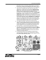
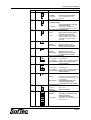
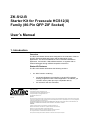
ZK-S12-B
Starter Kit for Freescale HCS12(X)
Family (80-Pin QFP ZIF Socket)
User’s Manual
1. Introduction
Overview
The ZK-S12-B Starter Kit has been designed for the evaluation of the 80pin QFP Freescale HCS12(X) family and the debugging of user
applications. The ZK-S12-B Starter Kit can be used as a standalone
application, via its built-in USB to BDM interface, or together with an
external debugger through a BDM-compatible connection.
Starter Kit Features
The ZK-S12-B Starter Kit features the following sections.
1.
An “MCU” section containing:
An MC9S12DJ256 microcontroller (in 80-pin QFP package,
already programmed with a demo application—in addition, you
can also use any other pin-to-pin compatible device);
ZIF socket for the microcontroller;
SofTec Microsystems
E-mail (general information): [email protected]
E-mail (marketing department): [email protected]
E-mail (technical support): [email protected]
Copyright © 2005 SofTec Microsystems®
DC01133
Web: http://www.softecmicro.com
Important
SofTec Microsystems reserves the right to make improvements to its products, their documentation and software routines, without notice. Information
in this manual is intended to be accurate and reliable. However, SofTec Microsystems assumes no responsibility for its use; nor for any infringements
of rights of third parties which may result from its use.
SOFTEC MICROSYSTEMS WILL NOT BE LIABLE FOR DAMAGES RESULTING FROM LOSS OF DATA, PROFITS, USE OF PRODUCTS, OR
INCIDENTAL OR CONSEQUENTIAL DAMAGES, EVEN IF ADVISED OF THE POSSIBILITY THEREOF.
Trademarks
Freescale™ and the Freescale logo are trademarks of Freescale Semiconductor, Inc.
Metrowerks and CodeWarrior are trademarks or registered trademarks of Metrowerks Corp.
Metrowerks is a wholly-owned subsidiary of Freescale Semiconductor.
Microsoft and Windows are trademarks or registered trademarks of Microsoft Corporation.
PC is a registered trademark of International Business Machines Corporation.
Other products and company names listed are trademarks or trade names of their respective companies.
ZK-S12-B User's Manual
A connector area to access the I/O pins of the microcontroller
for expansion prototyping;
Three clock sources: a provision for a clock module, a 16 MHz
crystal in Pierce configuration and a 16 MHz crystal in Colpitts
configuration, selectable via the “OSC SEL” and “XCLK#=0”
jumpers;
A jumper (“XFC SEL”) allowing either the provided RC loop
filter (needed for the microcontroller’s internal PLL) or a usermade RC loop filter to be enabled;
Two jumpers (“VRH SEL” and “VRL SEL”) which allow the
high and low voltage reference for the MCU internal A/D
converter to be defined;
A “VREGEN” jumper allowing the on-chip voltage regulator to
be enabled or disabled;
Two jumpers (“MODA=1” and “MODB=1”) which allow the
MCU operating mode upon reset to be defined.
2.
3.
4.
5.
6.
A “POWER SUPPLY” section which accepts a 12 V DC voltage
(used for the LIN and CAN transceivers) and, thanks to the built-in
switching power supply, provides a regulated VDD voltage for the
rest of the board. A jumper (“VDD SEL”) allows two different
microcontroller VDD voltages (3.3 V or 5.0 V) to be selected. An
additional linear power supply regulator provides the 5.0 V voltage
required by the “USB TO BDM INTERFACE” section.
A built-in “USB TO BDM INTERFACE” section which allows the host
PC to communicate with the microcontroller through a standard USB
interface. USB 2.0 is fully supported. When using an external incircuit debugger (via the BDM connector), the “USB TO BDM
INTERFACE” circuitry must be bypassed by removing the “RESET
ENA” and “BKGD ENA” jumpers.
A standard BDM connector for in-circuit debugging/programming;
A “RESET” section containing the reset supervisor circuitry and a
push-button connected to the MCU Reset pin. The reset supervisor
circuitry (enabled by default) can be disabled by removing the “LVD
ENA” jumper.
An “INPUTS” section containing:
Four push-buttons, connected to PP0, PP1, PP2 and PP3;
Eight general-purpose DIP-switches connected to Port T;
A potentiometer, together with a jumper to connect/disconnect
to/from PAD00.
7.
8.
An “OUTPUTS” section containing eight high-efficiency (low-current)
LEDs connected to Port B, together with eight jumpers to
connect/disconnect each of the eight LEDs to/from their respective
Port B pins.
A “RS-232” section providing two RS-232 channels connected to the
microcontroller’s SCI0 and SCI1 serial communication interfaces.
Each RS-232 channel can be configured as DTE (Data
Transmission Equipment) or DCE (Data Communication Equipment)
via the relative jumper (“RS-232 x DTE/DCE SEL”). The
microcontroller’s RX and TX lines used by the RS-232 transceivers
are shared with the LIN trasceivers’ RX and TX lines, respectively.
Use the “RXDx SEL” and “TXDx SEL” jumpers in the “SERIAL
Page 2
ZK-S12-B User's Manual
SETTINGS” section of the board to select whether to use the RS232, LIN, or to free the microcontroller’s RX and TX lines. Two 9-pin,
D-Sub female connectors are provided for each RS-232 channel.
9. The “LIN” section contains two LIN transceivers, each capable of a
speed of up to 100 Kbps in fast mode. Every LIN node can be
configured as a master node via its respective “MASTER NODEx
ENA” jumper, which inserts a 900 Ohm resistor between the LIN
bus line and the LIN transceiver power supply line. The LIN
transceivers can be powered either by the Starter Kit’s internal 12 V
DC reference, or by the LIN network itself, via the “TRANSCEIVER
SUPPLY SEL” jumper. Analogously, the LIN network can be
supplied by the Starter Kit’s internal 12 V DC reference via the “LIN
SUPPLY ENA” jumper. The microcontroller’s RX and TX lines used
by the LIN transceivers are shared with the RS-232 transceivers’ RX
and TX lines, respectively. Use the “RXDx SEL” and “TXDx SEL”
jumpers in the “SERIAL SETTINGS” section of the board to select
whether to use the RS-232, LIN, or to free the microcontroller’s RX
and TX lines associated with these nodes. Two 3x1 male header
connectors are provided to interface to an external LIN bus.
10. The “SERIAL SETTINGS” section has four jumpers that allow the
uses of the SCI0 and SCI1 peripherals of the microcontroller to be
chosen. The SCI0 peripheral can be connected to the LIN0 node or
to the RS-232 channel 0, or can be freed by removing all jumpers.
The SCI1 peripheral can be connected to the LIN1 node or to the
RS-232 channel 1, or can be freed by removing all jumpers.
11. The “CAN” section contains two fault-tolerant (up to 125 Kbaud)
CAN transceivers. The TX and RX signals of CAN nodes CAN0 and
CAN4 can be disconnected (by removing the respective “CANx TX
ENA” and “CANx RX ENA” jumpers) from the microcontroller’s
respective pins. Two 3x1 male header connectors are provided to
interface to an external CAN bus.
12. A prototype area features both a standard, thru-hole area (for
mounting traditional components) and a SMD area (for soldering
SMD components). Additionally, all of the board’s supply lines (12 V,
5 V, VDD and GND lines) are provided.
11
9
10
8
2
3
1
12
4
6
5
7
The ZK-S12-B Starter Kit
Page 3
ZK-S12-B User's Manual
Supported Devices
The ZK-S12-B Starter Kit supports the following devices:
MC9S12A family;
MC9S12B family;
MC9S12C family;
MC9S12D family;
MC9S12DG/DJ family;
MC9S12GC family;
MC9S12KC/KG/KL family;
MC9S12XDT family (S12X core);
And any future pin-to-pin compatible device.
Note: the MC9S12XDT family (S12X core) requires a special version of
CodeWarrior Development Studio (CodeWarrior Development Studio for
HC9S12X/XGATE).
Recommended Reading
Freescale HCS12 microcontroller-specific datasheets;
SK-S12(X) and ZK-S12(X) Series Starter Kit User’s Manual;
ZK-S12-B Schematic.
2. Device Configuration
Oscillator Configuration
Thanks to the 80-pin QFP ZIF socket, the ZK-S12-B Starter Kit can
support different devices, as detailed in the table below.
All of the jumpers in the “MCU” section of the board must be set
according to the specific microcontroller installed. Particular care must be
taken in order to correctly set the oscillator configuration.
Device
Pierce Configuration
Colpitts Configuration
Clock
“OSC SEL”
Jumpers
“XCLKS#=0”
Jumper
“OSC SEL”
Jumpers
“XCLKS#=0”
Jumper
“OSC SEL”
Jumpers
“XCLKS#=0”
Jumper
MC9S12A32
“PIERCE”
Installed
“COLPITTS”
Not Installed
“CLOCK”
Installed
MC9S12A64
“PIERCE”
Installed
“COLPITTS”
Not Installed
“CLOCK”
Installed
MC9S12A128
“PIERCE”
Installed
“COLPITTS”
Not Installed
“CLOCK”
Installed
MC9S12A256
-
-
“COLPITTS”
Not Installed
“CLOCK”
Installed
MC9S12B64
“PIERCE”
Installed
“COLPITTS”
Not Installed
“CLOCK”
Installed
MC9S12B128
“PIERCE”
Installed
“COLPITTS”
Not Installed
“CLOCK”
Installed
MC9S12C32
“PIERCE”
Installed
“COLPITTS”
Not Installed
“CLOCK”
Installed
MC9S12C64
“PIERCE”
Installed
“COLPITTS”
Not Installed
“CLOCK”
Installed
MC9S12C96
“PIERCE”
Installed
“COLPITTS”
Not Installed
“CLOCK”
Installed
MC9S12C128
“PIERCE”
Installed
“COLPITTS”
Not Installed
“CLOCK”
Installed
MC9S12D32
“PIERCE”
Installed
“COLPITTS”
Not Installed
“CLOCK”
Installed
MC9S12D64
“PIERCE”
Installed
“COLPITTS”
Not Installed
“CLOCK”
Installed
MC9S12DG128
“PIERCE”
Installed
“COLPITTS”
Not Installed
“CLOCK”
Installed
MC9S12DG256
-
-
“COLPITTS”
Not Installed
“CLOCK”
Installed
MC9S12DJ64
“PIERCE”
Installed
“COLPITTS”
Not Installed
“CLOCK”
Installed
MC9S12DJ128
“PIERCE”
Installed
“COLPITTS”
Not Installed
“CLOCK”
Installed
MC9S12DJ256
-
-
“COLPITTS”
Not Installed
“CLOCK”
Installed
Page 4
ZK-S12-B User's Manual
Device
Pierce Configuration
Colpitts Configuration
Clock
“OSC SEL”
Jumpers
“XCLKS#=0”
Jumper
“OSC SEL”
Jumpers
“XCLKS#=0”
Jumper
“OSC SEL”
Jumpers
“XCLKS#=0”
Jumper
MC9S12GC16
“PIERCE”
Installed
“COLPITTS”
Not Installed
“CLOCK”
Installed
MC9S12GC32
“PIERCE”
Installed
“COLPITTS”
Not Installed
“CLOCK”
Installed
MC9S12GC64
“PIERCE”
Installed
“COLPITTS”
Not Installed
“CLOCK”
Installed
MC9S12GC128
“PIERCE”
Installed
“COLPITTS”
Not Installed
“CLOCK”
Installed
MC9S12KC64
“PIERCE”
Installed
-
-
“CLOCK”
Installed
MC9S12KC128
“PIERCE”
Installed
-
-
“CLOCK”
Installed
MC9S12KG32
“PIERCE”
Installed
-
-
“CLOCK”
Installed
MC9S12KG64
“PIERCE”
Installed
-
-
“CLOCK”
Installed
MC9S12KG128
“PIERCE”
Installed
-
-
“CLOCK”
Installed
MC9S12KG256
“PIERCE”
Installed
-
-
“CLOCK”
Installed
MC9S12KL64
“PIERCE”
Installed
-
-
“CLOCK”
Installed
MC9S12KL128
“PIERCE”
Installed
-
-
“CLOCK”
Installed
MC9S12XDT512
“PIERCE”
Installed
-
-
“CLOCK”
Installed
Peripherals
Some devices do not feature the same number of CAN and SCI
peripherals. Please refer to the table below for details.
Device
CAN0
CAN1
CAN2
CAN3
CAN4
SCI0
SCI1
MC9S12A32
MC9S12A64
MC9S12A128
MC9S12A256
MC9S12B64
MC9S12B128
MC9S12C32
MC9S12C64
MC9S12C96
MC9S12C128
MC9S12D32
MC9S12D64
MC9S12DG128
MC9S12DG256
MC9S12DJ64
MC9S12DJ128
MC9S12DJ256
MC9S12GC16
MC9S12GC32
MC9S12GC64
MC9S12GC128
MC9S12KC64
MC9S12KC128
MC9S12KG32
MC9S12KG64
MC9S12KG128
MC9S12KG256
MC9S12KL64
MC9S12KL128
MC9S12XDT512
3. Summary of Jumper and Connector Settings
Jumpers Summary
Name
J105
Reference
1
2
3
Description/Pinout
VRH SELECTION
1-2 (VDDA)
2-3 (USER)
VRH tied to VDDA (default)
VRH connected to the J103
connector
Page 5
ZK-S12-B User's Manual
Name
Reference
J106
VRL SELECTION
1
2
J107
3
1-2 (GND)
2-3 (USER)
1
XFC SELECTION
2
VRL tied to ground (default)
VRL connected to the J104
connector
1-2 (LOOP FILTER)
The on-board RC PLL loop filter
is selected (default)
2-3 (USER)
The XFC PLL loop filter pin is
connected to signal pin connector
VOLTAGE REGULATOR ENABLE
3
J109
Description/Pinout
1
2
1-2 (1)
3
2-3 (0)
Microcontroller internal voltage
regulator enabled (default)
Microcontroller internal voltage
regulator disabled. VDD1, VDD2
and VDDPLL must be supplied
externally.
MODA=1
J110
Installed
Not Installed
MODA line pulled to VDD
MODA line tied to ground by
internal pull down (default)
MODB=1
J111
Installed
Not Installed
J113
J114
1
2
3
4
5
6
1
2
3
4
5
6
J115
MODB line pulled to VDD
MODB line tied to ground by
internal pull down (default)
OSCILLATOR SELECTION
1-2 (CLOCK)
Clock selected
3-4 (PIERCE)
Pierce crystal configuration selected
5-6 (COLPITTS) Colpitts crystal configuration
selected (default)
OSCILLATOR SELECTION
1-2 (CLOCK)
Clock selected
3-4 (PIERCE)
Pierce crystal configuration selected
5-6 (COLPITTS) Colpitts crystal configuration
selected (default)
XCLKS#=0
Installed
Not Installed
J202
1
2
3
J204
1
XCLKS# pin pushed to ground. Fullswing Pierce crystal configuration or
clock selected.
XCLKS# pulled to VDD. Loop
controlled Colpitts crystal
configuration selected. (default)
VDD SELECTION
1-2 (3V3)
2-3 (5V)
LED ENABLE
VDD = 3.3 V
VDD = 5 V (default)
Installed
The LEDs are connected to the
PB[7..0] port of the
microcontroller (default)
The LEDs are not connected to the
microcontroller.
Not Installed
Page 6
ZK-S12-B User's Manual
Name
Reference
Description/Pinout
POTENTIOMETER ENABLE
J205
Installed:
Not Installed:
The potentiometer is connected
to the microcontroller’s AN00 pin
(default)
The potentiometer is not connected
to the microcontroller
LVD ENABLE
J206
Installed:
J303
1
2
3
J304
1
2
3
J305
1
2
3
J306
1
2
The LVD circuit is connected to
microcontroller’s RESET line
(default)
Not Installed:
The LVD circuit is not connected to
RESET line of the microcontroller
RS-232 0 DTE/DCE SELECTION
1-2 (DCE)
The RS-232 channel 0 is
configured as DCE (default)
2-3 (DTE)
The RS-232 channel 0 is configured
as DTE
RS-232 0 DTE/DCE SELECTION
1-2 (DCE)
The RS-232 channel 0 is
configured as DCE (default)
2-3 (DTE)
The RS-232 channel 0 is configured
as DTE
RS-232 1 DTE/DCE SELECTION
1-2 (DCE)
The RS-232 channel 1 is
configured as DCE (default)
2-3 (DTE)
The RS-232 channel 1 is configured
as DTE
RS-232 1 DTE/DCE SELECTION
J307
The RS-232 channel 1 is
configured as DCE (default)
2-3 (DTE)
The RS-232 channel 1 is configured
as DTE
MASTER NODE 0 ENABLE
J309
Installed
LIN0 master node (default)
Not Installed
LIN0 slave node
MASTER NODE 1 ENABLE
J311
Installed
LIN1 master node (default)
Not Installed
LIN1 slave node
LIN TRANSCEIVER SUPPLY SELECTION
3
1
2
3
J312
1-2 (DCE)
1-2 (12V)
LIN transceivers are supplied by
the Starter Kit’s internal 12 V DC
voltage (default)
2-3 (LIN NETWORK)
LIN transceivers supplied by the LIN
bus’ VBAT line
LIN SUPPLY ENABLE
Installed
Not Installed
LIN bus is powered by the Starter
Kit’s internal 12 V DC voltage
(default)
LIN bus is self-powered
Page 7
ZK-S12-B User's Manual
Name
Reference
Description/Pinout
CAN0 TX ENABLE
J313
Installed
Microcontroller’s PM1/TXCAN0
pin connected to CAN0
transceiver (default)
Not Installed
Microcontroller’s PM1/TXCAN0 pin
floating
CAN0 RX ENABLE
J314
Installed
Microcontroller’s PM0/RXCAN0
pin connected to CAN0
transceiver (default)
Not Installed
Microcontroller’s PM0/RXCAN0 pin
floating
CAN4 TX ENABLE
J316
Installed
Microcontroller’s PJ7/TXCAN4
pin connected to CAN4
transceiver (default)
Not Installed
Microcontroller’s PJ7/TXCAN4 pin
floating
CAN4 RX ENABLE
J317
Installed
J319
1
2
3
J320
1
2
3
J321
1
2
3
J322
1
2
Microcontroller’s PJ6/RXCAN4
pin connected to CAN4
transceiver (default)
Not Installed
Microcontroller’s PJ6/RXCAN4 pin
floating
RXD0 SELECTION
1-2 (RS-232)
Microcontroller’s PS0/RXD0 pin
connected to RS-232 0
transceiver (default)
2-3 (LIN)
Microcontroller’s PS0/RXD0 pin
connected to LIN0 transceiver
TXD0 SELECTION
1-2 (RS-232)
Microcontroller’s PS1/TXD0 pin
connected to RS-232 0
transceiver (default)
2-3 (LIN)
Microcontroller’s PS1/TXD0 pin
connected to LIN0 transceiver
RXD1 SELECTION
1-2 (RS-232)
Microcontroller’s PS2/RXD1 pin
connected to RS-232 1
transceiver (default)
2-3 (LIN)
Microcontroller’s PS2/RXD1 pin
connected to LIN1 transceiver
TXD1 SELECTION
1-2 (RS-232)
3
2-3 (LIN)
J402
Microcontroller’s PS3/TXD1 pin
connected to RS-232 1
transceiver (default)
Microcontroller’s PS3/TXD1 pin
connected to LIN1 transceiver
BKGD ENABLE
Installed
Not Installed
Microcontroller’s BKGD line
connected to the “USB TO BDM
INTERFACE” (default)
Microcontroller’s BKGD line not
connected to the “USB TO BDM
INTERFACE”
Page 8
ZK-S12-B User's Manual
Name
Reference
Description/Pinout
RESET ENABLE
J403
Installed
Not Installed
Microcontroller’s RESET# line
connected to the “USB TO BDM
INTERFACE” (default)
Microcontroller’s RESET# line not
connected to the “USB TO BDM
INTERFACE”
Connectors Summary/Pinout
Name
Reference
J101,
J102,
J103,
J104
J108
Description/Pinout
MCU I/O Connectors
See schematic for pin explanation
Ground Test Point
BDM Connector
J112
1
J201
2
1. BKGD
2. GND
3. N.C.
4. RESET#
5. N.C.
6. VDD
12 V DC Power Supply Input Connector
1
J203
1. 12 V DC
2. GND
Ground Test Point
J301
RS-232 0 Connector
J302
1. N.C.
2. TX or RX (see J303/J304 jumpers)
3. RX or TX (see J303/J304 jumpers)
4. N.C.
5. GND
6. N.C.
7. N.C.
8. N.C.
9. N.C.
RS-232 1 Connector
J308
1. N.C.
2. TX or RX (see J305/J306 jumpers)
3. RX or TX (see J305/J306 jumpers)
4. N.C.
5. GND
6. N.C.
7. N.C.
8. N.C.
9. N.C.
LIN0 Connector
9
6
5
1
9
6
5
1
1
3
1.
2.
3.
VBAT – LIN Bus Power Supply
LIN – LIN Signal
GND
Page 9
ZK-S12-B User's Manual
Name
J310
J315
J318
J401
Reference
1
1
1
Description/Pinout
3
LIN1 Connector
3
1. VBAT – LIN Bus Power Supply
2. LIN – LIN Signal
3. GND
CAN0 Connector
3
1. CANH – CAN Differential Bus Line
2. GND
3. CANL – CAN Differential Bus Line
CAN4 Connector
1. CANH – CAN Differential Bus Line
2. GND
3. CANL – CAN Differential Bus Line
USB Connector
1.
2.
3.
4.
5 V DC USB Bus Power Supply Line
USB DUSB D+
GND
Page 10