1
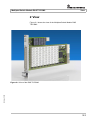
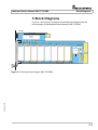
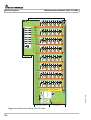
USER MANUAL
Multiplex/Switch Module 2
R&S®TS-PSM2
User Manual
for ROHDE & SCHWARZ Multiplex/Switch Module R&S TS-PSM2
2nd Issue / 08.06 / GB 1504.4799.12
All rights, also translation into foreign languages, are reserved. No part of this manual is permitted
to be reproduced in any form (print, photocopy or any other method), also not for the preparation
of lectures, or processed, reproduced or made available using electronic systems without written
permission from ROHDE & SCHWARZ.
® The passing on to third parties and the reproduction of this documentation, utilisation and communication of its contents is not permitted unless specifically approved. Infringements will incur
claims for damages. All rights reserved in the case of the award of a patent or registration of a
design.
R&S® is a registered trademark of ROHDE & SCHWARZ GmbH & Co. KG.
We draw to your attention that the names of software and hardware used in the Service Manual,
and the brand names of the respective companies are, in general, the subject of protection as
trademarks, or under proprietary rights, or patent law.
ROHDE & SCHWARZ GmbH & Co. KG
Corporate Headquarters
Mühldorfstr. 15
D-81671 München
Telephone:
Fax:
...49 (0)89/4129-13774
...49 (0)89/4129-13777
Printed in the Federal Republic of Germany. Errors excepted, subject to technical change without notice.
Safety Instructions
Attention!
Electrostatic
sensitive devices require
special care
Support Center
Telephone Europe:
+49 180 512 42 42
Telephone worldwide: +49 89 4129 13774
Fax:
+49 89 4129 13777
e-mail: [email protected]
If you have any technical queries about this Rohde &
Schwarz equipment, our Hotline at the Support Center of
Rohde & Schwarz Sales-GmbH will be glad to help.
Our team will discuss your queries and look for solutions to
your problems.
The Hotline is open Mondays to Fridays from 08.00 to 17.00
hrs.
For queries outside office hours, you can leave a message
or send a note via fax or email. We will then get back to you
as soon as possible.
Multiplex/Switch Module R&S TS-PSM2
Contents
Contents
1
Usage
1-1
1.1
General
1-1
1.2
Safety instructions
1-1
1.3
Characteristics
1-2
2
View
2-1
3
Block Diagrams
3-1
4
Layout
4-1
4.1
Mechanical layout
4-1
4.2
Display elements
4-2
Function Description
5-1
5.1
Signal concept
5-1
5.2
System functions
5-1
5.3
Flexibility
5-2
5.4
Compactness
5-3
5.5
Interference immunity
5-3
5.6
Sample applications
5-4
5.6.1
Simple switching function - normally open, 1-pin.
5-4
5.6.2
Simple switching function - changeover contact, 1-pin.
5-4
5.6.3
Current measurement - indirect, via shunt resistor
5-5
5.6.4
Current measurement - direct, up to 1 A
5-5
5.6.5
Multiplexer - test object signals
5-6
5.6.6
Multiplexer - CompactPCI/PXI instruments
5-7
5.6.7
Multiplexer - external components, up to 1 A
5-8
5
2nd Issue 08.06
6
7
Commissioning
6-1
6.1
Installation of the plug-in module
6-1
6.2
Initialisation of the plug-in module
6-1
6.3
Instructions for operation with voltages dangerous to the touch
6-2
Software
7-1
7.1
7-1
Driver software
3
Contents
8
9
Multiplex/Switch Module R&S TS-PSM2
7.2
Softpanel
7-2
7.3
Sample programme
7-3
7.3.1
Programming with GTSL libraries
7-3
7.3.2
Programming with device drivers
7-5
Self-Test
8-1
8.1
LED test
8-1
8.2
Power on test
8-1
8.3
TSVP self-test
8-2
Interface description
9-1
9.1
Connector X1
9-1
9.2
Connector X4
9-2
9.3
Connector X5
9-2
9.4
Connector X10
9-3
9.5
Connector X20
9-5
9.6
Connector X30
9-6
9.7
Connector X40
9-7
9.8
Connector X50
9-9
10-1
2nd Issue 08.06
10 Specifications
4
Multiplex/Switch Module R&S TS-PSM2
Figures
Figures
View of the R&S TS-PSM2.................................................................2-1
Figure 3-1
Functional block diagram R&S TS-PSM2 ........................................3-1
Figure 3-2
Detailed block diagram R&S TS-PSM2 ............................................3-2
Figure 4-1
Arrangement of connectors and LEDs ............................................4-1
Figure 5-1
Switching group.................................................................................5-2
Figure 5-2
Simple switching function - normally open, 1-pin..........................5-4
Figure 5-3
Simple switching function - changeover contact, 1-pin. ...............5-4
Figure 5-4
Current measurement - indirect, via shunt resistor .......................5-5
Figure 5-5
Current measurement - direct, up to 1 A .........................................5-5
Figure 5-6
Multiplexer - test object signals ......................................................5-6
Figure 5-7
Multiplexer - CompactPCI/PXI instruments.....................................5-7
Figure 5-8
Multiplexer - external components, up to 1 A .................................5-8
Figure 6-1
Permissible voltages on analog bus lines ......................................6-2
Figure 7-1
Softpanel R&S TS-PSM2 ...................................................................7-2
Figure 9-1
Connector X1 (view: mating side) ....................................................9-1
Figure 9-2
Connector X4 (view: mating side) ....................................................9-2
Figure 9-3
Connector X5 (view: mating side) ....................................................9-2
Figure 9-4
Connector X10 (view: mating side) ..................................................9-3
Figure 9-5
Connector X20 (view: mating side) ..................................................9-5
Figure 9-6
Connector X30 (view: mating side) ..................................................9-6
Figure 9-7
Connector X40 (view: mating side) ..................................................9-7
Figure 9-8
Connector X50 (view: mating side) ..................................................9-9
2nd Issue 08.06
Figure 2-1
5
Multiplex/Switch Module R&S TS-PSM2
2nd Issue 08.06
Figures
6
Multiplex/Switch Module R&S TS-PSM2
Tables
Tables
Characteristics R&S TS-PSM2..........................................................1-2
Table 4-1
Connector on the R&S TS-PSM2......................................................4-2
Table 4-2
Display elements on the R&S TS-PSM2 ..........................................4-2
Table 7-1
Driver installation R&S TS-PSM2 .....................................................7-1
Table 8-1
Observations about the LED test .....................................................8-1
Table 8-2
Observations about the power on test ............................................8-1
Table 9-1
Assignment of X1 ..............................................................................9-1
Table 9-2
Assignment of X4 ..............................................................................9-2
Table 9-3
Assignment of X5 ..............................................................................9-2
Table 9-4
Assignment of X10 ............................................................................9-3
Table 9-5
Assignment of X20 ............................................................................9-5
Table 9-6
Assignment of X30 ............................................................................9-6
Table 9-7
Assignment of X40 ............................................................................9-7
Table 9-8
Assignment of X50 ............................................................................9-9
2nd Issue 08.06
Table 1-1
7
Multiplex/Switch Module R&S TS-PSM2
2nd Issue 08.06
Tables
8
Multiplex/Switch Module R&S TS-PSM2
Usage
1 Usage
1.1 General
The ROHDE & SCHWARZ Multiplex/Switch Module R&S TS-PSM2 is
designed for switching or distribution of signals of medium output up to
125 VDC or currents up to 2 ADC. The R&S analog bus can be used to
measure voltages and currents on all circuit nodes. These functions are
especially important if current must be measured for the test object in
normal operation and in addition a measurement must be performed in
standby mode. In addition to the functionality of a simple power switching module, small signals can be switched in the lower MHz range with
high quality.
The R&S TS-PSM2 can be used in the R&S CompactTSVP and R&S
PowerTSVP (TSVP = Test System Versatile Platform). It is inserted
into the front of the TSVP housing.
The 96-pin connector connects flush with the TSVP. It is used to establish contact with test objects. If necessary, an additional adapter frame
can be used.
The R&S TS-PSM2 is connected on the rear of the CAN/PXI bus and
on the analog bus of the TSVP backplane. The side connector and the
system connector allow for project-specific extensions.
1.2 Safety instructions
WARNING!
2nd Issue 08.06
In order to prevent danger to users when voltages dangerous to
the touch are in use, the Test System Versatile Platform R&S
CompactTSVP TS-PCA3 and R&S PowerTSVP TS-PWA3 should
never be operated with the housing open or with the front and
back panels open. General safety regulations must be observed.
1-1
Usage
Multiplex/Switch Module R&S TS-PSM2
CAUTION!
If signals with voltages dangerous to the touch are being transferred via the analog bus, all modules involved, including PXImodules from other suppliers, must be specified for the relevant
voltage.
For additional information on operation with voltages dangerous to the
touch, see Section 6.3.
1.3 Characteristics
Characteristics R&S TS-PSM2
Switching module for power supplies and loads with medium power.
Switching of voltages up to 125 V
Switching of currents up to 2 A
8 relay groups, each with:
1 Multiplexer 4:1, two-pin, DPST
or
1 change-over contact, one-pin, SPDT with shunt resistor
3 make contacts, one-pin, SPST with shunt resistor
1 make contact, two-pin, DPDT to local Powerbus/side plug connector
Indirect current measurement via shunt resistors
Direct current measurement via R&S analog bus and plug-in module
R&S TS-PSAM (<1 A)
Self-test of all relays via analog bus and plug-in module R&S
TS-PSAM
Control bus: CAN
Table 1-1 Characteristics R&S TS-PSM2
1-2
2nd Issue 08.06
For use in R&S CompactTSVP and R&S PowerTSVP
Multiplex/Switch Module R&S TS-PSM2
View
2 View
Figure 2-1 shows the view of the Multiplex/Switch Module R&S
TS-PSM2.
2nd Issue 08.06
Figure 2-1 View of the R&S TS-PSM2
2-1
Multiplex/Switch Module R&S TS-PSM2
2nd Issue 08.06
View
2-2
Multiplex/Switch Module R&S TS-PSM2
Block Diagrams
3 Block Diagrams
Figure 3-1 and Figure 3-2 shows the functional block diagram and the
block diagram of the Multiplex/Switch Module R&S TS-PSM2.
TS-PSM2
Analog Bus (AB)
Analog Bus
X30
Coupling
Relais
CHANNEL 3
CHANNEL 4
CHANNEL 5
CHANNEL 6
CHANNEL 7
LABA1...LABD2
CHANNEL 8
RAM
PXI Trigger Logic
SPI
System Connector X50
Side Connector X40
Microcontroller
Extension
ConnectorX1
X20
cPCI Connector
CHANNEL 2
Front Connector X10
CHANNEL 1
Extension Connector X20
Local Analog Bus (LAB)
GND
Local Power Bus A
Local Power Bus B
2nd Issue 08.06
Figure 3-1 Functional block diagram R&S TS-PSM2
3-1
Extension
Connector X1
X20
cPCI Connector
Extension Connector X20
Microcontroller
2nd Issue 08.06
SPI
PXI Trigger Logic
System Connector X50
3-2
Figure 3-2 Detailed block diagram R&S TS-PSM2
Side Connector X40
Analog Bus
X30
Local Analog Bus
Front Connector X10
Block Diagrams
Multiplex/Switch Module R&S TS-PSM2
Multiplex/Switch Module R&S TS-PSM2
Layout
4 Layout
4.1 Mechanical layout
The Multiplex/Switch Module R&S TS-PSM2 is designed as a long
plug-in card for front installation in the TSVP housing. The installation
depth is 300 mm. The front panel has 4 height units.
X1/X20 connectors are used to make connections to the cPCI backplane of the R&S CompactTSVP; X20 connector is used for connections to the control backplane of the R&S PowerTSVP. The X30 connector connects the R&S TS-PSM2 with the analog bus backplane in
the TSVP housing. The test object and peripheral devices are connected to the X10 connection on the front. The X40 side connector and the
X50 system connector can be used project-specifically. The X4 and X5
connectors are used for internal purposes.
7
COM
PWR
X30
1
1
X20
X40
X10
1
X4
X1
X50
32
7
8
X5
1
2
1
2nd Issue 08.06
Figure 4-1 Arrangement of connectors and LEDs
4-1
Layout
Multiplex/Switch Module R&S TS-PSM2
Abbreviation
Use
X1
cPCI Connector
X4
Clock Configuration
X5
RS232 Interface
X10
Front Connector
X20
PXI/Extension Connector
X30
Analog Bus Connector
X40
Side Connector
X50
System Connector
Table 4-1 Connector on the R&S TS-PSM2
4.2 Display elements
(see Figure 4-1)
There are three light diodes (LEDs) on the front of the R&S TS-PSM2
with the following functions:
LED
Description
ERR
(red)
Error:
Lit if an error is discovered after the system is turned on
during the startup test on the R&S TS-PSM2 .
COM
(yellow)
Communication:
Lit briefly to indicate access to the R&S TS-PSM2 via the
interface.
PWR
(green)
Power supply voltage:
Lit if all power supply voltages are present.
2nd Issue 08.06
Table 4-2 Display elements on the R&S TS-PSM2
4-2
Multiplex/Switch Module R&S TS-PSM2
Function Description
5 Function Description
(see Chapter 3, Functional block diagram)
5.1 Signal concept
The design and construction of the Multiplex/Switch Module R&S
TS-PSM2 guarantee excellent guiding of load and measurement paths.
Both „Force“ channels with high currents as well as „Sense“ channels
of voltage and current sources or loads are guided to the test object via
the R&S TS-PSM2. In the opposite direction, test objects can be
switched with single- or multi-pin loads. Eight two-pin 4-to-1 multiplexers make it possible to select from four measurement signals. These
signals can be configured via local power buses (LPBA and LPBB) to
larger multiplexers or can be applied to GND.
Access to the R&S analog bus makes it possible to connect all input
channels with measurement and stimulus modules of the R&S CompactTSVP without the need for any additional external wiring.
In order to facilitate measurements of high currents without voltage
drops interfering, low-Ohm shunt resisters (22 mΩ) are inserted into
each channel. The instantaneous current can be measured indirectly
through these shunt resisters as a voltage value.
All channels are shielded in a low-Ohm design. This reduces voltage
drops and crosstalk.
5.2 System functions
The system functions are implemented by a local processor with internal Flash. There is also an external SRAM. Communication with the
system controller in the R&S CompactTSVP is via the CAN bus.
2nd Issue 08.06
The functions of the R&S TS-PSM2 may be summarised as follows:
•
Analog function test
•
Switching voltage/current sources
•
Switching test object loads (original loads, simulated/electronic
loads)
•
Power Multiplexer
•
Switch simulation
5-1
Function Description
Multiplex/Switch Module R&S TS-PSM2
5.3 Flexibility
The structure of the R&S TS-PSM2 in addition to the wide voltage and
current range, combined with effective use extending into the lower
MHz range, guarantee a high level of flexibility and a wide range of uses. Even complex yet flexible load systems with original loads and/or
electronic loads can be implemented using multiple module-internal
connections.
Figure 5-1 shows the basic principle with a switching group consisting
of four switching elements. Detail implementation with two changeover
contacts offers advantages for sensed current measurements because
the contact resistance of the relay is not introduced as an error. There
is no need to take this into consideration in the function.
LABx1
LABx2
Local Analog Bus
CHx_HI1
CHx_HI
CHx_HI1
CHx_LO1
Front Connector X10
CHx_LO1
CHx_LO
CHx_HI2
CHx_LO2
CHx_HI3
CHx_LO3
CHx_HI4
CHx_LO4
CHx_HI
CHx_LO
Side Connector
This switching group is present eight times on the R&S TS-PSM2 module. Four input channels each can be switched with two pins to a separate Mux bus. In addition, each bus can be switched to the local analog bus LABxx (max. 1 A), the local Powerbus LPBx or the side connector.
Input channels with R&S CompactTSVP measuring system and PXI
5-2
2nd Issue 08.06
Figure 5-1 Switching group
Multiplex/Switch Module R&S TS-PSM2
Function Description
measuring system can be connected via the R&S analog bus. The local
analog bus is also directed to connector X20. Signals can also be connected here from the back of the R&S CompactTSVP through corresponding rear I/O modules.
The local Powerbus lines are accessible on side connector X40. In this
case standard PXI modules, which typically do not have a relay multiplexer, can have access to the multiplexers or the R&S analog bus via
flat-band cable on the side. Another application consists of integrating
project-specific additions via the side and system connector X50 (for
example passive loads, terminating resistors, voltage distributors, etc.).
5.4 Compactness
The layout of the R&S TS-PSM2 (one slot) with 112 relays offers maximum space savings. Extremely high-powered and compact measurement and load systems can be set up with as many as 12 modules in
the R&S CompactTSVP and 16 modules in R&S PowerTSVP. These
measurement and load systems can be integrated directly into manufacturing cells, which makes them very cost-efficient.
5.5 Interference immunity
2nd Issue 08.06
Optimal behaviour regarding electrical interference or temperature increases is achieved by control through the serial differential CAN bus
(Controller Area Network).
5-3
Function Description
Multiplex/Switch Module R&S TS-PSM2
5.6 Sample applications
5.6.1 Simple switching function - normally open, 1-pin.
The relay switches the channel on and off; the shunt resistor is not
used.
CHx_HI2...4
Figure 5-2 Simple switching function - normally open, 1-pin
5.6.2 Simple switching function - changeover contact, 1-pin.
The relay switches the channel; the shunt resistor is not used.
CHx_HI1
CHx_LO1
2nd Issue 08.06
Figure 5-3 Simple switching function - changeover contact, 1-pin.
5-4
Multiplex/Switch Module R&S TS-PSM2
Function Description
5.6.3 Current measurement - indirect, via shunt resistor
The circuit is closed or opened through the relay. The voltage drop on
the shunt resistor is measured with a voltmeter via the R&S analog bus.
The current can be calculated from the voltage and the value of the
shunt. The second relay contact is used to eliminate the measurement
error caused by the resistance of the switching contact.
CHx_HI1...4
Figure 5-4 Current measurement - indirect, via shunt resistor
5.6.4 Current measurement - direct, up to 1 A
The current is measured directly with a current measurement device
via the analog bus.
CHx_HI1...4
2nd Issue 08.06
Figure 5-5 Current measurement - direct, up to 1 A
5-5
Function Description
Multiplex/Switch Module R&S TS-PSM2
5.6.5 Multiplexer - test object signals
Up to four test object signals can be multiplexed to a single local bus.
If necessary, the local bus can be connected with up to three additional
local buses or with the global R&S analog bus.
CH1_HI1
CH1_LO1
Local Analog Bus/
Analog Bus
CH1_HI2
CH1_LO2
CH1_HI3
CH1_LO3
CH1_HI4
CH1_LO4
CH1_HI
2nd Issue 08.06
Figure 5-6 Multiplexer - test object signals
5-6
Multiplex/Switch Module R&S TS-PSM2
Function Description
5.6.6 Multiplexer - CompactPCI/PXI instruments
Signals of adjacent CompactPCI/PXI modules can be directed to the local multiplex bus via the side connector and a two-pin changeover contact. Routing to the global R&S analog bus is also possible.
CH1_HI1
CH1_LO1
Local Analog Bus/
Analog Bus
CH1_HI2
CH1_LO2
CH1_HI3
CH1_LO3
CH1_HI4
CH1_LO4
CH1_HI
Side
Connector
Cable
2nd Issue 08.06
Figure 5-7 Multiplexer - CompactPCI/PXI instruments
5-7
Function Description
Multiplex/Switch Module R&S TS-PSM2
5.6.7 Multiplexer - external components, up to 1 A
Signals of external components can be directed to the local multiplexer
bus via the local R&S analog bus and an optional customer-specific
rear I/O module. Routing to the global R&S analog bus is also possible.
Backplane
Connector
RIO
Connector
RIO
Module
CH1_HI1
External
Instrument
Cable
Local Analog Bus
CH1_LO1
CH1_HI2
CH1_LO2
CH1_HI3
CH1_LO3
CH1_HI4
CH1_LO4
CH1_HI
2nd Issue 08.06
Figure 5-8 Multiplexer - external components, up to 1 A
5-8
Multiplex/Switch Module R&S TS-PSM2
Commissioning
6 Commissioning
6.1 Installation of the plug-in module
To install the Multiplex/Switch Module R&S TS-PSM2 , proceed as follows:
•
Shut down the TSVP and turn it off.
•
Select a suitable front plug-in slot.
•
Loosen the screws and remove the appropriate front plate section
on the TSVP housing.
CAUTION!
Check the backplane connectors for bent pins! Any pins that are
bent must be straightened!
Failure to observe this instruction may result in permanent damage to the backplane!
•
Applying moderate pressure, insert the plug-in module
•
The upper catch pin of the plug-in module must be guided into the
right hole, while the lower one is guided into the left hole on the
TSVP housing
CAUTION!
When inserting the plug-in module, use both hands to guide it
and carefully press it into the backplane connectors.
•
When the plug-in module is correctly inserted, you will feel it reach
a definite mechanical limit
•
Tighten the upper and lower screws on the front plate of the plugin module.
2nd Issue 08.06
6.2 Initialisation of the plug-in module
After the system is booted, the R&S TS-PSM2 is initialised. Signals
GA0 ... GA5 on the cPCI bus are used for slot identification.
6-1
Commissioning
Multiplex/Switch Module R&S TS-PSM2
6.3 Instructions for operation with voltages dangerous to the touch
In conformity with EN 61010-1, the following voltage limit values are
considered „dangerous and active“.
•
70 V DC
•
33 V AC eff
•
46.7 V AC peak
WARNING!
When operating the Multiplex/Switch Module R&S TS-PSM2
above these voltage limit values, the requirements of EN61010-1
must be observed.
The Multiplex/Switch Module R&S TS-PSM2 and Test System
Versatile Platform R&S CompactTSVP are designed for a maximum
voltage of 125 V between ground-free measurement devices, analog
buses and GND. Care must be taken to ensure that this limit is not exceeded at any time, even as the sum of voltages, and thus not as a results of alternating signals.
Figure 6-1 shows a typical permissible voltage configuration between
analog buses and ground.
0...125 V
Analog
bus
0...125 V
- 125 V
5V
125 V
125 V max
125 V max
125 V max
floating
125 V max!!
125 V max!!
0...125 V
125 V max!!
120 V
125 V max!!
125 V
GND referenced
signals
Figure 6-1 Permissible voltages on analog bus lines
2nd Issue 08.06
For reasons of fire prevention in conformity with EN 61010-1, we recommend limiting the current or output for DC sources to 150 VA.
6-2
Multiplex/Switch Module R&S TS-PSM2
Software
7 Software
7.1 Driver software
A LabWindows IVI driver is available to control the
Multiplex/Switch Module R&S TS-PSM2 that supports class IVI
SWTCH. All additional functions of the hardware are supported by specific extensions of the driver. The driver is a component of the ROHDE
& SCHWARZ GTSL software. All functions of the driver are documented extensively in online Help and in the LabWindows/CVI Function
Panels.
The following software modules are installed during driver installation:
Module
Path
Note
rspsm2.dll
<GTSL directory>\Bin
Driver
rspsm2.hlp
<GTSL directory>\Bin
Help file
rspsm2.fp
<GTSL directory>\Bin
LabWindows CVI Function Panel File,
Function Panels for CVI Development Environment
rspsm2.sub
<GTSL directory>\Bin
LabWindows CVI attribute file. This file is
required by several„Function Panels“.
rspsm2.lib
<GTSL directory>\Bin
Import library
rspsm2.h
<GTSL directory>\Include
Header file for driver
Table 7-1 Driver installation R&S TS-PSM2
NOTE:
2nd Issue 08.06
The IVI and VISA library of National Instruments are required to
operate the driver.
7-1
Software
Multiplex/Switch Module R&S TS-PSM2
7.2 Softpanel
Figure 7-1 Softpanel R&S TS-PSM2
7-2
2nd Issue 08.06
A "Soft-Panel" is included with the software package for R&S TS-PSM2
(see Figure 7-1). The Soft-Panel requires the support of the IVI driver.
It makes it possible to operate the module interactively pointing on the
screen and clicking with the mouse.
Multiplex/Switch Module R&S TS-PSM2
Software
7.3 Sample programme
7.3.1 Programming with GTSL libraries
/*
This example connects TS-PSM2 channel 1 to different internal
and external switch channels.
Error handling is not considered in this sample in order to
keep it easy to read. The return status should be checked for
"errorOccured" after each library call.
The following configuration files are used in this example:
physical.ini
-----------[device->psm2_7]
Description = "TS-PSM2, Slot 7"
Type
= PSM2
ResourceDesc = CAN0::0::2::7
DriverDll
= rspsm2.dll
DriverPrefix = rspsm2
DriverOption = "Simulate=0,RangeCheck=1"
; the analog bus pseudo device is used by the switch manager
[device->abus]
Type
= AB
Psm2Application.ini
------------------[bench->switch]
; configure the
SwitchDevice1 =
AnalogBus
=
AppChannelTable
TS-PSM2 as switch device
device->psm2_7
device->abus
= io_channel->switch
2nd Issue 08.06
; configure the switch channels
[io_channel->switch]
; TS-PSM2 channels
CH1
= psm2_7!CH1
CH1_1 = psm2_7!CH1_1
CH1_HI = psm2_7!CH1_HI
CH1_LO = psm2_7!CH1_LO
; TS-PSM2 local power bus
LPBA
= psm2_7!LPBA
7-3
Software
Multiplex/Switch Module R&S TS-PSM2
; TS-PSM2 local analog bus
LABa1 = psm2_7!LABa1
LABa2 = psm2_7!LABa2
; TSVP system wide analog bus
ABa1
= abus!ABa1
ABa2
= abus!ABa2
*/
#include "resmgr.h"
#include "swmgr.h"
int main (int argc, char *argv[])
{
long residSwmgr; /* resource ID for switch
manager library */
short errorOccurred = 0;
long errorCode = 0;
char errorMessage [GTSL_ERROR_BUFFER_SIZE] = "";
/* load the physical and application configuration files */
RESMGR_Setup ( 0, "physical.ini", "Psm2Application.ini",
&errorOccurred, &errorCode, errorMessage);
/* initialize the switch manager library */
SWMGR_Setup ( 0, "bench->switch", &residSwmgr,
&errorOccurred, &errorCode, errorMessage);
/* connect channel 1 to local power bus A */
SWMGR_Connect ( 0, residSwmgr, "CH1", "LPBA",
&errorOccurred, &errorCode, errorMessage);
/* connect channel 1 to local front connector */
SWMGR_Connect ( 0, residSwmgr, "CH1", "CH1_1",
&errorOccurred, &errorCode, errorMessage);
/* connect local analog bus lines to analog bus line on backplane */
SWMGR_Connect ( 0, residSwmgr, "LABa1", "ABa1",
&errorOccurred, &errorCode, errorMessage);
SWMGR_Connect ( 0, residSwmgr, "LABa2", "ABa2",
&errorOccurred, &errorCode, errorMessage);
/* wait until relays have settled; timeout 500
SWMGR_WaitForDebounce ( 0, residSwmgr, 500,
7-4
ms */
2nd Issue 08.06
/* connect channel 1 to local analog bus lines */
SWMGR_Connect ( 0, residSwmgr, "CH1_HI", "LABa1",
&errorOccurred, &errorCode, errorMessage);
SWMGR_Connect ( 0, residSwmgr, "CH1_LO", "LABa2",
&errorOccurred, &errorCode, errorMessage);
Multiplex/Switch Module R&S TS-PSM2
&errorOccurred, &errorCode,
Software
errorMessage);
/* disconnect channel 1 from local front connector */
SWMGR_Disconnect ( 0, residSwmgr, "CH1", "CH1_1",
&errorOccurred, &errorCode, errorMessage);
/* wait until relays have settled; timeout 500
SWMGR_WaitForDebounce ( 0, residSwmgr, 500,
&errorOccurred, &errorCode, errorMessage);
ms */
/* disconnect the rest */
SWMGR_DisconnectAll ( 0, residSwmgr,
&errorOccurred, &errorCode, errorMessage);
/* close the library */
SWMGR_Cleanup ( 0, residSwmgr,
&errorOccurred, &errorCode, errorMessage);
RESMGR_Cleanup ( 0, &errorOccurred, &errorCode,
errorMessage);
return 0;
}
7.3.2 Programming with device drivers
/*
Error handling is not considered in this sample in order to
keep it easy to read. The return status should be checked for
VI_SUCCESS after each driver call.
*/
#include "rspsm2.h"
2nd Issue 08.06
int main (int argc, char *argv[])
{
ViSession vi;
ViStatus status;
/*
open a session to the device driver. The resource descriptor
depends on the slot number of the module and must be adapted
to the target system.
*/
status = rspsm2_InitWithOptions ("CAN0::0::2::7::INSTR",
VI_TRUE,
VI_TRUE,
"Simulate=0,RangeCheck=1",
&vi);
/* connect channel 1 to Local Power Bus A */
status = rspsm2_Connect (vi, "CH1", "LPBA");
7-5
Software
Multiplex/Switch Module R&S TS-PSM2
/* connect channel 1 to front connector */
status = rspsm2_Connect (vi, "CH1", "CH1_1");
/* connect channel 1 HI to local analog bus line */
status = rspsm2_Connect (vi, "CH1_HI", "LABa1");
/* connect channel 1 LO to local analog bus line */
status = rspsm2_Connect (vi, "CH1_LO", "LABa2");
/* connect local analog bus line to analog bus
status = rspsm2_Connect (vi, "ABa1", "LABa1");
line on back plane */
/* connect local analog bus line to analog bus
status = rspsm2_Connect (vi, "ABa2", "LABa2");
line on back plane */
/* wait until relays have settled; timeout 500
status = rspsm2_WaitForDebounce (vi, 500.0);
ms */
/* disconnect channel 1 from front connector */
status = rspsm2_Disconnect (vi, "CH1", "CH1_1");
/* wait until relay has settled; timeout 500
status = rspsm2_WaitForDebounce (vi, 500.0);
ms */
/* disconnect the rest */
status = rspsm2_DisconnectAll(vi);
/* close the driver session */
status = rspsm2_close (vi);
2nd Issue 08.06
return 0;
}
7-6
Multiplex/Switch Module R&S TS-PSM2
Self-Test
8 Self-Test
The Multiplex/Switch Module R&S TS-PSM2 has an integrated capability for self-test. The following tests are possible:
•
LED test
•
Power on test
•
TSVP self-test
8.1 LED test
After the system is turned on, all three LEDs are lit for about three seconds. This indicates that the 5-V power supply has been applied; all
LEDs are in proper order. The following observations may be made
about different display states:
LED
Description
One individual LED is not
lit
Hardware problem in the module
All LEDs are
not lit
+5 V power supply voltage missing
Table 8-1 Observations about the LED test
8.2 Power on test
The power on test runs in parallel to the LED test. The following observations may be made about the different display states of the LEDs.
2nd Issue 08.06
LED
Description
PWR LED
(green) on
Power supply voltage present
PWR LED
(green) off
Power supply voltage missing
ERR LED
(red) off
No error is present
Table 8-2 Observations about the power on test
8-1
Self-Test
Multiplex/Switch Module R&S TS-PSM2
LED
ERR LED
(red) Is lit or
flashing
Description
Hardware error present (processor is not starting,
SPI error)
Table 8-2 Observations about the power on test
8.3 TSVP self-test
As part of the TSVP self test, an extensive test of the R&S TS-PSM2
module is performed and an exhaustive protocol is generated. This is
done with the „Self-Test Support Library“.
The R&S TS-PSAM analog stimulus and measurement module is used
as a measurement unit in the TSVP self-test. The functionality of the
modules in the system is insured by measurements via the analog bus.
The analog bus and the local Powerbus are first tested for not-allowed
voltages. These voltages could possibly come from an outside source,
for example through sources connected to the back. After an isolation
measurement between the buses, all relays (coupling, matrix, local
Powerbus, Multiplexer, sense relay) and the shunt resistors are tested.
NOTE:
2nd Issue 08.06
For information on starting the self-test and the order of required
work steps, please consult the GTSL Software Description or the
GTSL online Help. A detailed description of the parameters and
sequences tested may be found in the R&S CompactTSVP / R&S
PowerTSVP Service Manual.
8-2
Multiplex/Switch Module R&S TS-PSM2
Interface description
9 Interface description
9.1 Connector X1
25
F E D C BAZ
2nd Issue 08.06
Figure 9-1 Connector X1 (view: mating side)
Pin
25
24
23
22
21
20
19
18
17
16
15
12..14
11
10
9
8
7
6
5
4
3
2
1
Pin
F
GND
GND
GND
GND
GND
GND
GND
GND
GND
GND
GND
GND
GND
GND
GND
GND
GND
GND
GND
GND
GND
GND
F
E
D
C
B
+5V
A
+5V
+5V
+5V
GND
GND
GND
GND
GND
GND
GND
GND
GND
GND
GND
GND
GND
GND
GND
+5V
+5V
+5V
E
+5V
D
C
B
A
Z
GND
GND
GND
GND
GND
GND
GND
GND
GND
GND
GND
GND
GND
GND
GND
GND
GND
GND
GND
GND
GND
GND
Z
Table 9-1 Assignment of X1
9-1
Interface description
Multiplex/Switch Module R&S TS-PSM2
9.2 Connector X4
Figure 9-2 Connector X4 (view: mating side)
Pin
Signal
Pin
Signal
1
PRO_DAT_4
2
GND
3
MAN_RST/
4
GND
5
OSC_CLK10
6
PRO_CLK10
7
PXI_CLK10
8
PRO_CLK_R
9
OSC_OE
10
GND
Table 9-2 Assignment of X4
9.3 Connector X5
Figure 9-3 Connector X5 (view: mating side)
Signal
Signal
1
nc
2
nc
3
RS232_RXD/
4
Nc
5
RS232_TXD/
6
nc
7
RS232_CTS/
8
T2_low
9
GND
10
GND
Table 9-3 Assignment of X5
9-2
Pin
2nd Issue 08.06
Pin
Multiplex/Switch Module R&S TS-PSM2
Interface description
9.4 Connector X10
1
32
A BC
Figure 9-4 Connector X10 (view: mating side)
2nd Issue 08.06
Pin
A
B
C
1
CH1_HI1
CH1_LO1
CH1_THRU
2
CH1_HI2
CH1_LO2
CH1_HI3
3
CH1_LO3
CH1_HI4
CH1_LO4
4
CH1_HI
CH1_LO
CH2_HI1
5
CH2_LO1
CH2_THRU
CH2_HI2
6
CH2_LO2
CH2_HI3
CH2_LO3
7
CH2_HI4
CH2_LO4
CH2_HI
8
CH2_LO
CH3_HI1
CH3_LO1
9
CH3_THRU
CH3_HI2
CH3_LO2
10
CH3_HI3
CH3_LO3
CH3_HI4
11
CH3_LO4
CH3_HI
CH3_LO
12
CH4_HI1
CH4_LO1
CH4_THRU
13
CH4_HI2
CH4_LO2
CH4_HI3
Table 9-4 Assignment of X10
9-3
Interface description
Multiplex/Switch Module R&S TS-PSM2
Pin
A
B
C
14
CH4_LO3
CH4_HI4
CH4_LO4
15
CH4_HI
CH4_LO
CH5_HI1
16
CH5_LO1
CH5_THRU
CH5_HI2
17
CH5_LO2
CH5_HI3
CH5_LO3
18
CH5_HI4
CH5_LO4
CH5_HI
19
CH5_LO
CH6_HI1
CH6_LO1
20
CH6_THRU
CH6_HI2
CH6_LO2
21
CH6_HI3
CH6_LO3
CH6_HI4
22
CH6_LO4
CH6_HI
CH6_LO
23
CH7_HI1
CH7_LO1
CH7_THRU
24
CH7_HI2
CH7_LO2
CH7_HI3
25
CH7_LO3
CH7_HI4
CH7_LO4
26
CH7_HI
CH7_LO
CH8_HI1
27
CH8_LO1
CH8_THRU
CH8_HI2
28
CH8_LO2
CH8_HI3
CH8_LO3
29
CH8_HI4
CH8_LO4
CH8_HI
30
CH8_LO
GND
GND
31
GND
GND
GND
32
GND
GND
CHA-GND
Table 9-4 Assignment of X10
Note: Signals printed in bold are high power
2nd Issue 08.06
The CHA_GND signal is connected with the front plate of the module
and via two 10 nF capacitors with GND. The front plate itself has no direct connection to GND. When a test object is connected, the test object GND should be connected to GND. To avoid ripple loops, do not
connect GND and CHA_GND.
9-4
Multiplex/Switch Module R&S TS-PSM2
Interface description
9.5 Connector X20
22
F E D C BAZ
Figure 9-5 Connector X20 (view: mating side)
NP = not populated
2nd Issue 08.06
Pin
22
21
20
19
18
17
16
15
14
13
12
11
10
9
8
7
6
5
4
3
2
1
Pin
F
E
D
C
B
A
GA0
GA1
GA2
GA3
GA4
+5V (PWA)
GND
+5V (PWA)
AUX1R
AUX1L
AUX2L
+5V (PWA)
GND
PXI_TRIG6
CAN_EN ab PCA V4.0
PXI_TRIG5
PXI_TRIG4
Z
GA5
PXI_CLK10
NP
NP
PXI_TRIG3
GND
PXI_TRIG2
PXI_TRIG7
GND
PXI_TRIG0
PXI_TRIG1
+5V
+5V (PWA)
GND
LABA1
LABC1
LABB1
LABD1
LABA2
LABC2
LABB2
LABD2
RSA0
F
AUX2R
RRST#
GND
NP
NP
RSD0
RSDI
RSA1
RSCLK
+5V (PWA)
CAN_L
CAN_H
GND
RCS#
E
D
C
B
A
Z
Table 9-5 Assignment of X20
9-5
Interface description
Multiplex/Switch Module R&S TS-PSM2
9.6 Connector X30
Figure 9-6 Connector X30 (view: mating side)
Pin
E
D
C
B
A
7
6
5
GND
ABC1
4
3
ABB1
ABC2
2
1
ABA1
ABB2
ABA2
ABD2
ABD1
2nd Issue 08.06
Table 9-6 Assignment of X30
9-6
Multiplex/Switch Module R&S TS-PSM2
Interface description
9.7 Connector X40
Figure 9-7 Connector X40 (view: mating side)
2nd Issue 08.06
Pin
Signal
Pin
Signal
1
LABA1
2
GND
3
LABC1
4
GND
5
LABD1
6
GND
7
LABB1
8
GND
9
LABC2
10
GND
11
LABA2
12
GND
13
LABD2
14
GND
Table 9-7 Assignment of X40
9-7
Multiplex/Switch Module R&S TS-PSM2
Pin
Signal
Signal
15
LABB2
16
GND
17
AUX2R
18
GND
19
AUX1R
20
GND
21
AUX2L
22
GND
23
AUX1L
24
GND
25
CH1_SIDECON_HI
26
GND
27
CH1_SIDECON_LO
28
GND
29
CH2_SIDECON_HI
30
GND
31
CH2_SIDECON_LO
32
GND
33
CH3_SIDECON_HI
34
GND
35
CH3_SIDECON_LO
36
GND
37
CH4_SIDECON_HI
38
GND
39
CH4_SIDECON_LO
40
GND
41
42
GND
43
44
GND
45
46
GND
47
48
GND
49
CH5_SIDECON_HI
50
GND
51
CH5_SIDECON_LO
52
GND
53
CH6_SIDECON_HI
54
GND
55
CH6_SIDECON_LO
56
GND
57
CH7_SIDECON_HI
58
GND
59
CH7_SIDECON_LO
60
GND
61
CH8_SIDECON_HI
62
GND
63
CH8_SIDECON_LO
64
GND
Table 9-7 Assignment of X40
9-8
Pin
2nd Issue 08.06
Interface description
Multiplex/Switch Module R&S TS-PSM2
Interface description
9.8 Connector X50
Figure 9-8 Connector X50 (view: mating side)
2nd Issue 08.06
Pin
Signal
Pin
Signal
1
RRST/
2
RCS
3
RSCLK
4
RSDI
5
RSDO
6
RSA0
7
RSA1
8
GA0
9
GA1
10
GA2
11
GA3
12
GA4
13
CAN_H
14
CAN_L
15
SYSCON_IO_0
16
SYSCON_IO_1
17
SYSCON_IO_2
18
SYSCON_IO_3
19
SYSCON_IO_4
20
SYSCON_IO_5
21
SYSCON_IO_6
22
SYSCON_IO_7
23
PRO_CLK10
24
PRO_RST_IN
25
+5V
26
GND
Table 9-8 Assignment of X50
9-9
Multiplex/Switch Module R&S TS-PSM2
2nd Issue 08.06
Interface description
9-10
Multiplex/Switch Module R&S TS-PSM2
Specifications
10 Specifications
NOTE:
2nd Issue 08.06
Technical data for the Multiplex/Switch Module R&S TS-PSM2 is
specified in the corresponding data sheets.
If there are discrepancies between the information in this operating
manual and the values of the data sheet, the values of the data
sheet take precedence.
10-1