1
COMPASS Note 1998-16
CATCH1
A Test-facility for COMPASS Front-End Electronics
User Manual
G. Braun, H. Fischer, J. Franz, A. Grunemaier,
F.H. Heinsius, K. Konigsmann, M. Schierloh,
T. Schmidt, H. Schmitt, J. Urban
Fakultat fur Physik, Universitat Freiburg, 79104 Freiburg, Germany
November 23, 1998
Abstract
A 6U VME based printed circuit board for testing the functionality
of the COMPASS front-end electronics will be described. The user can
generate up to 64 independent test pulses to simulate pulses from a
detector system. The data produced from these articial signals (or
from a real detector equipped with front-end boards) can be read out
to a computer via the VMEbus. Readout and control of the front-end
boards is done via a standard RJ-45 connector, as used in COMPASS.
A exible design allows to create complex test-setups.
1
Contents
1 Introduction
2 Functional Description
2.1
2.2
2.3
2.4
2.5
2.6
VME Interface . . . . . . . . .
HOTLink serial receiver . . . .
FIFO Bu
er . . . . . . . . . . .
Serial Transmitter (10 Mbit/s) .
Test Pulse Controller . . . . . .
User Command Coding Unit . .
3 Board Layout
3.1
3.2
3.3
3.4
3.5
Front Panel Information . .
Front Panel Pin Assignment
Rear Panel Pin Assignments
Jumper Settings . . . . . . .
Rotary Switches . . . . . . .
.
.
.
.
.
.
.
.
.
.
.
.
.
.
.
.
.
.
.
.
.
.
.
.
.
.
.
.
.
.
.
.
.
.
.
.
.
.
.
.
.
.
.
.
.
.
.
.
.
.
.
.
.
.
.
.
.
.
.
.
.
.
.
.
.
.
.
.
.
.
.
.
.
.
.
.
.
.
.
.
.
.
.
.
.
.
.
.
.
.
.
.
.
.
.
.
.
.
.
.
.
.
.
.
.
.
.
.
.
.
. 6
. 8
. 9
. 10
. 10
. 13
.
.
.
.
.
.
.
.
.
.
.
.
.
.
.
.
.
.
.
.
.
.
.
.
.
.
.
.
.
.
.
.
.
.
.
.
.
.
.
.
.
.
.
.
.
.
.
.
.
.
.
.
.
.
.
.
.
.
.
.
.
.
.
.
.
.
.
.
.
.
.
.
.
.
.
Xilinx XC95288-15 CPLD . . . . . .
Xilinx XC4020E-2 FPGA . . . . . . .
Cypress CY7B933 HOTLink Receiver
CY7C4251-15 JC FIFO . . . . . . . .
Lattice GAL22V10C GAL . . . . . .
CY7C199-10vc Memory . . . . . . .
.
.
.
.
.
.
.
.
.
.
.
.
.
.
.
.
.
.
.
.
.
.
.
.
.
.
.
.
.
.
.
.
.
.
.
.
.
.
.
.
.
.
.
.
.
.
.
.
.
.
.
.
.
.
.
.
.
.
.
.
.
.
.
.
.
.
.
.
.
.
.
.
.
.
.
.
.
.
.
.
.
.
.
.
4 Components on the Board
4.1
4.2
4.3
4.4
4.5
4.6
.
.
.
.
.
.
3
5
16
16
16
19
19
20
21
21
21
22
22
22
22
5 Electrical and Mechanical Specications
23
A Getting started with the CATCH1
B Example: FPGA Conguration
C List of Sheets
26
27
30
5.1 Cables . . . . . . . . . . . . . . . . . . . . . . . . . . . . . . . 23
5.2 Signal Characteristics . . . . . . . . . . . . . . . . . . . . . . . 23
5.3 Power Requirements, Mechanical Size . . . . . . . . . . . . . . 25
2
1 Introduction
Experiments in modern high energy physics have a demand for higher precision and therefore feature an increasing number of readout channels of the
detectors.
For the COMPASS experiment at CERN which is a xed target spectrometer allowing beam intensities up to 2 108 particles per spill, new electronics
for digitization and a new data acquisition system is being developed which
can cope with the large data rates.
Once the new front-end electronics reach the stage of mass-production,
they will have to be tested thoroughly before being used in the experiment.
The CATCH1-module is the ideal facility for testing purposes. It features the
same communications with the front-end as those being used in the COMPASS experiment. All the data between front-end board and CATCH1 are
transferred via an S-UTP cable (CAT 5+): the digitized detector information (Chapters 2.2 and 2.3), initialization data for the front-end electronics
(Chapter 2.4), four USER commands (e.g. TRIGGER) for the front-end
(Chapter 2.6) and distribution of a 40 MHz clock. The main di
erence is
that the CATCH1 only communicates with one front-end board (64 channels) whereas in the experiment 16 front-end boards will be read out by one
CATCH-module.
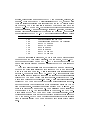
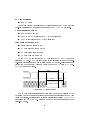
64 analog pulses
Pulser Box
1 FE-board
S-UTP (CAT 5) cable:
64 bit Pattern
Amplitude (DAC)
Data (250 MHz)
Pattern strobe
USER 1 - 4 (40 MHz)
Setup (10 MHz)
40 MHz clock
External (ECL)
CATCH 1
USER 1-4
Pattern pulse
VME bus (A32/D32)
VME :
Setup, Control & Readout
Figure 1: Possible test-setup with the CATCH1 board
3
The CATCH1 is a very exible device. It provides up to 64 independent
TTL test pulses which can be programmed via the VMEbus. The pulses are
converted into analog signals in an external `Pulser Box1 ' before being used
to simulate a detector system. This makes it easy for the user to adjust pulse
shapes to the needs of the front-end system which is to be tested. The data
ow for a possible test-setup can be found in Figure 1.
Another feature are internal scalers for the USER commands (Chapter 2.5). This, for instance, allows to keep track of the number of external TRIGGER signals. All functions of the CATCH1 board as well as the
readout of the front-end data are controlled via the VMEbus (Chapter 2.1).
Additional connectors on the front panel allow to apply external signals as
well.
In the experiment the VME interface will only be used to transfer data
needed for initialization of the front-end electronics and to collect data for
slow control purposes. The data from the front-end side will be ordered
by events on the CATCH-module before being passed ahead to the on-line
ltering via a fast optical S-Link.
1
PULPO: PULse and Pattern bOx
4
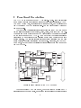
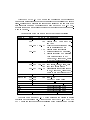
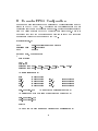
2 Functional Description
The CATCH1 is a one unit wide 6U VME slave-module. Its main features
are a unit to control an external module for test pulse generation, a USER
Command Coding Unit, one serial port to transmit data, one to receive data
(`HOTLink') and the VME interface logic. See the block diagram (Figure 2)
for more details.
The Test Pulse Controller receives test pattern and four USER commands
(in the following referred to as Trigger, Reset, Clear, User) from the VMEbus.
This unit can apply 64 independent TTL test pulses to a connector (80 pins)
on the front panel of the CATCH1. Via a at cable the digital signals are
transferred to an external device ('Pulser Box') which converts them into
analog signals. The control signals for pulse height selection and the test
pulse duration are also transferred via this cable. Moreover, for the USER
commands, the Test Pulse Controller provides scalers which can be read out
via the VMEbus.
FIFO
Buffer
Tristate Driver
9 Data
6 Control
VME Interface
Logic
9 Setup Data (Flags)
24
Data
4
Control
9 JTAG I/O
40 MHz Clock
Address
Decoder
8
2 x 9: Program & Debug I/O
5 Program
4 Control
4
4 USER Commands
40 Address
16 Data
Tristate Driver
USER
Command
Coding
Unit
5
32 Data
VME Data Transfer Bus
Enable
Serial
Transmitter
Direction
Bidirectional Drivers
HOTLink
Receiver
3 Connectors:
(Debug, JTAG I/O for prog. Logic)
Connector (ECL)
Front Panel
Connector (S-UTP)
4 Flags
9 data
Rotary Switches
25/ 30/ 50/ 66
MHz Clocks
Connector (80 pins)
4
USER 1 to 4
Test Pattern Strobe
DAC Control
Test Pulse
Controller
SRAM
(32 kB)
8 + 15 + 3
64 Bit Test Pulse Pattern
or 12 Bit DAC Value
Figure 2: Block diagram of the CATCH1 board
The four di
erent USER commands, which can also be applied as ECL
level signals on the front panel, are encoded into signals of di
erent lengths
5
by the User Command Coding Unit before being transmitted to the front-end
boards via one pair of wires on a S-UTP cable (Cat 5+).
The serial transmitter provides the possibility to transfer data needed for
initialization of the front-end electronics. This serial port runs at 10 Mbit/s
and transfers 24 bit of data on a second pair of wires on the S-UTP cable
with each transmission. It cannot receive data and has no provision for error
handling.
The third wire-pair on the S-UTP cable is used to transmit the 40MHz
clock to the front-end. On the CATCH1 this clock is used by the User
Command Coding Unit and the serial transmitter. Both components send
their data synchronously to the clock.
Data generated on the front-end boards are received by the HOTLink via
the last pair of wires on the S-UTP cable. It operates at frequencies up to
330 MHz and monitors transmission errors. Having arrived on the CATCH1module the data are parallelized into words of 8 bit. The data are stored in a
FIFO bu
er from where they can be read out to the VMEbus. An additional
bit indicating transmission errors is also stored in the FIFO bu
er being nine
bit wide.
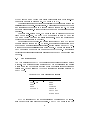
2.1 VME Interface
The VME interface of the CATCH1 consists of an address decoder and a state
machine. The address decoder monitors the VME address lines and passes
a valid command to the state machine where the corresponding actions are
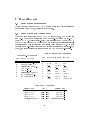
carried out. Table 1 lists the VME data transfer bus signals monitored by
the CATCH1.
Table 1: VME data transfer bus signals
Addressing Data
A31-A01 D31-D00
AM5-AM0
DS0*
DS1*
LWORD*
Control
AS*
DS0*
DS1*
WRITE*
(BERR*)
(DTACK*)
SYSRESET*
DTACK* is asserted by the module itself and the signal BERR* is foreseen but not yet implemented in the design. The CATCH1 works in the A32
6
addressing mode and recognizes the following Address Modier codes (a \%"
indicates hexadecimal numbers):
AM0-AM5 = %0D extended supervisor data access
AM0-AM5 = %09 extended non-privileged data access
The base address of the CATCH1 can be manually selected with two four
bit rotary switches on the board which are compared to the address lines
A08-A15. Hence the Base Address can be selected in the range of
%E000 0000 to %E000 FF00.
The module transfers data in the D32 mode. It responds to 'Quad Byte
Transfers' which require the signals DS0*, DS1*, LWORD* and A01 to be
low.
The commands controlling the CATCH1-module are encoded in the address lines A02-A07. Therefore an o
set has to be added to the module's
base address for each command. Most commands also require the transfer of
data. There are 13 commands dened for the CATCH1 which perform the
following actions:
%00
%08
%10
%18
%40
READ ID
READ FIFO
READ STATUS
READ FPGA
WRITE SERIAL
%48 WRITE FPGA
%50 WRITE TRIG
%80 PROG FIFO
%88 PROG FPGA
%90 BISTEN
%98 REFRAME
%C0 RESET FIFO
%C8 RESET FPGA
reads a unique board identier
reads front-end data from the FIFO bu
er
reads the status of the board's components
reads scalers of the Test Pulse Controller
writes front-end setup data to the serial
transmitter
writes test pattern or control data to the
Test Pulse Controller
writes USER1-4 to the USER Command
Coding Unit
sets the programmable ags of the FIFO
bu
er
sets the pins for programming the FPGA
enables the Built In Self Test of the serial
data receiver
toggles the REFRAMING option of the serial data receiver on/o
resets the FIFO bu
er (ADDRESS ONLY
cycle)
Soft reset of the Test Pulse Controller
(ADDRESS ONLY cycle)
7
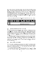
In the following these commands will be described in more detail. An
overview of all commands, their o
set addresses and the data transferred
can be found in Table 5 at the end of this chapter. Chapter 4 contains a
brief description of all the components on the CATCH1.
The board identier is of the form "CA1000XX" (hexadecimal) where the
XX stands for the serial number of the CATCH1. The READ ID command
has an o
set address of %00.
The o
set address of the READ STATUS command is %10. It reads nine
bit (VME data lines D15 to D07) of status information. The di
erent bits
have the following meaning:
bit D15: INIT pin is 1 if the Test Pulse Controller is programmed,
0 when an error occurred during conguration
bit D14: DONE pin is 1 if the Test Pulse Controller is programmed
bit D13: EF pin is 0 if the FIFO is empty
bit D12: PAE pin is 0 if the FIFO is almost empty (programmable)
bit D11: PAF pin is 0 if the FIFO is almost full (programmable)
bit D10: FF pin is 0 if the FIFO is full
bit D09: RVS pin is 1 if transmission errors occurred (HOTLink)
this information is also included in the data stream, here
it is read out asynchronously
bit D08: RDY pin is 0 if the HOTLink-self-test has nished
bit D07: is 1 if the serial transmitter (setup data) is busy
The FIFO bu
er can be cleared with the command RESET FIFO. It has
the o
set address %C0 and causes an address only cycle which requires no
data to be transferred. The same applies to the command RESET FPGA
with the o
set address %C8. This command clears all registers of the Test
Pulse Controller and puts it in the initial state after conguration.
2.2 HOTLink serial receiver
The HOTLink is a high-speed serial link. On the CATCH1 it runs with
a 25 MHz (exchangeable) clock, which is the reference for a phase locked
loop (PLL) that generates the high-speed transmission clock, allowing the
transmission taking place at 250 MHz.
Blocks of the incoming 10 bit-coded data stream are decoded into words
of one byte. These can be either data characters or special characters. For
instance the special character K28.5 (`comma') is a separator for the data
words. If the receiver decodes a K28.5 its internal free-running bit counter
is synchronously reset on the correct byte boundaries.
8
All data and command words are written into the FIFO with one exception. If consecutive K28.5 characters are received, only the rst one is
written into the FIFO. For violations (transmission errors) and special commands the HOTLink has two bits that are combined by or into the ninth
FIFO bit to identify corrupted data. The command-feature of the HOTLink
is not used on the front-end board. To avoid erroneous framing on wrong
byte boundaries the REFRAME command (o
set address %98) can be used.
Certain data sequences can be taken for a special K28.5 character and could
cause corrupted data. When reframing is switched o
the HOTLink receiver
will not try to reframe the incoming serial data whenever it decodes such a
special character.
Another command is BISTEN with the o
set address %90. With this
command the receiver enters a built-in self test state. For a successful self test
of the transmitter-receiver system it is necessary to start the test function
on the front-end side too. For example this could be done with the User
command (USER4).
2.3 FIFO Buer
The FIFO bu
er is nine bit wide and can hold up to 8 KByte of data. It has
four ags which indicate that it is full, almost full, almost empty or empty.
By default the almost full ag is asserted when the FIFO has space for up
to seven more words. On the other hand the almost empty ag is asserted
when it contains seven or less words. The user can alter the value at which
a ag should be asserted with the PROG FIFO command. It has the o
set
address %80 and transfers 32 bit of data into the FIFO's programmable ag
registers. These 32 bit are split into 4 bytes:
bits D31 to D24:
bits D23 to D16:
bits D15 to D08:
bits D07 to D00:
empty o
set LSB register (default value: %07h)
empty o
set MSB register (default value: %00h)
full o
set LSB register (default value: %07h)
full o
set MSB register (default value: %00h)
All eight bit are written into the least signicant bit registers (LSB)
whereas only the ve least signicant bits are written into the most signicant
bit registers. Therefore the user can program the almost empty and the
almost full ags in the range from 0 to 7905.
Front-end data can be read from the FIFO using the READ FIFO command with the o
set address %08. Each time three words of eight bit are
read in the big-endian format. The rst word read from the FIFO is transferred in bits 23 to 16, the second in bits 15 to 8 and the third in bits 7 to
9
0. For each word two more bits are read out: the rst is the `ninth FIFObit' which indicates possible transmission errors of the incoming serial data
stream. The second one is the empty ag of the FIFO bu
er. In case of
transmission errors the error bit is one and when the FIFO bu
er is empty
the bit containing the empty ag is zero. Reading data from an empty FIFO
bu
er results in getting always the same datum, i.e. the last datum that was
written into the bu
er. The bit assignment for the READ FIFO command
can be found in Table 2.
Table 2: Bit assignment for the front-end data read from the FIFO bu
er
31 30 29 28 27 26 25 24 23 .. 16 15 .. 8 7 .. 0
0 Flags 0 Error Bits Data1 (8) Data2 (8) Data3 (8)
"
"
bits belong to data word 1
"
"
bits belong to data word 2
"
"
bits belong to data word 3
2.4 Serial Transmitter (10 Mbit/s)
The serial interface for the front-end setup data can be selected with the
WRITE SERIAL command with the o
set address %80. The interface works
unidirectional and provides no error handling. Each transmission consists of
two start bits, 24 data bits and two stop bits. Both the start and the stop
bits are a sequence of one-zero. After data transmission the interface stays
at zero.
This serial transmitter runs with a frequency of 10 MHz which is derived
from the 40 MHz clock. The serial data is transmitted to the front-end system
synchronously with the 40 MHz clock. This clock can be used to decode the
serial data on the front-end side and to synchronize the front-end equipment
in the experiment.
2.5 Test Pulse Controller
The Test Pulse Controller is implemented in a programmable logic device
(FPGA) which has to be congured after each power up. This conguration
process can be either done from a PC via a connector on the front panel of
the CATCH1 or via the VMEbus.
The programming via the VMEbus is done using the PROG FPGA command with the o
set address %88. Depending on the datum written to this
10
address, three programming pins of the FPGA can be enabled, disabled, set
or reset. These are the 'PROG pin' (initializes the FPGA), the 'DIN pin'
(here the serial conguration data is applied) and the 'CCLK pin' (is a clock
for the data). Two more pins ('INIT' and 'DONE') can be read out with
the READ STATUS command. They indicate whether the conguration was
nished successfully. An example routine, written in C-language, that congures the Test Pulse Controller via VME is given in Appendix B. The di
erent
words transferred with PROG FPGA and their results are described below:
Data lines D08 to D00
%01
enable programming via VME
%02
disable programming via VME (default)
%04
set PROG pin to 0
%08
set PROG pin to 1
%10
set DIN pin to 1
%20
set DIN pin to 0
%40
set CCLK pin to 1
%80
set CCLK pin to 0
Once the controller is congured, 16 bit of data can be either written
to or read from the Test Pulse Controller. Two commands, WRITE FPGA
with the o
set address %48 and READ FPGA with the o
set address %18
can be used for this data and command transfer via the VME data lines D31
to D16.
The Test Pulse Controller knows ve di
erent commands which are encoded in the three least signicant data lines D18 to D16 and its default
mode is to wait for a command. A list of all possible data transfers is given
in Table 3. The rst command is SETUP TRIGGER. Here the user can write
all the information to select the delay and the source of the trigger signals:
disable USER Command Coding Unit (see Chapter2.6) prevents USER commands from being sent to the front-end board. Automatic trigger generation
causes the USER Command Coding Unit to send a trigger signal to the frontend board for each Test Pattern Strobe that was received either via VME or
from the front panel. The latency is programmable: t = t0 +(n 25) ns . The
o
set t0 is between 975 ns and 1000 ns. The multiplier n can be selected in
the range from 0 to 27. As will be explained in Chapter 2.6 the USER commands arrive at the USER Command Coding Unit asynchronously. Hence
there is an uncertainty of 25 ns (one 40 MHz clock cycle) for the timing of the
USER commands. Five LEDs on the front panel indicate whether internal
(red) or external (green) USER commands and Test Pattern Strobe will be
used.
11
With the PREPARE SCALERS command the user can do two things: he
can prepare a scaler for readout and he can select which scaler(s) he wants to
clear. Scalers can be prepared for readout and cleared at the same time but
only after this command the scaler can be read out with READ SCALER.
Because these commands belong together they are treated as being one command in Table 3.
Table 3: List of the commands for the Test Pulse Controller
MODE
BITS
VALUE COMMAND
1 : WRITE D18-D16
%00 SETUP TRIGGER
D21
D26-D22
D31-D27
2a: WRITE D18-D16
D26-D24
D31-D27
2b: READ D31-D16
3 : WRITE D18-D16
D31-D19
4a: WRITE D18-D16
4b:
D31-D16
4c:
4d:
4e:
5 : WRITE D18-D16
%01 disable USER Command Coding Unit
%00-%1A delay between pattern and trigger in multiples of 25 ns
%1F disable automatic trigger
1 enable external USER signals,
0 disable external USER signals:
Test Pattern Strobe (D31)
User (D30), Clear (D29), Reset
(D28) and Trigger input (D27)
%01 PREPARE SCALERS
%00-%03 for Trigger, Reset, Clear, User
%04 for Test Pattern Strobe
%01-%1F clear scalers for pattern strobe
(D31), User (D30), Clear (D29),
Reset (D28) and Trigger (D27)
READ SCALER
%02 SET DAC
12 bit DAC setup value
%03 WRITE PATTERN
16 bit test pattern 01-16
16 bit test pattern 17-32
16 bit test pattern 33-48
16 bit test pattern 49-64
%04 PATTERN STROBE
The third command is SET DAC which programs the digital to analog
converter on the 'Pulser Box'. After the command WRITE PATTERN the
FPGA waits for another four data transfers which contain the 64 bit test
12
pattern for the front-end. When all 64 bit are received they can be sent to
the 'Pulser Box' with the completing command PATTERN STROBE. This
command, executed without new test pattern information, will transfer the
most recent test pattern data to the 'Pulser Box'.
The seven segment display on the front panel of the CATCH1 shows the
actual mode of the Test Pulse Controller and possible errors. Once an error
occurred its value stays on the display until reset or another error occurs. A
list of all values is given in Table 4.
Table 4: The 7-Segment display shows the status of the Test Pulse Controller
Display
.
0
1
2
3
4
5
STATUS
conguration error / not congured
controller waits for more data or READ SCALER command
no error
WRITE command expected
READ SCALER expected
WRITE PATTERN data word 1, 2 or 3 expected
WRITE PATTERN data word 4 expected
unknown command
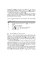
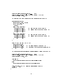
2.6 User Command Coding Unit
The USER Command Coding Unit uses the 40 MHz clock to encode four
di
erent USER commands (Trigger, Reset, Clear and User) in terms of clock
cycles before they are transmitted to the front-end board via the S-UTP
cable. The shortest signal is the Trigger with a length of one clock cycle (25
ns) while the Reset, the Clear and the User commands have lengths of 50 ns,
75 ns and 100 ns respectively.
During normal operation the Test Pulse Controller sends an automatically
generated trigger signal to the USER Command Coding Unit for each test
pattern that was written to the 'Pulser Box'. Delay between Test Pattern
Strobe and the trigger signal can be adjusted in multiples of 25 ns plus an
o
set of 975 ns in the Test Pulse Controller.
In case the automatic trigger generation is disabled, the trigger signals
can either come from the VMEbus or from the ECL input connector on the
front panel. These are the only possibilities to feed the other three USER
commands and the pattern strobe into the CATCH1. The ve ECL channels
13
4.5 ns
25 ns
1
5 ns
25 ns
2
3
4
5
6
7
8
9
10
40 MHz Clock
USER1
SERIAL OUT
25 ns
USER2
SERIAL OUT
50 ns
USER3
SERIAL OUT
75 ns
USER4
SERIAL OUT
100 ns
Figure 3: USER command timings
on the connector can be individually enabled with the SETUP TRIGGER
command (see Table 3). The applied signals must be at least 30 ns long. After
one signal has been encoded the next one can be handled one clock cycle later.
Maximum rates for the USER commands can be found in Chapter 5.2.
The timing of the outgoing USER commands with respect to the 40 MHz
clock can be taken from Figure 3. Because the incoming signals (from VME,
automatically generated Triggers or ECL signals) arrive asynchronously at
the USER Command Coding Unit, the encoded USER commands have an
uncertainty of one clock cycle. In Figure 3 incoming signals that are present
in the 25 ns interval ending 4.5 ns before the rising edge of clock cycle 4
produce encoded signals with the same timing. The 4.5 ns are the chip's
internal register setup time. For incoming signals that are present within
this time before a rising edge of the clock it is not predictable if the encoding
will start with the next rising edge or only one clock cycle later.
The USER command transfer via VME is done with the WRITE TRIG
command that has the o
set address %50. Here the signals are sent via the
VME data lines D03 to D00 which correspond to the User, the Clear, the
Reset and the Trigger signals respectively. Whenever two USER commands
are applied at the same time, the shorter output signal has priority. For
instance only the trigger signal will be encoded if both the trigger and the
reset signal are applied to the coding unit. However this should not be done
via the VME command WRITE TRIG. If necessary the trigger coding unit
can be disabled from the Test Pulse Controller (see Table 3).
14
Table 5: O
set addresses of the CATCH1 commands
COMMAND
OFFSET DATA WORD
READ ID
%00
D31-D00
READ FIFO
%08
D31-D00
READ STATUS
%10
D15-D07
READ FPGA
%18
D31-D16
WRITE SERIAL
%40
D23-D00
WRITE FPGA
%48
D31-D16
WRITE TRIG
%50
D03=1
D02=1
D01=1
D00=1
PROG FIFO
%80
D31-D16
PROG FPGA
%88
D07-D00:
%01
%02
%04
%08
%10
%20
%40
%80
REFRAME
%98
D07-D00
%01
%02
BISTEN
%90
D07-D00
%01
%02
RESET FIFO
%C0 RESET FPGA
%C8 -
15
CATCH1 identier
three data words
status bits
scaler values
setup data to front-end
pattern, pulse height
User command
Clear command
Reset command
Trigger command
set FIFO ags
data transferred:
enable programming pins
disable programming pins
set PROG pin to 0
set PROG pin to 1
set DIN pin to 1
set DIN pin to 0
set CCLK pin to 1
set CCLK pin to 0
enable reframing
disable reframing
start built in self test
stop built in self test
reset FIFO buer
reset Test Pulse Controller
3 Board Layout
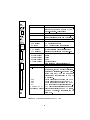
3.1 Front Panel Information
Figure 4 shows a sketch of the CATCH1 front panel and a table describing
the function of its LEDs, connectors and buttons.
3.2 Front Panel Pin Assignment
There are four connectors on the CATCH1 front panel. The uppermost
is a RJ-45 for the communication with the front-end board via a S-UTP
cable (CAT 5+). While the high-speed data transfer via HOTLink (PECL),
the USER commands (LVDS) and the 40 MHz clock are di
erential signals,
the serial setup data is generated as a single ended signal (TTL). However
because an opto-coupler will be used to receive this signal on the front-end
board, the cable carries both lines to drive the LED of the opto-coupler.
Table 6: RJ-45 Connector
PIN SIGNAL NAME
#
1
40 MHz Clock (-)
2
40 MHz Clock (+)
3
Serial Setup Data (-)
4
USER 1-4 (+)
5
USER 1-4 (-)
6
Serial Setup Data (+)
7
HOTLink Data (-)
8
HOTLink Data (+)
Table 7: Programming Connectors
PIN
#
9
8
7
6
5
4
3
2
1
'CPLD' 'TEST' 'PROG'
VCC
GND
n.c.
TCK
n.c.
TDO
TDI
n.c.
TMS
RT
RD
TRIGG
n.c.
TDI
TCK
TMS
CLKI
CLKO
VCC
GND
n.c.
CCLK
DONE
DIN
/PROG
/INIT
/SOFTRES
Table 8: ECL Connector
Signal Name
PIN #
Signal Name
USER 1 (+)
10 09
USER 1 (-)
USER 2 (+)
08 07
USER 2 (-)
USER 3 (+)
06 05
USER 3 (-)
USER 4 (+)
04 03
USER 4 (-)
Pattern Strobe (+) 02 01 Pattern Strobe (-)
16
FPF 288 B
PWR
ERR
BUTTON
DESCRIPTION
7 SEGMENT
DESCRIPTION
RESET
CPLD
7
SEG
S
H
RESET
E S D
R Y A
R N T
RJ-45
CPLD
TEST
FPGA
VCC
RED
INT
GRN
EXT
E
C
L
TRG
RST
CLR
USR
PAT
TRG
RST
CLR
USR
PAT
P
A
T
T
E
R
N
O
U
T
UNIVERSITÄT
FREIBURG
LED
PWR (green)
CPLD (green)
ERR (red)
ERR (red)
SYNC (green)
DATA (yellow)
TRG (red/green)
RST (red/green)
CLR (red/green)
USR (red/green)
PAT (red/green)
CONNECTOR
RJ-45
S clears all registers of FPGA (soft reset) and both S and H put the CATCH1
power-up state. (hard reset)
status of the Test Pulse Controller. For
more details see Table 4 in Chapter 2.5
DESCRIPTION
power
VME interface is busy
FPGA error during conguration
corrupted data from front-end
synchronization characters received
serial data arrives from the front-end
Trigger
Reset
Clear
User
Pattern Strobe
red: internal - green: external ECL
DESCRIPTION
carries serial HOTLink data, USER
commands, the 40 MHz clock (all dierential) and serial front-end setup data.
Setup data and USER commands are
transmitted synchronously to the 40
MHz clock.
CPLD
coded connector to program the CPLD
TEST
coded connector to debug the FPGA
FPGA
coded connector to program the FPGA
ECL
ECL inputs for the trigger signals (+ -)
PATTERN OUT TTL test pattern transfer with 64 pins
(Robinson Nugent) test pattern (including 12 DAC value),
1 pin DAC control, 1 pin trigger and 10
pins GND.
Figure 4: The Front Panel of the CATCH1
17
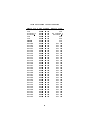
Table 9: Robinson Nugent Connector
SIGNAL NAME
GND
GND
DACSTR(+)
DACSTR(-)
GND
GND
not used
not used
DOUT63
DOUT61
DOUT59
DOUT57
DOUT55
DOUT53
DOUT51
DOUT49
DOUT47
DOUT45
DOUT43
DOUT41
DOUT39
DOUT37
DOUT35
DOUT33
DOUT31
DOUT29
DOUT27
DOUT25
DOUT23
DOUT21
DOUT19
DOUT17
DOUT15
DOUT13
DOUT11
DOUT09
DOUT07
DOUT05
DOUT03
DOUT01
PIN NUMBER SIGNAL NAME
B40
A40
GND
B39
A39
GND
B38
A38 DOUTSTR(+)
B37
A37
DOUTSTR(-)
B36
A36
GND
B35
A35
GND
B34
A34
GND
B33
A33
GND
B32
A32
DOUT62
B31
A31
DOUT60
B30
A30
DOUT58
B29
A29
DOUT56
B28
A28
DOUT54
B27
A27
DOUT52
B26
A26
DOUT50
B25
A25
DOUT48
B24
A24
DOUT46
B23
A23
DOUT44
B22
A22
DOUT42
B21
A21
DOUT40
B20
A20
DOUT38
B19
A19
DOUT36
B18
A18
DOUT34
B17
A17
DOUT32
B16
A16
DOUT30
B15
A15
DOUT28
B14
A14
DOUT26
B13
A13
DOUT24
B12
A12
DOUT22
B11
A11
DOUT20
B10
A10
DOUT18
B09
A09
DOUT16
B08
A08
DOUT14
B07
A07
DOUT12
B06
A06
DOUT10
B05
A05
DOUT08
B04
A04
DOUT06
B03
A03
DOUT04
B02
A02
DOUT02
B01
A01
DOUT00
18
The di
erential signals should be decoupled by capacitors on the frontend board. Table 6 shows the pin assignment for the RJ-45 connector.
Three connectors are foreseen for programming and debugging of the
FPGA and the CPLD devices. With the `CPLD' JTAG connector the VME
interface can be reprogrammed. `PROG' and `TEST' can be used to program
and debug the FPGA. Table 7 shows the pin assignments.
The external signals USER1 to USER4 and Test Pattern Strobe can be
applied to the ECL connector. The pinning is listed in Table 8
The test pattern output is an 80 pin Robinson Nugent connector. This
connector is used to transfer the TTL test pattern to the 'Pulser Box'. The
64 bit test pattern are transferred via lines D00 to D63.
Optionally lines D00-D11 can carry the 12 bit needed to set the DAC. This
information is loaded into the DAC with the di
erential signal DACSTR.
DOUTSTR is the second di
erential signal enabling the analog output of
the 'Pulser Box'. Table 9 shows the pin allocation for the signals.
3.3 Rear Panel Pin Assignments
Tables 10 and 11 show the pin assignment for the VME signals used on the
CATCH1 board.
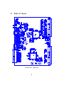
3.4 Jumper Settings
Five di
erent clock speeds can be selected for the programmable logic devices
on the CATCH1 board: 8 and 17 MHz are derived from an exchangeable 33
MHz clock and 25 MHz are derived from an exchangeable 50 MHz clock.
These clocks can be individually selected for both chips by shorting the appropriate jumpers JP4 (FPGA) and JP5 (CPLD). For the FPGA there is
also a 80 MHz clock foreseen which can only be selected by the logic implementation in this device and is unused in the current design. Figure 5 shows
the location of the jumpers for clock selection on the board. The default
setting are 33 MHz for the CPLD as well as for the FPGA.
Besides the internal clocks on the CATCH1 an external one can be selected for the FPGA. This external clock is enabled with Jumper JP3 and
can be taken from a PC. Selecting external clocks should only be done for
debugging the FPGA. During normal operation the two INT pins are shorted
with a jumper by default (see Figure 5).
The remaining two jumpers also serve debugging purposes. If JP1 is
shorted the user can send trigger signals via the `TEST' connector to the
FPGA. A shorted jumper JP2 allows soft reset signals to be sent from a PC
19
Table 10: VME J1/P1 Connector
PIN
#
1
2
3
4
5
6
7
8
9
10
11
12
13
14
15
16
17
18
19
20
21
22
23
24
25
26
27
28
29
30
31
32
ROW
A
D00
D01
D02
D03
D04
D05
D06
D07
GND
n.c.
GND
DS1*
DS0*
WRITE*
GND
DTACK*
GND
AS*
GND
IACK*
IACKIN*
IACKOUT*
AM4
A07
A06
A05
A04
A03
A02
A01
-12 V
+5 V
ROW
B
n.c.
n.c.
n.c.
n.c.
n.c.
n.c.
n.c.
n.c.
n.c.
BG3IN*
BG3OUT*
n.c.
n.c.
n.c.
n.c.
AM0
AM1
AM2
AM3
GND
n.c.
n.c.
GND
n.c.
n.c.
n.c.
n.c.
n.c.
n.c.
n.c.
n.c.
+5 V
ROW
C
D08
D09
D10
D11
D12
D13
D14
D15
GND
n.c.
BERR*
SYSRESET*
LWORD
AM5
A23
A22
A21
A20
A19
A18
A17
A16
A15
A14
A13
A12
A11
A10
A09
A08
n.c.
+5
Table 11: VME J2/P2 Connector
PIN
#
1
2
3
4
5
6
7
8
9
10
11
12
13
14
15
16
17
18
19
20
21
22
23
24
25
26
27
28
29
30
31
32
ROW
A
n.c.
n.c.
n.c.
n.c.
n.c.
n.c.
n.c.
n.c.
n.c.
n.c.
n.c.
n.c.
n.c.
n.c.
n.c.
n.c.
n.c.
n.c.
n.c.
n.c.
n.c.
n.c.
n.c.
n.c.
n.c.
n.c.
n.c.
n.c.
n.c.
n.c.
n.c.
n.c.
ROW
B
+5 V
GND
n.c.
A24
A25
A26
A27
A28
A29
A30
A31
n.c.
+5 V
D16
D17
D18
D19
D20
D21
D22
D23
n.c.
D24
D25
D26
D27
D28
D29
D30
D31
n.c.
+5 V
ROW
C
n.c.
n.c.
n.c.
n.c.
n.c.
n.c.
n.c.
n.c.
n.c.
n.c.
n.c.
n.c.
n.c.
n.c.
n.c.
n.c.
n.c.
n.c.
n.c.
n.c.
n.c.
n.c.
n.c.
n.c.
n.c.
n.c.
n.c.
n.c.
n.c.
n.c.
n.c.
n.c.
to the FPGA via the `PROG' connector on the front panel. There is no need
to change these settings during normal operation.
3.5 Rotary Switches
Two rotary switches adjust the base address of the CATCH1 board in the
range of %E0000000 to %E000FF00. Switch SW2 selects the lower four bit
and switch SW1 the upper four bit of the base address. For the location on
the board see Figure 5.
20
VME J1/P1 Connector
VME J2/P2 Connector
F3
Default JUMPER Settings
CPLD
F4
50
33
25
17
08
FPGA
JP5 JP4
50
111
000
0000
1111
33
000
111
0000
1111
000025
1111
17
08
33 MHz
JP3
111
000
000
111
CPLD
EXT INT EXT
50 MHz
FPGA
Rotary switches
HOTLink
SW1
SW2
80 MHz
FIFO
40 MHz
GAL
GAL
25 MHz
JP1
JP2
F2
Reset switches
F1
RJ - 45
CPLD / TEST
ECL Input
Robinson Nugent Connector
FPGA
Figure 5: Components on the CATCH1
4 Components on the Board
In this section a brief overview will be given on the important ICs on the
CATCH1 board. Their locations can be taken from Figure 5 and detailed
descriptions can be found in the corresponding data sheets or specications.
4.1 Xilinx XC95288-15 CPLD
This `Complex Programmable Logic Device' (CPLD) houses the VME interface logic and the serial transmitter for the setup data to the front-end. It
retains its information when power is switched o
but can be reprogrammed
via the `CPLD' JTAG connector on the front panel. For detailed information
see 1].
4.2 Xilinx XC4020E-2 FPGA
This IC is a `Field Programmable Gate Array' in which the Test Pulse Controller is implemented. It has to be congured on each power up. As already
mentioned this can be done either via the VMEbus or via the FPGA connector on the front panel of the CATCH1. The conguration via VME requires
21
conguration data in form of a le that contains either binary or hexadecimal
numbers. This data will be transferred to the chip bit by bit. An example
routine, written in C-language, can be found in Appendix B.
Since the FPGA can be easily and quickly recongured it can perform
quite di
erent tasks. For instance it could be used to read data into the
CATCH1 from the Robinson Nugent connector and thus use the FPGA for
digitization. For a detailed description of the XC4020E-2 see 1].
4.3 Cypress CY7B933 HOTLink Receiver
The HOTLink receives data from the transmitter on the front-end side. Both
the transmitter and the receiver side must have a reference clock which must
be within 0.1% to each other. These clocks are exchangeable and can
operate at di
erent frequencies up to 33 MHz. A detailed description of the
HOTLink transmitter and receiver devices can be found in 2].
4.4 CY7C4251-15 JC FIFO
This FIFO bu
er is nine bit wide and 8 KByte deep. It features empty,
almost empty, almost full and full ags of which the almost empty/full ags
can be programmed. The FIFO belongs to a family of pin-compatible bu
ers
and can be easily replaced in case a bigger memory is required. A detailed
description can be found in 3].
4.5 Lattice GAL22V10C GAL
The USER Command Coding Unit and part of the interface logic between
HOTLink and FIFO bu
er are each implemented in a GAL (`Generic Array
Logic'). They are exchangeable and can be reprogrammed. However, these
devices are not capable to hold as much logic as a CPLD. For more details
see 4].
4.6 CY7C199-10vc Memory
This memory (36 KByte) can be accessed via the FPGA but is not used in the
current design. For example, test pattern could be stored here before being
sent to the `Pulser Box'. A detailed description of this device is available in
5].
22
5 Electrical and Mechanical Specications
5.1 Cables
The three connectors for programming and debugging the CPLD and the
FPGA require special Xilinx-adapters. These have to be connected to a PC
and should not be used during normal operation. The following list gives an
overview of the cables for the other connectors on the front panel:
S-UTP cable - CAT5+ (shielded twisted pair)
Length : 20 m
Wires : 8
Twisted pair at cable to `Pulser Box'
Length : 3 m
Wires : 80
Twisted pair at cable for ECL signals
Length : 3 m
Wires : 10
5.2 Signal Characteristics
Signals on the S-UTP cable
HOTLink data
: Di
erential PECL level, max. frequency 330
MHz, the lines are terminated with 110 ! to
VCC and with 300 ! to GND
USER commands
: Di
erential LVDS level
Clock
: Di
erential LVDS level, frequency: 40 MHz
Serial setup data (-) : TTL level, frequency: 10 MHz
Serial setup data (+) : for driving the LED of an opto-coupler
Signals on the twisted pair cable (80 wires)
Data lines D00-63
DACSTR
DOUTSTR
remaining wires
:
:
:
:
TTL level
Di
erential LVDS level
Di
erential LVDS level
GND or not used
Signals on the twisted pair cable (10 wires)
All USER commands : ECL level, dynamically terminated with 100 !
Pattern Strobe
: ECL level, dynamically terminated with 100 !
23
ECL input pulses
width : 30 ns
The device driving the external ECL signals must have a 750 ! emitter
pull-down resistor and a ground connection to the CATCH1 must exist.
USER command output
width : 25 ns to 100 ns
USER1 (TRIGGER) frequency : 15 MHz (fastest)
USER4 (User) frequency: 5 MHz (slowest)
Test Pulse Pattern output
Pattern strobe width : 30 ns
DAC data strobe width : 150 ns
DAC data setup time : 120 ns
DAC data hold time : 20 ns
On the CATCH1 the timing of DAC data strobe (DACSTR) and data
signals (DOUT00 - DOUT11) is adjusted to the requirements of the digitalto-analog converter used on the `Pulser Box' (AD7845) 6]. Signal levels and
timing can be taken from Figure 6 where the 12 bit DAC data (DOUT00 DOUT11) are active high.
150ns
DACSTR(-)
DACSTR(+)
120 ns
20 ns
DOUT00 - DOUT11
Figure 6: DAC setup timing
The 64 test pattern signals are active high and remain present at the
Robinson Nugent connector until another pattern is transferred to the Test
Pulse Controller. Pattern strobe is also a di
erential signal: DOUTSTR(+)
is positive and DOUTSTR(-) negative when the test pattern is sent to the
front-end board.
24
VME Performance (with MVME 2604)
Writing 64 bit test pattern + pattern strobe : 0.33 MHz
Writing only pattern strobe : 1.92 MHz
Writing USER commands : 2.73 MHz
Reading FIFO data : 1.11 MHz
Reading Board Status: 1.20 MHz
5.3 Power Requirements, Mechanical Size
+5 V / 1150 mA protected with a 3 A fuse (F3)
-12 V / 25 mA protected with a 250 mA fuse (F4)
+5 V, `CPLD' (F1) and `PROG' (F2) connectors each protected with a 250
mA fuse.
For the location of the fuses see Figure 5.
The CATCH1 is a single-width 6U VME-module.
References
1] Xilinx: The Programmable Logic Databook (1996).
2] CYPRESS Semiconductor Corporation, CY7B923/33 HOTLink Transmitter/Receiver Data Sheet.
3] CYPRESS Semiconductor Corporation, CY7C42x1 8Kx9 Synchronous
FIFO Data sheet.
4] Lattice Semiconductor Corporation, Data Book (1994)e
5] CYPRESS Semiconductor Corporation, CY7C199 Memory Data sheet.
6] Analog Devices, AD7845 D/A Converter Data sheet.
25
A Getting started with the CATCH1
The consecutive steps, necessary to run tests with the CATCH1 board are
described in this Appendix:
1.
2.
3.
4.
5.
6.
7.
switch o
the power of your VME crate
select suitable base address(es) for your CATCH1 board(s)
plug in the board(s)
connect the `Pulser Box(es)' and the front-end electronics
switch power on again
now change to directory where your `CATCH1 software' is installed
run the conguration routine for the FPGA (le containing the design
required!)
8. when the seven segment display shows a zero everything is ready# if not
use the right conguration data.
26
B Example: FPGA Conguration
Here an example will be given to demonstrate how the logical design must be
loaded on the FPGA via VME. The design must be available in form of a le
containing only binary or hexadecimal numbers. Hexadecimal les generated
from the Xilinx software have to be converted into binary ones. Here it is
important that each two hexadecimal numbers are swapped and their bits
are reversed before they are written to the VME.
#include<stdio.h>
void
unsigned long
void
PROG_FPGA(unsigned long VALUE)
READ_STATUS()
WAIT()
main(int argc, char *argv])
{
FILE *input
int i, a
char bit
unsigned long ENA_H, ENA_L, PROG_H, PROG_L, DIN_H, DIN_L
unsigned long BASE, VALUE, CCLK_H, CCLK
/*
some constants
BASE
ENA_H
PROG_L
DIN_H
CCLK_H
=
=
=
=
=
0xE0000000
0x00000001
0x00000004
0x00000010
0x00000040
PROG_FPGA(ENA_H)
/*
*/
/*
ENA_L
PROG_H
DIN_L
CCLK_L
=
=
=
=
0x00000002
0x00000008
0x00000020
0x00000080
enable the programming pins
*/
reset FPGA with the PROG pin: first low then high
*/
PROG_FPGA(PROG_L)
PROG_FPGA(PROG_H)
WAIT()
/*
INIT pin is high now: FPGA is ready for programming
27
*/
printf("\nReading BOARD_STATUS...
")
VALUE = READ_STATUS() a = (VALUE & 0x4000 ? 1 : 0)
printf("INIT : %d\n", a)
/*
reading the file containing the configuration data
while(!feof(input)){
fscanf(input,"%c", &bit)
if(bit == '\r')
break
else if(bit == '1'){
PROG_FPGA(DIN_H)
/*
PROG_FPGA(CCLK_H)
/*
PROG_FPGA(CCLK_L)
}
else if(bit == '0'){
PROG_FPGA(DIN_L)
/*
PROG_FPGA(CCLK_H)
/*
PROG_FPGA(CCLK_L)
}
}
*/
set the DIN pin to one */
assert one CCLK clock cycle
*/
set the DIN pin to one */
assert one CCLK clock cycle
*/
for(i = 0 i <= 15 i = i + 1){
PROG_FPGA(DIN_H)
PROG_FPGA(CCLK_H)
/* 16 more ones to the FPGA */
PROG_FPGA(CCLK_L)
/* required to finish configuration
}
/*
check whether programming was successful (DONE pin high)
printf("\nReading BOARD_STATUS...
")
VALUE = READ_STATUS() a = (VALUE & 0x4000 ? 1 : 0)
printf("DONE : %d\n", a)
if(a == 1)
printf("\nConfiguration cycle completed!\n\n")
else
printf("\nConfiguration cycle failed!\n\n")
PROG_FPGA(ENA_L)
exit(1)
/*
disable programming pins
}
28
*/
*/
*/
/*
SUBROUTINES
*/
/* PROG_FPGA : change state of FPGA's programming pins */
void PROG_FPGA(unsigned long VALUE)
{
unsigned long ADDRESS
ADDRESS
= 0xE0000000 + 0x00000088
/* BASE + OFFSET
* (unsigned long *) ADDRESS
= VALUE
return
}
/* READ_STATUS : check the status of the two pins INIT & DONE
unsigned long READ_STATUS()
{
unsigned long ADDRESS, DATUM
ADDRESS
= 0xE0000000 + 0x00000010,
/* BASE + OFFSET
DATUM
= * (unsigned long *) ADDRESS
return DATUM
}
/* Wait a while */
void WAIT()
{
int i
printf("\nWAITING...")
for(i = 0 i <= 500000 i = i + 1){}
printf("\n")
return
}
29
*/
*/
*/
C List of Sheets
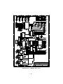
Figure 7: IC Placement
30
B
R9
3
green
10 x 330
CLR
USER
PATT
1
17
D5
D5
C1
13
ENTRG
ENRST
ENCLR
ENUSER
ENPATT
U2A
4
3
8
9
2
1
6
5
/ENTRG
/ENRST
/ENCLR
/ENUSER
/ENPATT
U2F
11
2
ENTRG
ENRST
ENCLR
ENUSER
13
1
4
2
3
U4B
3
4
10
9
8
3
2
1
4
TRG
U5B
5
6
F100325
D4
D4
23
24
R11
R12
R13
R14
R15
R16
R17
R18
R19
R20
10 x
100
Q0
Q1
Q2
Q3
Q4
Q5
D3
D3
21
22
J1
9
U4A
D2
D2
19
20
11
U1F
12
U3
D1
D1
16
15
8
12
74LS125
U5A
RST
U5C
9
8
VEE
RST
14
13
10
U2E
10
D0
D0
VBB
10
9
8
7
6
5
4
3
2
1
TRIG
3
5
13
12
11
+-
2
2
2
D5
4
CLR
U5D
12
11
USER
18
4
D4
2
D3
2
D2
U1B
1
6
TR-GN
RS-GN
CL-GN
US-GN
PA-GN
red
D1
E
U1A
2
TR-RD
RS-RD
CL-RD
US-RD
PA-RD
10
R7
D
PA-GN
PA-RD
1 R8
3
R5
US-GN
US-RD
1 R6
3
R4
R3
C
CL-GN
CL-RD
1
3
R2
1
3 R1
RS-GN
RS-RD
1 R10
A
TR-GN
TR-RD
PATT
0.1µF
TP1
VEE
13
14
4
12
DO4- EN
DO4+ EN
11
10
DO3DO3+ DI4
3
5
6
15
9
DO2- DI3
DO2+
DI2
DO1DO1+ DI1
3
2
U6
17
18
19
20
21
23
24
25
26
27
U7
I11
I10
I9
I8
I7
I6
I5
I4
I3
I2
I1
I0
7
F9
F8
F7
F6
F5
F4
F3
F2
F1
F0
16
13
12
11
10
9
7
6
5
4
3
2
40MHZ
TP2
/EN-CODE
5
OUT
U8
22V10plcc
1
3
VCC
40 MHz
TP3
R22
470
C3
100pF
U39A
90C031
2
VCC
J2
RJ45
1k
VCC
300
24
21
9
1
2
27
28
3
23
26
110 300
VCC
2
4
5
0.1µF
C4
R154
5
U9
REFCLK
VCCA
VCCA
VCCA
INAQ0
INA+
Q1
Q2
INBQ3
INB+
Q4
Q5
A/B
Q6
SO
Q7
MODE
U12 SC/D
CY7B933 RVS
RDY
BISTEN
RF
CKR
470k
R29
C5
6
510
LEDgn
SYNC
7
3
DIS
1
19
TP27
19
10
7
U14
CV
5
0.1µF
NE555
Q
TR
A1
A2
A3
A4
A5
A6
A7
A8
Y1
Y2
Y3
Y4
Y5
Y6
Y7
Y8
18
17
16
15
14
13
12
11
6
FIFI0
5
FIFI1
4
FIFI2
3
FIFI3
2
FIFI4
1
FIFI5
FIFI6 32
FIFI7 31
FIFI8 30
FIFI0
FIFI1
FIFI2
FIFI3
FIFI4
FIFI5
FIFI6
FIFI7
FIFI8
G1
G2
1k
74ALS541
10k
R27
28
26
27
R28
D0
D1
D2
D3
D4
D5
D6
D7
D8
WEN1
REN1
WEN2/LD REN2
WCLK
RCLK
U13
22
2
3
4
5
6
7
9
10
11
12
13
16
I0
I1
I2
I3
I4
I5
I6
I7
I8
I9
I10
I11
F0
F1
F2
F3
F4
F5
F6
F7
F8
F9
27
26
25
24
23
21
20
19
18
17
Q0
Q1
Q2
Q3
Q4
Q5
Q6
Q7
Q8
U10
RS
TP6
TP8
TP9
PAE
PAF
EF
FF
OE
29
16
17
18
19
20
21
22
23
24
FIFO0
FIFO1
FIFO2
FIFO3
FIFO4
FIFO5
FIFO6
FIFO7
FIFO8
FIFO0
FIFO1
FIFO2
FIFO3
FIFO4
FIFO5
FIFO6
FIFO7
FIFO8
10
12
11
/FIFOREN
FIFORCLK
FPAE
8
7
14
15
FPAF
FEF
FFF
/FIFORST
/FIFO-LD
FIFOWCLK
22V10plcc
/CYENA
CYRVS
/CYRDY
CYRF
/CYBIST
2
4
0.1µF
C6
470k
R31
2
13
R
R30
THR
18
17
16
15
14
13
12
11
CY7C42x1
U11
2
3
4
5
6
7
8
9
TP7
VCC
D6
FIFI[0:8]
OUT
25
R25
R26
R23
R24
1
2
3
4
5
6
7
8
110
1
2
3
4
5
6
7
8
UART
74ALS04
TP4
25 MHz
1
TP5
FIFI0
VCC
TP10 TP11
VCC
C7
6
510
D7
LEDye
DATA
7
3
DIS
U15
CV
5
0.1µF
NE555
Q
TR
2
4
R
R32
THR
1
0.1µF
C8
470k
R33
1
VCC
VCC
C9
510
LEDrd
ERROR
7
3
DIS
U16
CV
5
0.1µF
NE555
Q
TR
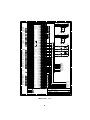
Fakultät für Physik, Freiburg, G. Braun
Title
2
Catch 1 - Data Transfer to/from FE
Size
4
R34
THR
R
6
D8
VCC
A
Date:
B
C
Document
Number
Rev
FPF 288 B
Thursday, October 15, 1998
D
Figure 8: Data Transfer from/to FE
31
05
Sheet
1
of
E
7
A
1k
B
R35
1k
C
D
E
R36
CPLDLED
VCC
VCC
1k
R37
/INIT
D9
D10
D11
3 x LED 3mm 2mA (low current)
LEDgn
PWR
LEDgn
CPLD
LEDrd
FPGAERR
/7SEG8
/7SEG7
/7SEG6
/7SEG5
/7SEG4
/7SEG3
/7SEG2
/7SEG1
VCC
1
6
4
DIS1
HDSP7801(gn)
ANO DE
7
3
2
4
5
8
9
10
DP
G
F
E
D
C
B
A
HARDRES
330
330
330
330
330
330
330
330
R38
R39
R40
R41
R43
R44
R45
R46
/7SEG8
/7SEG7
/7SEG6
/7SEG5
/7SEG4
/7SEG3
/7SEG2
/7SEG1
4
U17A
1
VCC
2
R42
27k
/SOFTRES
74LS07
S1
/PROG
/CPLDRES
SOFTRES
S2
F1 250mA
VCC
CPLD
TEST
J3
3
J5
9
8
6
R50
CTDO
CTDI
1
CTMS
R61
9
R47
8
R48
7
R49
CTCK
4
R54
3
R57
2
F-RT
F-RD
2 FTRIGG
1
JP1
5
R52
4
R55
3
R58
2
1
R62
4 x 270
J6
A01
A02
A03
A04
A05
A06
A07
A08
A09
A10
A11
A12
A13
A14
A15
A16
A17
A18
A19
A20
A21
A22
A23
A24
A25
A26
A27
A28
A29
A30
A31
A32
A33
A34
A35
A36
A37
A38
A39
A40
B01
B02
B03
B04
B05
B06
B07
B08
B09
B10
B11
B12
B13
B14
B15
B16
B17
B18
B19
B20
B21
B22
B23
B24
B25
B26
B27
B28
B29
B30
B31
B32
B33
B34
B35
B36
B37
B38
B39
B40
VCC
9
8
6
5
4
3
2
1
FTDI
FTCK
FTMS
CLKI
CLKO
7 x 270
32 x 270
A01
DOUT0
R64
A02
DOUT2
R66
A03
DOUT4
R68
A04
DOUT6
R70
A05
DOUT8
R72
DOUT10 R74 A06
DOUT12 R76 A07
DOUT14 R78 A08
DOUT16 R80 A09
DOUT18 R82 A10
DOUT20 R84 A11
DOUT22 R86 A12
DOUT24 R88 A13
DOUT26 R90 A14
DOUT28 R92 A15
DOUT30 R94 A16
DOUT32 R96 A17
DOUT34 R98 A18
DOUT36 R100 A19
DOUT38 R102 A20
DOUT40 R104 A21
DOUT42 R106 A22
DOUT44 R108 A23
DOUT46 R110 A24
DOUT48 R112 A25
DOUT50 R114 A26
DOUT52 R116 A27
DOUT54 R118 A28
DOUT56 R120 A29
DOUT58 R122 A30
DOUT60 R124 A31
DOUT62 R126 A32
A33
A34
A35
A36
A37
A38
A39
A40
F2 250mA
PROG
J4
3
R51
R53
R56
R59
R60
R63
6 x 270
CCLK
DONE
DIN
1
/PROG
/INIT
/SOFTRES
2
JP2
F-RT
F-RD
FTRIGG
FTDI
FTCK
FTMS
CLKI
CLKO
32 x 270
B01
DOUT1
R65
B02
DOUT3
R67
B03
DOUT5
R69
B04
DOUT7
R71
B05
DOUT9
R73
B06
DOUT11
R75
B07
DOUT13
R77
B08
DOUT15
R79
B09
DOUT17
R81
B10
DOUT19
R83
B11
DOUT21
R85
B12
DOUT23
R87
B13
DOUT25
R89
B14
DOUT27
R91
B15
DOUT29
R93
B16
DOUT31
R95
B17
DOUT33
R97
B18
DOUT35
R99
B19
DOUT37
R101
B20
DOUT39
R103
B21
DOUT41
R105
B22
DOUT43
R107
B23
DOUT45
R109
B24
DOUT47
R111
B25
DOUT49
R113
B26
DOUT51
R115
B27
DOUT53
R117
B28
DOUT55
R119
B29
DOUT57
R121
B30
DOUT59
R123
B31
DOUT61
R125
B32
DOUT63
R127
B33
B34
B35
B36
B37
B38
B39
B40
CTCK
CTDO
CTDI
CTMS
2
DOUT[0:63]
TP12
DACSDI
TP13
DACLD
90C031
U18
2 x 270
R128
R129
13
14
DO4- EN
DO4+ EN
11
10
DO3DO3+ DI4
5
6
DO2- DI3
DO2+
DI2
DO1DO1+ DI1
3
2
1
4
12
15
9
TP14
7
DACCLK
1
1
DOUTSTR
ROB-NUGENT-80polig (Plug)
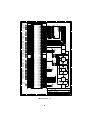
Fakultät für Physik, Freiburg, G. Braun
Title
A1
Size
Date:
A
B
C
Catch 1 - Test Outputs
Document
Number
D
Figure 9: Test Outputs
32
Rev
FPF 288 B
Thursday, October 15, 1998
05
Sheet
2
of
E
7
A
B
C
D
E
VCC
40MHZ
CLOCPLD
CTDI
CTCK
CTMS
CTDO
CCLK
DONE
DIN
/PROG
/INIT
/SOFTRES
UART
3
/FIFOREN
FIFORCLK
FFF
FEF
FPAF
FPAE
/FIFO-LD
FIFOWCLK
/FIFORST
53
VCC
54
/DIP4
55
TIE
56
/DIP3
57
/DIP2
58
/DIP1
59
VCC
60
/DIP0
FSELECT 61
/SOFTRES 62
63
FRW
64
DIN
65
VCC
66
/PROG
67
CCLK
68
GND
69
FTRIG3
70
FTRIG2
71
FTRIG1
72
FTRIG0
73
TIE
FREADY 74
75
/INIT
76
DONE
FDAT15 77
FDAT14 78
79
VCC
FDAT13 80
81
GND
FDAT12 82
FDAT11 83
FDAT10 84
85
FDAT9
86
TIE
87
TIE
88
FDAT8
89
FDAT7
90
FDAT6
91
FDAT5
92
VCC
93
GND
94
CTDI
95
FDAT4
96
CTMS
97
FDAT3
98
CTCK
99
FDAT2
FDAT1 100
FDAT0 101
102
TIE
103
GND 104
/CYENA
CYRF
/CYBIST
CYRVS
/CYRDY
CPLDLED
2
FIFO0
FIFO1
FIFO2
FIFO3
FIFO4
FIFO5
FIFO6
FIFO7
FIFO8
FIFI[0:8]
FDAT0
FDAT1
FDAT2
FDAT3
FDAT4
FDAT5
FDAT6
FDAT7
1
FDAT8
FDAT9
FDAT10
FDAT11
FDAT12
FDAT13
FDAT14
FDAT15
VCC
2
3
4
5
4
SW1
ADD 12..15
VCC
R145
R146
R147
/DIP0
/DIP1
/DIP2
/DIP3
R148
4 x 27k
SW2
ADD 8..11
VCC
D12
330
R149
D13
330
R150
D14
330
R151
D15
330
R152
D16
330
R153
/S0
/S1
3
/S2
/S3
/S4
5 x LED (SMD) grün
/BDS0
/BDS1
/BWRITE
/BAS
/BLWORD
/BIACK
2
/BSYSRES
/BDTACK
/BBERR
/TOVME
BAM[0:5]
BA[1:23]
BA[24:31]
BD[0:15]
BD[16:31]
Fakultät für Physik, Freiburg, G. Braun
VCC
Title
Catch 1 - CPLD
GND
Size
TIE
Date:
A
C
1
2
4
8
GND
BAM4
BA14
VCC
BA7
BA13
BA6
BA12
BA5
BA11
BA4
BA10
BA3
BA9
BA2
GND
BA8
BA1
BA24
BA25
BA26
BA27
BA28
BA29
VCC
BA30
GND
GND
BA31
BD16
BD17
BD18
VCC
BD19
BD20
BD21
TIE
BD22
BD23
BD24
TIE
BD25
BD26
BD27
TIE
BD28
BD29
BD30
GND
BD31
/TOVME
VCC
C
156
155
154
153
152
151
150
149
148
147
146
145
144
143
142
141
140
139
138
137
136
135
134
133
132
131
130
129
128
127
126
125
124
123
122
121
120
119
118
117
116
115
114
113
112
111
110
109
108
107
106
105
4 x 27k
6
GND
I/O_155
I/O_154
VCC
I/O_152
I/O_151
I/O_150
I/O_149
I/O_148
I/O_147
I/O_146
I/O_145
I/O_144
I/O_143
I/O_142
GND
I/O_140
I/O_139
I/O_138
I/O_137
I/O_136
I/O_135
I/O_134
I/O_133
VCC
I/O_131
GND
GND
I/O_128
I/O_127
I/O_126
I/O_125
VCC
I/O_123
I/O_122
I/O_121
I/O_120
I/O_119
I/O_118
I/O_117
I/O_116
I/O_115
I/O_114
I/O_113
I/O_112
I/O_111
I/O_110
I/O_109
GND
I/O_107
I/O_106
VCC
R141
R142
R143
R144
/DIP4
/DIP5
/DIP6
/DIP7
1
VCC
I/O_54
I/O_55/GCK3
I/O_56
I/O_57
I/O_58
VCC
I/O_60
I/O_61
I/O_62
I/O_63
I/O_64
VCC
I/O_66
I/O_67
GND
I/O_69
I/O_70
I/O_71
I/O_72
I/O_73
I/O_74
I/O_75
I/O_76
I/O_77
I/O_78
VCC
I/O_80
GND
I/O_82
I/O_83
I/O_84
I/O_85
I/O_86
I/O_87
I/O_88
I/O_89
I/O_90
I/O_91
VCC
GND
TDI
I/O_95
TMS
I/O_97
TCK
I/O_99
I/O_100
I/O_101
I/O_102
I/O_103
GND
/S1
GND
/S0
BD8
VCC
BD0
BD9
BD1
/BWRITE
BD10
BD2
BD11
BD3
BD12
TIE
BD4
BD13
BD5
GND
BD14
BD6
BD15
BD7
/BDS0
VCC
/BDS1
/BAS
VCC
/BLWORD
/BIACK
/BDTACK
GND
CTDO
/BBERR
/BSYSRES
BA23
VCC
BA22
BAM0
BA21
BAM1
BA20
BAM2
BA19
BAM3
GND
BA18
BA17
BAM5
BA16
BA15
VCC
C
/CPLDRES
208
207
206
205
204
203
202
201
200
199
198
197
196
195
194
193
192
191
190
189
188
187
186
185
184
183
182
181
180
179
178
177
176
175
174
173
172
171
170
169
168
167
166
165
164
163
162
161
160
159
158
157
2
3
4
5
FREADY
FTRIG0
FTRIG1
FTRIG2
FTRIG3
I/O_208
GND
I/O/GSR
I/O_205
VCC
I/O_203
I/O_202
I/O_201
I/O_200
I/O_199
I/O_198
I/O_197
I/O_196
I/O_195
I/O_194
I/O_193
I/O_192
I/O_191
GND
I/O_189
I/O_188
I/O_187
I/O_186
I/O_185
VCC
I/O_183
I/O_182
VCC
I/O_180
I/O_179
I/O_178
GND
TDO
I/O_175
I/O_174
I/O_173
VCC
I/O_171
I/O_170
I/O_169
I/O_168
I/O_167
I/O_166
I/O_165
I/O_164
GND
I/O_162
I/O_161
I/O_160
I/O_159
I/O_158
VCC
1
2
4
8
4
VCC
GND
I/O_3/GTS3
I/O_4
I/O_5/GTS4
I/O_6
I/O_7/GTS1
I/O_8
I/O_9/GTS2
I/O_10
VCC
I/O_12
GND
I/O_14
I/O_15
I/O_16
I/O_17
I/O_18
I/O_19
I/O_20
I/O_21
I/O_22
I/O_23
GND
I/O_25
VCC
GND
I/O_28
I/O_29
I/O_30
I/O_31
I/O_32
I/O_33 FB1
I/O_34
I/O_35
I/O_36
I/O_37
I/O_38
I/O_39
I/O_40
I/O_41
GND
I/O_43
I/O_44/GCK1
I/O_45
I/O_46/GCK2
I/O_47
I/O_48
I/O_49
I/O_50
I/O_51
GND
C
FRW
FSELECT
1
2
3
4
5
6
7
8
9
10
11
12
13
14
15
16
17
18
19
20
21
22
23
24
25
26
27
28
29
30
31
32
33
34
35
36
37
38
39
40
41
42
43
44
45
46
47
48
49
50
51
52
6
VCC
GND
/S2
/S3
/S4
/CYENA
/FIFO-LD
FIFOWCLK
/FIFORST
FIFI8
VCC
FIFI0
GND
FIFI1
FIFI2
FIFI3
FIFI4
FIFI5
FIFI6
FIFI7
FPAF
FPAE
/FIFOREN
GND
FIFORCLK
VCC
GND
FEF
FFF
FIFO0
FIFO1
FIFO2
FIFO3
FIFO4
FIFO8
FIFO7
FIFO6
FIFO5
CYRVS
/CYRDY
/CYBIST
GND
CYRF
40MHZ
UART
CLOCPLD
/CPLDRES
CPLDLED
/DIP7
/DIP6
/DIP5
GND
U38
1
XC95288
B
Document
Number
C
Figure 10: CPLD
33
Rev
FPF 288 B
Wednesday, May 13, 1998
D
04
Sheet
3
of
E
7
1
B
TRG
RST
CLR
USER
PATT
3
ENTRG
ENRST
ENCLR
ENUSER
ENPATT
/ENTRG
/ENRST
/ENCLR
/ENUSER
/ENPATT
/EN-CODE
VCC
M2
DACCLK
DACSDI
DACLD
2
DOUT63
DOUT62
DOUT61
/7SEG7
DOUT60
DOUT59
DOUT58
DOUT57
GND
DOUT56
DOUT55
DOUT54
DOUT53
DOUT52
DOUT51
DOUT50
DOUT49
DOUT48
/INIT
VCC
GND
DOUT47
DOUT46
DOUT45
DOUT44
DOUT43
DOUT42
DOUT41
DOUT40
DOUT39
DOUT38
GND
DOUT37
DOUT36
DOUT35
DOUT34
DOUT33
DOUT32
DOUT31
DOUT30
DOUT29
/7SEG1
/7SEG2
/7SEG3
/7SEG4
/7SEG5
/7SEG6
/7SEG7
/7SEG8
FDAT0
FDAT1
FDAT2
FDAT3
FDAT4
FDAT5
FDAT6
FDAT7
FDAT8
FDAT9
FDAT10
FDAT11
FDAT12
FDAT13
FDAT14
FDAT15
DOUTSTR
DOUT[0:63]
1
GND
DONE
53
54
55
56
57
58
59
60
61
62
63
64
65
66
67
68
69
70
71
72
73
74
75
76
77
78
79
80
81
82
83
84
85
86
87
88
89
90
91
92
93
94
95
96
97
98
99
100
101
102
103
104
nc
nc
VCC
I_56
I/O_57
I/O_58
I/O_59
I/O_60
I/O_61
I/O_62
I/O_63
I/O_64
I/O_65
I/O_66
GND
I/O_68
I/O_69
I/O_70
I/O_71
I/O_72
I/O_73
I/O_74
I/O_75
I/O_76
I/O_77
VCC
GND
I/O_80
I/O_81
I/O_82
I/O_83
I/O_84
I/O_85
I/O_86
I/O_87
I/O_88
I/O_89
GND
I/O_91
I/O_92
I/O_93
I/O_94
I/O_95
I/O_96
I/O_97
I/O_98
I/O_99
I/O_100
GND
nc
DONE
nc
nc
nc
VCC
CCLK
I/O_152
I/O_151
I/O_150
I/O_149
I/O_148
I/O_147
I/O_146
I/O_145
I/O_144
I/O_143
GND
I/O_141
I/O_140
I/O_139
I/O_138
I/O_137
I/O_136
I/O_135
I/O_134
I/O_133
I/O_132
GND
VCC
I/O_129
I/O_128
I/O_127
I/O_126
I/O_125
I/O_124
I/O_123
I/O_122
I/O_121
I/O_120
GND
I/O_118
I/O_117
I/O_116
I/O_115
I/O_114
I/O_113
I/O_112
I/O_111
I/O_110
I/O_109
PROGRAM
nc
VCC
nc
156
155
154
153
152
151
150
149
148
147
146
145
144
143
142
141
140
139
138
137
136
135
134
133
132
131
130
129
128
127
126
125
124
123
122
121
120
119
118
117
116
115
114
113
112
111
110
109
108
107
106
105
20
22
27
11
12
13
15
16
17
18
19
4
CE
OE
WE
R130 4.7k
RDAT7
RDAT6
RDAT5
RDAT4
RDAT3
RDAT2
RDAT1
RDAT0
80 MHz
5
CLO80M
OUT
TP15
U21
JP3
1
2
3
4
CLKI
CLOFPGA
CLKO
3
EXT
N
I T
EXT
50 MHz
OUT
5
U22
GND
F-RD
50
33
25
17
08
JP(2mm)
JP4
1
10
2
9
3
8
4
7
5
6
FPGA
VCC
CCLK
VCC
6
Q
CLK
TP16
DIN
/RAMWE
/RAMOE
5
CLOCPLD
/RAMCE
DACSDI
DACLD
DOUTSTR
DOUT0
GND
DOUT1
DOUT2
DOUT3
DOUT4
DOUT5
DOUT6
DOUT7
DOUT8
DOUT9
DOUT10
GND
VCC
DOUT11
DOUT12
DOUT13
DOUT14
DOUT15
DOUT16
DOUT17
DOUT18
DOUT19
DOUT20
GND
DOUT21
DOUT22
DOUT23
DOUT24
DOUT25
DOUT26
DOUT27
DOUT28
CLO80M
50
33
25
17
08
Q
JP(2mm)
JP5
10
9
8
7
6
VCC
CPLD
VCC
1
2
3
4
5
8
TP23
TP24
TP25
TP26
FSELECT
FREADY
FRW
FDAT0
U23A
74ALS74
1
CCLK
DONE
DIN
/PROG
/INIT
/SOFTRES
/RAMCE
/RAMOE
/RAMWE
D1
D2
D3
D4
D5
D6
D7
D8
CL
FTDI
FTCK
FTMS
FTRIGG
F-RD
F-RT
A0
A1 U20
A2
A3
A4
A5
A6
A7
A8
A9
A10
A11
A12
A13
A14
PR
40MHZ
10
9
8
7
6
5
4
3
25
24
21
23
2
26
1
D
3
2
4
CLKO
RADD0
RADD1
RADD2
RADD3
RADD4
RADD5
RADD6
RADD7
RADD8
RADD9
RADD10
RADD11
RADD12
RADD13
RADD14
U23B
74ALS74
13
CLKI
CY7C199-10
VCC
FSELECT
FRW
FTRIG3
FTRIG2
FTRIG1
FTRIG0
FREADY
FDAT15
FDAT14
FDAT13
GND
FDAT12
FDAT11
FDAT10
FDAT9
FDAT8
FDAT7
FDAT6
FDAT5
FDAT4
FDAT3
VCC
GND
FDAT2
FDAT1
FDAT0
DACCLK
/ENPATT
ENPATT
/ENUSER
ENUSER
/ENCLR
ENCLR
GND
/ENRST
ENRST
/ENTRG
ENTRG
PATT
USER
CLR
RST
CLOFPGA
Q
CLK
9
Q
2
CL
CLOCPLD
208
207
206
205
204
203
202
201
200
199
198
197
196
195
194
193
192
191
190
189
188
187
186
185
184
183
182
181
180
179
178
177
176
175
174
173
172
171
170
169
168
167
166
165
164
163
162
161
160
159
158
157
PR
4
nc
nc
nc
VCC
I/O_204
I/O_203
I/O_202
I/O_201
I/O_200
I/O_199
I/O_198
I/O_197
I/O_196
I/O_195
GND
I/O_193
I/O_192
I/O_191
I/O_190
I/O_189
I/O_188
I/O_187
I/O_186
I/O_185
I/O_184
VCC
GND
I/O_181
I/O_180
I/O_179
I/O_178
I/O_177
I/O_176
I/O_175
I/O_174
I/O_173
I/O_172
GND
I/O_170
I/O_169
I/O_168
I/O_167
I/O_166
I/O_165
I/O_164
I/O_163
I/O_162
I/O_161
GND
O_159
nc
nc
D
11
12
10
FREADY
FTRIG0
FTRIG1
FTRIG2
FTRIG3
nc
GND
nc
I/O_4
I/O_5
I/O_6
I/O_7
I/O_8
I/O_9
I/O_10
I/O_11
I/O_12
I/O_13
GND
I/O_15
I/O_16
I/O_17
I/O_18
I/O_19
I/O_20
I/O_21
I/O_22
I/O_23
I/O_24
GND
VCC
I/O_27
I/O_28
I/O_29
I/O_30
I/O_31
I/O_32
I/O_33
I/O_34
I/O_35
I/O_36
GND
I/O_38
I/O_39
I/O_40
I/O_41
I/O_42
I/O_43
I/O_44
I/O_45
I/O_46
I/O_47
O_48
GND
I_50
nc
nc
E
VCC
VCC
VCC
U24A
74ALS74
1
GND
D
M1
M2
F-RT
F-RD
DONE
/PROG
/INIT
/SOFTRES
R131
R132
R133
R134
R135
R136
R137
R138
6
CLK
5
8 x 27k
VCC
/PROG
Q
CL
1
2
3
4
40MHZ
5
6
/7SEG1
7
/7SEG2
8
FTDI
9
FTCK
10
/7SEG3
11
/7SEG4
12
/7SEG5
13
/7SEG6
14
GND
15
/7SEG8
/SOFTRES 16
17
FTMS
18
FTRIGG
/EN-CODE 19
20
TRG
RADD14 21
RADD12 22
23
RADD7
RADD13 24
25
GND
26
VCC
27
RADD6
28
RADD8
29
RADD5
30
RADD9
RADD4
31
RADD11 32
33
RADD3
34
RADD2
RADD10 35
36
RADD1
37
GND
38
RADD0
39
RDAT7
40
RDAT0
41
RDAT6
42
RDAT1
43
RDAT5
44
RDAT2
45
RDAT4
46
RDAT3
47
48
M1
49
GND
50
F-RT
51
52
FRW
FSELECT
C
U19
Q
PR
XC4020
D
3
2
4
A
VCC
VCC
33 MHz
GND
OUT
1
5
U25
VCC
Fakultät für Physik, Freiburg, G. Braun
Title
Catch 1 - FPGA
Size
Date:
A
B
Document
Number
C
Figure 11: FPGA
34
Rev
FPF 288 B
Wednesday, May 13, 1998
D
04
Sheet
4
of
E
7
A
B
C
D
E
J7
U26 DIR
G
11
12
13
14
15
16
17
18
TP17
/BDTACK
/BBERR
4
B8
B7
B6
B5
B4
B3
B2
B1
A8
A7
A6
A5
A4
A3
A2
A1
1
19
9
8
7
6
5
4
3
2
A1
A2
A3
A4
A5
A6
A7
A8
A9
A10
A11
GND
/DS1
A12
A13
/DS0
A14
/WRITE
A15
GND
A16
/DTACK
A17
GND
A18
/AS
A19
GND
A20
/IACK
A21
/IACKIN
/IACKOUT A22
A23
AM4
A24
A7
A25
A6
A26
A5
A27
A4
A28
A3
A29
A2
A30
A1
A31
-12V
A32
VCCIN
B1
B2
B3
B4
B5
B6
B7
B8
B9
B10
/BG3IN
/BG3OUT B11
B12
B13
B14
B15
B16
AM0
B17
AM1
B18
AM2
B19
AM3
B20
GND
B21
B22
B23
GND
B24
B25
B26
B27
B28
B29
B30
B31
B32
VCCIN
C1
D8
C2
D9
C3
D10
C4
D11
C5
D12
C6
D13
C7
D14
C8
D15
C9
GND
C10
C11
/BERR
C12
/SYSRES
C13
/LWORD
C14
AM5
C15
A23
C16
A22
C17
A21
C18
A20
C19
A19
C20
A18
C21
A17
C22
A16
C23
A15
C24
A14
C25
A13
C26
A12
C27
A11
C28
A10
C29
A9
C30
A8
C31
C32
VCCIN
D0
D1
D2
D3
D4
D5
D6
D7
GND
/DTACK
/BERR
74ALS641-1
U27
/BDS0
/BDS1
/BWRITE
/BAS
/BLWORD
/BIACK
/BSYSRES
11
12
13
14
15
16
17
18
TP18
Y8
Y7
Y6
Y5
Y4
Y3
Y2
Y1
G2
G1
A8
A7
A6
A5
A4
A3
A2
A1
19
1
9
8
7
6
5
4
3
2
/DS0
/DS1
/WRITE
/AS
/LWORD
/IACK
/SYSRES
74ALS541
/TOVME
U28 DIR
G
11
12
13
14
15
16
17
18
BD0
BD1
BD2
BD3
BD4
BD5
BD6
BD7
3
B8
B7
B6
B5
B4
B3
B2
B1
A8
A7
A6
A5
A4
A3
A2
A1
1
19
9
8
7
6
5
4
3
2
D0
D1
D2
D3
D4
D5
D6
D7
74ALS645-1
U29 DIR
G
11
12
13
14
15
16
17
18
BD8
BD9
BD10
BD11
BD12
BD13
BD14
BD15
BD[0:15]
B8
B7
B6
B5
B4
B3
B2
B1
A8
A7
A6
A5
A4
A3
A2
A1
1
19
9
8
7
6
5
4
3
2
D8
D9
D10
D11
D12
D13
D14
D15
74ALS645-1
BA[1:23]
U30
11
12
13
14
15
16
17
18
BA23
BA22
BA21
BA20
BA19
BA18
BA17
BA16
2
Y8
Y7
Y6
Y5
Y4
Y3
Y2
Y1
G2
G1
A8
A7
A6
A5
A4
A3
A2
A1
19
1
9
8
7
6
5
4
3
2
A23
A22
A21
A20
A19
A18
A17
A16
74ALS541
U31
11
12
13
14
15
16
17
18
BA15
BA14
BA13
BA12
BA11
BA10
BA9
BA8
Y8
Y7
Y6
Y5
Y4
Y3
Y2
Y1
G2
G1
A8
A7
A6
A5
A4
A3
A2
A1
19
1
9
8
7
6
5
4
3
2
A15
A14
A13
A12
A11
A10
A9
A8
74ALS541
U32
11
12
13
14
15
16
17
18
BA7
BA6
BA5
BA4
BA3
BA2
BA1
1
Y8
Y7
Y6
Y5
Y4
Y3
Y2
Y1
G2
G1
A8
A7
A6
A5
A4
A3
A2
A1
GND
19
1
9
8
7
6
5
4
3
2
A7
A6
A5
A4
A3
A2
A1
74ALS541
AM[0:5]
A1
A2
A3
A4
A5
A6
A7
A8
A9
A10
A11
A12
A13
A14
A15
A16
A17
A18
A19
A20
A21
A22
A23
A24
A25
A26
A27
A28
A29
A30
A31
A32
4
B1
B2
B3
B4
B5
B6
B7
B8
B9
B10
B11
B12
B13
B14
B15
B16
B17
B18
B19
B20
B21
B22
B23
B24
B25
B26
B27
B28
B29
B30
B31
B32
3
C1
C2
C3
C4
C5
C6
C7
C8
C9
C10
C11
C12
C13
C14
C15
C16
C17
C18
C19
C20
C21
C22
C23
C24
C25
C26
C27
C28
C29
C30
C31
C32
2
1
VME_J1/P1_UPPER_CONN
Fakultät für Physik, Freiburg, G. Braun
Title
Catch 1 - Upper VME Connector
Size
Date:
A
B
C
Document
Number
D
Figure 12: Upper VME connector
35
Rev
FPF 288 B
Wednesday, May 13, 1998
04
Sheet
5
of
E
7
A
B
C
D
E
J8
A1
A2
A3
A4
A5
A6
A7
A8
A9
A10
A11
A12
A13
A14
A15
A16
A17
A18
A19
A20
A21
A22
A23
A24
A25
A26
A27
A28
A29
A30
A31
A32
4
/TOVME
U33 DIR
G
BD16
BD17
BD18
BD19
BD20
BD21
BD22
BD23
3
11
12
13
14
15
16
17
18
B8
B7
B6
B5
B4
B3
B2
B1
A8
A7
A6
A5
A4
A3
A2
A1
1
19
9
8
7
6
5
4
3
2
D16
D17
D18
D19
D20
D21
D22
D23
VCCIN
A24
A25
A26
A27
A28
A29
A30
A31
74ALS645-1
U34 DIR
G
BD24
BD25
BD26
BD27
BD28
BD29
BD30
BD31
11
12
13
14
15
16
17
18
BD[16:31]
B8
B7
B6
B5
B4
B3
B2
B1
9
8
7
6
5
4
3
2
VCCIN
D16
D17
D18
D19
D20
D21
D22
D23
D24
D25
D26
D27
D28
D29
D30
D31
74ALS645-1
BA[24:31]
U35
BA24
BA25
BA26
BA27
BA28
BA29
BA30
BA31
2
A8
A7
A6
A5
A4
A3
A2
A1
1
19
11
12
13
14
15
16
17
18
Y8
Y7
Y6
Y5
Y4
Y3
Y2
Y1
G2
G1
A8
A7
A6
A5
A4
A3
A2
A1
D24
D25
D26
D27
D28
D29
D30
D31
19
1
9
8
7
6
5
4
3
2
A24
A25
A26
A27
A28
A29
A30
A31
VCCIN
C1
C2
C3
C4
C5
C6
C7
C8
C9
C10
C11
C12
C13
C14
C15
C16
C17
C18
C19
C20
C21
C22
C23
C24
C25
C26
C27
C28
C29
C30
C31
C32
74ALS541
BAM[0:5]
U36
BAM0
BAM1
BAM2
BAM3
BAM4
BAM5
11
12
13
14
15
16
17
18
Y8
Y7
Y6
Y5
Y4
Y3
Y2
Y1
G2
G1
A8
A7
A6
A5
A4
A3
A2
A1
19
1
9
8
7
6
5
4
3
2
B1
B2
B3
B4
B5
B6
B7
B8
B9
B10
B11
B12
B13
B14
B15
B16
B17
B18
B19
B20
B21
B22
B23
B24
B25
B26
B27
B28
B29
B30
B31
B32
AM0
AM1
AM2
AM3
AM4
AM5
74ALS541
AM[0:5]
1
A1
A2
A3
A4
A5
A6
A7
A8
A9
A10
A11
A12
A13
A14
A15
A16
A17
A18
A19
A20
A21
A22
A23
A24
A25
A26
A27
A28
A29
A30
A31
A32
4
B1
B2
B3
B4
B5
B6
B7
B8
B9
B10
B11
B12
B13
B14
B15
B16
B17
B18
B19
B20
B21
B22
B23
B24
B25
B26
B27
B28
B29
B30
B31
B32
3
C1
C2
C3
C4
C5
C6
C7
C8
C9
C10
C11
C12
C13
C14
C15
C16
C17
C18
C19
C20
C21
C22
C23
C24
C25
C26
C27
C28
C29
C30
C31
C32
2
1
VME_J2/P2_LOWER_CONN
Fakultät für Physik, Freiburg, G. Braun
Title
Catch 1 - Lower VME Connector
Size
Date:
A
B
C
Document
Number
D
Figure 13: Lower VME connector
36
Rev
FPF 288 B
Wednesday, May 13, 1998
04
Sheet
6
of
E
7
A
B
L1
4
C
D
E
F3
4
VCCIN
VCC
DROSSEL
+
3A
C10
6.8µF/20V
C11
0.1µF
C12
0.1µF
C13
0.1µF
C14
0.1µF
VCC
C15
0.1µF
C16
0.1µF
C17
0.1µF
C18
0.1µF
C19
0.1µF
C20
0.1µF
C21
0.1µF
C22
0.1µF
C23
0.1µF
C24
0.1µF
C25
0.1µF
C26
0.1µF
C27
0.1µF
C28
0.1µF
C29
0.1µF
C30
0.1µF
C31
0.1µF
C32
0.1µF
C33
0.1µF
C34
0.1µF
C35
0.1µF
C36
0.1µF
C37
0.1µF
C38
0.1µF
C39
0.1µF
C40
0.1µF
C41
0.1µF
C42
0.1µF
C43
0.1µF
C44
0.1µF
3
3
C45
0.1µF
C46
0.1µF
C47
0.1µF
C48
0.1µF
C49
0.1µF
C50
0.1µF
C51
0.1µF
C52
0.1µF
C53
0.1µF
C54
0.1µF
C59
0.1µF
C60
0.1µF
C61
0.1µF
C62
0.1µF
C63
0.1µF
C64
0.1µF
C65
0.1µF
C66
0.1µF
C67
0.1µF
C68
0.1µF
C71
0.1µF
C70
0.1µF
C69
0.1µF
U37
500mA
V_OU
3
1
DROSSEL
LM337D2T
V_IN
+
2
4
V_AD
F4
C55
VEE
+
L2
-12V
2
R139
330
C56
6.8µF/20V
6.8µF/20V
R140
1k
VEE
C57
0.1µF
TP19
TP20
TP21
TP22
1
1
Fakultät für Physik, Freiburg, G. Braun
Title
Catch 1 - Power
Size
Date:
A
B
Document
Number
C
Figure 14: Power
37
Rev
FPF 288 B
Wednesday, May 13, 1998
D
04
Sheet
7
of
E
7