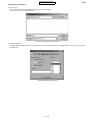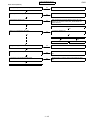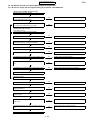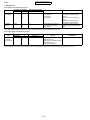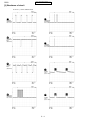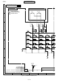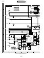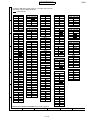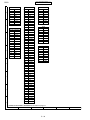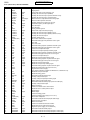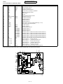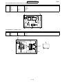
1
CONFIDENTIAL
GX20
SERVICE MANUAL
No. S9311TQGX20/B
DIGITAL MOBILE PHONE
MODEL
GX20
(INTERNAL MODEL NAME:
TQ-GX20E/G/R/T/S/H/EP/PP/W/B/D/A/Z/Q/L/F/C)
E : For U.K.
R : For Ireland
S : For Spain
EP: For U.K. (Prepaid)
W : For Sweden
D : For Greece
Z : For New Zealand
L : For Malta
C : For Switzerland
G : For Germany
T : For Italy
H : For Netherlands
PP: For Portugal (Prepaid)
B : For Hungary
A : For Australia
Q : For Egypt
F : For France
• In the interests of user-safety the set should be restored to its
original condition and only parts identical to those specified
should be used.
• Caution
Risk of explosion if battery is replaced by an incorrect type,
dispose of used batteries according to the instruction.
CONTENTS
CHAPTER 1. GENERAL DESCRIPTION
[1] Specifications ................................................ 1-1
[2] Names of parts .............................................. 1-2
[3] Operation manual.......................................... 1-3
CHAPTER 2. ADJUSTMENTS
[1] Adjustments
SHARP Program Support Tool (SPST)........ 2-1
[2] SHARP RF Test tool manual ....................... 2-30
[3] Adjustment procedures
after replacement of the parts .................. 2-36
[4] Test points ................................................... 2-39
[5] Troubleshooting........................................... 2-42
[6] Specification for function test ...................... 2-64
CHAPTER 3. DISASSEMBLY AND REASSEMBLY
[1] Servicing Concerns ....................................... 3-1
[2] Disassembly and reassembly ....................... 3-5
CHAPTER 4. DIAGRAMS
[1] Block diagram .................................................4-1
CHAPTER 5. SCHEMATIC DIAGRAM AND
WIRING SIDE OF P.W.BOARD
[1] Notes on schematic diagram ..........................5-1
[2] Types of transistor and LED ...........................5-1
[3] Waveforms of circuit .......................................5-2
[4] Schematic diagram/
wiring side of P.W.Board ..............................5-6
CHAPTER 6. OTHERS
[1] Function table of IC.........................................6-1
[2] Function table of Camera .............................6-27
Parts Guide
Parts marked with "
" are important for maintaining the safety of the set. Be sure to replace these parts with specified ones for
maintaining the safety and performance of the set.
SHARP CORPORATION
This document has been published to be used
for after sales service only.
The contents are subject to change without notice.
GX20
CONFIDENTIAL
Service
GX20
OZ/IQ/YO/Calc
E
Market
TQGX20
Manual 1. GENERAL DESCRIPTION
CHAPTER
FOR A COMPLETE DESCRIPTION OF THE OPERATION OF THIS UNIT, PLEASE
REFER TO THE OPERATION MANUAL.
[1] Specifications
General:
Dimensions
(folded, excluding the aerial)
(H x W x D):
Weight:
Battery operating
temperature:
Main display:
Sound:
Mobile light:
External DC
supply voltage:
Battery:
Standby time:
Talk time:
Others:
Tri - band (GSM 900 MHz/DCS 1800 MHz/
PCS 1900MHz)
GPRS-enabled
WAP, MMS, SMS
95 x 49 x 25 mm
102 g
0°C - 40°C
Display dimensions: 320 x 240 pixels
LCD display: CGS 262,144 colours with backlight
LCD backlight: LED backlight white colour LEDs
External display: Display dimensions: 60 x 80 pixels
LCD display: STN 256 colours LCD with backlight
Camera:
CCD 350K pixels built-in camera
Zoom: Wide and zoom mode
[Supported 4 (when image size is
120 x 160 pixels) x zoom]
Lens: F2.8, f = 2.6 mm
Powered by JBlend R , C 1997-2003 Aplix Corporation. All
rights reserved.
Java and all Java-based trademarks and logos are trademarks or registered trademarks of Sun Microsystems, Inc.
in the U.S. and other countries.
JBlend and all JBlend-based trademarks and logos are
trademarks or registered trademarks of Aplix Corporation in
Japan and other countries.
R
In this product, JBlend is incorporated.
R
JBlend is a Java execution environment
that Aplix developed for implementing
advanced performance and fast operation
on small-memory systems. JBlend and
JBlend logo are trademarks or registered
trademarks of Aplix Corporation in Japan
and other countries.
Powered by Mascot Capsule /Micro3D EditionTM
Mascot Capsule R is a registered trademark of HI Corporation
C 2002-2003 HI Corporation. All Rights Reserved.
R
1–1
16-polyphonic ring melodies
7 colours
5.2 V
3.7 V, 720 mAh, Li-Ion
100 ~ 250 hours
180 ~ 240 min.
Side key
Infrared port 1.2 L/P (maximum distance 20 cm)
Connector for AC charger and data cable
Standard hands free connector (ø2.5)
Battery ranning time depends on the battery and SIM card as well as
the network conditions and usage
Specifications for this model are subject to change without prior
notice.
Licensed by Inter Digital Technology Corporation under one
or more of the following United States Patents and/or their
domestic or foreign counterparts and other patents pending, including U.S. Patents: 4,675,863: 4,779,262:
4,785,450 & 4,811,420.
Licensed under U.S. Patent 4,558,302 and foreign counterparts.
T9 Text input is licensed under one or more of the following:
U.S. Pat. Nos. 5,818,437, 5,953,541, 5,187,480, 5,945,928,
and 6,011,554; Australian Pat. No. 727539; Canadian Pat.
No. 1,331,057; United Kingdom Pat. No. 2238414B; Hong
Kong Standard Pat. No. HK0940329; Republic of
Singapore Pat. No. 51383; Euro. Pat. No. 0 842 463
(96927260.8) DE/DK, Fl, FR, IT, NL,PT.ES,SE,GB;
Republic or Korea Pat. Nos. KR201211B1 and
KR226206B1; and additional patents are pending
worldwide.
GX20
CONFIDENTIAL
[2] Names of parts
17
18
19
1
8
20
21
2
3
4
5
6
7
22
9
10
11
12
13
23
24
14
15
26
25
16
1. Earpiece
2. Navigation Keys (Arrow Keys):
Moves cursor to select
menu items, etc.
,
,
,
in this
manual indicate these keys.
Up/Down arrow keys: Displays Contacts List
entries in stand-by mode.
Left arrow key:
Displays list of
Applications in stand-by
mode.
Right arrow key:
Displays list of Saved
Pictures in stand-by mode.
3. Centre Key:
Displays Main menu in
stand-by mode and
executes functions.
in this manual indicates
this key.
4. Left Soft Key:
Executes the function at the
bottom left of the screen.
in this manual indicates
this key.
5. Send Key:
Makes or accepts calls,
views the call in stand-by
mode.
6. Voice Mail Key:
Press and hold this key to
connect to the Voice mail
centre automatically.
(Depends on the SIM card.)
7. * /Shift Key,
Viewfinder Switch Key:
Enters *.
Press and hold this key to
switch input method among
four modes: Abc, ABC, abc
and 123.
Switches viewfinders
between main display and
external display in digital
camera/video camera
mode.
8. Main Display
9. Hands Free Connector
10. Right Soft Key:
Executes the function at the
bottom right of the screen.
in this manual indicates
this key.
11. “Vodafone live!” Key:
Used to access “Vodafone
live!” by opening the
browser.
12. End/Power Key:
13. Keypad
14. #/Flash light Key:
Ends a call, turns power on/
off.
Switches symbol screens.
Press and hold this key to
shift text input method
between multi-tap and T9
mode.
Turns the flash/auxiliary
light on or off in digital
camera/video camera
mode.
15. Microphone
16. External Connector:
Used to connect either the
charger or data cable.
17. Aerial
18. Mobile Light:
Used as a flash or an
auxiliary light in digital
camera/video camera
mode, as a battery charge
indicator, or notification for
incoming calls, data/fax
calls or messages.
19. Macro Dial:
(Close-up)
20. Camera
21. External Display
22. Infrared Port:
Turns the dial to normal
( ) or macro ( )
position.
Sends and receives data via
infrared.
23. Speaker
24. RF Connector
25. Side-Up/Side-Down Keys:
Moves cursor to select
menu items, adjusts
earpiece volume, etc.
In stand-by mode, press
and hold this key to turn the
mobile light on and off.
When the mobile light is
on, press this key to change
the light colour.
26. Battery Cover
1–2
1–3
ii
Select
G
by SHARP
Camera
Exit
key. Do the same to turn it off again.
i
Takes you to the Vodafone live! home page.
(During call): Ends a call.
(Press and hold): Turns handset on and off.
(In menus): Takes you back to the Standby screen.
(When ringing): Answers a call.
(In Standby): Brings up Last Dialled numbers.
The softkey selects whatever icon or command is shown in the bottom left of the
screen. The softkey selects the bottom right of the screen (this usually acts as
Cancel or Back.) The
key will select what’s in the middle.
(Navigation keys): Use to move between icons in menus and item lists.
(In Standby): Brings up commonly used menus (Contacts List, Applications and Saved
Pictures).
(Centre key): Use to select an icon or menu item.
In Standby: Takes you to the main Menu (shown in phone).
In Camera mode: Takes a picture or starts/stops video recording.
The GX20 has many features, but exploring and using them is simple,
thanks to the 5-way central navigation key and the contextual
softkeys.
3. Turning it on and off:
Open the handset, then press and hold the red
2. Charging the battery:
Before using your handset for the first time, it’s important to charge the battery for at least 2
hours (see page 14 of the Manual).
1. Inserting your SIM card:
Slide off the battery cover, and remove the battery. Slide your Vodafone SIM card (with the
gold contacts facing downwards) into its holder. Replace the battery and cover.
QUICKSTART GUIDE
2: NAVIGATION
SIM card
The Sharp GX20 is one of the most advanced mobile handsets available. With it you will be
able to use its built-in camera to take pictures and video clips, play arcade quality games,
listen to life-like polyphonic ringtones and sounds, send Multimedia messages, and connect
to Vodafone live! and the mobile internet.
But before you can do any of this, first you need to make sure your handset is prepared.
QUICKSTART GUIDE
1: GETTING STARTED
•
•
•
•
•
In just a few minutes this QuickStart Guide will show you how to use
some of the main features of your new GX20.
GX20
CONFIDENTIAL
[3] Operation manual
(Page numbers refer to the user guide)
[Optional Accessories]
Li-ion spare battery (XN-1BT11)
High capacity Li-ion battery (XN-1BT13)
Cigarette lighter charger (XN-1CL10)
Data cable (RS232C cable: XN-1DC10)
AC charger (Except for France: XN-1QC10, XN-1QC11)
(for France: XN-1QC11)
The above accessories may not be available in all regions.
For details, please contact your dealer.
[Quickstart Guide] (Except for France, Swiss)
F
Fine
0 x1
1–4
iv
G
32KB
T9
Abc
T9
Options
32KB
OK
Picture
Sound
Video Clip
Message Template
Text Template
Preview Message
Select
Message:
G
Options
Abc
Hi there - wait til you
see this! |
Message:
Back
34/2000
Clear
34/2000
key in Standby mode). Select
,
4. Add your picture: ( symbol in message menu bar)
Press [Options] and select Picture. Highlight the picture you want, press
[Back].
, then press
Tip: To send video you may have to adjust the setting. Select Multimedia Messages in the
Messages menu, then press [Options]. Choose Settings, Slide Show then make sure
that Off is selected.
3. Add your video clip: ( symbol in message menu bar)
Press [Options] and select Video Clip. Highlight the clip you want to send. Press
then press [Back].
Tip: To turn Predictive Text (T9) off and on while entering text, press and hold the
key
(you’ll see the T9 symbol at the top of the screen). Press and hold the
key to cycle
through the Input Method (capitals, numeric, etc.).
2. Write your message:
Use the keypad to write your text. To enter punctuation or other characters, press the
key, then select the symbol you want. For a space, press
.
1. Create a new Multimedia message:
Select Messages in the main Menu (or press the
Multimedia Messages, then Create Message.
Life is more than just text. With Multimedia Messaging you can now
send video clips, pictures and sounds as well! Your handset is already
enabled to send and receive Multimedia Messaging, but if you have
any problems call your local Vodafone customer services.
Tip: You can change the camera viewfinder to the external display (for taking pictures/
videos of yourself) by pressing the
key. And you can adjust the Macro dial around the
lens to take close-up shots ( ).
4. Digital Camera mode:
Macro Choose Digital Camera in the Camera menu (or press the key in Standby mode).
dial
Press
to take the picture. Press [Save] to save it (in My Stuff), or press [Cancel]
and take it again.
3. Saving your video:
Now you’ll be offered the choice of Save or Preview. Choose Preview to review your clip,
then press [Back]. If you’re happy with the clip, select Save (it will be saved in My Stuff
in the main Menu). If not, press [Cancel], and try again.
2. Recording a video clip:
The screen becomes your viewfinder. You can zoom in (up to 4×) by pressing the
key
(the
key zooms out again). You can also adjust the brightness using the
and
keys. Then press
to start recording. When you’ve finished, press
again.
iii
QUICKSTART GUIDE
3: THE CAMERA
1. Video Camera mode:
Go to the main Menu (press
in Standby mode), select the Camera icon (you’ll see the
word ‘Camera’ in the red title bar), then press
. Select Video Camera.
QUICKSTART GUIDE
4: MULTIMEDIA MESSAGING
External
display
Stop
16
The GX20’s built-in camera now lets you take video clips, as well as
having digital zoom and even a flash. Once you’ve taken your video
or picture you can save it, then send it to others at a mobile number
or email address (see next page).
G
G
abc
21/60
Back
Clear
vi
Help &
Search
This works very like an
ordinary web browser. Use
the navigation keys to
highlight the item you want
to select, then press
to
open that page. Press
[Back] to go back a page.
Press [Options] for the
Browser Option menu.
My
Vodafone
More...
Download
Chat
Games
Messages
New
[Options], then Play.
v
Tip: Vodafone live! is growing and changing all the time, so these options may vary. Keep
checking it out to see what’s new.
Or link directly to Vodafone live! services:
In the main Menu, select the Vodafone live! section, and choose your service:
Games: Online fun and games to download...
Ringtones: Download music, sounds and ringtones.
Pictures: Download images, animations and background wallpaper.
News: Get the latest news as it happens...
Sport: News, results and latest scores (with pictures).
Find & Seek: Get the local information you need, wherever you are.
Chat: Instant messaging and text chat with all your friends.
Search: Find what you need in Vodafone live!
Tip: Your GX20 uses GPRS, a fast way of getting mobile information. Also, the connection
is ‘always on’ — which means no wait for dialling up. You only pay for data you send or get,
not how long you’re connected.
Connect to Vodafone live!:
Simply press the
key (under the Navigation key) to connect you to the Vodafone live!
main menu. To exit, press the
key.
Vodafone live! is a mobile internet portal which is your gateway to a
new world of information, games, music and sevices.
Tip: Press [Options], then select Search in the To: screen to bring up your Contacts list.
Then choose the mobile number or email address for the contact you wish to send it to. It
will be entered in the To: screen automatically.
8. Send to an email address:
After Step 6, press [Options], and select Input Method. Choose abc and then press
[Back]. Then write the email address (using the
key to bring up the symbols menu for
the @ key). Press
, then select Send and press
again.
Tip: Try sending it to yourself to see how it works!
7. Send to another mobile:
Enter the number of the mobile phone you want to send it to. Press
, then select Send
and press
again. If the receiving phone can’t display Multimedia messages or video
clips, they’ll be sent a link to a web page they can view them on.
6. Preview your message:
Then press [Options], and select Preview Message. If you’re happy with the message,
press
, then
again to go to the To: screen.
5. Add a sound file: ( symbol in message menu bar)
Press [Options] and select Sound. To listen to the sounds, press
Highlight the sound you want, press
, then press [Back].
QUICKSTART GUIDE
5: Vodafone live!
Options
[email protected]|
To:
Options
Hi there - wait til you
see this!
QUICKSTART GUIDE
CONFIDENTIAL
GX20
Back
1–5
viii
G
Select
External Display
Illustration 1
Wallpaper
Backlight
LCD Contrast
Incoming Indication
Clock Display
Icon Display
LCD On/Off
Start
Voice Memo
Ready to record
G
Back
Back
5. External display:
You can customise your External display in the same way as your main screen. Go to Phone
Settings from the main Menu, then choose External Display. Now you can change the way
the clock looks, the background picture, even the icon displayed when there’s a call...
4. Front light:
Press and hold the side key on the left side of the handset (in Standby mode) to turn the
light on and off (it can be used as a makeshift torch). Press the side key to change the colour
(the last selection cycles through them all like a disco light).
3. Voice Memo:
Press
then
to bring up the Voice Memo application. Press
to record, and again
to stop. You can send voice memos as part of a Multimedia message.
2. International dialling:
Press and hold the
key for the (+) sign when dialling international numbers.
1. Silent mode:
To switch your handset to silent mode, press and hold the
key. Highlight the Silent
profile and select it. Select the Normal profile to go back to your usual setting.
Here are a few tips to help you use your new handset. There’s much
more information in the manual — or you could just explore all the
menus and options screens...
3. Download new games:
To add more arcade quality games to your handset, go to Fun & Games (in the main Menu)
and choose Games & More/Download More. Choose a game to download, and you’ll find
it in Fun & Games/Games & More/Applications.
2. Download new background wallpaper:
To choose a new background image for your phone, go to My Stuff/Pictures/
Download More. Choose an image and follow the instructions to download it. Then go to
Settings (in the main Menu)/Phone Settings/Main Display/Wallpaper/My Pictures, and
select your downloaded image.
Tip: To activate your ringtone, go to Profiles (in the main Menu), then choose Normal, then
select Options/Personalise/Assign Melody. Choose My Sounds and select your
downloaded ringtone.
1. Download a new ringtone:
Your GX20 uses polyphonic ringtones for a more life-like sound. Go to the My Stuff section
from the main Menu, choose Sounds and then Download More. Choose the ringtone you’d
like and follow the instructions to download it.
vii
QUICKSTART GUIDE
6: DOWNLOADING
You can download from the Vodafone live! portal or the handset shortcuts (see previous
page), or use the Download More menus:
QUICKSTART GUIDE
7: TIPS AND TRICKS
Select
1-1-3
Games & More
Applications
Screensavers
Download More
Settings
JavaªTM Information
G
Normal
Pattern 1
Ringer VolumeDownload More
Assign Melody
Vibration
Keypad Tones
Warning Tone
Power On Sound
Power Off Sound
Message Alert
Save
Back
G
Personalise your new handset by downloading new ringtones,
images and background wallpaper from Vodafone live!. All
downloads are saved in the My Stuff section of the main Menu.
GX20
CONFIDENTIAL
CONFIDENTIAL
Service
GX20
OZ/IQ/YO/Calc
E
Market
TQGX20
Manual 2. ADJUSTMENTS
CHAPTER
[1] Adjustments
SHARP Program Support Tool (SPST)
1. Outline
This document provides user information required to install and use GX20 Program Support Tool (SPST).
2. System requirements
•
IBM PC compatible personal computer (standard COM1 serial port (115,200 bps) and USB required)
Supporting OS: Windows 98/98SE/2000/XP (except for Windows 95/ME/NT)
(English, German, Italian, Spanish, French and Chinese versions)
•
Data cable
•
Full charged battery
<During RF adjustment>
•
RF test instrument: CMU200
•
GPIB interface: National Instruments USB-GPIB cable
Model No.: NI GPIB-USB-B
•
The battery should be fully charged.
3. Introduction
3.1. Functions
SPST offers five key functions:
1. Software download
2. User data transfer (processes all data at once but not individually)
3. RF calibration
4. Default setting
5. Identification
SPST functions as a launcher for these independent software programs.
3.2. Installation
The SPST software is distributed in CD-ROM format.
1) Use Windows Explorer and copy “UpgradingTool.zip” and “SPST.zip” to the desktop.
2) Unzip and install “UpgradingTool.zip” following the procedures below.
3) Unzip the “SPST.zip”.
Hereinafter, procedures are carried out in the SPST folder.
3.2.1 Starting up
Connect GX20 to an operable serial port of the PC with the supplied data cable. Connect the AC charger to the Data cable.
Execute the GX20 SPST.exe program in the SPST folder.
1) The SPC input screen appears. Input SPC (2968) and press “OK”.
If you do not know SPC, press “Cancel” to close.
Figure 1
2–1
GX20
GX20
CONFIDENTIAL
2) If SPC is correct, the following screen appears.
Figure 2
The software for each function is independent and thus multi-bootable. However, you can only activate single software at a time. To start snother
software, exit the current one.
3) Click the “Change Password” button in Step 1. The screen below appears and you can change SPC.
Figure 3
3.3. Functions
3.3.1 Identification
SPST downloads and displays the main data configured in GX20.
<Operation>
1) On the SPST startup screen, press “Identity”.
Figure 4
2) Connect PC and MS with a Data cable.
3) Remove the SIM card and turn on the phone. → Regular display.
4) Select the COM port.
5) Press “Get Identity”. → The information will be displayed.
2–2
GX20
CONFIDENTIAL
6) IMEI will be displayed, and the following dialog box appears.
Figure 5
7) Make sure GX20 is turned off and press the power key.
8) Press “OK” when **** appears on the GX20 display.
9) Make sure “Success!!” appears. Check the data and exit.
Refer to the attachment 1
for the operator code.
Software version: 012
IMEISV: 06
Figure 6
Attachment 1
No.
01
02
03
04
05
06
08
10
11
12
13
14
15
16
17
48
50
Operator Code Chart
Operator name
Vodafone UK
Post-Paid
Airtel
Post-Paid
SFR
Post-Paid
Vodafone Omnitel
Post-Paid
D2
Post-Paid
Vodafone NL
Post-Paid
Vodafone Ireland
Post-Paid
Vodafone Greece
Post-Paid
Vodafone Hungary
Post-Paid
Vodafone Australia
Post-Paid
Vodafone New Zealand
Post-Paid
Vodafone Sweden
Post-Paid
Vodafone Egypt
Post-Paid
Vodafone Malta
Post-Paid
Swisscom
Post-Paid
Vodafone PT
Pre-Paid
Vodafone UK
Pre-Paid
Country
UK
Spain
France
Italy
Germany
Netherlands(Holland)
Ireland
Greece
Hungary
Australia
New Zealand
Sweden
Egypt
Malta
Switzerland
Portugal
UK
2–3
Model name
A4TQGX20E
A4TQGX20S
A4TQGX20F
A4TQGX20T
A4TQGX20G
A4TQGX20H
A4TQGX20R
A4TQGX20D
A4TQGX20B
A4TQGX20A
A4TQGX20Z
A4TQGX20W
A4TQGX20Q
A4TQGX20L
A4TQGX20C
A4TQGX20PP
A4TQGX20EP
GX20
CONFIDENTIAL
3.3.2 User data transfer
SPST saves and downloads all the following user data.
1) Connect PC and MS with a Data cable and turn on MS.
2) Activate the software.
Figure 7
a) Select the COM port. You cannot specify the communication protocol. (115 kbps)
b) Press “Recognition”.
Do not press “Recognition” until “InsertSIM” appears.
3) Press either “BACKUP”, “RESTORE” or “END”.
Figure 8
2–4
CONFIDENTIAL
4) If “BACKUP” is pressed, the dialog box for file selection appears. Select the file and press “Save”.
Figure 9
The buttons are grayed out during the process.
Firue 10
2–5
GX20
GX20
CONFIDENTIAL
When they return to black, the process is complete. Press “END” to exit.
Figure 11
5) If “RESTORE” is pressed, the following confirmation dialog box appears. Press “OK” to confirm.
Figure 12
The dialog box for file selection appears. Select the file and press “Open”.
Figue 13
2–6
CONFIDENTIAL
The buttons are grayed out during the process.
The process is complete when the buttons turn black.
Figure 14
3.3.3 Default setting
You can reset settings to the factory default. The following will be performed:
1. All user data in the file system is deleted.
2. All WAP settings return to the default.
3. All values set by users return to the default.
4. 1) MEPLOCK setting remains unchanged.
When “MEPLOCK Set Default” is unchecked:
MEPLOCK remains disabled if canceled after shipment. Check “MEPLOCK Set Default” to activate it.
2) MEPLOCK setting returns to the factory default.
Check “MEPLOCK Set Default”. Even if canceled after shipment, MEPLOCK is activated.
(MEPLOCK is not activated when units are shipped to some countries and remains disabled. Check the country code.)
<Procedure>
1) Connect the cable to the phone.
2) Press the power button to enter the standby mode.
3) Click the “Set to Default” button.
Figure 15
2–7
GX20
GX20
CONFIDENTIAL
4) Click the “OK” button, The display changes as follows:
H/W CHECK ∗ GX20 ∗
ROM VERSION : 002
GX20 Diag Version. 1.3
CVS A07-005-0094-GX20
BLCD (256): 091 +001
BLCD (64k): 077
Figure 16
Check the version. It takes approx. 35 seconds for initialization.
Figure 17
5) When MEPLOCK data exists, the screen below appears asking if the data should be restored. If there is no data, the screen in 8) appears.
Figure 18
6) Select [Yes]. After the following screen, turn on the phone power and click the [Retry] button.
To cancel the operation, click the [Cancel] button.
Figure 19
2–8
GX20
CONFIDENTIAL
7) The screen below is displayed after initialization and the phone turns off.
Figure 20
8) Click the [OK] button. After the following screen, disconnect the cable.
Figure 21
The setting is completed.
3.3.4 RF Adjustment Tool
1) Tool layout
GSM tester
MS
GPIB cable
Cable loss should be adjusted
according to the input value.
Data cable
PC
Figure 22
2–9
GX20
CONFIDENTIAL
2) Preparation
•
Connect PC and GSM tester with a GPIB cable.
•
Connect PC and MS with a Data cable. (Use a full charged battery or one close.)
•
Connect an antenna input/output cable of GSM tester to MS.
3) Default setting for the program.
•
Activate the program and set defaults.
1) Select the COM port.
2) Set the GPIB No.
3) Select the test instrument.
4) Set the GPIB address.
5) Set the cable loss. For the
supplied cables
(YA00-0988-03), set:
GSM 0.60
DCS 0.95
PCS 0.96
Figure 23
2 – 10
CONFIDENTIAL
4) RF adjustment
1. Press “Calibration”.
2. When initialization is complete, press “OK”.
Figure 24
3. Turn on the phone and press “OK”.
Figure 25
4. Make sure the phone is turned on and press “OK”. (Adjustments start.)
Figure 26
5. Press “OK”.
Figure 27
6. The startup screen appears.
2 – 11
GX20
GX20
CONFIDENTIAL
5) RF performance check
Press “Check”.
1. When initialization is complete, press “OK”.
Figure 28
2. Turn on the phone, enter the PIN code and press “OK”.
Figure 29
3. Make sure that the phone is in the idle mode and press “OK”.
Figure 30
4. Press the keys 1, 2, 3 and Send and press “OK”.
Figure 31
5. Make sure the terminal display is “In Call” and press “OK”.
(RF performance check starts.)
Figure 32
6. The following message appears during the check. Press the keys 1, 2, 3 and Send again and press “OK”.
Figure 33
2 – 12
CONFIDENTIAL
7. Make sure the terminal display is “In Call” and press “OK”.
Figure 34
8. RF performance check is complete. Press “Save As…”and name the file to save the result. Press “OK” to exit.
Figure 35
The following will be displayed in case of failure.
Figure 36
9. Press “OK”.
Figure 37
10.The startup screen appears.
2 – 13
GX20
GX20
CONFIDENTIAL
Attachment 2
Whole inspection list by RF performance check.
Band
GSM
band
Sending/
Recei
ve
Tx
No.
1
2
3
4
5
6
7
8
9
10
11
12
13
14
15
16
17
18
19
20
21
22
23
24
25
26
27
28
29
30
31
32
33
34
35
36
37
38
39
40
41
42
43
44
45
46
47
48
49
50
51
52
53
54
55
56
57
58
59
60
Item to be inspected
Sending output
Sending output
Sending output
Sending output
Sending output
Frequency deviation
Frequency deviation
Frequency deviation
Phase error (RMS)
Phase error (RMS)
Phase error (RMS)
Phase error (Peak)
Phase error (Peak)
Phase error (Peak)
Mod_spectrum –800
Mod_spectrum –600
Mod_spectrum –400
Mod_spectrum –250
Mod_spectrum –200
Mod_spectrum +200
Mod_spectrum +250
Mod_spectrum +400
Mod_spectrum +600
Mod_spectrum +800
Mod_spectrum –800
Mod_spectrum –600
Mod_spectrum –400
Mod_spectrum –250
Mod_spectrum –200
Mod_spectrum +200
Mod_spectrum +250
Mod_spectrum +400
Mod_spectrum +600
Mod_spectrum +800
Mod_spectrum –800
Mod_spectrum –600
Mod_spectrum –400
Mod_spectrum –250
Mod_spectrum –200
Mod_spectrum +200
Mod_spectrum +250
Mod_spectrum +400
Mod_spectrum +600
Mod_spectrum +800
Mod_spectrum –800
Mod_spectrum –600
Mod_spectrum –400
Mod_spectrum –250
Mod_spectrum –200
Mod_spectrum +200
Mod_spectrum +250
Mod_spectrum +400
Mod_spectrum +600
Mod_spectrum +800
Mod_spectrum –800
Mod_spectrum –600
Mod_spectrum –400
Mod_spectrum –250
Mod_spectrum –200
Mod_spectrum +200
Band
Channel
PCL
37CH
975CH
124CH
37CH
37CH
37CH
975CH
124CH
37CH
975CH
124CH
37CH
975CH
124CH
37CH
37CH
37CH
37CH
37CH
37CH
37CH
37CH
37CH
37CH
975CH
975CH
975CH
975CH
975CH
975CH
975CH
975CH
975CH
975CH
124CH
124CH
124CH
124CH
124CH
124CH
124CH
124CH
124CH
124CH
37CH
37CH
37CH
37CH
37CH
37CH
37CH
37CH
37CH
37CH
37CH
37CH
37CH
37CH
37CH
37CH
PCL5
PCL5
PCL5
PCL11
PCL19
PCL5
PCL5
PCL5
PCL5
PCL5
PCL5
PCL5
PCL5
PCL5
PCL5
PCL5
PCL5
PCL5
PCL5
PCL5
PCL5
PCL5
PCL5
PCL5
PCL5
PCL5
PCL5
PCL5
PCL5
PCL5
PCL5
PCL5
PCL5
PCL5
PCL5
PCL5
PCL5
PCL5
PCL5
PCL5
PCL5
PCL5
PCL5
PCL5
PCL11
PCL11
PCL11
PCL11
PCL11
PCL11
PCL11
PCL11
PCL11
PCL11
PCL19
PCL19
PCL19
PCL19
PCL19
PCL19
Sending/
Recei
ve
Rx
DCS
band
2 – 14
Tx
No.
Item to be inspected
Channel
PCL
61
62
63
64
65
66
67
68
69
70
71
72
73
74
75
76
77
78
79
80
81
82
83
84
85
86
87
88
89
90
91
92
93
94
95
96
97
98
99
100
101
102
103
104
105
106
107
108
109
110
111
112
113
114
115
116
117
118
119
120
121
122
Mod_spectrum +250
Mod_spectrum +400
Mod_spectrum +600
Mod_spectrum +800
Switch_Spectrum –1800
Switch_Spectrum –1200
Switch_Spectrum –600
Switch_Spectrum –400
Switch_Spectrum +400
Switch_Spectrum +600
Switch_Spectrum +1200
Switch_Spectrum +1800
Switch_Spectrum –1800
Switch_Spectrum –1200
Switch_Spectrum –600
Switch_Spectrum –400
Switch_Spectrum +400
Switch_Spectrum +600
Switch_Spectrum +1200
Switch_Spectrum +1800
Switch_Spectrum –1800
Switch_Spectrum –1200
Switch_Spectrum –600
Switch_Spectrum –400
Switch_Spectrum +400
Switch_Spectrum +600
Switch_Spectrum +1200
Switch_Spectrum +1800
Switch_Spectrum –1800
Switch_Spectrum –1200
Switch_Spectrum –600
Switch_Spectrum –400
Switch_Spectrum +400
Switch_Spectrum +600
Switch_Spectrum +1200
Switch_Spectrum +1800
Switch_Spectrum –1800
Switch_Spectrum –1200
Switch_Spectrum –600
Switch_Spectrum –400
Switch_Spectrum +400
Switch_Spectrum +600
Switch_Spectrum +1200
Switch_Spectrum +1800
Burst Timing
Burst Timing
Burst Timing
Burst Timing
Burst Timing
Reception sensitivity
Reception sensitivity
Reception sensitivity
Floor sensitivity 2
Reception level report
Sending output
Sending output
Sending output
Sending output
Sending output
Frequency deviation
Frequency deviation
Frequency deviation
37CH
37CH
37CH
37CH
37CH
37CH
37CH
37CH
37CH
37CH
37CH
37CH
975CH
975CH
975CH
975CH
975CH
975CH
975CH
975CH
124CH
124CH
124CH
124CH
124CH
124CH
124CH
124CH
37CH
37CH
37CH
37CH
37CH
37CH
37CH
37CH
37CH
37CH
37CH
37CH
37CH
37CH
37CH
37CH
37CH
975CH
124CH
37CH
37CH
37CH
975CH
124CH
37CH
37CH
699CH
512CH
855CH
699CH
699CH
699CH
512CH
885CH
PCL19
PCL19
PCL19
PCL19
PCL5
PCL5
PCL5
PCL5
PCL5
PCL5
PCL5
PCL5
PCL5
PCL5
PCL5
PCL5
PCL5
PCL5
PCL5
PCL5
PCL5
PCL5
PCL5
PCL5
PCL5
PCL5
PCL5
PCL5
PCL11
PCL11
PCL11
PCL11
PCL11
PCL11
PCL11
PCL11
PCL19
PCL19
PCL19
PCL19
PCL19
PCL19
PCL19
PCL19
PCL5
PCL5
PCL5
PCL11
PCL19
PCL5
PCL5
PCL5
PCL5
PCL5
PCL0
PCL0
PCL0
PCL5
PCL15
PCL0
PCL0
PCL0
GX20
CONFIDENTIAL
Band
Sending/
Recei
ve
No.
Item to be inspected
Channel
PCL
123
124
125
126
127
128
129
130
131
132
133
134
135
136
137
138
139
140
141
142
143
144
145
146
147
148
149
150
151
152
153
154
155
156
157
158
159
160
161
162
163
164
165
166
167
168
169
170
171
172
173
174
175
176
177
178
179
180
181
182
183
184
Phase error (RMS)
Phase error (RMS)
Phase error (RMS)
Phase error (Peak)
Phase error (Peak)
Phase error (Peak)
Mod_spectrum –800
Mod_spectrum –600
Mod_spectrum –400
Mod_spectrum –250
Mod_spectrum –200
Mod_spectrum +200
Mod_spectrum +250
Mod_spectrum +400
Mod_spectrum +600
Mod_spectrum +800
Mod_spectrum –800
Mod_spectrum –600
Mod_spectrum –400
Mod_spectrum –250
Mod_spectrum –200
Mod_spectrum +200
Mod_spectrum +250
Mod_spectrum +400
Mod_spectrum +600
Mod_spectrum +800
Mod_spectrum –800
Mod_spectrum –600
Mod_spectrum –400
Mod_spectrum –250
Mod_spectrum –200
Mod_spectrum +200
Mod_spectrum +250
Mod_spectrum +400
Mod_spectrum +600
Mod_spectrum +800
Mod_spectrum –800
Mod_spectrum –600
Mod_spectrum –400
Mod_spectrum –250
Mod_spectrum –200
Mod_spectrum +200
Mod_spectrum +250
Mod_spectrum +400
Mod_spectrum +600
Mod_spectrum +800
Mod_spectrum –800
Mod_spectrum –600
Mod_spectrum –400
Mod_spectrum –250
Mod_spectrum –200
Mod_spectrum +200
Mod_spectrum +250
Mod_spectrum +400
Mod_spectrum +600
Mod_spectrum +800
Switch_Spectrum –1800
Switch_Spectrum –1200
Switch_Spectrum –600
Switch_Spectrum –400
Switch_Spectrum +400
Switch_Spectrum +600
699CH
512CH
885CH
699CH
512CH
855CH
699CH
699CH
699CH
699CH
699CH
699CH
699CH
699CH
699CH
699CH
512CH
512CH
512CH
512CH
512CH
512CH
512CH
512CH
512CH
512CH
855CH
855CH
855CH
855CH
855CH
855CH
855CH
855CH
855CH
855CH
699CH
699CH
699CH
699CH
699CH
699CH
699CH
699CH
699CH
699CH
699CH
699CH
699CH
699CH
699CH
699CH
699CH
699CH
699CH
699CH
699CH
699CH
699CH
699CH
699CH
699CH
PCL0
PCL0
PCL0
PCL0
PCL0
PCL0
PCL0
PCL0
PCL0
PCL0
PCL0
PCL0
PCL0
PCL0
PCL0
PCL0
PCL0
PCL0
PCL0
PCL0
PCL0
PCL0
PCL0
PCL0
PCL0
PCL0
PCL0
PCL0
PCL0
PCL0
PCL0
PCL0
PCL0
PCL0
PCL0
PCL0
PCL5
PCL5
PCL5
PCL5
PCL5
PCL5
PCL5
PCL5
PCL5
PCL5
PCL15
PCL15
PCL15
PCL15
PCL15
PCL15
PCL15
PCL15
PCL15
PCL15
PCL0
PCL0
PCL0
PCL0
PCL0
PCL0
Band
Sending/
Recei
ve
Rx
PCS
band
(CMU
200
only)
2 – 15
Tx
No.
Item to be inspected
Channel
PCL
185
186
187
188
189
190
191
192
193
194
195
196
197
198
199
200
201
202
203
204
205
206
207
208
209
210
211
212
213
214
215
216
217
218
219
220
221
222
223
224
225
226
227
228
229
230
231
232
233
234
235
236
237
238
239
240
241
242
243
244
245
246
Switch_Spectrum +1200
Switch_Spectrum +1800
Switch_Spectrum –1800
Switch_Spectrum –1200
Switch_Spectrum –600
Switch_Spectrum –400
Switch_Spectrum +400
Switch_Spectrum +600
Switch_Spectrum +1200
Switch_Spectrum +1800
Switch_Spectrum –1800
Switch_Spectrum –1200
Switch_Spectrum –600
Switch_Spectrum –400
Switch_Spectrum +400
Switch_Spectrum +600
Switch_Spectrum +1200
Switch_Spectrum +1800
Switch_Spectrum –1800
Switch_Spectrum –1200
Switch_Spectrum –600
Switch_Spectrum –400
Switch_Spectrum +400
Switch_Spectrum +600
Switch_Spectrum +1200
Switch_Spectrum +1800
Switch_Spectrum –1800
Switch_Spectrum –1200
Switch_Spectrum –600
Switch_Spectrum –400
Switch_Spectrum +400
Switch_Spectrum +600
Switch_Spectrum +1200
Switch_Spectrum +1800
Burst Timing
Burst Timing
Burst Timing
Burst Timing
Burst Timing
Reception sensitivity
Reception sensitivity
Reception sensitivity
Floor sensitivity 2
Reception level report
Sending output
Sending output
Sending output
Sending output
Sending output
Frequency deviation
Frequency deviation
Frequency deviation
Phase error (RMS)
Phase error (RMS)
Phase error (RMS)
Phase error (Peak)
Phase error (Peak)
Phase error (Peak)
Mod_spectrum –800
Mod_spectrum –600
Mod_spectrum –400
Mod_spectrum –250
699CH
699CH
512CH
512CH
512CH
512CH
512CH
512CH
512CH
512CH
855CH
855CH
855CH
855CH
855CH
855CH
855CH
855CH
699CH
699CH
699CH
699CH
699CH
699CH
699CH
699CH
699CH
699CH
699CH
699CH
699CH
699CH
699CH
699CH
699CH
512CH
855CH
699CH
699CH
699CH
512CH
855CH
699CH
699CH
661CH
512CH
810CH
661CH
661CH
661CH
512CH
810CH
661CH
512CH
810CH
661CH
512CH
810CH
661CH
661CH
661CH
661CH
PCL0
PCL0
PCL0
PCL0
PCL0
PCL0
PCL0
PCL0
PCL0
PCL0
PCL0
PCL0
PCL0
PCL0
PCL0
PCL0
PCL0
PCL0
PCL5
PCL5
PCL5
PCL5
PCL5
PCL5
PCL5
PCL5
PCL15
PCL15
PCL15
PCL15
PCL15
PCL15
PCL15
PCL15
PCL0
PCL0
PCL0
PCL5
PCL15
PCL0
PCL0
PCL0
PCL0
PCL0
PCL0
PCL0
PCL0
PCL5
PCL15
PCL0
PCL0
PCL0
PCL0
PCL0
PCL0
PCL0
PCL0
PCL0
PCL0
PCL0
PCL0
PCL0
GX20
Band
Tx
Rx
CONFIDENTIAL
Sending/
Recei
ve
No.
Item to be inspected
Channel
PCL
247
248
249
250
251
252
253
254
255
256
257
258
259
260
261
262
263
264
265
266
267
268
269
270
271
272
273
274
275
276
277
278
279
280
281
282
283
284
285
286
287
288
289
290
291
292
293
294
295
Mod_spectrum –200
Mod_spectrum +200
Mod_spectrum +250
Mod_spectrum +400
Mod_spectrum +600
Mod_spectrum +800
Mod_spectrum –800
Mod_spectrum –600
Mod_spectrum –400
Mod_spectrum –250
Mod_spectrum –200
Mod_spectrum +200
Mod_spectrum +250
Mod_spectrum +400
Mod_spectrum +600
Mod_spectrum +800
Mod_spectrum –800
Mod_spectrum –600
Mod_spectrum –400
Mod_spectrum –250
Mod_spectrum –200
Mod_spectrum +200
Mod_spectrum +250
Mod_spectrum +400
Mod_spectrum +600
Mod_spectrum +800
Mod_spectrum –800
Mod_spectrum –600
Mod_spectrum –400
Mod_spectrum –250
Mod_spectrum –200
Mod_spectrum +200
Mod_spectrum +250
Mod_spectrum +400
Mod_spectrum +600
Mod_spectrum +800
Mod_spectrum –800
Mod_spectrum –600
Mod_spectrum –400
Mod_spectrum –250
Mod_spectrum –200
Mod_spectrum +200
Mod_spectrum +250
Mod_spectrum +400
Mod_spectrum +600
Mod_spectrum +800
Switch_Spectrum –1800
Switch_Spectrum –1200
Switch_Spectrum –600
661CH
661CH
661CH
661CH
661CH
661CH
512CH
512CH
512CH
512CH
512CH
512CH
512CH
512CH
512CH
512CH
810CH
810CH
810CH
810CH
810CH
810CH
810CH
810CH
810CH
810CH
661CH
661CH
661CH
661CH
661CH
661CH
661CH
661CH
661CH
661CH
661CH
661CH
661CH
661CH
661CH
661CH
661CH
661CH
661CH
661CH
661CH
661CH
661CH
PCL0
PCL0
PCL0
PCL0
PCL0
PCL0
PCL0
PCL0
PCL0
PCL0
PCL0
PCL0
PCL0
PCL0
PCL0
PCL0
PCL0
PCL0
PCL0
PCL0
PCL0
PCL0
PCL0
PCL0
PCL0
PCL0
PCL5
PCL5
PCL5
PCL5
PCL5
PCL5
PCL5
PCL5
PCL5
PCL5
PCL15
PCL15
PCL15
PCL15
PCL15
PCL15
PCL15
PCL15
PCL15
PCL15
PCL0
PCL0
PCL0
Test item
Sending output
Frequency deviation
Phase error
Mod_spectrum
Switch_spectrum
Burst Timing
Reception sensitivity
Floor sensitivity
Reception level report
Band
Sending/
Recei
ve
Rx
No.
Item to be inspected
Channel
PCL
296
297
298
299
300
301
302
303
304
305
306
307
308
309
310
311
312
313
314
315
316
317
318
319
320
321
322
323
324
325
326
327
328
329
330
331
332
333
334
335
336
337
338
339
340
341
342
Switch_Spectrum –400
Switch_Spectrum +400
Switch_Spectrum +600
Switch_Spectrum +1200
Switch_Spectrum +1800
Switch_Spectrum –1800
Switch_Spectrum –1200
Switch_Spectrum –600
Switch_Spectrum –400
Switch_Spectrum +400
Switch_Spectrum +600
Switch_Spectrum +1200
Switch_Spectrum +1800
Switch_Spectrum –1800
Switch_Spectrum –1200
Switch_Spectrum –600
Switch_Spectrum –400
Switch_Spectrum +400
Switch_Spectrum +600
Switch_Spectrum +1200
Switch_Spectrum +1800
Switch_Spectrum –1800
Switch_Spectrum –1200
Switch_Spectrum –600
Switch_Spectrum –400
Switch_Spectrum +400
Switch_Spectrum +600
Switch_Spectrum +1200
Switch_Spectrum +1800
Switch_Spectrum –1800
Switch_Spectrum –1200
Switch_Spectrum –600
Switch_Spectrum –400
Switch_Spectrum +400
Switch_Spectrum +600
Switch_Spectrum +1200
Switch_Spectrum +1800
Burst Timing
Burst Timing
Burst Timing
Burst Timing
Burst Timing
Reception sensitivity
Reception sensitivity
Reception sensitivity
Floor sensitivity 2
Reception level report
661CH
661CH
661CH
661CH
661CH
512CH
512CH
512CH
512CH
512CH
512CH
512CH
512CH
810CH
810CH
810CH
810CH
810CH
810CH
810CH
810CH
661CH
661CH
661CH
661CH
661CH
661CH
661CH
661CH
661CH
661CH
661CH
661CH
661CH
661CH
661CH
661CH
661CH
512CH
810CH
661CH
661CH
661CH
512CH
810CH
661CH
661CH
PCL0
PCL0
PCL0
PCL0
PCL0
PCL0
PCL0
PCL0
PCL0
PCL0
PCL0
PCL0
PCL0
PCL0
PCL0
PCL0
PCL0
PCL0
PCL0
PCL0
PCL0
PCL5
PCL5
PCL5
PCL5
PCL5
PCL5
PCL5
PCL5
PCL15
PCL15
PCL15
PCL15
PCL15
PCL15
PCL15
PCL15
PCL0
PCL0
PCL0
PCL5
PCL15
PCL0
PCL0
PCL0
PCL0
PCL0
Troubleshooting list according to the results of RF performance check.
Check parts for GSM
Check parts for DCS
Check parts for PCS
IC831, IC881, FL811, FL801
IC831, IC881, FL816, FL801
IC831, IC881, FL816, FL801
TCX951
TCX951
TCX951
VCO971, IC901, VCO851
VCO971, IC901, VCO851
VCO971, IC901, VCO851
VCO971, IC901, VCO851
VCO971, IC901, VCO851
VCO971, IC901, VCO851
VCO971, IC901, VCO851
VCO971, IC901, VCO851
VCO971, IC901, VCO851
IC881
IC881
IC881
FL801, FL901
FL801, FL902
FL801, FL903
FL801, FL901
FL801, FL902
FL801, FL903
FL801, FL901
FL801, FL902
FL801, FL903
2 – 16
GX20
CONFIDENTIAL
3.3.5 Software download
1) Overview
This document describes the specification of the Flash-downloading tool (Upgrading Tool) used for the user service.
2) Purpose of this document
The aim of this document is to provide a sufficient description of the GX20 Upgrading Tool for readers.
3) Scope
This document covers the description of the Flash-downloading tool specification for the user service.
4) Operating environment
Operating environment for the Upgrading Tool
OS: Windows 98, 98SE, 2000 or XP
Downloadable file: Only Motorola format is available for downloading.
Communication mode: Asynchronous mode
Data length: 8 bit
Parity bit: None
Stop bit length: 1 bit
Operating environment for the loading loader
Phone: GX20
Communication mode: Asynchronous mode
Data length: 8 bit
Parity bit: None
Stop bit length: 1 bit
1) Description of the screens.
1) Activation
You can start the application either from the short cut on your desktop or Start menu.
2) The Upgrading Tool (on the PC)
Check here if you wish to use
"Communication Box Ver. 2G".
Note 1)
Check here if you wish
to initialize the file system.
COM port list box
Available when
"Communication Box Ver. 2G"
is set. Note 2)
Figure 38
2 – 17
Click this button to display
the dialog for selecting a
file to download.
GX20
CONFIDENTIAL
Note 1)
If using “Communication Box Ver. 2G”, the only the phone connected to No.1 cable is controlled on your PC.
Note2)
The time displayed in this dialog indicates a margin of processing time taken for data to be downloaded to the phones that are connected to cable
No.2 to No.10 of the “Communication Box Ver. 2G”. If an error occurs, increase this margin time. See the section 3.3.5.2 (3) “Using the Communication Box Ver. 2G” on page 2-20 for details.
[Caution!]
•
If you wish to download using “Communication Box Ver. 2G”, power on from No.10 to No.1 after “Sending Sync Byte…/Press Power Button”
message has appeared.
•
Use a fully charged battery and remove the check from “Communication Box” if using a Data cable for the downloading operation.
•
Start downloading after the phone has been properly turned off in order to clear the Backup RAM.
•
If you select “FileSystem Initialize” for the download, user’s data stored in the phone will be deleted. Care should be taken for this performance.
3) The loading loader (on the phone side)
The progress indication of the operation and error status are displayed on the phone.
The following are example screens.
1. Initial screen
Flash Loader 3.10
2. Deleting the Flash
Flash Loader 3.10
P ERASING ...
##########
3. Writing the data
Flash Loader 3.10
WRITING ...
Indicates a program data.
In case of the data area,
"D ERASEING" is displayed.
Appears if the loading loader is
successfully expanded. (the version
of the loading loader software is
displayed). The mobile light will be
turned on to red until the write
operation is complete.
Indicates that the Flash is being
erased. "#" disappears as the
erasing operation proceeded.
4. Writing data is completed
5. SUM value is indicated Note 1)
Indicates that data is being written
into the phone.
During this operation, the mobile
light stays purple.
6. Error screen Note 2)
Flash Loader 3.10
Flash Loader 3.10
Flash Loader 3.10
COMPLETE!
SUMCHECK END
SUM = XXXX h
ERS_ERROR!
ADR = 1000000
STR = A0
Indicates that the program data is
successfully loaded and the mobile
light will blink green light.
SUM value is displayed few
seconds after the program data has
been successfully loaded.
The value is displayed at "XXXX".
This screen appears when an error
occurs and the mobile light will blink
yellow.
ADR: Address where the error occurs.
STR: Flash Status information.
Note 1)
You can check if the loaded program data is correct or not by comparing the SUM values displayed on the PC side and the phone as shown on the
screen 5. If both SUM values are the same, it means the correct program data has been loaded. Please check the SUM value quickly since this display will disappear very soon if using the Data cable.
Note 2)
The screen 6 shows an example of one error occurred while in Flash erasing operation.
“ADR” and “STR” only appear for Flash-oriented errors. Other errors are described latter in section 3. (see pages 2-22, 2-23)
2 – 18
CONFIDENTIAL
GX20
2) Operational specification
1) Selecting a file.
Press “Select File” button to open the dialog. Select a file you wish to download.
You can only select the file with Motorola format.
Figure 39 The dialog screen to select the file
2) Selecting a COM Port.
Select the COM Port that connects the PC and the phone (or “Communication Box Ver. 2G”) from COM Port box on the screen. You can choose
from COM1 to 9.
Figure 40 COM Port selecting screen
2 – 19
GX20
CONFIDENTIAL
3) Using the Communication Box.
Check the dialog box “Use Communication Box Ver. 2G” displayed on your PC if using “Communication Box Ver. 2G”.
You can specify the wait time from 0 to 999 seconds since the access latency differs depending on the phone if using “Communication Box Ver.
2G”. (Default value is set to 100 seconds).
Serial connection port
Power On/Off
button.
Set to OFF for
the initial status.
Cable 1.
Figure 41 Image of Communication Box Ver. 2G
[Caution]
Cable 1 is used for the handshaking between the PC and the phone. Make sure that cable is properly connected to the phone while the handshaking if using “Communication Box Ver. 2G”.
Switch on the power buttons from No.10 to No.1 when “Sending Sync Byte…/Press Power Button” message appears. You may turn on the power
switch as necessary.
2 – 20
CONFIDENTIAL
GX20
4) Starting the download.
Press [Start Loading Flash] button after you finish selecting the file to download.
Downloading operation starts. The message as below appears if no file is selected.
• Select “File System Initialize” if you wish to initialize the file system only. In this case, you can download the program by pressing the
[Start Loading Flash] button without selecting a downloading file.
Figure 42
[Using a Data cable]
If using a Data cable for the downloading operation, press Power button of the phone after [Please remove AC charger, when you use PCcableSending Sync Byte…/Press Power Button!] information message has appeared. The loading loader starts being expanded.
[Using “Communication Box Ver. 2G”]
If using “Communication Box Ver. 2G”, switch on the power button of the Box from No.10 to No.1 after [Please remove AC charger, when you use
PCcableSending Sync Byte…/Press Power Button!] information message has appeared. The loading loader starts expanding.
[Caution]
If using a Data cable, [Keep Power Button! ] message will appear after the power button of the phone is pressed. Keep pressing the button until this
message disappears. The above-mentioned message disappears and the following screen will appear after the expansion of the loading loader
has been completed.
Flash Loader 3.00
Figure 43
5) Completing the download
If the program data is successfully downloaded, [Download completed] message appears and then, the SUM value of the data loaded into the
Flash is displayed. If the operation is not properly completed, the error message will appear. Refer to pages 2-22, 2-23 [Table of Error messages]
for details of error messages.
[Caution!]
After the downloading operation is ended, SUM value is displayed on the phone.
You can check if the program data is successfully downloaded or not by comparing the SUM values displayed on the phone and the PC. Please
check the SUM value quickly since this display will disappear very soon if using the Data cable (it will disappear in about 7 seconds).
If both values are not the same, the program data may not be successfully downloaded. Please start downloading all over again.
2 – 21
GX20
CONFIDENTIAL
6) Matters to be attended to the downloading operation.
[If using a Data cable:]
1. Make sure to remove the AC charger from the Data cable. Otherwise it may cause the charging application to be activated and downloading operation cannot be operated properly.
2. Use a fully charged battery for the downloading operation.
3. If the battery is not charged enough, the downloading operation may not be completed. Make sure to charge the battery fully before
downloading.
4. If the downloading operation is cancelled or interrupted due to an error condition, remove the battery once and then, start over the operation.
5. Start downloading after the phone has been properly turned off in order to clear the back-up RAM.
6. If you select “FileSystem Initialize” for the download, user’s data stored in the phone will be deleted. Care should be taken for this performance.
7. If the power saving mode is set on your PC, the download may fail depending on PCs. Please cancel the power saving mode when performing the download.
[If using “Communication Box Ver. 2G”:]
1. Switch on the Power button of the Box starting from No.10 to No.1 when “Sending Sync Byte…/Press Power Button” message appears.
If the button 1 is switched on first, it results in failure of the downloading operation on phhones that are connected to the cable 2 to 10.
2. The time to be taken for erasing the program data differs depending on the phones.
If failed for the erasing operation at 100 seconds wait time, increase “Wait Time”. However it takes more time to finish downloading.
3. Start downloading after turning off the phone in order to clear the back-up RAM.
4. If you select “FileSystem Initialize” for the download, user’s data stored in the phone will be deleted. Care should be taken for this performance.
5. If the power saving mode is set on your PC, the download may fail depending on PCs. Please cancel the power saving mode when performing the download.
3) Table of Error messages
1) Error messages for the Upgrading Tool (on PC side)
No.
1
Displayed Message
Unable to open file
2
Unable to receive Sync Byte
3
Cannot communicate to port
4
RAM Loader not responding to commands
5
RAM Loader cannot understand commands
6
Unable to program flash
7
Unable to reconfigure port
8
Select File Error
Description
File open error
Failed to open MOT file to download.
Communication error
Could not be synchronized with Boot ROM
Serial setting error
Wrong serial port was selected.
Communication error
No response from the downloaded loading loader.
Communication error
Received undefined response from the loading loader.
Flash operation error
Failed to write or erase the Flash ROM.
Serial setting error
Selected COM Port is still in use.
Wrong file is selected.
The file you select is not applicable for the upgrading.
Choose another file to download.
2 – 22
CONFIDENTIAL
GX20
2) Table of the Loading loader error messags (on the phone side)
No.
1
2
3
4
5
6
7
8
9
10
11
12
13
14
15
16
17
18
19
20
21
22
23
24
25
26
27
28
29
30
•
Display Message
COMPLETE!
ERASE READY
WRITE READY
BRT CHANGING
P ERASING ...
WRITING ...
FLASH ERS OK!
SUMCHECK ...
SUMCHECK END
SUM = XXXX h
SUM ERROR!
PARITYERR!
FRAMINGERR!
OVERFLOW!
ERS_REC_ERROR
BRT_REC_ERROR
DAT_REC_ERROR
ADR_REC_ERROR
END_REC_ERROR
HDR_ERROR!
ODD_ERROR!
SEQ_ERROR!
VPP ERROR!
PRT_ERROR!
ERS_ERROR!
WRT ERROR!
ERASE CHK ERR
WRITE CHK ERR
ADR = XXXXXXXX
STR =XX
Description
Indicates that the downloading operation is completed.
Appears while waiting for the erase operation to be ready.
Appears while waiting for the program data to be ready.
Appears while changing the baud rate.
Appears while erasing the program data.
Appears while loading the program data.
Indicates that the program data is successfully erased.
Appears while calculating the written data of SUM value.
Indicates that the calculation of the SUM value of the written data is completed.
Indicates the SUM value of the written data.
Serial communication error (Check SUM error).
Serial communication error (Parity bit error).
Serial communication error (Framing error).
Serial communication error (Buffer overflow error).
Serial communication error (Failed to receive the erase record).
Serial communication error (Failed to receive the change record of baud rate).
Serial communication error (Failed to receive the data record).
Serial communication error (Failed to receive the address record).
Serial communication error (Failed to receive the end record).
Serial communication error (Received the undefined record).
Serial communication error (Odd error).
Indicates that the Flash operation was failed (Sequence error).
Indicates that the Flash operation was failed (VppLow error).
Indicates that the Flash operation was failed (Protect error).
Indicates that the Flash operation was failed (Erase error).
Indicates that the Flash operation was failed (Write error).
Indicates that an error occurred while verifying the erase.
Indicates that error occurred while writing data.
Indicates the Flash address where the error occurred.
Indicates the Flash status when the error occurred.
From No.1 to No.10 are information messages. These messages are displayed in the normal operation.
From No.11 to 33 are error messages. Regarding to the messages from No.22 to 28, they indicate the errors that have occurred on Flash.
Address (No.29) and status information (No.30) are also displayed at the same time.
2 – 23
GX20
CONFIDENTIAL
4) Installation / Un-installation
1) Installation
Execute “setup.exe” and activate the setup wizard.
Figure 44
Select a folder you wish to install to.
Figure 45
2 – 24
CONFIDENTIAL
The confirmation screen appears. Select [Next].
Figure 46
The Up Grading Tool is being installed.
Figure 47
2 – 25
GX20
GX20
CONFIDENTIAL
The installation is complete.
Figure 48
The icon of the Up Grading Tool as shown below is configured on your desktop.
You can also activate this application selecting “The GX20 Up Ggrading Tool” from Start menu.
Figure 49 The icon of theUp Grading Tool icon
2) Un-installation
Execute “setup.exe” and activate the setup wizard.
Running “setup.exe” on the PC un-installs the preloaded program.
Check here
Figure 50
2 – 26
CONFIDENTIAL
The preloaded program is being un-installed.
Figure 51
The un-installation is complete.
Figure 52
2 – 27
GX20
GX20
CONFIDENTIAL
3.3.6 Matters to be attended to the Installation /Uninstallation
•
If installing the Up Ggrading Tool to the PC that the tool has been already installed, uninstall the preloaded tool first then start installing the program
again.
•
If you are performing the Up Ggrading Tool on Windows 98, 98SE and Me operation system, a message may appear asking you to restart up the
operation system during the installation. In this case, please restart your operation system according to the instruction. Even if such massages do
not appear, restart your operation system after the installation has been completed.
Note)
If you are using Windows 98 and trying to activate the Up Grading Tool without restarting the operation system, the following message may appear.
In this case, you need to restart your operation system for the proper operation of the Up Grading Tool.
Figure 53
Attachment 3
Reset Tool for the phone code
<Description>
Reset the phone code to “0000”.
<Operation>
1) Connect the Reset tool to the cable.
2) Execute “PWDinit.exe”.
3) Press the power key to access the idle mode. (“InsertSIM” is displayed.)
4) Press “Set to Default”.
Figure 54
5) Enter “2968” and press “OK”.
Figure 55
2 – 28
CONFIDENTIAL
6) Press “Reset”. The following confirmation message appears.
Figure 56
7) Press “Yes” .
Figure 57
8) When initialization is complete, the dialog box below appears. Press “OK” to turn off the phone.
Figure 58
2 – 29
GX20
GX20
CONFIDENTIAL
[2] SHARP RF Test tool manual
1. Requirements
•
PC with COM port
•
Mouse
•
GX20 Data Cable
•
PWB repair jig
Figure 59 PWB repair jig
2. Setup
Figure 60
1. Set PWB and make connections as shown in Figures 62 and 63.
Make sure connections are correct at the points shown in Figure 64.
2. Connect PC and GX20 with Data Cable.
3. Turn on the phone.
4. Start RF Test Tool.
5. Select a COM port to which Data Cable is connected.
6. Press the “Initialize & Read Data” Button.
7. Figure 61 appears.
8. Click OK to proceed.
Figure 61
2 – 30
GX20
CONFIDENTIAL
PWB
Setting Pin
Hook
Setting Pin
Hook
Hook
Setting Pin
Figure 62 PWB installation
Black
Red
PC
Data Cable
Figure 63 Connections
2 – 31
GX20
CONFIDENTIAL
Points
Figure 64 Contact points
Push
Figure 65 Turning power on
2 – 32
GX20
CONFIDENTIAL
3. Tests
3.1. BAND Select & Channel
Select a band and a channel to test. Settings are applied to all tests.
Input box
Band selection
Channel bar
Figure 66
[Procedure]
1. Select a band. (GSM, DCS or PCS)
2. Select or enter a channel using Channel bar or Input box.
3.2. TX test
Test burst transmission.
TX frequency of selected channels
Current PCL (Read only)
PCL bar
TX ON/OFF button
This indicator appears during
burst transmission.
Data patterns
Figure 67
[Procedure]
1. Select a band and channel. (see 3.1)
2. Select PCL (Power Control Level) using PCL bar.
3. Select Data pattern.
4. Click TX ON to start burst transmission.
(You can check each part in this state.)
5. Click TX OFF to end burst transmission.
*
Data pattern (TSC 5) includes Training Sequence GSM 5, and other part is pseudo random data.
2 – 33
GX20
CONFIDENTIAL
GX20 TX power Table (Target power during calibration, supply voltage: 3.7[V])
GSM
PCL
5
6
7
8
9
10
11
12
13
14
15
16
17
18
19
DCS/PCS
PCL
TX Power [dBm]
31.6
30.0
29.0
27.0
25.0
23.0
21.0
19.0
17.0
15.0
13.0
11.0
9.0
7.0
5.0
0
1
2
3
4
5
6
7
8
9
10
11
12
13
14
15
TX Power [dBm]
28.6
27.0
26.0
24.0
22.0
20.0
18.0
16.0
14.0
12.0
10.0
8.0
6.0
4.0
2.0
0.0
3.3. RX test
The phone receives burst signals in this test.
RX frequency of selected channels
Current RX Gain (Read only)
RX Gain Setting bar
RX ON/OFF button
This indicator appears while
receiving burst signals.
Sniff ON/OFF
Figure 68
[Procedure]
1. Select a channel and band. (see 3.1)
2. Select RX Gain using RX Gain Setting bar.
3. Choose Sniff ON or OFF.
4. Click RX ON to start receiving burst signals.
5. From GSM tester, send burst signals in the specified channel.
(You can check each part in this state.)
6. Click RX OFF to end receiving burst signals.
*
In this test, the reception timing cannot be synchronized with burst signals from Signal Generator or GSM tester.
*
The standard RX Gain Setting is:
(Input power at the antenna connector of the phone) + (RX Gain) = –16 dBm
Excessive Input power or RX Gain may cause damage to the phone.
2 – 34
GX20
CONFIDENTIAL
3.4. RSSI Measure
The phone notifies you of input power value at the antenna connector.
Measured power box
Estimated Power
Input box
(Integer only)
Measure button
Figure 69
[Procedure]
1. Connect the phone and GSM tester (or Signal Generator) with RF cable.
2. Select a band and channel. (see 3.1)
3. Send signals (*) from GSM tester.
4. Enter the value of input power from GSM tester in integers (from –10 to –110) considering RF cable loss.
5. Press the Measure button.
6. The result appears in Measured Power box.
*
The signal type from GSM tester must be either of two:
1. Continuous sine wave (without modulation) with the frequency as follows:
(Frequency of the measured channel) + 67.708kHz.
(Ex. channel: GSM 37ch → the result: 942.467708 MHz)
Power: –110 to –10 dBm
2. BCCH signal of the measured channel
Power: –110 to –10 dBm
Result
When the phone is properly calibrated, the error between “Estimated Power” and “Measured Power” is less than 2dB.
4. Termination
Turn off the phone to ensure proper operations.
5. Trouble imfomation
When switching DCS and PCS, change the channel number as well. Or the band does not change properly.
Example: If you change DCS 512 CH to PCS 512 CH, the band remains DCS.
2 – 35
GX20
CONFIDENTIAL
[3] Adjustment procedures after replacement of the parts
Be sure to make adjustments to the parts as shown in the table below.
1. Adjustment to
camera temperature
2. Adjustment to
battery temperature
3. Main display flicker
adjustment
4. External display
contrast adjustment
IC105
IC307
Camera FPC a’ssy
Main display
External display
1. Adjustment procedures of camera temperature
1. Place a thermometer near the unit to be adjusted. Make sure the room temperature is over 0°C.
2. Attach the battery pack and then connect the Data cable.
3. Access the normal mode by holding down the “End/Power” key.
4. Send the [AT+XDIAG] command to receive the response [DIAGREADY].
5. Send the [PWRFON] command to receive the response [OK].
6. Send the [PWRDOWN] command to power off.
7. Hold down the "End/Power" key to display "****".
8. Press the "3" key to display "H/W CHECK *GX20*".
Then the test mode is started.
9. Access the TEMP ADJ mode by pressing the “
” key, and push the “1” (1. CAM TEMP) key.
10.Temperature detected by the sensor is displayed after “Temp:”. Compare the displayed value to the room temperature.
Enter the difference as a corrected value with the “
The corrected value is displayed after “Correct:”.
” key if the displayed value is higher, and use the “
11. Press the “#” key. The corrected value is registed.
12.Press the “0” key to access the initial screen of the function test mode.
13.Press the "End/Power" key to power off.
14.Connect the Data cable and then hold down the "End/Power" key to display "****".
15.Press the "2" key to display "Function Mode *GX20*".
16.Send the [PWRFOFF] command to receive the response [OK].
17.Send the [PWRDOWN] command to power off.
18.Hold down the "End/Power " key to check for the startup in the normal mode.
19.Hold down the "End/Power" key to power off.
2. Adjustment procedures of battery temperature
1. Perform steps 1 – 8 of “Camera temperature adjustment procedure”.
2. Access the TEMP ADJ mode by pressing the “
” key, and push the “2” (2.BAT TEMP) key.
3. Perform steps 10 – 19 of “Camera temperature adjustment procedure”.
2 – 36
” key if it is lower.
5. White defect
correction
CONFIDENTIAL
GX20
3. Main display flicker adjustment procedure
1. Attach the battery pack.
2. Access the manual testmode.
3. Access the manual testmodeF81 (LCD Setting) by pressing the “8”, “1” and “Right Soft” keys in this order.
4. Press the “2” (2. VCOM Adjust) key.
5. Adjust the flickers on the screen to the minimum by pressing the “
” and the “
” keys. Make sure visually they are minimized at a distance of
about 20 cm from the inverter fluorescent lamp. (Fine adjustments to the DC voltage between display electrodes)
Enlargement
(Add a black line at every one line)
58
Current set value
8 gradation patterns with a black line between each line of the patterns (monochrome pattern)
Figure 70
6. Press the “Centre” key twice. The corrected value is registered.
7. Press the “End/Power” key to exit this mode.
4. External display contrast adjustment
1. Attach the battery pack and then connect the Data cable.
2. Hold down the "End/Power" key for startup in the normal mode.
3. Send the [AT+XDIAG] command to receive the response [DIAGREADY].
4. Send the [PWRFON] command to receive the response [OK].
5. Send the [PWRDOWN] command to power off.
6. Hold down the "End/Power" key to display "****".
7. Press the "3" key to display "H/W CHECK *GX20*" and then to access the test mode.
8. Press the "8" key to show the following pattern on the external display.
Current set value
Den: 075
8 gradation pattern (Monochrome pattern)
Figure 71
9. Use “
“ or “
“ key to adjust the gradation pattern by comparing it with the other one already adjusted at the plant.
10.Press the “Centre” key to show [Save OK.] on the external display.
Then the adjusted value is entered.
11. Press the "0 key to access the initial screen of the function test mode.
12.Press the "End/Power" key to power off.
13.Connect the Data cable and then hold down the "End/Power" key to display "****".
14.Press the "2" key to display "Function Mode *GX20*".
15.Send the [PWRFOFF] command to receive the response [OK].
16.Send the [PWRDOWN] command to power off.
17.Hold down the "End/Power" key to check for startup in the normal mode.
18.Hold down the "End/Power" key to power off.
2 – 37
GX20
CONFIDENTIAL
5. Procedures of white defect correction
1. Attach the battery pack and then connect the Data cable.
2. Access the normal mode by holding down the “End/Power” key.
3. Send the [AT+XDIAG] command to receive the response [DIAGREADY].
4. "Function Mode *GX20*"is shown on the display.
5. Cover the camera front to block off light completely.
6. Transmit the [WHC00840120000000] command.
7. Response will be received if the transmission is completed after 20 to 30 seconds. Be sure to continue to block off light during this process.
<Response to be received>
•
In case of [LDDEVPRMOK]: aaaabbb will be received.
aaaa: the number of white defects
bbb: the maximum level of dark current
•
In case of [LDDEVPRMNG]: 000000 will be received.
This indicates light was not blocked completely. Go back to step 6.
8. Send the [WH] command.
9. After receiving th response [OK], send the [POWDOWN] command.
10.Power off and then remove the Data cable.
*
White defect correction
White defects indicate pixel defects in the image detected by the light sensor. These appear as white spots even when light is completely blocked
off (even on a black background). White defect correction solves this problem.
2 – 38
GX20
CONFIDENTIAL
[4] Test points
TP216
TP107
TP106
TP205
TP203
TP202
TP171
TP175
TP218
TP214
TP404
TP176
MAIN PWB-A (REAR SIDE)
TP213
TP109
TP138
TP430
TP421
TP425
TP141
TP206
TP110
TP111
TP212
TP412
TP405
TP211
TP177
TP419
TP410
TP407
TP406
TP217
TP215
TP413
TP411
TP208
TP207
TP415
TP209
TP414
TP416
TP429
TP428
TP424
TP422
TP426
TP168
TP167
TP420
TP418
Figure 72 TEST POINT
TP No.
TP106
TP107
TP109
TP110
TP111
TP138
Signal name
JAKMIC
JAKEAR
CONT2
SP1
SP2
Terminal for STACK MEMORY
adhesion check 1
TP141
Terminal for STACK MEMORY
adhesion check 2
TP167
TP168
TP171
TP175
TP176
TP177
TP202
TP203
TP205
TP206
RECIVER_OUTP
RECIVER_OUTN
AUXADC6
AUXADC6
VPP
CINT
3V
VBACK (3V)
VRTC (1.8V)
VCAM (3.1V)
TP No.
TP207
TP208
TP209
TP211
TP212
TP213
TP214
TP215
TP216
TP217
TP218
TP404
TP405
TP406
TP407
TP410
Signal name
VCORE (1.8V)
VANA (2.45V)
VMEM( 2.8V)
VCCD (2.5V)
VEXT_CN (2.5V)
VINT (3V)
VAMP (3V)
VT (2.715V)
VIR (2.8V)
POWONKEY
VLCD (1.8V)
/LCD_RESET
VPLUS2
LEDR
LEDG
Terminal for APPLICATION
POWER adhesion check 1
TP411
Terminal for APPLICATION
POWER adhesion check 2
2 – 39
TP No.
TP412
TP413
TP414
TP415
TP416
Signal name
Power supply for camera (+13V)
Power supply for camera (-7V)
13MHzCLK
CAMCLK
Terminal for LCDC adhesion
check 1
TP418
Terminal for LCDC adhesion
check 2
TP419
TP420
TP421
TP422
TP424
TP425
TP426
TP428
TP429
TP430
VOUT (External display)
CS
SCLK
SI
DCLK
HSYNC
VSYNC
Back light (LED+)
Back light (LED-)
VDD2
GX20
CONFIDENTIAL
KEY PWB-B (FRONT SIDE)
TP344
TP308
TP323
TP322
Figure 73 TEST POINT
TP No.
TP308
TP344
Signal name
VEXT_CN
DGND
2 – 40
GX20
CONFIDENTIAL
TP330
TP309
TP328
TP329
TP313
KEY PWB-B (REAR SIDE)
TP301
TP321
TP346
TP314
TP348
TP315
TP311
TP345
TPB335
TPB333
TPB331
TP317
TP324
TPB336
TPB332
TP347
TP306
TPB334
TP305
TP307
TP319
Figure 74 TEST POINT
TP No.
TP301
TP305
TP306
TP307
TP309
TP311
TP313
TP314
TP315
TP317
TP319
TP320
TP321
TP324
Signal name
VSIM (2.85V)
VVIB
DGND
VVIB
TXD
ADPDET
RXD
RTS
CTS
VTCXO (2.9V)
VRF (2.9V)
CHGIN
CHGIN
MIC
TP No.
TP328
TP329
TP330
TP345
TP346
TP347
TP348
TPB331
TPB332
TPB333
TPB334
TPB335
TPB336
2 – 41
Signal name
KEYPADCOL [1]
KEYPADCOL [2]
KEYPADROW [0]
KEY_BL_ON
KEY_BL_ON
JACK_GND
DGND
BATT_SENSE
DGND
BATT
DGND
BATT
BATT
TP320
GX20
CONFIDENTIAL
[5] Troubleshooting
1. Power does not turn on.
Connect a battery with voltage of more than 4.0 V.
Manual test mode gained?
NOTE:
NO
If the cause is damage to 4-level memory (IC106), ensure to
upload flash data before operation as initializing user area
may prevent detecting the damaged data.
A (To page 2-43)
YES
Can initialization of only user area (File System) be conducted
by Flash Loader?
NO
4-level stack memory (IC106), and IC104 defective.
YES
4-level stack memory (IC106) data damaged.
NO
4-level stack memory (IC106), and IC104 defective.
YES
Program of 4-level stack memory (IC106) transformed.
YES
Does the normal mode start?
NO
Is the program rewritable?
YES
After restart, the normal mode gained?
NO
4-level stack memory (IC106), and IC104 defective.
2 – 42
CONFIDENTIAL
GX20
A (From page 2-42)
More than 3.6 V output at BATT terminal (TPB336)?
NO
Battery terminal defective, adhesive foreign matter at contact
battery (CN303) terminal, or bad soldering.
NO
Battery or battery mounting defective.
NO
Blowout of fuse (FS301).
NO
•
•
NO
Relay FPC_A or connector CN201 defective.
NO
Defective mounting of 4-level stack memory (IC106).
NO
Power supply IC (IC202) defective.
NO
IC205 or jumper (IC205 5 pin to TP213) defective.
YES
Voltage of below 1.6 V applied to SENSE terminal (TPB331)?
YES
Is fuse (FS301) connected?
YES
More than 3.6 V output at VBAT_S terminal (IC202 4 Pin),
VBAT_AP terminal (Between FS401 and FS402), VBAT_BB
terminal (IC202 22 Pin)?
Relay FPC_A or connector CN201 defective.
Parts connected to each VBAT line or mounting defective.
YES
Voltage of below 1.6 V applied to IC102 15 pin BATT_ SENSE
terminal (C188 signal side)?
YES
Is 4-level stack memory (IC106) properly mounted?
YES
3.0 V output at VMEM (TP209), and 1.8 V output at VCORE
(TP207), respectively?
YES
3.0 V output at VINT (TP213)?
YES
32.768 kHz properly output (at X102 connected to IC104 28
pin)?
Are appearance and mounting of R132, jumper (R132 to
C149), R147, C149, X102 and IC104 properly given?
NO
X102 (32 kHz oscillator), R132, jumper (R132 to C149), R147
and C149 defective, or mounting defective.
Or IC104 oscillation circuit defective.
YES
13 MHz square waves properly output at TP414?
YES
IC102, IC103, IC403, jumper (IC102 46 pin to IC104 84 pin)
and L405 defective or mounting defective.
YES
IC104 defective.
YES
Parts of IC901 36 pin to IC104 142 pin defective.
NO
Regulator (IC303) and C318 defective.
NO
13 MHz triangle waves input to IC104 142pin?
NO
13 MHz triangle waves output from IC901 36 pin?
NO
2.9 V output at VTCXO (TP317)?
YES
TCXO (TCX951), IC901 and peripheral circuit defective.
2 – 43
GX20
CONFIDENTIAL
2. Incoming audio cannot be heard.
Phone
Signal output at the Back light FPC earpiece contact terminal?
YES
Built-in earpiece defective or defective connection between
TP167 and TP168.
YES
Back light FPC or CN402 defective.
Or defective connection between Back light FPC and CN402.
YES
Defective connection between L103 to CN402 1 pin or L104 to
CN402 2 pin.
YES
L103 or L104 defective.
YES
Defective parts of L103 to IC102 62 pin and L104 to IC102 61
pin.
YES
IC102 or PWB defective.
NO
Signal output at CN402 1 pin and 2 pin?
NO
Signal output at TP167/TP168?
NO
Signal output at C102?
NO
Signal output at both ends of C120?
NO
Voltage of more than 0.5 V applied to C186 (IC102 6 pin side)
?
NO
Voltage of more than 0.5 V applied to JK301 5 pin?
YES
Parts of hands free connector JK301 5 pin to IC102 6 pin
defective or connection of Relay FPC-B with CN306 and
CN202 defective.
NO
Voltage of more than 0.5 V applied to JK301 3 pin?
YES
Hands free connector JK301 defective.
NO
Voltage of more than 0.5 V applied to TP106?
YES
Parts of hands free connector JK301 3 pin to TP106 defective
or connection of Relay FPC_B with CN306 and CN202 defective.
NO
Voltage of more than 2.4 V applied to Q101 3 pin?
YES
Parts of Q101 3 pin to TP106 defective.
YES
Q101 defective.
NO
Voltage of 3 V applied to Q101 2 pin?
NO
IC104 defective.
2 – 44
GX20
CONFIDENTIAL
Hands free kit (Headset)
When replacing the hands free kit, output available?
YES
Hands free kit defective.
YES
JK301 defective or defective connection.
NO
Signal output at JK301 4 pin?
NO
Signal output at IC101 5 pin?
YES
NO
Parts of hands free connector JK301 4 pin to IC101 5 pin
defective or connection of Relay FPC_B with CN306 and
CN202 defective.
Jumper (TP214 to IC209 4 pin) defective.
YES
Voltage of 3 V applied to IC101 6 pin?
NO
3 V output at IC209 4 pin?
NO
YES
3 V output at IC209 1 pin?
NO
IC209 defective.
Voltage of 3 V applied to IC101 1 pin?
YES
IC104 defective.
NO
IC104 defective.
YES
Parts of IC102 63 pin to IC101 4 pin defective or IC101 defective.
YES
IC102 defective or soldering around C186 and R184 defective.
YES
Signal output at IC102 63 pin?
NO
Is the voltage of 0 V applied to IC102 6 pin?
NO
Hands free connector JK301 or R184 defective.
2 – 45
GX20
CONFIDENTIAL
Hands free car kit
When replacing the hands free car kit, output available?
YES
Hands free car kit defective.
NO
Refer to "Hands free kit" in Troubleshooting "Incoming
audio cannot be heard" (see page 2-45).
NO
Calling available in the hands free kit mode?
YES
YES
Incoming/outgoing call available with hands free car kit?
Refer to Troubleshooting, "Charging impossible" (see
page 2-49).
NO
YES
Does Charge LED light up when connecting hands free
car kit?
NO
More than 5 V applied to CN302 8 pin?
NO
YES
Hands free car kit defective, or CN302 defective.
Voltage of 0 V applied to CN302 12 pin when connecting
hands free car kit?
NO
Hands free car kit defective. Or defective parts of IC302
12 pin to IC104 20 pin and IC104 defective.
NO
R104 or IC104 defective.
NO
Defective parts of CN302 10 pin to IC104 125 pin or IC104
defective.
YES
Hands free car kit defective.
YES
Voltage of 3 V applied to TP109 regardless of connction to
hands free car kit?
YES
Hands free car kit defective.
Voltage of 0 V applied to CN302 10 pin during a call?
YES
Signal output at CN302 4 pin during a call?
NO
CN302, L318, R308, V311, jumper (R308 to JK301 6 pin)
or JK301 defective.
3. Audio cannot be sent/recorded.
Phone
Voltage of 0.8 to 1.8 V applied to TP324?
YES
B (To page 2-47)
NO
Voltage of 0.8 to 1.8 V applied to R112 (C129 side)?
YES
Parts of C129 to L314 defective.
YES
Parts of Q101 3 pin to C129 defective.
YES
Q101 defective.
NO
IC104 defective.
NO
Voltage of more than 2.4 V applied to Q101 3 pin?
NO
Voltage of 3 V applied to Q101 2 pin?
D (From page 2-47)
2 – 46
GX20
CONFIDENTIAL
B (From page 2-46)
Voltage of approx. 1 V applied to IC102 54 pin?
YES
C
NO
Voltage of approx. 1 V applied to IC102 64 pin?
YES
IC102 defective.
NO
Voltage of more than 2.4 V applied to Q101 3 pin?
NO
D (To page 2-46)
YES
Parts of R110, R111, C126 and jumper (IC102 64 pin to R111)
defective or soldering defective.
Built-in microphone defective.
defective connection between microphone and PWB.
C
YES
Voltage of more than 0.5 V applied to C186 (IC102 6 pin
side)?
YES
Attach the PC board on the microphone side again or replace
the microphone. Then improvement observed?
NO
NO
IC102 defective.
Voltage of more than 0.5 V applied to JK301 5 pin?
YES
Parts of hands free connector JK301 5 pin to IC102 6 pin
defective or defective connection between Relay FPC_B and
CN306, CN202.
NO
Voltage of more than 0.5 V applied to JK301 3 pin?
YES
Hands free connector JK301 defective.
YES
Parts of JK301 3 pin to TP106 defective or defective connection between Relay FPC_B and CN306, CN202.
NO
Voltage of more than 0.5 V applied to TP106?
NO
Voltage of more than 2.4 V applied to Q101 3 pin?
NO
YES
Parts of Q101 3 pin to TP106 defective.
2 – 47
D (To page 2-46)
GX20
CONFIDENTIAL
Hands free kit (Headset)
When replacing the hands free kit, output avilable?
YES
Hands free kit defective.
NO
Voltage of 1 to 1.9 V applied to JK301 3 pin?
YES
E
NO
Voltage of 1 to 1.9 V applied to TP106?
YES
Parts of L105 to JK301 3 pin defective.
YES
Parts of Q101 3 pin to L105 defective.
YES
Q101 defective.
NO
IC104 defective.
NO
Voltage of more than 2.4 V applied to Q101 3 pin?
NO
Voltage of 3 V applied to Q101 2 pin?
G
E
Voltage of approx. 1 V applied to IC102 44 pin?
YES
F
NO
Voltage of approx. 1 V applied to IC102 40 pin?
YES
IC102 defective.
NO
Voltage of more than 2.4 V applied to Q101 3 pin?
NO
G
YES
Parts of R107, R108, C113 and L106 defective or soldering
defective.
F
Voltage of 0 V applied to C186 (IC102 6 pin side)?
YES
NO
JK301 defective or R184 defective.
2 – 48
IC102 defective or soldering around C186 and R184 defective.
GX20
CONFIDENTIAL
Hands free car kit
When replacing the hands free car kit, output available?
YES
Hands free car kit defective.
NO
Refer to "Hands free kit" in Troubleshooting "Audio cannot be
sent/recorded." (see page 2-48).
NO
Refer to "Hands Free Car Kit" in Troubleshooting "Incoming
audio cannot be heard" (see page 2-46).
NO
Parts of CN302 10 pin to IC104 125 pin defective or IC104
defective.
NO
Hands free car kit defective.
NO
Calling available in the hands free kit mode?
YES
Incoming/outgoing call available with hands free car kit?
YES
Voltage of 0 V applied to CN302 10pin during a call?
YES
Signal output at CN302 11 pin during a call?
YES
CN302, L309, V319, C328, jumper (R309 to C328), or JK301
defective.
4. Charging impossible.
Start the test mode, using a batterry fully charged with a specified battery charger. Check that the battery voltage is more
than 4.15 V.
Q402, R403, and mobile light (LED405) defective.
YES
Does “Red of mobile light (LED405)” turn on/off when press
“1” key by manual testmode F45 (LED setting)?
NO
Is the voltage of 3 V applied to Q402 5 pin when charge LED
(LED405) is ON?
NO
YES
Defective connection jumper (IC104 186 pin to Q402 5 pin).
IC104 Defective.
Is the temperature shown in the procedure "2.BAT TEMP" of
manual testmode F42 (Temp Adjust) correct? (Measuring tolerance: ± 5 deg)
NO
IC307, R368, CN305, Relay FPC_A, CN201, and IC102
defective.
NO
Defective connection between IC202 5 pin and IC102 4 pin.
IC102 and IC202 defective.
YES
Is the battery voltage of 4.15 to 4.25 V shown in the procedure
manual testmode F80 (Voltage control)?
YES
Startup in the normal mode, using a battery with the voltage of
3.3 to 3.8 V.
When inserting AC Charger in External Connector, is the voltage of approx. 5.2 V applied to IC202 7 pin?
NO
Defective connection between CN302 18 pin and IC202 7 pin.
CN302, CN306, FL303, FL304, FL307, Relay FPC_B, and
CN202 defective.
YES
When inserting AC Charger in External Connector, is the voltage of approx. 5.2 V applied to TP321?
NO
Defective connection between CN302 18 pin and IC202 7 pin.
CN302, FL303, FL304 and FL307 defective.
NO
Defective connection between IC202 9 pin and Q305 3 pin.
R348, Q305, D303, D306, D309 and IC202 defective.
YES
Approx. 15 sec after inserting AC Charger in External Connector, does the voltage of TPB333 and TPB335 increase by
more than 0.05 V?
YES
Battery defective or battery cycle deteriorated.
2 – 49
GX20
CONFIDENTIAL
5. Vibrator does not operate.
Vibrator terminals contacting the land?
NO
Dirt or foreign matter detedted at vibrator terminals and the
land?
Check the vibrator during operation.
Vibrator deformed.
(Remove foreign matter or replace parts.)
YES
3 V square waves output between vibrator terminals in synchronization with vibration pattern?
YES
Vibrator defective.
NO
Soldering of IC302 defective.
YES
IC302 defective.
YES
CN201, Relay FPC_A and CN305 defective.
NO
VBAT Voltage applied to IC302 5 pin?
YES
Signals ourput at IC302 1pin in synchronization with vibration
pattern?
NO
Signals output from IC103 19pin in synchronization with vibration pattern?
NO
Jumper (IC103 5 pin to VINT line), C141 and C142 defective.
NO
Voltage of approx. 3 V applied to IC103 7 pin?
NO
Are appearance and mounting of jumper (IC103 5 pin to VINT
line), C141 and C142 properly given?
YES
YES
IC103 or the control signal line to IC104 defective.
6. Clock is reset.
More than 2.5 V output at TP202 when a battery is fitted in the
set?
NO
Regulator IC201 defective.
NO
Voltage detecter IC204 or Q201 defective.
YES
More than 2.5 V output at TP203 when a battery is fitted in the
set?
YES
Defective mounting of back-up battery holder.
NO
More than 1.5 V output at TP203 when a battery is not fitted in
the set?
NO
Back-up battery holder properly mounted in Relay FPC_B?
YES
YES
• Insufficient back-up battery capacity.
• Back-up battery defective.
• Back-up battery holder defective.
• Relay FPC_B disconnected or CN202 defective.
More than 1.2 V output at TP205 when a battery is not fitted in
the set?
NO
YES
IC104 defective.
2 – 50
Regulator IC203 defective.
CONFIDENTIAL
GX20
7. Speaker does not operate.
*
When ring tones sound but only key touch tones do not, "Keypad Tones" are set to OFF.
*
When the ring tone volume is set to “Silent”, Voice Memo is not played back.
Do speaker terminals contact with the land?
NO
Speaker defective.
NO
Speaker defective.
YES
Speaker defective.
YES
R172, R173 and CN201 defective or Relay FPC_A breaking defective.
NO
Relay FPC_A and CN305 defective.
YES
R182 defective.
NO
Jumper (IC103 5 pin to VINT line) defective.
YES
R122, R123 or IC103 defective.
YES
Resistance of 8 ohms available between the speaker terminals?
YES
Signal output at the speaker land on the Relay FPC_A?
NO
Signal output at TP110/TP111?
NO
YES
VBAT_AP Voltage applied to IC103 15pin?
NO
VBAT_AP voltage applied to Relay FPC_A of R182?
YES
Does the speaker function after replacing R182?
NO
Voltage of approx. 3 V applied to IC103 7 pin?
YES
Signal output at IC103 12 pin?
NO
IC103 defective or control signal line to IC104 defective.
2 – 51
GX20
CONFIDENTIAL
8. Movie, Voice Memo cannot be played back.
Speaker
Key pad tones and incoming-call ring tones normally ?
NO
Refer to Troubleshooting, "Speaker does not operate." (see
page 2-51).
NO
IC104 or IC106 defective.
YES
When normally starting playback on the playback screen, is
the capacity bar changed?
YES
Nondefective.
YES
Ringer Volume set to "Silent"?
YES
Cancel "Silent". Then the tones normally output?
NO
Signal output at IC102 63 pin?
NO
YES
Parts of IC102 63 pin to IC103 14, 13 pin defective or soldering defective.
YES
Hands free kit defective.
NO
IC104 or IC106 defective.
NO
IC102 defective.
Hands free kit (Headset)
When replacing the hands free kit, output available?
NO
When normally starting playback on the playback screen, is
the capacity bar changed?
YES
Nondefective.
YES
Ringer Volume set to "Silent"?
YES
NO
Cancel "Silent". Then the tones normally output?
NO
Refer to "Hands free kit" in Troubleshooting "Incoming audio
cannot be heard" (see page 2-45).
2 – 52
GX20
CONFIDENTIAL
9. Back light does not turn on.
Do the keypad tones and ring tone sound from the speaker?
NO
Jumper (TPB333 to CN305 36, 37 pin) or Relay FPC_A,
CN305, CN201 defective.
NO
Jumper (CN201 2 pin to FS401) defective or defective mounting.
YES
Voltage of VBAT_AP applied to FS401?
YES
Defective mounting or blowout of FS401.
NO
Voltage of VBAT_AP applied to IC404 6 pin?
NO
Apparance, mounting and continuity properly given to FS401
(Fuse)?
YES
YES
C465 and C466 defective.
Only external display back light.
Which display does not light up? Main or external?
H (To page 2-54)
Only main display back light
or both displays' back lights.
Is the main display back light set to ON?
NO
ON Setting by the following menu.
Settings → Phone settings → Main display → Back light
NO
Does the back light turn on?
YES
YES
Nondefective.
When the external display
back light does not light up. H (To page 2-54)
Are appearance and mounting of CN402 properly given?
NO
YES
CN402 defective.
Back light FPC defective or CN402 defective.
NO
Dirt and foreign matter detected at the back light FPC terminal? Back light FPC properly inserted in CN402?
NO
Clean the back light FPC and insert it again. Then does it light
up?
YES
YES
Nondefective.
Voltage of 13 to 24 V applied between TP428 to TP429?
YES
NO
Back light FPC defective.
IC104 or Jumper (IC104 42 pin to IC404 4 pin) defective and
defective mounting.
NO
Does the back light slightly light up as the auxiliary light?
NO
Is the pulse shape sent to IC404 4 pin? (Don’t hold to Low?)
YES
YES
IC404, L410, L411 and D413 defective.
Voltage of 3 V applied to Q404 gate (G) terminal?
NO
IC104 defective.
NO
Q404 defective. (0.95 mV at drain terminal)
YES
Voltage of less than 10 mV applied to Q404 drain (D) (R453
side) terminal?
YES
R453, R437 and IC404 defective.
2 – 53
GX20
CONFIDENTIAL
H (From page 2-53)
Is the external display back light set to ON?
NO
ON Setting by the following menu.
Settings → Phone settings → External display → Back light
NO
Does the back light turn on?
YES
YES
Nondefective.
Voltage of 3 V applied to Q403 gate (G) terminal?
NO
YES
LED401, LED402 or Q403 defective.
2 – 54
Defective connection between IC104 112 pin and Q403 gate
(G) or IC104 defective.
CONFIDENTIAL
GX20
10. "No Service" display and receiving/transmitting do not function.
10.1. "No Service" display and receiving/transmitting do not function in the EGSM band.
[Checkpoints for GSM tester transmission]
Fixed line: During input of –70 dBm.
After replacing the main PWB unit with normal one, transmission with GSM tester possible?
YES
IC104, IC102, CN201, CN202, or PWB defective.
YES
FPC defective.
NO
NO
YES
After replacing FPC (flexible printed circuit) with normal
one, transmission with GSM tester possible?
[Checkpoints in RF Test Tool]
[Transmitting System]
Is transmission possible using RF Test Tool?
NO
Voltage applied to VCO971 7 pin?
NO
IC202, IC303, Q304, or Q308 defective.
YES
Is VCO971 frequency fixed at 4 times as the EGSM-band
transmitting frequency + 80 MHz (or 82 MHz)?
NO
IC901, VCO971, FL971, TCX951, or IC304 defective.
NO
IC104, IC102, or PWB defective.
YES
IQ Signal input to IC901 20, 21, 22, and 23 pins?
YES
Voltage applied to VCO851 11 pin?
NO
Q304 or Q309 defective.
YES
EGSM-Band Transmitting frequency input to IC831 1 pin?
NO
VCO851, IC901, or IC993 defective.
NO
FL811, R811, IC831, IC881, or IC992 defective.
NO
IC991, IC992, IC993, FL801 or FL817 defective.
NO
IC202, IC303, Q304, or Q308 defective.
NO
IC901, VCO971, FL971, TCX951, or IC304 defective.
YES
IC104, IC102, IC901, or PWB defective.
YES
FL901 defective.
YES
IC991, IC992, IC993, or FL801 defective.
YES
EGSM-Band Transmitting frequency input to FL801 11
pin?
YES
EGSM-Band Transmitting frequency input to J801 1 pin?
YES
J801 defective.
[Receiving System]
Fixed line: During input of –70 dBm.
Voltage applied to VCO971 7 pin?
YES
Is VCO971 frequency fixed at 4 times as the EGSM band
receiving frequency?
YES
EGSM-Band Receiving frequency signal applied to IC901
10 and 11 pins?
NO
EGSM-Band Receiving frequency signal output from
FL801 7 pin?
NO
EGSM-Band Receiving frequency signal input to FL801 9
pin?
NO
J801 or FL817 defective.
2 – 55
GX20
CONFIDENTIAL
10.2. "No Service" display and receiving/transmitting do not function in the DCS/PCS band.
[Checkpoints for GSM tester transmission]
Fixed line: During input of –70 dBm.
After replacing the main PWB unit with normal one, transmission with GSM tester possible?
YES
IC104, IC102, CN201, CN202, or PWB defective.
YES
FPC defective.
NO
NO
YES
After replacing FPC (flexible printed circuit) with normal
one, transmission with GSM tester possible?
[Checkpoints in RF Test Tool]
[Transmitting System]
Is transmission possible using RF Test Tool?
NO
Voltage applied to VCO971 7 pin?
NO
IC202, IC303, Q304, or Q308 defective.
YES
Is VCO971 frequency fixed at twice as the DCS (PCS)band transmitting frequency + 80 MHz (or 82 MHz)?
NO
IC901, VCO971, FL971, TCX951, or IC304 defective.
NO
IC104, IC102, or PWB defective.
YES
IQ Signal input to IC901 20, 21, 22, and 23 pins?
YES
Voltage applied to VCO851 11 pin?
NO
Q304 or Q309 defective.
YES
DCS (PCS)-Band Transmitting frequency input to IC831 8
pin?
NO
VCO851, IC901, or IC993 defective.
NO
FL811, R811, IC831, IC881, or IC992 defective.
NO
IC991, IC992, IC993, FL801 or FL817 defective.
NO
IC202, IC303, Q304, or Q308 defective.
NO
IC901, VCO971, FL971, TCX951, or IC304 defective.
YES
IC104, IC102, IC901, or PWB defective.
YES
FL901 (FL903) defective.
YES
IC991, IC992, IC993, or FL801 defective.
YES
DCS (PCS)-Band Transmitting frequency input to FL801 1
pin?
YES
DCS (PCS)-Band Transmitting frequency input to J801 1
pin?
YES
J801 defective.
[Receiving System]
Fixed line: During input of –70 dBm.
Voltage applied to VCO971 7 pin?
YES
Is VCO971 frequency fixed at twice as the DCS (PCS)band receiving frequency?
YES
DCS (PCS)-Band Receiving frequency signal applied to
IC901 7 and 8 (4 and 5) pins?
NO
DCS (PCS)-Band Receiving frequency signal output from
FL801 5 (3) pin?
NO
DCS (PCS)-Band Receiving frequency signal input to
FL801 9 pin?
NO
J801 or FL817 defective.
2 – 56
CONFIDENTIAL
GX20
11. Main display does not function.
Is main display to CN404 surely inserted?
NO
Connector insertion defective.
NO
Connector insertion part soiled.
YES
Main display defective.
NO
Refer to Troubleshooting, "Power does not turn on."
(see page 2-42).
NO
Refer to Troubleshooting, “Power does not turn on.”
(see page 2-42).
NO
Refer to Troubleshooting, “Power does not turn on.”
(see page 2-42).
NO
Regulator IC207 or jumper (TP218 to IC207 5 pin) defective.
NO
Refer to Troubleshooting, “Power does not turn on.”
(see page 2-42).
NO
IC104 Defective.
Defective mounting of C417, C473 and R413.
YES
Clean the connector CN404 contact point and insert the main
display again. Does it function?
YES
Does the display function after replacement?
NO
More than 3.6 V output at VBAT_S terminal (IC202 4 pin),
VBAT_AP terminal (FS402 to FS401) and VBAT_BB terminal
(IC202 22 pin)?
YES
Voltage of 2.8 V ± 0.1 V applied to TP209?
YES
More than 3.0 V ± 0.1 V applied to TP213?
YES
More than 1.8 V ± 0.1 V applied to TP218?
YES
13 MHz output at clock TP414?
YES
3.0 V ± 0.1 V output at LCD_RST (TP404)?
Are appearance and mounting of C417, C473 and R413 properly given?
YES
Voltage of 3.0 V ± 0.1 V applied to CN404 34 pin, 37 pin and
38 pin?
Are appearance and mounting of jumper (CN404 34 pin to
VINT line), jumper (CN404 37 pin to VINT line), C447 and
C453 properly given?
NO
CN404, jumper (CN404 34 pin to VINT line), jumper (CN404
37 pin to VINT line), C447 and C453 defective or defective
mounting.
YES
3.0 V ± 0.1 V output at the liquid crystal reset (CN404 33 pin
and C470)?
Are appearance and mounting of C470 properly given?
NO
Display controller (IC403) and C470 defective or defective
mounting.
NO
Display controller (IC403), C469, C471, C472 and C474
defective or defective mounting.
YES
Approx. 62 Hz of signal given to TP426?
Proper appearance and mounting given to C469, C471, C472,
and C474?
YES
Normal voltage applied to the following terminal?
TP430: Approx. 10 V
Or are appearance and mounting of C450, C451, C452,
C454, C455, C457, C458, C459, C460, C461 and Jumper
(CN404 49 pin to 51 pin) properly given?
NO
YES
Main display defective.
Or defective mounting of connector CN404.
2 – 57
Main display, CN404, C450, C451, C452, C454, C455, C457,
C458, C459, C460, C461 and Jumper (CN404 49 pin to 51
pin) defective.
GX20
CONFIDENTIAL
12. External display does not function.
Does the main display function?
NO
Refer to Troubleshooting, “Power does not turn on.”
(see page 2-42).
YES
Is the external display set to ON?
NO
ON Setting by the following menu:
Settings → Phone settings → External display → External display On/Off.
YES
Is external display to CN401 surely inserted?
NO
Connector insertion defective.
NO
Connector insertion part soiled.
NO
Jumper (CN401 27 pin to VINT Line) defective or defective
mounting.
NO
IC104, C417, C473 and R413 defective or defective mounting.
NO
C426, C427, C428 and CN401 defective or external display unit
defective.
NO
C418, C419, C420, C421, C423, CN401 and IC403 defective.
Control signal line to IC403, or external display unit defective.
YES
Clean the connector CN401 contact point and insert the external display again. Does it function?
YES
Voltage of 3 V ± 0.1 V applied to CN401 27pin?
Proper appearance and mounting given to the jumper (CN401
27pin to VINT)?
YES
3.0 V ± 0.1 V output at LCD_RST (CN401 8 pin)?
YES
Proper appearance and mounting given to C426, C427 and
C428?
Electric potential on the both ends of C426, C427and C428
normal?
Square waves output?
C426: Square waves of approx. 3 V
C427: Square waves of approx. 6 V
C428: Square waves of approx. 9 V
YES
Voltage of approx 11.8 V output at CN401 29pin (TP419)?
Voltage of V0 to V4 output?
V0 (C418): Approx. 8.56 V
V1 (C419): Approx. 7.33 V
V2 (C420): Approx. 6.11 V
V3 (C421): Approx. 2.42 V
V4 (C423): Approx. 1.20 V
YES
* The backlight turns off. After a while, the voltage at TP419 becomes approx. 9 V.
External display unit defective.
2 – 58
GX20
CONFIDENTIAL
13. Camera does not function.
Does the camera flexible unit operate after replacement?
NO
Camera unit defective.
NO
Regulator IC208 or jumper (IC208 5 pin to TP211) defective.
NO
Jumper (CN101 8 pin to TP211) and CN101 defective.
Defective disconnection of Camera unit.
NO
Regulator IC205 or Jumper (IC205 5 pin to TP213) defective.
NO
Jumper (CN101 12 pin to TP211) and CN101 defective.
Defective disconnection of Camera unit.
YES
Voltage of 2.5 V applied to TP211?
YES
Voltage of 2.5 V applied to camera (CA1001) 2 pin?
YES
Voltage of 3.0 V applied to TP213?
YES
Voltage of 3.0 V applied to camera (CA1001) 41 pin?
YES
IC104 defective.
NO
Voltage of 3.1 V applied to TP206?
NO
Voltage of 3.0 V applied to IC206 1 pin?
YES
YES
Regulator IC206 defective.
Voltage of 3.1 V applied to camera (CA1001) 32 pin?
NO
YES
Jumper (CN101 3 pin to TP206) and CN101 defective.
Defective disconnection of Camera unit.
IC402 or peripheral circuit defective.
IC403 or control signal line defective.
NO
Voltage of 13 V applied to TP412?
NO
Is the strobe LED normally operating?
YES
YES
IC402 or peripheral circuit defective.
C184 and C411 defective.
NO
Voltage of 13 V applied to camera (CA1001) 30 pin?
NO
Are appearance and mounting of C184 and C411 properly
given?
YES
YES
Jumper (CN101 10 pin to TP412) and CN101 defective.
Defective disconnection of Camera unit.
IC402 or peripheral circuit defective.
IC403 or control signal line defective.
NO
Voltage of –7 V applied to TP413?
NO
Is the strobe LED normally operating?
YES
YES
IC402 or peripheral circuit defective.
To the next page
2 – 59
GX20
CONFIDENTIAL
From the previous page
C177, C413 and R410 defective.
YES
NO
Voltage of –7 V applied to camera (CA1001) 31 pin?
NO
Are appearance and mounting of C177, C413 and R410 properly given?
YES
YES
Jumper (CN101 5 pin to TP413) and CN101 defective.
Defective disconnection of Camera unit.
CAM_CLK(TP415) normally output?
NO
YES
IC104, parts of control signal lines and CN101 defective.
2 – 60
IC403 defective.
GX20
CONFIDENTIAL
14. Strobe light does not light up.
Execute the AT command (STROBOR1, STROBOG1and
STROBOB1) and then check which color does not light up
among Red, Green and Blue.
Red only
Which color does not light up?
J
Parts of Relay FPC_A and CN201 defective or soldering
defective or CN201 5 pin connection defective.
Blue, green or three colors
YES
Voltage of 4.35 V ± 0.75 V output at TP405?
YES
Voltage of 4.35 V ± 0.75 V output at CN201 5 pin?
NO
NO
Defective connection between Q201 5 pin to TP405.
Voltage of VBAT_AP applied to IC402 4, 46 pin?
YES
Q401, L402, D404 and R404 defective, or defective mounting.
NO
Defective mounting or blowout of FS402.
NO
IC406 and peripheral circuit defective or defective mounting.
YES
IC402 defective.
YES
Defective connection between CN201 4 pin to IC402 10 pin.
Or IC402 defective.
YES
Parts of Relay FPC_A and CN201 defective or soldering
defective or CN201 4 pin connection defective.
NO
Apparance, mounting and continuity properly given to FS402
(Fuse)?
YES
3 V output at IC406 4 pin?
YES
Does the camera normally function?
NO
Defective control signal line between IC402 to IC403 defective.
Or IC402, IC403 defective.
J
Does it light up with the AT command (STROBOR2)?
NO
Voltage of VBAT_AP applied to CN201 2 pin?
NO
Parts of Relay FPC_A and CN201 defective or soldering
defective or CN201 2 pin connection defective.
2 – 61
GX20
CONFIDENTIAL
15. SIM Card is not recognized.
Can SIM card be recognized after replacement?
YES
SIM card defective or undesignated SIM card used.
NO
IC104 defective.
NO
IC202 or Q208 defective.
NO
IC104 defective.
NO
Relay FPC_A or CN306 and CN202 defective.
Or jumper (CN306 17 pin to CN301 1 pin) and C303 defective.
NO
Relay FPC_A or CN306 and CN202 defective.
Or jumper (CN306 14 pin to CN301 6 pin) and R305 defective.
NO
Relay FPC_A or CN306 and CN202 defective.
Or R363 and IC104 defective.
NO
SIM card connector (CN301) defective or defective mounting.
NO
2.8 V Output at Q208 5 pin?
YES
2.85 V Output at SIM power supply IC202 18 pin?
YES
Do Jumper (IC104 196 pin to CN202 24 pin) and jumper
(IC104 177 pin to CN202 25 pin)regularly output pulse
waves?
YES
Does TP301 (SIM power source) output 2.85 V?
Are appearance and mounting of jumper (CN306 17 pin to
CN301 1 pin) and C303 properly given?
YES
Do CN301 3 pin and 6 pin regularly output pulse waves?
Are appearance and mounting of jumper (CN306 14 pin to
CN301 6 pin) and R305 properly given?
YES
Does SIM reset signal CN301 2 pin output 3.0 V?
Are appearance and mounting of R363 properly given?
YES
Are appearance and mounting of SIM card connector (CN301)
properly given?
YES
IC104 defective.
2 – 62
GX20
CONFIDENTIAL
16. IrDA Communications unavailable
Set the specified distance and angle necessary for IrDA communications.
2.8 V output at Q207 2 pin?
Check in the IRDA test mode.
NO
IC104 defective.
NO
Q207 defective.
NO
Soldering of UN101 6 pin defective.
YES
Does IrDA power source TP216 output 2.8 V?
YES
2.8 V output at UN101 6 pin?
YES
R150 defective.
NO
Do transmitting signals (UN101 5 pin) regularly output pulse
waves?
NO
Are appearance and mounting of R150 properly given?
YES
YES
IC104 defective.
Jumper (VINT line to UN101 1 pin) and C170 defective.
NO
3.0 V output at VCC (UN101 1 pin)?
NO
Are appearance and mounting of jumper (VINT line to UN101
1 pin) and C170 properly given?
YES
YES
IC104 defective.
Less than 0.2 V applied at SD signal (UN101 3 pin)?
NO
IC104 defective.
NO
Infrared port (UN101) defective.
NO
Infrared port (UN101) defective or defective mounting.
NO
IC104 defective.
YES
Do receiving signals (UN101 4 pin) regularly output pulse
waves?
YES
Are appearance and mounting of UN101 properly given?
YES
After replacement of Infrared port (UN101), communications
available?
YES
Infrared port (UN101) defective.
2 – 63
GX20
CONFIDENTIAL
[6] Specification for function test
•
Outline
AT commands are used for the function test mode.
To enter the general mode, send the command “AT+XDIAG”.
Then the machine can accept all key test functions (see “All Key Test and Others” on page 2-76) and further commands from the computer.
KEY Layout
Right Soft
Left Soft
Centre
Side
Up
Side
Down
•
Send
"Vodafone live!"
End/Power
1
2
ABC
3
DEF
4
GHI
5
JKL
6
MNO
7
PQRS
8
TUV
9
WXYZ
0
#
Logic of signals
1)Setting function (AT Command: AT+XDIAG)
Asynchronous (Consisting of 115200bps, data length 8, start 1, stop 1, and Parity None).
2)After shifting to Function Test
Incoming/Outgoing serial signals should be as follows.
ST
D0
D1
D2
D3
D4
D5
D6
D7
PB
SP
H
L
ST:
Start bit
D0-D7:Data bit
PB:
Parity bit
SP:
Stop bit
After AT+XDIAG
1. Synchro systemAsynchronous (Consisting of data length 8, start 1, stop 1, and Parity None)
•
Signal protocol
1. The personal computer requests a response from a mobile machine to establish communications.
2. When keys are pressed, appropriate key codes are transmitted serially.
3. ASCII Characters (only capitals in the case of alphabet) are used for incoming/outgoing serial signals. At the end, return codes (0Dh, 0Ah)
are added.
4. Once making a request, the personal computer cannot make another request until the mobile machine returns a certain response. Timeout does not occur.
2 – 64
CONFIDENTIAL
•
Basic procedure (when using Hyper terminal)
Flow chart
Connect the phone to PC.
Turn on the phone.
Open Hyper terminal.
Send “AT+XDIAG” with 115200 bps and proper “ASCII setting”.
The phone is in the All key test mode. *
Send further commands to check the phone.
* : Keys are disabled if you enter the All Key test mode by AT command. To avoid this, perform steps on page 2-76.
2 – 65
GX20
GX20
CONFIDENTIAL
(Details)
1. Connect the phone to the computer via a data cable.
2. Turn on the phone.
3. Open Hyper terminal. (Start → Program → Accessory → Communication → Hyper terminal)
4. Enter the name and choose the desired icon. Then click “OK”.
Figure 75
5. Choose the appropriate COM port for network and click “OK”.
Figure 76
2 – 66
CONFIDENTIAL
6. Adjust the port settings and click “OK”.
Figure 77
7. From the file menu, select “Properties” and click the Settings tab.
Figure 78
2 – 67
GX20
GX20
CONFIDENTIAL
8. Click “ASCII setting” and check “Send line ends with line feeds” and “Echo typed characters locally”.
Figure 79
9. Click “OK” for “ASCII setting” and “Properties” to exit.
Figure 80
2 – 68
CONFIDENTIAL
10. Send “AT+XDIAG”
• You will see AATT++XXDDIIAAGG instead of AT+XDIAG as shown below by the Local echo mode, although you input AT+XDIAG.
• After sending you will receive “OK”, and the machine should enter the All key test mode (see “All Key Test and Others” on page 2-76).
Figure 81
11. You can now send commands. (See example below for the “BATVAL” command.)
Figure 82
2 – 69
GX20
GX20
CONFIDENTIAL
1. Basic Operation Test
<Startup and initial condition>
Fit a battery or a dummy battery in the set. Hold down the “End/Power” key to start up in the general mode.
Then enter AT+XDIAG without pressing any key. → Start up in the general function test mode. (3 sec. until startup)
•
Back light lights up in the standby mode.
•
After startup, “Function Mode * GX20 *” is displayed.
Serial Signal Format for Basic Operation Test
Item
Main display
Back light
Incoming Serial Signal
Command
n
LED
0
1
2
Red LED
STROBOR
0
1
Outgoing Serial Signal
Response
OFF
Main display back light
(Brightness 4) ON
Main display standby ON
STROBORn
2
Green LED
STROBOG
0
1
STROBOGn
2
Contents
OFF
Main display back light
(Brightness 4) ON.
Main display standby ON.
Red OFF
Red strobe light ON
(IC402 control).
Red strobe light ON
(IC104 control).
Green OFF
Green strobe light ON
(IC402 control).
Green strobe light ON
(IC 103 control).
Blue OFF
Blue strobe light ON
(IC402 control).
Blue LED
STROBOB
0
1
STROBOBn
External display back
light
BKLED
0
1
BKLEDn
External display back light OFF.
External display back light ON.
Key back light
LED
KLED
0
1
KLEDn
OFF
ON
Measuring
RTC clock
OUT32K
1
0
OUT32Kn
32 kHz Output (MON Output)
32 kHz Stop (Returned to ALT1)
Battery voltage check
BATVAL
None
Okn.nn
Reading down to the last two digits
of voltage.
RTC Test
(Writing)
RTCWR
yymm
ddhh
mmss
OK
Writing time of day
“yymmddhhmmss” to RTC.
RTC Test
(Reading)
RTCRD
None
RTC yymmddhhmmss
Reading time of day
“yymmddhhmmss” from RTC.
Temperature
A/D Adjustment
TMPAD
4
3
ADSETOK
TMPADH <Readout AD
value>
TMPADL <Readout AD
value>
TMPADRDY
TMPnxx: Temperature
NG: Except 0 – 50 ºC
Adjustment mode ended. *2
2.2 V Measurement started.
2
Temperature
check
TMP
1
n
Test Method
Checking for the main display back
light *1
LED0: Display back light OFF
LED1: ON (Brightness 4)
LED2: Standby ON
Checking for the red strobe light *1
STROBOR0: OFF
STROBOR1: Strobe light ON
STROBOR2: Charge LED ON
Checking for the green strobe light
*1
STROBOG0: OFF
STROBOG1: Strobe light ON
STROBOG2: Incoming LED ON
Checking for the blue strobe light
*1
STROBOB0: OFF
STROBOB1: Strobe light ON
Checking for the external display
back light *1
BKLED0: OFF
BKLED1: LED ON
Checking for the key back light *1
KLED0: OFF
KLED1: LED ON
Checking frequency of the real
time clock.
Normal: When OUT32K1 is transmitted, TP109 frequency is 32.768
kHz ±1.11 kHz.
Reading the voltage of the battery
power line. BATVAL is transmitted,
“OK” and the voltage value are
returned.
Writing time to the clock.
When RTCWR yymmddhhmmss is
transmitted, yy (year), mm
(month), mm (hour), and ss
(minute) are written. (Writing yy=03
for 2003)
Reading time of the clock. When
RTCRD is transmitted, time of day
is read out.
Refer to the “Adjustment procedures after replacement of parts”
on pages 2 – 36 to 2 – 38.
0.4 V Measurement started.
Adjustment mode started.
Temperature readout. (0 °C min.)
n=1: Camera
n=2: Battery
2 – 70
Reading temperature measured by
the temperature sensor.
When TMP is transmitted, TM and
temperature are returned. In case
of other than 0 – 50 °C, “NG” is
returned.
GX20
CONFIDENTIAL
Item
Temperature
correction
IrDA Test
Incoming Serial Signal
Command
n
TMPADJ
4nn
IRDA
Outgoing Serial Signal
Response
TMPADJ4nn
3nn
TMPADJ3nn
2nn
TMPADJ2nn
1nn
TMPADJ1nn
1
2
3
4
5
6
OK
NG aa
NG NODATA
IrDA Jig
Mode
IRDACH
1
2
3
4
5
6
OK
Vibrator Test
VIB
1
VIBn
Contents
Test Method
Battery side -nn ºC. (Not cumulative subtraction)
Battery side +nn ºC. (Not cumulative addition)
Camera side -nn ºC. (Not cumulative subtraction)
Camera side +nn ºC. (Not cumulative addition)
“nn”: To input difference from the
present temperature.
Cumulative addition is unavailable
for more than one transmission.
Correcting difference between the
ambient temperature and the temperature read by the sensor. Comparing the ambient temperature
and the temperature read by the
sensor to transmit the corrected
value.
TMPADJ15: To raise temperature
by 5 °C.
TMPADJ25: To reduce temperature by 5 °C.
* When the same commands are
transmitted several times, corrected vales are not added.
Provide the set in the IrDA jig
mode to the other end of the line to
perform the transmitting/receiving
test. When IRDA is transmitted, the
set in the IrDA jig mode receives
signals and returns “5A”. Detecting
“5A”, the tested set returns “OK” to
the personal computer.
When values are other than “5A”,
“NG aa” is returned. If data cannot
be received, NG NODATA is
returned. *3
When IRDACH5 is transmitted,
using the command to set the IrDA
jig mode, the jig mode starts.
Reset, or disconnect the power
from the set, to release the jig
mode. *3
1: 2.4 kbps
2: 9.6 kbps
3: 19.2 kbps
4: 38.4 kbps
5: 57.6 kbps
6: 115.2 kbps
“OK” if “5A” is detected.
If values other than “5A” are
detected, they are returned.
Data cannot be received.
1: 2.4 kbps
2: 9.6 kbps
3: 19.2 kbps
4: 38.4 kbps
5: 57.6 kbps
6: 115.2 kbps
IrDA Jig mode entered.
After that commands are rejected.
Asynchronous drive. (Always ON)
Stop.
0
Melody Test
MELO
Memory test
(SRAM)
MEMCHK1
Memory test
(PSRAM)
POWER OFF
MEMCHK2
PWRDOWN
2
1
0
00000
00000
07FF
FE5
MELOn
00370
00000
3703
FE5
MEMCHK2 OK
None
OK
MEMCHK1 OK
MEMCHK1 NG 0000
0000dddd
MEMCHK2 NG 0037
0000dddd
1 kHz playback from Jack.
1 kHz playback from SP.
Stop.
Addresses (00000000 to
0007FFFE) are checked.
For NG, the address “00000000”
and the readout data “dddd” are
returned.
(dddd: Production Process No)
Addresses (00370000 to 003
703FE) are checked.
For NG, the address “00370000”
and the readout data “dddd” are
returned. (dddd: Production Process No)
POWER OFF
[Note]
In the test mode clock setting is reset; after finishing the test, if necessary, reset the current
time by selecting [Date&Time] in [Settings] in the normal mode.
2 – 71
Checking vibrator operation.
When VIB1 is transmitted, the
vibrator operates continuously;
when VIB2 is transmitted, it stops
operation.
Checking melody playback. *4
Checking read/write of 4Mbit
SRAM.
Checking read/write of 16 Mbit.
Smartcombo RAM.
POWER OFF when PWRDOWN is
transmitted.
GX20
*
CONFIDENTIAL
1: The LED test is also available in the manual test mode F45.
<Startup>
1. Fit a battery in the set to start the manual test mode.
2. Press the keys “4” → “5” → “Right Soft” to start the manual test mode F45 (LED Setting).
3. Press the following keys for ON/OFF operation.
Key
“0”
“1”
“2”
“3”
“4”
“5”
“6”
“7”
“ ”
Description
OFF
Charge LED ON/OFF
Incoming call LED ON/OFF
Key LED ON/OFF
Main display back light ON/OFF
External display back light ON/OFF
Changing the strobe light color
Changing full output time of strobe light
Strobe light ON with full output
“#”
“Centre”
Changing flash mode
End
Contents
All LEDs OFF
Charge LED (Also used as the strobe light: RED)
MA2 LED (Also used as the strobe light: GREEN)
Key LED (LED301 to LED316: GREEN)
Main display back light (Back light FPC: WHITE) *a
External display back light (LED401, 402: WHITE)
Changing the strobe LED color (7 colors) *b
Changing full output time of strobe LED *c
Lighting the strobe LED with full output for the setting time as
specified in "7" above.
Changing brightness according to flash modes *d
Shifting from this mode to the initial screen
* a : Every time a key is pressed, the operation, “Stanb-by → Brightness 1 → 2 → 3 → 4 → OFF”, is repeated.
* b : With every pressing of the key, color changes repeatedly in the order of "Blue → Green → Light Blue → Red → Purple
→ Yellow → White"
* c : With every pressing of the key, setting time changes repeatedly in the order of "400ms → 800ms → 300ms".
* d : With every pressing of the key, flash mode changes repeatedly in the order of "Macro pre-flash → Normal pre-flash →
Spot light → OFF".
4. Press the "Centre" key twice to return to the initial screen of the manual test mode.
5. Press the “End/Power” key to finish operation.
*
2: Only when performing the TMPAD4 command or turning power OFF/ON, A/D adjusted values are reflected in temperature.
*
3: The IrDA test is also available in the manual test mode F13.
<Startup in the jig mode>
Provide a set other than the tested set, which has been confirmed to operate normally. Use this set as the IrDA receiver.
1. Fit a battery in the set to start the manual test mode.
2. Press the keys, “1” → “3” → “Right Soft” to start the manual test mode F13 (IrDA Test).
3. Press the key “Left Soft” (S1: Test Device Mode).
* The infinite loop mode for the IrDA data stand-by is started. After finishing the test, remove the battery.
<Startup in the test mode>
Data are transmitted/received by using the tested set.
1. Fit a battery in the set to start the manual test mode.
2. Press the keys, “1” → “3” → “Right Soft”, to start the manual test mode F13 (IrDA Test).
3. Direct the IrDA window of the tested set to that of the jig set.
4. Press the key “0” (0: Check IrDA) to transmit data automatically.
5. When “OK” is displayed, transmitting/receiving is normally completed. When “NG No Data” is displayed, transmitting/receiving is
abnormally ended.
6. Press the "Centre" key twice to return to the initial screen of the manual test mode.
7. Press the “End/Power” key to finish operation.
*
4: The melody playback test is also available in the manual test mode F51.
<Startup>
1. Fit a battery in the set to start the manual test mode.
2. Press the keys, “5” → “1” → “Right Soft”, to start the manual test mode F51 (Melody Test).
3. Press the following keys to switch operations.
Key
“
”
“
”
Description
Selecting melody tone.
Selecting melody tone.
“0”
Ring tone playback.
Playback/Stop.
“Right
Soft”
Key touch tone output.
Contents
Select the next melody by toggling.
If the final melody is selected, further selection is unavailable.
Select the preceding melody by toggling.
If the default melody is selected, further selection is unavailable.
Toggle the selected ring tone between playback and stop.
Default: –16 dB
0: Stop 1: Playback
Toggle the key touch tone between ON and OFF.
0: Stop 1: Output (DTMF: –16dB)
2 – 72
GX20
CONFIDENTIAL
Key
“
”
“
”
“Centre”
Description
Volume control.
Volume control.
End
Contents
Turn up the volume by 1 level.
During playback of ring tone: Ring tone is changed.
During key touch tone output: Incoming audio volume is
changed.
Turn down the volume by 1 level.
During playback of ring tone: Ring tone is changed.
During key touch tone output: Incoming audio volume is
changed.
Shifting from this mode to the initial screen.
4. Press the key “Centre” to return to the initial screen with the display, “Diag Param Saving”.
5. Press the “End/Power” key to finish operation.
2. Camera Adjustment/Test
Serial Signal Format for Camera Adjustment/Test
Item
Dark current
correction
and white
flaw check.
White flaw
correction *1
Camera ON/
OFF
Incoming Serial Signal
Command
n
WHC
Swwx
(Including ini- yyyzaaa
tialization)
bbb
WH
(Including initialization)
CAM
Recommended
value:
00840
12000
0000
Outgoing Serial Signal
Response
In the case of OK.
AAAA, BBB
AAAA: Number of white
flaws
BBB: Max. level
In the case of NG.
COUNT NG (More than
2000 white flaws)
000000: Insufficient light
shielding
None
OK
White flaw correction.
6
CAMn
ON (QQVGA Macro pre-flash
[White])*3
ON (QQVGA full output [White])*2
ON (QQVGA Normal pre-flash
[White]) *3
D’ont support
ON (VGA)
ON (QQVGA)
OFF
Shutter ON (Full output [White] 400
mS) *4
Shutter ON
Shutter OFF
5
4
Shutter ON/
OFF
SHT
3
2
1
0
2
SHT n
1
0
Zoom
ON/OFF
ZOOM
2
1
0
ZOOM n
Contents
Test Method
S: Mode (0 to 3)
Recommended value: 0
ww: Dividing ratio (00 to 16)
Recommended value: 08
x: Average number (0 to 4)
Recommended value: 4
yyy: Thresholddetection
frequency (000 to 255)
Recommended value: 012
z: G Data mode (0 to 3) *1
Recommended value: 0
aaa: Stabilized frame number
immediately after startup
Recommended value: 000
bbb: Frame rate to be corrected
Recommended value: 000
Refer to the “Adjustment procedures after replacement of parts”
on pages 2 – 36 to 2 – 38.
Refer to the “Adjustment procedures after replacement of parts”
on pages 2 – 36 to 2 – 38.
Checking photography.
To switch to the other mode, power
off and then send the command
again.
ZOOM ON (4 x Zoom)
ZOOM ON (2 x Zoom)
ZOOM OFF
*ZOOM only available for CAM,
CAM4, or CAM5
*
1: Be sure to check white flaw (WHC command) before performing white flaw correction (WH command).
*
2: CAM5
*
3: CAM4,6 Pre-flash 0.5 sec after the camera startup.
*
4: SHT2
Full output of flash is given 0.5 sec after the camera startup and then lights out.
After full output, pre-flash also lights out.
2 – 73
Shutter ON/OFF operation.
When SHT 1 or 2 is transmitted,
the shutter turns ON; when SHT0
(to fix the screen) is transmitted,
the shutter is released.
Changing zoom.
When ZOOM 1 is transmitted, the
double size image is displayed;
when ZOOM 2 is transmitted, the
original state is returned.
GX20
CONFIDENTIAL
3. Display Test
Serial Signal Format for Main Display Test
Item
Checking
main display
Gradation
display
Incoming Serial Signal
Command
n
LCDDISP
3
2
1
0
Outgoing Serial Signal
Response
LCDDISPn
SGRA
OK
1
0
Contents
VCOM adjustment pattern.
Color gradation.
Black display.
White display.
VCOM adjustment pattern displayed on the main display.
White display.
Test Method
Checking for the main display.
LCDDISP3: VCOM adjustment
pattern.
LCDDISP2: Color gradation display.
LCDDISP1: All black display.
LCDDISP0: All white display.
8-gradation pattern displayed.
Send the signal for flicker adjustment.
* For VCOM adjustment (flicker adjustment), refer to "the Adjustment Procedures for Replacement of Parts".
Serial Signal Format for External Display Test
Item
Checking the
rear liquid
crystal display
Incoming Serial Signal
Command
n
SUBLCD
1
0
Outgoing Serial Signal
Response
OK
Contents
RGB display: Vertical tripartition
(RGB from the left).
RGB display: Horizontal tripartition
(RGB from the top).
* 256-color mode display.
Test Method
Checking RGB display available.
* For contrast adjustment of the external display, refer to "the Adjustment procedures after replacement of parts" on pages 2-36 to 2-38.
2 – 74
GX20
CONFIDENTIAL
4. Audio Test
Serial Signal Format for Audio Test
Audio system
power source
and codec
loop-back
test.
Incoming Serial Signal
Command
n
PCMLP
4xx
3xx
2xx
1xx
0
Outgoing Serial Signal
Response
PCMLPnxx
(xx: Volume level)
H/S Detection
EAR
EARON•EAROFF
Item
None
Contents
Test Method
Mic to JackEar path check.
JackMic to Earpiece check.
Jack to Jack path check.
Mic to Earpiece path check.
Path release (Finished)
Detection of hands free insertion.
Loop-back test for codec IC.
Ex.: xx=20 (when the volume level
is 5)
PCMLP120: Checking that signals
from the main unit microphone
(TP324) are transmitted to the
main unit earpiece (between
TP167 and TP168). (In case that
the volume level is 20)
(Other cases.)
PCMLP220: Inputting the signal
from headset microphone (TP106)
to check that it is output at the
headset earpiece (TP107).
PCMLP320: Between the hands
free microphone and the main unit
earpiece.
PCMLP420: Between the main unit
microphone and the hands free
earpiece.
PCMLP000: Exiting from the loopback.
Detecting that the hands free is
connected to the hands free connector.
When “EAR” is transmitted:
“EARON” is returned if the hands
free is connected, and “EAROFF”
returned if not connected.
Gain Table during “Mic to Earpiece” and “JackMic to Earpiece” Path Check.
Table Value of
Audio Volume
xx
00
03
07
11
15
20
0x1F
0x12
0x10
0x0D
0x08
0x03
DAC Output Gain (dB)
Mute
–18.0 dB
–15.0 dB
–10.5 dB
–3.0 dB
+4.5 dB
Equivalent to Volume
Position for User Setting
Mute
VOLUME 1
VOLUME 2
VOLUME 3
VOLUME 4
VOLUME 5
Gain Table during “Jack to Jack” and “Mic to JackEar” Path Check.
Table Value of
Audio Volume
xx
00
03
07
11
15
20
0x1F
0x0F
0x0C
0x09
0x06
0x03
DAC Output Gain (dB)
Mute
–13.5 dB
–9.0 dB
–4.5 dB
0 dB
+4.5 dB
2 – 75
Equivalent to Volume
Position for User Setting
Mute
VOLUME 1
VOLUME 2
VOLUME 3
VOLUME 4
VOLUME 5
GX20
CONFIDENTIAL
5. All Key Test and Others
<Startup and initial condition>
1) Fit a battery or a dummy battery in the set. Hold down the “End/Power” key to start up in the general mode.
2) Connect the Data cable and send the [AT+XDIAG] command to receive the response [DIAGREADY].
3) Send the [PWRFON] command to receive the response [OK].
4) Send the [PWRDOWN] command to power off.
5) Hold down the “End/Power” key to display “****”.
6) Press the “3” key to display “H/W CHECK *GX20*” and then to access the test mode.
• After the test mode is started, the Data cable can be removed.
• The back light is on for standby.
<Ending the test>
The [PWRFON] command is executed to enter the special mode; in the case of restart, the test mode is started with the display "****". Startup is
unavailable in the normal mode. After ending the test, follow the procedures below.
1) Press the “End/Power” key with the all key test initial screen displayed to power off.
2) Connect the Data cable and hold down the “End/Power” key to display "****".
3) Press the “2” key to display “Function Mode *GX20*”.
4) Send the [PWRFOFF] command to receive the response [OK].
5) Send the [PWRDOWN] command to power off.
6) Hold down the “End/Power” key and check for the startup in the normal mode.
7) Hold down the “End/Power” key to power off.
Key
“Send”
“
”
”
”
“Centre”
“0”
“1”
Contents
Vibrator operation. “VIBRATOR” Displayed. Stop the vibrator with the key “0” to return to the all key test mode initial screen.
Playback melody at max. volume (MERODY1 in the normal condition). “MELODY” displayed.
Press the key “ ” to set the volume to the minimum, and the key “#”, to the maximum, respectively.
Stop melody with the key “0” to return to the all key test mode initial screen.
Playback the ringer at max. volume (Ringer1 in the normal condition). “RINGER” displayed.
Press the key “ ” to set the volume to the minimum, and the key “#”, to the maximum, respectively.
Stop melody with the key “0” to return to the all key test mode initial screen.
Full-rate codec loop-back. “CODEC INT” displayed.
Stop loop-back with the key “0” to return to the all key test mode initial screen.
Return to the all key test initial screen.
Display check mode. Display is as shown below.
(The main display back light MAX; the external display back light Off; the key back light On; the mobile light Off.)
LCD CHECK ∗ GX-20 ∗
ROM VERSION : ∗∗∗
GX20 Diag Version ∗∗∗
CVS Ver. A∗∗_∗∗∗_∗∗∗∗_GX20
BLCD (256) : 089+004
BLCD (64K) : 075
“2”
“3”
“4“
“1”: All White → All Red → All Green → All Blue → All Black → Color gradation → (Returning to white.)
“2”: First pressing of the key for white pre-flash of the strobe light. 400 ms full output given after the second pressing (Back to
pre-flash).
“3”: Press this key for white pre-flash of the mobile light. The same state is remained until the “0” key is pressed. Press the
key furthermore to change flash colors in the order of “White → Red → Green → Blue → Light blue → Purple → Yellow →
(Back to white).
“0”: Press this key to turn off the mobile light and the key back light and then to access the all key test initial screen.
“8”: Press this key to turn on the external display back light with “H/W CHECK Den: 075” displayed. Every pressing of the
“Side-Up” changes the screen in the order of “All white → All red → All green → All blue → All black → Color gradation →
VCOM adjustment pattern → (Back to all white)”. Press the “Side-Down” to reverse the order.
IrDA Check (115 kbps). Press the key “0” to return to the initial screen. Time out: 1 sec.
Display changed to CHG CHECK. Press the key “0” to return to the initial screen.
AC Charger is inserted to turn on the red LED.
Press this key to change the main display to the flickering check pattern. Press the “0” key to return to the all key test initial
screen.
2 – 76
CONFIDENTIAL
Key
“8”
“6”
“9”
GX20
Contents
External display contrast check. Press the key “0” to return to the initial screen. To thickness is reflected in the general mode.
*
To increase the contrast by one level. (Write operation not performed)
“
”
(Other set value is changed to obtain the equation, “256-color setting= 65 k-color setting +14”.)
To decrease the contrast by one level. (Write operation not performed)
“
”
(Other set value is changed to obtain the equation, “256-color setting= 65 k-color setting +14”.)
“0”
To return to the all key test initial screen.
“Centre“ To write in the contrast SRAM. (“SaveOK” displayed on the external display.)
Camera turns ON to display camera image. (Optical axis at the left end)
Press the key “Left Soft“ to repeat the operation of “2 x ZOOM → 4 x ZOOM → Standard”.
Press the key “Centre“ to repeat the operation of the shutter ON/OFF.
Press the key “0“ to return to the all key test initial screen.
Red LED ON. Display is shown below. Back light remains ON. Key back light ON.
RTC contents are displayed at the time the key “9” is pressed. Clock does not tick.
KEY CHECK ∗ GX-20 ∗
ROM VERSION : ∗∗∗
GX20 Diag Version ∗∗∗
CVS Ver. A∗∗_∗∗∗_∗∗∗∗_GX20
BLCD (256) : 089+004
BLCD (64K) : 075
2003/**/** **: **: **
Press all keys except the key “0” in random order. The first pressing of the key brings white display and red LED OFF.
Every pressing makes a bleep. Opening/closing flip also makes a bleep. With flip closed, green LED ON.
Press the key “
“#”
” to sound melody. (When pressing the next key, melody stops.)
Press the key “
” so sound ringer at max volume. (When pressing the next key, ringer stops.)
Press the key “0” before pressing all keys to return to the all key test initial screen.
When pressing all keys except the key “0”, ringer sounds at max. volume. Green LED for incoming call blinks and the screen
display becomes black.
When closing the flip, the ringer stops sounding. (Thereafter the ringer does not sound.) After that open/close the flip to make
a bleep. Close it to turn on green LED.
Press the key “0” to stop ringer, to turn off green LED for incoming call, and to return to the all key test initial screen.
Sum check.
SUM CHECK ∗ GX-20 ∗
ROM VERSION : ∗∗∗
GX20 Diag Version ∗∗∗
CVS Ver. A∗∗_∗∗∗_∗∗∗∗_GX20
BLCD (256) : 089+004
BLCD (64K) : 075
SUM : ∗∗∗∗
Press the key “0” to return to the all key test initial screen.
2 – 77
GX20
CONFIDENTIAL
Key
“
”
Contents
Shifting to the mode for temperature correction.
TEMP ADJ
1. CAM TEMP
2. BAT TEMP
0. EXIT
“1” (Selecting the camera side) or “2” (Selecting the battery side) “0” Exit
TEMP ADJ (BAT)
Temp.
: +23 Deg..
Correct
: --05 Deg.
" "
" "
“
KEY : +1 Deg..
KEY : --1 Deg..
”: +1 ºC Correction in the correction mode.
“
”: -1 ºC Correction in the correction mode.
“#”: Determination of corrected value.
TEMP is not updated automatically.
Press the key “0” to return to the all key test initial screen.
Note) Display: No temperature correction during the all key test; Display in the user contrast setting default condition.
* : Display in the external display contrast adjustment mode
6. Initializing Flash User Domain (Manual Test Mode F99)
Only use the troubleshooting procedure, “Power does not turn on” (page 2 - 42).
Take care that the user setting data will be lost in this operation.
Before starting this mode, be sure to backup the user data, referring to “SOFTWARE DOWNLOAD.”
<Startup>
1. Fit a battery in the set to start the manual test mode.
2. Press the keys, “9” → “9” → “Right Soft”, to start the manual test mode F99 (User Function).
3. When “Select Init Area: ” is displayed on the screen, enter “1” and press the key “Right Soft”.
4. “EE_FORMAT START” is displayed on the screen.
5. When initialization ended, [FINISHED PLEASE ANY KEY] is displayed on the lower part of the screen.
6. Press any key to return to the F99 initial screen.
7. Press the “Centre” key.
8. Press the “End/Power” key to finish operation.
After initialization, start up in the general mode.
2 – 78
GX20
CONFIDENTIAL
Service
GX20
OZ/IQ/YO/Calc
E
Market
TQGX20
Manual 3. DISASSEMBLY AND REASSEMBLY
CHAPTER
[1] Servicing Concerns
•
SOLDERING SPECIFICATION
Soldering iron must be set to 350° C for 5 seconds.
1. General
•
1. Before servicing, you must warn the user that the repair may clear
the information stored in the memory.
Diagram for Service Label Position
Before attaching the cabinet, remove and throw out the service
label with IMEI Number written on it as shown in the illustration. If it
is not removed or it is put on the other position, the handset may be
damaged.
2. Before storing or transporting the circuit board, put it into the conductive bag or wrap it in aluminium foil.
(C-MOS IC may be damaged by electrostatic charges.)
Case RF, shield (cover)
3. In order not to stain cosmetic parts such as a cabinet, especially
clear window parts for main and external display panels by finger
print or whatever, please cover your finger by finger sack.
Also, please take care about surface of main and external display
panels not to stamp finger print.
4. To prevent oxidation which cause connection problem, please do
not touch any terminal on electric board, microphone, vibrator, earpiece and speaker.
If you have to touch there, please cover your finger by finger sack.
If you touch those parts, please clean by soft dry cloth.
Also, please do not touch shield case on electric board directly without finger sack, otherwise performance of the phone may decline
because of oxidation.
Fixing tape
Separator
Service label
5. Since FPC is sensitive, please handle FPC careful so that you will
not make any damage.
Standard
position
(External connector end face)
6. Please do not wet the moisture sensor.
Once the sheet is wet, red ink is supposed to run. In this case,
please replace the sheet with new one.
Please take care about your sweat.
7. Be sure to remove the Li-Ion battery from mobilephone.
8. Take sufficient care on static electricity of integrated circuits and
other circuits by using static electricity prevention bands when servicing.
2. For disassembling
1. Please do not remove the board of base band section by pulling
external interface connector, otherwise you will make damage to
the board.
•
Note:
Do not put the fixing
tape on the service
label.
SIM card connector
Standard
position
(SIM card connector end face)
STANDARD POSITION OF ATTACHMENT
When replacing the following labels (marked with
put new ones on the specified positions.
2. Shield case is attached on shield case holder without clearance.
When you remove it, please take care not to remove together with
shield case holder. If you remove shield case holder together, you
can not attach it again because it is attached by solder and in such
a case, you should have taken electric pattern on the board as well.
), be sure to
Back Cabinet (Key)
3. For reassembling
1. Please make sure that all cosmetic parts have no scratch and
clean.
2. Please make sure that you can open and close handset smoothly
and hear tick sound of hinges.
3. Please make sure that external display cushion can not be seen
from the window.
Standard
position
(Corner)
Sensor, Moisture
4. Please make sure that main screen display panel is placed in
proper position without inclination.
5. Please make sure that all three battery terminals protrude evenly.
6. Please make sure that the pawl of aerial is upside.
•
FASTENING TORQUE (Referential Value)
• Back Cabinet (Key)/
Front Cabinet (Key)
• Back Cabinet (Display)/
Front Cabinet (Display)
14.7 ± 2.0 N • cm
(1.5 ± 0.2 Kgf • cm)
Standard
position
(Corner)
[Sensor, Moisture]
The value is for reference when an electric screwdriver (HIOS
CL4000) is used.
3–1
GX20
CONFIDENTIAL
Cushion, Battery
Sheet, Shade
Standard
position
Standard
position
Standard
position
Holder, Mg
[Sheet, Shade]
Back Cabinet (key)
[Cushion, Battery]
Standard
position
Standard
position
Sheet,
Sensitivity decrease prevention
Tape, Mg Holder
Standard
position
Holder, Mg
Standard
position
Standard
position
Main PWB-A
Standard
position
Sheet, FPC
Fix A
Standard
position
Standard
position
Standard
position
[Sheet, Sensitivity decrease prevention]
Cushion, Magnet
Standard
position
Main PWB-A
(Front Side)
Standard
position
Standard Standard
position position
Cushion, LED
Protect Sheet,
Main PWB
[Tape, Mg Holder/Cushion, Magnet/Sheet, FPC Fix A/Cushion,
LED]
Standard
position
Standard
position
Main PWB Spacer A
Application range
Spacer A,
Main PWB
Standard
position
Main PWB-A
(Rear Side)
Spacer, Driver
Standard
position
Spacer B,
Main PWB
[Protect Sheet, Main PWB/Spacer, Driver]
Application
range
Standard
position
External
Display
Holder Ass'y
Sheet, FPC
Fix B
Standard
position
Sheet, Light Leak
Prevention
Standard
position
Main PWB Spacer B
Application range
[Sheet, Light Leak Prevention]
[Spacer A, Main PWB/Spacer B, Main PWB/Sheet, FPC Fix B]
3–2
GX20
CONFIDENTIAL
Standard
position
Spacer,
Key PWB
Main PWB-A
(Rear Side)
Standard
position
Cushion,
Main Connector
Standard
position
Electrostatic Sheet,
Side keys
Standard
position
Spacer,
External Display
FPC
Standard
position
Standard
position
[Cushion, Main Connector/Spacer, External Display FPC]
Standard
position
Front Cabinet (key)
Standard
position
Standard
position
Electrostatic
Sheet,
Side keys
Standard
position
Tape1, External
Display Holder
External Display Holder Ass'y
(Rear side view)
[Spacer, Key PWB/Electrostatic Sheet, Side keys]
Standard
position
Main PWB-A
(Front Side)
Standard
position
Standard
position
Standard
position
Tape2, External
Display Holder
Spacer, Relay
FPC_B
External Display Holder Ass'y
(Front side view)
Standard
position
[Tape1, External Display Holder/Tape2, External Display
Holder]
Sheet,
Reinforcement
Standard
position
Spacer,
External
Display L
Spacer,
External
Display R
[Spacer, Relay FPC_B]
External Display
(Front side view)
Standard
position
Standard
position
External Display
(Rear side view)
Standard
position
Standard
position
[Sheet, Reinforcement/Spacer,External Display L/Spacer,External Display R]
3–3
GX20
CONFIDENTIAL
Application
range
Cushion,
Reinforcement
Back Cabinet
(Display)
[Cushion, Reinforcement]
Standard
Driver Sheet
Application range position
Cushion,
Driver
Standard
position
Sheet, Driver
Front Cabinet
(Display)
[Cushion, Driver/Sheet, Driver]
3–4
GX20
CONFIDENTIAL
[2] Disassembly and reassembly
•
To reassemble, follow the reverse procedure.
STEP
1
2
REMOVAL
Back Cabinet
(Key) Ass’y
Key PWB-B
(A1) x 1
PROCEDURE
1.Battery Cover........ (A1)x1
2.Li-Ion Battery......... (A2)x1
3.Screw Cover.......... (A3)x2
4.Screw.................... (A4)x4
5.Hook..................... (A5)x5
FIGURE
1
1.Socket...................
2.Solder....................
3.Hook.....................
2
(B1)x2
(B2)x7
(B3)x4
(A2) x 1
(A3) x 2
(A4) x 2
Ø1.7 x 5 mm
(A4) x 2
Ø1.7 x 5 mm
Back Cabinet (Key)
Ass'y
(A5) x 5
Back Cabinet (Display) A'ssy
Figure 1
Relay FPC_A
PWB-C
(B1) x 1
Relay FPC_B
PWB-D
(B2) x 1
Relay FPC_C
PWB-E
(B2) x 2
(B1) x 1
Flexible PWB,
Side Switch
PWB-I
(B2) x 2
(B2) x 2
Key PWB-B
Cover, Jack
(Hands Free)
Keys, Side
Cover, External Connector
(B3) x 4
Electrostatic
plate (Inside) *
Back Cabinet (Display) A'ssy
Figure 2
*
3–5
Be careful not to deform the electrostatic plate (PSLDC3348AFZZ)
used to eliminate static electricity when installing/removing the key
PWB.
GX20
CONFIDENTIAL
STEP
3
REMOVAL
Back Cabinet
(Display) Ass’y
PROCEDURE
1.Screw Cover.......... (C1)x4
2.Screw.................... (C2)x4
3.Hook..................... (C3)x11
FIGURE
3
4
Main PWB-A
1.Solder....................
2.Sheet....................
3.Socket...................
4.Hook.....................
4
(D1)x3
(D2)x2
(D3)x6
(D4)x2
Back Cabinet (Display)
Ass'y
(C3) x 7
(C3) x 2
Main PWB-A
(C3) x 2
(C2) x 2
Ø1.7 x 4.5 mm,
Black
(C2) x 2
Ø1.7 x 5 mm
(C1) x 2
(C1) x 2
Figure 3
External Display/
External Display Holder
(D4) x 1
(D4) x 1
(D3) x 1
Back Light FPC Ass'y
(D3) x 2
(D2) x 1
Main Display
(D2) x 1
(D3) x 3
Main PWB-A
(D1) x 3
Main Display/
Main Display Holder
Figure 4
3–6
CONFIDENTIAL
- MEMO -
3–7
GX20
GX20
CONFIDENTIAL
Service
GX20
OZ/IQ/YO/Calc
E
Market
TQGX20
Manual 4. DIAGRAMS
CHAPTER
[1] Block diagram
[Main]
RF I/F
ITXP
ITXN
QTXP
QTXN
IRXP
IRXN
QRXP
QRXN
VANA
VCORE
VMEM
RAMPDAC
AFCDAC
IC102 AD6521ACA
ANALOG BASEBAND
IC104 AD6529
DIGITAL BASEBAND
I Transmit
Filter
DAC
GSMK
Q Transmit
MOD
Filter
DAC
Power
RAMP
Filter
Ranping RAM
DAC
V-ANA
GPO_3
I Receive
ADC
Filter
Q Receive
ADC
Filter
BSDO,BSOFS
BSDI,BSIFS
Baseband
Serial
Port
GPO_0 (RXON)
GPO_1 (TXON)
GPO_5 (ARSM)
GPO_6 (ATSM)
HSL/
Trace
VOUT****
EP100
EARPIECE
PGA
MIC100
MICROPHONE
AUXADC[1:6]
IDAC
MVBAT
JK301
HANDS FREE
CONNECTOR
A
VCORE
DIGITAL
Core LDO
VANA
ANALOG
LDO
CLKOUT (13MHz)
BATT+
VINT
IC202 ADP3408ACP
POWER
SUPPLY
Power-UP
Sequencing
And
Protection
Logic
2.6V
detect
VINT
(Not use)
RTC
LDO
(Not use)
REF
BUFFER
+
-
BOOT
ROM
Serial
number
MCU
ARM7T
52MHz
nRESET
MMI
PWRON
GPIO
DISPLAY
RTC
GATEIN
KEYPAD
High(VMEM)
BMC
Battery
Charge
Controller
PWRONKEY
ROWX
SBUS
CLKON,GPIO_24(SIMEN)
MEMORY
LDO
VMEM
MCU Subsystem
GPO_29(RESET)
PWRONOIN
TCXO
LDO
VT
Auxiliary
Serial
Port
CLKOUT_GATE
Battery
Voltage
Divider
SIM
LDO
VSIM
E
Control
Registers
AUX
ADC
Voltage
Reference
GPO_3
ASDO,ASFS
ASDI
Voiceband
Serial
Port
CSDO,CSFS
CSDI
AFC
DAC
D
F
Filter
Filter
ADC
VIN****
E
DAC
Filter
PGA
CLKIN
(13MHz)
GPO_18(SYNTHEN)
GPO_20(SYNTHDATA)
GPO_21(SYNTHCLK)
CLKON,GPO_1(TXON)
GPO_2(BS2),GPO_9(RFON)
GPO_16(BS0),GPO_17(BS1)
CHGIN
GPO_2(CHGEN)
GPIO_10(EOC)
GPIO_6(CHRDET)
SIM
USC
UART
BATSNS
GATEDR
ISENSE
USB 1.1
Fast IrDA
MMC/SD
External
Circuit For
Charging
10
2
15
9
GPIO_37(Genie_SW)
GPIO_35(CONT1/DTR)
GPIO_36(ADPDET)
6
7 14 13
CN302
EXTERNAL CONNECTOR
4 11
USC 6(CONT2/GSPdb_RX/DAIRESET)
USC2(TXD)
USC1(RXD)
USC3(GPIO_28,CD)
USC0(ADP/GSPda_TX/DAICLK)
USC4(RTS)
USC5(CTS)
GPIO_7(Jack det)
KEYPADROW[4:0]
KEYPADCOL[4:0]
POWER ON
KEY
GPIO_12
KEYPAD:5X5 KEYPAD
BACK LIGHT
IC306
V-EXT_CN TK71635S
(2.5V)
REG15 for Q305
LODER
12
16
5
1
3
8
VSIM
CN301
SIM CARD
CONNECTOR
3V 0NLY
BATT+
5.2V/600mA
From AC/DC CHAGER
Figure 1 MAIN BLOCK DIAGRAM (1/2)
4–1
SIMDATAIO
SIMCLK
GPIO_23(RESET)
GPIO_11
FLIP KEY
VRTC 1.8V
IC204
REG1
R3111Q251C Q201
VOLTAGE 2.5V DET
DETECTOR
IC205
REG10
R1160N301B
VINT:3.0V IC201
XC6209B302MR
REG8
HIGH SPEED LDO
Controlled by VMEN REGULATOR
Li-Ion
BATTERY
720mAh
BAT100
BACK-UP
BATTERY
GX20
CONFIDENTIAL
GPIO_8(Hardware revison monitor[0])
GPIO_16(Hardware revison monitor[1])
GPIO_17(Hardware revison monitor[2])
VSIM
VCORE
VMEM
VINT
VRTC
VDDUSB
VMC
VEXT
z)
When JTAGEN=H,
automaticaly
GPIO_18 TCK
GPIO_19 TMS
GPIO_20 TDI
GPIO_21 TDO
X102
32kHz
CRYSTAL
C
13V
-7V
CCD
sensor
nWE,nRD,nDISPLAYCS2,
ADD[19:17],ADD[2:1],D[15:0]
IP part
DSP part
GPIO_47
OSCIN
OSCOUT
B
CA1001
CAMERA UNIT
JTAGEN
RESET
GPIO_34
V-Driver
INT
GPO_7
JTAG I/F
BAND
DSP Subsystem
Cache RAM
(4k word)
VSPORT
SPORT-1
REG9
IC207
R116018B
Controlled by VMEM
LCD100
MAIN DISPLAY
(CGS module)
Controlled by VMEN
IC208
XC6209B252MR
Q205
V-INT:3.0V
SPORT-0
PLL
Cipher
Coprocessor
HSL/
Trace
PM (16k word)
IDMA
DSP
ADSP-218x
Viterbi
Coprocessor
DM (16k word)
RESET
IC403
DISPLAY CONTROLLER
LR38863
nRD,nWE,GPO_25(RSP),nWAIT,
GPIO_33(LCDINT),DATA[15:0],
GPO_10(BUFOFF)
EBUS
S
VDDPLL V-LCD:1.8V
VDDCORE
CAM_CK
GPIO_39
78MHz
Cache
16k byte
em
ADD IC206
TK1131C
3.1V
REG11
VDD1
V-CCD:2.5V
REG7
BSPORT
VDD2
MCU
ARM7TDMI
nDISPLAYCS1
CLK
&
BS GEN
PBUS
CS
RBUS 2M
RBUS 2M
Internal
SRAM
(2Mbit)
Cipher
Engine
MHz
Internal
SRAM
(2Mbit)
SE_D0, SE_LD2,
SE_CK
DISPLAY DRIVER IC
LCD001
EXTERNAL DISPLAY
VBAT
MI
HOUSE-KEEPING
COMMS-SYSTEM
IO
System DMA
MicroSM
WDT
Slow Clocking
LAY
TC
General Timers
A-SPORT
PAD
IRQ-CTRL & RAU
Synth i/f
LED
(BLUE)
LED
(GREEN)
LED
(RED)
VBAT
IC402
IX3053AF
POWER MANAGEMENT
(BD6010 Rohm)
CAMP
CAMN
GPIO_4
MAIN
DISPLAY
BACKLIGHT
B
C
MC
IC404
LT1937
DC-DC
EXTERNAL
DISPLAY
BACKLIGHT
M
GPO_23
CLKOUT(13MHz)
SC
GPO_19
RT
B1.1
IrDA
C/SD
nAUXCS2
Peripheral PLL
CS
nWE,nRD,ADD[1] DATA[7:0],
GPIO_15(RESET),
GPIO_38(INT)
Peripheral Subsystem
ADDRESS & DATA BUS/GPIO(INT)
SP100
SPEAKER
IC103
YMU759B
SOUND
V-INT:3.0V
(MA2)
IC302
NJM2871F03
VMEM 2.8V
Q207
LEDA
1.8V
REG14
eGSPa
GPIO_1(RXD)
GPIO_0(TXD)
SD
UN101
INFRARED PORT
D
nROMCS1,nRAMCS1,
nRAMCS2,nGPCS1
ADD[22:1],DATA[15:0]
nWE,nRD,nUB,nLB,
GPIO_14(WP),nRESET
EQ3
VBACK 3.0V
IC101
NJM2149R
SPEAKER AMP.
IC209
TK11130C
3.0V
REG17
IC203
RQ5RW18B
3.0V
HP_OUT
GPO_11(E_AMP)
GPIO_3
REG13
MO100
VIBRATOR
GPIO_8
Bias
A
SRAM
4Mbit(X16)
nRAMCS2
SC-RAM
64Mbit(X16)
nRAMCS1
FLASH2
64Mbit(X16)
nGPCS1
FLASH1
64Mbit(X16)
nROMCS1
AUXADC2
AUXADC5
Y
CLKOUT(13MHz)
DMA and BUS
ARBITRATION
V-INT: 3.0V
IC106
LRS1B24 4-LEVEL STACK MEMORY
Figure 2 MAIN BLOCK DIAGRAM (2/2)
4–2
F
IC105
TEMP.SENSOR
LM20BIM7
For CAMERA
IC307
TEMP.SENSOR
LM20BIM7
For BATTERY
VT
GX20
CONFIDENTIAL
[RF]
+B(VRF)
BS0
IC991 NL27WZ08
IC992 TC7W00FK
IC993 NL27WZ08
LOGIC
BS1
BS2
RAMPDAC
35
39
37
SYNTHEN
SYNTHDATA
SYNTHCLK
20
21
22
23
ITXN
ITXP
QTXN
QTXP
36
TCXOOUT
28,30,31,32,41,46
+B(VTCXO)
TCX951
AFCDAC
1
90DEG
SHIFT1/2
3
QRXP
IRXP
IRXN
1/2
1
38
RF SYNTHESIZER
4
1/2
33
IF SYNTHESIZER
4
2,13,16,18,47,56
1/2
1/2
5
1/2
1,3,6,9,12,14,19
29,34,40,45,48,51
QRXN
1
PHASE
DETECTOR
1/2
2
LOOP
FILTER
+B(VRF)
I&Q
MOD
4
26MHz
VCTCXO
RF
IC901
HD155148TF
SERIAL DATA
INTERFACE
24
25
26
IFVCO
EGSM 975CH - 4CH 656MHz
5CH - 124CH 640MHz
DCS 512CH - 665CH 640MHz
666CH - 885CH 656MHz
PCS 512CH - 810CH 640MHz
PGA PART
90DEG
SHIFT
LNA
90DEG
SHIFT
LNA
90DEG
SHIFT
LNA
11
1
8
7
PGA
27
Figure 3 RF BLOCK DIAGRAM (1/2)
4–3
5
4
GX20
CONFIDENTIAL
+B(VTXVCO)
4,9,10
AUTO
POWER
11,14
CONTROL
5,6,7
1,2,15,16
12
TxVCO
EGSM 880.2MHz - 914.8MHz
DCS 1710.2MHz - 1784.8MHz
PCS 1850.2MHz - 1909.8MHz
R811
2,3
11
17
LOOP
FILTER
8
4
7
6
SAW FILTER
FL902
1
DIRECTIONAL
COUPLER
4 FL816
1
6
2
5
3
1
2,5
6
4
2,5
DIRECTIONAL
IC831
COUPLER
PF08123B
FL811
11
RF POWER AMP.
1
1
6,10,12
2,4,8
7
+B(VSYNTH)
9
1
2,4,6,8
RF VCO
VCO971
2
1,3,5
2
AERIAL
DCS/PCS Tx
SAW FILTER
FL901
2,3
7
2,5
6
1
ATT
GSM Tx
3 BALUN
10
1
5
FL971
50
4
8
LOOP
FILTER
4
11
5
9
43,44
49
ATT
7
2,4,6,8
10,12
15
ER
3,6
3,7
R816
4
1
4
9
Tx VCO
VCO851
13
+B(VBAT)
+B(VTXVCO)
IC881
HD155173
8
5
FL801
RF SWITCH
3
RF
CONNECTOR
2
1
3
1
FL817
ESD DEVICE
J801
3,4
GSM Rx
RFVCO
Tx EGSM
DCS
PCS
Rx EGSM
DCS
PCS
3848.8MHz - 3979.2MHz
3580.4MHz - 3733.6MHz
3860.4MHz - 3979.6MHz
3700.8MHz - 3839.2MHz
3610.4MHz - 3759.6MHz
3860.4MHz - 3979.6MHz
DCS Rx
1,3,5
EGSM Band
Tx 880.2MHz - 914.8MHz
Rx 925.2MHz - 959.8MHz
DCS Band
Tx 1710.2MHz - 1784.8MHz
Rx 1805.2MHz - 1879.8MHz
PCS Band
Tx 1850.2MHz - 1909.8MHz
Rx 1930.2MHz - 1989.8MHz
Rx LINE
5
4
4
6
SAW FILTER
FL903
Tx LINE
2
PCS Rx
CONTROL LOGIC LINE
1,3,5
Figure 4 RF BLOCK DIAGRAM (2/2)
4–4
GX20
CONFIDENTIAL
- MEMO -
4–5
GX20
CONFIDENTIAL
Service
GX20
OZ/IQ/YO/Calc
E
Market
TQGX20
Manual 5. SCHEMATIC DIAGRAM AND WIRING SIDE OF P.W.BOARD
CHAPTER
[1] Notes on schematic diagram
•
The indicated voltage in each section is the one measured by Digital Multimeter between such a section and the chassis with no signal given.
•
Conditions: SIM card inserted, power on, in stand-by mode
(opened)
•
Schematic diagram and Wiring Side of P.W. Board for this model
are subject to change for improvement without prior notice.
•
Parts marked with “ ” are important for maintaining the safety of
the set. Be sure to replace these parts with specified ones for maintaining the safety and performance of the set.
Resistor:
To differentiate the units of resistors, the symbols K and M are used.
The symbol K means 1000 ohm and the symbol M means 1000
kohm. The resistor without any symbol is an ohm resistor.
•
•
Capacitor:
To indicate the unit of capacitor, the symbol is used.
The symbol P means pico-farad and the unit of the capacitor without such a symbol is microfarad. As to electrolytic capacitor, the
expression “capacitance/withstand voltage” is used.
(CH), (RH), (UJ): Temperature compensation
(ML): Mylar type
(S): Styrol type
(PP): Polypropylene type
[2] Types of transistor and LED
B
(3)
(G)
E
(1)
(S)
1
TOP
VIEW
C
(2)
(D)
D
6
D
TOP
VIEW
D
D
G
S
3
4
1
(S)
2
(D)
3
(G)
TOP
VIEW
6
(G)
5
(D)
4
(S)
1
(G)
2
(S)
3
(G)
TOP
VIEW
6
(D)
5
(S)
4
(D)
1
6
1
2
TOP
VIEW
3
(3)
(2)
(1)
3
4
2SA1955 A
2SA1989 SR
2SC4617 R
2SK3019
MCH3443
RT1N144 U
CPH6311
FDG311 N
EMD6
EMD9
EMD12
EMG9
UM6K1
FDC6322 C
EMH11
TOP VIEW
TOP VIEW
TOP VIEW
TOP VIEW
TOP VIEW
CUS01
HN2S01FU
GM56271A
RD22SL
RSB6.8S
1SS388
1SS405
RB160M30
RB520S30
RB521S30
RB551V30
TOP VIEW
TOP VIEW
YPY1105C
NSCW335T
5–1
GX20
CONFIDENTIAL
[3] Waveforms of circuit
RF UNIT PLL_IC SERIAL COMMUNICATION
5
1
TCXOEN
(STAND-BY)
IC304 1Pin
SYNTHDATA
(STAND-BY)
IC901 39Pin
2
RFON_B
(STAND-BY)
R351
(Q304 5Pin)
6
SYNTHEN
(STAND-BY)
IC901 35Pin
3
TXON_B
(Talking)
R352
(Q304 4Pin)
7
QTXN
(Talking)
C924
(IC901 22Pin)
4
SYNTHCLK
(STAND-BY)
IC901 37Pin
8
QTXP
(Talking)
C924
(IC901 23Pin)
5–2
CONFIDENTIAL
9
ITXN
(Talking)
C923
(IC901 20Pin)
13
IRXN
(Talking)
IC901 27Pin
10
14
ITXP
(Talking)
C923
(IC901 21Pin)
IRXP
(Talking)
IC901 26Pin
11
15
QRXN
(Talking)
IC901 24Pin
BS0(GSM)
(Talking)
IC993 1Pin
12
16
QRXP
(Talking)
IC901 25Pin
BS1(GSM)
(Talking)
IC993 2Pin
5–3
GX20
GX20
17
BS2(GSM)
(Talking)
IC992 1Pin
18
BS0(DCS)
(Talking)
IC993 1Pin
19
BS1(DCS)
(Talking)
IC993 2Pin
20
BS2(DCS)
(Talking)
IC992 1Pin
CONFIDENTIAL
21
CLKIN
(Stand-by)
C148
(IC104 142Pin)
22
CLKOUT
(Stand-by)
Jumper
(IC104 84Pin
–IC102 46Pin)
23
OSCIN
(32 kHz)
(Stand-by)
R147
(IC104 49Pin)
24
DCLK
(Stand-by)
TP424
5–4
CONFIDENTIAL
25
29
VSYNC
(Stand-by)
TP426
BS2 (PCS)
(Talking)
IC992 1Pin
26
SUBFLM
(Stand-by)
L445 7Pin
In this case, the external display is in 256-color mode
with the handset closed.
27
BS0 (PCS)
(Talking)
IC993 1Pin
28
BS1 (PCS)
(Talking)
IC993 2Pin
5–5
GX20
GX20
CONFIDENTIAL
[4] Schematic diagram/wiring side of P.W.Board
MAIN PWB-A (1/3)
T-COM
T-COM
TFT-COM
COMC
COMC
COMDC
VCOMH
B0
B1
B2
B3
B4
B5
G0
G1
G2
G3
G4
G5
R0
R433
56K
C449
4.7
C448
1
8 7 6 5
8 7 6 5 8 7 6 5
8 7 6
1 2 3 4
1 2 3 4 1 2 3 4
1 2 3
B4
G0
G2
G4
R0
R2
R4
B1
B3
B5
G1
G3
G5
R1
R3
B
B0
B1
B2
B3
B4
B5
G0
G1
G2
G3
G4
G5
R0
C
8 7 6 5 8 7 6 5
1 2 3 4 1 2 3 4
1 2 3
29
87
77
64
101
99
89
39
30
28
86
65
R0
R2
R4
B1
B3
B5
G1
G3
4
3
Figure 1 SCHEMATIC DIAGRAM (1/24)
5–6
5
G5 63
R1 100
R3 98
72
71
70
69
68
67
66
65
64
63
62
61
F
48
60
59
58
57
56
55
54
53
52
51
50
49
38
37
D
E
36
6
23 VDDIO
26 VDDIO
43 VDDIO
47
46
45
44
43
42
41
40
26
39
24
35
C416
0.1
NOTES ON SCHEMATIC DIAGRAM can be found on page 5-1.
2
25
12
VLCD
H
1
C
27
28
29
30
31
32
33
34
23
11
10
22
21
9
8
20
19
7
6
18
17
5
4
16
15
3
2
14
13
1
A
B
VDDCORE
VDDCORE
VDDCORE
VDDCORE
VDDCORE
12
1
2
3
4
5
6
7
C417
0.01
VLCD
5-19 (10-G)
VINT
5-8 (6-C)
5-9 (11-B)
G
2 VDDPLL
BUFOFF
LCD_INT
/LCD_WAIT
/RD
/WE
/LCD_CS
85 CAMCK
C418
1
NC
CN401
C473
100P
(CH)
54 XIN
42 XOUT
/LCD_RESET
C422
0.1
C423
1
C421
1
C420
1
C419
1
56 RESET_B
DATA[0]
DATA[1]
DATA[2]
DATA[3]
DATA[4]
DATA[5]
DATA[6]
DATA[7]
DATA[8]
DATA[9]
DATA[10]
DATA[11]
DATA[12]
DATA[13]
DATA[14]
DATA[15]
SUBWR
SUBRS
SUBCS
R424
75K
RSP
DB0
DB1
DB2
DB3
DB4
DB5
DB6
DB7
DB8
DB9
DB10
DB11
DB12
DB13
DB14
DB15
BUFOFF_B
LCDINT
WAIT_B
RD_B
WR_B
CS_B
26
74
84
90
139
143
L445
11
L446
IC
LR
DI
10
SUBFLM
SUBLP
SUBD7
SUBD6
SUBD5
SUBD4
SUBD3
SUBD2
SUBD1
SUBD0
SUBDB6
SUBDB4
SUBDB2
SUBDB0
SUBDB3
SUBDB1
SUBCKS
SUBLPIN
SUBCK
SUBFLMIN
SUBDB7
SUBDB5
SUBRS
SUBWR_B
SUBCS_B
9
SUBCKS
SUBCK
L447
8
SUBD6
SUBD4
SUBD2
SUBD0
SUBD3
SUBD1
SUBCKS
SUBLP
SUBCK
SUBFLM
SUBD7
SUBD5
SUBRS
SUBWR
SUBCS
C424
0.1
15 VDDCORE
19 VDDCORE
C425
1
5 6 7 8 5 6 7 8 5 6 7 8
C426
1
21 17 35 78 110 122 80 136 123 27 66 57 58 67 55
C427
TP419
1
22 34 46 121 24 131 120 119 118 108 107 106 96 95 94 93 81 72 71 70 69 60 47
F
C428
1
4 3 2 1 4 3 2 1 4 3 2 1
E
LCD001
EXTERNAL DISPLAY
D
CAPA3+
CAPA3CAPA2+
CAPA2CAPA1+
CAPA1VOUT
VREG
VEE
VDD
CKS
CK
GND
FLM
LP
D7
D6
D5
D4
D3
D2
D1
D0
RD
WR
RS
CSB
RESB
GND
V4
V3
V2
V1
V0
V0
1 2 3 4 5 6 7 8 9 10 11 12 13 14 15 16 17 18 19 20 21 22 23 24 25 26 27 28 29 30 31 32 33 34 35
1 2 3 4
8 7 6
B4
G0
G2
G4
L448
L449
8 7 6 5
L450
1
2
5
4
3
IC405
TC7SZ08A
AND GATE
CN404
MAIN PWB-A(1/3)
1
2
3
4
5
6
7
C462
8
4.7
9
10
11
12
13
14
15
16
17
18
19
20
A
(
7
83
111
127
142
121 122 123 124 125 126 127 128 129 130 131 132
133 134 135 136 137 138 139 140 141 142 143 144
M
93
92
109 110 111 112 113 114 115 116 117 118 119 120
91
L
89
90
K
88
94
95
83
71
96
84
72
(
)
(
)
IC403
LR38863
DISPLAY CONTROLLER
8
MP4_PLLCK
MP4_P0
GTDIO_B
MP4 RESET_B
BSPIXEL0
BSPIXEL1
BSPIXEL2
BSPIXEL3
BSPIXEL4
BSPIXEL5
BSPIXEL6
BSPIXEL7
BSCLK
BSBLK_B
BSVS_B
BSHS_B
PWM1/PORT8
PWMLCD/PORT4
PWM0/PORT3
HSD7
HSD6
HSD5
HSD4
HSD3
HSD2
HSD1
HSD0
HSWRD
HSEN
HSCK
TESTI
STKCHK
SE_LD2/PORT5
SE_LD3/PORT6
DUMMY1
DUMMY2
DUMMY3
DUMMY4
C472
10P(CH)
C470
0.01
DCLK
HSYNC
VSYNC
D408
RB520S30
C451
1
C452
1
C453
2.2
G3
G4
G5
R0
R1
R2
R3
R4
R5
C450
1
NC
C454
1
C455
1
NC
NC
D409
1SS405
) : Not Mount
)
C461
4.7
C459
4.7
C457
4.7
(
C460
2.2
C458
4.7
TP430
BL_ICONT
G
5-8 (6-G)
NC
NC
NC
NC
1 2 3 4
36 25 102 109
103
41
62
53
EXCS_B0
EXCS_B1
EXCS_B2
EXCS_B3
NC
24
DCS_B 114
DA1 124
DA0 112
50
52
51
140
117
129
141
DCLK
HSYNC
VSYNC
SE_DI/PORT7
SE_DO/PORT0
SE_CK/PORT1
SE_LD1/PORT2
L407
60 (100MHz) L451
L408
60 (100MHz)
G5
R1
R3
R5
B2
B0
C447
4.7
33 105 92 79 104 116 128 126 138 137 125 113
99 100 101 102 103 104 105 106 107 108
87
82
70
L450
TP424
20 91 13
GND
GND
GND
GND
4
5
14
3
16
18
31
44
48
75
98
81
80
63
100
98
88
38
40
G5
R1
R3
R5
B2
B0
G3 65
8 7 6 5
86
69
68
60
97
48
85
79
78
59
J
47
H
67
66
58
TP425
73 32 11 10 9 6 7 8 49 61 59 37 68
PLLDIV0
PLLDIV1
PLLDIV2
PLLGND
GND
GND
GND
GND
GND
GND
97
115
132
135
45
46
TP426
134 130
VDDIO
VDDIO
VDDIO
VDDIO
SCANEN
77
65
57
56
1 2 3 4
76
64
45
44
4
75
55
54
5
63
43
42
8 7 6 5
74
53
62
41
73
52
61
40
F
51
G
39
50
49
E
38
37
D
5
1 12 133 144
VDDIO
VDDIO
VDDIO
VDDIO
VDDIO
4
23
26
43
76
82
143 VDDCORE
16
17
18
19
20
21
22
23
24
25
26
27
28
29
30
31
32
33
34
35
36
37
38
39
40
41
42
43
44
45
46
47
48
49
50
51
52
53
54
55
56
57
58
59
60
G2
G3
G4
G5
R0
R1
R2
R3
R4
R5
DCLK
HSY
VSY
SO
SI
SCLK
CS
RESET
VCC
GND
GND
VDC
VDC
COM2
VCL AMP
VSS2
NC
VSS1
NC
VDD2
C5C5+
C4C4+
C3C3+
C2C2+
C1C1+
VDC2
VDC2
VR
VS
VS
CONFIDENTIAL
9
10
Figure 2 SCHEMATIC DIAGRAM (2/24)
5–7
GX20
LCD100
MAIN DISPLAY
25
C469
10P(CH)
TP422
TP421
TP420
C474
10P(CH)
C471
10P(CH)
NC
NC
NC
NC
NC
NC
TP418
TP416
The numbers 24 to 26 are waveform numbers shown in pages 5-4 ,5-5.
11
12
G
1
2
3
5–8
4
Figure 3 SCHEMATIC DIAGRAM (3/24)
5
H
NOTES ON SCHEMATIC DIAGRAM can be found on page 5-1.
6
G
BUFOFF
/RD
5-17 (11-B)
5-17 (11-A)
5-15 (11-G)
LED_K
LED_A
CAMCLK
5-15 (11-G) 13M_CLK
5-17 (11-A) DATA[0-15]
G
G
G
G
G
G
5-17 (10-A)
G /WE
5-15 (10-H)
G /LCD_RESET
5-17 (10-A)
G /LCD_CS
LED402
NSCW335T
BL_ICONT
G
G
G
G
LCD_INT
VBAT_AP
5-11 (7-B)
5-18 (3-B)
TP404
13M_CLK
VINT
5-6 (2-G)
/LCD_RESET,/RD,/WE,BUFOFF,/LCD_CS,LCD_INT,/LCD_WAIT
D
5-15 (11-H)
/LCD_WAIT
/LCD_CS
LCD_INT
/LCD_RESET
BUFOFF
/WE
/RD
LCD_RST
C
5-17 (11-B) /LCD_WAIT
G
LCD_RST
TP414
L404
60 (100MHz)
B
5-7 (9-E)
5-15 (11-H) SUB_BL_ON
F
5-17 (11-B)
L405
60 (100MHz)
V
5-19
GX20
CONFIDENTIAL
MAIN PWB-A (1/3)
C416
0.1
A
/LCD_RESET
TP415
C41
0.1
FS402
Fuse
FS403
0.63A
Fuse
C
1
FS401
0.63A
Fuse
E
L
2
LED401
NSCW335
R455
470K
(
LED_A
TP429
TP428
G
7
0.09V
C468
0.22
C464
0.0022
6.46V
D
S
0V
Q403
2SK3019
R454
220
R453
4.7
0.09V
D
0V
G
D414
RB520S30
G
S
BL_ICONT
H
L
ALL ON LOW LIGHT ON
EP100
EARPIECE
8
0.01V
Q404
MCH3443
G
9
5–9
1
2
3
Q402
EMH11
(
C465
100P(CH)
C405
1
) (
5-18 (3-B)
10
Figure 4 SCHEMATIC DIAGRAM (4/24)
2.29V
0V
0V
)
6
5
4
C408
1
D406
RB521S30
C406
1
D405
RD22SL
D401
RB520S30
11
TP407
TP410
C401
0.1
0V
0V
R407
120K
1
2
3
GND
NC
C403
0.1
5-14 (5-B)
4
Vcc 5
C475
0.1
(
)
NC
NC
NC
NC
C414
0.1
IC406
TC7SZ04A
LOGIC
VINT
5-6 (2-G)
3 37 24 45
5
6
13
14
7
32
33
LSO11
LSO12
LSO21
LSO22
WVOUT
VREF
LEDCTL
34 35 9
1 2 3 4 5 6 7 8
9 10 11 12 13 14 15 16
17 18 49
19 20
21 22
23 24
25 26
27 28
29 30
31 32
33 34 35 36 37 38 39 40
41 42 43 44 45 46 47 48
1 8 48 41 31
A
B
C
D
E
F
G
H
42
29
25
26
30
IREF
T4
T3
T2
T1
G
(
TEST
CUR1
CUR2
TP406
C404
1
GND
GND3
GND2
GND1
G
R440
470K
RSTB
DATA
STRB
CLK
FRP
VBAT2
VBAT1
1 2 3 4 5 6 7 8
21 19
CPIN
VIO
TRSW
SENSP
SENSN
VPLUS2
INDEX
LEDR
LEDG
LEDB
SW1
VPLUS11
VPLUS12
BLED
FLED
SBD
VNEG
C402
4.7
12
17
18
22
49
10
2
11
44
47
27
43
36
38
39
15 16 20 23
CAPN2
CAPP2
CAPN1
CAPP1
D407
RB521S30
R404
0.1
28 40
CAMN
CAMP
4 46
C413
1
LEDR
L401
4.7∝H
G
S402
use
LEDG_M
G
LEDB_M
R410
1.2K
5-13 (9-G)
TXON
5-18 (3-D)
G
Q401
FDG311 N
0V
3.69V
NC
NC
NC
NC
G
G 3
3.69V
C411
1
C409
0.1
LEDR_M
G
4 S
D 2
D 1
)
G
D404
RB551V30
VPLUS2
0V
5 D
C415
0.1
LEDG
R438
4.7K
TP405
L402
4.7∝H
D402
RB521S30
D413
RB521S30
C463
100P(CH)
3.69V
6 D
C466
1
3.69V
TP413
5-12 (1-D)
IC404
LT1937
DC-DC
G
TP412
RECIVER_OUTN_REC
D410
RD22SL
PWM_CPU
-7V
5-15 (12-C)
5-15 (11-G)
5-15 (11-C)
+13V
(
5-12 (1-D)
S403
.63A
use
G
)
RECIVER_OUTP_REC
G
1 SW
Vin 6
GND
2 GND
5
3 FB
SHDN 4
(
CN402
1
2
3
4
455
70K
)
LED_K_M
G
L410
33nH
LED401
NSCW335T
(
R437
G 1K
LED_K
G
LED_K
LED_A
G
L411
22∝H
G
G
BL_ICONT
FS401
0.63A
Fuse
LED_K_M
5-7 (9-E)
CONFIDENTIAL
GX20
R413
100K
IC402
IX3053AF
POWER MANAGEMENT
TP411
R405
220
R403
4.7K
)
D403
RD22SL
LED_A
LED_K_M
RECEPTION SIGNAL
BACK LIGHT
FPC ASS'Y PWB-F
) : Not Mount
12
GX20
CONFIDENTIAL
MAIN PWB-A (2/3)
A
MAIN PWB-A(2/3)
RECEPTION SIGNAL
TRANSMISSION SIGNAL
SPEAKER SIGNAL
5-18 (3-D)
G
VIB_CNT
SP1-1
G
5-18 (6-B)
B
SP2-1
G
TP111
C
D
G
KEYPADROW[0-4],KEYPADCOL[0-4]
R104
10K
5-12 (2-F) 3.0V VINT
5-19 (8-G)
)
5-18 (3-C)
5-18 (4-D)
5-18 (3-E)
5-18 (4-E)
5-18 (4-D)
5-18 (4-D)
5-18 (3-C)
H
1
2
3
4
5
6
7
8
3.0V
G
G
G
G
ADP
RXD
TXD
G
CD
RTS
G
CTS
CONT2
G
)
ADPDET 5-18
CONT1 (4-C, 6-E)
G
(
5-18 (4-C)
)
G
F
G
GENIE_CHG
G
(
5-18 (3-D)
R191
10K
G
)
5-18 (5-E)
G
(
E
SIMIO
SIMCLK
SIMRST
G
R113
10K
5-18 (4-G)
ADP
RXD
TXD
CD
RTS
CTS
CONT2
VINT
ADP
RXD
TXD
CD
RTS
CTS
CONT2
9
10
11
12
13
14
JTAGEN
TCK
TMS
TDI
TDO
NOTES ON SCHEMATIC DIAGRAM can be found on page 5-1.
1
2
4
3
Figure 5 SCHEMATIC DIAGRAM (5/24)
5 – 10
5
6
D102
1SS388
VB
TP110
GX20
CONFIDENTIAL
R123
18K
C137
NC 0.047
VINT
C141
4.7
C142
0.1
SPVSS
SPVDD
EQ3
EQ2
EQ1
HPOUT-R
HPOUT-L/MONO
17 SPOUT1
18 SPOUT2
19 EXT2
20 D7
21 D6
22 D5
23 D4
24 D3
25 D2
IC103
YMU759B
SOUND
C143
0.1
9
8
C146
0.001
7
6
5
4
R128
3.3K
3
2
1
C145
0.1
R143
470K
DATA[7]
DATA[6]
DATA[5]
DATA[4]
DATA[3]
DATA[2]
VREF
VSS
VDD
PLLC
IFSEL
/RST
/IRQ
EXT1
CLK1
D1
D0
/WR
SDIN(/CS)
SYNC(A0)
SCLK(/RD)
SDOUT
D103
1SS388
5-18 (4-G)
16 15 14 13 12 11 10
R172
1
R173
1
R122
68K
VIB_CNT
VBAT_AP 5-8 (6-D)
D102
1SS388
R124
27K
C136
220P
(CH)
C144
0.047
C132
10
R182
2.2
C135
0.1
VBAT_AP
DATA[1]
DATA[0]
NC
26 27 28 29 30 31 32
1.8
VCORE
VRT
1.8V
5-19 (7-E)
C150
0.1
C151
0.1
8
132
130
98
VDDRTC
177 SIMCLK
82
160
196 SIMDATAIO
62
31
VCC
VCC
VCC
VCC
VCC
VCC
VCC
VCC
SIMIO
SIMCLK
SIMRST
120
C152
0.1
C153
0.1
195 GPIO_23 [SIM RESET]
197 GPIO_24 [SIM ENABLE]
SIMEN
157 GPIO_47 [Camera RESET]
KEYPADROW[0]
KEYPADROW[1]
KEYPADROW[2]
KEYPADROW[3]
KEYPADROW[4]
KEYPADCOL[0]
KEYPADCOL[1]
KEYPADCOL[2]
KEYPADCOL[3]
KEYPADCOL[4]
40 KEYPADROW[0]
54 KEYPADROW[1]
16 KEYPADROW[2]
53 KEYPADROW[3]
15 KEYPADROW[4]
67 KEYPADCOL[0]
14 KEYPADCOL[1]
33 KEYPADCOL[2]
32 KEYPADCOL[3]
13 KEYPADCOL[4]
3.0V
VINT
51 GPIO_55 [Boot Control 1]
12 GPIO_56 [Boot Control 0]
ADP
RXD
TXD
CD
RTS
CTS
CONT2
148 USC[0] [External Connector 15pin]
146 USC[1] [External Connector 6pin]
133 USC[2] [External Connector 7pin]
145 USC[3] [External Connector 9pin]
134 USC[4] [External Connector 2pin]
125 USC[5] [External Connector 10pin]
131 USC[6] [External Connector 13pin]
TP109
JTAGEN
TCK
TMS
TDI
TDO
R188
470K
(
122 GPIO_18 [TCK]
198 GPIO_19 [TMS]
158 GPIO_20 [TDI]
R193
10K
3.0V
VINT
178 JTAGEN
199 GPIO_21 [TDO]
NC
NC
97 MC_CLK
50 MC_CMD
) : Not Mount
7
8
10
9
Figure 6 SCHEMATIC DIAGRAM (6/24)
5 – 11
11
12
GX20
CONFIDENTIAL
MAIN PWB-A (2/3)
A
TCK
TMS
TDI
TDO
11
12
13
14
15
16
17
18
19
20
(
NC
NC
BS2
BS0
BS1
SYNTHDATA
SYNTHEN
SYNTHCLK
5-18 (3-G)
5-18 (4-G)
5-18 (4-F)
G
G
Q101
EMD9
2.46V
TCXOOUT
G
5-18 (4-F)
5-18 (3-F) MIC_INP_R
3
0V
2
0V
1
C101
47P(CH)
G
MIC_INN_R
R106
470
0V
4
5
2.44V
6
G
5-9 (9-F) G
RECIVER_OUTN_REC
L103
FERRITE BEADS
L104
FERRITE BEADS
D105
RSB6.8S
TP168
JAKMIC
G
5-18 (4-F)
JAKEAR
TP106
TP107
C104
10
JAKDET
R197
120K
ADC_MTC
MVBAT
5-19 (11-C)
C199
0.1
VINT
C107
0.1
C110
0.0022
L106
FERRITE
BEADS
C113
0.001
C11
33P
BAT
R116 C124
10K 0.1
R115
10K
R118
10K
L102
FERRITE
BEADS
NC
IC107
TC75S55E
ORE ANP.
5
6
7
8
Vout1 -Vin 4
V+
+Vin 3
GND Vref 2
Vout2 CD 1
C125
0.1
C115
1
C112
47P(CH)
IC101
NJM2149R
SPEAKER AMP.
ADC_MTC
G
BATT_SENSE
G
G
L108
C114
FER
47P
BEA
(CH) L105
FERRITE BEAD
3.0V
1 IN(+)Vdd 5
2 Vss
3 IN(-) Out 4
C198
1
5-19 (8-A)
5-19 (10-G)
C105
4.7
R196 R195
620K
68K
F
L107
FER
C116
47P(CH)
(
VAMP
3.0V
5-10 (2-E)
VINT
5-14 (6-F)
C123
1
5-18 (4-C)
5-19 (11-B)
G
R149
470
ADIN_B
C168
0.1
G
C183
47P(CH)
G
5-18 (4-D)
E
C182
47P
(CH)
D106
RSB6.8S
C103
0.1
G
5-18 (4-G)
C102
47P(CH)
R111
4.7K
5-9 (8-F) G
C186
0.1
TP167
RECIVER_OUTP_REC
R108
4.7K
D
R110
3.3K
RECIVER_OUTP
RECIVER_OUTN
C118
G
G
C127
47P(CH)
G
IT
IT
Q
Q
IR
IR
Q
Q
AF
R
C
0.
C188
0.01
G
G
R112
2.2K
5-18 (4-C)
G
)
G
C126
47P(CH)
ITXP
ITXN
QTXP
QTXN
IRXP
IRXN
QRXP
QRXN
AFCDAC
RAMPDAC
G
5-18 (3-C)
5-18 (4-D)
5-18 (3-C)
VANA_AD6521
R109
1.5K
C
G
VANA
C111
0.001
5-18 (5-H)
G
2.45V
R184
470K
G
5-19 (10-C)
R107
3.3K
G
C109
0.1
G
C108
10
5-18 (4-G)
R199
33K
G
B
5-18 (3-E)
NC
3
2
1
V
G
N
IC
LM
TE
SE
H
NOTES ON SCHEMATIC DIAGRAM can be found on page 5-1.
1
2
4
3
Figure 7 SCHEMATIC DIAGRAM (7/24)
5 – 12
5
6
GX20
CONFIDENTIAL
TDO
199 GPIO_21 [TDO]
97 MC_CLK
NC
NC
NC
NC
NC
NC
NC
50 MC_CMD
10 MC_DAT[0]
64 MC_DAT[1]
29 MC_DAT[2]
85 MC_DAT[3]
11 GPIO_22
[Not use]
)
R188
470K
R193
10K
VINT
(
NC
NC
184 GPO_17 [BS1]
161 GPO_18 [SYNTHEN]
186 GPO_19 [LED Bright Control = Charge LED]
SYNTHDATA
SYNTHCLK
168 GPO_20 [SYNTHDATA]
1
162 GPO_21 [SYNTHCLK]
A
57
41
46 CSDO
42
96 CSFS
45
25 CSDI
38
24 BSDO
34
3
33
2
30
23
29
1
25
19
26
22
55
6
56
47
13M_CLK
NC
)
22
PWRON
C139
1
B 19
C 21
D 37
BSOFS
BSDI
BSIFS
ASDO
ASDI
ASFS
GPO_29
CLKOUT_GATE
CLKOUT [13MHz Output]
GPIO_48
3
3
22
38
44
E 43
F 57
58
72
G 71
H 79
80
92
J 91
K 103
104
116
L 115
M 127
128
N 135
P 149
136
R 163
T 169
164
150
170
U 185
V 187 188 189
142 CLKIN
159 CLKON
TCXOEN
NC
NC
4
2
2
63 PWRON
189 nRESET
49 OSCIN
NC
NC
R132
20M
28 OSCOUT
C148
100P
(CH)
L109
FERRITE
BEADS
23
1
2
R147
10M
4
3
86 GND
BUZZER 50
PEFOUT 7
REFCAP 8
IDACOUT 14
IDACREF 3
C138
0.1
84
TP122
(
46
1
81 GND
47
65 GND
58
61 GND
TP108
21
C200
0.001
167 GPO_11 [External AMP]
183 GPO_16 [BS0]
BS0
BS1
SYNTHEN
11
TP175
TP171
DVDD1 1
DVDD3 59
DVDD2 37
AVDD1 36
AVDD2 9
AVDD3 52
55
TP104
TP105
12
203 GPO_09 [RFON]
204 GPO_10 [BUFOFF]
C191
0.001
)
17
(
C118
0.01
C188
0.01
4
16
45
19 NC(REFCAP2)
53 NC(MICCAP)
15
37
DGND1
5
33
41
2
BATT_SENSE
AUXADC1
AUXADC2
AUXADC3
AUXADC4
AUXADC5
AUXADC6
29
49 DGND3
6
48
51 AGND3
13 AGND4
C117
33P(CH)
RXON
TXON
ARSM
ATSM
ASDI
ASFS
22
23 24
ASDO
27 28
26
BSDI
30
31 32
TOP VIEW
BSIFS
35 36
34
BSDO
38
39 40
BSOFS
42
43 44
VSDI
46 47 48 49 50 51 52 53 54
VSDO
56 57 58 59 60 61 62 63 64
VSFS
RESET
AUXADC1: JACK Detect
AUXADC2: Temperature
AUXADC3: Main Battery sence MCLKEN
AUXADC4: Main Battery voltage MCLK
AUXADC5: Battery Temperature
AUXADC6:
22
GPO_05 [ARSM]
182 GPO_07 [CAMERA Power on/off]
202 GPO_08 [IrDA Power on/off]
RFON
TP103
21
39 AGND1
18 AGND2
(
)
54 VINNORP
L107
64 VINNORN
E
116 FERRITE BEADS
62 VOUTNORP
7P(CH)
F
C120
61 VOUTNORN
G
L108 47P(CH)
FERRITE C121
H
BEADS
47P(CH)
J
5
44 VINAUXP
RITE BEADS C130
K
40 VINAUXN
0.1
L106
63 VOUTAUXP
FERRITE
L110
60 VOUTAUXN
BEADS
33nH
181 GPO_04 [Not use]
26 GPO_06 [ATSM]
CAM_ON
TCK
TMS
TDI
TDO
ITXP
ITXN
QTXP
QTXN
IC102
IRXP
AD6521ACA
IRXN
ANALOG BASEBAND
QRXP
QRXN
1 2 3 4 5 6 7 8 9 10
AFCDAC
A 1 2 3 4 5 6 7 8 9 10
RAMPDAC
11 12 13 14 15 16 17 18 19 20
180 GPO_03 [ADC_MTC]
7
C134
0.1
R177
100K
B
C 21
D 25
TP123
C140
0.001
C176
1
C181
47P(CH)
C127
47P(CH)
ITXP
35
ITXN
31
QTXP
27
QTXN
23
IRXP
32
IRXN
28
QRXP
24
QRXN
20
AFCDAC
10
RAMPDAC
43
C129 C119
0.1 47P(CH)
48 GPO_01 [TXON]
200 GPO_02 [BS2]
C133
0.1
C131
0.1
C128
0.1
27 GPO_00 [RXON]
TXON
BS2
VCORE
52 GND
1.8V
VMEM
121 DMINUS
39 GND
5-19 (7-E) 2.8V
176 DPLUS
NC
NC
X102
32kHz
C149
2P(CH)
DGND SHIELD
149
70
5-18 (3-D)
5-9 (12-F) TXON
5-18 (4-D)
5-19 (7-B) PWRON
5-18 (6-B)
5-18 (6-B) SIMEN
5-19 (10-C)
5-19 (11-C) EOC
5-18 (6-B)
5-18 (6-F) CAM_ON
5-19 (8-H)
5-18 (4-E)
3 VO V+ 4
2 GND
GND 5
1
NC
NC
C169
0.1
2.715V
VT
IC105
LM20BIM7
TEMPERATURE
SENSOR
(
5-19 (11-E) /RESET
G
RFON
G
TCXOEN
G
CHRDET
G
CHGEN
G
AMP_ON
G
G
G
G
TXON
RFON
PWRON
TCXOEN
SIMEN
CHRDET
EOC
CHGEN
CAM_ON
AMP_ON
/RESET
G
) : Not Mount
7
G
The numbers 21 to 23 are waveform numbers shown in page 5-4.
8
10
9
Figure 8 SCHEMATIC DIAGRAM (8/24)
5 – 13
11
12
GX20
CONFIDENTIAL
MAIN PWB-A (2/3)
A
5-18 (3-D)
FLIP_SW
(
)
G
5-9
(12-F)
5-9
(11-F)
LEDR
G
LEDG
G
5-18
(3-G)
KEY_BL_ON
G
5-18
B
IR_O
C
ADD[1]
DATA[0-15]
ADD[19]
ADD[18]
ADD[17]
ADD[1]
ADD[2]
5-18
(4-G)
1.8V 2.85V 3.0V
D
2.8V 3.0V 3.0V
VRTC VSIM VINT
VMEM VINT VINT
3.0V
)
)
(
(
VMC 30
[Flash_Memory_1 /CS]
[PSRAM /CS]
[SRAM /CS]
[Flash_Memory_2 /CS]
[Not use]
[LCD Controller /CS]
[Camera /CS]
[Not use]
H
nROMCS1 140
nRAMCS1 191
nRAMCS2 154
nGPCS1 172
nAUXCS1 192
GPIO_42 141
GPIO_43 193
GPIO_44 155
CHGEN
AMP_ON
CHRDET
5-12 (2-F)
5-17 (8-C)
3.0V
VINT
EOC
)
[ADP3408 CHGEN]
[AMP Power on/off]
[Sub Backlight on]
[Not use]
[ADP3408 CHRDET]
[Not use]
[Hardware revision monitor_0]
[Genie Rx]
[ADP3408 EOC]
[Flip
Switch
Detection]
IC104
[Keypad Backlight on/off]
AD6529
[Genie Tx]
DIGITAL BASEBAND
[Flash WP]
[Sound IC RESET]
[Hardware revision monitor_1]
[Hardware revision monitor_2]
[LCD controller Interrupt]
[Camera Controller Interrupt]
[External Connector 12pin]
[External Connector 14pin]
[External Connector 16pin]
[Sound IC Interrupt]
[LCD controller RESET, Sub LCD RESET, Camera Power on]
[Flash VPP]
[Not use]
[IrDA Tx]
GPIO_00 126
[IrDA Rx]
GPIO_01 124
GPIO_02 113
GPIO_03 114
GPIO_04 112
NC
GPIO_05 101
GPIO_06 102
GPIO_07 89
GPIO_08 100
GPIO_09 90
GPIO_10 77
GPIO_11 99
GPIO_12 78
GPIO_13 88
GPIO_14 76
GPIO_15 69
GPIO_16 70
GPIO_17 56
GPIO_33 55
GPIO_34 36
GPIO_35 20
GPIO_36 18
GPIO_37 35
GPIO_38 17
GPIO_39 34
GPO_22 75
GPO_23 42
(
VINT 5
C164
0.1
VDDUSB 194
(
179
68
166
66
110
VEXT
VEXT
VEXT
VEXT
VEXT
VEXT
41
0.1
173
79
0.1
170
C161
0.1
C162
C163 0.1
128
44
C157
0.1
C158
C159 0.1
ADD[1-22]
G
in]
n]
n]
n]
n]
in]
in]
C160
0.1
C156
0.1
VMEM
VMEM
VMEM
VMEM
VMEM
C154
0.1
F
VSIM 143
VDDRTC 8
VCC 132
VCC 160
E
C155
0.1
)
VINT
TP147
TP148
TP149
TP150
TP128
TP151
NC
NOTES ON SCHEMATIC DIAGRAM can be found on page 5-1.
1
2
4
3
Figure 9 SCHEMATIC DIAGRAM (9/24)
5 – 14
5
6
(
)
(
)
GX20
CONFIDENTIAL
5-19 (10-D)
3.0V
VINT VIR
UN101
INFRARED PORT
7 SGND
6
5
IR_ON
TXD
4 RXD
G
3 SD
2 GND
5-18 (6-D)
C170
4.7
5-18 (6-D)
R150
470K
IR_SD
LEDA
1 Vcc
G
5-19 (10-D)
2.5V
VCCD
5-19 (9-F)
3.0V
VINT
3.1V
VCAM
5-9 (7-B) 5-9 (7-C)
C177
1
C184
1
(
(
C192
1
DATA[0-15]
C194
1
+13V
-7V
)
)
C196
1
R157
0
DATA[15]
DATA[13]
DATA[11]
DATA[9]
R162
0
(
)
R161
0
DATA[14]
DATA[12]
DATA[10]
DATA[8]
DATA[7]
DATA[5]
DATA[3]
DATA[1]
)
(
)
R158
0
DATA[6]
DATA[4]
DATA[2]
DATA[0]
R160
0
GND
A1
AVDD(3.1V)
A17
-7V
A18
A19
VDD1(2.5V)
A2
+13V
CLK
VDD2(3.0V)
RESET
CINT
RD
CS
WR
D15
D14
D13
D12
D11
D10
D9
D8
D7
D6
D5
D4
D3
D2
D1
D0
GND
GND
R192
470K
(
35 34 33 32 31 30 29 28 27 26 25 24 23 22 21 20 19 18 17 16 15 14 13 12 11 10 9 8 7 6 5 4 3 2 1
CN101
5-8 (5-F)
G
G
TP177
CAMCLK
G
PWM_CPU
5-9 (8-D)
13M_CLK
5-8 (5-F)
5-8 (4-F)
G
/LCD_RESET
5-8 (4-F)
G
G
(
/LCD_CS
LCD_INT
to LCD Curcuit
G
5-8 (6-G)
SUB_BL_ON
5-8 (4-F)
) : Not Mount
7
8
10
9
Figure 10 SCHEMATIC DIAGRAM (10/24)
5 – 15
11
12
GX20
CONFIDENTIAL
MAIN PWB-A (2/3)
1
5
5
6
6
7
7
8
8
9 10 11 12 13 14 15 16 17 18
9 10111 12 3 14 15 16 17 18
22 23 24 25 26 27 28 29 30 31 32 33 34 35
38 39
36
40 41
42
E 43
F 57
44
45 46 47 48 49 50 51 52 53 54
55
56
58
59 60 61 62 63 64 65 66 67 68
69
70
G 71
H 79
72
73 74
75 76
77
78
80
81 82
83 84 85 86
87 88
89
90
J 91
K 103
92
93 94
95 96 97 98
99 100
101
102
104
105 106
107 108 109 110
111 112
113
114
L 115
M 127
116
117 118
119 120 121 122
123 124
125
126
128
129 130
131 132
133
134
N 135
P 149
136
137 138 139 140 141 142 143 144 145 146
147
148
150
151 152 153 154 155 156 157 158 159 160
161
162
R 163
T 169
164 165
166 167
168
170 171 172 173 174 175 176 177 178 179 180 181 182 183
184
156 VSSUSB
VSSRTC
9
201 GND
147 GND
153 GND
137 GND
144 GND
111 GND
123 GND
129 GND
87 GND
107 GND
109 GND
86 GND
81 GND
65 GND
186
U 185
V 187 188 189 190 191 192 193 194 195 196 197 198 199 200 201 202 203 204
61 GND
E
4
4
20
B 19
C 21
D 37
D
TOP VIEW
3
3
NC
TP129
DATA[0]
DATA[1]
DATA[2]
DATA[3]
DATA[4]
DATA[5]
DATA[6]
DATA[7]
DATA[8]
DATA[9]
DATA[10]
DATA[11]
DATA[12]
DATA[13]
DATA[14]
DATA[15]
ADD[0] 21
ADD[1] 45
ADD[2] 38
ADD[3] 60
ADD[4] 37
ADD[5] 59
ADD[6] 74
ADD[7] 43
ADD[8] 73
ADD[9] 58
ADD[10] 83
ADD[11] 57
ADD[12] 72
ADD[13] 71
ADD[14] 80
ADD[15] 94
ADD[16] 95
ADD[17] 92
ADD[18] 93
ADD[19] 91
ADD[20] 106
ADD[21] 104
ADD[22] 103
ADD[23] 108
GPIO_40 105
ADD[1]
ADD[2]
ADD[3]
ADD[4]
ADD[5]
ADD[6]
ADD[7]
ADD[8]
ADD[9]
ADD[10]
ADD[11]
ADD[12]
ADD[13]
ADD[14]
ADD[15]
ADD[16]
ADD[17]
ADD[18]
ADD[19]
ADD[20]
ADD[21]
ADD[22]
TP152
TP153
TP156
TP160
TP162
TP172
)
A
2
2
R171
100
(
1
R178
100
DATA[0] 116
DATA[1] 118
DATA[2] 115
DATA[3] 119
DATA[4] 127
DATA[5] 117
DATA[6] 136
DATA[7] 135
DATA[8] 150
DATA[9] 138
DATA[10] 149
DATA[11] 164
DATA[12] 163
DATA[13] 139
DATA[14] 152
DATA[15] 169
C
harge LED]
TP130
ADD[1]
ADD[2]
ADD[3]
ADD[4]
ADD[5]
ADD[6]
ADD[7]
ADD[8]
ADD[9]
ADD[10]
ADD[11]
ADD[12]
ADD[13]
ADD[14]
ADD[15]
ADD[16]
NC
66 A0
59 A1
58 A2
57 A3
65 A4
64 A5
56 A6
55 A7
14 A8
16 A9
15 A10
4 A11
8 A12
7 A13
6 A14
5 A15
ADD[17]
ADD[18]
ADD[19]
ADD[20]
ADD[21]
ADD[22]
F
G
H
NOTES ON SCHEMATIC DIAGRAM can be found on page 5-1.
1
2
4
3
Figure 11 SCHEMATIC DIAGRAM (11/24)
5 – 16
5
SC-/CE1 60
B
NC
NC
6
13 A16
A
TP128
TP151
R187
470K
[Not use] nAUXCS1 192
[LCD Controller /CS] GPIO_42 141
[Camera /CS] GPIO_43 193
[Not use] GPIO_44 155
[Not use] GPIO_45 174
[Sound_IC /CS] GPIO_46 175
nRD 151
nWE 165
nHWR 185
[/UBS]
nLWR 187
[/LBS]
nWAIT 188
[LCD Controller /Wait]
nADV 171
[Not use]
[Not use] BURSTCLK 190
GX20
CONFIDENTIAL
G
/RD
5-8 (4-F)
/WE
5-8 (4-F) DATA[0-15]
G
5-8 (5-F)
5-8 (4-F)
DATA[0-15]
)
3.0VV
VINT
SUB_BL_ON
5-8 (4-F)
G
G
to LCD Curcuit
G
/LCD_CS
(
/LCD_WAIT
DATA [0-15]
G
BUFOFF
G
5-8 (4-F)
LCD_RST
G
5-14 5-18
(6-F) (6-B)
5-8 (3-F)
TP176
C175
0.1
C174
0.1
C173
0.1
IC106
LRS1B24
4-LEVEL
STACK MEMORY
2
3
4
5
6
7
8
9 10 11 12
1
2
3
4
5
6
7
8
9 10 11 12
G
53 54 55 56 57 58 59 60
8 A12
H 61 62 63 64 65 66 67 68 69 70 71 72
F-Vpp 38
F/SC-Vcc 36
52
43
44
27
28
26
20
50
49
42
40
33
25
19
17
DATA[0]
DATA[1]
DATA[2]
DATA[3]
DATA[4]
DATA[5]
DATA[6]
DATA[7]
DATA[8]
DATA[9]
DATA[10]
DATA[11]
DATA[12]
DATA[13]
DATA[14]
DATA[15]
TP139
TP138
(
)
NC
5 A15
51
NC
NC
6 A14
13 A16
7 A13
TP142
4 A11
62 NC
71 NC
45 46 47 48 49 50 51 52
12 NC
61 NC
F
TP140
TP141
15 A10
11 NC
37 38 39 40 41 42 43 44
10 NC
E
1 NC
2 NC
16 A9
68 GND
29 30 31 32 33 34 35 36
29 GND
21 22 23 24 25 26 27 28
D
9 GND
C
14 A8
23 A21
55 A7
3 A20
13 14 15 16 17 18 19 20
39 F-A19
B
24 S-A17
56 A6
53 A18
A
54 F-A17
64 A5
DQ0
DQ1
DQ2
DQ3
DQ4
DQ5
DQ6
DQ7
DQ8
DQ9
DQ10
DQ11
DQ12
DQ13
DQ14
DQ15
48 T3
1
32 T2
65 A4
S-Vcc 35
63
70
22
37
21
30
69
67
46
45
18
47
34
57 A3
31 T1
58 A2
72 NC
59 A1
F/SC-Vcc 41
66 A0
SC-/CE1
CE2
S-/OE
S-/WE
/LB
/UB
F1-/CE
F-/OE
F-/WE
F-/WP
/RST
RY/-BY
S-/CE1
F2-CE
60
(
)
TP137
3.0V 3.0V
VINT VBACK
CA1001
CAMERA UNIT
GND
VDD1
A19
A18
A17
A2
A1
GND
OD15
OD14
OD13
OD12
OD11
OD10
OD9
OD8
OD7
OD6
OD5
OD4
OD3
OD2
OD1
OD0
GND
CTL3
MODE
CTL2
TEST4
+13V
Ð7V
AVDD
GND
CBREQ
CINT
RSTN
RDB
WRB
CSB
PWCK
VDD2
EXCK1
1 2 3 4 5 6 7 8 9 10 11 12 13 14 15 16 17 18 19 20 21 22 23 24 25 26 27 28 29 30 31 32 33 34 35 36 37 38 39 40 41 42
(
) : Not Mount
7
8
10
9
Figure 12 SCHEMATIC DIAGRAM (12/24)
5 – 17
11
12
GX20
CONFIDENTIAL
IC201
XC6209B302MR
HIGH SPEED LDO
REGULATOR
TP202
LED405
GM56271A
MOBILE
LIGHT
C
5-23 (11-B)
SP1
b
CN405
SP2
D
E
5-27 (10-A)
CN305
5-24 (1-E)
RELAY FPC_B PWB-D
F
CN306
a
G
1
2
VBAT_BB
VBAT_BB
KEYPADROW2
KEYPADROW0
KEYPADROW1
KEYPADROW3
KEYPADROW4
AGND
MIC
MIC_GND
JAKEAR
KEYPADCOL0
KEYPADCOL1
KEYPADCOL2
KEYPADCOL3
KEYPADCOL4
DGND
TCXOOUT
DGND
JAKMIC
DGND
DGND
SIMRST
SIMIO
SIMCLK
VINT
VSIM
BACK_BATT AFCDAC
RAMPDAC
BACK-UP
KEY_BL_ON
BATTERY
BS2
HOLDER
BS1
BS0
SYNTHDATA
SYNTHCLK
SYNTHEN
CHGIN
BAT100
BACK-UP
BATTERY
H
1
2
3
4
5
6
7
8
9
10
11
12
13
14
15
16
17
18
19
20
21
22
23
24
25
26
27
28
29
30
31
32
33
34
35
36
37
38
NC 39
40
DGND
G
MIC_INP_R
G
G
JAKEAR
KEYPADCOL[0]
KEYPADCOL[1]
KEYPADCOL[2]
KEYPADCOL[3]
KEYPADCOL[4]
G
SIMIO
G
G
KEY_BL_ON
G
5-14 (5-A)
BS1
G
R208
470K
R214
7.5K
P-D P-G 3
3V
5 N-S P-S 2
3V
6 N-D N-G 1
3V
4
0V
Q201
FDC6322 C
SP2-1
5-13 (9-G)
SIMEN
G
IR_SD
IR_ON
5-15 (7-B)
5-10 (2-F)
V203
650P
ADPDET
G
G
SIMRST
G
SIMCLK
5-10
(1-E)
5
C237
100P(CH)
C239
100P(CH)
5-13 (9-H)
CAM_ON
G
5-12 (2-E)
VINT 5-11 (10-A)
VSIM 5-14 (1-D)
G
RAMPDAC
G
BS2
G
BS0
CHGIN
BACK_BATT
5-12 (1-C)
5-12 (2-B)
SYNTHDATA
G
SYNTHCLK
SYNTHEN
5-12 (1-B)
NOTES ON SCHEMATIC DIAGRAM can be found on page 5-1.
1
2
4
3
Figure 13 SCHEMATIC DIAGRAM (13/24)
5 – 18
G
5
D202
RSB6.8S
5-12 (2-E)
CHGEN
G
TP217
D201
RSB6.8S
JAKMIC
P
G
5-12 (2-E)
G
5-1
G
C240
5-12 (1-D)
C212
1
G
5-10 (6-B)
5-15 (8-B)
G
G
G
VEXT_CN
G
NC
SP2-1
SP1-1
5-12 (2-D) 100P(CH)
TCXOOUT
5-12 (2-C)
AFCDAC
TCXOEN
G
CHGIN
C238
100P(CH)
MIC_INN_R
VDD
VO
5-13 (9-G)
CHGEN
KEYPADCOL[0-4],
KEYPADROW[0-4]
C236
100P(CH)
KEYPADROW[2]
KEYPADROW[0]
KEYPADROW[1]
KEYPADROW[3]
KEYPADROW[4]
0V
0V
NC
VBAT_BB
CN202
5-29 (10-G)
2
BACK_BATT
SP1-1
C246
100P
(CH)
LEDR
VPLUS2 DGND
GATEDR
VBAT_AP
VBAT_AP
VBAT_AP
VBAT_S
BATT_SENSE
ADP
ADPDET
CONT2
CONT1
IRXN
IRXP
QRXP
QRXN
QTXP
QTXN
ITXP
ITXN
ISENSE
DGND
TCXOEN
RFON
TXON
RTS
VEXT_ON
GENIE_CHG
RXD
VIB_CNT
JAKDET
FLIP_SW
CTS
TXD
CD(RS232C)
ADIN_B
VT
POWONKEY
SP2
SP2
SP1
1
LEDB_M
2
G
LEDG_M
5-9 (9-E)
3
LEDR_M
4
G
VPLUS2
5
G
6
7
8
9
10
11
5-10 (2-F)
12
G BATT_SENSE 5-12 (2-G)
ADP
G
13
ADPDET 5-10 (2-F)
14
G
CONT2
G
15
5-10 (2-F)
5-10
16
G CONT1
(2-G)
G IRXP
17
IRXN
G
18
QRXP
G
19
G 5-12
20
G
QTXP
21
QRXN (1-C)
22
QTXN
G
ITXP
23
G
24
ITXN
G
25
26
5-9 (12-F)
27
5-13 (9-G) G
28
RFON 5-13 (9-G)
G
29
TXON
RTS 5-10 (2-F)
30
G
31
GENIE_CHG
G
5-10 (2-F)
32
G RXD
5-10 (2-F)
33
VIB_CNT
G
5-10 (6-A)
34
G JAKDET 5-12 (2-E)
35
G
FLIP_SW
5-14 (4-A)
36
G CTS
5-10 (2-G)
37
G
TXD
5-10 (2-F)
38
G CD
5-10 (2-F)
39
G
ADIN_B
40
5-12 (2-G)
VT
41
POWONKEY
5-13 (7-G)
42
43
V201
44
650P
45
1 GND
G
IC204
R3111Q251C
VOLTAGE
DETECTOR
G
TP203
C243
47P
(CH)
3
2
1
4
5
6
CN201
3.0V
VBACK
C242
33P
(CH)
LEDG
4
NC
VBAT_AP
VBAT_AP LEDB
1
3
C241
47P(CH)
B
5-8 (6-D)
2
C202
1
RELAY FPC_A
PWB-C
NC
R204
470K
1 Vin Vout 5
2 Vss
3 CE NC 4
OUT
TRANSMISSION SIGNAL
SPEAKER SIGNAL
5-17 (8-C)
VDD
VBAT_BB
Vss
RECEPTION SIGNAL
C204
1
MAIN PWB-A(3/3)
A
5
6
GX20
CONFIDENTIAL
C245
4.7
1
5-12 (2-G)
2.44V
G
BATT_SENSE
)
5-12 (1-F)
TP205
2
2.44V
R215
8.2K 0V
3
0V
0V
(
)
(
C219
4.7
C212
1
ADC_MTC
G
1.8V
VDD
VOUT 3
2
Q204
2SA1989 SR
2.46V
Q203
RT1N144 U
R212
10K
1 GND CE 4
VANA
R211
68K
IC203
RQ5RW18B
1.8V REGULATOR
P203
VBAT_BB
C210
10
VBAT_BB
)
5-13 (9-G)
24
23
22
21
20
19
18
17
RESCAP
NC
NC
NC
VSIM
C230
2.2
C229
2.2
C228
0.22
NC
VT
Q207 VMEM
EMD6
2.81V
4
2.87V
5
2.86V
)
)
R223
470K
R222
470K
TP215
TP209
VEXT_CN
C247
0.1
VINT
0V
3
0V
2
0V (
1
)
5-12 (3-B)
TP208
VIR 5-15
TP216
2.5V
(8-A)
5-15 (10-C)
TP211
2.5V
TP212
2.51V
NAME
VBAT
VSIM
VCORE
VANA
VT
VMEM
VIR
VLCD
VEXT_CN
VINT
VINT_SW
VBACK
VRTC
VCAM
VTXVCO
VRF
VSYNTH
VTCXO
VCCD
VAMP
VOLTAGE
VBAT
2.85V
1.8V
2.45V
2.715V
2.8V
2.8V
1.8V
2.5V
3.0V
3.0V
3.0V
2.5V
3.1V
2.9V
2.9V
2.9V
2.9V
2.5V
3.0V
3.0V
VINT
5-13 (9-H)
4
G
Out
GND
2
Cd 3
/RESET
C226
IC210
0.01
R3112Q261A
VOLTAGE DETECTOR
5-15 (11-C)
3.1V
VCAM
TP206
LM252
FERRITE BEADS
C218
0.01
1.8V
VLCD
VLCD
5-12 (4-E)
TP218
3.0V
VAMP
R216
1
(
1 Vdd Vout 5
2 GND
3 CE ECO 4
C205
1
5-6 (4-H)
IC207
R116018B
REGULATOR
)
(
3.0V
VINT
TP207
R227
1K
4
5
6
SIMEN
IC206
TK11131C
REGULATOR
C235
100P
(CH)
)
5-10 (2-E)
C223
10
C222
1
1 Cont Vin 5
2 GND
Vout
3
Np(Vref) 4
CAM_ON
2.8V
2.8V
VCCD
1 Vdd
IC205
R1160N301B
REGURATOR
C215
0.1
(
2.715V
G
Q208
EMD12
TP213
C208
1
(
5-13 (8-B)
2.45V
0.05V
R232 C221
1
1
2.8V
VMEM
1 Vdd Vout 5
2 GND
3 CE ECO 4
C214
1
VCORE
2.99V
5-13 (9-G)
2.80V
VMEM
R219
1.2K
C244
0.001
C213
1
ADPDET
5-11 (12-D) 1.8V
NC
IC208
XC6209B252MR
HIGH SPEED
LDO REGULATOR
5-12 (1-G)
2.81V
3V
2.86V
1.8V
3
0V
2
0V
1
Q205
2SA1955 A
MVBAT
EOC
2.85V
VANA
6
1 Vin
5
Vout
2 Vss
3 CE NC 4
G
/RESET
G
VCORE
C225
0.1
17 NC
24 NC
32 NC
18
21 VCORE
23
25
VMEM_OUT
20
VRTC_NO
3
26
CHRDET
R218
330
C231
2.2
VSIM
9
11
13
15
16
27 AGND
10 DGND
11 DGND
CHRIN
C224
0.1
15
VAN
VTCXO
VMEM
VRTC
REFOUT
9 GATEDR
4 BATSNS
12 ISENSE
7
CHGIN
G
C227
4.7
TOP
VIEW
5-13 (9-G) G
KEYPADROW[4]
KEYPADROW[4]
32
30
28
26
25
1
2
3
4
5
6
7
8
30
C211
0.1
IC202
ADP3408ACP
POWER SUPPLY
MVBAT 5
CHRDET 6
EOC 13
ROWX 31
RESET 16
31
29
27
PWRONKEY
TCXOEN
SIMEN
GATEIN
CHGEN
10
12
14
C233
0.1
(
)
C234
0.0047
29
28
1
8
14
VBAT 22
VBAT2 19
VRTCIN 2
(
GEN
C232
0.1
C220
0.1
)
PWRONIN
C216
10
PWRON
G PWRON
TCXOEN
SIMEN
C206
0.01
AMP_ON
C207
1
TP214
IC209
TK11130C
REGULATOR
(
G
)
5-13 (9-H)
AMP_ON
1 Cont Vin 5
2 GND
Vout
3
Np(Vref) 4
C217
0.1
VAMP
(
) : Not Mount
7
8
10
9
Figure 14 SCHEMATIC DIAGRAM (14/24)
5 – 19
11
12
GX20
CONFIDENTIAL
MAIN PWB-A (FRONT SIDE)
30
20
TP151
D106
D105
C102
C175
C173
C417
C415
45
Q401
D404
D410
R437
4
R440
1
FS401
C465
5
L401
1
44
2
40
30
20
10
D402
C403
CN201
10
Q402
IC404
L411
6
R405
3
R403
L402
C411
FS403
15
C409
L404
C405
C402
C414
R407
D414
25
35
IC402
C466
C464
R438
25
R404
C401
FS402
C141
C408
C142
TP130
26
20
C468
D401
C404
R177
32
30
15
16
V201
1
5
IC103
C144 C135 17
R173
C132
R106
R182
D406
D405
D413
1
9
CN202
40
IC405
L405
V203
C463
L410
C237
R143
C146
10
R196
R197
C198
5
1
C462
IC403
C406
C145
D103
R111
1
C236 C108
D202
D201
C107
3
5
C101
15
R122 R123 C176 C143
C111
C240
C238
R109
C239
C109 R107 R108C113
C130 C103
25
C128
R195
R124
C136 C137
C181
C119
C129
C127
C121
L106
C124
35
Q101
X102
R128
C139
C199
4
C123
C105
C104
C138
3
R172
C186 C118
L108 C116
L102
8
39
C188
IC107
C126
R110
C226
C191
R171
C149
C133
R104
C110
R115
IC101
5
1
R112 L105
3
5
R413 C416
C134 D407
IC406
R184
4
E
C475
IC102
1
TP147
4
21
TP153
5
TP122
TP103 TP104
TP108 TP105
C112 C115
R199
TP148
TP140
TP142
TP149
TP150
TP152
L104
C448
C148TP137
4
L107 C114
C117
C125
R118
C183
L103
L109
R132
C131
R113
C140
C154 C164
R191
R116 L110
D
C182
C474
R187
TP156
C
C120
3
TP172
TP160
TP162
23
2
IC106
R147
R188
IC104
1
TP139
C158 R178
TP128 TP129
TP123
22
4
D102
B
IC210
C157 C159
C174
C156
C163
C162
C161
C160
C155
A
R192
2
35
34
30
20
SOLDER
SOLDER
SOLDER
CN101
25
UN101
INFRARED
PORT
F
15
5-34 (2-F)
FROM
CA1001
10
5
2
E
FROM RELAY
FPC_B
PWB-D
G
F
FROM
CA1001
5-34 (3-F)
5-34 (4-B)
1
D
FROM RELAY
FPC_A
PWB-C
5-34 (1-B)
FROM RELAY FPC_A
PWB-C
FROM RELAY FPC_B
PWB-D
5-34 (2-A)
5-34 (4-A)
H
1
2
4
3
Figure 15 WIRING SIDE OF P.W.BOARD (1/5)
5 – 20
5
6
GX20
CONFIDENTIAL
MAIN PWB-A (REAR SIDE)
5-34 (5-F)
FROM
LCD100
TP168 TP167
TP422
R227
32
L445
TP419 C425
TP211
R219
TP412
C216
C427
30
20
10
C458
5
C460
C243
C241
C215
4
IC201
3
1
C217
3
4
R223
2
C210 1
Q207 TP175
R204
TP171
2
R222
2
C246
IC209
C214 C207
1
5
1
3 4
5
4
C206 5
3 1
IC207 IC205
15
LM252
4 3
C205
L447
25
IC206
4 5
CN401
34
C424
C422
C221
L446
C428
C426
R410
Q205
C247
TP405
C208
1
C232
35
C413
5
C220
C211
TP407 TP410
R232
Q208
1
30
R216
1
3
C200
C419
C420
TP176
TP404
TP214
TP218
IC204
C228
C213
TP217
C223
TP413
5
25
1
TP406 TP215
C225
IC202
D409
C452
D408
C418
C423
1
TP203
4
3
C219
TP205
C245
Q201
D403
TP106
TP212
TP202
C212
IC203
5
9
8
24
IC208
TP411
R215
C234
3
17
C233
4
C229
C244
TP208
R218
20
C230
TP415 TP207
10
Q204
C459
C153
C151
C150
C235
C242 C152
C202 C204 C473
R212
Q203
C451
C450 C454
R193
C457
R208
C469
L451
59
55
R214
L450
45
C470
C461
25
C455
C222
C218
L449
16 15
C227
TP414
60
R424 C421
L448
C224
1
C231
TP209 4
50
C447
15
C472
5
CN402
TP416
TP213
TP138
40
C453
TP429
30
35
1
L408
L407
TP428
5-34 (5-E)
20
CN404
R433
C471
FROM
BACK LIGHT FPC
ASS'Y PWB-F
2
C449
TP424
24
TP109
TP421
TP141
10
R211
25
26
TP430
TP425
TP420 TP418
TP426
LED401
TP107
TP111
TP216
R160
LED402
TP110
R161
R150
S G
TP206 TP177
Q403
C170
D
R455
C184
C192
R162
R158
C194
R454
R453
R157
C196
Q404
G
FROM
LCD001
C177
D
S
5-34 (6-H)
IC105
4
3
5
1
C169
R149
C168
The numbers 21 to 26 are waveform numbers shown in pages 5-4 ,5-5.
7
8
10
9
Figure 16 WIRING SIDE OF P.W.BOARD (2/5)
5 – 21
11
12
GX20
CONFIDENTIAL
KEY PWB-B (1/2)
A
FLEXIBLE PWB, SIDE SWITCH PWB-I
KEY PWB-B(1/2)
RECEPTION SIGNAL
TRANSMISSION SIGNAL
SPEAKER SIGNAL
SIDE-UP
SIDE-DOWN
TP344
TP330
TP329
TP328
B
C
CENTRE
V317
100P
V318
100P
D310
RSB6.8S
(
(
(
)
RIGHT
D
)
)
0
#
RIGHT SO
"VODAFONE
LIVE"
UP
1
2
3
DOWN
4
5
6
LEFT
7
8
9
SEND
)
(
(
)
KEYPADCOL[4]
LEFT SOF
KEYPADCOL[3]
KEYPADCOL[2]
F
KEYPADCOL[1]
V321
100P
KEYPADCOL[0]
E
G
5-27 (9-F)
VEXT_CN
C337
0.1
TP308
Down
Genie load Printer PC Normal
cable
H
-
-
-
-
-
-
-
-
Power(-) 17
(+)
L305
FERRITE BEADS
8
R310
100
V301
100P
NOTES ON SCHEMATIC DIAGRAM can be found on page 5-1.
1
2
4
3
Figure 17 SCHEMATIC DIAGRAM (15/24)
5 – 22
5
6
GX20
CONFIDENTIAL
TP451 and TP452 are
patterns for Vibrator.
VVIB
MO100
VIBRATOR
DGND
SP1
SP100
SPEAKER
b
5-18 (1-C)
SP2
AGND
KEYPADCOL0 KEYPADCOL1 KEYPADCOL2 KEYPADCOL3 KEYPADCOL4
KEYPADROW0
CENTRE
KEYPADROW1
RIGHT
KEYPADROW2
UP
KEYPADROW3
KEYPADROW4
On the FPC
SIDE-UP
NOT
On the FPC
SIDE-DOWN
NOT
0
#
RIGHT SOFT
1
2
3
"VODAFONE
LIVE"
DOWN
4
5
6
SEND
LEFT
7
8
9
LEFT SOFT
GOAST
NOT
TP305
NOT
TP307
NOT
TP306
NOT
END/
POWER
KEYPADROW[0]
RIGHT SOFT
KEYPADROW[1]
V313
100P
"VODAFONE
LIVE"
KEYPADROW[2]
V314
100P
SEND
KEYPADROW[3]
V315
100P
LEFT SOFT
KEYPADROW[4]
)
(
C338
0.1
V316
100P
END/POWER
TPB331
(
5-30 (1-B)
BATT
G
CN303
BATTERY
CONTACT
BATT 1
TPB336
)
POWONKEY
T
T
FS301
2.5A
SENSE 2
GND 3
Q306
RT1N144 U
3
GENIE_CHG
2
0V
2.99V
0V 1
(
) : Not Mount
7
8
10
9
Figure 18 SCHEMATIC DIAGRAM (16/24)
5 – 23
11
12
GX20
CONFIDENTIAL
KEY PWB-B (1/2)
15
RxD
6
-
-
-
"Low" ADPDET 14
-
-
-
VCC VCC
Debug_Rx
-
-
-
CONT2 13
-
-
-
-
AUX-OUT 4
-
-
GND GND
5
FERRITE BEADS
L318
R308
FERRITE BEADS
100
L311
FERRITE BEADS
L316
FERRITE BEADS
L319
R309
100
FERRITE BEADSL312
FERRITE BEADS
L313
FERRITE BEADS
CONT1 DTR CONT1 12
-
GND
-
3
-
-
-
-
-
-
-
RTS
RTS
2
-
-
-
CTS CTS
10
-
GND GND
1
GND GND
R313
L307
100
FERRITE BEADS
L308
R314
FERRITE BEADS
100
R315
D307
L309
100
RSB6.8S
FERRITE BEADS
R316
100
L310
-
GND
-
-
-
-
-
-
AUX-IN 11
CD
L302
FERRITE BEADS
9
Power(+) 18
C
5-26 (2-E)
5-29 (10-C)
CHGIN
D
R321
100
R319
100
FL304
COMMON MODE
0
3
2
0
4
1
0.9
C328
1
RELAY FPC_C
PWB-E
R320
100
R317
100
V309
100P
ADP
V306
100P
-
V307
100P
-
TP3
R312
100
L306
FERRITE BEADS
V308
15P
-
RxD RxD RxD
V301
100P
R310
100
V302
15P
B
L305
FERRITE BEADS
(+)
8
FLashload_ON 16
Genie_CHG
7
TxD TxD TxD TxD
V311
100P
CN302
EXTERNAL
CONNECTOR
-
V303
100P
-
-
-
V304
15P
Debug_Tx
-
V305
15P
-
-
"High"
Power(-) 17
V319
100P
-
-
V307A
100P
-
-
FL307
FERRITE BEADS
A
-
FL303
FERRITE BEADS
-
C353
0.1
TP347
TP348
5-18 (1-G)
a
V306A
100P
E
C335
0.001
1
2
L303
FERRITE BEADS
3
5
JK301
HANDS FREE
CONNECTOR
C304
47P(CH)
L301
FERRITE BEADS
V320
100P
C334
0.001
or 0.01
6
4
5-29 (9-C) 2.85V
TP301
VSIM
3
CLK
)
2
RESET
1
Power
I/O
6
)
)
OP
5
GND
4
C303
0.1
R363
1K
(
(
SIMIO
(
8
(
)
R305
20K
F
7
CN301
SIM CARD
CONNECTOR
DGND
SIMCLK
G
SIMRST
H
NOTES ON SCHEMATIC DIAGRAM can be found on page 5-1.
1
2
4
3
Figure 19 SCHEMATIC DIAGRAM (17/24)
5 – 24
5
6
GX20
CONFIDENTIAL
3
GENIE_CHG
2
0V
2.99V
0V 1
TP309
D301
HN2S01FU
NC
TP311
1
6
2
5
3
4
1
6
2
5
3
4
TP314
NC
RXD
ADPDET
D302
HN2S01FU
CONT2
CONT1
RTS
3.0V
VINT
1
5
2
7
3
4
3
6
4 GND
5
Q301
UM6K1
8
R334
470K
6
2
CTS
R333
470K
VCC
1
R332
470K
C316
0.1
TP315
R322
470K
TP313
TXD
IC301
TC7WH04FK
LOGIC
ADP
CD
0V
0V
0V
0.93V
1
6
2
5
4
3
0.01V
NC
0V
1
NC
VCC 5
2
0V
3 GND
Q302
UM6K1
4
IC308
TC7SZ04A
LOGIC
TP322
TP323
MIC100
MICROPHONE
(
) : Not Mount
7
8
10
9
Figure 20 SCHEMATIC DIAGRAM (18/24)
5 – 25
11
12
GX20
CONFIDENTIAL
KEY PWB-B (1/2)
A
IC302
NJM2871F03
3.0V REGULATOR
)
(
)
(
)
(
)
(
R346
LED312
YPY1105C 1K
(
)
(
)
R345
LED311
YPY1105C 1.5K
R344
LED310
YPY1105C 1K
R343
LED309
YPY1105C 1K
R342
LED308
YPY1105C 820
R341
LED307
YPY1105C 820
R340
LED306
YPY1105C 820
R339
LED305
YPY1105C 820
NB VOUT 4
C340
0.1
R338
LED304
YPY1105C 820
3
5
R337
LED303
YPY1105C 1.5K
GND
R336
LED302
YPY1105C 820
CONT VIN
2
R335
LED301
YPY1105C 1K
1
C342
0.1
B
VBAT
VBAT
Q303
2SC4617 R
0V
)
(
C
C341
1
D304
1SS388
TP346
R325
1.2K
0V
TP345
R327
68K
D
2
Vss
Vout
5
3 ON/OFFNp
4
IC306
TK71635S
HIGH SPEED LDO
REGULATOR
C321
0.01
1
1.68V
D306
CUS01
6
2
5
3
4
1.36V
CHGIN
D309
CUS01
D303
RB160M30
1.67V
5-24 (2-C)
C331
2.2
Vin
C329
0.01
R326
10K
C330
1
VBAT
1
E
R348
0.18
(1/2W)
(
)
Q305
CPH6311
TP321
TP320
VBAT
F
VBAT_BB
5-29 (10-C)
31
VBAT_AP
VBAT_S
C318
2.2
2.9V
VTCXO
TP317
2.9V
VSYNTH
Q308
2SA1955 A
0V
VTCXO
G
R349
2.2K
Vin
VSYNTH
5-30
(1-F)
G
C350
0.01
1
TPB334
GND
Cont
TPB332
4
3 Np(Vref)
Vout
C349
2.2
D305
1SS388
C332
22
G
5
IC303
TK11129CSIL
2.9V REGULATOR
TPB335
2
TPB333
H
2.9V
VRF
VRF
NOTES ON SCHEMATIC DIAGRAM can be found on page 5-1.
1
2
4
3
Figure 21 SCHEMATIC DIAGRAM (19/24)
5 – 26
5
6
GX20
CONFIDENTIAL
RERAY FPC_A
PWB-C
5-18 (2-E)
C347
0.1
3
Vdd
1
C310
0.1
)
2
Out
Gnd
R368
470
IC307
LM20BIM7
TEMPERATURE
SENSOR
NC
3
VO
2
GND
1
NC
V+
4
GND
5
2.715V
VT
C348
0.1
VINT
(
)
C308
0.1
(
(
)
(
)
CN405
IC305
EW6671
HALL
5-22 (4-G)
VEXT_CN
VBAT_AP VBAT_S
2.715V
VT
CN305
NC
CONT1
G
IRXN
5-30 (1-E)
G
IRXP
G
QRXP
QTXP
QRXN
G
ITXP
QTXN
G
G
G
G
ITXN
1
NC
2
CONT1
3
IRXN
GATEDR 38
4
IRXP
VBAT_AP 37
5
QRXP
VBAT_AP 36
6
QRXN
VBAT_S 35
7
QTXP
BATT_SENSE 34
8
QTXN
ADP 33
9
ITXP
ADPDET 32
10 ITXN
CONT2 31
DGND 40
DGND 39
11 ISENSE
12 DGND
TCXOEN
13 TCXOEN
RFON
TXON
RTS
(
ADP
ADPDET
CONT2
VIB_CNT
VIB_CNT 30
JAKDET
JAKDET 29
FLIP_SW 28
14 RFON
CTS 27
15 TXON
TXD 26
16 RTS
CTS
TXD
CD
CD 25
17 VEXT_ON
GENIE CHG
BATT_SENSE
ADIN_B
ADIN_B 24
) : Not Mount
7
8
10
9
Figure 22 SCHEMATIC DIAGRAM (20/24)
5 – 27
11
12
GX20
CONFIDENTIAL
KEY PWB-B (1/2)
2.9V
VRF
0V
0V
TXON
0V
5
1
2
2.88V
R351
1.2K
2.87V
R352
1.2K
2
4
3
Q304
EMG9
5-30 (2-C)
VTXVCO
G
R350
2.2K
IC304
TK11129CSIL
2.9V REGULATOR
C320
0.01
1
2.9V
VTXVCO
Q309
2SA1955 A
VRF
G
TP319
C323
1
5
Vin
RFON
GND
Np(Vref)
4
3
Vout
Cont
1
TCXOEN
B
2
C319
0.1
A
3
C
D
E
F
TP324
L314
C326
47P(CH) FERRITE BEADS
2
(
)
L315
FERRITE BEADS
3
D308
RSB6.8S
G
SIMCLK,SIMIO,SIMRST
H
NOTES ON SCHEMATIC DIAGRAM can be found on page 5-1.
1
2
4
3
Figure 23 SCHEMATIC DIAGRAM (21/24)
5 – 28
5
6
GX20
CONFIDENTIAL
TXON
15 TXON
RTS
NC
VT 23
19 RXD
POWONKEY 22
20 NC
POWONKEY 21
5-24
(3-F)
VINT
ADIN_B
ADIN_B 24
18 GENIE_CHG
2-C)
CD
CD 25
17 VEXT_ON
GENIE_CHG
RXD
TXD
TXD 26
16 RTS
POWONKEY
5-26
(2-F)
5-24
(2-C)
VBAT_BB CHGIN
VSIM
CN306
NC
KEYPADCOL[0]
1
TCXOOUT
DGND
5
KEYPADCOL[4]
TCXOOUT
9
4
KEYPADCOL[3]
6
C352
0.01
G
8
3
KEYPADCOL[2]
5-30 (1-F)
7
VBAT_BB
NC
KEYPADCOL0
VBAT_BB
KEYPADCOL1
KEYPADROW2
KEYPADCOL2
KEYPADROW0
KEYPADCOL3
KEYPADROW1
KEYPADCOL4
KEYPADROW3
DGND
KEYPADROW4
2
KEYPADCOL[1]
JAKMIC
10 JAKMIC
11
SIMRST
SIMIO
SIMCLK
AFCDAC
G
G
RAMPDAC
5-30 (2-D)
NC
39
KEYPADROW[2]
38
KEYPADROW[0]
37
KEYPADROW[1]
36
KEYPADROW[3]
35
KEYPADROW[4]
34
DGND 33
MIC
MIC 32
MIC_GND
MIC_GND 31
DGND
JAKEAR 30
12 DGND
KEY_BL_ON 29
13 SIMRST
BS2 28
14 SIMIO
BS1 27
15 SIMCLK
BS0
16 VSIM VINT
SYNTHDATA
17 VINT VSIM
SYNTHCLK
18 AFCDAC SYNTHEN
19 RAMPDAC
CHGIN
5-30 (1-G)
40
20 NC
JAKEAR
KEY_BL_ON
BS2
G
BS1
BS0
26
SYNTHDATA
25
SYNTHCLK
24
5-30 (2-B)
G
5-30 (2-G)
G
5-30 (2-F)
G
SYNTHEN
23
G
G
22
NC 21
NC
RERAY FPC_B
PWB-D
5-18 (2-E)
(
) : Not Mount
7
The numbers 1 to 3 are waveform numbers shown in page 5-2.
8
10
9
Figure 24 SCHEMATIC DIAGRAM (22/24)
5 – 29
11
12
GX20
PCS
BS0
5-29 (1-D)
B
BS1
BS2
G
17 , 20 , 29
BS2
HIGH
LOW
HIGH
LOW
HIGH
LOW
IC992
TC7W00FK
LOGIC
+B
15 , 18 , 27
16 , 19 , 28
G
5-23 (11-G) BATT
G
5-28 (6-A)
G
5-28 (6-A) VRF
BS1
LOW
LOW
LOW
LOW
HIGH
HIGH
G
IC993
NL27WZ08
LOGIC
+B
VTXVCO
+B
R886
10K
C889
2.2
VTXVCO
C
BS0
LOW
LOW
HIGH
HIGH
HIGH
HIGH
5 6 7 8
DCS
TX
RX
TX
RX
TX
RX
C993
0.01
GSM
5 6 7 8
BS
+B
TRANSMISSION SIGNAL
RECEPTION SIGNAL
4 3 2 1
KEY PWB-B(2/2)
4 3 2 1
A
CONFIDENTIAL
VRF
G
+B
RAMPDAC
G
R887
100K
R871
47
R872
33
8 7
SYNTHDATA
G
5-29 (11-E)
H
R974
4.7K
4
3 2 1
VCO971
RF VCO
5 6 7
C861
C872
0.012
GSM
DCS
PCS
C921
0.01
C923
220P(CH)
R972
1.5K
C974 C973
0.001 0.0082
C976
0.01
+B
C980
0.0022
L902
8.2n
1 2 3 4 5 6 7
L903
2.7n
L904
2.7n
L905
2.2n
R905
10
C905
0.01
56
55
C981
0.0022
C902
C901
0.01
C982
0.01
R973
3.3K
52
53
54
5
L90
8.2n
R901
10
15
8 9 10 11 12 13 14
16
17
18
20
19
22
21
23
IC901
HD155148TF
RF
4
51
C975
150P
(CH)
C971
0.1
VCO971
Pin3
Rx(~50CH)
LOW
GSM
Tx,Rx(51CH~) HIGH
LOW
DCS
PCS
HIGH
C946
0.01
6
C978
3P(CH)
C955
0.1
5-29 (8-E)
G
G
C952
100P
(CH)
C945
270P
(CH)
48
49
50
AFCDAC
L973
FERRITE BEADS
L974
OUTPUT
FERRITE BEADS
3
4 Vcc
1 Vcont
2
GND
TCX951
26MHz
TCXO
C944
0.0018
L971
FERRITE BEADS
R953
10
C954
0.1
SYNTHCLK
L951
FERRITE BEADS
C947
22P(CH)
+B
TCXOOUT
G
G
5-29 (8-D)
5-29 (11-E)
L972
FERRITE BEADS
13 14 12 11
43
44
5-29 (11-E)
C942
0.1 R944
4.7K
C977
0.01
SYNTHEN
G
46
47
C943
0.01
F
45
G
VSYNTH
25
24
R942
10
VTCXO
5-26 (6-G)
VCO8
+B
R941 C941
0.1
10
+B
G
L861
FERRITE BEADS
C922
0.01
C924
220P(CH)
G
G
G
G
NC
QRXN
QRXP
IRXP
IRXN
28
27
26
5-27 (8-G)
G
G
G
G
42 41 40 39 38 37 36 35 34 33 32 31 30 29
E
C873
0.001
10 9
ITXN
ITXP
QTXN
QTXP
L90
2.2n
+B
6 5 4
FL971
BALUM
8
1 2 3
C979
3P(CH)
NOTES ON SCHEMATIC DIAGRAM can be found on page 5-1.
1
2
4
3
Figure 25 SCHEMATIC DIAGRAM (23/24)
5 – 30
C860
22P(C
C911
D
C871
100P(CH)
5-29 (8-E)
5
6
GX20
CONFIDENTIAL
C992
0.01
+B
5 6 7 8
4 3 2 1
IC991
NL27WZ08
LOGIC
C886
47P
(CH)
+B
R854
100
GSM TX
+B
PCS/DCS
GSM
1
4
FL816 1 2 3
DIRECTIONAL
COUPLER
2
3
R816
10dB
GSM Tx
1
4
3 2 1
2
3
4 5 6
R811
10dB
1 2 3
1 2 3
6 5 4
C911
0.5P(CH)
4
J801
RF
CONNECTOR
C908
22P(CH)
ANT801
AERIAL
TERMINAL
PCS Rx
FL801
GSM
L906
2.2nH
DCS
PCS
) : Not Mount
7
2
C801A
0.5P(CH)
FL903
SAW FILTER
(
1
3
FL902
SAW FILTER
L905
2.2nH
AERIAL
C824
1P(CH)
C801
47P(CH)
FL817
ESD DEVICE
L822
4.7nH
DCS Rx
C803
47P(CH)
6 5 4
C821
1.5P
(CH)
C907
22P(CH)
C804
47P(CH)
C802
47P(CH)
6
1 2 3
6 5 4
FL901
SAW FILTER
C910
0.5P(CH)
NC
GSM Rx
5 4 3 2 1
FL801
12
RF SWITCH
7 8 9 10 11
1 2 3
6 5 4
C902
1P(CH)
L902
8.2nH
C906
47P(CH)
FL811
DIRECTIONAL
COUPLER
R812
47
Pin 7
GSM HIGH
DCS LOW
PCS LOW
L901
8.2nH
L904
2.7nH
IC881
HD155173
AUTO POWER
CONTROL
6 5 4
IC831
Pin 3 Pin 7
GSM LOW LOW
DCS HIGH LOW
PCS HIGH HIGH
L903
2.7nH
R882
22K
C881
100P(CH)
C883
470P
C884
100P(CH)
C882
100P(CH)
R817
47
R857
56
R883
8.2K
IC831
PF08123B
RF POWER AMP.
1 2 3 4
C831
270P(CH)
R858
180
+B
R885
10K
C832
47P(CH)
R859
56
VCO851
1 2 3 4
8 7 6 5
R851
47
R856
68
8
7
6
5
DCS/PCS TX
9
R855
68
12 11 10 9
C836
100P(CH)
DCS/PCS TX
R852
100
C857
10P(CH)
C859
47P(CH)
VCO851
Tx VCO
1 2 3 4 5
11 10 9 8 7
C861
0.001
12
61
BEADS
R853
47
6
C860
22P(CH)
C833
100P
(CH)
Pin 8
GSM HIGH
DCS LOW
PCS LOW
R881
10K
+B
C834
22P
(CH)
IC881
C885
0.01
+B
13
14
15
16
C835
100/6.3V
FL831
FERRITE BEADS
C887
22P(CH)
+B
Tx
Rx
Tx
Rx
Tx
Rx
Pin 2
LOW
LOW
HIGH
LOW
HIGH
LOW
Pin 4
LOW
LOW
LOW
LOW
LOW
HIGH
Pin8
HIGH
LOW
LOW
LOW
LOW
LOW
The numbers 4 to 20 are waveform numbers shown in pages 5-2, 5-3, 5-4.
8
10
9
Figure 26 SCHEMATIC DIAGRAM (24/24)
5 – 31
11
12
GX20
CONFIDENTIAL
KEY PWB-B (FRONT SIDE)
V321
V316
V315
V313
V314
A
B
LEFT
SOFT
RIGHT
SOFT
CENTRE
V317
C
V318
R345
R346
LED311
LED312
R344
7
8
9
R339
LED305
LED303
6
LED307
5
R341
R336
LED302
R338
R340
LED308
3
4
LED309
R343
F
2
LED306
1
R342
E
"VODAFONE
LIVE!"
LED301
END/
POWER
LED310
LED304
SEND
D
R337
R335
TP344
#
0
TP308
G
L315
R325
R327
C308
IC305
C310
1
3
TP322
L314
D308
Q303
2
TP323 C326
FL303
MIC100
MICROPHONE
H
1
2
4
3
Figure 27 WIRING SIDE OF P.W.BOARD (3/5)
5 – 32
5
6
GX20
CONFIDENTIAL
5-34 (4-D)
(103-6)
AERIAL
FROM RELAY FPC_B PWB-D
FROM RELAY
G
FPC_C PWB-E
5-34 (6-C)
5-34 (2-D)
TP348
SOLDER
TP305 TP307
35
40
1
10
R332
V306A
35
40
25
21
5
7
R333
4
D301
IC308
D303
C331
1
D302
D310
C801
C910
R816 R811 R812
C911
C884
C833
C981
R817 C887 C886 FL811
C802 C908 C803
FL816
5
4
6
3
IC831
7
2
8
1
IC991
16 , 19
15 , 18
5
1
CN301
SIM CARD
CONNECTOR
R363
4
2
6
3
TP311
TP309
TP315
TP314
TP313
R309
R319
R320
R321
FL304
R852 R851 R855 C859 R856 R857
R887
C860
C902
C901
L902
1
8
D306
L305
L306
L307
L308
L309
L310
L318
L311
L316
L319
L312
L313
L302
R348
TP320
12
4
C337
Q305
1
9
5
R326
3
IC306
IC301
4
8
3
1
C907
D309
V301
5
5
5
IC993
FL801
13
VCO851
8
11
TP319
Q306
C316
1
4
C330
5
5
R322
3
IC302
C342
4
Q302
1
4
16
IC881
R881 8
R885
C882
1
Q301
C321
D307
C329 D304
C340
C341 R368
IC307
5
R352
C347
R351
C348
4 3
IC992
Q308
Q304
C350
TP317
5
4
1
5-34 (3-H)
C303
R349
8
R883
C883
4
R334
V308
R310
V309 R312V304
V305 R313V302
V311 R314
V306 R315
R316
V319 R308
R317
V303
R305
V307
V307A
4
R974 C971 L971
1
Q309
3
R350
5
C318
1
C993
C975
C349
C889
4
3
FL903
C885
5
C
C804
R854 R853 C834
C323
5
IC303
3
VCO971
IC304
C320
C319
C332
1
SOLDER
C835
FL902
C905
R886
5-34 (3-G)
FROM
FLEXIBLE PWB,
SIDE SWITCH
PWB-I
12
TP329
FL901
L906
C992
TPB335 TPB336 C954 R953 C955
1
C861 L861 C871 R871
C974
FL971
R973
C973
56
C980
C947
R972
C976
C977
C978
C979
C946
43
TCX951
1
55
R882
50
C881
45
C982
R905
40
TPB333
5
L904
L905
5
42
R859
9
SOLDER
FL831
L901
L903
IC901
35
FS301
4
14
20
10
C952
CN303
6
25
30
C945
L972
L951
L973
L974
CONTACT BATTERY
C338
TPB331
15
B
10
TP330 TP328
C836
R858
C873
R941 C924 C923
28
29
C943
R944
13
R872
R901
C944
C942
R942
C941
TPB332
14
2
C801A
C872
C921
C857
C922
SOLDER
J801
RF
CONNECTOR
20
15
FL817
TP347
FROM RELAY
A
FPC_B PWB-D
17 , 20
10
C328
8
1
ANT801
AERIAL
TERMINAL
30
CN305
C906
V320
L301
C352
20
15
C832
5
D305 C335
1
5-34 (3-D)
CN405
TP321
C824
C353 L303
JK301
HANDS FREE
CONNECTOR
21
L822
TPB334
25
C821
TP306
MO100
VIBRATOR
30
CN306
C304
C334
M
FROM RELAY FPC_A
PWB-C
SOLDER
C831
KEY PWB-B (REAR SIDE)
TP324
8
FL307
7
6
5
4
3
2
TP346 TP345
TP301
1
16 15 14 13 12 11 10 9
CN302
EXTERNAL CONNECTOR
17
CHARGER
CONNECTOR
7
18
The numbers 1 to 20 are waveform numbers shown in pages 5-2, 5-3, 5-4.
8
10
9
Figure 28 WIRING SIDE OF P.W.BOARD (4/5)
5 – 33
11
12
GX20
CONFIDENTIAL
RELAY FPC_B
PWB-D
RELAY FPC_A
PWB-C
A
TO MAIN PWB-A
(FRONT SIDE)
CN201
RELAY FPC_C
PWB-E
TO MAIN PWB-A
(FRONT SIDE)
5-20 (4-G)
CN202
5-20 (3-G)
5-20 (4-G)
TO MAIN PWB-A
(FRONT SIDE)
B
BACK-UP
BATTERY
HOLDER
D
SOLDER
LED405
MOBILE
LIGHT
5-20 (3-G)
SOLDER
E
TO MAIN PWB-A
(FRONT SIDE)
SOLDER
BAT100
BACK-UP
BATTERY
C
SOLDER
G 5-33 (9-A)
TO KEY PWB-B
(REAR SIDE)
SP100
SPEAKER
CN405
SOLDER
TO KEY PWB-B
EP100
EARPIECE
CN306 (REAR SIDE)
5-33 (10-A)
D
CN305
BACK LIGHT
FPC ASS'Y
PWB-F
A 5-33 (7-C)
5-33 (11-A)
TO KEY PWB-B
(REAR SIDE)
TO KEY PWB-B
(REAR SIDE)
E
CN402
5-20 (6-F)
SOLDER 5-20 (3-G)
CN101
21
22
TO MAIN PWB-A
(FRONT SIDE)
F
30
31
G
10
42
TO MAIN PWB-A
(REAR SIDE)
F
9 TO MAIN PWB-A
CN404
(FRONT SIDE)
1
5-21 (7-B)
TO MAIN PWB-A
(REAR SIDE)
CA1001
CAMERA UNIT
5-21 (10-A)
LCD001
EXTERNAL
DISPLAY
TO KEY PWB-B
(REAR SIDE)
B
5-33 (11-B)
LCD100
MAIN DISPLAY
FLEXIBLE PWB,
SIDE SWITCH PWB-I
H
CN401
5-33 (11-C)
C
TO KEY PWB-B
(REAR SIDE)
1
2
5-21 (10-G)
TO MAIN PWB-A
(REAR SIDE)
4
3
Figure 29 WIRING SIDE OF P.W.BOARD (5/5)
5 – 34
5
6
GX20
CONFIDENTIAL
Conditions: SIM card inserted, power on, in stand-by mode (opened)
Measuring instrument: Digital multimeter
: Unmeasurable
A
B
C
D
E
F
G
IC101
PIN NO. VOLTAGE
0V
1
0V
2
0V
3
0V
4
0.05V
5
0V
6
0V
7
Not used
8
IC103
PIN NO. VOLTAGE
1.3V
1
0V
2
3V
3
3V
4
3V
5
0V
6
3V
7
0V
8
0V
9
10
11
Not used
12
0.01V
13
0.01V
14
3.69V
15
0V
16
0.01V
17
0.01V
18
0V
19
0.84V
20
0.63V
21
1.08V
22
0.78V
23
1.16V
24
1.21V
25
0.91V
26
1.09V
27
2.4V
28
3V
29
1.83V
30
2.11V
31
32
Not used
IC105
PIN NO. VOLTAGE
1
Not used
0V
2
1.49V
3
4
2.75V
0V
5
IC107
PIN NO. VOLTAGE
1
2
0V
3
0.29V
0V
4
3V
5
IC201
PIN NO. VOLTAGE
3.68V
1
0V
2
3.68V
3
Not used
4
3.01V
5
IC202
PIN NO. VOLTAGE
3V
1
3.68V
2
1.98V
3
3.7V
4
1.57V
5
0V
6
1.39V
7
2.81V
8
1.37V
9
0V
10
0V
11
1.4V
12
0V
13
3V
14
0V
15
2.81V
16
Not used
17
2.86V
18
3.68V
19
2.81V
20
1.8V
21
3.68V
22
2.46V
23
24
Not used
2.75V
25
1.21V
26
0V
27
3V
28
1.81V
29
3.65V
30
3V
31
32
Not used
IC203
PIN NO. VOLTAGE
0V
1
3.01V
2
1.8V
3
3.01V
4
IC210
PIN NO. VOLTAGE
3V
1
0V
2
2V
3
2.81V
4
IC204
PIN NO. VOLTAGE
3V
1
3.01V
2
3
Not used
4
0V
IC301
PIN NO. VOLTAGE
1
2
3
4
0V
5
3V
6
0V
7
3V
8
IC205
PIN NO. VOLTAGE
3.67V
1
0V
2
2.81V
3
2.81V
4
3V
5
IC307
PIN NO. VOLTAGE
1
Not used
0V
2
1.5V
3
2.75V
4
0V
5
IC308
PIN NO. VOLTAGE
1
Not used
2
3
4
5
3V
IC404
PIN NO. VOLTAGE
3.69V
1
0V
2
0.09V
3
2.97V
4
0V
5
3.69V
6
IC302
PIN NO. VOLTAGE
0V
1
0V
2
3
0V
4
3.69V
5
IC206
PIN NO. VOLTAGE
0V
1
0V
2
0.02V
3
0V
4
3.68V
5
IC405
PIN NO. VOLTAGE
3.61V
1
1.82V
2
0V
3
1.8V
4
3.61V
5
IC303
PIN NO. VOLTAGE
3V
1
0V
2
1.28V
3
4
5
IC207
PIN NO. VOLTAGE
3.67V
1
0V
2
2.82V
3
3V
4
1.8V
5
IC406
PIN NO. VOLTAGE
1
Not used
0V
2
0V
3
3V
4
3V
5
IC304
PIN NO. VOLTAGE
3V
1
0V
2
1.28V
3
4
5
IC208
PIN NO. VOLTAGE
3.67V
1
0V
2
2.81V
3
0V
4
2.53V
5
IC305
PIN NO. VOLTAGE
3V
1
0V
2
3V
3
IC209
PIN NO. VOLTAGE
0V
1
0V
2
0V
3
0V
4
3.68V
5
IC306
PIN NO. VOLTAGE
1.39V
1
0V
2
0V
3
0V
4
3.69V
5
H
NOTES ON SCHEMATIC DIAGRAM can be found on page 5-1.
1
2
4
3
5 – 35
5
6
GX20
A
B
C
D
CONFIDENTIAL
IC831
PIN NO. VOLTAGE
1
0V
2
0.19V
3
3.89V
4
0V
5
0V
6
3.89V
7
2.95V
8
0V
9
0V
IC881
PIN NO. VOLTAGE
1
0.19V
2
0.24V
3
0.24V
4
1.3V
5
0.24V
6
0.24V
7
0.24V
8
2.95V
9
1.3V
10
1.3V
11
0V
12
1.23V
13
1.3V
14
0V
15
0.24V
16
0.19V
E
F
G
H
IC901
PIN NO. VOLTAGE
1
0V
2
2.94V
3
0V
4
0V
5
0V
6
0V
7
0V
8
0V
9
0V
10
0.14V
11
0.14V
12
0V
13
2.94V
14
0V
15
0.41V
16
2.95V
17
0.21V
18
2.95V
19
0V
20
0.5V
21
0.5V
22
0.5V
23
0.5V
24
0.5V
25
0.5V
26
0.5V
27
0.5V
28
2.89V
29
0V
30
2.89V
31
2.89V
32
2.89V
33
1.57V
34
0V
35
0V
36
0V
37
0V
38
0V
39
0V
40
0V
41
2.9V
42
2.75V
43
0V
44
1.25V
45
0V
46
2.9V
47
2.95V
48
0V
49
0.73V
50
0.73V
51
0V
52
2.74V
53
2.74V
54
2.74V
55
2.74V
56
2.95V
IC991
PIN NO. VOLTAGE
1
0V
2
0V
3
2.94V
4
0V
5
0V
6
0V
7
2.94V
8
2.94V
IC992
PIN NO. VOLTAGE
1
0V
2
0V
3
0V
4
0V
5
2.94V
6
0V
7
0V
8
2.94V
IC993
PIN NO. VOLTAGE
1
0V
2
2.94V
3
0V
4
0V
5
0V
6
0V
7
0V
8
2.94V
NOTES ON SCHEMATIC DIAGRAM can be found on page 5-1.
1
2
4
3
5 – 36
5
6
GX20
CONFIDENTIAL
Service
GX20
OZ/IQ/YO/Calc
E
Market
TQGX20
Manual 6. OTHERS
CHAPTER
[1] Function table of IC
IC101 VHINJM2149R-1+ (NJM2149R): SPEAKER AMP.
Pin No.
1
2
3
4
5
6
7
8*
Terminal name
CD
VREF
+VIN
–VIN
Vout1
V+
GND
VOUT2
Input/Output
Input
Input
Input
Input
Output
Input
–
–
Description of terminal
Chip disable control terminal
Reference voltage terminal
Analog input terminal
Analog input terminal
Analog output terminal
Power supply +3V
Ground
Not used
In this unit, the terminal with asterisk mark (*) is (open) terminal which is not connected to the outside.
V+
6
BIAS
VIN 4
+
+VIN 3
50 k
+VREF 2
145 k
50 k
+
5 VOUT1
20 k
20 k
7
GND
6–1
1 CD
8 VOUT2
GX20
CONFIDENTIAL
IC102 (AD6521ACA): ANALOG BASEBAND
Pin No.
1
2
3*
4
5
6
7
8
9
10
11
12
13
14*
15
16
17
18
19*
20
21
22
23
24
25
26
27
28
29
30
31
32
33
34
35
36
37
Terminal name
DVDD1
DGND1
IDACREF
AUXADC4
AUXADC2
AUXADC1
REFOUT
REFCAP
AVDD2
AFCDAC
TDO
TDI
AGND4
IDACOUT
AUXADC3
AUXADC5
AUXADC6
AGND2
NC (REFCAP2)
QRXN
TCK
TMS
QTXN
QRXP
VSDO
VSFS
QTXP
IRXN
VSDI
BSOFS
ITXN
IRXP
BSDO
BSIFS
ITXP
AVDD1
DVDD2
Input/Output
–
–
Output
Input
Input
Input
Input/Output
Output
–
Output
Output
Input
–
Output
Input
Input
Input
–
Output
Input
Input
Input
Output
Input
Output
Output
Output
Input
Input
Output
Output
Input
Output
Output
Output
–
–
38
39
40
41
42
43
44
45
46
47
48
49
50*
51
52
53*
54
55
56
57
58
59
60
61
62
BSDI
AGND1
VINAUXN
ASDI
ASFS
RAMPDAC
VINAUXP
ASDO
MCLK
ARSM
RXON
DGND3
BUZZER
AGND3
AVDD3
NC (MICCAP)
VINNORP
RESET
MCLKEN
ATSM
TXON
DVDD3
VOUTAUXN
VOUTNORN
VOUTNORP
Input
–
Input
Input
Input
Output
Input
Output
Input
Input
Input
–
Output
–
–
Output
Input
Input
Output
Input
Input
–
Output
Output
Output
Description of terminal
Digital core power supply (1.6V AVDD1/2)
Digital ground
Current DAC bias resistor connection, rset
Auxiliary A/D converter input 4 (MVBAT)
Auxiliary A/D converter input 2 (Camera thermal sensor)
Auxiliary A/D converter input 1 (Jack detection)
Buffered reference output/external bias voltage input
Reference filter capacitor connection
Auxiliary analog power supply (2.4V to 2.6V)
Automatic frequency control signal output
Test data output
Test data input
Analog substrate ground
Current DAC output for battery charging
Auxiliary A/D converter Input 3 (Battery sense)
Auxiliary A/D converter Input 5 (Battery thermal sensor)
Auxiliary A/D converter Input 6
Auxiliary analog ground
Reserved for reference filter capacitor
Differential analog input for quadrature receive signal
Test clock
Test mode select
Differential analog output for quadrature transmit signal
Differential analog input for quadrature receive signal
Voiceband serial port data output
Voiceband serial port input/output framing signal
Differential analog output for quadrature transmit signal
Differential analog input for in-phase receive signal
Voiceband serial port data input
Baseband serial port output framing signal
Differential analog output for in-phase transmit signal
Differential analog input for in-phase receive signal
Baseband serial port data output
Baseband serial port input framing signal
Differential analog output for in-phase transmit signal
Baseband Analog Power Supply (2.4V to 2.6V)
Digital Interface Power Supply
(The greater of DVDD1 or DVDD3 or AVDD3-0.2V, to maximum 3.3V)
Baseband serial port data input
Baseband analog ground
Differential voiceband auxiliary input
Auxiliary serial port data input
Auxiliary serial port input/output framing signal
Power ramping control signal output
Differential voiceband auxiliary input (Jack mic audio input)
Auxiliary serial port data output
Master clock input
Advance baseband receive state machine
Baseband receive section power-on input
Digital ground
Buzzer output
Voiceband analog ground
Voiceband analog power supply (2.4 V to 2.7 V)
Reserved for microphone
Differential voiceband normal input (Mic audio input)
Active low reset signal input
Master clock enable
Advance baseband transmit state machine
Baseband transmit section power-on input
Digital core power supply (1.6 V to AVDD1/2)
Differential voiceband auxiliary output
Differential voiceband normal output (Earpiece audio output)
Differential voiceband normal output (Earpiece audio output)
6–2
CONFIDENTIAL
Pin No.
63
64
Terminal name
VOUTAUXP
VINNORN
Input/Output
Output
Input
Description of terminal
Differential voiceband auxiliary output (Jack Earpiece audio output)
Differential voiceband normal input
In this unit, the terminal with asterisk mark (*) is (open) terminal which is not connected to the outside.
6–3
GX20
GX20
CONFIDENTIAL
IC103 VHIYMU759B+1FL (YMU759B): SOUND
Pin No.
1
2
3
4
5
6
7
8
9
10
11*
12
13
14
15
16
17
18
19
20
21
22
23
24
25
26
27
28
29
Terminal name
CLKI
EXT1
/IRQ
/RST
IFSEL
PLLC
VDD
VSS
VREF
HPOUT-L/MONO
HPOUT-R
EQ1
EQ2
EQ3
SPVDD
SPVSS
SPOUT1
SPOUT2
EXT2
D7
D6
D5
D4
D3
D2
D1
D0
/WR
SDIN (/CS)
Input/Output
Input
Output
Output
Input
Input
–
–
–
–
Output
Output
–
–
–
–
–
Output
Output
Output
Input/Output
Input/Output
Input/Output
Input/Output
Input/Output
Input/Output
Input/Output
Input/Output
Input
Input
30
SYNC (A0)
Input
31
SCLK (/RD)
Input
32*
SDOUT
Output
Description of terminal
Clock input terminal (2 – 20 MHz)
External control terminal 1
Interrupt output terminal
Hardware reset input terminal
CPU I/F select; L: serial I/F, H: parallel I/F
Built-in PLL capacitor terminal
Power supply
Ground
Analog reference voltage terminal
Headphone output Lch
Headphone output Rch
Equalizer terminal 1
Equalizer terminal 2
Equalizer terminal 3
Analog power supply for speaker amplifier (Typ + 3.6 V)
Analog ground for speaker amplifier
Speaker terminal 1
Speaker terminal 2
External control terminal 2
Parallel I/F data bus 7
Parallel I/F data bus 6
Parallel I/F data bus 5
Parallel I/F data bus 4 (Not connected when IFSEL terminal at L)
Parallel I/F data bus 3 (Not connected when IFSEL terminal at L)
Parallel I/F data bus 2 (Not connected when IFSEL terminal at L)
Parallel I/F data bus 1 (Not connected when IFSEL terminal at L)
Parallel I/F data bus 0 (Not connected when IFSEL terminal at L)
Parallel I/F write pulse (Not connected when IFSEL terminal at L)
IFSEL terminal = L serial I/F data input
IFSEL terminal = H
parallel I/F chip select input
IFSEL terminal = L serial I/F data read signal
FSEL terminal = H
parallel I/F address signal
IFSEL terminal = L serial I/F bit clock input
IFSEL terminal = H
parallel I/F read pulse
Serial I/F data output (external pull-up resistor required)
In this unit, the terminal with asterisk mark (*) is (open) terminal which is not connected to the outside.
VDD
VSS
PLLC
CLKI
HPOUT-R
HPOUT-L/
MONO
7
8
6
1
11
10
/RST 4
SCLK
SYNC
SDIN
SDOUT
31
30
29
32
HP
Vol R
HP
Vol L
Power
Down
Control
Select
Register
CPU I/F
FM
FIFO
x1
Sequencer
SELECT
FM
Synthesizer
Number of
voices: 16
(Fs = 49.7 kHz)
Vol
Mono
Rch
Lch
Vol
16-bit
DAC
EQ
Vol
12 EQ1
13 EQ2
VREF
+ Sequencer
/CS 29
A0 30
/WR 28
/RD 31
20 ~ 27
D0~D7
Timing Generator
PLL
ADPCM
Seq
FIFO
IFSEL 5
ADPCM
Playback
(Fs = 4 or 8 kHz)
14 EQ3
Vol
&
LPF
SP
Vol
ADPCM
Waveform
FIFO
17 SPOUT1
/IRQ 3
EXT2 19
Mix & Select
EXT1 2
18 SPOUT2
LED control
Vibrator control
VREF
TIMER
SPVDD
SPVSS
16 15
VREF
6–4
9
CONFIDENTIAL
IC104 (AD6529): DIGITAL BASEBAND
Pin No.
1
2
3
4
5
6
7
8
9
10*
11*
12
13
14
15
16
17
18
19
20
21
22
23
24
25
26
27
28
29*
30
31
32
33
34
35
36
37
38
39
40
41
42
43
44
45
46
47
48
49
50*
51
52
53
54
55
56
57
58
59
60
61
62
63
Terminal name
ASDO
BSDI
BSOFS
GPIO_48
VINT
GPO_29
GPO_05
VDDRTC
VSSRTC
MC_DAT[0]
GPIO_22
GPIO_56
KEYPADCOL[4]
KEYPADCOL[1]
KEYPADROW[4]
KEYPADROW[2]
GPIO_38
GPIO_36
ASDI
GPIO_35
ADD[0]
ASFS
BSIFS
BSDO
CSDI
GPO_06
GPO_00
OSCOUT
MC_DAT[2]
VMC
VCC
KEYPADCOL[3]
KEYPADCOL[2]
GPIO_39
GPIO_37
GPIO_34
ADD[4]
ADD[2]
GND
KEYPADROW[0]
VEXT
GPO_23
ADD[7]
VMEM
ADD[1]
CSDO
CLKOUT_GATE
GPO_01
OSCIN
MC_CMD
GPIO_55
GND
KEYPADROW[3]
KEYPADROW[1]
GPIO_33
GPIO_17
ADD[11]
ADD[9]
ADD[5]
ADD[3]
GND
VCC
PWRON
Input/Output
Output
Input
Input
Input/Output
–
Output
Output
–
–
Input/Output
Input/Output
Input
Input/Output
Input/Output
Input
Input
Input/Output
Input/Output
Input
Input/Output
Output
Input
Input/Output
Output
Input
Output
Output
Output
Input/Output
–
–
Input/Output
Input/Output
Input/Output
Input/Output
Input/Output
Output
Output
–
Input
–
Input/Output
Output
–
Output
Output
Input
Output
Input
Input/Output
Input
–
Input
Input
Input/Output
Input/Output
Output
Output
Output
Output
–
–
Output
Description of terminal
Audio serial port data output
Baseband serial port data input
Baseband serial port output framing signal
ABB_IRQ
AD6535 interface power supply 1.7V to 3.3V
ABB_RESET
ASM (Typhoon)
RTC power supply 1.2V to 2.0V
RTC power supply return
MC_DAT[0]
MC_WR_Protect
Boot control [0]
KEYPADCOL [4]
KEYPADCOL [1]
KEYPADROW [4]
KEYPADROW [2]
Camera IRQ
GPIO_36 Serial display
Audio serial port data input
SD card detect
Display_A0
Audio serial port framing signal (Optional)
Baseband serial port input framing signal
Baseband serial port data output
Control serial port data input
ATSM
Rx_On
32.768 kHz oscillator output and feedback to crystal
MC_DAT [2]
Multimedia card interface supply 1.7V to 3.3V
Core power supply voltage 1.7V to 1.9V
KEYPADCOL [3]
KEYPADCOL [2]
Buzzer
Sound IC IRQ
Bluetooth Tx
Processor address bus
Processor address bus
Ground
KEYPADROW [0]
External device power supply 2.4V to 3.3V
Display back light 1
Processor address bus
Memory power supply 2.7V to 3.3V memory support
Processor address bus
Control serial port data output
Hardware CLKOUT on/off switching
Tx_On
32.768 kHz crystal input inverted (GND if no crystal)
MC_CMD
Boot control [1]
Ground
KEYPADROW [3]
KEYPADROW [1]
Bluetooth Rx
Serial display DI/DO
Processor address bus
Processor address bus
Processor address bus
Processor address bus
Ground
Core power supply voltage 1.7V to 1.9V
Power on/off control
6–5
GX20
GX20
Pin No.
64*
65
66
67
68
69
70
71
72
73
74
75
76
77
78
79
80
81
82
83
84
85*
86
87
88
89
90
91
92
93
94
95
96
97*
98
99
100
101*
102
103
104
105*
106
107
108
109
110
111
112
113
114
115
116
117
118
119
120
121*
122
123
124
125
126
127
CONFIDENTIAL
Terminal name
MC_DAT[1]
GND
VEXT
KEYPADCOL[0]
VEXT
GPIO_15
GPIO_16
ADD[13]
ADD[12]
ADD[8]
ADD[6]
GPO_22
GPIO_14
GPIO_10
GPIO_12
VMEM
ADD[14]
GND
VCC
ADD[10]
CLKOUT
MC_DAT[3]
GND
GND
GPIO_13
GPIO_07
GPIO_09
ADD[19]
ADD[17]
ADD[18]
ADD[15]
ADD[16]
CSFS
MC_CLK
VCC
GPIO_11
GPIO_08
GPIO_05
GPIO_06
ADD[22]
ADD[21]
GPIO_40
ADD[20]
GND
ADD[23]
GND
VEXT
GND
GPIO_04
GPIO_02
GPIO_03
DATA[2]
DATA[0]
DATA[5]
DATA[1]
DATA[3]
VCC
DMINUS
GPIO_18
GND
GPIO_01
USC[5]
GPIO_00
DATA[4]
Input/Output
Input/Output
–
–
Input/Output
–
Input/Output
Input/Output
Output
Output
Output
Output
Input/Output
Input/Output
Input/Output
Input/Output
–
Output
–
–
Output
Input/Output
Input/Output
–
–
Input/Output
Input/Output
Input/Output
Output
Output
Output
Output
Output
Output
Output
–
Input/Output
Input/Output
Input/Output
Input/Output
Output
Output
Input/Output
Output
–
Output
–
–
–
Input/Output
Input/Output
Input/Output
Input/Output
Input/Output
Input/Output
Input/Output
Input/Output
–
Input/Output
Input/Output
–
Input/Output
Output
Input/Output
Input/Output
Description of terminal
MC_DAT [1]
Ground
External device power supply 2.4V to 3.3V
KEYPADCOL [0]
External device power supply 2.4V to 3.3V
Serial display A0
Serial display EN
Processor address bus
Processor address bus
Processor address bus
Processor address bus
Keypad back light
Serial display CLK
Flip-switch detect
Display back light 2
Memory power supply 2.7V to 3.3V memory support
Processor address bus
Ground
Core power supply voltage 1.7V to 1.9V
Processor address bus
Clock output to ABB
MC_DAT [3]
Ground
Ground
Service light
SPI SCK/12 C Clk
SPI MOSI/12 C_Tx
Processor address bus
Processor address bus
Processor address bus
Processor address bus
Processor address bus
Control serial port framing signal
MC_CLK
Core power supply voltage 1.7V to 1.9V
Flip WP
SPI Sel/12 C En
Bluetooth enable
SPI MISO/12 C data
Processor address bus
Processor address bus
Processor address 16 M words
Processor address bus
Ground
Processor address 8 M words
Ground
External device power supply 2.4V to 3.3V
Ground
Display back light 3
IrDA_EN
Viblator
Processor data bus
Processor data bus
Processor data bus
Processor data bus
Processor data bus
Core power supply voltage 1.7V to 1.9V
USB DJTAG Test clock (TCK [I])
Ground
IrDA_Rx
USC pin (CTS)
IrDA_Tx
Processor data bus
6–6
CONFIDENTIAL
Pin No.
128
129
130
131
132
133
134
135
136
137
138
139
140
141
142
143
144
145
146
147
148
149
150
151
152
153
154
155*
156
157
158
159
160
161
162
163
164
165
166
167
168
169
170
171*
172
173
174*
175
176*
177
178
179
180
181
182
183
184
185
186
187
188
189
190
191
Terminal name
VMEM
GND
VCC
USC[6]
VCC
USC[2]
USC[4]
DATA[7]
DATA[6]
GND
DATA[9]
DATA[13]
nROMCS1
GPIO_42
CLKIN
VSIM
GND
USC[3]
USC[1]
GND
USC[0]
DATA[10]
DATA[8]
nRD
DATA[14]
GND
nRAMCS2
GPIO_44
VSSUSB
GPIO_47
GPIO_20
CLKON
VCC
GPO_18
GPO_21
DATA[12]
DATA[11]
nWE
VEXT
GPO_11
GPO_20
DATA[15]
VMEM
nADV
nGPCS1
VMEM
GPIO_45
GPIO_46
DPLUS
SIMCLK
JTAGEN
VEXT
GPO_03
GPO_04
GPO_07
GPO_16
GPO_17
nHWR/nUBS
GPO_19
nLWR/nLBS
nWAIT
nRESET
BURSTCLK
nRAMCS1
Input/Output
–
–
–
Input
–
Output
Input
Input/Output
Input/Output
–
Input/Output
Input/Output
Output
Input/Output
Input
–
–
Input
Input
–
Output
Input/Output
Input/Output
Output
Input/Output
–
Output
Input/Output
–
Input/Output
Input/Output
Output
–
Output
Output
Input/Output
Input/Output
Output
–
Output
Output
Input/Output
–
Output
Output
–
Input/Output
Input/Output
Input/Output
Output
Input
–
Output
Output
Output
Output
Output
Output
Output
Output
Input
Input
Output
Output
Description of terminal
Memory power supply 2.7V to 3.3V memory support
Ground
Core power supply voltage 1.7V to 1.9V
USC pin (CONT2)
Core power supply voltage 1.7V to 1.9V
USC pin (TXD)
USC pin (RTS)
Processor data bus
Processor data bus
Ground
Processor data bus
Processor data bus
Extenal ROM chip select
Display 1 chip select
13 MHz or 26 MHz crystal system clock input (Auto detect)
SIM power supply 1.7V to 3.3V
Ground
USC pin (CD)
USC pin (RXD)
Ground
USC pin (ADP)
Processor data bus
Processor data bus
Processor read strobe
Processor data bus
Ground
Pseudo SRAM chip select
Flash 2 chip select
USB ground
SIM Volt (SIM voltage select)
JTAG Test data input (TDI [I] DAI [1])
Oscillator power control signal (On/off)
Core power supply voltage 1.7V to 1.9V
TCK
SYNTHCLK
Processor data bus
Processor data bus
Processor write strobe
External device power supply 2.4V to 3.3V
TR_SW 4
SYNTHDATA
Processor data bus
Memory power supply 2.7V to 3.3V memory support
nADV (Burst)
Camera chip select
Memory power supply 2.7V to 3.3V memory support
Flash 3 chip select
Extra chip select
USB D+
SIM Clock
JTAG Enable pull down
External device power supply 2.4V to 3.3V
RXON1
OTH_PA_ Negblas
Camera power ON/OFF
GSM_On
DCS_On
Processor high write strobe
SYNTHEN
Processor low write strobe
nWAIT (Burst/page)
System reset input
Burst clock
Extenal RAM chip select
6–7
GX20
GX20
Pin No.
192
193
194
195
196
197
198
199
200
201
202
203
204
CONFIDENTIAL
Terminal name
nAUXCS1
GPIO_43
VDDUSB
GPIO_23
SIMDATAIO
GPIO_24
GPIO_19
GPIO_21
GPO_02
GND
GPO_08
GPO_09
GPO_10
Input/Output
Output
Input/Output
–
Input/Output
Input/Output
Input/Output
Input/Output
Input/Output
Output
–
Output
Output
Output
Description of terminal
Sound IC chip select
Display 2 chip select
USB power supply 2.8V to 3.3V
SIM Reset
SIM Data input/output
SIM Enable
JTAG Test mode select (TMS [I] DAIRESET)
JTAG Test data output (TDO [O] DAI [0])
OTH_Tx_ PA
Ground
TR_SW 2
TR_SW 1
TR_SW 3
In this unit, the terminal with asterisk mark (*) is (open) terminal which is not connected to the outside.
IC105, IC307 VHILM20BIM7-1L (LM20BIM7): TEMPERATURE SENSOR
Pin No.
1*
2
3
4
5
Terminal name
NC
GND
VO
V+
GND
Input/Output
–
–
Output
Input
–
Description of terminal
Not used
Ground
Output
Input
Ground
In this unit, the terminal with asterisk mark (*) is (open) terminal which is not connected to the outside.
3
2
1
(TOP VIEW)
4
5
6–8
CONFIDENTIAL
GX20
IC106 (LRS1B24): 4-LEVEL STACK MEMORY
Pin No.
1
2
3
4
5
6
7
8
9
10*
11
12
13
14
15
16
17
18
19
20
21
22
Terminal name
NC
NC
A20
A11
A15
A14
A13
A12
GND
NC
NC
NC
A16
A8
A10
A9
DQ15
S-/WE
DQ14
DQ7
F-/WE
RY/-BY
Input/Output
–
–
Input
Input
Input
Input
Input
Input
–
–
–
–
Input
Input
Input
Input
Input/Output
Input
Input/Output
Input/Output
Input
Output
23
24
25
26
27
28
29
30
A21
S-A17
DQ13
DQ6
DQ4
DQ5
GND
/RST
Input
Input
Input/Output
Input/Output
Input/Output
Input/Output
–
Input
31
32*
33
34
35
36
37
T1
T2 (NC)
DQ12
CE2
S-VCC
F/SC-VCC
/WP (F-/WP)
–
–
Input/Output
Input
–
–
Input
38
VPP (F-VPP)
Input/–
39
40
41
42
43
44
45
46
47
48*
49
50
51
52
53
54
A19 (F-A19)
DQ11
F/SC-VCC
DQ10
DQ2
DQ3
/LB
/UB
S-/OE
T3(NC)
DQ9
DQ8
DQ0
DQ1
A18
F-A17
Input
Input/Output
–
Input/Output
Input/Output
Input/Output
Input
Input
Input
–
Input/Output
Input/Output
Input/Output
Input/Output
Input
Input
Description of terminal
Not used
Not used
Address input (Flash, Smartcombo RAM)
Address input (common)
Address input (common)
Address input (common)
Address input (common)
Address input (common)
Ground
Not used
Not used
Not used
Address input (common)
Address input (common)
Address input (common)
Address input (common)
Data input/output (common)
Write enable input (SRAM, Smartcombo RAM)
Data input/output (common)
Data input/output (common)
Write enable input (Flash)
Ready busy output (Flash)
When deleting/writing: VOL
When interrupting block delete/write: High-Z (High impedance)
Address input (Flash, Smartcombo RAM)
Address input (SRAM, Smartcombo RAM)
Data input/output (common)
Data input/output (common)
Data input/output (common)
Data input/output (common)
Ground
Reset power down input (Flash)
When deleting/writing block: VIH
When reading: VIH
Reset power down: VIL
Test pin (all open)
Test pin (all open)
Data input/output (common)
Chip enable input (SRAM), sleep state input (Smartcombo RAM)
Power (SRAM)
Power (Flash, Smartcombo RAM)
Write protect input (Flash)
When WP is set to VIL, it is prohibited to cancel lock bit of the block that has lock bit down set.
Deletion and program operation are executable for the block that has neither lock bit nor lock
down bit set. Disable lock down bit by setting WP to VIH.
Power voltage detect terminal (Flash)
When deleting/writing: VPP = VPPH
When deleting/writing is prohibited: VPP < VPPLK
Address input (Flash, Smartcombo RAM)
Data input/output (common)
Power (Flash, Smartcombo RAM)
Data input/output (common)
Data input/output (common)
Data input/output (common)
SRAM, Smartcombo RAM byte enable input (DQ0 – DQ7)
SRAM, Smartcombo RAM byte enable input (DQ8 – DQ15)
Output enable input (SRAM, Smartcombo RAM)
Test pin (all open)
Data input/output (common)
Data input/output (common)
Data input/output (common)
Data input/output (common)
Address input (Flash, Smartcombo RAM)
Address input (Flash)
6–9
GX20
Pin No.
55
56
57
58
59
60
61
62
63
64
65
66
67
68
69
70
71
72
CONFIDENTIAL
Terminal name
A7
A6
A3
A2
A1
SC-/CE1
NC
NC
F2-/CE
A5
A4
A0
F1-/CE
GND
F1-/OE
S-/CE1
NC
NC
Input/Output
Input
Input
Input
Input
Input
Input
–
–
Input
Input
Input
Input
Input
–
Input
Input
–
–
Description of terminal
Address input (common)
Address input (common)
Address input (common)
Address input (common)
Address input (common)
Chip enable input (Smartcombo RAM)
Not used
Not used
Chip enable input (Flash – when selecting F2)
Address input (common)
Address input (common)
Address input (common)
Chip enable input (Flash – when selecting F1)
Ground
Output enable input (Flash)
Chip enable input (SRAM)
Not used
Not used
In this unit, the terminal with asterisk mark (*) is (open) terminal which is not connected to the outside.
(TOP VIEW)
F/SC-VCC
A0~A16
A18~A21
F-A17
F-/OE,F-/WE,
/WP, /RST
VPP
F1: 64M (x16) bit
Flash memory
1
2
3
4
5
6
7
8
9
10
11
12
1
NC
2
NC
3
A20
4
A11
5
A15
6
A14
7
A13
8
A12
9
GND
10
NC
11
NC
12
NC
B
13
A16
14
A8
15
A10
16
A9
17
DQ15
18
S-/WE
19
DQ14
20
DQ7
C
21
F-/WE
22
RY/-BY
23
A21
24
S-A17
25
DQ13
26
DQ6
27
DQ4
28
DQ5
D
29
GND
30
/RST
31
T1
32
T2
33
DQ12
34
CE2
35
S-VCC
36
F/SC-VCC
E
37
/WP
38
VPP
39
A19
40
DQ11
41
F/SC-VCC
42
DQ10
43
DQ2
44
DQ3
F
45
/LB
46
/UB
47
S-/OE
48
T3
49
DQ9
50
DQ8
51
DQ0
52
DQ1
G
53
A18
54
F-A17
55
A7
56
A6
57
A3
58
A2
59
A1
60
SC-/CE1
63
F2-/CE
64
A5
65
A4
66
A0
67
F1-/CE
68
GND
69
F-/OE
70
S-/CE1
71
NC
72
NC
A
RY/-BY
F1-/CE
F2: 64M (x16) bit
Flash memory
F2-/CE
DQ0~DQ15
S-A17
CE2, S-/OE, S-/WE,
/LB, /UB
64M (x16) bit
Smartcombo RAM
SC-/CE1
S-/CE1
4M (x16) bit
SRAM
GND
S-VCC
H
61
NC
62
NC
IC107 VHITC75S55E-1L (TC75S55E): OPE AMP.
Pin No.
1
2
3
4
5
Terminal name
IN (+)
VSS
IN (–)
OUT
VDD
Input/Output
Input
–
Input
Output
–
Description of terminal
Input (+)
Ground
Input (–)
Output
Power supply
6 – 10
GX20
CONFIDENTIAL
IC201 VHIXC620930-1L (XC6209B302MR): HIGH SPEED LDO REGULATOR
Pin No.
1
2
3
4*
5
Terminal name
VIN
VSS
CE
NC
VOUT
Input/Output
Input
–
Input
–
Output
Description of terminal
Input
Ground
ON/OFF Control
Not used
Output
In this unit, the terminal with asterisk mark (*) is (open) terminal which is not connected to the outside.
1 VIN
ON/OFF
Control
CE 3
+
Each ciruit
Current
Limit
Voltage
Reference
5 VOUT
2 VSS
IC202 VHIAD340818-1L (ADP3408ACP) POWER SUPPLY
Pin No.
1
2
3
4
5
6
7
8
9
10
11
12
13
14
15
16
17*
18
19
20
21
22
23
24*
25
26*
27
28
29
30
31
32*
Terminal name
SIMEN
VRTCIN
VRTC
BATSNS
MVBAT
CHRDET
CHRIN
GATEIN
GATEDR
DGND
DGND
ISENSE
EOC
CHGEN
RESCAP
RESET
NC
VSIM
VBAT2
VMEM
VCORE
VBAT
VAN
NC
VTCXO
REFOUT
AGND
TCXOEN
PWRONIN
PWRONKEY
ROWX
NC
Input/Output
Input
Input
Output
Input
Output
Output
Input
Input
Output
–
–
Input
Input
Input
Input
Output
–
Output
Input
Output
Output
Input
Output
–
Output
Output
–
Input
Input
Input
Output
–
Description of terminal
SIM LDO enable
RTC LDO input voltage
Real time clock supply/coin cell battery chager
Battery voltage sense input
Divided battery voltage output
Charge detect output
Charger input voltage
Microprocessor gate input signal
Gate drive output
Digital ground
Digital ground
Charge current sense input
End of charge signal
Charge enable for GATEIN, NiMH pulse charging
Reset delay time
Main reset
Not used
SIM LDO output
Battery input voltage 2
Memory LDO output
Digital core LDO output
Battery input voltage
Analog LDO output
Not used
TCXO LDO output
Output reference
Analog ground
TCXO LDO enable and MVBATenable
Power on/off signal from microprocessor
Power on/off key
Power key interface output
Not used
In this unit, the terminal with asterisk mark (*) is (open) terminal which is not connected to the outside.
6 – 11
GX20
CONFIDENTIAL
IC203 VHIRQ5RW18B-1L (RQ5RW18B): 1.8 V REGULATOR
Pin No.
1
2
3
4
Terminal name
GND
VDD
VOUT
CE
Input/Output
–
–
Output
Input
Description of terminal
Ground
Power supply
Output
Chip enable
3 VOUT
VDD 2
+
VREF
CURRENT LIMIT
1 GND
CE 4
IC204 VHIR3111Q25-1L (R3111Q251C): VOLTAGE DETECTOR
Pin No.
1
2
3*
4
Terminal name
OUT
VDD
NC
VSS
Input/Output
Output
–
–
–
Description of terminal
Output
Power supply
Not used
Ground
In this unit, the terminal with asterisk mark (*) is (open) terminal which is not connected to the outside.
VSS 2
+
1 OUT
VREF
4 GND
IC205 VHIR116030B-1L (R1160N301B): REGULATOR
IC207 VHIR116018B-1L (R116018B): REGULATOR
Pin No.
1
2
3
4
5
Terminal name
VDD
GND
CE
ECO
VOUT
Input/Output
Input
–
Input
Input
Output
Description of terminal
Input
Ground
Chip enable
High speed/low consumption selector switch
Output
ECO
4
5 VOUT
VDD 1
+
VREF
CURRENT LIMIT
2 GND
CE 3
6 – 12
GX20
CONFIDENTIAL
IC206 VHITK11131C-1R (TK11131C): REGULATOR
IC209 VHITK11130C-1R (TK11130C): REGULATOR
Pin No.
1
2
3
4
5
Terminal name
CONT
(IC209: VCONT)
GND
NP
VOUT
VIN
Input/Output
Input
Control
Description of terminal
–
–
Output
Input
Ground
Capacitor
Output
Input
VOUT
4
VIN
5
Over Heat &
Over Current
Protection
Control
Circuit
- +
320 k
Bandgap
Reference
500 k
1
CONT
(IC209: VCONT)
2
GND
3
NP
IC208 VHIXC620925-1L (XC6209B252MR): HIGH SPEED LDO REGULATOR
Pin No.
1
2
3
4*
5
Terminal name
VIN
VSS
CE
NC
VOUT
Input/Output
Input
–
Input
–
Output
Description of terminal
Input
Ground
Chip enable
Not used
Output
In this unit, the terminal with asterisk mark (*) is (open) terminal which is not connected to the outside.
1 VIN
ON/OFF
Control
CE 3
+
Each ciruit
Current
Limit
Voltage
Reference
6 – 13
5 VOUT
2 VSS
GX20
CONFIDENTIAL
IC210 VHIR3112Q26-1L (R3112Q261A): VOLTAGE DETECTOR
Pin No.
1
2
3
4
Terminal name
VDD
GND
CD
OUT
Input/Output
–
–
Input
Output
Description of terminal
Power supply
Ground
External condenser connection terminal for delay
Output terminal (L: when output is detected, H: when output is cancelled)
4 OUT
VDD 1
RD
+
-
VREF
2 GND
3
CD
IC301 VHITC7WH04K-1R (TC7WH04FK): LOGIC
Pin No.
1
2
3
4
5
6
7
8
Terminal name
1A
3Y
2A
GND
2Y
3A
1Y
VCC
Input/Output
Input
Output
Input
–
Output
Input
Output
–
Description of terminal
Input 1
Output 3
Input 2
Ground
Output 2
Input 3
Output 1
Power supply
VCC
8
1
1A
1Y
7
3A
6
2Y
5
2
3
4
3Y 2A GND
(TOP VIEW)
IC302 VHINJ287130-1L (NJM2871F03): 3.0 V REGULATOR
Pin No.
1
2
3
4
5
Terminal name
CONT
GND
NB
VOUT
VIN
Input/Output
Input
–
–
Output
Input
Description of terminal
Control
Ground
Noise bypass
Output
Input
VIN 5
4
VOUT
3
NB
Thermal
Protection
CONT 1
Bandgap
Reference
GND 2
6 – 14
GX20
CONFIDENTIAL
IC303, IC304 VHITK11129C-1R (TK11129CSIL): 2.9 V REGULATOR
Pin No.
1
2
3
4
5
Terminal name
CONT
GND
NP
VOUT
VIN
Input/Output
Input
–
–
Output
Input
Description of terminal
Control
Ground
Capacitor
Output
Input
VOUT
4
VIN
5
Control
Circuit
Constant
Current
Source
Over Heat &
Over Current
Protection
Bandgap
Reference
500 k
1
CONT
3
NP
2
GND
IC305 VHIEW6671++-1R (EW6671): HALL
Pin No.
1
2
3
Terminal name
VDD
GND
OUT
Input/Output
Input
–
Output
Description of terminal
Input
Ground
Output
VDD
1
Reg.
Pulse Regulator
3
Amplifier
Output
stage
3 OUTPUT
Hall cell
1
Schmitt trigger
& Latch
6 – 15
2 GND
2
GX20
CONFIDENTIAL
IC306 VHITK71635S-1R (TK71635S): HIGH SPEED LDO REGULATOR
Pin No.
1
2
3
4
5
Terminal name
VIN
VSS
ON/OFF
NP
VOUT
Input/Output
–
–
Input
Input
Output
Description of terminal
Power supply
Ground
ON/OFFcontrol
VREF (NP)
Output
VIN 1
5 VOUT
SW Circuit
Constant Over Heat &
Current Current Protect
Source
Disconnect
Bandgap
Circuit
Reference
VSS 2
ON/OFF
3
CONTROL
4
750k½
NP
(VREF)
(Top View)
IC308, IC406 VHITC7SZ04A-1L (TC7SZ04A): LOGIC
Pin No.
1*
2
3
4
5
Terminal name
NC
IN
GND
OUT
VCC
Input/Output
–
Input
–
Output
–
Description of terminal
Not used
Input
Ground
Output
Power supply
In this unit, the terminal with asterisk mark (*) is (open) terminal which is not connected to the outside.
VCC
OUT
5
4
1
2
3
NC
IN
GND
6 – 16
CONFIDENTIAL
IC402 (IX3053AF): POWER MANAGEMENT
Pin No.
1
2
3
4
5*
6*
7
8
9
10
11
12
13*
14*
15*
16*
17
18
19
20*
21
22
23*
24
25
26
27
28
29
30
31
32
33
34
35
36
37
38
39
40
41
42
43
44
45
46
47
48
Terminal name
T1
LEDG
GND1
VBAT1
LSO11
LSO12
WVOUT
T2
TEST
LEDR
LEDB
TRSW
LSO21
LSO22
CAPP1
CAPN1
SENSP
SENSN
CPIN
CAPP2
VIO
VPLUS2
CAPN2
GND3
STRB
CLK
VPLUS12
CAMP
DATA
FRP
IREF
VREF
LEDCTL
CUR2
CUR1
FLED
GND2
SBD
VNEG
CAMN
T4
RSTB
BLED
SW1
GND
VBAT2
VPLUS11
T3
Input/Output
–
Output
–
–
Output
Output
Output
–
Input
Output
Output
Output
Output
Output
Output
Output
Input
Input
Input
Output
–
Input
Output
–
Input
Input
Input
Output
Input
Input
Output
Output
Input
Output
Output
Output
–
Input
Input
Output
–
Input
Output
Output
Output
–
Input
–
Description of terminal
Dummy terminal (connected with T2 internally.)
G LED drive output terminal (Constant current drive)
Ground power supply terminal
VBAT power supply terminal
Level shift output 1
Level shift output 1
Triple pressure rise charge pump output
Dummy terminal (connected with T1 internally.)
Test terminal (Internal pull down processing with IC)
R LED drive output terminal (Constant current drive)
B LED drive output terminal (Constant current drive)
DC-DC switching Tr drive terminal for R/G/B LED
Level shift output 2
Level shift output 2
Triple pressure rise charge pump C1 connection output
Triple pressure rise charge pump C1 connection output
DC-DC switching current sense terminal for R/G/B LED
DC-DC switching current sense terminal for R/G/B LED
Triple pressure rise charge pump input terminal
Triple pressure rise charge pump C2 connection terminal
Logic system power supply terminal
DC-DC pressure rise voltage feedback input for R/G/B LED
Triple pressure rise charge pump C2 connection terminal
Ground power supply terminal
3-wire serial strobe input
3-wire serial clock input
DC-DC pressure rise voltage feedback input for back light LED (main/external)
+13V voltage output terminal for cameras
3-wire serial data input
Level shift circuit and square wave input terminal
Resistance connection terminal for current reference
Voltage reference terminal C is connected
On/Off control terminal for R/G/B LED
Constant current drive output 2
Constant current drive output 1
White backlight LED drive terminal (main)
Ground power supply terminal
SBD input terminal
Negative power supply terminal for cameras
–7V voltage output terminal for cameras
Dummy terminal (connected with T3 internally.)
Reset input (when Low is input)
White backlight LED drive terminal (external)
DC-DC coil switching terminal for backlight (main/external)
Ground power supply terminal
VBAT power supply terminal
DC-DC pressure rise voltage feedback input for backlight (main/external)
Dummy terminal (connected with T4 internally.)
In this unit, the terminal with asterisk mark (*) is (open) terminal which is not connected to the outside.
6 – 17
GX20
GX20
CONFIDENTIAL
A
T1
LEDG
GND1
VBAT1
LSO11
LSO12
WVOUT
T2
B
TEST
LEDR
LEDB
TRSW
LSO21
LSO22
CAPP1
CAPN1
C
SENSP
SENSN
CPIN
CAPP2
D
VIO
VPLUS2
CAPN2
GND3
E
STRB
CLK
VPLUS12
CAMP
F
DATA
FRP
IREF
VREF
G
LEDCTL
CUR2
CUR1
FLED
GND2
SBD
VNEG
CAMN
H
T4
RSTB
BLED
SW
GNDP
VBAT2
VPLUS11
T3
1
2
3
4
5
6
7
8
6 – 18
CONFIDENTIAL
IC403 (LR38863): DISPLAY CONTROLLER
Pin No.
1
2
3
4
5
6
7
8
9
10
11
12
13*
Terminal name
DUMMY4
VDDPLL
PLLGND
PLLDIV0
PLLDIV1
HSD0
HSD1
HSD2
HSWRD
HSEN
HSCK
DUMMY3
PWM1/PORT8
Input/Output
–
–
–
Input
Input
Input/Output
Input/Output
Input/Output
Input/Output
Input/Output
Input/Output
–
Output
14
15
16
17
18
19
20
PLLDIV2
VDDCORE
GND
SUBWR_B
GND
VDDCORE
PWM0/PORT3
Input
–
–
Input/Output
–
–
Output
21
22
23
24
25*
26
27
28
29
30
31
32
33
34
35
36*
37
38
39
40
41*
42*
43
44
45
SUBCS_B
CS_B
VDDIO
LCDINT
GTDIO_B
VDDIO
SUBDB1
BDATA[5] (B5)
BDATA[5] (B4)
BDATA[5] (B3)
GND
TESTI
BSHS_B
WR_B
SUBRS
MP4 RESET_B
HSD6
BDATA[2] (B2)
BDATA[2] (B1)
BDATA[2] (B0)
EXCS_B1
XOUT
VDDIO
GND
SCANEN
Input/Output
Input/Output
–
Output
Output
–
Input/Output
Output
Output
Output
–
Input
Input/Output
Input/Output
Input/Output
Output
Input/Output
Output
Output
Output
Input/Output
Output
–
–
Input
46
47
RD_B
RSP
Input/Output
Input/Output
48
49
50
51
52
53*
54
GND
HSD3
DCLK
VSYNC
HSYNC
EXCS_B3
XIN
–
Input/Output
Input/Output
Input/Output
Input/Output
Input/Output
Input
55
56
SUBDB6
RESET_B
Input/Output
Input
Description of terminal
Dummy 4
PLL Power supply 1.8 V (1.6 V~ 2.0 V)
PLL Ground
PLL multiply switching signal
PLL multiply switching signal
Data bus for high-speed serial transfer
Data bus for high-speed serial transfer
Data bus for high-speed serial transfer
Read/Write determination signal for high-speed serial transfer
High-speed serial data effective signal High is active
Standard clock for high-speed serial transfer (5 to 33 MHz)
Dummy 3
PWM output 1
General-purpose PORT output (default)
PLL multiply switching signal
CORE Power supply 1.8 V (1.6 V~ 2.0 V)
Logic ground
Light signal for External display
Logic ground
CORE Power supply 1.8 V (1.6 V~ 2.0 V)
PWM output 0
General-purpose PORT output (default)
Chip select signal for External display
Device select signal (Display is active when CS_B is “Low”)
IO Power supply 3.0 V (2.7 V~ 3.3 V)
External interrupt signal (Starting varies when interruption occurs.)
MPEG4ASIC internal core power-cut signal (“Low” is active.)
IO Power supply 3.0 V (2.7 V~ 3.3 V)
Data bus for External display
Display panel B output signa
Display panel B output signa
Display panel B output signa
Logic ground
Test terminal (Connected to GND normally)
External Bit Stream horizontal synchronization signal (“Low” is active)
Host write strobe signal
Data determination signal for External display
MPEG4ASIC reset control signal (“Low” is active)
Data bus for high-speed serial transfer
Display panel B output signal
Display panel B output signal
Display panel B output signal
Chip select output 1 (internal decode output)
Oscillation circuit output
IO Power supply 3.0 V (2.7 V~ 3.3 V)
Logic ground
Full scan effective signal “High” is active
(Connected to GND normally)
Host read strobe signal
Register selection signal
HOST_IF section : RSP = Low...Display access
RSP = High...Control access
Hyper_Serial section : RSP = Low...Control acces
RSP = High...Display access
Logic ground
Data bus for high-speed serial transfer
Data sampling clock (display clock)
Vertical synchronization signal
Horizontal synchronization signal
Chip select output 3 (internal decode output)
Oscillation circuit input/External clock input signal
Clock input for full scan
Data bus for External display
Master reset (All registers are initialized when Low is activated)
6 – 19
GX20
GX20
CONFIDENTIAL
Pin No.
57
58
59
60
61
62*
63
64
65
66
67
68
69
70
71
72
73
Terminal name
SUBDB0
SUBDB2
HSD5
DB0
HSD4
EXCS_B2
GDATA[5] (G5)
GDATA[4] (G4)
GDATA[3] (G3)
SUBDB3
SUBDB4
HSD7
DB1
DB2
DB3
DB4
STKCHK
Input/Output
Input/Output
Input/Output
Input/Output
Input/Output
Input/Output
Input/Output
Output
Output
Output
Input/Output
Input/Output
Input/Output
Input/Output
Input/Output
Input/Output
Input/Output
Input
74
75
76
77
78
79
80
81
82
83
84
85
86
87
88
89
90
91
–
–
–
Output
Input/Output
Input/Output
Output
Input/Output
–
–
–
Output
Output
Output
Output
Output
–
Output
92
93
94
95
96
97
98
99
100
101
102*
103*
104
105
106
107
108
109*
110
111
112
113
114
115
116
117
VDDCORE
GND
VDDIO
GDATA[2] (G2)
SUBDB5
BSCLK
SUBCK
DB5
VDDIO
GND
VDDCORE
CAMCK
GDATA[1] (G1)
GDATA[0] (G0)
RDATA[5] (R5)
RDATA[4] (R4)
VDDCORE
PWMLCD/
PORT4
BSBLK_B
DB6
DB7
DB8
DB9
VDDIO
RDATA[3] (R3)
RDATA[2] (R2)
RDATA[1] (R1)
RDATA[0] (R0)
MP4_P0
EXCS_B0
BSPIXEL7
BSVS_B
DB10
DB11
DB12
MP4_PLLCK
SUBDB7
GND
DA0
BSPIXEL0
DCS_B
VDDIO
BSPIXEL6
SE_DO/PORT0
Input/Output
Input/Output
Input/Output
Input/Output
Input/Output
–
Output
Output
Output
Output
Output
Input/Output
Input/Output
Input/Output
Input/Output
Input/Output
Input/Output
Output
Input/Output
–
Input/Output
Input/Output
Input
–
Input/Output
Output
118
DB13
Input/Output
Description of terminal
Data bus for External display
Data bus for External display
Data bus for high-speed serial transfer
Data bus
Data bus for high-speed serial transfer
Chip select output 2 (internal decode output)
Display panel G output signal
Display panel G output signal
Display panel G output signal
Data bus for External display
Data bus for External display
Data bus for high-speed serial transfer
Data bus
Data bus
Data bus
Data bus
Setting BS-related output terminal to Hi-z when a stack is installed
(Connected to GND normally)
CORE Power supply 1.8 V (1.6 V~ 2.0 V)
Logic ground
IO Power supply 3.0 V (2.7 V~ 3.3 V)
Display panel G output signal
Data bus for External display
External Bit Stream data clock
Clock for External display
Data bus
IO Power supply 3.0 V (2.7 V~ 3.3 V)
Logic ground
CORE Power supply 1.8 V (1.6 V~ 2.0 V)
Clock for camera operation
Display panel G output signal
Display panel G output signal
Display panel R output signal
Display panel R output signal
CORE Power supply 1.8 V (1.6 V~ 2.0 V)
PWM LCD output
General-purpose PORT output (default)
External Bit Stream data effective signal (“High” is active when transferring the data)
Data bus
Data bus
Data bus
Data bus
IO Power supply 3.0 V (2.7 V~ 3.3 V)
Display panel R output signal
Display panel R output signal
Display panel R output signal
Display panel R output signal
MPEG4 control
Chip select output 0 (internal decode output)
External Bit Stream data bus
External Bit Stream vertical synchronization signal (“Low” is active)
Data bus
Data bus
Data bus
MPEG4ASIC clock 15.36 MHz/CPU supply XIN clock
Data bus for External display
Logic ground
Address input for chip select decode
External Bit Stream data bus
Chip select input dedicated for chip select decode
IO Power supply 3.0 V (2.7 V~ 3.3 V)
External Bit Stream data bus
Data output for 4-wire serial IF (default)
General-purpose PORT output
Data bus
6 – 20
CONFIDENTIAL
Pin No.
119
120
121
122
123
124
125
126
127
128
129
Terminal name
DB14
DB15
WAIT_B
SUBFLMIN
SUBCKS
DA1
BSPIXEL1
BSPIXEL4
GND
BSPIXEL5
SE_CK/PORT1
Input/Output
Input/Output
Input/Output
Output
Input
Output
Input/Output
Input/Output
Input/Output
–
Input/Output
Output
130
SE_LD2/PORT5
Output
131
BUFOFF_B
Input
132
133
134*
VDDIO
DUMMY2
SE_LD3/PORT6
–
–
Output
135
136
137
138
139
140*
VDDIO
SUBLPIN
BSPIXEL2
BSPIXEL3
VDDCORE
SE_DI/PORT7
–
Input
Input/Output
Input/Output
–
Input/Output
141
SE_LD1/PORT2
Output
142
143
144
GND
VDDCORE
DUMMY1
–
–
–
Description of terminal
Data bus
Data bus
External wait signal (“Low” is active)
Driver FLM signal input for External display
Clock switching signal for External display
Address input for chip select decode
External Bit Stream data bus
External Bit Stream data bus
Logic ground
External Bit Stream data bus
Control clock for 4-wire serial IF (default)
General-purpose PORT output
Load signal 2 for 4-wire serial IF
General-purpose PORT output (default)
Buffer Gated switching signal for I/O through current prevention
(High when Host_IF signal is activated)
IO Power supply 3.0 V (2.7 V~ 3.3 V)
Dummy 2
Load signal 3 for 4-wire serial IF
General-purpose PORT output (default)
IO Power supply 3.0 V (2.7 V~ 3.3 V)
Driver LP input External display
External Bit Stream data bus
External Bit Stream data bus
CORE Power supply 1.8 V (1.6 V~ 2.0 V)
4-wire serial input (default)
General-purpose PORT output
Load signal 1 for 4-wire serial IF (default)
General-purpose PORT output
Logic ground
CORE Power supply 1.8 V (1.6 V~ 2.0 V)
Dummy 1Dummy 4
In this unit, the terminal with asterisk mark (*) is (open) terminal which is not connected to the outside.
6 – 21
GX20
GX20
Clock
Generator
Oscillation
circuit
Oscillation
ON/OFF
·····PWM
·····External MPEG4_ASIC
·····External CAMERA_DSP
ReadDATA (72bit)
VDRD
Read Buffer
6 bit x 4
ReadDATA
RSP
RAM for mag/dif/sol
SEL
MCLK system
buffer
LINE_Buffer (160 pixels x 48 x 4)
Buffer RAM for 1 line
Buffer RAM for 1 line
Buffer RAM for 1 line
Buffer RAM for 1 line
Conversion from YUV
to RGB
(Available for highspeed pipelines)
PalletRAM
Solidify
3D circuit
Display size
320 x 240
Pixel
260,000
colors
Memory Interface
·18 bit x 4
·Vertical and horizontal
access
(No limitation for the
start address)
·Available for mask bit
WREQ
72
SEL
SEL
Diffusion
Error diffusion
circuit
SE_CK/PORT1
SE_LD1/PORT2
SE_DI/PORT7
MaskBit Memory
320x240
Pixcel
(2bit)
320x240
Pixcel
32bit
RGBOUT0,2
32bit
RGB
6bit
Conversion
from YUV to RGB
(18bitx4
=72bit)
Commonly used
for sub-LCD
VRAM
PIO for
MPEG4ASIC
control
External
clock
output
Available for sub-LCD
130,000 colors
Equivalent to LR38840
UV determination
and latch circuit
SUBCK
SUBCKS
CAMCK
MP4_PLLCK
MP4_P0
GTDIO_B
I/F
Timing
Control
MP4RESET_B
BSPIXEL[7:0]
Conversion from
8-bit to 16-bit
6bit
17bit
6 – 22
17
8bit
4SCAN FRC
CPU_DataBus
DB[7:0]
Blue Palette
6bit
YUVIN0,2
5~20MHzmax
BSCLK
BSHS_B
BSBLK_B
BSVS_B
H/V effective
signal creation
Display Memory
Buffer section
BUF_
BUF_
DATA0 DATA1
UV determination
and latch control
signal creation
LCD
I/F
Palette
I/F
Red Palette
Available for
MPEG4
R[5:0]
B[5:0]
Green Palette
Magnify
Solidify
Magnification 3D circuit
circuit
BLUE
Pallet
R[4:0],B[4:0]
SEL
Bit Stream circuit A
Buffer
control
creation
RED
Pallet
SUBRS
SUBCS_B
SUBWR_B
For BS magnification function/
3D data sort function
MCLK
phase
conversion
VSYNC
Available for
260,000 colors
ColorDepthExpand
Buffer
18bitx4
RAM for BS mag/sol
BS_CLK
HSYNC
72bit BS_DATA[71:0]
BS circuit
LINE_Buffer (160 pixels x 48 x 4)
Buffer RAM for 1 line
Buffer RAM for 1 line
Buffer RAM for 1 line
Buffer RAM for 1 line
DCLK
RW
Command
function
(Transmission)
Buffer
18bitx4
Pallet
RAM(R)
8bitx256
RAM(G)
RAM(B)
STKCHK
RACK
RACK
WACK
Magnify
Magnification
circuit
Pallet gamma circuit
ADDRESS
DECODE
EXCS_B[3:0]
For magnification function/
3D data sort function
VideoSignalProcessor
HSD[7:0]
DA[1:0]
LINE_Buffer (160 pixels x 36 x 1)
Buffer RAM for 1 line
Format conversion
circuit
HSWRD
HSEN
HSCK
DCS_B
For error diffusion
CPU system
buffer
SEL
LCDINT
WriteDATA
HOST Interface
WAIT_B
SE_DO/PORT0
CDE
RD_B
Available for
Address
Bus
magnification
Generator
Controller
function
LCD Panel Interface
DB[15:0]
LCD Output Timing Generator
VideoDisplay IF
Selector
BUFOFF_B
CS_B
PWMLCD/PORT4
PWM1/PORT8
Registor
Current consumption
is decreased in a
standby mode.
WR_B
SE_LD3/PORT6
PWM0/PORT3
·····SIO
SUBDB[7:0]
XIN/
SCANCK
SCANCK
LowSpeedClock (LCLK)
100 kHz~200 kHz
PWMClock (PCLK)
XIN clock
MPEGClock (MPCLK)
15.36MHz or XIN
CameraClock (CAMCK)
Approx.16.128 MHz
SE_LD2/PORT5
PWM/
PO
PLL
FULL
Scan
TEST
MasterClock (MCLK)
·····VRAM/HOST/HS/BS/
Some MHz to 33 MHz
VDIF/VSPetc
LCDTimingClock (TCLK) ·····TG/Pallet/LCD IF
5MHz~10MHz
/CDE/BS
SUBLCDTimingClock
·····SUB
(STCK) XIN clock
SUBFLMIN
XOUT
Dividing
PLLDIV[2:0]
PLL
Some MHz
to 68 MHz
4-wire SO/PO
Reset
Halt
Ctrl
SUBLPIN
RESET_B
PO
TESTI
SCANEN
CONFIDENTIAL
RDATA[5:0]
GDATA[5:0]
BDATA[5:0]
GX20
CONFIDENTIAL
IC404 VHILT1937++-1R (LT1937): DC - DC
Pin No.
1
2
3
4
5
6
Terminal name
SW
GND
FB
SHDN#
GND
VIN
Input/Output
Output
–
Input
Input
–
Input
Description of terminal
LED voltage output
Ground
LED ground
Chip enable
Ground
Input
VIN
6
FB
3
SW
1
COMPARATOR
VREF
1.25V
95mV
A1
DRIVER
Rc
R
A2
Cc
S
Q
Q1
0.2 ohms
SHUTDOWN
RAMP
GENERATOR
1.2MHz
OSCILLATOR
2 5
GND
4
SHDN
IC405 VHITC7SZ08A-1L (TC7SZ08A): AND GATE
Pin No.
1
2
3
4
5
Terminal name
A
B
GND
Y
VCC
Input/Output
Input
Input
–
Output
Input
Description of terminal
Signal input
Signal input
Ground
Logic value output
Power supply
VCC
5
1
A
Y
4
2
B
6 – 23
3
GND
GX20
CONFIDENTIAL
IC831 VHIPF08123B-1L (PF08123B): RF POWER AMP.
Pin No.
1
2
3
4
5
6
7
8
9
Terminal name
Pin GSM
Vapc
Vdd1
Pout GSM
Pout DCS
Vdd2
Vctl
Pin DCS
GND
Input/Output
Input
Input
–
Output
Output
–
Input
Input
–
Description of terminal
Input power from TXVCO (GSM)
Power control voltage from APCIC
Power supply
Output power (GSM)
Output power (DCS/PCS)
Power supply
Band select switch
Input power from TXVCO (DCS/PCS)
Ground
Vctl
7
Vdd2
6
Pin DCS 8
5 Pout DCS
Pin GSM 1
4 Pout GSM
Bias circuit
2
Vapc
3
Vdd1
IC881 VHIHD155173-1L (HD155173): AUTO POWER CONTROL
Pin No.
1
2
3
4
5
6
7
8
9
10
11
12
13
14
15
16
Terminal name
VAPC1
IN1(-)
IN(+)
VCC1
DACin
AMPIB
AMPO
Mode SW
VCC2
PS
GND2
RFin1
RFin2
GND1
IN2(-)
VAPC2
Input/Output
Output
Input
Input
Input
Input
Input
Output
Input
Input
Input
–
Input
Input
–
Input
Output
Description of terminal
APC voltage output terminal (GSM900)
Output amp negative terminal (GSM900)
Output amp positive terminal
Power supply
DAC voltage input terminal
DAC amp input terminal
DAC amp output terminal
Mode switch
Power supply
Power save switch
Ground
GSM900 signal input terminal
DCS/PCS signal input terminal
Ground
Output amp negative terminal (DCS/PCS)
APC voltage output terminal (DCS/PCS)
6 – 24
CONFIDENTIAL
IC901 VHIHD155148-1L (HD155148TF): RF
Pin No.
1
2
3
4
5
6
7
8
9
10
11
12
13
14
15
16
17
18
19
20
21
22
23
24
25
26
27
28
29
30
31
32
33
34
35
36
37
38
39
40
41
42
43
44
45
46
47
48
49
50
51
52
53
54
55
56
Terminal name
GNDLNA
VCCLNA
GNDDUM,GNDPCS
PCSLNAI
PCSLNAIB
GNDPCSB,GNDDCS
DCSLNAI
DCSLNAIB
GNDDCSB,GNDGSM
GSMLNAI
GSMLNAIB
GNDGSMB,GNDDUM
VCCLNA
GNDOPLL
VCOIN
VCCOPLL
PLLOUT
VCCIQ/ADDAC
GNDIQ/ADDAC
IINB
IIN
QINB
QIN
QOUTB
QOUT
IOUTB
IOUT
VCCIFVCO
GNDIFVCO
VCCOSC
TCXOCONT
VCCIFSYN
CPIFSYN
GNDIFSYN
LE
TCXOOUT
CLK
TCXOIN
SDATA
GNDRFSYN
VCCRFSYN
BANDSW
FLOCK
CPRFSYN
GNDBB
VCCBB
VCCRFLO
GNDRFLO
RFLOINB
RFLOIN
GNDMIX
CAPQB
CAPQ
CAPIB
CAPI
VCCMIX
Input/Output
–
Input
–
Input
Input
–
Input
Input
–
Input
Input
–
Input
–
Input
Input
Output
Input
–
Input
Input
Input
Input
Output
Output
Output
Output
Input
–
Input
–
Input
Output
–
Input
Output
Input
Input
Input
–
Input
Output
Output
Output
–
Input
Input
–
Input
Input
–
Output
Output
Output
Output
Input
Description of terminal
Ground for LNA bias
VCC for LNA transistor and LNA bias
Ground for emitter of LNA transistor (PCS)
Positive input for LNA transistor (PCS)
Negative input for LNA transistor (PCS)
Ground for emitter of LNA transistor (PCS,DCS)
Positive input for LNA transistor (DCS)
Negative input for LNA transistor (DCS)
Ground for emitter of LNA transistor (DCS,GSM)
Positive input for LNA transistor (GSM)
Negative input for LNA transistor (GSM)
Ground for emitter of LNA transistor (GSM)
VCC for LNA transistor and LNA bias
Ground for OPLL
TXVCO signal input
VCC for OPLL and phase comparator
Current output to control and modulate TXVCO
VCC for IQ modulator and offset canceling AD/DAC
Ground for IQ modulator and offset canceling AD/DAC
Negative input of I signal for modulator
Positive input of I signal for modulator
Negative input of Q signal for modulator
Positive input of Q signal for modulator
Negative output of Q channel
Positive output of Q channel
Negative output of I channel
Positive output of I channel
VCC for IFVCO and IFVCO buffer and divider
Ground for IFVCO buffer an divider
VCC for IFVCO
TCXOOUT frequency (GND: 26 MHz/VCC: 13 MHz)
VCC for IF synthesizer and TCXOOUT buffer (13 MHz/26 MHz)
Charge pump output of IF synthesizer
Ground for IFsynthesizer and TCXOOUT buffer (13 MHz/26 MHz)
Load enable for serial data
TCXO output for base band
Clock for serial data
TCXO input for IF and RF synthesizer
Serial data
Ground for RF synthesizer and TCXO input buffer (26 MHz)
VCC for RF synthesizer and TCXO input buffer (26 MHz)
Band select or frequency select switch for RFVCO
Fast lock control for RF synthesizer
Charge pump output of RF synthesizer
Ground for base band
VCC for base band
VCC for RF local buffer and divider
Ground for RF local buffer and divider
Negative input for RF local
Positive input for RF local
Ground for direct conversion mixer
Capacitor for Q channel LPF (Negative output)
Capacitor for Q channel LPF (Positive output)
Capacitor for I channel LPF (Negative output)
Capacitor for I channel LPF (Positive output)
VCC for direct conversion mixer
6 – 25
GX20
GX20
CONFIDENTIAL
IC991, IC993 VHINL27WZ08-1R (NL27WZ08): LOGIC
Pin No.
1
2
3
4
5
6
7
8
Terminal name
1A
1B
2Y
GND
2A
2B
1Y
VCC
Input/Output
Input
Input
Output
–
Input
Input
Output
–
Description of terminal
Input 1
Input 1
Output 2
Ground
Input 2
Input 2
Output 1
Power supply
VCC
1Y
2B
2A
8
7
6
5
4
GND
1
2
3
1A
1B
2Y
IC992 VHITC7W00FK-1R (TC7W00FK): LOGIC
Pin No.
1
2
3
4
5
6
7
8
Terminal name
1A
1B
2Y
GND
2A
2B
1Y
VCC
Input/Output
Input
Input
Output
–
Input
Input
Output
–
Description of terminal
Input 1
Input 1
Output 2
Ground
Input 2
Input 2
Output 1
Power supply
VCC
8
1
1A
1Y
7
2B
6
2
3
2Y
1B
(TOP VIEW)
6 – 26
2A
5
4
GND
GX20
CONFIDENTIAL
[2] Function table of Camera
CA1001 (DKENDW025AFSI): CAMERA UNIT
Pin No.
1
2
3
4
5
6
7
8
9
10
11
12
13
14
15
16
17
18
19
20
21
22
23
24
25
26
27
28
29
30
31
32
33
34
35
36
37
38
39
40
41
42
Terminal name
GND
VDD1
A19
A18
A17
A2
A1
GND
OD15
OD14
OD13
OD12
OD11
OD10
OD9
OD8
OD7
OD6
OD5
OD4
OD3
OD2
OD1
OD0
GND
CTL3
MODE
CTL2
TEST4
+13V
–7V
AVDD
GND
CBREQ
CINT
RSTN
RDB
WRB
CSB
PWCK
VDD2
EXCKI
Input/Output
–
–
Input
Input
Input
Input
Input
–
Input/Output
Input/Output
Input/Output
Input/Output
Input/Output
Input/Output
Input/Output
Input/Output
Input/Output
Input/Output
Input/Output
Input/Output
Input/Output
Input/Output
Input/Output
Input/Output
–
Output
Input
Output
Input
–
–
–
–
Output
Output
Input
Input
Input
Input
Output
–
Input
Description of terminal
Digital ground
Power supply input (2.5 V/DSP core)
Address bus 19
Address bus 18
Address bus 17
Address bus 2
Address bus 1
Digital ground
Data bus 15
Data bus 14
Data bus 13
Data bus 12
Data bus 11
Data bus 10
Data bus 9
Data bus 8
Data bus 7
Data bus 6
Data bus 5
Data bus 4
Data bus 3
Data bus 2
Data bus 1
Data bus 0
Digital ground
Power circuit standby output (3)
Moving image mode switching
Power circuit standby output (2)
Test terminal
Power supply input (+13 V/sensor)
Power supply input (–7 V/sensor)
Power supply input (+3.1 V/V-Driver)
Analog ground
DMA request
Interruption signal
Reset signal
IP parameter read signal
IP parameter write signal
Chip select input
Clock output for power supply
Power supply input (3.0 V/I/O)
External clock input
21
10
22
9
30
1
31
6 – 27
42
GX20
CONFIDENTIAL
PARTS GUIDE
DIGITAL MOBILE PHONE
MODEL
GX20
(INTERNAL MODEL NAME:
TQ-GX20E/G/R/T/S/H/EP/PP/W/B/D/A/Z/Q/L/F/C)
E :
R :
S :
EP :
W :
D :
Z :
L :
C :
For U.K.
For Ireland
For Spain
For U.K. (Prepaid)
For Sweden
For Greece
For New Zealand
For Malta
For Switzerland
G :
T :
H :
PP :
B :
A :
Q :
F :
For Germany
For Italy
For Netherlands
For Portugal (Prepaid)
For Hungary
For Australia
For Egypt
For France
“HOW TO ORDER REPLACEMENT PARTS”
To have your order filled promptly and correctly, please furnish the following information.
1. MODEL NUMBER
3. PART NO.
2. REF. No.
4. DESCRIPTION
Explanation of capacitors/resistors parts codes
Capacitors
Resistors
VCC ....................... Ceramic type
VCK ........................ Ceramic type
VCT ........................ Semiconductor type
VC • • MF ............... Cylindrical type (without lead wire)
VC • • MN ............... Cylindrical type (without lead wire)
VC • • TV ................ Square type (without lead wire)
VC • • TQ ............... Square type (without lead wire)
VC • • CY ............... Square type (without lead wire)
VC • • CZ ............... Square type (without lead wire)
VC • • • • • • • • • J .. The 13th character represents capacity difference.
("J" ±5%, "K" ±10%, "M" ±20%, "N" ±30%,
"C" ±0.25 pF, "D" ±0.5 pF, "Z" +80-20%.)
VRD ....................... Carbon-film type
VRS ........................ Carbon-film type
VRN ....................... Metal-film type
VR • • MF ............... Cylindrical type (without lead wire)
VR • • MN ............... Cylindrical type (without lead wire)
VR • • TV ................ Square type (without lead wire)
VR • • TQ ............... Square type (without lead wire)
VR • • CY ............... Square type (without lead wire)
VR • • CZ ............... Square type (without lead wire)
VR • • • • • • • • • J .. The 13th character represents error.
("J" ±5%, "F" ±1%, "D" ±0.5%.)
If there are no indications for the electrolytic capacitors, error is ±20%.
If there are no indications for other parts, the resistors are ±5%
carbon-film type.
NOTE:
Parts marked with “ ” are important for maintaining the safety of the set.
Be sure to replace parts with specified ones for maintaining the safety and performance of the set.
GX20
CONFIDENTIAL
NO.
PART CODE
PRICE
RANK
DESCRIPTION
INTEGRATED CIRCUITS
IC101
1 IC102
VHINJM2149R-1+
————
AF
––
1 IC103
1 IC104
VHIYMU759B+1FL
————
AW
––
IC105
IC106
VHILM20BIM7-1L
————
AE
––
IC107
IC201
VHITC75S55E-1L
VHIXC620930-1L
AE
AD
VHIAD340818-1L
VHIRQ5RW18B-1L
VHIR3111Q25-1L
VHIR116030B-1L
VHITK11131C-1R
VHIR116018B-1L
VHIXC620925-1L
AV
AE
AD
AE
AD
AE
AD
IC209
IC210
IC301
IC302
IC303,304
IC305
IC306
VHITK11130C-1R
VHIR3112Q26-1L
VHITC7WH04K-1R
VHINJ287130-1L
VHITK11129C-1R
VHIEW6671++-1R
VHITK71635S-1R
AE
AD
AD
AE
AD
AD
AE
IC307
IC308
IC402
VHILM20BIM7-1L
VHITC7SZ04A-1L
————
AE
AD
––
1 IC202
IC203
IC204
IC205
IC206
IC207
IC208
IC403
IC404
IC405
IC406
1 IC831
IC881
1 IC901
IC991
IC992
IC993
AL
AD
AD
AX
AL
AW
AD
AD
AD
Speaker Amp.,NJM2149R
Not Replacement Item,This Parts
is Supplied with Cabinet Parts
104
Sound,YMU759B
Not Replacement Item,This Parts
is Supplied with Cabinet Parts
104
Temperature Sensor,LM20BIM7
Not Replacement Item,This Parts
is Supplied with Cabinet Parts
104
Ope Amp.,TC75S55E
High Speed LDO Regulator,
XC6209B302MR
Power Supply,ADP3408ACP
1.8V Regulator,RQ5RW18B
Voltage Detector,R3111Q251C
Regulator,R1160N301B
Regulator.TK11131C
Regulator,R116018B
High Speed LDO Regulator,
XC6209B252MR
Regulator.TK11130C
Voltage Detector,R3112Q261A
Logic,TC7WH04FK
3.0V Regulator,NJM2871F03
2.9V Regulator,TK11129CSIL
Hall,EW6671
High Speed LDO Regulator,
TK71635S
Temperature Sensor,LM20BIM7
Logic,TC7SZ04A
Not Replacement Item,This Parts
is Supplied with Cabinet Parts
104
Not Replacement Item,This Parts
is Supplied with Cabinet Parts
104
DC-DC,LT1937
And Gate,TC7SZ08A
Logic,TC7SZ04A
RF Power Amp.,PF08123B
Auto Power Control,HD155173
RF,HD155148TF
Logic,NL27WZ08
Logic,TC7W00FK
Logic,NL27WZ08
VSEMD9+++++-1R
VSFDC6322C+-1L
VSRT1N144U/-1+
VS2SA1989SR-1+
VS2SA1955A/-1+
VSEMD6+++++-1R
VSEMD12++++-1R
VSUM6K1////-1VS2SC4617R/-1+
VSEMG9+++++-1R
VSCPH6311++-1R
VSRT1N144U/-1+
VS2SA1955A/-1+
VSFDG311N++-1L
VSEMH11++++-1R
VS2SK3019//-1+
VSMCH3443++-1L
AC
AD
AB
AB
AC
AC
AC
AE
AB
AC
AE
AB
AC
AD
AC
AC
AD
Digital,PNP/NPN,EMD9
FET,FDC6322 C
Digital,NPN,RT1N144 U
Silicon,PNP,2SA1989 SR
Silicon,PNP,2SA1955 A
Digital,PNP/NPN,EMD6
Digital,PNP/NPN,EMD12
FET,UM6K1
Silicon,NPN,2SC4617 R
Digital,PNP/NPN,EMG9
FET,CPH6311
Digital,NPN,RT1N144 U
Silicon,PNP,2SA1955 A
FET,FDG311 N
Digital,NPN,EMH11
FET,2SK3019
FET,MCH3443
VHD1SS388//-1+
VHERSB6R8S+-1L
VHERSB6R8S+-1L
VHDHN2S01FU-1L
VHDRB160M30-1L
VHD1SS388//-1+
VHDCUS01+++-1L
VHERSB6R8S+-1L
VHDCUS01+++-1L
AB
AC
AC
AD
AC
AB
AC
AC
AC
Silicon,1SS388
Zener,6.8V,RSB6.8S
Zener,6.8V,RSB6.8S
Silicon,HN2S01FU
Silicon,RB160M30
Silicon,1SS388
Silicon,CUS01
Zener,6.8V,RSB6.8S
Silicon,CUS01
————
VHILT1937++-1R
VHITC7SZ08A-1L
VHITC7SZ04A-1L
VHIPF08123B-1L
VHIHD155173-1L
VHIHD155148-1L
VHINL27WZ08-1R
VHITC7W00FK-1R
VHINL27WZ08-1R
––
PRICE
RANK
D310
D401
D402
D403
D404
D405
D406,407
D408
D409
D410
D413
D414
LED301~312
LED401,402
LED405
UN101
VHERSB6R8S+-1L
VHDRB520S30-1VHDRB521S30-1VHERD22SL++-1L
VHDRB551V30-1VHERD22SL++-1L
VHDRB521S30-1VHDRB520S30-1VHD1SS405++-1L
VHERD22SL++-1L
VHDRB521S30-1VHDRB520S30-1VHPYPY1105C-1L
VHPNSCW335T-1L
VHPGM56271A-1L
VHPGP2W0116-1R
AC
AB
AB
AC
AC
AC
AB
AB
AC
AC
AB
AB
AC
AK
AS
AK
Zener,6.8V,RSB6.8S
Schottky,RB520S30
Silicon,RB521S30
Zener,22V,RD22SL
Silicon,RB551V30
Zener,22V,RD22SL
Silicon,RB521S30
Schottky,RB520S30
Silicon,1SS405
Zener,22V,RD22SL
Silicon,RB521S30
Schottky,RB520S30
LED,Green,YPY1105C
LED,White,NSCW335T
LED,GM56271A
Infrared Port
RFILN0018AFZZN
RFILN1005YCZZN
RFILN0018AFZZN
RFILR0251AFZZL
RFILR0214AFZZL
RFILR0215AFZZL
RFILR0256AFZZL
RFILN0020AFZZN
RFILR0253AFZZL
RFILR0254AFZZL
RFILR0255AFZZL
RFILR0631AFZZL
AC
AF
AC
AM
AD
AD
AE
AB
AG
AG
AG
AD
Ferrite Beads
Common Mode Filter
Ferrite Beads
RF Switch
Directional Coupler
Directional Coupler
ESD Device
Ferrite Beads
SAW Filter
SAW Filter
SAW Filter
Balun
RCILZ1088YCZZRCILZ0387AFZZN
VPCAMS33J0000RCILZ0315AFZZT
RCILZ1088YCZZRCILZ0315AFZZT
RCILZ1088YCZZRCILZ1088YCZZRCILZ1088YCZZRCILZ1088YCZZRCILC0385AFZZL
RCILZ0370AFZZN
RCILZ0370AFZZN
VPBFMS33JR65MT
RCILZ0346AFZZN
VPCAMT47S0000RCILZ0305AFZZT
VPBZNT82D0000VPBZNT27S0000VPBZNT22S0000RCILZ1088YCZZRCILZ0305AFZZT
RCILZ1127YCZZN
RCILZ0315AFZZT
AC
AB
AA
AB
AC
AB
AC
AC
AC
AC
AC
AB
AB
AB
AC
AA
AB
AA
AA
AA
AC
AB
AB
AB
Ferrite Beads
Ferrite Beads
33nH
Ferrite Beads
Ferrite Beads
Ferrite Beads
Ferrite Beads
Ferrite Beads
Ferrite Beads
Ferrite Beads
4.7 µH
60 ohms (100MHz)
60 ohms (100MHz)
33 nH
22 µH
4.7 nH
Ferrite Beads
8.2 nH
2.7 nH
2.2 nH
Ferrite Beads
Ferrite Beads
Ferrite Beads
Ferrite Beads
AB
AB
AB
AB
AB
AB
AB
AB
AB
AB
AB
AB
AB
AB
AB
Varistor,650 pF,8V
Varistor,650 pF,8V
Varistor,100 pF,8V
Varistor,15 pF,27V
Varistor,100 pF,8V
Varistor,15 pF,27V
Varistor,100 pF,8V
Varistor,100 pF,8V
Varistor,100 pF,8V
Varistor,15 pF,27V
Varistor,100 pF,8V
Varistor,100 pF,8V
Varistor,100 pF,8V
Varistor,100 pF,8V
Varistor,100 pF,8V
FL303
FL304
FL307
1 FL801
1 FL811
1 FL816
FL817
FL831
FL901
FL902
FL903
FL971
DESCRIPTION
COILS
L102~108
L109
L110
L301
L302
L303
L305~313
L314,315
L316
L318,319
L401,402
L404,405
L407,408
L410
L411
L822
L861
L901,902
L903,904
L905,906
L951
L971
L972~974
LM252
VARIABLE RESISTORS
V201
V203
V301
V302
V303
V304,305
V306,307
V306A
V307A
V308
V309
V311
V313~318
V319,320
V321
DIODES
D102,103
D105,106
D201,202
D301,302
D303
D304,305
D306
D307,308
D309
PARTS CODE
FILTERS
TRANSISTORS
Q101
Q201
Q203
Q204
Q205
Q207
Q208
Q301,302
Q303
Q304
Q305
Q306
Q308,309
Q401
Q402
Q403
Q404
NO.
VHV10080MAB-1N
VHV10080MAB-1N
VHV10080MBB-1N
VHV10270MBB-1N
VHV10080MBB-1N
VHV10270MBB-1N
VHV10080MBB-1N
VHV10080MBB-1N
VHV10080MBB-1N
VHV10270MBB-1N
VHV10080MBB-1N
VHV10080MBB-1N
VHV10080MBB-1N
VHV10080MBB-1N
VHV10080MBB-1N
VIBRATORS
TCX951
X102
–1–
RTCOX0025AFZZL
RCRSC0065AFZZL
AQ TCXO,26 MHz
AF Crystal,32 kHz
GX20
NO.
CONFIDENTIAL
PART CODE
PRICE
RANK
DESCRIPTION
NO.
C226
C227
C228
C229~231
C232,233
C234
C235
C236~240
C241
C242
C243
C244
C245
C246
C247
C303
C304
C308
C310
C316
C318
C319
C320,321
C323
C326
C328
C329
C330
C331
C332
C334
C335
C337,338
C340
C341
C342
C347,348
C349
C350
C352
C353
C401
C402
C403
C404,405
C406
C408
C409
C411
C413
C414~416
C417
C418~420
C421
C422
C423
C424
C425
C426~428
C447
C448
C449
C450
C451
C452
C453
C454,455
C457~459
C460
C461,462
C463
C464
C465
C466
C468
C469
C470
C471,472
C473
C474
C475
C801~804
C801A
ARRAY PARTS
L445~451
R104
R157,158
R160~162
R811
R816
RCILZ0390AFZZN
RMPTR4103ACZZN
RR-DZ1133AFZZN
RR-DZ1133AFZZN
RR-TZ1118AFZZR
RR-TZ1118AFZZR
AC
AA
AB
AB
AB
AB
Array,120 ohms
Array,10 kohm
Array,0 ohm
Array,0 ohm
Array,10 dB
Array,10 dB
AB
AA
AC
AD
AA
AC
AA
AA
AB
AB
AB
AB
AB
AB
AB
AB
AB
AB
AA
AB
AA
AC
AA
AA
AB
AA
AB
AB
AD
AA
AB
AA
AB
AB
AB
AA
AA
AA
AD
AA
AB
AB
AB
AB
AA
AB
AB
AB
AB
AB
AB
AA
AB
AB
AB
AB
AB
AC
AA
AB
AB
AB
AA
AF
AA
AB
AD
AA
AB
AC
AA
47 pF (CH),25V
0.1 µF,10V
10 µF,6.3V
4.7 µF,6.3V
0.1 µF,10V
10 µF,6.3V
0.1 µF,10V
0.0022 µF,25V
0.001 µF,25V
47 pF (CH),25V
0.001 µF,25V
47 pF (CH),25V
1 µF,10V
47 pF (CH),25V
33 pF (CH),25V
0.01 µF,16V
47 pF (CH),25V
1 µF,10V
0.1 µF,10V
47 pF (CH),25V
0.1 µF,10V
10 µF,6.3V
0.1 µF,10V
220 pF (CH),25V
0.047 µF,10V
0.1 µF,10V
1 µF,6.3V
0.001 µF,25V
4.7 µF,6.3V
0.1 µF,10V
0.047 µF,10V
0.1 µF,10V
0.001 µF,25V
100 pF (CH),25V
2 pF (CH),25V
0.1 µF,10V
0.1 µF,10V
0.1 µF,10V
4.7 µF,6.3V
0.1 µF,10V
1 µF,6.3V
1 µF,16V
47 pF (CH),25V
1 µF,16V
0.1 µF,10V
0.01 µF,16V
0.001 µF,25V
1 µF,6.3V
1 µF,6.3V
1 µF,6.3V
1 µF,6.3V
0.1 µF,10V
0.001 µF,25V
1 µF,6.3V
1 µF,6.3V
0.01 µF,16V
1 µF,6.3V
10 µF,6.3V
0.1 µF,10V
1 µF,6.3V
1 µF,10V
1 µF,6.3V
0.1 µF,10V
10 µF,6.3V
0.1 µF,10V
0.01 µF,16V
4.7 µF,6.3V
0.1 µF,10V
1 µF,6.3V
10 µF,6.3V
0.1 µF,10V
CAPACITORS
C101,102
C103
C104
C105
C107
C108
C109
C110
C111
C112
C113
C114
C115
C116
C117
C118
C119~121
C123
C124,125
C126,127
C128~131
C132
C133~135
C136
C137
C138
C139
C140
C141
C142,143
C144
C145
C146
C148
C149
C150~153
C154~164
C168,169
C170
C173~175
C176
C177
C181~183
C184
C186
C188
C191
C192
C194
C196
C198
C199
C200
C202
C204,205
C206
C207,208
C210
C211
C212
C213
C214
C215
C216
C217
C218
C219
C220
C221,222
C223
C224,225
VCCCCZ1EH470JT
VCKYCZ1AB104KT
RC-KZ1315AFZZN
RC-KZ1308AFZZT
VCKYCZ1AB104KT
RC-KZ1315AFZZN
VCKYCZ1AB104KT
VCKYCZ1EB222KT
VCKYCZ1EB102KT
VCCCCZ1EH470JT
VCKYCZ1EB102KT
VCCCCZ1EH470JT
VCKYCY1AB105KT
VCCCCZ1EH470JT
VCCCCZ1EH330JT
VCKYCZ1CB103KT
VCCCCZ1EH470JT
VCKYCY1AB105KT
VCKYCZ1AB104KT
VCCCCZ1EH470JT
VCKYCZ1AB104KT
RC-KZ1315AFZZN
VCKYCZ1AB104KT
VCCCCZ1EH221JT
VCKYCZ1AB473KT
VCKYCZ1AB104KT
VCKYCZ0JB105KT
VCKYCZ1EB102KT
RC-KZ1308AFZZT
VCKYCZ1AB104KT
VCKYCZ1AB473KT
VCKYCZ1AB104KT
VCKYCZ1EB102KT
VCCCCZ1EH101JT
VCCCCZ1EH2R0CT
VCKYCZ1AB104KT
VCKYCZ1AB104KT
VCKYCZ1AB104KT
RC-KZ1308AFZZT
VCKYCZ1AB104KT
VCKYCZ0JB105KT
RC-KZ1317AFZZN
VCCCCZ1EH470JT
RC-KZ1317AFZZN
VCKYCZ1AB104KT
VCKYCZ1CB103KT
VCKYCZ1EB102KT
VCKYCZ0JB105KT
VCKYCZ0JB105KT
VCKYCZ0JB105KT
VCKYCZ0JB105KT
VCKYCZ1AB104KT
VCKYCZ1EB102KT
VCKYCZ0JB105KT
VCKYCZ0JB105KT
VCKYCZ1CB103KT
VCKYCZ0JB105KT
RC-KZ1315AFZZN
VCKYCZ1AB104KT
VCKYCZ0JB105KT
VCKYCY1AB105KT
VCKYCZ0JB105KT
VCKYCZ1AB104KT
VCKYTV0JB106MT
VCKYCZ1AB104KT
VCKYCZ1CB103KT
RC-KZ1308AFZZT
VCKYCZ1AB104KT
VCKYCZ0JB105KT
RC-KZ1315AFZZN
VCKYCZ1AB104KT
–2–
PARTS CODE
VCKYCZ1CB103KT
RC-KZ1308AFZZT
VCKYCY1AB224KT
VCKYCY0JB225KT
VCKYCZ1AB104KT
VCKYCZ1EB472KT
VCCCCZ1EH101JT
VCCCCZ1EH101JT
VCCCCZ1EH470JT
VCCCCZ1EH330JT
VCCCCZ1EH470JT
VCKYCZ1EB102KT
RC-KZ1308AFZZT
VCCCCZ1EH101JT
VCKYCZ1AB104KT
VCKYCZ1AB104KT
VCCCCZ1EH470JT
VCKYCZ1AB104KT
VCKYCZ1AB104KT
VCKYCZ1AB104KT
VCKYTV0JB225KT
VCKYCZ1AB104KT
VCKYCZ1CB103KT
VCKYCY1AB105KT
VCCCCZ1EH470JT
VCKYCY1AB105KT
VCKYCZ1CB103KT
VCKYCY1AB105KT
VCKYCY1AB225KT
RC-KZ1321AFZZN
VCKYCZ1CB103KT
VCKYCZ1EB102KT
VCKYCZ1AB104KT
VCKYCZ1AB104KT
VCKYCY1AB105KT
VCKYCZ1AB104KT
VCKYCZ1AB104KT
VCKYCY0JB225KT
VCKYCZ1CB103KT
VCKYCZ1CB103KT
VCKYCZ1AB104KT
VCKYCY1CB104KT
RC-KZ1308AFZZT
VCKYCY1EB104KT
RC-KZ1300AFZZN
RC-KZ1311AFZZN
RC-KZ1300AFZZN
VCKYCZ1AB104KT
RC-KZ1300AFZZN
VCKYCY1AB105KT
VCKYCZ1AB104KT
VCKYCZ1CB103KT
RC-KZ1317AFZZN
VCKYCZ0JB105KT
VCKYCZ1AB104KT
VCKYCZ0JB105KT
VCKYCY1CB104KT
RC-KZ1317AFZZN
VCKYCZ0JB105KT
RC-KZ1308AFZZT
RC-KZ1317AFZZN
RC-KZ1308AFZZT
RC-KZ1317AFZZN
VCKYCZ0JB105KT
RC-KZ1317AFZZN
VCKYCY0JB225KT
VCKYCY1AB105KT
RC-KZ1308AFZZT
VCKYCY0JB225KT
RC-KZ1308AFZZT
VCCCCZ1EH101JT
VCKYCZ1EB222KT
VCCCCZ1EH101JT
VCKYCY1AB105KT
VCKYTV1EB224KT
VCCCCZ1EH100DT
VCKYCZ1CB103KT
VCCCCZ1EH100DT
VCCCCZ1EH101JT
VCCCCZ1EH100DT
VCKYCZ1AB104KT
VCCCCZ1EH470JT
VCCCCZ1EH0R5CT
PRICE
RANK
AB
AD
AA
AC
AA
AB
AB
AB
AB
AB
AB
AB
AD
AB
AA
AA
AB
AA
AA
AA
AD
AA
AB
AB
AB
AB
AB
AB
AB
AD
AB
AB
AA
AA
AB
AA
AA
AC
AB
AB
AA
AA
AD
AA
AC
AC
AC
AA
AC
AB
AA
AB
AB
AB
AA
AB
AA
AB
AB
AD
AB
AD
AB
AB
AB
AC
AB
AD
AC
AD
AB
AA
AB
AB
AB
AB
AB
AB
AB
AB
AA
AB
AB
DESCRIPTION
0.01 µF,16V
4.7 µF,6.3V
0.22 µF,10V
2.2 µF,6.3V
0.1 µF,10V
0.0047 µF,25V
100 pF (CH),25V
100 pF (CH),25V
47 pF (CH),25V
33 pF (CH),25V
47 pF (CH),25V
0.001 µF,25V
4.7 µF,6.3V
100 pF (CH),25V
0.1 µF,10V
0.1 µF,10V
47 pF (CH),25V
0.1 µF,10V
0.1 µF,10V
0.1 µF,10V
2.2 µF,6.3V
0.1 µF,10V
0.01 µF,16V
1 µF,10V
47 pF (CH),25V
1 µF,10V
0.01 µF,16V
1 µF,10V
2.2 µF,10V
22 µF,6.3V
0.01 µF,16V
0.001 µF,25V
0.1 µF,10V
0.1 µF,10V
1 µF,10V
0.1 µF,10V
0.1 µF,10V
2.2 µF,6.3V
0.01 µF,16V
0.01 µF,16V
0.1 µF,10V
0.1 µF,16V
4.7 µF,6.3V
0.1 µF,25V
1 µF,16V
1 µF,25V
1 µF,16V
0.1 µF,10V
1 µF,16V
1 µF,10V
0.1 µF,10V
0.01 µF,16V
1 µF,16V
1 µF,6.3V
0.1 µF,10V
1 µF,6.3V
0.1 µF,16V
1 µF,16V
1 µF,6.3V
4.7 µF,6.3V
1 µF,16V
4.7 µF,6.3V
1 µF,16V
1 µF,6.3V
1 µF,16V
2.2 µF,6.3V
1 µF,10V
4.7 µF,6.3V
2.2 µF,6.3V
4.7 µF,6.3V
100 pF (CH),25V
0.0022 µF,25V
100 pF (CH),25V
1 µF,10V
0.22 µF,25V
10 pF (CH),25V
0.01 µF,16V
10 pF (CH),25V
100 pF (CH),25V
10 pF (CH),25V
0.1 µF,10V
47 pF (CH),25V
0.5 pF (CH),25V
GX20
CONFIDENTIAL
NO.
C821
C824
C831
C832
C833
C834
C835
C836
C857
C859
C860
C861
C871
C872
C873
C881,882
C883
C884
C885
C886
C887
C889
C901
C902
C905
C906
C907,908
C910,911
C921,922
C923,924
C941,942
C943
C944
C945
C946
C947
C952
C954,955
C971
C973
C974
C975
C976,977
C978,979
C980,981
C982
C992,993
PART CODE
VCCCCZ1EH1R5CT
VCCCCZ1EH1R0CT
VCCCCZ1EH271JT
VCCCCZ1EH470JT
VCCCCZ1EH101JT
VCCCCZ1EH220JT
RC-SZ1158AFZZL
VCCCCZ1EH101JT
VCCCCZ1EH100DT
VCCCCZ1EH470JT
VCCCCZ1EH220JT
VCKYCZ1EB102KT
VCCCCZ1EH101JT
VCKYTV1EB123KT
VCKYCZ1EB102KT
VCCCCZ1EH101JT
VCKYCZ1EB471KT
VCCCCZ1EH101JT
VCKYCZ1CB103KT
VCCCCZ1EH470JT
VCCCCZ1EH220JT
VCKYCY0JB225KT
VCKYCZ1CB103KT
VCCCCZ1EH1R0CT
VCKYCZ1CB103KT
VCCCCZ1EH470JT
VCCCCZ1EH220JT
VCCCCZ1EH0R5CT
VCKYCZ1CB103KT
VCCCCZ1EH221JT
VCKYCZ1AB104KT
VCKYCZ1CB103KT
VCKYCY1HB182KT
VCCCCZ1EH271JT
VCKYCZ1CB103KT
VCCCCZ1EH220JT
VCCCCZ1EH101JT
VCKYCZ1AB104KT
VCKYCZ1AB104KT
RC-KZ1305AFZZN
RC-KZ1304AFZZN
VCCCCZ1EH151JT
VCKYCZ1CB103KT
VCCCCZ1EH3R0CT
VCKYCY1HB222JT
VCKYCZ1CB103KT
VCKYCZ1CB103KT
PRICE
RANK
DESCRIPTION
AB
AA
AA
AB
AB
AA
AF
AB
AB
AB
AA
AB
AB
AB
AB
AB
AA
AB
AB
AB
AA
AC
AB
AA
AB
AB
AA
AB
AB
AA
AA
AB
AA
AA
AB
AA
AB
AA
AA
AC
AC
AB
AB
AA
AA
AB
AB
1.5 pF (CH),25V
1 pF (CH),25V
270 pF (CH),25V
47 pF (CH),25V
100 pF (CH),25V
22 pF (CH),25V
100 µF,6.3V,Tantalum,Electrolytic
100 pF (CH),25V
10 pF (CH),25V
47 pF (CH),25V
22 pF (CH),25V
0.001 µF,25V
100 pF (CH),25V
0.012 µF,25V
0.001 µF,25V
100 pF (CH),25V
470 pF,25V
100 pF (CH),25V
0.01 µF,16V
47 pF (CH),25V
22 pF (CH),25V
2.2 µF,6.3V
0.01 µF,16V
1 pF (CH),25V
0.01 µF,16V
47 pF (CH),25V
22 pF (CH),25V
0.5 pF (CH),25V
0.01 µF,16V
220 pF (CH),25V
0.1 µF,10V
0.01 µF,16V
0.0018 µF,50V
270 pF (CH),25V
0.01 µF,16V
22 pF (CH),25V
100 pF (CH),25V
0.1 µF,10V
0.1 µF,10V
0.0082 µF,25V
0.001 µF,25V
150 pF (CH),50V
0.01 µF,16V
3 pF (CH),25V
0.0022 µF,50V
0.01 µF,16V
0.01 µF,16V
AA
AB
AA
AA
AB
AA
AA
AB
AB
AA
AA
AA
AA
AB
AA
AA
AA
AB
AA
AA
AB
AB
AA
AA
AB
AA
AB
AB
AA
AB
AA
AA
AA
0 ohm,Jumper,0.8×1.55mm,Green
0 ohm,Jumper,0.5×1.0mm
470 ohms,1/16W
3.3 kohms,1/16W
4.7 kohms,1/16W
1.5 kohms,1/16W
3.3 kohms,1/16W
4.7 kohms,1/16W
2.2 kohms,1/16W
10 kohm,1/16W
10 kohm,1/16W
10 kohm,1/16W
68 kohms,1/16W
18 kohms,1/16W
27 kohms,1/16W
3.3 kohms,1/16W
20 Mohms,1/16W
470 kohms,1/16W
10 Mohm,1/16W
470 ohms,1/16W
470 kohms,1/16W
100 ohm,1/16W
1 ohm,1/16W
100 kohm,1/16W
100 ohm,1/16W
2.2 ohms,1/16W
470 kohms,1/16W
470 kohms,1/16W
10 kohm,1/16W
470 kohms,1/16W
10 kohm,1/16W
620 kohms,1/16W
68 kohms,1/16W
NO.
RESISTORS
R106
R107
R108
R109
R110
R111
R112
R113
R115,116
R118
R122
R123
R124
R128
R132
R143
R147
R149
R150
R171
R172,173
R177
R178
R182
R184
R187,188
R191
R192
R193
R195
R196
VRS-CY1JB000JT
VRS-CZ1JB000JT
VRS-CZ1JB471JT
VRS-CZ1JB332JT
VRS-CZ1JB472JT
VRS-CZ1JB152JT
VRS-CZ1JB332JT
VRS-CZ1JB472JT
VRS-CZ1JB222JT
VRS-CZ1JB103JT
VRS-CZ1JB103JT
VRS-CZ1JB103JT
VRS-CZ1JB683JT
VRS-CZ1JB183JT
VRS-CZ1JB273JT
VRS-CZ1JB332JT
VRS-CZ1JB206JT
VRS-CZ1JB474JT
VRS-CZ1JB106JT
VRS-CZ1JB471JT
VRS-CZ1JB474JT
VRS-CZ1JB101JT
VRS-CY1JB1R0JT
VRS-CZ1JB104JT
VRS-CZ1JB101JT
VRS-CY1JB2R2JT
VRS-CZ1JB474JT
VRS-CZ1JB474JT
VRS-CZ1JB103JT
VRS-CZ1JB474JT
VRS-CZ1JB103JT
VRS-CZ1JB624DT
VRS-CZ1JB683DT
–3–
R197
R199
R204
R208
R211
R212
R214
R215
R216
R218
R219
R222,223
R227
R232
R305
R308~310
R312~317
R319~321
R322
R325
R326
R327
R332~334
R335
R336
R337
R338~342
R343,344
R345
R346
R348
R349,350
R351,352
R363
R368
R403
R404
R405
R407
R410
R413
R424
R433
R437
R438
R440
R453
R454
R455
R812
R817
R851
R852
R853
R854
R855,856
R857
R858
R859
R871
R872
R881
R882
R883
R885,886
R887
R901
R905
R941,942
R944
R953
R972
R973
R974
PARTS CODE
PRICE
RANK
VRS-CZ1JB124JT
VRS-CZ1JB333JT
VRS-CZ1JB474JT
VRS-CZ1JB474JT
VRS-CZ1JB683JT
VRS-CZ1JB103JT
VRS-CZ1JB752JT
VRS-CZ1JB822JT
VRS-CZ1JB1R0JT
VRS-CZ1JB331JT
VRS-CZ1JB122JT
VRS-CZ1JB474JT
VRS-CZ1JB102JT
VRS-CZ1JB1R0JT
VRS-CZ1JB203JT
VRS-CZ1JB101JT
VRS-CZ1JB101JT
VRS-CZ1JB101JT
VRS-CZ1JB474JT
VRS-CZ1JB122JT
VRS-CZ1JB103JT
VRS-CZ1JB683JT
VRS-CZ1JB474JT
VRS-CZ1JB102JT
VRS-CZ1JB821JT
VRS-CZ1JB152JT
VRS-CZ1JB821JT
VRS-CZ1JB102JT
VRS-CZ1JB152JT
VRS-CZ1JB102JT
RR-NZ1103AFZZN
VRS-CZ1JB222JT
VRS-CZ1JB122JT
VRS-CZ1JB102JT
VRS-CZ1JB471JT
VRS-CZ1JB472JT
VRS-TV2ABR10JT
VRS-CZ1JB221JT
VRS-CZ1JB124DT
VRS-CZ1JB122JT
VRS-CZ1JB104JT
VRS-CZ1JB753JT
VRS-CZ1JB563JT
VRS-CZ1JB102JT
VRS-CZ1JB472JT
VRS-CZ1JB474JT
VRS-CZ1JB4R7JT
VRS-CZ1JB221JT
VRS-CZ1JB474JT
VRS-CZ1JB470JT
VRS-CZ1JB470JT
VRS-CZ1JB470JT
VRS-CZ1JB101JT
VRS-CZ1JB470JT
VRS-CZ1JB101JT
VRS-CZ1JB680JT
VRS-CZ1JB560JT
VRS-CZ1JB181JT
VRS-CZ1JB560JT
VRS-CZ1JB470JT
VRS-CZ1JB330JT
VRS-CZ1JB103JT
VRS-CZ1JB223JT
VRS-CZ1JB822JT
VRS-CZ1JB103JT
VRS-CZ1JB104JT
VRS-CZ1JB100JT
VRS-CZ1JB100JT
VRS-CZ1JB100JT
VRS-CZ1JB472JT
VRS-CZ1JB100JT
VRS-CZ1JB152JT
VRS-CZ1JB332JT
VRS-CZ1JB472JT
AB
AB
AB
AB
AA
AA
AA
AA
AA
AB
AA
AB
AA
AA
AA
AB
AB
AB
AB
AA
AA
AA
AB
AA
AA
AA
AA
AA
AA
AA
AC
AB
AA
AA
AA
AB
AA
AA
AB
AA
AA
AA
AA
AA
AB
AB
AA
AA
AB
AA
AA
AA
AB
AA
AB
AA
AA
AA
AA
AA
AA
AA
AA
AA
AA
AA
AA
AA
AA
AB
AA
AA
AA
AB
120 kohms,1/16W
33 kohms,1/16W
470 kohms,1/16W
470 kohms,1/16W
68 kohms,1/16W
10 kohm,1/16W
7.5 kohms,1/16W
8.2 kohms,1/16W
1 ohm,1/16W
330 ohms,1/16W
1.2 kohms,1/16W
470 kohms,1/16W
1 kohm,1/16W
1 ohm,1/16W
20 kohms,1/16W
100 ohm,1/16W
100 ohm,1/16W
100 ohm,1/16W
470 kohms,1/16W
1.2 kohms,1/16W
10 kohm,1/16W
68 kohms,1/16W
470 kohms,1/16W
1 kohm,1/16W
820 ohms,1/16W
1.5 kohms,1/16W
820 ohms,1/16W
1 kohm,1/16W
1.5 kohms,1/16W
1 kohm,1/16W
0.18 ohms,1/2W
2.2 kohms,1/16W
1.2 kohms,1/16W
1 kohm,1/16W
470 ohms,1/16W
4.7 kohms,1/16W
0.1 ohm,1/10W
220 ohms,1/16W
120 kohms,1/16W
1.2 kohms,1/16W
100 kohm,1/16W
75 kohms,1/16W
56 kohms,1/16W
1 kohm,1/16W
4.7 kohms,1/16W
470 kohms,1/16W
4.7 ohms,1/16W
220 ohms,1/16W
470 kohms,1/16W
47 ohms,1/16W
47 ohms,1/16W
47 ohms,1/16W
100 ohm,1/16W
47 ohms,1/16W
100 ohm,1/16W
68 ohms,1/16W
56 ohms,1/16W
180 ohms,1/16W
56 ohms,1/16W
47 ohms,1/16W
33 ohms,1/16W
10 kohm,1/16W
22 kohms,1/16W
8.2 kohms,1/16W
10 kohm,1/16W
100 kohm,1/16W
10 ohm,1/16W
10 ohm,1/16W
10 ohm,1/16W
4.7 kohms,1/16W
10 ohm,1/16W
1.5 kohms,1/16W
3.3 kohms,1/16W
4.7 kohms,1/16W
AE
AG
BQ
AL
AL
AL
Terminal,Aerial
Battery,Back-up
Camera Unit
Socket,35Pin
Socket,45Pin
Socket,40Pin
DESCRIPTION
OTHER CIRCUITRY PARTS
ANT801
BAT100
CA1001
CN101
CN201
CN202
QCNTA0132AFZZN
RDNTL0015AFZZ
DKENDW025AFSI
QCNCWTL35AFZZL
QCNCWTL45AFZZL
QCNCWTL40AFZZL
GX20
NO.
CN301
CN302
CN303
CN305
CN306
CN401
CN402
CN404
CN405
EP100
FS301
FS401
FS402
FS403
J801
JK301
LCD001
LCD100
MIC100
MO100
SP100
1 VCO851
1 VCO971
CONFIDENTIAL
PART CODE
QSOCZ9171AFZZL
QSOCN1801AFZZL
QCNTA0128AFZZN
QCNCMXM40AFZZN
QCNCMXN40AFZZN
QCNCWUF35AFZZL
QCNCW950DAFZZL
QCNCWTL60AFZZL
QCNCWTF40AFZZN
RPHOD0043AFZZ
QFS-L252EAFNZN
QFS-L631AAFNZN
or
QFS-L631EAFNZN
QFS-L0004QCZZN
or
QFS-L102EAFNZN
QFS-L631AAFNZN
or
QFS-L631EAFNZN
QCNCW927AAFZZR
QJAKM0223AFZZL
RLCUB0042AFZZ
RLCUB0041AFZZ
RMICC0213AFZZ
RMOTV0553AFZZ
RSPA00021AF8P
RUNTZ0831AFZZR
RUNTZ0832AFZZR
PRICE
RANK
AH
AM
AG
AH
AH
AK
AE
AN
AH
AK
AC
AC
101- 1
DCABAW025AFSG
DCABAW025AFSH
DCABAW025AFS1
————
101- 2
101- 5
101- 6
101- 8
101- 9
GCABC7011AFSA
PCUSS0993AFZZ
PMAGZ0074AFZZ
PSHEZ1733AFZZ
PCUSSA001AFZZ
101-10
101-11
101-12
PSLDC3348AFZZ
RUNTZ0884AFZZ
PCUSS1070AFZZ
101-13
101-14
PSHEZ1839AFZZ
PSHEZ1844AFZZ
102
DCABBW025AFSG
102
DCABBW025AFSH
102
DCABBW025AFS1
102- 1
————
102- 2
102- 3
102- 5
103
103- 1
PCUSG0776AFZZ
PFILW0122AFZZ
TLABZ2595AFZZ
DCABDW025AFS1
————
103- 2
103- 3
103- 4
103- 5
1 103- 6
103- 7
103- 8
104
104
104
104
104
104
104
104
104
104
GCOVH1337AFZZ
GCOVH1346AFSA
PCUSS0902AFZZ
PSHEZ1717AFZZ
QANTH0206AFSA
TLABZ2595AFZZ
GCOVH8125AFZZ
DKENDW025AFSA
DKENDW025AFSB
DKENDW025AFSC
DKENDW025AFSD
DKENDW025AFSE
DKENDW025AFSF
DKENDW025AFSG
DKENDW025AFSH
DKENDW025AFS1
DKENDW025AFS2
PRICE
RANK
104
104
104
104
104
104
104
104- 1(PWB-A)
104- 2(PWB-B)
104- 3(PWB-C)
104- 4
104- 5
DKENDW025AFS3
DKENDW025AFS4
DKENDW025AFS5
DKENDW025AFS6
DKENDW025AFS7
DKENDW025AFS8
DKENDW025AFS9
————
————
DUNTZW025AF01
LHLDZ1928AF01
LHLDZ1929AF01
CV
CV
CV
CV
CV
CV
CV
––
––
BB
AS
AP
104- 5
LHLDZ1929AF02
AP
104- 6
104- 7
104- 8
104- 9
104-10
104-11
104-12
104-13
104-14
LHLDZ3220AFZZ
PCUSG0783AFZZ
PCUSS0994AFZZ
PSHEZ1702AFZZ
PSHEZ1703AFZZ
PSHEZ1707AFZZ
PSHEZ1730AFZZ
PSHEZ1738AFZZ
PSHEZ1757AFZZ
AP
AB
AC
AC
AC
AC
AC
AC
AH
104-15
104-16
104-17
PSHEZA003AFZZ
PSHEZ1777AFZZ
PSHEZ1788AFZZ
AB
AA
AC
104-18
PSHEZ1801AFZZ
AB
NO.
SIM Card Connector
External Connector
Contact,Battery
Plug,40Pin
Plug,40Pin
Socket,35Pin
Socket,4Pin
Socket,60Pin
Socket,40Pin
Earpiece
Fuse,2.5A
Fuse,0.63A
AC Fuse,0.63A
AC Fuse,1A
AC Fuse,1A
AC Fuse,0.63A
AC
AG
AE
BD
BS
AL
AL
AK
AQ
AP
Fuse,0.63A
Connector,RF
Hands Free Connector
External Display
Main Display
Microphone
Vibrator
Speaker
Tx VCO
RF VCO
CABINET PARTS
101
101
101
PARTS CODE
DESCRIPTION
BD Front Cabinet Assembly [F]
BD Front Cabinet Assembly [C]
BD Front Cabinet Assembly
(Except for [F], [C])
–– Front Cabinet (Display),Display
(Not Replacement Item)
AS Front Cabinet (Key),Display
AB Protect Cushion,Camera
AD Magnet
AB Electrostatic Sheet,Side Keys
AD Cushion,Driver ([F], [C] and
Except for [F], [C] from Serial
No. 308XXXXX)
AC Electrostatic Plate,Side Keys
AG Hinge
AB Cushion,Driver (Except for [F],
[C] to Serial No. 307XXXXX)
AB Spacer,Key PWB
AB Sheet,Driver (Except for [F], [C]
to Serial No. 307XXXXX)
BC Back Cabinet (Display)
Assembly [F]
BC Back Cabinet (Display)
Assembly [C]
BC Back Cabinet (Display)
Assembly (Except for [F], [C])
–– Back Cabinet (Display),Display
(Not Replacement Item)
AB Cushion,Reinforcement
AC Filter,Ir
AA Sensor,Moisture
AY Back Cabinet (Key) Assembly
–– Back Cabinet (Key),Display
(Not Replacement Item)
AC Cover,Aerial A
AC Cover,Jack (Hands Free)
AB Cushion,Battery
AC Electrostatic Sheet,Speaker
AL Aerial
AA Sensor,Moisture
AC Cover,Aerial B
CV Board Unit [W]
CV Board Unit [B]
CV Board Unit [Z]
CV Board Unit [D]
CV Board Unit [Q]
CV Board Unit [L]
CV Board Unit [F]
CV Board Unit [C]
CV Board Unit [E]
CV Board Unit [G]
104-19
PCUSS1068AFZZ
1 104-20
PSLDM3809AFZZN
1 104-21
PSLDM3857AFZZ
104-22
PSPAP0160AFZZ
104-23
PSPAP0161AFZZ
104-24(CA1001) DKENDW025AFSI
104-25
QTANZ9190AFZZL
104-26(LCD100) RLCUB0041AFZZ
104-27(LCD001) RLCUB0042AFZZ
104-29(PWB-I) RUNTK0702AFZZ
104-31(PWB-D) RUNTK0706AFZZ
104-32(PWB-E) RUNTK0707AFZZ
104-33(PWB-F) RUNTK0708AFZZ
104-34
TLABZ2595AFZZ
104-35
PCUSG0788AFZZ
104-36
PCUSS1069AFZZ
104-37
PSHEZ1820AFZZ
–4–
AC
AG
AE
AB
AD
BQ
AB
BS
BD
AK
AY
AN
AY
AA
AB
AC
AB
104-38
PSHEZ1821AFZZ
AB
104-39
104-40
104-41
104-42
104-43
105
106
107
108
109
110
111
112(BAT100)
113(MIC100)
114(MO100)
115(EP100)
116(SP100)
117
117
PSHEZ1822AFZZ
PSHEZ1840AFZZ
PSHEZ1841AFZZ
PSHEZ1842AFZZ
PSHEZ1791AFZZ
GCOVA2528AFSA
GCOVA2546AFSA
GCOVD1119AFSP
GCOVH1345AFZZ
GCOVH1347AFSA
JKNBZ2352AFSA
JKNBZ2359AFSA
RDNTL0015AFZZ
RMICC0213AFZZ
RMOTV0553AFZZ
RPHOD0043AFZZ
RSPA00021AF8P
TSPC-A081AFZZ
TSPC-A079AFZZ
AB
AB
AB
AC
AB
AC
AC
AB
AC
AD
AT
AG
AG
AL
AL
AK
AK
DF
DH
117
601
602
TSPC-A080AFZZ
LX-EZ0193AFZZ
LX-EZ0195AFZZ
DH
AB
AB
DESCRIPTION
Board Unit [A]
Board Unit [EP]
Board Unit [R]
Board Unit [T]
Board Unit [PP]
Board Unit [S]
Board Unit [H]
Main (Not Replacement Item)
Key (Not Replacement Item)
Relay FPC_A
Main Display Holder Assembly
External Display Holder
Assembly (Except for [F], [C] to
Serial No. 307XXXXX)
External Display Holder
Assembly ([F], [C] and Except
for [F], [C] from Serial No.
308XXXXX)
Holder,Mg
Cushion,LED
Cushion,Camera
Sheet,FPC Fix A
Sheet,FPC Fix B
Sheet,Protect
Protect Sheet,Main PWB
Sheet,Shade
Sheet,Sensitivity Decrease
Prevention
Tape,Mg Holder
Sheet,Light Leak Prevention
Sheet,Relay FPC ([F], [C] and
Except for [F], [C] from Serial
No. 309XXXXX is not used)
Sheet,Reinforcement
(External Display)
Cushion,Aerial
Case RF,Shield (Frame)
Case RF,Shield (Cover)
Spacer,External Display FPC
Spacer,Driver
Camera Unit
Contact,Spring
Main Display
External Display
Flexible PWB,Side Switch
Relay FPC_B
Relay FPC_C
Back Light FPC Assembly
Sensor,Moisture
Cushion,Magnet
Cushion,Main Connector
Spacer,External Display R ([F],
[C] and Except for [F], [C] from
Serial No. 308XXXXX is not
used)
Spacer,External Display L ([F],
[C] and Except for [F], [C] from
Serial No. 308XXXXX is not
used)
Spacer,Relay FPC-B
Spacer A,Main PWB
Spacer B,Main PWB
Tape1,External Display Holder
Tape2,External Display Holder
Screw Cover,Display
Cap,Aerial
Screw Cover,Key
Cover,Hinge
Cover,External Connector
Button,10 Key
Keys,Side
Battery,Back-up
Microphone
Vibrator
Earpiece
Speaker
Label,Specifications [F]
Label,Specifications
(Except for [A], [Z], [F])
Label,Specifications [A], [Z]
Screw,ø1.7×4.5mm,Black
Screw,ø1.7×5mm
CONFIDENTIAL
NO.
PART CODE
PRICE
RANK
DESCRIPTION
ACCESSORIES/PACKING PARTS
1
12
12
GFTAB1404AFSA
RADPT6214AF01
RADPT7203AF01
12
3
4
5
RADPT8201AF01
RUNTZ0893AFZZ
SPAKA2823AFZZ
SPAKC7719AFZZ
5
SPAKC7730AFZZ
5
6
7
8
9
10
11
12
12
12
12
12
12
12
12
12
12
12
12
13
13
13
13
13
13
13
13
13
13
13
13
13
14
1 15
16
17
18
19
SPAKC7731AFZZ
SPAKP1252AFZZ
SPAKP1284AFZZ
SPAKX3534AFZZ
SSAKH0329AFZZ
SSAKH0337AFZZ
TCADZ0263AFZZ
TGANZA001AFZZ
TGANE1239AFZZ
TGANE1243AFZZ
TGANE1245AFZZ
TGANE1246AFZZ
TGANI1072AFZZ
TGANZ1099AFZZ
TGANZ1109AFZZ
TGANZ1111AFZZ
TGANZ1112AFZZ
TGANZ1113AFZZ
TGANZ1114AFZZ
TINSEA001AFZZ
TINSE1682AFZZ
TINSE1689AFZZ
TINSFA001AFZZ
TINSGA001AFZZ
TINSG0110AFZZ
TINSI0037AFZZ
TINSP0257AFZZ
TINSZ1435AFZZ
TINSZ1436AFZZ
TINSZ1437AFZZ
TINSZ1438AFZZ
TINSZ1439AFZZ
TLABZ2793AFZZ
UBATI0147AF02
————
UDSKAA001AF01
SSAKA0233AFZZ
TCADHA003AFZZ
AH Cover,Battery
** AC Charger [A] [Z]
** AC Charger [B] [D] [G] [H] [PP]
[S] [T] [W] [Q] [F] [C]
** AC Charger [E] [EP] [R] [L]
AS Hands Free Kit
AG Packing Add.
AN Packing Case [E] [B] [D] [PP] [R]
[T] [S] [W] [L]
AK Packing Case [EP] [G] [H] [Q] [F]
[C]
AN Packing Case [A] [Z]
AC Polyethylene Bag,AC Charger
AC Polyethylene Bag,Unit
AE Spacer
AA Polyethylene Bag,Battery Cover
AB Polyethylene Bag,User Guide
AC Card,Free Service ([T] Only)
AD Guarantee [C]
AB Guarantee [Q] [L]
AC Guarantee [A] [Z]
AC Guarantee [E] [EP]
AC Guarantee [R]
AC Guarantee [T]
AD Guarantee [H]
AC Guarantee [S]
AE Guarantee [PP]
AE Guarantee [W]
AE Guarantee [B]
AC Guarantee [D]
AL User Guide [L]
AK User Guide [E] [EP] [R] [Q]
AL User Guide [A] [Z]
AL User Guide [F]
AL User Guide [C]
AK User Guide [G]
AL User Guide [T]
AP User Guide [PP]
AL User Guide [S]
AN User Guide [H]
AP User Guide [W]
AP User Guide [B]
AN User Guide [D]
AA Sheet,Security ([E] [L] Only)
** Rechargeable Li-ion Battery
–– Label,Case
AK CD-ROM
AD Polyethylene Bag,CD-ROM
Card,”How to” ([E] Only from
Serial No. 309XXXXX)
P.W.B. ASSEMBLY
PWB-A
PWB-B
PWB-C
PWB-D
PWB-E
PWB-F
PWB-I
————
————
DUNTZW025AF01
RUNTK0706AFZZ
RUNTK0707AFZZ
RUNTK0708AFZZ
RUNTK0702AFZZ
––
––
BB
AY
AN
AY
AK
Main (Not Replacement Item)
Key (Not Replacement Item)
Relay FPC_A
Relay FPC_B
Relay FPC_C
Back Light FPC Assembly
Flexible PWB,Side Switch
–5–
GX20
GX20
A
CONFIDENTIAL
107x2
117
602x2
602x2
106
102-5
102
103-3
102-1
102-3 102-2
103
103-6
104-18x2
104-27
(LCD001)
103-4
B
104-37
104-16
104-43x2 104-14
104-36
103-1
104-38
103-2
103-8
104
103-7
103-5
104-42
104-5
112
(BAT100)
114
(MO100)
C
[F], [C] and Except for [F], [C]
from Serial No. 308XXXXX is
not used
104-10
104-40
104-41
104-22
104-1
(PWB-A)
104-25
116
(SP100)
104-25x6
104-3
(PWB-C)
104-25
104-39
104-9
104-12
104-23
104-35
104-15
104-7
D
104-6
104-31
(PWB-D)
104-21
104-32
(PWB-E)
104-33
(PWB-F)
104-29
(PWB-I)
104-34
104-4
104-13
104-20
104-19
E
104-26
(LCD100)
104-17
[F], [C] and Except for [F], [C]
from Serial No. 309XXXXX is
not used
104-2
(PWB-B)
F
109
115
(EP100)
104-8
104-11
104-24
(CA1001)
110
[F], [C] and Except for [F], [C]
from Serial No. 308XXXXX
101-9
101-5
Except for [F], [C] to
Serial No. 307XXXXX
101-12
101-14
111
G
101-6
113
(MIC100)
108
101
101-1
101-11
101-13
101-11
101-8
101-10
101-2
H
1
2
4
3
Figure 1 CABINET EXPLODED VIEW
–6–
602
602
105
105
5
601
105
601
105
6
GX20
CONFIDENTIAL
Packing method
1. GFTAB1404AFSA
2. RADPT6214AF01
2. RADPT7203AF01
2.
3.
4.
5.
5.
5.
6.
7.
8.
9.
10.
11.
12.
12.
12.
12.
12.
12.
12.
12.
Cover,Battery
AC Charger [A] [Z]
AC Charger [B] [D] [G] [H] [PP] [S] [T] [W] [Q]
[F] [C]
AC Charger [E] [EP] [R] [L]
Hands Free Kit
Packing Add.
Packing Case [E] [B] [D] [PP] [R] [T] [S] [W] [L]
Packing Case [EP] [G] [H] [Q] [F] [C]
Packing Case [A] [Z]
Polyethylene Bag,AC Charger
Polyethylene Bag,Unit
Spacer
Polyethylene Bag,Battery Cover
Polyethylene Bag,User Guide
Card,Free Service ([T] Only)
Guarantee [C]
Guarantee [Q] [L]
Guarantee [A] [Z]
Guarantee [E] [EP]
Guarantee [R]
Guarantee [T]
Guarantee [H]
Guarantee [S]
RADPT8201AF01
RUNTZ0893AFZZ
SPAKA2823AFZZ
SPAKC7719AFZZ
SPAKC7730AFZZ
SPAKC7731AFZZ
SPAKP1252AFZZ
SPAKP1284AFZZ
SPAKX3534AFZZ
SSAKH0329AFZZ
SSAKH0337AFZZ
TCADZ0263AFZZ
TGANZA001AFZZ
TGANE1239AFZZ
TGANE1243AFZZ
TGANE1245AFZZ
TGANE1246AFZZ
TGANI1072AFZZ
TGANZ1099AFZZ
TGANZ1109AFZZ
12.
12.
12.
12.
13.
13.
13.
13.
13.
13.
13.
13.
13.
13.
13.
13.
13.
14.
15.
16.
17.
18.
19.
TGANZ1111AFZZ
TGANZ1112AFZZ
TGANZ1113AFZZ
TGANZ1114AFZZ
TINSEA001AFZZ
TINSE1682AFZZ
TINSE1689AFZZ
TINSFA001AFZZ
TINSGA001AFZZ
TINSG0110AFZZ
TINSI0037AFZZ
TINSP0257AFZZ
TINSZ1435AFZZ
TINSZ1436AFZZ
TINSZ1437AFZZ
TINSZ1438AFZZ
TINSZ1439AFZZ
TLABZ2793AFZZ
UBATI0147AF02
—
————
————
——
UDSKAA001AF01
SSAKA0233AFZZ
TCADHA003AFZZ
Guarantee [PP]
Guarantee [W]
Guarantee [B]
Guarantee [D]
User Guide [L]
User Guide [E] [EP] [R] [Q]
User Guide [A] [Z]
User Guide [F]
User Guide [C]
User Guide [G]
User Guide [T]
User Guide [PP]
User Guide [S]
User Guide [H]
User Guide [W]
User Guide [B]
User Guide [D]
Sheet,Security ([E] [L] Only)
Rechargeable Li-ion Battery
Label,Case
CD-ROM
Polyethylene Bag,CD-ROM
Card,"How to" ([E] Only from
Serial No.309XXXXX)
16 ([EP] [H] [F] [C] Only)
11 ([T] Only),
12,13
9
19 ([E] Only)
1
10
3
17
7
18
8
2
6
Phone
15
16
4
5
AC Charger
RADPT6214AF01
RADPT7203AF01
RADPT8201AF01
–7–
14 ([E] [L] Only)
GX20
CONFIDENTIAL
COPYRIGHT
© 2003
BY SHARP CORPORATION
ALL RIGHTS RESERVED.
No part of this publication may be reproduced,
stored in a retrieval system, or transmitted in
any form or by any means, electronic, mechanical,
photocopying, recording, or otherwise, without
prior written permission of the publisher.
SHARP CORPORATION
Communication Systems Group
Quality & Reliability Control Center
Higashihiroshima, Hiroshima 739-0192, Japan
B0310-PDF • KS • KJ • J