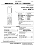
1
CONFIDENTIAL
DRAFT
q SERVICE MANUAL
CODE : 00ZTM150/SM/E
DIGITAL MOBILE PHONE
TM150
MODEL
(INTERNAL MODEL NAME: TM150U)
• In the interests of user-safety the set should be restored
to its original condition and only parts identical to those
specified should be used.
Caution:
Risk of explosion if battery is replaced by an incorrect type,
dispose of used batteries according to the instruction.
CONTENTS
SERVICING CONCERNS
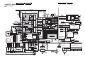
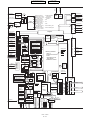
CHAPTER 4. DIAGRAMS
CHAPTER 1.GENERAL DESCRIPTION
[1] Block diagram . . . . . . . . . . . . . . . . . . . . . . . 4-1
[1] Specifications . . . . . . . . . . . . . . . . . . . . . . . . 1-1
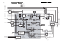
CHAPTER 5. CIRCUIT DIAGRAM
[2] Names of parts . . . . . . . . . . . . . . . . . . . . . . . 1-2
[3] Operation manual . . . . . . . . . . . . . . . . . . . . . 1-3
[1] Notes on schematic diagram. . . . . . . . . . . . 5-1
[2] Types of transistor and LED . . . . . . . . . . . . 5-1
CHAPTER 2. ADJUSTMENTS, PERFORMANCE
CHECK, AND FIRMWARE UPGRADE
[3] Waveforms of circuit . . . . . . . . . . . . . . . . . . 5-2
[1] SHARP Program Support Tool (SPST) . . . . 2-1
[4] Schematic diagram/
Wiring side of P.W.Board . . . . . . . . . . . . . . . . . 5-5
[2] Test points . . . . . . . . . . . . . . . . . . . . . . . . . 2-48
[3] Trouble shooting. . . . . . . . . . . . . . . . . . . . . 2-52
CHAPTER 6. OTHERS
CHAPTER 3. DISASSEMBLY AND REASSEMBLY
[1] Function table of IC . . . . . . . . . . . . . . . . . . . 6-1
[1]
Servicing Concerns . . . . . . . . . . . . . . . . . . 3-1
Parts Guide
[2]
Disassembly and reassembly. . . . . . . . . . . 3-4
Parts marked with "!" are important for maintaining the safety of the set. Be sure to replace these parts with specified
ones for maintaining the safety and performance of the set.
SHARP CORPORATION
This document has been published to be used
for after sales service only.
The contents are subject to change without notice.
CONFIDENTIAL
DRAFT
SERVICING CONCERNS
1. When requested, back up user’s handset data using SPST (SHARP Program Support Tool). Otherwise, before servicing, warn the user that data
in the memory may be lost during repairs.
2. Upgrade the firmware to the latest version using SPST before returning the handset to the customer.
3. After repairs, inspect the handset according to the following flowchart.
Repairs are completed.
(Fixed parts have been checked for proper operation.)
4
Check IMEI No./Operator code (Destination)/
Firmware version by Identity function of SPST.
4
Inspect each device using performance check adjustment function of SPST.
4
Carry out RF performance check with SPST.
4
All completed.
4. When storing or transporting a PWB, put it into a conductive bag or wrap it in aluminum foil.
(C-MOS IC may be damaged by electrostatic charges.)
5. Do not leave fingerprints, etc. on ornamental parts including a cabinet, especially clear windows for main and sub displays.
Wear fingerstalls to avoid this.
Also, ensure not to leave fingerprints on the surface of main and external display panels.
6. To prevent oxidation which causes connection problems, do not touch any terminals on the electric board,
microphone, vibrator, earpiece and speaker.
When handling these parts, wear fingerstalls. Should you touch these parts, clean them with a soft dry cloth.
Always wear fingerstalls when handling a shield case on the electric board.
Otherwise oxidation may occur causing handset performance deterioration.
7. The FPC is a precision device. Handle it carefully to prevent any damages.
8. Do not expose the moisture sensor to liquids.
If the sheet gets wet, red ink runs. In this case, replace the sheet with a new one.
Be careful about your perspiration.
9. Before you disassemble or reassemble handset, make sure to remove the Li-Ion battery.
10. Be sufficiently careful with static electricity of integrated circuits and other circuits. Wear static electricity prevention bands while servicing.
TM100
SERVICING CONCERNS
i
CONFIDENTIAL
DRAFT
CHAPTER 1. GENERAL DESCRIPTION
FOR A COMPLETE DESCRIPTION OF THE OPERATION OF THIS UNIT, PLEASE REFER TO THE OPERATION MANUAL.
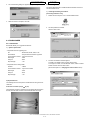
1. SPECIFICATIONS
General:
Quad - band (GSM 900 MHz/DCS 1800 MHz/PCS 1900MHz)
GPRS-enabled WAP, MMS, SMS
Dimensions (folded, excluding the aerial) (H x W x D): 27.1 x 49.2 x 94.8 mm
Weight:
112 g
Battery operating temperature:
0 °C - 40 °C
Main display:
Display dimensions: 240 x 320 pixels
LCD display: CGS 262,144 colours with backlight
LCD backlight: LED backlight white colour LEDs
External display:
Display dimensions: 64 x 96 pixels
LCD display: STN 65,536 colours LCD with backlight
Camera:
CCD 1M pixels built-in camera Zoom: Wide and zoom mode
[Supported 20 (when image size is 120 x 160 pixels) x zoom]
Lens: F2.8, f = 3.7 mm
Sound:
16-polyphonic ring melodies
External DC supply voltage:
5.2 V
Battery:
3.7 V, 780 mAh, Li-Ion
Standby time:
100 ~ 250 hours
Talk time:
160 ~ 240 min.
Others:
Side key Connector for AC charger and data cable Standard hands free connector ($2.5)
Battery running time depends on the battery and SIM card as well as the network conditions and usage.
Specifications for this model are subject to change without prior notice.
Powered by JBlend TM , Copyright1997-2004 Aplix
Corporation. All rights reserved.
Java and all Java-based trademarks and logos are
trademarks or registered trademarks of Sun Microsystems, Inc. in the U.S. and other countries.
JBlend and all JBlend-based trademarks and logos
are trademarks or registered trademarks of Aplix
Corporation in Japan and other countries.
T9 Text Input is licensed under one or more of the following: U.S. Pat.
Nos. 5,818,437, 5,953,541, 5,187,480, 5,945,928, and 6,011,554;
Australian Pat. No. 727539; Canadian Pat. No. 1,331,057;United
Kingdom Pat. No. 2238414B; Hong Kong Standard Pat. No.
HK0940329; Republic of Singapore Pat. No. 51383; Euro. Pat. No. 0
842 463 (96927260.8) DE/DK, FI, FR, IT, NL,PT.ES,SE,GB; Republic
of Korea Pat. Nos. KR201211B1 and KR226206B1; and additional
patents are pending worldwide.
Powered by Mascot Capsule R /Micro3D Edition TM
Mascot Capsule R is a registered trademark of HI Corporation
C 2002-2003 HI Corporation. All Rights Reserved.
SD logo
CP8 PATENT
Licensed by Inter Digital Technology Corporation under one or more
of the following United States Patents and/or their domestic or foreign
counterparts and other patents pending, including U.S. Patents:
4,675,863 : 4,779,262 : 4,785,450 & 4,811,420.
Licensed under U.S. Patent 4,558,302 and foreign counterparts.
TM150
GENERAL DESCRIPTION
1–1
is a trademark.
CONFIDENTIAL
DRAFT
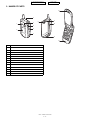
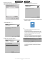
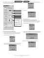
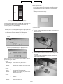
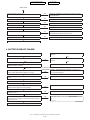
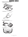
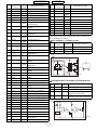
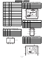
2. NAMES OF PARTS
12
3
9
4
1
8
10
5
6
2
7
11
13
No.
PARTS NAME
1
SPEAKER
2
SUB LCD
3
STRAP
4
CAMERA
5
CLOSE-UP KNOB
6
PHONE JACK
7
SD CARD SLOT
8
BATTERY LOCK KNOB
9
EXT ANTENNA
10
SIDE KEY
11
I/O CONNECTER
12
RECEIVER
13
MIC
TM150
GENERAL DESCRIPTION
1–2
CONFIDENTIAL
DRAFT
3. OPERATION MANUAL
(Page numbers refer to the user guide)
[OPTIONAL ACCESSORIES]
• USB data cable
The above accessories may not be available in all regions. For details, please contact your dealer.
[QUICKSTART GUIDE]
TM150
GENERAL DESCRIPTION
1–3
TM150
GENERAL DESCRIPTION
1–4
Messages
Games
Spor t
New
Download
News
7-5
1-3
6-3-3
CONFIDENTIAL
DRAFT
CONFIDENTIAL
DRAFT
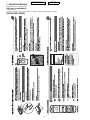
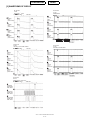
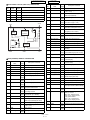
CHAPTER 2. ADJUSTMENTS, PERFORMANCE CHECK, AND FIRMWARE UPGRADE
SPST (SHARP Program Support Tool) allows you to adjust settings, conduct performance checks, and upgrade the firmware.
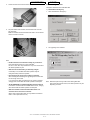
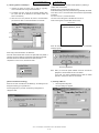
[1] SHARP PROGRAM SUPPORT TOOL (SPST)
1. SYSTEM REQUIREMENTS
2. To change the password, enter the current password in procedure 1,
and then click "Change Password".
• IBM PC compatible personal computer (standard COM1 115,200 bps
serial port and USB required)
Supported OS: Windows 98/98SE/2000/XP
(except for Windows 95/ME/NT)
(English, German, Italian, Spanish, French and Chinese versions)
• Data cable
<During RF adjustment>
• GSM tester: CMU200
• GPIB interface: National Instruments USB-GPIB cable
(Model No.: NI GPIB-USB-B)
2. INTRODUCTION
2-1. FUNCTIONS
SPST offers seven key functions:
3. To check the usage status of tools, click "Show Repair Log" in procedure 1.
1) Firmware download
4. Click “Downloader for Emergency”.
2) User data transfer (processes all data at once but not individually.)
3) RF calibration check and test
4) Default setting
5) Identification
6) Performance check and adjustment
7) User password reset
2-2. INSTALLATION
1. Use Windows Explorer to execute the "setup.exe" file on the CDROM.
2. The SPST TM150 setup wizard appears. Follow the installation
instructions.
3. After the installation is complete, shortcuts to SPST are created on
the desktop and under the "Start"-"Programs"-"TM150" menu.
Start SPST from the shortcuts.
The above screen appears. Select a model to use and execute the
Downloader. (Use this to initialize the flash, etc.)
2-3. STARTING UP
5. When the password is correct, a connection is established and the
following screen appears.
Connect TM150 to an operable serial port of the PC with the supplied
data cable. Make sure that the battery is fully charged.
Start SPST from the desktop.
Refer to the attachment 1
for the destination and
operator name.
1. The Input password dialog box appears. Enter the password, select
a port where TM150 is connected from the list box, and click "OK".
If you do not know SPC, click “Cancel” to exit.
TM150
TM150
ADJUSTMENTS, PERFORMANCE CHECK, AND FIRMWARE UPGRADE
2–1
Software version:
A02-006-0138-TM150
CONFIDENTIAL
DRAFT
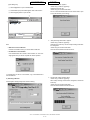
■ Buttons
Default Set
Refer to "4-1. Default setting".
User Data Back-up
Refer to "4-2. User data back-up".
User Data Restore
Refer to "4-3. User data restore".
Downloader
Refer to "4-4. Downloader".
RF Calibration & Check Refer to "4-5. RF calibration & check".
RF Test
Refer to "4-6. RF test tool".
User Password Reset
Refer to "4-7. Password reset".
Performance check
adjustment
Refer to "4-8. Performance check and adjustment".
**** mode release
Refer to "4-9. ****mode release".
Exit
End SPST.
3. ADJUSTMENTS FOR TM150
1. Adjustments are required after replacing the following parts. ( F )
Parts
Temperature adjustment
(Camera)
Temperature adjustment
(Battery)
Main display
flicker adjustment
White defect correction
TH101
u
F
u
u
TH701
F
u
u
u
Main display unit
u
u
F
u
Camera unit
u
u
u
F
When replacing other parts in the RF section, carry out RF calibration.
2. Click the buttons on the SPST screen for adjustments.
3. The following screen appears.
1
2
3
4
5
6
1 Temperature adjustment (Camera section)
RF calibration
To abjust the device, click this button
(Performance check adjustment).
2 Temperature adjustment (Battery section)
3 Main display flicker adjustment
4 External display contrast adjustment
5 White defect correction
6 Black defect correction
TM150
ADJUSTMENTS, PERFORMANCE CHECK, AND FIRMWARE UPGRADE
2–2
CONFIDENTIAL
DRAFT
4. FUNCTIONS
4-1. DEFAULT SETTING
4-2. USER DATA BACK-UP
SPST can restore the factory settings.
SPST saves all the data stored on the handset.
This function
1. Set the COM port on the SPST initial screen and click
"User Data Back-up".
1. Deletes all user data in the file system;
2. Restores all WAP settings to default; and
2. Specify the file name in the following dialog box and click "Save"
3. Restores the values set by the user to default;
(MEP_LOCK settings and the destination and operator name do not change.)
<Operation>
1) Set the COM port on the SPST initial screen and click "Default Set".
2) Click "Yes" to proceed. Click "No" to exit.
TM150
3. The communicating dialog box appears while processing.
3) Click "Yes" to back-up the MEPLOCK data. Click "No" to restore
default settings.
TM150
4. When completed, the following message appears. Click "OK".
4) Communication starts.
TM150
4-3. USER DATA RESTORE
5) The following appears when you select "Yes" in step 3 and
MEPLOCK data exists. Click "Yes" to restore the data.
SPST completely restores the backed up data.
1. Set the COM port on the SPST initial screen and click "User Data
Restore".
TM150
2. Specify the file name in the following dialog box and click "Save".
6) After the handset is turned on, the initialization is complete.
TM150
TM150
ADJUSTMENTS, PERFORMANCE CHECK, AND FIRMWARE UPGRADE
2–3
CONFIDENTIAL
DRAFT
4-4-2. Getting started
3. The communicating dialog box appears while processing.
This section describes how to install/uninstall the software and how to
connect handset to a PC.
1)
Installing/uninstalling the software
[Connecting handset to a PC]
1. Double click the “setup.exe” icon in TM150 Install-E folder.
4. When the restore is complete, click "OK".
TM150
2. The Setup Wizard is activated.
Click the "Next" button.
TM150
TM150
TM150
4-4. DOWNLOADER
4-4-1. Introduction
Downloader allows you to upgrade the firmware.
1)
System requirements
• Requirements for the upgrading tool:
OS
: Windows 98, 98 SE, 2000, or XP
Download file
: Only the Motorola format is supported.
Communication method : Asynchronous mode
Data length
: 8 bits
Parity bit
: None
Stop bit length
: 1 bit
3. A location to install the software appears.
To install in the default location, click the "Next" button.
To change the location, click the "Browse" button, select a desired
location and then click the "Next" button.
(See the description in "* Changing the install location" below.)
• Requirements for Loading loader
Handset
: TM150
Communication method : Asynchronous mode
Data length
: 8 bits
Parity bit
: None
Stop bit length
: 1 bit
TM150
TM150
2) Required devices
TM150
The following devices are required to rewrite MOT files using Communication Box.
Conversion connector (16-pin 3 10-pin)
This conversion connector is required to connect TM150 with Communication Box since the cable connector of Communication Box has 16 pins.
TM150
ADJUSTMENTS, PERFORMANCE CHECK, AND FIRMWARE UPGRADE
2–4
CONFIDENTIAL
DRAFT
6. The installation is completed.
Click the "Close" button to close the Setup Wizard.
* Changing the install location
Click the "Browse" button in step 3 to browse folders.
Click the "c" button, select a folder and click the "OK" button.
TM150
TM150
7. The shortcut icon shown left is created on your desktop when the
installation is completed.
4. A confirmation message appears.
Click the "Next" button.
TM150
TM150
Note:
• After installing the upgrading tool in Windows 98 or 98 SE,
restart the operating system.
While installing the upgrading tool in Windows 98, 98 SE, or ME,
a message may appear prompting to restart the operating system.
In this case, restart your operating system follwoing the instruction.
Even if the message does not appear, restart your operating
system after the installation.
On Windows 98, if you start the upgrading tool without restarting the
operation system, the following message may appear. Restart the
operating system to ensure the proper operation of the upgrading tool.
5. Installtion starts. The progress is displayed.
TM150
TM150
• Uninstall the upgrading tool before installing the latest version or
reinstalling the current version.
Otherwise, the upgrading tool may not function properly.
To ensure the proper operation, uninstall and then reinstall the
upgrading tool.
TM150
TM150
ADJUSTMENTS, PERFORMANCE CHECK, AND FIRMWARE UPGRADE
2–5
CONFIDENTIAL
DRAFT
[Uninstalling the software]
2) Connecting handset to a PC
1. Double click "setup.exe" in TM150 Install-E folder.
A) Using a cable for upgrading
1. Connect the cable to a PC.
2. Connect the cable to handset.
3. The photo below shows handset connected to a PC.
2. The Setup Wizard is activated. Select "Remove The TM150
Upgrading Tool" and click the "Finish" button.
TM150
TM150
TM150
TM150
TM150
B) Using Communication Box
1. Connect a PC to Communication Box via a serial cable.
2. Connect the AC charger to Communication Box and then plug it into
the outlet.
All SET POWER SW on Communication Box must be turned off.
3. Uninstalltion starts. The progress is displayed.
3. Connect the conversion connector to Communication Box Cables.
Connect the conversion connector in the following order, label side up.
From upper right end: Cable No. 1, 3, 5, 7, and 9.
From lower right end: Cable No. 2, 4, 6, 8, and 10.
TM150
TM150
TM150
4. The uninstallation is completed. Click the "Close" button to close
the Setup Wizard.
4. The photo below shows the conversion connector connected to
Communication Box Cable 1.
TM150
TM150
TM150
ADJUSTMENTS, PERFORMANCE CHECK, AND FIRMWARE UPGRADE
2–6
CONFIDENTIAL
DRAFT
4-4-3. Rewriting MOT files
5. Connect the other end of the conversion connector to handset.
This section describes how to rewrite MOT files.
1) Downloader for Emergency
1. Click “Downloader for Emergency“.
6. The photo below shows handset, Communication Box and a PC
(all connected).
Make sure handset and Communication Box Cable 1 are connected
via the conversion connector.
2. The upgrading tool is activated.
Note:
• Handset must be turned off before making any connections.
Press and hold the Power key to turn off handset.
Do not turn off in other ways. Malfunction may occur and the MOT
file rewrite operation may fail.
• Make sure the handset battery is sufficiently charged.
If the battery is low, the MOT file rewrite operation may fail.
Charge the battery before the operation.
• Disconnect the AC charger from a cable for upgrading.
When rewriting MOT files using the upgrading tool, do not connect
the AC charger to the cable.
If you connect the cable connected to the AC charger to handset,
charging starts and the MOT file rewrite operation is interrupted.
Note: Disable the power saving mode before rewriting MOT files.
If the power saving mode is active, the rewrite operation may fail
depending on the PC.
• All SET POWER SW on Communication Box must be turned off.
If handset is connected with SET POWER SW turned on, charging
starts and the MOT file rewrite operation is interrupted.
• Make sure handset and Communication Box Cable 1 are
connected via the conversion connector.
(When using Communication Box, the only handset connected to
Cable 1 can be operated on the PC.)
TM150
ADJUSTMENTS, PERFORMANCE CHECK, AND FIRMWARE UPGRADE
2–7
CONFIDENTIAL
DRAFT
You can shorten time for the MOT rewrite operation by selecting a
smaller value for Wait Time.
Example: Time to rewrite two MOT files at a time.
At the default setting (3 seconds), rewrite time is approximately 40 minutes.
If the value is set to 1, the rewrite time will be reduced to approximately
30 minutes.
If an error occurs at 1, increase the value.
The error screen will appear on handsets No. 2 to No.10.
If this screen appears, increase Wait Time and retry.
2) Selecting options and COM port
1 Uncheck the check box when using a cable for upgrading.
Leave it checked when using Communication Box.
2 To initialize user area, check the File System Initialize check
box. (User data will be deleted and the handset status will
return to the default.)
3 Click here and in the pull-down list, select a communications
port where the cable or Communication Box is connected.
Error screen
TM150
Flash Loader 5.02
CORRESPONDENCE_ERROR
TM150
1
3
2
When the File System Initialize check box is checked, a confirmation
message appears.
When using Communication Box, set Wait Time.
Check the Communication Box check box to adjust Wait Time (default: 3
seconds). The time to delete the program data varies between handsets.
Handsets wait for the set Wait Time until the whole process is
completed. If an error occurs, increase the value.
Click the [OK] button.
Note: When you check File System Initialize check box and click the
[OK] button, handset status returns to the default.
In this case, user data is initialized after the MOT file rewrite
operation. Uncheck the check box to avoid this.
[Notes for the Wait Time setting]
3) Selecting a MOT file
When the set value is smaller than the default (3), the message on the
left appears alerting you a possible error.
1. Click the [Select File] button.
The Open dialog box appears.
Click the [OK] button to proceed, and click the [Cancel] button to
change the value.
TM150
TM150
TM150
ADJUSTMENTS, PERFORMANCE CHECK, AND FIRMWARE UPGRADE
2–8
CONFIDENTIAL
DRAFT
1. "Press Power Button" appears.
<When using a cable for upgrading>
Hold down the Power key.
<When using the Communication Box>
Turn on Communication Box SW from No.10 down to No.1 (turn
on only the handsets you are using).
[Open dialog box]
1 Click the [c] button to open a desired folder.
2 A Motorola file (.mot) in the folder appears. Click a file to write in.
3 Click the [Open] button to open the file.
1
TM150
2
3
2. "Keep Pressing Power Button" appears.
<When using a cable for upgrading>
Hold down the Power key until the "Keep Pressing Power Button" disappears.
<When using the Communication Box>
Leave the Communication Box SW turned on.
Note:
• Make sure to select a MOT file.
If the File name field is blank, you cannot rewrite a MOT file.
• Use MOT files in the hard disk.
If the selected MOT file is stored in other locations, an error message appears and you cannot complete the rewrite operation.
TM150
To use MOT files on CDs or on the network, copy or download them to
the hard disk first.
3. The MOT file rewrite operation starts.
<When using a cable for upgrading>
When "Keep Pressing Power Button" disappears, release the
Power key.
<When using the Communication Box>
Leave the Communication Box SW turned on.
4) Rewriting a MOT file
Click the [Start Loading Flash] button to start rewriting.
TM150
TM150
TM150
TM150
ADJUSTMENTS, PERFORMANCE CHECK, AND FIRMWARE UPGRADE
2–9
CONFIDENTIAL
4. When the rewrite operation starts, handset display screen shows
the software version and process of communications with the PC.
Flash Loader 5.02
DRAFT
SUM also appears on handset.
<When using a cable for upgrading>
After 8 seconds, SUM disappears.
<When using Communication Box>
When SET POWER SW is turned off, SUM disappears.
XXXXXXXCommand
Flash Loader 5.02
SUM Check End
SUM = 0xdb3d
Canceling the ongoing rewrite operation:
Click the [QUIT] button.
To rewrite MOT files later, remove and install the battery first.
Make sure SUM is the same between the PC and handset.
The same SUM means that the rewrite operation is completed properly.
If the value is different, try again to ensure completion of the operation.
[Notes for the use of a cable for upgrading]
1. Disconnect the AC charger from the cable. Otherwise charging
starts and the MOT file rewrite operation is interrupted.
If the MOT file rewrite operation fails, an error message appears on
handset.
2. Make sure the handset battery is sufficiently charged.
If the battery is low, the rewrite operation may fail. Charge the battery before the operation.
* The screen shot on the left shows an error in erasing Flash data.
[ADR] and [STR] appear only when an error occurs in the FLASHrelated operation.
Start over the MOT file rewrite operation.
<When other error messages appear>
Find the message in 4-4-4. 2)Error messages for Loading loader, and
follow the instructions.
3. If the ongoing rewrite operation is canceled, or interrupted by an
error, remove and reinstall the battery and retry.
Error screen
[Notes for the use of the Communication Box]
1. When "Press Power Button!" appears, turn on Communication Box
SW from No.10 down to No.1. If the communication BoxSW No.1 is
first turned on, the rewrite on communication BoxSW No. 2 to No. 10
operation will fail.
Flash Loader 5.02
FLASH_ERROR
ERROR_ERASE
2. The time to delete the program data varies between handsets. If the
process fails at the default Wait Time (3 seconds), increase the
value.
Consequently, this will increase the time to complete the rewrite
operation.
ADR = 0x1000000
STR = 0xA0
5) Checking the value of SUM
When the rewrite operation is completed, a confirmation message
appears with SUM.
6) After the operation
Disconnect the cable for upgrading from handset.
When using the Communication Box, turn off SET POWER SW and
then disconnect the cable from handset.
TM150
ADJUSTMENTS, PERFORMANCE CHECK, AND FIRMWARE UPGRADE
2 – 10
CONFIDENTIAL
DRAFT
2) Error messages for Loading loader (on the handset side)
7) Initializing only the file system
Follow the instructions below to initialize only the file system.
(User data will be deleted and the handset status will return to the
default.)
No.
* Perform this procedure when the handset does not turn on.
Message
1
FLASH_ERROR
An error in Flash Rom.
Start over the rewrite operation.
2
ERROR_PARAM
The upgrading tool is damaged.
Uninstall and reinstall the upgrading tool,
and start over the rewrite operation.
3
ERROR_WPROTECT
Flash Rom is protected.
Battery may be too low.
Use a sufficiently charged battery and
start over the rewrite operation.
4
ERROR_READ
Failed to read Flash Rom data and the
operation was aborted.
Start over the rewrite operation.
5
ERROR_WRITE
Failed to write to Flash Rom and the
operation was aborted.
Start over the rewrite operation.
6
ERROR_ERASE
Failed to erase Flash Rom data and the
operation was aborted.
Start over the rewrite operation.
7
ERROR_VERIFY
The rewrite operation was aborted since
there was a mismatch between data written to Flash Rom and that written to
handset.
Start over the rewrite operation.
8
ERROR_RWE_TMOUT Communication was terminated since
there was no response from Flash Rom
for a certain period of time.
Start over the rewrite operation.
9
CORRESPONDENCE Communication was terminated since
_ERROR
serial data communication failed.
Start over the rewrite operation.
1 Check the File System Initialize check box.
2 Leave the Load File text box blank.
3 Click the [Start Loading Flash] button.
TM150
TM150
1
2
3
For further operations, refer to [4-4-3. 4) Rewriting a MOT file] or
[4-4-3. 5) Checking the value of SUM].
4-4-4. Error message list
Below is the list of error messages for the upgrading tool (on the PC
side) and Loading loader (on the handset side).
1) Error messages for the upgrading tool (on the PC side)
Message
1
Select a file for Downloading
or check the box of Initializing.
Load File is not set. Select
a MOT file.
2
Unable to open file.
Failed to open the MOT file.
Start over the rewrite operation.
3
You need to set the Wait Time! WaitTime (S) is not set.
Set WaitTime (S) value.
4
The file you selected is
unsuitable for Upgrading.
The selected file cannot be rewritten for upgrading.
Select an appropriate MOT file.
5
Cannot Setup COM port.
The selected COM port does not
exist or is used for other operations.
Select a COM port connected to
the PC cable.
Descriptions/Instructions
11 STR = XX
Indicates the status of Flash
(the error source).
Stabilized
power supply
RAM Loader not responding
to Commands.
No response from Loading loader.
Start over the rewrite operation.
7
RAM Loader responding
Parameter Error.
Information sent from the PC is illegal.
Reinstall the upgrading tool. Start
over the rewrite operation.
RAM Loader responding
Flash Error (XXXX).
Failed to initialize FLASH ROM in
(XXXX).
Start over the rewrite operation.
Correspondence Error.
Undefined response from Loading
loader.
Start over the rewrite operation.
TM150
Indicates the address of Flash
(the error source).
4-5. RF CALIBRATION & CHECK
6
9
10 ADR = XXXXXXXX
* When No.1 occurs, handset screen shows error messages for No.2
to No.8 as well as the address (No.10) and status (No.11) of the error
source at the same time.
No.
8
Descriptions/Instructions
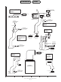
RF cable
GSM tester
Handset
GPIB cable
Test battery
Data cable
PC
4-5-1. Preparation
• Connect PC and GSM tester with a GPIB cable.
• Connect PC and handset with a Data cable.
(Use a test battery or one close.)
• Connect a RF cable of GSM tester to handset.
ADJUSTMENTS, PERFORMANCE CHECK, AND FIRMWARE UPGRADE
2 – 11
CONFIDENTIAL
4-5-2. Default setting for the program.
DRAFT
5. Make sure the handset is on and click "OK". (Adjustment starts.)
• Activate the program and set defaults.
TM150
1) Select the COMport.
6. Click "OK".
2) Set the GPIB No.
3)Select the test instrument.
4) Set the GPIBaddress.
5) Set the"Cable Offset" values.
For cables with connector
UKOG-1031YCZZ (1.0m)
UKOG-1032YCZZ (0.5m)
the values as follows:
7. The initial screen returns.
4-5-4. RF performance check (Insert SIM card)
1. Apply 4 V using a stabilized power supply and turn on the handset.
(1.0m) (0.5m)
GSM900 : 0.48 0.27
DCS1800 : 0.67 0.38
PCS1900 : 0.68 0.38
2. Start "RF calibration & check" on SPST and click "Calibration".
3. When initialization is complete, click "OK".
* In case of an attenuator
addition state, 6 db addition
to the value.
4. Apply 4 V using a stabilized power supply and turn on the handset.
After the handset enters Standby mode, lower the voltage to 3.7 V.
4-5-3. RF calibration (Remove SIM card)
1. Apply 4 V using a stabilized power supply and turn on the handset.
2. Start "RF calibration & check" on SPST and click "Calibration".
3. When initialization is complete, click "OK".
5.Make sure the handset is in the idle mode and click "OK"..
4. Apply 4 V using a stabilized power supply and turn on the handset.
After the handset enters Standby mode, lower the voltage to 3.7 V.
TM150
ADJUSTMENTS, PERFORMANCE CHECK, AND FIRMWARE UPGRADE
2 – 12
CONFIDENTIAL
DRAFT
The following will be displayed in case of failure.
See the attachment 2 for troubleshooting.
6. Press the keys 1, 2, 3 and Send and click "OK".
7. Make sure the terminal display is "In Call" and click "OK".
(RF performance check starts.)
11. Click "OK".
8. The following message appears during the check. Press the keys 1,
2, 3 and Send again and click "OK".
12. The initial screen returns.
9. Make sure the terminal display is "In Call" and click "OK".
10. RF performance check is complete. Click "Save As..." and name
the file to save the result. Click "OK" to exit.
TM150
ADJUSTMENTS, PERFORMANCE CHECK, AND FIRMWARE UPGRADE
2 – 13
CONFIDENTIAL
Attachment 2
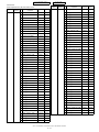
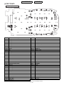
Whole inspection list by RF performance check.
Band
Sending/
No.
Receive
GSM900 Tx
Item to be
inspected
Band
Channel
PCL
1
Burst Power
37CH
PCL5
2
Burst Power
975CH
PCL5
3
Burst Power
124CH
PCL5
4
Burst Power
37CH
PCL11
5
Burst Power
37CH
PCL19
6
Frequency Error
37CH
PCL5
7
Frequency Error
975CH
PCL5
8
Frequency Error
124CH
PCL5
9
Phase Error (RMS)
37CH
PCL5
10
Phase Error (RMS)
975CH
PCL5
11
Phase Error (RMS)
124CH
PCL5
12
Phase Error (Peak)
37CH
PCL5
13
Phase Error (Peak)
975CH
PCL5
14
Phase Error (Peak)
124CH
PCL5
15
Mod_spectrum -800
37CH
PCL5
16
Mod_spectrum -600
37CH
PCL5
17
Mod_spectrum -400
37CH
PCL5
18
Mod_spectrum -250
37CH
PCL5
19
Mod_spectrum -200
37CH
PCL5
20
Mod_spectrum +200
37CH
PCL5
21
Mod_spectrum +250
37CH
PCL5
22
Mod_spectrum +400
37CH
PCL5
23
Mod_spectrum +600
37CH
PCL5
24
Mod_spectrum +800
37CH
PCL5
25
Mod_spectrum -800
975CH
PCL5
26
Mod_spectrum -600
975CH
PCL5
27
Mod_spectrum -400
975CH
PCL5
28
Mod_spectrum -250
975CH
PCL5
29
Mod_spectrum -200
975CH
PCL5
30
Mod_spectrum +200
975CH
PCL5
31
Mod_spectrum +250
975CH
PCL5
32
Mod_spectrum +400
975CH
PCL5
33
Mod_spectrum +600
975CH
PCL5
34
Mod_spectrum +800
975CH
PCL5
35
Mod_spectrum -800
124CH
PCL5
36
Mod_spectrum -600
124CH
PCL5
37
Mod_spectrum -400
124CH
PCL5
38
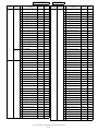
Mod_spectrum -250
124CH
PCL5
39
Mod_spectrum -200
124CH
PCL5
40
Mod_spectrum +200
124CH
PCL5
41
Mod_spectrum +250
124CH
PCL5
42
Mod_spectrum +400
124CH
PCL5
43
Mod_spectrum +600
124CH
PCL5
44
Mod_spectrum +800
124CH
PCL5
45
Mod_spectrum -800
37CH
PCL11
46
Mod_spectrum -600
37CH
PCL11
47
Mod_spectrum -400
37CH
PCL11
TM150
DRAFT
Sending/
No.
Receive
GSM900 Tx
Channel
PCL
48
Mod_spectrum -250
37CH
PCL11
49
Mod_spectrum -200
37CH
PCL11
50
Mod_spectrum +200
37CH
PCL11
51
Mod_spectrum +250
37CH
PCL11
52
Mod_spectrum +400
37CH
PCL11
53
Mod_spectrum +600
37CH
PCL11
54
Mod_spectrum +800
37CH
PCL11
55
Mod_spectrum -800
37CH
PCL19
56
Mod_spectrum -600
37CH
PCL19
57
Mod_spectrum -400
37CH
PCL19
58
Mod_spectrum -250
37CH
PCL19
59
Mod_spectrum -200
37CH
PCL19
60
Mod_spectrum +200
37CH
PCL19
61
Mod_spectrum +250
37CH
PCL19
62
Mod_spectrum +400
37CH
PCL19
63
Mod_spectrum +600
37CH
PCL19
64
Mod_spectrum +800
37CH
PCL19
65
Switch_Spectrum -1800
37CH
PCL5
66
Switch_Spectrum -1200
37CH
PCL5
67
Switch_Spectrum -600
37CH
PCL5
68
Switch_Spectrum -400
37CH
PCL5
69
Switch_Spectrum +400
37CH
PCL5
70
Switch_Spectrum +600
37CH
PCL5
71
Switch_Spectrum +1200
37CH
PCL5
72
Switch_Spectrum +1800
37CH
PCL5
73
Switch_Spectrum -1800
975CH
PCL5
74
Switch_Spectrum -1200
975CH
PCL5
75
Switch_Spectrum -600
975CH
PCL5
76
Switch_Spectrum -400
975CH
PCL5
77
Switch_Spectrum +400
975CH
PCL5
78
Switch_Spectrum +600
975CH
PCL5
79
Switch_Spectrum +1200
975CH
PCL5
80
Switch_Spectrum +1800
975CH
PCL5
81
Switch_Spectrum -1800
124CH
PCL5
82
Switch_Spectrum -1200
124CH
PCL5
83
Switch_Spectrum -600
124CH
PCL5
84
Switch_Spectrum -400
124CH
PCL5
85
Switch_Spectrum +400
124CH
PCL5
86
Switch_Spectrum +600
124CH
PCL5
87
Switch_Spectrum +1200
124CH
PCL5
88
Switch_Spectrum +1800
124CH
PCL5
89
Switch_Spectrum -1800
37CH
PCL11
90
Switch_Spectrum -1200
37CH
PCL11
91
Switch_Spectrum -600
37CH
PCL11
92
Switch_Spectrum -400
37CH
PCL11
ADJUSTMENTS, PERFORMANCE CHECK, AND FIRMWARE UPGRADE
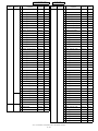
2 – 14
Item to be
inspected
CONFIDENTIAL
Band
Sending/
No.
Receive
GSM900 Tx
Rx
DCS
Tx
Item to be
inspected
Channel
PCL
DRAFT
Band
DCS
Sending/
No.
Receive
Tx
Item to be
inspected
Channel
PCL
93
Switch_Spectrum +400
37CH
PCL11
140 Mod_spectrum -600
512CH
PCL0
94
Switch_Spectrum +600
37CH
PCL11
141 Mod_spectrum -400
512CH
PCL0
95
Switch_Spectrum +1200
37CH
PCL11
142 Mod_spectrum -250
512CH
PCL0
96
Switch_Spectrum +1800
37CH
PCL11
143 Mod_spectrum -200
512CH
PCL0
97
Switch_Spectrum -1800
37CH
PCL19
144 Mod_spectrum +200
512CH
PCL0
98
Switch_Spectrum -1200
37CH
PCL19
145 Mod_spectrum +250
512CH
PCL0
99
Switch_Spectrum -600
37CH
PCL19
146 Mod_spectrum +400
512CH
PCL0
100 Switch_Spectrum -400
37CH
PCL19
147 Mod_spectrum +600
512CH
PCL0
101 Switch_Spectrum +400
37CH
PCL19
148 Mod_spectrum +800
512CH
PCL0
102 Switch_Spectrum +600
37CH
PCL19
149 Mod_spectrum -800
885CH
PCL0
103 Switch_Spectrum +1200
37CH
PCL19
150 Mod_spectrum -600
885CH
PCL0
104 Switch_Spectrum +1800
37CH
PCL19
151 Mod_spectrum -400
885CH
PCL0
105 Burst Timing
37CH
PCL5
152 Mod_spectrum -250
885CH
PCL0
106 Burst Timing
975CH
PCL5
153 Mod_spectrum -200
885CH
PCL0
107 Burst Timing
124CH
PCL5
154 Mod_spectrum +200
885CH
PCL0
108 Burst Timing
37CH
PCL11
155 Mod_spectrum +250
885CH
PCL0
109 Burst Timing
37CH
PCL19
156 Mod_spectrum +400
885CH
PCL0
110 Rx Sensitivity
37CH
PCL5
157 Mod_spectrum +600
885CH
PCL0
111 Rx Sensitivity
975CH
PCL5
158 Mod_spectrum +800
885CH
PCL0
112 Rx Sensitivity
124CH
PCL5
159 Mod_spectrum -800
699CH
PCL5
113 Usable Receiver Level
37CH
PCL5
160 Mod_spectrum -600
699CH
PCL5
114 Rx Level Reports
37CH
PCL5
161 Mod_spectrum -400
699CH
PCL5
115 Burst Power
699CH
PCL0
162 Mod_spectrum -250
699CH
PCL5
116 Burst Power
512CH
PCL0
163 Mod_spectrum -200
699CH
PCL5
117 Burst Power
855CH
PCL0
164 Mod_spectrum +200
699CH
PCL5
118 Burst Power
699CH
PCL5
165 Mod_spectrum +250
699CH
PCL5
119 Burst Power
699CH
PCL15
166 Mod_spectrum +400
699CH
PCL5
120 Frequency Error
699CH
PCL0
167 Mod_spectrum +600
699CH
PCL5
121 Frequency Error
512CH
PCL0
168 Mod_spectrum +800
699CH
PCL5
122 Frequency Error
885CH
PCL0
169 Mod_spectrum -800
699CH
PCL15
123 Phase Error (RMS)
699CH
PCL0
170 Mod_spectrum -600
699CH
PCL15
124 Phase Error (RMS)
512CH
PCL0
171 Mod_spectrum -400
699CH
PCL15
125 Phase Error (RMS)
885CH
PCL0
172 Mod_spectrum -250
699CH
PCL15
126 Phase Error (Peak)
699CH
PCL0
173 Mod_spectrum -200
699CH
PCL15
127 Phase Error (Peak)
512CH
PCL0
174 Mod_spectrum +200
699CH
PCL15
128 Phase Error (Peak)
855CH
PCL0
175 Mod_spectrum +250
699CH
PCL15
129 Mod_spectrum -800
699CH
PCL0
176 Mod_spectrum +400
699CH
PCL15
130 Mod_spectrum -600
699CH
PCL0
177 Mod_spectrum +600
699CH
PCL15
131 Mod_spectrum -400
699CH
PCL0
178 Mod_spectrum +800
699CH
PCL15
132 Mod_spectrum -250
699CH
PCL0
179 Switch_Spectrum -1800
699CH
PCL0
133 Mod_spectrum -200
699CH
PCL0
180 Switch_Spectrum -1200
699CH
PCL0
134 Mod_spectrum +200
699CH
PCL0
181 Switch_Spectrum -600
699CH
PCL0
135 Mod_spectrum +250
699CH
PCL0
182 Switch_Spectrum -400
699CH
PCL0
136 Mod_spectrum +400
699CH
PCL0
183 Switch_Spectrum +400
699CH
PCL0
137 Mod_spectrum +600
699CH
PCL0
184 Switch_Spectrum +600
699CH
PCL0
138 Mod_spectrum +800
699CH
PCL0
185 Switch_Spectrum +1200
699CH
PCL0
139 Mod_spectrum -800
512CH
PCL0
186 Switch_Spectrum +1800
699CH
PCL0
187 Switch_Spectrum -1800
512CH
PCL0
TM150
ADJUSTMENTS, PERFORMANCE CHECK, AND FIRMWARE UPGRADE
2 – 15
CONFIDENTIAL
Band
DCS
Sending/
No.
Receive
Tx
Rx
PCS
Tx
Item to be
inspected
DRAFT
Band
Sending/
No.
Receive
Item to be
inspected
Channel
PCL
188 Switch_Spectrum -1200
512CH
PCL0
232 Burst Power
661CH
PCL5
189 Switch_Spectrum -600
512CH
PCL0
233 Burst Power
661CH
PCL15
PCS
Tx
Channel
PCL
190 Switch_Spectrum -400
512CH
PCL0
234 Frequency Error
661CH
PCL0
191 Switch_Spectrum +400
512CH
PCL0
235 Frequency Error
512CH
PCL0
192 Switch_Spectrum +600
512CH
PCL0
236 Frequency Error
810CH
PCL0
193 Switch_Spectrum +1200
512CH
PCL0
237 Phase Error (RMS)
661CH
PCL0
194 Switch_Spectrum +1800
512CH
PCL0
238 Phase Error (RMS)
512CH
PCL0
195 Switch_Spectrum -1800
885CH
PCL0
239 Phase Error (RMS)
810CH
PCL0
196 Switch_Spectrum -1200
885CH
PCL0
240 Phase Error (Peak)
661CH
PCL0
197 Switch_Spectrum -600
885CH
PCL0
241 Phase Error (Peak)
512CH
PCL0
198 Switch_Spectrum -400
885CH
PCL0
242 Phase Error (Peak)
810CH
PCL0
199 Switch_Spectrum +400
885CH
PCL0
243 Mod_spectrum -800
661CH
PCL0
200 Switch_Spectrum +600
885CH
PCL0
244 Mod_spectrum -600
661CH
PCL0
201 Switch_Spectrum +1200
885CH
PCL0
245 Mod_spectrum -400
661CH
PCL0
202 Switch_Spectrum +1800
885CH
PCL0
246 Mod_spectrum -250
661CH
PCL0
203 Switch_Spectrum -1800
699CH
PCL5
247 Mod_spectrum -200
661CH
PCL0
204 Switch_Spectrum -1200
699CH
PCL5
248 Mod_spectrum +200
661CH
PCL0
205 Switch_Spectrum -600
699CH
PCL5
249 Mod_spectrum +250
661CH
PCL0
206 Switch_Spectrum -400
699CH
PCL5
250 Mod_spectrum +400
661CH
PCL0
207 Switch_Spectrum +400
699CH
PCL5
251 Mod_spectrum +600
661CH
PCL0
208 Switch_Spectrum +600
699CH
PCL5
252 Mod_spectrum +800
661CH
PCL0
209 Switch_Spectrum +1200
699CH
PCL5
253 Mod_spectrum -800
512CH
PCL0
210 Switch_Spectrum +1800
699CH
PCL5
254 Mod_spectrum -600
512CH
PCL0
211 Switch_Spectrum -1800
699CH
PCL15
255 Mod_spectrum -400
512CH
PCL0
212 Switch_Spectrum -1200
699CH
PCL15
256 Mod_spectrum -250
512CH
PCL0
213 Switch_Spectrum -600
699CH
PCL15
257 Mod_spectrum -200
512CH
PCL0
214 Switch_Spectrum -400
699CH
PCL15
258 Mod_spectrum +200
512CH
PCL0
215 Switch_Spectrum +400
699CH
PCL15
259 Mod_spectrum +250
512CH
PCL0
216 Switch_Spectrum +600
699CH
PCL15
260 Mod_spectrum +400
512CH
PCL0
217 Switch_Spectrum +1200
699CH
PCL15
261 Mod_spectrum +600
512CH
PCL0
218 Switch_Spectrum +1800
699CH
PCL15
262 Mod_spectrum +800
512CH
PCL0
219 Burst Timing
699CH
PCL0
263 Mod_spectrum -800
810CH
PCL0
220 Burst Timing
512CH
PCL0
264 Mod_spectrum -600
810CH
PCL0
221 Burst Timing
885CH
PCL0
265 Mod_spectrum -400
810CH
PCL0
222 Burst Timing
699CH
PCL5
266 Mod_spectrum -250
810CH
PCL0
223 Burst Timing
699CH
PCL15
267 Mod_spectrum -200
810CH
PCL0
224 Rx Sensitivity
699CH
PCL0
268 Mod_spectrum +200
810CH
PCL0
225 Rx Sensitivity
512CH
PCL0
269 Mod_spectrum +250
810CH
PCL0
226 Rx Sensitivity
885CH
PCL0
270 Mod_spectrum +400
810CH
PCL0
227 Usable Receiver Level
699CH
PCL0
271 Mod_spectrum +600
810CH
PCL0
228 Rx Level Reports
699CH
PCL0
272 Mod_spectrum +800
810CH
PCL0
229 Burst Power
661CH
PCL0
273 Mod_spectrum -800
661CH
PCL5
230 Burst Power
512CH
PCL0
274 Mod_spectrum -600
661CH
PCL5
231 Burst Power
810CH
PCL0
275 Mod_spectrum -400
661CH
PCL5
276 Mod_spectrum -250
661CH
PCL5
277 Mod_spectrum -200
661CH
PCL5
278 Mod_spectrum +200
661CH
PCL5
279 Mod_spectrum +250
661CH
PCL5
280 Mod_spectrum +400
661CH
PCL5
TM150
ADJUSTMENTS, PERFORMANCE CHECK, AND FIRMWARE UPGRADE
2 – 16
CONFIDENTIAL
Band
PCS
Sending/
No.
Receive
Tx
Item to be
inspected
Channel
DRAFT
PCL
Band
PCS
Sending/
No.
Receive
Tx
Item to be
inspected
Channel
PCL
281 Mod_spectrum +600
661CH
PCL5
325 Switch_Spectrum -1800
661CH
PCL15
282 Mod_spectrum +800
661CH
PCL5
326 Switch_Spectrum -1200
661CH
PCL15
283 Mod_spectrum -800
661CH
PCL15
327 Switch_Spectrum -600
661CH
PCL15
284 Mod_spectrum -600
661CH
PCL15
328 Switch_Spectrum -400
661CH
PCL15
285 Mod_spectrum -400
661CH
PCL15
329 Switch_Spectrum +400
661CH
PCL15
286 Mod_spectrum -250
661CH
PCL15
330 Switch_Spectrum +600
661CH
PCL15
287 Mod_spectrum -200
661CH
PCL15
331 Switch_Spectrum +1200
661CH
PCL15
288 Mod_spectrum +200
661CH
PCL15
332 Switch_Spectrum +1800
661CH
PCL15
289 Mod_spectrum +250
661CH
PCL15
333 Burst Timing
661CH
PCL0
290 Mod_spectrum +400
661CH
PCL15
334 Burst Timing
512CH
PCL0
291 Mod_spectrum +600
661CH
PCL15
335 Burst Timing
810CH
PCL0
292 Mod_spectrum +800
661CH
PCL15
336 Burst Timing
661CH
PCL5
293 Switch_Spectrum -1800
661CH
PCL0
294 Switch_Spectrum -1200
661CH
PCL0
295 Switch_Spectrum -600
661CH
296 Switch_Spectrum -400
661CH
297 Switch_Spectrum +400
298 Switch_Spectrum +600
337 Burst Timing
661CH
PCL15
338 Rx Sensitivity
661CH
PCL0
PCL0
339 Rx Sensitivity
512CH
PCL0
PCL0
340 Rx Sensitivity
810CH
PCL0
661CH
PCL0
341 Usable Receiver Level
661CH
PCL0
661CH
PCL0
342 Rx Level Reports
661CH
PCL0
299 Switch_Spectrum +1200
661CH
PCL0
300 Switch_Spectrum +1800
661CH
PCL0
301 Switch_Spectrum -1800
512CH
PCL0
302 Switch_Spectrum -1200
512CH
PCL0
303 Switch_Spectrum -600
512CH
PCL0
304 Switch_Spectrum -400
512CH
PCL0
305 Switch_Spectrum +400
512CH
PCL0
306 Switch_Spectrum +600
512CH
PCL0
307 Switch_Spectrum +1200
512CH
PCL0
308 Switch_Spectrum +1800
512CH
PCL0
Mod_spectrum
IC801, TCX801
IC801, TCX801
IC801, TCX801
309 Switch_Spectrum -1800
810CH
PCL0
Switch_Spectrum
310 Switch_Spectrum -1200
810CH
PCL0
IC801, IC802
IC803
IC801, IC802
IC803
IC801, IC802,
IC803
311 Switch_Spectrum -600
810CH
PCL0
Burst Timing
IC802
IC802
IC802
IC801, IC803,
FL902, FL905
IC801, IC803,
FL902, FL905
IC801, IC803,
FL903, FL905
Rx
■ Troubleshooting list
Check parts
for GSM900
Test items
Check parts
for DCS
Check parts
for PCS
Tx
Burst Power
IC802, IC803,
FL905
IC802, IC803,
FL905
IC802, IC803,
FL905
Frequency Error
TCX801
TCX801
TCX801
Phase Error
IC801
IC801
IC801
Rx
312 Switch_Spectrum -400
810CH
PCL0
313 Switch_Spectrum +400
810CH
PCL0
314 Switch_Spectrum +600
810CH
PCL0
Usable Receiver Level
IC801
IC801
IC801
315 Switch_Spectrum +1200
810CH
PCL0
Rx Level Reports
316 Switch_Spectrum +1800
810CH
PCL0
IC801, IC803,
FL902, FL905
IC801, IC803,
FL902, FL905
IC801, IC803,
FL903, FL905
317 Switch_Spectrum -1800
661CH
PCL5
318 Switch_Spectrum -1200
661CH
PCL5
319 Switch_Spectrum -600
661CH
PCL5
320 Switch_Spectrum -400
661CH
PCL5
321 Switch_Spectrum +400
661CH
PCL5
322 Switch_Spectrum +600
661CH
PCL5
• TM150 Data Cable
323 Switch_Spectrum +1200
661CH
PCL5
• PWB repair jig
324 Switch_Spectrum +1800
661CH
PCL5
• GSM Tester (CMU200)
TM150
Rx Sensitivity
4-6. RF TEST TOOL
4-6-1. Requirements
For repairs, this test checks the condition of an electric board
(especially the RF section).
• PC with COM port
ADJUSTMENTS, PERFORMANCE CHECK, AND FIRMWARE UPGRADE
2 – 17
CONFIDENTIAL
4-6-2. Setup
DRAFT
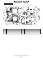
2. Apply 4 V using a stabilized power supply and turn on the handset.
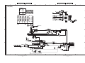
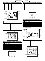
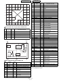
1. Set PWB and make connections as shown below.
Make sure connections are correct at the points shown below.
Hook
Hook
Hook
Push
PWB
Hook
Hook
3. Start RF test tool.
Hook
4. Select a COM port to which Data Cable is connected.
5. Press the "Initialize & Read Data" button.
Black
Red
GSM Tester
(CMU 200)
6. The figre shown below appears (wait a few seconds).
PC
PWB repair jig
Data Cable
7. Click "OK" to proceed.
4-6-3. Tests
1) BAND Select & Channel
Select a band and a channel to test. Settings are applied to all tests.
Band selection
Channel bar
Input box
[Procedure]
Points
1. Select a band. (GSM900, DCS or PCS)
2. Select or enter a channel using Channel bar or Input box.
TM150
ADJUSTMENTS, PERFORMANCE CHECK, AND FIRMWARE UPGRADE
2 – 18
CONFIDENTIAL
DRAFT
2) TX test
Test burst transmission.
TX frequency of selected channels
Current PCL (Read only)
This indicator appears
during burst transmission.
Data patterns
PCL bar
TX ON/OFF button
[Procedure]
1. Select a band and channel. [See 4-6-13. 1)]
2. Select PCL (Power Control Level) using PCL bar.
3. Select Data pattern.
4. Click TX ON to start burst transmission. (You can check each part in this state.)
5. Click TX OFF to end burst transmission.
* Data pattern (TSC 5) includes Training Sequence GSM 5, and other part is pseudo random data.
TM150 TX power Table (25°C, voltage: 3.7[V])
■ GSM900 Band
■ DCS/PCS Band
GSM900
PCL
[dBm]
Tolerance
PCL
DCS/PCS
[dBm]
Tolerance
5
33
+/- 2 dB
0
30
+/− 2 dB
6
31
+/- 3 dB
1
28
+/− 3 dB
7
29
+/- 3 dB
2
26
+/− 3 dB
8
27
+/- 3 dB
3
24
+/− 3 dB
9
25
+/- 3 dB
4
22
+/− 3 dB
10
23
+/- 3 dB
5
20
+/− 3 dB
11
21
+/- 3 dB
6
18
+/− 3 dB
12
19
+/- 3 dB
7
16
+/− 3 dB
13
17
+/- 3 dB
8
14
+/− 3 dB
14
15
+/- 3 dB
9
12
+/− 4 dB
15
13
+/- 3 dB
10
10
+/− 4 dB
16
11
+/- 5 dB
11
8
+/− 4 dB
17
9
+/- 5 dB
12
6
+/− 4 dB
18
7
+/- 5 dB
13
4
+/− 4 dB
19
5
+/- 5 dB
14
2
+/− 5 dB
15
0
+/− 5 dB
3) RX test
The handset receives burst signals in this test.
RX frequency of selected channels
Current RX Gain (Read only)
RX Gain Setting bar
This indicator appears
while receiving burst signals.
Sniff ON/OFF
RX ON/OFF button
TM150
ADJUSTMENTS, PERFORMANCE CHECK, AND FIRMWARE UPGRADE
2 – 19
CONFIDENTIAL
DRAFT
[Procedure]
4-7. Password reset
1. Select a channel and band. [see 4-6-3.1)]
SPST resets the password (handset code is set to “0000”).
2. Select RX Gain using RX Gain Setting bar.
<Operation>
3. Choose Sniff ON or OFF.
1) Set the COM port on the SPST initial screen and click “User Password Reset”. Click “Yes” to reset. Click “No” to exit.
4. Click "RX ON" to start receiving burst signals.
5. From GSM tester, send burst signals in the specified channel.
(You can check each part in this state.)
TM150
6. Click "RX OFF" to end receiving burst signals.
* In this test, the reception timing cannot be synchronized with burst
signals from Signal Generator or GSM tester.
* The standard RX Gain Setting is:
(Input power at the aerial connector of the handset) + (RX Gain)
= -16 dBm
Excessive Input power or RX Gain may cause damage to the handset.
2) When completed, the following appears.
TM150
4) RSSI Measure
The handset notifies you of input power value at the aerial connector.
4-8. Performance check and adjustment
Estimated Power
Input box
(Integeronly)
Measure button
Measured power box
With this function, SPST checks the performance of the handset and
makes adjustments.
<Operation>
[Procedure]
1. Connect the handset and GSM tester (or Signal Generator) with RF cable.
2. Select a band and channel. [see 4-6-3. 1)]
1) Set the COM port on the SPST initial screen and click "Performance
check and adjustment". The following dialog box appears while processing.
3. Send signals (*) from GSM tester.
4. Enter the value of input power from GSM tester in integers (from -10
to -110) considering RF cable loss.
5. Press the [Measure] button.
6. The result appears in Measured Power box.
* The signal type from GSM tester must be either of two:
1. Continuous sine wave (without modulation) with the frequency
as follows:
(Frequency of the measured channel) + 67.708kHz.
(Ex. channel: GSM 37ch 3 the result: 942.467708 MHz)
Power: -110 to -10 dBm
2) When completed, the following is displayed. Click "Back to main
menu" to exit.
2. BCCH signal of the measured channel
Power: -110 to -10 dBm
Result
When the handset is properly calibrated, the error between "Estimated Power" and "Measured Power" is less than 3dB.
4-6-4. Termination
Turn off the handset to ensure proper operations.
4-6-5. Trouble information
When switching DCS and PCS, change the channel number as well. Or
the band does not change properly.
The functions of each button are described below.
Example: If you change DCS 512 CH to PCS 512 CH, the band
remains DCS.
TM150
ADJUSTMENTS, PERFORMANCE CHECK, AND FIRMWARE UPGRADE
2 – 20
CONFIDENTIAL
DRAFT
4-8-1. Main back light check
4-8-4. LED check
The main display backlight turns on and the message appears on the PC.
The LED lights up in a specified color and the message appears on the
PC. Check the LED and press "OK".
TM150
• If a failure occurs, see "15. Flash light does not work." in [3] Troubleshooting.
4-8-5. Battery voltage check
Click to display the current battery voltage.
• If a failure occurs, see "1. Power is not turned on." in [3] Troubleshooting.
Check the backlight and press "OK".
• If a failure occurs, see "10. Back Light does not turn on." in [3] Troubleshooting.
4-8-2. External back light check
4-8-6. SD read/write test
Insert an SD card (otherwise a message prompts you to do so and click
the button to perform the SD card read/write test.
• If a failure occurs, see "17. SD (Memory) card is not recognized." in
[3] Troubleshooting.
The external display back light turns on and the message appears on
the PC. Check the back light and press "OK".
• If a failure occurs, see "10. Back Light does not turn on." in [3] Troubleshooting.
4-8-7. Vibrator test
Click to vibrate the handset. Click "OK" to exit.
4-8-3. Key back light check
The keypad back light turns on and the message appears on the PC.
Check the back light and press "OK".
• If a failure occurs, see "5. Vibrator does not work." in [3] Troubleshooting.
4-8-8. Melody test
A message describes test items. Click "Yes" to proceed and "No" to exit.
The order of the test items:
speaker 3 hands free 3 hands free (stereo) 3 speaker (analog melody)
Troubleshooting (based on [3] Troubleshooting)
Trouble found by SPST
(1) Speaker
(2) Hands free
(3) Hands free (stereo)
See "Speaker does not work."
Sound is heard in audio test.
Parts between IC105 pin 10 and IC103 pin 93 are defective, or IC103 is defective.
No sound is heard in audio test.
See "Hands free kit (monaural headset)" in the section "3. No voice is heard from the earpiece."
Sound is heard in audio test.
Parts between IC105 pin 10 and IC103 pin 93; IC105 pin 11 and IC103 pin 94 are defective.
Otherwise IC103 is defective.
No sound is heard in audio test.
See "Hands free kit (stereo headset) - Option" in the section " No voice is heard from
the earpiece."
(4) Speaker (analog melody)
See "Video/Voice Recorder playback is impossible."
Otherwise parts between IC105 pin 10 and IC103 pin 93 are defective, or IC103 is defective.
4-8-9. Audio test
The following appears.
Select a test item from Audio device. Check the output sound from the
receiver by speaking to the microphone, etc. Click "Back to test menu"
to return to the previous screen.
TM150
ADJUSTMENTS, PERFORMANCE CHECK, AND FIRMWARE UPGRADE
2 – 21
CONFIDENTIAL
DRAFT
Troubleshooting (based on [3] Troubleshooting)
Trouble found by SPST
(1)
Handset microphone
Handset receiver
(2)
Handset microphone
Hands free receiver
(1) & (2): No voice is heard.
(3)
Hands free microphone
Hands free receiver
(4)
Hands free microphone
Handset receiver
(1) & (2): No voice is heard.
See "Phone" in the section "2. Voice transmission/recording is impossible."
(1): Voice is heard.
(2): No voice is heard.
See "Hands free kit (monaural headset)" in the section "3. No voice is heard
from the earpiece" or "Hands free kit (stereo headset)-Option" in the section
"3. No voice is heard from th earpiece."
(1): No voice is heard.
(2): Voice is heard.
See "Phone" in the section "3. No voice is heard from the earpiece."
(3) & (4): No voice is heard.
See "Hands free kit (headset)" in the section
"2. Voice transmission/recording is impossible."
(3): Voice is heard.
(4): No voice is heard.
(3): No voice is heard.
(4): Voice is heard.
4-8-10. Camera check
4-8-14. Main display flicker adjustment
The following appears.
The following is displayed.
Select a Camera mode from the pull-down menu. Click "Shutter" to check
that the camera operates properly. Click "Back to performance check
menu" to return to the previous screen.
Check a main display visually within a distance of 20 cm from a fluorescent
light, and adjust the value to minimize flicker on the display with the [b] and [c]
buttons. Click "Save" and confirm that the main display does not flicker.
(Fine adjustment for DC voltage between display electrodes)
• If a failure occurs, see "10. Pictures cannot be taken." in [3] Troubleshooting.
Enlarged view
(A black line appears
after each gradation line.)
4-8-11. Memory check
Click "S-RAM" and "PSRAM" to see each test result.
For "Check Sum", the calculation appears after the SPST communicating
dialog box.
4-8-12. LCD test
8-level graduation pattern with alternate black and gradation lines
(black and white)
Check that the specified color appears on the main display.
• If a failure occurs, see "12. The display does not appear on Main Display." and "13. The display does not appear on External Display (in 65K
color mode)." in [3] Troubleshooting.
4-8-13. Temperature adjustment
The following appears.
Setting temp. indicates the current temperature. The relative temperature is
displayed in the text box below.
(Only the relative temperature is adjustable.)
If displayed Setting temp. value differs from the current temperature, click [b]
or [c] to set a correction value in the range of -99 to +99 and click “Save”
4-8-15. External display contrast adjustment
Click the “External display contrast adjustment” button. The following
screen appears.
Correction value = (Setting temp.)-(current temp.)+(displayed correction value)
TM150
ADJUSTMENTS, PERFORMANCE CHECK, AND FIRMWARE UPGRADE
2 – 22
CONFIDENTIAL
DRAFT
4-8-17. Black defect correction
* Black defect correction:
Defective pixels in a camera light sensor appear as black points in the display even when a captured image is completely white (display is all white).
Perform black defect correction to eliminate errors in these pixels.
1) Requirements
DEN:
• Desk top type of fluorescent lamp
075
• Black defect correction sheet
8-level gradation pattern (black & white pattern)
Comparing with an adjusted handset, click “b“ or "c" to adjust the value
so that the same gradation pattern is displayed. Click "Save" and
confirm the pattern on the external display.
4-8-16. White defect correction
• Illuminance meter
* White defect correction:
Defective pixels in a camera light sensor appear as bright points in the
display even when light is blocked completely (display is all black). Perform white defect correction to eliminate errors in these pixels.
2) Procedure
1. Cover the camera section with the black defect correction sheet as
shown in Figure 96.
1. Protect the handset camera from light completely with a black cover.
2. Click the "White defect correction" button. The following screen
appears.
TM150
Click the "Yes" button and leave it for about 20 seconds.
When completed, the following message appears.
Attach the Black defect correction sheet
to the handset firmly with clear scotch tape.
TM150
2. Check the distance from the fluorescent lamp by using an illuminance meter.
In the proper position for black defect correction, illuminance is
between 8,000 and 10,000 lux.
When an error occurs, the corresponding message appears. Solve the
problem according to "Solution".
• Error 1
Error message
: "There are too many white cracks."
Cause
: The light is not sufficiently blocked.
Solution
: Block the light completely and perform white
defect correction again.
• Error 2
Error message
: "There are many white cracks."
Cause
: The light is not sufficiently blocked.
Solution
: Block the light completely and perform white
defect correction again.
• Error 3
Error message
: "There are too many white cracks cannot be
rectified."
Cause
: There is a hardware error.
Solution
: Replace the camera unit.
TM150
ADJUSTMENTS, PERFORMANCE CHECK, AND FIRMWARE UPGRADE
2 – 23
CONFIDENTIAL
DRAFT
4-9. ****MODE RELEASE
3. Hold the handset in the proper position.
When the handset does not turn on and enter the normal mode, use this
function to change ****mode to the normal mode.
<Operation>
1) Select the COM port on the SPST initial screen and click
"****mode release". The following dialog box appears.
4. Click the "Black defect correction" button.
The following message is displayed.
2) If SPST cannot communicate with the handset, the following message is displayed. Make sure the handset is turned on and click
"Retry". To exit, click "Cancel".
TM150
5. Click the "Yes" button. Communication starts.
3) When complete, the following message appears.
TM150
6. The result is displayed within a minute as follows.
5. OTHER TESTS
When an error occurs, the corresponding message appears. Solve the
problem according to "Solution".
SPST does not provide tests of Bluetooth/USB communication.
Check them according to the following instructions.
5-1. USB
• Error 1
Connect TM150 and a PC with a USB cable. Check that TM150 is
recognized as a device.
Error message : "There are too many black cracks."
Cause
: The light is too weak or strong.
Solution
: At the proper distance from the light source (8,00010,000 lux), perform black defect correction again.
If the USB driver for TM150 (SHARP GSM GPRS USB Driver) is not
installed on the PC, “Found New Hardware” window appears and
“Found New Hardware Wizard“ starts (the handset is recognized).
• Error 2
Error message : "There are many black cracks."
Cause
: The light is too weak or strong.
Solution
: At the proper distance from the light source
(8,000 - 10,000 lux), perform black defect correction again.
• Error 3
Error message : "There are too many black cracks cannot be rectified."
Cause
: There is a hardware error.
Solution
: Replace the camera unit.
TM150
ADJUSTMENTS, PERFORMANCE CHECK, AND FIRMWARE UPGRADE
2 – 24
CONFIDENTIAL
DRAFT
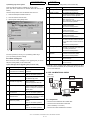
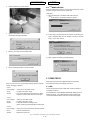
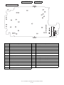
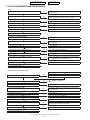
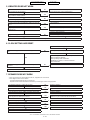
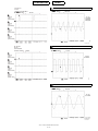
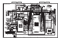
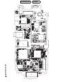
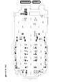
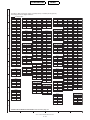
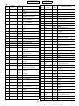
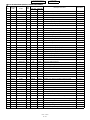
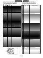
[2] TEST POINTS
MAIN PWB (FRONT SIDE)
TP No.
Signal name
TP No.
Signal name
TP103
USC [0]
TP171
VCORE (1.8V)
TP104
USC [1]
TP172
VAPP
TP105
USC [2]
TP173
VINT (3V)
TP107
USC [4]
TP174
LIGHT3 (KEYLED)
TP108
USC [5]
TP176
VMIC
TP109
USC [6]
TP177
AUXADC1, 2
TP113
VVIB
TP178
TEMP
TP118
USC [3]
TP179
AUXADC1, 2
TP119
MIC
TP180
CHGIN_A (5.2V)
TP120
AUDIO_IN
TP181
Flexible PWB insert check terminal 1
TP121
JACK_L
TP182
Flexible PWB insert check terminal 2
TP123
RESET
TP183
Flexible PWB insert check terminal 3
TP124
PWRON
TP184
Flexible PWB insert check terminal 4
TP126
SP1
TP502
VBAT
TP127
SP2
TP503
VBAT
TP144
Terminal for STACK MEMORY adhesion check 1
TP506
BATT_SENSE
TP147
Terminal for STACK MEMORY adhesion check 2
TP514
BT_VCC (3.0V)
TP153
VPP Flash
TP515
VBUS_IN
TP157
Analog Power Supply IC INT
TP521
POWONKEY
TP158
VINT (3V)
TP523
USB D+
TP160
HEDSET_DET
TP524
USB D
TP161
STEREO_SW
TP525
RTS
TP162
REMOTE_SW
TP526
CTS
TP163
JACK_R
TP527
DGND
TP164
VABB
TP528
DGND
TP165
VT (2.75V)
TP535
Reserved
TP166
VUSB
TP536
ManufactUre Specific
TP167
VRTC (1.8V)
TP537
CHGIN
TP168
VBACK (3V)
TP801
VTCXO (2.9V)
TP169
VSIM (2.85V)
TP802
VRF (2.9V)
TP170
VMEM (2.8V)
TM150
ADJUSTMENTS, PERFORMANCE CHECK, AND FIRMWARE UPGRADE
2 – 25
CONFIDENTIAL
DRAFT
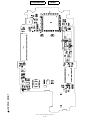
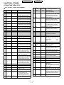
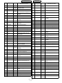
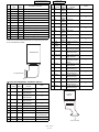
MAIN PWB-B (REAR SIDE)
TP No.
TP111
Signal name
TP No.
Signal name
VVIB
TP505
TP112
DGND
TP520
BATT
TP501
BATT
TP522
POWONKEY
TP504
DGND
TP534
BATT_SENSE
TM150
DGND
ADJUSTMENTS, PERFORMANCE CHECK, AND FIRMWARE UPGRADE
2 – 26
CONFIDENTIAL
DRAFT
LCD PWB (FRONT SIDE)
TP No.
Signal name
TP No.
TP722
Signal name
TP701
SP1
RECIVER_OUTP
TP702
SP2
TP723
Terminal for LCDC adhesion check 3
TP705
VCCD (2.5V)
TP724
Terminal for LCDC adhesion check 4
TP706
Terminal for APPLICATION POWER adhesion check 1
TP727
LIGHT1
TP707
Terminal for APPLICATION POWER adhesion check 2
TP728
LEDCTL
TP709
VDD6 (3.1V)
TP729
LEDR
TP710
Backlight (LED+)
TP730
LEDG
TP711
Backlight (LED-)
TP731
LEDB
TP712
CAMCLK
TP732
Power supply for camera (+15V)
TP713
13MHzCLK
TP733
Power supply for camera (-8V)
TP714
VLCD (1.8V)
TP734
RECIVER_OUTN
TP715
Terminal for LCDC adhesion check 1
TP735
RECIVER_OUTP
TP716
Terminal for LCDC adhesion check 2
TP736
AVDD (3.1V)
TP717
VOUT (External Display)
TP737
VPLUS2
TP720
VDD2
TP738
Connector connection check terminal
TP721
RECIVER_OUTN
TM150
ADJUSTMENTS, PERFORMANCE CHECK, AND FIRMWARE UPGRADE
2 – 27
CONFIDENTIAL
DRAFT
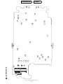
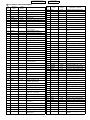
LCD PWB (REAR SIDE)
TP No.
TP703
Signal name
SP1
TP No.
TP704
TM150
Signal name
SP2
ADJUSTMENTS, PERFORMANCE CHECK, AND FIRMWARE UPGRADE
2 – 28
CONFIDENTIAL
DRAFT
[3] TROUBLESHOOTING
2. Voice transmission/recording is impossible.
10. Back Light does not turn on.
11. Out of range and incoming/outgoing calls are impossible.
3. No voice is heard from the earpiece.
12. The display does not appear on Main Display.
4. Battery does not charge.
13. The display does not appear on External Display (in 65K
color mode).
5. Vibrator does not work.
14. Pictures cannot be taken.
6. Clock Settings are reset.
15. SIM card is not recognized.
7. Speaker does not work.
16. SD (Memory) card is not recognized.
8. MP3 cannot be played.
17. USB connection is impossible.
1. Power is not turned on.
9. Video/Voice Recorder playback is impossible.
1. POWER IS NOT TURNED ON.
Connect a battery of 4.0 V or more.
Execute File System Initialization of Downloader in SPST
without loading a file.
YES
Does File System Initialize start properly
Is the user area (file system) initialized by Flash Loader?
NO
YES
NO
5-level stack memory (IC101)
and IC106 are defective.
Does normal mode start?
YES
NO
5-level stack memory (IC101)
data is corrupted.
Is it possible to rewrite the firmware?
NO
YES
5-level stack memory (IC101)
and IC106 are defective.
Does normal mode start after restart?
NO
5-level stack memory (IC101)
and IC106 are defective.
Is 3.6 V or more applied to BATT terminal (TP520)?
NO
YES
Program code of 5-level stack
memory (IC101) is garbled.
Battery terminals are defective, connector terminal is dirty, or
soldering is improper.
YES
Is the voltage 1.2 V or lower on SENSE terminal (TP506)?
YES
Is there conduction through fuse (FS501)?
NO
The battery is defective or set improperly.
NO
Fuse (FS501) is blown.
NO
5-level stack memory (IC106) is installed improperly.
NO
IC103 is defective.
YES
Is 5-level stack memory (IC101) installed properly
YES
Is 2.8 V and 1.8 V applied to VMEM (TP170) and VCORE
(TP171) respectively?
YES
NO
Is 3.0 V applied to VINT (TP173)?
IC111 is defective.
YES
Is the waveform of signals from R169 connected to X101 (32
kHz) correct? Are R167, R169, R174A, C176, X101, and
IC106 good in appearance and mounted properly?
NO
YES
Is the rectangular wave of 13 MHz properly sent to TP713?
YES
X101 (32 kHz oscillator), R167, R169, C174, and C176 are
defective or mounted improperly.
Or oscillating circuit of IC106 is defective.
IC106, R179, and R110A are defective or mounted improperly.
CN701 and CN102 are connected improperly.
NO
Is the triangular wave of 13 MHz sent from C833?
YES
C801 is defective.
NO
NO
Is 2.9 V supplied from VTCXO (TP801)?
Power Supply (IC804) is defective.
YES
IC801 and peripheral circuits are defective.
TM150
ADJUSTMENTS, PERFORMANCE CHECK, AND FIRMWARE UPGRADE
2 – 29
CONFIDENTIAL
DRAFT
2. VOICE TRANSMISSION/RECORDING IS IMPOSSIBLE.
Phone
YES
Replace the microphone. Is the problem solved?
The built-in microphone is defective or in a poor contact with
the PWB.
NO
L101, L102, and C101 are defective.
YES
NO
Is 1.2 - 2.1 V applied to both ends of C101?
Is 1.2 - 2.1 V applied to TP119?
NO
Is 2.4 - 2.5 V applied to TP176?
NO
YES
YES
R125 is defective.
Is 2.4 - 2.5 V applied to IC103 pin 76?
YES
NO
R115 and C108 are defective.
IC103 is defective.
NO
Is approx. 1.7 V applied to IC103 pin 80?
Is approx. 1.7 V applied to IC103 pin 96?
NO
YES
R263 and R130 are defective.
Is 2.7 or more voltage applied to R192 (IC106 pin 89 side)?
NO
YES
IC103 is defective.
R192 is defective. (Headset mode is set.)
YES
Replace C126 or C133. Is the problem solved?
YES
C126 or C133 is defective.
NO
IC103 and IC106 are defective.
Hands free kit (headset)
(The following procedure applies to both monaural and stereo headsets.)
Replace the hands free kit. Is the signal sent?
YES
NO
Hands free kit is defective.
R104A, R112, and V101 are defective.
NO
Is 0.7 - 1.8 V applied to JK101 pin 2?
YES
Is 0.7 - 1.8 V applied to TP120?
YES
NO
Is 2.4 - 2.5 V applied to TP176?
YES
NO
R122 is defective.
Is 2.4 - 2.5 V applied to IC103 pin 76?
YES
NO
R115 and C108 are defective.
IC103 is defective.
NO
Is approx. 1.7 V applied to IC103 pin 79?
Is approx. 1.7 V applied to IC103 pin 95?
NO
YES
R262 and R129 are defective.
Is the voltage 0 V on R192 (IC106 pin 89 side) ?
NO
YES
IC103 is defective.
Jack JK101 is defective, or the jack plug is in a poor contact
with hands free kit (Handset mode is set.)
YES
Replace C127 or C134. Is the problem solved?
YES
C127 or C134 is defective.
NO
YES
Replace JK101. Is the problem solved?
JK101 is defective, or the jack plug pin 2 is in a poor contact
with hands free kit.
NO
IC103 and IC106 are defective.
TM150
ADJUSTMENTS, PERFORMANCE CHECK, AND FIRMWARE UPGRADE
2 – 30
CONFIDENTIAL
DRAFT
3. NO VOICE IS HEARD FROM THE EARPIECE.
Phone
Is the signal sent to the contact terminal of the earpiece?
YES
The built-in earpiece is defective, or in a poor contact with
TP734 or TP735.
YES
The camera relay FPC, CN103, or CN701 is defective. Or the
camera is in a poor contact with CN103 and CN701.
YES
L107, L108, C115, and C120 are defective.
NO
Is the signal sent to CN103 pins 17 and 18?
NO
Is the signal sent to vsGNDs at both ends of C132?
NO
Is 2.7 or more voltage applied to R192 (IC106 pin 89 side)?
NO
R192 is defective. (Headset mode is set.)
NO
IC103 is defective.
YES
Is approx. 1.2 V applied to IC103 pins 59 and 63?
YES
IC103 or IC106 is defective.
Hands free kit (monaural headset)
Replace the hands free kit. Is the signal sent ?
YES
Hands free kit is defective.
NO
Is the signal sent to JK101 pin 3?
YES
Jack JK101 is defective, or the jack plug is in a poor contact
with hands free kit.
YES
L103 is defective.
YES
C107, C103, and V106 are defective.
YES
R124 is defective.
NO
Jack JK 101 is defective, or the jack plug is in a poor contact
with hands free kit. (Handset mode is set.)
NO
IC103 is defective.
NO
Is the signal sent to TP121?
NO
Is the signal sent to the positive pole of C107?
NO
Is the signal sent to IC103 pin 60?
NO
Is the voltage 0 V on R192 (IC106 pin 89 side) ?
YES
Is approx. 1.2 V applied to IC103 pin 60?
YES
IC103 or IC106 is defective.
Hands free kit (stereo headset) - Option
The headset cannot be used. (It works as a monaural headset.)
NO
NO
Is the stereo headset the one specified by Sharp?
Is the plug a 6 pole type with a ring?
YES
YES
Is R-ch only the channel that does not send signals?
NO
Replace the hands free kit. Is the signal sent ?
YES
YES
B
(NEXT PAGE)
Hands free kit is defective.
NO
Is the signal sent to JK101 pin 3?
YES
Jack JK101 is defective, or the jack plug is in a poor contact
with hands free kit.
NO
YES
Is the signal sent to TP121?
NO
Is the signal sent to the positive pole of C107?
NO
YES
YES
Is the signal sent to IC103 pin 60?
L103 is defective.
C107, C103, and V106 are defective.
R124 is defective.
NO
Is the voltage 0 V on R192 (IC106 pin 89 side)? YES
NO
NO
Is approx. 1.2 V applied to IC103 pin 60?
Jack JK 101 is defective, or the jack plug is in a poor contact
with hands free kit. (Handset mode is set.)
IC103 is defective.
YES
IC103 or IC106 is defective.
TM150
ADJUSTMENTS, PERFORMANCE CHECK, AND FIRMWARE UPGRADE
2 – 31
CONFIDENTIAL
DRAFT
(BACK PAGE)
B
Is the signal sent to JK101 pin 1?
YES
Jack JK101 is defective, or the jack plug is in a poor contact
with hands free kit.
NO
YES
Is the signal sent to TP163?
L105 is defective.
NO
YES
Is the signal sent to the positive pole of C110?
C110, C105, and V109 are defective.
NO
YES
Is the signal sent to IC103 pin 64?
R126 is defective.
NO
Is the voltage 0.1 V or lower on R191 (IC106 pin 100 side)?
NO
Jack JK101 is defective, or the jack plug is in a poor contact
with hands free kit. (Monaural mode is set.)
YES
NO
Is approx. 1.2 V applied to IC103 pin 64?
IC103 is defective.
YES
IC103 or IC106 is defective.
4. BATTERY DOSE NOT CHARGE.
Set a battery of 3.8 - 3.9 V and connect the charger.
CN701 and CN103 are connected improperly, and IC103 is
defective.
YES
NO
Is the mobile light turned on red?
NO
YES
Set a battery of 4.0 - 4.2 V. Click the “Performance check
adjustment” button on SPST.
YES
Click the “Temperature adjustment” button. Is the value of
“temp” normal? (Measurement tolerance: ± 5 deg.)
Does the waveform periodically change between “H” and “L”
at R701?
YES
LED702 of the mobile light is defective.
* For settings and connections for SPST, refer to the “ADJUSTMENTS,
PERFORMANCE CHECK, AND FIRMWARE UPGRADE” (see page 2-1).
TH701, TH101, and IC103 are defective. CN701 and CN103
NO
are connected improperly.
YES
Click the “Battery voltage check” button. Is the voltage 4.0 4.2 V?
NO
IC103 is defective.
NO
R535, R536, Q108, IC115, and IC103 are defective.
NO
IC115 is defective.
NO
R535, R536, Q108, IC115, IC103, D103, and D105 are defective.
YES
Set a battery of 3.3 - 4.2 V and start in normal mode.
Connect the charger to the external connector. Is the voltage
applied to TP537 higher than that of battery?
YES
When the charger is inserted to the external connector, is
IC115 pin 1 at “L”?
YES
Connect the charger to the external connector. After approx.
15 seconds, do the voltages on TP180 and TP520 increase by
more than 0.05 V?
YES
The battery is defective, or the battery cycle is shortened.
TM150
ADJUSTMENTS, PERFORMANCE CHECK, AND FIRMWARE UPGRADE
2 – 32
CONFIDENTIAL
DRAFT
5. VIBRATOR DOSE NOT WORK.
Are vibrator terminals in contact with the land?
NO
Are terminals and the land clean?
Hereafter check with Vibrator working.
YES
Is rectangular wave of 3 V sent to between Vibrator terminals
YES
in sync with the vibration pattern?
NO
NO
Is VBAT voltage applied to IC109 pin 5?
YES
Is signal synchronized with the vibration pattern sent to IC109
pin 1?
NO
Is signal synchronized with the vibration pattern sent from
IC105 pin 19?
Vibrator is deformed and defective. (When vibrator terminals
and the land are dirty, clean or replace them.)
Vibrator is defective.
IC109 is soldered improperly.
YES
IC109 is defective.
YES
IC105 is soldered improperly.
NO
C167 and C168 are defective.
NO
Is approx. 3 V applied to IC105 pin 7?
YES
NO
C167 and C168 good in appearance and mounted properly?
YES
IC105 is defective, or the control signal line to IC106 is defective.
6. CLOCK SETTING ARE RESET.
The holder is installed improperly.
NO
Is 2.5 V or more applied to TP168 with a battery in the handset?
NO
Is back-up battery holder properly installed to SD/SIM FPC?
YES
• The remaining power of back-up battery is insufficient.
• Back-up battery is defective.
• Back-up battery holder is defective.
• SD/SIM FPC is broken, or CN104 is defective.
• R254 is defective.
YES
Is 1.5 V or more applied to TP167 without a battery in the
handset ?
NO
IC103 is defective.
YES
X101, R169, R174A, and C176 are defective.
7. SPEAKER DOSE NOT WORK.
* When ring tones sound, but keypad tones do not, “Keypad Tones” is set to Off.
* When Ringer Volume is set to “Silent”:
· Voice Recorder playback sound is not produced.
· Playback sound of Video and MP3 can be heard by increasing the volume during playback.
Are speaker terminals in contact with the land?
YES
Is the impedance between speaker terminals approx. 8 ohms?
YES
Is the signal sent to TP701, TP702, or speaker contact pad?
NO
NO
NO
Speaker is defective.
Speaker is defective.
YES
Speaker is defective.
Is the signal sent to CN103 pins 3 and 4?
YES
The camera relay FPC, CN103, or CN701 is defective. Or the
camera is in a poor contact with CN103 and CN701.
NO
Is VBAT voltage applied to IC105 pin 15?
YES
NO
R139 is defective.
NO
R158 is defective.
Is approx. 3 V applied to IC105 pins 7 and 32?
YES
Is the signal sent to IC105 pin 12?
NO
YES
R145 and R146 are defective, or IC105 is defective.
IC105 or the control line to IC106 is defective.
TM150
ADJUSTMENTS, PERFORMANCE CHECK, AND FIRMWARE UPGRADE
2 – 33
CONFIDENTIAL
DRAFT
8. MP3 CANNOT BE PLAYED.
Speaker
Not defective.
YES
Is Ringer Volume set to “Silent”?
YES
Cancel “Silent”. Is sound produced?
NO
Go to the section “Video/Voice Recorder playback is impossible.”
NO
Is output of the video and voice recorder normal?
NO
YES
Insert an SD card with MP3 files recorded on a normal unit.
Do they play?
NO
Is the SD card recognized?
YES
Is the signal sent to IC103 pin 60?
YES
NO
YES
YES
Are keypad tones and ring tones normal?
NO
Go to the section “Speaker does not work.”
Not defective.
Go to the section “SD (Memory) card is not recognized.”
Parts between IC103 pin 60 and IC105 pins 14 & 13 are
defective or soldered improperly.
NO
IC103 is defective.
Hands free kit (headset)
(The following procedure applies to both monaural and stereo headsets.)
NO
Is sound normally produced from Speaker?
YES
YES
Replace the hands free kit. Is sound produced?
Go to the section regarding Speaker.
Hands free kit is defective.
NO
Go to “Hands free kit (monaural headset)” in the section “No
voice is heard from the earpiece.”
9. VIDEO/VOICE RECORDER PLAYBACK IS IMPOSSIBLE.
Speaker
NO
Are keypad tones and ring tones normal?
YES
In Playback window, does playback start normally and the
capacity bar change?
NO
Go to the section “Speaker does not work.”
IC101 or IC106 is defective.
Not defective.
YES
YES
Is Ringer Volume set to "Silent"?
YES
Cancel “Silent”. Is sound produced?
NO
NO
YES
Is the signal sent to IC103 pin 60?
Parts between IC103 pin 60 and IC105 pins 14 & 13 are
defective or soldered improperly.
NO
IC103 is defective.
Hands free kit (headset)
* If R-ch is the only channel of stereo headset that does not send signals, see “Hands free kit (stereo headset)” in the section
“No voice is heard from the earpiece.”
Replace the hands free kit.
Hands free kit is defective.
YES
Is the signal sent?
NO
In Playback window, does playback start normally and the
capacity bar change?
NO
IC101 or IC106 is defective.
Not defective.
YES
YES
Is Ringer Volume set to "Silent"?
YES
Cancel "Silent". Is sound produced?
NO
NO
Go to “Hands free kit (monaural headset)” in the section “No voice is heard from the earpiece.”
TM150
ADJUSTMENTS, PERFORMANCE CHECK, AND FIRMWARE UPGRADE
2 – 34
CONFIDENTIAL
DRAFT
10. BACK LIGHT DOES NOT TURN ON.
FS701 is mounted improperly, or the fuse is brown.
NO
Is VBAT voltage applied to C701?
NO
Is fuse (FS701) in good appearance, mounted properly, and is
there conduction?
YES
YES
C701, C703, and L701 are defective.
External display only.
Which back light does not turn on, Main or External?
C
Main Display only or both.
Is back light setting for External Display set to On?
NO
Go to the setting as follows and set it to On:
Settings
Phone
Settings
Main
Display
Backlight
NO
Does it turn on?
YES
YES
Not defective.
Is CN705 in good appearance and mounted properly?
NO
YES
CN705 is defectiv e.
Back light FPC or CN705 is defective.
NO
Is the contact point of back light FPC clean?
Is back light FPC properly inserted to CN705?
NO
Clean back light FPC and insert it again. Does it turn on?
YES
YES
Not defective.
YES
Is 13 - 24 V applied between TP710 and TP711?
NO
Are C790, C791, C702, C707, C713, R718, and D702 in good
appearance and mounted properly?
YES
Back light FPC is defective.
NO
C790, C791, C702, C707, C713, R718, and D702 are defective.
NO
Go to the setting as follows and set it to On:
Settings
Phone
Settings
External
Display
Back light
R453, R437, and IC404 are defective.
C
Is back light setting for Sub Display set to On?
NO
YES
Does it turn on?
YES
Not defective.
Is 7 V applied between LED703 anode (A) terminal and
LED704 cathode (K) terminal?
YES
NO
IC707 is defective or mounted improperly.
LED703 and LED704 are defective.
TM150
ADJUSTMENTS, PERFORMANCE CHECK, AND FIRMWARE UPGRADE
2 – 35
CONFIDENTIAL
DRAFT
11. OUT OF RANGE AND INCOMING/OUTGOING CALLS ARE IMPOSSIBLE.
[Checkpoint s in RF Test Tool ]
Is transmission possible using RF Test Tool?
YES
[Sender]
NO
Is voltage (applox. 2.9 V) supplied to pin 6 of IC804?
NO
IC804 is defective.
YES
Is IQ signal supplied to pins 23, 24, 25, and 26 of IC801?
NO
IC103, IC106, or PWB is defective.
YES
Is frequency signal sent?
GSM900 bands ....................... IC801 pin 17
DCS1800/PCS1900 bands ...... IC801 pin 19
NO
IC801 is defective.
YES
Is frequency signal supplied?
GSM900 bands ....................... IC803 pin 15
DCS1800/PCS1900 bands ..... IC803 pin 13
NO
IC802 is defective.
YES
Is frequency signal supplied to pin 1 of FL905?
NO
IC803 is defective.
NO
FL905 is defective.
YES
Is frequency signal supplied to pin 1 of J801?
YES
J801 is defective.
[Receiver]
–70 dBm input.
Is frequency signal supplied?
GSM900 bands ........................... IC801 pins 9, 10
DCS1800 band ............................ IC801 pins 6, 7
PCS1900 band ............................ IC801 pins 3, 4
IC801 is defective.
YES
NO
Is frequency signal supplied?
GSM850 band ................................ FL901 pin 1
GSM900 band ................................ FL902 pin 4
DCS1800 band ............................... FL902 pin 1
PCS1900 band ............................... FL903 pin 1
FL902, or FL903 is defective.
YES
NO
Is frequency signal supplied to pin 9 of IC803
YES
IC803 is defective.
NO
FL905 or J801 is defective.
TM150
ADJUSTMENTS, PERFORMANCE CHECK, AND FIRMWARE UPGRADE
2 – 36
CONFIDENTIAL
DRAFT
12. THE DISPAY DOES NOT APPEAR ON MAIN DISPLAY.
Is Main Display unit fully inserted to CN704?
NO
Improperly inserted to the connector.
Clean the contact point of CN704 and insert the unit again.
Does the display appear?
NO
YES
The contact point of the connector is dirty.
Replace Main Display.
Does the display appear?
YES
Main Display unit is defective.
Is 3.6 or more voltage applied to VBAT terminal (FS701) and
VBAT_L terminal (FS702)?
YES
NO
Go to the section “Power is not turned on.”
Is 2.8 ± 0.1 V applied to TP170?
YES
NO
Go to the section “Power is not turned on.”
Is 3.0 ± 0.1 V or more applied to TP173?
NO
Go to the section “Power is not turned on.”
YES
NO
YES
Regulator IC703 or R716 is defective.
NO
Is 1.8 ± 0.1 V or more applied to TP714?
NO
Is 3.0 ± 0.1 V applied to IC703 pin 1?
Are R743 and C728 good in appearance and mounted properly?
YES
YES
YES
Are CN701 and CN103 good in appearance and mounted
properly?
NO
CN703 and CN103 are defective or mounted improperly. And
FPC is defective.
Is 13 MHz applied to clock TP713?
YES
NO
Go to the section “Power is not turned on.”
Is 3.0 ± 0.1 V supplied from LCD_RST (L746)?
Are L746, C736, C751, CN701, and CN703 good in appearance and mounted properly?
YES
NO
L746, C736, C751, CN701, and CN703 are defective or
mounted improperly.
Is 3.0 V ± 0.1 V applied to CN704 pins 34, 37, and 38?
Are R737, R738, C774, and C775 good in appearance and
mounted properly?
YES
Is 3.0 ± 0.1 V applied to the LCD reset (CN704 pin 33 and
C766)?
Is C766 good in appearance and mounted properly?
YES
NO
CN404, R737, R738, C774, and C775 are defective or
mounted improperly.
NO
Display controller IC (IC704) and C761 are defective or
mounted improperly.
Is the signal of approx. 62 Hz present on C760?
Are C758, C759, C760, and C761 good in appearance and
mounted properly?
YES
NO
Display controller IC (IC704), C758, C759, C760, and C761
are defective or mounted improperly.
Is the following voltage applied to the terminal?
TP720: approx. 10 V
Are C771, C772, C773, C776, C777, C779, C780, C781,
C782, and C783 good in appearance and mounted properly?
YES
NO
Main Display unit, CN704, C771, C772, C773, C776, C777,
C779, C780, C781, C782, and C783 are defective.
Main Display unit is defective, or connector CN704 is mounted
improperly.
TM150
ADJUSTMENTS, PERFORMANCE CHECK, AND FIRMWARE UPGRADE
2 – 37
CONFIDENTIAL
DRAFT
13 . THE DISPLAY DOES NOT APPEAR ON EXTERNAL DISPLAY (IN 65K COLOR MODE).
Does the display appear on Main Display?
NO
Go to the section “Power is not turned on.”
NO
Go to the setting as follows and set it to On:
Settings
Phone
Settings
External
Display
Display On/Off
YES
Is External Display On/Off setting set to On?
YES
NO
Is External Display unit fully inserted to CN703?
Improperly inserted to the connector.
YES
Clean the contact point of the connector CN703 and insert the
unit again. Does the display appear?
YES
The contact point of the connector is dirty.
NO
R723 is defective or mounted improperly.
NO
CN703 and CN103 are defective or mounted improperly. And
FPC is defective.
NO
IC707, C736, C751, and L749 are defective or mounted
improperly.
NO
R222 is defective or mounted improperly.
NO
Is 3 ± 0.1 V applied to CN703 pin 9?
Is R723 good in appearance and mounted properly?
YES
Are CN701 and CN103 good in appearance and mounted
properly?
YES
Is 3.0 ± 0.1 V supplied from LCD_RST (CN703 pin 27 and
C751)?
YES
Is R222 good in appearance and mounted properly?
YES
Are C755, C756, and C758 good in appearance and mounted
properly?
Is electric potential normal at both ends of C755, C756, and
C757? Are rectangular waves sent?
C755: rectangular wave of approx. 3 V
C756: rectangular wave of approx. 6 V
C757: rectangular wave of approx. 9 V
C755, C756, C757, and CN703 are defective, or External Display unit is defective.
NO
YES
Is approx. 11.8 V applied to CN703 pin 7 (TP717)?
Are the following voltages applied to V0 - V4?
V0 (C744): approx. 8.56 V
V1 (C745): approx. 7.33 V
V2 (C747): approx. 6.11 V
V3 (C748): approx. 2.42 V
V4 (C750): approx. 1.20 V
NO
C744, C745, C747, C748, C750, CN703, and IC704 are
defective. The control signal line to IC704 or External Display
unit is defective.
* After a period of time the back light turns off, the voltage on TP717 decreases
to approx. 9 V.
YES
External Display unit is defective.
TM150
ADJUSTMENTS, PERFORMANCE CHECK, AND FIRMWARE UPGRADE
2 – 38
CONFIDENTIAL
DRAFT
14. PICTURES CANNOT BE TAKEN.
YES
Replace camera relay FPC. Does camera work?
Camera relay FPC is defective.
NO
Is 2.5 V applied to TP705?
NO
Regulator IC701 or R705 is defective.
NO
CN701 is defective.
Camera relay FPC is broken.
NO
Regulator IC 111 or R239 is defective.
NO
R101 and CN102 are defective.
Camera relay FPC is broken.
YES
Is 2.5 V applied to pin 23 of camera unit?
YES
Is 3.0 V applied to TP173?
YES
Is 3.0 V applied to pins 33 & 34 of camera module?
YES
NO
Is 3.0 V applied to TP736?
Regulator IC708 or R758 is defective.
YES
Is 3.0 V applied to pin 32 of camera module?
NO
CN701 is defective.
Camera relay FPC is broken.
IC704 is defective.
YES
NO
NO
Is 3.1 V applied to TP709?
Is 3.0 V applied to IC702 pin 1?
YES
YES
Regulator IC702 is defective.
Is 3.1 V applied to pin 35 of camera module?
NO
CN701 is defective.
Camera relay FPC is broken.
IC707 or peripheral circuits are defective.
YES
YES
NO
Is 15 V applied to TP732?
Does the LED of the flash work properly?
NO
IC707 or peripheral circuits are defective. Also IC704 or the
control line is defective.
YES
CN701 is defective.
Camera relay FPC is broken.
YES
Is 15 V applied to pin 42 of camera module?
NO
Are C741 and C724 good in appearance and mounted properly?
NO
C741 and C724 are defective.
YES
IC707 or peripheral circuits are defective.
YES
NO
YES
Does the LED of the flash work properly?
NO
IC707 or peripheral circuits are defective. Also IC704 or the
control line is defective.
D
(NEXT PAGE)
TM150
ADJUSTMENTS, PERFORMANCE CHECK, AND FIRMWARE UPGRADE
2 – 39
CONFIDENTIAL
DRAFT
(BACK PAGE)
CN701 is defective.
Camera relay FPC is broken.
D
YES
NO
Is -8 V applied to pin 36 of camera module?
Are C740 and C726 good in appearance and mounted properly?
NO
YES
C740 and C726 are defective.
NO
Is signal properly sent from CAMCK (TP712)?
IC704 is defective.
YES
IC106, parts of the control signal line, CN102, and CN702 are
defective.
15. SIM CARD IS NOT RECOGNIZED.
YES
Replace the SIM card. Is it recognized?
SIM card is defective or not the one specified.
Hereafter, check the signal waveform of each SIM when the power is turned on
without a SIM card inserted.
(SIM signal waveform appears for approx. 70 ms after the power is turned on.)
NO
Is 2.85 V supplied from pins 1, 2, and 6 of the SIM card?
And is periodic pulse wave (3.25 MHz) sent from pin 3 of the
SIM card?
YES
The contact point of the SIM card connector is deformed or
dirty.
Replace C210 or C159.
NO
NO
NO
Is 2.85 V supplied from CN104 pin 28?
Are C210 and C159 good in appearance and mounted properly?
YES
IC103 is defective.
YES
Replace R195 or C216.
NO
NO
Is 2.85 V supplied from CN104 pin 30?
Are R195 and C216 good in appearance and mounted properly?
YES
IC106 is defective.
YES
Replace R164 or C217.
NO
Is periodic pulse wave sent from CN104 pin 31?
NO
Are R164 and C217 good in appearance and mounted properly?
YES
IC106 is defective.
YES
Replace R163, R249, or C218.
NO
NO
Is 2.85 V supplied from CN104 pin 27?
YES
CN104 or SD/SIM FPC is defective.
Are R163, R249, and C218 good in appearance and mounted
properly?
YES
IC106 is defective.
TM150
ADJUSTMENTS, PERFORMANCE CHECK, AND FIRMWARE UPGRADE
2 – 40
CONFIDENTIAL
16. SD (MEMORY) CARD IS NOT RECOGNIZED.
NO
Is the SD card checked for operation?
YES
DRAFT
Use an SD card that has been checked.
Is the SD card recognized on PC, etc.?
YES
NO
Is the card insertion detected?
Is SD/SIM FPC properly inserted to CN104?
NO
YES
Reinsert SD/SIM FPC, and
try again.
Does the signal of SD_DET become “L” when the card is
inserted?
YES
NO
YES
IC106 is defective.
NO
Is 2.75 V or more applied to VAPP?
SD card socket and CN104
are in poor contact. Hardwiring on PWB is broken.
IC103 or Q103 is defective.
YES
NO
Can the SD card be formatted?
SD card socket and CN104 are in poor contact. SD_CLK,
SD_CMD, and SD_DAT [3:0] on PWB are broken or short-circuited. IC106 is defective or has come off.
YES
NO
After formatting, can the SD card be used?
IC106 is defective or has come off.
YES
File system on the SD card is damaged.
17. USB CONNECTION IS IMPOSSIBLE.
Connect a properly working handset to the Data/USB cable
that is not recognized. Is it recognized?
NO
Reinstall the driver and replace the USB cable to connect the
handset.
NO
IC106, IC502, and IC504 are defective.
NO
The signal line from CN502 pin 8 to IC106 pin 90 is short-circuited with GND. Or R566 is has come off.
YES
Is a communication with the handset established via SPST for
TM150?
YES
Connect to a Data with the USB cable.
Is TP536 at “H”?
YES
NO
Is 5 V or more applied to TP515?
CN502 is connected improperly.
YES
NO
Is Q503 pin 3 at “L”?
Q503 is defective.
YES
NO
Is 3 V or more applied to TP166?
IC103 or IC106 is defective.
YES
IC106 and IC502 are defective.
TM150
ADJUSTMENTS, PERFORMANCE CHECK, AND FIRMWARE UPGRADE
2 – 41
CONFIDENTIAL
DRAFT
CHAPTER 3. DISASSEMBLY AND REASSEMBLY
* When installing, squeeze the camera closeup lever.
A. BATTERY REMOVAL
1) Release lock, and remove the battery cover.
3) Remove the speaker from the cabinet B unit.
2) Remove the battery.
C. VIBRATING MOTOR REMOVAL
1) Open the display section. Remove the screw cover, and remove the
special screw.
B. SPEAKER REMOVAL
* When removing or installing the special screw, use the exclusive tool.
* When tightening the screws, follow the tightening sequence of (a),
(b), (c), and (d).
1) Open the display section. Remove the screw cover, and remove the
special screw.
* When removing the special screw, use the exclusive tool.
(c)
* When tightening the screws, follow the tightening sequence of
(a), (b), (c), and (d).
(a)
(b)
(c)
(a)
(b)
(d)
(d)
2) Disengage the pawls, and cabinet D unit. Remove the side key,
the jack cover, and the external connector cover.
* Slightly open the cabinet D on the external connector side. Disengage
two pawls on the external connector side, Disengage two pawls on the
antenna side. Remove the cabinet D.
2) Close the display section, and remove the cabinet B unit.
Remove the side frame L and R, and remove the closeup lever.
TM150
DISASSEMBLY AND REASSEMBLY
3–1
CONFIDENTIAL
DRAFT
* When attaching the PWB unit, rotate the main PWB and the LCD
PWB 180 degrees in the arrow direction to wind the flat cable.
3) Remove the vibrating motor from the cabinet D unit.
2) Remove the camera shield case unit from the main/LCD PWB unit.
Disengage the pawl, and remove the sub LCD unit.
Disconnect the connector.
D. BACKUP BATTERY REMOVAL
1) Remove the backup battery from the PWB unit.
* When installing the battery, be careful of the installing direction and
install it diagonally from the lower side of the battery holder spring.
3) Remove the connector (a). Disengage the pawl, and remove the
main LCD unit. Disconnect the connector (b).
E. MAIN/LCD PWB UNIT REMOVAL
1) Remove the antenna characteristics countermeasure sheet (a),
the ANT dust-prevention sheet (b), and the submersion sheet (c).
Remove the PWB unit (d).
(d)
(b)
(a)
(c)
(b)
(a)
F. SUB LCD REMOVAL
1) Remove the sub LCD from the sub LCD holder unit.
* When attaching the antenna characteristics countermeasure sheet (a),
use the BB shield case end face (reference line (b)) and the SIM
connector end face (reference line (c)) as the reference.
* Hold the both ends of the sub LCD as shown in the figure,
and never press TAB (a).
* Attach the ANT dust-prevention sheet (d) so that it is fit with the RF
external antenna connector with the PWB silk section as the reference.
* Attach the submersion sheet (e) inside the bump area.
(a)
(e)
(a)
(b)
(d)
(c)
TM150
DISASSEMBLY AND REASSEMBLY
3–2
CONFIDENTIAL
DRAFT
G. MAIN LCD, BL FLEXIBLE UNIT REMOVAL
1) Remove the main LCD from the main LCD holder unit.
Remove the BL flexible unit.
* Hold the both ends of the main LCD as shown in the figure, and
never press TAB (a).
(a)
H. RECEIVER AND MIC REMOVAL
1) Remove the receiver and the mic from the cabinet A/C unit.
* When attaching the mic, use care to set so that the spring direction
is vertical to the cabinet.
TM150
DISASSEMBLY AND REASSEMBLY
3–3
CONFIDENTIAL
CONFIDENTIAL
DRAFT
DRAFT
CHAPTER 4. DIAGRAMS
[1] Block diagram
[Main]
RF I/F ( BRIGHT5E )
CLKON,TXON,BS1,BS2,BS3,BS4 SYNTHEN
SYNTHDATA
SYNTHCLK
VBAT
AFCDAC,
PA
AD6535 (Typhoon)
IP, IN
QP, QN
CLKIN
(13MHz)
DAC
Filter
GMSK
MOD
OSCIN
OSCOUT
ADC
Filter
ADC
Filter
RAMP DAC
Baseband
Serial
Port
BSIFS BSDI
BSOFS BSDO
Ramp RAM
Cipher
Coprocessor
CSFS CSDI
CSDO
Control
Serial
Port
AUX ADC
AUXADC2
REFEN, REF
BUFFER
AUXRILY SECTION
Analog SW
AOUT3R
VVCXO
AOUT3L
D
AIN1P/AIN1N
MIC
Headset Jack
Filter
CLK
&
BS GEN
POWER ON
RESET GENERATOR
LCD_RESET
Internal
SRAM
RESET
VDDCORE VDDPLL
MMI
GSM-SYSTEM
GPIO
System DMA
MicroSM
DISPLAY
RTC
WDT
General Timers
IRQ-CTRL & RAU
Slow Clocking
CSPORT
Synth i/f
KEYPAD
BMC
SIM
USC
VCHG
BATTERY
CHARGER
REGULATOR
CONTOROL
Reg8
3.0V
SUB
PANEL
SE_D0, SE_LD2
SE,CK,
VINT 3.0V
controlled by Vmem
LCD
BACKLIGHT
RESET
SUB LCD
BACKLIGHT
Power management IC
(BD6015)
Peripheral
UART
USB 1.1
Fast IrDA
PWRON
(
DBBON)
,
CLKON
(
VCXOEN)
SIM
LDO
LCD
DRIVER
controlled by Vmem
HOUSE-KEEPING
RESET
VRTC
LDO
VBAT
LCD
Controller
(LR38863)
13M CLK
RBUS
Reg 11
1.8V
2.6V
detect
POWER MANAGEMENT SECTION
VUSB
LDO
VBACK
LDO
CGS module
nRD, BUFOFF nWR,
nDISPLAYCS1,nWAIT,RSP
DATA[15:0],LCDINT
EBUS
Cipher
Engine
MP4RESET_B
Reg9
3.1V
controlled by Vmem
PBUS
52MHz
nRESET
VINT
Filter
ADC
VABB
LDO
VUSB
Headset detect
ARM7TDMI
C
VDD6
Reg 7
2.5V
Cache
(16k byte)
B
-8V
MODE
EXCKI
VDD
ASFS ASDI
ASDO
Audio
Serial
Port
Filter
DAC
PGA
VMIC
LDO
USB_VBUS
Remote control SW
DM (16k word)
15V
V-Driver
VDD2
(2Mbit ×2)
AUDIO SECTION
VMIC
Stereo / MONO Detect
DAC
PGA
PGA
AIN2P/AIN2N
Functions of
Accessary Connector
・RS232C Cabel
・USB
・Genie
・AC/DC Charger
・Hands Free
MCU
ROM
CAM_INT
91MHz
Tone Generator
RECEIVER
VCORE
BOOT
Serial
number
AIN3R
AOUT1P
PM (16k word)
DSP
ADSP-218x
DMA and BUS
ARBITRATION
Interrupt
INTERRUPT LOGIC
A
Viterbi
Coprocessor
PLL
IDMA
CCD
sensor
DSP part
IP part
Cache RAM
(4k word)
SBUS
CLKOUT
(13MHZ)
Voltage Reference
AIN3L
MCU Subsystem
MCLKEN
For Camera
ADR280
HSL/
Trace
Light Controller
REFOUT
TEMP1
DSP Subsystem
SPORT-0
SPORT-1
ASPORT
TXON,RXON,AS
REFCHG
TEMP2
For
bt t
ADD[2:1], ADD[19:17],
DATA[15:0], nDISPLAYCS2 ,
nWR, nRD,
JTAG I/F
BSPORT
RESETABB
×3
RESET
AVDD
JTAGEN
AD6529 (Hermes)
AFC DAC
LIGHT1
LIGHT2
LIGHT3
Camera module (LZ0P3720)
Camera LSI
CAM_RESE
DAC
Filter
Filter
TCK
TMS
TDI
TDO
32kHz
Crystal
BOOTCTRL[1]
BOOTCTRL[0]
BASEBAND SECTION
B
CAMP
C
CAMN
Peripheral PLL
LEDCTL
MA3_INT, nWR,nRD
ADD[1],DATA[15:0]
MA3_RESET,
nAUXCS2
I2C
Backlight
SPI(MMC)
LED
(LDOEN)
VAPP
LDO
VCXO
LDO
VEXT
LDO
VMEM
LDO
VCORE
LDO
VHGOSC, GATEDRIVE,
CHGDACREF, ISENSE(ADC)
REFCHG, VBATSENSE(ADC)
External Circuit
For Charging
VCORE, VINT_ABB
VMEM, VEXT
VRTC, VSIM
VUSB, VMC
A
D
SPOUT1/2
Sound IC
(MA3)
HP_OUTL
HP_OUTR
Reg13
3.0V
EQ
Speaker
Vibrator
KEYPADROW[4:0]
KEYPADCOL[4:0]
KEYOUT
KEYON
VBUS_DETECT
Adapter Detect
VINT VUSB
GPIO_39(USB_PU_Control)
MODESEL1
MODESEL3
USB D+
MODESEL2
ADP_RXD
ADP_RTS
USC[0]
ADP_CTS
ADP_TXD
USB D-
ADDRESS & DATA BUS / GPIO (INT)
Power-up
Key
USB_VBUS
GPIO_11
SIMDATAIO
SIMCLK
SIM_RESET
Flip-Key
VSIM
LIGHT3
(Typhoon)
KEY PAD
BACKLIGHT
3.0V / (1.8V)
EN
SRAM
4Mbit(×16)
nGPCS2
Reg15 for
loader
5.2V/600mA
from AC/DC Charger
P-SRAM 1
32Mbit(×16)
nRAMCS1
VBACK
BATTYPE
(Typhoon ADC)
USB_C_CNT
Accessary Connector
: nRD, nWR, ADD[23:1], DATA[15:0]
: nROMCS1, VPP, F_WP,
nRESET
Super AND Flash : nGPCS1, ALE,CLE,SA_WP
SRAM, P-SRAM : nRAMCS1,nRAMCS2, nGPCS2, UBS,
LBS, PS2_CE1
Memory
VBAT
Keypad:5×5
LIGHT2
(Typhoon)
COMMON
Flash memory
SD
SIM
CARD
VIN
BU7870KN
VAPP
SD_CLK
SD_CMD
SD_DAT[3:0]
SD_DETECT
SD_WP
P-SRAM 2
64Mbit(×16)
nRAMCS2
VINT
3.0V
Li-ION
Battery
720mAh
Back-up
Battery
TM150 DIAGRAM
TM150 DIAGRAM
4-1
4-2
Flash
128Mbit(×16)
nROMCS1
Super AND Flash
128Mbit(×16)
nGPCS1
CONFIDENTIAL
CONFIDENTIAL
DRAFT
DRAFT
[RF]
RX Line
TX Line
Control Line
BS1 (D)
BS2 (D)
BS3 (D)
BS4 (D)
(D): Digilal, (A): Analog
BS 2
BS 4
PA (A)
VBAT
IC804
VRF
TCXOEN (D)
Voltage
Regulator
Loop
filter
VTCXO
VBAT
BS1
BS2
BS3
IP (A)
1800/ 1900
IN (A)
I&Q
MOD
QP (A)
1800 / 1900
IC802
900
QN (A)
PA
(RF3146)
900
DPD
APC
TCXOOUT (D)
Antenna
1/ 2
1/ 2
90deg
shift( 1/2 )
IC803
TCX801
AFCDAC(A)
26MHz
VCTCXO
RF Synthesizer
Test Connector
1/ 2
1/ 2
Loop
filter
Loop
filter
IF Synthesizer
J 801
1/ 2
RFSW
90 deg
Shift(1/2 )
LNA
FL902
GSM900 RX
PGA Part
SAW Filter
PGA
DCS RX
LNA
IC801
SYNTHEN (D)
SYNTHDATA (D)
SYNTHCLK(D)
Serial data
interface
RFIC
(HD155155)
90 deg
Shift (1/2 )
FL903
PCS RX
LNA
4
SAW Filter
TM150 DIAGRAM
TM150 DIAGRAM
4-3
4-4
CONFIDENTIAL
DRAFT
CHAPTER 5. SCHEMATIC DIAGRAM AND WIRING SIDE OF P.W.BOARD
[1] NOTES ON SCHEMATIC DIAGRAM
• Resistor:
To differentiate the units of resistors, the symbols K and M are used.
The symbol K means 1000 ohm and the symbol M means 1000
kohm. The resistor without any symbol is an ohm resistor.
• The indicated voltage in each section is the one measured by Digital
Multimeter between such a section and the chassis with no signal
given.
• Capacitor:
To indicate the unit of capacitor, the symbol is used.
The symbol P means pico-farad and the unit of the capacitor without
such a symbol is microfarad. As to electrolytic capacitor, the expression “capacitance/withstand voltage” is used.
(CH), (RH), (UJ) : Temperature compensation
• Schematic diagram and Wiring Side of P.W. Board for this model are
subject to change for improvement without prior notice.
(ML)
: Mylar type
(S)
: Styrol type
(PP)
: Polypropylene type
• Conditions: SIM card inserted, power on, in stand-by mode (opened)
• Parts marked with “%“ are important for maintaining the safety of
the set. Be sure to replace these parts with specified ones for maintaining the safety and performance of the set.
[2] TYPES OF TRANSISTOR AND LED
B
(3)
(G)
E
(1)
(S)
1
TOP
VIEW
C
(2)
(D)
D
6
TOP
VIEW
D
TOP VIEW
1SS388
1SS405
MA2SD31
MA2SD32
RB160M30
RB521S30
RB551V30
TOP VIEW
D
G
S
3
2SK3019
RT1N144 U
D
4
1
8
S1
D1
G1
D1
S2
TOP
VIEW
D2
G2
D2
4
5
1
(D)
2
(D)
3
(G)
CPH6311
ECH8603
MCH6413
TOP VIEW
TOP VIEW
TOP VIEW
HN2S01FU
GM56271A
TOP VIEW
TOP VIEW
GP2W0116
YPY1105C
TOP
VIEW
NECW008A
TM150
CIRCUIT DIAGRAM AND PWB LAYOUT
5–1
RSB6.8S
6
(D)
5
(D)
4
(S)
4
1
PD
PG
PD
3
TOP
VIEW
EC4301 C
EC4401 C
PS
2
CONFIDENTIAL
DRAFT
[3] WAVEFORMS OF CIRCUIT
RF Test Tool
Tx test
Data pattern ... TSC5
RF Test Tool
Tx test
GSM900 Band
8
BS1
(talking)
C870
(IC803 10Pin)
IP
(talking)
C811
(IC801 23Pin)
2
9
BS2
(talking)
C871
(IC803 6Pin)
IN
(talking)
C811
(IC801 24Pin)
10
3 QP
BS3
(talking)
C872
(IC803 12Pin)
4 QN
BS4
(talking)
R1863
(IC802 41Pin)
(talking)
C812
(IC801 25Pin)
11
(talking)
C812
(IC801 26Pin)
Ch3
RF Test Tool
Rx test
channel_62, Gain 62dB, SniffOff
2.00 V
2.00 V
2.00 V
2.00 V
RF Test Tool
Tx test
DCS1800, PCS1900 Band
8
IP
(talking)
C811
(IC801 23Pin)
BS1
(talking)
C870
(IC803 10Pin)
2
9
IN
(talking)
C811
(IC801 24Pin)
BS2
(talking)
C871
(IC803 6Pin)
3
10
QP
(talking)
C812
(IC801 25Pin)
BS3
(talking)
C872
(IC803 12Pin)
4
11
QN
(talking)
C812
(IC801 26Pin)
BS4
(talking)
R1863
(IC802 41Pin)
RF Test Tool
Rx test
GSM900 Band (channel 62)
5
SYNTHEN
(STAND-BY)
IC801 29Pin
6
SYNTHCLK
(STAND-BY)
IC801 30Pin
7
SYNTHDATA
(STAND-BY)
IC801 32Pin
TM150
CIRCUIT DIAGRAM AND PWB LAYOUT
5–2
CONFIDENTIAL
DRAFT
12 13MHz IN (Point R261) To Digital Base Band LSI Pin142
RF Test Tool
Rx test
GSM900, DCS1800 Band
8
BS1
(talking)
C870
(IC803 10Pin)
9
BS2
(talking)
C871
(IC803 6Pin)
10
BS3
(talking)
C872
(IC803 12Pin)
11
BS4
(talking)
C874
(IC803 14Pin)
RF Test Tool
Rx test
PCS1900 Band
13 13MHz OUT (Point R166) from Digital Base Band LSI Pin84
8
BS1
(talking)
C870
(IC803 10Pin)
9
BS2
(talking)
C871
(IC803 6Pin)
10
BS3
(talking)
C872
(IC803 12Pin)
11
BS4
(talking)
C874
(IC803 14Pin)
14 32.768KHz IN (Point-R152) To Digtal Base Band LSI Pin49
TM150
CIRCUIT DIAGRAM AND PWB LAYOUT
5–3
CONFIDENTIAL
DRAFT
15 DCLK (Point-R759 on LCDC_PCB) To LCD Unit pin26
16 VSYNC (Point-C760 on LCDC_PCB) To LCD Unit pin28
17 TCXOEN (Point-IC804 pin 1) From Analog Base Band LSI Pin 2
TM150
CIRCUIT DIAGRAM AND PWB LAYOUT
5–4
CONFIDENTIAL
8
CONFIDENTIAL
DRAFT
7
6
5
4
DRAFT
3
2
1
BASE BAND (MAIN)
D
D
C
C
B
B
A
A
8
7
6
5
4
2
3
TM100 CIRCUIT DIAGRAM AND PWB LAYOUT
TM100 CIRCUIT DIAGRAM AND PWB LAYOUT
5-5
5-6
1
CONFIDENTIAL
8
CONFIDENTIAL
DRAFT
7
6
5
4
DRAFT
3
2
1
RF PORT (MAIN)
D
D
C
C
B
B
A
A
8
7
6
5
4
2
3
TM100 CIRCUIT DIAGRAM AND PWB LAYOUT
TM100 CIRCUIT DIAGRAM AND PWB LAYOUT
5-7
5-8
1
CONFIDENTIAL
8
CONFIDENTIAL
DRAFT
7
6
5
4
DRAFT
3
2
1
KEY (MAIN)
D
D
C
C
B
B
A
A
8
7
6
5
4
2
3
TM100 CIRCUIT DIAGRAM AND PWB LAYOUT
TM100 CIRCUIT DIAGRAM AND PWB LAYOUT
5 -9
5 - 10
1
CONFIDENTIAL
8
CONFIDENTIAL
DRAFT
7
6
5
4
DRAFT
3
2
1
LCD
D
D
C
C
B
B
A
A
8
7
6
5
4
2
3
TM100 CIRCUIT DIAGRAM AND PWB LAYOUT
TM100 CIRCUIT DIAGRAM AND PWB LAYOUT
5 - 11
5 - 12
1
DRAFT
■ MAIN PWB_FRONT
CONFIDENTIAL
TM150
CIRCUIT DIAGRAM AND PWB LAYOUT
5 – 13
DRAFT
■ MAIN PWB_REAR
CONFIDENTIAL
TM150
CIRCUIT DIAGRAM AND PWB LAYOUT
5 – 14
DRAFT
■ LCD PWB_FRONT
CONFIDENTIAL
TM150
CIRCUIT DIAGRAM AND PWB LAYOUT
5 – 15
DRAFT
■ LCD PWB_REAR
CONFIDENTIAL
TM150
CIRCUIT DIAGRAM AND PWB LAYOUT
5 – 16
CONFIDENTIAL
DRAFT
5-13 (3-G)
BACK LIGHT FPC
PWB-C
A
CN701
CN705
MAIN PWB-A
(FRONT SIDE)
5-14 (8-B)
TO MAIN PWB-A
(REAR SIDE)
CA1001
CAMERA UNIT
B
SOLDER
5-14 (12-G)
MAIN PWB-A
E TO
(REAR SIDE)
5-14 (9-G)
TO MAIN PWB-A
(REAR SIDE)
A
CAMERA RELAY FPC
PWB-F
SOLDER
5-14 (12-G)
CN103
CN102
TO KEY PWB-B
(FRONT SIDE)
TO KEY PWB-B
(REAR SIDE)
5-27 (4-A)
5-28 (9-A)
MEMORY CARD
SLOT CONNECTOR
CAMERA
GROUND FPC
PWB-D
D
SD/SIM FPC
PWB-G
5-28 (11-A)
E
SOLDER
[SIDE]
SOLDER
MAIN PWB-A
B TO
(REAR SIDE)
SIM CARD
CONNECTOR
C
KEY PWB-B
C TO
(REAR SIDE)
BAT100
BACK-UP
BATTERY
BACK-UP BATTERY
HOLDER
CN104
TO KEY PWB-B
(REAR SIDE)
5-28 (11-G)
CN704
GROUND FPC
PWB-E
F
5-14 (8-D)
TO MAIN PWB-A
(REAR SIDE)
LCD001
EXTERNAL
DISPLAY
G
LCD1000
MAIN DISPLAY
SOLDER
5-27 (4-A)
KEY PWB-B
D TO
(FRONT SIDE)
H
1
5-14 (11-E)
CN703
TO MAIN PWB-A
(REAR SIDE)
2
4
3
TM150
CIRCUIT DIAGRAM AND PWB LAYOUT
5 – 17
5
6
CONFIDENTIAL
A
B
C
D
Conditions: SIM card inserted, power on (battery=3.7V), in stand-by mode (opened)
Measuring instrument: Digital multimeter
: Unmeasurable
IC105
PIN NO. VOLTAGE
1
1.41V
2
0V
3
2.98V
4
2.98V
5
---------6
0V
7
2.98V
8
0V
9
0V
10
1.13V
11
0.27V
12
---------13
0V
14
0V
15
3.69V
16
0V
17
0V
18
0V
19
0V
20
0.49V
21
0.7V
22
0.91V
23
0.95V
24
1.01V
25
1.08V
26
0.73V
27
1.36V
28
2.39V
29
2.97V
30
1.79V
31
2.07V
32
2.98V
E
IC107
PIN NO. VOLTAGE
1
2.98V
2
0V
3
2.98V
F
G
DRAFT
IC111
PIN NO. VOLTAGE
1
---------2
---------3
---------4
---------5
----------
IC113
PIN NO. VOLTAGE
1
0V
2
2.98V
3
0V
4
0V
5
2.98V
IC114
PIN NO. VOLTAGE
1
---------2
---------3
---------4
---------5
----------
IC115
PIN NO. VOLTAGE
1
0V
2
0V
3
Not used
4
0V
IC116
PIN NO. VOLTAGE
1
0V
2
0.14V
3
0V
4
0.14V
IC108
PIN NO. VOLTAGE
1
---------2
---------3
---------4
----------
IC502
PIN NO. VOLTAGE
1
0V
2
0V
3
2.99V
4
2.97V
5
2.99V
6
2.97V
7
---------8
2.99V
9
0V
10
0V
11
0V
12
0.01V
13
1.31V
14
0V
15
---------16
---------17
Not used
18
---------19
---------20
---------21
0V
22
---------23
---------24
0.01V
25
0V
26
---------27
0V
28
0V
IC503
PIN NO. VOLTAGE
1
0V
2
0.03V
3
0.03V
4
0V
5
0V
6
0V
7
Not used
8
3.68V
9
2.25V
IC504
PIN NO. VOLTAGE
1
---------2
0V
3
---------4
---------5
Not used
6
----------
IC109
PIN NO. VOLTAGE
1
0V
2
0V
3
0V
4
0V
5
3.69V
IC505
PIN NO. VOLTAGE
1
3.69V
2
0V
3
0V
4
Not used
5
----------
IC506
PIN NO. VOLTAGE
1
Not used
2
Not used
3
0V
4
0V
5
0V
6
0.01V
7
0V
8
0.01V
9
0V
10
0V
11
0V
12
0.01V
13
0V
14
Not used
15
Not used
16
0V
17
0V
18
0V
19
0V
20
1.87V
21
0V
22
1.8V
23
0V
24
0V
25
0V
26
1.8V
27
0V
28
2.78V
29
0V
30
0V
31
0V
32
1.7V
33
7.75V
34
1.75V
IC507
PIN NO. VOLTAGE
1
0V
2
0V
3
0V
4
0V
5
0V
IC508
PIN NO. VOLTAGE
1
0V
2
3.69V
3
2.99V
4
3.69V
IC509
PIN NO. VOLTAGE
1
2.97V
2
0V
3
2.99V
4
2.97V
5
2.97V
6
2.95V
IC701
PIN NO. VOLTAGE
1
3.69V
2
0V
3
1.81V
4
2.98V
5
2.51V
IC702
PIN NO. VOLTAGE
1
0V
2
0V
3
0V
4
0V
5
3.69V
IC703
PIN NO. VOLTAGE
1
2.96V
2
0V
3
1.81V
4
2.98V
5
1.79V
IC706
PIN NO. VOLTAGE
1
3.58V
2
1.82V
3
0V
4
1.78V
5
3.58V
IC801
PIN NO. VOLTAGE
1
2.89V
2
0V
3
0V
4
0V
5
0V
6
0V
7
0V
8
0V
9
0V
10
0V
11
0V
12
0V
13
2.89V
14
2.89V
15
0V
16
0V
17
0V
18
0V
19
0V
20
0V
21
0V
22
2.89V
23
0.21V
24
0.21V
25
0.21V
26
0.21V
27
2.89V
28
0.27V
29
0V
30
0V
31
1.14V
32
0V
33
0V
34
0V
35
1.82V
36
2.89V
37
2.89V
38
0.26V
39
0V
40
2.89V
41
2.89V
42
2.89V
43
2.89V
44
2.87V
45
2.87V
46
2.87V
47
2.87V
48
2.89V
49
0V
IC802
PIN NO. VOLTAGE
1
0V
2
0V
0V
3
4
0V
5
0V
0V
6
7
0V
8
0V
9
0V
10
0V
11
0V
12
0V
13
0V
14
0V
15
0V
16
0V
17
0V
18
0V
19
0V
20
0V
21
0V
22
0V
23
0V
24
0V
25
0V
26
0V
27
0V
28
0V
29
0V
30
0V
31
2.47V
32
0V
33
0V
34
0V
35
0V
36
0V
37
0V
38
0V
39
0V
40
0V
41
0V
3.70V
42
3.70V
43
44
0V
45
0V
46
0V
47
0V
48
0V
IC804
PIN NO. VOLTAGE
1
2.96V
2
3.80V
3
2.96V
4
2.89V
5
0V
6
2.89V
IC708
PIN NO. VOLTAGE
1
1.81V
2
0V
3
1.3V
4
2.99V
5
3.69V
H
NOTES ON SCHEMATIC DIAGRAM can be found on page 5-1.
1
2
4
3
TM150
CIRCUIT DIAGRAM AND PWB LAYOUT
5 – 18
5
6
CONFIDENTIAL
DRAFT
CHAPTER 6. OTHERS
[1] FUNCTION TABLE OF IC
■ IC101 (LRS1B27): 5-LEVEL STACK MEMORY
Pin
No.
Terminal
name
Input/Output
Pin
No.
Description of terminal
NC
-
A20
Input
Address input
(NOR Flash, Smartcombo RAM)
3
A11
Input
Address input
(NOR Flash, Smartcombo RAM, SRAM)
4
A15
Input
Address input
(NOR Flash, Smartcombo RAM, SRAM)
5
A14
Input
Address input
(NOR Flash, Smartcombo RAM, SRAM)
1
2
*
Not used
6
A13
Input
Address input
(NOR Flash, Smartcombo RAM, SRAM)
7
A12
Input
Address input
(NOR Flash, Smartcombo RAM, SRAM)
8
GND
-
Ground
9
NC
-
Not used (VCC IO/NC)
10* NC
-
Not used
11* NC
-
Not used
-
Not used
*
12
*
NC
SF-RY/BY
Output
Ready busy output
(Smartcombo Flash)
14
A16
Input
Address input
(NOR Flash, Smartcombo RAM, SRAM)
15
A8
Input
Address input
(NOR Flash, Smartcombo RAM, SRAM)
Input/Output
SC2-CE2
29
DQ13
Input/Output Data input/output
(NOR Flash, Smartcombo RAM, SRAM)
Command, Address, and Data
input/output (Smartcombo Flash)
30
DQ6
Input/Output Data input/output
(NOR Flash, Smartcombo RAM, SRAM)
Command, Address, and Data
input/output (Smartcombo Flash)
31
DQ4
Input/Output Data input/output
(NOR Flash, Smartcombo RAM, SRAM)
Command, Address, and Data
input/output (Smartcombo Flash)
32
DQ5
Input/Output Data input/output
(NOR Flash, Smartcombo RAM, SRAM)
Command, Address, and Data
input/output (Smartcombo Flash)
*
Input
Description of terminal
28
Sleep state input
(Smartcombo RAM 2)
NC
-
Not used
34
SF/F/SC-VCC
-
Power (NOR Flash ,Smartcombo
Flash, Smartcombo RAM)
35
GND
-
Ground
36
/RST
Input
Reset input (NOR Flash) (F-/RST)
When deleting block/writing: VIH
When reading
: VIH
Reset
: VIL
37
A22
Input
Address input (NOR Flash)
SC2-/CE1/NC
(F2-/CE)
Input
Chip enable input
(Smartcombo RAM 2)
33
13
Terminal
name
16
A10
Input
Address input
(NOR Flash, Smartcombo RAM, SRAM)
38
17
A9
Input
Address input
(NOR Flash, Smartcombo RAM, SRAM)
39
DQ12
18
DQ15
40
S/SC1-CE2
Input
Chip enable input (SRAM), sleep
state input (Smartcombo RAM 1)
41
S-VCC
-
Power (SRAM)
42
SF/F/SC-VCC
-
Power (NOR Flash ,Smartcombo
Flash, Smartcombo RAM)
43
NC
19
S/SC-/WE
20
DQ14
21
DQ7
Input/Output Data input/output
(NOR Flash, Smartcombo RAM, SRAM)
Command, Address, and Data
input/output (Smartcombo Flash)
Input
Write enable input
(SRAM, Smartcombo RAM)
Input/Output Data input/output
(NOR Flash, Smartcombo RAM, SRAM)
Command, Address, and Data
input/output (Smartcombo Flash)
Input/Output Data input/output
(NOR Flash, Smartcombo RAM, SRAM)
Command, Address, and Data
input/output (Smartcombo Flash)
Input
Input/-
Power voltage detect terminal
(NOR Flash)
When deleting/writing: VPP = VPPH
When deleting/writing is prohibited:
VPP < VPPLK
Read enable input
(Smartcombo Flash)
47
A19
Input
Address input
(NOR Flash, Smartcombo RAM, SRAM)
Input
Write enable input (NOR Flash)
48
DQ11
Output
Ready busy output (NOR Flash)
When deleting/writing: VOL
When interrupting block delete/
write: High-Z (High impedance)
49
SF/F/SC-VCC
Not used
-
Not used
SF-/RE
25
F-/WE
26* F-RY/-BY
27
A21
Write protect input (NOR Flash)
/WP (F-/WP)
VPP (F-VPP)
-
24
Not used
Command latch enable input
(Smartcombo Flash)
46
NC
*
Input
45
23* NC
22
44* CLE
Input/Output Data input/output
(NOR Flash, Smartcombo RAM, SRAM)
Command, Address, and Data
input/output (Smartcombo Flash)
Input
Input
Address input
(NOR Flash, Smartcombo RAM 2)
TM150
OTHERS
6–1
Input/Output Data input/output
(NOR Flash, Smartcombo RAM, SRAM)
Command, Address, and Data
input/output (Smartcombo Flash)
-
Power (Flash, Smartcombo RAM)
CONFIDENTIAL
Pin
No.
50
51
52
Terminal
name
DQ10
DQ2
DQ3
53* NC
Input/Output
DRAFT
Pin
No.
Description of terminal
Terminal
name
Input/Output
Description of terminal
Input/Output Data input/output
(NOR Flash, Smartcombo RAM, SRAM)
Command, Address, and Data
input/output (Smartcombo Flash)
77
SF-/WP
Input
Write protect input
(Smartcombo Flash)
78
SF-/CE
Input
Chip enable input
(Smartcombo Flash)
Input/Output Data input/output
(NOR Flash, Smartcombo RAM, SRAM)
Command, Address, and Data
input/output (Smartcombo Flash)
79
A5
Input
Address input
(NOR Flash, Smartcombo RAM, SRAM)
80
A4
Input
Address input
(NOR Flash, Smartcombo RAM, SRAM)
81
A0
Input
Address input
(NOR Flash, Smartcombo RAM, SRAM)
Input
Chip enable input (NOR Flash)
Input/Output Data input/output
(NOR Flash, Smartcombo RAM, SRAM)
Command, Address, and Data
input/output (Smartcombo Flash)
-
82
F-/CE (F1-/CE)
Not used
83
GND
-
54
ALE
Input
Address latch enable input
(Smartcombo Flash)
84
/OE
Input
Output enable input
(NOR Flash, Smartcombo RAM, SRAM)
55
/LB
Input
Byte enable input (DQ0-DQ7)
(Smartcombo RAM, SRAM)
85
S-/CE1
Input
Chip enable input (SRAM)
NC
-
Byte enable input (DQ8-DQ15)
(Smartcombo RAM, SRAM)
Not used
87 * NC
-
Not used
56* /UB
Input
86
NC
-
Not used
58
NC
-
Not used
59
DQ9
Input/Output Data input/output
(NOR Flash, Smartcombo RAM, SRAM)
Command, Address, and Data
input/output (Smartcombo Flash)
60
DQ8
Input/Output Data input/output
(NOR Flash, Smartcombo RAM, SRAM)
Command, Address, and Data
input/output (Smartcombo Flash)
57
*
61
62
DQ0
DQ1
In this unit, the terminal with asterisk mark (*) is (open) terminal which
is not connected to the outside.
-
Not used
NC
-
Not used
65
SF-/WE
Input
Write enable input
(Smartcombo Flash)
66
A18
Input
Address input
(NOR Flash, Smartcombo RAM)
67
A17
Input
Address input
(NOR Flash, Smartcombo RAM, SRAM)
68
A7
Input
Address input
(NOR Flash, Smartcombo RAM, SRAM)
69
A6
Input
Address input
(NOR Flash, Smartcombo RAM, SRAM)
70
A3
Input
Address input
(NOR Flash, Smartcombo RAM, SRAM)
71
A2
Input
Address input
(NOR Flash, Smartcombo RAM, SRAM)
72
A1
Input
Address input
(NOR Flash, Smartcombo RAM, SRAM)
73
SC1-/CE1
Input
Chip enable input
(Smartcombo RAM 1)
NC
-
Not used
75 * NC
-
Not used
76
NC
1
Input/Output Data input/output
(NOR Flash, Smartcombo RAM, SRAM)
Command, Address, and Data
input/output (Smartcombo Flash)
64*
*
(TOPVIEW)
Input/Output Data input/output
(NOR Flash, Smartcombo RAM, SRAM)
Command, Address, and Data
input/output (Smartcombo Flash)
63* NC
74 *
-
*
Ground
3
4
5
6
7
8
9
10
11
12
2
A20
3
A11
4
A15
5
A14
6
A13
7
A12
8
GND
9
NC
10
NC
11
NC
13
SF-RY/BY
14
A16
15
A8
16
A10
17
A9
18
DQ15
19
S/SC-/WE
20
DQ14
21
DQ7
22
NC
23
NC
C
24
SF-/RE
25
F-/WE
26
F-RY/-BY
27
A21
28
SC2-CE2
29
DQ13
30
DQ6
31
DQ4
32
DQ5
33
NC
D
34
F/SF/SC-VCC
35
GND
36
/RST
37
A22
38
SC2-/CE1/NC
39
DQ12
40
S/SC1-CE2
41
S-VCC
42
F/SF/SC-VCC
43
NC
E
44
CLE
45
/WP
46
VPP
47
A19
48
DQ11
49
SF/F/SC-VCC
50
DQ10
51
DQ2
52
DQ3
53
NC
F
54
ALE
55
/LB
56
/UB
57
NC
58
NC
59
DQ9
60
DQ8
61
DQ0
62
DQ1
63
NC
A
1
NC
B
12
NC
2
G
64
NC
65
SF-/WE
66
A18
67
A17
68
A7
69
A6
70
A3
71
A2
72
A1
73
SC1-/CE1
74
NC
75
NC
H
76
NC
77
SF-/WP
78
SF-/CE
79
A5
80
A4
81
A0
82
F-/CE
83
GND
84
/OE
85
S-/CE1
86
NC
87
NC
A22
A21
A0~A17
A18~A20
F-/WE,/WP,/RST
/OE
F-/CE
SF-/WE,SF-/WP
ALE,CLE,SF-/RE
SF-/CE
S/SC-/WE,/LB,/UB
128M (x16) bit
NOR Flash memory
128M (x16) bit
Smartcombo
Flash memory
SF/F/SC-VCC
VPP
F-RY/-BY
SF-RY/BY
SC1: 32M (x16) bit
Smartcombo RAM
SC1-/CE1
S/SC1-CE2
DQ0~DQ15
SC2: 64M (x16) bit
Smartcombo RAM
SC2-/CE1
SC2-CE2
4M (x16) bit
SRAM
S-/CE1
Not used
TM150
OTHERS
6–2
GND
S-VCC
CONFIDENTIAL
DRAFT
■ IC103 (AD6535): ANALOG BASEBAND
Pin
No.
Terminal
name
Input/
Output
Input
Input
VCXO supply
51
VBAT2
Input
Input
External interface regulator input
52 * NC_G16
Not used
53
CSDO
Output
Charge supply
54
CSDI
Input
Control serial port data input
Charge DAC (FET) output control
55
VBAT2
Input
Analog baseband regulator input
VCXOEN
3
VBAT3
VEXT
Output
VCHG
Description of terminal
BSDI
2
5
Input/
Output
50
Input
*
Terminal
name
Not used
1 * TDI
4
Pin
No.
Description of terminal
Input
Analog baseband regulator input
Not used
Control serial port data output
6
GATEDRIVE
7
ISENSE
Input
Charge current sense input
56
VABB
Output
Analog baseband supply
8
TEMP2
Input
Temp sensor input for battery
57
ASM
Input
Advanced state machine
Input
Not used
58
MCLKEN
Output
Baseband transmit & receive
voltage reference
59
AOUT1P
Output
Receiver audio positive output
60
AOUT3L
Output
Headset receiver audio L-channel
output
Input/Output I-channel positive input/output
61
RXON
Input
Baseband receive section control
Input/Output I-channel negative input/output
62
TXON
Input
Baseband transmit section control
AOUT1N
Output
Receiver audio negative output
Output
Headset receiver audio R-channel
output
9 * AUXADC2
10
REFBB
11
AGND2
12
IP
13
IN
Output
-
Baseband serial port data input
Output
-
Analog baseband ground
Master clock enable
14
QN
Input/Output Q-channel positive input/output
63
15
QP
Input/Output Q-channel negative input/output
64
AOUT3R
65
MCLK
Input
66
CSFS
Input
67
AGND3
-
Analog audio ground
68
LIGHT1
Output
Charge LED control
69
ABBRESET
70
DGND
16 * RSVD_A16
-
Not used
17 * TMS
Input
Not used
18 * TCK
Input
Not used
19
VBAT3
20 * VEXT
Input
Output
External interface regulator input
Not used
21
CHGOSC
Input
Charge oscillator capacitor
22
BATTYPE
Input
Battery type identification input
23
CHGDACREF
Output
Reset input
Digital ground
LIGHT2
Output
USB charge enable
72
LIGHT3
Output
Key-pad LED control
73
VCORE
Output
Digital core supply 1.72 - 1.9 V
74
VCOREIN
75
LGND
Voltage reference output
76
VMIC
Output
Microphone supply 2.4 - 2.6 V
Power amplifier control output
77
VCORE
Output
Digital core supply 1.72 - 1.9 V
Analog ground
VBATSENSE
Input
Battery voltage sense input
25
TEMP1
Inpsut
Temp sensor input for camera
26
AUXADC1
Input
Auxiliary ADC input for temp.
sensor adjustment
27
REFOUT
Output
-
Control serial port framing signal
71
Charge DAC reference
24
Output
Input
Master clock
Input
-
Digital core regulator input
Light driver ground
28
PA
29
AGND0
78
VMEMIN
Input
Memory interface regulator input
30
AFCDAC
Output
Automatic frequency control DAC
output
79
AIN2P
Input
Headset mic audio positive input
80
AIN1P
Input
31
REF
Output
Voltage reference
81
CRST
Output
32
AGND1
-
-
Mic audio positive input
Power-on reset capacitor
Analog ground
82
VMEMIN
Input
Memory interface regulator input
33 * TDO
Output
Not used
83
VMEMSEL
Input
Memory supply voltage selection
34 * GPI
Input
Not used
84
VBAT5
Input
Back-up battery regulator input
35
Input
Voltage controlled crystal
oscillator regulator input
85
VBAT4
Input
SIM interface regulator input
86
VRTCIN
Input
Real-time clock regulator input
87
DBBON
Input
Digital BB supply regulator on signal
VBAT1
36 * RSVD_C16
-
Not used
37
INT
Output
Digital BB interrupt
38
ASDO
Output
Audio serial port data output
39
REFCHG
Output
Voltage reference output
40
VVCXO
Output
Voltage controlled crystal oscillator
supply 2.71 - 2.79 V (VT)
41
ASDI
Input
42
BSDO
43
VUSB
44
VAPPGATE
45
BSIFS
Input
46
ASFS
Output
47
VUSBIN
48
VAPP
49
BSOFS
88
89
SGND
*
AOUT2N
90* SPWR
Output
AOUT2P/N ground
Not used
Input
Not used
91* AOUT2P
Output
Not used
Audio serial port data input
92 * NC_R12
-
Not used
Output
Baseband serial port data output
93
AIN3L
Input
Output
USB interface supply 3.0 - 3.6 V
94
AIN3R
Input
Sound IC audio R-channel input
Output
Application regulator pass device
gate control
95
AIN2N
Input
Headset mic audio negative input
96
AIN1N
Input
Mic audio negative input
Baseband serial port input framing signal
97
RESET
Output
Reset output
Audio serial port framing signal
98
VMEM
Output
Memory interface supply 2.75 - 3.05 V
USB interface regulator input
99
VMEM
Output
Memory interface supply 2.75 - 3.05 V
Output
Application supply 2.75 - 3.3 V
100
VBACK
Output
Backup battery supply 2.72 - 3.05 V
Output
Baseband serial port output
framing signal
101
VBACKSEL
Input
TM150
OTHERS
6–3
Input
Sound IC audio L-channel input
Backup battery supply voltage
selection
CONFIDENTIAL
Pin
No.
Terminal
name
Input/
Output
DRAFT
■ IC105 VHIYMU762C+-1L (YMU762C): SOUND
Description of terminal
102
VSIM
Output
SIM interface supply 2.75 - 2.95 V
Pin
No.
103
VRTC
Output
Real-time clock supply 1.6 - 2.0 V
1
CLKI
Input
104
SGND
-
AOUT2P/N ground
2
LED
Output
External LED control terminal
Output
Not used
3
/IRQ
Output
Interrupt output terminal
Input
Not used
4
/RST
Input
Hardware reset input terminal
107* AOUT2P
Output
Not used
-
Not used
108
LDOEN
Output
Regulator enable output
109
KEYOUT
Output
Power-on key output
110
KEYON
111
IBIAS
112
AGND4
-
113
AGND0
-
Thermal ground for power supply
114
AGND0
-
Thermal ground for power supply
115
AGND0
-
Thermal ground for power supply
105* AOUT2N
106* SPWR
116
AGND0
Input
Output
-
Terminal
name
Input/Output
5 * NC
Power-on key input
Regulator bias current reference
Power management analog ground
Description of terminal
Clock input terminal
6
PLLC
-
Built-in PLL capacitor terminal
7
VDD
-
Power supply (Typ + 3.0 V)
8
VSS
-
Ground
9
VREF
-
Analog reference voltage terminal
10 HPOUT-L/MONO
Output
Headphone output L-ch
11 HPOUT-R
Output
Headphone output R-ch
12 EQ1
-
Equalizer terminal 1
Thermal ground for power supply
13 EQ2
-
Equalizer terminal 2
-
Equalizer terminal 3
117
AGND0
-
Thermal ground for power supply
14 EQ3
118
AGND0
-
Thermal ground for power supply
15 SPVDD
-
119
AGND0
-
Thermal ground for power supply
Analog power supply for speaker
amplifier (Typ + 3.6 V)
AGND0
-
Thermal ground for power supply
16 SPVSS
-
120
Analog ground for speaker amplifier
121
AGND0
-
Thermal ground for power supply
AGND0
-
Thermal ground for power supply
Output
18 SPOUT2
Output
Speaker terminal 1
Speaker terminal 2
19 MTR
Output
External motor control terminal
123
AGND0
-
Thermal ground for power supply
124
AGND0
-
Thermal ground for power supply
20 D7
Input/Output CPU I/F data bus 7
Thermal ground for power supply
21 D6
Input/Output CPU I/F data bus 6
Input/Output CPU I/F data bus 5
125
AGND0
-
126
AGND0
-
Thermal ground for power supply
22 D5
127
AGND0
-
Thermal ground for power supply
23 D4
Input/Output CPU I/F data bus 4
128
AGND0
-
Thermal ground for power supply
24 D3
Input/Output CPU I/F data bus 3
Input/Output CPU I/F data bus 2
129
AGND0
-
Thermal ground for power supply
25 D2
130
AGND0
-
Thermal ground for power supply
26 D1
Input/Output CPU I/F data bus 1
131
AGND0
-
Thermal ground for power supply
27 D0
Input/Output CPU I/F data bus 0
132
AGND0
-
Thermal ground for power supply
28 /WR
133
AGND0
-
Thermal ground for power supply
29 /CS
Input
CPU I/F chip select input
134
AGND0
-
Thermal ground for power supply
30 A0
Input
CPU I/F address signal
135
AGND0
-
Thermal ground for power supply
31 /RD
Input
CPU I/F read enable
136
AGND0
-
Thermal ground for power supply
32 IOVDD
137
AGND0
-
Thermal ground for power supply
138
AGND0
-
Thermal ground for power supply
139
AGND0
-
Thermal ground for power supply
140
AGND0
-
Thermal ground for power supply
141
AGND0
-
Thermal ground for power supply
142
AGND0
-
145
AGND0
-
Thermal ground for power supply
146
AGND0
-
Thermal ground for power supply
147
AGND0
-
Thermal ground for power supply
/CS
A0
/WR
/RD
Thermal ground for power supply
29
30
28
31
20~2 7
D0~D7
PLLC
HPOUT-R
VSS
1
HPOUT-L/
MONO
VDD
6
CLKI
IOVDD
8
11
10
HP
Vol R
HP
Vol L
Timing Generator
PLL
FiFO
64 byte
FiFO
512 byte
Sequencer
Buffer
FM +
Wave Table
Synthesizer
Select
R-ch
R-ch
16-bit
DAC
L-ch
Vol
L-ch
Vol
PCM/ADPCM
Playback
Mono
EQ
Vol
12 EQ1
13 EQ2
VREF
14 EQ3
SP
Vol
Soft IRQ
Thermal ground for power supply
3
/IRQ
2
LED
In this unit, the terminal with asterisk mark (*) is (open) terminal which
is not connected to the outside.
19
MTR
5
NC
TM150
OTHERS
6–4
LED control
17
SPOUT1
TIMER
18
SPOUT2
Vibrator control
VREF
9
VREF
-
-
7
Control register SRAM/ROM
Thermal ground for power supply
AGND0
AGND0
Power supply for terminal
Thermal ground for power supply
144
148
32
/RST 4
Intermediate register
-
-
Interface r egister
AGND0
CPU I/F write enable
In this unit, the terminal withasterisk mark (*) is (open) terminal which
is not connected to the outside.
CPU interface
143
Input
Analog power supply
for speaker amplifier
16 15
SPVSS
SPVDD
122
17 SPOUT1
CONFIDENTIAL
DRAFT
■ IC106 (AD6529B): DIGITAL BASEBAND
Pin
No.
1
Terminal
name
ASDO
2
BSDI
3
BSOFS
Input/
Output
Output
Input
Output
Pin
No.
Description of terminal
Terminal
name
Input/
Output
Description of terminal
Audio serial port data output to analog BB
36
GPIO_34
Output
UART_TXD for Bluetooth module
37
ADD[4]
Output
Processor address bus 4
Baseband serial port data input from
analog BB
38
ADD[2]
Output
Processor address bus 2
39
GND
40
KEYPADROW[0]
VEXT
Baseband serial port output framing
signal output to analog BB
-
Ground
Input
KEYIN signal input 0
Input
System interface power supply
2.4 - 3.3 V (VINT)
4
GPIO_48
Input
Hook switch of hands free kit
(earphone) detection
41
5
VINT
Input
Analog BB interface power supply
1.7 - 3.3 V (VCORE)
42
GPO_23
Output
SLEEP control for SRAM 2
43
ADD[7]
Output
Processor address bus 7
6
GPO_29
Output
Analog BB reset output (ABBRESET)
44
VMEM
7
GPO_5
Output
Advanced state machine of analog BB
8
VDDRTC
45
ADD[1]
46
CSDO
Input
-
RTC power supply 1.0 - 1.9 V
(VRTC)
9
VSSRTC
10
MC_DAT[0]
Input/
Output
SD interface data bus 0
47
CLKOUT_GATE
11
GPIO_22
Output
RSP for main LCD controller
48
GPO_1
12
GPIO_56
Input
Boot control 2
(Hardware version select)
49
OSCIN
13
KEYPADCOL[4]
Output
KEYIN signal output 4
50
MC_CMD
14
KEYPADCOL[1]
Output
15
KEYPADROW[4]
Input
51
GPIO_55
RTC ground
KEYIN signal output 1
KEYIN signal input 4
16
KEYPADROW[2]
Input
KEYIN signal input 2
52
GND
17
GPIO_38
Input
Interrupt input from sound
generator IC
53
KEYPADROW[3]
18
GPIO_36
Output
Mode select 2 for interface IC/
AOUT3 bias control
Input
SD card interface write protect
57
21
ADD[0]
Write protect control for flash
memory 2
Audio serial port framing signal
input from analog BB
25
CSDI
*
26
GPO_6
27
GPO_0
28
ADD[9]
Output
Processor address bus 9
59
ADD[5]
Output
Processor address bus 5
60
ADD[3]
Output
Processor address bus 3
61
GND
63
PWRON
Control serial port data input from
analog BB
64
MC_DAT[1]
65
GND
66
VEXT
67
KEYPADCOL[0]
Output
32.768 kHz crystal oscillator output
29
MC_DAT[2]
Input/
Output
SD interface data bus 2
30
VMC
31
VCC
68
VEXT
Input
SD card interface power supply
1.7 - 3.3 V (VAPP)
69
GPIO_15
Input
Core power supply 1.7 - 1.9 V
(VCORE)
70
GPIO_16
71
32
KEYPADCOL[3]
Output
KEYIN signal output 3
33
KEYPADCOL[2]
Output
KEYIN signal output 2
34
GPIO_39
Output
USB PU control for interface IC
GPIO_37
58
Output
OSCOUT
35
Processor address bus 11
VCC
Output
Input
Interrupt input from analog BB
TM150
Input
Output
Input/
Output
Input
Output
Ground
Core power supply 1.7 - 1.9 V
(VCORE)
System power control for analog
BB
SD interface data bus 1
Ground
SIM power supply 2.4 - 3.3 V
(VINT)
KEYIN signal output 0
Input
SIM power supply 2.4 - 3.3 V
(VINT)
Input
PCM data input for Bluetooth
module
Output
PCM SYNC output for Bluetooth
module
ADD[13]
Output
Processor address bus 13
72
ADD[12]
Output
Processor address bus 12
73
ADD[8]
Output
Processor address bus 8
74
ADD[6]
Output
Processor address bus 6
OTHERS
6–5
Ground
KEYIN signal input 3
Output
62
Not used
Boot control 1
(Hardware version select)
ADD[11]
Baseband serial port data output to
analog BB
Analog baseband receive section
control (RXON)
Input
SD interface CMD (SD_CMD)
PCM data output for Bluetooth
module
Baseband serial port input framing
signal input from analog BB
Output
Input
32.768 kHz crystal oscillator input
Output
Input
Input
Input
Input/
Output
Analog baseband transmit
section control (TXON)
KEYIN signal input 1
GPIO_35
BSDO
Output
Master clock enable from analog
BB (MCLKEN)
UART_RXD for Bluetooth module
20
24
Input
Input
GPIO_17
BSIFS
Control serial port data output to
analog BB
Input
56
23
Output
KEYPADROW[1]
Audio serial port data input from
analog BB
Input
Processor address bus 1
GPIO_33
Input
ASFS
Output
55
ASDI
22
Memory power supply 2.7 - 3.3 V
(VMEM)
54
19
Output
Input
CONFIDENTIAL
Pin
No.
Terminal
name
75
GPO_22
76
GPIO_14
Input/
Output
DRAFT
Pin
No.
Description of terminal
Terminal
name
Input/
Output
Description of terminal
Output
VPP control for flash memory 1
115 DATA[2]
Input/
Output
Processor data bus 2
Output
PCM clock output for
Bluetooth module
116 DATA[0]
Input/
Output
Processor data bus 0
117 DATA[5]
Input/
Output
Processor data bus 5
Memory power supply 2.7 - 3.3 V
(VMEM)
118 DATA[1]
Input/
Output
Processor data bus 1
Processor address bus 14
119 DATA[3]
Input/
Output
Processor data bus 3
77
GPIO_10
Input
78
GPIO_12
Output
79
VMEM
80
ADD[14]
81
GND
82
VCC
83
ADD[10]
84
CLKOUT
85
MC_DAT[3]
Input
Output
Input
USB detection
Reset output for main LCD controller/
Sub LCD driver/Power management IC
Ground
120 VCC
Core power supply 1.7 - 1.9 V
(VCORE)
Input
Core power supply 1.7 - 1.9 V
(VCORE)
121 DMINUS
Input
USB D-
122 GPIO_18
Output
Output
Processor address bus 10
Output
13 MHz clock output for analog BB
(CLKOUT)
123 GND
SD interface data bus 3
124 GPIO_1
Input
IrDA receive data
125 USC[5]
Input
USC pin (CTS/Ginie_TX)
Input/
Output
-
JTAG TCK
Ground
86
GND
-
Ground
126 GPIO_0
Output
IrDA transmit data
87
GND
-
Ground
127 DATA[4]
Processor data bus 4
88
GPIO_13
Input
Interrupt input from camera module
Input/
Output
89
GPIO_7
Input
Hands free kit (earphone) detection
128 VMEM
90
GPIO_9
Input
Manufacturer specific input from
I/O connector
129 GND
130 VCC
Input
USC pin (GPIO_31/Ginie_RX)
Input
Core power supply 1.7 - 1.9 V
(VCORE)
Input
USC pin (TXD)
134 USC[4]
Input
USC pin (RTS/Ginie_RX)
135 DATA[7]
Input/
Output
Processor data bus 7
Input/
Output
Processor data bus 6
Output
Processor address bus 19
92
ADD[17]
Output
Processor address bus 17
93
ADD[18]
Output
Processor address bus 18
94
ADD[15]
Output
Processor address bus 15
95
ADD[16]
Output
Processor address bus 16
133 USC[2]
96
CSFS
Output
Control serial port framing signal
output to analog BB
98
VCC
99
GPIO_11
100 GPIO_8
101 GPIO_5
102 GPIO_6
Ground
Core power supply 1.7 - 1.9 V
(VCORE)
ADD[19]
MC_CLK
-
SIM power supply 2.7 - 3.3 V
(VMEM)
Input
91
97
Input
131 USC[6]
132 VCC
Input
SD interface clock (SD_CLK)
Input
Core power supply 1.7 - 1.9 V
(VCORE)
136 DATA[6]
Input
Flip switch detection
137 GND
Input
Stereo/monaural detection for
hands free kit (earphone)
138 DATA[9]
Input/
Output
Processor data bus 9
Input
SD card detection
139 DATA[13]
Input/
Output
Processor data bus 13
Input
Interrupt input from main LCD
controller
-
Ground
140 NROMCS1
Output
Chip select for flash memory 1
103 ADD[22]
Output
Processor address bus 22
141 GPIO_42
Output
Chip select for main LCD controller
104 ADD[21]
Output
Processor address bus 21
142 CLKIN
Output
13 MHz clock output for main LCD
controller & Sound generator IC
143 VSIM
Output
Processor address bus 20
144 GND
Ground
145 USC[3]
Input
Pull up to VINT
Processor address bus 23
146 USC[1]
Input
USC pin (RXD)
Ground
147 GND
SIM power supply 2.4 - 3.3 V
(VINT)
148 USC[0]
105 GPIO_40
106 ADD[20]
107 GND
108 ADD[23]
109 GND
110 VEXT
111 GND
Output
Input
Output
UART_CTS for Bluetooth module
113 GPIO_2
Output
USB charge current control
114 GPIO_3
Input
UART_RTS for Bluetooth module
TM150
Input
SIM power supply 1.7 - 3.3 V
(VSIM)
-
Input
Ground
Ground
USC pin (Ginie_TX)
Input/
Output
Processor data bus 10
150 DATA[8]
Input/
Output
Processor data bus 8
151 NRD
Output
Processor read strobe
152 DATA[14]
Input/
Output
Processor data bus 14
OTHERS
6–6
13 MHz clock input
149 DATA[10]
Ground
112 GPIO_4
Input
CONFIDENTIAL
Pin
No.
Terminal
name
153 GND
154 NRAMCS2
Input/
Output
Output
Input
195 GPIO_23
Output
SIM interface reset
Wakeup mode select
196 SIMDATAIO
Input/
Output
SIM interface data input/output
197 GPIO_24
Output
Sound generator IC reset
198 GPIO_19
Output
JTAG TMS
199 GPIO_21
Output
JTAG TDO
200 GPO_2
Output
Write protect control for flash memory 1
157 GPIO_47
Output
Camera module reset
158 GPIO_20
Output
JTAG TDI
161 GPO_18
162 GPO_21
Description of terminal
194 VDDUSB
-
Input
Input/
Output
Ground
Input
160 VCC
Terminal
name
Chip select for SRAM 2
156 VSSUSB
Output
Pin
No.
Description of terminal
155 GPIO_44
159 CLKON
DRAFT
USB ground
13 MHz oscillator power control
signal (VCXOEN)
-
201 GND
Core power supply 1.7-1.9V
(VCORE)
Output
SYNTH enable for RF (SYNTHEN)
Output
SYNTH clock output for RF
(SYNTHCLK)
USB power supply 2.8 - 3.3 V (VUSB)
Ground
202 GPO_8
Output
IrDA power ON/OFF control
203 GPO_9
Output
Band select 3 for RF (BS3)
204 GPO_10
Output
BUF OFF for main LCD controller
163 DATA[12]
Input/
Output
Processor data bus 12
In this unit, the terminal with asterisk mark (*) is (open) terminal which
is not connected to the outside.
164 DATA[11]
Input/
Output
Processor data bus 11
■ IC107 VHIEW6671++-1R (EW6671): HALL
165 NWE
Output
Processor write strobe
166 VEXT
167 GPO_11
168 GPO_20
169 DATA[15]
170 VMEM
171 NADV
172 NGPCS1
173 VMEM
Pin
No.
VDD
Input
Output
Band select 4 for RF (BS4)
2
GND
-
Ground
SYNTH data output for RF
(SYNTHDATA)
3
OUT
Output
Output
Output
Input/
Output
Input
Processor data bus 15
VDD
1
Memory power supply 2.7 - 3.3 V
(VMEM)
Reg.
Output
Address latch enable for
flash memory 2
Output
Chip select for flash memory 2
Input
Memory power supply 2.7 - 3.3 V
(VMEM)
Chip select for 4M SRAM
Output
Chip select for sound generator IC
176 DPLUS
Input
177 SIMCLK
Output
178 JTAGEN
Input
JTAG enable
Input
SIM power supply 2.4 - 3.3 V
(VINT)
3
Output
stage
3
OUTPUT
Hall cell
2
1
Schmitt trigger
& Latch
2 GND
USB D+
System interface clock output
■ IC108 VHIR3112Q26-1L (R3112Q261A): VOLTAGE DETECTOR
Pin
No.
180 GPO_3
Output
Incoming LED OFF control
181 GPO_4
Output
Mode select 1 for interface IC
182 GPO_7
Output
Bluetooth module power ON/OFF control
183 GPO_16
Output
Band select 1 for RF (BS1)
184 GPO_17
Output
Band select 2 for RF (BS2)
185 NHWR/NUSB
Output
Processor high write strobe
186 GPO_19
Output
Mode select 3 for interface IC
187 NLWR/NLSB
Output
Processor low write strobe
188 NWAIT
Input
Processor wait input
189 NRESET
Input
System reset input
Terminal
name
1
VDD
2
GND
3
CD
4
OUT
Input/
Output
Input
Output
Description of terminal
Power supply
Ground
External condenser
connection terminal for delay
Output terminal (L: when output is
detected, H: when output is canceled)
4 OUT
VDD 1
RD
+
-
190 BURSTCLK
Output
Not used
191 NRAMCS1
Output
Chip select for SRAM 1
Output
Command latch enable for
flash memory 2
Output
Chip select for Camera module
193 GPIO_43
Input
Pulse Regulator
Amplifier
Output
192 NAUXCS1
Description of terminal
1
Input
175 GPIO_46
*
Input/Output
SIM power supply 2.4 - 3.3 V
(VINT)
174 GPIO_45
179 VEXT
Terminal
name
VREF
2 GND
3
CD
TM150
OTHERS
6–7
CONFIDENTIAL
DRAFT
■ IC109 VHINJ287130-1L (NJM2871F03): 3.0 V REGULATOR
Pin
No.
Terminal
name
1
CONT
Input/
Output
■ IC114 RH-IXA007AFZZL (HA1631S03CME): COMPARATOR
Pin
No.
Description of terminal
Terminal
name
Input
Control
1
IN+
2
GND
-
Ground
2
VSS
3
NB
-
Noise bypass
3
IN-
4
VOUT
Output
4
VOUT
5
VIN
Input
5
VDD
Output
Input
VIN 5
4
VOUT
3
NB
Input/
Output
Description of terminal
Input
Input
-
Ground
Input
Input
Output
Output
-
Power supply
VDD
VOUT
5
4
Thermal
Protection
CONT 1
Bandgap
Reference
1
2
3
IN+
VSS
IN-
GND 2
■ IC115 VHIXC61CN27-1L (XC61CN27): REGULATOR
Pin
No.
■ IC111 VHIR116030B-1L (R1160N301B): REGULATOR
■ IC703 VHIR116018B-1L (R116018B): 1.8 V REGULATOR
Pin
No.
Terminal
name
Input/
Output
1
VDD
Input
2
GND
-
3
CE
4
ECO
5
VOUT
Description of terminal
Input
Ground
Input
Terminal
name
1
VOUT
2
VIN
Input/
Output
Description of terminal
Output
Output
Input
Supply voltage input
3 * NC
-
Not used
4
-
Ground
GND
In this unit, the terminal withasterisk mark (*) is (open) terminal which
is not connected to the outside.
Chip enable
High speed/low consumption selector switch
Input
Output
Output
VIN 2
1 VOUT
ECO
4
+
5 VOUT
VDD 1
VREF
-
4 VSS
+
NC 3
VREF
CURRENT LIMIT
2 GND
CE 3
■ IC116 VHIRQ5RW45B-1L (RQ5RW45B): 4.5 V REGULATOR
Pin
No.
■ IC113, 706 VHITC7SZ08A-1L (TC7SZ08A): AND GATE/LOGIC
Pin
No.
1
Terminal
name
A
2
B
3
GND
4
Y
5
VCC
Input/
Output
Input
Input
Output
Description of terminal
Signal input
Signal input
Terminal
name
1
GND
2
VDD
3
VOUT
4
CE
Input/
Output
Description of terminal
-
Ground
-
Power supply
Output
Input
Output
Chip enable
Ground
Logic value output
Input
Power supply
5
4
VCC
Y
3 VOUT
VDD 2
+
VREF
(TOP VIEW)
CURRENT LIMIT
CE 4
A
B
GND
1
2
3
TM150
OTHERS
6–8
1 GND
CONFIDENTIAL
DRAFT
■ IC502 VHIBU7870KN-1L (BU7870KN): USB CONTROLLER
Pin
No.
Terminal
name
Input/
Output
■ IC505 VHIXC620930-1L (XC620930): REGULATOR
Description of terminal
1
MODESEL1
Input
Operation mode switching 1
2
MODESEL2
Input
Operation mode switching 2
Pin
No.
Terminal
name
Input/
Output
1
VIN
Input
2
VSS
-
3
CE
Input
Digital power supply
4
NC
-
Input
UART_RTS input
5
VOUT
Input
BSYNC input
3
UART_RXD
Output
4
UART_TXD
Input
-
UART_RXD output
UART_TXD input
5
CPUVDD
6
UART_RTS
7
BSYNC
8
UART_CTS
9
BDATA
Input
BDATA input
10
BCNT
Input
BDATA input control
11
MODESEL3
Input
Operation mode switching 3
12
TXANAOUT
Output
Hands free sending external output
13
RXANAIN
Input
Hands free receiving external input
-
14
GND1
Ground
+
15
RXANAOUT
16
TXANAIN
Output
Output
17 * NC
18
ON/OFF Control
Not used
Output
Output
1 VIN
ON/OFF
Control
CE 3
Hands free sending input
-
Not used
Input/
Output
BDATA/CTS switching external
input/output
19
BSYNC/RTS
Output
BSYNC/RTS switching external output
20
USBD-/TXD
Input/
Output
USBD-/TXD switching external
input/output
Current
Limit
GND2
USBD+/RXD
Input/
Output
USBD+/RXD switching external
input/output
23
CPU_USB_D+
Input/
Output
CPU_USB_D+ input/output
24
CPU_USB_D-
25
REG33
Input/
Output
26
PU15
Output
27
PUEA
Input
28
GND3
-
-
Voltage
Reference
Pin
No.
*
Terminal
name
Input/
Output
1
USBP
Input/ USB DATA+ (Not used)
Output
Power supply voltage for USB
2 * USBN
Input/ USB DATA- (Not used)
Output
PU15 control input
3
UART_RTS
Output UART/Ready to send to DTE
Ground
4
GND
-
Ground
5
GND
-
Ground
6
UART_TxD
PMOS open drain output
GND2
USBD-/TXD
BSYNC/RTS
BDATA/CTS
NC
TXANAIN
RXANAOUT
21
20
19
18
17
16
15
MODE 0,2,3: OFF
MODE 1,5: ON
Output UART/TxD to DTE
7
UART_RxD
Input
UART/RxD from DTE
8
UART_CTS
Input
UART/Clear to send from DTE
9
PIO8
10
VCC_IO
Input
Positive supply voltage for IO voltage
Connect the VCC, if IO voltage is
same as VCC
13 RXANAIN
11
VCC
Input
Main supply voltage input 1 Regulated
DC source recommended
12 TXANAOUT
12
PCM_OUT
Output PCM data stream output
13
PCM_SYNC
Input/ Connection to PCM frame sync Input/
Output output of 8 kHz
MODE 0,1,2: ON
MODE 3,5: OFF
MODE 0,1,2: ON
MODE 3,5: OFF
14 GND1
Input/ General purpose I/O
Output
MODE 0,1,3,5: OFF
MODE 2: ON
CPUVDD
GND3 28
MODE 0,1,2: OFF
MODE 3,5: ON
CPUVDD
MODE 0,2,3,5: L
MODE 1: H
CPUVDD
11 MODESEL3
14* XTAL_IN
10 BCNT
MODE 0,2,3,5: L
MODE 1: H
CPUVDD
MODE 0,2,3,5: L
MODE 1: H
CPUVDD
MODE 0,1,3,5: H
MODE 2: L
CPUVDD
PUEA 27
CPUVDD
CPUVDD
MODE 0,1,5: H
MODE 2,3: L
MODE 0,1,5: OFF
MODE 2,3: ON
MODE 0,1,5: H
MODE 2,3: L
10K
CPUVDD
MODE 0,1,3,5: H
MODE 2: L
10K
CPU_USB_D+ 23
H: ON
L: OFF
Description of terminal
CPU_USB_D- input/output
MODE 0,2,3,5: OFF
MODE 1: ON
PU15 26
2 VSS
■ IC506 RUNTZA005AFZZL (UGNZ2): BLUETOOTH MODULE
In this unit, the terminal withasterisk mark (*) is (open) terminal which
is not connected to the outside.
REG33 25
5 VOUT
Ground
21
22
CPU_USB_D- 24
Each ciruit
Hands free receiving output
BDATA/CTS
USBD+/RXD 22
Input
Ground
In this unit, the terminal withasterisk mark (*) is (open) terminal which
is not connected to the outside.
UART_CTS output
Input
-
Description of terminal
*
9 BDATA
8 UART_CTS
DEC
1
2
3
4
5
6
7
MODESEL1
MODESEL2
UART_RXD
UART_TXD
CPUVDD
UART_RTS
BSYNC
CPUVDD
TM150
Ext clock in (Not used)
15
XTAL_OUT
Input
Ext clock out (Not used)
16
RESETB
Input
System reset
17
VDD18V
Output VDD_CORE decupling capacitor
18
PCMCLK
Input/ Connction to PCM reference Clock
Output input/output of 256 kHz
19
PCM_IN
20
PIO5
OTHERS
6–9
Input
Input
PCM data stream input
Input/ General purpose I/O
Output
CONFIDENTIAL
Pin
No.
Terminal
name
■ IC508 VHI817A30NB-1R (817A30NB): 3.0V REGULATOR
Input/
Output
Description of terminal
21
PIO6
Input/ General purpose I/O
Output
22
PIO3
Input/ General purpose I/O
Output
-
GND
24
SPIMOSI
Input/ For factory use only
Output
25
SPICLK
Input/ For factory use only
Output
26
PIO4
Input/ General purpose I/O
Output
27
PIO7
Input/ General purpose I/O
Output
28
PIO1
Input/ General purpose I/O
Output
29
RF_IO
Input/ RF input/output
Output
GND
31
SPIMISO
-
Pin
No.
Ground
23
30
DRAFT
Terminal
name
1
VSS
2
VIN
3
VOUT
4
NC
Input/
Output
-
Description of terminal
Ground (GND)
Input
Input voltage (VDD)
Output
Output voltage
-
Not used (CE)
3 VOUT
VIN 2
+
Reference
voltage
Short-circuit
protection circuit
4 NC
VSS 1
Ground
■ IC509 VHILVC2G34P-1R (LVC2G34P): BUFFER
Input/ For factory use only
Output
32 * SPICSB
Input/ For factory use only (Not used)
Output
33
PIO2
Input/ General purpose I/O
Output
34
PIO0
Input/ General purpose I/O
Output
Pin
No.
In this unit, the terminal withasterisk mark (*) is (open) terminal which
is not connected to the outside.
Terminal
name
Input/
Output
1
1A
2
GND
Input
3
2A
Input
4
2Y
Output
5
VCC
6
1Y
-
Description of terminal
Input
Ground
-
Input
Output
Power supply
Output
Output
■ IC507 VHITC7SET00FU- (TC7SET00FU): LOGIC
Pin
No.
Terminal Input/
name
Output
Description of terminal
1
INB
Input
Input B
2
INA
Input
Input A
-
Ground
3
GND
4
OUT Y
5
VCC
Output Output Y
-
1A
1
6
1Y
2A
3
4
2Y
GND
2
5
VCC
Power supply
VCC
OUT Y
5
4
■ IC701 VHIR116025B-1L (R116025B): 2.5V REGULATOR
Pin
No.
(TOP VIEW)
1
2
3
IN B
IN A
GND
Terminal
name
Input/
Output
Description of terminal
1
VDD
Input
2
GND
-
Input
3
CE
Input
Chip enable
4
ECO
Input
High speed/low consumption selector switch
5
VOUT
Ground
Output
Output
ECO
4
5 VOUT
VDD 1
+
VREF
CURRENT LIMIT
CE 3
TM150
OTHERS
6 – 10
2 GND
CONFIDENTIAL
DRAFT
■ IC702 VHITK11131C-1R (TK11131C): REGULATOR
Pin
No.
Terminal
name
1
CONT
2
GND
3
NP
4
VOUT
5
VIN
Input/
Output
Description of terminal
Input
Control
-
Ground
Input
Output
Input
Pin
No.
Output
Over Heat &
Over Current
Protection
- +
320K
Bandgap
Reference
500K
1
CONT
3
NP
2
GND
■ IC704 (LR38863): DISPLAY CONTROLLER
Pin
No.
Terminal
name
Input/
Output
Description of terminal
1
DUMMY4
-
Dummy 4
2
VDDPLL
-
PLL Power supply 1.8 V (1.6 V~ 2.0 V)
3
PLLGND
-
PLL Ground
4
PLLDIV0
Input
PLL multiply switching signal
5
PLLDIV1
Input
PLL multiply switching signal
6
HSD0
Input/ Data bus for high-speed serial transfer
Output
7
HSD1
Input/ Data bus for high-speed serial transfer
Output
Description of terminal
18
GND
-
Logic ground
VDDCORE
-
CORE Power supply 1.8 V
(1.6 V~ 2.0 V)
20
PWM0/PORT3
Output PWM output 0 General-purpose
PORT output (default)
21
SUBCS_B
Input/ Chip select signal for External display
Output
22
CS_B
Input/ Device select signal (Display is
Output active when CS_B is "Low")
23
VDDIO
24
LCDINT
Output External interrupt signal (Starting
varies when interruption occurs.)
25
GTDIO_B
Output MPEG4ASIC internal core powercut signal ("Low" is active.)
26
VDDIO
27
SUBDB1
Input/ Data bus for External display
Output
28
BDATA[5] (B5)
Output Display panel B output signa
29
BDATA[5] (B4)
Output Display panel B output signa
30
BDATA[5] (B3)
Output Display panel B output signa
Input
VOUT
4
Input/
Output
19
Capacitor (Vref)
VIN
5
Control
Circuit
Terminal
name
-
-
-
IO Power supply 3.0 V (2.7 V~ 3.3 V)
IO Power supply 3.0 V (2.7 V~ 3.3 V)
31
GND
32
TESTI
33
BSHS_B
Input/ External Bit Stream horizontal
Output synchronization signal ("Low" is active)
34
WR_B
Input/ Host write strobe signal
Output
35
SUBRS
Input/ Data determination signal for
Output External display
36
MP4 RESET_B
Output MPEG4ASIC reset control signal
("Low" is active)
37
HSD6
Input/ Data bus for high-speed serial transfer
Output
38
BDATA[2] (B2)
Output Display panel B output signal
39
BDATA[2] (B1)
Output Display panel B output signal
BDATA[2] (B0)
Output Display panel B output signal
EXCS_B1
Input/ Chip select output 1 (internal
Output decode output) (Not used)
40
41
*
42* XOUT
Input
Logic ground
Test terminal (Connected to GND
normally)
Output Oscillation circuit output (Not used)
43
VDDIO
-
IO Power supply 3.0 V (2.7 V~ 3.3 V)
44
GND
-
Logic ground
8
HSD2
Input/ Data bus for high-speed serial transfer
Output
45
SCANEN
9
HSWRD
Input/ Read/Write determination signal for
Output high-speed serial transfer
46
RD_B
10
HSEN
Input/ High-speed serial data effective
Output signal High is active
Input/ Host read strobe signal
Output
47
RSP
11
HSCK
Input/ Standard clock for high-speed
Output serial transfer (5 to 33 MHz)
Input/ Register selection signal
Output HOST_IF section :
RSP =Low...Display access
RSP = High...Control access
Hyper_Serial section :
RSP = Low...Control acces
RSP = High...Display access
PLL multiply switching signal
48
GND
-
Dummy 3
Input
Full scan effective signal "High" is
active (Connected to GND normally)
12
DUMMY3
13
PWM1/PORT8
14
PLLDIV2
15
VDDCORE
-
CORE Power supply 1.8 V
(1.6 V~ 2.0 V)
49
HSD3
Input/ Data bus for high-speed serial transfer
Output
16
GND
-
Logic ground
50
DCLK
Input/ Data sampling clock (display clock)
Output
17
SUBWR_B
Output PWM output 1 General-purpose
PORT output (default) (Not used)
Input
Input/ Light signal for External display
Output
TM150
OTHERS
6 – 11
-
Logic ground
CONFIDENTIAL
Pin
No.
51
VSYNC
52
53
Terminal
name
HSYNC
*
54
EXCS_B3
XIN
Input/
Output
DRAFT
Pin
No.
Description of terminal
Input/ Vertical synchronization signal
Output
Input/ Horizontal synchronization signal
Output
Input/ Chip select output 3
Output (internal decode output) (Not used)
Input
Oscillation circuit input/External
clock input signal Clock input for full
scan
Input/ Data bus for External display
Output
Terminal
name
Input/
Output
Description of terminal
-
CORE Power supply 1.8 V (1.6 V~ 2.0 V)
84
VDDCORE
85
CAMCK
Output Clock for camera operation
86
GDATA[1] (G1)
Output Display panel G output signal
87
GDATA[0] (G0)
Output Display panel G output signal
88
RDATA[5] (R5)
Output Display panel R output signal
89
RDATA[4] (R4)
Output Display panel R output signal
90
VDDCORE
-
CORE Power supply 1.8 V (1.6 V~ 2.0 V)
91* P W M L C D /
PORT4
Output PWM LCD output General-purpose
PORT output (default) (Not used)
92
BSBLK_B
Input/ External Bit Stream data effective
Output signal ("High" is active when
transferring the data)
55
SUBDB6
56
RESET_B
57
SUBDB0
Input/ Data bus for External display
Output
93
DB6
Input/ Data bus
Output
58
SUBDB2
Input/ Data bus for External display
Output
94
DB7
Input/ Data bus
Output
59
HSD5
Input/ Data bus for high-speed serial transfer
Output
95
DB8
Input/ Data bus
Output
60
DB0
Input/ Data bus
Output
96
DB9
Input/ Data bus
Output
61
HSD4
Input/ Data bus for high-speed serial transfer
Output
97
VDDIO
RDATA[3] (R3)
Input
Master reset (All registers are
initialized when Low is activated)
-
IO Power supply 3.0 V (2.7 V~ 3.3 V)
EXCS_B2
Input/ Chip select output 2 (internal
Output decode output) (Not used)
98
99
RDATA[2] (R2)
Output Display panel R output signal
63
GDATA[5] (G5)
Output Display panel G output signal
100
RDATA[1] (R1)
Output Display panel R output signal
64
GDATA[4] (G4)
Output Display panel G output signal
101
RDATA[0] (R0)
65
GDATA[3] (G3)
Output Display panel G output signal
102* MP4_P0
Output MPEG4 control
66
SUBDB3
Input/ Data bus for External display
Output
103* EXCS_B0
Input/ Chip select output 0 (internal
Output decode output) (Not used)
67
SUBDB4
Input/ Data bus for External display
Output
104
BSPIXEL7
Input/ External Bit Stream data bus
Output
68
HSD7
Input/ Data bus for high-speed serial transfer
Output
105
BSVS_B
Input/ External Bit Stream vertical synchroOutput nization signal ("Low" is active)
69
DB1
Input/ Data bus
Output
106
DB10
Input/ Data bus
Output
70
DB2
Input/ Data bus
Output
107
DB11
Input/ Data bus
Output
71
DB3
Input/ Data bus
Output
108
DB12
Input/ Data bus
Output
72
DB4
Input/ Data bus
Output
109* MP4_PLLCK
Output MPEG4ASIC clock 15.36 MHz/CPU
supply XIN clock (Not used)
73
STKCHK
Input
Setting BS-related output terminal to
Hi-z when a stack is installed (Connected to GND normally)
110
SUBDB7
Input/ Data bus for External display
Output
74
VDDCORE
-
CORE Power supply 1.8 V (1.6 V~ 2.0 V)
111
GND
75
GND
-
Logic ground
112
DA0
Input/ Address input for chip select
Output decode
-
IO Power supply 3.0 V (2.7 V~ 3.3 V)
113
BSPIXEL0
Input/ External Bit Stream data bus
Output
114
DCS_B
62
*
76
VDDIO
77
GDATA[2] (G2)
Output Display panel G output signal
78
SUBDB5
Input/ Data bus for External display
Output
79
BSCLK
Input/ External Bit Stream data clock
Output
80
SUBCK
Output Clock for External display
81
DB5
Input/ Data bus
Output
82
VDDIO
-
IO Power supply 3.0 V (2.7 V~ 3.3 V)
83
GND
-
Logic ground
TM150
Output Display panel R output signal
-
Logic ground
Input
Chip select input dedicated for chip
select decode
-
IO Power supply 3.0 V (2.7 V~ 3.3 V)
115
VDDIO
116
BSPIXEL6
Input/ External Bit Stream data bus
Output
117
SE_DO/PORT0
Output Data output for 4-wire serial IF (default)
General-purpose PORT output
118
DB13
Input/ Data bus
Output
OTHERS
6 – 12
Output Display panel R output signal
CONFIDENTIAL
Pin
No.
Terminal
name
Input/
Output
Description of terminal
119
DB14
Input/ Data bus
Output
120
DB15
Input/ Data bus
Output
121
WAIT_B
Output External wait signal ("Low" is active)
122
SUBFLMIN
123
SUBCKS
Output Clock switching signal for External
display
124
DA1
Input/ Address input for chip select decode
Output
125
BSPIXEL1
Input/ External Bit Stream data bus
Output
126
BSPIXEL4
Input/ External Bit Stream data bus
Output
127
GND
128
BSPIXEL5
Input/ External Bit Stream data bus
Output
129
SE_CK/PORT1
Output Control clock for 4-wire serial IF
(default) General-purpose PORT
output
130
SE_LD2/PORT5 Output Load signal 2 for 4-wire serial IF
G en era l-pu rp ose P O R T o ut put
(default)
131
BUFOFF_B
Input
-
Driver FLM signal input for External
display
Logic ground
Input
Buffer Gated switching signal for I/O
through current prevention (High
when Host_IF signal is activated)
132
VDDIO
-
IO Power supply 3.0 V (2.7 V~ 3.3 V)
133
DUMMY2
-
Dummy 2
134
*
DRAFT
SE_LD3/PORT6 Output Load signal 3 for 4-wire serial IF
General-purpose PORT output
(default) (Not used)
135
VDDIO
-
IO Power supply 3.0 V (2.7 V~ 3.3 V)
136
SUBLPIN
Input
Driver LP input External display
137
BSPIXEL2
Input/ External Bit Stream data bus
Output
138
BSPIXEL3
Input/ External Bit Stream data bus
Output
139
VDDCORE
140
SE_DI/PORT7
Input/ 4-wire serial input (default) GeneralOutput purpose PORT output
141
SE_LD1/PORT2
Output Load signal 1 for 4-wire serial IF
(default) General-purpose PORT output
142
GND
-
Logic ground
143
VDDCORE
-
CORE Power supply 1.8 V (1.6 V~ 2.0 V)
144
DUMMY1
-
Dummy 1Dummy 4
-
CORE Power supply 1.8 V
(1.6 V~ 2.0 V)
In this unit, the terminal with asteriskmark (*) is (open) terminal which
is not connected to the outside.
TM150
OTHERS
6 – 13
Clock
Generator
Oscillation
circuit
Oscillation
ON/OFF
·····External MPEG4_ASIC
·····External CAMERA_DSP
VideoDisplay IF
ReadDATA (72bit)
Read Buffer
6 bit x 4
RAM for mag/dif/sol
MCLK system
buffer
LINE_Buffer (160 pixels x 48 x 4)
Buffer RAM for 1 line
Buffer RAM for 1 line
Buffer RAM for 1 line
Buffer RAM for 1 line
Conversion from YUV
to RGB
(Available for highspeed pipelines)
RACK
Memory Interface
·18 bit x 4
·Vertical and horizontal
access
(No limitation for the
start address)
·Available for mask bit
SEL
PalletRAM
SEL
Solidify
3D circuit
WREQ
72
SEL
Pallet gamma circuit
SE_DO/PORT0
SE_CK/PORT1
SE_LD1/PORT2
SE_DI/PORT7
RED
Pallet
320x240
Pixcel
(2bit)
Magnify
Solidify
Magnification 3D circuit
circuit
Available for
MPEG4
Bit Stream circuit A
320x240
Pixcel
Commonly used
for sub-LCD
VRAM
External
clock
output
Available for sub-LCD
130,000 colors
Equivalent to LR38840
UV determination
and latch circuit
SUBCK
SUBCKS
CAMCK
MP4_PLLCK
MP4_P0
GTDIO_B
MP4RESET_B
BSPIXEL[7:0]
Conversion from
8-bit to 16-bit
I/F
Timing
Control
TM150
OTHERS
6 – 14
17
8bit
4SCAN FRC
SUBDB[7:0]
PIO for
MPEG4ASIC
control
6bit
17bit
SUBFLMIN
32bit
RGBOUT0,2
6bit
(18bitx4
=72bit)
YUVIN0,2
5~20MHzmax
BSCLK
BSBLK_B
BSVS_B
BSHS_B
H/V effective
signal creation
Conversion
from YUV to RGB
LCD
I/F
Palette
I/F
6bit
SUBLPIN
UV determination
and latch control
signal creation
R[5:0]
B[5:0]
Display Memory
Buffer section
BUF_
BUF_
DATA0 DATA1
32bit
RGB
Buffer
control
creation
BLUE
Pallet
R[4:0],B[4:0]
SEL
CPU_DataBus
DB[7:0]
LCD Panel Interface
MaskBit Memory
SUBRS
SUBCS_B
SUBWR_B
For BS magnification function/
3D data sort function
MCLK
phase
conversion
VSYNC
Available for
260,000 colors
ColorDepthExpand
Buffer
18bitx4
RAM for BS mag/sol
BS_CLK
HSYNC
72bit BS_DATA[71:0]
BS circuit
LINE_Buffer (160 pixels x 48 x 4)
Buffer RAM for 1 line
Buffer RAM for 1 line
Buffer RAM for 1 line
Buffer RAM for 1 line
DCLK
RW
Command
function
(Transmission)
Buffer
18bitx4
Pallet
RAM(R)
8bitx256
RAM(G)
RAM(B)
STKCHK
Display size
320 x 240
Pixel
260,000
colors
RACK
WACK
Magnify
Magnification
circuit
Diffusion
Error diffusion
circuit
ADDRESS
DECODE
EXCS_B[3:0]
For magnification function/
3D data sort function
VideoSignalProcessor
HSD[7:0]
DA[1:0]
Buffer RAM for 1 line
Format conversion
circuit
HSWRD
HSEN
HSCK
DCS_B
For error diffusion
LINE_Buffer (160 pixels x 36 x 1)
CPU system
buffer
SEL
HOST Interface
LCDINT
WriteDATA
Blue Palette
RD_B
Selector
ReadDATA
RSP
LCD Output Timing Generator
Available for
Address
Bus
magnification
Generator
Controller
function
VDRD
DB[15:0]
WAIT_B
PWMLCD/PORT4
PWM1/PORT8
Registor
BUFOFF_B
CS_B
PWM0/PORT3
·····PWM
Current consumption
is decreased in a
standby mode.
WR_B
SE_LD3/PORT6
·····SIO
Red Palette
XIN/
SCANCK
SCANCK
LowSpeedClock (LCLK)
100 kHz~200 kHz
PWMClock (PCLK)
XIN clock
MPEGClock (MPCLK)
15.36MHz or XIN
CameraClock (CAMCK)
Approx.16.128 MHz
SE_LD2/PORT5
PWM/
PO
PLL
FULL
Scan
TEST
MasterClock (MCLK)
·····VRAM/HOST/HS/BS/
Some MHz to 33 MHz
VDIF/VSPetc
LCDTimingClock (TCLK) ·····TG/Pallet/LCD IF
5MHz~10MHz
/CDE/BS
SUBLCDTimingClock
·····SUB
(STCK) XIN clock
Green Palette
XOUT
Dividing
PLLDIV[2:0]
PLL
Some MHz
to 68 MHz
4-wire SO/PO
Reset
Halt
Ctrl
CDE
RESET_B
PO
SCANEN
DRAFT
TESTI
CONFIDENTIAL
RDATA[5:0]
GDATA[5:0]
BDATA[5:0]
CONFIDENTIAL
DRAFT
■ IC707 RH-IX3050AFZZL (BD6015): POWER MANAGEMENT
Pin
No.
Terminal
name
Input/
Output
-
1
T1
2
LEDG
Output
3
GND1
-
4
VBAT1
5 * LSO11
6
*
7
LSO12
WVOUT
8
T2
9
TEST
ESD Diode
Input
level Power side GND side
-
Description of terminal
-
GND1
Dummy terminal (internally connected with T2)
-
-
GND1
Green LED drive output terminal (constant current drive)
-
VBAT1
-
Ground
-
-
-
GND1
VBAT power supply terminal
O, CMOS output
-
WVOUT
GND3
Level shift output 1 (Not used)
O, CMOS output
-
WVOUT
GND3
Level shift output 1 (Not used)
Output
-
-
GND3
2/4 times step-up charge pump output
Initial status
LED off
0 V output
0 V output
Step-up stop
-
-
-
GND1
Dummy terminal (internally connected with T1)
-
I, CMOS input
-
VBAT1
GND1
Test terminal (pulldown with IC, inside)
-
10
LEDR
Output
-
VBAT1
GND1
Red LED drive output terminal (constant current drive)
LED off
11
LEDB
Output
-
-
GND1
Blue LED drive output terminal (constant current drive)
LED off
12
TRSW
Output
-
VBAT1
GND1
DC-DC switching Tr drive terminal for R/G/B LED
Step-up stop
13
CAPP1
Output
-
WVOUT
GND3
2/4 times step-up charge pump C1 connection terminal
Step-up stop
14*
CAPN1
Output
-
WVOUT
GND3
2/4 times step-up charge pump C1 connection terminal (Not used) Step-up stop
15
SENSP
Input
-
VBAT1
GND1
DC-DC switching current sense terminal for R/G/B LED
16
SENSN
17
CAP3
18
CPIN
19
CAPP2
20
VIO
21
VPLUS2
22 * CAPN2
Step-up stop
Input
-
VBAT1
GND1
DC-DC switching current sense terminal for R/G/B LED
Step-up stop
Output
-
-
GND3
2/4 times step-up charge pump output terminal
Step-up stop
Input
-
-
GND3
2/4 times step-up charge pump input terminal
Output
-
WVOUT
GND3
2/4 times step-up charge pump C2 connection terminal
-
-
-
GND2
Logic system power supply terminal
Input
-
-
GND1
DC-DC step-up voltage feedback input for R/G/B LED
2/4 times step-up charge pump C2 connection terminal (Not used) Step-up stop
Output
-
CPIN
GND3
-
-
VBAT1
-
Step-up stop
Step-up stop
Ground
-
GND2
Three-wire serial strobe input
-
GND2
Three-wire serial clock input
-
23
GND3
24
STRB
I, CMOS input
VIO
VIO
25
CLK
I, CMOS input
VIO
VIO
26
VPLUS12
Input
-
-
GND3
DC-DC step-up voltage feedback input for front/rear backlights
27
CAMP
Output
-
VPLUS12
GND3
+15 V voltage output terminal for camera
Step-up stop
0 V output
28
DATA
I, CMOS input
VIO
VIO
GND2
Three-wire serial data input
-
29
FRP
I, CMOS input
VIO
VIO
GND2
Level shift circuit, rectangular wave input terminal
-
30
IREF
Output
-
VBAT1
GND3
Resistor connection terminal for current reference
-
31
VREF
Output
-
VBAT1
GND3
Voltage reference terminal (connected with C)
-
32
LEDCTL
I, CMOS input
VIO
VIO
GND2
On/Off control terminal for R/G/B LED
33* ERROUT
Output
-
VBAT2
GND2
SWREG1 error detection amplifier output (Not used)
34
FLED
Output
-
-
GND2
White LED drive terminal for front backlight
35
GND2
-
-
VBAT2
-
36
SBD
Input
-
-
GND2
37
VNEG
Input
-
VBAT1
-
38
CAMN
Output
-
VBAT1
-
39
T4
-
-
-
GND3
-
SBD input terminal
-
Negative power supply terminal for camera
-
-8 V voltage output terminal for camera
40
RSTB
I, CMOS input
VIO
VIO
GND2
Reset input (reset by low input)
41
BLED
Output
-
-
GND2
White LED drive terminal for rear backlight
DC-DC coil switching terminal for front/rear backlights
42
SW
Output
-
-
GNDP
GNDP
Output
-
VBAT2
-
44
VBAT2
45
VPLUS11
46
T3
LED off
Ground
Dummy terminal (internally connected with T3)
43
No output
Ground
-
-
-
GND2
VBAT power supply
Input
-
-
GND2
DC-DC step-up voltage feedback input for front/rear backlights
-
-
-
GND3
Dummy terminal (internally connected with T4)
In thisunit, the terminal with asterisk mark (*) is (open) terminal which is not connected to the outside.
TM150
OTHERS
6 – 15
0 V output
LED off
Step-up stop
Step-up stop
-
CONFIDENTIAL
DRAFT
Pin
No.
H
:T3
:VPLUS11 :VBAT2
G
:CAMN
:VNEG
F
:VREF
:IREF
:SBD
:GNDP
:GND2
:SW
:BLED
:FLED
10
GSMLNAIB
11
GSMGND
:ERROUT :LEDCTL
12
PLLOUT
:FRP
13
VCCOPLL
14
VCCTXVCO
15
GNDTXVCOD
:RSTB
:T4
:DATA
E
:CAMP
:VPLUS12
:CLK
D
:GND3
:CAPN2
:VPLUS2 :VIO
C
B
A
:CAPP2
:CAPN1
:T2
:CPIN
:CAP3
:TRSW
:WVOUT :LSO12
8
7
:STRB
:SENSN
:CAPP1
:LSO11
6
5
:VBAT1
:LEDB
:GND1
4
:LEDR
:SENSP
:TEST
:LEDG
:T1
2
3
1
■ IC708 VHITK11130C-1R (TK11130C): REGULATOR
Pin
No.
Terminal
name
1
VCONT
2
Input/
Output
Description of terminal
Input
Control
GND
-
Groun
3
NP
-
Capacitor (Vref)
4
VOUT
5
Output
VIN
Input
Output
Input
16
GNDTXVCODB
17
TXOUTG
18
COMMONGND
19
TXOUTD
+
Bandgap
Reference
500K
1
VCONT
3
NP
2
GND
■ IC801 VHIHD155155-1L(HD155155NP): RF
Pin
No.
1
Terminal
name
VCCLNA
Output
Input
GND for DCS/PCS TxVCO
-
GND for DCS/PCS TxVCO
Output Tx output for GSM
GND for common
Output Tx output for DCS/PCS
TXVCOGB
Input
Negative TxVCO output for GSM
Input
Positive TxVCO output for GSM
22
VCCIQ
Input
VCC for IQ modulator
23
IOUT/IIN
Input/ Positive output/input of
Output I channel/modulator
24
IOUTB/IINB
Input/ Negative output/input of
Output I channel/modulator
25
QOUT/QIN
Input/ Positive output/input of
Output Q channel/modulator
26
QOUTB/QIN
Input/ Negative output/input of
Output Q channel/modulator
27
VCCIFSYN
28
CPIFSYN
Input
29
LE
Input
Load enable for serial data
30
CLK
Input
Clock for serial data
31
VCXOOUT
32
SDATA
Output Output for VCXO
Input
-
Base of VCXO transistor
36
VCCVCXO
Input
VCC for VCXO
37
VCCRFSYN
Input
VCC for RF Synthesiser
38
CPRFSYN
Output Charge Pump output of RF Synthesise
39
FLOCK
Output FLOCK,Output,Fast Lock control for
RF Synthesiser
40
VCCBB
Input
VCC for Base band and State Logic
41
VCCRFVCO
Input
VCC for RF VCO
42
DIVON
43
VCCRFLO
44
CAPQB
Output Capacitor for Q channel LPF
(Negative output)
45
CAPQ
Output Capacitor for Q channel LPF
(Positive output)
46
CAPIB
Output Capacitor for I channel LPF
(Negative output)
47
CAPI
Output Capacitor for I channel LPF
(Positive output)
Output VCXOOUT divider control input
Input
48
VCCMIX
Input
49
GNDLNA
-
PCSLNAI
Input
Positive input for LNA transistor (PCS)
PCSLNAIB
Input
Negative input for LNA transistor (PCS)
5
PCSDCSGND
6
DCSLNAI
Input
Positive input for LNA transistor (DCS)
7
DCSLNAIB
Input
Negative input for LNA transistor (DCS)
8
DCSGSMGND
9
GSMLNAI
-
Input
Emitter of VCXO transistor (Not used)
Input
GND for Emitter of LNA transistor (PCS)
4
Serial Data
GND for VCXO (Not used)
VCXOB
VCC for LNA transistor and LNA Bias
3
VCC for IFVCO Buffer and Divider,
and IF Synthesiser
Output Charge Pump output of
IF Synthesiser
Input
-
VCC for OPLL and Phase comparator
-
Description of terminal
PCSGND
Current output to control and modulate
TXVCO
VCC for TXVCO
Input/
Output
2
Negative input for LNA transistor (GSM)
GND for Emitter of LNA transistor (GSM)
TXVCOG
35
320K
Input
Description of terminal
21
34* VCXOE
Over Heat &
Over Current
Protection
Input/
Output
20
33* GNDVCXO
VOUT
4
VIN
5
Control
Circuit
Terminal
name
VCC for RF Local Buffer and Divider
VCC for Direct conversion Mixer
GND for LNA Bias
In this unit, the terminal with asterisk mark (*) is (open) terminal which
is not connected to the outside.
GND for Emitter of LNA transistor
(PCS,DCS)
GND for Emitter of LNA transistor
(DCS,GSM)
Positive input for LNA transistor (GSM)
TM150
OTHERS
6 – 16
CONFIDENTIAL
DRAFT
■ IC802 RF3146
Pin
No.
Teminal name
Description of terminal
Pin
No.
36
NC
No internal connection. Connect to ground
plane close to the package pin.
37
DCS/PCS IN
RF input for the DCS/PCS band.
This is a 50Ω output.
38
NC
No internal connection. Connect to ground
plane close to the package pin.
39
VCC1 DCS/PCS Controlled voltage input to the DCS/PCS
driver stage. This voltage is applied internal to
the package. This pin should be externally
decoupled.
40
BAND SEL
Allows external control to select the GSM or
DSC/PCS bands with a logic high or low. A
logic low enables the GSM bands, whereas a
logic high enables the DCS/PCS bands.
41
TX ENABLE
This signal enables the PA module for operation with a logic high. Both bands are disabled
with a logic low.
42
VBATT
Power supply for the module. This pin should be
externally decoupled and connected to the battery.
43
VBATT
Power supply for the module. This pin should be
externally decoupled and connected to the battery.
1
NC
Internal circuit node. Do not externally connect.
2
VCC2 GSM
Contorolled voltage input to the GSM driver stage.
This voltage is part of the power control function
for the module. This node must be connected to
VCC OUT. This pin should be externally decoupled.
3
NC
Internal circuit node. Do not externally connect.
4
GND
Internally connected to the package base.
5
GND
Internally connected to the package base.
6
GSM900 OUT
RF output for the GSM bands. This is a 50Ω
output. The output matching circuit and
DC-block are internal to the package.
Teminal name
Description of terminal
7
GND
Internally connected to the package base.
8
NC
Internal circuit node. Do not externally connect.
9
NC
Internal circuit node. Do not externally connect.
10
NC
Internal circuit node. Do not externally connect.
11
NC
Internal circuit node. Do not externally connect.
12
NC
Internal circuit node. Do not externally connect.
13
NC
No internal or external connection.
14
NC
Internal circuit node. Do not externally connect.
44
NC
Internal circuit node. Do not externally connect.
15
NC
Internal circuit node. Do not externally connect.
45
VRAMP
16
NC
Internal circuit node. Do not externally connect.
17
NC
Internal circuit node. Do not externally connect.
Ramping signal from DAC. A simple RC filter
may be required depending on the selected
baseband.
18
VCC3 GSM
Controlled voltage input to the GSM output
stage. This voltage is part of the power control
function for the module. This node must be
connected to VCC OUT. This pin should be
externally decoupled.
46
VCC1 GSM
Internally connected to VCC1 (pin39).
No external connection required.
47
GND1 GSM
Ground connection for the GSM preamplifier stage.
Connect to ground plane close to the package pin.
48
GSM900 IN
RF input to the GSM band. This is a 50Ω input.
GND
Connect to groung plane with mulitiple via
holes. See revommended footprint.
19
VCC OUT
Controlled voltage output to feed VCC2 and
VCC3. This voltage is part of the power control
function for the module. It cannot be connected
to any pins other than VCC2 and VCC3.
20
VCC OUT
Controlled voltage output to feed VCC2 and
VCC3. This voltage is part of the power control
function for the module. It cannot be connected
to any pins other than VCC2 and VCC3.
21
Pkg
base
DCS/PCS IN 37
NC
Internal circuit node. Do not externally connect.
23
NC
Internal circuit node. Do not externally connect.
24
NC
No internal or external connection.
25
NC
Internal circuit node. Do not externally connect.
26
NC
Internal circuit node. Do not externally connect.
27
NC
Internal circuit node. Do not externally connect.
28
NC
Internal circuit node. Do not externally connect.
DCS/PCS OUT
TX ENABLE 41
VBATT 42
VCC3 DCS/PCS Controlled voltage input to the DCS/PCS output stage. This voltage is part of the power
control function for the module. This node
must be connected to VCC OUT. This pin
should be externally decoupled.
22
31
BAND SELECT 40
Fully Integrated
Power Control Circuit
VBATT 43
VRAMP 45
6
GSM IN 48
GSM OUT
■ IC804 VHIR5322N29-1L(R5322N002B): POWER SUPPLY
29
NC
Internal circuit node. Do not externally connect.
30
GND
Internally connected to the package base.
31
DCS/PCS OUT
RF output for the DCS/PCS bands. This is a
50Ω output.The output matching circuit and
DC-block are internal to the package.
32
GND
Internally connected to the package base.
33
NC
Internal circuit node. Do not externally connect.
34
GND
Internally connected to the package base.
35
VCC2 DCS/PCS Controlled voltage input to the DCS/PCS
driver stage. This voltage is part of the power
control function for the module. This node
must be connected to VCC OUT. This pin
should be externally decoupled.
TM150
Pin
No.
Input/
Output
Description of terminal
1
CE1
Input
Chip Enable1
2
VDD
Input
Power supply
Input
Chip Enable2
Output
VCC for VRF
3
CE2
4
VOUT2
5
GND
6
VOUT1
OTHERS
6 – 17
Terminal
name
Output
Ground
VCC for VTCXO
CE1 1
6 VOUT
VDD 2
5 GND
CE2 3
4 VOUT2
CONFIDENTIAL
[2] FUNCTION TABLE OF CAMERA
DRAFT
[3] FUNCTION TABLE OF DISPLAY
■ CA1001 DKENDW108AFSN: CAMERA UNIT
■ LCD1000 RLCUB0048AF03: MAIN DISPLAY
Pin
No.
Terminal
name
Input/
Output
Description of terminal
1
A1
Input
Address signal
2
A2
Input
Address signal
3
A17
Input
Address signal
Pin
No.
Terminal
name
Input/
Output
Description of terminal
1
T-COM
Input
COM electric potential input for CS
2
T-COM
Input
COM electric potential input for CS
3
TFT-COM
Input
COM voltage input
4
A18
Input
Address signal
5
A19
Input
Address signal
4
COMC
Output COM signal output
COMC
Output COM signal output
6
OD15
Input/Output
Data bus signal 15
5
7
OD14
Input/Output
Data bus signal 14
6
COMDC
Output COM center voltage output
8
OD13
Input/Output
Data bus signal 13
7
VCOMH
Output COM amplitude voltage output
9
OD12
Input/Output
Data bus signal 12
8
B0
Input
Blue data signal (LSB)
10
OD11
Input/Output
Data bus signal 11
9
B1
Input
Blue data signal
11
OD10
Input/Output
Data bus signal 10
10
B2
Input
Blue data signal
12
OD9
Input/Output
Data bus signal 9
11
B3
Input
Blue data signal
13
OD8
Input/Output
Data bus signal 8
14
OD7
Input/Output
Data bus signal 7
15
OD6
Input/Output
Data bus signal 6
16
OD5
Input/Output
Data bus signal 5
12
B4
Input
Blue data signal
13
B5
Input
Blue data signal (MSB)
14
G0
Input
Green data signal (LSB)
G1
Input
Green data signal
17
OD4
Input/Output
Data bus signal 4
15
18
OD3
Input/Output
Data bus signal 3
16
G2
Input
Green data signal
G3
Input
Green data signal
19
OD2
Input/Output
Data bus signal 2
17
20
OD1
Input/Output
Data bus signal 1
18
G4
Input
Green data signal
21
OD0
Input/Output
Data bus signal 0
19
G5
Input
Green data signal (MSB)
22
RSTN
Input
Reset signal
20
R0
Input
Red data signal (LSB)
23
VDD1
-
Power supply input (2.5V/DSP core)
21
R1
Input
Red data signal
24
GND
-
Ground
25
GND
-
Ground
22
R2
Input
Red data signal
26
GND
-
Ground
23
R3
Input
Red data signal
27
GND
-
Ground
24
R4
Input
Red data signal
R5
Input
Red data signal (MSB)
28
GND
-
Ground
25
29
GND
-
Ground
26
DCLK
Input
Data sampling clock
HSY
Input
Horizontal sync signal
Input
Vertical sync signal
30
GND
-
Ground
27
31
GND
-
Ground
28
VSY
32
AVDD
-
Power supply input (+3.1 V/DSP analog)
29
SO
33
VDD5
-
Power supply input
(+2.9 V/For YUV output buffer)
30
SI
Input
serial data input
31
SCLK
Input
serial clock input
32
CS
Input
serial interface chip select
33
RESET
Input
Hardware reset
34
VDD2
-
Power supply input (+3.1 V/I/O)
35
VDD6
-
Power supply input (+3.3 V/V-Driver)
36
VDD4
-
37
RDB
Input
Power supply input ( 8 V/Sensor)
Output serial data output
IP parameter read signal
34
VCC
-
Logic power
GND
-
Ground
38
EXCKI
Input
External clock input
35
39
CSB
Input
Chip select input
36
GND
-
Ground
40
WRB
Input
IP parameter write signal
37
VDC
-
Analog power
41
CINT
Output
Interruption signal
38
VDC
-
Analog power
42
VDD3
-
39
COM2
-
COM control for CS
Power supply input (+15 V/Sensor)
42
1
40
VCLAMP
Output Voltage for CS output
41
VSS2
Output DC/DC converter output
42
VSS1
Output DC/DC converter output
43 * NC
TM150
Not used
44
VDD2
45
C5-
-
Booster capacitor connection terminal
46
C5+
-
Booster capacitor connection terminal
OTHERS
6 – 18
-
Output DC/DC converter output
CONFIDENTIAL
Pin
No.
Terminal
name
Input/
Output
DRAFT
Description of terminal
47
C4-
-
Booster capacitor connection terminal
48
C4+
-
Booster capacitor connection terminal
49
C3-
-
Booster capacitor connection terminal
50
C3+
-
Booster capacitor connection terminal
51
C2-
-
Booster capacitor connection terminal
52
C2+
-
Booster capacitor connection terminal
53
C1-
-
Booster capacitor connection terminal
54
C1+
-
Booster capacitor connection terminal
55
VDC2
Output DC/DC converter output
56
VDC2
Output DC/DC converter output
57
VR
Output Reference power supply output
58
VS
Output Source power supply output
59
VS
Output Source power supply output
In this unit, the terminal with asterisk mark (*) is (open) terminal which
is not connected to the outside.
Pin
No.
Terminal
name
Input/
Output
12
D0
Input/ Data signal
Output
-
13
D1
Input/ Data signal
Output
-
14
D2
Input/ Data signal
Output
-
15
D3
Input/ Data signal
Output
-
16
D4
Input/ Data signal
Output
-
17
D5
Input/ Data signal
Output
-
18
D6
Input/ Data signal
Output
-
19
D7
Input/ Data signal
Output
-
20
LP
Input/ Latch signal
Output
-
21
FLM
Output Display sync signal
-
22
GND
(VSS)
23
CK
24
CKS
25
VDD/VEE
26
VREG
-
Input
Master clock
external input terminal
-
Input
Master clock input "L": Built-in oscillation
selection terminal
-
Description of
terminal
Notes
-
1
V0
-
Display drive power
supply terminal
2
V1
-
Display drive power
supply terminal
-
3
V2
-
Display drive power
supply terminal
-
4
V3
-
Display drive power
supply terminal
-
5
V4
-
Display drive power
supply terminal
-
6
GND
-
Ground
-
7
RESB
Input
Reset signal
-
8
CSB
Input
Chip select signal
-
9
RS
Input
Register select signal "0": Display RAM data
"1": Command data
10
WRB
Input
Write signal
"L": Activated
11
RDB
Input
Read signal
"L": Activated
Output Output terminal for
generating constant
voltage
-
Output Built-in step-up circuit
output terminal
-
28
CAP1-
Output Booster capacitor connection terminal (-)
-
29
CAP1+
Output Booster capacitor connection terminal (+)
-
30
CAP2-
Output Booster capacitor connection terminal (-)
-
31
CAP2+
Output Booster capacitor connection terminal (+)
-
32
CAP3-
Output Booster capacitor connection terminal (-)
-
33
CAP3+
Output Booster capacitor connection terminal (+)
-
59
Input/
Output
-
VOUT
To InputTerminal
Terminal
name
Logic system power
supply terminal
-
27
1
Pin
No.
Notes
Ground
MAIN DISPLAY
■ LCD001 RLCUB0049AFZZ : EXTERNAL DISPLAY
Description of
terminal
EXTERNAL
DISPLAY
1
33
To Input Terminal
TM150
OTHERS
6 – 19
q
COPYRIGHT 2004 BY SHARP CORPORATION
All rights reserved.
Printed in Japan.
No part of this publication may be reproduced,
stored in a retrieval system, or transmitted.
In any form or by any means,
electronic, mechanical, photocopying, recording, or otherwise,
without prior written permission of the publisher.
SHARP CORPORATION
Information and Communication Systems Group
Products Quality Assurance Department
Yamatokoriyama, Nara 639-1186, Japan
2004 June Printed in Japan t