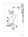
1
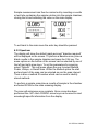
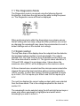
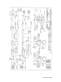
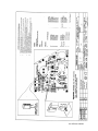
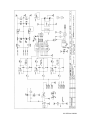
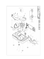
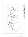
Jenway 6310
Spectrophotometer Service Manual
Main Index
Section 1 Introduction
Section 2 Quick Reference
Section 3 System Description
Section 4 Optical Description
Section 5 Electronic Description
Section 6 Software and Operation
Section 7 Diagnostics
Section 8 Maintenance
Section 9 Circuit Diagrams
Section 10 Assembly Diagrams
Section 11 Spare Parts List
631 070/Ver A/09-04
Section 1
Introduction
1.0 Index to Sections
1.1 About This Manual
1.2 Using This Manual
1.3 Warnings & Safe Practice
1.4 Standards & Certification
1.5 Ordering Spares
1.6 Returning Items
1.7 Contacting Jenway
631 070/Ver A/09-04
1.0 Index to Sections
Section 1 – Introduction
1.0 Index to Sections
1.1 About This Manual
1.2 Using This Manual
1.3 Warnings & Safe Practice
1.4 Standards & Certification
1.5 Ordering Spares
1.6 Returning Items
1.7 Contacting Jenway
Section 2 - Quick Reference
2.0 About ‘Quick Reference’
2.1 Specification
2.2 Main Sub-Assemblies
2.3 Special Key Functions
2.4 Signal Levels
2.5 Error Codes
2.6 Power Supply Voltages
2.7 Test Solutions
Section 3 - System Description
3.1 Background
3.2 Sub-Assemblies
3.3 Accessories
3.4 Outputs
Section 4 - Optical Description
4.1 Light source
4.2 Grating
4.3 Shutter and Filter
4.4 Signal Detector
Section 5 - Electronic Description
5.1 Power Supplies
5.2 Detector Circuit
5.3 Microprocessor and Display
631 070/Ver A/09-04
Section 6 - Software and Operation
6.0 Warning
6.1 Start Up Routine
6.2 Main Menu.
Section 7 – Diagnostics
7.1 The Diagnostics Mode
7.2 Signal Readout
7.3 Filter and Lamp Control
7.4 CAL ADC
7.5 CAL DAC
7.6 CAL Zero Wavelength
7.7 Zero offset
7.8 Find Peak
Section 8 – Maintenance
8.1 Routine Maintenance
8.2 Dismantling
8.3 Optical Alignment
8.4 Energy Levels
8.5 Wavelength Calibration
8.6 A to D Calibration
8.7 D to A Calibration
8.8 Performance Verification
Section 9 - Circuit Diagrams
9.1 Power Supply PCB Schematic 630 504
9.2 Power Supply Layout 630 504
9.3 Detector PCB Schematic 630 506
9.4 Detector PCB Layout 630 506
9.5 Microprocessor PCB Schematic 870 001
9.6 Microprocessor PCB Layout 870 001
Section 10 - Assembly Diagrams
10.1 6310 Final Assembly 631 003
10.2 6310 Lower Case Assembly 630 510
10.3 6310 Top Case Assembly 631 004
10.4 6310 Optics Assembly 630 580
10.5 6310 Rear Panel Assembly 630 012
631 070/Ver A/09-04
Section 11 – Spare Parts List
11.1 Packed Instrument
11.2 Top Case Assembly
11.3 Microprocessor/display PCB
11.4 Lower Case Assembly
11.5 Optics Assembly
11.6 Detector PCB
11.7 Power Supply PCB
11.8 Rear Panel Assembly
631 070/Ver A/09-04
1.1 About This Manual
This manual covers the service, maintenance, calibration and repair
of the Jenway model 6310 Spectrophotometer.
This manual must be used in conjunction with the Instruction Manual
(P/N 631 050) for this model, as many of the routine maintenance
procedures detailed in the Instruction Manual are not repeated in this
Service Manual.
1.2 Using This Manual
This manual is only for the use of Engineers and Technicians who
have successfully completed a Jenway approved Service Training
course on the Model 6310 Spectrophotometer. Updates to this
manual will be circulated through Jenway to registered users of this
manual. Please complete the form at the rear of this manual to
register your copy for future updates.
The manual should be read completely prior to commencing servicing
the 6310 spectrophotometer. Section 2 - Quick Reference and
Section 8 – Maintenance, with the Diagrams in Section 9 and 10, will
be most frequently used. To find the information required refer to the
Main Index or Index to Sections to identify the relevant Section/page
number required.
1.3 Warnings & Safe Practice
Always disconnect the mains supply when any covers are removed
as there are voltages present inside the unit that pose the risk of
electric shock at levels that are hazardous to life!
Do not look directly at the light source or allow the light beam to fall
directly on the eyes, switch off or dim the lamp (Section 7.3)
whenever possible and wear eye protection at ALL times.
The lamp gets very hot when in use, always allow time for it to cool
down before removal. Always wear cotton gloves when removing a
faulty lamp and replacing with a new one.
Finger marks, dust and condensation can quickly destroy sensitive
and expensive optical components, always wear cotton gloves when
631 070/Ver A/09-04
the optical bench is uncovered and handle any components by their
edges only. Never touch optical surfaces. Do not remove optical
covers unless the unit is in a clean, dust and condensation free
environment.
Many of the reagents, solutions and standards used for maintenance
and calibration are corrosive or hazardous, ensure all precautions
supplied with them are followed, where there is any doubt request a
MSDS (Material Safety Data Sheet) from the supplier.
This instrument can be used for analysing a broad range of samples,
do not handle them unless you are qualified to do so. Ensure that the
instrument has been correctly decontaminated before working on it,
specifically in areas where the instrument may have been used for
clinical, biological, corrosive or radioactive samples.
For additional information regarding decontamination contact Jenway
or your local Health and Safety Authority.
1.4 Standards & Certification
No adjustments should be made to this instrument unless the test
and measurement equipment, signal source or filters have a current
calibration certificate that is traceable to national or international
standards and that it is known that this test equipment is currently
performing to the certified standards. All solutions and reagents
should be fresh and within stated shelf life with a certificate of
analysis.
1.5 Ordering Spares
When ordering spare parts as detailed in this manual please quote
the Model Number, Serial Number, Description and Part number of
the equipment. These items should be ordered from the original
supplier of the equipment or your local Jenway Distributor.
631 070/Ver A/09-04
1.6 Returning Items
Should it be necessary to return any item for any reason then this
should be done through the original supplier of the equipment or your
local Jenway Distributor.
For items returned to Jenway please note no items can be returned to
(or will be accepted by) Jenway without a Returns Authorisation
number (RA number) and a completed Safety Clearance certificate.
Failure to do so will delay any repair to your equipment.
1.7 Contacting Jenway
Before contacting Jenway please check our web pages for any
information or updates that may be helpful to you.
www.jenway.com
Emails should be sent to [email protected]
Fax: +44 1371 821083
Phone: +44 1371 820122
631 070/Ver A/09-04
Section 2
Quick Reference
2.0 About ‘Quick Reference’
2.1 Specification
2.2 Main Sub-Assemblies
2.3 Special Key Functions
2.4 Signal Levels
2.5 Error Codes
2.6 Power Supply Voltages
2.7 Test Solutions
631 070/Ver A/09-04
2.0 About ‘Quick Reference’
This section contains a selection of the key information that will be
commonly used when servicing or supporting the Jenway 6310.
For more information check out the references to the main sections
on each point.
2.1 Specification
Also see Section 11.1 of the Instruction Manual.
Wavelength Range
320nm to 1000nm
Wavelength Resolution
1nm
Wavelength Accuracy
+/-2nm
Spectral Bandwidth
8.0nm
Light Source
Tungsten Halogen
Optics
Single Beam
Transmittance Range
0 to 199.9%
Resolution
0.1%
Absorbance Range
-0.300A to 1.999A
Resolution
0.001A
Photometric Accuracy
+/-1%
Photometric Noise
Less than 1%
Stray Light
Less than 0.5%T
Photometric Stability
Better than 1% per Hour (after
warm up)
Outputs
Analogue (0 to 1999mV) &
RS232 Serial
Supply Voltages
115/230 V a.c.
Power
Less than 50W
Dimensions
365 (w) x 272 (d) x 160 (h) mm
Weight
6Kg
631 070/Ver A/09-04
2.2 Main Sub-Assemblies
Also see Section 11 – Spare Parts
631 004 Top Case Assembly – includes the following…
631 020 Membrane Keypad
631 040 Display PCB (includes EPROM)
tbc PCB Battery
630 510 Lower case Assembly – includes the following…
630 580 Optics Assembly
630 504 Power Supply PCB
630 506 Detector PCB
060 311 Cooling Fan
010 040 Torroidal Transformer
630 580 Optics Assembly – includes the following…
012 075 Tungsten Halogen Lamp
032 005 12V Solenoid
630 516 IR Filter (supplied as a Kit)
635 016 Rear Panel Assembly – includes the following…
016 021 2A Fuse 20 x 5mm
017 050 Mains Switch
009 123 Mains Input Socket
Misc
630 204 Single 10 x 10 Cell Holder
631 070/Ver A/09-04
2.3 Special Key Functions
There are a number of special key functions for use by trained
engineers, do not use them unless you are fully conversant with all
the procedures these keypresses can invoke.
Power On Reset. Hold down the <Enter> key while turning on the
power. This clears the operator set parameters held in non-volatile
memory and is useful in correcting many software conflicts. This will
also reset any internal methods or data stored. Please ensure that
customer methods and important data are printed or stored prior to
performing a reset. As this procedure by passes the start up routine
the instrument must be re-booted before use.
Diagnostics Mode. Hold the <right arrow> key depressed while
turning on the power. The main display shows the diagnostics menu.
See Section 7.1.
View Start Up Routine. Hold down the <Cal> key while turning on
the power. This enables the detector output and grating position to be
monitored on the display during the Start Up Routine.
Skip Power On Self Tests. Hold down the <Print>. This can be used
for diagnostics purposes.
631 070/Ver A/09-04
2.4 Signal Levels
Also see Section 7.2 - Filters and 8.3 – Energy Levels
All analogue signal processing is dealt with on the Detector PCB. The
output from the detector is shown in the Diagnostics mode as a
Voltage, in mV. For more information see Section 5.2 – Detector
Circuit and Section 7.1 – The Diagnostics Mode.
This voltage display can be used to check lamp energy (ageing), the
correct functioning of the IR filter, the Dark Shutter and its related
solenoid.
320nm Energy, In the Diagnostics Mode (see Section 7.1
Diagnostics Mode) set the wavelength to 320nm, close the Dark
Shutter. Allow the mV reading to stabilise and record the stable value.
Open the dark shutter and the mV reading must increase by more
than 4mV from that recorded above. If not the lamp should be
changed, if it still has not improved then the condition and alignment
of the optical components should be checked.
Dark Current, Set wavelength to 320nm, Dark Shutter closed, IR
stray light filter closed, Voltage Display should be zero +/- 6mV. If not
and no light leaks are obvious (damaged seals around sample
chamber, lid not closing fully, damaged or poorly fitted casework etc.)
then the dark shutter or detector PCB may be faulty.
720nm Output, Set wavelength to 720nm, Dark Shutter open, IR
stray light filter open, Voltage Display must not be greater than
3600mV.
If greater than 3600mV check the lamp, lamp supply voltage, other
power supply levels and detector PCB.
631 070/Ver A/09-04
2.5 Error Codes
See also Section 6 + 7 and Section 9 of the Instruction Manual
A number of Service Fault Codes are generated that relate to fault
conditions, these are detailed below with a brief description of some
of the most common causes for these errors.
2.5.1 Start up error codes.
Warning Operating Parameters reset to Defaults.
This message indicates that the parameters stored in non volatile
memory such as methods data, time, language etc. have been reset
to defaults.
It is a warning only and a press of the enter key will bypass and
complete the startup tests. This message will automatically display
after a “power on reset”. Persistent display of this message on startup
indicates a problem with the Display PCB battery back up. The
battery may need replacing.
Service Fault: 001 Unable to calibrate dark level.
Dark level calibration has been performed twice, the first time, the
user is asked to check sample lid is closed.
631 070/Ver A/09-04
The second time this service fault is displayed.
1) Check the lid of the spectrometer for light leakage into the sample
chamber, this can be due to damage to the lid or material
obstructing the lid.
2) Check the dark shutter by entering diagnostics mode (see section
7). Select 540nm and check that green light is observed at the
sample chamber. Activate the dark shutter, the light should be
completely obscured. If light is still visible then the dark shutter
needs attention.
3) Check the dark current in diagnostics mode. A high signal level
(>6mV @ 320nm) indicates a problem with the detector board.
The calibration of this board is described in section (8.6)
Service Fault: 002 Unable to Locate Endstop Detector.
Unable to locate the -50nm endstop detector during wavelength
calibration.
The Jenway 6310 uses an opto-coupler to define the limit of
movement for the grating. This error occurs during the wavelength
calibration procedure in the start up routine and is generated at the
beginning of this procedure. The grating is driven in a clockwise
direction until the attached vane breaks the path of an opto-coupler.
This is effectively the ‘end-stop’ and the point from which autocalibration will always start.
631 070/Ver A/09-04
1) Check the Function of the Optocoupler (section 8.3.1)
2) Ensure that green light is displayed at 540nm and that the grating
is moving by selecting a wavelength at least 100nm from 540 and
check that the light is no longer green. Should the instrument not
display green light at 540nm see section 8.3.
Failure to detect this point may be due to a faulty opto-coupler,
wavelength drive from the power supply PCB, a faulty motor or
mechanical coupling.
Service Fault: 003 Unable to Access Calibration Data.
Unable to read back data written to the EEPROM located on the
detector board.
Calibration data for A to D conversion is stored on the detector board
in an EEPROM. The failure to read this data may be due to a problem
with the data or a failed component on the detector board.
1) Recalibrate the detector board using the procedure in section
(8.6).
2) Replace the detector board.
Service Fault: 004 Failed to locate zero order wavelength peaks.
Wavelength calibration has been performed twice, the first time, the
user is asked to check the sample lid is closed and the lamp is on.
631 070/Ver A/09-04
The second time this service fault is displayed.
1) Check the lamp is a genuine Jenway supplied lamp and that the
lamp lights up.
2) Start the unit in diagnostics mode and select 540nm, check the
sample chamber for green light in front of the sample holder. If no
green light is observed check that the IR filter and dark shutter are
operational and out of line. If the filters are not obscuring the light it
is possible that the unit requires Zero order calibration (see section
8.3).
3) Check the sample chamber is not obscuring the light by checking
the green light after the sample chamber.
4) Check the status of the IR filter by selecting 350nm in diagnostics
mode and recording the signal level with the IR filter IN line and
OUT of line. The level with the filter should not be less than 50%
the unfiltered light. If necessary replace the IR filter.
System test Errors.
The first test during the startup is the system test. This is an internal
check of the software, possible failures during this process are as
follows.
Invalid DAC count
One or all of the stored DAC calibration values stored in EEPROM
exceed their upper or lower limits.
631 070/Ver A/09-04
This relates to data stored DAC values stored in the EEPROM on the
processor board.
1) Calibrate DAC using procedure in section 8.7.
2) The EEPROM may be faulty, replace the processor board.
Invalid detector calibration data
One or all of the stored A to D calibration values stored in EEPROM
exceed their upper or lower limits.
This relates to data stored ADC values stored in the EEPROM on the
detector board.
1) Recalibrate the detector board using the procedure in section
(8.6).
2) Replace the detector board.
A to D not operating
Readings from the x1, x10 and x100 gain inputs of the A to D are all
equal.
631 070/Ver A/09-04
This is most likely to indicate that the A to D is not functioning, but
there is a small probability that identical readings will be obtained if
the offset for all three stages are all equal to zero. This test is
performed with the dark shutter closed to prevent saturation,
therefore an inoperative solenoid may cause this fault to be reported
if the wavelength is close to 0nm (saturation at full lamp voltage).
1) Recalibrate the detector board using the procedure in section
(8.6).
2) Replace the detector board.
2.5.2 In use error messages.
The following messages are only shown when the instrument has
completed its start up tests ensuring that the instrument is functional.
The majority of causes for the following messages are related to user
error or application difficulty.
Calibration Error <Dark level too high>.
Dark level too high during a functional calibration. In normal operation
the dark shutter closes during an operator instigated calibration
sequence to ensure that the detector output is below a threshold
level. The calibration is aborted and “Calibration Error <Dark level too
high>” indicated if the detector output is above this threshold level.
The most likely cause is that the sample chamber door has been left
open or was opened during the calibration sequence, it may also
occur due to light leakage cause by a blockage or a faulty detector
PCB.
Fault finding is as Service Fault 001 above.
Calibration Error < Light level too low>.
Light level too low during a functional calibration. After the dark level
test above is complete the instrument will calibrate the available light
to 0.000A or 100%T. If insufficient light is detected “Calibration Error
< Light level too low>” will be displayed. This may be caused by the
following.
631 070/Ver A/09-04
1) The Blank/Calibrant is too optically dense (dark), Calibrate the unit
on an empty cuvette in photometrics mode and insert the sample,
This will display the transmission of the sample, If the %
transmission is low then dilute the Blank/Calibrant to an
appropriate level.
2) The lamp may have failed since the start up tests, check for light at
the rear of the unit, replace lamp if needed.
3) The cuvette may not be suitable for the analysis that you are
doing. Visible plastic may give poor transmission at wavelengths
below 400nm. The use of small volume cuvettes of the incorrect
type may also cause this error please contact Jenway for more
details on Cuvettes.
Calibration Error < Factor out of range>.
When using the concentration mode on the instrument, a factor is
determined automatically based on the absorbance and standard
value entered. If a factor is generated by this procedure which is
greater than the maximum factor this error will display.
This may be because the standard is too optically dense at the
wavelength selected. Dilution of the sample is the usual approach it
may be possible for the measurement to be undertaken at a different
wavelength.
631 070/Ver A/09-04
2.6 Power Supply Voltages
Also see Section 9 - Circuit Diagrams
Before commencing complex fault finding it is important to check all
the internally generated supply voltages are correct. The following list
is a useful guide to help quickly check these are functioning correctly.
Not all the points where these voltages can be measured are given
and where the voltage is stated as unregulated, variations may occur.
In general regulated supplies should vary by no more than +/-5%
from their nominal value.
Tungsten Lamp Supply, 12V dc regulated and set by VR1, measure
at SK9 pin 5 with respect to SK9 pin 6 on the power supply PCB and
at the terminals on the lamp base with the lamp fitted. This value
should be within +/- 0.2V of 12V dc
Solenoid and Fan Supplies, 12V dc regulated and pre-set, measure
at SK1 pin 1 with respect to SK1 pin 2 on the power supply PCB and
on the solenoid and fan terminals.
Digital Supply, 5V dc regulated and pre-set, measure at SK5 pin 1
with respect to SK5 pin 2 or on SK1 pin 1 with respect to SK1 pin 2
on the Display PCB.
Stepper Motor Drive, 30V dc unregulated, measure between Star1
and Star 2 on power supply PCB.
DAC Supply, +/- 10V dc supplies.
+10V dc generated on the RS232 Interface, IC3, on the Display PCB,
measure between pins 2 (positive) and 15 (0V) on IC3 on the Display
PCB.
-10V dc generated on the RS232 Interface, IC3, on the Display PCB,
measure between pins 6 (negative) and 15 (0V) on IC3 on the
Display PCB.
631 070/Ver A/09-04
2.7 Test Solutions
These solutions can be used as an alternative to calibrated filters.
1. Holmium Perchlorate – 5% w/v solution of Holmium Oxide in 1.4N
Perchloric acid, this will give absorbance maxima at 361.4, 416.1,
451.1, 485.3, 536.5 and 640.5nm.
2. Potassium Dichromate – 100.0mg/l in 0.005M Sulphuric Acid (use
the Sulphuric Acid as the blank). This will give an Absorbance value
of 1.071 at 350nm.
Potassium Dichromate – 50.0mg/l in 0.005M Sulphuric Acid (use the
Sulphuric Acid as the blank). This will give an Absorbance value of
0.536 at 350nm.
3. Sodium Nitrate – 50g/l in deionised water, should give less than
0.1% Transmittance at 340nm. (Deionised water Blank)
All these solutions are hazardous and the
manufacturer/suppliers safety precautions should be carefully
followed at all times in preparation, use and storage.
631 070/Ver A/09-04
Section 3
System Description
3.1 Background
3.2 Sub-Assemblies
3.3 Accessories
3.4 Outputs
631 070/Ver A/09-04
3.1 Background
The model 6310 is a single beam, UV/visible spectrophotometer with
Photometrics (Absorbance and Transmission) Scanning, kinetics,
Concentration and Quantitation measurement modes. The unit also
features method and data storage, GLP functions and optional PC
control software.
This manual covers the service, maintenance and repair of all units.
3.2 Sub-Assemblies
The model 6310 spectrophotometer can easily be broken down into
sub-assemblies for the purposes of repair or replacement. All the
PCBs are easily removed, see Section 8.2 – Dismantling. The optical
assembly is also a replaceable sub-assembly. There is a range of
sampling accessories that can be easily fitted and removed from the
sample chamber.
631 070/Ver A/09-04
3.3 Accessories
The following sampling accessories are available, where necessary
additional service information for these accessories is available on
request. The development of other sampling accessories is
continuous, please check current brochures or www.jenway.com for up to
date information.
631 100 63Ten PC software
633 001 Electrically heated cell holder
632 001 External Sipper Pump (230V)
632 031 External Sipper Pump (115V)
634 001 4 Position Cell Changer
630 020 Test Tube Holder (13mm diameter)
630 021 Test Tube Holder (25mm diameter)
630 022 Test tube Holder (16mm diameter)
630 005 20 to100mm Single Cell Holder
tbc
Reaction tube holder
648 001 Water Heated Single Cuvette Holder
037 201 Water/refrigerant Circulator for use with 648 001*
543 001 External 40 Column Printer
542 009 Interface Cable Kit
630 028 Dust Cover
* This item requires a separate water bath, please contact Jenway for
details.
3.4 Outputs
The 6300 has both analogue and RS232 outputs. Details of the level
of the analogue output for the different ranges that may be selected
on the instrument is given in Section 11.2 of the Instruction Manual.
Pin configuration for the RS232 socket is given in Section 11.3 of the
Instruction Manual. The RS232 socket is used to connect to the
optional PC software (PN 631 100). All the required cables are
included in the original shipment of the 6310, for additional or
replacement cables order an interface cable kit (542 009).
631 070/Ver A/09-04
Section 4
Optical Description
4.1 Light Source
4.2 Grating
4.3 Filters
4.4 Signal Detector
631 070/Ver A/09-04
Introduction
The model 6310 is based on the established and successful model
6300 visible spectrophotometer. The optical system is controlled by
the microprocessor with a stepper-motor driven grating and
automatically selected IR filter. A long-life tungsten halogen lamp is
used and the optics optimised to cover the wavelength range of 320
to 1000nm with a spectral bandwidth of 8nm.
4.1 Light Source
The 6300 uses a single Tungsten Halogen lamp to cover the full
wavelength range from 320 to 1000nm. This is a pre-focussed lamp
selected for the accurate position of the filament, making realignment
after replacement unnecessary.
The use of lamps other than those supplied by Jenway (part number
012 075) will cause error codes to be displayed and result in
erroneous results. See Section 9.2 of the Instruction Manual.
4.2 Grating
From the lamp the light passes through a lens assembly then onto a
flat holographic grating with 1200 lines per millimetre. The grating is
directly coupled to the stepper motor, which is under microprocessor
control. An opto-coupler mounted just behind the grating acts as an
‘end stop’ when the sensor vane connected to the grating mount
blocks the light path across it. The stepper motor is a high torque
stepper motor which can only be moved by the signal from the two
stepper motor driver chips on the power supply PCB (IC1 an IC2 See
section 5.1 Power supplies).
The Grating should not be handled in any way, no cleaning of the
grating is possible. If you suspect the grating has been cleaned in any
way you should seek advice from Jenway.
4.3 Filter and shutter
The diffracted spectrum then passes through a further slit and lens
arrangement after which the light beam can be blocked by a shutter
switched in and out by an electronically operated solenoid. Before
passing into the sample chamber the monochromatic light passes
through an infra-red filter when wavelengths below 360nm are
selected. Similar to the shutter this filter is switched in or out by an
631 070/Ver A/09-04
electronically operated solenoid under microprocessor control. The IR
filter is designed to absorb IR light at wavelengths below 360nm. No
cleaning of this filter is possible due to its optical coating, attempts to
clean the filter will remove this coating and the filter will degrade at an
accelerated rate.
.
4.4 Signal Detector
An S1133 photo-diode is used as the detector on the 6310, it is
mounted directly onto the detector PCB, behind the lens block. The
detector PCB carries out the entire analogue signal processing,
including the A to D conversion, and has its individual calibration data
stored in an on-board EEPROM. For more information see Section
5.2 – Detector Circuit.
631 070/Ver A/09-04
Section 5
Electronic Description
5.1 Power Supplies
5.2 Detector Circuit
5.3 Microprocessor and Display
631 070/Ver A/09-04
Introduction
The 6310 features three modern PCB’s utilising modern surface
mount technology. It is designed to be serviced at the PCB
interchange level. Some components may be replaced if necessary
see Section 11.
5.1 Power Supplies
See Section 9.1 Power Supply Schematic
The ac mains supply is reduced by the torroidal transformer giving
two low voltage outputs from the secondary windings. First the 20V
ac output from the transformer is rectified by BR1; the 30V dc output
from this rectifier is used as the input to two L4960 switch mode
regulators. (REG1 and REG 3).
Tungsten Lamp Supply, The output of the switch mode regulator
REG 3 is set to 12V dc by VR1. The 12V output can be reduced to
5.1V by a logic ‘1’ on the gate of TR2. This happens during the start
up tests to reduce the light level for accurate zero order detection, it
can also be manually reduced when in the Diagnostics Mode.
Solenoid and Fan Supply, The output of the switch mode regulator
REG1 is pre-set to 12V. The output to the fan is via Sk1 pin 1 and 2.
The output to solenoid 1 (Dark Shutter) is via SK9 pins 1 and 2.
The output to solenoid 2 (IR Stray Light Filter) is via Sk9 pin 3 and 4.
5V Digital Supply, The other transformer secondary output is half
wave rectified and regulated to 5V by the linear regulator REG 2. The
output is distributed via SK5 pin 1.
Ancillary, Supplies to the end stop opto-coupler are connected via
SK2 pins 1 to 4. The RS232 output, accessible through the rear panel
on SK6, is fed from the microprocessor PCB via SK5. IC1 and 2,
TEA3717DP, are the stepper motor drivers, controlled from the
microprocessor PCB via SK5 pins 9 to 12, with outputs to the motor
on SK2 pins 5 to 8.
631 070/Ver A/09-04
5.2 Detector Circuit
Detectors and Amplifiers
The current through the detector D1 (S1133 type fitted) is
proportional to the incident light. IC3a acts as a current to voltage
converter, the gain being set by the feedback resistors in the T
network.
In normal operation pins 3 and 4 of SK2 are linked so the signal
passes to the three amplifiers of IC1. IC1b is set for unity gain, IC1c
has a gain of 10 and IC1d a gain of 100.
A to D Conversion
Each of these amplified signals then pass into the first three channels
(CH0 to CH2) of an 8 channel, 12 bit, serial, A to D converter. All
three channels are converted and the microprocessor selects the
channel that gives the best resolution without reaching saturation
(32767 counts). In effect this means CH2 will be selected for inputs
up to 40mV, CH1 for inputs up to 400mV and CH0 for inputs up to
4.0V.
The A to d converter requires a reference voltage of 4.096V which is
generated from the 5V rail by D4, this is fed to pin 14, Ref+, of the A
to D converter, IC2. The EEPROM, IC4, maintains calibration data for
the PCB, see Section 8.6 - A to D Calibration.
5.3 Microprocessor and Display
The microprocessor (IC1) is an H8-3002 type with 1Mbyte linear
address space; its internal 32-bit architecture is register based and
optimised for software written in the C programming language. A 20bit address bus is used with an 8-bit external data bus to interface
with the memory mapped devices.
The operating system software is stored in the 256Kbyte EPROM
IC9. This will have a label attached identifying the software version
and date programmed. Removal of this label may damage the
component and will invalidate the warranty. The microprocessor
internally maps the memory space using chip select signals CS0 to
CS3 (CS4 to CS7 are not used). CS0 and CS1 select the EPROM.
631 070/Ver A/09-04
CS2 selects the 32Kbyte SRAM IC8. This device also incorporates
the real time clock and is battery-backed by a non-rechargeable
lithium battery (minimum data retention 8 years). The battery can be
replaced if persistent failure of the battery-backed data is reported
during the power on self-tests. This would be indicated by repeated
display of the error message described in Section 6.1.1
CS3 selects the LCD controller IC11. The microprocessor interface to
IC11 is slowed down by the circuitry associated with IC10 to meet the
timing requirements of LCD controller. IC11 controls the 128 x 118
pixel graphics LCD via row and column drivers IC13, 14,15 and 16.
The LCD controller stores LCD pixel data in a 64K SRAM (IC12)
connected directly to IC11. The bias voltage for the LCD is generated
by IC2.
A 12 bit DAC (IC4) generates the analogue output. This is scaled to
+/-2000mV by the differential amplifier circuit based on IC5a. The
watchdog circuitry (IC17) monitors the activity of the microprocessor,
while IC3 generates the correct levels for the RS232 output.
The EEPROM contains a unique ID code which enables the
spectrometer to be used with the 63TEN PC software. If the main
PCB is replaced this code need to be pre-programmed at the factory
to ensure that it is compatible with the user’s software. Please ensure
that the serial number of the 6310 is notified when an order for a
replacement PCB is placed.
631 070/Ver A/09-04
Section 6
Software and Operation
6.0 Warning
6.1 Start Up Routine
6.2 Main Menu
631 070/Ver A/09-04
6.0 Warning
This section gives an overview of the software functions, it is not
meant to be a detailed analysis of the software routines or code. It
must not be treated as a substitute Instruction Manual, its purpose is
to enable basic navigation through the operation and set up of the
6310 spectrophotometer sufficient to verify basic operation.
6.1 Start Up Routine
When the power to the unit is switched on a self-test routine is
activated. During these start-up tests the following parameters are
checked and must be passed before operation can continue any
failure noted during these tests would lead to an error message see
section 6.1.1:
System Tests:- A series of tests are performed on the stored
parameters in the instrument memory to ensure that valid data is read
from the EEPROM’s on the Display PCB, Power supply PCB and the
Detector PCB. The A to D cal information and the DAC cal
information is checked at this point. A power on reset will cause an
error to be displayed at this point indicating that internal non-volatile
memory has been reset to defaults.
Dark Level Test: - The light beam is blocked by the dark shutter
solenoid switching in. This test checks that the output of the detector
is below a threshold level when there is no light falling on it. The test
will be failed if the sample chamber lid is left open during the start up
routine, if the dark shutter solenoid is faulty (electrical or mechanical)
or if the Detector PCB is faulty.
Wavelength Calibration: - This test checks for the zero order (white)
light that is reflected through the sample chamber when the grating is
in a position where it acts as a mirror (effectively 0nm). Each time the
unit is switched on this position is used as a physical reference point
against which the stored wavelength calibration data is applied. This
test is carried out in the following manner; the microprocessor
instructs the grating to drive to its minimum value of –200nm. This
should ensure that the vane attached to the grating mount breaks the
light path of the opto-coupler mounted on the monochromator base
plate that is set at a position of approximately –50nm. If it does not
631 070/Ver A/09-04
receive a signal from the opto-coupler then error code “Service Fault:
002 Unable to Locate Endstop Detector”, is returned when the motor
stops.
In correct operation a signal is returned when the vane reaches the
opto-coupler. Then the microprocessor instructs the grating to rotate
in the reverse direction, in 1nm, steps for 200nm, or until a signal
greater than 200mV is returned from the detector (this level, with the
lamp dimmed can only be produced by the white zero order light). If
this 200mV level can not be achieved then the grating stops after
having rotated the 200nm and an error code “Service Fault: 004
Failed to Locate zero order wavelength peaks”, is returned.
In correct operation when this 200mV level is detected the grating
rotates in the same direction for a further 200nm but in 0.5nm steps.
For each step an increasing output is returned until the peak is
reached. The grating is stopped when a decrease in output is
measured and by reversing again for one step the position of the
peak is verified. If the grating rotates the full 200nm without the output
increasing and then falling the error “Service Fault: 004 Failed to
Locate zero order wavelength peaks”, is returned.
This test will be failed if samples or cuvettes are left in the sample
compartment during the start up routine, if the sample holder or
sampling device in the sample chamber is incorrectly fitted/aligned
such that it obscures the light beam. Also if the incorrect lamp is
fitted, if the lamp has not been fitted correctly, if the dark shutter is
(stuck) in the closed position or through contamination, degradation
or misalignment of other optical components.
631 070/Ver A/09-04
6.1.1 Error Codes
A number of Service Fault Codes are generated that relate to fault
conditions, these are detailed below with a brief description of some
of the most common causes for these errors.
Warning Operating Parameters reset to Defaults.
This message indicates that the parameters stored in non volatile
memory such as methods data, time, language etc. have been reset
to defaults.
It is a warning only and a press of the enter key will bypass and
complete the startup tests. This message will automatically display
after a “power on reset”. Persistent display of this message on startup
indicates a problem with the Display PCB battery back up. The
battery may need replacing.
Service Fault: 001 Unable to calibrate dark level.
Dark level calibration has been performed twice, the first time, the
user is asked to check sample lid is closed.
The second time this service fault is displayed.
631 070/Ver A/09-04
4) Check the lid of the spectrometer for light leakage into the sample
chamber, this can be due to damage to the lid or material
obstructing the lid.
5) Check the dark shutter by entering diagnostics mode (see section
7). Select 540nm and check that green light is observed at the
sample chamber. Activate the dark shutter, the light should be
completely obscured. If light is still visible then the dark shutter
needs attention.
6) Check the dark current in diagnostics mode. A high signal level
(>6mV @ 320nm) indicates a problem with the detector board.
The calibration of this board is described in section (8.6)
Service Fault: 002 Unable to Locate Endstop Detector.
Unable to locate the -50nm endstop detector during wavelength
calibration.
The Jenway 6310 uses an opto-coupler to define the limit of
movement for the grating. This error occurs during the wavelength
calibration procedure in the start up routine and is generated at the
beginning of this procedure. The grating is driven in a clockwise
direction until the attached vane breaks the path of an opto-coupler.
This is effectively the ‘end-stop’ and the point from which autocalibration will always start.
3) Check the Function of the Optocoupler (section 8.3.1)
4) Ensure that green light is displayed at 540nm and that the grating
is moving by selecting a wavelength at least 100nm from 540 and
check that the light is no longer green. Should the instrument not
display green light at 540nm see section 8.3.
631 070/Ver A/09-04
Failure to detect this point may be due to a faulty opto-coupler,
wavelength drive from the power supply PCB, a faulty motor or
mechanical coupling.
Service Fault: 003 Unable to Access Calibration Data.
Unable to read back data written to the EEPROM located on the
detector board.
Calibration data for A to D conversion is stored on the detector board
in an EEPROM. The failure to read this data may be due to a problem
with the data or a failed component on the detector board.
3) Recalibrate the detector board using the procedure in section
(8.6).
4) Replace the detector board.
Service Fault: 004 Failed to locate zero order wavelength peaks.
Wavelength calibration has been performed twice, the first time, the
user is asked to check the sample lid is closed and the lamp is on.
The second time this service fault is displayed.
631 070/Ver A/09-04
5) Check the lamp is a genuine Jenway supplied lamp and that the
lamp lights up.
6) Start the unit in diagnostics mode and select 540nm, check the
sample chamber for green light in front of the sample holder. If no
green light is observed check that the IR filter and dark shutter are
operational and out of line. If the filters are not obscuring the light it
is possible that the unit requires Zero order calibration (see section
8.3).
7) Check the sample chamber is not obscuring the light by checking
the green light after the sample chamber.
8) Check the status of the IR filter by selecting 350nm in diagnostics
mode and recording the signal level with the IR filter IN line and
OUT of line. The level with the filter should not be less than 50%
the unfiltered light. If necessary replace the IR filter.
System test Errors.
The first test during the startup is the system test. This is an internal
check of the software, possible failures during this process are as
follows.
Invalid DAC count
One or all of the stored DAC calibration values stored in EEPROM
exceed their upper or lower limits.
This relates to data stored DAC values stored in the EEPROM on the
processor board.
3) Calibrate DAC using procedure in section 8.7.
4) The EEPROM may be faulty, replace the processor board.
631 070/Ver A/09-04
Invalid detector calibration data
One or all of the stored A to D calibration values stored in EEPROM
exceed their upper or lower limits.
This relates to data stored ADC values stored in the EEPROM on the
detector board.
3) Recalibrate the detector board using the procedure in section
(8.6).
4) Replace the detector board.
A to D not operating
Readings from the x1, x10 and x100 gain inputs of the A to D are all
equal.
This is most likely to indicate that the A to D is not functioning, but
there is a small probability that identical readings will be obtained if
the offset for all three stages are all equal to zero. This test is
performed with the dark shutter closed to prevent saturation,
therefore an inoperative solenoid may cause this fault to be reported
if the wavelength is close to 0nm (saturation at full lamp voltage).
1) Recalibrate the detector board using the procedure in section
(8.6).
631 070/Ver A/09-04
2) Replace the detector board.
6.2 Main Menu
The menu options can be selected using the up and down arrow
keys, please note it is possible to select the display options so some
or all of the options below may not visible. To display all options
please see security setup section 6.2.5. Press enter to select the
highlighted option.
6.2.1 Photometrics
The display returns to the last wavelength used before the instrument
was turned off. The wavelength displayed on the lower digital display
can be adjusted by using the up and down arrow keys to select the
value suitable for a specific application.
The display shows the Absorbance value (top) and the %
transmission value (middle). These two modes are calibrated by
simply inserting a cuvette or test tube containing a blank solution in
the sample chamber, closing the lid and pressing the CAL
pushbutton. “Calibrating” will display while the calibration sequence is
in progress; when it stops the main digital display will be set to 100.0
%T and 0.000 ABS automatically.
631 070/Ver A/09-04
Sample measurement can then be carried out by inserting a cuvette
or test tube containing the sample solution into the sample chamber,
closing the lid and recording the value on the main display.
To exit back to the main menu the enter key should be pressed.
6.2.2 Spectrum
The display will show the default graph axis and “baseline required”
will be displayed on the screen. To perform a Baseline scan, place a
blank cuvette in the sample chamber and press the CAL key. The
menu options on the bottom of the screen can be selected by use of
the left and right arrow keys. To set the parameters for scanning
select “Options”. This sub menu allows the user to select Method,
Peaks, Valleys, or Recall Scan. Within the Method option the start
and end point of the scan can be selected as can the scan interval.
There is also a method ID number which can be used to identify
stored methods.
To perform a sample scan place a cuvette of sample in the chamber
and select SCAN on the main scanning display.
The scan will autorange once complete. Once a scan has been
performed the <UP> and <DOWN> arrow keys can be used to read
wavelength specific information from the display.
631 070/Ver A/09-04
To exit back to the main menu the enter key should be pressed with
the exit option selected on the bottom of the screen.
For a detailed explanation of scanning please see the instruction
manual section 5.
6.2.3 Kinetics
The display will show the absorbance, the wavelength and the
method id. The <LEFT> and <RIGHT> arrow keys can be used to
select menu options at the bottom. Prior to starting a kinetic run a
blank need to be performed by pressing the <CAL> key. The option
on screen will change to Start. The kinetics parameters are set by
selecting Options Followed by Method. A sample run is initiated by
Pressing Start on the main display.
When the run has started the display will change to show the graph of
absorbance against time, once complete the display will autorange.
The results can then be displayed by selecting the results option on
the main screen.
631 070/Ver A/09-04
The graph can be recalled or the result can be saved by selecting
Options on the display.
For a detailed explanation of kinetics please see the instruction
manual section 6.
To exit back to the main menu the enter key should be pressed with
the exit option selected on the bottom of the screen.
6.2.4 Concentration
The display shows concentration, wavelength and the method ID.
Method details can be accessed by selecting method on the menu at
the bottom of the screen. To perform a blank calibration press the
CAL key. To calibrate against a standard, the value of the standard
should be set in the method menu and press the ENTER key. This
will set the factor to a value which will give the standard value at the
absorbance of that standard.
The Concentration mode is only designed to perform simple single
point linear calibration for more complex analysis the quantitation
mode should be used.
For a detailed explanation of concentration please see the instruction
manual section 7.
631 070/Ver A/09-04
To exit back to the main menu the enter key should be pressed with
the exit option selected on the bottom of the screen.
6.2.5 Quantitation.
The display is exactly the same as for concentration. To set up the
quantitation analysis select Options on the bottom of the screen.
Method information is accessed by selecting Method within the
options menu. A maximum of six standards can be used and these
are entered by selecting standards table. To start a run select
construct curve. Once a run is in progress it can be aborted by
selecting this options on the screen.
For a detailed explanation of quantitation please see the instruction
manual section 8.
To exit back to the main menu the enter key should be pressed with
the exit option selected on the bottom of the screen.
6.2.4 Instrument setup
By selecting this option the time, date, date format and language can
be set.
For full details please refer to the instruction manual section 3.1
631 070/Ver A/09-04
6.2.5 Security.
The lock code for the instrument can be set on this menu along with
activating the lock code. When the instrument is locked method
choice can be allowed, this functionality can be set using this menu.
The mode setup option at the bottom of the menu leads to a further
screen. This menu can be used to display only the relevant methods
on the main menu. At least one option should be selected.
For full details please refer to the instruction manual section 3.2 + 3.3
If a user has locked his 6310 and has forgotten the code to unlock the
unit a generic security code can be used. This code is 660 for the
6310. A power on reset will also clear nay lock codes but this will also
clear all method and data memory
6.2.6 Set Operator ID
The operator ID is a three-digit code that can be quickly and easily
entered from the main menu. This ID will appear in the header of all
results printed or downloaded from the model 6310, identifying the
operator that carried out the analysis. When using this facility all
potential users should be allocated individual three-digit codes.
Operators should enter their code using the following procedure.
1.
2
3.
Use the up or down arrow keys to select SET OPERATOR ID
from the main menu, then press the enter key.
A pop-up box opens on the display showing the three digits of
the last set operator ID or the default of 000. Use the right and
left arrow keys to highlight each digit in turn for adjustment with
the up or down keys until the new operator ID is set.
Confirm the operator ID number by pressing the enter key
which will close the pop-up box.
631 070/Ver A/09-04
This current ID will be used in the header of all result printouts and
result data transferred to a PC or other serial device.
631 070/Ver A/09-04
Section 7
Diagnostics
7.1 The Diagnostics Mode
7.2 Signal Readout
7.3 Filter and Lamp Control
7.4 CAL ADC
7.5 CAL DAC
7.6 CAL Zero Wavelength
7.7 Zero offset
7.8 Find Peak
631 070/Ver A/09-04
7.1 The Diagnostics Mode
The Diagnostics mode is accessed using the following Special
Keyfunction, hold down the right arrow key while turning the power
on. The Diagnostics menu will then be displayed.
When performing tests within the diagnostics menu please ensure
that all setting (such as lamp voltage and filter positions) are correct
as changing the wavelength may cause these parameters to reset to
default settings and not the desired test settings.
7.2 Signal readout
The top three lines of the display show the outputs from the detector,
the linearised voltage and the current wavelength. The outputs
labelled CH0, CH1 and CH2 are from the detector board, these are
the values described in section 5.2. The typical values should be X,
10X and 100X, where X is an integer value. Values above the
maximum value (32767) will be displayed as the maximum value.
All three channels are converted and the microprocessor selects the
channel that gives the best resolution without reaching saturation
(32767 counts). In effect this means CH2 will be selected for inputs
up to 40mV, CH1 for inputs up to 400mV and CH0 for inputs up to
4.0V.
The next line displays the current voltage output which was selected
from the three above. This is the voltage required for the tests in
section 2.5.
The wavelength can be selected using the left and right arrow keys or
press enter when wavelength is highlighted and select which
wavelength you wish to move to.
631 070/Ver A/09-04
IMPORTANT. Prior to exiting the diagnostic menu a readable
wavelength should be selected (320nm to 1000nm). This ensures
that the startup tests can be performed as normal.
7.3 Filter and lamp Control
The Lamp voltage option displays the current lamp voltage (either 5V
or 12V) This is not a measured voltage (see section 2.6). When
selected the voltage can be toggled between 5V and 12V by pressing
the <ENTER> key. This is used to check zero order position as at
12V the light at zero order would be over the range of the detector.
The IR filter option displays the current status of the IR filter IN OUT
or INP. This option can be used to test the function of the IR filter and
its solenoid. To Check the status of the IR filter select 350nm and
record the signal level with the IR filter IN line and OUT of line. The
level with the filter should not be less than 50% the unfiltered light. If
necessary replace the IR filter.
The INP function which is accessed via the IR filter option is used to
test the optocoupler endstop. INP is selected by pressing enter when
the IR filter line is highlighted, press once if the IR filter is listed as
OUT or twice if the IR filter is IN and the second line of the display will
show OPEN or BLOCKED dependant on the status of the
optocoupler.
To test the function of the optocoupler a wavelength of approx. –
50nm should selected and the INP option then selected on the IR
filter control. IF the display shows OPEN at –50nm then move the
wavelength value around until BLOCKED is displayed. Failure to
locate the position of the endstop may indicate a loss of zero order
calibration or a failed optocoupler
Movement of the wavelength will override the selection made by this
menu. Hence if the wavelength is changed then filter settings need to
be rechecked.
The Dark shutter option displays the current status of the dark shutter
When selected the dark shutter can be toggled between IN and OUT
631 070/Ver A/09-04
by pressing the <ENTER> key. This function is used to check the
dark level (section 2.4) and the operation of the dark shutter.
Check the dark shutter by selecting 540nm and check that green light
is observed at the sample chamber. Activate the dark shutter, the
light should be completely obscured. If light is still visible then the
dark shutter needs attention .
7.4 Cal ADC
This option is used to calibrate the Analogue to Digital Converter on
the detector board if these calibration values have become corrupt or
if an uncalibrated detector board is fitted. See section 8.6 for a
detailed description on how to use this menu option.
7.5 Cal DAC
This option is used to calibrate the Digital to Analogue converter on
the display PCB which generates the analogue outputs on the rear of
the unit.
See section 8.7 for a detailed description on how to use this menu
option.
7.6 CAL Zero Wavelength
This function will set the displayed wavelength in the diagnostics
mode to 0nm. This does not affect the stored wavelength calibration
which will be used the next time the instrument is started up. This
function is used to confirm that a calculated zero offset equates to
zero order prior to changing the zero offset described in section 7.7
and section 8.3.
7.7 Zero Offset
Warning;- This function can be used to re-set the stored wavelength
calibration data, so a new wavelength calibration must be carried
out after this procedure has been used. Also see Section 8.3 Optical
Alignment
This function is used to reset the wavelength calibration of the unit.
The offset value is the difference between the measure zero
631 070/Ver A/09-04
absorbance value and the results of a calibrated wavelength filter to
ensure that the reported wavelength is accurate
Please see section 8.3 for a full description of how to use this function
as part of a wavelength calibration.
7.8 Find Peak
This function will search +/- 20nm around the currently selected
wavelength and will display the peak wavelength in that range. This
can be used find the zero order peak around 0nm with the lamp
voltage set to 5V.
631 070/Ver A/09-04
Section 8
Maintenance
8.1 Routine Maintenance
8.2 Dismantling
8.3 Optical Alignment
8.4 Energy Levels
8.5 Wavelength Calibration
8.6 A to D Calibration
8.7 D to A Calibration
8.8 Performance Verification
631 070/Ver A/09-04
8.1 Routine Maintenance
The Jenway Limited, Model 6310 Spectrophotometer has been
designed to give optimum performance with minimal maintenance. It
is only essential to keep the external surfaces clean and free from
dust and to ensure that the area around and underneath the unit is
also clean and dust free. The sample area should be kept clean and
accidental spillage should be wiped away immediately as some
corrosive or solvent based samples or standards may attack the
materials used in the construction of the sample chamber and cell
holders. To give added protection when not in use the unit should be
disconnected from the mains supply and covered with the optional
dust cover (630 028). For longer term storage it is recommended that
the unit be returned to the original carton, for re-shipment a further
external packing case suitable for the method of carriage should be
used.
Details of all routine maintenance tasks, including changing the lamp
can be found in Section 9 of the Instruction Manual.
8.2 Dismantling
Before dismantling any of the following sub-assemblies ensure that
the unit is switched off and the power cable is disconnected from the
supply. Do not attempt to dismantle these units unless they are in a
clean, dry and dust free environment.
Use a soft lint free cover on any benches that will have casework,
displays or keypads placed on them.
Use approved and tested anti-static procedures when dismantling
any electronic sub-assembly or PCB and store these items in
antistatic containers where necessary.
General – Access to all major sub-assemblies can easily be gained
by removing the top half of the case. Access to the lamp housing can
be made through the lamp access panel on the rear of the unit. The
sampling accessory can be accessed through the sample chamber
lid.
631 070/Ver A/09-04
Top/Bottom Case Assemblies – The top and bottom case
assemblies can easily be separated by unscrewing the four recessed
screws in each corner of the base. This should be done without
inverting the unit, by moving it forward over the front edge of the
bench to unscrew the front two screws, and then turning it around to
do the same with the back two. Turn it back round and then the top
half of the case can be lifted off the bottom half take care not to strain
any cables between the top and bottom sections.
Should it be necessary to work on the top case assembly by itself it is
simply a matter of disconnecting the plug from SK5 on the power
supply PCB then the top can be completely removed.
Microprocessor/Display PCB The microprocessor/display PCB is
mounted in the top case assembly. To remove it disconnect SK1 on
the ribbon cable to SK5 and PL601 to the membrane keypad.
Unscrew the four screws and the PCB can be removed. The display
module and microprocessor PCB should be treated as a pair and
replaced together. Removing the display from the PCB should not be
attempted.
The software for the unit is contained within IC9 which features a
sticker identifying the version. Removal of this label may damage the
component and will invalidate the warranty. Should the software need
to be upgraded it is this chip which will be replaced.
This PCB also features the battery which ensures non volatile
memory storage. The battery is designed to last the life of the
instrument however if it needs replacing, it should be removed with a
IC extraction tool and replaced.
Detector PCB The detector PCB is mounted vertically at the far right
hand side of the lower chassis. It is easily removed by unscrewing the
two screws recessed in the top of the metal mounting block. SK4 on
the power supply PCB should be removed. In normal operation SK2
should have pins 3 and 4 linked.
Remove the two screws and spacers that hold the lens block, take
care not to rotate it as the detector is mounted in a recess inside the
block and can easily be broken off. Remove the last screw with its nut
and washer to enable the electrostatic screen to be removed from the
PCB.
631 070/Ver A/09-04
Ensure that the three spacers used to isolate the electrostatic screen
are replaced when the board is replaced. The lens block and the
electrostatic screen should be retained when the board is exchanged
as these are not supplied with a replacement detector board
The Detector PCB stores detailed calibration data relating to the
optics of the unit it is fitted in, replacing the detector PCB without a
full re-calibration will invalidate the quoted specification.
Optical Bench
The Optical Bench is located across the front of the lower case. It is a
sealed unit and breaking the seals will invalidate the warranty. Before
proceeding with replacement ensure the unit is in a clean, dust and
humidity free area. In addition ensure that the instrument is set to the
default setting (500nm) to ensure wavelength accuracy Remove the
four screws from the base plate, two at the front, one at the far right
hand side in front of the detector PCB the other on the far left hand
side. Carefully lift the Optical Bench assembly unplugging the
connectors SK1 and SK9 without straining the cables. The Optical
Bench can now be removed.
Replacement is the reverse of dismantling, but ensure that all cables
are carefully fitted in the appropriate recesses so that they are not
crushed when screwing the unit down. When fitting a replacement
unit ensure a full calibration is run so that the new calibration data for
the new Optical Bench is stored. (See Section 8.5, 8.4 and 8.7)
Power Supply PCB Remove the Optical Bench as above and place
to one side. The power supply PCB is easily removed by undoing the
four screws holding it to the lower case assembly. SK3 to the
transformer and SK1 to the fan should be removed before lifting it out
of the lower case.
Cooling Fan Carry out the above procedures to enable the fan to be
lifted out of its recess in the lower case. Ensure the position of the
retaining spring and the direction of the airflow are noted for reassembly.
Transformer Remove SK3 from the power supply PCB and the push
on connectors for the cables that go to the mains switch and inlet
filter assembly. Then remove the transformer by undoing the single
631 070/Ver A/09-04
bolt through the centre that holds it to the moulded bracket in the
base assembly.
8.3 Optical Alignment
In a significant development from the 6300 the optical alignment of
the 6310 has been significantly simplified. To ensure that zero order
alignment is achieved on start-up, it is only essential that the optocoupler is positioned at approx. –50nm as the zero order position will
be automatically detected from this position. Minor adjustments in
wavelength accuracy can be achieved by setting an offset of up to
10nm (+/-) from the detected zero order peak. This offset is set using
the procedure described in section 8.5 Wavelength calibration.
8.3.1 Grating Position Sensor
The operation and position of the sensor can be check in the
diagnostics mode using the following procedure.
1) Select diagnostics mode by depressing the right arrow key and
powering up the instrument.
2) Select a wavelength of –50 using the menu option.
3) Select the IR filter option on the diagnostic menu and set this to
INP using the enter key.
4) The upper display should show BLOCKED.
5) If the display should show OPEN, then check wavelengths up to
–100nm in steps of 10nm and wavelengths down to 0nm in steps
of 10nm.
6) If this procedure does not find the opto-coupler position then follow
the separate adjustment procedure below.
If the position of the opto-coupler is detected during this procedure
the unit does not require mechanical adjustment and minor
corrections can be applied using the zero offset function in section
8.5.
8.3.2 Grating position sensor adjustment
This procedure can irreversibly affect the performance and
operation of the instrument. Please read the following warnings
and request help or clarification before proceeding. Carrying out
this procedure will invalidate the manufacturers optical
631 070/Ver A/09-04
performance specification and should only be undertaken by
personnel trained and equipped to verify the optical
performance of the instrument. Instrument covers should only
be removed by engineers trained in safe working practices and
aware of electric shockhazards.
Removal of the Optical Bench cover will invalidate any warranty
claim regarding performance to specification.
Do not look directly at the light source, use eye protection or the
lamp dimming function when necessary. Do not touch any
optical surfaces.
If in any doubt DO NOT PROCEED.
Hold down the Right arrow key and power up the unit in diagnostics
mode
Remove the top half of the case by undoing the four recessed screws
in the corners of the base.
Place the top half of the case behind the base taking care not to trap
or strain the connecting cables.
Remove the Optical Bench cover observing all the previously stated
precautions. Select a wavelength 540nm and check that the grating
rotates correctly.
Pass a piece of thick paper or card between the ‘jaws’ of the optocoupler and select the INP function on the IR filter menu option.
Check that when the card is inserted a BLOCKED is displayed on the
top of the display and that when it is removed this display shows
OPEN.
If these results are correct then the position should be adjusted as
below, if not then the opto-coupler or power supply PCB may be
faulty. There may also be a bad connection between them. Check the
wiring to SK2 and that no wires are trapped under the Optical Bench.
631 070/Ver A/09-04
To adjust the position select a wavelength of –50nm and select the
INP function on the IR filter menu option. Slacken the two fixing
screws slightly and adjust the position of the opto-coupler until the
display changes from OPEN to BLOCKED.
Tighten the screws and check that at –40nm the display will show
OPEN and that at –50nm it shows BLOCKED. If not repeat as above.
8.4 Energy Levels
All analogue signal processing is dealt with on the Detector PCB. The
output from the detector is shown in the Diagnostics mode as a
Voltage, in mV. For more information see Section 5.2 – Detector
Circuit and Section 7.1 – The Diagnostics Mode.
This voltage display can be used to check lamp energy (ageing), the
correct functioning of the IR filter, the Dark Shutter and its related
solenoid.
320nm Energy, In the Diagnostics Mode (see Section 7.1
Diagnostics Mode) set the wavelength to 320nm, close the Dark
Shutter. Allow the mV reading to stabilise and record the stable value.
Open the dark shutter arrow key and the mV reading must increase
by more than 4mV from that recorded above. If not the lamp should
be changed, if it still has not improved then the condition and
alignment of the optical components should be checked.
Dark Current, Set wavelength to 320nm, Dark Shutter closed, IR
stray light filter closed, Voltage Display should be zero +/- 6mV. If not
and no light leaks are obvious (damaged seals around sample
chamber, lid not closing fully, damaged or poorly fitted casework etc.)
then the dark shutter or detector PCB may be faulty.
720nm Output, Set wavelength to 720nm, Dark Shutter open, IR
stray light filter open, Voltage Display must not be greater than
3600mV.
If greater than 3600mV check the lamp, lamp supply voltage, other
power supply levels and detector PCB.
631 070/Ver A/09-04
8.5 Wavelength Calibration
Equipment Required; - A certified wavelength standard, i.e.
Holmium Oxide Filter, Holmium Perchlorate Solution etc. (See
Section 8.8.1) Wavelength calibration can be carried out in the
Diagnostics Mode using the zero offset function. Do not carry out the
following procedure without a suitable, certified wavelength
calibration standard.
Turn the unit on and allow the Start Up tests to complete then allow
15 minutes for the instrument to warm up. Select the Spectrum mode
on the instrument. Set a range on the scan which will cover all the
peaks required under test and at least 10nm above and below the
first and last peaks.
Run a baseline scan over the selected range using either a solvent
blank or a blank filter holder. Run a scan of the filter or solution and
select the peaks function within the options menu. This will display a
list of peaks and the peak absorbance values.
NOTE: If it is known that there are other peaks closer than 10nm to
the certified peak then the this peak may not be suitable for this
check on the 6310 due to the bandpass of the instrument.
Check that the reported peak wavelength falls within the specified
tolerance of the instrument PLUS the tolerance of the filter or
standard used. Calculate the adjustment required to correctly align
the reported figure with the certified value from the following.
Certified Value – Reported Value = Correction factor (can be negative
or positive, maximum correction permissible is 10.0nm)
Switch the unit off and re-start it in the Diagnostics Mode by holding
down the right hand arrow key while turning power on.
Add the Correction factor to the current Zero offset value and enter
the new Zero offset value
Switch the unit off and then on again, allowing the Start Up tests to be
completed, re-check the certified wavelength calibration standard as
above and check that the reported value is now correct.
631 070/Ver A/09-04
8.6 A to D Calibration
The A to D converter should only be calibrated by engineers who
have been trained on this aspect of servicing by Jenway.
Equipment Required; - A certified voltage calibrator with a resolution
of 0.1mV and a range up to at least +/-4.0000V.
A lead for connecting the calibrator to pins 1 (negative) and pin 3
(positive) of SK2 on the detector PCB. (8 pin Molex type connector)
Access the Detector PCB by removing the top case assembly as
described in Section 8.2 - Dismantling.
Remove the jumper from pins 3 and 4 on SK2 on the Detector PCB
and fit the lead connected to the calibrator. Switch the calibrator on
and select a negative output (or reverse the contacts) Select the A to
D calibration mode by turning the unit on with the Right arrow key
depressed, and selecting the CAL ADC function within the
diagnostics mode.
The initial prompt is for –1mV, set the calibrator to give an input
signal of –1mV, let the upper display settle and then press the enter
key. Then the prompt changes to –20mV, set the calibrator to –20mV
let the upper display settle and then press the enter key. Continue
responding to the prompts in this way for –39mV, -200mV, -390mV, 2000mV and –3900mV. Note that the –39mV and –390mV levels are
repeated as these are the cross over points from one channel to the
next.
When successfully completed the display returns to the last settings
used in the measurement mode.
631 070/Ver A/09-04
8.7 D to A Calibration
Equipment required; - Voltmeter capable of reading 2.0V with
aresolution of 1mV.
The D to A calibration sets the levels of the analogue output. This is
carried out with the on-board voltage reference at zero and +/2000mV.
Select the D to A calibration mode by holding the right arrow
depressed while the power is turned on. In the diagnostics mode
select CAL DAC. Connect a voltmeter to the analogue output on the
rear panel. Select a range that will display 2000mv to 0.1mV
resolution.
The first prompt indicates an output level of -2000mV, use the up and
down and left and right arrow keys to adjust the actual reading on the
voltmeter to –2000mV. The left and right arrow keys change the
output in 5mV steps, the up and down arrow keys in 1mV steps.
When the correct level is reached press the enter key and the prompt
moves on to 0mV, repeat the above for this and the 2000mV levels.
When successfully completed the display returns to the diagnostics
mode.
Please note that entering the DAC calibration will delete the
previously stored values and the displayed values will be the
default setting.
To check the calibration restart the 6310 in normal mode and select
photometrics mode. Using samples or filters ensure that the
displayed absorbance value is accurately represented on the
voltmeter display.
631 070/Ver A/09-04
8.8 Performance Verification
Equipment Required; - 1. Certified Wavelength Standard, 2.
Certified Absorbance Standards, 3. Certified Stray Light Standard.
Items 1 and 2 above can be supplied as Calibration Filter Sets, order
part numbers 035 088 (visible Only) or 035 091 (UV/Visible).
Where filters are not available the following reagents may be used:
8.8.1 Holmium Perchlorate – 5% w/v solution of Holmium Oxide in
1.4N Perchloric acid, this will give absorbance maxima at 361.4,
416.1, 451.1, 485.3, 536.5 and 640.5.
8.8.2 Potassium Dichromate – 100.0mg/l in 0.005M Sulphuric Acid
(use the Sulphuric Acid as the blank). This will give Absorbance
values of 1.071 at 350nm, 0.484 at 313nm.
Potassium Dichromate – 50.0mg/l in 0.005M Sulphuric Acid (use the
Sulphuric Acid as the blank). This will give Absorbance values of
0.536 at 350nm, 0.242 at 313nm.
8.8.3 Sodium Nitrate – 50g/l in deionised water, should give less than
0.1% transmittance at 340nm.
All these solutions are hazardous and the manufacturer/suppliers
safety precautions should be carefully followed at all times in
preparation, use and storage.
631 070/Ver A/09-04
8.8.4 Wavelength Verification
Equipment Required; - A certified wavelength standard, i.e.
Holmium Oxide Filter, Holmium Perchlorate Solution etc. (See
Section 8.8.1)
Turn the unit on and allow the Start Up tests to complete then allow
15 minutes for the instrument to warm up.
Select the Spectrum mode on the instrument. Set a range on the
scan which will cover all the peaks required under test and at least
10nm above and below the first and last peaks.
Run a baseline scan over the selected range using either a solvent
blank or a blank filter holder. Run a scan of the filter or solution and
select the peaks function within the options menu. This will display a
list of peaks and the peak absorbance values.
NOTE: If it is known that there are other peaks closer than 10nm to
the certified peak then the this peak may not be suitable for this
check on the 6310 due to the bandpass of the instrument.
Check that the reported peak wavelength falls within the specified
tolerance of the instrument PLUS the tolerance of the filter or
standard used.
631 070/Ver A/09-04
8.8.5 Absorbance Verification
Equipment Required; - Certified Standard Absorbance Filters or
Potassium Dichromate solution. (See Section 8.8.2)
Turn the unit on and allow the Start Up tests to complete then allow
15 minutes for the instrument to warm up.
Select the photometrics mode. Use the up or down arrow keys to
select a wavelength at which the filter or solution is certified.
For the Potassium Dichromate solution use the Sulphuric Acid
solution as a blank, (See Section 8.8.2) if the filter set includes a zero
filter use this as the blank, if not set the blank (zero absorbance or
100% transmittance) with an empty sample chamber. Insert the blank
into the sample chamber and close the lid. Press the CAL key and
ensure the display reads 0.000 ABS / 100% T. Remove the blank
from the sample chamber.
Insert the certified filter or Potassium Dichromate solution and check
that the reading is within the specified tolerance of the instrument
PLUS the tolerance of the filter/solution used.
Repeat this for other filters or solutions and at other specified
wavelengths as necessary.
631 070/Ver A/09-04
8.8.6 Stray Light Verification
Equipment Required; - Certified Stray Light Filters or Sodium Nitrate
Solution or Sodium Iodide Solution. (See Section 8.8.3)
Turn the unit on and allow the Start Up tests to complete then allow
15 minutes for the instrument to warm up. Select photometrics mode.
Select a wavelength at which the filter or solution is certified (340nm
for Sodium Nitrate).
Fill a cuvette with the deionised water used to make up the solutions
and place it in the sample chamber. Or for a filter standard use the
blank filter supplied by the manufacturer Press the CAL key and
ensure the reading is 100.0%
Insert the stray light filter or solutions, as above, and ensure that the
reading is within the specified tolerance of the instrument PLUS the
tolerance of the filter/solution used.
631 070/Ver A/09-04
Section 9
Circuit Diagrams
9.1 Power Supply PCB Schematic 630 504
9.2 Power Supply Layout 630 504
9.3 Detector PCB Schematic 630 506
9.4 Detector PCB Layout 630 506
9.5 Microprocessor PCB Schematic 870 001*
9.6 Microprocessor PCB Layout 870 001*
* Note Spare part is as per section 11.03 which includes the
current EPROM.
631 070/Ver A/09-04
631 070/Ver A/09-04
631 070/Ver A/09-04
631 070/Ver A/09-04
631 070/Ver A/09-04
631 070/Ver A/09-04
631 070/Ver A/09-04
631 070/Ver A/09-04
631 070/Ver A/09-04
Section 10
Assembly Diagrams
10.1 6310 Final Assembly 631 003
10.2 6310 Lower Case Assembly 630 510
10.3 6310 Top Case Assembly 631 004
10.4 6310 Optics Assembly 630 580
10.5 6310 Rear Panel Assembly 630 012
631 070/Ver A/09-04
631 070/Ver A/09-04
631 070/Ver A/09-04
631 070/Ver A/09-04
631 070/Ver A/09-04
631 070/Ver A/09-04
Section 11
Spare Parts
11.1 Packed Instrument
11.2 Top Case Assembly
11.3 Microprocessor PCB
11.4 Lower Case Assembly
11.5 Monochromator Assembly
11.6 Detector PCB
11.7 Power Supply PCB
11.8 Rear Panel Assembly
631 070/Ver A/09-04
6310 SPARE PARTS LIST
Section 11.1
631 001
Packed Instrument.
033 227
Packing case complete with inserts
060 084
Disposable cuvettes (4ml) pack of 100
631 050
Instruction manual
013 046
Mains cable without plug
013 083
Mains Cable U.S.A. plug
013 123
Mains Cable European plug
013 181
Mains Cable U.K. plug
631 070
Service Manual
630 028
Dust Cover
630 204
10 x 10 sample holder
Section 11.2
631 004
Top Case Assembly.
631 040
Microprocessor PCB.
631 020
Membrane keypad
tbc
Sample Chamber Lid
Section 11.3
631 040
Microprocessor PCB*.
870 001
Micro-processor PCB*
631 010
EPROM (Programmed)
Section 11.4
630 510
Lower Case Assembly.
010 040
Torroidal transformer assembly
060 040
Large rubber feet
060 311
Cooling fan 12V 60mm
tbc
Sample chamber retaining screw
630 204.
10 x 10 Cell Holder
Section 11.5
630 580
Monochromator Assembly.
Tbc
Tungsten halogen lamp mounting
012 075
Tungsten halogen lamp
032 005
Solenoid 12V dc
630 516
IR Filter 6300 kit
012 089
Chassis mount optocoupler
Section 11.6
630 506
Detector PCB.
630 506
Detector PCB assembly 6300
002 054
470uF 16V radial electrolytic capacitor
631 070/Ver A/09-04
012 085
020 002
020 006
Photodetector 6300
Voltage regulator 79L05
Voltage regulator 7805
Section 11.7
630 504
Power Supply PCB.
630 504
Main power supply PCB
002 070
1000uF 25V radial electrolytic capacitor
005 024
Bridge rectifier
002 112
4700uF 40V radial electrolytic capacitor
020 027
L4960 voltage regulator
006 115
25 way D socket
009 124
4mm socket red
009 125
4mm socket black
Section 11.8
640 006
Rear Panel Assembly.
009 123
Mains input socket
016 021
2A fuse 20mm (for 220V supply)
062 241
Lamp Panel Retaining Screw
017 050
Switch rocker 2p
*Please ensure that the serial number is supplied with any
order for this microprocessor board to ensure it contains the
same ID code as the original instrument.
631 070/Ver A/09-04