1
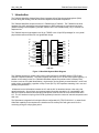
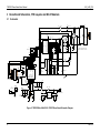
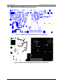
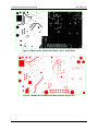
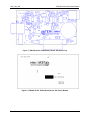
Simplifying System IntegrationTM
73M1922
Demo Board User Manual
June 24, 2010
Rev. 5.1
UM_1922_006
73M1922 Demo Board User Manual
UM_1922_006
© 2010 Teridian Semiconductor Corporation. All rights reserved.
Teridian Semiconductor Corporation is a registered trademark of Teridian Semiconductor Corporation.
Simplifying System Integration is a trademark of Teridian Semiconductor Corporation.
MicroDAA is a registered trademark of Teridian Semiconductor Corporation.
Microsoft is a registered trademark of Microsoft Corporation.
Windows is a registered trademark of Microsoft Corporation.
All other trademarks are the property of their respective owners.
Teridian Semiconductor Corporation makes no warranty for the use of its products, other than expressly
contained in the Company’s warranty detailed in the Teridian Semiconductor Corporation standard Terms
and Conditions. The company assumes no responsibility for any errors which may appear in this
document, reserves the right to change devices or specifications detailed herein at any time without
notice and does not make any commitment to update the information contained herein. Accordingly, the
reader is cautioned to verify that this document is current by comparing it to the latest version on
http://www.teridian.com or by checking with your sales representative.
Teridian Semiconductor Corp., 6440 Oak Canyon, Suite 100, Irvine, CA 92618
TEL (714) 508-8800, FAX (714) 508-8877, http://www.teridian.com
2
Rev. 5.1
UM_1922_006
73M1922 Demo Board User Manual
Table of Contents
1
Introduction ................................................................................................................................... 5
1.1 Package Contents.................................................................................................................... 6
1.2 Safety and ESD Notes ............................................................................................................. 6
1.3 Demo Board Options................................................................................................................ 6
2
Connectors .................................................................................................................................... 7
3
Demo Board Schematics, PCB Layouts and Bill of Materials ..................................................... 8
3.1 Schematic ................................................................................................................................ 8
3.2 73M1922 20-Pin TSSOP Demo Board Layout .......................................................................... 9
3.3 Demo Board Physical Dimensions ......................................................................................... 12
3.4 Bill of Materials ...................................................................................................................... 13
3.5 Pin Descriptions ..................................................................................................................... 14
3.5.1 731922 MicroDAA Pinout ............................................................................................ 15
4
Related Documentation ............................................................................................................... 15
5
Contact Information..................................................................................................................... 15
Rev. 5.1
3
73M1922 Demo Board User Manual
UM_1922_006
Figures
Figure 1: MicroDAA System Block Diagram ............................................................................................. 5
Figure 2: 73M1922 MicroDAA 20-Pin TSSOP Demo Board Schematic Diagram ...................................... 8
Figure 3: 73M1922 20-Pin TSSOP Demo Board: Top Signal Layer .......................................................... 9
Figure 4: 73M1922 20-Pin TSSOP Demo Board: Layer 2, Ground Plane ................................................. 9
Figure 5: 73M1922 20-Pin TSSOP Demo Board: Layer 3, Supply Plane ................................................ 10
Figure 6: 73M1922 20-Pin TSSOP Demo Board: Bottom Signal Layer ................................................... 10
Figure 7: 73M1922 20-Pin TSSOP Demo Board: Silk Screen Top .......................................................... 11
Figure 8: 73M1922 20-Pin TSSOP Demo Board: Silk Screen Bottom ..................................................... 11
Figure 9: 73M1902/73M1912 20-Pin TSSOP Packages: Pinout (top view) ............................................. 15
Tables
Table 1: 73M1922 Demo Board Connectors ............................................................................................ 7
Table 2: 73M1922 Demo Board Configuration Settings ............................................................................ 7
Table 3: JS1 Host Interface Connector..................................................................................................... 7
Table 4: 73M1922 20-Pin TSSOP Demo Board Bill of Materials ............................................................. 13
Table 5: 73M1902 HIC 20-Pin TSSOP Package Pin Definitions ............................................................. 14
Table 6: 73M1912 LIC 20-Pin TSSOP Package Pin Definitions .............................................................. 14
4
Rev. 5.1
UM_1922_006
73M1922 Demo Board User Manual
1 Introduction
The 73M1922 MicroDAA Chipset Demo Board integrates silicon Data Access Arrangement (DAA)
function along with Analog Front End functions chipsets for worldwide compliance.
The 73M1922 MicroDAA chipset consists of a 73M1902 and a 73M1912. The 73M1902 is the Host
Interface Chip (HIC) providing a host microprocessor or DSP interface by a synchronous serial port
(Modem Analog Front End (MAFE)) and the 73M1912 is the Line Interface Chip (LIC) to connect to a
telephone line.
The 73M1922 chipset is packaged in two 20-pin TSSOP or two 32-pin QFN packages for a very small
physical dimension and offers low cost global DAA design.
GPIO
FS
FSB
E
73M
1902
73M
1912
PULSE
TRANSFORMER
Line Interface
Chip (Circuitry)
SCLK
SDIN
I
SDOUT
N
TYPE
T
SCKM
E
M/S
RINT/RGDT
F OSCIN
A OSCOUT
C
AOUT
Host Interface
Chip (Circuitry)
H
O
S
T
RGP
RGN
OFH
DCI
DCD
DCB
DCE
TXN
RXM
RXP
SRE
ACS
SRB
L
I
N
E
I
N
T
E
R
F
A
C
E
Shaded pins and names are optional depending on packages
73M1922
Figure 1: MicroDAA System Block Diagram
The 73M1922 performs a modem codec function that interfaces a Host/DSP and the PSTN (Public
Switched Telephone Network). The codec supports data rates up to V.92 with call progress signaling. In
addition to the codec function, the 73M1922 MicroDAA chipset also performs other necessary DAA
functions, such as CID (caller identification), ring detection, tip/ring polarity reversal detection, on/off hook
switch control, pulse dialing, regulation of loop current (DC-IV), line impedance matching, line in use and
parallel pickup detection.
All data and control information between the LIC and the HIC is transferred across a low cost pulse
transformer barrier. Also all clock and synchronization information needed in LIC is embedded in this
data and control bit stream across the barrier transformer received from HIC and reconstructed within
LIC. The LIC interface to tip/ring of the PSTN significantly lowers the number of external components and
their cost.
The DAA feature integrated in this chipset offers a configurable US, ETSI ES 203 021-2, or other World
Wide DAA capability to the telephone line interface and an auxiliary DAC with gain control for line
monitoring during the call progress period.
Rev. 5.1
5
73M1922 Demo Board User Manual
1.1
UM_1922_006
Package Contents
The 73M1922 Demo Board Kit includes:
•
•
1.2
A 73M1922 Demo Board (Rev. D1)
The following documents on CD:
• 73M1922 Demo Board User Manual (this document)
• 73M1822/73M1922 Data Sheet
• 73M1822/73M1922 Layout Guideline
• 73M1x22 Worldwide Design Guide
Safety and ESD Notes
Connecting live voltages to the Demo Board system will result in potentially hazardous voltages on the
boards.
Extreme caution should be taken when handling the Demo Boards after connection to
live voltages!
The Demo Boards are ESD sensitive! ESD precautions should be taken when handling
these boards!
1.3
Demo Board Options
The 73M1922 Demo Board has 20-pin right angle connectors to plug on to a target DSP or CPU system.
Each has a 3.3 V power receptacle for powering on-board circuits from target system or external power
supply, or power can be supplied through the 20-pin connector along with the other signals. The
73M1922 Demo Board allows the evaluation of the 73M1922 chipset for universal modem, voice
application and interface to a general DSP or CPU system use.
6
Rev. 5.1
UM_1922_006
73M1922 Demo Board User Manual
2 Connectors
Table 1 shows all the connectors and jumpers available on 73M1922 MicroDAA Demo Board. JS1 is the
main connector for interfacing to a host processor or DSP board. Line monitor/Call progress monitor
speaker and driver circuits are also on board. J1 is a modular connector for phone line connection and J4
is for power connection from the main board or an external power supply.
Table 1: 73M1922 Demo Board Connectors
Schematic and PCB
Reference
Name
Description
JS1
3M CONN.
10X2
20-pin connector to interface 73M1922 Demo Board to a
HOST controller main board.
J1
RJ-11
Telephone line connector.
J2
3.3 V supply
Plug for connecting external 3.3 V DC power supply.
Table 2: 73M1922 Demo Board Configuration Settings
Schematic and PCB
Reference
Name
Description
R54 (20 TSSOP DB),
TYPE
Frame Sync Type:
0 Ω population: Late FSB (Default for Samsung ARM9
Interface).
None: Early FSB.
R64 (32 QFN DB only)
MODE
SCLK mode:
0 Ω population: 32 Clock.
None: Continuous SCLK. (Default for Samsung ARM9
Interface)
* NOTE: Due to the package restrictions, the MODE pin is not available in a 20-pin TSSOP package.
And neither the Mode pin nor the TYPE pin is available in 42-pin QFN package. User should choose the
right device option when ordering parts depending on the clock mode (32 clock or continuous) and Frame
sync type (early or late frame sync) required. Refer to the ordering information section of the
73M1822/73M1922 Data Sheet.
Table 3: JS1 Host Interface Connector
PIN Number
Name
1
NC
2
VCC
3
NC
4
RESET
5
Description
PIN Number
Name
Description
11
RINGD
12
NC
13
NC
14
NC
NC
15
AFEIN
Serial Data In
6
NC
16
AFEOUT
Serial Data Out
7
NC
17
SCLK
Serial Clock
8
NC
18
FS
Frame Sync
9
RINGD
19
NC
10
NC
20
GND
Rev. 5.1
3.3V power
supply
Reset Input
Ring Det.out
Ring Det.out
Ground
7
73M1922 Demo Board User Manual
UM_1x22_006
3 Demo Board Schematics, PCB Layouts and Bill of Materials
3.1
Schematic
R66
1M, 1%
C1
0.022uF, 250V
1M, 1%
C3
0.022uF, 250V
F1
L1
BR1
1 +
1
MMBTA42
C14
3
TP10
TXM
1
HD04
2
R65 200
1
R6
100K, 1%
R8
100K, 1%
0.1uF
R11
3K
R4
100K, 1%
C50
100pF
C6
1uF
C33
1
R10
255, 1%
2
20
19
18
17
16
15
14
13
12
11
R5
8.2
C8
0.1uF
4.7uF
C43
1nF
D1
MMSZ4710
1
C37
0.01uF
C12
2
C4
0.1uF 2.2uF
C48
0.01uF
1
49.9
R51 49.9
GND
CONN SOCKET 10X2
C38
U1
73M1902
FSBD
SDOUT
SDIN
FS
VND
VND
SCLK
VPD
OSCIN
INT
OSCOUT VPT/VPD
VNPLL
PRP
AOUT
PRM
TYPE
M/S
VPA/VPM VNM/VNT
R50
C47
1nF
Q6
BCP56
TP18
VNS
1
2
3
4
5
6
7
8
9
10
R52
R53
C34
3,3uF
3
TP15
VPS
1
Q5
MMBTA06
GND
VCC
VCC
2
4
R58 1K
3
0.1uF
R61 1K
2
4
6
8
10
12
14
16
18
20
1
3
5
7
9
11
13
49.9 15
17
19
49.9
NOTE: GND f or C35 and C36 connect
to GND on the HOST side of the barrier
R9 100K, 1%
C7
1uF
C24
1
JS1
2kOhm
C36
220pF, 3KV
73M1912
C26 1nF
15pF
3.3uF
L2
Q7
MMBTA42
2
C49
NC (1nF, 3kV)
1nF
RJ-11
R3 412K, 1%
3
Q3
6
5
4
3
2
1
C10 0.47uF
C13
15pF
VCC
C31
C32
20
19
18
17
16
15
14
13
12
11
DCB
DCE
DCD
TXM
RXM
RXP
VPS
VNS
ACS
VBG
2
1
Pulse TFR
DCI
RGN
RGP
OFH
VND/VNX
SCP
MID
VPX
SRE
SRB
R2
MMBTA92 10M
3
1
C9
0.47uF
3
4
T1
1
2
3
4
5
6
7
8
9
10
C41
220pF
Q4
5.1K
E1
TB3100H
P3100SBRP
3
1
R12
U2
J1
- 2
2
TP14
OFH
TRF600-150
4
R67
2kOhm
C35
220pF, 3KV
TP16
FSBD
VCC
1
R54 0
C15
0.1uF
C22
3,3uF
C28
1nF
VCC
R46
J4
3.3V POWER
C30
1nF
C21
3.3uF
C45 0.1uF
C17
0.1uF
GND
2
1
2
3
LS2
R49
3
TP1
GND
U3
20K
R48 20K
VCC
4
1
1
1
C18
27pF
2
3
4
1
2
3
120K
VCC
C46
1nF
Y2
24.576MHz
C19
27pF
C29
3,3uF
C27
1uF
-VIN
CD
VOUT1
VOUT2
V+
VREF1
VREF2 GND
5
8
6
7
AST-2308MR-R
Projects Unlimited
VCC
C25
3,3uF
NJM#2135M
8DMP
Figure 2: 73M1922 MicroDAA 20-Pin TSSOP Demo Board Schematic Diagram
8
Rev. 5.0
UM_1922_006
3.2
73M1922 Demo Board User Manual
73M1922 20-Pin TSSOP Demo Board Layout
Figure 3: 73M1922 20-Pin TSSOP Demo Board: Top Signal Layer
Figure 4: 73M1922 20-Pin TSSOP Demo Board: Layer 2, Ground Plane
9
Rev. 5.0
73M1922 Demo Board User Manual
UM_1922_006
Figure 5: 73M1922 20-Pin TSSOP Demo Board: Layer 3, Supply Plane
Figure 6: 73M1922 20-Pin TSSOP Demo Board: Bottom Signal Layer
10
Rev. 5.0
UM_1922_006
73M1922 Demo Board User Manual
Figure 7: 73M1922 20-Pin TSSOP Demo Board: Silk Screen Top
Figure 8: 73M1922 20-Pin TSSOP Demo Board: Silk Screen Bottom
Rev. 5.0
11
73M1922 Demo Board User Manual
3.3
UM_1922_006
Demo Board Physical Dimensions
PCB Dimensions
•
Size
73M1922DB
Height w/ components and solder
73M1922DB
3.16 x 2.05” (80.20 x 52.50 mm)
0.65” (16.5 mm)
Environmental
•
Operating Temperature
(function of crystal oscillator affected outside
• Storage Temperature
°-40 to +85°C
–10°C to +60°C)
-65 to 150°C
Power Supply
•
DC Input Voltage (powered from DC supply)
•
Supply Current
3.3 VDC ±10%
25 mA (off-hooked at room temperature) typical
12
Rev. 5.0
UM_1922_006
3.4
73M1922 Demo Board User Manual
Bill of Materials
Table 4: 73M1922 20-Pin TSSOP Demo Board Bill of Materials
Qty Reference
Part
DigikeyPN
MFRPN
MFR
1
BR1
HD04
HD04DICT-ND
HD04-T
DIODES Inc.
2
1
C1,C3
C4
0.022uF, 250V
10uF
399-1242-1-ND
399-3522-1-ND
C1206C223K5RACTU
C0805C225K8RACTU
Kemet
Kemet
2
1
C6,C7
C8
1uF
4.7uF
587-1241-1-ND
PCC2176CT-ND
EMK107BJ105KA-TR
ECJ-2FB0J475M
Taiyo Yuden
Panasonic
2
6
C10,C9
C12,15,17,33,38,49
0.47uF
0.1uF
PCC1911CT-ND
399-1095-1-ND
ECJ-1VB0J474K
C0603C104K8RACTU
Panasonic
Kemet
2
2
C14,C13
C19,C18
15pF
27pF
445-1271-1-ND
PCC270ACVCT-ND
C1608COG1H150J
ECJ-1VC1H270J
TDK
Panasonic
4
2
C21,C22,C32,C34
C35,C36
3.3uF
220pF, 3KV
PCC1925CT-ND
445-2380-1-ND
ECJ-2YB0J335K
C4532COG3F221K
Panasonic
TDK
8
2
C26,28,30,31,39,43,46,47 1nF
C37,C48
0.01uF
PCC1772CT-ND
478-1227-1-ND
ECJ-1VB1H102K
06035C103KAT2A
Panasonic
AVX
1
1
C50
C51
100pF
220pF, 630V
311-1069-1-ND
445-2338-1-ND
CC0603JRNP09BN101
C3216COG2J221J
Yageo
TDK
1
1
E1
F1
TB3100H
TRF600-150
TB3100H-FDICT
576-04611.25ER
TB3100H-13-H
04611.25ER
DIODES
Littlefuse
1
1
JS1
J1
CONN 10X2
RJ-11
517-8520-4500
A31420-ND
8520-4500JL
5555163-1
3M
AMP/Tyco
1
J4
RAPC712X
Switchcraft Inc.
2
2
L1,L2
Q3,Q7
POWER CONN SC237-ND
2kOhm@
100MHz, 200mA 240-2396-1-ND
MMBTA42
863-MMBTA42LT1G
HZ0805C202R-10
MMBTA42LT1G
Steward
ON Semi.
1
1
Q4
Q5
MMBTA92
MMBTA06
863-MMBTA92LT1G
863-MMBTA06LT1G
MMBTA92LT1G
MMBTA06LT1G
ON Semi.
ON Semi.
1
1
Q6
R2
BCP56
10M
568-1639-1-ND
541-10.0MCCT-ND
BCP56
CRCW080510M0FKEA
Philips
Vishay
1
4
R3
R4,R6,R8,R9
412K, 1%
100K, 1%
P412KHTR-ND
P100KHCT-ND
ERJ-3EKF4123V
ERJ-3EKF1003V
Panasonic
Panasonic
1
1
R5
R10
8.2
255, 1%
541-8.20CCT-ND
311-255HRCT-ND
CRCW08058R20FNEA
RC0603FR-07255RL
Vishay
Yageo
1
1
R11
R12
3K
5.1K
311-3.00KHRCT-ND
311-5.10KHRCT-ND
RC0603FR-073K0L
RC0603FR-075K1L
Yageo
Yageo
4
1
R50,R51,R52,R53
R54
49.9
0
P49.9HCT-ND
P0.0GCT-ND
ERJ-3EKF49R9V
ERJ-3GEY0R00V
Panasonic
Panasonic
2
1
R58,R61
R65
1K
200
P1.00KHCT-ND
P200HCT-ND
ERJ-3EKF1001V
ERJ-3EKF2000V
Panasonic
Panasonic
2
2
R67,R66
TP1,10, 14, 15,16,18
1M, 1%
Test Points
311-1.00MCRCT-ND
5002K-ND
RC0805FR-071ML
5002
Yageo
Keystone
1
1
T1
U1
Pulse TFR
73M1902
1
1
U2
Y2
73M1912
24.576MHz
Rev. 5.0
ESMIT-4180/750110001 Sumida//Midcom
73M1902
Teridian
73M1912
815-ABMM2-24.576-E2T ABMM2-24.576MHZ-E2-T
Teridian
ABRACON
13
73M1922 Demo Board User Manual
3.5
UM_1922_006
Pin Descriptions
Table 5 shows the 73M1902 20-pin TSSOP package pin names and Table 6 shows the 73M1912 20-pin
TSSOP package pin definitions.
Table 5: 73M1902 HIC 20-Pin TSSOP Package Pin Definitions
Pin
Name
Pin
Name
1
FSD
11
VNM/VNT
2
FS
12
M/S
3
VND
13
PRM
4
VPD/VPPLL
14
PRP
5
OSCIN
15
VPT/VPD
6
OSOUT
16
INT/RGDT
7
VNPLL/VNA
17
SCLK
8
AOUT
18
VND
9
TYPE
19
SDIN
10
VPA/VPM
20
SDOUT
Table 6: 73M1912 LIC 20-Pin TSSOP Package Pin Definitions
14
Pin
Name
Pin
Name
1
DCI
11
VBG
2
RGN
12
ACS
3
RGP
13
VNS
4
OFH
14
VPS
5
VNX/VNS
15
RXP
6
SCP
16
RXM
7
MID/LEV
17
TXM
8
VPX
18
DCD
9
SRE
19
DCE
10
SRB
20
DCB
Rev. 5.0
UM_1922_006
73M1922 Demo Board User Manual
3.5.1 731922 MicroDAA Pinout
Figure 9 shows the pinout top views of the 73M1902/73M1912 TSSOP packages.
FSD
1
20
SDOUT
2
19
3
18
4
17
OSCIN
5
16
INT
OSCOUT
6
15
VPT/VPD
VNPLL/VNA
7
14
AOUT
8
TYPE
FS
VND
VPD/VPPLL
VPA/VPM
DCI
1
20
DCB
SDIN
RGN
2
19
DCE
VND
RGP
3
18
DCD
SCLK
OFH
4
17
TXM
VND/VNX
5
16
RXM
SCP
6
15
RXP
PRP
MID
7
14
VPS/VPD
13
PRM
VPX
8
13
VNS
9
12
M/S
SRE
9
12
ACS
10
11
VNM/VNT
SRB
10
11
VBG
73M1902
73M1912
Figure 9: 73M1902/73M1912 20-Pin TSSOP Packages: Pinout (top view)
4 Related Documentation
The following 73M1x22 documents are available from Teridian Semiconductor Corporation:
73M1822/73M1922 Data Sheet
73M1922 Demo Board User Manual (this document)
73M1822/73M1922 Layout Guideline
73M1x22 Worldwide Design Guide
73M1822/73M1922 Evaluation System with Linux Softmodem User’s Guide
73M1x22/73M1x66B MicroDAA DC Control Loop Operation
73M1x22/73M1x66 MicroDAA Hybrid Operation
5 Contact Information
For more information about Teridian Semiconductor products or to check the availability of the 73M1922,
contact us at:
6440 Oak Canyon Road
Suite 100
Irvine, CA 92618-5201
Telephone: (714) 508-8800
FAX: (714) 508-8878
Email: [email protected]
For a complete list of worldwide sales offices, go to http://www.teridian.com.
Rev. 5.0
15