1
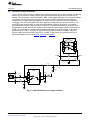
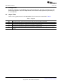
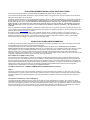
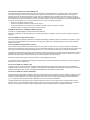
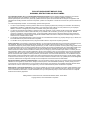
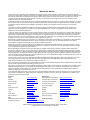
User's Guide SBOU119 – November 2011 INA149EVM This user's guide describes the characteristics, operation, and use of the evaluation module (EVM) for the INA149. The EVM is designed to evaluate the performance of the device in both single and dual-supply configurations. This document also includes the schematic, printed circuit board (PCB) layout, and a bill of materials (BOM). Throughout this document the terms evaluation board, evaluation module, and EVM are synonymous with the INA149EVM. WARNING Danger: HIGH VOLTAGE! This evaluation board is intended for professional use only. It has exposed high voltages. Do not operate this board without proper high-voltage/high-current safety practices. Read Section 1.3 before using the EVM. 1 2 3 4 Contents Introduction and Warnings ................................................................................................. 2 INA149EVM Hardware ..................................................................................................... 4 Bill of Materials ............................................................................................................. 10 Related Documentation from Texas Instruments ..................................................................... 10 List of Figures 1 INA149EVM .................................................................................................................. 2 2 INA149EVM Input/Output Schematic..................................................................................... 4 3 INA149EVM Reference Voltage Schematic ............................................................................. 5 4 INA149EVM Power Schematic ............................................................................................ 6 5 INA149EVM Complete Schematic ........................................................................................ 7 6 INA149EVM PCB Layout SBOU119 – November 2011 Submit Documentation Feedback .................................................................................................. INA149EVM Copyright © 2011, Texas Instruments Incorporated 9 1 Introduction and Warnings 1 Introduction and Warnings 1.1 INA149 www.ti.com The INA149 is a precision unity-gain difference amplifier with a very high input common-mode voltage range (±275 V). It is composed of a precision operational amplifier and an integrated thin-film resistor network. The topology allows the device to buffer small differential signals in the presence of a large common-mode voltage. The device is pin-compatible with the INA117 and other industry standard devices. It is available in an SO-8 package. 1.2 INA149EVM The INA149EVM is intended to provide basic functional evaluation of the INA149. It provides the following features: • • • • • • Easy access to pertinent nodes with test points and terminal blocks Convenient input and output filtering Versatile pad for evaluation in current/sensing applications Reverse supply and overvoltage protection Advanced evaluation with prototype areas and SMA/SMB connector footprints Footprints for providing a flexible reference voltage A picture of the INA149EVM is shown in Figure 1 Figure 1. INA149EVM 2 INA149EVM Copyright © 2011, Texas Instruments Incorporated SBOU119 – November 2011 Submit Documentation Feedback Introduction and Warnings www.ti.com 1.3 Evaluation Module Limitations & Warnings As a result of the high common-mode input voltage rating of the INA149, evaluation of the device often involves high-voltage operation. As a difference amplifier, it may also be used in current-sensing applications. In addition to voltage and current limitations, proper electrostatic discharge precautions are recommended. 1.3.1 High Voltage The common-mode input voltage rating of the INA149 is ±275 V. When using the device and EVM under such circumstances, all proper safety practices must be followed. Do not apply more than ±275 V common-mode. 1.3.2 High Current For current-sensing applications, an unpopulated pad is provided for a sense resistor (RSENSE). The sense resistor trace has a maximum current rating of 5 A. Ensure that the power rating of the sense resistor is sufficient for the application. 1.3.3 Electrostatic Discharge Many of the components on the INA149EVM are susceptible to damage by electrostatic discharge (ESD). Customers are advised to observe proper ESD handling precautions when unpacking and handling the EVM, including the use of a grounded wrist strap at an approved ESD workstation. SBOU119 – November 2011 Submit Documentation Feedback INA149EVM Copyright © 2011, Texas Instruments Incorporated 3 INA149EVM Hardware 2 www.ti.com INA149EVM Hardware This section discusses the INA149EVM hardware schematics, PCB layout, prototype area, and jumpers. 2.1 Input/Output Schematic The input/output section of the schematic is shown in Figure 2. The input signal is applied through terminal block T2 and the output can be measured with test point VOUT. Alternately, SMA or SMB connectors can be populated in the provided footprints: CON1, CON2, and CON_OUT. Input filtering can be applied with R1, R2, and C1-3. The common-mode and differential-mode cutoff frequency equations are given in Equation 1 and Equation 2, respectively. It is recommended to make C2 approximately ten times larger than C1 and C3. The equations assume R1 is equivalent to R2 and C1 is equivalent to C3. Note that any of the capacitors and resistors selected must be rated for the inputs being applied. An output filter can also be implemented with R6 and C6. The corresponding cutoff frequency equation is given in Equation 3. Finally, a versatile pad is provided for evaluation in current-sensing applications. RSENSE can accommodate through-hole resistors or a surface-mount sense resistor from 0603 to 1206 in size. The trace width provides for evaluation of load currents up to 5 A. U1 CON2 R1 C1 INA149 20kΩ 380kΩ REFB NC 0Ω -IN RSENSE C2 +IN R2 V- VOUT 380kΩ V+ CON_OUT R6 + T2 -IN GND +IN VOUT 380kΩ 0Ω 19kΩ REFA 0Ω C6 C3 CON1 Figure 2. INA149EVM Input/Output Schematic Common-mode cutoff frequency: fc -cm = 1 2π ⋅ R1 ⋅ C1 (1) Differential-mode cutoff frequency: fc−dm = 1 C1 2π ⋅ (R1+ R2) ⋅ C2+ 2 (2) Output filter cutoff frequency: fc −o = 4 1 2π ⋅ R6 ⋅ C6 (3) INA149EVM Copyright © 2011, Texas Instruments Incorporated SBOU119 – November 2011 Submit Documentation Feedback INA149EVM Hardware www.ti.com 2.2 Reference Voltage Schematic Figure 3 shows that the reference voltage can be applied to the INA149 in a variety of ways. The INA149 has two pins for reference voltages: REFA, REFB. Most applications require REFA and REFB to be shorted. This functionality is accomplished with JMP4. In dual-supply applications, the reference voltages are typically connected to ground. Connecting pins 2 and 3 of JMP2 and JPM3 accommodate this configuration. For single-supply applications, It is often required to connect the reference voltages to mid-supply. This can be accomplished by either applying a voltage directly to test point REFA (or test point REFB) and shorting JMP4, or using the resistive divider created by R3 and R4. If a matched precision resistor network is desired, a SOT-23 pad (R9) is located on the bottom of the board. When using a resistor divider, however, the voltage must be buffered to ensure good common-mode rejection (CMR). U2 is intended for a standard pinout operational amplifier in an SO-8 package. If U2 is to be powered by the V+ and V– supplies, R7 and R8 should be populated with 0-Ω resistors; otherwise, another supply can be connected to the REFV+ and REFV– test points. Recommendations for this operational amplifier include the OPA376, OPA330, and OPA277. U1 INA149 20kΩ 380kΩ NC REFB +IN V+ + -IN 380kΩ VOUT 380kΩ 19kΩ V- REFA JMP4 REFB JMP3 123 C8 U2 GND SO-8 8 1 R4 R9 JMP2 321 GND R5 V+ REFA V+ REFV+ REF R7 2 7 C4 R3 + REFV- 3 6 4 5 R8 C5 GND V- GND Figure 3. INA149EVM Reference Voltage Schematic SBOU119 – November 2011 Submit Documentation Feedback INA149EVM Copyright © 2011, Texas Instruments Incorporated 5 INA149EVM Hardware 2.3 www.ti.com Power Schematic The power schematic is depicted in Figure 4. Power is applied to the INA149EVM through terminal block T1. Reverse supply protection diodes (D2, D3) protect the device from accidental switching of the positive and negative supply voltages. As a consequence, each supply voltage should be increased by one diode voltage drop. Test points V+ and V– have been provided to ensure the desired supply voltage is being applied to the device. D1 is a transient voltage suppressor (TVS) diode. D1 aids in protecting the INA149 from supply voltages in excess of 36 V (±18 V). JMP1 allows the user to short the negative supply voltage (V–) to ground, which provides a simple method for operating the device with a single supply. Do not shunt JMP1 during dual-supply operation because this action will short the negative supply to ground. Capacitors C2 and C11 are placed as close to the device as possible to provide power-supply decoupling. V+ GND VT1 D3 D2 C32 10µF JMP1 C31 10µF GND C33 10µF V- V+ D1 U1 INA149 20kΩ 380kΩ NC REFB +IN 380kΩ V+ + -IN C11 0.1µF VOUT 380kΩ 19kΩ V- C2 REFA GND 0.1µF GND Figure 4. INA149EVM Power Schematic 6 INA149EVM Copyright © 2011, Texas Instruments Incorporated SBOU119 – November 2011 Submit Documentation Feedback INA149EVM Hardware www.ti.com 2.4 Complete Schematic TP3 TP2 TP1 TP1 TP1 PROTOSPACE REFB C11 7 VOUT TP1 2 CON_OUT DNI 1 2 R6 V- REFA TP1 DNI C6 V.1uF C12 JMP4 7 V+ R4 RESISTOR_TH R5 2 REF 0ohm 1 NC 5 NC 8 NC 4 V- +IN 1 R3 V- 1 6 OUT 3 RESISTOR_TH REF R9 V+ REFV- R8 REFA 1 JMP3 3 JMP3 JUMP2 REF V+ REFB 2 0ohm U2 2 -IN 3 JMP2 2 1 2 1 REF REFA R7 REFB V+ .1uF C4 REFV+ Do not populate JMP4 shorts REFA and REFB DNI GND 0ohm TP1 REFA +IN 2 5 C3 3 INA149_SO8 4 +IN V- V- 3 R2 1 1 VOUT REF_A DNI 6 CON1 2 8 NC 2 -IN C2 R_SENSE 2 1 2 3 V+ REF_B 1 DNI -IN DNI T2 DNI TP1 U1 R1 V- V+ C1 1 V+ .1uF REFB CON2 V+ 1 V+ D3 Prototyping Space TP1 1 2 3 TP1 T1 D2 GND Test Points Terminal Block + V- D1 C33 10uF + 10uF C32 + 10uF JMP1 V- = GND C31 V+ Reverse Standoff = 40-44.4 Figure 5 depicts the complete INA149EVM schematic. C8 2 V- 0ohm .1uF V- C5 Figure 5. INA149EVM Complete Schematic SBOU119 – November 2011 Submit Documentation Feedback INA149EVM Copyright © 2011, Texas Instruments Incorporated 7 INA149EVM Hardware 2.5 www.ti.com Prototype Area For flexible evaluation, the INA149EVM has a small prototyping area. This area is intended to be used with devices mounted on 8-pin DIP adapter boards. Power can be readily applied using the nearby V+, V–, and GND rails. 2.6 Jumper Table There are four jumpers located on the INA149EVM. Their functions are summarized in Table 1. Table 1. Jumpers Jumper 8 Function JMP1 This jumper shorts the V– power rail to ground. It allows a single supply to be used instead of a dual supply. JMP2 This jumper allows the REFA pin on the INA149 to be connected to ground or the external reference op amp. The shunt on the jumper can be removed as well to allow an external reference to be attached to the REFA test point. JMP3 This jumper allows the REFB pin on the INA149 to be connected to ground or the external reference op amp. The shunt on the jumper can be removed as well to allow an external reference to be attached to the REFB test point. JMP4 This jumper shorts the REFA and REFB pins together. When shorting this jumper, make sure JMP2 and JMP3 are not in conflicting positions. INA149EVM Copyright © 2011, Texas Instruments Incorporated SBOU119 – November 2011 Submit Documentation Feedback INA149EVM Hardware www.ti.com 2.7 PCB Layout Figure 6 depicts the PCB layout. Figure 6. INA149EVM PCB Layout NOTE: Board layout is not to scale. This figure is intended to show how the board is laid out; it is not intended to be used for manufacturing INA149EVM PCBs. SBOU119 – November 2011 Submit Documentation Feedback INA149EVM Copyright © 2011, Texas Instruments Incorporated 9 Bill of Materials 3 www.ti.com Bill of Materials Table 2 the bill of materials used for the INA149EVM. It also lists examples of optional components. Table 2. INA149EVM Bill of Materials Count 4 RefDes Value 1 U1 N/A 2 C11-12 3 C31-33 1 D1 2 D2-3 2 T1-2 1 R6 0ohm 2 R1-2 2 Description Part Number MFR INA149, SO-8 INA149 Texas Instruments 0.1µF Capacitor, .10µF, 50V, X7R, 0603 06035C104JAT2A AVX Corporation 10µF Capacitor, 4.7µF, 50V, X7S, 1210 C3225X7S1H106M TDK Corporation N/A Diode, TVS, 36V, 400W Bi-directional, SMD SMAJ36CA Bourns Inc. N/A Diode, Schottky, 40V, SMB MBRS2040LT3G On Semiconductor N/A Terminal Block, 3.5mm, 3 Position 1984620 Phoenix Contact Resistor, 0Ohm, 0603 RC0603JR-070RL Yageo 0ohm Resistor, 0Ohm, 1206 RC1206JR-070RL Yageo JMP2-3 3POS 3 Position Connection Header .100" TSW-102-07-G-S Samtec 2 JMP1,4 2POS 2 Position Connection Header .100" TSW-102-07-G-S Samtec 10 REFA, REFB, 3xGND, V+, V–, VOUT N/A Through-hole Test Points 5009 Keystone Electronics 4 N/A N/A Bumpon, .375X.135, Black SJ61A8 3M 881545-2 TE Connectivity 5009 Keystone Electronics 4 N/A N/A Shunt w/Handle, 2 Position Not Installed C1-3 N/A Capacitor, 0603-1206 or through–hole Not Installed C4-6, C8 N/A Capacitor, 0603 Not Installed RSENSE N/A Sense Resistor, 0603-1206 or through–hole Not Installed R3-R4 N/A Resistor, 0603-1206 or through-hole Not Installed R5, R7-8 N/A Resistor, 0603 Not Installed REF, REFV+, REFV–, +IN, –IN N/A Through-hole Test Point Not Installed U2 N/A Op-Amp, SO-8 Not Installed CON1, CON2, CON_OUT N/A SMA/SMB Edge mounted connector Related Documentation from Texas Instruments The following documents provide information regarding Texas Instruments' integrated circuits and support tools for the INA149EVM. This user's guide is available from the TI web site under literature number SBOU119. Any letter appended to the literature number corresponds to the document revision that is current at the time of the writing of this document. Newer revisions may be available from the TI web site, or call the Texas Instruments' Literature Response Center at (800) 477-8924 or the Product Information Center at (972) 644-5580. When ordering, identify the document by both title and literature number. Related Documentation 10 Document Literature Number INA149 Product Data Sheet SBOS579 OPA376 Product Data Sheet SBOS406 OPA277 Product Data Sheet SBOS079 OPA330 Product Data Sheet SBOS432 INA149EVM Copyright © 2011, Texas Instruments Incorporated SBOU119 – November 2011 Submit Documentation Feedback Evaluation Board/Kit Important Notice Texas Instruments (TI) provides the enclosed product(s) under the following conditions: This evaluation board/kit is intended for use for ENGINEERING DEVELOPMENT, DEMONSTRATION, OR EVALUATION PURPOSES ONLY and is not considered by TI to be a finished end-product fit for general consumer use. Persons handling the product(s) must have electronics training and observe good engineering practice standards. As such, the goods being provided are not intended to be complete in terms of required design-, marketing-, and/or manufacturing-related protective considerations, including product safety and environmental measures typically found in end products that incorporate such semiconductor components or circuit boards. This evaluation board/kit does not fall within the scope of the European Union directives regarding electromagnetic compatibility, restricted substances (RoHS), recycling (WEEE), FCC, CE or UL, and therefore may not meet the technical requirements of these directives or other related directives. Should this evaluation board/kit not meet the specifications indicated in the User’s Guide, the board/kit may be returned within 30 days from the date of delivery for a full refund. THE FOREGOING WARRANTY IS THE EXCLUSIVE WARRANTY MADE BY SELLER TO BUYER AND IS IN LIEU OF ALL OTHER WARRANTIES, EXPRESSED, IMPLIED, OR STATUTORY, INCLUDING ANY WARRANTY OF MERCHANTABILITY OR FITNESS FOR ANY PARTICULAR PURPOSE. The user assumes all responsibility and liability for proper and safe handling of the goods. Further, the user indemnifies TI from all claims arising from the handling or use of the goods. Due to the open construction of the product, it is the user’s responsibility to take any and all appropriate precautions with regard to electrostatic discharge. EXCEPT TO THE EXTENT OF THE INDEMNITY SET FORTH ABOVE, NEITHER PARTY SHALL BE LIABLE TO THE OTHER FOR ANY INDIRECT, SPECIAL, INCIDENTAL, OR CONSEQUENTIAL DAMAGES. TI currently deals with a variety of customers for products, and therefore our arrangement with the user is not exclusive. TI assumes no liability for applications assistance, customer product design, software performance, or infringement of patents or services described herein. Please read the User’s Guide and, specifically, the Warnings and Restrictions notice in the User’s Guide prior to handling the product. This notice contains important safety information about temperatures and voltages. For additional information on TI’s environmental and/or safety programs, please contact the TI application engineer or visit www.ti.com/esh. No license is granted under any patent right or other intellectual property right of TI covering or relating to any machine, process, or combination in which such TI products or services might be or are used. FCC Warning This evaluation board/kit is intended for use for ENGINEERING DEVELOPMENT, DEMONSTRATION, OR EVALUATION PURPOSES ONLY and is not considered by TI to be a finished end-product fit for general consumer use. It generates, uses, and can radiate radio frequency energy and has not been tested for compliance with the limits of computing devices pursuant to part 15 of FCC rules, which are designed to provide reasonable protection against radio frequency interference. Operation of this equipment in other environments may cause interference with radio communications, in which case the user at his own expense will be required to take whatever measures may be required to correct this interference. EVM Warnings and Restrictions It is important to operate this EVM within the input voltage range of ±275 V common–mode and ±13.5 V differential and the output voltage range of –13.5 V to +13.5 V. Exceeding the specified input range may cause unexpected operation and/or irreversible damage to the EVM. If there are questions concerning the input range, please contact a TI field representative prior to connecting the input power. Applying loads outside of the specified output range may result in unintended operation and/or possible permanent damage to the EVM. Please consult the EVM User's Guide prior to connecting any load to the EVM output. If there is uncertainty as to the load specification, please contact a TI field representative. During normal operation, some circuit components may have case temperatures greater than +30°C. The EVM is designed to operate properly with certain components above +30°C as long as the input and output ranges are maintained. These components include but are not limited to linear regulators, switching transistors, pass transistors, and current sense resistors. These types of devices can be identified using the EVM schematic located in the EVM User's Guide. When placing measurement probes near these devices during operation, please be aware that these devices may be very warm to the touch. Mailing Address: Texas Instruments, Post Office Box 655303, Dallas, Texas 75265 Copyright © 2011, Texas Instruments Incorporated EVALUATION BOARD/KIT/MODULE (EVM) ADDITIONAL TERMS Texas Instruments (TI) provides the enclosed Evaluation Board/Kit/Module (EVM) under the following conditions: The user assumes all responsibility and liability for proper and safe handling of the goods. Further, the user indemnifies TI from all claims arising from the handling or use of the goods. Should this evaluation board/kit not meet the specifications indicated in the User’s Guide, the board/kit may be returned within 30 days from the date of delivery for a full refund. THE FOREGOING LIMITED WARRANTY IS THE EXCLUSIVE WARRANTY MADE BY SELLER TO BUYER AND IS IN LIEU OF ALL OTHER WARRANTIES, EXPRESSED, IMPLIED, OR STATUTORY, INCLUDING ANY WARRANTY OF MERCHANTABILITY OR FITNESS FOR ANY PARTICULAR PURPOSE. EXCEPT TO THE EXTENT OF THE INDEMNITY SET FORTH ABOVE, NEITHER PARTY SHALL BE LIABLE TO THE OTHER FOR ANY INDIRECT, SPECIAL, INCIDENTAL, OR CONSEQUENTIAL DAMAGES. Please read the User's Guide and, specifically, the Warnings and Restrictions notice in the User's Guide prior to handling the product. This notice contains important safety information about temperatures and voltages. For additional information on TI's environmental and/or safety programs, please visit www.ti.com/esh or contact TI. No license is granted under any patent right or other intellectual property right of TI covering or relating to any machine, process, or combination in which such TI products or services might be or are used. TI currently deals with a variety of customers for products, and therefore our arrangement with the user is not exclusive. TI assumes no liability for applications assistance, customer product design, software performance, or infringement of patents or services described herein. REGULATORY COMPLIANCE INFORMATION As noted in the EVM User’s Guide and/or EVM itself, this EVM and/or accompanying hardware may or may not be subject to the Federal Communications Commission (FCC) and Industry Canada (IC) rules. For EVMs not subject to the above rules, this evaluation board/kit/module is intended for use for ENGINEERING DEVELOPMENT, DEMONSTRATION OR EVALUATION PURPOSES ONLY and is not considered by TI to be a finished end product fit for general consumer use. It generates, uses, and can radiate radio frequency energy and has not been tested for compliance with the limits of computing devices pursuant to part 15 of FCC or ICES-003 rules, which are designed to provide reasonable protection against radio frequency interference. Operation of the equipment may cause interference with radio communications, in which case the user at his own expense will be required to take whatever measures may be required to correct this interference. General Statement for EVMs including a radio User Power/Frequency Use Obligations: This radio is intended for development/professional use only in legally allocated frequency and power limits. Any use of radio frequencies and/or power availability of this EVM and its development application(s) must comply with local laws governing radio spectrum allocation and power limits for this evaluation module. It is the user’s sole responsibility to only operate this radio in legally acceptable frequency space and within legally mandated power limitations. Any exceptions to this are strictly prohibited and unauthorized by Texas Instruments unless user has obtained appropriate experimental/development licenses from local regulatory authorities, which is responsibility of user including its acceptable authorization. For EVMs annotated as FCC – FEDERAL COMMUNICATIONS COMMISSION Part 15 Compliant Caution This device complies with part 15 of the FCC Rules. Operation is subject to the following two conditions: (1) This device may not cause harmful interference, and (2) this device must accept any interference received, including interference that may cause undesired operation. Changes or modifications not expressly approved by the party responsible for compliance could void the user's authority to operate the equipment. FCC Interference Statement for Class A EVM devices This equipment has been tested and found to comply with the limits for a Class A digital device, pursuant to part 15 of the FCC Rules. These limits are designed to provide reasonable protection against harmful interference when the equipment is operated in a commercial environment. This equipment generates, uses, and can radiate radio frequency energy and, if not installed and used in accordance with the instruction manual, may cause harmful interference to radio communications. Operation of this equipment in a residential area is likely to cause harmful interference in which case the user will be required to correct the interference at his own expense. FCC Interference Statement for Class B EVM devices This equipment has been tested and found to comply with the limits for a Class B digital device, pursuant to part 15 of the FCC Rules. These limits are designed to provide reasonable protection against harmful interference in a residential installation. This equipment generates, uses and can radiate radio frequency energy and, if not installed and used in accordance with the instructions, may cause harmful interference to radio communications. However, there is no guarantee that interference will not occur in a particular installation. If this equipment does cause harmful interference to radio or television reception, which can be determined by turning the equipment off and on, the user is encouraged to try to correct the interference by one or more of the following measures: • Reorient or relocate the receiving antenna. • Increase the separation between the equipment and receiver. • Connect the equipment into an outlet on a circuit different from that to which the receiver is connected. • Consult the dealer or an experienced radio/TV technician for help. For EVMs annotated as IC – INDUSTRY CANADA Compliant This Class A or B digital apparatus complies with Canadian ICES-003. Changes or modifications not expressly approved by the party responsible for compliance could void the user’s authority to operate the equipment. Concerning EVMs including radio transmitters This device complies with Industry Canada licence-exempt RSS standard(s). Operation is subject to the following two conditions: (1) this device may not cause interference, and (2) this device must accept any interference, including interference that may cause undesired operation of the device. Concerning EVMs including detachable antennas Under Industry Canada regulations, this radio transmitter may only operate using an antenna of a type and maximum (or lesser) gain approved for the transmitter by Industry Canada. To reduce potential radio interference to other users, the antenna type and its gain should be so chosen that the equivalent isotropically radiated power (e.i.r.p.) is not more than that necessary for successful communication. This radio transmitter has been approved by Industry Canada to operate with the antenna types listed in the user guide with the maximum permissible gain and required antenna impedance for each antenna type indicated. Antenna types not included in this list, having a gain greater than the maximum gain indicated for that type, are strictly prohibited for use with this device. Cet appareil numérique de la classe A ou B est conforme à la norme NMB-003 du Canada. Les changements ou les modifications pas expressément approuvés par la partie responsable de la conformité ont pu vider l’autorité de l'utilisateur pour actionner l'équipement. Concernant les EVMs avec appareils radio Le présent appareil est conforme aux CNR d'Industrie Canada applicables aux appareils radio exempts de licence. L'exploitation est autorisée aux deux conditions suivantes : (1) l'appareil ne doit pas produire de brouillage, et (2) l'utilisateur de l'appareil doit accepter tout brouillage radioélectrique subi, même si le brouillage est susceptible d'en compromettre le fonctionnement. Concernant les EVMs avec antennes détachables Conformément à la réglementation d'Industrie Canada, le présent émetteur radio peut fonctionner avec une antenne d'un type et d'un gain maximal (ou inférieur) approuvé pour l'émetteur par Industrie Canada. Dans le but de réduire les risques de brouillage radioélectrique à l'intention des autres utilisateurs, il faut choisir le type d'antenne et son gain de sorte que la puissance isotrope rayonnée équivalente (p.i.r.e.) ne dépasse pas l'intensité nécessaire à l'établissement d'une communication satisfaisante. Le présent émetteur radio a été approuvé par Industrie Canada pour fonctionner avec les types d'antenne énumérés dans le manuel d’usage et ayant un gain admissible maximal et l'impédance requise pour chaque type d'antenne. Les types d'antenne non inclus dans cette liste, ou dont le gain est supérieur au gain maximal indiqué, sont strictement interdits pour l'exploitation de l'émetteur. SPACER SPACER SPACER SPACER SPACER SPACER SPACER SPACER 【Important Notice for Users of this Product in Japan】 】 This development kit is NOT certified as Confirming to Technical Regulations of Radio Law of Japan If you use this product in Japan, you are required by Radio Law of Japan to follow the instructions below with respect to this product: 1. 2. 3. Use this product in a shielded room or any other test facility as defined in the notification #173 issued by Ministry of Internal Affairs and Communications on March 28, 2006, based on Sub-section 1.1 of Article 6 of the Ministry’s Rule for Enforcement of Radio Law of Japan, Use this product only after you obtained the license of Test Radio Station as provided in Radio Law of Japan with respect to this product, or Use of this product only after you obtained the Technical Regulations Conformity Certification as provided in Radio Law of Japan with respect to this product. Also, please do not transfer this product, unless you give the same notice above to the transferee. Please note that if you could not follow the instructions above, you will be subject to penalties of Radio Law of Japan. Texas Instruments Japan Limited (address) 24-1, Nishi-Shinjuku 6 chome, Shinjuku-ku, Tokyo, Japan http://www.tij.co.jp 【ご使用にあたっての注】 本開発キットは技術基準適合証明を受けておりません。 本製品のご使用に際しては、電波法遵守のため、以下のいずれかの措置を取っていただく必要がありますのでご注意ください。 1. 2. 3. 電波法施行規則第6条第1項第1号に基づく平成18年3月28日総務省告示第173号で定められた電波暗室等の試験設備でご使用いただく。 実験局の免許を取得後ご使用いただく。 技術基準適合証明を取得後ご使用いただく。 なお、本製品は、上記の「ご使用にあたっての注意」を譲渡先、移転先に通知しない限り、譲渡、移転できないものとします。 上記を遵守頂けない場合は、電波法の罰則が適用される可能性があることをご留意ください。 日本テキサス・インスツルメンツ株式会社 東京都新宿区西新宿6丁目24番1号 西新宿三井ビル http://www.tij.co.jp SPACER SPACER SPACER SPACER SPACER SPACER SPACER SPACER SPACER SPACER SPACER SPACER SPACER SPACER SPACER SPACER EVALUATION BOARD/KIT/MODULE (EVM) WARNINGS, RESTRICTIONS AND DISCLAIMERS For Feasibility Evaluation Only, in Laboratory/Development Environments. Unless otherwise indicated, this EVM is not a finished electrical equipment and not intended for consumer use. It is intended solely for use for preliminary feasibility evaluation in laboratory/development environments by technically qualified electronics experts who are familiar with the dangers and application risks associated with handling electrical mechanical components, systems and subsystems. It should not be used as all or part of a finished end product. Your Sole Responsibility and Risk. You acknowledge, represent and agree that: 1. 2. 3. 4. You have unique knowledge concerning Federal, State and local regulatory requirements (including but not limited to Food and Drug Administration regulations, if applicable) which relate to your products and which relate to your use (and/or that of your employees, affiliates, contractors or designees) of the EVM for evaluation, testing and other purposes. You have full and exclusive responsibility to assure the safety and compliance of your products with all such laws and other applicable regulatory requirements, and also to assure the safety of any activities to be conducted by you and/or your employees, affiliates, contractors or designees, using the EVM. Further, you are responsible to assure that any interfaces (electronic and/or mechanical) between the EVM and any human body are designed with suitable isolation and means to safely limit accessible leakage currents to minimize the risk of electrical shock hazard. You will employ reasonable safeguards to ensure that your use of the EVM will not result in any property damage, injury or death, even if the EVM should fail to perform as described or expected. You will take care of proper disposal and recycling of the EVM’s electronic components and packing materials. Certain Instructions. It is important to operate this EVM within TI’s recommended specifications and environmental considerations per the user guidelines. Exceeding the specified EVM ratings (including but not limited to input and output voltage, current, power, and environmental ranges) may cause property damage, personal injury or death. If there are questions concerning these ratings please contact a TI field representative prior to connecting interface electronics including input power and intended loads. Any loads applied outside of the specified output range may result in unintended and/or inaccurate operation and/or possible permanent damage to the EVM and/or interface electronics. Please consult the EVM User's Guide prior to connecting any load to the EVM output. If there is uncertainty as to the load specification, please contact a TI field representative. During normal operation, some circuit components may have case temperatures greater than 60°C as long as the input and output are maintained at a normal ambient operating temperature. These components include but are not limited to linear regulators, switching transistors, pass transistors, and current sense resistors which can be identified using the EVM schematic located in the EVM User's Guide. When placing measurement probes near these devices during normal operation, please be aware that these devices may be very warm to the touch. As with all electronic evaluation tools, only qualified personnel knowledgeable in electronic measurement and diagnostics normally found in development environments should use these EVMs. Agreement to Defend, Indemnify and Hold Harmless. You agree to defend, indemnify and hold TI, its licensors and their representatives harmless from and against any and all claims, damages, losses, expenses, costs and liabilities (collectively, "Claims") arising out of or in connection with any use of the EVM that is not in accordance with the terms of the agreement. This obligation shall apply whether Claims arise under law of tort or contract or any other legal theory, and even if the EVM fails to perform as described or expected. Safety-Critical or Life-Critical Applications. If you intend to evaluate the components for possible use in safety critical applications (such as life support) where a failure of the TI product would reasonably be expected to cause severe personal injury or death, such as devices which are classified as FDA Class III or similar classification, then you must specifically notify TI of such intent and enter into a separate Assurance and Indemnity Agreement. Mailing Address: Texas Instruments, Post Office Box 655303, Dallas, Texas 75265 Copyright © 2012, Texas Instruments Incorporated IMPORTANT NOTICE Texas Instruments Incorporated and its subsidiaries (TI) reserve the right to make corrections, enhancements, improvements and other changes to its semiconductor products and services per JESD46, latest issue, and to discontinue any product or service per JESD48, latest issue. Buyers should obtain the latest relevant information before placing orders and should verify that such information is current and complete. All semiconductor products (also referred to herein as “components”) are sold subject to TI’s terms and conditions of sale supplied at the time of order acknowledgment. TI warrants performance of its components to the specifications applicable at the time of sale, in accordance with the warranty in TI’s terms and conditions of sale of semiconductor products. Testing and other quality control techniques are used to the extent TI deems necessary to support this warranty. Except where mandated by applicable law, testing of all parameters of each component is not necessarily performed. TI assumes no liability for applications assistance or the design of Buyers’ products. Buyers are responsible for their products and applications using TI components. To minimize the risks associated with Buyers’ products and applications, Buyers should provide adequate design and operating safeguards. TI does not warrant or represent that any license, either express or implied, is granted under any patent right, copyright, mask work right, or other intellectual property right relating to any combination, machine, or process in which TI components or services are used. Information published by TI regarding third-party products or services does not constitute a license to use such products or services or a warranty or endorsement thereof. Use of such information may require a license from a third party under the patents or other intellectual property of the third party, or a license from TI under the patents or other intellectual property of TI. Reproduction of significant portions of TI information in TI data books or data sheets is permissible only if reproduction is without alteration and is accompanied by all associated warranties, conditions, limitations, and notices. TI is not responsible or liable for such altered documentation. Information of third parties may be subject to additional restrictions. Resale of TI components or services with statements different from or beyond the parameters stated by TI for that component or service voids all express and any implied warranties for the associated TI component or service and is an unfair and deceptive business practice. TI is not responsible or liable for any such statements. Buyer acknowledges and agrees that it is solely responsible for compliance with all legal, regulatory and safety-related requirements concerning its products, and any use of TI components in its applications, notwithstanding any applications-related information or support that may be provided by TI. Buyer represents and agrees that it has all the necessary expertise to create and implement safeguards which anticipate dangerous consequences of failures, monitor failures and their consequences, lessen the likelihood of failures that might cause harm and take appropriate remedial actions. Buyer will fully indemnify TI and its representatives against any damages arising out of the use of any TI components in safety-critical applications. In some cases, TI components may be promoted specifically to facilitate safety-related applications. With such components, TI’s goal is to help enable customers to design and create their own end-product solutions that meet applicable functional safety standards and requirements. Nonetheless, such components are subject to these terms. No TI components are authorized for use in FDA Class III (or similar life-critical medical equipment) unless authorized officers of the parties have executed a special agreement specifically governing such use. Only those TI components which TI has specifically designated as military grade or “enhanced plastic” are designed and intended for use in military/aerospace applications or environments. Buyer acknowledges and agrees that any military or aerospace use of TI components which have not been so designated is solely at the Buyer's risk, and that Buyer is solely responsible for compliance with all legal and regulatory requirements in connection with such use. TI has specifically designated certain components which meet ISO/TS16949 requirements, mainly for automotive use. Components which have not been so designated are neither designed nor intended for automotive use; and TI will not be responsible for any failure of such components to meet such requirements. Products Applications Audio www.ti.com/audio Automotive and Transportation www.ti.com/automotive Amplifiers amplifier.ti.com Communications and Telecom www.ti.com/communications Data Converters dataconverter.ti.com Computers and Peripherals www.ti.com/computers DLP® Products www.dlp.com Consumer Electronics www.ti.com/consumer-apps DSP dsp.ti.com Energy and Lighting www.ti.com/energy Clocks and Timers www.ti.com/clocks Industrial www.ti.com/industrial Interface interface.ti.com Medical www.ti.com/medical Logic logic.ti.com Security www.ti.com/security Power Mgmt power.ti.com Space, Avionics and Defense www.ti.com/space-avionics-defense Microcontrollers microcontroller.ti.com Video and Imaging www.ti.com/video RFID www.ti-rfid.com OMAP Applications Processors www.ti.com/omap TI E2E Community e2e.ti.com Wireless Connectivity www.ti.com/wirelessconnectivity Mailing Address: Texas Instruments, Post Office Box 655303, Dallas, Texas 75265 Copyright © 2012, Texas Instruments Incorporated