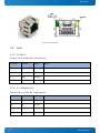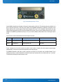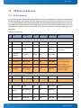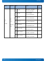
1
» User Guide «
SMARC Evaluation Carrier User Guide
Document revision 1.0
www.kontron.com
User’s Guide
» Table of Contents «
1 User Information ............................................................................................................. 6
1.1
About This Document ............................................................................................................................... 6
1.2
Copyright Notice ................................................................................................................................ 6
1.3
Trademarks ............................................................................................................................................... 6
1.4
Standards .......................................................................................................................................... 6
1.5
Warranty ............................................................................................................................................ 6
1.6
Technical Support .............................................................................................................................. 7
2 Introduction ..................................................................................................................... 8
2.1
General Introduction .......................................................................................................................... 8
2.2
SMARC Evaluation Carrier Goals .............................................................................................................. 8
2.3
User Cautions ............................................................................................................................................ 8
2.4
Feature Set Overview ....................................................................................................................................... 8
2.5
Document and Standards References....................................................................................................... 9
2.5.1
External Industry Standard Documents ..................................................................................... 9
2.5.2
Kontron Documents ................................................................................................................ 10
3 Block Diagrams ............................................................................................................. 11
4 Layout Diagrams ........................................................................................................... 14
5 Connectors – Cabled Interfaces .................................................................................................. 17
5.1
USB Connectors .......................................................................................................................................17
5.1.1
J1 – USB Hub Connections .............................................................................................................17
5.1.2
J2 – USB OTG Module Connection ............................................................................................................. 17
5.1.3
J3 – J4 – USB Module Connection ............................................................................................... 17
5.2
Gigabit Ethernet ............................................................................................................................... 17
5.2.1
5.3
2
J5 - GBE RJ45 ................................................................................................................................17
Audio ...................................................................................................................................................... 18
5.3.1
J6 – Mic In ......................................................................................................................................18
5.3.2
J7 – Headphone Out ..................................................................................................................... 18
5.3.3
J8 – Amplified Differential Audio Out, Left ............................................................................... 19
5.3.4
J9 – Amplified Differential Audio Out, Right ............................................................................. 19
5.3.5
J10 – Differential Microphone In .............................................................................................. 19
5.3.6
J11 – Line Level Audio Out ........................................................................................................... 19
5.3.7
J12 – Digital Microphone In ..................................................................................................... 20
www.kontron.com
User’s Guide
5.3.8
J13 – Line Level Audio ............................................................................................................ 20
5.3.9
J14 – SPDIF ....................................................................................................................................20
5.4
CAN Bus ................................................................................................................................................................... 21
5.4.1
J15 – CAN0 .....................................................................................................................................21
5.4.2
J16 – CAN1 .....................................................................................................................................21
5.5
Asynchronous Serial Ports .......................................................................................................................21
5.5.1
General ...........................................................................................................................................21
5.5.2
J18 – SER2 .....................................................................................................................................22
5.5.3
J19 – SER3 .....................................................................................................................................22
5.5.4
J20 – SER0 .....................................................................................................................................22
5.5.5
J21 – SER1 .....................................................................................................................................23
5.6
Battery and Power Related Connectors and Jumpers .............................................................................23
5.6.1
J22 - Battery Management Connector ..................................................................................... 23
5.6.2
J23 - J25 Battery Connectors .................................................................................................. 24
5.6.3
J28 Charger Input................................................................................................................................. 24
5.7
Bench Power Supply....................................................................................................................................... 24
5.8
HDMI Connection .....................................................................................................................................25
5.9
Parallel LCD .............................................................................................................................................25
5.10
Auxiliary Backlight Power............................................................................................................. 27
5.10.1
J33 Auxiliary Backlight Power .................................................................................................. 27
6 Connectors – Standard Mezzanines, Slots and Sockets ....................................................... 28
6.1
mSATA Site ..............................................................................................................................................28
6.2
miniPCIe Connectors ...............................................................................................................................28
6.3
PCIe x 1 Slot........................................................................................................................................... 28
6.4
SPI Socket ...............................................................................................................................................28
6.5
SD Card Slot ................................................................................................................................................... 29
6.6
Micro SIM Site ..........................................................................................................................................29
6.7
RTC Battery Clip.......................................................................................................................................29
6.8
SMARC Module Connector ............................................................................................................................ 29
7 Jumpers ............................................................................................................................. 30
3
7.1
Jumper J34 - LID# ............................................................................................................................ 30
7.2
Jumper J35 – TEST# ......................................................................................................................... 30
7.3
Jumpers J37, J38 and J39 – Boot Select .......................................................................................... 30
7.4
Jumper J36 – LVDS Panel Color Depth – Module LVDS ...........................................................................31
7.5
Jumper J49 – SD Card WP .......................................................................................................................31
www.kontron.com
User’s Guide
7.6
Jumper J58 – LVDS Panel Color Depth – Carrier LVDS ............................................................................31
7.7
Jumper J59 – Carrier Dual Channel LVDS Clock Edge .............................................................................32
7.8
Jumper J60 – Carrier LVDS Pixel Clock Rate ...........................................................................................32
7.9
Jumper J51 and J53 – Battery Select – Power Paths ........................................................................ 32
7.10
Jumpers J50 and J52 – Battery Select – Thermistor Paths ........................................................... 33
7.11
Jumpers J55 and J56 – Input Power Path ..........................................................................................33
7.12
Jumper J27 – Step-Down Switcher Disable ................................................................................. 34
7.13
Jumper J26 LED Power Source ...........................................................................................................34
8 Push Button Switches ............................................................................................................. 35
8.1
SW1 Reset Switch ....................................................................................................................................35
8.2
SW2 Power On Switch .............................................................................................................................35
8.3
SW3 Force Recovery Switch ....................................................................................................................35
9 LEDs ................................................................................................................................................ 36
10 KLAS (Kontron LVDS Adapter System) Connections............................................................. 37
11 I/O Mezzanine ............................................................................................................... 43
12 MMC Mezzanine ...................................................................................................................... 48
13 Camera Mezzanine .................................................................................................................. 51
14 AFB Mezzanine ........................................................................................................................ 55
15 I2C Buses and Devices ................................................................................................................. 58
15.1
I2C Bus Summary ................................................................................................................................58
15.2
I2C Bus Power Domains ......................................................................................................................59
15.3
I2C PM Bus I/O Expanders ..................................................................................................................59
15.4
I2C GP Bus I/O Expanders...................................................................................................................61
16 I2S Buses and Devices ................................................................................................................. 63
16.1
I2S0 ............................................................................................................................................. 63
16.2
I2S1 ............................................................................................................................................. 63
16.3
I2S2 ............................................................................................................................................. 64
17 Power Architecture ........................................................................................................ 65
17.1
Block Diagram Discussion......................................................................................................................... 65
17.2
Figure 17 Power Architecture....................................................................................................... 66
18 Mechanical and Environmental Parameters ..................................................................... 67
4
18.1
Mechanical Outline ...................................................................................................................... 67
18.2
Standoffs and Screw Hardware ...........................................................................................................68
18.3
Shock and Vibration .......................................................................................................................... 68
18.4
Thermal Environment .................................................................................................................. 68
www.kontron.com
User’s Guide
18.5
Humidity ...................................................................................................................................... 68
18.6
RoHS Compliance ...............................................................................................................................68
19 Appendix A: Connector Mating Part Number Information .............................................. 69
20 Appendix B: Assembly Part Numbers..................................................................................... 72
21 Appendix C: Document Revision History ............................................................................... 74
» Table of Figures «
Figure 1. System Block Diagram ................................................................................................................................ 12
Figure 2. Input Power Path Block Diagram ....................................................................................................13
Figure 3. Carrier Top-side Connectors and Jumpers ...................................................................................... 14
Figure 4. Carrier Bottom-side Connectors .....................................................................................................15
Figure 5. Carrier Top-side LEDs .................................................................................................................................. 16
Figure 6. Ethernet LEDs ................................................................................................................................18
Figure 7. KLAS Board 34mm x 18mm ......................................................................................................................... 37
Figure 8. KLAS Board 43mm x 18mm ........................................................................................................................ 38
Figure 9. KLAS Board 34mm x 18mm Outline ............................................................................................... 39
Figure 10. KLAS Board 43mm x 18mm Outline ............................................................................................. 40
Figure 11. I/O Mezzanine Card Outline ...................................................................................................................... 44
Figure 12. eMMC Mezzanine Card .............................................................................................................................. 48
Figure 13. eMMC Mezzanine Card Outline ................................................................................................................. 49
Figure 14. Camera Mezzanine Card Outline............................................................................................................... 52
Figure 15. AFB Mezzanine Card Outline .................................................................................................................... 56
Figure 16. I2S0 Switches .............................................................................................................................. 63
Figure 17. Power Architecture ....................................................................................................................... 66
Figure 18. Mechanical Outline .......................................................................................................................67
5
www.kontron.com
User’s Guide
1
User Information
1.1
About This Document
This document provides information about products from Kontron and/or its subsidiaries. No warranty of suitability,
purpose, or fitness is implied. While every attempt has been made to ensure that the information in this document is
accurate, the information contained within is supplied “as-is” and it is subject to change without notice.
For the circuits, descriptions and tables indicated, Kontron assumes no responsibility as far as patents or other rights of
third parties are concerned.
1.2
Copyright Notice
Copyright © 2012 Kontron America Inc.
All rights reserved. No part of this document may be reproduced, transmitted, transcribed, stored in a retrieval system,
or translated into any language or computer language, in any form or by any means (electronic, mechanical,
photocopying, recording, or otherwise), without the express written permission from Kontron.
1.3
Trademarks
The following lists the trademarks of components used in this board.
» NVidia, Tegra, ARM and all other products and trademarks mentioned in this manual are trademarks of their
respective owners.
1.4
Standards
Kontron is certified to ISO 9000 Quality Standards.
1.5
Warranty
This Kontron product is warranted against defects in material and workmanship for the warranty period from the date of
shipment. During the warranty period, Kontron will at its discretion decide to repair or replace defective products.
Within the warranty period, the repair of products is free of charge as long as warranty conditions are observed.
The warranty does not apply to defects resulting from improper or inadequate maintenance or handling by the buyer,
unauthorized modification or misuse, operation outside of the product’s environmental specifications or improper
installation or maintenance.
Kontron will not be responsible for any defects or damages to other products not supplied by Kontron that are caused
by a faulty Kontron product.
6
www.kontron.com
User’s Guide
1.6
Technical Support
Technicians and engineers from Kontron and/or its subsidiaries are available for technical support. We are committed
to making our product easy to use and will help you use our products in your systems.
Please consult our website at http://www.kontron.com/support for the latest product documentation, utilities, drivers
and support contacts. Consult our customer section http://emdcustomersection.kontron.com/ for the latest software
downloads, Product Change Notifications and additional tools and software. In any case you can always contact your
board supplier for technical support.
7
www.kontron.com
User’s Guide
2
Introduction
2.1
General Introduction
This document serves as a user manual and technical reference for the Kontron SMARC Evaluation Baseboard. The
manual is intended for use by engineering personnel working with SMARC systems.
2.2
SMARC Evaluation Carrier Goals
The SMARC Evaluation Carrier is intended to serve multiple needs:
» SMARC Module bring-up platform for hardware and software development.
» Module validation platform.
» Customer evaluation platform.
» Customer design reference.
» Manufacturing test platform.
» Flexible prototyping vehicle (facilitated by multiple mezzanines).
2.3
User Cautions
Caution! The SMARC Evaluation Carrier is ESD sensitive equipment. Users must observe precautions for handling
electrostatic discharge sensitive devices.
Caution! The SMARC Evaluation Carrier is a platform for Engineering evaluation and development. It is not a piece of
consumer electronics.
Caution! There are jumper settings for power options, detailed in sections below, which are potentially hazardous if
used incorrectly.
2.4
Feature Set Overview
» SMARC specification compliant.
» 210mm x 200mm form factor.
» Accepts 82mm x 50mm and 82mm x 80mm SMARC Modules.
» Accepts 1.8V SMARC V_IO and 3.3V V_IO.
» Module LVDS KLAS (Kontron LVDS Adapter System) port.
» HDMI port.
» Parallel LCD port.
» Carrier LVDS KLAS Adapter – 24 bit color packing, single and dual channel LVDS.
» LED Backlight support – up to 31.9V.
» USB OTG micro AB connector – direct from SMARC.
» USB R/A Type A connector – direct from SMARC.
8
www.kontron.com
User’s Guide
» USB 7 port hub.
» SATA MO-300 site.
» Mini-PCIe sites (2) with shared SIM slot.
» PCIe slot.
» GbE port with integrated magnetics.
» On-board I2S Audio Codec.
» RS232 support for all 4 SMARC serial ports.
» CAN Bus support (2).
» Micro SD Card slot.
» eMMC Mezzanine site.
» Micro SD Card slot.
» Camera Mezzanine site.
» AFB (Alternate Function Block) site.
» I/O Mezzanine site.
» RTC backup power sources – Lithium coin cell socket and SuperCap option.
» On-board accelerometer.
» SIM card support.
» Lab bench power input option – 3.0V to 5.25V input voltage range.
» Support for Li-Ion batteries and on-board charging circuit.
» Loop-back features for test on selected interfaces.
» Carrier cutout allows access to back side of Module for Module debug.
2.5
Document and Standards References
2.5.1 External Industry Standard Documents
» CAN (“Controller Area Network”) Bus Standards – ISO 11898, ISO 11992, SAE J2411.
» CSI-2 (Camera Serial Interface version 2) The CSI-2 standard is owned and maintained by the MIPI Alliance
(“Mobile Industry Processor Alliance”) (www.mipi.org).
» eMMC (“Embedded Multi-Media Card”) the eMMC electrical standard is defined by JEDEC JESD84-B45 and the
mechanical standard by JESD84-C44 (www.jedec.org).
» GBE MDI (“Gigabit Ethernet Medium Dependent Interface”) defined by IEEE 802.3. The 1000Base-T
operation over copper twisted pair cabling defined by IEEE 802.3ab (www.ieee.org).
» HDMI Specification, Version 1.3a, November 10, 2006 © Hitachi and other companies (www.hdmi.org).
» The I2C Specification, Version 2.1, January 2000, Philips Semiconductor (now NXP) (www.nxp.com).
» I2S Bus Specification, Feb. 1986 and Revised June 5, 1996, Philips Semiconductor (now NXP)
(www.nxp.com).
» JEDEC MO-300 (mSATA) defines the physical form factor of the mSATA format (www.jedec.org). The electrical
connections are defined in the Serial ATA document.
9
www.kontron.com
User’s Guide
» MXM3 Graphics Module Mobile PCI Express Module Electromechanical Specification, Version 3.0, Revision
1.1, © 2009 NVidia Corporation (www.mxm-sig.org).
» PICMG® EEEP Embedded EEPROM Specification, Rev. 1.0, August 2010 (www.picmg.org).
» PCI Express Specifications (www.pci-sig.org).
» PCI Express Mini Card Electromechanical Specification Revision 2.0, April 21, 2012, © PCI-SIG (www.pcisig.org).
» RS-232 (EIA “Recommended Standard 232”) this standard for asynchronous serial port data exchange dates
from 1962. The original standard is hard to find. Many good descriptions of the standard can be found on-line,
e.g. at Wikipedia, and in text books.
» Serial ATA Revision 3.1, July 18, 2011, Gold Revision, © Serial ATA International Organization (www.sataio.org).
» SD Specifications Part 1 Physical Layer Simplified Specification, Version 3.01, May 18, 2010, © 2010 SD
Group and SD Card Association (“Secure Digital”) (www.sdcard.org).
» SPDIF (aka S/PDIF) (“Sony Philips Digital Interface) - IEC 60958-3.
» SPI Bus – “Serial Peripheral Interface” – de-facto serial interface standard defined by Motorola. A good
description may be found on Wikipedia (http://en.wikipedia.org/wiki/Serial_Peripheral_Interface_Bus).
» USB Specifications (www.usb.org).
2.5.2 Kontron Documents
Some of the documents referenced below may require an NDA to be in place before delivery. Check with your Kontron
contact.
» Ultra Low Power – Computer On Module Hardware Specification, version 1.2 September 19, 2012. © Kontron
America 2012.
» SMARC Evaluation Carrier (KARMA Eval Carrier) Board Schematic, 501-146, latest revision.
» eMMC Mezzanine Schematic, KAI 501-151, latest revision.
» KLAS Schematic, Hyundai 1366 x 768 Single Ch. LVDS, KAI 501-162, latest revision.
» KLAS Schematic, NEC 1280 x 768 Single Ch. LVDS, KAI 501-163, latest revision.
10
www.kontron.com
User’s Guide
3
Block Diagrams
An overall system block diagram for the SMARC Evaluation Carrier is shown on the following page. The following color
coding is used on the block diagram:
» Industry standard wired I/O connectors are shown in orange.
» Kontron defined wired I/O connectors are shown in dark red.
» Industry standard mezzanine and slot format connectors are shown in blue.
» Kontron defined mezzanine connectors are shown in green.
» ICs on the board are shown in pale yellow.
» Miscellaneous features (jumpers, switches) are shown in drab green.
“A picture is worth 1000 words”. Much may be gleaned from this diagram:
» How SMARC resources are used on the Evaluation Carrier.
» What the major Evaluation Carrier Features are.
» An indication of the power supply architecture.
» An indication of the loop-back possibilities for test.
11
www.kontron.com
User’s Guide
Block Diagram Color Key:
Configuration Options
Industry standard connectors
for wired, off-board connections
(Depleted / Nominal / Fully Charged)
One level (3.0V /
3.6V / 4.2V)
Two level (6.0V /
7.2V / 8.4V)
Three level (9.0V / 10.8V / 12.6V)
Industry standard connectors
for mezzanine format connectors
I2C_PM
Li-Ion
Battery
Battery
Fuel Guage IC
Kontron defined connectors
Wired, off-board connections
Li-Ion
Battery
I2C_PM
Kontorn defined connectors
and mezzanines
EEPROM
Li-Ion
Battery
IC and IC subsystems
I2C_PM
BQ24171
I2C
8 Bit I/O
TCA9554
Enables
Battery Charger
Charger
In
Other features
Charge Status
I2C_PM
RTC Backup
Power Source
(Batt / SuperCap)
I2C
8 Bit I/O
TCA9554
Status
Energy Flow Color Key:
Battery Energy
Charger Energy
Bench Supply Energy
DC – DC
Converter
(Used only for 8.4V and 10.8V
Nominal Series Batteries)
LDO
1.8V
V_IN_MOD (3.0V – 5.25V)
Module Power (3.0V – 5.25V)
V_IN_CAR (3.0V – 5.25V)
Power State Status Signals
I2C_PM
I2C_PM_CAR
FET
Isolation
Carrier
Power Supply
Enables
Boot Device elect
Carrier
Power Supply
Status
Jumper
Block
Test Bench
Power In
May be single 5V
Or single 3.3V
Or single 3.0V to 5.25V
Or dual supply in 3.0 to 5.25V
range
5V
3.3V
Charge Status
5V (single level cell)
12V (two level cell)
16V (three level cell)
Carrier Power
Supply Circuits
V_IO 1.8V Default
Allow build option for 3.3V
1.8V
PWR
1.5V
Header
Backlight Pwr
Used if separate
Backlight cable is
needed
12V
I2C_GP
Misc Ctrl (Pwr Btn etc)
Pwr Btn
Reset Btn
Force Recovery Btn
LED
(variable, to 31.9V)
I2C_LCD
I2C_LCD
LVDS Xmitter
Odd Pixels
SN75LVDS83B
24 Bit Parallel LCD Data and Control
Dual Ch 24 Bit LVDS
LVDS Xmitter
Even Pixels
SN75LVDS83B
Header
Parallel LCD Data
HDMI
SMARC Carrier Connector: 314 Pin 0.5mm Pitch R/A MXM3 Style Baseboard Connector
KLAS
LVDS
Connector
Mezzanine adapter
Add on KLAS card
has native LVDS panel
connector
KLAS
LVDS
Connector
Mezzanine adapter
Add on KLAS card
has native LVDS panel
connector
Module LVDS (Single Channel)
LVDS
HDMI
UARTs (2x 4 Wire and 2x 2 Wire)
SER3
SDIO (4 Bit)
I2C_CAM
Header
I2C_LCD
eMMC Mezzanine
2x
SER1
EEPROM
SDIO / eMMC (8 Bit)
Header
RS232
XCVRS
SER2
I2C_GP
EEPROM
Micro SD Slot
SER0
Header
Texas Inst
TRS3253E
Header
EEPROM
Enables
GPIO
FETS
Carrier RS232
XCVR Disabled if
Port is used
on I/O Mezzanine
SER0 - 3
CAN1
LED
s
(x12)
I2S0
CAN0
I2C_GP
CAN PHY
On-Semi
NCV7341
CAN PHY
On-Semi
NCV7341
Header
Header
Mux
Passthru /
Loopback
I/O
MEZZANINE
100 pin Hirose FX8 Connector
Mux
Passthru /
Loopback
I2S1
I2C
8 Bit I/O
TCA9554
SMARC GPIO
May be read back
over I2C for test
I2C_GP
I2C
8 Bit I/O
TCA9554
I2S2
I2C_PM_CAR
I2C_PM_CAR
I2C_GP
I2C_GP
SPI1
I2C_CAM
I2C_CAM
SPI0
I2C_LCD
I2C_LCD
Headphone
Build Options
TRS Jack
I2C
I2C_GP
Default
MIC
I2S
CODEC
SPI
EEPROM
(Socket)
I2S0
I2C_GP, I2C_CAM, I2C_LCD
FSUSB43
Passthru /
Loopback/
Isolate
TRS Jack
Header
Dual Class D
Amplifiers
Wolfson
Micro
WM8903
I2S
Header
Header
Line In
Header
Line Out
I2S0, I2S1, I2S2
SPDIF
Header
I2C_GP, I2C_LCD
(Build options)
Accelerometer
ST Micro
LIS302DL
USB2
USB Type A
I2C_GP
USB1
1:7
USB HUB
I2C
8 Bit I/O
TCA9554
Enables for subsystems
(I2S loopbacks,
RS232 XCVRs, etc)
Not Used
USB
Type A
R/A Dual
SMSC
USB2517
USB
Micro AB
OTG
USB0 (OTG )
PCIe x1 Slot
SATA
MO-300
SATA
Mini PCIe
(PCIe / USB)
SIM
Card
PCIE_C
PCIE_B
PCIE_A
Mini PCIe
(PCIe / USB)
GBE
RJ45
With
Magnetics
GBE
CAM1 (CSI 4 pair / Parallel Low Order Bits)
CAM0 (CSI 2 pair / Parallel Hi Order Bits)
AFB
Camera
Mezzanine
AFB
Mezzanine
Connector
Support signals
Per SMARC spec
Support signals
Per SMARC spec
Figure 1. System Block Diagram
12
www.kontron.com
User’s Guide
IF CHARGER POWER
AND / OR BATTERY
POWER ARE USED,
THEN BENCH SUPPLY
INPUT MUST BE LEFT
OPEN
J29
3.0V TO 5.25V MODULE POWER
BENCH
SUPPLY
CONNECTOR
3.0V TO 5.25V CARRIER POWER
J28
CHARGER
CONNECTOR
5V OUTPUT IF
SWITCHER IS USED
V_CHARGER
IN
STEP-DOWN SWITCHER
WIDE INPUT RANGE
BATTERY CHARGER
CIRCUITS
J56
NOT USED FOR SINGLE LEVEL CELLS
OUT
IN
MODULE POWER
OUT
IS USED FOR TWO AND THREE LEVEL
SERIES CELLS
J23, J24, J25
BATTERY
SELECT
JUMPERS
BATTERY
CONNECTORS
V_BAT
CARRIER POWER
J55
IN / OUT
ENABLE
JUMPERS J56 AND J55
MUST BE OPEN WHEN
POWER IS BROUGHT IN
FROM BENCH SUPPLY
CONNECTOR J29
P-FET
BATTERY
CONFIG
V_CHARGER
V_BAT
NOMINAL
V_BAT
RANGE
SINGLE LEVEL
~ 5V
3.6V
3.0V - 4.2V
TWO SERIES
~10V
7.2V
6.0V – 8.4V
THREE SERIES
~15V
10.8V
9.0V – 12.6V
Resistor
J27
Switcher Bypass Jumper
3.0V – 5.25V IF
SWITCHER IS
BYPASSED
(SINGLE LEVEL CELL)
Figure 2. Input Power Path Block Diagram
Caution! There are two different ways to power the SMARC Evaluation Carrier and Module:
» Bench Power Connector J29 (with jumpers J55 and J56 open).
» Battery Charger / Battery Power Path - J28, J23, J24, J25 (with jumpers J55 and J56 closed; connector J29
open and not used).
Caution! These paths are mutually exclusive – you must use one or the other. More details on power options, battery
options, etc. may be found in subsequent sections of this manual.
The Bench Supply connection, through J29, is convenient and easy to use. The two J29 power feeds may be wired
together and can be sourced from a single 5V supply or used separately to allow Module and Carrier power
measurements and voltage range validation.
Caution! If using the Bench Supply power path, jumpers J55 and J56 must be open.
13
www.kontron.com
User’s Guide
4
Layout Diagrams
The following section shows the physical location of connectors, configuration jumpers and other important features
on the SMARC Evaluation Carrier.
Figure 3. Carrier Top-side Connectors and Jumpers
14
www.kontron.com
User’s Guide
Figure4.CarrierBottom-sideConnectors
15
www.kontron.com
User’s Guide
Figure 5. Carrier Top-side LEDs
16
www.kontron.com
User’s Guide
5
Connectors – Cabled Interfaces
Wired connections to the SMARC Evaluation Carrier are described in this section. Information on mating connector
part numbers is given in a table in Section 27 Appendix A: Connector Mating Part Number Information.
5.1
USB Connectors
5.1.1 J1 – USB Hub Connections
Connector J1 implements an industry standard USB dual Type A host connection. The USB ports for J1 are ports that are
downstream ports of the Evaluation Carrier’s SMSC USB2517 hub. The hub upstream port is connected to the SMARC
Module USB1 port.
5.1.2 J2 – USB OTG Module Connection
Connector J2 implements an industry standard USB micro-AB connector. This small form factor flavor of USB
connection is allowed to be either a client or a host, or can switch between being client or host. If the Module supports
it, the J2 port may be USB OTG (On The Go) capable.
J2 is wired to the SMARC USB0 port, and the details of whether the port is client, host, or OTG capable depend on
Module capabilities and how the Module is configured.
5.1.3 J3 – J4 – USB Module Connection
J3 is an industry standard USB single Type A host connection. It is wired directly to the SMARC USB2 port.
There is a hole pattern at this connector site that allows a dual USB Type A host connector, J4, to be loaded instead of
J3. If this is done, then the SMSC USB2517 USB Hub controller is not used, and the SMARC USB1 port is configured
(via build options) to go to the upper connector slot in the J4 pattern. This is not the usual build, and exists only for
certain special Module validation purposes.
5.2
Gigabit Ethernet
5.2.1 J5 - GBE RJ45
J5 is an industry standard 8 pin RJ45 jack for use with 4-pair CAT5 cabling common for Gigabit Ethernet connections.
The specific part used is the Bel-Fuse L829-1J1T-43 (Kontron SAP 1045-4258) or equivalent.
17
www.kontron.com
User’s Guide
Figure 6. Ethernet LEDs
5.3
Audio
5.3.1 J6 – Mic In
Connector: CUI Inc SJ-43514-SMT, 3.5mm Audio Jack.
Pin Number
Pin Name
Signal
1
Sleeve
GND
2
Tip
HP_MIC
3
Ring 1
HP_MIC
4
Ring 2
GND
Notes
Microphone In signal
5.3.2 J7 – Headphone Out
Connector: CUI Inc SJ-43514-SMT, 3.5mm Audio Jack.
18
Pin Number
Pin Name
Signal
1
Sleeve
GND
2
Tip
HP_LEFT
3
Ring 1
HP_RIGHT
4
Ring 2
GND
Notes
www.kontron.com
User’s Guide
5.3.3 J8 – Amplified Differential Audio Out, Left
Connector: JST SM02B-SRSS-TB, 1mm pitch R/A SMD Header.
Pin Number
Signal
1
Amplified Audio Out Left +
2
Amplified Audio Out Left -
Notes
5.3.4 J9 – Amplified Differential Audio Out, Right
Connector: JST SM02B-SRSS-TB, 1mm pitch R/A SMD Header.
Pin Number
Signal
1
Amplified Audio Out Right +
2
Amplified Audio Out Right -
Notes
5.3.5 J10 – Differential Microphone In
Connector: JST SM03B-SRSS-TB, 1mm pitch R/A SMD Header.
Pin Number
Signal
1
MIC Right +
2
MIC Right -
3
Ground
Notes
5.3.6 J11 – Line Level Audio Out
Connector: JST SM03B-SRSS-TB, 1mm pitch R/A SMD Header.
19
Pin Number
Signal
1
Line OUT Right
2
Line OUT Left
3
Ground
Notes
www.kontron.com
User’s Guide
5.3.7 J12 – Digital Microphone In
Connector: JST SM03B-SRSS-TB, 1mm pitch R/A SMD Header.
Pin Number
Signal
1
Digital MIC Data
2
Digital MIC Clock
3
Ground
Notes
5.3.8 J13 – Line Level Audio
Connector: JST SM03B-SRSS-TB, 1mm pitch R/A SMD Header.
Pin Number
Signal
1
Line IN Right
2
Line IN Left
3
Ground
Notes
5.3.9 J14 – SPDIF
Connector: JST SM04B-SRSS-TB, 1mm pitch R/A SMD Header.
20
Pin Number
Signal
Notes
1
IO Power
1.8V or 3.3V
2
SPDIF Data Out
3
SPDIF Data In
4
Ground
www.kontron.com
User’s Guide
5.4
CAN Bus
5.4.1 J15 – CAN0
Connector: Molex 53261-0471, 1.25mm pitch R/A Header.
Pin Number
Signal
1
CAN 0 Dominant Low
2
CAN0 Dominant High
3
5V power
4
Ground
Notes
5.4.2 J16 – CAN1
Connector: Molex 53261-0471, 1.25mm pitch R/A Header.
Pin Number
Signal
1
CAN1 Dominant Low
2
CAN1 Dominant High
3
5V power
4
Ground
5.5
Notes
Asynchronous Serial Ports
5.5.1 General
The SMARC Evaluation Carrier supports the four serial ports defined in the SMARC specification. The Evaluation
Carrier has EIA RS232 compliant signal levels and polarities. Per the SMARC specification, two of the four ports have
RTS / CTS handshaking, and two have TX and RX data only, without handshaking.
The Evaluation Carrier runs SER0 and SER1 through one transceiver, and SER2 and SER3 through a 2nd transceiver. There
are provisions that allow I/O Mezzanine card circuitry to disable the SER0/1 transceiver, and / or disable the SER2/3
transceiver. These provisions exist so that users may optionally take over SER0/1 or SER2/3 and use them in alternative
ways on the I/O Mezzanine (to interface to a peripheral such as a GPS module or an RS485 transceiver).
21
www.kontron.com
User’s Guide
5.5.2 J18 – SER2
Connector: JST SM05B-SRSS-TB, 1mm pitch R/A SMD header.
Pin Number
Signal
1
Serial port 2 – Receive Data
2
Serial port 2 – Transmit Data
3
Serial port 2 – Request to Send
4
Serial port 2 – Clear to Send
5
Ground
Notes
5.5.3 J19 – SER3
Connector: JST SM05B-SRSS-TB, 1mm pitch R/A SMD header.
Pin Number
Signal
1
Serial port 3 – Receive Data
2
Serial port 3 – Transmit Data
Notes
3
Not used
4
Not used
5
Ground
5.5.4 J20 – SER0
Connector: JST SM05B-SRSS-TB, 1mm pitch R/A SMD header.
22
Pin Number
Signal
1
Serial port 0 – Receive Data
2
Serial port 0 – Transmit Data
3
Serial port 0 – Request to Send
4
Serial port 0 – Clear to Send
5
Ground
Notes
www.kontron.com
User’s Guide
5.5.5 J21 – SER1
Connector: JST SM05B-SRSS-TB, 1mm pitch R/A SMD header.
Pin Number
Signal
1
Serial port 1 – Receive Data
2
Serial port 1 – Transmit Data
Notes
3
Not used
4
Not used
5
5.6
Ground
Battery and Power Related Connectors and Jumpers
The SMARC Evaluation Carrier implements a flexible battery connection scheme, allowing single level single cells,
parallel single level cells, two series cells and three series cells.
Caution! Moving between these combinations requires that the user pay close attention to the battery wiring details
and the battery jumper settings. There are hazards in getting it wrong.
5.6.1 J22 - Battery Management Connector
This connector exists so that key battery management signals are available off-board to allow engineers to prototype
an external battery charger circuit, separate from the charger circuit implemented on the Evaluation Carrier. In most
cases, this connector is not needed and can be ignored.
Connector: Molex 53261-1071, 1.25mm pitch R/A SMD header.
23
Pin Number
PIN Name
Notes
1
CHARGER_PRSNT#
Charger Present indication from battery
3
CHARGING#
Charging indication from battery
5
BATLOW#
Battery Low indication from battery
7
I2C_PM_CK
I2C Clock
8
I2C_PM_DAT
I2C Data
2,4,10
NC
No Connect
6,9
GND
Ground
www.kontron.com
User’s Guide
5.6.2 J23 - J25 Battery Connectors
J23, J24 and J25 are slots for inserting Battery 1, Battery 2 and Battery 3 respectively.
All the three connectors have the same pin-out.
Connector: TE-Connectivity 2-292173-6, 2mm pitch R/A SMT Header.
Pin Number
Signal
Notes
1,2
Battery Supply Positive
3
Battery Thermistor +
4
Battery Thermistor -
5,6
Battery Supply Negative
5.6.3 J28 Charger Input
Connector: Molex 39-30-3035
Pin Number
Signal
1
Charger Input
2
Ground
3
No Connect
4.2mm pitch R/A through hole header
Notes
Caution! The charger voltage level depends on the battery configuration (single, dual or triple level cells – nominally
5V, 10V or 15V).
5.7
Bench Power Supply
The Evaluation Carrier may be powered by a lab bench supply over connector J29. This is the most common way that the
SMARC Evaluation Carrier is used.
There are two power feeds to the Bench Supply: one for the Evaluation Carrier circuits, and one for the Module. This
allows the Evaluation Carrier current and power consumption and the Module current and power consumption to be
measured separately. The two feeds may be combined and powered from a single source if the user does not care about
the separate measurements. The source(s) should be a DC supply in the 3.0 to 5.25V range.
24
www.kontron.com
User’s Guide
Connector: Molex 39-30-3045, 4.2mm pitch R/A through-hole header.
Pin Number
Signal
Notes
1
Module Power
3.0V to 5.25V may be independent of Carrier power.
2
GND
3
Carrier Power
4
GND
3.0V to 5.25V may be independent of Carrier power.
Caution! When power is brought in through the J29 Bench Power Supply connector, then jumpers J56 and J57 must be
open.
5.8
HDMI Connection
The SMARC Evaluation Carrier implements an industry standard HDMI connector.
5.9
Parallel LCD
The SMARC Evaluation Carrier brings the SMARC Module parallel LCD signals to a 40 pin 1mm pitch header that can be
cabled to. The parallel LCD signals are also routed to a pair of LVDS transmitters on the Carrier, allowing dual
channel LVDS to be realized.
The color mapping of the parallel LCD data bits are defined in the SMARC specification document.
The parallel LCD data signal level is, per the SMARC specification, at V_IO, which typically is 1.8V. The 40 pin LCD header
has pins with 1.8V and 3.3V supply voltages for the panel. All signals listed below are at V_IO level.
There are no backlight supply voltages or control pins on the 40 pin connector. There is a separate connector, J33, for
supplying voltages to the backlight.
Connector: JST BM40B-SRDS-A-G-TF, 1mm pitch 2 row (20x2) SMD vertical header.
25
Pin Number
Signal
Notes
1
LCD Data 0
BLU0 (LS bit)
2
LCD Data 1
BLU1
3
LCD Data 2
BLU2
4
LCD Data 3
BLU3
6
LCD Data 4
BLU4
7
LCD Data 5
BLU5
8
LCD Data 6
BLU6
www.kontron.com
User’s Guide
26
9
LCD Data 7
BLU7 (MS bit)
11
LCD Data 8
GRN0 (LS bit)
12
LCD Data 9
GRN1
13
LCD Data 10
GRN2
14
LCD Data 11
GRN3
16
LCD Data 12
GRN4
17
LCD Data 13
GRN5
18
LCD Data 14
GRN6
19
LCD Data 15
GRN7 (MS bit)
21
LCD Data 16
RED0 (LS bit)
22
LCD Data 17
RED1
23
LCD Data 18
RED2
24
LCD Data 19
RED3
26
LCD Data 20
RED4
27
LCD Data 21
RED5
28
LCD Data 22
RED6
29
LCD Data 23
RED7 (MS bit)
31
Horizontal Sync
32
Vertical Sync
33
Display Enable
34
Pixel clock
38
Enable for panel VDD
5,10,15,20,
25,30,35
GND
36,37
3.3V
39, 49
1.8V
www.kontron.com
User’s Guide
5.10 Auxiliary Backlight Power
5.10.1 J33 Auxiliary Backlight Power
Connector: Hirose DF11-10DP-2DSA, 2mm pitch dual row (5x2) vertical header.
27
Pin Number
Signal
Notes
5
LCD_BKLT_EN
Backlight Enable V_IO signal level
6
LCD_BKLT_PWM
Backlight PWM V_IO signal level
1,3
5V
7,9
12V
2,4,6,8,10
GND
www.kontron.com
User’s Guide
6
Connectors – Standard Mezzanines, Slots and Sockets
Connector part number information is given in a table in Section 27 Appendix A: Connector Mating Part Number
Information.
6.1
mSATA Site
The SMARC Evaluation Carrier implements a SATA port in the JEDEC MO-300 (mSATA) form factor at site J71. This form
factor uses the same connector as mini-PCIe, but the electrical connections are different. Mini-PCIe cards will not be
functional in site J71. If a mini-PCIe card is accidentally inserted, the chance of damage is remote but possible.
6.2
miniPCIe Connectors
Two miniPCIe sites are implemented on the SMARC Evaluation Carrier. The two sites use industry standard miniPCIe
connector implementations, as defined in PCI Express Mini Card Electromechanical Specification. The Evaluation Carrier
design allows full size or half-size miniPCIe configurations to be built.
Site J72 is referred to as the “miniPCIe A” site because it ties to SMARC Module PCIE_A. This site is typically built in
the half-size card configuration.
Site J44 is the “miniPCIe B” site, fed by SMARC Module PCIE_B. This site is typically built in the full-size card
configuration.
Both of the Evaluation Carrier miniPCIe sites have a USB connection as well as a PCIe connection. The USB interfaces
are to the Evaluation Carrier 7 port USB hub chip.
The two miniPCIe sites share a connection to a microSIM card slot.
6.3
PCIe x 1 Slot
An industry standard PCIe x1 slot is implemented on the SMARC Evaluation Carrier. It is connected to the SMARC
PCIE_C port.
All SMARC Modules are expected to provide at least one PCIe port (Port A). Some will support two ports (A and B).
Relatively few Modules support a 3rd port, so the SMARC PCIe x1 slot may be of limited use.
6.4
SPI Socket
The Evaluation Carrier has a “coffin style” zero insertion force socket for 8 pin SPI devices. The socket is Lotes ACA-SPI004-T01, for SPI devices with a 5.4mm x 5.4mm body size, 1.27mm lead pitch and 8.2mm overall lead span.
The SPI device is powered by V_IO on the Evaluation Carrier. The V_IO voltage is usually 1.8V, determined by the
Module.
A suitable SPI device for 1.8V I/O operation is the Winbond W25Q64DWSSIG (64 Mbits). Another one is Winbond
W25Q16DWSSIG (16 Mbits).
28
www.kontron.com
User’s Guide
6.5
SD Card Slot
An industry standard micro-SD Card slot is located on the back of the Eval Carrier, in position J74. It supports 3.3V SD
cards.
Jumper J49 may be open to write-protect the card. To allow the card to be written to, leave J49 closed.
6.6
Micro SIM Site
The PCI Express Mini Card Electromechanical Specification defines connection pins for a SIM (“Subscriber Identity
Module”) card. In the PCI-SIG document, it is referred to as a UIM (“User Identity Module). The SMARC Evaluation
Carrier implements a micro-SIM slot at position J73, on the back of the Evaluation Carrier. The connector part used is a
6 pin 15mm x 12mm micro SIM connector, Molex 470230001.
6.7
RTC Battery Clip
A socket connector for a 20mm diameter 3V lithium coin cell battery is available on the Evaluation Carrier in position
BT1. The connector socket used is Renata SMTU2032-LF. A suitable battery is Panasonic CR2032.
The battery ‘+’ terminal is protected against charging (as required by safety regulations) by a series Schottky diode and
a 1K resistor (R147). The 1K resistor feeds the SMARC VDD_RTC pin (SMARC pin S147).
The Evaluation Carrier also has a 0.2F “SuperCap” that may be loaded to supply a backup voltage to the SMARC
VDD_RTC, instead of the battery. The SuperCap is at position C134, and connects to the SMARC VDD_RTC pin through a
1K resistor, at position R151.
6.8
SMARC Module Connector
The SMARC Module is supported on J40. This is a 314 pin MXM3 style connector. The J40 pin-out conforms to the ULPCOM Module specification. Both 1.8V and 3.3V Module I/O can be supported on the Evaluation Carrier.
The MXM3 style connector used on the Evaluation Carrier is a low profile part, with a board-to-board spacing of 1.5mm.
The Evaluation Carrier has captive M2.5 threaded standoffs in the SMARC mounting hole positions. The standoffs
accept M2.5 screws, inserted from above, through the Module holes.
Both 82mm x 50mm and 82mm x 80mm format SMARC Modules may be used with the Evaluation Carrier. The
Evaluation Carrier PCB has a cut-out allowing access to the back side of the SMARC Module for test and debug.
29
www.kontron.com
User’s Guide
7
Jumpers
7.1
Jumper J34 - LID#
J34 is used to simulate LID-open and LID-closed condition, for test and development.
Jumper
Position
Function
Inserted
Simulates LID closed condition
Not inserted
Simulates LID open condition
J34
7.2
Jumper J35 – TEST#
J35 is used for Module specific test purposes. In normal operation, this jumper should be open.
Jumper
Position
Function
Inserted
Module specific test – check Module documentation
Not inserted
Normal operation
J35
7.3
Jumpers J37, J38 and J39 – Boot Select
J37, J38 and J39 are used to select the boot device. The following table is transcribed form the SMARC Module
specification. Some Modules may not support all options; refer to the Module documentation. The meaning of “boot”
may vary as well – check the Module documentation.
30
J39
J38
J37
Boot Device
Inserted
Inserted
Inserted
Carrier SATA
Inserted
Inserted
Not inserted
Carrier SD Card
Inserted
Not inserted
Inserted
Carrier eMMC Flash
Inserted
Not inserted
Not inserted
Carrier SPI
Not inserted
Inserted
Inserted
Module device (NAND, NOR) – vendor specific
Not inserted
Inserted
Not inserted
Remote boot (GBE, serial) – vendor specific
Not inserted
Not inserted
Inserted
Module eMMC Flash
Not inserted
Not inserted
Not inserted
Module SPI
www.kontron.com
User’s Guide
7.4
Jumper J36 – LVDS Panel Color Depth – Module LVDS
Jumpers J36 is used for selecting the color depth of the Module LVDS display. Most Modules will use 6 bit color packing
on the Module LVDS, and J36 should be inserted. This jumper has an effect only when the LVDS display in use has the
corresponding 6 bit / 8 bit color pack selection capability.
Jumper
Position
Function
Inserted
Sets 6 bit per color packing on the display (if the display supports
this feature)
Not inserted
Sets 8 bit per color packing on the display (if the display supports
this feature)
J36
7.5
Jumper J49 – SD Card WP
J49 is used to enable or disable the SDIO Write Protect.
Jumper
Position
Function
Inserted
Write access enabled for the SD card
Not inserted
SD card is write protected
J49
7.6
Jumper
Jumper J58 – LVDS Panel Color Depth – Carrier LVDS
Position
Function
Inserted
Sets 6 bit per color packing on the display (if the display supports
this feature)
Not inserted
Sets 8 bit per color packing on the display (if the display supports
this feature)
J58
31
www.kontron.com
User’s Guide
7.7
Jumper J59 – Carrier Dual Channel LVDS Clock Edge
A 24 bit dual channel LVDS implementation comprises 10 differential pairs: 4 pairs for odd pixel and control data; 1 pair
for the LVDS clock for the odd data; 4 pairs for the even pixel data and control data, and 1 pair for the even LVDS clock.
The SMARC Evaluation Carrier uses one LVDS transmitter for even pixel signals (U14) and another LVDS transmitter for
odd pixel signals (U21). Data is clocked into the pair of Carrier Board LVDS transmitters by LCD_DUAL_PCK.
J59 is used for selecting the active clock edge for the LVDS transmitters to latch data on as shown below:
Jumper
Position
Function
Inserted
U14 latches on rising clock edge and U21 latches on falling clock
edge
Not inserted
U21 latches on rising clock edge and U14 latches on falling clock
edge
J59
7.8
Jumper J60 – Carrier LVDS Pixel Clock Rate
J60 is a 3 pin header. Two pins (1-2 or 2-3) are shorted together to select between two pixel clock options. For dualchannel LVDS displays connected to the Carrier KLAS board, use the 1-2 position. For single channel displays, used the
2-3 position.
Jumper
Position
Function
1-2
Dual Pixel Clock (one- half frequency of Pixel Clock)
2-3
Pixel Clock
60
7.9
Jumper J51 and J53 – Battery Select – Power Paths
Three batteries (BAT1, BAT2 and BAT3) are provided on the board and the user can realize various combinations
mentioned in the table below based on the position of the jumpers J51 and J53.
32
Function
Inserted
Not inserted
3.6V Li-Ion (1 cell, BAT1)
J51 (Pin 3-4)
All others
3.6V Li-Ion (2 cells, parallel, BAT1 & BAT2)
J51 (Pin 1-2)
J51 (Pin 3-4)
J53 (Pin 3-4)
All others
7.2V Li-Ion (2 cells, series, BAT1 & BAT2)
J51 (Pin 2-3)
J53 (Pin 3-4)
All others
10.8V Li-Ion (3 cells, series BAT1, BAT2, &
BAT3)
J51 (Pin 2-3)
J53 (Pin 2-3)
All others
www.kontron.com
User’s Guide
7.10 Jumpers J50 and J52 – Battery Select – Thermistor Paths
Corresponding to the chosen battery combination, battery pack thermistor selection is done using jumpers J50 and J52
as per the table below:
Function
Inserted
Not inserted
3.6V Li-Ion (1 cell, BAT1)
J50 (Pin 3-4)
All others
J50 (Pin 1-2)
3.6V Li-Ion (2 cells, parallel, BAT1 & BAT2)
J50 (Pin 3-4)
All others
J52 (Pin 3-4)
J50 (Pin 2-3)
7.2V Li-Ion (2 cells, series, BAT1 & BAT2)
All others
J52 (Pin 3-4)
10.8V Li-Ion (3 cells, series BAT1, BAT2, &
BAT3)
J50 (Pin 2-3)
All others
J52 (Pin 2-3)
7.11 Jumpers J55 and J56 – Input Power Path
Jumpers J55 and J56 connect the Evaluation Carrier battery charging subsystem to the rest of the Evaluation Carrier.
Refer to Figure 2 Input Power Path Block Diagram for an illustration. There are two different ways to power the ULPCOM Evaluation Carrier:
» Bench Power Connector J29 (with jumpers J55 and J56 open).
» Battery Charger / Battery Power Path - J28, J23, J24, J25 (with jumpers J55 and J56 closed; connector J29
open and not used).
Caution! These paths are mutually exclusive – you must use one or the other.
Caution! The Bench Supply connection, through J29, is convenient and easy to use. The two J29 power feeds may be
wired together and can be sourced from a single 5V supply. If using the Bench Supply power path, jumpers J55 and
J56 must be open.
33
www.kontron.com
User’s Guide
7.12 Jumper J27 – Step-Down Switcher Disable
J27 is used to enable or disable and bypass the step-down switcher in the Battery Charger subsystem. Refer to Figure 2
Input Power Path Block Diagram for an illustration.
For single level battery cells (3.6V nominal battery voltage), the switcher should be disabled. For two level and three
level cells, the switcher should be enabled.
Jumper
Position
Function
Inserted
Disables step-down switcher in Battery Charger system.
Not inserted
Switcher enabled
J27
7.13 Jumper J26 LED Power Source
The LED power source can be disconnected by removing jumper J26. This can be important when trying to minimize
power. The combined power consumption of all the LEDs, if they are all on, can be over 0.5W.
Jumper
Position
Function
Inserted
LEDs are powered
Not inserted
LED power is cut off
J34
34
www.kontron.com
User’s Guide
8
Push Button Switches
8.1
SW1 Reset Switch
Switch SW1, if pressed, forces the SMARC Module RESET_IN# (Module connector J40 pin P127) signal to GND. It also
forces the I/O Module J66 pin 66 to GND.
The switch does nothing else, and does not issue a general reset signal to the Evaluation Carrier. It is just a signal to
the Module that the user is requesting a reset. The Module processes this and the Module in turn may force the ULPCOM RESET_OUT# line low (Module connector J40 pin P127).
There is no de-bouncing of SW1 on the Eval Carrier. This happens on the Module. If the SW1 switch is not being pressed,
then the RESET_IN# line floats on the Carrier and is pulled up on the Module.
8.2
SW2 Power On Switch
Switch SW2 is the power button input to the SMARC module from the carrier board (POWER_BTN#: pin P128 of J40). If
pressed, it forces POWER_BTN# signal to GND.
The switch only powers ON the module, it does not power the carrier. The carrier does not have a pull up on this signal
and remains in the float state when the switch is released. The signal should be pulled up in the module.
De-bouncing circuitry is not provided for SW2 in the carrier.
8.3
SW3 Force Recovery Switch
Switch SW3 gives the Force recovery input to the SMARC module (FORCE_RECOV# Pin S155 of J40). If pressed, it
asserts FORCE_RECOV# signal to GND.
Low on this pin allows non-protected segments of Module boot device to be rewritten / restored from an external USB
Host on Module USB0. For SOCs that do not implement USB based Force Recovery functions, a low on the Module
FORCE_RECOV# pin may invoke the SOC native Force Recovery mode – such as over a Serial Port.
If the switch is not being pressed, then the FORCE_RECOV# line floats on the Carrier and is pulled up on the Module. Debouncing circuitry is not provided for SW3 in the carrier.
35
www.kontron.com
User’s Guide
9
LEDs
There are 20 status LEDs on the Evaluation Carrier.
Location
Signal
Function
D11
SATA Activity
Blinks on SATA activity
D12
GPIO11
GPIO is high if LED is lit
D13
GPIO10
GPIO is high if LED is lit
D14
GPIO09
GPIO is high if LED is lit
D15
GPIO08
GPIO is high if LED is lit
D19
GPIO07
GPIO is high if LED is lit
D21
GPIO06
GPIO is high if LED is lit
D22
GPIO05
GPIO is high if LED is lit
D23
GPIO04
GPIO is high if LED is lit
D26
GPIO03
GPIO is high if LED is lit
D27
GPIO02
GPIO is high if LED is lit
D28
GPIO01
GPIO is high if LED is lit
D29
GPIO00
GPIO is high if LED is lit
D17
5V
Indicates Carrier 5V rail is up
D25
5V USB
Indicates Carrier 5V_USB rail is up
D31
3.3V PCIe
Indicates Carrier 3.3V PCIe rail is up
D33
3.3V
Indicates Carrier 3.3V rail is up
D40
SLEEP
Indicates unit is in sleep state
D41
BATLOW
Indicates low battery state
D54
Bat Charging
On bottom of PCB on Rev A (an error)
The LED power source can be disconnected by removing jumper J26. This can be important when trying to minimize
power. The combined power consumption of all the LEDs, if they are all on, can be over 0.5W.
36
www.kontron.com
User’s Guide
10 KLAS (Kontron LVDS Adapter System) Connections
The Evaluation Carrier features two Kontron LVDS Adapter System mezzanine boards: one for the Module LVDS, and one
for the LVDS path that is created on the Evaluation Carrier from the Module parallel LCD bus. This later LVDS path is
referred to as the “Carrier LVDS”.
The purpose of the KLAS boards is to allow adaptation of the Evaluation Carrier LVDS interfaces to various displays that
is mechanically robust and electrically preserves excellent signal integrity. Modern LVDS displays come with various
connector interfaces, including more than a few that use very fine pitch FFC (Flat Flexible Cables). The only good way to
interface to displays with FFC connections is to have the correct mating connector for the FFC on the source board.
Other displays use various discrete wire connectors. In order to not lock the Evaluation Carrier down to a single LVDS
display, the KLAS concept was developed. KLAS is a small transition board that is mounted to the Evaluation Carrier.
The KLAS transition board mounts to the Evaluation Carrier and has a display specific connector on it. It may also have
an EDID EEPROM and display –specific strap options on board.
KLAS boards come in two sizes: 34mm x 18mm and 43mm x 18mm. The larger size allows for larger (usually discrete
wire) display connectors, and also makes it easier to fit in an EDID EEPROM. The two sizes have a common hole pattern
for M2.5 mounting hardware. The two KLAS board sizes are illustrated in the two figures on the following pages.
Designers should plan for the larger KLAS size, and then the smaller one will always fit as well.
The following figure shows some images of a typical KLAS board. This one is a 34mm x 18mm board with a connector for
a 0.3mm pitch FFC for a Hyundai flat panel, evident in the right hand image. The bottom of the KLAS board is shown in
the image at left. This connector mates with the Evaluation Carrier.
Figure 7. KLAS Board 34mm x 18mm
A slightly larger format KLAS board is shown in the image below. The board is extended to the right, relative to the
smaller KLAS board, allowing room for larger display connectors. There is also room for an EDID serial EEPROM. The
mounting holes are compatible between the two KLAS board sizes. Some of the various passives set certain display
specific straps – for example, on the display used with this particular KLAS board allows the display image to be rotated
180 degrees, depending on a display pin strap. The KLAS board can be configured to take advantage of that feature.
37
www.kontron.com
User’s Guide
Figure 8. KLAS Board 43mm x 18mm
Per the SMARC specification, the Module LVDS path is single-channel LVDS only. The physical interface is capable of 18
bit (4 LVDS pair) and 24 bit (5 LVDS pair) color depths. Per the SMARC specification, the Module must support 18 bit
single channel LVDS, should support 24 bit single channel LVDS in the 18 bit compatible LVDS format, and may
support 24 bit single channel LVDS in the 24 bit standard LVDS format. (There is a more detailed discussion of the LVDS
formats in the SMARC specification document). The most common Module LVDS format will be 18 bit single channel
LVDS.
The connectors used for the KLAS Mezzanine to Evaluation Carrier are:
Vendor
Vendor P/N
Where Used
Kontron PN
Hirose
FX12B-60S-SV
SMARC Evaluation Carrier
1052-2683
Hirose
FX12B-60P-SV
KLAS Mezzanine PCB
1052-2681
These connectors are fine pitch (0.4mm) low profile (1.5mm board to board) parts with excellent signal integrity
characteristics. The connector vendor claims operation to 6 GHz and beyond.
The SMARC Evaluation Carrier has no parts, other than the Hirose FX12 connector and mounting standoffs, in the
shadow of the 43mm x 18mm KLAS board. The KLAS boards may thus have parts on the bottom side, up to 1.3mm tall.
Top side KLAS part height should be limited to 3mm.
38
www.kontron.com
User’s Guide
Figure 9. KLAS Board 34mm x 18mm Outline
39
www.kontron.com
User’s Guide
Figure 10. KLAS Board 43mm x 18mm Outline
The KLAS Module connector pin-out is as follows.
40
www.kontron.com
User’s Guide
41
Pin Number
Description
Pin Number
Description
1
GND
2
LCD_I2C_DAT
3
ODD_0+
4
LCD_I2C_CK
5
ODD_0-
6
V_3V3
7
GND
8
V_3V3
9
ODD_1+
10
PORTRAIT#
11
ODD_1-
12
V_3V3_SWITCHED
13
GND
14
V_3V3_SWITCHED
15
ODD_2+
16
SIX_BIT_PACK#
17
ODD_2-
18
V_5V
19
GND
20
V_5V
21
ODD_CK+
22
NC
23
ODD_CK-
24
V_12V
25
GND
26
V_12V
27
ODD_3+
28
V_12V
29
ODD_3-
30
NC
31
GND
32
PNL_EN
33
EVEN_0+
34
BKL_EN
35
EVEN_0-
36
BKL_PWM
37
GND
38
V_LED+
39
EVEN_1+
40
V_LED+
41
EVEN_1-
42
V_LED+
43
GND
44
V_LED+
45
EVEN_2+
46
NC
47
EVEN_2-
48
NC
49
GND
50
V_LED_STRING_1-
51
EVEN_CK+
52
V_LED_STRING_2-
www.kontron.com
User’s Guide
53
EVEN_CK-
54
V_LED_STRING_3-
55
GND
56
V_LED_STRING_4-
57
EVEN_3+
58
V_LED_STRING_5-
59
EVEN_3-
60
V_LED_STRING_6-
Notes for KLAS pin-out table:
» All logic signals (LCD_I2C_DAT, LCD_I2C_CK, PNL_EN, BKL_EN, BKL_PWM) are 3.3V level signals.
» Single channel LVDS displays use the ODD LVDS pairs only, and leave EVEN not connected.
» Six bit per color (aka 18 bit color depth) do not use the 4th LVDS data pair
» Some displays have a PORTRAIT / LANDSCAPE mode pin strap. If the display supports this, then the display
should operate in Landscape mode if the KLAS PORTRAIT# pin is floating, and should operate in Portrait mode
if the KLAS PORTRAIT# pin is driven low by the Carrier.
» Some displays have a pin strap to allow either 8 bit per color or 6 bit per color compatible LVDS packing. If the
display supports this, then the display should be set for 8 bit per color packing if the KLAS SIX_BIT_PACK# is
floating, and should be set for 6 bit per color packing if the SIX_BIT_PACK# pin is driven low by the Carrier.
» The number of LED strings used by displays varies with display makes and models. Some of the LED strings may
be left open in many implementations.
42
www.kontron.com
User’s Guide
11 I/O Mezzanine
The I/O Mezzanine site accepts a 68mm x 52mm I/O Module. The I/O Module may be created by Kontron or by Kontron
customers.
The Evaluation Carrier interface to the I/O Module is over a 100 pin Hirose FX8 connector pair.
Vendor
Vendor P/N
Where Used
Kontron PN
Hirose
FX8-100S-SV
SMARC Evaluation Carrier
1051-7773
Hirose
FX8-100P-SV
IO Mezzanine Board
1044-9102
The separation between the SMARC Evaluation Carrier top side and the I/O Mezzanine PCB bottom side is 3mm.
Standoffs with threads for M2.5 hardware are present on the Evaluation Carrier. There are no parts on the Evaluation
Carrier in the shadow of the I/O Mezzanine, except for the mating Hirose connector and the standoffs. Hence parts up
to 2.5mm tall may be placed on the bottom side of the I/O Mezzanine PCB. On the top side, a part height limit of 6mm is
advised.
43
www.kontron.com
User’s Guide
Figure 11. I/O Mezzanine Card Outline
44
www.kontron.com
User’s Guide
45
Pin Number
Description
Pin Number
Description
1
GND
2
GND
3
SPI0_CS0#
4
AUDIO_MCLK
5
SPI0_CS1#
6
GND
7
SPI0_CK
8
I2S0_LRCK
9
SPI0_DIN
10
I2S0_SDOUT
11
SPI0_DO
12
I2S0_SDIN
13
GND
14
I2S0_CK
15
SPI1_CS0#
16
GND
17
SPI1_CS1#
18
I2S1_LRCK
19
SPI1_CK
20
I2S1_SDOUT
21
SPI1_DIN
22
I2S1_SDIN
23
SPI1_DO
24
I2S1_CK
25
GND
26
GND
27
USB0+
28
I2S2_LRCK
29
USB0-
30
I2S2_SDOUT
31
GND
32
I2S2_SDIN
33
USB1+
34
I2S2_CK
35
USB1-
36
GND
37
GND
38
I2C_LCD_DAT
39
NC
40
I2C_LCD_CK
41
NC
42
I2C_GP_DAT
43
NC
44
I2C_GP_CK
45
NC
46
I2C_PM_DAT
47
GPIO0/CAM0_PWR#
48
I2C_PM_CK
49
GPIO1/CAM1_PWR#
50
I2C_CAM_DAT
51
GPIO2/CAM0_RST#
52
I2C_CAM_CK
www.kontron.com
User’s Guide
46
53
GPIO3/CAM1_RST#
54
GND
55
GPIO4/HDA_RST#
56
WDT_TIME_OUT#
57
GPIO5/PWM_OUT
58
PCIE_WAKE#
59
GPIO6/TACHIN
60
SLEEP#
61
GPIO7/PCAM_FLD
62
CARRIER_STBY#
63
GPIO8/CAN0_ERR#
64
RESET_OUT#
65
GPIO9/CAN1_ERR#
66
RESET_IN#
67
GPIO10
68
GND
69
GPIO11
70
SER0_TX
71
GND
72
SER0_RX
73
SPDIF_OUT
74
SER0_RTS#
75
SPDIF_IN
76
SER0_CTS#
77
V_IO
78
SER1_TX
79
V_IO
80
SER1_RX
81
GND
82
SER0_1_MEZ_KILL#
83
1.8V
84
GND
85
1.8V
86
SER2_TX
87
GND
88
SER2_RX
89
3.3V
90
SER2_RTS#
91
3.3V
92
SER2_CTS#
93
GND
94
SER3_TX
95
5.0V
96
SER3_RX
97
5.0V
98
SER2_3_MEZ_KILL#
99
5.0V
100
NC
www.kontron.com
User’s Guide
Notes:
» Signal SER0_1_MEZ_KILL# should be tied low on the I/O Module if the I/O Module intends to drive any of the
SER0 or SER1 lines. Tying SER0_1_MEZ_KILL# low disables the Evaluation Carrier Serial Port 0 and 1
transceiver.
» Signal SER2_3_MEZ_KILL# should be tied low on the I/O Module if the I/O Module intends to drive any of the
SER2 or SER3 lines. Tying SER2_3_MEZ_KILL# low disables the Evaluation Carrier Serial Port 2 and 3
transceivers.
» The I/O Module should use V_IO for its I/O buffers. Per the SMARC specification, V_IO may be 1.8V or 3.3V, with
most systems using 1.8V I/O.
47
www.kontron.com
User’s Guide
12 MMC Mezzanine
The eMMC Mezzanine is a 29.5mm x 32mm board that allows eMMC devices of various capacities and from various
vendors to be prototyped with the SMARC Evaluation Carrier board.
Vendor
Vendor P/N
Connector type
Kontron PN
Hirose
FX12B-40P-0.4SV
SMARC carrier connector
1051-1278
Hirose
FX12B-40S-0.4SV
eMMC Mezzanine Module connector
1051-1279
The separation between the SMARC Evaluation Carrier top side and the eMMC Mezzanine PCB bottom side is 1.5mm.
Standoffs with threads for M2.5 hardware are present on the Evaluation Carrier. There are no parts on the Evaluation
Carrier in the shadow of the eMMC Mezzanine, except for the mating Hirose connector and the standoffs. Hence parts
up to 1.3mm tall may be placed on the bottom side of the eMMC Mezzanine PCB.
The Kontron eMMC Mezzanine cards fabricated to date have all the eMMC Mezzanine card parts on the bottom of the
eMMC Mezzanine card, facing the Evaluation Carrier PCB top side. There are no parts on the top side of this card. This
was done to allow a 4 layer PCB and to have a lower fabrication cost by having all parts on one side of the PCB. This is
evident in the following figure. The left photo shows the bottom of the eMMC Mezzanine card, that mates with the
Evaluation Carrier. The right photo shows the top of the card.
Figure 12. eMMC Mezzanine Card
48
www.kontron.com
User’s Guide
Figure 13. eMMC Mezzanine Card Outline
49
www.kontron.com
User’s Guide
The pin-out used for the eMMC Mezzanine interface is shown in the following table. Per the SMARC specification, the IO
interface may run at either 1.8V or 3.3V. Usually 1.8V is used.
Per the eMMC specification, the data interface may be used in 8 bit, 4 bit or 1 bit modes. If using a 4 bit mode, then
SDMMC_D[5] through SDMMC_D[7] are simply left unconnected.
50
Pin Number
Description
Pin Number
Description
1
SDMMC_D[7]
2
V_3V3
3
GND
4
V_3V3
5
SDMMC_D[6]
6
GND
7
GND
8
GND
9
SDMMC_D[2]
10
GND
11
GND
12
GND
13
SDMMC_D[1]
14
GND
15
GND
16
GND
17
SDMMC_D[5]
18
GND
19
GND
20
GND
21
SDMMC_D[0]
22
GND
23
GND
24
GND
25
SDMMC_D[4]
26
GND
27
GND
28
GND
29
SDMMC_D[3]
30
GND
31
GND
32
GND
33
SDMMC_RST#
34
GND
35
SDMMC_CMD
36
GND
37
NC
38
V_IO (usually 1.8V)
39
SDMMC_CLK
40
V_IO (usually 1.8V)
www.kontron.com
User’s Guide
13 Camera Mezzanine
The Camera Mezzanine is a 50mm x 26mm board that allows various cameras, serial and parallel, to be prototyped with
the SMARC Evaluation Carrier board.
Vendor
Vendor P/N
Connector type
Kontron PN
Hirose
FX12B-60P-0.4SV
SMARC carrier connector
1052-2681
Hirose
FX12B-60S-0.4SV
Camera Mezzanine Module connector
1052-2683
The separation between the SMARC Evaluation Carrier top side and the Camera Mezzanine PCB bottom side is 1.5mm.
Standoffs with threads for M2.5 hardware are present on the Evaluation Carrier. There are no parts on the Evaluation
Carrier in the shadow of the Camera Mezzanine, except for the mating Hirose connector and the standoffs. Hence parts
up to 1.3mm tall may be placed on the bottom side of the Camera Mezzanine PCB. On the top side, a part height limit of
6mm is advised.
If through hole parts are used on the Camera Mezzanine PCB, be careful that the solder tits do not touch the surface of
the Evaluation Carrier. Through hole parts are not advised.
A camera may be mounted directly to the Camera Mezzanine for test, or cabled to the Camera Mezzanine. Flex circuits or
rigid-flex circuits can be considered, to allow camera(s) mounting.
51
www.kontron.com
User’s Guide
Figure 14. Camera Mezzanine Card Outline
52
www.kontron.com
User’s Guide
The Camera Mezzanine pin-out to the Carrier is shown in the following table:
53
Pin Number
Description
Pin Number
Description
1
PCAM_PXL_CK1
2
GND
3
GND
4
PCAM_PXL_CK0
5
PCAM_D0/CSI1_CK_P
6
GND
7
PCAM_D1/CSI1_CK_N
8
I2C_CAM_CK
9
GND
10
I2C_CAM_DAT
11
PCAM_D2/CSI1_D0_P
12
GND
13
PCAM_D3/CSI1_D0_N
14
CAM_MEM_CK
15
GND
16
GND
17
PCAM_D4/CSI1_D1_P
18
PCAM_ON_CSI0#
19
PCAM_D5/CSI1_D1_N
20
NC
21
GND
22
NC
23
PCAM_D6/CSI1_D2_P
24
NC
25
PCAM_D7/CSI1_D2_N
26
CAM1_PWR#
27
GND
28
CAM1_RST#
29
PCAM_D8/CSI1_D3_P
30
NC
31
PCAM_D9/CSI1_D3_N
32
GND
33
GND
34
PCAM_VSYNC
35
PCAM_DE
36
PCAM_HSYNC
37
PCAM_MCK
38
GND
39
GND
40
CSI0_CK_P/PCAM_D10
41
PCAM_ON_CSI1#
42
CSI0_CK_N/PCAM_D11
43
CAM0_PWR#
44
GND
45
CAM0_RST#
46
CSI0_D0_P/PCAM_D12
47
PCAM_FLD
48
CSI0_D0_N/PCAM_D13
49
GND
50
GND
51
3.3V
52
CSI0_D1_P/PCAM_D14
www.kontron.com
User’s Guide
53
3.3V
54
CSI0_D1_N/PCAM_D15
55
1.8V
56
GND
57
1.8V
58
V_IO
59
NC
60
V_IO
Caution! The Camera Mezzanine must ensure that parallel cameras are not powered on unless the PCAM_ON_CSI0#
signal is low (for parallel camera signals on CSI0) and PCAM_ON_CSI1# is low (for parallel camera signals on CSI1).
Refer to the SMARC specification document for details.
54
www.kontron.com
User’s Guide
14 AFB Mezzanine
The AFB (“Alternative Function Block”) is a set of pins in the SMARC Module specification that are set aside for
various alternative functions that are project and design specific. Some of the possibilities include but are not limited
to a MOST Media Local Bus interface; a 2nd GBE interface, or a Fieldbus interface.
The connector used is a Samtec part designed for high speed differential pair use. The selected part allows for up to 20
differential pairs. The parts used are shown in the flowing table.
Vendor
Vendor P/N
Connector type
Kontron PN
Samtec
QSH-020-01-L-D-DP-A
SMARC Evaluation Carrier
1052-2542
Samtec
QTH-020-01-L-D-DP-A
AFB Mezzanine
There is also a cabled version of the Samtec connector that will mate with the part used on the Evaluation Carrier for
AFB use.
The AFB Mezzanine is a 50mm x 36mm card, as shown in the figure on the following page. The board – to – board
spacing is 5mm. Standoffs with M2.5 threads are present on the Evaluation Carrier.
There are no parts in the shadow of the AFB Mezzanine (except for 4 standoffs and the Samtec connector) on the
Evaluation Carrier. A bottom side maximum component height of 3mm is recommended. On the AFB top side, tall parts
such as a GBE Mag-Jack may be used.
55
www.kontron.com
User’s Guide
Figure 15. AFB Mezzanine Card Outline
56
www.kontron.com
User’s Guide
The AFB Mezzanine card signal pin-out is given in the following table. The 40 signal pins are arranged by the connector
design into pairs for high speed differential pair use. This is suggested in the table by the blank lines between pairs.
Not shown are the GND connections. The Samtec connector used has 4 large dedicated GND / shield pins.
Pin Number
Description
Pin Number
Description
1
AFB_DIFF4-
2
NC
3
AFB_DIFF4+
4
NC
5
NC
6
NC
7
NC
8
AFB7_PTIO
9
AFB_DIFF3-
10
NC
11
AFB_DIFF3+
12
AFB6_PTIO
13
AFB_DIFF1-
14
AFB5_IN
15
AFB_DIFF1+
16
AFB4_IN
17
AFB_DIFF2-
18
AFB3_IN
19
AFB_DIFF2+
20
AFB2_OUT
21
AFB_DIFF0-
22
NC
23
AFB_DIFF0+
24
AFB9_PTIO
25
AFB8_PTIO
26
AFB1_OUT
27
NC
28
AFB0_OUT
29
NC
30
V_IO
31
NC
32
V_IO
33
I2C_GP_CK
34
MLB_INT
35
I2C_GP_DAT
36
NC
37
3.3V
38
3.3V
39
3.3V
40
12V
Caution! Pins marked NC are not connected (to anything – and are not connected to each other).
57
www.kontron.com
User’s Guide
15 I2C Buses and Devices
15.1 I2C Bus Summary
There are five I2C buses defined in the SMARC specification: PM (Power Management), LCD (Liquid Crystal Display),
GP (General Purpose), CAM (Camera) and HDMI. There are I2C devices on the Evaluation Carrier for four of these: the
PM, LCD, GP and CAM I2C buses, per the following table. There are no Evaluation Carrier board I2C devices on the ULPCOM HDMI I2C bus. More details on the individual devices are given in the following sections. Items shown in the
shaded rows are not present on the Evaluation Carrier and are shown for illustration as to what else might appear on an
I2C bus scan.
I2C Device Summary Chart:
#
Device
Description
Ref Des
Address(7 bit)
Address(8 bit)
Notes
I2C_PM Bus
1
TI TCA9554
IO Expander
U35
0x22
0x44 / 0x45
Power Enables (Outputs)
2
TI TCA9554
IO Expander
U34
0x24
0x48 / 0x49
Power Status (Inputs)
3
Atmel AT24C32D
EEPROM
U37
0x57
0xAE / 0xAF
Should have PICMG EEP
data structure
4
BQ27510-G2 or
BQ34Z100
Fuel Gauge
U8/U23
0x55
0xAA / 0xAB
5
TI TPS65911C
PMU
U7
0x2D
0x5A / 0x5B
6
On Semi NCT72
Thermal Sensor
U5
0x4C
0x98 / 0x99
7
Atmel AT24C32D
EEPROM
U9
0x50
0xA0 / 0xA1
8
TI TPS62361
Buck Regulator
U8
0x60
0xC0 / 0xC1
On Kontron’s SMARC
sAT30 Module. Other ULPCOM Modules may have
different devices, at
different addresses,except
for the EEPROM which
should be the same
I2C_LCD Bus
1
Atmel AT24HC02
EEPROM
U29
0x55
0xAA / 0xAB
For test
2
Atmel AT24HC02
EEPROM
U1
0x50
0xA0 / 0xA1
On KLAS NEC board
For test
I2C_GP Bus
58
1
AtmelAT24HC02
EEPROM
U26
0x56
0xAC / 0xAD
2
STMicro
LIS302DL
Accelerometer
U1
0x1C
0x38 / 0x39
3
TI TCA9554
IO Expander
U44
0x20
0x40 / 0x41
GPIO readback / test
4
TI TCA9554
IO Expander
U43
0x21
0x42 / 0x43
GPIO readback / test and
www.kontron.com
User’s Guide
miscellaneous control
5
TI TCA9554
IO Expander
U33
0x24
0x48 / 0x49
6
Wolfson
WM8903
Audio Codec
U54
0x1B
0x36 / 0x37
May not be visible – this
device has PWM and I2C
modes – initial builds are
with PWM modes.
Backlight
7
NS LP8545
U16
Miscellaneous control
0x54
LED Supply
I2C_CAM Bus
1
Atmel AT24HC02
EEPROM
U31
0x54
0xA8 / 0xA9
HDMI I2C Bus
1
No HDMI I2C devices on
the Eval Carrier. I2C
device(s) should be visible
if an HDMI display is
connected.
15.2 I2C Bus Power Domains
The Evaluation Carrier I2C_PM bus devices are in the Module Power Domain, and not in the Carrier Power Domain. This
allows the Module to use the I2C_PM bus for monitoring and controlling power on the Evaluation Carrier. The other I2C
buses (I2C_LCD, I2C_GP, I2C_CAM, and HDMI) are in the Carrier Power Domain.
15.3 I2C PM Bus I/O Expanders
There are two I/O expanders on the I2C_PM bus. One is used to enable / disable various power rails on the Evaluation
Carrier, and the other to monitor the Power Good status of most these rails.
The use of these I/O expanders is optional, and the Evaluation Carrier can function without any manipulation of these
devices. The devices power up such that all of their I/O pins are inputs, and pull-up or pull-down resistors ensure that
the default function is in the ‘Enabled’ state.
59
www.kontron.com
User’s Guide
Part
Address (7 bit)
Address (8 bit)
U35
TI
0x22
Address (7 bit)
Address (8 bit)
Default 2 R275
In
P0
V_5V0_EN
Enabled
CARRIER_PWR_ON
P1
V_3V3_EN
Enabled
CARRIER_PWR_ON
P2
V_1V8_EN
Enabled
CARRIER_PWR_ON
P3
V_1V5_EN
Enabled
CARRIER_PWR_ON
P4
V_5V0_USB_EN
Enabled
CARRIER_PWR_ON
P5
V_3V3_PCIE_EN
Enabled
CARRIER_PWR_ON
P6
CAN0_1V8_EN
Enabled
CARRIER_PWR_ON
P7
CAN1_1V8_EN
Enabled
CARRIER_PWR_ON
I/O (Use as Input)
Notes
P0
PG_5V0
Power Good – 5V rail
P1
PG_3V3
Power Good – 3.3V rail
P2
U34
TI
0x24
TCA9554
Default 1 R275
Out
0x44 / 0x45
TCA9554
Part
I/O (Use as Output)
Not used
P3
PG_1V5
Power Good – 1.5V rail
P4
PG_5V0_USB
Power Good – 5V USB rail
P5
PG_3V3_PCIE
Power Good – 3.3V PCIe rail
P6
PG_SWITCHER
Power Good – Bat Step Down
0x48 / 0x49
P7
Not used
If resistor R275 is omitted, then the power rails shown above come on whenever the Evaluation Carrier has power. If
R275 is installed with a low value resistor, then the power rails are disabled until the Module asserts the
CARRIER_PWR_ON signal
60
www.kontron.com
User’s Guide
15.4 I2C GP Bus I/O Expanders
There are three I/O expanders on the I2C_GP bus, described in the tables below. “Module” notation means that the
pull-up is on the Module (weak pull-up per the SMARC specification)
Device
I2C Address
Output
Function
Pulled
Hi / Low
P0
GPIO0/CAM0_PWR#
GPIO0 R/W
Module
P1
GPIO1/CAM1_PWR#
GPIO1 R/W
Module
P2
GPIO2/CAM0_RST#
GPIO2 R/W
Module
P3
GPIO3/CAM1_RST#
GPIO3 R/W
Module
P4
GPIO4/HDA_RST#
GPIO4 R/W
Module
P5
GPIO5/PWM_OUT
GPIO5 R/W
Module
P6
GPIO6/TACHIN
GPIO6 R/W
Module
P7
GPIO7/PCAM_FLD
GPIO7 R/W
Module
Function
Pulled
0x20
U44
(7 bit)
TI
TCA9554
0x40 / 0x41
(8 bit)
Device
I2C Address
Output
Hi / Low
P0
GPIO8/CAN0_ERR#
GPIO8 R/W
Module
P1
GPIO9/CAN1_ERR#
GPIO9 R/W
Module
P2
GPIO10
GPIO10 R/W
Module
P3
GPIO11
GPIO11 R/W
Module
P4
LVDS_EVEN_SHDN#
Shutdown Carrier LVDS – even
Low
P5
LVDS_ODD_SHDN#
Shutdown Carrier LVDS – odd
Low
0x21
U43
(7 bit)
TI
TCA9554
0x42 / 0x43
(8 bit)
61
P6
Not used
P7
Not used
www.kontron.com
User’s Guide
Device
I2C Address
Output
Function
Pulled
Hi / Low
High: I2S0 to 2nd bus (I2S0A)
P0
Low
I2S0_SEL
Low: I2S0 to Audio CODEC
High: I2S1 loopback
P1
Low
I2S1_SEL
Low: I2S1 to I/O Mezzanine
High: I2S1 loopback
P2
Low
I2S2_SEL
Low: I2S1 to I/O Mezzanine
0x24
High: I2S0A loopback
U33
(7 bit)
P3
Low
I2S0A_SEL
Low: I2S0A to I/O Mezzanine
TI
TCA9554
High: I2C LED BKLT control
0x48/ 0x49
P4
Low
BKLT_REF_SEL
Low: PWM LED BKLT control
(8 bit)
High: PORTRAIT_MODE on
P5
Low
PORTRAIT_MODE
Low: PORTRAIT_MODE off
High: SER0_1 XCVR Enabled
P6
High
SER0_1_XCVR_EN
Low : SER0_1_XCVR Disabled
High: SER2_3 XCVR Enabled
P7
High
SER2_3_XCVR_EN
Low : SER2_3_XCVR Disabled
62
www.kontron.com
User’s Guide
16 I2S Buses and Devices
16.1
I2S0
The SMARC I2S0 channel on the Evaluation Carrier is run through a couple of software controlled switches, allowing
the following soft selections:
» I2S0 to / from Evaluation Carrier Audio CODEC.
» I2S0 to / from Evaluation Carrier I/O Mezzanine board.
» I2S0 looped back on the Evaluation Carrier, for system test.
The hardware is set up to default to the first option without any software setup for the switches. To use the other
options software must manipulate the switch controls. This is done via the I2C I/O expanders described in the I2C
section above. The I2S0 switch routing is illustrated in the following figure.
I2S0_CK
S42
S39
8
I2S0_SDOUT_SW
SMARC
Connector
(J40)
I2S0_SDIN_SW
S40
S41
I2S0_SDOUT
I2S0_SDIN
Switch
I2S0_CK
6
I2S0_LRCK
14
7
IO
Mezzanine
(J66)
9
1
2
1
I2S0_SEL
Fairchild
FSUSB43
Switch
I2S0_SDOUT_SW2
8
3
4
I2S0_SDIN_SW2
8
Wolfson
WM8903
8
7
I2S0_LRCK
Audio Codec
7
Fairchild
FSUSB43
I2S0A_SEL
2
I2S0_SDOUT_SW3
10
I2S0_SDIN_SW3
12
3
4
Loop Back
Figure 16. I2S0 Switches
On the Evaluation Carrier, the I2S0 audio CODEC used is the Wolfson WM8903, coupled with a pair of WM9001 Class D
amplifiers.
16.2
I2S1
The SMARC I2S1 port on the Evaluation Carrier is routed through a software controlled switch. There are two switch possibilities:
» I2S1 port goes to / from the Evaluation Carrier I/O Mezzanine.
» Loop back for system test.
63
www.kontron.com
User’s Guide
There are no active I2S1 devices on the Evaluation Carrier (the switch is a high speed analog switch, technically not an
I2S device). The switch is controlled via an I2C expander described in the I2C section above. The hardware defaults to
option 1) above on power up; no special I2C set up is needed for that option.
16.3
I2S2
The SMARC I2S2 port on the Evaluation Carrier is routed through a software controlled switch. There are two switch
possibilities:
» I2S2 port goes to / from the Evaluation Carrier I/O Mezzanine.
» Loop back for system test.
There are no active I2S2 devices on the Evaluation Carrier (the switch is a high speed analog switch, technically not an
I2S device). The switch is controlled via an I2C expander described in the I2C section above. The hardware defaults to
option 1) above on power up; no special I2C set up is needed for that option.
64
www.kontron.com
User’s Guide
17 Power Architecture
17.1 Block Diagram Discussion
A block diagram of the supply architecture used on the Evaluation Carrier is shown on the following page. Some points
about this diagram:
» As outlined in the SMARC specification document, there are separate Module and Carrier power domains.
» Some of the circuitry on the Evaluation Carrier is within the Module power domain (even those circuits are
physically on the Carrier). Such circuits include the power control circuit shown at the lower left of the block
diagram, and the I2C_PM based Carrier EEPROM (not shown in this diagram).
» Al Carrier I2C_PM devices are in the Module power domain (and are not shown in this diagram)
» The Evaluation Carrier implements a pair of power P-FETS that allow 1.8V or 3.3V Module I/O. If the Module ties
Module pin S158 (pin name VDD_IO_EL#) to GND, then the Module is selecting 1.8V I/O
» If the Evaluation Carrier is built with resistor R275 not loaded, the Evaluation Carrier power rails all come up
when there is input power available.
» If R275 is loaded with a low value resistor, then the Evaluation Carrier power rails that are in the Carrier power
domain do not come up until the Module asserts Module pin S154 high (Module pin name CARRIER_PWR_ON).
» A pair of I/O expanders is available on the I2C_PM bus that allows fine-grained control of the various Carrier
domain power supplies. By default, these I/O expanders are inactive, all of their I/O pins are inputs, and they
exert no control. They are described Section 15.3 I2C PM Bus I/O Expanders.
65
www.kontron.com
User’s Guide
17.2 Figure 17 Power Architecture
IF CHARGER POWER
AND / OR BATTERY
POWER ARE USED,
THEN BENCH SUPPLY
INPUT MUST BE LEFT
OPEN
J29
MODULE POWER DOMAIN
MODULE POWER
3.0V TO 5.25V MODULE POWER
BENCH
SUPPLY
CONNECTOR
3.0V TO 5.25V CARRIER POWER
J28
CHARGER
CONNECTOR
5V OUTPUT IF
SWITCHER IS USED
V_CHARGER
IN
STEP-DOWN SWITCHER
WIDE INPUT RANGE
BATTERY CHARGER
CIRCUITS
J56
NOT USED FOR SINGLE LEVEL CELLS
OUT
BATTERY
SELECT
JUMPERS
MAX1818
IN
IS USED FOR TWO AND THREE LEVEL
SERIES CELLS
BATTERY
CONNECTORS
MODULE POWER
OUT
IN
J23, J24, J25
1V8_LDO_SHDN#
OUT
V_1V8_LDO
1V8_LDO_POK
SHDN#
POK
V_BAT
IN / OUT
ENABLE
J55
CARRIER POWER
IN
P-FET
BATTERY
CONFIG
V_CHARGER
V_BAT
NOMINAL
SINGLE LEVEL
~ 5V
3.6V
3.0V - 4.2V
TWO SERIES
~10V
7.2V
6.0V – 8.4V
THREE SERIES
~15V
10.8V
9.0V – 12.6V
V_5V0_USB_EN
TPS63020
EN
OUT
PG
V_5V0_USB @2A
PG_5V0_USB
V_BAT
RANGE
Resistor
J27
Switcher Bypass Jumper
3.0V – 5.25V IF
JUMPERS J56 AND J55
SWITCHER IS
MUST BE OPEN WHEN
BYPASSED
POWER IS BROUGHT IN
(SINGLE LEVEL CELL) FROM BENCH SUPPLY
CONNECTOR J29
IN
V_5V0_EN
IN
LCD_BKLT_EN
CARRIER POWER ENABLE SCHEME – IN MODULE POWER DOMAIN
TPS63020
OUT
PG
EN
LP8545
OUT
TPS61087
OUT
TPS53310
OUT
V_5V0 @2A
PG_5V0
V_31V9 @300mA
EN
IN
V_12V0 @ 0.5A min
V_12V_EN
EN
V_1V8_LDO
IN
V_1V5_EN
CARRIER_PWR_ON
MODULE PIN S154
POWER ENABLES
(ONLY 3 OF MANY SHOWN)
R275
MAY BE NOT
INSTALLED
EN
IN
V_3V3_EN
PGD
TPS63020
OUT
PG
EN
V_1V5 @3A
PG_1V5
V_3V3 @2A
PG_3V3
I2C_PM
I2C I/O Expander
IN
I/O pins default to being inputs
V_3V3_PCIE_EN
IN
V_1V8_EN
V_3V3
TPS63020
EN
OUT
PG
TPS62020
OUT
V_3V3_PCIe @2A
PG_3V3_PCIE
[email protected]
EN
V_IO Select
PFET Power Switches
CARRIER POWER DOMAIN
V_IO
V_1V8
Low:1V8
SMARC VDD_IO_SEL#
Figure 17. Power Architecture
66
www.kontron.com
User’s Guide
18 Mechanical and Environmental Parameters
18.1 Mechanical Outline
Holes that may be used to mount the SMARC Evaluation Carrier to a chassis are dimensioned in the figure below. The
holes are 2.7mm diameter clearance holes for use with metric M2.5 hardware.
Figure 18. Mechanical Outline
67
www.kontron.com
User’s Guide
18.2 Standoffs and Screw Hardware
All of the SMARC Evaluation Carrier mezzanine sites have captive, threaded standoffs of the correct height installed. All
of these sites use PEM SMTSO surface mount standoffs with M2.5 threads. The standoffs have very good pull-strength
and may be used to secure the mezzanine boards.
18.3 Shock and Vibration
The SMARC Evaluation Carrier is not designed to any particular shock and vibration standard.
It does have 10 mounting holes that are distributed fairly evenly across the 210mm x 200mm board area, and the
Evaluation Carrier PCB is stiff as the PCB is 2mm thick, so it should be possible to create a robust system from it.
However, its primary purposes are as an evaluation and development tool, and it is not intended for use in high shock
and vibration environments.
18.4 Thermal Environment
All components, save a very limited number of exceptions, on the SMARC Evaluation Carrier are selected as Industrial
Temperature range (-40 °C to +85 °C) parts.
The SMARC Carrier is validated over the -40 °C to +70 °C range.
The overall system performance depends of course on the combination of sub-systems. Some SMARC Modules are
available in the Industrial Temperature range. Others are Commercial Temp range parts. Similar considerations apply to
any of the Mezzanine peripherals that are used with the Evaluation Carrier.
18.5 Humidity
Operating: 10% to 90% RH (non-condensing).
Non-operating: 5% to 95% RH (non-condensing).
18.6 RoHS Compliance
The SMARC Evaluation Carrier is compliant to the 2002/95/EC RoHS directive.
68
www.kontron.com
User’s Guide
19 Appendix A: Connector Mating Part Number Information
Connector
Reference
Kontron PN
Mfg
MPN
Qty
Description
Mating Connector
PN
Ref Des
Li-Ion Battery
1052-4601
TE Conn
2-292173-6
3
Header, 4-pin, SMT
173977-6
J23,J24,J25
39-01-4030
Crimp Terminal
45750
J28
Battery
Charger Input
1046-5609
MOLEX
39-30-3035
1
Mini-Fit Jr., 3-pin, RA,
Header
Test Bench
Power Input
1051-5020
MOLEX
39303045
1
Mini-Fit Jr., 4-pin, RA,
Header
39-01-4040
Crimp Terminal
45750
J29
KLAS
Connector
1052-2683
Hirose
FX12B-60S0.4SV
2
Receptacle, 60-pin,
SMT
FX12B-60P-0.4SV
J31,J32
HDMI
1050-0849
FCI
10029449001TLF
1
HDMI Receptacle, RA,
SMT
NA
J30
RS232 Header
1046-3583
JST
SM05B-SRSSTB(LF)(SN)
4
Header, Shrouded, 5pin, SMT
SHR-05V-S-B
Crimp terminal
SSH-003T-P0.2-H
J18,J19,J20,J2
1
Headphone
TRS Jack
1051-5812
CUI
SJ-43514
1
Audio Jack, 4-pin, PTH
NA
J7
MIC TRS Jack
1051-5812
CUI
SJ-43514
1
Audio Jack, 4-pin, PTH
NA
J6
USB Type A
(single)
1051-5324
TE Conn
292303-4
1
Conn USB RCP 4 POS
Solder RA
NA
J3
USB Type A
(dual-stacked)
1045-1459
FCI
723097024BLF
1
USB-A, Dual-stacked,
RA, PTH
NA
J1, J4
USB micro AB
OTG
1046-5754
Molex
475900001
1
USB-AB, RA, SMT
NA
J2
GBE RJ45
1045-4258
Bel Fuse
L829-1J1T-43
1
RJ45, 1-port, SMT
NA
J5
Camera
Mezzanine
1052-2681
Hirose
FX12B-60P0.4SV
1
Plug, 60-pin, SMT
FX12B-60S-0.4SV
J43
AFB Mezzanine
1052-2542
Samtec
QSH-020-01-LD-DP-A
1
High Speed Socket. 20
Diff Pairs
QTH-020-01-L-DDP-A
J41
Boot Select
Jumper
1051-5515
FCI
77311-11802LF
13
Header, 2-pin, PTH
NA
J26,J27,J34,J3
5,J36,J37,J38,J
39,J49,J55,J56
69
www.kontron.com
User’s Guide
Connector
Reference
Kontron PN
Mfg
MPN
Qty
Description
Mating Connector
PN
Ref Des
,J58,J59
PWR/RST/RCVR
Y Buttons
1051-5022
Panason
ic
EVQPBC04M
3
Buttons
NA
SW1,SW2,SW3
Header, 40-pin, SMT
SHDR-40V-S-B
Crimp terminal
SSH-003GA-P0.2
J61
Parallel LCD
Conn
1051-5578
JST
BM40B-SRDS- S1
G-TF
Micro SD
Socket
1044-1719
Molex
503398-0891
1
micro-SD connector,
SMT
NA
J74
eMMC
Mezzanine
1051-1278
Hirose
FX12B-40P0.4SV
1
Plug, 40-pin, SMT
FX12B-40S-0.4SV
J64
Multi-Purpose
I/O Mezzanine
1051-7773
Hirose
FX8-100S-SV
1
RCP 100 POS 0.6mm
FX8-100P-SV
J66
SPI EEPROM
Socket
1045-8636
Lotes
ACA-SPI-004T02
1
SPI SOIC-8 Socket, SMT
NA
J63
Cell Selection
Jumper Block
1042-7759
Samtec
TSW-104-07-FS
4
Header, 4-pin, PTH
ESW-104-12-G-S
J50,J51,J52,J5
3
Mini PCIe
Socket
1044-3171
Molex
67910-0002
3
mini-PCIe connector,
SMT
NA
J44,J71,J72
PCIe x1
Connector
1050-9379
Molex
87715-9002
1
PCIe x1 connector, PTH
NA
J17
KARMA
Connector
1046-5833
Lotes
AAA-MXM-008P03
1
MXM3.0, 314-pin, SMT
NA
J40
J33
LCD Backlight
Connector
1039-1228
Hirose
DF11-10DP2DSA
1
Header, 10 pin 2mm
5x2, Vertical PTH
DF11-10DS2R26(05)
Crimp terminal
DF11EP2428PCFA
2032 Battery
Socket
1044-0845
Renata
SMTU2032-LF
1
2032 Battery socket
NA
BT1
microSIM
Socket
1052-4772
Molex
470230001
1
microSIM Card Socket
(15mm x 12mm) 6 pin
NA
J73
Speaker
Connector
1037-0484
JST
SM02B-SRSSTB
2
Header, 2-pin, SMT
SHR-02V-S-B
Crimp terminal
SSH-003T-P0.2-H
J8,J9
70
www.kontron.com
User’s Guide
Connector
Reference
Kontron PN
Mfg
MPN
Qty
Description
Mating Connector
PN
Ref Des
Line-In & Lineout, MIC data
1046-3590
JST
SM03B-SRSSTB(LF)(SN)
4
Header, 3-pin, SMD
SHR-03V-S-B
Crimp terminal
SSH-003T-P0.2-H
J10,J11,J12,J1
3
2
Conn Shrouded Header
HDR 4 POS 1.25mm
51021-0400 :
Housing
Crimp terminal
50058-8000
J15,J16
NA
J46,J68,J70,
(J65,J67,J69)D
NI
CAN Bus
connectors
1051-9866
Molex
53261-0471
Mini_PCIE_latc
h
1044-5361
Molex
48099-4000
3
Mini PCI Latch
Polyamide 6/6
LCD Clk Select
Jumper Block
1042-7754
Samtec
TSW-103-07-FS
1
Header, 3-pin, PTH
NA
J60
Battery Mgmnt
Connector
1046-1052
Molex
53261-1071
1
Header HDR 10 POS
1.25mm Solder RA
51021-1000
Crimp terminal
50058-8000
J22
1
Header, 4-pin, SMD
SHR-04V-S-B
Crimp terminal
SSH-003T-P0.2-H
J14
7
HDR 1 POS ST ThruHole
NA
J42,J45,J47,J4
8,J54,J57,J62
SPDIF Header
1050-1106
JST
SM04B-SRSSTB(LF)(SN)
Debug
1052-7007
Samtec
TSW-101-07-FS
71
www.kontron.com
User’s Guide
20 Appendix B: Assembly Part Numbers
Item Description
PCB
Number
Assembly Number
Orderable Part
Number
SMARC Evaluation Carrier
501-146-A0
701-188
51000-0000-00-0
SMARC Development Kit
51000-0000-00-S
SMARC eMMC Mezzanine
501-151-A0
701-199
SMARC KLAS Hyundai (HD-1366G768-101MTW)
501-162-A0
701-215
Hyundai HD-1366G768-101MTW Display
Cable for Hyundai (HD-1366G768-101MTW) 10” FFC
SMARC KLAS NEC (NL12876AC18-03)
1052-7352
501-163-A0
Cable for NEC (NL12876AC18-03) 10”
701-216
420-0039-00
NEC NL12876AC18-03 Display
SMARC Hy-Line KLAS (Hy-Line PM070WL4)
501-164-A0
Cable for Hy-Line (Hy-Line PM070WL4)
72
SMARC VESA Standard KLAS
501-165-A0
SMARC I/O Mezzanine
NA
SMARC Camera Mezzanine
NA
SMARC AFB Mezzanine
NA
Serial Port (w DB9 connectors)
423-0549-00
microUSB to USB type A
423-0556-00
Battery connector pigtails
423-0546-00
Charger connector pigtails
423-0547-00
Test Bench connector pigtails
423-0548-00
LCD Backlight power pigtails
423-0551-00
Audio Line in pigtails
423-0553-00
Audio Line out pigtails
423-0553-00
Speaker pigtails
423-0552-00
SPDIF pigtails
423-0555-00
www.kontron.com
User’s Guide
73
CAN pigtails
423-0554-00
Parallel LCD pigtails
423-0550-00
Battery Management Cable
423-0557-00
www.kontron.com
User’s Guide
21 Appendix C: Document Revision History
Revision
Date
Edited by
Changes
1.0
2012-09-14
DCruz
Initial Public Release
Corporate Offices
74
Europe, Middle East & Africa
North America
Asia Pacific
Oskar-von-Miller-Str. 1
85386 Eching/Munich
Germany
Tel.: +49 (0)8165/ 77 777
Fax: +49 (0)8165/ 77 219
[email protected]
14118 Stowe Drive
Poway, CA 92064-7147
USA
Tel.: +1 888 294 4558
Fax: +1 858 677 0898
[email protected]
17 Building Block #1,ABP.
188 Southern West 4th Ring
Beijing 100070, P.R.China
Tel.: + 86 10 63751188
Fax: + 86 10 83682438
[email protected]
www.kontron.com