1
Extensa 670
Service Guide
PART NO.: 49.47010.001
DOC. NO.: SG248-9708A
PRINTED IN TAIWAN
Copyright
Copyright © 1996 by Acer Incorporated. All rights reserved. No part of this publication may be
reproduced, transmitted, transcribed, stored in a retrieval system, or translated into any language or
computer language, in any form or by any means, electronic, mechanical, magnetic, optical,
chemical, manual or otherwise, without the prior written permission of Acer Incorporated.
Disclaimer
Acer Incorporated makes no representations or warranties, either expressed or implied, with
respect to the contents hereof and specifically disclaims any warranties of merchantability or fitness
for any particular purpose. Any Acer Incorporated software described in this manual is sold or
licensed "as is". Should the programs prove defective following their purchase, the buyer (and not
Acer Incorporated, its distributor, or its dealer) assumes the entire cost of all necessary servicing,
repair, and any incidental or consequential damages resulting from any defect in the software.
Further, Acer Incorporated reserves the right to revise this publication and make changes from time
to time in the contents hereof without obligation of Acer Incorporated to notify any person of such
revision or changes.
Acer is a registered trademark of Acer Incorporated.
IBM, PS/2 and OS/2 are registered trademarks of International Business Machines Corporation.
Intel and Pentium are registered trademarks of Intel Corporation.
MS-DOS, Windows and Windows 95 are registered trademarks of Microsoft Corporation.
Other brands and product names are trademarks and/or registered trademarks of their respective
holders.
ii
About this Manual
Purpose
This service guide contains reference information for the Extensa 670 computer. It gives the
system and peripheral specifications, shows how to identify and solve system problems and
explains the procedure for removing and replacing system components. It also gives information
for ordering spare parts.
Manual Structure
This service guide consists of six chapters and one appendices as follows:
Chapter 1
General Description
This chapter contains a general overview of the system, describes the standard and optional
features, and identifies the major assemblies and subassemblies. This section also contains
detailed functional and environmental specifications.
Chapter 2
Installation
This chapter contains unpacking and preparation for use instructions for the system.
Chapter 3
Operating Instructions
This chapter contains a summary of notebook operating procedures useful for maintenance
operations.
Chapter 4
Theory of Operation
This chapter contains a general block diagram theory of operation description and major
chips introductions.
Chapter 5
Troubleshooting Procedures
This chapter contains an overview of the fault isolation process, provides guidelines for
isolating 67x series computer malfunctions to replaceable subassemblies and provides
instructions for executing diagnostics and interpreting error messages.
Chapter 6
Field Service
This chapter contains the machine disassembly and unit replacement information.
Appendix A
Maintenance Data
This appendix contains the FRU information, jumper settings information and schematic
diagrams of the system.
iii
Related product information
Extensa 670 User's Manual contains system description and general operating instructions.
ALi M1521/M1523 Chipset Data Sheets contain information on the system core chips .
C&T 65550 Data Sheet contains detailed information on the VGA controller.
ALi M6377 Chipset Data Sheet contains detailed information on the power management
controller.
ES1878 Data Sheet contains detailed information on the audio controller.
NS87336VJG Data Sheet contains detailed information on the super I/O controller.
TI1130 Data Sheet contains detailed information on the PCMCIA controller.
PCI0643 Data Sheets contain detailed information on the CMD PCI IDE controller.
T62.045.C.00 Data Sheets contain detailed information on the charger board component.
DAC-07B008 Data Sheets contain detailed information on the LCD inverter component
DC-R05 Data Sheets contain detailed information on the LCD ID board component
M38802 Data Sheet contains detailed information on the Phoenix keyboard controller.
iv
Conventions
The following are the conventions used in this manual:
Text entered by user
Represents text input by the user.
Screen messages
Denotes actual messages that appear onscreen.
a, e, s, etc.
Represent the actual keys that you have to press on the
keyboard.
NOTE
Gives bits and pieces of additional information related to the
current topic.
WARNING
Alerts you to any damage that might result from doing or not
doing specific actions.
CAUTION
Gives precautionary measures to avoid possible hardware or
software problems.
IMPORTANT
Reminds you to do specific actions relevant to the
accomplishment of procedures.
TIP
Tells how to accomplish a procedure with minimum steps
through little shortcuts.
v
Table of Contents
Chapter 1
1.1.
Introduction ..................................................................................................................1-1
1.2.
Notebook Model Number Definition.............................................................................1-2
1.3.
Product Overview.........................................................................................................1-3
1.4.
1.3.1
Video Display Features ...................................................................................1-5
1.3.2
Software Features...........................................................................................1-5
1.3.3
67x Series External Ports ...............................................................................1-6
1.3.4
Standard Peripheral Devices ..........................................................................1-7
1.3.5
Expansion Capabilities....................................................................................1-7
1.3.6
PCMCIA Card Options....................................................................................1-8
Standard Test Features ...............................................................................................1-9
1.4.1
Power On Self Test.........................................................................................1-9
1.5.
Extensa 67x Series Specifications.............................................................................1-10
1.6.
Regulatory Agency Approvals....................................................................................1-12
Chapter 2
Installation
2.1.
Introduction ..................................................................................................................2-1
2.2.
Unpacking Instructions ................................................................................................2-1
2.3.
Installing Internal Notebook Options............................................................................2-2
2.4.
2.3.1
Installing Main Memory Expansion (Optional) ................................................2-2
2.3.2
Setting up the Software...................................................................................2-3
Installing External Options ...........................................................................................2-4
2.4.1
2.5.
vi
General Introduction
Installing PCMCIA Options .............................................................................2-4
Installing External Notebook Options...........................................................................2-5
2.5.1
Installing Ext. Keyboard/Mouse/Numeric Keypad ...........................................2-5
2.5.2
Installing an External Parallel Printer or Floppy Drive.....................................2-6
2.5.3
Installing an External Serial Port Device.........................................................2-7
2.5.4
Installing an External VGA Monitor .................................................................2-8
2.5.5
Installing the Security Lock Option..................................................................2-9
2.6.
Battery Pack Installation ............................................................................................2-10
2.7.
Installing the AC Power Adapter................................................................................2-11
2.8.
Initial System Checkout .............................................................................................2-12
2.9.
Making Backups of System Software .......................................................................2-12
Chapter 3
Operating Instructions
3.1.
Introduction ..................................................................................................................3-1
3.2.
Controls/Indicators.......................................................................................................3-1
3.2.1
Power On/Off Switch ......................................................................................3-1
3.2.2
Notebook LEDs...............................................................................................3-1
Chapter 4
Theory of Operation
4.1.
Introduction ..................................................................................................................4-1
4.2.
Notebook Functional Overview....................................................................................4-1
4.3.
4.2.1
System Processor...........................................................................................4-1
4.2.2
Memory Subsystem ........................................................................................4-2
4.2.3
Video Subsystem ............................................................................................4-2
4.2.4
Sound Subsystem...........................................................................................4-2
4.2.5
Keyboard Subsystem......................................................................................4-3
4.2.6
Hard Disk Drive Subsystem............................................................................4-3
4.2.7
Floppy Disk Drive Subsystem .........................................................................4-3
4.2.8
Power Subsystem ...........................................................................................4-3
Detailed Circuit Theory ................................................................................................4-4
4.3.1
Major Components .........................................................................................4-4
4.3.2
System Architecture........................................................................................4-5
4.3.3
ALI M1521 (PCI, Cache and Memory Controller) ...........................................4-6
vii
4.3.4
ALI M1523 (PCI, Cache and Memory Controller) ...........................................4-8
4.3.5
ALI M6377 (Powre Management Unit)..........................................................4-10
4.3.6
C&T 65550 High Performance Flat Panel / CRT VGA Controller.................4-13
4.3.7
TI1130 PCMCIA Controller ...........................................................................4-16
4.3.8
NS87336VJG Super I/O Controller ...............................................................4-19
4.3.9
ESS1878 Audio Controller with Interface to Expansion Audio Mixer............4-23
Chapter 5
5.1.
Introduction ..................................................................................................................5-1
5.2.
Overview of Fault Isolation Process ............................................................................5-1
5.3.
Troubleshooting Procedures........................................................................................5-2
5.3.1
Troubleshooting a Power Supply Problem......................................................5-2
5.3.2
Troubleshooting a Display Problem ................................................................5-2
5.3.3
Fault Isolation Using Self Test ........................................................................5-3
5.3.4
PCMCIA Modem Problems.............................................................................5-7
Chapter 6
viii
Troubleshooting Procedures
Field Service
6.1.
Introduction ..................................................................................................................6-1
6.2.
Preventive Maintenance ..............................................................................................6-1
6.2.1
Cleaning the Computer ...................................................................................6-1
6.2.2
Handling the Computer ...................................................................................6-1
6.2.3
Handling the Computer Battery Pack..............................................................6-2
6.2.4
Password Caution...........................................................................................6-2
6.3.
Required Tools and Equipment ...................................................................................6-2
6.4.
Notebook FRUs ...........................................................................................................6-2
6.5.
FRU Removal/Replacement Procedures ....................................................................6-3
6.5.1
Removing/Replacing the Notebook Battery Pack ...........................................6-4
6.5.2
Removing/Replacing PCMCIA Options ..........................................................6-5
6.5.3
Removing/Replacing the Hard Disk Drive Assembly ......................................6-6
6.5.4
Removing/Replacing the Keyboard Assembly................................................6-7
6.5.5
Removing/Replacing Expansion Memory.......................................................6-8
6.5.6
Removing the Heat Sink Assembly ................................................................6-9
6.5.7
Removing/Replacing the CPU Chip..............................................................6-10
6.5.8
FDD/CD-ROM Drive Removal ......................................................................6-11
6.5.9
Removing/Replacing the Display Assembly .................................................6-12
6.5.10 Removing/Replacing the Top Cover.............................................................6-13
6.5.11 Removing/Replacing FIR/Audio Board .........................................................6-14
6.5.12 Removing/Replacing the Fan Assembly.......................................................6-15
6.5.13 Removing/Replacing the LED Board ............................................................6-16
6.5.14 Removing/Replacing Inside Frame Assy......................................................6-16
6.5.15 Removing/Replacing the Battery Board........................................................6-17
6.5.16 Removing/Replacing the Charger Board ......................................................6-18
6.5.17 Removing/Replacing the Motherboard and Keyboard Connection Board
Assemblies ...................................................................................................6-19
6.5.18 Removing/Replacing the PCMCIA Connector Module .................................6-20
6.5.19 Removing/Replacing the Touchpad Assembly .............................................6-21
6.5.20 Removing/Replacing the Display Bezel ........................................................6-22
6.5.21 Removing/Replacing the LCD Inverter and LCD ID Boards .........................6-23
6.5.22
Removing/Replacing the LCD Panel ...........................................................6-23
Appendix A Maintenance Data
ix
List of Figures
x
1-1
Extensa 67x Series Notebook Computers ................................................................1-1
1-2
External Features......................................................................................................1-4
1-3
External Ports............................................................................................................1-6
1-4
Installing PCMCIA Card Options ...............................................................................1-8
3-1
67x Operating Controls and Indicators......................................................................3-1
4-1
Extensa 670 System Architecture Diagram ..............................................................4-5
4-2
M1521 Pin Assignments ...........................................................................................4-6
4-3
M1523 Chip Simplified Block Diagram......................................................................4-8
4-4
M1523 Chip Pinouts ..................................................................................................4-9
4-5
M6377 Chip Simplified Block Diagram....................................................................4-11
4-6
M6377 Chip Pinouts ................................................................................................4-12
4-7
C&T65550 Chip Pinouts..........................................................................................4-14
4-8
C&T65550 Chip Simplified Block Diagram .............................................................4-15
4-9
TI1130 Chip PCI-to-PC card (16-bit) Pinouts..........................................................4-16
4-10
TI1130 Chip PCI-to-CardBus (32-bit) Pinouts.........................................................4-17
4-11
TI1130 Chip Simplified Block Diagram ...................................................................4-18
4-12
NS87336VJG Chip Pinouts .....................................................................................4-21
4-13
NS87336VJG Chip Simplified Block Diagram.........................................................4-22
4-14
ES1878 Chip Pinouts ..............................................................................................4-23
6-1
Removing/Installing Cables with Locking-Type Connectors .....................................6-3
6-2
Battery Removal/Replacement .................................................................................6-4
6-3
Installing/Removing PCMCIA Options ......................................................................6-5
6-4
Removing the HDD Bay Cover..................................................................................6-6
6-5
Removing/Replacing the Hard Disk Drive Module ....................................................6-6
6-6
Removing the Display Hinge Covers.........................................................................6-7
6-7
Removing/Replacing the Keyboard Assembly ..........................................................6-7
6-8
Memory Expansion Removal/Replacement .............................................................6-8
6-9
Removing/Replacing the Heat Sink Assembly.........................................................6-9
6-1
0 Removing/Replacing the CPU Chip .....................................................................6-10
6-1
1 Removing/Replacing a Module ............................................................................6-11
6-1
2 Unplugging the Display Cable ..............................................................................6-12
6-13
Removing the Display Hinge Screws ......................................................................6-12
6-14
Removing/Replacing the Top Cover .......................................................................6-13
6-15
Unplugging Cables on FIR/Audio Board .................................................................6-14
6-16
Removing/Replacing the FIR/Audio Board .............................................................6-14
6-17
Internal Assemblies, Removal/Replacement ..........................................................6-15
6-18
Removing/Replacing the Inside Frame Assembly .................................................6-16
6-19
Removing/Replacing the Battery Board ..................................................................6-17
6-20
Removing/Replacing the Charger Board Assembly................................................6-18
6-21
Detaching Motherboard from Inside Frame Assembly ...........................................6-19
6-22
Removing/Replacing the PCMCIA Module .............................................................6-20
6-23
Removing/Replacing the Touchpad Assembly .......................................................6-21
6-24
Display Unit Disassembly........................................................................................6-22
xi
List of Tables
xii
1-1
Feature Comparison for 65x/67x Series Notebooks .................................................1-3
1-2
Operating System Environments ..............................................................................1-6
1-3
External Ports............................................................................................................1-7
1-4
Expansion Features Summary..................................................................................1-7
1-5
Specifications ..........................................................................................................1-10
3-1
Indicators...................................................................................................................3-2
3-2
Summary of Notebook Hot Key Sequences..............................................................3-2
4-1
Major Chips List ........................................................................................................4-4
5-1
Display Troubleshooting Guide .................................................................................5-2
5-2
Self Test Error Messages..........................................................................................5-3
5-3
Self Test Beep Messages .........................................................................................5-5
Chapter
1
General Description
1.1. Introduction
This chapter provides a general overview of the Extensa 67x Series, describes the standard and
optional features, and identifies the major assemblies and subassemblies. This chapter also
contains detailed functional and environmental specifications for the Extensa 67x Series Notebook
Computers.
Figure 1-1
Service Guide
Extensa 67x Series Notebook Computers
1-1
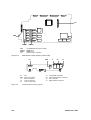
1.2. Notebook Model Number Definition
The following figure contains a summary of the available models in the 67x Series.
670 XX - X X X
1-2
Code
0
1
2
3
4
5
6
7
8
9
A
B
C
D
E
F
G
H
I
J
K
L
M
N
P
Q
R
S
T
U
V
W
X
Y
Z
Country
Reserved
USA
W Europe
Latin AM
Reserved
Reserved
Reserved
Reserved
Reserved
Reserved
Reserved
Belgium
Taiwan
Denmark
Finland
France
Germany
Asia
Italy
Japan
Korea
Latin AM
Dutch
Norway
Portugal
Australia
Reserved
Spain
Reserved
UK
Reserved
Sweden
Sws/Ger
Sws/Fra
Reserved
KB
PWR cord
Manual
US
US
US
US(110v)
EUR(220v)
US(110v)
English
English
Multi-language
BEL
CHN
US
SWD
FRA
GER
US
ITA
JPN
US
SPN
US
NOR
PORT
US
EUR(220v)
US(110v)
EUR(220v)
EUR(220v)
EUR(220v)
EUR(220v)
US(110v)
EUR(220v)
US(110v)
US(110v)
US(110v)
EUR(220v)
EUR(220v)
EUR(220v)
AUS(250v)+UK(250v)
Multi-language
English
Multi-language
Multi-language
Multi-language
Multi-language
English
Multi-language
English
English
Multi-language
Multi-language
Multi-language
Multi-language
English
SPN
EUR(220v)
Multi-language
UK
UK(250v)
Multi-language
SWD
GER
FRA
EUR(220v)
EUR(220v)
EUR(220v)
Multi-language
Multi-language
Multi-language
Code
0
1
2
3
4
5
6
7
8
CPU
w/o
MMX-150
MMX-150
MMX-166
MMX-166
MMX-150
MMX-150
MMX-166
MMX-166
Batt
w/o
NiMH
Li-Ion
NiMH
Li-Ion
NiMH
Li-Ion
NiMH
Li-Ion
Code
0
1
2
3
4
5
6
Preload
w/o
Win95
Win95
WFW3.11
WFW3.11
NT4.0
NT4.0
HDD
w/o
1.6GB
2.1GB
1.6GB
2.1GB
1.6GB
2.1GB
Code
D
DX
LCD
12.1" DSTN
12.1" TFT
CD-ROM
10X
10X
10X
10X
10X
10X
10X
10X
10X
Memory
16MB
16MB
16MB
16MB
16MB
32MB
32MB
32MB
32MB
General Description
1.3. Product Overview
The Extensa 67x Series follows the 65x Series. The Extensa 67x notebook series is similar in
construction and appearance, has similar operating controls and indicators and uses the same
software. It uses a similar startup self test program (described in detail in Chapter 5 of this manual).
There are differences at the board level which affect assembly/disassembly as described in Chapter
6 of this manual. There are also differences in Field-Replaceable Units (FRUs), particularly the
Printed Circuit Boards, so separate FRU lists and logic diagram sets are provided in the appendices.
Table 1-1 summarizes some of the major differences between the 67x Series and the 65x Series
Notebook Computers.
Table 1-1
Feature Comparison for 65x/67x Series Notebooks
Feature
65x Series
67x Series
133 MHz Pentium
150/166 MHz Pentium with MMX Technology
Standard Onboard Memory
16 MB
16 MB
Maximum Expandable
Memory
80 MB
80 MB
1.3 GB or 1.6 GB
1.6 GB or 2.1 GB
DSTN or TFT
DSTN or TFT
CPU
HDD
LCD Display Type
(new 12.1-inch DSTN and TFT LCDs)
2 MB
2 MB
4 Mb/s FIR
4 Mb/s FIR
Internal Microphone
Yes
Yes
Port Replicator Option
Yes
Yes
Video Memory
Infrared Port
The Extensa 67x Series Notebook Computers are large screen, high-performance, multimedia
notebooks powered by the Intel® P55CLM Pentium® Processor Chip (150/166-MHz). Other major
features of the 67x Series include:
•
PCI Bus architecture
•
16 MB (Extended Data Out) memory onboard
•
2 MB video memory
•
Fast video graphics accelerator
•
0-Volt Suspend, 5-Volt Suspend and Standby power saving modes
•
No-reboot setup function
•
STN or TFT color display (Model Dependent)
•
16-bit stereo audio
•
Fast infrared communication
Service Guide
1-3
•
Duracell NiMH (Nickel-Metal-Hydride) or optional Li-Ion (Lithium-Ion) battery pack
•
1.6/2.1 GB (or higher) capacity hard disk drive with Local Bus
•
Internal touchpad pointing device
•
Small, lightweight AC adapter
•
Modular bay for expansion
•
PS/2 port for connecting an external keyboard, numeric keypad, or mouse
•
9-pin serial port for connecting external devices such as a modem or mouse
•
Simultaneous display with external CRT
•
•
•
•
One Type III or two Type II/I Cardbus PC Card slots; lower slot accepts Zoomed Video port
enabled PC cards
Parallel port with EPP and ECP for connecting to a printer or the floppy disk drive module
8 MB, 16 MB and 32 MB EDO 64-bit type small outline dual inline memory module (soDIMM)
upgrades
Advanced PCI Card slot for installing a feature upgrade option
CD-ROM Drive or
Floppy Disk Drive
Figure 1-2
1-4
External Features
General Description
1.3.1 Video Display Features
The Extensa 67x Series Notebooks contain large screen internal LCD displays and can
simultaneously drive an external CRT (SimulSCANTM mode). On all Extensa models, the LCD
screen brightness, contrast, video mode of operation, etc. are adjustable from the keyboard as
described in Paragraph 1.2.2.3.
1.3.1.1 Internal LCD
The Extensa 67x Series Notebooks contain one of the following LCDs (model dependent):
•
12.1-Inch DSTN display
•
12.1-Inch TFT display
1.3.1.2 External CRTs
The Extensa 67x Series Notebooks are equipped with a 15-pin SVGA connector that can drive an
external CRT (either alone or simultaneously with the internal LCD).
When the notebook is set to the SimulSCAN mode, a minimum resolution of 800 x 600 x 256 colors
is supported. When operating in the External CRT Mode, resolutions up to 1280 x 1024 x 256 colors
are supported.
1.3.1.3 Display Hot Key Sequences
The display mode of operation (LCD only, Simultaneous LCD and external CRT and external CRT
only modes) is keyboard-selectable using the following hot key sequences.
•
Fn-Up Arrow and Fn-Down Arrow - control LCD screen brightness (higher brightness setting
uses more battery energy)
•
Fn-Right Arrow - lightens the LCD screen contrast
•
Fn-Left Arrow - darkens the LCD screen contrast
•
Fn-F12 - alternates between display modes (LCD, External CRT or both)
•
Fn-F11 - turns off the LCD backlight; pressing any key turns the LCD backlight on.
Note:
In addition to the hot keys that control the notebook display functions, there are several
other hot key functions that control other notebook functions such as turning the
Touchpad on/off, etc. For these sequences, refer to Chapter 3.
1.3.2 Software Features
As a standard feature, the Extensa 67x notebooks are factory loaded with Windows 95, Windows
NT or Windows for Workgroups software to allow the user to configure the notebook’s operating
system environment as summarized in Table 1-2.
Service Guide
1-5
Table 1-2
Operating System Environments
Operating System
Description
Windows 95
Supports both desktop and mobile operation with Plug and Play capabilities and
Advanced Power Management; multimedia options, and choice of wallpaper to
customize different computer resources; variety of device drivers including C&T®
65550, ESS 1878 Sound Device Drivers, PC-Card Bus Socket Services and
Card Services Device Drivers, TranXit™ Communication Utility for parallel/serial
and FIR (IrDA™), 0V Suspend Utility PhDisk and SafeOFF Utility
Windows NT
Supports both desktop and mobile operation with Advanced Power Management;
multimedia options, and choice of wallpaper to customize different computer
resources; variety of device drivers including C&T® 65550, ESS 1878 Sound
Device Drivers, PC-Card Bus Socket Services and Card Services Device Drivers,
TranXit™ Communication Utility for parallel/serial and FIR (IrDA™)
Windows/DOS 6.22
This environment has some limitations in the Plug and Play area; includes
utilities and various device drivers including C&T® 65550, ESS 1878 Sound
Device Drivers, PC-Card Bus Socket Services and Card Services Device Drivers,
and TranXit™ Serial Infrared (IrDA™) Device Drivers, etc.
1.3.3 67x Series External Ports
The Extensa 67x Series notebooks have a variety of external ports (connectors) for the desktop
environment as shown in Figure 1-3 and summarized in Table 1-3.
Figure 1-3
1-6
External Ports
General Description
Table 1-3
External Ports
Port Assignment
Description
External VGA Port
15-Pin Female connector used to attach an external SVGA monitor to the
notebook.
Serial Port
9-Pin Male connector used to attach an RS-232 serial device to the notebook.
Parallel/Floppy Port
25-Pin Female connector used to attach a bidirectional printer or an external floppy
disk drive (requires special cable for use with floppy disk drive).
PS/2® Port
6-Pin Circular connectors used to attach external keyboard/mouse devices to the
notebook.
DC-IN Connector
Power in connector used to attach the output of the AC adapter to the notebook.
Fast Infrared Port
Fast Infrared Port (4 M/b) used for wireless communications between the notebook
and an FIR-equipped device such as keyboard, another notebook, printer, etc.
Audio In/Out, Mic In
Jacks
Provide for input of external sound source or audio output to drive external
speakers
Expansion Bus
120-Pin PCI Bus that supports an external Port Replicator
1.3.4 Standard Peripheral Devices
As standard features, the Extensa notebooks include a user-removable internal hard drive, a 3.5inch floppy disk drive, a CD-ROM drive and built-in point touchpad (mouse device). The FDD or
CD-ROM drives is user removable.
1.3.5 Expansion Capabilities
The Extensa 67x Series Notebooks are designed with a variety of expansion features that permit
substantial functionality and performance upgrades over the life of the product. The expansion
capabilities built into the notebook are summarized in Table 1-4 and described in greater detail in the
following paragraphs.
Table 1-4
Expansion Features Summary
Expansion Feature
Description
CD-ROM Drive
Reads from Audio CD, Photo CD or CD ROM
3.5-inch Diskette Drive Module
Provides convenient storage on a removable disk format
Memory Expansion Features
Main memory can be expanded from 16 MB to a maximum of 80 MB
using soDIMM modules (8 MB, 16 MB or 32 MB configurations).
Flash ROM (hardware feature)
Permits new versions of BIOS to be downloaded into Flash ROM without
physically having to replace the ROMs
PCMCIA Slots
Allows installation of any optional PCMCIA device such as speakerphone
modems, Ethernet® cards, and full motion video cards.
Desktop Connectivity Ports
Permits attaching a variety of external devices to the notebook including
external CRTs, keyboards, mouse devices, modems, printers, etc.
Port Replicator
Device that attaches to the Expansion Bus and provides the connectivity
for the desktop environment. Removing and replacing the notebook
from/to the desktop environment is greatly simplified using the Port
Replicator option.
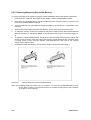
1.3.6 PCMCIA Card Options
The Notebook contains an onboard PCMCIA Controller and two 64-pin sockets that can accept up
to two credit-card size (14.5 mm) Type I or Type II PCMCIA option cards or one Type III card. The
Service Guide
1-7
PCMCIA Card options install on the left side of the notebook (Figure 1-5) and are removed using the
PCMCIA Release Buttons.
Figure 1-5
1-8
Installing PCMCIA Card Options
General Description
1.4. Standard Test Features
The Extensa 67x Series Notebook Computers use modular design and built-in test features to
reduce the mean time to repair.
1.4.1 Power On Self Test
The Extensa line of notebook computers contain a BIOS-resident, Power On Self Test (POST) that
automatically performs a test of memory and all major circuits each time the computer is powered
up. In the event of a failure, the computer displays a descriptive error message and issues a series
of coded beeps (in case the display subsystem is not functioning). If self test completes normally,
the computer displays the amount of memory tested, loads the Operating System and Windows
environment.
Service Guide
1-9
1.5. Extensa 67x Series Specifications
General specifications for the Extensa 67x Series Notebooks are provided in Table 1-5.
Table 1-5
Specifications
Characteristic
CPU
Model 670
Pentium P54CSLM, 133 MHz; 3.1 Volt,
Internal Hard Disk Drive
Disk Storage Capacity
Average access time
Throughput
1.6 GB, 2.1 GB
12 ms or less
11+ Million I/O's per second
DRAM Memory
Size
Maximum Expansion Size
16 MB DRAM, 60-ns, EDO-type
80 MB
Flash ROM
256 KB
FDD
Media Bay Modular
Disk Storage Capacity:
Disk Size
Drive Height
Mode
1.44 MB
3.5-inch disk
12.5 mm
Choice of 720 KB/1.2 MB or 1.44 MB
CD-ROM Drive
Media Bay
LCD Display
12.1-inch DSTN SVGA or 12.1-inch TFT SVGA
Software
Windows 95, Windows NT, or Windows for Workgroups 3.11
Internal Keyboard
84/85-Key, PS/2 and AT-Compatible
Numeric Keypad
Key Travel
Localization Features
Key Spacing
Embedded
3 mm
All major International Language Configurations
19 mm
Built-in Mouse Device
Touchpad built-in to the base of the keyboard (select buttons just below
Touchpad)
Video Subsystem
LCD Aspect Ratio
Emulations
Video Memory Size
Video Bus
LCD Resolution
LCD Characters/Line
LCD Lines/Screen
LCD Brightness Control
1-1
SVGA
2 MByte
32 bits
640x480 pixels bit-mapped at 16.77 million colors; 600x800 at 65K colors
80
25
Function hot key brightness and contrast control and SimulSCAN control
External CRT Monitor Interface
Connector Type
Monitors Supported
1-10
15-Pin, female, D-type connector
640 x 480 with 16.7 million colors on CRT
800 x 600 with 16.7 million colors on CRT
1024 x 768 with up to 64K colors on CRT
1280 x 1024 with 256 colors on CRT (interlaced)
General Description
Table 1-5
Specifications
Characteristic
Model 670
RS-232-D Serial Port:
9-Pin, male, sub-D-type connector
Method
Type
Bits per second
Parity
EIA RS-232-D
Asynchronous transmission
110, 200, 300, 600, 1200, 2400, 4800, 9600, 19200
Odd, even, mark, space
Data check: odd, even
READY/BUSY, DC1/DC3
Transmit/Receive
Line control
Data word
16550 UART Support
Selectable Serial Port
(BIOS Setup)
7- or 8-bit
Yes
COM1(IRQ4, 3F8h)
COM2(IRQ3, 2F8h)
COM3(IRQ4, 3E8h)
COM4(IRQ4, 2E8h)
Disable
Parallel Port
EPP/ECP Bidirectional
Connector Type
FDD Support
Selectable Parallel Port
(BIOS Setup)
25-Pin, DB-25 Connector
Yes, Hot Pluggable & Auto-Detection if BIOS Setup is set to 1.44 MB
LPT 1 (IRQ5, 278h)
LPT 2 (IRQ7, 378h)
Disable
Fast I/R Port
Yes
Transfer Data Rate
Transfer Distance
Standard
4M bit/sec
100cm
IrDA
Expansion Bus Port
128-pin
Service Guide
1-11
1.6. Regulatory Agency Approvals
All Extensa 67x Series products meet the following regulatory agency standards:
•
Underwriter’s Lab (UL) Standard 1950 (safety)
•
Canadian Standards Association (CSA) Standard 950 or CUL (safety)
•
FCC CFR 47, Part 15, Subpart B, FCC Level B (Emissions)
•
Canadian Department of Communications (DOC) ICES, Class B (Emissions)
•
VDE- EN60950 (Safety)
•
EN 50082-1 (Immunity: ESD, RFI, EFT, and Surge)
•
EN 50081-1 (Emissions: RFI, EMI, Harmonics, and Flicker)
•
Approval Marks: UL, CUL, VDE, FCC, ICES, and CE
1-12
General Description
Chapter
2
Installation
2.1. Introduction
This chapter contains unpacking and preparation for use instructions for the Extensa 67x Series
Notebook Computers. This includes:
•
Removing the computer and all manuals, options and accessories from the shipping
container(s)
•
Installing Internal Notebook Options
•
Installing External Notebook Options
•
Installing Battery Packs
•
Installing Desktop Devices
•
Installing the AC Adapter
•
Checking Out the System
•
Configuring the System
•
Making Backups of System Software
•
Loading Application Software
2.2. Unpacking Instructions
Unpack the computer using the following instructions:
1.
Carefully cut the tape that seals the top flap of the shipping carton.
2.
Remove the computer and the accessories Carton from the main shipping carton.
3.
Remove all protective coverings from the computer.
4.
Open the accessory box; remove the contents.
Note:
Save the two shipping containers and packaging for later reuse.
Service Guide
2-1
2.3. Installing Internal Notebook Options
If you have no internal options to install at this time, skip to Paragraph 2.4. Otherwise, continue with
Paragraph 2.3.1.
2.3.1 Installing Main Memory Expansion (Optional)
Main memory on the 67x Series Notebooks can be expanded using EDO Small Outline Dual Inline
Memory Modules (EDO soDIMMs). These modules currently are available in 8 MB, 16 MB or 32 MB
sizes and install in expansion memory slots on the Main Board accessed through the Memory
Expansion Door on the bottom of the notebook. The installation process consists of the following
steps:
Caution: The EDO soDIMM module option contains components that are sensitive to static
electricity. When handling the module and the internal parts of the computer, protect
against static electricity by using wrist or ankle grounding straps and grounded working
mats. When moving or storing items, use the anti-static bags supplied with the items.
Figure 2-1
Memory Expansion Removal/Replacement
1.
Ensure that the notebook is powered off and the AC adapter disconnected from the AC outlet.
Also, ensure that the battery is out of the unit.
2.
Disconnect any peripheral device interface cables from the external interface connectors and
remove any installed PCMCIA options.
3.
Turn the notebook over and locate the Expansion Memory Access Cover on the bottom of the
notebook.
4.
Remove the screw holding the Expansion Memory Access Cover and remove the cover.
5.
Remove the EDO soDIMM module from its shipping container.
6.
Refer to Figure 2-1. To install an soDIMM module, first align the connector edge of the memory
module with the key in the connector. Insert the edge of the memory module board into the
connector using a rocking motion to fully insert the module. Push downward on each side of the
memory module until it snaps in place.
2-2
Installation
7.
If installing a second soDIMM, repeat Step 6.
8.
Reinstall the Expansion Memory Access Cover using the screw removed in Step 4.
9.
Replace the Keyboard Assembly and any components previously removed. Replace the AC
adapter.
10. Power up the notebook and reboot. If all of the installed memory is not recognized, try
reseating the soDIMM module(s) and rebooting.
Note:
After installing expansion memory in your notebook, you must run the PHDISK utility in
order for the Save-To-Disk or 0V Suspend functions to operate correctly.
2.3.2 Setting up the Software
After installing expansion memory, perform the following procedure:
1.
Run PHDISK.
•
In Windows 95
•
1.
From the Taskbar, select Start, then Shut Down.
2.
Select the "Restart the Computer in MS-DOS mode" option.
3.
Click on Yes.
4.
Type PHDISK/C/F at the DOS prompt.
In Windows for Workgroups and Windows NT
1.
Exit all applications and exit Windows to DOS.
2.
At the DOS command prompt, type PHDISK/C/F. This will create a file which can be
used to save the contents of your memory system when you perform a 0V Suspend
operation
Service Guide
2-3
2.4. Installing External Options
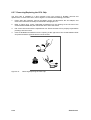
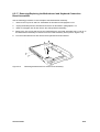
2.4.1 Installing PCMCIA Options
The Notebook has two connector slots for PCMCIA option cards. These two slots can be used to
install one Type III or two Type I/II credit card size PCMCIA option cards. You can install a PCMCIA
(PC card) without turning the computer off.
Use the following procedure to install a PCMCIA option:
1.
Review the installation instructions supplied with the PCMCIA option card(s).
2.
Hold the card at the end opposite the connector pins with the label side up. Insert the card into
an unused slot on the left side of the Notebook.
3.
If the option requires external cabling (e.g. Modem option), connect external cabling at this
time.
Note:
After installation of a PCMCIA option card, Windows 95 displays the New Hardware Found
dialog box to help you configure the new device. To remove a card, click on the PCMCIA
icon; then, press the appropriate PC Card Release Button (or press both buttons for a
Type III device) and remove the option.
Figure 2-2
2-4
Installing PCMCIA Option Cards
Installation
2.5. Installing External Notebook Options
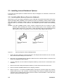
2.5.1 Installing Ext. Keyboard/Mouse/Numeric Keypad
A PS/2 compatible keyboard, mouse or an optional PS/2-compatible numeric keypad may be
installed on the notebook via the mouse connector on the left rear port as shown in Figure 2-3.
Figure 2-3
Service Guide
PS/2 Port Pinouts
2-5
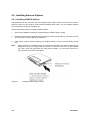
2.5.2 Installing an External Parallel Printer or Floppy Drive
The Notebook is equipped with an external, bidirectional, ECC/EPP compatible, 25-pin parallel
printer port. The connector pinouts and connector location are shown in Figure 2-4. When used with
a special cable, an external floppy disk drive may also be attached to the notebook via the parallel
port. When a floppy disk drive is connected to the parallel port, the floppy disk drive in the Modular
Bay is disabled, if present.
Figure 2-4
2-6
Parallel Port Pinouts
Installation
2.5.3 Installing an External Serial Port Device
The notebook contains an external RS-232 serial port with a 9-pin, male DB-9 connector as shown
in Figure 2-5 (25-pin cables require the use of an adapter for use with the 9-pin port). The serial
ports are used to interconnect such devices as:
•
External Modem
•
Serial Mouse
•
Serial Printer
•
Any device that uses an RS-232 interface
Caution: Never connect a parallel device to a serial port or a serial device to a parallel port or video
port; this may cause damage to the notebook and/or external device. If you are uncertain
of what type connector the external device has, refer to the technical manual for the
external device.
Figure 2-5
Service Guide
Serial Port Pinouts
2-7
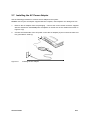
2.5.4 Installing an External VGA Monitor
The notebook contains an external CRT port that can drive one of a variety of monitor resolutions
and colors as summarized in Table 1-9. The associated connector location and pinouts are shown in
Figure 2-6.
Figure 2-6
External VGA Pinouts
Use the following procedure to install an external monitor:
1.
Turn off power to both the notebook and monitor.
2.
Connect the 15-pin external VGA cable from the monitor to the VGA connector on the notebook
computer (refer to Figure 2-6).
3.
Power up the notebook computer first; then turn on power to the monitor.
4.
Setup the notebook display mode for LCD only, simultaneous LCD and CRT or CRT only using
the BIOS setup utility or hotkey (see Paragraph 1.2.2.3).
5.
Install the correct driver if required (refer to the Monitor Installation Instructions supplied by the
CRT vendor).
2-8
Installation
2.5.5 Installing the Security Lock Option
Use the following procedure to install the optional Kensington® security lock.
1.
Unpack the Kensington Lock Kit.
2.
Secure the loop end of the lock to a permanent fixture located such that the notebook can be
installed in a desired location.
3.
Insert the lock into the slot on the left side of the computer.
4.
Rotate the key to its locked position and remove the key.
This completes the options installation subsection.
Service Guide
2-9
2.6. Battery Pack Installation
First turn off the computer and disconnect the AC adapter if attached to the computer; then follow
these steps:
1.
Unlatch the battery compartment door (right front corner of the unit) as shown in Figure 2-7.
2.
Slide the battery compartment door out slightly and then swing the door outward as shown in
Figure 2-7.
3.
If changing batteries, grasp the loop attached to the battery and pull the battery out of the
compartment.
4.
Look for label "THIS SIDE UP" and insert the battery with label up until it snaps in place; then
close the battery compartment door.
Figure 2-7
2-10
Battery Pack Installation
Installation
2.7. Installing the AC Power Adapter
Use the following procedures to connect the AC adapter to the system:
Caution: Use only the AC adapter supplied with the computer; other adapters can damage the unit.
1.
Remove the AC adapter from the packaging. Connect the round coaxial connector supplied
with the notebook to the DC IN power receptacle on the left rear of the notebook as shown in
Figure 2-8 (a).
2.
Connect the female side of the AC power cord to the AC adapter (b) and connect the male end
to a grounded AC outlet (c).
Figure 2-8
Service Guide
Installing the AC Adapter
2-11
2.8. Initial System Checkout
After you've installed all internal options and external cabling, you're ready for system checkout and
software configuration.
To check out the system, press the power button on the left side of the notebook which initiates self
test. During self test execution, the computer checks the operation of all key hardware including
memory and CPU (and displays copyright and version number data during test execution).
Upon successful conclusion of self test, the computer automatically loads its operating system and
windows environment. If self test fails to complete and an error message is displayed, try powering
down the computer for a couple of minutes and turning power back on to repeat self test. If the error
message persists, refer to Chapter 5 for troubleshooting information.
2.9. Making Backups of System Software
Immediately after completion of the installation procedures, make backups of all software. In the
event of a disk problem, restore the system using the System Files Recovery disk and the set of
backup disks.
Note:
2-12
Refer to the Extensa Series Notebook Computer User’s Guide for additional information.
Installation
&KDSWHU
Operating Instructions
3.1. Introduction
This chapter contains a summary of notebook operating procedures useful for maintenance
operations. For additional detail, refer to the Extensa Series Notebook Computer User's Guide
supplied with the notebook.
3.2. Controls/Indicators
The operating controls and indicators for the 67x Series Notebooks are identical (refer to Figure 31). A brief description of the controls and indicators is provided in the following paragraphs.
Disk Media
LED
Battery
Charging
LED
Caps
Lock
LED
Num
Lock
LED
Power/Battery Low
Indicator
Standby Mode
Indicator
Power Button
Figure 3-1
67x Operating Controls and Indicators
3.2.1 Power On/Off Switch
The notebook contains an alternate action power button located on the right side of the notebook as
shown in Figure 3-1. On the first button depression, power is turned on to the notebook. On the
second depression, power is turned off.
3.2.2 Notebook LEDs
The notebook contains four front indicator LEDs and two right side LEDs as shown in Figure 3-1
and described in Table 3-1.
Table 3-1
Service Guide
Indicators
3-1
Indicator Light
Description
Power/Battery-low
Lights when the system is on and there is power to the system.
Flashes when the battery power is low. Connect a powered AC adapter to the
computer as soon as possible.
Standby Mode
Lights when the computer is in Standby mode.
Flashes when the computer is in 5V Suspend mode.
The computer enters Standby mode if the Standby hot key (Fn+F4) is pressed
or the STANDBY TIMEOUT parameter in Setup is enabled and expires.
The computer enters 5V Suspend mode when you press the 5V Suspend hot
key (Fn+F3) or the 5 VOLT SUSPEND TIMEOUT parameter in Setup is
enabled and expires, or the display is closed.
Disk Media
Lights when the computer writes to or reads from the hard disk drive, or reads
from the CD-ROM drive.
Battery Charging
Lights when a powered AC adapter connected to the computer is charging the
battery.
Flashes when there is a problem with the battery or the battery is not
recognized by the smart charger.
Turns off when there is no battery or the battery is fully charged.
Caps Lock
Lights when the caps lock function is toggled ON using the Caps Lock key.
Num Lock
Lights when the embedded numeric keypad is toggled ON using the Num
Lock hot key (Fn+F7)
3.2.2.1 Hot Key Sequences
Table 3-2 contains a summary of hot key sequences useful when performing maintenance
operations.
Table 3-2
Summary of Notebook Hot Key Sequences
Function
Key Sequence
Increase LCD screen brightness
Fn-Up Arrow
Decrease LCD screen brightness
Fn-Down Arrow
Lighten LCD screen contrast
Fn-Right Arrow
Darken the LCD screen contrast
Fn-Left Arrow
Alternate between display modes (LCD, Ext.l CRT or both)
Fn-F12 or Ctrl-Alt-F12
Enter 0V Suspend Mode
Fn-F2 or Ctrl-Alt-F2
Exit 0V Suspend Mode
Press Power Button
Enter 5V Suspend Mode
Fn-F3 or Ctrl-Alt-F3
Exit 5V Suspend Mode
Press any key
Enter Standby Mode
Fn-F4
Resume from Standby Mode
Press any key
Toggle speaker output on/off
Fn-End or Ctrl-Alt-S
Enter BIOS Setup (during POST)
F2
Numeric Lock
Fn-F7
Turn off the LCD backlight
Fn-F11
Turn on the LCD backlight
Press any key
Stop a command or application
Ctrl-Pause
Resume a command or application
Press any key
Send the contents of the screen to the printer
Shift-PrtSc
3-2
Operating Instructions
Table 3-2
Summary of Notebook Hot Key Sequences
Function
Key Sequence
Sets the notebook to echo keystrokes to the printer; prints a line
when you press Enter; continues until you press Ctrl-P
Ctrl-P
Enable/disable the internal keypad
Fn-T
Toggle Scroll Lock function on/off
Fn-F6
Bring up the setup screen anytime
Fn-F1 or Ctrl-Alt-F1
Warm boot
Ctrl-Alt-Del
Start
Windows logo key
Activate next taskbar button
Windows logo key-Tab
Explore the computer
Windows logo key-E
Find files
Windows logo key-F
Minimize all
Windows logo key-M
Display run dialog box
Windows logo key-R
Display the application's context menu
Application key
Service Guide
3-3
Chapter
4
Theory of Operation
4.1. Introduction
This chapter contains a general block diagram theory of operation description of the Extensa 67x
Series Notebook Computers.
Note:
Various internal components may change on future models and busses/bus speeds are
subject to change.
4.2. Notebook Functional Overview
The Extensa 67x Series Notebook consist of:
•
System Processor - implemented on the Motherboard Assembly
•
Memory Subsystem - implemented on the Motherboard Assembly
•
Processor/Memory/I/O Control - implemented on the Motherboard Assembly
•
Keyboard Subsystem - implemented on the Motherboard and the Keyboard Assemblies
•
Video Subsystem - implemented on the Motherboard and on the LCD Display Assembly
•
Sound Subsystem - implemented on the Motherboard Assembly.
•
•
•
•
Touchpad Mouse Subsystem- implemented on the Touchpad assembly and on the
Motherboard Assembly
Hard Disk Drive Subsystem - implemented on the Motherboard Assembly and the Hard Disk
Drive Assembly
Floppy Disk Drive Subsystem - implemented on the Motherboard and Floppy Disk Drive
Assembly
Power Subsystem - implemented on the Charger Board, Inverter Board, battery packs, and AC
adapter
4.2.1 System Processor
The System Processor function for the notebook is implemented on the Motherboard in the form of
an Intel Pentium P55-C Superscalar 586 Processor Chip. The processor operates in conjunction
with RAM and ROM Memory and other control logic to process software instructions (BIOS, DOS,
Windows, and applications). The processor communicates with the hard disk drive and the memory
components using high speed busses.
The Processor also interacts with other hardware logic to provide the power savings features for the
notebook. These features include controlling CPU clock speeds, reducing clock speeds whenever
possible (e.g. when performing floppy disk drive accesses), powering down unused devices, etc.
Service Guide
4-1
4.2.2 Memory Subsystem
The memory subsystem comprises the following components:
•
Main memory
•
L2 Secondary Memory (cache)
•
Flash ROM
The Extensa Series uses fast Extended Data Out (EDO) DRAM for main and video memory and
high-speed synchronous, pipelined burst SRAM for L2 cache memory. Main BIOS and Video BIOS
are stored in Flash ROM.
4.2.2.1 Main Memory
The 67x Series Notebooks come standard with 16 MB main memory, expandable to 80 MB.
Memory expansion accommodations are provided via standard soDIMM connectors on the bottom
of the Motherboard Assembly.
4.2.2.2 Flash ROM
All versions of the Extensa notebook family use a "Flash" ROM that contains both the main system
BIOS and the VGA BIOS.
The Flash ROM execution is 8 bits wide. However, better performance can be attained by enabling
the Shadow ROM in the CMOS setup routine. When the Shadow ROM is enabled, BIOS is copied
into 32-bit high speed memory system.
4.2.3 Video Subsystem
The video subsystem is implemented on the Motherboard Assemblies.
The notebook contains a built-in 12.1 inch LCD and features simultaneous LCD and external VGA
display.
The video subsystem includes a 2 MB DRAM memory, 32-bit DRAM bus, and separate display and
memory clocks. An additional frame buffer/accelerator DRAM increases the available memory band
width for CPU accesses. The video section also uses additional levels of write FIFOs, a read cache,
page mode DRAM.
4.2.4 Sound Subsystem
The Extensa Series Notebook is equipped with a sound chip set that is Sound BlasterTM and Sound
Blaster Pro compatible. Internal stereo speakers provide the Notebook with sound generation
capabilities. A set of 3.5 mm connectors allow for external microphone and line inputs and
headphone/speaker outputs.
The sound subsystem also includes a variety of sound utilities that combine to provide additional
multi-media functions:
4-2
Theory of Operation
4.2.5 Keyboard Subsystem
The keyboard subsystem, implemented on the Keyboard Assembly and the Motherboard
Assemblies Board, consists of the following major sections:
•
Keyboard Assembly
•
Keyboard Scanner
•
Status LED Interface
4.2.6 Hard Disk Drive Subsystem
The Hard Disk Drive Subsystem, implemented on the Motherboard Board and on the associated
hard disk drive module(s), provides disk storage for all system software and user files.
The notebook is equipped with an 1.6 GB or larger hard disk drive. The hard disk drive also
features built-in power conservation features configured from the standard CMOS Setup Routine. An
Automatic Power Down mode can be selected which powers down the drive motor during periods of
inactivity. An additional level of power conservation may also be selected which powers down the
motor plus all control circuits.
The hard disk drives are factory formatted as a single drive (Drive C:) and are preloaded with
installation versions of Windows 95, Windows NT or Windows for Workgroups.
4.2.6.1 Hard Disk Drive Power Management
Both the internal hard disk drive and the hard disk drive installed in the media bay implement power
savings features. From the CMOS setup routine, an automatic power down mode can be selected
which enables the drive to turn off its motor after a specified period of inactivity. Additional Sleep
modes can direct additional power savings during inactive periods by powering down the control
circuitry.
4.2.7 Floppy Disk Drive Subsystem
The Extensa 67x Series notebooks contain provisions for supporting a Floppy Disk Drive installed
internally or externally connected to the parallel port. The Floppy Disk Drive Subsystem consists of a
Floppy Controller and the Floppy Disk Drive located either in the media bay or external to the
notebook (not both).
The 3.5-inch floppy disk drive can read/write standard 3.5-inch disks (either1.44 MB or 2 MB
capacity). The drive can also read a 720 KB disk (for interchange of data with other computers).
The data transfer rate for the floppy disk drive is 500 Kbits per second for high-density disks and 250
Kbits per second for double-density disks.
4.2.8 Power Subsystem
The notebook is equipped with a software/hardware monitored/controlled Power Subsystem that
minimizes battery usage for prolonged battery operation and automatically recharges the batteries
when the notebook is used with an AC adapter.
Service Guide
4-3
4.2.8.1 AC Power Adapter
The computer is equipped with a universal AC power adapter that converts AC voltage into DC
voltage (approx. 46 Watts of power) used to operate the notebook and charge the batteries. The
specifications for the AC adapter include:
•
Input Voltage: 100 to 250 VAC
•
Input Current: Approximately 1.5 Amps
•
Input Frequency: 50 to 60 Hz
4.3. Detailed Circuit Theory
The remainder of this chapter provides chip-level circuit description for the Extensa Series
Notebooks.
4.3.1 Major Components
Table 4-1 shows a listing the of the major components used in the Extensa Series Notebooks.
Table 4-1
Major Chips List
Component
Vendor
Description
M1521
Acer
PCI, cache and memory controller (Host-PCI
Bridge)
M1523
Acer
System controller chip (PCI-ISA Bridge)
M6377
Acer
Power management controller
65550
C&T (Chips & Technology)
Video controller
TI1130
Texas Instruments
PCMCIA controller
NS87336VJG
NS (National Semiconductor)
Super I/O controller
ES1878
ESS Technology
Audio controller
T62.045.C.00
Ambit
Charger board
DAC-07B008
Delta
LCD inverter
DC-R05
Delta
LCD ID board
M38802
Phoenix
Keyboard encoder and decoder
4-4
Theory of Operation
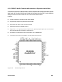
4.3.2 System Architecture
Figure 4-1 shows the Extensa system architecture. The remainder of this chapter provides a
detailed description of the major chips used in the Extensa Notebooks.
586
CPU
CPU Bus
SRAM
DRAM
M1521
UMA
G raphic
controller
BGA
PCI Bus
IDE Master
CD
M1523
USB connector
HDD
ISA Bus
Aladdin III System Block Diagram
Figure 4-1
Service Guide
Extensa 670 System Architecture Diagram
4-5
4.3.3 ALI M1521 (PCI, Cache and Memory Controller)
The ALADDIN-III consists of tow chips, ALI M1521 and M1523 to give a 586 class system the
complete solution with the most up-to-date feature and architecture for the new multimedia/
multithreading operating system. It utilizes the BGA package to improve the AC characterization,
resolves system bottleneck and make the system manufacturing easier. The ALADDIN-III gives a
highly-integrated system solution and a most up-to-date system architecture including the UMA,
ECC, PBSRAM, SDRAM/BEDO and multi-bus with highly efficient, deep FIFO between the buses,
such as the HOST/PCI/ISA dedicated IDE bus.
The M1521 provides a complete integrated solution for the system controller and data path
components in a Pentium-based system. It provides a 64-bit CPU bus interface, 32-bit PCI bus
interface, 64/72 DRAM data bus with ECC or parity, secondary cache interface including pipeline
burst SRAM or asynchronous SRAM, PCI master to DRAM interface, four PCI master arbiters and a
UMA arbiter. The M1521 bus interfaces are designed to interface with 3V and 5V buses.
The chip pinouts are provided in Figure 4-2.
4-6
Theory of Operation
Figure 4-2
Service Guide
M1521 Pin Assignments
4-7
4.3.4 ALI M1523 (PCI, Cache and Memory Controller)
The M1523 is a bridge between PCI and ISA bus, providing full PCI and ISA compatible functions.
The M1523 has Integrated System Peripherals (ISP) on-chip and provides advanced features in the
DMA controller. This chip contains the keyboard controller, real-time clock and IDE master
controller. This chip also supports the Advanced Programmable Interrupt controller (APIC)
interface.
One eight-byte bidirectional line buffer is provided for ISA/DMA master memory read/writes. One
32-bit wide posted-write buffer is provided for PCI memory write cycles to the ISA bus. It also
supports a PCI to ISA IRQ routing table and level-to-edge trigger transfer.
The chip has two extra IRQ lines and one programmable chip select for motherboard Plug and Play
functions. The interrupt lines can be routed to any of the available ISA interrupts.
The on-chip IDE controller supports two IDE connectors for up to four IDE devices providing an
interface for IDE hard disk and CD-ROMs. The ATA bus pins are dedicated to improve the
performance of IDE master.
The M1523 supports the Super Green feature for Intel and Intel compatible CPUs. It implements
programmable hardware events, software event and external switches (for suspend/turbo/ring-in).
The M1523 provides CPU clock control (STPCLKJ). The STPCLKJ can be active (low) or inactive
(high) in turn by throttling control.
A simplified block diagram of the M1523 chip is shown in Figure 4-3 and the associated pinouts are
provided in Figure 4-4.
M1523 Block Diagram
PWG
CPURST
RSTDRV
OSC14M
PCICLK
CBEJ[3:0]
AD[31:0]
FRAMEJ
TRDYJ
IRDYJ
STOPJ
DEVSELJ
SERRJ
PAR
PHOLDJ
PHLDAJ
FERRJ
IRQ[15:14]
IRQ[11:3]
INTAJ/M1II
NTBJ/S0
INTCJ/S1
INTDJ/S2
IGNNEJ
INTR
NMI
A20MJ
USBCLK
USBP[11:10]
IDRQ[0:1]
IDAKJ[0:1]
IDERDY
IDEIORJ
IDEIOWJ
IDESCS3J
IDESCS1J
IDEPCS3J
IDEPCS1J
IDE_A[2:0]
IDE_D[15:0]
Figure 4-3
4-8
Clock & Reset
PCI BUS
Interface
UNIT
PCI
Arbiter
Interface
ISA
Interrupt
UNIT
DATA
Buffer
Control
Address
Buffer
Decoder
PCI
Interrupt
UNIT
CPU
Interface
USB
Interface
(reserved)
PCI
IDE
Master
Interface
ISA BUS
Interface
UNIT
PMU or APIC
Interface
Timer
UNIT
SD[15:8]
XD[7:0]
SA[19:0]
SBHEJ
LA[23:17]
IO16J
M16J
MEMRJ
MEMWJ
AEN
IOCHRDYJ
NOWSJ
IOCHKJ
SYSCLK
BALE
IORJ
IOWJ
SMEMRJ/LMEGJ
SMEMWJ/RTCAS
EXTSW
STPCLKJ
SPKR
MISC.
Logic
SIRQI
XDIR
SPLED
ROMCSJ
REAL
Time
Clock
SIRQII
RTC32KI
RTC32KII
PS2/AT
Keyboard
Controller
DMA
Refresh
UNIT
KBINH/IRQ1
KBCLK/KBCSJ
KBDATA
MSCLK
IRQ12/MDATA
DREQ[7:5]
DREQ[3:0]
DACKJ[7:5]
DACK2J/3J
TC
REFSHJ
M1523 Chip Simplified Block Diagram
Theory of Operation
1
2
3
4
5
6
7
8
9
10
11
12
13
14
15
16
17
18
19
20
21
22
23
24
25
26
27
28
29
30
31
32
33
34
35
36
37
38
39
40
41
42
43
44
45
46
47
48
49
50
51
52
Figure 4-4
Service Guide
Vss
BALE
SA2
SA1
SA0
SBHEJ
M16J
LA23
IO16J
LA22
IRQ10
LA21
IRQ11
VDD/BAT
RTC32KII
RTC32KI
PWG
LA20
LA19
IRQ15
LA18
IRQ14
LA17
MEMRJ
DREQ0
Vss
MEMWJ
DACK5J
SD8
DREQ5
SD9
DACK6J
SD10
DREQ6
SD11
DACK7J
SD12
DREQ7
SD13
VDD
SD14
SD15
OSC14M
SIRQI
SIRQII
USBCLK
DACK0J
DACK1J
CPURST
SMIJ
STPCLKJ
Vss
ALi
M1523
VDD
IRQ12
MSCLK
KBDATA
KBCLK/KBCSJ
KBINH/IRQ1
IDESCS3J
IDESCS1J
IDEPCS3J
IDEPCS1J
IDE_A0
IDE_A2
IDE_A1
IDAKJ1
IDAKJ0
IDERDY
IDEIORJ
IDEIOW J
IDRQ1
IDRQ0
IDE_D0
IDE_D15
Vss
IDE_D1
IDE_D14
IDE_D2
IDE_D13
IDE_D3
IDE_D12
IDE_D4
IDE_D11
IDE_D5
IDE_D10
IDE_D6
IDE_D9
IDE_D7
VDD
IDE_D8
AD0
AD1
AD2
AD3
AD4
AD5
AD6
AD7
CBEJ0
AD8
AD9
AD10
AD11
VDD
156
155
154
153
152
151
150
149
148
147
146
145
144
143
142
141
140
139
138
137
136
135
134
133
132
131
130
129
128
127
126
125
124
123
122
121
120
119
118
117
116
115
114
113
112
111
110
109
108
107
106
105
M1523 Chip Pinouts
4-9
4.3.5 ALI M6377 (Powre Management Unit)
•
Three operation states
• ON state
• DOZE state
• SLEEP state
•
Programmable DOZE and SLEEP timers
•
Programmable EL timer for backlight control
•
•
Three output pins depending on operation state, each pin is programmable and power
configurable
Provide system activity monitoring, including:
• video
• hard disk
• floppy disk
• serial port
• keyboard
• parallel port
• two programmable I/O groups activity monitor, each group contains 16/8 I/O
addresses
• one predefined I/O group activity monitor
•
Multiple external wake up events from DOZE and SLEEP states:
• External push button
• RTC alarm
•
Two levels battery warning monitor
•
AC power monitoring to disable PMU function
A simplified block diagram of the M6377 Power Management Unit is provided in Figure 4-5. The
chip pinouts are provided in Figure 4-6.
4-10
Theory of Operation
WAKEUP
EVENT
HANDLER
ACTIVITY
MONITOR
STATE
CONTROLLER
EL TIMER
Timebase
PROGRAMABLE
APM TIMER
x 2
BATTERY
MONITOR
BUS
INTERF
ACE
OTHER
Figure 4-5
Service Guide
SMI
HANDLER
GPIO
M6377 Chip Simplified Block Diagram
4-11
Figure 4-6
4-12
M6377 Chip Pinouts
Theory of Operation
4.3.6 C&T 65550 High Performance Flat Panel / CRT VGA Controller
The C&T 65550 of high performance multimedia flat panel / CRT GUI accelerators extend CHIPS’
offering of high-performance flat panel controllers for full-featured notebooks and sub-notebooks.
The C&T 65550 offers 64-bit high performance and new hardware multimedia support features.
High Performance
Based on a totally new internal architecture, the C&T65550 integrates a powerful 64-bit graphics
accelerator engine for Bit Block Transfer (BitBLT), hardware cursor, and other functions intensively
used in graphical user interfaces (GUIs) such as Microsoft Windows™. Superior performance is
also achieved through a direct 32-bit interface to the PCI local bus. The C&T65550 offers
exceptional performance when combined with CHIPS advanced linear acceleration driver
technology.
Hardware Multimedia Support
The C&T65550 implements independent multimedia capture and display systems on-chip. The
capture system places data in display memory (usually off screen) and the displya system places it
in a window on the screen.
The capture system can receive data from either the system bus or from the ZV enabled video port
in either RGB or YUV format. The input data can also be scaled down before storage in display
memory (e.g., from any size larger than 320x240 down to 352x248). Capture of input data may also
be double buffered fro smoothing and to prevent image tearing.
The display system can independently place either RGB or YUV data from anywhere in display
memory into an onscreen window which can be any size and located at any pixel boundary (YUV
data is converted to RGB “on-the-fly” on output). Non-rectangular windows are supported via color
keying. The data can be functionally zoomed on output up to 8x to fit the onscreen window and can
be horizontally and vertically interpolated to scale or zoom artifacts. Interlaced and non-interlaced
data are supported in both capture and display systems.
Versatile Panel Support
The C&T65550 supports a wide variety of monchrome and color Single-Panel, Single-Drive (SS)
and Dual-Panel, Dual-Drive (DD) standard and high-resolution passive STN and active matrix
TFT/MIM LCD and EL panels. For monchrome panels, up to 64 gray scales are supported. Up to
4096 different colors can be displayed on passive STN LCDs and up to 16M colors on 24-bit active
matrix LCDs.
Low Power Consumption
The C&T65550 employs a variety of advanced power management features to reduce power
consumption of the display sub-system and extend battery life. Although optimized for 3.3V
operation. The C&T65550 controller’s internal logic, memory interface, and panel interfaces can be
independently configured to operate at either 3.3V or 5V.
Software Compatibility / Flexibility
The C&T65550 are fully compatible with VGA at the register, and BIOS levels. CHIPS and thirdparty vendors supply fully VGA-compatible BIOS, end-user utilites and drivers for common
application programs.
Service Guide
4-13
The pin diagram is shown in Figure 4-7. Pin names in parentheses (…) indicate alternate functions.
Figure 4-7
4-14
C&T65550 Chip Pinouts
Theory of Operation
A simplified block diagram of the C&T65550 is shown in Figure 4-8.
Video Memory
Memory Controller
Video
Capture
Port
Scaling
Capture
PCI Bus
Figure 4-8
Service Guide
64-bit
Graphics
Engine
YUV to RGB
Color Key Zoom
Bus Interface
Analog
RGB
Digital
RGB
C&T65550 Chip Simplified Block Diagram
4-15
4.3.7 TI1130 PCMCIA Controller
The TI PCI1130 is a high-performance PCI-to-PC Card controller that supports two independent PC
Card sockets compliant with the 1995 PC Card standard. The PCI1130 provides a set of features
that make it ideal for bridging between PCI and PC Cards in both notebook and desktop computers.
The 1995 PC Card standard retains the 16-bit PC Card specification defined in PCMCIA release 2.1
and defines the new 32-bit PC Card, called CardBUs, capable of full 32-bit data transfers at 33 MHz.
The PCI1130 supports any combination of 16-bit and CardBus PC Cards in its two sockets, powered
at 3.3V or 5V as required.
The PCI1130 is compliant with the PCI local bus specification revision 2.1 and its PCI interface can
act as either a PCI master device or a PCI slave device. The PCI bus mastering is initiated during
16-bit PC Card DMA transfers or CardBus PC Card bus mastering cycles.
All card signals are internally buffered to allow hot insertion and removal without external buffering.
The PCI1130 internal data path logic allows the host to access 8-, 16-, and 32-bit cards using full
32-bit PCI cycles for maximum performance. Independent 32-bit write buffers allw fast-posted
writes to improve system-bus utilization.
An advanced CMOS process is used to achieve low system power consumption while operating at
PCI clock rates up to 33 MHz. Several low power modes allow the host power-management system
to further reduce power consumption.
The pin diagrams are shown in Figure 4-9 first for PCI-TO-PC CARD (16-BIT); then Figure 4-10 for
PCI-TO-CARDBUS (32-BIT).
Figure 4-9
4-16
TI1130 Chip PCI-to-PC card (16-bit) Pinouts
Theory of Operation
Figure 4-10
Service Guide
TI1130 Chip PCI-to-CardBus (32-bit) Pinouts
4-17
A simplified block diagram of the PCMCIA Controller is shown in Figure 4-11.
Figure 4-11
4-18
TI1130 Chip Simplified Block Diagram
Theory of Operation
4.3.8 NS87336VJG Super I/O Controller
The PC87336VJG is a single chip solution for most commonly used I/O periherals in ISA< and EISA
based comptuers. It incorporates a Floppy Disk Controller (FDC), two full featured UARTS, and an
IEEE 1284 compatible parallel port Standard PC-AT address decoding for all the peripherals and a
set of configuration registers are also implemented in this highly integrated member of the Super I/O
family. Advanced power management features, mixed voltage operation and integrated SerialInfrared (both IrDA and Sharp) support makes the PC87336 an ideal choice for low-power and/or
portable personal computer applications.
The PC87336 FDC uses a high performance digital data separator eliminating the need for any
external filter components. It is fully compatible with the PC8477 and incorporates a superset of
DP8473, NEC PD765 and N82077 floppy disk controller functions. All popular 5.25” and 3.5” floppy
drives, including the 2.88 MB 3.5” floppy drive, are supported. In addition, automatic media sense
and 2 Mbps tape drive support are provided by the FDC.
The two UARTs are fully NS16450 and NS16550 compatible. Both ports support MIDI baud rates
and one port also supports IrDAs the HP SIR and Sharp SIR compliant signaling protocol.
The parallel port is fully IEEE 1284 level 2 compatible. The SPP (Standard Parallel Port) is fully
compatible with ISA dand EISA parallel ports. In addtion to the SPP, EPP (Enhanced Parallel Port)
and ECP (Extended Capabilities Port) modes are supported by the parallel port.
A set of configuration registers are provided to control the Plug and Play and other various functions
of the PC87336 . These registers are accessed using tow 98-bit wide index and data registers. The
ISA I/O address of the register pari can be relocated using a power-up strapping option and the
software configuration after power-up.
When idle, advanced power management features allow the PC87336 to enter extremely low power
modes under software control. The PC87336 can operate from a 5V or a 3.3V power supply. A
unique I/O cell structure allows the PC87336 to interface directly with 5V external components while
operating from a 3.3V power supply.
Some of the major features include:
•
100% compatible with ISA and EISA architectures
•
Floppy Disk Controller:
• Software compatible with the DP8473, the 765A and the N82077
• 16-byte FIFO (disabled by default)
• Burst and non-burst modes
• Perpendicular recording drive support
• New high-performance internal digital data separator (no external filter components
required)
• Low-power CMOS with enhanced power-down mode
• Automatic media-sense support, with full IBM TDR (Tape Drive Register)
implementation
• Supports fast 2 Mbps and standard 1 Mbps/500 kbps/250 kbps tape drives
•
Parallel Port
• Enhanced Parallel Port (EPP) compatible
Service Guide
4-19
• Extended Capabilitie Port (ECP) compatible, including level 2 support
• Bidirectional under either software or hardware control
• Compatible with ISA and EISA architectures
• Ability to multiplex FDC signals on parallel port pins allows use of an external Floppy
Disk Drive (FDD)
• Includes protection circuit to prevent damage to the parallel port when a connected
printer is powered up or is operated at a higher voltage
•
UARTs:
• Software compatible with the PC16550A and PC16450
• MIDI baud rate support
• Infared support on UART2 (IrDA and Sharp-compliant)
•
Address Decoder
• 6-bit or 10-bit decoding
• External Chip Select capability when 10-bit decoding
• Full relocation capability (no limitation)
•
Enhanced Power Management
• Special configuration registers for power-down
• Enhanced programmable power-down FDC command
• Auto power-down and wake-up modes
• 2 special pins for power management
• Typical current consumption during power-down is less than 10 µA
• Reduced pin leakage current
•
Mixed Voltage support
• Supports standard 5V operation
• Supports 3.3V operation
• Supports mixed internal 3.3V operation with 3.3V/5V external configuration
•
General Purpose Pins:
• 2 pins the Bidirectional Parallel Port, for 2 separate programmable chip select
decoders, can be programmed for game port control
•
Plug and Play Compatible:
• 16 bit addressing (full programmable)
• 10 selectable IRQs
• 3 selectable DMA Channels
• 3 SIRQ Inputs allow external devices to mapping IRQs
•
4-20
100-pin TQFP package - PC87336VJG
Theory of Operation
The pin diagram is shown in Figure 4-12.
Figure 4-12
Service Guide
NS87336VJG Chip Pinouts
4-21
A simplified block diagram of the Super I/O controller is provided in Figure 4-13.
Config.
Inputs
Configuration
Registers
Interrupt
UART
(16550 or 16450)
General
Purpose
Registers
Power
Down Logic
I/O Ports
Control
Figure 4-13
4-22
Serial
Interface
Serial Interrupt
IR
Interface
Interface
UART
+ IrDA/HP & Sharp IR
(16550 or 16450)
IEEEE1284
Parallel Port
Floppy
Drive
Interface
Floppy Disk
Controller with
Digital Data
Separator
Floppy
Drive
Interface
(Enhabced 8477)
Hifh Current Driver
OSC
Interrupt
Data
Handshake
Interrupt
and
DMA
NS87336VJG Chip Simplified Block Diagram
Theory of Operation
4.3.9 ESS1878 Audio Controller with Interface to Expansion Audio Mixer
The ES1878 is a member of the ESS family of audio controllers that includes the ES1868. It shares
most of the features of the ES1868. and includes new features, such as support for the expansion
audio mixer chip, the ES978, and a new IIS serial port and stereo D/A converter. A 4-wire expansion
analog bus and 2-wire serial control bus connect the ES1878 and the ES978
Features
•
Hot-dock interface to expansion audio mixer (ES978)
•
Plug-and-Play support using internal resource ROM.
•
Monophonic full-duplex using two DMA channels.
•
Self-timed joystick port ("digital joystick")
•
Support for up to 7 general purpose outputs and 7 general purpose inputs that can be slaved
with corresponding pins of ES978 in expansion unit
IIS interface to intemal stereo D/A for external ZV port or MPEG audio
•
Completely general interrupt mapping, including sharing all interrupts
Xl
VDDD
RESET
DOCKED
IIMCLK
llLR
IISLCK
IIDATA
MSD
MCLK
FS
DCLK
DR
DX
GNDD
MSI
MSO
VDDD
XSC
XSD
GNDA
XA0
XA1
XA2
XA3
•
75
76
51
50
100
1
26
25
PCSPKO
AOUT_R
AOUT_L
LINE_R
LINE_L
CIN_R
CIN_L
FOUT_L
FOUT_R
VDDA
VREF
GNDA
MIC
CMR
AUXA_R
AUXA_L
AUXB_R / FDXO
AUXB_L / FDXI
TA
TB
SWC
SWB
SWA
TD
TC
GNDD
A0
A1
A2
A2
A4
A5
A6
A7
A8
A9
A10
A11
AEN
VDDD
D0
D1
D2
D3
D4
D5
D6
D7
GNDD
SWD
GPI1
GPIO
GNDD
PCsPKI
XO
GPO0
GPO1
GPO2
DRQC / GPI2
DACKBC / GPI3
DRQB
DACKBB
DRQA
DACKBA
MUTE / GPI6
VOLUP / GPI5
VOLDN / GPI4
IRQE / GPO6
IRQD / GPO5
IRQC / GPO4
IRQC / GPO3
IRQA
IORB
IOWB
VDDD
Figure 4-14
Service Guide
ES1878 Chip Pinouts
4-23
Chapter
5
Troubleshooting Procedures
5.1. Introduction
This chapter provides an overview of the fault isolation process, provides guidelines for isolating 67x
Series computer malfunctions to replaceable subassemblies and provides instructions for executing
diagnostics and interpreting error messages.
5.2. Overview of Fault Isolation Process
The fault isolation process (summarized in Figure 5-1) consists of the following steps:
•
Notebook power system (including battery packs and AC adapter connections)
•
Switch settings (ensure Power is On)
•
Press the Shift key to ensure that Notebook is not in Suspend mode
•
Verify if computer is configured to boot from the A: Drive or C: Drive.
•
Check LCD brightness adjustment (press Fn-Up Arrow keys to increase brightness)
•
Ensure that computer is not set for external monitor (press Fn-F12 to select internal screen)
•
•
•
•
Record and attempt to resolve any displayed error messages
Paragraph 5.2.3.1 and Tables 5-1 and 5-2)
or error beeps (refer to
Try rebooting the system (Ctrl-Alt-Del)
If the computer is capable of running the Setup program; check the serial and parallel port
configurations, Sound System enable/disable, and other features that may affect system
operation.
Remove and replace suspect hardware (as described in Chapter 6 of this manual) and retest
the system.
Service Guide
5-1
5.3. Troubleshooting Procedures
The built-in self test program and the disk resident diagnostics program (PC-Doctor) are useful tools
in computer troubleshooting. However, if the computer has a power, keyboard or display problem,
you must first solve this problem before running diagnostics. If the computer powers up and displays
messages on the LCD or emits a series of beeps, skip to Paragraph 5.3.3 for further instructions.
5.3.1 Troubleshooting a Power Supply Problem
If the computer does not power up when the Power Switch is pressed ON, you most likely have a
malfunction in the power subsystem (loss of power at the AC outlet, faulty AC adapter, discharged
Battery Packs, or faulty Power Supply on the Main Board). With a power problem, all LEDs are
extinguished, the LCD screen is blank, the system does not respond when the suspend switch is
pressed several times consecutively and no drive activity can be heard. The computer is unable to
load software and displays no visible signs of activity. To fault isolate a power problem, check the
following:
•
•
•
•
AC adapter and Battery - Plug in the AC adapter and double-check all connections on the
adapter and computer. Ensure that the Notebook Power switch is set to the On position and
that the system is not in Suspend or sleep mode.
Measure the voltage at the AC outlet or plug in a known good appliance (e.g. a lamp) to verify
that voltage is present. If the voltage is ok, try replacing the AC adapter.
Check to see that the battery packs are installed correctly and that the battery charge indicators
on the front of the battery packs indicate the batteries are charged (try using a new battery pack
if batteries are discharged).
If the AC outlet voltage, AC adapter, and battery packs test normal but the computer will not
power up, try disconnecting the display cable from the base (refer to Chapter 6 for disassembly
instructions) then connect an external monitor to see if a short in the display assembly has
occurred.
5.3.2 Troubleshooting a Display Problem
If the LCD remains blank when you turn on the computer, and the status indicators light, check the
following controls on the display):
•
LCD suspend mode - press Shift to terminate Suspend mode.
•
Brightness set too low - press Fn-Up Arrow keys to increase screen brightness
•
Notebook Set for External Monitor - press Fn-F12 to switch to the internal screen.
•
Faulty LCD - Replace the LCD panel as described in Chapter 6 of this manual.
Table 5-1 contains fault isolation information for Display Problems on the notebook. Symptoms are
listed along the left side of the chart and the various Display FRUs are listed along the top of the
chart. Within the body of the table are the probabilities of each of the FRUs causing that particular
problem. For example, a single display line on the screen is most likely caused by the LCD Panel or
Display Cable; other components have a low probability of causing the problem.
5-2
Troubleshooting Procedures
Table 5-1
Display Troubleshooting Guide
Problem Description
Inverter
Board
LCD
Panel
Display
Cable
Mother
Board
BIOS
Single line on LCD display (horizontal or
vertical)
Low
High
Medium
Low
Low
Multiple lines on display (horizontal or vertical)
Low
Medium
Medium
Low
Low
Sections of the display are missing characters
Low
Medium
Medium
Low
Low
Scrambled Display
Low
Medium
Low
Medium
Medium
Intermittent characters on display
Low
Medium
Medium
Medium
Low
Bright display, no visible characters
Low
Medium
Medium
Medium
Low
Brightness level fluctuating or display blinking
on/off
High
Low
Medium
Low
Low
Display goes dim over time
High
Medium
Low
Low
Low
Dim display but characters very visible
Medium
Medium
Low
Low
Low
Very dark display and characters are slightly
visible when a light is directed at surface of the
display
High
Low
Low
Low
Low
Very dark display and no characters are visible
Low
High
High
Medium
Low
5.3.3 Fault Isolation Using Self Test
When the computer is first powered up, it automatically performs a self test of its central hardware
and memory functions. During self test (which lasts for a few seconds), the display shows copyright
and version number information.
Note:
Some procedures in this paragraph require you to use keystroke sequences, such as CtrlAlt-Del. To execute a keystroke sequence such as this, you must press all three keys
simultaneously.
5.3.3.1 Self Test Error Messages
Upon successful completion of the self test, the computer automatically loads its operating system
and other built-in utilities. If the self test fails to complete successfully, the display shows one of the
error messages described in Table 5-2.
Note:
In the event of a hardware problem that affects the display, the Notebook also
communicates errors via a series of beeps. The interpretation of the beep codes is
provided in Table 5-3.
Table 5-2
Self Test Error Messages
Error Message
Diskette drive 0 failure
Explanation
This message indicates the internal floppy disk (drive A) has failed (or is not
installed on the computer). Press Ctrl-Alt-Esc to ensure that drive type is correctly
set (3.5 inch, 1.44 MB) in BIOS Setup.
Run the Diagnostics to check Drive A as described in Paragraph 5.4. Also try using
a new, correctly formatted disk.
Service Guide
5-3
Table 5-2
Self Test Error Messages
Error Message
Diskette read failure strike F1 to try to retry
boot
Explanation
This message indicates the disk is defective or not formatted.
Try another known good formatted disk and press F1. Fixed disk failure
This message indicates the system disk drive failed to complete the self test or that
the nonvolatile random-access memory (NVRAM) is configured incorrectly for the
installed drive type.
Ensure that the notebook is configured to boot from the C: Drive.
Press Ctrl-Alt-Esc to ensure that the hard disk drive type is correctly identified in
Setup (should be default for the internal hard disk drive).
Press the Ctrl-Alt-Del keys to attempt to reboot the system. If the error occurs a
second time, run the diagnostics as described in Paragraph 5.4.
Fixed disk read failure
- strike F1 to retry boot
This message indicates that the hard disk drive improperly formatted, or that a
hardware failure has occurred in the hard disk drive subsystem.
Press Ctrl-Alt-Esc to ensure that the hard disk drive type is correctly identified in
Setup (should be default for the internal hard drive).
If the booting process still fails, run the diagnostics as described in Paragraph 5.4.
Invalid configuration
information
This message indicates the computer has been configured incorrectly. Check the
settings in the Setup program menu. Also, NVRAM battery failure (resulting in loss
of configuration data) can generate this error message. Install an AC adapter and
recharge the system. If the problem persists, replace Top Board.
Keyboard clock/data
line failure
This message indicates either the keyboard or the external keyboard (if one is
installed) is defective. If the computer has an external keyboard connected, check
the connection to ensure that it is connected correctly.
Keyboard stuck key
failure
This message indicates the self test has detected a stuck key on the keyboard. Try
the keyboard keys to determine if they appear to be working properly and reboot
the computer.
Note: Also, ensure that no key is pressed during power up and that no keys are
jammed.
If the self test still fails, execute the diagnostics as described in Paragraph 5.4.
No boot device
available - press F1 to
retry boot.
This message indicates the system disk, the disk drive, or the disk is defective (if
loading MS-DOS from disk) or that the NVRAM is not correctly configured for the
installed disk drive type. Replace the disk and reboot the computer.
No boot sector on
system disk - press F1
to retry boot
This message indicates the system disk is not formatted. Try powering down the
system and re-running the self test. Press Ctrl-Alt-Esc to ensure that the drive type
is correctly set in Setup. Also, press F1 to try loading MS-DOS from the hard disk
drive again. If the message persists, the disk must be reformatted and software
reloaded from disks (refer to Chapter 3).
Non-System Disk or
Disk error. Replace
and press any key
when ready.
This message indicates the disk installed in floppy disk Drive A is not a bootable
disk. Format an MS-DOS bootable disk and install the disk in Drive A, Reboot the
computer. Also try pressing Ctrl-Alt-Esc to ensure the disk drive type is correctly
set in Setup.
Time-of-day clock
stopped
This message indicates that the battery sustaining the system configuration has
failed. Reset the configuration.
Note: The following messages are informational messages that do not necessarily
indicate a self test failure.
NNN Main Memory,
NNN Extended
This message lists the amount of standard memory and optional extended memory
that has tested successfully during self test execution. This message is only
displayed if Quick Boot is off in System Setup.
Memory tests
terminated by
keystroke
This message tells you that you have pressed the Space Bar while the memory
tests were running. Pressing the Space Bar during memory testing stops the tests.
5-4
Troubleshooting Procedures
Table 5-2
Self Test Error Messages
Error Message
Explanation
Press F1 to continue
This message tells you that an error was found during self test execution. Press F1
to attempt to reboot the computer.
Save-to-Disk file is too
small
This message occurs when you add memory. Use the MS-DOS program PHDISK
to increase the size of the save-to-disk file.
Save-to-disk file is
missing
Use the MS-DOS program PHDISK to create a new save-to-disk file.
Swap File is missing
Use the MS-DOS program PHDISK to create a new swap file.
5.3.3.2 Self Test Beep Error Messages
In the event of a hardware problem that affects the display, the Notebook also communicates errors
via a series of beeps. These codes may be heard over the system's speaker as three bursts of
beeps. The interpretation of the beep codes is provided in Table 5-3.
To recover from a self test error, try cycling power to the computer. Also, press Ctrl-Alt-Esc to
ensure that the Setup configuration is correct. In general, most of the failures are associated with the
Motherboard and may require board removal/replacement.
Table 5-3
Self Test Beep Messages
Beep Code
Port 80h
Description
None
01h
CPU Register Test in Progress
1-1-3
02h
CMOS Write/Read Failure
1-1-4
03h
ROM BIOS Checksum Failure
1-2-1
04h
Programmable Interval Timer Failure
1-2-2
05h
DMA Initialization Failure
1-2-3
06h
DMA Page Register Write/Read Failure
1-3-1
08h
DRAM Refresh Verification Failure
None
09h
1ST 64K RAM Test in Progress
1-3-3
0Ah
1ST 64K RAM Chip or Data line Failure
1-3-4
0Bh
1ST 64K RAM Odd/Even Logic Failure
1-4-1
0Ch
Address Line Failure, 1ST 64K RAM
1-4-2
0Dh
Parity Failure, 1ST 64K RAM
2-1-1
10h
Bit 0, 1ST 64K RAM Failure
2-1-2
11h
Bit 1, 1ST 64K RAM Failure
2-1-3
12h
Bit 2, 1ST 64K RAM Failure
2-1-4
13h
Bit 3, 1ST 64K RAM Failure
2-2-1
14h
Bit 4, 1ST 64K RAM Failure
2-2-2
15h
Bit 5, 1ST 64K RAM Failure
2-2-3
16h
Bit 6, 1ST 64K RAM Failure
2-2-4
17h
Bit 7, 1ST 64K RAM Failure
2-3-1
18h
Bit 8, 1ST 64K RAM Failure
2-3-2
19h
Bit 9, 1ST 64K RAM Failure
2-3-3
1Ah
Bit A, 1ST 64K RAM Failure
2-3-4
1Bh
Bit B, 1ST 64K RAM Failure
Service Guide
5-5
Table 5-3
Self Test Beep Messages
Beep Code
Port 80h
Description
2-4-1
1Ch
Bit C, 1ST 64K RAM Failure
2-4-2
1Dh
Bit D, 1ST 64K RAM Failure
2-4-3
1Eh
Bit E, 1ST 64K RAM Failure
2-4-4
1Fh
Bit F, 1ST 64K RAM Failure
3-1-1
20h
Slave DMA Register Failure
3-1-2
21h
Master DMA Register Failure
3-1-3
22h
Master Interrupt Mask Register Failure
3-1-4
23h
Slave Interrupt Mask Register Failure
None
25h
Interrupt Vector Loading In Progress
3-2-4
27h
Keyboard Controller Test Failure
None
28h
CMOS Power Failure and Checksum in Progress
None
29h
CMOS Configuration Validation in Progress
3-3-4
2Bh
Screen Memory Test Failure
3-4-1
2Ch
Screen Initialization Failure
3-4-2
2Dh
Screen Retrace Test Failure
None
2Eh
Search for Video ROM in progress
1-2
2Eh
Cirrus Video Chip Failure
1-3
2Eh
Cirrus RAM DAC or Video RAM Failure
None
30h
Screen Believed Operable; running with Video ROM
None
31h
Monochrome Monitor Believed Operable
None
32h
Color Monitor (40 Column) Believed Operable
None
33h
Color Monitor (80 Column) Believed Operable
4-2-1
34h
No Time Tick
4-2-2
35h
Shutdown Failure
4-2-3
36h
Gate A20 Failure
4-2-4
37h
Unexpected Interrupt in Protected Mode
4-3-1
38h
Memory High Address Line Failure at 010000h-0A0000h
4-3-3
3Ah
Timer Chip Counter 2 Failed
4-3-4
3Bh
Time of Day Clock Stopped
4-4-1
3Ch
Serial Port Failure
4-4-2
3Dh
Parallel Port Failure
4-4-3
3Eh
Math Coprocessor Failure
5-6
Troubleshooting Procedures
5.3.4 PCMCIA Modem Problems
If an optional PCMCIA modem does not work properly, check the following items:
•
Dialing problem or wrong number - Try dialing a number that you have previously dialed
successfully.
•
Faulty phone line - Connect a telephone to the line and listen for a dial tone.
•
Software program - Check to ensure that you have installed the software correctly.
Service Guide
5-7
Chapter
6
Field Service
6.1. Introduction
This chapter contains general preventive and corrective maintenance procedures that apply to all
members of the Extensa 67x Series Notebook Computers. The first part of the chapter describes
the computer cleaning procedures and preferred handling procedures for sensitive components (e.g.
disk drives, batteries).
The second part of the chapter identifies all field-replaceable parts; the remainder of the chapter
contains removal and replacement procedures for the field-replaceable parts.
6.2. Preventive Maintenance
Preventive maintenance is limited to cleaning the plastic case, keyboard and the display screen.
6.2.1 Cleaning the Computer
When it is necessary to clean the plastic case and keyboard use a soft, lint-free cloth, slightly
dampened with a mild detergent solution or use the contents of any commercially available
computer cleaning kit.
Caution: Never spray any liquids directly on the computer case, keyboard, or screen. If the liquidcrystal display (LCD) screen has become smeared or dusty, clean the screen first with a
soft, clean, lint-free cloth and gently wipe the glass. If the glass is still smeared, use
distilled water or a 25% solution of alcohol and distilled water.
Caution: Do not use paper towels to clean the display screen. Paper can scratch the display
screen matte.
6.2.2 Handling the Computer
The notebook computer requires reasonable care and handling for extended life. Some of the
precautions to follow to protect your computer against accidental damage include:
•
Never pick up or carry the unit by the cover
•
Do not force the cover beyond its fully opened position (about 180 degrees)
•
•
•
•
Never subject the computer to harsh environments (dusty areas or areas of rapidly changing
temperatures)
Never place anything on top of the computer, particularly when it is operating or charging (could
result in overheating and damage to the computer).
Never move the computer while the hard drive is rotating (press the Suspend button to put the
computer in a Sleep mode before closing cover).
Never expose the computer hard disk drive(s) or disks to strong magnetic fields such as those
generated by transformers, speakers, or telephone handsets.
Service Guide
6-1
6.2.3 Handling the Computer Battery Pack
The battery pack furnished with the computer requires reasonable care and handling to ensure
efficient operation and maximum life. Periodically inspect the battery terminals and the batteries for
evidence of corrosion and oxide build-up; clean if necessary.
To ensure that the battery packs endure normal life cycle, always observe the following precautions
when handling the battery packs:
•
Do not drop the battery pack or subject it to excessive shock and vibration.
•
Do not expose the battery pack to direct sunlight, moisture, or chemical compounds.
•
Do not disassemble the battery pack.
•
Do not use the battery pack to power other devices.
•
Do not short the battery leads or connect the battery with reversed polarity.
•
Never attempt to charge the battery pack in any way other than as described in this manual.
•
Always charge the battery pack as soon as possible after a low battery indication.
6.2.4 Password Caution
The notebook computer can be password protected to prevent unauthorized use. However, if the
password is lost, the notebook must be returned to the Acer Incorporated manufacturing facility in
Temple, Texas U.S.A. to restore access. This service is not covered by warranty.
6.3. Required Tools and Equipment
All Extensa 67x Series Notebook corrective maintenance procedures can be performed using the
following tools:
•
Tweezers
•
Plastic Stick
•
Small flat-blade screwdriver
•
Small Phillips screwdriver
Caution: All boards, options and peripherals contain components that are sensitive to static
electricity. When handling any of these items, protect against static electricity by using
wrist grounding straps and grounded working mats. When moving or storing items, use
the anti-static bags supplied with the items.
6.4. Notebook FRUs
For a listing and description of the notebook Field Replacement Units (FRUs), refer to the appendix
A in this manual for the maintenance data.
6-2
Field Service
6.5. FRU Removal/Replacement Procedures
The following paragraphs contain field service-level removal/replacement procedures for the 67x
Series Notebook Computers.
Most FRU removal/replacement procedures involve connecting and disconnecting cable connectors.
The Extensa series uses two types of connectors including:
•
•
Locking-type connectors - use a plastic stick to unlock and lock these type of connectors as
shown in Figure 6-1.
Non-locking connectors
Figure 6-1
Service Guide
Removing/Installing Cables with Locking-Type Connectors
6-3
6.5.1 Removing/Replacing the Notebook Battery Pack
Before performing any of the assembly/disassembly procedures, always disconnect the AC adapter
from the notebook and remove the battery pack. The procedure for removing and replacing the
battery pack is as follows:
1.
Turn off the computer and disconnect the AC adapter from the computer.
2.
Unlatch the battery compartment door (right front corner of the unit) as shown in Figure 6-2.
3.
Slide the battery compartment door out slightly and then swing the door outwards as shown in
Figure 6-2.
4.
Grasp the loop attached to the battery and pull the battery out of the compartment.
5.
Insert the replacement battery with "THIS SIDE UP" label facing upwards until it snaps in place
and then close the battery compartment door (reverse of Steps 2 and 3).
Figure 6-2
6-4
Battery Removal/Replacement
Field Service
6.5.2 Removing/Replacing PCMCIA Options
The procedure for removing and replacing the PCMCIA options is as follows:
1.
Turn off the computer and remove the battery pack as described in Paragraph 6.5.1.
2.
Press the upper card eject button to eject the upper card, lower button controls the lower card
and use both buttons for Type III devices.
3.
To replace the PCMCIA device, remove any filler cards present and insert the device. Reinstall
any external cabling required for the device.
Figure 6-3
Service Guide
Installing/Removing PCMCIA Options
6-5
6.5.3 Removing/Replacing the Hard Disk Drive Assembly
The procedure for removing and replacing the Hard Disk Drive assembly is as follows:
1.
Power down the notebook, disconnect the AC adapter, if installed, and remove the battery
pack as described in Paragraph 6.5.1.
2.
Disconnect any peripheral device interface cables from the external interface connectors and
remove any installed PCMCIA options.
3.
Turn the computer over and locate the release tab for the hard disk drive bay cover (refer to
Figure 6-4).
4.
While pressing slightly on the release tab (Figure 6-4), slide the cover to the right and set aside.
Figure 6-4
Removing the HDD Bay Cover
Figure 6-5
Removing/Replacing the Hard Disk Drive Module
5.
While lifting upward on the HDD release tab ( using your fingernails), use both finger grip areas
(Figure 6-5) and pull the HDD module out of the notebook.
Caution: Exercise care to only handle the drive by its sides to prevent damage to the drive.
6.
Store the HDD in an antistatic bag.
7.
Replacement is the reverse of Steps 1 through 5.
6-6
Field Service
6.5.4 Removing/Replacing the Keyboard Assembly
The procedure for removing and replacing the keyboard assembly is as follows:
1.
Turn off the computer; disconnect the AC power adapter (if it is attached), and remove the
battery pack as described in Paragraph 6.5.1.
2.
Press the Cover Release Latch and open the notebook to a full 180 degree position as shown
in Figure 6-6.
3.
Slide each of the two display hinge covers out and pull upward to remove from the notebook.
Figure 6-6
Removing the Display Hinge Covers
4.
Pull up on the keyboard as shown in Figure 6-7 and disconnect the Keyboard cable connectors
J0102 and J0103.
5.
If you intend to remove further, then disconnect the Touchpad cable connector J0104.
Figure 6-7
6.
Removing/Replacing the Keyboard Assembly
Install the replacement keyboard assembly by reversing Steps 1 through 5.
Service Guide
6-7
6.5.5 Removing/Replacing Expansion Memory
To remove and replace an expansion memory module (soDIMM), perform the following procedure:
1.
Power down the notebook, disconnect the AC adapter, and any installed battery packs.
2.
Disconnect any peripheral device interface cables from the external interface connectors and
remove any installed PCMCIA options.
3.
Turn the notebook over and locate the Expansion Memory Access Cover on the bottom of the
notebook.
4.
Remove the screw holding the Expansion Memory Access Cover and remove the cover.
5.
To remove a memory module, first release the slot locks located on each side of the Expansion
Memory Connector to release the DIMM. Then pull the memory module out (refer to Figure 68).
6.
To replace or install a DIMM module, first align the connector edge of the memory module with
the key in the connector. Insert the edge of the memory module board into the connector using
a rocking motion to fully insert the module. Push downward on each side of the memory
module until it snaps in place.
7.
Reinstall the Expansion Memory Access Cover using the screw removed in Step 4.
Figure 6-8
Memory Expansion Removal/Replacement
Note: After installing expansion memory in your notebook, you must run the PHDISK utility in order
for the Save-To-Disk or 0V Suspend functions to operate correctly (refer to the procedure
in Chapter 2 of this manual).
6-8
Field Service
6.5.6 Removing the Heat Sink Assembly
Use the following procedure to remove and replace the Heat Sink Assembly:
1.
Remove the Keyboard Assembly as described in Paragraph 6.5.4.
2.
Remove the two screws that secure the heat plate to the housing as shown in Figure 6-9.
3.
Replacement is the reverse of Steps 1 and 2.
Figure 6-9
Service Guide
Removing/Replacing the Heat Sink Assembly
6-9
6.5.7 Removing/Replacing the CPU Chip
The CPU chip is installed in a Zero Insertion Force type socket to facilitate removal and
replacement. To remove the CPU, refer to Figure 6-10 and use the following procedure:
1.
Power down the notebook, remove the battery packs, and disconnect the AC Adapter, and
remove the Heat Sink Assembly as described in Paragraph 6.5.7.
2.
Refer to Figure 6-10. Insert a flat-blade screwdriver into the opening at the left end of the
socket labeled OPEN and push toward the other end of the socket.
3.
Pull out the CPU and insert the replacement unit. Ensure that the CPU is properly keyed before
pressing it into the socket.
4.
Insert a flat-bladed screwdriver into the opening at the right end of the socket labeled LOCK
and push toward the opposite end to lock the socket.
Figure 6-10
6-10
Removing/Replacing the CPU Chip
Field Service
6.5.8 FDD/CD-ROM Drive Removal
1.
Remove the battery and AC adapter as described in Paragraph 6.5.1.
2.
Unlatch the module by pushing the Module Lock (Figure 6-11) toward the unlock icon.
3.
Grasp the recessed grip area on the module and pull the module straight out.
4.
Reinstall the module by reversing Step 3.
Figure 6-11
Service Guide
Removing/Replacing a Module
6-11
6.5.9 Removing/Replacing the Display Assembly
Use the following procedure to remove/replace the display assembly:
1.
Remove the battery and AC adapter as described in Paragraph 6.5.1.
2.
Refer to Figure 6-12 and remove the two screws that secure the display cable to the
Motherboard assembly. Then unplug display cable J19
Figure 6-12
Unplugging the Display Cable
3.
Remove the four display hinge screws (Figure 6-13) and separate the Display Assembly from
the Base Assembly.
4.
Installation is the reverse of Steps 1 through 3.
Figure 6-13
6-12
Removing the Display Hinge Screws
Field Service
10 Removing/Replacing the Top Cover
1.
Separa
2.
Remove the two screws that secure the heat sink to the base assembly.
Remove the two screws on the top and nine screws on the bottom that hold the top cover in
place; unsnap and remove the top cover (refer to Figure 6-14).
Replacement of the top cover is the reverse of Steps 1 through 3.
1. Remove two screws near display hinge
screw holes.
2. Remove 9 screws from the bottom of the
unit (1 circled screw is shorter).
3. Unsnap and remove the top cover.
Figure 6-14
Service Guide
Removing/Replacing the Top Cover
6-13
6.5.11 Removing/Replacing FIR/Audio Board
Use the following procedure to remove/replace the FIR/Audio Board Assembly:
1.
Remove the top cover and fan assemblies as described in Paragraph 6.5.10.
2.
Separate the inside frame assembly from the base assembly.
3.
Refer to Figure 6-15 and remove the following connectors:
• Left Speaker Cable J4
• Internal Microphone Cable J5
• Fan Connector J6
• Right Speaker Cable J7
Figure 6-15
Unplugging Cables on FIR/Audio Board
4.
Remove the two screws that secure the FIR/Audio Board to the Motherboard and remove the
cover plate (refer to Figure 6-15).
5.
Pull up and remove the FIR/Audio Board (Figure 6-16).
6.
Replacement is the reverse of Steps 1 through 5.
Figure 6-16
6-14
Removing/Replacing the FIR/Audio Board
Field Service
6.5.12 Removing/Replacing the Fan Assembly
To remove and replace the fan assembly, perform the following procedure:
1.
Remove the Top Cover Assembly as described in Paragraph 6.5.10.
2.
Remove the two screws that secure the cover plate to the FIR/Audio Board.
3.
Remove the two screws holding the fan assembly in place and unplug the fan cable connector
J6 from the FIR/Audio Board (refer to Figure 6-17).
4.
Remove the Fan Assembly.
5. Replacement is the reverse of Steps 1 through 4.
FIR/Audio Cover
LED Board Cable
LED Board Assembly
Battery Board Cable
CN1
J17
Fan Assembly
Fan Connector J6
Battery Board
Figure 6-17
Service Guide
Internal Assemblies, Removal/Replacement
6-15
6.5.13 Removing/Replacing the LED Board
1.
Remove the Top Cover Assembly as described in Paragraph 6.5.10.
2.
Disconnect the LED cable from the Main Board (refer to Figure 6-17).
3.
Remove the LED Board Assembly.
4.
Replacement is the reverse of Steps 1 through 3.
6.5.14 Removing/Replacing Inside Frame Assy
Use the following procedure to separate the inside frame assembly from the base assembly:
1.
Remove the Top Cover as described in Paragraphs 6.5.10.
2. Separate the inside frame assembly from the base assembly as shown in Figure 6-18.
Remove three screws that secure
the inside frame assembly to the
base assembly.
Separate
assembly
assembly
Figure 6-18
6-16
the inside
from
the
frame
base
Removing/Replacing the Inside Frame Assembly
Field Service
6.5.15 Removing/Replacing the Battery Board
1.
Remove the Top Cover Assembly as described in Paragraph 6.5.10.
2.
Disconnect the Battery Board Cable from the Main Board (refer to Figure 6-17).
3.
Remove the two screws holding the Battery Board and remove the Battery Board Assembly
(refer to Figure 6-19). .
4. Replacement is the reverse of Steps 1 through 3.
Figure 6-19
Service Guide
Removing/Replacing the Battery Board
6-17
6.5.16 Removing/Replacing the Charger Board
Use the following procedure to remove/replace the Charger Board:
1.
Remove the Top Cover as described in Paragraphs 6.5.10 respectively.
2.
Separate the inside frame assembly from the base assembly as shown in Figure 6-18.
3.
Turn the unit over and remove the screw holding the Charger Board to the inside of the Frame
Assembly (Figure 6-20). Remove the Charger Board.
4. To reinstall the Charger Board, reverse the removal procedure.
Figure 6-20
6-18
Removing/Replacing the Charger Board Assembly
Field Service
6.5.17 Removing/Replacing the Motherboard and Keyboard Connection
Board Assemblies
Use the following procedure to remove/replace the Motherboard Assembly:
1.
Remove the Top Cover and Fan Assemblies as described in Paragraphs 6.5.10.
2.
Unplug the Battery Board, LED Board Connector as described in paragraph 6.5.12.
4.
Refer to Paragraph 6.5.16 and remove the Charger Board Assembly.
5. Remove the five screws that secure the motherboard to the inside assembly frame. Pull up on
the Motherboard Assembly to release it from the inside assembly frame (refer to Figure 6-21).
6. Turn the motherboard over and remove the Keyboard Connection Board.
Figure 6-21
Service Guide
Detaching Motherboard from Inside Frame Assembly
6-19
6.5.18 Removing/Replacing the PCMCIA Connector Module
Use the following procedure to remove/replace the PCMCIA Connector Module:
1.
Remove the Motherboard Assembly as described in Paragraph 6.5.17.
2.
Remove the four screws securing the PCMCIA Module to the Motherboard Assembly (refer to
Figure 6-22).
3. Replacement is the reverse of Steps 1 through 3.
Figure 6-22
6-20
Removing/Replacing the PCMCIA Module
Field Service
6.5.19 Removing/Replacing the Touchpad Assembly
Use the following procedure to remove/replace the Touchpad Assembly:
1.
Remove the Keyboard Assembly as described in Paragraph 6.5.4.
2.
Remove the Top Cover Assembly as described in Paragraph 6.5.10.
3.
Refer to Figure 6-23; remove the center screw and disconnect the Touchpad cable J1.
4.
Remove the Touchpad main sensor and connector unit.
5.
Remove the two side screws and remove the metal plate.
6.
Lift up and remove the Touchpad buttons.
7.
Lift up and remove the Touchpad.
8.
Replacement is essentially the reverse of Steps 1 through 7.
Remove 1 screw and disconnect J1
Lift up and remove touchpad buttons
Figure 6-23
Lift up and remove touchpad
Removing/Replacing the Touchpad Assembly
Caution: If the notebook is powered up with the LCD bezel removed, you can be exposed to high
voltages which could result in shock and equipment damage. Ensure that the batteries
and AC adapter are removed from the notebook when working on the LCD/Display
assembly.
Service Guide
6-21
6.5.20 Removing/Replacing the Display Bezel
To remove/replace the Display Bezel, use the following the procedure;
1.
Remove the AC adapter and Battery Pack as described in Paragraph 6.5.1.
2.
Remove the round LCD bumpers at the top of the display (refer to Figure 6-24).
3.
Remove the left and right screws near the display hinges (note that the screw covers are not
identical).
4.
Remove four screws on the Display Bezel (Figure 6-24).
5. Pull out and remove the Display Bezel
CN2
LCD Inverter
LCD ID Board
Figure 6-24
6-22
Display Unit Disassembly
Field Service
6.5.21 Removing/Replacing the LCD Inverter and LCD ID Boards
To remove/replace the LCD Inverter or the LCD ID Board, use the following the procedure;
1.
Remove the Display Bezel as described in Paragraph 6.5.20.
2.
Gently fold back the foil around the LCD and unplug Inverter Cable CN2 (refer to Figure 6-24).
3.
Remove the screws that secure the three Inverter Boards to the display back cover and remove
the boards.
4.
Replacement is essentially the reverse of Steps 1 through 3.
6.5.22 Removing/Replacing the LCD Panel
To remove/replace the LCD Panel, use the following the procedure;
1.
Remove the Display Bezel as described in Paragraph 6.5.20.
2.
Slide out and remove the Hinge Cable Cover (Figure 6-24).
3.
Remove four screws on the four sides of the LCD panel (Figure 6-24).
4.
Gently fold back the foil around the LCD and unplug Inverter Cable CN2.
5.
Remove the three screws that secure the Inverter and LCD ID Boards to the display back cover
and unplug the LCD ID board cable.
6.
Refer to Figure 6-24 and tilt the LCD panel away from the Display Cover.
7.
Unplug the LCD Panel from the Display Cable Assembly and remove the LCD Panel.
8.
Replacement is the reverse of Steps 1 through 7.
Service Guide
6-23
Appendix
A
Maintenance Data
A.1. Introduction
This chapter contains model-dependent maintenance data for the Extensa Model 67x Series
Notebook Computers. For information common to all members of the Extensa 67x Series, refer to
Chapter 1 through 6 of this manual.
A.2. Features Summary
The Extensa 67x Series Notebook Computers come standard with a 12.1-inch Super VGA Display,
1.6 or 2.1 GB Hard Drive and is powered by a 150 or 160 MHz Pentium processor. Refer to Chapter
1 for a more detailed description of Extensa 67x Series features.
A.3. Field-Replaceable Units (FRUs)
Note:
For FRU removal/replacement procedures, refer to Chapter 6 of this manual.
As shown in Figure A-1, all members of the Extensa 67x Series Notebook Computers contain two
major assemblies:
•
System Base Assembly
•
Cover-Display Assembly
Figure A- 1
Service Guide
Extensa 67x Series Assemblies
A-1
A.3.1 Cover-Display Assembly
The Cover-Display Assembly shown in Figure A-2, contains the LCD screen, DC-AC Inverter Board
Logic, DC-DC Inverter Board Logic, bezel LCD cover and various other components as listed in
Table A-1.
LCD Inverter
LCD ID Board
Figure A- 2
Display FRUs
Table A-1
Top Cover Assembly Field-Replaceable Units (FRUs)
FRU Description
Assembly/Disassembly
Paragraph
Part No.
LCD Panel, 12.1", DSTN
6.5.22
56.07469.071
LCD Panel, 12.1", TFT
6.5.22
56.07530.011
Display Back Cover, 12.1"
6.5.22
Display Bezel for 12.1", DSTN LCD
6.5.20
41.46913.001
Display Bezel for 12.1", TFT LCD
6.5.20
41.47003.001
LCD ID Board for 12.1", DSTN LCD
6.5.21
19.21018.111
LCD ID Board for 12.1", TFT LCD
6.5.21
19.21018.121
LCD Inverter for 12.1", TFT/DSTN LCD
6.5.21
19.21026.041
Display Cable Assembly, for 12.1", DSTN LCD
6.5.22
50.46915.021
Display Cable Assembly, for 12.1", TFT LCD
6.5.22
50.48405.021
LCD Screw Cover Left
Ref
47.46907.001
LCD Screw Cover Right
Ref
47.46904.001
Left Hinge
Ref
34.46909.001
Right Hinge
Ref
34.46919.001
A-2
Maintenance Data
A.3.2 System Base Assembly
As shown in Figure A-3, the System Base Assembly houses a variety of field-replaceable
subassemblies and components. The various assemblies and reference paragraph numbers
containing removal/replacement procedures are listed in Table A-2.
Charger Board
Assembly
LED Board
Assembly
Figure A- 3
Table A-2
Base Assembly FRUs
Base Assembly Field-Replaceable Units (FRUs)
Base Assembly FRU Description
Assembly/Disassembly
Paragraph
Part No.
PC Board Assemblies
Motherboard
6.5.17
Audio Baord
6.5.18
55.47002.001
LED Board
6.5.13
55.47003.001
Power Supply / Charger Board
6.5.16
05.62045.010
Battery Board W/Cable
6.5.15
55.46904.501
Keyboard Connection Board
6.5.17
55.46905.501
Touchpad Assembly
6.5.19
56.17469.011
Button Board Logic w/Cable Assembly
6.5.19
50.46912.001
KeyBoard Logic Assembly (U.S.)
6.5.4
90.46907.011
KeyBoard Logic Assembly (UK)
6.5.4
90.46907.00U
KeyBoard Logic Assembly (German)
6.5.4
90.46907.00G
KeyBoard Logic Assemblies
Service Guide
A-3
Table A-2
Base Assembly Field-Replaceable Units (FRUs)
Base Assembly FRU Description
Assembly/Disassembly
Paragraph
Part No.
KeyBoard Logic Assembly (French)
6.5.4
90.46907.00F
KeyBoard Logic Assembly (Spanish)
6.5.4
90.46907.00S
KeyBoard Logic Assembly (Swiss/German)
6.5.4
90.46907.007
KeyBoard Logic Assembly (Italian)
6.5.4
90.46907.00I
KeyBoard Logic Assembly (Portuguese)
6.5.4
90.46907.00P
KeyBoard Logic Assembly (Sweden)
6.5.4
90.46907.00W
KeyBoard Logic Assembly (Danish)
6.5.4
90.46907.00D
KeyBoard Logic Assembly (Norwegian)
6.5.4
90.46907.00N
KeyBoard Logic Assembly (Finnish)
6.5.4
90.46907.008
KeyBoard Logic Assembly (Belgian)
6.5.4
90.46907.00B
KeyBoard Logic Assembly (Chinese)
6.5.4
90.46907.00C
KeyBoard Logic Assembly (Korean)
6.5.4
90.46907.00K
KeyBoard Logic Assembly (Japanese)
6.5.4
90.46907.00J
Internal CD-ROM FPC Cable
6.5.8
50.47002.001
Internal CD-ROM FPC Cable
6.5.8
50.47003.001
FDD, 1.44 MB
6.5.8
56.01051.071
HDD, 1620 MB
6.5.3
56.02921.021
HDD, 2160 MB
6.5.3
56.02941.011
CD-ROM Drive, 8X
6.5.8
56.10019.011
Top Cover Assembly
6.5.10
60.47005.001
Memory Expansion Cover
6.5.5
34.46904.011
Left Hinge Cover
6.5.4
42.46925.001
Right Hinge Cover
6.5.4
42.46924.001
Hinge Cable Cover
Ref (Figure 6-24)
42.46921.001
HDD Cover
6.5.3
42.47003.001
Battery Door
6.5.1
60.47016.001
Base Assembly, 67x
6.5.10
60.47004.002
Battery, Duracell, Ni-MH, SMB, (10.8V, 3500 mAH)
6.5.1
23.20040.051
AC Power Adapter, 45W, ADP-45HB
Ref
25.10046.111
Fan
6.5.12
23.10029.011
Inside Frame Assembly
6.5.14
60.47003.002
Heat Sink Assembly, 67x
6.5.5
34.47007.002
CPU P55CLM 150 2.5V PPGA
6.5.7
01.IP55C.F00
CPU INT P55C-166 2.8V SPGA
6.5.7
01.IP55C.G60
Touchpad Buttons
6.5.19
42.46937.001
PCMCIA Connector Module
6.5.18
21.H0010.001
Cables
Peripherals
Covers, Doors, Buttons
Misc.
A-4
Maintenance Data
Table A-2
Base Assembly Field-Replaceable Units (FRUs)
Base Assembly FRU Description
Assembly/Disassembly
Paragraph
Part No.
Right Speaker with cable
Ref
23.40015.021
Left Speaker with cable
Ref
23.40015.031
Cover, FIR/Audio Board
6.5.11
34.47005.001
Microphone W/Cable
Ref
60.47011.001
The motherboard is composed of the following spare parts/ components:
Table A-3
Mainboard Spare Parts/Components
Mainboard Assembly Component Description
Location
Part No.
CONVERTER DC-DC T62.050 V.C
J10
19.20084.021
CONNECTOR D ML 2R 9P RT HOLE
J3
20.10033.009
CONNECTOR D FML 3R 15P RT HOLE
J4
20.20058.015
CONNECTOR D FML 2R 25P RT HOLE
J2
20.20059.025
HEADER BLK 1R 6P ST D2 4S H6
J17
20.60076.106
CONN CTR ML 4R 120P RT D1.27
J5
20.80031.120
SKT MINI-DIN FML 6P RT SHIELD
J1
22.10021.011
SKT IC PGA 320P ZIF 91607-2
22.10197.320
SW SLIDE 12V0.3A RT DS-1200-02
SW3
22.40048.341
BTY LI 3V BR1225/H1A 48MAH
BT1
23.20004.071
BUZZER KSS-1201E 2048HZ D12
J13
23.60010.011
CONN CTR SMD ML 32P ST D0.8
J14
20.F0009.032
CONN D SMD 40P RT D0.635
J16
21.A0004.040
CONN D SMD 52P RT D0.635 H11
J15
21.A0006.052
HEAD SMD FML 2R 4P ST D2 4S
J9
21.E0004.202
HEAD SMD FML 2R 30P ST D2 4S
J8
21.E0004.215
CONN CTR SMD FML 80P ST D0.5
J7
21.F0010.080
SSKT DIMM 144P C-316310-1
J11
62.10024.001
IC BUS BRIDGE M1523 V.I QFP208
71.M1523.A0E
IC PWR STATE CTRL M6375 QFP64P
U20
71.M6375.00E
IC PWR MANAG. CTRL M6377 QFP100
U13
71.M6377.00E
PC PCI/CARDBUS CTRL PCI1130
U7
71.01130.00G
IC AUDIO CTRL ES1878S TQFP100P
U3
71.01878.00G
IC PWR INTF.SW TPS2202AIDF SOP
U18
71.02202.00N
IC CLK DRV CY2252 SSOP 28P
CK1
71.02252.00I
IC RTC BQ3285E SSOP 24P
U25
71.03285.00I
IC GUI ACCE 65550 VB 3.3V TQFP
U46
71.65550.B0G
IC SUPER I/O PC87338VJG A4
U46
71.87338.A0G
IC FEROM 28F020-12 256K*8 PLCC
U17
72.28020.053
IC SRAM 32K*32(UMC) PQFP
SM1 2
72.32588.L15
IC DRAM 416C254BT-6 256K*16 EDO
UM2 UM3
72.41254.209
Service Guide
A-5
Table A-3
Mainboard Spare Parts/Components
Mainboard Assembly Component Description
Location
Part No.
IC DRAM 2M*8-60 EDO 3.3V 2K/SR
DM1-8
72.48214.209
IC SRAM 7C1399 15NS 32K*8 SOJ
TG1
72.71399.23B
IC CMOS 74QST3384 QSOP 24P(TI)
QS1-9 11
73.03384.L13
IC CMOS CD4066BC SO-N 14P
U10
73.04066.091
IC TRANSCEIVER MAX213ECAI SSOP
U36
74.00213.0F9
IC V.R PST594CMT SO-N 4P
U32
74.00594.031
IC OP LM1458 SO-N 8P
U41
74.01458.011
IC PWR SW TPS2013D SO-N 8P
U37 38
74.02013.031
IC A.R. LP2951ACM SO-N 8P
U40
74.02951.A31
IC INTF. SW SI9706DY SO-N 8P
U39 45 47
74.09706.031
THERMOMETER DS1620 SO-N 8P
TH1
75.01620.041
RESO 8MHZ CSTC8.00MT CERAMIC
X1
82.10009.001
CRYSTAL 32.768KHZ 6PF MC306
X3 4
82.30001.001
CRYSTAL 14.31818 16P 10PPM
X2
82.30005.601
A-6
Maintenance Data
A.4. Jumper Options
The remainder of this appendix describes the jumper configuration options for the 670 Series
boards.
J1
J4
J5
J2
J3
J6
J8
J7
J10
J11
J12
J15
J14
J16
SW1 SW2
J1
J4
J5
J2
J3
J6
J8
J10
J12
CN1
J17
External PS/2 mouse/keyboard port
External CRT port
Expansion port (port replicator)
Parallel port
Serial port
FIR/audio board connector
Charger connector
DC-DC converter connector
Debug card golden finger
J15
J17
CN1
SW2
SW1
J16
J14
J11
J7
CD-ROM/FDD connector
Power supply board connector
LED board connector
CPU speed switch
Password switch
HDD connector
Keyboard transfer board connector
PC Card connector
Display cable connector
Password Switch (SW1)
SW1
ON
OFF
switch 1
bypass
check
switch 2
-
reserved
CPU Core Voltage
(Switch on DC-DC converter))
CPU Speed Switch (SW2)
SW2
150 MHz
166 MHz
3.1V
2.9V
switch 1
ON
OFF
switch 1
OFF
ON
switch 2
OFF
ON
switch 2
OFF
ON
switch 3
ON
ON
switch 3
OFF
OFF
switch 4
ON
ON
switch 4
ON
OFF
Figure A- 4
Service Guide
Main Board Jumper Options (top side)
A-7
J18
SW3
DIMM1
SW3
DIMM2
DIMM1
J18
Figure A-5
DIMM2
CD-ROM/FDD lock/unlock switch
DIMM slot 2
DIMM slot 1
Feature board connector
Main Board Jumper Options (bottom side)
U1
J4
U1
SW1
J1
J2
J3
Figure A-6
A-8
SW1
J5
FIR
LCD cover switch
Mic-in connector
Line-in connector
Line-out connector
J6
J1
J2
J3
J7
J4
J5
J6
J7
Left speaker connector
Internal microphone connector
Fan connector
Right speaker connector
FIR/Audio Board Jumper Options
Maintenance Data
A.5. Logic Diagrams
The remainder of this chapter contains logic diagrams for the Extensa Model 67x Series. The
following pages (36 sheets) contains the logic diagrams for the main board.
Service Guide
A-9
Figure A- 7
A-10
Main Board Logic Diagrams (Sheet 1 of 36)
Maintenance Data
Figure A- 8
Service Guide
Main Board Logic Diagrams (Sheet 2 of 36)
A-11
Figure A- 9
A-12
Main Board Logic Diagrams (Sheet 3 of 36)
Maintenance Data
Figure A- 10
Service Guide
Main Board Logic Diagrams (Sheet 4 of 36)
A-13
Figure A- 11
A-14
Main Board Logic Diagrams (Sheet 5 of 36)
Maintenance Data
Figure A- 12
Service Guide
Main Board Logic Diagrams (Sheet 6 of 36)
A-15
Figure A- 13
A-16
Main Board Logic Diagrams (Sheet 7 of 36)
Maintenance Data
Figure A- 14
Service Guide
Main Board Logic Diagrams (Sheet 8 of 36)
A-17
Figure A- 15
A-18
Main Board Logic Diagrams (Sheet 9 of 36)
Maintenance Data
Figure A- 16
Service Guide
Main Board Logic Diagrams (Sheet 10 of 36)
A-19
Figure A- 17
A-20
Main Board Logic Diagrams (Sheet 11 of 36)
Maintenance Data
Figure A- 18
Service Guide
Main Board Logic Diagrams (Sheet 12 of 36)
A-21
Figure A- 19
A-22
Main Board Logic Diagrams (Sheet 13 of 36)
Maintenance Data
Figure A- 20
Service Guide
Main Board Logic Diagrams (Sheet 14 of 36)
A-23
Figure A- 21
A-24
Main Board Logic Diagrams (Sheet 15 of 36)
Maintenance Data
Figure A- 22
Service Guide
Main Board Logic Diagrams (Sheet 16 of 36)
A-25
Figure A- 23
A-26
Main Board Logic Diagrams (Sheet 17 of 36)
Maintenance Data
Figure A- 24
Service Guide
Main Board Logic Diagrams (Sheet 18 of 36)
A-27
Figure A- 25
A-28
Main Board Logic Diagrams (Sheet 19 of 36)
Maintenance Data
Figure A- 26
Service Guide
Main Board Logic Diagrams (Sheet 20 of 36)
A-29
Figure A- 27
A-30
Main Board Logic Diagrams (Sheet 21 of 36)
Maintenance Data
Figure A- 28
Service Guide
Main Board Logic Diagrams (Sheet 22 of 36)
A-31
Figure A- 29
A-32
Main Board Logic Diagrams (Sheet 23 of 36)
Maintenance Data
Figure A- 30
Service Guide
Main Board Logic Diagrams (Sheet 24 of 36)
A-33
Figure A- 31
A-34
Main Board Logic Diagrams (Sheet 25 of 36)
Maintenance Data
Figure A- 32
Service Guide
Main Board Logic Diagrams (Sheet 26 of 36)
A-35
Figure A- 33
A-36
Main Board Logic Diagrams (Sheet 27 of 36)
Maintenance Data
Figure A- 34
Service Guide
Main Board Logic Diagrams (Sheet 28 of 36)
A-37
Figure A- 35
A-38
Main Board Logic Diagrams (Sheet 29 of 36)
Maintenance Data
Figure A- 36
Service Guide
Main Board Logic Diagrams (Sheet 30 of 36)
A-39
Figure A- 37
A-40
Main Board Logic Diagrams (Sheet 31 of 36)
Maintenance Data
Figure A- 38
Service Guide
Main Board Logic Diagrams (Sheet 32 of 36)
A-41
Figure A- 39
A-42
Main Board Logic Diagrams (Sheet 33 of 36)
Maintenance Data
Figure A- 40
Service Guide
Main Board Logic Diagrams (Sheet 34 of 36)
A-43
Figure A- 41
A-44
Main Board Logic Diagrams (Sheet 35 of 36)
Maintenance Data
Figure A- 42
Service Guide
Main Board Logic Diagrams (Sheet 36 of 36)
A-45