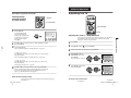
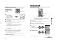
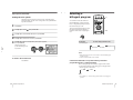
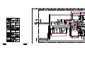
1
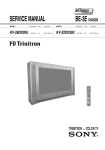
SERVICE MANUAL
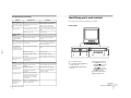
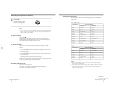
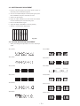
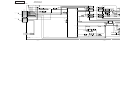
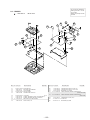
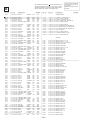
MODEL
COMMANDER
DEST. CHASSIS NO.
KV-VF21M40 RM-956
KV-VF21M70 RM-956
KV-VF21M70 RM-956
EJECT
E
SCC-P10A-A
ME
SCC-P11A-A
JE
SCC-P12A-A
BC-4A CHASSIS
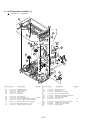
MODEL
COMMANDER
KV-VF21M70 RM-956
KV-VF21M77 RM-955
DEST. CHASSIS NO.
HK
SCC-P09B-A
HK
SCC-P09A-A
EJECT
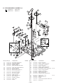
Z
Z
PIC MODE
PIC MODE
TAPE SPEED TIMER REC G-CODE
zREC
ON/OFF
zREC
INDEX
.
TAPE SPEED TIMER REC G-CODE
REW
m
.
>
X PAUSE
FF
M
PLAY
H
REW
m
FF
M
PLAY
H
ENTER
ENTER
x STOP
MENU COUNTER RESET A/B
t
ON/OFF
INDEX
>
X PAUSE
x STOP
MENU COUNTER RESET
GAME
t
GAME
1
2
3
1
2
3
4
5
6
4
5
6
7
8
9
7
8
-/--
0
C
-/--
0
2
PROGR
RM-955
2
9
C
PROGR
RM-956
PAL NTSC
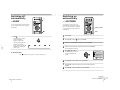
®
(VF21M77 ONLY)
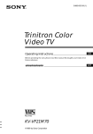
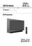
TRINITRON COLOR VIDEO TV
®
∗ Please file according to model size. ....
21
SPECIFICATIONS
TV Section
Television system
Color system
Bilingual system
(VF21M77 ONLY)
Channel coverage
Picture tube
Antenna in
B/G, I, D/K, M
PAL/SECAM and
NTSC3.58/NTSC4.43
NICAM bilingual I
See “Receivable
channels and channel
display”
Trinitron
21 inches (approx. 50.7
cm measured
diagonally)
75-ohm antenna socket
for VHF/UHF
Video Section
Format
VHS standard
Video recording system
Rotary 2-head helical
scanning system
Audio recording system
Monaural
Video signal
PAL/MESECAM/
NTSC
Tape speed
PAL/MESECAM
SP: 23.39 mm/sec.
LP: 11.70 mm/sec.
NTSC
SP: 33.35 mm/sec.
EP: 11.11 mm/sec.
Maximum recording time
PAL/MESECAM
SP: 240 minutes with
E-240
LP: 480 minutes with
E-240
NTSC
SP: 180 minutes with
T-180
EP: 540 minutes with
T-180
–2–
Inputs and Outputs
Inputs
t1, t2/GAME IN
(video): phono jack
1 Vp-p, 75 ohms,
unbalanced,
sync negative
9 (audio): phono jack
Input level:
500 mVrms
Headphones jack
Minijack
General
Clock
Quartz locked
Power requirements 110-240 V AC, 50/60Hz
Power consumption 123 W
Operating temperature
5˚ C to 40˚ C
(41˚ F to 104˚ F)
Storage temperature –20˚ C to 60˚ C
(–4˚ F to 140˚ F)
Dimensions
489 x 500 x 485 mm
(19 3/8 x 19 3/4 x 19 1/8
inches)
Mass
27.5 kg (60 lb 10 oz.)
Supplied accessories
Remote control
Two R6 (size AA)
batteries
Stabilizer band
Two clamps
Two wood screws
AC plug adaptor
(E/ME/JE model)
These operating
instructions
Design and specifications are subject to
change without notice.
Receivable channels and channel display
System
Area
Channel coverage
Channel display
B/G, H
Middle East/Asia
E-2 to E-12
E-21 to E-69
C02 to C12
C21 to C69
Indonesia
1A
2 to 11
C01
C03 to C12
Morocco
M-4 to M-7
M-8 to M-10
C70 to C73
C08 to C10
CATV
S-01 to S-05
S-1 to S-41
S42 to S46
S01 to S41
Hong Kong/
United Kingdom
B-21 to B-69
C21 to C69
Ireland
A, B, C,....J
C01 to C10
South Africa
4 to 13
21 to 68
C04 to C13
C21 to C68
Angola
1
2 to 3
C00
C02 to C03
CATV
S-01 to S-05
S-1 to S41
S42 to S46
S01 to S41
East European
coutries
R-1 to R-12
R-21 to R-60
C01 to C12
C21 to C60
China
C-1
C-2
C-3
C-4
C-5
C-6
C-7 to C-12
C-13 to C-24
C-25 to C-47
C-48 to C-57
C01
C02
C13
C03
C04
C14
C06 to C11
C21 to C32
C38 to C60
C61 to C70
Ivory Coast
1 to 3
C71 to C73
CATV
S-1 to S-39
S01 to S39
America
A-2 to A-13
A-14 to A-69
C02 to C13
C14 to C69
CATV
A-8
A-7
A-6
A-5 to A-1
A to E
F to W+28
W+29 to W+58
S01
S05
S06
S95 to S99
S14 to S18
S19 to S64
S65 to S94
I
D/K, K1
M
–3–
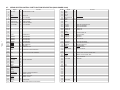
TABLE OF CONTENTS
Section
Title
Page
SELF DIAGNOSIS FUNCTION ......................................
[ TV SECTION]
1. GENERAL
1-1.
1-2.
5
Title
Page
5. CIRCUIT ADJUSTMENTS
5-1.
5-2.
5-3.
5-4.
KV-VF21M40/VF21M70 ........................................ 8
KV-VF21M77 ......................................................... 35
2. DISASSEMBLY
2-1.
2-2.
2-3.
2-4.
2-5.
2-6.
Section
Adjustments with Commander ................................
Adjustment Method .................................................
Service Data ............................................................
A Board Adjustment ................................................
73
74
75
77
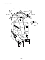
6. DIAGRAMS
Rear Cover Removal ...............................................
Chassis Assy Removal ............................................
Service Position (A Board) .....................................
A Board Removal ....................................................
Harnes Location ......................................................
Picture Tube Removal .............................................
65
65
65
65
66
67
6-1.
6-2.
6-3.
•
•
Block Diagrams .......................................................
Circuit Boards Location ..........................................
Printed Wiring Boards and Schematic Diagrams ....
A Board ....................................................................
CV, F Boards ............................................................
79
83
83
84
91
6. EXPLODED VIEWS
3. SET-UP ADJUSTMENTS
3-1.
3-2.
3-3.
3-4.
3-5.
3-6.
Beam Landing .........................................................
Convergence ............................................................
Focus Adjustment ....................................................
Screen (G2) Adjustment ..........................................
White Barance Adjustment .....................................
Picture Distortion Adjustment .................................
68
69
70
70
71
71
4. SAFETY RELATED ADJUSTMENT ...................... 72
6-1.
6-2.
Picture Tube ............................................................ 124
Chassis ..................................................................... 125
7. ELECTRICAL PARTS LIST ...................................... 129
[ VIDEO SECTION]
1. GENERAL ....................................................................... 96
2. DISASSEMBLY ............................................................. 97
3. CIRCUIT ADJUSTMENTS ........................................ 98
4. INTERFACE, IC PIN FUNCTION
DESCRIPTION .............................................................. 101
5. DIAGRAMS ..................................................................... 105
6. EXPLODED VIEWS ..................................................... 126
7. ELECTRICAL PARTS LIST ...................................... 135
CAUTION
SHORT CIRCUIT THE ANODE OF THE PICTURE TUBE AND
THE ANODE CAP TO THE METAL CHASSIS, CRT SHIELD, OR
CARBON PAINTED ON THE CRT, AFTER REMOVING THE ANODE.
SAFETY-RELATED COMPONENT WARNING!!
COMPONENTS IDENTIFIED BY SHADING AND MARK ! ON
THE SCHEMATIC DIAGRAMS, EXPLODED VIEWS AND IN THE
PARTS LIST ARE CRITICAL FOR SAFE OPERATION. REPLACE
THESE COMPONENTS WITH SONY PARTS WHOSE PART
NUMBERS APPEAR AS SHOWN IN THIS MANUAL OR IN SUPPLEMENTS PUBLISHED BY SONY. CIRCUIT ADJUSTMENTS
THAT ARE CRITICAL FOR SAFE OPERATION ARE IDENTIFIED
IN THIS MANUAL. FOLLOW THESE PROCEDURES WHENEVER CRITICAL COMPONENTS ARE REPLACED OR IMPROPER OPERATION IS SUSPECTED.
–4–
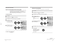
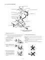
SELF DIAGNOSTIC FUNCTION
1.
OUTLINE
• The units in this manual contain a self-diagnostic function.
• If an error occurs, the STANDBY lamp will automatically begin to flash.
The number of times the lamp flashes translates to a probable source of the problem. A definition of the STANDBY lamp
flash indicators is listed in the instruction manual for the user’s knowledge and reference.
• If an error symptom cannot be reproduced, the remote commander can be used to review the failure occurrence data
stored in memory to reveal past problems and how often these problems occur.
2.
DIAGNOSTIC TEST INDICATORS
• When an errors occurs, the STANDBY lamp will flash a set number of times to indicate the possible cause of the problem.
If there is more than one error, the lamp will identify the first of the problem areas.
• Result for all of the following diagnostic items are displayed on screen. No error has occured if the screen displays a “0”.
Diagnostic
Item
Description
No. of times
STANDBY lamp
flashes
Self-diagnostic
display/Diagnostic
result
Probable
Cause
Location
• Power does not
turn on
Does not light
—
• +B overcurrent
(OCP) or
overvoltage
(OVP)
2 times
2 : 0 or
2:1
at the same
4:1
time
(Note 1)
• FBT
• Q802 (H OUT) shorted
• Vertical deflection
stopped
4 times
4:0
or
4:1
• IC501
• IC301 !¢ pin
• IC606
• Q802 (H OUT) shorted
• Q803
• Q608
• R803 open
• Has entered standby state
after horizontal raster.
• Vertical deflection pulse is
stopped.
• Horizontal deflection
stopped.
• Power line is shorted or
power supply is stopped.
• White balance
failure (no
PICTURE)
5 times
5:0
or
5:1
• CRT
• IC301
• IC701 - IC703, Q701
(CV board)
• G2 is improperly adjusted.
(Note 2)
• No raster is generated.
• CRT cathode current
detection reference pulse
output is small.
• Power cord is not plugged
in.
• Fuse is burned out F901
Detected
Symptoms
• Power does not come on.
• No power is supplied to the
TV.
• AC power supply is faulty.
• On standby state.
• Load on power line is
shorted
(at the same time 4 : 1 on
display).
Note 1: If a + B overcurrent is detected, stoppage of the vertical deflection is detected simultaneously.
The symptom that is diagnosed first by the microcontroller is displayed on the screen.
Note 2: Refer to screen (G2) Adjustment in section 3-4 of this manual.
• VCR EMG code List
Code
00h
10h
11h
12h
20h
21h
22h
23h
24h
25h
Coutents
NO EMG
CAM encode NG during unloading
CAM encode NG during unloading
CAM encode NG at intial
T reel NG during unloading
S reel FG NG
T reel FG NG
S reel FG NG
T reel FG NG at initial
S reel FG NG at initial
Code
30h
31h
40h
41h
42h
43h
44h
50h
60h
70h
–5–
Coutents
Capstan FG NG at initial
Capstan FG NG
Drum FG NG
Drum FG NG at initial
Drum FG NG
Drum PG NG
Drum PG NG
DEW
FL NG
DEW eject NG
3.
DISPLAY OF STANDBY LIGHT FLASH COUNT
* One flash count is not used for self-diagnostic.
< Diagnostic Item >
< Flash Count >
2 times
• +B OCP/OVP
STANDBY lamp (RED)
• Vertical deflection stopped
4 times
• White balance failure
5 times
Lamp ON 0.3 sec.
Lamp OFF 0.3 sec.
Lamp OFF 3.0 sec.
STOPPING THE STANDBY FLASH
• Turn off the power switch on the TV main unit or unplug the power cord from the outlet to stop the STANDBY lamp from flashing.
4.
SELF-DIAGNOSTIC SCREEN DISPLAY
• For errors with symptoms such as “power sometimes shuts off” or “screen sometimes goes out” that cannot be confirmed,
it is possible to bring up past occurances of failure for confirmation on the screen:
[To Bring Up Screen Test]
• In standby mode, press buttons on the remote commander sequentially in rapid succession as shown below:
[Screen display] / channel [5] / Sound volume [-] / Power ON u
˘
+
Note that this differs from entering the service mode (mode volume [+]).
Self-Diagnosis screen display
SELF CHECK
1:
2:1
3:
diagnostic item : result
4:0
5:1
VCR : -- --
Numeral "0" means that no fault has been detected.
Numeral "1" means a fault has been detected.
EMG code.
Note: Though "1: , 3:" indicated, not using.
5.
HANDLING OF SELF-DIAGNOSTIC SCREEN DISPLAY
• Since the diagnostic results displayed on the screen are not automatically cleared, always check the self-diagnostic
screen during repairs. When you have completed the repairs, clear the result display to “0”.
• Unless the result display is cleared to “0”, the self-diagnostic function will not be able to detect subsequent faults after
completion of the repairs.
[Clearing the result display]
• To clear the result display to “0”, press buttons on the remote commander sequentially as shown below when the diagnostic screen is being displayed.
• Pay attention when perform by the service mode, other all electric adjustment data will be rewrite.
Channel [8] / [0]
[Quitting Self-diagnostic screen]
• To quit the entire self-diagnostic screen, turn off the power switch on the remote commander or the main unit.
–6–
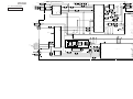
6.
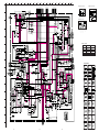
SELF-DIAGNOSTIC CIRCUIT
LED flash
IC001
µ-COM
STANDBY
lamp
To item 2 and 5 via bus line
SCL1 49
D1308
RY601
RELAY
4
3
SDA1 47
52 LED1
41
42
43
R •G •B
A
MEMORY
1
IC004
2
ITEM 3
Over current
Detection(OVP)
62 VCR
Q601
OVP 37
Q606
A
60 V PULSE
R611
V•STOP
+B LINE
R656
8
R613
1
IC301
Y/C/J
3
R615
HP/
PROTECT
PM601
PM21
R614
FBT
(T801)
ITEM 2.
Over voltage
Detection(OCP)
✩ Diagnostic screen display
SDA 35
SCL 34
15 VM OUT
IK IN 21
CRT
ITEM 5.
Auto cut-off white balance detection(AKB)
R,G,B STOP
IC501
Q502
7 BOOST
VCC
3
C504
Q501
D502
R510
ITEM 4.
Vertical Deflection
output Detection
(V•STOP)
C505
[+B overcurrent]
Owing to current increase voltage of R615 decrease and that it make PM601 pin 8 to
become LOW and OFF RY601.
[+B over voltage]
When +B voltage become more than 142.5V, PM601 8 pin become LOW and RY601
OFF.
[Vertical deflection stopped]
Detect Vertical deflection Pulse lost by IC001 ^º pin of micro computer.
Mute the picture at !∞ pin of IC301 that performed by Y/C/J.
[White balance]
Detect when R.G.B. output wrong level balance of automatic white balance detecting
standard pulse which detect cathode current, or which become low almost.
–7–
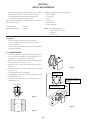
SECTION 1
1-1.
KV-VF21M40/VF21M70
GENERAL
The operating instructions mentioned here are partial abstracts from the
Operating Instruction Manual. The page numbers of the Operating Instruction Manual remein as in the manual.
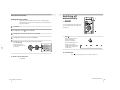
Getting Started
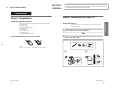
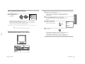
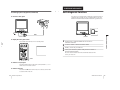
Step 1: Preparation
Step 2: Installing the video TV
Check the supplied accessories
Insert the batteries into the remote control
Secure the video TV
Getting Started
When you have taken everything out of the carton, check that you
have these items:
• Remote control
• Two R6 (size AA) batteries
• Stabilizer band
• Two clamps
• Two wood screws
• AC plug adaptor
• These operating instructions
To prevent the video TV from falling, secure it using one of the
following methods:
the supplied screws, attach the stabilizer band to the TV stand and to
A With
the rear of the video TV using the existing hole.
OR
a cord or chain through the clamps and secure them to the rear of the
B Pass
video TV and a wall or pillar.
–8–
20
mm
3.8 mm
Note
• Do not use old batteries or different types of batteries together.
A
4
Getting Started
B
Getting Started
5
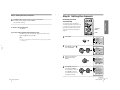
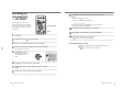
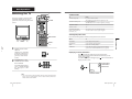
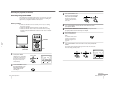
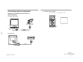
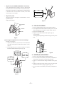
Step 3: Connecting the antenna
For better TV reception and clear recordings, connect an outdoor
antenna to your video TV.
You can change the menu and on-screen
information language to Chinese.
EJECT
?/1
Z
To connect a VHF antenna or a combination VHF/UHF
antenna—75-ohm coaxial cable (round)
PIC MODE
TAPE SPEED TIMER REC G-CODE
Attach an IEC antenna connector to the 75-ohm coaxial cable.
Plug the connector into the 8 (antenna) socket of the video TV.
zREC
ON/OFF
INDEX
.
>
X PAUSE
REW
m
FF
M
PLAY
H
ENTER
Rear
VHF/UHF
antenna
Getting Started
Connecting an outdoor antenna
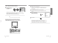
Step 4: Selecting
the language
M/,/m/</
ENTER
x STOP
MENU COUNTER RESET A/B
On a wall
t
?/1
1
or
–9–
Attach the antenna cable ends to the VHF/UHF mixer (not
supplied).
Plug the mixer into the 8 (antenna) socket of the video TV.
VHF antenna
1
2
MENU
3
Press ?/1 to turn on the
video TV.
When the TV is in standby
mode (the 1 indicator on
the video TV is lit in red),
press ?/1 , PROGR +/– or
a number button on the
remote control.
To connect both VHF and UHF antennas
UHF antenna
GAME
2
Press MENU.
PICTURE MODE
·DYNAMIC
·STANDARD
·SOFT
·PERSONAL
ADJUST
MENU
Rear
300-ohm twin-lead cable
SELECT
75-ohm coaxial cable
VHF/UHF mixer
(not supplied)
3
Press M or m to select
then press ENTER.
3
ENTER
,
PLAY
PLAY
H
H
ENTER
ENTER
SET UP
3
TV SET UP
VIDEO SET UP
LANGUAGE/
:ENGLISH
PIC ROTATION
SELECT
ENTER
continued
6
Getting Started
Getting Started
7
Step 4: Selecting the language (continued)
4
PLAY
PLAY
H
H
ENTER
ENTER
SET UP
3
TV SET UP
VIDEO SET UP
LANGUAGE/
:ENGLISH
PIC ROTATION
SELECT
EJECT
Z
PIC MODE
TAPE SPEED TIMER REC G-CODE
You need to set the clock to use timer
recording, Quick-Timer recording and
on-timer functions.
zREC
ON/OFF
INDEX
.
>
X PAUSE
ENTER
REW
m
FF
M
PLAY
H
ENTER
5
Press M or m to select
, then press ENTER.
M/,/m/</
ENTER
x STOP
MENU COUNTER RESET A/B
t
The menu language changes to Chinese.
GAME
1
To return to the normal screen
Getting Started
Press M or m to select
LANGUAGE/
, then
press ENTER.
The selected item turns
red.
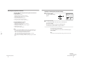
Step 5: Setting
the clock
1
2
MENU
3
Press MENU.
PICTURE MODE
·DYNAMIC
·STANDARD
·SOFT
·PERSONAL
ADJUST
MENU
Press MENU.
SELECT
– 10 –
2
Press M or m to select
then press ENTER.
ENTER
,
PLAY
PLAY
H
H
ENTER
ENTER
Press M or m to select
CLOCK SET , then press
ENTER.
PLAY
PLAY
H
H
ENTER
ENTER
3
TIMER
ON TIMER SET
CLOCK SET
SELECT
3
3
ENTER
CLOCK SET
3
31.12.1999 FRI 10:00
ENTER
4
Press ENTER.
5
Press M or m to set the
day, then press ,.
The day section turns red.
The month section turns
red.
CLOCK SET
3
27.12.1999 MON 10:00
PLAY
PLAY
H
H
ENTER
ENTER
SELECT
ENTER
continued
8
Getting Started
Getting Started
9
Step 5: Setting the clock (continued)
Step 6: Setting the channels
6
Press M, m or , to set the month, year, hour and minutes in
the same way as in step 5, then press ENTER.
Presetting channels
automatically
The clock starts working.
You can preset up to 100 channels.
Press MENU.
Z
PIC MODE
TAPE SPEED TIMER REC G-CODE
Automatic presetting is the easiest way
to setup your video TV if you want to
preset all receivable channels at once.
zREC
Note
• If power is interrupted or you disconnect the AC power cord, you have to
re-set the clock.
ON/OFF
INDEX
.
>
X PAUSE
REW
m
To preset the channels manually, see
page 30.
PLAY
H
FF
M
ENTER
M/,/m/</
ENTER
x STOP
MENU COUNTER RESET A/B
If you have made a mistake while setting the clock
Press < to go back to the item to be changed and set the correct
digits using M or m, then press ,.
Getting Started
To return to the normal screen
EJECT
t
1
GAME
MENU
Press MENU.
PICTURE MODE
·DYNAMIC
·STANDARD
·SOFT
·PERSONAL
ADJUST
MENU
SELECT
– 11 –
2
Press M or m to select
then press ENTER.
PLAY
H
H
ENTER
ENTER
SET UP
3
TV SET UP
VIDEO SET UP
LANGUAGE/
:ENGLISH
PIC ROTATION
SELECT
Make sure TV SET UP is
selected, then press
ENTER.
H
ENTER
Press M or m to select TV
SYS, then press ENTER.
The selected item turns red.
Press M or m to select the
TV system (B/G, I, D/K or
M) and press ENTER.
PLAY
ENTER
TV SET UP
3
AUTO PROGRAM
MANUAL PROGRAM
SKIP : PR 01 OFF
TV SYS : B/G
COL SYS : AUTO
INTELLIGENT VOL : OFF
SELECT
ENTER
PLAY
4
ENTER
,
PLAY
3
3
PLAY
H
H
ENTER
ENTER
TV SET UP
3
AUTO PROGRAM
MANUAL PROGRAM
SKIP : PR 01 OFF
TV SYS : B/G
COL SYS : AUTO
INTELLIGENT VOL : OFF
SELECT
ENTER
continued
10
Getting Started
Getting Started
11
Step 6: Setting the channels (continued)
5
PLAY
AUTO PROGRAM
PR : 01
TV SYS : B/G
CH : 01
PLAY
H
H
ENTER
ENTER
Press ?/1 to turn on the video TV.
2
Press TUNER PRESET ON/OFF with a pointed object.
3
Press t to select the TV
system of the channels
which you want to preset.
3
ENTER
Presetting starts from program position 1. The preset program and channel
numbers are displayed on the screen in sequence.
When presetting is finished, program position 1 appears again. All available
channels are now stored on successive number buttons.
When the TV is in standby mode (the 1 indicator on the video TV
is lit in red), press ?/1 , PROGR +/– or a number button on the
remote control.
Do not use an item (such as a pencil) that might break off when
inserted.
t
TUNER PRESET
Getting Started
Press M or m to select
AUTO PROGRAM, then
press ENTER.
1
PR : 01
TV SYS : B/G
CH : 01
Press t
for system selection.
GAME to start.
Tip
• To stop automatic channel presetting, press MENU.
– 12 –
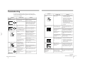
Presetting channels automatically using the
TUNER PRESET ON/OFF button on the video TV
4
Press GAME.
GAME
Presetting starts from program position 1. The preset program and
channel numbers are displayed on the screen in sequence.
When presetting is finished, program position 1 appears again. All
available channels are now stored on successive number buttons.
STOP REW
x
m
–PLAY–
FF
PAUSE
H
M
X
GAME
t
REC
QUICK TIMER
2
PROGR
TIMER REC
REC
PUSH
q
TUNER PRESET GAME
ON/OFF
12
Getting Started
t
?/1
Getting Started
13
Basic Operations
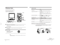
Watching the TV
%
EJECT
This section explains various functions
used while watching the TV. Most
operations can be done using the remote
control.
Z
?/1
Additional tasks
To
Press
Turn off temporarily
?/1 on the remote control.
The 1 indicator on the video TV lights up in red.
Turn off the main power
?/1 on the video TV.
The w indicator on the video TV lights up in orange.
Adjust the volume
2 +/–.
PIC MODE
PIC MODE
TAPE SPEED TIMER REC G-CODE
zREC
ON/OFF
INDEX
.
>
X PAUSE
REW
m
FF
M
PLAY
H
ENTER
x STOP
MENU COUNTER RESET A/B
t
GAME
Mute the sound
%.
Watch the video input
(from a connected VCR,
camcorder, etc.)
t to select “t1” or “t2”(see page 48).
To return to the TV screen, press t again.
t
2
3
4
5
6
7
8
9
-/--
0
C
2
2+/–
PROGR+/–
Selecting the picture mode
Number buttons
PROGR
?/1
PROGR+/–
2+/–
– 13 –
1
Press ?/1 to turn on the
video TV.
When the TV is in standby
mode (the 1 indicator on
the video TV is lit in red),
press ?/1 on the remote
control.
2
Press PROGR +/– or the
number buttons to select
the TV channel.
For double digit numbers,
press -, then the numbers
(e.g., for 25, press -, then
2 and 5).
Press PIC MODE repeatedly until the desired picture mode is selected.
Select
To
DYNAMIC
receive high contrast pictures.
STANDARD
receive normal contrast pictures.
SOFT
receive low contrast pictures.
PERSONAL
receive the latest picture settings from the ADJUST
option in the PICTURE MODE menu (see page 35).
Basic Operations
1
Displaying on-screen information
Press
to display the following on-screen information.
To have the program number and channel number stay on the
screen, press
again.
To make the information disappear, press
until no information is
displayed on the screen.
PROGR
1
2
3
4
5
6
12
Program position
7
8
9
Channel number
-/--
0
C
C30
MAIN
27.11 SAT
20:00
Current date and time
Note
• You can also select the channel number directly with the number buttons.
Press C (once for regular channels, twice for cable channels), the desired
number buttons, then ENTER.
14
Basic Operations
Basic Operations
15
Playing a tape
Additional tasks
This section shows you how to play a
tape. Other convenient functions you
can use while playing a tape are
explained in “Additional Operations.”
To
Press
stop playback
STOP x.
The video TV goes back to the normal TV picture.
stop playback for a moment
PAUSE X.
Press PAUSE X again or press PLAY N to resume
playback.
If you leave your video TV in pause mode, normal
playback resumes after about 5 minutes to prevent tape
damage.
search a tape at high speed
REW m
(rewind) or FF M
(fast-forward)
during playback.
To resume normal playback, press PLAY N.
fast-forward the tape
STOP x, then press FF M.
EJECTZ
EJECT
?/1
Z
PIC MODE
TAPE SPEED TIMER REC G-CODE
zREC
ON/OFF
INDEX
.
>
PAUSEX
FFM
X PAUSE
REW
m
FF
M
PLAY
H
ENTER
x STOP
MENU COUNTER RESET A/B
STOP REW
x
m
– PLAY –
FF
PAUSE
H
M
X
STOPx PLAYN PAUSEX
REWm FFM
t
?/1 EJECTZ
GAME
1
2
PLAYN
STOPx
REWm
COUNTER RESET
3
rewind the tape
STOP x, then press REW m.
view the picture in fast-forward
or rewind mode
and hold FF M during fast-forward or REW m during
rewind.
When you release the button, fast-forward or rewind
mode is resumed.
eject a cassette
EJECT Z.
You can eject the cassette even if the power is off.
– 14 –
Protecting your cassette against accidental erasure
1
Press ?/1 to turn on the video TV.
2
Insert a cassette.
3
When the TV is in standby mode (the 1 indicator on the video TV is lit in
red), skip this step.
If you insert a cassette with its safety tab removed, playback starts
automatically.
To prevent accidental erasure, break off the safety tab as illustrated.
To record on a cassette without a safety tab, simply cover the tab
hole with adhesive tape.
Safety tab
Adhesive tape
Press PLAY N.
Playback starts. On-screen
information is displayed
for a few seconds.
PLAY
H
ENTER
Note
• The picture’s color may be affected when playing a MESECAM-recorded
tape in the LP mode.
continued
16
Basic Operations
Basic Operations
17
Recording TV
programs
Playing a tape (continued)
Displaying on-screen information
Press
to display the following on-screen information. To show
only the amount of remaining tape and the linear tape counter on
the screen, press
again.
To make the information disappear, press
until no information is
displayed on the screen.
EJECT
PIC MODE
Recording TV programs
TAPE SPEED TIMER REC G-CODE
zREC
X PAUSE
PAUSEX
REW
m
FF
M
PLAY
H
ENTER
STOPx
x STOP
MENU COUNTER RESET A/B
E
t
Tape operation mode
M
SP
E
S
2 : 05 : 10
STOP REW
x
Current date
and time
RECz
>
End of the tape
S
27.11 SAT
20:00
TAPE SPEED
ON/OFF
INDEX
.
Amount of remaining tape
Beginning of the tape
?/1
Z
Linear tape counter
Tape speed
STOPx
m
– PLAY –
FF
PAUSE
H
M
X
PAUSEX
GAME
1
2
3
4
5
6
7
8
9
-/--
REC
0
2
Number
buttons
C
PROGR
PROGR+/–
?/1
PROGR+/–
RECz
– 15 –
Resetting the tape counter
The tape counter helps you to locate a certain scene after playback.
Press COUNTER RESET on the remote control to set the counter to
“0:00:00” before playing a tape. The tape counter is automatically
reset to zero whenever a cassette is inserted. The video TV keeps
counting the length of the tape being played. Note, however, that
the tape counter does not count the portions that do not contain any
recordings.
1
Press ?/1 to turn on the video TV.
2
Insert a cassette with a safety tab.
3
Press PROGR+/– or the
number buttons to select
the program position.
If the TV is in standby mode (the 1 indicator on the video TV is lit in
red), the video TV will turn on automatically when a cassette is
inserted.
For double digit numbers,
press -, then press the
numbers (e.g., for 25, press
-, then 2 and 5).
4
Press TAPE SPEED to select
the tape speed.
PROGR
1
2
3
4
5
6
7
8
9
-/--
0
C
TAPE SPEED
For details about the tape
speed, see “Selecting the
tape speed” on page 21.
continued
18
Basic Operations
Basic Operations
19
Recording TV programs (continued)
5
Press REC z.
Selecting the tape speed
zREC
The REC indicator lights
up and recording begins.
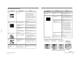
The chart below shows the recording/playback time available in
each mode.
PAL, MESECAM
Tape speed setting
Cassette tape
Note
• You can also select the channel number directly with the number buttons.
Press C (once for regular channels, twice for cable channels), the desired
number buttons, then ENTER.
To stop recording
Press STOP x.
When the tape reaches the end, the video TV rewinds the tape
automatically to the beginning, then stops. This function does not
work when the power of the video TV is off.
SP mode
LP mode
E-30
30 min.
1 hr.
E-60
1 hr.
2 hrs.
E-90
1 hr 30 min.
3 hrs.
E-120
2 hrs.
4 hrs.
E-150
2 hrs 30 min.
5 hrs.
E-180
3 hrs.
6 hrs.
E-195
3 hrs 15 min.
6 hrs 30 min.
E-210
3 hrs 30 min.
7 hrs.
E-240
4 hrs.
8 hrs.
To pause recording
– 16 –
You can cut out an unwanted scene during recording with this
button.
1 Press PAUSE X when an unwanted scene appears on the screen.
Recording pauses.
2 Press PAUSE X again to release the pause mode at the end of the
unwanted scene.
Recording resumes from the point set in step 1.
When the recording pause mode lasts for about 5 minutes, the video
TV stops recording to prevent tape damage.
Recording with the TV off
Press ?/1 on the video TV.
The video TV is turned off and the w indicator lights up.
The video TV continues recording.
NTSC
Tape speed setting
Cassette tape
SP mode
EP mode
T-30
30 min.
1 hr 30 min.
T-60
1 hr.
3 hrs.
T-120
2 hrs.
6 hrs.
T-160
2 hrs 40 min.
8 hrs.
T-180
3 hrs.
9 hrs.
Notes
• In the SP mode, the tape runs twice as fast as the LP mode, and three
times as fast as the EP mode.
• When a PAL format cassette is used with the NTSC system for recording,
the actual recording time is shorter than the standard recording time
stipulated on the cassette.
continued
20
Basic Operations
Basic Operations
21
Recording TV programs (continued)
3
Recording using QUICK-TIMER
The Quick-Timer recording function allows you to preset your video
TV to record one program within a 24-hour period. For setting the
Quick-Timer, use QUICK TIMER on the video TV.
Turn QUICK TIMER to set
the hour of the start time,
then press QUICK TIMER.
The hour is set and the
minute of the start time
turns red.
QUICK TIMER
PUSH
QUICK TIMER
PUSH
Before you begin
• Make sure that the clock is set correctly. If it is not, see “Setting
the clock” on page 9.
• Make sure that the loaded cassette has its safety tab intact.
• Make sure that the video TV does not enter the timer recording
standby mode (the TIMER REC indicator on the video TV should
not be lit.)
4
Turn QUICK TIMER to set the minute of the start time, then
press QUICK TIMER.
5
Use the QUICK TIMER dial to set the recording time period and
program position in the same way as in step 3.
6
Turn QUICK TIMER to move the cursor to OK, then press QUICK
TIMER.
The Quick Timer indicator lights up and the video TV enters the
timer recording standby mode.
EJECT
Z
PIC MODE
TAPE SPEED TIMER REC G-CODE
zREC
ON/OFF
QUICK TIMER
TAPE SPEED
QUICK TIMER
QUICK TIMER
27 SAT 20:00
START
PROG
INDEX
– 17 –
.
27SAT 23:15
>
X PAUSE
PUSH
PUSH
TAPE SPEED : SP
OK
REW
m
PLAY
H
1H15M 12
CHANGE CLEAR
FF
M
SELECT
ENTER
ENTER
x STOP
MENU COUNTER RESET A/B
t
QUICK TIMER
1
2
Press QUICK TIMER.
When the TV is in standby
mode (the 1 indicator on
the video TV is lit in red),
the power is turned on
automatically.
Press TAPE SPEED to select
the tape speed, SP or LP.
EP cannot be selected
when making timer
recordings.
QUICK TIMER
GAME
QUICK TIMER
START
PROG
27SAT 20:00
PUSH
27 SAT 20:00
0H15M 12
TAPE SPEED : SP
OK
CHANGE CLEAR
SELECT
ENTER
TAPE SPEED
continued
22
Basic Operations
Basic Operations
23
Recording TV programs (continued)
The QUICK TIMER button changes the following when turned clockwise
or counterclockwise
• When setting the start time:
The hour increases or decreases by one hour.
The minutes increase or decrease by one minute.
• The recording time period:
Increases or decreases by 15 minutes.
• The program position changes as follows:
1... y 8... y 12... y t1 y t2 y 0 y 1
If the QUICK TIMER button is pressed
• When the Quick Timer is not set:
The display for setting the Quick Timer appears.
• When the Quick Timer is set:
The display for checking the Quick Timer appears.
• When the clock is not set:
The CLOCK SET display appears.
– 18 –
Note
• When you turn QUICK TIMER to move the cursor to OK and then press
it, one of the following messages may appear depending on the cassette
used. If a message appears, the recording is canceled.
- Put in a tape. The program recording is canceled.
- Put in a tape with safety tab. The program recording is canceled.
- Tape ran out. The program recording is canceled.
Insert a cassette for recording, rewind the tape and press QUICK TIMER
again.
Changing or canceling the Quick Timer settings
1
Press QUICK TIMER.
The QUICK TIMER display
appears.
QUICK TIMER
QUICK TIMER
27 SAT 20:00
Programmed as below
START
27SAT 23:15
PROG
1H15M 12
TAPE SPEED : SP
PUSH
OK
CHANGE CLEAR
SELECT
2
ENTER
Change the settings:
(1) Turn QUICK TIMER to move the cursor to CHANGE, then
press QUICK TIMER.
(2) Change the settings according to steps 2 through 7 of
“Recording using QUICK-TIMER” on pages 22 and 23.
To cancel the Quick Timer settings
Turn QUICK TIMER to move the cursor to CLEAR, then press
QUICK TIMER.
Note
• You cannot cancel the Quick Timer settings with the remote control.
continued
24
Basic Operations
Basic Operations
25
Recording TV programs (continued)
3
Set the recording start time, recording stop time, program
position/input (1 or 2) and tape speed in the same way as in
step 2.
4
Press ENTER.
Recording TV programs using the timer
You can preset up to five programs within a one-month period.
Before you begin
• When the TV is in standby mode (the 1 indicator on the video TV
is lit in red), press ?/1 , PROGR +/– or a number button on the
remote control.
• Make sure that the clock is set correctly. If it is not, see “Setting the
clock” on page 9.
• Make sure that the loaded cassette has its safety tab intact.
• Make sure that the video TV does not enter the timer recording
standby mode (the Quick Timer indicator on the video TV should
not be lit.)
EJECT
Setting the timer
For daily and weekly
recording, see “Daily/
weekly recording” below.
DATE START STOP PRG
28 SUN 21:00 22:00
6 SP
PLAY
H
ENTER
OK
NEXT
SELECT
5
Press < or , to move the cursor to NEXT for other programs,
then press ENTER. Repeat steps 2 through 4.
6
Press < or , to move the cursor to OK after setting your
desired programs, then press ENTER.
CHANGE CLEAR
SET
ENTER
The TIMER REC indicator lights up and the video TV enters timer
recording standby mode.
?/1
Z
– 19 –
Example: How to record a program
broadcast on program position 6 from
21:00 to 22:00 on Sunday, 28th
November 1999.
PROGRAM LIST 27 SAT 20:00
The cursor appears at OK.
PIC MODE
TAPE SPEED TIMER REC G-CODE
zREC
ON/OFF
.
TIMER REC
ON/OFF
INDEX
>
If you have made a mistake during timer setting
X PAUSE
REW
m
PLAY
H
FF
M
M/,/m/</ENTER
Press < to go back to the previous position and correct the setting.
ENTER
Daily/weekly recording
x STOP
MENU COUNTER RESET A/B
1
Press TIMER REC.
PROGRAM LIST 27 SAT 20:00
DATE START STOP PRG
27 SAT – –:– – – –:– – – – SP
TIMER REC
OK
NEXT
SELECT
2
Press M or m to set the
date , then press ,.
CHANGE CLEAR
SET
ENTER
You can preset your video TV to record the same program every day
of the week (daily recording) or the same program on the same day
every week (weekly recording). Press m in step 2 until the desired
setting appears in the “DATE” position. With each press, the setting
changes as follows:
27 (today) t MON–SUN t MON–SAT t MON–FRI t
EVERY SAT t EVERY FRI t ... t EVERY SUN t 26 (next
month) ......
PROGRAM LIST 27 SAT 20:00
DATE START STOP PRG
28 SUN – –:– – – –:– – – – SP
PLAY
PLAY
H
H
ENTER
ENTER
To stop timer recording
Press ON/OFF.
OK
NEXT
SELECT
CHANGE CLEAR
SET
ENTER
Using the video TV before timer recording starts
Press ON/OFF to turn off the TIMER REC indicator on the front of
the video TV.
Remember to press ON/OFF again to make the TIMER REC
continued
indicator light up after setting the recording time.
26
Basic Operations
Basic Operations
27
Additional Operations
Adjusting the TV
Recording TV programs (continued)
Checking/adding/
changing/canceling
the timer settings
PIC MODE
EJECT
TAPE SPEED TIMER REC G-CODE
zREC
ON/OFF
TIMER REC
Z
INDEX
.
>
X PAUSE
PIC MODE
TAPE SPEED TIMER REC G-CODE
REW
m
PLAY
H
FF
M
M/,/m/</ENTER
zREC
ON/OFF
INDEX
.
ENTER
>
X PAUSE
x STOP
MENU COUNTER RESET A/B
REW
m
PLAY
H
M/,/m/</ENTER
FF
M
ENTER
1
x STOP
MENU COUNTER RESET A/B
Press TIMER REC.
PROGRAM LIST 27 SAT 20:00
To exit the PROGRAM
LIST after checking the
settings, skip steps 2 and 3.
t
TIMER REC
DATE START STOP PRG
28 SUN 21:00 22:00
6 SP
29 MON 1:30 3:00 79 LP
MON·SAT 18:50 19:00
2 SP
EVERY TUE21:00 23:30
1 LP
OK
ADD
SELECT
– 20 –
2
Press < or , to move the cursor to ADD, CHANGE or CLEAR,
then press ENTER.
3
To add new settings
Adjusting the volume — INTELLIGENT VOL
Some programs are broadcast at different volume levels. By setting
this function to ON, the volume level is stabilized and sudden
changes in volume can be prevented.
CHANGE CLEAR
SET
ENTER
Follow steps 2 through 4 of “Setting the timer” on page 26.
To change the settings
Press M or m to move the cursor to the setting you want to change,
then press ENTER.
Follow steps 2 through 4 of “Setting the timer” on page 26.
1
Press MENU.
2
Press M or m to select
3
Make sure TV SET UP is selected, then press ENTER.
4
Press M or m to select
INTELLIGENT VOL , then
press ENTER.
, then press ENTER.
The selected item turns red.
To clear the settings
Press M or m to move the cursor to the setting you want to clear,
then press ENTER.
The setting is cleared and “--” appears.
Press < or , to move the cursor to OK, then press ENTER.
5
Additional Operations
To add, change or clear the
settings, follow steps 2
through 4.
4
MENU
GAME
Programmed as below
PLAY
PLAY
H
H
ENTER
ENTER
PLAY
PLAY
Press M or m to select ON,
then press ENTER.
If there are other timer settings on the list, the video TV enters the
timer recording standby mode and the TIMER REC indicator
lights up. The PROGRAM LIST disappears.
H
H
ENTER
ENTER
TV SET UP
3
AUTO PROGRAM
MANUAL PROGRAM
SKIP : PR 01 OFF
TV SYS : B/G
COL SYS : AUTO
INTELLIGENT VOL : OFF
SELECT
ENTER
TV SET UP
3
AUTO PROGRAM
MANUAL PROGRAM
SKIP : PR 01 OFF
TV SYS : B/G
COL SYS : AUTO
INTELLIGENT VOL : ON
SELECT
ENTER
When the timer settings overlap
The second program starts recording only after the first program
has finished.
28
Basic Operations
To return to the normal screen
Press MENU.
continued
Additional Operations
29
Adjusting the TV (continued)
7
Presetting channels manually
Preset the channels manually if you want to select channels that
were not set automatically or if you want to allocate program
numbers to channels one by one.
If the sound of the desired channel is abnormal, select the
appropriate TV system.
(1) Press M or m to select TV SYS, then press ENTER.
(2) Press M or m until the sound becomes normal, then press ENTER.
8
If you are not satisfied with the picture and sound quality, you
may be able to improve them by using the FINE tuning feature.
1
Press MENU.
2
Press M or m to select
3
Make sure TV SET UP is selected, then press ENTER.
(2) Press M or m to select
MANUAL, then press
ENTER.
4
Press M or m to select
MANUAL PROGRAM, then
press ENTER.
(3) Press M or m until the
picture and sound quality
are optimal, then press
ENTER.
(1) Press M or m to select
FINE, then press ENTER.
The selected item turns red.
, then press ENTER.
PLAY
PLAY
H
H
ENTER
ENTER
MANUAL PROGRAM 3
PR : 01
TV SYS : B/G
CH : 01
FINE : AUTO
SELECT
– 21 –
5
Select the program number to which you want to assign a
channel number.
(1) Make sure PR is selected, then press ENTER.
ENTER
FINE tuning can be set
between –15 and +15.
PLAY
PLAY
H
H
ENTER
ENTER
PLAY
PLAY
H
H
ENTER
ENTER
MANUAL PROGRAM 3
PR : 01
TV SYS : B/G
CH : 01
FINE : MANUAL
SELECT
ENTER
To return to the normal screen
Press MENU.
(2) Press M or m until the program number you want to preset
appears on the menu, then press ENTER.
You can also select the program number with the PROGR +/– or
number buttons.
6
Select the desired channel.
(1) Press M or m to select CH, then press ENTER.
(2) Press M or m until the desired channel number appears on the
menu, then press ENTER.
You can also select the channel number directly with the number buttons.
Press C (once for regular channels, twice for cable channels), the desired
number buttons, then ENTER.
continued
30
Additional Operations
Additional Operations
31
Adjusting the TV (continued)
Adjusting the TV system
If the sound of some channels is abnormal, select the appropriate
TV system for your area.
Skipping program positions
You can skip unused program positions when selecting a program
with the PROGR +/– buttons. However, the skipped programs may
still be called up when you select them with the number buttons.
1
Press MENU.
2
Press M or m to select
3
Make sure TV SET UP is selected, then press ENTER.
1
Press MENU.
2
Press M or m to select
3
Make sure TV SET UP is selected, then press ENTER.
4
Press M or m to select TV SYS, then press ENTER.
4
Press M or m to select SKIP, then press ENTER.
5
Press M or m until the
appropriate TV system
appears on the menu,
then press ENTER.
, then press ENTER.
– 22 –
5
Press M or m until the program position which you want to skip
appears on the menu, then press ENTER.
6
Press M or m to select ON,
then press ENTER.
7
PLAY
PLAY
H
H
ENTER
ENTER
TV SET UP
3
AUTO PROGRAM
MANUAL PROGRAM
SKIP : PR 07 ON
TV SYS : B/G
COL SYS : AUTO
INTELLIGENT VOL : OFF
SELECT
ENTER
, then press ENTER.
PLAY
PLAY
H
H
ENTER
ENTER
TV SET UP
3
AUTO PROGRAM
MANUAL PROGRAM
SKIP : PR 01 OFF
TV SYS : D/K
COL SYS : AUTO
INTELLIGENT VOL : OFF
SELECT
ENTER
To return to the normal screen
Press MENU.
Press ENTER and repeat steps 5 and 6 to skip other program
positions.
To return to the normal screen
Press MENU.
continued
32
Additional Operations
Additional Operations
33
Adjusting the TV (continued)
Changing the PICTURE MODE setting
The PICTURE MODE menu allows you to adjust the picture quality.
Adjusting the color system
Normally set the color system to AUTO. However, when the picture
has no color, manually select the appropriate color system for your
area.
1
Press MENU.
1
Press MENU.
2
Press M or m to select
then press ENTER.
,
PLAY
2
Press M or m to select
3
Make sure TV SET UP is selected, then press ENTER.
4
Press M or m to select COL SYS, then press ENTER.
, then press ENTER.
PICTURE MODE
·DYNAMIC
·STANDARD
·SOFT
·PERSONAL
ADJUST
PLAY
H
H
ENTER
ENTER
SELECT
3
Press M or m to select
ADJUST , then press
ENTER.
PLAY
5
– 23 –
Press M or m until the
appropriate color system
appears, then press
ENTER.
To return to the normal screen
Press MENU.
PLAY
PLAY
H
H
ENTER
ENTER
TV SET UP
3
AUTO PROGRAM
MANUAL PROGRAM
SKIP : PR 01 OFF
TV SYS : D/K
COL SYS : PAL
INTELLIGENT VOL : OFF
SELECT
ENTER
H
H
ENTER
ENTER
PERSONAL ADJUST 3
PICTURE
80
50
COLOR
BLIGHT
50
00
HUE
50
SHARP
PLAY
ENTER
3
SELECT
4
Press M or m to select the desired item, then press ENTER.
5
Adjust the value according to the following table, then press
ENTER.
ENTER
The adjustment bar for the selected item appears at the bottom of the
screen.
For
Press m to
PICTURE
decrease picture contrast
Press M to
increase picture contrast
COLOR
decrease color intensity
increase color intensity
BRIGHT
darken the picture
brighten the picture
HUE*
increase red picture tones
increase green picture tones
SHARP
soften the picture
sharpen the picture
*You can adjust HUE for the NTSC color system only.
To return to the normal screen
Press MENU.
continued
34
Additional Operations
Additional Operations
35
Tape options
Adjusting the TV (continued)
Adjusting the alignment of
the picture
Adjusting the tracking
EJECT
The picture may be out of alignment due
to influence from the earth’s magnetic
field in relation to the position of the TV.
You can adjust the angle of the picture if
it is not aligned to the TV screen.
Adjusting the tracking automatically
Z
The tracking condition is automatically adjusted when this function
is set to AUTO.
PIC MODE
TAPE SPEED TIMER REC G-CODE
zREC
ON/OFF
INDEX
.
>
X PAUSE
REW
m
Adjusting the tracking manually
FF
M
PLAY
H
If streaks or snow noise appear during normal playback, adjust the
tracking.
M/,/m/</ENTER
ENTER
x STOP
MENU COUNTER RESET A/B
t
1
– 24 –
1
Press MENU.
2
Press M or m to select
3
MENU
GAME
2
Press MENU in playback mode.
2
Press M or m to select
3
Press M or m to select
VIDEO SET UP, then press
ENTER.
3
, then press ENTER.
, then press ENTER.
PLAY
VIDEO SET UP
3
TRACKING : AUTO
APC : ON
AUTO REPEAT : OFF
RENTAL : OFF
VHS : OTHERS
COL SYS : AUTO
SELECT
ENTER
PLAY
H
H
ENTER
ENTER
Press M or m to select PIC
ROTATION, then press
ENTER.
PLAY
PLAY
H
H
ENTER
ENTER
PIC ROTATION
4
1
4
Make sure TRACKING is selected, then press ENTER.
5
Press M or m to select
MANUAL, then press
ENTER.
Press M or m to align the picture’s position, then press ENTER.
The tracking meter appears
on the screen.
6
TRACKING
PLAY
PLAY
H
H
ENTER
ENTER
NORMAL TRACKING
SET
ENTER
Press < or , to reduce picture noise, then press ENTER.
To return to the normal screen
Press MENU.
continued
36
Additional Operations
Additional Operations
37
Tape options (continued)
Playing a tape repeatedly
You can play the recorded portion of a tape repeatedly.
Adjusting with Adaptive Picture Control (APC)
This function allows you to improve playback and recording quality
automatically according to the condition of the video tape.
This function is set to ON at the factory. To maintain better picture
quality, it is advisable to leave the function on. The APC function
works on all types of tapes, even on rental tapes.
To change the setting
1
2
Press MENU.
Press M or m to select
, then press ENTER.
3
Press M or m to select VIDEO SET UP, then press ENTER.
4
Press M or m to select
APC, then press ENTER.
The selected item turns red.
– 25 –
5
PLAY
PLAY
H
H
ENTER
ENTER
Press M or m to select
OFF, then press ENTER.
To return to the normal screen
PLAY
PLAY
H
H
ENTER
ENTER
1
Press MENU.
2
Press M or m to select
3
Press M or m to select VIDEO SET UP, then press ENTER.
4
Press M or m to select
AUTO REPEAT, then press
ENTER.
, then press ENTER.
The selected item turns
red.
VIDEO SET UP
3
TRACKING : AUTO
APC : ON
AUTO REPEAT : OFF
RENTAL : OFF
VHS : OTHERS
COL SYS : AUTO
SELECT
ENTER
VIDEO SET UP
3
TRACKING : AUTO
APC : OFF
AUTO REPEAT : OFF
RENTAL : OFF
VHS : OTHERS
COL SYS : AUTO
SELECT
ENTER
5
PLAY
PLAY
H
H
ENTER
ENTER
PLAY
PLAY
H
H
ENTER
ENTER
Press M or m to select ON,
then press ENTER.
6
Press MENU to return to the normal screen.
7
Press PLAY N.
Playback starts. When the
tape reaches its end, the
video TV rewinds the tape
to the beginning, then
plays it again.
VIDEO SET UP
3
TRACKING : AUTO
APC : ON
AUTO REPEAT : OFF
RENTAL : OFF
VHS : OTHERS
COL SYS : AUTO
SELECT
ENTER
3
VIDEO SET UP
TRACKING : AUTO
APC : ON
AUTO REPEAT : ON
RENTAL : OFF
VHS : OTHERS
COL SYS : AUTO
ENTER
SELECT
PLAY
H
ENTER
Press MENU.
continued
38
Additional Operations
Additional Operations
39
Tape options (continued)
When connecting to a Sony VCR
If you use this video TV with another Sony VCR, the remote control
may accidentally operate both the video TV and VCR at the same
time. To prevent this from happening, set VHS to SONY so that the
remote control operates only this video TV.
Adjusting the picture for rental tapes
If you are not satisfied with the picture quality while playing a tape,
even when APC is on, set RENTAL to ON. It is recommended to
use this function when watching rental tapes.
1
Press MENU.
2
Press M or m to select
3
Press M or m to select VIDEO SET UP, then press ENTER.
4
Press M or m to select
RENTAL, then press
ENTER.
, then press ENTER.
The selected item turns red.
– 26 –
5
PLAY
PLAY
H
H
ENTER
ENTER
1
Press MENU.
2
Press M or m to select
3
Press M or m to select VIDEO SET UP, then press ENTER.
4
Press M or m to select
VHS, then press ENTER.
3
VIDEO SET UP
TRACKING : AUTO
APC : ON
AUTO REPEAT : OFF
RENTAL : OFF
VHS : OTHERS
COL SYS : AUTO
ENTER
SELECT
The selected item turns red.
5
Press M or m to select ON,
then press ENTER.
PLAY
PLAY
H
H
ENTER
ENTER
, then press ENTER.
PLAY
PLAY
H
H
ENTER
ENTER
PLAY
PLAY
H
H
ENTER
ENTER
Press M or m to select
SONY, then press ENTER.
VIDEO SET UP
3
TRACKING : AUTO
APC : ON
AUTO REPEAT : OFF
RENTAL : ON
VHS : OTHERS
COL SYS : AUTO
SELECT
ENTER
VIDEO SET UP
3
TRACKING : AUTO
APC : ON
AUTO REPEAT : OFF
RENTAL : OFF
VHS : OTHERS
COL SYS : AUTO
SELECT
ENTER
VIDEO SET UP
3
TRACKING : AUTO
APC : ON
AUTO REPEAT : OFF
RENTAL : OFF
VHS : SONY
COL SYS : AUTO
SELECT
ENTER
To return to the normal screen
To return to the normal screen
Press MENU.
Press MENU.
continued
40
Additional Operations
Additional Operations
41
Tape options (continued)
Setting the color system
Normally set COL SYS in the menu to AUTO. If streaks appear
during playback, set COL SYS to correspond to the system that the
tape was recorded in.
1
Press MENU.
2
Press M or m to select
3
Press M or m to select VIDEO SET UP, then press ENTER.
4
Press M or m to select COL SYS, then press ENTER.
5
Press M or m until the corresponding color system appears,
then press ENTER.
Switching off
automatically
—SLEEP
EJECT
?/1
Z
PIC MODE
TAPE SPEED TIMER REC G-CODE
zREC
You can automatically switch the video
TV into standby mode after a selected
time period.
ON/OFF
INDEX
.
>
X PAUSE
REW
m
PLAY
H
FF
M
ENTER
, then press ENTER.
x STOP
MENU COUNTER RESET A/B
t
– 27 –
Select the same color
system that the tape was
recorded in.
PLAY
PLAY
H
H
ENTER
ENTER
Press
GAME
.
With each press, the time
period (in minutes)
changes as illustrated.
VIDEO SET UP
3
TRACKING : AUTO
APC : ON
AUTO REPEAT : OFF
RENTAL : OFF
VHS : OTHERS
COL SYS : PAL
SELECT
ENTER
One minute before the TV
switches into standby
mode, the message “SLEEP
TIMER: 1M” is displayed
on the screen.
OFF
30M
60M
90M
To cancel the timer
Press
to select OFF or press ?/1 to turn on the power.
To return to the normal screen
Press MENU.
42
Additional Operations
Additional Operations
43
Switching on
automatically
— ON TIMER
9
EJECT
The SOURCE changes as follows.
TV PROG t VCR N (video playback)
PIC MODE
TAPE SPEED TIMER REC G-CODE
You can preset your video TV to
automatically switch on at a desired
time. You can select the TV program,
video playback or input source to be
switched on.
Press M or m to set the source to be switched on, then press
ENTER.
Z
zREC
ON/OFF
R
INDEX
.
>
X PAUSE
REW
m
PLAY
H
FF
M
M/,/m/</ENTER
If you select TV PROG, press M or m to change the channel
numbers. Then press ENTER again.
ENTER
10 Press M or m to select ON TIMER, then press ENTER.
x STOP
MENU COUNTER RESET A/B
t
GAME
MENU
11 Press M or m to set ON TIMER to ON, then press ENTER.
– 28 –
1
Press MENU.
2
Press M or m to select
3
Make sure ON TIMER SET is selected, then press ENTER.
4
Make sure that the cursor appears at DAY, then press ENTER.
5
Press M, m, < or , to
set the timer on (✓) or off
(–) for each day of the
week.
12 Press MENU to return to the normal screen.
The
, then press ENTER.
To cancel the on-timer function
In step 11, press M or m to set ON TIMER to OFF, then press
ENTER.
The
indicator on the video TV turns off.
The selected item turns red.
ON TIMER SET
3
DAY : S M
_ T_ W
_ T F_ S_
PLAY
H
ENTER
TIME : 10:00
SOURCE : TV PROG 12
ON TIMER : ON
SELECT
44
6
Press M or m to select TIME, then press ENTER.
7
Press M or m to set the on-time hour and minute, then press
ENTER.
8
Press M or m to select SOURCE, then press ENTER.
Additional Operations
indicator on the video TV lights up.
ENTER
Additional Operations
45
Connecting optional equipment
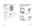
Searching using
the index
function
EJECT
Z
Watching and recording the picture input from
optional equipment
PIC MODE
TAPE SPEED TIMER REC G-CODE
zREC
The video TV marks the tape with an
index signal at the point where each
recording begins. Use these signals as
references to find a specific recording.
This video TV can search up to 99 index
signals ahead of or behind the current
position.
– 29 –
1
Insert an indexed tape.
2
Press INDEX ./>
repeatedly to specify how
many index signals ahead
or behind you want to
search.
ON/OFF
INDEX
.
INDEX ./>
>
To connect a video camera
X PAUSE
REW
m
PLAY
H
FF
M
ENTER
STOP x
x STOP
MENU COUNTER RESET A/B
t
GAME
to audio
output
t 2/GAME
IN
INDEX
.
>
t 2/GAME IN 9
VMC-710M/720M
(not supplied)
INDEX 5
SEARCH
To search ahead, press
INDEX >.
to video
output
To connect a VCR
To search backwards, press
INDEX ..
The video TV starts searching and the index number on the TV
screen counts down to zero. Playback starts automatically from
that point.
to audio
output
to video
output
To stop searching
t 1/
Press STOP x.
t 1/9
continued
46
Additional Operations
Additional Operations
47
Connecting optional equipment (continued)
To connect a video game
To watch the video input signal
Press t so that t1 or t2 appears on the screen.
EJECT
Z
1
PIC MODE
TAPE SPEED TIMER REC G-CODE
zREC
ON/OFF
INDEX
.
>
X PAUSE
REW
m
H
t 2/GAME IN 9
t 2/GAME
IN
FF
M
PLAY
ENTER
x STOP
MENU COUNTER RESET A/B
t
GAME
1
2
3
t
To display the video game screen
Press GAME when the video TV is in standby mode.
EJECT
– 30 –
Z
GAME
PIC MODE
TAPE SPEED TIMER REC G-CODE
zREC
ON/OFF
INDEX
.
>
X PAUSE
REW
m
FF
M
PLAY
H
ENTER
x STOP
MENU COUNTER RESET A/B
t
GAME
GAME
1
2
3
To switch to a TV program
Press the number button on the remote control, PROGR +/– or t
on the video TV or remote control.
To switch to the VCR
Press the PLAY N button on the video TV or remote control when
a cassette is in the video TV.
48
Additional Operations
Additional Operations
49
Additional Information
Self-diagnosis function
Troubleshooting
Your video TV is equipped with a self-diagnosis function. If there is
a problem with your video TV, the 1 indicator flashes in red. The
number of times the indicator flashes indicates the possible causes.
If you have any problems while viewing your video TV, please
check the following troubleshooting guide. If the problem persists,
contact your Sony dealer.
Symptom
Possible cause
Solutions
TV section
No picture/No sound
Good picture/No sound
The power cord or antenna Check the AC power cord and the
antenna connections.
is not connected.
The video TV is not turned
on.
Press ?/1 on the video TV. If the
standby indicator (1) is lit in red,
press ?/1 or a program number
button on the remote control.
The volume level is too
low.
Press 2 + to increase the volume
level.
Press % to cancel the muting.
Headphones are connected
to i (headphones) jack.
Disconnect the headphones.
The color level setting is
too low.
Adjust PICTURE, COLOR and
BRIGHT in the PERSONAL
ADJUST menu. (page 35)
The picture setting is
inappropriate.
Press PIC MODE to switch the
picture setting. (page 15)
The color system setting is
inappropriate.
Display the TV SET UP menu and
check the color system (COL SYS)
setting. (page 34)
The antenna direction,
position and angle need
adjustment.
Adjust the antenna direction,
position and angle. Contact a Sony
dealer for advice.
Broadcast signals are
reflected by nearby
mountains or buildings.
Use a highly directional antenna.
The antenna direction,
position and angle need
adjustment.
Adjust the antenna direction,
position and angle. Contact a Sony
dealer for advice.
The connecting cord
between the video TV and
the input sources is
disconnected.
Check the connection between the
video TV and the input sources.
Input is not selected
correctly.
Press t so that “t1” or “t2”
appears. (page 48)
Additional Information
The sound is muted.
1 indicator
– 31 –
1
Check that the 1 indicator flashes red once or more in
intervals of 3 seconds.
2
3
4
Count the number of times the indicator flashes.
No color or poor color
Press ?/1 to turn off your video TV.
Inform your nearest Sony service facility about the number of
times the indicator flashes.
Be sure to note the model name and serial number located on the
rear of your video TV.
Double images or “ghosts”
No picture/No sound from
video input sources
continued
50
Additional Information
Additional Information
51
Troubleshooting (continued)
Symptom
Good picture/Abnormal
sound
Snowy picture/Abnormal
sound
– 32 –
Dotted lines or stripes
Abnormal color patches
Possible cause
The TV system setting is
inappropriate.
Solutions
• If the sound of all the channels
is abnormal, display the TV SET
UP menu and select the
appropriate TV system (TV
SYS), then preset the channels
again. (pages 11 and 12)
• If the sound of some channels is
abnormal, display the MANUAL
PROGRAM menu in the TV SET
UP menu and select the
appropriate TV system (TV SYS)
(page 30).
The connection is loose or
the cable is damaged.
Check the antenna cable and
connection on the video TV and at
the wall.
The channel presetting is
inappropriate or
incomplete.
Display the TV SET UP menu and
select MANUAL PROGRAM to
manually preset the channel again.
The antenna type is
inappropriate.
Check the antenna type (VHF/
UHF). Contact a Sony dealer for
advice.
The antenna direction,
position and angle need
adjustment.
Adjust the antenna direction,
position and angle. Contact a Sony
dealer for advice.
There is local interference
from cars, neon signs, hair
dryers, power generators,
etc.
• Do not use a hair dryer or other
equipment near the video TV.
• Adjust the antenna direction,
position and angle for minimum
interference. Contact a Sony
dealer for advice.
There is magnetic
disturbance from external
speakers or other
equipment.
Locate external speakers or other
equipment away from the video
TV. Press ?/1 on the video TV to
turn off the video TV for about five
minutes, then turn on again.
Symptom
Possible cause
Solutions
Playback section
Power is on, but the tape
does not run.
The safety device has been
activated.
Switch off, disconnect the AC
power cord, and leave the set for
about one minute.
Poor playback picture
The color system setting is
inappropriate.
Display VIDEO SET UP and set
the color system (COL SYS) to the
setting corresponding to the color
system that the tape is recorded in.
(page 42)
The tracking condition is
inappropriate.
Adjust the tracking manually.
(page 37)
The video heads are dirty.
Clean the video heads using the
Sony T-25CLD, T-25CLDR, or T25CLW video head cleaning
cassette (not supplied). If these
cleaning cassettes are not available
in your area, have the heads
cleaned at your nearest Sony
service facility (a standard service
fee will be charged). Do not use
any commercially available liquid
type cleaning cassettes other than
Sony’s, as it may damage the video
heads.
The video heads may be
worn out.
The video heads may have to be
replaced. Contact a Sony dealer for
advice.
The tape is worn out.
Use a new tape.
The tape is defective.
Use a new tape.
The sound drops out.
Symptoms caused by contaminated video heads
• Normal picture
• Rough picture
•Unclear picture
• No picture (or
black & white
screen appears)
Clock and timer section
The clock has
stopped and “--:--” is
displayed.
Re-set the clock and timer settings.
The power has been
(page 9)
interrupted or the AC
power cord is disconnected.
initial
contamination
t
terminal
continued
52
Additional Information
Additional Information
53
Troubleshooting (continued)
Symptom
Possible cause
Identifying parts and controls
Solutions
Recording section
The cassette is ejected
when you press REC
z.
The safety tab of the cassette has
been removed.
Cover the safety tab hole with
adhesive tape, or use another
cassette with its safety tab intact.
Cannot record.
No cassette has been inserted.
Insert a cassette with its safety tab
intact.
The tape is at its end.
Rewind the tape.
Cannot program a
recording using the
timer.
The clock has not been set.
Set the current time and date.
(page 9)
The cassette is ejected
when you press ON/
OFF.
The safety tab of the cassette has
been removed.
Cover the tab hole with adhesive
tape, or use another cassette with
its safety tab in place.
The TIMER REC
indicator does not
light up even though
you press ON/OFF.
No cassette has been inserted.
Insert a cassette with its safety tab
intact.
Refer to the pages indicated in parentheses ( ) for details.
Front panel
Timer recording
section
EJECT
– 33 –
Z
STOP REW
Timer recording was
not made.
The tape is at its end.
Rewind the tape.
No setting is made for timer
recording.
Set the program for timer
recording. (pages 26 through 27)
• You did not press ON/OFF.
• There has been a power
interruption.
1
2
3
1 i (headphones) jack
A cassette cannot be
inserted.
Another cassette is already
inserted.
Press EJECT Z to eject the cassette.
2 t2/GAME IN jacks (
(audio)) (47, 48)
The remote control
does not work.
The batteries are low.
Replace the batteries. (page 4)
3 TUNER PRESET ON/OFF button
(12, 13)
The batteries are installed
incorrectly.
Install the batteries with correct
polarities. (page 4)
TV cabinet creaks.
Changes in room temperature
sometimes make the TV cabinet
expand or contract, causing a
noise. This does not indicate a
malfunction.
—
The video TV’s demagnetizing
function is working. This does not
indicate a malfunction.
—
A small “boom”
sound is heard when
the video TV is
turned on.
Additional Information
4
m
FF
PAUSE
H
M
X
REC
5
6
—
Others
54
x
–PLAY–
(video)/9
4 Tape transport buttons
STOP x button (17, 20)
button (17)
REW m/
PLAY N button (17)
button (17)
FF M/
PAUSE X button (17, 20)
REC z button (20)
5 Cassette compartment
6 EJECT Z button (17)
continued
Additional Information
55
Identifying parts and controls (continued)
Remote control
1
2
5
6
7
EJECT
Z
EJECT
Z
qs
qd
PIC MODE
TAPE SPEED TIMER REC G-CODE
zREC
ON/OFF
qf
FF
M
PLAY
H
8
REW
m
FF
PAUSE
H
M
X
GAME
t
qh
REC
QUICK TIMER
2
PROGR
TIMER REC
REC
H
x STOP
MENU COUNTER RESET A/B
q
– 34 –
7 8
9
q;
7 GAME button (13, 49)
qf 1 (standby) indicator (14)
qg Remote control sensor
qh TIMER REC (recording) indicator
(27)
qd w (VCR) indicator (20)
t
9
ql
GAME
qg
1
2
3
4
5
6
9
7
8
9
C
-/--
0
C
1
2
3
4
5
6
7
8
-/--
0
q;
2
PROGR
4
qk
PROGR
qa
qa qs qd qf qg
9 2 (volume) +/– buttons (15)
qa QUICK TIMER (22, 23)
Indicator
Rotary button
qs
(ON TIMER) indicator (44)
GAME
qh
qj
qk
8 t (input select) button (48)
q; PROGR +/– buttons (14)
t
2
qj
PUSH
FF
M
PLAY
ENTER
x STOP
MENU COUNTER RESET A/B
PLAY
>
X PAUSE
ENTER
3
ON/OFF
INDEX
.
>
X PAUSE
REW
m
TAPE SPEED TIMER REC G-CODE
zREC
INDEX
.
PIC MODE
qj REC (recording) indicator (20)
qk ?/1 (power/standby) switch (14)
1 % (muting) button (15)
qs TIMER REC (recording) button (26)
2 EJECT Z button (17)
qd TAPE SPEED button (19)
3 t (input select) button (48)
qf REC z (recording) button (20)
4 2 (volume) +/– buttons (15)
qg COUNTER RESET button (18)
5
(display) button (16, 18)
6 ?/1 (power/standby) button (14)
7 PIC MODE (picture mode) button
(15)
qh ON/OFF button (for timer
recording) (27)
qj INDEX ./> button (46)
qk Tape transport buttons
PAUSE X button (17, 20)
8 Menu operation buttons (26)
button (17)
MENU button
REW m/
V/B/v/b buttons
STOP x button (17, 20)
FF M/
ENTER button
q; Number buttons (19)
button (17)
PLAY N button (17)
9 GAME button (49)
ql
(SEEEP TIMER) button (43)
qa PROGR +/– buttons (19)
continued
56
Additional Information
Additional Information
57
1-2.
KV-VF21M77
Getting Started
Step 1: Preparation
Step 2: Installing the video TV
Check the supplied accessories
Insert the batteries into the remote control
Secure the video TV
To prevent the video TV from falling, secure it using one of the
following methods:
the supplied screws, attach the stabilizer band to the TV stand and to
A With
the rear of the video TV using the existing hole.
OR
a cord or chain through the clamps and secure them to the rear of the
B Pass
video TV and a wall or pillar.
20
mm
– 35 –
Note
• Do not use old batteries or different types of batteries together.
3.8 mm
A
4
Getting Started
Getting Started
When you have taken everything out of the carton, check that you
have these items:
• Remote control
• Two R6 (size AA) batteries
• Stabilizer band
• Two clamps
• Two wood screws
• These operating instructions
B
Getting Started
5
Step 3: Connecting the antenna
For better TV reception and clear recordings, connect an outdoor
antenna to your video TV.
You can change the menu and on-screen
information language to Chinese.
EJECT
?/1
Z
To connect a VHF antenna or a combination VHF/UHF
antenna—75-ohm coaxial cable (round)
PIC MODE
TAPE SPEED TIMER REC G-CODE
Attach an IEC antenna connector to the 75-ohm coaxial cable.
Plug the connector into the 8 (antenna) socket of the video TV.
zREC
ON/OFF
INDEX
.
>
X PAUSE
REW
m
FF
M
PLAY
H
ENTER
Rear
VHF/UHF
antenna
Getting Started
Connecting an outdoor antenna
Step 4: Selecting
the language
M/,/m/</
ENTER
x STOP
MENU COUNTER RESET A/B
On a wall
t
?/1
1
or
– 36 –
Attach the antenna cable ends to the VHF/UHF mixer (not
supplied).
Plug the mixer into the 8 (antenna) socket of the video TV.
VHF antenna
2
MENU
3
Press ?/1 to turn on the
video TV.
When the TV is in standby
mode (the 1 indicator on
the video TV is lit in red),
press ?/1 , PROGR +/– or
a number button on the
remote control.
To connect both VHF and UHF antennas
UHF antenna
GAME
1
2
Press MENU.
PICTURE MODE
·DYNAMIC
·STANDARD
·SOFT
·PERSONAL
ADJUST
MENU
Rear
300-ohm twin-lead cable
SELECT
75-ohm coaxial cable
VHF/UHF mixer
(not supplied)
3
Press M or m to select
then press ENTER.
3
ENTER
,
PLAY
PLAY
H
H
ENTER
ENTER
SET UP
3
TV SET UP
VIDEO SET UP
LANGUAGE/
:ENGLISH
PIC ROTATION
SELECT
ENTER
continued
6
Getting Started
Getting Started
7
Step 4: Selecting the language (continued)
4
PLAY
PLAY
H
H
ENTER
ENTER
SET UP
3
TV SET UP
VIDEO SET UP
LANGUAGE/
:ENGLISH
PIC ROTATION
SELECT
EJECT
Z
PIC MODE
TAPE SPEED TIMER REC G-CODE
You need to set the clock to use timer
recording, Quick-Timer recording and
on-timer functions.
zREC
ON/OFF
INDEX
.
>
X PAUSE
ENTER
REW
m
FF
M
PLAY
H
ENTER
5
Press M or m to select
, then press ENTER.
M/,/m/</
ENTER
x STOP
MENU COUNTER RESET A/B
t
The menu language changes to Chinese.
GAME
1
To return to the normal screen
Getting Started
Press M or m to select
LANGUAGE/
, then
press ENTER.
The selected item turns
red.
Step 5: Setting
the clock
1
2
MENU
3
Press MENU.
PICTURE MODE
·DYNAMIC
·STANDARD
·SOFT
·PERSONAL
ADJUST
MENU
Press MENU.
SELECT
– 37 –
2
Press M or m to select
then press ENTER.
ENTER
,
PLAY
PLAY
H
H
ENTER
ENTER
Press M or m to select
CLOCK SET , then press
ENTER.
PLAY
PLAY
H
H
ENTER
ENTER
3
TIMER
ON TIMER SET
CLOCK SET
SELECT
3
3
ENTER
CLOCK SET
3
31.12.1999 FRI 10:00
ENTER
4
Press ENTER.
5
Press M or m to set the
day, then press ,.
The day section turns red.
The month section turns
red.
CLOCK SET
3
27.12.1999 MON 10:00
PLAY
PLAY
H
H
ENTER
ENTER
SELECT
ENTER
continued
8
Getting Started
Getting Started
9
Step 5: Setting the clock (continued)
Step 6: Setting the channels
6
Press M, m or , to set the month, year, hour and minutes in
the same way as in step 5, then press ENTER.
Presetting channels
automatically
The clock starts working.
You can preset up to 100 channels.
Press MENU.
Z
PIC MODE
TAPE SPEED TIMER REC G-CODE
Automatic presetting is the easiest way
to setup your video TV if you want to
preset all receivable channels at once.
zREC
Note
• If power is interrupted or you disconnect the AC power cord, you have to
re-set the clock.
ON/OFF
INDEX
.
>
X PAUSE
REW
m
To preset the channels manually, see
page 34.
PLAY
H
FF
M
ENTER
M/,/m/</
ENTER
x STOP
MENU COUNTER RESET A/B
If you have made a mistake while setting the clock
Press < to go back to the item to be changed and set the correct
digits using M or m, then press ,.
Getting Started
To return to the normal screen
EJECT
t
1
GAME
MENU
Press MENU.
PICTURE MODE
·DYNAMIC
·STANDARD
·SOFT
·PERSONAL
ADJUST
MENU
SELECT
– 38 –
2
Press M or m to select
then press ENTER.
PLAY
PLAY
H
H
ENTER
ENTER
Make sure TV SET UP is
selected, then press
ENTER.
SET UP
3
TV SET UP
VIDEO SET UP
LANGUAGE/
:ENGLISH
PIC ROTATION
H
ENTER
Press M or m to select TV
SYS, then press ENTER.
The selected item turns red.
Press M or m to select the
TV system (B/G, I, D/K or
M) and press ENTER.
PLAY
ENTER
TV SET UP
3
AUTO PROGRAM
MANUAL PROGRAM
SKIP : PR 01 OFF
TV SYS : B/G
COL SYS : AUTO
INTELLIGENT VOL : OFF
SELECT
ENTER
PLAY
4
ENTER
,
SELECT
3
3
PLAY
H
H
ENTER
ENTER
TV SET UP
3
AUTO PROGRAM
MANUAL PROGRAM
SKIP : PR 01 OFF
TV SYS : B/G
COL SYS : AUTO
INTELLIGENT VOL : OFF
SELECT
ENTER
continued
10
Getting Started
Getting Started
11
Step 6: Setting the channels (continued)
5
PLAY
AUTO PROGRAM
PR : 01
TV SYS : B/G
CH : 01
PLAY
H
H
ENTER
ENTER
Press ?/1 to turn on the video TV.
2
Press TUNER PRESET ON/OFF with a pointed object.
3
Press t to select the TV
system of the channels
which you want to preset.
3
ENTER
Presetting starts from program position 1. The preset program and channel
numbers are displayed on the screen in sequence.
When presetting is finished, program position 1 appears again. All available
channels are now stored on successive number buttons.
When the TV is in standby mode (the 1 indicator on the video TV
is lit in red), press ?/1 , PROGR +/– or a number button on the
remote control.
Do not use an item (such as a pencil) that might break off when
inserted.
t
TUNER PRESET
Getting Started
Press M or m to select
AUTO PROGRAM, then
press ENTER.
1
PR : 01
TV SYS : B/G
CH : 01
Press t
for system selection.
GAME to start.
Tip
• To stop automatic channel presetting, press MENU.
– 39 –
Presetting channels automatically using the
TUNER PRESET ON/OFF button on the video TV
4
Press GAME.
GAME
Presetting starts from program position 1. The preset program and
channel numbers are displayed on the screen in sequence.
When presetting is finished, program position 1 appears again. All
available channels are now stored on successive number buttons.
STOP REW
x
m
–PLAY–
FF
PAUSE
H
M
X
GAME
t
REC
QUICK TIMER
2
PROGR
TIMER REC
REC
PUSH
q
TUNER PRESET GAME
ON/OFF
12
Getting Started
t
?/1
Getting Started
13
Basic Operations
Watching the TV
%
EJECT
This section explains various functions
used while watching the TV. Most
operations can be done using the remote
control.
Z
?/1
Additional tasks
To
Press
Turn off temporarily
?/1 on the remote control.
The 1 indicator on the video TV lights up in red.
Turn off the main power
?/1 on the video TV.
The w indicator on the video TV lights up in orange.
Adjust the volume
2 +/–.
PIC MODE
PIC MODE
TAPE SPEED TIMER REC G-CODE
zREC
ON/OFF
INDEX
.
>
X PAUSE
REW
m
FF
M
PLAY
H
ENTER
x STOP
MENU COUNTER RESET A/B
t
GAME
Mute the sound
%.
Watch the video input
(from a connected VCR,
camcorder, etc.)
t to select “t1” or “t2”(see page 53).
To return to the TV screen, press t again.
t
1
2
4
5
6
7
8
9
2
– 40 –
1
PROGR+/–
0
Selecting the picture mode
Number buttons
Select
To
DYNAMIC
receive high contrast pictures.
PROGR+/–
STANDARD
receive normal contrast pictures.
2+/–
SOFT
receive low contrast pictures.
PERSONAL
receive the latest picture settings from the ADJUST
option in the PICTURE MODE menu (see page 39).
C
PROGR
?/1
Press ?/1 to turn on the
video TV.
When the TV is in standby
mode (the 1 indicator on
the video TV is lit in red),
press ?/1 on the remote
control.
2
Press PROGR +/– or the
number buttons to select
the TV channel.
For double digit numbers,
press -, then the numbers
(e.g., for 25, press -, then
2 and 5).
Press PIC MODE repeatedly until the desired picture mode is selected.
Basic Operations
-/--
2+/–
3
Displaying on-screen information
Press
to display the following on-screen information.
To have the program number and channel number stay on the
screen, press
again.
To make the information disappear, press
until no information is
displayed on the screen.
PROGR
1
2
3
4
5
6
12
Program position
7
8
9
Channel number
-/--
0
C
C30
MAIN
Selected sound
27.11 SAT
20:00
Current date and time
Note
• You can also select the channel number directly with the number buttons.
Press C (once for regular channels, twice for cable channels), the desired
number buttons, then ENTER.
14
Basic Operations
Basic Operations
15
Playing a tape
Additional tasks
This section shows you how to play a
tape. Other convenient functions you
can use while playing a tape are
explained in “Additional Operations.”
To
Press
stop playback
STOP x.
The video TV goes back to the normal TV picture.
stop playback for a moment
PAUSE X.
Press PAUSE X again or press PLAY N to resume
playback.
If you leave your video TV in pause mode, normal
playback resumes after about 5 minutes to prevent tape
damage.
search a tape at high speed
REW m
(rewind) or FF M
(fast-forward)
during playback.
To resume normal playback, press PLAY N.
fast-forward the tape
STOP x, then press FF M.
EJECTZ
EJECT
?/1
Z
PIC MODE
TAPE SPEED TIMER REC G-CODE
zREC
ON/OFF
INDEX
.
>
PAUSEX
FFM
X PAUSE
REW
m
FF
M
PLAY
H
ENTER
x STOP
MENU COUNTER RESET A/B
STOP REW
x
m
– PLAY –
FF
PAUSE
H
M
X
STOPx PLAYN PAUSEX
REWm FFM
t
?/1 EJECTZ
GAME
1
2
PLAYN
STOPx
REWm
COUNTER RESET
3
rewind the tape
STOP x, then press REW m.
view the picture in fast-forward
or rewind mode
and hold FF M during fast-forward or REW m during
rewind.
When you release the button, fast-forward or rewind
mode is resumed.
eject a cassette
EJECT Z.
You can eject the cassette even if the power is off.
– 41 –
Protecting your cassette against accidental erasure
1
Press ?/1 to turn on the video TV.
2
Insert a cassette.
3
When the TV is in standby mode (the 1 indicator on the video TV is lit in
red), skip this step.
If you insert a cassette with its safety tab removed, playback starts
automatically.
To prevent accidental erasure, break off the safety tab as illustrated.
To record on a cassette without a safety tab, simply cover the tab
hole with adhesive tape.
Safety tab
Adhesive tape
Press PLAY N.
Playback starts. On-screen
information is displayed
for a few seconds.
PLAY
H
ENTER
Note
• The picture’s color may be affected when playing a MESECAM-recorded
tape in the LP mode.
continued
16
Basic Operations
Basic Operations
17
Recording TV
programs
Playing a tape (continued)
Displaying on-screen information
Press
to display the following on-screen information. To show
only the amount of remaining tape and the linear tape counter on
the screen, press
again.
To make the information disappear, press
until no information is
displayed on the screen.
EJECT
PIC MODE
Recording TV programs
TAPE SPEED TIMER REC G-CODE
zREC
X PAUSE
PAUSEX
REW
m
FF
M
PLAY
H
ENTER
STOPx
x STOP
MENU COUNTER RESET A/B
E
t
Tape operation mode
M
SP
E
S
2 : 05 : 10
STOP REW
x
Current date
and time
RECz
>
End of the tape
S
27.11 SAT
20:00
TAPE SPEED
ON/OFF
INDEX
.
Amount of remaining tape
Beginning of the tape
?/1
Z
Linear tape counter
Tape speed
STOPx
m
– PLAY –
FF
PAUSE
H
M
X
PAUSEX
GAME
1
2
3
4
5
6
7
8
9
-/--
REC
0
2
Number
buttons
C
PROGR
PROGR+/–
?/1
PROGR+/–
RECz
– 42 –
Resetting the tape counter
The tape counter helps you to locate a certain scene after playback.
Press COUNTER RESET on the remote control to set the counter to
“0:00:00” before playing a tape. The tape counter is automatically
reset to zero whenever a cassette is inserted. The video TV keeps
counting the length of the tape being played. Note, however, that
the tape counter does not count the portions that do not contain any
recordings.
1
Press ?/1 to turn on the video TV.
2
Insert a cassette with a safety tab.
3
Press PROGR+/– or the
number buttons to select
the program position.
If the TV is in standby mode (the 1 indicator on the video TV is lit in
red), the video TV will turn on automatically when a cassette is
inserted.
For double digit numbers,
press -, then press the
numbers (e.g., for 25, press
-, then 2 and 5).
4
Press TAPE SPEED to select
the tape speed.
PROGR
1
2
3
4
5
6
7
8
9
-/--
0
C
TAPE SPEED
For details about the tape
speed, see “Selecting the
tape speed” on page 21.
continued
18
Basic Operations
Basic Operations
19
Recording TV programs (continued)
5
Press REC z.
Selecting the tape speed
zREC
The REC indicator lights
up and recording begins.
The chart below shows the recording/playback time available in
each mode.
PAL, MESECAM
Tape speed setting
Cassette tape
Note
• You can also select the channel number directly with the number buttons.
Press C (once for regular channels, twice for cable channels), the desired
number buttons, then ENTER.
To stop recording
Press STOP x.
When the tape reaches the end, the video TV rewinds the tape
automatically to the beginning, then stops. This function does not
work when the power of the video TV is off.
SP mode
LP mode
E-30
30 min.
1 hr.
E-60
1 hr.
2 hrs.
E-90
1 hr 30 min.
3 hrs.
E-120
2 hrs.
4 hrs.
E-150
2 hrs 30 min.
5 hrs.
E-180
3 hrs.
6 hrs.
E-195
3 hrs 15 min.
6 hrs 30 min.
E-210
3 hrs 30 min.
7 hrs.
E-240
4 hrs.
8 hrs.
To pause recording
– 43 –
You can cut out an unwanted scene during recording with this
button.
1 Press PAUSE X when an unwanted scene appears on the screen.
Recording pauses.
2 Press PAUSE X again to release the pause mode at the end of the
unwanted scene.
Recording resumes from the point set in step 1.
When the recording pause mode lasts for about 5 minutes, the video
TV stops recording to prevent tape damage.
Recording with the TV off
Press ?/1 on the video TV.
The video TV is turned off and the w indicator lights up.
The video TV continues recording.
NTSC
Tape speed setting
Cassette tape
SP mode
EP mode
T-30
30 min.
1 hr 30 min.
T-60
1 hr.
3 hrs.
T-120
2 hrs.
6 hrs.
T-160
2 hrs 40 min.
8 hrs.
T-180
3 hrs.
9 hrs.
Notes
• In the SP mode, the tape runs twice as fast as the LP mode, and three
times as fast as the EP mode.
• When a PAL format cassette is used with the NTSC system for recording,
the actual recording time is shorter than the standard recording time
stipulated on the cassette.
continued
20
Basic Operations
Basic Operations
21
Recording TV programs (continued)
3
Recording using QUICK-TIMER
The Quick-Timer recording function allows you to preset your video
TV to record one program within a 24-hour period. For setting the
Quick-Timer, use QUICK TIMER on the video TV.
Turn QUICK TIMER to set
the hour of the start time,
then press QUICK TIMER.
The hour is set and the
minute of the start time
turns red.
QUICK TIMER
PUSH
QUICK TIMER
PUSH
Before you begin
• Make sure that the clock is set correctly. If it is not, see “Setting
the clock” on page 9.
• Make sure that the loaded cassette has its safety tab intact.
• Make sure that the video TV does not enter the timer recording
standby mode (the TIMER REC indicator on the video TV should
not be lit.)
4
Turn QUICK TIMER to set the minute of the start time, then
press QUICK TIMER.
5
Use the QUICK TIMER dial to set the recording time period and
program position in the same way as in step 3.
6
Press A/B to select the
sound mode MAIN or
SUB.
EJECT
Z
For details on the sound
mode, see “Selecting a
bilingual program” on
page 47.
PIC MODE
TAPE SPEED TIMER REC G-CODE
zREC
ON/OFF
TAPE SPEED
INDEX
– 44 –
.
>
X PAUSE
REW
m
A/B
PLAY
H
7
FF
M
Turn QUICK TIMER to move the cursor to OK, then press QUICK
TIMER.
ENTER
x STOP
MENU COUNTER RESET A/B
t
QUICK TIMER
The Quick Timer indicator lights up and the video TV enters the
timer recording standby mode.
A/B
GAME
QUICK TIMER
QUICK TIMER
QUICK TIMER
27 SAT 20:00
START
1
2
Press QUICK TIMER.
When the TV is in standby
mode (the 1 indicator on
the video TV is lit in red),
the power is turned on
automatically.
Press TAPE SPEED to select
the tape speed, SP or LP.
EP cannot be selected
when making timer
recordings.
PUSH
QUICK TIMER
QUICK TIMER
START
PUSH
27 SAT 20:00
PROG
27SAT 20:00
0H15M 12
TAPE SPEED : SP
A / B : MAIN
OK
PUSH
PROG
27SAT 23:15
1H15M 12
TAPE SPEED : SP
A / B : MAIN
OK
CHANGE CLEAR
SELECT
ENTER
CHANGE CLEAR
SELECT
ENTER
TAPE SPEED
continued
22
Basic Operations
Basic Operations
23
Recording TV programs (continued)
The QUICK TIMER button changes the following when turned clockwise
or counterclockwise
• When setting the start time:
The hour increases or decreases by one hour.
The minutes increase or decrease by one minute.
• The recording time period:
Increases or decreases by 15 minutes.
• The program position changes as follows:
1... y 8... y 12... y t1 y t2 y 0 y1
If the QUICK TIMER button is pressed
• When the Quick Timer is not set:
The display for setting the Quick Timer appears.
• When the Quick Timer is set:
The display for checking the Quick Timer appears.
• When the clock is not set:
The CLOCK SET display appears.
– 45 –
Note
• When you turn QUICK TIMER to move the cursor to OK and then press
it, one of the following messages may appear depending on the cassette
used. If a message appears, the recording is canceled.
- Put in a tape. The program recording is canceled.
- Put in a tape with safety tab. The program recording is canceled.
- Tape ran out. The program recording is canceled.
Insert a cassette for recording, rewind the tape and press QUICK TIMER
again.
Changing or canceling the Quick Timer settings
1
Press QUICK TIMER.
The QUICK TIMER display
appears.
QUICK TIMER
QUICK TIMER
PROG
27SAT 23:15
1H15M 12
TAPE SPEED : SP
A / B : MAIN
PUSH
OK
CHANGE CLEAR
SELECT
2
27 SAT 20:00
Programmed as below
START
ENTER
Change the settings:
(1) Turn QUICK TIMER to move the cursor to CHANGE, then
press QUICK TIMER.
(2) Change the settings according to steps 2 through 7 of
“Recording using QUICK-TIMER” on pages 22 and 23.
To cancel the Quick Timer settings
Turn QUICK TIMER to move the cursor to CLEAR, then press
QUICK TIMER.
Note
• You cannot cancel the Quick Timer settings with the remote control.
continued
24
Basic Operations
Basic Operations
25
Recording TV programs (continued)
Recording TV programs using the G-CODE system
The G-CODE system allows you to simplify the task of programming your video TV to make recordings with the timer. Whenever
you want to record a TV program, all you need to do is look up the
program’s G-CODE number, a number assigned to each program
published in the TV section of most newspapers and cable TV
listings. Then, just enter the tape speed, sound mode, and the GCODE number of the program that you want and the video TV is
automatically programmed to record that show.
1
Press MENU.
2
Press M or m to select
3
Make sure TV SET UP is selected, then press ENTER.
4
Press M or m to select
MANUAL PROGRAM, then
press ENTER.
, then press ENTER.
PLAY
PLAY
H
H
ENTER
ENTER
Setting up the G-CODE system
Setting up your video TV involves coordinating the program
number (the number you turn to on your video TV to watch a
program) with the guide channel number (the number that’s
assigned to that channel in your program guide). For a listing of the
guide channel numbers, look in a program guide for your area that
features G-CODE numbers.
– 46 –
Before you begin
• When the TV is in standby mode (the 1 indicator on the video TV
is lit in red), press ?/1 , PROGR +/– or a number button on the
remote control.
SELECT
5
Make sure PR is selected, then press ENTER.
6
Press M or m to display the program number to which you want
to assign a guide channel number, then press ENTER.
7
Press M or m to select GUIDE CH, then press ENTER.
8
Press M or m to select the
guide channel number
listed in a program guide
for your area, then press
ENTER.
EJECT
?/1
Z
MANUAL PROGRAM 3
PR : 01
TV SYS : B/G
CH : C08
FINE : AUTO
GUIDE CH : 01
PLAY
PLAY
H
H
ENTER
ENTER
ENTER
MANUAL PROGRAM 3
PR : 01
TV SYS : B/G
CH : C08
FINE : AUTO
GUIDE CH : 25
PIC MODE
TAPE SPEED TIMER REC G-CODE
zREC
SELECT
ON/OFF
ENTER
INDEX
.
>
X PAUSE
REW
m
FF
M
PLAY
H
M/,/m/</ENTER
ENTER
9
Press M or m to select PR, then press ENTER and repeat steps 6
through 8 to set the guide channel number of other channels.
x STOP
MENU COUNTER RESET A/B
t
GAME
1
2
3
MENU
To return to the normal screen
Press MENU.
Note
• Do not change the CH (channel) settings here.
If you want to reassign the channel settings to the program numbers, see
“Presetting channels manually” on page 34.
continued
26
Basic Operations
Basic Operations
27
Recording TV programs (continued)
2
Press TAPE SPEED to select the tape speed, SP or LP.
EP cannot be selected when making timer recordings.
3
Press the number buttons
to enter the program’s GCODE number.
Recording TV programs using the G-CODE system
Before you begin
• When the TV is in standby mode (the 1 indicator on the video TV
is lit in red), press ?/1 , PROGR +/– or a number button on the
remote control.
• Make sure that the clock is set correctly. If it is not, see “Setting the
clock” on page 9.
• Make sure that the loaded cassette has its safety tab intact.
• Make sure that the video TV does not enter the timer recording
standby mode (the QUICK TIMER indicator on the video TV
should not be lit.)
4
?/1
zREC
ON/OFF
INDEX
.
>
X PAUSE
– 47 –
REW
m
G-CODE
ON/OFF
TAPE SPEED
5
FF
M
PLAY
H
t
1
A/B
6
GAME
1
2
3
4
5
6
7
8
9
-/--
0
C
Press the G-CODE button.
Number buttons
G–CODE
G-CODE
4
5
6
7
8
9
Set 0–9
and press
Press ENTER.
The date, start and stop
times, program position,
tape speed and sound
mode appears on the TV
screen.
27 SAT 20:00
G–CODE NO TAPE SPEED
[1 2 3 1 9 – – – –] [SP]
G–CODE
to enter
27 SAT 20:00
G–CODE NO TAPE SPEED
[1 2 3 1 9 – – – –] [SP]
PLAY
H
ENTER
DATE START STOP PRG A/B
6SP MAIN
28 SUN 21:00 22:00
Set 0–9
and press
to exit
Repeat steps 2 through 4
to enter other settings.
You can set up to five programs in a one month period using both
the G-CODE setting and the timer setting.
ENTER
x STOP
MENU COUNTER RESET A/B
3
If you want to change the
sound mode, press A/B to
select MAIN or SUB.
PIC MODE
TAPE SPEED TIMER REC G-CODE
2
0
EJECT
Z
G–CODE
1
27 SAT 20:00
G–CODE NO TAPE SPEED
[– – – – – – – – –] [SP]
Press ENTER.
The TIMER REC indicator
on the front of the video
TV lights up and the video
TV enters timer recording
standby mode.
PLAY
H
ENTER
To stop timer recording
Press ON/OFF.
If you make a mistake entering the G-CODE number
Press < and re-enter the correct number.
Set 0–9
and press
to enter
To use the video TV before timer recording starts
See page 31.
To check/add/change/cancel the timer settings
See page 32.
28
Basic Operations
continued
Basic Operations
29
Recording TV programs (continued)
3
Set the recording start time, recording stop time, program
position/input (1 or 2), tape speed and sound mode in the same
way as in step 2.
4
Press ENTER.
Recording TV programs using the timer
You can preset up to five programs within a one-month period
using both the G-CODE setting and the timer setting.
Before you begin
• When the TV is in standby mode (the 1 indicator on the video TV
is lit in red), press ?/1 , PROGR +/– or a number button on the
remote control.
• Make sure that the clock is set correctly. If it is not, see “Setting the
clock” on page 9.
• Make sure that the loaded cassette has its safety tab intact.
• Make sure that the video TV does not enter the timer recording
standby mode (the Quick Timer indicator on the video TV should
not be lit.)
PROGRAM LIST 27 SAT 20:00
DATE START STOP PRG A/B
6SP MAIN
28 SUN 21:00 22:00
The cursor appears at OK.
For daily and weekly
recording, see “Daily/
weekly recording” below.
PLAY
H
ENTER
OK
NEXT
SELECT
5
Press < or , to move the cursor to NEXT for other programs,
then press ENTER. Repeat steps 2 through 4.
6
Press < or , to move the cursor to OK after setting your
desired programs, then press ENTER.
CHANGE CLEAR
SET
ENTER
The TIMER REC indicator lights up and the video TV enters timer
recording standby mode.
EJECT
Setting the timer
?/1
Z
– 48 –
Example: How to record a program
broadcast on program position 6 from
21:00 to 22:00 on Sunday, 28th
November 1999.
PIC MODE
TAPE SPEED TIMER REC G-CODE
zREC
ON/OFF
.
TIMER REC
>
X PAUSE
REW
m
PLAY
H
FF
M
M/,/m/</ENTER
ENTER
x STOP
MENU COUNTER RESET A/B
1
Press TIMER REC.
PROGRAM LIST 27 SAT 20:00
OK
NEXT
SELECT
You can preset your video TV to record the same program every day
of the week (daily recording) or the same program on the same day
every week (weekly recording). Press m in step 2 until the desired
setting appears in the “DATE” position. With each press, the setting
changes as follows:
CHANGE CLEAR
SET
ENTER
27 (today) t MON–SUN t MON–SAT t MON–FRI t
EVERY SAT t EVERY FRI t ... t EVERY SUN t 26 (next
month) ......
To stop timer recording
Press M or m to set the
date , then press ,.
PROGRAM LIST 27 SAT 20:00
PLAY
H
H
ENTER
ENTER
Using the video TV before timer recording starts
OK
NEXT
SELECT
Basic Operations
Press ON/OFF.
DATE START STOP PRG A/B
28 SUN – –:– – – –:– – – – SP MAIN
PLAY
30
Daily/weekly recording
DATE START STOP PRG A/B
27 SAT – –:– – – –:– – – – SP MAIN
TIMER REC
2
If you have made a mistake during timer setting
Press < to go back to the previous position and correct the setting.
ON/OFF
INDEX
CHANGE CLEAR
SET
ENTER
Press ON/OFF to turn off the TIMER REC indicator on the front of
the video TV.
Remember to press ON/OFF again to make the TIMER REC
indicator light up after setting the recording time.
continued
Basic Operations
31
Additional Operations
Adjusting the TV
Recording TV programs (continued)
PIC MODE
Checking/adding/
changing/canceling
the timer or G-CODE
settings
TAPE SPEED TIMER REC G-CODE
ON/OFF
TIMER REC
EJECT
zREC
INDEX
.
Z
>
X PAUSE
REW
m
PLAY
H
FF
M
PIC MODE
M/,/m/</ENTER
TAPE SPEED TIMER REC G-CODE
zREC
INDEX
.
REW
m
PLAY
H
M/,/m/</ENTER
FF
M
ENTER
Press TIMER REC.
To exit the PROGRAM
LIST after checking the
settings, skip steps 2 and 3.
PROGRAM LIST 27 SAT 20:00
Programmed as below
TIMER REC
x STOP
MENU COUNTER RESET A/B
DATE START STOP PRG A/B
6SP MAIN
28 SUN 21:00 22:00
29 MON 1:30 3:00 79LP SUB
MON·SAT 18:50 19:00
2SPMAIN
EVERY TUE21:00 23:30
1LP SUB
OK
ADD
SELECT
– 49 –
2
Press < or , to move the cursor to ADD, CHANGE or CLEAR,
then press ENTER.
3
To add new settings
CHANGE CLEAR
SET
ENTER
Follow steps 2 through 4 of “Setting the timer” on page 30.
To change the settings
Press M or m to move the cursor to the setting you want to change,
then press ENTER.
Follow steps 2 through 4 of “Setting the timer” on page 30.
t
Adjusting the volume — INTELLIGENT VOL
Some programs are broadcast at different volume levels. By setting
this function to ON, the volume level is stabilized and sudden
changes in volume can be prevented.
1
Press MENU.
2
Press M or m to select
3
Make sure TV SET UP is selected, then press ENTER.
4
Press M or m to select
INTELLIGENT VOL , then
press ENTER.
To clear the settings
Press M or m to move the cursor to the setting you want to clear,
then press ENTER.
The setting is cleared and “--” appears.
Press < or , to move the cursor to OK, then press ENTER.
If there are other timer settings on the list, the video TV enters the
timer recording standby mode and the TIMER REC indicator
lights up. The PROGRAM LIST disappears.
MENU
GAME
, then press ENTER.
The selected item turns red.
5
Additional Operations
To add, change or clear the
settings, follow steps 2
through 4.
4
>
X PAUSE
x STOP
MENU COUNTER RESET A/B
1
ON/OFF
ENTER
PLAY
PLAY
H
H
ENTER
ENTER
PLAY
PLAY
H
H
ENTER
ENTER
Press M or m to select ON,
then press ENTER.
TV SET UP
3
AUTO PROGRAM
MANUAL PROGRAM
SKIP : PR 01 OFF
TV SYS : B/G
COL SYS : AUTO
INTELLIGENT VOL : OFF
SELECT
ENTER
TV SET UP
3
AUTO PROGRAM
MANUAL PROGRAM
SKIP : PR 01 OFF
TV SYS : B/G
COL SYS : AUTO
INTELLIGENT VOL : ON
SELECT
ENTER
When the timer settings overlap
The second program starts recording only after the first program
has finished.
To return to the normal screen
Press MENU.
32
Basic Operations
continued
Additional Operations
33
Adjusting the TV (continued)
7
Presetting channels manually
Preset the channels manually if you want to select channels that
were not set automatically or if you want to allocate program
numbers to channels one by one.
If the sound of the desired channel is abnormal, select the
appropriate TV system.
(1) Press M or m to select TV SYS, then press ENTER.
(2) Press M or m until the sound becomes normal, then press ENTER.
8
If you are not satisfied with the picture and sound quality, you
may be able to improve them by using the FINE tuning feature.
1
Press MENU.
2
Press M or m to select
3
Make sure TV SET UP is selected, then press ENTER.
(2) Press M or m to select
MANUAL, then press
ENTER.
4
Press M or m to select
MANUAL PROGRAM, then
press ENTER.
(3) Press M or m until the
picture and sound quality
are optimal, then press
ENTER.
(1) Press M or m to select
FINE, then press ENTER.
The selected item turns red.
, then press ENTER.
PLAY
PLAY
H
H
ENTER
ENTER
MANUAL PROGRAM 3
PR : 01
TV SYS : B/G
CH : 01
FINE : AUTO
GUIDE CH : 01
SELECT
– 50 –
5
Select the program number to which you want to assign a
channel number.
(1) Make sure PR is selected, then press ENTER.
(2) Press M or m until the program number you want to preset
appears on the menu, then press ENTER.
You can also select the program number with the PROGR +/– or
number buttons.
6
FINE tuning can be set
between –15 and +15.
ENTER
9
PLAY
PLAY
H
H
ENTER
ENTER
PLAY
PLAY
H
H
ENTER
ENTER
MANUAL PROGRAM 3
PR : 01
TV SYS : B/G
CH : 01
FINE : MANUAL
GUIDE CH : 01
SELECT
ENTER
If the program position is not matched with its correct G-CODE
guide channel, set the guide channel.
For a listing of the guide channel numbers, look in a program
guide for your area that features G-CODE numbers.
(1) Press M or m to select GUIDE CH, then press ENTER.
(2) Press M or m until the appropriate guide channel appears, then
press ENTER.
Select the desired channel.
(1) Press M or m to select CH, then press ENTER.
(2) Press M or m until the desired channel number appears on the
menu, then press ENTER.
To return to the normal screen
Press MENU.
You can also select the channel number directly with the number buttons.
Press C (once for regular channels, twice for cable channels), the desired
number buttons, then ENTER.
continued
34
Additional Operations
Additional Operations
35
Adjusting the TV (continued)
Adjusting the TV system
If the sound of some channels is abnormal, select the appropriate
TV system for your area.
Skipping program positions
You can skip unused program positions when selecting a program
with the PROGR +/– buttons. However, the skipped programs may
still be called up when you select them with the number buttons.
1
Press MENU.
2
Press M or m to select
3
Make sure TV SET UP is selected, then press ENTER.
1
Press MENU.
2
Press M or m to select
3
Make sure TV SET UP is selected, then press ENTER.
4
Press M or m to select TV SYS, then press ENTER.
4
Press M or m to select SKIP, then press ENTER.
5
Press M or m until the
appropriate TV system
appears on the menu,
then press ENTER.
, then press ENTER.
– 51 –
5
Press M or m until the program position which you want to skip
appears on the menu, then press ENTER.
6
Press M or m to select ON,
then press ENTER.
PLAY
7
PLAY
H
H
ENTER
ENTER
TV SET UP
3
AUTO PROGRAM
MANUAL PROGRAM
SKIP : PR 07 ON
TV SYS : B/G
COL SYS : AUTO
INTELLIGENT VOL : OFF
SELECT
ENTER
, then press ENTER.
PLAY
PLAY
H
H
ENTER
ENTER
TV SET UP
3
AUTO PROGRAM
MANUAL PROGRAM
SKIP : PR 01 OFF
TV SYS : D/K
COL SYS : AUTO
INTELLIGENT VOL : OFF
SELECT
ENTER
To return to the normal screen
Press MENU.
Press ENTER and repeat steps 5 and 6 to skip other program
positions.
To return to the normal screen
Press MENU.
continued
36
Additional Operations
Additional Operations
37
Adjusting the TV (continued)
Changing the PICTURE MODE setting
The PICTURE MODE menu allows you to adjust the picture quality.
Adjusting the color system
Normally set the color system to AUTO. However, when the picture
has no color, manually select the appropriate color system for your
area.
1
Press MENU.
1
Press MENU.
2
Press M or m to select
then press ENTER.
,
PLAY
2
Press M or m to select
3
Make sure TV SET UP is selected, then press ENTER.
4
Press M or m to select COL SYS, then press ENTER.
, then press ENTER.
PICTURE MODE
·DYNAMIC
·STANDARD
·SOFT
·PERSONAL
ADJUST
PLAY
H
H
ENTER
ENTER
SELECT
3
Press M or m to select
ADJUST , then press
ENTER.
PLAY
5
– 52 –
Press M or m until the
appropriate color system
appears, then press
ENTER.
To return to the normal screen
Press MENU.
PLAY
PLAY
H
H
ENTER
ENTER
TV SET UP
3
AUTO PROGRAM
MANUAL PROGRAM
SKIP : PR 01 OFF
TV SYS : D/K
COL SYS : PAL
INTELLIGENT VOL : OFF
SELECT
ENTER
H
H
ENTER
ENTER
PERSONAL ADJUST 3
PICTURE
80
50
COLOR
BLIGHT
50
00
HUE
50
SHARP
PLAY
ENTER
3
SELECT
4
Press M or m to select the desired item, then press ENTER.
5
Adjust the value according to the following table, then press
ENTER.
ENTER
The adjustment bar for the selected item appears at the bottom of
the screen.
For
Press m to
PICTURE
decrease picture contrast
Press M to
increase picture contrast
COLOR
decrease color intensity
increase color intensity
BRIGHT
darken the picture
brighten the picture
HUE*
increase red picture tones
increase green picture tones
SHARP
soften the picture
sharpen the picture
*You can adjust HUE for the NTSC color system only.
To return to the normal screen
Press MENU.
continued
38
Additional Operations
Additional Operations
39
Tape options
Adjusting the TV (continued)
Adjusting the alignment of
the picture
Adjusting the tracking
EJECT
The picture may be out of alignment due
to influence from the earth’s magnetic
field in relation to the position of the TV.
You can adjust the angle of the picture if
it is not aligned to the TV screen.
Adjusting the tracking automatically
Z
The tracking condition is automatically adjusted when this function
is set to AUTO.
PIC MODE
TAPE SPEED TIMER REC G-CODE
zREC
ON/OFF
INDEX
.
>
X PAUSE
REW
m
Adjusting the tracking manually
FF
M
PLAY
H
If streaks or snow noise appear during normal playback, adjust the
tracking.
M/,/m/</ENTER
ENTER
x STOP
MENU COUNTER RESET A/B
t
1
– 53 –
1
Press MENU.
2
Press M or m to select
3
MENU
GAME
2
Press MENU in playback mode.
2
Press M or m to select
3
Press M or m to select
VIDEO SET UP, then press
ENTER.
3
, then press ENTER.
, then press ENTER.
PLAY
VIDEO SET UP
3
TRACKING : AUTO
APC : ON
AUTO REPEAT : OFF
RENTAL : OFF
VHS : OTHERS
COL SYS : AUTO
SELECT
ENTER
PLAY
H
H
ENTER
ENTER
Press M or m to select PIC
ROTATION, then press
ENTER.
PLAY
PLAY
H
H
ENTER
ENTER
PIC ROTATION
4
1
4
Make sure TRACKING is selected, then press ENTER.
5
Press M or m to select
MANUAL, then press
ENTER.
Press M or m to align the picture’s position, then press ENTER.
The tracking meter appears
on the screen.
6
TRACKING
PLAY
PLAY
H
H
ENTER
ENTER
NORMAL TRACKING
SET
ENTER
Press < or , to reduce picture noise, then press ENTER.
To return to the normal screen
Press MENU.
continued
40
Additional Operations
Additional Operations
41
Tape options (continued)
Playing a tape repeatedly
You can play the recorded portion of a tape repeatedly.
Adjusting with Adaptive Picture Control (APC)
This function allows you to improve playback and recording quality
automatically according to the condition of the video tape.
This function is set to ON at the factory. To maintain better picture
quality, it is advisable to leave the function on. The APC function
works on all types of tapes, even on rental tapes.
To change the setting
1
2
Press MENU.
Press M or m to select
, then press ENTER.
3
Press M or m to select VIDEO SET UP, then press ENTER.
4
Press M or m to select
APC, then press ENTER.
The selected item turns red.
– 54 –
5
PLAY
PLAY
H
H
ENTER
ENTER
Press M or m to select
OFF, then press ENTER.
PLAY
To return to the normal screen
PLAY
H
H
ENTER
ENTER
1
Press MENU.
2
Press M or m to select
3
Press M or m to select VIDEO SET UP, then press ENTER.
4
Press M or m to select
AUTO REPEAT, then press
ENTER.
, then press ENTER.
The selected item turns
red.
VIDEO SET UP
3
TRACKING : AUTO
APC : ON
AUTO REPEAT : OFF
RENTAL : OFF
VHS : OTHERS
COL SYS : AUTO
SELECT
ENTER
VIDEO SET UP
3
TRACKING : AUTO
APC : OFF
AUTO REPEAT : OFF
RENTAL : OFF
VHS : OTHERS
COL SYS : AUTO
SELECT
ENTER
5
PLAY
PLAY
H
H
ENTER
ENTER
PLAY
PLAY
Press M or m to select ON,
then press ENTER.
H
H
ENTER
ENTER
6
Press MENU to return to the normal screen.
7
Press PLAY N.
Playback starts. When the
tape reaches its end, the
video TV rewinds the tape
to the beginning, then
plays it again.
VIDEO SET UP
3
TRACKING : AUTO
APC : ON
AUTO REPEAT : OFF
RENTAL : OFF
VHS : OTHERS
COL SYS : AUTO
SELECT
ENTER
3
VIDEO SET UP
TRACKING : AUTO
APC : ON
AUTO REPEAT : ON
RENTAL : OFF
VHS : OTHERS
COL SYS : AUTO
ENTER
SELECT
PLAY
H
ENTER
Press MENU.
continued
42
Additional Operations
Additional Operations
43
Tape options (continued)
When connecting to a Sony VCR
If you use this video TV with another Sony VCR, the remote control
may accidentally operate both the video TV and VCR at the same
time. To prevent this from happening, set VHS to SONY so that the
remote control operates only this video TV.
Adjusting the picture for rental tapes
If you are not satisfied with the picture quality while playing a tape,
even when APC is on, set RENTAL to ON. It is recommended to
use this function when watching rental tapes.
1
Press MENU.
2
Press M or m to select
3
Press M or m to select VIDEO SET UP, then press ENTER.
4
Press M or m to select
RENTAL, then press
ENTER.
, then press ENTER.
The selected item turns red.
– 55 –
5
PLAY
PLAY
H
H
ENTER
ENTER
1
Press MENU.
2
Press M or m to select
3
Press M or m to select VIDEO SET UP, then press ENTER.
4
Press M or m to select
VHS, then press ENTER.
3
VIDEO SET UP
TRACKING : AUTO
APC : ON
AUTO REPEAT : OFF
RENTAL : OFF
VHS : OTHERS
COL SYS : AUTO
ENTER
SELECT
The selected item turns red.
5
Press M or m to select ON,
then press ENTER.
PLAY
PLAY
H
H
ENTER
ENTER
, then press ENTER.
PLAY
PLAY
H
H
ENTER
ENTER
PLAY
PLAY
Press M or m to select
SONY, then press ENTER.
VIDEO SET UP
3
TRACKING : AUTO
APC : ON
AUTO REPEAT : OFF
RENTAL : ON
VHS : OTHERS
COL SYS : AUTO
SELECT
ENTER
H
H
ENTER
ENTER
VIDEO SET UP
3
TRACKING : AUTO
APC : ON
AUTO REPEAT : OFF
RENTAL : OFF
VHS : OTHERS
COL SYS : AUTO
SELECT
ENTER
VIDEO SET UP
3
TRACKING : AUTO
APC : ON
AUTO REPEAT : OFF
RENTAL : OFF
VHS : SONY
COL SYS : AUTO
SELECT
ENTER
To return to the normal screen
To return to the normal screen
Press MENU.
Press MENU.
continued
44
Additional Operations
Additional Operations
45
Selecting a
bilingual program
Tape options (continued)
Setting the color system
Normally set COL SYS in the menu to AUTO. If streaks appear
during playback, set COL SYS to correspond to the system that the
tape was recorded in.
1
Press MENU.
2
Press M or m to select
EJECT
PIC MODE
You can listen to the sub-channel of
NICAM bilingual I system programs.
TAPE SPEED TIMER REC G-CODE
zREC
Press M or m to select VIDEO SET UP, then press ENTER.
4
Press M or m to select COL SYS, then press ENTER.
5
Press M or m until the corresponding color system appears,
then press ENTER.
– 56 –
Select the same color
system that the tape was
recorded in.
PLAY
PLAY
H
H
ENTER
ENTER
>
X PAUSE
REW
m
FF
M
PLAY
H
ENTER
The on-screen display changes to show
the selected sound mode and the 1
indicator on the video TV lights up in
red.
3
ON/OFF
INDEX
.
Press A/B repeatedly until you receive
the sound mode you want.
, then press ENTER.
?/1
Z
x STOP
MENU COUNTER RESET A/B
t
1
A/B
Broadcasting
A/B
GAME
2
3
On-screen display (Selected sound)
NICAM bilingual I
VIDEO SET UP
3
TRACKING : AUTO
APC : ON
AUTO REPEAT : OFF
RENTAL : OFF
VHS : OTHERS
COL SYS : PAL
SELECT
ENTER
MAIN
SUB
MONO
(Main sound)
(Sub sound)
(Regular sound)
Notes
• Bilingual broadcasts can be received only in the NICAM bilingual I
television system.
• Only the selected sound can be recorded.
To return to the normal screen
Press MENU.
If the sound is distorted or noisy when receiving a monaural
program through the 8 (antenna) terminal
Press A/B repeatedly until “MONO” appears on the screen.
To cancel the monaural sound setting, press A/B again until
“AUTO” appears on the screen.
MONO
AUTO
Note
• The “MONO” or “AUTO” setting is memorized for each program
position.
46
Additional Operations
Additional Operations
47
Switching off
automatically
—SLEEP
Switching on
automatically
— ON TIMER
EJECT
?/1
Z
PIC MODE
TAPE SPEED TIMER REC G-CODE
zREC
You can automatically switch the video
TV into standby mode after a selected
time period.
ON/OFF
You can preset your video TV to
automatically switch on at a desired
time. You can select the TV program,
video playback or input source to be
switched on.
>
X PAUSE
PLAY
H
FF
M
x STOP
MENU COUNTER RESET A/B
t
30M
60M
– 57 –
To cancel the timer
Press
ON/OFF
INDEX
.
>
X PAUSE
REW
m
PLAY
H
M/,/m/</ENTER
FF
M
ENTER
t
With each press, the time
period (in minutes)
changes as illustrated.
OFF
zREC
x STOP
MENU COUNTER RESET A/B
GAME
.
One minute before the TV
switches into standby
mode, the message “SLEEP
TIMER: 1M” is displayed
on the screen.
PIC MODE
TAPE SPEED TIMER REC G-CODE
ENTER
Press
Z
INDEX
.
REW
m
EJECT
MENU
GAME
1
Press MENU.
2
Press M or m to select
3
Make sure ON TIMER SET is selected, then press ENTER.
4
Make sure that the cursor appears at DAY, then press ENTER.
5
Press M, m, < or , to
set the timer on (✓) or off
(–) for each day of the
week.
, then press ENTER.
90M
to select OFF or press ?/1 to turn on the power.
The selected item turns red.
ON TIMER SET
3
DAY : S M
_ T_ W
_ T F_ S_
PLAY
TIME : 10:00
SOURCE : TV PROG 12
ON TIMER : ON
H
ENTER
SELECT
6
Press M or m to select TIME, then press ENTER.
7
Press M or m to set the on-time hour and minute, then press
ENTER.
8
Press M or m to select SOURCE, then press ENTER.
ENTER
continued
48
Additional Operations
Additional Operations
49
Switching on automatically - ON TIMER (continued)
9
Press M or m to set the source to be switched on, then press
ENTER.
The SOURCE changes as follows.
Searching using
the index
function
EJECT
Z
PIC MODE
TAPE SPEED TIMER REC G-CODE
zREC
TV PROG t VCR N (video playback)
R
If you select TV PROG, press M or m to change the channel
numbers. Then press ENTER again.
10 Press M or m to select ON TIMER, then press ENTER.
ON/OFF
INDEX
.
INDEX ./>
>
X PAUSE
The video TV marks the tape with an
index signal at the point where each
recording begins. Use these signals as
references to find a specific recording.
This video TV can search up to 99 index
signals ahead of or behind the current
position.
REW
m
PLAY
H
FF
M
ENTER
STOP x
x STOP
MENU COUNTER RESET A/B
t
GAME
11 Press M or m to set ON TIMER to ON, then press ENTER.
12 Press MENU to return to the normal screen.
The
indicator on the video TV lights up.
– 58 –
To cancel the on-timer function
In step 11, press M or m to set ON TIMER to OFF, then press
ENTER.
The
indicator on the video TV turns off.
1
Insert an indexed tape.
2
Press INDEX ./>
repeatedly to specify how
many index signals ahead
or behind you want to
search.
INDEX
.
>
INDEX 5
SEARCH
To search ahead, press
INDEX >.
To search backwards, press
INDEX ..
The video TV starts searching and the index number on the TV
screen counts down to zero. Playback starts automatically from
that point.
To stop searching
Press STOP x.
50
Additional Operations
Additional Operations
51
Connecting optional equipment
To watch the video input signal
Press t so that t1 or t2 appears on the screen.
Watching and recording the picture input from
optional equipment
To connect a video camera
EJECT
Z
1
PIC MODE
TAPE SPEED TIMER REC G-CODE
zREC
ON/OFF
INDEX
.
>
X PAUSE
REW
m
FF
M
PLAY
H
ENTER
to audio
output
to video
output
x STOP
MENU COUNTER RESET A/B
t
GAME
1
t 2/GAME
IN
2
t
3
t 2/GAME IN 9
VMC-710M/720M
(not supplied)
– 59 –
To connect a VCR
to audio
output
to video
output
t 1/
t 1/9
continued
52
Additional Operations
Additional Operations
53
Additional Information
Self-diagnosis function
Connecting optional equipment (continued)
To connect a video game
Your video TV is equipped with a self-diagnosis function. If there is
a problem with your video TV, the 1 indicator flashes in red. The
number of times the indicator flashes indicates the possible causes.
t 2/GAME IN 9
t 2/GAME
IN
Additional Information
1 indicator
To display the video game screen
– 60 –
Press GAME when the video TV is in standby mode.
EJECT
Z
GAME
PIC MODE
TAPE SPEED TIMER REC G-CODE
zREC
ON/OFF
INDEX
.
>
X PAUSE
REW
m
H
Check that the 1 indicator flashes red once or more in
intervals of 3 seconds.
2
3
4
Count the number of times the indicator flashes.
Press ?/1 to turn off your video TV.
Inform your nearest Sony service facility about the number of
times the indicator flashes.
Be sure to note the model name and serial number located on the
rear of your video TV.
FF
M
PLAY
1
ENTER
x STOP
MENU COUNTER RESET A/B
t
GAME
GAME
1
2
3
To switch to a TV program
Press the number button on the remote control, PROGR +/– or t
on the video TV or remote control.
To switch to the VCR
Press the PLAY N button on the video TV or remote control when
a cassette is in the video TV.
54
Additional Operations
Additional Information
55
Troubleshooting
If you have any problems while viewing your video TV, please
check the following troubleshooting guide. If the problem persists,
contact your Sony dealer.
Symptom
Possible cause
Symptom
Possible cause
The TV system setting is
inappropriate.
• If the sound of all the channels
is abnormal, display the TV SET
UP menu and select the
appropriate TV system (TV
SYS), then preset the channels
again. (pages 11 and 12)
• If the sound of some channels is
abnormal, display the MANUAL
PROGRAM menu in the TV SET
UP menu and select the
appropriate TV system (TV SYS)
(page 34).
Snowy picture/Abnormal
sound
The connection is loose or
the cable is damaged.
Check the antenna cable and
connection on the video TV and at
the wall.
The channel presetting is
inappropriate or
incomplete.
Display the TV SET UP menu and
select MANUAL PROGRAM to
manually preset the channel again.
The antenna type is
inappropriate.
Check the antenna type (VHF/
UHF). Contact a Sony dealer for
advice.
The antenna direction,
position and angle need
adjustment.
Adjust the antenna direction,
position and angle. Contact a Sony
dealer for advice.
Dotted lines or stripes
There is local interference
from cars, neon signs, hair
dryers, power generators,
etc.
• Do not use a hair dryer or other
equipment near the video TV.
• Adjust the antenna direction,
position and angle for minimum
interference. Contact a Sony
dealer for advice.
Abnormal color patches
There is magnetic
disturbance from external
speakers or other
equipment.
Locate external speakers or other
equipment away from the video
TV. Press ?/1 on the video TV to
turn off the video TV for about five
minutes, then turn on again.
Solutions
TV section
No picture/No sound
Good picture/No sound
No color or poor color
– 61 –
Double images or “ghosts”
No picture/No sound from
video input sources
The power cord or antenna Check the AC power cord and the
antenna connections.
is not connected.
The video TV is not turned
on.
Press ?/1 on the video TV. If the
standby indicator (1) is lit in red,
press ?/1 or a program number
button on the remote control.
The volume level is too
low.
Press 2 + to increase the volume
level.
The sound is muted.
Press % to cancel the muting.
Headphones are connected
to i (headphones) jack.
Disconnect the headphones.
The color level setting is
too low.
Adjust PICTURE, COLOR and
BRIGHT in the PERSONAL
ADJUST menu. (page 39)
The picture setting is
inappropriate.
Press PIC MODE to switch the
picture setting. (page 15)
The color system setting is
inappropriate.
Display the TV SET UP menu and
check the color system (COL SYS)
setting. (page 38)
The antenna direction,
position and angle need
adjustment.
Adjust the antenna direction,
position and angle. Contact a Sony
dealer for advice.
Broadcast signals are
reflected by nearby
mountains or buildings.
Use a highly directional antenna.
The antenna direction,
position and angle need
adjustment.
Adjust the antenna direction,
position and angle. Contact a Sony
dealer for advice.
The connecting cord
between the video TV and
the input sources is
disconnected.
Check the connection between the
video TV and the input sources.
Input is not selected
correctly.
Press t so that “t1” or “t2”
appears. (page 53)
Solutions
Good picture/Abnormal
sound
Clock and timer section
The clock has
stopped and “--:--” is
displayed.
Re-set the clock and timer settings.
The power has been
(page 9)
interrupted or the AC
power cord is disconnected.
continued
56
Additional Information
Additional Information
57
Troubleshooting (continued)
Symptom
Possible cause
Solutions
Playback section
Possible cause
Solutions
Power is on, but the tape
does not run.
The safety device has been
activated.
Switch off, disconnect the AC
power cord, and leave the set for
about one minute.
The cassette is ejected
when you press REC
z.
The safety tab of the cassette has
been removed.
Cover the safety tab hole with
adhesive tape, or use another
cassette with its safety tab intact.
Poor playback picture
The color system setting is
inappropriate.
Display VIDEO SET UP and set
the color system (COL SYS) to the
setting corresponding to the color
system that the tape is recorded in.
(page 46)
Cannot record.
No cassette has been inserted.
Insert a cassette with its safety tab
intact.
The tape is at its end.
Rewind the tape.
Cannot program a
recording using the
timer.
The clock has not been set.
Set the current time and date.
(page 9)
The cassette is ejected
when you press ON/
OFF.
The safety tab of the cassette has
been removed.
Cover the tab hole with adhesive
tape, or use another cassette with
its safety tab in place.
The TIMER REC
indicator does not
light up even though
you press ON/OFF.
No cassette has been inserted.
Insert a cassette with its safety tab
intact.
The tape is at its end.
Rewind the tape.
No setting is made for timer
recording.
Set the program for timer
recording. (pages 30 through 31)
The tracking condition is
inappropriate.
Adjust the tracking manually.
(page 41)
The video heads are dirty.
Clean the video heads using the
Sony T-25CLD, T-25CLDR, or T25CLW video head cleaning
cassette (not supplied). If these
cleaning cassettes are not available
in your area, have the heads
cleaned at your nearest Sony
service facility (a standard service
fee will be charged). Do not use
any commercially available liquid
type cleaning cassettes other than
Sony’s, as it may damage the video
heads.
– 62 –
The sound drops out.
The video heads may be
worn out.
The video heads may have to be
replaced. Contact a Sony dealer for
advice.
The tape is worn out.
Use a new tape.
The tape is defective.
Use a new tape.
• Normal picture
• Rough picture
initial
contamination
Additional Information
•Unclear picture
• No picture (or
black & white
screen appears)
t
Timer recording
section
Timer recording was
not made.
• You did not press ON/OFF.
• There has been a power
interruption.
—
Others
Symptoms caused by contaminated video heads
58
Symptom
Recording section
terminal
A cassette cannot be
inserted.
Another cassette is already
inserted.
Press EJECT Z to eject the cassette.
The remote control
does not work.
The batteries are low.
Replace the batteries. (page 4)
The batteries are installed
incorrectly.
Install the batteries with correct
polarities. (page 4)
TV cabinet creaks.
Changes in room temperature
sometimes make the TV cabinet
expand or contract, causing a
noise. This does not indicate a
malfunction.
—
The video TV’s demagnetizing
function is working. This does not
indicate a malfunction.
—
A small “boom”
sound is heard when
the video TV is
turned on.
Additional Information
59
Identifying parts and controls
Refer to the pages indicated in parentheses ( ) for details.
Front panel
PLAY
FF
PAUSE
H
M
X
qh
REC
QUICK TIMER
EJECT
– 63 –
Z
GAME
t
2
PROGR
TIMER REC
REC
qj
PUSH
q
STOP REW
x
1
2
3
4
m
–PLAY–
FF
PAUSE
H
M
X
REC
5
6
7 8
1 i (headphones) jack
2 t2/GAME IN jacks (
(audio)) (52, 53)
(video)/9
3 TUNER PRESET ON/OFF button
(12, 13)
4 Tape transport buttons
STOP x button (17, 20)
button (17)
REW m/
PLAY N button (17)
button (17)
FF M/
PAUSE X button (17, 20)
REC z button (20)
5 Cassette compartment
6 EJECT Z button (17)
qk
9
q;
7 GAME button (13, 54)
8 t (input select) button (53)
9 2 (volume) +/– buttons (15)
q; PROGR +/– buttons (14)
qa QUICK TIMER (22, 23)
Indicator
Rotary button
qs
(ON TIMER) indicator (49)
qa qs qd qf qg
qf 1/aa (standby/bilingual) indicator
(14)
qg Remote control sensor
qh TIMER REC (recording) indicator
(31)
qj REC (recording) indicator (20)
qk ?/1 (power/standby) switch (14)
qd w (VCR) indicator (20)
continued
60
Additional Information
Additional Information
61
Identifying parts and controls (continued)
Remote control
1
2
5
6
7
EJECT
Z
EJECT
Z
qs
qd
PIC MODE
TAPE SPEED TIMER REC G-CODE
zREC
ON/OFF
qf
FF
M
PLAY
H
8
>
REW
m
FF
M
PLAY
H
ENTER
x STOP
MENU COUNTER RESET A/B
x STOP
MENU COUNTER RESET A/B
t
GAME
t
9
w;
wa
1
2
3
1
2
3
4
5
6
4
5
6
7
8
9
7
8
9
-/--
0
C
-/--
0
C
2
2
PROGR
4
ql
GAME
qg
q;
qh
qj
qk
X PAUSE
ENTER
3
ON/OFF
INDEX
.
>
X PAUSE
REW
m
TAPE SPEED TIMER REC G-CODE
zREC
INDEX
.
PIC MODE
PROGR
qa
– 64 –
1 % (muting) button (15)
qs TIMER REC (recording) button (30)
2 EJECT Z button (17)
qd TAPE SPEED button (19)
3 t (input select) button (53)
qf REC z (recording) button (20)
4 2 (volume) +/– buttons (15)
qg COUNTER RESET button (18)
5
(display) button (16, 18)
6 ?/1 (power/standby) button (14)
7 PIC MODE (picture mode) button
(15)
8 Menu operation buttons (26)
qh G-CODE button (26)
qj ON/OFF button (for timer
recording) (31)
qk INDEX ./> button (51)
ql Tape transport buttons
MENU button
PAUSE X button (17, 20)
V/B/v/b buttons
REW m/
ENTER button
STOP x button (17, 20)
button (17)
9 GAME button (54)
FF M/
q; Number buttons (19)
PLAY N button (17)
qa PROGR +/– buttons (19)
w;
button (17)
(SLEEP TIMER) button (48)
wa A/B (bilingual) button (47)
62
Additional Information
SECTION 2
DISASSEMBLY
2-1. REAR COVER REMOVAL
2-2. CHASSIS ASSY REMOVAL
2 Rear cover
1 Eight screws
(+BVTP 4 X 16)
Cassette door
2 Chassis assy
Note: Notice for Installing chassis assmbly
Install chassis assembly when keep
the cassette door open state.
2-3. SERVICE POSITION (A BOARD)
1 Two screws (+BVTP 4 X 16)
2-4. A BOARD REMOVAL
CV board
1 Three screws
(+BVTP 3 X 12)
3 A board
Insulator
A board
Claw
Claw
2 Claw
Note: Open the A board after move the claw
– 65 –
2-5. HARNESS LOCATION
Demagnetic coil
Anode cap
Deflection yoke
NA rotation coil
DGC holder
DGC holder
VM coil
MA10 board
CV board
Red( + )
White( - )
CN251
Speaker
CN001
CN002
CN1003
CN302
CN303
CN301
CN305
CN304
CN306
Tuner
CN605
A
board
CN803
CN801
CN602
CN604
CN603
CN601
FBT
CN962
CN503
CN902
CN901
F board
CN551
CN903
CN704
CN961
CN703
Power cord
CN702
CN701
CV
board
– 66 –
2-6. PICTURE TUBE REMOVAL
8 Two DGC clip
0 Two spring
9 Demagnetization
2 Two screws (+BVTP 4 X 16)
4 CV board
3 Chassis assmbly
5 NA rotation coil
6 Deflection yoke
!¡ Four screws
(Tapping screw 5)
!™ Picture tube
1 Anode cap
7 Top support
Cassette door
Cushion
Note: Notice for Installing chassis assmbly
Install chassis assembly when keep
the cassette door open state.
•
Removal of anode-cap
NOTE : Short circuit the anode of the picture tube and the
anode cap to the metal chassis, CRT shield or carbon paint on the CRT, after removing the anode.
•
removing procedures
1 Turn up one side of the
rubber cap in the
direction indicated by
the arrow a.
a
a
2 Using a thumb pull up the
rubber cap firmly in the
direction indicated by the
arrow b.
3 When one side of the rubber
cap is separated from the
anode button, the anode-cap
can be removed by turning
up the rubber cap and pulling
it up in the direction of the
arrow c.
•
how to handle an anode-cap
1 Don't hurt the surface of anode-caps with shaped
objects!
2 Don't press the rubber too hard so as not to hurt inside of
anode-caps!
A metal fitting called the shatter-hook terminal is built into
the rebber.
3 Don't turn the foot of rubber over too hard!
The shatter-hook terminal will stick out of damage the
rubber.
b
b
c
– 67 –
SECTION 3
SET-UP ADJUSTMENTS
•
The following adjustments should be made when a complete
Perform the adjustments in the following order:
•
realignment is required or a new picture tube is installed.
These adjustments should be performed with the rated
1. Beam Landing
2. Convergence
power supply voltage, unless otherwise noted.
The PICTURE and Brightness controls should be set as follows
3. Focus
4. Screen (G2)
unless otherwise noted:
5. White Balance
6. Picture Distortion
PICTURE control ................ standard
BRIGHTNESS control .......... standard
Note: Test Equipment Required.
1. Color bar/Pattern Generator
2. Degausser
3. Oscilloscope
Preparation:
• In order to reduce the influence of external magnetic
forces on the picture tube, face the TV set in an easterly
or westerly direction.
•
Turn the power switch for the unit ON and erase the magnetic
force using a degausser.
3-1. BEAM LANDING
1. Receive PAL MONOSCO signal, make [picture] to maximum.
2. Set service mode to VP38 (RON) = "00", VP39 (GON) = "01",
VP40 (BON) = "00" and make all green pattern.
3. Shift the DY Assy to full of front side and rotate purity magnet
and make green to center. (Fig.3-1 to 3-3)
4. Rotate DY Assy to right and the left and screen align to
horizontal.
5. Shift slowly the DY Assy to back side and set raster to get full
green. (Fig.3-3)
6. Fix roughly the DY Assy by the stopper.
7. When the landing at the corners is not correct, adjust by using
disk magnets. (Fig.3-4)
8. Set service mode to VP38 (RON) = "01", VP39 (GON) = "01",
VP40 (BON) = "01".
Fig.3-3
Purity control
corrects this area.
a
c
b
Disk magnets or rotatable
disk magnets correct these
areas (a-d).
d
Purity control
Deflection yoke positioning
corrects these areas.
a
c
Fig.3-1
b
B
d
R
G
Fig.3-4
Fig.3-2
– 68 –
•
3-2. CONVERGENCE
Movement of red, green and blue dots by V. STAT tilting
and opening or closing.
Purity
1
BMC magnet
Vertical static
convergence magnet
2
Movement of opening or closing the
V. STAT convergence magnet.
B
B
G
R
G
R
Movement of tilting the V. STAT convergence magnet counterclockwise.
R
G B
(1) Horizontal and Vertical Static Convergence
1. Receive DOT HATCH signal adjust [BRT], [PIX] to looks
easily.
2. Set V. STAT Mg, BMC Mg to standard condition.
3
Movement of tilting the V. STAT convergence magnet clockwise.
3. Correct V. STAT Mg.
(Correct vertical lag of R, B-DOT around the center of CRT.)
B
G R
(Fig.3-5)
4. Adjust BMC Mg.
(Make evenly horizontal lag of R, B-DOT toward G-DOT
around the center of CRT.)
4
5. Adjust H. STAT VR. (RV701)
(Adjust horizontal lag of R, B-DOT around the center of CRT.)
Movement of tilting and opening or closing the V. STAT convergence magnet.
R
B
(Fig.3-5)
6. Have to tracking adjust V. STAT Mg, BMC Mg because DOT
moves influence each other.
(Correct vertical lag of R.G.B.-DOT.)
Center dot
G
G
R
B
•
If the blue dot did not harmonize with red and green,
then use the BMC magnet to adjust.
1)HMC (Horizontal mis-convergence) correction
R
G
HMC correction (A)
B
R G B
R G
HMC correction (B)
R
B
A<B
Horizontal static
convergence
A
Vertical static
convergence magnet
A
B
R G B
A=B
A
A
B
2)VMC (Vertical mis-convergence) correction.
VMC correction (A)
VMC correction (B)
C<D
C>D
RV701 (H-STAT)
Fig.3-5
C
D G
D
B
– 69 –
C=D
C
B
R G B
A=B
R
GB
A>B
R
G
B
C=D
R
C G
D
R
C
B
D
G
B
B
•
Adjust TLH. (TLH CORRECTION PIECE : 4-057-714-01)
Correct horizontal mis-convergence of X axis' right and left
a
b
red and blue. When red is outside and view from DY neck side,
insert TLH correction piece to rightside (TLH+) and when blue
a
is outside and also view from DY neck side, insert TLH
correction piece to left (TLH-).
a-d : screen-corner
misconvergence
c
•
b
Adjust YCH. (YCH)
d
Adjust the horizontal convergence of red and blue of Y axis'
up and down part.
c
d
(Adjust with tracking)
Fig.3-8
TLH
YCH
TLH correction
piece
3-3. FOCUS ADJUSTMENT
CV board
1. Receive PAL MONOSCO signal, with standard condition.
2. Focus adjustment should be balanced whole picture area (not
RV701
detail), and adjust focus by [FOCUS] VR of FBT. (Fig.3-9)
3. Receive ALL WHITE signal.
4. Magenta ring should be within limit sample. (Fig.3-9)
<If out of limit>
Tracking adjust magentaring and the focus by [FOCUS] VR of
FBT.
Fig.3-6
(2) Convergence adjustment of screen surroundings.
(Dynamic convergence)
1. Adjust by the deflection yoke (swivel) to screen both sides
cross mis-convergence become finest whole screen.
(Fig.3-7)
2. Fix the deflection yoke to insert the wedge to the picture
tube funnel and the deflection yoke. (Fig.3-8)
R
B G R B
G
G
R G B R
B
Focus
Screen
Fig.3-9
B G R R G B
3-4. SCREEN (G2) ADJUSTMENT
1. Receive white signal and make standard condition.
2. Set service data to VP38 (RON), VP39 (GON), VP40 (BON) =
"00" and take care that the screen become pitch-dark.
R G B B G R
3. Add 175 ± 1.0VDC external voltage to cathodes of red, green,
blue.
4. Adjust to obtain just before retrace line goes out (The point
where the retrace line is going to appears). (Fig.3-9)
B R G B R
G
G
B G R
B
R
5. Set service data to VP38 (RON), VP39 (GON), VP40 (BON) =
"01".
Fig.3-7
– 70 –
3-5. WHITE BALANCE ADJUSTMENT
1. Receive color-bar signal and set menu picture quality to
minimum picture and standard brightness.
2. Set to service mode and adjust CUT-OFF (VP25-green, VP26blue) and DRIVE (22-green, VP23-blue) of center.
3. Switch to all white signal.
4. Repeat CUT-OFF adjustment to become finest white balance
between minimum picture and maximum picture.
5. Receive PAL MONOSCO signal.
6. Adjust sub-bright (VP29-SBRT) to become gleaming.
Blue
Black
Red
Green
Magenta
Cyan
Yellow
White
7. Subtract 1 step from below adjusted data.
Fig.3-10
3-6. PICTURE DISTORTION ADJUSTMENT
•
When performing these adjustment, do receive monoscope
signal.
VP1 (VPOS)
VP7 (AFBW)
VP2 (VSIZ)
VP8 (AFAG)
VP3 (SCOR)
VP9 (TRAP)
VP4 (VLIN)
VP10 (PAMP)
VP5 (HPOS)
VP11 (UCPN)
VP6 (HSIZ)
VP12 (LCPN)
– 71 –
SECTION 4
SAFETY RELATED ADJUSTMENT
CONFIRMATION OF HOLD-DOWN
When the parts with a , mark on the circuit diagram shown
below are replaced, confirm the matters described in items 1. and
2. shown below.
: PM601, R614, C614, IC607, R638
1. CONFIRMATION OF +B LINE (A BOARD)
3. CONFIRMATION AFTER EXCHANGED IC607
AND R638
1) Input 110 +2
–0 V A C.
2) Receive DOT HATCH signal and adjust PIX, BRT to minimum.
3) Connect the digital multimeter to ⊕ line of C632.
(Fig.4-2)
4) Confirm the voltage value of +B line corresponds like below.
Confirm the voltage value of +B line voltage satisfying with
standard value when exchanged IC607 and R638.
4. CONFIRMATION AFTER EXCHANGED PM601,
R614 AND C614
Less than 137.5V DC
Confirm the protection circuit satisfying with standard value.
+B Line
FBT
D803
2. CONFIRMATION OF HOLD-DOWN (A BOARD)
1) Receive monoscope signal and adjust PIX, BRT, VOL to
standard.
2) Input the undermentioned voltage to between C632 + side
Applied voltage
point
C632
and GND, then check the protector function to works.
(Fig.4-1)
Fig.4-1
Less than 142.5V DC
A BOARD – COMPONENT SIDE –
digital
multimeter
+
-
C632
+
R638
IC607
+
I
C614
O
8
1
PM601
R614
FBT
Fig.4-2
– 72 –
R615
SECTION 5
CIRCUIT ADJUSTMENT
5-1. ADJUSTMENTS WITH COMMANDER
6. WRITING "STANDARD VALUE"
1. ENTERING SERVICE MODE
1) Turn on the main power of the set and enter into stand-by
mode.
1) Set to service mode.
2) When push 5 button on the remote commander green
2) Press the following sequence of buttons on the Remote
Control Commander.
colored "INITIAL write" indicates on the screen right above.
Continuing to press - button while words are displaying
(about 3 seconds). Display turns to red colored "INITIAL
write" then the screen become pitch-dark and select 1ch
ON SCREEN DISPLAY
about 5 seconds after. Then it turns green colored "G"
display.
+
CH “ 5 ”
Perform writing "standard value" standard data in micro
computer will write to the MEMORY and set to initialization
VOLUME (+)
POWER “ ON ”
(REMOTE CONTROL POWER “ ON ”)
state all.
Note: When exchange only MEMORY IC002, perform "standard
u
value" writing in the begginning.
2. TO READ THE MEMORY
1) Set to service mode.
2) When push these buttons 7 n - on the remote
commander, it would read all item's adjustment value and
switch set-up value which written in the memory.
Note: Do not read before "standard value" writing when exchange
the MEMORY IC002.
3. PICTURE ADJUSTMENT
1) Select adjustment item number of service mode by 1 and
4 buttons on the remote commander.
2) Adjust 3 and 6 buttons to satisfy set-up value and picture
condition of the screen.
4. WRITE TO THE MEMORY
•
After adjusted, write to the MEMORY by MUTE and buttons and push - button while green "light" word
indicated on the picture display (about 3 seconds). It takes
about 1 second to complete the writing to the MEMORY.
When red "light" displayed turns to "G" and that makes
writing completely finish.
Color of the screen displayed light word.
MUTE button on ..................... Green word
- button on ........................... Red word
5. RELEASE THE SERVICE MODE
• Turn off TV set and turn on again or turn off by the remote
commander, and turn off by the remote commander again
by stand-by state to disappear serivce display and set to
normal TV mode.
– 73 –
5-2. ADJUSTMENT METHOD
Service adjustment to this model can be performed with the supplied Remote Control Commander RM-955, 956.
•
HOW TO ENTER INTO SERVICE MODE
Entering the
service mode
When exchange
the MEMORY
IC002 (MA10 board)
When exchange
the board
Perform “standard
value” writing
When repair connected with picture quality
A board deflection system
exchange CRT and DY.
A board
YCJ adjustment
Deflection circuit
adjustment
Micro computer
adjustment
Write to
the MEMORY
Note :
•
Release the
service mode.
• Write to the MEMORY every performing one item adjustment.
• Before writing to the MEMORY adjusted data would not memorize when turn off.
R E M OT E C O M M A N D E R ' S F U N C T I O N I N
SERVICE MODE
•
SERVICE MODE DISPLAY
DATA
No.
EJECT
EJECT
Z
Z
PIC MODE
TAPE SPEED TIMER REC G-CODE
zREC
ON/OFF
Write memory
After pressed "0" button
zREC
INDEX
.
REW
m
FF
M
H
H
ENTER
x STOP
MENU COUNTER RESET
x STOP
MENU COUNTER RESET A/B
t
GAME
1
2
3
4
5
6
7
8
9
-/--
0
C
2
FF
M
PLAY
ENTER
t
SERVICE ITEM
>
X PAUSE
PLAY
PROGR
RM-955
Adjustment item up
Adjustment item down
Read memory
After pressed "0" button
00
AFMD
ON/OFF
INDEX
.
>
X PAUSE
REW
m
VP
Releace service mode
PIC MODE
TAPE SPEED TIMER REC
GAME
1
2
3
4
5
6
7
8
9
-/--
0
C
2
PROGR
Data up
Data down
Write standard value
After pressed "0" button
Perform read and write
RM-956
(Same as RM-956)
– 74 –
001
G
5-3. SERVICE DATA
No.
DISP
VP0
VP1
VP2
VP3
VP4
VP5
VP6
VP7
VP8
VP9
VP10
VP11
VP12
VP13
VP14
VP15
VP16
VP17
VP18
VP19
VP20
VP21
VP22
VP23
VP24
VP25
VP26
VP27
VP28
VP29
VP30
VP31
VP32
VP33
VP34
VP35
VP36
VP37
VP38
VP39
VP40
VP41
VP42
VP43
VP44
VP45
VP46
VP47
VP48
VP49
VP50
AFC
VPOS
VSIZ
SCOR
VLIN
HPOS
HSIZ
AFBW
AFAG
TRAP
PAMP
UCPN
LCPN
HBLK
LBLK
RBLK
VUND
EHT
HSS
VSS
HMSK
RAMP
GAMP
BAMP
RCUT
GCUT
BCUT
SCOL
SHUE
SBRT
SSHP
SHPF
PREL
GAMM
ABLM
VTH
DYCL
YDC
RON
GON
BON
CDMD
HOSC
VMSW
YDE
PAF
IDS
IDP
IDL
BELL
VSHU
DATA
RANGE
00-03
00-3F
00-3F
00-0F
00-0F
00-3F
00-3F
00-0F
00-0F
00-0F
00-3F
00-3F
00-3F
00-01
00-0F
00-0F
00-01
00-0F
00-01
00-01
00-01
00-3F
00-3F
00-3F
00-0F
00-0F
00-0F
00-3F
00-1F
00-3F
00-0F
00-01
00-01
00-03
00-01
00-01
00-01
00-01
00-01
00-01
00-01
00-03
00-0F
00-01
00-0F
00-03
00-03
00-03
00-03
00-3F
00-0F
STANDARD
DATA
00
21
21
07
07
1E
21
07
07
07
0B
1F
1F
00
07
07
00
07
00
00
01
20
1F
*1F
09
07
07
19
07
1F
07
00
00
02
*01
01
01
01
01
01
01
00
07
00
08
00
01
01
02
22
06
ITEM
AFC LOOP GAIN SWITCHING
V POSITION
V SIZE
S CORRECTION
V LINIARITY
HORIZONTAL POSITION
H SIZE
AFC BOW
AFC ANGLE
TRAPEZIUM
PIN AMPLITUDE
UPPERSIDE CORNER PIN
LOWERSIDE CORNER PIN
H BLANKING
LEFT H BLANKING
RIGHT H BLANKING
V UNDER SCAN
EHT COMP
SLICE LEVEL OF H SYNC SEPARATION
SLICE LEVEL OF V SYNC SEPARATION
H MASK
R DRIVE
G DRIVE
B DRIVE
R CUTOFF
G CUTOFF
B CUTOFF
SUB COLOR
SUB HUE FOR RF INPUT
SUB BRIGHT
SUB SHARPNESS
SHARPNESS F0 SWITCHING
PRE/OVER-SHOOT RATIO SWITCHING
GAMMA CORRECTION
ABL MODE
ABL VTH
DYNAMIC COLOR
DC TRAN
R ON
G ON
B ON
COUNT DOWN MODE
H VCO’S OSCILLATION
VM SW(0:ON,1:OFF)
Y DELAY
PB AFC
ID START
ID STOP
ID LEVEL
BELL F0
SUB HUE FOR LINE INPUT,PB
– 75 –
DEVICE
CXA2130S
(Y/C/J)
No.
DISP
MS0
MS1
MS2
MS3
MS4
MS5
MS6
MS7
MS8
MS9
MS10
MS11
NDL
AGC
REL
CRM
ACO
FP
FPM
FH
FHM
NIP
ERR
VOL
No.
DISP
OP0
OP1
OP2
OP3
OP4
OP5
OP6
OP7
OP8
OSDH
NS
ODL
HDCG
APC
ID0
ID1
ID2
ID3
DATA
RANGE
00-FF
00-01
00-3F
00-01
00-01
00-7F
00-7F
00-7F
00-7F
00-7F
00-FF
00-FF
STANDARD
DATA
52
01
28
00
01
1B
32
2D
65
6D
50
6D
DATA
RANGE
00-3F
00-01
00-FF
00-03
00-01
00-01
00-01
00-01
00-01
STANDARD
DATA
06
01
08
01
00
00
00
01
00
ITEM
DEVICE
NICAM SEARTH DELAY
AGC SWITCH
AGC GAIN
CARRIER MUTING
AUDIO CLOCK OUT
NICAM PRESCALE
AUTO-FM SWITCH THRESHOLD
INTELLIGENT VOLUME
ITEM
OSD HORIZONTAL POSITION
MENU FOR NS(0:OFF,1:ON)
ON DELAY TIMER
HEADCLOG DETECT(0:OFF,1:ON)
PLL-switch
– 76 –
DEVICE
CXP85460
(µ-COM)
5-4. A BOARD ADJUSTMENT
1. H OSC ADJUSTMENT
1) Input select should be selected LINE input (no signal).
2) Connect a frequency counter to TP801 (A board).
3) Adjust service data "VP42" (HOSC) to become 15.690kHz
± 25Hz.
2. PICTURE QUALITY ADJUSTMENT
2-1. SUB HUE, SUB COLOR adjustment. (For RF input)
1) Receive RF NTSC COLOR BAR signal (B OUT signal).
2) Color Condition
2-2. SUB HUE adjustment (For LINE input)
1) Input the NTSC COLOR BAR Signal to LINE INPUT.
• Color .................. 50%
• HUE center ........ 50%
• HUE center ........ 50%
• Picture ............... 80%
• Picture ............... 80%
* H white condition is "OFF" (VP36 : DYCL "= 00")
3) Adjust service data (VP28 : SHUE) for CN308 6 pin B
OUT waveform shown VB2 = VB3 (SUB HUE).
4) Adjust service data (VP27 : SCOL) for CN308 6 pin B
out waveform shown VB1 = VB4 (SUB COLOR).
Note : Repeat the above steps 2) and 3) untill an optimum value is
obtained.
5) Add the figure of each step of SUB HUE and SUB COLOR
shown below to the above adjustment data.
SUB COLOR
SUB HUE
VB1
VB2
VB3
2) Color Condition
• Color .................. 50%
VB4
SUB COLOR 70mV or less
SUB HUE
110mV or less
Fig.5-1
• SUB HUE : From just flat VP28 : SHUE (TV) 0 STEP
• SUB COLOR : From just flat VP27 : SCOL 0 STEP
6) Write SUB HUE, SUB COLOR for "VIDEO" the values
which are same as 4).
– 77 –
* H white condition is "OFF" (VP36 : DYCL = "00")
3) Adjust service data (VP50 : VSHU)for CN308 6 pin B
OUT waveform shown VB2 = VB3.
4) Write SUB HUE (for LINE INPUT)
MEMO
○
○
○
○
○
○
○
○
○
○
○
○
○
○
○
○
○
○
○
○
○
○
○
○
○
○
○
○
○
○
○
○
○
○
○
○
○
○
○
○
○
○
○
○
○
○
○
○
○
○
○
○
○
○
○
○
○
○
○
○
○
○
○
○
○
○
○
○
○
○
○
○
○
○
○
○
○
○
○
○
○
○
○
○
○
○
○
○
○
○
○
○
○
○
○
○
○
○
○
○
○
○
○
○
○
○
○
○
○
○
○
○
○
○
○
○
○
○
○
○
○
○
○
○
○
○
○
○
○
○
○
○
○
○
○
○
○
○
○
○
○
○
○
○
○
○
○
○
○
○
○
○
○
○
○
○
○
○
○
○
○
○
○
○
○
○
○
○
○
○
○
○
○
○
○
○
○
○
○
○
○
○
○
○
○
○
○
○
○
○
○
○
○
○
○
○
○
○
○
○
○
○
○
○
○
○
○
○
○
○
○
○
○
○
○
○
○
○
○
○
○
○
○
○
○
○
○
○
○
○
○
○
○
○
○
○
○
○
○
○
○
○
○
○
○
○
○
○
○
○
○
○
○
○
○
○
○
○
○
○
○
○
○
○
○
○
○
○
○
○
○
○
○
○
○
○
○
○
○
○
○
○
○
○
○
○
○
○
○
○
○
○
○
○
○
○
○
○
○
○
○
○
○
○
○
○
○
○
○
○
○
○
○
○
○
○
○
○
○
○
○
○
○
○
○
○
○
○
○
○
○
○
○
○
○
○
○
○
○
○
○
○
○
○
○
○
○
○
○
○
○
○
○
○
○
○
○
○
○
○
○
○
○
○
○
○
○
○
○
○
○
○
○
○
○
○
○
○
○
○
○
○
○
○
○
○
○
○
○
○
○
○
○
○
○
○
○
○
○
○
○
○
○
○
○
○
○
○
○
○
○
○
○
○
○
○
○
○
○
○
○
○
○
○
○
○
○
○
○
○
○
○
○
○
○
○
○
○
○
○
○
○
○
○
○
○
○
○
○
○
○
○
○
○
○
○
○
○
○
○
○
○
○
○
○
○
○
○
○
○
○
○
○
○
○
○
○
○
○
○
○
○
○
○
○
○
○
○
○
○
○
○
○
○
○
○
○
○
○
○
○
○
○
○
○
○
○
○
○
○
○
○
○
○
○
○
○
○
○
○
○
○
○
○
○
○
○
○
○
○
○
○
○
○
○
○
○
○
○
○
○
○
○
○
○
○
○
○
○
○
○
○
○
○
○
○
○
○
○
○
○
○
○
○
○
○
○
○
○
○
○
○
○
○
○
○
○
○
○
○
○
○
○
○
○
○
○
○
○
○
○
○
○
○
○
○
○
○
○
○
○
○
○
○
○
○
○
○
○
○
○
○
○
○
○
○
○
○
○
○
○
○
○
○
○
○
○
○
○
○
○
○
○
○
○
○
○
○
○
○
○
○
○
○
○
○
○
○
○
○
○
○
○
○
○
○
○
○
○
○
○
○
○
○
○
○
○
○
○
○
○
○
○
○
○
○
○
○
○
○
○
○
○
○
○
○
○
○
○
○
○
○
○
○
○
○
○
○
○
○
○
○
○
○
○
○
○
○
○
○
○
○
○
○
○
○
○
○
○
○
○
○
○
○
○
○
○
○
○
○
○
○
○
○
○
○
○
○
○
○
○
○
○
○
○
○
○
○
○
○
○
○
○
○
○
○
○
○
○
○
○
○
○
○
○
○
○
○
○
○
○
○
○
○
○
○
○
○
○
○
○
○
○
○
○
○
○
○
○
○
○
○
○
○
○
○
○
○
○
○
○
○
○
○
○
○
○
○
○
○
○
○
○
○
○
○
○
○
○
○
○
○
○
○
○
○
○
○
○
○
○
○
○
○
○
○
○
○
○
○
○
○
○
○
○
○
○
○
○
○
○
○
○
○
○
○
○
○
○
○
○
○
○
○
○
○
○
○
○
○
○
○
○
○
○
○
○
○
○
○
○
○
○
○
○
○
○
○
○
○
○
○
○
○
○
○
○
○
○
○
○
○
○
○
○
○
○
○
○
○
○
○
○
○
○
○
○
○
○
○
○
○
○
○
○
○
○
○
○
○
○
○
○
○
○
○
○
○
○
○
○
○
○
○
○
○
○
○
○
○
○
○
○
○
○
○
○
○
○
○
○
○
○
○
○
○
○
○
○
○
○
○
○
○
○
○
○
○
○
○
○
○
○
○
○
○
○
○
○
○
○
○
○
○
○
○
○
○
○
○
○
○
○
○
○
○
○
○
○
○
○
○
○
○
○
○
○
○
○
○
○
○
○
○
○
○
○
○
○
○
○
○
○
○
○
○
○
○
○
○
○
○
○
○
○
○
○
○
○
○
○
○
○
○
○
○
○
○
○
○
○
○
○
○
○
○
○
○
○
○
○
○
○
○
○
○
○
○
○
○
○
○
○
○
○
○
○
○
○
○
○
○
○
○
○
○
○
○
○
○
○
○
○
○
○
○
○
○
○
○
○
○
○
○
○
○
○
○
○
○
○
○
○
○
○
○
○
○
○
○
○
○
○
○
○
○
○
○
○
○
○
○
○
○
○
○
○
○
○
○
○
○
○
○
○
○
○
○
○
○
○
○
○
○
○
○
○
○
○
○
○
○
○
○
○
○
○
○
○
○
○
○
○
○
○
○
○
○
○
○
○
○
○
○
○
○
○
○
○
○
○
○
○
○
○
○
○
○
○
○
○
○
○
○
○
○
○
○
○
○
○
○
○
○
○
○
○
○
○
○
○
○
○
○
○
○
○
○
○
○
○
○
○
○
○
○
○
○
○
○
○
○
○
○
○
○
○
○
○
○
○
○
○
○
○
○
○
○
○
○
○
○
○
○
○
○
○
○
○
○
○
○
○
○
○
○
○
○
○
○
○
○
○
○
○
○
○
○
○
○
○
○
○
○
○
○
○
○
○
○
○
○
○
○
○
○
○
○
○
○
○
○
○
○
○
○
○
○
○
○
○
○
○
○
○
○
○
○
○
○
○
○
○
○
○
○
○
○
○
○
○
○
○
○
○
○
○
○
○
○
○
○
○
○
○
○
○
○
○
○
○
○
○
○
○
○
○
○
○
○
○
○
○
○
○
○
○
○
○
○
○
○
○
○
○
○
○
○
○
○
○
○
○
○
○
○
○
○
○
○
○
○
○
○
○
○
○
○
○
○
○
○
○
○
○
○
○
○
○
○
○
○
○
○
○
○
○
○
○
○
○
○
○
○
○
○
○
○
○
○
○
○
○
○
○
○
○
○
○
○
○
○
○
○
○
○
○
○
○
○
○
○
○
○
○
○
○
○
○
○
○
○
○
○
○
○
○
○
○
○
○
○
○
○
○
○
○
○
○
○
○
○
○
○
○
○
○
○
○
○
○
○
○
○
○
○
○
○
○
○
○
○
○
○
○
○
○
○
○
○
○
○
○
○
○
○
○
○
○
○
○
○
○
○
○
○
○
○
○
○
○
○
○
○
○
○
○
○
○
○
○
○
○
○
○
○
○
○
○
○
○
○
○
○
○
○
○
○
○
○
○
○
○
○
○
○
○
○
○
○
○
○
○
○
○
○
○
○
○
○
○
○
○
○
○
○
○
○
○
○
○
○
○
○
○
○
○
○
○
○
○
○
○
○
○
○
○
○
○
○
○
○
○
○
○
○
○
○
○
○
○
○
○
○
○
○
○
○
○
○
○
○
○
○
○
○
○
○
○
○
○
○
○
○
○
○
○
○
○
○
○
○
○
○
○
○
○
○
○
○
○
○
○
○
○
○
○
○
○
○
○
○
○
○
○
○
○
○
○
○
○
○
○
○
○
○
○
○
○
○
○
○
○
○
○
○
○
○
○
○
○
○
○
○
○
○
○
○
○
○
○
○
○
○
○
○
○
○
○
○
○
○
○
○
○
○
○
○
○
○
○
○
○
○
○
○
○
○
○
○
○
○
○
○
○
○
○
○
○
○
○
○
○
○
○
○
○
○
○
○
○
○
○
○
○
○
○
○
○
○
○
○
○
○
○
○
○
○
○
○
○
○
○
○
○
○
○
○
○
○
○
○
○
○
○
○
○
○
○
○
○
○
○
○
○
○
○
– 78 –
SECTION 6
TV BLOCK
DIAGRAMS
6-1. BLOCK DIAGRAMS
DET OUT
L OUT
NC(MONO)
R OUT
AFT OUT
RF AGC
NC
PLL SW
SCL
SDA
30V
TU101
CN304
IC301 Y/C/J
M77
ONLY
BUFF
Q101
BUFF
Q305
SCL
SDA
B INT
GND
B
R
VIDEO
7
6
5
4
3
2
1
CN703
200V
NC
GND
NC
H1
TO JIG
1
2
3
4
5
+200V
V901
PICTURE TUBE
43 TV IN
IC701 R AMP
CN305
4 V OUT V IN 1
9V
IC103
DC-DC CONV.
R OUT
G OUT
B OUT
IK IN
M77 ONLY
CN301
IC101
D103
G4
KG
G2
CN704
KB
G2
1000V
OSD G
OSD B
OVP
3 VI
32 R2 IN
VO 8
K 5
31 G2 IN
30 B2 IN
NS MUTE
Q538
YM/YS
5
4
3
2
1
35 SDA
34 SCL
B INT,NS
VM SW
Q304
CRT PWR
VCR PWR
RELAY IN
RELAY OUT
CN605
CN503
GND
9V
STBY 5V
NS
12V
GND
9V
STBY 5V
NS
12V
5
4
3
2
1
CN306
CN961
VS SW
VM OUT
9V
GND
NC
+B
6
5
4
3
2
1
VS SW
VM OUT
9V
GND
NC
+B
6
5
4
3
2
1
BUFF
Q301-Q303
VM OUT 15
+9V
IK BUFF
Q701
29 YS2/YM IN
41 VCR FR IN
1
2
3
4
5
6
RV701
H.STAT
IC502
N/S OUT
CN551
NS MUTE
Q531
STBY +5V
PWM
Q537
2 -IN1
OUT1 1
5 +IN2
OUT2 7
NS+
NC
NS-
3
2
1
NS
COIL
CN962
AMP
Q961,962
BUFF
Q967,968
VM DRIVE
Q963,965
VM
NC
E
3
2
1
VM
COIL
A(2/2)
(POWER SUPPLY)
T604
STB
+9V
1
CV (RGB OUT, VM)
D602
AC RECT
IC601
+5V REG
IC603
6V REG
D611
AC RECT
DRIVE
Q607
DRIVE
Q605
3
1 I
O 2
1 I
O 2
+5V
4
4
48 XTAL 1
7
8
9
IC604
STBY 5V REG
D627
+5V RECT
X301
4.43MHz
5
VCR
PWR
STBY 5V
CN302
9
I
1
2
3
4
O
IC602
+9V REG
10
11
12
6
IC501
V OUT
X302
3.58MHz
CN801
4 REF
VD+ 13
VD- 14
OUT 2
6
5
4
3
2
1
5 IN
7 BOOST
O 2
D621
47 XTAL 2
13
4
8
1 I
V PROT
Q501,502
Vcc 3
V
V
H
H
H
H
V.DY
CN901
DY+
DYDYDYDY+
DY+
AC IN
AC IN @
AC IN
F901
1
2
3
T902
LFT
T901
LFT
2
1
2
1
3
4
3
4
1
2
3
4
5
CN902
CN601
AC
NC
NC
AC
NC
NC
NC
AC NUET
NC
AC NUET
5
6
7
8
1
2
3
5 I
O 3
2
4
5
IC605
+13.2V REG
VCR
PWR
H.DY
F
D503
PUMP UP
T602 SRT
(AC FILTER)
R605
~
D506
200V RECT
CN803
AC RECT
D601
~
H DRIVE
Q803
HD 19
1
2
3
4
5
H OUT
Q802
HP/PROTECT 18
200V
NC
GND
NC
HI
18
+B
D618
RECT
RY603
D620
FEED BACK
D 3
8
11
9
D625
+7V RECT
12
+12V
D605
+12V RECT
15
HV
D606
VCC RECT
IC801
PIN COMP
200V
4
4
DRIVE
Q610
THP601
EW 11
5 +V IN2 OUT2 7
6 -V IN2
PIN OUT
Q801
+B
2
H1
5
H2
6
10
+13V
BUFF
Q102
D804
D807
AFC FIL 20
HV AFC
COMP
Q503
L
G2
D610
13 AUDIO
RECT
1
2
2
3
1
4
14
CN603
DGC
9
GND
8
-13V
7
GND
11
D801
-13 RECT
T802 HLT
C
R
FV
13
+13V
BUFF
Q103
CHECK
CHECK
14
RY602
D507
+13V RECT
DGC
NC
DGC 1
VCR PWR
TO
IC601,602,6054PIN
IC6052PIN
DGC DRIVE
Q609
3
2
1
D609
MOTOR RECT
PH601
FEED BACK
4
1
3
2
IC607
2
ABL
REG SW
Q602
REG DRIVE
Q604
+135V
RECT
3
1
RY DRIVE
Q601
-13V
PM601
+B
PROTECT
DRIVE
Q606
S801
H-CENT
8 OCP/OVP
PROT
1
IC608
+9V REG
3
1 I
O 2
ABL IN 3
– 79 –
DGC SW,VCR POW,CRT POW,OVP,RELAY IN,RELAY OUT
– 80 –
1
1
– 81 –
– 82 –
RELAY IOUT
A(1/2) (TUNER, Y/C/J, H/V DEFLECTION)
OVP
H PLS,V PLS
RELAY IN
4
CRT PWR
AUDIO
16
3
2
3 +V IN1 OUT1 1
2 -V IN1
VIDEO
GND V IN 4
5
REF
CN602
+B
V REF
RY601
10
TV DRIVE
Q608
1
17
7
D612
+135V REG
IC606
SWITCHING REG
(-)
S 2
T801 FBT
C
6
(+)
OCP/FB 1
VCR PWR
B
FV
VO 8
K 5
H PLS
TO
MA10 BOARD
CN002
KR H2
IC703 G AMP
3 VI
1
CN303
TV V
TV Y
GND(A)
TV C
NC
TU V(TV)
TU AL(TV)
NC
NC
RE LINE V
RE LINE L
NC
NC
J701
IC702 B AMP
OSD R
DGC SW
12
11
10
9
8
7
6
5
4
3
2
1
K 5
4 RESET
16
15
14
13
VO 8
DGC SW
A
21
20
19
18
17
1
2
3
4
5
6
7
V PLS
TO
MA10 BOARD
CN001
NICAM
PLL SW
RESET Q
AFT 0(TV)
OSD R
OSD G
OSD B
OVP
YM/YS
DGC SW
SDA 1
SCL 1
B INT
NS
V PLS
H PLS
CRT PWR
VCR PWR
VM SW
RELAY IN
RELAY OUT
22
23
24
21
3 VI
9V
GND
GND
R
G
B
IK
9V
GND
GND
R
G
B
IK
1
2
3
4
5
6
7
HV
CN701
+9V
D 5V
GND(A)
SW 5V
SW 9V
GND(M)
MTR 13.2V
VCC(SP)
GND(SP)
D
TO
MA10 BOARD
CN1003
– A BOARD –
A
1
IC101
IC103
IC301
IC501
IC601
IC602
IC603
IC604
IC605
IC606
IC607
IC608
IC801
Reference information
RESISTOR
CV
FF10
F
COIL
CAPACITOR
A
6-3. PRINTED WIRING BOARDS AND
SCHEMATIC DIAGRAMS
: RN
: RC
: FPRD
METAL FILM
SOLID
NONFRAMMABLE CARBON
: FUSE
: RW
: RS
: RB
:Å
: LF-8L
NONFRAMMABLE FUSIBLE
NONFRAMMABLE WIREWOUND
NONFRAMMABLE METAL OXIDE
NONFRAMMABLE CEMENT
ADJUSTMENT RESISTOR
MICRO INDUCTOR
: TA
: PS
: PP
: PT
: MPS
: MPP
: ALB
TANTALUM
STYROL
POLYPROPYLENE
MYLAR
METALIZED POLYESTER
METALIZED POLYPROPYLENE
BIPOLAR
: ALT
: ALR
HIGH TEMPERATURE
HIGH RIPPLE
• All capacitors are in µF unless otherwise noted. pF: µµF
Capacitors without voltage indication are all 50V.
• All resistors are in ohms.
kΩ = 1000Ω, MΩ = 1000kΩ
Terminal name of semiconductors in silk screen
printed circuit ( )
• Indication of resistance, which does not have one for rating electrical
power, is as follows.
1
Device
2
Pitch: 5 mm
Rating electrical power: 1/4W(CHIP:1/10W)
3
: nonflammable resistor.
: fusible resistor.
*
Printed symbol
Terminal name
Collector
Q101
Q102
Q103
Q301
Q302
Q303
Q304
Q305
Q501
Q502
Q503
Q601
Q602
Q604
Q605
Q606
Q607
Q608
Q609
Q610
Q801
Q802
Q803
Circuit
Transistor
Base
Transistor
Diode
Emitter
Collector
Base
Emitter
Cathode
Anode
Cathode
: internal component.
Å
•
: panel designation and adjustment for repair.
• All variable and adjustable resistors have characteristic curve B, unless
otherwise noted.
•
: earth-chassis.
• The components identified by C in this basic schematic diagram have been
carefully factory-selected for each set in order to satisfy regulations regarding
X-ray radiation.
Should replacement be required, replace only with the value originally used.
(Refer to PM601,R614,C614,IC607 and R638 adjustment on Page 70 .)
• When replacing the part in below table, be sure to perform the related
adjustment.
Adjustment (C )
4
Diode
5
Diode
6
Diode
• Circled numbers are waveform reference.
V
•
: B + line
V
•
: B – line.
•
: signal path.
Anode
7
Diode
D101
D102
D103
D301
D302
D304
(NC)
8
Diode
9
!™
Cathode
Common
Anode
5
6
– 83 –
A-4
A-5
C-4
E-2
E-2
E-2
*
D305
D307
D308
D501
D502
D503
D506
D507
D601
D602
D603
D604
D605
D606
D607
D608
D609
D610
D611
D612
D613
D614
D615
D616
D617
D618
D619
D620
D621
D622
D623
D624
D625
D626
D627
D628
D629
D630
D631
D632
D633
D634
D801
D802
D803
D804
D805
D806
D807
D810
D811
D-2
D-2
E-3
C-1
D-1
C-1
C-2
C-1
B-6
B-5
B-5
B-6
D-6
C-6
C-7
D-3
D-5
D-5
B-5
D-4
C-5
D-4
A-5
C-5
C-6
C-6
C-6
C-6
C-5
C-5
D-4
E-4
D-6
E-4
D-4
C-5
E-4
B-5
C-5
D-4
D-2
D-4
C-1
A-1
C-2
A-3
D-1
C-2
A-3
A-2
A-3
A
B
C
D
Cathode
Common
Anode
Anode
Common
Diode
Anode
Anode
Common
Diode
Cathode
Cathode
Common
Diode
Diode
Cathode
Anode
Anode
Cathode
Cathode
Cathode
Anode
Anode
(Chip semiconductors that are not actually used are included.)
E
Ver.1.6
NOTE:
The circuit indicated as left contains high voltage of over
600 Vp-p. Care must be paid to prevent an electric shock in
inspection or repairing.
Note: The components identified by shading and mark B
are critical for safety. Replace only with part
nummber specified.
P
*
1
1
1
1
1
1
1
1
1
1
1
1
1
1
1
1
1
1
1
-
DIODE
Common
!¡
Readings are taken with a color-bar signal input.
Readings are taken with a 10MΩ digital multimeter.
Voltage variations may be noted due to normal production tolerances.
All voltages are in V.
Anode
B-4
A-4
A-4
D-1
D-2
D-2
D-2
E-3
D-2
D-2
D-1
D-5
E-4
E-4
C-5
D-3
C-5
D-4
C-7
D-4
C-2
B-2
B-3
(NC)
Cathode
0
PM601,R614,C614,IC607,
R638 ............ A Board
Anode
C-4
A-4
E-2
C-1
E-7
C-4
D-7
D-4
D-6
C-6
D-4
D-2
E-1
TRANSISTOR
Note:
•
•
•
•
4
A BOARD
IC
•
•
•
3
[TUNER, Y/C/J, HV DEFLECTION, POWER SUPPLY]
6-2. CIRCUIT BOARDS LOCATION
MA10
2
– 84 –
– 85 –
– 86 –
7
1
2
3
4
5
6
7
8
9
10
11
12
13
14
15
16
17
18
19
20
21
22
ABOARD : IC103 TK11819M
L102
:LAV35
1
2
3
4
5
6
7
8
R105
100
:CHIP
TO F BOARD
CN903
MOTIVE
OSC
JL36
JL35
JL34
R123
1k
C119
:CHIP
47
46
45
44
VD-
SDA
VMOUT
SCL
EYIN
R312
10k
:RN-CP
C309
3.3
R124
100k
:CHIP
R314 3.6
100 :CHIP
R316 3.5
100 :CHIP
JL41
R317
100
4.9 :CHIP
4
3
10
4
11
D630
MTZJ-T-77-18B
Q605
2SK2845
R624
22
DRIVE
1/2W
S
0
R628
C631
1k
0.001
CH:CHIP :CHIP
D616
1SS119
DUMPER
5
9
D622
1SS119
R632 R637
68k
10k
:CHIP :CHIP
C628
470p
CH:CHIP
D627
D1NS6
+5V-RECT
C655
470
25V
D623
MTZJ-T-77-10 JL122
FB612
C651
0.001
CH:CHIP
D631
1SS119
6
8
R340
1k
:CHIP
O
R670
1.2k
:RN-CP
C617
47
25V
1.3
34
33
16
32
17
ROUT
YS2/YM
31
30
29
20
21
IKIN
R1IN
28
G1IN
27
2
R325
1.2k :CHIP
3
R328
1.2k :CHIP
BOUT
B1IN
YS1
VIDEO
R
B
GND
B.INT
SDA
SCL
4
CN305
7P
WHT
:S-MICRO
JL47
JL50
R
JL51
G
JL52
8
JL53
B
JL54
1
2
3
4
5
6
7
9V
GND
GND
R
G
B
IK
B
R342
100
:CHIP
R341
100
:CHIP
IC301
CXA2130S
Y/C/J
R343
100
:CHIP
TO CV BOARD
CN701
C331
470p
B
9V
0.1
1.7
G
0.5
R612
4.7
1/2W
:FPRD
C606
0.047
B:CHIP
Q607
2SC2412K
DRIVE 0
R623
680
:CHIP
C634
0.001
B:CHIP
D621
D1N20R
FB611
JW(5)
R641
470
:CHIP
C647
22
D613
MTZJ-T-77-6.8A
R673
220
:CHIP
R677
100
:CHIP
Q610
2SC2412K
DRIVE
R669
330
:RN-CP
C661
0.001
:CHIP
C330
100
25V
L302
:LAV35
D308
MTZJ-T-77-3.9B
L301
JW(5)
DGC 3
NC 2
DGC 1
R505
3.3k
4.8
JL56
56µH
0.1
D607
1SS119
JL84 JL85
R660
220
:CHIP
R661
220
:CHIP
JL78
R622
10k
:CHIP
JL79
JL82
C612
2200
25V
R627
0.47
:FPRD
4
JL126
1
O
G
Q609
2SC2412K
DGC-DRIVE
R671
220
:CHIP
L605
I
14.8
FB620
1.1UH
JL77
2
C664
100
25V
1
3
C615
1
C610
47
25V
IC603
IC601
PQ05RD11
5V-REG
µPC2406AHF
JL83
6V-REG
2
3
4
6
7
Q503
2SC2412K 4.4
H.V AFC
COMP
3.9
R672
JW(5)
R614
100
:FPRD
1.2
0.1
R611
15k
:CHIP 0.7
R506
100k
:CHIP
Q606
2SC2412K
PROTECT-DRIVE
C614
10
R613
1.2k
:FPRD
R656
15k
:CHIP
D608
MTZJ-T-77-18B
L602
:LHL08
47µH
JL88
J
D605
JL100
EGP30DL-6085 +12V-RECT
4
5
2
17
RY601
0
18
JL109
C638
0.0015
2kV
FB613
JW(5)
159.0
D603
MTZJ-T-77-6.8A
C640
220p
B:CHIP
D619
D1NS4-TR
PROTECT
FB609
1.1UH
D614
1SS119 R662
220
D620
D1NL20U
C660
220
25V
C618
680p
B:CHIP
PH601
PC123FY2
FEED BACK
4
R646
680
:CHIP
R648
0.22
2W
:RS
R649
0.22
2W
:RS
N
D618
D1NL20U
C641
470p
B
3
R640
3.3k
:CHIP
2.8
C632
100
160V
D612
RU4AM-T3
+135V-RECT
R644
1.8k
:CHIP
C636
470p
B:CHIP
FB610
1.1UH
FB607 C630 2200p 1kV
JW(5)
Q601
2SC2412K
RY-DRIVE
R663
220
R652
680
:CHIP
14.0
1
0.2
0.8
C808
0.001
CH:CHIP
R633
15k
:CHIP
R816
27k
:RN-CP
1.3
3.2
2.0
R818
C809
18k
0.1
25V :RN-CP
F:CHIP
R837
4.7k
:CHIP
D802
1SS119
IC801
NJM2903D
PIN-COMP
R814
150k
:RN-CP
R817
2.2k
:CHIP
13
12
2.9
13.0
D634
R645
MTZJ-T-77-39 5.6k
C639
0.0047
B:CHIP
Q604
2SC2412K
REG-DRIVE
:RN-CP
Q602
D628
2SC2412K
1SS119
REG-SW
SW
1.3
R620
15k
:CHIP
0.7
L807
10
C648
0.1
25V
B:CHIP
C818
47
25V
0.7
D629
1SS119
BIAS
6.5
R840
12
2W
:RS
13.0
R834
18
3W
:RS
R830
18
3W
:RS
R831
18
3W
:RS
C825
47
160V
C805
33
160V
5.5 R819
R824
15k
33k
2.0 :CHIP :RN-CP
R823
10k
:CHIP
C806
470p
500V
1
2
3
4
5
6
JL103
D805
MTZJ-T-77-5.1C
C813
0.01
F:CHIP
R822
330
:FPRD
C814
0.01
B:CHIP R825
10k
:CHIP
R828
100k
:CHIP
C810
9.2 0.0047
500V
E
5.1
C807
1
250V
HV
JL92
JL94
JL93
+B
2
C513
470
25V
JL95
1
2
3
4
5
D507
RGP10GPKG23
-13V-RECT
D801
RGP10GPKG23
+13V-RECT
R802
10
1W
:RS
6
H.DY+
H.DY+
H.DYH.DYV.DYV.DY+
200V
NC
GND
NC
H1
TO
PICTURE TUBE
HV
5
H-OUT
C821
560p
2kV
B
C823
220p
2kV
B
B
C826
0.0047
200V
:PT
L809
18µH
:LAV35
C827
0.047
630V
:PP
KV-VF21M40/M70
D103
IC101
1SS119
S-80743AL-Z
Not used
Not used
R118
R125
Not used
0 : CHIP
0 : CHIP
Not used
TU101
BTF-WG441
BTF-LG443
A BOARD WAVEFORMS
1
PAL
1
SECAM
1.0Vp-p (H)
PAL
1
1.4Vp-p (H)
1.0Vp-p (H)
2
SECAM
2
NTSC
1.0Vp-p (H)
5
4
3
1.4Vp-p (H)
1.0Vp-p (H)
1.4Vp-p (V)
6
PAL/SECAM
7.0Vp-p (H)
1.4Vp-p (V)
6
NTSC
7
PAL/SECAM
G2
14
3.0Vp-p (H)
3.0Vp-p (H)
3.2Vp-p (H)
13
ABL JL108
D804
GP08DPKG23
H-CENT
11
7
NTSC
8
PAL/SECAM
8
NTSC
+24V
10
D807
GP08DPKG23
H-CENT
+13V
S801
R826
1k
2W
:RS
C817
JW(5)
T802
HLT
1
3.4Vp-p (H)
8
3.4Vp-p (H)
3.0Vp-p (H)
-13V
R
7
C L
3
9
10
11
JL112
JL113
C816
470p
C819
0.82
250V
2
4
L808
470µH
R832
2.7k
1/4W
:FPRD
4
D811
RGP15GPKG23
DUMPER
C820
0.047
200V
:PT
2.6Vp-p (H)
13
12
E
3.6Vp-p (H)
3.6Vp-p (H)
14
B-SS8848<HK.>-A..
4.4
C828
1
R835
6.8k
:CHIP 2.7
Q803
2SK1482-T
H-DRIVE
R836
10k
:CHIP
D624
MTZJ-T-77-6.8A
BIAS
9
R676
JW(10)
R608
15k
:CHIP
FB101
1.1UH
DY
S
4.0Vp-p (H)
15
A
TUNER,Y/C/J,HV DEFLECTION,
14.0Vp-p (H)
6.0Vp-p (H)
16
17
JL118
POWER SUPPLY
H.DY V.DY
V.DY
1
2
3
4
5
H.DY
TO CV BOARD
CN503
12V
NS
STBY5V
9V
GND
1.4Vp-p (V)
CN605
5P
BLACK
:S-MICRO
150Vp-p (H)
– 88 –
– 89 –
1100Vp-p (H)
54.0Vp-p (V)
19
18
P
– 87 –
NTSC
TO CV BOARD
J701(G4)
TO CV BOARD
CN704
FV
R803
0.68
1/2W
:FPRD
R806
0.68
1/2W
:FPRD
L805
10mH
Q801
D806
1SS119 2SK2251-01
PINOUT
DUMPER
D810
ERC06-15S
DUMPER
KV-VF21M77
9
1
C824
0.01
1.2kV
C802
470
25V
R808
56k
1/2W
:RN
C812
0.022
200V
1
136.6
Ref No.
TO CV BOARD
CN703
3 3
2
14
* mark LIST
CN803
5P
RED
:S-MICRO
T801
NX4001
4 4
C515
10
250V
JL97
R805
15k
:RN
L804
4.7mH
:LHL08
R821
6.8
:FPRD
S
R829
4.7k
R807 2
100
1/2W
:FPRD
L803
10mH 1
:LHL10
C803
0.68
250V
A BOARD
CN801
6P
:DY
20
C
R519
1
L501 0.47
47µH 1/4W
:LHL08 :FPRD 200V
L801
R815
JW(7.5)
Q802
11 2SC5388
C
TP801
R629
1k
:CHIP
R653
5.6k
:RN-CP
R833
1
:FPRD
47µH
-1.2
13.0 1
C801
0.0047
200V
:PT
7
JL86
D506
RGP10GPKG23
200V-RECT
15µH
D803
RGP10GPKG23
R827
10k
:CHIP
IC607
SE-135N
+135V-RECT 2
R618
10k
:CHIP
C665
100
25V
R639
1.8k
:CHIP
R666
2.2k
:CHIP
O
R809
33k
:CHIP
R812
33k
:RN-CP
JL110 JL111
R638
100
:FPRD
2
C804
47
25V
R635
15k
:CHIP
R665
100k
1/2W
C643
0.001
250V
E
R811
2.2k
:CHIP
R801
270k
:RN-CP
JW902
7.5MM
C514
0.01
F:CHIP
R515
4.7
2W
:RS
135V
C622
47
25V
R609
1k
3W
:RS
JL107
C510
0.01
F:CHIP
12.0
R667
1.2k
:CHIP
8
3
D610
D2L20U-F AUDIO-RECT
C625
1000
C508
0.1
100V
:PT
R512
220
2W
:RS
6
2
JL96
R516
2.2
:FPRD
7
2
C627
0.001 500V B
3
4
1
6
16
4.8
19
TO CV BOARD
CN961
JL101
1
15
3
C621
47
25V
R514
10k
:CHIP
5
+B
NC
GND
9V
VM OUT
VM SW
R508 -11.6
1k
C504
:CHIP
100
:HT
D503
GP08DPKG23
PUMPUP
R518
10k
:CHIP
2
4
PS604 FB605
2.7A JW(5)
R630
1M
S
D
VIN
GND
OCP/ FB
1
5
2
JL104
D609
JL106
D2L20U-F MOTOR-RECT
FB603
1.1UH
18
-13V
14
R621
10
C623
220
1.7
R601
220
:CHIP
C620
470
25V
2.4
C509
0.47
:MPS
R517
4.7k
:CHIP
3
D606
D1NL20U
RECT
C624 0.001 500V B
PS603 FB604
JL102
2.7A JW(5)
0.4 14.0 2.5
JL98
4
15V
JL105
13
7
R507
C645
47
25V
C657
47
C644 25V
470p
B:CHIP
L601
IC605
10µH
SI-3120CA :NSL0808
13.2V-REG
JL117
6
6
D502
1k
R510 C505
MTZJ-T-77-5.6 100k 0.1 :CHIP
:CHIP B:CHIP
PROTECT
2
3
L604
1mH
:LHL13
JL116
IC606
STR-F6656
SWITCHING REG
12
5
R513
4.7k
:CHIP
1
R668
5.6k
3W
:RS
7
4
C507
100
:HT
2
K
R636
47k
3W
:RS
11
JL99
3
135V
JL91
9V
1
C626
3300
25V
3
C642
0.01
630V
:PP
R674
5.6k
3W
:RS
8
PS601FB606
2.7A 1.1UH FB601
1.1UH
C619
PS602 FB602
2.7A 1.1UH 0.001 500V B
2
15
0.7
IC608
PQ09RD11
9V-REG
R675
1k
C662 :CHIP
100
4
25V
R634
1k
:CHIP
JL128
12V
10
JL115
9
D617
RU1P-V1
DUMPER
R678
8.2k
5W
:RS
JL68
JL71
1
16
4.4
R616
1k
JL114
FB608
1.1UH
D604
ERC04-06S
C663
100
25V
JL90
IC501
LA7840L
V-OUT
1
2
3
4
5
6
R359
10k
:CHIP
JL65
D633 1SS119
R615
0.56 2W :RS
C635 C646
0.01 2200
500V 25V
E
R509
10k
:CHIP
8
0
JL89
D625
S3L20UF4
+7V-RECT
JL60
R346
10k
:CHIP
JL70
PM601
PM-21
OCP/OVP PROT
R619
10k
:CHIP
T602
SRT
JL59
1.8 5
JL69
IC602
PQ09RD11
9V-REG
7V
C659
0.1
250V
JL80 JL81
JL58
17
BOOST
CN603
3P
3
R605
0.1
1/2W
:RF
RY602
R353 R354
470 470
:CHIP :CHIP
JL57
JL64
D501
MTZJ-T-77-18B
PROTECT
JL74 JL75
R664
33k
1/2W
10k
:CHIP 2.5
R355
470
:CHIP
C609
47
25V
+15V
CHECK 1
CHECK 2
Q304
2SD601A
VM SW
IN
C605
560
450V
C502
1
R503
22k
:CHIP
REF
R604
680k
1/2W
C604
0.001
250V
E
Q501
Q502
UN2211-TX 2SC2412K
V-PROTECT V-PROTECT
VCC
THP601
JL72 JL73
2
C608
1000
25V
JL124
C503
0.01
B:CHIP
R606
220
:CHIP
JL63
1
JL123
C607
0.001
250V
E
R603
8.2M
1W
4
10
R347 16V
1k
:CHIP
-0.1
OUT
C603
0.001
250V
E
L603
220µH JL125
R357
2.2k
:CHIP R358
R504
2.7k 5.9
100k
0.1 :CHIP
:CHIP
0.1
-15V
D601
D6SB60LF
AC-RECT
R655
10k
:CHIP
4.8
JL55
C329
R350 R352
Q302
68p
470
18k
L303
2SC2412K :CHIP :CHIP CH:CHIP 10µH
BUFFER R349
6.6
3.1
0
5.2
Q301
:CHIP
2.5
2SC2412K
BUFFER
C328
R351
R520
47k
:CHIP
1
RY603
DG5D1
JL66 JL67
CN602
2P
:MINI
R607
1
3W
:RS
15k
:CHIP
C501 R502
47k
220
16V :CHIP
0.1
2
R650
1.0
10W
:RB
0.8 R659
5
R617
1.2
10W
:RB
C602
0.001
250V
E
5.9
R658
10k
:CHIP
134.1
Q608
2SC2412K
TV-DRIVE
TP602
JL61 JL62
1
2
3
4
5
D632
1SS119
134.5
TP601
R651
33
:CHIP
0.4
D615
1SS119
CN601
5P
:VH
Q303
2SC2412K
BUFFER
135V
9V
5.9
4
CN306
6P
WHT
:S-MICRO
10µH
R631
33
:CHIP
3
TO JIG
C339
0.1
25V
F:CHIP
7
GOUT
1
2
3
4
5
6
7
2
1
R322
1.2k :CHIP
6
R338 2.1
2.2k
:CHIP
R337
2.2k
:CHIP
G
C601
47
25V
AFCFIL
JL46
C318
100 25V
R323
C322
0.01 F:CHIP 560 :CHIP
R326
C323
560
:CHIP
0.01 F:CHIP
R329
R331
560 :CHIP
4.7k :CHIP
R330
0
:CHIP
0.1
2.0
R336
2.2k
:CHIP
5V
JL87
VC
I
B2IN
G 2.1
C326 C327
1 0.0047
B:CHIP
1.3
IC604
PQ30RV11
5V-REG
1.7
G2IN
JL45
CN304
7P
:MICRO
R319
100
:CHIP
C319
0.1
25V
F:CHIP
C320
0.01 F:CHIP
4.6
5
26
157.0
C616
22
450V
R
R333
2.2M
:CHIP
R318
100 :CHIP
D302
MTZJ-T-77-5.6
1.8
R334
2.2k
:CHIP
2
HD
3.9
R332
22k
:CHIP
1
D626
ERA22-08
DUMPER
HP/PROTECT
25
F
R626
22M
1/2W
C611
0.0022
1kV
:R
C658
0.0022
1kV
:R
18
9V
T604
STB
C650
0.01
250V
:PP
R2IN
3.7
R327
470 :CHIP
6 100 :CHIP JL44
100 :CHIP
4.6
22
JL49
SSCP
23
JL48
R657
470k
1/4W
:RN
VCC
4.6
D304
R324 7.7
MTZJ-T-77-9.1 100 3.4
PROTECT :CHIP
JL127
FB102
1.1UH
REG
19
C321
0.1
25V
F:CHIP
5V
D301
MTZJ-T-77-5.6
4.9 R321
24
E
JL42
R313
100 :CHIP
JL43
R315
L305
JW(5)
3
C317
10
R320
1k
:CHIP
R647
4.7
:FPRD
R311
100
:CHIP
JL40
2.4
6.0
D602
D611
ERC04-06S ERC04-06S
AC-RECT
AC-RECT
R308
100
:CHIP
C312
4.7
1
PUMP UP OUT
5.2
R306
100
:CHIP
Vcc
YUVSW
C314
10
16V
:BP
INVERTING INPUT
VD+
VIDEO
(PB)
8.7
NON INV. INPUT
IREF
ER-YIN
+
OUTPUT STAGE Vcc
43
EW
GND2
EB-YIN
R304
100
:CHIP
5.2
42
GND1
5 GND
–
VIDEO
41
COMBY IN
R1
PUMP
UP
THERMAL
PROTECTION
C307
0.22
Ver. OUTPUT
1
2
3
4
2
2
R307
1M
:CHIP
C118
0.1
25V
F:CHIP
1 O.C.P/F.B
Comp2
C310
10
4.0
R116
4.7k
:CHIP
4.6
VCR/FR IN
4.3
R309
D305 D307
22k
1SS119 1SS119 :CHIP
D102
MTZJ-T-77-9.1
PROTECT
33.8
M
Rconst
–
ABOARD : IC501 LA7840L
GND
R115
68k
:CHIP
Comp1
–
+ Vth(1)
–
+ Vth(2)
AMP
40
5.2
R104
100
:CHIP
YCLAMP
39
C338
100
25V
4
DK V-OUT
Q103
2SC2412K
BUFFER
ABLFIL
38
GND
R103
1M
:CHIP
COMBC IN
37
5
L108
10µH
:LAV35
TV IN
36
T1
MONOUT
(APCFIL)
35
1
(SECAM)
XTAL3
C313
0.1 B:CHIP
:CHIP
R114
47k
:CHIP
C114
22
16V
C304
18p
CH:CHIP
0.1
C306
R303
220p
10k
5.1 CH:CHIP
2
5.1 R360
1k
C106
100
16V
5
10µH
X302 3.58
2.9
:CHIP
Q305
2SB709A
BUFFER
5.8
(VSAW)
6
L105
R117
4.7k
:CHIP
R113
1k
:CHIP
D101
MTZJ-T-77-9.1
PROTECT
Y1 IN
7
VIDEO
5.1
JL39
R110
22k
:CHIP 3.8
C308
0.47
16V
B:CHIP
R356
1k
:CHIP
L304
JW(5)
ABLIN
8
5.7
4.4
R108
75
:CHIP
XTAL2
9
3
C1 IN
C302
18p
CH:CHIP
1.9
10
2
IC101
*
RESET
Q102
2SC2412K
BUFFER
C301
4.7
R301
2.2k
:CHIP
1
XTAL1
11
R112
2.2k
:CHIP
1
6
OSC
3
L107
1.2mH
V-IN
2
C117
47
25V
1
D
Q101
2SC2412K
BUFFER
IC103
TK11819MTL
DC-DC.CONVERTER
L106
10µH
:LAV35
R126
1.2k
:CHIP
R109
22k
:CHIP
C111
22
16V
APED
R364
680
:CHIP X301 4.43
48
3.5
VIDEO
12
R111
0
:CHIP
C113
10
L
T.S.D
R2
R118
*
JL121
JL120
DGC
FEEDBACK
CONTROL
5
3 D
2 S
Rconst
+
C315
47µF
25V
D103
*
R127
1k
:CHIP
C110
47
25V
R4
DRIVE
REG.
6 T1
V REF
VIDEO(PB)
13
L104
10µH
:LAV35
C
I
LATCH
VIDEO
14
L103
10µH
:LAV35
C108
47
25V
JL119
TO F BOARD
CN902
O.V.P
O.S.C
AUDIO
H
R3
START
4 V OUT
C1
AUDIO
A.C
NC
DGC
NC
AC NUET
4
3 DK
Iconst
C311
47µF
25V
10µH
JL33
C325
47µF
25V
JL31
JL29
JL28
JL27
JL26
JL25
JL24
JL23
JL22
C316
47µF
25V
JL21
JL20
JL19
JL18
JL14
3 JL15
2 JL16
1 JL17
JL12
JL11
4 JL13
JL10
JL8
JL7
JL6
JL5
6 JL9
R125
*
JL4
JL2
JL1
JL38
V IN
OSC
2
NC
NC
RE LINE V
RE LINE L
NC
NC
TU V(TV)
TU AL(TV)
TV V
TV Y
GND(A)
TV C
NC
CN303
13P
1
2
3
4
5
6
7
8
9
10
11
12
13
RESET Q
PLL SW
NICAM
AFT 0(TV)
VMSW
VCR PWR
CRT PWR
H PLS
V PLS
NS
B INT
SCL 1
SDA 1
DGC SW
YM/YS
OVP
OSD B
OSD G
OSD R
1
2
3
4
5
6
7
8
9
10
11
12
13
14
15
16
17
18
19
20
21
V
L OUT
R OUT
NC
SDA
SCL
NC
NC
NC
PLL-SW
DET OUT
5V
NC(MONO)
NC
NC
NC
GND
AFT OUT
9V
C104
100
16V
R102
100
:CHIP
GND 1
VIF
RF AGC
AS
SDA
SCL
L101
10µH
:LAV35
CN302
8P
V IN
1
GND
JL37
R107
100
:CHIP
ABOARD : IC606 STR-F6614
TO MA10(1/3)BOARD CN002
15
B
C102
100
16V
J101
2P
R106
100
:CHIP
R101
100
:CHIP
VIDEO
CN301
21P
5 JL3
CN604
1P
:TAB
5V
9V
30V
*
NC
AUDIO
TU101
RELAY OUT
RELAY IN
A
TO MA10(1/3)BOARD CN1003
D 5V
GND(A)
SW 5V
SW 9V
GND(M)
MTR 13.2V
VCC(SP)
GND(SP)
TO MA10(1/3)BOARD CN001
20
5.5Vp-p (V)
– 90 –
54.0Vp-p (V)
1
2
3
4
5
6
7
A
8
9
13
14
15
16
17
18
5
7
3.4
+9V
R729
68k
3W
:RS
VM SW
VM OUT
9V
E
+B
+B
2.1
E
200V
V1
1K
3.6
C712
0.047
F
3.4
R962
100
7
1
R731
1k
1/2W
:RC
D709
HSS83TD
PROTECT
R727
68k
3W
:RS
2
PAL/SECAM
2
1
4
CV
[RGB OUT,VM]
F
[AC FILTER]
200V
3.0Vp-p (H)
3.0Vp-p (H)
3.0Vp-p (H)
NTSC
3
3.0Vp-p (H)
R981
820
Q967
2SC3311A
BUFFER
6.1
R977
10k
R978
100
R980
100
4
5.7
5.4
Q968
2SA1309A
BUFFER
R968
1k
PAL/SECAM
3
– F BOARD –
NTSC
Q962
2SC3311A
AMP
C980
47
10V
1.8
R973
68
100Vp-p (H)
CN962
3P
WHT
:S-MICRO
-2
1.8
R970
68
R971
220
CN503
5P
BLK
:S-MICRO
C970
0.1
200V
:PT
R975
-2
1k
:FPRD 67.0
R976
18k
R972
18k
C978
C979
0.001 :PT 0.001 :PT
C969
2.2
160V
12V
-2
-2
5
PAL/SECAM
6.9
R546
10k
5
6
7
6
PAL/SECAM
6
NTSC
VM
100Vp-p (H)
R979
560
:FPRD
100Vp-p (H)
100Vp-p (H)
8
7
-2
CN551
3P
BLK
:S-MICRO
-2
1
2
3
R559
JW(5) 6.9
6.9
NTSC
100Vp-p (H)
100Vp-p (H)
TO NECK ASSY
-2
R549
10k
D505
1SS119
D504
1SS119
5
R985
47
:FPRD
C975
470
10V
0.4 R982
2.7
0.9 :FPRD
C973
0.047
:PT
VM
NC
E
3
2
1
Q965
2SC4793
VM.DRIVE.2
D968
MTZJ39
DC BIAS
67.1 MTZJ39
133.8 DC BIAS
C968
0.047
200V
:PT
R501
27
1/2W
R974
180
3W
:RS
D967
R969
2.7
:FPRD
R965
560
:FPRD
8
-2
Q963
-2
2SA1837
134.3VM.DRIVE.1
R964
47
1/2W
:FPRD
NTSC
2.4
C963
33
160V
-2
4
R986
22
:FPRD
-2
C964
470
10V
PAL/SECAM
3.0Vp-p (H)
3.0Vp-p (H)
-2
D964
R963
1SS119
TEMP-CORR 1k Q961
2SC3311A
R967
AMP
C961
0.0047
500V
E
NSN.C
NS+
8
– CV BOARD –
24.0Vp-p (H)
1.4Vp-p (5msec)
NS
COIL
TO DY
4.1
0.5
NTSC
VIDEO section
270
J
1
C962
0.047
:PT
2.4
TO A BOARD
CN605
PAL/SECAM
C710
4.7
250V
-2
1
2
3
4
5
3
CV BOARD WAVEFORMS
9
9V
H
1
C711
4.7
250V
B
R966
1k
L961
47µH
:LAV35
4
VOF
R732
1k
1/2W
:RC
D701
MTZJ-3.9A
SLICE
+B
12V
NS
STBY5V
9V
GND
E
1
C717
560p 139.5
500V
B
2.3
R719
3.3k
C972
470
16V
TO A BOARD
CN306
TO A BOARD
CN601
5
2
-2
AC
NC
NC
NC
AC NUET
8
VF
VB
5
3
1
2
3
4
5
VO
6
3
4
C902
0.1
250V
:AC
B
VOF
4
1
2
C903
0.0047
250V
TO A BOARD
CN604
6
R713
2.2k
R712
10k
6
5
4
3
2
1
CN903
1P
:TAB
1
9
140.8
R707
1.2k
2.1
2
9V
E
C701
470p
B
TO A BOARD
T801(FBT)
HV
T902
LFT
T901
LFT
B-SS8848<HK.>-F..
BLUE.OUT
140.3
C714
0.047
F
2.3
AC IN
CN703
5P
RED
:S-MICRO
C901
0.1
250V
:AC
D710
HSS83TD
PROTECT
9V
Q701
2SA1309A
IK BUFFER
CV KR G1 G4 HV
R901
1M
1/2W
GND 1
C707
4.7
250V
C718 139.0
560p
500V
B
2.3
G
C704
15p
CH
AC IN 1
AC IN 2
CN702
1P
VF
1K
3
R720
3.3k
IC702
TDA6101Q/N3
VIDEO-AMP
TO A BOARD
CN803
CN902
5P
:VH
R902
1.2
10W
:RB
F901
5A
250V
VO
E
V1
1
3.6
C702
100
16V
R740
0.56
2W
:RS
R702
470k
1/2W
VOF
4
200V
2
140.1
R708
1.2k
CN961
6P
WHT
:S-MICRO
KR
H-STAT
7 G1-2
9 8 KB
7
KG
V901
PICTURE
TUBE
H
CN901
2P
:VH
4
GREEN.OUT
139.7
6
8
IC703
TDA6101Q/N3
VIDEO-AMP
C705
24p
CH
10
G
D711
HSS83TD
PROTECT
R725
68k
2W
:RS
9V
C715
0.047
F
D
R701
100
11
G1-3
F(AC FILTER)
KG KB G2
R
R718
3.3k
C703
47
10V
R710
470
:RN
F
RV701
110M
9
R733
1k
1/2W
G1-1
4
5 H1
6 H2
200V
NC
GND
NC
H1
1
2
3
4
5
L701
22µH
:EL0607
C721
22
250V
G2
3
1
13
R734
100
1/2W
C716
560p 148.5
500V
B
2.4
R
VB
3
R704
470
:RN
7
3.4
J701
TO A BOARD
T801(FBT)
G2
2
1000V
C720
4700p
2kV
R738
100k
1/2W
G4
RCV
1
D705 D707 D704
1SS119 1SS119 1SS119
SLICE SLICE SLICE
B
VO
3.6
R709
1.2k
2
200V
1K
5
D703
1SS119
C719
0.001
B
VF
V1
3
D713
MTZJ-3.9A C708
R
G
TO A BOARD
CN305
1
R711
2.2k
C706
24p
CH
1
VB
D714
1SS119
VB-RECT
1
2
3
4
5
6
7
8
150.3
CN701
7P
WHT
:S-MICRO
9V
GND
GND
R
G
B
IK
6
E
( RGB OUT, VM )
4
9V
IC701
TDA6101Q/N3
VIDEO-AMP
2
G2
D702
1SS119
RED.OUT
149.0
C709
0.047
F
CV
B
I
12
3
CN704
1P
G
11
TO A BOARD
T801(FBT)
FV
1
C
10
IC502
M5216P
N/S OUT
Q537
2SC3311A
PWM AMP
6.9
R550
10k
0
R551
10k
C511
10
R538
22k
4
3
2
R511
22
1W
:RS
1
0
6.8 6.8 R537 10k 6.8
Q531
2SC3311A
N/S MUTE
0
R545
22k
R539
22k
0
K
0.6
R556
100k
R555
100k
C512
47
10V
Q538
2SC3311A
N/S MUTE
0
B-SS8848<HK.>-CV.-15
CV BOARD : IC701,702,703 TDA6101Q/N3
supply voltage
input HIGH
6
feedback
output
9
NOTE:
The circuit indicated as left contains high voltage of over
600 Vp-p. Care must be paid to prevent an electric shock in
inspection or repairing.
7V
MIRROR
MIRROR
FOLLOWERS
cathode
7 transient
output
V bias
C par
INV IN 3
–
NON-INV IN 1
+
DIFFERENTIAL
STAGE
8
CURRENT
SOURCE
MIRROR
4
GND
cathode
DC output
VCC
OUT2
IN2–
IN2+
8
7
6
5
5 black current
measurement
output
MIRROR
2
supply voltage
input LOW
2
1
–
+
+
–
1
2
3
4
OUT1
IN1–
IN1+
VEE
Schematic diagrams
Schematic diagram
< A board
CV BOARD : IC502 M5216P
– 91 –
CV , F
boards
,
– 92 –
– 93 –
– 94 –
TABLE OF CONTENTS
Section
Title
Page
[ VIDEO SECTION]
1. GENERAL
1-1.
Section
5-1.
5-2.
5-3.
•
•
•
•
5-4.
INTERNAL VIEWS ............................................... 96
Top Cover Removal .................................................
VCR Block Assy Removal ......................................
FF10 Board Removal ..............................................
MA10 Board Removal ............................................
Service Position (MA10 Board) ..............................
Page
5. DIAGRAMS
2. DISASSEMBLY
2-1.
2-2.
2-3.
2-4.
2-5.
Title
97
97
97
97
97
Block Diagrams ....................................................... 105
Circuit Boards Location .......................................... 107
Printed Wiring Boards and Schematic Diagrams .... 108
MA10 (1/3) Board .................................................. 111
MA10 (2/3) Board .................................................. 115
MA10 (3/3) Board .................................................. 119
FF10 Board ............................................................. 121
Semiconductors ....................................................... 122
6. EXPLODED VIEWS
3. CIRCUIT ADJUSTMENTS .................................... 98
6-3.
6-4.
6-5.
4. INTERFACE, IC PIN FUNCTION DESCRIPTION
4-1.
4-2.
4-3.
4-4.
4-5.
4-6.
4-7.
µ-COM Poart Function Description
(MA10 Board IC001) .............................................. 101
System Control-Video Block Interface
(MA10 Board IC402) .............................................. 102
System Control-Servo Peripheral Circuit Interface
(MA10 Board IC402) .............................................. 102
System Control-Mechanism Block Interface
(MA10 Board IC402) .............................................. 103
System Control-System Control Peripheral Circuit Interface
(MA10 Board IC402) .............................................. 103
System Control-Audio Block Interface
(MA10 Board IC402) .............................................. 103
Servo/System Control Port Function Description
(MA10 Board IC402) .............................................. 104
Mechanism Deck Assembly (1) .............................. 126
Mechanism Deck Assembly (2) .............................. 127
Mechanism Deck Assembly (3) .............................. 128
7. ELECTRICAL PARTS LIST ...................................... 135
– 95 –
SECTION 1
GENERAL
1-1. INTERNAL VIEWS
Drum assembly DZH-89A-R
1-759-453-11
- Top Side -
ACE block assembly
A-6759-620-A
FE head
1-500-144-11
Pinch press block assmbly
A-6759-615-A
FL complete assembly
A-6759-619-B
Reel table (S)
3-977-507-01
- Bottom Side -
Reel table (T)
3-977-508-01
M902
Capstan motor
1-698-971-11
Timing belt
3-977-510-01
M903
Cam motor assembly (Loading motor)
X-3947-577-1
– 96 –
SECTION 2
DISASSEMBLY
2-1. TOP COVER REMOVAL
2-2. VCR BLOCK ASSY REMOVAL
3 Six screws
(+BVTP 3 X 12)
1 Four screws
(+BVTP 3 X 12)
RP earth plate
2 Top cover
4 VCR BLOCK assembly
1 CN701
2 Two screws
(+BVTP 3 X 12)
2-3. FF10 BOARD REMOVAL
3 H holder
2-4. MA10 BOARD REMOVAL
1 Screw
(+BVTP 3 X 12)
MA10 board
2 Four craws
4 FF10 board
2-5. SERVICE POSITION (MA10 BOARD)
MA10 board
Chassis assmbry
– 97 –
SECTION 3
CIRCUIT ADJUSTMENTS
Necessary items and indications for total adjustment of electric
circuit of this unit will be described in this chapter.
[ SET-UP FOR ADJUSTMENT ]
The video signal from the pattern generator is used as adjustment
signal for electrical adjustment. This video signal should meet the
requirement. Connect the oscilloscpe to the video input terminal
[ INSTRUMENTS TO BE USED ]
1) Color TV
2) Signal or dual trace type oscilloscope, band more than 30 MHz,
delay, as provided.
3) Frequency counter (4 digits or more)
4) PAL pattern generater
on the MF 1 board and make sure that the amplitudes of sync signal
of video signal, video portion and burst signal are flat at
approximately 0.3, 0.7 and 0.3 V, respectively, and that the level
ratio of the burst signal and “red siganl” are 0.30 : 0.66, Fig.3-2
shows video signals (color bars) used in adjusting the electrical
adjustment.
5) Digital voltmeter
6) Audio level meter
7) Audio generator
8) Attenuator
White (approx. 100%)
9) Distortion meter
10) Alignment tape
Burst signal
(To be flat)
Approx.
0.7V
Part code : H7099052H (MH-2)
Approx.
0.3V
Approx.
0.3V
Red
[ CONNECTION ]
Horizontal sync signal
Unless otherwise specified, connect and adjust the measurement
equipment as follows.
Fig.3-2
Alignment Tape (MH-2)
Pattern generator
1
Time
10 minutes
Video signal
Starir-step
Audio signal
6kHz
2
3
5 minutes
10 minutes
Color bar
3kHz
1kHz
4
3 minutes
RF sweep
-
[ SPECIFIED INPUT/OUTPUT LEVEL IMPEDANCE ]
VIDEO INPUT
Input/Output terminal
VIDEO LINE OUT (75Ω)
Video input
Fig.3-1
Pin jack
Input signal : 1Vp-p, 75Ω, unbalanced
Sync negative
AUDIO LINE IN
Pin jack
Input level : -7.5dBs
(0dBs=0.775Vrms)
Input impedance : More than 47kΩ
– 98 –
X’tal OSC CHECK
CARRIER DEVIATION CHECK
Mode
Signal
PB
Alignment tape, Stair step
Mode
Signal
E-E
Color bar
Measurement Point
MA10 board Q823 emitter(NTSC)
IC802 %ªpin(PAL)
Measurement Point
Measurement Equipment
MA10 board IC802 !•pin
Spectrum Analyzer
Measurement Equipment
Specified Value
Oscilloscope
500±200mVp-p
Specified Value
f2-f1=1.00±0.08MHz
Check: Confirm f2-f1=1.00±0.08MHz
Check: 1)Confirm the frequency is 3.579545MHz±82Hz(NTSC), and
Confirm f 1 =3.40±0.13MHz(NTSC), and
3.80±0.13MHz(PAL)
4.433619MHz±100Hz(PAL).
2)Confirm the waveform amplitude is 500±200mVp-p.
f2
f1
500 ± 200mVp-p
3.579545MHz ± 82Hz (NTSC)
4.433619MHz ± 100Hz (PAL)
Fig.3-3
Fig.3-5
WHITE/DARK CLIP CHECK
SYNC AGC CHECK
Mode
E-E
Mode
E-E
Signal
Measurement Point
Color bar
MA10 board Q830 emitter
Signal
Measurement Point
Color bar
MA10 board IC802 #¶pin
Measurement Equipment
Specified Value
Oscilloscope
1.0±0.1Vp-p
Measurement Equipment
Specified Value
Oscilloscope
190±20%(White), 55±20%(Dark)
Check: Confirm the waveform amplitude is 1.0±0.1Vp-p.
Preparation: Add 3.3kΩ resistor between IC802 $™pin and GND.
Check: Taking the height from sync to white level as 100%, check
white clip and dark clip.
White clip
1.0 ± 0.1Vp-p
100%
Fig.3-4
Dark clip
Fig.3-6
– 99 –
REC Y LEVEL CHECK
PB Y LEVEL CHECK
Mode
E-E(SP)
Signal
Measurement Point
No signal
MA10 board IC802 !•pin
Measurement Equipment
Specified Value
Oscilloscope
240±70mVp-p(NTSC)
260±70mVp-p(PAL)
Mode
Signal
PB
Color bar
Measurement Point
Measurement Equipment
MA10 board Q830 emitter
Oscilloscope
Specified Value
1.0±0.1Vp-p
Check: Confirm the Vp-p of the waneform is 1.0±0.1Vp-p.
Check: Confirm the Vp-p of the waveform is 220±70mVp-p.
1.0 ± 0.1Vp-p
(Y Level)
240 ± 70mVp-p (NTSC)
260 ± 70mVp-p (PAL)
Fig.3-7
Fig.3-9
SWITCHING LOCATION ADJUSTMENT
WHEN CHANGE DRUM
REC CHROMA CHECK
Mode
REC(SP)
Signal
Measurement Point
Color bar
MA10 board IC802 !¢pin
Measurement Equipment
Specified Value
Oscilloscope
350±60mVp-p
1.VIDEO SWITCHING LOCATION ADJUSTMENT
1) Connect between CN1004 pin 2 and pin 6 on MA10
board.
2) Insert switching over up tape(KRV-23PS)and push the play
back key.
3) Push the channel + and-keys simultaneously.
Check: Confirm the Vp-p of the waveform is 350±60mVp-p.
4) Short instant between CN1004 pin 1 and pin 6.(LED goes
on and off)
350 ± 60mVp-p
Less than 30µsec.
Fig.3-8
Fig.3-10
5) Adjust the channel+/- keys of the set so that waveform width
of CN702 pin 2 become minimum.(less than 30µsec.)
6) Push the pause key of the set.(LED wink disappear)
7) Remove the connection between CN1004 pin 2 and pin
6.
– 100 –
SECTION 4
INTERFACE, IC PIN FUNCTION DESCRIPTION
4-1.
µ-COM PORT FUNCTION DESCRIPTION (MA10 BOARD IC001)
Pin No.
1
2
3
4
5
6
7
8
9
10
11
12
13
14
15
16
17
18
19
20
21
22
23
24
25
26
27
28
29
30
31
32
33
34
35
36
37
38
39
40
41
42
43
44
45
46
47
48
49
50
51
52
53
54
55
56
57
58
59
60
61
62
63
64
Signal
S SEL F
S SEL R
ST
BIL
DGC SW
ST/ MONO
–
MAIN /SUB
F MONO
VM SW
GP A
GP B
GP C
ASURA CS
SLAVE RESE
J CLK
FACT
1TU /2TU
JUST CLOCK
SIRCS
HSYNC 1
HSYNC 0
SI
SO
SCK
Vss
B INT
X TAL
EXTAL
RESET
A MUTE
CLK OS
KEY2
KEY1
AFT1
AFT0
OVP
G SW
XLC
EXLC
OSD R
OSD G
OSD B
I
YS
YM
SDA1
SDA0
SCL1
SCL0
LED2
LED1
NS
VOL
MP
NC
Vdd
Vss
HPULSE
VPULSE
CRTPOW
VCRPOW
M SW
SP MUTE
I/O
I
I
I
I
–
I
–
O
O
O
I
I
I
O
O
O
I
I
I
I
I
I
I
O
O
–
I
–
–
–
O
O
I
I
I
I
I
I
–
–
–
–
–
–
–
–
O
O
O
O
O
O
O
O
–
–
–
–
I
I
O
O
I
O
Function
S-INPUT SELECT (FRONT)
S-INPUT SELECT (REAR)
TU STEREO MODE
TU BILINGUAL MODE
DGC ON/OFF CONTROL
SET MODE STEREO/MONO
TU MAIN/SUB CONTROL
TU FOCE MONO CONTROL
VM ON/OFF CONTROL
"REC PON" SW A
"REC PON" SW B
"REC PON" SW C
CHIP SELECT FOR ASURA
RESET FOR ASURA
JUST CLOCK DISABLE ("H" : DISAB)
FACTORY MODE
SET MODE 1TU/2TU
JUST CLOCK DET INPUT
REMOCON SIGNAL IN
H SYNC DET INPUT (REC)
H SYNC DET INPUT (TV)
SIGNAL DATA INPUT
SIGNAL DATA OUTPUT
SIGNAL CLOCK OUTPUT
BUS INT
AUDIO MUTE
CHIP SELECT FOR RT CLOCK
KEY SCAN 2
KEY SCAN 1
AFT DET 1
AFT DET 0
OVP DET
"REC PON" SW
2
1 C BUS DATA FOR YCJ etc
2
1 C BUS DATA FOR NVM
2
1 C BUS CHECK FOR YCJ etc
2
1 C BUS CHECK FOR NVM
POWER LED
STBY LED
NS COIL CONTROL (PWM)
VOLUME CONTROL (PWM)
CRT POWER ON
VCR POWER ON
MAIN SW
SPEAKER MUTE
– 101 –
4-2.
SYSTEM CONTROL-VIDEO BLOCK INTERFACE (MA10 BOARD IC402)
TAPE
Signal
TAPE
PB ·
Pin No.
I/O
STOP
FF
REW
RF SW P (SW30)
IC402 1
O
*1
*1
*1
Q VD
IC402 4
O
L
L
L
L
L
*2
V SYNC
IC402 ^§
I
*4
*4
*4
*5
*5
*5
*1.
*2.
*3.
*4.
*5.
4-3.
THREADING UNTHREADING
*1
*1
PICTURE SEARCH
REC ·
PB
PAUSE
SLOW
X2
CUE
REVIEW
REC
PAUSE
*1
*1
*1
*1
*1
*1
*1
*1
*3
*3
*3
*3
*3
L
L
*5
*5
*5
*5
*5
*5
*5
30Hz 50% duty pulse synchronizing with drum rotation.
Normally “L” . “H” when the video signal is not detected.
V period “H” pulse.
“H” in the LP mode. Selected according to the recording mode.
Selected according to the tape recording mode.
SYSTEM CONTROL-SERVO PERIPHERAL CIRCUIT INTERFACE (MA10 BOARD IC402)
TAPE
Signal
REC CTL
– 102 –
Pin No.
I/O
STOP
FF
REW
IC402 7
O
HI-Z
HI-Z
HI-Z
HI-Z
HI-Z
HI-Z
HI-Z
O
TAPE
THREADING UNTHREADING
PB ·
PICTURE SEARCH
PB
PAUSE
SLOW
X2
CUE
REVIEW
HI-Z
HI-Z
HI-Z
HI-Z
HI-Z
HI-Z
HI-Z
HI-Z
HI-Z
HI-Z
REC ·
REC
PAUSE
HI-Z
*1
HI-Z
HI-Z
HI-Z
HI-Z
CAP STOP
IC402 #¢
STEP PLS
IC402 (ª
O
PB CTL
IC402 ^¶
DRUM PG
IC402 ^•
DRUM FG
IC402 ^ª
I
*4
*7
*7
*5
*5
*7
*7
*7
*7
*7
*7
*7
*7
CAP FG
IC402 &º
I
H/L
*6
*6
*5
*5
*6
H/L
*2
*6
*6
*6
*6
H/L
CAP DA
IC402 &£
O
*8
*8
*8
*8
*8
*9
*8
*8
*9
*9
*9
*9
*8
DRUM DA
IC402 &¢
O
*10
*10
*10
*10
*10
*10
*10
*10
*10
*10
*10
*10
*10
CTL RESET
IC402 0
I/O
HI-Z
HI-Z
HI-Z
HI-Z
HI-Z
HI-Z
HI-Z
*11
HI-Z
HI-Z
HI-Z
HI-Z
HI-Z
L
(O.D)
L
*3
(O.D)
(O.D)
(O.D)
(O.D)
(O.D)
(O.D)
(O.D)
(O.D)
(O.D)
(O.D)
L
L
L
L
L
L
L
*2
L
L
L
L
L
I
H
*6
*6
*1
H/L
*2
*6
*6
*6
*1
H
I
*4
*1
*1
*5
*5
*1
*1
*1
*1
*1
*1
*1
*1
*1. 30Hz 50% pulse.
*2. Pulse in tape running.
*3. Reverse logic pulse of STEP PLS.
*4. “L” when drum rotation stops.
*5. Unstable period pulse.
*6. Pulse of Period proportionate to tape speed.
*7. 360Hz pulse.
*8. Pulse in tape running.
*9. Approx. 2 msec. period “H” or “L” pulse.
*10. Approx. 1.5 msec. period “H” or “L” pulse.
4-4.
SYSTEM CONTROL-MECHANISM BLOCK INTERFACE (MA10 BOARD IC402)
CASSETTE CASSETTE
Signal
Pin No.
CAM UN LOAD
CAM LOAD
MODE 1
MODE 2
MODE 3
MODE 4
C IN REC PRF
T REEL FG
S REEL FG
IC402 9
IC402 8
IC402 @™
IC402 @¡
IC402 @º
IC402 !ª
IC402 !¶
IC402 ^¢
IC402 ^£
T/S LED
CAP STOP
CAP RVS
T SENS
S SENS
– 103 –
*1.
*2.
*3.
*4.
*5.
*6.
*7.
TAPE
TAPE
PB ·
I/O EJECTED LOADING UNLOADING THREADING UNTHREADING STOP
O
O
I
I
I
I
I
I
I
O
IC402 #∞
(O.D)
O
IC402 #¢
(O.D)
IC402 &™
O
IC402 ^¡
I
IC402 ^™
I
PICTURE SEARCH
REC ·
FF
REW
PB
PAUSE
SLOW
X2
CUE
REVIEW
REC
PAUSE
HI-Z
L
H
H
L
L
L
H/L
H/L
H
L
L
L
L
H
*2
H/L
H/L
L
L
L
L
L
H
*2
H/L
H/L
H
L
*1
*1
*1
*1
*2
H/L
*3
L
L
*1
*1
*1
*1
*2
H/L
*3
*7
L
H
H
H
L
*2
H/L
H/L
*7
L
H
H
L
H
*2
*3
*3
*7
L
H
H
L
H
*2
*3
*3
*7
L
H
L
L
L
*2
*3
*3
*7
L
H
L
L
L
*2
H/L
H/L
*7
L
H
L
L
L
*2
*3
*3
*7
L
H
L
L
L
*2
*3
*3
*7
L
H
L
L
L
*2
*3
*3
*7
L
L
L
H
L
*2
*3
*3
*7
L
H
L
L
L
*2
*3
*3
*7
L
H
L
L
L
*2
H/L
H/L
*4
*4
*4
*4
*4
*4
*4
*4
*4
*4
*4
*4
*4
*4
*4
*4
L
L
L
H
H
L
H
H
H
L
*5
H
H
H
H
L
L
*4
*4
*4
*4
*4
*4
H
*6
*6
L
*6
*6
H/L
*6
*6
H
*6
*6
L
*6
*6
H
*6
*6
H
*6
*6
H/*5
*6
*6
H
*6
*6
H
*6
*6
L
*6
*6
H
*6
*6
H
*6
*6
Uncertainty.
“L” when the erasing protection tab is bent, “H” when not bent.
Pulse of period proportionate to reel rotation speed.
Apporx. 2 msec. period “H” pulse.
Pulse in tape running.
Normally “L”. 2 msec. period “H” pulse when tape top or tape end is detected.
“L” when unloading to switchover. “H” when loading. “HI-Z” when CAM motor is stop.
4-5.
SYSTEM CONTROL-SYSTEM CONTROL PERIPHERAL CIRCUIT INTERFACE (MA10 BOARD IC402)
Pin No.
I/O
ASURA RESET
Signal
IC402 $º
I
Normally "H"."L"when service interruption is detected or restored.
ASURA CS
IC402 $¢
I
Chip select signal from the timer microprocessor. V period “L” pulse.
S IN 0
IC402 $∞
I
Serial communication data from the timer microprocessor. V period “L” pulse.
S OUT 0
IC402 $§
O
Serial communication data to the timer microprocessor. V period “L” pulse.
S CLK
IC402 $¶
I
Serial communication clock with the timer microprocessor. V period “L” pulse.
4-6.
Function
SYSTEM CONTROL-AUDIO BLOCK INTERFACE (MA10 BOARD IC402)
Sigmal
A MUTE
TAPE
TAPE
Pin No.
I/O
STOP
FF
REW
LOADING
UNLOADING
PB
PAUSE
SLOW
X2
CUE
REVIEW
REC
PAUSE
IC402 $ª
O
(O.D)
L
L
L
L
L
*1
H
H
H
H
H
L
L
*1. 30Hz 50% duty pulse approximately 5 msec. delayed from RF SW P.
PB ·
PICTURE SEARCH
REC ·
4-7.
Pin No.
– 104 –
1
2
3
4
5
6
7
8
9
10
11
12
13
14
15
16
17
18
19
20
21
22
23
24
25
26
27
28
29
30
31
32
33
34
35
36
37
38
39
40
41
42
43
44
45
46
47
48
49
50
SERVO/SYSTEM CONTROL PORT FUNCTION DESCRIPTION (MA10 BOARD IC402)
Signal
I/O
RF SWP
O
–
–
–
–
QVD
O
CTLHYS HIGH O
–
–
REC CTL
O
CAM LOAD
O
CAM UNLOAD O
CTL RESET
O
–
–
–
–
–
–
–
–
–
–
–
–
C IN
I
–
–
MODE4
I
MODE3
I
MODE2
I
MODE1
I
LED6
O
LED5
O
LED4
O
LED3
O
–
–
SDA
I/O
–
–
SCL
O
–
–
–
–
GND
O
CAP STOP
O
T/S LED
O
GND
O
GND
O
GND
O
MP
–
ASURA RESET –
Vss
–
XTAL
–
EXTAL
–
ASURA CS
I
S IN 0
I
S OUT 0
O
S CLK
I
GND
O
MUTE
O
POS
I
Function
RF SWITCHING PULSE
QUASI VD
CTL CONTROL
REC CTL SIGNAL
CAM LOADING
CAM UNLOADING
CTL CONTROL
CASSETTE IN
MD MODE DET
MD MODE DET
MD MODE DET
MD MODE DET
REC PON LED
ON TIMER LED
REC LED
TIMER REC LED
I2C BUS DATA FOR VIDEO/HiFi
I2C BUS CLOCK FOR VIDEO/HiFi
T/S LED CONTROL
ASURA u-COM CHIP SELECT
SERIAL DATA IN
SERIAL DATA OUT
SERIAL CLOCK
AUDIO MUTE
SWITCHING POSITION ADJ MODE
Pin No.
Signal
I/O
51
52
53
54
55
56
57
58
59
60
61
62
63
64
65
66
67
68
69
70
71
72
73
74
75
76
77
78
79
80
81
82
83
84
85
86
87
88
89
90
91
92
93
94
95
96
97
98
99
100
GND
AVss
AV ref
AVdd
SECAM/SVHS
GND
DEW
GND
–
RF ENV
T SENS
S SENS
SREEL FG
TREEL FG
GND
VSYNC
PB CTL
DRM PG
DRM FG
CAP FG
–
CAP RVS
CAP DA
DRM DA
JOG
S VHS
REC COUNT
–
–
SO 1
SCK1
GND
V PB
CAP PWM
–
–
–
Vss
Vdd
–
–
–
–
–
–
–
–
–
STEP PLS
–
O
–
–
–
I
O
I
O
–
I
I
I
I
I
O
I
I
I
I
I
–
O
O
O
O
O
I
–
–
O
O
O
O
O
–
–
–
–
–
–
–
–
–
–
–
–
–
–
O
–
Function
SVHS DET IN
DEW SENSOR
VIDEO RF ENVELOPE DET
TAPE TOP SENSOR
TAPE END SENSOR
S-REEL FG
T-REEL FG
V SYNC SIGNAL IN
PB CTL SIGNAL
DRUM PG
DRUM FG
CAPSTAN FG
CAPSTAN REVERSE
CAPSTAN D/A OUTPUT
DRUM D/A OUTPUT
JOG CONTROL
S VHS DET OUT
REC CTL COUNT
SERIAL DATA OUTPUT FOR RP AMP
SERIAL CLOCK FOR RP AMP
VIDEO PB MODE
CAPSTAN
SECTION 5
CN702
GND
RF SWP
PB RF
REC CUR
CHECK
CONNECTOR
DIAGRAMS
4
3
2
1
MA10
SYSTEM CONTROL,MAIN MICON,
VCR SERVO,AUDIO OUT,Y/C PROCESS,
AUDIO PROCESS,VIDEO•AFM REC/PB AMP
1
2
3
4
5
6
7
8
CN1001
V FM AMP
Q808
V FM AMP
Q803
3
2
1
BUFF
Q812
GND(AV)
NC
FE HEAD
FULL
ERASE
HEAD
IC801 1H DELAY
IC802 Y/C PROCESS
IC701 VIDEO REC/PB AMP
HIFI CH2
5-1. BLOCK DIAGRAMS
SP CH1
HIFI CH1
VIDEO BLOCK
SP CH2
1
2
3
4
5
6
7
8
3 PB VIDEO
PB RF 22
BUFF
Q701
5 Y IN
Y OUT 42
21 TRICK HIGH OUT
V FM BUFF
Q801
6 CONT 2
60/50 41
17 V PB IN
JOG SW
Q809
30 REC CUR
CN701
HIFI CH2 F
HIFI CH2 S
SP CH1 F
SP CH1 S
HIFI CH1 F
HIFI CH1 S
SP CH2 F
SP SH2 S
CN1002
6
CTL(X)
5
CTL(Y)
4 A ERASE HEAD
3
GND(AV)
2 A HEAD REC
1 A HEAD PB
Y OUT 7
NT+2FSC 43
11 CONT 1
C OUT1 50
1 C IN1
C OUT2 48
3 C IN2
C OUT 13
15 V PB
2 SW(REC)
CLK 10
OSC 59
CN1003
D 5.8V
GND(A)
SW 5V
SW 9V
GND(M)
MTR 13.2V
VCC(SP)
GND(SP)
D
TO
A BOARD
CN302
CTL HEAD
5-2. CIRCUIT BOARDS LOCATION
CAPSTAN MOTOR
AUDIO
ERASE HEAD
AUDIO
REC/PB HEAD
X801
4.43MHz
5 PB VIDEO
OSC 60
20 V SUB PB
6 SW(REC)
X802
3.58MHz
18 Y REC
4 REC VIDEO
Y/C MIX
Q815
REC RF 28
CLK BUFF
Q823
OSC 55
14 C REC
IC1
CAPSTAN
MOTOR DRIVE
C BUFF
Q825
C IN 52
RF SWP 17
14
M
15
66 RF SWP
37 COMP SYNC
COMP SYNC 18
CAPSTAN
FG
SENSOR
CAP FG
AMP
OSC 56
CN403
Y BUFF Q824
Y IN 40
LOGIC
1
2
3
4
5
6
7
8
9
DATA 19
CLAMP IN 26
5
CAP FG
72 70 84
T1001
BIAS OSC TRANS.
1
6
CAP PWM
BUFF
Q821
REC/PB SIG. 25
CAP RVS
CLOCK 20
26 RF ENV
IC403(1/2)
CAP MOTOR D/A AMP
CAP DA 73
2 -V IN1
OUT1 1
CAP STOP 34
STEP PLS 99
3
OSC
Q1001
AUDIO OUT(REC) 5
M902
CAPSTAN
MOTOR
16
1
2
3
4
5
6
7
8
9
32 FRC
1
2
3
4
5
6
22 VS
21 LIMIT
U(+)
U(-)
V(+)
V(-)
W(+)
W(-)
HALL
DRIVE
CV
4
T/S LED 35
BIAS SW
Q1002
BIAS SW 6
SW 5V
CAP RVS
CAP FG
REF
CAP VS
LIM
MTR 13V
GND(M)
GND(A)
LED DRIVE
Q451
Q452
TAKE-UP
END SENSOR
IC1001
AUDIO HEAD SW
D451
T/S
LED
T SENS 61
3
FF10
IC1 DRUM MOTOR DRIVE
2
77 AL OUT
OUTPUT
F
5
S SENS 62
4
M901
DRUM
MOTOR
D +5V
Q453
SUPPLY
END SENSOR
79 NOR AU
A-H SW 80
AUDIO IN(PB) 7
63 SCL
CN1004
GND (A)
NC
AL OUT
V OUT
FOR JIG
FACT MODE
SWP
6
5
4
3
2
DRA DA 74
1 OUT1 -VIN 1 2
1
3 OUT1 +VIN 1 1
5 -VIN 2 OUT2 7
SW
Q402
IC901 A/V SW
BUFF
Q1101
DRM FG 69
67 PB CTL
DRM PG 68
5 CTL HYS/HIGHT
7
6
5
4
3
2
1
CN401
D VS
GND(M)
D FG
MTR 12V
D PG
GND(A)
SW 5V
1
2
3
CN404
CAM(-)
CAM(+)Ł
CAM(+)
1
2
3
4
S401
MODE 4
MODE 3
MODE 2
MODE 1
1
2
3
4
5
GND(A)
5
7
6
5
4
3
2
1
MA10
DRUM FG
DRUM PG
DRUM MOTOR
73 VCR AL IN
VCR L 39
V
6 -V IN2 OUT2 7
7 REC CTL
77 REC COUNT
HALL DEVICE
MATRIX
IC403(2/2)DROM D/A AMP
IC405
CTL AMP
IC404
CTL AMP
PB AL
PB V
J101
M
OUTPUT
64 SDA
42 XTAL
8 FR V
ACK OUT 62
X430
16MHz
10 FR Y
9 FR AL
L
BUFF
Q901
VCR V 40
43 EXTAL
SECAM/S VHS D 65
30 VCR V IN
S451
REC PRF
IC401
CAM MOTOR DRIVE
MUTE CTL 70
17 C IN
PB AL 46
BUFF
Q830
QVD 33
38 VCR V OUT
3 CAM1
4 CAM2
CAM(-) 2
CAM(+) 10
PB AL
PB V
PB V 47
CAM LOAD 8
CAM UNLOAD 9
NT JUDGE
CTL RESET
81 SCK1
50 SW POS
TO
A BOARD
CN303
B
NC
TV C
GND(A)
TV Y
TV V
D1303-D1308
16 RE AL
15 RE V
LED 2
LED 1
EJECT
GND A
LED 5
LED 4
LED 3
SECAM
51 LED 2
52 LED 1
S1301
EJECT
22 RU AL(TV)
23 RU V(TV)
8
9
28
29
7 14 15 23 24 25
S REEL FG
PH451
5 SDA
6 CLK
TO
IC901
SCL1 49
@§, ,@¶
20 SIRCS
OUT 2
17 FACT
K2
K1
K3
FUNCTION KEY MATRIX
K2
K4
S1102-S1109
K3
S001
D1119 D1118
34 KEY1
33 KEY2
1TU/2TU 18
30 RESET
IC001 MAIN µ-COM
38 G SW
K4
A
D +5V
D1117
11 GP A
B
IC003 RESET
14 OUT
12 GP B
C
I
SVRR
7
VOL
3
INV.
Q001
MUTE 10
MUTE
Q201
RST Q
AFT0
OSD R
OSD G
OSD B
3
36
41
42
43
OVP 37
YS 45
DGC 5
13 GP C
O
TV(L) 5
BUFF
Q002
64 SP MUTE
CN251
1
BINT 27
1
2
3
54 VOL
NS 53
V PULSE 60
CRT POW 61
VCR POW 62
VM SW 10
M SW 36
31 A MUTE
22 H SYNC 0
H PULSE 59
MUTE
Q009
– 105 –
ROTARY
SWITCH MECHA
POSITION
IC002 N.V.M.
SDA0 48
SCL0 50
SDA1 47
IC1101
SIRCS
FACT MODE
10
11
12
13
J1102
HEADPHONE
SP L OUT
GND(SP)
GND(SP)
S REEL FG 63
TV L 30
IC201 AUDIO OUT
SP
T REEL FG
PH452
3
X001
8.38MHz
9
8
7
6
5
4
3
2
1
SCK
D 5V
LED 6
LED 5
LED 4
LED 3
SO
1
2
3
4
5
6
7
CN004
D 5V
LED 6
LED 5
LED 4
LED 3
LED 2
LED 1
EJECT
GND A
11 44 40 46 45 47
SI
FUNCTION
LED
CN002
TU AL(REC)
TU V(REC)
RE LINE L
RE LINE Y
NC
RE LINE C
TU AL(TV)
TU V(TV)
CN1301
26
SECAM
9
8
7
6
5
4
3
2
1
25
ASURA CS
EJECT SW,
LED
24
XTAL
FF10
33 TV V
23
EXTAL
V BUFF
Q902
LED 6
1C402 SYSTEM CONTROL
SLAVE RST
SW P
T REEL FG 64
M
S CLK
10
S IN 0
79
S OUT 0
55
ASURA RESET
49
MODE 3 20
MODE 2 21
MODE 1 22
ASURA CS
4
SECAM/S VHS D
28 30
QVD
1
A MUTE
66
SCL O
80 SO1
60
SDA O
26 SCL 1
,$ª
RF SWP
$$¶,
V SYNC
27 SDA 1
RF ENV
MODE 4 19
FROM IC001
M903
LOADING MOTOR
1
2
– 106 –
INV
Q003
1
2
3
4
5
6
7
8
9
10
11
12
13
CN001
1TU/2TU/NI
S SEL R
AFT1/RST Q
AFT 0(TV)
OSD R
OSD G
OSD B
OVP
YM/YS
DGC
SDA1
SCL1
B INT
14
15
16
17
18
19
20
21
NS
V PLS
H PLS
CRT PWR
VCR PWR
VM SW
RELAY IN
RELAY OUT
A
TO
A BOARD
CN301
S1101
POWER
– 107 –
A
– MA10 BOARD –
MA10 (1/3)
5-3. PRINTED WIRING BOARDS AND
SCHEMATIC DIAGRAMS
Note:
• All capacitors are in µF unless otherwise noted. pF: µµF
1
SYSTEM CONTROL, MAIN MICON
VCR SERVO, AUDIO OUT
MA10 (2/3)
[Y/C PROCESS]
MA10 (3/3)
[VIDEO REC/PB AMP]
2
3
4
5
6
A
Capacitors without voltage indication are all 50V.
• All resistors are in ohms.
kΩ = 1000Ω, MΩ = 1000kΩ
• Indication of resistance, which does not have one for rating electrical
power, is as follows.
MA10 BOARD
Pitch: 5 mm
Rating electrical power: 1/4W(CHIP:1/10W)
•
•
•
•
f
IC001
IC002
IC003
IC201
IC401
IC402
IC403
IC404
IC405
IC701
IC801
IC802
IC901
IC1001
IC1101
: internal component.
: panel designation and adjustment for repair.
• All variable and adjustable resistors have characteristic curve B, unless
otherwise noted.
•
: earth-chassis.
• Readings are taken with a color-bar signal input.
• Readings are taken with a 10MΩ digital multimeter.
• Voltage variations may be noted due to normal production tolerances.
• All voltages are in V.
no mark : REC/PB
(
) : REC
<
> : PB
• Circled numbers are waveform reference.
•
•
V
V
÷
•
: signal path.
Reference information
COIL
CAPACITOR
: RN
METAL FILM
: RC
: FPRD
SOLID
NONFRAMMABLE CARBON
: FUSE
: RW
NONFRAMMABLE FUSIBLE
NONFRAMMABLE WIREWOUND
: RS
: RB
NONFRAMMABLE METAL OXIDE
NONFRAMMABLE CEMENT
:Ŷ
: LF-8L
ADJUSTMENT RESISTOR
MICRO INDUCTOR
: TA
: PS
TANTALUM
STYROL
: PP
: PT
POLYPROPYLENE
MYLAR
: MPS
: MPP
METALIZED POLYESTER
METALIZED POLYPROPYLENE
: ALB
: ALT
BIPOLAR
HIGH TEMPERATURE
: ALR
HIGH RIPPLE
Q001
Q002
Q003
Q009
Q201
Q402
Q451
Q452
Q453
Q701
Q801
Q803
Q808
Q809
Q812
Q815
Terminal name of semiconductors in silk screen
printed circuit ( )
Device
1
*
Printed symbol
Terminal name
Collector
B-2
B-2
B-6
B-7
B-1
D-7
C-4
C-6
C-2
E-3
C-4
D-5
D-5
D-5
D-5
D-6
D-5
E-5
E-5
E-5
D-5
D-2
D-2
E-7
D-6
A-1
1
1
1
1
1
1
1
1
1
B
DIODE
*
1
1
1
1
1
1
1
1
1
1
1
1
1
D001
D002
D004
D005
D006
D007
D201
D202
D251
D252
D253
D254
D402
D403
D405
D406
D451
D1101
D1103
D1105
D1110
D1117
D1118
D1119
C-7
C-7
B-6
A-6
B-5
B-5
B-7
B-7
C-7
D-7
D-7
C-6
B-3
C-7
E-4
C-6
C-4
A-1
A-1
A-2
A-7
A-5
A-5
A-5
*
C
D
Circuit
Transistor
Base
2
Transistor
3
Diode
4
B-6
C-6
B-6
B-1
A-4
B-4
B-3
D-7
D-7
E-3
E-5
D-6
C-2
E-6
A-7
TRANSISTOR
: B + line
: B – line.
RESISTOR
Q821
Q823
Q824
Q825
Q830
Q901
Q902
Q1001
Q1002
Q1101
IC
: nonflammable resistor.
: fusible resistor.
Emitter
Collector
Base
Emitter
Cathode
Anode
Cathode
Diode
Anode
(NC)
Cathode
5
Diode
Anode
(NC)
E
Common
6
7
Diode
Anode
Diode
Note: The components identified by shading and mark B
are critical for safety. Replace only with part
nummber specified.
Cathode
Common
Anode
Cathode
(Chip semiconductors that are not actually used are included.)
Ver.1.6
– 108 –
– 109 –
– 110 –
7
TO DRUM MOTOR
FOR JIG
10
11
12
13
14
ST-BY SW
MUTE
GND
NC
VCC
OUT
GND
1
9 10 11 12 13 14 15
C422
0.0056
B:CHIP
SECAM/SVHSD
QVD
S7
S8
PB V
PB AL
0.2
9.6
SW9V
C202
1
O2
S8
S7
R901
(2.8) 4.7k
:CHIP
VCC
SW 5V
C402
47
6.3V
C1
MTR 12V
C430
10p
CH:CHIP
J
2.4
A1
A2
R447
22k
:CHIP
G7
G4
D403
11ES2
R446
12k 4.8
:CHIP
R449
22k
:CHIP
C407
0.01
F:CHIP
C405
47
16V
G5
C406
0.01
F:CHIP
CN404
3P
0
R448
12k
:CHIP
4.8
2.8
2.7
R077
47k
:CHIP
L
PH451
GP3S120
S.REEL
1.2
1
R405
10k
:CHIP
F1
R028
0
:CHIP
G14
T.REEL
1.2
1
(2.3)
<2.8>
R458
33k
:CHIP
D5V
2
4
4.9
2.5
R456
47k
:CHIP
3
C460
0.001
B:CHIP
4.9
C457
0.001
B:CHIP
R003
1k
:CHIP
4.9
C458
0.001
B:CHIP
Q452
RPT-37PBT32
R099
1k
:CHIP
Q453
RPT-37PBT32
*
R10
S.SENS
T.SENS
0
0
4.9(SECAM)
R457
33k
:CHIP
R098
1k
:CHIP
R21
5.0
0
5.0
T1
T2
T3
R008 1k :CHIP
SW5V
C1
H4
H5
R009 1k :CHIP
R010 4.9
1k
:CHIP 5.0
O2
D4
D3
D2
D1
R14
R468
47k
:CHIP
R011 1k :CHIP
(0)<4.8>
VM
GP
GP
GP
JW166
5MM
R013
1k
:CHIP
10µH
C435
0.1
25V
F:CHIP
C436
100
10V
4.4
ASURA CS
SLAVE RST
J CLK
FACT
8
K5
10µH
S1104
S1105
S1106
S1108
S1109
N
C1111
22
25V
R1103
75
:CHIP
2.6
C1108
1
16V
F:CHIP
D1105
MTZJ-T-77-9.1
R1139 R1140 C1110
1k
68k
22
:CHIP :CHIP 25V
4.5
C1104
0.1
25V
:CHIP
R1104
JW(5)
4V
R047
100
:CHIP
SDA
CLK
VDD
VSS
A2
A1
A0
1
2
REC/PB
REC
3
REC/PB
5.0Vp-p (V)
R14
D5V
R7
R044
4.7k
:CHIP
R041 R042
4.7k 4.7k
:CHIP :CHIP
(4.0)
<4.4>
Q6
Q5
Q4
Q8
Q3
4.7
R039 100 :CHIP
4.7 R038 100 :CHIP
4.7 R037 100 :CHIP
R036 100 :CHIP
4.7
Q1
Q2
R10 Q2
Q1
Q7
R25
D001
1SS119
R035 1k :CHIP
R063
C028
R034
R033
1.8k R062
1.8k 470 :CHIP 10p CH:CHIP :CHIP 1.8k
:CHIP
:CHIP
0
R032 1.8k :CHIP
0 R031 1.8k :CHIP
R061
2.9
1.8k :CHIP
C007
39p
2.9
L001
CH:CHIP
18µH
0.5 R030 220 :CHIP
C006
39p
R029 1k :CHIP
0
CH:CHIP
2.0
R027 1k :CHIP
Q3
R3
R2
R4
R5
R21
Q4
Q5
Q6
K8
Q8
K7
R7
5.0
K2
R025 10k :CHIP
R024
10k
:CHIP
5.0Vp-p (16MHz)
4.0Vp-p (V)
CN001
21P
D002
MTZJ-T-77-6.2
K3
R021 R022
4.7k 4.7k
:CHIP :CHIP
1
2
3
4
5
6
7
8
9
10
11
12
13
14
15
16
17
18
19
20
21
1TU/2TU/NI
S SEL R/PLL
AFT1/RST Q
AFT0(TV)
OSD R
OSD G
OSD B
OVP
YM/YS
GDC
SDA1
SCL1
B INT
NS
V PLS
H PLS
CRT PWR
VCR PWR
VM SW
RELAY IN
RELAY OUT
4
5
REC/PB
PAL/SECAM:5.0Vp-p
(20msec)
NTSC:5.0Vp-p (34msec)
3.7Vp-p (V)
7
8
REC/PB
PAL/SECAM:4.8Vp-p
(1.3msec)
NTSC:4.8Vp-p (0.94msec)
10
REC/PB
REC/PB
REC/PB
5.0Vp-p (H)
11
REC/PB
6
5.0Vp-p (H)
12
REC/PB
9
REC/PB
REC/PB
5.0Vp-p(8.38MHz)
12
REC/PB
PAL
1.0Vp-p (H)
5.0Vp-p (V)
12
REC/PB
PAL/SECAM:4.0Vp-p
(1.6msec)
NTSC:4.0Vp-p (1.4msec)
TO A BOARD
CN301
R018
1k
:CHIP
13
REC/PB
C004
R085
1k :CHIP 0.1 25V F:CHIP
R005
47k
:CHIP
K7
SECAM
1.0Vp-p (H)
Q7
R017
100
:CHIP
I
O
R020
5.6k
:CHIP
G
X001
8.38MHz
D252
MTZJ-T-77-6.2
D251
MTZJ-T-77-6.2
13
D253
MTZJ-T-77-6.2
REC/PB
NTSC
1.6Vp-p (H)
13
REC
PAL
2.2Vp-p (H)
13
PB
D254
MTZJ-T-77-6.2
R1101
0
:CHIP
IC003
PST572C RESET IC
NTSC
2.0Vp-p (H)
NTSC
3.0Vp-p (H)
SECAM
2.2Vp-p (H)
GND(A)
B-SS8848<HK.>-MA10-P1
14
R1132
10k D1117 D1118
:CHIP 1SS119
1SS119
REC/PB
14
REC/PB
REW
CL
TU PR
PB
G-SW
FF
INSEL
PAUSE
VOL-
REC
VOL+
14
REC
D1119
CH-
CH+
R1133
4.7k
:CHIP
JW1101
5MM
A
POWER
CN004
9P
PB
V IN
S001
D 5V
LED 6
LED 5
LED 4
LED 3
LED 2
LED 1
EJECT
GND A
L IN
14
B
S1101
9
8
7
6
5
4
3
2
1
J1101
2P
SECAM
1.0Vp-p (H)
C
R1135
4.7k
:CHIP
R1129
330
:CHIP
IC1101
SBX1981-11
SIRCS
PAL
1.0Vp-p (H)
R1134
4.7k
:CHIP
R1128
330
:CHIP
V
O
4.7
1SS119
STOP
G-SEL
L
3
VCC
OUT
GND
2
D007
1SS119
C008
0.01
F:CHIP
R043
4.7k
:CHIP
GND(D)
1
CXP87852-062Q
MA10(1/3) BOARD WAVEFORMS
IC002
M24C16-MN6T
N.V.M
4.1
L2
L1101
JW(5)
2.0
R1119
0
:CHIP
CXP87852-061Q
C002
22p CH:CHIP
S1107
D1110
MTZJ-T-77-6.2
:EL0607
R046
100 4.7
:CHIP
R097
10k
:CHIP
T1
S1103
K8
K6
K1
Q1101
2SD601A
BUFF
L6
L5
L4
L3
L1
R1106
47k
:CHIP
N3
N1
N2
N3
K3
K2
R1137
680
:CHIP
D1103
MTZJ-T-77-6.2
S1102
IC402
4.9
R014 R015 R016 R075
1k
1k
1k
1k
:CHIP :CHIP :CHIP :CHIP
C001
30p
CH:CHIP
AUDIO
R1116
820
:CHIP
KV-VF21M40/M70
10µH
R051
4.7k
:CHIP
R040
680
:CHIP
AUDIO
R1136
1.2k
:CHIP
D5V
AUDIO
R1115
1.8k
:CHIP
R1117
680
:CHIP
D1101
MTZJ-T-77-6.2
R1113
3.3k
:CHIP
R1138
820
:CHIP
S14
R1111
5.6k
:CHIP
R1114
1.2k
:CHIP
S30
R1109
18k
:CHIP
R1107
1.8k
:CHIP
K1
K5
R1112
3.3k
:CHIP
R1102
5.6k
:CHIP
KV-VF21M77
R15
4.9
R012
100
:CHIP
L402
9
1TU/2TU
5.0
JUST
CLOCK
GND(A)
D 5V
R084
220
:CHIP
R058
390
:CHIP
R048
470
:CHIP
LED2
SCL0
SCL1
SDA0
SDA1
YM0
0
YS
I0
OSD B
OSD G
OSD R
EXLC
XLC
G SW
OVP
AFT0
AFT1
KEY1
KEY2
IC001
CXP85460
MAIN UCOM
SW
A
B
C
REC PRF
C408
0.1
25V
B:CHIP
Ref No.
JW001
5MM
S SEL F
S SEL R
10
NC
11
NC
DGC
0
ST(NICAM)/ MONO
SECAM
NC
NC
S451
R439 R440 R441
47k 47k 47k
:CHIP :CHIP:CHIP
* mark LIST
L004
R045
0
:CHIP
0
0
R076
4.7k
:CHIP
M
R055
220
:CHIP
R056
220
:CHIP
4
2
L431
TO A BOARD
CN303
MA10 BOARD
10µH
R052
10k
:CHIP
3
G2
R432
10k
:CHIP
R057
1k
:CHIP
D 5V
R442
47k
:CHIP
VIDEO
(PB)
9 10 11 12
8
:CHIP
R30
C456
0.001
B:CHIP
PH452
GP3S120
4.9
0
*
R455
47k
:CHIP
GND (A)
TO MODE SW
8
R096
6.8k
:CHIP
L2
R454
330
1/4W
1
2
3
1
2
3
4
5
Q003
UN2211R073
INV 10k
C024 220p CH:CHIP
R059
12k
:CHIP
S401
MODE 4
MODE 3
MODE 2
MODE 1
GND(A)
7
S4
R5
R4
R3
R2
R060
10k
:CHIP
K6
B4
TO CAM MOTOR
(LODING MOTOR)
6
S4
R078
10k
:CHIP
0.8
R054 1k :CHIP
R438
0
:CHIP
R444
0
:CHIP F6
1
C923
1
16V
F:CHIP
100
:CHIP
GND(A)
0.1
R404
10k
:CHIP
5
L002
4.8
4.5
-0.2
4.1
2.5 A2
4.5
3.9 R931
S30
S14
47
46
0.8
45
0.8
44
4.4
43
*
42
2.6
41
40
4.8
39
38
37
36 0.5
35
34 B3
2.5
33
32
31
RF SWP
R064
1M
:CHIP
C013
10
0.4
0.9
1.0
1.2
4.9
2.5
2.2
4.9
R450
R445 15k
47k :CHIP
:CHIP
8.6
F5
2.5
A1
AUDIO
C919
1
16V
F:CHIP
R928
100
:CHIP
H2
H3
H1
0.3
R480 R481
1k
1k
:CHIP :CHIP
4.1
0
Q001
2SB709A
INV
SP MUTE 64
M SW 63
VCRPOW 62
CRTPOW 61
VPULSE 60
HPULSE 59
Vss 58
Vdd 57
NC 56
MP 55
VOL 54
NS 53
LED1 52
B1
R469
1k
:CHIP
0.1
4.9(SECAM)
R068
470
:CHIP
C022
47
16V
R066
680
:CHIP
R067
C019
470
220p
:CHIP B:CHIP
20 SIRCS
21 HSYNC1
(REC)
22 HSYNC0
23 SI
24 SO
25 SCK
26 Vss
27 BINT
28 XTAL
29 EXTAL
30 RESET
31 A MUTE
32 CLK CS
8
R484
4.9 1k
:CHIP
D006
MTZJ-T-77-5.1
D004
MTZJ-T-77-6.2
C015
100 10V
0.047
25V
B:CHIP
4.3
C014
0.1
25V
F:CHIP
R053
2.2k
:CHIP
1
7
4.8
2.5
2.5
(1.8)<1.4>
CTL RESET
CAM UNLOAD
CAM LOAD
REC CTL
2
NC
CTLHYS HIGH
QVD
NC
NC
5.0
Q002
R065
2SD601A
100k
BUFF C020 :CHIP
2
6
6.3
5
4.8
0.3
2.5
2.5
4
C2
R479
4.7k
:CHIP
SW9V
R070
220
:CHIP
3
9 10
3
B2
2.8
2.5
AUDIO
GND(A)
SW9V
4
VCC 2
1
L403
10µH
CAM(+)
MTR GND
CAM(-)
CAM 1
CAM 2
VCL
VCH
V REF
VCC 1
C3
R403 F4
1k
:CHIP
R478
1k
:CHIP
0.5
PB CTL 5
DRM PG
0.1
DRM FG
6
CAP FG
7
NC
CAP RVS
CAP DA
DRM DA
JOG
S VHS
REC COUNT
NC
NT JUDGE
SO1
C917
1
16V
F:CHIP
R926
100
:CHIP
TU AL(REC)
TU V(REC)
RE LINE L
RE LINE Y
NC
RE LINE C
TU AL(TV)
TU V(TV)
NC
TV C
GND(A)
TV Y
TV V
D 5V
L5
L6
4.9 D1
0.1
D2
0.1
D3
0.1
D4
5
IC401
LB1643
CAM MOTOR DRIVE
*
SYSTEM CONTROL
4
1
2
3
4
5
6
7
8
9
10
11
12
13
VIDEO(REC)
4.5
L3
L4
R487
680 :CHIP
4.9 680R466
:CHIP
4.9 680R467
:CHIP
6
MTR12V
IC402
3
C455
330
6.3V
1.7
7
R476
1k
G3 :CHIP(2.3)
R477 F2<1.7>
1k
:CHIP F3
LED 4
LED 5
LED 6
MODE1
MODE2
MODE3
MODE4
NC
C IN
NC
NC
NC
NC
NC
SECAM
23
22
21
20
19
18
17
16
15
14
13
D451
GL528V1
8
D402
1SS119
AF ENV
RF ENV
T SENS
S SENS
SREEL FG
TREEL FG
GND
4
VSYNC
2
R917
100
:CHIP
C912
1
16V
F:CHIP
19 18 17 16 15 14 13 12 11 10 9
G1 (0)<1.2>
4.9
4.9
*
*
I4
I3
I2
I1
B1
B2
B3
B4
H
R410
1k 0.1
:CHIP
R433
10k
:CHIP
R428
10k
:RN-CP
(0.3)<0>
4.2(SECAM)
R409
10k
:CHIP
3.6 R465
680
4.9:CHIP
C920
1
16V
F:CHIP
R934
100
24 5.1 :CHIP
Q451
2SC1815GR
LED DRIVE
G10
I1
I2
G12
R427
180k
:CHIP
R426
2.2k
:CHIP
0.3
GND
DEW
GND
9 10 11 12 13 14 15 16 17 18 19 20 21 22 23 24 25 26 27 28 29 30
2.5
G13
0.5
G9
R407
1.5k
:CHIP
8
C419
2.2
SCLø
NC
SDAø
NC
LED 3
7
C432
0.1
25V R460
F:CHIP 2.2k
:CHIP
4
3
3.6
6
3
GND
AVSS
AV ref
AVDD
SECAM/SVHSD
R408
10k
:CHIP
R406
1.5k
:CHIP
5
2
R453
39
1/4W
4
1
R425
C418
2.2k
0.027
:CHIP 2.5 :PT 2.5
1
3
0.1
1
16V
F:CHIP
R461
33k
:CHIP
R463
JW(5)
2
5
1.1
6
2.5
R473
470
:CHIP
SCLK
S OUT 0
S IN 0
ASURA CS
EXTXL
7
2.5
IC403
NJM062M
CAP/DRUM
DA AMP
2
R443
1k :CHIP
VIDEO
(PB)
NC
TU V(TV)
TU AL(TV)
NC
NC
RE C
NC
RE Y
RE AL
RE V
NC
NC
IC901
CXA2089Q
A/V SW
D 5V
R451
2.2k R452
39 T.S.LED
:CHIP 1/4W
81 SCK1
82 GND
83 V PB
84 CAP PWM
85 NC
86 NC
87 NC
88 Vss
89 Vdd
90 NC
91 NC
92 NC
93 NC
94 NC
95 NC
96 NC
97 NC
98 NC
99 STEP PLS
100 NC
8
2.5
0.2
4.9
80 79 78 77 76 75 74 73 72 71 70 69 68 67 66 65 64 63 62 61 60 59 58 57 56 55 54 53 52 51
C417
22
25V
R424
10k
:RN-CP
R422
39k
:CHIP
SW POS 50
A MUTE 49
GND 48
C415
0.022
:PT
R423
1k
:CHIP
I
R471
470
:CHIP
C441
0.01
F:CHIP
R472
470
:CHIP
C416
0.01
F:CHIP
G
R474
10k
:CHIP
H1
H2
H3
H4
R421
18k
:CHIP
1
F
R459
33k
:CHIP
I4
I3
C431
15p
CH:CHIP
R470
470 X430
:CHIP 16MHz
S8(PB)
S7
Q009
2SD601A
MUTE
0.7
H5
C401
0.047
F:CHIP
CAM(-)
CAM(+)
CAM(+)
R007
2.2k
R911
100k
:CHIP
AUDIO
0
D005
MTZJ-T-77-3.3
TO CAPSTAN MOTOR
K
R902
2.2k
:CHIP
R101
10k
:CHIP
GND(M)
39
4.4
40
(4.2) 41
<3.6>
42
43
44
R905
C907
45
100
:CHIP 1 16V F:CHIP
46
4.5
47
4.3
C908 48
(2.1)
<1.8>
CN002
13P
12
D201
MTZJ-T-77-6.2
R401
10k
:CHIP
BIAS
NC
VCR L
VCR V
NC
TRAP
NC
GND(A)
NC
PB AL
14
PB V
NC
37
Q901 R903
2SB709A 2.2k AUDIO(REC)38
:CHIP
BUFF
C901
10
16V
GND(A)
R402
10k
:CHIP
Q1
R920
100
:CHIP
D202
MTZJ-T-77-6.2
C2
C3
C904 4.5
10
0
0.8
1
2
3
4
5
6
7
8
9
S1
S2
CTL CHECK
XTAL
Vss
ASURA RESET
MP
GND
GND
GND
T/S LED
CAP STOP
GND
LED 7
E
SW 5V
CAP RVS
CAP FG
REF
CAP VS
LIM
MTR 13V
GND (M)
GND (A)
13
36 35 34 33 32 31 30 29 28 27 26 25
VIDEO(REC)
<2.4>
JW401
7.5MM
R919
100
:CHIP
R215
0
:CHIP
R415
100k
:CHIP
CN403
9P
R914
100
:CHIP
R913
0
:CHIP
Q2
C905
0.1
25V
B:CHIP
AUDIO(PB)
R437
4.7k
:CHIP
R916
2.2k
:CHIP
4
R436
560
:CHIP
VIDEO
(PB)
C906
470
16V
3
C414
47
6.3V
R212
820
:CHIP
VIDEO(PB)
VIDEO(PB)
2
R419 R429
100k 4.7k
:CHIP :CHIP
Q902
2SB709A
V BUFF
SP L OUT
GND(SP)
GND(SP)
1
D
C421
100
10V
R420 R430
680k 330
:CHIP :CHIP
R909 (1.8)
2.2k
:CHIP <2.1>
C209
0.33
AUDIO(REC)
SCL
SDA
A MUTE
1
2
3
5
R416
220k
:CHIP
C412
1
R210
2.2k
:CHIP
S1
S2
SPEAKER
N2
(2.4)
<2.8>
AUDIO
VIDEO(REC)
R30
R417
390k
:CHIP
R412
2.2k
:CHIP
CN251
3P
AUDIO
R918
4.7k
:CHIP
R211
10k
:CHIP
VCR V
VCR L
NT JUDGE
SW9V
6
R435
1k
C424
:CHIP
1
CH:CHIP
R220
4.7k
:CHIP
7
R418
100k
:CHIP
2.4
CLOCK
SYSTEM CONTROL,MAIN MICON,
VCR SERVO,AUDIO OUT
N3
0
Q201
2SD601A
MUTE
4.7
3
2
1
(1.7)
C413 <1.3> 1.4 1.2
330p
C217
1
C
2.2
4
C211
2.2
4.7
2.4
1
23
R219
220
:CHIP
9.6
4.5
2
R216
2.2
:FPRD
C219
0.1
25V
F:CHIP
C218
1000
C214
220
25V
V
AL
Y
3
22
MA10 (1/3)
AUDIO
NC
NC
+9V
TV V
NC
TV Y
TV L
TV C
DC OUT
SDA1
SCL1
ADR
4
R414
100k
:CHIP
21
4.5
4.2
G1
G2
G3
G4
G5
G7
G9
G10
G12
G13
G14
C208
4.7
C220
1000
25V
C210
0.001
B:CHIP
TO
GND(A)
MA(2/3)
RF ENV
RF SWP
COMP SYNC
DATA
D405
11ES2
C410
0.047
F:CHIP
C
R218
220k
:CHIP
8
4.2
8
20
NC
NC
NC
NC
NC
NC
NC
FR
FR
FR
NC
FR
7
19
R25
6
18
T2
5
R206
330k
:CHIP
7
T3
8
6
R1
7
TO
MA(2/3)
SW 5V
5
L1
6
17
VOLTAGE
no mark:REC/PB
( ) :REC
< > :PB
33 34 35 36 37 38 39 40 41 42 43 44 45 46 47 48 49 50 51
5
C409
47
6.3V
R1
CTL(X)
CTL(Y)
C425
0.1
25V
F:CHIP
IC405
BA6305F
CTL AMP
2.4 <2.1>
2.2
R205
1k
:CHIP
UN2113
SW
1.6
IC404
BA10393F
CTL AMP (1.8)
4
D406
11ES2
F3
F4
2.1 Q402
16
5.0
L401
JW(5)
3
4.9
R204
10k
B
2
C216
10
IC201
TDA7494
AUDIO OUT
9.6
CN1003
8P
9.6
CN1004
6P
R15
4.9
R411
4.7k
:CHIP
15
TO A BOARD CN302
AUDIO
F2
F1
F5
F6
SW5V
9
TV(R)
SW
VOL
MON OUT
TV(L)
NC
SVRR
GND
CN401
7P
8
0.1
0.3
A
7
D 5.8V
GND(A)
SW 5V
SW 9V
GND(M)
MTR 13.2V
VCC(SP)
GND(SP)
6
1
2
3
4
5
6
7
8
5
GND(A)
NC
AL OUT
V OUT
FACT MODE
SWP
4
6
5
4
3
2
1
3
D VS
GND(M)
D FG
MTR 12V
D PG
GND(A)
SW 5V
2
7
6
5
4
3
2
1
1
NTSC
1.0Vp-p (H)1.0
J1102
HEADPHONE
TO FF10 BOARD CN1301
P
– 111 –
– 112 –
– 113 –
– 114 –
NTSC
1.0Vp-p (H)
1
2
3
4
5
6
7
8
9
10
11
12
13
14
15
16
17
18
19
20
21
22
A
MA10 (2/3)
(Y/C PROCESS)
GND(A)
PB AL
B
AUDIO(PB)
VOLTAGE
no mark:REC/PB
( ) :REC
< > :PB
TO
MA10(1/3)
SW 5V
GND(A)
PB V
SW5V
VIDEO(PB)
C
R1024
R1025 2.2M :CHIP 68k :CHIP
0.4
4.1(SECAM)
66
2.3
67
65
C1021 10
64
63
62
61
60
59
58
57
R864
0
:CHIP
R855 1.8k :CHIP
C863
47 10V
56
55
(2.9)
<3.6>
2.2
X802
R856
8.2k
:CHIP
54
3.58MHz
C858
1
C837
47
10V
C840
100
10V
R848
4.7k
:CHIP
13
12
0.4
11
4FSC
NC
0.9
Y-IN
R865
0 :CHIP
CONT2
CLK
10
14
2.2
VCO
9
22µH
14
1
16
13
6
47
46
45
C-IN2 CONT1
R869
1k :CHIP
15
C853
0.1 25V F:CHIP
2.0
R860
3.3k :CHIP
0
1.4
2.1
Y-OUT
RD
C865
0.1
25V
B:CHIP
Q824
IC801
2SB709A
Y BUFF LC89978M-TE-L
1H DELAY
9.0
C867
0.01 B:CHIP
C866
0.1
25V
B:CHIP
C854
1
41
42
43
44
1.8
C843
100
10V
C842
0.01 F:CHIP
C834
0.1 25V F:CHIP
L811
22µH
VIDEO(PB)
R849
0
:CHIP
1.8
1.7
0.4
1.9
C862
0.01
F:CHIP
0
40
IC802
LA71504M-MPB
Y/C PROCESS
(0)
<3.0>
3.0
39
38
36
35
0.6
34
3.0
33
0.2
2.2
32
31
4.1
30
29
(2.2)<0>
VIDEO(REC)
27
VIDEO(REC/PB)
3.1
25
26
(1.1)<1.5>
9
C845
1
16V
F:CHIP
C835
0.1
25V
F:CHIP
R847
0
:CHIP
60/50
CLAMP
C829
1 16V F:CHIP
YNR
37
22
R
LPF
VIDEO
AMP
Y-VCC
SYNC
SEP
8
NT+2FSC
H
P
QV/QH
INS
R
P
VIDEO
AGC
C832 1
18
20
CNC
1/2
21
C848
0.01 F:CHIP
R
23
C-VCC
BPF
NAP
2.6
(0.2)
<2.7>
R867
C860 2.2k
1 :CHIP
16V
F:CHIP
C-OUT
8
C852
47 6.3V
VDD
VSS
1.8
2.6
2.6
5
48
C849
1
C-IN1
2
C857
0.022
B:CHIP
Q825
2SD601A
C BUFF
C861 12
0.01
F:CHIP
3
(0)
<3.7>
0
C847 C850
C851
0.1
0.047
0.01
25V
25V
F:CHIP F:CHIP
B:CHIP
C856
R852
1
1.5k :CHIP
3.7
P
FBC
R
C841
10
R870
2.2k
:CHIP
C864
0.1 25V F:CHIP
4
53
50
52
51
INV SLD
DL
EQ
P
24
L813
47µH
49
8
10
11
12
13
2.2
VCO
15
AMP
LPF
COMB
14
REC
APC
DET
TH
KIL
B.D
VIDEO
(REC/PB)
R861
47k
:CHIP
0
AFC
DET
N.L.
DE-EN
16
PB
APC
DET
P
17
C855
0.047
25V
B:CHIP
7
0.2
69 0.8
1.3(SECAM)
68
73
70
C1020 1
2.2
2.2
74
75
76
78
0
2.2
2.2
80
1
2
3
6
5
7
VX01
9
C-GND
R
DHP
NC
19
7
6
4
5
8
1
2
3
VX02
4
KIL
DET
P
BPF1
(JOG)
ACK
OUT
SERIAL
DECODER
(1.0)<4.8>
C-ROT
IN
SECAM
DET
PB
BGA-A
PB
BGA-B
15
REG
REC/PB
7
CLAMP
15
PAL/SECAM
0.4Vp-p(H)
12 3
REC:0.5Vp-p(H)
PB:0.2Vp-p (H)
R845
2.2k
:CHIP
R829
4.7k
:CHIP
REC/PB
R
REC/PB
14
P
14
NTSC
J
SUB
CONV
REC:0.4Vp-p(H)
PB:0.3Vp-p (H)
13
Q821
2SD601A
BUFF
C803
0.01
F:CHIP
CLAMP
PAL/SECAM
REC:0.5Vp-p(H)
PB:0.2Vp-p (H)
PIC
CTL
NTSC
BPF2
13
REC:0.2Vp-p(H)
PB:0.4Vp-p (H)
X801
4.43MHz
P
2.1
R834
0
:CHIP
YC
MIX
0
Q809
UN2213
JOG SW
SW5V
REC:0.4Vp-p(H)
PB:0.3Vp-p(H)
6
R837
C815
L809
10k
33p
:CHIP CH:CHIP 100µH
Y-GND
12
(2.4)
<1.8>
CLAMP
SECAM
(0)
<1.4>
AGC
DET
12
C807
10p
CH:CHIP
1.0
11
2.0
R
PAL
R811
470
:CHIP
R803
R801 2.2k
470 :CHIP
:CHIP
0.54Vp-p (4.43MHz)
R814
470
:CHIP
1.6
C819
390p
CH:CHIP
R827
100
:CHIP
DETAIL
ENH
12
I
0.58Vp-p (3.58MHz)
15µH
R824
1k
:CHIP
5
P
NTSC
2.0Vp-p (H)
L804
39µH
:EL0405
0
L808
R
VIDEO RF 1.5
(PB)
3.1
CLAMP
R813
820
:CHIP
3.6
3.0
FM
AGC
Q801
2SD601A
V FM BUFF
REC/PB
R820
22k
:CHIP
C818
0.01 F:CHIP
C822
22 10V
2.5
C813
100p
1.7 CH:CHIP
(2.4)
<0.8>
4
3.1
DOUBLE
LIMIT
11
(3.1)
<1.4>
3
2.1
SUB
LPF
REC/PB
2.1
Q803
2SD601A
V FM AMP
R815
220
DEMOO
10
C801
0.15
16V
B:CHIP
Q808
2SD601A
V FM AMP
C879 VIDEO RF Y R840
150p L815 (REC)
220
CH:CHIP 120µH
:CHIP
N
PB
R882
39k
:CHIP
NTSC
2.4Vp-p (H)
2.3
SW5V
MAIN
PEAKING EMPH
9
SECAM
2.4Vp-p (H)
C808
0.01
F:CHIP
L803
39µH
:EL0405
3.1
R858
1k :CHIP
1.8
L812
TRICK
HIGH OUT
H
PAL
2.4Vp-p (H)
C804
39p
(2.4) CH:CHIP
<4.0>
Q812
2SD601A
BUFF
N.L.
EMPH
470µH
R819
22k
:CHIP
R823
1k
:CHIP
S
L801
R810
470
:CHIP
R881
47k
:CHIP
MAIN
EMPH
R843
820 :CHIP
REC
MOO
9
P
REC/PB
0
0
S
9
REC
EQ
REC/PB
N
9
2.5
(3.1)
<1.4>
R
2
S-EQ
C817
0.01 F:CHIP
R
(2.5)
<0>
(0)
<3.0>
C-LPF
0.01 F:CHIP
C816
0.022 B:CHIP
R875
0 :CHIP
3.8Vp-p (H)
R841
6.8k :CHIP
R857
1k
:CHIP
10
1
PB-EQ
NTSC
1.8Vp-p (V)
2.1
2.3
C8241.8
KIL
SECAM
1.2Vp-p (H)
Q815
2SD601A
Y/C MIX
C820
0.047 25V B:CHIP
P
VIDEO RF(REC)
VIDEO RF C
(REC)
P
1.5
SUB
BPF
R835
470 :CHIP
VIDEO RF(PB)
(2.7)
<2.2>
C823
1
MAIN
CONV
C1006
0.01 B:CHIP
G
2.3
AUDIO(PB)
R1011
6.8k :CHIP R1015
10k :CHIP
R1012
2.2
820 :CHIP
C1013
1 16V F:CHIP2.2
R1010
330k
:CHIP
TO ACE HEAD
REC/PB
P
AUDIO(PB)
C1009
10
R885
1k
:CHIP
(0)
<3.6>
ACC
AMP
R1008
270
:CHIP
R
C1010
0.01 :PT
R1007
18k
:CHIP
C828
0.01
F:CHIP
B
8
2.2
C1008 4.7
(3.9)
<0.3>
R
C1001
0.047
100V
:PT
AUDIO(REC)
(0.8)L1003
<0>
C859
0.1 25V F:CHIP
R873
47k
:CHIP
R,A
C1005
47
10V
100µH
ALC
L1001
REC
BGA
3
P
8
REC
2
4
AUDIO(REC)
GND(AV) 3
A HEAD REC 2
A HEAD PB 1
C1012
0.0015 B:CHIP
BAL
TC1
7
5
AERASE HEAD 4
C1007 47 10V
PB-LP,SP
PAL
1.2Vp-p(H)
2.2
REC
F
AUDIO
ERASE
HEAD
AUDIO
REC/PB
HEAD
(0.8)<4.8>
0
ACC
DET
REC
Q1002
2SD601A
BIAS SW
0
EQ
AMP
0.5Vp-p (H)
REC
7
NTSC
0.5Vp-p (H)
PAL/SECAM
7
REC/PB
CTL(X) 6
CTL(Y) 5
C1004
47
10V
1
PB
6
6
R1002
180
1/4W
PB
REC/PB
7
CN1002
6P
CTL
HEAD
0.25Vp-p (H)
A-GND
REC
6
0.24p-p (H)
2.2
R1013
18k :CHIP
C1011
(2.2)<0.1>
0.0015
B:CHIP
AUTO
BIAS
0.32Vp-p (H)
2.2
R1006
12k
:CHIP
REC-EP,LP
PB-EP
R1005
47
1/4W
T1001
100µH
LINE
AMP
R1001
JW(5)
R1014
1.5k
:CHIP
IC1001
BA7755AF-E2
AUDIO HEAD SW
L1002
ALC
DET
C1003
0.01
B:CHIP
MUTE
CTL
FULL ERASE HEAD
VREF
E
A-VCC
PB
MUTE
5
REC
(4.4)
<4.8>
REC
4
R1003 Q1001
1 2SD879-AA
OSC
1/4W
R1004
3.9k
:CHIP
C1002
0.01
F:CHIP
A-H.SW
PB
(3.9)
<0.3>
(1.1)<4.8>
REC
AMP
3
AUDIO(REC)
GND(AV) 3
NC 2
FE HEAD 1
0.32Vp-p (H)
1.5
C846
0.01
B:CHIP
RF SW
IN
NTSC
0.4Vp-p (H)
PAL/SECAM
0.4Vp-p (H)
R1016
12k
:CHIP
79
CN1001
3P
Q823
2SD601A
CLK BUFF
R863
680
:CHIP
72
C1016
47 16V
C1015
1
2.1
(1.0)
<0>
D
PB
C1019
47
10V
C1017
4.7
2
REC
77
1
28
REC
(2.5)<2.1>
1
AUDIO(REC)
R1023
5.6k
:CHIP
R1019
10k
:CHIP
R1018
3.3k
:CHIP
AUDIO(REC)
47µH
AUDIO(PB)
C1014
0.01
F:CHIP R1017
5.6k
MA10(2/3) BOARD WAVEFORMS
L1004
71
R1020
100
:CHIP
R850
4.7k
:CHIP
Q830
2SB709A 1.5
BUFF
0.8
C844
10
R883
1k
:CHIP
SW5V
C868
22p
CH:CHIP
K
REC/PB
R833
0
:CHIP
R839
1.8k
:CHIP
CTL(X)
CTL(Y)
VIDEO(PB)
R838
4.7k
:CHIP
VCR L
A MUTE
SDA
SCL
NT JUDGE
C825
180p
CH:CHIP
VIDEO RF(PB)
PB RF
5V
NTSC
0.4Vp-p (H)
16
PAL
NTSC
0.4Vp-p (H)
PAL/SECAM
0.4Vp-p (H)
16
SECAM
16
L
NTSC
VIDEO(REC)
R831
0
:CHIP
REC RF
RF SWP
SECAM/SVHSD
VCR V
VIDEO RF(REC)
TO
MA10(3/3)
GND
COMP SYNC
QVD
COMP SYNC
RF ENV
REC:0.46Vp-p(H)
PB:0.3Vp-p (H)
REC:0.14Vp-p(H)
PB:0.3Vp-p (H)
RF ENV
RF SWP
DATA
CLOCK
DATA
CLOCK
REC:0.5Vp-p(H)
PB:0.2Vp-p (H)
M
Schematic diagram
< MA10(1/3) board
B-SS8848<HK.>-MA10-P2
Schematic diagrams
– 115 –
MA10(2/3) boards ,
– 116 –
– 117 –
– 118 –
TO
MA10(1/3)
23
1
2
3
4
5
6
7
8
9
10
12
CN702
4P
A
MA10 (3/3)
C727 0.01 F:CHIP
(VIDEO REC/PB AMP)
IC701
HA118295NT
VIDEO REC/PB AMP
3
VIDEO RF(PB)
SW1
VIDEO RF(REC)
(0)<0.6>
6
C721
3.6 0.01
23
21
C726
0.01
F:CHIP
VIDEO RF
(PB)
19
R712
1k
:CHIP
18
R706
22k
:CHIP
17
3
(2.6) 4
<2.2>
L704
100µH
16
12
13
14
15
0.3
VCC
EP
REC
C728
0.01
F:CHIP
LOGIC
SP/EP
REC/PB
ENV DET T.PLAY
AGC CONT
R.MUTE
REC
SW2
PB
SW10
SW5V
TO
MA10(2/3)
20
11
PB
SW6
R710
1k
:CHIP
R711
1k
:CHIP
3.1
0.6
CLOCK
DATA
COMP SYNC
RF SWP
RF ENV
GND
REC RF
5V
PB RF
GND
3.2
0.6
0
VOLTAGE
no mark:REC/PB
( ) :REC
< > :PB
VIDEO RF(PB)
22
8
9
10
SW5
R701
100
:CHIP
VIDEO RF
(PB)
(0.6) R716
0
<2.2>:CHIP
R707
10k
:CHIP
(1.2)
<2.9>
ENV
DET
0
D
HPF AMP
REC
IDLE
DET
DET
EP
REC
SW9
2.1
Q701
2SD601A
BUFF
R709
3.3k
:CHIP
F:CHIP
C717
0.01
F:CHIP
(1.2)
<2.9>
R714
0
:CHIP
(1.6)
<0.8>
C716
0.022
F:CHIP
C707
0.022
F:CHIP
C719 C725
0.1
25V
F:CHIP F:CHIP
24
SW8
R708
1k
:CHIP
2
7
C
C713 (4.5)
39p
CH:CHIP <2.1>
(1.9)
<2.2>
VIDEO RF
(REC)
L703
(0.3) 0.1
<1.3> 25V
DET
(3.8)<0>
SP
REC
C709
39p
CH:CHIP
100µH
27
SW4
VIDEO RF(PB)
VCA
C701
0.022
F:CHIP
C718
0.01
F:CHIP
26
5
C706
27p
CH:CHIP
PB
VIDEO RF
(PB)
TO DRUM
C724
100
10V
(3.6)
<4.8>
1
(3.8)<0>
SP CH2
CHECK CN
30
SW3
4
R702
680
:CHIP
C723
0.1
25V
F:CHIP
REC CUR
PB RF
RF SWP
GND
29
2
DET
C705
0.022
F:CHIP
VCC
REC
ADJ
C712 (0.1)
0.022
F:CHIP <0.6>
VCA
VIDEO RF
VIDEO RF
(REC)
(REC)
EP
3
4
F 5
S 6
7
8
(3.8)
<0>
SP
VIDEO RF
(PB)
REC
F 1
S 2
PB
HIFI CH1
HIFI CH2
HIFI CH2
SP CH1 F
SP CH1 S
HIFI CH1
HIFI CH1
SP CH2 F
SP CH2 S
SW7
SP
REC
SP CH1
B
1
2
3
4
5
6
7
8
R705
1.8k
:CHIP
1
2
3
4
28
1
(1.8)
<2.2>
25
C711
0.022
F:CHIP
CN701
8P
HIFI CH2
E
11
C720
100
10V
C722
0.1
25V
F:CHIP
B-SS8848<HK.>-MA10-P3
F
• MA10 (3/3) BOARD WAVEFORMS
1
REC
2
60mVp-p (H)
3
REC/PB
2.2Vp-p (H)
– 119–
– 120 –
PB
0.36Vp-p (H)
4
PB
5.0Vp-p (H)
5-4.SEMICONDUCTORS
IC
FF10
BA10393F-E2
BA6305F-E2
BA7755AF-E2
M24C16-MN6T
NJM062M
[LED, EJECT SW]
– FF10 BOARD –
HA118295NT
1
STR-F6656
PQ05RD11
-PQ09RD11
TOP VIEW
30pin DIP
1
3
12
34
LA71504M-MPB
1
64
65
TOP VIEW
2
4 5
PQ30RV11
41
40
S-80743AL-A7
8pin SOP
25
24
80
1
CXA2089Q
TOP VIEW
1
48
4
37
1
1
36
25
12
2
LA7840L
3
PST572C
MARKING SIDE VIEW
13
24
TOP VIEW
2
1
7pin SIP
2
3
4
MARKING SIDE VIEW
1
CXA2130S
1
5
TDA6101Q/N3
3
LB1643
1
1
9pin ZIP
SBX1981
TOP VIEW
48pin DIP
A
FF10
CXP85460
(LED,EJECT SW)
CN1301
9P
:B TO B
D 5V
LED 6
LED 5
LED 4
LED 3
LED 2
LED 1
EJECT
GND(A)
B
TO MA10(1/3)BOARD
CN004
51
52
D5V
5
MARKING SIDE VIEW
32
31
9
8
7
6
5
4
3
2
1
REC PON
ON.TIMER
REC
T.REC
POWER
STBY
D1304
SLR-325VCT31
D1303
SLR-325VCT31
20
64
1
19
2
LC89978M-TE-L
1
TOP VIEW
15pin ZIP
SE-135N
D1305
SLR-325VCT31
D1306
SLR-325VCT31
D1307
SLR-325VCT31
D1308
SLR-325DCT31
1
CXP87852
80
TOP VIEW
TK11819MTL
16pin SOP
51
81
C
TDA7494
1
33
50
S1301
EJECT
1
INDEX
2 3
31
100
1
30
TOP VIEW
LM393N
M5216P
1
GP3S120
1
D
TOP VIEW
6pin SOP
SI-3120C
SI-3120CA
B-SS8848<HK.>-FF10-15
TOP VIEW
8pin DIP
µPC2406AHF
2
1
PC123F2
PC123FY2
4
3
1
2
Schematic diagram
< MA10 (3/3) board
Schematic diagram
– 121–
FF10 board ,
– 122 –
3
4
5
TRANSISTOR
RPT-37PBT32
RPT-37PB3F
DIODE
2SC5388
D1NL20U
D6SB60LF
CATHODE
-
-
~
-
~-
~
~
B
ANODE
-
E
E
C
C
UN2113
UN2211
UN2213
2SA1162-G
2SB709A-QRS-TX
2SC1623-L5L6
2SC2412K-T-146-QR
2SD601A-Q
2SD601A-QRS-TX
C
2SK1482-T
G D
S
2SK2251-01
B
E
D1NS4
D1N20R
MTZJ-T-77-3.9B
MTZJ-3.3
MTZJ-5.1C
MTZJ-6.2B
RD10ESB2
RD18ES-B2
RD3.9ES-B1
RD3.9ES-B2
RD39ES-B2
RD5.1ES-B1
RD5.6ESB2
RD6.8ES-B2
1SS119-25
11ES2
EGP30D
CATHODE
ANODE
ERC04-06S
ERC06-15S
RU-1P
CATHODE
CATHODE
2SA1175-HFE
2SA1309A-QRSTA
2SC2785-HFE
2SC3311A-QRSTA
G
D S
ANODE
2SK2845-LB102
ANODE
RU-4AM-T3
LETTER SIDE
D
G D
E C
B
2SA1837
2SC4793
B
C E
2SC1815-GR
2SD879
S
D1NS4-TR
D1NS6-TA2
D2L20U
EL1Z
EGP20G
EGP30DL-6085
ERA22-08
GP08D
GP08DPKG23
HSS83TD
MTZJ-T-77-10
MTZJ-T-77-18B
MTZJ-T-77-3.3
MTZJ-T-77-3.9A
MTZJ-T-77-39
MTZJ-T-77-5.1
MTZJ-T-77-5.1C
MTZJ-T-77-5.6
MTZJ-T-77-6.2
MTZJ-T-77-6.8A
MTZJ-T-77-9.1
MTZJ-T-77-9.1A
RGP10GPKG23
RGP15GPKG23
CATHODE
CATHODE
ANODE
U05G
CATHODE
ANODE
GL528V1
ANODE
CATHODE
SLR-325DCT31
SLR-325VCT31
ANODE
E C
B
ANODE
– 123 –
CATHODE
SECTION 6
EXPLODED VIEWS
NOTE:
The components identified by
shading and mark ! are critical for safety.
Replace only with part number
specified.
• The construction parts of an assembled part are
indicated with a collation number in the remark
column.
• Items with no part number and no description are
not stocked because they are seldom required
for routine service.
• Items marked " * " are not stocked since they are
seldom required for routine service. Some delay
should be anticipated when ordering these items.
6-1. PICTURE TUBE
: 7-685-134-19
: 7-685-663-71
: 7-685-648-79
+PTP 2.6X8
+BVTP 4X16
+BVTP 3X12
34
31
30
35
19
36
29
37
15
1
20
16
27
21
32
14
3
2
27
33
28
26
23
25
24
4
6
5
22
7
17
18
9
8
10
11
12
REF. NO.
-----------1
1
2
3
4
13
REMARK
------------2-13
2-13
REF. NO. PART NO.
------------ ------------19
* 3-704-372-11
20
4-046-600-11
21
4-057-714-01
22
! 8-738-809-05
22
! 8-738-812-05
DESCRIPTION
REMARK
------------------------------HOLDER, HV CABLE
SPACER, DY
PIECE ASSY, TLH CORRECTION
PICTURE TUBE (A51LPT70X) (VF21M70/M77)
PICTURE TUBE (A51LPT70X) (VF21M40)
PART NO.
------------X-4036-324-1
X-4036-487-1
4-066-501-11
4-066-493-11
4-066-626-11
DESCRIPTION
------------------BEZNET ASSY (VF21M77)
BEZNET ASSY (VF21M40/M70)
SPRING, DOOR
BUTTON (A), FUNCTION
BUTTON, EJECT
5
6
7
7
8
4-066-495-11
3-953-432-01
4-069-445-01
4-069-445-11
4-066-494-11
GUIDE, LIGHT
SPRING (GE), FL
DOOR, CASSETTE (VF21M77)
DOOR, CASSETTE (VF21M40/M70)
BUTTON (B), FUNCTION
23
24
25
26
27
! 1-416-864-11
! 8-451-505-11
! 1-452-728-21
* A-1331-925-A
4-369-318-61
COIL, VM
DEFLECTION YOKE (Y21RSA-S)
COIL, NA ROTATION (RT-154)
CV MOUNT
SPRING, TENSION
9
10
11
12
13
4-068-502-11
X-4036-327-1
4-066-496-11
4-066-497-11
4-042-593-21
CUSHION, DOOR
DOOR ASSY, CONTROL
FILTER, REMOTE
BUTTON, POWER
SPRING, COMPRESSION
28
29
30
31
32
4-069-071-01
! 1-416-946-11
4-069-468-01
4-064-883-11
4-049-416-01
CUSHION (21), DGC
COIL, DEMAGNETIC
CUSHION (UPPER), DGC
HOLDER, DGC
SHEET, BLIND
14
15
16
17
18
1-529-394-11
4-070-212-01
4-365-808-01
4-069-350-11
4-069-452-11
SPEAKER (5X9CM)
SUPPORT, TOP
SCREW (5), TAPPING
SHEET (B), BLOTTING
SHEET (C), BLOTTING
33
34
35
36
37
4-066-491-11
4-308-870-00
1-452-032-00
1-452-094-00
4-051-736-21
– 124 –
COVER, REAR
CLIP, LEAD WIRE
MAGNET,DISK ; 10mmø
MAGNET, ROTATABLE DISK ; 15mmø
PIECE A(90), CONV. CORRECT
The components identified by
shading and mark ! are critical for safety.
Replace only with part number
specified.
6-2. CHASSIS
: 7-685-648-79
+BVTP 3X12
61
60
62
63
64
57
54
65
55
59
58
51
52
REF. NO. PART NO.
------------ ------------51
* A-1241-368-A
52
4-066-498-11
53
4-394-972-01
54
* A-1306-569-A
55
1-900-234-88
DESCRIPTION
------------------FF10 MOUNT
BUTTON, RECORDING
CAP, POWER
MA10 COMPL
CONNECTOR ASSY 7P
56
66
53
REMARK
-------------
REF. NO. PART NO.
------------ ------------60
1-900-244-71
61
1-900-244-04
62
4-022-115-00
63
! 1-574-062-22
63
56
57
57
58
59
* A-1298-844-A
8-598-449-01
8-598-451-10
! 1-453-296-11
1-900-226-67
A COMPL
57,58
TUNER, FSS BTF-LG443 (VF21M40/M70)
TUNER, FSS BTF-WG441 (VF21M77)
FBT ASSY (NX-4001/M3B4)
LEAD ASSY, G2
64
65
66
– 125 –
! 1-769-609-21
DESCRIPTION
REMARK
------------------------------CONNECTOR ASSY, FLAT 13P
CONNECTOR ASSY , FLAT 21P
HOLDER, AC CORD
CORD, POWER (WITH CONNECTOR)
(E/ME/JE model)
CORD, POWER (WITH CONNECTOR)
(HK model)
4-069-720-01 TERMINAL PLATE (GA)
* A-1241-367-A F MOUNT
* 4-046-677-11 HOLDER (B), PWB
6-3. MECHANISM DECK ASSEMBLY (1)
: 7-685-646-79
+BVTP 3X8
207
210
208
209
206
205
202
223
204
212
211
203
222
201
213
224
221
201
214
216
220
219
215
217
218
REF. NO.
-----------201
202
203
204
205
PART NO.
------------3-977-509-01
3-977-507-01
3-977-508-01
1-500-471-11
3-977-495-01
DESCRIPTION
------------------WASHER, THRUST
TABLE, REEL (S)
TABLE, REEL (T)
HEAD, FE
SHAFT TG2
REMARK
-------------
206
207
208
209
210
3-977-494-01
A-6759-619-B
3-977-535-01
3-977-536-01
3-970-471-01
HOLDER, FEH
FL COMPLETE ASSY
208-210
PLATE, LUMINOUS(END SENSOR)
PLATE, LUMINOUS(TOP SENSOR)
SPRING (DECK OPEN), TORSION
211
212
A-6759-615-A PRESS BLOCK ASSY, PINCH
3-958-455-01 SPRING (PINCH), TENSION
212
REF. NO.
-----------213
214
215
PART NO.
------------3-977-447-01
3-977-514-01
3-977-441-01
DESCRIPTION
------------------GEAR, ELEVATOR
OPENER, LID
GEAR, PINCH PRESSING
216
217
218
219
220
3-977-445-01
3-977-465-01
X-3947-582-1
3-977-446-01
X-3947-590-1
GEAR, TG8 ARM DRIVING
SPRING,EXTENSION(RVS BRAKE)
ARM ASSY, RVS BRAKE
GEAR, TG8 ARM
TG8 ASSY
221
222
223
224
A-6759-620-A
3-974-556-11
3-979-508-01
3-719-381-01
HEAD BLOCK ASSY, ACE (TDK)
+ HEXA TT 2.6X9 (TAPER)
SCREW +HEXA TP SW 3X8
SCREW (M2X4)
– 126 –
REMARK
-------------
224
222
6-4. MECHANISM DECK ASSEMBLY (2)
: 7-685-646-79
: 7-682-547-04
+BVTP 3X8
+P 3X6
268
267
261
269
266
262 263
260
258
263
259
262
257
265
256
264
255
254
252
253
251
REF. NO.
-----------251
252
253
254
255
256
257
258
259
260
PART NO.
------------X-3947-581-4
3-977-462-01
X-3947-573-1
X-3947-580-5
3-977-513-02
DESCRIPTION
REMARK
------------------------------BRAKE ASSY,MAIN(T)
SPRING,EXTENTION. (MAIN BRAKE)
ARM ASSY, PENDULUM
BRAKE ASSY, MAIN(S)
LEVER, REC. PROOF
3-976-767-01
3-977-487-01
X-3947-587-1
X-3947-589-1
3-977-488-01
SPRING, TENS. (REC. PROOF)
BOSS, TG1 FULCRUM
TG1 ASSY
BAND ASSY, TG1
SPRING (POWER TENSION)
259
REF. NO.
-----------261
262
263
264
265
266
267
268
269
– 127 –
PART NO.
------------A-6750-324-A
3-965-178-01
X-3944-378-1
A-6750-328-E
3-977-501-01
DESCRIPTION
------------------SHUTTLE (S) BLOCK ASSY
SPRING
ROLLER ASSY, GUIDE
SHUTTLE (T) BLOCK ASSY
PLATE, LUMINOUS
3-969-632-04
1-759-453-11
X-3947-255-1
3-975-724-07
BASE, DRUM
DRUM ASSY (DZH-89A-R)
ROLLER ASSY, HC
ARM, HC
REMARK
------------262,263
262,263
6-5. MECHANISM DECK ASSEMBLY (3)
: 7-685-646-79
: 7-685-133-19
+BVTP 3X8
+BVTP 2.6
316
315
317
336
303
318
303
314
312
313
328
311
329
319
320
321
310
308
309
327
326
307
305
304
322
306
323
324
335
334
325
333
331
332
301
303
330
302
REF. NO.
-----------301
302
303
304
305
PART NO.
------------3-977-437-01
X-3947-584-1
3-977-443-01
3-977-438-01
3-977-506-01
DESCRIPTION
------------------RETAINER,CAM MOTOR
ASSY, REEL DIRECT
WASHER, STOPPER
WORM - WHEEL
ARM, LIMITTER SELECTION
306
307
308
309
310
3-977-444-01
3-977-515-01
3-977-517-01
3-977-519-01
3-977-518-02
GEAR, PINCH TRANSMISSION
GUIDE, FL SLIDER
PLATE, SLIDE, FL
SPRING, TENS. (LIMIT, FL)
PLATE, LIMITTER, FL
311
312
313
314
315
3-977-516-01
3-977-877-01
3-977-504-01
X-3947-585-1
3-977-510-01
HOLDER, FL SLIDER
PLATE, RETAINER
GEAR, CLUTCH
GEAR ASSY, PULLEY
BELT, RUBBER
316
317
318
3-977-440-01
3-977-439-01
3-977-442-01
WASHER, STOPPER
GEAR, CAM
SLIDER
REMARK
-------------
REF. NO.
-----------319
320
PART NO.
------------3-977-455-01
3-977-456-03
DESCRIPTION
------------------GEAR, LOADING(T)
SPRING, TORSION (LOAD T)
321
322
323
324
325
X-3947-579-1
3-977-451-01
3-977-452-01
X-3947-578-1
A-6759-616-A
LEVER ASSY, LOADING(T)
GEAR, LOADING(S)
SPRING, TORSION (LOAD S)
LEVER ASSY, LOADING(S)
GEAR BLOCK ASSY, LOADING(S) 322-324
326
327
328
329
330
3-977-468-01
3-977-467-02
X-3947-583-1
3-977-489-01
X-3947-576-2
SHAFT, CAPSTAN BRAKE
SPRING, CAP BRAKE
BRAKE ASSY, CAPSTAN
ARM, TG1 DRIVING
CHASSIS ASSY, MECHANICAL
331
332
333
334
335
X-3947-577-1
1-666-524-11
1-541-309-11
3-977-436-01
1-766-723-21
MOTOR ASSY, CAM
332-335
PWB, CA-55
MOTOR, L (RF-370C)
WORM
CONNECTOR, BOARD TO BOAR 3P
336
1-698-971-11
MOTOR, DC
– 128 –
REMARK
-------------
The components identified by
shading and mark ! are critical for safety.
Replace only with part number
specified.
SECTION 7
ELECTRICAL PARTS LIST
F A
cal for safety.
Replace only with part number
specified.
---------------------------------------------------------------------------------------------------------------------------------------------------------------------------------------------------------------------------------------------------------------------------------
NOTE:
indicating parts by reference number,
• The components identified by
in this manual
REF. NO. PART NO.
DESCRIPTION
REMARK
REF.have
NO. been
PART NO.WhenDESCRIPTION
REMARK
-----------------------------------------------------------------------------please------------------------------include the board name.
carefully factory-selected for
each set in order
to satisfy
The components
identified by
regulations regarding X-ray radiation. Should replacement
shading and mark ! are critibe required, replace only with the value originally used.
• Items marked " * " are not stocked since they are seldom
required for routine service. Some delay should be
anticipated when ordering these items.
• All variable and adjustable resistors have characteristic
curve B, unless otherwise noted.
RESISTORS
• All resistors are in ohms
• F : nonflammable
REF. NO.
------------
PART NO.
DESCRIPTION
------------------------------* A-1241-367-A F MOUNT
**********
REMARK
-------------
<CAPACITOR>
C901
C902
C903
! 1-104-705-51 FILM
! 1-104-705-51 FILM
! 1-113-924-91 CERAMIC
0.1MF
20%
0.1MF
20%
0.0047MF 20%
250V
250V
250V
<CONNECTOR>
CN901
CN902
CN903
* 1-580-843-11 PIN, CONNECTOR (POWER)
* 1-691-291-11 PIN, CONNECTOR (PC BOARD) 5P
1-695-915-11 TAB (CONTACT)
<FUSE>
F901
! 1-532-299-00 FUSE, TIME-LAG 5A/250V
1-533-223-11 CLIP, FUSE ; F901
<RESISTOR>
R901
R902
! 1-202-885-51 SOLID
! 1-202-968-11 CEMENTED
1M
1.2
20%
5%
1/2W
10W
<TRANSFORMER>
T901
T902
! 1-424-461-11 TRANSFORMER, LINE FILTER
! 1-424-461-11 TRANSFORMER, LINE FILTER
*************************************************************
* A-1298-844-A A COMPL (VF21M77)
**********
* A-1298-845-A A COMPL (VF21M40/M70)
**********
4-352-844-01
4-382-854-01
4-382-854-11
7-685-648-79
PIN, LEAD, COATING
SCREW (M3X8), P, SW (+)
SCREW (M3X10), P, SW (+)
SCREW +BVTP 3X12 TYPE2 IT-3
<CAPACITOR>
C102
C104
C106
C108
C110
1-126-933-11
1-126-933-11
1-126-933-11
1-104-664-11
1-104-664-11
ELECT
ELECT
ELECT
ELECT
ELECT
100MF
100MF
100MF
47MF
47MF
20%
20%
20%
20%
20%
16V
16V
16V
25V
25V
C111
C113
C114
C117
C118
1-124-234-00
1-126-964-11
1-124-234-00
1-104-664-11
1-163-038-91
ELECT
ELECT
ELECT
ELECT
CERAMIC CHIP
22MF
10MF
22MF
47MF
0.1MF
20%
20%
20%
20%
16V
50V
16V
25V
25V
• CAPACITORS
PF : µµ F
• There are some cases the reference number on one board
overlaps on the other board. Therefore, when ordering
parts by the reference number, please include the board
name.
TV BLOCK
REF. NO.
-----------C119
C301
C302
C304
C306
PART NO.
------------1-126-964-11
1-126-963-11
1-163-233-11
1-163-233-11
1-163-259-91
DESCRIPTION
------------------ELECT
ELECT
CERAMIC CHIP
CERAMIC CHIP
CERAMIC CHIP
10MF
4.7MF
18PF
18PF
220PF
20%
20%
5%
5%
5%
C307
C308
C309
C310
C311
1-126-957-11
1-107-823-11
1-126-162-11
1-126-964-11
1-104-664-11
ELECT
CERAMIC CHIP
ELECT
ELECT
ELECT
0.22MF
0.47MF
3.3MF
10MF
47MF
20%
10%
20%
20%
20%
50V
16V
50V
50V
25V
C312
C313
C314
C315
C316
1-126-963-11
1-115-339-11
1-107-714-11
1-104-664-11
1-104-664-11
ELECT
CERAMIC CHIP
ELECT
ELECT
ELECT
4.7MF
0.1MF
10MF
47MF
47MF
20%
10%
20%
20%
20%
50V
50V
16V
25V
25V
C317
C318
C319
C320
C321
1-126-964-11
1-104-665-11
1-163-038-91
1-163-031-11
1-163-038-91
ELECT
ELECT
CERAMIC CHIP
CERAMIC CHIP
CERAMIC CHIP
10MF
100MF
0.1MF
0.01MF
0.1MF
20%
20%
50V
25V
25V
50V
25V
C322
C323
C325
C326
C327
1-163-031-11
1-163-031-11
1-104-664-11
1-126-960-11
1-163-017-00
CERAMIC CHIP
CERAMIC CHIP
ELECT
ELECT
CERAMIC CHIP
0.01MF
0.01MF
47MF
20%
1MF
20%
0.0047MF 10%
50V
50V
25V
50V
50V
C328
C329
C330
C331
C338
1-107-714-11
1-163-113-00
1-104-665-11
1-102-114-00
1-104-665-11
ELECT
CERAMIC CHIP
ELECT
CERAMIC
ELECT
10MF
68PF
100MF
470PF
100MF
20%
5%
20%
10%
20%
16V
50V
25V
50V
25V
C339
C501
C502
C503
C504
1-163-038-91
1-126-934-11
1-126-960-11
1-163-021-91
1-107-910-11
CERAMIC CHIP
ELECT
ELECT
CERAMIC CHIP
ELECT
0.1MF
220MF
1MF
0.01MF
100MF
20%
20%
10%
20%
25V
16V
50V
50V
50V
C505
C507
C508
C509
C510
1-115-339-11
1-107-910-11
1-106-220-00
1-137-194-81
1-163-031-11
CERAMIC CHIP
ELECT
MYLAR
FILM
CERAMIC CHIP
0.1MF
100MF
0.1MF
0.47MF
0.01MF
10%
20%
10%
5%
50V
50V
100V
50V
50V
C513
C514
C515
C601
C602
1-126-941-11
1-163-031-11
1-107-652-11
1-104-664-11
! 1-113-903-11
ELECT
CERAMIC CHIP
ELECT
ELECT
CERAMIC
470MF
0.01MF
10MF
47MF
0.001MF
20%
20%
20%
20%
25V
50V
250V
25V
250V
C603
C604
C605
C606
C607
! 1-113-903-11
! 1-113-903-11
1-125-906-11
1-104-760-11
! 1-113-903-11
CERAMIC
CERAMIC
ELECT
CERAMIC CHIP
CERAMIC
0.001MF
0.001MF
560MF
0.047MF
0.001MF
20%
20%
20%
10%
20%
250V
250V
450V
50V
250V
C608
C609
C610
C611
1-126-942-61
1-104-664-11
1-104-664-11
1-104-331-11
ELECT
ELECT
ELECT
CERAMIC
1000MF
47MF
47MF
0.0022MF
20%
20%
20%
10%
25V
25V
25V
1KV
– 129 –
REMARK
------------50V
50V
50V
50V
50V
• The components identified by
in this manual have been
carefully factory-selected for each set in order to satisfy
regulations regarding X-ray radiation. Should replacement be
required, replace only with the value originally used.
A
PART NO.
DESCRIPTION
------------------------------1-126-943-11 ELECT
2200MF
20%
REMARK
------------25V
ELECT
ELECT
ELECT
ELECT
CERAMIC CHIP
10MF
1MF
22MF
47MF
680PF
20%
20%
20%
20%
10%
50V
50V
450V
25V
50V
C614
C615
C616
C617
C618
! 1-126-964-11
1-126-960-11
1-107-680-91
1-104-664-11
1-163-007-11
C619
C620
C621
C622
C623
1-162-318-11
1-126-941-11
1-104-664-11
1-104-664-11
1-126-969-11
CERAMIC
ELECT
ELECT
ELECT
ELECT
0.001MF
470MF
47MF
47MF
220MF
10%
20%
20%
20%
20%
500V
25V
25V
25V
50V
C624
C625
C626
C627
C628
1-162-318-11
1-126-972-11
1-126-944-21
1-162-318-11
1-163-133-00
CERAMIC
ELECT
ELECT
CERAMIC
CERAMIC CHIP
0.001MF
1000MF
3300MF
0.001MF
470PF
10%
20%
20%
10%
5%
500V
50V
25V
500V
50V
C630
C631
C632
C634
C635
1-125-978-91
1-163-275-11
1-124-347-00
1-163-009-11
1-102-050-00
CERAMIC
CERAMIC CHIP
ELECT
CERAMIC CHIP
CERAMIC
2200PF
0.001MF
100MF
0.001MF
0.01MF
10%
5%
20%
10%
1KV
50V
160V
50V
500V
C636
C638
C639
C640
C641
1-163-005-11
1-109-880-11
1-163-017-00
1-163-001-11
1-102-114-00
CERAMIC CHIP
FILM
CERAMIC CHIP
CERAMIC CHIP
CERAMIC
470PF
0.0015MF
0.0047MF
220PF
470PF
10%
3%
10%
10%
10%
50V
2KV
50V
50V
50V
C642
C643
C644
C645
C646
1-136-601-11
1-113-903-11
1-163-005-11
1-104-664-11
1-126-943-11
FILM
CERAMIC
CERAMIC CHIP
ELECT
ELECT
0.01MF
0.001MF
470PF
47MF
2200MF
5%
20%
10%
20%
20%
630V
250V
50V
25V
25V
C647
C648
C650
C651
C655
1-126-965-11
1-164-004-11
1-137-605-11
1-163-275-11
1-126-941-11
ELECT
CERAMIC CHIP
FILM
CERAMIC CHIP
ELECT
22MF
0.1MF
0.01MF
0.001MF
470MF
20%
10%
10%
5%
20%
50V
25V
250V
50V
25V
C657
C658
C659
C660
C661
1-104-664-11
1-104-331-11
1-104-705-11
1-104-666-11
1-163-275-11
ELECT
CERAMIC
FILM
ELECT
CERAMIC CHIP
47MF
0.0022MF
0.1MF
220MF
0.001MF
20%
10%
20%
20%
5%
25V
1KV
250V
25V
50V
C662
C663
C664
C665
C801
1-104-665-11
1-104-665-11
1-104-665-11
1-104-665-11
1-137-417-11
ELECT
ELECT
ELECT
ELECT
MYLAR
100MF
100MF
100MF
100MF
0.0047MF
20%
20%
20%
20%
10%
25V
25V
25V
25V
200V
C802
C803
C804
C805
C806
1-126-941-11
1-117-669-71
1-104-664-11
1-123-024-21
1-102-228-00
ELECT
FILM
ELECT
ELECT
CERAMIC
470MF
0.68MF
47MF
33MF
470PF
20%
5%
20%
10%
25V
250V
25V
160V
500V
C807
C808
C809
C810
C812
1-107-957-11
1-163-275-11
1-163-038-91
1-161-830-00
1-107-366-11
ELECT
CERAMIC CHIP
CERAMIC CHIP
CERAMIC
FILM
1MF
20%
0.001MF 5%
0.1MF
0.0047MF
0.022MF 10%
250V
50V
25V
500V
200V
C813
C814
C816
C818
C819
1-163-031-11
1-163-021-91
1-102-114-00
1-104-664-11
1-115-521-11
CERAMIC CHIP
CERAMIC CHIP
CERAMIC
ELECT
FILM
0.01MF
0.01MF
470PF
47MF
0.82MF
10%
10%
20%
5%
50V
50V
50V
25V
250V
C820
C821
C823
C824
C825
1-106-383-00
! 1-162-135-11
1-162-131-11
! 1-117-644-21
1-107-492-11
MYLAR
CERAMIC
CERAMIC
FILM
ELECT
0.047MF
560PF
220PF
0.01MF
47MF
10%
10%
10%
3%
20%
200V
2KV
2KV
1.2KV
160V
C826
C827
C828
1-137-417-11 MYLAR
! 1-129-722-00 FILM
1-126-960-11 ELECT
0.0047MF 10%
0.047MF 5%
1MF
20%
200V
630V
50V
---------------------------------------------------------------------------------------------------------------------------------------------------------------------------------------------------------------------------------------------------------------------------------
REF. NO.
-----------C612
REF. NO.
------------
PART NO.
-------------
The components identified by
shading and mark ! are critical for safety.
Replace only with part number
specified.
DESCRIPTION
------------------<CONNECTOR>
REMARK
-------------
CN301
CN302
CN303
CN304
CN305
1-569-937-11
* 1-564-511-11
* 1-569-930-11
* 1-560-127-00
* 1-564-510-11
SOCKET, CONNECTOR 21P
PLUG, CONNECTOR 8P
SOCKET, CONNECTOR 13P
PLUG, CONNECTOR (2.5MM) 7P
PLUG, CONNECTOR 7P
CN306
CN601
CN602
CN603
CN604
* 1-564-509-11
* 1-691-291-11
* 1-508-786-00
* 1-573-963-11
1-695-915-11
PLUG, CONNECTOR 6P
PIN, CONNECTOR (PC BOARD) 5P
PIN, CONNECTOR (5mm PITCH) 2P
PIN, CONNECTOR (PC BOARD) 3P
TAB (CONTACT)
CN605
CN801
CN803
* 1-564-508-11 PLUG, CONNECTOR 5P
* 1-580-798-11 CONNECTOR PIN (DY) 6P
* 1-564-508-11 PLUG, CONNECTOR 5P
<DIODE>
D101
D102
D103
D301
D302
8-719-923-60
8-719-923-60
8-719-911-19
8-719-109-89
8-719-109-89
DIODE MTZJ-T-77-9.1A
DIODE MTZJ-T-77-9.1A
DIODE 1SS119-25 (VF21M77)
DIODE RD5.6ESB2
DIODE RD5.6ESB2
D304
D305
D307
D308
D501
8-719-923-60
8-719-911-19
8-719-911-19
8-719-109-72
8-719-110-49
DIODE MTZJ-T-77-9.1A
DIODE 1SS119-25
DIODE 1SS119-25
DIODE RD3.9ESB2
DIODE RD18ESB2
D502
D503
D506
D507
D601
8-719-109-89
8-719-908-03
8-719-302-43
8-719-302-43
! 8-719-018-79
D602
D603
D604
D605
D606
8-719-911-55
8-719-109-97
8-719-911-55
8-719-979-50
8-719-063-73
DIODE U05G
DIODE RD6.8ESB2
DIODE U05G
DIODE EGP30D
DIODE D1NL20U-TR
D607
D608
D609
D610
D611
8-719-911-19
8-719-110-49
8-719-028-45
8-719-028-45
8-719-911-55
DIODE 1SS119-25
DIODE RD18ESB2
DIODE D2L20U
DIODE D2L20U
DIODE U05G
D612
D613
D614
D615
D616
8-719-312-10
8-719-109-97
8-719-911-19
8-719-911-19
8-719-911-19
DIODE RU4AM-T3
DIODE RD6.8ESB2
DIODE 1SS119-25
DIODE 1SS119-25
DIODE 1SS119-25
D617
D618
D619
D620
D621
8-719-311-31
8-719-063-73
8-719-510-02
8-719-063-73
8-719-510-48
DIODE RU-1P
DIODE D1NL20U-TR
DIODE D1NS4
DIODE D1NL20U-TR
DIODE D1N20R
D622
D623
D624
D625
D626
8-719-911-19
8-719-110-17
8-719-109-97
8-719-510-73
8-719-948-45
DIODE 1SS119-25
DIODE RD10ESB2
DIODE RD6.8ESB2
DIODE S3L20UF4
DIODE ERA22-08
D627
D628
D629
D630
D631
8-719-032-12
8-719-911-19
8-719-911-19
8-719-110-53
8-719-911-19
DIODE D1NS6
DIODE 1SS119-25
DIODE 1SS119-25
DIODE RD20ESB2
DIODE 1SS119-25
D632
D633
D634
D801
D802
8-719-911-19
8-719-911-19
8-719-110-88
8-719-302-43
8-719-911-19
DIODE 1SS119-25
DIODE 1SS119-25
DIODE RD39ESB2
DIODE EL1Z
DIODE 1SS119-25
D803
D804
8-719-302-43 DIODE EL1Z
8-719-908-03 DIODE GP08D
– 130 –
DIODE RD5.6ESB2
DIODE GP08D
DIODE EL1Z
DIODE EL1Z
DIODE D6SB60LF
The components identified by
shading and mark ! are critical for safety.
Replace only with part number
specified.
• The components identified by
in this manual have been
carefully factory-selected for each set in order to satisfy
regulations regarding X-ray radiation. Should replacement be
required, replace only with the value originally used.
PART NO.
------------8-719-921-44
8-719-911-19
8-719-908-03
DESCRIPTION
------------------DIODE MTZJ-5.1C
DIODE 1SS119-25
DIODE GP08D
D810
D811
8-719-945-80 DIODE ERC06-15S
8-719-979-85 DIODE EGP20G
<FERRITE BEAD>
FB101
FB102
FB601
FB602
FB603
1-410-397-21
1-410-397-21
1-410-397-21
1-410-397-21
1-410-397-21
FERRITE
FERRITE
FERRITE
FERRITE
FERRITE
1.1UH
1.1UH
1.1UH
1.1UH
1.1UH
FB606
FB608
FB609
FB610
FB612
1-410-397-21
1-410-397-21
1-410-397-21
1-410-397-21
1-412-911-11
FERRITE
FERRITE
FERRITE
FERRITE
FERRITE
1.1UH
1.1UH
1.1UH
1.1UH
0UH
FB620
1-410-397-21 FERRITE
1.1UH
<IC>
IC101
IC103
IC301
IC501
IC601
8-759-042-02
8-749-925-00
8-752-088-39
8-759-444-83
8-759-471-81
IC602
IC603
IC604
IC605
IC606
8-759-459-99
8-759-390-48
8-759-098-24
8-749-921-21
! 8-749-014-48
IC S-80743AL-A7-S (VF21M77)
IC TK11819MTL
IC CXA2130S
IC LA7840L
IC PQ05RD11
IC PQ09RD11
IC uPC2406AHF
IC PQ30RV11
IC SI-3120C
IC STR-F6656
IC607 ! 8-749-920-61 IC SE-135N
IC608
8-759-459-99 IC PQ09RD11
IC801
8-759-729-03 IC NJM2903D
<JACK>
J101
1-779-204-11 JACK, PIN 2P (GAME/INPUT)
<COIL>
L101
L102
L103
L104
L105
1-414-856-11
1-414-856-11
1-414-856-11
1-414-856-11
1-414-856-11
INDUCTOR 10UH
INDUCTOR 10UH
INDUCTOR 10UH
INDUCTOR 10UH
INDUCTOR 10UH
L106
L107
L108
L302
L303
1-414-856-11
1-410-444-11
1-414-856-11
1-414-856-11
1-414-856-11
INDUCTOR 10UH
INDUCTOR 1.2mH
INDUCTOR 10UH
INDUCTOR 10UH
INDUCTOR 10UH
L501
L601
L602
L603
L604
1-412-533-21
1-412-525-31
1-412-533-21
1-412-541-41
1-406-983-11
INDUCTOR 47UH
INDUCTOR 10UH
INDUCTOR 47UH
INDUCTOR 220UH
INDUCTOR 1mH
L605
L801
L803
L804
L805
1-412-534-31
1-412-527-11
1-406-677-11
1-414-493-41
1-459-111-00
INDUCTOR 56UH
INDUCTOR 15UH
INDUCTOR 10mH
INDUCTOR 4.7mH
INDUCTOR 10mH
L807
L808
L809
1-414-187-11 INDUCTOR 47UH
1-406-981-21 INDUCTOR 470UH
1-469-013-31 INDUCTOR 18UH
<PHOTO COUPLER>
PH601 ! 8-749-010-64 PHOTO COUPLER PC123FY2
REMARK
-------------
---------------------------------------------------------------------------------------------------------------------------------------------------------------------------------------------------------------------------------------------------------------------------------
REF. NO.
-----------D805
D806
D807
REF. NO.
------------
PART NO.
-------------
A
DESCRIPTION
------------------<MODULE>
REMARK
-------------
PM601 ! 1-809-054-71 MODULE, PROTECTOR PM-21
<IC LINK>
PS601
PS602
PS603
PS604
! 1-532-686-21
! 1-532-686-21
! 1-532-686-21
! 1-532-686-21
LINK, IC 2.7A/150V
LINK, IC 2.7A/150V
LINK, IC 2.7A/150V
LINK, IC 2.7A/150V
<TRANSISTOR>
Q101
Q102
Q103
Q301
Q302
8-729-120-28
8-729-120-28
8-729-120-28
8-729-120-28
8-729-120-28
TRANSISTOR 2SC1623-L5L6
TRANSISTOR 2SC1623-L5L6
TRANSISTOR 2SC1623-L5L6
TRANSISTOR 2SC1623-L5L6
TRANSISTOR 2SC1623-L5L6
Q303
Q304
Q305
Q501
Q502
8-729-120-28
8-729-422-27
8-729-216-22
8-729-421-22
8-729-120-28
TRANSISTOR 2SC1623-L5L6
TRANSISTOR 2SD601A-Q
TRANSISTOR 2SA1162-G
TRANSISTOR UN2211
TRANSISTOR 2SC1623-L5L6
Q503
Q601
Q602
Q604
Q605
8-729-120-28
8-729-120-28
8-729-120-28
8-729-120-28
8-729-044-30
TRANSISTOR 2SC1623-L5L6
TRANSISTOR 2SC1623-L5L6
TRANSISTOR 2SC1623-L5L6
TRANSISTOR 2SC1623-L5L6
TRANSISTOR 2SK2845-LB102
Q606
Q607
Q608
Q609
Q610
8-729-120-28
8-729-120-28
8-729-120-28
8-729-120-28
8-729-120-28
TRANSISTOR 2SC1623-L5L6
TRANSISTOR 2SC1623-L5L6
TRANSISTOR 2SC1623-L5L6
TRANSISTOR 2SC1623-L5L6
TRANSISTOR 2SC1623-L5L6
Q801
Q802
Q803
8-729-038-82 TRANSISTOR 2SK2251-01
8-729-047-13 TRANSISTOR 2SC5388
8-729-040-55 TRANSISTOR 2SK1482-T
<RESISTOR>
R101
R102
R103
R104
R105
1-216-025-91
1-216-025-91
1-216-121-91
1-216-025-91
1-216-025-91
RES,CHIP
RES,CHIP
RES,CHIP
RES,CHIP
RES,CHIP
100
100
1M
100
100
5%
5%
5%
5%
5%
1/10W
1/10W
1/10W
1/10W
1/10W
R106
R107
R108
R109
R110
1-216-025-91
1-216-025-91
1-216-022-00
1-216-081-00
1-216-081-00
RES,CHIP
RES,CHIP
RES,CHIP
RES,CHIP
RES,CHIP
100
100
75
22K
22K
5%
5%
5%
5%
5%
1/10W
1/10W
1/10W
1/10W
1/10W
R111
R112
R113
R114
R115
1-216-295-91
1-216-057-00
1-216-049-91
1-216-089-91
1-216-093-91
SHORT
RES,CHIP
RES,CHIP
RES,CHIP
RES,CHIP
0
2.2K
1K
47K
68K
5%
5%
5%
5%
1/10W
1/10W
1/10W
1/10W
R116
R117
R118
R123
R124
1-216-065-91
1-216-065-91
1-216-295-91
1-216-049-91
1-216-097-91
RES,CHIP
RES,CHIP
SHORT
RES,CHIP
RES,CHIP
4.7K
5%
4.7K
5%
0 (VF21M40/M70)
1K
5%
100K
5%
1/10W
1/10W
R125
R126
R127
R301
R303
1-216-295-91
1-216-051-00
1-216-049-91
1-216-057-00
1-216-073-00
SHORT
RES,CHIP
RES,CHIP
RES,CHIP
RES,CHIP
0 (VF21M77)
1.2K
5%
1K
5%
2.2K
5%
10K
5%
1/10W
1/10W
1/10W
1/10W
R304
R306
R307
R308
R309
1-216-025-91
1-216-025-91
1-216-121-91
1-216-025-91
1-216-081-00
RES,CHIP
RES,CHIP
RES,CHIP
RES,CHIP
RES,CHIP
100
100
1M
100
22K
5%
5%
5%
5%
5%
1/10W
1/10W
1/10W
1/10W
1/10W
R311
1-216-025-91 RES,CHIP
100
5%
1/10W
– 131 –
1/10W
1/10W
• The components identified by
in this manual have been
carefully factory-selected for each set in order to satisfy
regulations regarding X-ray radiation. Should replacement be
required, replace only with the value originally used.
A
REMARK
------------1/10W
1/10W
1/10W
1/10W
---------------------------------------------------------------------------------------------------------------------------------------------------------------------------------------------------------------------------------------------------------------------------------
REF. NO.
-----------R312
R313
R314
R315
PART NO.
------------1-216-675-11
1-216-025-91
1-216-025-91
1-216-025-91
DESCRIPTION
------------------METAL CHIP
RES,CHIP
RES,CHIP
RES,CHIP
10K
100
100
100
0.50%
5%
5%
5%
R316
R317
R318
R319
R320
1-216-025-91
1-216-025-91
1-216-025-91
1-216-025-91
1-216-049-91
RES,CHIP
RES,CHIP
RES,CHIP
RES,CHIP
RES,CHIP
100
100
100
100
1K
5%
5%
5%
5%
5%
1/10W
1/10W
1/10W
1/10W
1/10W
R321
R322
R323
R324
R325
1-216-025-91
1-216-051-00
1-216-043-91
1-216-025-91
1-216-051-00
RES,CHIP
RES,CHIP
RES,CHIP
RES,CHIP
RES,CHIP
100
1.2K
560
100
1.2K
5%
5%
5%
5%
5%
1/10W
1/10W
1/10W
1/10W
1/10W
R326
R327
R328
R329
R330
1-216-043-91
1-216-041-00
1-216-051-00
1-216-043-91
1-216-295-91
RES,CHIP
RES,CHIP
RES,CHIP
RES,CHIP
SHORT
560
470
1.2K
560
0
5%
5%
5%
5%
1/10W
1/10W
1/10W
1/10W
R331
R332
R333
R334
R336
1-216-065-91
1-216-081-00
1-216-129-00
1-216-057-00
1-216-057-00
RES,CHIP
RES,CHIP
RES,CHIP
RES,CHIP
RES,CHIP
4.7K
22K
2.2M
2.2K
2.2K
5%
5%
5%
5%
5%
1/10W
1/10W
1/10W
1/10W
1/10W
R337
R338
R340
R341
R342
1-216-057-00
1-216-057-00
1-216-049-91
1-216-025-91
1-216-025-91
RES,CHIP
RES,CHIP
RES,CHIP
RES,CHIP
RES,CHIP
2.2K
2.2K
1K
100
100
5%
5%
5%
5%
5%
1/10W
1/10W
1/10W
1/10W
1/10W
R343
R346
R347
R349
R350
1-216-025-91
1-216-073-00
1-216-049-91
1-216-295-91
1-216-079-00
RES,CHIP
RES,CHIP
RES,CHIP
SHORT
RES,CHIP
100
10K
1K
0
18K
5%
5%
5%
1/10W
1/10W
1/10W
5%
1/10W
R351
R352
R353
R354
R355
1-216-073-00
1-216-041-00
1-216-041-00
1-216-041-00
1-216-041-00
RES,CHIP
RES,CHIP
RES,CHIP
RES,CHIP
RES,CHIP
10K
470
470
470
470
5%
5%
5%
5%
5%
1/10W
1/10W
1/10W
1/10W
1/10W
R356
R357
R358
R359
R360
1-216-049-91
1-216-057-00
1-216-059-00
1-216-073-00
1-216-049-91
RES,CHIP
RES,CHIP
RES,CHIP
RES,CHIP
RES,CHIP
1K
2.2K
2.7K
10K
1K
5%
5%
5%
5%
5%
1/10W
1/10W
1/10W
1/10W
1/10W
R364
R502
R503
R504
R505
1-216-045-00
1-216-089-91
1-216-081-00
1-216-097-91
1-247-843-11
RES,CHIP
RES,CHIP
RES,CHIP
RES,CHIP
CARBON
680
47K
22K
100K
3.3K
5%
5%
5%
5%
5%
1/10W
1/10W
1/10W
1/10W
1/4W
R506
R507
R508
R509
R510
1-216-097-91
1-216-049-91
1-216-049-91
1-216-073-00
1-216-097-91
RES,CHIP
RES,CHIP
RES,CHIP
RES,CHIP
RES,CHIP
100K
1K
1K
10K
100K
5%
5%
5%
5%
5%
1/10W
1/10W
1/10W
1/10W
1/10W
R512
R513
R514
R515
R516
1-215-888-00
1-216-065-91
1-216-073-00
1-216-377-11
1-249-385-11
METAL OXIDE
RES,CHIP
RES,CHIP
METAL OXIDE
CARBON
220
4.7K
10K
4.7
2.2
5%
5%
5%
5%
5%
2W
F
1/10W
1/10W
2W
F
1/4W F
R517
R518
R519
R520
R601
1-216-065-91
1-216-073-00
1-249-443-11
1-216-089-91
1-216-033-00
RES,CHIP
RES,CHIP
CARBON
RES,CHIP
RES,CHIP
4.7K
10K
0.47
47K
220
5%
5%
5%
5%
5%
1/10W
1/10W
1/4W F
1/10W
1/10W
R603
R604
R605
R606
R607
! 1-218-265-11
1-260-133-11
! 1-202-933-61
1-216-033-00
1-216-389-11
METAL
CARBON
FUSIBLE
RES,CHIP
METAL OXIDE
8.2M
680K
0.1
220
1
5%
5%
10%
5%
5%
1W
1/2W
1/2W F
1/10W
3W
F
REF. NO.
-----------R608
R609
R611
R612
R613
The components identified by
shading and mark ! are critical for safety.
Replace only with part number
specified.
PART NO.
------------1-216-077-00
1-215-917-11
1-216-077-00
1-249-482-11
1-249-418-11
DESCRIPTION
------------------RES,CHIP
METAL OXIDE
RES,CHIP
CARBON
CARBON
15K
1K
15K
4.7
1.2K
5%
5%
5%
5%
5%
REMARK
------------1/10W
3W
F
1/10W
1/2W F
1/4W F
R614
R615
R616
R617
R618
1-216-366-00
1-249-417-11
! 1-202-968-11
1-216-073-00
CARBON
METAL OXIDE
CARBON
CEMENTED
RES,CHIP
0.56
1K
1.2
10K
5%
5%
5%
5%
5%
1/4W F
2W
F
1/4W
10W
1/10W
R619
R620
R621
R622
R623
1-216-073-00
1-216-077-00
1-249-393-11
1-216-073-00
1-216-045-00
RES,CHIP
RES,CHIP
CARBON
RES,CHIP
RES,CHIP
10K
15K
10
10K
680
5%
5%
5%
5%
5%
1/10W
1/10W
1/4W
1/10W
1/10W
R624
R626
R627
R628
R629
1-260-079-11
1-240-205-91
1-249-377-11
1-216-049-91
1-216-049-91
CARBON
CARBON
CARBON
RES,CHIP
RES,CHIP
22
22M
0.47
1K
1K
5%
5%
5%
5%
5%
1/2W
1/2W
1/4W F
1/10W
1/10W
R630
R631
R632
R633
R634
1-247-903-00
1-216-013-00
1-216-073-00
1-216-077-00
1-216-049-91
CARBON
RES,CHIP
RES,CHIP
RES,CHIP
RES,CHIP
1M
33
10K
15K
1K
5%
5%
5%
5%
5%
1/4W
1/10W
1/10W
1/10W
1/10W
15K
47K
68K
1.8K
5%
5%
5%
5%
5%
1/10W
3W
F
1/10W
1/4W F
1/10W
RES,CHIP
RES,CHIP
RES,CHIP
METAL CHIP
RES,CHIP
3.3K
470
1.8K
5.6K
680
5%
5%
5%
0.50%
5%
1/10W
1/10W
1/10W
1/10W
1/10W
CARBON
METAL OXIDE
METAL OXIDE
CEMENTED
RES,CHIP
4.7
0.22
0.22
1
33
5%
5%
5%
5%
5%
1/4W F
2W
F
2W
F
10W
1/10W
R635
R636
R637
R638
R639
!
1-216-077-00 RES,CHIP
1-215-927-00 METAL OXIDE
1-216-093-91 RES,CHIP
!
CARBON
1-216-055-00 RES,CHIP
R640
R641
R644
R645
R646
1-216-061-00
1-216-041-00
1-216-055-00
1-216-669-11
1-216-045-00
R647
R648
R649
R650
R651
1-249-389-11
1-216-361-00
1-216-361-00
! 1-202-998-11
1-216-013-00
R652
R653
R655
R656
R657
1-216-045-00
1-216-669-11
1-216-073-00
1-216-077-00
1-215-485-00
RES,CHIP
METAL CHIP
RES,CHIP
RES,CHIP
METAL
680
5.6K
10K
15K
470K
5%
0.50%
5%
5%
1%
1/10W
1/10W
1/10W
1/10W
1/4W
R658
R659
R660
R661
R662
1-216-073-00
1-216-077-00
1-216-033-00
1-216-033-00
1-247-815-91
RES,CHIP
RES,CHIP
RES,CHIP
RES,CHIP
CARBON
10K
15K
220
220
220
5%
5%
5%
5%
5%
1/10W
1/10W
1/10W
1/10W
1/4W
R663
R664
R665
R666
R667
1-247-815-91
1-260-117-11
1-260-123-11
1-216-057-00
1-216-051-00
CARBON
CARBON
CARBON
RES,CHIP
RES,CHIP
220
33K
100K
2.2K
1.2K
5%
5%
5%
5%
5%
1/4W
1/2W
1/2W
1/10W
1/10W
R668
R669
R670
R671
R673
1-216-485-11
1-216-639-11
1-216-653-11
1-216-033-00
1-216-033-00
METAL OXIDE
METAL CHIP
METAL CHIP
RES,CHIP
RES,CHIP
5.6K
330
1.2K
220
220
5%
0.50%
0.50%
5%
5%
3W
F
1/10W
1/10W
1/10W
1/10W
R674
R675
R677
R678
R801
1-216-485-11
1-216-049-91
1-216-025-91
1-216-510-11
1-218-762-11
METAL OXIDE
RES,CHIP
RES,CHIP
METAL OXIDE
METAL CHIP
5.6K
1K
100
8.2K
270K
5%
5%
5%
5%
0.50%
3W
F
1/10W
1/10W
5W
F
1/10W
R802
R803
R805
R806
1-215-857-11
1-260-290-71
1-215-449-00
1-260-290-71
METAL OXIDE
CARBON
METAL
CARBON
10
0.68
15K
0.68
5%
5%
1%
5%
1W
1/2W
1/4W
1/2W
– 132 –
F
The components identified by
shading and mark ! are critical for safety.
Replace only with part number
specified.
A CV
REMARK
------------1/2W
---------------------------------------------------------------------------------------------------------------------------------------------------------------------------------------------------------------------------------------------------------------------------------
REF. NO.
-----------R807
PART NO.
DESCRIPTION
------------------------------1-260-316-51 CARBON
100
5%
R808
R809
R811
R812
R814
1-214-907-00
1-216-085-00
1-216-057-00
1-216-687-11
1-218-756-11
METAL
RES,CHIP
RES,CHIP
METAL CHIP
METAL CHIP
56K
33K
2.2K
33K
150K
1%
5%
5%
0.50%
0.50%
1/2W
1/10W
1/10W
1/10W
1/10W
R816
R817
R818
R819
R821
1-216-685-11
1-216-057-00
1-216-681-11
1-216-077-00
1-249-391-11
METAL CHIP
RES,CHIP
METAL CHIP
RES,CHIP
CARBON
27K
2.2K
18K
15K
6.8
0.50%
5%
0.50%
5%
5%
1/10W
1/10W
1/10W
1/10W
1/4W F
R822
R823
R824
R825
R826
1-249-411-11
1-216-073-00
1-216-687-11
1-216-073-00
1-215-892-11
CARBON
RES,CHIP
METAL CHIP
RES,CHIP
METAL OXIDE
330
10K
33K
10K
1K
5%
5%
0.50%
5%
5%
1/4W F
1/10W
1/10W
1/10W
2W
F
R827
R828
R829
R830
R831
1-216-073-00
1-216-097-91
1-249-425-11
1-216-470-00
1-216-470-00
RES,CHIP
RES,CHIP
CARBON
METAL OXIDE
METAL OXIDE
10K
100K
4.7K
18
18
5%
5%
5%
5%
5%
1/10W
1/10W
1/4W
3W
F
3W
F
R832
R833
R834
R835
R836
1-249-422-11
1-249-381-11
1-216-470-00
1-216-069-00
1-216-073-00
CARBON
CARBON
METAL OXIDE
RES,CHIP
RES,CHIP
2.7K
1
18
6.8K
10K
5%
5%
5%
5%
5%
1/4W F
1/4W F
3W
F
1/10W
1/10W
R837
R840
1-216-065-91 RES,CHIP
4.7K
1-216-445-11 METAL OXIDE 12
5%
5%
1/10W
2W
F
<RELAY>
RY601
1-755-198-11 RELAY, AC POWER
RY602
1-755-198-11 RELAY, AC POWER
RY603 ! 1-755-245-11 RELAY, AC POWER
<SWITCH>
S801
1-572-707-11 SWITCH, LEVER (H-CENT)
<TRANSFORMER>
T602
T604
T801
T802
! 1-433-897-11
! 1-433-540-11
! 1-453-296-11
! 1-433-660-11
TRANSFORMER, CONVERTER (SRT)
TRANSFORMER, CONVERTER (SBT)
FBT ASSY(NX-4001//M3B4)
TRANSFORMER, HORIZONTAL LINEAR
<THERMISTOR>
THP601 ! 1-810-961-11 THERMISTOR, POSITIVE
<TEST PIN>
TP601
TP602
TP801
* 1-508-784-21 PIN, CONNECTOR (5mm PITCH) 1P
* 1-508-784-21 PIN, CONNECTOR (5mm PITCH) 1P
* 1-508-784-21 PIN, CONNECTOR (5mm PITCH) 1P
<TUNER>
TU101
TU101
8-598-449-01 TUNER, FSS BTF-LG433 (VF21M40/M70)
8-598-451-10 TUNER, FSS BTF-WG441 (VF21M77)
<CRYSTAL>
X301
X302
1-567-504-11 OSCILLATOR, CRYSTAL
1-567-505-11 OSCILLATOR, CRYSTAL
*************************************************************
REF. NO.
------------
PART NO.
DESCRIPTION
------------------------------* A-1331-925-A CV MOUNT
***********
REMARK
-------------
4-352-844-01 PIN, LEAD, COATING
4-382-854-01 SCREW (M3X8), P, SW (+)
<CAPACITOR>
C511
C512
C701
C702
C703
1-126-964-11
1-104-664-11
1-102-114-00
1-126-933-11
1-104-664-11
ELECT
ELECT
CERAMIC
ELECT
ELECT
10MF
47MF
470PF
100MF
47MF
20%
20%
10%
20%
20%
50V
10V
50V
16V
10V
C704
C705
C706
C707
C708
1-102-951-00
1-102-960-00
1-102-960-00
1-107-651-11
1-126-960-11
CERAMIC
CERAMIC
CERAMIC
ELECT
ELECT
15PF
24PF
24PF
4.7MF
1MF
5%
5%
5%
20%
20%
50V
50V
50V
250V
50V
C709
C710
C711
C712
C714
1-101-006-00
1-107-651-11
1-107-651-11
1-101-006-00
1-101-006-00
CERAMIC
ELECT
ELECT
CERAMIC
CERAMIC
0.047MF
4.7MF
4.7MF
0.047MF
0.047MF
20%
20%
50V
250V
250V
50V
50V
C715
C716
C717
C718
C719
1-101-006-00
1-102-157-00
1-102-157-00
1-102-157-00
1-102-074-00
CERAMIC
CERAMIC
CERAMIC
CERAMIC
CERAMIC
0.047MF
560PF
560PF
560PF
0.001MF
10%
10%
10%
10%
50V
500V
500V
500V
50V
C720
C721
C961
C962
C963
1-162-114-00
1-107-662-11
1-161-830-00
1-130-491-00
1-107-638-11
CERAMIC
ELECT
CERAMIC
MYLAR
ELECT
0.0047MF
22MF
20%
0.0047MF
0.047MF 5%
33MF
20%
2KV
250V
500V
50V
160V
C964
C968
C969
C970
C972
1-126-925-11
1-106-383-00
1-107-949-11
1-104-999-11
1-126-935-11
ELECT
MYLAR
ELECT
MYLAR
ELECT
470MF
0.047MF
2.2MF
0.1MF
470MF
20%
10%
20%
10%
20%
10V
200V
160V
200V
16V
C973
C975
C978
C979
C980
1-130-491-00
1-126-925-11
1-130-471-00
1-130-471-00
1-104-664-11
MYLAR
ELECT
MYLAR
MYLAR
ELECT
0.047MF
470MF
0.001MF
0.001MF
47MF
5%
20%
5%
5%
20%
50V
10V
50V
50V
10V
<CONNECTOR>
CN503
CN551
CN701
CN702
CN703
* 1-564-508-11
* 1-564-506-11
* 1-564-510-11
1-695-915-11
* 1-564-508-11
PLUG, CONNECTOR 5P
PLUG, CONNECTOR 3P
PLUG, CONNECTOR 7P
TAB (CONTACT)
PLUG, CONNECTOR 5P
CN704
CN961
CN962
1-695-915-11 TAB (CONTACT)
* 1-564-509-11 PLUG, CONNECTOR 6P
* 1-564-506-11 PLUG, CONNECTOR 3P
<DIODE>
D504
D505
D701
D702
D703
8-719-911-19
8-719-911-19
8-719-109-71
8-719-911-19
8-719-911-19
DIODE 1SS119-25
DIODE 1SS119-25
DIODE RD3.9ESB1
DIODE 1SS119-25
DIODE 1SS119-25
D704
D705
D707
D709
D710
8-719-911-19
8-719-911-19
8-719-911-19
8-719-051-85
8-719-051-85
DIODE 1SS119-25
DIODE 1SS119-25
DIODE 1SS119-25
DIODE HSS83TD
DIODE HSS83TD
D711
D713
D714
8-719-051-85 DIODE HSS83TD
8-719-109-71 DIODE RD3.9ESB1
8-719-911-19 DIODE 1SS119-25
– 133 –
The components identified by
shading and mark ! are critical for safety.
Replace only with part number
specified.
CV
PART NO.
------------8-719-911-19
8-719-110-88
DESCRIPTION
------------------DIODE 1SS119-25
DIODE RD39ESB2
D968
8-719-110-88 DIODE RD39ESB2
REMARK
-------------
<IC>
IC502
IC701
IC702
IC703
8-759-603-37
8-759-346-42
8-759-346-42
8-759-346-42
IC M5216P
IC TDA6101Q/N3
IC TDA6101Q/N3
IC TDA6101Q/N3
<JACK>
J701
! 1-451-470-21 SOCKET, PICTURE TUBE
<COIL>
L701
L961
1-410-667-31 INDUCTOR 22UH
1-414-187-11 INDUCTOR 47UH
<TRANSISTOR>
Q531
Q537
Q538
Q701
Q961
8-729-119-78
8-729-119-78
8-729-119-78
8-729-119-76
8-729-119-78
TRANSISTOR 2SC2785-HFE
TRANSISTOR 2SC2785-HFE
TRANSISTOR 2SC2785-HFE
TRANSISTOR 2SA1175-HFE
TRANSISTOR 2SC2785-HFE
Q962
Q963
Q965
Q967
Q968
8-729-119-78
8-729-017-05
8-729-017-06
8-729-119-78
8-729-119-76
TRANSISTOR 2SC2785-HFE
TRANSISTOR 2SA1837
TRANSISTOR 2SC4793
TRANSISTOR 2SC2785-HFE
TRANSISTOR 2SA1175-HFE
<RESISTOR>
R501
R511
R537
R538
R539
1-260-080-11
1-215-859-00
1-249-429-11
1-247-863-91
1-247-863-91
CARBON
METAL OXIDE
CARBON
CARBON
CARBON
27
22
10K
22K
22K
5%
5%
5%
5%
5%
1/2W
1W
1/4W
1/4W
1/4W
R545
R546
R549
R550
R551
1-247-863-91
1-249-429-11
1-249-429-11
1-249-429-11
1-249-429-11
CARBON
CARBON
CARBON
CARBON
CARBON
22K
10K
10K
10K
10K
5%
5%
5%
5%
5%
1/4W
1/4W
1/4W
1/4W
1/4W
R555
R556
R701
R702
R704
1-249-441-11
1-249-441-11
1-247-807-31
1-219-510-11
1-215-413-00
CARBON
CARBON
CARBON
CARBON
METAL
100K
100K
100
470K
470
5%
5%
5%
5%
1%
1/4W
1/4W
1/4W
1/2W
1/4W
R707
R708
R709
R710
R711
1-249-418-11
1-249-418-11
1-249-418-11
1-215-413-00
1-249-421-11
CARBON
CARBON
CARBON
METAL
CARBON
1.2K
1.2K
1.2K
470
2.2K
5%
5%
5%
1%
5%
1/4W
1/4W
1/4W
1/4W
1/4W
R712
R713
R718
R719
R720
1-249-429-11
1-249-421-11
1-247-843-11
1-247-843-11
1-247-843-11
CARBON
CARBON
CARBON
CARBON
CARBON
10K
2.2K
3.3K
3.3K
3.3K
5%
5%
5%
5%
5%
1/4W
1/4W
1/4W
1/4W
1/4W
R725
R727
R729
R731
R732
1-215-903-11
1-215-928-11
1-215-928-11
1-219-746-11
1-219-746-11
METAL OXIDE
METAL OXIDE
METAL OXIDE
CARBON
CARBON
68K
68K
68K
1K
1K
5%
5%
5%
5%
5%
2W
3W
3W
1/2W
1/2W
R733
R734
R738
R740
1-219-746-11
1-219-743-51
1-219-752-11
1-216-366-00
CARBON
CARBON
CARBON
METAL OXIDE
1K
100
100K
0.56
5%
5%
5%
5%
1/2W
1/2W
1/2W
2W
---------------------------------------------------------------------------------------------------------------------------------------------------------------------------------------------------------------------------------------------------------------------------------
REF. NO.
-----------D964
D967
REF. NO.
-----------R962
PART NO.
DESCRIPTION
------------------------------1-247-807-31 CARBON
100
5%
REMARK
------------1/4W
R963
R964
R965
R966
R967
1-249-417-11
1-260-312-11
1-249-414-11
1-249-417-11
1-249-410-11
CARBON
CARBON
CARBON
CARBON
CARBON
1K
47
560
1K
270
5%
5%
5%
5%
5%
1/4W
1/2W
1/4W
1/4W
1/4W
R968
R969
R970
R971
R972
1-249-417-11
1-249-386-11
1-249-403-11
1-247-815-91
1-249-432-11
CARBON
CARBON
CARBON
CARBON
CARBON
1K
2.7
68
220
18K
5%
5%
5%
5%
5%
1/4W
1/4W
1/4W
1/4W
1/4W
R973
R974
R975
R976
R977
1-249-403-11
1-216-476-11
1-249-417-11
1-249-432-11
1-249-429-11
CARBON
METAL OXIDE
CARBON
CARBON
CARBON
68
180
1K
18K
10K
5%
5%
5%
5%
5%
1/4W
3W
1/4W
1/4W
1/4W
R978
R979
R980
R981
R982
1-247-807-31
1-249-414-11
1-247-807-31
1-249-416-11
1-249-386-11
CARBON
CARBON
CARBON
CARBON
CARBON
100
560
100
820
2.7
5%
5%
5%
5%
5%
1/4W
1/4W
1/4W
1/4W
1/4W
R985
R986
1-249-401-11 CARBON
1-249-397-11 CARBON
47
22
5%
5%
1/4W
1/4W
<VARIABLE RESISTOR>
RV701 ! 1-241-714-21 RES, ADJ, METAL FILM 110M (H-STAT)
F
F
F
F
F
– 134 –
F
F
F
F
F
F
F
F
The components identified by
shading and mark ! are critical for safety.
Replace only with part number
specified.
FF10 MA10
VIDEO BLOCK
PART NO.
DESCRIPTION
------------------------------* A-1241-368-A FF10 MOUNT
*************
REMARK
-------------
<CONNECTOR>
CN1301
1-784-041-41 CONNECTOR, BOARD TO BOARD 9P
<DIODE>
D1303
D1304
D1305
D1306
D1307
8-719-053-43
8-719-053-43
8-719-053-43
8-719-053-43
8-719-053-43
DIODE SLR-325VCT31
DIODE SLR-325VCT31
DIODE SLR-325VCT31
DIODE SLR-325VCT31
DIODE SLR-325VCT31
D1308
8-719-061-96 DIODE SLR-325DCT31
<SWITCH>
S1301
1-572-200-11 SWITCH, KEYBOARD (EJECT)
*************************************************************
* A-1306-569-A MA10 COMPL (VF21M77)
*************
* A-1306-570-A MA10 COMPL (VF21M40/M70)
*************
* 3-960-273-01 SPACER, TOP END
* 3-960-274-01 SPACER, LED
4-382-854-01 SCREW (M3X8), P, SW (+)
<CAPACITOR>
C001
C002
C004
C006
C007
1-163-104-00
1-163-235-11
1-163-038-91
1-163-241-11
1-163-241-11
CERAMIC CHIP
CERAMIC CHIP
CERAMIC CHIP
CERAMIC CHIP
CERAMIC CHIP
30PF
22PF
0.1MF
39PF
39PF
5%
5%
C008
C013
C014
C015
C019
1-163-031-11
1-126-964-11
1-163-038-91
1-104-665-11
1-163-001-11
CERAMIC CHIP
ELECT
CERAMIC CHIP
ELECT
CERAMIC CHIP
0.01MF
10MF
0.1MF
100MF
220PF
20%
10%
50V
50V
25V
10V
50V
C020
C022
C024
C028
C202
1-163-809-11
1-124-589-11
1-163-259-91
1-163-227-11
1-126-960-11
CERAMIC CHIP
ELECT
CERAMIC CHIP
CERAMIC CHIP
ELECT
0.047MF
47MF
220PF
10PF
1MF
10%
20%
5%
0.5PF
20%
25V
16V
50V
50V
50V
C208
C209
C210
C211
C214
1-126-963-11
1-124-252-00
1-163-009-11
1-119-821-11
1-104-666-11
ELECT
ELECT
CERAMIC CHIP
ELECT MELF
ELECT
4.7MF
0.33MF
0.001MF
2.2MF
220MF
20%
20%
10%
20%
20%
50V
50V
50V
50V
25V
C216
C217
C218
C219
C220
1-124-261-00
1-126-960-11
1-107-914-31
1-163-038-91
1-126-942-61
ELECT
ELECT
ELECT
CERAMIC CHIP
ELECT
10MF
1MF
1000MF
0.1MF
1000MF
20%
20%
20%
50V
50V
50V
25V
25V
C401
C402
C405
C406
C407
1-163-035-00
1-124-589-11
1-104-664-11
1-163-031-11
1-163-031-11
CERAMIC CHIP
ELECT
ELECT
CERAMIC CHIP
CERAMIC CHIP
0.047MF
47MF
47MF
0.01MF
0.01MF
C408
C409
C410
C412
C413
1-164-004-11
1-124-589-11
1-163-035-00
1-126-160-11
1-163-263-11
CERAMIC CHIP
ELECT
CERAMIC CHIP
ELECT
CERAMIC CHIP
0.1MF
47MF
0.047MF
1MF
330PF
5%
5%
20%
20%
20%
20%
10%
20%
20%
5%
50V
50V
25V
50V
50V
50V
6.3V
16V
50V
50V
25V
6.3V
50V
50V
50V
---------------------------------------------------------------------------------------------------------------------------------------------------------------------------------------------------------------------------------------------------------------------------------
REF. NO.
------------
REF. NO.
-----------C414
C415
C416
C417
C418
PART NO.
------------1-124-589-11
1-130-487-00
1-163-031-11
1-124-248-00
1-130-488-00
DESCRIPTION
------------------ELECT
MYLAR
CERAMIC CHIP
ELECT
MYLAR
47MF
0.022MF
0.01MF
22MF
0.027MF
20%
5%
C419
C421
C422
C424
C425
1-124-257-00
1-104-665-11
1-163-018-00
1-126-160-11
1-163-038-91
ELECT
ELECT
CERAMIC CHIP
ELECT
CERAMIC CHIP
2.2MF
100MF
0.0056MF
1MF
0.1MF
20%
20%
10%
20%
50V
10V
50V
50V
25V
C430
C431
C432
C435
C436
1-163-227-11
1-163-231-11
1-163-038-91
1-163-038-91
1-104-665-11
CERAMIC CHIP
CERAMIC CHIP
CERAMIC CHIP
CERAMIC CHIP
ELECT
10PF
15PF
0.1MF
0.1MF
100MF
0.5PF
5%
20%
50V
50V
25V
25V
10V
C441
C455
C456
C457
C458
1-163-031-11
1-126-924-11
1-163-009-11
1-163-009-11
1-163-009-11
CERAMIC CHIP
ELECT
CERAMIC CHIP
CERAMIC CHIP
CERAMIC CHIP
0.01MF
330MF
0.001MF
0.001MF
0.001MF
20%
10%
10%
10%
50V
6.3V
50V
50V
50V
C460
C701
C705
C706
C707
1-163-009-11
1-163-033-91
1-163-033-91
1-163-237-11
1-163-033-91
CERAMIC CHIP
CERAMIC CHIP
CERAMIC CHIP
CERAMIC CHIP
CERAMIC CHIP
0.001MF
0.022MF
0.022MF
27PF
0.022MF
10%
C709
C711
C712
C713
C716
1-163-241-11
1-163-033-91
1-163-033-91
1-163-241-11
1-163-033-91
CERAMIC CHIP
CERAMIC CHIP
CERAMIC CHIP
CERAMIC CHIP
CERAMIC CHIP
39PF
0.022MF
0.022MF
39PF
0.022MF
5%
C717
C718
C719
C720
C721
1-163-031-11
1-163-031-11
1-163-038-91
1-104-665-11
1-163-031-11
CERAMIC CHIP
CERAMIC CHIP
CERAMIC CHIP
ELECT
CERAMIC CHIP
0.01MF
0.01MF
0.1MF
100MF
0.01MF
C722
C723
C724
C725
C726
1-163-038-91
1-163-038-91
1-104-665-11
1-163-038-91
1-163-031-11
CERAMIC CHIP
CERAMIC CHIP
ELECT
CERAMIC CHIP
CERAMIC CHIP
0.1MF
0.1MF
100MF
0.1MF
0.01MF
C727
C728
C801
C803
C804
1-163-031-11
1-163-031-11
1-164-492-11
1-163-031-11
1-163-241-11
CERAMIC CHIP
CERAMIC CHIP
CERAMIC CHIP
CERAMIC CHIP
CERAMIC CHIP
0.01MF
0.01MF
0.15MF
0.01MF
39PF
C807
C808
C813
C815
C816
1-163-227-11
1-163-031-11
1-163-251-11
1-163-239-11
1-163-037-11
CERAMIC CHIP
CERAMIC CHIP
CERAMIC CHIP
CERAMIC CHIP
CERAMIC CHIP
10PF
0.01MF
100PF
33PF
0.022MF
C817
C818
C819
C820
C822
1-163-031-11
1-163-031-11
1-163-131-00
1-163-809-11
1-124-248-00
CERAMIC CHIP
CERAMIC CHIP
CERAMIC CHIP
CERAMIC CHIP
ELECT
0.01MF
0.01MF
390PF
0.047MF
22MF
C823
C824
C825
C828
C829
1-126-960-11
1-163-031-11
1-163-257-11
1-163-031-11
1-164-346-11
ELECT
CERAMIC CHIP
CERAMIC CHIP
CERAMIC CHIP
CERAMIC CHIP
1MF
0.01MF
180PF
0.01MF
1MF
C832
C834
C835
C837
C840
1-115-871-11
1-163-038-91
1-163-038-91
1-104-664-11
1-104-665-11
ELECT
CERAMIC CHIP
CERAMIC CHIP
ELECT
ELECT
1MF
0.1MF
0.1MF
47MF
100MF
C841
C842
C843
C844
1-126-795-11
1-163-031-11
1-104-665-11
1-126-795-11
ELECT
CERAMIC CHIP
ELECT
ELECT
10MF
0.01MF
100MF
10MF
– 135 –
REMARK
------------6.3V
50V
50V
20%
25V
5%
50V
5%
5%
20%
50V
50V
50V
50V
50V
50V
50V
50V
50V
50V
50V
50V
25V
10V
50V
20%
25V
25V
10V
25V
50V
10%
50V
50V
16V
50V
50V
5%
0.5PF
5%
5%
10%
50V
50V
50V
50V
50V
5%
10%
20%
50V
50V
50V
25V
25V
20%
5%
20%
20%
20%
20%
20%
20%
50V
50V
50V
50V
16V
50V
25V
25V
10V
10V
50V
50V
10V
50V
The components identified by
shading and mark ! are critical for safety.
Replace only with part number
specified.
MA10
PART NO.
DESCRIPTION
------------------------------1-164-346-11 CERAMIC CHIP 1MF
REMARK
------------16V
C846
C847
C848
C849
C850
1-163-021-91
1-163-038-91
1-163-031-11
1-126-960-11
1-163-031-11
CERAMIC CHIP
CERAMIC CHIP
CERAMIC CHIP
ELECT
CERAMIC CHIP
0.01MF
0.1MF
0.01MF
1MF
0.01MF
C851
C852
C853
C854
C855
1-163-809-11
1-124-589-11
1-163-038-91
1-126-960-11
1-163-809-11
CERAMIC CHIP
ELECT
CERAMIC CHIP
ELECT
CERAMIC CHIP
0.047MF
47MF
0.1MF
1MF
0.047MF
10%
20%
C856
C857
C858
C859
C860
1-126-960-11
1-163-037-11
1-126-960-11
1-163-038-91
1-164-346-11
ELECT
CERAMIC CHIP
ELECT
CERAMIC CHIP
CERAMIC CHIP
1MF
0.022MF
1MF
0.1MF
1MF
20%
10%
20%
C861
C862
C863
C864
C865
1-163-031-11
1-163-031-11
1-124-589-11
1-163-038-91
1-164-004-11
CERAMIC CHIP
CERAMIC CHIP
ELECT
CERAMIC CHIP
CERAMIC CHIP
0.01MF
0.01MF
47MF
0.1MF
0.1MF
10%
50V
50V
10V
25V
25V
C866
C867
C868
C879
C901
1-164-004-11
1-163-021-91
1-163-235-11
1-163-121-00
1-126-157-11
CERAMIC CHIP
CERAMIC CHIP
CERAMIC CHIP
CERAMIC CHIP
ELECT
0.1MF
0.01MF
22PF
150PF
10MF
10%
10%
5%
5%
20%
25V
50V
50V
50V
16V
C904
C905
C906
C907
C908
1-126-964-11
1-164-004-11
1-127-720-91
1-164-346-11
1-164-346-11
ELECT
CERAMIC CHIP
ELECT MELF
CERAMIC CHIP
CERAMIC CHIP
10MF
0.1MF
470MF
1MF
1MF
20%
10%
20%
50V
25V
16V
16V
16V
C912
C917
C919
C920
C923
1-164-346-11
1-164-346-11
1-164-346-11
1-164-346-11
1-164-346-11
CERAMIC CHIP
CERAMIC CHIP
CERAMIC CHIP
CERAMIC CHIP
CERAMIC CHIP
1MF
1MF
1MF
1MF
1MF
C1001
C1002
C1003
C1004
C1005
1-137-397-11
1-163-031-11
1-163-021-91
1-104-664-11
1-104-664-11
FILM
CERAMIC CHIP
CERAMIC CHIP
ELECT
ELECT
0.047MF
0.01MF
0.01MF
47MF
47MF
5%
10%
20%
20%
100V
50V
50V
10V
10V
C1006
C1007
C1008
C1009
C1010
1-163-021-91
1-104-664-11
1-126-963-11
1-126-964-11
1-137-370-11
CERAMIC CHIP
ELECT
ELECT
ELECT
FILM
0.01MF
47MF
4.7MF
10MF
0.01MF
10%
20%
20%
20%
5%
50V
10V
50V
50V
50V
C1011
C1012
C1013
C1014
C1015
1-163-011-11
1-163-011-11
1-164-346-11
1-163-031-11
1-126-960-11
CERAMIC CHIP
CERAMIC CHIP
CERAMIC CHIP
CERAMIC CHIP
ELECT
0.0015MF 10%
0.0015MF 10%
1MF
0.01MF
1MF
20%
50V
50V
16V
50V
50V
C1016
C1017
C1019
C1020
C1021
1-104-664-11
1-126-963-11
1-104-664-11
1-126-960-11
1-126-964-11
ELECT
ELECT
ELECT
ELECT
ELECT
47MF
4.7MF
47MF
1MF
10MF
20%
20%
20%
20%
20%
16V
50V
10V
50V
50V
C1104
C1108
C1110
C1111
1-163-038-91
1-164-346-11
1-128-551-11
1-128-551-11
CERAMIC CHIP
CERAMIC CHIP
ELECT
ELECT
0.1MF
1MF
22MF
22MF
20%
20%
25V
16V
25V
25V
10%
20%
20%
10%
20%
50V
25V
50V
50V
50V
25V
6.3V
25V
50V
25V
50V
50V
50V
25V
16V
16V
16V
16V
16V
16V
<CONNECTOR>
CN001
CN002
CN004
CN251
CN401
1-569-937-11
* 1-569-930-11
1-784-038-11
* 1-564-506-11
* 1-569-926-11
SOCKET, CONNECTOR 21P
SOCKET, CONNECTOR 13P
CONNECTOR, BOARD TO BOARD 9P
PLUG, CONNECTOR 3P
SOCKET, CONNECTOR 7P
---------------------------------------------------------------------------------------------------------------------------------------------------------------------------------------------------------------------------------------------------------------------------------
REF. NO.
-----------C845
REF. NO.
-----------CN403
CN404
CN701
CN702
CN1001
PART NO.
------------1-779-723-11
* 1-766-716-11
* 1-695-331-31
* 1-560-892-00
* 1-564-506-11
DESCRIPTION
REMARK
------------------------------CONNECTOR, BOARD TO BOARD 9P
CONNECTOR, BOARD TO BOARD 3P
PIN, CONNECTOR (PC BOARD) 8P
PIN, CONNECTOR 4P
PLUG, CONNECTOR 3P
CN1002 * 1-564-509-11 PLUG, CONNECTOR 6P
CN1003 * 1-564-511-11 PLUG, CONNECTOR 8P
CN1004 1-778-226-21 CONNECTOR, BOARD TO BOARD 6P
<DIODE>
D001
D002
D004
D005
D006
8-719-911-19
8-719-921-54
8-719-921-54
8-719-981-99
8-719-109-84
DIODE 1SS119-25
DIODE MTZJ-6.2B
DIODE MTZJ-6.2B
DIODE MTZJ-3.3
DIODE RD5.1ESB1
D007
D201
D202
D251
D252
8-719-911-19
8-719-921-54
8-719-921-54
8-719-921-54
8-719-921-54
DIODE 1SS119-25
DIODE MTZJ-6.2B
DIODE MTZJ-6.2B
DIODE MTZJ-6.2B
DIODE MTZJ-6.2B
D253
D254
D402
D403
D405
8-719-921-54
8-719-921-54
8-719-911-19
8-719-200-82
8-719-200-82
DIODE MTZJ-6.2B
DIODE MTZJ-6.2B
DIODE 1SS119-25
DIODE 11ES2
DIODE 11ES2
D406
D451
D1101
D1103
D1105
8-719-200-82
8-719-048-26
8-719-921-54
8-719-921-54
8-719-923-60
DIODE 11ES2
DIODE GL528V1
DIODE MTZJ-6.2B
DIODE MTZJ-6.2B
DIODE MTZJ-T-77-9.1A
D1110
D1117
D1118
D1119
8-719-921-54
8-719-911-19
8-719-911-19
8-719-911-19
DIODE MTZJ-6.2B
DIODE 1SS119-25
DIODE 1SS119-25
DIODE 1SS119-25
<IC>
IC001
IC002
IC003
IC201
IC401
8-752-906-46
8-759-527-77
8-759-510-43
8-759-442-73
8-759-353-59
IC CXP85460-220Q
IC M24C16-MN6T
IC PST572C
IC TDA7494
IC LB1643
IC402
IC402
IC403
IC404
IC405
8-752-906-47
8-752-906-48
8-759-702-02
8-759-510-73
8-759-438-83
IC CXP87852-061Q (VF21M77)
IC CXP87852-062Q (VF21M40/M70)
IC NJM062M
IC BA10393F-E2
IC BA6305F-E2
IC701
IC801
IC802
IC901
IC1001
8-759-357-84
8-759-439-51
8-759-492-90
8-752-081-33
8-759-499-30
IC HA118295NT
IC LC89978M-TE-L
IC LA71504M-MPB
IC CXA2089Q
IC BA7755AF-E2
IC1101
8-742-041-12 HYB IC SBX1981-11
<JACK>
J1101
J1102
1-779-205-11 JACK, PIN 2P (GAME/INPUT (REAR))
1-568-267-21 JACK (HEADPHONE)
<CHIP CONDUCTOR>
JR101
JR102
JR103
JR104
JR105
1-216-295-91
1-216-295-91
1-216-295-91
1-216-295-91
1-216-295-91
SHORT
SHORT
SHORT
SHORT
SHORT
0
0
0
0
0
JR106
JR107
1-216-295-91 SHORT
1-216-295-91 SHORT
0
0
– 136 –
The components identified by
shading and mark ! are critical for safety.
Replace only with part number
specified.
MA10
PART NO.
------------1-216-295-91
1-216-295-91
1-216-295-91
DESCRIPTION
------------------SHORT
SHORT
SHORT
0
0
0
REMARK
-------------
JR115
JR116
JR119
JR120
JR121
1-216-295-91
1-216-295-91
1-216-295-91
1-216-295-91
1-216-295-91
SHORT
SHORT
SHORT
SHORT
SHORT
0
0
0
0
0
JR122
JR123
JR124
JR402
JR403
1-216-295-91
1-216-295-91
1-216-295-91
1-216-295-91
1-216-295-91
SHORT
SHORT
SHORT
SHORT
SHORT
0
0
0
0
0
<COIL>
L001
L002
L004
L402
L403
1-469-013-31
1-410-509-11
1-414-856-11
1-410-509-11
1-414-856-11
INDUCTOR 18UH
INDUCTOR 10UH
INDUCTOR 10UH
INDUCTOR 10UH
INDUCTOR 10UH
L431
L703
L704
L801
L803
1-410-509-11
1-414-857-11
1-414-857-11
1-410-439-11
1-408-977-21
INDUCTOR 10UH
INDUCTOR 100UH
INDUCTOR 100UH
INDUCTOR 470UH
INDUCTOR 39UH
L804
L808
L809
L811
L812
1-408-977-21
1-414-184-41
1-414-857-11
1-414-185-41
1-414-185-41
INDUCTOR 39UH
INDUCTOR 15UH
INDUCTOR 100UH
INDUCTOR 22UH
INDUCTOR 22UH
L813
L815
L1001
L1002
L1003
1-414-187-11
1-414-190-31
1-414-857-11
1-414-857-11
1-420-872-00
INDUCTOR 47UH
INDUCTOR 120UH
INDUCTOR 100UH
INDUCTOR 100UH
COIL, AIR CORE
L1004
1-414-187-11 INDUCTOR 47UH
<PHOTO COUPLER>
PH451
PH452
8-749-013-23 PHOTO INTERRUPTER GP3S120
8-749-013-23 PHOTO INTERRUPTER GP3S120
<TRANSISTOR>
Q001
Q002
Q003
Q009
Q201
8-729-216-22
8-729-422-27
8-729-421-22
8-729-422-27
8-729-422-27
TRANSISTOR 2SA1162-G
TRANSISTOR 2SD601A-Q
TRANSISTOR UN2211
TRANSISTOR 2SD601A-Q
TRANSISTOR 2SD601A-Q
Q402
Q451
Q452
Q453
Q701
8-729-424-18
8-729-281-53
8-729-042-88
8-729-042-88
8-729-422-27
TRANSISTOR UN2113
TRANSISTOR 2SC1815-GR
TRANSISTOR RPT-37PB3F
TRANSISTOR RPT-37PB3F
TRANSISTOR 2SD601A-Q
Q801
Q803
Q808
Q809
Q812
8-729-422-27
8-729-422-27
8-729-422-27
8-729-421-19
8-729-422-27
TRANSISTOR 2SD601A-Q
TRANSISTOR 2SD601A-Q
TRANSISTOR 2SD601A-Q
TRANSISTOR UN2213
TRANSISTOR 2SD601A-Q
Q815
Q821
Q823
Q824
Q825
8-729-422-27
8-729-422-27
8-729-422-27
8-729-216-22
8-729-422-27
TRANSISTOR 2SD601A-Q
TRANSISTOR 2SD601A-Q
TRANSISTOR 2SD601A-Q
TRANSISTOR 2SA1162-G
TRANSISTOR 2SD601A-Q
Q830
Q901
Q902
Q1001
8-729-216-22
8-729-216-22
8-729-216-22
8-729-802-91
TRANSISTOR 2SA1162-G
TRANSISTOR 2SA1162-G
TRANSISTOR 2SA1162-G
TRANSISTOR 2SD879
---------------------------------------------------------------------------------------------------------------------------------------------------------------------------------------------------------------------------------------------------------------------------------
REF. NO.
-----------JR108
JR109
JR111
REF. NO.
-----------Q1002
Q1101
PART NO.
------------8-729-422-27
8-729-422-27
DESCRIPTION
------------------TRANSISTOR 2SD601A-Q
TRANSISTOR 2SD601A-Q
REMARK
-------------
<RESISTOR>
R003
R005
R007
R008
R009
1-216-049-91
1-216-089-91
1-249-421-11
1-216-049-91
1-216-049-91
RES,CHIP
RES,CHIP
CARBON
RES,CHIP
RES,CHIP
1K
47K
2.2K
1K
1K
5%
5%
5%
5%
5%
1/10W
1/10W
1/4W
1/10W
1/10W
R010
R011
R012
R013
R014
1-216-049-91
1-216-049-91
1-216-025-91
1-216-049-91
1-216-049-91
RES,CHIP
RES,CHIP
RES,CHIP
RES,CHIP
RES,CHIP
1K
1K
100
1K
1K
5%
5%
5%
5%
5%
1/10W
1/10W
1/10W
1/10W
1/10W
R015
R016
R017
R018
R020
1-216-049-91
1-216-049-91
1-216-025-91
1-216-049-91
1-216-067-00
RES,CHIP
RES,CHIP
RES,CHIP
RES,CHIP
RES,CHIP
1K
1K
100
1K
5.6K
5%
5%
5%
5%
5%
1/10W
1/10W
1/10W
1/10W
1/10W
R021
R022
R024
R025
R027
1-216-065-91
1-216-065-91
1-216-073-00
1-216-073-00
1-216-049-91
RES,CHIP
RES,CHIP
RES,CHIP
RES,CHIP
RES,CHIP
4.7K
4.7K
10K
10K
1K
5%
5%
5%
5%
5%
1/10W
1/10W
1/10W
1/10W
1/10W
R028
R029
R030
R031
R032
1-216-295-91
1-216-049-91
1-216-033-00
1-216-055-00
1-216-055-00
SHORT
RES,CHIP
RES,CHIP
RES,CHIP
RES,CHIP
0
1K
220
1.8K
1.8K
5%
5%
5%
5%
1/10W
1/10W
1/10W
1/10W
R033
R034
R035
R036
R037
1-216-055-00
1-216-041-00
1-216-049-91
1-216-025-91
1-216-025-91
RES,CHIP
RES,CHIP
RES,CHIP
RES,CHIP
RES,CHIP
1.8K
470
1K
100
100
5%
5%
5%
5%
5%
1/10W
1/10W
1/10W
1/10W
1/10W
R038
R039
R040
R041
R042
1-216-025-91
1-216-025-91
1-216-045-00
1-216-065-91
1-216-065-91
RES,CHIP
RES,CHIP
RES,CHIP
RES,CHIP
RES,CHIP
100
100
680
4.7K
4.7K
5%
5%
5%
5%
5%
1/10W
1/10W
1/10W
1/10W
1/10W
R043
R044
R045
R046
R047
1-216-065-91
1-216-065-91
1-216-295-91
1-216-025-91
1-216-025-91
RES,CHIP
RES,CHIP
SHORT
RES,CHIP
RES,CHIP
4.7K
4.7K
0
100
100
5%
5%
1/10W
1/10W
5%
5%
1/10W
1/10W
R048
R051
R052
R053
R054
1-216-041-00
1-216-065-91
1-216-073-00
1-216-057-00
1-216-049-91
RES,CHIP
RES,CHIP
RES,CHIP
RES,CHIP
RES,CHIP
470
4.7K
10K
2.2K
1K
5%
5%
5%
5%
5%
1/10W
1/10W
1/10W
1/10W
1/10W
R055
R056
R057
R058
R059
1-216-033-00
1-216-033-00
1-216-049-91
1-216-039-00
1-216-075-00
RES,CHIP
RES,CHIP
RES,CHIP
RES,CHIP
RES,CHIP
220
220
1K
390
12K
5%
5%
5%
5%
5%
1/10W
1/10W
1/10W
1/10W
1/10W
R060
R061
R062
R063
R064
1-216-073-00
1-216-055-00
1-216-055-00
1-216-055-00
1-216-121-91
RES,CHIP
RES,CHIP
RES,CHIP
RES,CHIP
RES,CHIP
10K
1.8K
1.8K
1.8K
1M
5%
5%
5%
5%
5%
1/10W
1/10W
1/10W
1/10W
1/10W
R065
R066
R067
R068
R070
1-216-097-91
1-216-045-00
1-216-041-00
1-216-041-00
1-216-033-00
RES,CHIP
RES,CHIP
RES,CHIP
RES,CHIP
RES,CHIP
100K
680
470
470
220
5%
5%
5%
5%
5%
1/10W
1/10W
1/10W
1/10W
1/10W
R073
R075
R076
R077
1-216-073-00
1-216-049-91
1-216-065-91
1-216-089-91
RES,CHIP
RES,CHIP
RES,CHIP
RES,CHIP
10K
1K
4.7K
47K
5%
5%
5%
5%
1/10W
1/10W
1/10W
1/10W
– 137 –
The components identified by
shading and mark ! are critical for safety.
Replace only with part number
specified.
MA10
PART NO.
DESCRIPTION
------------------------------1-216-073-00 RES,CHIP
10K
5%
REMARK
------------1/10W
R084
R085
R096
R097
R098
1-216-033-00
1-216-049-91
1-216-069-00
1-216-073-00
1-216-049-91
RES,CHIP
RES,CHIP
RES,CHIP
RES,CHIP
RES,CHIP
220
1K
6.8K
10K
1K
5%
5%
5%
5%
5%
1/10W
1/10W
1/10W
1/10W
1/10W
R099
R101
R204
R205
R206
1-216-049-91
1-216-073-00
1-249-429-11
1-216-049-91
1-216-109-00
RES,CHIP
RES,CHIP
CARBON
RES,CHIP
RES,CHIP
1K
10K
10K
1K
330K
5%
5%
5%
5%
5%
1/10W
1/10W
1/4W
1/10W
1/10W
R210
R211
R212
R215
R216
1-216-057-00
1-216-073-00
1-216-047-91
1-216-295-91
1-249-385-11
RES,CHIP
RES,CHIP
RES,CHIP
SHORT
CARBON
2.2K
10K
820
0
2.2
5%
5%
5%
1/10W
1/10W
1/10W
5%
1/4W
R218
R219
R220
R401
R402
1-216-105-91
1-216-033-00
1-216-065-91
1-216-073-00
1-216-073-00
RES,CHIP
RES,CHIP
RES,CHIP
RES,CHIP
RES,CHIP
220K
220
4.7K
10K
10K
5%
5%
5%
5%
5%
1/10W
1/10W
1/10W
1/10W
1/10W
R403
R404
R405
R406
R407
1-216-049-91
1-216-073-00
1-216-073-00
1-216-053-00
1-216-053-00
RES,CHIP
RES,CHIP
RES,CHIP
RES,CHIP
RES,CHIP
1K
10K
10K
1.5K
1.5K
5%
5%
5%
5%
5%
1/10W
1/10W
1/10W
1/10W
1/10W
R408
R409
R410
R411
R412
1-216-073-00
1-216-073-00
1-216-049-91
1-216-065-91
1-216-057-00
RES,CHIP
RES,CHIP
RES,CHIP
RES,CHIP
RES,CHIP
10K
10K
1K
4.7K
2.2K
5%
5%
5%
5%
5%
1/10W
1/10W
1/10W
1/10W
1/10W
R414
R415
R416
R417
R418
1-216-097-91
1-216-097-91
1-216-105-91
1-216-111-00
1-216-097-91
RES,CHIP
RES,CHIP
RES,CHIP
RES,CHIP
RES,CHIP
100K
100K
220K
390K
100K
5%
5%
5%
5%
5%
1/10W
1/10W
1/10W
1/10W
1/10W
R419
R420
R421
R422
R423
1-216-097-91
1-216-117-00
1-216-079-00
1-216-689-11
1-216-049-91
RES,CHIP
RES,CHIP
RES,CHIP
RES,CHIP
RES,CHIP
100K
680K
18K
39K
1K
5%
5%
5%
5%
5%
1/10W
1/10W
1/10W
1/10W
1/10W
R424
R425
R426
R427
R428
1-216-675-11
1-216-057-00
1-216-057-00
1-216-103-00
1-216-675-11
METAL CHIP
RES,CHIP
RES,CHIP
RES,CHIP
METAL CHIP
10K
2.2K
2.2K
180K
10K
0.50%
5%
5%
5%
0.50%
1/10W
1/10W
1/10W
1/10W
1/10W
R429
R430
R432
R433
R435
1-216-065-91
1-216-037-00
1-216-073-00
1-216-073-00
1-216-049-91
RES,CHIP
RES,CHIP
RES,CHIP
RES,CHIP
RES,CHIP
4.7K
330
10K
10K
1K
5%
5%
5%
5%
5%
1/10W
1/10W
1/10W
1/10W
1/10W
R436
R437
R438
R439
R440
1-216-043-91
1-216-065-91
1-216-295-91
1-216-089-91
1-216-089-91
RES,CHIP
RES,CHIP
SHORT
RES,CHIP
RES,CHIP
560
4.7K
0
47K
47K
5%
5%
1/10W
1/10W
5%
5%
1/10W
1/10W
R441
R442
R443
R444
R445
1-216-089-91
1-216-089-91
1-216-049-91
1-216-295-91
1-216-089-91
RES,CHIP
RES,CHIP
RES,CHIP
SHORT
RES,CHIP
47K
47K
1K
0
47K
5%
5%
5%
1/10W
1/10W
1/10W
5%
1/10W
R446
R447
R448
R449
R450
1-216-075-00
1-216-081-00
1-216-075-00
1-216-081-00
1-216-077-00
RES,CHIP
RES,CHIP
RES,CHIP
RES,CHIP
RES,CHIP
12K
22K
12K
22K
15K
5%
5%
5%
5%
5%
1/10W
1/10W
1/10W
1/10W
1/10W
R451
R452
R453
1-216-057-00 RES,CHIP
1-249-400-11 CARBON
1-249-400-11 CARBON
2.2K
39
39
5%
5%
5%
1/10W
1/4W
1/4W
---------------------------------------------------------------------------------------------------------------------------------------------------------------------------------------------------------------------------------------------------------------------------------
REF. NO.
-----------R078
F
REF. NO.
-----------R454
R455
PART NO.
------------1-249-411-11
1-216-089-91
DESCRIPTION
------------------CARBON
RES,CHIP
330
47K
5%
5%
REMARK
------------1/4W
1/10W
R456
R457
R458
R459
R460
1-216-089-91
1-216-085-00
1-216-085-00
1-216-085-00
1-216-057-00
RES,CHIP
RES,CHIP
RES,CHIP
RES,CHIP
RES,CHIP
47K
33K
33K
33K
2.2K
5%
5%
5%
5%
5%
1/10W
1/10W
1/10W
1/10W
1/10W
R461
R465
R466
R467
R468
1-216-085-00
1-216-045-00
1-216-045-00
1-216-045-00
1-216-089-91
RES,CHIP
RES,CHIP
RES,CHIP
RES,CHIP
RES,CHIP
33K
680
680
680
47K
5%
5%
5%
5%
5%
1/10W
1/10W
1/10W
1/10W
1/10W
R469
R470
R471
R472
R473
1-216-049-91
1-216-041-00
1-216-041-00
1-216-041-00
1-216-041-00
RES,CHIP
RES,CHIP
RES,CHIP
RES,CHIP
RES,CHIP
1K
470
470
470
470
5%
5%
5%
5%
5%
1/10W
1/10W
1/10W
1/10W
1/10W
R474
R476
R477
R478
R479
1-216-073-00
1-216-049-91
1-216-049-91
1-216-049-91
1-216-065-91
RES,CHIP
RES,CHIP
RES,CHIP
RES,CHIP
RES,CHIP
10K
1K
1K
1K
4.7K
5%
5%
5%
5%
5%
1/10W
1/10W
1/10W
1/10W
1/10W
R480
R481
R484
R487
R701
1-216-049-91
1-216-049-91
1-216-049-91
1-216-045-00
1-216-025-91
RES,CHIP
RES,CHIP
RES,CHIP
RES,CHIP
RES,CHIP
1K
1K
1K
680
100
5%
5%
5%
5%
5%
1/10W
1/10W
1/10W
1/10W
1/10W
R702
R705
R706
R707
R708
1-216-045-00
1-216-055-00
1-216-081-00
1-216-073-00
1-216-049-91
RES,CHIP
RES,CHIP
RES,CHIP
RES,CHIP
RES,CHIP
680
1.8K
22K
10K
1K
5%
5%
5%
5%
5%
1/10W
1/10W
1/10W
1/10W
1/10W
R709
R710
R711
R712
R714
1-216-061-00
1-216-049-91
1-216-049-91
1-216-049-91
1-216-295-91
RES,CHIP
RES,CHIP
RES,CHIP
RES,CHIP
SHORT
3.3K
1K
1K
1K
0
5%
5%
5%
5%
1/10W
1/10W
1/10W
1/10W
R716
R801
R803
R810
R811
1-216-295-91
1-216-041-00
1-216-057-00
1-216-041-00
1-216-041-00
SHORT
RES,CHIP
RES,CHIP
RES,CHIP
RES,CHIP
0
470
2.2K
470
470
5%
5%
5%
5%
1/10W
1/10W
1/10W
1/10W
R813
R814
R815
R819
R820
1-216-047-91
1-216-041-00
1-247-815-91
1-216-081-00
1-216-081-00
RES,CHIP
RES,CHIP
CARBON
RES,CHIP
RES,CHIP
820
470
220
22K
22K
5%
5%
5%
5%
5%
1/10W
1/10W
1/4W
1/10W
1/10W
R823
R824
R827
R829
R831
1-216-049-91
1-216-049-91
1-216-025-91
1-216-065-91
1-216-295-91
RES,CHIP
RES,CHIP
RES,CHIP
RES,CHIP
SHORT
1K
1K
100
4.7K
0
5%
5%
5%
5%
1/10W
1/10W
1/10W
1/10W
R833
R834
R835
R837
R838
1-216-295-91
1-216-295-91
1-216-041-00
1-216-073-00
1-216-065-91
SHORT
SHORT
RES,CHIP
RES,CHIP
RES,CHIP
0
0
470
10K
4.7K
5%
5%
5%
1/10W
1/10W
1/10W
R839
R840
R841
R843
R845
1-216-055-00
1-216-033-00
1-216-069-00
1-216-047-91
1-216-057-00
RES,CHIP
RES,CHIP
RES,CHIP
RES,CHIP
RES,CHIP
1.8K
220
6.8K
820
2.2K
5%
5%
5%
5%
5%
1/10W
1/10W
1/10W
1/10W
1/10W
R847
R848
R849
R850
R852
1-216-295-91
1-216-065-91
1-216-295-91
1-216-065-91
1-216-053-00
SHORT
RES,CHIP
SHORT
RES,CHIP
RES,CHIP
0
4.7K
0
4.7K
1.5K
5%
1/10W
5%
5%
1/10W
1/10W
R855
R856
1-216-055-00 RES,CHIP
1-216-071-00 RES,CHIP
1.8K
8.2K
5%
5%
1/10W
1/10W
– 138 –
The components identified by
shading and mark ! are critical for safety.
Replace only with part number
specified.
MA10
PART NO.
------------1-216-049-91
1-216-049-91
1-216-061-00
DESCRIPTION
------------------RES,CHIP
RES,CHIP
RES,CHIP
1K
1K
3.3K
5%
5%
5%
REMARK
------------1/10W
1/10W
1/10W
R861
R863
R864
R865
R867
1-216-089-91
1-216-045-00
1-216-295-91
1-216-295-91
1-216-057-00
RES,CHIP
RES,CHIP
SHORT
SHORT
RES,CHIP
47K
680
0
0
2.2K
5%
5%
1/10W
1/10W
5%
1/10W
R869
R870
R873
R875
R881
1-216-049-91
1-216-057-00
1-216-049-91
1-216-295-91
1-216-089-91
RES,CHIP
RES,CHIP
RES,CHIP
SHORT
RES,CHIP
1K
2.2K
1K
0
47K
5%
5%
5%
1/10W
1/10W
1/10W
5%
1/10W
R882
R883
R885
R901
R902
1-216-689-11
1-216-049-91
1-216-049-91
1-216-065-91
1-216-057-00
RES,CHIP
RES,CHIP
RES,CHIP
RES,CHIP
RES,CHIP
39K
1K
1K
4.7K
2.2K
5%
5%
5%
5%
5%
1/10W
1/10W
1/10W
1/10W
1/10W
R903
R905
R909
R911
R913
1-216-057-00
1-216-025-91
1-216-057-00
1-216-097-91
1-216-295-91
RES,CHIP
RES,CHIP
RES,CHIP
RES,CHIP
SHORT
2.2K
100
2.2K
100K
0
5%
5%
5%
5%
1/10W
1/10W
1/10W
1/10W
R914
R916
R917
R918
R919
1-216-025-91
1-216-057-00
1-216-025-91
1-216-065-91
1-216-025-91
RES,CHIP
RES,CHIP
RES,CHIP
RES,CHIP
RES,CHIP
100
2.2K
100
4.7K
100
5%
5%
5%
5%
5%
1/10W
1/10W
1/10W
1/10W
1/10W
R920
R926
R928
R931
R934
1-216-025-91
1-216-025-91
1-216-025-91
1-216-025-91
1-216-025-91
RES,CHIP
RES,CHIP
RES,CHIP
RES,CHIP
RES,CHIP
100
100
100
100
100
5%
5%
5%
5%
5%
1/10W
1/10W
1/10W
1/10W
1/10W
R1002
R1003
R1004
R1005
R1006
1-249-408-11
1-249-381-11
1-216-063-91
1-249-401-11
1-216-075-00
CARBON
CARBON
RES,CHIP
CARBON
RES,CHIP
180
1
3.9K
47
12K
5%
5%
5%
5%
5%
1/4W
1/4W
1/10W
1/4W
1/10W
R1007
R1008
R1010
R1011
R1012
1-216-079-00
1-216-035-00
1-216-109-00
1-216-069-00
1-216-047-91
RES,CHIP
RES,CHIP
RES,CHIP
RES,CHIP
RES,CHIP
18K
270
330K
6.8K
820
5%
5%
5%
5%
5%
1/10W
1/10W
1/10W
1/10W
1/10W
R1013
R1014
R1015
R1016
R1017
1-216-079-00
1-216-053-00
1-216-073-00
1-216-075-00
1-249-426-11
RES,CHIP
RES,CHIP
RES,CHIP
RES,CHIP
CARBON
18K
1.5K
10K
12K
5.6K
5%
5%
5%
5%
5%
1/10W
1/10W
1/10W
1/10W
1/4W
R1018
R1019
R1020
R1023
R1024
1-216-061-00
1-216-073-00
1-216-025-91
1-216-067-00
1-216-093-91
RES,CHIP
RES,CHIP
RES,CHIP
RES,CHIP
RES,CHIP
3.3K
10K
100
5.6K
68K
5%
5%
5%
5%
5%
1/10W
1/10W
1/10W
1/10W
1/10W
R1025
R1101
R1102
R1103
R1106
1-216-129-00
1-216-295-91
1-216-067-00
1-216-022-00
1-216-089-91
RES,CHIP
SHORT
RES,CHIP
RES,CHIP
RES,CHIP
2.2M
0
5.6K
75
47K
5%
1/10W
5%
5%
5%
1/10W
1/10W
1/10W
R1107
R1109
R1111
R1112
R1113
1-216-055-00
1-216-079-00
1-216-067-00
1-216-061-00
1-216-061-00
RES,CHIP
RES,CHIP
RES,CHIP
RES,CHIP
RES,CHIP
1.8K
18K
5.6K
3.3K
3.3K
5%
5%
5%
5%
5%
1/10W
1/10W
1/10W
1/10W
1/10W
R1114
R1115
R1116
R1117
R1119
1-216-051-00
1-216-055-00
1-216-047-91
1-216-045-00
1-216-295-91
RES,CHIP
RES,CHIP
RES,CHIP
RES,CHIP
SHORT
1.2K
1.8K
820
680
0
5%
5%
5%
5%
1/10W
1/10W
1/10W
1/10W
R1128
1-216-037-00 RES,CHIP
330
5%
1/10W
---------------------------------------------------------------------------------------------------------------------------------------------------------------------------------------------------------------------------------------------------------------------------------
REF. NO.
-----------R857
R858
R860
REF. NO.
-----------R1129
R1132
R1133
R1134
PART NO.
------------1-216-037-00
1-216-073-00
1-216-065-91
1-216-065-91
DESCRIPTION
------------------RES,CHIP
RES,CHIP
RES,CHIP
RES,CHIP
330
10K
4.7K
4.7K
5%
5%
5%
5%
REMARK
------------1/10W
1/10W
1/10W
1/10W
R1135
R1136
R1137
R1138
R1139
1-216-065-91
1-216-051-00
1-216-045-00
1-216-047-91
1-216-093-91
RES,CHIP
RES,CHIP
RES,CHIP
RES,CHIP
RES,CHIP
4.7K
1.2K
680
820
68K
5%
5%
5%
5%
5%
1/10W
1/10W
1/10W
1/10W
1/10W
R1140
1-216-049-91 RES,CHIP
1K
5%
1/10W
<SWITCH>
S001
S401
S451
S1101
S1102
1-473-555-11
1-771-155-11
1-762-108-11
1-571-032-11
1-570-577-11
ENCODER, ROTARY (QUICK TIMER)
SWITCH, ROTARY (MODE)
SWITCH, PUSH (1 KEY) (REC/PROF)
SWITCH, PUSH (1 KEY) (POWER)
SWITCH, PUSH (STOP)
S1103
S1104
S1105
S1106
S1107
1-570-577-11
1-570-577-11
1-570-577-11
1-570-577-11
1-570-577-11
SWITCH, PUSH (REW)
SWITCH, PUSH (PLAY/GAME)
SWITCH, PUSH (FF/INPUT SELECT)
SWITCH, PUSH (PAUSE/VOL -)
SWITCH, PUSH (REC/VOL +)
S1108
S1109
1-571-532-21 SWITCH, TACTIL (PROG -)
1-571-532-21 SWITCH, TACTIL (PROG +)
<TRANSFORMER>
T1001
1-431-097-11 TRANSFORMER, BIAS OSCILLATION
<CRYSTAL>
X001
X430
X801
X802
– 139 –
1-767-755-11
1-760-494-11
1-579-608-11
1-577-380-11
! 1-416-864-11
! 1-416-946-11
1-452-032-00
1-452-094-00
! 1-452-728-21
VIBRATOR, CRYSTAL
VIBRATOR, CRYSTAL
VIBRATOR, CRYSTAL
VIBRATOR, CRYSTAL
MISCELLANEOUS
*****************
COIL, VM
COIL, DEMAGNETIC
MAGNET,DISC ; 10mmø
MAGNET, ROTATABLE DISC ; 15mmø
COIL, NA ROTATION (RT-154)
1-529-394-11 SPEAKER (5X9CM)
KV-VF21M40/VF21M70/VF21M77
RM-956
V901
V901
RM-955
The components identified by
shading and mark ! are critical for safety.
Replace only with part number
specified.
---------------------------------------------------------------------------------------------------------------------------------------------------------------------------------------------------------------------------------------------------------------------------------
REF. NO.
------------
RM-956
PART NO.
DESCRIPTION
REMARK
REF. NO.
-----------------------------------------------------! 1-574-062-22 CORD, POWER (WITH CONNECTOR)
(E/ME/JE model)
! 1-769-609-21 CORD, POWER (WITH CONNECTOR)
(HK model)
1-900-226-67 LEAD ASSY, G2
1-900-234-88 CONNECTOR ASSY 7P
1-900-244-04
1-900-244-71
! 8-451-505-11
! 8-738-809-05
PART NO.
-------------
DESCRIPTION
-------------------
REMARK
-------------
CONNECTOR ASSY , FLAT 21P
CONNECTOR ASSY, FLAT 13P
DEFLECTION YOKE (Y21RSA-S)
PICTURE TUBE (A51LPT70X)
(VF21M70/M77)
! 8-738-812-05 PICTURE TUBE (A51LPT70X) (VF21M40)
*************************************************************
ACCESSORIES AND PACKING MATERIALS
****************************************
1-569-008-21 ADAPTOR, CONVERSION 2P
(E/ME/JE model)
3-701-910-00 SCREW, SPECIAL (DIA. 3.8X20)
3-866-053-11 MANUAL, INSTRUCTION (HK model)
3-866-053-21 MANUAL, INSTRUCTION (E/JE model)
3-866-053-31 MANUAL, INSTRUCTION (ME model)
* 4-069-447-01
* 4-070-013-01
* 4-070-014-01
* 4-070-015-01
4-392-003-11
INDIVIDUAL CARTON (VF21M40/M70)
INDIVIDUAL CARTON (VF21M77)
CUSHION,(UPPER) (ASSY)
CUSHION,(LOWER) (ASSY)
BAND, HOLD
4-392-004-11 CLIP
* 4-392-859-11 BAG, PROTECTION
REMOTE COMMANDER
**********************
1-418-447-11 REMOTE COMMANDER (RM-955)
(VF21M77)
1-418-448-11 REMOTE COMMANDER (RM-956)
(VF21M40/M70)
9-882-043-01 COVER, BATTERY (FOR RM-955/956)
Sony Ichinomiya Corporation
9-965-739-01
Quality Assurance Division
– 140 –
English
99DN70194-1
Printed in Malaysia
© 1999. 4