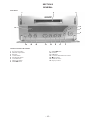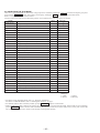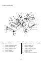
1
MDS-SD1
SERVICE MANUAL
AEP Model
UK Model
E Model
MDS-SD1 is the minidisc deck that can
be used only with section CMT-SD1/SD3.
US and foreign patents licensed from Dolby Laboratories
Licensing Corporation.
Model Name Using Similar Mechanism
MDS-JE520
MD Mechanism Type
MDM-5A
Base Unit Type
MBU-5A
Optical Pick-up Type
KMS-260A/J1N
SPECIFICATIONS
MINIDISC DECK
MICROFILM
–1–
SELF-DIAGNOSIS FUNCTION
The self-diagnosis function consists of error codes for customers which are displayed automatically when errors occur, and error codes which
show the error history in the test mode during servicing. For details on how to view error codes for the customer, refer to the following box
in the instruction manual. For details on how to check error codes during servicing, refer to the following “Procedure for using the SelfDiagnosis Function (Error History Display Mode)”.
Procedure for using the Self-Diagnosis Function (Error History Display Mode).
Note: Perform the self-diagnosis function in the “error history display mode” in the test mode. The following describes the least required
procedure. Be careful not to enter other modes by mistake. If you set other modes accidentally, press the MENU/NO button to exit
the mode.
1. While pressing the ENTER/YES button and π button, connect the power plug to the outlet, and release the ENTER/YES button and
π button.
2. “TEMP CHECK” will be displayed. Press the MENU/NO button to display “Check”.
3. Rotate the – ˜ + knob and when “[Service]” is displayed, press the ENTER/YES button.
4. Rotate the – ˜ + knob and display “ERR DP MODE”.
5. Pressing the ENTER/YES button sets the error history mode and displays “total rec”.
6. Select the contents to be displayed or executed using the – ˜ + knob.
7. Pressing the CD SYNC/MD WM SYNC button will display or execute the contents selected.
8. Pressing the CD SYNC/MD WM SYNC button another time returns to step 5.
9. Pressing the MENU/NO button displays “ERROR DP MODE” and exits the error history mode.
10.To exit the test mode, press the 1/u button. The unit sets into the STANDBY state, the disc is ejected, and the test mode ends.
–2–
ITEMS OF ERROR HISTORY MODE ITEMS AND CONTENTS
Selecting the Test Mode
Display
Details of History
Displays the recording time.
Displayed as “rππππππh”.
The displayed time is the total time the laser is set to the high power state.
This is about 1/4 of the actual recording time.
The time is displayed in decimal digits from 0h to 65535h.
total rec
total play
Displays the play time.
Displayed as “pππππππh”. The time displayed is the total actual play time. Pauses are not counted.
The time is displayed in decimal digits from 0h to 65535h.
retry err
Displays the total number of retries during recording and number of retry errors during play.
Displayed as “rππ pππ”.
“r” indicates the retries during recording while “p” indicates the retry errors during play.
The number of retries and retry errors are displayed in hexadecimal digits from 00 to FF.
total err
Displays the total number of errors.
Displayed as “total ππ”.
The number of errors is displayed in hexadecimal digits from 00 to FF.
err history
Displays the 10 latest errors.
Displayed as “0π E@@”.
π indicates the history number. The smaller the number, the more recent is the error. (00 is the latest).
@@ indicates the error code.
Refer to the following table for the details. The error history can be switched by rotating the – ˜ + knob.
er refresh
Mode which erases the “retry err”, “total err”, and “err history” histories.
When returning the unit to the customer after completing repairs, perform this to erase the past error history,
After pressing the CD SYNC/MD WM SYNC button and “er refresh?” is displayed, press the ENTER/YES
button to erase the history.
“Complete!” will be displayed momentarily.
Be sure to check the following when this mode has been executed.
• The data has been erased.
• The mechanism operates normally when recording and play are performed.
tm refresh
Mode which erases the “total rec” and “total play” histories.
These histories serve as approximate indications of when to replace the optical pickup.
If the optical pickup has been replaced, perform this operation and erase the history.
After pressing the CD SYNC/MD WM SYNC button and “tm refresh?” is displayed, press the ENTER/YES
button to erase the history.
“Complete!” will be displayed momentarily.
Be sure to check the following when this mode has been executed.
• The data has been erased.
• The mechanism operates normally when recording and play are performed.
Table of Error Codes
Error Code
Details of Error
Error Code
E00
No error
E05
Details of Error
FOK has deviated
E01
Disc error. PTOC cannot be read
E06
Cannot focus (Servo has deviated)
(DISC ejected)
E07
Recording retry
Disc error. UTOC error
E08
Recording retry error
(DISC not ejected)
E09
Playback retry error
E02
E03
Loading error
E04
Address cannot be read (Servo has deviated)
(Access error)
E0A
–3–
Play retry error (C2 error)
CAUTION
Laser component in this product is capable of emitting radiation
exceeding the limit for Class 1.
Danger of explosion if battery is incorrectly replaced.
Replace only with the same or equivalent type recommended by
the equipment manufacturer.
Discard used batteries according to manufacture’s instructions.
This appliance is classified as
a CLASS 1 LASER product.
The CLASS 1 LASER PRODUCT MARKING is located on
the rear exterior.
ADVARSEL!
Lithiumbatteri - Eksplosionsfare ved fejlagtig håndtering.
Udskiftning må kun ske med batteri af samme fabrikat og type.
Levér det brugte batteri tilbage til leverandøren.
This caution
label is located
inside the unit.
ADVARSEL
Eksplosjonsfare ved feilakting skifte av batteri.
Benytt samme batteritype eller en tilsvarende type anbefalt av
apparatfabrikanten.
Brukte batterier katterier kasseres i henhold til fabrikantens
VARNIG
CAUTION
Explosionsfara vid felaktigt batteribyte.
Använd samma batterityp eller en likvärdig typ som rekommenderas
av apparattillverkaren.
Kassera använt batteri enligt gällande föreakrifter.
VAROITUS
Parist voi räjähtää, jos se on virheellisesti asennettu.
Vaihda paristo ainoastaan laitevalmistajan suosittelemaan tyyppiin.
Hävitä käytetty paristo valmistajan ohjeiden mukaisesti.
Use of controls or adjustments or performance of procedures
other than those specified herein may result in hazardous radiation exposure.
Notes on chip component replacement
• Never reuse a disconnected chip component.
• Notice that the minus side of a tantalum capacitor may be
damaged by heat.
Flexible Circuit Board Repairing
• Keep the temperature of soldering iron around 270˚C
during repairing.
• Do not touch the soldering iron on the same conductor of the
circuit board (within 3 times).
• Be careful not to apply force on the conductor when soldering
or unsoldering.
MODEL IDENTIFICATION
– Specification Label –
Parts No.
MODEL
AEP, UK model
SP, HK model
SAFETY-RELATED COMPONENT WARNING !!
COMPONENTS IDENTIFIED BY MARK ! OR DOTTED LINE
WITH MARK ! ON THE SCHEMATIC DIAGRAMS AND IN
THE PARTS LIST ARE CRITICAL TO SAFE OPERATION.
REPLACE THESE COMPONENTS WITH SONY PARTS
WHOSE PART NUMBERS APPEAR AS SHOWN IN THIS
MANUAL OR IN SUPPLEMENTS PUBLISHED BY SONY.
PARTS No.
4-212-572-1π
4-212-572-2π
• Abbreviation
HK : Hong Kong model
SP
: Singapore model
–4–
TABLE OF CONTENTS
1. SERVICING NOTE .......................................................... 6
2. GENERAL ........................................................................ 15
3. DISASSEMBLY
3-1.
3-2.
3-3.
3-4.
3-5.
Glass ASSY ......................................................................... 16
Front Panel ......................................................................... 16
Slider (CAM) ...................................................................... 17
Base Unit and BD Board .................................................... 17
SW Board and Loading Motor (M103) .............................. 18
4. TEST MODE ..................................................................... 19
5. ELECTRICAL ADJUSTMENTS ............................... 23
6. DIAGRAMS
6-1. Circuit Boards Location ...................................................... 32
6-2. Block Diagrams
• BD Section ....................................................................... 33
• Main Section .................................................................... 35
6-3. Printed Wiring Board – BD Section – ................................. 39
6-4. Schematic Diagram – BD (1/2) Section – ........................... 41
6-5. Schematic Diagram – BD (2/2) Section – ........................... 43
6-6. Schematic Diagram – Main (1/2) Section – ........................ 45
6-7. Schematic Diagram – Main (2/2) Section – ........................ 47
6-8. Printed Wiring Board – Main Section – .............................. 49
6-9. Schematic Diagram – Panel Section – ................................ 51
6-10. Printed Wiring Board – Panel Section – ........................... 53
6-11. Schematic Diagram – Connector Section – ...................... 55
6-12. Printed Wiring Board – Connector Section – ................... 57
6-13. Schematic Diagram – BD Switch Section – ..................... 59
6-14. Printed Wiring Board – BD Switch Section – .................. 59
6-15. Schematic Diagram – Encoder Section – ......................... 60
6-16. Printed Wiring Board – Encoder Section – ...................... 60
6-17. IC Block Diagrams ........................................................... 61
6-18. IC Pin Functions ............................................................... 64
7. EXPLODED VIEWS
7-1.
7-2.
7-3.
7-4.
Case and Back Panel Section .............................................. 67
Front Panel Section ............................................................. 68
Mechanism Section (MDM-5A) ......................................... 69
Base Unit Section (MBU-5A) ............................................. 70
8. ELECTRICAL PARTS LIST ........................................ 71
–5–
SECTION 1
SERVICING NOTE
JIG FOR CHECKING BD BOARD WAVEFORM
The special jig (J-2501-149-A) is useful for checking the waveform of the BD board. The names of terminals and the checking items to be
performed are shown as follows.
GND
I+3V
IOP
TEO
RF
VC
:
:
:
:
:
:
Ground
For measuring IOP (Check the deterioration of the optical pick-up laser)
For measuring IOP (Check the deterioration of the optical pick-up laser)
TRK error signal (Traverse adjustment)
RF signal (Check jitter)
Reference level for checking the signal
Mechanism deck
CN110
6P connector
5P Connector
VC
RF
TEO
IOP
I+3V
GND
RF
VC
1 RF
VC
TEO MDM-3
IOP
5 I+3V
TEO
IOP
I+3V
GND
–6–
1 VC
RF
TEO MDM-5
IOP
I+3V
6 GND
IOP DATA RECORDING AND DISPLAY WHEN PICKUP AND NON-VOLATILE MEMORY (IC171 OF BD BOARD)
ARE REPLACED
The IOP value labeled on the pick-up can be recorded in the non-volatile memory. By recording the value, it will eliminate the need to look
at the value on the label of the optical pick-up. When replacing the pick-up or non-volatile memory (IC171 of BD board), record the IOP
value on the pick-up according to the following procedure.
Record Precedure:
1. While pressing the ENTER/YES button and π button, connect the power plug to the outlet, and release the ENTER/YES button and
π button.
2. “TEMP CHECK” will be displayed. Press the MENU/NO button to display “Check”.
3. Rotate the – ˜ + knob to display “[Service]”, and press the ENTER/YES button.
4. Rotate the – ˜ + knob to display “lop.Write”, and press the ENTER/YES button.
5. The display becomes “Ref=@@@.@” (@ is an arbitrary number) and the numbers which can be changed will blink.
6. Input the IOP value written on the optical pick-up.
To select the number : Rotate the – ˜ + knob.
To select the digit
: Press the CD SYNC/MD WM SYNC button.
7. When the ENTER/YES button is pressed, the display becomes “Measu=@@@.@” (@ is an arbitrary number).
8. As the adjustment results are recorded for the step 6 value. Leave it as it is and press the ENTER/YES button.
9. “Complete!” will be displayed momentarily. The value will be recorded in the non-volatile memory and the display will become “Iop
Write”.
10.Press the 1/u button to complete. “Standby” will be displayed.
Display Precedure:
1. While pressing the ENTER/YES button and π button, connect the power plug to the outlet, and release the ENTER/YES button and
π button.
2. “TEMP CHECK” will be displayed. Press the MENU/NO button to display “Check”.
3. Rotate the – ˜ + knob to display “[Service]”, and press the ENTER/YES button.
4. Rotate the – ˜ + knob to display “lop.Read”.
5. “@@.@/##.#” is displayed and the recorded contents are displayed.
@@.@ : indicates the Iop value labeled on the pick-up.
##.#
: indicates the Iop value after adjustment
6. To end, press the CD SYNC/MD WM SYNC button or MENU/NO button to display “Iop Read”. Then press the 1/u button to display
“Standby”.
–7–
CHECKS PRIOR TO PARTS REPLACEMENT AND ADJUSTMENTS
Before performing repairs, perform the following checks to determine the faulty locations up to a certain extent.
Details of the procedures are described in “5 Electrical Adjustments”.
Laser power check
(5-6-2 : See page 25)
Traverse check
(5-6-3 : See page 25)
Focus bias check
(5-6-4 : See page 26)
C PLAY check
(5-6-5 : See page 26)
Self-recording/playback
check
(REC/PLAY)
(5-6-6 : See page 26)
TEMP check
(Temperature
compensation
offset check)
(5-6-1 : See page 25)
Criteria for Determination
(Unsatisfactory if specified value is not satisfied)
• 0.9 mW power
Specified value : 0.84 to 0.92 mW
• 7.0 mW power
Specified value : 6.8 to 7.2 mW
lop (at 7mW)
• Labeled on the optical pickup
Iop value ± 10mA
• Traverse waveform
Specified value : Below 10% offset
• Error rate check
Specified value : For points a, b, and c
C1 error : Below 220
AD error : Below 2
• Error rate check
Specified value:
a.When using test disc (MDW-74/AU-1)
C1 error : Below 80
AD error : Below 2
b.When using check disc (TDYS-1)
C1 error : Below 50
• CPLAY error rate check
Specified value:
C1 error : Below 80
AD error : Below 2
• Unsatisfactory if displayed as T=@@ (##) [NG]”
NG
(@@, ## are both arbitrary numbers)
Measure if unsatisfactory:
• Clean the optical pick-up
• Adjust again
• Replace the optical pick-up
• Replace the optical pick-up
• Replace the optical pick-up
• Replace the optical pick-up
• Replace the optical pick-up
If always unsatisfactory:
• Replace the overwrite head
• Check for disconnection of the circuits around the
overwrite head
If occasionally unsatisfactory:
• Check if the overwrite head is distorted
• Check the mechanism around the sled
• Check for disconnection of the circuits around D101
(BD board)
• Check the signals around IC101, IC121, CN102,
CN103 (BD board)
Note:
The criteria for determination above is intended merely to determine if satisfactory or not, and does not serve as the specified value for
adjustments.
When performing adjustments, use the specified values for adjustments.
–8–
FORCED RESET
The system microprocessor can be reset in the following procedure.
Use these procedure when the unit cannot be operated normally due to the overrunning of the microprocessor, etc.
Procedure :
Short-circuit jumper wire of JW40 and JW41 (RESET).
[MAIN BOARD] (Component Side)
3
IC821
JW40
1
JW42
–9–
CLEANING OF OBJECTIVE LENS OF OPTICAL PICKUP
• When cleaning the objective lens of the optical pickup, move the mechanism deck using the following method.
1 If a disc is inside, eject it out.
2 Disconnect the power cord from the outlet, and set the non-conducted state.
3 Using a pair of tweezers, while pulling the claw at A towards B, move part C in direction D.
4 Move part C to a position which allows it to be cleaned easily, and clean.
A
B
C
D
Objective lens of
optical pick-up
FLUORESCENT INDICATOR TUBE AND MECHANISM DECK
• The fluorescent indicator tube will not display anything if the mechanism deck is not connected to the MAIN board.
Before servicing, check the connection of the cables connecting these parts first.
– 10 –
ATTACHING THE GLASS ASSEMBLY
• Attach according to steps 1 to 4.
1
2
1
4 Screw (PTP2.6x6)
3 Bracket (shaft)
(Bottom side)
When fixing this part, secure at the
center to allow for some play.
Open and close the glass window
several times, and check that the
parts do not touch each other.
FLUORESCENT INDICATOR TUBE, LED COMPLETE LIGHTING CHECK
• The fluorescent indicator tube and LED complete lighting and key check mode of this unit can be performed as follows.
Procedure:
1. While pressing the ENTER/YES and rREC buttons, insert the power plug into the outlet, and turn ON the power.
2. “FL All On Key” will be displayed momentarily, after which immediately the fluorescent indicator tube and LED will light up completely.
3. The fluorescent display tube will go off part by part each time a button is pressed. When all buttons have been pressed, “Push Yen” will be
displayed.
4. When the ENTER/YES button is pressed next, “Seg Chk” will be displayed momentarily.
5. Checkered pattern will be displayed on the fluorescent display tube.
6. When the ENTER/YES button is pressed next, “Jog & LED Chk” will be displayed.
7. The LED lighting state changes each time the – ˜ + knob is rotated.
(The LED will stop reacting after the knob has been rotated to some extent. This is not a fault.)
8. When the ENTER/YES button is pressed, “Check End” will be displayed on the fluorescent indicator tube, and the check mode ends.
– 11 –
SERVICING POSITION
1 Remove the four screws securing the upper cover, and remove the upper cover.
2 Undo the bound cables.
3 Remove the two screws A securing the rear panel.
4 Remove the four screws B securing the transformer.
5 Remove the screw C securing the MAIN board.
6 Remove the MAIN board with the rear panel.
B
B
A
C
– 12 –
RETRY CAUSE DISPLAY MODE
• In this test mode, the causes for retry of the unit during recording can be displayed on the fluorescent indicator tube. During playback, the
“track mode” for obtaining track information will be set.
This is useful for locating the faulty part of the unit.
• The following will be displayed :
During recording and stop : Retry cause, number of retries, and number of retry errors.
During playback
: Information such as type of disc played, part played, copyright.
These are displayed in hexadecimal.
Precedure:
1. Load a recordable disc whose contents can be erased into the unit.
2. Press the MENU/NO button. When “Edit/Menu” is displayed on the fluorescent indicator tube, rotate the – ˜ + knob to display “All
Erase?”.
3. Press the ENTER/YES button.
4. When “All Erase??” is displayed on the fluorescent indicator tube.
5. Press the ENTER/YES button to display “Complete!!”, and press the π button immediately. Wait for about 15 seconds while pressing
the button.
6. When the “TOC” displayed on the fluorescent indicator tube goes off, release the π button.
7. Press the r REC button to start recording. Then press the fl button and start recording.
8. To check the “track mode”, press the fl button to start play.
9. To exit the test mode, press the 1/u button, and turn OFF the power. When “TOC” disappears, disconnect the power plug from the outlet.
If the test mode cannot be exited, refer to “Forced Reset” on page 8.
Fig. 1 Reading the Test Mode Display
(During recording and stop)
Fig. 2 Reading the Test Mode Display
(During playback)
RTs@@c##c**
Fluorescent display tube display
@@####**$$
Fluorescent display tube display
@@ : Cause of retry
## : Number of retries
** : Number of retry errors
@@
##
**
$$
:
:
:
:
Parts No. (name of area named on TOC)
Cluster
} Address (Physical address on disc)
Sector
Track mode (Track information such as copyright
information of each part)
Reading the Retry Cause Display
Higher Bits
Hexadecimal 8
Bit
Binary
4
2
1
Lower Bits
8
4
2
1
b7 b6 b5 b4 b3 b2 b1 b0
Hexadecimal
Cause of Retry
Occurring conditions
0
0
0
0
0
0
0
1
01
shock
0
0
0
0
0
0
1
0
02
ader5
0
0
0
0
0
1
0
0
04
Discontinuous address When ADIP address is not continuous
0
0
0
0
1
0
0
0
08
DIN unlock
When DIN unlock is detected
0
0
0
1
0
0
0
0
10
FCS incorrect
When not in focus
0
0
1
0
0
0
0
0
20
IVR rec error
When ABCD signal level exceeds the specified range
0
1
0
0
0
0
0
0
40
CLV unlock
When CLV is unlocked
1
0
0
0
0
0
0
0
80
Access fault
When access operation is not performed normally
When track jump (shock) is detected
When ADER was counted more than five times
continuously
Reading the Display:
Convert the hexadecimal display into binary display. If more than two causes, they will be added.
Example
When 42 is displayed:
Higher bit : 4 = 0100 n b6
Lower bit : 2 = 0010 n b1
In this case, the retry cause is combined of “CLV unlock” and “ader5”.
When A2 is displayed:
Higher bit : A = 1010 n b7+b5
Lower bit : 2 = 0010 n b2
The retry cause in this case is combined of “access fault”, “IVR rec error”, and “ader5”.
– 13 –
Reading the Track Mode Display
Higher Bits
Hexadecimal 8
Bit
Binary
4
2
1
Lower Bits
8
4
2
1
b7 b6 b5 b4 b3 b2 b1 b0
Details
Hexadecimal
When 0
When 1
0
0
0
0
0
0
0
1
01
Emphasis OFF
Emphasis ON
0
0
0
0
0
0
1
0
02
Monaural
Stereo
0
0
0
0
0
1
0
0
04
This is 2-bit display. Normally 01.
0
0
0
0
1
0
0
0
08
01:Normal audio. Others:Invalid
0
0
0
1
0
0
0
0
10
Audio (Normal)
Invalid
0
0
1
0
0
0
0
0
20
Original
Digital copy
0
1
0
0
0
0
0
0
40
Copyright
No copyright
1
0
0
0
0
0
0
0
80
Write prohibited
Write allowed
Reading the Display:
Convert the hexadecimal display into binary display. If more than two causes, they will be added.
Example When 84 is displayed:
Higher bit : 8 = 1000 n b7
Lower bit : 4 = 0100 n b2
In this case, as b2 and b7 are 1 and others are 0, it can be determined that the retry cause is combined of “emphasis OFF”, “monaural”,
“original”, “copyright exists”, and “write allowed”.
Example When 07 is displayed:
Higher bit : 0 = 1000 n All 0
Lower bit : 7 = 0111 n b0+b1+b2
In this case, as b0, b1, and b2 are 1 and others are 0, it can be determined that the retry cause is combined of “emphasis ON”, “stereo”,
“original”, “copyright exists”, and “write prohibited”.
Hexadecimal n Binary Conversion Table
Hexadecimal
Binary
Hexadecimal
Binary
0
0000
8
1000
1
0001
9
1001
2
0010
A
1010
3
0011
B
1011
4
0100
C
1100
5
0101
D
1101
6
0110
E
1110
7
0111
F
1111
– 14 –
SECTION 2
GENERAL
Front Panel
2
1
3
4
15
5
6
14
13
12
11
10
9
8
7
Location of Parts and Controls
1
2
3
4
5
6
7
8
1/u (Power) button
MD disk compartment
§ button
CLEAR button
ENTER/YES button
VOLUME knob
MENU/NO button
±/) button
9
10
11
12
13
14
15
– 15 –
≠/0 button
π button
fl button
CD SYNC/MD WM SYNC button
r REC button
DISPLAY button
Display window
SECTION 3
DISASSEMBLY
Note: Follow the disassembly procedure in the numerical order given.
3-1. GLASS ASSY
4
3
4
1 Screw (PTP2.6x6)
2 Bracket (shaft)
(Bottom side)
3-2. FRONT PANEL
3 Flat type wire (13core)
(CN791)
4 Connector (CN793)
5 Front panel
1 Two screws (BVTP3x8)
– 16 –
2 Connector (CN792)
3-3. SLIDER (CAM)
6 Slider (Cam)
Set the shaft of Cam gear to
be at the position in the figure.
2 Bracket (Guide L)
1 Two screws (BTP2.6x6)
Set the shaft of Lever (O/C) to
be at the position in the figure.
3 Leaf spring
4 Two screws (BTP2.6x6)
5 Bracket (Guide R)
3-4. BASE UNIT AND BD BOARD
2 Base unit (MBU-5A)
5 Flexible board
(CN104)
6 Flexible board
(CN101)
1 Three screws
(BTP2.6x6)
3 Remove the solder (Five portion)
7 BD board
4 Screw (M1.7x4)
– 17 –
3-5. SW BOARD AND LOADING MOTOR (M103)
1 Screw (PTPWH M2.6x6)
2 Gear B
3 Two screws
(PWH1.7x4)
4 Loading motor (M103)
6 SW board
5 Two screws (BTP2.6x6)
– 18 –
SECTION 4
TEST MODE
4-1. PRECAUTIONS FOR USE OF TEST MODE
• As loading related operations will be performed regardless of the test mode operations being performed, be sure to check that the disc is
stopped before setting and removing it.
Even if the § button is pressed while the disc is rotating during continuous playback, continuous recording, etc., the disc will not stop
rotating.
Therefore, it will be ejected while rotating.
Be sure to press the § button after pressing the MENU/NO button and the rotation of disc is stopped.
4-1-1. Recording laser emission mode and operating buttons
•
•
•
•
•
•
Continuous recording mode (CREC MODE)
Laser power check mode (LDPWR CHECK)
Laser power adjustment mode (LDPWR ADJUST)
Traverse (MO) check (EF MO CHECK)
Traverse (MO) adjustment (EF MO ADJUST)
When pressing the rREC button.
4-2. SETTING THE TEST MODE
The following are two methods of entering the test mode.
Procedure 1: While pressing the ENTER/YES button and π button, connect the power plug to an outlet, and release the ENTER/YES
button and π button.
When the test mode is set “TEMP CHECK” will be displayed. Press the MENU/NO button to display “Check”.
“[Check]” will be displayed. Rotating the – ˜ + knob switches between the following four groups; ···Nn Check Nn
Adjust Nn Service Nn Develop Nn ···.
Procedure 2: While pressing the ENTER/YES button, connect the power plug to the outlet and release the ENTER/YES button.
When the test mode is set, “TEMP CHECK” will be displayed. By setting the test mode using this method, only the “Check”
group of method 1 can be executed.
4-3. EXITING THE TEST MODE
Press the 1/u button in the mode other than “TEMP CHECK”. The disc is ejected when loaded, and “Standby” display blinks, and the
STANDBY state is set.
4-4. BASIC OPERATIONS OF THE TEST MODE
All operations are performed using the – ˜ + knob, ENTER/YES button, and MENU/NO button.
The functions of these buttons are as follows.
Function name
Function
– ˜ + knob
Changes parameters and modes
ENTER/YES button
Proceeds onto the next step. Finalizes input.
MENU/NO button
Returns to previous step. Stops operations.
– 19 –
4-5. SELECTING THE TEST MODE
There are 31 types of test modes as shown below. The groups can be switched by rotating the – ˜ + knob. After selecting the group to be
used, press the ENTER/YES button. After setting a certain group, rotating the – ˜ + knob switches between these modes.
Refer to “Group” in the table for details selected.
All items used for servicing can be treated using group S. So be carefully not to enter other groups by mistake.
Display
Mark
Contents
Group (*)
TEMP CHECK
Temperature compensation offset check
C
S
LDPWR CHECK
Laser power check
C
S
EF MO CHECK
Traverse (MO) check
C
S
EF CD CHECK
Traverse (CD) check
C
S
FBIAS CHECK
Focus bias check
C
S
S curve CHECK
S letter check
(X)
C
VERIFY MODE
Non-volatile memory check
(X)
C
DETRK CHECK
Detrack check
(X)
C
TEMP ADJUST
Temperature compensation offset adjustment
A
S
LDPWR ADJUST
Laser power adjustment
A
S
EF MO ADJUST
Traverse (MO) adjustment
A
S
EF CD ADJUST
Traverse (CD) adjustment
A
S
FBIAS ADJUST
Focus bias adjustment
A
S
EEP MODE
Non-volatile memory control
(X) (!)
D
MANUAL CMD
Command transmission
(X)
D
SVDATA READ
Status display
(X)
D
ERR DP MODE
Error history display, clear
S
Sled check
(X)
D
Access check
(X)
D
0920 CHECK
Outermost circumference check
(X)
D
HEAD ADJUST
Head position check
(X)
D
CPLAY2 MODE
Same functions as CPLAY MODE
(X)
D
CREC2 MODE
Same functions as CREC MODE
(X)
D
ADJ CLEAR
Initialization of non-volatile memory of adjustment value
A
S
AG Set (MO)
Auto gain output level adjustment (MO)
A
S
AG Set (CD)
Auto gain output level adjustment (CD)
A
S
Iop Read
IOP data display
Iop Write
IOP data write
SLES MOVE
ACCESS MODE
C
S
A
S
INFOMATION
Microprocessing version display
C
S
CPLAY MODE
Continuous play mode
C
A
S
D
CREC MODE
Continuous recording mode
C
A
S
D
Group (*)
C: Check
S: Service
A: Adjust
D: Develop
• For details of each adjustment mode, refer to “5. Electrical Adjustments”.
For details of “ERR DP MODE”, refer to “Self-Diagnosis Function” on page 2.
• If a different mode has been selected by mistake, press the MENU/NO button to exit that mode.
• Modes with (X) in the Mark column are not used for servicing and therefore are not described in detail. If these modes are set accidentally,
press the MENU/NO button to exit the mode immediately. Be especially careful not to set the modes with (!) as they will overwrite the
non-volatile memory and reset it, and as a result, the unit will not operate normally.
– 20 –
4-5-1. Operating the Continuous Playback Mode
1. Entering the continuous playback mode
1 Set the disc in the unit. (Whichever recordable discs or discs for playback only are available.)
2 Rotate the – ˜ + knob and display “CPLAY MODE”.
3 Press the ENTER/YES button to change the display to “CPLAY MID”.
4 When access completes, the display changes to “C1 =
AD = ”.
Note : The numbers “ ” displayed show you error rates and ADER.
2. Changing the parts to be played back
1 Press the ENTER/YES button during continuous playback to change the display as below.
“CPLAY MID” n “CPLAY OUT” n “CPLAY IN”
When pressed another time, the parts to be played back can be moved.
2 When access completes, the display changes to “C1 =
AD = ”.
Note : The numbers “ ” displayed show you error rates and ADER.
3. Ending the continuous playback mode
1 Press the MENU/NO button. The display will change to “CPLAY MODE”.
2 Press the § button to remove the disc.
Note : The playback start addresses for IN, MID, and OUT are as follows.
IN
40h cluster
MID 300h cluster
OUT 700h cluster
4-5-2. Operating the Continuous Recording Mode (Use only when performing self-recording/palyback check.)
1. Entering the continuous recording mode
1 Set a recordable disc in the unit.
2 Rotate the – ˜ + knob and display “CREC MODE”.
3 Press the ENTER/YES button to change the display to “CREC MID”.
4 When access completes, the display changes to “CREC (
” and REC lights up.
Note : The numbers “ ” displayed shows you the recording position addresses.
2. Changing the parts to be recorded
1 When the ENTER/YES button is pressed during continuous recording, the display changes as below.
“CPLAY MID” n “CPLAY OUT” n “CPLAY IN”
When pressed another time, the parts to be recorded can be changed. REC goes off.
2 When access completes, the display changes to “CREC (
)” and REC lights up.
Note : The numbers “ ” displayed shows you the recording position addresses.
3. Ending the continuous recording mode
1 Press the MENU/NO button. The display changes to “CREC MODE” and REC goes off.
2 Press the § button to remove the disc.
Note 1 : The recording start addresses for IN, MID, and OUT are as follows.
IN
40h cluster
MID 300h cluster
OUT 700h cluster
Note 2 : The MENU/NO button can be used to stop recording anytime.
Note 3 : Do not perform continuous recording for long periods of time above 5 minutes.
Note 4 : During continuous recording, be careful not to apply vibration.
4-5-3. Non-Volatile Memory Mode (EEP MODE)
This mode reads and writes the contents of the non-volatile memory.
It is not used in servicing. If set accidentally, press the MENU/NO button immediately to exit it.
4-6. FUNCTIONS OF OTHER BUTTONS
Contents
Function
¢
Sets continuous playback when pressed in the STOP state. When pressed during continuous playback, the tracking servo turns
ON/OFF.
π
Stops continuous playback and continuous recording.
)/±
The sled moves to the outer circumference only when this is pressed.
0/≠
The sled moves to the inner circumference only when this is pressed.
SCROLL
Switches between the pit and groove modes when pressed.
DISPLAY
Switches the displayed contents each time the button is pressed
§
Ejects the disc
1/u
Exits the test mode
– 21 –
4-7. TEST MODE DISPLAYS
Each time the DISPLAY button is pressed, the display changes in the following order.
1. Mode display
Displays “TEMP ADJUST”, “CPLAYMODE”, etc.
Mode display
2. Error rate display
Displays the error rate in the following way.
C1 =
AD =
C1 = Indicates the C1 error.
AD = Indicates ADER.
Error rate display
Address display
Auto gain display (Not used in servicing)
3. Address display
The address is displayed as follows. (MO:recordable disc, CD:playback only disc)
Pressing the CLEAR button switches between the group display and bit display.
h=
s=
(MO pit and CD)
h=
a=
(MO groove)
h = Indicates the header address.
s = Indicates the SUBQ address.
a = Indicates the ADIP address.
Detrack check display (Not used in servicing)
IVR display (Not used in servicing)
Note: “–” is displayed when servo is not imposed.
4. Auto gain display (Not used in servicing)
The auto gain is displayed as follows.
AG =
/
[ ]
5. Detrack check display (Not used in servicing)
The detrack is displayed as follows.
ADR =
6. IVR display (Not used in servicing)
The IVR is displayed as follows.
][
]
[ ][
MEANINGS OF OTHER DISPLAYS
Contents
Display
When Off
When Lit
¢
During continuous playback (CLV: ON)
STOP (CLV: OFF)
P
Tracking servo OFF
Tracking servo ON
SYNC
CLV low speed mode
CLV normal mode
LEVEL-SYNC
ABCD adjustment completed
OVER
Tracking offset cancel ON
REPEAT
Tracking auto gain OK
1
Focus auto gain OK
TRACK
Pit
Groove
DISC
High reflection
Low reflection
DATE
CLV-S
CLV-A
MONO
CLV LOCK
CLV UNLOCK
Tracking offset cancel OFF
– 22 –
SECTION 5
ELECTRICAL ADJUSTMENTS
5-1. PARTS REPLACEMENT AND ADJUSTMENT
• Check and adjust the MDM and MBU as follows.
The procedure changes according to the part replaced
• Abbreviation
OP : Optical pick-up
OWH: Overwrite head
• Temperature compensation offset check
• Laser power check
• Traverse check
• Focus bias check
• C PLAY check
• Self-recording/playback check
OK
NG
Check the sleding and spindle
mechanisms.
Other causes can be suspected.
Parts Replacement and Repair
YES
Has the OWH been replaced?
NO
Has OP, IC171, IC101, or
IC121 been replaced?
YES
Initial setting of the adjustment value
NO
NO
Has OP or IC171 been replaced?
YES
IOP information recording
(IOP value labeled on OP)
Has IC171 or D101
been replaced?
NO
YES
Temperature compensation offset adjustment
• Laser power adjustment
• Traverse adjustment
• Focus bias adjustment
• Error rate adjustment
• Focus bias check
• Auto gain adjustment
– 23 –
5-2. PRECAUTIONS FOR CHECKING LASER DIODE
EMISSINON
To check the emission of the laser diode during adjustments, never
view directly from the top as this may lose your eye-sight.
5-3. PRECAUTIONS FOR USE OF OPTICAL PICKUP (KMS-260A)
As the laser diode in the optical pick-up is easily damaged by static
electricity, solder the laser tap of the flexible board when using it.
Before disconnecting the connector, desolder first. Before connecting the connector, be careful not to remove the solder. Also take
adequate measures to prevent damage by static electricity. Handle
the flexible board with care as it breaks easily.
pick-up
flexible board
laser tap
Optical pick-up flexible board
4) Use the following tools and measuring devices.
• Check Disc (MD) TDYS-1
(Parts No. 4-963-646-01)
• Test Disk (MDW-74/AU-1) (Parts No. 8-892-341-41)
• Laser power meter LPM-8001 (Parts No. J-2501-046-A)
or
MD Laser power meter 8010S (Parts No. J-2501-145-A)
(NOTE:)
• Oscilloscope (Measure after performing CAL of prove.)
• Digital voltmeter
• Thermometer
• Jig for checking BD board waveform
(Parts No. : J-2501-149-A)
5) When observing several signals on the oscilloscope, etc.,
make sure that VC and ground do not connect inside the oscilloscope.
(VC and ground will become short-circuited.)
6) Using the above jig enables the waveform to be checked without
the need to solder.
(Refer to Servicing Note on page 6.)
7) As the disc used will affect the adjustment results, make sure
that no dusts nor fingerprints are attached to it.
Note:
When performing laser power checks and adjustment (electrical
adjustment), use of the new MD laser power meter 8010S (J-2501145-A) instead of the conventional laser power meter is convenient.
It sharply reduces the time and trouble to set the laser power meter
sensor onto the objective lens of the pick-up.
5-5. CREATING CONTINUOUSLY RECORDED DISC
5-4. PRECAUTIONS FOR ADJUSTMENTS
1) When replacing the following parts, perform the adjustments
and checks with ¬ in the order shown in the following table.
Optical
Pick-up IC171
BD Board
D101
IC101, IC121 IC192
1. Initial setting of
adjustment value
¬
¬
G
¬
G
2. Recording of IOP
information
(Value written in
the pick-up)
¬
¬
G
G
G
3. Temperature
compensation
offset adjustment
G
¬
¬
G
G
4. Laser power
adjustment
¬
¬
G
¬
¬
5. Traverse
adjustment
¬
¬
G
¬
G
6. Focus bias
adjustment
¬
¬
G
¬
G
7. Error rate check
¬
¬
G
¬
G
8. Auto gain output
level adjustment
¬
¬
G
¬
G
* This disc is used in focus bias adjustment and error rate check.
The following describes how to create a continuous recording disc.
1. Insert a disc (blank disc) commercially available.
2. Rotate the – ˜ + knob and display “CREC MODE”.
3. Press the ENTER/YES button again to display “CREC MID”.
Display “CREC (0300)” and start to recording.
4. Complete recording within 5 minutes.
5. Press the MENU/NO button and stop recording .
6. Press the § button and remove the disc.
The above has been how to create a continuous recorded data for
the focus bias adjustment and error rate check.
Note :
• Be careful not to apply vibration during continuous recording.
2) Set the test mode when performing adjustments.
After completing the adjustments, exit the test mode.
Perform the adjustments and checks in “group S” of the test mode.
3) Perform the adjustments to be needed in the order shown.
– 24 –
5-6. CHECKS PRIOR TO REPAIRS
These checks are performed before replacing parts according to
“approximate specifications” to determine the faulty locations. For
details, refer to “Checks Prior to Parts Replacement and
Adjustments” (See page 8).
5-6-1. Temperature Compensation Offset Check
When performing adjustments, set the internal temperature and room
temperature to 22 to 28 C.
Checking Procedure:
1. Rotate the – ˜ + knob to display “TEMP CHECK”.
2. Press the ENTER/YES button.
3. “T=@@(##) [OK]” should be displayed. If “T=@@ (##) [NG]”
is displayed, it means that the results are bad.
(@@ indicates the current value set, and ## indicates the value
written in the non-volatile memory.)
5-6-2. Laser Power Check
Before checking, check the IOP value of the optical pick-up.
(Refer to 5-8. Recording and Displaying IOP Information.)
Connection :
Laser power
meter
Optical pick-up
objective lens
Note 1: After step 4, each time the ENTER/YES button is pressed,
the display will be switched between “LD 0.7 mW $ ”,
“LD 6.2 mW $ ”, and “LD Wp
$ ”. Nothing
needs to be performed here.
5-6-3. Traverse Check
Connection :
Oscilloscope
BD board
CN110 pin 3 (TE)
CN110 pin 1 (VC)
V : 0.5 V/div
H : 10 ms/div
Input : DC mode
Checking Procedure:
1. Connect an oscilloscope to CN110 pin 3 (TE) and CN110 pin
1 (VC) of the BD board.
2. Load a disc (any available on the market). (Refer to Note 1.)
3. Press the )/± button and move the optical pick-up outside the pit.
4. Rotate the – ˜ + knob and display “EF MO CHECK”.
5. Press the ENTER/YES button and display “EFB = MO-R”.
(Laser power READ power/Focus servo ON/tracking servo OFF/
spindle (S) servo ON)
6. Observe the waveform of the oscilloscope, and check that the
specified value is satisfied. Do not rotate the – ˜ + knob.
(Read power traverse checking)
(Traverse Waveform)
Digital volt meter
A
BD board
CN110 pin 5 (I+3V)
CN110 pin 4 (IOP)
VC
B
Checking Procedure:
1. Set the laser power meter on the objective lens of the optical
pick-up. (When it cannot be set properly, press the 0/≠
button or )/± button to move the optical pick-up.)
Connect the digital volt meter to CN110 pin 5 (I+3V) and
CN110 pin 4 (IOP).
2. Then, rotate the – ˜ + knob and display “LDPWR CHECK”.
3. Press the ENTER/YES button once and display “LD 0.9 mW $
”. Check that the reading of the laser power meter become
0.84 to 0.92 mW.
4. Press the ENTER/YES button once more and display “LD 7.0
mW $ ”. Check that the reading the laser power meter and
digital volt meter satisfy the specified value.
Specified value : Below 10% offset value
Offset value (%) = IA – BI X 100
2 (A + B)
7. Press the ENTER/YES button and display “EFB = MO-W”.
8. Observe the waveform of the oscilloscope, and check that the
specified value is satisfied. Do not rotate the – ˜ + knob.
(Write power traverse checking)
(Traverse Waveform)
A
Specified Value :
Laser power meter reading : 7.0 ± 0.2 mW
Digital voltmeter reading : Optical pick-up displayed value ± 10%
VC
B
(Optical pick-up label)
KMS
260A
27X40
B0825
Specified value : Below 10% offset value
(For details of the method for checking
this value, refer to “5-8. Recording and
Displaying IOP Information”.)
Offset value (%) = IA – BI X 100
2 (A + B)
N
Iop = 82.5 mA in this case
Iop (mA) = Digital voltmeter reading (mV)/1 (Ω)
5. Press the MENU/NO button and display “LDPWR CHECK”
and stop the laser emission.
(The MENU/NO button is effective at all times to stop the
laser emission.)
9. Press the ENTER/YES button display “EFB = MO-P”.
Then, the optical pick-up moves to the pit area automatically
and servo is imposed.
– 25 –
10. Observe the waveform of the oscilloscope, and check that the
specified value is satisfied. Do not rotate the – ˜ + knob.
(Traverse Waveform)
A
VC
B
Specified value : Below 10% offset value
Offset value (%) = IA – BI X 100
2 (A + B)
11. Press the ENTER/YES button display “EF MO CHECK”
The disc stops rotating automatically.
12. Press the § button and remove the disc.
13. Load the check disc (MD) TDYS-1.
14. Roteto the – ˜ + knob and display “EF CD CHECK”.
CD”.
15. Press the ENTER/YES button and display “EFB =
Servo is imposed automatically.
16. Observe the waveform of the oscilloscope, and check that the
specified value is satisfied. Do not rotate the – ˜ + knob.
(Traverse Waveform)
A
VC
B
Specified value : Below 10% offset value
Offset value (%) = IA – BI X 100
2 (A + B)
17. Press the ENTER/YES button and display “EF CD CHECK”.
18. Press the § button and remove the check disc (MD) TDYS-1.
Note 1 : MO reading data will be erased during if a recorded disc is
used in this adjustment.
Note 2 : If the traverse waveform is not clear, connect the oscilloscope as shown in the following figure so that it can be
seen more clearly.
Oscilloscope
BD board
CN110 pin 3 (TE)
CN110 pin 1 (VC)
330 kΩ
10pF
5-6-4. Focus Bias Check
Change the focus bias and check the focus tolerance amount.
Checking Procedure :
1. Load a test disk (MDW-74/AU-1).
2. Rotate the – ˜ + knob and display “CPLAY MODE”.
3. Press the ENTER/YES button twice and display “CPLAY MID”.
4. Press the MENU/NO button when “C1 =
AD = ” is
displayed.
5. Rotate the – ˜ + knob and display “FBIAS CHECK”.
6. Press the ENTER/YES button and display “
/ c = ”.
The first four digits indicate the C1 error rate, the two digits
after [/] indicate ADER, and the 2 digits after [c =] indicate the
focus bias value.
Check that the C1 error is below 220 and ADER is below 2.
7. Press the ENTER/YES button and display “
/ b = ”.
Check that the C1 error is below 220 and ADER is below 2.
8. Press the ENTER/YES button and display “
/ a = ”.
Check that the C1 error is below 220 and ADER is below 2.
9. Press the MENU/NO button, next press the § button, and
remove the test disc.
5-6-5. C PLAY Checking
MO Error Rate Check
Checking Procedure :
1. Load a test disk (MDW-74/AU-1).
2. Rotate the – ˜ + knob and display “CPLAY MODE”.
3. Press the ENTER/YES button and display “CPLAY MID”.
AD = ”.
4. The display changes to “C1 =
5. If the C1 error rate is below 80, check that ADER is below 2.
6. Press the MENU/NO button, stop playback, press the § button, and test disc.
CD Error Rate Check
Checking Procedure :
1. Load a check disc (MD) TDYS-1.
2. Rotate the – ˜ + knob and display “CPLAY MODE”.
3. Press the ENTER/YES button twice and display “CPLAY MID”.
4. The display changes to “C1 =
AD = ”.
5. Check that the C1 error rate is below 50.
6. Press the MENU/NO button, stop playback, press the § button, and the test disc.
5-6-6. Self-Recording/playback Check
Prepare a continuous recording disc using the unit to be repaired
and check the error rate.
Checking Procedure :
1. Insert a recordable disc (blank disc) into the unit.
2. Rotate the – ˜ + knob to display “CREC MODE”.
3. Press the ENTER/YES button to display the “CREC MID”.
4. When recording starts, “ REC ” is displayed, this becomes
“CREC @@@@" (@@@@ is the address), and recording starts.
5. About 1 minute later, press the MENU/NO button to stop
continuous recording.
6. Rotate the – ˜ + knob to display “C PLAY MODE”.
7. Press the ENTER/YES button to display “C PLAY MID”.
8. “C1 =
AD = ” will be displayed.
9. Check that the C1 error becomes below 80 and the AD error
below 2.
10. Press the MENU/NO button to stop playback, and press the
§ button and remove the disc.
– 26 –
5-7. INITIAL SETTING OF ADJUSTMENT VALUE
5-9. TEMPERATURE COMPENSATION OFFSET
ADJUTMENT
Note:
Mode which sets the adjustment results recorded in the non-volatile
memory to the initial setting value. However the results of the
temperature compensation offset adjustment will not change to the
initial setting value.
If initial setting is performed, perform all adjustments again
excluding the temperature compensation offset adjustment.
For details of the initial setting, refer to “5-4. Precautions on
Adjustments” and execute the initial setting before the adjustment
as required.
Save the temperature data at that time in the non-volatile memory
as 25 ˚C reference data.
Note :
1. Usually, do not perform this adjustment.
2. Perform this adjustment in an ambient temperature of 22 ˚C to
28 ˚C. Perform it immediately after the power is turned on when
the internal temperature of the unit is the same as the ambient
temperature of 22 ˚C to 28 ˚C.
3. When D101 has been replaced, perform this adjustment after the
temperature of this part has become the ambient temperature.
Adjusting Procedure :
1. Rotate the – ˜ + knob and display “TEMP ADJUST”.
2. Press the ENTER/YES button and select the “TEMP ADJUST”
mode.
3. “TEMP =
[OK]” and the current temperature data will be
displayed.
4. To save the data, press the ENTER/YES button.
When not saving the data, press the MENU/NO button.
5. When the ENTER/YES button is pressed, “TEMP = SAVE”
will be displayed and turned back to “TEMP ADJUST” display
then. When the MENU/NO button is pressed, “TEMP ADJUST” will be displayed immediatelly.
Setting Procedure :
1. Rotate the – ˜ + knob to display “ADJ CLEAR”.
2. Press the ENTER/YES button. “Complete!” will be displayed
momentarily and initial setting will be executed, after which “ADJ
CLEAR” will be displayed.
5-8. RECORDING AND DISPLAYING THE IOP
INFORMATION
The IOP data can be recorded in the non-volatile memory. The IOP
value on the label of the optical pickup and the IOP value after the
adjustment will be recorded. Recording these data eliminates the
need to read the label on the optical pick-up.
Recording Procedure :
1. While pressing the ENTER/YES button and π button, connect the power plug to the outlet, and release the ENTER/YES
button and π button.
2. “TEMP CHECK” will be displayed. Press the MENU/NO button to display “Check”.
3. Rotate the – ˜ + knob to display “[Service]”, and press the
ENTER/YES button.
4. Rotate the – ˜ + knob to display “Iop.Write”, and press the
ENTER/YES button.
5. The display becomes Ref=@@@.@ (@ is an arbitrary number)
and the numbers which can be changed will blink.
6. Input the IOP value written on the optical pick-up.
To select the number : Rotate the – ˜ + knob.
To select the digit : Press the CD SYNC/MD WM SYNC button.
7. When the ENTER/YES button is pressed, the display becomes
“Measu=@@@.@” (@ is an arbitrary number).
8. As the adjustment results are recorded for the step 7 value. Leave
it as it is and press the ENTER/YES button.
9. “Complete!” will be displayed momentarily. The value will be
recorded in the non-volatile memory and the display will become
“Iop Write”.
Display Procedure :
1. Rotate the – ˜ + knob to display “Iop.Read”.
2. “@@.@/##.#” is displayed and the recorded contents are
displayed.
@@.@ indicates the Iop value labeled on the pick-up.
##.# indicates the Iop value after adjustment
3. To end, press the CD SYNC/MD WM SYNC button. or MENU/
NO button to display “Iop Read”.
Specified Value :
” should be within “E0 - EF”, “F0 - FF”, “00 The “TEMP =
0F”, “10 - 1F” and “20 - 2F”.
5-10. LASER POWER ADJUSTMENT
Check the IOP value of the optical pick-up before adjustments.
(Refer to 5-8. Recording and Displaying IOP Information.)
Connection :
Laser power
meter
Optical pick-up
objective lens
Digital volt meter
BD board
CN110 pin 5 (I+3V)
CN110 pin 4 (IOP)
Adjusting Procedure :
1. Set the laser power meter on the objective lens of the optical
pick-up. (When it cannot be set properly, press the 0/≠
button or )/± button to move the optical pick-up.)
Connect the digital volt meter to CN110 pin 5 (I+3V) and
CN110 pin 4 (IOP).
2. Rotate the – ˜ + knob and display “LDPWR ADJUST”.
(Laser power : For adjustment)
3. Press the ENTER/YES button once and display “LD 0.9 mW $
”.
4. Rotate the – ˜ + knob so that the reading of the laser power
meter becomes 0.85 to 0.91 mW. Press the ENTER/YES button after setting the range knob of the laser power meter, and
save the adjustment results. (“LD SAVE $ ” will be displayed
for a moment.)
5. Then “LD 7.0 mW $ ” will be displayed.
6. Rotate the – ˜ + knob so that the reading of the laser power
meter becomes 6.9 to 7.1 mW, press the ENTER/YES button and
save it.
Note : Do not perform the emission with 7.0 mW more than 15
seconds continuously.
– 27 –
7. Then, rotate the – ˜ + knob and display “LDPWR CHECK”.
8. Press the ENTER/YES button once and display “LD 0.9 mW $
”. Check that the reading of the laser power meter become
0.85 to 0.91 mW.
9. Press the ENTER/YES button once more and display “LD 7.0
mW $ ”. Check that the reading the laser power meter and
digital volt meter satisfy the specified value.
Note down the digital voltmeter reading value.
5-11. TRAVERSE ADJUSTMENT
Connection :
Oscilloscope
BD board
CN110 pin 3 (TE)
CN110 pin 1 (VC)
V : 0.5 V/div
H : 10 ms/div
Input : DC mode
Specified Value :
Laser power meter reading : 7.0 ± 0.1 mW
Digital voltmeter reading : Optical pick-up displayed value ± 10%
(Optical pick-up label)
KMS
260A
27X40
B0825
(For details of the method for checking
this value, refer to “5-8. Recording and
Displaying IOP Information”.)
N
Iop = 82.5 mA in this case
Iop (mA) = Digital voltmeter reading (mV)/1 (Ω)
10. Press the MENU/NO button and display “LDPWR CHECK”
and stop the laser emission.
(The MENU/NO button is effective at all times to stop the
laser emission.)
11. Rotate the – ˜ + knob to display “Iop.Write”.
12. Press the ENTER/YES button. When the display becomes
Ref=@@@.@ (@ is an arbitrary number), press the ENTER/
YES button to display “Measu=@@@.@” (@ is an arbitrary
number).
13. The numbers which can be changed will blink. Input the Iop
value noted down at step 9.
To select the number : Rotate the – ˜ + knob.
To select the digit : Press the CD SYNC/MD WM SYNC button.
14. When the ENTER/YES button is pressed, “Complete!” will
be displayed momentarily. The value will be recorded in the
non-volatile memory and the display will become “Iop Write”.
Note 1: After step 4, each time the ENTER/YES button is pressed,
the display will be switched between “LD 0.7 mW $ ”,
“LD 6.2 mW $ ”, and “LD Wp
$ ”. Nothing
needs to be performed here.
Adjusting Procedure :
1. Connect an oscilloscope to CN110 pin 3 (TE) and CN110 pin
1 (VC) of the BD board.
2. Load a disc (any available on the market). (Refer to Note 1.)
3. Press the )/± button and move the optical pick-up outside the pit.
4. Rotate the – ˜ + knob and display “EF MO ADJUST”.
5. Press the ENTER/YES button and display “EFB = MO-R”.
(Laser power READ power/Focus servo ON/tracking servo OFF/
spindle (S) servo ON)
6. Rotate the – ˜ + knob so that the waveform of the oscilloscope becomes the specified value.
(When the – ˜ + knob is rotated, the of “EFB= ” changes
and the waveform changes.) In this adjustment, waveform varies at intervals of approx. 2%. Adjust the waveform so that the
specified value is satisfied as much as possible.
(Read power traverse adjustment)
(Traverse Waveform)
A
VC
B
Specification A = B
7. Press the ENTER/YES button and save the result of adjustment
to the non-volatile memory (“EFB = SAVE” will be displayed
for a moment. Then “EFB =
MO-W” will be displayed).
8. Rotate the – ˜ + knob so that the waveform of the oscilloscope becomes the specified value.
(When the – ˜ + knob is rotated, the of “EFB- ” changes
and the waveform changes.) In this adjustment, waveform varies at intervals of approx. 2%. Adjust the waveform so that the
specified value is satisfied as much as possible.
(Write power traverse adjustment)
(Traverse Waveform)
A
VC
B
Specification A = B
9. Press the ENTER/YES button, and save the adjustment results
in the non-volatile memory. (“EFB = SAVE” will be displayed
for a moment.)
10. “EFB =
MO-P”. will be displayed.
The optical pick-up moves to the pit area automatically and servo
is imposed.
– 28 –
11. Rotate the – ˜ + knob until the waveform of the oscilloscope moves closer to the specified value.
In this adjustment, waveform varies at intervals of approx. 2%.
Adjust the waveform so that the specified value is satisfied as
much as possible.
(Traverse Waveform)
A
VC
B
Specification A = B
12. Press the ENTER/YES button, and save the adjustment results
in the non-volatile memory. (“EFB =
SAVE” will be displayed for a moment.)
Next “EF MO ADJUST” is displayed. The disc stops rotating
automatically.
13. Press the § button and remove the disc.
14. Load the check disc (MD) TDYS-1.
15. Roteto – ˜ + knob and display “EF CD ADJUST”.
CD”.
16. Press the ENTER/YES button and display “EFB =
Servo is imposed automatically.
17. Rotate the – ˜ + knob so that the waveform of the oscilloscope moves closer to the specified value.
In this adjustment, waveform varies at intervals of approx. 2%.
Adjust the waveform so that the specified value is satisfied as
much as possible.
(Traverse Waveform)
A
5-12. FOCUS BIAS ADJUSTMENT
Adjusting Procedure :
1. Load a test disk (MDW-74/AU-1).
2. Rotate the – ˜ + knob and display “CPLAY MODE”.
3. Press the ENTER/YES button and display “CPLAY MID”.
AD = ” is
4. Press the MENU/NO button when “C1 =
displayed.
5. Rotate the – ˜ + knob and display “FBIAS ADJUST”.
6. Press the ENTER/YES button and display “
/ a = ”.
The first four digits indicate the C1 error rate, the two digits
after [/] indicate ADER, and the 2 digits after [a =] indicate the
focus bias value.
7. Rotate the – ˜ + knob in the clockwise direction and find the
focus bias value at which the C1 error rate becomes 220 (Refer
to Note 2).
8. Press the ENTER/YES button and display “
/ b = ”.
9. Rotate the – ˜ + knob in the counterclockwise direction and
find the focus bias value at which the C1 error rate becomes
approximately 220.
At this time, set the C1 error rate to about the same value set at
step 7.
10. Press the ENTER/YES button and display “
/ c = ”.
11. Check that the C1 error rate is below 50 and ADER is 00. Then
press the ENTER/YES button.
( )” is above 20, press the EN12. If the “( )” in “ TER/YES button.
If below 20, press the MENU/NO button and repeat the
adjustment from step 2.
13. Press the § button to remove the test disc.
Note 1 : The relation between the C1 error and focus bias is as
shown in the following figure. Find points a and b in the
following figure using the above adjustment. The focal
point position C is automatically calculated from points a
and b.
Note 2 : As the C1 error rate changes, perform the adjustment using the average vale.
VC
C1 error
B
approx.
220
Specification A = B
18. Press the ENTER/YES button, display “EFB = SAVE” for
a moment and save the adjustment results in the non-volatile
memory.
Next “EF CD ADJUST” will be displayed.
19. Press the § button and remove the check disc (MD) TDYS-1.
Note 1 : MO reading data will be erased during if a recorded disc is
used in this adjustment.
Note 2 : If the traverse waveform is not clear, connect the oscilloscope as shown in the following figure so that it can be
seen more clearly.
Oscilloscope
BD board
CN110 pin 3 (TE)
CN110 pin 1 (VC)
330 kΩ
10pF
– 29 –
b
c
a
Focus bias value
(F. BIAS)
5-13. ERROR RATE CHECK
5-15. AUTO GAIN CONTROL OUTPUT LEVEL
ADJUSTMENT
5-13-1. CD Error Rate Check
Checking Procedure :
1. Load a check disc (MD) TDYS-1.
2. Rotate the – ˜ + knob and display “CPLAY MODE”.
3. Press the ENTER/YES button twice and display “CPLAY MID”.
4. The display changes to “C1 =
AD = ”.
5. Check that the C1 error rate is below 20.
6. Press the MENU/NO button, stop playback, press the § button, and remove the test disc.
5-13-2. MO Error Rate Check
Checking Procedure :
1. Load a test disc (MDW-74/AU-1).
2. Rotate the – ˜ + knob and display “CPLAY MODE”.
3. Press the ENTER/YES button and display “CPLAY MID”.
4. The display changes to “C1 =
AD = ”.
5. If the C1 error rate is below 50, check that ADER is 00.
6. Press the MENU/NO button, stop playback, press the § button, and remove the test disc.
5-14. FOCUS BIAS CHECK
Change the focus bias and check the focus tolerance amount.
Checking Procedure :
1. Load a test disc (MDW-74/AU-1).
2. Rotate the – ˜ + knob and display “CPLAY MODE”.
3. Press the ENTER/YES button twice and display “CPLAY MID”.
4. Press the MENU/NO button when “C1 =
AD = ” is
displayed.
5. Rotate the – ˜ + knob and display “FBIAS CHECK”.
6. Press the ENTER/YES button and display “
/ c = ”.
The first four digits indicate the C1 error rate, the two digits
after [/] indicate ADER, and the 2 digits after [c =] indicate the
focus bias value.
Check that the C1 error is below 50 and ADER is below 2.
7. Press the ENTER/YES button and display “
/ b = ”.
Check that the C1 error is below 220 and ADER is below 2.
8. Press the ENTER/YES button and display “
/ a = ”.
Check that the C1 error is below 220 and ADER is below 2
9. Press the MENU/NO button, next press the § button, and
remove the continuously recorded disc.
Be sure to perform this adjustment when the pickup is replaced.
If the adjustment results becomes “Adjust NG!”, the pickup may be
faulty or the servo system circuits may be abnormal.
5-15-1. CD Auto Gain Control Output Level Adjustment
Adjusting Procedure :
1. Insert the check disc (MD) TDYS-1.
2. Rotate the – ˜ + knob to display “AG Set (CD)”.
3. When the ENTER/YES button is pressed, the adjustment will
be performed automatically.
“Complete!!” will then be displayed momentarily when the value
is recorded in the non-volatile memory, after which the display
changes to “AG Set (CD)”.
4. Press the § button to remove the disc.
5-15-2. MO Auto Gain Control Output Level Adjustment
Adjusting Procedure :
1. Insert the reference disc (MDW-74/AU-1) for recording.
2. Rotate the – ˜ + knob to display “AG Set (MO)”.
3. When the ENTER/YES button is pressed, the adjustment will
be performed automatically.
“Complete!!” will then be displayed momentarily when the value
is recorded in the non-volatile memory, after which the display
changes to “AG Set (MO)”.
4. Press the § button to remove the disc.
Note 1 : If the C1 error and ADER are above other than the specified
value at points a (step 8. in the above) or b (step 7. in the
above), the focus bias adjustment may not have been carried out properly. Adjust perform the beginning again.
– 30 –
5-15. ADJUSTING POINTS AND CONNECTING POINTS
[BD BOARD] (SIDE A)
CN101
D101
GND
I+3V
IOP
CN110
TE
RF
VC
NOTE
IC171
[BD BOARD] (SIDE B)
IC101
IC121
IC192
NOTE:It is useful to use the jig. for checking the waveform.
(Refer to Servicing Note on page 6.)
– 31 –
SECTION 6
DIAGRAMS
6-1. CIRCUIT BOARDS LOCATION
MAIN board
CONNECTOR board
SW board
PANEL SW board
BD board
PANEL board
ENCODER board
– 32 –
MDS-SD1
DIGITAL SERVO SIGNAL PROCESSOR, DIGITAL SIGNAL PROCESSOR
EFM/ACIRC ENCODER/DECODER, SHOCK-PROOF MEMORY CONTROLLER,
ATRAC ENCODER/DECODER
IC121
6-2. BLOCK DIAGRAMS
– BD SECTION –
OVER WRITE HEAD DRIVE
IC181
HEAD
DRIVE
Q181,182
MORFO
MORFI
RFO
AGCI
RF AMP
BPF
AUX
P-P
A
B
C
D
ABCD
ABCD
AMP
E
F
FOCUS
ERROR
AMP
IV AMP
AT
AMP
FE
ADAGC
ADIN
VC
ADFG
CVB
10
TRACKING
ERROR
AMP
TEMPI
TEMP
AMP
TE
SE
CSLED
XINIT
CLOCK
GENERATOR
OSCI
BOTM
64
PEAK
63
35
65
34
VC
31
XBCK
LRCK
ABCD
VC
ANALOG
MUX
SQSY
DQSY
SUBCODE
PROCESSOR
FE
66
VC
68
TE
75
SE
74
MNT3
MNT2
MNT1
MNT0
MONITOR
CONTROL
A/D
CONVERTER
SENS
SRDT
SCLK
SWDT
XLAT
30
32
78
ADFG
26
28
27
SERIAL
12
WBLADJ
EQADJ
3TADJ
APCREF
APC
11
22 23 25
PARALLEL
DECODER
SWDT
ADIP
DEMODULATOR/
DECODER
APC
SPINDLE
SERVO
VC
16
SCLK
17
XLAT
18
FOCNT
20
82
81
80
79
SERVO
DSP
PWM
GENERATOR
CPU
I/F
3
DIN1
25
ADDT
26
DADT
21
DOUT
28
27
BCK
LRCK
7
16
512FS
93
94
95
10
13
83 88 89 86 85 92 91
D0
D3
49 • 48 • 50 • 51
SQSY
DQSY
4
3
2
1
MNT3
9
8
6
5
7
SENS
SRDT
SCLK
SWDT
XLAT CH
MNT2
MNT1
MNT0
DRAM
IC124
XWE
47
XRAS
46
XCAS
44
XOE
43
A00
A09
34 31 • 36 40 • 45
APC
Q162,163
ILCC
3
11
12
AUTO
SEQUENCER
DTRF
CKRF
XLRF
FOCNT
DIN0
20
BUFFER IC123
20
PD
VICONV
LD
SAMPLING
RATE
CONVERTER
AUX1
19
DIGITAL
AUDIO
I/F
DOUT
APCREF
FFDR
FRDR
TFDR
TRDR
SFDR
SRDR
PD
ATRAC
ENCODER/
DECODER
RFI
RECP
14
67
PLL
SHOCK
RESISTANT
MEMORY
CONTROLLER
DADT
TEMPR
D101
LASER ON
SW
Q101
33
EFM,
ACIRC,
ENCODER/
DECODER
XRST
15
57
29
BPF
ADFM
VCC
VC
3
38
PCO
FILI
FILO
CLTV
IV AMP
E-F
BALANCE
VC
DIN1
FG IN
4
5
6
7
8
9
E
59
60
61
62
BOTM
36
PEAK
37
PEAK
&
BOTTOM
J
C B
D A
TX
RF AGC & EQ
F
I
RF
DIN0
EFMO
SPFD
DETECTOR
14
ADDT
RF AMP
IC101
48 47 46 40
I
1
J
2
3
100
4
5
6
OPTICAL PICK-UP BLOCK
(KMS-260A/J1N)
1
2
SPRD
• SIGNAL PATH
: PB
: REC
: PB (Digital out)
: REC (Digital in)
15
9
•
12
10
•
13
8
•
11
FILTER
HR901
OVER WRITE
HEAD
SCTX
DIG-RST
3
4
17
16
1
•
2
•
18
•
19
6
9
•
11
15
•
5
XWE
XRAS
XCAS
XOE
DQ1
DQ4
A0
A9
LDON
WRPWR
HF MODULE
SW
IC103,Q102-104
HF
MODULE
TRACKING
COIL
MOD
SLED/SPINDLE MOTOR DRIVE
FOCUS/TRACKING COIL DRIVE
IC152
FOCUS
COIL
TRK–
TRK+
FSC+
FSC–
M102
SLED MOTOR
M
M101
SPINDLE MOTOR
M
SLED+
SLED–
SPDL+
SPDL–
EEP ROM
IC171
10
12
DRIVER
14
15
21
23
DRIVER
18
19
27
25
DRIVER
29
30
6
8
DRIVER
3
4
PSB
16
5
SDA
SCL
6
SCL
TFDR
TRDR
DETECT SW
S101, S102,
S601-604
FRDR
FFDR
SFDR
SRDR
SPFD
SPRD
M103
LOADING MOTOR
XRST
M
LIMIT-IN
REFLECT
PROTECT
CHACK IN
PACK OUT
PLAY-P
REC P
LOAD-IN
LOAD-OUT
IDG-RST
09
– 33 –
SDA
– 34 –
MAIN
SECTION
(Page 35)
MDS-SD1
– MAIN SECTION –
IC601
4
OPT IN 1 CS/BS
3
6
J101
OPT IN 1 CD
IC601
DIN0
A/D,D/A CONVERTER
IC201
IC502
1
5
DIGITAL
OPTICAL
IC501
1
18 DATAO
L
VINL1 2
VINL2 6
IN
VINR1 4
DIN1
OPT OUT
DOUT
R-CH
MD
VOUTL 26
VOUTR 24 R-CH
5
BCK
LRCK
DADT
16 BCK
17 WS
19 DATAI
IC601
IC601
10
9
8
12 SYSCLK
+
–
6
ADDT
11
MUTE
Q101
7
L
OUT
R-CH
IC774
2
SWITCH
Q782
I CDATA
L3MODE 13
L3CLK 14
L3DATA 15
+B RIPPLE
FILTER
Q841
MUTE
DRIVE
Q171
2
I CCLK
3 SX
SWITCH
Q781
6 SY
+11.6V
BD SECTION
(Page 34)
CHACKIN
PACK-OUT
PLAY-P
REC-P
LD ON
WRPWR
MOD
LOAD-IN
LOAD OUT
LOADING
10
5
MOTER
DRIVE
2
6
IC301
4
54
LD-IN
55
CHACKIN
PACK-OUT
PB-P
REC-P
LDON
WR PWR
MOD
SDA
SCL
DIG-RST
LY 7
88
87
77
SDA
SCL
DIG-RST
1
3
J773
CONTROL I
2
L3CLK
L3DATA
L3MODE
MUTE
WMOUT
12
22
69
49
1
SYS3.3V
D172
D173
1
SWITCH
Q771
BUFFER
Q775
4
1
2
BUSY
2
I C CLK
3
5
SYSTEM
CONTROL
2
I C CLK
2
WMCLK
WMINV
WMSYNC
WMIN
XOUT
XIN
J772
To HCD-S1
2
2
IC772
4
IC702
45
19
100
SWITCH
Q772
2
6
3
5
BUFFER
Q774
2
J771
To TC-SD1
2
I C CLK
5
MD WM LINK
J421
X701
10MHz
13
15
1
BUSY
1
I2 CCLK 29
I 2 CDATA 30
R-CH
1
L-CH
2
3
JOG0 43
JOG1 44
3
1
DATA
CLOSE:ON(LOW)
OPEN:OFF(HIGH)
S991
SENSOR 39
D943-D946
ILLU 38
LED SWITCH
Q791,792
6
VCC
IC861
D943
±/)
XACCUT
D944
D945 D946
fl
≠\0 π
6
IC861
5
3
RECTIFIER
D815,816
2
3
SYS+3.3V
MATRIX
SWITCH
7
T801
POWER
TRANSFORMER
+11.6V
LD-LOVO
2
I CDATA
LD OUT
56
5
IC771
KEY0 97
LOADING SW
Q301,302
6
I 2C BUS
EXTENDER
IC774
SYSTEM CONTROL
IC701
SCTX
XINT
SQSY
DQSY
MNT3(S-LOCK)
MNT2(X-BUSY)
MNT1(SHOCK)
MNT0(F-OK)
SENS
SRDT
SCLK
SWDT
XLAT
LIMIT-IN
REFLECT
PROTECT
LX 2
4
X601
22.5792MHz
72
73
27
75
79
80
81
82
78
36
37
35
66
63
58
59
51
53
60
74
57
67
65
R
8
512FS
SCTX
XINT
SQSY
DQSY
MNT3
MNT2
MNT1
MNT0
SENS
SRDT
SCLK
SWDT
XLATCH
LIMIT-IN
REFLECT
PROTECT
R
VINR2 8
IC503
1
R-CH
LINE AMP
IC101
AC IN
+3.3V REG
IC821
RECTIFIER
D811,812
1
AC OUT
KEY1 95
1
DISPLAY
DRIVER
IC901
P1 1
FLDATA 31
FLCLK 33
FLCS 34
63 DAT
62 CLK
61 CS
-32V
P.DOWN 18
STB 50
56 VFL
P2 2
G13 52
LED SW
Q941
D941
LED SW
Q941
D942
GRID DRIVE
Q921
r REC
RESET
IC822
3
BACKUP+3.3V
AC
CD SYNC
MD WM SYNC
AC
UNSW+5V
FL901
AC
+5V
+5V OUT
Q831
3
+5V REG
IC831
1
S1
5
S35
I
G1
51
G12
FL901
FLUORESCENT
INDICATOR TUBE
–32V
+B SWITCH
Q832
3
–32V REG
IC851
RST 60
S.RST 12
– 35 –
– 36 –
1
• SIGNAL PATH
: PB
: REC
:PB(Digital out)
:REC(Digital in)
MDS-SD1
WAVEFORMS
– BD (1/2) SECTION –
THIS NOTE IS COMMON FOR PRINTED WIRING
BOARDS AND SCHEMATIC DIAGRAMS.
(In addition to this, the necessary note is printed
in each block.)
– MAIN SECTION –
1
1
0.46Vp-p
3.2Vp-p
For schematic diagrams.
Note:
• All capacitors are in µF unless otherwise noted. pF: µµF
50 WV or less are not indicated except for electrolytics
and tantalums.
• All resistors are in Ω and 1/4 W or less unless otherwise
specified.
¢
•
: internal component.
• C : panel designation.
10MHz
IC101 1, 2 (I, J) (PLAY mode)
IC701 !£ (XOUT)
2
2
3.8Vp-p
0.1Vp-p
44.1kHz
Note: The components identified by mark ! or dotted line
with mark ! are critical for safety.
Replace only with part number specified.
•
•
•
•
•
•
•
•
•
IC101 4 (A) (PLAY mode)
IC201 !¶ (LRCK1)
3
3
U : B+ Line.
V : B– Line.
H : adjustment for repair.
no mark : STOP
(
) : Play the test disc (TDYS-1)
<
> : REC
: Can not be measured.
∗
Voltages are taken with a VOM (Input impedance 10 MΩ).
Voltage variations may be noted due to normal production tolerances.
Waveforms are taken with a oscilloscope.
Voltage variations may be noted due to normal production tolerances.
Circled numbers refer to waveforms.
Signal path.
E : PB
q : REC
a : PB (DIGITAL OUT)
r : REC (DIGITAL IN)
Abbreviation
HK
: Hong Kong model.
SP
: Singapore model.
0.06Vp-p
3.4Vp-p
2.822MHz
IC201 !§ (BCK)
IC101 8, 9 (E, F) (PLAY mode)
4
3.0Vp-p
– BD (1/2) SECTION –
22.581MHz
4
IC201 !™ (SYSCLK)
3.1Vp-p
22.581MHz
IC121 !§ (OSCI)
5
3.2Vp-p
44.1kHz
IC121 @¶ (LRCK)
For printed wiring boards.
Note:
• X : parts extracted from the component side.
• Y : parts extracted from the conductor side.
•
p
: parts mounted on the conductor side.
®
•
: Through hole.
• b : Pattern from the side which enables seeing.
(The other layers' patterns are not indicated.)
Caution:
Pattern face side:
(Side B)
Parts face side:
(Side A)
6
3.8Vp-p
2.822MHz
IC121 @• (XBCK)
7
Parts on the pattern face side seen from the
pattern face are indicated.
Parts on the parts face side seen from the
parts face are indicated.
3.8Vp-p
11.29MHz
– DISPLAY SECTION –
IC121 @ª (FS256)
• Indication of transistor
Q
1
8
C
3.9Vp-p
3.2Vp-p
These are omitted
B E
2.4MHz
176.4kHz
IC901 %• (OSCO)
IC121 (º (FS4)
BC E
These are omitted
– 37 –
– 38 –
MDS-SD1
6-3. PRINTED WIRING BOARD – BD SECTION –
• See page 32 for Circuit Boards Location.
(Page 49)
• Semiconductor
Location
Ref. No.
Location
D101
D181
D183
A-1
D-3
D-3
IC103
IC123
IC171
B-1
D-2
D-1
Q102
Q103
Q104
B-1
B-1
B-1
(Page 49)
• Semiconductor
Location
– 39 –
Ref. No.
Location
IC101
IC121
IC124
IC152
IC181
IC192
A-3
C-3
C-3
B-1
C-1
D-1
Q101
Q162
Q163
Q181
Q182
B-3
B-3
B-3
C-1
C-2
– 40 –
MDS-SD1
6-4. SCHEMATIC DIAGRAM – BD (1/2) SECTION –
• See page 38 for Waveforms.
• See page 61 for IC Block Diagrams.
• See page 64 for IC Pin Functions.
RT1P441M-TP-1
RT1P441MTP-1
RT1P441M-TP-1
RT1P441M-TP-1
(Page 43)
– 41 –
(Page 43)
(Page 43)
(Page 44)
(Page 44)
(Page 44)
(Page 44)
– 42 –
MDS-SD1
6-5. SCHEMATIC DIAGRAM – BD (2/2) SECTION –
• See page 38 for Waveforms.
• See page 39 for Printed Wiring Board.
(Page 41)
(Page 41)
(Page 41)
(Page 42)
(Page 42)
(Page 45)
(Page 45)
S-24CO2AFJA-TB
– 43 –
– 44 –
(Page 42)
(Page 42)
MDS-SD1
6-6. SCHEMATIC DIAGRAM – MAIN (1/2) SECTION –
• See page 38 for Waveforms.
• See page 49 for Printed Wiring Board.
• See page 65 for IC Pin Functions.
(Page 59)
(Page 43)
(Page 55, 56)
(Page 43)
(Page 60)
(Page 47)
– 45 –
(Page 47)
(Page 48)
– 46 –
MDS-SD1
6-7. SCHEMATIC DIAGRAM – MAIN (2/2) SECTION –
• See page 38 for Waveforms.
• See page 62 for IC Block Diagrams.
(Page 45)
(Page 45)
(Page 46)
(Page 52)
– 47 –
– 48 –
MDS-SD1
6-8. PRINTED WIRING BOARD – MAIN SECTION –
• See page 32 for Circuit Boards Location.
• Semiconductor
Location
DIGITAL OPTICAL
OUT
IN
L
L
TO
HCD-SD1
AC OUTLET
(Page 57)
UN SWITCHED
200W MAX
TC-SD1
ONLY
NOT REPLACEABLE:
BUILT IN TRANSFORMER
(Page 60)
EP801
(Page 53)
(Page 40)
– 49 –
(Page 40)
(Page 59)
– 50 –
Ref. No.
Location
D172
D173
D811
D812
D815
D816
D821
D823
D824
D831
D832
D833
D851
D852
D861
C-1
C-1
D-5
D-5
D-6
D-6
C-4
B-4
B-3
E-6
E-5
E-6
D-7
D-7
D-6
IC101
IC201
IC301
IC501
IC502
IC503
IC601
IC701
IC702
IC821
IC822
IC831
IC851
IC861
B-1
C-1
F-7
A-2
A-3
A-4
A-2
D-2
A-3
C-3
B-4
E-6
D-7
E-6
Q101
Q151
Q171
Q301
Q302
Q791
Q792
Q831
Q832
Q841
A-1
A-2
A-1
E-7
E-7
F-2
F-2
E-5
E-5
D-3
MDS-SD1
6-9. SCHEMATIC DIAGRAM – PANEL SECTION –
• See page 38 for Waveforms.
470p
DTC144EKA-T146
DTC144EKA-T146
DTC143TKA-T146
(Page 47)
– 51 –
– 52 –
MDS-SD1
6-10. PRINTED WIRING BOARD – PANEL SECTION –
• See page 32 for Circuit Boards Location.
(Page 49)
• Semiconductor
Location
Ref. No.
Location
D941
D942
D943
D944
D945
D946
C-7
C-6
C-3
C-3
C-4
C-5
IC901
B-5
Q921
Q941
Q942
B-3
C-7
C-6
– 53 –
– 54 –
MDS-SD1
6-11. SCHEMATIC DIAGRAM – CONNECTOR SECTION –
• See page 63 for IC Block Diagrams.
(Page 46)
– 55 –
– 56 –
MDS-SD1
6-12. PRINTED WIRING BOARD – CONNECTOR SECTION –
• See page 32 for Circuit Boards Location.
• Semiconductor
Location
SYSTEM CONTROL
CONTROL
TO HCD-SD1
TO TC-SD1
Ref. No.
Location
D781
D782
A-1
A-2
IC771
IC772
IC774
B-2
B-2
B-1
Q771
Q772
Q774
Q775
Q781
Q782
Q783
A-3
A-4
A-2
A-4
B-1
A-2
B-3
(Page 49)
– 57 –
– 58 –
MDS-SD1
6-15. SCHEMATIC DIAGRAM – ENCODER SECTION –
6-13. SCHEMATIC DIAGRAM – BD SWITCH SECTION –
(Page 45)
(Page 45)
6-14. PRINTED WIRING BOARD – BD SWITCH SECTION –
• See page 32 for Circuit Boards Location.
6-16. PRINTED WIRING BOARD – ENCODER SECTION –
• See page 32 for Circuit Boards Location.
(Page 50)
(Page 49)
– 59 –
– 60 –
6-17. IC BLOCK DIAGRAMS
– BD Section –
–
+
RF AGC
RF
PEAK
44
43 42
41
40
39
38
37
USROP
RF AGC
+
–
EQ
USRC
EQ
DET
+
–
RFA1
AGCI
45
COMPO
OPN
46
COMPP
RFO
47
ADDC
MORFI
48
OPO
MORFO
IC101 CXA2523AR
BPF3T
RFA2
I
1
J
2
–1
–
–2
–
HLPT
–1
CVB
IVR
WBL
TEMP
PEAK
–2
BOTTOM
GRVA
36 BOTM
PBH
–1
GRV
+
–
4
3T
PTGR
–
1
–
–2
–
+
A
3
P-P
–2
CFST
VC
PEAK3T
3T
WBL
34 FE
+
+
+
+
AA
35 ABCD
33 AUX
BPFC
ABCDA
32 ADFG
B
+
–
5
IVR
C
31 ADAGC
BB
+
–
6
IVR
+
+
–
–
30 ADIN
FEA
CC
DET
BPF22
D
–
–
+
+
+
–
7
IVR
ADIP
AGC
WBL
ATA
DD
WBL
E
+
–
8
IVR
29 ADFM
EE
+
–
EE'
–1
PTGR
–
+
–
+
–2
–1
TESW
–2
+
–
9
IVR
FF
+
–
TG
3T
25 WBLADJ
VI CONV
EQ
AUXSW
PD 10
BGR
+
–
COMMAND
+
–
VREF
SCRI - PARA
DECODE
APC 11
26 TE
TEA
WBL
FF'
FBAL
GSW IV
28 SE
SEA
27 CSLED
EFB
F
TG
SWDT
SCLK
20
21
22 23
24
VCC
TEMPR
19
– 61 –
3TADJ
TEMPI
18
EQADJ
17
VREF
16
F0CNT
15
XSTBY
14
XLAT
13
GND
APCREF 12
CAPA–
CAPA+
IN2R
IN2F
VM2
OUT2F
PGND2
OUT2R
VM12
OUT1R
PGND1
OUT1F
VM1
IN1F
IN1R
VDD
IC152 BH6511FS-E2
32
31
30
29
28
27
26
25
24
23
22
21
20
19
18
17
AMP
INTERFACE
CHARGE
PUMP.
OSC
AMP
AMP
AMP
INTERFACE
PREDRIVE
PREDRIVE
PREDRIVE
PREDRIVE
AMP
1
2
3
4
5
6
7
8
9
10
11
12
13
14
15
16
OUT4F
PGND4
OUT4R
VM34
OUT3R
PGND3
OUT3F
VM3
IN3F
IN3R
PSB
PSB
VM4
INTERFACE
IN4F
AMP
IN4R
AMP
VG
AMP
GND
INTERFACE
VDD
– MAIN Section –
IC201 UDA1341TS/N2
VDD(AD)
VSS(AD)
VADCP
VADCN
3
1
7
5
PGA
PGA
ADC2L
ADC1L
MOTOR
DRIVE
8 VINR2
0DB/6DB
SWITCH
ADC2R
4 VINR1
INTERFACE
5
6
7
8
9
10
MOTOR
DRIVE
WS 17
L3-BUS
4
NOISE
FILTER
DIGITAL
3
VCC 2
BCK 16
2
VCC 1
DATAO 18
1
REV.IN
9 OVERFLOW
DECIMATION FILTER
FWD.IN
DIGITAL MIXER
FWD/REV/STOP
CONTROL LOGIC
CLAMP
VSSD 11
22 AGCSTAT
NOISE
FILTER
DIGITAL AGC
14 L3CLOCK
13 L3MODE
INTERFACE
DATAI 19
DSP FEATURES
INTERPOLATION FILTER
15 L3DATA
12 SYSCLK
PRAK
DETECTOR
20 TEST1
NOISE SHAPER
VREF 28
DAC
DAC
25
27
VDD(DAC)
VSS(DAC)
21 TEST2
VOUTL 26
MOTOR
DRIVE
ADC1R
VDDD 10
QMUTE 23
O.C.P
MOTOR
DRIVE
0DB/6DB
SWITCH
T.S.D
GND
VINL2 6
VINL1 2
IC301 LB1641
24 VOUTR
– 62 –
VCC
NC
NC
NC
IC822 M62016FP-E1
3
4
5
6
R1
R2
+
–
COM
INTERRUPT
SIGNAL
GENERATOR
8
RESET
SIGNAL
GENERATOR
1 RESET
INT
R3
7
2
CD
COM
GND
+
–
R4
IC851 M5293L
GND
2
5k
5
REFERENCE
VOLTAGE
3
OUT
27k
+
ON/OFF
4
REFERENCE
VOLTAGE
–
OVERHEAT
PROTECTION
IN
OVERCURRENT
LIMITTER
1
– CONNECTOR Section –
VCC
NC
NC
IC774 P82B715TD.118
8
1
5
SDA
6
BUFFER
7 LDA
SCL
3
BUFFER
2
LCL
GND
4
– 63 –
6-18. IC PIN FUNCTIONS
• IC101 CXA2523AR (RF Amplifier) (BD Board)
Pin No.
1
2
3
4 to 9
Pin Name
I
I/O
I
Function
I-V converted RF signal I input from the optical pick-up block detector
J
I
I-V converted RF signal J input from the optical pick-up block detector
VC
O
Middle point voltage (+1.65V) generation output terminal
A to F
I
Signal input from the optical pick-up detector
10
PD
I
Light amount monitor input terminal
11
APC
O
Laser amplifier output terminal to the automatic power control circuit
12
APCREF
13
GND
I
—
Reference voltage input terminal for setting laser power
Ground terminal
14
TEMPI
I
Connected to the temperature sensor
15
TEMPR
O
Output terminal for a temperature sensor reference voltage
16
SWDT
I
Writing serial data input from the CXD2652AR (IC121)
17
SCLK
I
Serial clock signal input from the CXD2652AR (IC121)
18
XLAT
I
Serial latch signal input from the CXD2652AR (IC121)
19
XSTBY
I
Standby signal input terminal “L”: standby (fixed at “H” in this set)
Center frequency control voltage input terminal of internal circuit (BPF22, BPF3T, EQ)
20
F0CNT
I
21
VREF
O
Reference voltage output terminal
22
EQADJ
I
Center frequency setting terminal for the internal circuit (EQ)
23
3TADJ
I
Center frequency setting terminal for the internal circuit (BPF3T)
24
VCC
—
input from the CXD2652AR (IC121)
Not used (open)
Power supply terminal (+3.3V)
25
WBLADJ
I
Center frequency setting terminal for the internal circuit (BPF22)
26
TE
O
Tracking error signal output to the CXD2652AR (IC121)
27
CSLED
I
Connected to the external capacitor for low-pass filter of the sled error signal
28
SE
O
Sled error signal output to the CXD2652AR (IC121)
29
ADFM
O
FM signal output of the ADIP
30
ADIN
I
Receives a ADIP FM signal in AC coupling
31
ADAGC
I
Connected to the external capacitor for ADIP AGC
32
ADFG
O
ADIP duplex signal (22.05 kHz ± 1 kHz) output to the CXD2652AR (IC121)
33
AUX
O
Auxiliary signal (I3 signal/temperature signal) output to the CXD2652AR (IC121)
34
FE
O
Focus error signal output to the CXD2652AR (IC121)
35
ABCD
O
Light amount signal (ABCD) output to the CXD2652AR (IC121)
36
BOTM
O
Light amount signal (RF/ABCD) bottom hold output to the CXD2652AR (IC121)
37
PEAK
O
Light amount signal (RF/ABCD) peak hold output to the CXD2652AR (IC121)
38
RF
O
Playback EFM RF signal output to the CXD2652AR (IC121)
39
RFAGC
I
Connected to the external capacitor for RF auto gain control circuit
40
AGCI
I
Receives a RF signal in AC coupling
41
COMPO
O
User comparator output terminal
42
COMPP
I
User comparator input terminal Not used (fixed at “L”)
43
ADDC
I
Connected to the external capacitor for cutting the low band of the ADIP amplifier
44
OPO
O
User operational amplifier output terminal
45
OPN
I
User operational amplifier inversion input terminal
46
RFO
O
RF signal output terminal
47
MORFI
I
Receives a MO RF signal in AC coupling
48
MORFO
O
MO RF signal output terminal
– 64 –
Not used (open)
Not used (open)
Not used (fixed at “L”)
• IC701 M30610MC-A01FP (SYSTEM CONTROL µCON) (MAIN BOARD)
Pin No.
1
Pin Name
WMOUT
I/O
O
MD WM LINK data out
Function
2
WMCLK
I
MD WM LINK clock in
3
LEVEL-L
O
LEVEL-L DA output (Not used)
4
LEVEL-R
O
LEVEL-R DA output (Not used)
5
LEDDATA
O
LED DRIVER DATA output (Not used)
6
NC
O
Not used
7
LEDCLK
O
LED DRIVER CLOCK output (Not used)
8
BYTE
I
Data bus switching (Fixed at “L”)
9
CNVSS
I
Pulled down to “L”
10
XIN-T
I
11
XOUT-T
O
12
S.RST
I
System reset
13
XOUT
O
Main clock output (10 MHz)
14
GND
–
Ground pin
15
XIN
I
Main clock output (10 MHz)
16
3.3V
–
Power supply 3.3V
17
NMI
I
Not used (Fixed at “H”)
18
P.DOWN
I
Power down detection
Not used
19
WMSYNC
I
MD WM LINK SYNC input
20
IICBUSY
O
I2C BUSY output (Not used)
21
L3CLK
O
AD/DA clock out
22
L3DATA
O
AD/DA data out
23
NC
O
Not used
24
ELEUP
O
Elevator control up output (Not used)
25
NC
O
Not used
26
ELEDOWN
O
Elevator control down output (Not used)
27
SQSY
I
SUBQ, ADIP sync input
28
RESETSW
I
Reset switch detection signal (Not used)
29
IICCLK
I/O
I2C clock
30
IICDATA
I/O
I2C data
31
FLDATA
O
32
NC
O
Not used
33
FLCLK
O
FLD transmission data clock out
34
FLCS
O
FLD transmission data chip select out
35
SWDT
O
Serial data out
36
SRDT
I
Serial data in
37
SCLK
O
Serial clock out
38
ILLU
O
Illumination output (“H”:Light up)
39
SESOR
I
Main sensor detection signal (Front panel open detection “H”:OPEN)
40
SENSOR2
I
Sub sensor detection signal (Not used)
41
HEADDOWN
O
Recording head control down output (Not used)
42
HEADUP
O
Recording head control up output (Not used)
43
JOG0
I
Jog 0 input
44
JOG1
I
Jog 1 input
45
WMINV
O
MD WM LINK clock inverse signal output
46
LEDLATCH
O
LED driver latch output (Not used)
47
OPTSEL1
O
Optical input selection signal output (Not used)
48
DARST
O
A/D, D/A reset signal output (Not used)
49
MUTE
O
Line mute (“L”:MUTE)
50
STB
O
Power on/off output (“H”:POW ON)
FLD transmission data out
– 65 –
Pin No.
51
Pin Name
CHAK-IN
I/O
I
Function
Detection signal from IN switch
52
HOME
I
Detection signal form HOME switch
53
PACK-OUT
I
Detection signal from OUT switch
54
LDIN
O
Loading motor in control
55
LDOUT
O
Loading motor out control
56
LD-LOW
O
Loading motor voltage control output
57
LDON
O
Laser power ON/OFF
58
REFLECT
I
Disc reflection rate detection
59
PROTECT
I
Disc hole detection
60
PB-P
I
Detection signal from playback position detection switch
61
REC/PB
O
Not used
62
3.3V
–
Power supply 3.3V
63
LIMITIN
I
Detection signal from limit switch
64
GND
–
Ground pin
65
MOD
O
High frequency superimposing ON/OFF output
66
XLAT
O
Latch signal output to serial pulse
67
WRPWR
O
BD light power ON/OFF output
68
LODINGSEL
I
LOADING SELECT input (Fixed at “L”)
69
L3MODE
I
AD/DA MODE signal output
70
MODEL
I
Model selection (Fixed at “H”)
71
DIST
I
Destination selection (Fixed at “H”)
72
SCTX
O
Timing for sending write data to CXD2654
73
XINT
I
CXD2654 interrupt status input
74
REC-P
I
Not used
75
DQSY
I
Digital in sync input
76
NC
O
Not used
77
DIGRST
O
CXD2654, motor driver reset signal
78
SENS
I
Internal status
79
MNT3
I
Spindle servo lock status monitor
80
MNT2
I
Command execution status monitor
81
MNT1
I
Track jump signal
82
MNT0
I
Focus OK signal
83
SENSORSW
O
MAIN SENSOR waveform switching output (Not used)
84
DISK5
I
DISC5 IN SW (Not used)
85
DISK1
I
DISC1 IN SW (Not used)
86
DISK2
I
DISC2 IN SW (Not used)
87
SCL
O
Clock signal to backup memory
88
SDA
I/O
Data signal to backup memory
89
DISK4
I
DISC4 IN SW (Not used)
90
DISK3
I
DISC3 IN SW (Not used)
91
HEADSWDWN
I
Recording head down detection signal (Not used)
92
HEADSWUP
I
Recording head up detection signal (Not used)
93
KEY3
I
Key 3 (A/D) (Not used)
94
KEY2
I
Key 2 (A/D) (Not used)
95
KEY1
I
Key 1 (A/D)
96
AVSS
–
Ground pin
97
KEY0
I
Key 0 (A/D)
98
VREF
–
A/D reference voltage 3.3V
99
3.3V
–
Power supply 3.3V
100
WMCLK
I
MD WM LINK data input
– 66 –
SECTION 7
EXPLODED VIEWS
NOTE:
• Items marked “*” are not stocked since they are
seldom required for routine service. Some delay
should be anticipated when ordering these items.
• The mechanical parts with no reference number in
the exploded views are not supplied.
• Hardware (# mark) list and accessories and packing materials are given in the last of this parts list.
• Abbreviation
HK : Hong Kong model
SP
: Singapore model
The components identified by
mark ! or dotted line with mark
! are critical for safety.
Replace only with part number
specified.
7-1. CASE AND BACK PANEL SECTION
#3
#3
1
not supplied
1
T801
2
14
3
8
5
15
7
CNJ802
6
4
#1
MDM-5A
#1
#1
#3
#1
not supplied
#1
not supplied
10
#3
not supplied
11
12
Front panel
13
not supplied
#3
#1
#1
9
13
#1
9
#1
Ref. No.
Part No.
Description
1
2
3
* 4
* 4
4-212-589-01
1-783-140-11
1-783-139-11
A-4724-618-A
A-4724-626-A
SCREW (+BVTPWH M3), STEP
WIRE (FLAT TYPE) (23 CORE)
WIRE (FLAT TYPE) (21 CORE)
MAIN BOARD, COMPLETE (AEP,UK)
MAIN BOARD, COMPLETE (SP,HK)
Remark
*
*
*
*
* 5
6
* 7
!8
9
4-944-316-01
1-769-969-11
3-703-244-00
1-783-499-11
3-363-099-51
HOLDER, PC BOARD
WIRE (FLAT TYPE) (13 CORE)
BUSHING (2104), CORD
CORD, POWER
SCREW (CASE 3 TP2)
14
15
! CNJ802
! T801
Ref. No.
10
10
11
12
13
– 67 –
Part No.
Description
4-212-572-11
4-212-572-21
1-671-538-11
4-212-561-31
X-4950-994-1
PANEL (MD), BACK (AEP,UK)
PANEL (MD), BACK (SP,HK)
CONNECTOR BOARD
CASE
FOOT ASSY
1-569-972-21
3-531-576-01
1-526-794-11
1-431-685-31
SOCKET, SHORT 2P
RIVET
OUTLET, AC
TRANSFORMER, POWER
Remark
7-2. FRONT PANEL SECTION
61
63
62
66
61
56
FL901
not
supplied
not
supplied
#2
67
68
55
64
not
supplied
65
60
61
51
54
not supplied
59
52
Supplied with S981
58
71
53
52
70
57
53
Ref. No.
Part No.
Description
51
52
53
54
55
X-4950-581-1
4-212-584-01
4-993-007-01
4-942-636-21
4-212-551-11
56
57
58
59
* 60
X-4950-996-1
4-212-580-11
X-4950-999-1
4-212-553-11
1-671-540-11
Remark
Ref. No.
Part No.
Description
GLASS (MD) ASSY
BRACKET (SHAFT)
SCREW (M2.6X6), +P TAPPING
EMBLEM (NO.3.5), SONY
PANEL (AL-MD), FRONT
61
* 62
63
64
65
4-951-620-01
1-671-539-11
X-4950-998-1
4-996-690-91
4-976-593-01
SCREW (2.6X8), +BVTP
PANEL SW BOARD
BRACKET (L) ASSY
LID (CARTRIDGE)
SPRING (LID), TORSION
PANEL (MD) ASSY , FRONT
SPRING (GLASS)
BRACKET (R) ASSY
KNOB (JOG)
ENCODER BOARD
66
* 67
* 68
70
71
1-751-086-11
A-4724-619-A
4-212-590-11
4-213-692-02
4-214-458-01
WIRE (FLAT TYPE) (13 CORE)
PANEL BOARD, COMPLETE
HOLDER (FL)
TAPE (SPRING)
TAPE
FL901
– 68 –
1-517-804-11 INDICATOR TUBE, FLUORESCENT
Remark
7-3. MECHANISM DECK SECTION (MDM-5A)
224
213
211
212
213
217
218
210
214
207
215
221
219
209
208
220
#7
216
222
223
207
203
203
225
202
#7
201
206
#8
204
M103
205
MBU-5A
#7
Ref. No.
Part No.
Description
* 201
* 202
203
* 204
205
1-671-115-21
4-996-217-01
4-996-223-11
4-996-218-01
4-996-277-01
SW BOARD
CHASSIS
INSULATOR (F)
BRACKET (GUIDE R)
SPRING (O/C), TENSION
206
207
* 208
209
210
4-996-226-01
4-999-347-01
4-996-225-01
4-988-466-21
4-996-219-01
LEVER (O/C)
INSULATOR (R)
BRACKET (GUIDE L)
SPRING (ELECTROSTATIC), LEAF
GEAR (CAM GEAR)
211
212
213
214
4-996-220-01
4-996-221-01
4-933-134-01
4-996-224-11
GEAR (A)
GEAR (B)
SCREW (+PTPWH M2.6X6)
SCREW (1.7X3), +PWH
Remark
Ref. No.
Part No.
Description
215
4-996-227-01 LEVER (HEAD)
216
217
218
219
220
4-996-229-01
4-996-212-01
4-996-213-01
4-996-214-01
4-996-216-01
SPRING (HEAD LEVER), TORSION
LEVER (LIMITTER)
SPRING (LIMITTER), TORSION
SPRING (SLIDER), TENSION
SPRING (HOLDER), TENSION
221
222
223
* 224
225
4-210-396-01
X-4949-246-1
X-4949-245-1
4-996-211-01
4-998-763-24
SPRING (LOCK LEVER), TENSION
SLIDER ASSY
HOLDER ASSY
SLIDER (CAM)
SPRING (SHUTTER), LEAF
M103
– 69 –
X-4949-264-1 MOTOR ASSY, LOADING
Remark
7-4. BASE UNIT SECTION (MBU-5A)
252
265
264
HR901
266
271
#5
263
267
#4
272
270
not supplied
268
#4
269
262
261
#4
255
#4
not supplied
256
#6
259
M101
260
#5
S102
258
#4
254
257
#4
252
253
M102
251
252
The components identified by mark ! or dotted
line with mark ! are critical for safety.
Replace only with part number specified.
Ref. No.
Part No.
Description
* 251
252
* 253
* 254
255
A-4699-893-A
3-372-761-01
4-996-267-01
4-996-255-01
4-900-590-01
BD BOARD, COMPLETE
SCREW (M1.7), TAPPING
BASE (BU-D)
BASE (BU-C)
SCREW, PRECISION SMALL
256
257
* 258
* 259
! 260
4-996-258-01
4-996-262-01
1-667-954-11
4-996-253-12
8-583-028-02
SPRING, COMPRESSION
GEAR (SL-C)
FLEXIBLE BOARD
BASE (BU-A)
OPTICAL PICK-UP KMS-260A/J1NP
* 261
* 262
263
264
4-996-252-01
4-996-254-01
4-967-688-11
4-996-260-01
CHASSIS, BU
BASE (BU-B)
MAGNET, ABSORPTION
GEAR (SL-A)
Remark
Ref. No.
Part No.
Description
265
4-996-261-01 GEAR (SL-B)
266
267
268
269
270
4-996-264-01
4-996-265-01
4-996-256-11
4-996-257-01
4-996-263-01
SPRING (SHAFT), LEAF
SHAFT, MAIN
SL (BASE)
RACK (SL)
SPRING (CLV), TORSION
271
272
HR901
M101
M102
4-988-560-01
4-211-036-01
1-500-502-11
A-4672-475-A
A-4672-474-A
SCREW (+P 1.7X6)
SCREW (1.7X2.5), +PWH
HEAD, OVER LIGHT
MOTOR ASSY, SPINDLE
MOTOR ASSY, SLED
S102
1-762-148-21 SWITCH, PUSH (2 KEY)
– 70 –
Remark
SECTION 8
ELECTRICAL PARTS LIST
BD
Note:
The components identified by
mark ! or dotted line with mark
! are critical for safety.
Replace only with part number
specified.
When indicating parts by reference
number, please include the board
name.
• Due to standardization, replacements in the parts list
may be different from the parts specified in the
diagrams or the components used on the set.
• -XX, -X mean standardized parts, so they may have
some difference from the original one.
• Items marked “*” are not stocked since they are
seldom required for routine service. Some delay
should be anticipated when ordering these items.
• RESISTORS
All resistors are in ohms
METAL: Metal-film resistor
METAL OXIDE: Metal Oxide-film resistor
F : nonflammable
Ref. No.
Part No.
*
A-4699-893-A BD BOARD, COMPLETE
******************
Description
Remark
< CAPACITOR >
C101
C102
C103
C104
C105
1-125-822-11
1-163-038-91
1-125-822-11
1-125-822-11
1-163-021-91
TANTALUM
CERAMIC CHIP
TANTALUM
TANTALUM
CERAMIC CHIP
10uF
0.1uF
10uF
10uF
0.01uF
20%
C106
C107
C108
C109
C111
1-163-275-11
1-163-038-91
1-163-038-91
1-163-037-11
1-164-344-11
CERAMIC CHIP
CERAMIC CHIP
CERAMIC CHIP
CERAMIC CHIP
CERAMIC CHIP
0.001uF
0.1uF
0.1uF
0.022uF
0.068uF
5%
10%
10%
50V
25V
25V
25V
25V
C112
C113
C115
C116
C117
1-163-017-00
1-109-982-11
1-164-489-11
1-163-037-11
1-163-809-11
CERAMIC CHIP
CERAMIC CHIP
CERAMIC CHIP
CERAMIC CHIP
CERAMIC CHIP
0.0047uF
1uF
0.22uF
0.022uF
0.047uF
5%
10%
10%
10%
10%
50V
10V
16V
25V
25V
C118
C119
C121
C122
C123
1-163-038-91
1-125-822-11
1-125-822-11
1-163-021-91
1-163-038-91
CERAMIC CHIP
TANTALUM
TANTALUM
CERAMIC CHIP
CERAMIC CHIP
0.1uF
10uF
10uF
0.01uF
0.1uF
20%
20%
10%
25V
10V
10V
50V
25V
C124
C127
C128
C129
C130
1-163-038-91
1-163-038-91
1-163-021-91
1-107-823-11
1-163-251-11
CERAMIC CHIP
CERAMIC CHIP
CERAMIC CHIP
CERAMIC CHIP
CERAMIC CHIP
0.1uF
0.1uF
0.01uF
0.47uF
100PF
10%
10%
5%
25V
25V
50V
16V
50V
C131
C132
C133
C134
C135
1-163-023-00
1-107-823-11
1-163-017-00
1-163-038-91
1-163-038-91
CERAMIC CHIP
CERAMIC CHIP
CERAMIC CHIP
CERAMIC CHIP
CERAMIC CHIP
0.015uF 5%
0.47uF
10%
0.0047uF 5%
0.1uF
0.1uF
50V
16V
50V
25V
25V
C136
C142
C143
C144
C146
1-126-206-11
1-163-251-11
1-163-251-11
1-163-251-11
1-163-038-91
ELECT CHIP
CERAMIC CHIP
CERAMIC CHIP
CERAMIC CHIP
CERAMIC CHIP
100uF
100PF
100PF
100PF
0.1uF
20%
5%
5%
5%
6.3V
50V
50V
50V
25V
C151
C152
C153
C156
C158
1-126-206-11
1-163-038-91
1-163-021-91
1-163-038-91
1-163-019-00
ELECT CHIP
CERAMIC CHIP
CERAMIC CHIP
CERAMIC CHIP
CERAMIC CHIP
100uF
20%
0.1uF
0.01uF
10%
0.1uF
0.0068uF 10%
6.3V
25V
50V
25V
50V
C160
C161
C163
1-104-601-11 ELECT CHIP
1-104-601-11 ELECT CHIP
1-163-021-91 CERAMIC CHIP
10uF
10uF
0.01uF
10V
10V
50V
20%
20%
10%
10V
25V
10V
10V
50V
Ref. No.
Part No.
• SEMICONDUCTORS
In each case, u: µ , for example:
uA...: µ A..., uPA...: µ PA..., uPB...: µ PB...,
uPC...: µ PC..., uPD...: µ PD...
• CAPACITORS
uF : µ F
• COILS
uH : µ H
• Abbreviation
HK : Hong Kong model
SP
: Singapore model
Description
Remark
C164
C167
1-163-021-91 CERAMIC CHIP
1-163-038-91 CERAMIC CHIP
0.01uF
0.1uF
C168
C169
C171
C181
C183
1-163-038-91
1-125-822-11
1-163-038-91
1-104-913-11
1-163-038-91
CERAMIC CHIP
TANTALUM
CERAMIC CHIP
TANTAL. CHIP
CERAMIC CHIP
0.1uF
10uF
0.1uF
10uF
0.1uF
C184
C185
C187
C188
C189
1-117-970-11
1-164-611-11
1-104-913-11
1-163-021-91
1-163-989-11
ELECT CHIP
CERAMIC CHIP
TANTAL. CHIP
CERAMIC CHIP
CERAMIC CHIP
22uF
0.001uF
10uF
0.01uF
0.033uF
20%
10%
20%
10%
10%
10V
500V
16V
50V
25V
C190
C191
C196
C197
1-126-206-11
1-163-038-91
1-163-038-91
1-163-038-91
ELECT CHIP
CERAMIC CHIP
CERAMIC CHIP
CERAMIC CHIP
100uF
0.1uF
0.1uF
0.1uF
20%
6.3V
25V
25V
25V
20%
20%
< CONNECTOR >
CN101
CN102
CN103
CN104
CN110
1-569-479-21
1-784-833-21
1-784-834-21
1-770-687-11
1-695-440-21
CONNECTOR, FPC 21P
CONNECTOR,FFC(LIF(NON-ZIF))21P
CONNECTOR,FFC(LIF(NON-ZIF))23P
CONNECTOR, FFC/FPC 4P
PIN, CONNECTOR (PC BOARD) 6P
< DIODE >
D101
D181
D183
8-719-988-61 DIODE 1SS355
8-719-046-86 DIODE F1J6TP
8-719-046-86 DIODE F1J6TP
< IC >
20%
20%
10%
10%
IC101
IC103
IC121
IC123
IC124
8-752-080-95
8-729-903-10
8-752-389-44
8-759-096-87
8-759-498-44
IC
IC
IC
IC
IC
CXA2523AR
TRANSISTOR FMW1
CXD2654R
TC7WU04FU(TE12R)
MSM51V4400-70TS-K
IC152
IC171
IC181
IC192
8-759-430-25
8-759-487-04
8-759-481-17
8-759-460-72
IC
IC
IC
IC
BH6511FS-E2
S-24C02AFJA-TB
MC74ACT08DTR2
BA033FP-E2
< COIL >
L101
L102
L103
L105
L106
1-414-813-11
1-414-813-11
1-414-813-11
1-414-813-11
1-414-813-11
FERRITE
FERRITE
FERRITE
FERRITE
FERRITE
0uH
0uH
0uH
0uH
0uH
L121
1-414-813-11 FERRITE
0uH
– 71 –
50V
25V
25V
10V
25V
16V
25V
BD
Ref. No.
CONNECTOR
Part No.
Description
L122
L151
L152
L153
1-414-813-11
1-412-029-11
1-412-029-11
1-412-032-11
FERRITE
INDUCTOR CHIP
INDUCTOR CHIP
INDUCTOR CHIP
0uH
10uH
10uH
100uH
Remark
L154
L161
L162
L181
1-412-032-11
1-414-813-11
1-414-813-11
1-216-295-91
INDUCTOR CHIP
FERRITE
FERRITE
SHORT
100uH
0uH
0uH
0
Ref. No.
< TRANSISTOR >
Q101
Q102
Q103
Q104
Q162
8-729-028-91
8-729-026-53
8-729-028-99
8-729-028-99
8-729-101-07
TRANSISTOR
TRANSISTOR
TRANSISTOR
TRANSISTOR
TRANSISTOR
RT1P441M-TP-1
2SA1576A-T106-QR
RT1P441M-TP-1
RT1P441M-TP-1
2SB798-DL
Q163
Q181
Q182
8-729-028-91 TRANSISTOR RT1P441M-TP-1
8-729-018-75 TRANSISTOR 2SJ278MY
8-729-017-65 TRANSISTOR 2SK1764KY
< RESISTOR >
R103
R104
R105
R106
R107
1-216-049-91
1-216-073-00
1-216-065-91
1-216-133-00
1-216-113-00
RES,CHIP
METAL CHIP
RES,CHIP
METAL CHIP
METAL CHIP
1K
10K
4.7K
3.3M
470K
5%
5%
5%
5%
5%
1/10W
1/10W
1/10W
1/10W
1/10W
R109
R110
R111
R112
R113
1-216-295-91
1-216-073-00
1-216-295-91
1-216-089-91
1-216-049-91
SHORT
METAL CHIP
SHORT
RES,CHIP
RES,CHIP
0
10K
0
47K
1K
5%
1/10W
5%
5%
1/10W
1/10W
R115
R117
R120
R121
R123
1-216-049-91
1-216-113-00
1-216-025-91
1-216-097-91
1-216-295-91
RES,CHIP
METAL CHIP
RES,CHIP
RES,CHIP
SHORT
1K
470K
100
100K
0
5%
5%
5%
5%
1/10W
1/10W
1/10W
1/10W
R124
R125
R127
R129
R131
1-216-025-91
1-216-025-91
1-216-025-91
1-216-295-91
1-216-073-00
RES,CHIP
RES,CHIP
RES,CHIP
SHORT
METAL CHIP
100
100
100
0
10K
5%
5%
5%
1/10W
1/10W
1/10W
5%
1/10W
R132
R133
R134
R135
R136
1-216-097-91
1-216-117-00
1-216-049-91
1-216-061-00
1-216-049-91
RES,CHIP
METAL CHIP
RES,CHIP
METAL CHIP
RES,CHIP
100K
680K
1K
3.3K
1K
5%
5%
5%
5%
5%
1/10W
1/10W
1/10W
1/10W
1/10W
R137
R140
R142
R143
R144
1-216-295-91
1-216-029-00
1-216-073-00
1-216-073-00
1-216-025-91
SHORT
METAL CHIP
METAL CHIP
METAL CHIP
RES,CHIP
0
150
10K
10K
100
5%
5%
5%
5%
1/10W
1/10W
1/10W
1/10W
R145
R146
R147
R148
R149
1-216-073-00
1-216-037-00
1-216-025-91
1-216-045-00
1-216-073-00
METAL CHIP
METAL CHIP
RES,CHIP
METAL CHIP
METAL CHIP
10K
330
100
680
10K
5%
5%
5%
5%
5%
1/10W
1/10W
1/10W
1/10W
1/10W
R150
R151
1-216-295-91 SHORT
1-216-073-00 METAL CHIP
0
10K
Part No.
Description
Remark
R152
R158
R159
1-216-073-00 METAL CHIP
1-216-097-91 RES,CHIP
1-216-097-91 RES,CHIP
10K
100K
100K
5%
5%
5%
1/10W
1/10W
1/10W
R160
R161
R162
R163
R164
1-216-295-91
1-216-057-00
1-216-057-00
1-216-057-00
1-216-045-00
SHORT
METAL CHIP
METAL CHIP
METAL CHIP
METAL CHIP
0
2.2K
2.2K
2.2K
680
5%
5%
5%
5%
1/10W
1/10W
1/10W
1/10W
R165
R166
R167
R169
R170
1-216-097-91
1-220-149-11
1-216-065-91
1-219-724-11
1-216-073-00
RES,CHIP
REGISTER
RES,CHIP
METAL CHIP
METAL CHIP
100K
2.2
4.7K
1
10K
5%
10%
5%
1%
5%
1/10W
1/2W
1/10W
1/4W
1/10W
R171
R173
R175
R177
R179
1-216-073-00
1-216-121-91
1-216-065-91
1-216-061-00
1-216-085-00
METAL CHIP
RES,CHIP
RES,CHIP
METAL CHIP
METAL CHIP
10K
1M
4.7K
3.3K
33K
5%
5%
5%
5%
5%
1/10W
1/10W
1/10W
1/10W
1/10W
R180
R182
R183
R184
R185
1-216-073-00
1-216-089-91
1-216-089-91
1-216-073-00
1-216-081-00
METAL CHIP
RES,CHIP
RES,CHIP
METAL CHIP
METAL CHIP
10K
47K
47K
10K
22K
5%
5%
5%
5%
5%
1/10W
1/10W
1/10W
1/10W
1/10W
R186
R188
R189
R190
R195
1-216-089-91
1-216-073-00
1-216-073-00
1-216-073-00
1-216-073-00
RES,CHIP
METAL CHIP
METAL CHIP
METAL CHIP
METAL CHIP
47K
10K
10K
10K
10K
5%
5%
5%
5%
5%
1/10W
1/10W
1/10W
1/10W
1/10W
R196
R197
1-216-295-91 SHORT
1-216-295-91 SHORT
0
0
< SWITCH >
S101
S102
1-762-596-21 SWITCH, PUSH (1 KEY)(LIMIT IN)
1-762-148-21 SWITCH, PUSH (2 KEY)
**************************************************************
1-671-538-11 CONNECTOR BOARD
***************
*
< CAPACITOR >
5%
C421
C422
C423
C431
C432
1-163-038-91
1-126-964-11
1-126-934-11
1-163-017-00
1-163-038-91
CERAMIC CHIP
ELECT
ELECT
CERAMIC CHIP
CERAMIC CHIP
0.1uF
10uF
20%
220uF
20%
0.0047uF 5%
0.1uF
25V
50V
10V
50V
25V
C471
C472
C771
C772
C773
1-163-038-91
1-126-964-11
1-163-038-91
1-163-038-91
1-126-964-11
CERAMIC CHIP
ELECT
CERAMIC CHIP
CERAMIC CHIP
ELECT
0.1uF
10uF
0.1uF
0.1uF
10uF
25V
50V
25V
25V
50V
C774
C775
C776
1-163-017-00 CERAMIC CHIP
1-163-251-11 CERAMIC CHIP
1-163-038-91 CERAMIC CHIP
0.0047uF 5%
100PF
5%
0.1uF
C777
C778
1-104-656-11 ELECT
1-163-251-11 CERAMIC CHIP
2200uF
100PF
20%
5%
50V
50V
25V
(AEP,UK)
6.3V
50V
C780
1-163-251-11 CERAMIC CHIP
100PF
5%
50V
20%
20%
1/10W
– 72 –
CONNECTOR
Ref. No.
C792
Part No.
Description
Remark
1-163-121-00 CERAMIC CHIP
150PF
5%
Ref. No.
50V
< CONNECTOR >
* CN771
1-568-832-11 SOCKET, CONNECTOR 13P
< GROUND TERMINAL >
* EPT771 1-537-738-21 TERMINAL, EARTH
Part No.
ENCODER
MAIN
Description
Remark
R781
1-216-073-00 METAL CHIP
10K
5%
1/10W
R782
R783
R784
R787
R790
1-216-073-00
1-216-073-00
1-216-073-00
1-216-025-91
1-216-295-91
10K
10K
10K
100
0
5%
5%
5%
5%
1/10W
1/10W
1/10W
1/10W
R792
R793
1-216-077-00 RES,CHIP
1-216-077-00 RES,CHIP
15K
15K
5%
5%
1/10W
1/10W
METAL CHIP
METAL CHIP
METAL CHIP
RES,CHIP
SHORT
< FERRITE BEAD >
**************************************************************
FB771
FB772
1-500-445-21 FERRITE 0UH
1-500-445-21 FERRITE 0UH
1-671-540-11 ENCODER BOARD
*************
*
< IC >
< CAPACITOR >
IC771
IC772
IC774
8-749-015-19 IC PHOTO COUPLER ON3131-SA.S0
8-719-802-25 IC PHOTO TRANSISTOR TLP550-0
8-759-549-80 IC P82B715TD.118
C981
C982
1-163-009-11 CERAMIC CHIP
1-163-009-11 CERAMIC CHIP
< JACK >
J421
* J771
* J772
J773
J773
10%
10%
50V
50V
< SWITCH >
1-785-382-21 JACK, MINIATURE(+ CONNECTOR)4P
(MD WM LINK)
1-566-856-11 SOCKET, CONNECTOR 5P (TC-SD1)
1-566-856-11 SOCKET, CONNECTOR 5P (HCD-SD1)
1-580-394-11 CONNECTOR DIN 6P (AEP,UK)
1-774-136-11 CONNECTOR 6P (CONTROL) (SP,HK)
< JUMPER RESISTOR >
JW251
JW252
JW253
JW254
JW255
1-216-295-91
1-216-295-91
1-216-296-91
1-216-296-91
1-216-295-91
SHORT
SHORT
SHORT
SHORT
SHORT
0
0
0
0
0
JW256
JW257
1-216-296-91 SHORT
1-216-296-91 SHORT
0
0
Q771
Q772
Q774
Q775
Q781
8-729-027-59
8-729-422-29
8-729-120-28
8-729-027-59
8-729-025-28
Q782
8-729-025-28 TRANSISTOR 2SK1828
S981
1-418-000-11 ENCODER,ROTARY(WITH PUSH ROCK)
**************************************************************
*
A-4724-618-A MAIN BOARD, COMPLETE (AEP,UK)
********************
*
A-4724-626-A MAIN BOARD, COMPLETE (SP,HK)
********************
*
4-212-590-11 HOLDER (FL)
7-685-646-79 SCREW +BVTP 3X8 TYPE2 N-S
< CAPACITOR >
< TRANSISTOR >
TRANSISTOR
TRANSISTOR
TRANSISTOR
TRANSISTOR
TRANSISTOR
0.001uF
0.001uF
DTC144EKA-T146
2SD601A-S
2SC1623-L5L6
DTC144EKA-T146
2SK1828
< RESISTOR >
R421
R422
R471
R472
R762
1-216-608-11
1-216-025-91
1-216-608-11
1-216-025-91
1-216-295-91
METAL CHIP
RES,CHIP
METAL CHIP
RES,CHIP
SHORT
16
100
16
100
0
0.5%
5%
0.5%
5%
1/10W
1/10W
1/10W
1/10W
R771
R772
R773
R774
R775
1-216-025-91
1-216-295-91
1-216-067-00
1-216-049-91
1-216-037-91
RES,CHIP
SHORT
METAL CHIP
METAL CHIP
METAL CHIP
100
0
5.6K
1K
330
5%
1/10W
5%
5%
5%
1/10W
1/10W
1/10W
R777
R778
R779
R780
1-216-031-00
1-216-073-00
1-216-073-00
1-216-097-91
METAL CHIP
METAL CHIP
METAL CHIP
RES,CHIP
180
10K
10K
100K
5%
5%
5%
5%
1/10W
1/10W
1/10W
1/10W
C101
C102
C103
C111
C112
1-128-551-11
1-126-963-11
1-163-012-00
1-126-933-11
1-163-038-91
ELECT
ELECT
CERAMIC CHIP
ELECT
CERAMIC CHIP
22uF
4.7uF
0.0018uF
100uF
0.1uF
20%
20%
5%
20%
25V
50V
50V
16V
25V
C151
C152
C153
C161
C162
1-128-551-11
1-126-963-11
1-163-012-00
1-126-934-11
1-163-038-91
ELECT
ELECT
CERAMIC CHIP
ELECT
CERAMIC CHIP
22uF
4.7uF
0.0018uF
220uF
0.1uF
20%
20%
5%
20%
25V
50V
50V
10V
25V
C171
C201
C202
C203
C204
1-126-925-11
1-163-038-91
1-163-038-91
1-163-038-91
1-163-038-91
ELECT
CERAMIC CHIP
CERAMIC CHIP
CERAMIC CHIP
CERAMIC CHIP
470uF
0.1uF
0.1uF
0.1uF
0.1uF
20%
10V
25V
25V
25V
25V
C206
C207
C301
C302
C303
1-126-934-11
1-126-934-11
1-163-038-91
1-163-038-91
1-163-038-91
ELECT
ELECT
CERAMIC CHIP
CERAMIC CHIP
CERAMIC CHIP
220uF
220uF
0.1uF
0.1uF
0.1uF
20%
20%
10V
10V
25V
25V
25V
C401
C402
C451
C452
C501
1-163-251-11
1-126-963-11
1-163-251-11
1-126-963-11
1-163-038-91
CERAMIC CHIP
ELECT
CERAMIC CHIP
ELECT
CERAMIC CHIP
100PF
4.7uF
100PF
4.7uF
0.1uF
5%
20%
5%
20%
50V
50V
50V
50V
25V
C502
1-163-038-91 CERAMIC CHIP
– 73 –
0.1uF
25V
MAIN
Ref. No.
Remark
Ref. No.
Part No.
Description
Remark
Part No.
Description
C503
C504
C505
C506
1-163-038-91
1-163-121-00
1-163-121-00
1-163-038-91
CERAMIC CHIP
CERAMIC CHIP
CERAMIC CHIP
CERAMIC CHIP
0.1uF
150PF
150PF
0.1uF
C507
C508
C509
C601
C602
1-163-038-91
1-126-934-11
1-163-038-91
1-163-038-91
1-163-231-11
CERAMIC CHIP
ELECT
CERAMIC CHIP
CERAMIC CHIP
CERAMIC CHIP
0.1uF
220uF
0.1uF
0.1uF
15PF
C603
C702
C703
C704
C706
1-163-231-11
1-163-038-91
1-163-038-91
1-163-019-00
1-163-038-91
CERAMIC CHIP
CERAMIC CHIP
CERAMIC CHIP
CERAMIC CHIP
CERAMIC CHIP
15PF
5%
0.1uF
0.1uF
0.0068uF 10%
0.1uF
50V
25V
25V
50V
25V
C793
! C801
! C802
C811
C813
1-163-009-11
1-113-920-11
1-113-920-11
1-126-939-11
1-163-038-91
CERAMIC CHIP
CERAMIC
CERAMIC
ELECT
CERAMIC CHIP
0.001uF
0.0022uF
0.0022uF
10000uF
0.1uF
50V
250V
250V
16V
25V
C814
C815
C821
C822
C823
1-163-038-91
1-163-038-91
1-163-038-91
1-126-964-11
1-126-933-11
CERAMIC CHIP
CERAMIC CHIP
CERAMIC CHIP
ELECT
ELECT
0.1uF
0.1uF
0.1uF
10uF
100uF
C824
C825
C826
C831
C832
1-126-934-11
1-110-501-11
1-163-009-11
1-163-038-91
1-126-933-11
ELECT
CERAMIC CHIP
CERAMIC CHIP
CERAMIC CHIP
ELECT
220uF
0.33uF
0.001uF
0.1uF
100uF
20%
10%
10%
C833
C841
C842
C851
C852
1-126-916-11
1-126-933-11
1-126-933-11
1-128-551-11
1-165-319-11
ELECT
ELECT
ELECT
ELECT
CERAMIC CHIP
1000uF
100uF
100uF
22uF
0.1uF
20%
20%
20%
20%
6.3V
16V
16V
63V
50V
IC101
IC201
IC301
IC501
IC502
8-759-357-68
8-759-553-65
8-759-822-09
8-749-923-05
8-749-923-05
IC
IC
IC
IC
IC
NJM2115M-TE2
UDA1341TS/N2
LB1641
TORX178A (DIGITAL OPTICAL IN1 CD)
TORX178A (DIGITAL OPTICAL IN2 CS/BS)
C853
C854
C855
C856
C861
1-126-967-11
1-126-965-11
1-165-319-11
1-165-319-11
1-128-551-11
ELECT
ELECT
CERAMIC CHIP
CERAMIC CHIP
ELECT
47uF
22uF
0.1uF
0.1uF
22uF
20%
20%
50V
35V
50V
50V
25V
IC503
IC601
IC701
IC702
IC821
8-749-923-04
8-759-269-92
8-759-585-60
8-759-195-02
8-759-445-59
IC
IC
IC
IC
IC
TOTX178 (DIGITAL OPTICAL OUT)
SN74HCU04ANS-E20
M30624MG-A01FP
TC7S86F-TE85L
BA033T
C862
C863
C871
1-126-964-11 ELECT
1-163-038-91 CERAMIC CHIP
1-126-916-11 ELECT
10uF
0.1uF
1000uF
20%
50V
25V
6.3V
IC822
IC831
IC851
IC861
8-759-565-74
8-759-231-53
8-759-633-42
8-759-242-70
IC
IC
IC
IC
M62016FP-E1
TA7805S
M5293L
TC7WU04F
5%
5%
20%
5%
25V
50V
50V
25V
25V
10V
25V
25V
50V
D812
D815
8-719-200-82 DIODE 11ES2
8-719-016-74 DIODE 1SS352
D816
D821
D823
D824
D851
8-719-016-74
8-719-988-61
8-719-200-82
8-719-988-61
8-719-200-82
D852
D861
8-719-976-96 DIODE DTZ4.7C
8-719-988-61 DIODE 1SS355TE-17
DIODE
DIODE
DIODE
DIODE
DIODE
1SS352
1SS355TE-17
11ES2
1SS355TE-17
11ES2
< GROUND PLATE >
* EP801
4-962-200-11 PLATE (TR), GROUND
< FERRITE BEAD >
10%
20%
20%
20%
20%
20%
20%
20%
20%
25V
25V
25V
50V
16V
10V
16V
50V
25V
16V
FB201
FB202
FB204
FB221
FB222
1-500-445-21
1-216-295-91
1-216-295-91
1-216-295-91
1-216-295-91
FERRITE
SHORT
SHORT
SHORT
SHORT
0UH
0
0
0
0
FB223
FB505
FB601
FB602
FB603
1-216-295-91
1-216-295-91
1-500-445-21
1-500-445-21
1-500-445-21
SHORT
SHORT
FERRITE
FERRITE
FERRITE
0
0
0UH
0UH
0uH
FB607
FB608
1-216-295-91 SHORT
1-216-295-91 SHORT
0
0
< IC >
< CONNECTOR >
< JACK >
CN501
* CN701
CN702
* CN791
CN792
1-784-418-11
1-568-934-11
1-784-417-11
1-568-832-11
1-506-468-11
CONNECTOR, FFC(LIF(NON-ZIF)21P
PIN, CONNECTOR 7P
CONNECTOR, FFC(LIF(NON-ZIF)23P
SOCKET, CONNECTOR 13P
PIN, CONNECTOR 3P
* CN793
* CN801
CN802
CN821
1-568-951-11
1-580-230-11
1-564-321-00
1-568-683-11
PIN, CONNECTOR 2P
PIN, CONNECTOR (PC BOARD) 2P
PIN, CONNECTOR 2P
PIN, CONNECTOR (PC BAORD) 2P
< DIODE >
D172
D173
D811
8-719-988-61 DIODE 1SS355TE-17
8-719-988-61 DIODE 1SS355TE-17
8-719-200-82 DIODE 11ES2
J101
1-695-188-31 JACK, PIN 4P (MD IN/OUT)
< JUMPER RESISTOR >
JW126
JW127
JW135
JW136
JW137
1-216-296-91
1-216-295-91
1-216-295-91
1-216-295-91
1-216-295-91
SHORT
SHORT
SHORT
SHORT
SHORT
0
0
0
0
0
JW138
JW139
JW140
1-216-296-91 SHORT
1-216-296-91 SHORT
1-216-295-91 SHORT
0
0
0
– 74 –
The components identified by mark ! or dotted
line with mark ! are critical for safety.
Replace only with part number specified.
MAIN
Ref. No.
Part No.
Description
Remark
< COIL >
L501
1-414-396-21 INDUCTOR
Part No.
Description
Remark
R601
R602
1-216-089-91 RES,CHIP
1-216-089-91 RES,CHIP
47K
47K
5%
5%
1/10W
1/10W
R605
R606
R607
R608
R609
1-216-121-91
1-216-025-91
1-216-025-91
1-216-025-91
1-216-049-91
RES,CHIP
RES,CHIP
RES,CHIP
RES,CHIP
RES,CHIP
1M
100
100
100
1K
5%
5%
5%
5%
5%
1/10W
1/10W
1/10W
1/10W
1/10W
R621
R703
R704
R705
R706
1-500-445-21
1-216-073-00
1-216-073-00
1-216-073-00
1-216-073-00
FERITE
METAL CHIP
METAL CHIP
METAL CHIP
METAL CHIP
0uH
10K
10K
10K
10K
5%
5%
5%
5%
1/10W
1/10W
1/10W
1/10W
R707
R708
R709
R710
R712
1-216-073-00
1-216-073-00
1-216-073-00
1-216-073-00
1-216-073-00
METAL CHIP
METAL CHIP
METAL CHIP
METAL CHIP
METAL CHIP
10K
10K
10K
10K
10K
5%
5%
5%
5%
5%
1/10W
1/10W
1/10W
1/10W
1/10W
R713
R714
R715
R716
R720
1-216-073-00
1-216-073-00
1-216-073-00
1-216-073-00
1-216-073-00
METAL CHIP
METAL CHIP
METAL CHIP
METAL CHIP
METAL CHIP
10K
10K
10K
10K
10K
5%
5%
5%
5%
5%
1/10W
1/10W
1/10W
1/10W
1/10W
R721
R722
R724
R725
R726
1-216-073-00
1-216-295-91
1-216-073-00
1-216-025-91
1-216-025-91
METAL CHIP
SHORT
METAL CHIP
RES,CHIP
RES,CHIP
10K
0
10K
100
100
5%
1/10W
5%
5%
5%
1/10W
1/10W
1/10W
R727
R728
R729
R730
R789
1-216-025-91
1-216-025-91
1-216-073-00
1-216-025-91
1-216-025-91
RES,CHIP
RES,CHIP
METAL CHIP
RES,CHIP
RES,CHIP
100
100
10K
100
100
5%
5%
5%
5%
5%
1/10W
1/10W
1/10W
1/10W
1/10W
R821
R822
R832
R841
R852
1-216-073-00
1-216-045-00
1-216-295-91
1-216-057-00
1-216-097-91
METAL CHIP
METAL CHIP
SHORT
METAL CHIP
RES,CHIP
10K
680
0
2.2K
100K
5%
5%
1/10W
1/10W
5%
5%
1/10W
1/10W
! R853
R854
R855
R861
R862
1-216-033-00
1-216-033-00
1-215-881-11
1-216-033-00
1-216-047-91
METAL CHIP
METAL CHIP
METAL OXIDE
METAL CHIP
RES,CHIP
220
220
15
220
820
5%
5%
5%
5%
5%
1/10W
1/10W
2W
F
1/10W
1/10W
1-216-037-00
1-216-081-00
1-216-111-00
1-216-091-00
1-216-295-91
METAL CHIP
METAL CHIP
METAL CHIP
METAL CHIP
SHORT
330
22K
390K
56K
0
5%
5%
5%
5%
1/10W
1/10W
1/10W
1/10W
4.7uH
< LINE FILTER >
LF801
Ref. No.
1-424-485-11 FILTER, LINE
< TRANSISTOR >
Q101
Q151
Q171
Q301
Q302
8-729-107-45
8-729-107-45
8-729-027-59
8-729-600-22
8-729-027-59
TRANSISTOR
TRANSISTOR
TRANSISTOR
TRANSISTOR
TRANSISTOR
2SC3624A-L16
2SC3624A-L16
DTC144EKA-T146
2SA1235-F
DTC144EKA-T146
Q791
Q792
Q831
Q832
Q841
8-729-027-36
8-729-027-57
8-729-040-20
8-729-027-57
8-729-281-53
TRANSISTOR
TRANSISTOR
TRANSISTOR
TRANSISTOR
TRANSISTOR
DTA143XKA-T146
DTC143XKA-T146
RT1P137L-TP
DTC143XKA-T146
2SC1815-GR
< RESISTOR >
R101
R102
R103
R104
R105
1-216-073-00
1-216-073-00
1-216-081-00
1-216-082-00
1-216-049-91
METAL CHIP
METAL CHIP
METAL CHIP
RES,CHIP
RES,CHIP
10K
10K
22K
24K
1K
5%
5%
5%
5%
5%
1/10W
1/10W
1/10W
1/10W
1/10W
R106
R107
R111
R113
R151
1-216-089-91
1-216-025-91
1-216-057-00
1-500-445-21
1-216-073-00
RES,CHIP
RES,CHIP
METAL CHIP
FERRITE
METAL CHIP
47K
100
2.2K
0uH
10K
5%
5%
5%
1/10W
1/10W
1/10W
5%
1/10W
R152
R153
R154
R155
R156
1-216-073-00
1-216-081-00
1-216-082-00
1-216-049-91
1-216-089-91
METAL CHIP
METAL CHIP
RES,CHIP
RES,CHIP
RES,CHIP
10K
22K
24K
1K
47K
5%
5%
5%
5%
5%
1/10W
1/10W
1/10W
1/10W
1/10W
R157
R161
R171
R172
R201
1-216-025-91
1-216-057-00
1-216-061-00
1-216-057-00
1-216-033-00
RES,CHIP
METAL CHIP
METAL CHIP
METAL CHIP
METAL CHIP
100
2.2K
3.3K
2.2K
220
5%
5%
5%
5%
5%
1/10W
1/10W
1/10W
1/10W
1/10W
R202
R203
R204
R205
R301
1-216-033-00
1-216-033-00
1-216-025-91
1-216-073-00
1-216-067-00
METAL CHIP
METAL CHIP
RES,CHIP
METAL CHIP
METAL CHIP
220
220
100
10K
5.6K
5%
5%
5%
5%
5%
1/10W
1/10W
1/10W
1/10W
1/10W
R302
R303
R401
R402
R403
1-216-057-00
1-216-063-91
1-216-049-91
1-216-097-91
1-216-075-00
METAL CHIP
RES,CHIP
RES,CHIP
RES,CHIP
METAL CHIP
2.2K
3.9K
1K
100K
12K
5%
5%
5%
5%
5%
1/10W
1/10W
1/10W
1/10W
1/10W
R451
R452
R453
R501
R502
1-216-049-91
1-216-097-91
1-216-075-00
1-216-057-00
1-216-089-91
RES,CHIP
RES,CHIP
METAL CHIP
METAL CHIP
RES,CHIP
1K
100K
12K
2.2K
47K
5%
5%
5%
5%
5%
1/10W
1/10W
1/10W
1/10W
1/10W
R503
R504
R505
1-216-057-00 METAL CHIP
1-216-089-91 RES,CHIP
1-216-033-00 METAL CHIP
2.2K
47K
220
5%
5%
5%
1/10W
1/10W
1/10W
R863
R864
R865
R866
R1001
< VIBRATOR >
X601
X701
1-579-314-11 VIBRATOR, CRYSTAL (22.5792MHz)
1-579-175-11 VIBRATOR, CERAMIC (10MHz)
**************************************************************
– 75 –
The components identified by mark ! or dotted
line with mark ! are critical for safety.
Replace only with part number specified.
PANEL
PANEL SW
SW
Ref. No.
Part No.
*
A-4724-619-A PANEL BOARD, COMPLETE
*********************
Description
Ref. No.
Remark
< CAPACITOR >
C901
C902
C903
C921
C922
1-163-038-91
1-165-319-11
1-123-618-11
1-163-038-91
1-163-009-11
CERAMIC CHIP
CERAMIC CHIP
ELECT
CERAMIC CHIP
CERAMIC CHIP
0.1uF
0.1uF
22uF
0.1uF
0.001uF
20%
10%
25V
50V
6.3V
25V
50V
C923
C924
C931
C948
1-163-009-11
1-163-009-11
1-163-243-11
1-163-133-00
CERAMIC CHIP
CERAMIC CHIP
CERAMIC CHIP
CERAMIC CHIP
0.001uF
0.001uF
47PF
470PF
10%
10%
5%
5%
50V
50V
50V
50V
D943
D944
D945
8-719-058-04 DIODE SEL5223S-TP15 (r REC)
8-719-058-04 DIODE SEL5223S-TP15
(CD SYNC/MD WM SYNC)
8-719-072-76 DIODE SEL5E23C-TP15 (±/))
8-719-072-76 DIODE SEL5E23C-TP15 (≠/0)
8-719-072-76 DIODE SEL5E23C-TP15 (π)
D946
8-719-072-76 DIODE SEL5E23C-TP15 (fl)
5%
1/10W
R947
R948
1-216-034-00 METAL CHIP
1-216-089-91 RES,CHIP
240
47K
5%
5%
1/10W
1/10W
S901
S902
S903
S904
S905
1-762-875-21
1-762-875-21
1-762-875-21
1-762-875-21
1-762-875-21
SWITCH, KEYBOARD (§)
SWITCH, KEYBOARD (CLEAR)
SWITCH, KEYBOARD (ENTER/YES)
SWITCH, KEYBOARD (MENU/NO)
SWITCH, KEYBOARD (±/))
S906
S907
S908
S909
S910
1-762-875-21
1-762-875-21
1-762-875-21
1-762-875-21
1-762-875-21
SWITCH, KEYBOARD (≠/0)
SWITCH, KEYBOARD (π)
SWITCH, KEYBOARD (fl)
SWITCH, KEYBOARD (CD SYNC/MD WM SYNC)
SWITCH, KEYBOARD (r REC)
S911
S912
1-762-875-21 SWITCH, KEYBOARD (DISPLAY)
1-762-875-21 SWITCH, KEYBOARD (1/u)
**************************************************************
1-671-539-11 PANEL SW BOARD
**************
*
< SWITCH >
S991
< FLUORESCENT INDICATOR >
FL901
Remark
240
1-568-856-21 SOCKET, CONNECTOR 13P
< DIODE >
D941
D942
Description
1-216-034-00 METAL CHIP
< SWITCH >
< CONNECTOR >
* CN901
Part No.
R946
1-771-516-11 SWITCH, PUSH(DETECTION)(1 KEY)
**************************************************************
1-517-804-11 INDICATOR TUBE, FLUORESCENT
1-671-115-21 SW BOARD
********
*
< IC >
< CONNECTOR >
IC901
8-759-572-22 IC MSM9202-02GS-KR1
CN601
1-506-486-11 PIN, CONNECTOR 7P
< TRANSISTOR >
< SWITCH >
Q921
Q941
Q942
8-729-027-56 TRANSISTOR DTC143TKA-T146
8-729-027-59 TRANSISTOR DTC144EKA-T146
8-729-027-59 TRANSISTOR DTC144EKA-T146
S601
S602
S604
< RESISTOR >
R901
R902
R903
R904
R905
1-216-057-00
1-216-061-00
1-216-065-91
1-216-073-00
1-216-085-00
METAL CHIP
METAL CHIP
RES,CHIP
METAL CHIP
METAL CHIP
2.2K
3.3K
4.7K
10K
33K
5%
5%
5%
5%
5%
1/10W
1/10W
1/10W
1/10W
1/10W
R906
R907
R908
R909
R910
1-216-057-00
1-216-061-00
1-216-065-91
1-216-073-00
1-216-085-00
METAL CHIP
METAL CHIP
RES,CHIP
METAL CHIP
METAL CHIP
2.2K
3.3K
4.7K
10K
33K
5%
5%
5%
5%
5%
1/10W
1/10W
1/10W
1/10W
1/10W
R921
R922
R923
R924
R931
1-216-025-91
1-216-025-91
1-216-025-91
1-216-025-91
1-216-061-00
RES,CHIP
RES,CHIP
RES,CHIP
RES,CHIP
METAL CHIP
100
100
100
100
3.3K
5%
5%
5%
5%
5%
1/10W
1/10W
1/10W
1/10W
1/10W
R941
R942
R944
R945
1-216-021-00
1-216-021-00
1-216-034-00
1-216-034-00
METAL CHIP
METAL CHIP
METAL CHIP
METAL CHIP
68
68
240
240
5%
5%
5%
5%
1/10W
1/10W
1/10W
1/10W
–
1-572-126-21 SWITCH, PUSH (1 KEY)(REC POSITION)
1-572-126-21 SWITCH, PUSH (1 KEY)(PACK OUT)
1-771-264-11 SWITCH, PUSH(DETECTION)(1 KEY)
(PB POSITION)
**************************************************************
MISCELLANEOUS
*************
2
3
6
!8
14
1-783-140-11
1-783-139-11
1-769-969-11
1-783-499-11
1-569-972-21
WIRE (FLAT TYPE) (23 CORE)
WIRE (FLAT TYPE) (21 CORE)
WIRE (FLAT TYPE) (13 CORE)
CORD, POWER
SOCKET, SHORT 2P
66
! 260
! CNJ802
FL901
HR901
1-751-086-11
8-583-028-02
1-526-794-11
1-517-804-11
1-500-502-11
WIRE (FLAT TYPE) (13 CORE)
OPTICAL PICK-UP KMS-260A/J1NP
OUTLET, AC
INDICATOR TUBE, FLUORESCENT
HEAD, OVER LIGHT
M101
M102
M103
S102
! T801
A-4672-475-A
A-4672-474-A
X-4949-264-1
1-762-148-21
1-431-685-31
MOTOR ASSY, SPINDLE
MOTOR ASSY, SLED
MOTOR ASSY, LOADING
SWITCH, PUSH (2 KEY)
TRANSFORMER, POWER
**************************************************************
The components identified by mark ! or dotted
line with mark ! are critical for safety.
Replace only with part number specified.
76 –
Ref. No.
Part No.
Description
Remark
ACCESSORIES & PACKING MATERIALS
*******************************
1-543-793-11 FILTER, CLAMP (FERRITE CORE)
1-558-271-11 CORD, CONNECTION (AUDIO, 108cm)
1-574-264-11 CORD, OPTICAL PLUG (OPTICAL PLUG, 60cm)
(AEP,UK)
1-790-034-11 CORD (WITH CONNECTOR) (5 CORE)
(SYSTEM CABLE, 50cm)
1-790-137-11 CORD (WITH CONNECTOR)
(WALKMAN-LINK, 80cm)
3-864-771-11 MANUAL, INSTRUCTION (ENGLISH)
3-864-771-21 MANUAL, INSTRUCTION
(FRENCH,SPANISH)(AEP,UK)
3-864-771-31 MANUAL, INSTRUCTION
(ITALIAN,PORTUGUESE)(AEP,UK)
3-864-771-41 MANUAL, INSTRUCTION
(GERMAN,DUTCH,SWEDISH)(AEP,UK)
3-864-771-51 MANUAL, INSTRUCTION (CHINESE)(SP,HK)
**************************************************************
*************
HARDWARE LIST
*************
#1
#2
#3
#4
#5
7-685-646-79
7-685-532-14
7-685-871-01
7-621-772-20
7-621-772-40
SCREW +BVTP 3X8 TYPE2 N-S
SCREW +BTP 2.6X5 TYPE2 N-S
SCREW +BVTT 3X6 (S)
SCREW +B 2X5
SCREW +B 2X8
#6
#7
#8
7-627-852-08 SCREW,PRECISION +P 1.7X2.5
7-685-133-19 SCREW (DIA. 2.6) (IT3B)
7-685-533-19 SCREW +BTP 2.6X6 TYPE2 N-S
– 77 –
MDS-SD1
Sony Corporation
9-922-970-11
Home A&V Products Company
– 78 –
98L0953-1
Printed in Japan © 1998. 12
Published by Quality Assurance Dept.
(Shibaura)