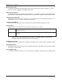
1
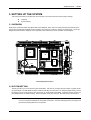
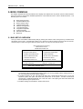
AR-B1570
INDUSTRIAL GRADE
CPU BOARD
User’ s Guide
Edition: 1.71
Book Number: AR-B1570-02.0715
AR-B1570 User’s Guide
Table of Contents
0.PREFACE ...................................................................................................................................................................... 3
0.1COPYRIGHT NOTICE AND DISCLAIMER................................................................................................................................... 3
0.2 WELCOME TO THE AR-B1570 CPU BOARD............................................................................................................................. 3
0.3 BEFORE YOU USE THIS GUIDE ............................................................................................................................................... 3
0.4 RETURNING YOUR BOARD FOR SERVICE ............................................................................................................................. 3
0.5 TECHNICAL SUPPORT AND USER COMMENTS ..................................................................................................................... 3
0.6 ORGANIZATION......................................................................................................................................................................... 4
0.7 STATIC ELECTRICITY PRECAUTIONS ..................................................................................................................................... 4
1. OVERVIEW................................................................................................................................................................... 5
1.1SPECIFICATION.......................................................................................................................................................................... 5
1.2 PACKING LIST ........................................................................................................................................................................... 5
1.3 FEATURES................................................................................................................................................................................. 6
2. SYSTEM CONTROLLER ............................................................................................................................................. 7
2.1 MICROPROCESSOR.................................................................................................................................................................. 7
2.2 DMA CONTROLLER................................................................................................................................................................... 7
2.3 KEYBOARD CONTROLLER ....................................................................................................................................................... 8
2.4 INTERRUPT CONTROLLER....................................................................................................................................................... 8
2.4.1 I/O Port Address Map ........................................................................................................................................................... 9
2.4.2 Real-Time Clock and Non-Volatile RAM ............................................................................................................................. 10
2.4.3 Timer.................................................................................................................................................................................. 10
2.5 SERIAL PORT .......................................................................................................................................................................... 11
2.6 PARALLEL PORT ..................................................................................................................................................................... 13
3. SETTING UP THE SYSTEM....................................................................................................................................... 15
3.1 OVERVIEW............................................................................................................................................................................... 15
3.2 SYSTEM SETTING ................................................................................................................................................................... 15
3.2.1 Hard Disk (IDE) Connector ................................................................................................................................................. 16
3.2.2 FDD Port Connector (CN3)................................................................................................................................................. 17
3.2.3 Ethernet RJ-45 Connector (LAN1) ...................................................................................................................................... 18
3.2.4 PS/2 KB/Mouse Connector (CN4 & PS1)............................................................................................................................ 18
3.2.5 PS-ON Header (CN9)......................................................................................................................................................... 18
3.2.6 Reset Header (J7) .............................................................................................................................................................. 18
3.2.7 Power Connector (PWR2) .................................................................................................................................................. 19
3.2.8 CRT Connector (P4)........................................................................................................................................................... 19
3.2.9 LCD Supported Voltage Select (JP4).................................................................................................................................. 19
3.2.10 LCD Panel Display Connector (LCD1) .............................................................................................................................. 19
3.2.11 LED Header (J8)............................................................................................................................................................... 20
3.2.12 USB Connector(USB1) ..................................................................................................................................................... 20
3.2.13 PC104 Connector ............................................................................................................................................................. 21
3.2.14 Parallel Port Connector (CN2) .......................................................................................................................................... 22
3.2.15 IR. Header (J1)................................................................................................................................................................. 22
3.2.16 Ext. Battery (CN1) ............................................................................................................................................................ 22
3.2.17 Battery Jumper (JP2)........................................................................................................................................................ 22
3.2.18 COM1, COM2 (CN5, CN6) ............................................................................................................................................... 23
3.2.19 Touch Screen Connector (J3 & J4)................................................................................................................................... 24
3.2.20 D.O.C. Memory Address Select (JP1)............................................................................................................................... 24
3.2.21 ATX POWER External Bottom Connector (J6).................................................................................................................. 24
4. INSTALLATION.......................................................................................................................................................... 25
4.1 OVERVIEW............................................................................................................................................................................... 25
4.2 UTILITY DISKETTE .................................................................................................................................................................. 25
4.2.1 Driver Installation................................................................................................................................................................ 25
4.3 WATCHDOG TIMER................................................................................................................................................................. 26
4.3.1 Watchdog Timer Setting ..................................................................................................................................................... 27
4.3.2 Watchdog Timer Trigger ..................................................................................................................................................... 27
5. BIOS CONSOLE......................................................................................................................................................... 28
5.1 BIOS SETUP OVERVIEW......................................................................................................................................................... 28
5.2 STANDARD CMOS SETUP ...................................................................................................................................................... 29
5.3 BIOS FEATURES SETUP......................................................................................................................................................... 31
5.4 CHIPSET FEATURES SETUP .................................................................................................................................................. 33
5.5 PNP/PCI CONFIGURATION ..................................................................................................................................................... 34
5.6 LOAD DEFAULT SETTING....................................................................................................................................................... 34
5.6.1 Load BIOS Defaults............................................................................................................................................................ 34
5.6.2 Load Setup Defaults ........................................................................................................................................................... 34
5.7 INTEGRATED PERIPHERALS ................................................................................................................................................. 35
5.8 PASSWORD SETTING ............................................................................................................................................................. 36
5.8.1 Setting Password ............................................................................................................................................................... 36
5.8.2 Password Checking............................................................................................................................................................ 36
1
AR-B1570 User’s Guide
5.9 IDE HDD AUTO DETECTION ................................................................................................................................................... 36
5.10 BIOS EXIT............................................................................................................................................................................... 36
5.10.1 Save & Exit Setup............................................................................................................................................................. 36
5.10.2 Exit Without Saving .......................................................................................................................................................... 36
2
AR-B1570 User’s Guide
0.PREFACE
0.1COPYRIGHT NOTICE AND DISCLAIMER
April 2001
Acrosser Technology makes no representations or warranties with respect to the contents hereof and specifically
disclaims any implied warranties of merchantability or fitness for any particular purpose. Furthermore, Acrosser
Technology reserves the right to revise this publication and to make changes from time to time in the contents
hereof without obligation of Acrosser Technology to notify any person of such revisions or changes. Changes will
be posted on the Internet (WWW.ACROSSER.COM) as soon as possible, but there is obligation on the part of
Acrosser to this fact.
Possession, use, or copying of the software described in this publication is authorized only pursuant to a valid
written license from Acrosser or an authorized sublicensor.
(C) Copyright Acrosser Technology Co., Ltd., 2001. All rights Reserved.
No part of this publication may be reproduced, transmitted, transcribed, stored in a retrieval system, or translated
into any language or computer language, in any form or any means, electronic, mechanical, magnetic, optical,
chemical, manual or otherwise, without the prior written consent of Acrosser Technology.
Acrosser, AMI, IBM PC/AT, ALI, Windows 3.1, MS-DOS, …are registered trademarks.
All other trademarks and registered trademarks are the property of their respective holders.
0.2 WELCOME TO THE AR-B1570 CPU BOARD
This guide introduces the Acrosser AR-B1570 CPU board.
The following information describes this card’s functions, features, and how to start, set up and operate your ARB1570. General system information can also be found here.
0.3 BEFORE YOU USE THIS GUIDE
If you have not already installed this AR-B1570, refer to the Chapter 3, “Setting Up The System” in this guide.
Check the packing list, make sure the accessories are complete.
The AR-B1570 CD provides the newest information about the card. Please refer to the files of the enclosed
utility CD. It contains the modification, hardware & software information, and it has updates to product functions
that may not be mentioned here.
0.4 RETURNING YOUR BOARD FOR SERVICE
If your board requires servicing, contact the dealer from whom you purchased the product for service information.
If you need to ship your board to us for service, be sure it is packed in a protective carton. We recommend that
you keep the original packaging for this purpose.
You can assure efficient servicing of your product by following these guidelines:
1.
Include your name, address, daytime telephone and facsimile numbers and E-mail.
2.
A description of the system configuration and/or software at the time is malfunction,
3.
And a brief description of the symptoms.
0.5 TECHNICAL SUPPORT AND USER COMMENTS
User’s comments are always welcome as they assist us in improving the usefulness of our products and the
understanding of our publications. They form a very important part of the input used for product enhancement
and revision.
We may use and distribute any of the information you supply in any way we believe appropriate without incurring
any obligation. You may, of course, continue to use the information you supply.
If you have suggestions for improving particular sections or if you find any errors, please indicate the manual title
and book number.
Please send your comments to Acrosser Technology Co., Ltd. or your local sales representative.
Internet electronic mail to: [email protected]
Check our FAQ sheet for quick fixes to known technical problems.
3
AR-B1570 User’s Guide
0.6 ORGANIZATION
This manual covers the following topics (see the Table of Contents for a detailed listing):
!
!
!
!
!
Chapter 1, “Overview”, provides an overview of the system features and packing list.
Chapter 2, “System Controller” describes the major structure.
Chapter 3, “Setting Up the System”, describes how to adjust the jumper, and the connector’s settings.
Chapter 4, “Installation”, describes setup procedures including information on the utility diskette.
Chapter 5, “BIOS Console”, provides the BIOS options settings.
0.7 STATIC ELECTRICITY PRECAUTIONS
Before removing the board from its anti-static bag, read this section about static electricity precautions.
Static electricity is a constant danger to computer systems. The charge that can build up in your body may be
more than sufficient to damage integrated circuits on any PC board. It is, therefore, important to observe basic
precautions whenever you use or handle computer components. Although areas with humid climates are much
less prone to static build-up, it is always best to safeguard against accidents that may result in expensive repairs.
The following measures should be sufficient to protect your equipment from static discharge:
•
Touch a grounded metal object to discharge the static electricity in your body (or ideally, wear a grounded
wrist strap).
•
When unpacking and handling the board or other system components, place all materials on an anti-static
surface.
•
Be careful not to touch the components on the board, especially the “golden finger” connectors on the bottom
of the board.
4
AR-B1570 User’s Guide
1. OVERVIEW
This is a AR-B1570 Pentium Grade CPU Board with Ethernet, DOC, SSD and Compact Flash.
This chapter provides an overview of your system features and capabilities. The following topics are covered:
!
!
!
Specification
Packing List
Features
1.1SPECIFICATION
!
!
!
!
!
!
!
!
!
!
!
!
!
!
!
!
!
!
!
CPU : NS GEODE GX1 BGA.
Chipset:Cyrix CS5530A.
RAM Memory: Support 1xDIMM 168-Pin socket, 128M maximum.
SSD: Support one socket for DiskOnChip.
Support up to 1MB SRAM on board.
Watchdog: Software programmable 1~63sec.
VGA Display: CS5530A UMA,Memory Size 1~4MB.
CRT-with HDB 15-pin connector.
LCD with 2.0 mm 44-pin Header.
Ethernet: RTL8139C chipset, supports 10/100M baseT with RJ-45 connector built-in LED.
Super I/O: Winbond 83977TF
2 EIDE (Ultra DMA33)– with one 2.54 mm 40-pin connector and
one 2.00 mm 44-pin connector
1 FDC – with 2.54 mm 34-pin connector.
1 Parallel – with 2.54 mm 26-pin connector (supports SPP/EPP/ECP mode).
1 RS-232C/RS485 – with DB-9 connector located at the bracket.
1 RS-232C /IrDA/Touch Screen – with 2.54 mm 10-pin connector
RS-232C is selectable by jumper and use the same connector.
IrDA with 2.54mm 5-pin header.
Touch Screen with 2.0mm 3-pin JST connector.
BIOS: Flash BIOS AWARD.
Keyboard/Mouse: PS/2 compatible 6-pin mini-DIN connector and JST 6pin.
USB: Built-in 2 ports USB interface with 2.54mm 10-pin headers.
RTC: Chipset including, Support ACPI function with 10 years data retention.
Speaker: Supports on-board buzzer.
LED Indicators: Power LED, LAN LED at LAN Port.
Expansion Bus: PC/104,ISA Bus.
Power Connector: One 4-pin Wafer Connector.
Power Req.: +5V-3.0A maximum and 12V –0.5A maximum.
PC Board: 6 layers, EMI considered
Dimensions: 185 mm x 122 mm (7.3”x4.8”)
1.2 PACKING LIST
Some accessories are included with the system. Before you begin installing your AR-B1570 board, take a moment
to make sure that the following items have been included inside the AR-B1570 package.
! The quick setup manual
! 1 AR-B1570 all-in-one single CPU board
! Software utility CD.
! 2HD cable (one 2.54mm, one 2.0mm).
! FD cable.
! USB, AR-B9462A (optional)
! KB/Mouse (one mini din)
! COM 2 cable (2*5pin)
! Parallel cable (2*13pin)
5
AR-B1570 User’s Guide
1.3 FEATURES
The system provides a number of special features that enhance its reliability, ensure its long-term availability, and
improve its expansion capabilities, as well as its hardware structure.
!
!
!
!
!
!
!
!
!
!
6
CPU NS GEODE GX1
Cyrix CS5530A Chipset
1xDIMM SDRAM
Supports DOC Flash Disk
1Mbyte SRAM
10/100M-Base Ethernet
Compact Flash (optional)
AWARD BIOS
Power Req.: +5V-3.0A maximum and 12V –0.5A maximum.
Dimensions: 185 mm x 122 mm (7.3”x4.8”).
AR-B1570 User’s Guide
2. SYSTEM CONTROLLER
This chapter describes the main structure of the AR-B1570 CPU board. The following topics are covered:
!
!
!
!
!
!
Microprocessors
DMA Controller
Keyboard Controller
Interrupt Controller
Serial Port
Parallel Port
2.1 MICROPROCESSOR
The AR-B1570 uses the NS GEODE GX1 CPU, it is an advanced 32-bit x86 compatible processor offering high
performance, fully accelerated 2D graphics, a 64-synchronous DRAM controller and a PCI bus controller, all on a
single chip. This latest generation of the MediaGX processor enables a new class of premium performance
notebook/desktop, and IPC computer designs.
The MediaGX MMX enhanced processor companion chips provide advanced video and audio functions and permit
direct interface to memory. This high-performance 64-bit processor is x86 instruction set compatible and supports
MMX technology.
This processor is the latest member of the NS MediaGX family, offering high performance, fully accelerated 2D
graphics, synchronous memory interface and a PCI bus controller, all on a single chip. As described in separate
manuals, the CS5520 and the CS5530 I/O Companion chips fully enable the features of the MediaGX processor
with MMX support. These features include full VGA and VESA video, 16-bit stereo sound, IDE interface, ISA
interface, SMM power management, and AT compatibility logic. In addition, the newer CS5530 provides an Ultra
DMA/33 interface, MPEG2 assist, and is AC97 Version 2.0 audio compliant.
In addition to the advanced CPU features, the MediaGX processor integrates a host of functions, which are
typically implemented with external components. A full-function graphics accelerator provides pixel processing and
rendering functions.
The NS MediaGX MMX-Enhanced Processor represents a new generation of x86-compatible 64-bit
microprocessors with sixth-generation features. The decoupled load/store unit (within the memory management
unit) allows multiple instructions in a single clock cycle. Other features include single-cycle execution, single-cycle
instruction decode, 16KB write-back cache, and clock rates up to 266MHz. These features are possible by the use
of advanced-process technologies and super pipelining.
2.2 DMA CONTROLLER
The equivalent of two 8237A DMA controllers are implemented on the AR-B1570 board. Each controller is a fourchannel DMA device that will generate the memory addresses and control signals necessary to transfer
information directly between a peripheral device and memory. This allows high-speed information transfer with less
CPU intervention. The two DMA controllers are internally cascaded to provide four DMA channels for transfers to
8-bit peripherals (DMA1) and three channels for transfers to 16-bit peripherals (DMA2). DMA2 channel 0 provides
the cascade interconnection between the two DMA devices, thereby maintaining IBM PC/AT compatibility.
The Following is the system information for the DMA channels:
Slave with four 8-bit chnls
DMA Controller 1
Channel 0: Spare
Master with three 16-bit chnls
DMA Controller 2
Channel 4(0): Cascade for controller 1
Channel 1: IBM SDLC
Channel 5(1): Spare
Channel 2: Diskette adapter
Channel 6(2): Spare
Channel 3: Spare
Channel 7(3): Spare
DMA Channel Controller
7
AR-B1570 User’s Guide
2.3 KEYBOARD CONTROLLER
The 8042 processor is programmed to support the keyboard serial interface. The keyboard controller receives
serial data from the keyboard, checks its parity, translates scan codes, and presents it to the system as a byte data
in its output buffer. The controller can interrupt the system when data is placed in its output buffer, or wait for the
system to poll its status register to determine when data is available.
Data can be written to the keyboard by writing data to the output buffer of the keyboard controller.
Each byte of data is sent to the keyboard controller in a series with an odd parity bit automatically inserted. The
keyboard controller is required to acknowledge all data transmissions. Therefore, another byte of data will not be
sent to keyboard controller until acknowledgment is received for the previous byte sent. The “output buffer full”
interruption may be used for both send and receive routines.
2.4 INTERRUPT CONTROLLER
The equivalent of two 8259 Programmable Interrupt Controllers (PIC) are included on the AR-B1570 board. They
accept requests from peripherals, resolve priorities on pending interrupts in service, issue interrupt requests to the
CPU, and provide vectors which are used as acceptance indices by the CPU to determine which interrupt service
routine to execute. These two controllers are cascaded with the second controller representing IRQ8 to IRQ15,
which is rerouted through IRQ2 on the first controller.
The following is the system information of interrupts levels:
Interrupt Level
NMI
CTRL1
IRQ0
IRQ1
IRQ2
Description
Parity check
CTRL2
System timer interrupt from timer 8254
keyboard output buffer full
Rerouting to IRQ8 to IRQ15
IRQ8:Real time clock
IRQ9:Reserved
IRQ10:LAN adapters(based on PCI INT routing)
IRQ12:Reserved for PS/2 mouse
IRQ13:Math.Co-processor
IRQ14:Hard disk adapter
IRQ15:Hard disk adapter
IRQ3
IRQ4
IRQ5
IRQ6
IRQ7
Serial port(depends on setup assignment)
Serial port(depends on setup assignment)
Reserved
Reserved for floppy disk adapter
Parallel port 1
Interrupt Controller
8
AR-B1570 User’s Guide
2.4.1 I/O Port Address Map
Hex Range
000-01F
020-021
022-023
040-04F
050-05F
060-06F
070-071
080-09F
0A0-0A1
0C0-0DF
0F0
0F1
0F8-0FF
170-178
1F0-1F8
201
208-20A
210-213
214
218-21A
278-27F
290-293
2E8-2EF
2F8-2FF
300-31F
320-33F
378-37F
380-38F
3A0-3AF
3B0-3BF
3C0-3CF
3D0-3DF
3E8-3EF
3F0-3F7
3F8-3FF
Device
DMA controller 1
Interrupt controller 1
Cyrix CS5530
Timer 1
Timer 2
8042 keyboard/controller
Real-time clock (RTC), non-maskable interrupt (NMI)
DMA page registers
Interrupt controller 2
DMA controller 2
Clear Math Co-processor
Reset Math Co-processor
Math Co-processor
Reserved for Fixed disk 1
Fixed disk 0
Reserved for Game port
EMS register 0
SSD
Watchdog
EMS register 1
Parallel printer port (depends on setup assignment)
SSD
Serial port (depends on setup assignment)
Serial port (depends on setup assignment)
Prototype card/streaming type adapter
Reserved
Parallel printer port (depends on setup assignment)
SDLC, bisynchronous
Bisynchronous
Monochrome display and printer port 3 (LPT 3)
EGA/VGA adapter
Color/graphics monitor adapter
Serial port 3 (depends on setup assignment)
Reserved for diskette controller
Serial port (depends on setup assignment)
I/O Port Address Map
9
AR-B1570 User’s Guide
2.4.2 Real-Time Clock and Non-Volatile RAM
The AR-B1570 contains a real-time clock compartment that maintains the date and time in addition to storing
configuration information about the computer system. It contains 14 bytes of clock and control registers and
114 bytes of general purpose RAM. Because of the use of CMOS technology, it consumes very little power
and can be maintained for long periods of time using an internal Lithium battery. The contents of each byte in
the CMOS RAM are listed as follows:
Address
00
01
02
03
04
05
06
07
08
09
0A
0B
0C
0D
0E
0F
10
11
12
13
14
15
16
17
18
19-2D
2E-2F
30
31
32
33
34-7F
Description
Seconds
Second alarm
Minutes
Minute alarm
Hours
Hour alarm
Day of week
Date of month
Month
Year
Status register A
Status register B
Status register C
Status register D
Diagnostic status byte
Shutdown status byte
Diskette drive type byte, drive A and B
Fixed disk type byte, drive C
Fixed disk type byte, drive D
Reserved
Equipment byte
Low base memory byte
High base memory byte
Low expansion memory byte
High expansion memory byte
Reserved
2-byte CMOS checksum
Low actual expansion memory byte
High actual expansion memory byte
Date century byte
Information flags (set during power on)
Reserved for system BIOS
Real-Time Clock & Non-Volatile RAM
2.4.3 Timer
The AR-B1570 provides three programmable timers, each with a timing frequency of 1.19 MHz.
10
Timer 0
The output of this timer is tied to interrupt request 0. (IRQ 0)
Timer 1
This timer is used to trigger memory refresh cycles.
Timer 2
This timer provides the speaker tone.
Application programs can load different counts into this timer to generate various sound frequencies.
AR-B1570 User’s Guide
2.5 SERIAL PORT
The ACEs (Asynchronous Communication Elements ACE1 to ACE4) are used to convert parallel data to a serial
format on the transmit side and convert serial data to parallel on the receiver side. The serial format, in order of
transmission and reception, is a start bit, followed by five to eight data bits, a parity bit (if programmed) and one,
1.5 (in a five-bit format only) or two stop bits(in a 6,7, or 8-bit format). The ACEs are capable of handling divisors of
1 to 65535, and produce a 16x clock for driving the internal transmitter logic.
Provisions are also included to use this 16x clock to drive the receiver logic. Also included in the ACE a completed
MODEM control capability, and a processor interrupt system that may be software tailored to the computing time
required to handle the communications link.
The following table is a summary of each ACE accessible register
DLAB
0
Port Address
base + 0
0
X
X
X
X
X
X
1
1
Register
Receiver buffer (read)
Transmitter holding register (write)
base + 1
Interrupt enable
base + 2
Interrupt identification (read only)
base + 3
Line control
base + 4
MODEM control
base + 5
Line status
base + 6
MODEM status
base + 7
Scratched register
base + 0
Divisor latch (least significant byte)
base + 1
Divisor latch (most significant byte)
ACE Accessible Registers
(1) Receiver Buffer Register (RBR)
Bit 0-7: Received data byte (Read Only)
(2) Transmitter Holding Register (THR)
Bit 0-7: Transmitter holding data byte (Write Only)
(3) Interrupt Enable Register (IER)
Bit 0: Enable Received Data Available Interrupt (ERBFI)
Bit 1: Enable Transmitter Holding Empty Interrupt (ETBEI)
Bit 2: Enable Receiver Line Status Interrupt (ELSI)
Bit 3: Enable MODEM Status Interrupt (EDSSI)
Bit 4: Must be 0
Bit 5: Must be 0
Bit 6: Must be 0
Bit 7: Must be 0
(4) Interrupt Identification Register (IIR)
Bit 0: “0” if Interrupt Pending
Bit 1: Interrupt ID Bit 0
Bit 2: Interrupt ID Bit 1
Bit 3: Must be 0
Bit 4: Must be 0
Bit 5: Must be 0
Bit 6: Must be 0
Bit 7: Must be 0
(5) Line Control Register (LCR)
Bit 0: Word Length Select Bit 0 (WLS0)
Bit 1: Word Length Select Bit 1 (WLS1)
11
AR-B1570 User’s Guide
WLS1
WLS0
Word Length
0
0
5 Bits
0
1
6 Bits
1
0
7 Bits
1
1
8 Bits
Bit 2: Number of Stop Bit (STB)
Bit 3: Parity Enable (PEN)
Bit 4: Even Parity Select (EPS)
Bit 5: Stick Parity
Bit 6: Set Break
Bit 7: Divisor Latch Access Bit (DLAB)
(6) MODEM Control Register (MCR)
Bit 0: Data Terminal Ready (DTR)
Bit 1: Request to Send (RTS)
Bit 2: Out 1 (OUT 1)
Bit 3: Out 2 (OUT 2)
Bit 4: Loop
Bit 5: Must be 0
Bit 6: Must be 0
Bit 7: Must be 0
(7) Line Status Register (LSR)
Bit 0: Data Ready (DR)
Bit 1: Overrun Error (OR)
Bit 2: Parity Error (PE)
Bit 3: Framing Error (FE)
Bit 4: Break Interrupt (BI)
Bit 5: Transmitter Holding Register Empty (THRE)
Bit 6: Transmitter Shift Register Empty (TSRE)
Bit 7: Must be 0
(8) MODEM Status Register (MSR)
Bit 0: Delta Clear to Send (DCTS)
Bit 1: Delta Data Set Ready (DDSR)
Bit 2: Training Edge Ring Indicator (TERI)
Bit 3: Delta Receive Line Signal Detect (DSLSD)
Bit 4: Clear to Send (CTS)
Bit 5: Data Set Ready (DSR)
Bit 6: Ring Indicator (RI)
Bit 7: Received Line Signal Detect (RSLD)
(9) Divisor Latch (LS, MS)
Bit 0:
Bit 1:
Bit 2:
Bit 3:
Bit 4:
Bit 5:
Bit 6:
Bit 7:
12
LS
Bit 0
Bit 1
Bit 2
Bit 3
Bit 4
Bit 5
Bit 6
Bit 7
MS
Bit 8
Bit 9
Bit 10
Bit 11
Bit 12
Bit 13
Bit 14
Bit 15
AR-B1570 User’s Guide
Desired Baud Rate
Divisor Used to Generate 16x Clock
300
384
600
192
1200
96
1800
64
2400
48
3600
32
4800
24
9600
12
14400
8
19200
6
28800
4
38400
3
57600
2
115200
1
Serial Port Divisor Latch
2.6 PARALLEL PORT
(1) Register Address
Port Address
base + 0
base + 0
base + 1
base + 2
Read/Write
Write
Read
Read
Write
Registers’ Address
Register
Output data
Input data
Printer status buffer
Printer control latch
(2) Printer Interface Logic
The parallel port of the W83977F-A is for attaching various devices that accept eight bits of parallel data at
standard TTL level.
(3) Data Swapper
The system microprocessor can read the contents of the printer’s Data Latch through the Data Swapper by reading
the Data Swapper address.
(4) Printer Status Buffer
The system microprocessor can read the printer status by reading the address of the Printer Status Buffer. The bit
definitions are described as follows:
7
6
5
4
3
2
1
0
X
X
X
-ERROR
SLCT
PE
-ACK
-BUSY
Printer Status Buffer
NOTE: X presents not used.
13
AR-B1570 User’s Guide
Bit 7: This signal may become active during data entry, when the printer is off-line during printing, or when the
print head is changing position or in an error state. When Bit 7 is active, the printer is busy and cannot
accept data.
Bit 6: This bit represents the current state of the printer’s ACK signal. A0 means the printer has received the
character and is ready to accept another. Normally, this signal will be active for approximately 5
microseconds before receiving a BUSY message stops.
Bit 5: A1 means the printer has detected the end of the paper.
Bit 4: A1 means the printer is selected.
Bit 3: A0 means the printer has encountered an error condition.
(5) Printer Control Latch & Printer Control Swapper
The system microprocessor can read the contents of the printer control latch by reading the address of printer
control swapper. Bit definitions are as follows:
7
6
X
X
5
4
3
2
1
0
STROBE
AUTO FD XT
INIT
SLDC IN
IRQ ENABLE
DIR(write only)
Bit’s Definition
NOTE: X presents not used.
Direction control bit. When logic 1, the output buffers in the parallel port are disabled allowing data driven
Bit 5: from external sources to be read; when logic 0, they work as a printer port. This bit is write only.
Bit 4: A1 in this position allows an interrupt to occur when ACK changes from low state to high state.
Bit 3: A1 in this bit position selects the printer.
Bit 2: A0 starts the printer (50 microseconds pulse, minimum).
Bit 1: A1 causes the printer to line-feed after a line is printed.
Bit 0: A0.5 microsecond minimum highly active pulse clocks data into the printer. Valid data must be present for
a minimum of 0.5 microseconds before and after the strobe pulse.
14
AR-B1570 User’s Guide
3. SETTING UP THE SYSTEM
This section describes pin assignments for the system’s external connectors and the jumper settings.
!
!
Overview
System Setting
3.1 OVERVIEW
AR-B1570 is a Pentium Grade CPU Board that comes Ethernet, DOC, SSD, and Compact Flash (optional) functions.
This section provides the hardware’s jumper settings, the connectors’ locations, and the pin assignments. The #1 pin
assignments have all been designed on the right side of the board with a “block” indication on the diagram.
CN7
CN3
CN2
USB1
JP4
J4
DIMM1
26
25
24
23
22
21
20
19
18
17
16
15
14
13
12
11
10
9
8
7
6
5
4
3
2
1
U1
B
A
D
C
F
E
H
G
K
J
M
L
P
N
T
R
V
U
Y
W
AB
AA
AD
AC
AF
AE
U1
J7
CN5
U21
U2
J2
CN1
J6
B
A
D
C
F
E
H
G
K
J
M
L
P
N
T
R
V
U
Y
W
AB
AA
AD
AC
U6
U19
-+
J8
U16
P2
J9
JP2
J1
CN4
AR-B1570V1.2
A
CN9
P4
BT3
LAN1
P3
AF
AE
P1
JP1
A
CN8
PWR2
J3
LCD1
26
25
24
23
22
21
20
19
18
17
16
15
14
13
12
11
10
9
8
7
6
5
4
3
2
1
J2
CN1
J6
PS1
SILK TOP
External System Location
3.2 SYSTEM SETTING
Jumper pins allow you to set specific system parameters. Set them by changing the pin location of jumper blocks.
(A jumper block is a small plastic-encased conductor that slips over the pins.) To change a jumper setting, remove
the jumper from its current location with your fingers or small needle-nosed pliers. Place the jumper over the two
pins designated for the desired setting. Press the jumper evenly onto the pins. Be careful not to bend the pins.
CAUTION: Do not touch any electronic components unless you are safely grounded. Wear a grounded wrist strap
or touch an exposed metal part of the system unit chassis. The static discharges from your fingers can
permanently damage electronic components.
15
AR-B1570 User’s Guide
3.2.1 Hard Disk (IDE) Connector
(1) 40-Pin Hard Disk (IDE) Connector (CN7)
A 40-pin header type connector (CN7) is provided to interface with up to two embedded hard disk drives (IDE AT
bus). This interface, through a 40-pin cable, allows the user to connect up to two drives in a “daisy chain” fashion.
To enable or disable the hard disk controller, please use the BIOS Setup program, which is explained further in
chapter 5. The following table illustrates the pin assignments of the hard disk drive’s 40-pin connector.
2
40
1
39
Pin
1
3
5
7
9
11
13
15
17
19
21
23
25
27
29
31
33
35
37
39
Signal
-RESET
DATA 7
DATA 6
DATA 5
DATA 4
DATA 3
DATA 2
DATA 1
DATA 0
GROUND
IDEDREQ
-IOW A
-IOR A
IDEIORDYA
-DACKA
AINT
SA 1
SA 0
CS 0
HD LED A
Pin
2
4
6
8
10
12
14
16
18
20
22
24
26
28
30
32
34
36
38
40
Signal
GROUND
DATA 8
DATA 9
DATA 10
DATA 11
DATA 12
DATA 13
DATA 14
DATA 15
NOT USED
GROUND
GROUND
GROUND
GROUND
GROUND
GROUND
Not Used
SA 2
CS 1
GROUND
Hard Disk (IDE) Connector
(2) 44-Pin Hard Disk (IDE) Connector (CN8)
AR-B1570 also provides IDE interface 44-pin connector to connect with the hard disk device.
16
2
44
1
43
AR-B1570 User’s Guide
Pin
1
3
5
7
9
11
13
15
17
19
21
23
25
27
29
31
33
35
37
39
41
43
Signal
Pin
-RESET
2
DATA 7
4
DATA 6
6
DATA 5
8
DATA 4
10
DATA 3
12
DATA 2
14
DATA 1
16
DATA 0
18
GROUND
20
IDEDREQ
22
-IOW A
24
-IOR A
26
IDEIORDYA
28
-DACKA
30
AINT
32
SA 1
34
SA 0
36
CS 0
38
HD LED A
40
VCC
42
GROUND
44
Hard Disk (IDE1) Connector
Signal
GROUND
DATA 8
DATA 9
DATA 10
DATA 11
DATA 12
DATA 13
DATA 14
DATA 15
NOT USED
GROUND
GROUND
GROUND
GROUND
GROUND
GROUND
Not Used
SA 2
CS 1
GROUND
VCC
Not Used
3.2.2 FDD Port Connector (CN3)
The AR-B1570 provides a 34-pin header type connector for supporting up to two floppy disk drives.
To enable or disable the floppy disk controller, please use the BIOS Setup program.
33
1
34
2
Figure 0-1 CN3: FDD Port connector
Pin
Signal
Pin
Signal
1-33(odd)
GROUND
18
DIRECTION
2
DRVEN 0
20
-STEP OUTPUT PULSE
4
NOT USED
22
-WRITE DATA
6
DRVEN 1
24
-WRITE GATE
8
-INDEX
26
-TRACK 0
10
-MOTOR ENABLE 0
28
-WRITE PROTECT
12
-DRIVE SELECT 1
30
-READ DATA
14
-DRIVE SELECT 0
32
-SIDE 1 SELECT
16
-MOTOR ENABLE 1
34
DISK CHANGE
Table 0-1 FDD Pin Assignment
17
AR-B1570 User’s Guide
3.2.3 Ethernet RJ-45 Connector (LAN1)
The LAN1 RJ-45&LED header is the standard network header. The following table is the pin assignment.
8
1
PIN (CN8)
1
2
3
4
5
6
7
8
RJ-45 Pin Assignment
FUNCTION
TPTX+
TPTX TPRX+
Not Used
Not Used
TPRX Not Used
Not Used
3.2.4 PS/2 KB/Mouse Connector (CN4 & PS1)
To use the PS/2 interface, an adapter cable has to be connected to the CN4 (6-pin header type) connector. This
adapter cable is mounted on a bracket and is included in your AR-B1570 package. The connector for the PS/2
KB/mouse is a Mini-DIN 6-pin connector. Pin assignments for the PS/2 port connector are as follows:
MSDAT 1
KBDAT 2
GND 3
VCC 4
MSCLK 5
KBCLK 6
1 2
3
4
5
6
1 KBDAT
2 MSDAT
3 GND
4 VCC
5 KBCLK
6 MSCLK
PS1
6 Pin Mini-DIN
CN4
Figure 0-2 CN4 & PS1: PS/2 KB/Mouse Connector
3.2.5 PS-ON Header (CN9)
1 PS-ON
2 VCC
3 5VSB
CN9
Factory Preset
3.2.6 Reset Header (J7)
The J7 is a reset header. Shorting these two pins will reset the system.
1
2
18
AR-B1570 User’s Guide
3.2.7 Power Connector (PWR2)
The PWR2 is a 4-pin power connector. It’s the standard connectors on all Acrosser boards.
1
2
3
4
PWR2
+12
GND
GND
+5
PWR2: 4-Pin Power Connector
3.2.8 CRT Connector (P4)
1
2
3
4
5
P4 (CRT Connector)
6
1 Red
11 2 Green
3 Blue
13 Horizontial
14 Vertical Sync
4, 9, & 11 Not used
5 & 10 Ground
6, 7 & 8 AGND
12 DDC DATA
15 15 DDC CLOCK
10
P4: CRT Connector
3.2.9 LCD Supported Voltage Select (JP4)
2 4 6
2 4 6
1 3 5
1 3 5
3.3V
5V
Factory Preset
Figure 0-3 JP4: LCD Supported Voltage Select
3.2.10 LCD Panel Display Connector (LCD1)
Attach a display panel connector to this 44-pin connector with pin assignments as shown below:
2
1
Figure 0-4 LCD1: LCD Display Connector
19
AR-B1570 User’s Guide
Pin
Signal
1
GND
3
GND
5
FLM
7
NC
9
P0 (B0)
11
P2 (B2)
13
GND
15
P5 (B5)
17
NC
19
P7 (G1)
21
P8 (G2)
23
P10 (G4)
25
NC
27
GND
29
P13 (R1)
31
P15 (R3)
33
P17 (R5)
35
VCC
37
+12V
39
GND
41
DE
43
GND
Table 0-2 LCD Display Pin Assignment
Pin
2
4
6
8
10
12
14
16
18
20
22
24
26
28
30
32
34
36
38
40
42
44
Signal
SHFCLK
LP
GND
NC
P1 (B1)
P3 (B3)
P4 (B4)
NC
P6 (G0)
GND
P9 (G3)
P11 (G5)
NC
P12 (R0)
P14 (R2)
P16 (R4)
GND
VCC
+12V
GND
ENABLK
VEE
3.2.11 LED Header (J8)
J8
2
4
6
1
3
5
1.HLEDP+
2.HLEDP3.HLEDS+
4.HLEDS5.P/WLED+
6.P/WLED-
3.2.12 USB Connector(USB1)
USB1 2 4 6 8 10
1 3 5 7 9
Pin
1
3
5
7
9
20
Description
USB1V
USBD1FUSBD1F+
GND
CASE
Pin
2
4
6
8
10
Description
USB2V
USBD2FUSBD2F+
GND
CASE
AR-B1570 User’s Guide
3.2.13 PC104 Connector
(1) 64-Pin PC/104 Connector Bus A & B (PC104)
2
64
1
63
64-Pin PC/104 Connector
PC104
1 2
B1 --- GND
-IOCHCK A1
B2 --- RSTDRV
SD7 --- A2
B3 --- +5 VDC
SD6 --- A3
B4 --- IRQ9
SD5 --- A4
B5 --- -5 VDC
SD4 --- A5
B6 --- DRQ2
SD3 --- A6
B7 --- -12 VDC
SD2 --- A7
B8 --- -ZWS
SD1 --- A8
B9 --- +12
SD0 --- A9
B10 --- KEY
IOCHRDY- A10
B11 --- -SMEMW
AEN
A11
B12 --- -SMEMR
SA19 A12
B13 --- -IOW
SA18 A13
B14 --- -IOR
SA17 A14
B15 --- -DACK3
SA16 A15
B16 --- DRQ3
SA15 A16
B17 --- -DACK1
SA14 A17
B18 --- DRQ1
SA13 A18
B19 --- -REFRESH
SA12 A19
B20 --- BUSCLK
SA11 A20
B21 --- IRQ7
SA10 A21
B22 --- IRQ6
SA9 --- A22
B23 --- IRQ5
SA8 --- A23
B24 --- IRQ4
SA7 --- A24
SA6 --- A25
B25 --- IRQ3
B26 --- -DACK2
SA5 --- A26
B27 --- TC
SA4 --- A27
B28 --- BALE
SA3 --- A28
B29 --- +5
SA2 --- A29
B30 --- OSC
SA1 --- A30
B31 --- GND
SA0 --- A31
B32 --- GND
GND A32
Figure PC104: 64-Pin PC/104 Connector Bus A & B
(2) 40-Pin PC/104 Connector Bus C & D (PC104)
1
2
39
40
40 Pin PC/104 Connector
GND
SBHE
LA23
LA22
LA21
LA20
LA19
LA18
LA17
-MEMR
-MEMW
SD8
SD9
SD10
SD11
SD12
SD13
SD14
SD15
KEY
PC104
1 2
C1
C2
C3
C4
C5
C6
C7
C8
C9
C10
C11
C12
C13
C14
C15
C16
C17
C18
C19
C20
D1 --- GND
D2 --- -MEMCS16
D3 --- -IOCS16
D4 --- IRQ10
D5 --- IRQ11
D6 --- IRQ12
D7 --- IRQ15
D8 --- IRQ14
D9 --- -DACK0
D10--- DRQ0
D11 --- -DACK5
D12--- DRQ5
D13--- -DACK6
D14--- DRQ6
D15--- -DACK7
D16--- DRQ7
D17--- +5 VDC
D18--- -MASTER
D19--- GND
D20--- GND
Figure PC104: 40-Pin PC/104 Connector Bus C & D
21
AR-B1570 User’s Guide
3.2.14 Parallel Port Connector (CN2)
The connector for the parallel port is a 26 pins female connector.
1
2
Parallel Port Connector
PIN
1
2
3
4
5
6
7
8
9
10
11
12
13
Signal
PIN
Signal
-Strobe
14
-Auto Form Feed
Data 0
15
-Error
Data 1
16
-Initialize
Data 2
17
-Printer Select In
Data 3
18
Ground
Data 4
19
Ground
Data 5
20
Ground
Data 6
21
Ground
Data 7
22
Ground
-Acknowledge
23
Ground
Busy
24
Ground
Paper
25
Ground
Printer Select
26
Not Used
Parallel Port Pin Assignments
3.2.15 IR. Header (J1)
The Infra-red Header pins assignments are as follow:
5
1
JI
1 VCC
2 NOT USED
3 IRRX
4 GND
5 IRTX
3.2.16 Ext. Battery (CN1)
1 EXBAT (3.6V)
2 GND
CN1
1
3.2.17 Battery Jumper (JP2)
JP2
1
1 EXBAT
2 VCC
3 INTVBAT
1-2
External Battery
JP2: Battery Setting
22
2-3
On-Board Battery
AR-B1570 User’s Guide
3.2.18 COM1, COM2 (CN5, CN6)
C N 5 (C O M 1)
C N 6 (C O M 2)
1
2
9
7
5
3
1
10
8
6
4
2
6
7
8
3
4
5
9
Figure 0-5 CN5 & CN6: RS-232 Connector
CN5
CN6
Signal
CN5
DB6
Signal
1
1
/DCD
8
6
/CTS
6
2
/DSR
4
7
/DTR
2
3
RXD
9
8
/RI
7
4
/RTS
5
9
VCC
3
5
TXD
-10
Table 0-3 RS-232 Connector Pin Assignment
VCC
(1) RS-232/RS-485 Select for COM1 (P2 & P3)
The P2&P3 jumper is used to choose between the use of the on-board RS-232 or RS-485 for the CN5 – COM1.
P3 1
P2 2
3
1
2
3
A B C
RS-232
Factory Preset
A B C
RS-485
Figure 3-10 P2 & P3: RS-232/RS-485 Select for COM1
(2) RS-485 Terminator Select (J2)
When there is only one line the setting should be left off, but if you are using multiple blocks on a single line
this should be set to “ON” in order to properly terminate the connection for better transmission of data
1
1
2
2
OFF
ON
Factory Preset
Figure 0-6 J2: RS-485 Terminator Select
(3) RS-485 Header (J9)
1 2 3
1
2
3
N485+
N485GND
J9
23
AR-B1570 User’s Guide
3.2.19 Touch Screen Connector (J3 & J4)
1
2
3
RXDF
TXDF
CGND
Figure 0-7 J3&J4: Touch Screen Connector
3.2.20 D.O.C. Memory Address Select (JP1)
This section provides the information about how to use the D.O.C. (DiskOnChip).
hardware setting and software configuration.
Step 1: Use JP1 to select the correct D.O.C. memory address.
Step 2: Insert programmed DiskOnChip into sockets U19 setting as DOC.
Step 3: Line up and insert the AR-B1570 card into slot of your computer.
1
1
2
2
OFF
Factory Preset
ON
Figure 0-8 JP1: D.O.C. Memory Address Select
JP1
Address
Note
OFF
CE00 : 0000
Factory Preset
ON
D200 : 0000
Table 0-4 D.O.C. Memory Address
3.2.21 ATX POWER External Bottom Connector (J6)
1
1
2
2
OFF
ON
Factory Preset
Figure 0-9 J6: ATX POWER External Bottom Connector
24
There divided two parts:
AR-B1570 User’s Guide
4. INSTALLATION
This chapter describes the installation procedure. The following topics are covered:
!
Overview
!
Utility Diskettes
!
Watchdog Timer Setting
4.1 OVERVIEW
This chapter provides information for you to set up a working system based on the AR-B1570 CPU board. Please
carefully read the details of the CPU board’s hardware descriptions before installation. Pay special attention to the
jumper settings, switch settings and cable connections.
Follow steps listed below for proper installation:
Step 1:
Read the CPU board’s hardware description in this manual.
Step 2:
Set jumpers.
Step 3:
Make sure that the power supply connected to your AR-B1570 CPU board is turned off.
Step 4:
Connect all necessary cables. Make sure that the HDC; serial and parallel cables are connected to
pin 1 of the related connector (not upside down).
Step 5:
Connect the hard disk flat cables from the CPU board to the drives. Connect a power source to
drive.
Step 6:
Plug the keyboard into the keyboard connector.
Step 7:
Turn on the power.
Step 8:
Configure your system with the BIOS Setup program (section 5) then re-boot your system.
Step 9:
If the CPU board does not work, turn off the power and read the hardware description carefully
again.
Step 10:
If the CPU board still does not perform properly, return the board to your dealer for immediate
service.
4.2 UTILITY DISKETTE
The AR-B1570 provides CD.
4.2.1 Driver Installation
The AR-B1570 provides LAN function drivers for the WIN95, WIN98, WIN2000, WINCE, LINUX, and NT. The
driver can auto-setup in the specified mode. The user must first decompress the compressed file.
st
The 1 step: Decompress the zip files included in the CD to your hard disk.
The 2
nd
step: Execute the corresponding files to setup the system.
25
AR-B1570 User’s Guide
The files list and descriptions are as follow:
Disk 1
README.TXT
391 09-22-00 11:17 README.TXT
GEODEW~1
<DIR> 09-22-00 10:53 Geode win9x
WINCED~1
<DIR> 09-22-00 10:53 WinCE driver
1. GEODE win9x
Includes auto-execution program that will setup/install Geode Media drivers in Windows 9X
Descriptions environment.
2. WinCE driver
Includes the GxM drivers needed in Win CE environment.
Disk 2
Files
Files
Descriptions
NT4~1 0DR <DIR> 09-22-00 10:53 NT4.0 driver
LINUXD~1
<DIR> 09-22-00 10:53 Linux driver
WIN200~1
<DIR> 09-22-00 10:53 Win2000 driver
README.TXT
1,611 04-23-99 11:48 README.TXT
1. NT4.0 driver
Includes the GxM drivers needed in NT4.0 environment.
2. Linux driver
Includes the GxM drivers needed in Linux environment.
3. Win2000 driver
Includes the GxM drivers needed in Win2000 environment.
Disk 3
Files
Description
8139SW.EXE
An auto extract file that includes:
1. Device drivers of RTL8139A for various operating systems
2. LAN Configuration EEPROM programmer
3. Diagnostic and modification program for RTL8139
4.3 WATCHDOG TIMER
This section describes the use of Watchdog Timer, including disable, enable, and trigger. AR-B1570 is equipped
with a programmable time-out period watchdog timer that occupies I/O port 214H. Users can use simple program
to enable the watchdog timer. Once you enable the watchdog timer, the program should trigger it every time before
it times out. Watchdog Timer will generate a response (system or IRQ) due to system fails to trigger or disable
watchdog timer before preset timer, times out.
Enable(D7)
Time Factor
(D0-D5)
Write and
Trigger
Time Base
Watchdog
Register
Counter and
Compartor
RESET
Watchdog Block Diagram
26
AR-B1570 User’s Guide
4.3.1 Watchdog Timer Setting
The watchdog timer is a circuit that maybe be used from your program software to detect crash or hang up. The
Watchdog timer is automatically disabled after reset. Once you enabled the watchdog timer, your program should
trigger the watchdog timer every time before it times out. After you trigger the watchdog timer, the timer will be set
to zero and start to count again. If your program fails to trigger the watchdog timer before times out, it will generate
a reset pulse to reset the system or trigger the IRQ 9 signal in order to tell your system that the watchdog time is
out.
Please refer to the following table in order to properly program Watchdog function
D7
D6
D5 D4 D3 D2 D1 D0
1
Enable
Reset
Time period
0
Disable IRQ 9
Users could test watchdog function under ‘Debug’ program as follows:
C:>debug
! O 214 C8H
Generally, watchdog function would
reset system after 8 seconds
! O 214 0H
Disable watchdog function
C:>debug
! O 214 88H
Generally, watchdog function would
generate IRQ 9 after 8 seconds
! O 214 0H
Disable watchdog function
4.3.2 Watchdog Timer Trigger
After you enable the watchdog timer, your program must write the same factor as triggering to the watchdog timer
at least once during every time-out period. You can change the time-out period by writing another timer factor to
the watchdog register at any time, and you must trigger the watchdog during every new time-out period in next
trigger.
C:>debug
! O 214 CFH
Generally, watchdog function would
reset system after 15 seconds
!
O 214 40H
Disable watchdog function
Trigger success.
27
AR-B1570 User’s Guide
5. BIOS CONSOLE
This chapter describes the AR-B1570 BIOS menu displays and explains how to perform common tasks needed to
get up and running, and presents detailed explanations of the elements found in each of the BIOS menus. The
following topics are covered:
!
!
!
!
!
!
!
!
!
!
BIOS Setup Overview
Standard CMOS Setup
BIOS Features Setup
Chipset Features Set
PNP/PCI Configuration
Load Default Setting
Integrated Peripherals
Password Setting
IDE HDD Auto Detection
BIOS Exit
5.1 BIOS SETUP OVERVIEW
Once you enter Award BIOS CMOS Setup Utility by holding the “Delete” button during boot-up, the Main Menu
will appear on the screen. The Main Menu allows you to select from various setup functions and two exit choices.
Use arrow keys to select among the items and press <Enter> to accept or enter the sub-menu.
ROM PCI/ISA BIOS (2A434AVF)
CMOS SETUP UTILITY
AWARD SOFTWARE, INC.
INTEGRATED PERIPHERALS
STANDARD CMOS SETUP
BIOS FEATURES SETUP
SUPERVISOR PASSWORD
CHIPSET FEATURES SETUP
USER PASSWORD
PNP/PCI CONFIGURATION
IDE HDD AUTO DETECTION
LOAD BIOS DEFAULTS
SAVE & EXIT SETUP
LOAD SETUP DEFAULTS
EXIT WITHOUT SAVING
Esc: Quit
↑↓→←:
Select Item
F10: Save & Exit Setup
(Shift) F2:
Change Color
Time, Date, Hard Disk Type…
BIOS Setup Main Menu
CAUTION: 1. AR-B1570 BIOS the factory-default setting is used to the <LOAD BIOS DEFAULTS> Acrosser
recommends using the BIOS default setting, unless you are very familiar with the setting function, or
you can contact the technical support engineer.
2. If the BIOS settings are lost, the CMOS will detect the <LOAD SETUP DEFAULTS> to boot the
operation system, this option will reduce the performance of the system. Acrosser recommends
choosing the <LOAD BIOS DEFAULTS> in the main menu. This option gives best-case values that
should optimize system performance.
3. The BIOS settings are described in detail in this section.
28
AR-B1570 User’s Guide
5.2 STANDARD CMOS SETUP
The <Standard CMOS Setup> option allows you to record some basic system hardware configuration and set the
system clock and error handling. If the CPU board is already installed in a working system, you will not need to
select this option anymore.
ROM PCI/ISA BIOS (2A434AVF)
STANDARD CMOS SETUP
AWARD SOFTWARE, INC.
Date (mm:dd:yyyy): Tue, Mar 16, 2000
Time (hh:mm:ss): 16:39:30
Drive C :
Drive D:
<type>
0
0
CYLS. HEADS PRECOMP LANDZONE SECTORS MODE
( 0Mb)
( 0Mb)
Drive A:
Drive B:
None
None
Video:
EGA/VGA
Halt On:
All, But Keyboard
0
0
0
0
0
AUTO
0
0
0
0
0
AUTO
Base Memory:
640K
Extended Memory: 29184K
Other Memory:
384K
Total Memory:
Esc: Quit
↑↓→←:
Select Item
F1:
(Shift) F2:
Change Color
Help
30208K
PU/PD/+/-: Modify
Standard CMOS Setup
Date & Time Setup
Highlight the <Date> field and then press the [Page Up] /[Page Down] or [+]/[-] keys to set the current date. Follow
the month, day and year format.
Highlight the <Time> field and then press the [Page Up] /[Page Down] or [+]/[-] keys to set the current date. Follow
the hour, minute and second format.
The user can bypass the date and time prompts by creating an AUTOEXEC.BAT file. For information on how to
create this file, please refer to the MS-DOS manual.
Hard Disk Setup
The BIOS supports various types for user settings, The BIOS supports <Pri Master>, <Pri Slave>, <Sec Master>
and <Sec Slave> so the user can install up to two hard disks. For the master and slave jumpers, please refer to
the hard disk’s installation descriptions and the hard disk jumper settings in section three of this manual.
You can select <AUTO> under the <TYPE> and <MODE> fields. This will enable auto detection of your IDE drives
during boot-up. This will allow you to change your hard drives (with the power off) and then power on without
having to reconfigure your hard drive type. If you use older hard disk drives, which do not support this feature,
then you must configure the hard disk drive in the standard method by choosing the HDD type, which should be
noted directly on the HDD.
Floppy Setup
The <Standard CMOS Setup> option records the types of floppy disk drives installed in the system.
To enter the configuration value for a particular drive, highlight its corresponding field and then select the drive type
using the left-or right-arrow key.
Video
This option selects the type of adapter used for the primary system monitor that must match your video display
card and monitor. Although secondary monitors are supported, you do not have to select the type in Setup.
29
AR-B1570 User’s Guide
You have two ways to boot up the system:
1. When VGA as primary and monochrome as secondary, the selection of the video type is “ VGA Mode”.
2
.
When monochrome as primary and VGA as secondary, the selection of the video type is “Monochrome
Mode”.
EGA/VGA Enhanced Graphics Adapter/Video Graphics Array. For EGA, VGA, SEGA, or PGA monitor
adapters
CGA 40
Color Graphics Adapter, power up in 40 column mode
CGA 80
Color Graphics Adapter, power up in 80 column mode
MONO
Monochrome adapter, includes high resolution monochrome adapters
Halt On
This option determines whether the computer will stop if an error is detected during power up.
No errors The system boot will not be stopped for any error that may be detected.
All errors Whenever the BIOS detects a non-fatal error the system will be stopped and you will be
prompted.
All, But The system boot will not stop for a keyboard error, it will stop for all other errors.
Keyboard
All, But The system boot will not stop for a disk error, it will stop for all other errors.
Diskette
All, But The system boot will not stop for a keyboard or disk error, it will stop for all other errors.
Disk/Key
30
AR-B1570 User’s Guide
5.3 BIOS FEATURES SETUP
The <BIOS FEATURES SETUP> option consists of configuration entries that allow you to improve your system
performance, or let you set up some system features according to your preference. Some entries here are
required by the CPU board’s design to remain in their default settings for optimal performance.
It is suggested that you leave the settings on the factory default unless you are well versed in BIOS features.
ROM PCI/ISA BIOS (2A434AVF)
BIOS FEATURES SETUP
AWARD SOFTWARE, INC.
CPU Internal Cache
: Enabled
Quick Power On Self Test
Boot Sequence
: Enabled
: C, CDROM,A
Boot Up NumLock Status
Boot Up System Speed
Gate A20 Option
Memory Parity Check
Typematic Rate Setting
Typematic Rate (Chars/Sec)
Typematic Delay (Msec)
Security Option
PCI/VGA Palette Snoop
: On
: High
: Fast
: Disabled
: Enabled
: 30
: 250
: Setup
: Disabled
Video BIOS Shadow
: Enabled
Cyrix 6x86/MII CPUID
: Enabled
Esc: Quit
↑↓→←:
Select Item
F1: Help
PU/PD/+/-: Modify
F5: Old Values
(Shift) F2: Change Color
F6:
Load BIOS Defaults
F7:
Load Setup Defaults
BIOS Features Setup
CPU Internal Cache/External Cache
The two functions speed up memory access. However, it depends on CPU/chipset design. If your CPU is without
Internal cache then this item <CPU Internal Cache> will not be show. The AR-B1570’s GX1 Cyrix CPU has an
internal cache and will automatically be set to <enabled>.
Quick Power On Self-Test
This option speeds up Power On Self Test (POST) after you power on the computer. If it is set to Enable, BIOS
will shorten or skip some items’ checks during POST.
Boot Sequence
The option determines which drive computer searches first for the disk operating system.
Boot Up NumLock Status
This item is used to activate the NumLock function upon system boot. If the setting is on, after a boot, the
NumLock light is lit, and the user can use the number keys.
Boot Up System Speed
This item is used to choose the boot-up speed of system. The choices provided are <LOW> and <HIGH>.
Gate A20 Option
This item is chosen as <Normal>, the A20 signal is controlled by keyboard controller or chipset hardware. The
selection is “Fast” means the A20 signal is Port 92 or a chipset specific method controls.
31
AR-B1570 User’s Guide
Memory Parity Check
An approach that generates and checks parity on each memory transfer and provides an interrupt if an error is
found. This item is to <Disabled> or <Enabled> this function.
Typematic Rate Setting
To enable typematic rate and typematic delay programming. If you disable the typematic rate and typematic delay
programming, the system BIOS will use the default value of the keyboard to control these 2 items and the default.
Typematic Rate (Chars/Sec)
Typematic Rate sets the rate at which characters on the screen repeat when a key is pressed and held down. The
settings are 6, 8, 10, 12, 15, 20, 24, or 30 characters per second.
Typematic Delay (Msec)
The number selected indicates the time period between two identical characters appearing on screen.
Security Option
The option allows the user to limit access to the System and Setup, or just to Setup.
System
The system will not boot and accesses to Setup will de denied if the correct password is not
entered at the prompt.
Setup
The system will boot, but access to Setup will be denied if the correct password is not entered at
the prompt.
Note:
To disable security, select PASSWORD SETTING at Main Menu and then you will be asked to enter
password. Do not type anything and just press <Enter>, it will disable security. Once the security
is disabled, the system will boot and you can enter Setup freely.
PCI/VGA Palette Snoop
This option must be set to Enabled if any ISA adapter card installed in the computer requires VGA palette snooping.
Video BIOS Shadow
ROM Shadow copies Video BIOS code from slower ROM to faster RAM. Video BIOS can then execute from RAM.
This makes your system faster.
Cyrix 6x86/MII CPUID
The option is to determine whether or not to use the function of controlling or accessing the Cyrix 6x86/MII CPUID.
32
AR-B1570 User’s Guide
5.4 CHIPSET FEATURES SETUP
This option controls the configuration of the board’s chipset. Control keys for this screen are the same as for the
previous screen. This selection is automatic.
ROM PCI/ISA BIOS (2A434AVF)
CHIPSET FEATURES SETUP
AWARD SOFTWARE, INC.
SDRAM CAS latency Time
SDRAM Clock Ratio Div By
:3T
:4
16-bit I/O Recovery (CLK)
8-bit I/O Recovery (CLK)
:5
:5
Esc: Quit
↑↓→←:
Select Item
F1: Help
PU/PD/+/-: Modify
F5: Old Values (Shift) F2: Color
F6:
Load BIOS Defaults
F7:
Load Setup Defaults
Chipset Features Setup
SDRAM CAS latency Time
This item is to setup the SDRAM CAS# signal latency time, the smaller value you set it, the higher efficiency you
will get.
SDRAM Clock Ratio Div By
This item is to determine the SDRAM Clock Ratio.
16-Bit I/O Cycle Recovery Time
8-Bit I/O Cycle Recovery Time
These options specify the length of the delay (in BUSCLK) inserted between consecutive 8-bit/16-bit I/O operations.
33
AR-B1570 User’s Guide
5.5 PNP/PCI CONFIGURATION
ROM PCI/ISA BIOS (2A434AVF)
PNP/PCI CONFIGURATION
AWARD SOFTWARE, INC.
PNP OS Installed
Resources Controlled By
Reset Configuration Rate
: NO
: Auto
: Disabled
PCI IRQ Actived By
Esc:
F1:
F5:
F6:
F7:
: Level
Quit
↑↓→←:
Select Item
Help
PU/PD/+/-: Modify
Old Values
(Shift) F2: Color
Load BIOS Defaults
Load Setup Defaults
PNP/PCI CONFIGURATION
PNP OS Installed
This item is to choose whether or not installing the PNP (Plug & Play) operation system.
Resources Controlled By
The available choices are <Auto>&<Manual>. To choose <Auto>the resources will be under the control of
system automatically. If <Manual> is chosen, the following items will be listed.
<IRQ (3,4,5,7,9,10,11,12,14,15)> Setting these items one by one will clear up the conflict between NON-PNP
ISA extension cards and PNP system.
<DMA (0,1,3,5,6,7)> these items are used for the PNP ISA (PCI) cards or NON-PNP old ISA cards which use
DMA channel to enable them work normally.
Reset Configuration Data
This item is used to <enable> the function of Reset Configuration Data or not.
PCI IRQ Actived By
This item is to determine the active mode.
5.6 LOAD DEFAULT SETTING
This section permits the user to select a group of settings for all BIOS Setup options. Not only can you use these
items to quickly set system configuration parameters, you can choose a group of settings that have a better chance
of working when the system is having configuration related problems.
5.6.1 Load BIOS Defaults
User can load the optimal default settings for the BIOS. The <LOAD BIOS DEFAULTS> uses best-case values
that should optimize system performance. If CMOS RAM is corrupted, the optimal settings are loaded
automatically.
Load high performance settings (Y/N)?
5.6.2 Load Setup Defaults
User can load the <LOAD SETUP DEFAULTS> Setup option settings by selecting the Fail-Safe item from the
Default section of the BIOS Setup main menu.
The Fail-Safe settings provide far from optimal system performance, but are the most stable settings. Use this
option as a diagnostic aid if the system is behaving erratically.
Load failsafe settings (Y/N)?
34
AR-B1570 User’s Guide
5.7 INTEGRATED PERIPHERALS
This section is designed to configure the peripheral features.
ROM PCI/ISA BIOS (2A434AVF)
INTEGRATED PERIPHERALS
AWARD SOFTWARE, INC.
IDE HDD Block Mode
Primary IDE Channel
Master Drive PIO Mode
Slave Drive PIO Mode
: Enabled
: Enabled
: Auto
: Auto
IDE Primary Master UDMA
IDE Primary Slave UDMA
: Disabled
: Disabled
KBC input clock
: 8 MHz
Onboard Serial Port 1
Onboard Serial Port 2
Onboard IR Controller
: 3F8/IRQ4
: 2F8/IRQ3
: Disabled
Onboard Parallel Port
Parallel Port Mode
378/IRQ7
SPP
Multiple Monitor Support
:
: No Onboard
Video Memory Size
: 2.5M
Esc:
F1:
F5:
F6:
F7:
Quit
Help
Old Values
Load BIOS Defaults
Load Setup Defaults
↑↓→←:
Select Item
PU/PD/+/-: Modify
(Shift) F2: Color
Integrated Peripherals
IDE HDD Block Mode
This option allows your hard disk controller to use the fast block mode to transfer data to and from your hard disk
drive (HDD).
Enabled
Disabled
IDE controller uses block mode.
IDE controller uses standard mode.
IDE PIO
IDE hard drive controllers can support up to two separate hard drives. These drives have a master/slave
relationship, which is determined by the cabling configuration used to attach them to the controller. Your system
supports one IDE controller – a primary and a secondary – so you have the ability to install up to four separate
hard disks.
PIO means Programmed Input/Output. Rather than have the BIOS issue a series of commands effect a
transferring to or from the disk drive, PIO allows the BIOS to tell the controller what it wants and then let the
controller and the CPU perform the complete task by them. This is simpler and more efficient (and faster). Your
system supports five modes, numbered from 0 to 4, which primarily differ in timing. When Auto is selected, the
BIOS will select the best available mode.
KBC input clock
This item it to chose the input clock of Keyboard Controller
OnBoard Serial Port 1 & 2
These options are used to select the port address of the on-board serial port A. The options are 3F8H, 2F8H,
3E8H, 2E8H, Auto and Disable. Port 1 is COM A; Port 2 is Com D and so on. Port four can be set to be IrDA
(Choose Auto) if the IrDA device has been connected.
OnBoard Parallel Port
This option is used to select the port address of the on-board parallel port. The options are 378H, 278H, 3BCH,
and Disabled.
Parallel Port Mode
This option specifies the parallel port Mode. The settings are Printer or Extended (Bi-direction).
35
AR-B1570 User’s Guide
Multiple Monitor Support
This is to determine the highest priority that the monitor supports. <PCI First> is the default setting. The other two
choices are <No Onboard> and <M/B First>.
5.8 PASSWORD SETTING
This BIOS Setup has an optional password feature. The system can be configured so that all users must enter a
password every time the system boots or when BIOS Setup is executed.
5.8.1 Setting Password
Select the appropriate password icon from the Security section of the BIOS Setup main menu. Enter the password
and press [Enter]. The screen does not display the characters entered. After the new password is entered, retype
the new password as prompted and press [Enter].
If the password confirmation is incorrect, an error message appears. If the new password is entered without error,
press [Esc] to return to the BIOS Main Menu. The password is stored in CMOS RAM after BIOS is completed.
The next time the system boots, the prompt for the password function is present and is enabled.
Enter new supervisor password:
5.8.2 Password Checking
The password check option is enabled in Advanced Setup by choosing either Always (the password prompt
appears every time the system is powered on) or Setup (the password prompt appears only when BIOS is run).
The password is stored in CMOS RAM. User can enter a password by typing with the keyboard. Enter a 1-6
character password. The password does not appear on the screen when typed. Make sure you write it down.
5.9 IDE HDD AUTO DETECTION
This option detects the parameters of an IDE hard disk drive, and automatically enters them into the Standard
CMOS Setup screen.
5.10 BIOS EXIT
This section is used to exit the BIOS main menu in two types of situation. After making your changes, you can
either save them or exit the BIOS menu and without saving the new values.
5.10.1 Save & Exit Setup
This item set in the <Standard CMOS Setup>, <BIOS Features Setup>, <Chipset Features Setup>, <Power
Management Setup>, <Integrated Peripherals> and the new password (if it has been changed) will be stored in the
CMOS. The CMOS checksum is calculated and written into the CMOS.
As you select this function, the following message will appear at the center of the screen to assist you in saving
data to CMOS and Exit the Setup.
Save current settings and exit (Y/N) ?
5.10.2 Exit Without Saving
When you select this option, the following message will appear at the center of the screen to help to abandon all
Data and Exit Setup.
Quit without saving (Y/N) ?
Notice:
If you find any difficulty in the operating systems installation, please contact our technical support for further assistance.
If the content in Setting is inconsistent with the CD-ROM. Please refer to the setting as the priority.
36