1
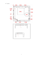
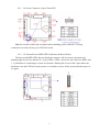
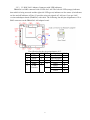
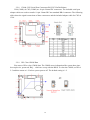
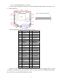
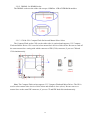
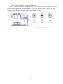
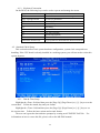
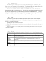
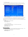
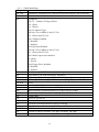
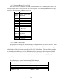
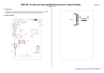
CPU-2616 PCI-104 CPU Card User’s Manual 健昇科技股份有限公司 JS AUTOMATION CORP. 新北市汐止區中興路 100 號 6 樓 6F., No.100, Zhongxing Rd., Xizhi Dist., New Taipei City, Taiwan TEL:+886-2-2647-6936 FAX:+886-2-2647-6940 http://www.automation.com.tw http://www.automation-js.com/ E-mail:[email protected] CONTENTS 1. 2. 3. 4. Introducing the CPU2616 System .......................................................................................................4 1.1 Overview....................................................................................................................................4 1.2 Layout ........................................................................................................................................5 1.3 Specifications.............................................................................................................................6 1.4 Packing List ...............................................................................................................................6 Hardware Installation...........................................................................................................................7 2.1 Before Installation......................................................................................................................7 2.2 Hardware Features .....................................................................................................................7 2.2.1 J4: Power Connector (4-pin 2.5mm JST) ....................................................................8 2.2.2 J2: External Power/HDD LED’s Indicators & Reset Header ......................................8 2.2.3 J3: RJ45 LAN /Adapter Connector with LED indicators ............................................9 2.2.4 J1: Keyboard/Mouse Connector ................................................................................10 2.2.5 BZ1 & D2: Onboard Buzzer /Power LED.................................................................10 2.2.6 CN1: Audio Connector ..............................................................................................11 2.2.7 CN7: USB Connector ................................................................................................11 2.2.8 CN4 & CN5: Serial Port Connectors RS-232C Pin Definitions................................12 2.2.9 JP2: Clear CMOS Data ..............................................................................................12 2.2.10 CN8: IDE hard Disk Connectors ...............................................................................13 2.2.11 CN6: PCI-104 Bus Connectors..................................................................................14 2.2.12 DIMM1: So-DIMM Socket .......................................................................................15 2.2.13 CN9 & JP1: Compact Flash Socket and Master/Slave Select ...................................15 2.2.14 FB4641x: Provides Audio and USB Board ...............................................................16 Installing CRT & LCD Display .........................................................................................................17 3.1 LCD Flat Panel Display...........................................................................................................17 3.2 CRT Display (CN3) .................................................................................................................18 3.2.1 CN2: LCD Connector ................................................................................................19 BIOS Setup ........................................................................................................................................20 4.1 Overview..................................................................................................................................20 4.1.1 BIOS Functions .........................................................................................................21 4.1.2 Keyboard Convention ................................................................................................22 4.2 Standard CMOS Setup.............................................................................................................22 4.2.1 Date & Time Setup ....................................................................................................22 4.2.2 Hard Disk Setup.........................................................................................................23 4.2.3 Video..........................................................................................................................23 4.2.4 Halt On.......................................................................................................................23 4.2.5 4.2.6 4.2.7 4.2.8 Memory......................................................................................................................24 Base Memory.............................................................................................................24 Extended Memory......................................................................................................24 Other Memory ...........................................................................................................24 1 5. 4.2.9 Total Memory ............................................................................................................24 4.3 BIOS Features Setup................................................................................................................25 4.3.1 Virus Warning ............................................................................................................25 4.3.2 CPU Internal Cache ...................................................................................................25 4.3.3 First /Second /Third/Boot Other Device/ Boot Device..............................................26 4.3.4 Boot Up Numlock status............................................................................................26 4.3.5 Gate A20 Option ........................................................................................................26 4.3.6 Typematic rate Setting ...............................................................................................26 4.3.7 Security Option ..........................................................................................................27 4.4 Chipset Features Setup.............................................................................................................27 4.4.1 CPU Frequency..........................................................................................................27 4.4.2 CAS Latency..............................................................................................................28 4.4.3 Video Memory Size ...................................................................................................28 4.4.4 Output Display...........................................................................................................28 4.4.5 Onboard Audio...........................................................................................................30 4.5 Peripheral Setup.......................................................................................................................30 4.5.1 On-Chip Primary IDE Channel 1...............................................................................30 4.5.2 Master /Slave Drive PIO mode..................................................................................30 4.5.3 IDE Primary Master/Slave UDMA............................................................................31 4.5.4 IDE HDD Block Mode ..............................................................................................31 4.5.5 OnBoard UART/IRQ Port 1/2, ..................................................................................31 4.5.6 LAN1 Controller........................................................................................................31 4.5.7 Onboard LAN Boot ROM .........................................................................................31 4.6 Power Management .................................................................................................................32 4.7 PCI/Plug and Play....................................................................................................................33 4.7.1 PNP O/S Installed ......................................................................................................33 4.7.2 Reset Configuration Data: Enable, Disable ...............................................................33 4.7.3 Resources Controlled By: Auto, Manual ...................................................................33 4.7.4 PCI/VGA Palette Snoop.............................................................................................34 4.8 Password Setup ........................................................................................................................34 Driver and Utility...............................................................................................................................36 5.1 VGA Drivers ............................................................................................................................36 5.1.1 WINDOWS XP Driver ..............................................................................................36 5.2 LAN Utility & Driver ..............................................................................................................36 5.3 Audio Drivers ..........................................................................................................................36 5.3.1 WINDOWS XP Driver ..............................................................................................36 5.4 AES Drivers.............................................................................................................................37 5.4.1 WINDOWS XP Driver ..............................................................................................37 5.5 BIOS Flash Utility ...................................................................................................................37 5.6 Watchdog Timer.......................................................................................................................38 5.6.1 Watchdog Timer Setting ............................................................................................39 2 6. 7. 5.6.2 Watchdog Timer Enabled...........................................................................................40 5.6.3 Watchdog Timer Trigger ............................................................................................40 5.6.4 Watchdog Timer Disabled .........................................................................................41 Technical Reference...........................................................................................................................42 6.1 Trouble Shooting for Post Beep and Error Messages..............................................................42 6.1.1 POST BEEP...............................................................................................................42 6.1.2 Error Message ............................................................................................................42 6.2 Technical Reference.................................................................................................................44 6.2.1 Physical and Environmental ......................................................................................44 6.2.2 Real-Time Clock and Non-Volatile RAM .................................................................45 6.2.3 CMOS RAM Map......................................................................................................46 6.2.4 I/O Port Address Map ................................................................................................47 6.2.5 Interrupt Request Lines (IRQ) ...................................................................................48 6.2.6 DMA Channel Map....................................................................................................48 6.2.7 Serial Ports.................................................................................................................49 Appendix............................................................................................................................................53 7.1 Dimension................................................................................................................................53 3 1. Introducing the CPU2616 System 1.1 Overview The CPU2616 is an AMD Geode™ LX-800 Low power processor, all in one, PCI-104 CPU board. This user’s manual provides information on the physical features, installation, and BIOS setup of the CPU2616. Built to unleash the total potential of the AMD Geode™ Processor, the CPU2616 is a single board computer capable of handling today’s demanding requirements. Able to support 500 MHz CPU, this unit supports 10/100M interface network port, audio, 1 DIMM socket supports up to 1GB DDR RAM, two USB2.0 ports, and a VGA controller. Each CPU2616 has two ports for I/O communications. Two RS-232 ports are available. There is also a watchdog timer that can be configured from software to automatically reset the system. And for easy configuration, Phoenix-Award BIOS are available. Power management is also featured to lower the rate of consumption. The unit supports doze mode, <Suspend Mode> and <Standby mode> as well as it adheres to the “Green Function” standard. The CPU2616 is perfect for POS and POI applications, network systems, panel / MMI’s, order entry kiosks, test equipment, OEM projects or as a motherboard for a panel PC. The unit is only 90.2x95.9mm, offering unparalleled performance in a very small footprint. 4 1.2 Layout 5 1.3 Specifications 1. AMD Geode™ LX800 (500MHz) Low Power CPU. 2. AMD Geode CS5536 chipset and 64KB or above L2 cache inside the CPUs. 3. Supporting One 200 pin So-DIMM socket for up to 1GB DDR-333/400 RAM. 4. One 100M/10M Ethernet port. 5. Supports CRT port and LCD interface up to 254MB shared memory. 6. Two RS-232 ports, two USB ports, and One PCI IDE interface. 7. Compact Flash socket for 3.3V Compact Flash and Micro Drives. 8. PS/2 compatible keyboard and mouse interface. 9. Providing speaker and hard disk access LED. 10. Software programmable watchdog timer. 11. Providing one AC97 audio function. 12. Flash BIOS with easy upgrade utility. 13. PCI-104 form factor, 90.2 mm x 95.9 mm (3.55” x 3.775”) 14. Power requirement: +5V only, 1.3A maximum. (500MHz CPU) 1.4 Packing List Upon receiving the package, verify the following things. Should any of the mentioned happens, contact us for immediate service. • Unpack and inspect the CPU2616 package for possible damage that may occur during the delivery process. • Verify the accessories in the package according to the packing list and see if there is anything missing or incorrect package is included. • If the cable(s) you use to install the CPU2616 is not supplied from us, please make sure the specification of the cable(s) is compatible with the CPU2616 system. Note: After CPU2616 is installed, it is recommended that you keep the diskette or CD that contains drivers and document files, and keep the document copies, or unused cables in the carton for future use. The following lists the accessories that may be included in your CPU2616 package. Some of the accessories are optional shipped only upon order. ‧ One CPU2616 All-In-One PCI-104 CPU board ‧ One VGA (CRT interface) adapter cable ‧ One 44-pin hard disk drive interface cable ‧ Two serial ports and one parallel port interface cable ‧ One PS2 keyboard and mouse port adapter cable ‧ One 10-pin LAN adapter cable with FB4605A board. ‧ One USB cable, one Audio cable, and one FB4641X Audio/USB adapter board.(All are Optional items) ‧ One compact disc containing manual file in PDF format and necessary utilities 6 drivers and 2. Hardware Installation This chapter introduces the system connectors & jumper settings, and guides you to apply them for field application. 2.1 Before Installation Before you install the system, make sure you follow the following descriptions. 1. Before removing the board from its anti-static bag, wear an anti-static strap to prevent the generation of Electricity Static Discharge (ESD). The ESD may be generated by man’s physical touch. It may do damage to the board circuit. 2. Install any connector, module, or add-on card, be sure that the power is disconnected from the system board. If not, this may damage the system board components, module, or the add-on-card. 3. When you connect the connectors and memory modules, be careful with the pin orientations. 2.2 Hardware Features The following list is for the setup of the connectors and jumpers of the CPU2616. Item Description CN1 AMR connector for provides AC97 signals for Audio function (IDC) CN2 40-pin LCD Connector with 24 bit LCD signals (DF13) CN3 10-pin 2.0mm CRT connector (IDC) CN4 ,CN5 10-pin 2.0mm RS-232 port connector (IDC) CN6 PCI-104 CN7 10-pin USB connector header CN8 44-pin 2.0mm IDE 2 hard disk connector CN9,JP1 Compact Flash Socket and Master/Slave Select J1 5-pin for Keyboard and Mouse 2.0mm connector (JST) J2 6-pin Power and watchdog of LED indicator header and Reset header J3 10-pin for RJ45-Lan 2.54mm connector r (JST) J4 4-pin Power 2.5mm connector BZ1 On board Buzzer JP2 3-pin Battery Select /Clean CMOS jumper DIMM1 DDR So-DIMM Socket 200-pin 7 (IDC) 2.2.1 J4: Power Connector (4-pin 2.5mm JST) Note: Be careful with the pin orientation when installing power connector. A wrong connection can easily destroy your CPU2616 board. 2.2.2 J2: External Power/HDD LED’s Indicators & Reset Header The Power and HDD LED’s has two distinctive statuses: Off for inactive operation and blinking light for activity, and the J2 3, 4 pin (LED1+/LED1-) for Power and 5,6 pin for HDD. And 1, 2 pin header for connecting to system reset button. Shorting the circuit of the 2 pins makes the hardware reset and CPU2616 restart system. It is similar to power off the system and then power it on again. 8 2.2.3 J3: RJ45 LAN /Adapter Connector with LED indicators FB4605A is a RJ45 connector with 2 LEDs for LAN. The left side LED (orange) indicates data which is being accessed and the right side LED (green) indicates on-line status. (On indicates on-line and off indicates off-line) J3 provides twist-pair signals of LAN port if you got LAN version and adapter board (FB4605A) with cable. The following lists the pin assignments of J1 to RJ45 connector on the FB4605A LAN adapter board: The following list the pin assign8ments of J3. TPin Signal RJ45 Pi7n Signal RJ45 1 TPTX+ 1 6 Access LED 2 TPTX2 7 On-Line LED 3 TPRX+ 3 8 Case GND 4 TPRX6 9 FBG1 4 5 LED FBG1 5 Common 10 FBG2 7 FBG2 8 9 2.2.4 J1: Keyboard/Mouse Connector J1 is a 6-pin 2.0mm JST connector, use the included KB/MS adapter cables you can attach standard PS/2 type keyboard and mouse. 2.2.5 BZ1 & D2: Onboard Buzzer /Power LED 10 2.2.6 CN1: Audio Connector CN1 is a 12-pin 2.0mm IDC connector with AC97 signals for Audio I/O. Use the included Audio cable and FB4641x adapter board for your Audio applications. 2.2.7 CN7: USB Connector Use the USB adapter cable and FB4641 board, you can attach up to 2 USB devices. 11 2.2.8 CN4 & CN5: Serial Port Connectors RS-232C Pin Definitions CN4 (COM1) & CN5 (COM2) are 10-pin 2.0mm IDC connectors. The included serial port adapter cables are used to transfer 10-pin 2.0mm IDC into standard DB-9 connector. The following tables show the signal connections of these connectors and the included adapter cable for CN5 & CN6: 2.2.9 JP2: Clear CMOS Data You can use JP2 to clear CMOS data. The CMOS stores information like system date, time, boot up device, password, IRQ… which are set up with the BIOS. To clear the CMOS, set JP2 to 2-3 and then return to 1-2 before system powers off. The default setting is 1-2. 12 2.2.10 CN8: IDE hard Disk Connectors CN8 is 44-pin 2.0mm IDC connectors. Use the included hard disk cables to attach up to two 2.5” hard disk drives. The following table lists the pin description of CN8. Pin Description Pin Description 1 -RESET 2 GROUND 3 DATA 7 4 DATA 8 5 DATA 6 6 DATA 9 7 DATA 5 8 DATA 10 9 DATA 4 10 DATA 11 11 DATA 3 12 DATA 12 13 DATA 2 14 DATA 13 15 DATA 1 16 DATA 14 17 DATA 0 18 DATA 15 19 GROUND 20 NOT USED 21 IDEDREQ 22 GROUND 23 -IOW A 24 GROUND 25 -IOR A 26 GROUND 27 IDEIORDYA 28 GROUND 29 -DACKA 30 GROUND 31 AINT 32 GROUND 33 SA 1 34 Not Used 35 SA 0 36 SA 2 37 CS 0 38 CS 1 39 HD LED A 40 GROUND 41 VCC 42 VCC 43 GROUND 44 Not Used Note: Be careful with the pin orientation when installing connectors and the cables. A wrong connection can easily destroy your hard disk. CN8 is used to connect a 2.5" HDD with included 44-pin flat-cable or 44-pin DiskOnModule directly. 13 2.2.11 CN6: PCI-104 Bus Connectors Pin A1 A2 A3 A4 A5 A6 A7 A8 A9 A10 A11 A12 A13 A14 A15 A16 A17 A18 A19 A20 A21 A22 A23 A24 A25 A26 A27 A28 A29 A30 Signal Pin B1 B2 AD5 B3 CBE0# B4 GND B5 AD11 B6 AD14 B7 + 3.3V B8 SERR# B9 GND B10 STOP# B11 + 3.3V B12 FRAME# B13 GND B14 AD18 B15 AD21 B16 + 3.3V B17 IDSEL0 B18 AD24 B19 GND B20 AD29 B21 + 5V B22 REQA B23 GND B24 GNTB# B25 + 5V B26 PCICLK2 B27 GND B28 B29 B30 Signal Pin C1 AD2 C2 GND C3 AD7 C4 AD9 C5 C6 AD13 C7 CBE1# C8 GND C9 PERR# C10 + 3.3V C11 TRDY# C12 GND C13 AD16 C14 + 3.3V C15 AD20 C16 AD23 C17 GND C18 CBE3# C19 AD26 C20 + 5V C21 AD30 C22 GND C23 REQC C24 C25 PCICLK0 C26 + 5V C27 INTD# C28 INTA# C29 C30 Signal + 5V AD1 AD4 GND AD8 AD10 GND AD15 + 3.3V LOCK# GND IRDY# + 3.3V AD17 GND AD22 IDSEL1 AD25 AD28 GND REQB# + 5V GNTC# GND PCICLK3 + 5V INTB# 14 Pin D1 D2 D3 D4 D5 D6 D7 D8 D9 D10 D11 D12 D13 D14 D15 D16 D17 D18 D19 D20 D21 D22 D23 D24 D25 D26 D27 D28 D29 D30 Signal AD0 + 5V AD3 AD6 GND M66EN AD12 + 3.3V PAR GND GND DEVSEL# + 3.3V CBE2# GND AD19 + 3.3V IDSEL2 IDSEL3 GND AD27 AD31 GNTA# GND PCICLK1 GND PCIRST# INTC# - 2.2.12 DIMM1: So-DIMM Socket The DIMM1 socket on the solder side accepts 128MB to 1GB of DDR RAM modules 2.2.13 CN9 & JP1: Compact Flash Socket and Master/Slave Select The Compact Flash socket CN9 (on the solder side) is optional and supports 3.3V Compact Flash and Micro Drives. JP1 is used to select master/slave device of this socket. Be sure to ward off the same master/slave setting with which connects to IDE (CN8) connector, if you use CN8 and CN9 simultaneously. Note: The Compact Flash socket supports 3.3V Compact Flash and Micro Drives. The JP1 is used to select master/slave device of this socket and default is slave (close). Be sure not to set master/slave to the same IDE connector, if you use CF and IDE hard disk simultaneously. 15 2.2.14 FB4641x: Provides Audio and USB Board The J3, J4, and J5 connectors on FB4641x are 2-way Line-In, mono Microphone input, and 2-way Lineout respectively. You can connect J1, CN2 cable from CPU2616 CN1 to CN7. The following figure shows these Audio connectors on FB4641x board: 16 3. Installing CRT & LCD Display This chapter describes the configuration and installation procedure of LCD and CRT displays. Both CRT and LCD displays may be used at the same time. However, each type of LCD requires different BIOS. This section describes the configuration and installation procedure using LCD display. Skip this section if you are using CRT monitor only. • LCD Flat Panel Display • CRT & LCD Display 3.1 LCD Flat Panel Display Using the BIOS setting for different types of LCD pane, then set your system properly and configures BOS setting for the right type of LCD panel you are using. The following shows the block diagram of using CPU2616 for LCD display. LCD Panel Block Diagram The diagram shows that CPU2616 needs components to be linked with a LCD panel. NOTE: Be careful with the pin orientation when installing connectors and the cables. A wrong connection can easily destroy your LCD panel. The pin 1 of the cable connectors is indicated with a sticker and the pin1 of the ribbon cable usually has a different color. 17 3.2 CRT Display (CN3) The CPU2616 supports a CRT colored monitor. It can be connected to create a compact video solution for the industrial environment. 254MB simulated VRAM allows a maximum CRT resolution of 1920X1440 with 32 bpp at 85Hz. The following table and figure illustrate the pin definition of CN3 and D-sub 15-pin on the CRT adapter cable: PIN Signal DB-15 PIN Signal DB15 1 RED 1 2 Case Ground Case 3 GREEN 2 4 Digital Ground 5,10 5 BLUE 3 6 Analog Ground 6,7,8 7 VSYNC 14 8 DDC Data 12 9 HSYNC 13 10 DDC Clock 15 NOTE: Be careful with the pin orientation when installing VGA connector and the cable. 18 3.2.1 CN2: LCD Connector CN2 is a 24-bit LCD interface connector. The pin assignments are listed in the following table. Pin Signal Pin Signal 1 +5V 2 +5V 3 Ground 4 Ground 5 +3.3V 6 +3.3V 7 NC 8 Ground 9 FP0 10 FP1 11 FP2 12 FP3 13 FP4 14 FP5 15 FP6 16 FP7 17 FP8 18 FP9 19 FP10 20 FP11 21 FP12 22 FP13 23 FP14 24 FP15 25 FP16 26 FP17 27 FP18 28 FP19 29 FP20 30 FP21 31 FP22 32 FP23 33 Ground 34 Ground 35 SHFCLK 36 FP (VS) 37 DE 38 LP (HS) 39 ENVDD 40 ENAVEE NOTE: If any trouble occurs when connecting CPU2616 with LCD panels, you could contact technical support division of FabiaTech Corporation. 19 4. BIOS Setup This chapter describes the BIOS setup. 4.1 Overview BIOS are a program located on a Flash memory chip of a circuit board. It is used to initialize and set up the I/O peripherals and interface cards of the system, which includes time, date, hard disk drive, the ISA bus and connected devices such as the video display, diskette drive, and the keyboard. This program will not be lost when you turn off the system. The BIOS provides a menu-driven interface to the console subsystem. The console subsystem contains special software, called firmware that interacts directly with the hardware components and facilitates interaction between the system hardware and the operating system. The BIOS default values ensure that the system will function at its normal capability. In the worst situation the user may have corrupted the original settings set by the manufacturer. All the changes you make will be saved in the system RAM and will not be lost after power-off. When you start the system, the BIOS will perform a self-diagnostics test called Power On Self Test (POST) for all the attached devices, accessories, and the system. Press the [Del] key to enter the BIOS Setup program, and then the main menu will show on the screen. Note: Change the parameters when you fully understand their functions and subsequences. 20 4.1.1 BIOS Functions On the menu, you can perform the following functions 1. Standard CMOS Features 2. Advanced BIOS Features 3. Advanced Chipset Features 4. Integrated Peripherals 5. Power Management Setup 6. PNP/PCI Configuration 7. Frequency/Voltage Control 8. Set Supervisor Password 9. Set User Password 10. Load Optimized Default: to auto configure the system according to optimal setting with pre-defined values. This is also the factory default setting of the system when you receive the board. 11. Load Fail-Safe Default: to configure the system in fail-safe mode with predefined values. 12. Save Settings and Exit: perform this function when you change the setting and exit the BIOS Setup program. 13. Exit without saving: perform this function when you want to exit the program and do not save the change. 21 4.1.2 Keyboard Convention On the BIOS, the following keys can be used to operate and manage the menu: Item Function ESC To exit the current menu or message Page Up/Page Down To select a parameter F10 Save and exit F1 General Help F2 Item Help F5 Previous Values F6 Fail-Safe Defaults F7 Optimized Defaults F9 Menu in BIOS UP/Down Arrow Keys To go upward or downward to the desired item 4.2 Standard CMOS Setup This section describes basic system hardware configuration, system clock setup and error handling. If the CPU board is already installed in a working system, you will not need to select this option anymore. 4.2.1 Date & Time Setup Highlight the <Date> field and then press the [Page Up] /[Page Down] or [+]/[-] keys to set the current date. Follow the month, day and year format. Highlight the <Time> field and then press the [Page Up] /[Page Down] or [+]/[-] keys to set the current time. Follow the hour, minute and second format. The user can bypass the date and time prompts by creating an AUTOEXEC.BAT file. For information on how to create this file, please refer to the MS-DOS manual. 22 4.2.2 Hard Disk Setup The BIOS supports various types for user settings, The BIOS supports <Pri Master>, <Pri Slave>, so the user can install up to two hard disks. For the master and slave jumpers, please refer to the hard disk’s installation descriptions and the hard disk jumper settings. You can select <AUTO> under the <TYPE> and <MODE> fields. This will enable auto detection of your IDE drives during boot up. This will allow you to change your hard drives (with the power off) and then power on without having to reconfigure your hard drive type. If you use old-type hard disk drives, which do not support this feature, then you must configure the hard disk drive in the standard procedures as described above by the <USER> option. 4.2.3 Video This option is to select the type of adapter used for the primary system monitor that must match your video display card and monitor. Although secondary monitors are supported, you do not have to select the type in Setup. You have two ways to boot up the system: When VGA set as primary and monochrome set as secondary, the selection of the video type is “ VGA Mode”. When monochrome is set as primary and VGA as secondary, the selection of the video type is “Monochrome Mode”. 4.2.4 Halt On This option determines whether the computer will stop if an error is detected during power up. No errors The system boot will not be stopped for any error that may be detected. All errors Whenever the BIOS detect a non-fatal error the system will be stopped and you will be prompted. All, But Keyboard The system boot will not stop for a keyboard error; it will stop for all other errors. All, But Diskette The system boot will not stop for a disk error; it will stop for all other errors. All, But Disk/Key The system boot will not stop for a keyboard or disk error; it will stop for all other errors. 23 4.2.5 Memory This option is for the display-only which is determined by POST (Power On Self Test) of the BIOS. 4.2.6 Base Memory The POST of the BIOS will determine the amount of base (or conventional) memory installed in the system. The value of the base memory is typically 512K for systems with 512K memories installed on the motherboard, or 640K for systems with 640K or more memory installed on the motherboard. 4.2.7 Extended Memory The BIOS determines how much extended memory is existing during the POST. amount of memory located above 1MB in the CPU’s memory address map. This is the 4.2.8 Other Memory This refers to the memory located in the 640K to 1024K-address space. This is memory that can be used for different applications. DOS uses this area to load device drivers to keep as much base memory free for application programs. Most use for this area is Shadow RAM. 4.2.9 Total Memory System total memory is the sum of basic memory, extended memory, and other memory. 24 4.3 BIOS Features Setup This section describes the configuration entries that allow you to improve your system performance, or let you set up some system features according to your preference. Some entries here are required by the CPU board’s design to remain in their default settings. 4.3.1 Virus Warning This option may flash on the screen. During and after the system boots up, any attempt to write to the boot sector or partition table of the hard disk drive will halt the system and the following error message will appear, in the mean time, you can run an anti-virus program to locate the problem. Available Options: Disabled, Enabled Default setting: Disable 4.3.2 CPU Internal Cache This functions speeds up memory access. The CPU has an internal cache. Available options: Disabled, Enabled Default setting: Enabled Quick Power On Self Test This option speeds up Power On Self Test (POST) after you power on the computer. set to Enable, BIOS will shorten or skip some items’ checks during POST. Available options: Disabled, Enabled Default setting: Enable 25 If it is 4.3.3 First /Second /Third/Boot Other Device/ Boot Device This field specifies which device the system checks first upon power on. Available options: LS120, Hard Disk, ZIP100, USB-ZIP, USB-CDROM, USB-HDD, LAN and Disable Default setting: Hard Disk, CDROM, LAN 4.3.4 Boot Up Numlock status This field is used to activate the Num Lock function upon system boot. If the setting is on, after a boot, the Num Lock light is lit, and user can use the number key. Available options: On, Off Default setting: On 4.3.5 Gate A20 Option This item is chosen as <Normal>, the A20 signal is controlled by keyboard controller or chipset hardware. Available options: Normal, Fast Default setting: Normal 4.3.6 Typematic rate Setting This function specifies the keystroke repeat rate when a key is pressed and held down on. Available options: Disable, Enable Default setting: Disable Typematic Rate (Chars/Sec) Typematic Rate sets the rate at which characters on the screen repeat when a key is pressed and held down on. Available options: 6, 8, 10, 12, 15, 20, 24, or 30 characters per second Default setting: 6 Typematic Delay (Msec) The number selected indicates the time period between two identical characters appearing on screen. Available options: 250,500 750 and 1000 Default setting: 250 26 4.3.7 Security Option This field enables password checking every time when the computer is powered on or every time when the BIOS Setup is executed. If Always is chosen, a user password prompt appears every time and the BIOS Setup Program executes and the computer is turned on. If Setup is chosen, the password prompt appears if the BIOS executed. Available options: Setup, Always Default setting: Setup 4.4 Chipset Features Setup This section describes the configuration of the board’s chipset features. 4.4.1 CPU Frequency This display sent by the CPU host clock and DDR-RAM memory clock Available Options: Auto, 200 MHz, 300 MHz, 400 MHz, and 500 MHz Default setting: Auto Memory Frequency This Select equates are used for determining the DDR-RAM Memory Clock frequency. SPD represents Serial Presence Detect. It is an 8-bit, 2048 bits EEPROM, built on the SDRAM for different frequencies. Available Options: Auto, 100 MHz, 133 MHz, 166 MHz and 200 MHz Default setting: 100 MHz 27 4.4.2 CAS Latency This field specifies the latency for the DDR RAM system memory signals. Available Options: Auto, 1.5, 2.0, 2.5, 3.0 and 3.5 Default setting: Auto 4.4.3 Video Memory Size This field specifies which VGA display memory. VGA. There are setting share onboard memory. You can select either Video memory on the Available Options: None M, 8MB, 16MB, 32MB, 64MB,128MB and 254MB Default setting: 8MB 4.4.4 Output Display This field specifies which VGA display will be used when the system is boot. either the Flat Panel or the CRT booting on the VGA. You can select Available Options: Flat Panel, CRT and Panel & CRT Default setting: CRT Flat Panel Configuration When using the LCD, the field specifies the selections of display resolution for different TFT LCD display type. 28 Flat Panel Type See the Flat Panel Display Table Available Options: Auto and TFT Default setting: Auto Flat Panel Display LCD Type Table Resolution 320x240 640x480 800x600 1024x768 1152x864 1280x1024 1600x1200 Data Bus Type This field specifies the Data Bus width and data type Available Options: 18,24 bits, 1 ppc and 18,24 bits, 2 ppc Default setting: 18,24 bits, 1 ppc Refresh Rate This field specifies the refresh rate required by the panel Available Options: 60 Hz, 70Hz, 72 Hz, 75 Hz, 85 Hz, 90 Hz and 100 Hz Default setting: 60 Hz HSYNC/VSYNC Polarity Active This field specifies the HSYNC/VSYNC signal to the panel Available Options: Low and High Default setting: Low LP Active Period This field specifies the LDE/MOD signal to the panel Available Options: Free running and Active Only Default setting: Free running 29 4.4.5 Onboard Audio This field specifies the internal Audio Control. Available Options: Disable, Enable Default setting: Enable 4.5 Peripheral Setup This section describes the function of peripheral features. 4.5.1 On-Chip Primary IDE Channel 1 This field specifies the IDE channel that can be applied when using IDE hard disk connector. Available Options: Disabled, Enable Default setting: Enable 4.5.2 Master /Slave Drive PIO mode IDE hard drive controllers can support up to two separate hard drives. These drives have a master/slave relationship, which is determined by the cabling configuration used to attach them to the controller. PIO means Programmed Input/Output. Rather than have the BIOS issue a series of commands to affect a transfer to or from the disk drive, PIO allows the BIOS to tell the controller what it wants and then let the controller and the CPU perform the complete task by them. This is simpler and more efficient (and faster). Your system supports five modes, numbered from 0 to 4, which primarily differs in timing. When Auto is selected, the BIOS will select the best available mode. 30 4.5.3 IDE Primary Master/Slave UDMA Ultra DMA/33 implementation is possible only if your IDE hard drive supports it and the operating environment includes a DMA driver (Windows 95 OSR2 or a third-party IDE bus master driver). If your hard drive and your system software both support Ultra DMA/33, select Auto to enable this option, which allows your hard disk controller to use the fast block mode to transfer data to and from your hard disk drive (HDD). 4.5.4 IDE HDD Block Mode This option allows your hard disk controller to use the fast block mode to transfer data to and from your hard disk drive (HDD). 4.5.5 OnBoard UART/IRQ Port 1/2, These fields select the I/O port address for each Serial port. Available Options: Disabled, 3F8H/IRQ4, 2F8H/IRQ3, and 3E8H/IRQ4, 2E8H/IRQ3. Default setting: 3F8/IRQ4 and 2F8H/IRQ3 4.5.6 LAN1 Controller This field specifies the Enable or Disable of the onboard LAN chip. Available Options: Disabled, Enable Default setting: Enable 4.5.7 Onboard LAN Boot ROM This field specifies the PXE boot ROM of the onboard LAN chip. Available Options: Disabled, Enable Default setting: Disable 31 4.6 Power Management Power Management The field determines how much power consumption is needed for the system after selecting the below items. Standby Mode This field defines the continuous idle time before the system enters Standby Mode. defined is enabled & active Standby timer will be reloaded. 32 If any item 4.7 PCI/Plug and Play 4.7.1 PNP O/S Installed Set to Yes to inform BIOS that the operating system can handle Plug and Play (PnP) devices. Available Options: Yes, No Default setting: No 4.7.2 Reset Configuration Data: Enable, Disable If you select Enable to reset Extended System Configuration Data (ESCD) when you exit setup is you have installed a new add-on and the system reconfiguration has caused such a serious conflict that the operation operating system cannot boot. Available Options: Enable, Disable Default setting: Disable 4.7.3 Resources Controlled By: Auto, Manual If you select Enable to reset Extended System Configuration Data (ESCD) when you exit setup which you have installed a new add-on card and the system reconfiguration has caused such a serious conflict that the operation system cannot boot. Available Options: Auto. , Manual Default setting: Manual 33 IRQ-n/DMA-n Assigned: PCI/Reserved PnP The resources are controlled manually. 1. Reserved Devices compliant with the original PC AT bus specification, and require a specific interrupt/DMA (such as IRQ4, IRQ3 for serial port 1 and 2). 2. PCI/Reserved PnP Devices compliant with Plug and play standard, whether to be designed for PCI or Reserved. Memory Source: Resources Controlled By: Auto, Manual Select a base address for the memory area used by any peripheral that requires high memory. Available Options: N/A, C800, CC00, D000, D400, D800 and DC00 Default setting: N/A 4.7.4 PCI/VGA Palette Snoop This option must be set to Enabled if any ISA adapter card installed in the computer requiring VGA palette snooping. Available options: Enable, Disable Default setting: Disable 4.8 Password Setup There are two security passwords: Supervisor and User. Supervisor is a privileged person that can change the User password from the BIOS. According to the default setting, both access passwords are not set up and are only valid after you set the password from the BIOS. To set the password, please complete the following steps. 1. Select Change Supervisor Password. 2. Type the desired password (up to 8 character length) when you see the message, “Enter New Supervisor Password.” 3. Then you can go on to set a user password (up to 8 character length) if required. Note that you cannot configure the User password until the Supervisor password is set up. 4. Enter Advanced CMOS Setup screen and point to the Password Checkup field. 5. Select Always or Setup. Always: a visitor who attempts to enter BIOS or operating system will be prompted for password. Setup: a visitor who attempts to the operating system will be prompted for user password. You can enter either User password or Supervisor password. 6. Point to Save Settings and Exit and press Enter. 7. Press Y when you see the message, “Save Current Settings and Exit (Y/N)?” 34 Note: it is suggested that you write down the password in a safe place to avoid that password may be forgotten or missing. To set the password, please complete the following steps. 1. Select Change Supervisor Password. 2. Press Enter instead of entering any character when you see the message, “Enter New Supervisor Password.” 3. Thus you can disable the password. 35 5. Driver and Utility The enclosed diskette includes CPU2616 VGA, AUDIO driver and LAN driver. To install and configure you CPU2616 system, you need to perform the following steps. 5.1 VGA Drivers 5.1.1 WINDOWS XP Driver 1. To install the VGA driver, insert the CD ROM into the CD ROM device, and enter DRIVER>VGA> Geode_LX >WINXP. If your system is not equipped with a CD ROM device, copy the VGA driver from the CD ROM to a CF. 2. Open Control Panel. [Start->Settings->Control Panel]. 3. Click on System button> Select Hardware >click on Device Manager. 4. Click on Video Controller (VGA Compatible) >Update Driver> Select Specify a location > Browse > Select “lX_win ” file from CF . 5. Click on OK >Next >Yes >Finish 6. In the WINDOWS-XP, you can find the <DISPLAYL> icon located in the {CONTROL PANEL} group. 7. Adjust the <Resolution> and <Color>, 5.2 LAN Utility & Driver 1. To install the LAN utility OR driver, insert the CD ROM into the CD ROM device, and enter DRIVER>LAN>RTL8139C>DIAG. If your system is not equipped with a CD ROM device, copy the LAN driver from the CD ROM to a CF. 2. Execute install.exe file. 3. Note: In the LAN directory, a HELPME.EXE file is included to provide installation information. 5.3 Audio Drivers 5.3.1 WINDOWS XP Driver 1. To install the Audio driver, insert the CD ROM into the CD ROM device, and enter DRIVER>AUDIO>CS5536>WINXP. If your system is not equipped with a CD ROM device, copy the Audio driver from the CD ROM to a CF. 2. Open Control Panel. [Start->Settings->Control Panel]. 3. Click on System button> Select Hardware >click on Device Manager. 4. Click on Multimedia Audio Controller >Update Driver> Select Specify a location > Browse > Select “lxWDMAu ” file from CF . 5. Click on OK >Next >Yes >Finish 36 5.4 AES Drivers 5.4.1 WINDOWS XP Driver 1. To install the SysChip driver, insert the CD ROM into the CD ROM device, and enter DRIVER>SysChip>GeodeLX_XP_AES. If your system is not equipped with a CD ROM device, copy the AES driver from the CD ROM to a CF. 2. On the target LX processor computer running Windows XP, open the device manager 3. Find the question mark on "Entertainment Encryption/Decryption Device" in Other Devices. 4. Pick "Install from a list or specific location" and click next. 5. Pick "Don't search. I will choose the driver to install." and click next. 6. Pick "Show All Devices", wait, and pick "Have Disk". 7. It will come back with "Geode LX AES Crypto Driver", click Next. 8. Click yes to the warning box that comes up. 5.5 BIOS Flash Utility In the <UTILITY> directory, there is the FLASH845.EXE file. Step 1: Use the AWDFLASH.EXE program to update the BIOS setting. Step 2: And then refer to the chapter “BIOS Setup”, as the steps to modify BIOS. Step 3: Now the CPU board’s BIOS loaded with are the newest program; user can use it to modify BIOS function in the future, when the BIOS add some functions. 37 5.6 Watchdog Timer This section describes how to use the Watchdog Timer, including disabled, enabled, and trigger functions. The CPU2616 is equipped with a programmable time-out period watchdog timer. You can use your own program to enable the watchdog timer. Once you have enabled the watchdog timer, the program should trigger the I/O every time before the timer times out. If your program fails to trigger or disable this timer before it times out, e.g. because of a system hang-up, it will generate a reset signal to reset the system. The time-out period can be programmed to be set from 1 to 255 seconds or minutes. The CD –ROM includes a Watch Dog demo file. In the file, there are 3 execution programs written in different forms. The sub-directories of the file are: 1. WATCHDOG/ASSEMBLE: Library and Test Program written in Assembly Language 2. WATCHDOG/TURBOC: Library and Test Program written in Turbo C++ The WATCHDOG includes a demonstration program established for users who would like to configure the Watchdog timer by themselves. Note: In the WATCHDOG/ITE8712 directory, README.TXT file is included to provide demo program information. 38 5.6.1 Watchdog Timer Setting The watchdog timer is a circuit that may be used from your program software to detect system crashes or hang-ups. LED on the Front side is the watchdog timer indicator. Whenever the watchdog timer is enabled, the LED will blink to indicate that the timer is counting. The watchdog timer is automatically disabled after reset. Once you have enabled the watchdog timer, your program must trigger the watchdog timer every time before it times out. After you trigger the watchdog timer, it will be set to non-zero value to watchdog counter and start to count down again. If your program fails to trigger the watchdog timer before time-out, it will generate a reset pulse to reset the system. The factor of the watchdog timer time-out constant is approximately 1 second. The period for the watchdog timer time-out is between 1 to FF timer factors. If you want to reset your system when watchdog times out, the following table listed the relation of timer factors between time-out periods. Time Factor 1 2 3 4 5 “ “ “ FF Time-Out Period Time-Out Period (Seconds) 1 2 3 4 5 “ “ “ FF (Minutes) 1 2 3 4 5 “ “ “ FF 39 5.6.2 Watchdog Timer Enabled To enable the watchdog timer, you have to output a byte of timer factor to the watchdog. The following is a Turbo C++ program, which demonstrates how to enable the watchdog timer and set the time-out period at 6 seconds. #include “stdio.H” #include “WDLIB.H” main( ) { char WD_TIME=ox6; InitWD(equWdUnitS); printf (“Enable watchdog”); //Trigger watchdog Timer Output is 6 seconds EnWD(WD_TIME); } 5.6.3 Watchdog Timer Trigger After you enable the watchdog timer, your program must write the same factor as enabling to the watchdog register at least once every time-out period to its previous setting. You can change the time-out period by writing another timer factor to the watchdog register at any time, and you must trigger the watchdog before the new time-out period in the next trigger. Below is a Turbo C++ program, which demonstrates how to trigger the watchdog timer: #include “stdio.H” #include “WDLIB.H” main( ) { char WD_TIME=ox6; InitWD(equWdUnitS); printf (“Enable watchdog”); //Trigger watchdog Timer Output is 6 seconds EnWD(WD_TIME); } 40 5.6.4 Watchdog Timer Disabled To disable the watchdog timer, simply write a 00H to the watchdog register. #include “stdio.H” #include “WDLIB.H” main( ) { InitWD(equWdUnitS); printf (“Disable Watch Dog”); //Disable watch dog DisWD(WD_TIME); } 41 6. Technical Reference This section outlines the errors that may occur when you operate the system, and also gives you the suggestions on solving the problems. Topic include: Trouble Shooting for Post Beep & Error Messages Technical Reference 6.1 Trouble Shooting for Post Beep and Error Messages The following information informs the Post Beep & error messages. Please adjust your systems according to the messages below. Make sure all the components and connectors are in proper position and firmly attached. If the errors still exist, please contact with your distributor for maintenance. 6.1.1 POST BEEP Currently there are two kinds of beep codes in BIOS setup. One indicates that a video error has occurred and the BIOS cannot initialize the video screen to display any additional information. This beep code consists of a single long beep followed by three short beeps. The other indicates that an error has occurred in your DRAM. This beep code consists of a constant single long beep. 6.1.2 Error Message CMOS BATTERY FAILURE When the CMOS battery is out of work or has run out, the user has to replace it with a new battery. CMOS CHECKSUM ERROR This error informs that the CMOS has corrupted. When the battery runs weak, this situation might happen. Please check the battery and change a new one when necessary. DISK BOOT FAILURE When you can‘t find the boot device, insert a system disk into Drive A and press < Enter >. Make sure both the controller and cables are all in proper positions, and also make sure the disk is formatted. Then reboot the system. 42 DISKETTE DRIVES OR TYPES MISMATCH ERROR When the diskette drive type is different from CMOS, please run setup or configure the drive again. ERROR ENCOUNTERED INITIALIZING HARD DRIVE When you can‘t initializes the hard drive, ensure the following things: 1. The adapter is installed correctly 2. All cables are correctly and firmly attached 3. The correct hard drive type is selected in BIOS Setup ERROR INITIALIZING HARD DISK CONTROLLER When this error occurs, ensure the following things: 1. The cord is exactly installed in the bus. 2. The correct hard drive type is selected in BIOS Setup 3. Whether all of the jumpers are set correctly in the hard drive KEYBOARD ERROR OR NO KEYBOARD PRESENT When this situation happens, please check keyboard attachment and no keys being pressed during the boot. If you are purposely configuring the system without a keyboard, set the error halt condition in BIOS Setup to HALT ON ALL, BUT KEYBOARD. This will cause the BIOS to ignore the missing keyboard and continue the boot procedure. MEMORY ADDRESS ERROR When the memory address indicates error, you can use this location along with the memory map for your system to find and replace the bad memory chips. MEMORY SIZE HAS CHANGED Memory has been added or removed since last boot. In EISA mode, use Configuration Utility to re-configure the memory configuration. In ISA mode enter BIOS Setup and enter the new memory size in the memory fields. MEMORY VERIFYING ERROR It indicates an error verifying a value is already written to memory. Use the location along with your system's memory map to locate the bad chip. OFFENDING ADDRESS MISSING This message is used in connection with the I/O CHANNEL CHECK and RAM PARITY ERROR messages when the segment that has caused the problem cannot be isolated. 43 REBOOT ERROR When this error occurs that requires you to reboot. Press any key and the system will reboot. SYSTEM HALTED Indicates the present boot attempt has been aborted and the system must be rebooted. Press and hold down the CTRL and ALT keys and press DEL. 6.2 Technical Reference 6.2.1 Physical and Environmental Temperature: Operating 0°C ~ 60°C Relative humidity 5 % to 95 % non-condensing 44 6.2.2 Real-Time Clock and Non-Volatile RAM The CPU2616 contains a real-time clock compartment that maintains the date and time in addition to storing configuration information about the computer system. It contains 14 bytes of clock and control registers and 114 bytes of general purpose RAM. Because of the use of CMOS technology, it consumes very little power and can be maintained for long periods of time using an internal Lithium battery. The contents of each byte in the CMOS RAM are listed below: Address 00 01 02 03 04 05 06 07 08 09 0A 0B 0C 0D 0E 0F 10 11 12 13 14 15 16 17 18 19-2D 2E-2F 30 31 32 33 34-7F Description Seconds Second alarm Minutes Minute alarm Hours Hour alarm Day of week Date of month Month Year Status register A Status register B Status register C Status register D Diagnostic status byte Shutdown status byte Diskette drive type byte, drive A and B Fixed disk type byte, drive C Fixed disk type byte, drive D Reserved Equipment byte Low base memory byte High base memory byte Low expansion memory byte High expansion memory byte Reserved 2-byte CMOS checksum Low actual expansion memory byte High actual expansion memory byte Date century byte Information flags (set during power on) Reserved for system BIOS 45 6.2.3 CMOS RAM Map Register Description 00h -10h Standard AT-compatible RTC and Status and Status Register data definitions 11h – 13h Varies 14h Equipment Bits 7-6 Number of Floppy Drives 00 1 Drive 01 2 Drives Bits 5-4 Monitor Type 00 Not CGA or MDA 01 40x25 CGA 01 2 Drives 80x25 CGA Bits 3 Display Enabled 0 Disabled 1 Enabled Bit 2 Keyboard Enabled 00 Not CGA or MDA 01 40x25 CGA 01 2 Drives 80x25 CGA Bit 1 Math Coprocessor Installed 0 Absent 1 Present Bit 0 Floppy Drive Installed 0 Disabled 1 Enabled 15h Base Memory (in 1KB increments), Low Byte 16h Base Memory (in 1KB increments), High Byte 17h IBM-compatible memory (in 1KB increments), Low Byte 18h IBM-compatible memory (in 1KB increments), High Byte (max 15 MB) 19h-2Dh Vaires 2Eh Standard CMOS RAM checksum, high byte 2Fh Standard CMOS RAM checksum, low byte 30h IBM-compatible Extended Memory, Low Byte (POST) in KB 31h IBM-compatible Extended Memory, High Byte (POST) in KB 32h Century Byte 33h Reserved. Do not use 34h Reserved. Do not use 35h Low byte of extended memory (POST) in 64 KB 36h High byte of extended memory (POST) in 64 KB 37h-3Dh Varies 3Eh Extended CMOS Checksum, Low Byte (including 34h-3Dh) 3Fh Extended CMOS Checksum, High Byte (including 34h-3Dh) 46 6.2.4 I/O Port Address Map Each peripheral device in the system is assigned a set of I/O port addresses, which also becomes the identity of the device. There is a total of 1K-port address space available. The following table lists the I/O port addresses used on the Industrial CPU Card. Address Device Description 000h - 01Fh DMA Controller #1 020h - 03Fh Interrupt Controller #1 040h - 05Fh Timer 060h - 06Fh Keyboard Controller 070h - 073h Real Time Clock, NMI 080h - 09Fh DMA Page Register 0A0h - 0BFh Interrupt Controller #2 0C0h - 0DFh DMA Controller #2 0F0h Clear Math Coprocessor Busy Signal 0F1h Reset Math Coprocessor 1F0h - 1F7h IDE Interface 290h – 297h System Chipset 2E8h – 2EFh Serial Port #4(COM4) 2F8h - 2FFh Serial Port #2(COM2) 2B0 - 2DF Graphics adapter Controller 378h - 3FFh Parallel Port #1(LPT1) 360 - 36F Network Ports 3B0 - 3BF Monochrome & Printer adapter 3C0 - 3CF EGA adapter 3D0 - 3DF CGA adapter 3E8h – 3EFh Serial Port #3(COM3) 3F0h - 3F7h Floppy Disk Controller 3F8h - 3FFh Serial Port #1(COM1) 47 6.2.5 Interrupt Request Lines (IRQ) There are a total of 15 IRQ lines available on the Industrial CPU Card. Peripheral devices use interrupt request lines to notify CPU for the service required. The following table shows the IRQ used by the devices on the Industrial CPU Card. Level Function IRQ0 System Timer Output IRQ1 Keyboard IRQ2 Interrupt Cascade IRQ3 Serial Port #2 IRQ4 Serial Port #1 IRQ5 USB IRQ6 - Reserved IRQ7 - Reserved IRQ8 Real Time Clock IRQ9 - Reserved IRQ10 Display Control IRQ11 LAN IRQ12 PS2 Mouse IRQ13 FPU IRQ14 Primary IDE IRQ15 - Reserved - 6.2.6 DMA Channel Map The equivalent of two 8237A DMA controllers is implemented in the CPU2616 board. Each controller is a four-channel DMA device that will generate the memory addresses and control signals necessary to transfer information directly between a peripheral device and memory. This allows high speeding information transfer with less CPU intervention. The two DMA controllers are internally cascaded to provide four DMA channels for transfers to 8-bit peripherals (DMA1) and three channels for transfers to 16-bit peripherals (DMA2). DMA2 channel 0 provides the cascade interconnection between the two DMA devices, thereby maintaining IBM PC/AT compatibility. The following is the system information of DMA channels: DMA Controller 1 DMA Controller 2 Channel 0: Spare Channel 4: Cascade for controller 1 Channel 1: Reserved for IBM SDLC Channel 5: Spare Channel 2: Diskette adapter Channel 6: Spare Channel 3: Spare Channel 7: Spare 48 6.2.7 Serial Ports The ACEs (Asynchronous Communication Elements ACE1 to ACE2) are used to convert parallel data to a serial format on the transmit side and convert serial data to parallel on the receiver side. The serial format, in order of transmission and reception, is a start bit, followed by five to eight data bits, a parity bit (if programmed) and one, one and half (five-bit format only) or two stop bits. The ACEs are capable of handling divisors of 1 to 65535, and produce a 16x clock for driving the internal transmitter logic. Provisions are also included to use this 16x clock to drive the receiver logic. Also included in the ACE a completed MODEM control capability, and a processor interrupt system that may be software tailored to the computing time required to handle the communications link. The following table is a summary of each ACE accessible register DLAB Port Address Register 0 Base + 0 Receiver buffer (read) Transmitter holding register (write) 0 Base + 1 Interrupt enable X Base + 2 Interrupt identification (read only) X Base + 3 Line control X Base + 4 MODEM control X Base + 5 Line status X Base + 6 MODEM status X Base + 7 Scratched register 1 Base + 0 Divisor latch (least significant byte) 1 Base + 1 Divisor latch (most significant byte) Receiver Buffer Register (RBR) Bit 0-7: Received data byte (Read Only) Transmitter Holding Register (THR) Bit 0-7: Transmitter holding data byte (Write Only) Interrupt Enable Register (IER) Bit 0: Enable Received Data Available Interrupt (ERBFI) Bit 1: Enable Transmitter Holding Empty Interrupt (ETBEI) Bit 2: Enable Receiver Line Status Interrupt (ELSI) Bit 3: Enable MODEM Status Interrupt (EDSSI) Bit 4: Must be 0 Bit 5: Must be 0 Bit 6: Must be 0 Bit 7: Must be 0 49 Interrupt Identification Register (IIR) Bit 0: “0” if Interrupt Pending Bit 1: Interrupt ID Bit 0 Bit 2: Interrupt ID Bit 1 Bit 3: Must be 0 Bit 4: Must be 0 Bit 5: Must be 0 Bit 6: Must be 0 Bit 7: Must be 0 Line Control Register (LCR) Bit 0: Word Length Select Bit 0 (WLS0) Bit 1: Word Length Select Bit 1 (WLS1) WLS1 WLS0 Word Length 0 0 5 Bits 0 1 6 Bits 1 0 7 Bits 1 1 8 Bits Bit 2: Number of Stop Bit (STB) Bit 3: Parity Enable (PEN) Bit 4: Even Parity Select (EPS) Bit 5: Stick Parity Bit 6: Set Break Bit 7: Divisor Latch Access Bit (DLAB) MODEM Control Register (MCR) Bit 0: Data Terminal Ready (DTR) Bit 1: Request to Send (RTS) Bit 2: Out 1 (OUT 1) Bit 3: Out 2 (OUT 2) Bit 4: Loop Bit 5: Must be 0 Bit 6: Must be 0 Bit 7: Must be 0 50 Line Status Register (LSR) Bit 0: Data Ready (DR) Bit 1: Overrun Error (OR) Bit 2: Parity Error (PE) Bit 3: Framing Error (FE) Bit 4: Break Interrupt (BI) Bit 5: Transmitter Holding Register Empty (THRE) Bit 6: Transmitter Shift Register Empty (TSRE) Bit 7: Must be 0 MODEM Status Register (MSR) Bit 0: Delta Clear to Send (DCTS) Bit 1: Delta Data Set Ready (DDSR) Bit 2: Training Edge Ring Indicator (TERI) Bit 3: Delta Receive Line Signal Detect (DSLSD) Bit 4: Clear to Send (CTS) Bit 5: Data Set Ready (DSR) Bit 6: Ring Indicator (RI) Bit 7: Received Line Signal Detect (RSLD) 51 Divisor Latch (LS, MS) Bit 0: Bit 1: Bit 2: Bit 3: Bit 4: Bit 5: Bit 6: Bit 7: LS Bit 0 Bit 1 Bit 2 Bit 3 Bit 4 Bit 5 Bit 6 Bit 7 MS Bit 8 Bit 9 Bit 10 Bit 11 Bit 12 Bit 13 Bit 14 Bit 15 Desired Baud Rate 300 600 1200 1800 2400 3600 4800 9600 14400 19200 28800 38400 57600 115200 Divisor Used to Generate 16x Clock 384 192 96 64 48 32 24 12 8 6 4 3 2 1 52 7. Appendix 7.1 Dimension 53