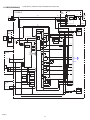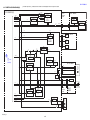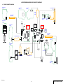
1
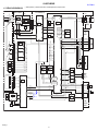
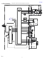
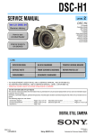
DSC-H5
SERVICE MANUAL
LEVEL
2
US Model
Canadian Model
AEP Model
UK Model
E Model
Australian Model
Chinese Model
Brazilian Model
Hong Kong Model
Korea Model
Tourist Model
Japanese Model
Ver. 1.1 2006. 06
Revision History
How to use
Acrobat Reader
Internal memory
ON BOARD
Link
SPECIFICATIONS
BLOCK DIAGRAMS
PRINTED WIRING BOARDS
SERVICE NOTE
FRAME SCHEMATIC DIAGRAM
REPAIR PARTS LIST
DISASSEMBLY
SCHEMATIC DIAGRAMS
• Precaution on Replacing the SY-150 board
Note :
The components identified by
mark 0 or dotted line with mark
0 are critical for safety.
Replace only with part number
specified.
Note :
Les composants identifiés par
une marque 0 sont critiques
pour la sécurité.
Ne les remplacer que par une
pièce portant le numéro spécifié.
DIGITAL STILL CAMERA
DSC-H5_L2
9-852-117-31
Sony EMCS Co.
2006F1600-1
©2006.06
Published by Kohda TEC
These specifications are extracted from User’s Guide/
Troubleshooting of DSC-H5 (2-673-176-11 (1)).
SPECIFICATIONS
Camera
[Input and Output connectors]
Dimensions
[System]
A/V OUT jack (Monaural)
Minijack
Video: 1 Vp-p, 75 Ω,
unbalanced, sync negative
Audio: 327 mV (at a 47 kΩ
load)
Output impedance 2.2 kΩ
113.2×83.0×94.0 mm
(4 1/2 inches × 3 3/8 inches ×
3 3/4 inches) (W/H/D,
excluding protrusions)
Mass
Approx. 554 g (1 lb 3.5 oz)
(including two batterries,
shoulder strap, adaptor ring,
lens hood, lens cap, etc.)
USB jack
Microphone
Electret condenser microphone
Image device
7.20 mm (1/2.5 type) color
CCD, Primary color filter
Total pixel number of camera
Approx. 7 410 000 pixels
Effective pixel number of camera
Approx. 7 201 000 pixels
Lens
Carl Zeiss Vario-Tessar
12× zoom lens
f = 6.0 – 72.0 mm (36 –
432 mm when converted to a
35 mm still camera)
F2.8 – 3.7
Exposure control Automatic exposure, Shutter
speed priority, Aperture
priority, Manual exposure,
Scene Selection (7 modes)
White balance
Automatic, Daylight, Cloudy,
Fluorescent, Incandescent,
Flash, One push
File format (DCF compliant)
Still images: Exif Ver. 2.21
JPEG compliant, DPOF
compatible
Movies: MPEG1 compliant
(Monaural)
Recording media Internal Memory (30 MB)
“Memory Stick Duo”
Flash
Viewfinder
Flash range (ISO set to Auto):
approx. 0.3 m to 9.0 m (11 7/
8 inches to 29 feet 6 3/8 inches)
(W)/approx. 0.9 m to 6.8 m
(35 1/2 inches to 22 feet 3 3/
4 inches) (T)
Electric viewfinder (color)
mini-B
USB communication
Hi-Speed USB (USB 2.0
compliant)
[LCD screen]
LCD panel
7.5 cm (3.0 type) TFT drive
Speaker
Dynamic speaker
Exif Print
Compatible
PRINT Image Matching III
Compatible
PictBridge
Compatible
Total number of dots
230 400 (960×240) dots
BC-CS2A/CS2B Ni-MH battery charger
[Finder]
Power requirements
AC 100 to 240 V, 50/60 Hz,
3W
Panel
0.5 cm (0.2 type) color
Total number of dots
Approx. 200 000 dots
equivalent
[Power, general]
Power
HR 15/51:HR6 (size AA)
Nickel-Metal Hydride batteries
(2), 2.4 V
LR6 (size AA) alkaline
batteries (2), 3 V
ZR6 (size AA) Oxy Nickel
Primary Battery (2), 3 V
AC-LS5K AC Adaptor 4.2 V
Power consumption (during shooting with the
LCD screen)
1.4 W
Operating temperature
0 to 40°C (32 to 104°F)
Storage temperature
–20 to +60°C (–4 to +140°F)
DSC-H5_L2
—2—
Output voltage
AA: DC 1.4V 400 mA × 2
AAA: DC 1.4 V 160 mA × 2
Operating temperature
0 to +40°C (+32 to +104°F)
Storage temperature
–20 to +60°C (–4 to +140°F)
Dimensions
Approx. 713091 mm
(2 7/8×1 3/16×3 5/8 inches)
(W/H/D)
Mass
Approx. 90 g (3 oz)
Design and specifications are subject to change
without notice.
SAFETY CHECK-OUT
After correcting the original service problem, perform the following
safety checks before releasing the set to the customer.
1.
2.
3.
4.
5.
6.
Check the area of your repair for unsoldered or poorly-soldered
connections. Check the entire board surface for solder splashes
and bridges.
Check the interboard wiring to ensure that no wires are
"pinched" or contact high-wattage resistors.
Look for unauthorized replacement parts, particularly
transistors, that were installed during a previous repair. Point
them out to the customer and recommend their replacement.
Look for parts which, through functioning, show obvious signs
of deterioration. Point them out to the customer and
recommend their replacement.
Check the B+ voltage to see it is at the values specified.
Flexible Circuit Board Repairing
• Keep the temperature of the soldering iron around 270˚C
during repairing.
• Do not touch the soldering iron on the same conductor of the
circuit board (within 3 times).
• Be careful not to apply force on the conductor when soldering
or unsoldering.
SAFETY-RELATED COMPONENT WARNING!!
COMPONENTS IDENTIFIED BY MARK 0 OR DOTTED LINE WITH
MARK 0 ON THE SCHEMATIC DIAGRAMS AND IN THE PARTS
LIST ARE CRITICAL TO SAFE OPERATION. REPLACE THESE
COMPONENTS WITH SONY PARTS WHOSE PART NUMBERS
APPEAR AS SHOWN IN THIS MANUAL OR IN SUPPLEMENTS
PUBLISHED BY SONY.
Unleaded solder
Boards requiring use of unleaded solder are printed with the leadfree mark (LF) indicating the solder contains no lead.
(Caution: Some printed circuit boards may not come printed with
the lead free mark due to their particular size.)
: LEAD FREE MARK
Unleaded solder has the following characteristics.
• Unleaded solder melts at a temperature about 40°C higher than
ordinary solder.
Ordinary soldering irons can be used but the iron tip has to be
applied to the solder joint for a slightly longer time.
Soldering irons using a temperature regulator should be set to
about 350°C.
Caution: The printed pattern (copper foil) may peel away if the
heated tip is applied for too long, so be careful!
• Strong viscosity
Unleaded solder is more viscous (sticky, less prone to flow) than
ordinary solder so use caution not to let solder bridges occur such
as on IC pins, etc.
• Usable with ordinary solder
It is best to use only unleaded solder but unleaded solder may
also be added to ordinary solder.
ATTENTION AU COMPOSANT AYANT RAPPORT
À LA SÉCURITÉ!
LES COMPOSANTS IDENTIFÉS PAR UNE MARQUE 0 SUR LES
DIAGRAMMES SCHÉMATIQUES ET LA LISTE DES PIÈCES SONT
CRITIQUES POUR LA SÉCURITÉ DE FONCTIONNEMENT. NE
REMPLACER CES COMPOSANTS QUE PAR DES PIÈSES SONY
DONT LES NUMÉROS SONT DONNÉS DANS CE MANUEL OU
DANS LES SUPPÉMENTS PUBLIÉS PAR SONY.
CAUTION :
Danger of explosion if battery is incorrectly replaced.
Replace only with the same or equivalent type.
DSC-H5_L2
—3—
TABLE OF CONTENTS
1.
SERVICE NOTE
1-1. DESCRIPTION ON SELF-DIAGNOSIS DISPLAY ······ 1-1
1-2. METHOD FOR COPYING OR ERASING THE DATA IN
INTERNAL MEMORY ·················································· 1-2
1-3. PRECAUTION ON REPLACING THE SY-150
BOARD ··········································································· 1-3
1-4. VIDEO OUT DEFAULT DATA CHECK ······················· 1-3
1-5. INITIAL LANGUAGE DATA CHECK ·························· 1-3
2.
DISASSEMBLY
2-1. DISASSEMBLY ······························································ 2-3
3.
BLOCK DIAGRAMS
3-1.
3-2.
3-3.
3-4.
OVERALL BLOCK DIAGRAM (1/2) ··························· 3-1
OVERALL BLOCK DIAGRAM (2/2) ··························· 3-2
POWER BLOCK DIAGRAM (1/2) ································ 3-3
POWER BLOCK DIAGRAM (2/2) ································ 3-4
4.
PRINTED WIRING BOARDS AND
SCHEMATIC DIAGRAMS
4-1.
4-2.
4-3.
4-4.
FRAME SCHEMATIC DIAGRAM ································ 4-1
SCHEMATIC DIAGRAMS ············································ 4-5
PRINTED WIRING BOARDS ····································· 4-25
MOUNTED PARTS LOCATION ································· 4-32
5.
REPAIR PARTS LIST
5-1. EXPLODED VIEWS ······················································ 5-3
5-2. ELECTRICAL PARTS LIST ········································ 5-10
DSC-H5_L2
—4—
1. SERVICE NOTE
1-1. DESCRIPTION ON SELF-DIAGNOSIS DISPLAY
Self-diagnosis display
• C: ss: ss
The contents which can be handled
by customer, are displayed.
• E: ss: ss
The contents which can be handled
by engineer, are displayed.
Display Code
C:32:ss
C:13:ss
E:61:ss
E:62:ss
E:91:ss
E:92:ss
Countermeasure
Turn the power off and on again.
Cause
Trouble with hardware.
Caution Display During Error
SYSTEM ERROR
Format the “Memory Stick” or internal “Memory Stick” or internal memory is
memory.
unformatted.
FORMAT ERROR
Insert a new “Memory Stick”.
“Memory Stick” is broken.
MEMORY STICK ERROR
Turn the power off and on again.
Trouble with internal mamory.
INTERNAL MEMORY ERROR
Checking of lens drive circuit.
When failed in the focus zoom
initialization.
Inspect angular velocity sensor
peripheral circuits.
Checking of flash unit or replacement
of flash unit. (Note)
Insert a batteries correctly.
Steady shot function does not work well.
Abnormality when flash is being
charged.
Batteries are pack is not inserted correctly.
Note : After repair, be sure to execute the “Initialize” of the setup screen.
DSC-H5_L2
1-1
_
1-2. METHOD FOR COPYING OR ERASING THE DATA IN INTERNAL MEMORY
The data can be copied/erased by the operations on the Setup screen. (When erasing the data, execute formatting the internal memory.)
Note: 1 When replacing the SY-150 board, erase the data in internal memory of the board before replacement.
Note: 2 When replacing the SY-150 board or the IC202 on the SY-150 board, execute formatting and initialize the internal memory after
replacement.
Method for copying the data in internal memory
Copy
Copies all images in the internal memory to a “Memory Stick Duo”.
OK
See the following procedure.
Cancel
Cancels the copying.
1 Insert a “Memory Stick Duo” having 32 MB or larger capacity.
2 Select [OK] with v on the control button, then press z.
The message “All data in internal memory will be copied Ready?” appears.
3 Select [OK] with v, then press z.
Copying starts.
Copying
102_COPY
• Use a fully charged Nickel-Metal Hydride battery or the AC Adaptor (not supplied). If you attempt to
copy image files using a batteries with little remaining charge, the batteries may run out, causing copying
to fail or possibly corrupting the data.
• You cannot copy individual images.
• The original images in the internal memory are retained even after copying. To delete the contents of the
internal memory, remove the “Memory Stick Duo” after copying, then execute the [Format] command in
(Internal Memory Tool).
• You cannot select a folder copied on a “Memory Stick Duo”.
• Even if you copy data, a
(Print order) mark is not copied.
Method for formatting the internal memory
This item does not appear when a “Memory Stick Duo” is inserted in the camera.
The default settings are marked with .
Format
Formats the internal memory.
• Note that formatting irrevocably erases all data in the internal memory, including even protected images.
OK
See the following procedure.
Cancel
Cancels the formatting.
1 Select [OK] with v on the control button, then press z.
The message “All data in internal memory will be erased Ready?” appears.
2 Select [OK] with v, then press z.
The format is complete.
• PROCESS AFTER FIXING FLASH ERROR
When “FLASH error” (Self-diagnosis Code E : 91 : ** ) occurs, to prevent any abnormal situation caused by high voltage, setting of the
flash is changed automatically to disabling charge and flash setting.
After fixing, this setting needs to be deactivated. Flash error code can be initialized by the operations on the Setup screen.
Method for Initializing the Flash Error Code
Initialize
Initializes the setting to the default setting.
OK
See the following procedure.
Cancel
Cancels the resetting.
1 Select [OK] with v on the control button, then press z.
The message “Initialize all settings Ready?” appears.
2 Select [OK] with v, then press z.
The settings are reset to the default setting.
Make sure that the power is not disconnected during resetting.
DSC-H5_L2
1-2
1-3. PRECAUTION ON REPLACING THE SY-150 BOARD
Ver. 1.1 2006. 06
• The Repair Board has already been adjusted. Re-initialization or EVR data copy from the set before repair is not
required.
• Perform “VIDEO OUT Default Data Check” and “Initial Language Data Check” mentioned below, and also the
adjustment items necessary after SY Board replacement.
1-4. VIDEO OUT DEFAULT DATA CHECK
When you replace to the repairing board, the written data of repairing board also might be changed to original setteing
because of broadcast system (NTSC/PAL).
When the data has changed because of board replaceing etc., check the default data of VIDEO OUT if destination code
is right. If not, rewrite to the right value.
VIDEO OUT Default Data
Page
Address
4F
8D
Data
NTSC
PAL
00
01
Writing Method:
1) Select page: 00, address: 01, and set data: 01.
2) Select page: 4F, address: 8D, and set data: 00 (NTSC) or data: 01 (PAL).
3) Select page: 40, address: 38, and set data: 00.
4) Click [Save] on the SEUS screen.
5) Select page: 80, address: 34, and check that the data is “00”.
6) Select page: 80, address: 30, and check that the data is “00”.
7) Select page: 00, address: 01, and set data: 00.
1-5. INITIAL LANGUAGE DATA CHECK
If the SY-150 board was replaced, initial language setting may be changed. Accordingly, change the following data so
as to set same initial language as that of the set distributing in each region.
Initial language: Language displayed at the next starting if the setting of Setup menu was reset.
It is different from the language setting selectable with the menu.
Initial Language Data
Page
4F
Address
8C
Data
Language
00
English
01
Japanese
04
Spanish
GP1
GP2
GP3
GP4
z
z
z
z
z
z
06
Portugal
z
08
Simplified Chinese
z
0B
Russian
0D
Korean
z
z
Note: GP1 is fixed to Japanese.
GP2 is fixed to English.
GP3 is either English, Spanish, or Russian.
GP4 is either English, Spanish, Portugal, Simplified Chinese, or Korean.
Writing Method:
1) Select page: 00, address: 01 and set data: 01.
2) Select page: 4F, address: 8C, and set the Initial Language Data.
3) Select page: 40, address: 38, and set data: 00.
4) Click [Save] on the SEUS screen.
5) Select page: 80, address: 34, and check that the data is “00”.
6) Select page: 80, address: 30, and check that the data is “00”.
7) Select page: 00, address: 01, and set data: 00.
8) Turn off the camera.
9) Turn on the camera. Execute “Initialize” of Setup screen.
10) Check the language displayed when the camera starts.
DSC-H5_L2
1-3E
2. DISASSEMBLY
Link
DISASSEMBLY
HELP
COMMON NOTE FOR DISASSEMBLY
DSC-H5_L2
2. DISASSEMBLY
2. DISASSEMBLY
NOTE FOR REPAIR
Make sure that the flat cable and flexible board are not cracked of
bent at the terminal.
Do not insert the cable insufficiently nor crookedly.
When remove a connector, don't pull at wire of connector.
Be in danger of the snapping of a wire.
When installing a connector, don't press down at wire of connector.
Be in danger of the snapping of a wire.
Cut and remove the part of gilt
which comes off at the point.
(Take care that there are
some pieces of gilt left inside)
DISCHARGING OF THE FLASHLIGHT POWER SUPPLY CAPACITOR
Discharging the Capacitor
The charging elect capacitor 320uF (330V) is charged up to the
maximum 300 V potential.
There is a danger of electric shock by this high voltage when the
capacitor is handled by hand. The electric shock is caused by the
charged voltage which is kept without discharging when the main
power of the DSC-H5 is simply turned off. Therefore, the
remaining voltage must be discharged as described below.
Short circuits between the positive and the negative terminals of
charged capacitor with the short jig about 10 seconds.
Short jig (1kΩ/1W)
Preparing the Short Jig
To preparing the short jig. a small clip is attached to each end of
a resistor of 1 kW /1 W (1-215-869-11)
Wrap insulating tape fully around the leads of the resistor to
prevent electrical shock.
ST-142 board
1 kΩ/1 W
Capacitor
Wrap insulating tape.
ST-142
DSC-H5_L2
2-1
2. DISASSEMBLY
2. DISASSEMBLY
The following flow chart shows the disassembly procedure.
2-1. DISASSEMBLY
2
8
SW
1
47
7
1
SW1
7
4
5
6
2
3
4
3
1
1 Three screws (M1.7x4)
1 Two claws
4 Two claws, two dowels
2 Three screws (M1.7x4)
2 Flexible board (from the LCD unit)
5 Claw, two dowels
3 Cabinet (rear) section
3 Flexible board
6 Two tapping screws (M1.7x3.5)
(from the light guide plate (3.0) block)
7 SW-478 flexible board
8 SW-471 board
Note: Be very careful not to
damage the flexible board.
9
7
8
1
A (See page 2-4)
0
-15
SY
5
B (See page 2-4)
6
4
2
0
3
15
SY
2
66
5
9
1 Fuse replacement caution label
3
2 Flexible board (from the lens section)
3 Tape CD retainer (420)
1 Two claws
4 CD-621 flexible board
2 Two tapping screws (M1.7x3.5)
5 AF-105 flexible board
3 LCD frame
6 Flexible board (from the lens section)
7 Control switch block
8 Flexible flat cable (ST-003)
9 From the microphone
q; Tapping screw (M1.7x5)
qa Main section
DSC-H5_L2
2-3
3
7
4
SY-150
8
HELP 01
qa
2 1
1
q;
q;
6
2. DISASSEMBLY
4
1
2
Refer to page 2-1 "DISCHARGING
OF THE FLASHLIGHT POWER
SUPPLY CAPACITOR, when
discharging the capacitor.
2
1
3
3
1
6
2
7
4
HELP 04
8
5
9
3
HELP 05
HELP 07
HELP 06
1
A
2
HELP 08
1 Turn the flexible board.
2 Tapping screw (M1.7x5)
3 Lens section
1 Two tapping screws (M1.7x4)
1 Tapping screw (M1.7x4)
1 Claw
2 Control switch block
2 Microphone holder
2 Three harnesses (HA-001) (Red, White, Blue)
3 Microphone cushion (B)
3 Open the ST cover in the direction of the arrow.
4 Microphone
4 ST section
5 Microphone cushion
6 Tapping screw (M1.7x4)
7 AF-105 flexible board
8 Tapping screw (M1.7x4)
9 AF holder
B
3
1
5
5
4
HELP 03
6
3
3
2
6
2
1
50
1
-
SY
-1
SY
0
15
HELP 02
2
4
7
1 Flexible flat cable (MS-030)
8
2 Two tapping screws (M1.7x4)
3 MS-305 board
1 Two claws
1 Battery connector
5 Flexible flat cable (MS-030)
4 Battery connector
2 Flexible board (from the LCD module)
2 From the loudspeaker
6 SW-478 flexible board
5 Three claws
3 EVF section
3 JK-306 flexible board
7 CK-161 flexible board
6 Battery terminal board
4 Two tapping screws (M1.7x4)
8 SY-150 board
DSC-H5_L2
2-4E
SM05
3
HELP
Disassembling and assembling procedures that require attention are described here.
HELP 01
When attaching the fuse replacement caution label to the SY-150 board,
cover the harness of the loudspeaker with the fuse replacement caution label.
Fuse replacement
caution label
Harnesses of
the loudspeaker
HELP 02
When installing the loudspeaker, route the harnesses of the loudspeaker as shown in the figure.
Harnesses of
the loudspeaker
Loudspeaker (1.0cm)
Bend the harnesses of the
loudspeaker at the route
of the connector.
HELP 03
When installing the battery terminal board, route the harnesses of the
battery terminal board as shown in the figure.
The harnesses in the area A
must be kept below surface B.
Battery terminal
board
The harnesses in the area C must be
kept within the D lines.
Bend the harness at portion E so that
the harness runs along line F.
surface B
Harnesses of the battery
terminal board
Harnesses of the battery
terminal board
C
A
D
E
F
DSC-H5_L2
HELP
HELP 05
HELP 04
When installing the ST section, route the
Harness (HA-004) (Blue) ,Harness (HA-004)(White),
and Harness (HA-004) (Red) as shown in the figure.
When installing the ST section, route the
Harness (HA-004) (Blue) ,Harness (HA-004)(White),
and Harness (HA-004) (Red) as shown in the figure.
ST section
Route the harnesses with the ST cover closed.
Harness (HA-004) (Blue) ,
Harness (HA-004)(White),
ST section
Harness (HA-004) (Red)
Harness (HA-004) (Blue)
Harness (HA-004) (White)
Harness (HA-004) (Red)
HELP 06
4
1 Harness (H-004) (Red)
5
9
2 Harness (H-004) (White)
3 Harness (H-004) (Blue)
4 Flash unit, ST-144 board
5 Apply the soldering in three points.
q;
6 ST-142 board
7 Apply the soldering in three points.
8 ST cover
9 Two claws
2White
8
q; Tapping screw (M1.7x4)
3Blue
Solder each harness according to the color
( Red, White, Blue) as shown in the figure.
1Red
Solder each harness according to the color
( Red, White, Blue) as shown in the figure.
6
ST-142 board
ST-144 board
Blue
White
Blue
Red
White
7
Red
DSC-H5_L2
HELP
HELP 07
Microphone holder
Install the microphone tilted as
shown in the figure below.
Microphone cushion (B)
Microphone
holder
Microphone
Microphone
cushion (B)
Microphone
Microphone cushion
Microphone cushion
HELP 08
When removing the lens ring, remove the screw and strap sheet metal (R) first.
Slide the cap lever in the direction of arrow A while taking care that the cap
lever is not caught on the notch of the lens ring.
Remove the lens ring by turning it in the direction of arrow B.
1 Tapping screw (M1.7x4)
2 Strap sheet metal (R)
Cap lever
B
3 Lens ring
Cap lever
Lens ring
A
Notch of the
lens ring
DSC-H5_L2
HELP
3. BLOCK DIAGRAMS
Link
OVERALL BLOCK DIAGRAM (1/2)
POWER BLOCK DIAGRAM (1/2)
OVERALL BLOCK DIAGRAM (2/2)
POWER BLOCK DIAGRAM (2/2)
DSC-H5_L2
3. BLOCK DIAGRAMS
( ) : Number in parenthesis ( ) indicates the division number of schematic diagram where the component is located.
3-1. OVERALL BLOCK DIAGRAM (1/2)
LENS UNIT
CD-621 FLEXIBLE
BOARD
CD-617 BOARD
IRIS
SHUTER
IC002
CCD IMAGER
15
IC001
1
V1
V2
V3A,B
V4
V5A,B
V6
V7
V8
V9
V10
VST,
VHLD
CCD OUT
3
20
6
20
1
RANDOM TRIGGER
4
CN001
12,10,8,6,14
2
26-39
12,10,8,6,14
2
4
E1
XCS_FE
1
|
5
U22
VSUB_CONT_POST
VSUB
42
VSUB_CONT_PRE
XSAN_RST_OUT
T4
D0-D31
D17,D18,D16,B18,A19
B19,E16,D19,E19,E17
B20,A20
A0-A11
1
M
(1/8)
F2
E2
D2
B1
4
SHUTTER
MOTOR
SHUTTER +
SHUTTER-
8
M
5
FOCUS A
FOCUS XA
FOCUS B
FOCUS XB
FOCUS
MOTOR
9
M
16
ZOOM
MOTOR
ZOOM +
ZOOM -
36
M
(1/2)
IRIS DRIVE
F5
E5
D3
F1
F3
F4
SHUTTER DRIVE
G1
E4
D6
E6
B7
C6
FOCUS MOTOR
DRIVE
D5
A6
B6
C5
B4
B5
39
IC401
ZOOM MOTOR
DRIVE
N4
P6
P4
R2
MSHUT DIR
MSHUT EN
MSHUT DIR
MSHUT EN
FC DIR A
FC DIR B
FC EN
ZM DIR A
ZM BRK A
ZM DIR A
ZM BRK A
22
ZOOM RESET
SENSOR 1ST
24
ZOOM RESET
SENSOR 2ND
25
B4
ZM SENS 2ND
B5
(4/8)
ZM DC FG 1A
ZM DC FG 1B
LENS TEMP
ACTIVE LENS ACTUATOR
12
13
B1
D1
A7
XSAN RST OUT
H2
J4
YAW+
YAW-
B10
D10
YAW HALL+
YAW HALL-
J9
J7
V5
W4
J25
XSAN RST OUT
IC201
IC202
BURST
FLASH MEMORY
ONE NAND
FLASH MEMORY
Y26
STEADY SHOT
CONTROL
A5
AB13,AA13,AE13,AF13,AF12
AE12,AA12,AC12,AC11,AB12
AE11,AF11,AE10,AB11,AC10
AB10
AF21,AF20,AE20,AB18,AB19
AC19,AB16,AE19,AF19,AF18
AE18,AA15,AC18,AC17,AB15
AE17,AF17,AE16,AB14,AC16
AC15
SAN27M CK0
XBONOBO CPU RESET
XBONOBO CPU RESET
B4
(6/8)
IC506
YAW
SENSOR
XCS BONOBO
XCS BONOBO
6
14
BUFFER
SAN0 SO, SI, SCK
B5
G5
B6
18
8
YAW AD
KEY BONO
J5
USB V BUS
E6
LCD9002
COLOR EVF
UNIT
6
4
with in
BACK LIGHT
20
(5/8)
IC602
CN602
MIC AMP
2
B6
MIC SIG
MIC
C1
SPEAKER AMP
1
2
A5
A2
SP+
SP-
MIC9001
SP9001
SPEAKER
CN601
K26
AUOUT
E5
D1
AU OUT AMP
C2
CN651
3,2
AC1
AD1
9
8
USB DPP, USB DMM
USB VBUS
CN001
(USB)
6
AC25
1
Y23
U25
H26
U23
1
XAV JACK IN
VIDEO AMP ON
3
AU LINE OUT
J001
A/V OUT
TO
OVERALL
BLOCK DIAGRAM
(2/2)
1
4
SAN1 SO, SCK
(PAGE 3-2)
(5/8)
3
IC601
5
V LINE OUT
V LINE OUT
2
VIDEO AMP
19
C_RESET
Q503
PITCH AD
XMS IN
PITCH/YAW
SENSOR
AMP
12
2
F3
E3
AUIN
AF9
V OUT
SE501
E4
D0-D15
SAN 27M CLK0
A4
SE502
24
A01-A16
A01-A21
A3
XCS_AUDIO
SAN1 SO, SCK
IC504
A6
CN501
8
10
9
SAN1 SO, SCK
D0-D15
(6/8)
PITCH HALL+
PITCH HALL-
3
2
H
20
22
23
15
|
12
LCD D0-D7 10
|
7
LCD HD
LCD VD
18
17
LCD CK
19
(4/8)
D0-D15
PITCH +
PITCH -
11
10
YAW
12
LCD9001
3.0 INCH
COLOR LCD
PANEL
CN703
U5
V4
L26
7
6
21
22
XMS IN
CN401
H
XSAN RST OUT
A2
A01-A21
PITCH
SENSOR
AF4
SAN1 SO, SCK
12
|
19
LCD D0-D7
11
10
ZM SENS 1ST
18
PITCH
LCD CK
U4
ZM DC FG 1A
ZM DC FG 1B
31
LENS TEMP
SENSOR
LCD D0-D7
LCD HD
LCD VD
U2
SAN1 SO, SCK
R6
CN001
20
LCD D0-D7 |
13
FC SENS
32
ZOOM DC FG
CK-161
BOARD
256Mbit
SDRAM
CN707
N6
N2
LENS TEMP
FOCUS RESET
SENSOR
IC203
L2
N5
L4
FC SENS
ZM SENS 1ST
ZM SENS 2ND
A2
B2
D9
R25
R5
FC DIR A
FC DIR B
FC EN
(4/8)
R23
E9
B8
DIR2A
BRK2A
DIR2B
BRK2B
6
MS-305
BOARD
D8,D7,E8
E7,D6,D5
E6,B4
SAN1 SO,SCK
IRIS
MOTOR
DIR2A
BRK2A
DIR2B
BRK2B
6
6
CN706
D21,D22,D20,B22,A22,A23
B23,E20,E21,B24,A24,A25
B25,C25,C26,B26,E10,A10
D10,E11,B10,A11,B11,E12
D11,D12,F12,B12,A12,E13
D13,D14
40, 41
IRIS A
IRIS XA
IRIS B
IRIS XB
CN302
MEMORY
STICK Duo
CONNECTOR
CAMERA DSP
Q301
7
|
20
XMS IN
IC101
(1/2)
H5
J5
CA HD, CA FD
45
46
39
CN301
A6
CLK TGO
47
36
CN301
CN001
EXTAL
CP301
4,3,5,7,2,8
CN301
4,3,5,
7,2,8
4,3,5,
7,2,8
MS D0-MS D3, MS BS, MS CLK
(3/8)
X101
12MHz
XTAL OSC
TIMING
GENERATOR
Q001
VSUB
26-39
21
1
AC4,AE4
AE5,AC5
AB6,AF6
K5,G4,H4,L5
H2,H1,J1,J2
M5,J4,K4,M6
K2,K1
CA AD0 - CA AD13
(2/8)
VSUB
CSUB
22
|
35
S/H
A/D CONV.
24 23
H1A,B
H2A,B
RG
MS-030 FLEXIBLE
FLAT CABLE
SY-150 BOARD (1/2)
BUFFER
27,28
19-17
1-14
Ver. 1.1 2006. 06
JK-306
FLEXIBLE
BOARD
D5
D6
DSC-H5_L2
3-1
Ver. 1.1 2006. 06
3-2. OVERALL BLOCK DIAGRAM (2/2)
( ) : Number in parenthesis ( ) indicates the division number of schematic diagram where the component is located.
ST-003
FLEXIBLE
FLAT CABLE
SY-150 BOARD (2/2)
ST-142 BOARD
1
|
3
1
|
3
ST-144
BOARD
ST UNREG
D102
(RECT)
T101
XE H
(3/8)
15
IC101
(2/2)
R22
V23
AB22
STRB CHG
STRB CHG
7
XSTRB FULL
XSTRB FULL
6
STRB CHG CONT
5
STRB CHG CONT
7
10
6
9
5
6
HIGH VOLTAGE
CHAGER
STRB ON
Q702
D1.2V
1
TO
OVERALL
BLOCK DIAGRAM
(1/2)
CN701
KEY BONO
USB VBUS
AA25
STRB PLUNGER ON
XMS IN
AC23
BATTERY
TERMINAL
UNREG
3
4
REG GND
XE L
FLASH
DRIVE
7
D001
CN101
STRB CONT
A1
IC401
(2/2)
AF-105 FLEXIBLE BOARD
CN705
STRB PLUNGER
8
7
B3
XSTRB POPUP
RY201
PLUNGER
3 4
4 3
XSTRB_POPUP
5
XLENS COVER SENSE
S201
(FLASH POP UP)
1 6
CN201
S001
(LENS COVER OPEN)
1
4
1
2
IGBT
DRIVE
4
Q101
STRB PLUNGER DRIVE
V22
BT9001
4
L001
TRIGGER
COIL
(1/8)
SAN0 SO, SI, SCK
(PAGE 3-1)
STRB ON
4
1
2
IC101
SYSTEM CONTROL
R4
C105
XAF LED
D001 (AF LED)
PL-045 BOARD
ST UNREG
F001
SAN0 SO C5
SAN0 SI C6
XSAN0 SCK B6
CN001
(8/8)
IC001
SAN0 SO, SI, SCK
SAN0 SO
SAN0 SI
XSAN0 SCK AB5
AA5
Y5
XCS DD
XCS DD A6
W23
BATT SENS
BATT SENS D4
L22
L25
K25
RSTA
XDD RST OUT
DC/DC CONVERTER XDD RST OUT A7
REAL TIME CLOCK
XPWR OFF
N21
P23
XPWR OFF
B7
Y4
R26
AA23
AB23
W22
XAE LOCK SW
XSHUTTER SW
CN704
MODE DIAL 0
MODE DIAL 1
S103
9
6
SHUTTER
14
12
MODE DIAL
CONTROL SWITCH
BLOCK
S105
JOG A
JOG B
11
10
JOG DIAL
S106,101,102
KEY AD2
8
G25
EXEC
FINDER, FOCUS, BRK
UNREG
S108
F002
1
XPLAY SW
PLAY
XPWR LED
X001
32.768KHz
BT001
LITHIUM
BATTERY
(SECONDARY)
A8
OSC I
A9
OSC O
B8
VL 3V
C7
XPWR ON
C9
USB VBUS
EVER SRAM
D 3.2V
CAM 3.2V
A 3.2V
MS VCC
CAM 2.9V
S104
3
XPWR ON
POWER
S107
2
KEY BONO
STEADY SHOT
PANEL 2.9V
D 1.8V
M 5V
ST 5V
D 1.2V
B10 XMS IN
CAM 15V
CAM -7.5V
D7
D102 (POWER)
5
D23
XPLAY SW
KEY AD0
K23
A4
8
26
DOWN, RIGHT, UP, LEFT, SET, DUST
7
27
ZOOM W, ZOOM T, MENU, DISP
1
33
S407 — S410
BL H
BL L
S401 — S406
CN702
L23
XAF LED
KEY AD1
XACCESS LED
E4
30
BL H
4
31
32
33
BL L
3
2
1
DSC-H5_L2
3-2
LCD
BACK
LIGHT
D401 (ACCESS)
6
5
2
1
CN401
SW-478
FLEXIBLE
BOARD
LED9001
SW-471 BOARD
CN402
FLASH
UNIT
( ) : Number in parenthesis ( ) indicates the division number of schematic diagram where the component is located.
3-3. POWER BLOCK DIAGRAM (1/2)
1
2
BT9001
BATTERY
TERMINAL
UNREG
ST-142 BOARD
ST-003
FLEXIBLE
FLAT CABLE
SY-150 BOARD (1/2)
F001
ST UNREG
3 REG GND
4
CN001
T101
1
|
3
1
|
3
STRB CHG
7
7
10
XSTRB FULL
6
6
9
5
5
6
8
8
ST UNREG
STRB CHG CONT
ST 5V
D102(RECT)
L101
IC101
1
C105
2
HIGH VOLTAGE
CHAGER
IGBT DRIVE
3
ST-144 BOARD
CN101
CN701
MS VCC
F002
UNREG
ST UNREG
(5/8)
(8/8)
9
MS VCC
10
R002
10
EVER SRAM
D001
H1
CN706
VL 3V
BT001
LITHIUM
BATTERY
(SECONDARY)
MS-030 FLEXIBLE
FLAT CABLE
STRB CHG
X001
32.768KHz
R22
XSTRB FULL
STRB CHG CONT
(3/8)
V23
AB22
K25
Y4
CAMERA DSP
SYSTEM CONTROL
R26
AA23
BATT SENS
XDD RST OUT
XPWR OFF
MS PWR ON
T25
XCS DD
SAN0 SO
SAN0 SI
XSAN0 SCK
D23
5
D102 (POWER)
MS PWR IN
B8 RTC BAT
A8 OSC I
LDO3IN
AA5
Y5
D 3.2V
D 3.2V
A 3.2V
L011
A 3.2V
(5/8)
G1
MS VCC
4
1
G2
IC603
3
AU 3.0V
3V REG
B2
CAM 2.9V
CAM 2.9V
A2
LDO2IN
A7 XRESET
B7 XPWR OFF
MS PWR ON
D3
PANEL 2.9V
B3
1.8V REG
D 1.8V
LDO2
A3
UNREG2
A6
AB5
J6
K6
PWR56 OUT J7
K7
LX5-1
LX5-2
LX5-3
LX5-4
L006
J9
CAM 15V
J10
K9
K10
Q004
SWITCHING & RECT
D003
(RECT)
XPWR LED
CAM -7.5V
VFB5 H9
D 3.2V
A 3.2V
MODE
DIAL
D 3.2V
A 3.2V
4
M 5V
AU 3.0V
VI 3.2V
D 1.2V
PWR2
L003
13
D 1.8V
XPWR ON
XPLAY SW
SD 1.8V
XPWR ON
3
XPLAY SW
1
CN704
VFB2 D8
C7 XPWRON1
LX3
VO3 E9
(4/8)
LV3
(4/8)
IC203
RS3
IC202
256Mbit
SDRAM
D 1.8V
3
D001 (AF LED)
XAF LED
F9
BL H
BL L
BL L
F8
Q003
SWITCH
M 5V
ST 5V
ST 5V
BG4 G9
(4/8)
BL H
D002
(RECT)
L008
PANEL 8.5V ON
IC201
TG4
BURST
FLASH MEMORY
D3.2V
ST UNREG
F003
L005
Q001
SWITCHING
ONE NAND
FLASH MEMORY
AF-105 FLEXIBLE
BOARD
D 1.2V
E10
D7 XPWRON2
L201
D 3.2V
D10
LX2 C10
S108
PLAY
1
(PAGE 3-4)
L009
GT6 H6
TO
POWER
BLOCK DIAGRAM
(2/2)
VFB6 H7
S104
POWER
MIC AMP
SPEAKER AMP
AU OUT AMP
CAM 3.2V
2.9V REG
D4 DTG1
XCS DD
C5 SAN0 SO
C6 SAN0 SI
B6 XSAN0 SCK
W23
L601
IC602
VFB1 H2
MS PWR
A9 OSC O
L001
LDO3
IC101
CONTROL SWITCH
BLOCK
3.1V
REG.
LDO1
ST 5V
CAM 3.2V
VO1-1 F1
VO1-2 F2
J1 UNREG1-1,2
K1
CN301
AU 3.0V
ST 5V
PWR1-1 A1
PWR1-2 B1
PWR1-3 C2
DC/DC CONVERTER
REAL TIME CLOCK
CN302
MEMORY
STICK Duo
CONNECTOR
AU 3.0V
IC001
MS-305
BOARD
F10
MT 5V ON
Q002
RECT
VFB4 F7
PANEL 2.9V
PSG4 G8
A4
4
XAF LED
CN705
PORTB C4
PORTA B4
PANEL 8.5V ON
(5/8)
MT 5V ON
IC601
CAM 3.2V
D601
VI 3.2V
L602
D 3.2V
A 3.2V, AU 3.0V, VI 3.2V, D 1.8V, D 1.2V
DSC-H5_L2
3-3
XE H
15
VIDEO AMP
FLASH
UNIT
Ver. 1.1 2006. 06
3-4. POWER BLOCK DIAGRAM (2/2)
( ) : Number in parenthesis ( ) indicates the division number of schematic diagram where the component is located.
SY-150 BOARD (2/2)
L303
CAM 3.2V
D 3.2V
A 3.2V
ST 5V
CAM 2.9V
4
1
TG 3V
FB308
DRVDD
L304
(2/8)
HDVDD
L302
CP301
FE 3V
TCVDD
IC301
CD-617 BOARD
CD-621
FLEXIBLE
BOARD
(2/8)
IC001
S/H
A/D CONV.
TIMING GENERATOR
RGVDD
3
BUFFER
3.3V REG
CAM 15V
FB302
FB301
22
22
IC002
18
18
CCD IMAGER
CAM 15V CD
L301
CAM -7.5V
CAM -7.5V CD
CN001
CN301
D 3.2V
D 3.2V
(1/8)
A 3.2V
21
FC RST VCC
FOCUS
RESET
SENSOR
ZM RST VCC
ZOOM
RESET
SENSOR
IC401
M 5V
IRIS DRIVE
SHUTTER DRIVE
FOCUS MOTOR DRIVE
ZOOM MOTOR DRIVE
PLUNGER DRIVE
27
28
ZM FG VCC
33
(6/8)
L503
6
ZOOM
DC FG
CN401
IC507
D501
(RECT)
C542
LENS UNIT
PANEL 8.5V
4
8.5V REG
1
ST UNREG
TO
POWER
BLOCK DIAGRAM
(1/2)
6
8
VBAT
PS
1
EN
Q504
ST 5V
1
D502
(RECT)
9
SW
(6/8)
PANEL 8.5V 0N
5V
VOUT 2
IC501
(6/8)
IC506
DC/DC CONV.
M 5V ON
(PAGE 3-3)
PITCH/YAW
SENSOR AMP
(6/8)
4
CK-161 BOARD
CN707
IC503
A 3.2V
SE501, 502
PITCH/YAW
SENSOR
L703
2.9V
27
26
3
2.9V REG
L705
1
4
ST 5V
ST 5V
L704
3
PDD
VSSG
5
6
VDD2
28
VDD1
LCD9001
3.0 INCH
COLOR LCD
PANEL
29
CN001
DISCHARGE
D401
D 3.2V
6
BL H
30
BL L
31
32
33
CN702
B9
(6/8)
D3.2V
ST 5V
4
1
1.5V
3
1.5V REG
BL H
BL L
SW-478
FLEXIBLE
BOARD
(6/8)
IC504
IC505
D 3.2V
STEADY SHOT
CONTROL
PANEL 8.5V 0N
(7/8)
M 5V ON
L701
PANEL 2.9V
4
1
IC701
3
2.5V
2.5V REG
5.0V
L702
ST 5V
LED 5V
CN703
DSC-H5_L2
3-4E
22
LCD9002
COLOR EVF
UNIT
1
11
EVF BACK LIGHT
ACCESS LED
28
4
6
3
2
1 CN401
5
2
1
SW-471
BOARD
CN402
LED9001
LCD BACK LIGHT
4. PRINTED WIRING BOARDS AND SCHEMATIC DIAGRAMS
4-1. FRAME SCHEMATIC DIAGRAM
MS-305 BOARD
(SIDE B)
CD-617 BOARD
(A SIDE)
CD-617 BOARD
(B SIDE)
AF-105 FLEXIBLE BOARD
39
39
38
S001
(LENS COVER OPEN)
1
2 1
3
1
CN001
2
10
CD-621
FLEXIBLE
BOARD
IC002
S201
(FLASH POP UP)
1
1
1
39
CN301
12
2
1
6
CN201
6
1
PL-045 BOARD
(SIDE A)
1
PL-045 BOARD
(SIDE B)
4
3
6
BT9001
BATTERY
TERMINAL
AF LED
LCD9002
MIC9001
MICROPHONE
COLOR
EVF
UNIT
LEVEL3
SY-150 BOARD
(SIDE B)
1
39
38
CN301
14
10
1
1
1
CONTROL
SWITCH
BLOCK
CN704
CN703
22
2
F003
CN706
CN705
CN602
1
1
4
F001
MEMORY STICK Duo
CONNECTOR
LEVEL3
SY-150 BOARD
(SIDE A)
BT001
LITHIUM BATTERY
(SECONDARY)
21
CN001
CN302
CN702
33
33
2
2
1
2
1
1
33
33
32
CN401
32
1
2
14
1
CN651
CN701
1
12
12
ST-003 FLEXIBLE
FLAT CABLE
SW-478 FLEXIBLE BOARD
1
1
D001
SW-471 BOARD
(SIDE B)
F002
1
RY201
(PLUNGER)
2
MS-030 FLEXIBLE
FLAT CABLE
MS-305 BOARD
(SIDE A)
10
1
CN401
38
39
CN601
1
CN707
28
29
1
ST-142 BOARD
(SIDE A)
14
CN501
1 2
1
CN101
12
FLASH UNIT
SW-471 BOARD
(SIDE A)
LND004
1
29
LND006
J001
A/V OUT
JACK
LND005
LND003
J001
4
LND002 LND001
SP9001
SPEAKER
2
LCD9001
3
ST-144 BOARD
1
3.0 INCH
COLOR
LCD
MONITOR
CN001
USB
CONNECTOR
CN001
2
1
1
LND101
5
14
LED9001
31
30
CN001
LND103
1
2
6
1
CN402
LND102
CK-161 FLEXIBLE BOARD
JK-306 FLEXIBLE BOARD
BACKLIGHT
LENS BLOCK
C105
ST-142 BOARD
(SIDE B)
1
DSC-H5_L2
4-1
2
FRAME SCHEMATIC DIAGRAM
4-2. SCHEMATIC DIAGRAMS
Link
CD-617 BOARD (CCD IMAGER)
CONTROL SWITCH BLOCK
(MODE/JOG DIAL, FUNCTION SW)
SW-471 BOARD
AF-105 FLEXIBLE BOARD
(LCD BACK LIGHT, FUNCTION SWITCH)
(AF LED, LENS COVER SW)
CK-161 BOARD (LCD PANEL)
JK-306 FLEXIBLE BOARD (AV/USB JACK)
ST-142 BOARD (FLASH DRIVE)
CD-621 FLEXIBLE BOARD (SY-CD RELAY)
ST-144 BOARD (FLASH)
SW-478 FLEXIBLE BOARD (SY-SW RELAY)
MS-305 BOARD (MEMORY STICK)
MS-030 FLEXIBLE FLAT CABLE (SY-MS RELAY)
PL-045 BOARD (PLUNGER)
ST-003 FLEXIBLE FLAT CABLE (SY-ST RELAY)
COMMON NOTE FOR SCHEMATIC DIAGRAMS
DSC-H5_L2
4-2. SCHEMATIC DIAGRAMS
4-2. SCHEMATIC DIAGRAMS
THIS NOTE IS COMMON FOR SCHEMATIC DIAGRAMS
(In addition to this, the necessary note is printed in each block)
(For schematic diagrams)
• All capacitors are in µF unless otherwise noted. pF : µ
Link
µF. 50 V or less are not indicated except for electrolytics
and tantalums.
• Chip resistors are 1/10 W unless otherwise noted.
kΩ=1000 Ω, MΩ=1000 kΩ.
• Caution when replacing chip parts.
New parts must be attached after removal of chip.
Be careful not to heat the minus side of tantalum
capacitor, Because it is damaged by the heat.
• Some chip part will be indicated as follows.
Example
C541
L452
22U
10UH
TA A
2520
1. Connection
Pattern box
Color bar chart
For PTB-450:
J-6020-250-A
Pattern box PTB-450
J-6082-200-A
or
Small pattern box
PTB-1450
J-6082-557-A
For PTB-1450:
J-6082-559-A
L = 1 m (PTB-450)
L = 40 cm (PTB-1450)
Pattern box
Front of the lens
L
Kinds of capacitor
Camera
Temperature characteristics
External dimensions (mm)
• Constants of resistors, capacitors, ICs and etc with XX
indicate that they are not used.
In such cases, the unused circuits may be indicated.
• Parts with * differ according to the model/destination.
Refer to the mount table for each function.
• All variable and adjustable resistors have characteristic
curve B, unless otherwise noted.
• Signal name
XEDIT → EDIT
PB/XREC → PB/REC
• 2: non flammable resistor
• 5: fusible resistor
• C: panel designation
• A: B+ Line
• B: B– Line
• J : IN/OUT direction of (+,–) B LINE.
• C: adjustment for repair.
(Measuring conditions voltage)
• Voltages are measured between the measurement
points and ground when camera shoots color bar chart
of pattern box. They are reference values.
(VOM of DC 10 MΩ input impedance is used)
• Voltage values change depending upon input
impedance of VOM used.)
A B
Red
Blue
White
Magenta
H
Cyan
Green
Yellow
2. Adjust the distance so that the output waveform of
Fig. a and the Fig. b can be obtain.
A=B
B A
Fig. a (Video output terminal output waveform)
Electronic beam
scanning frame
CRT picture frame
Fig.b (Picture on monitor TV)
Precautions for Replacement of imager
When indicating parts by reference number, please
include the board name.
• If the imager has been replaced, carry out all the
adjustments for the camera section.
• As the imager may be damaged by static electricity from
its structure, handle it carefully like for the MOS IC.
In addition, ensure that the receiver is not covered with
dusts nor exposed to strong light.
Note :
The components identified by
mark 0 or dotted line with mark
0 are critical for safety.
Replace only with part number
specified.
DSC-H5_L2
4-3
Note :
Les composants identifiés par
une marque 0 sont critiques
pour la sécurité.
Ne les remplacer que par une
pièce portant le numéro spécifié.
4-2. SCHEMATIC DIAGRAMS
2
1
4
3
5
6
8
7
9
10
CD-617 BOARD
IC002
4
3
2
1
V1
5
V2
32
6
VST
33
V2
7
H1A
34
V6
8
VL
35
9
V3A
V1
V3A
14 13 12 11 10
V4
36
V3B
37
V3B
V6
VST
CL007
V5B
38
V7
39
V8
V4
V10
V5A
39P
VHLD
B
R-6.0
P0
R-0.7
P0
R-0.7
P0
R-0.7
CL008
P0
R-0.7
P0
R-0.7
CL002
P0
R-0.7
CL003
P0
R-0.7
P0
R-0.7
P0
R-0.7
CL001
P0
R-7.2
P0
R-6.0
P0
R-5.4
P0
R-6.0
CL006
P0
CN001
V9
XX MARK:NO MOUNT
V10
A
NO MARK:REC/PB MODE
R :REC MODE
P :PB MODE
CCD IMAGER
IC002
ICX629BQF-13
H2A
N.C.
CSUB
SUB
GND
27
GND
28
V9
GND
V5B
Note: IC002 is not included in this
COMPLETE of CD-617 board.
H2B
29
H1B
30
V7
RG
31
VDD
V8
VHLD
CCD_OUT
CCD IMAGER
E
F
21
CCD_OUT
20
REG_GND
19
CAM_-7.5V_CD
18
REG_GND
17
REG_GND
16
REG_GND
15
RG
14
REG_GND
13
H1A
12
REG_GND
11
H1B
10
REG_GND
9
H2B
8
REG_GND
7
H2A
6
REG_GND
5
RAMDOM_TRIGGER
4
REG_GND
3
CSUB
2
VSUB
1
0
R-7.5
P0
R2.1
P0
R1.1
P0
22
REG_GND
R9.1
P-0.2
R9.5
P0
CAM_15V_CD
R001
0
C002
0.1u
R9.1
P0
R9.1
P0
ISF
IN
VCC
GND
OUT IDRV
IC001
CXA3691EN-T9
Q001
DTC144EMT2L
VSUB
R12.7
P0
R4.3
P0
R007
150k
C008
XX
C004
0.1u
16V
R010
100K
C009
0.1u
C003
XX
R009
XX
C007
0.1u
16V
B
R003
270k
1
2
R002
0
R5.0
P0
C006
0.1u 16V B
23
R011 0
REG_GND
C005
0.1u
16V
BUFFER
6
24
5
REG_GND
IC001
4
D
25
1
(PAGE 4-12)
26
2
TO
CD-621
FLEXIBLE
BOARD
V5A
REG_GND
3
C
R9.1
P0
R12.7
P0
R7.7
P0
R2.1
P0
R1.1
P0
15 16 17 18 19 20 21 22 23 24 25 26 27 28
R8.8
P0
R004
1M
C001
XX
0
3
DSC-H5_L2
4-5
CD-617
2
1
3
4
5
6
7
8
9
10
SW-471 BOARD
A
LCD BACK LIGHT, FUNCTION SWITCH
XX MARK:NO MOUNT
S407
ZOOM T
RB402
2200x4
33P
S409
ZOOM W
1
CN401
C
TO
SW-478
FLEXIBLE
BOARD
(PAGE 4-12)
D
33
REG_GND
32
REG_GND
31
NC
30
REG_GND
29
D_3.2V
28
KEY_AD1
27
KEY_AD0
26
REG_GND
25
NC
24
NC
23
NC
22
NC
21
NC
20
NC
19
REG_GND
18
REG_GND
17
NC
16
REG_GND
15
REG_GND
14
NC
13
NC
12
REG_GND
11
D401
SML-310LTT86
(ACCESS)
NO 2
1
NO 2
4
3
4
3
5
6
5
6
R401
330
S404
UP
1
2
3
4
R405
5600
S410
MENU
RB401
2200x4
1005
1
2
3
4
D402
MAZW068H0LS0
S406
LEFT
1
LND401
D403
MA2S111-(K8).SO
STATIC_GND
E
1
1
B
XACCESS_LED
R403
5600
2
1
2
4
3
4
10
NC
9
R402
REG_GND
8
27k
NC
7
NC
6
NC
5
6
BL_H
4
5
BL_H
BL_H
3
4
NC
BL_L
2
3
NC
BL_L
1
2
1
BL_H
2
3
4
S408
DISP
2
1
S401
RIGHT
R404
27k
3
4
6P
LED9001
1
2
S402
DUST
S403
DOWN
3
4
2
1
BL_L
BL_L
1
SET
3
NC
CN402
S405
LCD
BACK LIGHT
3
4
DSC-H5_L2
4-6
SW-471
2
1
3
4
5
6
CK-161 FLEXIBLE BOARD
A
LCD PANEL
XX MARK:NO MOUNT
29P
CN001
GND
B
TO
SY-150
BOARD(7/8)
CN707
C
(PAGE 4-20
of LEVEL 3)
D
E
1
GND
2
VCC1
3
VCC2
4
4.2VADJ
5
VBRT
6
COMAC
7
COMDC(H)
8
COMDC(L)
9
VD
10
HD
11
DCK
12
D7
13
D6
14
D5
15
D4
16
D3
17
D2
18
D1
19
D0
20
XCS
21
SI
22
SCLK
23
RESET
24
POFF
25
VSSG
26
PVDD
27
GND
28
COM
29
LND001
LND002
LND003
LND004
LND005
LND006
LND007
LND008
LND009
LND010
LND011
LND012
LND013
LND014
LND015
LND016
LND017
LND018
LND019
LND020
LND021
LND022
LND023
LND024
LND025
LND026
LND027
LND028
LND029
31 P
31
GND
30
GND
29
VCC1
28
VCC2
27
4.2VADJ
26
VBRT
25
COMAC
24
COMDC(H)
23
COMDC(L)
22
VD
21
HD
20
DCK
19
D7
18
D6
17
D5
16
D4
15
D3
14
D2
13
D1
12
D0
11
XCS
10
SI
9
SCLK
8
RESET
7
POFF
6
VSSG
5
PVDD
4
GND
3
COM
2
N.C.
1
N.C.
LCD9001
(LCD UNIT)
3.0 INCH
COLOR
LCD PANEL
DSC-H5_L2
4-7
CK-161
• Refer to page 4-3 for mark 0.
1
2
ST-142 BOARD
FLASH DRIVE
A
5
6
NO MARK:REC/PB MODE
R :REC MODE
P :PB MODE
TO
ST-003 FLEXIBLE
FLAT CABLE
(PAGE 4-13)
ST_UNREG
1
2
ST_UNREG
3
STRB_ON
4
STRB_CHG_CONT
5
XSTRB_FULL
6
STRB_CHG
7
ST_5V
8
REG_GND
9
REG_GND
10
REG_GND
11
REG_GND
12
C101
22u
6.3V
C102
22u
6.3V
9
10
3
5
L101
4.7uH
ST_UNREG
8
7
T101
CONVERTER
TRANSFORMER
XX MARK:NO MOUNT
CN101 12P
B
4
3
2
C106
22u
6.3V
D102
CRF02(TE85R)
LND101
4
1
1
XE_H
CL101
C105
320u
330V
C
Note: C105 is not included in this
COMPLETE of ST-142 board.
TO
ST-144
BOARD
R2.4/P2.6
(PAGE 4-9)
D101
MAZS068008SO
R102
XX
C103
1u
B
F_ON
N.C
N.C
N.C
IC101
TPS65552RGTR
5
6
7
8
CHG
XFULL
10 11 12
VCC
HIGH VOLTAGE CHARGE,
IGBT DRIVE
0
LND102
REG_GND
3
XE_L
Q101
GT8G133 (T2LSONY.Q)
FLASH DRIVE
0
283
0
2
3.2
9
4
0
PGND
SW
N.C
3
D
PGND
IC101
G_IGBT
5.0
SW
I_PEAK
2
R2.4/P2.6
N.C
1
R2.4/P2.6
VBATT
HGND
17 16 15 14 13
1
E
0
R103
4.7M
C104
XX
5
2
6
3
7
4
8
LND103
R104
33
F
DSC-H5_L2
4-8
ST-142
• Refer to page 4-3 for mark 0.
2
1
3
4
5
6
ST-144 BOARD
3
4
PL-045 BOARD
FLASH
A
2
1
A
XX MARK:NO MOUNT
Note: RY201 is not included in this
COMPLETE of PL-045 board.
PLUNGER
XX MARK:NO MOUNT
CN201
LND005
LND001
XE_H
XE_+
1
R001
1M
B
C002
0.047u
250V
L001
TRIGGER COIL
1
B
LND004
3
FLASH
UNIT
TRIGGER
TO
ST-142
BOARD
1
2
STRB_PLUNGER
3
STRB_PLUNGER
4
(PAGE 4-11)
REG_GND
5
XSTRB_POPUP
6
1
C201
1u
2
3
RY201
(PLUNGER)
S201
2
LND006
LND002
XE_L
REG_GND
REG_GND
TO
AF-105
FLEXIBLE
BOARD
D203
MAZW068H0LS0
(FLASH POP UP)
C003
0.01u
250V
(PAGE 4-8)
D202
1SS355TE-17
6P
XE_-
2
D001
RR255L-400TE25
C
R002
100k
LND003
REG_GND
2
1
3
3
4
5
6
MS-305 BOARD
A
MEMORY STICK
XX MARK:NO MOUNT
CN301 12P
TO
MS-030
FLEXIBLE
FLAT CABLE
B
(PAGE 4-13)
C
10P
REG_GND
1
MS_BS
2
MS_D1
3
MS_D0
4
R303 82
FB305
0
FB301
0uH
FB302
0uH
FB303
0uH
1
REG_GND
2
MS_BS
3
MS_D1
4
MS_D0
5
MS_D2
6
XMS_IN
7
MS_D3
8
8
MS_SCLK
9
9
MS_VCC
MS_D2
5
XMS_IN
6
MS_D3
7
MS_SCLK
REG_GND
R302 1k
FB304
MS_VCC
10
REG_GND
11
REG_GND
12
R304
C301
22u
6.3V
LND302
82
C302
0.1u
B
FB306
CN302
MEMORY
STICK Duo
CONNECTOR
0uH
0
10
REG_GND
STATIC_GND
DSC-H5_L2
4-9
ST-144/MS-305/PL-045
2
1
3
4
5
6
7
8
CONTROL SWITCH BLOCK
A
MODE/JOG DIAL, FUNCTION SW
R111
2k
R109
2k
XX MARK:NO MOUNT
R112
2k
S107
S106
(MODE DIAL)
FOCUS
2
4
B
FINDER
S102
S101
R104
2k
BRK
1
2
3
4
1
6
R105
2k
3
R106
2k
R101
4900
R107
2k
5
12
4
11
3
10
2
1
R110
2k
R103
13
7
R108
10k
C
STEADY SHOT
2
1
2
1
R116
2k
4
3
4
3
R117
2k
R118
2k
9
8
R115
2k
R114
2k
2200
S103
R102
9300
SHUTTER
S105
2
6
5
4
POWER
3
1
3
2
2
4
JOG DIAL
S104
1
1
7
3
4
D
S108
PLAY
1
3
2
4
D102
POWER
E
MODE_DIAL0
14
LND114
A_3.2V
13
LND113
MODE_DIAL1
12
LND112
JOG_A
11
LND111
JOG_B
10
LND110
XAE_LOCK_SW
9
LND109
KEY_AD2
8
LND108
REG_GND
7
LND107
XSHUTTER_SW
6
LND106
XPWR_LED
5
LND105
D_3.2V
4
LND104
XPWR_ON
3
LND103
KEY_BONO
2
LND102
XPLAY_SW
14P
F
1
LND101
CONTROL SWITCH BLOCK is replaced as a block.
So that this PRINTED WIRING BOARD is omitted.
TO SY-150 BOARD(7/8) CN704
G
(PAGE 4-20
of LEVEL 3)
DSC-H5_L2
4-10
MODE DIAL
Ver. 1.1 2006. 06
2
1
3
4
5
Note: D001 (AF LED) is not supplied,
but this is included in AF-105
flexible board complete.
AF-105 FLEXIBLE BOARD
AF LED,LENS COVER SW
A
D001
DOR5073
(AF LED)
XX MARK:NO MOUNT
S001
(LENS COVER OPEN)
10P
1
1
6
LND001
2
5
LND002
3
4
XLENS_COVER_SENSE
2
REG_GND
3
D_3.2V
4
XAF_LED
5
XSTRB_POPUP
6
REG_GND
6
LND003
TO
SY-150
BOARD
(7/8)
CN705
B
(PAGE 4-20
of LEVEL 3)
LND004
STRB_PLUNGER
8
STRB_PLUNGER
9
REG_GND
LND007
LND013
LND008
LND014
1
REG_GND
2
STRB_PLUNGER
3
STRB_PLUNGER
4
REG_GND
5
REG_GND
6
LND015
LND009
LND010
10
XSTRB_POPUP
LND012
LND006
7
6P
LND011
LND005
TO
PL-045
BOARD
CN201
(PAGE 4-9)
LND016
REG_GND
C
2
1
3
4
5
6
JK-306 FLEXIBLE BOARD
AV/USB JACK
A
XX MARK:NO MOUNT
14P
3
1
LND001
XAV_JACK_IN
1
LND002
V_LINE_OUT
2
AU_LINE_OUT
3
GND
4
NC
5
VCC
6
2
4
LND003
J001
A/V OUT
LND004
LND005
B
TO
SY-150 BOARD
(5/8)
CN651
(PAGE 4-18
of LEVEL 3)
LND006
CN001
5P
LND007
GND
7
D-
8
D+
9
5
GND
4
ID
3
D+
2
D-
1
VCC
LND008
LND009
LND010
GND
10
GND
11
NC
12
STATIC_GND
13
STATIC_GND
14
(USB)
LND011
LND012
LND013
C
LND014
LND015
STATIC_GND
DSC-H5_L2
4-11
AF-105/JK-306
2
1
4
3
5
SY-CD RELAY
A
XX MARK:NO MOUNT
V10
VST
V3B
V1
V3A
V6
V2
V8
VHLD
V7
V5B
V9
V5A
TO
SY-150
BOARD(2/8)
CN301
D
(PAGE 4-15
of LEVEL 3)
38
37
36
35
34
33
32
31
30
29
28
27
26
39
SY-SW RELAY
XX MARK:NO MOUNT
33P
38
37
36
35
34
33
32
31
30
29
28
27
26
REG_GND
CAM_15V_CD
REG_GND
REG_GND
RG
REG_GND
H1A
REG_GND
H1B
REG_GND
H2B
16
15
14
13
12
11
10
9
8
16
15
14
13
12
11
10
9
8
REG_GND
7
7
TO
SY-150
BOARD(7/8)
CN702
V5A
REG_GND
17
C
V9
21
17
30
4
BL_H
NC
29
5
NC
NC
28
6
NC
NC
27
7
NC
REG_GND
26
8
REG_GND
NC
25
9
NC
NC
24
10
NC
REG_GND
23
11
REG_GND
NC
22
12
NC
NC
21
13
NC
REG_GND
20
14
REG_GND
REG_GND
19
15
REG_GND
V5B
22
18
BL_H
BL_H
V7
21
18
3
VHLD
22
19
31
V8
REG_GND
19
BL_L
BL_H
V2
CAM_15V_CD
REG_GND
2
V6
REG_GND
20
32
V3A
24
20
B
V1
24
CCD_OUT
BL_L
BL_L
V3B
REG_GND
23
1
VST
REG_GND
23
33
V10
25
REG_GND
BL_L
V4
25
REG_GND
F
39
REG_GND
CAM_-7.5V_CD
E
5
39P
V4
C
4
33P
39P
B
3
SW-478 FLEXIBLE BOARD
CD-621 FLEXIBLE BOARD
A
2
1
CCD_OUT
(PAGE 4-20
of LEVEL 3)
TO
CD-617
BOARD
CN001
(PAGE 4-5)
D
REG_GND
NC
18
16
NC
REG_GND
17
17
REG_GND
REG_GND
16
18
REG_GND
NC
15
19
NC
NC
14
20
NC
NC
13
21
NC
NC
12
22
NC
NC
11
23
NC
NC
10
24
NC
REG_GND
9
25
REG_GND
KEY_AD0
8
26
KEY_AD0
KEY_AD1
7
27
KEY_AD1
D_3.2V
6
28
D_3.2V
REG_GND
5
29
REG_GND
NC
4
30
NC
REG_GND
3
31
REG_GND
REG_GND
2
32
REG_GND
XACCESS_LED
1
33
XACCESS_LED
TO
SW-471
BOARD
CN401
(PAGE 4-6)
CAM_-7.5V_CD
REG_GND
REG_GND
REG_GND
RG
REG_GND
H1A
E
REG_GND
H1B
REG_GND
H2B
REG_GND
H2A
6
6
H2A
REG_GND
5
5
REG_GND
RANDOM_TRIGGER
4
4
RANDOM_TRIGGER
REG_GND
3
3
REG_GND
CSUB
2
2
CSUB
VSUB
1
1
VSUB
DSC-H5_L2
4-12
CD-621/SW-478
1
2
3
4
5
MS-030 FLEXIBLE FLAT CABLE
A
XX MARK:NO MOUNT
B
(PAGE 4-20
of LEVEL 3)
C
SY-ST RELAY
12P
12P
REG_GND
1
1
REG_GND
REG_GND
12
12
REG_GND
MS_BS
2
2
MS_BS
REG_GND
11
11
REG_GND
MS_D1
3
3
MS_D1
REG_GND
10
10
REG_GND
MS_D0
4
4
MS_D0
REG_GND
9
9
REG_GND
MS_D2
5
5
MS_D2
ST_5V
8
8
ST_5V
XMS_IN
6
6
XMS_IN
STRB_CHG
7
7
STRB_CHG
MS_D3
7
7
MS_D3
MS_SCLK
8
8
MS_SCLK
TO
MS-305
BOARD
CN301
B
(PAGE 4-9)
TO
SY-150
BOARD(7/8)
CN701
(PAGE 4-20
of LEVEL 3)
XSTRB_FULL
6
6
XSTRB_FULL
STRB_CHG_CONT
5
5
STRB_CHG_CONT
9
9
REG_GND
STRB_ON
4
4
STRB_ON
MS_VCC
10
10
MS_VCC
ST_UNREG
3
3
ST_UNREG
REG_GND
11
11
REG_GND
ST_UNREG
2
2
ST_UNREG
REG_GND
12
12
REG_GND
ST_UNREG
1
1
ST_UNREG
REG_GND
5
XX MARK:NO MOUNT
12P
12P
TO
SY-150
BOARD(7/8)
CN706
4
ST-003 FLEXIBLE FLAT CABLE
SY-MS RELAY
A
3
2
1
C
MS-030 FLEXIBLE FLAT CABLE is replaced as a block.
So that this PRINTED WIRING BOARD is omitted.
TO
ST-142
BOARD
CN101
(PAGE 4-8)
ST-003 FLEXIBLE FLAT CABLE is replaced as a block.
So that this PRINTED WIRING BOARD is omitted.
Schematic diagram of the SY-150 board and CH-199
board are not shown.
Pages from 4-14 to 4-22 are not shown.
DSC-H5_L2
4-13
MS-030/ST-003
4-3. PRINTED WIRING BOARDS
Link
CD-617 BOARD
AF-105 FLEXIBLE BOARD
SW-471 BOARD
JK-306 FLEXIBLE BOARD
ST-142 BOARD
CD-621 FLEXIBLE BOARD
ST-144 BOARD
SW-478 FLEXIBLE BOARD
MS-305 BOARD
CK-161 FLEXIBLE BOARD
PL-045 BOARD
COMMON NOTE FOR PRINTED WIRING BOARDS
DSC-H5_L2
MOUNTED PARTS LOCATION
4-3. PRINTED WIRING BOARDS
4-3. PRINTED WIRING BOARDS
THIS NOTE IS COMMON FOR WIRING BOARDS
(In addition to this, the necessary note is printed in each block)
(For printed wiring boards)
•
: Uses unleaded solder.
•
: Pattern from the side which enables seeing.
(The other layers’ patterns are not indicated)
• Through hole is omitted.
• There are a few cases that the part printed on diagram
isn’t mounted in this model.
• C: panel designation
• Chip parts.
Transistor
6 5 4 4 5 6 5
C
B
DSC-H5_L2
4-23
E
4 4
5
Diode
3
3
3
1 2 3 3 2 1 1 2 3 3 2 1
2
1 2
1 2
1
1
2 3
4
2 2
1 3
4
5 4 3 3 4 5 2
1
4
3 2
5
4
1
3 1
6
1 6 54
3
3
4
1 1 2
4
3
2
1
3
4
1 23
1
2
4-3. PRINTED WIRING BOARDS
CD-617 (4 layers), SW-471 (4 layers)
•
: Uses unleaded solder.
CD-617 BOARD(SIDE A)
CD-617 BOARD(SIDE B)
A
Note:IC002 is not included in
this COMPLETE of CD-617 board
A
28
R009
6
C008
4
R007
C009
1
1
2
2
4
4
3
1
>EP GW<
4
1-869-214-
1
2
3
4
5
B
11
CL007
CL008
CL006
2
3
A
2
B
8
7
1
RB401
2 3
D403 D402
1
2
S403
DOWN
S402
DUST
2
LND401
4
3
1
3
R401
(ACCESS)
S406
LEFT
6
3
SET
1
A
D401
S404
UP
S409
ZOOM W
C
K
2
6
4
1
7
CN402
2
5
1
1
2
3
RB402
1
4
2
ZOOM T
3
S405
2
3
8
1
S410
MENU
3
B
S407
3
1
S401
RIGHT
1
6
1
S408
DISP
1-869
-214SW-471
1
R405
3
4
3
2
Q001
CL001
2
4
4
2
5
39
C006
SW-471 BOARD(SIDE B)
2
R404
4
CN001
1
3
SW-471 BOARD(SIDE A)
A
38
11
1-869-215-
1
1-869-215CL002
CL003
R002
2
R003
R004
C001
14
1
C004
R001
B
IC001
C007
3
IC002
1
R011
C002
C005
C003
R010
15
R402 R403
2
CN401
1
32
33
C
1-869-214-
11
6
6
DSC-H5_L2
4-25
5
4
3
2
1
CD-617/SW-471
ST-142 (2 layers), ST-144 (1 layer), MS-305 (4 layers)
•
: Uses unleaded solder.
ST-142 BOARD(SIDE B)
>EP GW<
A
4
5
T101
1
LND102
C103
CL101
R104 5 4
1
16
C106
17
8
9
12
A
R102
13
K
D102
IC101
C105
B
1
D101 C104
12
1
B
1-869-218-
2
CN101
ST-142
1-869-218-
11
11
1-869-218-
2
3
ST-144 BOARD
11
CN302
FB303
R302
11
12
LND004
1-869-225-
10
3
C302
FB304
FB306
LND005
L001
MEMORY STICK Duo
CONNECTOR
GW<
1
CN301
DSC-H5_L2
4-26
1-869-216-
12
1
R304
1
C002
FB302
2
1
MS-305 BOARD(SIDE B)
FB305
FB301
R002
LND006
2
MS-305 >EP
1-869-216-
ST144
>PI<
LND002
C003
LND003
MS-305 BOARD(SIDE A)
LND001
R001
3
4
+ P
D001
4
LND302
1
R303
1 4
R103
8
5
LND103
Q101
LND101
A
C102
C101
3
2
L101
ST142-
ST-142 BOARD(SIDE A)
C301
1-869-21611
11
ST-142/ST-144/MS-305
Ver. 1.1 2006. 06
PL-045 (2 layers), AF-105 FLEXIBLE (1 layer), JK-306 FLEXIBLE (1 layer)
•
: Uses unleaded solder.
PL-045 BOARD
(SIDE B)
PL-045 BOARD
(SIDE A)
1
6
D202
CN201
D203
3
1
2
C201
>EP GW<
S201
(FLASH POP UP)
2
1
1
2
PL045
RY201
(PLUNGER)
1-869-217-
11
1-869-217-
11
Note: RY201 is not included in this
COMPLETE of PL-045 board.
AF-105 FLEXIBLE BOARD
LND011
LND012
LND013
LND014
LND015
LND016
JK-306 FLEXIBLE BOARD
1
6
4
2
A/V OUT
J001
3
1
>PI<
1
CN001
D001
1
10
AF LED
K
LND010
LND009
LND008
LND007
LND006
LND005
LND004
LND003
LND002
4
6
2
(USB)
S001
(LENS COVER OPEN)
5
14
2
1
FX
JK-306-
3
1
1-869-224-
3
A
1
AF-105
1-869-223-
>PI<
1-869-223-
11
11
Note: D001 (AF LED) is not supplied,
but this is included in AF-105
flexible board complete.
DSC-H5_L2
4-27
PL-045/AF-105/JK-306
CD-621 FLEXIBLE (2 layers), SW-478 FLEXIBLE (1 layer), CK-161 FLEXIBLE (2 layer) •
: Uses unleaded solder.
CD-621 FLEXIBLE BOARD
1
1
1-869-222- 39
39
11
SW-478 FLEXIBLE BOARD
33
CK-161 FLEXIBLE BOARD
1
2
30
31
FX
SW-478-
>PI<
1
CN001
SY
LND029
LND028
LND027
LND026
LND025
LND024
LND023
LND022
LND021
LND020
LND019
LND018
LND017
LND016
LND015
LND014
LND013
LND012
LND011
LND010
LND009
LND008
LND007
LND006
LND005
LND004
LND003
LND002
LND001
1-869-22629
1-869-227-
1
Printed wiring board of the SY-150 board and CH-199
board are not shown.
Pages from 4-29 to 4-31 are not shown.
11
1
11
33
DSC-H5_L2
4-28
CD-621/SW-478/CK-161
4-3. PRINTED WIRING BOARDS
no mark : side A
* mark : side B
4-4. MOUNTED PARTS LOCATION
CD-617 BOARD
*
*
*
*
*
*
*
*
*
C001
C002
C003
C004
C005
C006
C007
C008
C009
B-2
B-1
B-1
B-1
B-1
B-2
B-1
B-2
B-2
*
*
*
*
*
*
CL001
CL002
CL003
CL006
CL007
CL008
B-3
B-3
B-3
B-3
B-3
B-3
SW-471 BOARD
ST-142 BOARD
* CN401 C-5
CN402 B-2
C101
C102
C103
C104
* C105
C106
D401
* D402
* D403
B-6
B-6
B-5
A-2
A-2
A-2
B-2
B-3
B-3
* LND401 B-6
CL101
* R401
* R402
* R403
R404
R405
CN101 B-3
B-5
B-5
B-5
A-2
B-2
* RB401 B-5
RB402 B-2
A-2
D101
D102
B-2
B-3
IC101
B-3
L101
A-1
* CN001 B-1
* IC001
IC002
B-1
B-2
* Q001
B-2
R001
R002
R003
R004
R007
R009
R010
R011
B-2
B-2
B-2
B-2
B-2
B-2
B-2
B-1
*
*
*
*
*
*
*
*
S401
S402
S403
S404
S405
S406
S407
S408
S409
S410
A-4
C-5
B-5
B-3
B-4
C-4
B-1
B-2
C-1
B-3
LND101 A-1
LND102 A-2
LND103 A-1
Q101
B-1
R102
R103
R104
B-3
B-2
B-2
T101
A-3
Mounted parts location of the SY-150 board is not shown.
Page 4-33 is not shown.
DSC-H5_L2
4-32E
CD-617/SW-471/ST-142
NOTE
5. REPAIR PARTS LIST
NOTE: Characters A to Z of the electrical parts list indicate location of exploded views in which the desired part is shown.
EXPLODED VIEWS
Link
J
I
G
B
F
OVERALL SECTION
LCD SECTION
Link
LENS SECTION
H
C
E
A
CABINET (FRONT) SECTION
MAIN SECTION
D
ST SECTION
ELECTRICAL PARTS LIST
ACCESSORIES
AF-105 FLEXIBLE BOARD
A
MS-305 BOARD
B
ST-144 BOARD
C
CD-617 BOARD
D
PL-045 BOARD
E
SW-471 BOARD
F
CK-161 FLEXIBLE BOARD
G
ST-142 BOARD
H
SY-150 BOARD
I
JK-306 FLEXIBLE BOARD
J
DSC-H5_L2
5. REPAIR PARTS LIST
5. REPAIR PARTS LIST
NOTE:
• -XX, -X mean standardized parts, so they may have some differences from
the original one.
• Items marked “*” are not stocked since they are seldom required for routine
service. Some delay should be anticipated when ordering these items.
• The mechanical parts with no reference number in the exploded views are not
supplied.
• Due to standardization, replacements in the parts list may be different from
the parts specified in the diagrams or the components used on the set.
• CAPACITORS:
uF: µF
• COILS
uH: µH
• RESISTORS
All resistors are in ohms.
METAL: metal-film resistor
METAL OXIDE: Metal Oxide-film resistor
F: nonflammable
• SEMICONDUCTORS
In each case, u: µ, for example:
uA...: µA... , uPA... , µPA... ,
uPB... , µPB... , uPC... , µPC... ,
uPD..., µPD...
When indicating parts by reference number,
please include the board name.
The components identified by mark 0 or
dotted line with mark 0 are critical for safety.
Replace only with part number specified.
Les composants identifiés par une marque
0 sont critiques pour la sécurité.
Ne les remplacer que par une pièce portant
le numéro spécifié.
GP1
GP2
z
J
US
CND
z z
AUS
Vietnam
z z
z
GP3
AEP
UK
z z z z z z
GP4
E
JE
HK
CH
KR
BR
z
z
z
z
z z z
z
Thai
Arabic
Dutch
Russian
Swedish
Korean
Norwegian
Danish
Finnish
Polish
Hungarian
Czech
Persian
Portugal
Simplified
Chinese
Traditional
Chinese
Italian
German
Spanish
Japanese
English
French
Area
Language that can be selected about SY-150 board
z
z
z z z z z z
z
• Abbreviation
J
: Japanese model
CND : Canadian model
AUS : Australian model
JE : Tourist model
HK : Hong Kong model
CH : Chinese model
KR : Korea model
BR : Brazilian model
DSC-H5_L2
5-1
z z
5. REPAIR PARTS LIST
5-1. EXPLODED VIEWS
5-1-1. OVERALL SECTION
ns : not supplied
3
2
SW
1
47
3
4
8
1
ns
LCD section
(See page 5-4)
5
3
3
7
6
Ref. No.
Part No.
Description
1
2
2
3
3
2-673-346-01
2-673-327-11
2-673-327-21
2-630-005-31
2-655-582-11
PLATE, ORNAMENTAL
CABINET (UPPER) (SILVER)
CABINET (UPPER) (BLACK)
SCREW (M2), NEW TRUSTER, P2 (BLACK)
SCREW 0+P2 M2 NEWTRU-STAR (SILVER)
4
4
X-2108-909-1 CABINET (REAR) ASSY (420) (SILVER)
X-2109-111-1 CABINET (REAR) ASSY (420D) (BLACK)
Ref. No.
5
5
6
6
7
* 8
DSC-H5_L2
5-3
Part No.
Description
2-673-247-01
2-673-247-11
2-673-303-01
2-673-303-11
2-673-345-01
LID, DC (SILVER)
LID, DC (BLACK)
LID, JK (SILVER)
LID, JK (BLACK)
WINDOW (420), LCD
2-685-484-01 CUSHION (REAR)
5. REPAIR PARTS LIST
5-1-2. LCD SECTION
Cabinet (front) section
(See page 5-7)
55
51
56
52
0
-15
SY
52
53
Lens section
(See page 5-6)
58
60
Main section
(See page 5-5)
54 57
LED9001
59
Ref. No.
Part No.
Description
Ref. No.
51
52
* 53
* 54
55
2-666-551-21
3-078-890-01
2-694-714-01
2-673-339-03
A-1176-922-A
SCREW, TAPPING, P2
SCREW, TAPPING
TAPE CD RETAINER (420)
LABEL, FUSE REPLACEMENT CAUTION
SW-471 BOARD, COMPLETE
* 57
2-673-342-01
* 58
2-673-344-01
* 59
2-673-343-01
60
2-666-551-21
LCD9001 8-753-256-97
Part No.
* 56
2-678-099-01 SHEET, SW MUFFLE
LCD9001
Description
FRAME (420), LCD
HOLDER (R), LCD
HOLDER (L), LCD
SCREW, TAPPING, P2
ACX541AKA-1
LED9001 1-479-403-11 BLOCK, LIGHT GUIDE PLATE (3.0)
DSC-H5_L2
5-4
5. REPAIR PARTS LIST
5-1-3. MAIN SECTION
ns : not supplied
111
LCD9002
113
112
BT9001
102
MS
-30
114
5
110
A
106
BT001
ns
A
109
115
107
50
105
108
-1
SY
116
102
103
SP9001
104
102
101
ns
: BT001 (Lithium battery) SY-150 board
on the mount position. (See page 4-29)
Ref. No.
Part No.
Description
Ref. No.
Part No.
Description
* 101
102
* 103
104
105
2-684-446-01
3-080-204-11
2-672-564-01
A-1176-978-A
A-1176-915-A
SPACER, SP
SCREW, TAPPING, P2
SHEET (JK), RADIATION
CK-161 FLEXIBLE BOARD, COMPLETE
JK-306 FLEXIBLE BOARD, COMPLETE
* 110
* 111
112
113
114
2-677-004-01
2-673-337-01
X-2108-913-1
A-1176-924-A
1-831-557-11
SHEET (INR), RADIATION
RETAINER, MODULE
ASSY, VF
MS-305 BOARD, COMPLETE
FLEXIBLE FLAT CABLE (MS-030)
106
106
106
106
107
A-1176-925-A
A-1176-926-A
A-1176-927-A
A-1176-928-A
1-869-227-11
SY-150 BOARD, COMPLETE (SERVICE) (GP1)
SY-150 BOARD, COMPLETE (SERVICE) (GP2)
SY-150 BOARD, COMPLETE (SERVICE) (GP3)
SY-150 BOARD, COMPLETE (SERVICE) (GP4)
SW-478 FLEXIBLE BOARD
* 115
* 116
0 BT001
* BT9001
* BT9001
2-694-712-01
2-694-713-01
1-756-539-21
1-780-338-11
1-780-338-21
USB PROTECTION SHEET
USB GASKET
BATTERY, LITHIUM SECONDARY
TERMINAL BOARD, BATTERY (SILVER)
TERMINAL BOARD, BATTERY (BLACK)
* 108
109
109
2-673-306-01 PLATE, JK GROUND
X-2108-910-1 HOLDER ASSY, BATTERY (SILVER)
X-2109-112-1 HOLDER (420D), BATTERY (BLACK)
LCD9002 1-802-033-11 LCD MODULE
SP9001 1-826-403-21 LOUDSPEAKER (1.0CM)
CAUTION :
Danger of explosion if battery is incorrectly replaced.
Replace only with the same or equivalent type.
• Refer to page 5-1 for mark 0.
DSC-H5_L2
5-5
5. REPAIR PARTS LIST
5-1-4. LENS SECTION
ns : not supplied
161
154
158
157
151
153
155
17
-6
CD
156
IC002
152
159
160
ns
ns
Ref. No.
Part No.
Description
151
* 152
153
* 154
155
A-1177-128-A
2-672-563-01
2-592-693-01
2-672-565-01
1-788-338-11
SERVICE, OPTICS UNIT (B191A) (SERVICE)
SHEET (LNS), RADIATION
PLATE (T), LIGHT INTERCEPTION
SHEET (TB), RADIATION
OPTICAL FILTER BLOCK
156
* 157
2-592-605-01 RUBBER (TM), SEAL
2-672-562-01 SHEET (CD), RADIATION
Ref. No.
158
159
160
* 161
IC002
Part No.
160
Description
1-869-222-11 CD-621 FLEXIBLE BOARD
A-1176-923-A CD-617 BOARD, COMPLETE
(IC002 is not included in this COMPLETE board.)
2-666-551-21 SCREW, TAPPING, P2
2-689-504-01 SHEET (LNS 2), RADIATION
A-1176-035-A CCD BLOCK ASSY (CCD IMAGER)
(IC002 is not included in this COMPLETE board
of CD-617.)
Be sure to read “Precautions upon replacing CCD imager”
on page 4-3 when changing the CCD imager.
DSC-H5_L2
5-6
5. REPAIR PARTS LIST
5-1-5. CABINET (FRONT) SECTION
ns : not supplied
ST section
(See page 5-8)
208
209
212
207
210
211
219
213
202
206
214
205
MIC9001
202
215
216
ns
203
202
218
202
217
204
202
202
201
Ref. No.
Part No.
Description
Ref. No.
Part No.
Description
201
201
202
203
* 204
X-2108-907-1
X-2109-110-1
3-080-204-11
2-673-230-01
2-673-328-01
CABINET (FRONT) ASSY (420) (SILVER)
CABINET (FRONT) ASSY (420D) (BLACK)
SCREW, TAPPING, P2
SCREW, TRIPOD
SHEET METAL (R), STRAP
* 210
* 211
212
213
* 214
2-673-305-01
2-673-302-01
1-831-558-11
1-479-699-21
2-673-335-01
PLATE, GRIP GROUND
HOLDER, AF
FLEXIBLE FLAT CABLE (ST-003)
SWITCH BLOCK, CONTROL
CUSHION, MICROPHONE
205
206
207
207
208
2-673-324-11
2-673-323-11
2-673-325-11
2-673-325-21
X-2108-326-1
RING, ORNAMENTAL
RING, LENS
GRIP (SILVER)
GRIP (BLACK)
RELEASE ASSY (420)
* 215
* 216
217
* 218
219
2-678-097-01
2-673-334-01
A-1176-913-A
2-689-505-01
2-695-940-01
CUSHION (B), MICROPHONE
HOLDER, MICROPHONE
AF-105 FLEXIBLE BOARD, COMPLETE
SHEET (TRIPOD), RADIATION
SPACER, RELEASE
209
2-673-301-11 BUTTON, FB
MIC9001 1-542-618-21 MICROPHONE
DSC-H5_L2
5-7
5. REPAIR PARTS LIST
5-1-6. ST SECTION
ns : not supplied
257
255
258
254
256
264
C105
251
Blue
Red
RY201
263
261
White
260
262
259
253
252
251
PRECAUTION DURING SOLENOID PLUNGER INSTALLATION
7
6
5
4
3
2
1
1 Close the ST cover.
3 Two claws
5 PL-045 board
2 Plunger solenoid
4 Solenoid retainer
6 Apply the soldering in two points.
7 Tapping screw (M1.7x4)
Ref. No.
Part No.
Description
Ref. No.
Part No.
Description
251
252
253
254
0 255
3-080-204-11
A-1176-908-A
2-629-818-01
X-2108-912-1
1-479-553-11
SCREW, TAPPING, P2
PL-045 BOARD, COMPLETE
RETAINER, SOLENOID
BASE ASSY, ST
FLASH UNIT
258
259
260
261
* 262
2-673-326-11
1-964-411-11
1-964-411-21
1-964-411-31
2-678-098-01
COVER, ST (BLACK)
HARNESS (HA-004) (Red)
HARNESS (HA-004) (White)
HARNESS (HA-004) (Blue)
SHEET, ST ELECTROSTATIC
256
257
257
258
A-1176-914-A
2-673-341-01
2-673-341-11
2-673-326-01
ST-144 BOARD, COMPLETE
EMBLEM (320), ST (SILVER)
EMBLEM (320), ST (BLACK)
COVER, ST (SILVER)
263
* 264
0 C105
RY201
A-1176-909-A
2-678-099-01
1-112-763-11
1-455-038-11
ST-142 BOARD, COMPLETE
SHEET, SW MUFFLE
CAP, ELECT 320uF 330V
SOLENOID, PLUNGER
• Refer to page 5-1 for mark 0.
DSC-H5_L2
5-8
5. REPAIR PARTS LIST
Checking supplied accessories.
Make sure that the following accessories are supplied with your camcorder.
0 Ni-MH battery charger BC-CS2A/CS2B (1)
(US,CND,JE,J model)
1-479-378-11
0 Ni-MH battery charger BC-CS2A/CS2B (1)
(AEP,UK,E,AUS,HK model)
1-479-378-21
0 Ni-MH battery charger BC-CS2A/CS2B (1)
(KR,CH model)
1-479-378-31
0 Power cord (Mains lead) (1)
(US,CND model)
1-790-107-51
0 Power cord (Mains lead) (1)
(AEP,E model)
1-824-910-31
0 Power cord (Mains lead) (1)
(AUS model)
1-827-945-41
0 Power cord (Mains lead) (1)
(KR model)
1-823-947-51
0 Power cord (Mains lead) (1)
(UK model)
1-827-269-22
0 Power cord (Mains lead) (1)
(HK model)
1-783-374-22
0 Power cord (Mains lead) (1)
(CH model)
1-782-476-41
0 Power cord (Mains lead) (1)
(JE, J model)
1-792-549-31
HR6 (size AA) Nickel-Metal
Hydride batteries (2)
(not supplied)
Adaptor ring (1)
2-629-861-01
Battery case (1)
3-074-757-01
Lens cap (1)
X-2055-960-1
Lens cap strap (1)
3-979-194-31
USB cable (1)
1-829-868-41
CD-ROM
(Cyber-shot application software) (1)
(Except BR model)
2-666-673-03
AV cable (1)
1-824-519-11
Shoulder strap (1)
2-629-892-01
2-pin conversion adaptor (1)
(JE model)
1-569-007-12
Lens hood (1)
2-629-860-01
2-pin conversion adaptor (1)
(E model)
1-569-008-12
Other accessories
2-673-174-01 INSTRUCTION (READ THIS FIRST) (JAPANESE)(J)
2-673-174-11 INSTRUCTION (READ THIS FIRST) (ENGLISH)
(US,CND,AEP,UK,E,AUS,HK,JE)
2-673-174-21 INSTRUCTION (READ THIS FIRST) (FRENCH/ITALIAN)
(CND,AEP)
2-673-174-31 INSTRUCTION (READ THIS FIRST)
(SPANISH/PORTUGUESE)(AEP,E,JE)
2-673-174-41 INSTRUCTION (READ THIS FIRST) (GERMAN/DUTCH)
(AEP)
2-673-175-31 INSTRUCTION (READ THIS FIRST)
(NORWEGIAN/DANISH)(AEP)
2-673-176-01 INSTRUCTION (USER’S GUIDE) (JAPANESE)(J)
2-673-176-11 INSTRUCTION (USER’S GUIDE) (ENGLISH)
(US,CND,AEP,UK,E,AUS,HK,JE)
2-673-176-21 INSTRUCTION (USER’S GUIDE) (FRENCH/ITALIAN)
(CND,AEP)
2-673-176-31 INSTRUCTION (USER’S GUIDE)
(SPANISH/PORTUGUESE)(AEP,E,JE)
2-673-174-51 INSTRUCTION (READ THIS FIRST)
(SIMPLIFIED CHINESE/TRADITIONAL CHINESE)
(E,HK,CH,JE)
2-673-174-61 INSTRUCTION (READ THIS FIRST) (RUSSIAN)(AEP)
2-673-174-71 INSTRUCTION (READ THIS FIRST) (ARABIC/PERSIAN)(E)
2-673-174-81 INSTRUCTION (READ THIS FIRST) (KOREAN)(KR,JE)
2-673-174-91 INSTRUCTION (READ THIS FIRST) (CZECH/POLISH)
(AEP)
2-673-176-41 INSTRUCTION (USER’S GUIDE) (GERMAN/DUTCH)(AEP)
2-673-176-51 INSTRUCTION (USER’S GUIDE) (SIMPLIFIED CHINESE/
TRADITIONAL CHINESE)(E,HK,CH,JE)
2-673-176-61 INSTRUCTION (USER’S GUIDE) (RUSSIAN)(AEP)
2-673-176-71 INSTRUCTION (USER’S GUIDE) (ARABIC/PERSIAN)(E)
2-673-176-81 INSTRUCTION (USER’S GUIDE) (KOREAN)(KR,JE)
2-673-175-11 INSTRUCTION (READ THIS FIRST)
(HUNGARIAN/SLOVAK)(AEP)
2-673-175-21 INSTRUCTION (READ THIS FIRST) (SWEDISH/FINNISH)
(AEP)
2-673-176-91 INSTRUCTION (USER’S GUIDE) (POLISH/CZECH)(AEP)
2-673-177-11 INSTRUCTION (USER’S GUIDE) (HUNGARIAN/SLOVAK)
(AEP)
2-673-177-21 INSTRUCTION (USER’S GUIDE) (SWEDISH/FINNISH)
(AEP)
2-673-177-31 INSTRUCTION (USER’S GUIDE) (NORWEGIAN/DANISH)
(AEP)
• Refer to page 5-1 for mark 0.
DSC-H5_L2
5-9
Ver. 1.1 2006. 06
AF-105
CD-617
CK-161
JK-306
MS-305
PL-045
5-2. ELECTRICAL PARTS LIST
Ref. No.
Part No.
Description
Ref. No.
A-1176-913-A AF-105 FLEXIBLE BOARD, COMPLETE
******************************
(D001 (AF LED) is not supplied, but this is included
in AF-105 flexible board complete.)
Not supplied
< CONNECTOR >
CN001
DIODE DOR5073 (AF LED)
(D001 (AF LED) is not supplied, but this is included
in AF-105 flexible board complete.)
Description
A-1176-915-A JK-306 FLEXIBLE BOARD, COMPLETE
********************
< DIODE >
D001
Part No.
1-794-962-11 CONNECTOR, SQUARE TYPE (USB 5P)
< JACK >
J001
1-793-620-41 JACK (A/V OUT)
************************************************************
< SWITCH >
A-1176-924-A MS-305 BOARD, COMPLETE
**********************
S001
1-762-805-21 SWITCH, PUSH (1 KEY)(LENS COVER OPEN)
************************************************************
< CAPACITOR >
A-1176-923-A CD-617 BOARD, COMPLETE
**********************
(IC002 is not included in this COMPLETE board.)
C301
C302
1-100-786-91 TANTAL. CHIP
1-125-777-11 CERAMIC CHIP
< CAPACITOR >
20%
10%
6.3V
10V
< CONNECTOR >
C002
C004
C005
C006
C007
1-100-566-91
1-107-826-11
1-107-826-11
1-107-826-11
1-107-826-11
CERAMIC CHIP
CERAMIC CHIP
CERAMIC CHIP
CERAMIC CHIP
CERAMIC CHIP
0.1uF
0.1uF
0.1uF
0.1uF
0.1uF
10%
10%
10%
10%
10%
25V
16V
16V
16V
16V
C009
1-100-566-91 CERAMIC CHIP
0.1uF
10%
25V
* CN301
CN302
1-816-644-51 FFC/FPC CONNECTOR (LIF) 12P
1-817-827-11 MEMORY STICK DUO CONNECTOR
< FERRITE BEAD >
< CONNECTOR >
* CN001
22uF
0.1uF
FB301
FB302
FB303
FB304
FB305
1-469-581-21
1-469-581-21
1-469-581-21
1-469-581-21
1-218-990-81
INDUCTOR, FERRITE BEAD (1005)
INDUCTOR, FERRITE BEAD (1005)
INDUCTOR, FERRITE BEAD (1005)
INDUCTOR, FERRITE BEAD (1005)
SHORT CHIP
0 (Note1)
FB306
1-218-990-81 SHORT CHIP
1-816-057-51 CONNECTOR, FPC (ZIF) 39P
0 (Note1)
< IC >
< RESISTOR >
IC001
IC002
8-753-230-85 IC CXA3691EN-T9
A-1176-035-A CCD BLOCK ASSY (CCD IMAGER)
(IC002 is not included in this COMPLETE of
CD-617 board.)
R302
1-218-953-11 RES-CHIP
1K
5%
1/16W
R303
1-218-940-11 RES-CHIP
82
5%
1/16W
R304
1-218-940-11 RES-CHIP
82
5%
1/16W
************************************************************
< TRANSISTOR >
Q001
6-550-119-01 TRANSISTOR
A-1176-908-A PL-045 BOARD, COMPLETE
**********************
(RY201 is not included in this COMPLETE board.)
DTC144EMT2L
< RESISTOR >
< CAPACITOR >
R001
R002
R003
R004
R007
1-218-990-81
1-218-990-81
1-218-982-11
1-218-989-11
1-218-979-11
SHORT CHIP
SHORT CHIP
RES-CHIP
RES-CHIP
RES-CHIP
0
0
270K
1M
150K
C201
5%
5%
5%
1/16W
1/16W
1/16W
1-165-908-11 CERAMIC CHIP
1uF
10%
10V
< CONNECTOR >
* CN201
R010
1-218-977-11 RES-CHIP
100K
5%
1/16W
R011
1-218-990-81 SHORT CHIP
0
************************************************************
< DIODE >
D202
D203
A-1176-978-A CK-161 FLEXIBLE BOARD, COMPLETE
******************************
1-816-654-51 FFC/FPC CONNECTOR (LIF) 6P
8-719-988-61 DIODE 1SS355TE-17
6-500-776-01 DIODE MAZW068H0LS0
< RELAY >
< CONNECTOR >
RY201
* CN001 1-817-391-51 CONNECTOR, FPC (ZIF) 31P
************************************************************
Be sure to read “Precautions upon replacing CCD imager”
on page 4-3 when changing the CCD imager.
1-455-038-11 SOLENOID, PLUNGER
(RY201 is not included in this COMPLETE of
PL-045 board.)
Note 1:
Resistor is mounted to the location where FB305
and FB306 are printed.
DSC-H5_L2
5-10
PL-045
Ref. No.
Part No.
Description
ST-142
Ref. No.
ST-144
Part No.
< SWITCH >
A-1176-922-A SW-471 BOARD, COMPLETE
***********************
< CAPACITOR >
C106
< CONNECTOR >
CERAMIC CHIP 22uF
20%
6.3V
CERAMIC CHIP 22uF
20%
6.3V
CERAMIC CHIP 1uF
10%
10V
CAP, ELECT
320uF
330V
(C105 is not included in this COMPLETE of
ST-142 board.)
1-100-611-91 CERAMIC CHIP
22uF
20%
* CN401
* CN402
1-815-333-51 CONNECTOR, FPC (ZIF) 33P
1-816-654-51 FFC/FPC CONNECTOR (LIF) 6P
< DIODE >
D401
D402
D403
6.3V
8-719-064-07 DIODE SML-310LTT86 (ACCESS)
6-500-776-01 DIODE MAZW068H0LS0
8-719-056-23 DIODE MA2S111-(K8).SO
< CONNECTOR >
* CN101
< RESISTOR >
1-816-644-51 FFC/FPC CONNECTOR (LIF) 12P
R401
R402
R403
R404
R405
< DIODE >
D101
0 D102
Description
R001
1-216-121-11 RES-CHIP
1M
5%
1/10W
R002
1-216-097-11 RES-CHIP
100K
5%
1/10W
************************************************************
A-1176-909-A ST-142 BOARD, COMPLETE
**********************
(C105 is not included in this COMPLETE board.)
1-100-611-91
1-100-611-91
1-165-908-11
1-112-763-11
SY-150
< RESISTOR >
S201
1-786-179-31 SWITCH, PUSH (1KEY)(FLASH POP UP)
************************************************************
C101
C102
C103
0 C105
SW-471
8-719-056-54 DIODE MAZS068008SO
6-501-096-01 DIODE CRF02 (TE85R)
1-208-671-11
1-218-970-11
1-218-962-11
1-218-970-11
1-218-962-11
METAL CHIP
RES-CHIP
RES-CHIP
RES-CHIP
RES-CHIP
330
27K
5.6K
27K
5.6K
0.5%
5%
5%
5%
5%
1/16W
1/16W
1/16W
1/16W
1/16W
< COMPOSITION CIRCUIT BLOCK >
< IC >
IC101
RB401
RB402
6-707-555-01 IC TPS65552RGTR
1-234-376-11 RES, NETWORK 2.2K (1005X4)
1-234-376-11 RES, NETWORK 2.2K (1005X4)
< COIL >
L101
1-456-995-22 INDUCTOR
< SWITCH >
4.7uH
S401
S402
S403
S404
S405
< TRANSISTOR >
Q101
6-550-891-01 TRANSISTOR
GT8G133 (T2LSONY.Q)
< RESISTOR >
R103
R104
1-243-975-11 METAL CHIP
1-218-935-11 RES-CHIP
4.7M
33
5%
5%
1/16W
1/16W
< TRANSFORMER >
0 T101
1-443-850-21 DC-DC CONVERTER TRANSFORMER,
************************************************************
1-786-157-11
1-786-157-31
1-786-157-11
1-786-157-11
1-786-157-11
SWITCH, TACTILE (RIGHT)
TACTILE SWITCH (DUST)
SWITCH, TACTILE (DOWN)
SWITCH, TACTILE (UP)
SWITCH, TACTILE (SET)
S406
1-786-157-11 SWITCH, TACTILE (LEFT)
S407
1-786-525-31 TACTILE SWITCH (ZOOM T)
S408
1-786-157-11 SWITCH, TACTILE (DISP)
S409
1-786-525-31 TACTILE SWITCH (ZOOM W)
S410
1-786-157-11 SWITCH, TACTILE (MENU)
************************************************************
SY-150 BOARD, COMPLETE
**********************
************************************************************
A-1176-914-A ST-144 BOARD, COMPLETE
**********************
< CAPACITOR >
C002
C003
1-100-758-11 CERAMIC CHIP
1-100-761-21 CERAMIC CHIP
0.047uF
0.01uF
10%
10%
250V
250V
Electrical parts list of the SY-150 board is not
shown.
Pages from 5-12 to 5-15 are not shown.
< DIODE >
D001
6-500-811-01 DIODE RR255L-400TE25
< COIL >
L001
1-456-193-11 COIL, TRIGGER
• Refer to page 5-1 for mark 0.
DSC-H5_L2
5-11E
[Description of main button functions on toolbar of the Adobe Acrobat Reader Ver5.0 (for Windows)]
Toolbar
Printing a text
Reversing the screens displayed once
1. Click the Print button
.
2. Specify a printer, print range, number of copies, and other options, and then click [OK].
• To reverse the previous screens (operation) one by one, click
.
the
• To advance the reversed screens (operation) one by one, click
the
.
Application of printing:
To set a range to be printed within a page, select the graphic
and drag on the page to enclose a range to
selection tool
be printed, and then click the Print button.
Application to the Service Manual:
This function allows you to go and back between circuit diagram and printed circuit board diagram, and accordingly it
will be convenient for the voltage check.
Finding a text
1. Click the Find button
.
2. Enter a character string to be found into a text box, and click
the [Find]. (Specify the find options as necessary)
Application to the Service Manual:
To execute “find” from current page toward the previous pages,
select the check box “Find Backward” and then click the
“Find”.
Moving with link
1. Select either palm tool
, zoom tool
, text selection tool
, or graphic selection tool
.
2. Place the pointer in the position in a text where the link exists
(such as a button on cover and the table of contents page, or
blue characters on the removal flowchart page or drawing
page), and the pointer will change to the forefinger form
.
3. Then, click the link. (You will go to the link destination.)
Moving with bookmark:
Click an item (text) on the bookmark pallet, and you can move
can display the
to the link destination. Also, clicking
hidden items.
(To go back to original state, click
)
3. Open the find dialog box again, and click the [Find Again] and
you can find the matched character strings displayed next.
(Character strings entered previously are displayed as they are
in the text box.)
Application to the Service Manual:
The parts on the drawing pages (block diagrams, circuit diagrams, printed circuit boards) and parts list pages in a text
can be found using this find function. For example, find a
Ref. No. of IC on the block diagram, and click the [Find Again]
continuously, so that you can move to the Ref. No. of IC on
the circuit diagram or printed circuit board diagram successively.
Note: The find function may not be applied to the Service
Manual depending on the date of issue.
Zooming or rotating the screen display
“Zoom in/out”
• Click the triangle button in the zoom control box to select the
display magnification. Or, you may click
ing in or out.
or
for zoom-
Switching a page
• To move to the first page, click the
.
• To move to the last page, click the
.
• To move to the previous page, click the
• To move to the next page, click the
.
.
“Rotate”
• Click rotate tool
, and the page then rotates 90 degrees each.
Application to the Service Manual:
The printed circuit board diagram you see now can be changed
to the same direction as the set.
Reverse
985211732.pdf
Revision History
Ver.
Date
1.0
2006.04
Official Release
1.1
2006.06
Correction-1
DSC-H5_L2
History
Contents
—
• Correction of service note
• Correction of block diagrams
• Correction of schematic diagrams
• Correction of printed wiring boards
• Correction of electrical parts list
S.M. correction: Page 1-3E, 3-1, 3-2, 3-4E,
4-11, 4-27, 5-10
S.M. Rev.
issued
—
Yes