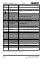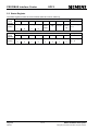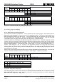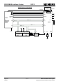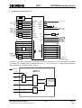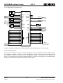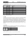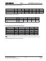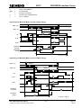
1
SIMATIC NET SPC3 Siemens PROFIBUS Controller Hardware Description Date 2003/04/09 SIM ATIC - NET SPC3 Hardw are Description (Siem ens P R OFIBU S Controller according to IEC 61158) Version: 1.3 Date: 2003/04 PROFIBUS Interface Center SPC3 Liability Exclusion We have tested the contents of this document regarding agreement with the hardware and software described. Nevertheless, there may be deviations, and we don’t guarantee complete agreement. The data in the document is tested periodically, however. Required corrections are included in subsequent versions. We gratefully accept suggestions for improvement Copyright Copyright © Siemens AG 2003. All Rights Reserved. Unless permission has been expressly granted, passing on this document or copying it, or using and sharing its content are not allowed. Offenders will be held liable. All rights reserved, in the event a patent is granted or a utility model or design is registered. Subject to technical changes. Page 2 2003/04 V1.3 SPC3 Hardware Description Copyright (C) Siemens AG 2003. All rights reserved. SPC3 PROFIBUS Interface Center Versions Release V 1.1 Date 12/23/99 V 1.2 09/25/02 V 1.3 2003/04 Changes Chapter 8.2 Current consumption without bus accesses Chapter 10.1 Contact persons Included the specification of the different manufacturers in Chap. 8.1, 8.3, 8.5 and 10.3 Order numbers chap 10.1 contact persons Included the specification of the different manufacturers in Chap. 8.1, 8.3, 8.5 and 10.3 SPC3 Hardware Description Copyright (C) Siemens AG 2003 All rights reserved. V1.3 Page 3 2003/04 PROFIBUS Interface Center SPC3 Directory 1 INTRODUCTION 7 2 FUNCTION OVERVIEW 8 3 PIN DESCRIPTION 9 4 MEMORY ALLOCATION 5 11 4.1 Memory Area Distribution in the SPC3 11 4.2 Processor Parameters (Latches/Register) 13 4.3 Organizational Parameters (RAM) 15 ASIC INTERFACE 17 5.1 Mode Register 5.1.1 Mode Register 0 5.1.2 Mode Register 1 (Mode-REG1, writable): 17 17 19 5.2 Status Register 20 5.3 Interrupt Controller 22 5.4 Watchdog Timer 5.4.1 Automatic Baud Rate Identification 5.4.2 Baud Rate Monitoring 5.4.3 Response Time Monitoring 6 PROFIBUS-DP INTERFACE 6.1 26 DP_Buffer Structure 26 6.2 Description of the DP Services 6.2.1 Set_Slave_Address (SAP55) 6.2.2 Set_Param (SAP61) 6.2.3 Check_Config (SAP62) 6.2.4 Slave_Diagnosis (SAP60) 6.2.5 Write_Read_Data / Data_Exchange (Default_SAP) 6.2.6 Global_Control (SAP58) 6.2.7 Read_Inputs (SAP56) 6.2.8 Read_Outputs (SAP57) 6.2.9 Get_Config (SAP59) 7 HARDWARE INTERFACE 2003/04 29 29 30 31 32 33 35 36 36 36 37 7.1 Universal Processor Bus Interface 7.1.1 General Description 7.1.2 Bus Interface Unit (BIU) 7.1.3 Switching Diagram Principles 7.1.4 Application with the 80 C 32 7.1.5 Application with th 80 C 165 Page 4 25 25 25 25 37 37 37 39 41 42 V1.3 SPC3 Hardware Description Copyright (C) Siemens AG 2003. All rights reserved. SPC3 7.1.6 PROFIBUS Interface Center Interface Signals 43 7.2 UART 43 7.3 ASIC Test 43 8 TECHNICAL DATA 44 8.1 Maximum Limit Values 44 8.2 Permitted Operating Values 44 8.3 DC-Specifikation of the I/O- Drivers 44 8.4 AC-Specification for the Output Drivers 45 8.5 Timing Characteristics 8.5.1 SYS Bus Interface 8.5.2 Timing in the Synchronous C32-Mode: 8.5.3 Timing in the Asynchronous Intel Mode (X86 Mode) : 8.5.4 Timing in the Synchronous Motorola Mode (E_Clock-Mode, for example, 68HC11) : 8.5.5 Timing in the Asynchronous Motorola-Mode (for example, 68HC16) : 8.5.6 Serial Bus Interface 8.5.7 Housing 8.5.8 Processing Instructions 9 PROFIBUS INTERFACE 46 46 47 49 50 52 54 55 56 57 9.1 Pin Assignment 57 9.2 Example for the RS 485 Interface 58 10 APPENDIX 59 10.1 Addresses 59 10.2 General Definition of Terms 60 10.3 Ordering of ASICs 10.3.1 SPC3 (AMI) 10.3.2 SPC3 (ST) 11 11.1 60 60 60 APPENDIX A: DIAGNOSTICS PROCESSING IN PROFIBUS DP Introduction 61 61 11.2 Diagnostics Bits and Expanded Diagnostics 11.2.1 STAT_DIAG 11.2.2 EXT_DIAG 11.2.3 EXT_DIAG_OVERFLOW 61 61 61 63 11.3 63 12 12.1 Diagnostics Processing from the System View APPENDIX B: USEFUL INFORMATION 64 Data format in the Siemens PLC SIMATIC 64 SPC3 Hardware Description Copyright (C) Siemens AG 2003 All rights reserved. V1.3 Page 5 2003/04 PROFIBUS Interface Center Page 6 2003/04 SPC3 V1.3 SPC3 Hardware Description Copyright (C) Siemens AG 2003. All rights reserved. SPC3 PROFIBUS Interface Center 1 Introduction For simple and fast digital exchange between programmable logic controllers, Siemens offers its users several ASICs. These ASICs are based on and are completely handled on the principles of the EN 50170 Vol. 2, of data traffic between individual programmable logic controller stations. The following ASICs are available to support intelligent slave solutions, that is, implementations with a microprocessor. The ASPC2 already has integrated many parts of Layer 2, but the ASPC2 also requires a processor’s support. This ASIC supports baud rates up to 12 Mbaud. In its complexity, this ASIC is conceived primarily for master applications. Due to the integration of the complete PROFIBUS-DP protocol, the SPC3 decisively relieves the processor of an intelligent PROFIBUS slave. The SPC3 can be operated on the bus with a baud rate of up to 12 MBaud. However, there are also simple devices in the automation engineering area, such as switches and thermoelements, that do not require a microprocessor to record their states. There are two additional ASICs available with the designations SPM2 (Siemens Profibus Multiplexer, Version 2 ) and LSPM2 (Lean Siemens PROFIBUS Multiplexer) for an economical adaptation of these devices. These blocks work as a DP slave in the bus system (according to DIN E 19245 T3) and work with baud rates up to 12 Mbaud. A master addresses these blocks by means of Layer 2 of the 7 layer model. After these blocks have received an error-free telegram, they independently generate the required response telegrams. The LSPM2 has the same functions as the SPM2, but the LSPM2 has a decreased number of I/O ports and diagnostics ports. SPC3 Hardware Description Copyright (C) Siemens AG 2003 All rights reserved. V1.3 Page 7 2003/04 PROFIBUS Interface Center SPC3 2 Function Overview The SPC3 makes it possible to have a price-optimized configuration of intelligent PROFIBUS-DP slave applications. The processor interface supports the following processors: Intel: Siemens: Motorola: 80C31, 80X86 80C166/165/167 HC11-,HC16-,HC916 types In SPC3, the transfer technology is integrated (Layer 1), except for analog functions (RS485 drivers), the FDL transfer protocol (Fieldbus Data Link) for slave nodes (Layer 2a), a support of the interface utilities (Layer 2b), some Layer 2 FMA utilities, and the complete DP slave protocol (USIF: User Interface, which makes it possible for the user to have access to Layer 2). The remaining functions of Layer 2 (software utilities and management) must be handled via software. The integrated 1.5k Dual-Port-RAM serves as an interface between the SPC3 and the software/application. The entire memory is subdivided into 192 segments, with 8 bytes each. Addressing from the user takes place directly and from the internal microsequencer (MS) by means of the so-alled base pointer. The base-pointer can be positioned at any segment in the memory. Therefore, all buffers must always be located at the beginning of a segment. If the SPC3 carries out a DP communication the SPC3 automatically sets up all DP-SAPs. The various telegram information is made available to the user in separate data buffers (for example, parameter setting data and configuration data). Three change buffers are provided for data communication, both for the output data and for the input data. A change buffer is always available for communication. Therefore, no resource problems can occur. For optimal diagnostics support, SPC3 has two diagnostics change buffers into which the user inputs the updated diagnostics data. One diagnostics buffer is always assigned to SPC3 in this process. The bus interface is a parameterizable synchronous/asynchronous 8-bit interface for various Intel and Motorola microcontrollers/processors. The user can directly access the internal 1.5k RAM or the parameter latches via the 11-bit address bus. After the processor has been switched on, procedural-specific parameters (station address, control bits, etc.) must be transferred to the Parameter Register File and to the mode registers. The MAC status can be scanned at any time in the status register. Various events (various indications, error events, etc.) are entered in the interrupt controller. These events can be individually enabled via a mask register. Acknowledgement takes place by means of the acknowledge register. The SPC3 has a common interrupt output. The integrated Watchdog Timer is operated in three different states: ‘Baud_Search’, ‘Baud_Control,’ and ‘DP_Control’. The Micro Sequencer (MS) controls the entire process. Procedure-specific parameters (buffer pointer, buffer lengths, station address, etc.) and the data buffer are contained in the integrated 1.5kByte RAM that a controller operates as Dual-Port-RAM. In UART, the parallel data flow is converted into the serial data flow, or vice-versa. The SPC3 is capable of automatically identifying the baud rates (9.6 kBd - 12 MBd). The Idle Timer directly controls the bus times on the serial bus cable. Page 8 2003/04 V1.3 SPC3 Hardware Description Copyright (C) Siemens AG 2003. All rights reserved. SPC3 PROFIBUS Interface Center 3 Pin Description The SPC3 has a 44-pin PQFP housing with the following signals: Pin 1 Signal Name XCS In/Out I© 2 3 XWR/E_Clock DIVIDER 4 5 6 7 8 XRD/R_W CLK VSS CLKOUT2/4 XINT/MOT 9 10 X/INT AB10 11 12 13 14 15 DB0 DB1 XDATAEXCH XREADY/XDTACK DB2 I©/O I©/O O O I©/O 16 DB3 I©/O 17 18 19 VSS VDD DB4 I©/O 20 DB5 I©/O 21 22 23 DB6 DB7 MODE I©/O I©/O I 24 ALE/AS I© 25 AB9 I 26 27 28 29 TXD RTS VSS AB8 O O <log> 0 = 80C166 Data bus/address bus separated; ready signal <log> 1 = 80C32 data bus/address bus multiplexed, fixed timing Address latch enable C32 mode: ALE C165 mode: <log> 0 Address bus C32 mode: <log> 0 C165 mode: address bus Serial send port Request to Send I© Address bus 30 31 32 33 34 35 36 37 38 39 40 41 42 43 44 RXD AB7 AB6 XCTS XTEST0 XTEST1 RESET AB4 VSS VDD AB3 AB2 AB5 AB1 AB0 I© I© I© I(TS) O I© O I(CPD) I© I© I© I© I© I© I(CS) I© I© I© I© I© I© Description Chip-Select Source / Destination C32 Mode: place on VDD. C165 Mode: CS-Signal Write signal /EI_Clock for Motorola Setting the scaler factor for CLK2OUT2/4. low potential means divided through 4 Read signal / Read_Write for Motorola Clock pulse input Clock pulse divided by 2 or 4 <log> 0 = Intel interface <log> 1 = Motorola interface Interrupt Address bus CPU System System, CPU System CPU, Interrupt-Contr. C32 mode: <log> 0 C165 mode: address bus Data bus C32 Mode: Data/address bus multiplexed C165 Mode: Data/address bus separated Data_Exchange state for PROFIBUS-DP Ready for external CPU Data bus C32 mode: data bus/address bus multiplexed C165 mode: data/address bus separate Data bus CPU (80C165) CPU CPU, memory LED System, CPU CPU, memory C32 mode: data bus/address bus multiplexed C165 mode: data bus/address CPU, memory bus separate System CPU (80C32) CPU (C165), memory RS 485 sender RS 485 sender C32 Mode : <log> 0 C165 Mode: address bus Serial receive port Address bus Address bus Clear to send <log> 0 = send enable Pin must be placed fixed at VDD. Pin must be placed fixed at VDD. Connect reset input with CPU’s port pin. Address bus RS 485 receiver System, CPU System, CPU FSK modem Address bus System, CPU Address bus System, CPU System, CPU Figure 3.1: SPC3 Pin Assignment Note: • All signals that begin with X.. are LOW active • VDD = +5V, VSS = GND Input levels: I ©: I (CS): CMOS CMOS Schmitt trigger SPC3 Hardware Description Copyright (C) Siemens AG 2003 All rights reserved. V1.3 Page 9 2003/04 PROFIBUS Interface Center I (CPD): I (TS): Page 10 2003/04 SPC3 CMOS with pull down TTLt Schmitt trigger V1.3 SPC3 Hardware Description Copyright (C) Siemens AG 2003. All rights reserved. SPC3 PROFIBUS Interface Center 4 Memory Allocation 4.1 Memory Area Distribution in the SPC3 The figure displays the division of the SPC3 1.5k internal address area. The internal latches/register are located in the first 21 addresses. The internal latches/register either come from the controller or influence the controller. Certain cells can be only read or written. The internal work cells to which the user has no access are located in RAM at the same addresses. The organizational parameters are located in RAM beginning with address 16H. The entire buffer structure (for the DP-SAPS) is written based on these parameters. In addition, general parameter setting data (station address, Ident no., etc.) are transferred in these cells and the status displays are stored in these cells (global control command, etc.). Corresponding to the parameter setting of the organizational parameters, the user-generated buffers are located beginning with address 40H. All buffers or lists must begin at segment addresses (48 bytes segmentation). Address 000H 016H 040H 5FFH Function Processor parameters internal work cells Latches/register (22 bytes) Organizational parameters (42 bytes) DP- buffer: Data In (3) * Data Out (3) * Diagnostics (2) Parameter setting data (1) Configuration data (2) Auxiliary buffer (2) SSA-buffer(1) Figure 4.1: SPC3 Memory Area Distribution Caution: The HW prohibits overranging the address area. That is, if a user writes or reads past the memory end, 400H is subtracted from this address and the user therefore accesses a new address. This prohibits overwriting a process parameter. In this case, the SPC3 generates the RAM access violation interrupt. If the MS overranges the memory end due to a faulty buffer initialization, the same procedure is executed. * Data In is the input data from PROFIBUS slave to master Data out is the output data from PROFIBUS master to slave SPC3 Hardware Description Copyright (C) Siemens AG 2003 All rights reserved. V1.3 Page 11 2003/04 PROFIBUS Interface Center SPC3 The complete internal RAM of the SPC 3 is divided logically into 192 segments. Each segment consists of 8 bytes. For more informations about the contents of the 3 memory areas see previous chapter.The physical address is build by multiplikation with 8. internal SPC 3 RAM (1.5 kByte) Segment 0 Segment 1 Segment 2 8 Bit Segmentaddresses (Pointer to the buffers 7 0 + 10 0 Segment 190 Segment 191 Page 12 2003/04 V1.3 SPC3 Hardware Description Copyright (C) Siemens AG 2003. All rights reserved. SPC3 PROFIBUS Interface Center 4.2 Processor Parameters (Latches/Register) These cells can be either read only or written only. SPC3 carries out “address swapping” for an access to the address area 00H - 07H (word register) in the Motorola mode. That is, the SPC3 exchanges address bit 0 (generated from an even address, one uneven, and vice-versa). The following sections more clearly explain the significance of the individual registers. Name Address Intel / Motorla No. 00H 01H Int-Req-Reg 7..0 01H 00H Int-Req-Reg 15..8 02H 03H Int—Reg 7..0 03H 02H Int—Reg 15..8 04H 05H Status-Reg 7..0 05H 04H Status-Reg 15..8 06H 07H Reserved 07H 06H 08H DIN_Buffer_SM 7..0 09H New_DIN_Buffer_Cmd 1..0 0AH DOUT_Buffer_SM 7..0 0BH Next_DOUT_Buffer_Cmd 1..0 0CH DIAG_Buffer_SM 3..0 0DH New_DIAG_Puffer_Cmd 1..0 0EH User_Prm_Data_OK 1..0 0FH UserPrmDataNOK 1..0 10H User_Cfg_Data_OK 1..0 11H User_Cfg_Data_NOK 12H 13H 14H SSA_Bufferfreecmd 15H Reserved Bit Significance (Read Access!) Interrupt Controller Register Status Register Buffer assignment of the DP_Din_Buffer_State_Machine The user makes a new DP Din buffer available in the N state. Buffer assignment of the DP_Dout_Puffer_State_Machine The user fetches the last DP Dout-Buffer from the N state. Buffer assignment for the DP_Diag_Puffer_State_Machine The user makes a new DP Diag Buffer available to the SPC3. The user positively acknowledges the user parameter setting data of a Set_Param-Telegram. The user negatively acknowledges the user parameter setting data of a Set_Param-Telegram. The user positively acknowledges the configuration data of a Check_Config-Telegram. 1..0 The user negatively acknowledges the configuration data of a Check_Config-Telegram. Reserved The user has fetched the data from the SSA buffer and enables the buffer again. Figure 4.2: Assignment of the Internal Parameter Latches for READ SPC3 Hardware Description Copyright (C) Siemens AG 2003 All rights reserved. V1.3 Page 13 2003/04 PROFIBUS Interface Center Address Intel /Motorola 00H 01H 01H 00H 02H 03H 03H 02H 04H 05H 05H 04H 06H 07H 07H 06H 08H 09H 0AH 0BH OCH 0DH 0EH 0FH 10H 11H 12H 13H 14H 15H Name No. Int-Req-Reg 7..0 Int-Req_Reg 15..8 Int-Ack-Reg 7..0 Int-Ack-Reg 15..8 Int—Mask-Reg 7..0 Int—Mask-Reg 15..8 Mode-Reg0 7..0 Mode-Reg0-S 15..8 Mode-Reg1-S 7..0 Mode-Reg1-R 7..0 WD Baud 7..0 MinTsdr_Val 7..0 SPC3 Bit Significance (Write Access !) Interrupt- Controller - Register Setting parameters for individual bits Ctrl -Val Root value for baud rate monitoring MinTsdr time Reserved Figure 4.3: Assignment of the Internal Parameter Latches for WRITE Page 14 2003/04 V1.3 SPC3 Hardware Description Copyright (C) Siemens AG 2003. All rights reserved. SPC3 PROFIBUS Interface Center 4.3 Organizational Parameters (RAM) The user stores the organizational parameters in RAM under the specified addresses. These parameters can be written and read. SPC3 Hardware Description Copyright (C) Siemens AG 2003 All rights reserved. V1.3 Page 15 2003/04 PROFIBUS Interface Center Address Intel /Motorola 16H Name Bit No. Significance 1AH 1BH 1CH 1DH 1EH 1FH 20H 21H 22H 23H 24H 25H 26H 27H 28H R_TS_Adr 7..0 reserved R_User_Wd_Value 7..0 R_User_Wd_Value ..8 R_Len_Dout_Puf R_Dout_buf_Ptr1 R_Dout_buf_Ptr2 R_Dout_buf_Ptr3 R_Len_Din_buf R_Din_buf_Ptr1 R_Din_buf_Ptr2 R_Din_buf_Ptr3 reserved reserved R Len Diag buf1 R Len Diag buf2 R_Diag_Puf_Ptr1 R_Diag_Puf_Ptr2 R Len Cntrl Pbuf1 29H R Len Cntrl Puf2 2AH R Aux Puf Sel 2BH 2CH 2DH 2EH 2FH 30H 31H 32H 33H 34H 35H 36H 37H 38H 39H R_Aux_buf_Ptr1 R_Aux_buf_Ptr2 R_Len_SSA_Data R SSA buf Ptr R_Len_Prm_Data R_Prm_buf_Ptr R_Len_Cfg_Data R Cfg Buf Ptr R_Len_Read_Cfg_Data R_Read_Cfg_buf_Ptr reserved reserved reserved reserved R_Real_No_Add_Change 3AH 3BH 3CH 3DH R_Ident_Low R_Ident_High R_GC_Command R_Len_Spec_Prm_buf 17H 18H 19H 19H 18H SPC3 Set up station address of the relevant SPC3 Pointer to a RAM address which is presetted with 0FFH Based on an internal 16-bit wachdog timer, the user is monitored in the DP_Mode. 15 Length of the 3 Dout buffers Segment base address of Dout buffer 1 Segment base address of Dout buffer 2 Segment base address of Dout buffer 3 Length of the 3 Din buffers Segment base address of Din buffer 1 Segment base address of Din buffer 2 Segment base address of Din buffer 3 Preset with 00H. Preset with 00H. Length of Diag buffer 1 Length of Diag buffer 2 Segment base address of Diag buffer 1 Segment base address of Diag buffer 2 Length of Aux buffer 1 and the control buffer belonging to it, for example, SSA-Buf, Prm-Buf, Cfg-Buf, Read-Cfg-Buf Length of Aux-Buffer 2 and the control buffer belonging to it, for example, SSA-Buf, Prm-Buf, Cfg-Buf, Read-Cfg-Buf Bit array, in which the assignments of the Aux-buffers ½ are defined to the control buffers, SSA-Buf, Prm-Buf, Cfg-Buf Segment base address of auxiliary buffer 1 Segment base address of auxiliary buffer 2 Length of the input data in the Set_Slave_Address-buffer Segment base address of the Set_Slave_Address-buffer Length of the input data in the Set_Param-buffer Segment base address of the Set_Param-buffer Length of the input data in the Check_Config-buffer Segment base address of the Check_Config-buffer Length of the input data in the Get_Config-buffer Segment base address of the Get_Config-buffer Preset with 00H. Preset with 00H Preset with 00H. Preset with 00H. This parameter specifies whether the DP slave address may again be changed at a later time point. The user sets the parameters for the Ident_Low value. The user sets the parameters for the Ident_High value. The Global_Control_Command last received If parameters are set for the Spec_Prm_Buffer_Mode (see mode register 0), this cell defines the length of the param buffer. Figure 4.4: Assignment of the Organizational Parameters Page 16 2003/04 V1.3 SPC3 Hardware Description Copyright (C) Siemens AG 2003. All rights reserved. SPC3 PROFIBUS Interface Center 5 ASIC Interface The registers that determine both the hardware function of the ASIC as well as telegram processing are described in the following. 5.1 Mode Register Parameter bits that access the controller directly or which the controller directly sets are combined in two mode registers (0 and 1) in the SPC3. 5.1.1 Mode Register 0 Setting parameters for Mode Register 0 takes place in the offline state only (for example, after switching on). The SPC3 may not exit offline until Mode Register 0, all processor parameters, and organizational parameters are loaded (START_SPC3 = 1, Mode-Register 1). Address Control Register 06H (Intel) Address Control Register 07H (Intel) Bit Position 4 3 7 6 5 Freeze_ Supported Sync_ Supported EARLY_ RDY 15 14 13 Spec_Cle ar_Mode *) INT_ POL MinTSDR Bit Position 12 11 Spec_Prm_ Puf_Mode **) Designation 2 WD Test 1 0 DIS_ STOP_ CON TROL DIS_ START_ CON TROL Mode Reg0 7..0 Designation 10 9 8 User Time base EOI Time base DP Mode Mode-Reg0 13 .. 8 *) When Spec_Clear_Mode (Fail Safe Mode ) = 1 the SPC3 will accept data telegramm with a data unit=0 in the state Data Exchange. The reaction to the outputs can be parameterized f.e. in the parameterization telegram ( only available from version Step C). **) When using a big number of parameters to be transmitted from the PROFIBUS-Master to the slave the Auxiliary buffer ½ has to have the same size like the Parameterization buffer. Sometimes this could reach the limit of the available memory space in the SPC3. When Spec_Prm_Puf_Mode = 1 the parameterization data are processed directly in this special buffer and the Auxiliary buffers can be held compact. SPC3 Hardware Description Copyright (C) Siemens AG 2003 All rights reserved. V1.3 Page 17 2003/04 PROFIBUS Interface Center Bit 0 Bit 1 Bit 2 Bit 3 Bit 4 Bit 5 Bit 6 Bit 7 Bit 8 Bit 9 Bit 10 Bit 11 Bit 12 Bit 13 SPC3 DIS_START_CONTROL Monitoring the following start bit in UART. Set-Param Telegram overwrites this memory cell in the DP mode. (Refer to the user-specific data.) 0= Monitoring the following start bit is enabled. 1= Monitoring the following start bit is switched off. DIS_STOP_CONTROL Stop bit monitoring in UART. Set-Param telegram overwrites this memory cell in the DP mode. (Refer to the user-specific data.) 0= Stop bit monitoring is enabled. 1= Stop bit monitoring is switched off. EN_FDL_DDB Reserved 0= The FDL_DDB receive is disabled. MinTSDR Default setting for the MinTSDR after reset for DP operation or combi operation 0= Pure DP operation (default configuration!) 1= Combi operation INT_POL Polarity of the interrupt output 0= The interrupt output is low-active. 1= The interrupt output is high-active. EARLY_RDY Moved up ready signal 0= Ready is generated when the data are valid (read) or when the data are accepted (write). 1= Ready is moved up by one clock pulse. Sync_Supported Sync_Mode support 0= Sync_Mode is not supported. 1= Sync_Mode is supported. Freeze_Supported Freeze_Mode support 0= Freeze_Mode is not supported. 1= Freeze_Mode is supported. DP_MODE DP_Mode enable 0= DP_Mode is disabled. 1= DP_Mode is enabled. SPC3 sets up all DP_SAPs. EOI_Time base Time base for the end of interrupt pulse 0= The interrupt inactive time is at least 1 usec long. 1= The interrupt inactive time is at least 1 ms long. User_Time base Time base for the cyclical User_Time_Clock-Interrupt 0= The User_Time_Clock-Interrupt occurs every 1 ms. 1= The User_Time_Clock-Interrupt occurs every 10 ms. WD_Test Test mode for the Watchdog-Timer, no function mode 0= The WD runs in the function mode. 1= Not permitted Spec_Prm_Puf_Mode Special parameter buffer 0= No special parameter buffer. 1= Special parameter buffer mode .Parameterization data will be stored directly in the special parameter buffer. Spec_Clear_Mode Special Clear Mode (Fail Safe Mode) 0= 1= No special clear mode. Special clear mode. SPC3 will accept datea telegramms with data unit = 0. Figure 5.1: Mode-Register 0 Bit 12 .. 0.(can be written to, can be changed in offline only) Page 18 2003/04 V1.3 SPC3 Hardware Description Copyright (C) Siemens AG 2003. All rights reserved. SPC3 PROFIBUS Interface Center 5.1.2 Mode Register 1 (Mode-REG1, writable): Some control bits must be changed during operation. These control bits are combined in Mode-Register 1 and can be set independently of each other (Mode_Reg_S) or can be deleted independently of each other (Mode_Reg_R). Various addresses are used for setting and deleting. Log ‘1’ must be written to the bit position to be set or deleted. Address Control Register 08H 09H Bit 0 Bit 1 Bit 2 Bit 3 Bit 4 Bit 5 7 6 Bit Position 4 3 5 Res_ User_WD Res_ User_WD EN_ Change_ Cfg_ Puffer EN_ Change_ Cfg_ Puffer Designation 2 1 0 User_ Leave_ Master Go_ Offline EOI START_ SPC3 Mode-Reg_S 7..0 User_ Leave_ Master Go_ Offline EOI START_ SPC3 Mode-Reg_R 7..0 START_SPC3 Exiting the Offline state 1 = SPC3 exits offline and goes to passive-idle. In addition, the idle timer and Wd timer are started and ‘Go_Offline = 0’ is set. EOI End of Interrupt 1 = End of Interrupt: SPC3 switches the interrupt outputs to inactive and again sets EOI to log.’0.’ Go_Offline Going into the offline state 1 = After the current requests ends, SPC3 goes to the offline state and again sets Go_Offline to log.’0.’ User_Leave_Master Request to the DP_SM to go to ‘Wait_Prm.’ 1 = The user causes the DP_SM to go to ‘Wait_Prm.’ After this action, SPC3 sets User_Leave_Master to log.’0.’ En_Change_Cfg_Puffer Enabling buffer exchange (Cfg buffer for Read_Cfg buffer) 0 = With ‘User_Cfg_Data_Okay_Cmd,’ the Cfg buffer may not be exchanged for the Read_Cfg buffer. 1 = With ‘User_Cfg_Data_Okay_Cmd,’ the Cfg buffer must be exchanged for the Read_Cfg buffer. Res_User_Wd Resetting the User_WD_Timers 1 = SPC3 again sets the User_Wd_Timer to the parameterized value ‘User_Wd_Value15..0.’ After this action, SPC3 sets Res_User_Wd to log.’0.’ Figure 5..2: Mode Register1 S and Mode Register1 R Bit7..0.(writable) SPC3 Hardware Description Copyright (C) Siemens AG 2003 All rights reserved. V1.3 Page 19 2003/04 PROFIBUS Interface Center SPC3 5.2 Status Register The status register mirrors the current SPC3 status and can be read only. Address Control Register 04H (Intel) Address Control Register 05H (Intel) 7 2003/04 5 Bit Position 4 3 RAM access violation WD_State DP_State 1 0 1 0 15 14 13 Bit Position 12 11 SPC3 Release 3 Page 20 6 2 1 Designation 2 1 0 Diag_ Flag FDL_ IND_ST Offline/ PassiveIdle 10 9 8 Designation Baud Rate 0 3 V1.3 Status-Reg 7..0 2 1 Status-Reg 15 .. 8 0 SPC3 Hardware Description Copyright (C) Siemens AG 2003. All rights reserved. SPC3 Bit 0 Bit 1 Bit 2 Bit 3 Bits 4,5 Bits 6,7 Bits 8,9 10,11 Bit 12 13,14, 15 PROFIBUS Interface Center Offline/Passive-Idle Offline-/Passive-Idle state 0 = SPC3 is in offline. 1 = SPC3 is in passive idle. FDL_IND_ST FDL indication is temporarily buffered. 0 = No FDL indication is temporarily buffered. 1 = No FDL indication is temporarily buffered. Diag_Flag Status diagnostics buffer 0 = The DP master fetches the diagnostics buffer. 1 = The DP master has not yet fetched the diagnostics buffer. RAM Access Violation Memory access > 1.5kByte 0 = No address violation 1 = For addresses > 1536 bytes, 1024 is subtracted from the current address, and there is access to this new address. DP-State1..0 DP-State Machine state 00 = ’Wait_Prm’ state 01= ’Wait_Cfg’ state 10 = ’DATA_EX’ state 11= Not possible WD-State1..0 Watchdog-State-Machine state 00 = ’Baud_Search’ state 01= ’Baud_Control’ state 10 = ’DP_Control’ state 11= Not possible Baud rate3..0: The baud rates SPC3 found 0000 = 12 MBaud 0001 = 6 MBaud 0010 = 3 MBaud 0011 = 1.5 MBaud 0100 = 500 kBaud 0101 = 187.5 kBaud 0110 = 93.75 kBaud 0111 = 45.45 kBaud 1000 = 19.2 kBaud 1001 = 9.6 kBaud Rest = Not possible SPC3-Release3..0: Release no. for SPC3 0000 = Release 0 Rest = Not possible Figure 5.3: Status Register Bit15 .. 0.(readable) SPC3 Hardware Description Copyright (C) Siemens AG 2003 All rights reserved. V1.3 Page 21 2003/04 PROFIBUS Interface Center SPC3 5.3 Interrupt Controller The processor is informed about indication messages and various error events via the interrupt controller. Up to a total of 16 events are stored in the interrupt controller. The events are carried out on an interrupt output. The controller does not have a prioritization level and does not provide an interrupt vector (not 8259A compatible!). The controller consists of an Interrupt Request Register (IRR), an Interrupt Mask Register (IMR), an Interrupt Register (IR), and an Interrupt Acknowledge Register (IAR). uP SPC3 uP uP uP SEP_INT IR S IRR S IMR X/INT uP FF R R INT_Pol IAR uP Each event is stored in the IRR. Individual events can be suppressed via the IMR. The input in the IRR is independent of the interrupt masks. Event signals not masked out in the IMR generate the X/INT interrupt via a sum network. The user can set each event in the IRR for debugging. Each interrupt event the processor processed must be deleted via the IAR (except for New_Prm_Data, New_DDB_Prm_Data, and New_Cfg_Data). Log ‘1’ must be written on the relevant bit position. If a new event and an acknowledge from the previous event are present at the IRR at the same time, the event remains stored. If the processor subsequently enables a mask, it must be ensured that no prior input is present in the IRR. For safety purposes, the position in the IRR must be deleted prior to the mask enable. Prior to exiting the interrupt routine, the processor must set the “end of interrupt signal (E01) = 1” in the mode register. The interrupt cable is switched to inactive with this edge change. If another event must be stored, the interrupt output is not activated again until after an interrupt inactive time of at least 1 usec or 12 ms. This interrupt inactive time can be set via ‘EOI_Timebase.’ This makes it possible to again come into the interrupt routine when an edge-triggered interrupt input is used. The polarity for the interrupt output is parameterized via the INT_Pol mode bit. After the hardware reset, the output is low-active. Address Control Register 00H (Intel) Address Control Register 01H (Intel) Page 22 2003/04 7 6 5 Res Res Res 15 14 13 Res Res DX_OUT Bit Position 4 3 User_ Timer_ Clock WD_DP_ Mode_ Timeout Bit Position 12 11 Diag_ Puffer_ Changed New_ Prm_ Data V1.3 Designation 2 1 0 Baud_ rate_ Detect Go/Leave Data_ EX MAC_ Reset 10 9 8 New_ Cfg_ Data New_ SSA_ Data New_GC Com mand Int-Req-Reg 7..0 Designation Int-Req-Reg 7 15..8 SPC3 Hardware Description Copyright (C) Siemens AG 2003. All rights reserved. SPC3 Bit 0 Bit 1 Bit 2 Bit 3 Bit 4 Bit 5 Bit 6 Bit 7 Bit 8 Bit 9 Bit 10 Bit 11 Bit 12 Bit 13 Bit 14 Bit 15 PROFIBUS Interface Center MAC_Reset After it processes the current request, the SPC3 has arrived at the offline state (through setting the ‘Go_Offline bit’ or through a RAM access violation). Go/Leave_DATA_EX The DP_SM has entered or exited the ‘DATA_EX’ state. Baudrate_Detect The SPC3 has exited the ‘Baud_Search state’ and found a baud rate. WD_DP_Control_Timeout The watchdog timer has run out in the ‘DP_Control’ WD state. User_Timer_Clock The time base for the User_Timer_Clocks has run out (1/10ms). Res For additional functions Res For additional functions Res For additional functions New_GC_Command The SPC3 has received a ‘Global_Control telegram’ with a changed ‘GC_CommandByte,’ and this byte is stored in the ‘R_GC_Command’ RAM cell. New_SSA_Data The SPC3 has received a ‘Set_Slave_Address telegram’ and made the data available in the SSA buffer. New_Cfg_Data The SPC3 has received a ‘Check_Cfg telegram’ and made the data available in the Cfg buffer. New_Prm_Data The SPC3 has received a ‘Set_Param telegram’ and made the data available in the Prm buffer. Diag_Puffer_Changed Due to the request made by ‘New_Diag_Cmd,’ SPC3 exchanged the diagnostics buffer and again made the old buffer available to the user. DX_OUT The SPC3 has received a ‘Write_Read_Data telegram’ and made the new output data available in the N buffer. For a ‘Power_On’ or for a ‘Leave_Master,’ the SPC3 deletes the N buffer and also generates this interrupt. Res For additional functions Res For additional functions Figure 5.4: Interrupt Request Register, IRR Bit 15..0 (writable and readable) SPC3 Hardware Description Copyright (C) Siemens AG 2003 All rights reserved. V1.3 Page 23 2003/04 PROFIBUS Interface Center SPC3 The other interrupt controller registers are assigned in the bit positions, like the IRR. Address 02H / 03H 04H / 05H 02H / 03H Register Interrupt Register (IR) Interrupt Mask Register (IMR) Interrupt Acknowledge Register (IAR) Readable only Writable, can be changed during operation Writable, can be changed during operation Reset State All bits deleted Assignment All bits set Bit = 1 All bits deleted Bit = 0 Bit = 1 Bit = 0 Mask is set and the interrupt is disabled. Mask is deleted and the interrupt is enabled. The IRR bit is deleted. The IRR bit remains unchanged. Figure 5.5: Additional Interrupt Registers The ‘New_Prm_Data’, ‘New_Cfg_Data’ inputs may not be deleted via the Interrupt Acknowledge Register. The relevant state machines delete these inputs through the user acknowledgements (for example, ‘User_Prm_Data_Okay’ etc.). Page 24 2003/04 V1.3 SPC3 Hardware Description Copyright (C) Siemens AG 2003. All rights reserved. SPC3 PROFIBUS Interface Center 5.4 Watchdog Timer 5.4.1 Automatic Baud Rate Identification The SPC3 is able to identify the baud rate automatically. The „baud search“ state is located after each RESET and also after the watchdog (WD) timer has run out in the ‘Baud_Control_state.’ As a rule, SPC3 begins the search for the set rate with the highest baud rate. If no SD1 telegram, SD2 telegram, or SD3 telegram was received completely and without errors during the monitoring time, the search continues with the next lowest baud rate. After identifying the correct baud rate, SPC3 switches to the “Baud_Control” state and monitors the baud rate. The monitoring time can be parameterized (WD_Baud_Control_Val). The watchdog works with a clock of 100 Hz (10 msec). The watchdog resets each telegram received with no errors to its own station address. If the timer runs out, SPC3 again switches to the baud search state. 5.4.2 Baud Rate Monitoring The located baud rate is constantly monitored in ‘Baud_Control.’ The watchdog is reset for each error-free telegram to its own station address. The monitoring time results from multiplying both ‘WD_Baud_Control_Val’ (user sets the parameters) by the time base (10 ms). If the monitoring time runs out, WD_SM again goes to ‘Baud_Search’. If the user carries out the DP protocol (DP_Mode = 1, see Mode register 0) with SPC3, the watchdog is used for the “DP_Control’ state, after a ‘Set_Param telegram’ was received with an enabled response time monitoring ‘WD_On = 1.’ The watchdog timer remains in the baud rate monitoring state when there is a switched off ‘WD_On = 0’ master monitoring. The PROFIBUS DP state machine is also not reset when the timer runs out. That is, the slave remains in the DATA_EXchange state, for example. 5.4.3 Response Time Monitoring The ‘DP_Control’ state serves response time monitoring of the DP master (Master_Add). The set monitoring times results from multiplying both watchdog factors and multiplying the result with the momentarily valid time base (1 ms or 10 ms): TWD = (1 ms or 10 ms) * WD_Fact_1 * WD_Fact_2 (See byte 7 of the parameter setting telegram.) The user can load the two watchdog factors (WD_Fact_1, and WD_Fact_2) and the time base that represents a measurement for the monitoring time via the ‘Set_Param telegram’ with any value between 1 and 255. EXCEPTION: The WD_Fact_1=WD_Fact_2=1 setting is not permissible. The circuit does not check this setting. Monitoring times between 2 ms and 650 s - independent of the baud rate - can be implemented with the permisible watchdog factors. If the monitoring time runs out, the SPC3 goes again to ‘Baud_Control,’ and the SPC3 generates the ‘WD_DP_Control_Timeout-Interrupt’. In addition, the DP_State machine is reset, that is, generates the reset states of the buffer management. If another master accepts SPC3, then there is either a switch to ‘Baud_Control” (WD_On = 0), or there is a delay in ‘DP_Control’ (WD_On = 1), depending on the enabled response time monitoring (WD_On = 0). SPC3 Hardware Description Copyright (C) Siemens AG 2003 All rights reserved. V1.3 Page 25 2003/04 PROFIBUS Interface Center SPC3 6 PROFIBUS-DP Interface 6.1 DP_Buffer Structure The DP mode is enabled in the SPC3 with ‘DP_Mode = 1’ (see mode Register0). In this process, the following SAPS are fixed reserved for the DP mode: ` ` ` ` ` ` ` ` ` ` Default SAP: SAP53: SAP55: SAP56: SAP57: SAP58: SAP59: SAP60: SAP61: SAP62: Data exchange (Write_Read_Data) reserved Changing the station address (Set_Slave_Address) Reading the inputs (Read_Inputs) Reading the outputs (Read_Outputs) Control commands to the DP-Slave (Global_Control) Reading configuration data (Get_Config) Reading diagnostics information (Slave_Diagnosis) Sending parameter setting data (Set_Param) Checking configuration data (Check_Config) The DP Slave protocol is completely integrated in the SPC3 and is handled independently. The user must correspondingly parameterize the ASIC and process and acknowledge transferred messages. Except for the default SAP, SAP56, SAP57, and SAP58, all SAPS are always enabled. The remaining SAPS are not enabled until the the DP Slave Machine (DP_SM) goes into the ‘DATA_EX’ state. The user has the possibility of disabling SAP55. The relevant buffer pointer R_SSA_Puf_Ptr must be set to ‘00H’ for this purpose. The DDB utility is disabled by the already described initialization of the RAM cells. The DP_SAP buffer structure is displayed in Figure 6.1. The user configures all buffers (length and buffer beginning) in the ‘offline state.’ During operation, the buffer configuration must not be changed, except for the length of the Dout-/Din buffers. The user may still adapt these buffers in the ‘Wait_Cfg’ state after the configuration telegram (Check_Config). Only the same configuration may be accepted in the ‘DATA_EX’ state. The buffer structure is divided into the data buffer, diagnostics buffer, and the control buffer. Both the output data and the input data have three buffers each available with the same length. These buffers function as change buffers. One buffer is assigned to the ‘D’ data transfer, and one buffer is assigned to the ‘U’ user. The third buffer is either in a Next ‘N’ state or Free ‘F’ state, whereby one of the two states is always unoccupied. Two diagnostics buffers that can have varying lengths are available for diagnostics. One diagnostics buffer is always the ‘D’ assigned to SPC3 for sending. The other diagnostics buffer belongs to the user for preparing new diagnostics data, ‘U.’ The SPC3 first reads the different parameter setting telegrams (Set_Slave_Address, and Set_Param) and the configuring telegram (Check_Config) into Aux-Puffer1 or Aux-Puffer 2..... Page 26 2003/04 V1.3 SPC3 Hardware Description Copyright (C) Siemens AG 2003. All rights reserved. SPC3 D-Nis changed by SPC 3 D PROFIBUS Interface Center N- U is changed by the user N U Dout-buffer D N U Din-buffer D U Diagnosticsbuffer UART ReadConfigbuffer User Aux1/2-buffer Configbuffer SSA-buffer Aux1/2-buffer Parambuffer Figure 6.1: DP_SAP Buffer Structure Data exchanged with the corresponding target buffer (SSA buffer, Prm buffer, and Cfg buffer). Each of the buffers to be exchanged must have the same length. The user defines which Aux_buffers are to be used for the above-named telegrams in the ‘R_Aux_Puf_Sel’ parameter cell. The Aux- buffer1 must always be available. The Aux-buffer2 is optional. If the data profiles of these DP telegrams are very different, such as the data amount in the Set_Param telegram is significantly larger than for the other telegrams, it is suggested to make an Aux-Buffer2 available (Aux_Sel_Set_Param = 1) for this telegram. The other telegrams are then read via Aux-Buffer 1 (Aux_Sel_..=0). If the buffers are too small, SPC3 responds with “no resources”! SPC3 Hardware Description Copyright (C) Siemens AG 2003 All rights reserved. V1.3 Page 27 2003/04 PROFIBUS Interface Center Address RAM Register 2AH X1 0 1 SPC3 7 6 5 Bit Position 4 3 2 0 0 0 0 0 Designation 0 Set_ Slave_ Adr Check_ Cfg Set_ Prm R_Aux_Puf_Sel X1 X1 X1 See below for coding. Coding Aux_Buffer1 Aux_Buffer2 Figure 6.2: Aux-Buffer Management The user makes the configuration data (Get_Config) available in the Read_Cfg buffer for reading. The Read_Cfg buffer must have the same length as the Cfg_buffer. The Read_Input_Data telegram is operated from the Din buffer in the ‘D state’, and the Read_Output_Data telegram is operated from the Dout buffer in the ‘U state.’ All buffer pointers are 8-bit segment addresses, because the SPC3 internally has only 8-bit address registers. For a RAM access, SPC3 adds an 8-bit offset address to the segment address shifted by 3 bits (result: 11-bit physical address). As regards the buffer start addresses, this results in an 8-byte graunularity from this specification. Page 28 2003/04 V1.3 SPC3 Hardware Description Copyright (C) Siemens AG 2003. All rights reserved. SPC3 PROFIBUS Interface Center 6.2 Description of the DP Services 6.2.1 Set_Slave_Address (SAP55) 6.2.1.1 Sequence for the Set_Slave_Address Utility The user can disable this utility by setting the ‘R_SSA_Puf_Ptr = 00H’ buffer pointer. The slave address must then be determined, for example, by reading a switch, and written in the R_TS_Adr. RAM register. The user must make a retentive memory possibility available (for example, EEPROM) to support this utility. It must be possible to store the ‘station address’ and the ‘Real_No_Add_Change’ (‘True’ = FFH) parameter in this external EEPROM. After each restart caused by a power failure, the user must again make these values available to SPC3 in the R_TS_Adr und R_Real_No_Add_Change RAM register. If SAP55 is enabled and the Set_Slave_Address telegram is correctly accepted, SPC3 enters all net data in the Aux-Puffer1/2, exchanges the Aux buffer1/2 for the SSA buffer, stores the entered data length in ‘R_Len_SSA_Data’, generates the ‘New_SSA_Data’ interrupt and internally stores the new ‘station address’ and the new ‘Real_No_Add_Change’ parameter. The user does not need to transfer this changed parameter to SPC3 again. After the user has read the buffer, the user generates the ‘SSA_Puffer_Free_Cmd’ (read operation on address 14H). This makes SPC3 again ready to receive an additional Set Slave Address telegram (such as from another master). SPC3 reacts independently when there are errors. Address Control Register 14H 7 6 5 0 0 0 Bit Position 4 3 Designation 0 0 don´t care 2 1 0 0 0 0 SSA_Puffer_Free_Cmd Figure 6.3: Coding SSA_Buffer_Free_Cmd 6.2.1.2 Structure of the Set_Slave_Address Telegram The net data are stored as follows in the SSA buffer: Byte 7 6 5 Bit Position 4 3 Designation 2 0 1 2 3 4-243 1 0 New_Slave_Address Ident_Number_High Ident_Number_Low No_Add_Chg Rem_Slave_Data additional applicationspecific data Figure 6.4: Data Format for the Set_Slave_Address Telegram SPC3 Hardware Description Copyright (C) Siemens AG 2003 All rights reserved. V1.3 Page 29 2003/04 PROFIBUS Interface Center SPC3 6.2.2 Set_Param (SAP61) 6.2.2.1 Parameter Data Structure SPC3 evaluates the first seven data bytes (without user prm data), or the first eight data bytes (with user prm data). The first seven bytes are specified according to the standard. The eighth byte is used for SPC3specific characteristics. The additional bytes are available to the application. Byte 0 1 2 3 4 5 6 7 7 6 5 Lock Req Unlo. Req Sync Req 0 0 0 Bit Position 4 3 Free Req 0 WD on 0 Designation 2 1 0 Res Res Res WD_ Base Dis Stop Dis Start 8-243 Station status WD_Fact_1 WD_Fact_2 MinTSDR Ident_Number_High Ident_Number_Low Group_Ident Spec_User_Prm_Byte User_Prm_Data Byte 7 Bit 0 Spec_User_Prm_Byte Name Significance Dis_Startbit The start bit monitoring in the receiver is switched off with this bit. 1 Dis_Stopbit 2 WD_Base 3-7 res Default State Dis_Startbit= 1 , that is, start bit monitoring is switched off. Stop bit monitoring in the receiver is Dis_Stopbit= 0, switched off with this bit. that is, stop bit monitoring is not switched off. This bit specifies the time base used WD_Base= 0, to clock the watchdog. that is, the time base is 10 ms WD_Base = 0: time base 10 ms WD_Base = 1: time base 1 ms to be parameterized with 0 0 Figure 6.5: Data Format for the Set_Param_Telegram 6.2.2.2 Parameter Data Processing Sequence In the case of a positive validatation for more than seven data bytes, SPC3 carries out the following reaction, among others: SPC3 exchanges Aux-Puffer1/2 (all data bytes are input here) for the Prm buffer, stores the input data length in ‘R_Len_Prm_Data’, and triggers the ‘New_Prm_Data Interrupt’. The user must then check the ‘User_Prm_Data’ and either reply with the ‘User_Prm_Data_Okay_Cmd’ or with ‘User_Prm_Data_Not_Okay_Cmd.’ The entire telegram is input in the buffer, that is, application-specific parameter data are stored beginning with data byte 8 only. The user response (User_Prm_Data_Okay_Cmd or User_Prm_Data_Not_Okay_Cmd) again takes back the ‘New_Prm_Data’ interrupt. The user may not acknowledge the ‘New_Prm_Data’ interrupt in the IAR register. The relevant diagnostics bits are set with the ‘User_Prm_Data_Not_Okay_Cmd’ message and are branched to ‘Wait_Prm.’ The ‘User_Prm_Data_Okay’ and ‘User_Prm_Data_Not_Okay’ acknowledgements are reading accesses to defined registers with the relevant signals: • ‘User_Prm_Finished’: • ‘Prm_Conflict’ : • ‘Not_Allowed’, Page 30 2003/04 No additional parameter telegram is present. An additional parameter telegram is present, processing again Access not permitted in the current bus state V1.3 SPC3 Hardware Description Copyright (C) Siemens AG 2003. All rights reserved. SPC3 Address Control Register 0EH Address Control Register 0FH 7 6 5 0 0 0 7 6 5 0 0 0 Bit Position 4 3 0 0 Bit Position 4 3 0 0 PROFIBUS Interface Center Designation 2 1 0 0 0 1 0 1 1 1 0 0 0 1 0 1 1 0 User_Prm_Data_Okay User_Prm_Finished PRM_Conflict Not_Allowed Designation 2 0 User_Prm_Data_Not_Okay User_Prm_Finished PRM_Conflict Not_Allowed Figure 6.6: Coding User_Prm_Data_Not/_Okay_Cmd If an additional Set-Param telegram is supposed to be received in the meantime, the signal ‘Prm_Conflict’ is is returned for the acknowledgement of the first Set_Param telegram, whether positive or negative. Then the user must repeat the validation because the SPC3 has made a new Prm buffer available. 6.2.3 Check_Config (SAP62) The user takes on the evaluation of the configuration data. After SPC3 has received a validated Check_Config-Telegram, SPC3 exchanges the Aux-Puffer1/2 (all data bytes are entered here) for the Cfg buffer, stores the input data length in ‘R_Len_Cfg-Data,’ and generates ‘New_Cfg_Data-Interrupt’. The user must then check the ‘User_Config_Data’ and either respond with ‘User_Cfg_Data_Okay_Cmd’ or with ‘User_Cfg_Data_Not_Okay_Cmd’ (acknowledgement to the Cfg_SM). The net data is input in the buffer in the format regulation of the standard. The user response (User_Cfg_Data_Okay_Cmd or the User_Cfg_Data_Not_Okay_Cmd response) again takes back the ‘New_Cfg_Data’ interrupt and may not be acknowledged in the IAR. If an incorrect configuration is signalled back, various diagnostics bits are changed, and there is branching to ‘Wait_Prm.“ For a correct configuration, the transition to ‘DATA_EX’ takes place immediately, if no Din_buffer is present (R_Len_Din_Puf = 00H) and trigger counters for the parameter setting telegrams and configuration telegrams are at 0. Otherwise, the transition does not take place until the first ‘New_DIN_Puffer_Cmd’ with which the user makes the first valid ‘N buffer” available. When entering into ‘DATA_EX,’ SPC3 also generates the ‘Go/Leave_Data_Exchange-Interrupt. If the received configuration data from the Cfg buffer are supposed to result in a change of the Read-Cfgbuffer ( the change contains the data for the Get_Config telegram), the user must make the new Read_Cfg data available in the Read-Cfg buffer before the ‘User_Cfg_Data_Okay_Cmd” acknowledgement. After receiving the acknowledgement, SPC3 exchanges the Cfg buffer with the Read-Cfg buffer, if ‘EN_Change_Cfg_buffer = 1’ is set in mode register1. During the acknowledgement, the user receives information about whether there is a conflict or not. If an additional Check_Config telegram was supposed to be received in the meantime, the user receives the ‘Cfg_Conflict” signal during the acknowledgement of the first Check_Config telegram, whether positive or negative. Then the user must repeat the validation, because SPC3 has made a new Cfg buffer available. The ‘User_Cfg_Data_Okay_Cmd’ and ‘User_Cfg_Data_Not_Okay_Cmd’ acknowledgements are read accesses to defined memory cells (see Section 2.2.1) with the relevant ‘Not_Allowed’, ‘User_Cfg_Finished,’ or ‘Cfg_Conflict’ signals (see Figure 3.7). If the ‘New_Prm_Data’and ‘New_Cfg_Data’ are supposed to be present simultaneously during power up, the user must maintain the Set_Param and then the Check_Config. acknowledgement sequence. SPC3 Hardware Description Copyright (C) Siemens AG 2003 All rights reserved. V1.3 Page 31 2003/04 PROFIBUS Interface Center Address Control Register 10H Address Control Register 11H 7 6 5 0 0 0 7 6 5 0 0 0 Bit Position 4 3 0 0 Bit Position 4 3 0 0 SPC3 Designation 2 1 0 0 0 1 0 1 1 1 0 0 0 1 0 1 1 0 User_Cfg_Data_Okay User_Cfg_Finished Cfg_Conflict Not_Allowed Designation 2 0 User_Cfg_Data_Not_Okay User_Cfg_Finished Cfg_Conflict Not_Allowed Figure 6.7: Coding of the User_Cfg_Data_Not/_Okay_Cmd 6.2.4 Slave_Diagnosis (SAP60) 6.2.4.1 Diagnostics Processing Sequence Two buffers are available for diagnostics. The two buffers can have varying lengths. SPC3 always has one diagnostics buffer assigned to it, which is sent for a diagnostics call-up. The user can pre-process new diagnostics data in parallel in the other buffer. If the new diagnostics data are to be sent now, the user uses the ‘New_Diag_Cmd’ to make the request to exchange the diagnostics buffers. The user receives confirmation of the exchange of the buffers with the ‘Diag_Puffer_Changed Interrupt.’ When the buffers are exchanged, the internal ‘Diag_Flag’ is also set. For an activated ‘Diag_Flag,’ SPC3 responds during the next Write_Read_Data with high-priority response data that signal the relevant master that new diagnostics data are present at the slave. Then this master fetches the new diagnostics data with a Slave_Diagnosis telegram. Then the ‘Diag_Flag” is reset again. If the user signals ‘Diag.Stat_Diag = 1,’ however (static diagnosis, see the structure of the diagnostics buffer), then ‘Diag_Flag’ still remains activated after the relevant master has fetched the diagnosis. The user can poll the ‘Diag_Flag’ in the status register to find out whether the master has already fetched the diagnostics data before the old data is exchanged for the new data. Status coding for the diagnostics buffers is stored in the‘Diag_bufferSM’ processor parameter. The user can read this cell with the possible codings for both buffers: ‘User,’ ‘SPC3,’ or ‘SPC3_Send_Mode.’ Address Control Register 0CH X1 0 0 1 1 X2 0 1 0 1 7 6 5 0 0 0 Bit Position 4 3 0 Designation 2 D_Puf2 X1 X2 0 D_Puf1 X1 X2 Diag_Puffer_SM See below for coding. Coding Each for the D_Buf2 or D_Buf1 User SPC3 SPC3_Send_Mode Figure 6.8: Diag_Buffer Assignment The ‘New_Diag_Cmd’ is also a read access to a defined processor parameter with the signal as to which diagnostics buffer belongs to the user after the exchange, or whether both buffers are currently assigned to SPC3 (‘no Puffer’, ‘Diag_Puf1’, ‘Diag_Puf2’). Page 32 2003/04 V1.3 SPC3 Hardware Description Copyright (C) Siemens AG 2003. All rights reserved. SPC3 Address Control Register 0DH 7 6 5 0 0 0 Bit Position 4 3 0 PROFIBUS Interface Center Designation 2 0 1 0 0 0 1 0 1 0 0 New_Diag_Cmd no Puffer Diag_Puf1 Diag_Puf2 Figure 6.9: Coding Diag_Puffer_SM, New_Diag_Cmd 6.2.4.2 Structure of the Diagnostics Buffer: The user transfers the diagnostics buffer displayed in the figure below to SPC3. The first 6 bytes are space holders, except for the three least significant bit positions in the first byte. The user stores the diagnostics bits, ‘Diag.Ext_Diag’ ‘Diag.Stat_Diag,” and Diag.Ext.Diag_Overflow’ in these three bit positions. The remaining bits can be assigned in any order. When sending, SPC3 pre-processes the first six bytes corresponding to the standard. Byte 7 6 Bit Position 4 3 5 0 1 2 3 4 5 6-n Designation 2 1 0 Ext_ Diag Overf Stat Diag Ext_ Diag The user must input Spaceholder Spaceholder Spaceholder Spaceholder Spaceholder Spaceholder Ext_Diag_Data (n = max 243) Figure 6.10: Structure of the Diagnostics Buffer for Transfer to the SPC3 The ‘Ext-Diag_Data’ the user must enter into the buffers follow after the SPC3-internal diagnostics data. The three different formats are possible here (device-related, ID-related, and port-related). In addition to the ‘Ext_Diag_Data,’ the buffer length also includes the SPC3 diagnostics bytes (R_Len_Diag_Puf1, R_Len_Diag_Puf2). 6.2.5 Write_Read_Data / Data_Exchange (Default_SAP) 6.2.5.1 Writing Outputs SPC3 reads the received output data in the D buffer. After error-free receipt, SPC3 shifts the newly filled buffer from ‘D’ to ‘N.’ In addition, the ‘DX_Out_Interrupt’ is generated. The user now fetches the current output data from ‘N.’ The buffer changes from ‘N’ to ‘U’ with the ‘Next_Dout_Buffer_Cmd,’ so that the current data of the application can be sent back for the master’s Read_Outputs. If the user’s evaluation cycle time is shorter than the bus cycle time, the user does not find any new buffers with the next ‘Next_Dout_Buffer_Cmd’ in ‘N.’ Therefore, the buffer exchange is omitted, At a 12 Mbd baud rate, it is more likely, however, that the user’s evaluation cycle time is larger than the bus cycle time. This makes new output data available in ‘N’ several times before the user fetches the next buffer. It is guaranteed, however, that the user receives the data last received. For ‘Power_On’, ‘Leave_Master’ and the Global_Control-Telegram ‘Clear,’ SPC3 deletes the D buffer and then shifts it to ‘N.’ This also takes place during the power up (entering into ‘Wait_Prm’). If the user fetches this buffer, he receives the ‘U_buffer cleared’ display during the ‘Next_Dout_Buffer_Cmd.’ If the user is still supposed to enlarge the output data buffer after the Check_Config telegram, the user must delete this delta in the N buffer himself (possible only during the power-up phase in the ‘Wait_Cfg’ state). If ‘Diag.Sync_Mode = 1’, the D buffer is filled but not exchanged with the Write_Read_Data-Telegram, but rather exchanged at the next Sync or Unsync. SPC3 Hardware Description Copyright (C) Siemens AG 2003 All rights reserved. V1.3 Page 33 2003/04 PROFIBUS Interface Center SPC3 The user can read the buffer management state with the following codes for the four states: ‘Dout_Puf_Ptr1-3’. The pointer for the current data is in the “N” state. Address Control Register 0AH 7 X2 0 1 0 1 5 X2 X1 F X1 X1 0 0 1 1 6 Bit Position 4 3 U Designation 2 0 N X2 X1 ‘Nil’, D X2 X1 X2 Dout_Puffer_SM See below for coding. Coding Nil Dout_Puf_Ptr1 Dout_Puf_Ptr2 Dout_Puf_Ptr3 Figure 6.11: Dout_Buffer Management When reading the ‘Next_Dout_Buffer_Cmd’ the user gets the information which buffer (U-buffer) belongs to the user after the change, or whether a change has taken place at all. Address Control Register 0BH 7 6 5 Bit Position 4 3 0 0 0 0 U_ Buffer Cleared Designation 2 1 State_ U_ Buffer 0 1 0 1 0 Ind_U_ Buffer Next_Dout_Buf_Cmd 0 1 1 Dout_Buf_Ptr1 Dout_Buf_Ptr2 Dout_Buf_Ptr3 No new U buffer New U buffer U buffer contains data U buffer was deleted 1 0 1 Figure 6.12: Next_Dout_Puffer_Cmd The user must delete the U buffer during initialization so that defined (deleted) data can be sent for a Read_Output Telegram before the first data cycle. 6.2.5.2 Reading Inputs SPC3 sends the input data from the D buffer. Prior to sending, SPC3 fetches the Din buffer from ‘N’ to ‘D.’ If no new buffer is present in ‘N,’ there is no change. The user makes the new data available in ‘U’. With the ‘New_Din_buffer_Cmd,’ the buffer changes from ‘U’ to ‘N’. If the user’s preparation cycle time is shorter than the bus cycle time, not all new input data are sent, but just the most current. At a 12 Mbd baud rate, it is more probable, however, that the user’s preparation cycle time is larger than the bus cycle time. Then SPC3 sends the same data several times in succession. During start-up, SPC3 first goes to ‘DATA_EX’ after all parameter telegrams and configuration telegrams are acknowledged, and the user then makes the first valid Din buffer available in ‘N’ with the ‘New_Din_Buffer_Cmd. If ‘Diag.Freeze_Mode = 1’, there is no buffer change prior to sending. The user can read the status of the state machine cell with the following codings for the four states: ‘Nil’, ‘Dout_Puf_Ptr1-3.’ (See Figure 3.13.) The pointer for the current data is in the “N” state. Page 34 2003/04 V1.3 SPC3 Hardware Description Copyright (C) Siemens AG 2003. All rights reserved. SPC3 Address Control Register 08H 7 X2 0 1 0 1 5 X2 X1 F X1 X1 0 0 1 1 6 Bit Position 4 3 U Designation 2 0 N X2 X1 PROFIBUS Interface Center D X2 X1 X2 Din_Buffer_SM See below for coding. Coding Nil Din_Buf_Ptr1 Din_Buf_Ptr2 Din_Buf_Ptr3 Figure 6.13: Din_Buffer Management When reading the ‘New_Din_Buffer_Cmd’ the user gets the information which buffer (U-buffer) belongs to the user after the change (Din_Buf_Ptr 1-3). Address Control Register 09H 7 6 5 0 0 0 Bit Position 4 3 0 0 Designation 2 1 0 0 1 1 1 0 1 0 New_Din_Buf_Cmd Din_Buf_Ptr1 Din_Buf_Ptr2 Din_Buf_Ptr3 Figure 6.14: Next_Din_Buffer_Cmd 6.2.5.3 User_Watchdog_Timer After power-up (‘DATA_EX’ state), it is possible that SPC3 continually answers Write_Read_Data-telegrams without the user fetching the received Din buffers or making new Dout buffers available. If the user processor ‘hangs up,’ the master would not receive this information. Therefore, a ‘User_Watchdog_Timer’ is implemented in SPC3. This User_Wd_Timer is an internal 16-bit RAM cell that is started from a ‘R_User_Wd_Value15..0’ value the user parameterizes and is decremented with each received Write_Read_Data telegram from SPC3. If the timer attains the ‘0000hex’ value, SPC3 transitions to the ‘Wait_Prm’ state, and the DP_SM carries out a ‘Leave_Master.’ The user must cyclically set this timer to its start value. Therefore, ‘Res_User_Wd = 1’ must be set in mode register 1. Upon receipt of the next Write_Read_Data telegram, SPC3 again loads the User_Wd_Timer to the parameterized value ‘R_User_Wd_Value15..0’ and sets ‘Res_User_Wd = 0’ (Mode Register 1). During power-up, the user must also set ‘Res_User_Wd = 1’, so that the User_Wd_Timer is even set at its parameterized value. 6.2.6 Global_Control (SAP58) SPC3 itself processes the Global_Control-Telegrams in the manner already described. In addition, this information is available to the user. The first byte of a valid Global_Control command is stored in the R_GC_Comand RAM cell. The second telegram byte (Group_Select) is processed internally. Address RAM Cell 3CH 7 6 5 Res Res Sync Bit Position 4 3 Un sync SPC3 Hardware Description Copyright (C) Siemens AG 2003 All rights reserved. Freeze Designation 2 1 0 Un freeze Clear_ Data Res V1.3 R_GC_Command Page 35 2003/04 PROFIBUS Interface Center Bit 0 1 Designation Reserved Clear_Data 2 3 Unfreeze Freeze 4 5 Unsync Sync 6,7 Reserved SPC3 Significance With this command, the output data is deleted in ‘D’ and is changed to ‘N.’ With „Unfreeze,“ freezing input data is cancelled. The input data is fetched from ‘N’ to ‘D’ and „frozen“. New input data is not fetched again until the master sends the next ‘Freeze’ command. The „Unsync“ command cancels the „Sync“ command. The output data transferred with a WRITE_READ_DATA telegram is changed from ‘D’ to ‘N.’ The following transferred output data is kept in ‘D’ until the next ‘Sync’ command is given. The „Reserved“ designation specifies that these bits are reserved for future function expansions. Figure 6.15: Data Format for the Global_Control Telegram If the Control_Comand byte changed at the last received Global_Control telegram, SPC3 additionally generates the ‘New_GC_Command’ interrupt. During initialization, SPC3 presets the ‘R_GC_Command’ RAM cell with 00H. The user can read and evaluate this cell. So that Sync and Freeze can be carried out, these functions must be enabled in the mode register. 6.2.7 Read_Inputs (SAP56) SPC3 fetches the input data like it does for the Write_Read_Data Telegram. Prior to sending, ‘N’ is shifted to ‘D,’ if new input data are available in ‘N.’ For ‘Diag.Freeze_Mode = 1,’ there is no buffer change. 6.2.8 Read_Outputs (SAP57) SPC3 fetches the output data from the Dout buffer in ‘U’. The user must preset the output data with ‘0’ during start-up so that no invalid data can be sent here. If there is a buffer change from ‘N’ to ‘U’ (through the Next_Dout_Buffer_Cmd) between the first call-up and the repetition, the new output data is sent during the repetition. 6.2.9 Get_Config (SAP59) The user makes the configuration data available in the Read_Cfg buffer. For a change in the configuration after the Check_Config telegram, the user writes the changed data in the Cfg buffer, sets ‘EN_Change_Cfg_buffer = 1’ (see Mode-Register1), and SPC3 then exchanges the Cfg buffer for the Read_Cfg buffer. (See Section 3.2.3.) If there is a change in the configuration data (for example, for the modular DP systems) during operation, the user must return with ‘Go Offline’ (see Mode Register1) to ‘Wait_Prm’ to SPC3. Page 36 2003/04 V1.3 SPC3 Hardware Description Copyright (C) Siemens AG 2003. All rights reserved. SPC3 PROFIBUS Interface Center 7 Hardware Interface 7.1 Universal Processor Bus Interface 7.1.1 General Description SPC3 has a parallel 8-bit interface with an 11-bit address bus. SPC3 supports all 8-bit processors and microcontrollers based on the 80C51/52 (80C32) from Intel, the Motorola HC11 family, as well as 8-/16-bit processors or microcontrollers from the Siemens 80C166 family, X86 from Intel, and the HC16 and HC916 family from Motorola. Because the data formats from Intel and Motorola are not compatible, SPC3 automatically carries out ‘byte swapping’ for accesses to the following 16-bit registers (interrupt register, status register, and mode register0) and the 16-bit RAM cell (R-User_Wd_Value). This makes it possible for a Motorola processor to read the 16-bit value correctly. Reading or writing takes place, as usual, through two accesses (8-bit data bus). Due to the 11-bit address bus, SPC3 is no longer fully compatible to SPC2 (10-bit address bus). However, AB(10) is located on the XINTCI output of the SPC2 that was not used until now. For SPC3, the AB(10) input is provided with an internal pull-down resistor. If SPC3 is to be connected into existing SPC2 hardware, the user can use only 1 kByte of the internal RAM. Otherwise, the AB(10) cable on the modules must be moved to the same place. The Bus Interface Unit (BIU) and the Dual Port RAM Controller (DPC) that controls accesses to the internal RAM belong to the processor interface of the SPC3. In addition, a clock rate divider is integrated that the clock pulse of an external clock pulse generator divided by 2 (Pin: DIVIDER = High-Potential) or 4 (Pin: DIVIDER = Low-Potential) makes available on the pin CLKOUT2/4 as the system clock pulse so that a slower controller can be connected without additional expenditures in a low-cost application. SPC3 is supplied with a clock pulse rate of 48MHz. 7.1.2 Bus Interface Unit (BIU) The BIU forms the interface to the connected processor/microcontroller. This is a synchronous or asynchronous 8-bit interface with an 11-bit address bus. The interface is configurable via 2 pins (XINT/MOT, MODE). The connected processor family (bus control signals such as XWR, XRD, or R_W, and the data format) is specified with the XINT/MOT pin. Synchronous (rigid) or asynchronous bus timing is specified with the MODE pin. Various Intel system configurations are displayed in the figures in Section 7.1.3. The internal address latch and the integrated decoder must be used in the C32 mode. One figure displays the minimum configuration of a system with SPC3, whereby the block is connected to an EPROM version of the controller. Only a pulse generator is necessary as an additional block in this configuration. If a controller is to be used without an integrated program memory, the addresses must once again be latched off for the external memory. The connection schematic in the next figure is applicable for all Intel/Siemens processors that offer asynchronous bus timing and evaluate the ready signal. Notes: If the SPC3 is connected to an 80286 processor, or others, it must be taken into consideration that the processor carries out word accesses. That is, either a “swapper” is necessary that switches the characters out of the SPC3 at the relevant byte position of the 16-bit data bus during reading, or the least significant address bit is not connected, and the 80286 must read word accesses and evaluate only the lower byte, as displayed in the figure. SPC3 Hardware Description Copyright (C) Siemens AG 2003 All rights reserved. V1.3 Page 37 2003/04 PROFIBUS Interface Center XINT/MO MODE 1 1 synchron-ous Motorola 1 0 asynchron-ous Motorola 0 1 synchron-ous Intel 0 asynchron. Intel 1 SPC3 The SPC3 interface supports the following processors/microcontrollers. Motorola microcontroller with the following characteristics: • Synchronous (rigid) bus timing without evaluation of the XREADY signal • 8-bit non-multiplexed bus: DB7..0, AB10..0 The following can be connected: • HC11 types: K, N, M, F1 • HC16- und HC916 types with programmable E clock timing • All other HC11 types with a multiplexed bus must select addresses AB7..0 externally from DB7..0 data. The address decoder is switched off in the SPC3. The CS signal is fed to SPC3. • For microcontrollers with chip select logic (K, F1, HC16, and HC916), the chip select signals are programmable as regards the address range, the priority, the polarity, and the window width in the write cycle or read cycle. • For microcontrollers without chip select logic (N and M), and others, an external chip select logic is required. This means additional hardware and a fixed assignment. Condition: • The SPC3 output clock (CLKOUT2/4) must be four times larger than the E_CLOCK. The SPC3 input clock (CLK) must be at least 10 times larger than the desired system clock (E_Clock). The divider pin must be placed at „low“ (divider 4), and it results in an E_CLOCK of 3 MHz Motorola microcontroller with the following characteristics: • Asychronous bus timing with evaluation of the XREADY signal • 8-bit non-multiplexed bus: DB7..0, AB10..0 The following can be connected: • HC16 and HC916 types • All other HC11 types with a multiplexed bus must externally select addresses AB7..0 from data DB7..0. The address decoder is switched off in SPC3. The CS signal is fed into SPC3. • Chip select logic is available and programmable in all microcontrollers. Intel microcontroller CPU basis is 80C51/52/32, microcontrollers from various manufacturers: • Sychronous (rigid) bus timing without evaluation of the XREADY signal • 8-bit multiplexed bus: ADB7..0 The following can be connected: • Microcontroller families from Intel, Siemens, and Philips, for example The address decoder is switched on in SPC3. The CS signal is generated for SPC3 internally. • The lower address bits AB7..0 are stored with the ALE signal in an internal address latch. The internal CS decoder is activated in SPC3 that generates its own CS signal from the AB10..0 addresses. • The internal address decoder is fixed wired, so that SPC3 must always be addressed under the fixed addresses AB7..0 = 00000xxxb. SPC3 selects relevant address window from the AB2..0 signals. In this mode, the CS-Pin (XCS) must be located at VDD (high potential). Intel- and Siemens 16-/8-bit microcontroller families • Asychronous bus timing with evaluation of the XREADY signal • 8 bit non-multiplexed bus: DB7..0, AB10..0 The following can be connected: • Microcontroller families from Intel x86 and Siemens 80C16x, for example Address decoder is switched off in SPC3. The CS signal is fed in to the SPC3. • External address decoding is always necessary. • External chip select logic if the microcontroller is not present Figure 7.1: Bus Interface Page 38 2003/04 V1.3 SPC3 Hardware Description Copyright (C) Siemens AG 2003. All rights reserved. SPC3 PROFIBUS Interface Center 7.1.3 Switching Diagram Principles Low Cost System with 80C32 Pulse Generator 48MHz DIVIDER 12/24 MHz CLK WR RD INT 0 Port 0 80C32/ C501 XW R XRD X/INT A / D 7...0 ALE Port 2 Divider :2/4 RT S DB 7..0 Data T xD DB 7..0 Address Latch RxD XCT S AB 15...8 SPC3 AB 7..0 Address decoder (0000 00XX BIN) 1K GND AB8 AB9 AB10 SPC3 Reset Mode Reset 1K 1K 1K 3K3 GND 80C32 System with Ext. Memory (C32-Mode) VDD Pulse Generator 48 MHz DIVIDER 12/24 MHz CLK WR RD INT 0 XW R XRD X/INT Scaler:2/4 RT S T xD 80C32 20/16M Hz DB 7..0 Data ALE Port 0 Port 2 RxD DB 7..0 Address Latch A / D 7...0 Address Latch XCT S SPC3 AB 15...8 1K AB 7....0 Addressdecoder (0000 00XX BIN) GND PSEN AB 15...0 AB8 AB9 AB10 Reset Mode EPROM RAM 64kB 32kB Address Decoder 1K 1K 1K RD W R SPC3 Hardware Description Copyright (C) Siemens AG 2003 All rights reserved. SPC3 Reset GND V1.3 3K3 VDD Page 39 2003/04 PROFIBUS Interface Center SPC3 80286-System (X86-Mode) Clock -Generator 48 MHz 12/24 MHz CLK WR RD INTR XWR XRD X/INT READYLogic 80286 + Buscontr. (82288) + 82244 DIVIDER Teiler :2/4 RTS TxD XREADY RxD DB DB (7..0) DB 7...0 DB 15...0 XCTS SPC3 RD AB (10..0 ) AB 12...1 AB 23...0 AB 1K GND WR Reset Driver, Control-logic XCS CSRAM EPROM RAM 64kB 32kB CSEPROM Address Decoder Mode SPC3 Reset CS 3K3 GND Page 40 2003/04 V1.3 SPC3 Hardware Description Copyright (C) Siemens AG 2003. All rights reserved. SPC3 PROFIBUS Interface Center 7.1.4 Application with the 80 C 32 5 CLK 8 XINT/MOT SPC3 48 MHz M 1K Px.x uC 36 P5 1 3k3 P5 23 3k3 ALE uC uC uC 24 XCS XREADY 14 AB 10 10 MODE ALE XRD 4 XRD 3k3 5V or GND uC 13 XWR P5 ADB(8:15) XHOLDT. 2 3k3 7 RESET XWR P5 CLK2 34 XTEST0 35 XTEST1 3 DIVIDER 1K M INT0/1 9 X/INT uC XCTS 33 RXD 30 RXD RTS 27 RTS TXD 26 TXD 1K AB8 44 0 AB9 43 1 AB10 41 2 0 11 ADB0 AB11 40 3 1 12 ADB1 AB12 37 4 2 15 ADB2 AB13 42 5 3 16 ADB3 AB14 32 6 4 19 ADB4 AB15 31 7 5 20 ADB5 8 6 21 ADB6 7 22 ADB7 1 M 1K M 1K 29 25 AB DB 9 RS485 RS485 RS485 DB(0:7) uC The pull up / pull down resistances in the drawing above are only relevant for a in circuit tester.The internal chip select logic is activated when the address pins A 11 .. A 15 are set to „0“ . In the example above the starting address of the SPC3 is set to 0x1000 . Processor SPC 3 ALE AD 0 ..7 AddreßAD 0 ..7 latch A 0..10 1,5 kByte RAM in the SPC 3 A8 .. 10 A 11..15 alle 0 SPC3 Hardware Description Copyright (C) Siemens AG 2003 All rights reserved. CS V1.3 Page 41 2003/04 PROFIBUS Interface Center SPC3 7.1.5 Application with th 80 C 165 5 CLK 8 XINT/MOT SPC3 48 MHz M 1K 36 uC XSPC3CS uC uC M 1K M 1K XWRL uC XRD uC P5 3k3 P5 3k3 5V or ground AB(0:10) 1 RESET XCS 23 MODE 24 ALE 2 XWR 4 XRD 34 XTEST0 35 XTEST1 3 DIVIDER CLK2 7 XDATAEX. 13 XREADY 14 XREADY 9 XEXxIN XINT uC XCTS 33 RXD 30 RXD RTS 27 RTS TXD 26 TXD 1K 44 0 AB1 43 1 AB2 41 2 0 11 DB0 AB3 40 3 1 12 DB1 AB4 37 4 2 15 DB2 AB5 42 5 3 16 DB3 AB6 32 6 4 19 DB4 7 5 20 DB5 8 6 21 DB6 7 22 DB7 AB7 31 AB8 29 AB9 25 AB10 10 uC DB 9 10 RS485 RS485 AB0 AB uC RS485 DB(0:7) uC The pull up / pull down resistances in the drawing above are only relevant for a in circuit tester. Dual Port RAM Controller The internal 1.5k RAM of the SPC3 is a Single Port RAM. Due to an integrated Dual Port RAM controller, the controller, however, permits an almost simultaneous access of both ports (bus interface and microsequencer interface). When there is a simultaneous access of both ports, the bus interface has priority. This provides for the shortest possible access time. If SPC3 is connected to a microcontroller with an asynchronous interface, SPC3 can evaluate the Ready signal. Page 42 2003/04 V1.3 SPC3 Hardware Description Copyright (C) Siemens AG 2003. All rights reserved. SPC3 PROFIBUS Interface Center 7.1.6 Interface Signals The data bus outputs are high-resistance during the reset phase. All outputs are switched to high-resistance in the test mode. (See block test.) Name Input/ Output DB(7..0) I/O AB(10..0) I MODE I XWR/E_CLOCK I XRD/R_W I XCS I ALE/AS I DIVIDER I X/INT O XRDY/XDTACK O CLK I XINT/MOT I CLKOUT2/4 O RESET I Type Comments Tristate High-resistance for RESET AB(10) has a pull down resistor. Setting: syn/async interface Intel: Write /Motorola: E-Clk Intel: Read /Motorola: Read/Write Chip Select Intel/Motorola: Address Latch Enable Scaling factor 2/4 for CLKOUT 2/4 Tristate Polarity programmable Tristate Intel/Motorola: Ready-Signal 48 MHz Setting: Intel/Motorola Tristate 24/12 MHz Schmitt-Trigger Minimum of 4 clock pulse cycles Figure 7.2: Microprocessor Bus Signals 7.2 UART The transmitter converts the parallel data structure into a serial data flow. Request-to-Send (RTS) is generated before the first character. The XCTS input is available for connecting a modem. After RTS active, the transmitter must hold back the first telegram character until the XCTS modem activates. The receiver converts the serial data flow into the parallel data structure. The receiver scans the serial data flow with the four-fold transmission speed. Stop bit testing can be switched off for test purposes („DIS_STOP_CONTROL = 1“, in mode register 0 or ‘Set_Param-Telegram’ for DP). One requirement of the PROFIBUS protocol is that no rest states are permitted between the telegram characters. The SPC3 transmitter ensures that this specification is maintained. This following start bit test is switched off with the parameter setting „DIS_START_CONTROL = 1“ (in mode register 0 or ‘Set_Param telegram’ for DP). Specified by the four-fold scan, a maximum distortion of the serial input signal of X = -47% to y = +22% is permissible. 7.3 ASIC Test All output pins and I/O pins can be switched in the high-resistance state via the XTESTO test pin. An additional XTEST1 input is provided (more information upon request) to test the block internally with test automatic devices (not in the target hardware environment!). Pin No. 34 Name XTEST0 35 XTEST1 Function VSS (GND) VDD (+5V) VSS (GND) VDD (+5V) All outputs high-resistance Normal SPC3 function Various test modes Normal SPC3 function Figure 7.3: Test Support XTEST0 and XTEST1 must be placed on VDD (+5V) via external pull-up resistors. SPC3 Hardware Description Copyright (C) Siemens AG 2003 All rights reserved. V1.3 Page 43 2003/04 PROFIBUS Interface Center SPC3 8 Technical Data 8.1 Maximum Limit Values Parameter Designation Supply Voltage Input Voltage Input Current Storage Temperature Ambient Temperature Lead Temp. (Soldering, 10 sec) VDD VI II TStg TA TL Min AMI-Vers. ST-Vers. -0,3 -0,5 -0,3 -0,5 -10 k.A. -55 -40 -40 -40 k.A k.A. Max AMI-Vers. ST-Vers. 6 7 V DD +0,5 VDD+0,3 10 k.A. 150 125 85 85 300 k.A. Unit V V mA 0 C 0 C C 0 Tabel 8.1: Maximum Limit Values 8.2 Permitted Operating Values Parameter Designation Supply Voltage Input High Voltage VDD VIHC Input Low Voltage VILC Schmitt-Trigger (CMOS) Input High Voltage VP / VIHC Input Low Voltage Vn / VILC Hysteresis Voltage Vh Schmitt-Trigger (TTL) Input High Voltage Input Low Voltage Hysteresis Voltage Min AMI-Vers. ST-Vers. 4,5 4,75 0,7 V DD 0,7 VDD Max AMI-Vers. ST-Vers. 5,5 5,25 V DD k.A. Unit V V k.A. 0 0,3 VDD 0,3 V DD V k.A. 0,2 VDD 1 k.A. 1 k.A. 0,8 VDD k.A. k.A. 4 k.A. k.A. V V V k.A. 0,7 0,4 k.A. 0,6 k.A. 2,1 k.A. k.A. 2,4 k.A. k.A. V V V VP / VIHC Vn / VILC Vh Tabel 8. 2: -Permitted Operating Values 8.3 DC-Specifikation of the I/O- Drivers Parameter Design. Output High Voltage VOH Output High Voltage Output Low Voltage Output Low Voltage VOH VOL VOL Condition AMI-Vers. ST-Vers. VDD=4,5V k.A. VDD=4,5V k.A. VDD=4,5V k.A. VDD=4,5V k.A. Min Max AMI-Vers. ST-Vers. AMI-Vers. ST-Vers. VDD-0.5 * V DD -0,5 k.A. k.A. 3.65 ** k.A. k.A. V DD -0,5 k.A. k.A. k.A. 0,4* 0,55** k.A. 0,4 0,4 Unit V V V V * at an output load of 4mA ** at an output load of 8mA Page 44 2003/04 V1.3 SPC3 Hardware Description Copyright (C) Siemens AG 2003. All rights reserved. SPC3 PROFIBUS Interface Center Tabel 8.3: DC-Specifikation of the I/O- Drivers Input capacity Output capacity I/O-capacity CIN COUT CI/O AMI-Vers. ST-Vers. n.c n.c. n.c n.c. n.c. n.c. AMI-Vers. 5 5 5 ST-Vers. AMI-Vers. ST-Vers. 10 n.c. n.c. 10 n.c. n.c. 10 n.c. n.c. pF pF pF Tabel 8.4: Capacity of the I/O drivers Parameter Des Input leakage current Tristate output leakage current II IOZ Min AMI-Vers. ST-Vers. -1 -1 -10 -10 Max unit AMI-Vers. ST-Vers. 1 1 µA 10 10 µA Tabelle 8.5: Leakage current of the output drivers 8.4 AC-Specification for the Output Drivers Signal lineeitung Driver type DB(7:0) TXD RTS X/INT XREADY/XDSACK XDATAEXCH CLKOUT2/4 Tristate Tristate Tristate Tristate Tristate Tristate Tristate Driver power AMI-Vers. ST-Vers. 8 8 8 8 8 8 8 4 8 4 8 8 8 8 Unit kap. Last mA mA mA mA mA mA mA 100pF 50pF 50pF 50pF 50pF 50pF 100pF Hint: The output power of the AMI-drivers is entspricht 8mA under the circumstances described in Tabel 8.3 Tabel 8.6: AC-Specifikation of the output drivers SPC3 Hardware Description Copyright (C) Siemens AG 2003 All rights reserved. V1.3 Page 45 2003/04 PROFIBUS Interface Center SPC3 8.5 Timing Characteristics The following is generally applicable: All signals beginning with ‘X’ are ‘low active’. All signal runtimes are based on the capacitive loads specified in the table above. 8.5.1 SYS Bus Interface Clock Pulse: No. Parameter 1 2 3 4 Clock pulse 48 Mhz : Clock High Time Clock Low Time Rise Time Fall Time MIN MAX Unit 6.25 6.25 14.6 14.6 4 4 ns ns ns ns Clock Pulse Timing: TCLH TCLL 1 2 2,4V CLK 0,6V 3 4 Distortions in the clock pulse signal are permitted up to a ratio of 40:60. At a threshold of 1.5 or 3.5 V: Interrupts: No. Parameter 1 X/INT MIN MAX Unit Interrupt Inactive Time (for EOI_Timebase = 0) 1 1 µs Interrupt Inactive Time 1 1 ms 1 EOI After acknowledging an interrupt with EO1, a min. of 1 us or 1 ms is expected in SPC3 before a new interrupt is output. Page 46 2003/04 V1.3 SPC3 Hardware Description Copyright (C) Siemens AG 2003. All rights reserved. SPC3 PROFIBUS Interface Center Reset: SPC3 requires a minimum of 400 clock pulse cycles during the reset phase so that it can be reset correctly. Reset 8.5.2 Timing in the Synchronous C32-Mode: If SPC3 is operated at 48MHz, an 80C32 with a maximum clock pulse rate of 20MHz can be connected. In the C32 mode, SPC3 saves the least significant addresses with the negative edge of ALE. At the same time, SPC3 expects the more significant address bits on the address bus. SPC3 generates a chipselect signal from the more significant address bits. The request for an access to SPC3 is generated from the negative edge of the read signal and from the positive edge of the write signal. AMI-Vers. No. Parameter Min Max ST-Vers. Min Max Unit 1 Address to ALE ↓ Setuptime 10 10 ns 2 Address (AB8..15) Holdtime after XRD ↑ or XWR ↑ 5 5 ns 3 XRD ↓ to Data Out (Zugriff auf RAM) 3T+42.5 (105) 4T+20.2 (103,5) 4T + 5 (88,3) 4T + 18 (101,3) XRD ↓ to Data Out (Zugriff auf die Register) ns ns 4 ALE ↓ to XRD ↓ 5 Data Holdtime after XRD ↑ 2 6 Data Holdtime after XWR ↑ 10 10 ns 7 Data Setuptime to XWR ↑ 10 10 ns 8 XRD ↑ to ALE ↑ 10 10 ns 10 XRD-Pulse-Width 6T - 10 6T − 10 ns 11 XWR-Pulse-Width 4T 4T ns 12 Address-Holdtime after ALE ↓ 10 10 ns 13 ALE-Puls-Width 14 XRD, XWR Cycletime 15 16 20 20 6 3.1 ns 10.2 ns 10 10 ns 6T + 30 6T + 30 ns ALE ↓ to XWR ↓ 20 20 ns XWR ↑ to ALE ↑ 10 10 ns Explanations: T TBD (1 (2 (3) = = = = Clock pulse cycle (48MHz) to be defined Access to the RAM Access to the registers/latches = for T = 48MHz SPC3 Hardware Description Copyright (C) Siemens AG 2003 All rights reserved. V1.3 Page 47 2003/04 PROFIBUS Interface Center SPC3 Synchronous Intel-Mode, Processor-Read-Timing 8 13 12 ALE 1 AB(7..0) 2 VALID DB(7..0) VALID Adressen Data Out 4 3 Adressen 5 10 XRD 14 XWR = log.'1' Synchronous Intel-Mode, Processor-Write-Timing 13 16 12 ALE 1 AB(7..0) DB(7..0) 2 VALID VALID Adressen Data In 15 XWR 7 Adressen 6 11 14 XRD = log.'1' Page 48 2003/04 V1.3 SPC3 Hardware Description Copyright (C) Siemens AG 2003. All rights reserved. SPC3 PROFIBUS Interface Center 8.5.3 Timing in the Asynchronous Intel Mode (X86 Mode) : In 80X86 operation, SPC3 acts like memory with ready logic. The access times depend on the type of accesses. The request for an access to SPC3 is generated from the negative edge of the read signal or the positive edge of the write signal. SPC3 generates the Ready signal synchronously to the fed in pulse. The Ready signal is reset when the read signal or write signal is deactivated. The data bus is switched to the Tristate with XRD = 1. ST-Vers. AMI-Vers. No. Parameter 20 Address-Setuptime to RXD ↓ or XWR ↓ 21 XRD ↓ to Data valid (Zugriff auf RAM) Min Address (AB10..0) Holdtime after XRD or XWR ↑ 23 XCS ↓ Setuptime to XRD ↓ or XWR ↓ 24 XRD-Puls-Width 25 Min Max Unit 3T+42.5 (105) 4T+20.2 (103,5) ns 0 0 4T+5 (88,3) 4T+18 (101,3) XRD ↓ to Data valid (Zugriff auf die Register) 22 Max ns ns 0 0 ns -5 -5 ns 6T − 10 (115) 3.1 ns Data Holdtime after XRD ↑ 6T – 10 (115) 2 26 Read/Write-Inactive-Time 10 10 ns 27 XCS Holdtime after XRD ↑ or XWR ↑ 0 0 ns 28 XRD/XWR ↓ to XRDY ↓ (Normal Ready) 4T + 5 5T+ 14 29 XRD/XWR ↓ to XRDY ↓ (Early Ready) 3T + 5 4T+ 14 30 XREADY-Holdtime after XRD or XWR 4.3 12.8 31 Data Setuptime to XWR ↑ 10 10 ns 32 Data Holdtime after XWR ↑ 10 10 ns 33 XWR-Pulse-Width * 4T 4T ns 34 XRD, XWR Cycletime 6T 6T ns 4T + 10 4T + 10 ns 2T + 10 2T + 10 ns 6T 6T ns 35 last XRD 36 XCS 37 XWR to XCS to next XWR to next XWR (XCS don’t care) 6 10.2 5T + 16 6 ns ns 4T + 12 ns 22 ns Explanations: T TBD (1 (2 (3 = = = Clock pulse cycle (48MHz) to be defined Access to the RAM = = Access to the registers/latches For T = 48 MHz SPC3 Hardware Description Copyright (C) Siemens AG 2003 All rights reserved. V1.3 Page 49 2003/04 PROFIBUS Interface Center SPC3 Asynchronous Intel-Mode, Processor-Read-Timing VALID AB(10..0) 20 22 21 DB(7..0) Data Out 25 XRD 35 24 23 26 27 XCS XREADY (normal) 30 28 29 XREADY (early) 34 XWR = log.'1' Asynchronous Intel-Mode, Processor-Write-Timing VALID AB(10..0) 22 20 DB(7..0) Data In 31 XWR 32 33 26 23 27 XCS 36 30 28 XREADY (normal) XREADY (early) 29 37 34 XRD = log.'1' 8.5.4 Timing in the Synchronous Motorola Mode (E_Clock-Mode, for example, 68HC11) : For a CPU clockline through the SPC3, the output clock pulse (CLKOUT2/4) must be 4 times larger than the E_CLOCK. That is, a clock pulse signal must be present at the CLK input that is at least 10 times larger than the desired system clock pulse (E_CLOCK). The Divider-Pin must be placed on <log. 0> (divider 4). This results in an E_CLOCK of 3MHz. Page 50 2003/04 V1.3 SPC3 Hardware Description Copyright (C) Siemens AG 2003. All rights reserved. SPC3 PROFIBUS Interface Center The request for a read access to SPC3 is derived from the positive edge of the E clock (in addition: XCS = 0, R W = 1). The request for a write access is derived from the negative edge of the E clock (in addition: XCS = 0, R W = 0). ST-Vers. AMI-Vers. No. 40 Parameter Min Max E_Clock-Pulse-Width Min Max Unit 3T + 74.2 ns 10 ns 8.5.4.1.1.1 T + 74.2 41 Address (AB10..0) Setuptime to E_Clock ↑ 42 Address (AB10..0) Holdtime after E_Clock ↓ 43 E_Clock ↑ to Data Active Delay 44 E_Clock ↑ to Data valid (Zugriff auf RAM) 10 5 5.7 17 E_Clock ↑ to Data valid (Zugriff auf die Register) 5 ns 5 ns 4T + 5 3T + 44.2 (88,3) (107) 4T + 18 4T + 21.9 (101,3) (105,2) ns ns 45 Data Holdtime after E_Clock ↓ 2 46 R_W Setuptime to E_Clock ↑ 10 47 R_W Holdtime after E_Clock ↓ 5 5 ns 48 XCS Setuptime to E_Clock ↑ 0 0 ns 49 XCS Holdtime after E_Clock ↓ 0 0 ns 50 Data Setuptime to E_Clock ↓ 10 10 ns 51 Data Holdtime after E_Clock ↓ 10 10 ns 6.3 4 12 10 ns ns Explanations: T TBD (1 (2 (3 = = = = = Clock pulse cycle (48MHz) to be defined Access to the RAM Access to the registers/latches For T = 48 MHz Synchronous Motorola-Mode, Processor-Read-Timing 40 E_Clock 44 41 42 VALID AB(10..0) 43 DB(7..0) 45 Data Invalid 46 Data Valid 47 R_W 48 49 XCS AS = log.'1' SPC3 Hardware Description Copyright (C) Siemens AG 2003 All rights reserved. V1.3 Page 51 2003/04 PROFIBUS Interface Center SPC3 Synchronous Motorola-Mode, Processor-Write-Timing 40 E_Clock 42 41 VALID AB(10..0) 50 DB(7..0) 51 Da ta Va lid 46 47 R_W 48 49 XCS AS = log.'1' 8.5.5 Timing in the Asynchronous Motorola-Mode (for example, 68HC16) : In the asynchronous Motorola mode, the SPC3 acts like memory with Ready logic, whereby the access times depend on the type of accesses. The request for an access of SPC3 is generated from the positive edge of the AS signal (in addition: XCS=´0´, R_W=´1´). The request for a write access is generated from the positive edge of the AS signal (in addition: XCS=´0´, R_W=´0´). ST-Vers. AMI-Vers. No. Parameter 60 Address-Setuptime to AS ↓ 61 AS ↓ to Data valid (Zugriff auf RAM) Min Max Min Unit 3T + 45.2 (108) 4T + 22.9 (106,2) ns 0 0 4T + 5 (88,3) 4T + 18 (101,3) AS ↓ to Data valid (Zugriff auf die Register) Max ns ns 62 Address (AB10..0) Holdtime after AS ↑ 10 10 ns 63 R_W ↓ Setuptime to AS ↓ 10 10 ns 64 AS-Puls-Width (Read) 65 Data Holdtime after AS ↑ 6T − 10 6T - 10 2 4 6.3 ns 12 ns 66 AS-Inactive-Time 10 10 ns 67 R_W Holdtime after AS ↑ 10 10 ns 68 XCS ↓ Setuptime to AS ↓ -5 -5 ns 69 XCS Holdtime after AS ↑ 0 0 ns 70 AS ↓ to XDSACK ↓ (Read, Normal Ready) 4T + 5 5T + 14 5T + 16 ns 71 AS ↓ to XDSACK ↓ (Read, Early Ready) 3T + 5 4T + 14 4T + 16 ns 72 XDSACK-Holdtime after AS ↑ 4.3 12.7 22 ns 73 AS Cycletime 6T 6T ns 74 Data Setuptime to AS ↑ 10 10 ns 75 Data Holdtime after AS ↑ 10 10 ns ns 76 AS-Pulse-Width (Write) * 77 last AS 78 XCS 79 AS (Read) to XCS to next AS to next AS (Write) 6 4T 4T 4T + 10 4T + 10 ns 2T + 10 2T + 10 ns 6T 6T ns (Write, XCS don’t care) Explanations: Page 52 2003/04 V1.3 SPC3 Hardware Description Copyright (C) Siemens AG 2003. All rights reserved. SPC3 T TBD (1 (2 (3 = = = = = PROFIBUS Interface Center Pulse cycle (48MHz) To Be Defined Access to the RAM Access to the register/latches For T = 48MHz Asynchronous Motorola-Mode, Processor-Read-Timing VALID AB(10..0) 60 62 61 DB(7..0) Data Out 65 64 63 AS 66 67 R_W 77 68 69 XCS XDSACK (normal) 72 70 71 XDSACK (early) 73 E_Clock = log.'0' Asynchronous Motorola-Mode, Processor-Write-Timing AB(10..0) VALID 62 60 DB(7..0) Data In 74 AS R_W 75 76 66 67 63 68 69 XCS 70 XDSACK (normal) XDSACK (early) 78 72 79 71 73 E_Clock = log.'0' SPC3 Hardware Description Copyright (C) Siemens AG 2003 All rights reserved. V1.3 Page 53 2003/04 PROFIBUS Interface Center SPC3 8.5.6 Serial Bus Interface No. Parameter MIN 1 2 Pulse 48 MHz: RTS ↑ to TxD Setup Time RTS ↓ to TxD Hold Token T = Clock pulse cycle (48MHz) MAX Unit 4T 4T RTS 1 2 TxD Page 54 2003/04 V1.3 SPC3 Hardware Description Copyright (C) Siemens AG 2003. All rights reserved. SPC3 PROFIBUS Interface Center 8.5.7 Housing PQFP-44 Housing SPC3 Hardware Description Copyright (C) Siemens AG 2003 All rights reserved. V1.3 Page 55 2003/04 PROFIBUS Interface Center Symbol A A1 A2 D D1 E E1 L e BASIC B c α° β° γ° G H J K 2H (Footprint) SPC3 Min AMI-Vers. ST-Vers. 0.25 0.10 1.90 1.95 13.65 13.65 9.90 9.90 13.65 13.65 9.90 9.90 0.78 0.65 0.30 0.30 0.13 12 0 0 1 0 0.13 0.40 - Typ AMI-Vers. ST-Vers. 2.13 0.15 2.00 2.00 13.90 13.90 10.00 10.00 13.90 13.90 10.00 10.00 0.88 0.80 0.80 0.80 0.35 10 5 0.20 1.95 0.30 0.30 3.90 3.90 Max AMI-Vers. ST-Vers. 2.45 2.35 0.25 2.10 2.10 14.15 14.15 10.10 10.10 14.15 14.15 10.10 10.10 1.03 0.95 0.40 0.45 0.17 0.23 16 7 7 9 - 8.5.8 Processing Instructions ESD protective measures must be maintained for all electronic components. SPC3 is a cracking-endangered component that must be handled as such. A drying process must be carried out before SPC3 is processed. The component must be dried at 125o C for 24 hours and then be processed within 48 hours. This drying process may be carried out once only because the component is soldered. It must also be ensured that the SPC3’s connections are not bent. Flawless processing can be guaranteed only if a planity of less than 0.1 mm is ensured. SPC3 is released for infrared soldering with a soldering profile according to CECC00802. Page 56 2003/04 V1.3 SPC3 Hardware Description Copyright (C) Siemens AG 2003. All rights reserved. SPC3 PROFIBUS Interface Center 9 PROFIBUS Interface 9.1 Pin Assignment The data transmission is performed in RS 485 operating mode (i.e., physical RS 485). The SPC3 is connected via the following signals to the galvanically isolated interface drivers. Signal Name RTS TXD RXD Input/ Output Output Output Input Function Request to send Sending data Receiving data The PROFIBUS interface is a 9-way, sub D, plug connector with the following pin assignment. Pin 1 - Free Pin 2 - Free Pin 3 - B line Pin 4 - Request to send (RTS) Pin 5 - Ground 5V (M5) Pin 6 - Potential 5V (floating P5) Pin 7 - Free Pin 8 - A line Pin 9 - Free The cable shield must be connected to the plug connector housing. The free pins are described as optional in EN 50170 Vol. 2. If used, they should conform to the specifications in DIN192453. CAUTION: The designations A and B of the lines on the plug connector refer to the designations in the RS 485 standard, and not the pin designation of driver ICs. Keep the cable from driver to connector as short as possible. Use of higher baud rates )i.e., 3 to 12 Mbaud) requires the use of new plug connectors. These connectors compensate for line interferences on all possible combinations of cables. 6ES7 972-0BB10-0XA0 with PG socket 6ES7 972-0BA10-0XA0 without PG socket SPC3 Hardware Description Copyright (C) Siemens AG 2003 All rights reserved. V1.3 Page 57 2003/04 PROFIBUS Interface Center SPC3 9 7 Shield 2 2.2 .. 22nF 500 V Layout : lines must be kept as short as possible. 2M UOUT IN U- 68n M 68n 300R M RXD TXD P5 20K P5 CTS EN 680R U+ U+ HCPL7101 / 7721 / 0721 U+ U- U- EN IN OUT HCPL7101 / 7721 / 0721 U+ M M EN HCPL0601 680R 680R 68n 68n 1K2 680R 300R Important: electrical isolation to bus P5 and 2P5 Driver select : Differential voltage > 2V 1 2P5 2M 2M 1M 300R RTS 2M A - line 8 5 6 2P5 4 680R 1K2 68n 2P5 2P5 & RTS U+ EN1 GND EN2 1 100K 2 74HC132 2M 2 3 100K SN65ALS1176 300R 2P5 B - line 1 9.2 Example for the RS 485 Interface Explanations of the circuitry: The bus driver input EN2 has to be connected to low potential to ensure that after transmission of a telegram the ASIC is able to listen to the transmitted data. To minimize the capacity of the bus lines the user should avoid additional capacities. The typical capacity of a bus station should be 15 ... 25 pF. Page 58 2003/04 V1.3 SPC3 Hardware Description Copyright (C) Siemens AG 2003. All rights reserved. SPC3 PROFIBUS Interface Center 10 Appendix 10.1 Addresses PROFIBUS User Organisation PNO Office Mr. Dr. Wenzel Haid- und Neu- Straße 7 76131 Karlsruhe Tel.: (0721) 9658-590 Technical contact person at ComDeC in Germany Siemens AG A&D SE RD73 Mr. Putschky Address: Postfach 2355 90713 Fürth Tel.: (0911) 750 - 2078 Fax: (0911) 750 - 2100 email: [email protected] Technical contact person at the PROFIBUS Interface Center in the United States PROFIBUS Interface Center One Internet Plaza PO Box 4991 Johnson City, TN 37602-4991 Fax : (423) - 262 - 2103 Your Partner: Ron Mitchell Tel.: (423) - 262 - 2687 email: [email protected] SPC3 Hardware Description Copyright (C) Siemens AG 2003 All rights reserved. V1.3 Page 59 2003/04 PROFIBUS Interface Center SPC3 10.2 General Definition of Terms ASPC2 SPC2 SPC3 SPM2 LSPM2 DP FMS MS SM Advanced Siemens PROFIBUS Controller, 2nd generation Siemens PROFIBUS Controller, 2nd generation Siemens PROFIBUS Controller, 3rd generation Siemens PROFIBUS Multiplexer, 2nd generation nd Lean Siemens PROFIBUS Multiplexer, 2 generation Distributed I/Os Fieldbus Message Specification MicroSequenzer State Machine 10.3 Ordering of ASICs For Ordering SPC3 ASICs please refer to your contact person in the Siemens local branch office and use one of the ordering numbers depending on the amount you want to order. 10.3.1 SPC3 (AMI) ASIC SPC 3 (STEP C) 6ES7 195-0BD02-0XA0 6ES7 195-0BD12-0XA0 6ES7 195-0BD22-0XA0 6ES7 195-0BD32-0XA0 6ES7 195-0BD42-0XA0 Small amount Single-Tray Tray-Box 8 Tray-Box 17 Tray-Box 5 96 576 4608 9792 Kleinverpack. Einzel-Tray Tray-Box 8 Tray-Box 17 Tray-Box 5 96 576 4608 9792 10.3.2 SPC3 (ST) ASIC SPC 3 (STEP C) Page 60 2003/04 6ES7 195-0BD01-0XA0 6ES7 195-0BD11-0XA0 6ES7 195-0BD21-0XA0 6ES7 195-0BD31-0XA0 6ES7 195-0BD41-0XA0 V1.3 SPC3 Hardware Description Copyright (C) Siemens AG 2003. All rights reserved. SPC3 PROFIBUS Interface Center 11 Appendix A: Diagnostics Processing in PROFIBUS DP 11.1 Introduction PROFIBUS DP offers a convenient and multi-layer possibility for processing diagnostics messages on the basis of error states. As soon as a diagnostics request is required, the slave will respond in the current data exchange with a high priority reply message. In the next bus cycle, the master then requests a diagnostics from this slave, instead of executing normal data exchange. Likewise, any master (not only the assigned master!) can request a diagnostics from the slave. The diagnostics information of the DP slave consists of standard diagnostics information (6 bytes), and can be supplemented by user-specific diagnostics information. In the case of the ASICs, SPM2, and LSPM2, extensive diagnostics is possible through corresponding wiring. In the case of the intelligent SPCx solution, adapted and convenient diagnostics processing can be carried out through programming. 11.2 Diagnostics Bits and Expanded Diagnostics Parts of the standard diagnostics information are permanently specified in the firmware and in the microprogram of the ASICs through the state machine. Request diagnostics only once („update_diag(..)“) if an error is present or changes. By no means should diagnostics be requested cyclically in the data exchange state; otherwise, the system will be burdened by redundant data. Three information bits can be influenced by the application: 11.2.1 STAT_DIAG Because of a state in the application, the slave can’t make valid data available. Consequently, the master only requests diagnostics information until this bit is removed again. The PROFIBUS DP state is, however, Data_Exchange, so that immediately after the cancellation of the static diagnostics, data exchange can start. Example: failure of supply voltage for the output drivers 11.2.2 EXT_DIAG If this bit is set, a diagnostics entry must be present in the user-specific diagnostics area. If this bit is not set, a status message can be present in the user-specific diagnostics area. User-Specific Diagnostics The user-specific diagnostics can be filed in three different formats: Device-Specific Diagnostics: The diagnostics information can be coded as required. Header Byte Diagnostics Field ..... Bit 7 Bit 6 Bit 5-0 0 0 Block length in bytes, including header Coding of diagnostics is device-specific Can be specified as required SPC3 Hardware Description Copyright (C) Siemens AG 2003 All rights reserved. V1.3 Page 61 2003/04 PROFIBUS Interface Center SPC3 Identifier-Related Diagnostics: For each identifier byte assigned during configuration (for example, 0 x 10 for 1 byte input), a bit is reserved. In the case of a modular system with an identifier byte each per module, module-specific diagnostics can be indicated. One bit respectively will then indicate diagnostics per module. Bit 7 0 1 Header Byte Bit Structure Bit 6 1 Bit 5-0 Block length in bytes including header 1 Identifier Byte 7 has etc. diagnostics Identifier Byte 0 has diagnostics Channel-Related Diagnostics: In this block, the diagnosed channels and the diagnostics cause are entered in sequence. Three bits are required per entry. Bit 7 Bit 6 Bit 5 Bit 4 - 0 Identification Number 1 0 Coding Channel Number Input/Output Coding Coding Channel Type Error Type Header Byte Channel Number Type of Diagnostics Coding of the error type is in part manufacturer-specific; other codings are specified in the Standard. Example: 0 0 0 0 0 1 0 0 Device-related diagnostics. Device-specific Meaning of the bits diagnostics field of is specified length 3 manufacturer-specific. 0 1 0 0 0 1 0 1 Identifier-related diagnostics. 1 Identification number 0 has diagnostics. 1 1 Identification number 18 has diagnostics. 1 0 0 1 0 1 0 0 0 0 0 0 0 0 0 0 0 1 0 0 1 0 0 0 0 0 0 1 0 0 0 0 1 1 1 1 0 1 0 0 1 1 0 0 0 0 0 1 Channel-related diagnostics, identification number 0. Channel 2. Overload, channel organized bit by bit. Channel-related diagnostics identification number 12. Channel 6. Upper limit evalue xceeded, channel organized word by word. Status If the Bit EXT_DIAG is set to 0 , data is viewed as status info from the system view. f.e. cancellation of the error triggering the diagnostics. Page 62 2003/04 V1.3 SPC3 Hardware Description Copyright (C) Siemens AG 2003. All rights reserved. SPC3 PROFIBUS Interface Center 11.2.3 EXT_DIAG_OVERFLOW This bit is set if more diagnostics data is present than will fit in the available diagnostics data area. For example, more channel diagnostics could be present than the send buffer or the receive buffer makes possible. 11.3 Diagnostics Processing from the System View Inasmuch as it is bus-specific, the diagnostics information of the slaves is managed solely by the master interface (for example, IM308B). All diagnostics from the application are made available to the S6 program via corresponding data bytes. If the External Diagnostics bit is set, the slaves to be diagnosed can already be evaluated in the diagnostics overview. Then, a special error routine can be called up, whereby the standard diagnostics information and the user-specific information can be evaluated. After eliminating the current diagnostics situation, this can be signalled as a status message from the slave without setting the external diagnostics bit. With the COM ET200, a comfortable diagnostics tool is available on-line. At the present time, identificationrelated diagnostics information can be displayed with it in plain text. In later phases, channel-related diagnostics will also be supported. User-specific diagnostics are only displayed if the EXT_DIAG bit is set. The figure below shows a screen during data processing, for example: Set Program File SINGLE DIAGNOSTICS Station Number: 30 C:PNO4..ET.200 SIMATIC S5 / COM ET 200 Station Designation: Station Status: Station4 Slave not ready exchange External diagnostics Configuration error Station Type: COMBI for ET 200U- data Device-Related Diagnostics KH = 01 Identification-Related Diagnostics Slot 3 Active F1 F2 F3 F4 F5 F6 F7 F8 EXIT In the type file for the COM ET200 and in the GSD [device master data] file, fields are already provided for referencing device-specific bits and pertinent plain text messages (for example, Bit 7: „I have had it; good night!“). SPC3 Hardware Description Copyright (C) Siemens AG 2003 All rights reserved. V1.3 Page 63 2003/04 PROFIBUS Interface Center SPC3 12 Appendix B: Useful Information 12.1 Data format in the Siemens PLC SIMATIC The SPC3 always sends data from the beginning of the buffer till the end. 16Bit values are shown in the Motorola format. For example: Buffer pointer high byte Buffer pointer +1 low byte Page 64 2003/04 V1.3 SPC3 Hardware Description Copyright (C) Siemens AG 2003. All rights reserved. Siemens AG Division Automation Engineering Combination Engineering PO Box 23 55, D-90713 Fuerth/Germany SIEMENS Aktiengesellschaft Siemens AG Subject to change without prior notice Printed in the Fed. Rep. of Germany