1
!"#$%#&'($!"#)&*+
,516676 8 9:;<=.>?'@>"74A&
%BCD4 8 ?!*;EF;GHG##&
?!*FIF;GHG##
$/0+(,/
!"#$%#&'($!"#)&*+
%12314
,-.*/.*$
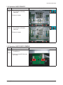
1. Precaution
2. Product Specification
3. Disassembly & Reassembly
4. Troubleshooting
5. Exploded View & Part List
6. Wiring Diagram
7. Schematic Diagram
HP-T4254
HP-T5054
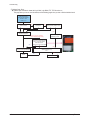
Refer to the service manual in the GSPN (see the rear cover) for the more information.
GSPN (Global Service Partner Network)
Area
Web Site
North America
service.samsungportal.com
Latin America
latin.samsungportal.com
CIS
cis.samsungportal.com
Europe
europe.samsungportal.com
China
china.samsungportal.com
Asia
asia.samsungportal.com
Mideast & Africa
mea.samsungportal.com
This Service Manual is a property of Samsung Electronics Co.,Ltd.
Any unauthorized use of Manual can be punished under applicable
International and/or domestic law.
© Samsung Electronics Co., Ltd. Feb. 2007
Printed in Korea
AA82-04340A
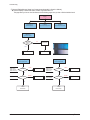
Table of Contents
Chapter 1 Precaution
! 1-1 Safety Precautions . . . . . . . . . . . . . . . . . . . . . . . . . . . . . . . . . . . . . . . . . . . . . . . . . . . . . . . . . . . 1-1
! 1-2 Servicing Precautions . . . . . . . . . . . . . . . . . . . . . . . . . . . . . . . . . . . . . . . . . . . . . . . . . . . . . . . . 1-3
! 1-3 Static Electricity Precautions . . . . . . . . . . . . . . . . . . . . . . . . . . . . . . . . . . . . . . . . . . . . . . . . . . . 1-4
! 1-4 Installation Precautions . . . . . . . . . . . . . . . . . . . . . . . . . . . . . . . . . . . . . . . . . . . . . . . . . . . . . . . 1-5
Chapter 2 Product Specification
! 2-1 Product Specification . . . . . . . . . . . . . . . . . . . . . . . . . . . . . . . . . . . . . . . . . . . . . . . . . . . . . . . . . 2-1
! 2-2 Specifications Analysis . . . . . . . . . . . . . . . . . . . . . . . . . . . . . . . . . . . . . . . . . . . . . . . . . . . . . . . . 2-3
! 2-3 Accessories . . . . . . . . . . . . . . . . . . . . . . . . . . . . . . . . . . . . . . . . . . . . . . . . . . . . . . . . . . . . . . . . 2-4
Chapter 3 Disassembly & Reassembly
! 3-1 Overhaul Disassembly & Reassembly . . . . . . . . . . . . . . . . . . . . . . . . . . . . . . . . . . . . . . . . . . . . 3-1
Chapter 4 Troubleshooting
! 4-1 Troubleshooting . . . . . . . . . . . . . . . . . . . . . . . . . . . . . . . . . . . . . . . . . . . . . . . . . . . . . . . . . . . . . 4-1
! 4-2 Adjustment . . . . . . . . . . . . . . . . . . . . . . . . . . . . . . . . . . . . . . . . . . . . . . . . . . . . . . . . . . . . . . . . . 4-16
! 4-3 Upgrade . . . . . . . . . . . . . . . . . . . . . . . . . . . . . . . . . . . . . . . . . . . . . . . . . . . . . . . . . . . . . . . . . . . 4-33
Chapter 5 Exploded View & Part List
! 5-1 HPT4254X/XAA Exploded View . . . . . . . . . . . . . . . . . . . . . . . . . . . . . . . . . . . . . . . . . . . . . . . . . 5-1
! 5-2 HPT5054X/XAA Exploded View . . . . . . . . . . . . . . . . . . . . . . . . . . . . . . . . . . . . . . . . . . . . . . . . . 5-3
! 5-3 HPT4254X/XAA Service Item . . . . . . . . . . . . . . . . . . . . . . . . . . . . . . . . . . . . . . . . . . . . . . . . . . . 5-5
! 5-4 HPT5054X/XAA Service Item . . . . . . . . . . . . . . . . . . . . . . . . . . . . . . . . . . . . . . . . . . . . . . . . . . . 5-6
Chapter 6 Wiring Diagram
! 6-1 Overall Wiring . . . . . . . . . . . . . . . . . . . . . . . . . . . . . . . . . . . . . . . . . . . . . . . . . . . . . . . . . . . . . . . 6-1
Chapter 7 Schematic Diagram
! 7-1 Circuit Description . . . . . . . . . . . . . . . . . . . . . . . . . . . . . . . . . . . . . . . . . . . . . . . . . . . . . . . . . . . 7-1
! 7-2 Schematic Diagram . . . . . . . . . . . . . . . . . . . . . . . . . . . . . . . . . . . . . . . . . . . . . . . . . . . . . . . . . . 7-3
Precaution
1. Precaution
To avoid possible damage or electric shocks or exposure to radiation, follow the instructions below with regard to safety, installation, service and ESD.
1-1 Safety Precautions
1.
Make sure all protective devices are properly installed
including non-metallic handles and compartment covers
when installing or re-installing the chassis or chassis
assemblies.
2.
Make sure that no gaps exist between the cabinets for
children to insert their fingers in to prevent children from
receiving electric shocks. Gaps mentioned above include
ventilation holes between the PDP module and the cabinet mask, and the improper installation of the rear cabinet.
5.
Warning for Engineering Changes:
Never make any changes or additions to the circuit
design or the internal part for this product.
Ex: Do not add any audio or video accessory
connectors. This might cause physical damage.
Furthermore, any changes or additions to the original
design/engineering will invalidate the warranty.
6.
Warning - Hot Chassis:
Some TV chassis are directly connected to one end of
the AC power cord for electrical reasons.
Without insulated transformers, the product can only be
repaired safely when the chassis is connected to the
earth end of the AC power source.
Errors may occur when the resistance is below 1.0 ! or
over 5.2 !.
In these cases, make sure that the device is repaired
before sending it back to the customer.
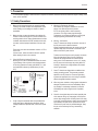
3.
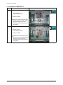
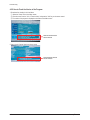
Check for Electricity Leakage (Figure 1-1)
Warning: Do not use an insulated transformer for checking the leakage. Use only those current leakage testers
or mirroring systems that comply with ANSIC 101.1 and
the Underwriter Laboratory's specifications (UL1410,
59.7).
LEAKAGE
CURRENT
TESTER
DEVICE
UNDER
TEST
2-WIRE CORD
EARTH
GROUND
Fig. 1-1 AC Leakage Test
4.
A high voltage is maintained within the specified limits
using safety parts, calibration and tolerances. When
voltage exceeds the specified limits, check each special
part.
Samsung Electronics
7.
Some TV chassis are shipped with an additional secondary grounding system. The secondary system is
adjacent to the AC power line. These two grounding
systems are separated in the circuit using an unbreakable/unchangeable insulation material.
8.
When any parts, material or wiring appear overheated or
damaged, replace them with new immediately. When
any damage or overheating is detected, correct this
immediately and make a regular check of possible
errors.
(READING SHOULD
NOT BE ABOVE
0.5mA)
TEST ALL
EXPOSED METAL
SURFACES
ALSO TEST WITH
PLUG REVERSED
(USING AC ADAPTER
PLUG AS REQUIRED)
To make sure the AC power cord is properly connected,
follow the instructions below. Use the voltmeter to
measure the voltage between the chassis and the
earth ground. If the measurement is over 1.0V, unplug
the AC power cord and change the polarity before reinserting it. Measure the voltage between the chassis
and the ground again.
9. Check for the original shape of the lead, especially that
of the antenna wiring, any sharp edges, the AC power
and the high voltage power. Carefully check if the wiring
is too tight, incorrectly placed or loose. Never change the
space between the part and the printed circuit board.
Check the AC power cord for possible damages. Keep
the part or the lead away from any heat-emitting
materials.
1-1
Precaution
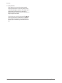
10. Safety Indication:
Some electrical circuits or device related materials
require special attention to their safety features, which
cannot be viewed by the naked eye. If an original part is
replaced with another irregular one, the safety or
protective features will be lost even if the new one has a
higher voltage or more watts.
Critical safety parts should be bracketed with (
! ).
Use only regular parts for replacements (in particular,
flame resistance and dielectric strength specifications).
Irregular parts or materials may cause electric shock or
fire.
1-2
Samsung Electronics
Precaution
1-2 Servicing Precautions
Warning 1: First carefully read the "Safety Instruction" in this service manual.
When there is a conflict between the service and the safety instructions, follow the safety instruction at all times.
Warning 2: Any electrolytic capacitor with the wrong polarity will explode.
1.
The service instructions are printed on the cabinet, and
should be followed by any service personnel.
2.
Make sure to unplug the AC power cord from the power
source before starting any repairs.
(a) Remove or re-install parts or assemblies.
(b) Disconnect the electric plug or connector, if any.
(c) Connect the test part in parallel with the electrolytic
capacitor.
3.
Some parts are placed at a higher position than the
printed board. Insulated tubes or tapes are used for this
purpose. The internal wiring is clamped using buckles to
avoid contact with heat emitting parts. These parts are
installed back to their original position.
4.
After the repair, make sure to check if the screws, parts
or cables are properly installed. Make sure no damage is
caused to the repaired part and its surroundings.
5.
Check for insulation between the blade of the AC plug
and that of any conductive materials (i.e. the metal
panel, input terminal, earphone jack, etc).
6.
Insulation Check Process: Unplug the power cord from
the AC source and turn the switch on. Connect the insulating resistance meter (500v) to the AC plug blade.
7.
Any B+ interlock should not be damaged.
If the metal heat sink is not properly installed, no
connection to the AC power should be made.
8.
Make sure the grounding lead of the tester is connected
to the chassis ground before connecting to the positive
lead. The ground lead of the tester should be removed
last.
9.
Beware of risks of any current leakage coming into
contact with the high-capacity capacitor.
10. The sharp edges of the metal material may cause
physical damage, so protect yourself by wearing gloves
during the repair.
11. Due to the nature of plasma display panels, partial afterimages may appear if a still picture is displayed on the
screen for a long period of time.
This is caused by brightness deterioration due to the
storage effect of the panel, and to prevent this from
happening, we recommend that the brightness and contrast are reduced.
(e.g.) Contrast: 25, Brightness: 50
The insulating resistance between the blade of the AC
plug and that of the conductive material should be more
than 1 !.
Samsung Electronics
1-3
Precaution
1-3 Static Electricity Precautions
1.
Some semi-conductive ("solid state") devices are
vulnerable to static electricity. These devices are known
as ESD. ESD includes the integrated circuit and the field
effect transistor. To avoid any materials damage from
electrostatic shock, follow the instructions described
below.
2.
Remove any static electricity from your body by
connecting the earth ground before handling any
semi-conductive parts or assemblies. Alternatively,
wear a dischargeable wrist-belt.
(Make sure to remove any static electricity before
connecting the power source - this is a safety instruction
for avoiding electric shock)
3.
Remove the ESD assembly and place it on a conductive
surface such as aluminum foil to prevent accumulating
static electricity.
4.
Do not use any Freon-based chemicals.
Such chemicals will generate static electricity that
causes damage to the ESD.
5.
Use only grounded-tip irons for soldering purposes.
6.
Use only anti-static solder removal devices.
Most solder removal devices do not support an
anti-static feature. A solder removal device without an
anti-static feature can store enough static electricity to
cause damage to the ESD.
7.
Do not remove the ESD from the protective box until the
replacement is ready. Most ESD replacements are
covered with lead, which will cause a short to the entire
unit due to the conductive foam, aluminum foil or other
conductive materials.
8.
Remove the protective material from the ESD
replacement lead immediately after connecting it to the
chassis or circuit assembly.
9.
Take extreme caution in handling any uncovered ESD
replacements. Actions such as brushing clothes or lifting
your leg from the carpet floor can generate enough static
electricity to damage the ESD.
CAUTION
These servicing instructions are for use by
qualified service personnel only.
To reduce the risk of electric shock do not
perform any servicing other than that contained in the
operating instructions unless you are qualified to do so.
1-4
Samsung Electronics
Precaution
1-4 Installation Precautions
1.
For safety reasons, more than two people are required
for carrying the product.
2.
Keep the power cord away from any heat emitting
devices, as a melted covering may cause fire or electric
shock.
3.
Do not place the product in areas with poor ventilation
such as a bookshelf or closet. The increased internal
temperature may cause fire.
4.
Bend the external antenna cable when connecting it to
the product. This is a measure to protect it from being
exposed to moisture. Otherwise, it may cause a fire or
electric shock.
5.
Make sure to turn the power off and unplug the power
cord from the outlet before repositioning the product.
Also check the antenna cable or the external connectors
if they are fully unplugged. Damage to the cord may
cause fire or electric shock.
Samsung Electronics
6.
Keep the antenna far away from any high-voltage cables
and install it firmly. Contact with the high-voltage cable or
the antenna falling over may cause fire or electric shock.
7.
When connecting the RF antenna, check for a DTV
receiving system and install a separate DTV reception
antenna for areas with no DTV signal.
8.
When installing the product, leave enough space (4")
between the product and the wall for ventilation
purposes.
A rise in temperature within the product may cause fire.
9.
When moving a PDP with removable speakers, detach
the speakers first before moving the main body.
Moving the PDP main body without separating the
speakers may cause the speakers to detach, possibly
causing damage or injury.
1-5
MEMO
1-6
Samsung Electronics
Product Specification
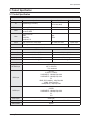
2. Product Specification
2-1 Product Specification
Features
Block
Specification
Major IC
Remark
RF
Digital/Analog (DTV Built In)
NTSC/VSB/QAM Tuner
S4LF111X01(Lake2)
PDP Module
Samsung SDI W2A Module
42"HD/50"HD
Power
Samsung/Dong-yang electro
mechanics SMPS
Video
NTSC 3.58, ATSC
HDMI
DNIe(FBE2)
Component, PC
Lake2
SDP64
Sound
SRS TruSuround XT, Dolby Digital
MSP 4450K, NTP-3000
Cabinet
C9 Design
New Module
Optical Output
Specification
Model
HP-T4254
HP-T5054
Screen Size
42 Inches (16:9)
50 Inches (16:9)
Dimensions (WxHxD)
41.5 x 29.9 x 12.4 inches
48.4 x 33.4 x 12.4 inches
Weight
73.2 lbs / 33.2 kg
97 lbs / 44 kg
PC Resolution
1024 x 768 @ 75Hz
1365 x 768 @ 60Hz
Voltage
AC 100~240V, 60Hz
ANTENNA input
ANT 1 - AIR IN
ANT 2 - CABLE IN
! 75" unbalanced
VIDEO input
AV1, AV2
S-VIDEO1, S-VIDEO2
COMPONENT1 - 480i/480p/720p/1080i
COMPONENT2 - 480i/480p/720p/1080i
PC
HDMI1 (DVI Compatible) - 480p/720p/1080i
HDMI2 - 480p/720p/1080i
HDMI3(Side-AV) - 480p/720p/1080i
AUDIO input
AV1, AV2
S-VIDEO
COMPONENT1 - 480i/480p/720p/1080i
COMPONENT2 - 480i/480p/720p/1080i
PC
DVI
Audio Output
AUDIO (L/R)
Speaker Output
New Features
Samsung Electronics
10W + 10W
15W + 15W
Anynet+
2-1
Product Specification
# New Features explanation
- Anynet+ : Anynet+ is an AV network system that enables you to control all connected Samsung AV devices with your
Samsung TV's remote.
To directly connect to TV
TV
Anynet + Device 1
HDMI 1.3 Cable
HDMI 1.3 Cable
Anynet + Device 2
Anynet + Device 3
Connect the [HDMI 1], [HDMI 2]
or [HDMI 3] jack on the TV
and the HDMI OUT jack of the
corresponding Anynet + device
using the HDMI cable.
HDMI 1.3 Cable
To connect to Home Theater
TV
Anynet + Device 1
HDMI 1.3 Cable
HDMI 1.3 Cable
Connect the [HDMI 1],
[HDMI 2] or [HDMI 3]
jack on the TV and the
HDMI OUT jack of the
corresponding Anynet +
device using the HDMI
cable.
2.
Connect the HDMI IN jack
of the home theater and
the HDMI OUT jack of the
corresponding Anynet +
device using the HDMI
cable.
Anynet + Device 2
HDMI 1.3 Cable
Anynet + Device 3
Home Theater
Optical Cable
1.
HDMI 1.3 Cable
Connect the Optical cable between [Digital Audio Out (Optical)] on your TV and Digital Audio Input on the Home
Theater.
Connect only one Home Theater.
You can listen to 5.1 channel sound through the home theater’s speakers. Otherwise, you can only listen to 2 channel
stereo sound in other cases. Make sure to connect the Digital Audio IN (Optical) of the home theater and the TV
correctly to listen to TV sound through the home theater. However, you cannot listen to sound from the BD recorder
that is sent to the home theater via the TV in 5.1 channel sound because the TV outputs only 2 channel stereo sound.
Please see the manual for the home theater.
You can connect an Anynet + device using the HDMI 1.3 cable. Some HDMI cables may not support Anynet + functions.
Anynet + works when the AV device supporting Anynet + is in the Standby or On status.
Anynet + supports up to 12 AV devices in total.
2-2
Samsung Electronics
Product Specification
2-2 Specifications Analysis
! $: application, X: non-application
Model
HP-T4254 (Lily-42HD)
HP-T5054 (Lily-50HD)
HP-S4253 (Cadillac-42HD)
PDP TV
Design
Basic
Picture
Audio
Display Type
PDP TV
PDP TV
Built-In Tuner
$
$
$
Resolution
1024 x 768
1365 x 768
1024 x 768
PDP Module
W2A
W2A
Samsung SDI V5.1
Screen Size
42"
50"
42"
Picture ratio
16 : 9
16 : 9
16 : 9
Dimensions (WxHxD)
41.5 x 29.9 x 12.4 inches
48.4 x 33.4 x 12.4 inches
41.5 x 28 x 3.8 inches
Weight
73.2 lbs / 33.2kg
97 lbs / 44kg
75.4 lbs / 34.2 kg
Brightness
1,500 Cd/m2
1,300 Cd/m2
1,200 Cd/m2
Contrast Ratio
10000:1
10000:1
7,000 : 1
Picture Enhacer
FBE2
FBE2
LBE
Comb Filter
$
$
$
Equalizer
5 Band
5 Band
5 Band
Auto Volume Control
$
$
$
Surround Sound
SRS TruSurround XT
SRS TruSurround XT
SRS TruSurround XT Dolby Digital (AC3)
Speaker Output
10W + 10W
15W + 15W
10W + 10W
PIP
$
$
$
Double Window
$
$
$
Caption
$
$
$
Still Image
$
$
$
EPG
$
$
$
My Color Control
$
$
$
Color Weakness
X
X
$
Energy Saving
$
$
$
Anynet
$
$
X
Antenna
2 (Cable/Air)
2 (Cable/Air)
2 (Cable/Air)
AV Input
2
2
2
S-Video
2
2
2
Component
2
2
2
PC(D-SUB)
1
1
1
DVI
X
X
X
Features
Connections
ETC
HDMI
3
3
2
Sub Woofer
X
X
X
1
Optical
1
1
Coaxial
X
X
1
Speaker/Stand
Built-in Speaker
Built-in Speaker
Built-in Speaker/Stand
! For the power supply and power consumption, refer to the label attached to the product.
Samsung Electronics
2-3
Product Specification
2-3 Accessories
Accessories that can be purchased
additionally
Supplied Accessories
Accessories
2-4
Item
Item code
Remote Control
Batteries
BN59-00599A
4301-000103
Power Cord
3903-000144
Owner's Instructions
BN68-01192E
Warranty Card
Registration Card
Safety Guide Manual
BN68-00872A
AA68-03870B
AA68-03242F
Cloth-Clean
BN63-01798A
Ferrite Core for
Power Cord
3301-001110
Ferrite Core for
Side-AV/S-VIDEO
3301-001305
Ferrite Core for
Headphone
3301-001456
Cover-Bottom
Screws (2ea)
BN63-03055A
6003-001621
S-VIDEO Cable
47.244 inches
BN39-00149A
HDMI Cable
118.11 inches
BN39-00641A
Remark
Samsung Service center
Electronics Store/
Internal shopping mall
HDMI/DVI cable
118.11 inches
BN39-00643A
Component Cables (RCA)
59.055 inches
BN39-00279A
Samsung Electronics
Product Specification
Accessories that can be purchased
additionally
Accessories
Samsung Electronics
Item
Item code
Optical Cable
None
PC Cable
72.047 inches
BN39-00115A
Remark
Electronics Store/
Internal shopping mall
PC Audio Cable
78.740 inches
BN39-00061B
Antenna Cable
118.11 inches
BN39-00333A
2-5
MEMO
2-6
Samsung Electronics
Disassembly & Reassembly
3. Disassembly & Reassembly
3-1 Overall Disassembly & Reassembly
Notice
- Be sure to separate the power cord before disassembling the unit.
- Discharge the capacitors first when separating PCB's with high capacity capacitors such as SMPS, X Main Board, Y Main
Board, etc. (A spark may be generated by the electric charge, and there is danger of electronic shock.)
- Check that the cables are properly connected referring to the circuit diagram when disassembling or assembling the unit
taking care not to damage the cables.
- Take care not to scratch the Glass Filter in the front.
- Assemble the boards in the reverse order of the disassembly.
- The plasma must be layed down on a flat padded surface for disassembly and reassembly.
3-1-1 Separation of ASSY COVER P-REAR
Part Name
Cover
Rear
Description
Description Photo
! Remove 4 screws. ( )
: M8,L16,ZPC(BLK),SWRCH18A,WP
" Remove 15 screws. ( )
: BH,+,B,M4,L3,ZPC(BLK)
# Remove 4 screws. ( )
: PH,+,WSP,S,M4,L35,ZPC(BLK)
$ Remove the 2 Hex nuts for the PC
input. ( )
: #4-40,L6,NI PLT,C3601,% Remove the rear cover.
: Please lay the PDP unit face down on a
soft surface when removing the stand.
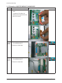
3-1-2 Separation of ASSY PCB MISC-MAIN
Part Name
Main
Board
Description
Description Photo
! Detach all connectors from the Main
Board.
" Remove 4 screws.
: PH,+,WWP,M3,L8,NI PLT
# Remove the Main Board.
Samsung Electronics
3-1
Disassembly & Reassembly
3-1-3 Separation of FILTER-EMI AC LINE
Part Name
FILTEREMI
AC LINE
Description
Description Photo
! Detach connector from SMPS.
" Remove 2 screws. ( )
: PH,+,WWP,M3,L8,NI PLT
# Remove a screw. ( )
: BH,+,S,M4,L10,ZPC(BLK)
$ Remove FILTER-EMI AC LINE.
3-1-4 Separation of BRACKET-PCB
Part Name
Bracket
PCB
Description
Description Photo
! Remove a screw.
: BH,+,S,M4,L10,ZPC(BLK)
" Remove the BRACKET-PCB.
3-2
Samsung Electronics
Disassembly & Reassembly
3-1-5 Separation of ASSY BRACKET
Part Name
42"
Bracket
Description
Description Photo
! Remove 4 screws. ( )
: BH,+,S,M4,L10,ZPC(BLK)
" Remove 2 screws. ( )
: BH,+,B,M4,L3,ZPC(BLK)
# Remove Bracket.
50"
Bracket
! Remove 4 screws. ( )
: BH,+,S,M4,L10,ZPC(BLK)
" Remove 2 screws. ( )
: BH,+,B,M4,L3,ZPC(BLK)
# Remove Bracket.
3-1-6 Separation of ASSY BOARD P-SIDE AV
Part Name
Side AV
Description
Description Photo
! Remove a screw. ( )
: BH,+,B,M4,L3,ZPC(BLK)
" Remove a screw. ( )
: BH,+,S,M4,L10,ZPC(BLK)
# Remove the Side AV.
Samsung Electronics
3-3
Disassembly & Reassembly
3-1-7 Separation of ASSY BRACKET P-WALL
Part Name
42"
Wall
Bracket
Description
Description Photo
! Remove 2 screws. ( )
: BH,+,B,M4,L3,ZPC(BLK)
" Remove 6 screws. ( )
: BH,+,S,M4,L10,ZPC(BLK)
# Remove Wall Bracket.
: Please lay the PDP panel face down
on a soft surface when separating front
cover.
50"
Wall
Bracket
! Remove 2 screws. ( )
: BH,+,B,M4,L3,ZPC(BLK)
" Remove 6 screws. ( )
: BH,+,S,M4,L10,ZPC(BLK)
# Remove Wall Bracket.
: Please lay the PDP panel face down on
a soft surface when separating front
cover.
3-4
Samsung Electronics
Disassembly & Reassembly
3-1-8 Separation of ASSY SPEAKER P
Part Name
42"
Speaker
Description
Description Photo
! Remove 4 screws.
: BH,+,WP,B,M4.0,L3,ZPC(BLK),
SWRCH18A
" Remove the Speaker.
50"
Speaker
! Remove 4 screws.
: BH,+,WP,B,M4.0,L3,ZPC(BLK),
SWRCH18A
" Remove the Speaker.
3-1-9 Separation of ASSY BOARD P-POWER&IR
Part Name
Description
Description Photo
Power ! Detach all connectors from the
&
Power&IR Board.
IR Board
" Remove the Power&IR PCB unlocking
the 2 holders.
Samsung Electronics
3-5
Disassembly & Reassembly
3-1-10 Separation of SMPS-PDP TV
Part Name
42"
SMPS
Description
Description Photo
! Detach all connectors from the SMPS.
" Remove 8 screws.
: PH,+,WWP,M3,L8,NI PLT
# Remove the SMPS.
: Wear gloves when handling the power
board as there may be some remaining
electrical charge in the capacitor.
Specifically, avoid touching any part of
the capacitor.
50"
SMPS
! Detach all connectors from the SMPS.
" Remove 8 screws.
: PH,+,WWP,M3,L8,NI PLT
# Remove the SMPS.
: Wear gloves when handling the power
board as there may be some remaining
electrical charge in the capacitor.
Specifically, avoid touching any part of
the capacitor.
3-6
Samsung Electronics
Disassembly & Reassembly
3-1-11 Separation of ASSY PDP MODULE P-LOGIC MAIN BOARD
Part Name
42"
Logic
Board
Description
Description Photo
! Detach all connectors from the Logic
Main Board.
" Remove 4 screws.
: WSP,PH,+,M3,L8,NI PLT
# Remove the Logic Main Board.
50"
Logic
Board
! Detach all connectors from the Logic
Main Board.
" Remove 4 screws.
: WSP,PH,+,M3,L8,NI PLT
# Remove the Logic Main Board.
Samsung Electronics
3-7
Disassembly & Reassembly
3-1-12 Separation of ASSY PDP MODULE P-X MAIN BOARD
Part Name
Description
Description Photo
Flat Cable ! Detach all Connectors from the X Main
Board.
& To separate the Flat Cable of the
X-Board, press the upper and the lower
sides of the connector.
42"
X-Main
Board
! Remove 4 screws.
: PH,+,WWP,M3,L8,NI PLT
" Remove the X-Main Board.
50"
X-Main
Board
! Remove 4 screws.
: PH,+,WWP,M3,L8,NI PLT
" Remove the X-Main Board.
3-8
Samsung Electronics
Disassembly & Reassembly
3-1-13 Separation of ASSY PDP MODULE P-Y MAIN BOARD
Part Name
Description
Description Photo
Flat Cable ! Detach the 6 scan board connectors
from the panel by pulling the holder from
both the top and bottom ends.
42"
Y-Scan
Board
! Remove 3 screws.
: PH,+,WWP,M3,L8,NI PLT
50"
Y-Scan
Board
! Remove 5 screws.
: PH,+,WWP,M3,L8,NI PLT
Samsung Electronics
3-9
Disassembly & Reassembly
Part Name
42"
Y-Main
Board
Description
Description Photo
! Remove 4 screws.
: PH,+,WWP,M3,L8,NI PLT
" Detach all connectors from the Y-Main
Board.
50"
Y-Main
Board
! Remove 4 screws.
: PH,+,WWP,M3,L8,NI PLT
" Detach all connectors from the Y-Main
Board.
3-10
Samsung Electronics
Disassembly & Reassembly
3-1-14 Separation of ASSY PDP MODULE P-ADDRESS BUFFER BOARD
Part Name
42"
Still Bar
Description
Description Photo
! Remove 4 screws.
: PH,+,WWP,M3,L8,NI PLT
" Remove the still bar.
50"
Still Bar
! Remove 4 screws.
: PH,+,WWP,M3,L8,NI PLT
" Remove the still bar.
42"
Buffer
Board
! Detach the all connectors from the
buffer board.
" Remove 12 screws.
: PH,+,WWP,M3,L8,NI PLT
# Remove the E-Board and F-Board.
50"
Buffer
Board
! Detach the all connectors from the
buffer board.
" Remove 14 screws.
: PH,+,WWP,M3,L8,NI PLT
# Remove the E-Board and F-Board.
Samsung Electronics
3-11
Disassembly & Reassembly
3-1-15 Separation of ASSY PANEL BRACKETS
Part Name
Panel
Brackets
Description
Description Photo
! Remove 3 screws. ( )
: BH,+,B,M4,L3,ZPC(BLK)
" Remove 4 screws. ( )
: BH,+,S,M4,L10,ZPC(BLK)
# Remove the Side Panel Brackets.
3-1-16 Separation of ASSY PCB FUNCTION
Part Name
Function
Board
Description
Description Photo
! Remove 2 screws.
: BH,+,B,M4,L3,ZPC(BLK)
" Remove the Function Board.
3-12
Samsung Electronics
Troubleshooting
4. Troubleshooting
4-1 Troubleshooting
4-1-1 First Checklist for Troubleshooting
1. Check the various cable connections first.
- Check to see if there is a burnt or damaged cable.
- Check to see if there is a disconnected or loose cable connection.
- Check to see if the cables are connected according to the connection diagram.
2. Check the power input to the Main Board.
3. Check the voltage in and out between the SMPS ! Main Board, between the SMPS ! X, Y Main Board, and between the
Logic Boards.
Samsung Electronics
4-1
Troubleshooting
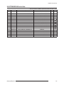
4-1-2 Checkpoints by Error Mode
" No Power
Symptom
- The LEDs on the front panel do not work when connecting the power cord.
- The SMPS relay does not work when connecting the power cord.
- The units appears to be dead.
The SMPS relay or the LEDs on the front panel does not work when connecting the power cord if the cables
are improperly connected or the Main Board or SMPS is not functioning. In this case, check the following:
- Check the internal cable connection status inside the unit.
Major Checklist
- Check the fuses of each part.
- Check the output voltage of SMPS.
- Replace the Main Board.
Troubleshooting
Procedures
#
Is the AC IN socket connector and
the SMPS CN800 connected?
No
Insert the AC in connector and the
SMPS CN800 connector
Yes
#
Is the Fuse (F801S) of the SMPS
Power Input Part blown?
Yes
Replace Fuse (F801S)
No
$
SMPS CN801
Pin 3 : STB 5V
Pin 2 PS-ON : Check to see if it is 0V
No
Replace the SMPS
Yes
Replace the Main Board
4-2
Samsung Electronics
Troubleshooting
" When the unit is repeatedly turned on and off
Symptom
- The SMPS relay is repeatedly turned on and off.
In general, the SMPS relay repeatedly turns on and off by the protection function due to a defect on a board
connected to the SMPS.
- Disconnect all cables from the SMPS, operate the SMPS alone and check if the SMPS works properly and if
Major Checklist each voltage output is correct.
- If the symptom continues even when SMPS is operated alone, replace the SMPS.
- If the symptom is not observed when operating the SMPS alone, find any defective assemblies by connecting
the cables one by one.
Troubleshooting
Procedures
#
Does the symptom continue when
connecting the power after removing
CN810 from the SMPS?
No
Replace the Y Main Board
Yes
$
Does the symptom continue when
connecting the power after removing
CN809 from the SMPS?
No
Replace the X Main Board
Yes
%
Does the symptom continue when
connecting the power after removing
CN807 from the SMPS?
No
Replace the Logic Board
Yes
Replace the SMPS
Caution
When separating and connecting the cables such as CN810, CN809, CN808, CN807 of the Main SMPS, CN4701
of the X Main Board, and CN5707 of the Y Main Board, a spark may be generated by the electric charge of the
high capacity capacitor. Therefore, wait some time after disconnecting the power cord from the unit.
Samsung Electronics
4-3
Troubleshooting
" No Picture (When audio is normal)
Symptom
- Audio is normal but no picture is displayed on the screen.
- This may happen when the Main Board is functioning but the X, Y Main Board, Logic Board, or Y Buffer
Boards are not.
Major Checklist
- The output voltage of the Main SMPS.
- This may happen when the LVDS cable connecting the Main Board and the Logic Board is disconnected.
CN810
CN809
CN808
CN807
Troubleshooting
Procedures
Are the Vs and Va voltages normal after
removing all cables from the SMPS?
(CN810, CN809, CN808, CN807)
No
Replace the SMPS
Yes
Did problem improve?
No
Replace the Y Main Board
Yes
Did problem improve?
No
Replace the X Main Board
Yes
Did problem improve?
No
Replace the Logic Board
Yes
Did problem improve?
Caution
4-4
No
Replace the Y Scan Board
When separating and connecting the cables such as CN810, CN809, CN808, CN807 of the Main SMPS, CN4701
of the X Main Board, and CN5707 of the Y Main Board, a spark may be generated by the electric charge of the
high capacity capacitor. Therefore, wait some time after disconnecting the power cord from the unit.
Samsung Electronics
Troubleshooting
" No Sound
Symptom
- Video is normal but there is no sound.
- When the speaker connectors are disconnected or damaged.
Major Checklist - When the sound processing part of the Main Board is not functioning.
- Speaker defect.
Troubleshooting
Procedures
#
Is the cable connection between the
Main Board and the speaker
properly connected?
No
Connect the cable properly or
replace the cable, if necessary.
Yes
$
Is the output voltage of SMPS normal?
(CN801 #13)
No
Replace the SMPS
Yes
Is the speaker output terminal
of the Main Board normal?
No
Replace the Main Board
Yes
%
Samsung Electronics
Replace the Speaker
4-5
Troubleshooting
" No Video
Symptom
- A normal/cable network analog broadcast screen is blank or abnormal but OSD is OK.
- Check the antenna connection settings (Air: NTSC / ATSC, Cable: NTSC)
Major Checklist - Check the CVBS cable connection.
- Check the power input of the Main board.
Troubleshooting
Procedures
Is the antenna connection setting
properly configured?
No
Configure properly
Yes
#
Check CN1101 pin2 for +5V
No
Replace the SMPS
Yes
Replace the Main Board
4-6
Samsung Electronics
Troubleshooting
" SMPS Troubleshooting
Power ON
STD_5V
Abnormal
Check the U101, D108
Normal
PFC
Abnormal
Check the U201, Q203, Q204
Normal
VA
Abnormal
Check the U501
Abnormal
Multi
Check the U601
Normal
VS
Abnormal
Check the Q401, Q402
Normal
Check the Other board (Image Board or Driver Board) or Cable.
Samsung Electronics
4-7
Troubleshooting
" Drive Board Troubleshooting
1) Troubleshooting Summary
Condition Name
Description
Related Board
No Voltage Output
Operating Voltage don't exist
PSU
No Display
Operating Voltage exist, but an Image doesn't exist on screen
Y-MAIN, X-MAIN, Logic Main, Cable
Abnormal Display
Abnormal Image (not open or short) is no screen
Y-MAIN, X-MAIN, Logic Main
Sustain Open
Some horizontal lines don't exist on screen
Scan Buffer, FPC of X/Y
Sustain Short
Some horizontal lines appear to be linked on screen
Scan Buffer, FPC of X/Y
Address Open
Some vertical lines don't exist on screen
Logic Main, Logic Buffer, TCP
Address Short
Some vertical lines appear to be linked on screen
Logic Main, Logic Buffer, TCP
4-8
Samsung Electronics
Troubleshooting
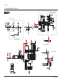
2) Troubleshooting Procedure in Abnormal Conditions
# No Display
& No Display is related with Y-MAIN, X-MAIN, Logic Main and so on.
This page shows you how to check the boards, and the following pages show you how to find the defective board.
No Display
[ Logic Main ]
LED Blinks
[ Y-MAIN ]
Check necessary points
[ Logic Main ]
Check if power is supplied
( 5V, 3.3V )
YES
NO
Check if internal is
Default Black
Check the
MICOM operation
Check if any address
data output is detected
Check the ASIC
Control Signal output
Check if the data
and control signals
between DDR & ASIC
are normal
FUSE
OPEN
Replace the Board
F4001 for VCC
F4002 for Vs
F4004 for VDD
F4005 for Ve
OK
Q5009~Q5021
D5005, D5007
D5008
FET/
DIODE
OK
Y-MAIN
Normal State
Samsung Electronics
Check the FUSE
Check the
input voltage
If the input voltage is
abnormal, replace the
PSU and check it
again as this indicates
a PSU output error
[ X-MAIN ]
Check several points
[ Y-MAIN ]
Check several points
F5001 for VDD
F5002 for Vs
F5004 for VCC
F5005 for OUT_L
NO
Check the
power connectivity
Check the LED
operation
YES
[ X-MAIN ]
Check necessary points
FUSE
OPEN
Replace the Board
OK
SHORT
Replace the Board
Q4002~Q4003
Q4011~Q4016
D4004
D4006~D4008
FET/
DIODE
SHORT
Replace the Board
OK
X-MAIN
Normal State
4-9
Troubleshooting
$ Abnormal Display(Abnormal Image is on Screen.(except abnormality in Sustain or Address))
& Abnormal Display is related with Y-MAIN, X-MAIN, Logic Main and so on.
This page shows you how to check the boards, and the following pages show you how to find the defective board.
Abnormal
Display
[ Logic Main ]
Observation of
abnormal display
[ Y-MAIN ]
Check necessary points
[ X-MAIN ]
Check necessary points
[ Logic Main ]
LED Blinks
( action of Vsync )
Regular
abnormal
pattern
NO
Logic Main
Normal State
YES
Replace the Board
Replace Panel
[ Y-MAIN ]
Check several points
F5001 for VDD
F5002 for Vs
F5004 for VCC
F5005 for OUT_L
FUSE
[ X-MAIN ]
Check several points
OPEN
Replace the Board
F4001 for VCC
F4002 for Vs
F4004 for VDD
F4005 for Ve
FUSE
OK
Q5009~Q5021
OK
Y-MAIN
Normal State
4-10
Replace the Board
OK
SHORT
FET
OPEN
Replace the Board
Q4002~Q4003
Q4011~Q4016
SHORT
FET
Replace the Board
OK
X-MAIN
Normal State
Samsung Electronics
Troubleshooting
% Sustain Open (some horizontal lines don't exist on screen)
[ Y-FPC ]
Sustain Open
After Changing Y-buffer,
recheck the status
NG
Replace the Panel
There is a defect on the FPC
OK
Done
(Defect is from Y-buffer)
' Sustain Short (some horizontal lines appear to be linked on Video)
[ Y-FPC ]
Sustain Short
(Discharging in unwanted Scan line)
After Changing Y-buffer,
recheck the status
NG
Replace the Panel
There is a defect on the FPC
OK
Done
(Defect is from Y-buffer)
Samsung Electronics
4-11
Troubleshooting
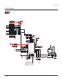
( Address Open, Short
& Address Open and Short is related with Logic Main, Logic Buffer, FFC, TCP film and so on.
This page shows you how to check the boards, and the following pages show you how to find the defective board.
[ Logic Main ]
Address Open/Short
Check the LED operation
LED2011 : blink
LED2010 : on
Check if the internal mode
screen is normal
NG
NG
Check the
Video Board
OK
OK
OK
NG
Reload the data onto the
MICOM and recheck it
Check if a specific TCP Block
screen is displayed abnormally
OK
4-12
check the voltage of
U2650 pin1 is 3.3V
Check if there is an open or
short circuit on the Buffer Board
and the Logic Main address
data output section.
Check the FFC connection status
NG
NG
Check the detailed waveform
and control the signal waveform
DONE
check the voltage of
C2901, C2902, C2903 is 1.25V
Replace Logic Main /
Address Buffer (E or F) /
FFC
OK
NG
Replace the Panel
Samsung Electronics
Troubleshooting
4-1-3 Troubleshooting
Symptom
A blank vertical cell (block)
appears on the screen.
Related Image
Causes and Countermeasures
Address buffer defect
- Replace the corresponding upper/lower
buffers (E, F)
COF defect (burnt)
- Replace the module
A green screen appears when
the TV is turned on.
The Scale is not reseting
- Replace the Main board
The OSD box appears but there
is no text.
Incorrect program version
- Check the version of each program
- Replace the Main board
A blank upper (or lower) block
appears on the screen.
Upper/Lower Y Buffer defect
- Replace the corresponding upper/lower
buffers (E, F)
Samsung Electronics
4-13
Troubleshooting
Symptom
Related Image
Causes and Countermeasures
Either the main or sub picture
does not appear.
Replace the Main board
A vertical green line appears on
the screen.
The SMPS voltage is incorrect
- Adjust the SMPS voltage according to
the voltage printed on the module label
Dim screen (blurred in red)
X-Main board defect
- Replace the X-Main board
A blank screen appears
- Replace the Y-Main board
4-14
Samsung Electronics
Troubleshooting
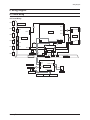
4-1-4 Troubleshooting Procedures by assembly
No
Assembly
Major Symptoms
1
SMPS-PDP TV
No power, Blank screen, the Relay repeats On and Off.
2
ASSY PDP MODULE P-X-MAIN
Blank screen
3
ASSY PDP MODULE P-Y-MAIN
Blank screen
4
ASSY PDP MODULE P-LOGIC MAIN
Blank screen, Screen noise
5
ASSY PDP MODULE P-Y-MAIN SCAN BUFFER
Row Bar screen is blank
6
ASSY PDP MODULE P-ADDRESS E BUFFER
Corresponding Buffer Board block screen is blank.
7
ASSY PDP MODULE P-ADDRESS F BUFFER
Corresponding Buffer Board block screen is blank.
8
ASSY PCB MISC-MAIN
No Power, Abnormal screen for each input source, PIP screen trouble, Sound trouble
9
ASSY BOARD P-FUNCTION
The side function key does not work properly
10 ASSY BOARD P-POWER&IR
The remote control does not work properly, the LED does not work properly.
11 ASSY BOARD P-SIDE AV
The AV2 and S-VIDEO2 modes do not work properly
<PDP 42”>
Samsung Electronics
<PDP 50”>
4-15
Troubleshooting
4-2 Adjustment
4-2-1 Service Instruction
" Before Performing After Sales Services
1. Check if the measurement and test equipment is working properly.
2. Secure sufficient work space for disassembling the product.
3. Prepare a soft pad for disassembling the product.
" Service adjustment item after replacement of Board
<If adjustment equipment is available>
# PDP Option of Factory Mode ) set the Factory Data Type item as the suitable value of relevant model.
$ Adjust Calibration of Factory Mode for each mode.
% Adjust White Balance of Factory Mode.
<If adjustment equipment is not available>
# Write down the value of HDMI White Balance of Factory Mode before replacing Board.
$ PDP Option of Factory Mode ) set the Factory Data Type item as the suitable value of relevant model.
% Set the value of HDMI White Balance with the value written down before.
4-16
Samsung Electronics
Troubleshooting
4-2-2 How to Access Service Mode
1. General Remote
To Enter: POWER OFF ) MUTE ) 1 ) 8 ) 2 ) POWER ON
(Interval between key strokes: less than 3 sec)
To Exit:
POWER OFF ) POWER ON
2. Factory Remote
To Enter: POWER ON ) INFO ) FACTORY
) Key
To Exit:
(Interval between key strokes: less than 3 sec)
POWER OFF ) POWER ON
Press the Factory key twice with a key stroke interval of more than 1 second (Pressing once enters Aging Mode)
3. Settings when entering Factory mode
- Sharp Screen (Dynamic), Color Tone (Cool1), Factory (Dynamic CE Off), DNIe(Off)
4. Adjustment Procedures
- Channel * + Key : Select an item.
- Volume ,& Key : Adjust the value up or down.
- MENU Key
: Save the changes to the EEPROM and return to the higher-level mode.
- Using the Numeric (0~9) keys, you can select a channel.
- Using the SOURCE key, you can switch AV modes.
5. Initial SERVICE MODE DISPLAY State
NTSC-RF
Calibration
Option Byte
White Balance
W/B Movie
SVP-PX
FBE2
MSP44XX
NTP3000
Sub Micom Download
Checksum
KS1410
Dynamic Contrast
EEPROM Access Count
PDP Option
RESET
Vol=0, B/S=Off, 10W, NONE
T-CAL42AUSC-xxxx Feb 7 2007
T-CAL42AUSS-xxxx Feb 7 2007
- The version of the firmware displayed at the bottom of the screen may differ and the firmware is subject to change for the
improvement of product functions.
- If you have adjusted the settings in Service Mode, you have to reset the product.
- If you exit Service Mode without reset, DNIe vlaue keeps Off regardless of setting up the user.
Samsung Electronics
4-17
Troubleshooting
4-2-3 Factory Data
. The underlined are items applied during the service adjustment. None of the others should be adjusted.
1. Calibration
Item
Data
AV Calibration
Failure
Comp Calibration
Failure
PC Calibration
Failure
HDMI Calibration
Failure
2. Option Byte
Item
Range
RF
AV/S-video
Component HD
PC
HDMI
HDMI Polarity
10
10
10
10
10
Watchdog Enable
1
1
1
1
1
Spread Spectrum
>>
>>
>>
>>
>>
NIM Version
KS1410
KS1410
KS1410
KS1410
KS1410
AUTO WALL
On
On
On
On
On
RS-232 JACK
AutoWM
AutoWM
AutoWM
AutoWM
AutoWM
Gamma
0.9
0.9
0.9
0.9
0.9
HSCB
STD
STD
STD
STD
STD
LVDS_TX_Fmt
[0]
[0]
[0]
[0]
[0]
LVDS_TX_Bit
12Bit
12Bit
12Bit
12Bit
12Bit
Panel Display Time
0Hr
0Hr
0Hr
0Hr
0Hr
2
2
2
2
2
CH Memory
SAMEX
SAMEX
SAMEX
SAMEX
SAMEX
shop mode
Off
Off
Off
Off
Off
Downloadable RRT
On
On
On
On
On
PC Mode ident
Auto
Auto
Auto
Auto
Auto
IRE
Off
Off
Off
Off
Off
IRE Offset
60
60
60
60
60
Enable
Enable
Enable
Enable
Enable
HDMI Delay Time
1200
1200
1200
1200
1200
HDMI Mode Ident
Auto
Auto
Auto
Auto
Auto
FBE2X
FBE2X
FBE2X
FBE2X
FBE2X
WM_Calibration
0
0
0
0
0
SVP Caption level
16
16
16
16
16
No MGT Case
Off
Off
Off
Off
Off
Hotel Mode
Off
Off
Off
Off
Off
Mute Time[RF]
HDMI Hot plug
Select FBE
* Spread Spectrum
Item
Data
SSC Range
0
SSC RESET SEL
0
4-18
Samsung Electronics
Troubleshooting
3. White Balance
Item
Range
RF
AV/S-video
Component HD
PC
HDMI
Sub-Briteness
0~255
128
128
128
128
128
R-offset
0~1023
512
512
512
512
512
G-offset
0~1023
512
512
512
512
512
B-offset
0~1023
512
512
512
512
512
Sub-Contrast
0~255
128
128
128
128
128
R-Gain
0~1023
512
512
512
512
512
G-Gain
0~1023
512
512
512
512
512
B-Gain
0~1023
512
512
512
512
512
4. W/B Movie
Item
Range
RF
AV/S-video
Component HD
PC
HDMI
W/B MOVIE ON/OFF
ON/OFF
Off
Off
Off
Off
Off
Dynamic/Movie
Dynamic
Dynamic
Dynamic
Dynamic
Dynamic
Coo2/Cool1/Normal
/Warm1/Warm2
Cool1
Cool1
Cool1
Cool1
Cool1
Msub Contrast
128
128
128
128
128
Msub Bright
128
128
128
128
128
MODE
Color Tone
W2_Rgain
127~-128
0
0
0
0
0
W2_Bgain
127~-128
0
0
0
0
0
W2_Roffset
511~-512
0
0
0
0
0
W2_Boffset
511~-512
0
0
0
0
0
W1_Rgain
127~-128
0
0
0
0
0
W1_Bgain
127~-128
0
0
0
0
0
W1_Roffset
511~-512
0
0
0
0
0
W1_Boffset
511~-512
0
0
0
0
0
Nor_Rgain
127~-128
0
0
0
0
0
Nor_Bgain
127~-128
0
0
0
0
0
Nor_Roffset
511~-512
0
0
0
0
0
Nor_Boffset
511~-512
0
0
0
0
0
C2_Rgain
127~-128
0
0
0
0
0
C2_Bgain
127~-128
0
0
0
0
0
C2_Roffset
511~-512
0
0
0
0
0
C2_Boffset
511~-512
0
0
0
0
0
Movie Contrast
0~100
80
0
80
80
80
Movie Bright
0~100
45
0
45
45
45
Movie Color
0~100
45
0
45
45
45
Samsung Electronics
4-19
Troubleshooting
5. SVP-PX
Item
Range
RF
AV/S-video
Component HD
PC
HDMI
Sharpness
>>
>>
>>
>>
>>
LNA PLUS
>>
>>
>>
>>
>>
UV Dealy
>>
>>
>>
>>
>>
PGA
>>
>>
>>
>>
>>
Calibration Target
>>
>>
>>
>>
>>
CLK_A
00 ~ 255
16
16
16
16
16
CLK_B
00 ~ 255
96
96
96
96
48
CLK_C
00 ~ 255
8
8
8
8
8
Roffset
68
68
67
110
67
Goffset
68
68
67
110
67
Boffset
68
68
67
110
67
RGain
294
294
274
265
274
GGain
294
294
274
265
274
BGain
294
294
274
265
274
RF
AV/S-video
Component HD
PC
HDMI
H2gain
10
10
10
10
10
H4gain
10
16
16
10
16
V2gain
10
10
10
10
10
V4gain
10
16
16
10
16
Sr2gain
0
0
0
0
0
Sr4gain
0
0
0
0
0
Sl2gain
0
0
0
0
0
Sl4gain
0
0
0
0
0
Peakth1
4
4
4
4
4
Peakth2
47
47
47
47
47
Sub_Color
60
62
62
62
62
# Sharpness
Item
4-20
Range
Samsung Electronics
Troubleshooting
$ LNA PLUS
Item
Range
RF
AV/S-video
Component HD
PC
HDMI
dB0_Peaking_th1
2
2
0
0
0
dB0_Vpeaking_th1
4
4
0
0
0
dB1_NoiseAmount
4
4
0
0
0
dB1_Peaking_th1
12
12
0
0
0
dB1_Vpeaking_th1
12
12
0
0
0
dB2_NoiseAmount
10
10
0
0
0
dB2_Peaking_th1
32
32
0
0
0
dB2_Vpeaking_th2
32
32
0
0
0
dB3_NoiseAmount
14
14
0
0
0
dB3_Peaking_th1
128
128
0
0
0
dB3_Vpeaking_th1
80
80
0
0
0
RF
AV/S-video
Component HD
PC
HDMI
U Delay
0
0
0
0
0
V Delay
0
0
0
0
0
RF
AV/S-video
Component HD
PC
HDMI
TCD3_Contrast
114
114
126
126
126
TCD3_Bright
45
45
40
40
40
TCD3_YC_Delay
0
0
0
0
0
ANALOG_Y_Offset
66
66
67
20
66
ANALOG_PB_Offset
128
128
128
23
128
ANALOG_PR_Offset
128
128
128
20
128
ANALOG_Y_Gain
194
194
193
206
194
ANALOG_PB_Gain
128
128
128
128
128
ANALOG_PR_Gain
128
128
128
128
128
% UV Delay
Item
Range
' PGA
Item
Samsung Electronics
Range
4-21
Troubleshooting
( Calibration Target
Item
Range
RF
AV/S-video
Component HD
PC
HDMI
1st_AV_Low
0x10
0x10
0x10
0x10
0x10
1st_AV_High
0xDC
1xDC
1xDC
0xDC
0xDC
1st_AV_Delta
0x4
0x4
0x4
0x4
0x4
1st_COMP_Low
0x10
0x10
0x10
0x10
0x10
1st_COMP_High
0xEB
1xEB
1xEB
0xEB
0xEB
1st_COMP_Delta
0x4
0x4
0x4
0x4
0x4
1st_PC_Low
0x4
0x4
0x4
0x4
0x4
1st_PC_High
0xEB
1xEB
1xEB
0xEB
0xEB
1st_PC_Delta
0x4
0x4
0x4
0x4
0x4
2nd_AV_Low
0x1
0x1
0x1
0x1
0x1
2nd_AV_High
0xEB
1xEB
1xEB
0xEB
0xEB
2nd_AV_Delta
0x8
0x8
0x8
0x8
0x8
2nd_COMP_Low
0x1
0x1
0x1
0x1
0x1
2nd_COMP_High
0xEB
1xEB
1xEB
0xEB
0xEB
2nd_COMP_Delta
0x8
0x8
0x8
0x8
0x8
2nd_PC_Low
0x1
0x1
0x1
0x1
0x1
2nd_PC_High
0xEB
1xEB
1xEB
0xEB
0xEB
2nd_PC_Delta
0x8
0x8
0x8
0x8
0x8
2nd_HDMI_Low
0x1
0x1
0x1
0x1
0x1
2nd_HDMI_High
0xEB
1xEB
1xEB
0xEB
0xEB
2nd_HDMI_Delta
0x8
0x8
0x8
0x8
0x8
None
None
None
4-22
Samsung Electronics
Troubleshooting
6. FBE2
Item
Range
RF
AV/S-video
Component HD
PC
HDMI
Patt-Sel
0
0
0
0
0
B-Slope Gain
74
80
84
84
84
B-Tilt Min
20
20
20
20
20
B-Tilt Max
120
120
120
120
120
Lfunc Basis
75
75
75
75
75
Hfunc Basis
88
88
88
88
88
Mean offset1
64
64
64
64
64
Mean offset2
235
235
235
235
235
Mean slope
93
93
93
93
93
Input Offset
128
128
128
128
128
Acr Offset
25
25
25
25
25
Arc Th1
30
30
30
30
30
Acr th2
120
120
120
120
120
1
1
1
1
1
Skin-Tu
130
130
130
128
134
Skin-Tv
130
130
130
128
134
Sub Color
128
128
140
130
140
M-Skin-Tu
100
100
100
100
100
M-Skin-Tv
100
100
100
100
100
M-Au Sub color
128
128
128
128
128
MW_Skin Tu
100
100
100
100
100
MW_Skin Tv
100
100
100
100
100
M-Wi Sub color
128
128
128
128
128
RF
AV/S-video
Component HD
PC
HDMI
FM_Precale
31
31
31
31
31
Melody Volume
7
7
7
7
7
SpdifDelay
0
0
0
0
0
InternalDelayDtv
0
0
0
0
0
InternalDelayAnalog
45
45
45
45
45
Carrier Mute
1
1
1
1
1
Pilot High
10
10
10
10
10
Pilot Low
5
5
5
5
5
Scart1 Out Volume
109
109
109
109
109
Scart2 Out Volume
115
115
115
115
115
Skin-Enable
7. MSP44XX
Item
Samsung Electronics
Range
4-23
Troubleshooting
8. NTP3000
Item
Range
RF
AV/S-video
Component HD
PC
HDMI
Amp Volume
21
21
21
21
21
PWM MOD
234
234
234
234
234
Drc Thresh
25
25
25
25
25
Speaker EQ
1
1
1
1
1
RF
AV/S-video
Component HD
PC
HDMI
RF_AGC
0x8A
0x8A
0x8A
0x8A
0x8A
VSB-CR_GAIN
0x2E
0x2E
0x2E
0x2E
0x2E
VSB-
0xE
0xE
0xE
0xE
0xE
VSB-
0xC
0xC
0xC
0xC
0xC
VSB-
0xD
0xD
0xD
0xD
0xD
VSB-
0xC
0xC
0xC
0xC
0xC
VSB-
0x12
0x12
0x12
0x12
0x12
VSB-
0x10
0x10
0x10
0x10
0x10
VSB-
0x11
0x11
0x11
0x11
0x11
VSB-
0x10
0x10
0x10
0x10
0x10
VSB_EQ_CTRL1
0x30E
0x30E
0x30E
0x30E
0x30E
VSB_EQ_CTRL2
0x104
0x104
0x104
0x104
0x104
VSB_EQ_INIT_STEP
0x3161
0x3161
0x3161
0x3161
0x3161
VSB_EQ_STEP
0x6111
0x6111
0x6111
0x6111
0x6111
VSB_PTL_STEP
0x522
0x522
0x522
0x522
0x522
VSB_PTL_ALPHA
0x55
0x55
0x55
0x55
0x55
QAM_AGC
0x2A38
0x2A38
0x2A38
0x2A38
0x2A38
QAM_EQ_STEP1
0x312F
0x312F
0x312F
0x312F
0x312F
QAM+EQ_STEP2
0xA8B0
0xA8B0
0xA8B0
0xA8B0
0xA8B0
QAM_PTL_K1
0X37
0X37
0X37
0X37
0X37
QAM_PTL_K2
0x2D
0x2D
0x2D
0x2D
0x2D
9. Submicom Download
10. Checksum
0
[0000]
11. KS1410
Item
Range
12. Dynamic Contrast
Item
Range
Dynamic CE
Off
Dynamic ASL Gain
On
FBE2 Y_MEAN READ
13. EEPROM Access Count
4-24
Samsung Electronics
Troubleshooting
14. PDP Option
Item
RF
AV/S-video
Component HD
PC
HDMI
0
0
0
0
0
Off
Off
Off
Off
Off
Sound Output
10W
10W
10W
10W
10W
Pattern Select
0
0
0
0
0
Model Select
CALLQ90
CALLQ90
CALLQ90
CALLQ90
CALLQ90
Panel Select
W2A
W2A
W2A
W2A
W2A
Panel Type
No Info
No Info
No Info
No Info
No Info
W2
W2
W2
W2
W2
61128
61128
61128
61128
61128
Off
Off
Off
Off
Off
NONE
NONE
NONE
NONE
NONE
OFF
OFF
OFF
OFF
OFF
0
0
0
0
0
OFF
OFF
OFF
OFF
OFF
0
0
0
0
0
Pixel Shift Test
Logic D/L
Panel Version
Logic SW Version
Factory Update
Factory Data Type
CDC_SW
CDC_STRENG_TH
BRE_SE
PANEL TEMP
Range
15. RESET
16. 10W, NONE
Samsung Electronics
4-25
Troubleshooting
4-2-4 Service Adjustment - You must perform Calibration in the Lattice Pattern before adjusting the White Balance.
" Color Calibration
Adjust spec.
1. Source
2. Setting Mode
3. Pattern
: HDMI
: 1280*720@60Hz
: Pattern #24 (Chess Pattern)
( Chess Pattern )
4. Use Equipment : CA210 & Master MSPG925 Generator
- Use other equipment only after comparing the result with that of the Master equipment.
Input mode
Calibration
Pattern
CVBS IN (Model_#1)
Perform in NTSC B&W Pattern #24
Lattice
Component IN (Model_#6)
Perform in 720p B&W Pattern #24
Lattice
PC Analog IN (Model_#21)
Perform in VESA XGA (1024x768)
B&W Pattern #24
Lattice
HDMI IN
Perform in 720p B&W Pattern #24
Lattice
<Table 1>
4-26
Samsung Electronics
Troubleshooting
" Method of Color Calibration (AV)
1) Apply the NTSC Lattice (N0. 3) pattern signal to the AV IN 1 port
2) Press the Source key to switch to "AV1" mode
3) Enter Service mode
4) Select the "Calibration" menu
5) Select the "AV Calibration" menu.
6) In "AV Calibration Off" status, press the "&" key to perform Calibration.
7) When Calibration is complete, it returns to the high-level menu.
8) You can see the change of the "AV Calibration" status from Failure to Success.
" Method of Color Calibration (Component)
1) Apply the 720p Lattice (N0. 6) pattern signal to the Component IN 1 port
2) Press the Source key to switch to "Component1" mode
3) Enter Service mode
4) Select the "Calibration" menu
5) Select the "Comp Calibration" menu.
6) In "Comp Calibration Off" status, press the "&" key to perform Calibration.
7) When Calibration is complete, it returns to the high-level menu.
8) You can see the change of the "Comp Calibration" status from Failure to Success.
" Method of Color Calibration (PC)
1) Apply the VESA XGA Lattice (N0. 21) pattern signal to the PC IN port
2) Press the Source key to switch to "PC" mode
3) Enter Service mode
4) Select the "Calibration" menu
5) Select the "PC Calibration" menu.
6) In "PC Calibration Off" status, press the "&" key to perform Calibration.
7) When Calibration is complete, it returns to the high-level menu.
8) You can see the change of the "PC Calibration" status from Failure to Success.
" Method of Color Calibration (HDMI)
1) Apply the 720p Lattice (N0. 6) pattern signal to the HDMI1/DVI IN port
2) Press the Source key to switch to "HDMI1" mode
3) Enter Service mode
4) Select the "Calibration" menu
5) Select the "HDMI Calibration" menu.
6) In "HDMI Calibration Off" status, press the "&" key to perform Calibration.
7) When Calibration is complete, it returns to the high-level menu.
8) You can see the change of the "HDMI Calibration" status from Failure to Success.
Samsung Electronics
4-27
Troubleshooting
" White Balance
Adjust spec.
1. Source
2. Setting Mode
3. Pattern
4. Use Equipment
: HDMI
: 1280*720@60Hz
: Pattern #92
: MIK-7256 (MSPG925L)
( SAMSUNG WHITE BALANCE Adjustment PATTERN with FPD )
5. Work order
# Connect HDMI (DVI) output terminal of MIK-7256 (MSPG925L) to the HDMI input in main set
$ Set the input to HDMI mode
% Enter the White Balance menu of service mode
' Contact CA-210 sensor to glass filter
( Fixed Position of CA210 Probe )
( Adjust the low light
- Adjust Sub-Bright (LBE) to set the 'Y' value
- Adjust R-Offset ('x') and B-Offset ('y') to the color coordinates.
* Do not adjust G-Offset data
/ Adjust the high light.
- Adjust Sub-Contrast (LBE) to set the 'Y' value
- Adjust R-Gain ('x') and B-Gain ('y') to the color coordinates.
* Do not adjust the G-gain data
4-28
Samsung Electronics
Troubleshooting
(CA-210)
Input mode
x
y
Y(L)
T(K), MPCD
CVBS
(NTSC-J)
H/L
2780 3
2850 3
22fL(20fL1 )
10,500 (0 0)
L/L
2780 5
2850 5
1.0fL0 0.3fL
10,500 (0 0)
COMP
(720P)
H/L
2780 3
2850 3
23fL(20fL1 )
10,500 (0 0)
L/L
2780 5
2850 5
1.3fL0 0.2fL
10,500 (0 0)
HDMI
(720P)
H/L
2780 3
2850 3
23fL(20fL1 )
10,500 (0 0)
L/L
2780 5
2850 5
1.2fL0 0.1fL
10,500 (0 0)
PC (XGA)
(1024*768)
H/L
2790 5
2940 5
21fL(20fL1 )
-
L/L
2870 5
2970 5
0.8fL0 0.2fL
-
Samsung Electronics
4-29
Troubleshooting
4-2-5 Replacements & Calibration
* PDP 42" Check items listed after changing each
Replaced assembly items
Check Items
ASSY PCB MISC-MAIN
1) Auto Program
2) White Balance Adjust
SMPS-PDP TV
Vs, Va voltage check and adjust
ASSY PDP MODULE P-LOGIC MAIN
ASSY PDP MODULE P-X-MAIN
ASSY PDP MODULE P-Y-MAIN
ASSY PDP MODULE P-Y-MAIN SCAN BUFFER
Not to be adjusted
ASSY PDP MODULE P-ADDRESS E BUFFER
ASSY PDP MODULE P-ADDRESS F BUFFER
ASSY BOARD P-SIDE HDMI A/V
* PDP 50" Check items listed after changing each
Replaced assembly items
Check Items
ASSY PCB MISC-MAIN
1) Auto Program
2) White Balance Adjust
SMPS-PDP TV
Vs, Va voltage check and adjust
ASSY PDP MODULE P-LOGIC MAIN
ASSY PDP MODULE P-X-MAIN
ASSY PDP MODULE P-Y-MAIN
ASSY PDP MODULE P-Y-MAIN SCAN BUFFER
ASSY PDP MODULE P-Y-MAIN SCAN BUFFER
Not to be adjusted
ASSY PDP MODULE P-ADDRESS E BUFFER
ASSY PDP MODULE P-ADDRESS F BUFFER
ASSY BOARD P-SIDE HDMI A/V
- When replacing the SMPS or PDP panel, you have to check the voltage printed on the panel sticker and adjust it.
4-30
Samsung Electronics
Troubleshooting
" Voltage Adjustment
1. After replacing the SMPS or PDP panel, you must adjust the voltage referring to the voltage label printed on the panel.
(If you do not adjust the voltage, an abnormal discharge symptom may appear.)
Value
Vs
210
Va
63
Vset
-
Ve
94
Vscan
-190
Board Adjustment
SMPS
SMPS
Voltage Label
2. A point of adjusting SMPS-MAIN voltage.
Vs Test point
Va Test point
Samsung Electronics
Vs Adjustment
Va Adjustment
4-31
Troubleshooting
" Y-RR and Y-FR controls
Test Point
Set the main reset (rising : 60usec, falling : 80usec) by change the value of variable resistor.
60usec
80usec
Rising ramp
variable resistor
Falling ramp
variable resistor
4-32
Samsung Electronics
Troubleshooting
4-3 Upgrade
4-3-1 USB Download Method
1. Copy the Upgrade Files into the path "2calla2us" in USB flash driver.
2. USB Download
# Insert the USB Memory Stick to the WISELINK port in Stand-by mode.
$ Turn the power on.
% Press "MENU" and find "SW Upgrade" in Menu "SETUP".
' Select the "SW Upgrade" from the menu.
( Select "USB" from the menu.
/ The banner OSD "Scaning for USB..." is displayed.
3 The banner OSD "Upgrade version **** to version ****" is displayed.
Select "Yes".
4 The banner OSD "Upgrade version **** to version ****" is displayed.
It takes about 30 sec.
(Warning: Don't remove USB flash driver during upgrade.)
5 The banner OSD "Upgrade is completed" is displayed when the upgrade is
completed.
6 Remove the USB flash driver from PDP TV and check the program version.
Samsung Electronics
4-33
Troubleshooting
4-3-2 How to Check the Version of the Program
1. Procedures for checking in the User Menu
# Select the "Setup" menu in the Menu screen
$ Place the cursor over the "On" of "Function Help", and press the "Info" key on the remote control
% The version of the program is displayed at the bottom of the Menu screen
MAIN PROGRAM VERSION
MICOM VERSION
2. How to check Program Version on factory mode.
MAIN PROGRAM VERSION
MICOM VERSION
4-34
Samsung Electronics
MEMO
4-35
Samsung Electronics
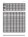
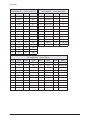
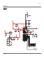
5-1
T0023
T0056
CIS7
T0023
M0146
T0003
T0074
M0105
M0112
T0268
M0145
M0150
T0175
T0456
M0105
M0146
M0149
T0044
M0020
M0013
T0915
M0412
M0111
T0920
T0079
M0013
Exploded View & Part List
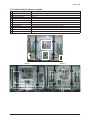
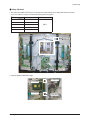
5. Exploded View & Part List
5-1 HPT4254X/XAA Exploded View
Samsung Electronics
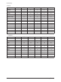
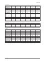
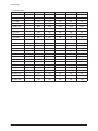
Exploded View & Part List
Loc. No.
Code No.
Description
Specification
Q'ty
SA/SNA
CIS7
AA61-60003B
SPRING ETC-CS
-,SUS304,-,-,OD11.2,N7,OD1
1
S.N.A
M0013
BN96-04714B
ASSY STAND P-BASE
C9/Q9,ABS HB SF-0507,B
1
S.A
M0013
BN96-04709E
ASSY COVER P-REAR
42Q9/C9,DO,PCM T0.5,BL
1
S.A
M0020
BN96-05039D
ASSY BOARD P-SIDE HDMI A/V
HP-T4254,CT50
1
S.A
M0105
BN67-00190A
LENS-LED
42Q9,PC,light blue,Material of
1
S.N.A
M0111
BN63-03049B
COVER-STAND
42Q9,ABS SF-0507,BK23
1
S.N.A
M0112
BN63-03047B
COVER-FRONT
42C9,ABS,HB,BK23,STEAM MOLD
1
S.N.A
M0145
BN96-04853B
ASSY BOARD P-FUNCTION
Lily/Calla,CT5000-
1
S.A
M0146
BN96-04687A
ASSY BRACKET P-FILTER SIDE
42Q9,AL6063,T
2
S.N.A
M0146
BN96-04861D
ASSY BOARD P-POWER & IR
Lily/Calla,CT500
1
S.A
M0149
BN96-04685A
ASSY BRACKET P-FILTER TOP
42Q9,AL6063,T1
1
S.N.A
M0150
BN96-04686A
ASSY BRACKET P-FILTER BOTTOM
42Q9,AL6063
1
S.N.A
M0150
BN96-04691B
ASSY BRACKET P-SUPPORT FILTER
42Q9,Al 60
1
S.N.A
M0412
BN96-04903A
ASSY BRACKET P-PCB
Q9,SECC,0.8
1
S.N.A
T0003
BN96-04712B
ASSY COVER P-FRONT
42C9,ABS HB,BK23,STEA
1
S.A
T0023
BN96-04707A
ASSY COVER P-KNOB POWER
C9/Q9,ABS HB
1
S.N.A
T0023
BN64-00567A
KNOB POWER
42Q9,PC,VIOLET
1
S.N.A
T0044
BN96-04592A
ASSY PDP MODULE P-MODULE
42HD W2,PL42AX0
1
S.A
T0056
BN63-03091A
COVER-DECORATION
42C9,ABS,HB,BLK
1
S.N.A
T0074
BN59-00599A
REMOCON
Bordeaux plus,TM87C,SAMSUNG28P+E
1
S.A
T0079
BN94-01226A
ASSY PCB MISC-MAIN
HPT4254X(C9),F34B,LIL
1
S.A
T0175
BN96-04704A
ASSY SPEAKER P
8ohm,C9,10W,4P connector,
1
S.A
T0268
3903-000144
CBF-POWER CORD
DT,US,BP3/Y,U(IEC C13-RA)
1
S.A
T0456
BN67-00188A
GLASS-FILTER EMI
42" C7 HD,Sputter,with
1
S.A
T0915
BN61-02894B
HOLDER-MODULE
42Q9,PC ABS
2
S.N.A
T0920
BN61-02990A
GUIDE-STAND
42Q9,PC GF20%
1
S.N.A
Samsung Electronics
Remark
5-2
5-3
T0023
M0146
T0056
CIS7
T0023
T0003
T0074
M0105
M0112
T0268
M0145
M0150
T0175
T0456
M0105
M0146
M0149
T0044
M0020
M0013
T0915
M0412
M0111
T0920
T0079
M0013
Exploded View & Part List
5-2 HPT5054X/XAA Exploded View
Samsung Electronics
Exploded View & Part List
Loc. No.
Code No.
Description
Specification
Q'ty
SA/SNA
CIS7
AA61-60003B
SPRING ETC-CS
-,SUS304,-,-,OD11.2,N7,OD1
1
S.N.A
M0013
BN96-04714B
ASSY STAND P-BASE
C9/Q9,ABS HB SF-0507,B
1
S.A
M0013
BN96-04711E
ASSY COVER P-REAR
50Q9/C9,DO,PCM T0.5,BL
1
S.A
M0020
BN96-05039G
ASSY BOARD P-SIDE HDMI A/V
HP-T5054,CT50
1
S.A
M0105
BN67-00190A
LENS-LED
42Q9,PC,light blue,Material of
1
S.N.A
M0111
BN63-03049B
COVER-STAND
42Q9,ABS SF-0507,BK23
1
S.N.A
M0112
BN63-03067B
COVER-FRONT
50C9,ABS,HB,BK23,STEAM MOLD
1
S.N.A
M0145
BN96-04853B
ASSY BOARD P-FUNCTION
Lily/Calla,CT5000-
1
S.A
M0146
BN96-04690A
ASSY BRACKET P-FILTER SIDE
50Q9,AL6063,T
2
S.N.A
M0146
BN96-04861D
ASSY BOARD P-POWER & IR
Lily/Calla,CT500
1
S.A
M0149
BN96-04688A
ASSY BRACKET P-FILTER TOP
50Q9,AL6063,T1
1
S.N.A
M0150
BN96-04692A
ASSY BRACKET P-SUPPORT FILTER
50Q9,AL606
1
S.N.A
M0150
BN96-04689A
ASSY BRACKET P-FILTER BOTTOM
50Q9,AL6063
1
S.N.A
M0412
BN96-04903A
ASSY BRACKET P-PCB
Q9,SECC,0.8
1
S.N.A
T0003
BN96-04713B
ASSY COVER P-FRONT
50C9,ABS HB,BK23,STEA
1
S.A
T0023
BN96-04707A
ASSY COVER P-KNOB POWER
C9/Q9,ABS HB
1
S.N.A
T0023
BN64-00567A
KNOB POWER
42Q9,PC,VIOLET
1
S.N.A
T0044
BN96-04775A
ASSY PDP MODULE P
50HD W2A,M1,W2A,1365*7
1
S.A
T0056
BN63-03081A
COVER-DECORATION
50C9,ABS,HB BLK
1
S.N.A
T0074
BN59-00599A
REMOCON
Bordeaux plus,TM87C,SAMSUNG28P+E
1
S.A
T0079
BN94-01230A
ASSY PCB MISC-MAIN
HPT5054X(C9),F34B,LIL
1
S.A
T0175
BN96-04704A
ASSY SPEAKER P
8ohm,C9,10W,4P connector,
1
S.A
T0268
3903-000144
CBF-POWER CORD
DT,US,BP3/Y,U(IEC C13-RA)
1
S.A
T0456
BN67-00197A
GLASS-FILTER EMI
50 W2, C9,Sputter, wit
1
S.A
T0915
BN61-02895B
HOLDER-MODULE
50Q9,PCABS
2
S.N.A
T0920
BN61-02990A
GUIDE-STAND
42Q9,PC GF20%
1
S.N.A
Samsung Electronics
Remark
5-4
Exploded View & Part List
5-3 HPT4254X/XAA Service Item
! This is the list which is available to repair the real material at the time of service.
Loc. No.
Code No.
Description
Specification
Q'ty
M0013
BN96-04709E
ASSY COVER P-REAR
42Q9/C9,DO,PCM T0.5,BL
1
M0013
BN96-04714B
ASSY STAND P-BASE
C9/Q9,ABS HB SF-0507,B
1
M2893
BN39-00802K
LEAD CONNECTOR
HPT4264,UL1007#26,24P/24P
1
M2893
BN39-00826A
LEAD CONNECTOR
CALLA 50",UL20276#30,UL/C
1
T0003
BN96-04712B
ASSY COVER P-FRONT
42C9,ABS HB,BK23,STEA
1
T0044
BN96-04592A
ASSY PDP MODULE P-MODULE
42HD W2,PL42AX0
1
T0074
BN59-00599A
REMOCON
Bordeaux plus,TM87C,SAMSUNG28P+E
1
T0079
BN94-01226A
ASSY PCB MISC-MAIN
HPT4254X(C9),F34B,LIL
1
T0175
BN96-04704A
ASSY SPEAKER P
8ohm,C9,10W,4P connector,
1
T0764
BN44-00159A
SMPS-PDP TV
PS42P7H,DYREL,AC/DC,370W,AC1
1
T1910
BN96-04593A
ASSY PDP MODULE P-X-MAIN
42HD W2,PL42AX0
1
T1911
BN96-04594A
ASSY PDP MODULE P-Y-MAIN
42HD W2,PL42AX0
1
T1914
BN96-04597A
ASSY PDP MODULE P-ADDRESS-E BU
42HD W2,P
1
T1915
BN96-04598A
ASSY PDP MODULE P-ADDRESS-F BU
42HD W2,P
1
T1917
BN96-04596A
ASSY PDP MODULE P-LOGIC MAIN
42HD W2,PL4
1
T9698
BN96-04595A
ASSY PDP MODULE P-Y-MAIN SCAN
42HD W2,PL
1
5-5
Remark
Samsung Electronics
Exploded View & Part List
5-4 HPT5054X/XAA Service Item
! This is the list which is available to repair the real material at the time of service.
Loc. No.
Code No.
Description
Specification
Q'ty
M0013
BN96-04711E
ASSY COVER P-REAR
50Q9/C9,DO,PCM T0.5,BL
1
M0013
BN96-04714B
ASSY STAND P-BASE
C9/Q9,ABS HB SF-0507,B
1
M2893
BN39-00802C
LEAD CONNECTOR
HPT4264H,UL1617#22,24P/24
1
M2893
BN39-00859A
LEAD CONNECTOR
CALLA 50",UL20276#30,UL/C
1
T0003
BN96-04713B
ASSY COVER P-FRONT
50C9,ABS HB,BK23,STEA
1
T0044
BN96-04775A
ASSY PDP MODULE P
50HD W2A,M1,W2A,1365*7
1
T0074
BN59-00599A
REMOCON
Bordeaux plus,TM87C,SAMSUNG28P+E
1
T0079
BN94-01230A
ASSY PCB MISC-MAIN
HPT5054X(C9),F34B,LIL
1
T0175
BN96-04704A
ASSY SPEAKER P
8ohm,C9,10W,4P connector,
1
T0764
BN44-00160A
SMPS-PDP TV
PS50P7H,DYREL,AC/DC,460W,AC1
1
T1910
BN96-04573A
ASSY PDP MODULE P-X-MAIN
50HD W2,PL50HW0
1
T1911
BN96-04574A
ASSY PDP MODULE P-Y-MAIN
50HD W2,PL50HW0
1
T1914
BN96-04578A
ASSY PDP MODULE P-ADDRESS E_BU
50HD W2,P
1
T1915
BN96-04579A
ASSY PDP MODULE P-ADDRESS F_BU
50HD W2,P
1
T1917
BN96-04881A
ASSY PDP MODULE P-LOGIC MAIN
PL50HW021A,
1
T1960
BN96-04575A
ASSY PDP MODULE P-Y-MAIN UPPER
50HD W2,P
1
T1961
BN96-04576A
ASSY PDP MODULE P-Y-MAIN LOWWE
50HD W2,P
1
Samsung Electronics
Remark
5-6
MEMO
5-7
Samsung Electronics
Wiring Diagram
6. Wiring Diagram
6-1 Overall Wiring
<42" Overall Wiring>
CN5401
Y-MAIN SCAN
4
CN810
CN5402
CN5407
5
CN809
CN5707
CN4002
SMPS
CN808
CN5403
X-DRIVE
CN5408
6
Y-DRIVE
CN800
CN801
CN807
CN5501
CN5409
CN5502
CN4701
CN5412
11
CN2006 CN2001
CN2002
CN5701
2
CN5503
CN4001
CN2000
LOGIC BOARD
CN2003
?
CN2004
CN2028
1
AC-INLET
E-BUFFER
CN4004
7
CN2509
CN2600
CN2500
F-BUFFER
CN2609
CN2610
CN2510
CN2202
CN1101
FUNCTION
CN1
10
CN1605
3
CN101
CN1606 CN1203
CN3
POWER SW
CN1404_SIDE
MAIN BOARD
8
9
SIDE AV
SPEAKER
Samsung Electronics
6-1
Wiring Diagram
<50" Overall Wiring>
CN5401
Y-MAIN SCAN(HIGH)
4
CN5402
CN810
CN5707
5
CN809
SMPS
CN5407
X-DRIVE
CN808
CN5403
CN4001
CN5412
Y-DRIVE
CN800
CN801
CN807
CN5501
CN4004
7
CN5507
11 2
CN5502
CN4002
CN4701
CN2001 CN2000
CN2006
Y-MAIN SCAN(LOW)
CN5503
CN2509
LOGIC BOARD
1
6
CN2003
CN2002
CN5701
CN4000
CN2005
CN2004
AC-INLET
E-BUFFER
CN2500
F-BUFFER
CN2600
CN2609
CN2610
CN2510
CN2202
CN1
MAIN BOARD
10
CN1605
3
CN101
CN1606 CN1203
CN3
POWER SW
CN1404_SIDE
CN1101
FUNCTION
9
8
SIDE AV
SPEAKER
6-2
Samsung Electronics
Wiring Diagram
! The code number of cable(Lead-connector) can be changed, see "5. Exploded View & Part List."
Use
" LVDS 31P-30P
# POWER 24P
$ Flat Cable
Code
42" - BN39-00826A
50" - BN39-00859A
42" - BN39-00802K
50" - BN39-00802C
42" - BN96-05164A
50" - BN96-05176A
Use
% Y Drive
& X Drive
' Address
Code
-
-
-
Use
( Logic
) Front
* SPEAKER
Code
-
-
-
Use
+ FUNCTION
, AC_INPUT
Code
-
42" - 2901-001378
50" - 2901-001340
Photo
Photo
Photo
Photo
Samsung Electronics
6-3
Wiring Diagram
"
CN2202(MAIN B'D) - CN2001(LOGIC B'D)
#
CN1101(MAIN B'D) - CN801(MAIN SMPS)
Pin No.
Signal
Pin No.
Signal
Pin No.
Signal
Pin No.
Signal
1
RxIN0-
16
NC
1
PS_ON
13
5V
2
RxIN0+
17
GND
2
N/C (Auto_V)
14
5V
3
RxIN1-
18
WP
3
STBY
15
5V
4
RxIN1+
19
SCL
4
GND_STBY
16
5V
5
RxIN2-
20
SDA
5
GND_18V AMP
17
GND_12V
6
RxIN2+
21
LVDS Opt
6
GND_18V AMP
18
GND_12V
7
RxINCLK-
22
DCC Opt
7
18V AMP
19
12V
8
RxINCLK+
23
GND
8
18V AMP
20
GND_12V
9
RxIN3-
24
GND
9
GND_5V
21
12V
10
RxIN3+
25
GND
10
GND_5V
22
12V
11
NC
26
Vdd
11
GND_5V
23
N.C(FAN_ON)
12
NC
27
Vdd
12
GND_5V
24
N.C(FAN_DET)
13
NC
28
Vdd
14
NC
29
Vdd
15
NC
30
Vdd
$
CN1404(MAIN B'D) - CN101(SIDE AV)
Pin No.
Signal
Pin No.
Signal
Pin No.
Signal
Pin No.
Signal
1
GND
12
TXC-
23
NC
34
VIDEO_SR_IN
2
TX2+
13
GND
24
NC
35
VIDEO_SL_IN
3
TX2-
14
MICOM_CEC
25
GND
36
HP_IDENT
4
GND
15
GND
26
SVHS_IDENT
37
HP_OUT_R
5
TX1+
16
TSCL
27
SVHS_Y
38
HP_OUT_L
6
TX1-
17
TSDA
28
GND
39
USB_VCC
7
GND
18
LSCL
29
SVHS_C
40
B1.8V
8
TX0+
19
HDMI3_5V
30
GND
41
B3.3V
9
TX0-
20
HPD_SIL9185
31
VIDEO_IDENT
10
GND
21
DDC_WP
32
VIDEO_CVBS
11
TXC+
22
GND
33
GND
6-4
Samsung Electronics
Wiring Diagram
%
CN810(SMPS)
CN5707(Y B'D)
&
CN809(SMPS)
CN4701(X B'D)
'
CN808(SMPS)
CN2609(E-BUFFER)
(
CN807(SMPS)
CN2000(LOGIC B'D)
)
CN1606(MAIN B'D)
POWER&IR
Pin No.
Signal
Pin No.
Signal
Pin No.
Signal
Pin No.
Signal
Pin No.
Signal
1
Vg
1
Vg
1
Va
1
STBY
1
IR
2
GND
2
GND
2
GND
2
VS_ON
2
GND
3
GND
3
GND
3
5.3V
3
N/C
3
A5V_1
4
GND
4
Vs
4
PS_ON
4
LED_STB
5
Vs
5
Vs
5
RTN
5
BUZZER
6
Vs
6
5.3V
6
KEY_INPUT1
7
RTN
7
KEY_INPUT2
8
RTN
8
GND
9
5.3V
9
B5V
10
5.3V
10
LED_CTRL
*
CN1203(MAIN B'D)
SPEAKER
+
CN1605(MAIN B'D)
FUNCTION
,
CN800(SMPS)
AC INLET
Pin No.
Signal
Pin No.
Signal
Pin No.
Signal
1
R+_OUT
1
KEY_INPUT1
1
AC Neutral
2
R-_OUT
2
KEY_INPUT2
2
N/C
3
L+_OUT
3
GND
3
AC Live
4
L-_OUT
Samsung Electronics
6-5
Wiring Diagram
6-1-1 Connector role
42" Loc. No.
50" Loc. No.
CN5401
CN5401
Module and Y-Main Scan Connect
CN5402
CN5402
Module and Y-Main Scan Connect
CN5403
CN5403
Module and Y-Main Scan Connect
-
CN5412
Y-Main Scan(High) and Y-Main Scan(Low) Connect
CN5501
CN5501
Module and Y-Main Scan Connect
CN5502
CN5502
Module and Y-Main Scan Connect
CN5503
CN5503
Module and Y-Main Scan Connect
CN5407
CN5407
Y-Drive and Y-Main Scan Connect
CN5408
CN5408
Y-Drive and Y-Main Scan Connect
CN5409
CN5409
Y-Drive and Y-Main Scan Connect
CN5412
CN5412
Y-Drive and Y-Main Scan Connect
CN5707
CN5707
Y-Drive and SMPS Connect
CN5701
CN5701
Y-Drive and Logic Board Connect
CN810
CN810
Y-Drive and SMPS Connect
CN809
CN809
X-Drive and SMPS Connect
CN808
CN808
SMPS and F-Buffer Connect
CN807
CN807
SMPS and Logic Board Connect
CN801
CN801
SMPS and Main Board Connect
CN800
CN800
SMPS and AC-Inlet Connect
CN4701
CN4701
SMPS and X-Drive Connect
CN4004
CN4004
Logic Board and X-Drive Connect
CN4002
CN4002
Module and X-Drive Connect
CN4001
CN4001
Module and X-Drive Connect
-
CN4000
Module and X-Drive Connect
CN2000
CN2000
SMPS and Logic Board Connect
CN2001
CN2001
Main Board and Logic Board Connect
CN2002
CN2002
Y-Drive and Logic Board Connect
CN2004
CN2004
Logic Board and F-Buffer Connect
CN2028
CN2028
Logic Board and E-Buffer Connect
CN2500
CN2500
Logic Board and E-Buffer Connect
CN2510
CN2510
E-Buffer and F-Buffer Connect
CN2610
CN2610
E-Buffer and F-Buffer Connect
CN2600
CN2600
Logic Board and F-Buffer Connect
CN2609
CN2609
SMPS and F-Buffer Connect
CN1101
CN1101
SMPS and Main Board Connect
CN2202
CN2202
Main Board and Logic Board Connect
CN1605
CN1605
Function Assy and Main Board Connect
CN1404
CN1404
Side AV Assy and Main Board Connect
6-6
Description
Samsung Electronics
Wiring Diagram
42" Loc. No.
50" Loc. No.
CN1606
CN1606
Power SW Assy and Main Board Connect
CN1203
CN1203
Speaker and Main Board Connect
CN101
CN101
Side AV Assy and Main Board Connect
CN1
CN1
Function Assy and Main Board Connect
CN3
CN3
Power SW Assy and Main Board Connect
Samsung Electronics
Description
6-7
MEMO
6-8
Samsung Electronics
Schematic Diagram
7. Schematic Diagram
7-1 Circuit Description
Logic Board
DRAM
Input
Data
Processor
Data
Controller
X Main Board
Y Main Board
Driver
Timing
Controller
Display
Data
Row
Driver
Display
Timing
Y-Pulse
Generator
Scan
Timing
PDP Panel
42” - 1024x768 Pixels
1024x768x3 Cells (R,G,B)
50” - 1365x768 Pixels
1365x768x3 Cells (R,G,B)
X-Pulse
Generator
Address Buffer
SMPS Board
LVDS
Main SMPS
Main Board
LVDS
Trans
Image
Enhancer
Deinterlacer
Audio
Processor
Image
Scaler
CPU
Decoder
Video
Decoder
Speaker
Out
TMDS
Recever
A/D
Converter
Video
S/W
Micom
Tuner
RF
Splitter
AC Power
Source
! SMPS Board
The SMPS used for the PDP has been designed to be efficient, compact and lightweight. For VS and VA outputs, a LLC converter
has been used. For the other outputs, a Flyback converter has been used.
! LOGIC Board
The logic circuit consists of a Logic Main Board and an Address Buffer Board. The Logic Main Board decodes the video signal
encoded by the Video Board, outputs the ADDRESS data signal for each pattern and generates X and Y drive signals. The
Address Buffer Board buffers and transfers the ADDRESS data output signal using TCP IC.
- LVDS with built-in video signal processing (W/L, error diffusion, APC, FCR, etc.) applied and 1 ASIC chip.
- Outputs the address Drive IC control and data signals to the Buffer Board.
- Outputs the control signal for the X and Y Drive Boards.
- Monitors major drive voltages (Micom Circuit Block); detects if a surge voltage has been applied and protects the Drive Circuit.
- Temperature Adaptive Operating Mode (Low Temperature/Room Temperature/High Temperature); Discharge optimization for
each temperature level.
! X-MAIN Board
Connects to the X terminal block, 1) provides maintaining voltage waveform (including ERC), and 2) maintains the Ve bias in the
Scan section.
! Y-MAIN Board
Connects to the Y terminal block, 1) provides maintaining voltage waveform (including ERC), 2) provides Y Rising, Falling Ramp
waveforms, and 3) maintains the Vscan bias.
! Address Buffer Board
It delivers the data signal and control signal to the TCP.
Samsung Electronics
7-1
MEMO
7-2
Samsung Electronics
Schematic Diagram
7-2 Schematic Diagram
7-2-1 MAIN POWER BLOCK
This Document can not be used without Samsung’s authorization.
STANDBY
STD_VCC
BD118
A3.3V
A5V
-
IC101D
KIA78D05F
B D 10 1 D
SUPLVAL
1
-
1
I
G
3
O
C103L
3
1
VIN
2
VOUT
LOCATION SUFFIX
1
ADJ
C107
100nF
25V
C106
22 u F
16V
2
T P 1 02
NCP1117DT33T5
C 10 2
100uF
16V
C101L
C1 04 L
100uF 100nF 10nF
16V
PGND
PGND
PGND
R101L
B2.5V_LX_DDR1
B5V
1Kohm
PGND
SUPLVAL
TP121
CN101
SMW200-24C
C
TP104 1
Q101L
2SC2412K-Q
SUPLVAL
BD116
R102L
1
TP126
SUPLVAL
TP109 1
VIN
C110
100nF
100uF
16V
R119P
SUPLVAL
2
VOUT
D
B
SIDE
S
OPTION
C
HOTEL
H
1
C111
AD J
C113
PGND
DEL
ON BOARD
TP103
AP1117D-25A
3
-
4.7Kohm
B18VS
L
P
IC103
1
SW_POWER
B
E
LCD
PDP
22uF
16V
0ohm
PDP OPTION
TP122
1
C 1 18
100uF
25V
SUPLVAL
C114
TP110
1
SUPLVAL
PGND
C115
100nF 10nF
PGND
TP123
1
B5V
SUPLVAL
TP113 1
C125
SUPLVAL
C136
ON : HIGH
-
100nF 10nF
10nF
1
IC107
100uF
16V
C134
PGND
MP1583DN
C128
1
2
3
4
100nF 10nF
C141
C140
100nF
16V
82uF
16V
B5V_VCC
SS
BS
MGND1
IN
EN
COMP
SW
GND
FB
R104
8
7
6
5
-
R103
3A Current
-
120uF
6.3V
C139
100nF
16V
VOUT
2
C105
100uF
16V
R121
120ohm
3.6Kohm
1/10W
15Kohm
180pF
C1 3 8
VIN
ADJ
C192
100nF
16V
C191
100uF
16V
1
R 1 06
D101
SS2 4
R 10 5
C144
BD108
OS_CON
6.2Kohm
1/10W
10Kohm
3
2
22uH
TP124
IC115
AP1117D-A
BD102
1
L101
C133
PGND
T P 11 2
C137
100uF
25V
B1.2VD_UX
B3.3V_2
OFF : LOW
C132
C1 35
PGND
100nF
16V
NC : Auto
BD106
B13V
1
1
2
3
4
5
6
7
8
9
10
11
12
13
14
15
16
17
18
19
20
21
22
23
24
1
TP106
IC102
T P 1 01
1
Power
C145
C147
100uF
16V
3.3nF
C146
100nF
16V
PGND
PGND
OPTION
PANEL_VCC
PANEL
BD114L, R111L
5V INPUT(32")
BD115L, R120L
12V INPUT(37", 40")
C158L
1uF
25V
BD114L
-
C156L
C157L
22uF
35V
BD115L
1
2
3
4
R111L
R120L
50 V
-
10Kohm
1/10W
PGND
SI4435DY
R108L
100Kohm
100nF
IC109L
47Kohm
1/10W
R112L
10Kohm
SW_PVCC
D
TP115L
8
7
6
5
1
C161L
C162L
100uF
25V
100nF
C
B
PGND
PGND
E
Q102L
2SC2412K-Q
H:POWER ON
L:OFF
PGND
S
G
PGND
TP116
-
L103
10nF
C172
C171
1
IC111
C166
1
2
3
4
BS
SS
MGND1
EN
IN
SW
COMP
GND
FB
1
2
2
MP1583DN
R115
8
7
6
5
R113
C168
120uF
6.3V
C169
C1 6 5
100nF
16V
100uF
16V
C170
100nF
25V
4
C167
100uF
R114
0ohm
1/10W
3
16V
300ohm
1/10W
3.6Kohm
1/10W
SS24
180pF
5
R 1 18
D103
C 1 73
VO
ADJ
R116
100nF
16V
82uF
16V
VIN
EN
LAKE
1
GND
6.2Kohm
1/10W
10Kohm
TP125
IC110
SC1566I5M-2.5TRTMGND1
1
GND
BD111
1.2V_CORE
B3.3V_1
C163
100nF
16V
R117
15Kohm
C174
3.3nF
B5V
IC112
TP117
AP1117D-25A
BD119
B9V_SPLITTER
IC113
BA178M09FP
BD112
-
1
IN
OUT
1
1
3
VOUT
VIN
TP118
2
2.5V_LAKE
1
AD J
C175
100uF
1 6V
TP119
3
-
C179
1
PGND
100nF
GND
C181
100uF
25V
C178
100nF
2
C177
10nF
PGND
PGND
B8VS
IC114
BA178M08FP
BD113
1
-
IN
OUT
GND
C188
100uF
25 V
C185
100nF
C184
1 0n F
2
TP120
3
1
C189
100uF
16V
C190
100nF
16V
PGND
P G ND
PGND
PGND
Samsung Electronics
7-3
Schematic Diagram
7-2-2 STANDBY MICOM (WT61P6) & SUB FUNCTION I/F
This Document can not be used without Samsung’s authorization.
Power
SUB FUNCTION I/F
A5V
A5V
B5V
IR
KEY_INPUT1
KEY_INPUT2
L201
10uH
MMBD4148SE
2
D220
C212
1N4148WS-F
SMICOM_nRESET
4.7Kohm
1/10W
C
B
2
1
R281L
1.5Kohm
R280L
1.5Kohm
3
R279L
1.5Kohm
B
R252 33ohm
R254 33ohm
1
D223
TP242
D 222
D221
Q210
KSC1623-Y
C
R256
2.2Kohm
B
E
LED_CTRL
1
AGND_IN AGND_IN
A5V
Q208
KSC1623-G
E
A3.3V
POP_MUTE
R225
A
R204L
XREF
X R EF
SOUND_MUTE
4.7Kohm
1Kohm
C219
C220L
C226L
C217
C218
C227
1
2
3
TP243
TP240
R282L
TP241
10nF
50V
SENSE_PWR
TP236
TP237
TP238
LED_STB
B
E
47pF
10nF
10nF
10nF
10nF
10nF
4
2
XREF
1
XREF
16V
10uF
1
R258L
BUZZER
CN202P
SMAW200-03P
10Kohm
1
C224D
D226
3
3
GND
TP239
Q205L
B
3
2
/RESET,RESET
VD D
3
SW201
2
1
0ohm
1/10W
1
R226
SYS_HALT
2
POWER_DET
KPS-1105PYN
RLZ5.6B-TE-11
D219D
3
3
1N4148WS-F
XREF
GND
1N4148WS-F
R221
10Kohm
RT9818C-42PV
1
C209
1uF
3
D215
1 0 0n F
B
BD203
A
BD205
1
/RESET,RESET
VDD
1
IC206
RT9818C-42PV
3
C210
IC205
C216L
100nF
KSC1623-Y
2
DDR_PWC
C
BD206
A
TP223
TP224
TP225
TP226
TP227
TP228
TP229
TP234
TP230
TP231
1 1 1 1 1 1 1 1 1 1
R274
10Kohm
D217
XR E F
R211
470ohm
1/10W
A5V
C 213
100nF 10nF
1
1N4148WS-F
D216
TP210
TP211
TP212
TP213
TP214
TP215
T P 216
TP235
TP217
TP218
1 1 1
RLZ5.6B-TE-11
1N4148WS-F
C215
1
2
3
4
5
6
7
8
9
10
1 1 1 1 1 1 1 1 1 1
A 3 .3 V
RLZ5.6B-TE-11
D206
A3.3V
D218
D209
SMAW200-10P(P)
2.2Kohm
D225
1N4148WS-F
D208L
CN201
B3.3V_2
B13V
B5V
D207L
AGND_IN
R212
A 5V
100uF
16V
0ohm
1N4148WS-F
Reset & Power Detection
1
1
2
2
A5V
C214
R296
D224D
100ohm
R220
1
1
1
TP207
TP208
TP209
10Kohm
10Kohm
10Kohm
10Kohm
10Kohm
10Kohm
10Kohm
10Kohm
R213
R214
100ohm
100ohm
10ohm
100ohm
100ohm
100ohm
PD2/PWM7/P13
PD1/HOUT
PD0/VOUT
PA7/CLAMP/AD7
PB3/FDO/NIRQ4
PA6/1/2VO/AD6
PB2/FDI/NIRQ3
PA5/1/2HO/AD5
PA4/AD4
VSS
(0xA0)
C203
100nF
1 6V
BUZZER
COMP2_IDENT
SW_PVCC
R288
HDMI_HPD_SINK
PC_VS_SVP
PC_HS_MICOM
SMICOM_DOWN
PA3/RXDA
100ohm
100ohm
100ohm
100ohm
10ohm
100ohm
100ohm
100ohm
100ohm
100ohm
100ohm
100ohm
100ohm
100ohm
R233
R234
R235
R236
R238
R240
R242
R244
R246
R248
R250
R257
R259
R260
33
32
31
30
29
28
27
26
25
24
23
PA2/TXDA
PA1/DSCL
PB0/NIRQ1
SDA
LOGIC_DOWN
1Kohm
Switch DDC-Sub Micom I2C
R 28 7
1Kohm
XREF
B
C
TP2416
TP2414
TP2415
Q206
TUNER_nRESET
HDMI2_IDENT
HDMI1_IDENT
CPU_nRESET
SW_POWER
RESET_SVP
SOUND_MUTE
SW_INVERTER
SCL_EEPROM
SDA_EEPROM
RX_DEBUG
KSC1623-Y
A5V
TP220
TP221
TP2417
C222
TX_DEBUG
SCL_DOWN
SDA_DOWN
100nF
R227
10Kohm
R295
A3.3V
R269
A5V
PC_5V
1
2
3
4
A5V
HPD_GLITCH_OFF
1 1
PD6/PWM3/HIM2
NC
VIN1
HIN1
PE3
PD7/PWM2/VIN2
PE2
NRES
VDD3V
PE0/PWM0
PE1/PWM1/PWML
PB4/PAT/CLKO/NIRQ5
PB1/NIRQ2
A2
12
13
14
15
16
17
18
19
20
21
22
1nF
50V
PD4/PWM5/P11
PA0/DSDA
100ohm
A0
A1
SC L
E
PD5/PWM4/P10
IC202
WT61P6S-RN440
PB5/MSCL
0ohm
1/10W
SMICOM_DOWN
PD3/PWM6/P12
PC0/AD0
Q211
2N7002L
C206
OSC I
PB6/MSDA
VCC
WP
Near To LAKE2(IC1301)
44
43
42
41
40
39
38
37
36
35
34
10Kohm
R249
POWER_DET
100ohm
100ohm
100ohm
100ohm
1Kohm
OSC O
PC1/AD1
MAIN_EEPROM_WP
RESET_NTP3000
IR
R237
R239
R241
R243
R245
GND
PC2/AD2
MICOM_CEC
D214
22pF
50V
22pF
50V
0ohm
RESET_MSP4450
PC_IDENT
R265
R267
SMICOM_nRESET
LED_CTRL
R201
R202
R203
R247
100nF
R222
R224
R228
R229
R230
R231
PC3/AD3
C204
R297
RLZ5.6B-TE-11
C205
MAIN_EEPROM_WP
SCL_EEPROM
SDA_EEPROM
R299
PC4/P14/RXDB
24.0MHz
VDD5V
PC5/P15/TXDB
R285
27Kohm
1/10W
1
2
3
4
5
6
7
8
9
10
11
PC6/P16/NIRQ6
3
X201
4C-49/SM5H,24MHZ,16PF
PC7/SOGIN/P17
D21 3
MMBD4148SE
10Kohm
R271
R298D
10Kohm
10Kohm
10Kohm
R268
R218
R219
A3.3V
1
2
A3.3V
8
7
6
5
1
C202
10uF
16V
A 3 .3 V
IC201
AT24C256BN-10SU-1.8
TP222
10Kohm
10Kohm
C201
B3.3V_2
B3.3V_2
A 3 .3 V
10Kohm
10Kohm
10Kohm
10Kohm
A3.3V
R205
R206
R207
R208
R209
R210
Near To Sub-Micom(IC202)
R270
FST3125MX
14
13
12
11
10
9
8
EMU_SCL
10Kohm
HDMI1_5V
10uF
16V
IC208
3.3Kohm
10Kohm
C223
SCL_DOWN
XREF
SDA_DOWN
XREF
EMU_SDA
VCC
/OE1
/OE4
1A
4A
1B
4B
/OE2
/OE3
2A
3A
2B
3B
GND
1
2
3
4
5
6
7
SCL_EEPROM_LAKE
SCL_EEPROM
SDA_EEPROM_LAKE
SDA_EEPROM
HDMI2_5V
HDMI3_5V
DDC_VCC
R261
R262
R263
R264
R291
R292
R293
R294
D203
D201
KDS184
KDS184
D202
KDS184
POWER_DET
XREF
B
C
E
R232
47Kohm
Q207
KSC1623-Y
R223
1 1
TP232D
TP233D
KEY_INPUT1
KEY_INPUT2
AGC_MAIN
AFT_MAIN
TX_CPU
RX_CPU
LED_STB
COMP1_IDENT
A3.3V
R215
1Kohm
DDC_WP
100ohm
100ohm
100ohm
100ohm
100ohm
100ohm
100ohm
100ohm
C
Q201
E
4.7Kohm
B
SW_DDC
R289
10Kohm
KSC1623-Y
R290
10Kohm
Control DDC_WP
7-4
Samsung Electronics
Schematic Diagram
7-2-3 SOUND PROCESSOR (MSP4450)
This Document can not be used without Samsung’s authorization.
Power
C301
PC_SL_IN
COMP1_SL_IN
HDMI_DTV_SL_IN
DVI_SL_IN
C303
B8VS
C302
100nF 22uF
16V
R301
R302
R307D R308
R306
R3 0 3 D
R304 R305
100Kohm 100Kohm100Kohm 100Kohm
100Kohm 100Kohm100Kohm100Kohm
BD301
1uF
6.3V
C304
1uF
6.3V
C305D
1uF
6.3V
C306
1uF
6.3V
C307
1uF
6.3V
C308
1uF
6.3V
C309D
1uF
6.3V
C311
1uF
6.3V
IC301
MM74HC4052M
PC_SR_IN
COMP1_SR_IN
HDMI_DTV_SR_IN
DVI_SR_IN
1
2
3
4
5
6
7
8
0Y
2Y
VD D
2X
Y-COM 1X
3Y X-COM
1Y
0X
/EN
3X
VEE
A
VSS
B
16
15
14
13
12
11
10
9
SOUND_SEL0
SOUND_SEL1
C3 1 0
10uF 16V
C312
XREF
1uF
6.3V
C313
1uF
6.3V
C314
XREF
XREF
1uF
6.3V
C315
1uF
6.3V
C316
XREF
VIDEO1_SL_IN
XREF
1uF
6.3V
C317
VIDEO1_SR_IN
XR E F
1uF
6.3V
C318
VIDEO2_SL_IN
R313
R309
R311D R312
R315D R316
R314
R310
100Kohm 100Kohm100Kohm100Kohm100Kohm100Kohm100Kohm100Kohm
10uF 16V
VIDEO2_SR_IN
COMP2_SR_IN
B8VS
COMP2_SL_IN
C323
L301
C321 C322 100uF
3.3uH
470pF 1.5nF 16V
C319
C358
4.7uF
35V
10uF
D301
BZT52-C15
C324
100nF
C325 100nF
3.3uH
C350 10uF
L303
AHVSS
SC3_OUT_L
SC3_OUT_R
NC
NC
AHVSS
SC4_IN_L
SC2_IN_L
SC3_IN_L
SC4_IN_R
SC1_IN_L
SC3_IN_R
SC2_IN_R
VREFTOP
AGNDC
DACM_SL
IC302
MSP4450K-VK-E8-500
NC
DACM_SR
DACM_SUB
NC
DACM_C
NC
DACM_L
NC
DACM_R
VREF2
SPDIF_OUT
DCTRI/O_1
DCTRI/O_0
DACA_L
DACA_R
ADR_SEL
STANDBYQ
NC
I2S_DA_IN4
100ohm
R318
100ohm
C336
10uF
XREF
C338
XR EF
MONITOR_SL_OUT
B5V
MONITOR_SR_OUT
10uF
47Kohm
1/10W
C340
100nF
SCL_TV_5V
XREF
SDA_TV_5V
XREF
R336
I2S_LRCLK_AMP
I2S_DATA_AMP
I2S_SCLK_IN
I2S_LRCLK_IN
RESET_MSP4450
I2S_SDO_IN
100ohm
C351
100nF
100ohm
XR
RE3F41
100ohm
XR
RE3F42
100ohm
C
E
Q301
KSA1182
D302
C342
100uF
C343
C345
1uF
C359
1uF
HP_R
100nF
100ohm
XR
RE3F38
B
47Kohm
1/10W
1N4148WS-F
100uF
R326
C349
R329
R320
R319
C341 10uF
AUD_CL_OUT
NC
HP_MUTE
XREF
R317
R328
20Kohm
100Kohm
1/10W
HP_L
I2S_SCLK_AMP
Samsung Electronics
SC2_OUT_R
NC
C329 10uF 16V
1
2
3
4
5
6
7
8
9
10
11
12
13
14
15
16
17
18
19
20
1Kohm
VREF1
SC2_OUT_L
XTAL_OUT
TP
40
39
38
37
36
35
34
33
32
31
30
29
28
27
26
25
24
23
22
21
R331
20Kohm
C347
4.7uF
35V
1
2
3
4
VOUT1
VIN1
VDD
VOUT2
BYPASS
VIN2
GND
SHUTDOWN
100uF
100Kohm
1/10W
1.5nF
C353
1.5nF
C354
1nF
C355
1nF
HP_OUT_L
C346
8
7
6
5
R337
C352
XREF
IC303
LM4810MM
XREF
R333
R332
1/10W
470Kohm
R325
TESTEN
XTAL_IN
I2S_DA_IN3
B5V_VCC
SC1_OUT_R
RESETQ
100ohm
100ohm
100ohm
R322
R324
R323
XREF
ANA_IN2+
I2S_WS3
CLOSE TO IC
AHVSUP
CAPL_A
I2S_CL3
MSP_SPDIF_OUT
3pF
XREF
C326
10uF 16V
CAPL_M
SC1_OUT_L
I2S_DA_IN2
C339
ANA_IN-
DVSS
22ohm
ANA_IN1+
DVSS
R3 2 1
AVSUP
DVSUP
X301
3pF
I2S_MCLK_AMP
56pF
C335
61
62
63
64
65
66
67
68
69
70
71
72
73
74
75
76
77
78
79
80
I2S_DEL_WS
DVSUP
C337
56pF
C328
I2S_DEL_CL
HC-49/SM5H_18R432
56pF
I2S_DEL_OUT
XREF
I2S_DEL_IN
47uF
16V
SC1_IN_R
C327
TUNER_SIF
MPZ2012S300A C330
AVSUP
I2S_DA_IN1
470pF
SC5_IN_L/MONO_IN
C334
I2S_DA_OUT
1.5nF
I2S_WS
C333
I2S_CL
22uF
AVSS
C3 3 2
I2C_CL
I2C_DA
47nF
NC
C331
BD302
AVSS
SC5_IN_R
60
59
58
57
56
55
54
53
52
51
50
49
48
47
46
45
44
43
42
41
B5V_VCC
1Kohm
HP_OUT_R
R334
1Kohm
C357
3.3nF
XREF
XREF
XREF
XREF
7-5
Schematic Diagram
7-2-4 SOUND AMP (NTP3000) & POP SOLUTION
This Document can not be used without Samsung’s authorization.
Power
POP NOISE SOLUTION
+1.8_AMP
B3.3V_2
(LOW ACTIVE)
SGND AVDD_PLL
D407
-
C402
POP_MUTE
DVDD_PLL
BD401
1N4148WS-F 1N4148WS-F
D402
D401
C401
D406
PMLL4148
1N4148WS-F
16V
10uF
B3.3V_2
A3.3V
R404
4.7Kohm
1/10W
E
B
KSA1182
100uF
16V
Q401
C
MONITOR_SL_OUT
-
2.2Kohm
1/10W
BD402
R405
B
C
Q402
KSC1623-G
E
SGND
MONITOR_SR_OUT
2.2Kohm
1/10W
R407
1nF R408
50V
-
4.7ohm
1/10W
3.3Kohm
C443
C446
XREF
100nF
25V
XREF
XREF
+1.8_AMP
100nF
50V
100nF
50V
C411
R414
SGND
1nF
50V
4.7Kohm
C440
1nF 50V
10V
1uF
B3.3V_2
100nF
2 5V
B
C
E
Q406
KSC1623-G
L-_OUT
R+_OUT TP405
R-_OUT TP406
L+_OUT TP407
L-_OUT TP408
SGND
1N4148WS-F
50V
R417
2
1nF
50V
4.7ohm
SGND
C450
100nF
25V
100nF
50V
100nF
25V
C 4 30
TP409
TP410
TP411
TP412
R+_OUT
R421
1nF
50V
4.7Kohm
C451
SGND
-
1
2
3
4
C428
100nF
50V
C436
470nF
50 V
2
1uF
10V
C421
D409
C426
C425
100nF
50V
C442
SGND
100nF
50V
R425
4.7Kohm
R424
C437
1nF
50V
4.7ohm
C444
C4 4 1
R413
CN401
1nF
50V
C447
KSA1182
Q405
SMAW250-04 WHT
22nF
50V
SGND
C
BD405
BD407
SGND
E
B
4.7Kohm
1/10W
Close to IC
4.7ohm
1nF 50V
Close to IC
XREF
XREF
C424
4.7Kohm
1/10W
SGND
R416
C431
100pF
50V
I2S_DATA_AMP
I2S_LRCLK_AMP
I2S_SCLK_AMP
SDA_HDMI
SCL_HDMI
C412
C449
3
PGND2B
BST2B
VDR2B
OUT2B
OUT2B
PGND2B
SOFT_RESET_2
AVDDPLL
DVDDPLL
TEST0
PWM_MASK_2
PVDD2B
BD406
SGND
R410
B18VS
1
PVDD2A
PVDD2B
22nF
VDR1B
BST1B
(0x54)
DGNDPLL
LFM
-
L402
C414
PVDD2A
AGNDPLL
POP_MUTE
1 1 1 1
100nF
25V
OUT1B
OUT1B
PGND1B
PGND1B
PVDD1B
PVDD1B
OUT1A
PVDD1A
PVDD1A
OUT1A
VDD_
4.7ohm
1/10W
25V
470uF
C4 2 2
C429
SGND
C4 3 9
R423
OUT2A
D408
Close to IC
1nF
50V
OUT2A
42
41
40
39
38
37
36
35
34
33
32
31
30
29
1N4148WS-F
C438
PGND2A
MGND1
AUX_PWM3A
C4 2 3
CLK_
CLK_
AUX_PWM3B
100nF
25V
BST2A
PGND2A
IC401
NTP-3000
VS S_
SCL
AVDD_PLL
16V
10uF
/RESET
AD
BCK
SDA
C403
C435
NC
VDR2A
WCK
100nF
25V
16V
10uF
1uF
10V
VDR1A
DVSS
SGND DVDD_PLL
SGND
C432
1nF R415
50V
C417
SGND
15
16
17
18
19
20
21
22
23
24
25
26
27
28
SGND
BST1A
1nF
50V
-
22nF
50V
56
55
54
53
52
51
50
49
48
47
46
45
44
43
XREF
RESET_NTP3000
1
2
3
4
5
6
7
8
9
10
11
12
13
14
PGND1A
D411
PGND1A
1N4148WS-F
SDATA
SGND
4.7Kohm
1/10W
R422
I2S_MCLK_AMP
1nF
50V
R418
C427
XREF
100nF
25V
R411
4.7Kohm
D410
1N4148WS-F
C419
C445
4.7Kohm
1/10W
CLOSE TO IC
10V
1uF
100nF
25V
DVDD
SGND
C420
C418
25V
C416
100nF
50V
L+_OUT
BD404
C407
HP_MUTE
SGND
CMI-SPC8L80F-150M
22nF
50V
4.7ohm
1/10W
4
C413
100nF
SGND
C415
SGND
1nF R412
50V
100nF
50V
3
SGND
B3.3V_2
C410
L401
Close to IC
C408
C409
470nF
5 0V
4
470uF
25V
1
C448
CMI-SPC8L80F-150M
C406
B3.3V_2
Close to Connector(CN401)
1 1 1 1
1nF R409
50V
C405
KSC1623-G
SGND
SGND
-
Q404
4.7ohm
1/10W
B18VS
BD403
C
E
Close to IC
C4 0 4
B
-
R-_OUT
Close to Connector(CN401)
R428
4.7ohm
BD408
SGND
Close to IC
SGND
SGND
R430
0ohm
SGND
POWER_DET
XREF
R431
10Kohm
7-6
Samsung Electronics
Schematic Diagram
7-2-5 NIM TUNER 1410
This Document can not be used without Samsung’s authorization.
Power
B3.3V_1
R501
4.7Kohm
Q501
2SC2412K-Q
C
B
SW_RF1
E
R502
1Kohm
1/10W
R504
100Kohm
1/10W
B9V_SPLITTER
R505
-
1/10W
220Kohm
BD503
R506
R507
C528
100nF
16V
22uF
16V
DNVS227IH262A
B5V_TUNER
MGND1
MGND2
B5V
GND
C505
22uF
16V
C530 2
100nF
16V
R513
330ohm
1/10W
C501
100uF
16 V
C512
22uF
16V
C514
10nF
R517
D501
MMBD4148SE
22Kohm
2
C521
3
220pF
C506
100uF
16V
B33V_TUNER
220uH
C518
3
C509
10nF
L501
47nF
OUT
IN
1
C522
10nF
L502
680uH
C523
100nF
50V
C524
3.3uF
50V
TP502
1
C519
3.3uF
D502
BZX84C33 50V
TP504
C520
100nF
50V
1
1
1
TP509
RF_AGC
5V(B+)
TP507
C507
100nF
16V
9V_FOR_LNA
1
1
B
INPUT_S/W
AFT
33V
TP508
TP510
TP511
TP512
TP513
TP514
TP515
1 1 1 1 1 1 1
2
GND
RESET
ERROR
CVBS
N.C
SIF
3.3V
MGND5
MGND6
TP516
TP517
TP518
TP519
TP520
TP521
TP522
TP523
TP524
TP525
TP526
TP527
TP528
TP52
30
9
1 1 1 1 1 1 1 1 1 1 1 1 1 1
A
TP501
BA17805FP
BD501
TP503
TP505
TP506
1 1 1
-
IC501
1/10W
220Kohm
TU501
AFT_MAIN
C503
100nF
16V
GND
N.C
1.2V
SYNC
VALID/EN
DATA7
DATA6
DATA5
DATA4
DATA3
DATA2
DATA1
DATA0
MPEG_CLK
SDA
SCL
TUNER_nRESET
C504
100nF
16V
R509
R510
0ohm
1/10W
TUNER_SIF
R512
100Kohm
1/10W
R511
0ohm
C510
100uF
16V
C511
100nF
16V
B
TP532
SAM_TSSYNC
SAM_TSVLD
B3.3V_1
IC502
AP1117D-A
1
33ohm
33ohm
TUNER_CVBS_MAIN
B3.3V_1
2
R514
R515
0ohm
1/10W
BD502
CIB32P600NE
VOUT
C531
47uF
16V
VIN
AD J
1
C527
1
100Kohm
1/10W
B
100nF
16V
2
C529
A
29 28 27 26 25 24 23 22 21 20 19 18 17 16 15 14 13 12 11 10 9 8 7 6 5 4 3 2 1
1
AGC_MAIN
C502
100nF
16V
3
C 516
100nF
16V
C 517
100uF
16V
MG ND3
MGND4
R518
100Kohm
B
C526
4.7nF
50V
C
E
Q502
KSC1623-Y
C525
2.2nF
50V
7
5
3
1
7
5
3
1
8
6
4
2
8
6
4
2
1/16W
33ohm
RA501
1/16W
33ohm
RA502
SAM_TS(7)
SAM_TS(6)
SAM_TS(5)
SAM_TS(4)
SAM_TS(3)
SAM_TS(2)
SAM_TS(1)
SAM_TS(0)
R519
33ohm
SAM_TS(0:7)
SAM_TSCLK
SDA1_DTVCH
SCL1_DTVCH
Samsung Electronics
7-7
Schematic Diagram
7-2-6 BACK AV IN/OUT
This Document can not be used without Samsung’s authorization.
Power
LCD : 3722-002360
PDP : 3722-001938
TP606
2
1
1
R605
6
5
4
C620
TP614
AGND_IN AGND_IN AGND_IN AGND_IN
R618
10ohm
S
VCC
B1
GND
A
B0
1
2
3
LAKE_SPDIF_OUT
MSP_SPDIF_OUT
C621
10uF
16V
L604
1
TP615
L605
470ohm
R615
470ohm
COMP1_SL_IN
COMP1_SR_IN
OP601
1
RFT6112
MGND2
3
TP625
AGND_IN
SVHS1_IDENT
MGND1
VCC
330pF
330pF
VIN
C614
B5V_VCC
TP626
1
C613
2
CDS3C30GTH
2
D618
1
CDS3C30GTH
5
R614
GND
1
2
D617
330pF
10ohm
100nF
25V
2
WHITE
1
C616
75ohm
D621
100pF
2
1
R621
C615
100ohm
R617
CDS3C30GTH
R620
75ohm
2
2
1
CDS3C30GTH
D623
D622
CDS3C30GTH
3
1
3.3uH
L606
1 TP618
5
6
R616
1 TP617
4
2
IC602
NC7SB3157P6X
TP613
RED
SVHS INPUT 1
1
AGND_IN
AGND_IN
SVHS1_C
AGND_IN
TP629
C622
100nF
SVHS1_Y
LCD : 3722-002360
PDP : 3722-001938
AGND_IN
COMPONENT 2
BD604
1
C625
10uF
16V
MPZ2012S300A
AGND_IN
JA606
TP620
TP619
1
TP622
1
GREEN
1
3
AGND_IN
75ohm 33pF
SEL_SPDIF
L607
CIC21J601NE
AGND_IN
LCD : 3722-002362
PDP : 3722-001903
4
6
1
75ohm 33pF
33pF
C605
AGND_IN
330pF AGND_IN
1
TP621
R607
C610
1
3
PJ6024B
H
75ohm
JA604
JA605
C604
2
AGND_IN
R606
C603
OUT
MSP_SPDIF_OUT
LAKE_SPDIF_OUT
B3.3V_2
CDS3C30GTH
CDS3C30GTH
AGND_IN
1 TP616
10ohm
D604
VIDEO1_SR_IN
D611
330pF
R604
SEL_SPDIF
L
COMP1_PR
TP605
1
8
1
7
9
VIDEO1_SL_IN
2
100pF
75ohm
10ohm
COMP1_PB
2
470ohm
1
5
CDS3C30GTH
R612
VIDEO1_CVBS
1
1
C611
2
2
C609
R613
D610
1
CDS3C30GTH
1
470ohm
10ohm
R603
1
AGND_IN
2
D608
8
D609
CDS3C30GTH
RED
L603
1
10ohm
R611
D603
TP609
CDS3C30GTH
WHITE
5
R468
TP604
1
L602
1
R602
COMP1_Y
4
6
2
3.3uH
L601
1
2
VIDEO1_IDENT
CDS3C30GTH
TP608
100ohm
COMP1_IDENT
D602
4
6
7
9
100ohm
R608
1
TP607
R601
1
CDS3C30GTH
1
2
BLUE
YELLOW
1
3
OPTICAL SPDIF OUT
TP602
TP601
1
TP603
1
1
3
GREEN
TP647
COMPONENT 1
JA601
RED
JA602
AV INPUT 1
D601
LCD : 3722-002363
PDP : 3722-002063
AGND_IN
R619
100ohm
R622
10ohm
R624
10ohm
COMP2_IDENT
1
2
COMP2_Y
LCD : 3722-002362
PDP : 3722-001903
5
AGND_IN
COMP2_SR_IN
2
330pF
AGND_IN
AGND_IN
B3.3V_2
G
R658H
3.3Kohm
D
BD603
G
D
S
Q602H
2N7002L
C629
10uF
1
1
TP650H
TP651H
CDS3C30GTH
100ohm
D644H
E
TP652H
TP653H
100ohm
D643H
100ohm
C2V-
T2IN
T2OUT
R2OUT
R2IN
0ohm
0ohm
AGND_IN
3
4
1
2
R649
TP636
R648
100ohm
AGND_IN
1
1
100ohm
1
TP637
UCT-EX-093
DGND_IN
TP635
AGND_IN
6
7
2
3
1
5
4
JA609
DEBUG
CN601H
AGND_IN
R666H
C632
C633
C2+
R1OUT
T1IN
100nF
C!-
R1IN
C630
100nF
TP638H TP649H
3
KSC1623-Y
T1OUT
1
2
3
4 100nF
5
6
7
8
GND
1
CDS3C30GTH
Q603H
B
R671H
R672H
R665H
10Kohm
1/10W
V+
CDS3C30GTH
TP639H
1
100ohm
D642H
A5V
R664H
C1+
D646
TP648H
CDS3C30GTH
IR
C
VCC
GND
CDS3C30GTH
R663H
0ohm
AGND_IN
16
15
14
13
12
11
10
9
D645
A4
/Y4
MGND4
/Y3
GND
SP3232EEY
R674H
R675H
MGND2
A5
/Y5
R662H
0ohm
0ohm
0ohm
MGND3
/Y2
A3
14
13
12
11
10
9
8
MGND1
/Y6
1 1
A6
A2
1 1
VCC
/Y1
R668
R669
TX_DEBUG
RX_DEBUG
0ohm
0ohm
C628
100nF
IC603
C631
100nF
R670H
AGND_IN
D647H
MMBD4148SE
2
1
10Kohm
1/10W
AGND_IN
7-8
D629
1
330pF
R673H
R667H
A1
COMP2_SL_IN
C624
A3.3V
R659H
3.3Kohm
CDS3C30GTH
1
2
2
1
CDS3C30GTH
D628
C623
IC604H
74LCX14MX
1
2
3
4
5
6
7
470ohm
1
A5V
1uF
10V
470ohm
BD602H
Q601H
2N7002L
0ohm
1/10W
C651H
R630
R631
1
RED
L609
R657H
4.7Kohm
1/10W
S
0ohm
1/10W
R661H
RX_DEBUG
L608
TP630
A5V
4.7Kohm
1/10W
R660H
CDS3C30GTH
1
DEBUG / HOTEL / WALL
TX_DEBUG
TP628
1
4
6
R656H
1
AGND_IN
2
AGND_IN
A3.3V
C619
75ohm 33pF
TP627
1
3
AGND_IN
AGND_IN
R629
C618
75ohm 33pF
AGND_IN
JA607
AGND_IN
10ohm
2
330pF
CDS3C30GTH
C627
330pF
R628
33pF
75ohm
1
$O,$V
C626
100Kohm
1/10W
C617
R627
2
$O,$V
R635
100Kohm
1/10W
AGND_IN
MONITOR_SR_OUT
D634
1
10uH-K
R634
MONITOR_SL_OUT
D627
100ohm
2
R633
CDS3C30GTH
100ohm
2
1
2
CDS3C30GTH
CDS3C30GTH
D637
RED
L611
1
5
R632
10uH-K
TP633
R636
COMP2_PR
8
D626
L610
2
TP624
1
7
9
1
4
6
5
RED
1
D638
WHITE
1
3
AUDIO_OUT
TP632
COMP2_PB
CDS3C30GTH
TP631
WHITE
JA608
TP623
1
D633
LCD : 3722-002362
PDP : 3722-001903
BLUE
4
6
AGND_IN
Samsung Electronics
Schematic Diagram
7-2-7 SIDE AV IN/OUT
This Document can not be used without Samsung’s authorization.
Power
SIDE AV
GCA03-0145
CN701B
T P 7 01
L701B 3.3uH
1
9
7
TP703
L7 02 B
1
TP704
6
4
100ohm
10ohm
R702B
470ohm
470ohm
1
R703B
C701B
R704B
100pF
75ohm
VIDEO2_IDENT
VIDEO2_CVBS
VIDEO2_SL_IN
VIDEO2_SR_IN
D704B
330pF
CDS3C30GTH
2
1
C703B
C702B
2
CDS3C30GTH
1
2
D703B
1
CDS3C30GTH
D701B
3
1
2
CDS3C30GTH
2
330pF AGND_IN
AGND_IN
AGND_IN
SIDE S-VIDEO
SIDE HP
TP722
1
100ohm
R708B
AGND_IN AGND_IN AGND_IN AGND_IN
TP725
SVHS2_C
SVHS2_Y
1
TP716
1
L711B
TP717
1
R751B
100ohm
R752B
R753B
47ohm
47ohm
HP_IDENT
HP_OUT_L
HP_OUT_R
TP726
AGND_IN
2
7
8
9
1
L710B
4
5
6
1
330pF
10ohm
1
75ohm
R713B
TP715
3
11
1
10
2
D711B
C707B
R715B
100pF
2
1
75ohm
10ohm
CDS3C30GTH
D713B
C706B
R714B
2
CDS3C30GTH
1
1
1
TP724
2
9
10
11
L706B 3.3uH
T P 7 23
CDS3C30GTH
6
7
8
1
1
3
5
D712B
2
4
R711B
SHQ9085-01-010
SVHS2_IDENT
D741B
CDS3C30GTH
1
2
USJ-AG-001
JA702B
D740B
CDS3C30GTH
CN702B
1
RED
L703B
1
D702B
WHITE
5
R701B
R760B
2
YELLOW
1
TP702
8
C715B
C716B
D744B
CDS3C30GTH
1.2nF
1.2nF
AGND_IN
AGND_IN
SUB SIDE USB
CN704B
5
4
3
B3.3V_1
NEAR TO DIODE (D745)
6
0ohm
0ohm
2
R770B
R771B
B1.8V_REPEATER
D745
MGND2
TP718
TP719
TP720
TP721
NUP4201MR6
1 1 1 1
MGND3
1
2
3
4
1
USB_VCC
184-0423231
MGND1
AGND_IN AGND_IN AGND_IN
AGND_IN
AGND_IN
AGND_IN
CN703S
USBPW_ONOFF
USB_VCC_CHECK
R774
0ohm
1
2
3
4
100ohm
R775
R776
160ohm
Samsung Electronics
EN
OUT
F LG
IN
GND
OUT
ILIM
NC
8
7
6
5
HH-1M1608-600JT
3
MMBD4148SE
1
2
DGND_IN
R740
R739
0ohm
47ohm
R732B
R736
R737
R738
4.7Kohm
1
1
TP712
TP713
VC C
SDA
HDMI3_DDC_SDA
10Kohm
HDMI3_DDC_SCL
10ohm
10ohm
R745
R746
10ohm
10ohm
R 7 68
R769
10ohm
10ohm
R747
R748
10ohm
10ohm
D726
D727
D728
D729
D730
3
R766
R767
3
10ohm
10ohm
3
R743
R744
3
10ohm
10ohm
10ohm
10ohm
3
R741
R742
R764
R765
3
10ohm
10ohm
D725
VSS
1
2
3
4
TP711
DGND_IN
R762
R763
D724
E0
E1
MODE,/WC
E2
SCL
HDMI3_IDENT
22ohm
22ohm
HDMI_CEC
D731
HDMI3_RXCLKHDMI3_RXCLK+
HDMI3_RX0HDMI3_RX0+
HDMI3_RX1HDMI3_RX1+
HDMI3_RX2HDMI3_RX2+
A3.3V
2
1
2
1
2
1
2
1
2
1
D734
DGND_IN
SIDE HDMI/USB CONNECTOR
2
MMBD4148SE
DGND_IN
RLZ5.6B-TE-11
BD705
C717
100nF
16 V
8
7
6
5
47ohm
R731B
D721B
3
1
2
HDMI_HPD_SINK
1
2
IC702B
AT24C02N-10SC
1
power
R735B
1Kohm
DDC_WP
1
TP709
100nF
D719
RLZ6.2B
TP708
10Kohm
C711B
1
R724
10ohm
R722
10Kohm
10uF
16V
3
D746
HPD_GLITCH_OFF
R721
C710B
2N7002L
1
DGND_IN
Q701
100ohm
HDMI3_HPD
2
MGND5 MGND3
DDC_WP
HDMI3_5V
R772
3
2
4 RA703B
6 0ohm
8 1/16W
SVHS2_Y
SVHS2_IDENT
DDC_VCC
NEAR TO DIODE (D745)
3
1
3
5
7
SVHS2_C
0ohm
0ohm
MMBD4148SE
2
4 RA702B
6 0ohm
8 1/16W
0ohm
VIDEO2_CVBS
VIDEO2_IDENT
R777S
R778S
D720B
1
3
5
7
0o hm
0o hm
0ohm
VIDEO2_SL_IN
VIDEO2_SR_IN
USB2_DN
USB2_DP
HH-1M1608-600JT
D723B
2
4 RA701B
6 0ohm
8 1/16W
0o hm
0 o hm
HP_OUT_L
HP_OUT_R
HP_IDENT
BD702S
RD8.2MB
MGND2
MGND7
1
3
5
7
MGND8
R734B
0o hm
MGND9
18
19
17
16
15
14
12
13
11
10
9
8
6
7
5
4
3
2
1
0ohm
0o h m
0ohm
0o hm
0ohm
0.2mm
1
B5V_VCC
IC701
MIC2544-1YM
MGND1
1
HH-1M1608-600JT
BD704S
2
100uF
16V
D722
RLZ6.2B
MGND4
T P 7 10 B
USB_VCC
HH-1M1608-600JT
1 BD701S
2
3
R717S
4
R718S
5
R716S
6
R719S
7
R720S
8
9
R723S
10
R725S
11
12
R728S
13
14
R 72 9S
15
R730S
16
17
18
19
20
R761S
21
22
23
24
25
26
27
28
29
30
31
32
33
34
35
36
37
38
39
40
41
1
C712
SP06-14555-02
MGND10
C713
100nF
16V
JA701B
MGND12
MGND2
MGND4
USB_VCC
HDMI INPUT 3 (SIDE)
ONE BD SIDE_AV OPTION
MGND6
MGND5
DGND_IN
1N4148WS-F
MGND11
MGND1
MGND3
FI-RE41S-VF
DGND_IN
DGND_IN
7-9
Schematic Diagram
7-2-8 HDMI SWITCH & PC IN & HDMI INPUT
This Document can not be used without Samsung’s authorization.
HDMI INPUT 1
DDC_VCC
Power
HDMI1_5V
R890
R838
TP834
TP827
HDMI2_DDC_SDA
10Kohm
HDMI2_DDC_SCL
R872
R874
10ohm
10ohm
R873
R875
10ohm
10ohm
D836
1
2
HDMI SWITCH
HDMI_HPD_SINK
DGND_IN
1
2
PC_VS_SVP
AGND_INAGND_IN
AGND_IN
RD8.2MB
EMU_SDA
EMU_SCL
TP828
L801
10uH
R853
470ohm
L802
10uH
R855
470ohm
D827
CDS3C30GTH C811
D826
CDS3C30GTH
C812
330pF
330pF
B3.3V_1
C828
100nF
25V
C829
100nF
25V
C830
100nF
25V
C831
10uF
16V
DVI SOUND INPUT
C832
10uF
16V
C844
100nF
25V
C845
10uF
16V
C846
10uF
16V
HDMI2_RXCLKHDMI2_RXCLK+
HDMI2_RX0HDMI2_RX0+
HDMI2_RX1HDMI2_RX1+
HDMI2_RX2HDMI2_RX2+
HDMI2_DDC_SDA
HDMI2_DDC_SCL
LSCL/EPSEL[1]
AGND
R1X1+
R1X1-
R0C-
AVCC33
R0C+
R1X0+
AGND
R1X0-
HDMI1_RX2+
HDMI1_RX2HDMI1_RX1+
HDMI1_RX1HDMI1_RX0+
HDMI1_RX0-
WHITE
TP832
2
DDC_VCC
R877
470ohm
R878
470ohm
5
1
L804
D839
R804
R841
0ohm
0ohm
DVI_SL_IN
DVI_SR_IN
10uH
C825
330pF
C826
330pF
AGND_IN
AGND_IN
AGND_IN
HDMI1_DDC_SCL
HDMI1_DDC_SDA
SEL_HDMI1
0ohm
0ohm
R1X2-
LSDA/EPSEL[0]
HPD0
AVCC18
HDMI1_IDENT
10uH
1
100ohm
HDMI_CEC
MICOM_CEC
R879 4.7Kohm
R1X2+
R882
0ohm
0ohm
R876 4.7Kohm
RESET#
HDMI3_HPD
R883D
R884D
L803
TP831
4
6
RED
R2X0-
R2X1-
R2X0+
AVCC33
R2X2-
AGND
R2X1+
R2X2+
DSCL2
DSDA2
RPWR2
AVDD18
RSVD
DVDD
DGND
HPDIN
TSCL
TSDA
AGND
TPWR/I2CADDR
80
79
78
77
76
75
74
73
72
71
70
69
68
67
66
65
64
63
62
61
DSCL1
DSDA1
AVDD18
60
59
58
57
56
55
54
53
52
51
50
49
48
47
46
45
44
43
42
41
1
1
R880
R885
100nF
25V
HDMI3_RX2+
HDMI3_RX2HDMI3_RX1+
HDMI3_RX1HDMI3_RX0+
HDMI3_RX0HDMI3_RXCLK+
HDMI3_RXCLK-
AGND
C843
TXC-
R1C+
100nF
25V
RPWR1
IC805
SII9185CTU
TXC+
EXTSWING
R1C-
C842
AGND
AVCC18
100nF
25V
CEC_D
HPD1
C841
CEC_A
TX0-
EXTPSEL/INT
100nF
25V
AVCC33
TX0+
DGND
C840
HPD2
TX1AVCC18
DVDD
100nF
25V
AVCC18
RPWR0
C839
RXC2-
TX1+
DSCL0
100nF
25V
AGND
DSDA0
C847
HDMI_SW_nRESET
SDA_HDMI
SCL_HDMI
HDMI2_HPD
BD808
MPZ2012S300A
AGND
RXC2+
AVCC18
SIL_AVCC1.8
HDMI_RXCLK+
HDMI_RXCLK-
TX2-
R0X2+
C835
10uF
16V
TX2+
R0X2-
100nF
25V
1
2
3
4
5
6
7
8
9
10
11
12
13
14
15
16
17
18
19
20
AGND
C834
HDMI_RX0+
HDMI_RX0-
0ohm
0ohm
R0X1+
100nF
25V
100uF
16V
HDMI_RX1+
HDMI_RX1-
TP830
1
3
R0X1-
C833
C836
PC_SR_IN
PC_SL_IN
JA804
AVCC33
C837
1 6V
100nF
100pF
50V
LCD : 3722-002362
PDP : 3722-001903
R0X0+
100uF
16V
1
ADJ
C838
C808
10Kohm
HH-1M1608-600JT
100nF
25V
R0X0-
BD807
MPZ2012S300A
R886
TP833
CIM10J121NC
R848
1 TP829
21
22
23
24
25
26
27
28
29
30
31
32
33
34
35
36
37
38
39
40
HDMI_RX2+
HDMI_RX2-
1/10W
499ohm
1
BD805
BD806
C827
4.7Kohm R895
4.7Kohm R894
R896
R897
HDMI_DDC_SDA
HDMI_DDC_SCL
2
1
1
3
2
100pF
HDMI2_RX2HDMI2_RX2+
SIL_AVCC1.8
VOUT
PC_HS_SVP
D841
CDS3C30GTH
R881
4.7Kohm
IC804
75ohm
1/10W
AGND_IN
SIL_AVCC1.8
VIN
PC_IDENT
1
C806
B3.3V_1
NCP1117DT18T5G
4
2
1
2
1
2
1
2
1
2
1
2
1
2
1
2
1
DGND_IN
3
Y
AGND_IN
D838
SIL_DVDD1.8
VCC
39pF
50V
R893
1
6
7
2
3
1
5
4
HDMI2_RX0HDMI2_RX0+
RLZ5.6B-TE-11
B1.8V_REPEATER
NC
A
GND
R892
HDMI2_RX1HDMI2_RX1+
DC1R019WBB DGND_IN
JA803
B3.3V_1
C849
5
HDMI2_RXCLKHDMI2_RXCLK+
A3.3V
D837
SN74LVC1G17
1
2
3
AGND_IN
TP815
PC_HS_MICOM
IC806
AGND_IN
2
D835
TP811
CDS3C30GTH
D834
100nF
16V
10Kohm
100ohm
R843
C848
D840
D833
DGND_IN
MMBD4148SE
MGND1
E2
V SS
1
3
D832
3
10ohm
10ohm
3
10ohm
10ohm
R869
R871
3
R865
R867
10ohm
10ohm
3
10ohm
10ohm
R868
R870
3
R864
R866
3
10ohm
10ohm
3
R861
R863
D831
TP825
3722-001061
10ohm
10ohm
MODE,/WC
SCL
SDA
1
2
3
4
1
TP814
PC_S_IN
TP823
JA802
HDMI2_IDENT
22ohm
22ohm
R860
R862
D830
E2
VSS
1
E0
E1
2
R859
TP826
SCL
SDA
47ohm
47ohm
R835
R839
VCC
CDS3C30GTH
R857
R858
4.7Kohm
1
1
2
3
4
DDC_WP
IC802
AT24C02N-10SC
8
7
6
5
1
R856
1
E0
E1
1
47ohm
VCC
MODE,/WC
100nF
D821
IC803
2
R852
8
7
6
5
D819
RD8.2MB
D816
D818
D817
AGND_IN
RD8.2MRBD8.2MRBD8.2MB
AT24C02N-10SC
GND
DGND_IN
47ohm
1
1
10Kohm
22ohm
R844
1
R851
3
3
2
MMBD4148SE
D822
2
1
D823
1
MMBD4148SE
2
D825
1
3
0ohm
R845
19
18
17
16
15
14
13
12
11
10
9
8
7
6
5
4
3
2
1
20
21
RD8.2MB
R854
1Kohm
RLZ6.2B
C810
DDC_WP
1
TP822
100nF
D824
1
MGND2
TP821
10Kohm
TP810
R825
PC_5V
HDMI3_IDENT
HDMI3_DDC_SCL
HDMI3_DDC_SDA
D843
R849
10ohm
TP824
MGND3
10Kohm
10uF
16V
HPD_GLITCH_OFF
R847
R846
C809
AGND_IN
SIL_DVDD1.8
2N7002L
R824
AGND_IN
75ohm
R842
2
Q802
100ohm
1N4148WS-F
HDMI2_HPD
HDMI INPUT 2
1
HDMI2_5V
R891
DGND_IN
DGND_IN
75ohm
75ohm
R840
TP819
1
DDC_VCC
B
A3.3V
C804
10uF
TP808
3
1
75ohm
22ohm
DDC_VCC
C803
PC_BLUE
R828
B
MGND1
RLZ5.6B-TE-11
PC_RED
PC_GREEN
2
D820
HDMI_CEC
10ohm
BD803
3
2
1
2
1
2
1
2
1
2
1
2
1
2
1
2
TP820
DGND_IN
R817
BD802
TP812
1 TP816
1 TP817
1
10ohm
10Kohm
2
TP818
10ohm
R813
B
1
A3.3V
D815
D814
1
R827
R810
BD801
TP809
2
D813
TP813
1
1
D812
D811
HDMI1_RX2HDMI1_RX2+
75ohm
ACB1608H-060-T
6
1
11
7
2
12
8
3
13
9
4
14
10
5
15
3
10ohm
10ohm
R826
3
R834
R837
HDMI1_RX1HDMI1_RX1+
TP807
2
10ohm
10ohm
HDMI1_RX0HDMI1_RX0+
1
1
R833
R836
MGND2
10ohm
10ohm
1
R830
R832
HDMI1_RXCLKHDMI1_RXCLK+
1
10ohm
10ohm
3
R829
R831
3
10ohm
10ohm
3
R821
R823
3
10ohm
10ohm
1
DC1R019WBB
JA801
D806
105-15202N330
MMBD4148SE
MGND1
D805
CN801
R820
R822
3
AGND_IN
HDMI1_DDC_SCL
10ohm
10ohm
3
TP803
DGND_IN
D804
R816
R819
3
VSS
HDMI1_DDC_SDA
10Kohm
D810
SDA
1
1
TP806
10ohm
10ohm
D809
E2
2
1
TP805
R815
R818
D808
SCL
PC_IN
A5V
HDMI1_IDENT
22ohm
22ohm
R812
AT24C02N-10SC
3
4.7Kohm
MODE,/WC
E0
E1
1
47ohm
VCC
1
2
3
4
3
47ohm
R806
R808
8
7
6
5
2
DGND_IN
R809
R811
IC801
1
3
3
MMBD4148SE
2
DDC_WP
1
TP802
R805
D802
2
1
1
D801
2
MMBD4148SE
1
3
0ohm
R814
MGND3
D807
R807
1Kohm
3
D803
RLZ6.2B
1
19
18
17
16
15
14
13
12
11
10
9
8
7
6
5
4
3
2
1
20
21
RD8.2MB
TP804
MGND2
TP801
10Kohm
C802
100nF
R803
10ohm
HPD_GLITCH_OFF
R802
10Kohm
10uF
16V
3
R801
C801
1
2N7002L
D842
100ohm
1
Q801
1N4148WS-F
HDMI1_HPD
DDC_VCC
IC807
NC7WBD3125K8X
1
2
3
4
/OE1
VC C
1A
/OE2
2A
1B
GND
2B
8
7
6
5
R887
R888
0ohm
0ohm
HDMI_DDC_SCL
HDMI_DDC_SDA
SIL_AVCC1.8
HDMI1_RXCLK+
HDMI1_RXCLKHDMI1_HPD
HDMI2_IDENT
SIL_DVDD1.8
4.7Kohm
R889
B3.3V_1
7-10
Samsung Electronics
Schematic Diagram
7-2-9 SVP-PX POWER
This Document can not be used without Samsung’s authorization.
Power
SVP_PX_POWER
PX_VA_VL_1.8
B3.3V_2
B3.3V_2
1203-003696
IC1001
NCP1117DT18T5G TP1001
3
C1006
22uF
16V
2
BD1001
BD1002
PX_AVDD3_ADC1
1
PX_AVDD_ADC1
C1003
A DJ
100uF
16 V
1
C1001
VOUT
VIN
C1002
C1004
C1005
16V
100nF
10uF
16V
C1008
100nF
C1007
10uF
16V
100nF
C1009
C1012
PX_AVSS_ADC1
BD1004
BD1003
PX_AVDD3_ADC2
PX_AVDD_ADC2
C 1010
10uF
16V
C1011
10uF
16V
100nF
100nF
C1013
100nF
PX_AVSS_ADC2
BD1005
BD1006
PX_AVDD_ADC3
PX_AVDD3_OUTBUF
C1015
10uF
16V
C1016
100nF
C1014
10uF
16V
PX_AVSS_ADC3
C1017
100nF
PX_AVSS_OUTBUF
BD1007
PX_AVDD_ADC4
C1019
10uF
16V
BD1008
PX_AVDD3_BG_ASS
C1020
100nF
C1018
10uF
16V
PX_AVSS_ADC4
C1021
100nF
PX_AVSS_BG_ASS
R1001
BD1009
22ohm
1/10W
PX_PAVDD1
C1024
10uF
16V
C1025
100nF
C1023
PX_LVDS_VDD
C1022
2.7nF
50V
10uF
16V
PX_MLF1
CHECK : PX_MLF1, PX_PLF2
C1026
100nF
C1027
100nF
C1028
100nF
C1029
100nF
PX_PAVSS1
R1002
22ohm
1/10W
PX_LVDS_VSS
PX_PAVDD2
VDDH_B3.3V
C1032
10uF
16V
C1033
100nF
C1031
2.7nF
50V
C1030
PX_PLF2
10uF
16V
PX_PAVSS2
C1034
100nF
C1035
100nF
C1036
100nF
C1037
100nF
BD1010
BD1011
PX_AVDDLLPLL
PX_REGVCC
C1039
10uF
16V
C1040
100nF
C1038
10uF
16V
PX_AVSSLLPLL
C1041
100nF
PX_DGND
BD1012
BD1013
PX_AVDDAPLL
PX_PVCC
C1043
10uF
16V
C1044
100nF
C1042
10uF
16V
PX_AVSSAPLL
C1045
100nF
PX_PGND
BD1014
PX_AVCC
C1046
10uF
16V
C1047
100nF
C1048
100nF
C1049
100nF
C1050
100nF
PX_AGND
PX_VD1.8
MGND1
B 3 . 3 V _2
IC1002
TP1002
SC1566I5M-2.5TRT
C1051
100uF
16V
C1052
100nF
1 6V
2
R1004
10Kohm
VIN
1
GND
1
VO
ADJ
EN
GND
3
5
4
R1003
7.5Kohm
1/10W
C1053
1 0 0nF
16V
C1056
C1054
100uF
16V
C1057
C1058 C1059
C1060
C1061 C1062
C1063
C1064 C1065
C1066
C1067
C 105 5
100uF
16V
100nF
100nF
100nF
100nF
100nF
100nF
100nF
100nF
100nF
100nF
100nF
100nF
R1005
15Kohm
1/10W
Samsung Electronics
7-11
Schematic Diagram
7-2-10 SVP-PX_MAIN
RAS#
CS0#
BA0
CLKE
WE#
CAS#
PX_PVCC
PX_PGND
BA1
HDMI_RXCLK+
HDMI_RXCLK-
DDR_MA(7)
DDR_MA(8)
DDR_MA(9)
DDR_MA(10)
DDR_MA(11)
DDR_MA(2)
DDR_MA(3)
DDR_MA(4)
DDR_MA(5)
DDR_MA(6)
DDR_MA(0)
DDR_MA(1)
TP1101
R1107
R1108
10ohm
10ohm
HDMI_RX0+
HDMI_RX0R1105
R1106
10ohm
10ohm
HDMI_RX1+
HDMI_RX1R1103
R1104
HDMI_RX2+
HDMI_RX2-
10ohm
10ohm
DDR_MA(0:11)
R1109
0ohm
1
1 0 0 nF
PX_AVSS_ADC1
PX_AVDD_ADC1
PX_AVDD_ADC4
PX_AVSS_ADC4
C1 1 2 0
100nF
C1 1 2 1
100nF
C1122
100nF
C1124
100nF
C1132
C1133
C1134
C1 1 3 5
R1110
R 1 11 1
R1112
PC_HS_SVP
PC_VS_SVP
HDMI_DDC_SCL
HDMI_DDC_SDA
R1113
R1114
R1115
R1117
HDMI_MCLK
10Kohm
10Kohm
VDDH_B3.3V
B3.3V_2
4.7Kohm
4.7Kohm
4.7Kohm
R1120D
R1122
R 11 2 4
4.7Kohm
4.7Kohm
4.7Kohm
SVP_C(3)
SVP_C(2)
SVP_C(1)
SCK
low
PAVDD1
SCK
I2C Slave address = 0x7E/7F
7-12
192
191
190
189
188
187
186
185
184
183
182
181
180
179
178
177
176
175
174
173
172
171
170
169
168
167
166
165
164
163
162
161
160
159
158
157
156
155
154
153
152
151
150
149
148
147
146
145
144
143
142
141
140
139
138
137
136
135
134
133
132
131
130
129
C1110
10nF 10nF
C1103
22uF
16V
VDDMQ
PX_VD1.8
4.7nF
MCLK0#
MCLK0
DDR_MD1(31)
DDR_MD1(30)
DDR_MD1(29)
DDR_MD1(28)
DDR_MD1(0:31)
DDR_DQS1(3)
DDR_DQM(0:3)
DDR_DQM(3)
DDR_MD1(27)
DDR_MD1(26)
DDR_MD1(25)
DDR_MD1(24)
DDR_MD1(23)
DDR_MD1(22)
DDR_MD1(21)
DDR_MD1(20)
DDR_DQS1(2)
DDR_DQM(2)
*** HEAT SINK
---> BP62-00017A
DDR_MD1(19)
DDR_MD1(18)
DDR_MD1(17)
DDR_MD1(16)
DDR_MD1(15)
DDR_MD1(14)
DDR_MD1(13)
DDR_MD1(12)
DDR_DQS1(1)
DDR_DQM(1)
DDR_MD1(11)
DDR_MD1(10)
DDR_MD1(9)
DDR_MD1(8)
DDR_MD1(7)
DDR_MD1(6)
DDR_MD1(5)
DDR_MD1(4)
DDR_DQS1(0)
DDR_DQM(0)
DDR_MD1(3)
DDR_MD1(2)
DDR_MD1(1)
DDR_MD1(0)
PX_LVDS_VSS
PX_LVDS_VDD
LV_O(0:11)
C1136
100nF
25V
CN1101
*
SDA_TV_3.3V
SCL_TV_3.3V
R 11 3 2
R1133
0ohm 1/10W
0ohm 1/10W
0ohm
0ohm
0ohm
0ohm
0ohm
0ohm
0ohm
0ohm
0ohm
0ohm
0ohm
B5V
LOW
Use falling edges of WR# & RD# to latch address
Use falling edge of WR# to latch data
I2C Slave address = 0x7C/7D
4.7nF
TB1P
TB1M
TA1P
TA1M
SVP_VS
SVP_HS
SVP_Y(0:7)
HIGH
Use ALE to latch address
Use rising edge of WR# to latch data
LVDS_VSSO
R1135
BOOT STRAP
WS
SD0
C1108
10nF
VSSR
MLF1
PAVSS1
XTALO
XTALI
AVSSAPLL
AVDDAPLL
AVSSLLPLL
AVDDLLPLL
REGVCC
DGND
VSSC
VDDC
AGND
RX2+
RX2AVCC
AGND
RX1+
RX1AVCC
AGND
RX0+
RX0AVCC
AGND
RXC+
RXCAVCC
ANTSTO
PVCC
PGND
BA1
BA0
CLKE
WE#
CAS#
VSSM
VDDM
RAS#
CS1#
CS0#
MA0
MA1
VSSC
VDDC
MA2
MA3
MA4
MA5
MA6
VSSM
VDDM
MA7
MA8
MA9
MA10
MA11
VDDR
MVREF
PLF2
PAVSS2
PAVDD2
SVP_C(0)
SVP_C(0:7)
* DEL : R1120, R1121, R1123
Pin Name
C1106
VS SC
VDDMQ
C1104
1
2
3
4
5
0ohm
R1136
R1137
R1138
R1139
R1140
R1141
R1142
R1143
R1144
R1145
R1146
TXOUTA0TXOUTA0+
TXOUTA1TXOUTA1+
TXOUTA2TXOUTA2+
TXOUTACLKTXOUTACLK+
TXOUTA3TXOUTA3-
LV_O(0)
LV_O(1)
LV_O(2)
LV_O(3)
LV_O(4)
LV_O(5)
LV_O(6)
LV_O(7)
LV_O(8)
LV_O(9)
LV_O(10)
LV_O(11)
I2C Chip Debug
low
high
DPA_9
SVP_Y(7)
SVP_Y(6)
SVP_Y(5)
SVP_Y(4)
SVP_Y(3)
SVP_Y(2)
SVP_Y(1)
SVP_Y(0)
WS
S D0
C1109
10nF
C1111
65
66
67
68
69
70
71
72
73
74
75
76
77
78
79
80
81
82
83
84
85
86
87
88
89
90
91
92
93
94
95
96
97
98
99
100
101
102
103
104
105
106
107
108
109
110
111
112
113
114
115
116
117
118
119
120
121
122
123
124
125
126
127
128
HDMI_SCLK
HDMI_LRCLK
HDMI_SDO
4.7Kohm
1/10W
R1119
R1121D
R1123D
SVP_C(7)
SVP_C(6)
SVP_C(5)
SVP_C(4)
DPA_8
DPA_7
Initial Setting Option
SVP_CLK
4.7Kohm
1/10W
R1 1 1 6 D
R1118D
33ohm
33ohm
33ohm
33ohm
R1129
B3.3V_2
0ohm
0ohm
10Kohm
SVP-PX56-7256
R1128
VIDEO1_CVBS
PC_BLUE
100nF
100nF
100nF
100nF
10nF
100nF
16V
VDDC
MCLKO#
MCLK0
MD31
MD30
MD29
MD 2 8
DQS3
VSSM
VDDM
DQM3
MD27
MD 2 6
MD 2 5
MD24
VSSC
VDDC
MD23
MD22
MD21
MD20
DQS2
VSSM
VDDM
DQM2
MD19
MD18
MD 1 7
MD16
VSSC
VDDC
MD15
MD14
MD13
MD 1 2
DQS1
VSSM
VDDM
DQM1
MD11
MD10
MD9
MD8
VSSC
VDDC
MD7
MD6
MD5
MD 4
DQ S 0
VSSM
VDDM
DQM0
MD 3
MD2
MD1
MD0
LVDS_VDDD
LVDS_VSSD
LVDS_VSSA
LVDS_VDDA
LVDS_VDDO
IC1101
RESET_SVP
COMP1_PB
COMP2_PB
C1127
C1128
C1129
C 1 13 0
C 11 3 1D
R1126
PC_RED
PX_AVDD_ADC3
PX_AVSS_ADC3
PX_AVDD3_ADC2
100nF
100nF
100nF
100nF
100nF
SVP_INT
COMP1_PR
COMP2_PR
SVHS1_Y
1/10W
PX_AVDD_ADC2
PX_AVSS_ADC2
0ohm
1/10W
0ohm
1/10W
100 n F
nSMC_CS3
100nF
R1125
0ohm
C1126
SVHS2_Y
PC_GREEN
R1127
PX_AVSS_ADC2
100nF
C1125
nOE
nWE
COMP1_Y
COMP2_Y
C1123
15
16
17
18
19
20
21
22
23
24
25
26
27
28
29
30
31
32
33
34
35
36
37
38
39
40
41
42
43
44
45
46
47
48
49
50
51
52
53
54
55
56
57
58
59
60
61
62
63
64
SVP_CD(0:7)
C1118
1 0 0n F
SVP_CD(0)
SVP_CD(1)
SVP_CD(2)
SVP_CD(3)
SVP_CD(4)
SVP_CD(5)
SVP_CD(6)
SVP_CD(7)
C1119
10
11
12
13
14
SVP_AD(0:7)
10 0 n F
R1130
SVP_AD(0)
SVP_AD(1)
SVP_AD(2)
SVP_AD(3)
SVP_AD(4)
SVP_AD(5)
SVP_AD(6)
SVP_AD(7)
PX_AVSS_ADC1
VIDEO2_CVBS
SVHS1_C
AVSS_OUTBUF
AVDD3_OUTBUF
AVDD3_BG_ASS
AVSS_BG_ASS
AVDD3_ADC1
CVBS1
FS2
FS1
FB2
FB1
VREFP_1
VREFN_1
AVSS_ADC1
AVDD_ADC1
AVDD_ADC4
AVSS_ADC4
Y_G1
Y_G2
Y_G3
PC_G
VREFP_2
VREFN_2
AVDD_ADC2
AVSS_ADC2
PR_R1
PR_R2
PR_R3
PC_4
C
AVDD_ADC3
AVSS_ADC3
AVDD3_ADC2
PB_B1
PB_B2
PB_B3
PC_B
VDDC
VSSC
AIN_HS
AIN_VS
PWR5V
DSCL
DSDA
S C DT
AUDIOCLK
SCK
WS
S D0
VDDH
VSSH
VDDH
VSSH
VDDC
VSSC
DPA_15
DPA_14
DPA_13
DPA_12
DPA_CLK
DPA_11
DPA_10
1Kohm
1/10W
TUNER_CVBS_MAIN
SVHS2_C
C1116
100nF
100nF
100nF
100nF
100nF
C1112
C1113
C1114
C1115
C1117D
CVBS_OUT2
CVBS_OUT1
DPA_6
DPA_5
DPA_4
DPA_3
DPA_2
DPA_1
DPA_0
DPA_HS
DPA_VS
VDDH
VSSH
VDDC
VSSC
VDDC
VSSC
HS
ADDR0
ADDR1
ADDR2
ADDR3
ADDR4
ADDR5
ADDR6
ADDR7
VDDH
VSSH
AD0
AD1
AD2
AD3
AD4
AD5
AD6
AD7
RD#
WR#
ALE
CPU_CS
SDA
SCL
VDDC
VSSC
INTN
RESET
TESTMODE
V5SF
LVDS_VSSP
LVDS_VDDP
LVDS_VSSO
LVDS_VDDO
TE1P
TE1M
TD1P
TD1M
TCLK1P
TCLK1M
TC1P
TC1M
PX_AVSS_OUTBUF
PX_AVDD3_OUTBUF
PX_AVDD3_BG_ASS
PX_AVSS_BG_ASS
PX_AVDD3_ADC1
1
2
3
4
5
6
7
8
9
C1107
MVREF
C1102
256
255
254
253
252
251
250
249
248
247
246
245
244
243
242
241
240
239
238
237
236
235
234
233
232
231
230
229
228
227
226
225
224
223
222
221
220
219
218
217
216
215
214
213
212
211
210
209
208
207
206
205
204
203
202
201
200
199
198
197
196
195
194
193
X1101
18pF
C1138
R1101
R1102
18 p F
C1137
10ohm
10ohm
E228322557
RLZ5.6B-TE-11
RLZ5.6B-TE-11
RLZ5.6B-TE-11
RLZ5.6B-TE-11
RLZ5.6B-TE-11
RLZ5.6B-TE-11
RLZ5.6B-TE-11
RLZ5.6B-TE-11
RLZ5.6B-TE-11
RLZ5.6B-TE-11
RLZ5.6B-TE-11
RLZ5.6B-TE-11
RLZ5.6B-TE-11
RLZ5.6B-TE-11
RLZ5.6B-TE-11
RLZ5.6B-TE-11
28.322MHz
D1101
D1102
D1103
D1104
D1105
D1106
D1107
D1108
D1109
D1110
D1111
D1112
D1113
D1114
D1115
D1116
PX_PAVDD2
PX_PLF2
PX_PAVSS2
PX_PAVDD1
PX_MLF1
PX_PAVSS1
NEAR TO PIN
Power
PX_AVSSAPLL
PX_AVDDAPLL
PX_AVSSLLPLL
PX_AVDDLLPLL
PX_REGVCC
PX_DGND
PX_AGND
PX_AVCC
This Document can not be used without Samsung’s authorization.
Samsung Electronics
Schematic Diagram
7-2-11 SVP-PX DDR MEMORY
This Document can not be used without Samsung’s authorization.
B2.5V_LX_DDR1
D1201
Near to DDR
B2.5V_LX_DDR1
C1208
BD1201
10nF
C 1 20 4
MPZ2012S300A
R1201
RLZ3.9B
Power
X R EF
1/10W
10Kohm
B
C
E
R1202
C1210
10nF
XREF
C1206
330ohm
1/10W
VDDMQ
DDR_PWC
Q1201
KSC1623-Y
4.7nF
C1201 C1202 C1203
10u F
10uF
16 V
16V
C1209
C1207
10nF
C1211
10nF 10nF
BD1202
C1205
4.7nF
DGND
MPZ2012S300A
VSS
VSS
VSS
VSS
VSSQ
VSSQ
VSSQ
VSSQ
VSSQ
VSSQ
VSSQ
VSSQ
VSSQ
VSSQ
VSSQ
VSSQ
VSSQ
VSSQ
VSSQ
VSSQ
VSSQ
VSSQ
NC
VSSQ
NC
VSSQ
NC
NC
NC
NC
NC
NC
A7
VSS
VSS
VSS
A9
A10
VSS
IC1201
A11
VSS
EM6A9320BI-5MG
DQ0
DQ1
DQ2
D Q3
VSS
VSS
VSS
VSS
DQ4
VSS
DQ5
VSS
DQ6
VSS
166MHz
DQ7
DQ8
DQ9
DQ10
VSS
VSS
VSS
VDDQ
4M X 32 DDR
1105-001538(SAMSUNG)
1105-001674(ETRON)
DQ11
DQ12
DQ13
DQ14
DQ15
DQ16
DQ17
DQ18
VDDQ
VDDQ
VDDQ
VDDQ
VDDQ
VDDQ
VDDQ
VDDQ
DQ19
VDDQ
DQ20
VDDQ
DQ21
VDDQ
VDDQ
VDDQ
VDD
VDD
VDD
VDD
VDD
VDD
VDD
VDD
VREF
WE#
CAS#
RAS#
CS#
CKE
CK#
CK
BA1
DM3
BA0
DM2
J6
J5
H8
H7
H6
H5
G8
G7
G6
G5
F8
F7
F6
F5
E8
E7
E6
E5
D9
D7
D6
D4
J1 0
J3
H1 0
H3
F10
F3
E10
E3
D1 1
D2
B11
B9
B7
B6
1
7 RA1208
5
3 22ohm
1
XREF
XREF
XREF
XREF
XREF
XREF
XREF
R1205
R1206
R1207
R1208
R1209
R1210
R1211
R1212
C1217
XREF
XREF
CLKE
CS0#
RAS#
CAS#
WE#
BA1
R1203
1Kohm
XREF
25V
100nF
MVREF
R1204
1Kohm
DGND
DDR_DQM(1)
DDR_DQM(3)
DDR_DQM(0)
DDR_DQM(2)
22ohm
22ohm
22ohm
22ohm
22ohm
22ohm
22ohm
22ohmBA0
XREF
XREF
25V
100nF
C1218
2
DDR_MD1(23)
DDR_MD1(22)8
DDR_MD1(21)6
DDR_MD1(20)4
DDR_MD1(19)2
DDR_MD1(18)8
DDR_MD1(17)6
DDR_MD1(16)4
7
RA1207
5
3 22ohm
D12
C12
C11
B12
A9
A8
B8
A7
A1
G12
G1
A12
A2
G11
G2
A11
M3
L4
L10
L11
M11
M1
L1
K1
K2
M12
C6
C7
D3
D10
K3
K6
K7
K10
B2
B4
DM1
VDDQ
DM0
VDDQ
DQ23
DQS3
DQ22
DQS2
1
2
4 RA1205
6 22ohm
8
2
4 RA1206
6 22ohm
8
VSS
A6
A8/AP
DQS1
1
7
R5A1204
3 22 ohm
VSS
DQS0
7
R5A1203
3 22ohm
VSS
A5
DQ31
RA1202
22ohm
VSS
A4
DQ30
RA1201
22ohm
VSS
A3
DQ29
8
6
4
2
8
6
4
2
1
3
5
7
1
3
5
7
2
4
6
8
2
4
6
8
A2
DQ28
1
3
5
7
1
3
5
7
VSS
DQ24
DDR_MD1(15)
DDR_MD1(14)
DDR_MD1(13)
DDR_MD1(12)
DDR_MD1(11)
DDR_MD1(10)
DDR_MD1(9)
DDR_MD1(8)
DDR_MD1(31)
DDR_MD1(30)
DDR_MD1(29)
DDR_MD1(28)
DDR_MD1(27)
DDR_MD1(26)
DDR_MD1(25)
DDR_MD1(24)
DDR_MD1(7)
DDR_MD1(6)
DDR_MD1(5)
DDR_MD1(4)
DDR_MD1(3)
DDR_MD1(2)
DDR_MD1(1)
DDR_MD1(0)
VSS
A1
DQ27
XR E F
DGND
A0
DQ26
DDR_MD1(0:31)
DDR_MD1(0:31)
M4
M5
L5
M6
M7
L8
M8
M9
M10
L7
K5
L6
A6
B5
A5
A4
B1
C2
C1
D1
J12
J11
H 12
H11
F12
F11
E12
E11
E2
E1
F2
F1
H2
H1
J1
J2
DQ25
DDR_MA(0)
DDR_MA(1)
DDR_MA(2)
DDR_MA(3)
DDR_MA(4)
DDR_MA(5)
DDR_MA(6)
DDR_MA(7)
DDR_MA(8)
DDR_MA(9)
DDR_MA(10)
DDR_MA(11)
NC
NC
XREF
NC
DDR_MA(0:11)
DDR_MA(0:11)
NC
M2
L12
L9
L3
L2
K12
K11
K8
G10
G3
B10
B3
J9
J4
H9
H4
G9
G4
F9
F4
E9
E4
D8
D5
C10
C9
C8
C5
C4
C3
A10
A3
K9
K4
J8
J7
C1212 C1213
C1215 C1216
10uF C1214
1 0uF
16V
16V
10nF
DGND
R1213
100ohm
R1215
XREF
DDR_DQM(0:3)
100ohm
R1214
DDR_DQS1(1)
DDR_DQS1(3)
DDR_DQS1(0)
DDR_DQS1(2)
MCLK0#
C1219 10nF
50V DGND
XREF
R1216 22ohm
Samsung Electronics
XREF
22ohm
MCLK0
DGND
7-13
Schematic Diagram
7-2-12 FBE
This Document can not be used without Samsung’s authorization.
R1_RING
R3_RING
BD910
BD912
C971
XREF
GND_R_RING
AVDD33A_5
GND_R_RING
AVDD33A_4
GND_R_RING
AVDD33A_3
GND_R_RING
AVDD33A_2
GND_R_RING
AVDD33A_1
GND_R_RING
AVDD12IA_2
GND_R_RING
AVDD12IA_1
GND_R_RING
PWR_R3_RING
GND_R_RING
PWR_R3_RING
GND_R_RING
PWR_R3_RING
GND_R_RING
PWR_R3_RING
GND_R_RING
PWR_R3_RING
GND_R_RING
PWR_R3_RING
GND_R_RING
PWR_R3_RING
GND_R_RING
PWR_R3_RING
GND_R_RING
PWR_R3_RING
GND_R_RING
PWR_R3_RING
GND_R_RING
PWR_R1_RING
GND_R_RING
PWR_R1_RING
GND_R_RING
PWR_R1_RING
GND_R_RING
AVSS12A_1
PWR_R1_RING
PWR_R1_RING
AVBBA
PWR_R1_RING
AVBBD_1
PWR_R1_RING
AVSS12D_1
PWR_R1_RING
AVSS12A_2
PWR_R1_RING
AVBBD_2
AVSS12D_2
PWR_R1_RING
PWR_R1_RING
AVSS12IA_1
PWR_R1_RING
AVSS12IA_2
PWR_R1_RING
AVSS33A_1
PWR_R1_RING
AVSS33A_2
PWR_R1_RING
AVSS33A_3
PWR_R1_RING
AVSS33A_4
PWR_R1_RING
AVSS33A_5
PWR_R1_RING
AVSS33A_6
PWR_R1_RING
AVSS33D_1
AVSS33P_2
AVSS33D_2
AVSS33P_1
AVDD12IA
R3_RING
R1_RING
VSYNC_IN
OUT_CLKN_ODD
HSYNC_IN
OUT_FP_ODD
OUT_FN_ODD
DATA_IN_ENB
B_DIN0
OUT_EP_ODD
B_DIN1
OUT_EN_ODD
B_DIN2
OUT_DP_ODD
B_DIN3
OUT_DN_ODD
B_DIN4
OUT_CP_ODD
B_DIN5
OUT_CN_ODD
B_DIN6
OUT_BP_ODD
OUT_BN_ODD
B_DIN7
B_DIN8
OUT_AP_ODD
B_DIN9
OUT_AN_ODD
G_DIN0
OUT_CLKP_EVEN
G_DIN1
OUT_CLKN_EVEN
G_DIN2
OUT_FP_EVEN
G_DIN3
OUT_FN_EVEN
G_DIN4
OUT_EP_EVEN
G_DIN5
OUT_EN_EVEN
G_DIN6
OUT_DP_EVEN
G_DIN7
OUT_DN_EVEN
G_DIN8
OUT_CP_EVEN
G_DIN9
OUT_CN_EVEN
R_DIN0
OUT_BP_EVEN
R_DIN1
OUT_BN_EVEN
R_DIN2
OUT_AP_EVEN
R_DIN3
OUT_AN_EVEN
R_DIN4
IN_CLKP_ODD
R_DIN5
IN_CLKN_ODD
R_DIN6
IN_5P_ODD
R_DIN7
IN_5N_ODD
R_DIN8
IN_4P_ODD
R_DIN9
IN_4N_ODD
IN_1N_EVEN
IN_3P_ODD
IN_1P_EVEN
IN_3N_ODD
IN_2N_EVEN
IN_2P_ODD
IN_2P_EVEN
IN_2N_ODD
IN_3N_EVEN
IN_1P_ODD
IN_3P_EVEN
IN_1N_ODD
IN_4N_EVEN
IN_CLKP_EVEN
IN_4P_EVEN
IN_CLKN_EVEN
IN_5N_EVEN
IN_5P_EVEN
0ohm
R988D
R990
0ohm
XREF
0ohm
XREF
0ohm
XREF
0ohm
XREF
0ohm
XREF
0ohm
XREF
0ohm
XREF
0ohm
XREF
0ohm
XREF
0ohm
XREF
0ohm
XREF
0ohm
XREF
0ohm
XREF
LCD_ODD_TXCLK+
LCD_ODD_TXCLKLCD_ODD_TX5+
LCD_ODD_TX5LCD_ODD_TX4+
LCD_ODD_TX4LCD_ODD_TX3+
LCD_ODD_TX3LCD_ODD_TX2+
LCD_ODD_TX2LCD_ODD_TX1+
LCD_ODD_TX1LCD_ODD_TX0+
LCD_ODD_TX0-
XREF
TP915
TP916
TP917
TP918
TP919
XREF
LV_O(7)
XREF
LV_O(6)
100ohm
XREF
LV_O(11)
XREF
LV_O(10)
100ohm
XREF
LV_O(9)
R915
R 916
R 917
XREF
LV_O(8)
100ohm
XREF
LV_O(5)
XREF
LV_O(4)
100ohm
XREF
LV_O(3)
R918
R919
100ohm
R920
XREF
LV_O(2)
XREF
LV_O(1)
XREF
LV_O(0)
XREF
XREF
XREF
XREF
SUPLVAL
SUPLVAL
SUPLVAL
SUPLVAL
SUPLVAL
10nF
C952
10nF
1
3
5
7
9
11
13
15
17
19
21
23
25
27
29
TP908
TP909
TP910
TP911
TP912
TP913
TP914
SUPLVAL
SUPLVAL XREF
SUPLVAL XREF
SUPLVAL XREF
SUPLVAL XREF
SUPLVAL XREF
SUPLVAL XREF
LCD_ODD_TX0LCD_ODD_TX1LCD_ODD_TX2LCD_ODD_TXCLKLCD_ODD_TX3LCD_ODD_TX4LCD_ODD_TX5-
XREF
SUPLVAL
SUPLVAL
SUPLVAL
TP921
TP922
TP923
SUPLVAL
TP924
0ohm R967L
TP920
SCL_LOGIC
SDA_LOGIC
WP_PANEL
B3.3V_2
100ohm
XREF
2
4
6
8
10
12
14
16
18
20
22
24
26
28
30
1 1 1 1 1 1 1
0ohm
0ohm
R901
R902
R903
R904
R905
R906
R907
R 90 8
R909
R910
R911
R912
R913
R914
XREF
SUPLVAL
SUPLVAL
SUPLVAL
SUPLVAL
SUPLVAL
SUPLVAL
SUPLVAL
1 1 1
OUT_CLKP_ODD
0ohm
1/16W
1 1 1 1 1 1 1
TEST0
SCANEN
CLK
R983D
TP901
TP902
TP903
TP904
TP905
TP906
TP907
1
AVDD33A_6
TEST1
I2C_SCL
XREF
LCD_ODD_TX0+
LCD_ODD_TX1+
LCD_ODD_TX2+
LCD_ODD_TXCLK+
LCD_ODD_TX3+
LCD_ODD_TX4+
LCD_ODD_TX5+
R968L
100ohm
R992D
SUPLVAL
TP936
PANEL_VCC
LCD OPTION
R991L
0ohm
1/10W
LCD OPTION
1
AVDD33D_1
GND_R_RING
TEST2
SMW200-30C
FFL_H
0ohm
R970P
A5V
PDP OPTION
C923L
100uF
25V
C922L
100uF
25V
C936L
WP_PANEL
1
2
3
4
B5V
100nF
(PDP I2C_READY)
C929P
NC7WBD3125K8X
LVDS_FORMAT
-
0o hm
LCD OPTION
0ohm
IC903P
C973L
10nF
50V
LCD OPTION
BD914L
R969L
XREF
AVDD33D_2
GND_R_RING
I2C_ADDR1
CN902
XREF
0ohm
AVDD33P_1
GND_R_RING
TEST4
TEST3
0ohm
R936P
GND_R_RING
TEST5
MODE_SEL
I2C_ADDR0
CLK_OUT
PLL_FILTER
560pF
50V
R997D
0ohm
1/16W
1/10W
AVDD33P_2
TEST6
1 1 1
AVDD12A_1
ANA_DIMING
I2C_SDA
XREF
10Kohm
R978D
1 1
AVDD12D_1
GND_R_RING
DPLL_AVDD12A
0ohm
TEST7
1
GND_R_RING
GND_R_RING
R989D
PWM_DIMING
INPUT_SEL
2Kohm
1/10W
R996D
0ohm
1/16W
R971L
AVDD12D_2
XREF
XREF
TEST8
1Kohm
GND_R_RING
J3
K2
H4
G3
M3
C3
L3
B3
F 14
H15
J14
L14
P3
F3
J16
M14
D6
F13
M13
N8
C8
D7
G13
J4
N6
N7
C13
D12
E4
J13
L4
N5
N 11
C 12
C 14
D 11
D13
D14
E 13
F4
K13
L13
M4
N4
N 12
N3
D3
XREF
NRESET
R975
DDC_CTRL_PANEL
AVDD12A_2
INPUT_SEL
MODE_SEL
I2C_ADDR0
I2C_ADDR1
TESTMODE1
TESTMODE0
0ohm
GND_R_RING
SDA_TV_3.3V
XR EF
R985
R987
R986
R984
N13
N10
N9
K4
H13
G4
D10
D8
D5
D4
C9
K10
K9
K8
K7
J10
J9
J8
J7
H14
H10
H9
H8
H7
G10
G9
G8
G7
D9
C10
G2
G1
H3
H2
J2
J1
K3
N14
H16
E3
R3
K14
J1 5
G14
E14
A3
K1
SCL_TV_3.3V
XR EF
TESTMODE2
PLL_EXT_DITHER
1/10W
0ohm
0ohm
IC901-2
S4LF112X01
XREF
TESTMODE3
PLL_EXT
CLK_EXT
0ohm
AVDD33P
4.7Kohm
4.7Kohm
4.7Kohm
4.7Kohm
PLL_AVDD12D
DPLL_AVDD12A
0ohm
PLL_FILTER
2
4
6
8
2
4
6
8
2
4
6
8
XREF
PLL_AVDD12A
FBE2_PWM
FBE2_ANA
0ohm
0ohm
1
3
5
7
1
3
5
7
1
3
5
7
R929L
RESET_FBE2
R 974D
R 976D
R977D
C6
A6
B7
B8
A10
B10
A11
B11
C11
A12
B12
A13
B13
B5
D15
D16
G15
G16
F15
F16
E15
E16
C15
C16
B15
B16
A15
A16
N15
N16
T1 5
T16
R15
R16
P15
P16
M15
M16
L15
L16
K15
K16
D2
D1
F2
F1
E2
E1
C2
C1
B2
B1
A2
A1
P2
P1
T2
R930P
R931P
R932L
PLL_FILTER
DPLL_AVDD12D
ACB2012L-015-T
R3_RING
IC901-1
S4LF112X01
H1
C7
B6
A7
A5
A14
B14
B9
A9
C5
A4
B4
C4
A8
P8
R7
P7
T7
T3
P4
R4
T4
P5
R5
T5
P6
R6
T6
R8
T8
P9
R9
T9
T10
R10
P10
T11
R11
P11
T12
R12
P12
T13
R13
P13
T14
R14
P14
L1
L2
M1
M2
N1
N2
R1
R2
T1
R972
5.6nF
50V
C972
XREF
100nF
C943
C951
10nF
100nF
C942
C950
10nF
DPLL_AVDD12A
100nF
C941
100nF
C949
C940
C939
1nF
10nF
1nF
C938
10nF
C947
C948
10nF
10nF
C944
47uF
16V
100nF
100nF
C958
C959
1nF
100nF
C957
1nF
C956
C955
10nF
1nF
C954
10nF
C963
10nF
C962
10nF
C961
C960
100nF
47uF
16V
C967
10nF
C970
100nF
C966
10nF
C965
C969
10nF
100nF
C968
C953
10uF
16V
BD911
ACB2012L-015-T
C937
ACB2012L-015-T C964
B3.3V_2
AVDD33P
ACB2012L-015-T
C946
BD913
10nF
AVDD12IA
PLL_AVDD12D
DPLL_AVDD12A
DPLL_AVDD12D
B1.2VD_UX
B1.2VD_UX
B3.3V_2
PLL_AVDD12A
C945
Power
/OE1
VCC
1A
/OE2
2A
1B
GND
2B
8
7
6
5
100nF
R993P
R994P
0 oh m
0ohm
R995P
0ohm
TX_DEBUG
RX_DEBUG
LOGIC_DOWN
LCD PANEL OPTION
LOW
HIGH
LVDS_FORMAT
JEIDA
NS
DDC_CTRL_PANEL
DDC OFF
DDC ON
R921D
1Kohm
1/10W
KSC1623-Y
XREF
FFL_H
B
4.7Kohm
B5V
DIMMING CONTROL
CN903L
R940D
TP927
1/10W 0ohm
1/10W 0ohm
R945D
R946L
R953L
10Kohm
FBE2_PWM
R960L
C933L
100nF
25V
OUT1 VCC
IN1-
OUT2
IN1+
IN2-
VEE
IN2+
2
C930L
1uF
10V
A
1
2
3
4
TP930
TP932
TP935
C927D
C931L
1nF
50V
16V
100nF
5
4
3
2
1
*
R952L
1Kohm
1
8
7
6
5
TP928
TP929
TP931
TP933
TP934
XREF
1 1 1 1 1
PWM_DIMMING
ANA_DIMMING
B
R954L
4.7Kohm
FBE2_ANA
FT904L
IC905L
LM358D
R998D
0o hm
ANA_DIMMING
R950L
22 ohm
E
1Kohm
SENSE_PWR
B8VS
R947L
0ohm
R999D
Q902D
C
PWM_DIMMING
R956L
3.3Kohm
R955L
470ohm
C934L
10uF
16 V
DGND
DGND
R959L
3.3Kohm
B5V_VCC
R 96 1 L
1Kohm
R962L
1Kohm
100ohm
SW_INVERTER
XREF
B
R963L
C
E
Q901L
KSC1623-Y
4.7Kohm
DGND
7-14
Samsung Electronics
Schematic Diagram
7-2-13 LAKE (I2C & GPIO & USB & UART & INTERRUPT)
This Document can not be used without Samsung’s authorization.
B3.3V_1
Power
R1317
B3.3V_1
10Kohm
C1304
IR
1.5nF
1nF
1.8nF
390pF
4.7Kohm
4.7Kohm
4.7Kohm
SCL_LOGIC
SDA_LOGIC
SPARE_1
SPARE_2
D21
D20
50V
50V
50V
50V
R1349
R1351
R1353D
R1304
R1357
AF16
AD14
AE15
AD13
P3
R1
R2
T2
T3
0ohm
0 oh m
0ohm
0ohm
R1361
R1363
R1365
R1367
L2
M1
M2
M3
10ohm
10ohm
10ohm
10ohm
10ohm
10ohm
R1396D
R1397D
R 13 98
R1399
R4001D
R4002D
E1
F1
D2
E2
F2
F3
IRRXO
Uvdd33_A0
IRRXI
Uvdd33_A1
VIDCLK
Uvdd33_A2
MCLK27
PWMOUT
USBVDD33
VDD33IH_CID
SRESET
Uvdd12ih0
RSTOUT
USBDP
USBDN
USBOV
WREQ
WOUT
USB1_DP
AFIL1
USB1_DM
AFIL2
AFIL3
USB_XI
CFIL1
USB_XO
USB_Rext
EXIRQ0
USB_ATEST
EXIRQ1
SSPRX
EXIRQX2
EXIRQX3
SSPTX
EXIRQX4
SSPFR
SSPCLK
TEST0
TEST1
A16TRSTn
TEST2
A16TMS
TEST3
A16TCK
I2CACLK
A16TDO
A16TDI
I2CADAT
I2CBCLK
M16TRSTn
I2CBDAT
M16TMS
I2CCCLK
M16TCK
M16TDI
I2CCDAT
1.5Kohm
1.5Kohm
1.5Kohm
1.5Kohm
M16TDO
A7TRSTn
A7TMS
A7TCK
A7TDI
A7TDO
R4005
R4004
R4003D
R4006D
A9TRSTn
A9TMS
A9TCK
A9TDO
A9TDI
V1
W1
R4027
R4028
0o hm
0ohm
BD1301
W2
V2
U2
Y2
R4022D
R4023
0ohm
0ohm
R1301
R4024D
0ohm
R4021
R1327
R1328D
R 133 1
R1333
R1335
R1336
R1338
R1339
R1340
0ohm
USB1_DP
USB1_DN
USB_VCC_CHECK
R1305 200ohm
3Kohm
3.4Kohm(3.3K+0.1, 1%)
R1301&1305 NEAR TO PIN AB3
100ohm
100ohm
100ohm
100ohm
R1341
R1344
R1345
R1346
R1347
100ohm
100ohm
100ohm
100ohm
100ohm
K1
K2
J1
K3
L1
R1350
R1352
R1354
R1356
R1358
100ohm
100ohm
100ohm
100ohm
100ohm
H1
H2
G2
J2
H3
G1
33ohm
33ohm
33ohm
33ohm
33ohm
33ohm
C1323
-
C1322
1uF
10V
22uF
16V
USB_CLK
VIDEO1_IDENT
SCL_TV_3.3V
SDA_TV_3.3V
100ohm
100ohm
100ohm
100ohm
100ohm
C24
C23
B24
C22
C2 1
C1324
100nF
16V
USB2_DP
USB2_DN
SCL_HDMI
VIDEO2_IDENT
MAIN_EEPROM_WP
SDA_HDMI
SCL_EEPROM_LAKE
B
C
E
SCL_TV_5V
Q1302
2N7002L
SDA_TV_5V
Q1303
2N7002L
Q1305
B5V_VCC
B3.3V_1
KSC1623-Y
SW_DDC
SDA_EEPROM_LAKE
R1342R1343
10Koh1m0Kohm
USBPW_ONOFF
HDMI_SW_nRESET
RESET_FBE2
HDMI3_IDENT
R1359
R1360
R 13 62
R1364
R1366
R1368D
DDC_VCC
ARM9_TRST
ARM9_TMS
ARM9_TCK
ARM9_TDO
ARM9_TDI
R4031
4.7Kohm
SEL_HDMI1
4.7Kohm
A9RTCK
1.2V_CORE
4.7Kohm
0 o hm
0ohm
AC2
AC3
AD1
AD2
AE2
C1302
16V
10uF
1uF
10V
R1303
R4025
R 402 6
N2
P2
N1
P1
C1320
C1319
100nF
16V
D
C 130 7
C1308
C 130 9
C 131 0
0oh m
R1392
R4010
R1320
B3.3V_1
R1334
R1337
1 00 ohm
0oh m
0ohm
0oh m
LAN_nINT
SVP_INT
SVHS1_IDENT
SVHS2_IDENT
0ohm
0ohm
USBVSS
D
TP1305
TP1306
Uvssiph0
IRRIN
1 6V
100nF
S
C1306
10 0n F
16V
X1301
M8208-12-32.768
32.768Hz
33oh m
Uvssbb_A3
G
R1332
10Kohm
Uvssbbh_A2
UARTBTX
V3
W3
Y1
AB3
T1
AB2
U3
Y3
AA3
AA2
D2 2
U1
AA1
AB1
A C1
S
R4012
R4029
Uvssbbh_A0
Uvssbbh_A1
UARTBRX
B3.3V_1
R 1 387
10Kohm
R1369
100ohm
1 1
2
4
3
Q2
Q1
Q3
Q0
27pF
50V
74M_LAKE
SYS27M_LAKE
PWM
CPU_nRESET
nRESETO
AE1
AE18
AF18
AD17
AE17
AF24
AD16
AF17
UARTARX
UARTATX
G
B1
C2
C1
D1
27pF
50V
1
C1305
R1307
R1310
R1312
R1314
BD1303
C1318
4.7Kohm
4.7Kohm
4.7Kohm
4.7Kohm
4.7Kohm
4.7Kohm
4.7Kohm
4.7Kohm
4.7Kohm
4.7Kohm
4.7Kohm
4.7Kohm
4.7Kohm
4.7Kohm
4.7Kohm
4.7Kohm
4.7Kohm
4.7Kohm
4.7Kohm
4.7Kohm
4.7Kohm
100ohm
100ohm
1Kohm
1K ohm
RX_CPU
TX_CPU
RX_DEBUG
TX_DEBUG
C1303
BD1304
R4007
R4008D
R4009
R1395
R1370
R1371
R1372
R1373
R1374
R1375
R1376
R1377
R1378
R1379
R1380
R1381
R1382D
R1383
R1384
R1385
R1386
1nF
50V
R1302
0ohm
IC1301-4
LAKE2
B
C
E
Q1306
KSC1623-Y
B3.3V_1
B3.3V_1
BD1302
C1314
10nF
50V
IC1302
6MRW016
74M_LAKE
SYS27M_LAKE
R1308
33ohm
33ohm
R1311D
33ohm
R1313
P WM
1
2
3
4
5
6
7
8
9
10
11
12
VDD
MPEG
GN D
GND
VD D
VDD
14.318M
14.318M
27M
27 M
VDD
VIN
VDD
S0
S1
48M
24M
VDD
GND
28.322M
/PDTS
GND
X2
X1
24
23
22
21
20
19
18
17
16
15
14
13
33ohm
R1315
C1325
75ohm
R1318
FSEL0 FSEL1 CLK1/CLK2
FSEL0
FSEL1
USB_CLK
L
15pF
50V
B3.3V_1
R1316D
4.7Kohm
1/10W
C1301
330nF
X1303
E227000160
R 13 19D
27MHz
C 13 1 5
3pF
50V
Samsung Electronics
C1316
4.7Kohm
1/10W
L
CN1302
12507WR-08L
27Mhz
L
27.027Mhz
L
H
74.250Mhz
H
H
74.175Mhz
H
B3.3V_1
ARM9_TRST
ARM9_TDI
ARM9_TMS
ARM9_TCK
ARM9_TDO
10Kohm
1/10W
R1388
1
2
3
4
5
6
7
8
1 1 1 1 1 1 1 1
C1313
100nF
16V
MGND1
100uF
16V
MGND2
C1311
TP1307
TP1308
TP1309
TP1310
TP1311
TP1312
TP1313
TP1314
3pF
50V
7-15
Schematic Diagram
7-2-14 LAKE (I2S INPUT/OUTPUT & TS-INPUT & YCbCr OUTPUT)
This Document can not be used without Samsung’s authorization.
Power
SAM_TSCLK
SAM_TSVLD
IC1301-3
LAKE2
AE21
A F2 1
AD22
AE22
A F2 2
AD23
AE23
AF23
AD24
A E 24
SAM_TS(0)
SAM_TS(1)
SAM_TS(2)
SAM_TS(3)
SAM_TS(4)
SAM_TS(5)
SAM_TS(6)
SAM_TS(7)
TCLK
HDYD0
TVALID
HDYD1
TDATA0
HDYD2
TDATA1
HDYD3
TDATA2
HDYD4
TDATA3
HDYD5
TDATA4
HDYD6
TDATA5
HDYD7
TDATA6
HDCD0
TDATA7
HDCD1
HDCD2
HDCD3
HDCD4
HDCD5
R1438D
R1439D
R1440D
R1441D
0ohm
0ohm
0ohm
0ohm
AC18
AD18
AD19
A E 19
HDCD6
I2SRXBC
HDCD7
I2SRXMC
I2SRXLRC
HDCXD0
I2SRXSDIN
HDCXD1
HDCXD2
HDCXD3
HDCXD4
HDCXD5
R1427
R1437
R1428
R1429
DTV_SCLK
DTV_MCLK
DTV_LRCLK
DTV_SDO
100ohm
100ohm
100ohm
100ohm
AD20
AF19
AE20
AF20
HDCXD6
HDCXD7
I2STXBC
I2STXMC
I2STXLRC
HDCLK
I2STXOUT
HDHSYN
HDVSYN
R1426
LAKE_SPDIF_OUT
100ohm
AD21
HFIELD
SPOUT
HACT
A F1
A F2
AF3
AE3
AD3
AD4
AE4
A F4
7
8
6
4
2
8
6
4
2
22
5
RA1401 3
1
7
5
22
RA1402 3
1
AD5
AE5
A F5
AD6
AE6
A F6
AD7
AE7
8
6
4
2
8
6
4
2
7
22
5
RA1403 3
1
7
5
22
RA1404 3
A F7
AC8
AD8
AE8
A F8
AD9
AE9
A F9
R1401
R1402
R1403
R1404
R1405
R1406
R1407
R1408
AF10
AD10
AE10
AE11
AF11
R1411
R1413
R1415
R1416D
R1417D
1
100ohm 1/10W
100ohm
100ohm
100ohm
100ohm
100ohm
100ohm
100ohm
75ohm
47ohm
47ohm
47ohm
47ohm
SVP_Y(0)
SVP_Y(1)
SVP_Y(2)
SVP_Y(3)
SVP_Y(4)
SVP_Y(5)
SVP_Y(6)
SVP_Y(7)
SVP_Y(0:7)
SVP_C(0)
SVP_C(1)
SVP_C(2)
SVP_C(3)
SVP_C(4)
SVP_C(5)
SVP_C(6)
SVP_C(7)
SVP_C(0:7)
XREF
SEL_SPDIF
SW_RF1
SCL1_DTVCH
SDA1_DTVCH
HP_IDENT
WP_PANEL
FSEL0
FSEL1
(PDP:I2C_READY)
SVP_CLK
SVP_HS
SVP_VS
4.7Kohm
4.7Kohm
4.7Kohm
4.7Kohm
4.7Kohm
4.7Kohm
4.7Kohm
4.7Kohm
SAM_TS(0:7)
R1425
B3.3V_1
R1418
R1419
R1420
R1421
R1422
R1436
R1423
R1424
47Kohm
B3.3V_1
R1451
4.7Kohm
1/10W
B3.3V_1
KSC1623-Y
C
Q1402
C1403
10 0nF
B
R1452
47Kohm
1/10W
XREF
SEL_SPDIF
E
BD1402
L
H
C1404
1 0uF
HDMI
DTV
IC1402
MC74VHC244DTR2
7-16
HDMI_SCLK
XR EF
HDMI_MCLK
XREF
HDMI_LRCLK
XREF
HDMI_SDO
XREF
20
19
18
17
16
15
14
13
12
11
VCC
/OE2
/OE1
I0
O0
I4
O4
I1
O1
O5
I5
I2
O2
O6
I6
I3
O3
I7
O7
GND
1
2
3
4
5
6
7
8
9
10
XREF
DTV_SDO
XREF
DTV_LRCLK
XREF
DTV_MCLK
XREF
DTV_SCLK
R1453
100ohm
XREF
I2S_SDO_IN
R1454
100ohm
XREF
I2S_LRCLK_IN
R1455
100ohm
XREF
I2S_MCLK_IN
R1456
100ohm
XREF
I2S_SCLK_IN
Samsung Electronics
Schematic Diagram
7-2-15 LAKE (DDR MEMORY)
This Document can not be used without Samsung’s authorization.
Power
2.5V_LAKE
2.5V_LAKE
IC1501
HYB25D256163CE-4.0
IC1502
HYB25D256163CE-4.0
NDATA0
NDATA1
NDATA2
NDATA3
NDATA4
IC1301-2
LAKE2
BMDQ0
BMDQ1
BMDQ2
BMDQ3
BMDQ4
BMDQ5
BMDQ6
BMDQ7
BMDQ8
BMDQ9
BMDQ10
BMDQ11
BMDQ12
BMDQ13
BMDQ14
BMDQ15
BMDQ16
BMDQ17
BMDQ18
BMDQ19
BMDQ20
BMDQ21
BMDQ22
BMDQ23
BMDQ24
BMDQ25
BMDQ26
BMDQ27
BMDQ28
BMDQ29
BMDQ30
BMDQ31
MADDR0
MADDR1
MADDR2
MADDR3
MADDR4
MADDR5
MADDR6
MADDR7
MADDR8
MADDR9
MADDR10
MADDR11
MADDR12
BMDQS0
BMDQS1
BMDQS2
BMDQS3
BMDQM0
BMDQM1
BMDQM2
BMDQM3
MCKE
MCLK
MNCLK
MNCS
MNRAS
MNCAS
MNWE
MBA0
MBA1
VREF0
VREF1
AF25
AF26
AE25
AE26
AD25
AD26
AC25
AC26
Y25
Y2 6
W24
W25
V24
U 24
T24
R24
M24
L24
K25
K24
J24
H24
G26
G25
D26
D 25
C26
C25
B26
B25
A26
A25
U26
V25
V26
W26
H25
H26
J25
J26
K26
L25
U25
L26
M25
AB25
AA26
F26
E2 5
AB26
AA25
F25
E26
M26
N25
N26
R26
R25
P2 6
P25
T25
T2 6
1/16W 8
33ohm 6
RA1501 4
2
1/16W 8
33ohm 6
RA1502 4
2
1/16W 8
33ohm 6
RA1503 4
2
1/16W 8
33ohm 6
RA1504 4
2
1/16W 8
33ohm 6
RA1505 4
2
1/16W 8
33ohm 6
RA1506 4
2
1/16W 8
33ohm 6
RA1507 4
2
1/16W 8
33ohm 6
RA1508 4
2
1/16W 8
33ohm 6
RA1509 4
2
1/16W 8
33ohm 6
RA1510 4
2
1/16W 8
33ohm 6
RA1511 4
R1501 2
33ohm
R1502
R1503
R1504
R1505
R1506
R1507
R1508
R1509
R1510
R1511
R1512
R1513
R1514
R1515
R1516
R1517
R1518
NDATA0
NDATA1
NDATA2
NDATA3
NDATA4
NDATA5
NDATA6
NDATA7
NDATA8
NDATA9
NDATA10
NDATA11
NDATA12
NDATA13
NDATA14
NDATA15
NDATA16
NDATA17
NDATA18
NDATA19
NDATA20
NDATA21
NDATA22
NDATA23
NDATA24
NDATA25
NDATA26
NDATA27
NDATA28
NDATA29
NDATA30
NDATA31
7
5
3
1
7
5
3
1
7
5
3
1
7
5
3
1
7
5
3
1
7
5
3
1
7
5
3
1
7
5
3
1
NADDR0
NADDR1
NADDR2
NADDR3
NADDR4
NADDR5
NADDR6
NADDR7
NADDR8
NADDR9
NADDR10
NADDR11
NADDR12
7
5
3
1
7
5
3
1
7
5
3
11/10W
33o hm
33o hm
33ohm
33ohm
1/10W
1/10W
1/10W
1/10W
NDATA5
NDATA6
NDATA7
NLDS0
NLDM0
NWE_DDR
NCAS
NRAS
NCS
NBA0
NBA1
NADDR10
NADDR0
NADDR1
NADDR2
NADDR3
1
2
3
4
5
6
7
8
9
10
11
12
13
14
15
16
17
18
19
20
21
22
23
24
25
26
27
28
29
30
31
32
33
VDD
VSS
DQ0
DQ15
VDDQ
D Q1
VSSQ
DQ14
DQ2
DQ13
VSSQ
VDDQ
D Q3
DQ12
DQ4
DQ11
VDDQ
VSSQ
D Q5
DQ6
VSSQ
DQ7
NC
DQ10
DQ9
VDDQ
DQ8
NC
VDDQ
VS SQ
LDQS
UDQS
NC
VDD
NC
VREF
NC
VSS
LDM
UDM
/WE
/CAS
/CK
CK
/RAS
CKE
/CS
NC
NC
A12
BA0
A11
BA1
A9
A10,AP
A8
A0
A7
A1
A2
A6
A5
A3
VDD
A4
VSS
NDATA16
66
65
64
63
62
61
60
59
58
57
56
55
54
53
52
51
50
49
48
47
46
45
44
43
42
41
40
39
38
37
36
35
34
NDATA15
NDATA17
NDATA18
NDATA14
NDATA13
NDATA19
NDATA20
NDATA12
NDATA11
NDATA21
NDATA22
NDATA10
NDATA9
NDATA23
NDATA8
NLDS1
NUDS0
VREFN
NUDM0
nNCLK
NCLK
NCKE
C1502
100nF
16V
NLDM1
NWE_DDR
NCAS
NRAS
NCS
NBA0
NBA1
NADDR10
NADDR0
NADDR1
NADDR2
NADDR3
NADDR12
NADDR11
NADDR9
NADDR8
NADDR7
NADDR6
NADDR5
NADDR4
1
2
3
4
5
6
7
8
9
10
11
12
13
14
15
16
17
18
19
20
21
22
23
24
25
26
27
28
29
30
31
32
33
VD D
V SS
DQ0
DQ15
VDDQ
VSSQ
DQ1
DQ14
DQ2
VSS Q
DQ13
VDDQ
DQ3
DQ12
DQ4
DQ11
VDDQ
VSSQ
DQ5
DQ10
D Q6
D Q9
VSSQ
DQ7
VDDQ
DQ8
NC
VDDQ
NC
VSSQ
LDQS
UDQS
NC
VDD
NC
VREF
NC
VSS
LDM
UDM
/WE
/CK
/CAS
CK
/RAS
/CS
CKE
NC
NC
A12
BA0
A11
BA1
A9
A10,AP
A8
A0
A7
A1
A6
A2
A3
VD D
A5
A4
V SS
66
65
64
63
62
61
60
59
58
57
56
55
54
53
52
51
50
49
48
47
46
45
44
43
42
41
40
39
38
37
36
35
34
NDATA31
NDATA30
NDATA29
NDATA28
NDATA27
NDATA26
NDATA25
NDATA24
NUDS1
VREFN
NUDM1
nNCLK
NCLK
NCKE
C1501
100nF
16V
NADDR12
NADDR11
NADDR9
NADDR8
NADDR7
NADDR6
NADDR5
NADDR4
2.5V_LAKE
2.5V_LAKE
C1503
100uF
C1504
100uF
1 6V
C1511
100nF
16V
C1512
100nF
16V
C1513
100nF
16V
C1514
100nF
16V
C1515
100nF
16V
C1516
100nF
16V
1 6V
C1505
100nF
1 6V
C1506
100nF
1 6V
C1507
100nF
16V
C1508
1 00n F
1 6V
C1509
100nF
1 6V
C1510
100nF
16V
NLDS0
NUDS0
NLDS1
NUDS1
NLDM0
NUDM0
NLDM1
NUDM1
33ohm
33 ohm
33ohm
33ohm
1/10W
1/10W
1/10W
1/10W
3 3ohm
33ohm
3 3oh m
33o hm
33oh m
33ohm
33ohm
33ohm
33ohm
NCKE
1/10W
NCLK
1/10W
nNCLK
1/10W
NCS
1/10W
NRAS
1/10W
1/10W
NCAS
1/10W NWE_DDR
NBA0
1/10W
NBA1
1/10W
P24
N24
2.5V_LAKE
R1519
150ohm
1/10W
VREFN
C1518
100nF
16V
Samsung Electronics
C1519
100nF
16V
R1520
150ohm
1/10W
C1517
3.3uF
50V
7-17
Schematic Diagram
7-2-16 LAKE (STATIC MEMORY & DEBUG)
This Document can not be used without Samsung’s authorization.
One-Nand Flash
SADDR0
SADDR2
SADDR3
SADDR4
SADDR5
SADDR6
SADDR7
SADDR8
SADDR9
SADDR10
SADDR11
SADDR12
SADDR13
SADDR14
SADDR15
SADDR16
SADDR17
SADDR18
SADDR19
SADDR20
SMCAD21
SMCAD22
SMCAD23
SADDR24
SADDR25
SMDAT0
SMDAT1
SMDAT2
SMDAT3
SMDAT4
SMDAT5
SMDAT6
SMDAT7
SMDAT8
SMDAT9
SMDAT10
SMDAT11
SMDAT12
SMDAT13
SMDAT14
SMDAT15
SMCLK
SM_RE
SM_WE
SMWAIT
CWAIT
SMCNT
SMCS0
SMCS1
SMCS2
SMCS3
SMCS4
D3
A4
B5
A5
B6
A6
B7
A7
B8
B11
A11
B12
A12
B13
A13
A14
B1 4
B4
B2
A2
B3
A9
B10
A10
C4
C6
33ohm
R1607
nWE
R1605
nRESETO
AD(8)
AD(7)
AD(6)
AD(5)
AD(4)
AD(3)
AD(2)
AD(1)
0ohm
1/10W
1
2
3
4
5
6
7
8
9
10
11
12
13
14
15
16
17
18
19
20
21
22
23
24
N.C
VSS
A15
/OE
A14
DQ15
A13
DQ7
A12
DQ14
A11
DQ6
A10
VDDQ
A9
DQ13
A8
DQ5
/WE
DQ12
VSS
DQ4
VDD
DQ11
INT
DQ3
DQ10
/AVD
/RP
DQ2
A7
VSS
A6
DQ9
A5
DQ1
A4
DQ8
A3
DQ0
A2
RDY
A1
CLK
A0
/CE
N.C
VDD
48
47
46
45
44
43
42
41
40
39
38
37
36
35
34
33
32
31
30
29
28
27
26
25
nOE
CD(15)
CD(7)
CD(14)
CD(6)
CD(13)
CD(5)
CD(12)
CD(4)
CD(11)
CD(3)
CD(10)
CD(2)
CD(9)
CD(1)
CD(8)
CD(0)
SMC_CLK
nMF_CS
R1606D
10Kohm
1/10W
A1 6
A1 7
A18
A19
A20
A21
A22
A23
B16
B17
B1 8
B1 9
B20
B21
B22
B23
CD(0)_A16
CD(1)_A17
CD(2)_A18
CD(3)_A19
CD(4)_A20
CD(5)_A21
CD(6)_A22
CD(7)_A23
CD(8)_B16
CD(9)_B17
CD(10)_B18
CD(11)_B19
CD(12)_B20
CD(13)_B21
CD(14)_B22
CD(15)_B23
B15
A24
A8
R1629
R1609
R1610
33ohm
33ohm
33ohm
C8
C20
A1
R1611
R1612
100ohm
100ohm
A3
A15
C3
C9
B9
R1614
R1615
R1616
R1618
33ohm
33ohm
33ohm
33ohm
B3.3V_1
B3.3V_1
SMC_CLK
nO E
nWE
R1608
4.7Kohm
R1613D
4.7Kohm
R1617
4.7Kohm
nSMC_CS0
nSMC_CS1
nSMC_CS2
nSMC_CS3
B3.3V_1
C1601
100nF
25V
C1602
R1602
100nF
4.7Kohm
25V
R1603
4.7Kohm
AD(0)
AD(1)
1
C1606
100nF
25V
KFG5616U1A-PIB5
AD(16)
AD(15)
AD(14)
AD(13)
AD(12)
AD(11)
AD(10)
AD(9)
AD(0:24)
C1605
100nF
25V
IC1601
R1601
4.7Kohm
TP1601
1
C1604
10nF
50V
1
35
2
36
3
37
4
38
5
39
6
40
7
41
8
42
9
43
10
44
11
45
12
46
13
47
14
48
15
49
16
50
17
51
18
52
19
53
20
54
21
55
22
56
23
57
24
58
25
59
26
60
27
61
28
62
29
63
30
64
31
65
32
66
33
67
34
68
TP1602
nBR_CS
1
C1603
100nF
25V
AD(0)
AD(1)
AD(2)
AD(3)
AD(4)
AD(5)
AD(6)
AD(7)
AD(8)
AD(9)
AD(10)
AD(11)
AD(12)
AD(13)
AD(14)
AD(15)
AD(16)
AD(17)
AD(18)
AD(19)
AD(20)
AD(21)
AD(22)
AD(23)
AD(24)
8 1/16W
6 33ohm
4 RA1605
2
8 1/16W
6 33ohm
4 RA1606
2
8 1/16W
6 33ohm
4 RA1607
2
8 1/16W
6 33ohm
4 RA1608
2
8 1/16W
6 33ohm
4 RA1609
2
8 1/16W
6 33ohm
4 RA1610
2
7
5
3
1
7
5
3
1
7
5
3
1
7
5
3
1
7
5
3
1
7
5
3
1
B3.3V_1
B3.3V_1
IC1301-1
LAKE2
SADDR1
Debug Board I/F
CD(0:15)
CD(0)
CD(8)
CD(1)
CD(9)
CD(2)
CD(10)
CD(3)
CD(11)
CD(4)
CD(12)
CD(5)
CD(13)
CD(6)
CD(14)
CD(7)
CD(15)
7
5
3
1
7
5
3
1
7
5
3
1
7
5
3
1
TP1603
AD(2)
nSF_CS
AD(3)
AD(4)
nSMC_CS2
R1604
0ohm
AD(5)
1
1/16W 8
33ohm 6
RA16014
2
1/16W 8
33ohm 6
RA16024
2
1/16W8
33ohm6
RA16034
2
1/16W 8
33ohm 6
RA16044
2
MGND2
CD(0)_A16
CD(8)_B16
CD(1)_A17
CD(9)_B17
CD(2)_A18
CD(10)_B18
CD(3)_A19
CD(11)_B19
CD(4)_A20
CD(12)_B20
CD(5)_A21
CD(13)_B21
CD(6)_A22
CD(14)_B22
CD(7)_A23
CD(15)_B23
MGND1
Power
TP1604
nRESETO
AD(6)
AD(7)
AD(8)
LAN_nINT
nWE
nOE
AD(9)
CD(0)
CD(1)
CD(2)
CD(3)
CD(4)
CD(5)
CD(6)
AD(10)
AD(11)
AD(12)
AD(13)
AD(14)
AD(15)
AD(16)
CD(7)
AD(17)
CD(8)
CD(9)
CD(10)
CD(11)
CD(12)
CD(13)
CD(14)
AD(18)
AD(19)
AD(20)
AD(21)
AD(22)
AD(23)
AD(24)
CD(15)
AD(0:24)
CD(0:15)
FX2-68P-1.27SVL
CN1601
BD1601
C1608
100nF
R1623
4.7Kohm
1/10W
C1607
nSMC_CS3
10uF
nOE
IC1603
TC74LCX245FT-ELK,M
CD(0:7)
CD(0)
CD(1)
CD(2)
CD(3)
CD(4)
CD(5)
CD(6)
CD(7)
1
2
3
4
5
6
7
8
9
10
DIR
VCC
A1
/OE
A2
A3
B1
B2
A4
B3
A5
B4
A6
B5
A7
B6
A8
B7
GND
B8
20
19
18SVP_CD(0)
17SVP_CD(1)
16SVP_CD(2)
15SVP_CD(3)
14SVP_CD(4)
13SVP_CD(5)
12SVP_CD(6)
11SVP_CD(7)
SVP_CD(0:7)
R1626
R1625
R1624
B3.3V_1
R1630
nSMC_CS0
nBR_CS
4.7Kohm
4.7Kohm
nMF_CS
4.7Kohm
AD(0:7)
1 MGNDM
3 G ND1 6
R1628
0ohm
AD(0)
AD(1)
AD(2)
AD(3)
AD(4)
AD(5)
AD(6)
AD(7)
1
3
5
7
1
3
5
7
0ohm
1/16W
2SVP_AD(0)
4SVP_AD(1)
6SVP_AD(2)
8SVP_AD(3)
2SVP_AD(4)
4SVP_AD(5)
6SVP_AD(6)
8SVP_AD(7)
SVP_AD(0:7)
R1631
2
3
4
5
7
8
9
10
nSMC_CS1
nSF_CS
0ohm
1/16W
MGNDM
4 GND2
SW1601
KSA-2441
7-18
Samsung Electronics
Schematic Diagram
7-2-17 LAKE (POWER BLOCK)
This Document can not be used without Samsung’s authorization.
1.2V_CORE
Power
C1701
100uF
16V
C1702
100nF
C1703
100nF
3.3V_PLL
C1704 C1705
100nF 100nF
C1706
100nF
C1707 C1708
10nF
10nF
C1709
10nF
C1710 C1711
100nF 100nF
C1712
100nF
C1713 C1714
100nF 100nF
C1715
100nF
C1716 C1717
100nF 10nF
C1718
10nF
2.5V_LAKE
C1721
100nF
C1722 C1723
100nF 100nF
C1724
100nF
C1725 C1726
100nF 100nF
C1727
10nF
C1728 C1729
10nF
10nF
C1730
100nF
C1731
100nF
B3.3V_1
2.5V_LAKE
BD1701
MPZ2012S300A
C1751
1 0uF
16V
C1719 C1720
10nF
100nF
C1752
100nF
16V
3.3V_IO
L11
L12
L13
L14
L15
L16
M11
M16
N10
N11
P10
P11
P16
R11
R16
T11
T12
T13
T14
T15
T16
N16
K10
K11
K1 2
K13
K14
K15
K16
L10
M10
R10
T10
U10
U11
U12
U13
U14
U15
U16
PWR25
PWR25
PWR25
PWR25
PWR25
PWR25
PWR25
PWR25
PWR25
PWR25
PWR25
PWR25
PWR25
PWR25
PWR25
PWR25
PWR25
PWR25
T23
T17
AB23
Y23
V23
U17
R17
P23
P17
N17
M23
M17
L17
K23
K17
H23
F23
D23
1.2V_CORE
C10
C12
C14
C16
D7
D9
D13
D15
G4
L4
N4
R4
W4
AC6
AC9
AC12
AC14
D11
J4
U4
AC10
P1vdd33th
PWR3
PWR3
P1vdd12t
PWR3
P1vssbbh
PWR3
P1vbb
PWR3
P1vsst
PWR3
PWR3
P2vdd12t_A1
PWR3
P2vdd12t_A2
PWR3
P2vbb_A1
PWR3
P2vbb_A2
PWR3
P2vsst_A1
PWR3
P2vsst_A2
PWR3
GND01
PWR3
PWR3
GND01
PWR3
GND01
PWR3
GND01
PWR3
GND01
PWR3
GND01
PWR3
GND01
PWR3
GND01
GND01
PWR12
GND01
PWR12
GND01
PWR12
GND01
PWR12
GND01
PWR12
GND01
PWR12
GND01
PWR12
GND01
PWR12
GND01
PWR12
GND01
PWR12
GND01
IC1301-5
LAKE2
PWR12
PWR12
GND01
GND01
PWR12
GND01
PWR12
GND01
PWR12
GND01
PWR12
GND01
PWR12
GND01
PWR12
GND01
PWR12
GND01
PWR12
GND01
PWR12
GND01
PWR12
GND01
PWR12
GND01
PWR12
GND01
PWR12
GND01
PWR12
GND01
PWR12
GND01
PWR12
GND01
PWR12
GND01
PWR12
GND01
PWR12
GND01
PWR12
GND01
PWR12
GND01
PWR12
GND01
PWR12
GND01
PWR12
GND01
PWR12
GND01
PWR12
GND01
PWR12
GND01
PWR12
GND01
GND01
GND01
GND01
GND01
GND01
AE14
AD15
AF13
AE16
AF14
AF15
E23
E24
F4
P15
N15
M15
R14
P14
N14
M14
R1 3
P13
N13
M13
R12
P12
N12
M12
AC24
AC23
AC21
AC20
AC19
AC17
AC15
AC13
AC11
AC7
AC5
AB24
AB4
AA24
AA23
Y24
Y4
W23
V4
U23
T4
R23
R3
P4
N23
N3
M4
L23
L3
F24
G3
G23
G24
H4
J3
J23
K4
C1732
100uF
16V
C1753
10uF
C1754
10uF
C1755
10uF
16V
1 6V
16V
C1756
100nF
16V
C1757
100nF
16V
C1733
100nF
16V
C1734
100 nF
16V
C1735
100nF
16V
C1736
100nF
16V
C1737
100nF
16V
C1738
100nF
16 V
C1739
100nF
16V
C1740
100nF
16V
C1741
1 00n F
C1758
100nF
16V
B3.3V_1
C1742
100nF
C1743 C1744
100nF 100nF
C1745
100nF
C1746 C1747
100nF 100nF
C1748
10nF
C1749 C1750
10nF
10nF
3.3V_IO
C1759
100nF
1 6V
C1760
100nF
16V
C1761
100nF
16 V
C1762
100nF
16 V
C1763
100nF
16V
C1764
100nF
1 6V
C1765
100nF
16V
C1766
100nF
16V
C1767
100nF
16V
C1768
100nF
16V
C1769
100nF
16 V
C1770
100nF
16V
C1771
100nF
16V
C1772
100nF
16V
C1773
100nF
16V
C1774
100nF
16V
C1775
100nF
16V
C1776
100nF
16V
C1777
100nF
1 6V
C1778
100nF
1 6V
C1779
22uF
16V
C1780
100uF
16 V
GND01
GND01
GND01
GND01
GND01
GND01
GND01
GND01
GND01
GND01
GND01
GND01
GND01
GND01
GND01
GND01
GND01
GND01
GND01
GND01
GND01
GND01
GND01
GND01
GND01
AF12
AD11
AE13
AE12
AD12
BD1703
MPZ2012S300A
E3
D24
D19
D18
D16
D14
D12
D10
D8
D6
D4
C18
C17
C15
C13
C11
R15
C7
C5
AC22
AC16
AC4
AA4
E4
D17
D5
C19
GND01
GND01
GND01
1.2V_CORE
1.2V_PLL
Samsung Electronics
7-19