1
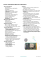
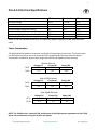
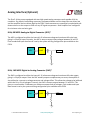
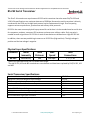
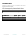
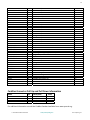
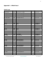
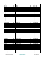
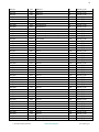
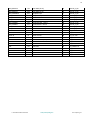
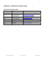
E‐14 Hardware Technical Reference Release: 14.1.8.12 Hardware Version: F
Pico E14 Hardware Reference www.picocomputing.com
(206) 283‐2178
Pico Computing, Inc.
150 Nickerson Street. Suite 311
Seattle, WA 98109
2
Contents: Product Overview Quick Reference Datasheet Electrical Specifications System Architecture Features Field Programmable Gate Array Power‐PC™ Processor CPLD TurboLoader Tri‐Mode Ethernet Interface Flash Memory DDR2 Memory I/O Interfaces Analog Interface RS‐232 Serial Interface Digital Peripheral Interface CardBus Interface Digital Bus Interface JTAG Debug Interface Appendices A – Peripheral I/O Connector Information B – CardBus Connector Information C – FPGA Pinout D – CPLD Pinout E – Standard Part Number Listing F – Errata G – FPGA Performance Enhancements E – Analog Interface Selection Guide Revision History Legal Notices E‐14 Hardware Reference Manual www.picocomputing.com
4
5
6
7
8
9
10
11
12
13
14
15
16
17
18
19
20
21
22
38
30
32
33
34
35
36
Pico Computing, Inc.
3
Product Overview: The Pico families of product are revolutionary embedded platforms. With performance that often exceeds modern microcomputers, a shockingly small form factor, and nominal power consumption that is less than one watt, the Pico family of products takes computing to a whole new level. The Pico E‐14 is based on the revolutionary Virtex‐4 chip. This device has the performance and power consumption of a custom chip (ASIC), but is completely reconfigurable! The Pico E‐14 EP (Embedded Processor) can be configured with either the FX20 FX40 or FX60 Virtex 4 FPGA. Advanced users will enjoy the open source development kits that allow absolute control over the hardware. Those who desire a high level programming environment can use Simulink® to implement custom algorithms in hardware with just the click of a button. Impulse C™ support is also included for rapid firmware development in the C programming language. Board support packages are available for operating systems such as Linux or μC/OS. E‐14 Hardware Reference Manual www.picocomputing.com
Pico Computing, Inc.
4
Pico E-14 EP Quick Reference Datasheet
Core Technologies
Features
- Virtex-4 FPGA
- PowerPC-405 450 MHz (680 DMIPS)
- 256 MB RAM
- 64 MB FPGA Image Flash
- Analog to Digital and Digital to Analog
Converters
- Gigabit Ethernet (1000/100/10 Mbps)
- 2 RS-232 Serial Ports
- JTAG Hardware / Software Debugging
- 54-bit High Speed Digital I/O Bus
- 16-bit external digital I/O port
- Standalone operation
- JTAG hardware / software debugging
- Open source
Mechanical Specification
- Cardbus Type II
- Stainless Steel Case
- Temperature Range: 0C to +85C
FPGA Performance
- DES > 16 Gbps / 250M Keys / second
- RC4 > 10 Gbps / 12M Keys / second
- > 16 Billion Multiply and Accumulates / second
Typical Applications
- Application on Card (AOC) systems. Vendors
sell their applications packaged with the
platform that they run on.
- Hybrid embedded processor / DSP applications
- Encryption / decryption
- Security algorithms and testing
- Software radio component
- Embedded control systems
- Embedded web servers / applications
- Weight and size constrained environments such
as UAVs, surveillance systems and
environmental monitoring devices.
- Complete development environment for laptop
computers. Ideal for rapid prototyping and
classroom environments.
- Complete Cardbus host interface capable of bus
speeds up to 1 Gbps
- DSP capability of the Virtex-4 FPGA
- Bus interface re-configurable to fit other bus nterface
protocols
- Works with Xilinx standard tool set (ISE, EDK, and
Platform SDK)
- Works with Starbridge Systems’ Viva, a graphical
development and modeling tool set designed for
parallel computing and IP portability
- Pico Flash utility for FPGA image and software
executable management. Runs on Windows, Linux,
and Apple Hosts
- Available plug-in for Matlab
- Pico DSP Accelerator / Xilinx System Generator plugin for Simulink available
- Available complete board support packages for
PowerPC embedded computing with Xilinx EDK
- Available port of RTCA DO-178B compliant UCOS-II
deterministic / pre-emptive kernel
- Available Linux port
- Available port of Green Hills Integrity RTOS
- Dynamic image swapping: unique design allows for
many FPGA images and user software images to be
stored on the PICO E-14's flash memory at one
time. FPGA and software images are associated
(paired). This allows image sets to be swapped
dynamically. Applications can store data in SDRAM.
This data can then be used by subsequent image
sets seamlessly.
Analog Capabilities
- 1 High Speed Analog to Digital
- 8 Bit @ 105MS/Sec
- 10 Bit @ 80MS/Sec
- 1 High Speed Digital to Analog
- 8 Bit @ 210MS/Sec
- 10 Bit @ 165MS/Sec
E‐14 Hardware Reference Manual www.picocomputing.com
Pico Computing, Inc.
5
Pico E‐14 Electrical Specifications
Minimum
Nominal Maximum
DC Input Voltage Power Consumption Recommended Temperature Range Maximum Allowable Temperature Range Continuous Storage Temperature Range Relative Humidity (Non‐Condensing) 3.15V 0°C 0°C ‐50°C 0% 3.3‐5.0V 10°C 30°C 5.5V 10W* 70°C 85°C 125°C 95% Note: If the card draws more than 10 watts the power supplies cut off and reset the card Power Consumption The graph below has power consumption running Pico Computing’s primary boot. The primary boot has everything running on the card, except D/A, A/D, and Ethernet. The lower chart has power consumption numbers for primary boot image with 10/100 and GigaBit ethernet running. Without Ethernet Voltage (V) Current (A) Power (W) FX 20 3.3 0.7 2.31 FX 60 3.3 0.8 2.64 With 10/100 Ethernet Voltage (V) Current (A) Power (W) FX 20 3.3 0.8 2.64 FX 60 3.3 1.0 3.3 FX 20 FX 60 With GigaBit Ethernet Voltage (V) Current (A) 3.3 1.0 3.3 1.3 Power (W) 3.3 4.3 NOTE: The CardBus slot is rated to 3.3W, and because of the higher power requirement of the FX 60, we do not recommend running the FX 60 in the laptop.
E‐14 Hardware Reference Manual www.picocomputing.com
Pico Computing, Inc.
6
System Architecture At the core of the Pico E‐14 is a Virtex‐4 FPGA. The FPGA can be dynamically configured to perform any number of specialized tasks such as: protocol processing, encryption, or complex mathematical functions. Embedded systems benefit from the integrated Power‐PC™ processor available on the EP series cards. Gigabit Ethernet
Analog Converters
Serial Transceiver
I/O
JTAG
DSP
Slices
RAM
DDR2 RAM
GPIO
Flash ROM
Figure 1
E‐14 Hardware Reference Manual www.picocomputing.com
Pico Computing, Inc.
7
Field Programmable Gate Array
The core of the Pico E‐14 is a high performance Virtex‐4 FPGA. Included in the FPGA are the FPGA Fabric, a Power‐PC ™ processor, ultra high‐speed DSP slices and DDR2 RAM. FPGA Fabric: The “Fabric” of an FPGA comprises an array of logic elements that can be connected in virtually unlimited patterns. These patterns of logic elements can be used to perform basic mathematical functions such as addition and subtraction, or can be grouped together to perform complex functions like Fast Fourier Transforms. Logic elements can even be connected to create a custom soft processor. The advantage of the FPGA is that the internal logic can be optimized for a specific application. FPGAs are also able to execute operations in parallel, not being limited by sequential execution like a traditional processor. FPGA operations can be executed in a parallel, pipelined or even an asynchronous manner. The FPGA allows incredible application speed with very low power consumption. Your imagination is really the limit. DSP Slice: Embedded within the FPGA are special areas that are designed to facilitate high speed “digital signal processing.” These areas are called DSP slices. The DSP slice can be configured in a variety of different ways. For example one DSP slice can be configured to be one tap of an FIR filter. DSP slices are fully pipelined and feature incredible speed. When configured for FIR filtering the DSP slice has a guaranteed performance of 500MHz with a latency of one cycle. An 18x18 multiply and accumulate also runs at 250MHz with a latency of two cycles. Smaller data widths allow higher clock speeds. FPGA Resources: Free FPGA Cores Virtex‐4 Website www.opencores.org
www.xilinx.com/virtex4
E‐14 Hardware Reference Manual www.picocomputing.com
Pico Computing, Inc.
8
PowerPC™ Processor PPC405x3 Processor Introduction: FPGAs are renowned for their ability to process parallel logic, but they typically have a hard time emulating a high performance processor. To get the best of both worlds the Virtex‐4™ features an embedded Power PC Processor. Since the processor shares the same die as the FPGA it seamlessly interfaces with the FPGA fabric. A new feature of the Vitex‐4 FPGA is the addition of an auxiliary processor interface. The APU is the highest speed interface between the Power‐PC™ processor and the FPGA fabric. Up to four custom instructions may be implemented in the FPGA, which are accessible from the Power‐PC™. Board support packages are currently available for μC/OS, Linux and Integrity. Board support source code is available open source under the GPL. E‐14 Hardware Reference Manual www.picocomputing.com
Pico Computing, Inc.
9
CPLD TurboLoader A CPLD (Complex Programmable Logic Device) is a smaller version of an FPGA (described above) with permanent Flash storage built in. The Pico E‐14 contains one CPLD that loads and reconfigures the FPGA. The Pico firmware guide describes how to access the CPLD Image Manager. CPLD Resources: Xilinx CPLD Website www.xilinx.com/cpld
E‐14 Hardware Reference Manual www.picocomputing.com
Pico Computing, Inc.
10
Tri‐Mode Ethernet Interface
The Pico E‐14 features the Marvell Alaska series 88E1111 tri‐mode Ethernet transceiver. On EP series parts the MAC (Middle access controller) is implemented on the FPGA die. On LO series parts the MAC must be implemented in firmware. Communication between the MAC and PHY takes place over an industry standard MII/GMII interface. The Ethernet transceiver features 10/100/1000 full/half duplex operation. It will automatically configure the physical interface on the fly for crossover or straight through operation. The PHY can even automatically correct for common wiring mistakes. The PHY has a built in Time Domain Reflectometer that can diagnose cable problems and pinpoint their distance away from the transceiver. In contrast to the Pico E‐12, the Ethernet interface on the Pico E‐14 is magnetically isolated allowing direct connections to an industry standard hub or switch. The Marvell 88E1111 is the only chip on the Pico E‐14 that requires an NDA for access to the datasheets. If you are interested in some of the advanced features not supported by the native driver, contact Pico Computing for assistance in obtaining an NDA from Marvell. Users are warned not to contact Marvell directly. Ethernet Resources: Marvell 88E1111 Webpage http://www.marvell.com/products/transceivers/singleport/88e1111.jsp
E‐14 Hardware Reference Manual www.picocomputing.com
Pico Computing, Inc.
11
Flash Memory The Pico E‐14 comes equipped with at least 64 megabytes of Flash ROM. The Flash ROM is divided into 512 sectors that can be erased independently. Most of the space on the ROM is reserved for the user. The Flash ROM’s address bus can be controlled by either the TurboLoader or the FPGA, but not both. During power‐up or reboot, the TurboLoader is in control of the Flash ROM Address bus. At all other times the FPGA is in control of the address bus. Figure 2 Typical Flash ROM Allocation Table: Byte addresses 0x00000000‐0x0000FFFF 0x00010000‐0x0006FFFF 0x000A0000‐0x000FFFFF 0x000D0000‐0x0012FFFF 0x00140000‐0x01FFFFFF Description Tuple Data and configuration management Primary FPGA Image Backup FPGA Image Secondary Image including boot loader Other FPGA images, executables and data files Flash Sectors 0 1‐6 7‐12 13‐19 20‐511 The Flash ROM has a simple, open file system that allows the user to store FPGA images, ELF binary files, or other data. The primary image is used to boot the FPGA initially, and the backup image is only invoked if the primary image fails to load correctly. Executable files are in ELF format and are loaded by a loader within the secondary image. The primary image can either load the secondary image or pause for the PC to access and manage the file system. E‐14 Hardware Reference Manual www.picocomputing.com
Pico Computing, Inc.
12
DDR2 Memory The Pico E‐14 comes equipped with 256 MB of PC‐266 DDR2 memory. There are four 256Mb chips each with 16 bit data paths that are grouped into two 32 bit banks. From 0°C to +95°C, the ram can run at 266 MHz. For operation at temperatures below 0°C, special firmware with reduced ram timings is required. The temperature compensated self‐refresh mode must be disabled below ‐20°C. 16x16
(LSBs)
16x16
(MSBs)
Bank 1
16x16
(LSBs)
16x16
(MSBs)
Bank 2
FPGA
Figure 3
E‐14 Hardware Reference Manual www.picocomputing.com
Pico Computing, Inc.
13
Analog Interface (Optional)
The Pico E‐14 also comes equipped with two high‐speed analog converters each capable of 14‐bit resolution. By default, both analog converters are powered down until the sleep lines are driven low and the amplifier lines are driven high by the FPGA. Both converters are capacitively coupled with pull‐
down resistors on the output to filter out any DC signal components. Both amplifiers are configured for minimum noise and unity gain. 8‐Bit, 80 MSPS Analog‐to‐Digital Converter (ADC)* The ADC is configured to utilize the internal 1.0V reference voltage and maximum full scale input, giving it a 2V pk‐pk input. Currently, the ADC is setup to accept input voltages between 0V and 2V. Clock modes and input data format is set by the system utilizing configuration pins available to the FPGA. ADC
AMP
Input
8‐Bit, 165 MSPS Digital‐to‐Analog Converter (DAC)* The DAC is configured to utilize the internal 1.2V reference voltage and maximum full‐scale output, giving it a 2V pk‐pk output. Since the DAC actually outputs complementary currents, the amplifier is also utilized as a current to voltage converter and voltage shifter. This allows the voltage to be buffered within the 0V to 3V rail voltages. Currently, the DAC is setup to output between .5V and 2.5V. This gives us a comfortable .5V between our maximum outputs and rail voltages. Clock modes and input data format is set by the system utilizing configuration pins available to the FPGA. DAC
AMP
Output
E‐14 Hardware Reference Manual www.picocomputing.com
Pico Computing, Inc.
14
*Please refer to the Analog Interface Selection Guide in Appendix E for compatible 8‐12‐bit converters RS‐232 Serial Transceiver The Pico E‐14 contains one asynchronous RS‐232 serial transceiver that also meets EIA/TIA‐232 and V.28/V.24 specifications at a maximum data rate of 250kBps. Because the serial transceiver is directly connected to the FPGA any bit high‐level protocol can be implemented in logic. Pico Computing supports various asynchronous, synchronous and military serial protocols. RS‐232 is the most common physical layer protocol for serial data. It is the standard used on serial mice for computers, modems, consumer GPS receivers and even some military radios. Only one wire is needed to send a signal on an RS‐232 link. A total of two devices are allowed on a single RS‐232 link. In addition, there are two possible logic states on an RS‐232 line (high and low). The high voltage is positive and the low voltage is negative. Physical Layer Specifications: Standard Noise Max
Immunity Distance Satisfactory 50ft
RS‐232 Max
Speed Max
Connections 250 kBps*
1 Tx / 1 Rx
*Maximum speed decreases with increased cable length. *The old RS‐232, 422 and 485 standards are now obsolete and have been replaced by EIA/TIA‐232, 422 and 485. Serial Transceiver Specifications: Maximum Continuous Positive Input Voltage Maximum Continuous Negative Input Voltage ESD Protection Limit Maximum Short Circuit Duration on Output Typical RS‐232 Output Voltage RS‐232 Maximum Low Input Threshold* RS‐232 Minimum High Input Threshold +25 VDC ‐25 VDC +/‐15,000V Infinite +/‐ 5.4 V 1.2 V 1.5 V *RS‐232 Receivers can accept digital inputs E‐14 Hardware Reference Manual www.picocomputing.com
Pico Computing, Inc.
15
Digital Peripheral Interface
The Pico E‐14 features 16 GPIO lines that are used for external peripheral support. Pulling the DIAG_EN pin low replaces 4 GPIO signals with JTAG signals. All GPIO signals have user selectable pull‐up, pull‐down, keeper or HI‐Z termination. Drive strength is also user selectable between 2 and 24mA. All GPIOs can be configured for input, output and bi‐
directional mode and are equipped with ESD protection. DIAG_EN State JTAG
GPIO
Float / High Low Disabled Enabled Enabled Disabled Electrical Specifications Minimum
Nominal Maximum
High Voltage Low Voltage Input Impedance (Pulldowns Disabled) Drive Strength (Selectable) ESD Withstand Voltage (Human Body Model) 1.7V ‐0.2V 2 mA 2.5V 0V HI‐Z 2.9V 0.7V 24 mA 2 KV E‐14 Hardware Reference Manual www.picocomputing.com
Pico Computing, Inc.
16
CardBus Interface The Pico E‐14 can run as a standalone product or be connected to a host using the CardBus connector. By default, the Pico E‐14 ships with firmware that is ready for use as a CardBus slave device, but it also supports bus mastering. That same firmware also provides the means to switch into standlone mode.1 CardBus is a 32‐bit interface with a maximum speed of 33 MHz. The Pico E‐14 hardware is designed to support standard PCMCIA as well as DMA mode. The CardBus standard specifies that all CardBus hosts be backward compatible with PCMCIA. Since CardBus systems can only be 3.3V, no digital translating transceivers are required to connect with a host. This allows direct connection to the Virtex‐4 FPGA for reduced power consumption. With this design, it is easily possible to reverse the CardBus interface and use the Pico E‐14 as a host controller for other CardBus and PCMCIA cards. Those who are interested in alternate interfaces should contact Pico Computing. The PCMCIA decoder source code and support is available. PCMCIA Interface Resources: CompactFlash Association PCMCIA Website www.compactflash.org
www.pcmcia.org
1
For more information on standlone, reference the Standalone documentation located in the doc directory of where Pico
Utility is installed.
E‐14 Hardware Reference Manual www.picocomputing.com
Pico Computing, Inc.
17
Digital Bus Interface When the Pico E‐14 is not connected to a CardBus host, the digital bus can be reconfigured to connect with a wide variety of high‐speed digital busses and peripherals. All signals have user selectable pull‐
up, pull‐down, keeper or HI‐Z termination. Drive strength is also user selectable between 2 and 24mA. All pins can be configured for input, output and bi‐directional mode. With proper termination, speeds of over 200 MHz are possible. The external digital bus is set to transmit and receive at 3.3V only. Electrical Specifications (DC) Minimum
Nominal Maximum
Positive Supply Input Voltage (Vcc) Low Level Input Voltage High Level Input Voltage Drive Strength 3.15V 0V 2V 2mA 3.3V 0V 3.0V 5.5V 0.7V 3.3V 24mA E‐14 Hardware Reference Manual www.picocomputing.com
Pico Computing, Inc.
18
JTAG Debug Interface The Pico E‐14 is equipped with a JTAG diagnostic port that allows real‐time debugging of hardware, firmware and software. Use of the external JTAG port disables four external GPIO pins as well as the internal JTAG loop back. Some JTAG programs require the length of the instruction register (IR). The IR length is listed below for all devices in the JTAG chain. Device Instruction register bit length
FPGA TurboLoader Ethernet PHY FX20 10 FX60 14 8 8 FPGA
TDI
PowerPC
FX20:
IR=IR
10= 10
FX60: IR = 14
Turbo Loader
Ethernet
IR= 8
IR= 8
TDO
Figure 4 The Primary Image in the Flash ROM contains an embedded JTAG diagnostic port. This allows a user in Windows or Linux to debug software without an external JTAG cable. The internal JTAG diagnostic loop back looks just like a Parallel Port IV diagnostic cable when used with the Pico E‐14 driver. E‐14 Hardware Reference Manual www.picocomputing.com
Pico Computing, Inc.
19
Appendix A – Peripheral I/O Connector Information Connector Information Description Mating Connector Mating Connector Backshell Brand Hirose Hirose Part Number NX30TA‐32PAA(50) NX‐32TA‐CV1(50) *Connectors are always in stock at Pico Computing Peripheral I/O Connector Pinout 1 2 3 4 5 6 7 8 9 10 11 12 13 14 15 16 17 18 19 20 21 22 23 24 25 26 27 28 29 30 31 32 ETHER_OUT_DD‐ ETHER_OUT_DD+ GPIO_15_FILTERED GPIO_14_FILTERED GPIO_13_FILTERED GPIO_12_FILTERED ETHER_OUT_DC‐ ETHER_OUT_DC+ GPIO_11_FILTERED GPIO_10_FILTERED GPIO_9_FILTERED GPIO_8_FILTERED ETHER_OUT_DB‐ ETHER_OUT_DB+ GPIO_7_FILTERED GPIO_6_FILTERED GPIO_5_FILTERED GPIO_4_FILTERED ETHER_OUT_DA‐ ETHER_OUT_DA+ DAC_OUTPUT SERIAL_RX_FILT SERIAL_TX_FILT ADC_INPUT PIC_TRIGGER_EXT 2.5V_EXT GPIO_3/TDI_FILT GPIO_2/TDO_FILT GPIO_1/TMS_FILT GPIO_0/TCK_FILT D\I\A\G\_\E\N\_\ GND_EXT Ethernet (Magnetically Isolated) Ethernet (Magnetically Isolated) General purpose I/O General purpose I/O General purpose I/O General purpose I/O Ethernet (Magnetically Isolated) Ethernet (Magnetically Isolated) General purpose I/O General purpose I/O General purpose I/O General purpose I/O Ethernet (Magnetically Isolated) Ethernet (Magnetically Isolated) General purpose I/O General purpose I/O General purpose I/O General purpose I/O Ethernet (Magnetically Isolated) Ethernet (Magnetically Isolated) D/A Converter output RS‐232 Serial receiver input RS‐232 Serial driver output A/D Converter input NOT CONNECTED 2.5V 0.45A peripheral power General purpose I/O or JTAG TDI General purpose I/O or JTAG TDO General purpose I/O or JTAG TMS General purpose I/O or JTAG TCK JTAG port enable when shorted to ground Ground return NOTE: Pin 1 indicator on the board is actually Pin 32 indicator E‐14 Hardware Reference Manual www.picocomputing.com
Pico Computing, Inc.
20
Peripheral Connector Pin #1 Location Figure 5 Appendix B – CardBus Connector Information
Connector Information Description CardBus Header Brand Hirose Part Number IC9‐68RD‐0.635SF‐(51) The Pico E‐14 will mate with any Type‐II CardBus Header The function and direction of the pins on the CardBus interface can be easily changed. Please see the “Digital Bus Interface” section for more information. CardBus Connector Pinout Name Pin Description Dir GND CAD0 CAD1 CAD3 CAD5 CAD7 C\C\/\B\E\0\ CAD9 CAD11 CAD12 CAD14 C\C\/\B\E\1\ CPAR C\P\E\R\R\ C\G\N\T\ C\I\N\T\ VCC VPP CCLK C\I\R\D\Y\ C\C\/\B\E\2\ CAD18 CAD20 CAD21 CAD22 CAD23 CAD24 CAD25 1 2 3 4 5 6 7 8 9 10 11 12 13 14 15 16 17 18 19 20 21 22 23 24 25 26 27 28 Card Ground
CardBus Data/Address 0
CardBus Data/Address 1
CardBus Data/Address 3
CardBus Data/Address 5
CardBus Data/Address 7
Command and Byte Enable
CardBus Data/Address 9
CardBus Data/Address 11
CardBus Data/Address 12
CardBus Data/Address 14
Command and Byte Enable
Parity
Parity Error
Grand
Card Intert Request
Card Power (3.3V)
Card Programming Voltage (Not Used)
CardBus Clock
Initiator Ready
Command and Byte Enable
CardBus Data/Address 18
CardBus Data/Address 20
CardBus Data/Address 21
CardBus Data/Address 22
CardBus Data/Address 23
CardBus Data/Address 24
CardBus Data/Address 25
PWR
IO
IO
IO
IO
IO
IO
IO
IO
IO
IO
IO
IO
IO
I
O
PWR
PWR
I
IO
IO
IO
IO
IO
IO
IO
IO
IO
E‐14 Hardware Reference Manual www.picocomputing.com
Pico Computing, Inc.
21
CAD26 CAD27 CAD29 RFU C\C\L\K\R\U\N\ GND GND C\C\D\1\ CAD2 CAD4 CAD6 RFU CAD8 CAD10 C\V\S\1\ CAD13 CAD15 CAD16 RFU C\B\L\O\C\K\ C\S\T\O\P\ C\D\E\V\S\E\L\ VCC VPP C\T\R\D\Y\ C\F\R\A\M\E\ CAD17 CAD19 C\V\S\2\ C\R\S\T\ C\S\E\R\R\ C\R\E\Q\ C\C\/\B\E\3\ CAUDIO CSTSCHG CAD28 CAD30 CAD31 C\C\D\2\ GND 29 30 31 32 33 34 35 36 37 38 39 40 41 42 43 44 45 46 47 48 49 50 51 52 53 54 55 56 57 58 59 60 61 62 63 64 65 66 67 68 CardBus Data/Address 26
CardBus Data/Address 27
CardBus Data/Address 29
Reserved For Future Use
Clock Request / Status
Card Ground
Card Ground
Card Detect
CardBus Data/Address 2
CardBus Data/Address 4
CardBus Data/Address 6
Reserved For Future Use
CardBus Data/Address 8
CardBus Data/Address 10
Voltage Select
CardBus Data/Address 13
CardBus Data/Address 15
CardBus Data/Address 16
Reserved For Future Use
Card Lock
Stop Transaction
Device Select
Card Power (3.3V)
Card Programming Voltage (Not Used)
Target Ready
Cycle Frame
CardBus Data/Address 17
CardBus Data/Address 19
Voltage Select
System Reset
System Error
Request
Command and Byte Enable
Card Audio Signal
Card Status Change
CardBus Data/Address 28
CardBus Data/Address 30
CardBus Data/Address 31
Card Detect
Card Ground
IO
IO
IO
IO
O
PWR
PWR
Passive
IO
IO
IO
IO
IO
IO
PWR
IO
IO
IO
IO
IO
IO
IO
PWR
PWR
IO
IO
IO
IO
Passive
I
O
O
IO
O
O
IO
IO
IO
Passive
PWR
CardBus Connector Pull Up and Pull Down Information Name Pin Description ‐CGNT ‐CFRAME ‐CTRDY ‐CIRDY 15 54 53 20 Pull Up
Pull Up
Pull Up
Pull Up
Value 15K
15K
15K
15K
For additional information consult the CardBus Standard available from: www.pcmcia.org. E‐14 Hardware Reference Manual www.picocomputing.com
Pico Computing, Inc.
22
E‐14 Hardware Reference Manual www.picocomputing.com
Pico Computing, Inc.
23
Appendix C – FPGA Pinout
FPGA Pinout 50MHZ_CLOCK 50MHZ_CLOCK 50MHZ_CLOCK 50MHZ_CLOCK 50MHZ_CLOCK 50MHZ_CLOCK ADC_AMP_PWUP ADC_CLK ADC_D0 ADC_D1 ADC_D2 ADC_D3 ADC_D4 ADC_D5 ADC_D6 ADC_D7 ADC_D8 ADC_D9 ADC_D10 ADC_D11 ADC_D12 ADC_D13 ADC_MODE ADC_OTR ADC_PDWN CB_CAD0 CB_CAD1 CB_CAD2 CB_CAD3 CB_CAD4 CB_CAD5 CB_CAD6 CB_CAD7 CB_CAD8 CB_CAD9 CB_CAD10 CB_CAD11 CB_CAD12 CB_CAD13 CB_CAD14 AA14 AB12 AB14 AC13 AD15 AE13 AD14 V23 W23 T24 V21 W18 Y22 W20 AB21 Y18 AB20 AC21 T20 R20 R21 V18 T17 T18 V22 K3 F3 D3 C3 M6 L7 K7 J4 G5 G9 F7 F8 D4 C4 D5 E‐14 Hardware Reference Manual 50 MHz Clock In +/‐ 50 ppm 50 MHz Clock In +/‐ 50 ppm 50 MHz Clock In +/‐ 50 ppm 50 MHz Clock In +/‐ 50 ppm 50 MHz Clock In +/‐ 50 ppm 50 MHz Clock In +/‐ 50 ppm A/D Amplifier Power Up Clock Data 0 [LSB] Data 1 Data 2 Data 3 Data 4 Data 5 Data 6 Data 7 Data 8 Data 9 Data 10 Data 11 Data 12 Data 13 [MSB] Data Format Select Out‐of‐Range Indicator Power Down A/D Controller CardBus Data/Address 0 CardBus Data/Address 1 CardBus Data/Address 2 CardBus Data/Address 3 CardBus Data/Address 4 CardBus Data/Address 5 CardBus Data/Address 6 CardBus Data/Address 7 CardBus Data/Address 8 CardBus Data/Address 9 CardBus Data/Address 10 CardBus Data/Address 11 CardBus Data/Address 12 CardBus Data/Address 13 CardBus Data/Address 14 www.picocomputing.com
I I I I I I O O I I I I I I I I I I I I I I O O O I/O I/O I/O I/O I/O I/O I/O I/O I/O I/O I/O I/O I/O I/O I/O LV_TTL 3.3V LV_TTL 3.3V LV_TTL 3.3V LV_TTL 3.3V LV_TTL 3.3V LV_TTL 3.3V LV_TTL 3.3V LV_CMOS 2.5V LV_CMOS 2.5V LV_CMOS 2.5V LV_CMOS 2.5V LV_CMOS 2.5V LV_CMOS 2.5V LV_CMOS 2.5V LV_CMOS 2.5V LV_CMOS 2.5V LV_CMOS 2.5V LV_CMOS 2.5V LV_CMOS 2.5V LV_CMOS 2.5V LV_CMOS 2.5V LV_CMOS 2.5V LV_CMOS 2.5V LV_CMOS 2.5V LV_CMOS 2.5V LV_TTL 3.3V LV_TTL 3.3V LV_TTL 3.3V LV_TTL 3.3V LV_TTL 3.3V LV_TTL 3.3V LV_TTL 3.3V LV_TTL 3.3V LV_TTL 3.3V LV_TTL 3.3V LV_TTL 3.3V LV_TTL 3.3V LV_TTL 3.3V LV_TTL 3.3V LV_TTL 3.3V Pico Computing, Inc.
24
CB_CAD15 CB_CAD16 CB_CAD17 CB_CAD18 CB_CAD19 CB_CAD20 CB_CAD21 CB_CAD22 CB_CAD23 CB_CAD24 CB_CAD25 CB_CAD26 CB_CAD27 CB_CAD28 CB_CAD29 CB_CAD30 CB_CAD31 CB_CAUDIO CB_CBLOCK CB_CC/BE0 CB_CC/BE1 CB_CC/BE2 CB_CC/BE3 CB_CCLK CB_CCLKRUN CB_CDEVSEL CB_CFRAME CB_CGNT CB_CINT CB_CIRDY CB_CPAR CB_CPERR CB_CREQ CB_CRST CB_CSERR CB_CSTOP CB_CSTSCHG CB_CTRDY CB_RFU1 CB_RFU2 CB_RFU3 CPLD_TDI DAC_AMP_PWUP DAC_CLK DAC_CLK‐ DAC_CMODE D6 C7 J5 K6 E5 E6 E7 D9 C8 F10 G4 J3 L10 K8 F4 K11 H9 H3 B9 H4 C6 H6 D10 D11 G10 G12 H8 A9 B11 G7 A7 A8 B10 D8 C9 A10 J9 E8 E3 H7 B7 R13 K12 H11 J11 B6 E‐14 Hardware Reference Manual CardBus Data/Address 15 CardBus Data/Address 16 CardBus Data/Address 17 CardBus Data/Address 18 CardBus Data/Address 19 CardBus Data/Address 20 CardBus Data/Address 21 CardBus Data/Address 22 CardBus Data/Address 23 CardBus Data/Address 24 CardBus Data/Address 25 CardBus Data/Address 26 CardBus Data/Address 27 CardBus Data/Address 28 CardBus Data/Address 29 CardBus Data/Address 30 CardBus Data/Address 31 Card Audio Signal Card Lock Command and Byte Enables Command and Byte Enables Command and Byte Enables Command and Byte Enables Clock Clock Request / Status Device Select Cycle Frame Grant Card Interrupt Request Initiator Ready Parity Parity Error Request Card Reset System Error Stop Transaction Card Status Change Target Ready CardBus: Reserved for Future Use CardBus: Reserved for Future Use CardBus: Reserved for Future Use CPLD JTAG TDI D/A Amplifier Power Up Clock Complementary Clock Clock Mode Selection www.picocomputing.com
I/O I/O I/O I/O I/O I/O I/O I/O I/O I/O I/O I/O I/O I/O I/O I/O I/O O I/O I/O I/O I/O I/O I I/O I/O I/O I O I/O I/O I/O O I O I/O O I/O I/O I/O I/O O O O O LV_TTL 3.3V LV_TTL 3.3V LV_TTL 3.3V LV_TTL 3.3V LV_TTL 3.3V LV_TTL 3.3V LV_TTL 3.3V LV_TTL 3.3V LV_TTL 3.3V LV_TTL 3.3V LV_TTL 3.3V LV_TTL 3.3V LV_TTL 3.3V LV_TTL 3.3V LV_TTL 3.3V LV_TTL 3.3V LV_TTL 3.3V LV_TTL 3.3V LV_TTL 3.3V LV_TTL 3.3V LV_TTL 3.3V LV_TTL 3.3V LV_TTL 3.3V LV_TTL 3.3V LV_TTL 3.3V LV_TTL 3.3V LV_TTL 3.3V LV_TTL 3.3V LV_TTL 3.3V LV_TTL 3.3V LV_TTL 3.3V LV_TTL 3.3V LV_TTL 3.3V LV_TTL 3.3V LV_TTL 3.3V LV_TTL 3.3V LV_TTL 3.3V LV_TTL 3.3V LV_TTL 3.3V LV_TTL 3.3V LV_TTL 3.3V LV_TTL 3.3V LV_TTL 3.3V LV_TTL 3.3V LV_TTL 3.3V LV_TTL 3.3V Pico Computing, Inc.
25
DAC_D0 DAC_D1 DAC_D2 DAC_D3 DAC_D4 DAC_D5 DAC_D6 DAC_D7 DAC_D8 DAC_D9 DAC_D10 DAC_D11 DAC_D12 DAC_D13 DAC_MODE DAC_SLEEP ETHER_25MHZ ETHER_125MHZ ETHER_COL ETHER_COMA ETHER_CRS ETHER_IRQ ETHER_MDC ETHER_MDIO ETHER_RESET ETHER_RX0 ETHER_RX1 ETHER_RX2 ETHER_RX3 ETHER_RX4 ETHER_RX5 ETHER_RX6 ETHER_RX7 ETHER_RX_CLK ETHER_RX_CTL ETHER_RX_ER ETHER_TX0 ETHER_TX1 ETHER_TX2 ETHER_TX3 ETHER_TX4 ETHER_TX5 ETHER_TX6 ETHER_TX7 ETHER_TX_CLK ETHER_TX_CTL H16 K13 G11 J14 E10 H12 H13 C11 H14 G15 G14 J15 J16 G16 K10 E11 AA15 P24 AD19 AC19 AA19 AB15 AD24 AC16 AC24 U24 AD20 AD21 AD16 U21 T23 AD18 T22 V24 AB16 Y23 AA22 AC18 AB24 AB19 AB17 AA23 AC17 AC23 W24 AA24 E‐14 Hardware Reference Manual Data 0 [LSB] Data 1 Data 2 Data 3 Data 4 Data 5 Data 6 Data 7 Data 8 Data 9 Data 10 Data 11 Data 12 Data 13 [MSB] Input Data Format Power Down D/A Controller 25 MHz Clock 125 MHz Clock Collision Detect Power Save Mode Carrier Sense IRQ Media Independent Interface Clock Media Independent Interface Data Reset MII/GMII Data In 0 MII/GMII Data In 1 MII/GMII Data In 2 MII/GMII Data In 3 MII/GMII Data In 4 MII/GMII Data In 5 MII/GMII Data In 6 MII/GMII Data In 7 MII/GMII RX Clock MII/GMII RX Enable MII/GMII RX Error MII/GMII Data Out 0 MII/GMII Data Out 1 MII/GMII Data Out 2 MII/GMII Data Out 3 MII/GMII Data Out 4 MII/GMII Data Out 5 MII/GMII Data Out 6 MII/GMII Data Out 7 MII/GMII TX Clock MII/GMII TX Enable www.picocomputing.com
O O O O O O O O O O O O O O O O O I I O I I O I/O O I I I I I I I I I I I O O O O O O O O O O LV_TTL 3.3V LV_TTL 3.3V LV_TTL 3.3V LV_TTL 3.3V LV_TTL 3.3V LV_TTL 3.3V LV_TTL 3.3V LV_TTL 3.3V LV_TTL 3.3V LV_TTL 3.3V LV_TTL 3.3V LV_TTL 3.3V LV_TTL 3.3V LV_TTL 3.3V LV_TTL 3.3V LV_TTL 3.3V LV_CMOS 2.5V LV_CMOS 2.5V LV_CMOS 2.5V LV_CMOS 2.5V LV_CMOS 2.5V LV_CMOS 2.5V LV_CMOS 2.5V LV_CMOS 2.5V LV_CMOS 2.5V LV_CMOS 2.5V LV_CMOS 2.5V LV_CMOS 2.5V LV_CMOS 2.5V LV_CMOS 2.5V LV_CMOS 2.5V LV_CMOS 2.5V LV_CMOS 2.5V LV_CMOS 2.5V LV_CMOS 2.5V LV_CMOS 2.5V LV_CMOS 2.5V LV_CMOS 2.5V LV_CMOS 2.5V LV_CMOS 2.5V LV_CMOS 2.5V LV_CMOS 2.5V LV_CMOS 2.5V LV_CMOS 2.5V LV_CMOS 2.5V LV_CMOS 2.5V Pico Computing, Inc.
26
ETHER_TX_ER F\L\A\S\H\_\B\Y\T\E\ F\L\A\S\H\_\O\E\ F\L\A\S\H\_\R\E\S\E\T\ F\L\A\S\H\_\W\E\ F\L\A\S\H\_\W\P\ F\L\A\S\H\_C\E\ F\P\G\A\_\P\R\O FLASH_A0 FLASH_A1 FLASH_A2 FLASH_A3 FLASH_A4 FLASH_A5 FLASH_A6 FLASH_A7 FLASH_A8 FLASH_A9 FLASH_A10 FLASH_A11 FLASH_A12 FLASH_A13 FLASH_A14 FLASH_A15 FLASH_A16 FLASH_A17 FLASH_A18 FLASH_A19 FLASH_A20 FLASH_A21 FLASH_A22 FLASH_A23 FLASH_A24 FLASH_A25 FLASH_D0 FLASH_D1 FLASH_D2 FLASH_D3 FLASH_D4 FLASH_D5 FLASH_D6 FLASH_D7 FLASH_D8 FLASH_D9 FLASH_D10 FLASH_D11 AA18 AD3 AA3 T3 W5 Y16 V3 K17 AD6 AD8 AD10 AC11 AD9 Y3 AC9 V4 P3 U5 P5 AC4 N4 R5 W3 AA8 AD4 AD11 AB6 AC7 AC6 AB5 AB11 AB9 AB4 AC3 V12 V13 V14 U14 W13 Y13 W14 W15 V11 W11 U15 U16 E‐14 Hardware Reference Manual MII/GMII TX Error Inverted 8/16 Bit Mode Select Inverted Output Enable Inverted Reset Inverted Write Enable InvertedWrite Protect Inverted Chip Enable Inverted FPGA Program Address 0 [LSB] Address 1 Address 2 Address 3 Address 4 Address 5 Address 6 Address 7 Address 8 Address 9 Address 10 Address 11 Address 12 Address 13 Address 14 Address 15 Address 16 Address 17 Address 18 Address 19 Address 20 Address 21 Address 22 Address 23 Address 24 Address 25 [MSB] Data 0 [LSB] Data 1 Data 2 Data 3 Data 4 Data 5 Data 6 Data 7 Data 8 Data 9 Data 10 Data 11 www.picocomputing.com
I O O O O O O O I/O I/O I/O I/O I/O I/O I/O I/O I/O I/O I/O I/O I/O I/O I/O I/O I/O I/O I/O I/O I/O I/O I/O I/O I/O I/O I/O I/O I/O I/O I/O I/O I/O I/O I/O I/O I/O I/O LV_CMOS 2.5V LV_CMOS 2.5V LV_CMOS 2.5V LV_CMOS 2.5V LV_CMOS 2.5V LV_CMOS 2.5V LV_CMOS 2.5V LV_CMOS 2.5V LV_CMOS 2.5V LV_CMOS 2.5V LV_CMOS 2.5V LV_CMOS 2.5V LV_CMOS 2.5V LV_CMOS 2.5V LV_CMOS 2.5V LV_CMOS 2.5V LV_CMOS 2.5V LV_CMOS 2.5V LV_CMOS 2.5V LV_CMOS 2.5V LV_CMOS 2.5V LV_CMOS 2.5V LV_CMOS 2.5V LV_CMOS 2.5V LV_CMOS 2.5V LV_CMOS 2.5V LV_CMOS 2.5V LV_CMOS 2.5V LV_CMOS 2.5V LV_CMOS 2.5V LV_CMOS 2.5V LV_CMOS 2.5V LV_CMOS 2.5V LV_CMOS 2.5V LV_CMOS 2.5V LV_CMOS 2.5V LV_CMOS 2.5V LV_CMOS 2.5V LV_CMOS 2.5V LV_CMOS 2.5V LV_CMOS 2.5V LV_CMOS 2.5V LV_CMOS 2.5V LV_CMOS 2.5V LV_CMOS 2.5V LV_CMOS 2.5V Pico Computing, Inc.
27
FLASH_D12 FLASH_D13 FLASH_D14 FLASH_D15 FLASH_READY FPGA_CCLK FPGA_DONE FPGA_INIT GPIO_0 GPIO_1 GPIO_2 GPIO_3 GPIO_4 GPIO_5 GPIO_6 GPIO_7 GPIO_8 GPIO_9 GPIO_10 GPIO_11 GPIO_12 GPIO_13 GPIO_14 GPIO_15 JTAG_LOOP_TCK JTAG_LOOP_TDI JTAG_LOOP_TDO JTAG_LOOP_TMS LOAD PEEKABOO PIC_CLK PIC_DATA R\A\M\_\C\A\S\ R\A\M\_\C\L\K\ R\A\M\_\C\L\K\ R\A\M\_\C\S\0\ R\A\M\_\C\S\1\ R\A\M\_\R\A\S\ R\A\M\_\W\E\ RAM_A0 RAM_A1 RAM_A2 RAM_A3 RAM_A4 RAM_A5 RAM_A6 Y11 Y12 W16 V16 Y15 M14 K15 L15 AA4 AA5 AC22 AB22 Y5 W4 Y6 Y7 AB10 Y10 AA10 N3 W19 AA20 W21 AD23 V8 V6 Y8 AC8 T4 P4 AF14 AF15 F24 B14 E15 C23 C24 F22 B15 D20 F19 A12 D21 E21 G21 A13 E‐14 Hardware Reference Manual Data 12 Data 13 Data 14 Data 15 [MSB] Flash Status FPGA Clock FPGA Done FPGA Initialize GPIO 1 GPIO 2 GPIO 3 GPIO 4 GPIO 1 GPIO 2 GPIO 3 GPIO 4 GPIO 1 GPIO 2 GPIO 3 GPIO 4 GPIO 1 GPIO 2 GPIO 3 GPIO 4 JTAG Loop back TCK JTAG Loop back TDI JTAG Loop back TDO JTAG Loop back TMS TurboLoader Load Image Request TurboLoader Load Image Request Power Management Controller Sleep Counter Power Management Controller Sleep Request Inverted Column Select Inverted Complementary Clock Inverted Comp. Clock Feedback Inverted Chip Select Bank 0 Inverted Chip Select Bank 1 Inverted Row Select Inverted Write Enable Address 0 [LSB] Address 1 Address 2 Address 3 Address 4 Address 5 Address 6 www.picocomputing.com
I/O I/O I/O I/O I O O O I/O I/O I/O I/O I/O I/O I/O I/O I/O I/O I/O I/O I/O I/O I/O I/O O I O O O O O O O O I O O O O O O O O O O O LV_CMOS 2.5V LV_CMOS 2.5V LV_CMOS 2.5V LV_CMOS 2.5V LV_CMOS 2.5V LV_CMOS 2.5V LV_CMOS 2.5V LV_CMOS 2.5V LV_CMOS 2.5V LV_CMOS 2.5V LV_CMOS 2.5V LV_CMOS 2.5V LV_CMOS 2.5V LV_CMOS 2.5V LV_CMOS 2.5V LV_CMOS 2.5V LV_CMOS 2.5V LV_CMOS 2.5V LV_CMOS 2.5V LV_CMOS 2.5V LV_CMOS 2.5V LV_CMOS 2.5V LV_CMOS 2.5V LV_CMOS 2.5V LV_CMOS 2.5V LV_CMOS 2.5V LV_CMOS 2.5V LV_CMOS 2.5V LV_CMOS 2.5V LV_CMOS 2.5V LV_TTL 3.3V LV_TTL 3.3V SSTL18_II_DCI SSTL18_II_DCI SSTL18_II_DCI SSTL18_II_DCI SSTL18_II_DCI SSTL18_II_DCI SSTL18_II_DCI SSTL18_II_DCI SSTL18_II_DCI SSTL18_II_DCI SSTL18_II_DCI SSTL18_II_DCI SSTL18_II_DCI SSTL18_II_DCI Pico Computing, Inc.
28
RAM_A7 RAM_A8 RAM_A9 RAM_A10 RAM_A11 RAM_A12 RAM_BA0 RAM_BA1 RAM_CLK RAM_CLK RAM_CLKE0 RAM_CLKE1 RAM_D0 RAM_D1 RAM_D2 RAM_D3 RAM_D4 RAM_D5 RAM_D6 RAM_D7 RAM_D8 RAM_D9 RAM_D10 RAM_D11 RAM_D12 RAM_D13 RAM_D14 RAM_D15 RAM_D16 RAM_D17 RAM_D18 RAM_D19 RAM_D20 RAM_D21 RAM_D22 RAM_D23 RAM_D24 RAM_D25 RAM_D26 RAM_D27 RAM_D28 RAM_D29 RAM_D30 RAM_D31 RAM_DM0‐7 RAM_DM8‐15 E22 D24 F20 F23 A14 D23 E23 K18 C14 F15 A15 G22 C19 F18 G20 D19 C21 E20 F17 B17 D15 D14 C16 A17 G17 B16 C12 B12 H19 H22 G24 H24 J21 G19 K20 K23 M22 M24 K21 L24 N22 L19 N24 J23 E17 C13 E‐14 Hardware Reference Manual Address 7 Address 8 Address 9 Address 10 Address 11 Address 12 [MSB] Bank Address 0 Bank Address 1 Clock Clock Feedback Clock Enable 0[Power Save Mode] Clock Enable 1[Power Save Mode] Data 0 (LSB) Data 1 Data 2 Data 3 Data 4 Data 5 Data 6 Data 7 Data 8 Data 9 Data 10 Data 11 Data 12 Data 13 Data 14 Data 15 Data 16 Data 17 Data 18 Data 19 Data 20 Data 21 Data 22 Data 23 Data 24 Data 25 Data 26 Data 27 Data 28 Data 29 Data 30 Data 31 Data Mask [0‐7] Data Mask [8‐15] www.picocomputing.com
O O O O O O O O O I O O I/O I/O I/O I/O I/O I/O I/O I/O I/O I/O I/O I/O I/O I/O I/O I/O I/O I/O I/O I/O I/O I/O I/O I/O I/O I/O I/O I/O I/O I/O I/O I/O O O SSTL18_II_DCI SSTL18_II_DCI SSTL18_II_DCI SSTL18_II_DCI SSTL18_II_DCI SSTL18_II_DCI SSTL18_II_DCI SSTL18_II_DCI SSTL18_II_DCI SSTL18_II_DCI SSTL18_II_DCI SSTL18_II_DCI SSTL18_II_DCI SSTL18_II_DCI SSTL18_II_DCI SSTL18_II_DCI SSTL18_II_DCI SSTL18_II_DCI SSTL18_II_DCI SSTL18_II_DCI SSTL18_II_DCI SSTL18_II_DCI SSTL18_II_DCI SSTL18_II_DCI SSTL18_II_DCI SSTL18_II_DCI SSTL18_II_DCI SSTL18_II_DCI SSTL18_II_DCI SSTL18_II_DCI SSTL18_II_DCI SSTL18_II_DCI SSTL18_II_DCI SSTL18_II_DCI SSTL18_II_DCI SSTL18_II_DCI SSTL18_II_DCI SSTL18_II_DCI SSTL18_II_DCI SSTL18_II_DCI SSTL18_II_DCI SSTL18_II_DCI SSTL18_II_DCI SSTL18_II_DCI SSTL18_II_DCI SSTL18_II_DCI Pico Computing, Inc.
29
RAM_DM16‐23 RAM_DM24‐31 RAM_LOOPBACK RAM_LOOPBACK RAM_ODT0 RAM_ODT1 RAM_STROBE0 RAM_STROBE1 RAM_STROBE2 RAM_STROBE3 RS232‐EN RS232‐RX RS232‐TX RS232‐VALID SLEEP TCK TDI TMS VRN1 VRN2 VRP1 VRP2 L18 N23 D13 H17 J19 D18 C18 C17 L23 K22 J13 M5 L5 L9 U4 U10 U11 T10 F14 J24 F13 H23 E‐14 Hardware Reference Manual Data Mask [16‐23] Data Mask [24‐31] Loopback Input Loopback Output On‐Die Termination Enable 0 On‐Die Termination Enable 1 Strobe D16‐D31 ‐ Bank 0 Strobe D0‐D15 ‐ Bank 0 Strobe D16‐D31 ‐ Bank 1 Strobe D0‐D15 ‐ Bank 1 Serial Transceiver Enable Serial Receive Serial Transmit Serial Valid TurboLoader Sleep Request JTAG TCK JTAG TDI JTAG TMS NOT CONNECTED NOT CONNECTED NOT CONNECTED NOT CONNECTED www.picocomputing.com
O O I O O O O O O O O O O I O O I O I/O I/O I/O I/O SSTL18_II_DCI SSTL18_II_DCI SSTL18_II_DCI SSTL18_II_DCI SSTL18_II_DCI SSTL18_II_DCI SSTL18_II_DCI SSTL18_II_DCI SSTL18_II_DCI SSTL18_II_DCI LV_TTL 3.3V LV_TTL 3.3V LV_TTL 3.3V LV_TTL 3.3V LV_CMOS 2.5V LV_CMOS 2.5V LV_CMOS 2.5V LV_CMOS 2.5V LV_CMOS 2.5V LV_CMOS 2.5V LV_CMOS 2.5V LV_CMOS 2.5V Pico Computing, Inc.
30
Appendix D – CPLD Pinout
CPLD Pinout Net Pin 50MHZ_CLOCK CPLD_TDI ETHER_TDI F\L\A\S\H\_\B\Y\T\E\ F\L\A\S\H\_\O\E\ F\L\A\S\H\_\R\E\S\E\T\ F\L\A\S\H\_\W\E\ F\L\A\S\H\_\W\P\ F\L\A\S\H\_C\E\ F\P\G\A\_\P\R\O\G\ FLASH_A0 FLASH_A1 FLASH_A2 FLASH_A3 FLASH_A4 FLASH_A5 FLASH_A6 FLASH_A7 FLASH_A8 FLASH_A9 FLASH_A10 FLASH_A11 FLASH_A12 FLASH_A13 FLASH_A14 FLASH_A15 FLASH_A16 FLASH_A17 FLASH_A18 FLASH_A19 FLASH_A20 FLASH_A21 FLASH_A22 FLASH_A23 FLASH_A24 FLASH_A25 FLASH_D15 FPGA_CCLK FPGA_DONE FPGA_INIT LOAD PEEKABOO E‐14 Hardware Reference Manual K2 J10 A6 K7 A8 A2 A3 A4 A9 A5 K8 K1 H1 F1 K4 C3 G3 H3 A7 J1 H10 G1 D1 C1 K5 E1 A1 B1 A10 E3 F3 C5 B10 C4 D8 C8 G10 F10 D10 E10 K6 H5 Description Direction 50 MHz Clock In +/‐ 50 ppm
CPLD JTAG TDI
Ethernet JTAG TDI
8/16 Bit Mode Select
Output Enable
Flash Reset
Flash Write Enable
Flash Write Protect
Flash Chip Enable
FPGA Asynchronous Reset
Address 1 [8 Bit Mode]
Address 2
Address 3
Address 4
Address 5
Address 6
Address 7
Address 8
Address 9
Address 10
Address 11
Address 12
Address 13
Address 14
Address 15
Address 16
Address 17
Address 18 Address 19
Address 20
Address 21
Address 22
Address 23
Address 24
Address 25
Address 26
Address 0*
FPGA Configuration Clock
FPGA Done Programming
FPGA Ready to Program
Load Image Request
Output Last Address Before Done Request
I
O
O
O
O
O
O
O
O
O
O
I/O
I/O
I/O
I/O
I/O
I/O
I/O
I/O
I/O
I/O
I/O
I/O
I/O
I/O
I/O
I/O
I/O
I/O
I/O
I/O
I/O
I/O
I/O
I/O
I/O
I/O
O
I
I/O
I
I
www.picocomputing.com
Pico Computing, Inc.
31
SLEEP Sleep Mode Request
C10 I
*Pin D15 turns into Address ‐1 when the Flash ROM is in 8 bit mode.
E‐14 Hardware Reference Manual www.picocomputing.com
Pico Computing, Inc.
32
Appendix E – Standard Part Number Listing
Standard Part Number Listing Device Pico E‐14 EP Part Number Website
FPGA XC4VFX20‐10FF672C XC4VFX60‐10FF672C XC2C64A‐7CP56I HYB18T512160BF‐3.7 S29GL512N10FAI010 88E1111‐B2‐BAB‐I000 AD9245ACP AD9744ACP ISL4221EIR http://www.xilinx.com/virtex4 CPLD RAM ROM Ethernet ADC DAC RS‐232 Serial http://www.xilinx.com/cpld http://www.infineon.com http://www.amd.com/us‐en/FlashMemory http://www.marvell.com http://www.analog.com http://www.analog.com http://www.intersil.com E‐14 Hardware Reference Manual www.picocomputing.com
Pico Computing, Inc.
33
Appendix F – Errata The following section lists all known errata: All versions: Permanent damage will result if the Pico E‐14 is left un‐configured and powered on for more than 10 minutes. This should not be a problem since the Pico E‐14 automatically loads an FPGA image upon power‐on. E‐14 Hardware Reference Manual www.picocomputing.com
Pico Computing, Inc.
34
Appendix G – FPGA Performance Enhancements
Overview: Like most silicon devices, the FPGA on the Pico can be overclocked if proper cooling techniques are employed. Care must be taken to avoid thermal runaway. Thermal Runaway: As the die temperature of the FPGA increases, it draws more current. This extra current gets turned into heat. If thermal equilibrium is not reached with proper cooling, the FPGA will overheat or overstress the power supplies. In all lab tests, the FPGA core power supply shut down before the FPGA could be damaged by an over temperature condition (although this behavior is not guaranteed). The maximum FPGA core temperature is 150°C. Note that chips surrounding the FPGA will be damaged by temperatures above 85°C. Heat Sink Placement: The heat sink of the FPGA is internally connected via thermal grease to the case of the CardBus card on the top side (serial number side). Placing a large heat sink on the outside of the case can allow higher performance. Power Requirements: Care must be taken to keep current consumption under the 1A maximum specified by the 3.3V CardBus standard. If an external power supply is available the board can be supplied 5.0V for maximum power, however, the digital interfaces will still communicate at the LVTTL 3.3V standard. Speed Ratings: Pico Computing uses all industrial temperature range parts where available. When a ‐10 industrial temperature speed grade FPGA is created, a ‐11 commercial speed grade part is tested to ‐10 performance ratings at the industrial temperature range. Pico computing does not guarantee that ‐10 industrial parts can be operated at ‐11 speeds when kept below 85°C. E‐14 Hardware Reference Manual www.picocomputing.com
Pico Computing, Inc.
35
Appendix E – Analog Interface Selection Guide
Parts in the table below are all pin‐compatible with footprints on the Pico E‐14 Card. Factors such as cost, power consumption, resolution, and speed should all be considered for the particular application in which the Pico E‐14 is utilized. Part DAC AD9748ACP DAC AD9740ACP DAC AD9742ACP DAC AD9744ACP DAC AD9704CPZ* DAC AD9705CPZ* DAC AD9706CPZ* DAC AD9707CPZ* ADC AD9215BCP‐65 ADC AD9215BCP‐80 ADC AD9215BCP‐105 ADC AD9235BCP‐20 ADC AD9235BCP‐40 ADC AD9235BCP‐65 ADC AD9236BCP‐80 ADC AD9237BCP‐20* ADC AD9237BCP‐40* ADC AD9237BCP‐65* ADC AD9245BCP‐80 Resolution (bits) 8 10 12 14 8 10 12 14 10 10 10 12 12 12 12 12 12 12 14 Speed (MSPS) Low Power 165 165 210 165 175 X 175 X 175 X 175 X 65 80 105 20 40 65 80 20 X 40 X 65 X 80 *Part not yet in production from Analog Devices as of 8/11/05
E‐14 Hardware Reference Manual www.picocomputing.com
Pico Computing, Inc.
36
Revision History 14.1.8.11 Initial public release 14.1.8.12 Updated: Electrical Specifications, JTAG Debug interface, updated part numbers E‐14 Hardware Reference Manual www.picocomputing.com
Pico Computing, Inc.
37
Legal Notices “Xilinx System Generator for DSP” is a registered trademark of Xilinx, INC. “Xilinx” and associated artwork are registered trademarks of Xilinx, INC. “Virtex” and associated artwork are registered trademarks of Xilinx, INC. “Virtex‐4” and associated artwork is registered trademarks of Xilinx, INC. “CoolRunner‐II” and associated artwork are registered trademarks of Xilinx, INC. “MATLAB” is a registered trademark of The MathWorks, INC. “Simulink” is a registered trademark of The MathWorks, INC. “PowerPC” and associated artwork are registered trademarks of International Business Machines Corporation. “Spansion” and associated artwork are registered trademarks of Spansion, LLC. “Infineon” and associated artwork are registered trademarks of Infineon Technologies AG. “Intersil” and associated artwork are registered trademarks of Intersil Corporation. “MirrorBit” and associated artwork are registered trademarks of Advanced Microdevices, INC. “AMD” and associated artwork are registered trademarks of Advanced Micro Devices, INC. “Microchip” and associated artwork are registered trademarks of Microchip Technology, INC. “Linear Technology” and the Linear Technology logo are registered trademarks of Linear Technology Corporation. “Impulse C” is a registered trademark of Impulse Accelerated Technologies, INC. “Impulse Accelerated Technologies” and associated artwork are registered trademarks of Impulse Accelerated Technologies, INC. “μC/OS” is a product of Micrimm. “PCMCIA” and “CARDBUS” governance is provided under the direction of the Personal Computer Memory Card International Association. This manual is © 2005 Pico Computing, Inc. E‐14 Hardware Reference Manual www.picocomputing.com
Pico Computing, Inc.