1
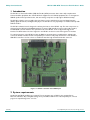
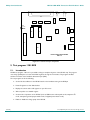
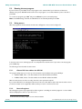
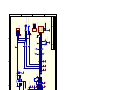
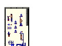
UM10028_1
ISP1301 USB OTG Transceiver
Eval Kit User’s Guide
February 2003
User’s Guide
Rev. 1.0
Revision History:
Version
Date
1.0
Feb 2003
Descriptions
First release
We welcome your feedback. Send it to [email protected].
Philips Semiconductors - Asia Product Innovation Centre
Visit www.semiconductors.philips.com/buses/usb or www.flexiusb.com
Author
David Wang
Philips Semiconductors
ISP1301 USB OTG Transceiver Eval Kit User’s Guide
This is a legal agreement between you (either an individual or an entity) and Philips Semiconductors. By accepting
this product, you indicate your agreement to the disclaimer specified as follows:
DISCLAIMER
PRODUCT IS DEEMED ACCEPTED BY RECIPIENT. THE PRODUCT IS PROVIDED “AS IS” WITHOUT
WARRANTY OF ANY KIND. TO THE MAXIMUM EXTENT PERMITTED BY APPLICABLE LAW, PHILIPS
SEMICONDUCTORS FURTHER DISCLAIMS ALL WARRANTIES, INCLUDING WITHOUT LIMITATION ANY
IMPLIED WARRANTIES OF MERCHANT ABILITY, FITNESS FOR A PARTICULAR PURPOSE, AND
NONINFRINGEMENT. THE ENTIRE RISK ARISING OUT OF THE USE OR PERFORMANCE OF THE
PRODUCT AND DOCUMENTATION REMAINS WITH THE RECIPIENT. TO THE MAXIMUM EXTENT
PERMITTED BY APPLICABLE LAW, IN NO EVENT SHALL PHILIPS SEMICONDUCTORS OR ITS SUPPLIERS BE
LIABLE FOR ANY CONSEQUENTIAL, INCIDENTAL, DIRECT, INDIRECT, SPECIAL, PUNITIVE, OR OTHER
DAMAGES WHATSOEVER (INCLUDING, WITHOUT LIMITATION, DAMAGES FOR LOSS OF BUSINESS
PROFITS, BUSINESS INTERRUPTION, LOSS OF BUSINESS INFORMATION, OR OTHER PECUNIARY LOSS)
ARISING OUT OF THIS AGREEMENT OR THE USE OF OR INABILITY TO USE THE PRODUCT, EVEN IF
PHILIPS SEMICONDUCTORS HAS BEEN ADVISED OF THE POSSIBILITY OF SUCH DAMAGES.
UM10028_1
User’s Guide
© Koninklijke Philips Electronics N.V. 2003. All rights reserved.
Rev. 1.0—February 2003
2 of 18
Philips Semiconductors
ISP1301 USB OTG Transceiver Eval Kit User’s Guide
CONTENTS
1.
INTRODUCTION ............................................................................................................................... 5
2.
SYSTEM REQUIREMENTS................................................................................................................ 5
3.
CONFIGURATIONS AND SETTINGS............................................................................................ 6
3.1.
3.2.
3.3.
3.4.
3.5.
POWER REQUIREMENTS ......................................................................................................................................................6
I2C MASTER SELECTION ......................................................................................................................................................6
USB INTERFACE ..................................................................................................................................................................7
AUDIO INTERFACE ..............................................................................................................................................................7
RESET ...................................................................................................................................................................................7
4.
LOCATION OF MAJOR COMPONENTS ....................................................................................... 7
5.
TEST PROGRAM 1301.EXE .............................................................................................................. 8
5.1.
INTRODUCTION..................................................................................................................................................................8
5.2.
RUNNING THE TEST PROGRAM ..........................................................................................................................................9
5.3.
USING MENUS ......................................................................................................................................................................9
5.3.1.
Choose I2C slave address for ISP1301..................................................................................................................................9
5.3.2.
Reset all registers .........................................................................................................................................................................9
5.3.3.
List all registers .......................................................................................................................................................................... 10
5.3.4.
Read/Write register .................................................................................................................................................................. 10
5.3.5.
Select Mode of Operation....................................................................................................................................................... 11
5.3.6.
Enable/Disable charge-pump................................................................................................................................................. 11
6.
HARDWARE DESCRIPTION..........................................................................................................12
6.1.
BLOCK DIAGRAM ..............................................................................................................................................................12
6.2.
FUNCTIONAL DESCRIPTION .............................................................................................................................................12
6.2.1.
PCF8584 I2C-bus controller .................................................................................................................................................... 12
6.2.2.
PC parallel to I2C converter .................................................................................................................................................... 12
6.2.3.
HC, DC and OTG core logic interface connector ............................................................................................................. 12
6.2.4.
Power manager.......................................................................................................................................................................... 13
6.2.5.
Audio interface........................................................................................................................................................................... 13
7.
CONNECTOR PIN INFORMATION..............................................................................................13
7.1.
7.2.
7.3.
DB-25 PC PARALLEL PORT CONNECTOR (J10) PIN ASSIGNMENT ...............................................................................13
8-BIT MICROPROCESSOR INTERFACE 20 X 2 HEADER (J13) PIN ASSIGNMENT .............................................................13
USB OTG CONTROLLER INTERFACE 8 X 2 HEADER (J8 AND J3) PIN ASSIGNMENT .................................................13
8.
SCHEMATICS OF THE EVALUATION BOARD .........................................................................14
9.
BILL OF MATERIALS.......................................................................................................................17
10.
REFERENCES ....................................................................................................................................18
UM10028_1
User’s Guide
© Koninklijke Philips Electronics N.V. 2003. All rights reserved.
Rev. 1.0—February 2003
3 of 18
Philips Semiconductors
ISP1301 USB OTG Transceiver Eval Kit User’s Guide
TABLES
Table 3-1: +5.0 V power selection.......................................................................................................................................................................... 6
Table 3-2: VBAT and VIO selection .............................................................................................................................................................................. 6
2
Table 3-3: I C master selection................................................................................................................................................................................ 6
Table 7-1: DB-25 PC parallel port connector (J10) pin assignment ..............................................................................................................13
Table 7-2: 8-bit microprocessor-interface 20 x 2 header (J13) pin assignment[1] .......................................................................................13
Table 7-3: OTG Controller interface J8 pin assignment ..................................................................................................................................14
Table 7-4: OTG Controller interface J3 pin assignment ..................................................................................................................................14
Table 9-1: BOM of the ISP1301 evaluation board .............................................................................................................................................17
FIGURES
Figure 1-1: ISP1301 evaluation board PCB layout ............................................................................................................................................... 5
Figure 4-1: Location of major components........................................................................................................................................................... 8
Figure 5-1: Test program main menu ..................................................................................................................................................................... 9
Figure 5-2: List all registers screen display ..........................................................................................................................................................10
Figure 5-3: Read/Write register screen display..................................................................................................................................................11
Figure 5-4: Select Mode of Operation screen display.......................................................................................................................................11
Figure 6-1: Block diagram of the ISP1301 evaluation board............................................................................................................................12
Microsoft and Windows are registered trademarks of Microsoft Corp. Intel is a registered trademark of Intel, Inc.
The names of actual companies and products mentioned herein may be the trademarks of their respective owners.
All other names, products, and trademarks are the property of their respective owners.
UM10028_1
User’s Guide
© Koninklijke Philips Electronics N.V. 2003. All rights reserved.
Rev. 1.0—February 2003
4 of 18
Philips Semiconductors
ISP1301 USB OTG Transceiver Eval Kit User’s Guide
1. Introduction
The ISP1301 is a Universal Serial Bus (USB) On-The-Go (OTG) transceiver device that is fully compliant with
Universal Serial Bus Specification Rev. 2.0 and On-The-Go Supplement to the USB 2.0 Specification Rev. 1.0. It integrates a
USB full-speed and low-speed transceiver, and other analog components to fully support OTG functionality.
The ISP1301 is ideal for use in portable electronics devices, such as mobile phones, personal digital assistants
(PDAs), digital still cameras, and digital audio players. The ISP1301 acts as a physical layer to interface with any USB
OTG Controller.
The ISP1301 evaluation board is designed to evaluate the functions of the ISP1301 chip. The main components on
the board are: the ISP1301 (in HVQFN24 package), I2C master, USB mini-AB connector, analog audio interface,
and USB OTG controller interface. The operation mode of the ISP1301 can be configured through the I2C
interface. The OTG status and control registers in the ISP1301 can also be accessed through the I2C interface.
To verify the functions of the ISP1301 by using the DOS test program that is provided with the evaluation kit,
connect the ISP1301 evaluation board to the parallel port of a PC. To fully verify the functions of the ISP1301, a
USB OTG controller is used to connect to the ISP1301 board through the defined interface connector.
Figure 1-1: ISP1301 evaluation board PCB layout
2. System requirements
An x86 PC with DB-25 parallel port is required. The test program runs on DOS (or the command line in
Microsoft® Windows® 98). In the BIOS setting, select port address 378H for the onboard parallel port. The test
program is compiled using Turbo® C++ 3.0.
UM10028_1
User’s Guide
© Koninklijke Philips Electronics N.V. 2003. All rights reserved.
Rev. 1.0—February 2003
5 of 18
Philips Semiconductors
ISP1301 USB OTG Transceiver Eval Kit User’s Guide
3. Configurations and settings
3.1.
Power requirements
By default, the ISP1301 board is powered by a +5.0 V power supply through the DC jack (J12, inner +). The +5.0 V
power can also be supplied from the USB Type-B connector (J4). However, when J4 is connected to a USB port
on the PC, leave the USB mini-AB connector (J9) unconnected. If an external microprocessor is used to control
the I2C controller chip PCF8584 (U4), the +5.0 V power can also be supplied from pin 16 and pin 18 of the
microprocessor connector (J13).
When the +5.0 V power is correctly applied to the board, LED2 (green) will turn ON.
Table 3-1: +5.0 V power selection
Jumper
JP6
Descriptions
Short 1(UP5V) and 2 (+5V):
+5.0 V from the microprocessor interface (pin 16 or 18 of J13)
Short 3 (H_VBUS) and 4 (+5V): +5.0 V from the VBUS line of the USB connector (pin 1 of J4)
Short 5 (EXT5V) and 6 (+5V): +5.0 V from the DC jack (J12, inner +) [default]
The power supply (VBAT pin) for the ISP1301 can be provided either from the onboard +3.3 V source or from the
OTG Controller interface (pin 2 of J3).
Similarly, the power supply for the VIO (called VDD_LGC in the ISP1301 datasheet) pin of the ISP1301 can be provided
either from the onboard +3.3 V source or from the OTG Controller interface (pin 2 of J8).
Table 3-2: VBAT and VIO selection
Jumper
JP2
JP5
3.2.
Descriptions
Short: VBAT from the onboard +3.3 V source [default]
Open: VBAT from the pin 2 of J3
Short: VIO from the onboard +3.3 V source [default]
Open: VIO from the pin 2 of J8
I2C master selection
The I2C master controller can be supplied from any one of three sources:
•
PC parallel port (software I2C master)
•
Philips I2C controller chip PCF8584 (hardware I2C master)
•
External I2C master that is connected to the I2C header J11.
2
Table 3-3: I C master selection
Jumper
JP3
JP4
Descriptions
Short 1 (SDA_8584) and 2 (SDA5V): SDA from PCF8584
Short 2 (SDA5V) and 3 (SDA_PC): SDA from PC parallel port [default]
Open:
SDA from I2C connector (pin 4 of J11)
Short 1 (SCL_8584) and 2 (SCL5V): SCL from PCF8584
Short 2 (SCL5V) and 3 (SCL_PC): SCL from PC parallel port [default]
Open:
SCA from I2C connector (pin 3 of J11)
Note: SCL and SDA come from the same I2C master.
UM10028_1
User’s Guide
© Koninklijke Philips Electronics N.V. 2003. All rights reserved.
Rev. 1.0—February 2003
6 of 18
Philips Semiconductors
3.3.
ISP1301 USB OTG Transceiver Eval Kit User’s Guide
USB interface
There are three USB connectors on the ISP1301 evaluation board.
•
If an OTG Controller is connected to the ISP1301, the USB port functions as an OTG dual-role device
and only the mini-AB connector (J5) will be used.
•
If a Host Controller is connected to the ISP1301, the USB port functions as a host and only the Type-A
connector (J1) will be used.
•
If a Device Controller is connected to the ISP1301, the USB port functions as a device and only the TypeB connector (J4) will be used.
You can use all the three ports at the same time. If you have a system that consists of a USB host port and a
separate device port, then the host port can be connected to J4 and the device port can be connected to J1 using
the standard USB cable. In such a case, the ISP1301 provides only OTG functions to the system; the transceiver
function of the ISP1301 is not used.
3.4.
Audio interface
The ISP1301 evaluation board has an interface to support an analog audio carkit application. Connect:
•
•
•
3.5.
The audio carkit to the mini-AB connector (J9) on the board;
The audio input line signal to the SPK LINE IN socket (J6) on the board;
The audio output line signalto the MIC LINE OUT socket (J7) on the board.
Reset
For a hardware reset to the ISP1301, press the manual reset switch (SW1). The reset pulse (active LOW) can also
come from the OTG Controller interface (pin 8 of J3).
4. Location of major components
Figure 4-1 shows the location of major components on the evaluation board.
UM10028_1
User’s Guide
© Koninklijke Philips Electronics N.V. 2003. All rights reserved.
Rev. 1.0—February 2003
7 of 18
Philips Semiconductors
ISP1301 USB OTG Transceiver Eval Kit User’s Guide
J6
J7
JP3
J12
JP5
JP4
JP1
J
2
J10
J11
JP2
J8
J
5
U1
J3
SW1
J9
J1
JP6
J13
U4
J4
ISP1301 EVALUATION BOARD
REV 1.0
Figure 4-1: Location of major components
5. Test program 1301.EXE
5.1.
Introduction
A DOS test program “1301.exe” is provided to help you verify the functions of the ISP1301 chip. The program
uses the PC parallel port to access the ISP1301 registers through the I2C interface. The program simulates
software I2C master at the hardware abstraction layer (HAL).
The test program can do the following:
•
Set the I2C slave address for the ISP1301 based on the hardware setting of the ADR pin
•
Reset all registers to their default values
•
Display the current value of all registers on your PC screen
•
Write any value to a writable register
•
•
Set the mode of operation of the ISP1301 (such as, USB function and suspend mode, transparent I2C
mode, transparent general-purpose buffer mode, and global power-down mode)
Enable or disable the charge pump of the ISP1301.
UM10028_1
User’s Guide
© Koninklijke Philips Electronics N.V. 2003. All rights reserved.
Rev. 1.0—February 2003
8 of 18
Philips Semiconductors
5.2.
ISP1301 USB OTG Transceiver Eval Kit User’s Guide
Running the test program
If your PC boots to pure DOS, run the test program on the command line. If your PC boots to Microsoft
Windows 98, open an MS-DOS window and run the test program. It is recommended that you boot the PC to
pure DOS.
To run the test program, type 13011 and press the Enter key at the command prompt.
Note: In the BIOS setting of the PC, the I/O address for the onboard parallel port is 378H.
5.3.
Using menus
After the program has been launched, the main menu will appear on the screen. See Figure 5-1.
Figure 5-1: Test program main menu
In the main menu screen, selecting any item 1–6 will perform the desired action. If you wish to exit the program,
press the Esc key.
The following sections describe the menu items.
5.3.1.
Choose I2C slave address for ISP1301
The program will prompt you to enter your choice based on the hardware setting of the ADR pin.
•
If ADR is HIGH, select 1. The slave address for the ISP1301 will become 0x5A.
•
If ADR is LOW, select 0. The slave address for the ISP1301 will become 0x58.
Make sure that choices are done correctly; otherwise, other operations may fail.
If you set the ISP1301 to the transparent I2C mode and choose a slave address value other than the value set here,
you must set it back to the original slave address when you revert to the direct I2C mode.
5.3.2.
Reset all registers
On selecting this option, the program will set all the registers—excluding the read-only registers—to their default
values and display these values on your PC screen.
1
In this document, items that you type or click are indicated in bold.
UM10028_1
User’s Guide
© Koninklijke Philips Electronics N.V. 2003. All rights reserved.
Rev. 1.0—February 2003
9 of 18
Philips Semiconductors
5.3.3.
ISP1301 USB OTG Transceiver Eval Kit User’s Guide
List all registers
On selecting this option, the program will display all the 22 registers on the screen. See Figure 5-2.
Figure 5-2: List all registers screen display
5.3.4.
Read/Write register
The program will display the current value of all registers and prompt you to write to a specific register.
On selecting item 4 from the main menu, the program will display the screen given in Figure 5-3. The program will
prompt you to type the address of the register whose value you want to change. On entering the address of the
register and pressing Enter, the program will prompt you to enter the new value that you want to assign. If you
want to return to the main menu, type FF at the command prompt.
UM10028_1
User’s Guide
© Koninklijke Philips Electronics N.V. 2003. All rights reserved.
Rev. 1.0—February 2003
10 of 18
Philips Semiconductors
ISP1301 USB OTG Transceiver Eval Kit User’s Guide
Figure 5-3: Read/Write register screen display
5.3.5.
Select Mode of Operation
You can select the mode of operation of the ISP1301 by selecting item 5 from the main menu. A submenu will
appear on the screen. See Figure 5-4. The possible choices include the USB functional mode (four data encoding
and decoding methods), transparent I2C mode, transparent buffer mode, USB suspend mode, and global powerdown mode.
Note: If the ISP1301 Engineering Sample 1 (ES1) (that is, the chip whose version register reads 0x0100, or the chip
package is marked ####AX) is mounted on the evaluation board, software cannot wake up the chip, if set to the
global power-down mode. Only a hardware reset can wake up the chip.
Figure 5-4: Select Mode of Operation screen display
5.3.6.
Enable/Disable charge-pump
If the charge pump in the ISP1301 is disabled, selecting menu item 6 will enable the charge pump. If the charge
pump is enabled, selecting menu item 6 will disable it.
UM10028_1
User’s Guide
© Koninklijke Philips Electronics N.V. 2003. All rights reserved.
Rev. 1.0—February 2003
11 of 18
Philips Semiconductors
ISP1301 USB OTG Transceiver Eval Kit User’s Guide
6. Hardware description
6.1.
Block diagram
Figure 6-1 shows the block diagram of the ISP1301 evaluation board.
PARALLEL
PC PARALLEL-TO-I2 C
CONVERTER
4-PIN I2 C
HEADER
PCF8584 I 2 C-BUS
CONTROLLER
ISA
DP, DM, ID
I2C-BUS (SCL, SDA, ADR, INT)
AUDIO INTERFACE
(L/R SPEAKER LINE IN,
MIC PRE-AMP OUT)
DP, DM, ID, V BUS
VBUS
ISP1301
OTG TRANSCEIVER
m ini-AB Receptacle
CORE INTERFACE (OE, VP, VM, RCV,
SPEED, SUSPEND, RESET, V DD_LGC )
V BAT
POW ER MANAGER
Vext
FPGA
INTERFACE
HC, DC and OTG CORE
LOGIC INTERFACE
CONNECTOR
(to the ISP1362 FPGA or
Phone FPGA)
Figure 6-1: Block diagram of the ISP1301 evaluation board
6.2.
Functional description
A brief description of each function module is given in the following sections.
6.2.1.
2
PCF8584 I C-bus controller
This block provides functions of the I2C-bus to the 8-bit parallel-bus converter. It can connect to the Philips
ISP1362 or ISP1161x ISA interface board, or any other generic 8-bit microprocessor interface through a 40-wire
IDE cable. The PC or other microprocessor can service the interrupt from the ISP1301 and access the registers of
the ISP1301 through this interface.
6.2.2.
2
PC parallel to I C converter
This interface provides an alternative method to access the ISP1301 I2C interface through the PC. The PC needs to
emulate software I2C master to access the ISP1301 I2C slave.
6.2.3.
HC, DC and OTG core logic interface connector
This interface provides connection to a Host Controller (HC), Device Controller (DC) or On-The-Go (OTG)
core logic. This interface is used during OTG system-level evaluation or during compliance testing.
UM10028_1
User’s Guide
© Koninklijke Philips Electronics N.V. 2003. All rights reserved.
Rev. 1.0—February 2003
12 of 18
Philips Semiconductors
6.2.4.
ISP1301 USB OTG Transceiver Eval Kit User’s Guide
Power manager
This block includes the 5.0 V-to-3.3 V regulator and power source selection.
6.2.5.
Audio interface
This block provides stereo audio line IN interface and microphone (with pre-amp) OUT interface. Its main
purpose is to demonstrate the carkit application (play audio or voice with carkit).
7. Connector pin information
7.1.
DB-25 PC parallel port connector (J10) pin assignment
J10 is used to connect to the PC parallel port through the DB-25 printer cable. Table 7-1 shows its pin assignment.
Table 7-1: DB-25 PC parallel port connector (J10) pin assignment
Pin no
9
11
15
17
10,13,18–25
1–8,12,14,16,
7.2.
Printer port signal
D7
S7#
S3
C3#
—
—
ISP1301 evaluation board signal
SDAOUT#
SDAIN#
SCLIN
SCLOUT#
GND
No connection
8-bit microprocessor interface 20 x 2 header (J13) pin assignment
J13 is used to connect to a generic 8-bit parallel bus microprocessor controller. The bus uses the Intel® mode.
Required signals include D0–D7, A0, WR_N, RD_N, CS_N, INT1 and INT2. Table 7-2 shows the pin assignment
for J13.
Note: We use a 20 x 2 header to make it compatible with the Philips ISP1362 and ISP1161x ISA interface boards.
Table 7-2: 8-bit microprocessor-interface 20 x 2 header (J13) pin assignment
Pin no
1
2
3
4
5
6
7
8
9
10
Pin name
GND
n. c.
n. c.
CHRG_EN
n. c.
n. c.
n. c.
n. c.
n. c.
+3.3 V
Pin no
11
12
13
14
15
16
17
18
19
20
Pin name
n. c.
+3.3 V
n. c.
n. c.
n. c.
+5.0 V
n. c.
+5.0 V
GND
n. c.
Pin no
21
22
23
24
25
26
27
28
29
30
Pin name
D7
INT2
D6
INT1
D5
n. c.
D4
n. c.
D3
n. c.
Pin no
31
32
33
34
35
36
37
38
39
40
[1]
Pin name
D2
n. c.
D1
WR_N
D0
RD_N
n. c.
CS_N
A0
n. c.
[1] n. c.—Denotes no connection.
Note: An external OTG Controller system can use the CHRG_EN signal to enable or disable +5.0 V from the
VBUS line of the mini-AB connector to pin 2 of J2. This is useful when an analog audio carkit is attached and the
carkit can charge the external battery.
7.3.
USB OTG Controller interface 8 x 2 header (J8 and J3) pin assignment
Header connectors J8 and J3 are used to connect the ISP1301 to the OTG Controller core. J8 includes the USB
Serial Interface Engine (SIE) signals—DAT_VP, SE0_VM, RCV and OE_TP_INT_N—and I2C signals—SDA, SCL and
INT_N. J3 also includes other signals that may be used by selected OTG Controller.
UM10028_1
User’s Guide
© Koninklijke Philips Electronics N.V. 2003. All rights reserved.
Rev. 1.0—February 2003
13 of 18
Philips Semiconductors
ISP1301 USB OTG Transceiver Eval Kit User’s Guide
Table 7-3: OTG Controller interface J8 pin assignment
Pin no
1
2
3
4
5
6
7
8
Pin name
GND
VIO
GND
INT_N
GND
SDA
GND
SCL
Pin no
9
10
11
12
13
14
15
16
Pin name
GND
OE_TP_INT_N
GND
DAT_VP
GND
SE0_VM
GND
RCV
Table 7-4: OTG Controller interface J3 pin assignment
Pin no
1
2
3
4
5
6
7
8
Pin name
GND
VBAT
GND
n. c.
GND
ADR
GND
RESET_N
Pin no
9
10
11
12
13
14
15
16
Pin name
GND
SPEED
GND
SUSPEND
GND
VM
GND
VP
8. Schematics of the evaluation board
UM10028_1
User’s Guide
© Koninklijke Philips Electronics N.V. 2003. All rights reserved.
Rev. 1.0—February 2003
14 of 18
A
B
C
1
1
2
3
4
5
6
7
8
9
10
11
12
13
14
15
16
HEADER 8X2
J8
1
2
3
4
5
6
7
8
9
10
11
12
13
14
15
16
HEADER 8X2
J3
VIO
INT_N
SDA
SCL
OE_TP_INT_N
DAT_VP
SE0_VM
RCV
ADR
RESET_N
SPEED
SUSPEND
VM
VP
VBAT
5
4
3
2
1
H_VBUS
2
SW-PB
SW1
+ C17
1uF
SDA R11
SCL R12
10K
R15
VIO
0
0
R2
R1
D+
D-
ISP1301
3
ADR
VIO
SDA
CGND
SCL
C2
RESET_N
C1
INT_N
VBAT
SPEED
VBUS
VOUT33
ID
SUSPEND
AGND
OE_TP_INT_N D+
VM
DVP
DAT_VP
RCV
SE0_VM
U1
+ C3
4.7uF16V
1
2
3
4
5
6
7
SUSPEND
8
OE_TP_INT_N 9
VM
10
VP
11
RCV
12
ADR
100R
100R
RESET_N
INT_N
SPEED
C1
0.1uF
+ C2
10uF16V
+5V
D_VBUS
R6 R7 R8 R9 R10
10K 10K 10K 10K 10K
VIO
USB B-RECEPTACLE
CHASSIS
GND
D+
DVBUS
J4
USB A-RECEPTACLE
VBUS
DD+
GND
CHASSIS
1
2
3
4
5
24
23
22
21
20
19
18
17
16
15
14
13
+ C4
4.7uF16V
VIO
R3
10K
DAT_VP
SE0_VM
VBAT
C5
0.1uF
VBUS
C11
0.1uF
C10
0.1uF
JP1
JUMPER
Q1
C12
28nF
R14
R13
4
4
R5
4.7K
LED1
5.0V
C14
22pF
33R%1
33R%1
C13
120nF
PHP125
8
7
6
5
NOT INSTALL
C50
0.1uF
+ C6
4.7uF16V
CHRG_EN
1
3
2
0
R4
4
1
J1
2
D
GND
25
C15
22pF
+ C16
4.7uF16V
TP1
VBUS
PAD
1
1
TP2
D-
PAD
5
Size
B
Date:
File:
Title
TP4
D+
VBUS
220nF
C9
220nF
C8
220nF
C7
5VOUT
TP3
ID
5
PAD
1
1
PAD
3
D1
STZ5.6N
1
ID
D+
DVBUS
ISP1301 PORT
SHIELD
GND
ID
D+
DVBUS
GND
ID
D+
DVBUS
R16
100R
Revision
SHIELD
6
10-Oct-2002
Sheet of 1/2
D:\wzw\Myproj\isp1301\eva_kit\eva board\pcb\02226-1.ddb
DrawnABy:
Number
6
5
4
3
2
1
HEADER 6
J5
V1.0
PHONEJACK(MIC LINE OUT)
J7
A
PHONEJACK
STEREO(SPK LINE IN)
J6
C
B
HEADER 6
J2
1
2
3
4
5
6
6
J9
USB mini-AB receptacle
1
LIN_L
LOUT
3
2
LIN_R
5
4
3
2
1
GND
5VOUT
LIN_R
LIN_L
LOUT
GND
ISP1301 EVALUATION BOARD
2
2
3
1
SHIELD
SHIELD
SHIELD
SHIELD
6
7
8
9
A
B
C
D
A
B
C
S3
C3#
D7
S7#
13
25
12
24
11
23
10
22
9
21
8
20
7
19
6
18
5
17
4
16
3
15
2
14
1
A0
D7
D6
D5
D4
D3
D2
D1
D0
1
D15
D14
D13
D12
D11
D10
D9
D8
DB25(MALE)
J10
3
74HCT05
U2B
C30
18pF
INT2
INT1
+5V
74HCT05
U2A
4
C31
18pF
1
+5V
2
74HCT04
U3A
+5V
+5V
C52
0.1uF
U3B
74HCT04
3
74HCT05
5
74HCT05
74HCT05
U2E
10
11
U2C
8
U2D
1
9
2
R19
10K
WR_N
RD_N
CS_N
2
6
R18
10K
CHRG_EN
AUD_EN
uP5V
4
uP33V
C29
18pF
J13
1
2
3
4
5
6
7
8
9
10
11
12
13
14
15
16
17
18
19
20
21
22
23
24
25
26
27
28
29
30
31
32
33
34
35
36
37
38
39
40
HEADER20X2
D[0..15]
SCLIN
SCLOUT#
SDAOUT#
SDAIN#
R17
10K
+5V
14
7
+5V
11
12
13
14
15
16
17
18
19
20
C51
0.1uF
D3
D4
D5
D6
D7
SCL5V
PCF8584
D3
D4
D5
D6
D7
RD_N
CS_N
WR_N
RESET_N
VDD
U4
SCL_8584
JP4
HEADER 3
SCL_PC
SDA5V
SDA_8584
JP3
HEADER 3
SDA_PC
C53
0.1uF
3
10
9
8
7
6
5
4
3
2
1
R20
3.3K
+5V
GND
D2
D1
D0
A0
INT_N
IACK_N
SCL
SDA
CLK
3
D2
D1
D0
INT_N
RESET_N
SCL_8584
SDA_8584
CLK
A0
Q3
ZVN4206
Q2
ZVN4206
R21
3.3K
SCL
SDA
R22
3.3K
VIO
R23
3.3K
2
1
4
+5V
VCC
4
+5V
C24
0.1uF
+ C18
10uF
uP5V
J11
SDA5V
4
SCL5V
3
2
1
I2C CONNECTOR
3
GND CLOCK
12MHz OSC_HALF
Y1
NC
4
+3.3V VBAT
JP2
JUMPER
+3.3V VIO
2
C19
0.1uF
+ C20
10uF
uP33V
JP5
JUMPER
2
2
3
2
1
3
2
1
1
1
D
1
14
7
5
Size
B
Date:
File:
Title
+ C25
10uF
+5V
1
+5V
Ext5V
C23
0.1uF
H_VBUS
uP5V
3
I2C MASTER / POWER
C28
0.1uF
+5V
6
Revision
V1.0
6
10-Oct-2002
Sheet of
2/2
D:\wzw\Myproj\isp1301\eva_kit\eva board\pcb\02226-1.ddb
Drawn By:
Number
+ C27
10uF
+3.3V
1
2
3
4
5
6
HEADER 3X2
JP6
Ext5V
ISP1301 EVALUATION BOARD
C26
0.1uF
1
2
3
POWER JACK
J12
Q4
LM1117DT33
Vin
Vout
C22
0.1uF
LED2
5.0V
R24
4.7K
+5V
C21
0.1uF
5
GND
2
A
B
C
D
Philips Semiconductors
ISP1301 USB OTG Transceiver Eval Kit User’s Guide
9. Bill of Materials
Table 9-1: BOM of the ISP1301 evaluation board
Part Type
18pF +80%/-20%
22pF ±10%
28nF ±10%
120nF ±10%
220nF ±10%
0.1uF+80%/-20%
Quantity
3
2
1
1
3
11
1
1
1
1
1
1
Designator
C29, C30, C31
C14, C15
C12
C13
C7, C8, C9
C1, C5, C10, C11, C19, C21, C22,
C23, C24, C26, C28
C17
C3, C4, C6, C16
C2, C18, C20, C25, C27
R1, R2, R4
R13, R14
R11, R12, R16
R20, R21, R22, R23
R5, R24
R3, R6, R7, R8, R9, R10, R15, R17,
R18, R19
Y1
U1
U2
U3
U4
Q1
1uF+80%/-20%
4.7uF16V
10uF16V
0R
33R ±%1
100R
3.3K
4.7K
10K
1
4
5
3
2
3
4
2
10
12MHz OSC_HALF
ISP1301
74HCT05
74HCT04
PCF8584 I2C CONTROLLER
PHP125 P-MOSFET POWER
MOS
ZVN4206 N-MOSFET
LM1117DT33 3.3V
REGULATOR
STZ5.6N ESD DIODE
LED
DB25 (MALE)
HEADER 3
HEADER 4
HEADER 3X2
HEADER 6
HEADER 8X2
HEADER20X2
JUMPER
PHONEJACK
(MIC LINE OUT)
PHONEJACK STEREO
(SPK LINE IN)
POWER JACK
SW-PB
USB A-RECEPTACLE
USB B-RECEPTACLE
USB mini-AB RECEPTACLE
XTAL-CTX
HVQFN24
SOP14
SOP14
DIP20
SO8
2
1
Q2, Q3
Q4
TO92
TO252
1
2
1
2
1
1
2
2
1
3
1
D1
LED1, LED2
J10
JP3, JP4
J11
JP6
J2, J5
J3, J8
J13
JP1, JP2, JP5
J7
SOT346
Thru'hole
Thru'hole
Thru'hole
Thru'hole
Thru'hole
Thru'hole
Thru'hole
Thru'hole
Thru'hole
PHONEJACK
1
J6
PHONEJACK STEREO
1
1
1
1
1
J12
SW1
J1
J4
J9
DC JACK
SW-TACT
USB A
USB B
USB mini-AB
UM10028_1
User’s Guide
Footprint
0805
0805
0805
0805
0805
0805
1206
RB.1/.2
RB.1/.2
0805
0805
0805
0805
0805
0805
© Koninklijke Philips Electronics N.V. 2003. All rights reserved.
Rev. 1.0—February 2003
17 of 18
Philips Semiconductors
10.
•
•
•
•
ISP1301 USB OTG Transceiver Eval Kit User’s Guide
References
ISP1301 USB On-The-Go Transceiver datasheet
Universal Serial Bus Specification Rev. 2.0
On-The-Go Supplement to the USB 2.0 Specification Rev. 1.0
ISP1301 Errata
UM10028_1
User’s Guide
© Koninklijke Philips Electronics N.V. 2003. All rights reserved.
Rev. 1.0—February 2003
18 of 18