1
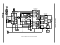
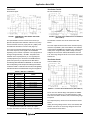
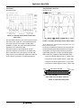
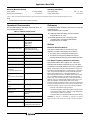
HWB3163-EVAL PRISM II 11Mbps PCMCIA
Wireless LAN Evaluation Kit User’s Guide
TM
Application Note
August 2000
AN9864.1
Author: Richard L. Abrahams
Introduction
This kit allows evaluation of the Intersil
PRISM® II Direct Sequence chip set
design in a Wireless Local Area
Network (WLAN) PCMCIA Card
implementation.
Software drivers are included allowing data to be transmitted
between cards at 1, 2, 5.5 and 11Mbps transfer rates, with a
diagnostic program to display the real data throughput from
system to system.
Included in the kit are PRISM II chip set data sheets with
application notes describing the implementation of a
wireless networking card using the chip set.
Contents of Your Evaluation Kit
Your PC Card Wireless LAN Evaluation Kit contains the
following items:
QUANTITY
DESCRIPTION
2
PRISM II Wireless LAN PC Cards
1
HWB3163 Wireless LAN Evaluation Kit User’s
Guide, AN9864
1
PRISM II Chip Set Data Sheets
1
PRISM II Application Notes
1
Microsoft® Windows® 95/98/NT/CE/2000, LINUX®
Driver
1
PRISM® Test Utilities (PTU) Software
1
Features/Benefits Card
1
Product Registration Form
1
Notification Card
Should you discover that your PC Card Wireless LAN
Evaluation Kit is incomplete, please contact Intersil
Corporation.
Overview of IEEE 802.11
The IEEE 802.11 specification is a standard for wireless
connectivity for fixed, portable, and moving stations within a
local area.
The IEEE 802.11 standard describes the services required
by a compliant device to operate within an “ad hoc” or
“infrastructure” network, as well as dealing with the issues
related to mobility within those networks. Spread spectrum
techniques are used to tolerate mobility and multipath
effects. They are also a requirement for compliance with
FCC, ETSI and those of other regulatory authorities when
operating within the Industrial, Scientific, and Medical (ISM)
frequency band.
An ad hoc communications network is created quickly and
informally for a temporary time period. An infrastructure
network usually requires more planning so that wireless
stations can communicate over longer distances through
access points, and may also communicate with existing
wired LANs using portals.
The IEEE 802.11 standard describes Media Access Control
(MAC) procedures. The principal method of communication
is the Carrier Sense Multiple Access with Collision
Avoidance (CSMA-CA) protocol. Using this protocol, each
station senses the communications medium (RF channel),
and does not transmit until the channel is clear. This avoids
collisions and minimizes the retransmission of subsequent
packets.
The standard also supports the operation of a station within
a wireless LAN that may coexist with several overlapping
wireless LANs. To accomplish this, a scheme of
channelization and spread spectrum techniques is used.
Direct Sequence (DSSS) and Frequency Hopping (FHSS)
spread spectrum techniques are supported by the standard
and both operate in the 2.4 to 2.4835GHz frequency band
(the unlicensed ISM band). An infrared technique is also
supported for indoor applications. The standard supports a
1Mbps and 2Mbps data rate for both DSSS and FHSS and
has recently introduced a high data rate standard supporting
5.5Mbps and 11Mbps DSSS using Complementary Code
Keying (CCK) modulation.
The standard has also specified the requirements and services
that enable private and secure communications to occur.
Wireless LAN Configurations
For ease of use in evaluating these cards, an ad hoc
network for peer to peer communications can be created.
An ad hoc network is usually created for a specific purpose
(such as file transfer or accessing a database). Ad hoc
networks simplify the process of creating and dissolving
networks for nontechnical users of the network facilities.
Two cards form an IEEE 802.11 Independent Basic Service
Set (IBSS), the simplest ad hoc network. The cards
communicate with each other directly and must remain
within radio range. When both cards are on, they
immediately “see” each other and the ad hoc network is
formed without user intervention.
To use the cards in an infrastructure BSS (also called an
Extended Service Set) where the two cards may not be in direct
radio contact, access points are needed. The association
between a card (station) and an infrastructure BSS - where
communication occurs only between a station and an access
point and not between stations directly is dynamic.
1-888-INTERSIL or 321-724-7143 | Intersil and Design is a trademark of Intersil Corporation. | Copyright © Intersil Corporation 2000
PRISM® is a registered trademark of Intersil Corporation. PRISM logo is a trademark of Intersil Corporation.
Microsoft® Windows® and Windows NT® are registered trademarks of Microsoft Corporation. LINUX® is a registered trademark of Linus Torvalds.
1
Application Note 9864
The IEEE 802.11 protocols are implemented in the firmware
so that file transfers or database access can begin
immediately.
Direct Sequence Spread Spectrum Approach
The use of spread spectrum techniques for wireless
computer communications is widely accepted because of
its robustness against multipath effects and interference
from intentional or unintentional radiators. The use of
spread spectrum techniques in the ISM frequency band
also allows products to be deployed without the need for an
FCC license.
The two main methods by which spread spectrum
communications can be achieved are Direct Sequence
Spread Spectrum (DSSS) and Frequency Hopping Spread
Spectrum (FHSS). This wireless LAN PC card uses the
DSSS technique. DSSS transmission has the best
performance in terms of multipath immunity and jamming
rejection. In an office environment, jamming sources are
likely to be unintentional such as emissions from
microwave ovens. Even though unintentional, they pose a
threat to the communications network. Direct sequence
techniques are superior to frequency hopping systems in
this case because FHSS gains its immunity to jamming by
avoiding the location of a single tone jammer (such as
other FHSS users). When collisions occur, data is lost.
With a DSSS system, the despreading function in the
receiver gives immunity to jamming by spreading the
interfering energy by the Pseudo Random Number (PN)
code over the whole bandwidth. This selective despreading
attenuates the jamming power while despreading the
desired signal.
In the office environment, multipath effects may degrade
network communications. Direct sequence techniques offer
better protection than slower frequency hopping systems in
the presence of multipath interference. With frequency
hopped systems, if the hopper jumps to a frequency where a
null resides, then data is lost until the next hop. Multipath
signals can be thought of as a special case of unintentional
jamming. In the DSSS approach, nulls resulting from
multipath fading only eliminate a fraction of the signal power
since the bandwidth in the DSSS case is very large. A
significant amount of energy still remains in the signal and
effective despreading still occurs. The probability of burst
errors is reduced significantly.
An often overlooked factor when comparing IEEE 802.11
compliant DSSS and FSSS implementations, is the
achievable data rate. A frequency hopping occupied
bandwidth of 1MHz as specified by the FCC acts as a
limitation when using data rates beyond 2Mbps. A similar
bandwidth limitation has not been imposed when using the
direct sequence implementation. In the new 802.11 high
data rate (11Mbps) standard utilizing Complementary Code
Keying (CCK) modulation, the 5-1/2 times increase in data
rate has been achieved in the same 17MHz bandwidth! This
2
is accomplished by encoding 6 bits of data in one out of a
possible 64 orthogonal PN spreading sequences. More
information on the new high data rate standard may be found
in Applications Note AN9850 “Complementary Code Keying
Made Simple” which may be found on the Intersil Web Site.
Installation of HWB3163 Windows 95/98
Drivers
Step 1. With the PRISM PCMCIA card removed, boot your
PC under Microsoft Windows 95 or 98.
Step 2. Once your system has booted and is idle, insert
PRISM II Driver for Windows, Disk #1 into the “A”
Floppy Drive. On the Desktop, left click on
<Start> -> <RUN> then type A:SETUP <Enter>
Follow the on-screen instructions. Accept all defaults.
Step 3. When the preliminary installation is complete,
insert the wireless LAN PC card in the lower
PCMCIA slot (see Hardware Installation below).
Step 4. Windows should automatically recognize that the
card has been inserted. It then displays a dialog box
titled “New Hardware Found”.
Step 5. Insert PRISM II Driver for Windows, Disk #1 into
the floppy drive. Tell Windows that the driver is
located on drive “A”. Accept all defaults.
Step 6. Follow the on-screen instructions to complete
installation of the driver. When complete, the NDC
driver icon should appear in the system area on the
desktop (computer monitor with antenna). Clicking on
this icon enables setting of channel, mode, etc.
Step 7. If operating in the Pseudo IBSS mode, you must
assign a unique IP address to the computer in
order for the card to be operable. Left click on
<Start> -> <Settings> -> <Control Panel> .
Double click on Network. Select TCP/IP ... PRISM
IEEE 802.11 PC Card .... and click on Properties.
Select the IP Address tab. Click on Obtain an IP
Address. Enter a valid IP address. Enter a valid
Subnet Mask (suggest 255 255 255 0). Click
on OK.
PRISM Test Utility (PTU) Software
Installation
NOTE: Perform after Windows Driver Installation.
Step 1. Insert the PTU disk #1 into the floppy drive.
Step 2. On the Desktop, left click on <Start> -> <RUN>
then type A:setup <Enter>. Follow the on-screen
instructions. Accept all defaults. When the
installation is complete, an icon should
automatically appear on the Desktop.
Application Note 9864
Hardware Installation
INSTRUMENT
Step 1. Ensure that power to the PCMCIA slot is OFF by
noting that the PCMCIA icon does not appear in the
System Tray on the Desktop. If unsure, re-boot the
computer.
Step 2. Insert the wireless LAN PC card extender card into
the PCMCIA slot.
Step 3. Insert the wireless LAN PC card into the end of the
extender card. Ensure that the LED and pin
headers of the extender card are on the same side.
Both the card and the extender are keyed so they
will fit correctly. The HWB3163 is a 3V only device.
Do not therefore force it in a 5V-keyed system as
permanent damage may occur.
PC Card Evaluation
This chapter describes several software programs supplied
with the kit. It also details some diagnostic test points that
may be accessed on the card.
Using the PRISM Test Utility (PTU) Software
The PTU permits continuous operation of the transmitter. It
is therefore convenient for performing RF measurements
such as Transmitter Power. It also provides a handy method
of changing channels within the ISM band, Use of the
PRISM Transmitter Test Utility is basically self explanatory.
An icon was automatically created on the desktop when the
PTU installation was performed. It may be run by doubleclicking on this icon.
Using the LANEVAL Software
LANEVAL provides a convenient method of analyzing
Packet Error Rate (PER) and Receiver Sensitivity. An icon
for starting LANEVAL was automatically placed on the
desktop when the PTU installation was performed. In order
for LANEVAL to form a successful link, the same packet
parameters (e.g., Packet Length, Packet Pad Words, etc.)
most be programmed at each end of the link.
LANEVAL runs in conjunction with the NDC Driver. The
Driver permits selection of Data Rate and Channel. It is
normally run in the Pseudo IBSS mode as this provides a
simple wireless Ad Hoc link between two computers. The
NDC Driver may be easily accessed by double-clicking on its
icon (looks like a computer with an antenna on top) located
in the System Tray area on the desktop.
List of Test Instruments
The following instruments may be used for conducting tests
on the wireless LAN PC card.
INSTRUMENT
MANUFACTURER
MODEL
Spectrum Analyzer Hewlett-Packard
8595E
Power Meter
Giga-tronics
8541B
Signal Generator
Hewlett-Packard
8648C
3
MANUFACTURER
Frequency Counter Hewlett-Packard
MODEL
53181A (012 Option)
Digital Scope
General-Purpose Multimeter
Computer with a PCMCIA Connection Slot (2 required)
3V PCMCIA
Extender Card
Swart Interconnect
EXT PCM-68-CC
NOTE: This is a 5V
Extender and must be
mechanically
modified for 3V
operation)
Differential Probe
Tektronix
P6247
RF Probe, 500Ω
Hewlett-Packard
54006A + 11742A
HFA3861B BBP
(FILE #4816)
4
I ADC
1
1
6
HFA3841 MAC
(FILE #4661)
6
6
Q ADC
REF_OUT
PLL
RF LO
PLL
IF LO
I/O
Q DAC
TX
DAC
TX
ADC
HFA3783 (FILE #4633)
IF I/Q MOD/DEMOD
6
6
MOD
AND
FILTER
7
RADIO
DATA
INTERFACE
VCO
RADIO
CONTROL
PORTS
CPU
16-BIT
PIPELINED
CONTROL
PROCESSOR
HOST
INTERFACE
LOGIC
TX
ALC
6
CONTROL
TEST I/O
VCTRL
WEP
ENGINE
I/Q LO
I DAC
BUFFER
RAKE
AND
DEMOD
GP
SERIAL
PORTS
MEMORY
ACCESS
ARBITER
VCO
VCTRL
EXTERNAL
MEMORY
44MHz
OSC
FIGURE 1. WIRELESS LAN PC CARD BLOCK DIAGRAM
Application Note 9864
HFA3983
(FILE #4635)
PA
AGC
CTL
HOST PC
INTERFACE
RF
DAC
RF
ADC
IF
DAC
HFA3683A
(FILE #4634)
RF/IF CONVERTER
Test Point Diagrams
5
Application Note 9864
TEST POINT L1 - RX Q- SIGNAL
TEST POINT L - RX Q+ SIGNAL
TEST POINT K1 - RX I- SIGNAL
TEST POINT K- RX I+ SIGNAL
FIGURE 2. WIRELESS LAN PC CARD TEST POINTS (TOP VIEW)
Test Point Diagrams
(Continued)
TEST POINT D - TX IF SIGNAL (AFTER SAW FL)
INSTALL FOR RF CONNECTOR
C137 (150 PF)
ALSO INSTALL C141 (SEE BELOW)
TEST POINT C
TX IF SIGNAL (BEFORE SAW FL)
TEST POINT
J- RX IF+ SIGNAL
6
Application Note 9864
RF IN/OUT
TEST POINT E
(INSTALL J1 FOR
RF CONNECTOR)
TEST POINT A
TX I+
TEST POINT A1
TX IINSTALL FOR RF CONNECTOR
C141 (150 PF)
ALSO INSTALL C137 (SEE ABOVE)
TEST POINT G
RF L.O. LOCK VOLTAGE
TEST POINT F - RF L.O.
TEST POINT I
IF L.O. LOCK VOLTAGE
TEST POINT H
IF L.O.
REMOVE FOR RF CONNECTOR
L4 (1.5 NH)
TEST POINT B1
TX Q-
FIGURE 3. WIRELESS LAN PC CARD TEST POINTS (BOTTOM VIEW)
TEST POINT B
TX Q+
Application Note 9864
Explanation of Test Points
Test Points C and D
All measurements were taken using the “Continuous
Transmit” or “Continuous Receive” features of the PTU
diagnostic software. Unless otherwise noted, spectrum
measurements included in this section were obtained using
a Hewlett-Packard 54006A 500Ω probe and 11742A coaxial
blocking capacitor and do not indicate the actual amplitude
of the signal owing to losses associated with the probe.
Unless noted, 11Mbps CCK modulation was employed.
IF Transmit Signal:
Many of the signals are differential (i.e., balanced with
respect to ground). These are denoted by + (plus) and
- (minus) symbols following the signal name (e.g., RX I+ and
RX I-).
Test Points A- A1, and B-B1
Transmit I and Q:
FIGURE 5. IF TRANSMIT SIGNAL BEFORE SAW FILTER
(TEST POINT C)
FIGURE 4. TRANSMIT I AND Q SIGNALS AT THE OUTPUT
OF THE HFA3861 (TEST POINTS A-A1 AND B-B1)
NOTE: BPSK mode is used for the plots in this figure. Therefore, I
and Q are identical.
The I and Q are both differential signals and, as such,
consist of I+, I-, Q+, and Q- respectively. As these are
balanced signals, data is measured using a Tektronix P6247
Differential Probe. For example in the measurement of the I
signal, the probe is bridged between Test Points A (I+) and
A1 (I-).
Transmit In-phase and Quadrature (I+ and Q+) signals are
the spread baseband single-bit I and Q digital data that are
outputted at the programmed chip rate (N).
7
FIGURE 6. IF TRANSMIT SIGNAL AFTER THE SAW FILTER
(TEST POINT D)
The intermediate frequency (IF) transmit signal is a spread
spectrum signal centered at 374MHz with a 17MHz
bandwidth.
The SAW filter is used to shape the sidelobes.
Test point C is at the input of the SAW Filter whereas D is at
the output.
Application Note 9864
Test Point E
Test Points F and G
RF Transmit Signal:
RF local oscillator (LO):
FIGURE 7. TRANSMITTED 2.4GHz SIGNAL SPECTRUM
(TEST POINT E)
The optional SMA connector can be used to hook up a
Spectrum Analyzer for RF evaluation. Note that L4 (1.5nH)
must be removed and C141 (15pF) and C37 (150pF) must
be installed to activate the connector See (Figure 3).
This is the up-converted spread spectrum output of the card.
The center frequency of this signal is 2412-2484MHz
depending on the channel of operation. The output power of
the signal is approximately +12.5dBm. The peaks of the
sidelobes of the output spectrum (i.e., the regrowth) are
normally adjusted by the ALC/AGC to be 30dB below the
peak of the spectrum per requirements of IEEE 802.11.
FIGURE 8. RF LOCAL OSCILLATOR OUTPUT AT CHANNEL 8
(TEST POINT F)
The behavior of the RF VCO can be monitored at Test
Point F.
The VCO output should be locked at the channel frequency
minus the IF (374MHz.) This means that the VCO will have
to lock between 2038MHz and 2110MHz. The output power
at test point F is approximately -6dBm. Ideally, the tuning
voltage of the VCO, when locked, falls between 0.5V and
2.2V. The tuning voltage of the RF VCO can be observed at
Test Point G.
Test Points H and I
IF local oscillator (LO):
The following table delineates the IEEE 802.11 channels and
their corresponding center frequencies. Although information
contained in Table 1 is deemed to be accurate, local regulatory
authorities should be consulted before using such equipment.
TABLE 1. IEEE 802.11 CHANNELS
CHANNEL
NUMBER
CHANNEL
FREQUENCY
GEOGRAPHIC
USAGE
1
2412MHz
US, CA, ETSI
2
2417MHz
US, CA, ETSI
3
2422MHz
US, CA, ETSI
4
2427MHz
US, CA, ETSI
5
2432MHz
US, CA, ETSI
6
2437MHz
US, CA, ETSI
7
2442MHz
US, CA, ETSI
8
2447MHz
US, CA, ETSI
9
2452MHz
US, CA, ETSI
10
2457MHz
US, CA, ETSI, FR, SP
11
2462MHz
US, CA, ETSI, FR, SP
12
2467MHz
ETSI, FR
13
2472MHz
ETSI, FR
14
2484MHz
Japan†
KEY: US = United States, CA = Canada, ETSI = ETSI countries
(except France and Spain), FR = France, SP = Spain.
† In Japan, authorization for Channels 1 through 11 is pending.
8
FIGURE 9. IF LOCAL OSCILLATOR OUTPUT (TEST POINT H)
The IF VCO is a discrete design and operates at 748MHz
(i.e., twice the IF frequency). The output frequency of this
VCO does not need to be varied; thus, minimal tuning range
is required.
The output frequency of this VCO can be observed at Test
Point H.
Ideally, the tuning voltage of the IF VCO, when locked, falls
between 0.5V and 2.2V. The tuning voltage of the IF VCO
can be observed at Test Point I.
Application Note 9864
Test Point J
Test Point K-K1 and L-L1
IF Receive Signal:
Receive I and Q:
FIGURE 10. IF RECEIVE SIGNAL PRIOR TO SAW FILTER
(TEST POINT J)
The intermediate frequency (IF) receive signal is the downconverted receive signal prior to the SAW bandpass filter.
The center frequency of this signal is 374MHz with a
bandwidth of 17MHz. The power of this signal is directly
dependent on the input signal power.
Note that the spurious signal visible below the DS
spectrum’s frequency is a harmonic of the 44MHz clock.
Much of this level is due to stray pickup in the 500Ω RF
probe because of the relatively low signal level present. As
such, it will have no influence on receiver performance.
FIGURE 11. RECEIVE I AND Q SIGNALS (TEST POINTS K AND L)
NOTE: BPSK mode is used for the plots in this figure; as such, I and
Q are inverse of each other.
The receive In-phase and Quadrature (I and Q) signals are
the demodulated lowpass-filtered data that are coupled to
the HFA3861. The output levels of these two signals are
approximately 500mVP-P. As these are balanced signals,
data is taken using a Tektronix P6247 Differential Probe.
• Test point K for RXI+ signal is at the 0Ω jumper, R19.
• Test point K1 for RXI- signal is at the 0Ω jumper, R23
• Test point L for RXQ+ signal is at the 0Ω jumper, R27
• Test point L1 for RXQ- signal is at the 0Ω jumper, R29.
PIN 34
TOP (LED, THIS SIDE)
PIN 1
3V KEY
PIN 68
BOTTOM
PIN 35
VIEW, LOOKING INTO 68 PIN FEMALE CONNECTOR
FIGURE 12. EDGE VIEW, PCMCIA CARD
9
Application Note 9864
Absolute Maximum Ratings
Operating Conditions
Supply Voltage . . . . . . . . . . . . . . . . . . . . . . . . . . -0.3V to 4.0V (Max)
Storage Temperature (Note 1) . . . . . . . . . . . . . . . . . . -20oC to 65oC
Temperature Range . . . . . . . . . . . . . . . . . . . . . . . . 0oC ≤ TA ≤ 55oC
Supply Voltage Range . . . . . . . . . . . . . . . . . . . . . . . . . . 3.0V to 3.6V
Caution: These are the absolute maximum ratings for the PC Card product. Exceeding these limits could cause permanent damage to the card.
NOTE:
1. All temperature references refer to ambient conditions.
Operational Characteristics
References
See the HWB3163-EVAL data sheet, Intersil File #4794, for
more detailed specifications.
For Intersil documents available on the internet, see web site
www.intersil.com/
Intersil AnswerFAX (321) 724-7800.
TABLE 2. GENERAL SPECIFICATIONS
SPECIFICATION
VALUE
Targeted Standard
IEEE 802.11
Data Rate
1Mbps DBPSK
2Mbps DQPSK
5.5Mbps CCK
11Mbps CCK
Range (11Mbps Data Rate)
120ft (37M) Indoor (Typ)
400ft (122M) Outdoor (Typ)
Center Frequency Range
2412MHz - 2484MHz
Step Size
1MHz
IF Frequency
374MHz
IF Bandwidth
17MHz
RX/TX Switching Speed
2µs (Typ)
Average Current without
Power Save
2% Transmit, 98% Receive
187mA (Typ)
Average Current with Power
Save
2% TX, 8% RX, 90% Standby
43mA (Typ)
Current in Continuous TX
mode
300mA (Typ)
Current in Continuous RX
mode
185mA (Typ)
Standby Current
25mA (Typ)
Mechanical
Type II PC Card, with Antenna
Extension
Output Power
+11.5dBm (Typ)
Transmit Spectral Mask
-30dBc at First Side Lobes
Antenna Interface
SMA, 50Ω (for testing only)
Dual Diversity Printed Antenna
[1] HWB3163-EVAL Data Sheet, Intersil Corporation,
AnswerFAX Doc. No. 4794.
[2] AN9850 Application Note, Intersil Corporation,
“Complementary Code Keying Made Simple”,
AnswerFAX Doc. No. 99850.
Notices
Electronic Emission Notices
This device complies with Part 15 of the FCC rules.
Operation is subject to the following two conditions:
1. This device may not cause harmful interference.
2. This device must accept any interference received,
including interference that may cause undesired operation.
FCC Radio Frequency Interference Statement
The wireless LAN PC card is subject to the rules of the
Federal Communications Commission (FCC). This card is
considered an intentional radiator as per the FCC guidelines.
NOTE: This equipment has been tested and found to comply with
the limits for a Class B digital device, pursuant to Part 15 of the FCC
rules. These limits are designed to provide reasonable protection
against harmful interference in a residential installation. This
equipment generates, uses and can radiate radio frequency energy
and, if not installed and used in accordance with the instruction
manual, may cause harmful interference to radio communications.
However, there is no guarantee that interference will not occur in a
particular installation. If this equipment does cause harmful
interference to radio or television reception, which can be determined
by turning the equipment off and on, the user is encouraged to try to
correct the interference by one or more of the following measures:
• Reorient or relocate the receiving antenna
• Increase the separation between the equipment and the receiver
• Connect the equipment into an outlet on a circuit different from
that to which the receiver is connected
• Consult the dealer or an experienced ratio/TV technician for help
10
WARNING! Any changes or modifications of equipment not expressly
approved by Intersil could void the user’s authority to operate the equipment.
Application Note 9864
All Intersil semiconductor products are manufactured, assembled and tested under ISO9000 quality systems certification.
Intersil semiconductor products are sold by description only. Intersil Corporation reserves the right to make changes in circuit design and/or specifications at any time without notice. Accordingly, the reader is cautioned to verify that data sheets are current before placing orders. Information furnished by Intersil is believed to be accurate and
reliable. However, no responsibility is assumed by Intersil or its subsidiaries for its use; nor for any infringements of patents or other rights of third parties which may result
from its use. No license is granted by implication or otherwise under any patent or patent rights of Intersil or its subsidiaries.
For information regarding Intersil Corporation and its products, see web site www.intersil.com
Sales Office Headquarters
NORTH AMERICA
Intersil Corporation
P. O. Box 883, Mail Stop 53-204
Melbourne, FL 32902
TEL: (321) 724-7000
FAX: (321) 724-7240
11
EUROPE
Intersil SA
Mercure Center
100, Rue de la Fusee
1130 Brussels, Belgium
TEL: (32) 2.724.2111
FAX: (32) 2.724.22.05
ASIA
Intersil Ltd.
8F-2, 96, Sec. 1, Chien-kuo North,
Taipei, Taiwan 104
Republic of China
TEL: 886-2-2515-8508
FAX: 886-2-2515-8369