1
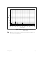
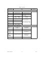
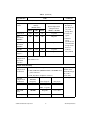
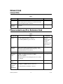
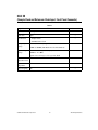
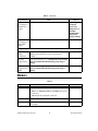
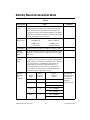
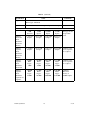
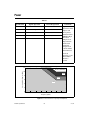
NI 5422 Specifications
NI PXI-5422 16-Bit 200 MS/s Arbitrary Waveform Generator
Unless otherwise noted, the following conditions were used for each
specification:
•
Analog Filter enabled.
•
Signals terminated with 50 Ω.
•
Direct Path set to 1 Vpk-pk, Low-Gain Amplifier Path set to 2 Vpk-pk,
and High-Gain Amplifier Path set to 12 Vpk-pk.
•
Sample rate set to 200 MS/s and the Sample Clock Source set to
Divide-by-N.
Typical values are representative of an average unit operating at room
temperature (20 °C ±3 °C). Specifications are subject to change without
notice. For the most recent NI 5422 specifications, visit ni.com/manuals.
To access all of the NI 5422 documentation, including the NI Signal
Generators Getting Started Guide, which contains functional descriptions
of the NI 5422 signals, navigate to Start»Programs»National
Instruments»NI-FGEN»Documentation.
Hot Surface If the NI 5422 has been in use, it may exceed safe handling temperatures and
cause burns. Allow the NI 5422 to cool before removing it from the chassis.
Contents
CH 0 ........................................................................................................ 2
Sample Clock .......................................................................................... 15
Onboard Clock ........................................................................................ 18
Phase-Locked Loop (PLL) Reference Clock .......................................... 18
CLK IN ................................................................................................... 19
PFI 0 and PFI 1 ....................................................................................... 20
DIGITAL DATA & CONTROL (DDC) ................................................ 22
Start Trigger ............................................................................................ 24
Markers ................................................................................................... 25
Arbitrary Waveform Generation Mode................................................... 27
Calibration............................................................................................... 29
Power ...................................................................................................... 30
Software .................................................................................................. 31
Environment ............................................................................................32
Safety, Electromagnetic Compatibility, and CE Compliance .................33
Physical....................................................................................................35
Where to Go for Support .........................................................................36
CH 0
(Channel 0 Analog Output, Front Panel Connector)
Table 1.
Specification
Value
Comments
Number of
Channels
1
—
Connector
SMB (jack)
—
Output Voltage Characteristics
Output Paths
1. The software-selectable Main Output Path setting
provides full-scale voltages from 12.00 Vpk-pk to
5.64 mVpk-pk into a 50 Ω load. NI-FGEN uses either the
Low-Gain Amplifier or the High-Gain Amplifier when
the Main Output Path is selected, depending on the Gain
attribute.
—
2. The software-selectable Direct Path is optimized for
IF applications and provides full-scale voltages from
1.000 Vpk-pk to 0.707 Vpk-pk.
DAC
Resolution
NI 5422 Specifications
16 bits
—
2
ni.com
Table 1. (Continued)
Specification
Value
Comments
Amplitude and Offset
Amplitude
Range
Amplitude (Vpk-pk)
Path
Load
Minimum Value
Maximum Value
Direct
50 Ω
0.707
1.00
1 kΩ
1.35
1.91
Open
1.41
2.00
50 Ω
0.00564
2.00
1 kΩ
0.0107
3.81
Open
0.0113
4.00
50 Ω
0.0338
12.0
1 kΩ
0.0644
22.9
Open
0.0676
24.0
LowGain
Amplifier
HighGain
Amplifier
Amplitude
Resolution
3 digits
Offset Range
Span of ±50% of Amplitude Range with increments
<0.0028% of Amplitude Range.
© National Instruments Corporation
3
1. Amplitude
values assume
the full scale
of the DAC is
utilized. If an
amplitude
smaller than
the minimum
value is
desired, then
waveforms less
than full scale
of the DAC can
be used.
2. NI-FGEN
compensates
for userspecified
resistive loads.
Not available on
the Direct Path.
NI 5422 Specifications
Table 1. (Continued)
Specification
Value
Comments
Maximum Output Voltage
Maximum
Output
Voltage
Path
Load
Maximum Output Voltage (V)
Direct
50 Ω
±0.500
1 kΩ
±0.953
Open
±1.000
50 Ω
±1.000
1 kΩ
±1.905
Open
±2.000
50 Ω
±6.000
1 kΩ
±11.43
Open
±12.00
LowGain
Amplifier
HighGain
Amplifier
The combination
of Amplitude and
Offset is limited
by the Maximum
Output Voltage.
Accuracy
DC Accuracy
For the Low-Gain or High-Gain Amplifier Path:
±0.2% of Amplitude ± 0.05% of Offset ± 500 µV
(within ±10 °C of self-calibration temperature)
±0.4% of Amplitude ± 0.05% of Offset ± 1 mV
(0 °C to 55 °C)
For the Direct Path:
Gain Accuracy: ±0.2% (within ±10 °C of self-calibration
temperature)
Gain Accuracy: ±0.4% (0 °C to 55 °C)
DC Offset Error: ±30 mV (0 °C to 55 °C)
AC Amplitude
Accuracy
±1.0% of desired Amplitude ± 1 mV
All paths are
calibrated for
amplitude and
gain errors. The
Low-Gain and
High-Gain
Amplifier Paths
also are
calibrated for
offset errors.
Calibrated for
high impedance
load.
50 kHz sine
wave.
Output Characteristics
Output
Impedance
50 Ω nominal or 75 Ω nominal, software-selectable.
—
Output
Coupling
DC
—
NI 5422 Specifications
4
ni.com
Table 1. (Continued)
Specification
Value
Comments
Output Enable
Software-selectable. When the Output Path is disabled, the
CH 0 Output is terminated to ground with a 1 W resistor
equal to the selected output impedance.
—
Maximum
Output
Overload
The CH 0 output can be connected to a 50 Ω, ±12 V
(±8 V for the Direct Path) source without sustaining any
damage. No damage occurs if the CH 0 output is shorted to
ground indefinitely.
—
Waveform
Summing
The CH 0 output supports waveform summing among
similar paths—specifically, the outputs of multiple NI 5422
signal generators can be connected directly together.
—
Output Characteristics (Continued)
Frequency and Transient Response
Analog
Filter
Pulse
Response
Software-selectable 7-pole elliptical filter for image
suppression.
Path
Direct
Low-Gain
Amplifier
High-Gain
Amplifier
Rise/Fall Time
1.0 ns
2.1 ns
4.8 ns
Aberration
16%
6%
8%
© National Instruments Corporation
5
Available on
Low-Gain
Amplifier and
High-Gain
Amplifier Paths.
Values are
typical. Analog
Filter disabled.
Measured with a
1 m RG-223
cable.
NI 5422 Specifications
1
+0.4 dB
+0.4 dB
–0.3 dB
–0.3 dB
+0.4 dB
+0.4 dB
Flatness (dB)
0
–1
–1.2 dB
–2
–3
Guaranteed Specification
Typical
–3.4 dB
–4
1
10
Frequency (MHz)
100
Figure 1. Normalized Passband Flatness, Direct Path
1
+0.3 dB
+0.7 dB
+0.7 dB
–0.7 dB
–0.7 dB
+0.7 dB
Flatness (dB)
0
–0.5 dB
–1
–2
–3
Guaranteed Specification
Typical
–3.4 dB
–4
1
10
Frequency (MHz)
100
Figure 2. Normalized Passband Flatness, Low-Gain Amplifier Path
NI 5422 Specifications
6
ni.com
1
+0.2 dB
+0.2 dB
+0.2 dB
–1.1 dB
–1.1 dB
Flatness (dB)
0
–0.6 dB
–1
–2
–3
Guaranteed Specification
Typical
–4
1
10
Frequency (MHz)
100
Figure 3. Normalized Passband Flatness, High-Gain Amplifier Path
2.0
1.6
1.2
Amplitude (V)
0.8
0.4
0
–0.4
–0.8
–1.2
–1.6
–2.0
0
10
20
30
40
50
60
Time (ns)
70
80
90
100
Figure 4. Pulse Response, Low-Gain Amplifier Path with a 50 Ω Load
© National Instruments Corporation
7
NI 5422 Specifications
Table 1. (Continued)
Specification
Value
Comments
Suggested Maximum Frequencies for Common Functions
Function
Path
Direct
Low-Gain
Amplifier
High-Gain
Amplifier
80 MHz
80 MHz
43 MHz
Square
Not Recommended
50 MHz
25 MHz
Ramp
Not Recommended
10 MHz
10 MHz
Triangle
Not Recommended
10 MHz
10 MHz
Sine
Disable the
Analog Filter for
square, ramp,
and triangle
functions.
Sine Amplitude (Vpp into 50 Ω)
14
43 MHz
12
Not Recommended
10
8
6
Recommended Operation
4
2
0
0
20
40
Frequency (MHz)
60
80
Figure 5. Recommended Sine Wave Frequency Versus Amplitude
NI 5422 Specifications
8
ni.com
Table 1. (Continued)
Specification
Value
Comments
Path
Amplitude
–1 dBFS.
Measured from
DC to 100 MHz.
Also called
harmonic
distortion.
SFDR with
harmonics at low
amplitudes is
limited by a
–148 dBm/Hz
noise floor. All
values are
typical and
include aliased
harmonics.
Spectral Characteristics
Spurious-Free
Dynamic
Range
(SFDR) with
Harmonics
Direct
Low-Gain
Amplifier
High-Gain
Amplifier
1 MHz
–70 dBc
–65 dBc
–66 dBc
5 MHz
–70 dBc
–65 dBc
–58 dBc
10 MHz
–70 dBc
–65 dBc
–52 dBc
20 MHz
–63 dBc
–64 dBc
–49 dBc
30 MHz
–57 dBc
–60 dBc
–43 dBc
40 MHz
–48 dBc
–53 dBc
–39 dBc
50 MHz
–48 dBc
–53 dBc
—
60 MHz
–47 dBc
–52 dBc
—
70 MHz
–47 dBc
–52 dBc
—
80 MHz
–41 dBc
–52 dBc
—
© National Instruments Corporation
9
NI 5422 Specifications
Table 1. (Continued)
Specification
Value
Comments
Path
Amplitude
–1 dBFS.
Measured from
DC to 100 MHz.
SFDR without
harmonics at low
amplitudes is
limited by a
–148 dBm/Hz
noise floor.
All values are
typical and
include aliased
harmonics.
Spectral Characteristics (Continued)
Spurious-Free
Dynamic
Range
(SFDR)
without
Harmonics
Direct
Low-Gain
Amplifier
High-Gain
Amplifier
1 MHz
–85 dBFS
–80 dBFS
–77 dBFS
5 MHz
–85 dBFS
–80 dBFS
–77 dBFS
10 MHz
–80 dBFS
–80 dBFS
–77 dBFS
20 MHz
–80 dBFS
–80 dBFS
–77 dBFS
30 MHz
–73 dBFS
–71 dBFS
–68 dBFS
40 MHz
–48 dBFS
–58 dBFS
–55 dBFS
50 MHz
–48 dBFS
–53 dBFS
—
60 MHz
–47 dBFS
–52 dBFS
—
70 MHz
–47 dBFS
–52 dBFS
—
80 MHz
–41 dBFS
–52 dBFS
—
Average Noise
Density
NI 5422 Specifications
Amplitude
Range
Average Noise Density
Path
Vpk-pk
dBm
nV
----------Hz
dBm/Hz
dBFS/
Hz
Direct
1.00
4.0
19.9
–141
–145
Low Gain
0.06
–20.5
1.3
–164
–144
Low Gain
0.10
–16.0
2.2
–160
–144
Low Gain
0.40
–4.0
8.9
–148
–144
Low Gain
1.00
4.0
22.3
–140
–144
Low Gain
2.00
10.0
44.6
–134
–144
High Gain
4.00
16.0
93.8
–128
–144
High Gain
12.00
25.6
281.5
–118
–144
10
Average Noise
Density at small
amplitudes is
limited by a
–168 dBm/Hz
noise floor.
ni.com
10
0
–10
–20
dBm
–30
–40
–50
–60
–70
–80
–90
0
10
20
30
40
50
60
Frequency (MHz)
70
80
90
100
Figure 6. 10 MHz Single-Tone Spectrum, Direct Path, 200 MS/s (Typical)
The noise floor in Figure 6 is limited by the measurement device. Refer to the
Average Noise Density specification.
Note
© National Instruments Corporation
11
NI 5422 Specifications
10
0
–10
–20
dBm
–30
–40
–50
–60
–70
–80
–90
0
10
20
30
40
50
60
Frequency (MHz)
70
80
90
100
Figure 7. 10.00001 MHz Single-Tone Spectrum, Low-Gain Amplifier Path,
200 MS/s (Typical)
Note The noise floor in Figure 7 is limited by the measurement device. Refer to the
Average Noise Density specification.
NI 5422 Specifications
12
ni.com
–30
Total Harmonic Distortion (dBc)
Guaranteed Specification
Typical
–40
–44 dBc
–49 dBc
–50
–60
–67 dBc
–70
–80
–90
0.1
1
10
100
Frequency (MHz)
Figure 8. Total Harmonic Distortion, Direct Path
–30
Total Harmonic Distortion (dBc)
Guaranteed Specification
Typical
–40
–45 dBc
–45 dBc
–50
–60 dBc
–60
–70
–80
–90
0.1
1
10
100
Frequency (MHz)
Figure 9. Total Harmonic Distortion, Low-Gain Amplifier Path
© National Instruments Corporation
13
NI 5422 Specifications
–30
Total Harmonic Distortion (dBc)
Guaranteed Specification
Typical
–40
–45 dBc
–50
–60
–70
–80
–90
0.1
1
10
100
Frequency (MHz)
Figure 10. Total Harmonic Distortion, High-Gain Amplifier Path
Intermodulation Distortion (dBc)
–50
–55
High-Gain
–60
–65
Low-Gain
–70
–75
Direct Path
–80
–85
1
10
Frequency (MHz)
100
Figure 11. Intermodulation Distortion, 200 kHz Separation (Typical)
NI 5422 Specifications
14
ni.com
10
0
–10
–20
dBm
–30
–40
–50
–60
–70
–80
–90
0
10
20
30
40
50
60
Frequency (MHz)
70
80
90
100
Figure 12. Direct Path, Two-Tone Spectrum (Typical)
The noise floor in Figure 12 is limited by the noise floor of the measurement device.
Refer to the Noise Floor specification.
Note
Sample Clock
Table 2.
Specification
Sources
Value
1. Internal, Divide-by-N (N ≥ 1)
2. Internal, DDS-based, High-Resolution
3. External, CLK IN (SMB front panel connector)
4. External, DDC CLK IN (DIGITAL DATA &
CONTROL front panel connector)
Comments
Refer to the
Onboard Clock
section for more
information
about Internal
Clock Sources.
5. External, PXI Star trigger (backplane connector)
6. External, PXI_Trig<0..7> (backplane connector)
© National Instruments Corporation
15
NI 5422 Specifications
Table 2. (Continued)
Specification
Value
Comments
Sample Rate Range and Resolution
Sample Clock
Source
Sample Rate Range
Divide-by-N
5 MS/s to 200 MS/s
High
Resolution
—
Sample Rate Resolution
Settable to (200 MS/s)/N
(1 ≤ N ≤ 40)
1.06 µHz
4.24 µHz
5 MS/s to 100 MS/s
>100 MS/s to 200 MS/s
CLK IN
5 MS/s to 200 MS/s
DDC CLK IN
5 MS/s to 200 MS/s
PXI Star
Trigger
5 MS/s to 105 MS/s
PXI_Trig<0..7>
5 MS/s to 20 MS/s
Resolution determined by
external clock source.
External Sample Clock duty
cycle tolerance 40% to 60%.
Sample Clock Delay Range and Resolution
Sample Clock
Source
Delay Adjustment
Range
Delay Adjustment
Resolution
Divide-by-N
±1 sample clock period
<5 ps
HighResolution
≤100 MHz
±1 sample clock period
Sample Clock
Period/16,384
HighResolution
>100 MHz
±1 sample clock period
Sample Clock
Period/4,096
0 ns to 7.6 ns
<15 ps
External (all)
NI 5422 Specifications
16
—
ni.com
Table 2. (Continued)
Specification
Value
Comments
System Phase Noise and Jitter (10 MHz Carrier)
Sample Clock
Source
System Phase Noise
Density
(dBc/Hz) Offset
100 Hz
1 kHz
10 kHz
System Output Jitter
(Integrated from
100 Hz to 100 kHz)
Divide-by-N
–110
–122
–138
1.5 ps rms
HighResolution1
100 MS/s
–109
–120
–120
4.0 ps rms
HighResolution1
200 MS/s
–108
–120
–122
4.2 ps rms
CLK IN2
–116
–130
–143
1.1 ps rms
PXI Star
Trigger2,3
–111
–128
–136
2.1 ps rms
External
Sample Clock
Input Jitter
Tolerance
Cycle-Cycle Jitter ±150 ps
1. HighResolution
specifications
vary with
Sample Rate.
2. Values are
typical.
3. PXI Star
trigger
specification is
valid when the
Sample Clock
Source is
locked to
PXI_CLK10.
—
Period Jitter ±1 ns
Sample Clock Exporting
Exported
Sample Clock
Destinations
1. PFI<0..1> (SMB front panel connectors)
2. DDC CLK OUT (DIGITAL DATA & CONTROL front
panel connector)
3. PXI_Trig<0..6> (backplane connector)
Exported
Sample Clock
Destinations
Maximum
Frequency
Jitter (Typical)
Duty Cycle
PFI<0..1>
200 MHz
PFI 0: 6 ps rms
25% to 65%
Exported Sample
Clocks can be
divided by integer
K (1 ≤ K ≤
4,194,304).
—
PFI 1: 12 ps rms
DDC CLK
OUT
200 MHz
60 ps rms
35% to 65%
PXI_Trig<0..6>
20 MHz
—
—
© National Instruments Corporation
17
NI 5422 Specifications
Onboard Clock
(Internal VCXO)
Table 3.
Specification
Value
Comments
Clock Source
Internal sample clocks can either be locked to a Reference
Clock using a phase-locked loop or be derived from the
onboard VCXO frequency reference.
—
Frequency
Accuracy
±25 ppm
—
Phase-Locked Loop (PLL) Reference Clock
Table 4.
Specification
Sources
Value
1. PXI_CLK10 (backplane connector)
2. CLK IN (SMB front panel connector)
Comments
The PLL
Reference Clock
provides the
reference
frequency for the
phase-locked
loop.
Frequency
Accuracy
When using the PLL, the Frequency Accuracy of the
NI 5422 is solely dependent on the Frequency Accuracy
of the PLL Reference Clock Source.
—
Lock Time
≤200 ms
—
Frequency
Range
5 MHz to 20 MHz in increments of 1 MHz.
Default of 10 MHz.
—
The PLL Reference Clock Frequency has to be accurate
to ±50 ppm.
Duty Cycle
Range
40% to 60%
—
Exported PLL
Reference
Clock
Destinations
1. PFI<0..1> (SMB front panel connectors)
—
NI 5422 Specifications
2. PXI_Trig<0..6> (backplane connector)
18
ni.com
CLK IN
(Sample Clock and Reference Clock Input, Front Panel Connector)
Table 5.
Specification
Value
Comments
Connector
SMB (jack)
—
Direction
Input
—
Destinations
1. Sample Clock
—
2. PLL Reference Clock
Frequency
Range
5 MHz to 200 MHz (Sample Clock Destination)
Input Voltage
Range
Sine wave: 0.65 Vpk-pk to 2.8 Vpk-pk into 50 Ω
(0 dBm to +13 dBm)
—
5 MHz to 20 MHz (PLL Reference Clock destination)
—
Square wave: 0.2 Vpk-pk to 2.8 Vpk-pk into 50 Ω
Maximum
Input Overload
±10 V
—
Input
Impedance
50 Ω
—
Input Coupling
AC
—
© National Instruments Corporation
19
NI 5422 Specifications
PFI 0 and PFI 1
(Programmable Function Interface, Front Panel Connectors)
Table 6.
Specification
Value
Comments
Connectors
Two SMB (jack)
—
Direction
Bi-directional
—
Frequency
Range
DC to 200 MHz
—
As an Input (Trigger)
Destinations
Start Trigger
—
Maximum
Input Overload
–2 V to +7 V
—
VIH
2.0 V
—
VIL
0.8 V
—
Input
Impedance
1 kΩ
—
As an Output (Event)
Sources
1. Sample Clock divided by integer K (1 ≤ K ≤ 4,194,304)
—
2. Sample Clock Timebase (200 MHz) divided
by integer M (4 ≤ M ≤ 4,194,304)
3. PLL Reference Clock
4. Marker
5. Exported Start Trigger (Out Start Trigger)
Output
Impedance
NI 5422 Specifications
50 Ω
—
20
ni.com
Table 6. (Continued)
Specification
Value
Comments
As an Output (Continued)
Maximum
Output
Overload
–2 V to +7 V
VOH
Minimum: 2.7 V (open load), 1.3 V (50 Ω load)
VOL
Maximum: 0.6 V (open load), 0.2 V (50 Ω load)
Rise/Fall Time
(20% to 80%)
≤2.0 ns
© National Instruments Corporation
—
Output drivers are
+3.3 V TTL
compatible.
Measured with
a 1 m cable.
Load of 10 pF.
21
NI 5422 Specifications
DIGITAL DATA & CONTROL (DDC)
Optional Front Panel Connector
Table 7.
Specification
Value
Comments
Connector
Type
68-pin VHDCI female receptacle
—
Number of
Data Output
Signals
16
—
Control
Signals
1. DDC CLK OUT (clock output)
—
2. DDC CLK IN (clock input)
3. PFI 2 (input)
4. PFI 3 (input)
5. PFI 4 (output)
6. PFI 5 (output)
Ground
23 pins
—
Output Signal Characteristics (Includes Data Outputs, DDC CLK OUT, and PFI<4..5>)
Signal Type
Signal
Characteristics
LVDS (Low-Voltage Differential Signal)
Minimum
Typical
Maximum
VOH
—
1.3 V
1.7 V
VOL
0.8 V
1.0 V
—
Differential
Output Voltage
0.25 V
—
0.45 V
Output
Common-Mode
Voltage
1.125 V
—
1.375 V
Rise/Fall Time
(20% to 80%)
—
0.8 ns
1.6 ns
NI 5422 Specifications
22
—
1. Tested with
100 Ω
differential
load.
2. Measured with
188143B-01
cable.
3. Driver and
receiver
comply with
ANSI/TIA/
EIA-644.
ni.com
Table 7. (Continued)
Specification
Value
Comments
Output Signal Characteristics (Continued)
Output Skew
Typical: 1 ns, maximum 2 ns. Skew between any
two outputs on the DIGITAL DATA & CONTROL
front panel connector.
—
Output
Enable/Disable
Controlled through the software on all Data Output Signals
and Control Signals collectively. When disabled, the outputs
go to a high-impedance state.
—
Maximum
Output
Overload
–0.3 V to +3.9 V
—
Input Signal Characteristics (Includes DDC CLK IN and PFI<2..3>)
Signal Type
LVDS (Low-Voltage Differential Signal)
—
Input
Differential
Impedance
100 Ω
—
Maximum
Output
Overload
–0.3 V to +3.9 V
—
Signal
Characteristics
—
Minimum
Maximum
Differential
Input Voltage
0.1 V
0.5 V
Input Common
Mode Voltage
0.2 V
2.2 V
DDC CLK OUT
Clocking
Format
Data outputs and markers change on the falling edge of
DDC CLK OUT.
—
Frequency
Range
Refer to the Sample Clock section for more information.
—
Duty Cycle
35% to 65%
—
Jitter
60 ps rms (typical)
—
© National Instruments Corporation
23
NI 5422 Specifications
Table 7. (Continued)
Specification
Value
Comments
DDC CLK IN
Clocking
Format
DDC Data Output signals change on the rising edge of
DDC CLK IN.
—
Frequency
Range
10 Hz to 200 MHz
—
Input Duty
Cycle
Tolerance
40% to 60%
—
Start Trigger
Table 8.
Specification
Sources
Value
1. PFI<0..1> (SMB front panel connectors)
Comments
—
2. PFI<2..3> (DIGITAL DATA & CONTROL front panel
connector)
3. PXI_Trig<0..7> (backplane connector)
4. PXI Star trigger (backplane connector)
5. Software (use function call)
6. Immediate (does not wait for a trigger). Default.
Modes
1. Single
—
2. Continuous
3. Stepped
4. Burst
Edge Detection
Rising
—
Minimum
Pulse Width
25 ns. Refer to ts1 at NI Signal Generators Help»Devices»
NI 5422»NI PXI-5422»Triggering»Trigger Timing.
—
NI 5422 Specifications
24
ni.com
Table 8. (Continued)
Specification
Value
Comments
Delay from
Start Trigger to
CH 0 Analog
Output
65 Sample Clock Periods + 110 ns
Refer to ts2 at
NI Signal
Generators
Help»Devices»
NI 5422»
NI PXI-5422»
Triggering»
Trigger Timing.
Delay from
Start Trigger to
Digital Data
Output
41 Sample Clock periods + 110 ns
—
Trigger Exporting
Exported
Trigger
Destinations
A signal used as a trigger can be routed out to any
destination listed in the Destinations specification
of Table 9.
—
Exported
Trigger Delay
65 ns (typical). Refer to ts3 at NI Signal Generators Help»
Devices»NI 5422»NI PXI-5422»Triggering»Trigger
Timing.
—
Exported
Trigger Pulse
Width
>150 ns. Refer to ts4 at NI Signal Generators Help»
Devices»NI 5422»NI PXI-5422»Triggering»Trigger
Timing.
—
Markers
Table 9.
Specification
Destinations
Value
1. PFI<0..1> (SMB front panel connectors)
Comments
—
2. PFI<4..5> (DIGITAL DATA & CONTROL front panel
connector)
3. PXI_Trig<0..6> (backplane connector)
Quantity
One Marker per Segment.
—
Quantum
Marker position must be placed at an integer multiple of
four samples.
—
© National Instruments Corporation
25
NI 5422 Specifications
Table 9. (Continued)
Specification
Width
Value
Comments
>150 ns. Refer to tm2 at NI Signal Generators Help»
Devices»NI 5422»NI PXI-5422»Waveform Generation»
Marker Events.
—
Skew
Destination
NI 5422 Specifications
With Respect to
Digital Data
Output
PFI<0..1>
±2 Sample Clock
Periods
N/A
PFI<4..5>
N/A
<2 ns
±2 Sample Clock
Periods
N/A
PXI_Trig<0..6>
Jitter
With Respect to
Analog Output
40 ps rms (typical)
Refer to tm1 at
NI Signal
Generators
Help»Devices»
NI 5422»
NI PXI-5422»
Waveform
Generation»
Marker Events.
—
26
ni.com
Arbitrary Waveform Generation Mode
Table 10.
Specification
Memory
Usage
Onboard
Memory Size
Value
Comments
The NI 5422 uses the Synchronization and Memory Core
(SMC) technology in which waveforms and instructions
share onboard memory. Parameters, such as number of
segments in sequence list, maximum number of waveforms
in memory, and number of samples available for waveform
storage, are flexible and user defined.
—
8 MB standard:
8,388,608 bytes
256 MB option:
268,435,456 bytes
32 MB option:
33,554,432 bytes
512 MB option:
536,870,912 bytes
—
Output Modes
Arbitrary Waveform mode and Arbitrary Sequence mode
—
Arbitrary
Waveform
Mode
In Arbitrary Waveform mode, a single waveform is selected
from the set of waveforms stored in onboard memory and
generated.
—
Arbitrary
Sequence
Mode
In Arbitrary Sequence mode, a sequence directs the NI 5422
to generate a set of waveforms in a specific order. Elements
of the sequence are referred to as segments. Each segment is
associated with a set of instructions. The instructions
identify which waveform is selected from the set of
waveforms in memory, how many loops (iterations) of
the waveform are generated, and at which sample in the
waveform a marker output signal is sent.
—
Minimum
Waveform
Size
(Samples)
Trigger
Mode
Arbitrary
Waveform
Mode
Arbitrary
Sequence
Mode
Single
16
16
Continuous
32
192 at >50 MS/s
The Minimum
Waveform Size
is sample rate
dependent in
Arbitrary
Sequence mode.
96 at ≤50 MS/s
Stepped
32
192 at >50 MS/s
96 at ≤50 MS/s
Burst
32
192 at >50 MS/s
96 at ≤50 MS/s
© National Instruments Corporation
27
NI 5422 Specifications
Table 10. (Continued)
Specification
Value
Comments
Loop Count
1 to 16,777,215.
Burst trigger: Unlimited
—
Quantum
Waveform size must be an integer multiple of four samples
—
Memory Limits
8 MB
Standard
32 MB
Option
256 MB
Option
512 MB
Option
Arbitrary
Waveform
Mode,
Maximum
Waveform
Memory
4,194,176
Samples
16,777,088
Samples
134,217,600
Samples
268,435,328
Samples
Arbitrary
Sequence
Mode,
Maximum
Waveform
Memory
4,194,048
Samples
16,776,960
Samples
134,217,472
Samples
268,435,200
Samples
Condition: One
or two segments
in a sequence.
Arbitrary
Sequence
Mode,
Maximum
Waveforms
65,000
Burst
trigger:
8,000
262,000
Burst
trigger:
32,000
2,097,000
Burst
trigger:
262,000
4,194,000
Burst
trigger:
524,000
Condition: One
or two segments
in a sequence.
Arbitrary
Sequence
Mode,
Maximum
Segments in a
Sequence
104,000
Burst
trigger:
65,000
418,000
Burst
trigger:
262,000
3,354,000
Burst
trigger:
2,090,000
6,708,000
Burst
trigger:
4,180,000
Condition:
Waveform
memory is
<4,000 samples.
NI 5422 Specifications
28
All trigger modes
except where
noted.
ni.com
Calibration
Table 11.
Specification
Value
Comments
Self-Calibration An onboard, 24-bit ADC and precision voltage reference are
used to calibrate the DC gain and offset. The self-calibration
is initiated by the user through the software and takes
approximately 90 seconds to complete.
—
External
Calibration
The External Calibration calibrates the VCXO, voltage
reference, DC gain, and offset. Appropriate constants are
stored in nonvolatile memory.
—
Calibration
Interval
Specifications valid within two years of External
Calibration.
—
Warm-up Time
15 minutes
—
© National Instruments Corporation
29
NI 5422 Specifications
Power
Table 12.
Specification
Typical Operation
Overload Operation
Comments
2A
2A
+5 VDC
Refer to Figure 13
2.7 A
+12 VDC
0.46 A
0.46 A
–12 VDC
0.01 A
0.01 A
12.2 W + 5 V * 5 V Current
25.7 W
Typical
Operation is Sine
Output, with
Analog Filter,
50 Ω termination.
200 MS/s High
Resolution
Sample Clock.
Digital Pattern
enabled and
terminated,
Sample Clock
routed to PFI 0
and terminated.
+3.3 VDC
Total Power
Overload
Operation occurs
when CH 0 is
shorted to
ground.
12
Sine Amplitude (Vpp into 50 Ω)
Not Recommended
10
2.6 A
8
2.3 A
6
2.0 A
4
2
0
0
10
20
30
40
50
Frequency (MHz)
60
70
80
Figure 13. 5 V Current Versus Frequency and Amplitude
NI 5422 Specifications
30
ni.com
Software
Table 13.
Specification
Value
Comments
Driver
Software
NI-FGEN version 2.2.1 or later. NI-FGEN is an
IVI-compliant driver that allows you to configure, control,
and calibrate the NI 5422. NI-FGEN provides application
programming interfaces for many development
environments.
—
Application
Software
NI-FGEN provides programming interfaces for the
following application development environments:
—
• LabVIEW
• LabWindows™/CVI™
• Measurement Studio
• Microsoft Visual C/C++
• Microsoft Visual Basic
• Borland C/C++
Interactive
Control and
Configuration
software
National Instruments provides several options for
interactively controlling and configuring your NI5422:
—
• NI Signal Express
• FGEN Soft Front Panel
• NI Measurement & Automation Explorer (MAX)
© National Instruments Corporation
31
NI 5422 Specifications
Environment
NI PXI-5422 Environment
Note To ensure that the NI PXI-5422 cools effectively, follow the guidelines in the
Maintain Forced-Air Cooling Note to Users included in the NI 5422 kit. The NI PXI-5422
is intended for indoor use only.
Table 14.
Specifications
Value
Comments
Operating
Temperature
0 ºC to +55 ºC in all NI PXI chassis except the following:
Storage
Temperature
–25 ºC to +85 ºC. Meets IEC-60068-2-1 and
IEC-60068-2-2.
—
Operating
Relative
Humidity
10% to 90%, noncondensing. Meets IEC-60068-2-56.
—
Storage
Relative
Humidity
5% to 95%, noncondensing. Meets IEC-60068-2-56.
—
Operating
Shock
30 g, half-sine, 11 ms pulse. Meets IEC-60068-2-27. Test
profile developed in accordance with MIL-PRF-28800F.
Spectral and jitter
specifications
could degrade.
Storage Shock
50 g, half-sine, 11 ms pulse. Meets IEC-60068-2-27. Test
profile developed in accordance with MIL-PRF-28800F.
—
Operating
Vibration
5 Hz to 500 Hz, 0.31 grms. Meets IEC-60068-2-64.
Storage
Vibration
5 Hz to 500 Hz, 2.46 grms. Meets IEC-60068-2-64. Test
profile exceeds requirements of MIL-PRF-28800F, Class B.
—
Altitude
2,000 m maximum (at 25 °C ambient temperature)
—
Pollution
Degree
2
—
NI 5422 Specifications
—
0 ºC to +45 ºC when installed in an NI PXI-101x or
NI PXI-1000B chassis. (Meets IEC-60068-2-1 and
IEC-60068-2-2.)
32
Spectral and jitter
specifications
could degrade.
ni.com
Safety, Electromagnetic Compatibility, and
CE Compliance
Table 15.
Specification
Safety
Value
Comments
The NI 5422 meets the requirements of the following
standards of safety for electrical equipment for
measurement, control, and laboratory use:
For UL and
other safety
certifications,
refer to the product
label or to
• IEC 61010-1, EN 61010-1
• UL 61010-1
• CAN/CSA-C22.2 No. 61010-1
ni.com/
certification,
search by model
number or product
line, and click the
appropriate link in
the Certification
column.
Emissions
EN 55011 Class A at 10 m
FCC Part 15A above 1 GHz
—
Immunity
EN 61326:1997 + A2:2001, Table 1
—
Up to 4 mVpp noise (about –44 dBm) may be present
on the output during the conducted immunity test. Use
of the product at levels below –44 dBm will result in
self-recoverable errors.
Good screening (shielding) techniques must be
employed throughout the data acquisition system.
© National Instruments Corporation
33
NI 5422 Specifications
Table 15. (Continued)
Specification
EMC/EMI
Value
CE, C-Tick, and FCC Part 15 (Class A) Compliant
Comments
—
Notes:
1. This device is not intended for, and is restricted
from, use in residential areas.
2. For EMC compliance, operate this device with
shielded cabling.
3. When connected to other test objects, this product
may cause radio interference. If this occurs, you
may be required to take adequate measures to
reduce the interference.
This product meets the essential requirements of applicable European Directives as amended for
CE marking, as follows:
Low-Voltage
Directive (safety)
73/23/EEC
—
Electromagnetic
Compatibility
Directive (EMC)
89/336/EEC
—
Note: Refer to the Declaration of Conformity (DoC) for this product for any additional regulatory
compliance information. To obtain the DoC for this product, visit ni.com/certification,
search by model number or product line, and click the appropriate link in the Certification column.
NI 5422 Specifications
34
ni.com
Physical
Table 16.
Specification
Value
Comments
Dimensions
3U, One Slot, PXI/cPCI Module
2.0 × 13.0 × 21.6 cm (0.8 × 5.1 × 8.5 in.)
—
Weight
352 g (12.4 oz)
—
Front Panel Connectors
Label
Function(s)
Connector Type
CH 0
Analog Output
SMB (jack)
CLK IN
Sample clock input and PLL
reference clock input.
SMB (jack)
PFI 0
Marker output, trigger input,
sample clock output,
exported trigger output, and
PLL reference clock output.
SMB (jack)
PFI 1
Marker output, trigger input,
sample clock output,
exported trigger output, and
PLL reference clock output.
SMB (jack)
DIGITAL
DATA &
CONTROL
Digital data output, trigger
input, exported trigger
output, markers, external
sample clock input, and
sample clock output.
68-pin VHDCI female
receptacle
—
Front Panel LED Indicators
Label
Function
ACCESS LED
The ACCESS LED indicates the status of the PCI bus and
the interface from the NI 5422 to the controller.
ACTIVE LED
The ACTIVE LED indicates the status of the onboard
generation hardware of the NI 5422.
For more
information, refer
to the NI Signal
Generators Help.
Included Cable
—
1 (NI part number 763541-01), 50 Ω, BNC Male to
SMB Plug, RG223/U, Double Shielded, 1 m cable.
© National Instruments Corporation
35
—
NI 5422 Specifications
Where to Go for Support
The National Instruments Web site is your complete resource for technical
support. At ni.com/support you have access to everything from
troubleshooting and application development self-help resources to email
and phone assistance from NI Application Engineers.
A Declaration of Conformity (DoC) is our claim of compliance with the
Council of the European Communities using the manufacturer’s
declaration of conformity. This system affords the user protection for
electronic compatibility (EMC) and product safety. You can obtain the DoC
for your product by visiting ni.com/certification. If your product
supports calibration, you can obtain the calibration certificate for your
product at ni.com/calibration.
National Instruments corporate headquarters is located at
11500 North Mopac Expressway, Austin, Texas, 78759-3504.
National Instruments also has offices located around the world to help
address your support needs. For telephone support in the United States,
create your service request at ni.com/support and follow the calling
instructions or dial 512 795 8248. For telephone support outside the United
States, contact your local branch office:
Australia 1800 300 800, Austria 43 0 662 45 79 90 0,
Belgium 32 0 2 757 00 20, Brazil 55 11 3262 3599,
Canada 800 433 3488, China 86 21 6555 7838,
Czech Republic 420 224 235 774, Denmark 45 45 76 26 00,
Finland 385 0 9 725 725 11, France 33 0 1 48 14 24 24,
Germany 49 0 89 741 31 30, India 91 80 51190000,
Israel 972 0 3 6393737, Italy 39 02 413091, Japan 81 3 5472 2970,
Korea 82 02 3451 3400, Lebanon 961 0 1 33 28 28,
Malaysia 1800 887710, Mexico 01 800 010 0793,
Netherlands 31 0 348 433 466, New Zealand 0800 553 322,
Norway 47 0 66 90 76 60, Poland 48 22 3390150,
Portugal 351 210 311 210, Russia 7 095 783 68 51,
Singapore 1800 226 5886, Slovenia 386 3 425 4200,
South Africa 27 0 11 805 8197, Spain 34 91 640 0085,
Sweden 46 0 8 587 895 00, Switzerland 41 56 200 51 51,
Taiwan 886 02 2377 2222, Thailand 662 992 7519,
United Kingdom 44 0 1635 523545
National Instruments, NI, ni.com, and LabVIEW are trademarks of National Instruments Corporation.
Refer to the Terms of Use section on ni.com/legal for more information about National
Instruments trademarks. Other product and company names mentioned herein are trademarks or trade
names of their respective companies. For patents covering National Instruments products, refer to the
appropriate location: Help»Patents in your software, the patents.txt file on your CD, or
ni.com/patents.
© 2004–2005 National Instruments Corporation. All rights reserved.
371400B-01
Feb05