1
Order No. CPD0611208C1
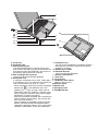
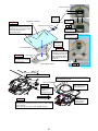
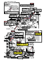
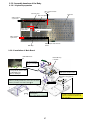
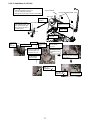
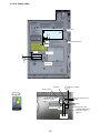
Notebook Computer
CF-Y5
This is the Service Manual for
the following areas.
M …for U.S.A. and Canada
Model No. CF-Y5LWVYZ 1 2
1: Operation System
B: Microsoft® Windows® XP Professional
2: Area
M: Refer to above area table
© 2006 Matsushita Electric Industrial Co., Ltd. All rights reserved.
Unauthorized copying and distribution is a violation of law.
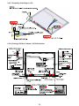
WARNING
For U.K.
This apparatus must be earthed for your safety.
To ensure safe operation the three-pin plug must be inserted only into a standard three-pin power point
which is effectively earthed through the normal household wiring.
Extension cords used with the equipment must be three-core and be correctly wired to provide connection to earth. Wrongly wired extension cords are a major cause of fatalities.
The fact that the equipment operates satisfactorily does not imply that the power point is earthed and
that the installation is completely safe.
For your safety, if you have any doubt about the effective earthing of the power point, consult a qualified electrician.
FOR YOUR SAFETY PLEASE READ THE FOLLOWING TEXT CAREFULLY
This appliance is supplied with a moulded three pin mains plug for your safety and convenience.
A 3 amp fuse is fitted in this plug.
Should the fuse need to be replaced please ensure that the replacement fuse has a rating of 3 amps and
that it is approved by ASTA or BSI to BS 1362.
or the BSI mark
on the body of the fuse.
Check for the ASTA mark
If the plug contains a removable fuse cover you must ensure that it is refitted when the fuse is replaced.
If you lose the fuse cover the plug must not be used until a replacement cover is obtained.
A replacement fuse cover can be purchased from your local Panasonic Dealer.
IF THE FITTED MOULDED PLUG IS UNSUITABLE FOR THE SOCKET OUTLET IN YOUR
HOME THEN THE FUSE SHOULD BE REMOVED AND THE PLUG CUT OFF AND DISPOSED
OF SAFELY.
THERE IS A DANGER OF SEVERE ELECTRICAL SHOCK IF THE CUT OFF PLUG IS INSERTED
INTO ANY 13 AMP SOCKET.
If a new plug is to be fitted please observe the wiring code as shown below.
If in any doubt please consult a qualified electrician.
Warning: THIS APPLIANCE MUST BE EARTHED.
Important
The wires in this mains lead are coloured in accordance with the following code:
Green-and-yellow:
Earth
Blue:
Neutral
Brown:
Live
As the colours of the wires in the mains lead of this apparatus may not correspond with the coloured
markings identifying the terminals in your plug, proceed as follows:
The wire which is coloured GREEN-and-YELLOW must be connected to the terminal in the plug
coloured GREEN or GREEN-andwhich is marked by the letter E or by the safety earth symbol
YELLOW.
The wire which is coloured Blue must be connected to the terminal which is marked with the letter N or
coloured BLACK.
The wire which is coloured Brown must be connected to the terminal which is marked with the letter L
or coloured RED.
The mains plug on this equipment must be used to disconnect the mains power.
Please ensure that a socket outlet is available near the equipment and shall be easily accessible.
How to replace the fuse
Open the fuse compartment with a screwdriver and replace the fuse.
Warnings
This equipment is not designed for connection to an IT power system.
(An IT system is a system having no direct connections between live parts and Earth; the exposed-conduciveparts of the electrical installation are earthed.
An IT system is not permitted where the computer is directly connected to public supply systems in the U.K.)
Disconnect the mains plug from the supply socket when the computer is not in use.
This equipment is produced to BS800/1983.
2
LASER SAFETY INFORMATION
For U.S.A.
Class 1 LASER-Product
This product is certified to comply with DHHS Rules 21 CFR Subchapter J.
This product complies with European Standard EN60825 (or IEC Publication 825)
For all areas
This equipment is classified as a class 1 level LASER product and there is no hazardous LASER radiation.
Caution:
(1) Use of controls or adjustments or performance of procedures other than those specified herein may result in
hazardous radiation exposure.
(2) The drive is designed to be incorporated into a computer-based system or unit which has an enclosing cover.
It should never be used as a stand alone drive.
Danger:
The serviceman should not remove the cover of drive unit and should not service because the drive unit is a nonserviceable part.
Please check DANGER label on PD-drive unit.
Unplug the AC power cord to the equipment before opening the top cover of the drive.
When the power switch it on, do not place your eyes close to the front panel door to look into the interior of the unit.
LASER Specification
Class 1 level LASER Product
Wave Length: DVD 658–8 nm
CD 775~815 nm
Laser safety information is appropriate only when drive with laser is installed.
3
4
5
CONTENTS
1. Specifications
7
2. Names and Functions of Parts
10
3. Block Diagram
12
4. Diagnosis Procedure
13
5. Power-On Self Test (Boot Check)
15
6. List of Error Codes <Only when the port replicator is connected>
16
7. Self Diagnosis Test
18
8. Wiring Connection Diagram
23
9. Disassembly/Reassembly
24
10. Exploded View
80
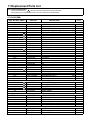
11. Replacement Parts List
83
1 Specifications
Useful Information
Getting Started
Main Specifications
Model No.
CPU/
Secondary cache memory
CF-Y5LWVYZBM
Chip Set
Mobile Intel® 945 GMS Express chip set
Main Memory
512 MB*1, DDR2 SDRAM (1536 MB*1 Max.)
Video Memory
UMA (128 MB*1 Max.)*2
Hard Disk Drive
60 GB*3
CD/DVD Drive
USB 2.0 connection interface
DVD MULTI Drive built-in, Buffer underrun error prevention function: Supported
Continuous Data Transfer Speed*4*5
Supported Disks/Format*5
Intel® Core™ Duo Processor Low Voltage L 2400 (1.66 GHz, 2 MB*1 L2 cache, 667
MHz FSB)
Reading*6
zDVD-RAM*7: 2X (4.7 GB*3)/1X (2.6 GB*3) zDVD-R*8: 4X (Max.) zDVD-RW: 4X
(Max.) zDVD-ROM: 8X (Max.) zCD-ROM: 24X (Max.) zCD-R: 24X (Max.) zCD-RW:
20X (Max.) z+R: 4X (Max.) z+R DL: 4X (Max.) z+RW: 4X (Max.)
Writing*9
zDVD-RAM*7: 2X (4.7GB*3) zDVD-R: 1X/2X/4X zDVD-RW: 1X/2X z+R: 2.4X/4X
z+RW: 2.4X zCD-R: 4X/8X/8-16X/8-24X zCD-RW: 4X zHigh-Speed CD-RW: 4X/8X/
10X zUltra-Speed CD-RW: 8X/10X
Reading
zDVD-ROM (Single Layer, Dual Layer) zDVD-Video zDVD-R*8(1.4 GB, 3.95 GB, 4.7
GB)*3 zDVD-RW (Ver.1.1/1.2 1.4 GB, 4.7 GB, 9.4 GB)*3 zDVD-RAM*7 (1.4 GB, 2.8 GB,
2.6 GB, 5.2 GB, 4.7 GB, 9.4 GB)*3 z+R (4.7 GB)*3 z+R DL (8.5 GB)*3 z+RW (4.7 GB)*3
zCD-Audio zCD-ROM (XA compatible) zCD-R zPhoto CD (multiple session compatible) zVideo CD zCD-EXTRA zCD-RW zCD-TEXT
Writing
zDVD-RAM*7 (1.4GB, 2.8GB, 4.7GB, 9.4GB)*3zDVD-R (1.4GB, 4.7GB for General)*3
zDVD-RW (Ver.1.1/1.2 4.7GB, 9.4GB)*3 z+R (4.7GB*3) z+RW (4.7GB*3) zCD-R zCD-RW
Display Method
14.1 SXGA+ type (TFT) (1400
Internal LCD
Troubleshooting
× 1050 dots)*10
65,536/16,777,216 colors (800 × 600 dots/1024 × 768 dots/1280 × 768 dots/1280 ×
1024 dots/1400 × 1050 dots/1600 × 1200 dots/2048 × 1536 dots (60 Hz)*12)
65,536/16,777,216 colors (800 × 600 dots/1024 × 768 dots/1280 × 768 dots/1280 ×
1024 dots/1400 × 1050 dots)*10
65,536/16,777,216 colors (1400
External Display*11
Appendix
× 1050 dots)
Simultaneous Display on LCD + External Display*11
Wireless LAN
Intel® PRO/Wireless 3945 ABG Network Connection (next page)
(next page)
Bluetooth™
IEEE 802.3 10Base-T, IEEE 802.3u 100Base-TX
LAN*13
Modem
Data: 56 kbps (V.92) FAX: 14.4 kbps
Sound
WAVE and MIDI playback, Intel® High Definition Audio subsystem support, Stereo
Speakers (built in)
Security Chip
TPM (TCG V1.2 compliant)*14
Card Slots
PC Card Slot
SD Memory Card
Slot*15
× 1, Type I or Type II, Allowable current 3.3 V: 400 mA, 5 V: 400 mA
× 1, Data transfer rate = 8 MB per second
RAM Module Slot
× 1, DDR2 SDRAM, 172-pin, 1.8 V, Micro DIMM, PC2-4200 Compliant*16
Interface
USB Ports × 2 (USB2.0 × 2)*17 / Modem Port (RJ-11) / LAN Port (RJ-45) *13 /
External Display Port: Mini Dsub 15-pin female / Microphone Jack: Miniature jack, 3.5
DIA / Headphone Jack: Miniature jack, 3.5 DIA / Mini Port Replicator connector: Dedicated 50-pin male
Keyboard/Pointing Device
Power Supply
87 keys/Touch Pad
AC adaptor or Battery pack
AC Adaptor*18
Input: 100 V - 240 V AC, 50 Hz/60 Hz
Output: 16 V DC, 3.75 A
Li-ion 10.65 V, 5.7 Ah
Battery Pack
Operating Time*19
Charging Time*22
Approx. 5 hours - 8 hours*20 (Approx. 6 hours*21) (Disable Economy Mode (ECO))
Approx. 5 hours (Power off)/Approx. 6.5 hours (Power on)
7
CF-Y5LWVYZBM
*23
Power Consumption
Approx. 35 W*24 / Approx. 60 W (maximum when recharging in the ON state)
Physical Dimensions (W × H × D)
309.6 mm × 28 mm (at the front)/44.5 mm (at the rear) × 245.5 mm (excluding protrusion) {12.2 " × 1.1 " / 1.8 " × 10.0 "}
Weight*25
Approx. 1530 g {3.4 lb.}
Environment
Operation Temperature
Storage
5°C to 35°C {41°F to 95°F}
Humidity
Temperature
30% to 80% RH (No condensation)
Humidity
30% to 90% RH (No condensation)
*26
-20°C to 60°C {-4°F to 140°F}
OS
Microsoft® Windows® XP Professional Service Pack 2 with Advanced Security Technologies (NTFS File system)
Pre-installed Software*26
Microsoft® Internet Explorer 6 Service Pack 2 / DirectX 9.0c /Microsoft® Windows®
Media Player 10 / Microsoft® Windows® Movie Maker 2.1 / Microsoft® .NET Framework
1.1 SP1/2.0 / Adobe Reader / Intel® PROSet/Wireless Software <Only for model with
wireless LAN> / SD Utility / Icon Enlarger / Loupe Utility / Touch Pad Utility / DMI Viewer
/ PC Information Viewer / WinDVD 5 (OEM Version) / B’s Recorder GOLD8 BASIC / B’s
CLiP 6*27 / Hotkey Settings / Optical Disc Drive Letter-Setting Utility / Optical Disc Drive
Power-Saving Utility / Wireless Switch Utility <Only for model with wireless LAN/Bluetooth> / Economy Mode (ECO) Setting Utility / Battery Recalibration Utility / Infineon
TPM Professional Package V2.5*28 / Recover Pro 6*28
Getting Started
Model No.
Wireless LAN
Data Transfer Rates
IEEE802.11a: 54/48/36/24/18/12/9/6 Mbps (automatically switched)*31
IEEE802.11b: 11/5.5/2/1 Mbps (automatically switched)*31
IEEE802.11g: 54/48/36/24/18/12/9/6 Mbps (automatically switched)*31
Standard Supported
IEEE802.11a/IEEE802.11b/IEEE802.11g
OFDM system, DS-SS system
Wireless Channels Used
IEEE802.11a: Channels 36/40/44/48/52/56/60/64/149/153/157/161/165
IEEE802.11b/ IEEE802.11g: Channels 1 to 11
RF Frequency Band
IEEE802.11a: 5.18 - 5.32 GHz, 5.745 - 5.825 GHz
IEEE802.11b/ IEEE802.11g: 2412 - 2462 MHz
Bluetooth™
Bluetooth Version
2.0 + EDR
Transmission Method
FHSS system
Wireless Channels Used
Channels 1 to 79
RF Frequency Band
2.402-2.48 GHz
Power Class
Class 1
*1
1 MB = 1,048,576 bytes
A segment of the main memory is allotted automatically
depending on the computer’s operating status. The size of
the Video Memory cannot be set by the user.
*3 1 GB = 1,000,000,000 bytes. Your operating system or some
application software will report as fewer GB.
*4 Data transfer speeds indicate values measured by
Matsushita Electric Industrial Co., Ltd. The data transfer rate
of DVD per 1X speed is 1,350 KB/s. The data transfer rate of
CD per 1X speed is 150 KB/s.
*5 Performance of CD-R, CD-RW, DVD-RAM, DVD-R, DVDRW, +R, +R DL, and +RW cannot be guaranteed depending
on writing status and recording format. Also, some data cannot be played back depending on the disk, settings, and
environment being used.
Does not support writing to DVD-R DL/+R DL (dual layer
disks) or reading from DVD-R DL.
*6
*2
8
*7
*8
*9
*10
*11
If an unbalanced disk (e.g., a disk with which the balance
has been displaced from the center) is inserted, the speed
may become slower if there are large vibrations while the
disk is rotating.
Only non-cartridge type or removable cartridge type can be
used.
When writing to DVD-RAM, use only disks up to 3x. This
application cannot be used with 5x DVD-RAM media (2-5x
disks, etc.).
DVD-R is compatible with 4.7 GB (for General) playback.
DVD-R (for Authoring) playback is compatible with disks
recorded using Disk-at-Once recording.
Depending on the disk, the writing speed may become
slower.
A 16,777,216 color display is achieved by using the dithering
function.
Display may be impossible using some connected external
displays.
Appendix
Troubleshooting
Transmission Method
Useful Information
Setup Utility / Hard Disk Data Erase Utility*29 / PC-Diagnostic Utility*30
*12
*13
*14
Getting Started
*15
*16
*17
20-M-2-1
Appendix
Troubleshooting
Useful Information
*18
When using an external display with a resolution of 2048 x
1536 dots, use a display that supports a 60Hz refresh rate. If
an external display that does not support a 60Hz refresh rate
is used, images may not be displayed properly.
Some devices cannot be used depending on the port type.
For information on TPM, click [start] - [Run] and input
“c:\util\drivers\tpm\README.pdf”, and refer to the Installation
Manual of “Trusted Platform Module (TPM)”.
Operation has been tested and confirmed using Panasonic
SD Memory Cards with a capacity of up to 2 GB.
The transfer rate using the SD Memory Card slot on this
computer is 8 MB per second. (This is a theoretical value,
and differs from actual speeds.)
The transfer rate is 8 MB per second even if you use an SD
Memory Card that supports high-speed transfer rates.
Operation on other SD equipment is not guaranteed.
This computer is not compatible with MultiMediaCards or
SDHC Memory Cards.
Do not insert these kinds of cards.
Only a RAM module designed for DDR2 (PC2-4200) can be
added (Panasonic : CF-BAW0512U, CF-BAW1024U).
JEDEC standard 214 pin Micro DIMM cannot be used.
PC2100 / PC2700 172 pin Micro DIMM cannot be used.
If a PC2-3200 RAM module is installed, the main memory
processing speed may become slower.
Does not guarantee operation of all USB-compatible peripherals.
<Only for North America>
The AC adaptor is compatible with power sources up to
240 V AC adaptor. This computer is supplied with a 125 V
AC compatible AC cord.
9
*19
*20
*21
*22
*23
*24
Varies depending on the usage conditions, or when an
optional device is attached. Measured when the power saving
function on the USB2.0 USB Root Hub is set to on. (At the
time of purchase, the power saving function is activated.)
When Economy Mode (ECO) is enabled, the operating time
becomes approximately 20% shorter than when it is disabled.
Measured using BatteryMark™ Version 4.0.1 (LCD brightness : Maximum - Minimum).
Measured using MobileMark™ 2005 (LCD brightness : 60
cd/m2).
Varies depending on the usage conditions, CPU speed, etc.
It may take a long time to charge a fully discharged battery.
Approx. 1.5 W when the battery pack is fully charged (or not
being charged) and the computer is off.
Rated power consumption.
23-E-1
*25
*26
*27
*28
*29
*30
*31
Average value. May differ depending on models.
Operations of this computer are not guaranteed except for
the pre-installed OS.
Preinstalled B’s CLiP does not support CD-R, DVD-R, +R
and DVD-RAM.
Must be installed before use.
The Product Recovery DVD-ROM is required.
For startup methods, refer to “Hardware Diagnostics”.
These are speeds specified in IEEE802.11a+b+g standards.
Actual speeds may differ.
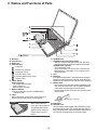
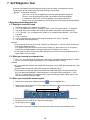
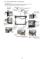
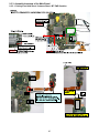
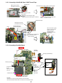
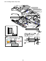
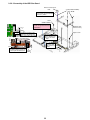
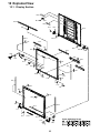
2 Names and Functions of Parts
A
B
C
D
E
F
J
G
K
H
L
M
N
I
A :Speakers
B :Function Key
C :Keyboard
D :LED Indicator
: Caps lock
: Numeric key (NumLk)
: Scroll lock (ScrLk)
: Hard disk drive status
ECO : Economy Mode (ECO) status
: Battery status
E : Power Switch
Power Indicator
• Off: Power off/Hibernation
• Green: Power on
• Blinking green: Standby
F : Wireless Switch
<Only for model with wireless LAN/Bluetooth>
“Wireless LAN”
G :Latch
When closing the display, press down firmly from
above until the latch is firmly closed (locked).
H :CD/DVD Drive
I : CD/DVD Drive Power/Open Switch
• Slide the switch to the right to open the disk cover.
• Slide the switch to the left to turn on/off the drive power.
CD/DVD Drive Indicator
• Off: Drive power is off.
• Green: Drive power is on, but the drive is not accessed.
• Blinking green: Drive power is on, and the drive is
being accessed.
J : LCD
K :LAN Port
If the Mini Port Replicator is connected to the computer,
connect the LAN cable to the LAN port on the Mini Port
Replicator. You cannot use the LAN port on the computer.
L : Modem Port
• Be sure to use the included modem telephone cable,
and insert the ferrite core side of modem telephone
cable into the modem port on the computer.
• Do not move/remove the ferrite core of modem telephone cable.
90 mm {3.5 "} or less
CAUTION
When closing the disk
cover, press down near the
drive power/open switch
(position of the arrow) to
ensure that the cover is
locked.
10
M :USB Ports
N :Security Lock
You can connect a Kensington cable. Refer to the instruc
tion manual of the cable. The security lock and cable is atheft prevention device. Matsushita Electric Industrial Co.,
Ltd. will bear no responsibility in the event of theft.
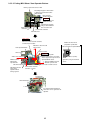
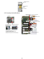
H
I
A
B
M
C
J
EXT. D
K
E
F
G
N
A :DC-IN Jack
B :Ventilation Hole
C :External Display Port
If the Mini Port Replicator is connected to the computer, connect the external display to the external display port on the Mini Port Replicator. You cannot use
the external display port on the computer.
D :Mini Port Replicator Connector
Connect the Mini Port Replicator (optional).
E : Microphone Jack
A condenser microphone can be used. If other types
of microphones are used, audio input may not be possible, or malfunctions may occur as a result.
• When recording in stereo using a stereo microphone
Double-click
in the notification area, click
[Options] - [Properties], and add a check mark for
[Recording], click [OK] - [Options] - [Advanced Controls] - [Advanced], remove a check mark for [Mono
Microphone], and then click [Close].
• When using a monaural microphone with a 2-terminal plug
With the settings outlined above, only audio on the
left track will be recorded.
When monitoring the microphone audio using headphones, sounds on the left track cannot be heard,
regardless of the above settings. This is a result of the
computer’s specifications, and is not a malfunction.
11
F : Headphone Jack
You can connect headphones or amplified speakers.
When they are connected, audio from the internal
speakers is not heard.
G :SD Memory Card Slot
H :Bluetooth Antenna
<Only for model with Bluetooth>
I : Wireless LAN Antenna
J : Touch Pad
K :PC Card Slot
L : SD Memory Card Indicat
Blinking: During access
M :Battery Latches
N :Battery Pack
O :Emergency Hole
P : RAM Module Slot
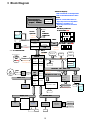
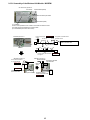
3 Block Diagram
Internal Core Frequency
HFM=1.6
GHz
Hz/LFM=
/LFM=1.0
HFM=1.66
1.66 G
Hz
/LFM=1.0 GHz
GHz (High Model)
HFM=1.2
1.2 GHz/LFM=
GHz/LFM=800
HFM=
800 MHz (Low Model)
VCC Core
Yonah LV Dual Core
Yonah ULV Single Core
HFM=1.0V
.2125V/
1.0V
V
HFM=1.0V1.0V-1.2125
V/ LFM=0.7625V
LFM=0.7625V0.7625V-1.0
Included
L2-Cache 2M
(479pin FCBGA)
Deeper Sleep=0.55V
0.85V
V (H
(High
Model))
Sleep=0.55V0.55V-0.85
igh Model
HFM=0.85V
0.85V--1.1
1.1V/
0.8--1.
1.0
HFM=
0.85V
V/ LFM=0.8
LFM=0.8
0V
Deeper Sleep=0.55
Sleep=0.55V
0.55V-0.85V (Low
(Low Model)
Model)
VCCP 1.05V
1.05V
Memory
y (DDR2
DDR2-- 533)
Main Memor
533)
On Board 512MB,
512MB, 1GB
AGTL+
64bit
Processor
CRT
667MHz(LV)
System Bus
Port
5.3GByte/Sec
533MHz(ULV)
533MHz(ULV)
Replicator
4.3GByte/Sec
1.05V
CRT
533MHz
CalistogaCalistoga-GMS
RGB
Graphics
DRAM
Interface
(1ch/2ch)
64bit
Interface
LVDS
HostHub Bridge
(TMD 14.1”
4.1”SXGA+/XGA TFT)
TFT
1.05V
4.3GByte/Sec
3.2GByte/Sec
DMI x 2
1.5V 66MHz
BlueTooth
1GByte/Sec
Storage Device
PATA
PATA
HDD
(IDE)
ICH7ICH7-M
33.3MByte/Sec
(Ultra DMA Mode 2)
Extended
Extended Memory (PC2PC2-4200 )
Micro
cro--DIMM 1 (MAX 2
2GB
GB)
Mi
cro
GB)
1.8V
998pin FCBGA
LCD
60G
60G/120G
1.8V/0.9V
USB4
USB3
USB5
USB0
USB2.0
PATA
USB
Interface
Interface
SATA
PCI
Interface
Bridge
480MByte/Sec
USB2
USB0
USB6
USB2
USB7
Port Replicator
PCI 2.3 Bus 32bit 33MHz 3.3V
PATA
DVD Multi
Drive
(IDE)
652 pin
USB
ATA
USB2.0
USB1
SPI Bus 3.3V
BGA
1.05V
SPI
Interface
LPC
SPI Flash
8Mbit
25PE08
Bridge
133MByte/Sec
PCI
(USB3)
2.5GByte/Sec
Express
PCI Express x 4 1.25GHz
Bridge
1.5V
HD Audio
Interface
Card Bus
LAN(100Base)
R5C811A
RTL8101L
RICOH
RealTek
Mini Express Card Slot
W-LAN Golan 11ABG
TYPE (SLOT A)
SD Slot(SLOT B)
SD-IO Not Support
RJ-45
RJ-45
Port
Replicator
Antenna
LPC Bus 3.3V
TPM
1.2
FWH
SST49LF008A
-33-4C-WHE
HD Audio / AC97
EC/KBDC
M306KA
MDC
Soft Modem
Microphone
STAC9200
Sigmatel
AMP
Speakers
Headphone
Flat Pad
Int KB
RJ-11
12
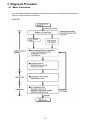
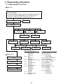
4 Diagnosis Procedure
4.1. Basic Procedures
13
4.2. Troubleshooting
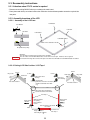
Please take note of the following two points with regard to troubleshooting:
1. Know-how of diagnosis upon occurrence of heavy troubles, e.g. Set cannot be turned ON , Set fails to start , No display on
screen , etc.
2. Explanation of each trouble, mainly symptom of trouble in operation.
Flow Chart
START
START
Set cannot be supplied with current.
Power lamp fails to light up.
Pay attention to the following points when in pursuit of the cause of a troubleshooting.
1. Peripheral apparatus connected with the set should all be removed before operation check.
2. Make sure that cables, boards, etc. are not coming off, and recheck the contact condition.
NG
AC
Adaptor/Battery
Output voltage
Replace AC Adaptor/Battery
OK
NO
Power lamp
check
YES
Dark display on screen.
Screen fails to display.
NG
Inverter board
Check contact condition of power input terminal. Replace if
defective.
Check Power SW. Replace if defective.
Replace inverter board.
Check inverter cable continuity. Replace if defective
OK
NO
LCD back
light lighting
YES
NG
LCD unit
check
Replace LCD back light.
Replace LCD unit.
OK
Failure in starting
NO
BIOS operation
check
Replace main board (Check fuse at power source).
YES
NG
Result of
POST
Refer to POST
error code table.
Replace main board.
OK
NG
Set-up utility
starting
Replace main board.
OK
Return set-up utility setpoint to the state of delivery from factory .
NO
HDD access
YES
Not displayed properly on screen.
NG
Main board
check
Heavy trouble e.g.,
Set cannot be turned
ON , Set fails to start ,
No display on
screen , etc.
Check HDD cable connection and continuity.
Replace if defective.
Replace HDD & Reinstall.
Replace main board.
Replace main board
OK
Some or all keys cannot be input.
DVD/CD CALL not practicable.
Make sure of contact of K/B connector in use.
Replace keyboard or main board.
NO
Trouble
symptoms on some
of DVD or CD
YES
*Clean DVD-ROM drive with an applicator.
Replace DVD drive.
Replace main board.
Starts but operates unstably.
Reinstall HDD.
Replace main board.
START
END
14
Check if there are any flaws on DVD or CD
media. Since flaws may appear on specific
media, DVD or CD media can be defective.
Each kind of
trouble in
operation.
5 Power-On Self Test (Boot Check)
Outline of POST
The set has a boot check function called POST (Power-On Self Test) in it.
The condition of the main body is diagnosed by checking beep sound or error code.
Start .............Test begins automatically when power switch is set to ON.
Normal finish .....After memory checking, a beep sound is issued once and the set is placed into automatic stop.
Note: If no error occurs, nothing is displayed. (No display of OK, etc.)
Error Diagnosis by Checking Beep Signal Sound
The beep sound is as follows:
(1 (long sound) -2-3-4)
(Length of bar shows length of sound.)
= long sound (about 0.4 sec.),
= short sound (about 0.2 sec.), Length between sounds is about 0.1 sec.
Table of errors classified by beep sounds
Diagnosis
Main board
Beep signal sound
Error message
1(long sound)-2
BIOS ROM error
1-2-2-3
BIOS ROM error
1-3-1-1
RAM error
1-3-1-3
Keyboard controller error
1-3-4-1
RAM error
1-3-4-3
RAM error
1-4-1-1
RAM error
2-1-2-3
BIOS ROM error
2-2-3-1
Occurrence of unexpected offering
(Note) A beep sound is also issued in case of other I/O trouble.
15
6 List of Error Codes <Only when the port replicator is connected>
The following is a list of the messages that BIOS can display. Most of them occur during
POST. Some of them display information about a hardware device, e.g., the amount of memory
installed. Others may indicate a problem with a device, such as the way it has been configured.
Following the list are explanations of the messages and remedies for reported problems.
If your system displays one of except the messages marked below with an asterisk (*), write
down the message and contact Panasonic Technical Support. If your system fails after you
make changes in the Setup menus, reset the computer, enter Setup and install Setup defaults
or correct the error.
0200 Failure Fixed Disk
Fixed disk in not working or not configured properly. Check to see if fixed disk is attached
properly. Run Setup. Find out if the fixed-disk type is correctly identified.
0210 Stuck key
Stuck key on keyboard.
0211 Keyboard error
Keyboard not working.
0212 Keyboard Controller Failed
Keyboard controller failed test. May require replacing keyboard controller.
0213 Keyboard locked - Unlock key switch
Unlock the system to proceed.
0230 System RAM Failed at offset : nnnn
System RAM failed at offset nnnn of in the 64k block at which the error was detected.
0231 Shadow RAM Failed at offset : nnnn
Shadow RAM failed at offset nnnn of the 64k block at which the error was detected.
0232 Extended RAM Failed at offset : nnnn
Extended memory not working or not configured properly at offset nnnn.
0250 System battery is dead - Replace and run SETUP
The CMOS clock battery indicator shows the battery is dead. Replace the battery and run Setup
to reconfigure the system.
*0251 System CMOS checksum bad - Default configuration used
System CMOS has been corrupted or modified incorrectly, perhaps by an application program
that changes data stored in CMOS. The BIOS installed Default SETUP Values. If you do not
want these values, enter Setup and enter your own values. If the error persists, check the system
battery or contact Panasonic Technical Support.
0260 System timer error
The timer test failed. Requires repair of system board.
0270 Real time clock error
Real-time clock fails BIOS test. May require board repair.
*0280 Previous boot incomplete - Default configuration used
Previous POST did not complete successfully. POST loads default values and offers to run
Setup. If the failure was caused by incorrect values and they are not corrected, the next boot
will likely fail. On systems with control of wait states, improper Setup settings can also terminate POST and cause this error on the next boot. Run Setup and verify that the wait-state
configuration is correct. This error is cleared the next time the system is booted.
0281 Memory Size found by POST differed from EISA CMOS
Memory size found by POST differed from EISA CMOS.
16
17
Troubleshooting
02D0 System cache error - Cache disabled
Contact Panasonic Technical Support.
02F0: CPU ID:
CPU socket number for Multi-Processor error.
02F4: EISA CMOS not writable
ServerBIOS2 test error: Cannot write to EISA CMOS.
02F5: DMA Test Failed
ServerBIOS2 test error: Cannot write to extended DMA (Direct Memory Access) registers.
02F6: Software NMI Failed
ServerBIOS2 test error: Cannot generate software NMI (Non-Maskable Interrupt).
02F7: Fail - Safe Timer NMI Failed
ServerBIOS2 test error: Fail-Safe Timer takes too long.
device address Conflict
Address conflict for specified device.
Allocation Error for: device
Run ISA or EISA Configuration Utility to resolve resource conflict for the specified device.
Failing Bits : nnnn
The hex number nnnn is a map of the bits at the RAM address which failed the memory test.
Each 1 (one) in the map indicates a failed bit. See error 230,231 or 232 for offset address of the
failure in System, Extended or Shadow memory.
Invalid System Configuration Data
Problem with NVRAM (CMOS) data.
I/O device IRQ conflict
I/O device IRQ conflict error.
Operating System not found
Operating system cannot be located on either drive A: or drive C:. Enter Setup and see if fixed
disk and drive A: are properly identified.
Parity Check 1 nnnn
Parity error found in the system bus. BIOS attempts to locate the address and display it on the
screen. If it cannot locate the address, it displays ????. Parity is a method for checking errors
in binary data. A parity error indicates that some data has been corrupted.
Parity Check 2 nnnn
Parity error found in the I/O bus. BIOS attempts to locate the address and display it on the
screen. If it cannot locate the address, it displays ????.
Press <F1> to resume, <F2> to Setup
Displayed after any recoverable error message. Press <F1> to start the boot process or <F2> to
enter a Setup and change the settings. Write down and follow the information shown on the
screen.
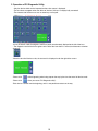
7 Self Diagnosis Test
As for the self-diagnosis test(PC-Diagnostic utility) to use this model, a standard test and the
enhancing test by the module of the main body building in are possible.
Notes To skip BIOS password
Use <Ctrl>+<F10> key to skip BIOS password or authentication of fingerprint.
This key is only for entering DIAG mode. Not available to boot the computer.
If customer set "HDD Lock", the DIAG program cannot perform HDD test.
*This key is for service purpose only. Do not disclose this information to unrelated others.
1. Beginning of self-diagnosis test
1-1. Setting of content of setup
1.
2.
3.
4.
The power supply of the computer is turned on.
" F2 " is pushed on the screen of "Panasonic" while " press <F2 to enter Setup> " is displayed.
The setup utility starts and then takes notes of the content of the BIOS setup of present set.
" F9 " is pushed, " Yes" is selected on the screen of " Is the default value loaded? ", and " Enter"
is pushed.
5. " F10 " is pushed.
6. " Yes" is selected on the screen of the setup confirmation, and " Enter" is pushed.
7. The computer starts automatically.
Attention
If the device which can be set is set to "Invalidity" by "Advanced" or "Security" menu, becomes an
error by "PC-Diagnostic utility".
(It is judged that the device which can be set to "Invalidity" by "Main" menu such as "Flat pad" is
normal if the controller operates normally though sets to "Invalidity" by the setup. )
In the model with built-in DVD of the USB connection, even if DVD is normal, becomes an error if
legacy USB is set to "Invalidity"
1-2. When you execute an automatic test
1. "Ctrl" + "F7" is pushed while the "Panasonic" start screen is displayed after the computer is started.
2. The test of all devices begins automatically by "PC-Diagnostic utility"’s starting.
Attention
It is a test which the customer who bought PC can execute. (As for HDD, the enhancing test is also
possible.)
A flat pad does not work for a while after starting "PC-Diagnostic utility".
The movement of a flat pad might become abnormal If after RAM begins from the CPU/System
test, a flat pad will be operated in about 30 seconds. In that case,restarts pushing"Alt" + "Ctrl" +
"Del" key. Or, please start "PC-Diagnostic utility" again after doing the power supply switch in the
slide, and turning off the power supply.
1-3. When you execute the enhancing test
1. Please let me discontinue diagnosing clicking
to end an automatic test.
2. Please click on the character of "D" "PC-Diagnostic utility" on the screen while pushing both of right
"Shift" and left "Shift" keys.
D
3. All devices which can select the enhancing test make the setting of the enhancing test possible.
4. The district device is made"FULL" display (enhancing test).
5. The test begins clicking
.
*Please refer to item 4 for the error result of each test and the division of the breakdown part.
18
2. Operation of PC-Diagnostic Utility
-Only the device which can be inspected on the entire screen is displayed.
-The item does not appear when the device of wireless LAN etc. is not physically connected.
-The movement of the item must use an arrow key or a flat pad.
-As for the device under the diagnosis, blue and yellow are alternately displayed at the left of the icon.
- The diagnosis result of the device greens at the left of the icon when it is normal, and becomes red when
abnormal.
-When the test of all devices ends, the test result is displayed under the right of the screen.
-Please click
while diagnosing when being stop on the way by the time the test of all devices ends.
-Please click
when you restart "PC-Diagnostic utility".
*Each device is tested from the beginning, and it is not possible to restart on the way.
19
2-1. Selection of tested device
-To test only a specific device, "Test" and "Do not test" of each device can be selected.
-The device which can select the enhancing test changes in order of "The standard is tested" and "Do not
test" whenever the device icon is clicked.
Do not test
Start the standard test
Please begin testing clicking
if the selection of the tested device ends.
2-2. "PC-Diagnostic utility" End method
When
of "Close" on the right of the screen is clicked, the computer reactivates automatically. Or, the
power supply switch is done in the slide and the power supply is turned off.
2-3. The content of the setup is returned to the setting of the user
1. Turned on the computer.
2. "F2" is pushed on the screen while "Press<F2>to enter Setup" is displayed of "Panasonic".
3. Push "F10", and on the screen of "Is the change in the setting preserved and do end?"and then "Yes"
is selected, and "Enter" is pushed.
4. The computer reactivates automatically.
5. The end option is chosen by the start menu, and the power supply of the computer is turned off.
Standard at test time
All devices other than RAM and HDD
RAM standard test
HDD standard test
HDD enhancing test (60GB)
about 1 minute
1 - 2 minutes
2 - 3 minutes
about 40 minutes
Ex.The standard when the standard <all device> is tested becomes 1+2+3=6 minutes.
There is greatly a difference from RAM test when the memory is increased according to the performance of the memory occasionally.
Moreover, when the main body of PC under the test is a high temperature, it occasionally takes time.
There is greatly a difference from HDD according to the performance of the drive occasionally.
20
7.1. Test Item and Division of trouble
Test item Stanard Enhancing
Content of standard test
Content of enhancing test
Place with possibility of breakdown
CPU /
SYSTEM
CPU is shifted to protected mode, and
"Violation of the paging", "Operation of
the violation of a privileged instruction", and DMA, INT, TIMER, and the
RTC operation are confirmed.
CPU /
Main board
RAM
All memory space is tested in a special memory access pattern based on
"R.S.T . technology".
Memory / Mainboard
HDD
The record area frequently accessed
with Microsoft Windows XP to test in
about two minutes regardless of
points of HDD is emphatically tested.
MODEM
It is confirmed not to find abnormality
in the AC97 modem controller.
MODEM/ Mainboard
Wireless
LAN
It is confirmed not to find abnormality
in the Wireless LAN modem controller.
Wireless LAN
board /
Connector /
Mainboard
All record area is tested.
HDD /
Mainboard /
Cable /
Connector
Sound *5
USB
It is confirmed not to find abnormality
in the USB controller.
It is confirmed not to find abMainboard /
normality in the wiring beConnector
tween the USB controller and
the connector by confirming
the connection of the USB
equipment connected with the
USB connector.
It is confirmed not to find abnormality
in the LAN controller.
It is confirmed not to find abnormality in the wiring between the controller and the
connector by connecting to
HUB with LAN cable.
*1
LAN
*2
Mainboard /
Connector
PC Card
It is confirmed not to find abnormality
in the CardBus controller.
Mainboard
SD
It is confirmed not to find abnormality
in the SD controller.
Mainboard
Mainboard /
Keyboard
Keyboard
*3
It is confirmed not to find abnormality The key is actually input, and
in keyboard controller’s keyboard inter- the operation is displayed on
the screen.
face.
Touch Pad
*4
Whether keyboard controller’s mouse The operation is actually dis- Mainboard /
interface operates normally is conplayed on the screen by oper- Touch Pad
firmed.
ating the touch pad.
DVD-ROM
*6
The drive is normally reset, and it is
accessible is confirmed.
21
It is confirmed to be able to
read media normally.
Mainboard /
Touch Pad
Test Item
Standard Enhanced
Content of Standard Test
It is confirmed not to find
abnormality in the USB
connection of Touch Screen.
This test cannot find
abnormality of Touch Screen.
It is confirmed not to find
abnormality in the connection
of Main board and Bluetooth
module.
It is confirmed not to find
abnormality in the legacy FD
drive.
This test cannot find
abnormality of mechanical
breakdown. (e.g.. Head, Motor)
It is confirmed not to find
abnormality in access to
VRAM with VESA.
The PC which uses main
of Main board and GPS
main memory failure.
It is confirmed not to find
abnormality in the connection
memory as VRAM may fail with
It is confirmed not to find
abnormality in the IEEE1394
controller.
Touch Screen
Bluetooth
Floppy
Video
GPS
IEEE1394
Perform Touch Screen
functionality practically.
Operator has to judge
PASS/FAIL with test result.
Smart Card
It is confirmed not to find
abnormality in the Smart Card
controller.
Serial Port
*7
It is confirmed not to find
abnormality of Super I/O
UART function.
This test cannot find lack of
wiring between Super I/O and
Serial Connector.
*8
It is confirmed not to find
abnormality of Super I/O
parallel function.
This test cannot find lack of
wiring between Super I/O and
Parallel Connector.
*1
*2
*3
*4
*5
The place with possibility of
breakdown
Main board/
Touch Screen
Bluetooth cable
FD Drive/
Main board (Super I/O)/
FDD cable
FDD connector
Main board
(Chipset, Graphic
Controller)/
Memory
GPS cable
Main board
(IEEE 1394 Controller)
It is confirmed not to find
abnormality in the wiring
between Chipset and Express
Card.
Express Card
Parallel Port
Content of Extend Test
Main board (Chipset)/
Express Card Connector
Main board
(Smart Card Controller)
It is confirmed not to find
abnormality in the wiring
between Super I/O and Serial
Connector.
This test cannot find failure of
cable characteristic and device
problems.
It is confirmed not to find
abnormality in the wiring
between Super I/O and
Parallel Connector.
This test cannot find failure of
cable characteristic and device
problems.
Main board (Super I/O)/
Serial Connector
Main board (Super I/O)/
Parallel Connector
Please connect the USB device with the port (USB connector) which wants to test before the tests.
Please connect LAN port with LAN HUB with LAN cable before the tests.
The operator actually inputs the key, and the operator judges PASS/FAIL of the test.
The operator actually operates the mouse, and the operator judges PASS/FAIL of the test.
It is not abnormal though the sound is emitted from the speaker while testing.
When the test result is PASS, trouble is thought by not hearing of the sound under the test from
the speaker and the headphone by the wiring of the audio output system.
*6 Please set DVD/CD media in the drive before the tests.
*7 Please set a Special Loop Back Connector Tool at serial connector for Enhanced Test.
(This Connector Tool is same as the one used before.)
*8 Please set a Special Loop Back Connector Tool at parallel connector for Enhanced Test.
(This Connector Tools is same as the one used before.)
22
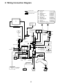
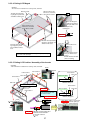
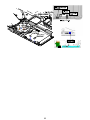
8 Wiring Connection Diagram
Connection Cable
عConnection
Cable
PAD FFC
SW FFC
DRIVEMAIN FPC
LCD Cable
DCINCable
Speaker Cable
L㧒R
MODEMCable
LANCable
Antenna PCB Unit R
Antenna PCB Unit L
USB FPC
HDD FPCUnit
Bluetooth Antenna PCB Unit
Parts on Bottom Side
̪4
LCD
DFJK12U112BB
DFJK20T108BB
DFJK9022ZA
DFJS1021ZB
DFJS1022YA
DFJS1023ZA
DFJS1024ZA
DFJS1025ZA
DL3UP1537AAA
DL3UP1538AAA
DFUP1522YA
DL3UP1521AAA
DL3UP1585BBA
̪1
̪2
̪3
̪4
̪5
̪6
̪7
̪8
̪9
̪10
̪11
̪12
̪13
Direct connection Connectors
Speaker(R)
Speaker(L)
Battery
Pack
Inverter Board
̪6
HDD
Keyboard
DC
Jack
FAN
̪13
̪12
̪5
CN600
CN911
Bluetooth
Antenna
PCB Unit
CN912
CN910
CN4
CN10
CN11
̪11
VGA
CN9
CN601
CN26
Main Board
CN24 CN25
CN7
CN17
CN2
MINI-PCI-EXP
Antenna PCB
Unit L
CN15
̪10
CN6
Wireless LAN
Module
CN18
JK1
Mic
CN14
JK2
Headphone
̪8
LAN
̪9
CN12
CN3
CN13
Lithium Battery
Antenna PCB
Unit R
CN8
CN20
Solenoid
with Lead
CN27
2%/%+5
SLOT
SW2 SW1
PowerSW W-LAN
Board ON/OFF
̪3
SW5
LCD Open
Detection SW
DVD MULTI Drive Board
CN510
MDC MODEM
CN801
̪1
DIMM Mrmory
(Option)
CF-BAW0512U
(PC2-4200)
̪7
̪2
CN900
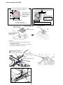
MODEM
Touch Pad
23
SW902
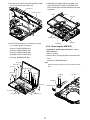
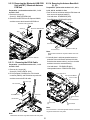
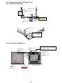
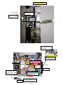
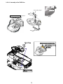
9 Disassembly instructions
9.1. Disassembly Flow Chart
Main Unit
9.2.1.
Preparation
1. End the Windows.
2. Turn off the Power, and then remove the AC Adaptor or Battery Pack.
3. Remove any optional DIMM Memory Cards or PCMCIA Cards.
4. Remove any other peripherals or Connected Devices.
9.2.2.
9.2.3.
HDD
Keyboard
9.2.4.
Top Case
9.2.5.
9.2.7.
SUB DVD
9.2.9.
FAN
Solenoid
9.2.6.
9.2.8.
Touch Pad / LCD Knob
9.2.10.
Speaker
9.2.12.
9.2.11.
Drive Unit
Main Board
9.2.14.
Antenna Board
(L), (R)
9.2.15.
9.2.13.
Bluetooth-USB PCB Unit
9.2.16.
Wireless LAN Module
MODEM
DC-IN Cable
9.2.17.
Card Bus Ejector
Main replaceable parts
Display Unit
9.2.18.
LCD Unit
9.2.19.
Hinge Cover (L), (R)
9.2.20.
LCD Unit / LCD Rear
9.2.21.
LCD Cable / Inverter Board
9.2.1. -Battery Pack
-DIMM Cover
-Side Cover
9.2.2. -HDD
-HDD Cover
9.2.3. -Keyboard
-Keyboard Side Cover (L), (R)
9.2.4. -Top Case
-Disk Side Cover
9.2.5. -SUB DVD
-Disk Eject Knob
9.2.6. -Touch Pad
-LCD Knob
-Pad Buttom
-PAD FFC
9.2.7. -Solenoid
-Disk Cover Angle
9.2.8. -Speaker
24
9.2.9. -FAN
9.2.10. -Drive Unit
9.2.11. -Main Board
-Lithium Battery
9.2.12. -Bluetooth-USB PCB Unit
9.2.13. -DC-IN Cable
9.2.14. -Antenna Board (L), (R)
9.2.15. -Wireless LAN Module
9.2.16. -MODEM
9.2.17. -Card Bus Ejector
9.2.18. -LCD Unit
9.2.19. -Hinge Cover (L), (R)
9.2.20. -LCD Rear
-LCD Hook
9.2.21. -Hinge (L), (R)
-LCD Cable
-Inverter Board
9.2. Disassembly lnstructions
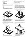
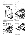
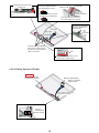
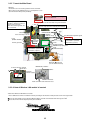
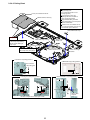
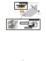
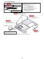
9.2.3. Removing the Keyboard
9.2.1. Preparation
Preparation : perform the section 9.2.1. first.
Attention:
Before disassembly, be sure to perform the
following steps.
1. End the Windows.
2. Turn off the power and then remove the AC adaptor.
3. Slide the hooks (A) and then remove the battery
Pack.
4. Remove the screw (A) and then remove the DIMM
cover.
(Remove if the DIMM memory is equipped with)
Screw (A) : XSB2+4FNL (N14)
Lithium Ion Battery Pack
1. Remove the 7 screws (D).
Screw (D) : DXQT2+E12FNL (N9)
2. Operate the LCD knob and open the LCD Unit to an
angle of 90 degrees or more.
The minus clock driver removes hook (B-1) in the
intuition combination part so as not to damage from
the W-LAN connector side space to the exterior,
and then rotates to the keyboard side, and KB side
cover is detached.
3. Remove the keyboard hook plates,and then remove
the hook of back side of keyboard with screwdriver.
Screw (D)
Hook (A)
Screw (D)
Screw (D)
Screw (A)
DIMM Cover
9.2.2. Removing the HDD
Preparation : perform the section 9.2.1. first.
1. Remove the 2 screws (B) and 1 screw (C).
Screw (B) : DXQT2+D4FNL (N7)
Screw (C) : DXQT2+E12FNL (N9)
2. Lift up the HDD unit and remove FFC connector and
then remove the HDD unit.
3. HDD is taken out of the HDD case.
Screw (B)
Bottom Case
4. Operate the LCD knob and open the LCD unit to an
angle of 90 degrees or more.
The minus clock driver removes hook (B-1) in the
hook position so as not to damage from the wireless
LAN connector side space to the exterior, and then
rotates to the keyboard side, and KB side cover is
removed.
Hook (B-1)
Hook (B-1)
HDD Cover
Screw (C)
Hook (B-2)
KB Side Cover (R)
HDD Case
LCD Unit
HDD FPC Connector
Note :
Be careful not to wrap the protection cloth etc.
around minus clock driver's point, and be careful
not to damage the exterior.
Note :
Please do not bend pins of the HDD connector, at
the time of removing HDD and FFC connector.
25
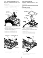
5. KB side cover (L) is adjusted to the upper part as
well as KB side cover (R), the minus clock driver
removes hook (C-1) in the hook position from the
space with the bottom case, rotates to the keyboard side, and detaches.
Hook (C-1)
Hook (C-1)
KB Side Cover (L)
Hook (C-2)
LCD Unit
Hook (C-2)
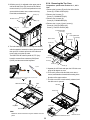
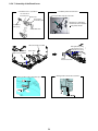
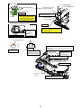
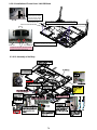
9.2.4. Removing the Top Case
Preparation : perform the section 9.2.1., 9.2.3.
first.
1. Remove the 2 screws (E) and 2 foot rubber backs.
Screw (E) : XTB26+10GFN (N12)
2. Remove the 5 screws (F).
Screw (F) : DXHM0057ZA (N5)
3. Remove the 2 screws (G).
Screw (G) : DXHM0049ZA (N3)
4. Remove the 1 screw (H) and 1 screw (I ).
Screw (H) : DXQT2+D4FNL (N7)
Screw (I ) : DXQT2+E10FNL (N8)
Foot Rubber Back
Screw (E)
Screw (G)
Foot Rubber Back
Screw (E)
Bottom Case
Screw (F)
Screw (G)
6. The both sides tape pasted to the keyboard bottom
with the spatula is inserted in order of the arrow and
then peel off. It is start-up from the LCD side and
turns inside out on the top case.
The KBD FPC WP sheet is peeld off, FFC (keyboard) is removed from connector (CN25) and
(CN24), and then remove the keyboard.
Screw (F)
Screw (F)
Screw (F)
Screw (I)
Screw (H)
Screw (F)
Spatula
5. Operate the LCD knob and open the LCD Unit to an
angle of 90 degrees or more.
6. The hook 2 places of the disk side cover are removed, and detaches forward while rotating in the
direction of the upper surface.
7. The disk cover lock is mechanically released, and
the disk cover is opened.
Do not damage the spatula ahead and move a top case in the
direction of the arrow in
order.
KBD FPC WP Sheet
CN24
LCD Unit
CN25
Disk Cover
Keyboard
Hook (D)
Back Side
Both Sides Tape
Note:
KBD-FPC sheet cannot be recycled. Please use new
parts.
Disk Side Cover
Mechanical Release Lever
26
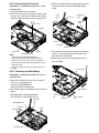
8. The disk cover shaft is removed and pulling out disk
cover is removed from the disk cover.
Disk Cover
10. CN26 (FAN) and CN15 (SP) are removed. A top
case is lifted and FFC (PAD), FFC (DRIVE) and
CN27 (solenoid) are removed and then the top case
is removed.
Disk Cover Shaft
CN15
CN26
Top Case
Solenoid Cable
9. Remove the 8 screws (J), 3 screws (K), 3 screws
(L), 4 screws (M) and 1 screw (N).
Screw (J) : DXQT2+E6FNL (N10)
Screw (K) : DRQT2+E8FKL (N2)
Screw (L) : DXQT2+E10FNL (N8)
Screw (M) : DXQT2+F3FNL (N16)
Screw (N) : DXHM0056ZA (N4)
FFC(PAD)
FFC(SW)
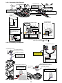
9.2.5. Removing the SUB DVD
Preparation : perform the section 9.2.1., 9.2.3.
and 9.2.4. first.
1. Peel off the tape.
2. Remove the 2 screw (O) and then remove the SUB
DVD.
Screw (O) : DXHM0056ZA (N4)
Note:
Note it that the disc eject knob comes off at the same
Screw (K)
Screw (M)
time.
Screw (J)
Screw (M) Screw (K)
Screw (J)
Screw (J)
Screw (L)
Screw (O)
SUB DVD
Screw (N)
Disk Eject Knob
Screw (M)
Screw (M)
Screw (J)
27
Top Case
9.2.6. Removing the Touch Pad / LCD
Knob
9.2.7. Removing the Solenoid / Disc Cover
Lock
Preparation : perform the section 9.2.1., 9.2.3.
and 9.2.4. first.
1. The pad top ring fixed to the pad cover by the both
sides tape is removed, and remove the screw (P).
Screw (P) : DXHM0057ZA (N5)
Preparation : perform the section 9.2.1., 9.2.3.
and 9.2.4. first.
1. Remove the solenoid line hold sheet and cable fixed
sheet.
Solenoid line hold sheet : DFHR3D20ZA (K122)
2. Remove the 1 screw (Q) and the solenoid from the
top case.
Screw (Q) : DXHM0056ZA (N4)
Pad Button
Touch Pad
Top Case
Pad Ring Top
Screw (Q)
Screw (P)
Tape
Pad Cover
Solenoid Line Hold Sheet
Top Case
Cable Fixed Sheet
2. Peel off the pad sheet.
The LCD knob is lifted from a top case, and removing LCD knob is removed from the knob side in the
LCD latch spring.
Note:
The each cable fixed tapes cannot be recycled.
Please use new parts.
3. Remove the disc cover lock spring, and slide the
disc cover lock and then remove.
Disk Cover Lock Spring
Pad WP Sheet
Disk Cover Lock
LCD Knob
Top Case
LCD Latch Spring
Top Case
Note:
Note:
When expanding or transforming, the disk cover knob
spring cannot be recycled.
The pad sheet cannot be recycled. Please use
new parts.
28
9.2.8. Removing the Speaker (L), (R)
9.2.9. Removing the FAN
Preparation : perform the section 9.2.1., 9.2.3.
and 9.2.4. first.
1. Peel off the 5 line hold sheet 1, the 4 brims of the
Preparation : perform the section 9.2.1., 9.2.3.
DVD PWB sheet, and remove the speaker (L).
Line hold sheet 1 : DFHR3D21YA (K123)
DVD PWB sheet : DFMX1229ZA (K161)
and 9.2.4. first.
1. Remove the KB heat spreader and the heat spreader.
2. Remove the 1 screw (R)
Screw (R ) : DXHM0057ZA (N5)
Speaker (L)
Speaker Ring
Speaker Cable
(Black, Blue)
Line Hold Sheet 1
DVD PWB Sheet
Line Hold Sheet 1
Note:
These sheet and speaker ring cannot be recycled.
Please use new parts.
2. Peel off the 2 line hold sheet 1, line hold sheet 2 the
1 tape, and remove the Speaker (L).
Line hold sheet 1 : DFHR3D21YA (K123)
Line hold sheet 2 : DFHR3D22ZA (K124)
Line Hold Sheet 2
Note:
KB heat spreader and the heat spreader cannot be
recycled. Please use new parts.
3. Remove the tape and line hold sheet 2 and then
remove the FAN.
Line hold sheet 1 : DFHR3D21YA (K123)
Line hold sheet 2 : DFHR3D22ZA (K124)
Speaker Cable (Black, Red)
Tape
Line Hold Sheet 2
Tape
Speaker (R)
FAN
Line Hold Sheet 1
Line Hold Sheet 1
Speaker Ring
Note:
These sheets and speaker ring cannot be recycled.
Please use new parts.
Note:
These sheets and tape cannot be recycled.
Please use new parts.
29
9.2.10. Removing the Drive Unit
Preparation : perform the section 9.2.1., 9.2.3.
and 9.2.4. first.
1. Peel off the tape from the connector.
3. Disconnect the LCD connector (CN9) (CN10), DC-IN
connector (CN601) and FFC (CN4) (CN6) (CN18)
(CN8).
2. DVD FFC is removed from connector (CN501), and
the drive unit is lifted from the bottom case, and the
gasket is peeled off and then remove the drive unit.
DC-IN
Cable
MODEM LAN
Holder
LCD Cable
MODEM
Cable
Tape
HDD FFC
CN501
FFC Drive
LAN Cable
USB FPC
Gadket
Drive Unit
Note:
DRIVE-MAIN FFC
-When you exchange DRIVE-MAIN FFC,
mark the bottom case, and match new FFC to
marking of the bottom case, bend, and build the
bend externals of FFC before peeling off FFC from
the bottom case.
-Tape and gusket cannot be recycled. Please use
new parts.
4. Turn inside out the main board. Remove the antenna
cable (L ), (R) from the wireless LAN module, and
then remove the main board.
5. Remove the connector from CN3 and then remove
the coin battery.
Antenna Cable
(L)
9.2.11. Removing the Main Board
Preparation : perform the section 9.2.1., 9.2.3.
and 9.2.4. first.
1. Remove the 2 screws (S), 2 screws (T) and 1 screw (U).
Screw (S) : K1YE5000022 (N15)
Screw (T) : DFHE5035ZB (N1)
Screw (U) : DXQT2+E6FNL (N10)
2. Peel off the 6 tapes, main PWB sheet and line hold
sheet 3.
Main PWB sheet : DFMX1228ZA (K64)
Line hold sheet 3 : DFHR3D59YA (K47)
Antenna Board
(L)
Antenna Cable
(R)
Coin Battery
Screw (U)
Main PWB Sheet
Screw (T)
Screw (S)
Tape
Tape
Tape
Line Hold Sheet 3
30
Antenna Board
(R)
9.2.12. Removing the Bluetooth-USB PCB
Unit (with BT) / Bluetooth Antenna
PCB Unit
Preparation : perform the section 9.2.1., 9.2.3.
and 9.2.4. first.
1. Remove the screw (V).
Screw (V) : DXQT2+D25FNL (N6)
2. Remove the USB FPC from the tape and CN910,
and then remove the bluetooth-USB PCB unit.
9.2.14. Removing the Antenna Board Unit
(L), (R)
Preparation : perform the section 9.2.1., 9.2.3.,
9.2.4., 9.2.10. and 9.2.11. first.
1. Peei off the line hold sheet and drive EMI sheet and
then remove the antenna board (R).
Line hold sheet : DFHR3D80ZA (K52)
Drive EMI sheet : DFHE1003ZA (K38)
FFC Drive
Bluetooth Antenna PCB Unit
Screw (V)
Bluetooth-USB PCB Unit
Tape
Drive EMI Sheet
Antenna Cable (R)
Line Hold Sheet
Note:
These sheet cannot be recycled. Please use new
parts.
USB FPC
9.2.13 . Removing the DC-IN Cable
Preparation : perform the section 9.2.1., 9.2.3.
and 9.2.4. first.
1. Remove the 1 screw (W) .
Screw (W) : DXQT2+E6FNL (N10)
2. DC-IN jack plate, DC MDM cover, DC-IN cable
connector (CN601), and FAN sheet are peeled off,
and then remove the DC-IN cable.
2. Line hold sheet 1 and heat spreader bottom are
peeled off from main Board's wireless LAN side,
and takes the antenna cable (L) out from the ditch
and then remove the antenna board (L).
Line hold sheet 1 : DFHR3D21ZB (K43)
Heat spreader bottom : DFMY3222ZA (K69)
Line Hold Sheet 1
Heat Spreader Bottom
Antenna Cable
(L)
Screw (W)
DC Jack Plate
DC MDM Cover
FAN Sheet
Antenna Board
(L)
Line Hold Sheet 1
DC-IN Cable
Antenna Cable
(R)
Antenna Board
(R)
Note:
Line hold sheet 1 and heat spreader bottom cannot be
recycled. Please use new parts.
Note:
FAN sheet cannot be recycled. Please use new parts.
31
9.2.15. Removing the Wireless LAN Module 9.2.17. Removing the Card Bus Ejector
Preparation : perform the section 9.2.1., 9.2.3.,
9.2.4. and 9.2.11. first.
1. Remove the 2 screws (X).
Preparation : perform the section 9.2.1., 9.2.3.,
9.2.4. and 9.2.11. first.
1. Remove the 1 screw (Z) from connection side of
Screw (X) : DXQT2+D25FNL (N6)
2. Wireless LAN module is floated in the connector
fulcrum and removed.
wireless LAN.
Screw (Z) : DXQT2+D25FNL (N6)
Wireless LAN Module
Screw (X)
Wireless LAN Module
Screw (Z)
2
1
9.2.16. Removing the MODEM
Preparation : perform the section 9.2.1., 9.2.3.,
9.2.4. and 9.2.11. first.
1. Remove the 2 screws (Y).
Screw (Y) : DXQT2+D25FNL (N6)
2. MODEM will be removed from connector (CN17) to
the vertical direction.
2. Return it on the revers to the card bus ejector side.
3. The minus small driver is inserted in connector
(CN13) and the card bus ejector intuition combination parts, 2 places of hooks (E). And then remove
the card bus ejector.
Card Bus Ejector
Screw (Y)
MODEM
Hook (E)
MODEM Cable
Connector
Main Board
Note :
Be careful not to transform the card bus ejector when
you remove the hook.
32
9.2.18. Removing the LCD Unit
9.2.19. Removing the Hinge Cover (L), (R)
Preparation : perform the section 9.2.1., 9.2.3.
and 9.2.4. first.
1. Remove the 1 screw (a).
Preparation : perform the section 9.2.1., 9.2.3.,
9.2.4. and 9.2.18. first.
1. Remove the 2 screws (c) and then remove the hinge
Screw (a) : DXQT2+E6FNL (N10)
2. Remove the DC-IN jack plate, DC MDM cover and
FAN sheet.
FAN sheet : DFMY0428ZA (K65)
3. Peel off the main PWB sheet and remove the
connector (CN9), (CN10) of the main board.
Main PWB sheet : DFMX1228ZA (K64)
Cover (L), (R).
Screw (c) : DRHM0076ZA (N17)
Screw (c)
Hinge Cover (L)
LCD Unit
Screw (a)
DC Jack Plate
Screw (c)
DC MDM Cover
Main PWB Sheet
Hinge Cover (R)
FAN Sheet
CN10
Note:
Screw (c) cannot be recycled. Please use new parts.
9.2.20. Removing the LCD Unit and the
LCD Rear
CN9
Note:
These sheet cannot be recycled. Please use new
parts.
Preparation : perform the section 9.2.1., 9.2.3.,
9.2.4., 9.2.18. and 9.2.19. first.
1. Remove the 2 screws (d).
Screw (d) : DRHM0076ZA (N17)
4. Remove the 2 screws (b).
Screw (b) : DXYN26+J6FNM (N11)
5. Peel off the EMI sheet 3 and then remove the LCD
unit.
LCD Unit
Screw (d)
LCD Unit
Screw (b)
Screw (d)
Screw (b)
Note:
Screw (d) cannot be recycled. Please use new parts.
EMI Sheet 3
33
9.2.21. Removing the LCD Cable / Inverter
Board
2. The intuition combination part of LCD rear case (21
places) is separated with LCD front case.
Hook position
LCD Rear
Preparation : perform the section 9.2.1., 9.2.3.,
9.2.4., 9.2.18. and 9.2.20. first.
1. Peel of the damper, conductive cloth, inverter tape
and the tape.
Inverter tape : DFHR3E07ZA (K18)
2. Remove the hinge (L), (R).
3. LCD Ccable is removed from LCD unit board
(CN101), and connector (CN1) is removed from
inverter board.
Conductive Cloth
Damper
Inverter Tape
LCD Unit
PET Tape
Hinge (R)
CN101
Note:
-When each hook is removed, it becomes easy to
detach if the driver who wraps protection cloth etc. is
inserted with LCD Front Case between LCD rear
covers, and the slide is repeated.
-Do noting that externals are not damaged.
CN1
3. Remove the 1 screw (e) from LCD rear and then
remove the LCD hook.
Screw (e) : DXQT2+D25FNL (N6)
Damper
LCD Cable
Screw (e)
Note:
Conductive Cloth
Conductive cloth and tapes cannot be recycled.
Please use new parts.
LCD Hook
LCD Rear
Hinge (L)
4. Inverter case is peeled off and Inverter fixed with a
both sided tape is taken out.
5. Peel off the tape from inverter.
6. Remove the connector (CN2) and then remove the
inverter.
Tape
Inverter
CN2
Inverter Case
Note:
Tape and inverter case cannot be recycled. Please
use new parts.
34
9.3. Reassenbly instructions
9.3.1. Attention when CF-Y5L series is repaired
- Please execute writing BIOS ID when you exchange the main board.
- Parts (sheet and rubber) etc.related various the conductive cloth and heat spreader cannot be recycled.Use
new parts.
9.3.2. Assembly knowhow of the LCD
9.3.2.1. Assembly of the LCD Front
LCD Rubber
LCD Rubber
Wide
Narrow
LCD Front
LCD Front
LCD Rubber
LCD
LCDBATT
BATTRubber
Rubber
Affixes in the standard on the left
Be parallel after putting
(Attention)
-The LCD Front is installed in the receiving stand, and works.
Safety Work -The LCD rubber and LCD BATT Rubber does not out of the concave part, moreover, not run aground.
-It is noted that the finger does not touch the paste side when the LCD Rubber and LCD BATT Rubber are affixed.
9.3.2.2. Putting LCD Side Cushion / LCD Tape 1
0-2mm
0-2mm
0-1mm
0-1mm
Hinge Side
Hook Side
There must not be
floatage
Hook Side
There must
not be floatage
Floatage NG
(Influences and exist in the hook
intuition combination when floating)
LCD Side Cushion 1
LCD Side Cushion 1
There must not be beginning to
see from the frame on the inside
LCD Tape 1
Hook central
standard
Hook
Wall root application putting
From wall root
0-1mm
From the frame on the inside
0.5-1.5mm
Edge standard of
wall of length 0 2mm
35
Hinge Side
LCD Tape 1
Hook central
standard
hook
9.3.2.3. Putting LCD Side Rubber / LCD Side Damper
(LCD handling attention)
-Do not take out the vicinity of the center of the lamp side having when you take out LCD of the packing box.
(Because there is a possibility that the transformation of the lamp reflector etc. occur)
-Take out right and left both ends of the lamp side having when you take out LCD.
Affixes it between
the length walls.
(There must not
be overflow)
10 1mm
Affixes in a plane plinth
(in the frame)
LCD Protect Plate
Attention,There
is directionality
Wide Side
Affixes it between the
length walls. (There
must not be overflow)
LCD Tape C
Rib standard
0 1mm
Narrow Side
Rib
Rib standard
0 1mm
LCD
Side Rubber 3
LCD Side Cushion
Rib
Rib standard
0 1mm
Rib
Rib
Affixes it between
the length walls.
(There must not be
overflow)
LCD
Side Rubber 3
LCD Side Dunper
Steps part
Affixes it between
the length walls.
(There must not
be overflow)
The flaking off paper is peeled
off by the post-processing
Rib standard
0 1mm
Affixes it between
the length walls.
(There must not
be overflow)
Affixes it between the
length walls. (There
must not be overflow)
LCD Side Dumper
Steps part
Steps part corner
standard 0 1mm
Cable Gasket Clot
Affixationh
Steps part corner
standard 0 1mm
from externals 0-1mm
There must not be
overflow from externals
36
Conductive Cloth
externals standard from externals 0-1mm
There must not be
0 1mm
overflow from externals
9.3.2.4. Putting LCD Magnet
(Attention)
-The LCD Front is installed in the receiving stand, and works.
Refer to A chart.
When inserting in the
Front Case, it is noted
not to roll the cushion
The both sides tape flaking off paper is peeled off,
and affixes to Front Case
The LCD Magnet is
affixed to the dotted
line part.(Affix on the
plate side)
When inserting in the
Front Case, it is noted
not to roll the cushion
LCD Magnet
LCD
Safety Work
Fit to inside surface.
The both sides tape flaking
off paper is peeled off, and
affixes to Front Case
The both sides tape flaking off paper is peeled
off, and affixes to Front
Case
Paste side
Affixes between ribs
Use the treatment device
when you affix the LCD
magnet
Division attention for XGA
(There is marking)
Pressurize it from the Front Case side (painting side) when you
pressurize a two sided tape
9.3.2.5. Putting LCD Cushion / Assembly of the Inverter
(Attention)
-The LCD Front is installed in the receiving stand, and works.
0-3mm
0 1mm
LCD Cushion 2
LCD Cushions
LCD Cushion 3
Rib
Paste side
There is no space.
Paste side
LCD Cushion 1
Paste side
LCD
Paste side
<Affixation OK figure>
Affixes to the length wall side.
LCD Cushions
Safety Work
LCD Cushion 2
Paste side
Do not bend, do not twist, and
do not add the impact when
you handle Inverter.
Pink
2-5mm
0 1mm
There is a space.
Safety important parts
Inverter Board
Paste side
LCD
<Affixation NG figure>
Safety Work Affixes in a connector
externals putting toPET Tape gether.(wrapping)
Connection
After affixing
the PET Tape
Rib
Safety Work <Affixation standard of PET Tape>
Standard of match affixation
of connector externals
(0 1mm)
37
<Preparation for Inverter Case>
Inverter Case
Inverter Board is affixed in a 0 1mm
both sides tape externals
match
<The order 1>
Affixes fit to rib
Inverter tape affixation without
transforming.(Room is given)
The tape is pulled too much and
LCD Front Case is transformed.
Inverter Tape
Rib
<The order 2>
Matches and
externals are affixed
So as not to transform LCD Front
Case, affixes.(Refer to a left chart)
Connection
The both sides tape flaking
off paper is affixed to the
peel connector.
LCD Cable
Connection
Connection
The both sides tape flaking off
paper of the Inverter Case bottom (3pieces) is peeled off and
affixes to the frame.
<Affixation standard of Inverter Box>
0 1mm
0 1mm
The externals part of Inverter Case is
set to the above-mentioned line
9.3.2.6. Putting Tape for LCD Cable
Safety Work
Processes straight from
begin to draw out Cable
PET Tape (10mmx35mm)
Affixes in a connector
externals match
The Conductive Cloth part is
processed to clamping
Affix to reflector surely
The line is
matched to the
frame externals
Frame
38
9.3.2.7. Assembly of the Hinge (L), (R)
9.3.2.8. Putting LCD Rear Cushion / LCD Side Cushion
39
9.3.2.9. Assembly of the LCD Rear / LCD Front
9.3.2.10. Assembly of the Hinge Cover (L), (R)
40
9.3.3. Assembly knowhow of the Main Board
9.3.3.1. Putting Line Hold Sheet / Antenna Sheet / BT PWB Cushion
41
9.3.3.2. Putting MCH Sheet / Heat Spreader Bottom
Running aground do not be on DAI
The flaking off paper in which "5011"
is displayed is peeled off and then
affixes to MCH.
MCH externals
standard 0 1mm
Safety work
Processes along the
DIMM connector
Coil externals standard.
Thing in which affixation
does not exist in coil.
MCH externals
standard 0 1mm
Coil externals standard
Line Hold Sheet
Safety work
Line Hold Sheet 1
Affixes in a Sheet externals standard,
and fixes Antenna Cable.
Heat Spreader Bottom
Bottom side Heat Sheet
preparation specification
Affixation as touch the Coil
Space 0-1mm
Antenna Cable
Safety work
Affixes to the capacitor
Antenna Cable fixes by Line Hold
Sheet 1 by processing on the Heat
Spreader Bottom Sheet.
CPU Cushion
Affixes in the silk frame
Affixation as fit the
CPU Cushion
Space 0-0.5mm
Touch the DIMM Connector
Affixation space 0-1mm
CPU Thrmal Sheet
CPU Thrmal Sheet is
a thing to the
capacitor without
running aground
Antenna Cable is drawn out here
CPU Cushion externals
standard 0 1mm
Coil externals
standard 0-1mm
CPU Thrmal Tape
1-2mm
It is confirmed that CPU Thrmal
Sheet does not run aground to the
capacitor
42
Sheet side of Heat Spreader Bottom
Grease1 (G-751)
Spreads by using the treatment
device.
9.3.3.3. Assembly of the WLAN Sheet / MCH Thermal Tape
W-LAN Sheet
Makes like the incision
part difference all-in roll
The Sheet center is lightly suppressed by the finger
Parallel
A two sided tape is peeled
off and affixes
BOX Sheet metal externals suiting
0 1mm
(The line part of the above figure is matched)
Processes from rue side to the right under
(Process in parallel to board)
MCH Thrmal Tape
Makes like the incision
part difference all-in roll
2-5mm
A both sided tape is
peeled off and affixes.
The Sheet center is lightly
suppressed by the finger.
Does not go out of
externals of Heat
Spreader Bottom when
suppressing.
Parallel
The corner part is matched on
the extension line of the
damper externals.
9.3.3.4. Assembly of the Main Board
Safety Work
DC-IN Cable
Connection
Main PWB
HDD FPC
Connection
PET Tape (10mmx25mm)
USB FPC
Connection
Slit externals match
0-1.5mm
*Does not overlap in the slit.
Memory Spreader
LAN Cable
Connection
A line is matched
mutually and Z is
bent by the
standard
Blue side
(reinforcement board side)
Slit externals match
0-2mm
*Does not overlap
in the slit.
FFC Drive
Connection
PCMCIA Sheet
<FIG1>
Safety Work
Puts according to the silk frame.
The inclination is within 0.5mm.
(Attention)
-The board is set in the receiving treatment device and works.
-The connector lock work after FPC is inserted uses the treatment device.
43
Externals match of IC
0-1mm
Externals match of
connector
0-1mm
Tape
9.3.3.5. Assembly of the Card Bus Ejector
Connector externals
standard
Connector
PET Tape (19mmX25mm)
Connector central standard
Connector externals PET Tape (10mmX25mm)
standard
Connector central standard
The transformer is
completely covered.
Connector externals
standard
The lever is drawn to the The lever is drawn to the
left before building in
right before building in
Square hole
Bend
Side where tape exists
on the other side
<Explanation 1>
The sheet metal bend part of Connector is
inserted in the corner hole part
(An opposite direction is also the same)
Multiply hook surely (There must not be floatage)
LAN ESD Sheet
Connector externals
standard
PAD connector central standard
PET Tape (19mmX25mm)
44
9.3.3.6. Assembly of the Wireless LAN Module / MODEM
<W-LAN Module preparation>
Connection
Antenna Board (MAIN)
Processes to board’s just beside.
Connection
Antenna Board (SUB)
W-LAN Module
-Work in midair prohibition when module is connected with antenna board.
-Connects applying the board to the receiving stand.
(For the distortion prevention of the board)
Safety work
From the tube edge
2-5mm
34-36
The film is
wrapped
<MODEM preparation 1>
Connection
The position is decided with a
treatment device.
MODEM Cable
2.0
MODEM
2.0
2.0
The PET Tape (19mmx25mm)
is wrapped
<MODEM preparation 2>
The remainder is affixed
on an opposite side
Board externals
0-2
EMI Sheet’s for MDC
tape externals
MDC EMI
Sheet
Safety work
Cable is processed
to the board side
Safety work
<MODEM preparation 3>
1-2
Safety work
2.0
PET Tape
(19mmx25mm)
Fit Board’s hole to
Conductive Cloth’s hole.
Safety work
45
Put out the position with the tube
drawn to the Jack side
9.3.3.7. Insert the Main Board
(Attention)
-The board is set in the receiving treatment device and works.
-When carrying to the following process, a special palette is used.
(The FPC bend in YB respect is prohibited)
Safety Work
Pressurizes with the battery the finger is
put in the PCMCIA slot.
Safety Work
After the pin by which the
position is decided is inserted, a
fixed screw is tightened.
After the screw is tightened, the
pin is detached.
Coin Battery Affixes to the sheet..Does not get on the board.
The cable is processed to this part remaining. Does
not get on a top side in the main body of the battery.
Edge side central distribution
2-4mm
1-3mm
Slit externals match
0-1.5mm
*Does not overlap in the slit
Screw
(DXQT2+E6FNL)
Tape
Affixation
within this range
Screw
(DXQT2+D25FNL)
Fit to
connector
affixation
W-LAN Module Preparation goods
Safety Work
The adsorption sheet of the
axis for fixation is peeled off
before installs. (2 places)
Screw
(DXQT2+D25FNL)
MODEM Preparation goods
Screw
(DXQT2+D25FNL)
Memory Spreader
Safety Work
The adsorption sheet of the
axis for fixation is peeled off
before installs. (2 places)
Valley case
Bend with 0.5 or more
(Use the treatment device)
MODEM CN installation
AL Sheet externals standard
Board Label
LAN CN installation
0
2mm
Character
direction (Upper)
MODEM LAN Holder
Installs so that the cable should not cross.
9.3.3.8. Note of Wireless LAN module is inserted
<Notes when Wireless LAN Module is inserted>
Please do Board’s insertion and extraction correctly according to the direction and the procedure shown in the figure below
Please go from parallel respect to mounting Board in Board’s insertion and extraction within the range of 5 -10
Please insert in the interior completely when you insert Board.
46
9.3.4. Assembly knowhow of the Top Case
9.3.4.1. Assembly of the Disk Cover
47
9.3.4.2. Putting Disk Angle Cushion
Disk Angle
Disk Angle Cushion
Affixes according to the
ruled line.
Disk Angle Cushion
Affixes according to the
ruled line.
Disk Angle Cushion
Affixes according to the
ruled line.
Affixes at the right of the ruled line.
9.4.3.3. Assembly of the Top Case
W-LAN ON /OFF
SW Knob Sheet
Power SW
knob Sheet
<Position where LED Cushion is Affixed>
Top Case
LED Cushion Affixation
LCD LENS PAD installation
(The pin after installs is welded)
The pin is inserted through
the top case hole.
Thing not diagonal inserted.(crack measures)
Tape positioning pin
The length hole (2 places) is
matched to the positioning pin,
and so as not to over on the top
case hole (4 places), affixes.
<Position where LED LENS PAD is installed>
Thing without
floatage
PAD Lenz Tape affixation
Hole for
LENZ (4 places)
LED LENZ BATT installation
(The pin after installs is
welded)
Pin shape standard after welds
The pin 2 places (outside) of a
top case are welded with a
treatment device.
2 places on the inside are the reserves for the second fixation.
Safety work
Lan Sw Blank Installation
48
<Position where LED LENZ BATT is installed>
Pin 2 place (outside) welding of top case
LED Lenz Batt : from cabi respect.
LAN SW Blank : from the application rib side.
Led Lenz Batt
Lan Sw Blank
Welds so that there is no
floatage from the top
case side.
There is no floatage.
Pin shape
standard after
welds
2 places on the inside are
the reserves for the second
fixation.
Safety work
Lan Sw Blank welds the
floatage which not is from
cabi application rib side.
9.4.3.4. Assembly of the LCD Knob / Putting Cushion
Pad Button Cushion (R) affixation
Directionality attention
A hither hook is upward.
Pad Button Cushion (L) affixation
After the hook in the LCD
Latch Spring is hooked,
installs in a Top Case
LCD Knob WP Cushin
LCD Konb Spring
The hook is put from the upper part on the top case
hole in the LCD Latch Spring.When expanding or
transforming, it is not possible to recycle
LCD Knob
The convex part is made to slip into the Top
Case under (right and left)
Division attention of LCD Knob
Safety work
<0075YA-0>
0075YA-0Goods
This outside (R) is
expanded.
(Inside R and a concentric circle R)
<Position where cushion for LCD knob is affixed>
<Position where Pad Button cushion (L),(R) is affixed>
A
A
LCD Knob Cushion
The gap on the edge
side is 1.0 or less by
return
(L)
Affixes in a central aim of the top
case rib and folds to the rib side
(R)
Top Case Rib
A-A SEC
Confirms the operation about the LCD knob
after building in
49
9.3.4.5. Assembly of the Touch Pad
Affixes Pad Cover Tape
It sticks it according
to U convex part.
Release coated paper
"NITTO No5000"
Print side
Safety work
Division attention of Pad Cover
Thing that doesn’t
begin to be seen
from window of
Pad Cover
ZA-0 = It is about the hemicycle.
YA-0 = There is no hemicycle.
Pad Cover
<preparation for PAD>
After of two PAD preparation completion
It installs in the pressurizing treatment
device and it pressurizes it.
(Range of shaded portion)
Pad FFC is inserted
Reinforcement board side
PAD that has been
prepared is stuck.
Insertion
after PAD is
pressurized
It sticks it
according to
U convex part
Release coated paper
"NITTO No5000"
Print side
Pad Cover Externals
The gap is
0.2 or less
<FIG2>
Thing that doesn’t
begin to be seen
from window of
Pad Cover
Pad Cover
Sticking
part externals
The hole of a transparent mount of
PAD WP SHEET is inserted in the
pin of the treatment device.
Affixes
Pad Cover Tape
Touch Pad
<Preparation for PAD-2>
Sticking part externals
and externals match of
Pad Case of sticking PAD
that has been prepared.
<FIG2>
1. PAD is installed on the treatment device
and it installs it between positioning
the installation three places.
2.The yellowish brown flaking off paper side
of Pad WS Sheet is peeled off and
the positioning hole of a transparent
mount is inserted in the pin of the
treatment device.
3. The sticking part of PAD and WP Sheet is
pressurized.
PAD position-determining pin
Pad WP Sheet
PAD positioning spacer
The hole of a transparent mount of
PAD WP SHEET is inserted in the
pin of the treatment device.
50
PAD positioning spacer
<FIG:1Preparation for PAD-1>
(3)
Insertion standard
Insertion
after PAD is
pressurized
Pad FFC is inserted
Pad WP Sheet affixation
Safety work
The hole of a peel of yellowish brown of
PAD WP Sheet flaking off paper and a
transparent mount is inserted in the pin
of the treatment device and
<Touch Pad> affixes.
(0.4)
Inside diameter
of grand foil
(0.4)
Reinforcement board side
Sticking part
outside diameter
The sticking part
externals are set
in a grand foil of PAD.
It sticks it
according to
U convex part
Touch Pad affixation
Safety work
Pad Cover A’ssy
Installs in the receiving
stand of the pressurizing
treatment device.
Safety work
After affixes with the hand
temporarily, pressurizes with
the treatment device so as
not to generate the sticking
part of Pad Wp Sheet like
wrinkle etc.
Sticking part
externals
<Preparation for PAD-2>
Pad Cover Externals
Gasket (PAD) affixation
Affixes in the concave part of a top case
Thing that pad Sheet’s corner does not hang on concave
happened the top part side
Cutting side
Pad Cover affixation
Safety work
The top part side
affixation in flaking
off paper of
transparency peel.
Safety work
Peel off PAD and PAD WP Sheet and assemble again in the
procedure of the standard book when you remove PAD COVER
by the repair etc.
(For steady adhesive power of PAD COVER and PAD).
51
Suppress right above
Gasket (PAD) when you
install the Pad Cover
Touch Pad connection FFC is passed
through the hole.
<Pad Cover installation position>
<Gasket (PAD) installation position>
Thing in which space does not exist between convex
happened the top part side and Pad Cover outside diameter
NG
OK
Top Case
Pad Cover
Affixes with the arrow direction touch to the convex
happened top part side
(Space measures with PAD BUTTON)
Touch Pad
52
Gasket(PAD)
The side is
hung
9.3.4.6. Putting Sheet
Puts within the range in the concave
happened top part.
(It is confirmed that there is not
running aground. )
Do not touch the paste side.
(garbage adhesion and down of
paste strength prevention)
Thing without bubble generation
Thing without lattice eyes transparent
of paste confirmation
From 0.5 or less to inclination 0.2 or
less to concave bottom case part and
seat externals space difference
Puts by the standard on the left.
Affixes Palmrest Sheet (L)
Affixes KBD fixation tape
Safety work
All are peeled off after putting
of the level peel positioning
the half and the flaking off
paper is put.
Affixes Disk angle cushion
Affixes Disk shaft
fixation seat
Affixes Disk cover cushion
Affixes the concave round type
part of a top case (four places).
Affixes Disk cover seat
Affixes Disk angle
cushion
< disk cover seat putting position >
< KBD fixation tape putting position >
Pressurize the
side putting part.
< disk angle cushion putting position >
(1.0)
< disk shaft fixation seat putting position >
Along U ditch
and puts.
Direction of length hand of disk angle cushion
53
9.3.4.7. Assembly of the Break Lever
< The Brake Lever is assembled >
< installation position of brake lever >
sets in the rib of
the brake lever.
has respect with shape up and installs.
Brake Lever
Do not touch
the bonding side.
Operativeness confirmation
of DISK brake after installation
Thing without Hi debt
Installation in
brake spring
Affixes Brake Pad
Affixes Disk Side Cover WP
Rib application putting
gap of 0.2mm or less.
the brake Lever sheet
Affixes Tape
Brake Lever installation
Affixes
Break Lever Sheet
< Putting position of Disk Side Cover WP >
< putting position of wire rod fixation tape >
54
9.3.4.8. Assembly of the FAN
< Cable fixation seat (FAN/SP) putting position >
< Cushion putting position for cooling FAN >
Affixes Fan Cushion X3
FAN externals
Pressurize the frame
within this range or
neither shuttlecock in
the opening nor the
rotation axis.
Flaking off paper ruled line
Affixes Fan/SP Cable Tape
It is a peel putting of
the half of the flaking
off paper.
Safety work
It is a thing in the opening
which does not begin to be seen.
FAN which has been
prepared is installed.
The FAN cable confirms the thing that
beginning to see is not in the concave part.
Pressurize neither rotation
axis nor the shuttlecock.
Do not
transform the frame.
The saliva of FAN is made
to slip into the boss of
a top case under.
Work notes
1. FAN must not be dropped, and do not add the impact.
< SCWER tightening torque >
Conclusion first time power : 0.16-0.18N.m {1.6-1.8kgf.cm}
At the repair : 0.10-0.12N.m {1.0-1.2kgf.cm}
After putting, the backup sheet of
the disk spring is installed.
Disk Cover Arm Spring installation
The point is inserted
in the hole of a top case.
Affixes
Disk Spring Backup Sheet
< putting position of disk spring backup sheet >
Rib
edge side
Do not go out of this
rib heaven side.
55
Screw(DXHM0057ZA)
Conclusion
9.3.4.9. Assembly of the Disk Cover Click
Conclusion Screw(DXHM0057ZA)
Water Cap installation
Disk Cover Click
installation
Affixes Water Cap Tape
Do not hang the roller end face
in this part on the top case side.
Affixes Insulation Sheet
9.3.4.10. Assembly of the Disk Cover Lock / SW PCB
< preparation for solenoid with lead >
The same to width
of tape standard
Flaking off
paper
Solenoid Fix Tape (FAN/SP)
The half of the
flaking off paper
is put on the
peel cable.
Flaking off paper
leaving side
Conclusion of
Screw(DXQT2+F2FNL)
Installation
Solenoid Angle
Solenoid with lead
This side of
red lead
Affixes Solen Fix Tape (FAN/SP)
< Preparation for Disk Cover Lock >
The insertion
order : 2
The fingernail
is multiplied.
The insertion order : 1
Inserts in R shape part
and the slide in
the right side.
There is directionality.
R shape is matched.
Safety work
The engagement fingernail is
the confirmation two places as
for there is not collapsing.
Convex is on both sides.
Do not crush convex
of this when detaching.
Disk Lock Bush installation
Hanging fee of fingernail = (0.2)
Hole externals of
Disc Cover Lock
Disc Cover Lock
56
< SW PCB >
yellow line
Screw (DXHM0056ZA)
Screw (DXHM0056ZA)
SW PCB which has been
prepared is installed.
yellow
line
Affixation
Disk Lever Fix Cushion
Safety work
SW PCB
When the SW PCB positioning
is not used, the cabi positioning
treatment device pin on becomes
the center of this hole and fixes.
The SW lever is put between ribs
of Disk Eject Knob Assy
Disk Eject Knob
ASSY installation.
<Disk Eject Knob ASSY2 installation position>
Safety work
Operativeness confirmation
When Screw is concluded, concludes
because Disk Eject Konb Assy is drawn
in the arrow direction.
DFBD9006ZA-0
Confirmation
Convex having
=9009ZA-0
Convex=9006ZA
Disk Cover Lock Holder
The part of R type of the Disk Cover Lock and the part
of the pin of the Disk Cover Lock holder are matched
and installs
Safety work
Thing that fingernail
on both sides hangs
The fingernail is held with
the treatment device in
the direction of the arrow.
Insertion in Disk
Cover Lock Spring
When expanding or
transforming, it is not
possible to recycle
The hook is passed through the hole
of the Disk Cover lock Assy fittings
The Disk Cover Lock Assy fittings which
have been prepared are installed
Thing that Hook hangs
Hook Side
Disk Cover Lock Holder
installation
The hook in spring for the Disk Cover
knob is put on the cabinet rib on
57
9.3.4.11. Assembly of the Solenoid
Line Hold Sheet 8
affixation
Screw(DXHM0056ZA)
Solenoid A’ssy
installation
Solenoid Line Sheet
affixation
Processes so that Cable should not stretch
Top Case’s U type slit
part is passed
The part where the axis can be
tied up is fixed into U type projection part of metal fittings
Pad SW Sheet
affixation
This side of a round pin is passed
Solenoid Spacer
affixation
Thing that running aground is not
on boss heaven side along boss
side
Safety work
<Spacer affixation
position>
<Line Hold Sheet 8
affixation position>
<Wire Fixation Tape affixation position>
L type rib side
L type rib side
<Pad SW Sheet affixation
position>
Sticks to Cable
and affixes
Affixes in boss’s outside diameter application and Top
Case’s corner hole is concealed
This side of
a round pin
is passed
0
Square hole
Boss bese
Work notes
A red lead fixes with the Line
Sheet (Solenoid) in the state
in this side
Rib side
< SCWER tightening torque >
Conclusion first time power : 0.16-0.18N m{ 1.6-1.8kgf cm }
At the repair : 0.10-0.12N m{ 1.0-1.2kgf cm }
9.3.4.12. Assembly of the Speaker
<Preparation for speaker>
Cable drawing out side
The speaker which has
been prepared is installed
Blue
Blue
Red
The height of the solder
height shall not be from
a magnet heaven side.
Speaker Ring affixation
Speaker Ring must not
hang on the positioning
rib side of the speaker
Speaker Cable
Pin No.1(Red)
Safety work
Soldering temperature
: 300-350 degrees
Soldering time : 3 seconds
The speaker which has
been prepared is installed
< Speaker installation position-Red >
The rib of the speaker is
set to the concave Top
Case part
Cable drawing
out side
Speaker Ring affixation
Red
< Speaker installation position-Blue >
The rib of SP is set to the concave Top Case part
Red
Blue
58
9.3.4.13. Wiring Speaker Cable
59
9.3.4.14. Putting Cushion / Tape / Sheet
KBD Backup Sheet affixation
Bend width small side
HDD Backup Plate installation
Inserts it until the inside of the
bend lies to the edge side of
the hole of a Top Case
KBDHook WP Sheet affixation
Positioning treatment device use
Front WP Cushion affixation
Side WP Cushin affixation
<KBD Backup Sheet affixation position>
PCMCIA Cushion affixation
Along Top Case to close this hole and affixes
Difference line
Side WP Cushin
The right and left is
between ribs
<Front WP Cushion affixation position>
KBD Hook WP Sheet
Flat side ridge
line
Both ends are affixed
to the side the bend
60
9.3.4.15. Assembly of the SW PCB FFC
FFC insertion standard
(going out =1 of electrodes)
Cabinet
difference line
Sheet edge side
Sheet edge side
Outside diameter of
machine screw
PET Tape affixation
When the part is bent this, the thing
which is placed by the finger, held to
Board who bends, and not bent
SW PCB FCC insertion
The bend habit is put on FFC
Electrode side
When the lock lever is released, slowly
operates in parallel because the lock
lever of the socket is damaged easily
<SW FFC bend position>
PET Tape affixation
3st bend
1st
bend
1st bend
4st
bend
3st
bend
Pet Tape
2st
bend
2nd
bend
Safety work
3st bend
61
Safety work
(FFC standard)
The tape externals
are centers of the
FFC reinforcement
board.
62
9.3.5. Assembly knowhow of the Bottom Case
9.3.5.1. Putting Line Hold Sheet
HDD Slot Guard
0-0.5
0-0.5
0-0.5
0-1
0-0.5
0-1
Line Hold Sheet 4
Affix
Side where flaking
off paper is short
Line Hold Sheet 5
Affix
Line Hold Sheet 7
Affix
Line Hold Sheet 9
Affix
0-1
Concave rib top side part
externals of HDD Slot
Guard
0-1
9.3.5.2. Assembly of the DIMM Cover
Concave part of
DIMM Cover Light
Externals
DIMM Heat Sheet
Externals
DIMM Thermal Sponge and DIMM Heat
Sheet is affixed so that the cutting lack part
should not get on the boss.
DIMM Heat Sheet
Affixation
DIMM Cover Sheet
Affixation
DIMM Thermal
Sponge
Arrangement
Rubber foot affixation side is
wiped off with IPA.
DIMM Cover Light
Safety Work
63
9.3.5.3. Putting Sheet / Cushion / Tape
DC Jack Sheet
Safety work
Difference root
line standard
0.5mm
Difference line
Difference line
Boss center
Gasket
Water Detector
Tape for DC-IN Jack cable
Waterdrop detection sheet
Cutting plane side
Gasket
Boss outer diameter
<Speaker Cushion Putting figure>
<Audio JK Sheet
Affixation photograph>
Fit to corner
Speaker Cushion
Audio JK Sheet Fit to boss
<LED LENZ SD
Installation figure>
From a rib root
pressurize
LED LENZ SD
Bottom WP cushion
Root reliance pasting
Fit to boss
Hung the Hook
Speaker Cushion
Fit to boss
Hook Tape
<Bottom WP Cushion Putting figure>
Put the tape by a round convex
rubber foot part central standard
Width
smallness
Width
Bottom WP Cushion
Does not get on the outer rib.
64
HDD damper
Tape
Cutting lack part top side
Cutting lack part central distribution pasting
A
(1.0)
Side WP Sheet 2 <part A chart>
Safety Work
Side WP Sheet 2
Side WP Sheet 2
Put along the case shape
The right and left : between ribs.
DVD Knob Sheet
Wall reliance
attachment
Wall reliance
attachment
Sheet must not get rolled up,
and not bend within this range.
Outer wall bottom corner
Putting standard
65
9.3.5.4. Putting Foot Rubber
<FIG1> Safety Work
Do not pressurize the concave
Bottom Case part
(Sheet concave measures).
Do not go out of the rib
heaven side
Bottom BATT Sheet
Adjust the inclination of the direction of
the length hand to 0.2 or less
Safety Work
<Notes and procedures when rubber foot / rubber foot (center) putting>
1) Wipe rubber foot/ rubber foot (center) pasting side
with the dry cloth (3 places)
(Cautions) - Exchange the cloth (rag)
wiped off regularly (twice / day)
2) A rubber foot/rubber foot(center) pasting
(Cautions) - Put on the Bottom Case with tweezers etc.
- Paste so as not to touch the sticking side.
3) Pressurizing (treatment device use) condition:
Pressurizing power : 2.5kgf or more,
Time : 3 seconds or more
Foot Rubber
Affixes to the concave part.
Pressurizing treatment device use
Safety Work
Foot Rubber Support
Affixes to the concave part.
Pressurizing treatment device use
Safety Work
Foot Rubber Support
Affixes to the concave part.
Pressurizing treatment device use
Screw
(XSB2+4FNL)
Installation
Safety Work
Bottom BATT Sheet
Put on the rib side
Ref to FIG 1
(Attention)
-Please work after installs in the treatment
device when you tighten the screw.
Work with a specified treatment device when you pressurize Foot Rubber and Bottom BATT Sheet .
66
9.3.6. Assembly knowhow of the Body
9.3.6.1. Keyboard preparation
both sides tape
Boss central standard
0 1mm
Keyboard
both sides tape
Affixes between
square holes
Affixes between
square holes
Square hole extemals standard
0 1mm
Affixes between
square holes
KBD Tape
From a square hole extemals
0-2mm
9.3.6.2. Installation of Main Board
MAIN PWB A'SSY
Main PWB A'ssy
is installed
Attention when Main
Pwb A'ssy is installed
FIG 1
It is confirmed that W-LAN SW
is turning off(Left) before building
in of BOTTOM CASE.
(OFF:Left ON:Right)
The ANT PWB connection
cable passes the FCC under
BOTTOM CAB A'SSY:
Attention of using properly
FIG1
Attention of using properly of BOTTOM CAB A'SSY
(Confirms by the hinge fixation boss in the cabi in the under)
YA-0=It is penetration and a hole of about 2.0.
FIG1
DIMM COVER
Attention of using properly
MK1=Only Dimm Cover
Excluding MK1=
There is heat radiation part affixation
67
There is BT and for the model
The flaking off paper of the cushion is
peeled off, installs in the cabinet in the
under, and affixes .
9.3.6.3. Assembly of the HDD Slot Guard
Affixes Line Hold Sheet
FIG2
The width of the flaking off paper
peels off short one and Hdd Slot
Guard A'ssy affixes
Screw (DXQT2+D25FNL)
A B C
A
B
Screw
(DXQT2+E6FNL)
0
It is confirmed that the substrate
does not run aground in the boss
and concludes
1
C
Installation Hdd
Slot Guard A'ssy
FIG1
0-0.5
The flaking off paper on the
other side is peeled off and
affixes in the cabi in the under
0-1 Line Hold Sheet
0-3
Tighten Screw
Conductive fabric from
MDC is affixed in the
cabinet in the under
FIG1
Affixes Pet Tape
after fixing Hdd
Slot Guard A'ssy
FIG2
White line
Pet Tape is affixed at the white
line of FPC and the position set
to corner part Hdd Slot Guard Pet Tape
FIG2
7-11
Corner part
68
9.3.6.4. Putting Line Hold Sheet 3 / Line Hold Cushion
Put on the rib side
while pulling the
tape
Secure the space with
bossing the outer rib
0.5 or more
Put the cushion for the lead fixation
Safety work
(Content of this page)
Directionality having
The back
Side without tape
LAN Cable (upper)
LAN Cable (upper)
MODEM Cable (lower)
Set the MODEM/LAN
holder in a lower cabinet
MODEM Cable (lower) < part A details >
Put wire rod fixation tape 3
B
E
A
C
D
Put on the rib side with
there not loosening
< part C details >
Pass the under of the cushion
for the lead fixation through
LAN cable
Pull out a MODEM cable just
beside in an HDD protection slot,
along the HDD protection slot, and
process the MODEM cable forward
Push the tape and push the Cable by
processing as shown in the figure below
0-1
Cushion for lead fixation
Insert the MODEM
cable in the slit
Prevent the cable from running
aground in boss heaven
side/bossing the outer rib.
0-1
< part B details >
E
Prevent the cable from
running aground on the
boss heaven side
B
MODEM Cable
Put on the rib side by processing the
tape to lower more than the boss
heaven side while pushing
LAN Cable
A
Prevent the cable from
running aground on the
rib heaven side
Put on the rib side
with there not
loosening
< part D details >
< part E details >
D
C
Process the cable in the order
of A-E after positioning the
wire rod fixation
tube of LAN cable
tape 3
2-5
HDD protection slot
Make the rib
under slipped
Be careful not to run aground on the boss
heaven side about wire rod fixation tape 3
69
0-2
Prevent the cable from
running aground on the
boss heaven side
Put on the rib side by pushing
so that running aground is not
on the boss heaven side
It is the same as last page excluding
the undermentioned specification
ANT CABLE is processed
under the cushion
Line Hold Cushion
affixes
0-1
The part product number
depends on last page
0-0.2
0-1
The Rib of Cabi in the under
is passed and the concave
part is passed
Boss
0-4
Line Hold Sheet externals
FIG1 W LAN for being
Line Hold Sheet is affixed
with ANT PWB arranged
at the figure below position
3 2
0-2
0-2
Safety work
0-2
Convex Cabi in
the under part
The thing that FFC does not
run aground in the boss of the
cabi in the under is confirmed
The cable is processed under
the main substrate too much
thing which does not run aground
in convex part in cabi in the under
Do not run aground
in the cable to the
convex part heaven
side
In the cabi in the under, affixes with
the two sided tape prepared for FFC
with the position of a red line decided
with the treatment device
Safety work
Driv Emi Sheet Affixes Driv
Affixes Line
Emi Sheet
FFC
Hold Sheet
After Line Hold Sheet is affixed, the
cable is processed without loosening
Convex Cabi in affixes Driv Emi Sheet
the under part
70
ANT PWB
The bent habit is
put on the cable
0-2
9.3.6.5. Installation of LCD Unit
Cautions
Cannot be repetition used because
of use of a fixed type lock agent.
Exchange for a new article in the case of re-bolting.
Set the LCD Block
Conclude DXYN26+J6FNM A
EMI sheet 3
B
Side with comb
dentiform
A
Paste EMI sheet 3
The EMI sheet 3 removes
a half exfoliation paper, and
twists around a LCD cable,
and one of the two sticks it
on a bottom case.
B
Attach the LCD Unit to
the Bottom Case by left
justify
Side with
'I-PEX' stamp
15-20
Insert the inverter
cable in CN
Cable black
tape
externals
0-1
Safety work
Bottom case rib side
On slope part
of hinge metal
fittings
Put Conductive Cloth
with the black tape left
end of the cable set to
the bottom case side
Pass between cushions
with the bottom
case boss
Be along the root of
the wall of the LCD
Cable
Insert CN of the inverter cable
and make the main substrate
under slipped
Be careful not to cover
this hole with the
Conductive Cloth
Thing without Cable
within 8
(Copper Foil = 9)
Prevent the cable from
being within 8
(Copper Foil = 9)
71
The inverter cable
is LCD cable back
9.3.6.6. Assembly of the DC Jack Plate
Safety work
The LCD cable must pass the
side of the DC MDM cover
Tighten DXQT2+E6FNL
Set DC-IN Jack Plate
Prevent metal fittings from
running aground in the
rotation stopper
Set Jack.
Put the cylinder part in the
bottom case hole
Set DC MDM Cover
Fix the DC-IN cable with a
couple-face tape of the botto
case preparation
Put the FAN Sheet
LCD cable/DC-IN cable processing
FAN sheet pasting position
Outside diameter
of boss
0-0.5
Be careful not to run
aground in this platform
Pressurize back
FAN
side a couple-face Sheet
tape part of the
FAN seat
Bottom Case
0-0.5
Black lead side Be lower to the right
Red lead side
under until hits the
Bottom Case, and
along the Bottom
Be sure to stick in parallel in
Case difference side
a red line and a black line .
of the cable
Be careful not to come in
succession.
Peel off the flaking off
paper of a couple-face
tape of the bottom case
preparation, and process
the DC-IN cable
0-0.5
(0-1)
Black lead side
Red lead side
Put the DC-IN Cable
under the substrate
too much.
Antenna Cable
Incert the Connector
Do not cross with
the Antenna Cable.
9.3.6.7. Putting Main PCB Sheet
Only turn affixation is executed
without the cable when there is
no W-LAN.
Maintain the antenna cable
in the part a brim in the Main Match the corner hole
Board insulating sheet
to CPU chip and put
After Screw is concluded,
the hole gap prevention tool
is temporarily tightened
DFHE5035ZB
Tighten K1YE5000022
A B
K1YE5000022
Antenna cable processing
Antenna
Put Main Board Insulating Sheet
hole
A
B
Set the cable to the slit part
Confirm the thing which of the seat, turn the sheet,
can be operated in the and affix
cable tape maintenance
part
CPU Chip
CPU
externals
After holding a part of the Main Board
insulation sheet on inside-out and a
tape, stuck the Main Board insulation
sheet on a regular position.
72
CPU externals
9.3.6.8. Assembly of the DVD Drive
0-1
0-1
Take off a Big Stopper
Range which you may grip
DVD Drive
Gasket Cloth
FIG1
Affixes Gasket Cloth
FIG1
73
9.3.6.9. Installation of Power Knob / LAN SW Knob
FIG1
Put the Conductive Cloth
with the antenna cable
not hung on the convex
part of the bottom case
Set the Power SW
Set the W-LAN ON/OFF SW
FIG1
Power SW
Make the bottom side rib slip into the main board under
* Confirm the floatage of the damper three places is not generated
Stuck the Conductive Cloth currently
prepared for the drive on a bottom case
W-LAN ON/OFF SW
Confirm the SW lever has been surely
inserted in the ditch of the knob
9.3.6.10. Assembly of the Body
74
9.3.6.11. Top Case side screw tightening
DXHM0056ZA
DXQT2+E6FNL
DXQT2+F3FNL
DXQT2+E10FNL
DRQT2+E8FKL
DXHM0056ZA
Engages with Board's concave part Top Case Rib
When there is BT
T
The tightening order A T
The following are pretermission
B
The cable is along bossing
outer and processed.
Do not go out of the above
cabi side.
G
C
H
Q
I
S
Disk Angle
installation
A
J
K
D
M
R
P
O
Processing of Antenna Cable
N
L
E
Draws under the side of Board
after tightening of the Screw and
pushes into the inside too much
Cable is tightened and so as
not to bite, the putting out
Screw is tightened on the outside among Board and bosses
Processing of Antenna Cable
Cable confirms the slit part and
the going thing is confirmed
The externals overplus to
which Cable does not go
out of the Top Case side is
processed under Board
9.3.6.12. Installation of K/B Heat Spreader
To the range of the heat
radiation board of the
steps dropping part
Heat radiation grease spreading position
(Heat radiation board)
13-15
3-5
6-8
Heat radiation board
installation
K/B Heat radiation seat putting
Thing without concave part range
running aground of top case,and thing
without waving
Peel off slowly when you peel off
the flaking off paper.
(Transformation and measures)
9-11
Heat radiation plate installation for CPU
To the hole part of
a top case
Grease spreading on the
other side with treatment device
HDD seat putting:
Heat radiation grease(G-751)
Flaking off paper
Spreading
three places
Grease spreading
on the other side Thing without concave part Heat radiation grease spreading position
range running aground of
(Heat radiation plate for CPU)
top case,and thing without
waving
HDD Seat putting
The flaking off paper of a
two sided tape of the top
case preparation is put
and peel HDD seat is put.
Heat radiation grease(G-751)
Spreading
Disk side cover fixation seat putting position
Disk cover fixation
seat putting
0-0.5
75
0-0.5
Thing without concave part range running
aground of concave part and disk angle
of top case, and thing without waving
9.3.6.13. Installation of Disk Cover / Disk Side Cover
Disk Cover installation
Disk Cover shaft insertion
Disk Cover's axis is
inserted in the Top
Case hole
Slide insertion of outer rib in
concave Top Case part
Disk Side Cover installation
9.3.6.14. Installation of Keyboard
Safety work
76
Engagement
from side
Lock the Lock Hook of the
bottom side surely
9.3.6.15. Installation of K/B Side Cover
Wire Fixation Tape 1 affixation position
KBD Side Rubber
Affisation without in concave
part of KBD Side Cober (L)
installation
KBD Side Rubber(L)
installation
Do not make a mistake as
L side. 3 hole having
Engages with 3 places simultaneous.
(Hook breaking measures)
KBD side Rubber affixation
Affisation without in concave
part of KBD Side Cober (R)
running
Hook
KBD Side Cover (R)
KBD Side Cover(L,R)
Inside Hook is previously
set, and then outside
Hook engages
0-1
1-3
KBD Side Cover (R)
installation
Whether Antenna Cable is
processed the side under
of Boadr is confirmed
Explain as an example of KBD Side Cover engagement R side
inside enKBD Side Cover
gagement
Hook
OK
Inside Hook hits
Top Case and
breaks
NG
Outside
engagement Hook
Hole of
Top Case
9.3.6.16. How to detach Keyboard and K/B Side Cover
K/B SIDE COVER (R)
Confirm there is no
transformation when
you recycle the K/B.
Both sides tape
for fixation
K/B fixation axis
The one in thin, long
state of Spatula such
as caulking palettes
K/B fixation axis
Both sides tape
for fixation
KBD side cover (R) is detached
K/B fixation axis
after the tightening the 8 Screw
from the bottom are detached,
the tools is inserted between
K/B SIDE COVER (L)
COVER
KBD and Top Case, and the
tape is peeled off while avoiding
How to detach K/B
Lock Hook
FIG1
Minus Small Driver which wraps
protection cloth etc. around point
How to detach K/B Side Cover (L)
Both sides tape
for fixation
the axis for fixation.
Peels off from a central tape.
Tool is not transformed.
How to detach K/B Side Cover (R)
Lock Hook 3 place of the cover is removed.
(Thin Sheet etc. are inserted between the
cover and Top Case and the lock is removed)
Lock Hook 3 place of the cover is removed.
(Thin Sheet etc. are inserted between the
cover and Top Case and the lock is removed)
77
9.3.6.17. Installation of HDD
HDD
When the HDD Cover is detached, it is
not possible to insert diagonally.
Detach with a horizontal slide.
(Projection part breaking measures)
CN of HDD connection
FPC is inserted
HDD Cover installation
The machine screw tightening projection part : on the
bottom Case boss
HDD Case installation
The pin of two
rows on the left
side is room
Slide insertion of projection
part of HDD cover in bottom
case hole
PET Tape affixation
To conceal the hole
of the HDD case
evenly, affixes
9.3.6.18. Bottom Case side screw tightening
Division attention of
Foot Rubber Back
The country:No Zaguri
Foreign countries:OK Zaguri
U
DFGX0464ZA-0(Foot Rubber Back)
XTB26+10GFN
DXHM0057ZA
DXHM0049ZA
DXQT2+D4FNL
DXQT2+E10FNL
R
DXQT2+E12FNL
Engages with the bottom
case boss the hole of the
Rubber Foot
Inserts in a
square hole of
the Bottom Case
S
F
Insert Foot Rubber
Back before tightening
the screw
E
C
G
D
T
I
O
Please for Screw by
tightening the hand
H
A
K
L
P
B
J
N
Q
M
The Screw is tightened
while inviting the other
78
Surely inserts so that the space
is not between difference part the
above Cabi and the cabinet edge
side on.
9.3.6.19. Putting Label
0-1
0-1
COA Label
0-1
COA Laminate Seal
0-1
0-1
Model Label
0-1
0-1
Direction of
character(TOP)
Direction of
character(TOP)
S/N Label
Intel Label
Win logo Label
Label externals standard
0 1mm
Reference
DFQT0046ZA
CENTRINO DUO Label
externals standard
0 1mm
From the character edge
2-5mm
3-5mm
Energy Star Label
Direction of character
(TOP)
CENTRINO DUO Label
externals standard
0 1mm
5-7mm
79
10 Exploded View
10.1. Display Section
K26
K28
N6
K29
K25
K16
K19
N17
K24
K27
K11
K7
K14
K3
K27
K9
K20
K10
N17
E20
K18
K36
K30
K15
K8
K5
K9
E7
K11
K7
K6
K12
K13
E19
K8
K17
K13
K7
K6
K23
K7
K23
N17
K17
K17
K1
N11
K4
K22
K21
Screw tightening torque
N11
K2
80
N17
10.2. Cabinet Section
K176
K76
K78
E13
K89
K88
K81
N6
K116
K112
N5
K156
K147
K34
K109
K70
K83
K119
K113
K134
K146
K119
E14
E22
K68
N6
K72
K39
K58
N10
K100
N10
K44
N5
N10
K101 K101
K159
N2
K90
K150
K105
K94
K52
N16
N4
N16
b
N10
N10
K56
K100
K100
N10
N2
N10
N16
E31
K94
E30
N10
c
K130
K105
N2 N8
N8
K129
K92
K141
K107
K99
K46
E24
f
K135
N6
K45
K125
K146
K39
K155
K143
K118
K87
K43
K103
K104
K102
K114
K82
K85
K167
K126
K129
K160
K121
K94
K165
K122
K170
K171
K115
K136
K168
K124
N13
K158
N4
E12
K166
K137
K106
N16
SW902
E23
E2
K138
K145
K144
E21
K169
K128
K148
N5
K144
K52
E11
K123
K123
K123
a
K123
K108
K31
K95
K127
K132
K60
K139
K93
K84
K59
K123
K161
N4
N4
K145
K157
81
Screw tightening torque
10.3. Bottom Section
K48
K64
E3
K175
K43
E27
N10
K69
CN11
CN7
K43
K73
K174
CN600
JK1
JK2
CN12
E17
K40
K66
E9
K79
f
SW2
K173
K74
K67
E1
SW1
CN13 SW5
a
d
e
N6
N6
N8
K80
N6
N10
N4
E6
N10
K63
E25
b
E8
K55
A2
K57
K43
N6
K71
K175
E5
N6
E28
c
CN911
N6
K42
E15
CN912
K120
K65
K53
K131
N9
K117
K33
K32
N15
N5
K96
K49
K61
N1 K133
N1
K140
N15
N6
N6
K50
N12
K91 K96
K51
K91
K86
K110
N6
K133
K98
K130
N5
K41
K35
K54
K47
N7
K97
K151
K154
K152
N5
K35
K172
N5
N8
K164
K111
K153
K163
K162
d
K79
K152
K142
e E16
N12
K154
K149
E10
N9
E29
K52
N14
N9
N9
K130 N9
N9
N9
K37
K62
K38
K109
N3
K177
N5
N3
K75
N9
N7
N7
82
Screw tightening torque
K38
E26
11 Replacement Parts List
Note : Important Safety Notice
! mark have special characteristics important for safety.
Components identified by
When replacing any of these components, use only manufacturer's specified parts.
CF-Y5LWVYZBM
REF. NO and AREA
Main Block Unit
E1
E2
E3
E5
E6
E7
E8
E9
E10
E11
E12
E13
E14
E15
E16
E17
E19
E20
E21
E22
E23
E24
E25
E26
E27
E28
E29
E30
E31
PART NO.
DESCRIPTION
Q'TY
DL3U11528ABA
DL3U31528ABA
DL3UP1521AAA
DL3UP1581BBA
DL3UP1585BBA
N0GF1J000008
N5HZC0000019
N5HAZ0000014
DFJS1024ZA
L0AA20A00007
DFJS1023ZA
N2AZZY000019
N2EAYYY00008
DFJS1022YA
DFJS1025ZA
K1YYZZ000060
L5EDDYY00038
DFJS1021ZB
L9AAAYYB0004
DFJK12U112BB
DFJK20T108BB
UDQFSEH62
CR-2032/K5B
DFJK9022ZA
N3CAYYY00006
DFUP1522YA
UJ-833ECD2-Z
DL3UP1537AAA
DL3UP1538AAA
PCB, MAIN
PCB, SUB DVD
HDD FPC UNIT
BLUETOOTH-USB PCB UNIT(WITH BT)
BLUETOOTH ANTENNA PCB UNIT
INVERTER
WIRELESS LAN MODULE
MODEM
MODEM CABLE
SPEAKER
SPEAKER CABLE
KBD (US)
TOUCH PAD
DC-IN CABLE
LAN CABLE
CONNECTOR
LCD
LCD CABLE
SOLENOID
FFC, PAD
FFC, SW PCB
FAN
COIN BATTERY
FFC, DRIVE
HDD
FPC, USB
DVD MULTI DRIVE
ANTENNA PCB UNIT R
ANTENNA PCB UNIT L
Accessories
A1
A2
A3
A4
A5
DFQX5647ZA
NCR-B/601A
CF-AA1633AM1
K2CG3DR00003
DFJS1070ZA
MANUAL(CF-Y5MK1)
LITHIUM ION BATTERY PACK
AC ADAPTOR
AC CORD
MODEM CABLE
1
1
1
1
1
Packing Material
P1
P2
P3
P4
P5
DFPE0772ZA
DFPE0842ZA
DFPN0841ZA
DFPN0842ZA
DFPK1158RA
ACCESSORIES BOX
HOLDER
CUSHION T
CUSHION B
PACKING CASE
1
1
2
2
1
Mechanical Parts
K1
K2
K3
DFBH3049ZA
DFBH3050ZA
DFHE0843ZA
HINGE L
HINGE R
LCD MAGNET
1
1
1
S
S
RTL
RTL
RTL
RTL
RTL
RTL
1
1
1
1
1
1
1
1
1
2
1
1
1
1
1
1
1
1
1
1
1
1
1
1
1
1
1
1
1
K4
K5
K6
K7
K8
K9
K10
K11
K12
K13
K14
K15
K16
K17
K18
K19
K20
K21
K22
K23
K24
K25
K26
K27
K28
K29
K30
K31
K32
K33
K34
K35
K36
K37
K38
K39
K40
K41
K42
K43
K44
K45
K46
K47
K48
K49
K50
K51
K52
K53
K54
K55
K56
K57
K58
K59
K60
K61
K62
DFHE0994ZA
DFHE0998ZA
DFHG1774ZA
DFHG1871ZA
DFHG1872ZA
DFHG1873ZA
DFHG1874YA
DFHG1875ZA
DFHG1876ZA
DFHG1877YA
DFHG1911ZA
DFHG830ZA
DFHP7175ZA
DFHP7239ZA
DFHR3E07ZA
DFKE0835YA-0
DFKE0836YA-0
DFKF0269YA-0
DFGX0397ZA-0
DFHG1546ZB-0
DFKM0510ZA-0
DFHR3E08ZA
DFHR3E09ZA
DFHR3E37ZA
DFMD1198VA
DFMD2162ZA
DFMX1231YA
DFBD9009ZA-0
DFBD0182ZA-0
DFBD0189ZA-0
DFDF5023ZA
DFGX0464ZA-0
DFHE0463ZA
DFHE0957ZA
DFHE1003ZA
DFHG1858ZA-0
DFHG1869ZA
DFHG1908ZA
DFHG1957ZA
DFHR3D21ZB
DFHR3D23ZA
DFHR3D24ZA
DFHR3D25ZA
DFHR3D59YA
DFHR3D60ZA
DFHR3D75ZA
DFHR3D76ZA
DFHR3D77ZA
DFHR3D80ZA
DFHR3D82ZA
DFHR3D84ZA
DFHR3E22ZA
DFHR3E35ZA
DFHR6230ZA
DFKE0837ZA-0
DFKE0838ZA-0
DFKE0839ZA-0
DFKE0840ZA
DFKE0894ZA-0
GASKET CLOTH
CABLE GASKET CLOTH
LCD SIDE DAMPER
LCD SIDE CUSHION 1
LCD SIDE CUSHION 2
LCD SIDE CUSHION 3
LCD CUSHION 1
LCD CUSHION2
LCD REAR CUSHION 1
LCD REAR CUSHION 2
LCD CUSHION 3
CON SPACER
LCD TAPE C
LCD TAPE 1
INVERTER TAPE
HINGE COVER L
HINGE COVER R
LCD FRONT
LCD BATT RUBBER
LCD RUBBER
LCD REAR
LCD REAR TAPE 1
LCD REAR TAPE 2
LCD REAR TAPE 3
LCD HOOK
LCD PROTECT PLATE
INVERTER BOX
DISK EJECT KNOB ASSY 2
LAN SW KNOB
POWER KNOB
DISK COVER SHAFT
FOOT RUBBER BACK OS
EMI SHEET 3
GASKET CLOTH
DRIVE EMI SHEET
KB SIDE RUBBER
CPU CUSHION
LINE HOLD CUSHION
BT PWB CUSHION 1
LINE HOLD SHEET 1
DISK ANGLE WP SHEET
KBD FPC WP SHEET
HDD WP SHEET
LINE HOLD SHEET 3
MCH SHEET
LINE HOLD SHEET 4
LINE HOLD SHEET 5
LINE HOLD SHEET 6
FAN/SP CABLE FIX SHEET
LINE HOLD SHEET 7
LINE HOLD SHEET 9
ANTENNA CABLE PROTECT SHEET
DISK SIDE COVER FIX SHEET
DC MDM COVER
KB SIDE COVER-L
KB SIDE COVER-R
DISK SIDE COVER
HDD SLOT GUARD
HDD COVER OS
1
1
2
4
2
2
1
2
1
2
1
1
1
3
1
1
1
1
1
2
1
1
1
2
1
1
1
1
1
1
1
2
1
1
2
2
1
1
1
4
1
1
1
1
1
1
1
1
3
1
1
1
1
1
1
1
1
1
1
K63
K64
K65
K66
K67
K68
K69
K70
K71
K72
K73
K74
K75
K76
K78
K79
K80
K81
K82
K83
K84
K85
K86
K87
K88
K89
K90
K91
K92
K93
K94
K95
K96
K97
K98
K99
K100
K101
K102
K103
K104
K105
K106
K107
K108
K109
K110
K111
K112
K113
K114
K115
K116
K117
K118
K119
K120
K121
K122
DFMD1202ZA
DFMX1228ZA
DFMY0428ZA
DFMY0430ZA
DFMY0431ZA
DFMY3221ZA
DFMY3222ZA
DFMY3223ZA
DFMY3224ZA
DFMY3227ZA
DFMY3228ZA
DFHG1956ZA
DFQX3999XA
DFQT0045ZA
DFQT9981ZA
DFHE0862ZA
DFHE1009ZA
DFBC0320ZB-0
DFBS0075YA-0
DFGE0134YA-0
DFGL0137ZA-0
DFGL0147ZA-0
DFGL0149ZA-0
DFGX0449ZA-0
DFGX0450XA-0
DFGX9026ZA-0
DFHE0993ZA
DFHE1010ZA
DFHG1778ZA
DFHG1860ZA
DFHG1861ZA
DFHG1862ZA
DFHG1863ZA
DFHG1865ZA
DFHG1866ZA
DFHG1867ZA
DFHG1868ZA
DFHG1878ZA
DFHG1898ZA
DFHG1899ZA
DFHG1900ZA
DFHG1909ZA
DFHG1910ZA
DFHG1912ZA
DFHG1914ZA
DFHP7106YA
DFHP7187ZA
DFHP7200ZA
DFHP7236ZA
DFHP7237ZA
DFHP7238ZA
DFHP7248ZA
DFHP7249ZA
DFHP7253ZA
DFHP7254ZA
DFHP7255ZA
DFHR3067ZA
DFHR3812YA
DFHR3D20ZA
DC JACK PLATE
MAIN PWB SHEET
FAN SHEET
CPU THERMAL TAPE
CPU THERMAL SHEET
HEAT SPREADER
HEAT SPREADER BOTTOM
KB HEAT SPREADER
WLAN SHEET
CPU THERMAL PLATE
MCH THERMAL PLATE
HDD CASE Y5 OS
OVERLAMINATE-LARGE
ENERGY STAR LABEL
CENTRINO DUO LABEL
FILM IMPEDOR
MDC EMI SHEET
PAD BUTTON
LCD KNOB 2
PAD COVER
LED LENZ BATT
LCD LENS PAD
LED LENZ SD
PALMREST SHEET L
PALMREST SHEET R(TOUCH MULTI)
PAD RING TOP
GASKET PAD
USB GASKET
PCMCIA STOPPER CUSHION
LCD KNOB WP CUHSION
DISK COVER CUSHION
LED CUSHION
SPEAKER CUSHION
HDD DAMPER
BOTTOM WP CUSHION
DISK COVER WP CUSHION
DISK ANGLE CUSHION
FAN CUSHION
FRONT WP CUSHION
PAD BUTTON WP CUSHION L
PAD BUTTON WP CUSHION R
DISK ANGLE WP CUSHION
DISK LEVER FIX CUSHION
DISK COVER WP CUSHION SMALL
DISK SIDE COVER WP SHEET
BOTH SLDES TAPE
HOOK TAPE
AHDESIVE TAPE
PAD BUTTON TAPE
PAD COVER TAPE
PAD LENS TAPE
WATER CAP TAPE
PAD RING TOP TAPE
DC JACK CABLE TAPE
KBD FIX TAPE
KBD TAPE
DU CON SCREEN SHEET B
SPEAKER RING 20
SOLENOID LINE HOLD SHEET
1
1
1
1
1
1
1
1
1
1
1
1
1
1
1
2
1
1
1
1
1
1
1
1
1
1
1
2
1
1
4
1
2
2
1
1
3
3
1
1
1
2
1
1
1
2
1
1
1
1
1
1
1
1
1
2
1
2
1
K123
K124
K125
K126
K127
K128
K129
K130
K131
K132
K133
K134
K135
K136
K137
K138
K139
K140
K141
K142
K143
K144
K145
K146
K147
K148
K149
K150
K151
K152
K153
K154
K155
K156
K157
K158
K159
K160
K161
K162
K163
K164
K165
K166
K167
K168
K169
K170
K171
K172
K173
K174
K175
K176
K177
N1
N2
DFHR3D21YA
DFHR3D22ZA
DFHR3D26YA
DFHR3D27ZA
DFHR3D28ZA
DFHR3D29ZA
DFHR3D30ZA
DFHR3D33ZA
DFHR3D61ZA
DFHR3D63ZA
DFHR3D74ZA
DFHR3D78ZA
DFHR3D79ZA
DFHR3D83ZA
DFHR3D85ZA
DFHR3E05ZA
DFHR3E11ZB
DFHR3E38ZA
DFHR3E86ZA
DFHR3E87ZA
DFHR3F17ZA
DFHR6175ZA
DFHR6188ZA
DFHR6236ZA
DFHR6267ZA
DFHR6268ZA
DFKE0815ZA-0
DFKE0841ZA
DFKF0268YA-0
DFHG377ZA-0
DFGX0469ZA-0
DFGX0468ZA-0
DFKM0509XA-0
DFKM0511ZA-0
DFMD1199ZA
DFMD1201ZA
DFMD2174ZA
DFMX0881ZA
DFMX1229ZA
DFMY0432ZA
DFMY3231ZA
DFQT6342ZA
DFUD0041ZA
DFUD0042ZA
DFUN0081ZA
DFUS0313ZA
JDBC0044ZA
JDBG0032ZA
JDKJ0059ZA
DFHR6232ZB
DFMX1230ZB
DFMX1244ZA
DFMY3225ZA
DFQT0046ZA
DFGT1209ZA
DFHE5035ZB
DRQT2+E8FKL
LINE HOLD SHEET 1
LINE HOLD SHEET 2
PAD WP SHEET
DISK SPRING BACKUP SHEET
PAD SW SHEET
BREAK LEBER SHEET
KBD HOOK WP SHEET
SIDE WP SHEET2
AUDIO JK SHEET
SOLENOID SPACER
WATER DETECTOR
DISK COVER SPACER 1
DISK COVER SPACER 2
LINE HOLD SHEET 8
DISK COVER SHEET
KBD BACKUP SHEET
DISK SHAFT FIX SHEET
BOTTOM BATTERY SHEET
POWER KNOB SHEET
DVD KNOB SHEE
WLAN KNOB SHEET
DISK COVER LOCK HOLDER
DISK LOCK BUSH
DISK COVER HOOK
DISK COVER SIDE HOOK
WATER CAP
DIMM COVER LIGHT
DISK ANGLE
BOTTOM CASE
FOOT RUBBER
FOOT CENTER OS
FOOT RUBBER SUPPORT
TOP CASE WAN
DISK COVER
DISK COVER LOCK
SOLENOID ANGLE
HDD BACKUP PLATE
INSULATION SHEET
DVD PWB SHEET
DIMM THERMAL SPONGE
DIMM HEAT SHEET
DIMM COVER SHEET T5
LCD LATCH SPRING
DISK COVER LOCK SPRING
DISK COVER ARM SPRING
DISK COVER CLICK WP
BREAK SPRING
BREAK PAD
BREAK LEVER
MODEM LAN HOLDER
PCMCIA SHEET
LAN ESD SHEET
MEMORY SPREADER
VISTA CAPABLE LABEL
BOTTOM SHEET
SCREW
SCREW
8
1
1
1
1
1
2
3
1
1
2
1
1
1
1
1
1
1
1
1
1
2
2
2
1
1
1
1
1
2
1
2
1
1
1
1
1
1
1
1
1
1
1
1
1
1
1
1
1
1
1
1
2
1
1
2
3
N3
N4
N5
N6
N7
N8
N9
N10
N11
N12
N13
N14
N15
N16
N17
DXHM0049ZA
DXHM0056ZA
DXHM0057ZA
DXQT2+D25FNL
DXQT2+D4FNL
DXQT2+E10FNL
DXQT2+E12FNL
DXQT2+E6FNL
DXYN26+J6FNM
XTB26+10GFN
DXQT2+F2FNL
XSB2+4FNL
K1YE50000022
DXQT2+F3FNL
DRHM0076ZA
SCREW
SCREW
SCREW
SCREW
SCREW
SCREW
SCREW
SCREW
SCREW
SCREW
SCREW
SCREW
SCREW, IO PIN
SCREW
SCREW
2
5
8
13
3
4
8
11
2
2
1
1
2
4
4
Replacement Parts List
Note: Important Safety Notice
Components identified by ! mark have special characteristics important for safety.
When replacing any of these components use only manufacturer's specified parts.
CF-Y5LWVYZBM (2006/11/16)
REF. NO and AREA
PART NO.
DESCRIPTION
Q'TY
MAIN PCB
C 1, 212, 708, 711
C 2, 3, 4, 6, 7, 8, 11, 12,
13, 15, 16, 17, 19, 20,
21, 23, 24, 25, 26, 29,
30, 31, 32, 33, 34, 35,
36, 37, 38, 39, 40, 41,
C 5, 60, 61, 69, 89, 181,
C 9, 10, 14, 18, 22, 27, 50,
51, 52, 57, 64, 65, 66,
68, 71, 85, 90, 92, 95,
96, 99, 100, 101, 102,
105, 106, 107, 108, 111,
112, 114, 115, 118, 119,
127, 128, 134, 135, 136,
137, 142, 143, 144, 145,
146, 147, 148, 168, 169,
170, 171, 175, 177, 178,
180, 182, 183, 187, 188,
189, 190, 191, 192, 193,
194, 195, 196, 197, 198,
199, 200, 201, 202, 203,
204, 205, 207, 208, 210,
217, 219, 221, 222, 228,
233, 234, 236, 239, 241,
243, 245, 247, 249, 252,
255, 257, 262, 275, 283,
289, 290, 291, 292, 293,
294, 295, 296, 298, 305,
310, 311, 313, 314, 315,
316, 317, 318, 319, 321,
323, 326, 328, 332, 347,
358, 364, 375, 377, 378,
379, 383, 384, 386, 392,
393, 394, 402, 406, 413,
430, 431, 434, 435, 436,
437, 438, 442, 444, 445,
C 46, 151, 152, 153, 154,
174, 179, 218, 230, 231,
238, 240, 260, 272, 277,
308, 312, 340, 401, 602,
605, 692, 731
C 48, 58, 59, 62, 63, 70,
72, 74, 87, 93, 167, 176,
206, 254, 297, 303, 304,
325, 339, 368, 395, 441,
446, 447, 668, 695
C 49, 251
C 53, 54, 165, 166, 337,
342, 343, 344, 345, 729,
730
C 55, 56, 67, 78, 79, 94,
97, 98, 103, 104, 109,
110, 113, 116, 117, 138,
139, 140, 141, 172, 173,
184, 186, 214, 216, 237,
301, 322, 338, 346, 351,
390 399 606 694 702
C 73, 76, 88, 91
EEFSX0D331ER
F1J0J1060004
CAPACITOR, 2V, 330µF
CAPACITOR, 6.3V, 10µF
4
36
EEFCX0D221R
F1G1C104A042
CAPACITOR, 2V, 220µF
CAPACITOR, 16V, 0.1µF
7
156
F1G1E103A062
CAPACITOR, 25V, 0.01µF
23
F1J0J106A016
CAPACITOR, 6.3V, 10µF
26
F1G1H222A496
F1G1A104A014
CAPACITOR, 50V, 2200pF
CAPACITOR, 10V, 0.1µF
2
11
F1H1A1050015
CAPACITOR, 10V, 1µF
36
F1G1A474A018
CAPACITOR, 10V, 0.47µF
4
C 77, 80, 149, 150, 330,
341, 348, 370, 372, 373,
374, 409, 421
C 81, 82, 83, 84, 86, 129,
155, 156, 157, 158, 391,
414
C 120, 121
C 159, 160, 620, 623, 628,
667, 683, 686
C 213, 215
C 223, 224, 226, 227, 281,
282, 284, 285, 286, 287,
288
C 225, 229, 256, 360, 361,
387, 388, 389, 403, 405,
407, 408, 422, 423, 424,
425, 426, 427, 428, 429,
443, 619, 622, 626, 644,
647, 663, 665, 670, 682,
689 714 716
C 235, 624, 649, 687, 718,
726
C 242, 248
C 279, 398, 614, 629, 705,
706, 707, 722, 723, 732,
733, 734
C 280, 306, 307, 362, 363,
385, 615, 664, 691
C 320, 324
C 329
C 333, 334, 335, 336, 349,
353, 366
C 354, 356
C 367, 439
C 400
C 411, 412, 642
C 415
C 601
C 603, 651, 652, 653, 658,
673, 677, 693
C 607
C 608
C 611, 612
C 616, 618, 625, 659, 662,
669, 678, 681, 688, 697,
699, 700, 703, 704, 719
C 617, 627
C 621, 648, 661, 666, 672,
679, 684, 685, 725
C 630, 675
C 631, 636, 637, 638, 640,
724
C 643
C 645
C 646
C 650
C 657, 676, 696
C 660, 690
C 671, 680
C 698
C 701
C 715
C 720
CF 1
CN 2
CN 3, 26, 27
F1J0J4750019
CAPACITOR, 6.3V, 4.7µF
13
F1H0J1050022
CAPACITOR, 6.3V, 1µF
12
F1G1H3R3A543
F1G1H220A542
CAPACITOR, 50V, 3.3pF
CAPACITOR, 50V, 22pF
2
8
F1G1H4R0A543
F1G1H330A542
CAPACITOR, 50V, 4pF
CAPACITOR, 50V, 33pF
2
11
F1G1H102A496
CAPACITOR, 50V, 1000pF
33
F1J0J475A009
CAPACITOR, 6.3V, 4.7µF
6
F1G1H8R0A544
F1K1E106A078
CAPACITOR, 50V, 8pF
CAPACITOR, 25V, 10µF
2
12
F1G1H1010005
CAPACITOR, 50V, 100pF
9
F1G1H5R0A543
F1L3D1020006
F1G0J224A001
CAPACITOR, 50V, 5pF
CAPACITOR, 1KV, 1000pF
CAPACITOR, 6.3V, 0.22µF
2
1
7
F1L0J107A016
F1G1H471A496
F1G1A683A014
F1G1H470A542
F1L1H220A066
F1H1H104A731
F1L1E106A021
CAPACITOR, 6.3V, 100µF
CAPACITOR, 50V, 470pF
CAPACITOR, 10V, 0.068µF
CAPACITOR, 50V, 47pF
CAPACITOR, 50V, 22pF
CAPACITOR, 50V, 0.1µF
CAPACITOR, 25V, 10µF
2
2
1
3
1
1
8
F1J1E105A009
F1J1E104A081
EEFCX0J101R
F1H1H104A748
CAPACITOR, 25V, 1µF
CAPACITOR, 25V, 0.1µF
CAPACITOR, 6.3V, 100µF
CAPACITOR, 50V, 0.1µF
1
1
2
15
F1H1H103A748
F1G1H221A495
CAPACITOR, 50V, 0.01µF
CAPACITOR, 50V, 220pF
2
9
EEFCX0G151R
F1G1C473A004
CAPACITOR, 2V, 150µF
CAPACITOR, 16V, 0.047µF
2
6
F1G1H151A495
F1H1H1830001
F1G1H561A496
F1J1H224A533
EEFCD0D101ER
F1H1H472A748
F1H1H182A748
EEFCD0D151ER
F1G1H152A496
F1G1H331A496
F1H1H222A748
D4CC1103A038
K1MMH2B00003
K1KA02BA0014
CAPACITOR, 50V, 150pF
CAPACITOR, 50V, 0.018µF
CAPACITOR, 50V, 560pF
CAPACITOR, 50V, 0.22µF
CAPACITOR, 2V, 100µF
CAPACITOR, 50V, 4700pF
CAPACITOR, 50V, 1800pF
CAPACITOR, 2V, 150µF
CAPACITOR, 50V, 1500pF
CAPACITOR, 50V, 330pF
CAPACITOR, 50V, 2200pF
THERMISTOR
CONNECTOR
CONNECTOR
1
1
1
1
3
2
2
1
1
1
1
1
1
3
CN
CN
CN
CN
CN
CN
CN
CN
CN
CN
CN
CN
CN
CN
CN
CN
CN
CN
CN
CN
D
D
D
D
D
D
D
D
D
D
D
D
D
D
D
D
D
D
D
D
D
F
F
F
F
IC
IC
IC
IC
IC
IC
IC
IC
IC
IC
IC
IC
IC
IC
4
6
7
8
9
10
11
12
13
14
15
17
18
20
21
23
24
25
600
601
1, 2, 3, 10
4
5, 6
7, 8, 9, 601, 602, 604
11, 600, 603
12, 619, 621
13,
14
15, 20
16, 17, 18, 19
605
606
607, 622
608
609, 611, 624, 626, 627,
629, 630, 633
610, 625, 628
612, 613, 614, 615, 617,
618
616
620
623, 632, 640
634
1, 2
4
6
600
1
2
3
4
5, 6, 7, 8, 9, 10, 11, 12
13
15
16
17
18
19
20
21, 22, 69
23
S
S
S
S
K1MN50BA0153
K1MN24BA0070
K1FY150BA007
K1MN60B00008
K1KA05BA0181
K1KY30BA0062
K1FB315BA003
K1NA09E00076
K1NA68E00096
K1KA08BA0181
K1KA04BA0014
K1KY12A00004
K1MY52BA0190
K1MN12BA0070
K1MY10BA0105
K1KA12BA0181
K1MY16BA0097
K1MY10BA0102
K1KA10B00233
K1KA02B00292
MA2J72900L
MA3J741E0L
B0KB00000044
B0ADDH000004
B0JCPD000023
MA2S111-TX
B3ABB0000196
B3AKB0000008
B3ACB0000020
B3ABB0000164
MAZ81200ML
MAZ81800ML
MA3S132E0L
B0JCQD000001
B0JCMD000010
CONNECTOR
CONNECTOR
CONNECTOR
CONNECTOR
CONNECTOR
CONNECTOR
CONNECTOR
CONNECTOR
CONNECTOR
CONNECTOR
CONNECTOR
CONNECTOR
CONNECTOR
CONNECTOR
CONNECTOR
CONNECTOR
CONNECTOR
CONNECTOR
CONNECTOR
CONNECTOR
DIODE
DIODE
DIODE
DIODE
DIODE
DIODE
DIODE
DIODE
DIODE
DIODE
DIODE
DIODE
DIODE
DIODE
DIODE
1
1
1
1
1
1
1
1
1
1
1
1
1
1
1
1
1
1
1
1
4
1
2
6
3
3
1
1
2
4
1
1
2
1
8
B0JDAE000004
MAZ80510ML
DIODE
DIODE
3
6
MAZ80620ML
B2ABAM000002
DEDRB081L20
MAZ80750ML
K5H2021A0003
K5H402Z00003
K5H202Z00005
K5H802300002
C2GBC0000304
C1CB00002432
C1DB00001541
C0DBZYY00017
C3ABSG000030
C0JBZZ000388
C0CBCAC00183
C0CBCBG00008
C1DB00001182
C3EBCG000100
C0CBCBC00137
C1CB00002540
C0DBZYY00026
C3EBEC000061
DIODE
DIODE
DIODE
ZENER DIODE
FUSE, 2A
FUSE, 4A, 32V
FUSE, 2A, 32V
FUSE, 8A
CPU
IC, CHIP SET
IC, CHIPSET
IC
IC, SDRAM
IC, CLOCK GENERATOR
IC, REGULATOR
IC, REGULATOR
IC, LAN CONTROLLER
IC, EEPROM
IC, REGULATOR
IC, TEMPERATURE CENSOR IC
IC, USB POWER SW
IC, EEPROM
1
1
3
1
2
1
1
1
1
1
1
1
8
1
1
1
1
1
1
1
3
1
IC 24
IC 25, 64, 68
IC 26, 37, 38
IC 27, 29
IC 28
IC 30
IC 31
IC 32
IC 33
IC 34
IC 36
IC 42
IC 43, 44, 54, 55, 61, 614
IC 45, 51
IC 46, 47, 48, 49,
IC 50
IC 52, 603, 604
IC 53, 601
IC 58
IC 63
IC 600, 602, 609
IC 605
IC 606
IC 607
IC 608
IC 610
IC 615
IC 617
KJ 1, 2
L 1, 3
L2
L4
L 5, 7, 11, 15, 26
L 9, 10, 13, 14, 27, 28, 29,
30, 31, 32, 33
L 17, 18, 19
L 20
L 21, 22, 23, 24
L 25
L 34, 35, 36, 37
L 38, 39, 40, 41, 42, 43
L 44
L 600
L 601, 606, 607
L 602
L 603
L 604
L 605
L 608
L 609
PA 1, 2, 3
Q 1, 24
Q 2, 3, 4, 25, 34, 604, 606,
619, 645, 646, 651, 652,
653, 657, 658,
Q 5, 622, 627
Q 6, 7, 27, 654, 662
Q 10, 36, 38, 616, 621,
628, 631, 632, 634, 635,
Q 11, 30, 626, 630, 633
Q 19
Q 20, 21
C1DB00001373
C0JBAZ002422
C0EBE0000460
C0JBAR000515
C0DBZYY00016
C1CB00002449
C0CBCBC00181
C1AB00002507
C1CB00002268
C3FBLY000024
C2CBJA000003
C0JBAB000832
C0JBAA000362
C0JBAE000321
C0JBAA000345
C1CB00002295
C0JBAB000621
C0ABBA000093
C0DBZYY00019
C0JBAB000686
C0DBALH00003
C0DBAYY00155
C0DBEFH00002
C0DBDJH00009
C0ABZA000047
C0EBE0000333
C0DBAZZ00098
C0EBE0000591
K2HC1YYB0027
G1C1R0MA0076
G1C91NM00001
J0JJC0000021
J0JHC0000074
J0JCC0000186
IC, USB-ATA CHIP
IC, FET SWITCH
IC
IC, Q-SWITCH
IC
IC, AUDIO CODEC
IC
IC, AUDIO POWER AMPLIFIER
IC, SECURITY CHIP
IC, SPI FLASH MEMORY
IC, MICON
IC, LOGIC
IC, LOGIC
IC, LOGIC
IC, LOGIC
IC
IC, LOGIC
IC, OP AMP
IC, POWER MANAGEMENT SWITCH
LOGIC IC
IC
IC, DC/DC
IC, REGULATOR
IC, LINER
IC, AMP
IC
IC
IC, RESET
JACK
INDUCTOR
INDUCTOR
INDUCTOR
INDUCTOR
INDUCTOR
1
3
3
2
1
1
1
1
1
1
1
1
6
2
4
1
3
2
1
1
3
1
1
1
1
1
1
1
2
2
1
1
5
11
J0JBC0000072
G1C1R0Z00002
J0ZZB0000080
DDB5Z024E-L
DDB5Z024C-L
DDB5Z021C-Y
J0MAB0000116
J0JKC0000007
G1C4R7MA0022
G1C100MA0022
G1CR56ZA0140
G1C2R8MA0022
G1C220MA0077
G1A160H00001
G1C4R7MA0273
S D4FB1R100009
B1GDCFNN0031
B1GBCFJN0037
INDUCTOR, FILTER
INDUCTOR
IDUCTOR, COMMON MODE FILTER
INDUCTOR
IDUCTOR, FERRITE PARTS
INDUCTOR
INDUCTOR
INDUCTOR
INDUCTOR
INDUCTOR
COIL
INDUCTOR
INDUCTOR
INDUCTOR
COIL
SWITCH
TRANSISTOR
TRANSISTOR
3
1
4
1
4
6
1
1
3
1
1
1
1
1
1
3
2
15
B1CHRC000009
B1CFGD000023
XP0421300L
FET
TRANSISTOR
TRANSISTOR
3
5
11
B1DHDC000028
B1GDCFJJ0050
XP0411300L
TRANSISTOR
TRANSISTOR
TRANSISTOR
5
1
2
Q 26
Q 28, 35, 37
Q 29, 39, 601, 603, 605,
611, 624
Q 40
Q 600
Q 602
Q 607, 608, 609, 610
Q 612, 613
Q 614, 643, 647, 659
Q 615, 644
Q 637, 639, 641, 642, 650,
656, 660
Q 638, 640
Q 648
Q 649
Q 655
Q 661, 665
R 1, 57, 58, 62, 190, 218,
235, 272, 273, 275, 392,
393, 478, 479, 480, 492,
656
R 2, 5, 6, 9
R 13, 14, 65, 203, 237,
332, 350, 362, 413, 464,
465, 466, 467, 473, 474,
502, 504, 508, 608, 609,
667, 668, 673, 676, 677,
678, 679, 697, 811
R 15, 695, 696
R 16
R 18
R 19, 21
R 20, 22, 32, 33
R 24
R 25, 27, 28
R 26
R 30, 34, 35, 86, 228
R 31, 354, 610, 614, 616,
747
R 37, 39
R 38, 40, 42
R 41
R 63
R 66, 319, 320, 325, 326,
394, 395
R 74, 75
R 78, 170, 196, 197, 220,
268
R 79, 80
R 81, 285
R 82
R 83, 84, 85, 327, 328,
329, 488, 489, 490
R 91
B1GFCFEN0003
B1MBDCA00004
B1GBCFNN0042
TRANSISTOR
TRANSISTOR
TRANSISTOR
1
3
7
B1GBCFNL0017
XP0421400L
B1CFMC000008
B1CHRD000001
B1CFRD000014
B1CFGD000003
B1MBEDA00017
B1DBGD000006
TRANSISTOR
TRANSISTOR
TRANSISTOR
TRANSISTOR
FET
TRANSISTOR
TRANSISTOR
TRANSISTOR
1
1
1
4
2
4
2
7
B1DFGD000032
B1MBEDA00018
B1CFRD000013
B1DHFD000015
B1DHFD000017
ERJ2GEJ102X
TRANSISTOR
TRANSISTOR
FET
TRANSISTOR
TRANSISTOR
RESISTOR, 1/16W, 1KΩ
2
1
1
1
2
17
ERJ2GEJ510X
ERJ2GEJ101X
RESISTOR, 1/16W, 51Ω
RESISTOR, 1/16W, 100Ω
4
29
ERJ2RKF1001X
ERJ2RKF2001X
ERJ2RKF51R0X
ERJ2RKF27R4X
ERJ2RKF54R9X
ERJ2GEJ680X
ERJ2GEJ560X
ERJ3GEYJ201V
ERJ2RKF24R9X
ERJ2GEJ562X
RESISTOR, 1/16W, 1KΩ
RESISTOR, 1/16W, 2KΩ
RESISTOR, 1/16W, 51Ω
RESISTOR, 1/16W, 27.4Ω
RESISTOR, 1/16W, 54.9Ω
RESISTOR, 1/16W, 68Ω
RESISTOR, 1/16W, 56Ω
RESISTOR, 1/16W, 200Ω
RESISTOR, 1/16W, 24.9Ω
RESISTOR, 1/16W, 5.6KΩ
3
1
1
2
4
1
3
1
5
6
ERJ2RKF2210X
ERJ2RKF1000X
ERJ2RKF2000X
ERJ2RKF1002X
ERJ2GEJ222X
RESISTOR, 1/16W, 221Ω
RESISTOR, 1/16W, 100Ω
RESISTOR, 1/16W, 200Ω
RESISTOR, 1/16W, 10KΩ
RESISTOR, 1/16W, 2.2KΩ
2
3
1
1
7
ERJ2RKF80R6X
D1H81034A024
RESISTOR, 1/16W, 80.6Ω
RESISTOR ARRAY
2
6
ERJ2GEJ390X
ERJ2RKF1501X
ERJ2RKF2550X
ERJ2RKF1500X
RESISTOR, 1/16W, 39Ω
RESISTOR, 1/16W, 1.5KΩ
RESISTOR, 1/16W, 255Ω
RESISTOR, 1/16W, 150Ω
2
2
1
9
ERJ3GEYJ220V
RESISTOR, 1/16W, 22Ω
1
R 93, 176, 177, 234, 243,
263, 264, 277, 282, 283,
284, 289, 290, 291, 298,
300, 303, 315, 335, 336,
338, 348, 349, 358, 372,
374, 388, 391, 396, 399,
402, 415, 421, 422, 426,
428, 437, 444, 447, 448,
452, 453, 471, 472, 483,
484, 619, 639, 644, 688,
704, 708, 712, 713, 728,
733 734 743 809
R 95, 96, 97, 98
R 99, 100, 101, 102, 127,
128, 129, 130
R 103, 104, 105, 106, 107,
108, 109, 110, 111, 112,
113, 114, 115, 116, 117,
118, 119, 120, 121, 122,
123, 124, 125, 126, 341,
636, 637, 649, 650, 705,
706, 716, 717, 725, 726,
737 738
R 131, 132, 133, 134, 135,
136, 137, 138, 139, 140,
141, 142, 143, 144, 145,
146, 147, 148, 149, 150,
151, 152, 153, 154, 155,
156, 172, 189, 192, 194,
224, 226, 233, 238, 239,
240, 247, 252, 257, 299,
317, 333, 346, 385, 407,
430, 435, 439, 440, 449,
450, 458, 481, 485, 487,
491, 501, 511, 512, 600,
692, 703, 719, 760, 761,
763, 768, 773, 774, 785,
787
R 157, 158, 159, 160, 161,
162, 163
R 165, 171, 215, 248, 249,
250, 308, 309, 310, 311,
331, 334, 337, 342, 343,
352, 383, 454, 459, 460,
461, 475, 476, 503, 506,
611, 621, 623, 624, 625,
662, 664, 666, 672, 781,
782 797
R 166, 167, 168, 169, 245,
699, 762, 769
R 174
R 179, 180, 181, 182, 183,
184, 185, 186, 191, 217,
271, 278, 279, 368, 404,
424, 493, 494, 496, 497,
498, 499
R 216
R 219, 265, 266, 267, 455,
456, 457, 486
R 221, 222, 295, 443, 463,
469
R 229
R 242, 254, 270, 292, 347,
370, 371, 378, 400, 505,
515, 517, 620, 634, 684,
780
R 246
R 255, 280, 355, 653
R 258
R 259
ERJ2GEJ103X
RESISTOR, 1/16W, 10KΩ
59
ERJ2GEJ201X
D1HG1008A001
RESISTOR, 1/16W, 200Ω
RESISTOR ARRAY
4
8
ERJ2GEJ100X
RESISTOR, 1/16W, 10Ω
37
ERJ2GE0R00X
RESISTOR, 1/16W, 0Ω
71
D1HA56080001
RESISTOR ARRAY
7
ERJ2GEJ104X
RESISTOR, 1/16W, 100KΩ
37
ERJ3GEYJ1R0V
RESISTOR, 1/16W, 1Ω
8
D1H81004A024
ERJ2GEJ330X
RESISTOR ARRAY
RESISTOR, 1/16W, 33Ω
1
22
D1H84724A024
DEARA8AJ103M
RESISTOR ARRAY
RESISTOR ARRAY
1
8
ERJ2GEJ470X
RESISTOR, 1/16W, 47Ω
6
ERJ2RKF22R6X
ERJ2GEJ473X
RESISTOR, 1/16W, 22.6Ω
RESISTOR, 1/16W, 47KΩ
1
16
ERJ3GEYJ121V
ERJ2GEJ334X
ERJ2GEJ203X
ERJ2GEJ106X
RESISTOR, 1/16W, 120Ω
RESISTOR, 1/16W, 330KΩ
RESISTOR, 1/16W, 20KΩ
RESISTOR, 1/16W, 10MΩ
1
4
1
1
R 260, 361, 397, 398, 622,
661, 669
R 261
R 262
R 274, 302, 754
R 286, 287
R 288
R 294, 296, 767, 775, 776
R 314, 316, 330, 380
R 339, 495
R 353
R 356, 357, 359, 360
R 367
R 369, 759
R 376, 377
R 384
R 386
R 387, 390, 680
R 401, 470, 757
R 446
R 451, 603, 607
R 462
R 468
R 507
R 513
R 601
R 602
R 604
R 605, 613
R 606, 612
R 615, 617
R 618
R 626, 627
R 628, 755, 756
R 629, 701, 702, 724, 741,
742, 777
R 630, 631
R 632
R 633
R 635, 654, 718, 720, 739,
745, 772, 778
R 638, 707, 727
R 640, 709, 729
R 641, 648
R 642, 751
R 643, 731
R 645
R 646
R 647, 753
R 651, 652, 723
R 663
R 665
R 681, 814
R 682, 683
R 687
R 689
R 690
R 693
R 694, 710
R 700
R 711, 735
R 714
ERJ2GEJ105X
RESISTOR, 1/16W, 1MΩ
7
ERJ2RKF3922X
ERJ2RKF2002X
ERJ2GEJ472X
ERJ2RKF39R0X
ERJ2RKF2431X
ERJ3GEY0R00V
ERJ6GEY0R00V
J0JCC0000396
ERJ2RHD562X
ERJ2RKF49R9X
EXBV8V750JV
ERJ2RKF5101X
ERJ3GEYJ330V
D1H84734A024
ERJ2GEJ1R0X
ERJ2GEJ223X
ERJ2GEJ471X
ERJ2RKF3901X
ERJ2RHD103X
ERJ6GEYJ221V
ERJ2GEJ391X
ERJ2GEJ273X
ERJ2GEJ181X
ERJ3GEYJ562V
D1ZZ00000046
D1BDR4700001
ERJ2RKD244X
ERJ2RKD364X
ERJ1TYJ331U
ERJ3GEYJ3R3V
D1BDR1000002
D1BDR0680001
D1BDR0220001
RESISTOR, 1/16W, 39.2KΩ
RESISTOR, 1/16W, 20KΩ
RESISTOR, 1/16W, 4.7KΩ
RESISTOR, 1/16W, 39Ω
RESISTOR, 1/16W, 2.43KΩ
RESISTOR, 1/16W, 0Ω
RESISTOR, 1/10W, 0Ω
RESISTOR, 1/16W, 120Ω
RESISTOR, 1/16W, 5.6KΩ
RESISTOR, 1/16W, 49.9Ω
RESISTOR ARRAY
RESISTOR, 1/16W, 5.1KΩ
RESISTOR, 1/16W, 33Ω
RESISTOR ARRAY
RESISTOR, 1/16W, 1Ω
RESISTOR, 1/16W, 22KΩ
RESISTOR, 1/16W, 470Ω
RESISTOR, 1/16W, 3.9KΩ
RESISTOR, 1/16W, 10KΩ
RESISTOR, 1/10W, 220Ω
RESISTOR, 1/16W, 390Ω
RESISTOR, 1/16W, 27KΩ
RESISTOR, 1/16W, 180Ω
RESISTOR, 1/16W, 5.6KΩ
RESISTOR, 1W, 5mΩ
RESISTOR, 1/8W, 0.47Ω
RESISTOR, 1/16W, 240KΩ
RESISTOR, 1/16W, 360KΩ
RESISTOR, 1W, 330Ω
RESISTOR, 1/16W, 3.3Ω
RESISTOR, 1/8W, 0.1Ω
RESISTOR, 1/8W, 0.068Ω
RESISTOR, 1/8W, 0.022Ω
1
1
3
2
1
5
4
2
1
4
1
2
2
1
1
3
3
1
3
1
1
1
1
1
1
1
2
2
2
1
2
3
7
D1BDR018A099
ERJ2RKF1102X
ERJ2RKF1302X
ERJ2GEJ474X
RESISTOR, 1/3W, 0.018Ω
RESISTOR, 1/16W, 11KΩ
RESISTOR, 1/16W, 13KΩ
RESISTOR, 1/16W, 470KΩ
2
1
1
8
ERJ2GEJ153X
ERJ3GEYJ100V
ERA3YEB622V
ERA3YKB104V
ERA3YEB203V
ERJ2GEJ333X
ERA3YEB333V
ERA3YEB123V
D1BDR0330001
ERJ2GEJ684X
ERJ2GEJ225X
ERJ6GEYJ122V
ERJ6GEYJ222V
ERJ2RKF5103X
ERJ2RKF1003X
ERJ2RKF1800X
ERJ2RHD222X
ERJ2RKF4701X
D1ZZ00000093
ERJ2RKF1502X
ERJ2RKF5102X
RESISTOR, 1/16W, 15KΩ
RESISTOR, 1/16W, 10Ω
RESISTOR, 1/16W, 6.2KΩ
RESISTOR, 1/16W, 100KΩ
RESISTOR, 1/16W, 20KΩ
RESISTOR, 1/16W, 33KΩ
RESISTOR, 1/16W, 33KΩ
RESISTOR, 1/16W, 12KΩ
RESISTOR, 1/8W, 0.033Ω
RESISTOR, 1/16W, 680KΩ
RESISTOR, 1/16W, 2.2MΩ
RESISTOR, 1/10W, 1.2KΩ
RESISTOR, 1/10W, 2.2KΩ
RESISTOR, 1/16W, 510KΩ
RESISTOR, 1/16W, 100KΩ
RESISTOR, 1/16W, 180Ω
RESISTOR, 1/16W, 2.2KΩ
RESISTOR, 1/16W, 4.7KΩ
RESISTOR, 1W, 1mΩ
RESISTOR, 1/16W, 15KΩ
RESISTOR, 1/16W, 51KΩ
3
3
2
2
2
1
1
2
3
1
1
2
2
1
1
1
1
2
1
2
1
R 715
R 721, 779, 824
R 730
R 732
R 736
R 740
R 744
R 746
R 748
R 749, 750
R 752
R 758
R 766,
R 771
R 783
R 784
R 790, 791
SW 1
SW 2
SW 3, 4
SW 5
T1
X1
X2
X3
X4
X5
ZA 1, 2
ZA 3, 4
ERJ2RKF2402X
D1BDR0470002
ERA3YEB621V
ERA3YEB243V
ERJ2RHD123X
ERJ2GEJ221X
ERJ2RKD114X
ERJ2RHD3652X
ERJ2GEJ154X
ERJ2RHD302X
ERA3YEB153V
ERJ2RKF4702X
ERJ3GEYJ101V
ERJ2RKF6801X
ERJ2RKD1403X
ERJ2RHD2002X
ERA3YKB154V
K0D112B00071
ESD165225
EVQPLDA15
K0ZZ00000617
G5BYC0000015
H0J143500058
H0J327200115
H0J300500018
H0J250500067
H2D800400015
DRHM0113ZA
K1YGZZ000060
RESISTOR, 1/16W, 24KΩ
RESISTOR, 1/8W, 0.047Ω
RESISTOR, 1/16W, 620Ω
RESISTOR, 1/16W, 24KΩ
RESISTOR, 1/16W, 12KΩ
RESISTOR, 1/16W, 220Ω
RESISTOR, 1/16W, 110KΩ
RESISTOR, 1/16W, 36.5KΩ
RESISTOR, 1/16W, 150KΩ
RESISTOR, 1/16W, 3KΩ
RESISTOR, 1/16W, 15KΩ
RESISTOR, 1/16W, 47KΩ
RESISTOR, 1/16W, 100Ω
RESISTOR, 1/16W, 6.80KΩ
RESISTOR, 1/16W, 140KΩ
RESISTOR, 1/16W, 20KΩ
RESISTOR, 1/16W, 150KΩ
SW
SLIDE SWITCH
SWITCH
SW
TRANCE
OSCILLATOR, 14.318MHz
OSCILLATOR, 32.768KHz
CRYSTAL OSCILLATOR
OSCILLATOR, 25MHz
OSCILLATOR, 8MHz
SCREW
SPACER
1
3
1
1
1
1
1
1
1
2
1
1
1
1
1
1
2
1
1
2
1
1
1
1
1
1
1
2
2
F1G1C104A042
K1MN20BA0070
B3ABB0000196
C0JBAA000345
B1GBCFJN0037
ERJ3GEYJ101V
K0L1BA000115
K0D113B00081
CAPACITOR, 16V, 0.1µF
CONNECTOR
DIODE
IC, LOGIC
TRANSISTOR
RESISTOR, 1/16W, 100Ω
SW
SW
1
1
1
1
1
1
2
1
CAPACITOR, 6.3V, 150µF
CAPACITOR, 16V, 0.1µF
CAPACITOR, 25V, 0.01µF
CAPACITOR, 6.3V, 10µF
CAPACITOR, 50V, 1000pF
CAPACITOR, 50V, 6pF
CAPACITOR, 50V, 0.5pF
CONNECTOR
CONNECTOR, USB
DIODE
IC, FET SWITCH
BLUETOOTH MODULE
IC
CONNECTOR
INDUCTOR
INDUCTOR
INDUCTOR
INDUCTOR
INDUCTOR
TRANSISTOR
TRANSISTOR
RESISTOR, 1/16W, 100KΩ
2
3
2
1
2
1
1
1
2
2
1
1
1
1
2
4
1
1
1
1
1
2
SUB PCB
C
CN
D
IC
Q
R
SW
SW
903
900
901
901
901
903
900, 901
902
BLUETOOTH PCB
C 1201, 1202
C 1203, 1206, 1213
C 1204, 1210
C 1205
C 1207, 1209
C 1212
C 1214
CN 1201
CN 1202, 1203
D 1201, 1202
IC 1201
IC 1202
IC 1203
KJ 1201
L 1201, 1202
L 1203, 1204, 1205, 1206
L 1207
L 1209
L 1210
Q 1201
Q 1202
R 1201, 1202
EEFUD0J151ER
F1G1C104A042
F1G1E103A062
F1J0J106A016
F1G1H102A496
F1G1H6R0A544
ECJ0EC1H0R5C
K1MN24BA0070
K1FY104BA024
B0KB00000044
C0JBAZ002422
S N5HZZ0000040
C0EBE0000460
K1QZA1AE0001
J0MAB0000116
J0JHC0000074
J0JJC0000015
J0MAB0000200
G1C10NJA0024
B1GBCFNN0042
B1DHDC000028
ERJ2GEJ104X
R 1203
ERJ2GE0R00X
RESISTOR, 1/16W, 0Ω
1