1
Order No. CPD061 1208C l
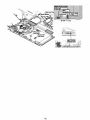
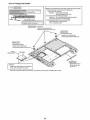
Notebook Computer
CF-Y5
This is the Service Ma nual for
the followin g a reas.
M .. .for U.S.A. and Canada
Model No. CF-Y5LWVYZ 1 2
1: Operation System
B: Microsoft® Windows® XP Professional
2: Area
M: Refer to above area table
L!'l. WARNING
This service information is designed for experienced repair technicians only and is not designed for use by the general public.
I! does nol contain warnings or cautions 10 advise non·technical individuals of potential dangers in attempting to service a product.
Products powered by electricity should be serviced or repaired only by experienced professional technicians. Any attempt 10 service
or repair the product or products dealt with in this service information by anyone else could result in serious injury or death.
Panasonid
o 2006 Matsushita Electric Industr ial Co .• Ltd. All r ights reserved.
Unauthorized copying and distribution is a violation of law.
WARNING
For U.K.
This apparatus must be earthed for your safety.
To el1Sllfe safe operation the three-pin plug must Ill! inserted ooly into a standard three-pin power point
which is dtectiveiy earthed through the normal household wiling.
Extension cords used with the equipment must be three-core and be correctly wired to provide connection to .-arth. Wrongly wired extension cords are a major cause of latalities.
The fact that the equipment opt!r3tes satisfactorily docs not imply that the power point is earthed and
that the installation is completely safe.
For your safety, if yOll have any doubt about the dTectiw earthing orthe power point, consult a qualitied electrician.
FOR YOUR SAfETY PLEASE READ THE FOLLOWING TEXT CAREFULLY
This appliance is supplied with a moulded three pin mains plug lor you r safety and convenience.
A 3 amp fuse is fitted in this plug.
Should the fu~e need to be replaced p lea~e ensure that the replacement fuse has a rating 01'3 amps and
that it is approved by ASTA or BSI to BS 1362.
Check lor the ASTA mark
orthe BSI mark ~ on the body or the fuse_
!fthe plll£ contains a removable fllse cOlier you must ensure that it is refitted when the fuse is replaced.
If you lose the fuse cover the plug must not be used until a replacement cover is obtained.
A replacement fllse cover can be purchased from your local Panasonic Dealer.
TF THE FITTED MOULDED PLUG IS UNSUITABLE FOR THE SOCKET OUTLET IN YOUR
HOME 1l-fEN THE FUSE SHOULD BE REMOVED AND THE PLUG CUT OFF AND DISPOSED
OF SAFELY.
THERE IS A DANGER OF SEVERE ELECTRICAL SHOCK fF THE CUT OFF PLUG IS INSERTED
INTO ANY 13 AMP SOCKET.
Ifa new plug is to be titted please observe the wiring code as shown below.
If in any doubt please consult a qualified electrician.
Waming: THIS APPLIANCE MUST BE EARTHED.
Important
The wires in this mains lead are coloured in accordance w ith the following code:
Green-and-yellow:
Earth
Blue :
Neutral
Brown:
Live
As the colours of the wires in the mains lead of this apparatus may not correspond with the coloured
markings identifying the terminals in your plug, proceed as tollows:
The wire which is coloured GREEN·and-YELLOW must be connected to the terminal in the plug
<b
which is marked by the letterE or by the safety earth symbol ~ colollred GREEN or GREEN-andYELLOW.
The wire which is coloured Blue must be connected to the terminal which is marked with the letter N or
coloured BLACK.
The wire which is coloured Brown must be connected to the ternlinal which is marked with the letter L
or coloured RED.
The main...; plug on this equipment must be used to disconnect the mains power.
Please ensure that a socket outlet is available near the equipment and shall be easily accessible.
• How to replace the fuse
Open the fuse com partment with a screwdriver and replace Ih e fu se.
Warnings
• This equ ipment is not des igned for con nection to an IT !",ower system.
{An IT system is 3 system having no di reci connections be twee n live parl~ and Earth.: the exposed -cooduc iveparts of the e leclrica l installaTio n are earthed.
An IT syMem is nol permitted whe re The computer is directly C(lnTl ec ted to puh lic I>u!"'p ly system ~ in the U.K.)
•
Ui ~connect
the mains plug from the
~u!",p! y
soc lcet when the compUTer
This equipment is produ ced to BS800fl 983.
2
i~
nOT in
u ~e_
LASER SAFETY INFORMATION
For U.S.A.
Class 1 LASER-Product
This product is certified to comply w ith DHHS Rules 21 CF R Subchapter J.
This product complies with European Standard EN60825 (or lEG Publication 825)
For all areas
This equipment is classified as a class 1 level LAS ER product and there is no hazardous LASE R radiation.
Caution:
(1) Use of controls or adjustments or performance of procedures other than t hose speci fied here in may result i n
hazardous radiation exposure.
(2) The drive is designed to be incorporated into a computer-based system or unit wh ich has an enclosing cover.
It should never be used as a stand alone drive.
Dange r:
The serviceman shou ld not remove the cover of drive unit and should not service because t he drive unit is a nonserviceable part.
Please check DANGER label on PO-drive unit .
Unplug the AC power cord to the equipment befo re opening the top cover of the drive.
When the power switch it on , do not place you r eyes close to the front panel door to look into the interior of the unit.
LASER S pecification
Class 1 level l ASER Product
Wave Length: DVD 658--8 nm
CD 775- 815 nm
Laser safety information is appropriate only when drive with laser is installed .
3
Safety precautions
1. Before sefllicing. unplug the power cord to prevent an electric shock.
2. When replacing par1s, use only manufacture's recommended components for safety.
3. Check the condition of the power cord. Replace if wear Of damage is evident.
4. After servicing, be sure 10 restore the lead dress, insulation barriers, insulation papers, shields, etc.
Important Safety Instructions
Lithium Battery
When usilll! your telephont cquipmc-nl . basic safel Y pr..::-
Uthium Battery!
This computer contains a lithium ballery to c nablc thc elmc, I imc..
and other data to be stored. The b:mery s hould only be e Xcll.1nged
by authorized service personoel.
Warninp:! A ri sk of explosion from incorrect installation or misapplication may possibly occur.
c!lulit)uS sth)uld always he followed II) reduce the risk of
fi n:. dl:ClriC siwek and i L~iu ry Itl ]1ers() n.~ . ind uding, Iht' fol·
lowi ng:
I. Do not usc this I)roduci f1C:H w,lIc r, lo r example. llcar a
bath tub. w:l:)h bowl, kjlc~n sink lITlaundry lub. in it wd
oaSClflcnl or nCilr il swimming. pool.
2. Avoid using ll l eh!pholle (other lilall a cordl ess lypt!) during an electrical storm. There may be a remote ri sk of
elewic shoc k from lighl ning.
~. o..) Ih' t usc the ldcphouc to rCptH1 a t!3f\ leak in the vicitl-
.
ily Ofl hc leak.
4. Use only the power cord and batleries indicated in Ihis
manual. ~ , IUlt di:·;posc of halkrics in a liR·. They may
e xplode. Chec k with local codes f or possil1le s pecia l d isposal ill:)lru~lj {) ns .
SAVE THESE INSTRUCTIONS
,----L
' ITHIUM BATTERY &.
• CAUTION
Danger of explosion if battery is incorrectly replaced.
Replace only with the same or equivalenltype recommended by the equipment manufacture.
Discard used ba1teries according to the manufacturer's instructions.
,---LlTHIUMBATTERIESL!\. - - - - - - - - - - - - - - - - - - - - - ,
Vorsichtl
Explosionsgefahr bei unsachgem.llBem Auslausch der BaU erie . Ersatz nur durch denselben order einen yom
Hersteller empfohlenen .!Ihnlichen T yp. Enlsorgung gebrauchter Bauerlen nach Angaben des Herstellers.
,----PILE AU LITHIUM&' - - - - - - - - - - - - - - - - - - - - - ,
ATTENT ION : IL Y A DANGER D'EXPLOS ION S' IL Y A REM PLACEMENT INCORREC T DE LA PILE.
REMPLACER UNIQUE ME NT AVEC UNE PILE DU MEME TYPE OU D'UN TYPE RECOMMAND E PAR LE
CONSTRUCTEUR . METIRE AU REBUT LES PILES USAGEES CONFOR MEMENT AUX INSTRUCTIONS DU
FABRICANT.
For U.S.A. I CANADA
A lithium ion battery that is recyclable powers the product you have
purchased. Please call 1-800-8-BATTERY for information on how to
recycle this battery.
L'appare il que vous vous etes procure est alimente par une batterie au
lithium-ion. Pour des renseignements sur Ie recyclage de la batterie,
veuillez com poser Ie 1-800-8-BATTERY.
4
Precautions (Battery Pack)
• Iflhehal1cry pack will not be used for a long period of time
(3 month or more), charge or discharge {use) Ihe hallery pack
until the remainin~ battery level becomes 30% to 40% and
store it in a cool, dry place.
• This com puter prevents overcharging of the battery by recharging onlywhcn the remaining power is less than approx.
95% of c.:apacily.
• The ballery pack is not charged whcn the computer is first
purchased. I3c sure \0 charge it before using it for the first
time. When the AC adaptor is connccted to lite computer,
charging begins lIulOmat ically.
• Should the ballery leak and lhe fluid get into yourc)'CS. do not
rub your eyes. lmmediat('ty flush youreycs with clear w:ller
and see a doctor for medical trealmentas soon as possihle.
• Care shou ld be exercised with regard to the following in
order to avoid the possibility of overheating, fi re or damage.
A\'oid Beal
Do /lOI throw Ihe bauery pack into a fire o r
expose it 10 excessive heat.
KL'CP Articles Away
Do 1101 place lhe battery pack together with articles such as necklaces or hairpins when carrying or sloring .
Du NOI Disassemble
Do nOt insert sharp objects imo Ihe banery pack,
expose it !O bumps or shocks, deform, disassemble. or modify iI.
NOTE
• The battery pack may become warm during reCharging or
normal usc. This is completely normal.
• Recharging wil l /101 commcnce outside or lhe allowable
tcmpcmture range (0 °C to 50°C {32°F to 122 °F}).(O'"
~ "Battery Powcr") Once the allowable range requirement is salisfied. charging begins automatical[y.
Note that Ihe recharging time varies based on Ihe usage
conditions. (Recharging takes longer than usual when the
temperature is [0 °C {50 OF} or less.)
• Iflhe temperature is [ow. the operating time is shortened.
Only use the computer within the allowab[e temperature
rangc.
• The battery pack isa consumable item. [ftlte amount of
time the camputerC"dll be run alTa par1icular battery pack
becomes dmmatically shorter and repeated rcchargings
do not restore its perfomlance, lite battery pack should be
replaced with a new onc.
• When transporting spare batteries inside a package, briefcase. Ctc., it is recommended that it be placed in a plastic
bag so thaI liS contacts arc proteCted.
• Always power off lhe computer when it is Dot in use.
Leaving the computer On when the AC adaptor is not
connected wit! exhauSllhe remaining haltery capacity.
Do Not Short
Do nOI shortlhe positive (-t ) and negative (-)
contacts.
Avoid Exl.rcDlc O('al , Cold lind I>irccl Sunlight
Do nOI charge, usc or leave the baltcry pack for
extended [)criods where it wil l he exposed 10
direct sunlight, in a hOI place (in an automobile
on a sunny day, for example). or in a cold place.
0., Nut Usc With Any Olhcr Cump uter
The battery pack is rechargeable and was in-
tended for the specified computer or charger.
Do not usc it wilh a computer other than the
ont! for which it was designed
Do No l Pul inlo a Microw3\'c
Do 1101 pUl the baltcry pack into a microwave
oven or a pressurized chamber.
Discontinue Use
Should lhe banery emit an abnonnal odor, become hot to the touch, become di!>c()lored,
change shape, or become in a.ny way differclll
rrom normal. remove i1 from the computcr or
chargcr and discontinue usc.
• Do nOt touch the tenninals on the banery pack. The battcry pack may no longer funct ion properly if the COillacts
arc diny or damaged.
• Do not expose the battery pack 10 water. or allow it 10
hecome wet.
5
CONTENTS
1. Specifications - - - - - - - - - - - - - - - - - - - - - - - - - 7
2. Names and Functions of Parts
10
3. Block Diagram
12
4. Diagnosis Procedure
13
5. Power-On Self Test (Boot Check)
15
6. List of Error Codes <Only when the port replicator is connected>
16
7. Self Diagnosis Test
18
8. Wiring Connection Diagram
23
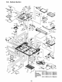
9. Disassembly/Reassembly
24
10. Exploded View
80
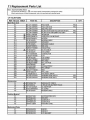
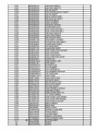
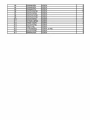
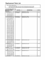
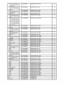
11. Replacement Parts List
83
1 Specifications
•
Main Specifications
Model No.
CF· YSl WWZBM
CPUI
Secondary cache memory
Intel® CoreTM Duo Processor low Voltage L 2400 (1.66 GHz, 2 MB ' 1 L2 cache, 667
MHz FSB)
Chip Set
Mobile Intel® 945 GMS Express chip set
Main Memory
512 tvlB'\ DDR2 SDRAM (1536 MB" Max.)
Video Memory
UMA (128 MB" Max.)';'>
Hard Disk Drive
60 G13'3
CD/OVO Drive
USB 2 .0 connection interface
OVO MULTI Drive built-in, Buffer underrun error preventlon funct ion: Supported
Continuous Data Transfer Speed' 4' 5
Supported Oisks/Format"5
Reading'6
ax
Writing'9
e OVO-RAM'7: 2X (4.7GB' 3) . OVO-R: 1X12X14X . OVO-RW: 1X12X . +R: 2.4X14X
. +RW: 2.4X e CO-R: 4X18X/8-16X18-2 4X e CD-RW: 4X eH igh-Speed CD-RW: 4X18XI
10X e Ultra-Speed CO-RW: 8X110X
Reading
e OVO-ROM (Single Layer, Dual Layer) e OVO-Video e OVO-R·S(1.4 GB, 3_95 GI3 , 4.7
(13)'3 e OVO-RW (Ver. 1_1/1.2 1.4 GI3, 4.7 GB , 9.4 GB)'3 e OVO-RAM'1 (1.4 GB , 2.8 GB,
2.6 GB, 5.2 GB, 4.7 GB, 9.4 GB)'3 e +R (4.7 (13)'3 e +R OL (8.5GB)·3 . +RW (4.7 GB)'3
e CD-Audio e CD-ROM (XA compatible) e CD-R e Photo CD (multiple session compatible) e Video CD e CO- EXT RA e CO-RW e CD-TEXT
Writing
e OVO_RAM'1 (1.4GB , 2.8GB, 4.7GB, 9.4GB)'3e OVO- R (1.4GB, 4.7GB fo r General)"3
e DVD-RW (Ver.1.111.2 4.7GB, 9.40B)"3 e +R (4.7(m-3) e +RW (4.7<.iB'3) e CD-R e CD-RW
Display Method
'"c:
'"oo
.c:
e OVO-RAM'7: 2X (4.7 GS'3)/1X (2.6 G8'3) _ OVD_R'S: 4X (Max.) e OVO-RW: 4X
(Max.) e OVO-ROM:
(Max.) _ CD_ROM: 24X (Max.) _ CD_R: 24X (Max.) e CO-RW:
20X (Max.) h R: 4X (Max.) e +R DL: 4X (Max.) e +RW: 4X (Max.)
14.1 SXGA+ type (TFT) (1400 x 1050 dots)
Internal LCD
65,536/16,777,216 colors (1400 x 1050dots)'10
External Display' 11
65,536/16,777 ,216 colors (800 x 600 dotsf1024 x 768 dots/1280 x 768 dots/1280 x
1024 dotsJ1400 x 1050 dots/16oo x 1200 dotsJ2048 x 1536 dots (60 Hzj"12)
SimultaneolJs Display on LCD + ExlernalDisplay"11
65,536/16,777 ,216 colors (800 x 600 dotsJ1024 x 768 dots/1280 x 768 dots/1280 x
1024 dots/1400 x 1050 dotS)'1 0
Wireless LAN
Inter® PROlWireless 3945 ABG Network Connection (next page)
::l
Bluetooth 1M
LAN'13
IEEE 802.3 10Base-T, IEEE 802.3u 1OOBase-TX
f-
Modem
Data: 56 kbps (V.92) FAX: 14.4 kbps
Sound
WAVE and M IDI playback. Intel® High Definition Audio subsystem support, Stereo
Speakers (built in)
Security Chip
TPM (TCG V1.2 com pliant)'14
:l!
.0
e
(next page)
.!!
"0
c:
Card Slots
0.
0.
RAM Module Slot
x 1, DOR2 SDRAM, 172-pin, 1.8 V, Micro DIMM, PC2-42OO Compliant'16
Interface
USB Ports x 2 (USB2.0 x 2)'11 I Modem Port (RJ-11) I LAN Port (RJ-45) ' 13 I
External Dishlay Port: Mini Osub 15-pin female I Microphone Jack: Min iature jack, 3.5
DIA I Headp one Jack: Miniature jack, 3.5 DIA I Mini Port Replicator connector: Dedicated 50-pin male
Keyboard/Pointing Device
87 keys/Touch Pad
Power Supply
AC Adaptor' 18
AC adaptor or Battery pack
..
«
PC Card Slot
x 1, Type I or Type II , Allowable current 3.3 V: 400 mA, 5 V: 400 mA
SD Memory Card SIot'15
x 1, Data transfer rate - 8 M 13 per second
Battery Pack
Input: 100 V - 240 V AC, 50 Hz{60 Hz
Output: 16 V DC, 3.75 A
Li-ion 10.65 v, 5.7 Ah
Operating Time'19
Approx. 5 hours - 8 hours"20 (Approx, 6 hours"21) (Disable Economy Mode (ECO))
Charging Time' 22
Approx . 5 hours (Power off)/Approx. 6,5 hours (Power on)
7
Model No.
CF-YSLWWZBM
Power Consumption0 23
Approx. 35 W"24 / Approx. 60 W (maximum when recharging in the ON state)
Physical Dimensions (W x H x D)
309.6 mm x 2S mm (at the trom)/44.5 mm (at the rear) x 245.5 mm (excluding protrusion){12 .2w x 1.1" / LS" x 10.0"}
Weight"25
Approx. 1530 g {3.4 lb.}
Environment
Operation
Storage
Temperature
5°C to 3SoC {41 °F to 9S0F}
Humidity
30% to 80% RH (No condensation)
Temperature
_20°C to 60°C {-4°F to 140°F}
Humidity
30% to 90% RH (No condensation)
OS026
Microsott® Windows® XP Professional Service Pack 2 with Advanced Security Technologies (NTFS File system)
Pre-installed Softwareo 2G
Microsoft® Internet Explorer 6 Service Pack 2 1 DirectX 9.0c /Microsoft® Windows®
Media Player 10/ Microsoft® Windcms® Movie Maker 2.1 1Microsoft® .NET Framework
1.1 SP1/2.0 / Adobe Reader / I nte ~ PROSetJV.lireless Software <Only for model with
wireless LAN> 1 SO Utility I Icon Enlarger 1 Loupe Utility 1 Touch Pad Utility 1 DM I Viewer
I PC Information Viewer I WinDVD 5 (OEM Version) f B's Recorder GOLD8 BAS IC / B's
CliP 6° 27 1 Hotkey Settings I Optical Disc Drive Letter-Setting L1tility f Optical Disc Drive
Pcmer-Saving Utility I W ireless Switch Utility <Only for model with wireless LANfBluetooth> 1 Economy Mode (ECO) Setting Utility 1 Battery Recal ibration Utility I infineon
TPM Professional Package V2.S"2S I Recover Pro 6°28
Setup Utility 1 Hard Disk Data Erase Utility029 1 PC-Diagnostic Utility030
W i re l ess LAN
•
Data Transfer Rates
IEEES02.11a: 54/4S/36124/1S/121916 Mbps (automatically switched)031
IEEES02.11 b : 11/5.S/2/1 Mbps (automatica lly switched) °31
IEEES02.11g: 54/4S/36f24/1S/12f916 Mbps (automatically switched)031
Standard Supported
IEEES02.11 af1EEES02.11 b/1EEES02.11 g
Transmission Method
OFDM system , DS-SS system
Wireless Channels Used
IEEES02.11a: Channels 36/40/44/48152156/601641149/153 /157/161 /165
IEEES02.11b/ IEEE802.11g: Channels 1 to 11
RF Frequency Band
IEEES02.11a· 5.18 - 5.32 GHz. 5.745 - 5.S25 GHz
IEEES02.11b/ IEEES02.11g: 2412 - 2462 MHz
•
"o'"
o
BI uetoo th n.I
Bluetoolh Version
2.0 + EDR
Transmission Method
FHSS system
.c
Wireless Channels Used
Channels 1 1079
RF Frequency Band
2.402-2.48 GHz
Power Class
Class 1
"
"~
I-
0'
<h
.c
1 MB = 1,048,576 bytes
°2 A segment of the main memory is allotted automatically
depending on the computer's operating status . The size of
the Video Memory cannot be set by the user.
°3
1 GI3 = 1.000,000,000 bytes. Your operating system or some
application software will report as fewer GB.
°4 Data transfer speeds indicate values measured by
Matsushita Electric Industrial Co., Ltd. The data transfer rate
of DVD per lX speed is 1,350 KB/s. The data transfer rate of
CD per 1X speed is 150 KB/s.
°s Performance of CD-R. CD-RW. DVD-RAM. DVD-R. DVDRW, +R, +R DL, and +RW cannot be guaranteed depending
on writing status and recording format. Also, some data cannot be played back depending on the disk, settings, and
environment being used.
Does not support writing to DVD-R DL/+R DL (dual layer
disks) or reading from DVD-R DL
8
°6 If an unbalanced disk (e.g., a disk with which the balance
has been displaced from the center) is inserted, the speed
may become slower if there are large vibrations while the
disk is rotating .
°7 Only non -cartridge type or removable cartridge type can be
used .
When writing to DVD-RAM, use only disks up to 3x. This
application cannot be used with 5x DVD-RAM media (2-5x
disks, etc.).
os DVD-R is compatible with 4.7 GI3 (for General) playback.
DVD-R (for Authoring) playback is compatible with disks
recorded us ing Disk-at-Once recording.
°9 Depending on the disk, the writing speed may become
slower.
°'0 A 16,777.216 color display is achieved by using the dithering
function.
°' 1 Display may be impossible using some connected external
displays .
)(
"0
""a.
a.
«
" 2 When using an external display with a resolution of 2048 x
1536 dots, use a display that supports a 60Hz refresh rate. If
an external display that does not support a 60Hz refresh rate
is used, images may not be displayed properly.
" 3 Some devices cannot be used depending on the port type.
"4 For information on TPM , click [start] - [Run] and input
"c:\util\drivers\tpm\README .pdf', and refer to the Installation
Manual of "Trusted Platform Module (TPM )" .
" 5 Operation has been tested and confirmed using Panasonic
SO Memory Cards with a capacity of up to 2 GB.
The transfer rate using the SO Memory Card slot on this
computer is 8 MB per second. (This is a theoretical value,
and diffe rs from actual speeds.)
The transfer rate is 8 MB per second even if you use an SO
Memory Card that supports high-speed transfer rates.
Ope ration on other SO equ ipment is not guaranteed .
This computer is not compatible with MultiMediaCards or
SO HC Memory Cards.
Do not insert these kinds of cards.
" 6 Only a RAM module designed for 00R2 (PC2-42DO) can be
added (Panasonic : CF-BAW0512U , CF-BAW1024U ).
JEOEC standard 214 pin Micro OIMM cannot be used.
PC21 DO I PC27DO 172 pin Micro OIMM cannot be used .
If a PC2-3200 RAM module is installed, the main memory
processing speed may become slower.
' 11 Does not guarantee operation of all USB-compaHbie peripherals.
"8 <Only for North America>
The AC adaptor is compatible with power sources up to
240 V AC adaptor. This computer is supplied with a 125 V
AC compatible AC cord.
2Q·M_2_1
.!!
"0
I:
8.
C-
o:(
9
'19 Varies depending on the usage conditions, or when an
optional device is attached. Measured when the power saving
function on the USB2.0 USB Root Hub is set to on. (At the
time of purchase, the power saving function is activated.)
When Economy Mode (ECO) is enabled, the operating time
becomes approximately 20"10 shorter than when it is disabled .
"20 Measured using BatteryMark TM Version 4.0.1 (LCD brightness: Maximum· Minimum).
'21 Measured using MobileMark ™ 2005 (LCD brightness : 60
cd /m2 ).
'22 Varies depending on the usage conditions. CPU speed, etc.
It may take a long time to charge a fully discharged battery.
'23 Approx. 1.5 W when the battery pack is fully charged (or not
being charged) and the computer is off.
'24 Rated power consumption.
23-E-1
'25 Average value. May differ depending on models.
'26 Operations of this computer a re not guaranteed except for
the pre-installed OS.
'27 Pre installed B's CliP does not support CO-R, OVO-R, +R
and OVO-RAM.
'26 Must be installed before lJse.
'29 The Product Recovery DVO-ROM is required.
'30 For startup methods, refer to "Hardware Diagnostics".
'31 These are speeds specified in IEEE802.11a+b+g standards.
Actual speeds may differ.
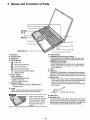
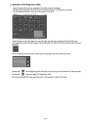
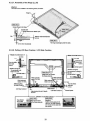
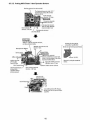
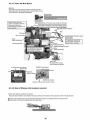
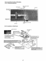
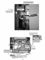
2 Names and Functions of Parts
A --------------~------,
8 -------------,:
C ----------:::;orlf/?<
~ ill i!lI@ 0 ------,'"""'~
ECO 0
<!J E
b~~;~IA~~g~~~
WIRELESS F
G -------'i~
H----->l~-
DRIVE OFFKlN ...
A : Speakers
H : CD /DVD Drive
I : CD /DVD Drive Power/Open Switch
• Slide the switch to the right to open the disk cover.
o Slide the switch to the left to turn on/off the drive power.
CO/DVD Driv e Indicator
Off: Drive power is off.
o Green: Drive power is on , but the drive is not accessed.
o Blinking green: Drive power is on, and t he drive is
being accessed.
J : LCD
K : LAN Port
If the Mini Port Replicator is conneded to the computer,
conned the LAN cable to the LAN port on the Mini Port
Repl icator. You cannot use the LAN port on the computer.
L : Modem Port
Be sure to use the included modem telephone cable,
and insert the ferrite core side of modem telephone
cable into the modem port on t he computer.
Do not move/remove the ferrite core of modem te lephone cable.
B : Function Key
C :Keyboard
o :LED Indicator
~ : Caps lock
Numeric key (NumLk)
Scro ll lock (ScrLk)
III :
lID :
Ii : Hard disk drive status
ECO: Economy Mode (ECO) status
Battery status
o:
E : Power Switch
Power Indicator
Off: Power off/Hibernation
• Green: Power on
• Blinking green: Standby
F : Wireless Switch
<Only for model wit h wireless LAN/Bluetooth>
"Wireless LAN"
G :Latch
When closing the display, press down firmly from
above until the latch is firmly closed (locked) .
When closing the disk
cover, press down near t he
drive power/open switch
(position of the arrow) to
ensure that the cover is
locked.
10
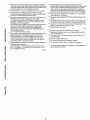
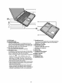
M :USB Ports
N : Sec urity Lock
You can connect a Kensington cable. Refer to the instruc
tion manual of the cable. The security lock and cable is atheft prevention device. Matsushita Electric Industrial Co.,
Ltd. will bear no responsibility in the event of theft.
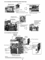
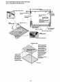
.,..,
OC"16V A --~;;
M-------------r-------,
[J
,
EXT. D_ _ _ _ _ _ _...J
n
p -------""~ :';,.,--=-',U
A :DC-IN Jack
8 :Ventilation Hole
C : External Display Port
If the Mini Port Replicator is connected to the computer, con nect the extemal display to t he external display port on the Mini Port Replicator. You ca nnot use
the externa l display port on the compu ter.
o :Mini Port Replicator Connector
Connect the Mini Port Replicator (optional).
E : Microphone Jack
A condenser microphone can be used. If other types
of microphones are used , audio input may not be possible, or malfunctions may occur as a result.
• When recording in stereo using a stereo microphone
0
Double-click
in the notification area, click
[Options] - [Properties], and add a check mark for
[Recording], click [O K] - [Options] - [Advanced Controls] - (Advanced], remove a check mark for (Mono
Microphone], and t hen click [Close].
• When using a monaural microphone with a 2-terminal plug
With t he settings outli ned above , only audio on the
left track w ill be recorded .
When monitoring the microphone aud io using headphones, sounds on the left track cannot be heard ,
regardless of the above settings. This is a result of t he
computer's specifications, and is not a malfunction.
11
F : Headphone Jack
You can conned headphones or amplified speakers.
When they are connected, aud io from the internal
speakers is not heard.
G :50 Memory Card Slot
H : Bluetooth Antenna
<O nly for model wi th B luetooth>
I: Wireless LAN Antenna
J : Touch Pad
K : PC Card Slot
L : SO Memory Card Indicat
Bl inking: During access
M :Battery Latches
N : Battery Pack
:Emergency Hole
P : RAM Module Slot
o
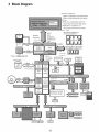
3 Block Diagram
r,,(prnn/ Cm.., FT"'lUl'''9HFM"'T. fi~ f;H?/I,FM =/J) (iR" (High MM"})
HF'M=Li (,'H"If.FAr=~oo MH? (T,ow ,'II,,,"")
Yooah LV Dual Core
Yonah ULV Single CoN
HFM=1.O V-/,;J12;;VI T.P,"' =/), 762,W·I.GV
Included
nP.t'l'"r .'i/~1) ",(Jfi..;V·(1.:1r,\i (Hi/:h AIM",)
L2-C"ch", 2.\1
l~:(4~7~9p~in:~!~F~C~BGA);~:~::::~Jv(:";FM=o,f;/;V"'IVI"FM=(),f;" 'lV
DP.<'l'er 81e<>/,=(J;;,·j V-O.,.,r,V (1."", ."rool/.)
I.O;;V
Main MelllOl.l rDDR2' 5Jj)
On Hmml:i 12,'1",,,, I (] R
AG1'U
onno
61bir
ProceiJBOr
System Dus
G67MIlz(LV)
638MIldULV)
Calistoga-GMS
OCTuD
Gl'Uphic~
Extended MemorJ IP(:2-1200 )
1,05F
Micr.,.nTM!If
Interface
OW fiRM,.,?,
OOGn 2iX:
USB4
US&1
I GBy~
PATA
II11 D
OIIA.\ i01»
".2G Bvt~.
DM! A:!
St..ruge Device
,
"G'~.". 100001
1.0liV
<'I'.\1U 14_ 1~SXGA+lXGA 'r}"I'
I
ICH7'M
USllO
<~~~~~::IIG;PA;.;"A~r~;~U~S~B~llk~===lmill:iC=:::ll
jnu.rf"""
Interface
SA'I'A
p(;t
O
iUhn .
U81:J2
USl:!2
I
Inlerfa""
USB
I.IGA
PC I
Exprc .....
UoSHl
l:lridg~
S l'1
Inh.:,.f,,~c
I{.')CA11A
."
HTUlIOIL
Interface
81'1 Fla.lh
>lMb i,
2,WHl!I
'\li~T<'
'fl'.\t
.\l.UC
1.2
8o,ft '\l"dcm
S'I'AC9200
hune
S cuke",
IHcudph"nc!
!W-U
12
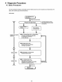
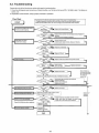
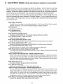
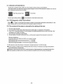
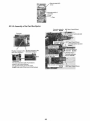
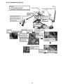
4 Diagnosis Procedure
4.1. Basic Procedures
The basic procedures for diagnosis, disassembly, and lest of defective parts of a set to be repaired are summarized below. For
details, refer to relevant pages in the Service Manual.
• Flow Chart
LTROUBLE
OCCURRENCE OF
J
Power son Is set to ON.
I
POST NORMAL I
ISH
I FIN
- - -DEFECTIVE PARTS
SORTING
,,
,
I
Automatic diagnosis lakes
place when the power switch
is set loON.
Power On SelfTes!
POSTERROR
OCCURRENCE
-- - - --- - -----~- -- --
• SELF·DIAGNOSIS TEST (IF REQUIRED)
Conduct as<If d"18gnOSls lesI wh en
it is necessary for conduct
trouble diagnosis.
-----------l-----------I
I
• TROUBLESHOOTING
Defective parts are sorted by
referring to symptoms.
REPAIRWQRK
• DISASSEMBLY PROCEDURE
Replace defective parts.
~
INSPECTION
~
• SELF-DIAGNOSIS TEST
After repair, conduct a selfdiagnOSis test and make sure that the
repaired set operates properly.
TEST OK
l
ENDOF
REPAIR WORK
13
J
TEST FAilED
4.2. Troubleshooting
Please lake nol e of t he fo Uowing two points with rega rd to troubleshooting :
1. Know-how of diagnosis upon occurrence of heavy troubles, e.9. Set cannot be turned O N , Set fails to start , No display on
screen , etc.
2. Explanation of each troub le, mainly symptom of trouble in operation.
Flow Chart
[
START }
Pay attention to thefollov.4ng poftts ""'en In pursuH aftha cause 0 a troublestmo:lng.
\ , PO'IIlph(!fal apparatus o:'1nee!ea....tth the set should all be '8ff\(1Vad balon, operation <;hOCk.
2. Makesur&1I1at cables. boards. etc_ art! not coming oil. and .edled< me contact condition.
NO.
NG
Resuhaf
!-
Re1er to POST
REplace main boord.
error code table.
eoST
___---'OK
NG
Set-\{llf.lHty
Replac@LCDbacklight,
starting
Replace main board.
r--
, - OK
Heavy trouble e·9 ·.
Set cannot be 1I.lmed
ON . Set falls 10 stan .
Nodls~ayon
I Retum set..,,:> utility setpoint 1011111 stat" of dellv&rylrom facto<y I""
HOO
..
I Not displ3)'ad PlOperly on screen. I
Some or an keys cannOl be Input.
_
NO
Cheek HOD calli!! connection a nd CQn1l1uily.
~>_~~ Replace If defective.
Replace H OO & Reinstall.
Replace main board.
YES
NG
MaTn board
"', -
OK
l roubi"".ome
e
"yrI1fltoms
NQ
==>:;;:~
ol ()\{D"' ~
S
I Replace main board .
I
I
[
J
'Oean OVO-ROM dflvewi:h an applicator.
I
Replace OVO drivEl.
Replace main board.
Reinstall HOD.
EN D
i
Replace maTn board
M"e sure of contact of KIB connector Tn lise.
Replace keyboard or main board .
-~E~E5~:::i:EE:E::]--<:::
OVOiCD CAL.L not pmctlca~e.
1
access
14
I
Check IfSlnCfl
there flaOM";
arEl any
on OVO
or CD
media.
mayflaws
appear
on sp9CiIIC
media . DVD or CO media can bedel8C1ive.
Each kind of
trouble In
-
"",-
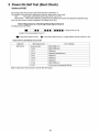
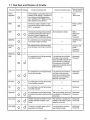
5 Power-On Self Test (Boot Check)
Outline of POST
The set has a boot check function called POST (Power-On Self Test) in it.
The condition of the main body is diagnosed by checking beep sound or error code.
Start __ ____ __ _...Tesl begins automatically when power switch is set to ON_
Normal finish .....After memory checking, a beep sound is issued once and the set is placed into automatic stop.
Note: If no error occurs, nothing is displayed. (No display of OK, etc.)
Error Diagnosis by Checking Beep Signal Sound
The beep sound is as follows:
(Length of bar shows length of sound_)
_
= long sound (about 0.4 sec.),
•
= shorl sound (about 0.2 sec.), Length between sounds is about 0.1 sec.
Table of errors classified by beep sou nds
Diagnosis
Main board
Error message
Beep signal sound
1 (long sound)-2
BIOS ROM error
1-2-2-3
BIOS ROM error
1-3-1-1
RAM error
1-3-1-3
Keyboard contro ller error
1-3-4-1
RAM error
1-3-4-3
RAM error
1-4-1-1
RAM error
2-1-2-3
BIOS ROM error
2-2-3-1
Occurrence of unexpected offering
(Note) A beep sound is a lso issued in case of other I/O trouble.
15
6 List of Error Codes
<Only when the port replicator is connected>
The following is a list of the messages that BIOS can di splay. Most of them occur during
POST. Some of them display infonnation about a hard ware dev ice, e .g., the amount of memory
installed. Others may indicate a problem with a device, such as the way it has been config ured.
Following the list are explanations of the messages and remedies for reported problems.
If YO lLf system displays one of except th e messages marked below with an asterisk (*), write
down the message and contact Panaso nic Technical Support. If yo ur system fai ls after YO LI
make changes in the Setup menus, reset the computer, enter Setup and install Setup defaults
or correct the error.
0200 Failure Fixed Disk
Fixed disk in not working or not confi gured properly. Check to see if fi xed disk is attached
properly. RLUI Setup. Find out jfthe fixed-disk type is correctly identified.
0210 Stuck key
Stuck key on keyboard.
0211 Keyboard error
Keyboard not working.
0212 Keyboard Controller Failed
Keyboard controller failed test. May require replacing keyboard controller.
0213 Keyboard locked - Unlock key switch
Unlock the system to proceed.
0230 System RAM Fa iled at offset: IImln
System RAM fai led at offset mum of in the 64k block at which the error was detected.
0231 Shadow RAM F ailed at offset: IImln
Shadow RAM fai led at offset nnl1l1 of the 64k block at which the error was detected.
0232 Extended RAM Failed at offset: nlllln
Extended memory not working or not configured properly at offset 11111111.
0250 System battery is dead - Replace and run SETUP
The CMOS clock battery indicator shows the battery is dead. Replace the battery and nm Setup
to reconfigure the system.
*0251 System CMOS checksllfll bad - Default configuration used
System CMOS has been corrupted or modified incorrectly, perhaps by an appli cation program
that changes data stored in CMOS. The BIOS installed Default SETUP Va lues. If you do not
want these values, enter Setup and enter your ovm values . If tile error persists, check the system
battery or contact Panasonic Technical Support.
0260 System timer error
The timer test failed. Requires repa ir of system board.
0270 Real time clock error
Real-time c-Iock fa il s BIOS test. May require board repair.
*0280 Previous boot incomplete - Default configuration used
Previous POST did not complete successfully. POST loads defa ul t values and offers to run
Setup . If tile fai lure was caused by incorrect values and they are not corrected, the next boot
will likely faiL On systems with control of wail states, improper Setup settings can also tenrn nate POST and cause this error on the next boot. Run Setup and verify that the wa it-state
configuration is correct. This error is cleared the next time the system is booted.
0281 Memory Size found by POST diff"'ed f"om EISA CMOS
Memory size fo und by POST differed from EISA CMOS.
16
02DO System cache error - Cache disabled
Contact Panasonic Technica l Support.
02FO: C PU 10:
CPU socket number for Mu lti-Processor error.
02F4: EISA CMOS not writable
ServerBIOS2 test error: Cannot write to EISA CMOS.
02F5: DMA Test Failed
ServerB IOS2 test error: CWIDot \vrite to extended DMA (Direct Memory Access) registers.
02F6: Software Nl\fl Failed
ServerBIOS 2 test error: Cannot generate software NMI (Non-Maskable Interrupt).
02F7: Fail - Safe Timer NMI Failed
ServerBIOS2 test error: Fail-Safe Timer takes too long.
del/ice address Co ntlict
Address conflic t for specifi ed device.
Allocation Errol' for: del/ice
RWl ISA or EISA Confi guration Utili ty to resolve resource conflic t for the spec ifi ed device.
Failing Bits: nmlll
The hex number nnnn is a map of the bits at the RAM address which fai led the memory test.
Eacb 1 (one) in the map indicates a failed bit. See error 230,23 1 or 232 for offset address oftbe
failure in System, Extended or Shadow memory.
Invalid System Configuration Data
Problem with NVRAM (CMOS) data.
1/0 device mQ conflict
110 device IRQ confl ict error.
Operating System not found
Operating system cannot be located on either drive A: or drive C:. Enter Setup and see iffixed
disk and drive A: are properly identified.
Parity C heck 1 nnnn
Parity error found in the system bu s. BIOS attempts to locate the address and display it on the
screen. If it cannot locate the address, it disp lays ???? Parity is a method for checking errors
in binary data. A parity error indicates tbat some data has been corrupted.
Parity C heck 2 nnnn
Parity error fo und in the lIO bus. BIO S attempts to locate the address and display it on the
screen. If it calIDot locate the address, it displays ????
Press <Fl> to resume, <F2> to Setup
Di splayed after any recoverabl e error message. Press <F 1> to start the boot process or <F2> to
enter a Setup and change the settings. Write down and follo w the information sho\\'11 on the
screen.
17
Cl
t:
15
o
.s:
:g
:c:>
o
.=
7 Self Diagnosis Test
As for the self-diagnosis test(PC-Diagnostic utility) to use this model, a standard test and the
enhancing test by the module of the main body building in are possible .
• Notes To skip BIOS password
Use <Ctrl>+< F1 0> key to skip BIOS password or authentication of fingerprint.
This key is only for entering DIAG mode. Not available to boot the computer.
If customer set "HOD Lock", the DrAG program cannot perform HOD test.
*This key is for service purpose only. Do not disclose this information to unrelated others.
1. Beginning of self-diagnosis test
1-1 . Setting of content of setup
1.
2.
3.
4.
The power supply of the computer is turned on.
" F2" is pushed on the screen of "Panasonic" while" press <F2 to enter Setup> " is displayed.
The setup utility starts and then takes notes of the content of the BIOS setup of present set.
" F9" is pushed , " Yes" is selected on the screen of " Is the default value loaded? ", and" Enter"
is pushed.
5. " F1 0" is pushed.
6. "Yes" is selected on the screen of the setup confirmation, and" Enter" is pushed .
7. The computer starts automatically.
Attentio n
• If the device which can be set is set to "Invalidity" by "Advanced" or "Security" menu, becomes an
error by "PC-Diagnostic utility".
(It is judged that the device which can be set to "Invalidity" by "Main" menu such as "Flat pad" is
normal if the controller operates normally though sets to "Invalidity" by the setup. )
• In the model with built-in DVD of the USB connection, even if DVD is normal, becomes an error if
legacy USB is set to "Invalidity"
1-2. When you execute an automatic test
1. "Ctrl" + "F7" is pushed while the "Panasonic" start screen is displayed after the computer is started.
2. The test of all dev ices begins automatically by "PC-Diagnostic utility'''s starting.
Attention
• It is a test which the customer who bought PC can execute . (As for HDD , the enhancing test is also
possible .)
• A flat pad does not work for a while after starting "PC-Diagnostic utility".
• The movement of a flat pad might become abnormal If after RAM begins from the CPU/System
test, a flat pad will be operated in about 30 seconds . In that case, restarts pushing"Alt" + "Ctrl " +
"Del" key. Or, please start "PC-Diagnostic utility" again after doing the power supply switch in the
slide, and turning off the power supply.
1-3. When you execute the enhancing test
1. Please let me discontin ue diagnosing clicking
end an automatic test.
2. Please click on the character of "0" "PC-Diagnostic utility" on the sc"een while pushing both of right
"Shift" and left "Shift" keys.
3. All devices which can select the enhancing test make the setting of the enhancing test possible.
4 . The district dev ice is made"FULL" display (enhancing test).
5. The test begins clicking
*Please re fer to item 4 for the error result of each test and the division of the breakdown part.
18
2. Operation of PC-Diagnostic Utility
-Only the device wh ich can be inspected on the entire screen is displayed.
-The item does not appear when the device of wireless LAN etc. is not physically connected.
-The movement of t he item must use an arrow key or a flat pad.
-As for the device under the diagnosis, blue and yellow are alternately displayed at the left of the icon.
- The diagnosis result of the device greens at the left of the icon when it is normal , and becomes red when
abnormal.
-When the test of all devices ends, the test result is displayed under the right of the screen.
-Please cl ick
while diagnosing when being stop on the way by the time the test of all devices ends.
-Please cl ick
when you restart "PC-Diagnostic utility".
*Each device is tested from the beg inning, and it is not possible to restart on the way.
19
2·1 . Selection of tested device
-To test ot1y a specific device, 'Test" and "Do not test" of each device can be selected.
-The device which can select the enhancing test changes in order of 'The standard is tested" and "Do not
test' whenever the device icon is clicked.
Start the standard test
Please begin testing dicking
Do not test
if the selection of the tested device ends.
2-2. "PC-Diagnostic utility" End method
181
When
of "Close" on the right of the screen is clicked, the computer reactivates automaticall y. Or, the
power supply switch is done in the slide and the power supply is turned off.
2·3. The content of the setup is returned to the setting of the user
1. Turned on the computer.
2. "F2" is pushed on the screen while "Press<F2>to enter Setup" is displayed of "Panasonic".
3. Push "F10", and on the screen of "Is the change in the setling preserved and do end?"and then "Yes"
is selected, and "Enter" is pushed .
4. The computer reactivates automatically.
5. The end option is chosen by the start menu, and the power supply of the computer is turned off.
Standard at test time
All devices other than RAM and HOD about 1 mi nute
RAM standard test
1 - 2 minutes
HOD standard test - - - - - - - - - 2 - 3 minutes
HOD enhancing test (60GB)
about 40 minutes
EX.The standard when the standard <all device> is tested becomes 1+2+3=6 minutes.
• There is greatl y a difference from RAM test when the me mory is increased according to the performance of the memory occasionally.
• Moreover, when the main body of PC under the test is a high temperature, it occasionally takes time.
• There is greatly a difference from HOD according to the performance of the drive occasionally.
20
7.1. Test Item and Division of tro uble
Test item
Stanard Enhancing
CPU!
SYSTEM
0
Content of standard test
CPU is shifted to protected mode, and
"Violation of the paging", "Operation of
the violation of a privileged inslruc-
-
Content o f enhancing test
Place with possibility of breakdown
CPU!
Main board
-
lion", and OMA, INT, TIMER, and the
RTC operation are confirmed.
RAM
O
All memory space is tested in a special memory access pattern based on
"R. S.T . technology".
-
HOD
MODEM
0
0
O
-
It is confirmed not to fi nd abnormality
in the AC97 modem controller.
Sound *S
0
-
0
-
SO
It is confirmed not to fi nd abnormality
in the LAN controller.
It is confirmed not to find abnormality in the wiring between the con troller and the
connector by connecting to
HUB with LAN cable.
Mainboard I
Connector
0
0
-
It is confirmed not to find abnormality
in the CardBus controller.
-
0
-
It is confirmed not to fi nd abnormality
in the SO controller.
-
>3
0
>.
Touch Pad
0
OVO-ROM
0
0
0
>6
0
Wireless LAN
board I
Connector I
Mainboard
Mainboard I
Connector
0
Keyboard
MOD EMI Mainboard
It is confirmed not to find abnormality in the wiring between the USB controller and
the connector by confirming
the connection of the USB
equipment connected with the
USB connector.
0
>2
PC Card
-
It is confirmed not to find abnormality
in the USB controller.
>1
LAN
HOD !
Mainboard I
Cable I
Connector
-
USB
0
All record area is tested.
It is confirmed not to find abnormality
in the Wireless LAN mode m co ntroller.
Wireless
LAN
The record area frequen tly accessed
with Microsoft Windows XP to test in
about two minutes regardless of
points of HOD is emphatically tested.
-
Memory I Mainboard
Mainboard
Mainboard
It is confi rmed not to find abnormality The key is actually input, and
in keyboard controller's keyboard inter the opera tion is displayed on
fa ce.
the screen.
Mainboard I
Keyboard
Whether keyboard controller's mouse
interface operates normally is confirmed.
The operation is actually displayed on the screen by operating the touch pad .
Mainboard I
Touch Pad
The drive is normally reset, and it is
accessible is confirmed.
It is confirmed to be able to
read media normally.
Mainboard I
Touch Pad
21
Test Item
Standard Enhanced
Touch Screen
0
Bluetooth
0
Floppy
0
0
Video
0
-
-
Content of Standard Test
It is confirmed not to find
abnormality in the USB
connection of Touch Screen .
This test cannot find
abnormality of Tooch Screen.
It is con firmed not to find
abnorma lity in the connection
of Main board and Bluetooth
module.
It is con firmed not to find
abnormality in the legacy FD
drive.
This test cannot find
abnormality of mechanical
breakdown. (e.g.. Head. Motor)
It is con firmed not to find
abnormality in access to
VRAM with VESA.
The PC which uses main
of Main board and GPS
main memory faiture.
It. IS com.~rn~e~. not to lIn.a
abnormality In the connection
memory as VRAM may fail with
tiS conl l rm~a not tc:~~~.
abnormality in the IEEE1 394
controller.
GPS
0
-
IEEE1 394
0
-
Express Card
-
0
Smart Card
0
-
It. IS con ~~r mea. no~ to fin_a
abnormality in the Smart Card
controller.
0"7
It is con fi rmed not to find
abnormality of Super 1/0
UART function.
This test cannot find lack of
wiring between Super 110 and
Serial Connector.
0"8
It is confirmed not to find
abnormality of Super 110
para llel function.
This test cannot find lack of
wiring between Super VO and
Parallel Connector.
Serial Port
Parallel Port
0
0
Content of Extend Test
Perform Touch Screen
functionality practically.
Operator has to judge
PASS/FAIL wi th test result.
Main board/
Touch Screen
-
Bluetooth cable
-
FD Drivel
Main board (Super 1/0)1
FDD cable
FDD connector
-
Main board
(Chipset, Graphic
Controller)1
Memory
-
GPS cable
-
Main board
(IEEE 1394 Controller)
It is confirmed not to find
abnormality in the wiring
between Chipset and Express
Card.
-
The place wi th possibility of
breakdown
It is confirmed not to find
abnormality in the wiring
between Super Iro and Seri al
Connector.
This test cannot find failure of
cable characteristic and device
roblems.
It is confirmed not to find
abnormality in the w iring
between Super I/O and
Parallel Connector.
This lest cannot find failure of
cable characteristic and device
problems.
Main board (Chipset)!
Express Card Connector
Main board
(Smart Card Controller)
Main board (Super 1/0)1
Serial Connector
Main board (Super 1/0)/
Parallel Connector
*1 Please connect the USB device with the port (USB connector) which wants to test before the tests.
*2 Please connect LAN port with LAN HUB with LAN cable before the tests.
*3 The operator actually in puts the key. and the operator judges PASS/FAIL of the test.
*4 The operator actually operates the mouse , and the operator judges PASSIFAIL of the test.
*5 It is not abnormal though the sound is emitted from the speaker while testing.
When the test result is PASS, trouble is thought by not hearing of the sound under the test from
the speaker and the headphone by the wiring of the audio output system.
*6 Please set DVD/CD media in the drive before the tests.
*7 Please set a Spec ial Loop Back Connector Tool at serial connector for Enhanced Test.
(This Connector Tool is same as the one used before .)
*
*8
Please set a Special Loop Back Connector Tool at paraUel connector for Enhanced Test.
(This Connector Tools is same as the one used before .)
22
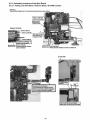
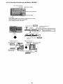
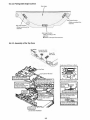
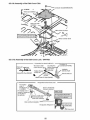
8 Wiring Connection Diagram
- - - Connection Cable
~
- - - Dirac! conl1'8C\ion Con nectars
C=::J Parts on Bottom Side
_ ConnectiOfl Cable
i!«1
PAD FFC
)<2
SW FFC
* 3
DRIVE-.fAAIN FPC
LC~ Cable
DC-IN Cable
~5
SpMkar Cable( L&.R)
..
*"
>.
>,
~,
*'0
*'1
:1/13
DFJK20T l068B
OFJK9022ZA
DFJS1 021ZB
DFJS1022YA
OFJS1 0Z32A
DFJS1024ZA
DFJS1025ZA
DL3UP1537AAA
OL3UP153BAAA
OFUP 1522YA
OL3UP1521AAA
MODEM Cabl e
LAN Cable
Antenna PCB Una R
Antenna PCB Un~ L
USB FPC
* 12 HOD FPC
CCD
DFJK12U112BB
Un~
OL3UPI585BBA
Bluetooth Antenna PCB Unit
Speaker(R)
Speaker(L)
,
1 - - __ - _ _ I
Ke)'tloard
Antenna
PCB Unit
Main Board
*.10
CN'
W ireless LAN
Module
Mic
Headphone
PowerSW W·lAN
Board
DNiOFF
LCD Open
,
Detection SW I
CF-BAW0512U
(PC2 ·4200)
Touch Pad
23
SW90Z
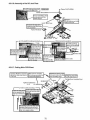
9 Disassembly instructions
9.1. Disassembly Flow Chart
. Main Unit
92
.. 1
Preparation
1. End t he Windows.
2. Turn off the Power, and then remove the AC Adaptor or Banery Pack.
3. Remove any optional DIMM Memory Cards or PCMCIA Cards.
4. Remove any other peripherals or Connected Devices.
•
9.2.2.
9.2.3.
+
9.2.4.
I
I
Top Case
l
9.2.5.
I I
~OUch Pad f LCD KnobJ
I
I
I
I
,+
~
IL), IR)
J
I
l
Speaker
~
9.2. 12.
Main Board
9.2.1 5.
Antenna Board
I I
Solenoid
9 .2.B.
9.2.".
+
I I
Bluetooth·USB PCB Unit
9.2.1 6.
Wireless LAN Module J
•
9.2.9.
9.2.6 .
9.2.10.
Drive U nit
•
9.2.7.
SUB DVD
9.2 .14.
I
HDD
Keyboard
l
I
FAN
J
9.2.1 3.
I
DC·I N Cable
+
MODEM
I
9.2.17.
I
+
Card Bus Ejector
I
J
Main replaceable parts
9.2.1.
• Display Unit
9.2.18.
I
•
LCD Unit I LCD Rear
9.2.21.
I
+
Hinge Cover (L), (R)
9.2.20.
I
I
LCD Unit
9.2.19.
I
9.2.2.
+
LCD Cable I Inverter Board
I
-Side Cover
·HDD
-HOD Cover
9.2.3.
9.2.4.
9.2.5.
I
-Battery Pack
-OIMM Cover
9.2.6.
I
9.2.7.
9.2.8.
-Keyboard
-Keyboard Side Cover (l), (R)
-Top Case
-Disk Side Cover
·SUB DVD
-Disk Eject Knob
-Touch Pad
·LCD Knob
-Pad Buttom
·PAD FFC
-Solenoid
-Disk Cover Angle
-Speake r
24
9.2.9.
·FAN
9.2. 10. -Drive Unit
9.2 .11. -M ain Board
-Lithium Sanery
9.2. 12. -Bluetooth-U 5B PCB Unit
9.2. 13. -DC-IN Ca ble
9.2. 14 . -Antenna Baard IL), IR)
9.2. 15. -Wireless LAN Module
9.2 .1 6. ·MODE M
9.2.17. -Card Bus Ej ector
9.2. 18. · LCD Unit
9.2 .1 9 . -Hinge COyer (L), (R)
9.2.20. -LCD Rear
· LCD Hook
9.2 .2 1. -Hinge (L), (R)
-LCD Cable
-I nverter Board
9.2.3. Removing the Keyboard
9.2. Disassembly Instructions
9.2.1. Preparation
Preparation : perform the section 9.2.1. first.
Attention :
Before disassembly, be sure to perform the
1. Remove the 7 screws (D).
Screw (0 ) : OXQT2+E12FNL (N9)
following steps.
2. Operate the LCD knob and open the LCD Unit to an
1. End the Windows.
2. Tum off the power and then remove the AC adaptor.
ang le of 90 degrees or more .
3. Slide the hooks (A) and then remove the banery
T he m inus clock driver removes hook (B-1 ) in the
i ntu~ion
Pack.
combination part so as not to damage fro m
the W-LA N connector side space to the exterior,
4. Remove the screw (A) and then remove the DIMM
rover.
and then rotates to the keyboard side, and KB side
(Remove if the DJMM memory is equipped with)
cover is detached .
3. Remove the keyboard hook plates,and then remove
Screw (A) : XSB2+4FNL (N 14)
the hook of back side of keyboard with screwdriver.
Lithium Ion Battery Pack
Hook (A)
Screw (D)
DIMM Cover
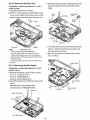
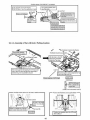
9.2.2. Removing the HDD
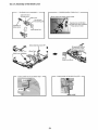
4 . Operate the LCD knob and open the LCD unit to an
Preparation : perform the section 9.2.1. first.
1. Remove the 2 screws (B) and 1 screw
angle of90 degrees or more.
(el.
The minus clock driver removes hook (B-1 ) in the
Screw (B) : OXQT2+D4FNL (N?)
hook position so as not to damage from the wireless
Screw (C) : OXQT2+E12FNL (N9)
LAN connector side space to the exterior, and then
2 . Lift up the HOD unit and remove FFC connector and
rota tes to the keyboard side, and KB side cover is
then remove the HOD unit.
removed.
Hook ( B-1 )
3. HOD is taken out of the HOD case .
HOD Cover
Ic)
Hook (B-2)
k.::::::":~l'!!~
1
KB Side Cover (R)
LCD Unit
~
Note:
Be careful not to wrap the protection cloth etc.
around minus clock driver's point, and be careful
not to damage the exterior.
Please do not bend pins of the HOD connector, at
the time of removing HOD and FFC connector.
25
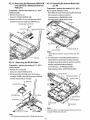
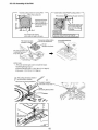
9.2.4. Removing the Top Case
5. KB side cover (L) is adjusted to the upper part as
Preparation: perform the section 9.2.1., 9.2.3.
well as KB side cover (R), the minus clock driver
first.
1. Remove the 2 screws (E) and 2 foot rubber backs.
removes hook (C-1) in the hook position from the
space with the bottom case, rotates to the keyboard side, and detaches.
Hook (C-1)
Screw (E) : XTB26+10GFN (N 12)
2. Remove the 5 screws (F).
Screw (F) : DXHMOOS7ZA (NS)
3. Remove the 2 screws (G).
KB Side Cover (L)
Screw (G) : DXHM0049ZA (N3)
Hook (C-2)
4. Remove the 1 screw (H) and 1 screw (I ).
Screw (H) : DXQT2+D4FNL (N7)
Screw (I ) : DXQT2+E 1OFN L (NB)
6. The both sides tape pasted to the keyboard bottom
with the spatula is inserted in order of the arrow and
then peel off. It is start-up from the LCD side and
turns inside out on the top case.
The KBD FPC WP sheet is peeld off, FFC (keyboard) is removed from connector (CN25) and
(CN24), and then remove the keyboard.
-
Screw (F)
Spatula
5. Operate the LCD knob and open the LCD Unit to an
angle of 90 degrees or more.
( j)
6. The hook 2 places of the disk side cover are removed, and detaches forward while rotating in the
direction of the upper surface.
damage the spatula ahead and move a lop case in the
ollhe arrow in <!>-al order.
7. The disk cover lock is mechanically released, and
the disk cover is opened .
KBD FPC WP Sheet -..2~
LCD
Both
Note:
KBD-FPC sheet cannot be recycled . Please use new
-"'_~ "M'<h'm;"'t Retease Lever
parts.
26
Disk Side Cover
8. The disk covershaft is removed and pulling o LII disk
10. CN26 (FAN) and CN15 (SP) are removed. A top
cover is removed from the disk cover.
case is lifted and FFC (PAD ), FFC (DRIVE) and
CN27 (solenoid ) are removed and then the top case
Disk Cover
is removed.
Top Case
FFC(PAD)
9. Remove the 8 screws (J) , 3 screws (K), 3 screws
(L), 4 screws (M) and 1 screw (N).
FFC(SW)
9.2.5. Removing the SUB DVD
Screw (J) : DXQT2+E6F NL (N10)
Preparation: perform the section 9.2.1., 9.2.3.
and 9.2.4. first.
Screw (K) : DRQT2+EBFKL (N2)
Screw (L): DXQT2+E10FNL(NB)
1. Peel off the tape.
Screw (M): DXQT2+F3FNL (N16)
2 . Remove the 2 screw (0) and then remove the SUB
Screw (N): DXHM0056ZA (N4)
DVD,
Screw (0) : DXHM0056ZA (N4)
Now:
Screw
Note it that the disc eject knob comes off at the same
time.
Screw IM)&~'w
II
Screw
Screw (0)
Screw 1M)."""
r---.\,,~•. ,IJ)
27
Top Case
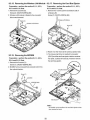
9.2.6. Removing the Touch Pad I LCD
Knob
9.2.7. Removing the Solenoid I Disc Cover
Lock
Preparation: perform the section 9.2.1., 9.2.3.
Prepa ration: perform the section 9.2.1., 9.2.3.
and 9.2.4. first.
and 9.2.4. first
1. The pad top ring fixed to the pad cover by the both
1. Remove the solenoi d line hold sheet and cable fixed
sides tape is removed, and remove the screw (P).
sheet.
Screw (P). DXHM0057ZA (N5)
Solenoid line hold sheet: DFHR3D20ZA (K1 22)
2. Remove the 1 screw (0) and the solenoid from the
top case.
Screw (Q). DXHM0056ZA (N4)
Pad Button
Touch Pad
P,d
Top Case
Top
SCI'ew
Tape
Top
Cable Fixed Sh,'''-~~
2. Peel off the pad sheet.
Note :
The LCD knob is lifted from a top case, and remov·
The each cable fixed tapes cannot be recycled.
Please use new parts.
ing LCD knob is removed from the knob side in the
3. Remove the d isc cover lock spring, and slide the
LCD latch spring
d isc cover lock and then remove .
Disk. Cover Lock Spring
Pad WPSheel
LCD Knob
Top case
Note:
Note:
When expanding or transforming, the disk. cover knob
spring cannot be recycled.
T he pad sheet cannot be recycled. Please lJse
new parts
28
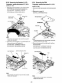
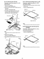
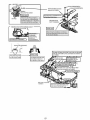
9.2.8. Removing the Speaker (L), (R)
9.2.9. Removing the FAN
Preparation: perform the section 9.2.1. , 9.2.3.
and 9.2.4. first.
1. Peel off the 5 fi ne hold sheet 1, the 4 brims of the
DVD PWB sheet, and remove the speaker (L)
Li ne hold sheet 1 : DFHR3D21YA (K1 23)
DV D PWB s heet : DFMX1229ZA (KI 61)
Speaker Cable
(Bla ck, Blue)
Preparation: perform the section 9.2.1., 9.2.3.
and 9.2.4. first.
1. Remove the KB heat spreader and the heat spreader.
2. Remove the 1 screw (R)
Screw (R ) : DXHM0057ZA (N5)
Speaker Ring
Line Hold
Heat Spreader
Note:
These sheet and speaker ring cannot be recycled .
Please use new parts .
Note:
KB heat spreader and the heat spreader cannot be
recycled . Please use new parts.
2 . Peel off the 2 tine hold sheet 1, line hol d s heet 2 the
1 ta pe, and remove the Speaker (L).
3 . Remove the tape and line hold sheet 2 and then
Li ne hold sheet 1 : DFHR3D21YA (KI 23)
remove the FA N.
Line hol d sheet 1: DFHR3D21YA(K 123)
Line hold sheet 2 : DFHR3D22ZA (K124 )
Line hold sheet 2 : DFHR3D22ZA (K124 )
Line Hold St1eel2
Una Hold Sheet 2
Tapa
Note:
These sheets and speaker ring cannot be recycled.
Please use new parts .
Note:
These sheets and t ape cannot be recycled .
Please use new parts.
29
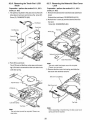
9.2.10. Removing the Drive Unit
3. Disconnectthe LC D connector (C N9) (eN 10), [x>IN
connector (CN601) and FFC (C N4 ) (CN6) (CN1 8)
Preparation: perform the section 9.2.1. , 9.2.3.
(CN8).
and 9.2.4. first.
1. Peel off the tape from the connector.
2. DVD FFC is removed from connector (C NS01), and
DC-IN
I
the drive unit is lifted from the bottom case, and the
Holder
gasket is peeled off and then remove the drive unit.
4 . Tum inside out the main board. Remove the ante nna
Note:
cable (L ), (R) from the wireless LAN modu le, and
DRIVE-MAIN FFC
then remove the main board.
-When you exchange DR IVE-MAIN FFC,
mark the bottom case. and match new FF C to
marking of the bottom case, bend, and bui ld the
bend externals of FFC before peeling off FFC from
the bottom case .
•Tape and gusket cannot be recycled. Please use
new parts.
5 . Remove the connector from C N3 and then remove
the coin battery.
Anl8l1na Cable
IL)
9.2.1 1. Removing the Main Board
Preparation: perform the section 9.2.1. , 9.2.3.
and 9.2.4. first.
1. Remove the 2 screws (S), 2 screws (T)and 1 screw (U).
Screw (S) : KIYE5000022 (N15)
Screw (T) • DFHE5035ZB (N1)
Screw (U) • DXQT2+E6FNL (N10)
2. Peel off the 6 tapes, main PWB sheet and line hold
s heet 3.
Main PWB sheet : DFMX1 228ZA (K64)
Line hold sheet 3 : DFHR3D59YA (K47)
So ..,
Coin Batiery
(U)
Main PWB Sheet
Line Hold Sheet 3
30
IR)
9.2.12. Removing the Bluetooth-USB PCB
Unit (with BT) I Bluetooth Antenna
PCB Unit
9.2.14. Removing the Antenna Board Unit
(L). (R)
Preparation: perform the section 9.2.1., 9.2.3.,
9.2.4.,9.2.10. and 9.2.11. first.
Preparation: perform the section 9.2.1. , 9,2.3.
and 9.2.4. first.
1. Peei off the line hold sheet and drive EMI sheet and
1. Remove the screw (V) .
then remove the antenna board (R) .
Screw (V) : DXQT2+D2SFNL (N6)
Line hold sheet: DFHR3D80ZA (K52)
2 . Remove the USB FPC from the tape and CN91 0,
Drive EMI sheet : DFHE1 003ZA (K38)
and then reroove the bluetooth-USB PCB unit.
BI",,,,,,1h
'Inl',"". PI" Unit
Screw (V)
~",,'oo,Ih·LJSB
PCB Unit
line Hold Sheet
Note:
T hese sheet cannot be recycled. Please use new
parts.
2 . Line hold sheet 1 and heat spreader bottom are
USB FPC
peeled off from main Board's wireless LAN side,
and takes the antenna cable (L ) o ut from the ditch
9.2.13 . Removing the DC-IN Cable
and then remove the antenna board (L ).
Preparation : perform the section 9.2.1 ., 9.2.3.
Line hold sheet 1 : DFHR3D21ZB (K43)
and 9.2.4. first.
1. Remove the 1 screw (W) .
Heat spreader bottom : DFMY3222ZA (K69)
Screw (W): DXQT2+E6FNL (N1 0)
2 . DC-IN jack plate, DC MDM cover, DC-IN cable
Heat Spreader Bottom
connector (C N601), and FAN sheet are peeled off,
Antenna Cable
(l )
and then remove the DC-IN cable .
DC J,d, PI,"'._......
DC
Cover
DC-IN Cable
FAN Sheet
_---::;;,r
Line Hold Sheet 1
Antenna Board
(R)
Note:
Line hold sheet 1 and heat spreader bottom cannot be
recycled. P lease use new parts .
Note:
FAN sheet cannot be recycled. Please use new parts.
31
9.2.15. Removing the Wireless LAN Module 9.2.17. Removing the Card Bus Ejector
Preparation : perform the section 9.2.1., 9.2.3.,
Preparation: perform the section 9.2.1., 9.2.3.,
9.2.4. and 9.2.11 . first .
9.2.4. and 9.2.11 . first .
1. Remove the 2 scre'WS (X).
1. Remove the 1 screw (Z) from connectio n side of
wireless LAN
Screw (Z) : DXQT2+D2SFNL (N6)
Screw (X) : DXQT2+D2SFNL(N6)
2. Wireless LAN module is floated in the connector
fulcrum and removed .
WI'",,, LAN Module
Wireless LAN Module
2. Return it on the revers to the card bus ejector side .
3. The minus small driver is inserted in connector
9.2.16. Removing the MODEM
(CN 13) and the card bus ejector intuition combina-
Preparation : perform the section 9.2.1., 9.2.3.,
9.2.4. a nd 9.2.11 . first.
1. Remove the 2 screws (Y) .
Screw (V) : DXQT2+D2SFNL (N6)
tion pa rts, 2 places of hooks (E). And then remove
the card bus ejector.
2. MODEM will be removed from connector (eN 17) to
the vertical direction.
(V)
Main
Note :
Be careful not to transform the card bus ejector when
you remove the hook .
32
9.2.18. Removing the LCD Unit
9.2.19. Removing the Hinge Cover (L), (R)
Preparation: perform the section 9.2.1. , 9.2.3.
and 9.2.4. first.
Preparation: perform the section 9.2.1., 9.2.3.,
9.2.4. and 9.2.18. first.
1. Remove the 2 scre'NS (el and then remove the hinge
Cover (L). (R) .
Screw (c): DRHM0076ZA (N17)
1. Remove the 1 screw (a).
Screw (a) : DXQT2+E6FNL (N 10)
2. Remove the DC-IN jack plate , DC MOM cover and
FA N sheet.
Screw (el
FA N sheet: DFMY0428ZA (K65)
LCD Unit
3. Peel off the main PWB sheet and remove the
connector (e Ng), (CN10) of the main board.
Main PWB sheet : DFMX1228ZA (K64)
S~w (,)
DC Jack Plale -
.....
II/I
Screw (el
DC MOM Cover
H inge Cover (R)
Note:
Screw (c) cannot be recycled. Please use new parts_
9.2.20. Removing the LCD Unit and the
LCD Rear
Preparation: perform the section 9.2.1., 9.2.3.,
9.2.4.,9.2.18. and 9.2.19. first.
1. Remove the 2 screws (d).
Note:
Screw (d) : DRHM0076ZA (N17)
These sheet cannot be recycled. Please use new
parts.
4. Remove the 2 screws (b ).
Screw (b ) : DXYN26+J6FNM (N11)
5. Peel off the EMl sheet 3 and then remove the LCD
unit.
LCD Unit
Screw (b)
(b)
Note:
Screw (d) cannot be recycled. Please use new parts.
33
9.2.21. Removing the LCD Cable I Inverter
Board
2. The intuition combination part of LCD rear case (21
places) is separated with LCD front case.
••
~ ~
...
Hook position
@
f
Preparation: perform the section 9.2.1., 9.2.3.,
9.2.4.,9.2.18. and 9.2.20. first.
.
(j)
1 . Peel of the damper, conductive cloth, inverter tape
and the tape .
Inverter tape : DFHR3E07ZA (K18)
2. Remove the hinge (L), (R).
3 , LCD Ccable is removed from LCD unit ooard
(CN1 01), and connedor (CN1) is removed from
inverter board.
,?",de,,',', Cloth
Damper
LCD Unit
01
Note:
-When each hook is removed. it be comes easy to
detach if the driver who wraps protection cloth etc. is
inserted with LCD Front Case between LCD rear
covers. and the slide is repeated
-Do noting that externals are not damaged.
3. Remove the 1 screw (e) from LCD rear and then
Damper
remove the LCD hook.
Screw Ie): DXQT2+D25FNL IN6)
Hinge (L)
Note:
Conductive cloth and tapes cannot be recycled.
Please use new parts.
4 , I nverter case is peeled off and Inverter fixed with a
both sided tape is taken out.
5. Peel off the tape from inverter.
6 , Remove the connedor (CN2) and then remove the
inverter.
Note:
Tape and inverter case cannot be recycled . Please
use new parts .
34
9.3. Reassenbly instructions
9.3.1. Attention when CF-Y5L series is repaired
- Please execute writing BIOS ID when you exchange the main board .
- Parts (sheet and rubber) etc. related various the conductive cloth and heat spreader cannot be recyded. Use
new parts.
9.3.2. Assembly knowhow of the LCD
9.3.2.1. Assembly of the LCD Front
LCD Rubber
lCD Rubber
*r--- f----.
Narrow
LCD Front
LCD Rubber
Affixes in the standard on the left
Be parallcl aller putting
(Attention)
LCD Front is installed in Ihe receiving stand, and worlls.
Safely Work I-The LCD rubber and LCD BATT Rubber doos not out ollhe concave part , moreover, not run aground.
-It is noled Ihal the linger does not touch the paste side when Ihe LCD Rubbcrand LCD BATT Rubber are alHxed .
r;:::;::::-;;:;::;:, -The
I
9.3.2.2. Putting LCD Side Cushion I LCD Tape 1
0-2mm
0-l mm I
II
0-1m~
~
There must nol be
. . floatage
,JJ
~ Floatage NG
There must
nolbe fIoalage
(Influences and eXist In the hook
intu~ i on combination when floating)
I
V
LCD Side Cushion 1
There must not be beginning to
see from the frame on the inside
LCD Tape 1
Hook contral
standard
O±2rM1
Hook
Wall root application pulling
From wall rool
0-lmm
From the frame on the inside
O.5-1 .5mm
Edge standard of
wall of length O±2mm
35
Hook central
standard
O±2mm
hook
LCD Tape 1
9.3.2.3. Putting LCD Side Rubber I LCD Side Damper
(lCO handling attontioo)
-Do not take 001100 vicinity of lhe centCf of the lamp side having when you take 001 LCD of the packing box.
(Because Ihcf'o is a possibility thai the transformation of the lamp relledor elc. occ....)
-Take out right and len both ends of the lamp side having when you lake out LCD.
Affb!os it bctwoon
the lenglh walls.
(Thoro must nol
be ovcrlJow)
LCD Protccl Plat
Attention,There
is di'edionally
lCO Tape C
Affixes
~
between the
length walls. (There
must not be OIIerflow)
Rib
Rib standard
O±1mm
too length wals.
Afrll(OS it between
the length walls.
(There must nol
be ovErllow)
{ThlJ"c must not be
"""""'I
AffllICS it between
the length walls.
(There must nol
be overflow)
The flaking off paper is
"" by 'h' ,~ ...~."i09
Atrl.l(os it belwccn the
length walls. (There
m""'~~~mer
Arnxationh
Sleps part corner
standard O±lmm
*
from externals O-I mm
There must not bc
ovcrllow from oxternals
Conductivo Cloth
externals standard from extemals O- I mm
O± l rrvn
J:iThere must not be
overflo,v Irern externals
36
9.3.2.4. Putting LCD Magnet
(Attemion)
-Tha LCD Front is installad in tha r8Caiving stand, and works.
Reier to A chart.
When inserting in the
.""Il!>,}<---,.
The both sk:les tape flaking off paper is peeled off,
and affixes to Front
"
Fr ont case , it is noted
Magnet is
h 'li ..dto the dotted
Is"",
w::~ &~D
Fit to insk:le surface.
The both sides tape flaking
off paper is peeled off, and
affixes \0 Front Case
Tho both sides tape flaking off paper is peeJod
off, and affixes to Front
Case
Pressurize rt from the From Casa side (painting side) when you
pressurize a two sided tape
magnet
Oivision attention for XGA
(There is mar king)
9.3.2.5. Putting LCD Cushion I Assembly of the Inverter
(AllentPon)
-The LCD Front is installed in the receiving stand, and works.
0-3mm
LCD Cushions
LCD C",h,", 3
ThQ"e is no space.
LCD
Paste side
.+.0/:
LCD
<AIlixation OK frgure>
LCD Cushions
There is a
Paste sl:le
space.
LCD
<AIlixation NG figure>
ConnectIOn...........
g~1
P£TTape;
ISafety Work I<Affl.>:atlon standard of PET Tape>
Standard of match affixation
of connector externa~
(O± lmm)
37
. __
I
ISafety Work Affixes in a connector
externals putting 10PET
gether.(wrapping)
<Prepara tion for Inverter C",,' __...,
"'1verter tape affillatic..'1 without
tmnsformin g.(Room is given)
i
i
both sides tape extern als
match
."
The tape is puled too much and
l CO Front Case is transform ed .
So as not to transform LCD Front
case, affixes.(Re fer to a left chart)
Th e both si des tape fla king off
paper of the Inverter Ca se bottom (3piec es) is peeled off and
affixes to th e frame.
lIE Th e externals pa rt
of Inverter Case is
set to the above-mentioned line
9.3.2.6. Putting Tape for LCD Cable
[Sa fely Work
I
PIOceSseS str aight from
begin 10 draw out
Affixes in a connectOl"
Th e line is
to th e
38
9.3.2.7. Assembly of the Hinge (L), (R)
(Attention)
-The LCD Front Is Installed In the receMng stand, and works.
l Saf!tywo~ 1
Surely af6x81 to the Hinge.
II
""' ... CIoCh
SUrely affixes to the IlI1Iector part
I~~~~;:~~_+Renector
Rib
O±1mm extemals standard
,
"I"""""7.w7""
o~
7"11
The hinge Is 8 11'11nged under the cable.
9.3.2.8. Putting LCD Rear Cushion I LCD Side Cushion
<:AIIIdIon d Ull SIda QlINon 1:.
3±lnvn
3±1mm
b- ' t t - -b
-~-
From the dlf-
_pM
From the dlffer-
.--li": .
""'" part
I>'!mm
0-2mm
<SectIon b-tI figure>
The remainder II 8~
the side
<Section IHl figure>
The remainder Is affixed to
1Salely Wo~ 1
Slde CUIIion 1
cable does not overflow
the frame externals
the81~
LCD
Side CUshion 1
LCD
Plinth externals
Plinth flxtomals
match O±1 mm
-
ma'"
From the hme
"'....mm
the "'"
LCD Rear Cushion 1
Ecige standard of wall of length
LCD Rear CUshion 2
O±lmm
~:~t~~~~~~::;~:~dO
~
be In
Cushion.
Do not atsp on the cable with
the cuahlon.
39
9.3.2.9. Assembly of the LCD Rear I LCD Front
<A-A. Cross section>
A
The convex top
t'·65mmorless
The convex top
The order of engagement of hook:
A
a~ h.c~d
."ow (DX'QT'2!D25FNl)
Afnxes In" ~:~::~
"'' ' ' ' -
up by one step
"
'
D
are inlMlrted
, - - - - - <Afr.xalion of LCD Rear Tape 3>
I
LCD Rear
Tape 3
Affixes touching
)
i
' j -LCD Rear
the bottom comer
I
ru
Tape 3
9.3.2.10. Assembly of the Hinge Cover (L), (R)
<Att8l'llion>
The tightening order : a ~ b
-Conclude afIer confirming there Is a machine screw hole.
~The thing that the machine screw Is not concluded Imper19ct Is c0nfirmed. (Generated by DVT a diagonal conclusion)
Tighten the back pushing al the lime
oftlght8l'llng.
(cover space generation prevention)
tig,..,"',;,.,g'oa.ck pushing at the time
(cover space generation prevention)
<Attention>
·The Screw (DRHMO076ZA) cannot use the fixed lock medicine repeatedly for use.
·Exchange for the new article when tightening again.
40
9.3.3. Assembly knowhow of the Main Board
9.3.3.1. Putting Line Hold Sheet I Antenna Sheet I BT PWB Cushion
(Attention)
~ecute after setting board in the receiving treatment device when worldng.
Ptlrts on cabMI and
board are insulated.
Isstetywort; 1
Antenna Sheat
wnIess LAN Module
Antenna Cable (R)
I
Antenna Cable (L)
Processes between Wireless
LAN and MODEM
"i!f!li~iEi LAN Hold Sheet
Affixes between Wireless LAN eN and DIMM eN
I!:
BT ANTPW'B
Connector lock confirmation
.The connector lock must be ensured.
-FPC must not been InsertBd diagonally.
-FPC must been Insetted In peralel.
41
9.3.3.2. Putting MCH Sheet I Heat Spreader Bottom
Running
,g'~m,ldo
not be on DAI
The flaking off paper in which "5011"
is displayed is peeled off and then
affixes to MCH.
MCH externals
standard 0±1mm
I Safety wor k l
Processes along the
connector
""-.-[""MM
Coil externals standard.
Th ilg in which afftxation
does not exist in coil.
standard
Coil externals standard
Line Hold Sheet
I safetY WOfk l
Lire Hold Sheet 1
Afftxes il a Sheet externals standard,
and fixes Antenna Cable.
Bottom side Heat Sheet
preparation specification
Atftxation as touch the Coil
Space 0-1mm
the capacMOf
Cable ftxes by Line Hold
Sheet 1 by processing on the Heat
Spreader Bottom Sheet.
Affixes i" Cii"-"'1' i
Affixabon as fit tOO
CPU Cushion
Space 0-O.5rnm
Touch the DIMM Connector
Atftxation space 0-1 mm
"'o"mo, Cable is dra'M1 out here
CPU Thrmal Sheet is
a thing tothe
capacitor without
running aground
standard 0±1mm
It is confirmed that CPU Thrmal
Sheet does not run aground tothe
capacitor
42
Sheet side
Heat Spreader Bottom
(G-751)
Spreads by using the treatment
device.
9.3.3.3. Assembly of the WLAN Sheet I MCH Thermal Tape
Sheet
Makes like the incision
The Sheet center is lightly suppressed by lhe finger
part difference alHn roll
A two sided tape is peeled
off and affixes
BOX Sheet metal externals su~ing
(The line part of the above figure is matChed)
.----;::::~7i
Processes from rue side to the right under
(Process In paralic I to board)
MCH Thrmal Tape
Makes like the incisKln
part difference all-in roi
The Sheet center is lightly
suppressed by the finger.
Does not go out of
externals of Heat
Spreader Bottom when
suppressing _
__ _ __ The corner part is matched on
the extension line of the
-
d,mpoe '''''m''C::)
9.3.3.4. Assembly of the Main Board
ISa fety Work I
DC-IN Cable
HOD FPC
PET Tape (10mmx2Smm)
0-2mm
'Does not overlap
in the Slit.
Connection
PCMC IASheel
<FIG1>
Puts according to the s4 lk frame.
The inclination is w ithin O.Smm.
(Attention)
-The board is set in the receiving treatment device and works.
-The connector lock work after FPC is inserted l/SCS the treatment device.
43
E.temals matdl of Ie
0-1mm
Externals matd! cA
eonnector
Q·1 mm
:---Tape
9.3.3.5. Assembly of the Card Bus Ejector
PFT T'""o ( 19mmX25mm)
Connector
PET Tape (1OmmX25mm)
Connector cen tm.1standard
000""'"
The lever ",,~~~: t o the
left before I-
<Explanation 1).
Th e sheet metal ben d part at Connector Is
Inserted il the comer hole part
(An opposite direction Is also the same)
Multip~ hook surely (Th ere must no! be floatage)
44
9.3.3.6. Assembly of the Wireless LAN Module I MODEM
<W-.t.A N Module preparation>
Connection
Antenna Board (MAIN)
~
to board's Just beside.
-Work In midair prohibition Yotien module Is connected w.h antenna board.
-Connects app~lng th e board to the receiving stand.
(FOI' the distortion prevention of the board)
From tne tUlle edge Isafety
2-5mm
Th e ~Im Is
.0.
•
<M ODEM prepa ration 2>
atrlXed~~~~~::
Theanremainder
on
oppo$ll e Is
skle
ISafely wor k!
~
l~s~.~r,~,y~w;a~k!1 ~~~
Ts
Cable
to th e board side
work !
34-36
r
The posI~on Is declOed >Min B
tre atme nt deVice.
Put out the position wlh the tube
drawn 10 the Jack side
M OOEM Cable
c:PrO
-, (;5' J r"'O
The PET lape (19mmx25mm) ' Safety war1\:
Is wrapped
<M ODEM preparation 3>
Board eX1ern als
EMI Sheer s fer MOe
O:t::o.S
.'
Fk
hole 10
ConciJ dive Cloth's hole.
' Safely work!
45
I
9.3.3.7. Insert the Main Board
(Attention)
-The board is set in the receiving treatment device and works.
-When carrying to the following process, a special pa~tte is used.
(The FPC bend in VB respect is prohibited)
ISafety Woril I
Pressur izes wijh the battery the l inger is
put in the PC MCtA slot.
Alter the pin by which the
position is decided is inserted, a
fixed screw is tightened.
After the screw is tightened, the
i is detached.
ISalety Work I
Coin Batter y Affixes to Ihe sheet. .Ooes not get on the board.
Screw
(OXQT2+D2SFNL)
of'
Memor y Spreader
Va lley
Bend with
0.5 or more
(Use the treatment device)
II i
MODEM LAN Holder
the cable should not cross.
9.3.3.8. Note of Wireless LAN module is inserted
<Notes when Wireless LAN Module is inserted>
Please do Board 's insertion and extraction correctly according to the direction and the procedure shown in the figure below
<D Please go lrom parallel respect to mounting Board in Board's insertion and extraction within the range 015--10"
(2) Please insert in the inter ior completely when you insert Board.
46
9.3.4. Assembly knowhow of the Top Case
9.3.4.1. Assembly of the Disk Cover
0-1 mm from length '1!.f:~ from oorrvex base
The ditch is Inserted In tha rib
:-7"'''-0
9
Disk COWl( Spacer 2
(square)
Disk Caver Spacer 1
(rectangle)
<0
Length wall baseapplicalim affixa.
-= ,'"
So as not to ganerale the
space,afl'b:es
length waJ baM application afftxatlon
The differ9nce part
can run aground
Disk Cover Cushion
Disk Cover Cushion (Small)
SUM
DXQT2+025FNl
~liii8iii" ,,,.
""i'",_,
pi,
PAlMREST SHEET
Atfixes it 10 the ooncaYe
part of the Disk Cover
not tDuch the paste
side when amxing.
(For lne garbage sdne~
slon and paste strength
Down prevention)
-There must nol be beginning to see from the
concave part. (thing
without nmning
&groond)
-'There must not be bub-bte generation.
ISa,,,, wo"' I
All the ftElking off
paper is peeled off
after half the level
peel positioning
Is affixed and afflxes.
Disk Cover
47
9.3.4.2. Putting Disk Angl e Cushion
Disk Angle
Disk Angle Cushion
Affixes according 10 tle
ruled line.
Affixes according 10 \he
ruled line.
Disk Angle CushiOn
Affixes according 10 tle
ruled line.
Affixes allhe righ t of the ruled line.
*
9.4.3.3. Assembly of the Top Case
W-LAN ON IOFF
SW Knob Sheet
,../
~
~
Power SW
knob Sheet
<Posil:(ll1 II.hem LED ClNtalIS A1J::ce¢>
LED Cushion Affixation
<Posiion whete LEO LENS PAD is i'l$talIed>
Lan Sw Blank
Installa~on
48
<Position where LED LENZ BATT is instaHed>
(outside) weld·
LED Lenz Batt · from cabi respect.
LAN SW Blank : from the application rib side.
q,1.7±O.2
There is no floatage .
1'-
2 places on the insfde are
the reserves for the second
fixation .
9.4.3.4. Assembly of the LCD Knob I Putting Cushion
-
........... Pad Bu tton Cushion (R) affixation
Pad Button Cushion (L) '~"'I;o"
I
• • •~ After the hook in the LCD
Latch Spring is hooked,
The hook is put from the upper part on the top case
hole in the LCD Lalch Spring When expanding or
transforming. it is not possible 10 recyc~
LCD Knob
rn~~~;;p,;'r~t ;'~m~'=d~'~I;O~'",lPi~;~"~ID~~;;'~P1
under (right and left)
/
ISafe ty work I
IDivision attention of LCD Knob l
<OO75YA.Q>
0075YA-OGoods
This outside (R) is
expanded.
(Inside R and a concentric circle R)
. -_ _ <Position where cushion for LCD knob is aflixed> _ _ _,
(Position where Pad Button cushion (l), (R) is afli~ed>
0-0.3
0-0.3
\~\ \ ~
, )~
)}Ji!'
M
0
0
(L)
Affixes in a central aim of the top
CBse rib and folds to the rib sida
'1
--
'rop Case Rib
I A-A SEC I
,
(R)
=
Confirms tha operation abou t tha LCD knob
after building in
49
9.3.4.5. Assembly of the Touch Pad
Affixes Pad Cover Tape
It slicks it according
\0 U mnve:>: part
Release coated paper
"NITTO NoSOOO"
I
Print side
IDivision atlention of Pad coverl
Safety work
I
~
Thing thai doesn't
begin to be seon
from window of
Pad Cover
ZA-O == It is aboullhe hemicycl e_
YA-O == There is no homicycle.
--
Pad Cover
<preparation for PAD>
after PAD is
ressurized
1\ sticks it
according \0
U convex part
Release coa ted paper
"NITTO No5000"
Prinl side
<FIG2>
Thing thai docsn'
Affixes
begin to be seen
in t he
Pad Cover Tape
from window of
Pad Cover
Touch
<Preparation for PAD-2>
Pad Cover
lie mg part extcm a s
and externa ls match of
Pa d Case of sticki ng PAD
thai has been prepared.
F IG2>
1. PAD is installed on the treatment
Pad WP Sheet
VI
81ld it installs it between positioning
the installation three places.
2. The yellowish brown flaking off paper side
of Pad WS Sheet is peeled off and
the positioning hole of a transparent
mount is inserted in the pin of the
treatment device.
o
3. The sticki ng part of PAD and WP Sheet is
pressurized.
<FIG: IPreparation for PAD-!:>
50
Insertion '"'"~:'''
I
Safety work
I
Pad WP Sheet affixation
of a peel of yellowish brown
Sheet flaking off paper and a
mount is inserted in the pin
device and
Reinforcement board side
Touch Pad ,ff,,,tim, _....:~
with the
I
Safely w ork
I
"
the sticking
Sheet like
~::~;;~~::::-=~~'~~'~~;i~~~~~~::::::~
Installs in the receivin g
stand of the pressulizing
treatment device.
<Preparati on fo r PAO-2>
concave
I
Safely w ork
I
The top part side
affixation in flaking
off paper of
transparency peel .
I
Safety work
I
.....
Peel off PAD and PAD WP Sheet and assemble again in the
procedure of the standard book when yo u remove PAD COVER
by the repair elc.
(For steady adhesive power of PAD COVER and PAD).
51
<Pad Cover installation position>
, - - - <Gasket (PAD) installation posi tion>
Thing in which space does not exist between convex
happened the top part sKle and Pad Cover O\.Jlside diameter
Top Case
(
o
NG
OK
Pad Cover
The side is
hung
Alrixes with the arrow direction touch to lhe convex
happened top part side
(Space measures with PAD SUTTON)
Touch Pad
.-
Afterthe iURalll1ion, Pad Button iG COrI-Space confinnation wtiI Ct:Ner
-HirQlng
-ThIng wtthout
In Ihe arrow dIrection
matching the
JII::;~'! the hole
after the con-
"••,10'
•
<Tape Installation posItJon tor Pad
I I
Rhg~"~OP>§~~~~
<Pad Botton's installation position>
Th
11'19 that hook
on externals
~~~
~~nrernaJ'k&.
~Cori", lti8tiond1f1eSpac8 betwBen bUt-
ton and cover between 1I'oe5eof Pad
Button aller Instalstlon.O.2 or less
{>:-)' ~
_ .
.[ . s
~
,"\,
,
I
I,
52
9.3.4.6. Putting Sheet
• Puts within the range in the concave
)::;;~;~=-
__
happened top part.
(It is confirmed thai thero is no!
running aground. )
Puts by the standard on the left.
• Do not touch the paste side
(garbage adhesion and down of
Affixes Palmresl Sheet (L)
paste strength prevention)
" Thing without bubble generation
• Thing wilhoullattice eyes transparont
of paste confirmation
• From 0.5 or less to inclination 0.2 or
less to concave bottom case part and
seat e xternals space difference
Affixes KBD fixation tape
All are peeled off after pulling
of the level peel positioning
the half and the flaking all
paper is
< disk cover seat putting position>
<
< disk ang le cushion
putlin,:g~po:'~;t~;o~'~>;":;::===;-l
< disk shaft fixation seat putting pos~io n >
0-1 .0
Direction of
~nglh
hand of disk angle cushion
53
KBD fixation tape putting positioo >
9.3.4.7. Assembly of the Break lever
.. The Brake lever is asscmblOO ,.
sets in 1M rib 01
the brnke lever.
~
Installation in
, - - - - .. irtstalation position 01 brnke lever" ---~
o has respecl with shape up and installs.
Brako lever
Do nollOllcl"1
Itm ba"tding sidc.
installatioo
"Tl1 ir1g without Hi debt
"It'/''V~
""" ""', jJ
AlliJ(CS Brake Pad
~
Affixcs Disk
L
.d, C""" .,P
~b , ...'''"~, ",W',',
.. Pul\i"lg posi\ior1
.. pulling position 01 wire rod fixalon tape "
54
ot Ois!<. Side Cover Wp,.
9.3.4.8. Assembly olthe FAN
< Cushion putting pos~ion for cooling FAN >
0-0.3
< Cable fixat ion seal (FAN/SP) putting position >
Affixes Fan Cushion X3
Flaking off paper ruled line
Pressurlze the frame
this range or
Ile ~hershutl lecock in
w~hin
the ope ning rlor the
rotation axis.
It is a peel putting of
the half of the fl akillg
off paper.
t
It is a thing in the opening
whic h does not begin to be see r!.
Screw(OXHMOO57ZA)
Conclusion
..
* Work notes
1. FAN must not be dropped, and do oot add the impact.
< seWER lightening locque >
Conclusion first lime powe r : O.16-0. 18N.m {1 .6-1 .Bkgf.cm)
At the repair ' 0.1O-O.12N.m {1 .0-1.2kgf.cm)
......... After putting, the backup sheela!
;:: the disk sprirlg is installed.
ff
~
C
Oisk Cove r Arm Sprillg in~ta " atA The po int is illserted
W;n of atop '''''' '',
the hole
AffIXes
Disk Spring Backup Sheet
\
55
9.3.4.9. Assembly of the Disk Cover Click
~ Conclu sion Screw(DXHM0057ZA)
~ ,,"',,,, "'"''''m Sheel
/
,
o
9.3.4.1 0. Assembly olthe Disk Cover Lock I SW PCB
< pr epa ralioo for solen oid wilh lead>
The same 10 width
Flaking
paper,
The half of the
Conclusion of
Screw(DXQT2+F2FNL)
ott 1~
_~
J
Solenoid Fix Tape (FAN/SP)
Instalation
Solenoid Ang le
Flaking off paper
leaving side
Solenoid wilh lead
< Preparalloo for Disk Cover Loci( >
Th e insertion
order: 2
The fin gern aK
is muftiplied.
I
Th e inserti oo order : 1
Insert s In R shape pari
and Ihe slide in
Ihe righl side.
Disk Lock Bu sh installation
Safety work
~===:::::::::::::---H a n g~g
lee of fln gern all '"
56
I
<SWPCB>
O-D.'
- -----1---
Screw (DXHMOO56ZA)
SW PCB w hlcfl has b een
prepared Is Inslalled.
Di sk L ever Fix Cushion
WI1en the SW PCB poslUonlng
Is nol u sed, the cab! posUlonng
treatment device pn on becomes
the cen ter of this hole and fixes.
<Disk Eject Knob ASSY2 ilsIalla tion position> - - - - ,
~;:--'\
Disk Eject Knob
ASSY in stallation.
I
S afety work
I
Is conclud ed, con cludas
Konb Assy Is drawn
'1;;;;Si!~ Confirma1ion
-
IOp erativeness confirmati on
Convex having
=90 09ZA'()
The pari of R typa of th e Disk Cover lock and Ihe pa rt
of the pi"! of t ha Disk Cover l oc k holder are malcfled
and in stalls
The IIngernaU Is h eld w ith
the treatment device in
the direc tion of the arrow.
Disk Cowr lock HoId~
installation
57
9.3.4.11. Assembly of the Solenoid
"01
Solenoid
affi)(aUon
"""
Sp",'''·''
<Spacer affixation
position:>
.~
r- O±O.S
/~.X.~
Iyl
T
<Line Hold Sheet 8
I
~~
,<,
PdSWShtffi!"
ee a I)(a 1011
posaion:>
AffIXes in boss's ou tside di·
ameter appliCation and Top
Castl"s COfner hole is concealed
I ~ \ ,.. i~
,; -1
S uare hole
~e
Boss bese
• Work notes
< SCWER tightening torque :>
Conclusion first time power: 0.16·0.18N · m{ 1.6·1.8kgf · cm)
At the repair: 0.1 O-O. 12N · m{ 1.0-1.2kgf ' cm )
9.3.4.12. Assembly of the Speaker
<Preparation for speaker>
Cable drawing olii side
J
been prepared is installed
/ ' S,,,,k,, Ring affixation
Soldering temperature
: 300-350 degrees
The speaker which has
been prepared is installed
Speaker insta~ation poslion·Red >
Cable d rawing
..-W~
out side
Speaker Ring affixation
/
< Speaker installation position-Blue >
u
58
9.3.4.13. Wiring Speaker Cab le
<Processing of SPIFAN cable> - - - - - ,
ftxeswtth '!he taps
''''''''''''''
ilia Fan aide
SPIFAN Cable to
-;'"~
,
Proc:esses left b'ward by the standard or the w;.
side diameter cAttle ci'awl1'IIJ out boss n the Fan
side drawing
'i
o
off paper of lite
Is confirmed.
line Hold Sheet 1
,,.,.1Ion
SP Cable
<OVD PWB Sheet projaction part atnxation position>
Along dTop Case's Ii) side
root and bas in OVO PWB
intheSP
Sheet's projection part
,
N
o
The dlaplay "NmO Na.5000 NS" d
the ftaklng olf paper Of line Hold Sheet 1
is confinned.
59
'" Safety work ~
The tapa Is along
- top cue aide and
the cable IiRI affixed.
9.3.4.14. Putting Cushion I Tape I Sheet
<KBD Backup Sh8llt affixaiun position>
Case 10 close Ihis hole and affixes
I
o
I
] 0 [l nil s;,.
---J'
,
0-1,
r---
JI '--'
'-'~
WP C"h;"
The right and left is
between ribs
III
•
<Fronl WP CU5hion affb:;alion position> - - - . ,
= "I
_0
o
SA<
I
Fl at side ridge
line
60
KBD Hook WP Sheet
o
0-'
9.3.4.15. Assembly olthe SW PCB FFC
...
machine screw
;:~~:~;~~ii~~~~~;~:j
Outside diameter
of
insertion
~~
...
When the lock lever is released, slowly
operates in pamllel because the lock
lever of the socket is damaged easily
<SW FFC bend position>
PET Tape affi xation
0-2
3, t bend
Safely work
bend
"
ISafely work I' - "e= ~
I
The tape extemals
are centers of the
,
3st bend
61
.L
(FFC standard)
FFC reinforcement
board.
Knob Sheet
AmxesPower
Knob Shut.
-#
62
9.3.5. Assembly knowhow of the Bottom Case
9.3.5.1. Putting Line Hold Sheet
HOD Slot Guard
o~,
Line Hold Sheet 4
AffIX
Side where flaking
off paper is shari
Line Hold Sheet 5
Affix
Line Hold Shee t 7
Affix
Line Hold Sheet 9
Affix
9.3.5.2. Assembly of the DIMM Cover
DIMM Heal Sheet
and I
Heat
Sheet is affixed so that t he cutting lack part
should not get on the boss.
OIMM Heat Sheet
Affixation
DIMM Co ..... ,
Affixatirn
OIMM Thermal
Sponge
Arrangement
OIMM Cover Light
ISafety WorK I
63
st.",,!
9.3.5.3. Putting Sheet I Cushion I Tape
DC Jack Sheet
I Safety work I
Difference root
line standard
± O.5mm
to'i Fr"~
DifferenC~'; ;'"i~ O-O"
sheet
II
o
T
o
o
r--
<Speaker Cushion Putting figu re> - - - ,
<Audio JK Sheet
Affixa tion
Speaker Cushion
<LED l ENZ SO
From a rib root
0-1mm
110..... LED
!Q)
ml~"DI
SO,,", W'P cushion
Root rel iance pasting
Hook Tape
<Bottom WP Cushion Putting figure >
Width
I
iI
Bottom WP Cushi::ln
Does not get on the outer rib.
64
Speaker Cushion
I
Cutting lack part top Sidel
Cuning lack
central distribution pasting
( I O)
SideWP
2 <part A cha rt>
ISafety Work I
Side WP Sheet 2
IThe r ight and left : between ribs_
OVD Knob Sheet
must not get rolled up.
not bend within
65
9.3.5.4. Putting Foot Rubber
I
<FIG1> Safety W ork
I
Do nol pressurize the concave
Bottom Case part
(Sheet concave measures).
0-0.2 ...
01 Ihe rib
I
~
• I
-
Do not go oul
heaven side
I
~r
0-0.5
I
Bottom BATT Sheet
Adjust the inclination of the direction of
the length hand to 0.2 or less
I
<Notes and procedures when rubber foot I rubtler foot (center) putting>
1) W ipe rubOOt lootl rubber loot (center) pasling side
with the dry cloth (3 places)
(Cautions) • Exchange the cloth (rag)
wiped off regularly (twice I day)
2) A rubber footkubtler loot{center) pasting
(Cau~ons) • Put on the Bottom Case wah tweezers etc.
. Paste so as not to touch the stc~ing side.
3) Pressurizing (treatment device use) cond~ion:
Pressurizirg power : 2.Skgf or more,
Time : 3 seconds or more
ISafety Work I Foot Rubtler
Affl)les to the concave part.
Pressurizing treatment device use
ISafety Work I
/
Foot Rubber Support
Alfl)les to the conca ve pa rt.
Pressu rizing treatment device use
ISalety Work I
Foot Rubtler Support
Affixes to the concave part.
Pressurizing treatment device use
Screw
(XSB2 ... 4FNL)
Safety Work
Bottom BATT Sheet
Put on the rib side
Rei to FIG 1
(Attention)
·Please work alter installs in the treatment
device when you tighten Ihe screw.
Work with a specified treatment device when you pressurize Foot Rubbe r and Bottom SA TT Sheet .
66
9.3.6. Assembly knowhow of the Body
9.3.6.1. Keyboard preparation
Boss central standard
ooth sKIes tape
both sides tape
square "0',,,,-_
AffIXes between
square holes
9.3.6.2. Installation of Main Board
I PWB A'SSY
Main PWB A'ssy
is'
II
CAB A'SSY:
/Iltto"'''. 01 using properly
orr paper of the cushion is
' CC:.:"'":;;" installs in Ihe cabinet in the
67
9.3.6.3. Assembly of the HOD Slot Guard
Affixes Line Hold Sheet
FIG2
~"al!,,",,~ Hdd
Slot Guard A'ssy
Tighten Screw
68
9.3.6.4. Putting line Hold Sheet 3 J line Hold Cushion
Secure the space with
bossin g the outer rib
r
havi ng
MODEM Cable (lower) < part A details>
< part B details>
Pu t on the rib side with
here not loosenin
of the cushion
< part C details>
I ;
001
;
< part D details>
m,
I
< part E details>
69
II is Ihe same as last page excluding
the undermentioned specification
line Hold Cushion
The part product number
depends on last page
ii
ii
,r.
~~~~~c-:c-_-,----::--,--JA~ff:ixes
line
Hold Sheet
After line Hold Sheet ~ affi~ ed . the
cable is processed withoulloosening
E~~~~U affixes Driv Emi Sheel
70
9.3.6.5. Installation of LCD Unit
ICautions ]
Cannot be repetition used because
of use of a fixed type lock agent.
Exchange for a new article in the case of re·bolting,
Set the LCD Block
'----.
Paste EMI sheet 3
a half exfoliation paper, and
twists around a LCD cable,
and one of the two sticks it
on a bottom case.
71
Conclude OXYN26<>J6FNM
,A_
9.3.6.6. Assembly of the DC Jack Plate
ISatety work l
Set DC-IN Jack PI"
Tighten DX0T2+E6FNL
~_ _ _ _ _ _-<~
r
Pullhe FAN Sheet -<:JV
< LCD cableJDC-IN cable processing
9.3.6.7. Putting Main PCB Sheet
Only tu m affixation Is executed
wKhout the cable w hen there is
no W-LAN.
Board Insulating Sheet
Tighlen K1YE500 0022
A-B
KIYE.S<i00022..~~~.
r - - - ( Antenna cable processing>
72
9.3.6.8. Assembly of the DVD Drive
Take off a Big Stopper
(FIG"
~ the PET lap.
/'
)'0
•
73
9.3.6.9. Installation of Power Knob I LAN SW Knob
"_"'rI1''-.I
1i
with the antenna cable
not hung on !he convex
of the bottom case
Sellhe Power SW
Sellhe W·LAN ON.IOFF
(FIG1 )
sw __
-.::~ ~~1~;~::=~~~~~~~~~~~~~~1~
Confirm lhe SW lever has been surely
inserted in !he ditch or the knob
9.3.6.10. Assembly of the Body
.."""
IrICIlnalion of Iha tape In the
d the 81'1'OW I
74
9.3.6.11 . Top Cas e side screw tightening
OJ
<2l
®
®
<!l
$
DXHM0056ZA
DXQ T2+E6FNL
DXQ T2+F3FNL
DXQT2+E10FNL
DRQT2 +EBFKL
DXHM0056ZA
When there is BT
The tightening order = A ...... T
The fo llowing are pretermission
of Antenna Cable >
r
Cable does nol go
of the Top Case side i
9.3.6.12. Installation of KlB Heat Spreader
Heat radiation plate installation for CPU
To the range of the heat
ra diation board of the
KI~~ H" " ~(~i:~~~;,,~re~:atconcave
putting part range
of top case,and th ing
o
;P::.:.,~~lf~~~~ .'h., Y'" ".,
the fiak ing
paper.
(Transformation and measures)
I
<Heat rad iation grease spreading fIOS~ion>
(Hea t radiation board)
13-15
~5~1
~
installa tion
To the hole part of
a top case
1
Heat radiation grease(G-75 1)
Spreading
of < Heat radiat ion wease
Gre ase spreading on the
other side with ";., ,",.,'
d'''k''ii~
.~~~~ ';"/.~:,}~;;:;~;,,,hi;~:~W:ii;t;hout
SPreadin~~Sition
(Heat radlai
tion
jplate for C
)
<
~HDD
Thing without concave part range runnin g
aground of concave part and disk angle
of top '''''~lthi'; W~lh~11 w"'i~
Heat radiation grease(G·751)
S read in
Disk side cover fixalion seat puWng position
cover fixation
seat putting
0
0,05
75
I
>
9.3.6.13. Installation of Disk Cover I Disk Side Cover
Disk: Side Cover installation
9.3.6.14. Installation of Keyboard
p;;;;;;;;;;;;;;;- <KBD FPCSPIFAN eN wiring~P.~-<:~M~.~·"~>~==:::;------1
<KBD-FPC She. aIIIxaIIon poslHon>
0-0.5
of1hlil
76
9.3.6 .15. Installation of KlB Side Cover
KBD Side Rubber
< Wire Fixation Tape 1 affixation position>
00 not make a mistake as
L side_ 3 hole having
Cober (L)
III
installation
<Explain as an example of KBD Side Cover engagement R side>
inside engagement
Hook
9.3.6.16. How to detach Keyboard and KlB Side Cover
K/B SIDE COVER (R)
fixation axis
The one in thin, long
state of Spa tula such
as cau lking palettes
I '<om"" bo'tom are detached,
Case, and the
Small Driver which wraps
doth etc_ around point
<How to detach KIB
Lock Hook 3 place of the cover is removed.
(Thin Sheet etc. are inserted between the
77
9.3.6.17. Installation of HOD
When the HDD Cover is detached, it is
not possible to insert diagonally.
Detach with a horizontal slide.
(Projection part breaking measures)
Cover installation
The machile screw tightening projection part: on the
bottom Case boss
9.3.6.18. Bottom Case side screw tightening
Engages with the bottom
case boss the hole of the
Rubber Foot
Inserts in a
square hole of
the Bottom Case
ill DFGX0464ZA-O(Foot Rubber Back)
(2) XTB26+1 OGFN
Gl DXHM 0057ZA
® DXHM 0049ZA
~
(J)
DXQT2+D4FNL
<Gl DXQT2+E10FNL
(l) DXQT2+E12FNL
Surely inserts so that the space
IS not between difference part the
above Cabi and the cabinet edge
side on.
The Screw is tightened
while invitin the other
78
9.3.6.19. Putting Label
< Reference>
DFQT0046ZA
From the dlaracter edge
2-5mm
_ _ (::E(<1"I"NO I)~O label
eJdernals standard
O± 1mm
79
10 Exploded View
10.1 . Display Section
K28
K29
K25
K11
K7
K3
K9
E20
K30
K15
K8
K5
K9
K11
K12
K8
K13
K7
K6
K7
Screw ti ghtening torque
N6 , O.18-0.22N· m (1.8-2.2kgf· em)
N11 : O.45-0.55N . m (4.5-S.5kgf · em)
N17 : O.35-0.40N . m (3.5 ..... 4.Okgf· em)
80
10.2. Cabinet Section
Screw tightening torque
N2.N6.N8.N10 : 0.18 - O.22N· m (1.8 - 2.2kgf·cm)
K52
81
N4,N5
: 0.10 - O.12N o m (1.0 - 1.2kgfo an)
N13
N16
: 0.16 - 0,20N' m (1,6 - 2.0kgf·cm)
:O.11 ..... 0.15N·m(1.1 ... 1.5kgf·cm)
10.3. Bottom Section
K74
E26
Screw tightening torque
N1
: 0.45 .... O.55N·m (4.5 -- 5.5kgf· an)
N3.N4.N5
, 0.10 - 0.12N·m (1 .0 -1.2kgf·cm)
N6,N7.NB,N9. : 0.18 - O.22N·m (1.8 - 2.2kgf·cm)
N10,N14, N15
N12
: 0.40 .... O.50N·m (4.0 .... S.Okgf·cm)
82
11 Replacement Parts List
Note: Important Safety Notice
Components identified by
mark have special characteristics important for safety.
When replacing any of these components. use on Iy manufacturer's specified parts.
.&.
CF-Y5LWVYZBM
I
REF . NO and AREA
IMai n Block Unit
E
E2
E3
E5
E6
E7
EB
I
PART NO.
DL3U3~A
DL3U~-Ws-~:
I
DESCRIPTION
IPCB, MAIN
IpCB, SUB DVD
,AA
RTL
RTL
PC
IBA
I PCB
Dl
I
I I B1
, PCB UN I
RTL
Rl
~ ~LAN
~=!r
23ZA
19
&
16
*
=~E
~ ~S~}~E
I
LAN
~
~
Q!:
\A
E3 '
~ir
A,
AI
~OO3
I
EZA
IZA
~
I Parts
K
K2
K3
~P~NI T R
PCB UNITL
I Dl
I
A
~3ZA
~
55
~
•
IHINGE
IHINGER
LCD
I
'BOX
RTL
RTL
Q'TY
~~K~
4
==~~~~
I G~=rH==_ _ _ _ _ _-r~
I--K5
iiFHEo99aZACii---BC""~
AI
CL TH
!
:1 0
74
D SI[
) SI[
CD I
USHION
USHION 2
,~~~
I _ _ _ _ _ _-~-~
~~:~~------r---~
~~;:.:<-------+-~
K14
K15
~
TAPE
~
TAPE
~
K65
K66
Qj
II
~
IDC JACK PLATE
I ~
~PL
TAPE
Ws~
K74
l2
K83
K84
K85
Kg'
~
~~
;ZA
~9X
II·
Ii.
~
QEB[
~
'~AS E
III~E
~ EN'
I
IM[
~
I
I
I P~
LC 'Ne
IPAD
JS BA
PAD
g
~.
RlK
Qj
~~
; 7ZA
It
100ZA
l 10ZA
Qj
~
;~
~
~A
~gP
'IS,
~A
K
I
eg.
I
~
DISK
~C
: WP C~N
I
' AN
I
I ~R
DISK ANC
WP c~
DISK L~" X c ~
DISK ~C
: WP CU
~ :SIDE
~ WP
SL&!t- r APE
,1
rAPE
WAD
' PE
IPA[ LENS T, PE
~P rAPE
IPA[
r APE
DC JAC K
I
d!
,
D IS K~
~A
K12'
K122
R(l OUCH MUL
)10ZA
~9ZA
K107
10
10
1AI. PLATE
. PLATE
Y5 OS
~A
i
i
~:~
Qj
~PI
IMe
IHDD
DU C
TA PE
rAPE
~R~20
DI D I : HOLD
.B
~HOL~~
, HOLD
,T 2
~
K123
K124
IPAD~t:{
DISK
I 'i1f
E
K12"
IPAD SW
~
E
~WP ~WP :
r
IAUDI C
I SO~OI D S PA~
~
~
m
DISK
!~
:SP~
,R 2
~
'ISK
B~~UP
~ FT FIX
ISK
l ZA
~ A
K141
K 142
K143
K144
K 145
K146
K147
K148
K149
K15U
K151
K152
K153
K154
K 155
K156
~
~
~A-O
' ZA-O
~,
~ZA
~~~
K160
'A
li~
"ZA
1ZA
fwI!
(NO~E
LMI KNC
,EUISK
CK
DISK 8CKB~
DISK
: HOO K
DISK
: SI DE
:AP
~ ~ _IGHT
IFOOT~DS
IFOOT
ITOP C~WAN
DISK
DIE
LO(
~
IH[ I BA(
rE
IINSULATI ON SHEE-
10VI~
0 11 M
011 M
IT
~LA ~~T5
JISK CC
~~~
~
K1fJ
K174
K175
K177
N1
N2
~
LOC K
C~~
~ '
~
B
~T
! KN2§..
LAN
-m
N3
N4
~
I~ :~~
~
NB
N9
N'
N'
-1
1'
<TB~
~
(1'
I~
~
ZA
ISC
Is e ; Ie, PIN
Replacement Parts List
Note: Important Safety Notice
Components identified b& mark have specia l characteristics important for safety.
When replacing any of these components use only manufacturer's specified parts.
-
CF YSLWVVZBM (2006/11/16)
REF. NO and A REA
I
PART NO.
I
DESCRIPTION
I Q'TV
MAIN PCB
C 1, 212 , 708, 711
EEFSXOD331ER
CAPACITOR. 2V,
C2 , 3, 4 , 6, 7 , B,11 , 12 .
F1JO J1Q60Q04
CAPACITOR, 6.3V,
EEFCXDD221 R
F1G1Cl04A042
CAPACITOR, 2V, 220jJF
CAPACITOR,16V, O.ljJF
7
156
F1G1E103A062
CAPACITOR, 25V, O,011lF
23
F1JOJ106A016
CAPAC ITOR, 6,3V, 10llF
26
C 49, 251
F1 G 1H222M96
CAPAC ITOR, 50V, 2200pF
C 53, 54 , 165, 166, 337 ,
342 , 343, 344, 345, 729,
730
C 55, 56, 67, 78, 79, 94,
97, 98, 103 , 104, 109,
110, 113, 116, 117, 138,
139, 140, 141 , 172, 173,
184, 186, 214, 216, 237,
F1G1A104A014
CAPACITOR,10V, O,1Il F
2
11
F1 H1A1 050015
CAPACITOR, 10V, 11lF
36
F1G1M74A01B
CAPAC ITOR, 10V, 0 .471lF
3 30~F
10~F
4
36
13, 15, 16.17, 19, 20,
21 , 23, 24. 25. 26. 29,
;~. ~~' ; ;' ;~. ~ , 35,
C 5, 50, 61 . 69, 89. 181.
C 9, 10, 14. 18, 22. 27, SO,
51. 52. 57. 64, 65, 66,
6B, 71 , 85, 90, 92, 95,
96,99, 100, 101 , 102,
105 , 106, 107, 108, 111 ,
112 . 114. 115. 118, 119.
127 , 128. 134, 135, 136,
137 , 142 . 143, 144. 145,
146 ,
170 ,
180 ,
189 ,
194 ,
199 ,
204 ,
217 ,
233 ,
243 ,
255 ,
289 ,
294 ,
310 ,
316 ,
323 ,
358 ,
379 ,
393 ,
147,
171 ,
182,
190,
195,
200,
205,
219,
234,
245,
257,
290,
295,
311 ,
317,
326,
364,
38 3,
394,
148,
175,
183,
191 ,
196,
201 ,
207,
221 ,
236,
247,
262,
291 ,
296,
313,
318,
328,
375,
384,
402,
168, 169,
177, 178,
187, 188,
192, 193,
197, 198,
202, 203,
208, 210,
222, 228,
239, 241 ,
249, 252 ,
275, 283,
292, 293,
298, 305,
314, 315,
319, 321 ,
332, 347,
377, 378,
386, 392 ,
406, 413,
!~ '
!;!'
4:;, 435,
~!~'
C46, 151 , 152 , 153, 154,
174 , 179, 2 18, 230, 231 ,
238 , 240, 260, 272, 277,
~~~ ' ~~;' ~'
401 , 602 ,
C 48, 58, 59, 62, 63, 70,
72. 74, 87, 93, 167 , 176,
206, 254,297, 303, 304,
3~, ~;' ~:' !:~' 441 ,
;~' ;~~' ~;:' ~~' ;~;'
C 73, 76, 88, 91
4
e
,
;';;~U~~~7;~~7~:"::73
374.
. 421
e 81 . . ,. ~ . ~~ 129.
'1 HOJ l OSOO22
,
· "V. 4'U'
"
. 63V. 1U F
12
~~~ ' 156, 157, 158, 391 ,
~:i~~: ." .,.
' lG1I
e 213.
e 223. 224. 226. 227. 281 .
lGl
'lGlI
;:!'
e
, V":50VW
,
•
· 50V. 4pF
JR. 50V. 33pF
2
11
' lGlI
,v". 5UV. 1UUUpF
"
'1.
'vn. 6.3V. 4.7 u F
6
284, 285, 286, 287.
~:; ~: ~~: :::;~ :~.
407 :408: 422: 423: 424:
425 , 426. 427. 428 , ~2~ .
443 , 619. 622. 626, 644,
647 , 663, 665, 670, 682 ,
~649. 687. 718.
e 242. 248
,
lG 1
e 279. ~:~ . 614. ~~:, 705.
' 11
'. 50V. 8pF
· 25V. lOuF
2
12
706, 707. 722. 723, 732 ,
~~:::.~ ,,'j
'lGlI
lG1
e 329
e :~: . :,,:,. 335. 336. 349 .
"v, . SOV.1UOpF
9
,
,
•. 50V. 5pF
. lKV . l000pF
2
,
· 63V. 022uF
7
-----cHC400
e41, 412, 642
e415
e 601
e
:~;
:;:
l H1Hl04A731
~~~' ""'. bOO
mew",,",
~
, tJ1Jlj
'"
e
. 612
~~. ::: :;; ~;::;
699: i ¥ f 70' 70,
e :;:
~
lG1
~:
:::
,
3
· 25V. lOuF
8
~
· .
.
'1 H1Hl04A748
' ,un. 50V, 0 .1 U
15
'lGlI
" u , '. SOV. "OpF
9
'lG
,
m
~~. '"
e 631J. 675
e :::. 636. 637. 638. 640.
C 650
C .57. 67• . • 9.
e 660. 690
e 671 . 680
e 698
1701
,
, 50V, 41'pF
· 50V. " pF
· 50V. O. u F
1 Jl
l H1Hl82A748
,
· 2V. 150 uF
. 16V. .
2
6
· 5UV. 022uF
· 2V. 10UuF
, 50V, 470 lpF
· 50V. 180 lpF
3
2
2
· 2V. 150u
. 50V.
CF 1
eN2
e N 3, 26. "
3
~
CN 7
CN 8
C~
CN 9
CN 10
CN
CN 12
II
. CON.
CN
CN 18
190
CN 20
CN 21
I~
105
~
e N 600
~
CN 601
0 . 2. 3 . 10
04
01 . 6
DIODE
DIODE
2
~96
o 13.
o 14
015. 20
016.
. 18. 19
0605
~
2
4
164
IMAZ81200ML
, tiOl!
'~::~
.
4
. 627.
0610.
e
DIODE
DIODE
DIODE
0::;. 613. 614. 615. 617.
&
-i
1A0003
F1 . 2
F4
3
6
i tODE
FUSE. 2A
2
FUSE. 4A. 32 V
~
:3
:~
IC4
IC 5. 6 . . 8. 9 . 10
IC 13
. 12
8
IC 15
IC 19
IC 20
IC 21 . 22. 69
IC 23
~
137
IC~LA-OR
IC.
. USB I
URE
(SW
<lC
3
Ie
Ie,
*3':38
le" . 29
Ie
Ie
Ie
Ie
28
30
31
32
3
2
, AUDIC
~iI
OGIC
OGIC
Ie 43. 44. 54. 55. 61 . 614
Ie 45. 51
Ie 46. 47. 48. 49.
Ie
Ie
Ie
Ie
OGIC
6
2
OGIC
4
63
LOGIC IC
600 . 602. 609
I
I
605
606
3
DCIDC
I
I
Ie,
Ie 61
KJ . 2
I
I~
I
IK2He1
JACK
I
I
, '.3
,2
IC
IC, RESEC
2
2
I
I
I" uue, vo
11
I NDUC' OR. FILTER
3
INDUCOR
IDUC OR.
I
' MODE FILTER
4
I
L 44
.600
. 601. 606. 607
I
INDUC'OR
.602
,603
,604
140
3
COIL
I
I
~3
&
01 . 24
02. 3. 4 , 25. 34. ~~ , 606 ,
~; ~:
J(;()IL
I
2
15
651 , 652.
Q
6. . 27.654 . 562
Q
:~83~3:86~;5~2'635
01 1 30, 626, 630. 633
019
'4FB1R~
I
5
11
5
-;~
I ;;; 3~,!01 , 603, 605 ,
040
060
~
~
i'RANSiSTOR
i'RANSiSTOR
7
17
o :;~: ~:' 641
7
642 650,
0638, 640
K ;:,
2
~ ~5~\~~~4~:~:...
29
465 , 466, 467,473, 474,
502 . 504, 508, 608, ~~ .
667 , 668, 673, 676, 677:
~R~16~~~~~X ~ 1I16W: ~======~~
R 18
R 19,2'
R 20, 22 , 32, 33
I
, lf16W, 511
, lf16W, 27.40
, lI16W, 54.90
R 24
R ;47'54, 61 ,
, 616,
R 37, 39
I
196, 197, 220,
:~9~';':~4~~7 ~~8
R 9'
,
,
~'f16W~
R 38 , 40 , 42
R
4
, 68"
I
~70 ,
2
I
I
6
, 1I16W, 2210
, f16W, 1000
3
2
, lf l oW, 2 2K"
7
, lI16W, 80.60
<ARRAY
6
2
9
263 , 264, 277, 282,
284 , 289, 290, 291 ,
300 , 303, 315, 335,
338 , 34B, 349, 35B,
374 , 38B, 391 , 396,
402 , 415, 421,422,
42B , 437, 444, 447,
452 , 453, 471 , 472,
484 , 619, 639, 644,
704 , 70B , 712, 713,
113 , 114, 115, 116, 11
11B , 119, 120, 121 ,
123 , 124, 125, 126,
636 , 637, 649, 650,
706 , 716, 717, 725,
136 , 137, 138, 139,
141 , 142 , 143, 144,
146 , 147, 148, 149,
151 , 152, 153, 154,
156 , 172, 189, 192,
224 , 226, 233, 238,
240 , 247, 252, 257,
317 , 333, 346, 385,
430 , 435, 439, 440,
450 , 458, 481 , 485,
491 , 501 , 511 , 512,
692 , 703, 719, 760,
763 , 76B , 773, 774,
250, 308, 309, 310, 311 ,
331 , 334,337, 342 , 343,
352,383,454, 459, 460,
461 , 475, 476, 503, 506,
611 , 621 , 623, 624 , 625,
662, 664, 666, 672 , 781 ,
184, 185, 186, 191 , 217,
271 , 278,279, 368, 404,
424, 493, 494, 496, 497,
370, 371 , 378, 400, 505,
515, 517, 620, 634 , 684,
~m ,s."" " ,
1
1
I
J472X
I
R 286, 287
, '116W, 4 .7Ko.
, 1116W, 390.
.'6W~
E
I
R 367
R 369, 759
, 1116W, 49.90
<ARRA'
, 1I16W, 5.1KC
101 X
='1'6W~
R401~757
I
R446
R 451 , 603 , 607
R462
R468
,
1~~
X ~:e::::::====+=+=1
R 274, 302, 754
353
R 356, 357 , 359, 360
, '''ow, 'M"
21V
I
, '116W, 3 .9Ko.
, 1116W, 10KO
, 11 10W, 2200
, 1I16W, 3900
3
2
4
2
2
3
3
~~ :~
rc~~~--------t--~
R604
R 605, 613
R 606, 612
-mR:
----;;s;a:
~'W,5~Cl
I
~
~1I'W,
755, 756
R :::: ;:;' 702, m , 741 ,
R 630, 63'
R632
K :::
:~
1102X
;;: "0
, 118W, 0 .470
, 1I16W, 240KO
, 11 6W, 360KO
I
rs.
R 63B, 707, 727
R 640, 709, 729
R 641 , 648
R 642, 75'
K 047.7'"
R 651, 652, 723
R66 3
R66 5
R 681, 814
I
I
R 682, 683
I
2
2
s
, lIBW, 0,0220
7
, 113W, 0 J180
,11 6W, lKI
2
, 1I 1OW, 470K"
"
, "'6W, 15KO
, 1116W, lao.
, 1I 16W, 6.2KC
,1I 16W, 100Ko.
, 20KI
3
3
2
2
2
, 1I1OW, '2KCl
, lIBW, 0,0330
, '116W, 680KO
, 1116W, 2.2MO
,11 10W, I.2KC
,110W, 22Ko.
2
3
2
2
h""~;';-----+--& a,Ji""~------+-----;-----i
R 694, '10
R 700
R711 , 735
I
I
, 1116W, 47Ko.
, 1W, 1mO
,116W, 15KO
2
2
~
R 732
~621V ~"'6W~
I
, "'6W, 24KO
. "'6W, 12KO
R 736
R 740
. ",6W. 2200
R 744
I
,116W, 'OKO
R 766,
I
, "'6W. '000
, 1,6W, 6.80KO
I
. l'6W. '40KO
R771
R 783
~
SW
SLIDE
SW 3. 4
I
2
,
,
SW
SW5
T
X
15
HO.
~5
X5
ZA . 2
113ZA
~ILLATOR~
ZA 3. 4
,
2
2
ISUB PCB
, 90'
DIODE
lOGIC
IC 90'
Q 90'
R 903
. , 1'6W, 1000
iPCB
C 120' 1202
C 1203, 1206, 12'3
, 6.3V, , 5O,F
EEFl
, 16V..',
12'0
CO2'
CN 120'
CN 1202 , 1203
=~12051206
, 1207
,1209
, 50V. 0.5pF
HOR5C
US8
K'FY'
I
D 120' 1202
IC 120'
I , FEl
ilit
2
3
2
2
2
,
5t::::======~
I NDUC'DR
I
I
R 1203
IERJ2GEOROOX
IRESISTOR, 1I16W, 00
,