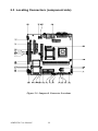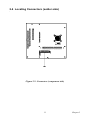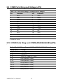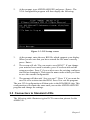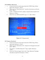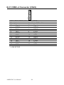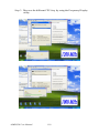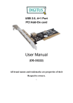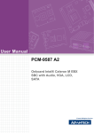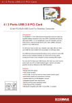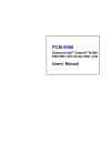
1
AIMB-350
Socket 478 Embedded ATX/
Micro ATX for Multimedia Applications
User Manual
Copyright
This document is copyrighted, © 2005. All rights are reserved. The original manufacturer reserves the right to make improvements to the products
described in this manual at any time without notice.
No part of this manual may be reproduced, copied, translated or transmitted in any form or by any means without the prior written permission of
the original manufacturer. Information provided in this manual is
intended to be accurate and reliable. However, the original manufacturer
assumes no responsibility for its use, nor for any infringements upon the
rights of third parties that may result from such use.
Acknowledgements
Award is a trademark of Award Software International, Inc.
VIA is a trademark of VIA Technologies, Inc.
IBM, PC/AT, PS/2 and VGA are trademarks of International Business
Machines Corporation.
Intel and Pentium are trademarks of Intel Corporation.
Microsoft Windows® is a registered trademark of Microsoft Corp.
RTL is a trademark of Realtek Semi-Conductor Co., Ltd.
ESS is a trademark of ESS Technology, Inc.
UMC is a trademark of United Microelectronics Corporation.
SMI is a trademark of Silicon Motion, Inc.
Creative is a trademark of Creative Technology LTD.
All other product names or trademarks are properties of their respective
owners.
For more information on this and other Advantech products, please visit
our websites at:
http://www.advantech.com
http://www.advantech.com/eplatform
For technical support and service, please visit our support website at:
http://www.advantech.com/support
This manual is for the AIMB-350.
Part No.2006035010
1st Edition
Dec. 2005
AIMB-350 User Manual
ii
Packing List
Before you begin installing your board, please make sure that the following materials have been shipped:
• 1 AIMB-350 all-in one single board computer
• 1 startup manual
• 1 CD-ROM or disks for utility, drivers, and manual (in PDF format)
• 1 UDMA/66 IDE flat cable
p/n:1701400452
• 1 COM2(W/485/422)cable
p/n:1701140201
• 1 DMA/33 IDE 40 to 44pin IDE flat cable
p/n:1701440350
• 1 I/O shield
p/n:1960001955
• 4 COM port cable kit 18CM
p/n:1701400181
If any of these items are missing or damaged, contact your distributor or
sales representative immediately.
Optional Items:
• 1 USB cable (2.54mm)
p/n:1700000719
• 1 DVI cable
p/n:1700000410
• 1 FDD cable
p/n:1701340700
• 1 SATA cable
p/n:1700001054
• 1 P4 CPU FAN
p/n:1750000069
• 1 COM3.4 cable 20pin (22CM) cable
iii
p/n:1701200220
Model No. List
Description
AIMB-350F-00A1
SKT 478 Pentium M SBC w/8USB/2LAN/
4COM/2PCIX/1PCI
AIMB-350G-00A1
SKT 478 Pentium M SBC w/8USB/
2GigaLAN/4COM/1PCIX/1PCI
AIMB-350L-00A1
SKT 478 Pentium M SBC w/4USB/1LAN/
4COM/1PCIX
Part Number
AIMB-350F-00A1
AIMB-350L-00A1
AIMB-350G-00A1
Form factor
EmbATX
EmbATX
MicroATX
LAN
2x 10/100
1x 10/100
2x Giga
USB
8ports
4ports
8ports
Display support
CRT/LVDS/TTL/DVI/TV out
CRT/LVDS
CRT/LVDS/TTL/DVI/
TV-out
SATA
2
2
2
COM
4 ports
4 ports
4 ports
Mini PCI
V
V
V
CF
V
V
V
Expansion slot
2 x PCI-X, 1x PCI
1x PCI-X, 1x PCI
1x PCI-X, 1x PCI
Additional Information and Assistance
Visit the Advantech web site at www.advantech.com where you can find
the latest information about the product.
Step 1. Contact your distributor, sales representative, or Advantech's customer service center for technical support if you need additional
assistance. Please have the following information ready before
you call:
• Product name and serial number
• Description of your peripheral attachments
• Description of your software (operating system, version, application
software, etc.)
• A complete description of the problem
• The exact wording of any error messages
AIMB-350 User Manual
iv
FCC
This device complies with the requirements in
part 15 of the FCC rules: Operation is subject to
the following two conditions:
1.This device may not cause harmful interference, and
2. This device must accept any interference
received, including interference that may cause
undesired operation
This equipment has been tested and found to
comply with the limits for a Class A digital device,
pursuant to Part 15 of the FCC Rules. These limits are designed to provide reasonable protection
against harmful interference when the equipment
is operated in a commercial environment. This
equipment generates, uses, and can radiate
radio frequency energy and, if not installed and
used in accordance with the instruction manual,
may cause harmful interference to radio communications. Operation of this device in a residential
area is likely to cause harmful interference in
which case the user will be required to correct
the interference at his/her own expense. The
user is advised that any equipment changes or
modifications not expressly approved by the
party responsible for compliance would void the
compliance to FCC regulations and therefore,
the user's authority to operate the equipment.
Caution!
Achtung!
There is a danger of a new battery exploding if it
is incorrectly installed. Do not attempt to
recharge, force open, or heat the battery.
Replace the battery only with the same or equivalent type recommended by the manufacturer.
Discard used batteries according to the manufacturer’s instructions.
v
AIMB-350 User Manual
vi
Contents
Chapter
1 General Information ........................................2
1.1
1.2
1.3
Introduction ....................................................................... 2
Features ............................................................................. 2
Specifications .................................................................... 3
1.3.1
1.3.2
1.3.3
1.3.4
1.3.5
1.3.6
1.4
Chapter
Standard SBC Functions................................................. 3
Display Interface............................................................. 4
DVI ................................................................................. 4
Solid State Disk .............................................................. 4
PCI bus Ethernet interface .............................................. 4
Mechanical and Environmental ...................................... 4
Board layout: dimensions.................................................. 5
2 Installation ........................................................8
2.1
2.2
2.3
2.4
2.5
2.6
2.7
2.8
2.9
2.10
2.11
2.12
2.13
2.14
2.15
2.16
2.17
2.18
2.19
Jumpers.............................................................................. 8
Connectors......................................................................... 8
Locating Connectors (component side)........................... 10
Locating Connectors (solder side)................................... 11
Setting Jumpers ............................................................... 12
USB Controller Power Select (JP2) ................................ 13
USB Wake-up Function (JP3)......................................... 13
Front Panel Connector (JP4) ........................................... 13
COM Ports Ring and Voltage (JP5)................................ 14
COM Ports Ring and COM2 (RS232/422/485)(JP6)...... 14
SM BUS Power Select (JP7)........................................... 15
PCI-X Socket Clock Set (JP8 & JP11)............................ 15
PCI-X Slot Power Select (JP9)........................................ 15
DVO or AGP Alternative Setting (JP10) ........................ 16
Clear CMOS.................................................................... 16
Installing DIMMs............................................................ 16
ATX power control connector (ATX1)........................... 17
Printer port connector (CN3)........................................... 17
CompactFlash Card Socket ............................................. 17
2.19.1 CompactFlash(CN16) ................................................... 17
2.20
Floppy drive connector (CN20) ...................................... 17
2.20.1 Connecting the floppy drive ......................................... 18
2.21
IDE connector(CN17,CN18)........................................... 18
2.21.1 Connecting the hard drive............................................. 18
2.22
VGA/LVDS interface connections.................................. 19
2.22.1 CRT display connector (CN1) ..................................... 19
2.22.2 LVDS LCD panel connector(CN11,VCN1)................. 19
vii
2.22.3 LCD inverter connector(CN8) ...................................... 19
2.22.4 DVI connector (CN12) ................................................. 20
2.23
2.24
USB connectors (CN6,CN7,CN13,CN14)...................... 20
Ethernet configuration..................................................... 20
2.24.1 LAN connector (CN6,CN7).......................................... 20
2.24.2 Network boot ................................................................ 20
2.25
Front Panel Connector (JP4) ........................................... 21
2.25.1
2.25.2
2.25.3
2.25.4
2.25.5
2.26
2.27
2.28
2.29
2.30
2.31
2.32
2.33
2.34
2.35
2.36
Chapter
Reset (Pin13&Pin14) ................................................... 21
HDD LED (Pin1&Pin2)................................................ 21
Power LED (Pin 3 & Pin 4) .......................................... 21
Suspend LED (Pin 5 & Pin 6)....................................... 21
Power Button (Pin 9 & Pin10)...................................... 21
COM port connector (CN2,CN21,CN22) ....................... 21
MINI PS/2, KB/Mouse connector (CN5)........................ 22
Audio Connector (CN4) .................................................. 22
DIO connector (CN23)................................................... 22
SATA Connector (SA1, SA2)........................................ 22
CD-In Connector (CN9).................................................. 22
Internal Speaker Connector (CN10)................................ 23
SIR Connector (CN15).................................................... 23
SM Bus Connector (CN19) ............................................. 23
System and CPU FAN Conn. (FAN1 and FAN2) .......... 23
AGP,PCI, PCI-X Conn(AGP1, PCI1, PCIX1, PCIX2) .. 23
3 Software Configuration .................................26
3.1
3.2
Introduction ..................................................................... 26
VGA display firmware configuration ............................. 26
3.3
Connectors to Standard LCDs......................................... 27
Figure 3.1:VGA setup screen........................................ 27
3.3.1
Chapter
AU M170EG01(1280 x1024 LVDS LCD)................... 28
Table 3.1:Connections to LCD/Flat Panel (CN15)....... 28
4 Award BIOS Setup.........................................30
4.1
System test and initialization........................................... 30
4.1.1
4.2
System configuration verification................................. 30
Award BIOS setup .......................................................... 31
4.2.1
4.2.2
4.2.3
4.2.4
4.2.5
AIMB-350 User Manual
Entering setup .............................................................. 31
Figure 4.1:BIOS setup program initial screen .............. 31
Standard CMOS Features setup.................................... 32
Figure 4.2:Standard CMOS Features setup .................. 32
Advanced BIOS Features setup .................................... 33
Figure 4.3:Advanced BIOS Features setup................... 33
Advanced Chipset Features setup ................................. 34
Figure 4.4:Advanced Chipset Features setup ............... 34
Integrated Peripherals ................................................... 35
viii
4.2.6
4.2.7
4.2.8
4.2.9
4.2.10
4.2.11
4.2.12
4.2.13
Chapter
5 PCI SVGA Setup ............................................46
5.1
Introduction ..................................................................... 46
5.1.1
5.1.2
5.1.3
5.2
Chipset .......................................................................... 46
Display memory............................................................ 46
Display types................................................................. 46
Installation of the SVGA Driver ..................................... 47
5.2.1
5.3
Chapter
Figure 4.5:Integrated Peripherals.................................. 35
Power Management Setup ............................................ 36
Figure 4.6:Power Management Setup........................... 36
PnP/PCI Configurations................................................ 37
Figure 4.7:PnP/PCI Configurations .............................. 37
PC Health Status ........................................................... 38
Figure 4.8:PC Health Status.......................................... 38
Frequency/Voltage Control........................................... 39
Figure 4.9:Frequency/Voltage Control ......................... 39
Load Optimized Defaults.............................................. 40
Figure 4.10:Load BIOS defaults screen........................ 40
Set Password ................................................................. 40
Figure 4.11:Set password.............................................. 41
Save & Exit Setup......................................................... 42
Figure 4.12:Save to CMOS and EXIT.......................... 42
Exit Without Saving...................................................... 43
Figure 4.13:Quit without saving ................................... 43
Installation for Windows 2000/XP ............................... 47
Further Information ......................................................... 50
6 PCI Bus Ethernet Interface...........................52
6.1
6.2
Introduction ..................................................................... 52
Installation of Ethernet driver ......................................... 52
6.2.1
Installation Fast Ethernet (10/100Mbps Intel 82551) for
Windows XP ....................................................................53
6.2.2 Installation Gigabit Ethernet (10/100/1000Mbps intel
82541) for Windows XP...................................................56
Chapter
7 Audio Setup.....................................................62
7.1
7.2
Introduction ..................................................................... 62
Driver installation............................................................ 62
7.2.1
7.2.2
Before you begin.......................................................... 62
Windows XP driver ..................................................... 62
Appendix A Programming GPIO & Watchdog Timer ....66
A.1
Supported GPIO Register................................................ 66
A.1.1
A.1.2
Appendix B
GPIO Registers ............................................................. 66
GPIO Example program-1 ............................................ 67
Pin Assignments ............................................72
ix
B.1
CRT Connector (CN1) .................................................... 72
B.2
COM1 Connector(CN2).................................................. 72
B.3
LPT1 Connector(CN3).................................................... 73
B.4
Audio Connector (CN4) .................................................. 74
B.5
Keyboard + PS/2 Mouse Connector (CN5) .................... 74
B.6
LAN2 USB3/4 Connector (CN6).................................... 75
B.7
LAN1 USB1/2 Connector(CN7)..................................... 76
B.8
LCD/LVDS INVERTER Connector(CN8)..................... 76
B.9
CD-IN Connector (CN9)................................................. 77
B.10
Internal Speaker Connector (CN10)................................ 77
B.11
LCD Connector(CN11) ................................................... 78
B.12
DVI Connector (CN12)................................................... 79
B.13
USB5/6/USB7/8 Connector (CN13, CN14).................... 80
B.14
SIR Connector (CN15).................................................... 80
B.15
Compact Flash Connector(CN16)................................... 81
B.16
Primary IDE Connector(CN17) ...................................... 82
B.17
Secondary Slave IDE Connector(CN18)......................... 83
B.18
SM BUS Connector(CN19) ............................................ 84
B.19
FDD Connector (CN20) .................................................. 84
B.20
COM2 Connector (CN21)............................................... 85
B.21
COM3~4 Connector (CN22)........................................... 86
B.22
Digital IO Connector (CN23).......................................... 87
Table B.1:CRT Connector (CN1)................................. 72
Table B.2:COM1 Connector (CN2).............................. 72
Table B.3:Primary IDE connector (CN3) ..................... 73
Table B.4:Audio Connector (CN4)............................... 74
Table B.5:Keyboard + PS/2 Mouse Connector (CN5) . 74
Table B.6:LAN2 USB3/4 Connector (CN6)................. 75
Table B.7:LAN1 USB1/ 2 Connector(CN7)................. 76
Table B.8:LCD/LVDS INVERTER Connector(CN8) . 76
Table B.9:CD-IN Connector (CN9).............................. 77
Table B.10:Internal Speaker Connector(CN10) ........... 77
Table B.11:LCD Connector (CN11)............................. 78
Table B.12:DVI Connector(CN12)............................... 79
Table B.13:USN5/6/USB7/8 Connector(CN13,CN14) 80
Table B.14:SIR Connector(CN15) ............................... 80
Table B.15:Compact Flash Connector(CN16).............. 81
Table B.16:Primary IDE Connector(CN17) ................. 82
Table B.17:Secondary Slave IDE Connector(CN18) ... 83
Table B.18:SM BUS Connector(CN19) ....................... 84
Table B.19:FDD Connector (CN20)............................. 84
Table B.20:COM2 Connector(CN21)........................... 85
Table B.21:COM3~4 Connector (CN22) ..................... 86
Table B.22:Digital IO Connector (CN23) .................... 87
AIMB-350 User Manual
x
B.23
TV OUT Connector(CN25) ............................................ 88
B.24
SATA Connector (SATA1/SATA2) ............................... 88
B.25
ATX Power Connector (ATX1)...................................... 89
B.26
LVDS Connector (VCN1)............................................... 90
B.27
SYSTEM/CPU FAN Control Conn. (FAN1/FAN2)....... 91
Table B.23:TV OUT Connector(CN25) ....................... 88
Table B.24:SATA Connector (SATA1/SATA2).......... 88
Table B.25:ATX Power Connector (ATX1)................. 89
Table B.26:LVDS Connector (VCN1) ......................... 90
Table B.27:SYSTEM/CPU FAN Control Connector(FAN1/FAN2)...............................................91
B.28
AGP SLOT (AGP1) ........................................................ 91
B.29
PCI SLOT Connector (PCI1) .......................................... 94
B.30
PCIX SLOT Connector (PCIX1) .................................... 96
B.31
PCIX SLOT Connector (PCIX2) ................................... 99
Table B.28:AGP SLOT (AGP1)................................... 91
Table B.29:PCI SLOT Connector (PCI1)..................... 94
Table B.30:PCIX SLOT Connector (PCIX1) ............... 96
Table B.31:PCIX SLOT Connector (PCIX2) ............... 99
Appendix C
System Assignments ....................................104
C.1
System I/O Ports............................................................ 104
C.2
1st MB memory map..................................................... 105
C.3
DMA channel assignments............................................ 105
C.4
Interrupt assignments .................................................... 106
Table C.1:System I/O ports ........................................ 104
Table C.2:1st MB memory map ................................. 105
Table C.3:DMA channel assignments ........................ 105
Table C.4:Interrupt assignments ................................. 106
Appendix D Intel Speedstep Technology .........................108
D.1
Intel® Pentium® M SpeedStep instruction................... 108
xi
AIMB-350 User Manual
xii
CHAPTER
1
General Information
This chapter gives background
information on the AIMB-350.
Sections include:
•
•
•
•
Introduction
Features
Specifications
Board layout and dimensions
1
Chapter 1
Chapter 1 General Information
1.1 Introduction
The AIMB-350 series is an Embedded ATX/Micro ATX form factor
(Socket 478) design for Intel Pentium® M processors with 400MHz FSB
and Intel’s 855GME and 6300ESB chipsets that support enhanced Intel
"SpeedStep" technology and Dynamic Video Memory Technology. For
maximum performance, AIMB-350 also supports two 200 PIN SODIMM
sockets for ECC DDR memory up to 2GB. These chipsets are specifically
for embedded computing and provide an optimized onboard integrated
graphics solution. "SpeedStep" technology intelligently focuses system
power where the CPU needs it and automatically regulates power usage
to preserve battery life.
This product uses Intel 855GME chipset for dual independent display.
AIMB-350F and AIMB-350L allow CRT+LVDS, DVI+LVDS,
CRT+DVI combinations. The dual independent display is suitable for
POS, Kiosks and multiple display applications.
There are 2 Ethernet interfaces that can be used; one LAN for communication and the other one for backup purposes.
Other onboard comprehensive peripherals include 2 EIDEs, 2 SATAs, up
to 6 USB 2.0, 4 serial ports (3x RS-232 and 1x RS-232/422/485), 1 FDD,
1 LPT, PS/2 Keyboard/mouse, watchdog timer, and a DIO interface. The
SSD solution supports Type I/II CompactFlash cards, and the standard
expansion interface includes PCI, PCI-X and miniPCI for user expansion
purposes.
AIMB-350 series are the best all-in-one embedded motherboards specifically designed for the embedded market.
1.2 Features
• Intel Pentium M/Celeron M 400MHz FSB Socket 478 uFCPGA2
Processor
• 0~60°C operating temperature
• Intel 855GME dual independent display (CRT+LVDS,
DVI+LVDS,CRT+DVI)
• Up to 2 x Gigabit LAN on board (AIMB-350G)
AIMB-350 User Manual
2
• Supports 2 SATA
• AGP, PCI, PCI-X multiple expansion
• Supports 8 x USB2.0 port
• Option up to 2 Channel 36bits LVDS for LCD
• Supports 400 MHz Front Side Bus
• Supports 200 MHz, 266 MHz and 333 MHz ECC DDR SDRAM
1.3 Specifications
1.3.1 Standard SBC Functions
• CPU: Intel Pentium M/Celeron M 400 MHz FSB Socket 478 uFCPGA2
Processor (Up to Pentium M 2 GHz)
• System chipsets: Intel 855GME + 6300ESB
• BIOS: Award 4 Mbit Flash memory
• System memory: 200 pin DIMM x 2, support ECC double data rate
(DDR) 128 MB to 2 GB, accepts 128/256/512/1000 MB DDR 200/
266/333 DRAM
• 2nd cache memory: 1 or 2 MB on Pentium M processor, 512 MB on
Celeron M
• PCI interface: Supports PCI Rev 2.2 Specification at 33 MHz
• PCI-X interface: Supports PCI-X Rev 2.2 Specification at 66 MHz
• AGP interface: Support AGP 2.0 slot (1x/2x/4x)
• Enhanced IDE Interface: Supports two enhanced IDE channels. Primary channel supports ATA-100 mode; Secondary channel only
supports ATA-33 and PIO mode. CFC card occupies secondary
master
• Serial Ports: Four serial ports: COM1, COM3, COM4: RS-232,
COM2: RS-232/422/485
• Parallel Ports: one parallel port, support SPP/EPP/ECP
• Keyboard/Mouse Connector: Supports standard PC/AT Keyboard and
a PS/2 Mouse
• Power Management: Supports Power Saving Mode including Normal/
Standard/Suspend modes. APM 1.2 compliant.
• FDD interface: Support up to two FDD devices
• DIO interface: Supports 8 general purpose input/output ports
• Watchdog Timer: 0~255 Sec., System reset
• Expansion Interface: 4 x AGP, 32-bit PCI Slot and 64-bit PCI-X Slot,
support PCI 2.2
3
Chapter 1
• Battery: Lithium 3V/195 mAH
• USB: Up to 8 USB Intel 6300ESB ports, USB 2.0 compliant
• SATA: Intel 6300ESB supports data transfer rates up to 150 Mbyte/s,
support RAID 0.1
1.3.2 Display Interface
• Chipset: Intel 855GME
• Memory size: Optimized Shared Memory Architecture, supports up to
64 MB frame buffer using system memory
• Display modes:
CRT Modes: up to 2048 x 1536 at 75Hz;
LCD Modes: up to 1280 x 1024 at 85Hz
• LCD Interface: 2 Channel LVDS (up to 36-bit)
• LVDS: Hirose connector support dual channel LVDS panel, up to
UXGA panel resolution with frequency range from 25 MHz to 112MHz
1.3.3 DVI
• Chipset: Chrontel CH7009
• Drives a DVI display at a pixel rate of up to 165MHz, supporting
UXGA resolution displays
• DVI hot plug detection
• Compliant with DVI Specification 1.0
1.3.4 Solid State Disk
• Supports CompactFlash Type I/II disks
1.3.5 PCI bus Ethernet interface
• Chipset: Intel 82541GI (Gigabit), Intel 82551ER/82551QM(optional)
• Connection: onboard 2XRJ-45
• Interface: IEEE 802.3 z/ab(1000BASE-T) or IEEE 802.3u(100BASET) protocol compatible
• Boot ROM: build-in-system (Supported by 82541GI and 82551QM
(optional))
1.3.6 Mechanical and Environmental
• Dimensions (L x W): 185 x 122 mm (7.3” x 4.8”)
• Power supply voltage: +5 V, +5V STB, +12V
• Power requirements:
Typical: [email protected], [email protected](Pentium M 1.6G, 256 MB
DDR333 with MPEG1)
Max: [email protected], [email protected](Pentium M 1.6G, 256 MB
DDR333 with HCT9.5)
AIMB-350 User Manual
4
• Operating temperature: 0 ~ 60°C (32 ~ 140°F),operation
• Operating humidity: 0% ~ 90% Relative Humidity, Non condensing
1.4 Board layout: dimensions
Figure 1.1: Board layout: dimensions (component side)
5
Chapter 1
Figure 1.2: Board layout: dimensions (solder side)
AIMB-350 User Manual
6
CHAPTER
2
Installation
This chapter explains the setup procedures
of AIMB-350 hardware, including instructions on setting jumpers and connecting
peripherals, switches and indicators. Be
sure to read all safety precautions before
you begin the installation procedure.
7
Chapter 2
Chapter 2 Installation
2.1 Jumpers
The AIMB-350 has a number of jumpers that allow you to configure your
system to suit your application. The table below lists the functions of the
various jumpers.
Table 2.1: Jumpers
Label
Function
JP2
VIA-VT6212 USB Controller Power Select
JP3
VIA-VT6212 USB Controller Wake-Up Function Select
JP4
Front Panel Connector
JP5
COM Port 1~6 Voltage Select Connector
JP6
COM Port 1~6 Ring/COM2 (RS-232/422/485)Select Connector
JP7
SM Bus Connector Power Select
JP8
PCI-X Clock Select Connector
JP9
PCI-X VIO Power Select Connector
JP10
AGP/DVO Mode Select
JP11
PCI-X Clock Select Connector
JP12
CMOS Clear Jumper
2.2 Connectors
Onboard connectors link the AIMB-350 to external devices such as LCD
Panels, LEDs, hard disk drives, a keyboard, or floppy drives. The table
below lists the function of each of the board’s connectors.
Table 2.2: Connectors
Label
Function
CN1
CRT Connector
CN2
COM1 Connector
CN3
LPT Connector
CN4
Audio Connector
CN5
KB/MS Connector
AIMB-350 User Manual
8
Table 2.2: Connectors
CN6
LAN2+USB 3/4 Connector
CN7
LAN1+USB 1/2 Connector
CN8
Panel Inverter Connector
CN9
CD-IN Connector
CN10
Internal Speaker Connector
CN11
LCD Connector
CN12
DVI Connector
CN13
Internal USB 7/8 Port Connector
CN14
Internal USB 5/6 Port Connector
CN15
SIR Connector
CN16
CompactFlash Connector
CN17
Primary IDE Connector
CN18
Secondary IDE Connector
CN19
SM Bus Connector
CN20
Floppy Connector
CN21
COM2 Connector
CN22
COM3~6 Connector
CN23
Digital IO Connector
CN24
Mini PCI Connector
CN25
TV OUT Connector
SA1
SATA1 Connector
SA2
SATA2 Connector
ATX1
ATX Power Connector
VCN1
LVDS Connector
FAN1
SYSTEM FAN
FAN2
CPU FAN
AGP1
AGP SLOT
PCI1
PCI SLOT
PCIX1
PCIX1 SLOT
PCIX2
PCIX2 SLOT
9
Chapter 2
2.3 Locating Connectors (component side)
Figure 2.1: Jumper & Connector Locations
AIMB-350 User Manual
10
2.4 Locating Connectors (solder side)
Figure 2.2: Connectors (component side)
11
Chapter 2
2.5 Setting Jumpers
You may configure your card to match the needs of your application by
setting jumpers. A jumper is a metal bridge used to close an electric circuit. It consists of two metal pins and a small metal clip (often protected
by a plastic cover) that slides over the pins to connect them. To “close” a
jumper, you connect the pins with the clip. To “open” a jumper, you
remove the clip. Sometimes a jumper will have three pins, labeled 1, 2
and 3. In this case you would connect either pins 1 and 2, or 2 and 3.
open
closed
closed 2-3
The jumper settings are schematically depicted in this manual as follows:.
open
closed
closed 2-3
A pair of needle-nose pliers may be helpful when working with jumpers.
If you have any doubts about the best hardware configuration for your
application, contact your local distributor or sales representative before
you make any changes. Generally, you simply need a standard cable to
make most connections.
AIMB-350 User Manual
12
2.6 USB Controller Power Select (JP2)
This jumper sets ALL USB ports to use 3.3V at anytime or 3.3V standby
power (3.3VSB) when the system is in sleep mode.
Table 2.3: VIA-VT6212 USB Controller Power Select
Close pins
Result
1-2
3.3v
2-3
3.3VSB
*: Default value 3.3VSB
2.7 USB Wake-up Function (JP3)
Sets all the USB ports to wake-up or NOT wake-up during sleep mode.
Table 2.4: VIA-VT6212 USB Controller Wake-Up Function Select
Close pins
Result
1-2
Enable
2-3
Disable
*: Default value Enable
2.8 Front Panel Connector (JP4)
Table 2.5: Front Panel Connector Type: Pin-Header 14-Pin 2.54mm
Pin
Function
Pin
Function
7
3VSB(LAN_ACKLED)
8
LAN_ACKLED#
11
GND
12
PWRBTN#
*: LOW ACTIVE
13
Chapter 2
2.9 COM Ports Ring and Voltage (JP5)
Table 2.6: COM Ports Ring & Voltage Select Jumper
Pin
Function
Pin
Function
1
VCC
2
VCC
3
RI#1
4
RI#2
5
+12V
6
+12V
7
NC
8
NC
9
VCC
10
VCC
11
RI#3
12
RI#4
13
+12V
14
+12V
15
NC
16
NC
17
VCC
18
VCC
19
RI#5
20
RI#6
21
+12V
22
+12V
*: LOW ACTIVE
2.10 COM Ports Ring and COM2 (RS232/422/485)(JP6)
Table 2.7: COM Ports Ring & COM2 (RS232/422/485)Select Jumper
Close Pins
COM2
1-2
RXD485
3-4
RXD422
5-6
RXD232 (Default: Close)
7-8
RI#1(Default: Close)
9-10
RI#2(Default: Close)
11-12
RI#3(Default: Close)
13-14
RI#4(Default: Close)
15-16
RI#5(Default: Close)
17-18
RI#6(Default: Close)
AIMB-350 User Manual
14
2.11 SM BUS Power Select (JP7)
This board can support client SMBUS 3.3V or 5V power when SM
BUS.had been connected.
Table 2.8: SM BUS Power Select
Close pins
Result
1-2
3.3V (Default: CLOSE)
2-3
5V
*: Default value 3.3V
2.12 PCI-X Socket Clock Set (JP8 & JP11)
This board can support PCI 33 MHz/66 MHz or PCI-X 66 MHz
Table 2.9: PCI-X Clock Select Connector
JP8 Close pin
JP11 Close pin
1-2 SHORT
Result
1-2 SHORT(DEFAULT)
PCI 33
1-2 OPEN (DEFAULT) 1-2 SHORT(DEFAULT)
PCI 66
1-2 SHORT
PCI-X 66
1-2 OPEN
*: Default value (OPEN)
2.13 PCI-X Slot Power Select (JP9)
With the jumper set can provide 3.3V or 5V to PCI-X add-on card.
Table 2.10: PCI-X VIO Select Connector
Close pins
Result
1-2
3.3V
2-3
5V
*: Default value (5V)
15
Chapter 2
2.14 DVO or AGP Alternative Setting (JP10)
This board cannot support DVO and AGP at the same time. User can set
the DVO or AGP using this jumper setting.
Table 2.11: DVO /AGP
Close pins
Result
1-2
OPEN (DVO) CLOSE (AGP)
*: Default value DVO (OPEN)
2.15 Clear CMOS
Action to erase CMOS data.
Warning!
To avoid damaging the computer, always turn
off the power supply before setting “Clear
CMOS” Before turning on the power supply, set
the jumper back to “3.0V Battery On”.
This jumper is used to erase CMOS data (including the setting of date,
time and password) and reset system BIOS information.
The procedure for clearing CMOS is:
1. Turn off the system.
2. Short pin 1 and pin 2.
3. Turn on the system. The BIOS is now reset to its default setting.
2.16 Installing DIMMs
Notes
The modules can only fit into a socket one way.
The gold pins must point down into the DIMM
socket.
The procedure for installing DIMMs appears below. Please follow these
steps carefully.
1. Make sure that all power supplies to the system are switched off
2. Install the DIMM card. Install the DIMM so that its gold pins
AIMB-350 User Manual
16
point down into the DIMM socket.
3. Slip the DIMM module perpendicular into the socket, apply more pressure until the clips fix the DIMM and socket securely.
4. Check to ensure that the DIMM is correctly seated and all connector contacts touch. The DIMM should not move around in its
socket.
2.17 ATX power control connector (ATX1)
The AIMB-350 supports ATX power. ATX1 supplies main power (+5V,
+12V, 5VSB), and it is a 20-Pin power connector, w/Fixed Lock.
Important
Make sure that the ATX power supply can take
at least a 10 mA load on the 5 V standby lead
(5VSB). If not, you may have difficulty powering on your system.
2.18 Printer port connector (CN3)
Normally, the parallel port is used to connect the card to a printer. The
AIMB-350 includes a multi-mode (ECP/EPP/SPP) parallel port accessed
via CN3 and a D-SUB 25-pin connector.
The parallel port interrupt channel is designated to be IRQ7.
You can select ECP/EPP DMA channel via BIOS setup.
2.19 CompactFlash Card Socket
The AIMB-350 provides a 50-pin socket for CompactFlash card type I/II.
2.19.1 CompactFlash(CN16)
The CompactFlash card occupies a secondary IDE channel which can be
enabled/disabled via the BIOS settings.
2.20 Floppy drive connector (CN20)
You can attach up to two floppy drives to the AIMB-350’s onboard controller. You can use any combination of 5.25” (360 KB and 1.2 MB) and/
or 3.5” (720 KB, 1.44 MB, and 2.88 MB) drives.
17
Chapter 2
A 34-pin daisy-chain drive connector cable is required for a dual-drive
system. On one end of the cable is a 34-pin flat-cable connector. On the
other end are two sets of floppy disk drive connectors. Each set consists
of a 34-pin flat-cable connector (usually used for 3.5” drives) and a
printed-circuit board connector (usually used for 5.25” drives).
2.20.1 Connecting the floppy drive
1.
Plug the 34-pin flat-cable connector into CN20. Make sure that the
red wire corresponds to pin one on the connector.
2.
Attach the appropriate connector on the other end of the cable to
the floppy drive(s). You can use only one connector in the set. The
set on the end (after the twist in the cable) connects to the A: drive.
The set in the middle connects to the B: drive.
3.
If you are connecting a 5.25” floppy drive, line up the slot in the
printed circuit board with the blocked-off part of the cable connector.
If you are connecting a 3.5” floppy drive, you may have trouble determining which pin is number one. Look for a number printed on the circuit
board indicating pin number one. In addition, the connector on the floppy
drive may have a slot. When the slot is up, pin number one should be on
the right. Check the documentation that came with the drive for more
information.
If you desire, connect the B: drive to the connectors in the middle of the
cable as described above.
In case you need to make your own cable, you can find the pin assignments for the board’s connector in Appendix B.
2.21 IDE connector(CN17,CN18)
The AIMB-350 provides two IDE channels to which you can attach up to
four Enhanced Integrated Device Electronics hard disk drives or
CDROM to the AIMB-350’s internal controller. The AIMB-350's IDE
controller uses a PCI interface. This advanced IDE controller supports
faster data transfer, PIO Mode 3 or Mode 4, UDMA 33/66/100 mode.
2.21.1 Connecting the hard drive
Connecting drives is done in a daisy-chain fashion. It requires one of two
cables (not included in this package), depending on the drive size. 1.8"
and 2.5" drives need a 1 x 44-pin to 2 x 44-pin flat-cable connector. 3.5"
drives use a 1 x 44-pin to 2 x 40-pin connector.
AIMB-350 User Manual
18
Wire number 1 on the cable is red or blue, and the other wires are gray.
1.
Connect one end of the cable to CN17,CN18. Make sure that the
red (or blue) wire corresponds to pin 1 on the connector, which is
labeled on the board (on the right side).
2.
Plug the other end of the cable into the Enhanced IDE hard drive,
with pin 1 on the cable corresponding to pin 1 on the hard drive.
(See your hard drive’s documentation for the location of the connector.)
If desired, connect a second drive as described above.
Unlike floppy drives, IDE hard drives can connect to either end of the
cable. If you install two drives, you will need to set one as the master and
one as the slave by using jumpers on the drives. If you install only one
drive, set it as the master.
2.22 VGA/LVDS interface connections
The AIMB-350’s display interface can drive conventional CRT displays
and is capable of driving a wide range of LVDS flat panel displays as
well. The board has two display connectors: one for standard CRT VGA
monitors, and one for LVDS/DVI flat panel displays. AIMB-350 with
852GME can support dual independent displays like CRT+LVDS or
CRT+DVI.
2.22.1 CRT display connector (CN1)
CN1 is a standard 15-pin connector used for conventional CRT displays.
Users can drive a standard progressive scan analog monitor with pixel
resolution up to 2048 x 1536 at 75 Hz. Pin assignments for CRT display
connector CN1 are detailed in Appendix B.
2.22.2 LVDS LCD panel connector(CN11,VCN1)
AIMB-350 uses the Intel 855GME to supports single or dual-channel
LVDS panels up to UXGA panel resolution with frequency range from 25
MHz to 112 MHz.
The display mode can be 2 channels (2 x 24bit) LVDS LCD panel displays Users can connector to either an 18, 24, 36 LVDS with VCN1 and
LCD with CN11.
2.22.3 LCD inverter connector(CN8)
The LCD inverter is connected to CN8 via a 5-pin connector to provide
+5V/+12V power.
19
Chapter 2
2.22.4 DVI connector (CN12)
Digital Visual Interface (DVI) is the standard interface for high-performance connection between PCs and Flat Panel Displays, Digital CRT displays, Projectors, and HDTV. AIMB-350 is able to drive a DVI connector
display at a pixel rate of up to 165MHz, supporting UXGA resolution displays and hot plug detection. DVI can connect with PCM-258 to have
standard DVI connector.
2.23 USB connectors (CN6,CN7,CN13,CN14)
The AIMB-350 board provides up to eight USB (Universal Serial Bus)
ports. This gives complete Plug and Play, and hot attach/detach for up to
127 external devices. The USB interfaces comply with USB specification
Rev. 2.0, and are fuse protected.
There are 4 USB connectors for external and 4 USB for internal use. The
4 external USBs are combine with LAN+2 USB in CN6 and CN7. The
internal USB interfaces are accessed through the 5 x 2-pin flat-cable connectors, CN13 (USB7, 8) and CN14 (USB5, 6). You will need an adapter
cable if you use a standard USB connector. The adapter cable has a 5 x 2pin connector on one end and a USB connector on the other. The USB
interfaces can be disabled in the system BIOS setup.
2.24 Ethernet configuration
The AIMB-350 is equipped with two high performance 32-bit PCI-bus
Ethernet interfaces which are fully compliant with IEEE 802.3U 10/
100Mbps CSMA/CD standards. These are supported by all major network operating systems.
The AIMB-640 supports 2 x 10/100Base-T or 2 x 1000Base-T Ethernet
connections with onboard RJ-45 connectors (CN6, CN7). AIMB-350M/
AIMB-350L series supports 10/100Base-T LAN, AIMB-350F series supports 1000Base-T LAN.
2.24.1 LAN connector (CN6,CN7)
10/100 or 1000 Base-T connects are standard RJ45 connectors on AIMB350.
2.24.2 Network boot
The Network Boot feature can be utilized by incorporating the Boot
ROM image files for the appropriate network operating system. The Boot
ROM BIOS files are included in the system BIOS, which is on the utility
AIMB-350 User Manual
20
CD disc. Boot ROM function is supported by 82541GI and
82551QM(optional), 82551ER can not support this function.
2.25 Front Panel Connector (JP4)
Next is to install external switches to monitor and control AIMB-350.
These features are optional: install them only if necessary. JP4 is an 2 x 7
pin header, 180 degree, male. It provides connections for reset, power,
and hard disk indicator.
2.25.1 Reset (Pin13&Pin14)
If a reset switch is installed, it should be an open single pole switch.
Momentarily pressing the switch will activate a reset. The switch should
be rated for 10 mA, 5V.
2.25.2 HDD LED (Pin1&Pin2)
The HDD LED indicator for hard disk access is an active low signal (24
mA sink rate). The HDD LED indicator lights up when the HDD is reading or writing.
2.25.3 Power LED (Pin 3 & Pin 4)
The Power LED indicator lights up when the power is on.
2.25.4 Suspend LED (Pin 5 & Pin 6)
The Suspend LED indicator lights up when the computer is in suspend.
2.25.5 Power Button (Pin 9 & Pin10)
AIMB-350 provides an ATX power input connector. When connected
with PIN 9 & PIN 10, it enables power On/Off from the chassis.
2.26 COM port connector (CN2,CN21,CN22)
The AIMB-350 provides six serial ports (COM1,COM3~COM6: RS-232
and COM2: RS-232/RS-422/RS-485). CN2 supports COM1 with D-SUB
9-Pin standard connector, CN21 supports COM2, CN22 supports
COM3~6,. and JP6 is for COM2 RS-232/RS-422/RS-485 selection. It
provides connections for serial devices (a mouse, etc.) or a communication network. You can find the pin assignments for the COM port connector in Appendix B.
21
Chapter 2
2.27 MINI PS/2, KB/Mouse connector (CN5)
The AIMB-350 board provides a keyboard connector that supports both a
keyboard and a PS/2 style mouse. In most cases, especially in embedded
applications, a keyboard is not used. If the keyboard is not present, the
standard PC/AT BIOS will report an error or fail during power-on selftest (POST) after a reset. The AIMB-350’s BIOS standard setup menu
allows you to select "All, but Keyboard" under the "Halt On"selection.
This allows no-keyboard operation in embedded system applications,
without the system halting under POST.
2.28 Audio Connector (CN4)
AIMB-350 can support AC97 2.2 compliant Audio line_in, line_out and
mic_in with on board standard connector.
2.29 DI/O connector (CN23)
The AIMB-350 supports DIO interface with CN23, which is a 2 x 8 dual
line pin header, supplying 8 general purpose input or output ports.
One characteristic of digital circuit are their fast response to high or low
signals, the kind of responses that are needed for harsh and critical industrial operating environments.
Generally, Digital Input and Output are signals to control external devices
that needs On/Off circuits or TTL devices. For detailed signal assignments refer to Appendix A.
2.30 SATA Connector (SA1, SA2)
AIMB-350 can support Serial ATA by two COMAX C504C connectors
(SA1, SA2), data transfer rates up to 150 Mbyte/s, enabling very fast data
and file transfer, and independent DMA operation on two ports. It also
supports alternate Device ID and RAID Class Code options for support of
Soft RAID.
2.31 CD-In Connector (CN9)
AIMB-350 has a CD-In connector for the CD-ROM driver audio signal
interface. CD-In connector is a 2.54mm pitch 4 pin connector.
AIMB-350 User Manual
22
2.32 Internal Speaker Connector (CN10)
There is a Wafer-Box 4-Pin 2.54 mm connector for the internal speaker
purpose.
2.33 SIR Connector (CN15)
This connector support wireless 115.2 Kbps infrared transmission and
receive mode.The IR module should mount on system case. It is a 5 pin
connector.
2.34 SM Bus Connector (CN19)
The System Management Bus (SM Bus) which uses 12C bus to make a
communication between the South Bridge and the rest of the system. In
AIMB-350 the South Bridge is dedicated to one PCI slot. The other will
handle the remaining I2C buses to other on-board devices such as the
PCI, PCI-X1, PCI-X2, LAN1 and LAN2.
2.35 System and CPU FAN Conn. (FAN1 and FAN2)
These 2 FAN connectors both have +12V FAN power and FAN speed
detection. AIMB-350 recommends FAN1 for system FAN and FAN2 for
CPU.
2.36 AGP,PCI, PCI-X Conn(AGP1, PCI1, PCIX1, PCIX2)
These 4 connectors all follow standards. AIMB-350M has 4 x AGP slots,
1 x PCI, and 1 PCI-X. AIMB-350F-00A1 has PCI-X and AIMB-350L
also has PCI-X.
23
Chapter 2
AIMB-350 User Manual
24
CHAPTER
3
Software Configuration
This chapter details the software configuration information. It shows you
how to configure the card to match
your application requirements. Award
System BIOS will be covered in
Chapter 4.
Sections include:
• Introduction
• VGA display software configuration
• Connectors to Standard LCDs
Chapter 3 Software Configuration
3.1 Introduction
The system BIOS and custom drivers are located on a 512 KB, 32-pin
(JEDEC spec.) Flash ROM device, designated U10. A single Flash chip
holds the system BIOS, VGA BIOS, and network Boot ROM image. The
display can be configured via software. This method minimizes the number of chips and eases configuration. You can change the display BIOS
simply by reprogramming the Flash chip.
NOTE:
Due to Intel not supporting Win98, and Windows ME drivers, AIMB-350 does not recommended installing Win98, Windows ME.
3.2 VGA display firmware configuration
The board’s onboard VGA interface supports a wide range of popular
LCDs, flat panel displays and traditional analog CRT monitors. The
855GME chip with optimized Shared Memory Architecture, supports up
to 64 MB frame buffer using system memory to provide LVDS mode up
to 1280 x 1024 @ 48bpp, the interface can drive CRT displays with resolutions up to 2048 x 1536 @ 24bpp (75Hz).
The VGA interface is configured completely via the software utility, so
you do not have to set any jumpers. Configure the VGA display as follows:
1.
Apply power to the board with a color TFT display attached. This
is the default setting for this board. Ensure that the AWDFLASH.EXE and *.BIN files are located in the working drive.
NOTE:
Ensure that you do not run AWDFLASH.EXE
while your system is operating in EMM386
mode.
AIMB-350 User Manual
26
2.
At the prompt, type AWDFLASH.EXE and press <Enter>. The
VGA configuration program will then display the following:
Figure 3.1: VGA setup screen
3.
At the prompt, enter the new BIN file which supports your display.
When you are sure that you have entered the file name correctly
press <Enter>.
4.
The screen will ask “Do you want to save BIOS?”. If you change
your mind or have made a mistake, press N to abort and end the
setup procedure. Press Y if you wish to save the existing configuration before changing it. Then type the name under which you want
to save the current configuration.
5.
The prompt will then ask “Are you sure?”. Press Y if you want the
new file to be written into the BIOS. Press N to exit the program.
The new VGA configuration will then write to the ROM BIOS chip. This
configuration will remain the same until you run the AWDFLASH.EXE
program and change the settings.
3.3 Connectors to Standard LCDs
The following table illustrates typical LCD connection pinouts for the
AIMB-350.
27
Chapter 3
3.3.1 AU M170EG01(1280 x1024 LVDS LCD)
Table 3.1: Connections to LCD/Flat Panel (CN15)
LCD Connector
Flat Panel Connector
JAE FI-X30C2L
DF13-40P
Pin
Signal
Pin
Signal
1
2
3
4
5
6
7
8
9
10
11
12
13
14
15
16
17
18
19
20
21
22
23
24
25
26
27
28
29
RxOIN0RxOIN0+
RxOIN1RxOIN1+
RxOIN2RxOIN2+
VSS
RxOCLKINRxOCLKIN+
RxOIN3RxOIN3+
RxEIN0RxEIN0+
VSS
RxEIN1RxEIN1+
VSS
RxEIN2RxEIN2+
RxECLKINRxECLKIN+
RxEIN3RxEIN3+
VSS
VSS
NC
VSS
VCC
VCC
7
9
13
15
19
21
23
25
27
35
37
8
10
4
14
16
12
20
22
26
28
36
38
34
30
X
34
1
2
OD0OD0+
OD1OD1+
OD2OD2+
GND
OCKOCK+
OD3OD3+
ED0ED0+
WP#
ED1ED1+
GND
ED2ED2+
ECKECK+
ED3ED3+
GND
GND
AIMB-350 User Manual
28
GND
VDDSAFE
VDDSAFE
CHAPTER
4
Chapter 4 Ducks that Need Love!
Award BIOS Setup
This chapter describes how to set BIOS
configuration data.
29
Chapter 4 Award BIOS Setup
4.1 System test and initialization
These routines test and initialize board hardware. If the routines encounter an error during the tests, you will either hear a few short beeps or see
an error message on the screen. There are two kinds of errors: fatal and
non-fatal. The system can usually continue the boot up sequence with
non-fatal errors. Non-fatal error messages usually appear on the screen
along with the following instructions:
press <F1> to CONTINUE
Write down the message and press the F1 key to continue the bootup
sequence.
4.1.1 System configuration verification
These routines check the current system configuration against the values
stored in the board’s CMOS memory. If they do not match, the program
outputs an error message. You will then need to run the BIOS setup program to set the configuration information in memory.
There are three situations in which you will need to change the CMOS
settings:
1.
You are starting your system for the first time
2.
You have changed the hardware attached to your system
3.
The CMOS memory has lost power and the configuration information has been erased.
The AIMB-350 Series' CMOS memory has an integral lithium battery
backup. The battery backup should at least three years in normal service,
but when it finally runs down, you will need to replace the complete unit.
AIMB-350 User Manual
30
4.2 Award BIOS setup
Award’s BIOS ROM has a built-in Setup program that allows users to
modify the basic system configuration. This type of information is stored
in battery-backed CMOS RAM so that it retains the Setup information
when the power is turned off.
4.2.1 Entering setup
Power on the computer and press <Del> immediately. This will allow you
to enter Setup.
Figure 4.1: BIOS setup program initial screen
31
4.2.2 Standard CMOS Features setup
When you choose the Standard CMOS Features option from the Initial
Setup Screen menu, the screen shown below is displayed. This standard
Setup Menu allows users to configure system components such as date,
time, hard disk drive, floppy drive and display. Once a field is highlighted, online help information is displayed in the right top of the Menu
screen.
Figure 4.2: Standard CMOS Features setup
AIMB-350 User Manual
32
4.2.3 Advanced BIOS Features setup
By choosing the Advanced BIOS Features Setup option from the Initial
Setup Screen menu, the screen below is displayed. This sample screen
contains the manufacturer’s default values for the AIMB-350 Series.
Figure 4.3: Advanced BIOS Features setup
33
4.2.4 Advanced Chipset Features setup
By choosing the Advanced Chipset Features option from the Initial Setup
Screen menu, the screen below is displayed. This sample screen contains
the manufacturer’s default values for the AIMB-350 Series.
Figure 4.4: Advanced Chipset Features setup
AIMB-350 User Manual
34
4.2.5 Integrated Peripherals
Choosing the Integrated Peripherals option from the Initial Setup Screen
menu should produce the screen below. Here we see the manufacturer’s
default values for the AIMB-350 Series.
Figure 4.5: Integrated Peripherals
35
4.2.6 Power Management Setup
By choosing the Power Management Setup option from the Initial Setup
Screen menu, the screen below is displayed. This sample screen contains
the manufacturer’s default values for the AIMB-350 Series.
Figure 4.6: Power Management Setup
AIMB-350 User Manual
36
4.2.7 PnP/PCI Configurations
By choosing the PnP/PCI Configurations option from the Initial Setup
Screen menu, the screen below is displayed. This sample screen contains
the manufacturer’s default values for the AIMB-350 Series.
Figure 4.7: PnP/PCI Configurations
37
4.2.8 PC Health Status
The PC Health Status option displays information such as CPU and motherboard temperatures, fan speeds, and core voltage.
Figure 4.8: PC Health Status
AIMB-350 User Manual
38
4.2.9 Frequency/Voltage Control
By choosing the Frequency/Voltage Control option from the Initial Setup
Screen menu, the screen below is displayed. This sample screen contains
the manufacturer’s default values for the AIMB-350
Figure 4.9: Frequency/Voltage Control
Caution
Incorrect settings in Frequency/Voltage Control
may damage the system CPU, video adapter,
or other hardware.
39
4.2.10 Load Optimized Defaults
Load Optimized Defaults loads the default system values directly from
ROM. If the stored record created by the Setup program should ever
become corrupted (and therefore unusable), these defaults will load automatically when you turn the AIMB-350 Series system on.
Figure 4.10: Load BIOS defaults screen
4.2.11 Set Password
Note
To enable this feature, you should first go to the
Advanced BIOS Features menu, choose the
Security Option, and select either Setup or
System, depending on which aspect you want
password protected. Setup requires a password only to enter Setup. System requires the
password either to enter Setup or to boot the
system. A password may be at most 8 characters long.
AIMB-350 User Manual
40
To Establish a Password
1.
Choose the Set Password option from the CMOS Setup Utility
main menu and press <Enter>.
2.
When you see “Enter Password,” enter the desired password and
press <Enter>.
3.
At the “Confirm Password” prompt, retype the desired password,
then press <Enter>.
4.
Select Save to CMOS and EXIT, type <Y>, then <Enter>.
Figure 4.11: Set password
To Change a Password
1.
Choose the Set Password option from the CMOS Setup Utility
main menu and press <Enter>.
2.
When you see “Enter Password,” enter the existing password and
press <Enter>.
3.
You will see “Confirm Password.” Type it again, and press
<Enter>.
4.
Select Set Password again, and at the “Enter Password” prompt,
enter the new password and press <Enter>.
41
5.
At the “Confirm Password” prompt, retype the new password, and
press <Enter>.
6.
Select Save to CMOS and EXIT, type <Y>, then <Enter>.
To Disable Password
1.
Choose the Set Password option from the CMOS Setup Utility
main menu and press <Enter>.
2.
When you see “Enter Password,” enter the existing password and
press <Enter>.
3.
You will see “Confirm Password.” Type it again, and press
<Enter>.
4.
Select Set Password again, and at the “Enter Password” prompt,
don’t enter anything; just press <Enter>.
5.
At the “Confirm Password” prompt, again don’t type in anything;
just press <Enter>.
6.
Select Save to CMOS and EXIT, type <Y>, then <Enter>.
4.2.12 Save & Exit Setup
Figure 4.12: Save to CMOS and EXIT
AIMB-350 User Manual
42
If you select this option and press <Y> then <Enter>, the values entered
in the setup utilities will be recorded in the chipset’s CMOS memory. The
microprocessor will check this every time you turn your system on and
use the settings to configure the system. This record is required for the
system to operate.
4.2.13 Exit Without Saving
Figure 4.13: Quit without saving
Selecting this option and pressing <Enter> lets you exit the Setup program without recording any new values or changing old ones.
43
AIMB-350 User Manual
44
CHAPTER
PCI SVGA Setup
Introduction
Installation of SVGA drivers
-for Windows 2000/XP
Further information
5
Chapter 5 PCI SVGA Setup
5.1 Introduction
The board has an onboard interface. The specifications and features are
described as follows:
5.1.1 Chipset
The AIMB-350 uses an Intel 855GME + 6300ESB chipset for its graphic
controller. It supports LVDS LCD displays, conventional CRT monitors.
5.1.2 Display memory
The 855GME chip with optimized Shared Memory Architecture, supports up to 64 MB frame buffer using system memory to provide LVDS
mode up to 1280 x 1024 @ 48bpp with frequency range from 25 MHz to
112 MHz. the interface can drive CRT displays with resolutions up to
2048 x 1536 @ 24 bpp 75 Hz.
5.1.3 Display types
CRT and panel displays can be used simultaneously. The board can be set
in one of three configurations: on a CRT, on a flat panel display, or on
both simultaneously. The system is initially set to simultaneous display
mode. If you want to enable the CRT display only or the flat panel display
only, please contact Intel Corporation LTD., or our sales representative
for detailed information.
Notes:
Due to Intel not supporting Win98, and Windows ME drivers, AIMB-350 does not recommended installing Win98 or Windows ME.
AIMB-350 User Manual
46
5.2 Installation of the SVGA Driver
Complete the following steps to install the SVGA driver. Follow the procedures in the flowchart that apply to the operating system that you are
using within your board.
Notes:
1. The windows illustrations in this chapter are
intended as examples only. Please follow the
listed steps, and pay attention to the instructions which appear on your screen.
2. For convenience, the CD-ROM drive is designated as "D" throughout this chapter.
5.2.1 Installation for Windows 2000/XP
To install SVGA driver for Window 2000/XP, please run the setup wizard
"Intel Extreme Graphic 2" in CD-ROM. Example of installation is shown
as bellow:
1
1.
Select the path: D:\2_VGA, then double click "win2k_xp141" to
run "Install Shield Wizard"
47
Chapter 5
2.
Press the "Next" button.
3.
Press the "Next" button.
AIMB-350 User Manual
48
4.
In order to continue setup, you must accept the agreement, press
the "Yes" button and wait a minute.
5.
Choose the option "Yes, I want to restart my computer now." and
press the "Finish" button.
49
Chapter 5
5.3 Further Information
For further information about the AGP/VGA installation in your AIMB350, including driver updates, troubleshooting guides and FAQ lists, visit
the following web resources:
Intel website:
www.intel.com.
Advantech websites: www.advantech.com
www.advantech.com.tw
AIMB-350 User Manual
50
CHAPTER
6
PCI Bus Ethernet Interface
This chapter provides information on
Ethernet configuration.
• Introduction
• Installation of Ethernet drivers for
Windows XP
• Further information
Chapter 6 PCI Bus Ethernet Interface
6.1 Introduction
The board is equipped with two high performance 32-bit Ethernet
chipsets which are fully compliant with 802.3u 100BASE-T or 802.3z/ab
1000BASE-T.
The Ethernet port provides a standard RJ-45 jack. The network boot feature can be utilized by incorporating the boot ROM image files for the
appropriate network operating system. The boot ROM BIOS files are
combined with system BIOS, which can be enabled/disabled in the BIOS
setup.
6.2 Installation of Ethernet driver
Before installing the Ethernet driver, note the procedures below. You
must know which operating system you are using in your board series,
and then refer to the corresponding installation flowchart. Then just follow the steps described in following procedure.
Note:
The windows illustrations in this chapter are
examples only. Follow the steps and pay attention to the instructions which appear on your
screen.
AIMB-350 User Manual
52
6.2.1 Installation Fast Ethernet (10/100Mbps Intel 82551)
for Windows XP
1.
Select “Ethernet Controller” from Device Manager.
2.
Select “Update Driver”.
53
Chapter 6
3.
Click the “Next” button.
4.
Click the “Next” button.
AIMB-350 User Manual
54
5.
Please choose “Continue Anyway”.
6.
Click the “Finish” button
55
Chapter 6
6.2.2 Installation Gigabit Ethernet (10/100/1000Mbps
intel 82541) for Windows XP
1.
Select Driver from Driver CD, and click from 82541 directory
"PRO2KXPM" intel driver installer program. (Ex: E:\AIMB350\LAN\82541GI\PRO2KXPM).
AIMB-350 User Manual
56
2.
Read the "License Agreement" carefully, select "I accept the items
in the license agreement." then click "Next>" go to next step.
3.
Select the location to save Driver Installer file, default is: C:\IntelPRO.
57
Chapter 6
4.
Click the “Install Base Driver” to install 82541 Gigabit LAN driver.
5.
Intel Driver Installer will install driver automatically.
AIMB-350 User Manual
58
6.
The "Found New Hardware" box will pop on the screen, then the
driver install has completed.
59
Chapter 6
AIMB-350 User Manual
60
CHAPTER
7
Audio Setup
• Introduction
• Installation of audio driver for Windows XP
61
Chapter 7
Chapter 7 Audio Setup
7.1 Introduction
The AIMB-350 supports AC97 audio.
7.2 Driver installation
7.2.1 Before you begin
Please read the instructions in this chapter carefully before you attempt
installation. The audio drivers for the AIMB-350 board are located on the
audio driver CD. Run the supplied SETUP program to install the drivers;
don't copy the files manually.
Note: The files on the software installation diskette are compressed. Do
not attempt to install the drivers by copying the files manually. You must
use the supplied SETUP program to install the drivers.
7.2.2 Windows XP driver
To install audio drivers for Window XP, please run the setup wizard on
the CD-ROM. An example installation is shown below:
1. Select the path: D:\wdm_a357, then double click to run "Install Shield
Wizard".
AIMB-350 User Manual
62
2. Press the "Next" button and wait for a moment.
3. Choose the option "Continue Anyway”.
63
Chapter 7
4. Choose the option "Yes, I want to restart my computer now", then click
"Finish" button to reboot your computer.
AIMB-350 User Manual
64
Appendix
A
Programming GPIO &
Watchdog Timer
The board is equipped with a watchdog
timer that resets the CPU if processing
comes to a standstill for any reason.
This feature ensures system reliability
in industrial standalone or unmanned
environments.
Appendix A Programming GPIO &
Watchdog Timer
A.1 Supported GPIO Register
Bellow are detailed description of the GPIO addresses and programming
sample.
A.1.1 GPIO Registers
CRF0 (GP10-GP17 I/O selection register. Default 0xFF)
When set to a '1', respective GPIO port is programmed as an input port.
When set to a '0', respective GPIO port is programmed as an output port.
CRF1 (GP10-GP17 data register. Default 0x00)
If a port is programmed to be an output port, then its respective bit can be
read/written.
If a port is programmed to be an input port, then its respective bit can
only be read.
CRF2 (GP10-GP17 inversion register. Default 0x00)
When set to a '1', the incoming/outgoing port value is inverted.
When set to a '0', the incoming/outgoing port value is the same as in data
register.
Extended Function Index Registers (EFIRs)
The EFIRs are write-only registers with port address 2Eh or 4Eh on PC/
AT systems.
Extended Function Data Registers (EFDRs)
the EFDRs are read/write registers with port address 2Fh or 4Fh on PC/
AT systems.
AIMB-350 User Manual
66
A.1.2 GPIO Example program-1
-----------------------------------------------/* Winbond 83627*/
#include <dos.h>
#include <conio.h>
#include <stdio.h>
#define SuperIO_A0
0x2E
#define SuperIO_A1
0x2F
#define DIO_A0
0x300
void main()
{
unsigned Temp;
unsigned ErrFlag;
ErrFlag=0;
clrscr();
/*---Winbond W83627--*/
outportb(SuperIO_A0, 0x87); /* External Function (Two Successive
writes of 0x87)*/
outportb(SuperIO_A0, 0x87); /* External Function (Two Successive
writes of 0x87)*/
/*--Global CR20--*/
outportb(SuperIO_A0, 0x20);
Temp-inportb(SuperIO_a1); /*Temp must be 0x52*/
/*--Global CR2A--*/
outportb(SuperIO_A0,0x2A);
Temp=inportb(SuperIO_A1);
Temp=Temp | 0xFC; /*set pin 121-128*/
outportb(SuperIO_A1, Temp);
/*--Configure Logical Device 7 GPIO Port1--*/
outportb(SuperIO_A0, 0x07);
outportb(SuperIO_A1,0x07);/*GP15 GP16 gp17*/
/*--CR30--*/
67
Appendix A
outportb(SuperIO_A0,0x30);
outportb(SuperIO_A1,0x01); /*Enable GPIO Port*/
/*--CR60--*/ /*Select FDC I/O Base*/
Temp=DIO_A0;
Temp>>=8; /* right shift 8 bit*/
outportb(SuperIO_A0,0x60);
outportb(SuperIO_A1,Temp);/*0x03*/
/*--CR61--*/ /*Select FDC I/O Base*/
Temp=DIO_A0;
Temp&=0x0FF;
outportb(SuperIO_A0, 0x61);
outportb(SuperIO_A1, Temp);/*0x00*/
/*--CRF0--*/ /*Configure logical device 1, configuration register CRF0*/
outportb(SuperIO_A0, 0xF0);
outportb(SuperIO_A1, 0xFF);
gotoxy(6,6);
printf(“!!aimb-350 DIO Testing!!);
gotoxy(6,7);
printf(“-->Set jumpers on CN23(1-2)and CN23(13-14)”);
gotoxy(6,8);
printf(“-->Press any key to start.”);
while(!bioskey(1));
/*--CRF0--*/
outportb(SuperIO_A0,0xF0);
outportb(SuperIO_A1,0x0F);/*set GP10-GP17 I/O=>”1” is input, “0”is
output=>(10101010)*/
/*--CRF1--*/
outportb(SuperIO_A0,0XF1);
outportb(SuperIO_A1,0x00);
/*--CRF1--*/
outportb(SuperIO_A0,0xF1);
Temp=inportb(SuperIO_A1);
AIMB-350 User Manual
68
Temp=Temp | 0x00;
/*printf (“Temp=”%s,Temp);*/
if(Temp!=0x0B)
ErrFlag=1;
/*-------------------------------------------------------*/
/*--Exit extended function mode--*/
outportb(SuperIO_A0,0xAA);
if(ErrFlag==0)
{ gotoxy(10,13);
printf (“Testing is successful!”);
}
else
{ gotoxy(10,13);
printf(“Testing is Failed!”);
} }
69
Appendix A
AIMB-350 User Manual
70
Appendix
B
Pin Assignments
This appendix contains information of a
detailed or specialized nature. It includes:
• CRT Connector
• COM1 connector
• LPT Connector
• Audio Connector
• KB/MS Connector
• LAN2+USB1/2 Connector
• LAN1+USB3/4 Connector
• LCD/LVDS Inverter Connector
• CD-IN Connector
• Internal Speaker Connector
• LCD Connector
• DVI Connector
• Internal USB 5,6/7,8Port Connector
• SIR Connector
• Compact Flash Connector
• Primary IDE Connector
• Secondary IDE Connector
• SM Bus Connector
• Floppy Connector
• COM Connector
• Digital IO Connector
• Mini PCI Connector
• TV-Out Connector
• SATA Connector
• ATX Power Connector
• LVDS Connector
• SYSTEM/CPU FAN Connector
• AGP SLOT
• PCI SLOT
• PCIX SLOT
71
Appx. B
Appendix B Pin Assignments
B.1 CRT Connector (CN1)
1
5
15
11
Table B.1: CRT Connector (CN1)
Description
D-SUB HD CONN.15P 90D(Blue)
Pin
Signal
Pin
Signal
Pin
Signal
1
2
3
4
5
RED
GREEN
BLUE
NC
GND
6
7
8
9
10
GND
GND
GND
NC
GND
11
12
13
14
15
NC
DDC DATA
H-SYNC
V-SYNC
DDC CLOCK
B.2 COM1 Connector(CN2)
1 2 3 4 5
6 7 8 9
Table B.2: COM1 Connector (CN2)
Description
Pin
D-SUB CONN.9P 90D(M) (Green)
Signal
1
DCD*
2
RX
3
TX
4
DTR*
5
GND
*: LOW ACTIVE
AIMB-350 User Manual
Pin
Signal
6
7
8
9
DSR*
RTS*
CTS*
RI
72
B.3 LPT1 Connector(CN3)
Table B.3: Primary IDE connector (CN3)
Description
D-SUB CONN.25P 90D(M)
Pin
Pin
Signal
14
15
16
17
18
19
20
21
22
23
24
25
ATUO FEED*
ERROR*
INT*
SELECT IN*
GND
GND
GND
GND
GND
GND
GND
GND
Signal
1
STROBE*
2
PD0
3
PD1
4
PD2
5
PD3
6
PD4
7
PD5
8
PD6
9
PD7
10
ACK*
11
BUSY
12
PE
13
SELECT
*: LOW ACTIVE
73
Appx. B
B.4 Audio Connector (CN4)
Table B.4: Audio Connector (CN4)
Description
Phone Jack 13P 90D(F)
Pin
Signal
Pin
Signal
A1
A3
A5
B1
B3
B5
C1
C3
C5
GND
NC
LINE IN (L)
GND
NC
LINE OUT (L)
GND
NC
MIC_IN1
A2
A4
LINE IN (R)
NC
B2
B4
12
C2
C4
LINE OUT (R)
NC
GND
MIN_IN2
NC
B.5 Keyboard + PS/2 Mouse Connector (CN5)
6
5
4
3
2
1
Table B.5: Keyboard + PS/2 Mouse Connector (CN5)
Description
Pin
Signal
1
2
3
4
5
6
KB DATA
MS DATA
GND
+5V
KB CLOCK
MS CLOCK
AIMB-350 User Manual
MINI DIN 6P 90D(F)
74
B.6 LAN2 USB3/4 Connector (CN6)
Table B.6: LAN2 USB3/4 Connector (CN6)
Description
Phone Jack RJ45 + USB*2 90D(F)
Pin
Signal
Pin
Signal
1
3
5
7
9
11
13
15
17
19
21
23
25
27
29
LAN_V25
LAN_MDI0LAN_MDI1LAN_MDI2LAN_MDI3LINK_LED#
LINK1000_LED#
USB1_5V
USBD1+
USB2_5V
USBD2+
GND
GND
GND
GND
2
4
6
8
10
12
14
16
18
20
22
24
26
28
30
LAN_MDI0+
LAN_MDI1+
LAN_MDI2+
LAN_MDI3+
GND
ACT_LED#
LINK100_LED#
USBD1GND
USBD2GND
GND
GND
GND
GND
75
Appx. B
B.7 LAN1 USB1/2 Connector(CN7)
Table B.7: LAN1 USB1/ 2 Connector(CN7)
Description
Phone Jack RJ45 + USB*2 90D(F)
Pin
Signal
Pin
Signal
1
3
5
7
9
11
13
15
17
19
21
23
25
27
29
LAN_V25
LAN_MDI0LAN_MDI1LAN_MDI2LAN_MDI3LINK_LED#
LINK1000_LED#
USB1_5V
USBD1+
USB2_5V
USBD2+
GND
GND
GND
GND
2
4
6
8
10
12
14
16
18
20
22
24
26
28
30
LAN_MDI0+
LAN_MDI1+
LAN_MDI2+
LAN_MDI3+
GND
ACT_LED#
LINK100_LED#
USBD1GND
USBD2GND
GND
GND
GND
GND
B.8 LCD/LVDS INVERTER Connector(CN8)
5
4
3
2
1
Table B.8: LCD/LVDS INVERTER Connector(CN8)
Description
Pin
Signal
1
2
3
4
5
+12V
GND
BKLTEN
VBR
+5V
AIMB-350 User Manual
WAFER BOX 2.0mm 5P 180D
76
B.9 CD-IN Connector (CN9)
1
2
3
4
Table B.9: CD-IN Connector (CN9)
Description
Pin
Signal
1
2
3
4
CDIN-R
GND
GND
CDIN-L
WAFER BOX 2.54mm 4P 180DMALE
B.10 Internal Speaker Connector (CN10)
1
2
3
4
Table B.10: Internal Speaker Connector(CN10)
Description
Pin
Signal
1
2
3
4
OUTAOUTA+
OUTB+
OUTB-
WAFER BOX 2.0mm 4P 180D
77
Appx. B
B.11 LCD Connector(CN11)
Table B.11: LCD Connector (CN11)
Description
DF13-40DP-1.25V
Pin
Signal
Pin
Signal
1
VDDSAFE_
5V
GND
VDDSAFE_
3V
VCON
PD0-B0
PD2-B2
PD4-B4
PD6-B6
PD8_G0
PD10_G2
PD12_G4
PD14_G6
PD16_R0
PD18_R2
PD20_R4
PD22_R6
GND
SHFCLK
M
EN_BKL
2
VDDSAFE_5V
4
6
GND
VDDSAFE_3V
8
10
12
14
16
18
20
22
24
26
28
30
32
34
36
38
40
GND
PD1-B1
PD3_B3
PD5_B5
PD7_B7
PD9_G1
PD11_G3
PD13_G5
PD15_G7
PD17_R1
PD19_R3
PD21_R5
PD23_R7
GND
FLM
LP
ENVEE
3
5
7
9
11
13
15
17
19
21
23
25
27
29
31
33
35
37
39
AIMB-350 User Manual
78
B.12 DVI Connector (CN12)
19
20
17
18
3
1
4
2
Table B.12: DVI Connector(CN12)
Description
DF13-20DP 1.25mm
Pin
Signal
Pin
Signal
1
3
5
7
9
11
13
15
17
19
TMDS_C0#
TMDS_C0
GND
TMDS_C1#
TMDS_C1
GND
TMDS_C2#
TMDS_C2
PD8
NC
2
4
6
8
10
12
14
16
18
20
VCC_DVI
TMDS_CK#
TMDS_CK
GND
MDVI_CLK
MDVI_DATA
HP_DET
MI2C_DATA
MI2C_CLK
NC
79
Appx. B
B.13 USB5/6/USB7/8 Connector (CN13, CN14)
9
7 5 3
1
10 8 6 4
2
Table B.13: USN5/6/USB7/8 Connector(CN13,CN14)
Description
Pin HEADER 5*2 180D 2.54mm
Pin
Signal
Pin
Signal
1
3
5
7
9
USB VCC
DATA1DATA1+
USB GND
USB GND
2
4
6
8
10
USB VCC
DATA2DATA2+
USB GND
USB GND
B.14 SIR Connector (CN15)
5
4
3
2
1
Table B.14: SIR Connector(CN15)
Description
Pin
Signal
1
2
3
4
5
+5V
CIR RX
IR RX
GND
IR TX
AIMB-350 User Manual
Wafer-Box 5-pin 2.54mm
80
B.15 Compact Flash Connector(CN16)
Table B.15: Compact Flash Connector(CN16)
Description
HEADER FOR CF Type II 50-pin 90D(M)
Pin
Signal
Pin
Signal
1
3
5
7
9
11
13
15
17
19
21
23
25
27
29
31
33
35
37
39
41
43
45
47
49
GND
IDE_SDD4
IDE_SDD6
IDE_SDCS1*
GND
GND
VCC
GND
GND
IDE_SDA1
IDE_SDD0
IDE_SDD2
GND
IDE_SDD11
IDE_SDD13
IDE_SDD15
NC
IDE_SDIOW*
IDE_IRQ15
CSEL*
IDE_RST*
NC
IDE_SDACTIVE*
IDE_SDD8
IDE_SDD10
2
4
6
8
10
12
14
16
18
20
22
24
26
28
30
32
34
36
38
40
42
44
46
48
50
IDE_SDD3
IDE_SDD5
IDE_SDD7
GND
GND
GND
GND
GND
IDE_SDA2
IDE_SDA0
IDE_SDD1
NC
NC
IDE_SDD12
IDE_SDD14
IDE_SDCS3*
IDE_SDIOR*
WE*
VCC
NC
IDE_SLORDY
REG
IDE_SATASET
IDE_SDD9
GND
*: LOW ACTIVE
81
Appx. B
B.16 Primary IDE Connector(CN17)
39 37
3
1
40 38
4
2
Table B.16: Primary IDE Connector(CN17)
Description
Box-Header 40-Pin 2.54mm (Blue)
Pin
Signal
Pin
Signal
1
3
5
7
9
11
13
15
17
19
21
23
25
27
29
31
33
35
37
39
IDE-RST*
IDE_PDD7
IDE_PDD6
IDE_PDD5
IDE_PDD4
IDE_PDD3
IDE_PDD2
IDE_PDD1
IDE_PDD0
GND
IDE_PDDREQ
IDE_PDIOW*
IDE_PDIOR*
IDE_PIORDY
IDE_PDDACK*
IDE_IRQ14
IDE_PAD1
IDE_PAD0
IDE_PDCS1*
IDE_PDACTIVE*
2
4
6
8
10
12
14
16
18
20
22
24
26
28
30
32
34
36
38
40
GND
IDE_PDD8
IDE_PDD9
IDE_PDD10
IDE_PDD11
IDE_PDD12
IDE_PDD13
IDE_PDD14
IDE_PDD15
NC
GND
GND
GND
IDE_PCSEL
GND
NC
IDE_PATADET
IDE_PAD2
IDE_PDCS3*
GND
*: LOW ACTIVE
AIMB-350 User Manual
82
B.17 Secondary Slave IDE Connector(CN18)
39 37
3
1
40 38
4
2
Table B.17: Secondary Slave IDE Connector(CN18)
Description
Box-Header 40-Pin 2.54mm (Black)
Pin
Signal
Pin
Signal
1
3
5
7
9
11
13
15
17
19
21
23
25
27
29
31
33
35
37
39
IDE-RST*
D7
D6
D5
D4
D3
D2
D1
D0
GND
IDE_DREQ
IOW*
IOR*
CHRDY
IDE DACK*
IDE_IRQ
A1
A0
CS0*
ACTIVE*
2
4
6
8
10
12
14
16
18
20
22
24
26
28
30
32
34
36
38
40
GND
D8
D9
D10
D11
D12
D13
D14
D15
NC
GND
GND
GND
NC
GND
NC
DMA33/66
A2
CS1*
GND
*: LOW ACTIVE
83
Appx. B
B.18 SM BUS Connector(CN19)
1
2
3
4
Table B.18: SM BUS Connector(CN19)
Description
Wafer-Box 4-Pin 2.0mm
Pin
Signal
1
2
3
4
GND
SMB DAT
SMB CLK
5V/+3.3V
B.19 FDD Connector (CN20)
33 31
3 1
34 32
4 2
Table B.19: FDD Connector (CN20)
Description
Box-Header 34-Pin 2.54mm
Pin
Signal
Pin
Signal
1
3
5
7
9
11
13
15
17
19
21
23
25
GND
GND
GND
GND
GND
GND
GND
GND
GND
GND
GND
GND
GND
2
4
6
8
10
12
14
16
18
20
22
24
26
DRVDENA
NC
NC
INDEX
MTR A*
DS B*
DS A*
MTR B*
DIR
STEP*
WDATA*
WGATE*
TRAK0*
AIMB-350 User Manual
84
Table B.19: FDD Connector (CN20)
Description
Box-Header 34-Pin 2.54mm
Pin
Signal
Pin
Signal
27
29
31
33
GND
GND
GND
GND
28
30
32
34
WR*
RDATA*
HDSEL*
DSKCHG*
*: LOW ACTIVE
B.20 COM2 Connector (CN21)
14
13
12
11
10
9
8
6
7
5
4
3
2
1
Table B.20: COM2 Connector(CN21)
Description
Box-Header 14-Pin 2.0mm
Pin
Signal
Pin
Signal
1
3
5
7
9
11
13
NDCD*
RX
TX
DTR*
GND
TXD485P
RXD485P
2
4
6
8
10
12
14
DSR*
RTS*
CTS*
RI
GND
TXD485N
RXD485N
*: LOW ACTIVE
85
Appx. B
B.21 COM3~4 Connector (CN22)
2
1
4
3
18
17
20
19
Table B.21: COM3~4 Connector (CN22)
Description
Box-Header 20-Pin 2.0mm
Pin
Signal
Pin
Signal
1
3
5
7
9
11
13
15
17
19
DCD3*
RX3
TX3
DTR3*
GND
DCD4*
RX4
TX4
DTR4*
GND
2
4
6
8
10
12
14
16
18
20
DSR3*
RTS3*
CTS3*
RI_3
GND
DSR4*
RTS4
CTS4*
RI_4
GND
*: LOW ACTIVE
AIMB-350 User Manual
86
B.22 Digital IO Connector (CN23)
1
2
3
4
13
15
14
16
Table B.22: Digital IO Connector (CN23)
Description
Pin-Header 16-Pin 2.54mm
Pin
Signal
Pin
Signal
1
3
5
7
9
11
13
15
DIO-IN0
DIO_IN1
DIO_IN2
DIO_IN3
GND
NC
DIO_OUT3
DIO_OUT4
2
4
6
8
10
12
14
16
5V
DIOOUT0
GND
DIOOUT1
12V
NC
GND
12V
*: LOW ACTIVE
87
Appx. B
B.23 TV OUT Connector(CN25)
5
4
3
2
1
Table B.23: TV OUT Connector(CN25)
Description
Wafer-Box 5-Pin 2.54mm
Pin
Signal
1
2
3
4
5
Y-OUT
C-OUT
GND
GND
CVBS_OUT
B.24 SATA Connector (SATA1/SATA2)
Table B.24: SATA Connector (SATA1/SATA2)
Description
DIP 7P 180D(M) 1.27mm
Pin
Signal
Pin
Signal
1
2
3
4
GND
SATA_TXP
SATA_TXN
GND
5
6
7
8
SATA_RXN
SATA_RXP
GND
NC
AIMB-350 User Manual
88
B.25 ATX Power Connector (ATX1)
11
1
12
2
13
14
3
4
15
5
16
6
17
7
18
8
19
20
9
10
Table B.25: ATX Power Connector (ATX1)
Description
Wafer ATX PWR 20-Pin
Pin
Signal
Pin
Signal
1
2
3
4
5
6
7
8
9
10
3.3V
3.3V
GND
+5V
GND
+5V
GND
PWROK
5VSB
+12V
11
12
13
14
15
16
17
18
19
20
3.3V
-12V
GND
PSON*
GND
GND
GND
-5V
+5V
+5V
*: LOW ACTIVE
89
Appx. B
B.26 LVDS Connector (VCN1)
1 3
37 39
2 4
38 40
Table B.26: LVDS Connector (VCN1)
Description
DF 13-40P
Pin
Signal
Pin
Signal
1
3
5
7
9
11
13
15
17
19
21
23
25
27
29
31
33
35
37
39
VDDSAFE
GND
VDDSAFE
LVDS0_N0
LVDS0-P0
GND
LVDS0_N1
LVDS0_P1
GND
LVDS0_N2
LVDS0_P2
GND
LVDS0_CLKN
LVDS0_CLKP
GND
LVDS_DDCPCLK
GND
LVDS0_N3
LVDS0_P3
NC
2
4
6
8
10
12
14
16
18
20
22
24
26
28
30
32
34
36
38
40
VDDSAFE
GND
VDDSAFE
LVDS1_N0
LVDS1_P0
GND
LVDS1_N1
LVDS_P1
GND
LVDS1_N2
LVDS_P2
GND
LVDS1_CLKN
LVDS1_CLKP
GND
LVDS_DDCPDATA
GND
LVDS1_N3
LVDS1_P3
LVDS_VCON
AIMB-350 User Manual
90
B.27 SYSTEM/CPU FAN Control Conn. (FAN1/FAN2)
3
2
1
Table B.27: SYSTEM/CPU FAN Control Connector(FAN1/FAN2)
Pin
Signal
1
2
3
FAN_PWM CONTROL
+12V
FAN DETECT
B.28 AGP SLOT (AGP1)
Table B.28: AGP SLOT (AGP1)
Pin
Signal
Pin
Signal
A1
A2
A3
A4
A5
A6
A7
A8
A9
A10
A11
A12
A13
A14
A15
A16
A17
A18
A19
A20
A21
+12V
TYPEDET#
NC
USBGND
AGP_INTA#
AGP_RST#
AGP_GNT#
3.3V
AGP_ST1
RESERVE
AGP_PIPE#
GND
AGP_WBF#
AGP_SBA1
3.3V
AGP_SBA3
AGP_SB_STB#
GND
AGP_SBA5
AGP_SBA7
B1
B2
B3
B4
B5
B6
B7
B8
B9
B10
B11
B12
B13
B14
B15
B16
B17
B18
B19
B20
B21
OVRCNT#
+5V
+5V
USB+
GND
AGP_INTB#
AGP_CLK66M
AGP_REQ#
3.3V
AGP_ST0
AGP_ST2
AGP_RBF#
GND
RESERVE
AGP_SBA0
3.3V
AGP_SBA2
AGP_SB_STB
GND
AGP_SBA4
AGP_SBA6
91
Appx. B
Table B.28: AGP SLOT (AGP1)
Pin
Signal
Pin
Signal
A22
A23
A24
A25
A26
A27
A28
A29
A30
A31
A32
A33
A34
A35
A36
A37
A38
A39
A40
A41
A42
A43
A44
A45
A46
A47
A48
A49
A50
A51
A52
A53
A54
A55
A56
A57
RESERVE
GND
RESERVE
3.3V
AGP_AD30
AGP_AD28
3.3V
AGP_AD26
AGP_AD24
GND
AGP_ADSTB1#
AGP_C/BE3#
VDDQ
AGP_AD22
AGP_AD20
GND
AGP_AD18
AGP_AD16
VDDQ
AGP_FRAME#
RESERVE
GND
RESERVE
3.3V
AGP_TRDY#
AGP_STOP#
AGP_PME#
GND
AGP_PAR#
AGP_AD15
VDDQ
AGP_AD13
AGP_AD11
GND
AGP_AD9
AGP_C/BE0#
B22
B23
B24
B25
B26
B27
B28
B29
B30
B31
B32
B33
B34
B35
B36
B37
B38
B39
B40
B41
B42
B43
B44
B45
B46
B47
B48
B49
B50
B51
B52
B53
B54
B55
B56
B57
RESERVE
GND
3.3VSB
3.3V
AGP_AD31
AGP_AD29
3.3V
AGP_AD27
AGP_AD25
GND
AGP_ADSTB1
AGP_AD23
VDDQ
AGP_AD21
AGP_AD19
GND
AGP_AD17
AGP_C/BE2#
VDDQ
AGP_IRDY#
3.3V_AUX
GND
RESERVE
3.3V
AGP_DEVSEL#
1.8V
AGP_PERR#
GND
AGP_SERR#
AGP_C/BE1#
VDDQ
AGP_AD14
AGP_AD12
GND
AGP_AD10
AGP_AD8
AIMB-350 User Manual
92
Table B.28: AGP SLOT (AGP1)
Pin
Signal
Pin
Signal
A58
A59
A60
A61
A62
A63
A64
A65
A66
VDDQ
AGP_ADSTB0#
AGP_AD6
GND
AGP_AD4
AGP_AD2
VDDQ
AGP_AD0
AGP_VREFCG
B58
B59
B60
B61
B62
B63
B64
B65
B66
VDDQ
AGP_ADSTB0
AGP_AD7
GND
AGP_AD5
AGP_AD3
VDDQ
AGP_AD1
AGP_VREFCG
*: LOW ACTIVE
93
Appx. B
B.29 PCI SLOT Connector (PCI1)
Table B.29: PCI SLOT Connector (PCI1)
Pin
Signal
Pin
Signal
A1
A2
A3
A4
A5
A6
A7
A8
A9
A10
A11
A12
A13
A14
A15
A16
A17
A18
A19
A20
A21
A22
A23
A24
A25
A26
A27
A28
A29
A30
A31
A32
A33
A34
GND (TRST#)
+12V
VCC5V (TMS)
VCC5V (TDI)
VCC5V
INTF#
INTH#
VCC5V
GNT#1 (REV)
VCC5V
GNT#2 (REV)
GND
GND
3VSB
RST#
VCC5V
GNT#0
GND
PCI_PME#
AD30
VCC3
AD28
AD26
GND
AD28
IDSEL
VCC3V
AD22
AD20
GND
AD18
AD16
VCC3V
FRAME#
B1
B2
B3
B4
B5
B6
B7
B8
B9
B10
B11
B12
B13
B14
B15
B16
B17
B18
B19
B20
B21
B22
B23
B24
B25
B26
B27
B28
B29
B30
B31
B32
B33
B34
-12V
GND (TCK)
GND
NC (TDO)
VCC5V
VCC5V
INTG#
INTE#
PCICLK1 (PRSNT#1)
PREQ#1 (REV)
PCICLK2 (PRSNT#2)
GND
GND
PREQ#2 (REV)
GND
PCICLK
GND
REQ#0
VCC5V
AD31
AD29
GND
AD27
AD25
VCC3V
C/BE#3
AD23
GND
AD21
AD19
VCC3V
AD17
C/BE#2
GND
AIMB-350 User Manual
94
Table B.29: PCI SLOT Connector (PCI1)
Pin
Signal
Pin
Signal
A35
A36
A37
A38
A39
A40
A41
A42
A43
A44
A45
A46
A47
A48
A49
A50
A51
A52
A53
A54
A55
A56
A57
A58
A59
A60
A61
A62
GND
TRDY#
GND
STOP#
VCC3V
SMBCLK
SMBDAT
GND
PAR
AD15
VCC3V
AD13
AD11
GND
AD9
NC
NC
C/BE#0
VCC3V
AD6
AD4
GND
AD2
AD0
VCC5V
REQ64#
VCC5V
VCC5V
B35
B36
B37
B38
B39
B40
B41
B42
B43
B44
B45
B46
B47
B48
B49
B50
B51
B52
B53
B54
B55
B56
B57
B58
B59
B60
B61
B62
IRDY#
VCC3V
DEVSEL#
GND
LOCK#
PERR#
VCC3V
SERR#
VCC3V
C/BE#1
AD14
GND
AD12
AD10
GND
NC
NC
AD8
AD7
VCC3V
AD5
AD3
GND
AD1
VCC5V
ACK64#
VCC5V
VCC5V
*: LOW ACTIVE
95
Appx. B
B.30 PCIX SLOT Connector (PCIX1)
Table B.30: PCIX SLOT Connector (PCIX1)
Pin
Signal
Pin
Signal
A1
A2
A3
A4
A5
A6
A7
A8
A9
A10
A11
A12
A13
A14
A15
A16
A17
A18
A19
A20
A21
A22
A23
A24
A25
A26
A27
A28
A29
A30
A31
A32
A33
A34
PX_TRST#
+12V
PX_TMS
PX_TDI
VCC5V
PX_INTB#
PX_INTD#
VCC5V
NC
PX_VIO
NC
GND
NC
3VSB
PX_RST#
PX_VIO
PX_GNTD#
GND
PCI_PME#
PX_AD30
VCC3V
PX_AD28
PX_AD26
GND
PX_AD24
PX1_IDSEL
VCC3V
PX_AD22
PX_AD20
GND
PX_AD18
PX_AD16
VCC3V
PX_FRAME#
B1
B2
B3
B4
B5
B6
B7
B8
B9
B10
B11
B12
B13
B14
B15
B16
B17
B18
B19
B20
B21
B22
B23
B24
B25
B26
B27
B28
B29
B30
B31
B32
B33
B34
-12V
PX_TCK
GND
NC (TDO)
VCC5V
VCC5V
PX_INTC#
PX_INTA#
NC
NC
NC
GND
NC
NC
GND
PX_CLK0
GND
PX_REQD#
PX_VIO
PX_AD31
PX_AD29
GND
PX_AD27
PX_AD25
VCC3V
PX_CBE#3
PX_AD23
GND
PX_AD21
PX_AD19
VCC3V
PX_AD17
PX_CBE#2
GND
AIMB-350 User Manual
96
Table B.30: PCIX SLOT Connector (PCIX1)
Pin
Signal
Pin
Signal
A35
A36
A37
A38
A39
A40
A41
A42
A43
A44
A45
A46
A47
A48
A49
A50
A51
A52
A53
A54
A55
A56
A57
A58
A59
A60
A61
A62
A63
A64
A65
A66
A67
A68
A69
A70
GND
PX_TRDY#
GND
PX_STOP#
VCC3V
SMBCLK (SDONE)
SMBDAT (SB0#)
SMBCLK (SDONE)
PX_PAR
PX_AD15
VCC3V
PX_AD13
PX_AD11
GND
PX_AD9
NC
NC
PX_CBE#0
VCC3V
PX_AD6
PX_AD4
GND
PX_AD2
PX_AD0
PX_VIO
PX_REQ64#
VCC5V
VCC5V
GND
PX_CBE#7
PX_CBE#5
PX_VIO
PX_PAR64
PX_VIO
GND
PX_AD60
B35
B36
B37
B38
B39
B40
B41
B42
B43
B44
B45
B46
B47
B48
B49
B50
B51
B52
B53
B54
B55
B56
B57
B58
B59
B60
B61
B62
B63
B64
B65
B66
B67
B68
B69
B70
PX_IRDY#
VCC3V
PX_DEVSEL#
PX_PCIXCAP (REV)
PX_PLOCK#
PX_PERR#
VCC3V
PX_SERR#
VCC3V
PX_CBE#1
PX_AD14
GND
PX_AD12
PX_AD10
PX_M66EN
NC
NC
PX_AD8
PX_AD7
VCC3V
PX_AD5
PX_AD3
GND
PX_AD1
PX_VIO
PX_ACK64#
VCC5V
VCC5V
NC
GND
PX_CBE#6
PX_CBE#4
GND
PX_AD63
PX_AD61
PX_VIO
97
Appx. B
Table B.30: PCIX SLOT Connector (PCIX1)
Pin
Signal
Pin
Signal
A71
A72
A73
A74
A75
A76
A77
A78
A79
A80
A81
A82
A83
A84
A85
A86
A87
A88
A89
A90
A91
A92
A93
A94
PX_AD58
GND
PX_AD56
PX_AD54
PX_VIO
PX_AD52
PX_AD50
GND
PX_AD48
PX_AD46
GND
PX_AD44
PX_AD42
PX_VIO
PX_AD40
PX_AD38
GND
PX_AD36
PX_AD34
GND
PX_AD32
NC
GND
NC
B71
B72
B73
B74
B75
B76
B77
B78
B79
B80
B81
B82
B83
B84
B85
B86
B87
B88
B89
B90
B91
B92
B93
B94
PX_AD59
PX_AD57
GND
PX_AD55
PX_AD53
GND
PX_AD51
PX_AD49
PX_VIO
PX_AD47
PX_AD45
GND
PX_AD43
PX_AD41
GND
PX_AD39
PX_AD37
PX_VIO
PX_AD35
PX_AD33
GND
NC
NC
GND
*: LOW ACTIVE
AIMB-350 User Manual
98
B.31 PCIX SLOT Connector (PCIX2)
Table B.31: PCIX SLOT Connector (PCIX2)
Pin
Signal
Pin
Signal
A1
A2
A3
A4
A5
A6
A7
A8
A9
A10
A11
A12
A13
A14
A15
A16
A17
A18
A19
A20
A21
A22
A23
A24
A25
A26
A27
A28
A29
A30
A31
A32
A33
A34
PX_TRST#
+12V
PX_TMS
PX_TDI
VCC5V
PX_INTB#
PX_INTD#
VCC5V
NC
PX_VIO
NC
GND
NC
3VSB
PX_RST#
PX_VIO
PX_GNTA#
GND
PCI_PME#
PX_AD30
VCC3V
PX_AD28
PX_AD26
GND
PX_AD24
PX1_IDSEL
VCC3V
PX_AD22
PX_AD20
GND
PX_AD18
PX_AD16
VCC3V
PX_FRAME#
B1
B2
B3
B4
B5
B6
B7
B8
B9
B10
B11
B12
B13
B14
B15
B16
B17
B18
B19
B20
B21
B22
B23
B24
B25
B26
B27
B28
B29
B30
B31
B32
B33
B34
-12V
PX_TCK
GND
NC (TDO)
VCC5V
VCC5V
PX_INTC#
PX_INTA#
NC
NC
NC
GND
NC
NC
GND
PX_CLK0
GND
PX_REQA#
PX_VIO
PX_AD31
PX_AD29
GND
PX_AD27
PX_AD25
VCC3V
PX_CBE#3
PX_AD23
GND
PX_AD21
PX_AD19
VCC3V
PX_AD17
PX_CBE#2
GND
99
Appx. B
Table B.31: PCIX SLOT Connector (PCIX2)
Pin
Signal
Pin
Signal
A35
A36
A37
A38
A39
A40
A41
A42
A43
A44
A45
A46
A47
A48
A49
A50
A51
A52
A53
A54
A55
A56
A57
A58
A59
A60
A61
A62
A63
A64
A65
A66
A67
A68
A69
A70
GND
PX_TRDY#
GND
PX_STOP#
VCC3V
SMBCLK (SDONE)
SMBDAT (SB0#)
SMBCLK (SDONE)
PX_PAR
PX_AD15
VCC3V
PX_AD13
PX_AD11
GND
PX_AD9
NC
NC
PX_CBE#0
VCC3V
PX_AD6
PX_AD4
GND
PX_AD2
PX_AD0
PX_VIO
PX_REQ64#
VCC5V
VCC5V
GND
PX_CBE#7
PX_CBE#5
PX_VIO
PX_PAR64
PX_VIO
GND
PX_AD60
B35
B36
B37
B38
B39
B40
B41
B42
B43
B44
B45
B46
B47
B48
B49
B50
B51
B52
B53
B54
B55
B56
B57
B58
B59
B60
B61
B62
B63
B64
B65
B66
B67
B68
B69
B70
PX_IRDY#
VCC3V
PX_DEVSEL#
PX_PCIXCAP (REV)
PX_PLOCK#
PX_PERR#
VCC3V
PX_SERR#
VCC3V
PX_CBE#1
PX_AD14
GND
PX_AD12
PX_AD10
PX_M66EN
NC
NC
PX_AD8
PX_AD7
VCC3V
PX_AD5
PX_AD3
GND
PX_AD1
PX_VIO
PX_ACK64#
VCC5V
VCC5V
NC
GND
PX_CBE#6
PX_CBE#4
GND
PX_AD63
PX_AD61
PX_VIO
AIMB-350 User Manual
100
Table B.31: PCIX SLOT Connector (PCIX2)
Pin
Signal
Pin
Signal
A71
A72
A73
A74
A75
A76
A77
A78
A79
A80
A81
A82
A83
A84
A85
A86
A87
A88
A89
A90
A91
A92
A93
A94
PX_AD58
GND
PX_AD56
PX_AD54
PX_VIO
PX_AD52
PX_AD50
GND
PX_AD48
PX_AD46
GND
PX_AD44
PX_AD42
PX_VIO
PX_AD40
PX_AD38
GND
PX_AD36
PX_AD34
GND
PX_AD32
NC
GND
NC
B71
B72
B73
B74
B75
B76
B77
B78
B79
B80
B81
B82
B83
B84
B85
B86
B87
B88
B89
B90
B91
B92
B93
B94
PX_AD59
PX_AD57
GND
PX_AD55
PX_AD53
GND
PX_AD51
PX_AD49
PX_VIO
PX_AD47
PX_AD45
GND
PX_AD43
PX_AD41
GND
PX_AD39
PX_AD37
PX_VIO
PX_AD35
PX_AD33
GND
NC
NC
GND
*: LOW ACTIVE
101
Appx. B
AIMB-350 User Manual
102
Appendix
C
System Assignments
This appendix contains information of a
detailed nature. It includes:
•
•
•
•
System I/O ports
1st MB memory map
DMA channel assignments
Interrupt assignments
103
Appx. C
Appendix C System Assignments
C.1 System I/O Ports
Table C.1: System I/O ports
Addr. range (Hex)
Device
00-0F
20-21F
40-5F
60-6F
(60h)
(61h)
(64h)
70-77
78-7F
80
81-8F
90-91
92
93-9F
A0-A1H
C0-DF
E0-FF
100-1EF
170-178
1F0-1F8
200-20F
295-296
2E8-2EF
2F8-2FF
378-37F
3C0-3CF
3D0-3DF
3E8-3EF
3F0-3F1
3F0-3F7
3F8-3FF
778-77A
Master DMA controller
Master Interrupt controller
Timer/Counter
Keyboard controller
KBC Data
Misc Functions & Spkr Ctrl
KBC Command/Status
RTC/COMS/NMI-Disable
-available for system use-reserved-(debug port)
DMA Page Registers
-available for system useSystem Control
-available for system useSlave Interrupt Controller
Slave DMA Controller
-available for system use-available for system useSecondary IDE Control
Primary IDE Control
Game Port
Hardware Monitor
COM4
COM2
Parallel Port (Standard & AFF)
EGA
VGA
COM3
Configuration Index/Data
Floppy Controller
COM1
Parallel Port (ECP Extensions) (Port 378+400)
AIMB-350 User Manual
104
Table C.1: System I/O ports
Addr. range (Hex)
Device
CF8-CFB
CFC-CFF
D00-FFFF
PCI Configuration Address
PCI Configuration Data
-available for system use-
C.2 1st MB memory map
Table C.2: 1st MB memory map
Addr. range (Hex)
Device
F0000h - FFFFFh
*D0000h - EFFFFh
C0000h - CFFFFh
B8000h - BFFFFh
B0000h - B7FFFh
A0000h - AFFFFh
00000h - 9FFFFh
System ROM
Unused (reserved for Ethernet ROM)
Expansion ROM (for VGA BIOS)
CGA/EGA/VGA text
Unused
EGA/VGA graphics
Base memory
* If Ethernet boot ROM is disabled (Ethernet ROM occupies about 16 KB)
* E0000 - EFFFF is reserved for BIOS POST
C.3 DMA channel assignments
Table C.3: DMA channel assignments
Channel
Function
0
Available
1
Available (audio)
2
Floppy disk (8-bit transfer)
3
Available (parallel port)
4
Cascade for DMA controller 1
5
Available
6
Available
7
Available
* Parallel port ECP mode DMA select 1 or 3
105
Appx. C
C.4 Interrupt assignments
Table C.4: Interrupt assignments
Interrupt#
Interrupt source
IRQ 0
IRQ 1
IRQ 2
IRQ 3
IRQ 4
IRQ 5
IRQ 6
IRQ 7
IRQ 8
IRQ 9
IRQ 10
IRQ 11
IRQ 12
IRQ 13
IRQ 14
IRQ 15
Interval timer
Keyboard
Interrupt from controller 2 (cascade)
COM2
COM1
COM4
FDD
LPT1
RTC
Reserved (audio)
COM3
Reserved for watchdog timer
PS/2 mouse
INT from co-processor
Primary IDE
Secondary IDE for CFC
AIMB-350 User Manual
106
Appendix
D
Intel Speedstep Technology
• Introduction and Installation
Appendix D Intel Speedstep Technology
D.1 Intel® Pentium® M SpeedStep instruction
Mobile Intel® Pentium® M processors with Enhanced Intel SpeedStep®
technology lets users customize the performance of their PC. Enhanced
Intel SpeedStep technology provides the Pentium M processor with a
flexible, multi-point operating mode, completely self managed, and with
a very low CPU and memory overhead, which optimizes its power and
performance according to demand.
Advantech products with Intel® Pentium® M processors support speed
stepping features in Windows XP, To implement the speed stepping feature under Windows XP, please follow the following steps:
Step 1. Update “Processor" driver by using "cpu_driver_winxp.zip”
Step 2. Change “Power schemes" to "Portable/Laptop”
AIMB-350 User Manual
108
109
Appendix D
Step 3. Discover the different CPU freq. by using the Frequency Display
utility
AIMB-350 User Manual
110
The Result of Pentium M speed stepping:
1.1 G---600 MHz / 800 MHz / 1.1 GHz (Intel® Pentium® M)
1.6 G---600 MHz / 800 MHz / 1.0 GHz /1.2 GHz / 1.4 GHz / 1.6
GHz(Intel® Pentium® M)
111
Appendix D
AIMB-350 User Manual
112