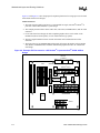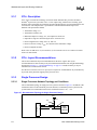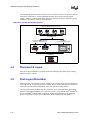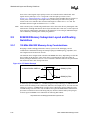
1
Intel® 440GX AGPset Design Guide March 1999 Order Number: 290651-001 Information in this document is provided in connection with Intel products. No license, express or implied, by estoppel or otherwise, to any intellectual property rights is granted by this document. Except as provided in Intel's Terms and Conditions of Sale for such products, Intel assumes no liability whatsoever, and Intel disclaims any express or implied warranty, relating to sale and/or use of Intel products including liability or warranties relating to fitness for a particular purpose, merchantability, or infringement of any patent, copyright or other intellectual property right. Intel products are not intended for use in medical, life saving, or life sustaining applications. Intel may make changes to specifications and product descriptions at any time, without notice. Contact your local Intel sales office or your distributor to obtain the latest specifications and before placing your product order. The Intel® 440GX AGPset may contain design defects or errors which may cause the products to deviate from published specifications. Current characterized errata are available on request. I2C is a two-wire communications bus/protocol developed by Philips. SMBus is a subset of the I2C bus/protocol and was developed by Intel. Implementations of the I2C bus/protocol or the SMBus bus/protocol may require licenses from various entities, including Philips Electronics N.V. and North American Philips Corporation. Copies of documents which have an ordering number and are referenced in this document, or other Intel literature may be obtained by: calling 1-800-548-4725 or by visiting Intel's website at http://www.intel.com. Copyright © Intel Corporation, 1999 *Third-party brands and names are the property of their respective owners. Intel® 440GX AGPset Design Guide Contents 1 Introduction ................................................................................................................1-1 1.1 1.2 1.3 1.4 2 About This Design Guide ..............................................................................1-1 References....................................................................................................1-2 Intel® Pentium® II Processor / Intel® 440GX AGPset Overview ...................1-3 1.3.1 Intel® Pentium® II Processor............................................................1-3 1.3.2 Intel® 440GX AGPset ......................................................................1-4 1.3.2.1 System Bus Interface......................................................1-5 1.3.2.2 DRAM Interface ..............................................................1-5 1.3.2.3 Accelerated Graphics Port Interface...............................1-5 1.3.2.4 PCI Interface...................................................................1-6 1.3.2.5 System Clocking .............................................................1-6 1.3.3 PCI-to-ISA/IDE Xcelerator (PIIX4E).................................................1-6 1.3.3.1 Instrumentation ...............................................................1-7 1.3.3.2 Remote Service Boot......................................................1-7 1.3.3.3 Remote Wake-Up ...........................................................1-8 1.3.3.4 Power Management........................................................1-8 Design Recommendations............................................................................1-8 1.4.1 Voltage Definitions ...........................................................................1-8 1.4.2 General Design Recommendations .................................................1-9 1.4.3 Transitioning from Intel“ 440BX AGPset to Intel“ 440GX AGPset Design ................................................................................1-9 Motherboard Layout and Routing Guidelines ............................................................2-1 2.1 2.2 2.3 2.4 2.5 BGA Quadrant Assignment...........................................................................2-1 Board Description .........................................................................................2-3 Routing Guidelines........................................................................................2-5 2.3.1 GTL+ Description .............................................................................2-6 2.3.2 GTL+ Layout Recommendations .....................................................2-6 2.3.3 Single Processor Design..................................................................2-6 2.3.3.1 Single Processor Network Topology and Conditions......2-6 2.3.3.2 Single Processor Recommended Trace Lengths ...........2-7 2.3.4 Dual Processor Systems..................................................................2-8 2.3.4.1 Dual Processor Network Topology and Conditions ........2-8 2.3.4.2 Dual Processor Recommended Trace Lengths..............2-8 2.3.5 Single Processor Systems—Single-End Termination (SET) ...........2-8 2.3.5.1 Set Network Topology and Conditions ...........................2-8 2.3.5.2 SET Trace Length Requirements ...................................2-9 2.3.6 Additional Guidelines .....................................................................2-10 2.3.6.1 Minimizing Crosstalk.....................................................2-10 2.3.6.2 Practical Considerations ...............................................2-10 2.3.7 Design Methodology ......................................................................2-11 2.3.8 Performance Requirements ...........................................................2-12 2.3.9 Topology Definition ........................................................................2-13 2.3.10 Pre-Layout Simulation (Sensitivity Analysis)..................................2-13 Placement & Layout....................................................................................2-14 Post-Layout Simulation ...............................................................................2-14 2.5.1 Crosstalk and the Multi-Bit Adjustment Factor ...............................2-15 Intel® 440GX AGPset Design Guide iii 2.6 2.7 2.8 2.9 3 Design Checklist ........................................................................................................3-1 3.1 3.2 3.3 3.4 3.5 3.6 iv Validation ....................................................................................................2-15 2.6.1 Flight Time Measurement ..............................................................2-15 2.6.2 Signal Quality Measurement..........................................................2-16 Timing Analysis...........................................................................................2-17 AGP Layout and Routing Guidelines ..........................................................2-19 2.8.1 AGP Connector (“Up Option) Layout Guidelines ...........................2-19 2.8.2 On-board AGP Compliant Device (“Down” Option) Layout Guidelines ..........................................................................2-20 82443GX Memory Subsystem Layout and Routing Guidelines..................2-22 2.9.1 100 MHz 82443GX Memory Array Considerations........................2-22 2.9.1.1 Matching the Reference Planes ...................................2-23 2.9.1.2 Adding Additional Decoupling Capacitor ......................2-23 2.9.1.3 Trace Width vs. Trace Spacing ....................................2-24 2.9.2 Memory Layout & Routing Guidelines ...........................................2-24 2.9.3 4 DIMM Routing Guidelines [NO FET]...........................................2-30 2.9.4 PCI Bus Routing Guidelines ..........................................................2-30 2.9.5 Decoupling Guidelines: Intel® 440GX AGPset Platform ...............2-31 2.9.6 Intel® 440GX AGPset Clock Layout Recommendations................2-32 2.9.6.1 Clock Routing Spacing .................................................2-32 2.9.6.2 System Bus Clock Layout.............................................2-32 2.9.6.3 PCI Clock Layout..........................................................2-33 2.9.6.4 SDRAM Clock Layout...................................................2-33 2.9.6.5 AGP Clock Layout ........................................................2-34 Overview .......................................................................................................3-1 Pull-up and Pull-down Resistor Values.........................................................3-1 Intel® Pentium® II Processor Checklist.........................................................3-2 3.3.1 Intel® Pentium® II Processor ...........................................................3-2 3.3.2 Intel® Pentium® II Processor Clocks................................................3-5 3.3.3 Intel® Pentium® II Processor Signals...............................................3-5 3.3.4 Uni-Processor (UP) Slot 1 Checklist ................................................3-7 3.3.5 Dual-Processor (DP) Slot 1 Checklist ..............................................3-7 3.3.6 Slot 1 Decoupling Capacitors ..........................................................3-7 3.3.7 Voltage Regulator Module, VRM 8.2 ...............................................3-7 Intel® 440GX AGPset Clocks........................................................................3-8 3.4.1 CK100 - 100 MHz Clock Synthesizer...............................................3-8 3.4.2 CKBF - SDRAM 1 to 18 Clock Buffer...............................................3-9 3.4.3 GCKE and DCLKWR Connection ....................................................3-9 82443GX Host Bridge .................................................................................3-10 3.5.1 82443GX Interface.........................................................................3-10 3.5.2 82443GX GTL+ Bus Interface .......................................................3-12 3.5.3 82443GX PCI Interface..................................................................3-12 3.5.4 82443GX AGP Interface ................................................................3-13 Intel® 440GX AGPset Memory Interface ....................................................3-14 3.6.1 SDRAM Connections .....................................................................3-14 3.6.2 DIMM Solution With FET Switches ................................................3-15 3.6.3 Registered SDRAM .......................................................................3-15 Intel® 440GX AGPset Design Guide 3.7 3.8 3.9 3.10 3.11 3.12 3.13 3.14 3.15 3.16 3.17 3.18 3.19 3.20 3.21 3.22 3.23 3.24 4 82371EB (PIIX4E).......................................................................................3-16 3.7.1 PIIX4E Connections.......................................................................3-16 3.7.2 IDE Routing Guidelines..................................................................3-20 3.7.2.1 Cabling..........................................................................3-20 3.7.2.2 Motherboard .................................................................3-20 3.7.3 PIIX4E Power And Ground Pins ....................................................3-22 PCI Bus Signals ..........................................................................................3-22 ISA Signals .................................................................................................3-23 ISA and X-Bus Signals................................................................................3-23 USB Interface..............................................................................................3-24 IDE Interface ...............................................................................................3-24 Flash Design ...............................................................................................3-25 3.13.1 Dual-Footprint Flash Design ..........................................................3-25 3.13.2 Flash Design Considerations .........................................................3-25 System and Test Signals ............................................................................3-28 Power Management Signals .......................................................................3-28 3.15.1 Power Button Implementation........................................................3-30 Miscellaneous .............................................................................................3-31 82093AA (IOAPIC)......................................................................................3-32 Manageability Devices ................................................................................3-33 3.18.1 Max1617 Temperature Sensor ......................................................3-33 3.18.2 LM79 Microprocessor System Hardware Monitor ..........................3-33 3.18.3 82558B LOM Checklist ..................................................................3-34 3.18.4 Wake On LAN (WOL) Header........................................................3-35 Software/BIOS ............................................................................................3-35 3.19.1 USB and Multi-processor BIOS .....................................................3-35 3.19.2 Design Considerations...................................................................3-36 Thermals / Cooling Solutions ......................................................................3-36 3.20.1 Design Considerations...................................................................3-36 Mechanicals ................................................................................................3-36 3.21.1 Design Considerations...................................................................3-37 Electricals....................................................................................................3-37 3.22.1 Design Considerations...................................................................3-37 Layout Checklist..........................................................................................3-38 3.23.1 Routing and Board Fabrication ......................................................3-38 3.23.2 Design Consideration.....................................................................3-38 Applications and Add-in Hardware..............................................................3-38 3.24.1 Design Consideration.....................................................................3-38 Debug Recommendations .........................................................................................4-1 4.1 4.2 Slot 1 Test Tools ...........................................................................................4-1 Debug/Simulation Tools................................................................................4-1 4.2.1 Logic Analyzer Interface (LAI)..........................................................4-1 4.2.2 In-Target Probe (ITP).......................................................................4-1 4.2.3 Bus Functional Model (BFM) ...........................................................4-2 4.2.4 I/O Buffer Models .............................................................................4-2 4.2.5 FLOTHERM* Model .........................................................................4-2 Intel® 440GX AGPset Design Guide v 4.3 5 Debug Features ............................................................................................4-2 4.3.1 Intel® Pentium® II Processor LAI Issue ...........................................4-2 4.3.2 Debug Logic Recommendations......................................................4-4 4.3.2.1 Debug Considerations ....................................................4-5 4.3.3 Debug Layout ..................................................................................4-5 4.3.3.1 Design Considerations ...................................................4-5 4.3.4 Debug Procedures ...........................................................................4-5 Third-Party Vendor Information .................................................................................5-1 5.1 5.2 5.3 Processors ....................................................................................................5-1 5.1.1 Voltage Regulator Modules .............................................................5-2 5.1.2 Voltage Regulator Control Silicon ....................................................5-2 Intel® 440GX AGPset ...................................................................................5-3 5.2.1 Clock Drivers ...................................................................................5-3 5.2.2 Power Management Components ...................................................5-3 5.2.3 FET Switches(4 DIMM/FET Design)................................................5-3 Other Processor Components ......................................................................5-4 5.3.1 Slot 1 Connector ..............................................................................5-4 5.3.2 Mechanical Support .........................................................................5-4 5.3.3 Heat sinks ........................................................................................5-4 5.3.4 Heat sink attachment: Rivscrews* and associated tools..................5-4 5.3.5 Thermal interface materials .............................................................5-4 A Intel® 440GX AGPset Platform Reference Design ................................................... A-1 vi Intel® 440GX AGPset Design Guide Figures 1-1 2-1 2-2 2-3 2-4 2-5 2-6 2-7 2-8 2-9 2-10 2-11 2-12 2-13 2-14 2-15 2-16 2-17 2-18 2-19 2-20 2-21 2-22 2-23 2-24 2-25 2-26 2-27 2-28 2-29 2-30 2-31 3-1 3-2 3-3 3-4 3-5 3-6 3-7 3-8 4-1 Intel® Pentium® II Processor / Intel® 440GX AGPset System Block Diagram..................................................................................1-4 Major Signal Sections (82443GX Top View).................................................2-1 Example ATX Placement for a UP Pentium® II processor/ Intel® 440GX AGPset Design .......................................................................2-2 Example NLX Placement for a UP Intel® Pentium® II processor / Intel® 440GX Design.....................................................................................2-3 Four Layer Board Stack-up...........................................................................2-4 Six Layer Board Stack-up With 4 Signal Planes and 2 Power Planes..........2-4 Six Layer Board Stack-up With 3 Signal Planes and 3 Power Planes..........2-5 Recommended Topology for Single Processor Design ................................2-6 Solution Space for Single Processor Design (Based on Results of Parametric Sweeps)..................................................................................2-7 Recommended Topology for Dual Processor Design...................................2-8 Topology for Single Processor Designs With Single-End Termination (SET).........................................................................................2-9 Solution Space for Single Processor Designs With Single-End Termination (SET).........................................................................................2-9 GTL+ Design Process.................................................................................2-12 Pre-layout simulation process.....................................................................2-14 AGP Connector Layout Guidelines .............................................................2-19 On-board AGP Compliant Device Layout Guidelines .................................2-21 FET Switch Example...................................................................................2-22 Registered SDRAM DIMM Example ...........................................................2-23 Matching the Reference Planes and Adding Decoupling Capacitor ..........2-24 4 DIMMs (Single or Double-Sided) .............................................................2-24 Motherboard Model—Data (MDxx), 4 DIMMs.............................................2-25 Motherboard Model—DQMA[0,2:4,6:7], 4 DIMMs ......................................2-26 Motherboard Model—DQM_A[1,5], 4 DIMMs .............................................2-26 Motherboard Model—DQM_A[1,5], 4 DIMMs .............................................2-26 Motherboard Model—DQM_B[1,5], 4 DIMMs .............................................2-27 Motherboard Model—CS_A#/CS_B#, 4 DIMMs .........................................2-27 Motherboard Model—SRAS_A#, 4 DIMMs.................................................2-27 Motherboard Model—Data (MDxx) Lines, 4 DIMMs (No FET) ...................2-30 PCI Bus Layout Example ............................................................................2-31 82443GX Decoupling..................................................................................2-31 Clock Trace Spacing Guidelines.................................................................2-32 AGP Clock Layout.......................................................................................2-34 Pull-up Resistor Example..............................................................................3-2 GCKE & DCLKWR Connections...................................................................3-9 Current Solution With Existing FET Switches .............................................3-15 Series Resistor Placement for Primary IDE Connectors.............................3-21 Dual Footprint Flash Layouts ......................................................................3-25 nterfacing Intel’s Flash with PIIX4E in Desktop ..........................................3-26 Interfacing Intel’s Flash with PIIX4E in Desktop .........................................3-28 PWRGOOD & PWROK Logic .....................................................................3-29 LAI Probe Input Circuit..................................................................................4-3 Intel® 440GX AGPset Design Guide vii Tables 2-1 2-2 2-3 2-4 2-5 2-6 2-7 2-8 2-9 2-10 2-11 2-12 2-13 2-14 2-15 2-16 2-17 2-18 2-19 2-20 2-21 2-22 2-23 2-24 2-25 3-1 3-2 3-3 3-4 3-5 3-6 3-7 3-8 3-9 3-10 3-11 3-12 3-13 5-1 5-2 5-3 5-4 5-5 5-6 5-7 5-8 viii Recommended Trace Lengths for Single Processor Design ........................2-7 Recommended Trace Lengths for Dual Processor Designs2.......................2-8 SET Trace Length Requirements .................................................................2-9 Recommended 100 MHz System Flight Time Specs .................................2-13 System Timing Requirements for Validating Setup/Hold Windows ............2-16 Ringback Guidelines at the Intel® Pentium® II Processor Edge Fingers ...2-16 Intel® Pentium® II Processor and Inte®l 440GX AGPset System Timing Equations ...........................................................................2-17 Intel® Pentium® II Processor and Intel® 440GX AGPset System Timing Terms .................................................................................2-17 Intel® Pentium® II Processor and Intel® 440GX AGPset 100 MHz Timing Specifications..................................................................................2-18 Recommended 100 MHz System Timing Parameters................................2-18 Recommended 100 MHz System Flight Time Specs .................................2-18 Data and Associated Strobe .......................................................................2-19 Source Synchronous Motherboard Recommendations ..............................2-20 Control Signal Line Length Recommendations ..........................................2-20 Source Synchronous Motherboard Recommendations ..............................2-21 Control Signal Line Length Recommendations ..........................................2-21 MDx lines Reference Planes Routing .........................................................2-23 FET Switch DQ Route Example .................................................................2-25 Motherboard Model: SRAS_B#, 4 DIMMs ..................................................2-28 Motherboard Model: SCAS_A#, 4 DIMMs ..................................................2-28 Motherboard Model: SCAS_B#, 4 DIMMs ..................................................2-28 Motherboard Model: WE_A#, 4 DIMMs ......................................................2-29 Motherboard Model: WE_B#, 4 DIMMs ......................................................2-29 Motherboard Model: MA_A[14:0], 4 DIMMs ...............................................2-29 Motherboard Model: MA_B[12,11,9:0]#, MA_B[14,13,10], 4 DIMMs..........2-30 Slot Connectivity ...........................................................................................3-2 GND & Power Pin Definition .........................................................................3-4 Processor Frequency Select.........................................................................3-8 82443GX Connectivity ................................................................................3-10 Strapping Options .......................................................................................3-13 SDRAM Connectivity ..................................................................................3-14 PIIX4E Connectivity ....................................................................................3-16 IDE Series Termination...............................................................................3-20 PIIX4E PWR & GND...................................................................................3-22 Non-PIIX4E PCI Signals .............................................................................3-23 Non-PIIX4E ISA Signals .............................................................................3-23 Non-PIIX4E IDE..........................................................................................3-24 Flash Vpp Recommendations....................................................................3-27 Slot 1 Connector ...........................................................................................5-1 Retention Mechanism, Retention Mechanism Module Attach Sink Suppor .......................................................................................5-1 GTL+ Bus Slot 1 Terminator Cards ..............................................................5-1 Voltage Regulator Modules ..........................................................................5-2 Voltage Regulator Control Silicon Vendors ..................................................5-2 Clock Driver Vendors....................................................................................5-3 Power Management Component Vendors....................................................5-3 FET Switch Vendors .....................................................................................5-3 Intel® 440GX AGPset Design Guide Revision History Date Revision 3/99 -001 Intel® 440GX AGPset Design Guide Description Initial Release. ix x Intel® 440GX AGPset Design Guide 1 Introduction Introduction Introduction 1 This document provides design guidelines for developing Intel® Pentium® II processor / Intel® 440GX AGPset based systems. Motherboard and memory subsystem design guidelines are covered. Special design recommendations and concerns are presented. Likely design issues have been identified and included here in a checklist format to alleviate problems during the debug phase. One reference board design is presented: • Dual Processor (DP), 4 DIMM design These designs use the Intel® Pentium® II processor and Intel® 440GX AGPset consisting of the 82443GX Host Bridge and the 82371EB PIIX4E. Note: 1.1 The Intel® Pentium® II processor may be installed in a Slot 1 connector. The Intel® Pentium® II processor will also be offered as an Intel boxed processor, intended for system integrators who build systems from motherboards and other components. Some hints for early debug problems are also included. About This Design Guide This document is intended for hardware design engineers who are experienced in the design of PC motherboards or memory subsystem. This document is organized as follows: Chapter 1, Introduction. This chapter provides an overview of the features on reference design. Chapter 1 also provides a general component overview of the Intel® Pentium® II processor and Intel 440GX AGPset. The Wired for Management Initiative is also discussed which is an Intel® initiative to improve the manageability of desktop, mobile, and server systems. This chapter also provides design recommendations which Intel feels will provide flexibility to cover a broader range of products within a market segment. Chapter 2, Motherboard Layout and Routing Guidelines. This Chapter provides detailed layout, routing, and placement guidelines for the motherboard and memory subsystem. Design guidelines for each bus (Host GTL+, PCI, DRAM, and AGP) are covered. This chapter provides details on design methodology, Timing analysis, simulation, and design validation. Chapter 3, Design Checklist. This chapter provides a design checklist that is intended to be used when reviewing your Intel® 440GX AGPset design. The checklist is based on the Intel® 440GX AGPset reference design provided in this Design Guide. Items which have been found to be incorrect on previous designs are provided as a tool to allow the quick debug of Intel® Pentium® II processor based systems. Chapter 4, Debug Recommendations. This chapter presents debug recommendations that may assist in the development of the Intel® Pentium® II processor, Intel® 440GX AGPset, and products utilizing them. This chapter also provides tool information, logic suggestions, technical support options, and a summary of the problems which have been found to be associated with system debug. Chapter 5, Third Party Vendor Information. This chapter includes information regarding various third-party vendors who provide products to support the Intel® 440GX AGPset. Appendix A, Intel® 440GX AGPset Reference Design Schematics. This appendix provides the schematics used in the single processor and dual processor reference designs. Intel® 440GX AGPset Design Guide 1-1 Introduction 1.2 References • • • • Intel® Pentium® II Processor Datasheet Intel® 440GX AGPset Datasheet (WWW; order number 290638) Intel 82371EB PCI-to-ISA/IDE Xcelerator (PIIX4) Datasheet (WWW; order number 290562) Intel Architecture Software Developer’s Manual, Volume 1; Basic Architecture (order number 243190) • Intel Architecture Software Developer’s Manual, Volume 2; Instruction Set Reference (order number 243191) • Intel Architecture Software Developer’s Manual, Volume 3; System Programming Guide (order number 243192) • • • • • • • • • • • • • • Intel Architecture MMX™ Technology Developer’s Guide (order number 243006) AP-485 CPUID Application Note (WWW; order number 41618) AP-585 Layout Application Note (WWW; order number 243330) AP-586 Thermal Application Note (WWW; order number 243331) AP-587 Power Application Note (WWW; order number 243332) AP-589 EMI (WWW; order number 243334) AP-524 Intel® Pentium® Pro Processor GTL+ Layout Guidelines (order number 242765) AP-525 Intel® Pentium® Pro Processor Thermal Design Guidelines (order number 242766) Multi-Processor Specification 1.4 (order number 242016) + Processor Fan/Heat Sink Target Specification, Revision 1.0 or later + Slot 1 Test Kit User’s Guide, Revision 1.0 or later + Slot 1 Processor Enabling Technologies Supplier Guide, Revision 3.0 PCI Local Bus Specification, Revision 2.1 Universal Serial Bus Specification, Revision 1.0 Intel® 440GX AGPset Design Guide 1-2 Introduction 1.3 Intel® Pentium® II Processor / Intel® 440GX AGPset Overview The following is a list of features that a Intel® Pentium® II processor / Intel® 440GX System will provide: • Full Support for up to two Intel® Pentium® II processors, with system bus frequencies of 100 MHz • Intel® 440GX AGPset — 82443GX Host Bridge Controller (GX) — 82371EB PCI ISA IDE Accelerator (PIIX4E) • 100 MHz Memory Interface: A wide range of DRAM support including — 64-bit memory data interface plus 8 ECC bits and hardware scrubbing — SDRAM (Synchronous) DRAM Support — 16Mbit, 64Mbit, 128Mbit, and 256Mbit DRAM Technologies • 4 PCI Add-in Slots — PCI Specification Rev 2.1 Compliant • 1 AGP Slot: — AGP Interface Specification Rev 1.0 Compliant — AGP 66/133 MHz, 3.3V device support • Integrated IDE Controller with Ultra DMA/33 support — PIO Mode 4 transfers — PCI IDE Bus Master support • • • • 1.3.1 Integrated Universal Serial Bus (USB) Controller with 2 USB ports Integrated System Power Management Support On-board Floppy, Serial, Parallel Ports, ISA Add-in slots I/O APIC device support for MP interrupt support Intel® Pentium® II Processor The Intel® Pentium® II processor is a follow-on to the Intel® Pentium® Pro processor. This high performance Intel Architecture processor offers features that can be designed into products for the following market segments: Desktop Home Market Segment Desktop Corporate Market Segment Workstation Market Segment Server Market Segment New applications and hardware add-ins from third party vendors are being developed that take advantage of the MMX™ technology incorporated into the Intel® Pentium® processor. Please contact your local Intel field sales representative for information on IHVs and ISVs utilizing Intel’s MMX™ technology. Intel® 440GX AGPset Design Guide 1-3 Introduction Intel introduced the Intel® Pentium® II processor as 350/100 and 400/100 speeds with 512 KB L2 cache versions. 1.3.2 Intel® 440GX AGPset • The Intel® 440GX AGPset is the fourth generation chipset based on the Intel® Pentium® Pro processor architecture. It has been designed to interface with the Intel® Pentium® II processor’s system bus at 100 MHz. Along with its Host-to-PCI bridge interface, the 82443GX host bridge controller has been optimized with a 100 MHz SDRAM memory controller and data path. The 82443GX also features the Accelerated Graphics Port (AGP) interface. The 82443GX component includes the following functions and capabilities: • • • • • • • Support for single and dual Intel® Pentium® II processor configurations 64-bit GTL+ based system data bus Interface 32-bit system address bus support 64/72-bit main memory interface with optimized support for SDRAM 32-bit PCI bus interface with integrated PCI arbiter AGP interface with up to 133 MHz data transfer rate Extensive data buffering between all interfaces for high throughput and concurrent operations Figure 1-1. Intel® Pentium® II Processor / Intel® 440GX AGPset System Block Diagram Pentium® II Processor Pentium® II Processor Host Bus Video - DVD - Camera - VCR - VMI - Video Capture 2X AGP Bus Graphics Device 72 Bit w/ECO 82443GX Host Bridge Main Memory 100 MHz SDRAM Support Display Graphics Local Memory PCI Slots Encoder TV Primary PCI Bus Video BIOS (PCI Bus #0) System Mgnt (SM) Bus 2 IDE Ports (Ultra DMA/33) 82371EB (PIIX4E) (PCI-to-ISA Bridge) 2 USB Ports IO APIC USB ISA Slots USB ISA Bus System BIOS sys_blk.vsd Intel® 440GX AGPset Design Guide 1-4 Introduction Figure 1-1 shows a block diagram of a typical platform based on the Intel® 440GX AGPset. The 82443GX system bus interface supports up to two Intel ® Pentium® II processors at the maximum bus frequency of 100 MHz. The physical interface design is based on the GTL+ specification and is compatible with the Intel® 440GX AGPset solution. The 82443GX provides an optimized 72-bit DRAM interface (64-bit Data plus ECC). This interface supports 3.3V DRAM technologies. The 82443GX is designed to support the PIIX4E I/O bridge. The PIIX4E is a highly integrated multifunctional component that supports the following functions and capabilities: • • • • • • • 1.3.2.1 PCI Rev 2.1 compliant PCI-to-ISA Bridge with support for 33 MHz PCI operations ACPI Desktop Power Management Support Enhanced DMA controller and standard interrupt controller and timer functions Integrated IDE controller with Ultra DMA/33 support USB host interface with support for 2 USB ports System Management Bus (SMB) with support for DIMM Serial Presence Detect Support for an external I/O APIC component System Bus Interface The Intel® Pentium® II processor supports a second level cache size of 512 KB with ECC. All cache control logic is provided on the processor. The 82443GX supports a maximum of 32 bit address or 4 GB memory address space from the processor perspective. The 82443GX provides bus control signals and address paths for transfers between the processors bus, PCI bus, Accelerated Graphics Port and main memory. The 82443GX supports a 4-deep in-order queue (i.e., it provides support for pipelining of up to 4 outstanding transaction requests on the system bus). For system bus-to-PCI transfers, the addresses are either translated or directly forwarded on the PCI bus, depending on the PCI address space being accessed. If the access is to a PCI configuration space, the processor I/O cycle is mapped to a PCI configuration space cycle. If the access is to a PCI I/O or memory space, the processor address is passed without modification to the PCI bus. Certain memory address range (later referred in a document as a Graphics Aperture) are dedicated for a graphics memory address space. If this space or portion of it is mapped to main DRAM, then the address will be translated via the AGP address remapping mechanism and the request forwarded to the DRAM subsystem. A portion of the graphics aperture can be mapped on AGP and corresponding system bus cycles that hit that range are forwarded to AGP without any translation. Other system bus cycles forwarded to AGP are defined by the AGP address map. 1.3.2.2 DRAM Interface The 82443GX integrates a main memory controller that supports a 64/72-bit DRAM interface which operates at 100 MHz. The integrated DRAM controller features: supports up to 4 doublesided DIMMs, 8M to 256M using 16Mbit technology, 1 GB using 64Mbit technology, and 2 GB using 128M or 256M technology, two copies of MAxx are provided for optimized timing, and ECC with hardware scrubbing. 1.3.2.3 Accelerated Graphics Port Interface The 82443GX supports an AGP interface. The AGP interface can reach a maximum theoretical ~532 Mbytes/sec transfer rate. Intel® 440GX AGPset Design Guide 1-5 Introduction 1.3.2.4 PCI Interface The 82443GX PCI interface is 33 MHz Revision 2.1 compliant and supports up to five external PCI bus masters in addition to the I/O bridge (PIIX4E). 1.3.2.5 System Clocking The 82443GX operates the system bus interface at 100 MHz, PCI at 33 MHz and AGP at 66/133 MHz. The 443GX clocking scheme uses an external clock synthesizer which produces reference clocks for the system bus and PCI interfaces. The 82443GX produces a single 100 MHz SDRAM clock output which is fed to a 1 to 18 clock buffer to support 1 to 4 DIMMs. 1.3.3 PCI-to-ISA/IDE Xcelerator (PIIX4E) The PCI-to-ISA/IDE Xcelerator (PIIX4E) is a multi-function PCI device implementing a PCI-toISA bridge function, a PCI IDE function, a Universal Serial Bus host/hub function, and an Enhanced Power Management function. As a PCI-to-ISA bridge, the PIIX4E integrates many common I/O functions found in ISA-based PC systems; a seven channel DMA Controller, two 82C59 Interrupt Controllers, an 8254 Timer/Counter, and a Real Time Clock. In addition to Compatible transfers, each DMA channel also supports Type F transfers. The PIIX4E contains full support for both PC/PCI and Distributed DMA protocols implementing PCI based DMA. The Interrupt Controller has Edge or Level sensitive programmable inputs and fully supports the use of an external I/O Advanced Programmable Interrupt Controller (APIC) and Serial Interrupts. Chip select decoding is provided for BIOS, Real Time Clock, Keyboard Controller, second external Microcontroller, as well as 2 Programmable Chip Selects. The PIIX4E provides full Plug and Play compatibility. The PIIX4E can be configured as a Subtractive Decode bridge or as a Positive Decode bridge. The PIIX4E supports two IDE connectors for up to four IDE devices providing an interface for IDE/EIDE hard disks and CD ROMs. Up to four IDE devices can be supported in Bus Master mode. The PIIX4E contains support for “Ultra DMA/33” synchronous DMA compatible devices. The PIIX4E contains a Universal Serial Bus (USB) Host Controller that is Universal Host Controller Interface (UHCI) compatible. The Host Controller’s root hub has two programmable USB ports. The PIIX4E supports Enhanced Power Management, including full Clock Control, Device Management for up to 14 devices, and Suspend and Resume logic with Power On Suspend, Suspend to RAM or Suspend to Disk. It fully supports Operating System Directed Power Management via the Advanced Configuration and Power Interface (ACPI) specification. The PIIX4E integrates both a System Management Bus (SMBus) Host and Slave interface for serial communication with other devices. For more information on the PIIX4E, please refer to thePIIX4 datasheet. 1.3.4 Wired for Management Initiative Wired for Management (WfM) is an Intel initiative to improve the manageability of desktop, and server systems. The goal of WfM is to reduce the Total Cost of Ownership (TCO) through improved manageability in the following four technology areas: • • • • Instrumentation Remote Service Boot Remote Wake-Up Power Management Intel® 440GX AGPset Design Guide 1-6 Introduction Manageability features in each of these four technology areas combine to form the Wired for Management Baseline Specification. A copy of the Wired for Management Baseline Specification can be obtained from: ftp://download.intel.com/ial/wfm/baseline.pdf An on-line Design Guide is available at: http://developer.intel.com/ial/WfM/design/index.htm Future versions of the specification, which preserve today's investments, will be available at this site. 1.3.3.1 Instrumentation A component's instrumentation consists of code that maintains attributes with up-to-the-minute values and adjusts the component's operational characteristics based on these values. By providing instrumentation, the platform provides accurate data to management applications, so those applications can make the best decisions for managing a system or product. The WfM 1.1a Baseline requires that compliant desktop and mobile platforms utilize the DMI Version 2.00 Management Interface (MI) and Component Interface (CI) application programming interfaces and host a DMI v2.00 Service Provider, as defined by the DMTF. Intel's DMI 2.0 Service Provider Software Development Kit (SDK) provides a DMI Service Provider and binaries that support DMI Version 2.00. This kit is available at: http://developer.intel.com/ial/WfM/tools/sdk/index.htm. Intel's LANDesk© Client Manager product includes the Service Provider and component instrumentation. Information regarding this product can be found at: http://developer.intel.com/ial/WfM/tools/ldcm/index.htm The WfM Baseline Instrumentation specification identifies specific DMI standard groups, including event generation groups, that must be instrumented for a Baseline-compliant platform. This reference design provides support for the SMBIOS revision 2.0 specification which along with appropriate component instrumentation will supply some of the required data in the specified DMI 2.0 groups. This reference design also provides additional optional instrumentation hardware support with the LM79 and Maxim MAX1617 components. 1.3.3.2 Remote Service Boot The WfM Baseline specifies the protocols by which a client requests and downloads an executable image from a server and the minimum requirements on the client execution environment when the downloaded image is executed. The Baseline specification includes a set of APIs for the particular network controller used. The code supporting the Preboot eXecution Environment (PXE) and the network controller is provided on the EtherExpress© PRO/100 WFM adapters Option ROM. Two implementation options are available: 1) NIC with Option ROM and Wake on LAN Header or 2) a LAN on Motherboard implementation. For the second option, the Preboot execution environment and the network controller code must be incorporated into the system BIOS. In addition, the BIOS must provide the _SYSID_ and _UUID_ data structures. The details of the BIOS requirements can be obtained from the Intel web site. http://developer.intel.com/ial/WfM/design/pxedt/index.htm Intel® 440GX AGPset Design Guide 1-7 Introduction 1.3.3.3 Remote Wake-Up If a PC supports a reduced power state, it must be possible to bring the system to a fully powered state in which all management interfaces are available. Typically, the LAN adapter recognizes a special packet as a signal to wake up the system. This reference design utilizes a Wake on LAN (WOL) Header to provide standby power to the NIC and the interface for the wake up signal. The physical connection to the NIC and motherboard is via a WOL Cable provided with the design kit. See the WOL Header Recommendations document at: ftp://download.intel.com/ial/wfm/wol_v14.pdf. The system BIOS must enable the wake event and provide wake up status. The details of the BIOS requirements can be obtained from the Intel Corporation web site: http://developer.intel.com/ial/WfM/design/rwudt/index.htm 1.3.3.4 Power Management WfM Baseline compliant systems have four distinct power states: Working, Sleeping, Soft Off, and Mechanical Off. Soft off is usually provided by a user accessible switch that will send a soft off request to the system. The PIIX4 provides the power button input for this purpose and implementation details are described in the schematics. A second optional “override” switch located in a less obvious place (or removal of the power cord) stops current flow forcing the platform into the mechanical off state without OS consent. Note that a second “override” switch is required for legal reasons in some jurisdictions (for example, some European countries). The BIOS may support the power management requirement either through the APM revision 1.2 or ACPI revision 1.0 specifications. This reference design’s BIOS implementation incorporates both interfaces. The PIIX4 provides hardware level register support for both the APM and ACPI specifications. See Intel's web site for additional information: http://developer.intel.com/ial/WfM/design/pmdt/index.htm. 1.4 Design Recommendations 1.4.1 Voltage Definitions For the purposes of this document the following nominal voltage definitions are used: Vcc Vcc3.3 VccCORE Vcc2.5 VTT VREF Intel® 440GX AGPset Design Guide 5.0V 3.3V Voltage is dependent on the five bit VID setting 2.5V 1.5V 1.0V 1-8 Introduction 1.4.2 General Design Recommendations 1. Intel recommends using an industry standard programmable Voltage Regulator Module (VRM) installed in a VRM header or an onboard programmable voltage regulator designed for Intel® Pentium® II processors. 2. Systems should be capable of varying the system bus to processor core frequency ratio per the System Bus to Core Frequency Multiplier Configuration table of the Intel® Pentium® II processor datasheet. The Intel® Pentium® II processor uses the following signals to configure the internal clock multiplier ratio: LINT[0]/INTR, IGNNE#, A20M#, LINT[1]/NMI. Follow the recommendations in this document to ensure that adequate hold times are met on the strapping signals. Ensure the output of the strapping logic is a Vcc2.5 logic level for connection to the Slot 1 connector. This can be accomplished using an open-drain output driver with pullups to Vcc2.5. 3. Please prepare for additional thermal margin for increases of 1-5W for higher performance or otherwise enhanced processor. 4. Motherboard designs targeted for system integrators should design to the Boxed Intel® Pentium® II processor electrical, mechanical and thermal specifications provided in the Intel® Pentium® II processor datasheet, most notably the required fan power header, fan/heatsink physical clearance on the motherboard. 5. Motherboard designs should incorporate a retention mechanism, retention mechanism attach mount and heatsink support mounting holes and keep out areas for the Intel® Pentium® II processor and boxed Intel® Pentium® II processor. 1.4.3 Transitioning from Intel 440BX AGPset to Intel 440GX AGPset Design 1. The 82443GX supports 2GB using 128M or 256M memory technology. The design guidelines for MAA14 and MAB14 are the same as MAA-13 and MAB-13 on the 82443BX. 2. Intel® 440GX AGPset supports 100 MHz system bus and 100 MHz SDRAM Memory only. 3. There is no 3 DIMM support with the Intel 440GX AGPset. Intel® 440GX AGPset Design Guide 1-9 Introduction 1-10 Intel® 440GX AGPset Design Guide 2 Motherboard Design Motherboard Layout and Routing Guidelines Motherboard Layout and Routing Guidelines 2 This chapter describes layout and routing recommendations to insure a robust design. Follow these guidelines as closely as possible. Any deviations from the guidelines listed here should be simulated to insure adequate margin is still maintained in the design 2.1 BGA Quadrant Assignment Intel assigned pins on the 82443GX to simplify routing and keep board fabrication costs down, by permitting a motherboard to be routed in 4-layers. Figure 2-1 shows the 4 signal quadrants of the 82443GX. The component placement on the motherboard should be done with this general flow in mind. This simplifies routing and minimizes the number of signals which must cross. The individual signals within the respective groups have also been optimized to be routed using only 2 PCB layers. Note: The Intel® 82443GX AGPset Datasheet contains a complete list of signals and Ball assignments. Figure 2-1. Major Signal Sections (82443GX Top View) PCI Quadrant Pin #1 Corner AGP Quadrant 1 2 3 4 24 25 26 A B C D E F G H J K L M N P R T U V W Y AA AB AC AD AE AF 5 6 GTL+ Quadrant 7 8 9 10 11 12 13 14 15 16 17 18 19 20 21 22 23 SDRAM Quadrant v001 Intel® 440GX AGPset Design Guide 2-1 Motherboard Layout and Routing Guidelines Figure 2-2 and Figure 2-3 show the proposed component placement for a single processor for both ATX and NLX form factor designs. ATX Form Factor: 1. The ATX placement and layout below is recommended for single (UP) Intel® Pentium® II processor / Intel® 440GX AGPset system design. 2. The example placement below shows 4 PCI slots, 2 ISA slots, 4 DIMM sockets, and one AGP connector. 3. For an ATX form factor design, the AGP compliant graphics device can be either on the motherboard (device down option), or on an AGP connector (up option). 4. The trace length limitation between critical connections will be addressed later in this document. 5. The figure below is for reference only and the trade-off between the number of PCI and ISA slots, number of DIMM socket, and other motherboard peripherals need to be evaluated for each design. Figure 2-2. Example ATX Placement for a UP Pentium® II processor/Intel® 440GX AGPset Design I/O Ports PCI0 AGP/PCI1 Pentium ® II Slot 1 Host Interface CKBF PCI Interface 82443GX AGP Interface CK100 SDRAM Interface SDRAM DIMMs PIIX4E IDE 0/1 v002 2-2 Intel® 440GX AGPset Design Guide Motherboard Layout and Routing Guidelines NLX Form Factor: 1. The NLX placement and layout below is recommended for a single (UP) Intel ® Pentium® II processor / Intel® 440GX AGPset system design. 2. The example placement below shows one Slot 1 connector, 4 DIMM sockets, and an AGP compliant device down. 3. For an NLX form factor design, the AGP compliant graphics device may readily be integrated on the motherboard (device down option). 4. The trace length limitation between critical connections will be addressed later in this document. 5. Figure 2-3 is for reference only and the trade-off between the number of DIMM sockets, and other motherboard peripherals need to be evaluated for each design. Figure 2-3. Example NLX Placement for a UP Intel® Pentium® II processor / Intel® 440GX Design CK100 SDRAM DIMMs SDRAM Interface CKBF 82443GX AGP AGP Interface PCI Interface I/O Ports Host Interface Pentium ® II Slot 1 PIIX4E PCI0/ISA Riser v003 2.2 Board Description For a single processor / Intel® 440GX AGPset motherboard design, a 4 layer stack-up arrangement is recommended. The stack up of the board is shown in Figure 2-4. The impedance of all the signal layers are to be between 50 and 80 ohms. Lower trace impedance will reduce signal edge rates, over & undershoot, and have less cross-talk than higher trace impedance. Higher trace impedance will increase edge rates and may slightly decrease signal flight times. Intel® 440GX AGPset Design Guide 2-3 Motherboard Layout and Routing Guidelines Figure 2-4. Four Layer Board Stack-up Z = 60 ohms Primary Signal Layer (1/2 oz. cu.) 5 mils 47 mils 5 mils Z = 60 ohms PREPREG CORE PREPREG Ground Plane (1 oz. cu.) Power Plane (1 oz. cu) Secondary Signal Layer (1/2 oz. cu) Total board thickness = 62.6 Note: The top and bottom routing layers specify 1/2 oz. cu. However, by the time the board is plated, the traces will end about 1 oz. cu. Check with your fabrication vendor on the exact value and insure that any signal simulation accounts for this value. Note: A thicker core may help reduce board warpage issues. For a dual processor / Intel® 440GX AGPset design, a 6 layer stack-up is recommended. Two examples are shown below. Figure 2-5 has 4 signal plane layers and 2 power plane layers. Figure 2-6 shows 3 signal plane layers and 3 power plane layers. The second option makes it easier to accommodate all of the power planes required in a Intel® 440GX AGPset design. If a 6 layer stack-up is used, then it is recommended to route most of the GTL+ bus signals on the inner layers. The primary and secondary signal layer can be used for GTL+ signals where needed. Routes on the two inner layers should be orthogonal to reduce crosstalk between the layers. Figure 2-5. Six Layer Board Stack-up With 4 Signal Planes and 2 Power Planes Primary Signal Layer (1/2 oz. cu.) Z = 66 ohms 6 mils 18 mils Z = 73 ohms 6 mils 18 mils 6 mils Z = 66 ohms PREPREG CORE PREPREG CORE PREPREG Ground Plane (1 oz. cu.) Inner Layer #1 (1 oz. cu.) Inner Layer #2 (1 oz. cu) Power Plane (1 oz. cu) Secondary Signal Layer (1/2 oz. cu) Total board thickness = 62.4 2-4 Intel® 440GX AGPset Design Guide Motherboard Layout and Routing Guidelines Figure 2-6. Six Layer Board Stack-up With 3 Signal Planes and 3 Power Planes Primary Signal Layer (1/2 oz. cu.) Z = 60 ohms 5 mils Z = 59 ohms PREPREG 18 mils CORE 8 mils PREPREG 18 mils 5 mils Z = 60 ohms CORE PREPREG Ground Plane (1 oz. cu.) Inner Layer #1 (1 oz. cu.) Power Plane #1 (1 oz. cu) Power Plane #2 (1 oz. cu) Secondary Signal Layer (1/2 oz. cu) Total board thickness = 62.4 Additional guidelines on board buildup, placement and layout include: • For a 4-layer single processor design, double ended termination is recommended for GTL+ signals. One termination resistor is present on the processor substrate, and the other termination resistor is needed on the motherboard. It may be possible to use single-ended termination, if the trace lengths can tightly be controlled to 1.5” minimum and 4.0” maximum. • For a 6-layer dual processor design, no termination is required on the motherboard for GTL+ signals, as each end of the GTL+ bus is terminated on each processor. If a single Slot 1 is populated in a DP design, the second Slot 1 must be populated with a termination card. • • • • The termination resistors on the GTL+ bus should be 56 ohms. The board impedance (Z) should be between 50 and 80 ohms (65 ohms ±20%) FR-4 material should be used for the board fabrication. The ground plane should not be split on the ground plane layer. If a signal must be routed for a short distance on a power plane, then it should be routed on a VCC plane, not the ground plane. • Keep vias for decoupling capacitors as close to the capacitor pads as possible. 2.3 Routing Guidelines This section lists guidelines to be followed when routing the signal traces for the board design. The order of which signals are routed first and last will vary from designer to designer. Some designers prefer routing all of the clock signals first, while others prefer routing all of the high speed bus signals first. Either order can be used, as long as the guidelines listed here are followed. If the guidelines listed here are not followed, it is very important that your design is simulated, especially on the GTL+ signals. Even when the guidelines are followed, it is still a good idea to simulate as many signals as possible for proper signal integrity, flight time and cross talk. Intel® 440GX AGPset Design Guide 2-5 Motherboard Layout and Routing Guidelines 2.3.1 GTL+ Description GTL+ is the electrical bus technology used for the Intel® Pentium® Pro processor and Intel® Pentium® II processor system bus. GTL+ is a low output swing, incident wave switching, opendrain bus with external pull-up resistors that provide both the high logic level and termination at the end of the bus. The complete GTL+ specification is contained in the Pentium II processor databook. The specification defines: • • • • • • • Termination voltage, VTT Termination resistance, RTT Maximum output low voltage, VOL, and output low current, IOL Output driver edge rate when driving the GTL+ reference load Receiver high and low voltage level, VIL and VIH Receiver reference voltage, VREF, as a function of the termination voltage Receiver ringback tolerance Refer to the 100 MHz GTL+ layout Guidelines for the Pentium® II Processor and Intel® 440GX AGPset for more details. 2.3.2 GTL+ Layout Recommendations This section contains the layout recommendations for the GTL+ signals. The layout recommendations are derived from pre-layout simulations that Intel has run using the methodology described in Section 2.3.7, “Design Methodology” on page 2-11. Results from the pre-layout simulations are included in this section. See the Intel® Pentium® II Processor Specification Update for workarounds for any errata that may be present on the particular stepping of the processor used. 2.3.3 Single Processor Design 2.3.3.1 Single Processor Network Topology and Conditions The recommended topology for single processor systems is shown in Figure 2-7. In addition to the termination resistor on the Pentium II processor substrate, a termination resistor is placed on the system board. The recommended value for the termination resistor is 56Ω ± 5%. Figure 2-7. Recommended Topology for Single Processor Design VTT RTT L4 L3 Slot 1 L2 2-6 L1 Intel® 440GX AGPset Intel® 440GX AGPset Design Guide Motherboard Layout and Routing Guidelines 2.3.3.2 Single Processor Recommended Trace Lengths Single processor trace length recommendations are summarized in Table 2-1. The recommended lengths are derived from the parametric sweeps and Monte Carlo analysis described in the following section. Table 2-1. Recommended Trace Lengths for Single Processor Design Trace Minimum Length Maximum Length L1 1.50” 6.75” 1 L3 0.00” 1.50” L4 0.00” 2.50” 2 NOTE: 1. Refer to the Intel® Pentium® II Processor Specification Update (order number 243337); Specifically, erratum #42: workaround L1=4.5”. Intel strongly recommends running analog simulations using the available I/O buffer models together with layout information extracted from your specific design. Simulation will confirm that the design adheres to the guidelines. Figure 2-8. Solution Space for Single Processor Design (Based on Results of Parametric Sweeps) FAIL PASS 1 L3 [in] 2 0 0 1 2 3 4 5 6 7 8 9 10 11 12 L2 [in] Intel® 440GX AGPset Design Guide 2-7 Motherboard Layout and Routing Guidelines 2.3.4 Dual Processor Systems 2.3.4.1 Dual Processor Network Topology and Conditions Figure 2-9. Recommended Topology for Dual Processor Design Intel® 440GX AGPset L3 L5 Slot 1 Slot 1 L4 2.3.4.2 Dual Processor Recommended Trace Lengths The recommended trace lengths for dual processor designs are summarized in Table 2-2. Intel’s simulations have shown that it is desirable to control the amount of imbalance in the network to meet ringback specifications at the Intel® Pentium® II processor when the Intel® 440GX AGPset drives. This control is reflected in the recommendations of Table 2-2. Table 2-2. Recommended Trace Lengths for Dual Processor Designs2 Trace Minimum Length Maximum Length L3 0.50” 1.50” L4 1 1.50” 4.00” L5 2 L4 - 1.00”, but L4+L5 must be at least 4.00” L4 + 1.00”, but not greater than 5.00” NOTES: 1. L4 & L5 are interchangeable 2. It is possible to find working solutions outside the recommendations of Table 2-2, as the solution space plot show. Intel strongly recommends that any traces that fall outside the recommended lengths be simulated to ensure they meeting timing and signal quality specs. 2.3.5 Single Processor Systems—Single-End Termination (SET) 2.3.5.1 Set Network Topology and Conditions Removal of the termination resistors from the system board can reduce system cost, at the expense of increased ringing and reduced solution space. Intel has simulated this topology, known as single end termination (SET), and found that it can work. However, the topology has some limitations which are discussed below. 2-8 Intel® 440GX AGPset Design Guide Motherboard Layout and Routing Guidelines In the SET topology, the only termination is on the Intel® Pentium® II processor substrate. There is no termination present at the other end of the network. Due to the lack of termination, SET exhibits much more ringback than the dual terminated topology. Extra care is required in SET simulations to make sure that the ringback specs are met under the worst case signal quality conditions. In addition, since there is only one pull-up resistor per net the rising edge response is substantially degraded when using slow corner buffers. This effect manifests itself as a degraded flight time, which results in a reduced maximum trace length that meets the 100 MHz timing requirements. This loss of design flexibility must be carefully weighed against the cost savings from removing the resistors. Slot 1 Figure 2-10. Topology for Single Processor Designs With Single-End Termination (SET) 2.3.5.2 Intel® 440GX AGPset L1 SET Trace Length Requirements Intel has performed sensitivity analysis on the SET topology. The required trace lengths for operation at 100 MHz with the SET topology are based on the sensitivity analysis results, and are listed in Table 2-3. Intel’s SET simulations were performed assuming a four layer system board, so that all traces used the microstrip propagation velocity range. The slower propagation of stripline transmission line structures is not included in the recommendations of Table 2-3. Table 2-3. SET Trace Length Requirements Trace Minimum Length Maximum Length L1 1.50” 4.00” Figure 2-11. Solution Space for Single Processor Designs With Single-End Termination (SET) 2.5 SUBSTRATE 2.0 TRACE LENGTH [IN] 1.5 0.0 1.0 Intel® 440GX AGPset Design Guide 2.0 3.0 L1 [in] 4.0 5.0 2-9 Motherboard Layout and Routing Guidelines 2.3.6 Additional Guidelines 2.3.6.1 Minimizing Crosstalk The following general rules will minimize the impact of crosstalk in the high speed GTL+ bus design: • Maximize the space between traces. Maintain a minimum of 0.010” between traces wherever possible. It may be necessary to use tighter spacings when routing between component pins. • Avoid parallelism between signals on adjacent layers. • Since GTL+ is a slow signal swing technology, it is important to isolate GTL+ signals from other signals by at least 0.025”. This will avoid coupling from signals that have larger voltage swings, such as 5V PCI. • Select a board stack-up that minimizes the coupling between adjacent signals. • Route GTL+ address, data and control signals in separate groups to minimize crosstalk between groups. The Pentium II processor uses a split transaction bus. In a given clock cycle, the address lines and corresponding control lines could be driven by a different agent than the data lines and their corresponding control lines. 2.3.6.2 Practical Considerations • Distribute VTT with a wide trace. A 0.050” minimum trace is recommended to minimize DC losses. Route the VTT trace to all components on the system bus. Be sure to include decoupling capacitors. Guidelines for VTT distribution and decoupling are contained in Intel® Pentium® II Processor Power Distribution Guidelines. • Place resistor divider pairs for VREF generation at the Intel® 440GX AGPset component. No VREF generation is needed at the processor(s). VREF is generated locally on the processor. Be sure to include decoupling capacitors. Guidelines for VREF distribution and decoupling are contained in P Intel® Pentium® II Processor Power Distribution Guidelines. • There are six GTL+ signals that can be driven by more than one agent simultaneously. These signals may require extra attention during the layout and validation portions of the design. When a signal is asserted (driven low) by two agents on the same clock edge, the two falling wave fronts will meet at some point on the bus. This can create a large undershoot, followed by ringback which may violate the ringback specifications. This “wired-OR” situation should be simulated for the following signals: AERR#, BERR#, BINIT#, BNR#, HIT#, and HITM#. • Lossless simulations can overstate the amount of ringing on GTL+ signals. Lossy simulations may help to make your results less pessimistic if ringing is a problem. Intel has found the resistivity of copper in printed circuit board signal layers higher than the value of 0.662 Ω-mil2/in that has been published for annealed copper. Intel recommends using a value of 1.0 Ω-mil2/in for lossy simulations. • Higher RTT values tend to increase the amount of ringback on the rising edge, while smaller values tend to increase the amount of ringback on the falling edge. It is not necessary to budget for RTT variation if your simulations comprehend the expected manufacturing variation. • I/O Buffer models for the fast corner correspond to the minimum Tco. Slow corner buffers will be at least 500 ps slower. Therefore, it is only necessary to ensure that the minimum flight time is met when the network is driven by fast buffer models. • I/O Buffer models for the slow corner correspond to the maximum Tco. Fast corner buffers will be at least 500 ps faster. It is only necessary to ensure that the maximum flight time is met when the network is driven by slow buffer models, as long as no ringback problems exist. 2-10 Intel® 440GX AGPset Design Guide Motherboard Layout and Routing Guidelines 2.3.7 Design Methodology Intel recommends using the following design methodology when designing systems based on one or two Intel® Pentium® II processors and one Intel® 440GX AGPset. The methodology evolved from Intel’s experience developing and validating high speed GTL+ bus designs for the Intel® Pentium® Pro and Intel® Pentium® II processors. The methodology provides a step-by-step process which is summarized in Figure 2-12. The process begins with an initial timing analysis and topology definition. Timing and topology recommendations are included in this section. The heart of the methodology is structured around extensive simulations and analysis prior to board layout. This represents a significant departure from traditional design methods. The pre-layout simulations provide a detailed picture of the working “solution space” for the design. By basing the board layout guidelines on the solution space, the need to iterate between layout and post-layout simulation is minimized. The methodology includes specific recommendations for analytical techniques and simulation conditions. Following layout, simulation with the extracted design database is used to verify that the design meets flight time and signal quality requirements prior to building hardware. Finally, validation verifies that the system meets 100 MHz timing and signal quality requirements with actual hardware. Intel® 440GX AGPset Design Guide 2-11 Motherboard Layout and Routing Guidelines Figure 2-12. GTL+ Design Process Establish System Performance Requirements (Timing Analysis) Define Topologies Perform Pre-Layout Simulations (Sensitivity Analysis) Define Routing Rules Place & Route Board Perform Post-Layout Simulations (Verification) Meet Requirements? No Yes Validate Design 2.3.8 Performance Requirements Prior to performing interconnect simulations, establish the minimum and maximum flight time requirements. Setup and hold requirements determine the flight time bounds for the host bus. The system contains multiple paths which must be considered: • Intel® Pentium® II processor driving an AGPset component • AGPset component driving a Intel® Pentium® II processor • Intel® Pentium® II processor driving a Intel® Pentium® II processor (dual processor systems only) 2-12 Intel® 440GX AGPset Design Guide Motherboard Layout and Routing Guidelines Section 2.7, “Timing Analysis” on page 2-17 describes the timing analysis for the 100 MHz host bus in more detail. Table 2-4 provides recommended flight time specifications for single and dual Intel® Pentium® II processor systems. Flight times are measured at the Intel® Pentium® II processor edge fingers. See the Pentium® II Processor Developer’s Manual (order number 243502), Chapter 8, “GTL+ Interface Specifications“, for information on GTL+ timing measurements and signal quality specifications. Table 2-4. Recommended 100 MHz System Flight Time Specs Driver ® ® Intel Pentium II processor ® Intel 440GX AGPset ® ® Intel Pentium II processor 2.3.9 Receiver AGPset Tflight,min [ns] Tflight,max [ns] 0.36 2.13 ® ® 0.37 1.76 ® ® 1.23 2.39 Intel Pentium II processor Intel Pentium II processor Topology Definition GTL+ is sensitive to transmission line stubs, which can result in ringing on the rising edge caused by the high impedance of the output buffer in the high state. GTL+ signals should be connected in a daisy chain, keeping transmission line stubs to the Intel® 440GX AGPset under 1.5 inches. Intel® Pentium® II processors should be placed at the end of the bus to properly terminate the GTL+ signals. For a single Intel® Pentium® II processor design, Intel recommends that termination resistors be placed at the other (AGPset) end of the bus. This provides the most robust signal integrity characteristics and maximizes the range of trace lengths that will meet the flight time requirements. The recommended termination resistor value is 56Ω ± 5%. For dual Intel® Pentium® II processor based designs, a termination card must be placed in the unused slot when only one processor is populated. This is necessary to ensure that signal integrity requirements are met. Refer to Slot 1 Bus Termination Card Design Guidelines for details. 2.3.10 Pre-Layout Simulation (Sensitivity Analysis) After an initial timing analysis has been completed, simulations should be performed to determine the bounds on system layout. The layout recommendations in Section 4, “Debug Recommendations” on page 4-1 are based on results of pre-layout simulations conducted by Intel. GTL+ interconnect simulations using transmission line models are recommended to determine signal quality and flight times for proposed layouts. Recommended parameter values can be obtained if your supplier’s specific capabilities are known. The corner values should comprehend the full range of manufacturing variation. Intel® Pentium® II processor models include the I/O buffer models, core package parasitics, and substrate trace length, impedance and velocity. Intel® 440GX AGPset models include the I/O buffers and package traces. Termination resistors should be controlled to within ± 5%. 2.3.11 Simulation Methodology Pre-layout simulation allows the system “solution space” that meets flight time and signal quality requirements to be understood before any routing is undertaken. Determining the layout restrictions prior to physical design removes iteration cycles between layout and post layout simulation, as shown in Figure 2-13. Intel® 440GX AGPset Design Guide 2-13 Motherboard Layout and Routing Guidelines The methodology that Intel recommends is known as “Sensitivity Analysis”. In sensitivity analysis, interconnect parameters are varied to understand how they affect system timing and signal integrity. Sensitivity analysis can be further broken into two types of analysis, parametric sweeps and Monte Carlo analysis, which are described below. Figure 2-13. Pre-layout simulation process Interconnect Simulations (Transmission-Line) 1.75v 1.75v 1.75v 1.25v 0.25v 1.25v 0.75v 0.75v 0.75v 0.25v 0.25v 0.00ns 20.00ns 40.00ns = ALL OTHERS = 82440FXPIN 33 = KLAMATH2PIN X3 = KLAMATH2 X3 X = 0.00ns y = +0.000v xdelta = 0.000ns = KLAMATH1PIN X3 NET: SLOWDPNM_LS_12_6, DRIVER: KLAMATH1 TRACKING: KLAMATH1 = KLAMATH1 X3 X3 1.75v 1.25v 1.25v 0.75v 0.25v 0.00ns 20.00ns 40.00ns = ALL OTHERS = 82440FXPIN 33 = KLAMATH2PIN X3 = KLAMATH2 X3 X = 0.00ns y = +0.000v xdelta = 0.000ns = KLAMATH1PIN X3 NET: SLOWDPNM_LS_12_6, DRIVER: KLAMATH1 TRACKING: KLAMATH1 X3= KLAMATH1 X3 0.00ns 20.00ns 40.00ns = ALL OTHERS = 82440FXPIN 33 = KLAMATH2PIN X3 = KLAMATH2 X3 X = 0.00ns y = +0.000v xdelta = 0.000ns = KLAMATH1PIN X3 NET: SLOWDPNM_LS_12_6, DRIVER: KLAMATH2 TRACKING: KLAMATH1 = KLAMATH1 X3 X3 0.00ns 20.00ns 40.00ns = ALL OTHERS = 82440FXPIN 33 = KLAMATH2PIN X3 = KLAMATH2 X3 X = 0.00ns y = +0.000v xdelta = 0.000ns = KLAMATH1PIN X3 NET: SLOWDPNM_LS_12_6, DRIVER: KLAMATH2 TRACKING: KLAMATH1 = KLAMATH1 X3 X3 Sensitivity Analyses Performance as function of Length (flight time, signal quality, etc.) Monte Carlo (pass/fail as function of length) D U AL K L A MA TH FL IGHT T IM E 82 44 0FX to KLA MA TH D U A L K L A M A T H P R O C E S S O R C A R D S O L U T IO N S P A C E M o n t e C a rl o MA X FT RIS ING (s low silicon - slow board) D U A L K L A M A T H F L IGH T T IME MIN FT RIS IN G (fast silic on - fas t boa rd) 12 MA X F T LP C = 2 .51 in ches LF X = 1.5 inc hes LR T = 1.5 inches R t = 5 8.5 ohm s 5 M A X FT LP C = 2. 51 inch es LF X = 1 .5 inche s LR T = 1.5 inc hes R t = 53 .5 ohm s 1. 2 1 M IN F T LP C = 0. 44 inch es LF X = 0 .0 inche s LR T = 1.5 inc hes R t = 53 .5 ohm s 0. 8 0. 6 4.5 4 11 10 PCard to 82440FX Separation Distance (in) 8 24 40F X to K LA MA TH MI N F T LP C = 0 .44 in ches LF X = 0.0 inc hes LR T = 1.5 inches R t = 5 8.5 ohm s 3.5 3 2.5 2 1.5 0. 4 5.5 4.7 5 1 7 5.5 6.25 8.5 7.75 10 1.7 5 9.25 4 2.5 1.75 1 L2 PC a rd #2 to 82 44 0F X Se p ar ati o n D is tan ce (i n ) L2 PC ard #2 to 8 244 0FX Se pa ratio n Di sta nce (in ) 2.5 L1 PC ard #1 to 8 244 0FX Se par atio n D ista nce (i n ) 8 7 Pa s s Pa s s 6 F a il 5 F a il 4 3 2 1 1 11.5 7 4 3.2 5 0 10.75 1 11.5 10.75 6.25 8.5 7.75 1 L1 PC a rd #1 to 82 44 0F X Se pa rati on Di stan c e (i n) 10 1. 75 9.25 4 2.5 3.25 5.5 2. 5 4.75 1.75 0 0.5 3.25 4. 75 4 3. 25 4.75 5. 5 0. 2 9 0 0 1 2 3 4 5 6 7 8 9 10 11 12 P C a r d t o 82 44 0 F X S e p ar at io n D is t a n c e (in ) Solution Space D U A L K L A M A T H P R O C E S S O R C A R D S O L U T IO N S P A C E R t = 5 6 Ω + /- 5 % 1 M AX F lig h t T im e L P C = 2 . 5 1 in ch e s L F X = 1 .5 i n c h e s L R T = 1 . 5 i n ch e s 1. 75 3. 25 4 4. 75 6. 25 7 7. 75 8. 5 V i ll a t io n s c a u s e d b y m in im u m f lig h t t i m e 9. 25 10 10 .75 M IN F l ig h t T i m e L P C = 0 . 4 4 in ch e s L F X = 0 .0 i n c h e s L R T = 1 . 5 i n ch e s V i ll a t io n s c a u s e d b y m a x i m u m f li g h t t im e 6 5 4 5.5 5.75 5.25 3 4.5 3.5 4.75 4.25 3.25 3.75 2.75 2 1 2.5 1.5 2.25 1.75 1.25 -1 1 0 11 .5 L1 5. 5 PCard#1 to 82440FX Separation Distance (in) 2. 5 S o l u t io n s p a c e L2 P C a r d # 2 to 8 2 4 4 0 F X S e p a r a t io n D i s t a n c e ( in ) 2.4 Placement & Layout Once the pre-layout simulation is completed, route the board using the solution space resulting from the sensitivity analysis. 2.5 Post-Layout Simulation Following layout, extract the traces and run simulations to verify that the layout meets timing and noise requirements. A small amount of trace “tuning” may be required, but experience at Intel has shown that sensitivity analysis dramatically reduces the amount of tuning required. The post layout simulations should take into account the expected variation for all interconnect parameters. For timing simulations, use a VREF of 2/3 VTT ± 2% for both the Intel® Pentium® II processor and Intel® 440GX AGPset components. Flight times measured from the Pentium II processor edge fingers to other system components use the standard flight time method. 2-14 Intel® 440GX AGPset Design Guide Motherboard Layout and Routing Guidelines 2.5.1 Crosstalk and the Multi-Bit Adjustment Factor Coupled lines should be included in the post-layout simulations. The flight times listed in Table 2-4 apply to single bit simulations only. They include an allowance for crosstalk. Crosstalk effects are accounted for, as part of the multi-bit timing adjustment factor, Tadj, that is defined in Table 2-8. The recommended timing budget includes 400 ps for the adjustment factor. Use caution in applying Tadj to coupled simulations. This adjustment factor encompasses other effects besides board coupling, such as processor and package crosstalk, and ground return inductances. In general, the additional delay introduced by coupled simulations should be less than 400 ps. 2.6 Validation 2.6.1 Flight Time Measurement The timings for the Intel® Pentium® II processor are specified at the processor edge fingers. In systems, the processor edges fingers are not readily accessible. In most cases, measurements must be taken at the system board solder connection to the Slot 1 connector. To effectively correlate delay measurements to values at the Pentium II processor edge fingers, the Slot 1 connector delay must be incorporated. Flight time is defined as the difference between the delay of a signal at the input of a receiving agent (measured at VREF), and the delay at the output pin of the driving agent when driving the GTL+ reference load. However, the driver delay into the reference load is not readily available, thus making flight time measurement unfeasible. There are three options for dealing with this limitation: • The first option is to subtract the delay of the driver in the system environment (at the Slot 1 connection to the board) from the delay at the receiver. Such a measurement will introduce uncertainty into the measurement due to differences between the driver delay in the reference and system loads. If simulations indicate that your design has margin to the flight time specifications, this approach will allow you to verify that the design is robust. • The second option is to subtract the simulated reference delay from the delay at the receiver. The limitation of this option is that there may be 1 ns or more of uncertainty between the actual driver delay and the results from a simulation. This approach is less accurate that the first option. • The final option is to simply use the measured delay from driver to receiver (Tmeasured) to validate that the system meets the setup and hold requirements. In this approach, the sum of the driver delay and the flight time must fit within the “valid window” for setup and hold. The timing requirements for satisfying the valid window are shown below. Intel® 440GX AGPset Design Guide 2-15 Motherboard Layout and Routing Guidelines Table 2-5. System Timing Requirements for Validating Setup/Hold Windows Driver Pentium® II processor Receiver AGPset Equation Tmeasured ≥ Thold + Tskew ,CLK + Tskew ,PCB + Tclk ,max Tmeasured ≤ Tcycle − Tsu − Tskew,CLK − Tskew, PCB − Tjit − Tadj + Tclk ,min AGPset Pentium® II processor Tmeasured ≥ Thold + Tskew ,CLK + Tskew ,PCB − Tclk ,min Tmeasured ≤ Tcycle − Tsu − Tskew ,CLK − Tskew , PCB − Tjit − Tadj − Tclk ,max Pentium® II processor Pentium® II processor Tmeasured ≥ Thold + Tskew ,CLK + Tskew , PCB Tmeasured ≤ Tcycle − Tsu − Tskew ,CLK − Tskew, PCB − Tjit − Tadj 2.6.2 Signal Quality Measurement Signal integrity is specified at the processor core, which is not accessible. Intel has found that there can be substantial miscorrelation between ringback at the edge finger versus the core. The miscorrelation creates instances where a signal fails to satisfy ringback requirements at the edge finger, but passes the ringback specification at the core. For this reason, signal integrity is specified at the core. Ringback guidelines are supplied at the edge finger, as shown in Table 2-6. Any measurement at the edge finger that violates the guidelines should be simulated to verify that it meets the specification at the core. Table 2-6. Ringback Guidelines at the Intel® Pentium® II Processor Edge Fingers Edge Guideline @ Processor Edge Finger Spec @ Processor Core Rising 1.29V 1.12V1 Falling 0.71V 0.88V NOTE: 1. Ringback specifications follow the methodology described in Intel® Pentium II Processor at 233 MHz, 266 MHz, 300 MHz and 333 MHz Datasheet. 2-16 Intel® 440GX AGPset Design Guide Motherboard Layout and Routing Guidelines 2.7 Timing Analysis To determine the available flight time window perform an initial timing analysis. Analysis of setup and hold conditions will determine the minimum and maximum flight time bounds for the host bus. Use the following equations to establish the system flight time limits. Table 2-7. Intel® Pentium® II Processor and Inte®l 440GX AGPset System Timing Equations Driver Pentium® II processor Receiver AGPset Equation Tflight ,min ≥ Thold − Tco,min + Tskew ,CLK + Tskew , PCB + Tclk ,max Tflight ,max ≤ Tcycle − Tco ,max − Tsu − Tskew ,CLK − Tskew ,PCB − Tjit − Tadj + Tclk ,min AGPset Pentium® II processor Tflight ,min ≥ Thold − Tco,min + Tskew ,CLK + Tskew ,PCB − Tclk ,min Tflight ,max ≤ Tcycle − Tco,max − Tsu − Tskew ,CLK − Tskew ,PCB − Tjit − Tadj − Tclk ,max Pentium® II processor Pentium® II processor Tflight ,min ≥ Thold − Tco,min + Tskew ,CLK + Tskew ,PCB Tflight ,max ≤ Tcycle − Tco ,max − Tsu − Tskew,CLK − Tskew , PCB − Tjit − Tadj The terms used in the equations are described in Table 2-8. Table 2-8. Intel® Pentium® II Processor and Intel® 440GX AGPset System Timing Terms Term Description Tcycle System cycle time. Defined as the reciprocal of the frequency Tflight,min Minimum system flight time. Flight time is defined in Section 4, “Debug Recommendations” on page 4-1. Tflight,max Maximum system flight time. Flight time is defined in Section 4, “Debug Recommendations” on page 4-1. Tco,max Maximum driver delay from input clock to output data. Tco,min Minimum driver delay from input clock to output data. Tsu Minimum setup time. Defined as the time for which the input data must be valid prior to the input clock. Th Minimum hold time. Defined as the time for which the input data must remain valid after the input clock. Tskew,CLK Clock generator skew. Defined as the maximum delay variation between output clock signals from the system clock generator. Tskew,PCB PCB skew. Defined as the maximum delay variation between clock signals due to system board variation and Intel® 440GX AGPset loading variation. Tjit Clock jitter. Defined as the maximum edge to edge variation in a given clock signal. Tadj Multi-bit timing adjustment factor. This term accounts for the additional delay that occurs in the network when multiple data bits switch in the same cycle. The adjustment factor includes such mechanisms as package and PCB crosstalk, high inductance current return paths, and simultaneous switching noise. Tclk,min Minimum clock substrate delay. Defined as the minimum adjustment factor that accounts for the delay of the clock trace on the Pentium II processor substrate. Tclk,max Minimum clock substrate delay. Defined as the maximum adjustment factor that accounts for the delay of the clock trace on the Pentium II processor substrate. Intel® 440GX AGPset Design Guide 2-17 Motherboard Layout and Routing Guidelines Notice that the timing equations include an extra term to account for the delay due to routing of the BCLK trace on the processor substrate from the processor edge fingers and the processor core. Adding the BCLK adjustment to the timing calculations between processor and chipset guarantees host clock synchronization between the AGPset and processor core. The minimum and maximum values for this term are contained in Table 2-9. Component timings for the Intel® Pentium® II processor and Intel® 440GX AGPset are contained in Table 2-10. The timing specifications are contained in the Intel® Pentium® II processor and Intel® 440GX AGPset Datasheets. These timing are for reference only. Table 2-9. Intel® Pentium® II Processor and Intel® 440GX AGPset 100 MHz Timing Specifications Timing Term Intel® Pentium II Processor Intel® 440GX AGPset Tco,max [ns] 4.66 4.45 Tco,min [ns] 0.71 0.80 Tsu [ns] 1.97 3.00 Th [ns] 1.61 -0.10 Tclk,min [ns] 0.77 Not applicable Tclk,max [ns] 0.84 No applicable Recommended values for system timings are contained in Table 2-10. Skew and jitter values for the clock generator device come from the CK97 clock driver specification. The PCB skew spec is based on the results of extensive simulations at Intel. The Tadj value is based on Intel’s experience with systems that use the Intel® Pentium® Pro processor and Intel® Pentium® II processor. Table 2-10. Recommended 100 MHz System Timing Parameters Timing Term Value Tskew,CLK [ns] 0.18 Tskew,PCB [ns] 0.15 Tjit [ns] 0.25 Tadj [ns] 0.40 The flight time requirements that result from using the component timing specifications and recommended system timings are summarized in Table 2-11. All component values should be verified against the current specifications before proceeding with analysis. Table 2-11. Recommended 100 MHz System Flight Time Specs Driver 2-18 Receiver Tflight,min Tflight,max Intel® Pentium® II processor AGPset 0.36 2.13 AGPset Intel® Pentium® II processor 0.37 1.76 Intel® Pentium® II processor Intel® Pentium® II processor 1.23 2.39 Intel® 440GX AGPset Design Guide Motherboard Layout and Routing Guidelines 2.8 AGP Layout and Routing Guidelines For the definition of AGP Interface functionality (protocols, rules and signaling mechanisms, as well as the platform level aspects of AGP functionality), refer to the latest AGP Interface Specification rev 1.0 and the AGP Platform Design Guide. These documents focus only on specific Intel® 440GX AGPset platform recommendations for the AGP interface. In this document the term “data” refers to AD[31:0], C/BE[3:0]# and SAB[7:0]. The term “strobe” refers to AD_STB[1:0] and SB_STB. When the term data is used, it is referring to one of three groups of data as seen in Table 2-12. When the term strobe is used it is referring to one of the three strobes as it relates to the data in its associated group. Table 2-12. Data and Associated Strobe Data 2.8.1 Associated Strobe AD[15:0] and C/BE[1:0]# AD_STB0 AD[31:16] and C/BE[3:2]# AD_STB1 SBA[7:0] SB_STB AGP Connector (“Up Option) Layout Guidelines The maximum line length is dependent on the routing rules used on the motherboard. These routing rules were created to give freedom for designs by making trade-offs between signal coupling (trace spacing) and line lengths. These routing rules are divided by trace spacing. In 1:1 spacing, the distance between the traces (air gap) is the same as the -width of the trace. In 1:2 spacing, the distance between the traces is twice the width of the trace. Figure 2-14. AGP Connector Layout Guidelines Always 1:2 Strobe Routing AGP Compliant Graphics Device AGP Signal Bundle 82443GX 1.0” - 4.5” 1:1 (Data) Routing 4.5” - 9.5” 1:2 (Data) Routing AGP Connector For trace lengths that are between 1.0 inch and 4.5 inches, a 1:1 trace spacing is recommended for data lines. The strobe requires a 1:2 trace spacing. This is for designs that require less than 4.5 inches between the AGP connector and the AGP target. Longer lines have more crosstalk. Therefore, to maintain skew, longer line lengths require a greater amount of spacing between traces. For line lengths greater than 4.5” and less than 9.5”, 1:2 routing is recommended for all data lines as well as the strobes. For all designs, the line length mismatch must be less than 0.5” and the strobe must be the longest signal of the group. Intel® 440GX AGPset Design Guide 2-19 Motherboard Layout and Routing Guidelines It is always best to reduce the line length mismatch wherever possible to insure added margin. It is also best to separate the traces by as much as possible to reduce the amount of trace to trace coupling. Table 2-13. Source Synchronous Motherboard Recommendations Width:Space Trace Line Length Line Length Matching 1:1 (Data) / 1:2 (Strobe) Data / Strobe 1.0 in < line length < 4.5 in -0.5 in, strobe longest trace 1:2 Data / Strobe 1.0 in < line length < 9.5 in -0.5 in, strobe longest trace The clock lines on the motherboard can couple with other traces. It is recommended that the clock spacing (air gap) be at least two times the trace width to any other traces. It is also strongly recommended that the clock spacing be at least four times the trace width to any strobes. The clock lines on the motherboard need to be simulated to determine the their proper line length. The motherboard needs to be designed to the type of clock driver that is being used and motherboard trace topology. These clocks need to meet the loading of the receiving device as well as the add-in trace length. Additionally, control signals less than 8.5 inches can be routed 1:1, while control signals greater than 8.5 inches should be routed 1:2. Table 2-14. Control Signal Line Length Recommendations Width:Space Board Trace Line Length Pull-up Stub Length 1:1 Motherboard Control signals 1.0 in < line length < 8.5 in < 0.5 in (Strobes < 0.1in) 1:2 Motherboard Control signals 1.0 in < line length < 10.0 in < 0.5 in (Strobes < 0.1in) 1:2 (1:4 to Strobe) Motherboard Clock Some of the control signals require pull-up resistors to be installed on the motherboard. AGP signals must be pulled up to VCC3.3 using 8.2K to 10K pull-up resistors (refer to Section 3.5.1, “82443GX Interface” on page 3-10). Pull-up resistors should be discrete resistors, as resistor packs will need longer stub lengths and may break timing. The stub to these pull-up resistors needs to be controlled. The maximum stub length on a strobe trace is < 0.1 inch. The maximum stub trace length on all other traces is < 0.5 inch. 2.8.2 On-board AGP Compliant Device (“Down” Option) Layout Guidelines Routing guidelines for the device ‘down’ option are very similar to those when the device is ‘up’. Some modifications need to be made when placing the graphics device on the motherboard, due to the various trace spacing. 2-20 Intel® 440GX AGPset Design Guide Motherboard Layout and Routing Guidelines Figure 2-15. On-board AGP Compliant Device Layout Guidelines Always 1:2 Strobe Routing AGP Compliant Graphics Device 82443GX 1.0” - 4.5” 1:1 (Data) Routing 1” - 12” 1:2 (Data) Routing For trace lengths that are between 1.0 inch and 4.5 inches, a 1:1 trace spacing is recommended for data lines. The strobe requires a 1:2 trace spacing. This is for designs that require less than 4.5 inches between the AGP device and the AGP target. Longer lines have more crosstalk. Therefore, to maintain skew, longer line lengths require a greater amount of spacing between traces. For line lengths greater than 4.5” and less than 12.0”, 1:2 routing is recommended for all data lines and the strobes. For all designs, the line length mismatch must be less than 0.5” and the strobe must be the longest signal of the group. In all cases it is best to reduce the line length mismatch wherever possible to insure added margin. It is also best to separate the traces by as much as possible to reduce the amount of trace to trace coupling. Table 2-15. Source Synchronous Motherboard Recommendations Width:Space Trace Line Length Line Length Matching 1:1(Data) / 1:2 (Strobe) Data / Strobe 1.0 in < line length < 4.5 in -0.5 in, strobe longest trace 1:2 Data / Strobe 1.0 in < line length < 12.0 in -0.5 in, strobe longest trace The clock lines on the motherboard can couple with other traces. It is recommended that the clock spacing (air gap) be at least two times the trace width to any other traces. It is also strongly recommended that the clock spacing be at least four times the trace width to any strobes. The clock lines on the motherboard need to be simulated to determine the their proper line length. The motherboard needs to be designed to the type of clock driver that is being used and motherboard trace topology. These clocks need to meet the loading of the receiving device as well as the add-in trace length. Additionally, control signals less than 8.5 inches can be routed 1:1, while control signals greater than 8.5 inches should be routed 1:2. Table 2-16. Control Signal Line Length Recommendations Width:Space Board Trace Line Length Pull-up Stub Length 1:1 Motherboard Control signals 1.0 in < line length < 8.5 in < 0.5 in (Strobes < 0.1in) 1:2 Motherboard Control signals 1.0 in < line length < 12.5 in < 0.5 in (Strobes < 0.1in) 1:2 (1:4 to Strobe) Motherboard Clock Intel® 440GX AGPset Design Guide 2-21 Motherboard Layout and Routing Guidelines Some of the control signals require pull-up resistors to be installed on the motherboard. AGP signals must be pulled up to VCC3.3 using 8.2K to 10K ohm pull-up resistors (refer to Section 3.5.1, “82443GX Interface” on page 3-10). Pull-up resistors should be discrete resistors, as resistor packs will need longer stub lengths and may break timing. The stub to these pull-up resistors needs to be controlled. The maximum stub length on a strobe trace is < 0.1 inch. The maximum stub trace length on all other traces is < 0.5 inch. Note: Under certain layouts, crosstalk and ground bounce can be observed on the AD_STB signals of the AGP interface. Although Intel has not observed system failures due to this issue, we have improved noise margin by enhancing the AGP buffers on the 82443GX. For new designs, additional margin can be obtained by following these AGP layout guidelines. 2.9 82443GX Memory Subsystem Layout and Routing Guidelines 2.9.1 100 MHz 82443GX Memory Array Considerations Designing a reliable and high performance memory system will be challenging. Careful consideration of motherboard routing and stackup topologies, DIMM topology, impedance, and trace lengths must all be taken into account. The 82443GX when configured with 4 double-sided DIMMs have heavy DQ loading. To offset the heavy loading on the DQ lines, a FET switch mux is recommended to reduce the loading for memory driving the 82443GX, and vice versa. An alternative NO-FET solution is also provided but this solution has more strict routing restrictions. Figure 2-16. FET Switch Example to 82443GX MDs & MECCs A1 B1 A2 B2 to DIMM[1:0] DQs to DIMM[3:2] DQs To build large capacity DIMMs (i.e., 512 MB) using present day technology, x4 SDRAM devices must be used. The loading on the control lines (MA/GXx, CS#, DQM, CK, etc.) are now twice the loading of a x8 device. A DIMM which “registers” these control lines must be produced to meet 100 MHz timings (note that a PLL must be added to the registered DIMM and the additional PLL jitter must be factored into the overall timing analysis). Electrical, thermal and layout topologies for these registered DIMMs can be founded at the following Web address: http://www.intel.com/design/pcisets/memory/index.htm 2-22 Intel® 440GX AGPset Design Guide Motherboard Layout and Routing Guidelines Data Register PLL Control Clock SDRAM SDRAM SDRAM SDRAM SDRAM SDRAM SDRAM SDRAM Figure 2-17. Registered SDRAM DIMM Example Register There are also “population” rules which need to be observed. To properly adjust memory timings for 100 MHz operation, it is asked of the OEM and end user to populate the motherboard starting with the DIMM located the furthest from the 82443GX. 2.9.1.1 Matching the Reference Planes Providing a good return path for the AC currents induced on the power and ground planes is critical to reducing signal noise. The best way to provide a low inductance return path is to “match” the BGA and motherboard reference planes for a given signal. For example, MD0 is routed on the BGA next to the ground plane. To “match” the reference planes, MD0 should be routed on the Motherboard such that it is closest to the motherboard ground plane. Routing the memory signals in this manner will provide the best possible path for the return currents. Table 2-17. MDx lines Reference Planes Routing Memory Data Line 82443GX BGA Reference Layer Motherboard Reference Plane GND layer GND plane 3.3v VCC layer 3.3v power plane MD0,MD1,MD2,MD3, MD4, MD7, MD11, MD14, MD15, MD16, MD17, MD19, MD20, MD21, MD22, MD23, MD27, MD28, MD29, MD31, MD33, MD36, MD37, MD38, MD40, MD41, MD42, MD43, MD 44, MD45, MD48, MD49, MD52, MD53,MD55, MD56, MD 57, MD 58, MD61, MD62, MD63, MECC[6:0] MD5, MD6, MD8, MD9, MD10, MD12, MD13, MD18, MD24, MD25, MD26, MD30, MD32, MD34, MD35, MD39, MD46, MD47, MD50, MD51, MD54, MD59, MD60, MECC7 2.9.1.2 Adding Additional Decoupling Capacitor Another way to provide a low inductance path for return currents is to provide additional decoupling capacitors next to signal vias. It is not possible to route all the MD lines on a single layer. As a result, some of the MD lines will transition between signal layers through vias. The return currents associated with these signals also require a low inductance path between Vcc and ground. This low inductance path is provided by decoupling capacitors between Vcc and ground. These decoupling capacitors should be placed as close as possible to the signal vias. Intel® 440GX AGPset Design Guide 2-23 Motherboard Layout and Routing Guidelines Figure 2-18. Matching the Reference Planes and Adding Decoupling Capacitor 2.9.1.3 Trace Width vs. Trace Spacing To minimize the crosstalk, a 1:2 trace width vs. trace spacing routing (e.g., 6 mils on 9 mils or 5 mils on 10 mils) should be used for all memory interface signals. 2.9.2 Memory Layout & Routing Guidelines Figure 2-19. 4 DIMMs (Single or Double-Sided) CS_A[7:6]#,CS_B[7:6]# CS_A[5:4]#,CS_B[5:4]# CS_A[3:2]#,CS_B[3:2]# CS_A[1:0]#,CS_B[1:0]# Group 0 Group 1 SRAS_A# SRAS_B# SCAS_A# SCAS_B# DQM_A[1,5] DQM_A[7,6,4:2,0] DQM_B[1,5] WE_A# WE_B# MAA[14:0] MAB[12, 11, 9:0]#, MAB[14, 13,10] MD[63:0] ~ 16212 FENA MECC[7:0] ~ 16212 DIMM_CLK[3:0] DIMM_CLK[7:4] DIMM_CLK[11:8] DIMM_CLK[15:12] SMB_CLK SMB_DATA Layout Guidelines: All signals require careful routing for both min and max trace lengths 2-24 Intel® 440GX AGPset Design Guide Motherboard Layout and Routing Guidelines . Table 2-18. FET Switch DQ Route Example 1.1” - 2.0” 0.6” 0.7” - 2.4 ” 0.6” FET SW 0.3” - 1.0” 82443GX v004 Figure 2-20. Motherboard Model—Data (MDxx), 4 DIMMs 0.7” - 2.4” FET Switch 16212 Intel® 440GX AGPset Design Guide 0.3” - 1.0” 1.1” - 2.0” 0.4” - 0.6” DIMM Module 4 DIMM Module 1 DIMM Module 2 0.4” - 0.6” DIMM Module 3 82443GX 2-25 Motherboard Layout and Routing Guidelines Figure 2-21. Motherboard Model—DQMA[0,2:4,6:7], 4 DIMMs 1.0” - 3.25” 82443GX 0.4” - 0.6” DIMM Module 4 0.4” - 0.6” DIMM Module 3 DIMM Module 2 DIMM Module 1 0.4” - 0.6” Figure 2-22. Motherboard Model—DQM_A[1,5], 4 DIMMs 1.0” - 3.25” 0.4” - 0.6” DIMM Module 2 DIMM Module 1 82443GX Figure 2-23. Motherboard Model—DQM_A[1,5], 4 DIMMs 1.0” - 3.25” 0.4” - 0.6” 2-26 DIMM Module 4 DIMM Module 3 82443GX Intel® 440GX AGPset Design Guide Motherboard Layout and Routing Guidelines Figure 2-24. Motherboard Model—DQM_B[1,5], 4 DIMMs 1.0” - 3.25” 0.4” - 0.6” DIMM Module 4 DIMM Module 3 82443GX Figure 2-25. Motherboard Model—CS_A#/CS_B#, 4 DIMMs 1.0” - 4.0” 82443GX DIMM Module x Figure 2-26. Motherboard Model—SRAS_A#, 4 DIMMs 1.0” - 3.0” 0.4” - 0.6” Intel® 440GX AGPset Design Guide DIMM Module 2 DIMM Module 1 82443GX 2-27 Motherboard Layout and Routing Guidelines Table 2-19. Motherboard Model: SRAS_B#, 4 DIMMs 1.0” - 3.0” 0.4” - 0.6” DIMM Module 4 DIMM Module 3 82443GX Table 2-20. Motherboard Model: SCAS_A#, 4 DIMMs 1.0” - 3.0” 0.4” - 0.6” DIMM Module 2 DIMM Module 1 82443GX Table 2-21. Motherboard Model: SCAS_B#, 4 DIMMs 1.0” - 3.0” 0.4” - 0.6” 2-28 DIMM Module 4 DIMM Module 3 82443GX Intel® 440GX AGPset Design Guide Motherboard Layout and Routing Guidelines Table 2-22. Motherboard Model: WE_A#, 4 DIMMs 1.0” - 3.0” 0.4” - 0.6” DIMM Module 2 DIMM Module 1 82443GX Table 2-23. Motherboard Model: WE_B#, 4 DIMMs 1.0” - 3.0” 0.4” - 0.6” DIMM Module 4 DIMM Module 3 82443GX Table 2-24. Motherboard Model: MA_A[14:0], 4 DIMMs 1.0” - 3.0” 0.4” - 0.6” Intel® 440GX AGPset Design Guide DIMM Module 2 DIMM Module 1 82443GX 2-29 Motherboard Layout and Routing Guidelines Table 2-25. Motherboard Model: MA_B[12,11,9:0]#, MA_B[14,13,10], 4 DIMMs VCC3 0.4” - 0.6” 1.0” - 3.0” 82443GX 2.9.3 Max stub to 10 KΩ pullup/pulldown at end of line: 0.2” - MAB12# 0.5” - MAB[11,9]# (only applies to straps) DIMM Module 4 DIMM Module 3 10 KΩ 4 DIMM Routing Guidelines [NO FET] Figure 2-27. Motherboard Model—Data (MDxx) Lines, 4 DIMMs (No FET) 2” - 3” 82443GX 0.4” DIMM Module 4 DIMM Module 2 DIMM Module 1 0.2” DIMM Module 3 0.2” 0.4” NOTE: 1. Route using ≤ 6 mil trace and ≥ 12 mil spacing. Route on outer layers. Trace impedance Z = 60–80 ohms. Trace velocity = 1.6–2.2 ns/ft 2.9.4 PCI Bus Routing Guidelines The 82443GX provides a PCI Bus interface that is compliant with the PCI Local Bus Specification. The implementation is optimized for high-performance data streaming when the 82443GX is acting as either the target or the initiator on the PCI bus. For more information on the PCI Bus interface, refer to the Intel® 440GX AGPset Datasheet. An Intel® 440GX AGPset PCI Bus design is basically the same as the Intel® 440BX AGPset. The Intel® 440GX AGPset supports 5 PCI Bus masters (excluding the Intel® 440GX AGPset and PIIX4E), by the support of 5 PREQ# and PGNT# lines. 2-30 Intel® 440GX AGPset Design Guide Motherboard Layout and Routing Guidelines Because of the specifics of an ATX layout, it is recommended that the PIIX4E component is at the “END” of the PCI bus, as shown in Figure 2-28. This insures proper “termination” of the PCI Bus signals. Figure 2-28. PCI Bus Layout Example 82443GX PIIX4E Decoupling Guidelines: Intel® 440GX AGPset Platform 2.9.5 Decoupling caps should be placed at the corners of the 443GX(BGA Package). A minimum of four 0.1uF and four 0.01 uF are recommended. The system bus, AGP, PCI, and DRAM interface can “break-out” from the BGA package on all four sides. Additional caps will also help reduce EMI and cross-talk. Figure 2-29. 82443GX Decoupling 0.1uF 0.01uF 0.1uF 0.01uF 82443GX Host Bridge Controller 492 BGA 0.1uF 0.01uF 0.1uF 0.01uF v006 Note: There are other discrete components for VTT, GTL Ref Voltages that must be also considered when routing around the 82443GX. Intel® 440GX AGPset Design Guide 2-31 Motherboard Layout and Routing Guidelines 2.9.6 Intel® 440GX AGPset Clock Layout Recommendations 2.9.6.1 Clock Routing Spacing A Intel® Pentium® II processor / Intel® 440GX AGPset platform requires a clock synthesizer for supplying 100 MHz system bus clocks, PCI clocks, APIC clocks, and 14 MHz clocks. These clocks are supplied by a CK100 clock synthesizer as defined by the CK97 clock/driver specification. The 100 MHz SDRAM DIMM clocks are generated from an I2C controlled clock buffer (CKBF) which produces 18 DIMM clock outputs from a single DCLK output provided by the 82443GX. To minimize the impact of crosstalk, a minimum of 0.014” spacing should be maintained between the clock traces and other traces. A minimum spacing of 0.018” is recommended for serpentines. Figure 2-30. Clock Trace Spacing Guidelines Clock 0.014” 0.018” 2.9.6.2 System Bus Clock Layout System bus clock nets should be routed as point-to-point connections with a 22 Ohm series resistor that is to be placed as close to the output pins on the clock driver as possible (<0.5”). In a UP system, clock skew between the 82443GX and the processor can be reduced by tying the clock driver pins together at the clock chip and driving the processor and 82443GX from this net with a 10 Ohm resistor at the driver for each. Trace lengths still match the specs defined below. Layout guidelines: Match trace lengths to the longest trace. Net 2-32 Trace length min max Substrate Clock chip - Processor H 1.0” 9.0” 3.25” Clock chip - 82443GX H + 3.25” 1.0” 12.0” NA Clock chip - ITP H + 4.00” 1.0” 13.0” NA Intel® 440GX AGPset Design Guide Motherboard Layout and Routing Guidelines 2.9.6.3 PCI Clock Layout PCI clock nets should be routed a point-to-point connections with a 22 Ohm series resistor that is to be placed as close to the output pins on the clock driver as possible (<0.5”). Layout guidelines: Match trace lengths to the longest trace. Net 2.9.6.4 Trace length min max Substrate Clock chip - PCI connector H + 4.8” 1.0” 12.5” 2.5” Clock chip - PIIX4E H + 7.3” 1.0” 15.0” NA Clock chip -440GX H + 7.3” 1.0” 15.0” NA SDRAM Clock Layout Series Termination: No series termination is required for the SDRAM clocks between the CKBF and the DIMMs. For DCLKO (between 82443GX and CKBF), two termination resistors are required: A 22 Ohm series resistor located at the driver, and a 47 Ohm series resistor located at the receiver. Layout guidelines: Net 440GX - CKBF (DLKO) CKBF - DIMM (SDRAM Clocks) CKBF - 82443GX (DCLKWR) Note: Trace Length Min Max Cap NA 1.0” 10.0” NA A 1.0” 3.0” NA A+2.5” 3.5”5.5” 20pF A single clock output from CKBF is used to drive DCLKWR at the 82443GX. The single clock net should be “T”d as close as possible to the 82443GX. An additional capacitive load of 20pF is also required. The capacitor should also be located as close to the 82443GX as possible. The 82443GX does not have an internal connection for pin AB22. Existing designs connected DCLKWR & AB22 nets on the motherboard. Since the 82443GX does not have an internal connection for pin AB22, it will cause a slightly reduced load capacitance on the net. To avoid additional clock skew on existing designs, a discrete capacitor larger than the 20pF capacitor recommended may be required. Intel® 440GX AGPset Design Guide 2-33 Motherboard Layout and Routing Guidelines 2.9.6.5 AGP Clock Layout Series Termination: 22 Ohm series termination should be used for the AGP clocks. Layout guidelines: The feedback clock trace length equals the standard clock motherboard trace length plus the card trace length. Figure 2-31. AGP Clock Layout BX 22ohm GCLKOUT AGPCLK 22ohm GCLKIN Net 22 Ohm resistor - AGP connector 22 Ohm resistor - 82443GX (feedback) Note: 2-34 Trace Length Min Max Card Trace Length A 0.5” 12” ~3.3” A + 3.3” 0.5” 15.3” NA One driver. The signal splits at the 82443GX, each half of the trace goes through a 22 Ohm resistor, and then to their respective loads. If the graphics chip is down on the motherboard, the trace length to the graphics chip and the feedback trace length to the 82443GX will both be the same length. Intel® 440GX AGPset Design Guide 3 Design Checklist Design Checklist Design Checklist 3.1 3 Overview The following checklist is intended to be used for schematic reviews of Intel® 440GX AGPset desktop designs. It does not represent the only way to design the system, but provides recommendations based on the Intel® 440GX AGPset reference platform. 3.2 Pull-up and Pull-down Resistor Values Pull-up and pull-down values are system dependent. The appropriate value for your system can be determined from an AC/DC analysis of the pull-up voltage used, the current drive capability of the output driver, input leakage currents of all devices on the signal net, the pull-up voltage tolerance, the pull-up/pull-down resistor tolerance, the input high/low voltage specifications, the input timing specifications (RC rise time), etc. Analysis should be done to determine the minimum/maximum values that may be used on an individual signal. Engineering judgment should be used to determine the optimal value. This determination can include cost concerns, commonality considerations, manufacturing issues, specifications and other considerations. A simplistic DC calculation for a pull-up value is: RMAX = (VccPU MIN - VIH MIN) / ILeakage MAX RMIN = (VccPU MAX - VIL MAX) / IOL MAX Since ILeakage MAX is normally very small, RMAX may not be meaningful. RMAX is also determined by the maximum allowable rise time. The following calculation allows for t, the maximum allowable rise time, and C, the total load capacitance in the circuit, including input capacitance of the devices to be driven, output capacitance of the driver, and line capacitance. This calculation yields the largest pull-up resistor allowable to meet the rise time t. A simplistic AC calculation for a pull-up value is:= RMAX = -t / ( C * ln( 1 - (VIH MIN / VccPU MIN) ) ) Intel® 440GX AGPset Design Guide 3-1 Design Checklist Figure 3-1. Pull-up Resistor Example VccPU MIN RMAX VIH MIN ILeakage MAX VccPU MAX RMIN VIL MAX IOLMAX 3.3 Intel® Pentium® II Processor Checklist 3.3.1 Intel® Pentium® II Processor Table 3-1. Slot Connectivity (Sheet 1 of 3) Processor Pin 100/66# Pin Connection UP: Connected to CK100. 10K ohm series resistor to MAB#12. 200 ohm pull-up to 3.3V at CK100. DP: connect between CPUs (Logic may be provided to detect a frequency match). A[35:32]#, A[31:3] Leave as NC, connect A[31:3]# to 82443GX. A20M# 150 ohm - 330 ohm pull-up to 2.5V. ADS# UP: Connect to 82443GX; DP: Connect CPUs and 82443GX AERR# Leave as NC. AP[1:0]# Leave as NC. BCLK Connect to CK100. 22 ohm series resistor. BERR# Leave as NC. BINIT# Leave as NC. BNR# UP: Connect to 82443GX; DP: Connect CPUs and 82443GX BP[3:2]# Leave as NC. BPM[1:0] Leave as NC. BPRI# UP: Connect to 82443GX; DP: Connect CPUs and 82443GX. BREQ[1:0]# UP: Connect BREQ0# to 82443GX. Leave BREQ1# as NC. DP: Connect BREQ0# of each CPU to BREQ1# of the other. Connect one of these to 82443GX. D[63:0]# UP: Connect to 82443GX; DP: Connect CPUs and 82443GX. Intel® 440GX AGPset Design Guide 3-2 Design Checklist Table 3-1. Slot Connectivity (Sheet 2 of 3) Processor Pin Pin Connection DBSY# UP: Connect to 82443GX; DP: Connect CPUs and 82443GX. DEFER# UP: Connect to 82443GX; DP: Connect CPUs and 82443GX. DEP[7:0] No connect. DRDY# UP: Connect to 82443GX; DP: Connect CPUs and 82443GX. EMI Connect to GND. FERR# UP: Connect to PIIX4E, 220 ohm pull-up to 2.5V. DP: Connect CPUs and PIIX4E, 220 ohm pull-up to 2.5V. FLUSH# UP: 510 ohm pull-up to 2.5V. DP: Connect CPUs and 510 ohm pull-up. FRCERR# Leave as NC. HIT# Connect between CPUs and 82443GX. HITM# Connect between CPUs and 82443GX. IERR# Leave as NC. IGNNE# UP: 330 ohm pull-up to 2.5V. Connected to bus frequency strapping circuit. DP: Connect CPUs, bus frequency strapping unit, and 330 ohm pull-up to 2.5V. INIT# UP: Connect to PIIX4E, 330 ohm pull-up to 2.5V. DP: Connect CPUs and PIIX4E, 330 ohm pull-up to 2.5V. LINT[1:0] UP: 150 ohm - 330 ohm pull-up to 2.5V. DP: Connect CPUs and 150 ohm - 330 ohm pullup to 2.5V. LOCK# UP: Connect to 82443GX; DP: Connect CPUs and 82443GX. PICCLK Connect to CK100. 22 ohm series resistor. PICD[1:0] UP: 150 ohm pull-up to 2.5V. DP: Connect CPUs and IOAPIC and 150 ohm pull-up to 2.5V. PRDY# 240 ohm series resistor to ITP. PREQ# Connected to ITP. 330 ohm pull-up to 2.5V. PWRGOOD UP: Requires 330 ohm pull-up to 2.5V. DP: Connect between CPUs. REQ[4:0]# UP: Connect to 82443GX; DP: Connect CPUs and 82443GX. RESET# UP: Connect to 82443GX, 240 ohm series resistor to ITP. DP: Connect CPUs and ITP with 240 ohm series resistor. RP# Leave as NC. RS[2:0]# UP: Connect to 82443GX; DP: Connect CPUs and 82443GX. RSP# Leave as NC. SLOTOCC# SLP# UP: Tie to GND. DP: Part of PWRGD logic, 8.2K ohm pull-up to 3.3V. UP: 150 ohm - 330 ohm pull-up to 2.5V. Connect to PIIX4E. DP: Connect CPUs and PIIX4E with 150 ohm - 330 ohm pull-up to 2.5V. UP: Connect to PIIX4E, 430 ohm pull-up to 2.5V. SMI# STPCLK# TCK DP: Connect CPUs and run to jumper on APC_SMI# and PX4_SMI# (on IOAPIC). 430 ohm pull-up to 2.5V. UP: Connect to PIIX4E, 430 ohm pull-up to 2.5V. DP: Connect CPUs and PIIX4E, 430 ohm pull-up. UP: 1K ohm pull-up to 2.5V. 47 ohm series resistor to ITP. DP: Separate series resistors then hooked together to ITP. 1K ohm pull-up to 2.5V. Intel® 440GX AGPset Design Guide 3-3 Design Checklist Table 3-1. Slot Connectivity (Sheet 3 of 3) Processor Pin Pin Connection UP: Connected to ITP. 150 ohm pull-up to 2.5V. TDO DP: Connected to jumpers between ITP and CPU signals. See DP schematics for details. UP: Connected to ITP. 150 ohm - 330 ohm pull-up to 2.5V. TDI DP: Connected to jumpers between ITP and CPU signals. See DP schematics for details. TESTHI UP: 4.7K ohm pull-up to 2.5V. DP: Connect CPUs and 4.7K ohm pull-up to 2.5V. THERMTRIP# UP: NC if not used. 220 ohm pull-up to 2.5V if used. DP: Connect CPUs and 220 ohm pull-up to 2.5V. TMS UP: 1K ohm pull-up to 2.5V. 47 ohm series resistor to ITP. DP: Separate 47 ohm series resistors then hooked together to ITP. 1K ohm pull-up to 2.5V. TRDY# UP: Connect to 82443GX. DP: Connect CPUs and 82443GX. TRST# UP: Connect to ITP. 680 ohm pull-down. DP: Connect CPUs and 680 ohm pull-down. VID[4:0] 8.2K ohm pull-up to 5V is the default for VRM use. Optional override could be used. Also connect to optional LM79. Table 3-2. GND & Power Pin Definition GND VccCORE Vtt (1.5V) VCC3 (3.3V) Reserved (NC) Vcc (5V) B109 A2 A62 B13 B89 A1 B113 A16 A6 A66 B17 B93 A3 B117 A47 A10 A70 B25 B97 B5 B121 A14 A74 B29 B105 B9 A18 A78 B33 A116 A22 A82 B37 B12 A26 A86 B45 B20 A30 A90 B49 B112 A34 A94 B53 A38 A98 B57 A42 A102 B65 A46 A106 B69 A50 A110 B73 A54 A114 B77 A58 A118 B85 Intel® 440GX AGPset Design Guide A88 A113 3-4 Design Checklist 3.3.2 Intel® Pentium® II Processor Clocks • Include a circuit for the system bus clock to core frequency ratio to the processor. The ratio should be configurable as opposed to hard wired. The bus frequency select straps will be latched on the rising edge of CRESET#. • CRESET# is used as the selection signal for muxing A20M#, IGNNE#, INTR, and NMI with the processor bus/core frequency selection jumpers. A ‘244 buffer maybe used as a mux. The outputs of the ‘244 device are fed to open collector buffers for voltage translation to the CPU. See the reference board schematics for specific implementation. • PICCLK must be driven by a clock even if an I/O APIC is not being used. This clock can be as high as 33.3 MHz in a UP system. A DP system utilizing Intel’s I/O APIC (82093AA) has a maximum PICCLK frequency of 16.666 MHz. 3.3.3 Intel® Pentium® II Processor Signals • Dual termination (56 ohm) to Vtt of the GTL+ bus is required if the trace length restrictions of a SET (single-ended termination) environment cannot be met. • THERMTRIP# must be pulled-up to Vcc2.5 (150 ohm to 10K ohm) if used by system logic. The signal may be wire-OR’ed and does not require an external gate. It may be left as NC if it is not used. See the Debug Recommendations for further information that may affect the resistor values. • The FERR# output must be pulled up to Vcc2.5 (150 ohm to 10K ohm) and connected to the PIIX4E. The reference schematics uses 220 ohms. See the Debug Recommendations for further information that may affect these resistor values. • PICD[1:0]# must have 150 ohm pull-ups to Vcc2.5 even if an I/O APIC is not being used. See the Debug Recommendations for further information that may affect these resistor values. • All CMOS inputs should be pulled up to Vcc2.5 (150 ohm to 10K ohm). See the Debug Recommendations for further information that may affect these resistor values. • Be sure the Slot 1 inputs are not being driven by 3.3V or 5V logic. Logic translation of 3.3V or 5V signals may be accomplished by using open-drain drivers pulled-up to Vcc2.5. • The PWRGOOD input should be driven to the appropriate level from the active-high “AND” of the Power-Good signals from the 5V, 3.3V and VccCORE supplies. The output of any logic used to drive PWRGOOD should be a Vcc2.5 level to the processor. • No VREF should be generated for the Intel® Pentium® II processor. VREF is locally generated on the processor card. • Vtt must have adequate bulk decoupling based on the reaction time of the regulator used to generate Vtt. It must provide for a current ramp of up to 8A/uS while maintaining the voltage tolerance defined in the Intel® Pentium® II Processor datasheet. • If an on-board voltage regulator is used instead of a VRM, VccCORE must have adequate bulk decoupling based on the reaction time of the regulator used to generate VccCORE. It must provide for a current ramp of up to 30A/uS while maintaining the VRM 8.2 DC-DC Converter Specification. • The VID lines should have pull-up resistors ONLY if they are required by the Voltage Regulator Module or on board regulator that you have chosen. The pull-up voltage used should be to the regulator input voltage (5V or 12V). However, if 12V is used, a resistor divider should be utilized to lower the VID signal to CMOS/TTL levels. The VID signals may be used to detect the presence of a processor core. A pull-up is not required unless the VID signals are Intel® 440GX AGPset Design Guide 3-5 Design Checklist used by other logic requiring CMOS/TTL logic levels. The VID lines on the Slot 1 connector are 5V tolerant. • Vcc (±5%) should be provided to the Slot 1 signal Vcc pin B109. This power connection is not used by the Intel® Pentium® II processor. It is required for the Slot 1 EMT tool and may be required by future Boxed processors. • The JTAG port must be properly terminated even if it is not used. See the Debug Recommendations for further information that may affect these resistor values. • The EMI pins of the Slot 1 connector (pins B1, B41, B61, B81 and B100) should be connected to system or chassis ground through zero ohm resistors. The determination to install these resistors is design dependent and can be determined through empirical methods. • TRST# must be driven low during reset to all components with TRST# pins. Connecting a pull-down resistor to TRST# will accomplish the reset of the port. • If two Vtt regulators are used, one at each end of the bus, Intel recommends connecting the two regulator outputs together with a wide trace that runs the along the same basic path as the GTL+ signals (beware of crosstalk). VREF should be generated at each AGPset component from this combined VTT. This is simply a recommendation to minimize the effects of noise. See AP-523 Intel® Pentium® Pro Processor Power Distribution Guidelines for more information. • A single VTT regulator may be used. For a UP system a simplistic calculation for maximum worst case current is 5.0A. This takes into consideration that some signals are not used by the Intel® 440GX AGPset. • Motherboards planning to support the Boxed Intel® Pentium® II processor must provide a matched power header for the Boxed Intel® Pentium® II processor fan/heatsink power cable connector. The power header must be positioned within close proximity to the Slot 1 connector. • The Slot 1 connector signal SLOTOCC# (Pin B101) is a ground on the Slot 1 processor. The presence of a CPU core can be determined from a combination of non-zero VID signals, (all ones designates “No Core”) and if the state of SLOTOCC# is low. • ITPREQ[1:0]#, ITPRDY[1:0]# can individually be hooked to either CPU. The ITP .inf file must match the connections. • DBRESET (ITP Reset signal) requires a 240 ohm pull-up to VCC3. Intel® 440GX AGPset Design Guide 3-6 Design Checklist 3.3.4 Uni-Processor (UP) Slot 1 Checklist • A UP system must connect BREQ0# of the Slot 1 connector to the 82443GX’s BREQ0# signal. This will assign an agent ID of 0 to the processor. BREQ1# on the Slot 1 connector is left as a no connect. • For a UP design, one set of GTL+ termination resistors (56 ohm) are recommended on the motherboard (dual ended termination). The second set of terminations are provided on the Intel® Pentium® II processor. Single ended termination (processor termination only) may be achieved provided the trace lengths adhere to the very restrictive lengths given in the layout guidelines. • FRCERR# may be left as a no connect for a UP design. On board termination resistors are not required since they are provided on the Intel® Pentium® II processor. 3.3.5 Dual-Processor (DP) Slot 1 Checklist • A DP system must cross connect BREQ[1:0]# of the Slot 1 connector to the 82443GX’s BREQ0# signal, i.e. BREQ0# should be tied to BREQ1# on the other processor. • No onboard termination is required because termination is provided on the Intel® Pentium® II processor. • FRCERR# may be left as a no connect for a DP design if FRC mode is not supported. On board termination resistors are not required since they are provided on the Intel® Pentium® II processors. • Each processor site should have an isolated VccCORE power plane. Contact your VRM vendor for availability of VRMs with current sharing capabilities if desired. • The SLOTOCC# signal can be used to block the system from booting if two sets of GTL+ termination resistors are not present. The Slot 1 VID lines from each of the connectors can be used to determine if a non-functional processor core or terminator card is present. • The IOAPIC clock is T’d and distributed to the CPUs through 22 ohm series resistors. 3.3.6 Slot 1 Decoupling Capacitors • Additional VccCORE decoupling capacitance, high frequency or bulk, may be required for a properly designed Slot 1 power delivery plane and VRM. For designs utilizing a local regulator on the motherboard, adequate bulk decoupling is required. This bulk decoupling is dependent upon the regulator reaction time. Contact your regulator vendor for bulk decoupling recommendations that will meet the VRM 8.2 DC-DC Converter Specification. • Decoupling capacitor traces should be as short and wide as possible. 3.3.7 Voltage Regulator Module, VRM 8.2 • Pin A5, formerly a reserved pin, is now 12VIN. • Pin B3, formerly a reserved pin, is now 5VIN. • ISHARE can be used in a DP design using the same manufacturer’s VRM to share the current load between the two VRMs. • VRM 8.2 is modified from VRM 8.1 to provide up to 18A of ICC for future processors. • VID (voltage identification) pins from the processor will determine the VccCORE output of the VRM. Intel® 440GX AGPset Design Guide 3-7 Design Checklist 3.4 Intel® 440GX AGPset Clocks 3.4.1 CK100 - 100 MHz Clock Synthesizer • The system clock which provides 100 MHz to the processor and the Intel® 440GX AGPset, and the clocks for the APIC must be +2.5V. • If implemented in the clock chip, pin 28, when strapped low, provides a spread spectrum modulation effect which may help reduce EMI. The modulation will be “down spread” only, meaning that the nominal 100/66 MHz frequencies will be modulated 0.25% to 0.5% below 100/66. While this may help EMI testing, performance will be impacted. Check with your clock vendor for availability of this feature. • SEL pins on CK100 can be used to select special functionality using 8.2K ohm pull-ups to V Table 3-3. Processor Frequency Select SEL100/66# SEL1 SEL0 Function 0 0 0 Tri-state 1 0 0 Test Mode 0 1 1 Active 66MHz 1 1 1 Active 100MHz • Unused clocks should be terminated to ground with 22 ohm resistors. • 22 ohm series resistors are recommended on the CPU, PCI, and IOAPIC clock outputs. • In a UP system, clock skew between the 82443GX and the CPU can be reduced by tying the clock driver pins together at the clock chip and driving the CPU and 82443GX from this net with a 10 Ohm resistor at the driver for each. • 10K ohm pull-ups to VCC3.3 are recommended on PCI_STP#, CPU_STP#, PWRDWN#. If POS is not supported, connecting these signals to the PIIX4E is not required. On reset, SUSA# (connected to PWRDWN#) is asserted, which causes the clock outputs to stop. This may cause problems with the ITP when connected. Zero ohm stuffing options can be used to select the functionality. • Check with your clock vendor and the reference schematics for special layout and decoupling considerations. The reference schematics implement an LC filter on the supply pins to reduce noise. Intel® 440GX AGPset Design Guide 3-8 Design Checklist 3.4.2 CKBF - SDRAM 1 to 18 Clock Buffer • A 4.7K ohm pull-up to VCC3.3 on the OE pin is needed to enable the buffer. • Note that DCLKRD pin has been changed to a no connect (NC). The DCLKRD functionality has been combined with DCLKWR. If desire to remove the trace going to DCLKRD pin, the capacitor value should be adjusted to compensate for the capacitance change. • An I2C interface is provided which allows the BIOS to disable unused SDRAM clocks to reduce EMI and power consumption. It is recommended that the BIOS disable unused clocks. • No series termination is required for the SDRAM clocks between the CKBF and the DIMMs. • DCLKO from the 82443GX to the CKBF should have a 22 ohm series resistor placed at the 82443GX, and a 47 ohm series resistor placed at the CKBF. This has been shown in simulations to improve the signal integrity of this signal. • Check with your clock vendor and the reference schematics for special layout and decoupling considerations. The reference schematics implement an LC filter on the supply pins to reduce noise. 3.4.3 GCKE and DCLKWR Connection • See the diagram below for implementation of the 16-bit flip-flop for CKE generation for 4 DIMMs. • GCKE trace length from the 82443GX to the flip-flop is recommended to be 1” MIN to 4” MAX. CKE trace lengths from the flip-flop to the DIMMS is recommended to be 3”. Figure 3-2. GCKE & DCLKWR Connections GND CKBF 1 EN 2 EN C1 C2 27pF DCLKWR NC (AB22) GCKE 82443GX 20pF - Clock signals fed back into 82443GX and D-FF must ‘T’-off with equal trace length and as close as possible to the 82443GX and D-FF. - The capacitors must be placed close to the node where the clock signals are ‘T’-ed. - The capacitor values are shown. 1D1 1D2 1D3 1D4 1D5 1D6 1D7 1D8 2D1 2D2 2D3 2D4 2D5 2D6 2D7 2D8 74LVCH16374 1Q1 1Q2 1Q3 1Q4 1Q5 1Q6 1Q7 1Q8 2Q1 2Q2 2Q3 2Q4 2Q5 2Q6 2Q7 2Q8 CKE7 1D3, 1D4 CKE6 1D5, 1D6 CKE5 1D7, 1D8 CKE4 2D1, 2D2 CKE3 2D3, 2D4 CKE2 2D5, 2D6 CKE1 2D7, 2D8 CKE0 v007 NOTES: 1. The above circuitry only applies to unbuffer DIMMS. GCKE needs to be disabled for register DIMMS. 2. Pin AB22 has been changed to a no connect (NC), The 82443GX does not have an internal connection for pin AB22. Existing designs connected DCLKWR & AB22 nets on the motherboard. Since the 82443GX does not have an internal connection for pin AB22, it will cause a slightly reduced load capacitance on the net. To avoid additional clock skew on existing designs, a discrete capacitor larger than the 20pF capacitor recommended may be required. Intel® 440GX AGPset Design Guide 3-9 Design Checklist 3.5 82443GX Host Bridge 3.5.1 82443GX Interface Table 3-4. 82443GX Connectivity (Sheet 1 of 3) SIGNAL CONNECTION AD#[31:0] Connected to PCI bus. ADS# Connected to CPUs. AGPREF Connected to be 0.4 of VCC3.3. Can be performed by a voltage divider. BNR# Connected to CPUs. BPRI# Connected to CPUs. BREQ0# Connected to CPUs. GXPWROK Connected to PIIX4E PWROK pin. C/BE[3:0]# Connected to PCI bus. FENA 4DIMM Design: Connected to FET-switches as an enable pin. GCKE needs to be disabled for register DIMMS. GCKE GCKE is a NC unless connected to SN74ALVCH16374 16-bit D flip-flop. See reference schematics for details. CLKRUN# If not connected to the PIIX4E, pull down through a 100 ohm resistor at both 82443GX and PIIX4E. CPURST# Connected to CPUs and ITP (240 ohm series resistor). CRESET# 10K ohm pull-up to 3.3V. Controls the mux for the CPU strapping signals. CSA[5:0]# Connect to DIMMs; two to each CSA[7:6]# Connect CSA[7:6]# to DIMM 3. CSB[5:0]# Connect to DIMMs; two to each CSB[7:6]# Connect CSB[7:6]# to DIMM 3 DBSY#, DRDY# Connected to CPUs. DCLKO Connected to CKBF. 22 ohm series resistor placed next to 443GX and 47 ohm series resistor placed next to CKBF. DCLKWR, Pin AB22 (NC) Driven by single clock from CKBF. See Clock section DEFER# Connected to CPUs. DEVSEL# 2.7K ohm pull-up to 5V. Connected to PCI bus. DQMA[7:0] Connected to all DIMMs. DQMB5, DQMB1 4 DIMM: Connected to DIMM2 and DIMM3. FRAME# 2.7K ohm pull-up to 5V. Connected to PCI bus. GAD[31:0], GC/ BE[3:0]# Connected to AGP connector. GCLKIN Connected to GCLKOUT through 22 ohm resistor. GCLKOUT Connected to AGP connector through 22 ohm series resistor. Intel® 440GX AGPset Design Guide 3-10 Design Checklist Table 3-4. 82443GX Connectivity (Sheet 2 of 3) SIGNAL GADSTBA, GADSTBB, GDEVSEL#, GFRAME#, GGNT#, GIRDY#, GREQ#, GSTOP#, GTRDY#, CONNECTION 8.2K ohm pull-ups to 3.3V. Connected to AGP connector. GPAR 100K ohm pull-down required. Connect to AGP connector. GTLREFA, GTLREFB GTL buffer voltage reference input (1.0V = 2/3 vtt) HA[31:3]# Connected to CPUs. HCLKIN Connected to CK100 through 22 ohm series resistor. HD[63:0]# Connected to the CPUs. HIT#, HITM# Connected to CPUs. HLOCK# Connected to CPUs. HREQ[4:0]# Connected to CPUs. HTRDY# Connected to CPUs. IRDY# 2.7K ohm pull-up to 5V. Connected to PCI bus. MAA[14:0] Connected to DIMM0 and DIMM1. MAB[14, 13, 10], MAB[11, 9:0]# Connected to DIMM2 and DIMM3. MD[63:0], MECC[7:0] Connected to each DIMM. FET Switch Design: Connected to FET switches. PAR Connected to PCI bus. PCIRST# Connected to PIIX4E, AGP connector, and PCI connectors. PCLKIN Connected to CK100 through 22 ohm series resistor. PGNT[4:0]# 8.2K ohm pull-ups to 3.3V. Connected to PCI connectors. PHLDA# 8.2K ohm pull-up to 3.3V. Connected to PIIX4E. PHOLD# 8.2K ohm pull-up to 3.3V. Connected to PIIX4E. PIPE# 8.2K ohm pull-ups to 3.3V. Connected to AGP connector. PLOCK# 2.7K ohm pull-up to 5V. Connected to PCI connectors. PREQ[4:0]# 2.7K ohm pull-ups to 5V. Connected to PCI connectors (except PREQ4#). RBF# 8.2K ohm pull-up to 3.3V. Connected to AGP connector. REFVCC5 PCI 5V reference voltage for 5V tolerant buffers. RS[2:0]# Connected to CPUs. SBA[7:0] Connected to AGP connector. SBSTB 8.2K ohm pull-up to 3.3V. Connected to AGP connector. SCAS[B:A]# Each connected to up to 2 DIMMs. SERR# 2.7K ohm pull-up to 5V. Connected to PCI bus. SRAS[B:A]# Each connected to up to 2 DIMMs. ST[2:0] Connected to AGP connector. STOP# 2.7K ohm pull-up to 5V. Connected to PCI bus. SUSTAT# 10K ohm pull-up to 3.3V. Connect to PIIX4E for POS implementation. TESTIN# 8.2K ohm pull-up to 3.3V which may be removed if validation permits. Intel® 440GX AGPset Design Guide 3-11 Design Checklist Table 3-4. 82443GX Connectivity (Sheet 3 of 3) SIGNAL CONNECTION TRDY# 2.7K ohm pull-up to 5V. Connected to PCI bus. VTTA, VTTB GTL threshold voltage for early clamps. WE[B:A]# Each connected to up to 2 DIMMs. WSC# UP: Leave as a NC. DP: Connected to IOAPIC. No pull-up resistor is needed. • GTLREFx pins are driven from independent voltage dividers which set the GTLREFx pins to VTT*2/3 using a 75 ohm and 150 ohm resistor ratio. • The 82443GX GTL_REF[B:A] pins should be adequately decoupled. • The 82443GX component is a 3.3V component. All pins labeled as VDD should be connected to VCC3.3. • VDD_AGP pins have been changed to VDD pins. • The VSSA pin has been changed to VSS. • The 82443GX REFVCC5 pin can be connected to the same power sequencing circuit used by the PIIX4E. See the PIIX4E section for further information on sharing this circuit. • The 82443GX AGPREF pin is required to be 0.4 of VCC3.3, this can be performed by a voltage divider. • The 82443GX GX_PWROK can be connected to the PIIX4E PWROK pin. • The 22 ohm series resistors on GCLKOUT and GCLKIN should be placed next to the driver GCLKOUT. • CRESET# is used to control the reset values of A20M#, IGNNE#, and LINT[1:0] and determine the ratio of core and bus frequencies. This signal is delayed to provide the two BCLK hold requirement. A 10K ohm pull-up to 3.3V is recommended. • TESTIN# should be pulled up to VCC3.3 with an 8.2K ohm resistor. The internal pull-up may prove to be sufficient, however the first rev of boards should include the external pull-up to be safe. 3.5.2 82443GX GTL+ Bus Interface • The Intel® 440GX AGPset does not support the entire Intel® Pentium® II processor GTL+ bus. For a UP design, on board termination resistors are recommended for the following signals: HD[63:0]#, A[31:3]#, HREQ[4:0]#, RS[2:0]#, HTRDY#, BREQ[0]#, BNR#, BPRI#, DBSY#, DEFER#, DRDY#, ADS#, HIT#, HITM#, HLOCK#, CPURST#. The second set of terminations are provided on the Intel® Pentium® II processor. • The Intel® 440GX AGPset does not support the entire Intel® Pentium® II processor GTL+ bus. For a DP design, on board termination resistors are NOT required for the following signals: HD[63:0]#, A[31:3]#, HREQ[4:0]#, RS[2:0]#, HTRDY#, BREQ[0]#, BNR#, BPRI#, DBSY#, DEFER#, DRDY#, ADS#, HIT#, HITM#, HLOCK#, CPURST#. The second set of terminations are provided on the second Intel® Pentium® II processor or terminator card. An empty Slot 1 connector is not allowed. 3.5.3 82443GX PCI Interface • If boundary scan is not supported on the motherboard: (See the PCI Specification Rev 2.1 Section 4.3.3 for more information) Intel® 440GX AGPset Design Guide 3-12 Design Checklist — TMS (connector pin A3) and TDI (connector pin A4) should be independently bussed and pulled up with 5K ohm (approximate) resistors. — TRST# (connector pin A1) and TCK (connector pin B2) should be independently bussed and pulled down with 5K ohm (approximate) resistors. — TDO (connector pin B4) should be left open. 3.5.4 82443GX AGP Interface • The following will help reduce the AGPREF margin needed when data is being written or read • • • • • • via the AGP bus interface. — Use only two 1% resistors for the AGPREF voltage divider on the 82443GX boards. This will limit the AGPREF margin needed to 100mV below 40% of Vcc. If 5% resistors are used, the AGPREF margin needed would be 160mV. — Have “at least” 2x spacing around Strobe A and B to decrease crosstalk inductive coupling from adjacent GAD signals. This could reduce crosstalk by as much as 100-300 mV. The AGP interface is designed for a 3.3V operating environment, and both the master and target AGP compliant devices must be driven by the same supply line. No external termination for signal quality is required by the AGP spec., but can be added to improve signal integrity provided the timing constraints are still satisfied. AGP interrupts may be shared with PCI interrupts similar to the recommendations in the PCI 2.1 spec. For example, in a system with 3 PCI slots and one AGP slot, interrupts should be connected such that each of the four INTA# lines hooks to a unique input on the PIIX4E. It is recommended that the interrupts be staggered. It is also recommended that each PIRQ be programmed to a different IRQ if possible. It is the requirement of the motherboard designer to properly interface the AGP interrupts to the PCI bus. In this reference design, the AGP interrupts are pulled up to 3.3V, and a buffer is used to isolate the 5V environment from the AGP bus. To minimize the impact of any mismatch between the motherboard and the add-in card, a board impedance of 65 ±15 ohms is strongly recommended. At each component that requires it, AGP_Vref should be generated locally from the AGP interface Vddq rail. Table 3-5. Strapping Options Signal Description MAB9# AGP Signals MAB11# In Order Queue Depth MAB12# Host Frequency Register PMCR[1] Pulled to ‘0’ Pulled to ‘1’ AGP Enabled (Default) AGP Disabled MGXCFG[2] Non-Pipelined Maximum Queue Depth Enabled (Default) NGXCFG[13] Reserved 100MHz (Default) NOTES: 1. MAB[9]# is connected to internal 50K ohm pull-down resistors. MAB[12:11] are connected to internal 50K ohm pull-up resistors. 2. Note that strapping signals are not driven by the 82443GX during reset sequence. Proper strapping must be used to define logical values for these signals. Default values provided by the internal pull-up or pull-down resistors can be overridden by an external resistor. 3. When AGP is disabled, all AGP signals are tri-stated and isolated. They do not need external pull-up resistors. The AGP signals are PIPE#, SBA[7:0], RBF#, ST[2:0], GADSTBA, GADSTBB, SBSTB, GFRAME#, GIRDY#, GTRDY#, GSTOP#, GDEVSEL#, GREQ#, GGNT#, GAD[31:0], FC/BE[3:0]#, GPAR. 4. When AGP is disabled, tie AGP_Vref to ground. Intel® 440GX AGPset Design Guide 3-13 Design Checklist 3.6 Intel® 440GX AGPset Memory Interface 3.6.1 SDRAM Connections Table 3-6. SDRAM Connectivity 82443GX Pins/Connection DIMM Pins Pin Function CKBF buffer outputs DCLK[x:y] CK[3:0] (4 DCLKs per DIMM) Clock CS_A[7:0]# S#[1:0] (2 CS per DIMM) Chip Select CS_B[7:0]# S#[3:2] (2 CS per DIMM) Chip Select GND A13 Address MAx[9:0]#, MAx10 A[10:0] Address MAx11# BA0 Address Max12# BA1 Address MAA13#, MAB13 A11 Address MAA14, MAB14 A12 Address DQ[63:0] Data MECC[7:0] CB[7:0] Error Checking and Correction Strap for SMBus individual Address SA[2:0] SMBus Address MDx[63:0] (from FET) MD[63:0] (NO FET) SMBDATA SDA SMBus Data SMBCLK SCL SMBus Clock SCASx# CAS# SDRAM Column Address Select SRASx# RAS# SDRAM Row Address Select WEx# WE0# Write Enable NOTES: 1. Some of the pin ranges above are dependent on which DIMM is being reviewed. “x” and “y” indicate signal copies. 2. MAAxx address lines need to be routed to the two DIMM sockets closest to the 82443GX. MABxx# will be routed to the one or two DIMM sockets furthest from the 82443GX. Selected MABxx# lines will also require strapping options to properly configure the 82443GX. 3. Can either be a FET or no-FET solution. A FET solution will require the use of six 56-pin FET switch multiplexers. The most common FET switches available are of the 5V family. A no-FET solution must adhere to the strict no-FET design layout guidelines. 4. The MD, MECC and the DQM lines require “T” routing for load balancing. 5. Copies of SRAS#, SCAS#, WE# should be evenly distributed throughout the memory array. 6. MABxx# pins (except for MAB10, MAB13, and MAB14) are inverted for signal integrity reasons. MAB10, MAB13, and MAB14 are not inverted to maintain correct SDRAM commands. 7. Series termination resistors are not required on the motherboard for DIMM signals (MD, MA, DQM, CS, etc.). 8. See the SDRAM Serial Presence Detect Data Structure specification for information on the EEPROM register contents. 9. The PC SDRAM Unbuffered DIMM Specification, Rev 1.0, dated Feb 1998, shows pin 81 of the DIMM module is the WP (write protect) pin for the SPD EEPROM. The block diagrams show there is a 47K pulldown resistor tied to the WP pin. This allows the DIMM manufacturers to write SPD data to the EEPROM. An OEM may wish to use the SPD EEPROM to write information into the DIMMs at production for system level checkout to identify the DIMM installed as being shipped with the system. For this reason, the OEM may wish to include some logic to control the level on pin 81 of the DIMM modules so that after the DIMM is tagged, they can be write protected again. If this pin is pulled high on the motherboard, the DIMM SPD EEPROM is write protected. Pin 81 of the DIMM sockets on the 82443GX dual processor reference schematics currently shows a “NC”, no connects. If an OEM wishes to write protect the SDRAM SPD EEPROMS, then these pins should be pulled high. Intel® 440GX AGPset Design Guide 3-14 Design Checklist 3.6.2 DIMM Solution With FET Switches • With existing 64Mbit technology, 512 MB, 1 GB and 2 GB support for servers and workstations must have 4 double sided DIMMs. • 500 ohm - 1K ohm pull-down resistors on each of the second inputs (1A2, 2A2, etc.) are recommended on the FET switches (500 ohms is recommended based on simulation) to prevent a direct short to ground while switching. Figure 3-3. Current Solution With Existing FET Switches DQ 0-71 FET SW 82443GX R0 R71 DQA 0-71 DQB 0-71 D I M M 0 D I M M 4 FENA v009.vsd • All 72 DQ lines are fed through the FET switch. • The current FET switch is Pericom PI5C16212A, package type A56. See third-party vendor list for more FET switch vendors. • 12 functional units per part requires 6 devices on motherboard. 3.6.3 Registered SDRAM • There may be power and thermal considerations for registered DIMMs. If a design is going to support registered DIMMs, the DIMM spacing may need to be evaluated based on mechanical and cooling issues. • REGE, pin 147 on all the DIMMs needs a 0 ohm pull-up to enable registered DIMMs. • Data lines are directly connected to the SDRAM components, while all address and control signals are registered. The clock signal is routed via a PLL to all the SDRAM devices. • Access to registered DIMMs requires an additional clock of leadoff latency, programmable in the 82443GX. Intel® 440GX AGPset Design Guide 3-15 Design Checklist 3.7 82371EB (PIIX4E) 3.7.1 PIIX4E Connections Table 3-7. PIIX4E Connectivity (Sheet 1 of 4) Signal Names Connection 48MHz Connect to CK100 through a 22 ohm series resistor. A20GATE Connected to SIO. 8.2K ohm pull-up to VCC3. A20M# Part of CPU/bus frequency circuit. 2.7K ohm pull-up to VCC3. AD[31:0] Connect to PCI slots and 82443GX. AEN Connect to SIO and ISA slots. APICACK# / GPO12 UP: Leave as a NC. DP: Connect to IOAPIC. APICCS# / GPO13 UP: Leave as a NC. DP: Connected to IOAPIC. 8.2K ohm pull-up to VCC3. APICREQ# / GPO15 8.2K ohm pull-up to VCC3. DP: Connected to IOAPIC. BALE Connect to ISA slots. BATLOW# / GPI9 8.2K ohm pull-up to 3VSB if BATLOW# is not used. BIOSCS# Connect to Flash. C/BE#[3:0] Connect to PCI slots and 82443GX. CLOCKRUN# 100 ohm pull-down. CONFIG1 8.2K ohm pull-up to 3VSB. CONFIG2 8.2K ohm pull-down. CPURST Leave as a NC. CPU_STP# / GPO17 No connect, or connected to CK100 with 10K ohm pull-up to 3VSB. DACK#[7:0] Connect to ISA slots. DACK#[3:0] also connect to SIO. DEVSEL# 2.7K ohm pull-up to 5V or 10K ohm pull-up to 3V. Connect between 82443GX, PCI slots, and PIIX4E. DREQ[7:0] Connected to ISA slots. 5.6K ohm pull-down. EXTSMI# Connected to LM79. 8.2K ohm pull-up to 3VSB. FERR# Connect between CPUs. 220 ohm pull-up to 2.5V. FRAME# 2.7K ohm pull-up to 5V or 10K ohm pull-up to 3V. Connect between 82443GX, PCI slots, and PIIX4E. GNT[C:A]# / GPO[11:9] No connect. GPI1 Used as PCI_PME. 8.2K ohm pull-up to 3VSB. Pull-up to 3VSB is also required when not using this pin. GPI[x:y] (Unused) 2.7K ohm pull-up to VCC3. GPO[x:y] (Unused) No connect. IDSEL 100 ohm resistor to AD18. IGNNE# Part of CPU/bus frequency circuit. 2.7K ohm pull-up to VCC3. INIT# Connected to CPUs. 330 ohm pull-up to 2.5V. INTR Intel® 440GX AGPset Design Guide Part of CPU/bus frequency circuit. 2.7K ohm pull-up to VCC3. DP: Connected to IOAPIC. 3-16 Design Checklist Table 3-7. PIIX4E Connectivity (Sheet 2 of 4) Signal Names Connection IOCHCK# Connected to ISA slots. 4.7K ohm pull-up to VCC. IOCHRDY Connected to ISA slots and Ultra I/O. 1K ohm pull-up to VCC. IOCS16# Connected to ISA slots. 1K ohm pull-up to VCC. IOR# Connected to ISA slots, Ultra I/O, LM79. 8.2K ohm pull-up to VCC. IOW# Connected to ISA slots, Ultra I/O, LM79. 8.2K ohm pull-up to VCC. IRDY# 2.7K ohm pull-up to 5V or 10K ohm pull-up to 3V. Connect between 82443GX, PCI slots, and PIIX4E. IRQ0 / GPO14 UP: No connect. DP: Connected to INTIN2 of IOAPIC. IRQ8# 8.2K ohm pull-up to 3VSB. DP: Connected to IOAPIC through tri-state buffer. IRQ[1,3:7] IRQ[15:14] IRQ[9:12] 8.2K ohm pull-up to VCC. Connected to ISA slots and Ultra I/O. DP: Connected to IOAPIC. Connected to ISA slots, Ultra I/O, IDE. 8.2K ohm pull-up to VCC. DP: Connected to IOAPIC. Connected to ISA slots, Ultra I/O. 8.2K ohm pull-up to VCC. DP: Connected to IOAPIC. KBCCS# / GPO26 No Connect. LA[17:23] Connected to ISA slots. 8.2K ohm pull-up to VCC. LID / GPI10 8.2K ohm pull-down if LID is not used. Connect to wake on LAN Header if used. MCCS# No connect. MEMCS16# Connected to ISA slots. 1K ohm pull-up to VCC. MEMR#, Connected to ISA slots and Flash. 8.2K ohm pull-up to VCC. MEMW# DP: Connected to IOAPIC. NMI Part of CPU/bus frequency circuit. 2.7K ohm pull-up to 3V. OCx Driven by USB overcurrent detection voltage divider. OSC Connect to CK100. PAR Connect to PCI slots and 82443GX. PCICLK Connect to CK100. PCIRST# Connect to AGP, PCI, and 82443GX. PCI_STP# / GPO18 No connect, or connected to CK100 with 10K ohm pull-up to 3VSB. PCS1# Connected to IDE connector through 33 ohm series resistor. PCS3# Connected to IDE connector through 33 ohm series resistor. PDA[2:0] Connected to IDE connector through 33 ohm series resistors. PDD[15:0] Connected to IDE connector through 33 ohm series resistors. It is recommended that PDD[7] have a 10K ohm pull-down resistor. PDDACK# Connected to IDE connector through 33 ohm series resistor. PDIOR# Connected to IDE connector through 33 ohm series resistor. PDIOW# Connected to IDE connector through 33 ohm series resistor. PDREQ Connected to IDE through 33 ohm series resistor. 5.6K ohm pull-down on the PIIX4E side of the series resistor. PGCS#0 No connect. PGCS#1 8.2K ohm pull-up to VCC3. Connected to LM79. Intel® 440GX AGPset Design Guide 3-17 Design Checklist Table 3-7. PIIX4E Connectivity (Sheet 3 of 4) Signal Names Connection PHLD# Connected to 82443GX. 8.2K ohm pull-up to VCC3. PHLDA# Connected to 82443GX. 8.2K ohm pull-up to VCC3. PIORDY Connected to IDE through 47 ohm series resistor. 1K ohm pull-up to VCC on the PIIX4E side of the series resistor. PIRQ[D:A]# 2.7K ohm pull-up to 5V or 10K ohm pull-up to 3V. Connect between 443GX, PCI slots, and PIIX4E. PIRQ[A:B]# also go to AGP. DP: PIRQ[A:D]# connected to IOAPIC. PWRBT# From power button circuitry. PWROK Connect to 82443GX and power up logic. RCIN# 8.2K ohm pull-up to VCC3. Connect to SIO. REFRESH# Connected to ISA slots. 1K ohm pull-up to VCC. REQ[C:A]# / GPI[4:2] 8.2K ohm pull-up to VCC3. REQ[3:0]# Connect to corresponding REQ[3:0]# signals on the Host Bridge(443GX) and PCI connectors. 8.2K-ohm pull-up to VCC. RI# / GPI12 Connected to AGP connector AGP_PME# (pin A48). 8.2K ohm pull-up to 3VSB. RSMRST# From ATX connector buffer/delay circuitry. RSTDRV Connect to Ultra I/O, ISA slots, and IDE (through a Schmitt trigger). RTCALE / GPO25 No connect. RTCCS# / GPO24 No connect. RTCX1 Connect to RTC crystal. RTCX2 Connect to RTC crystal. SA[0:19] Connected to ISA slots, Ultra I/O, Flash, LM79. 8.2K ohm pull-up to VCC. DP: Connected to IOAPIC. SBHE# Connect to ISA slots. SCS1# Connected to IDE connector through 33 ohm series resistor. SCS3# Connected to IDE connector through 33 ohm series resistor. SD[0:15] Connected to ISA slots, Ultra I/O, LM79. 8.2K ohm pull-up to VCC. DP: Connected to IOAPIC. SDA[2:0] Connected to IDE connector through 33 ohm series resistors. SDDACK# Connected to IDE connector through 33 ohm series resistor. SDD[15:0] Connected to IDE connector through 33 ohm series resistors. It is recommended that PDD[7] have a 10K ohm pull-down resistor. SDIOR# Connected to IDE connector through 33 ohm series resistor. SDIOW# Connected to IDE connector through 33 ohm series resistor. SDREQ Connected to IDE through 33 ohm series resistor. 5.6K ohm pull-down on the PIIX4E side of the series resistor. SERIRQ / GPI7 2.7K ohm pull-up to VCC3. SERR# 2.7K ohm pull-up to 5V or 10K ohm pull-up to 3V. Connect between 82443GX, PCI slots, and PIIX4E. SIORDY Connected to IDE through 47 ohm series resistor. 1K ohm pull-up to VCC on the PIIX4E side of the series resistor. SLP# Connected to CPUs. 330 ohm pull-up to 2.5V. SMBALERT# / GPI11 Connect to MAX1617. 8.2K ohm pull-up to 3VSB. Intel® 440GX AGPset Design Guide 3-18 Design Checklist Table 3-7. PIIX4E Connectivity (Sheet 4 of 4) Signal Names SMBCLK, Connection SMBDATA Connect to all devices on SMBus. 2.7K ohm pull-up to VCC3. This value may need to be adjusted based on bus loading. SMEMR#, SMEMW# Connected to ISA slots. 1K ohm pull-up to VCC. SMI# 430 ohm pull-up to 2.5V. This is an open drain output from PIIX4E. UP: Connected to CPU. DP: Connected to IOAPIC. SPKR Connect to speaker circuit. STOP# 2.7K ohm pull-up to 5V or 10K ohm pull-up to 3V. Connect between 82443GX, PCI slots, and PIIX4E. STPCLK# Connected to CPUs. 430 ohm pull-up to 2.5V. This is an open drain output from the PIIX4E. SUSA# No connect, or connected to CK100 power down control with 10K ohm pull-up to VCC3. SUSB# / GPO15 No connect. SUSC# / GPO16 Controls ATX power supply. SUSCLK No Connect SUS_STAT[2:1]# / GPO[21:20] No Connect SYSCLK Connect to LM79 and ISA slots. TC Connect to SIO and ISA slots. TEST# 8.2K ohm pull-up to 3VSB. THERM# / GPI8 Connected to LM75. 8.2K ohm pull-up to VCC3. TRDY# 2.7K ohm pull-up to 5V or 10K ohm pull-up to 3V. Connect between 82443GX, PCI slots, and PIIX4E. USBPx+- 47pF cap to ground with 27 ohm series resistor to USB port. These should be placed as close as possible to the PIIX4E. VBAT Connect to battery circuit. VREF Connect to 82443GX and power supply sequencing circuit. See PIIX4E data sheet. XDIR# / GPO22 Connect to SIO. XOE# / GPO23) Connect to SIO. ZEROWS# Connected to ISA slots. 1K ohm pull-up to VCC. ZZ / GPO19 No connect. Intel® 440GX AGPset Design Guide 3-19 Design Checklist 3.7.2 IDE Routing Guidelines This section contains guidelines for connecting and routing the PIIX4E IDE interface. The PIIX4E has two independent IDE channels. This section provides guidelines for IDE connector cabling and motherboard design, including component and resistor placement, and signal termination for both IDE channels. The current recommendations use 33 ohm resistors on all the signals running to the two ATA connectors, while the remaining signals use resistors between 22 and 47 ohm resistors. 3.7.2.1 Cabling 1. Length of cable: Each IDE cable must be equal to or less than 18 inches. 2. Capacitance: Less than 30 pF. 3. Placement: A maximum of 6 inches between drive connectors on the cable. If a single drive is placed on the cable it should be placed at the end of the cable. If a second drive is placed on the same cable it should be placed on the next closest connector to the end of the cable (6” from the end of the cable). 4. Grounding: Provide a direct low impedance chassis path between the motherboard ground and hard disk drives. 3.7.2.2 Motherboard 1. PIIX4E Placement: The PIIX4E should be placed as close as possible to the ATA connector(s). 2. Resistor Location: When the distance between the PIIX4E and the ATA connectors exceeds 4 inches, the series termination resistors should be placed within 1 inch of the PIIX4E. Designs that place the PIIX4E within 4 inches of the ATA connectors can place the series resistors anywhere along the trace. 3. PC97 requirement: Support Cable Select for master-slave configuration is a system design requirement for Microsoft* PC97. CSEL signal needs to be ground at host side by using a 470 ohm pull-down resistor for each ATA connector. 4. Capacitance: The capacitance of each pin of the IDE connector on the host should be below 25 pF when the cables are disconnected from the host. 5. Series Termination: The following resistor values are the current recommendations. Table 3-8. IDE Series Termination Signal Resistor Signal Resistor PDD[15:0] 33 ohm SDD[15:0] 33 ohm PDA[2:0] 33 ohm SDA[2:0] 33 ohm PDIOR# 33 ohm SDIOR# 33 ohm PDIOW# 33 ohm SDIOW# 33 ohm PDDREQ 33 ohm SDDREQ 33 ohm PDCS1# 33 ohm SDCS1# 33 ohm PDCS3# 33 ohm SDCS3# 33 ohm PDDACK# 33 ohm SDDACK# 33 ohm IRQ14 22-47 ohm IRQ15 22-47 ohm RESET# 22-47 ohm Intel® 440GX AGPset Design Guide 3-20 Design Checklist One resistor per IDE connector is recommended for all signals. For signals labeled as 22-47Ω, the correct value should be determined for each unique motherboard design, based on signal quality. Figure 3-4. Series Resistor Placement for Primary IDE Connectors 74HCT14 22 - 47 ohm RSTDRV Reset# 10K ohm PDD7 33 ohm PDD[15:0] 33 ohm PDA[2:0] 33 ohm PDCS1# 33 ohm PDCS3# 33 ohm PDIOW# 22 - 47 ohm PDDACK# 22 - 47 ohm IRQ14 33 ohm PDDREQ 5V 5.6k ohm Primary IDE Connector 33 ohm PDIOR# 1k ohm PIORDY 470 ohm PIIX4E N.C. CSEL Pin32,34 v010 RESET comes from the PIIX4E RSTDRV signal through a Schmitt trigger The design consideration shown above illustrates the series resistor placement for trace lengths not exceeding 4 inches. Note that if the trace length between the PIIX4E and the IDE header exceeds 4 inches, the series resistors should be placed within 1 inch of the PIIX4E. The series termination resistors are required in either design. Intel® 440GX AGPset Design Guide 3-21 Design Checklist 3.7.3 PIIX4E Power And Ground Pins • Vcc, Vcc(RTC), Vcc(SUS), and Vcc(USB) must be tied to 3.3V. • VREF must be tied to 5V in a 5V tolerant system. This signal must be power up before or simultaneous to Vcc, and it must be power down after or simultaneous to Vcc. For the layout guidelines, refer to the Pin Description section of the PIIX4E datasheet. The VREF circuitry can be shared between 82443GX and the PIIX4E. If the circuitry is placed close to the PIIX4E, then ensure that an extra 1uF capacitor is placed on the VREF pin of the 82443GX. — STR support: For systems implementing STR support, a separate VREF circuit must be used for each of the two devices since the PIIX4E Core and the 82443GX Host Bridge should be supplied by the different power planes. — No STR support: The VREF circuitry can be shared between 82443GX and the PIIX4E. If the circuitry is placed close to the PIIX4E, then ensure that an extra 1uF capacitor is placed on the VREF pin of the 82443GX. • Use a Schottky diode in the VREF circuit for a minimum voltage drop from VCC3.3 to VREF because there is an internal diode in parallel to the Schottky diode that does not have high current capability. The Schottky diode will begin to conduct first, therefore carrying the high current. • VREF can be tied to Vcc in a non-5V tolerant system. • Tie Vss and Vss(USB) to ground. Table 3-9. PIIX4E PWR & GND VCC 3.8 VCC(RTC) L16 VCC(SUS) N16 VCC(USB) J5 VSS E9 F15 E11 G6 E12 P15 E13 E16 R6 J9-J12 F5 R7 K9-K12 F6 R15 F14 T6 R16 K5 VSS(USB) D10 L9-L12 E7 M9-M12 PCI Bus Signals A specific board sensitivity has been identified that may result in a low going glitch on a deasserted PCIRST# signal when it is lightly loaded. This glitch may occur as a result of VCC droop caused by simultaneous switching of most/all AD[31:0] signals from 0 to 1. This glitch can in some designs be low enough (below 1.7V) to interfere with proper operation of the Host PCI Bridge Controller component. This sensitivity manifests itself on designs where PCIRST# is lightly loaded with less than approximately 50pF, or is not driving the entire PCI bus. Design features that could aggravate the problem are; an in-line active component on the PCIRST# signal, such as an AND gate or, lack of a series termination resistor on the PCIRST# signal at the PIIX4 or PIIX4E. There are several improvements that can be implemented individually or in any combination. First, a series termination resistor between 22 and 33 ohms placed close to the PIIX4/PIIX4E will help reduce the glitch. Second, an external capacitor of approximately 47pF will help reduce the glitch. Intel® 440GX AGPset Design Guide 3-22 Design Checklist Third, if the design currently uses an in-line active gate/buffer on PCIRST# to drive the PCI bus, consider removal of this gate/buffer entirely. The PIIX4/PIIX4E is designed to drive the entire PCI bus. Table 3-10. Non-PIIX4E PCI Signals SIGNAL (5V PCI environment) 2.7K ohm pull-up resistors to 5V. ACK64#, (3V PCI environment) 10K ohm pull-up resistors to 3.3V. PERR#, PERR# and PLOCK# can be connected together across PCI slots and pulled up by single resistor. PLOCK#, REQ64# Each REQ64# and ACK64# requires its own pull-up. GNT[3:0]# Connected between PCI slots and 82443GX. 8.2K ohm pull-up to VCC3. IDSEL lines to PCI connectors 100 ohm series resistor recommended per the PCI spec. SBO#, 5.6K ohm pull-up to VCC. SDONE 3.9 CONNECTION ISA Signals Table 3-11. Non-PIIX4E ISA Signals SIGNAL 3.10 CONNECTION OSC1 Connected to CK100 through 22 ohm resistor. RMASTER# 1K ohm pull-up to VCC. ISA and X-Bus Signals • The PIIX4E will support a maximum of 5 ISA slots. • XOE# and XDIR# are connected to the ULTRA I/O device. • If internal RTC is used, RTCALE and RTCCS# are no connect or become general purpose outputs by programming the General Configuration Register(GENCFG) in the Function 0, offset B0h–B3h. • The LM79 is connected to the X-Bus due to the functionality of the PGCS[1:0]# pins on the PIIX4E. Intel® 440GX AGPset Design Guide 3-23 Design Checklist 3.11 USB Interface • Contact your local Intel Field Sales representative for the following Application Note: 82371AB PIIX4 Application Note #1: USB Design Guide And Checklist Rev 1.1. This document discusses details of the PIIX4/PIIX4E implementation of the Universal Serial Bus. Included in the discussion are motherboard layout guidelines, options for USB connector implementation, USB clocking guidelines and a design checklist. • The AGP OVRCNT# pin should be pulled up with a 330K ohm resistor to 3.3V on the motherboard to prevent this line from floating when there is no add-in card present. 3.12 IDE Interface Table 3-12. Non-PIIX4E IDE Pin Pin 28 of IDE connector (CSEL) Connection 470 ohm pull-down. Pin 19, 2, 22, 24, 26, 30, 40 of both ATA connectors Tie to Ground. Pin 20, 32, 34of both ATA connectors Leave as a NC. • Support Cable Select(CSEL) is a PC97 requirement. The state of the cable select pin determines the master/slave configuration of the hard drive at the end of the cable. • Primary IDE connector uses IRQ14 and the secondary IDE connector uses IRQ15. • Layout - Proper operation of the IDE circuit depends on the total length of the IDE bus. The total signal length from the IDE drivers to the end of the IDE cables should not exceed 18”. Therefore, the PIIX4E should be located at close as possible to the ATA connectors to allow the IDE cable to be as long as possible. • Use ISA reset signal RSTDRV from PIIX4E through a Schmitt trigger for RESET# signals. • IDEACTP# and IDEACTS# each need a 10K ohm (approximate) pull-up resistor to Vcc. • There is no internal pull-up or down on PDD7 or SDD7 of the PIIX4E. The ATA3 specification recommends a 10K ohm pull-down resistor on DD7. Devices shall not have a pull-up resistor on DD7. It is recommended that a host have a 10K ohm pull-down resistor on PDD7 and SDD7 to allow the host to recognize the absence of a device at power-up. This pulldown resistor allows the BIOS to recognize the absence of an IDE slave device. Without this pull-down, some BIOSs may take up to 30 seconds to recognize that there is no slave device, or some BIOSs may hang the system. • If no IDE is implemented with the PIIX4E, the input signals (xDREQ and xIORDY) can be grounded, and the output signals left as no connects. Unused ports can be tri-stated using the General Configuration Register, address offset B0h–B3h, function 0. Intel® 440GX AGPset Design Guide 3-24 Design Checklist 3.13 Flash Design 3.13.1 Dual-Footprint Flash Design New features are coming to the PC continue to increase the size of BIOS code, pushing the limits of the 1 Mbit boundary. OEMs have already converted many PC designs to 2 Mbit BIOS and higher, and more will follow. Since it is difficult to predict when BIOS code will exceed 1 Mbit, OEMs should design motherboards to be flexible. Design in a dual-footprint on the motherboard that accepts both Intel’s 1 Mbit flash chips and 2 Mbit boot block chips. This will make the 1M-to2M transition easier by removing the need for PCB changes to accommodate higher density components. Intel provides various layout tools to help OEMs design in the dual-footprint. These tools are available from Intel’s BBS, WWW (http://www.intel.com/design/flcomp/devtools/ flas4.html), and literature distribution center. Look for Application Note AP-623 Multi-Site Layout Planning with Intel's Boot Block Flash Memory (Order #: 292178). This document provides detailed information on flexible layouts. Shown below are three of the reference layouts that Intel furnishes to customers. These layouts are described in AP-623 and are available electronically (Gerber and Postscript formats). Note the small amount of extra board space needed to implement the dual-footprint layouts. Figure 3-5. Dual Footprint Flash Layouts PLCC32 to TSOP40 3.13.2 PLCC32 to PSOP44 PDIP32 to TDIP40 Flash Design Considerations The Intel’s flash devices (GX/BL/BV/B5) use an Address Transition Detection (ATD) mechanism to improve their performance. When interfacing flash devices that employ the ATD mechanism, the designer needs to make sure that the address transition time is not more than 10 ns while CE# is active (low). If the address transition time is more than 10 ns invalid data can result on the data bus. When flash devices are interfaced to the ISA bus they can be exposed to address transitions in excess of 10 ns. Other types of interfacing considerations, specific to flash, can be referenced in Application Note AP-636 “Preventing BIOS Failures Using Intel’s Boot Block Flash Memory” (Order# 292192 or on WWW). Intel® 440GX AGPset Design Guide 3-25 Design Checklist Following are general layout guidelines for using the Intel’s boot block flash memories (28F001GX/28F002BC) in the system: • If adding a switch on VPP for write protection, switch to GND instead of VCC. • Connect the DU pin of the 2Mbit devices to GND if anticipating to use the Intel SmartVoltage boot block flash memory family in the future. • Use A16 inversion for 1Mbit devices and A17 inversion for 2Mbit devices to differentiate between recovery and normal modes. For systems needing a 1Mb to 2Mb upgrade path, A16 can be used for both devices alleviating the need for a board redesign. • Use a 0.01mf - 0.1mf ceramic capacitor connected between each Vcc and GND, and between its Vpp and GND. These high frequency, inherently low inductance capacitors should be placed as close as possible to the package leads. Figure 3-6 illustrates the recommended layout for using Intel’s flash devices in desktop designs. Figure 3-6. nterfacing Intel’s Flash with PIIX4E in Desktop XD[7:0] +12V LS245 1 SD[7:0] A B J1 2 Vpp XDIR# DIR XOE# G PIIX4E PIIX4 1Mbit/2Mbit Flash +12V 0.01uf J3 2 SA16/ SA17 0.01uf 1 SA16/ SA17 1 J2 RP# 1Mbit uses SA16 2Mbit uses SA17 Vcc 3 2 3 Vcc Vcc 3 MEMW# WE# MEMR# OE# DU CE# BIOSCS# J3 Mode Recovery Normal POS 1-2 2-3 Mode Program PnP Non-PnP J1 J2 1-2 1-2 1-2 2-3 2-3 x Simplified 2.7/3V/5V Design Considerations Following are general layout guidelines for the Intel’s SmartVoltage/Smart 5 boot block flash memory (2/4Mbit BV/B5) in 3V or 5V designs: • Connect 2.7V, 3V or 5V to VCC and connect 5V or 12V to VPP (program/erase levels) for BV devices. • Connect 5V only to VCC and connect 5V or 12V to VPP (program/erase levels) for B5 devices. • If adding a switch on VPP for write protection, switch to GND instead of VCC. • Connect WP# to VCC, GND, or a general purpose output GPO[x] control signal. This pin should not be left floating. WP# pin replaces a DU pin and is used in conjunction with the VPP and RP# pins, as detailed in the table below, to control write protection of the boot block. Intel® 440GX AGPset Design Guide 3-26 Design Checklist (WP# pin not available on 8-Mbit 44-lead PSOP. In this package, treat as if the WP# pin is internally tied low, effectively eliminating the last row of the table below.) • Use either A16 or A17 inversion for both the 2Mbit or 4Mbit to differentiate between recovery and normal modes. • If migrating a BV design to the lower cost B5 device, Application Brief AB-65 “Migrating SmartVoltage Boot Block Flash Designs to Smart 5 Flash” is available (Order#292194). Table 3-13. Flash Vpp Recommendations VPP RP# WP# Write Protection VIL X X All Blocks Locked (Programming) ≥ VPPLK VIL X All Blocks Locked (All operations) ≥ VPPLK VHH X All Blocks Unlocked (All operations) ≥ VPPLK VIH VIL Boot Block Locked (Programming) ≥ VPPLK VIH VIH All Blocks Unlocked (All operations) NOTES: 1. VPPLK is specified at 1.5V(maximum). 2. VIL is specified at logic low. 3. VIH is specified at logic high. 4. VHH is specified at 12V±5%. • Use SUSA# to drive the flash RP# pin into the deep power-down mode when system is in the suspend states. • (SUSA# Alternative) Use system “POWEROK” or “POWERGOOD” signal to drive flash RP# to keep device in deep power down during power-up only (write protection). For systems not needing power saving modes. • Connect BYTE# to GND for byte-wide mode operation if x16 device is used. • Use a 0.01mf - 0.1mf ceramic capacitor connected between each Vcc and GND, and between its Vpp and GND. These high frequency, inherently low inductance capacitors should be placed as close as possible to the package leads. • Add information on how BIOSCS# elevates the need for control logic and GPO[x] control on WE# • Add information on ISA load consideration and the reduction of the X-bus drivers/control Figure 3-7 illustrates the recommended layout for Intel’s flash devices in desktop designs: Intel® 440GX AGPset Design Guide 3-27 Design Checklist Figure 3-7. Interfacing Intel’s Flash with PIIX4E in Desktop SD[7:0] SD[7:0] +5V DQ[7:0] Vpp PIIX4E N.C. DQ[14:8] 0.01uf PIIX4 SUSA# GPO[x] 3.14 2/4Mbit BV/B5 Flash RP# Vcc WP# SA[17:0] SA[17:0] MEMW# WE# MEMR# OE# BIOSCS# CE# Vcc 0.01 uf BYTE# System and Test Signals • 8.2K ohm pull-up resistor is recommended on the TEST# pin of the PIIX4E. 3.15 Power Management Signals • A power button is required by the ACPI specification. • PWRBTN# is connected to the front panel on/off power button. The PIIX4E integrates 16msec debouncing logic on this pin. • All power button logic should be powered using 3VSB. • PS_POK from the ATX connector goes to AC power loss circuitry. This circuitry allows control of whether the PIIX4E will power up after a power loss or remain off. The PIIX4E defaults to powering up the system, which may cause system model implementation issues. This circuit allows the user/BIOS to determine what will happen when a system is plugged in. See PIIX4E Application Note #7, System Power Control, for details. • It is highly recommended that the PS_POK signal from the power supply connector not be connected directly to logic on the board without first going through a Schmitt trigger input to square-off and maintain its signal integrity. • PS_POK logic from the power supply connector can be powered from the core voltage supply. • RSMRST# logic should be powered by a standby supply, making sure that the input to the PIIX4E is at a 3V level. The RSMST# signal requires a minimum time delay of 1 millisecond from the rising edge of the standby power supply voltage. A Schmitt trigger circuit is recommended to drive the RSMRST# signal. To provide the required rise time, the 1 millisecond delay should be placed before the Schmitt trigger circuit. The reference design implements a 20ms delay at the input of the Schmitt trigger to ensure the Schmitt trigger inverters have sufficiently powered up before switching the input. Also ensure that voltage on RSMRST# does not exceed VCC(RTC). Refer to schematics for implementation details. If Intel® 440GX AGPset Design Guide 3-28 Design Checklist standby voltage is not provided by the power supply, then tie PWROK signal on the PIIX4E to the RSMRST# signal. • If an 8.2K ohm resistor divider is used to divide the RSMRST# signal down to a 3V level for input to the PIIX4E, the rise time of this signal will be approximately 170ns (based on the input capacitance of the PIIX4E), which is within the maximum 250ns requirement of the PIIX4E. It is important that if any other components are connected to RSMRST#, the resistor divider values may need to be adjusted to meet a faster rise time required by the other devices and increased loading. 3V driving devices, such as an 74LVC14 could also be used as a replacement for the voltage divider. • It is important to prevent glitches on the PWROK signal while the core well is being powered up or down. To accommodate this, the reference schematics shows a pull-up resistor to 3VSB in the last stage of this circuitry to keep PWROK from glitching when the core supply goes out of regulation. • All logic and pull-ups in the path of PWRGOOD to the CPU, and PWROK to the PIIX4E (with the above exception) can be powered from the core supply. • • • • The PWROK signal to the chipset is a 3V signal. The core well power valid to PWROK asserted at the chipset is a minimum of 1msec. PWROK to the chipset must be deasserted a minimum of 0ns after RSMRST#. PWRGOOD signal to CPU is driven with an open collector buffer pulled up to 2.5V using a 330 ohm resistor. • Below is a simplified diagram of the PWRGOOD and PWROK logic which is connected to the CPU slots and PIIX4E respectively in a DP system. The circuitry checks for both slots occupied, both CPU VRMs powered up, and the PS_POK signal from the ATX power supply connector before asserting PWRGOOD and PWROK to the CPU and PIIX4E. A reset button override pull-down is also included, causing the PWRGOOD and PWROK signals to get deasserted when pressed. Figure 3-8. PWRGOOD & PWROK Logic Simplified PWRGOOD and PWROK generation logic VCC3 A_SLOTOCC B_SLOTOCC VRM1_PWRGD VRM2_PWRGD ITP_RESET ATX_PS_POK 4.7K PWRGOOD to CPU (2.5V) PWROK to PIIX4E (3.3V) Note: The polarities have been altered to simplify drawing. v011 • The following should be considered when implementing a RESET BUTTON for desktop based systems: Intel® 440GX AGPset Design Guide 3-29 Design Checklist • The system reset button has typically been connected indirectly to the PWROK input of the PIIX4/PIIX4E. This technique will not reset the suspend well logic, which includes the SMBus Host and Slave controllers. To reset the hardware in the suspend well, the reset button should be connected to the RSMRST# input of the PIIX4/PIIX4E. Assertion of RSMRST#, via a reset button, will result in a complete system reset. RSMRST# assertion will cause SUS[A-C]# to assert which results in the deassertion of PWROK if SUS[A:C]# controls the power supply PS-ON control signal. The deassertion of PWROK will cause the PIIX4/PIIX4E to assert PCIRST#, RSTDRV, and CPURST. • In the reference schematics, 3VSB is generated from 5VSB on the power supply connector. The Zener diode, MMBZ5226BL, acts as a voltage regulator which clamps the standby voltage at 3.3V. The 0.1uF and 10uF caps are for noise decoupling and the 56 ohm series resistor is used for current limiting. This Zener diode and 56 ohm resistor should be validated to make sure the standby voltage is clamped to 3.3V. The series resistor may need to be tuned based on the standby current requirements of the board. As the 3VSB is required to supply more current, the voltage will drop slightly. Also note that the Zener being used requires approximately 20mA to sustain 3.3V, however a different Zener diode requiring less current may be used. Refer to the schematics for implementation details. • RI# can be connected to the modem if this feature is used. To implement ring indicate as a wake event, the source driving the RI# signal must be powered when the PIIX4E suspend well is powered. • SUSC# is connected to PS-ON (pin 14) of the power supply connector through an inverter to control the remote-off function. • PCIREQ[3:0]# is connected between the PIIX4E and the PCI bus. Bus master request are considered as power management events. • Connect SMBCLK and SMBDATA to 2.7K ohm (approximate) pull-up resistors to VCC3, and route to all DIMM sockets, PIIX4E, CKBF, LM79, LM75, and MAX1617. The 2.7K pull-up may not be sufficient for all these loads and their associated trace lengths. This needs to be considered on a design by design basis. • SMBALERT# is pulled up to 3VSB with an 8.2K ohm (approximate) resistor. 3.15.1 Power Button Implementation The items below should be considered when implementing a power management model for a desktop system. The power states are as follows: S1 - POS (Power On Suspend - CPU context not lost) S2 - POSCCL (Power On Suspend CPU Context Lost) S3 - STR (Suspend To RAM) S4 - STD (Suspend To Disk) S5 - Soft-off • • • • • • • Wake: Pressing the power button wakes the computer from S1-S5. Sleep: Pressing the power button signals software/firmware in the following manner: If SCI is enabled, the power button will generate an SCI to the OS. The OS will implement the power button policy to allow orderly shutdowns. Do not override this with additional hardware. If SCI is not enabled: Enable the power button to generate an SMI and go directly to soft-off or a supported sleep state. Intel® 440GX AGPset Design Guide 3-30 Design Checklist • Poll the power button status bit during POST while SMIs are not loaded and go directly to softoff if it gets set. • • • • • Always install an SMI handler for the power button that operates until ACPI is enabled. Emergency Override: Pressing the power button for 4 seconds goes directly to S5. This is only to be used in EMERGENCIES when software is locked-up. This will cause user data to be lost in most cases. Do not promote pressing the power button for 4 seconds as the normal mechanism to power the machine off - this violates ACPI. • To be compliant with the latest PC97 Specification, machines must appear off to the user when in the S1-S4 sleeping states. This includes: • All lights except a power state light must be off. • The system must be inaudible: Silent or stopped fan; drives are off. • Note: Contact Microsoft* for the latest information concerning PC97 and Microsoft* Logo programs. 3.16 Miscellaneous • The 32 kHz oscillator is always required by the PIIX4/PIIX4E, even if the internal RTC is not used. Also, if the internal RTC in the PIIX4/PIIX4E is not used, an on board battery is not required at the PIIX4/PIIX4E, but is required for an external implementation of the RTC (e.g., RTC in the Super I/O). In this case, connect VCC(RTC) pin of the PIIX4/PIIX4E directly to 3VSB voltage. • With the exception of GPI1, all unused GPIx inputs on the PIIX4E should be tied high through pull-up resistors (8.2K ohm - 10K ohm) to a power plane. Tying directly to the power plane is also acceptable. GPI1, if not used, should be tied to 3VSB through an 8.2K ohm resistor. If GPI1 is left floating, this will violate ACPI compliance by preventing the GPI_STS bit (register base + 0Ch, bit 9) from functioning properly. Note that GPI1 is tied to the resume well. • To maintain RTC accuracy, the external capacitor values for the RTC crystal circuit should be chosen to provide the manufacturer’s specified load capacitance for the crystal when combined with the parasitic capacitance of the trace, socket (if used), and package, which can vary from 0pF to 8pF. When choosing the capacitors, the following equation can be used: Specified Crystal Load = (Cap1 * Cap2)/(Cap1 + Cap2) + parasitic capacitance • The reference board uses 18pF capacitors and an Ecliptek EC38T crystal, which has a specified load of 12.5pF. • When the PIIX4/PIIX4E internal RTC is used, ensure that the VBAT pin of the SMC Ultra IO device, FDC37932FR, is connected to ground through a pull-down resistor between 1K and 0 ohms. Consult your IO device vendor for implementation guidelines for this or other IO devices. • Recommendations for New Board Designs to minimize ESD events that may cause loss of CMOS contents: — Provide a 1uF X5R dielectric, monolithic, ceramic capacitor between the VCCRTC pin of the PIIX4/PIIX4E and the ground plane. This capacitor’s positive connection should not Intel® 440GX AGPset Design Guide 3-31 Design Checklist be stubbed off the trace run and must be as close as possible to the PIIX4/PIIX4E. The capacitor must be no further than 0.5 inch from the PIIX4/PIIX4E. If a stub is required, it should be kept to a few mm maximum length. The ground connection should be made through a via to the ground plane, with no or minimal trace between the capacitor pad and the via. — Place the battery, 1K Ohm series current limit resistor, and the common-cathode isolation diode very close to the PIIX4/PIIX4E. If this is not possible, place the common-cathode diode and the 1K Ohm resistor as close to the 1uF capacitor as possible. Do not place these components between the capacitor and the PIIX4. The battery can be placed remotely from the PIIX4/PIIX4E. — On boards that have chassis-intrusion utilizing external logic powered by the VCCRTC pin, place the inverters as close to the common-cathode diode as possible. If this is not possible, keep the trace run near the center of the board. — Keep the PIIX4/PIIX4E VCCRTC trace away from the board edge. If this trace must run from opposite ends of the board, keep the trace run towards the board center, away from the board edge where contact could be made by people and equipment that handle the board. • Recommendations for Existing Board Designs to minimize ESD events that may cause loss of CMOS contents: — The effectiveness of adding a 1uF capacitor, as identified above, needs to be determined by examining the routing and placement. For example, placing the capacitor far from the PIIX4 reduces its effectiveness. 3.17 82093AA (IOAPIC) • An I/O APIC is required for a DP system and is optional for a UP system. • The I/O APIC is a 5V device. All Vcc pins must be connected to 5V. Pins 19, 51 and 64 are 5V power, and pins 1, 33 and 52 are ground pins. • APICCLK may be at 2.5V, 3.3V or 5V levels. If it is shared with the Slot 1 PICCLK then it must be 2.5V. The maximum frequency is 16.666 MHz while the minimum is 14.3 MHz. • APICACK2# (pin 8) - This pin is connected to the Intel® 440GX AGPset WSC# signal. • CLK is compatible with 2.5V, 3.3V or 5V input levels. It is typically connected to the APIC clocks that are 2.5V. The maximum frequency is 33 MHz while the minimum is 25 MHz. • SMI support - The option to route SMI through the IOAPIC in a Dual-Processor system is not recommended due to timing constraints between the PIIX4E and the Slot 1 processors. • RTC Alarm Interrupt - When an IOAPIC is enabled, the IRQ8# output signal on the PIIX4E reflects the state of IRQ8. IRQ8# resides in the PIIX4E suspend well and connects to INTIN8 on the IOAPIC. If the system is put in a STD or SOFF state, the PIIX4E will continue to drive IRQ8 to the IOAPIC which could damage the IOAPIC if it is not powered. For this reason a 74LVC125 buffer is included in the schematics to isolate the IOAPIC's INTIN8 signal from the PIIX4E's IRQ8# signal when the system is suspended. • System Timer Interrupt - When an IOAPIC is enabled, the PIIX4E IRQ0 output signal reflects the state of the system timer interrupt. This signal should be connected to INTIN2 on the IOAPIC, with no pull-up. • SCI and SMB Interrupts - The IRQ9OUT# output signal on the PIIX4E reflects the state of the internally generated IRQ9 interrupt. The SCI and SMB interrupts are hardwired to IRQ9 in the Intel® 440GX AGPset Design Guide 3-32 Design Checklist PIIX4E. For ACPI compliance, this signal must be connected to the IOAPIC. There are two different routing options: — INTIN9: IRQ9OUT# can be connected to INTIN9 on the IOAPIC. The ACPI BIOS will report to the OS that the SCI uses IRQ9 for both PIC and APIC enabled platforms. However, for this solution ISA IRQ9 must be left unconnected. The could create an ISA legacy incompatibility with ISA cards that must only use IRQ9. Note that this conflict exists in all PIC enabled systems. The PIIX4E automatically masks ISA IRQ9 when SCI_EN is set. — INTIN20 - INTIN22: IRQ9OUT# can be connected to any available IOAPIC interrupt (e.g. INTIN20-INTIN22 or INTIN13). This solution eliminates the IRQ9 ISA legacy conflict described in the INTIN9 routing option. However, this routing option creates a new issue. The ACPI BIOS needs to report to the OS which interrupt is used to generate an SCI. In a PIC enabled OS (like Windows 98*) the platform would use the PIIX4E internal IRQ9. In an APIC enabled OS (like NT) the platform would use INTIN20, for example. The ACPI BIOS has the job of telling the OS which one to use, but the BIOS does not know which OS will load. If the platform only supports an APIC enabled OS (Windows NT*-only) there is no issue since the BIOS will just report IRQ20. If the platform needs to support both PIC and APIC operating systems (NT & Windows 98*), the BIOS will require a setup screen option that selects between APIC OS (IRQ20) and PIC OS (IRQ9) so the BIOS can properly report to the OS which interrupt is assigned to the SCI. • The SMI# signal from the PIIX4/PIIX4E should be connected directly to both processors in a DP system. The option to generate an SMI using the SMIOUT# signal from the IOAPIC is not recommended because of timing delays through the IOAPIC. 3.18 Manageability Devices 3.18.1 Max1617 Temperature Sensor • Sensing temperature on the Slot1 processor is provided by the THRMDP# and THRMDN# signals. These are connected to a thermal diode on the processor core. • Consult the MAX1617 data sheet for the manufacturer’s specifications and layout recommendations for using this device. • D+ and D- are used to connect to the Slot 1 pins B14 and B15 respectively. The MAX1617 measures changes in the voltage drop across the diode and converts the drop into a temperature reading. An external NPN transistor, connected as a diode may be used on an external cable as well. 3.18.2 LM79 Microprocessor System Hardware Monitor • Consult the LM79 data sheet for the manufacturer’s specifications and recommendations for using this device. • ISA bus interface signals allow access to internal status and control registers such as POST codes and RAM which stores A/D information. The LM79 internal registers are accessed by writing a register offset value to IO address 05h followed by a read of IO address 06h. • VID[4:0]: These inputs allow storage of the voltage identification pin bits for Intel® Pentium® II processors to allow the BIOS to record voltage specification variations. • Fan inputs can be used with system fans having tachometer outputs. Intel® 440GX AGPset Design Guide 3-33 Design Checklist • Analog inputs feed inverting op-amp stages, useful for monitoring power supply regulation. • The LM79 is a 5V part, however SMBus requires a 3.3V interface. Level translation circuitry is required. See the reference schematics for an example circuit. • CHASSIS_INTRU and FAN3 are pulled down and SMI_IN# is pulled up with 10K ohm resistors. • The LM79 is connected to a programmable chip select on the PIIX4E. This assumes that the LM79 is tied to the X-Bus. See PIIX4 Datasheet for more details. 3.18.3 82558B LOM Checklist • Refer to Application Note # 383, Intel 82558 LAN on Motherboard Design Guide, for recommended PHY conformance testing (i.e., IEEE testing) and additional LOM design details. • The PWR_GOOD circuitry (shown in Ap-Note 383) should be implemented if the power supply dose not provide this signal. • Additional logic is needed to ensure that at least 4 clock cycles occur between ALTRST# and ISOLATE# assertion. • The distance between “Magnetics” (i.e., Cat-3 or Cat-5 wire) and RJ-45 connector should be kept to less than one inch. • Symmetrical 100 ohm traces should be used (differential impedance) for TDP/TDN and RDP/ RDN. • The 82558 requires decoupling on the power pins. At minimum, 3 capacitors (2 x 0.1uF and 1 x 4.7uF) should be implemented on each side. • High speed traces between the 82558 to magnetic or magnetic to RJ45 should be routed between layers to protect from EMI. Pull-up resistors and values are recommended for the following pins: Pin Number Pin Name Resistor Value 15 ZREF 10K (5%) Comment Required in both A and B stepping designs Pull-down resistors and values are recommended for the following pins: Pin Number Pin Name Resistor Value 30 TEST 1K (5%) 153 FLD4 10K (5%) Not required for B-stepping designs 154 FLD3 10K (5%) Not required for B-stepping designs 171 RDP 49.9 (1%) 172 RDN 49.9 (1%) 180 VREF 220 (5%) 181 RBIAS10 768 (1%) 182 RBIAS100 634 (1%) 187 TDN 49.9 (1%) 204 AUXPWR# 220 (5%) Intel® 440GX AGPset Design Guide Comment 3-34 Design Checklist 3.18.4 Wake On LAN (WOL) Header • A 3-pin WOL header interconnects the NIC and motherboard, and requires a 5VSB to pin1. • The WOL supports the MP_Wakeup pulse, allowing it to turn on the system via a signal pulse. The LID input on the PIIX4E requires a 16ms debounce signal. • The MP_Wakeup signal, to the PIIX4E LID pin, requires a 5V to 3V translation. NOTE: The LID pin will be configured as an active high signal through BIOS for this specific implementation. If other logic is used for the 5V to 3V translation, make sure BIOS configures the LID pin appropriately. • Maximum current provided by the power supply should be no less than 600mA. • BIOS support for boot-from-LAN (BIOS Boot Spec), if required. • See Wake on LAN* Leader Recommendations (order number 712940) 3.19 Software/BIOS See the Intel® Pentium® Pro Processor BIOS Writers Guide for details regarding the following responsibilities of the BIOS. • The Intel® Pentium® II processor L2 cache must be initialized and enabled by the BIOS. • The BIOS must load the BIOS Update to the Intel® Pentium® II processor as early as possible in the POST during system boot up. The BIOS update signature mechanism should be used to validate that the BIOS Update has been accepted by the processor. • It is recommended that the BIOS implement the minimum update API interface to allow the BIOS Update stored in BIOS to be updated. Of the two Intel-defined update APIs, it is recommended that the full real mode INT15h interface be implemented. An API calling utility and test tool is available for this interface. Contact your local Intel Field Sales representative for a copy. • Before starting a Flash update routine, use the MTRRs to disable caching, or only allow WT mode. This prevents a WBINVD instruction from writing stale data to the Flash memory. • MTRR 6 & 7 must be left unprogrammed and are reserved for Operating System use. 3.19.1 USB and Multi-processor BIOS • Initialize the USB function properly in the PIIX4E component, if USB connectors are provided. • Enable USB interrupt routing to one of the IRQ inputs. This should be set to Level Trigger Mode. • When running Virtual-Wire mode, configure this through the I/O APIC. See page 3-10 of the MultiProcessor Specification 1.4. • DP systems must construct an MPS table, see the MultiProcessor Specification 1.4 for details. Intel® 440GX AGPset Design Guide 3-35 Design Checklist 3.19.2 Design Considerations • For UP systems to support both the current Intel® Pentium® II processor and future processors, it is highly recommended that storage space for two (or more) BIOS Updates be provided. This will allow manufacturing flexibility to install either processor, the BIOS should detect the processor and load the correct BIOS Update. • For DP systems, it is recommended that storage for two (or more) BIOS Updates be reserved for the case where two different steppings of Slot 1 processors are installed. This will allow both processors to have BIOS Updates applied. 3.20 Thermals / Cooling Solutions • For the Intel® Pentium® II processor, an adequate heat sink and air ventilation must be provided to ensure that the processor TPLATE specification documented in the datasheet is met. See the Intel® Pentium® II Processor Power Distribution Guidelines, and Intel® Pentium® II Processor Thermal Design Guidelines for thermal design information. • For the Boxed processor, the system must have adequate air ventilation to ensure that the air intake temperature to the fan/heatsink is less than the maximum allowable fan preheat temperature (TPH) at the system maximum ambient temperature, measured 0.3” above the center of the fan. See the Intel® Pentium® II Processor Datasheet for the TPH Specification. • Verify that all major components, including the 82443GX can be cooled the way they are placed. Contact your local Intel Field Sales representative for the following Application Note: FW82443BX/FW82443GX PCI/AGP Controller Application Note #2: Thermal Design Considerations. This thermal application note contains thermal specifications, thermal solutions and the thermal test methodology for the 82443GX component. 3.20.1 Design Considerations • Could anything block the air flow to or from the processor card (I/O cards, VRM etc.)? • Is there anything between the processor and the air intake that may preheat the air flowing into the fan/heatsink? • If a system fan (other than the power supply fan) is used, have all recirculation paths been eliminated? • What is the air flow through the PSU/system fan? • What is the maximum ambient operation temperature of the system? 3.21 Mechanicals • For the Intel® Pentium® II processor: The physical space requirements of the processor must be met. See the Intel® Pentium® II Processor Datasheet for details. • For the Intel® Pentium® II processor: The physical space requirements of your heat sink must be met. • For the Boxed processor: The physical space requirements of the Boxed Intel® Pentium® II Processor processor fan/heatsink must be met. See the Intel® Pentium® II Processor Datasheet for details. Intel® 440GX AGPset Design Guide 3-36 Design Checklist 3.21.1 Design Considerations • The Intel® Pentium® II processor retention mechanism, retention mechanism attach mount and heat sink support is an optional support structure for retaining the Slot 1 processor in the system during shock and vibration situations. If these Intel enabled retention solutions are used, the motherboard keep out zones and mounting hole requirements must be met. See the Intel® Pentium® II Datasheet for details. • The Boxed Intel® Pentium® II processor requires the implementation of the heatsink support holes for the heatsink support structure as defined in the Intel® Pentium® II Datasheet to properly support the Boxed Intel® Pentium® II processor fan/heatsink. 3.22 Electricals 3.22.1 Design Considerations • It is recommended that simulations be performed on the GTL+ bus to ensure that proper bus timings and signal integrity are met, especially if the layout guideline recommendations in this document are not followed. • It is recommended that simulations be performed to ensure proper timings and signal integrity is met, especially if the non GTL+ (CMOS) layout guideline recommendations in this document are not followed. • Verify the voltage range and tolerance of your VRM or onboard regulator adequately cover the VccCORE requirements of the Slot 1 processor(s) is supported. • Verify the maximum current value your VRM or on board regulator can support at VccCORE. This should meet the value specified by the VRM 8.2 DC-DC Converter Specification. • Verify the voltage tolerance of your VRM or on board regulator at VccCORE. This should meet the value specified by the VRM 8.2 DC-DC Converter Specification. • Adequate 5V and/or 3.3V decoupling should be provided for all components. • VREF for the AGPset should be decoupled to VTT with 0.001mF capacitors at each voltage divider. It should be decoupled to ground, to ensure an even better solution. • It is recommended that AC/DC analysis be performed to determine proper pull-up and pulldown values. Intel® 440GX AGPset Design Guide 3-37 Design Checklist 3.23 Layout Checklist 3.23.1 Routing and Board Fabrication • VRM 8.2 Support: Is the VccCORE trace/power plane sufficient to ensure VccCORE meets specification. See the Intel® Pentium® II Datasheet for trace/power plane resistance and length requirements. • • • • • VTT should be routed with at least a 50 mil (1.25mm) wide trace. VREF traces should be isolated to minimize the chance of cross-talk. VccCORE from the voltage regulator to Slot 1 should be an “island” as opposed to a trace. Decoupling capacitor traces should be as short and wide as possible. GTL+ signals should follow the layout guidelines, see AP-524 Intel® Pentium® Pro Processor GTL+ Layout Guidelines for further information. If the recommendations are not followed, simulations should be been run using the actual layout. • GTL+ lines should be spaced as far apart as possible (at least 10 mils). Running GTL+ signals closer together (5 mils) for less than 1” (2.5cm) is acceptable. • There should be no CMOS/TTL signals running parallel to GTL+ signals. If they must run in parallel, separate them on different layers with a well decoupled power or ground plane. If they must run parallel on the same layer, then separate the traces by a minimum of 25 mils. • Proper operation of the IDE circuit depends on the total length of the IDE bus. The total signal length from the IDE drivers (PIIX4E pins) to the end of the IDE cables should not exceed 18”. Therefore, the PIIX4E should be located at close as possible to the IDE headers to allow the IDE cable to be as long as possible. 3.23.2 Design Consideration • The BCLK trace to the ITP562 connector is not required to have a matched trace length to the other BCLK signals to the Slot 1 connector or AGPset. 3.24 Applications and Add-in Hardware 3.24.1 Design Consideration • See the MMX™ Technology Developer’s Guide for information on the definition and use of Intel’s MMX™ technology instruction set extension. This guide provides optimization guidelines for developers of software utilizing the performance enhancement the instruction set offers. • Contact your local Intel field sales representative for information on IHVs and ISVs utilizing Intel’s MMX™ technology. • Contact your local Intel Field Sales representative for information on utilizing Intel’s latest AGP technology. Intel® 440GX AGPset Design Guide 3-38 4 Debug Recommendations Debug Recommendations Debug Recommendations 4 This chapter provides tool information, logic suggestions, technical support options and a summary of the problems which have been found to be associated with system debug. Although not comprehensive in scope, the recommendations are included to preclude unnecessary expenditures of time and effort during the early stages of debug. While the methodologies suggested are those which Intel believes are most likely to be successful, they are not a substitute for correct design practices nor are they a substitute for other Intel references. 4.1 Slot 1 Test Tools The Slot 1 Test Kit, consists of the following test tools: • The Slot 1 Electrical/Mechanical/Thermal (EMT) Test Tool, which provides mechanical, thermal and voltage transient testing capabilities • The Slot 1 Continuity Test Tool (CTT), which provides continuity testing capabilities for the Slot 1 connector. See the Slot 1 Test Kit User’s Guide for more information on these tools. 4.2 Debug/Simulation Tools 4.2.1 Logic Analyzer Interface (LAI) Logic analyzer interface modules provide a way to connect your logic analyzer to signals on the processor system bus. They are available from two logic analyzer vendors: • Hewlett-Packard Co. for their HP-16500B* series logic analyzers. Contact your local Field Sales representative to set up a three way non-disclosure agreement to begin discussions with Hewlett-Packard on their product. This product is purchased directly from Hewlett-Packard. • Tektronix for their DAS/NT*, DAS/XP*, and TDS 700 series logic analyzers. Contact your local Field Sales representative for availability of the LAI565T interface module for the Intel® Pentium® II processor from Intel. The LAI562T interface module is designed for the Intel® Pentium® II processor. The DAS* software is available directly from Tektronix. Contact your local Intel Field Sales representative to complete the proper non-disclosure agreement required to receive the LAI. 4.2.2 In-Target Probe (ITP) The ITP565 provides a software debug capability allowing the setting/clearing of hardware/ software breakpoints, assembly/disassembly of code, display/modification of the processor register set, display/modification of system memory, display/modification of I/O space and includes a macro language for custom debug procedure creation, etc. Contact your local Field Sales representative for availability of this tool from Intel. Intel® 440GX AGPset Design Guide 4-1 Debug Recommendations Contact your local Intel Field Sales representative to complete the proper software license agreement and non-disclosure agreement required to receive the ITP. 4.2.3 Bus Functional Model (BFM) A bus functional model for the Intel ® Pentium® II processor system bus is available from third party vendors and requires a special non-disclosure agreement. Contact your local Intel Field Sales representative for information on the bus functional model vendors and to complete the appropriate non-disclosure agreements. 4.2.4 I/O Buffer Models IBIS Models are available from Intel for: • Intel® Pentium® II processor (QUAD only, IBIS models TBD) • 82443GX IBIS Models • PIIX4E PCI ISA IDE Xcelerator IBIS Models Contact your local Intel Field Sales representative for a copy of these models and to complete the appropriate non-disclosure agreements. FLOTHERM* Model 4.2.5 A FLOTHERM* Model is available for the Intel® Pentium® II processor. 4.3 Debug Features These suggestions are for debug purposes only on initial prototype systems, and are not required for production level systems. Some of these features may be desirable test functions that you may incorporate onto production boards. Intel® Pentium® II Processor LAI Issue 4.3.1 Note: If the LAI562 tool is not being used, this issue can be ignored. However, be aware that if you send a system to Intel for debug, the absence of the required workarounds will prohibit debugassistance from Intel. To maintain backward compatibility with Intel® Pentium® II processor, Intel suggests the following circuitry to be considered. The LAI562 integration tool has been designed such that an extra load will be presented on the CMOS signals connected to the Slot 1 connector. The following list of signals are affected: PREQ#, TCK, TDI, TDO, TMS, TRST#, INIT#, FLUSH#, STPCLK#, PICCLK, PICD[1:0]#, LINT[0]/INTR, LINT[1]/NMI, IERR#, SMI#, PWRGOOD, THERMTRIP#, SLP#, FERR#, IGNNE# and A20M#. Figure 4-1 describes the CMOS probe signals of the LAI562. Intel® 440GX AGPset Design Guide 4-2 Debug Recommendations Figure 4-1. LAI Probe Input Circuit The extra loading of the LAI562 requires stronger pull-up values on the target system. However, due to the current limitations of some signal drivers, this stronger value may not be feasible. Calculation of the correct pull-up resistor value for each of the CMOS signals should include a load analysis based on the pull-up voltage, pull-up voltage tolerance, pull-up resistor tolerance, V IH and V IL specifications, driver current rating, input current leakage, input timings, etc. The resulting values may conflict. As a result of the extra loading the following compromise pull-ups to Vcc 2.5 are recommended. The actual value required by your system may vary depending on the logic connected and the drive strength of the signal to the Slot 1 connector. Inputs to the Slot 1 connector from the ITP562 Port: • • • • PREQ# 150 - 330 ohm TDI 150 - 330 ohm TMS, TCK 1 Kohm TRST# 470 - 680 ohm (A pull-down is recommended but a pull-up may be used) Inputs to the Slot 1 connector from the PIIX4E: • STPCLK# • SMI# • SLP# 430 ohm 430 ohm 150 - 330 ohm Outputs from the Slot 1 connector: • TDO • THERMTRIP# • FERR# Intel® 440GX AGPset Design Guide 150 ohm 150 - 220 ohm 150 - 220 ohm 4-3 Debug Recommendations Inputs to the Slot 1 connector, from system logic (assuming a 14mA driver): • • • • • • PWRGOOD 150 - 330 ohm INIT# 150 - 330 ohm LINT[0]/INTR 150 - 330 ohm LINT[1]/NMI 150 - 330 ohm IGNNE# 150 - 330 ohm A20M# 150 - 330 ohm Bi-directional signal to/from the Slot 1 connector: • PICD[0]# • PICD[1]# 150 ohm 150 ohm Inputs to the Slot 1 connector, only pull-up: •FLUSH# 4.3.2 510 ohm Debug Logic Recommendations Debug Recommendations are intended to assist in the development of the Intel® Pentium® II processor system and products utilizing it. The following are strongly recommended for early prototype designs only. • Provide a push button reset circuit, do not rely on power-on reset from the power supply. A push-button reset usually results in more repeatable results when debugging initialization problems. • Include a Intel® Pentium® II processor debug port connector. Intel cannot provide debug assistance without this connection. See the Integration tools chapter of the processor datasheet for schematics and a signal checklist. Be sure it is the proper 0.050” x .100” (1.27mm x 4mm) spacing connector. • Provide the capability to measure the processor’s case temperature (Tplate) to ensure that the maximum temperature specification per processor Intel® Pentium® II Processor Datasheet. • Place an SMA style (or similar) coaxial connector on the power plane between the VRM Header or on board voltage regulator and Slot 1 connector so that power plane noise can be monitored on systems. Note: an SMA to BNC cable for an oscilloscope may be needed as well. This component would only be placed during design evaluation. • For DP systems, an empty Slot 1 connector is not allowed because one end of the bus termination would be missing. • The ITP565 requires a complete boundary scan chain. For a DP system It is recommended that jumpers be placed on the motherboard to allow the boundary scan chain to bypass an “empty processor slot”. • TRST# must be driven low during reset to all components with TRST# pins. Connecting a pull-down resistor to TRST# will accomplish the reset of the port. Intel® 440GX AGPset Design Guide 4-4 Debug Recommendations 4.3.2.1 Debug Considerations • As technology drives better low power modes, the VccCORE current demand could approach 0 Amps. This may cause a regulator to go out of regulation. Place pads for a load resistance on the VccCORE regulator in the event the regulator cannot approach 0 Amps. • After meeting the guidelines in the Intel® Pentium® II Processor Datasheet, add as many extra high frequency and bulk decoupling capacitance sites as will fit near the processor slot. • Intel recommends using industry standard Voltage Regulator Modules designed for the processor. However, previous VRM modules may not support future processors for Slot 1 unless built to VRM 8.2 specifications.. 4.3.3 Debug Layout • Pay close attention to the keep out zones for the Logic Analyzer Interface (LAI). These keep out zones are required to ensure that the LAI can be installed within a system. 4.3.3.1 Design Considerations • Plan as much space as possible for the Intel® Pentium® II processor(s). This will allow for additional cooling or other requirements for early Intel® Pentium® II processor(s). 4.3.4 Debug Procedures • When using an ITP565 In-Target Probe for the processor a common error is that the boundary scan chain order in the ITP565.INI input file is not correct. Check the file to ensure that the scan chain connections on your motherboard match the order provided the tool in this file. This file needs to change based on what components are in the boundary scan chain. In DP systems, the processor with PREQ0# and PRDY0# is considered processor 0, even if it is not the first one in the chain. Processor 0 should be placed in its proper place in the order. • TCK noise may limit ITP speed or cause functional problems. Observe this signal with an oscilloscope. The TCK speed may be changed from 10MHz to 1250Hz using the keyword, TCLK = “value”, in the [Debug Port] section of the ITP565.INI file. See the ITP HELP menu “Changing the TCLK Signal Frequency” for the valid values. If you are having difficulty initializing the ITP562, try slowing TCK. • ITP macros are available for the Intel® 440GX AGPset to assist in debugging your system. A number of macros are provided (e.g., utilities to read/write any PCI configuration register) a macro display POST codes and stop on a specified code, macros to dump the 82443GX and PIIX4E register sets as well as processor specific registers, etc. • TDO out of each processor should have a 150 Ω pull-up. PICD0# and PICD1# should each have a 150Ω pull-up (IERR# might be asserted during the APIC/MP message generation if an insufficient pull-up is used.). • Watch out for incorrect clock voltages. BCLK, TCK, and PICCLK are all Vcc2.5 signals. • PICCLK must be driven even if APIC is not used. The APIC bus executes MP initialization even in a uni-processor system. • APIC may be disabled in BIOS for initial debug by clearing bit 11 in the APIC base MSR (1Bh). • Be sure boundary scan chains are properly reset using the TRST# pin of each device in the debug port chain. Intel® 440GX AGPset Design Guide 4-5 Debug Recommendations • The Global Descriptor Table (GDT) must be aligned. The GDT must be located on a DWord boundary, or else setting the PE bit and branching will cause a SHUTDOWN transaction. • The ITP “pins” command may be used to check reset configuration pin states. Be aware, however, that observing pin state during reset will not reveal anything about the stability or timing of the configuration signals around the reset edge. • You can expect the following processor system bus activity after reset: BNR# stops toggling approximately 2.8 million BCLKs after the deassertion of RESET#, if BIST is not configured to run. If BIST is configured to run, BNR# will continue to toggle until BIST completion. After BNR# stops toggling, the PICD[1:0]# signals begin the MP initialization to determine the bootstrap processor. In a single processor boot, two 21-cycle short messages are transmitted on the APIC. (Refer to the Intel® Pentium® Pro Family Developer’s Manual, Vol. III). The following fields are expected and all others are “don’t care.” Note that PICD[1:0]# are active low so the pin electrical levels will be the complement of the numbers presented here. Interrupt Vector = 0x4N for the first cycle and 0x1N for the second cycle. Where “N” is the processor number DM = 0, D3-D0 = 1111 (all including self shorthand) Trigger Mode = 1 (edge) Level = 0 (deasserted) Delivery Mode = 000 (fixed) Intel® 440GX AGPset Design Guide 4-6 5 Third Party Vendors Third-Party Vendor Information 5 Third-Party Vendor Information This design guide has been compiled to give an overview of important design considerations while providing sources for additional information. This chapter includes information regarding various third-party vendors who provide products to support the Intel® 440GX AGPset. The list of vendors can be used as a starting point for the designer. Intel does not endorse any one vendor, nor guarantee the availability or functionality of outside components. Contact the manufacturer for specific information regarding performance, availability, pricing, and compatibility. 5.1 Processors Table 5-1. Slot 1 Connector Supplier Contact Phone AMP Incorporated Mike Mullen 717-592-2352 Framatome Connectors Leonard Dore 717-767-8006 Foxconn (USA) Julia Jiang 408-749-1228, x232 Hon Hai Precision Ind. Co. LTD. (Taiwan) Jack Hou 886-2-268-3466, x376 Molex Jim McGrath 708-527-4037 Table 5-2. Retention Mechanism, Retention Mechanism Module Attach Sink Suppor Supplier Contact Phone AAVID Thermal Products, Inc. Chapman 603-223-1721 AMP Incorporated Mike Mullen 717-592-2352 Foxconn (USA) Julia Jiang 408-749-1228, x232 Hon Hai Precision Ind. Co. LTD. (Taiwan) Jack Hou 886-2-268-3466, x376 InteSys Technologies, Inc Steve Daniggelis 602-497-3178 Molex Jim McGrath 708-527-4037 Table 5-3. GTL+ Bus Slot 1 Terminator Cards Supplier AMP Incorporated Intel® 440GX AGPset Design Guide Contact Ron Mcdowell Phone 717-592-3468 5-1 Third-Party Vendor Information 5.1.1 Voltage Regulator Modules The following vendors are developing DC-DC converter modules for Intel ® Pentium® II processor voltage and current requirements per the VRM 8.2 DC-DC Converter Design Guidelines. Table 5-4. Voltage Regulator Modules Supplier, Intel CNDA Contact Phone Celestica Dariusz Basarab 416-448-5841 Corsair Microsystems John Beekley 408-559-1777 Delta Electronics Colin Weng North America: Delta Products Corp. Maurice Lee 886-2-7164822, x233 (Taiwan) 510-770-0660, x111 LinFinity Andrew Stewart 714-372-8383 Raytheon Hubert Engle Brechten 415-962-7982 Alan Moore 805-498-2111, x291 VXI Electronics Joe Chang 503-652-7300 Astec Tichard To 852-2411-7429 Switch Power Jeff Van Skike 408-871-2400 Semtech European CNDA 5.1.2 Voltage Regulator Control Silicon The following vendors are developing DC-DC converter silicon and reference designs for Intel® Pentium® II processor voltage and current requirements. Generally, VRM 8.1 (5-bit VID) control silicon supports VRM 8.2 requirements. Table 5-5. Voltage Regulator Control Silicon Vendors Supplier, Intel CNDA Contact Phone Cherry Semiconductor Barbara Gibson Elantee Steve Sacarisen 408-945-1323, x345 Harris Dean Henderson 919-405-3603 International Rectifie Chris Davis 310-252-7111 Linear Technology Jim MacDonald 408-432-1900, x2361 LinFinity Andrew Stewart 714-372-8383 Maxim David Timm 408-737-7600 Micro Linear Doyle Slack 408-433-5200 Motorola Stan Livingston 503-641-6881 atheon Dave McIntyre 415-962-7734 Semtech Alan Moore 805-498-2111, x291 Sharp See Sharp Web site Siliconix Howard Chen 408-567-8151 Unisem Reza Amirani 714-453-1008 Unitrode Larry Spaziani 603-424-2410 Intel® 440GX AGPset Design Guide 401-886-3895 5-2 Third-Party Vendor Information 5.2 Intel® 440GX AGPset 5.2.1 Clock Drivers Intel has supplied specifications to clock driver vendors, including the following. The specifications define requirements for Intel® Pentium® II processor-based systems with Intel® 440GX AGPset. Intel tests some clock devices to verify the ability of the industry to meet the Intel specification; there is no formal component qualification. Table 5-6. Clock Driver Vendors Supplier, Intel CNDA 5.2.2 Contact Phone Capella Microsystems Brian Kuo 408-260-3400 Cypress John Wunner 206-821-9202 x325 ICS Raju Shah 408-925-9493 IC Works Sales 408-922-0202 Integrated Device Technology Val Liva 408-654-6479 IMI Elie Ayache 408-263-6300, x235 Motorola Carlos Obregon 602-732-3248 Texas Instruments Murali Kadiyata 972-480-4834 Power Management Components The following vendors are developing hardware monitors (LM79,75) and thermal sensors (MAXIM1617) for the Intel® 440GX AGPset reference designs with a Intel® Pentium® II processor. The thermal sensors will be used to monitor processor and board temperature. In addition, the hardware monitor will be used to monitor voltage regulation and fan RPM. Table 5-7. Power Management Component Vendors Supplier, Intel CNDA 5.2.3 Contact Phone National Semiconductor Jorge E. Moguel 503-968-1285 MAXIM Bruce Moore 408-737-7600 FET Switches(4 DIMM/FET Design) Intel is recommending that OEMs contact the particular vendor for pricing and availability of sample and production units. Table 5-8. FET Switch Vendors Supplier, Intel CNDA Contact Phone Pericom Kay Annamalai 408-435-0800, x279 IDT Stan Hronik 408-492-8408 Fairchild Semiconductor Myron Miske 207-775-8722 Intel® 440GX AGPset Design Guide 5-3 Third-Party Vendor Information 5.3 Other Processor Components 5.3.1 Slot 1 Connector Public information; see Intel® Pentium® II Processor Support Components Web page: http://developer.intel.com/design/PentiumII/components/index.htm 5.3.2 Mechanical Support Public information; see Intel® Pentium® Processor Support Components Web page. These components include the Slot 1 retention mechanism, dual retention mechanism, retention mechanism attach mount, and heat sink supports. 5.3.3 Heat sinks Public information; see Intel® Pentium® Processor Support Components Web page. Mechanical dimensions are public; an MP-CITR is required to discuss Intel® Pentium® processor power levels. 5.3.4 Heat sink attachment: Rivscrews* and associated tools Public information; see Intel® Pentium® Processor Support Components Web page: http://developer.intel.com/design/PentiumII/components/index.htm 5.3.5 Thermal interface materials Public information; see Intel® Pentium® Processor Support Components Web page: http://developer.intel.com/design/PentiumII/components/index.htm 5-4 Intel® 440GX AGPset Design Guide A Reference Design Schematics Intel® 440GX AGPset Platform Reference Design Intel® 440GX AGPset Platform Reference Design A This section describes the DP/Intel® 440GX AGPset 4-DIMM Reference Design Schematics. The description of each schematic page is named by the logic block shown on that page. The numbers after the schematic page name list the page number of the dual processor design. Cover Sheet 1 The Cover Sheet shows the Schematic page titles, page numbers and disclaimers. Block Diagram 2 This page shows a block diagram overview of the Intel® Pentium® II / Intel® 440GX AGPset system design. Also included is a device table listing every major component in the design, its reference designator, and location. Intel® Pentium® II Slot 1 processor connector (part 1) 3 and 5 This page shows the first part of the Slot 1 connector (up to the key). SLP# connection comes directly from the PIIX4E. Intel recommends placing 0 ohm resistors on the EMI signals. A thermal sensor (the MAX 1617 ME) which connects to an internal processor diode has been included to monitor processor temperature. Intel® Pentium® II Slot 1 processor connector (part 2) 4 and 6 This page shows the remaining part Slot 1connector. Also shown are the optional connections for overriding the VID pins from the processor. Clock Synthesizer and ITP connector 7 This page shows the new clock synthesizer component the CK100 plus recommended decoupling. The clock synthesizer components must meet all of the system bus, PCI and other system clock requirements. Several vendors offer components that can be used in this design. This page also shows the In Target Probe (ITP) Connector. The ITP connector is recommended in order to use the In Target Probe tool available from Intel and other tool vendors for Intel® Pentium® II Processor based platform debug. Note: Some logic analyzer vendors also support the use of the ITP connector. This connector is optional. It is recommended to design these headers into the system for initial system debug and development, and leave the connector footprints unpopulated for production. Intel® 440GX AGPset Design Guide A-1 Intel® 440GX AGPset Platform Reference Design 82443GX Component (System bus and DRAM Interfaces) 8 This page shows the 82443GX component, System bus and DRAM Interfaces. The 82443GX connects to the lower 32 bits of the CPU address bus and the CPU control signals, and generates DRAM control signals for the memory interface. In this design, the 82443GX is configured to interface to a memory array of 4 DIMMs for a DP design. The CKBF is also shown on this page. The 82443GX delivers a single SDRAM clock to the CKBF which is a 18 output buffer, with an I2C interface which may be used to disable unused clock outputs for EMI reduction. It outputs 4 clocks to each DIMM socket, and 1 back to the 82443GX for data timings. The last clock is used for the Global Clock Enable (GCKE) logic. 82443GX Component (PCI and AGP Interfaces) 9 This page shows the 82443GX component, PCI and AGP Interfaces. The definition of pin AF3 has been changed from SUSCLK to GX-PWROK. Like PIIX4E PWROK, it is connected to the PWROK logic from the Power Connector page (Page 32). Note the GCLKIN and GCLKOUT trace length requirements on the AGP interface. 82443GX Component (Memory and System Data Bus Interfaces) 10 This page shows the 82443GX component, Memory and System Data Bus Interfaces. GTL_REF signal are also shown on this page. Ideally, the GTL_REF signals should be decoupled separately, and as close as possible to the 82443GX component, but this is not a requirement. The GCKE shift register circuit is also shown. FET Switch Component 11 and 12 These FET switches are used for a 4 DIMM memory configuration. 500 ohm series resistors have been added to all of the grounded xA2 input pins. DIMM Connectors 0, 1, 2 and 3 for the DP 4-DIMM schematics 13-16 These three pages show the DRAM interface connections from the 82443GX to the DRAM array. The serial presence detect pins are addressed as 1010-000,001,011 respectively. 82443GX strap pull-up/pull-downs will be located on selected MAB# lines. REGE (pin 147) on each DIMM socket should be pulled high to enable registered DIMMs, PIIX4E Component 17 This page shows the PIIX4E component. The PIIX4E component connects to the PCI bus, dual IDE connectors, and the ISA bus. This reference design supports a subset of the power management features of the PIIX4E. PIIX4E Component 18 This page shows the PIIX4E component Interrupts, USB, DMA, power management, X-Bus, and GPIO interfaces. Also shown is the CLOCKRUN# pull-down and the external logic needed to handle a power loss condition. IOAPIC Component 19 This sheet shows the connection for the IOAPIC controller to the various PIIX4E and processor interrupts. A-2 Intel® 440GX AGPset Design Guide Intel® 440GX AGPset Platform Reference Design Ultra I/O Component 20 This page shows the Ultra I/O component. The RTC may optionally be used. An Infra Red Header Port is also optional. AGP Connector 21 This page shows the AGP connector. In this design, AGP INTA and INTB are connected to the PCI INTA and INTB through a buffer/driver. The interrupt signals are open-collector, and pulled up to VCC3.3. PCI Connectors 22-23 These pages show the PCI connectors. In this design, four PCI connectors are used. AD 26, 27, 29 and 31 are the preferred lines for the PCI slot IDSELs. ISA Connectors 24 This page shows the ISA connectors. PCI IDE Connectors 25 This page shows the IDE Connectors. No special logic is required to support Ultra DMA/33 hard drives. USB Headers 26 This page shows the USB Headers. Note, the voltage divider on the open circuit signals provides logic level transitions for the PIIX4E. Note the placement requirements for the capacitors and series resistors at the bottom left. Flash BIOS Component 27 This page shows the 28F002BC-T Flash BIOS component which provides 128K bytes of BIOS memory. A jumper is used to provide the option for allowing the BIOS to be programmed in the system for BIOS upgrades and/or for programming plug and play information into the Flash device. Note that a 2 Meg Flash device may be required for certain applications (motherboard devices such as graphics, SCSI or LAN). Parallel Port/ Serial and Floppy/ Keyboard & Mouse 28-30 Nothing new here. VRM 31 The top of this page shows the voltage regulator modules (VRM 8.2) connectors. The VRM 8.2 module provides 5V to VCCcore voltage conversion for the processor. The bottom of this page shows two voltage regulators, one for generating the 1.5V GTL+ terminating voltage (VTT), the other is a 2.5V regulator. The VTT generation circuit must be able to provide about 5.0 amps of current under worst case conditions. Note: that two LT1587-1.5s (@ 3A) are recommended. Intel® 440GX AGPset Design Guide A-3 Intel® 440GX AGPset Platform Reference Design Power Connectors Front Panel Jumpers 32 This page shows the system ATX power connector, hardware reset logic, and standard chassis connectors for the hard disk, power LEDs, and speaker output. Included on this page are the dualcolor LED circuit required to indicate the system state (either ON, OFF, or any of the suspend states), the 6-pin optional ATX connector, and the Wake-On-LAN header. Note: a CPU Fan Header is required for the Intel Boxed processor. The dual-color LED circuit is also used to reduce the voltage going to the power supply fan, thus decreasing its speed and quieting the system. Pull-up and Pull-down Resistors 34-35 These pages show pull-up and pull-down resistors for PCI signals, PIIX4E, Slot 1(CMOS), ISA, and AGP signals. Also shown are spare gates. Decoupling Capacitors Decoupling Caps 36-37 38 These pages show de-coupling capacitance used in these schematics as well as the voltage dividers used to provide the GTL reference voltage. Hardware system manager 39 The LM79 is a hardware system monitor. It monitors voltage regulation, fan RPM and stores POST codes. The device can be accessed via the X-Bus bus or through the PIIX4E SMBus interface. Note the voltage level translation circuitry between the 5-Volt LM79 and the rest of the 3.3-Volt SMBus. Revision History 40 Changes made to the schematics are listed here underneath the revision where they first appeared and by page number. A-4 Intel® 440GX AGPset Design Guide