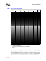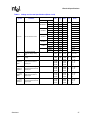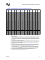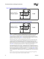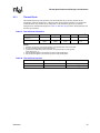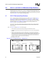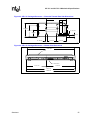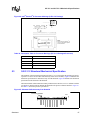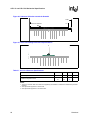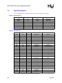
1
Intel® Pentium® III Processor for the
SC242 at 450 MHz to 1.0 GHz
Datasheet
Product Features
■
■
■
■
Available in 1.0B GHz, 933, 866, 800EB,
733, 667, 600B, 600EB, 533B, and 533EB
MHz speeds support a 133 MHz system
bus (‘B’ denotes support for a 133 MHz
system bus where a processor is available
at the same specific core frequency in
seperate 100 MHz and 133 MHz Front Side
Bus versions; ‘E’ denotes support for
Advanced Transfer Cache and Advanced
System Buffering)
Available in 1.0 GHz, 850, 800, 750, 700,
650, 600E, 600, 550E, 550, 500, and
450 MHz speeds support a 100 MHz
system bus (‘E’ denotes support for
Advanced Transfer Cache and Advanced
System Buffering)
Available in versions that incorporate
256-KB Advanced Transfer Cache (on-die,
full speed Level 2 (L2) cache with Error
Correcting Code (ECC)) or versions that
incorporate a discrete, half-speed, 512-KB
in-package L2 cache with ECC
Dual Independent Bus (DIB) architecture
increases bandwidth and performance over
single-bus processors
■
■
■
■
■
■
■
■
■
■
Internet Streaming SIMD Extensions for
enhanced video, sound and 3D
performance
Binary compatible with applications
running on previous members of the Intel
microprocessor line
Dynamic execution micro architecture
Power Management capabilities
— System Management mode
— Multiple low-power states
Intel Processor Serial Number
Optimized for 32-bit applications running
on advanced 32-bit operating systems
Single Edge Contact Cartridge (S.E.C.C.)
and S.E.C.C.2 packaging technology; the
S.E.C. cartridges deliver high performance
with improved handling protection and
socketability
Integrated high performance 16 KB
instruction and 16-KB data, nonblocking,
level one cache
Enables systems which are scaleable up to
two processors
Error-correcting code for System Bus data
The Intel® Pentium® III processor is designed for high-performance desktops and for
workstations and servers. It is binary compatible with previous Intel Architecture processors.
The Pentium III processor provides great performance for applications running on advanced
operating systems such as Microsoft Windows* 98, Windows NT* and UNIX*. This is achieved
by integrating the best attributes of Intel processors—the dynamic execution, Dual Independent
Bus architecture plus Intel® MMX™ technology and Internet Streaming SIMD Extensions—
bringing a new level of performance for systems buyers. ThePentium III processor is scaleable to
two processors in a multiprocessor system and extends the power of the Intel® Pentium® II
processor with performance headroom for business media, communication and internet
capabilities. Systems based on Pentium III processors also include the latest features to simplify
system management and lower the cost of ownership for large and small business environments.
The Pentium III processor offers great performance for today’s and tomorrow’s applications.
SC242 / SECC2 Package
Document Number: 244452-009
July 2002
INFORMATION IN THIS DOCUMENT IS PROVIDED IN CONNECTION WITH INTEL® PRODUCTS. NO LICENSE, EXPRESS OR IMPLIED, BY
ESTOPPEL OR OTHERWISE, TO ANY INTELLECTUAL PROPERTY RIGHTS IS GRANTED BY THIS DOCUMENT. EXCEPT AS PROVIDED IN
INTEL'S TERMS AND CONDITIONS OF SALE FOR SUCH PRODUCTS, INTEL ASSUMES NO LIABILITY WHATSOEVER, AND INTEL DISCLAIMS
ANY EXPRESS OR IMPLIED WARRANTY, RELATING TO SALE AND/OR USE OF INTEL PRODUCTS INCLUDING LIABILITY OR WARRANTIES
RELATING TO FITNESS FOR A PARTICULAR PURPOSE, MERCHANTABILITY, OR INFRINGEMENT OF ANY PATENT, COPYRIGHT OR OTHER
INTELLECTUAL PROPERTY RIGHT. Intel products are not intended for use in medical, life saving, or life sustaining applications.
Intel may make changes to specifications and product descriptions at any time, without notice.
Designers must not rely on the absence or characteristics of any features or instructions marked “reserved” or “undefined”. Intel reserves these for
future definition and shall have no responsibility whatsoever for conflicts or incompatibilities arising from future changes to them.
The Pentium® III processor may contain design defects or errors known as errata which may cause the product to deviate from published
specifications. Current characterized errata are available on request.
Contact your local Intel sales office or your distributor to obtain the latest specifications and before placing your product order.
Copies of documents which have an ordering number and are referenced in this document, or other Intel literature may be obtained by calling 1-800548-4725 or by visiting Intel's website at http://www.intel.com.
Intel, Pentium, Celeron, MMX, and the Intel logo are trademarks or registered trademarks of Intel Corporation or its subsidiaries in the United States
and other countries.
*Other names and brands may be claimed as the property of others.
Copyright © 2002, Intel Corporation
Datasheet
Contents
1.0
Introduction......................................................................................................................... 9
1.1
1.2
2.0
Electrical Specifications....................................................................................................13
2.1
2.2
2.3
2.4
2.5
2.6
2.7
2.8
2.9
2.10
2.11
2.12
2.13
3.0
Processor System Bus and VREF ........................................................................13
Clock Control and Low Power States..................................................................14
2.2.1 Normal State—State 1 ...........................................................................15
2.2.2 AutoHALT Powerdown State—State 2...................................................15
2.2.3 Stop-Grant State—State 3 .....................................................................15
2.2.4 HALT/Grant Snoop State—State 4 ........................................................16
2.2.5 Sleep State—State 5..............................................................................16
2.2.6 Deep Sleep State—State 6 ....................................................................16
2.2.7 Clock Control..........................................................................................17
Power and Ground Pins ......................................................................................17
Decoupling Guidelines ........................................................................................17
2.4.1 Processor VCCCORE Decoupling............................................................18
2.4.2 Processor System Bus AGTL+ Decoupling............................................18
Processor System Bus Clock and Processor Clocking .......................................18
Voltage Identification ...........................................................................................18
Processor System Bus Unused Pins...................................................................20
Processor System Bus Signal Groups ................................................................20
2.8.1 Asynchronous vs. Synchronous for System Bus Signals .......................21
2.8.2 System Bus Frequency Select Signal (BSEL0)......................................22
Test Access Port (TAP) Connection....................................................................23
Maximum Ratings................................................................................................24
Processor DC Specifications...............................................................................25
AGTL+ System Bus Specifications .....................................................................32
System Bus AC Specifications ............................................................................32
Signal Quality Specifications ............................................................................................40
3.1
3.2
3.3
Datasheet
Terminology.........................................................................................................10
1.1.1 S.E.C.C.2 and S.E.C.C. Packaged Processor Terminology ..................10
1.1.2 Processor Naming Convention...............................................................11
Related Documents.............................................................................................12
BCLK, PICCLK, and PWRGOOD Signal Quality Specifications and
Measurement Guidelines ....................................................................................40
AGTL+ and Non-AGTL+ Overshoot/Undershoot Specifications and
Measurement Guidelines ....................................................................................41
3.2.1 Overshoot/Undershoot Magnitude .........................................................41
3.2.2 Overshoot/Undershoot Pulse Duration...................................................42
3.2.3 Overshoot/Undershoot Activity Factor....................................................42
3.2.4 Reading Overshoot/Undershoot Specification Tables............................43
3.2.5 Determining If a System Meets the Overshoot/Undershoot
Specifications .........................................................................................44
AGTL+ and Non-AGTL+ Ringback Specifications and Measurement
Guidelines ...........................................................................................................46
3.3.1 Settling Limit Guideline...........................................................................48
3
4.0
Thermal Specifications and Design Considerations......................................................... 49
4.1
5.0
S.E.C.C. and S.E.C.C.2 Mechanical Specifications......................................................... 54
5.1
5.2
5.3
5.4
5.5
5.6
6.0
6.3
6.4
Introduction ......................................................................................................... 88
Fan Heatsink Mechanical Specifications............................................................. 88
6.2.1 Intel® Boxed Processor Fan Heatsink Dimensions ................................ 88
6.2.2 Intel® Boxed Processor Fan Heatsink Weight........................................ 90
6.2.3 Intel® Boxed Processor Retention Mechanism....................................... 90
Fan Heatsink Electrical Requirements ................................................................ 91
6.3.1 Fan Heatsink Power Supply ................................................................... 91
Fan Heatsink Thermal Specifications.................................................................. 92
6.4.1 Intel® Boxed Processor Cooling Requirements...................................... 92
Intel® Pentium® III Processor Signal Description ............................................................. 93
7.1
7.2
4
S.E.C.C. Mechanical Specifications.................................................................... 54
S.E.C.C.2 Mechanical Specification.................................................................... 61
S.E.C.C.2 Structural Mechanical Specification ................................................... 67
Processor Package Materials Information .......................................................... 69
Intel® Pentium® III Processor Signal Listing........................................................ 69
Intel® Pentium® III Processor Core Pad to Substrate Via Assignments .............. 76
5.6.1 Processor Core Pad Via Assignments (CPUID=067xh)......................... 76
5.6.2 Processor Core Signal Assignments (CPUID=067xh) ........................... 76
5.6.3 Processor Core Pad Via Assignments (CPUID=068xh)......................... 87
Boxed Processor Specifications....................................................................................... 88
6.1
6.2
7.0
Thermal Specifications........................................................................................ 50
4.1.1 Thermal Diode........................................................................................ 53
Alphabetical Signals Reference .......................................................................... 93
Signal Summaries ............................................................................................. 100
Datasheet
Figures
1
2
3
4
5
6
7
8
9
10
11
12
13
14
15
16
17
18
19
20
21
22
23
24
25
26
27
29
28
30
31
32
33
34
35
36
37
38
Datasheet
Second Level (L2) Cache Implementation ........................................................... 9
AGTL+ Bus Topology ..........................................................................................14
Stop Clock State Machine ...................................................................................14
BSEL[1:0] Example for a 100 MHz System Design (100 MHz Processor
Installed)..............................................................................................................22
BSEL[1:0] Example for a 100/133 MHz Capable System
(100 MHz Processor Installed) ............................................................................23
BSEL[1:0] Example for a 100/133 MHz Capable System
(133 MHz Processor Installed) ............................................................................23
BCLK, PICCLK, and TCK Generic Clock Waveform...........................................37
System Bus Valid Delay Timings ........................................................................38
System Bus Setup and Hold Timings..................................................................38
System Bus Reset and Configuration Timings....................................................38
Power-On Reset and Configuration Timings.......................................................39
Test Timings (TAP Connection) ..........................................................................39
Test Reset Timings .............................................................................................39
BCLK and PICCLK Generic Clock Waveform .....................................................40
Maximum Acceptable AGTL+ and Non-AGTL+ Overshoot/Undershoot
Waveform ............................................................................................................46
Low to High AGTL+ and Non-AGTL+ Receiver Ringback Tolerance .................48
Signal Overshoot/Undershoot, Settling Limit, and Ringback...............................48
S.E.C.Cartridge — 3-Dimensional View..............................................................49
S.E.C.Cartridge 2 — Substrate View ..................................................................50
Processor Functional Die Layout (CPUID=0686h)..............................................52
Processor Functional Die Layout (up to CPUID=0683h).....................................52
S.E.C.C. Packaged Processor — Multiple Views................................................54
S.E.C.C. Packaged Processor — Extended Thermal Plate Side
Dimensions..........................................................................................................55
S.E.C.C. Packaged Processor — Bottom View Dimensions...............................55
S.E.C.C. Packaged Processor — Latch Arm, Extended Thermal Plate Lug,
and Cover Lug Dimensions .................................................................................56
S.E.C.C. Packaged Processor — Latch Arm, Extended Thermal Plate,
and Cover Detail Dimensions (Reference Dimensions Only)..............................57
S.E.C.C. Packaged Processor — Extended Thermal Plate Attachment
Detail Dimensions ...............................................................................................58
S.E.C.C. Packaged Processor Substrate — Edge Finger Contact
Dimensions..........................................................................................................59
S.E.C.C. Packaged Processor — Extended Thermal Plate Attachment
Detail Dimensions, Continued .............................................................................59
S.E.C.C. Packaged Processor Substrate — Edge Finger Contact
Dimensions, Detail A ...........................................................................................60
Intel® Pentium® III Processor Markings (S.E.C.C. Packaged Processor)...........60
S.E.C.C.2 Packaged Processor — Multiple Views..............................................61
S.E.C.C.2 Packaged Processor Assembly — Primary View...............................62
S.E.C.C.2 Packaged Processor Assembly — Cover View with Dimensions ......62
S.E.C.C.2 Packaged Processor Assembly — Heatsink Attach Boss Section.....63
S.E.C.C.2 Packaged Processor Assembly — Side View ....................................63
Detail View of Cover in the Vicinity of the Substrate Attach Features.................63
S.E.C.C.2 Packaged Processor Substrate — Edge Finger Contact
Dimensions..........................................................................................................64
5
39
40
41
42
43
44
45
46
47
48
49
50
51
52
53
54
55
S.E.C.C.2 Packaged Processor Substrate — Edge Finger Contact
Dimensions (Detail A) ......................................................................................... 64
S.E.C.C.2 Packaged Processor Substrate (CPUID=067xh) —
Keep-In Zones..................................................................................................... 65
S.E.C.C.2 Packaged Processor Substrate (CPUID=068xh) —
Keep-In Zones..................................................................................................... 65
S.E.C.C.2 Packaged Processor Substrate (CPUID=067xh) —
Keep-Out Zone.................................................................................................... 66
S.E.C.C.2 Packaged Processor Substrate (CPUID=068xh) —
Keep-Out Zone.................................................................................................... 66
Intel® Pentium® III Processor Markings (S.E.C.C.2 Package) ........................... 67
Substrate Deflection away from Heatsink ........................................................... 67
Substrate Deflection toward the Heatsink ........................................................... 68
S.E.C.C.2 Packaged Processor Specifications................................................... 68
Processor Core Pad Via Assignments ................................................................ 76
Intel® Pentium® III Processor S.E.C.C. 2 Via Map .............................................. 87
Boxed Intel® Pentium® III Processor in the S.E.C.C.2 Packaging
(Fan Power Cable Not Shown) ........................................................................... 88
Side View Space Requirements for the Intel® Boxed Processor with
S.E.C.C.2 Packaging .......................................................................................... 89
Front View Space Requirements for the Intel® Boxed Processor with
S.E.C.C.2 Packaging .......................................................................................... 89
Top View Air Space Requirements for the Intel® Boxed Processor .................... 90
Intel® Boxed Processor Fan Heatsink Power Cable Connector Description....... 91
Recommended Baseboard Power Header Placement Relative to Fan
Power Connector and Intel® Pentium® III Processor........................................... 92
Tables
1
2
3
4
5
6
7
8
9
10
11
12
13
14
15
16
17
6
Processor Identification....................................................................................... 11
Related Documents ............................................................................................ 12
Voltage Identification Definition........................................................................... 19
System Bus Signal Groups ................................................................................. 21
Frequency Select Truth Table for BSEL[1:0] ...................................................... 22
Absolute Maximum Ratings (CPUID=067xh) ...................................................... 24
Absolute Maximum Ratings (CPUID=068xh) ...................................................... 25
Voltage and Current Specifications..................................................................... 26
AGTL+ Signal Groups DC Specifications............................................................ 31
Non-AGTL+ Signal Group DC Specifications...................................................... 31
AGTL+ Bus Specifications .................................................................................. 32
System Bus AC Specifications (Clock) at Processor Core Pins ......................... 33
Valid System Bus, Core Frequency, and Cache Bus Frequencies ..................... 34
System Bus AC Specifications (AGTL+ Signal Group) at the Processor
Core Pins ............................................................................................................ 35
System Bus AC Specifications (CMOS Signal Group) at the Processor
Core Pins ............................................................................................................ 35
System Bus AC Specifications (Reset Conditions) ............................................. 35
System Bus AC Specifications (APIC Clock and APIC I/O) at the Processor
Core Pins ............................................................................................................ 36
Datasheet
18
19
20
21
22
23
24
25
26
27
28
29
30
31
32
33
34
35
36
37
38
39
40
41
42
43
44
45
Datasheet
System Bus AC Specifications (TAP Connection) at the Processor
Core Pins.............................................................................................................36
BCLK, PICCLK, and PWRGOOD Signal Quality Specifications at the
Processor Core ...................................................................................................40
100 MHz AGTL+ Signal Group Overshoot/Undershoot Tolerance .....................44
133 MHz AGTL+ Signal Group Overshoot/Undershoot Tolerance .....................45
33 MHz Non-AGTL+ Signal Group Overshoot/Undershoot Tolerance................45
Signal Ringback Specifications for Signal Simulation .........................................47
AGTL+ and Non-AGTL+ Signal Groups Ringback Tolerance Specifications......47
Thermal Specifications for S.E.C.C. Packaged Processors................................50
Thermal Specifications for S.E.C.C.2 Packaged Processors..............................51
Thermal Diode Parameters .................................................................................53
Thermal Diode Interface......................................................................................53
Description Table for Processor Markings (S.E.C.C. Packaged Processor).......61
Description Table for Processor Markings (S.E.C.C.2 Packaged Processor) .....67
S.E.C.C.2 Pressure Specifications......................................................................68
S.E.C.C. Materials...............................................................................................69
S.E.C.C.2 Materials.............................................................................................69
Signal Listing in Order by Pin Number ................................................................70
Signal Listing in Order by Signal Name...............................................................73
Via Listing in Order by Signal Name ...................................................................77
Via Listing in Order by VIA Location....................................................................82
Intel® Boxed Processor Fan Heatsink Spatial Dimensions .................................90
Fan Heatsink Power and Signal Specifications...................................................91
Baseboard Fan Power Connector Location ........................................................92
Signal Description ...............................................................................................93
Output Signals...................................................................................................100
Input Signals......................................................................................................100
Input/Output Signals (Single Driver)..................................................................101
Input/Output Signals (Multiple Driver) ...............................................................101
7
Revision History
Revision
-009
8
Description
• Removed 1.13 GHz processor frequency. Minor edits for clarity.
Date
July 2002
Datasheet
Introduction
1.0
Introduction
The Intel® Pentium® III processor is the next member of the P6 family, in the Intel® IA-32
processor line. Like the Intel® Pentium® II processor, the Pentium III processor implements the
Dynamic Execution microarchitecture - a unique combination of multiple branch prediction, data
flow analysis, and speculative execution. This enables these processors to deliver higher
performance than the Pentium processor, while maintaining binary compatibility with all previous
Intel Architecture processors. The Pentium III processor also executes Intel® MMX™ technology
instructions for enhanced media and communication performance just as it’s predecessor, the
Pentium II processor. The Pentium III processor executes Internet Streaming SIMD Extensions for
enhanced floating point and 3-D application performance. In addition, the Pentium III processor
extends the concept of processor identification with the addition of a processor serial number.
Refer to the Intel® Processor Serial Number application note (Document Number 245125) for
more detailed information. The Pentium III processor utilizes multiple low-power states such as
AutoHALT, Stop-Grant, Sleep, and Deep Sleep to conserve power during idle times.
The Pentium III processor utilizes the same multiprocessing system bus technology as the
Pentium II processor. This allows for a higher level of performance for both uni-processor and twoway multiprocessor (2-way MP) systems. See the Intel® Pentium® III Processor Specification
Update (Document Number 244453) for guidelines on which processors can be mixed in an MP
system. Memory is cacheable for 4 GB of addressable memory space, allowing significant
headroom for desktop systems.
The Pentium III processor is available with two different second level (L2) cache implementations.
The “Discrete” cache version (CPUID=067xh) uses commercially available parts for the L2 cache.
The L2 cache is composed of an external (to processor silicon) TagRAM and burst pipelined
synchronous static RAM (BSRAM), as seen in Figure 1. The “Advanced Transfer Cache”
(CPUID=068xh) does not use commercially available L2 cache parts. Its L2 cache resides entirely
within the processor silicon, as seen in Figure 1. Refer to Table 1 to determine the L2 cache
implementation for each Pentium III processor.
Pentium III processors are offered in either Single Edge Contact Cartridge (S.E.C.C.) or Single
Edge Contact Cartridge 2 (S.E.C.C.2) package technologies. The S.E.C.C. package has the
following features: an extended thermal plate, a cover, and a substrate with an edge finger
connection. The extended thermal plate allows heatsink attachment or customized thermal
solutions. The S.E.C.C.2 package has a cover and a substrate with an edge finger connection. This
allows the thermal solutions to be placed directly onto the processor core package. The edge finger
connection maintains socketability for system configuration. The edge finger connector is called
the ‘SC242 connector’ in this and other documentation.
Figure 1. Second Level (L2) Cache Implementation
L2
Processor
Core
Tag
Discrete Cache
Datasheet
L2
Processor
Core
Advanced Transfer Cache
9
Introduction
1.1
Terminology
In this document, a ‘#’ symbol after a signal name refers to an active low signal. This means that a
signal is in the active state (based on the name of the signal) when driven to a low level. For
example, when FLUSH# is low, a flush has been requested. When NMI is high, a nonmaskable
interrupt has occurred. In the case of signals where the name does not imply an active state but
describes part of a binary sequence (such as address or data), the ‘#’ symbol implies that the signal
is inverted. For example, D[3:0] = ‘HLHL’ refers to a hex ‘A’, and D[3:0]# = ‘LHLH’ also refers to
a hex ‘A’ (H= High logic level, L= Low logic level).
The term “system bus” refers to the interface between the processor, system core logic (a.k.a. the
AGPset components), and other bus agents. The system bus is a multiprocessing interface to
processors, memory, and I/O. The term “cache bus” refers to the interface between the processor
and the L2 cache components (TagRAM and BSRAMs). The cache bus does NOT connect to the
system bus, and is not visible to other agents on the system bus.
1.1.1
S.E.C.C.2 and S.E.C.C. Packaged Processor Terminology
The following terms are used often in this document and are explained here for clarification:
• Pentium® III processor—The entire product including internal components, substrate, cover
and in S.E.C.C. packaged processors, an extended thermal plate.
• S.E.C.C.—The processor package technology called “Single Edge Contact Cartridge.”
• S.E.C.C.2—The follow-on to S.E.C.C. processor package technology. This differs from its
predecessor in that it has no extended thermal plate, thus reducing thermal resistance.
• Processor substrate—The FR4 board on which components are mounted inside the S.E.C.C.
or S.E.C.C.2 packaged processor (with or without components attached).
• Processor core—The processor’s execution engine.
• Extended Thermal Plate—This S.E.C.C. package feature is the surface used to attach a
heatsink or other thermal solution to the processor.
• Cover—The plastic casing that covers the backside of the substrate.
• Latch arms—An S.E.C.C. package feature which can be used as a means for securing the
processor in a retention mechanism.
• OLGA - Organic Land Grid Array. This package technology permits attaching the heatsink
directly to the die.
Additional terms referred to in this and other related documentation:
• SC242—The 242-contact slot connector (previously referred to as Slot 1 connector) that the
S.E.C.C. and S.E.C.C.2 plug into, just as the Pentium® Pro processor uses Socket 8.
• Retention mechanism—A mechanical piece which holds the S.E.C.C. or S.E.C.C.2 packaged
processor in the SC242 connector.
• Heatsink support—The support pieces that are mounted on the baseboard to provide added
support for heatsinks.
• Keep-out zone—The area on or near an S.E.C.C. or S.E.C.C.2 packaged processor substrate
that systems designs can not utilize.
• Keep-in zone—The area of the center of an S.E.C.C. or S.E.C.C.2 packaged processor
substrate that thermal solutions may utilize.
The L2 cache, TagRAM and BSRAM die, are industry designated names.
10
Datasheet
Introduction
1.1.2
Processor Naming Convention
A letter(s) is added to certain processors (e.g., 600B MHz) when the core frequency alone may not
uniquely identify the processor. Below is a summary what the letter means as well as a table listing
all Pentium III processors currently available.
• “B” — 133 MHz System Bus Frequency
• “E” — Processor with “Advanced Transfer Cache” (CPUID=068xh)
Table 1.
Processor Identification
Processor
Core
Frequency
(MHz)
System Bus
Frequency
(MHz)
L2 Cache Size
(Kbytes)
L2 Cache Type
CPUID1
450
450
100
512
Discrete
067xh
500
500
100
512
Discrete
067xh
533B
533
133
512
Discrete
067xh
533EB
533
133
256
ATC2
068xh
550
550
100
512
Discrete
067xh
2
550E
550
100
256
ATC
600
600
100
512
Discrete
067xh
600B
600
133
512
Discrete
067xh
600E
600
100
256
068xh
ATC
2
068xh
2
068xh
600EB
600
133
256
ATC
650
650
100
256
ATC2
068xh
256
ATC
2
068xh
ATC
2
068xh
2
068xh
667
700
667
700
133
100
256
733
733
133
256
ATC
750
750
100
256
ATC2
068xh
256
ATC
2
068xh
ATC
2
068xh
2
068xh
800
800EB
800
800
100
133
256
850
850
100
256
ATC
866
866
133
256
ATC2
068xh
256
ATC
2
068xh
ATC
2
068xh
ATC
2
068xh
933
1.0 GHz
1.0B GHz
933
1000
1000
133
100
133
256
256
NOTES:
1. Refer to the Intel® Pentium® III Processor Specification Update for the exact CPUID for each processor.
2. ATC = Advanced Transfer Cache. ATC is an L2 Cache integrated on the same die as the processor core.
With ATC, the interface between the processor core and L2 Cache is 256-bits wide, runs at the same
frequency as the processor core and has enhanced buffering.
Datasheet
11
Introduction
1.2
Related Documents
The reader of this specification should also be familiar with material and concepts in the
documents listed in Table 2. These documents, and a complete list of Pentium III processor
reference material, can be found on the Intel Developers’ Insight web site located at
http://developer.intel.com.
Table 2.
Related Documents
Document
®
AP-485, Intel Processor Identification and the CPUID Instruction
®
®
Intel Document Number
241618
AP-585, Intel Pentium II Processor GTL+ Guidelines
243330
AP-588, Mechanical and Assembly Technology for S.E.C. Cartridge Processors
243333
AP-589, Design for EMI
243334
AP-826, Mechanical Assembly and Customer Manufacturing Technology for
S.E.P. Packages
243748
AP-902, S.E.C.C.2 Heatsink Installation and Removal
244454
AP-903, Mechanical Assembly and Customer Manufacturing Technology for
Processor in S.E.C.C.2 Packages
244457
AP-905, Intel® Pentium® III Processor Thermal Design Guidelines
245087
AP-906, 100 MHz AGTL+ Layout Guidelines for the Intel® Pentium® III Processor
and Intel® 440BX AGPset
245086
AP-907, Intel® Pentium® III Processor Power Distribution Guidelines
245085
®
Intel Processor Serial Number
245119
CK97 Clock Synthesizer Design Guidelines
243867
®
Intel Architecture Software Developer's Manual
243193
Volume I: Basic Architecture
243190
Volume II: Instruction Set Reference
243191
Volume III: System Programming Guide
243192
P6 Family of Processors Hardware Developer’s Manual
244001
Intel® Pentium® II Processor at 350, 400 and 450 MHz datasheet
243657
Intel® Pentium® II Processor Developer’s Manual
243502
®
Pentium III Processor I/O Buffer Models
®
®
Note 1
Intel Pentium III Processor Specification Update
244453
SC242 Bus Termination Card Design Guidelines
243409
Slot 1 Connector Specification
243397
VRM 8.4 DC-DC Converter Design Guidelines
245335
NOTES:
1. These models are available in Viewlogic* XTK* model format (formerly known as QUAD format) at the Intel
Developer’s Website at http://developer.intel.com.
12
Datasheet
Electrical Specifications
2.0
Electrical Specifications
2.1
Processor System Bus and VREF
Most Pentium III processor signals use a variation of the low voltage Gunning Transceiver Logic
(GTL) signaling technology.
The Pentium Pro processor system bus specification is similar to the GTL specification, but was
enhanced to provide larger noise margins and reduced ringing. The improvements are
accomplished by increasing the termination voltage level and controlling the edge rates. This
specification is different from the GTL specification, and is referred to as GTL+. For more
information on GTL+ specifications, see the GTL+ buffer specification in the Intel® Pentium® II
Processor Developer’s Manual (Document Number 243502).
The Pentium III processor varies from the Pentium Pro processor in its output buffer
implementation. The buffers that drive the system bus signals on the Pentium III processor are
actively driven to VTT for one clock cycle after the low to high transition to improve rise times.
These signals should still be considered open-drain and require termination to a supply that
provides the high signal level. Because this specification is different from the GTL+ specification,
it is referred to as AGTL+ in this and other documentation. AGTL+ logic and GTL+ logic are
compatible with each other and may both be used on the same system bus. For more information on
AGTL+ routing, see AP-906, 100 MHz AGTL+ Layout Guidelines for the Pentium III® Processor
and Intel® 440BX AGPset (Document Number 245086) or the appropriate platform design guide.
AGTL+ inputs use differential receivers which require a reference signal (VREF). VREF is used by
the receivers to determine if a signal is a logical 0 or a logical 1, and is generated on the S.E.C.C.
and S.E.C.C.2 packages for the processor core. Local VREF copies should be generated on the
baseboard for all other devices on the AGTL+ system bus. Termination (usually a resistor at each
end of the signal trace) is used to pull the bus up to the high voltage level and to control reflections
on the transmission line. The processor contains termination resistors that provide termination for
one end of the Pentium III processor system bus. These specifications assume another resistor at the
end of each signal trace to ensure adequate signal quality for the AGTL+ signals; see Table 11 for
the bus termination voltage specifications for AGTL+. Refer to the Intel® Pentium® II Processor
Developer’s Manual (Document Number 243502) for the GTL+ bus specification. Solutions exist
for single-ended termination as well, though this implementation changes system design. Figure 2
is a schematic representation of AGTL+ bus topology with Pentium III processors.
The AGTL+ bus depends on incident wave switching. Therefore timing calculations for AGTL+
signals are based on flight time as opposed to capacitive deratings. Analog signal simulation of the
Pentium III processor system bus including trace lengths is highly recommended when designing a
system with a heavily loaded AGTL+ bus, especially for systems using a single set of termination
resistors (i.e., those on the processor substrate). Such designs will not match the solution space
allowed for by installation of termination resistors on the baseboard. See Intel’s Developer’s
Website (http://developer.intel.com) to download the Intel® Pentium® III Processor I/O Buffer
Models, Viewlogic* XTK* model format (formerly known as QUAD format).
Datasheet
13
Electrical Specifications
Figure 2. AGTL+ Bus Topology
Pentium III
Processor
2.2
ASIC
Pentium III
Processor
Clock Control and Low Power States
Pentium III processors allow the use of AutoHALT, Stop-Grant, Sleep, and Deep Sleep states to
reduce power consumption by stopping the clock to internal sections of the processor, depending
on each particular state. See Figure 3 for a visual representation of the Pentium III processor low
power states.
Figure 3. Stop Clock State Machine
HALT Instruction and
HALT Bus Cycle Generated
2. Auto HALT Power Down State
BCLK running.
Snoops and interrupts allowed.
INIT#, BINIT#, INTR,
SMI#, RESET# ,NMI
1. Normal State
Normal execution.
STPCLK# Asserted
Snoop
Event
Occurs
Snoop
Event
Serviced
4. HALT/Grant Snoop State
BCLK running.
Service snoops to caches.
STPCLK# De-asserted
and Stop-Grant State
entered from
AutoHALT
Snoop Event Occurs
Snoop Event Serviced
STPCLK#
Asserted
STPCLK#
De-asserted
3. Stop Grant State
BCLK running.
Snoops and interrupts allowed.
SLP#
Asserted
SLP#
De-asserted
5. Sleep State
BCLK running.
No snoops or interrupts allowed.
BCLK
Input
Stopped
BCLK
Input
Restarted
6. Deep Sleep State
BCLK stopped.
No snoops or interrupts allowed.
PCB757
14
Datasheet
Electrical Specifications
For the processor to fully realize the low current consumption of the Stop-Grant, Sleep, and Deep
Sleep states, a Model Specific Register (MSR) bit must be set. For the MSR at 02Ah (Hex), bit 26
must be set to a ‘1’ (this is the power on default setting) for the processor to stop all internal clocks
during these modes. For more information, see the Intel Architecture Software Developer’s
Manual, Volume 3: System Programming Guide (Document Number 243192).
Due to the inability of processors to recognize bus transactions during the Sleep and Deep Sleep
states, 2-way MP systems are not allowed to have one processor in Sleep/Deep Sleep state and the
other processor in Normal or Stop-Grant state simultaneously.
2.2.1
Normal State—State 1
This is the normal operating state for the processor.
2.2.2
AutoHALT Powerdown State—State 2
AutoHALT is a low power state entered when the processor executes the HALT instruction. The
processor will transition to the Normal state upon the occurrence of SMI#, BINIT#, INIT#, or
LINT[1:0] (NMI, INTR). RESET# will cause the processor to immediately initialize itself.
The return from a System Management Interrupt (SMI) handler can be to either Normal Mode or
the AutoHALT Power Down state. See the Intel Architecture Software Developer's Manual,
Volume III: System Programmer's Guide (Document Number 243192) for more information.
FLUSH# will be serviced during the AutoHALT state, and the processor will return to the
AutoHALT state.
The system can generate a STPCLK# while the processor is in the AutoHALT Power Down state.
When the system deasserts the STPCLK# interrupt, the processor will return execution to the
HALT state.
2.2.3
Stop-Grant State—State 3
The Stop-Grant state on the processor is entered when the STPCLK# signal is asserted.
Since the AGTL+ signal pins receive power from the system bus, these pins should not be driven
(allowing the level to return to VTT) for minimum power drawn by the termination resistors in this
state. In addition, all other input pins on the system bus should be driven to the inactive state.
BINIT# and FLUSH# will not be serviced during Stop-Grant state.
RESET# will cause the processor to immediately initialize itself, but the processor will stay in
Stop-Grant state. A transition back to the Normal state will occur with the deassertion of the
STPCLK# signal.
A transition to the HALT/Grant Snoop state will occur when the processor detects a snoop on the
system bus (see Section 2.2.4). A transition to the Sleep state (see Section 2.2.5) will occur with the
assertion of the SLP# signal.
While in Stop-Grant State, SMI#, INIT#, and LINT[1:0] will be latched by the processor, and only
serviced when the processor returns to the Normal state. Only one occurrence of each event will be
recognized and serviced upon return to the Normal state.
Datasheet
15
Electrical Specifications
2.2.4
HALT/Grant Snoop State—State 4
The processor will respond to snoop transactions on the Pentium III processor system bus while in
Stop-Grant state or in AutoHALT Power Down state. During a snoop transaction, the processor
enters the HALT/Grant Snoop state. The processor will stay in this state until the snoop on the
Pentium III processor system bus has been serviced (whether by the processor or another agent on
the Pentium III processor system bus). After the snoop is serviced, the processor will return to the
Stop-Grant state or AutoHALT Power Down state, as appropriate.
2.2.5
Sleep State—State 5
The Sleep state is a very low power state in which the processor maintains its context, maintains
the phase-locked loop (PLL), and has stopped all internal clocks. The Sleep state can only be
entered from the Stop-Grant state. Once in the Stop-Grant state, the SLP# pin can be asserted,
causing the processor to enter the Sleep state. The SLP# pin is not recognized in the Normal or
AutoHALT states.
Snoop events that occur while in Sleep State or during a transition into or out of Sleep state will
cause unpredictable behavior.
In the Sleep state, the processor is incapable of responding to snoop transactions or latching
interrupt signals. No transitions or assertions of signals (with the exception of SLP# or RESET#)
are allowed on the system bus while the processor is in Sleep state. Any transition on an input
signal before the processor has returned to Stop-Grant state will result in unpredictable behavior.
If RESET# is driven active while the processor is in the Sleep state, and held active as specified in
the RESET# pin specification, then the processor will reset itself, ignoring the transition through
Stop-Grant State. If RESET# is driven active while the processor is in the Sleep State, the SLP#
and STPCLK# signals should be deasserted immediately after RESET# is asserted to ensure the
processor correctly executes the Reset sequence.
While in the Sleep state, the processor is capable of entering its lowest power state, the Deep Sleep
state, by stopping the BCLK input (see Section 2.2.6). Once in the Sleep or Deep Sleep states, the
SLP# pin can be deasserted if another asynchronous system bus event occurs. The SLP# pin has a
minimum assertion of one BCLK period.
2.2.6
Deep Sleep State—State 6
The Deep Sleep state is the lowest power state the processor can enter while maintaining context.
The Deep Sleep state is entered by stopping the BCLK input (after the Sleep state was entered from
the assertion of the SLP# pin). The processor is in Deep Sleep state immediately after BCLK is
stopped. It is recommended that the BCLK input be held low during the Deep Sleep State. Stopping
of the BCLK input lowers the overall current consumption to leakage levels.
To re-enter the Sleep state, the BCLK input must be restarted. A period of 1 ms (to allow for PLL
stabilization) must occur before the processor can be considered to be in the Sleep state. Once in
the Sleep state, the SLP# pin can be deasserted to re-enter the Stop-Grant state.
While in Deep Sleep state, the processor is incapable of responding to snoop transactions or
latching interrupt signals. No transitions or assertions of signals are allowed on the system bus
while the processor is in Deep Sleep state. Any transition on an input signal before the processor
has returned to Stop-Grant state will result in unpredictable behavior.
16
Datasheet
Electrical Specifications
2.2.7
Clock Control
The processor provides the clock signal to the L2 cache. During AutoHALT Power Down and
Stop-Grant states, the processor will process a system bus snoop. The processor will not stop the
clock to the L2 cache during AutoHALT Power Down or Stop-Grant states. Entrance into the Halt/
Grant Snoop state will allow the L2 cache to be snooped, similar to the Normal state.
When the processor is in Sleep and Deep Sleep states, it will not respond to interrupts or snoop
transactions. During the Sleep state, the clock to the L2 cache is not stopped. During the Deep
Sleep state, the clock to the L2 cache is stopped. The clock to the L2 cache will be restarted only
after the internal clocking mechanism for the processor is stable (i.e., the processor has re-entered
Sleep state).
PICCLK should not be removed during the AutoHALT Power Down or Stop-Grant states.
PICCLK can be removed during the Sleep or Deep Sleep states. When transitioning from the Deep
Sleep state to the Sleep state, PICCLK must be restarted with BCLK.
2.3
Power and Ground Pins
For clean on-chip power distribution, Pentium III processors have 27 VCC (power) and 30 VSS
(ground) inputs. The 27 VCC pins are further divided to provide the different voltage levels to the
components. VCCCORE inputs for the processor core and some L2 cache components account for
19 of the VCC pins, while 4 VTT inputs (1.5 V) are used to provide an AGTL+ termination voltage
to the processor and 3 VCCL2/VCC3.3 inputs (3.3 V) are either used for the off-chip L2 cache
TagRAM and BSRAMs (CPUID=067xh) or for the voltage clamp logic (CPUID=068xh). One
VCC5 pin is provided for use by test equipment and tools. VCC5, VCCL2/VCC3.3, and VCCCORE
must remain electrically separated from each other. On the circuit board, all VCCCORE pins must be
connected to a voltage island and all VCCL2/VCC3.3 pins must be connected to a separate voltage
island (an island is a portion of a power plane that has been divided, or an entire plane). Similarly,
all VSS pins must be connected to a system ground plane.
Note:
2.4
The voltage clamp logic acts as a voltage translator between the processor’s 1.5 V tolerant CMOS
signals and the 2.5 V CMOS voltage on the motherboard. This logic is only available with
Pentium III processors with CPUID=068xh.
Decoupling Guidelines
Due to the large number of transistors and high internal clock speeds, the processor is capable of
generating large average current swings between low and full power states. This causes voltages on
power planes to sag below their nominal values if bulk decoupling is not adequate. Care must be
taken in the board design to ensure that the voltage provided to the processor remains within the
specifications listed in Table 8. Failure to do so can result in timing violations or a reduced lifetime
of the processor.
Datasheet
17
Electrical Specifications
2.4.1
Processor VCCCORE Decoupling
Regulator solutions need to provide bulk capacitance with a low Effective Series Resistance (ESR)
and keep an interconnect resistance from the regulator (or VRM pins) to the SC242 connector of
less than 0.3 mΩ. This can be accomplished by keeping a maximum distance of 1.0 inches between
the regulator output and SC242 connector. The recommended VCCCORE interconnect is a 2.0 inch
wide by 1.0 inch long (maximum distance between the SC242 connector and the VRM connector)
plane segment with a 1-ounce plating. Bulk decoupling for the large current swings when the part
is powering on, or entering/exiting low power states, is provided on the voltage regulation module
(VRM). If using Intel’s enabled VRM solutions see developer.intel.com for the specification and a
list of qualified vendors. The VCCCORE input should be capable of delivering a recommended
minimum dIccCORE/dt (defined in Table 8) while maintaining the required tolerances (also defined
in Table 8).
2.4.2
Processor System Bus AGTL+ Decoupling
The Pentium III processor contains high frequency decoupling capacitance on the processor
substrate; bulk decoupling must be provided for by the system baseboard for proper AGTL+ bus
operation. See AP-906, 100 MHz AGTL+ Layout Guidelines for the Intel® Pentium® III Processor
and Intel® 440BX AGPset (Document Number 245086) or the appropriate platform design guide,
AP-907, Pentium® III Processor Power Distribution Guidelines (Document Number 245085), and
the GTL+ buffer specification in the Pentium® II Processor Developer's Manual (Document
Number 243502) for more information.
2.5
Processor System Bus Clock and Processor Clocking
The BCLK input directly controls the operating speed of the Pentium III processor system bus
interface. All Pentium III processor system bus timing parameters are specified with respect to the
rising edge of the BCLK input. See the P6 Family of Processors Hardware Developer's Manual
(Document Number 244001) for further details.
2.6
Voltage Identification
There are five voltage identification pins on the SC242 connector. These pins can be used to
support automatic selection of power supply voltages. These pins are not signals, but are either an
open circuit or a short circuit to VSS on the processor. The combination of opens and shorts defines
the voltage required by the processor core. The VID pins are needed to cleanly support voltage
specification variations on current and future Pentium III processors. VID[4:0] are defined in
Table 3. A ‘1’ in this table refers to an open pin and a ‘0’ refers to a short to ground. The power
supply must supply the voltage that is requested or disable itself.
To ensure a system is ready for current and future Pentium III processors, the range of values in
bold in Table 3 should be supported. A smaller range will risk the ability of the system to migrate
to a higher performance Pentium III processor and/or maintain compatibility with current
Pentium III processors.
18
Datasheet
Electrical Specifications
Table 3.
Voltage Identification Definition
Processor Pins
Notes1,2
VID4
VID3
VID2
VID1
VID0
VccCORE
0
1
1
1
1
1.30
0
1
1
1
0
1.35
0
1
1
0
1
1.40
0
1
1
0
0
1.45
0
1
0
1
1
1.50
0
1
0
1
0
1.55
0
1
0
0
1
1.60
3
0
1
0
0
0
1.65
3
0
0
1
1
1
1.70
3
0
0
1
1
0
1.75
3
0
0
1
0
1
1.80
3
0
0
1
0
0
1.85
3
0
0
0
1
1
1.90
3
0
0
0
1
0
1.95
3
0
0
0
0
1
2.00
3
0
0
0
0
0
2.05
3
1
1
1
1
1
No Core
1
1
1
1
0
2.1
1
1
1
0
1
2.2
1
1
1
0
0
2.3
1
1
0
1
1
2.4
1
1
0
1
0
2.5
1
1
0
0
1
2.6
1
1
0
0
0
2.7
1
0
1
1
1
2.8
1
0
1
1
0
2.9
1
0
1
0
1
3.0
1
0
1
0
0
3.1
1
0
0
1
1
3.2
1
0
0
1
0
3.3
1
0
0
0
1
3.4
1
0
0
0
0
3.5
NOTES:
1. 0 = Processor pin connected to VSS.
2. 1 = Open on processor; may be pulled up to TTL VIH on baseboard.
3. To ensure a system is ready for the Pentium III processor, the values in BOLD in Table 3 should be
supported.
Note that the ‘11111’ (all opens) ID can be used to detect the absence of a processor core in a given
connector as long as the power supply used does not affect these lines. Detection logic and pull-ups
should not affect VID inputs at the power source (see Section 7.0).
The VID pins should be pulled up to a TTL-compatible level with external resistors to the power
source of the regulator only if required by the regulator or external logic monitoring the VID[4:0]
signals. The power source chosen must be guaranteed to be stable whenever the supply to the
Datasheet
19
Electrical Specifications
voltage regulator is stable. This will prevent the possibility of the processor supply going above the
specified VCCCORE in the event of a failure in the supply for the VID lines. In the case of a DC-toDC converter, this can be accomplished by using the input voltage to the converter for the VID line
pull-ups. A resistor of greater than or equal to 10 kΩ may be used to connect the VID signals to the
converter input.
2.7
Processor System Bus Unused Pins
All RESERVED pins must remain unconnected. Connection of these pins to VCCCORE, VCCL2/
VCC3.3, VSS, or to any other signal (including each other) can result in component malfunction or
incompatibility with future Pentium III processors. See Section 5.5 for a pin listing of the processor
and the location of each RESERVED pin.
All TESTHI pins must be connected to 2.5 V via 1 kΩ –10 kΩ pull-up resistor.
PICCLK must be driven with a valid clock input and the PICD[1:0] lines must be pulled-up to
2.5 V even when the APIC will not be used. A separate pull-up resistor must be provided for each
APIC data line.
For reliable operation, always connect unused inputs or bidirectional signals to an appropriate
signal level. Unused AGTL+ inputs should be left as no connects; AGTL+ termination is provided
on the processor. Unused active low CMOS inputs should be connected through a resistor to 2.5 V.
Unused active high inputs should be connected through a resistor to ground (VSS). Unused outputs
can be left unconnected. A resistor must be used when tying bidirectional signals to power or
ground. When tying any signal to power or ground, a resistor will also allow for system testability.
For unused pins, it is suggested that ~10 kΩ resistors be used for pull-ups (except for PICD[1:0]
discussed above), and ~1 kΩ resistors be used as pull-downs.
2.8
Processor System Bus Signal Groups
In order to simplify the following discussion, the Pentium III processor system bus signals have
been combined into groups by buffer type. All Pentium III processor system bus outputs are open
drain and require a high-level source provided externally by the termination or pull-up resistor.
However, the Pentium III processor includes on-cartridge (CPUID=067xh) or on-die
(CPUID=068xh) termination.
AGTL+ input signals have differential input buffers, which use VREF as a reference signal. AGTL+
output signals require termination to 1.5 V. In this document, the term “AGTL+ Input” refers to the
AGTL+ input group as well as the AGTL+ I/O group when receiving. Similarly, “AGTL+ Output”
refers to the AGTL+ output group as well as the AGTL+ I/O group when driving.
EMI pins may be connected to baseboard ground and/or to chassis ground through zero ohm (0 Ω)
resistors. The 0 Ω resistors should be placed in close proximity to the SC242 connector. The path to
chassis ground should be short in length and have a low impedance.
The CMOS, Clock, APIC, and TAP inputs can each be driven from ground to 2.5 V. The CMOS,
APIC, and TAP outputs are open drain and should be pulled high to 2.5 V. This ensures not only
correct operation for current Pentium III processors, but compatibility with future Pentium III
processors as well.
The groups and the signals contained within each group are shown in Table 4. Refer to Section 7.0
for a description of these signals.
20
Datasheet
Electrical Specifications
Table 4.
System Bus Signal Groups
Group Name
Signals
AGTL+ Input
BPRI#, BR1#, DEFER#, RESET#, RS[2:0]#, RSP#, TRDY#
AGTL+ Output
PRDY#
AGTL+ I/O
A[35:3]#, ADS#, AERR#, AP[1:0]#, BERR#, BINIT#, BNR#, BP[3:2]#, BPM[1:0]#,
BR0#1, D[63:0]#, DBSY#, DEP[7:0]#, DRDY#, HIT#, HITM#, LOCK#, REQ[4:0]#, RP#
CMOS Input5
A20M#, FLUSH#, IGNNE#, INIT#, LINT0/INTR, LINT1/NMI, PREQ#, PWRGOOD2,
SMI#, SLP#3, STPCLK#
CMOS Output5
FERR#, IERR#, THERMTRIP#4
System Bus Clock
BCLK
APIC Clock
PICCLK
APIC I/O5
PICD[1:0]
5
TAP Input
TCK, TDI, TMS, TRST#
5
TAP Output
TDO
Power/Other6
VCCCORE, VCCL2/VCC3.3, VCC5, VID[4:0], VTT, VSS, SLOTOCC#, THERMDP, THERMDN,
BSEL[1:0], EMI, TESTHI, Reserved
NOTES:
1. The BR0# pin is the only BREQ# signal that is bidirectional. The internal BREQ# signals are mapped onto
BR# pins after the agent ID is determined. See Section 7.0 for more information.
2. See Section 7.0 for information on the PWRGOOD signal.
3. See Section 7.0 for information on the SLP# signal.
4. See Section 7.0 for information on the THERMTRIP# signal.
5. These signals are specified for 2.5 V operation.
6. VCCCORE is the power supply for the processor core.
VCCL2/VCC3.3 is described in Section 2.3.
VID[4:0] is described in Section 2.6.
VTT is used to terminate the system bus and generate VREF on the processor substrate.
VSS is system ground.
TESTHI should be connected to 2.5 V with a 1 kΩ –10 kΩ resistor.
VCC5 is not connected to the Pentium III processor core. This supply is used for the test equipment and tools.
SLOTOCC# is described in Section 7.0.
BSEL[1:0] is described in Section 2.8.2 and Section 7.0.
EMI pins are described in Section 7.0.
THERMDP, THERMDN are described in Section 7.0.
2.8.1
Asynchronous vs. Synchronous for System Bus Signals
All AGTL+ signals are synchronous to BCLK. All of the CMOS, Clock, APIC, and TAP signals
can be applied asynchronously to BCLK.
All APIC signals are synchronous to PICCLK. All TAP signals are synchronous to TCK.
Datasheet
21
Electrical Specifications
2.8.2
System Bus Frequency Select Signal (BSEL0)
The BSEL[1:0] signals (BSEL0 is also known as 100/66#) are used to select the system bus
frequency for the Pentium III processor(s). Table 5 defines the possible combinations of the signals
and the frequency associated with each combination. The frequency is determined by the
processor(s), and frequency synthesizer. All system bus agents must operate at the same core and
system bus frequency in a 2-way MP Pentium III processor configuration. In a 2-way MP system
design, the BSEL[1:0] signals must be connected to the BSEL[1:0] pins of both processors. The
Pentium III processor operates at either a 100 MHz or 133 MHz system bus frequency, but not
both. 66 MHz system bus operation is not supported.
For systems that support only a 100 MHz system bus clock, resistors on the processor cartridge
will tie the BSEL1 signal to ground (as shown in Figure 4). This signal can either be left as a no
connect or tied to ground as shown below. The BSEL0 should be pulled up to 3.3 V with a 220 Ω
resistor, and provided as a frequency driver to the clock driver/synthesizer.
On baseboards which support operation at either 100 or 133 MHz, the BSEL[1:0] signals should be
pulled up to 3.3 V with a 220 Ω resistor (as shown in Figure 5 and Figure 6) and BSEL1 is
provided as a frequency selection signal to the clock driver/synthesizer. The BSEL0 signal can also
be incorporated into system shutdown logic on the baseboard (thus forcing the system to shutdown
as long as the BSEL0 signal is low). Figure 4 shows this routing example with a 100 MHz
Pentium III processor. Figure 5 shows the same routing example with a 133 MHz Pentium III
processor.
Table 5.
Frequency Select Truth Table for BSEL[1:0]
BSEL1
BSEL0
Frequency
0
0
66 MHz (unsupported)
0
1
100 MHz
1
0
Reserved
1
1
133 MHz
Figure 4. BSEL[1:0] Example for a 100 MHz System Design (100 MHz Processor Installed)
Intel® Pentium ® III Processor
0Ω
3.3V
220 Ω
GND
CK100
GND
100/66#
S
C
2
4
2
BSEL1
Processor
Core
1 ΚΩ
BSEL0
22
0Ω
3.3 ΚΩ
GND
Datasheet
Electrical Specifications
Figure 5. BSEL[1:0] Example for a 100/133 MHz Capable System
(100 MHz Processor Installed)
3.3V
CK133
220 Ω
Intel® Pentium ® III Processor
133/100#
0Ω
3.3V
BSEL1
220 Ω
System
Shutdown
Logic
0Ω
GND
S
C
2
4
2
Processor
Core
1 ΚΩ
3.3 ΚΩ
GND
BSEL0
Figure 6. BSEL[1:0] Example for a 100/133 MHz Capable System
(133 MHz Processor Installed)
3.3V
220 Ω
CK133
Intel ® Pentium ® III Processor
133/100#
1 ΚΩ
3.3V
BSEL1
220 Ω
System
Shutdown
Logic
GND
S
C
2
4
2
Processor
Core
1 ΚΩ
BSEL0
2.9
3.3 ΚΩ
3.3 ΚΩ
GND
Test Access Port (TAP) Connection
Due to the voltage levels supported by other components in the Test Access Port (TAP) logic, it is
recommended that the Pentium III processor be first in the TAP chain and followed by any other
components within the system. A translation buffer should be used to connect to the rest of the
chain unless one of the other components is capable of accepting a 2.5 V input. Similar
considerations must be made for TCK, TMS, and TRST#. Two copies of each signal may be
required with each driving a different voltage level.
The Debug Port should be placed at the start and end of the TAP chain with the TDI of the first
component coming from the Debug Port and the TDO from the last component going to the Debug
Port. In a 2-way MP system, be cautious when including an empty SC242 connector in the scan
chain. All connectors in the scan chain must have a processor installed to complete the chain or the
system must support a method to bypass the empty connectors; SC242 terminator substrates should
not connect TDI to TDO in order to avoid placing the TDO pull-up resistors in parallel. See SC242
Terminator Card Design Guidelines (Document Number 243409) for more details.
Datasheet
23
Electrical Specifications
2.10
Maximum Ratings
Table 6 contains Pentium III processor stress ratings only. Functional operation at the absolute
maximum and minimum is not implied nor guaranteed. The processor should not receive a clock
while subjected to these conditions. Functional operating conditions are given in the AC and DC
tables in Section 2.11 and Section 2.13. Extended exposure to the maximum ratings may affect
device reliability. Furthermore, although the processor contains protective circuitry to resist
damage from static electric discharge, one should always take precautions to avoid high static
voltages or electric fields.
Table 6.
Absolute Maximum Ratings (CPUID=067xh)
Symbol
Parameter
Min
Max
Unit
Notes
TSTORAGE
Processor storage temperature
–40
85
°C
VCC(All)
Any processor supply voltage with respect
to VSS
–0.5
Operating
voltage + 1.0
V
VinAGTL
AGTL+ buffer DC input voltage with
respect to VSS
–0.3
VCCCORE + 0.7
V
VinCMOS
CMOS buffer DC input voltage with
respect to VSS
–0.3
3.3
V
IVID
Max VID pin current
5
mA
ISLOTOCC
Max SLOTOCC# pin current
5
mA
Mech Max
Latch Arms
Mechanical integrity of latch arms
50
Cycles
4, 7
Mech Max
Edge Fingers
Mechanical integrity of processor edge
fingers
50
Insertions/
Extractions
5, 6
1, 2
3
NOTES:
1. Operating voltage is the voltage to which the component is designed to operate. See Table 8.
2. This rating applies to the VCCCORE, VCCL2/VCC3.3, VCC5, and any input (except as noted below) to the
processor.
3. Parameter applies to CMOS, APIC, and TAP bus signal groups only.
4. The mechanical integrity of the latch arms is specified to last a maximum of 50 cycles.
5. The electrical and mechanical integrity of the processor edge fingers are specified to last for 50 insertion/
extraction cycles.
6. While insertion/extraction cycling above 50 insertions will cause an increase in the contact resistance (above
0.1 Ω) and a degradation in the material integrity of the edge finger gold plating, it is possible to have
processor functionality above the specified limit. The actual number of insertions before processor failure will
vary based upon system configuration and environmental conditions.
7. This specification only applies to S.E.C.C. packaged processors.
24
Datasheet
Electrical Specifications
Table 7.
Absolute Maximum Ratings (CPUID=068xh)
Symbol
Parameter
Min
Max
Unit
Notes
TSTORAGE
Processor storage temperature
–40
85
°C
VCCCORE and
VTT
Processor core voltage and Termination
supply voltage with respect to VSS
-0.5
2.1
V
VCCL2/VCC3.3
VCC3.3 with respect to VSS
–0.5
5.0
V
1
Vin1.5
1.5 V buffer input voltage
VTT – 2.3
VSS + 2.3
V
2, 3, 5
Vin2.5
2.5 V buffer input voltage
–0.7
3.3
V
4
IVID
Max VID pin current
5
mA
ISLOTOCC
Max SLOTOCC# pin current
5
mA
Mech Max
Edge Fingers
Mechanical integrity of processor edge
fingers
50
Insertions/
Extractions
6, 7
NOTES:
1. Operating voltage is the voltage to which the component is designed to operate. See Table 7.
2. Input voltage can never be above VSS + 2.3 V.
3. Input voltage can never be below VTT – 2.3 V.
4. Parameter applies to the 2.5 V processor core signals (BCLK, PICCLK, and PWRGOOD).
5. Parameter applies to the 1.5 V processor core signals (all signals except BCLK, PICCLK, and PWRGOOD).
6. The electrical and mechanical integrity of the processor edge fingers are specified to last for 50 insertion/
extraction cycles.
7. While insertion/extraction cycling above 50 insertions will cause an increase in the contact resistance (above
0.1 Ω) and a degradation in the material integrity of the edge finger gold plating, it is possible to have
processor functionality above the specified limit. The actual number of insertions before processor failure will
vary based upon system configuration and environmental conditions.
2.11
Processor DC Specifications
The processor DC specifications in this section are defined at the Pentium III processor core pins,
edge fingers, and at the SC242 connector pins. See Section 7.0 for the processor edge finger signal
definitions and Section 5.0 for the core pin locations and the signal listing.
Most of the signals on the Pentium III processor system bus are in the AGTL+ signal group. These
signals are specified to be terminated to 1.5 V. The DC specifications for these signals are listed in
Table 9.
To allow connection with other devices, the Clock, CMOS, APIC, and TAP signals are designed to
interface at non-AGTL+ levels. The DC specifications for these pins are listed in Table 10.
Table 8 through Table 11 list the DC specifications for Pentium III processors. Specifications are
valid only while meeting specifications for case temperature, clock frequency, and input voltages.
Care should be taken to read all notes associated with each parameter.
Datasheet
25
Electrical Specifications
Table 8.
Voltage and Current Specifications (Sheet 1 of 4)
Processor
Symbol
Parameter
Min
Core Freq
450 MHz
500 MHz
533 MHz
533EB MHz
550 MHz
550E MHz
600 MHz
600B MHz
600E MHz
VccCORE
Vcc for Processor Core
600EB MHz
650 MHz
667 MHz
700 MHz
733 MHz
750 MHz
800 MHz
26
Typ
Max
Unit
Notes1
CPUID
0672h
2.00
2,3,4,5
0673h
2.00
2,3,4,5
0672h
2.00
2,3,4,5
0673h
2.00
2,3,4,5
0672h
2.00
2,3,4,5
0673h
2.00
2,3,4,5
0681h
1.65
2,3,4,5
0683h
1.65
2,3,4,5
0686h
1.70
2,3,4,5
0672h
2.00
2,3,4,5
0673h
2.00
2,3,4,5
0681h
1.65
2,3,4,5
0683h
1.65
2,3,4,5
0686h
1.70
2,3,4,5
0672h
2.05
2,3,4,5
0673h
2.05
2,3,4,5
0672h
2.05
2,3,4,5
0673h
2.05
2,3,4,5
0681h
1.65
2,3,4,5
0683h
1.65
2,3,4,5
0686h
1.70
0681h
1.65
0683h
1.65
2,3,4,5
0686h
1.70
2,3,4,5
0681h
1.65
2,3,4,5
0683h
1.65
2,3,4,5
0686h
1.70
2,3,4,5
0681h
1.65
2,3,4,5
0683h
1.65
2,3,4,5
0686h
1.70
2,3,4,5
0681h
1.65
2,3,4,5
0683h
1.65
2,3,4,5
0686h
1.70
2,3,4,5
0681h
1.65
2,3,4,5
0683h
1.65
2,3,4,5
0686h
1.70
2,3,4,5
0681h
1.65
2,3,4,5
0683h
1.65
2,3,4,5
0686h
1.70
2,3,4,5
0681h
1.65
2,3,4,5
0683h
1.65
2,3,4,5
0686h
1.70
2,3,4,5
V
2,3,4,5
2,3,4,5
Datasheet
Electrical Specifications
Table 8.
Voltage and Current Specifications (Sheet 2 of 4)
Processor
Symbol
Parameter
Min
Core Freq
800EB MHz
850 MHz
VccCORE
Vcc for Processor Core
866 MHz
933 MHz
1.0 GHz
1.0B GHz
Typ
Max
Unit
Notes1
CPUID
0681h
1.65
2,3,4,5
0683h
1.65
2,3,4,5
0686h
1.70
2,3,4,5
0681h
1.65
2,3,4,5
0683h
1.65
2,3,4,5
0686h
1.70
2,3,4,5
0681h
1.65
0683h
1.65
0686h
1.70
2,3,4,5
0683h
1.70
2,3,4,5
0686h
1.70
2,3,4,5
0683h
1.70
2,3,4,5
0686h
1.70
2,3,4,5
0683h
1.70
2,3,4,5
0686h
1.70
2,3,4,5
2,3,4,5
V
2,3,4,5
VCCL2/
VCC3.3
VCC for second level
cache or voltage clamp
logic
3.135
3.3
3.465
V
3.3 V ±5% 9
VTT
AGTL+ bus termination
voltage
1.365
1.50
1.635
V
1.5 ±9% 6
Baseboard
Tolerance,
Static
Processor core voltage
static tolerance level at
SC242 pins
–0.070
–0.080
–0.050
–0.055
0.070
0.040
0.040
0.040
V
2, 7, 18
2, 7, 19
2, 7, 21
2, 7
Baseboard
Tolerance,
Transient
Processor core voltage
transient tolerance level at
SC242 pins
–0.140
–0.080
–0.050
–0.055
0.140
0.050
0.050
0.050
V
2, 7, 18
2, 7, 19
2, 7, 21
2, 7
VCCCORE
Tolerance,
Static
Processor core voltage
static tolerance level at
edge fingers
–0.085
–0.110
–0.065
–0.075
0.085
0.040
0.040
0.040
V
2, 8, 18
2, 8, 19
2, 8, 21
2, 8
VCCCORE
Tolerance,
Transient
Processor core voltage
transient tolerance level at
edge fingers
–0.170
–0.110
–0.065
–0.075
0.170
0.080
0.080
0.080
V
2, 8, 18
2, 8, 19
2, 8, 21
2, 8
Datasheet
27
Electrical Specifications
Table 8.
Voltage and Current Specifications (Sheet 3 of 4)
Processor
Symbol
Parameter
Min
Core Freq
ICCCORE
28
ICC for processor core
ICCL2
ICC for second level cache
IVTT
Termination voltage
supply current
ISGnt
ICC Stop-Grant for
processor core
ISGntL2
ICC Stop-Grant for second
level cache
Typ
Max
Notes1
Unit
CPUID
450 MHz
500 MHz
533B MHz
533EB MHz
550 MHz
550E MHz
600 MHz
600B MHz
600E MHz
600EB MHz
650 MHz
667 MHz
700 MHz
733 MHz
750 MHz
800 MHz
800EB MHz
850 MHz
866 MHz
933 MHz
1.0 GHz
1.0B GHz
14.5
16.1
16.7
10.6
17.0
11.0
17.8
17.8
13.0
13.0
13.0
13.3
14.0
14.6
15.0
16.0
16.0
16.2
16.3
17.7
19.4
19.4
A
2, 3, 10, 11
2, 3, 10, 11
2, 3, 10, 11
2, 3, 20
2, 3, 10, 11
2, 3, 20
2, 3, 10, 11
2, 3, 10, 11
2, 3, 20
2, 3, 20
2, 3, 20
2, 3, 20
2, 3, 20
2, 3, 20
2, 3, 20
2, 3, 20
2, 3, 20
2, 3, 20
2, 3, 20
2, 3, 20
2, 3, 20, 21
2, 3, 20, 21
1.08
1.21
1.29
1.33
1.45
1.45
A
2, 9, 10, 18
2, 9, 10, 18
2, 9, 10, 18
2, 9, 10, 18
2, 9, 10, 18
2, 9, 10, 18
ALL
2.7
A
12
450 MHz
500 MHz
533B MHz
533EB MHz
550 MHz
550E MHz
600 MHz
600B MHz
600E MHz
600EB MHz
650 MHz
667 MHz
700 MHz
733 MHz
750 MHz
800 MHz
800EB MHz
850 MHz
866 MHz
933 MHz
1.0 GHz
1.0B GHz
1.20
1.40
1.49
2.50
1.54
2.50
1.68
1.68
2.50
2.50
2.50
2.50
2.50
2.50
2.50
2.50
2.50
2.50
2.50
2.50
2.50
2.50
A
2, 10, 13
2, 10, 13
2, 10, 13
2, 10, 13
2, 10, 13
2, 10, 13
2, 10, 13
2, 10, 13
2, 10, 13
2, 10, 13
2, 10, 13
2, 10, 13
2, 10, 13
2, 10, 13
2, 10, 13
2, 10, 13
2, 10, 13
2, 10, 13
2, 10, 13
2, 10, 13
2, 10, 13
2, 10, 13
0.1
A
2, 9, 10, 18
ALL
450 MHz
500 MHz
533B MHz
550 MHz
600 MHz
600B MHz
ALL
Datasheet
Electrical Specifications
Table 8.
Voltage and Current Specifications (Sheet 4 of 4)
Processor
Symbol
Parameter
Min
Core Freq
450 MHz
500 MHz
533B MHz
533EB MHz
550 MHz
550E MHz
600 MHz
600B MHz
600E MHz
600EB MHz
650 MHz
667 MHz
700 MHz
733 MHz
750 MHz
800 MHz
800EB MHz
850 MHz
866 MHz
933 MHz
1.0 GHz
1.0B GHz
Typ
Max
Notes1
Unit
CPUID
0.80
0.90
1.00
2.50
1.00
2.50
1.00
1.00
2.50
2.50
2.50
2.50
2.50
2.50
2.50
2.50
2.50
2.50
2.50
2.50
2.50
2.50
A
2, 10
2, 10
2, 10
2, 10
2, 10
2, 10
2, 10
2, 10
2, 10
2, 10
2, 10
2, 10
2, 10
2, 10
2, 10
2, 10
2, 10
2, 10
2, 10
2, 10
2, 10
2, 10
ISLP
ICC Sleep for processor
core
ISLPL2
ICC Sleep for second level
cache
0.1
A
2, 9, 10, 18
IDSLP
ICC Deep Sleep for
processor core
0.50
2.20
3.00
A
2, 10, 18
2, 10, 19
2, 10
IDSLPL2
ICC Deep Sleep for
second level cache
0.1
A
2, 9, 10, 18
dICCCORE/dt
Power supply current slew
rate
20
A/µs
2, 14, 15, 16
dICCL2/dt
L2 cache power supply
current slew rate
1
A/µs
14, 15, 16, 18
dICCVTT/dt
Termination current slew
rate
8
A/µs
14, 15, See
Table 11
VCC5
5 V supply voltage
5.25
V
5 V ±5% 16, 17
ICC5
ICC for 5 V supply voltage
A
17
ALL
4.75
5.00
1.0
NOTES:
1. Unless otherwise noted, all specifications in this table apply to all processor frequencies.
2. This specification applies to Pentium III processors. For baseboard compatibility information on Pentium II
processors, refer to the Intel® Pentium® II Processor at 350, 400 and 450 MHz datasheet (Document Number
243657).
3. VCCCORE and IccCORE supply the processor core.
4. A variable voltage source should exist on all systems in the event that a different voltage is required. See
Table 3 for more information.
5. Use the Typical Voltage specification with the Tolerance specifications to provide correct voltage regulation to
the processor.
6. VTT must be held to 1.5 V ±9%. It is recommended that VTT be held to 1.5 V ±3% while the Pentium III
processor system bus is idle. This is measured at the processor edge fingers across a 20 MHz bandwidth.
7. These are the tolerance requirements, across a 20 MHz bandwidth, at the SC242 connector pin on the
bottom side of the baseboard. The requirements at the SC242 connector pins account for voltage drops (and
impedance discontinuities) across the connector, processor edge fingers, and to the processor core.
VCCCORE must return to within the static voltage specification within 100 µs after a transient event; see the
VRM 8.4 DC-DC Converter Design Guidelines (Document Number 245335) for further details.
8. These are the tolerance requirements, across a 20 MHz bandwidth, at the processor edge fingers. The
requirements at the processor edge fingers account for voltage drops (and impedance discontinuities) at the
processor edge fingers and to the processor core. VCCCORE must return to within the static voltage
specification within 100 µs after a transient event.
Datasheet
29
Electrical Specifications
9. VCCL2/VCC3.3 and ICCL2/ICC3.3 supply the second level cache (“Discrete” cache type only). Unless otherwise
noted, this specification applies to all Pentium III processor cache sizes. Systems should be designed for
these specifications, even if a smaller cache size is used.
10.Max ICC measurements are measured at VCC max voltage, maximum temperature, under maximum signal
loading conditions. The Max Icc currents specified do not occur simultaneously under the stress
measurement condition.
11. Voltage regulators may be designed with a minimum equivalent internal resistance to ensure that the output
voltage, at maximum current output, is no greater than the nominal (i.e., typical) voltage level of VCCCORE
(VCCCORE_TYP). In this case, the maximum current level for the regulator, IccCORE_REG, can be reduced from
the specified maximum current IccCORE _MAX and is calculated by the equation:
IccCORE_REG = IccCORE_MAX × VCCCORE_TYP / (VCCCORE_TYP + VCCCORE Tolerance, Transient)
12.The current specified is the current required for a single Pentium III processor. A similar amount of current is
drawn through the termination resistors on the opposite end of the AGTL+ bus, unless single-ended
termination is used (see Section 2.1).
13.The current specified is also for AutoHALT state.
14.Maximum values are specified by design/characterization at nominal VCCCORE and nominal VCCL2/VCC3.3.
15.Based on simulation and averaged over the duration of any change in current. Use to compute the maximum
inductance tolerable and reaction time of the voltage regulator. This parameter is not tested.
16.dICC/dt specifications are measured and specified at the SC242 connector pins.
17.VCC5 and ICC5 are not used by the Pentium III processors. The VCC5 supply is used for the test equipment
and tools.
18.This specification applies to the Pentium III processor with CPUID=067xh.
19.This specification applies to the Pentium III processor with CPUID=068xh.
20.Max ICC measurements are measured at VCC nominal voltage, maximum temperature, under maximum
signal loading conditions. The Max Icc currents specified do not occur simultaneously under the stress
measurement condition.
21..This specification applies to the Pentium III processor with CPUID=0683h operating at 1.0 GHz.
30
Datasheet
Electrical Specifications
Table 9.
AGTL+ Signal Groups DC Specifications
Symbol
Parameter
Min
Max
Unit
Notes
1, 4, 5
VIL
Input Low Voltage
–0.30
–0.15
0.82
VREF – 0.20
V
V
12
13
VIH
Input High Voltage
1.22
VREF + 0.20
VTT
VTT
V
2, 3, 12
2, 3, 13
Ron
Buffer On Resistance
16.67
Ω
9
Leakage Current
±100
±100
µA
µA
6, 7, 8, 12
6, 10, 11, 13
IL
NOTES:
1. Unless otherwise noted, all specifications in this table apply to Pentium III processor frequencies.
2. VIH and VOH for the Pentium III processor may experience excursions up to 200 mV above VTT for a single
system bus clock. However, input signal drivers must comply with the signal quality specifications in
Section 3.0.
3. Minimum and maximum VTT are given in Table 11.
4. Parameter correlated to measure into a 25 Ω resistor terminated to 1.5 V.
5. IOH for the Pentium III processor may experience excursions of up to a 12 mA for a single bus clock.
6. Leakage current affects input, output, and I/O signals.
7. (0 ≤ VIN ≤ 2.0 V +5%).
8. (0 ≤ VOUT ≤ 2.0 V +5%).
9. Refer to the Pentium III I/O Buffer Models for I/V characteristics.
10.(0 ≤ VIN ≤ 1.5 V +5%).
11. (0 ≤ VOUT ≤ 1.5 V +5%).
12.This specification applies to the Pentium III processor with CPUID=067xh.
13.This specification applies to the Pentium III processor with CPUID=068xh.
Table 10. Non-AGTL+ Signal Group DC Specifications
Symbol
Parameter
Min
Max
Unit
Notes 1
–0.30
–0.15
–0.30
–0.30
–0.15
0.5
0.7
0.5
0.7
0.7
V
V
V
V
V
3, 8
3, 9, 10
2, 9; BCLK only
2, 9; PICCLK only
2, 9; PWRGOOD only
1.7
1.7
2.0
2.625
2.625
2.625
V
V
V
3, 8
3, 9, 10
2, 9; BCLK, PICCLK,
and PWRGOOD only
0.5
V
3, 4
2.625
V
All outputs are opendrain
VIL
Input Low Voltage
VIH
Input High Voltage
VOL
Output Low Voltage
VOH
Output High Voltage
N/A
IOL
Output Low Current
14
IL
Leakage Current
±100
mA
3, 11
µA
5, 6, 7
NOTES:
1. Unless otherwise noted, all specifications in this table apply to all Pentium III processor frequencies.
2. These values are specified at the processor core pins.
3. These values are specified at the processor edge fingers.
4. Parameter measured at 14 mA (for use with TTL inputs).
5. Leakage current affects input, output and I/O signals.
6. (0 ≤ VIN ≤ 2.5 V +5%).
7. (0 ≤ VOUT ≤ 2.5 V +5%).
8. This specification applies to the Pentium III processor with CPUID=067xh.
9. This specification applies to the Pentium III processor with CPUID=068xh.
10.Parameters apply to all non-AGTL+ signals except for BCLK, PICCLK, and PWRGOOD.
11. Specified as the minimum amount of current that the output buffer must be able to sink. However, VOL Max
cannot be guaranteed if this specification is exceeded.
Datasheet
31
Electrical Specifications
2.12
AGTL+ System Bus Specifications
It is recommended that the AGTL+ bus be routed in a daisy-chain fashion with termination
resistors to VTT at each end of the signal trace. These termination resistors are placed electrically
between the ends of the signal traces and the VTT voltage supply and generally are chosen to
approximate the substrate impedance. The valid high and low levels are determined by the input
buffers using a reference voltage called VREF.
Table 11 lists the nominal specification for the AGTL+ termination voltage (VTT). The AGTL+
reference voltage (VREF) is generated on the processor substrate for the processor core, but should
be set to 2/3 VTT for other AGTL+ logic using a voltage divider on the baseboard. It is important
that the baseboard impedance be specified and held to a ±15% tolerance, and that the intrinsic trace
capacitance for the AGTL+ signal group traces is known and well-controlled. For more details on
the GTL+ buffer specification, see the Intel® Pentium® II Processor Developer's Manual
(Document Number 243502) and AP-585, Intel® Pentium® II Processor GTL+ Guidelines
(Document Number 243330).
Table 11. AGTL+ Bus Specifications
Symbol
Parameter
VTT
Bus Termination Voltage
RTT
Termination Resistor
VREF
Bus Reference Voltage
Min
Typ
Max
Units
Notes1, 2
1.365
1.50
1.635
V
3
0.95
2/3 VTT
56
1.05
Ω
4
V
5
NOTES:
1. Unless otherwise noted, all specifications in this table apply to all Pentium III processor frequencies.
2. Pentium III processors contain AGTL+ termination resistors at the end of each signal trace on the processor
substrate. Pentium III processors generate VREF on the processor substrate by using a voltage divider on
VTT supplied through the SC 242 connector.
3. VTT must be held to 1.5 V ±9%; dICCVTT/dt is specified in Table 8. It is recommended that VTT be held to
1.5 V ±3% while the Pentium III processor system bus is idle. This is measured at the processor edge
fingers.
4. RTT must be held within a tolerance of ±5%
5. VREF is generated on the processor substrate to be 2/3 VTT ±2% nominally.
2.13
System Bus AC Specifications
The Pentium III processor system bus timings specified in this section are defined at the Pentium III
processor core pads. Unless otherwise specified, timings are tested at the processor core during
manufacturing. See Section 7.0 for the Pentium III processor edge connector signal definitions. See
Section 5.6 for the Pentium III processor closest accessible core pad to substrate via assignment.
Table 12 through Table 18 list the AC specifications associated with the Pentium III processor
system bus. These specifications are broken into the following categories: Table 12 through
Table 13 contain the system bus clock core frequency and cache bus frequencies, Table 14 contains
the AGTL+ specifications, Table 15 contains the CMOS signal group specifications, Table 16
contains timings for the Reset conditions, Table 17 covers APIC bus timing, and Table 18 covers
TAP timing.
All Pentium II processor system bus AC specifications for the AGTL+ signal group are relative to
the rising edge of the BCLK input. All AGTL+ timings are referenced to VREF for both ‘0’ and ‘1’
logic levels unless otherwise specified.
32
Datasheet
Electrical Specifications
The timings specified in this section should be used in conjunction with the I/O buffer models
provided by Intel. These I/O buffer models, which include package information, are available for
the Pentium III processor in Viewlogic XTK model format (formerly known as QUAD format) as
the Intel® Pentium® III Processor I/O Buffer Models on Intel’s Developer’s Website
(http://developer.intel.com.) AGTL+ layout guidelines are also available in AP-906, 100 MHz
AGTL+ Layout Guidelines for the Intel® Pentium® III Processor and Intel® 440BX AGPset
(Document Number 245086) or the appropriate platform design guide.
Care should be taken to read all notes associated with a particular timing parameter.
Table 12. System Bus AC Specifications (Clock) at Processor Core Pins
T# Parameter
Min
System Bus Frequency
T1: BCLK Period
Nom
Max
Unit
100.00
133.33
MHz
MHz
10.0
7.5
T2: BCLK Period Stability
±250
Notes1, 2, 3
Figure
4, 10
4, 11
ns
ns
7
7
4, 5, 10
4, 5, 11
ps
7
7, 9
T3: BCLK High Time
2.5
1.4
ns
ns
7
7
@>2.0 V, 10
@>2.0 V, 11
T4: BCLK Low Time
2.4
1.4
ns
ns
7
7
@<0.5 V 6, 10
@<0.5 V 6, 11
T5: BCLK Rise Time
0.4
1.60
ns
7
(0.5 V–2.0 V) 8, 10, 11
T6: BCLK Fall Time
0.4
1.60
ns
7
(2.0 V–0.5 V) 8, 10, 11
1. Unless otherwise noted, all specifications in this table apply to all Pentium III processor frequencies.
2. All AC timings for the AGTL+ signals are referenced to the BCLK rising edge at 1.25 V at the processor core
pin. All AGTL+ signal timings (address bus, data bus, etc.) are referenced at 1.00 V at the processor core
pins.
3. All AC timings for the CMOS signals are referenced to the BCLK rising edge at 1.25 V at the processor core
pin. All CMOS signal timings (compatibility signals, etc.) are referenced at 1.25 V at the processor core pins.
4. The internal core clock frequency is derived from the Pentium III processor system bus clock. The system
bus clock to core clock ratio is fixed for each processor. Individual processors will only operate at their
specified system bus frequency, either 100 MHz or 133 MHz. Table 13 shows the supported ratios for each
processor.
5. The BCLK period allows a +0.5 ns tolerance for clock driver variation.
6. Due to the difficulty of accurately measuring clock jitter in a system, it is recommended that a clock driver be
used that is designed to meet the period stability specification into a test load of 10 to 20 pF. This should be
measured on the rising edges of adjacent BCLKs crossing 1.25 V at the processor core pin. The jitter
present must be accounted for as a component of BCLK timing skew between devices.
7. The clock driver’s closed loop jitter bandwidth must be set low to allow any PLL-based device to track the
jitter created by the clock driver. The –20 dB attenuation point, as measured into a 10 to 20 pF load, should
be less than 500 kHz. This specification may be ensured by design characterization and/or measured with a
spectrum analyzer.
8. Not 100% tested. Specified by design characterization as a clock driver requirement.
9. The average period over a 1uS period of time must be greater than the minimum specified period.
10.This specification applies to the Pentium III processor with a system bus frequency of 100 MHz.
11. This specification applies to the Pentium III processor with a system bus frequency of 133 MHz.
Datasheet
33
Electrical Specifications
Table 13. Valid System Bus, Core Frequency, and Cache Bus Frequencies
Processor
Core Frequency
(MHz)
BCLK Frequency
(MHz)
Frequency Multiplier
L2 Cache (MHz)
450
450
100
9/2
225
500
500
100
5
250
533B
533
133
4
267
533EB
533
133
4
533
550
550
100
11/2
275
550E
550
100
11/2
550
600
600
100
6
300
600B
600
133
9/2
300
600E
600
100
6
600
600EB
600
133
9/2
600
650
650
100
13/2
650
667
666.67
133
5
666.67
700
700
100
7
700
733
733
133
11/2
733
750
750
100
15/2
750
800
800
100
8
800
800EB
800
133
6
800
850
850
100
17/2
850
866
866
133
13/2
866
933
933
133
7
933
1.0 GHz
1000.0
100
10
1000.0
1.0B GHz
1000.0
133
15/2
1000.0
Notes1
NOTE:
1. Contact your local Intel representative for the latest information on processor frequencies and/or frequency
multipliers.
34
Datasheet
Electrical Specifications
Table 14. System Bus AC Specifications (AGTL+ Signal Group) at the
Processor Core Pins
T# Parameter
Notes1, 2, 3
Min
Max
Unit
Figure
T7: AGTL+ Output Valid Delay
-0.20
-0.14
-0.10
3.15
2.20
2.70
ns
ns
ns
8
8
8
4, 10, 13
5, 11, 13
5, 11, 12, 14
T8: AGTL+ Input Setup Time
1.90
1.20
1.20
ns
ns
ns
9
9
9
6, 7, 8, 11, 13
6, 7, 8, 12, 13
6, 7, 8, 11, 12, 14
T9: AGTL+ Input Hold Time
0.85
0.58
0.80
ns
ns
ns
9
9
9
9, 11, 13
9, 12, 13
9, 11, 12, 14
T10: RESET# Pulse Width
1.00
ms
11
7, 10
NOTES:
1. Unless otherwise noted, all specifications in this table apply to all Pentium III processor frequencies.
2. These specifications are tested during manufacturing.
3. All AC timings for the AGTL+ signals are referenced to the BCLK rising edge at 1.25 V at the processor core
pin. All AGTL+ signal timings (compatibility signals, etc.) are referenced at 1.00 V at the processor core pins.
4. Valid delay timings for these signals are specified into 25 Ω to 1.5 V and with VREF at 1.0 V.
5. Valid delay timings for these signals are specified into 50 Ω to 1.5 V and with VREF at 1.0 V.
6. A minimum of 3 clocks must be guaranteed between two active-to-inactive transitions of TRDY#.
7. RESET# can be asserted (active) asynchronously, but must be deasserted synchronously. For 2-way MP
systems, RESET# should be synchronous.
8. Specification is for a minimum 0.40 V swing.
9. Specification is for a maximum 1.0 V swing.
10.This should be measured after VCCCORE, VCCL2/VCC3.3, and BCLK become stable.
11. This specification applies to the Pentium III processor with a system bus frequency of 100 MHz.
12.This specification applies to the Pentium III processor with a system bus frequency of 133 MHz.
13.This specification applies to the Pentium III processor with CPUID=067xh.
14.This specification applies to the Pentium III processor with CPUID=068xh.
Table 15. System Bus AC Specifications (CMOS Signal Group) at the Processor Core Pins
T# Parameter
Min
Max
Unit
Figure
T14: CMOS Input Pulse Width, except
PWRGOOD
2
BCLKs
8
T15: PWRGOOD Inactive Pulse Width
10
BCLKs
8, 11
Notes
1, 2, 3, 4
Active and Inactive
states
5
NOTES:
1. Unless otherwise noted, all specifications in this table apply to all Pentium III processor frequencies.
2. These specifications are tested during manufacturing.
3. All AC timings for the CMOS signals are referenced to the BCLK rising edge at 0.7 V at the processor core
pins. All CMOS signal timings (compatibility signals, etc.) are referenced at 1.25 V.
4. These signals may be driven asynchronously.
5. When driven inactive or after VCCCORE, VCCL2/VCC3.3, and BCLK become stable.
Table 16. System Bus AC Specifications (Reset Conditions)
T# Parameter
Min
T16: Reset Configuration Signals
(A[14:5]#, BR0#, FLUSH#,
INIT#) Setup Time
4
T17: Reset Configuration Signals (A[14:5]#,
BR0#, FLUSH#, INIT#) Hold Time
2
Max
20
Figure
Notes1
BCLKs
10
Before deassertion
of RESET#
BCLKs
10
After clock that
deasserts RESET#
Unit
NOTES:
1. Unless otherwise noted, all specifications in this table apply to all Pentium III processor frequencies.
Datasheet
35
Electrical Specifications
.
Table 17. System Bus AC Specifications (APIC Clock and APIC I/O) at the
Processor Core Pins
T# Parameter
Min
Max
Unit
Figure
T21: PICCLK Frequency
2.0
33.3
MHz
T22: PICCLK Period
30.0
500.0
ns
7
Notes
1, 2, 3
T23: PICCLK High Time
12.0
ns
7
T24: PICCLK Low Time
12.0
ns
7
T25: PICCLK Rise Time
0.25
3.0
ns
7
T26: PICCLK Fall Time
0.25
3.0
ns
7
T27: PICD[1:0] Setup Time
8.0
5.0
ns
ns
9
9
4, 7
4, 8
T28: PICD[1:0] Hold Time
2.5
ns
9
4
T29: PICD[1:0] Valid Delay
1.5
ns
8
4, 5, 6, 7
10
T29a: PICD[1:0] Valid Delay (Rising Edge)
1.5
8.7
ns
8
4, 5, 6, 8
T29b: PICD[1:0] Valid Delay (Falling Edge)
1.5
12.0
ns
8
4, 5, 6, 8
NOTES:
1. Unless otherwise noted, all specifications in this table apply to all Pentium III processor frequencies.
2. These specifications are tested during manufacturing.
3. All AC timings for the APIC I/O signals are referenced to the PICCLK rising edge at 1.25 V at the processor
core pins. All APIC I/O signal timings are referenced at 1.25 V (CPUID=067xh) or 0.75 V (CPUID=068xh) at
the processor core pins.
4. Referenced to PICCLK rising edge.
5. For open drain signals, valid delay is synonymous with float delay.
6. Valid delay timings for these signals are specified into a 150 Ω load pulled up to 2.5 V +5%.
7. This specification applies to the Pentium III processor with CPUID=067xh.
8. This specification applies to the Pentium III processor with CPUID=068xh.
Table 18. System Bus AC Specifications (TAP Connection) at the Processor Core Pins
T# Parameter
Min
T30: TCK Frequency
Unit
16.667
MHz
Notes1, 2, 3
Figure
T31: TCK Period
60.0
ns
7
T32: TCK High Time
25.0
25.0
ns
ns
7
7
@1.7 V 10, 11
@VREF + 0.20 V 10, 12
T33: TCK Low Time
25.0
25.0
ns
ns
7
7
@0.7 V 10, 11
@VREF – 0.20 V 10, 12
7
7
(0.7 V–1.7 V) 4, 10, 11
(VREF – 0.20 V) –
(VREF + 0.20 V) 10, 12
T34: TCK Rise Time
5.0
5.0
ns
ns
T35: TCK Fall Time
5.0
5.0
ns
ns
7
7
(1.7 V–0.7 V) 4, 10
(VREF + 0.20 V) –
(VREF – 0.20 V) 10, 12
T36: TRST# Pulse Width
40.0
ns
13
Asynchronous 10
T37: TDI, TMS Setup Time
5.0
ns
12
5
T38: TDI, TMS Hold Time
14.0
ns
12
5
T39: TDO Valid Delay
1.0
T40: TDO Float Delay
T41: All Non-Test Outputs Valid Delay
T42: All Non-Test Inputs Setup Time
36
Max
2.0
10.0
ns
12
6, 7
25.0
ns
12
6, 7, 10
25.0
ns
12
6, 8, 9
25.0
ns
12
6, 8, 9, 10
Datasheet
Electrical Specifications
Table 18. System Bus AC Specifications (TAP Connection) at the Processor Core Pins
T# Parameter
Min
Max
Unit
Figure
Notes
T43: All Non-Test Inputs Setup Time
5.0
ns
12
5, 8, 9
T44: All Non-Test Inputs Hold Time
13.0
ns
12
5, 8, 9
1, 2, 3
NOTES:
1. Unless otherwise noted, all specifications in this table apply to all Pentium III processor frequencies.
2. All AC timings for the TAP signals are referenced to the TCK rising edge at 1.25 V (CPUID=067xh) or 0.75 V
(CPUID=068xh) at the processor core pins. All TAP signal timings (TMS, TDI, etc.) are referenced at 1.25 V
(CPUID=067xh) or 0.75 V (CPUID=068xh) at the processor core pins.
3. These specifications are tested during manufacturing, unless otherwise noted.
4. 1 ns can be added to the maximum TCK rise and fall times for every 1 MHz below 16.667 MHz.
5. Referenced to TCK rising edge.
6. Referenced to TCK falling edge.
7. Valid delay timing for this signal is specified to 2.5 V +5%.
8. Non-Test Outputs and Inputs are the normal output or input signals (besides TCK, TRST#, TDI, TDO, and
TMS). These timings correspond to the response of these signals due to TAP operations.
9. During Debug Port operation, use the normal specified timings rather than the TAP signal timings.
10.Not 100% tested. Specified by design characterization.
11. This specification applies to the Pentium III processor with CPUID=067xh.
12.This specification applies to the Pentium III processor with CPUID=068xh.
Note:
For Figure 7 through Figure 13, the following apply:
1. Figure 7 through Figure 13 are to be used in conjunction with Table 12 through Table 18.
2. All AC timings for the AGTL+ signals at the processor core pins are referenced to the BCLK
rising edge at 1.25 V. All AGTL+ signal timings (address bus, data bus, etc.) are referenced at
1.00 V at the processor core pins.
Figure 7. BCLK, PICCLK, and TCK Generic Clock Waveform
th
tr
V3
V2
CLK
V1
tf
tl
tp
Tr =
Tf =
Th =
Tl =
Tp =
V1 =
V2 =
V3 =
Datasheet
T5, T25, T34, (Rise Time)
T6, T26, T35, (Fall Time)
T3, T23, T32, (High Time)
T4, T24, T33, (Low Time)
T1, T22, T31 (BCLK, TCK, PICCLK Period)
BCLK = 0.5V, PICCLK = 0.7V, and TCK = 0.7V (CPUID 067xh) or V REF - 0.20V (CPUID 068xh)
BCLK = 1.25V, PICCLK = 1.25V and TCK = 1.25V (CPUID 067xh) or 0.75V (CPUID 068xh)
BCLK = 2.0V, PICCLK = 1.7V (CPUID 067xh) or 2.0V (CPUID 068xh),
TCK = 1.7V (CPUID 067xh) or V REF - 0.20V (CPUID 068xh)
37
Electrical Specifications
Figure 8. System Bus Valid Delay Timings
CLK
Tx
Tx
Valid
V
Signal
Valid
Tpw
Tx = T7, T29, T29a, T29b (Valid Delay)
Tpw = T14, T15 (Pulse Width)
V
= 1.0V for AGTL+ signal group; 1.25V (CPUID 067xh) or 0.75V (CPUID 068xh)
for APIC and TAP signal groups
762
Figure 9. System Bus Setup and Hold Timings
CLK
Ts
Signal
V
Th
Valid
Ts = T8, T27 (Setup Time)
Th = T9, T28 (Hold Time)
V = 1.0V for AGTL+ signal group; 1.25V (CPUID 067xh) or
0.75V (CPUID 068xh) for APIC and TAP signal groups
Figure 10. System Bus Reset and Configuration Timings
BCLK
Tu
Tt
RESET#
Tv
Tw
Configuration
(A[14:5]#, BR0#,
FLUSH#, INT#)
Valid
Tt
Tu
Tv
Tw
Tx
38
Tx
= T9 (AGTL+ Input Hold Time)
= T8 (AGTL+ Input Setup Time)
= T10 (RESET# Pulse Width)
= T16 (Reset Configuration Signals (A[14:5]#, BR0#, FLUSH#, INIT#) Setup Time)
= T17 (Reset Configuration Signals (A[14:5]#, BR0#, FLUSH#, INIT#) Hold Time)
Datasheet
Electrical Specifications
Figure 11. Power-On Reset and Configuration Timings
BCLK
Vccp,
Vcc,
VREF
PWRGOOD
VIL, max
Ta
VIH, min
Tb
RESET#
Ta
Tb
= T15 (PWRGOOD Inactive Pulse)
= T10 (RESET# Pulse Width)
Figure 12. Test Timings (TAP Connection)
TCK
V
Tv
Tw
Tr
Ts
V
TDI, TMS
Input
Signal
Tx
Tu
Ty
Tz
TDO
Output
Signal
Tr = T43 (All Non-Test Inputs Setup Time)
Ts = T44 (All Non-Test Inputs Hold Time)
Tu = T40 (TDO Float Delay)
Tv = T37 (TDI, TMS Setup Time)
Tw = T38 (TDI, TMS Hold TIme)
Tx = T39 (TDO Valid Delay)
Ty = T41 (All Non-Test Outputs Valid Delay)
Tz = T42 (All Non-Test Outputs Float Time)
V = 1.25V (CPUID 067xh) or 0.75V (CPUID 068xh)
Figure 13. Test Reset Timings
TRST#
V
Tq
Tq = T36 (TRST# Pulse Width)
V = 1.25V (CPUID 067xh) or 0.75V (CPUID 068xh)
Datasheet
39
Signal Quality Specifications
3.0
Signal Quality Specifications
Signals driven on the Pentium III processor system bus should meet signal quality specifications to
ensure that the components read data properly and to ensure that incoming signals do not affect the
long term reliability of the component. Specifications are provided for simulation and
measurement at the processor core; they should not be tested at the edge fingers.
The AGTL+ and non-AGTL+ signal quality specifications listed in this section apply to Pentium III
processors with CPUID=068xh. It is recommended that these specifications be used with
Pentium III processors with CPUID=067xh, however any deviations from these guidelines must be
verified with the specifications listed in the Intel® Pentium® II Processor Developer's Manual
(Document Number 243502).
3.1
BCLK, PICCLK, and PWRGOOD Signal Quality
Specifications and Measurement Guidelines
Table 19 describes the signal quality specifications at the processor core for the Pentium III
processor system bus clock (BCLK), APIC clock (PICCLK), and PWRGOOD signals. Figure 14
describes the signal quality waveform for the system bus clock at the processor core pins.
Table 19. BCLK, PICCLK, and PWRGOOD Signal Quality Specifications at the
Processor Core
V# Parameter
Min
V1: VIN Absolute Voltage Range
–0.7
V2: Rising Edge Ringback
2.0
Nom
Max
Unit
Figure
3.3
0.5
0.7
V3: Falling Edge Ringback
Notes1
V
14
V
14
2
V
V
14
14
2
3
NOTES:
1. Unless otherwise noted, all specifications in this table apply to all Pentium III processor frequencies.
2. The rising and falling edge ringback voltage specified is the minimum (rising) or maximum (falling) absolute
voltage the BCLK signal can dip back to after passing the VIH (rising) or VIL (falling) voltage limits. This
specification is an absolute value.
3. The rising and falling edge ringback voltage specified is the minimum (rising) or maximum (falling) absolute
voltage the PICCLK signal can dip back to after passing the VIH (rising) or VIL (falling) voltage limits. This
specification is an absolute value.
Figure 14. BCLK and PICCLK Generic Clock Waveform
T3/T23
V3
V4
V2
V1
V5
V3
T6/T26
40
T4/T24
T5/T25
Datasheet
Signal Quality Specifications
3.2
AGTL+ and Non-AGTL+ Overshoot/Undershoot
Specifications and Measurement Guidelines
Overshoot/Undershoot is the absolute value of the maximum voltage differential across the input
buffer relative termination voltage (VTT). The overshoot/undershoot guideline limits transitions
beyond VTT or VSS due to the fast signal edge rates. The processor can be damaged by repeated
overshoot/undershoot events on 1.5 V or 2.5 V tolerant buffers if the charge is large enough (i.e., if
the overshoot/undershoot is great enough). Determining the impact of an overshoot/undershoot
condition requires knowledge of the Magnitude, the Pulse Duration, and the Activity Factor.
When performing simulations to determine impact of overshoot/undershoot, ESD diodes must be
properly characterized. ESD protection diodes do not act as voltage clamps and will not provide
overshoot/undershoot protection. ESD diodes modeled within the Intel provided Intel® Pentium®
III Processor I/O Buffer Models do not clamp overshoot/undershoot and will yield correct
simulation results. If other I/O buffer models are being used to characterize Pentium III processor
performance, care must be taken to ensure that ESD models do not clamp extreme voltage levels.
The Intel-provided Pentium® III Processor I/O Buffer Models also contains I/O capacitance
characterization. Therefore, removing the ESD diodes from the I/O buffer model will impact
results and may yield excessive overshoot/undershoot.
3.2.1
Overshoot/Undershoot Magnitude
Overshoot/Undershoot Magnitude describes the maximum potential difference between a signal
and its voltage reference level, VSS (overshoot) and VTT (undershoot). While overshoot can be
measured relative to VSS using one probe (probe to signal - GND lead to VSS), undershoot must be
measured relative to VTT. This could be accomplished by simultaneously measuring the VTT plane
while measuring the signal undershoot. The true waveform can then be calculated by the
oscilloscope itself or by the following oscilloscope date file analysis:
Converted Undershoot Waveform = VTT – Signal_measured
Note:
The Converted Undershoot Waveform appears as a positive (overshoot) signal.
Note:
Overshoot (rising edge) and undershoot (falling edge) conditions are separate and their impact
must be determined independently.
After the conversion, the Undershoot/Overshoot Specifications (Table 20 through Table 22) can be
applied to the Converted Undershoot Waveform using the same Magnitude and Pulse Duration
Specifications (Table 20 through Table 22) as with an overshoot waveform.
Overshoot/undershoot magnitude levels must observe the Absolute Maximum Specifications
(Table 20 through Table 22). These specifications must not be violated at any time regardless of
bus activity or system state. Within these specifications are threshold levels that define different
allowed Pulse Durations. Provided that the magnitude of the overshoot/undershoot is within the
Absolute Maximum Specifications, the impact of the Overshoot/Undershoot Magnitude may be
determined based upon the Pulse Duration and Activity Factor.
Datasheet
41
Signal Quality Specifications
3.2.2
Overshoot/Undershoot Pulse Duration
Overshoot/Undershoot Pulse duration describes the total time an overshoot/undershoot event
exceeds the Overshoot/Undershoot Reference Voltage (VOS_REF = 1.635 V). The total time could
encompass several oscillations above the Reference Voltage. Multiple overshoot/undershoot pulses
within a single overshoot/undershoot event may need to be measured to determine the total Pulse
Duration.
Note:
Oscillations below the Reference Voltage can not be subtracted from the total Overshoot/
Undershoot Pulse Duration.
Note:
Multiple Overshoot/Undershoot events occurring within the same clock cycle must be considered
together as one event. Using the worst case Overshoot/Undershoot Magnitude, sum together the
individual Pulse Durations to determine the total Overshoot/Undershoot Pulse Duration for that
total event.
3.2.3
Overshoot/Undershoot Activity Factor
Activity Factor (AF) describes the frequency of overshoot (or undershoot) occurrence relative to a
clock. Since the highest frequency of assertion of an AGTL+ or a CMOS signal is every other
clock, an AF = 1 indicates that the specific overshoot (or undershoot) waveform occurs EVERY
OTHER clock cycle. Thus, an AF = 0.01 indicates that the specific overshoot (or undershoot)
waveform occurs one time in every 200 clock cycles.
The Overshoot/Undershoot Specifications (Table 20 through Table 22) show the Maximum Pulse
Duration allowed for a given Overshoot/Undershoot Magnitude at a specific Activity Factor. Each
table entry is independent of all others, meaning that the Pulse Duration reflects the existence of
overshoot/undershoot events of that Magnitude ONLY. A platform with an overshoot/undershoot
that just meets the Pulse Duration for a specific Magnitude where the AF < 1, means that there can
be NO other overshoot/undershoot events, even of lesser Magnitude (note that if AF = 1, then the
event occurs at all times and no other events can occur).
42
Note:
Overshoot (rising edge) and undershoot (falling edge) conditions are separate and their impact
must be determined independently.
Note:
Activity factor for AGTL+ signals is referenced to BCLK frequency.
Note:
Activity factor for CMOS signals is referenced to PICCLK frequency.
Datasheet
Signal Quality Specifications
3.2.4
Reading Overshoot/Undershoot Specification Tables
The overshoot/undershoot specification for the Pentium III processor is not a simple single value.
Instead, many factors are needed to determine what the over/undershoot specification is. In
addition to the magnitude of the overshoot, the following parameters must also be known: the
width of the overshoot (as measured above 1.635 V) and the Activity Factor (AF). To determine
the allowed overshoot for a particular overshoot event, you must do the following:
1. Determine the signal group that particular signal falls into. If the signal is an AGTL+ signal
operating with a 100 MHz system bus, use Table 20. If the signal is an AGTL+ signal
operating with a 133 MHz system bus, use Table 21. If the signal is a CMOS signal, use
Table 22.
2. Determine the Magnitude of the overshoot (relative to VSS).
3. Determine the Activity Factor (how often does this overshoot occur?).
4. From the appropriate Specification table, read off the Maximum Pulse Duration (in ns)
allowed.
5. Compare the specified Maximum Pulse Duration to the signal being measured. If the Pulse
Duration measured is less than the Pulse Duration shown in the table, then the signal meets the
specifications.
The above procedure is similar for undershoots after the undershoot waveform has been converted
to look like an overshoot. Undershoot events must be analyzed separately from Overshoot events
as they are mutually exclusive.
Below is an example showing how the maximum pulse duration is determined for a given
waveform and how it relates to a measured value:
Platform Information:
•
•
•
•
Signal Group = 133 MHz AGTL+
Overshoot Magnitude (measured) = 2.3 V
Pulse Duration (measured) = 1.6 ns
Activity Factor (measured) = 0.1
Corresponding Maximum Pulse Duration Specification = 1.9 ns
Given the above parameters and using Table 21 (AF = 0.1 column), the maximum allowed pulse
duration is 1.9 ns. Since the measured pulse duration is 1.6 ns, this particular overshoot event
passes the overshoot specifications, although this doesn't guarantee that the combined overshoot/
undershoot events meet the specifications.
Datasheet
43
Signal Quality Specifications
3.2.5
Determining If a System Meets the Overshoot/Undershoot
Specifications
The overshoot/undershoot specifications (Table 20 through Table 22) specify the allowable
overshoot/undershoot for a single overshoot/undershoot event. However, most systems will have
multiple overshoot and/or undershoot events that each have their own set of parameters
(magnitude, duration, and AF). While each overshoot on its own may meet the overshoot
specification, when you add the total impact of all overshoot events, the system may exceed the
specifications. A guideline to ensure a system passes the overshoot and undershoot specifications is
shown below.
1. Ensure no signal (AGTL+ or 1.5 V non-AGTL+) ever exceeds the 1.635 V
OR
2. If only one overshoot/undershoot event magnitude occurs, ensure it meets the over/undershoot
specifications in the following tables. This means that whenever the over/undershoot event
occurs, it always over/undershoots to the same level.
OR
3. If multiple overshoots and/or multiple undershoots occur, measure the worst case pulse
duration for each magnitude and compare the results against the AF = 1 specifications
(note: multiple overshoot/undershoot events within one clock cycle must have their pulse
durations summed together to determine the total pulse duration). If all of these worst case
overshoot or undershoot events meet the specifications (measured time < specifications) in the
table where AF = 1, then the system passes.
Table 20. 100 MHz AGTL+ Signal Group Overshoot/Undershoot Tolerance
Overshoot/Undershoot
Magnitude
Maximum Pulse Duration
Unit
Figure
0.25
ns
15
4.93
0.49
ns
15
20
9.1
0.91
ns
15
2.15 V
20
16.6
1.67
ns
15
2.1 V
20
20
3.0
ns
15
2.05 V
20
20
5.5
ns
15
2.0 V
20
20
10
ns
15
AF = 0.01
AF = 0.1
AF = 1
2.3 V
20
2.53
2.25 V
20
2.2 V
Notes
1, 2, 3, 4, 5
NOTES:
1. BCLK period is 10 ns.
2. These values are specified at the processor core pins.
3. Overshoot/Undershoot Magnitude = 2.3 V is an absolute value and should never be exceeded.
4. Overshoot is measured relative to VSS, while undershoot is measured relative to VTT.
5. Overshoot/Undershoot Pulse Duration is measured relative to 1.635 V.
44
Datasheet
Signal Quality Specifications
Table 21. 133 MHz AGTL+ Signal Group Overshoot/Undershoot Tolerance
Overshoot/Undershoot
Magnitude
Maximum Pulse Duration
Unit
Figure
0.19
ns
15
3.7
0.37
ns
15
15
6.8
0.68
ns
15
2.15 V
15
12.5
1.25
ns
15
2.1 V
15
15
2.28
ns
15
2.05 V
15
15
4.1
ns
15
2.0 V
15
15
7.5
ns
15
AF = 0.01
AF = 0.1
AF = 1
2.3 V
15
1.9
2.25 V
15
2.2 V
Notes1, 2, 3, 4, 5
NOTES:
1. BCLK period is 7.5 ns.
2. These values are specified at the processor core pins.
3. Overshoot/Undershoot Magnitude = 2.3 V is an absolute value and should never be exceeded.
4. Overshoot is measured relative to VSS, while undershoot is measured relative to VTT.
5. Overshoot/Undershoot Pulse Duration is measured relative to 1.635 V.
Table 22. 33 MHz Non-AGTL+ Signal Group Overshoot/Undershoot Tolerance
Overshoot/Undershoot
Magnitude
Maximum Pulse Duration
AF = 0.01
AF = 0.1
Unit
Figure
Notes
1, 2, 3, 4, 5, 6
AF = 1
2.3 V
60
7.6
0.76
ns
15
2.25 V
60
14.8
1.48
ns
15
2.2 V
60
27.2
2.7
ns
15
2.15 V
60
50
5
ns
15
2.1 V
60
60
9.1
ns
15
2.05 V
60
60
16.4
ns
15
2.0 V
60
60
30
ns
15
NOTES:
1. PICCLK period is 30 ns.
2. This table applies to all 1.5 V tolerant non-AGTL+ signals. BCLK, PICCLK, and PWRGOOD are the only nonAGTL+ signals that are 2.5 V tolerant at the processor core pins.
3. These values are specified at the processor core pins.
4. Overshoot/Undershoot Magnitude = 2.3 V is an absolute value and should never be exceeded.
5. Overshoot is measured relative to VSS, while undershoot is measured relative to VTT.
6. Overshoot/Undershoot Pulse Duration is measured relative to 1.635 V.
Datasheet
45
Signal Quality Specifications
Figure 15. Maximum Acceptable AGTL+ and Non-AGTL+ Overshoot/Undershoot Waveform
Time Dependent
Overshoot
2.3V
2.2V
2.1V
2.0V
1.635V
VTT
Converted Undershoot
Waveform
Max
Overshoot
Magnitude
Undershoot
Magnitude
Vss
Overshoot
= Signal - Vss
Magnitude
Undershoot
= VTT - Signal
Magnitude
3.3
Time Dependent
Undershoot
AGTL+ and Non-AGTL+ Ringback Specifications and
Measurement Guidelines
Ringback refers to the amount of reflection seen after a signal has switched. The ringback
specification is the voltage that the signal rings back to after achieving its maximum absolute
value. (See Figure 16 for an illustration of ringback.) Excessive ringback can cause false signal
detection or extend the propagation delay. The ringback specification applies to the input pin of
each receiving agent. Violations of the signal ringback specification are not allowed under any
circumstances for both AGTL+ and non-AGTL+ signals.
When performing simulations to determine the impact of ringback, ESD diodes must be properly
characterized. The Intel provided Pentium III Processor I/O Buffer Models contain I/O capacitance
characterization. Therefore, removing the ESD diodes from the I/O buffer model will impact
results and may yield incorrect ringback. If other I/O buffer models are being used to characterize
Pentium III processor performance, care must be taken to ensure that ESD models account for the
I/O capacitance. See Table 24 for the signal ringback specifications for both AGTL+ and
non-AGTL+ signals for simulations at the processor core.
46
Datasheet
Signal Quality Specifications
Table 23. Signal Ringback Specifications for Signal Simulation
Transition
Maximum Ringback
(with Input Diodes Present)
Unit
Figure
0→1
VREF + 0.200
V
16
AGTL+
1→0
VREF – 0.200
V
16
Non-AGTL+ Signals
0→1
1.7
V
16
2
Non-AGTL+ Signals
1→0
0.7
V
16
2
PWRGOOD
0→1
2.00
V
16
Input Signal Group
AGTL+
Notes1
NOTES:
1. Unless otherwise noted, all specifications in this table apply to all Pentium III processor frequencies and
cache sizes.
2. Non-AGTL+ signals except PWRGOOD.
There are three signal quality parameters defined for both AGTL+ and non-AGTL+ signals:
overshoot/undershoot, ringback, and settling limit. All three signal quality parameters are shown in
Table 24 for the AGTL+ and non-AGTL+ signal group.
Table 24. AGTL+ and Non-AGTL+ Signal Groups Ringback Tolerance Specifications 1, 2, 3, 4
T# Parameter
Min
Unit
Figure
Notes
αα: Overshoot
100
mV
16
ττ: Minimum Time at High
0.50
ns
16
ρρ: Amplitude of Ringback
–200
mV
16
5, 6, 7, 8
φφ: Final Settling Voltage
200
mV
16
8
δδ: Duration of Squarewave Ringback
N/A
ns
16
4, 8
NOTES:
1. Unless otherwise noted, all specifications in this table apply to all Pentium III processor frequencies and
cache sizes.
2. These values are specified at the processor core pins.
3. Specifications are for the edge rate of 0.3 – 0.8 V/ns. See Figure 16 for the generic waveform.
4. See Table 22 for maximum allowable overshoot.
5. Ringback between VREF + 100 mV and VREF + 200 mV or VREF –200 mV and VREF – 100 mV requires the
flight time measurements to be adjusted as described in the AGTL+ Specification (Intel® Pentium® II
Developers Manual). Ringback below VREF + 100 mV or above VREF – 100 mV is not supported.
6. Intel recommends simulations not exceed a ringback value of VREF ± 200 mV to allow margin for other
sources of system noise.
7. A negative value for ρρ indicates that the amplitude of ringback is above VREF. (i.e., f = -100 mV specifies the
signal cannot ringback below VREF + 100 mV).
8. φφ and ρρ: are measured relative to VREF. αα: is measured relative to VREF + 200 mV.
Datasheet
47
Signal Quality Specifications
Figure 16. Low to High AGTL+ and Non-AGTL+ Receiver Ringback Tolerance
τ
α
VREF + 0.2
φ
VREF
ρ
VREF - 0.2
δ
0.7V Clk Ref
Vstart
Clock
Time
Note: High to low case is analogous
Figure 17. Signal Overshoot/Undershoot, Settling Limit, and Ringback
Settling Limit
Overshoot
V HI
Rising-Edge
Ringback
Falling-Edge
Ringback
Settling Limit
VLO
VSS
Time
Undershoot
000767
3.3.1
Settling Limit Guideline
Settling limit defines the maximum amount of ringing at the receiving pin that a signal must reach
before its next transition. The amount allowed is 10 percent of the total signal swing (VHI – VLO)
above and below its final value. A signal should be within the settling limits of its final value, when
either in its high state or low state, before it transitions again.
Signals that are not within their settling limit before transitioning are at risk of unwanted
oscillations which could jeopardize signal integrity. Simulations to verify settling limit may be
done either with or without the input protection diodes present. Violation of the settling limit
guideline is acceptable if simulations of 5 to 10 successive transitions do not show the amplitude of
the ringing increasing in the subsequent transitions.
48
Datasheet
Thermal Specifications and Design Considerations
4.0
Thermal Specifications and Design Considerations
Limited quantities of Pentium III processors utilize S.E.C.C. package technology. This technology
uses an extended thermal plate for heatsink attachment. The extended thermal plate interface is
intended to provide accessibility for multiple types of thermal solutions. The majority of SC242based Pentium III processors use S.E.C.C.2 packaging technology. S.E.C.C.2 package technology
does not incorporate an extended thermal plate.
This chapter provides needed data for designing a thermal solution. However, for the correct
thermal measuring processes, refer to AP-905, Intel® Pentium® III Processor Thermal Design
Guidelines (Document Number 245087).
Figure 18 provides a 3-dimensional view of an S.E.C.C. package. This figure illustrates the thermal
plate location. Figure 19 provides a substrate view of an S.E.C.C.2 package.
Figure 18. S.E.C.Cartridge — 3-Dimensional View
Left Latch
Cover
Right Latch
Extended Thermal Plate
Datasheet
49
Thermal Specifications and Design Considerations
Figure 19. S.E.C.Cartridge 2 — Substrate View
OLGA Package
L2 Cache
(CPUID 067xh Only
Substrate View
4.1
Thermal Specifications
Table 25 and Table 26 provide the thermal design power dissipation and maximum and minimum
temperatures for Pentium III processors with S.E.C.C. and S.E.C.C.2 package technologies
respectively. While the processor core dissipates the majority of the thermal power, thermal power
dissipated by the L2 cache also impacts the overall processor power specification. This total
thermal power is referred to as processor power in the following specifications. Systems should
design for the highest possible processor power, even if a processor with a lower thermal
dissipation is planned.
Table 25. Thermal Specifications for S.E.C.C. Packaged Processors 1
Processor
Core
Frequency
(MHz)
L2 Cache
Size
(KBs)
Processor
Power 2
(W)
Extended
Thermal
Plate Power 3
(W)
Min
TPLATE
(°C)
Max
TPLATE
(°C)
Min
TCOVER
(°C)
Max
TCOVER
(°C)
450
512
25.3
25.5
5
70
5
75
500
512
28.0
28.2
5
70
5
75
NOTES:
1. These values are specified at nominal VCCCORE for the processor core and nominal VCCL2/VCC3.3 for the L2
cache (if applicable).
2. Processor power includes the power dissipated by the processor core, the L2 cache, and the AGTL + bus
termination. The maximum power for each of these components does not occur simultaneously.
3. Extended Thermal Plate power is the processor power that is dissipated through the extended thermal plate.
50
Datasheet
Thermal Specifications and Design Considerations
Table 26. Thermal Specifications for S.E.C.C.2 Packaged Processors1
Proc.
Core Freq.
(MHz)
L2 Cache
Size
(Kbytes)
Thermal
Design
Power 2
(W)
L2 Cache
Power (W)
Power Density4
(W/cm2)
Up to
CPUID 0683h
Power
Density4
(W/cm2) For
CPUID 0686h6
Max
TJUNCTION
(°C)
TJUNCTION
Offset3
(°C)
L2 Cache
Min TCASE
(°C)
L2 Cache
Max TCASE
(°C)
Min
TCOVER
(°C)
Max
TCOVER
(°C)
450
512
25.3
1.26
21.65
n/a
90
4.8
5
105
5
75
500
512
28.0
1.33
23.95
n/a
90
4.8
5
105
5
75
5
75
533B
512
29.7
1.37
25.4
n/a
90
4.8
5
105
5
533EB
256
14.0
N/A
19.36
22.0
82
2.07
N/A
N/A
5
75
550
512
30.8
1.37
26.35
n/a
80
4.8
5
105
5
75
550E
256
14.5
N/A
20.06
22.8
82
2.17
N/A
N/A
5
75
5
600
512
34.5
1.60
29.5
n/a
85
4.8
5
105
5
75
600B
512
34.5
1.60
29.55
n/a
85
4.8
5
105
5
75
600E
256
15.8
N/A
21.86
24.8
82
2.37
N/A
N/A
5
75
6
600EB
256
15.8
N/A
21.8
24.8
82
2.37
N/A
N/A
5
75
650
256
17.0
N/A
23.46
26.7
82
2.57
N/A
N/A
5
75
667
256
17.5
N/A
24.16
27.5
82
2.57
N/A
N/A
5
75
700
256
18.3
N/A
25.26
28.7
80
2.77
N/A
N/A
5
75
733
256
19.1
N/A
26.36
30.0
80
2.87
N/A
N/A
5
75
6
750
256
19.5
N/A
26.9
30.6
80
2.87
N/A
N/A
5
75
800
256
20.8
N/A
28.76
32.6
80
3.07
N/A
N/A
5
75
800EB
256
20.8
N/A
28.76
32.6
80
3.07
N/A
N/A
5
75
850
256
22.5
N/A
31.06
35.2
80
3.37
N/A
N/A
5
75
866
256
22.9
N/A
31.56
35.9
80
3.37
N/A
N/A
5
75
933
256
25.5
N/A
35.16
39.9
75
3.7
N/A
N/A
5
75
1.0 GHz8
256
33
N/A
45.56
n/a
60
4.77,8
N/A
N/A
5
75
6
40.9
70
3.87
N/A
N/A
5
70
40.9
70
3.87
N/A
N/A
5
70
1.0 GHz
256
26.1
N/A
35.9
1.0B GHz
256
26.1
N/A
35.96
NOTES:
1. These values are specified at nominal VCCCORE for the processor core and nominal VCCL2/VCC3.3 for the L2
cache (if applicable).
2. Thermal Design Power (TDP) represents the maximum amount of power the thermal solution is required to
dissipate. The thermal solution should be designed to dissipate the TDP without exceeding the maximum
TJUNCTION specification. TDP does not represent the power delivery and voltage regulation requirements for
the processor.
3. TJUNCTIONOFFSET is the worst-case difference between the thermal reading from the on-die thermal diode
and the hottest location on the processor’s core.
4. Power density is the maximum power the processor die can dissipate (i.e., processor power) divided by the
die area over which the power is generated.
5. Power for these processors is generated over the entire processor die (see Figure 41 for processor die
dimensions).
6. Power for these processors is generated over the core area (see Figure 20 for processor die and core area
dimensions). Thermal solution designs should compensate for this smaller heat flux area (core) and not
assume that the power is uniformly distributed across the entire die area (core + cache).
7. TJUNCTION offset values do not include any thermal diode kit measurement error. Diode kit measurement
error must be added to the TJUNCTION offset value from the table, as outlined in the Intel® Pentium® III
processor Thermal Metrology for CPUID-068h Family Processors. Intel has characterized the use of the
Analog Devices AD1021 diode measurement kit and found its measurement error to be 1 °C.
8. This specification applies to the Pentium III processor with CPUID=0683h operating at 1.0 GHz.
9. These values are estimates based on preliminary simulation.
Datasheet
51
Thermal Specifications and Design Considerations
Figure 20. Processor Functional Die Layout (CPUID=0686h)
0.337”
0.275”
Die Area = 0.90 cm2
Cache Area = 0.26 cm2
Core Area = 0.64 cm2
0.146”
0.414”
Cache Area
0.04 in2
Die Area
0.14 in2
Core Area
0.10 in2
Figure 21. Processor Functional Die Layout (up to CPUID=0683h)
0.362”
0.292”
Die Area = 1.05 cm2
Cache Area = 0.32 cm2
Core Area = 0.73 cm2
0.170”
0.448”
Cache Area
0.05 in2
Die Area
0.16 in2
Core Area
0.11 in2
For S.E.C.C. packaged processors, the extended thermal plate is the attach location for all thermal
solutions. The maximum and minimum extended thermal plate temperatures are specified in
Table 25. For S.E.C.C.2 packaged processors, thermal solutions attach to the processor by
connecting through the substrate to the cover. The maximum and minimum temperatures of the
pertinent locations are specified in Table 26. A thermal solution should be designed to ensure the
temperature of the specified locations never exceeds these temperatures.
The total processor power is a result of heat dissipated by the processor core and L2 cache. The
overall system chassis thermal design must comprehend the entire processor power. In S.E.C.C.
packaged processors, the extended thermal plate power is a component of this power, and is
primarily composed of the processor core and the L2 cache dissipating heat through the extended
thermal plate. The heatsink need only be designed to dissipate the extended thermal plate power.
See Table 25 for current Pentium III processor S.E.C.C. thermal design specifications.
No extended thermal plate exists for S.E.C.C.2 packaged processors, so thermal solutions have to
attach directly to the processor core package. The total processor power dissipated by an S.E.C.C.2
processor is a combination of heat dissipated by both the processor core and L2 cache. Pentium III
processors that use a “Discrete” L2 cache have a separate TCASE specification (Table 26) for the
surface mounted BSRAM components on the substrate. TJUNCTION encompasses the L2 cache for
processors that utilize the “Advanced Transfer Cache”, therefore no separate cache measurement is
required.
Specifics on how to measure these specifications are outlined in AP-905, Intel® Pentium® III
Processor Thermal Design Guidelines (Document Number 245087).
52
Datasheet
Thermal Specifications and Design Considerations
4.1.1
Thermal Diode
The Pentium III processor incorporates an on-die diode that may be used to monitor the die
temperature (junction temperature). A thermal sensor located on the baseboard, or a stand-alone
measurement kit, may monitor the die temperature of the Pentium III processor for thermal
management or instrumentation purposes. Table 27 and Table 28 provide the diode parameter and
interface specifications.
Table 27. Thermal Diode Parameters
Symbol
Min
Typ
Iforward bias
5
n_ideality
1.0000
1.0057
1.0065
1.0080
Max
Unit
500
µA
1.0173
1.0125
Notes
1
2, 3, 4
2, 3, 5
NOTES:
1. Intel does not support or recommend operation of the thermal diode under reverse bias.
2. At room temperature with a forward bias of 630 mV.
3. n_ideality is the diode ideality factor parameter, as represented by the diode equation:
I=Io(e (Vd*q)/(nkT) – 1).
4. This specification applies to the Pentium III processor with CPUID=067xh.
5. This specification applies to the Pentium III processor with CPUID=068xh.
Table 28. Thermal Diode Interface
Pin Name
Datasheet
SC 242 Connector Signal #
Pin Description
THERMDP
B14
diode anode (p_junction)
THERMDN
B15
diode cathode (n_junction)
53
S.E.C.C. and S.E.C.C.2 Mechanical Specifications
5.0
S.E.C.C. and S.E.C.C.2 Mechanical Specifications
Pentium III processors use either S.E.C.C. or S.E.C.C.2 package technology. Both package types
contain the processor core, L2 cache, and other passive components. The cartridges connect to the
baseboard through an edge connector. Mechanical specifications for the processor are given in this
section. See Section 1.1.1 for a complete terminology listing.
5.1
S.E.C.C. Mechanical Specifications
S.E.C.C. package drawings and dimension details are provided in Figure 22 through Figure 31.
Figure 22 shows multiple views of the Pentium III processor in an S.E.C.C. package; Figure 23
through Figure 26 show the package dimensions; Figure 27 and Figure 28 show the extended
thermal plate dimensions; and Figure 29 and Figure 30 provide details of the processor substrate
edge finger contacts. Figure 31 and Table 29 contain processor marking information. See
Section 5.2 for S.E.C.C.2 mechanical specifications.
The processor edge connector defined in this document is referred to as the “SC242 connector.”
See the Slot 1 Connector Specification (Document Number 243397) for further details on the
SC242 connector.
Note:
For Figure 22 through Figure 44, the following apply:
1. Unless otherwise specified, the following drawings are dimensioned in inches.
2. All dimensions provided with tolerances are guaranteed to be met for all normal production
product.
3. Figures and drawings labeled as “Reference Dimensions” are provided for informational
purposes only. Reference Dimensions are extracted from the mechanical design database and
are nominal dimensions with no tolerance information applied. Reference Dimensions are
NOT checked as part of the processor manufacturing. Unless noted as such, dimensions in
parentheses without tolerances are Reference Dimensions.
4. Drawings are not to scale.
Figure 22. S.E.C.C. Packaged Processor — Multiple Views
Top View
Left Latch
Left
54
Right Latch
Cover
Cover Side view
Right
Right
Side
Thermal
Plate
Right
Thermal Plate
Side View
Left
Datasheet
S.E.C.C. and S.E.C.C.2 Mechanical Specifications
Figure 23. S.E.C.C. Packaged Processor — Extended Thermal Plate Side Dimensions
3.805±.020
(0.750)
(1.500)
2.473±.016
2.070±.020
2X .125±.005
1.235±.020
2X .342±.005
These dimensions are from the bottom
of the substrate edge fingers
2X .365±.005
1.745±.005
1.877±.020
005
Figure 24. S.E.C.C. Packaged Processor — Bottom View Dimensions
5.255±.006
Cover
Thermal Plate
2.181±.015
3.243±.015
5.341±.010
5.505±.010
Datasheet
55
S.E.C.C. and S.E.C.C.2 Mechanical Specifications
Figure 25. S.E.C.C. Packaged Processor — Latch Arm, Extended Thermal Plate Lug,
and Cover Lug Dimensions
2X 0.238
2X0.103
±0.005
2X 0.103 ± 0.005
2X 0.174 ±0.005
2X 0.647
±0.020
2X 0.488
±0.020
2X 0.058
±0.005
2X 0.253
2X 0.136
±0.005
Left
2X 0.136
±0.005
001056a
56
Datasheet
S.E.C.C. and S.E.C.C.2 Mechanical Specifications
Figure 26. S.E.C.C. Packaged Processor — Latch Arm, Extended Thermal Plate,
and Cover Detail Dimensions (Reference Dimensions Only)
0.075
0.236
0.122
0.113
0.084
Detail A
Detail B
(Bottom Side View)
0.120 Min.
0.316
0.116
0.082
0.216
0.291
0.276
45°
Detail C
Detail D
Detail E
001057a
Note: All dimensions without tolerance information
are considered reference dimensions only
Datasheet
57
S.E.C.C. and S.E.C.C.2 Mechanical Specifications
2.110 ±0.008
+0.001
–0.002
6X 0.124
58
0.375 ±0.008
0.000
0.250 ±0.008
0.500 ±0.008
0.978 ±0.008
0.000
Detail A
4X0.365
±0.005
8XR0.0625 ±0.002
See Detail A
Figure 27. S.E.C.C. Packaged Processor — Extended Thermal Plate Attachment
Detail Dimensions
Datasheet
S.E.C.C. and S.E.C.C.2 Mechanical Specifications
Figure 28. S.E.C.C. Packaged Processor — Extended Thermal Plate Attachment
Detail Dimensions, Continued
0.0032 / 1.000 x 1.000
1.250
2.500
v008
Figure 29. S.E.C.C. Packaged Processor Substrate — Edge Finger Contact Dimensions
Thermal Plate
Cover
Pin A1
Pin A121
Y
Substrate
See Detail A in
Next Figure
1.85
2.835
W
2.992 ±.008
.045
70°
+.007
.062
-.005
Z
2.01 ±.008
5.000
X
NOTE:
All dimensions without tolerance information are
considered reference dimensions only.
Datasheet
007.vsd
59
S.E.C.C. and S.E.C.C.2 Mechanical Specifications
Figure 30. S.E.C.C. Packaged Processor Substrate — Edge Finger Contact
Dimensions, Detail A
.098
.098
Pin A74
Pin A73
.010
.008
.360
.045
.236
.138 ±.005
.039
Y
.074 ±.002
W
121 X 0.043 ±.002
.008
ZW
.002
Z
121 X 0.16 ±.002
.008
.002
.037
ZW
Z
NOTE:
1. All dimensions without tolerance information are considered reference dimensions on
Figure 31. Intel® Pentium® III Processor Markings (S.E.C.C. Packaged Processor)
see note
Pentium ®
!!!
Hologram
Loation
Note: Please refer to the
Intel® Pentium ® III Processor
Specification Update for this
information
k
60
Datasheet
S.E.C.C. and S.E.C.C.2 Mechanical Specifications
Table 29. Description Table for Processor Markings (S.E.C.C. Packaged Processor)
Code Letter
5.2
Description
A
Logo
C
Trademark
D
Logo
E
Product Name
F
Dynamic Mark Area – with 2-D matrix
S.E.C.C.2 Mechanical Specification
S.E.C.C.2 drawings and dimension details are provided in Figure 32 through Figure 44. Figure 32
shows multiple views of the Pentium III processor in an S.E.C.C.2 package; Figure 33 through
Figure 37 show an S.E.C.C.2 package dimensions; Figure 38 and Figure 39 provide dimensions of
the processor substrate edge finger contacts; Figure 40 shows the heatsink solution keep-in zone;
Figure 42 shows multiple views of an S.E.C.C.2 packaged processor keep-out zone; and Figure 44
and Table 40 contain processor marking information. See Section 5.1 for S.E.C.C. Mechanical
Specifications.
Figure 32. S.E.C.C.2 Packaged Processor — Multiple Views
Top View
Cover
OLGA Package
L2 Cache
(CPUID 067xh Only
Pentium®!!!
Cover Side View
Datasheet
Right Side
View
Substrate View
61
S.E.C.C. and S.E.C.C.2 Mechanical Specifications
Figure 33. S.E.C.C.2 Packaged Processor Assembly — Primary View
L2 Cache
(CPUID 067xh Only
PLGA
CPUID 067xh 0.725 ±0.13
0.954 ±0.13
CPUID 068xh 0.685 ±0.13
0.954 ±0.13
OLGA
Figure 34. S.E.C.C.2 Packaged Processor Assembly — Cover View with Dimensions
OLGA
+.015
CPUID 067xh = .021PLGA
-.012
+.015
CPUID 068xh = .017OLGA
-.012
4.918 ±0.006
1.849 ±0.010
2.440 ±0.005
0.615 ±0.013
1.546
±0.013
5.000 ±0.016
62
Datasheet
S.E.C.C. and S.E.C.C.2 Mechanical Specifications
Figure 35. S.E.C.C.2 Packaged Processor Assembly — Heatsink Attach Boss Section
φ 0.112 ±0.001
φ 0.005
φ 0.025 ±0.001
Substrate
0.100
0.062
+0.007
-0.005
0.283
0.020 ±0.010
0.154
5.0°
Cover
82.0°
Dimensions in inches
Figure 36. S.E.C.C.2 Packaged Processor Assembly — Side View
OLGA
OLGA
CPUID 067xh = 0.094" ±0.005"
CPUID 068xh = 0.090" ±0.005"
Core Package
TQFP BS RAM
Package
(067xh) 0.129 ±0.025
0.061 ±0.005
0.365 ±0.025
Z
See Figure 36
Y
Dimensions in inches
Figure 37. Detail View of Cover in the Vicinity of the Substrate Attach Features
0.075
-Z0.280
0.340
Dimensions in inches
Datasheet
63
S.E.C.C. and S.E.C.C.2 Mechanical Specifications
Figure 38. S.E.C.C.2 Packaged Processor Substrate — Edge Finger Contact Dimensions
Keep Out Zone (Front Side View)
+.007
.062
-.005
.045
Figure 39. S.E.C.C.2 Packaged Processor Substrate — Edge Finger Contact
Dimensions (Detail A)
Pin A74
Pin A73
.010
.008
.360
.045
.236
.138 ±.005
Y
121 X 0.043 ±.002
.008
ZW
.002
Z
.039
W
.037
.074 ±.002
121 X 0.16 ±.002
.008
.002
ZW
Z
NOTE:
1. All dimensions without tolerance information are considered reference dimensions on
64
Datasheet
S.E.C.C. and S.E.C.C.2 Mechanical Specifications
Figure 40. S.E.C.C.2 Packaged Processor Substrate (CPUID=067xh) — Keep-In Zones
NON-KEEPOUT AREA
.448
.0275 TYP MAX
NON-KEEPOUT AREA
.405
Figure 41. S.E.C.C.2 Packaged Processor Substrate (CPUID=068xh) — Keep-In Zones
PRIMARY SIDE
NON-KEEPOUT AREA
..632
.363
.0275 TYP MAX
NON-KEEPOUT AREA
0.448
.440
Datasheet
65
S.E.C.C. and S.E.C.C.2 Mechanical Specifications
Figure 42. S.E.C.C.2 Packaged Processor Substrate (CPUID=067xh) — Keep-Out Zone
Keep Out Zone (Bottom Side View)
Figure 43. S.E.C.C.2 Packaged Processor Substrate (CPUID=068xh) — Keep-Out Zone
Keep Out Zone (Front Side View)
.362
.363
.440
.448
Keep Out Zone (Bottom Side View)
66
Datasheet
S.E.C.C. and S.E.C.C.2 Mechanical Specifications
Figure 44. Intel® Pentium® III Processor Markings (S.E.C.C.2 Package)
""""
""""""""""
" """" "
""" " ""
" """"
""""""
""""
"""""
" " "" """" "" """"
"""""" """"""""" ""
""
""
"" "" "" """""
"" " ""
F
D
NOTE:
Please refer to the Pentium® III
Processor Specification Update
for this information.
Table 30. Description Table for Processor Markings (S.E.C.C.2 Packaged Processor)
Code Letter
5.3
Description
A
Logo
C
Trademark
D
Logo
F
Dynamic Mark Area – with 2-D matrix
S.E.C.C.2 Structural Mechanical Specification
The intention of the structural specification for S.E.C.C.2 is to ensure that the package will not be
exposed to excessive stresses that could adversely affect device reliability. Figure 45 illustrates the
deflection specification for deflections away from the heatsink. Figure 46 illustrates the deflection
specification in the direction of the heatsink.
The heatsink attach solution must not induce permanent stress into the S.E.C.C.2 substrate with the
exception of a uniform load to maintain the heatsink to the processor thermal interface. Figure 47
and Table 31 define the pressure specification.
Figure 45. Substrate Deflection away from Heatsink
Processor Substrate
F/2
Datasheet
5 cycles maximum
0.025
F/2
67
S.E.C.C. and S.E.C.C.2 Mechanical Specifications
Figure 46. Substrate Deflection toward the Heatsink
.160 in. max. deflection
0.050
30 seconds maximum
10 cycles maximum
F/2Processor Substrate
F/2
F
Figure 47. S.E.C.C.2 Packaged Processor Specifications
.080 in. max. defle
30 seconds maxim
5 cycles maximum
F
2
F
Table 31. S.E.C.C.2 Pressure Specifications
Parameter
Static Compressive Force
Transient Compressive Force
Maximum
Unit
Figure
Notes
50
lbf
47
1
100
lbf
47
2
75
lbf
47
3
NOTES:
1. This is the maximum static force that can be applied by the heatsink to maintain the heatsink and processor
interface.
2. This specification applies to a uniform load.
3. This specification applies to a nonuniform load.
68
Datasheet
S.E.C.C. and S.E.C.C.2 Mechanical Specifications
5.4
Processor Package Materials Information
Both the S.E.C.C. and S.E.C.C.2 processor packages are comprised of multiple pieces to make the
complete assembly. This section provides the weight of each piece and the entire package. Table 32
and Table 33 contain piece-part information of the S.E.C.C. and S.E.C.C.2 processor packages,
respectively.
Table 32. S.E.C.C. Materials
S.E.C.C. Piece
Piece Material
Maximum Piece Weight (Grams)
Extended Thermal Plate
Aluminum 6063-T6
84.0
Latch Arms
GE Lexan 940-V0, 30% glass filled
Less than 2.0 per latch arm
Cover
GE Lexan 940-V0
24.0
Total Pentium III Processor
112.0
Table 33. S.E.C.C.2 Materials
S.E.C.C.2 Piece
Piece Material
Maximum Piece Weight (Grams)
Cover
GE Lexan 940-V0
18.0
Total Pentium III Processor
5.5
54.0
Intel® Pentium® III Processor Signal Listing
Table 34 and Table 35 provide the processor edge finger signal definitions. The signal locations on
the SC242 edge connector are to be used for signal routing, simulation, and component placement
on the baseboard.
Table 34 is the Pentium III processor substrate edge finger listing in order by pin number. Table 35
is the Pentium III processor substrate edge connector listing in order by signal name.
Datasheet
69
S.E.C.C. and S.E.C.C.2 Mechanical Specifications
Table 34. Signal Listing in Order by Pin Number
Pin #
A1
70
Pin Name
VTT
Signal Group
Power/Other
Pin #
B1
Pin Name
Signal Group
EMI
Power/Other
A2
GND
Power/Other
B2
FLUSH#
CMOS Input
A3
VTT
Power/Other
B3
SMI#
CMOS Input
A4
IERR#
CMOS Output
B4
INIT#
CMOS Input
A5
A20M#
CMOS Input
B5
VTT
Power/Other
A6
GND
Power/Other
B6
STPCLK#
CMOS Input
A7
FERR#
CMOS Output
B7
TCK
TAP Input
A8
IGNNE#
CMOS Input
B8
SLP#
CMOS Input
A9
TDI
TAP Input
B9
VTT
Power/Other
A10
GND
Power/Other
B10
TMS
TAP Input
A11
TDO
TAP Output
B11
TRST#
TAP Input
A12
PWRGOOD
CMOS Input
B12
Reserved
Power/Other
A13
TESTHI
Power/Other
B13
VCCCORE
Power/Other
A14
BSEL1
Power/Other
B14
THERMDP
Power/Other
A15
THERMTRIP#
CMOS Output
B15
THERMDN
Power/Other
A16
Reserved
Power/Other
B16
LINT1/NMI
CMOS Input
A17
LINT0/INTR
CMOS Input
B17
VCCCORE
Power/Other
A18
GND
Power/Other
B18
PICCLK
APIC Clock
A19
PICD0
APIC I/O
B19
BP2#
AGTL+ I/O
A20
PREQ#
CMOS Input
B20
Reserved
Power/Other
A21
BP3#
AGTL+ I/O
B21
BSEL0
Power/Other
A22
GND
Power/Other
B22
PICD1
APIC I/O
A23
BPM0#
AGTL+ I/O
B23
PRDY#
AGTL+ Output
A24
BINIT#
AGTL+ I/O
B24
BPM1#
AGTL+ I/O
A25
DEP0#
AGTL+ I/O
B25
VCCCORE
Power/Other
A26
GND
Power/Other
B26
DEP2#
AGTL+ I/O
A27
DEP1#
AGTL+ I/O
B27
DEP4#
AGTL+ I/O
A28
DEP3#
AGTL+ I/O
B28
DEP7#
AGTL+ I/O
A29
DEP5#
AGTL+ I/O
B29
VCCCORE
Power/Other
A30
GND
Power/Other
B30
D62#
AGTL+ I/O
A31
DEP6#
AGTL+ I/O
B31
D58#
AGTL+ I/O
A32
D61#
AGTL+ I/O
B32
D63#
AGTL+ I/O
A33
D55#
AGTL+ I/O
B33
VCCCORE
Power/Other
A34
GND
Power/Other
B34
D56#
AGTL+ I/O
A35
D60#
AGTL+ I/O
B35
D50#
AGTL+ I/O
A36
D53#
AGTL+ I/O
B36
D54#
AGTL+ I/O
A37
D57#
AGTL+ I/O
B37
VCCCORE
Power/Other
A38
GND
Power/Other
B38
D59#
AGTL+ I/O
A39
D46#
AGTL+ I/O
B39
D48#
AGTL+ I/O
A40
D49#
AGTL+ I/O
B40
D52#
AGTL+ I/O
A41
D51#
AGTL+ I/O
B41
EMI
Power/Other
Datasheet
Intel® Pentium® III Processor for the SC242 at 450 MHz to 1.0 GHz
Table 34. Signal Listing in Order by Pin Number (Continued)
Pin #
Datasheet
Pin Name
Signal Group
Pin #
Pin Name
Signal Group
A42
GND
Power/Other
B42
D41#
AGTL+ I/O
A43
D42#
AGTL+ I/O
B43
D47#
AGTL+ I/O
A44
D45#
AGTL+ I/O
B44
D44#
AGTL+ I/O
A45
D39#
AGTL+ I/O
B45
VCCCORE
Power/Other
A46
GND
Power/Other
B46
D36#
AGTL+ I/O
A47
Reserved
Power/Other
B47
D40#
AGTL+ I/O
A48
D43#
AGTL+I/O
B48
D34#
AGTL+ I/O
A49
D37#
AGTL+ I/O
B49
VCCCORE
Power/Other
A50
GND
Power/Other
B50
D38#
AGTL+ I/O
A51
D33#
AGTL+ I/O
B51
D32#
AGTL+ I/O
A52
D35#
AGTL+ I/O
B52
D28#
AGTL+ I/O
A53
D31#
AGTL+ I/O
B53
VCCCORE
Power/Other
A54
GND
Power/Other
B54
D29#
AGTL+ I/O
A55
D30#
AGTL+ I/O
B55
D26#
AGTL+ I/O
A56
D27#
AGTL+ I/O
B56
D25#
AGTL+ I/O
A57
D24#
AGTL+ I/O
B57
VCCCORE
Power/Other
A58
GND
Power/Other
B58
D22#
AGTL+ I/O
A59
D23#
AGTL+ I/O
B59
D19#
AGTL+ I/O
A60
D21#
AGTL+ I/O
B60
D18#
AGTL+ I/O
A61
D16#
AGTL+ I/O
B61
EMI
Power/Other
A62
GND
Power/Other
B62
D20#
AGTL+ I/O
A63
D13#
AGTL+ I/O
B63
D17#
AGTL+ I/O
A64
D11#
AGTL+ I/O
B64
D15#
AGTL+ I/O
A65
D10#
AGTL+ I/O
B65
VCCCORE
Power/Other
A66
GND
Power/Other
B66
D12#
AGTL+ I/O
A67
D14#
AGTL+ I/O
B67
D7#
AGTL+ I/O
A68
D9#
AGTL+ I/O
B68
D6#
AGTL+ I/O
A69
D8#
AGTL+ I/O
B69
VCCCORE
Power/Other
A70
GND
Power/Other
B70
D4#
AGTL+ I/O
A71
D5#
AGTL+ I/O
B71
D2#
AGTL+ I/O
A72
D3#
AGTL+ I/O
B72
D0#
AGTL+ I/O
A73
D1#
AGTL+ I/O
B73
VCCCORE
Power/Other
A74
GND
Power/Other
B74
RESET#
AGTL+ Input
A75
BCLK
System Bus
B75
BR1#
AGTL+ Input
A76
BR0#
AGTL+I/O
B76
Reserved
Power/Other.
A77
BERR#
AGTL+ I/O
B77
VCCCORE
Power/Other
A78
GND
Power/Other
B78
A35#
AGTL+ I/O
A79
A33#
AGTL+ I/O
B79
A32#
AGTL+ I/O
A80
A34#
AGTL+ I/O
B80
A29#
AGTL+ I/O
A81
A30#
AGTL+ I/O
B81
EMI
Power/Other
A82
GND
Power/Other
B82
A26#
AGTL+ I/O
A83
A31#
AGTL+ I/O
B83
A24#
AGTL+ I/O
71
Intel® Pentium® III Processor for the SC242 at 450 MHz to 1.0 GHz
Table 34. Signal Listing in Order by Pin Number (Continued)
Pin #
A84
72
Pin Name
Signal Group
Pin #
B84
Pin Name
A28#
Signal Group
A27#
AGTL+ I/O
AGTL+ I/O
A85
A22#
AGTL+ I/O
B85
VCCCORE
Power/Other
A86
GND
Power/Other
B86
A20#
AGTL+ I/O
A87
A23#
AGTL+ I/O
B87
A21#
AGTL+ I/O
A88
Reserved
Power/Other
B88
A25#
AGTL+ I/O
A89
A19#
AGTL+ I/O
B89
VCCCORE
Power/Other
A90
GND
Power/Other
B90
A15#
AGTL+ I/O
A91
A18#
AGTL+ I/O
B91
A17#
AGTL+ I/O
A92
A16#
AGTL+ I/O
B92
A11#
AGTL+ I/O
A93
A13#
AGTL+ I/O
B93
VCCCORE
Power/Other
A94
GND
Power/Other
B94
A12#
AGTL+ I/O
A95
A14#
AGTL+ I/O
B95
A8#
AGTL+ I/O
A96
A10#
AGTL+ I/O
B96
A7#
AGTL+ I/O
A97
A5#
AGTL+ I/O
B97
VCCCORE
Power/Other
A98
GND
Power/Other
B98
A3#
AGTL+ I/O
A99
A9#
AGTL+ I/O
B99
A6#
AGTL+ I/O
A100
A4#
AGTL+ I/O
B100
EMI
Power/Other
A101
BNR#
AGTL+ I/O
B101
SLOTOCC#
Power/Other
A102
GND
Power/Other
B102
REQ0#
AGTL+ I/O
A103
BPRI#
AGTL+ Input
B103
REQ1#
AGTL+ I/O
A104
TRDY#
AGTL+ Input
B104
REQ4#
AGTL+ I/O
A105
DEFER#
AGTL+ Input
B105
VCCCORE
Power/Other
A106
GND
Power/Other
B106
LOCK#
AGTL+ I/O
A107
REQ2#
AGTL+ I/O
B107
DRDY#
AGTL+ I/O
A108
REQ3#
AGTL+ I/O
B108
RS0#
AGTL+ Input
A109
HITM#
AGTL+ I/O
B109
VCC5
Power/Other
A110
GND
Power/Other
B110
HIT#
AGTL+ I/O
A111
DBSY#
AGTL+ I/O
B111
RS2#
AGTL+ Input
A112
RS1#
AGTL+ Input
B112
Reserved
Power/Other
A113
Reserved
Power/Other
B113
VCCL2/VCC3.3
Power/Other
A114
GND
Power/Other
B114
RP#
AGTL+ I/O
A115
ADS#
AGTL+ I/O
B115
RSP#
AGTL+ Input
A116
Reserved
Power/Other
B116
AP1#
AGTL+ I/O
A117
AP0#
AGTL+ I/O
B117
VCCL2/VCC3.3
Power/Other
A118
GND
Power/Other
B118
AERR#
AGTL+ I/O
A119
VID2
Power/Other
B119
VID3
Power/Other
A120
VID1
Power/Other
B120
VID0
Power/Other
A121
VID4
Power/Other
B121
VCCL2/VCC3.3
Power/Other
Datasheet
Intel® Pentium® III Processor for the SC242 at 450 MHz to 1.0 GHz
Table 35. Signal Listing in Order by
Signal Name
Pin Name
Datasheet
Pin #
Signal Group
Table 35. Signal Listing in Order by
Signal Name (Continued)
Pin Name
Pin #
Signal Group
A3#
B98
AGTL+ I/O
BNR#
A101
AGTL+ I/O
A4#
A100
AGTL+ I/O
BP2#
B19
AGTL+ I/O
A5#
A97
AGTL+ I/O
BP3#
A21
AGTL+ I/O
A6#
B99
AGTL+ I/O
BPM0#
A23
AGTL+ I/O
A7#
B96
AGTL+ I/O
BPM1#
B24
AGTL+ I/O
A8#
B95
AGTL+ I/O
BPRI#
A103
AGTL+ Input
A9#
A99
AGTL+ I/O
BR0#
A76
AGTL+I/O
A10#
A96
AGTL+ I/O
BR1#
B75
AGTL+ Input
A11#
B92
AGTL+ I/O
BSEL0
B21
Power/Other
A12#
B94
AGTL+ I/O
BSEL1
A14
Power/Other
A13#
A93
AGTL+ I/O
D0#
B72
AGTL+ I/O
A14#
A95
AGTL+ I/O
D1#
A73
AGTL+ I/O
A15#
B90
AGTL+ I/O
D2#
B71
AGTL+ I/O
A16#
A92
AGTL+ I/O
D3#
A72
AGTL+ I/O
A17#
B91
AGTL+ I/O
D4#
B70
AGTL+ I/O
A18#
A91
AGTL+ I/O
D5#
A71
AGTL+ I/O
A19#
A89
AGTL+ I/O
D6#
B68
AGTL+ I/O
A20#
B86
AGTL+ I/O
D7#
B67
AGTL+ I/O
A20M#
A5
CMOS Input
D8#
A69
AGTL+ I/O
A21#
B87
AGTL+ I/O
D9#
A68
AGTL+ I/O
A22#
A85
AGTL+ I/O
D10#
A65
AGTL+ I/O
A23#
A87
AGTL+ I/O
D11#
A64
AGTL+ I/O
A24#
B83
AGTL+ I/O
D12#
B66
AGTL+ I/O
A25#
B88
AGTL+ I/O
D13#
A63
AGTL+ I/O
A26#
B82
AGTL+ I/O
D14#
A67
AGTL+ I/O
A27#
A84
AGTL+ I/O
D15#
B64
AGTL+ I/O
A28#
B84
AGTL+ I/O
D16#
A61
AGTL+ I/O
A29#
B80
AGTL+ I/O
D17#
B63
AGTL+ I/O
A30#
A81
AGTL+ I/O
D18#
B60
AGTL+ I/O
A31#
A83
AGTL+ I/O
D19#
B59
AGTL+ I/O
A32#
B79
AGTL+ I/O
D20#
B62
AGTL+ I/O
A33#
A79
AGTL+ I/O
D21#
A60
AGTL+ I/O
A34#
A80
AGTL+ I/O
D22#
B58
AGTL+ I/O
A35#
B78
AGTL+ I/O
D23#
A59
AGTL+ I/O
ADS#
A115
AGTL+ I/O
D24#
A57
AGTL+ I/O
AERR#
B118
AGTL+ I/O
D25#
B56
AGTL+ I/O
AP0#
A117
AGTL+ I/O
D26#
B55
AGTL+ I/O
AP1#
B116
AGTL+ I/O
D27#
A56
AGTL+ I/O
BCLK
A75
System Bus
D28#
B52
AGTL+ I/O
BERR#
A77
AGTL+ I/O
D29#
B54
AGTL+ I/O
BINIT#
A24
AGTL+ I/O
D30#
A55
AGTL+ I/O
73
Intel® Pentium® III Processor for the SC242 at 450 MHz to 1.0 GHz
Table 35. Signal Listing in Order by
Signal Name (Continued)
Pin Name
74
Pin #
Signal Group
Table 35. Signal Listing in Order by
Signal Name (Continued)
Pin Name
Pin #
Signal Group
D31#
A53
AGTL+ I/O
DEP6#
A31
AGTL+ I/O
D32#
B51
AGTL+ I/O
DEP7#
B28
AGTL+ I/O
D33#
A51
AGTL+ I/O
DRDY#
B107
AGTL+ I/O
D34#
B48
AGTL+ I/O
EMI
B1
Power/Other
D35#
A52
AGTL+ I/O
EMI
B41
Power/Other
D36#
B46
AGTL+ I/O
EMI
B61
Power/Other
D37#
A49
AGTL+ I/O
EMI
B81
Power/Other
D38#
B50
AGTL+ I/O
EMI
B100
Power/Other
D39#
A45
AGTL+ I/O
FERR#
A7
CMOS Output
D40#
B47
AGTL+ I/O
FLUSH#
B2
CMOS Input
D41#
B42
AGTL+ I/O
GND
A2
Power/Other
D42#
A43
AGTL+ I/O
GND
A6
Power/Other
D43#
A48
AGTL+I/O
GND
A10
Power/Other
D44#
B44
AGTL+ I/O
GND
A18
Power/Other
D45#
A44
AGTL+ I/O
GND
A22
Power/Other
D46#
A39
AGTL+ I/O
GND
A26
Power/Other
D47#
B43
AGTL+ I/O
GND
A30
Power/Other
D48#
B39
AGTL+ I/O
GND
A34
Power/Other
D49#
A40
AGTL+ I/O
GND
A38
Power/Other
D50#
B35
AGTL+ I/O
GND
A42
Power/Other
D51#
A41
AGTL+ I/O
GND
A46
Power/Other
D52#
B40
AGTL+ I/O
GND
A50
Power/Other
D53#
A36
AGTL+ I/O
GND
A54
Power/Other
D54#
B36
AGTL+ I/O
GND
A58
Power/Other
D55#
A33
AGTL+ I/O
GND
A62
Power/Other
D56#
B34
AGTL+ I/O
GND
A66
Power/Other
D57#
A37
AGTL+ I/O
GND
A70
Power/Other
D58#
B31
AGTL+ I/O
GND
A74
Power/Other
D59#
B38
AGTL+ I/O
GND
A78
Power/Other
D60#
A35
AGTL+ I/O
GND
A82
Power/Other
D61#
A32
AGTL+ I/O
GND
A86
Power/Other
D62#
B30
AGTL+ I/O
GND
A90
Power/Other
D63#
B32
AGTL+ I/O
GND
A94
Power/Other
DBSY#
A111
AGTL+ I/O
GND
A98
Power/Other
DEFER#
A105
AGTL+ Input
GND
A102
Power/Other
DEP0#
A25
AGTL+ I/O
GND
A106
Power/Other
DEP1#
A27
AGTL+ I/O
GND
A110
Power/Other
DEP2#
B26
AGTL+ I/O
GND
A114
Power/Other
DEP3#
A28
AGTL+ I/O
GND
A118
Power/Other
DEP4#
B27
AGTL+ I/O
HIT#
B110
AGTL+ I/O
DEP5#
A29
AGTL+ I/O
HITM#
A109
AGTL+ I/O
Datasheet
Intel® Pentium® III Processor for the SC242 at 450 MHz to 1.0 GHz
Table 35. Signal Listing in Order by
Signal Name (Continued)
Pin Name
Datasheet
Pin #
Signal Group
Table 35. Signal Listing in Order by
Signal Name (Continued)
Pin Name
Pin #
Signal Group
IERR#
A4
CMOS Output
THERMDP
B14
Power/Other
IGNNE#
A8
CMOS Input
THERMTRIP#
A15
CMOS Output
INIT#
B4
CMOS Input
TMS
B10
TAP Input
LINT0/INTR
A17
CMOS Input
TRDY#
A104
AGTL+ Input
LINT1/NMI
B16
CMOS Input
TRST#
B11
TAP Input
LOCK#
B106
AGTL+ I/O
VCC5
B109
Power/Other
PICCLK
B18
APIC Clock
VCCCORE
B13
Power/Other
PICD0
A19
APIC I/O
VCCCORE
B17
Power/Other
PICD1
B22
APIC I/O
VCCCORE
B25
Power/Other
PRDY#
B23
AGTL+ Output
VCCCORE
B29
Power/Other
PREQ#
A20
CMOS Input
VCCCORE
B33
Power/Other
PWRGOOD
A12
CMOS Input
VCCCORE
B37
Power/Other
REQ0#
B102
AGTL+ I/O
VCCCORE
B45
Power/Other
REQ1#
B103
AGTL+ I/O
VCCCORE
B49
Power/Other
REQ2#
A107
AGTL+ I/O
VCCCORE
B53
Power/Other
REQ3#
A108
AGTL+ I/O
VCCCORE
B57
Power/Other
REQ4#
B104
AGTL+ I/O
VCCCORE
B65
Power/Other
Reserved
A16
Power/Other
VCCCORE
B69
Power/Other
Reserved
A47
Power/Other
VCCCORE
B73
Power/Other
Reserved
A88
Power/Other
VCCCORE
B77
Power/Other
Reserved
A113
Power/Other
VCCCORE
B85
Power/Other
Reserved
A116
Power/Other
VCCCORE
B89
Power/Other
Reserved
B12
Power/Other
VCCCORE
B93
Power/Other
Reserved
B20
Power/Other
VCCCORE
B97
Power/Other
Reserved
B76
Power/Other.
VCCCORE
B105
Power/Other
Reserved
B112
Power/Other
VCCL2
B113
Power/Other
RESET#
B74
AGTL+ Input
VCCL2
B117
Power/Other
RP#
B114
AGTL+ I/O
VCCL2
B121
Power/Other
RS0#
B108
AGTL+ Input
VID0
B120
Power/Other
RS1#
A112
AGTL+ Input
VID1
A120
Power/Other
RS2#
B111
AGTL+ Input
VID2
A119
Power/Other
RSP#
B115
AGTL+ Input
VID3
B119
Power/Other
SLOTOCC#
B101
Power/Other
VID4
A121
Power/Other
SLP#
B8
CMOS Input
VTT
A1
Power/Other
SMI#
B3
CMOS Input
VTT
A3
Power/Other
STPCLK#
B6
CMOS Input
VTT
B5
Power/Other
TCK
B7
TAP Input
VTT
B9
Power/Other
TDI
A9
TAP Input
TDO
A11
TAP Output
TESTHI
A13
Power/Other
THERMDN
B15
Power/Other
75
S.E.C.C. and S.E.C.C.2 Mechanical Specifications
5.6
Intel® Pentium® III Processor Core Pad to Substrate Via
Assignments
These test points are the closest locations to the processor core die pad and should be used to
validate processor core timings and signal quality on the back of the S.E.C.C. or the S.E.C.C.2
package. See the SECC Disassembly Process Application Note for the instructions on removing
the cover of the SECC package.
5.6.1
Processor Core Pad Via Assignments (CPUID=067xh)
Figure 48 shows the via locations on the back of the processor substrate.
Figure 48. Processor Core Pad Via Assignments
1 2
3
4 5 6 7
8 9 10 11 12 13 14 15 16 17 18 19 20 21 22 23 24 25
A
B
C
D
E
F
G
H
I
J
K
L
M
N
O
P
Q
R
S
T
U
V
W
X
Y
d
5.6.2
i
Processor Core Signal Assignments (CPUID=067xh)
Table 36 and Table 37 shows the signal to via and the via to signal assignments, respectively.
76
Datasheet
Intel® Pentium® III Processor for the SC242 at 450 MHz to 1.0 GHz
Table 36.
Datasheet
Via Listing in Order by
Signal Name
Table 36.
Via Listing in Order by
Signal Name (Continued)
Signal Name
Via Locations
Signal Name
Via Locations
A3#
S18
BCLK
R6
A4#
W18
BERR#
Q23
A5#
T18
BINT#
G17
A6#
U18
BNR#
S17
A7#
Y19
BP2#
C16
A8#
W19
BP3#
G16
A9#
V18
BPM0#
B17
A10#
V19
BPM1#
E17
A11#
W20
BPRI#
T15
A12#
X20
BR0#
V14
A13#
V20
BR1#
T16
A14#
Y20
BSEL0
N23
A15#
T21
BSEL1
V2
A16#
W21
D0#
M21
A17#
V21
D1#
M22
A18#
Y21
D2#
M19
A19#
W23
D3#
M24
A20#
V24
D4#
L23
A20M#
P23
D5#
M20
A21#
V23
D6#
L20
A22#
T22
D7#
L19
A23#
U22
D8#
L22
A24#
T24
D9#
L21
A25#
S20
D10#
K23
A26#
S23
D11#
K20
A27#
T23
D12#
K24
A28#
U23
D13#
K19
A29#
R21
D14#
K25
A30#
S22
D15#
K22
A31#
S21
D16#
J24
A32#
R24
D17#
J25
A33#
Q20
D18#
J21
A34#
R23
D19#
I22
A35#
Q21
D20#
J23
ADS#
X21
D21#
J22
AERR#
X13
D22#
I23
AP0#
S16
D23#
K21
AP1#
X15
D24#
J20
77
Intel® Pentium® III Processor for the SC242 at 450 MHz to 1.0 GHz
Table 36. Via Listing in Order by
Signal Name (Continued)
78
Table 36.
Via Listing in Order by
Signal Name (Continued)
Signal Name
Via Locations
Signal Name
Via Locations
D25#
I24
D63#
D19
D26#
H23
DBSY#
Y14
D27#
H22
DEFER#
X17
D28#
H20
DEP0#
H17
D29#
I21
DEP1#
D18
D30#
I19
DEP2#
C18
D31#
H24
DEP3#
G18
D32#
H21
DEP4#
E18
D33#
G24
DEP5#
H18
D34#
E25
DEP6#
B19
D35#
G23
DEP7#
F18
D36#
F23
DRDY#
Y16
D37#
F21
FERR#
P25
D38#
G25
FLUSH#
O19
D39#
E24
HIT#
V13
D40#
D25
HITM#
W14
D41#
C24
IERR#
Q25
D42#
C23
IGNNE#
O21
D43#
G22
INIT#
P22
D44#
F24
LINT[0]
F15
D45#
D23
LINT[1]
E14
D46#
D22
LOCK#
V15
D47#
E23
PICCLK
B16
D48#
E22
PICD[0]
D16
D49#
B22
PICD[1]
H16
D50#
H19
PRDY#
D17
D51#
D21
PREQ#
E16
D52#
D24
PWRGOOD
N21
D53#
C21
REQ0#
U17
D54#
E21
REQ1#
Y17
D55#
B20
REQ2#
S15
D56#
C19
REQ3#
W15
D57#
B21
REQ4#
W16
D58#
E19
RESET#
P21
D59#
E20
RP#
S14
D60#
G19
RS0#
W13
D61#
F19
RS1#
S13
D62#
D20
RS2#
T13
Datasheet
Intel® Pentium® III Processor for the SC242 at 450 MHz to 1.0 GHz
Table 36.
Datasheet
Via Listing in Order by
Signal Name (Continued)
Table 36.
Via Listing in Order by
Signal Name (Continued)
Signal Name
Via Locations
Signal Name
Via Locations
RSP#
V16
VCCCORE
J1
SLP#
O22
VCCCORE
J5
SMI#
Q24
VCCCORE
J8
STPCLK#
P24
VCCCORE
J10
TCK
O20
VCCCORE
J12
TDI
O23
VCCCORE
J14
TDO
N19
VCCCORE
J16
THERMTRIP#
M23
VCCCORE
K2
THRMDN
N24
VCCCORE
L8
THRMDP
M25
VCCCORE
L10
TMS
O24
VCCCORE
L12
TRDY#
X18
VCCCORE
L14
TRST#
N20
VCCCORE
L16
VCCCORE
A2
VCCCORE
M2
VCCCORE
A4
VCCCORE
N2
VCCCORE
B1
VCCCORE
N4
VCCCORE
B2
VCCCORE
N6
VCCCORE
B6
VCCCORE
N8
VCCCORE
B9
VCCCORE
N10
VCCCORE
B25
VCCCORE
N12
VCCCORE
C14
VCCCORE
N16
VCCCORE
D5
VCCCORE
P8
VCCCORE
E1
VCCCORE
P10
VCCCORE
E4
VCCCORE
P12
VCCCORE
E6
VCCCORE
P14
VCCCORE
E10
VCCCORE
P16
VCCCORE
E12
VCCCORE
Q22
VCCCORE
F14
VCCCORE
R5
VCCCORE
G3
VCCCORE
R7
VCCCORE
G8
VCCCORE
R8
VCCCORE
G10
VCCCORE
R10
VCCCORE
G12
VCCCORE
R12
VCCCORE
G14
VCCCORE
R14
VCCCORE
H2
VCCCORE
R16
VCCCORE
H8
VCCCORE
R18
VCCCORE
H10
VCCCORE
S19
VCCCORE
H25
VCCCORE
S24
VCCCORE
I17
VCCCORE
T4
79
Intel® Pentium® III Processor for the SC242 at 450 MHz to 1.0 GHz
Table 36. Via Listing in Order by
Signal Name (Continued)
80
Table 36.
Via Listing in Order by
Signal Name (Continued)
Signal Name
Via Locations
Signal Name
Via Locations
VCCCORE
T5
VSS
I12
VCCCORE
T9
VSS
I14
VCCCORE
T12
VSS
I16
VCCCORE
T19
VSS
I18
VCCCORE
U2
VSS
I20
VCCCORE
U14
VSS
J6
VCCCORE
W1
VSS
J7
VCCCORE
W6
VSS
J9
VCCCORE
W9
VSS
J11
VCCCORE
W24
VSS
J13
VCCCORE
X2
VSS
J15
VCCCORE
X14
VSS
J17
VCCCORE
Y22
VSS
J18
VCCCORE
Y23
VSS
K6
VSS
X24
VSS
K8
VSS
U3
VSS
K10
VSS
U4
VSS
K12
VSS
A1
VSS
K14
VSS
A3
VSS
K16
VSS
B11
VSS
K18
VSS
B24
VSS
L2
VSS
C17
VSS
L18
VSS
C20
VSS
L25
VSS
C22
VSS
M6
VSS
C25
VSS
M8
VSS
D4
VSS
M10
VSS
D6
VSS
M12
VSS
F6
VSS
M14
VSS
F10
VSS
M16
VSS
F17
VSS
M18
VSS
F20
VSS
N1
VSS
F22
VSS
N18
VSS
F25
VSS
O8
VSS
G4
VSS
O10
VSS
I1
VSS
O12
VSS
I2
VSS
O14
VSS
I8
VSS
O16
VSS
I10
VSS
P18
Datasheet
Intel® Pentium® III Processor for the SC242 at 450 MHz to 1.0 GHz
Table 36.
Datasheet
Via Listing in Order by
Signal Name (Continued)
Table 36.
Via Listing in Order by
Signal Name (Continued)
Signal Name
Via Locations
Signal Name
Via Locations
VSS
Q8
VSS
S5
VSS
Q10
VSS
U13
VSS
Q12
VSS
U16
VSS
Q14
VSS
U19
VSS
Q16
VSS
U20
VSS
Q18
VSS
U21
VSS
R4
VSS
U24
VSS
R9
VSS
V22
VSS
R11
VSS
W17
VSS
R13
VSS
W22
VSS
R15
VSS
X1
VSS
R17
VSS
X7
VSS
R19
VSS
X16
VSS
R22
VSS
X19
VSS
R25
VSS
X22
VSS
S3
VSS
X23
VSS
S4
81
Intel® Pentium® III Processor for the SC242 at 450 MHz to 1.0 GHz
Table 37. Via Listing in Order by VIA
Location
82
Table 37.
Via Listing in Order by VIA
Location (Continued)
Via Locations
Signal Name
Via Locations
Signal Name
A1
VSS
D23
D45#
A2
VCCCORE
D24
D52#
A3
VSS
D25
D40#
A4
VCCCORE
E1
VCCCORE
B1
VCCCORE
E4
VCCCORE
B2
VCCCORE
E6
VCCCORE
B6
VCCCORE
E10
VCCCORE
B9
VCCCORE
E12
VCCCORE
B11
VSS
E14
LINT[1]
B16
PICCLK
E16
PREQ#
B17
BPM0#
E17
BPM1#
B19
DEP6#
E18
DEP4#
B20
D55#
E19
D58#
B21
D57#
E20
D59#
B22
D49#
E21
D54#
B24
VSS
E22
D48#
B25
VCCCORE
E23
D47#
C14
VCCCORE
E24
D39#
C16
BP2#
E25
D34#
C17
VSS
F6
VSS
C18
DEP2#
F10
VSS
C19
D56#
F14
VCCCORE
C20
VSS
F15
LINT[0]
C21
D53#
F17
VSS
C22
VSS
F18
DEP7#
C23
D42#
F19
D61#
C24
D41#
F20
VSS
C25
VSS
F21
D37#
D4
VSS
F22
VSS
D5
VCCCORE
F23
D36#
D6
VSS
F24
D44#
D16
PICD[0]
F25
VSS
D17
PRDY#
G3
VCCCORE
D18
DEP1#
G4
VSS
D19
D63#
G8
VCCCORE
D20
D62#
G10
VCCCORE
D21
D51#
G12
VCCCORE
D22
D46#
G14
VCCCORE
Datasheet
Intel® Pentium® III Processor for the SC242 at 450 MHz to 1.0 GHz
Table 37.
Datasheet
Via Listing in Order by VIA
Location (Continued)
Table 37.
Via Listing in Order by VIA
Location (Continued)
Via Locations
Signal Name
Via Locations
Signal Name
G16
BP3#
J6
VSS
G17
BINT#
J7
VSS
G18
DEP3#
J8
VCCCORE
G19
D60#
J9
VSS
G22
D43#
J10
VCCCORE
G23
D35#
J11
VSS
G24
D33#
J12
VCCCORE
G25
D38#
J13
VSS
H2
VCCCORE
J14
VCCCORE
H8
VCCCORE
J15
VSS
H10
VCCCORE
J16
VCCCORE
H16
PICD[1]
J17
VSS
H17
DEP0#
J18
VSS
H18
DEP5#
J20
D24#
H19
D50#
J21
D18#
H20
D28#
J22
D21#
H21
D32#
J23
D20#
H22
D27#
J24
D16#
H23
D26#
J25
D17#
H24
D31#
K2
VCCCORE
H25
VCCCORE
K6
VSS
I1
VSS
K8
VSS
I2
VSS
K10
VSS
I8
VSS
K12
VSS
I10
VSS
K14
VSS
I12
VSS
K16
VSS
I14
VSS
K18
VSS
I16
VSS
K19
D13#
I17
VCCCORE
K20
D11#
I18
VSS
K21
D23#
I19
D30#
K22
D15#
I20
VSS
K23
D10#
I21
D29#
K24
D12#
I22
D19#
K25
D14#
I23
D22#
L02
VSS
I24
D25#
L08
VCCCORE
J1
VCCCORE
L10
VCCCORE
J5
VCCCORE
L12
VCCCORE
83
Intel® Pentium® III Processor for the SC242 at 450 MHz to 1.0 GHz
Table 37. Via Listing in Order by VIA
Location (Continued)
84
Table 37.
Via Listing in Order by VIA
Location (Continued)
Via Locations
Signal Name
Via Locations
Signal Name
L14
VCCCORE
O8
VSS
L16
VCCCORE
O10
VSS
L18
VSS
O12
VSS
L19
D7#
O14
VSS
L20
D6#
O16
VSS
L21
D9#
O19
FLUSH#
L22
D8#
O20
TCK
L23
D4#
O21
IGNNE#
L25
VSS
O22
SLP#
M2
VCCCORE
O23
TDI
M6
VSS
O24
TMS
M8
VSS
P8
VCCCORE
M10
VSS
P10
VCCCORE
M12
VSS
P12
VCCCORE
M14
VSS
P14
VCCCORE
M16
VSS
P16
VCCCORE
M18
VSS
P18
VSS
M19
D2#
P21
RESET#
M20
D5#
P22
INIT#
M21
D0#
P23
A20M#
M22
D1#
P24
STPCLK#
M23
THERMTRIP#
P25
FERR#
M24
D3#
Q8
VSS
M25
THRMDP
Q10
VSS
N1
VSS
Q12
VSS
N2
VCCCORE
Q14
VSS
N4
VCCCORE
Q16
VSS
N6
VCCCORE
Q18
VSS
N8
VCCCORE
Q20
A33#
N10
VCCCORE
Q21
A35#
N12
VCCCORE
Q22
VCCCORE
N16
VCCCORE
Q23
BERR#
N18
VSS
Q24
SMI#
N19
TDO
Q25
IERR#
N20
TRST#
R4
VSS
N21
PWRGOOD
R5
VCCCORE
N23
BSEL0
R6
BCLK
N24
THRMDN
R7
VCCCORE
Datasheet
Intel® Pentium® III Processor for the SC242 at 450 MHz to 1.0 GHz
Table 37.
Datasheet
Via Listing in Order by VIA
Location (Continued)
Table 37.
Via Listing in Order by VIA
Location (Continued)
Via Locations
Signal Name
Via Locations
Signal Name
R8
VCCCORE
T16
BR1#
R9
VSS
T18
A5#
R10
VCCCORE
T19
VCCCORE
R11
VSS
T21
A15#
R12
VCCCORE
T22
A22#
R13
VSS
T23
A27#
R14
VCCCORE
T24
A24#
R15
VSS
U02
VCCCORE
R16
VCCCORE
U03
VSS
R17
VSS
U04
VSS
R18
VCCCORE
U13
VSS
R19
VSS
U14
VCCCORE
R21
A29#
U16
VSS
R22
VSS
U17
REQ0#
R23
A34#
U18
A6#
R24
A32#
U19
VSS
R25
VSS
U20
VSS
S3
VSS
U21
VSS
S4
VSS
U22
A23#
S5
VSS
U23
A28#
S13
RS1#
U24
VSS
S14
RP#
V2
BSEL1
S15
REQ2#
V13
HIT#
S16
AP0#
V14
BR0#
S17
BNR#
V15
LOCK#
S18
A3#
V16
RSP#
S19
VCCCORE
V18
A9#
S20
A25#
V19
A10#
S21
A31#
V20
A13#
S22
A30#
V21
A17#
S23
A26#
V22
VSS
S24
VCCCORE
V23
A21#
T4
VCCCORE
V24
A20#
T5
VCCCORE
W1
VCCCORE
T9
VCCCORE
W6
VCCCORE
T12
VCCCORE
W9
VCCCORE
T13
RS2#
W13
RS0#
T15
BPRI#
W14
HITM#
85
Intel® Pentium® III Processor for the SC242 at 450 MHz to 1.0 GHz
Table 37. Via Listing in Order by VIA
Location (Continued)
86
Table 37.
Via Listing in Order by VIA
Location (Continued)
Via Locations
Signal Name
Via Locations
Signal Name
W15
REQ3#
X17
DEFER#
W16
REQ4#
X18
TRDY#
W17
VSS
X19
VSS
W18
A4#
X20
A12#
W19
A8#
X21
ADS#
W20
A11#
X22
VSS
W21
A16#
X23
VSS
W22
VSS
X24
VSS
W23
A19#
Y14
DBSY#
W24
VCCCORE
Y16
DRDY#
X01
VSS
Y17
REQ1#
X02
VCCCORE
Y19
A7#
X07
VSS
Y20
A14#
X13
AERR#
Y21
A18#
X14
VCCCORE
Y22
VCCCORE
X15
AP1#
Y23
VCCCORE
X16
VSS
Datasheet
S.E.C.C. and S.E.C.C.2 Mechanical Specifications
5.6.3
Processor Core Pad Via Assignments (CPUID=068xh)
Figure 49 shows the via locations on the back of the processor substrate.
Figure 49. Intel® Pentium® III Processor S.E.C.C. 2 Via Map
Datasheet
87
Boxed Processor Specifications
6.0
Boxed Processor Specifications
6.1
Introduction
The Pentium III processor is also offered as an Intel boxed processor. Intel boxed processors are
intended for system integrators who build systems from baseboards and components. Boxed
Pentium III processors are supplied with an attached fan heatsink. This section documents
baseboard and system requirements for the fan heatsink that will be supplied with the boxed
Pentium III processor. This section is particularly important for original equipment manufacturer’s
(OEMs) that manufacture baseboards for system integrators. Unless otherwise noted, all figures in
this section are dimensioned in inches. Figure 50 shows a mechanical representation of a boxed
Pentium III processor in the S.E.C.C.2 package. Boxed Pentium III processors are not available in
the S.E.C.C. package.
Note:
The airflow of the fan heatsink is into the center and out of the sides of the fan heatsink.
Figure 50. Boxed Intel® Pentium® III Processor in the S.E.C.C.2 Packaging
(Fan Power Cable Not Shown)
Heatsink
S.E.C.C. 2 Cover
Fan Power
Connector
Fan
Fan
Shroud
6.2
Fan Heatsink Mechanical Specifications
This section documents the mechanical specifications of the boxed Pentium III processor fan
heatsinks. Baseboard manufacturers and system designers should take into account the spacial
requirement for the boxed Pentium III processor in the S.E.C.C.2 package.
6.2.1
Intel® Boxed Processor Fan Heatsink Dimensions
The boxed processor is shipped with an attached fan heatsink. Clearance is required around the fan
heatsink to ensure unimpeded air flow for proper cooling. Spacial requirements and dimensions for
the boxed processor in S.E.C.C.2 package are shown in Figure 51 (Side View), Figure 52 (Front
View), and Figure 53 (Top View). All dimensions are in inches.
88
Datasheet
Boxed Processor Specifications
Figure 51. Side View Space Requirements for the Intel® Boxed Processor with S.E.C.C.2
Packaging
Figure 52. Front View Space Requirements for the Intel® Boxed Processor with S.E.C.C.2
Packaging
Datasheet
89
Boxed Processor Specifications
Figure 53. Top View Air Space Requirements for the Intel® Boxed Processor
Table 38. Intel® Boxed Processor Fan Heatsink Spatial Dimensions
6.2.2
Fig. Ref.
Label
Refers to
Figure
A
51
S.E.C.C.2 Fan Heatsink Depth (off processor
substrate)
B
51
S.E.C.C.2 Fan Heatsink Height Above Baseboard
C
52
S.E.C.C.2 Fan Heatsink Height
2.2
D
52
S.E.C.C.2 Fan Heatsink Width (plastic shroud only)
4.9
E
52
S.E.C.C.2 Power Cable Connector Location from
Edge of Fan Heatsink Shroud
1.4
F
53
Airflow keep-out zones from end of fan heatsink
0.40
G
53
Airflow keep-out zones from face of fan heatsink
0.20
Dimensions (Inches)
Min
Typ
Max
1.48
0.4
1.45
Intel® Boxed Processor Fan Heatsink Weight
The boxed processor fan heatsink will not weigh more than 225 grams. See Section 4.0 and
Section 5.0 for details on the processor weight and heatsink requirements.
6.2.3
Intel® Boxed Processor Retention Mechanism
The boxed processor requires processor retention mechanism(s) to secure the processor in the
242-contact slot connector. S.E.C.C.2 processors must use either retention mechanisms described
in AP-826, Mechanical Assembly and Customer Manufacturing Technology for S.E.P. Packages
(Document Number 243748) or Universal Retention Mechanisms that accept S.E.C.C., S.E.P.P.
and S.E.C.C.2 packaged processors. The boxed processor will not ship with a retention
mechanism. Baseboards designed for use by system integrators must include retention
mechanisms that support the S.E.C.C.2 package and the appropriate installation instructions.
90
Datasheet
Boxed Processor Specifications
Baseboards designed to accept both Pentium II processors and Pentium III processors have
component height restrictions for passive heatsink support designs, as described in AP-588,
Mechanical and Assembly Technology for S.E.C. Cartridge Processors (Document Number
243333).
6.3
Fan Heatsink Electrical Requirements
6.3.1
Fan Heatsink Power Supply
The boxed processor's fan heatsink requires a +12 V power supply. A fan power cable will be
shipped with the boxed processor to draw power from a power header on the baseboard. The power
cable connector and pinout are shown in Figure 54. Baseboards must provide a matched power
header to support the boxed processor. Table 39 contains specifications for the input and output
signals at the fan heatsink connector. The cable length will be 7.0 ±0.25 inches. The fan heatsink
outputs a SENSE signal, which is an open-collector output, that pulses at a rate of two pulses per
fan revolution. A baseboard pull-up resistor (~12 kΩ) provides VOH to match the baseboardmounted fan speed monitor requirements, if applicable. Use of the SENSE signal is optional. If the
SENSE signal is not used, pin 3 of the connector should be tied to GND.
The power header on the baseboard must be positioned to allow the fan heatsink power cable to
reach it. The power header identification and location should be documented in the baseboard
documentation, or on the baseboard itself. Figure 54 shows the location of the fan power connector
relative to the 242-contact slot connector. The baseboard power header should be positioned within
4.75 inches (lateral) of the fan power connector.
Figure 54. Intel® Boxed Processor Fan Heatsink Power Cable Connector Description
Pin
Signal
1
GND
Straight square pin, 3-pin terminal housing with
polarizing ribs and friction locking ramp.
2
+12V
0.100" pin pitch, 0.025" square pin width.
3
SENSE
Waldom/Molex P/N 22-01-3037 or equivalent.
Match with straight pin, friction lock header on motherboard
Waldom/Molex P/N 22-23-2031, AMP P/N 640456-3,
or equivalent.
1
2
3
Table 39. Fan Heatsink Power and Signal Specifications
Description
+12 V: 12 volt fan power supply
Typ
Max
9V
12 V
13.8 V
IC: Fan current draw
100 mA
Ics: Fan sense signal current
10 mA
SENSE: SENSE frequency (baseboard should pull this
pin up to appropriate VCC with resistor)
Datasheet
Min
2 pulses per
fan revolution
91
Boxed Processor Specifications
Figure 55. Recommended Baseboard Power Header Placement Relative to Fan Power
Connector and Intel® Pentium® III Processor
242-Contact Slot Connector
Fan power connector location
(1.56 inches above motherboard
V
W
X
Motherboard fan power header should be
positioned within 4.75 inches of the fan
power connector (lateral distance).
Table 40. Baseboard Fan Power Connector Location
Fig. Ref.
Labels
6.4
Dimensions (Inches)
Min
Typ
V
Approximate perpendicular distance of the fan power connector
from the center of the 242-contact slot connector
1.44
W
Approximate parallel distance of the fan power connector from
the edge of the 242-contact slot connector
1.45
X
Lateral distance of the baseboard fan power header location
from the fan power connector
Max
4.75
Fan Heatsink Thermal Specifications
This section describes the cooling requirements of the fan heatsink solution utilized by the boxed
processor.
6.4.1
Intel® Boxed Processor Cooling Requirements
The boxed processor will be directly cooled with a fan heatsink. However, meeting the processor's
temperature specification is also a function of the thermal design of the entire system, and
ultimately the responsibility of the system integrator. Refer to Section 4.0 for processor
temperature specifications. The boxed processor fan heatsink is able to keep the processor
temperature within the specifications (see Table 25 and Table 26) in chassis that provide good
thermal management. For the boxed processor fan heatsink to operate properly, it is critical that the
airflow provided to the fan heatsink is unimpeded. Airspace is required around the fan to ensure
that the airflow through the fan heatsink is not blocked. Blocking the airflow to the fan heatsink
reduces the cooling efficiency and decreases fan life. Figure 53 illustrates an acceptable airspace
clearance for the fan heatsink. It is also recommended that the air temperature entering the fan be
kept below 45 °C (see Figure 53 for measurement location). Again, meeting the processor's
temperature specification is the responsibility of the system integrator. Refer to Section 4.0 for
processor temperature specifications.
92
Datasheet
Intel® Pentium® III Processor Signal Description
7.0
Intel® Pentium® III Processor Signal Description
This section provides an alphabetical listing of all Pentium III processor signals. The tables at the
end of this section summarize the signals by direction: output, input, and I/O.
7.1
Alphabetical Signals Reference
Table 41. Signal Description (Sheet 1 of 7)
Name
A[35:3]#
Type
I/O
Description
The A[35:3]# (Address) signals define a 236-byte physical memory address space.
When ADS# is active, these pins transmit the address of a transaction; when ADS#
is inactive, these pins transmit transaction type information. These signals must
connect the appropriate pins of all agents on the processor system bus. The
A[35:24]# signals are parity-protected by the AP1# parity signal, and the A[23:3]#
signals are parity-protected by the AP0# parity signal.
On the active-to-inactive transition of RESET#, the processors sample the A[35:3]#
pins to determine their power-on configuration. See the Intel® Pentium® II
Processor Developer’s Manual (Document Number 243502) for details.
A20M#
I
If the A20M# (Address-20 Mask) input signal is asserted, the processor masks
physical address bit 20 (A20#) before looking up a line in any internal cache and
before driving a read/write transaction on the bus. Asserting A20M# emulates the
8086 processor's address wrap-around at the 1-Mbyte boundary. Assertion of
A20M# is only supported in real mode.
A20M# is an asynchronous signal. However, to ensure recognition of this signal
following an I/O write instruction, it must be valid along with the TRDY# assertion of
the corresponding I/O Write bus transaction.
ADS#
AERR#
I/O
I/O
The ADS# (Address Strobe) signal is asserted to indicate the validity of the
transaction address on the A[35:3]# pins. All bus agents observe the ADS#
activation to begin parity checking, protocol checking, address decode, internal
snoop, or deferred reply ID match operations associated with the new transaction.
This signal must connect the appropriate pins on all processor system bus agents.
The AERR# (Address Parity Error) signal is observed and driven by all processor
system bus agents, and if used, must connect the appropriate pins on all processor
system bus agents. AERR# observation is optionally enabled during power-on
configuration; if enabled, a valid assertion of AERR# aborts the current transaction.
If AERR# observation is disabled during power-on configuration, a central agent
may handle an assertion of AERR# as appropriate to the error handling architecture
of the system.
AP[1:0]#
BCLK
I/O
I
The AP[1:0]# (Address Parity) signals are driven by the request initiator along with
ADS#, A[35:3]#, REQ[4:0]#, and RP#. AP1# covers A[35:24]#, and AP0# covers
A[23:3]#. A correct parity signal is high if an even number of covered signals are
low and low if an odd number of covered signals are low. This allows parity to be
high when all the covered signals are high. AP[1:0]# should connect the appropriate
pins of all processor system bus agents.
The BCLK (Bus Clock) signal determines the bus frequency. All processor system
bus agents must receive this signal to drive their outputs and latch their inputs on
the BCLK rising edge.
All external timing parameters are specified with respect to the BCLK signal.
Datasheet
93
Intel® Pentium® III Processor Signal Description
Table 41. Signal Description (Sheet 2 of 7)
Name
Type
Description
The BERR# (Bus Error) signal is asserted to indicate an unrecoverable error
without a bus protocol violation. It may be driven by all processor system bus
agents, and must connect the appropriate pins of all such agents, if used. However,
Pentium III processors do not observe assertions of the BERR# signal.
BERR#
I/O
BERR# assertion conditions are configurable at a system level. Assertion options
are defined by the following options:
• Enabled or disabled.
• Asserted optionally for internal errors along with IERR#.
• Asserted optionally by the request initiator of a bus transaction after it observes
an error.
• Asserted by any bus agent when it observes an error in a bus transaction.
The BINIT# (Bus Initialization) signal may be observed and driven by all processor
system bus agents, and if used must connect the appropriate pins of all such
agents. If the BINIT# driver is enabled during power on configuration, BINIT# is
asserted to signal any bus condition that prevents reliable future information.
BINIT#
I/O
If BINIT# observation is enabled during power-on configuration, and BINIT# is
sampled asserted, all bus state machines are reset and any data which was in
transit is lost. All agents reset their rotating ID for bus arbitration to the state after
Reset, and internal count information is lost. The L1 and L2 caches are not
affected.
If BINIT# observation is disabled during power-on configuration, a central agent
may handle an assertion of BINIT# as appropriate to the error handling architecture
of the system.
The BNR# (Block Next Request) signal is used to assert a bus stall by any bus
agent who is unable to accept new bus transactions. During a bus stall, the current
bus owner cannot issue any new transactions.
I/O
BP[3:2]#
I/O
The BP[3:2]# (Breakpoint) signals are outputs from the processor that indicate the
status of breakpoints.
I/O
The BPM[1:0]# (Breakpoint Monitor) signals are breakpoint and performance
monitor signals. They are outputs from the processor which indicate the status of
breakpoints and programmable counters used for monitoring processor
performance.
BPM[1:0]#
BPRI#
94
Since multiple agents might need to request a bus stall at the same time, BNR# is a
wire-OR signal which must connect the appropriate pins of all processor system
bus agents. In order to avoid wire-OR glitches associated with simultaneous edge
transitions driven by multiple drivers, BNR# is activated on specific clock edges and
sampled on specific clock edges.
BNR#
I
The BPRI# (Bus Priority Request) signal is used to arbitrate for ownership of the
processor system bus. It must connect the appropriate pins of all processor system
bus agents. Observing BPRI# active (as asserted by the priority agent) causes all
other agents to stop issuing new requests, unless such requests are part of an
ongoing locked operation. The priority agent keeps BPRI# asserted until all of its
requests are completed, then releases the bus by deasserting BPRI#.
Datasheet
Intel® Pentium® III Processor Signal Description
Table 41. Signal Description (Sheet 3 of 7)
Name
Type
Description
The BR0# and BR1# (Bus Request) pins drive the BREQ[1:0]# signals in the
system. The BREQ[1:0]# signals are interconnected in a rotating manner to
individual processor pins. The table below gives the rotating interconnect between
the processor and bus signals.
BR0# (I/O) and BR1# Signals Rotating Interconnect
BR0#
I/O
BR1#
I
Bus Signal
Agent 0 Pins
Agent 1 Pins
BREQ0#
BR0#
BR1#
BREQ1#
BR1#
BR0#
During power-up configuration, the central agent must assert the BR0# bus signal.
All symmetric agents sample their BR[1:0]# pins on active-to-inactive transition of
RESET#. The pin on which the agent samples an active level determines its
symmetric agent ID. All agents then configure their pins to match the appropriate bu
signal protocol, as shown below.
BR[1:0]# Signal Agent IDs
Pin Sampled Active in RESET#
Agent ID
BR0#
0
BR1#
1
These signals are used to select the system bus frequency. A BSEL[1:0] = 01 will
select a 100 MHz system bus and a BSEL[1:0] = 11 will select a 133 MHz system
bus frequency. The frequency is determined by the processor(s), chipset, and
frequency synthesizer capabilities. All system bus agents must operate at the same
frequency. The Pentium III processor operates at 100 MHz and 133 MHz system
bus frequencies. Individual processors will only operate at their specified system
bus frequency. Either 100 MHz or 133 MHz, not both.
BSEL[1:0]
I/O
On motherboards which support operation at either 66 MHz or 100 MHz, a
BSEL[1:0] = x0 will select a 66 MHz system bus frequency.
These signals must be pulled up to 3.3 V with 1 kΩ resistors and provided as
frequency selection signal to the clock driver/synthesizer. If the system
motherboard is not capable of operating at 133 MHz, it should ground the BSEL1
signal and generate a 100 MHz system bus frequency. See Section 2.8.2 for
implementation details.
D[63:0]#
DBSY#
DEFER#
DEP[7:0]#
DRDY#
Datasheet
I/O
The D[63:0]# (Data) signals are the data signals. These signals provide a 64-bit
data path between the processor system bus agents, and must connect the
appropriate pins on all such agents. The data driver asserts DRDY# to indicate a
valid data transfer.
I/O
The DBSY# (Data Bus Busy) signal is asserted by the agent responsible for driving
data on the processor system bus to indicate that the data bus is in use. The data
bus is released after DBSY# is deasserted. This signal must connect the
appropriate pins on all processor system bus agents.
I
The DEFER# signal is asserted by an agent to indicate that a transaction cannot be
guaranteed in-order completion. Assertion of DEFER# is normally the responsibility
of the addressed memory or I/O agent. This signal must connect the appropriate
pins of all processor system bus agents.
I/O
The DEP[7:0]# (Data Bus ECC Protection) signals provide optional ECC protection
for the data bus. They are driven by the agent responsible for driving D[63:0]#, and
must connect the appropriate pins of all processor system bus agents which use
them. The DEP[7:0]# signals are enabled or disabled for ECC protection during
power on configuration.
I/O
The DRDY# (Data Ready) signal is asserted by the data driver on each data
transfer, indicating valid data on the data bus. In a multi-cycle data transfer, DRDY#
may be deasserted to insert idle clocks. This signal must connect the appropriate
pins of all processor system bus agents.
95
Intel® Pentium® III Processor Signal Description
Table 41. Signal Description (Sheet 4 of 7)
Name
Type
Description
EMI
I
EMI pins should be connected to baseboard ground and/or to chassis ground
through zero ohm (0 Ω) resistors. The 0 Ω resistors should be placed in close
proximity to the processor connector. The path to chassis ground should be short in
length and have a low impedance. These pins are used for EMI management
purposes.
FERR#
O
The FERR# (Floating-point Error) signal is asserted when the processor detects an
unmasked floating-point error. FERR# is similar to the ERROR# signal on the
Intel 387 coprocessor, and is included for compatibility with systems using
MS-DOS*-type floating-point error reporting.
When the FLUSH# input signal is asserted, processors write back all data in the
Modified state from their internal caches and invalidate all internal cache lines. At
the completion of this operation, the processor issues a Flush Acknowledge
transaction. The processor does not cache any new data while the FLUSH# signal
remains asserted.
FLUSH#
I
FLUSH# is an asynchronous signal. However, to ensure recognition of this signal
following an I/O write instruction, it must be valid along with the TRDY# assertion of
the corresponding I/O Write bus transaction.
On the active-to-inactive transition of RESET#, each processor samples FLUSH#
to determine its power-on configuration. See the P6 Family of Processors Hardware
Developer’s Manual (Document Number 244001) for details.
HIT#
I/O
HITM#
I/O
IERR#
IGNNE#
O
I
The HIT# (Snoop Hit) and HITM# (Hit Modified) signals convey transaction snoop
operation results, and must connect the appropriate pins of all processor system
bus agents. Any such agent may assert both HIT# and HITM# together to indicate
that it requires a snoop stall, which can be continued by reasserting HIT# and
HITM# together.
The IERR# (Internal Error) signal is asserted by a processor as the result of an
internal error. Assertion of IERR# is usually accompanied by a SHUTDOWN
transaction on the processor system bus. This transaction may optionally be
converted to an external error signal (e.g., NMI) by system core logic. The
processor will keep IERR# asserted until the assertion of RESET#, BINIT#, or
INIT#.
The IGNNE# (Ignore Numeric Error) signal is asserted to force the processor to
ignore a numeric error and continue to execute noncontrol floating-point
instructions. If IGNNE# is deasserted, the processor generates an exception on a
noncontrol floating-point instruction if a previous floating-point instruction caused an
error. IGNNE# has no effect when the NE bit in control register 0 is set.
IGNNE# is an asynchronous signal. However, to ensure recognition of this signal
following an I/O write instruction, it must be valid along with the TRDY# assertion of
the corresponding I/O Write bus transaction.
INIT#
I
The INIT# (Initialization) signal, when asserted, resets integer registers inside all
processors without affecting their internal (L1 or L2) caches or floating-point
registers. Each processor then begins execution at the power-on Reset vector
configured during power-on configuration. The processor continues to handle
snoop requests during INIT# assertion. INIT# is an asynchronous signal and must
connect the appropriate pins of all processor system bus agents.
If INIT# is sampled active on the active to inactive transition of RESET#, then the
processor executes its Built-in Self-Test (BIST).
LINT[1:0]
I
The LINT[1:0] (Local APIC Interrupt) signals must connect the appropriate pins of
all APIC Bus agents, including all processors and the core logic or I/O APIC
component. When the APIC is disabled, the LINT0 signal becomes INTR, a
maskable interrupt request signal, and LINT1 becomes NMI, a nonmaskable
interrupt. INTR and NMI are backward compatible with the signals of those names
on the Pentium processor. Both signals are asynchronous.
Both of these signals must be software configured via BIOS programming of the
APIC register space to be used either as NMI/INTR or LINT[1:0]. Because the APIC
is enabled by default after Reset, operation of these pins as LINT[1:0] is the default
configuration.
96
Datasheet
Intel® Pentium® III Processor Signal Description
Table 41. Signal Description (Sheet 5 of 7)
Name
Type
Description
The LOCK# signal indicates to the system that a transaction must occur atomically.
This signal must connect the appropriate pins of all processor system bus agents.
For a locked sequence of transactions, LOCK# is asserted from the beginning of
the first transaction end of the last transaction.
LOCK#
I/O
PICCLK
I
The PICCLK (APIC Clock) signal is an input clock to the processor and core logic or
I/O APIC which is required for operation of all processors, core logic, and I/O APIC
components on the APIC bus.
PICD[1:0]
I/O
The PICD[1:0] (APIC Data) signals are used for bidirectional serial message
passing on the APIC bus, and must connect the appropriate pins of all processors
and core logic or I/O APIC components on the APIC bus.
PRDY#
O
The PRDY (Probe Ready) signal is a processor output used by debug tools to
determine processor debug readiness.
PREQ#
I
The PREQ# (Probe Request) signal is used by debug tools to request debug
operation of the processors.
When the priority agent asserts BPRI# to arbitrate for ownership of the processor
system bus, it will wait until it observes LOCK# deasserted. This enables symmetric
agents to retain ownership of the processor system bus throughout the bus locked
operation and ensure the atomicity of lock.
The PWRGOOD (Power Good) signal is a 2.5 V tolerant processor input. The
processor requires this signal to be a clean indication that the clocks and power
supplies (VCCCORE, etc.) are stable and within their specifications. Clean implies
that the signal will remain low (capable of sinking leakage current), without glitches,
from the time that the power supplies are turned on until they come within
specification. The signal must then transition monotonically to a high (2.5 V) state.
The figure below illustrates the relationship of PWRGOOD to other system signals.
PWRGOOD can be driven inactive at any time, but clocks and power must again be
stable before a subsequent rising edge of PWRGOOD. It must also meet the
minimum pulse width specification in Table 15, and be followed by a 1 ms RESET#
pulse.
PWRGOOD
I
The PWRGOOD signal must be supplied to the processor; it is used to protect
internal circuits against voltage sequencing issues. It should be driven high
throughout boundary scan operation.
PWRGOOD Relationship at Power-On
BCLK
VCC,
VCCP,
VREF
PWRGOOD
VIH,min
1 msec
RESET#
D0026-00
REQ[4:0]#
Datasheet
I/O
The REQ[4:0]# (Request Command) signals must connect the appropriate pins of
all processor system bus agents. They are asserted by the current bus owner over
two clock cycles to define the currently active transaction type.
97
Intel® Pentium® III Processor Signal Description
Table 41. Signal Description (Sheet 6 of 7)
Name
Type
Description
Asserting the RESET# signal resets all processors to known states and invalidates
their L1 and L2 caches without writing back any of their contents. For a Power-on or
“warm” reset, RESET# must stay active for at least one millisecond after VccCORE
and CLK have reached their proper specifications. On observing active RESET#,
all processor system bus agents will deassert their outputs within two clocks.
RESET#
I
A number of bus signals are sampled at the active-to-inactive transition of RESET#
for power-on configuration. These configuration options are described in the P6
Family of Processors Hardware Developer’s Manual (Document Number 244001)
for details.
The processor may have its outputs tristated via power-on configuration. Otherwise,
if INIT# is sampled active during the active-to-inactive transition of RESET#, the
processor will execute its Built-in Self-Test (BIST). Whether or not BIST is
executed, the processor will begin program execution at the power on Reset vector
(default 0_FFFF_FFF0h). RESET# must connect the appropriate pins of all
processor system bus agents.
RP#
RS[2:0]#
RSP#
I/O
I
I
The RP# (Request Parity) signal is driven by the request initiator, and provides
parity protection on ADS# and REQ[4:0]#. It must connect the appropriate pins of
all processor system bus agents.
A correct parity signal is high if an even number of covered signals are low and low
if an odd number of covered signals are low. This definition allows parity to be high
when all covered signals are high.
The RS[2:0]# (Response Status) signals are driven by the response agent (the
agent responsible for completion of the current transaction), and must connect the
appropriate pins of all processor system bus agents.
The RSP# (Response Parity) signal is driven by the response agent (the agent
responsible for completion of the current transaction) during assertion of RS[2:0]#,
the signals for which RSP# provides parity protection. It must connect the
appropriate pins of all processor system bus agents.
A correct parity signal is high if an even number of covered signals are low and low
if an odd number of covered signals are low. While RS[2:0]# = 000, RSP# is also
high, since this indicates it is not being driven by any agent guaranteeing correct
parity.
The SLOTOCC# signal is defined to allow a system design to detect the presence
of a terminator card or processor in a SC242 connector. Combined with the VID
combination of VID[4:0]= 11111 (see Section 2.6), a system can determine if a
SC242 connector is occupied, and whether a processor core is present. See the
table below for states and values for determining the type of cartridge in the SC242
connector.
SC242 Occupation Truth Table
SLOTOCC#
SLP#
98
O
I
Signal
Value
Status
SLOTOCC#
VID[4:0]
0
Anything other
than ‘11111’
Processor with core in SC242 connector.
SLOTOCC#
VID[4:0]
0
11111
Terminator cartridge in SC242 connector
(i.e., no core present).
SLOTOCC#
VID[4:0]
1
Any value
SC242 connector not occupied.
The SLP# (Sleep) signal, when asserted in Stop-Grant state, causes processors to
enter the Sleep state. During Sleep state, the processor stops providing internal
clock signals to all units, leaving only the Phase-Locked Loop (PLL) still operating.
Processors in this state will not recognize snoops or interrupts. The processor will
recognize only assertions of the SLP#, STPCLK#, and RESET# signals while in
Sleep state. If SLP# is deasserted, the processor exits Sleep state and returns to
Stop-Grant state, restarting its internal clock signals to the bus and APIC processor
core units.
Datasheet
Intel® Pentium® III Processor Signal Description
Table 41. Signal Description (Sheet 7 of 7)
Name
Description
I
The SMI# (System Management Interrupt) signal is asserted asynchronously by
system logic. On accepting a System Management Interrupt, processors save the
current state and enter System Management Mode (SMM). An SMI Acknowledge
transaction is issued, and the processor begins program execution from the SMM
handler.
STPCLK#
I
The STPCLK# (Stop Clock) signal, when asserted, causes processors to enter a
low power Stop-Grant state. The processor issues a Stop-Grant Acknowledge
transaction, and stops providing internal clock signals to all processor core units
except the bus and APIC units. The processor continues to snoop bus transactions
and service interrupts while in Stop-Grant state. When STPCLK# is deasserted, the
processor restarts its internal clock to all units and resumes execution. The
assertion of STPCLK# has no effect on the bus clock; STPCLK# is an
asynchronous input.
TCK
I
The TCK (Test Clock) signal provides the clock input for the processor Test Bus
(also known as the Test Access Port).
TDI
I
The TDI (Test Data In) signal transfers serial test data into the processor. TDI
provides the serial input needed for JTAG specification support.
TDO
O
The TDO (Test Data Out) signal transfers serial test data out of the processor. TDO
provides the serial output needed for JTAG specification support.
TESTHI
I
The TESTHI signal must be connected to a 2.5 V power source through a
1–100 kΩ resistor for proper processor operation.
THERMDN
O
Thermal Diode Cathode. Used to calculate core temperature. See Section 4.1.
THERMDP
I
Thermal Diode Anode. Used to calculate core temperature. See Section 4.1.
THERMTRIP#
O
The processor protects itself from catastrophic overheating by use of an internal
thermal sensor. This sensor is set well above the normal operating temperature to
ensure that there are no false trips. The processor will stop all execution when the
junction temperature exceeds approximately 135 °C. This is signaled to the system
by the THERMTRIP# (Thermal Trip) pin. Once activated, the signal remains
latched, and the processor stopped, until RESET# goes active. There is no
hysteresis built into the thermal sensor itself; as long as the die temperature drops
below the trip level, a RESET# pulse will reset the processor and execution will
continue. If the temperature has not dropped below the trip level, the processor will
continue to drive THERMTRIP# and remain stopped.
TMS
I
The TMS (Test Mode Select) signal is a JTAG specification support signal used by
debug tools.
TRDY#
I
The TRDY# (Target Ready) signal is asserted by the target to indicate that it is
ready to receive a write or implicit writeback data transfer. TRDY# must connect the
appropriate pins of all processor system bus agents.
TRST#
I
The TRST# (Test Reset) signal resets the Test Access Port (TAP) logic. TRST#
must be driven low during power on Reset. This can be done with a 680 Ω pulldown resistor.
O
The VID[4:0] (Voltage ID) pins can be used to support automatic selection of power
supply voltages. These pins are not signals, but are either an open circuit or a short
circuit to VSS on the processor. The combination of opens and shorts defines the
voltage required by the processor. The VID pins are needed to cleanly support
voltage specification variations on processors. See Table 3 for definitions of these
pins. The power supply must supply the voltage that is requested by these pins, or
disable itself.
SMI#
VID[4:0]
Datasheet
Type
99
Intel® Pentium® III Processor Signal Description
7.2
Signal Summaries
Table 42 through Table 45 list attributes of the processor output, input, and I/O signals.
Table 42. Output Signals
Name
Active Level
Clock
Signal Group
FERR#
Low
Asynch
CMOS Output
IERR#
Low
Asynch
CMOS Output
PRDY#
Low
BCLK
AGTL+ Output
SLOTOCC#
Low
Asynch
Power/Other
TDO
High
TCK
TAP Output
THERMTRIP#
Low
Asynch
CMOS Output
VID[4:0]
High
Asynch
Power/Other
Table 43. Input Signals
Name
Active Level
Clock
Signal Group
Qualified
A20M#
Low
Asynch
CMOS Input
Always1
BPRI#
Low
BCLK
AGTL+ Input
Always
BR1#
Low
BCLK
AGTL+ Input
Always
BCLK
High
—
System Bus Clock
Always
DEFER#
Low
BCLK
AGTL+ Input
Always
FLUSH#
Low
Asynch
CMOS Input
Always1
IGNNE#
Low
Asynch
CMOS Input
Always1
INIT#
Low
Asynch
CMOS Input
Always1
INTR
High
Asynch
CMOS Input
APIC disabled mode
LINT[1:0]
High
Asynch
CMOS Input
APIC enabled mode
NMI
High
Asynch
CMOS Input
APIC disabled mode
PICCLK
High
—
APIC Clock
Always
PREQ#
Low
Asynch
CMOS Input
Always
PWRGOOD
High
Asynch
CMOS Input
Always
RESET#
Low
BCLK
AGTL+ Input
Always
RS[2:0]#
Low
BCLK
AGTL+ Input
Always
RSP#
Low
BCLK
AGTL+ Input
Always
SLP#
Low
Asynch
CMOS Input
During Stop-Grant state
SMI#
Low
Asynch
CMOS Input
STPCLK#
Low
Asynch
CMOS Input
TCK
High
—
TAP Input
TDI
High
TCK
TAP Input
TESTHI
High
Asynch
Power/Other
TMS
High
TCK
TAP Input
TRST#
Low
Asynch
TAP Input
TRDY#
Low
BCLK
AGTL+ Input
Always
NOTE:
1. Synchronous assertion with active TDRY# ensures synchronization.
100
Datasheet
Intel® Pentium® III Processor Signal Description
Table 44. Input/Output Signals (Single Driver)
Name
Active Level
Clock
Signal Group
Qualified
BSEL[1:0]
High
Asynch
Power/Other
Always
A[35:3]#
Low
BCLK
AGTL+ I/O
ADS#, ADS#+1
ADS#
Low
BCLK
AGTL+ I/O
Always
AP[1:0]#
Low
BCLK
AGTL+ I/O
ADS#, ADS#+1
BR0#
Low
BCLK
AGTL+ I/O
Always
BP[3:2]#
Low
BCLK
AGTL+ I/O
Always
BPM[1:0]#
Low
BCLK
AGTL+ I/O
Always
D[63:0]#
Low
BCLK
AGTL+ I/O
DRDY#
DBSY#
Low
BCLK
AGTL+ I/O
Always
DEP[7:0]#
Low
BCLK
AGTL+ I/O
DRDY#
DRDY#
Low
BCLK
AGTL+ I/O
Always
LOCK#
Low
BCLK
AGTL+ I/O
Always
REQ[4:0]#
Low
BCLK
AGTL+ I/O
ADS#, ADS#+1
RP#
Low
BCLK
AGTL+ I/O
ADS#, ADS#+1
Table 45. Input/Output Signals (Multiple Driver)
Datasheet
Name
Active Level
Clock
Signal Group
Qualified
AERR#
Low
BCLK
AGTL+ I/O
ADS#+3
BERR#
Low
BCLK
AGTL+ I/O
Always
BNR#
Low
BCLK
AGTL+ I/O
Always
BINIT#
Low
BCLK
AGTL+ I/O
Always
HIT#
Low
BCLK
AGTL+ I/O
Always
HITM#
Low
BCLK
AGTL+ I/O
Always
PICD[1:0]
High
PICCLK
APIC I/O
Always
101