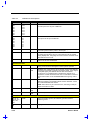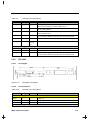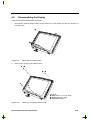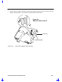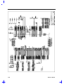
1
TM7300 Series Notebook Computer Service Guide PART NO.: 49.42A01.001 DOC. NO.: SG238-9712A PRINTED IN TAIWAN Copyright Copyright 1998 by Acer Incorporated. All rights reserved. No part of this publication may be reproduced, transmitted, transcribed, stored in a retrieval system, or translated into any language or computer language, in any form or by any means, electronic, mechanical, magnetic, optical, chemical, manual or otherwise, without the prior written permission of Acer Incorporated. Disclaimer Acer Incorporated makes no representations or warranties, either expressed or implied, with respect to the contents hereof and specifically disclaims any warranties of merchantability or fitness for any particular purpose. Any Acer Incorporated software described in this manual is sold or licensed "as is". Should the programs prove defective following their purchase, the buyer (and not Acer Incorporated, its distributor, or its dealer) assumes the entire cost of all necessary servicing, repair, and any incidental or consequential damages resulting from any defect in the software. Further, Acer Incorporated reserves the right to revise this publication and to make changes from time to time in the contents hereof without obligation of Acer Incorporated to notify any person of such revision or changes. Intel is a registered trademark and Pentium is a trademark of Intel Corporation. Other brand and product names are trademarks and/or registered trademarks of their respective holders. ii About this Manual Purpose This service guide aims to furnish technical information to the service engineers and advanced users when upgrading, configuring, or repairing the TM7300 series notebook computer. Manual Structure This service guide contains technical information about the TM7300 series notebook computer. It consists of three chapters and five appendices. Chapter 1 System Introduction This chapter describes the system features and major components. It contains the TM7300 series notebook computer board layout, block diagrams, cache and memory configurations, power management and mechanical specifications. Chapter 2 Major Chips Description This chapter describes the features and functions of the major chipsets used in the system board. It also includes chipset block diagrams, pin diagrams, and pin descriptions. Chapter 3 BIOS Setup Utility This chapter describes the parameters in the BIOS Utility screens. Chapter 4 Disassembly and Unit Replacement This chapter describes how to disassemble the TM7300 series notebook computer to make replacements or upgrades. Appendix A Model Number Definition This appendix shows the different configuration options for the TM7300 series notebook computer. Appendix B Exploded View Diagram This appendix illustrates the system board and CPU silk screens. Appendix C Spare Parts List This appendix lists the spare parts for the TM7300 series notebook computer with their part numbers and other information. iii Appendix D Schematics This appendix contains the schematic diagrams for the system board. Appendix E BIOS POST Checkpoints This appendix lists and describes the BIOS POST checkpoints. Conventions The following are the conventions used in this manual: Text entered by user Represents text input by the user. Screen messages Denotes actual messages that appear onscreen. , , , etc. Represent the actual keys that you have to press on the keyboard. NOTE Gives bits and pieces of additional information related to the current topic. WARNING Alerts you to any damage that might result from doing or not doing specific actions. CAUTION Gives precautionary measures to avoid possible hardware or software problems. IMPORTANT Reminds you to do specific actions relevant to the accomplishment of procedures. TIP Tells how to accomplish a procedure with minimum steps through little shortcuts. iv Table of Contents Chapter 1 1.1 Features .............................................................................................................. 1-1 1.1.2 1.2 System Introduction FlashStart Automatic Power-On ............................................................ 1-2 Ports .................................................................................................................... 1-3 1.2.1 Rear Panel Ports................................................................................... 1-3 1.2.2 Left Panel Ports .................................................................................... 1-4 1.2.3 Indicator Lights...................................................................................... 1-5 1.2.4 Hot Keys ............................................................................................... 1-6 1.2.5 Automatic Tilt........................................................................................ 1-8 1.3 System Specification Overview............................................................................ 1-9 1.4 Board Layout ......................................................................................................1-11 1.5 1.6 1.4.1 System Board (Top Side) .....................................................................1-12 1.4.2 System Board (Bottom Side)................................................................1-13 1.4.3 Media Board (Top Side) .......................................................................1-14 1.4.4 Media Board (Bottom Side) ..................................................................1-15 Jumpers and Connectors ....................................................................................1-16 1.5.1 Mainboard............................................................................................1-16 1.5.2 Media Board.........................................................................................1-18 System Configurations and Specifications ..........................................................1-19 1.6.1 System Memory Map ...........................................................................1-19 1.6.2 Interrupt Channel Map..........................................................................1-19 1.6.3 I/O Address Map ..................................................................................1-19 1.6.4 DMA Channel Map...............................................................................1-20 1.6.5 GPIO Port Definition Map.....................................................................1-21 1.6.6 PCI Devices Assignment......................................................................1-25 1.6.7 Power Management .............................................................................1-25 1.6.8 CPU Module.........................................................................................1-31 1.6.9 BIOS....................................................................................................1-32 1.6.10 System Memory ...................................................................................1-32 1.6.11 Video Memory......................................................................................1-33 1.6.12 Video Display Modes............................................................................1-34 1.6.13 Audio ...................................................................................................1-35 v 1.7 1.6.14 PCMCIA...............................................................................................1-35 1.6.15 Parallel Port .........................................................................................1-36 1.6.16 Serial Port............................................................................................1-36 1.6.17 Touchpad.............................................................................................1-36 1.6.18 SIR/FIR................................................................................................1-37 1.6.19 LCD .....................................................................................................1-37 1.6.20 CD-ROM..............................................................................................1-38 1.6.21 Diskette Drive ......................................................................................1-38 1.6.22 Hard Disk Drive....................................................................................1-39 1.6.23 Keyboard .............................................................................................1-39 1.6.24 Battery .................................................................................................1-40 1.6.25 DC-DC Converter.................................................................................1-40 1.6.26 DC-AC Inverter ....................................................................................1-41 1.6.27 AC Adapter ..........................................................................................1-41 System Block Diagrams......................................................................................1-42 1.7.1 System Functional Block Diagram........................................................1-42 1.7.2 System Bus Block Diagram..................................................................1-43 1.8 Environmental Requirements..............................................................................1-44 1.9 Mechanical Specifications...................................................................................1-45 Chapter 2 2.1 Major Component List...........................................................................................2-1 2.2 Intel PIIX4.............................................................................................................2-2 2.3 2.4 vi Major Chips Description 2.2.1 Features.................................................................................................2-4 2.2.2 Architecture Block Diagram....................................................................2-6 2.2.3 Block Diagram .......................................................................................2-7 2.2.4 Pin Descriptions .....................................................................................2-8 NM2160..............................................................................................................2-28 2.3.1 Features...............................................................................................2-28 2.3.2 Pin Diagram.........................................................................................2-30 2.3.3 Pin Descriptions ...................................................................................2-31 NMA1 .................................................................................................................2-38 2.4.1 Features...............................................................................................2-38 2.4.2 Block Diagram .....................................................................................2-39 2.5 2.6 2.7 2.8 2.9 2.4.3 Pin Diagram .........................................................................................2-40 2.4.4 Pin Descriptions ...................................................................................2-41 Philips 87C552 System Management Controller .................................................2-43 2.5.1 Features...............................................................................................2-43 2.5.2 Block Diagram .....................................................................................2-44 2.5.3 Pin Diagram .........................................................................................2-45 2.5.4 Pin Descriptions ...................................................................................2-46 NS87338VJG Super I/O Controller......................................................................2-48 2.6.1 Features...............................................................................................2-48 2.6.2 Block Diagram .....................................................................................2-50 2.6.3 Pin Diagram .........................................................................................2-51 2.6.4 Pin Description.....................................................................................2-52 CL-PD6832: PCI-to-CardBus Host Adapter .........................................................2-59 2.7.1 Features...............................................................................................2-59 2.7.2 Pin Diagram .........................................................................................2-60 2.7.3 Pin Descriptions ...................................................................................2-60 Ambit T62.036.C DC-DC Converter ....................................................................2-72 2.8.1 Pin Diagram .........................................................................................2-72 2.8.2 Pin Descriptions ...................................................................................2-72 Ambit DC-AC Inverter .........................................................................................2-74 2.9.1 T62.055C .............................................................................................2-74 2.9.2 T62.088C .............................................................................................2-75 Chapter 3 BIOS Setup Utility 3.1 About My Computer ............................................................................................. 3-2 3.2 System Configuration........................................................................................... 3-3 3.2.1 Date and Time ...................................................................................... 3-3 3.2.2 Floppy Drives........................................................................................ 3-3 3.2.3 Hard Disks ............................................................................................ 3-3 3.2.4 Num Lock After Boot............................................................................. 3-3 3.2.5 LCD Expansion Mode ........................................................................... 3-3 3.2.6 Internal Speaker.................................................................................... 3-4 3.2.7 Silent Boot ............................................................................................ 3-4 3.2.8 Fast Boot ................................................................................................ 3- vii 3.3 3.4 3.5 3.6 Advanced System Configuration...........................................................................3-5 3.3.1 Internal Cache........................................................................................3-5 3.3.2 External Cache ......................................................................................3-5 3.3.3 Enhanced IDE Features .........................................................................3-5 3.3.4 Onboard Communication Ports ..............................................................3-6 3.3.5 Onboard USB.........................................................................................3-6 3.3.6 Reset PnP Resources ............................................................................3-7 Power Saving Options ..........................................................................................3-8 3.4.1 When Lid is Closed ................................................................................3-8 3.4.2 Suspend to Disk on Critical Battery ........................................................3-8 3.4.3 Display Always On .................................................................................3-8 3.4.4 Resume On Modem Rings .....................................................................3-8 3.4.5 Resume On Schedule ............................................................................3-9 System Security..................................................................................................3-10 3.5.1 Supervisor and User Passwords...........................................................3-10 3.5.2 Diskette Drive Access Control ..............................................................3-11 3.5.3 Hard Disk Drive Access Control ...........................................................3-11 3.5.4 Start Up Sequences .............................................................................3-11 3.5.5 Refresh New BIOS...............................................................................3-11 Reset To Default Settings ...................................................................................3-12 Chapter 4 4.1 viii Disassembly and Unit Replacement General Information..............................................................................................4-1 4.1.1 Before You Begin...................................................................................4-1 4.1.2 Connector Types....................................................................................4-3 4.1.3 Disassembly Sequence ..........................................................................4-4 4.2 Removing the Module...........................................................................................4-6 4.3 Replacing the Hard Disk Drive ..............................................................................4-7 4.4 Replacing Memory................................................................................................4-8 4.5 Removing the Keyboard .....................................................................................4-10 4.6 Replacing the CPU .............................................................................................4-12 4.7 Removing the Display.........................................................................................4-13 4.8 Disassembling the Housing.................................................................................4-14 4.9 4.8.1 Detaching the Lower Housing from the Inside Assembly ......................4-14 4.8.2 Detaching the Upper Housing from the Inside Assembly ......................4-15 4.8.3 Removing the Touchpad ......................................................................4-16 4.8.4 Removing the Main Board....................................................................4-16 Disassembling the Display ..................................................................................4-19 Appendices Appendix A Model Number Definition Appendix B Exploded View Diagram Appendix C Spare Parts List Appendix D Schematics Appendix E BIOS POST Checkpoints ix List of Figures x 1-1 Lid Switch .............................................................................................................1-2 1-2 Rear Port Location................................................................................................1-3 1-3 Left Port Location .................................................................................................1-4 1-4 Indicator Lights .....................................................................................................1-5 1-5 System Board (Top Side)....................................................................................1-12 1-6 System Board (Bottom Side)...............................................................................1-13 1-7 Media Board (Top Side)......................................................................................1-14 1-8 Media Board (Bottom Side).................................................................................1-15 1-9 Mainboard Jumpers and Connectors (Top Side) .................................................1-16 1-10 Mainboard Jumpers and Connectors (Bottom Side) ............................................1-17 1-11 Media Board Jumpers and Connectors (Top Side) ..............................................1-18 1-12 Media Board Jumpers and Connectors (Bottom Side) .........................................1-18 1-13 System Functional Block Diagram ......................................................................1-42 1-14 System Bus Block Diagram.................................................................................1-43 2-1 PIIX4 Architecture Block Diagram .........................................................................2-6 2-2 PIIX4 Simplified Block Diagram ............................................................................2-7 2-3 NM2160 Pin Diagram..........................................................................................2-30 2-4 NMA1 Block Diagram .........................................................................................2-39 2-5 NMA1 Pin Diagram .............................................................................................2-40 2-6 87C552 Block Diagram .......................................................................................2-44 2-7 87C552 Pin Diagram...........................................................................................2-45 2-8 NS87338VJG Block Diagram..............................................................................2-50 2-9 NS87338VJG Pin Diagram .................................................................................2-51 2-10 CL-PD6832 Pin Diagram.....................................................................................2-60 2-11 T62.036.C Pin Diagram ......................................................................................2-72 2-12 T62.055.C Pin Diagram ......................................................................................2-74 2-13 T62.088.C Pin Diagram ......................................................................................2-75 4-1 Removing the Battery Pack ..................................................................................4-2 4-2 Using Plastic Stick on Connector With Locks ........................................................4-3 4-3 Disassembly Flow .................................................................................................4-5 4-4 Removing the Module...........................................................................................4-6 4-5 Removing the Hard Disk Drive Bay Cover ............................................................4-7 4-6 Removing the Hard Disk Drive..............................................................................4-7 4-7 Installing a Memory Module ..................................................................................4-8 4-8 Installing and Removing Memory......................................................................... 4-8 4-9 Removing the Display Hinge Covers...................................................................4-10 4-10 Removing the Center Hinge Cover .....................................................................4-10 4-11 Lifting Out the Keyboard .....................................................................................4-11 4-12 Unplugging the Keyboard Connectors and Removing the Keyboard....................4-11 4-13 Removing the CPU Heat Sink.............................................................................4-12 4-14 Removing the CPU Module.................................................................................4-12 4-15 Unplugging the Display Cable .............................................................................4-13 4-16 Removing the Display Hinge Screws and Removing the Display.........................4-13 4-17 Removing the Lower Housing .............................................................................4-14 4-18 Removing the Battery Bay Screws ......................................................................4-15 4-19 Detaching the Upper Housing from the Inside Frame Assembly ..........................4-15 4-20 Removing the Touchpad.....................................................................................4-16 4-21 Unplugging the Speaker Connectors and Battery Pack Connector ......................4-16 4-22 Removing the Main Board ..................................................................................4-17 4-23 Removing the Charger Board and Multimedia Board ..........................................4-17 4-24 Removing the PC Card Slots ..............................................................................4-18 4-25 Removing the LCD Bumpers ..............................................................................4-19 4-26 Removing the Display Bezel Screws...................................................................4-19 4-27 Removing the Display Bezel ...............................................................................4-20 4-28 Removing the Display Panel Screws and the Display Connectors .......................4-20 4-29 Removing the Display Cable Assembly...............................................................4-21 xi List of Tables xii 1-1 Rear Port Descriptions ..........................................................................................1-3 1-2 Left Port Descriptions............................................................................................1-5 1-3 Indicator Light Descriptions...................................................................................1-5 1-4 Hot Key Descriptions ............................................................................................1-6 1-5 Eject Menu Item Descriptions ...............................................................................1-7 1-6 System Specifications...........................................................................................1-9 1-7 Mainboard Jumpers Pads Settings (Bottom Side) ...............................................1-17 1-8 System Memory Map..........................................................................................1-19 1-9 Interrupt Channel Map ........................................................................................1-19 1-10 I/O Address Map.................................................................................................1-19 1-11 DMA Channel Map..............................................................................................1-20 1-12 GPIO Port Definition Map I .................................................................................1-21 1-13 GPIO Port Definition Map II ................................................................................1-22 1-14 PCI Devices Assignment ....................................................................................1-25 1-15 PMU Timers List .................................................................................................1-26 1-16 CPU Module Specifications.................................................................................1-31 1-17 BIOS Specifications............................................................................................1-32 1-18 System Memory Specifications ...........................................................................1-32 1-19 SIMM Memory Combination List .........................................................................1-33 1-20 Video Memory Specification ...............................................................................1-33 1-21 Video Display Specification.................................................................................1-34 1-22 External CRT Resolution Modes .........................................................................1-34 1-23 LCD Resolution Modes .......................................................................................1-34 1-24 Audio Specifications ...........................................................................................1-35 1-25 PCMCIA Specifications.......................................................................................1-35 1-26 Parallel Port Specifications .................................................................................1-36 1-27 Serial Port Specifications....................................................................................1-36 1-28 Touchpad Specifications.....................................................................................1-36 1-29 SIR/FIR Specifications........................................................................................1-37 1-30 LCD Specifications .............................................................................................1-37 1-31 CD-ROM Specifications ......................................................................................1-38 1-32 Diskette Drive Specifications ..............................................................................1-38 1-33 Hard Disk Drive Specifications............................................................................1-39 1-34 Keyboard Specifications .....................................................................................1-39 1-35 Battery Specifications .........................................................................................1-40 1-36 DC-DC Converter Specifications.........................................................................1-40 1-37 DC-AC Inverter Specifications ............................................................................1-41 1-38 AC Adapter Specifications ..................................................................................1-41 1-39 Environmental Requirements..............................................................................1-44 1-40 Mechanical Specifications...................................................................................1-45 2-1 Major Chips List ................................................................................................... 2-1 2-2 82371AB Pin Descriptions.................................................................................... 2-9 2-3 NM2160 Pin Descriptions....................................................................................2-31 2-4 NMA1 Pin Descriptions .......................................................................................2-41 2-5 87C552 Pin Descriptions.....................................................................................2-46 2-6 NS87338VJG Pin Descriptions............................................................................2-52 2-7 CL-PD6832 Pin Descriptions...............................................................................2-62 2-8 T62.036.C Pin Descriptions.................................................................................2-72 2-9 T62.055.C Pin Descriptions.................................................................................2-74 2-10 T62.088.C Pin Descriptions.................................................................................2-75 3-1 About My Computer Parameters .......................................................................... 3-2 3-2 Start Up Sequences ............................................................................................3-11 4-1 Guide to Disassembly Sequence.......................................................................... 4-4 B-1 Exploded View Diagram List ................................................................................ B-1 C-1 Spare Parts List ................................................................................................... C-1 D-1 Schematics Diagram List ..................................................................................... D-1 E-1 POST Checkpoint List.......................................................................................... E-1 xiii &KDSWHU System Introduction The computer is packed with features that make it as easy to work with as it is to look at. Here are some of the computer’s features: 1.1 Features PERFORMANCE • Intel Pentium II 266 MHz processor • 64-bit main memory and 512KB external (L2) cache memory • Large display in active-matrix TFT • PCI local bus video with 128-bit graphics accelerator • ® Flexible module bay (3.5-inch floppy drive or CD-ROM drive or DVD-ROM drive or LS120 or second hard disk drive option) • High-capacity, Enhanced-IDE hard disk • An advanced power management system with two power-saving modes • Lithium-Ion smart battery pack • High-speed connectivity MULTIMEDIA AND COMMUNICATIONS • 16-bit stereo audio with built-in FM synthesizer and 3D sound effect • Built-in microphone and dual angled stereo speakers • Support for simultaneous display on the built-in screen and an external monitor for presentations • Full-screen, 30 frames per second, true-color MPEG video playback • Infrared wireless communication ERGONOMICS • Intuitive FlashStart automatic power-on • Sleek, smooth and stylish design • Automatic tilt-up (12.1-inch models only), full-sized, full-function keyboard • Wide and comfortable palm rest System Introduction 1-1 • Ergonomically-positioned touchpad pointing device EXPANDABILITY • CardBus PC Card (PCMCIA) slots (two type II/I or one type III) with Zoomed Video port function • Mini-dock option with two CardBus PC Card slots (two type II/I or one type III) • USB port onboard • Upgradeable memory and hard disk 1.1.2 FlashStart Automatic Power-On The computer has no on/off switch. Instead it uses a lid switch, located near the center of the display hinge, that turns the computer on and off automatically. Lid Switch Figure 1-1 Lid Switch When you close the display lid, the computer saves all data either to the hard disk or to memory, depending on the When Lid Is Closed setting (see section 3.4.1). When all data is saved, the computer turns itself off. When you reopen the lid, the computer retrieves your data and resumes where you left off. 1-2 Service Guide 1.2 Ports The computer’s ports allow you to connect peripheral devices to your computer just as you would to a desktop PC. The main ports are found on the computer’s rear panel. The computer’s left panel contains the computer’s multimedia ports and PC card slots. 1.2.1 Rear Panel Ports The computer’s rear panel contains the computer’s main ports and connectors as shown in the illustration below. 1 2 3 4 5 6 1 2 3 4 5 6 7 8 7 8 DC-in Port PS/2 Port Serial Port Parallel Port Mini Dock Connector External CRT Port USB Port Infrared Port Figure 1-2 Rear Port Location Table 1-1 Rear Port Descriptions Port Icon Connects to... DC-in port AC adapter and power outlet PS/2 port PS/2-compatible device (PS/2 keyboard, keypad, mouse) Serial port (UART16650-compatible) Serial device (serial mouse) Parallel port (EPP/ECPcompliant) Parallel device (parallel printer, external floppy drive) Mini dock connector Mini dock External CRT port External monitor (up to 1024x768x256 colors) USB port USB device (USB mouse, keyboard) Infrared port Infrared-aware device (computer with IR port, desktop with IR adapter, IR-capable printer) System Introduction 1-3 UNIVERSAL SERIAL BUS (USB) PORT The computer’s USB (Universal Serial Bus) port located on the rear panel allows you to connect peripherals without occupying too many resources. Common USB devices include the mouse and keyboard. FAST INFRARED (FIR) PORT The computer’s FIR (fast infrared) port located on the rear panel allows you to transfer data to IRaware machines without cables. For example, you can transfer data between two IR-capable computers, or send data to an IR-aware printer without using a cable. The infrared port is IrDA-compliant, and can transfer data at speeds of up to 4 megabits per second (Mbps) at a distance of up to one meter. To use the infrared port, position two IR-aware devices such that their IR ports are no more than one meter apart and offset no more than 15 degrees. When the two computers are in position, simply begin the data transfer as you normally would. See your file transfer software for details. 1.2.2 Left Panel Ports The computer’s left side panel contains the computer’s multimedia ports and PC card slots, as shown in the illustration on the next page. 1 23 1 2 3 PC Card Slots Microphone-in/Line-in Port Speaker-out/Line-out Port Figure 1-3 1-4 Left Port Location Service Guide Table 1-2 Left Port Descriptions Port Icon Connects to... PC Card slots Two type I/II PC Cards or one type III Card Microphone-in/ Line-in External microphone or line input device Speaker-out/ Line-out Amplified speakers or headphones PC CARD SLOTS The computer contains two PC card slots on the left panel that accommodate two type I/II or one type III PC card(s). Consult your dealer for available PC card options. MULTIMEDIA PORTS The computer provides a Mic-In/Line-in port and a Speaker-out/Line-out port on the left panel to accommodate multimedia audio devices, such as a microphone, speakers, or headphones. 1.2.3 Indicator Lights The display panel contains a power indicator light and a battery indicator light as shown in the illustration below. Power Indicator Battery Indicator Figure 1-4 Indicator Lights Table 1-3 Indicator Light Descriptions Indicator Light Icon Description Power Indicator Lights when power is on. Flashes when the computer is in suspend-to-memory mode. Battery Indicator Lights when the battery pack is charging. Flashes when battery power is low. System Introduction 1-5 1.2.4 Hot Keys The computer’s special Fn key, used in combination with other keys, provides “hot-key” combinations that access system control functions, such as screen contrast, brightness, volume output, and the BIOS setup utility. Table 1-4 Hot Key Hot Key Descriptions Icon Fn+Esc Function Description Suspend-to-memory Enters suspend-to-memory mode Help Displays the hot-key list Setup Enters the BIOS setup utility Plug and Play Configuration Performs system configuration for Plug and Play operating systems like Windows 95 Fn+F4 Screen Blackout Blanks the screen to save power; to wake up the screen, press any key Fn+F5 Display Toggle Switches display from the built-in display, to an external monitor, to both built-in and external if one is connected Fn+F6 Fuel Gauge On/Off Toggles battery gauge display on and off. The gauge shows the percentage of charge left in the battery. Fn+F1 ? Fn+F2 Fn+F3 PnP Shows a plug icon if a powered AC adapter is connected to the computer; shows a speaker icon if speaker output is on (Fn+F7); shows a T icon if turbo mode is on (Fn+2) Fn+F7 Speaker On/Off Toggles speaker output on and off Fn+F8 Lock System Resources (Password Lock) Locks the computer and requires a password to unlock it Fn+F9 Eject Accesses the eject menu described on page 7 Fn+Ctrl+↑ Volume Up Increases speaker volume Fn+Ctrl+↓ Volume Down Decreases speaker volume Fn+Ctrl+→ Balance Right Shifts speaker balance to the right Fn+Ctrl+← Balance Left Shifts speaker balance to the left 1-6 Service Guide Table 1-4 Hot Key á+↑ Fn+á+↓ Fn+á+→ Fn+á+← Hot Key Descriptions Icon Function Description Brightness Up Increases screen brightness Brightness Down Decreases screen brightness Contrast Up Increases screen contrast (not available for TFT displays) Contrast Down Decreases screen contrast (not available for TFT displays) Fn+↑ Fuel Gauge Up With the fuel gauge displayed, moves the fuel gauge up Fn+↓ Fuel Gauge Down With the fuel gauge displayed, moves the fuel gauge down Fn+→ Fuel Gauge Right With the fuel gauge displayed, moves the fuel gauge right Fn+← Fuel Gauge Left With the fuel gauge displayed, moves the fuel gauge left Fn+1 CD Eject Ejects the CD-ROM drive Fn+2 Turbo Mode On/Off Toggles turbo mode on and off Fn+ EJECT MENU The Fn+F9 hot-key combination brings up a special eject menu that allows you to perform several system configuration functions. Eject Options: Battery (Suspend-to-disk) ................. Change CD-ROM Disk (Also Fn-1) .................... Eject Mini Dock (Suspend) ........................ Change Power Off .................................. Change ↑↓←→ = Move Highlight Bar, ↵ = Select, ESC = Exit Table 1-5 Eject Menu Item Descriptions Select… To… Battery (Suspend to Disk) Store all current data and system information to the hard disk. CD-ROM Disk (Also Fn-1) Open the CD-ROM drive (eject a CD). Mini Dock (Suspend) Undock the computer. Press the dock lock and pull the dock handle toward you to undock the computer. (See the mini dock manual for details.) Once the computer is successfully undocked, press any key to resume. Power Off Turn the computer off. If you are using Windows 95, use the Shutdown command to turn off your computer. System Introduction 1-7 1.3 System Specification Overview Table 1-6 System Specifications Item Microprocessor Memory System / Main External cache Standard Optional ® Intel Pentium II 266 MHz processor 64MB Dual 64-bit memory banks Expandable to 128MB using 8/16/32/64MB soDIMMs 512KB L2 cache (synchronous SRAM) Flash BIOS 256KB Storage system One 2.5-inch, high-capacity Enhanced-IDE hard disk One high-speed IDE CD-ROM drive module Higher-capacity E-IDE hard disk Second optional hard disk drive module (3-inch) One 3.5-inch, 1.44MB floppy drive module (internal/external use) Display Active-matrix TFT LCD 13.3-inch, 1024x768, 64K colors (XGA) Video system PCI local bus video with 128-bit graphics accelerator Audio system 16-bit stereo audio with built-in FM synthesizer Up to 1024x768, 256-color ultra-VGA monitor LCD projection panel Built-in microphone and dual angled speakers Communications system PC card modem Operating system Windows 95, 98 Keyboard and pointing device 84-/85-key with Win95 keys; auto-tilt feature 101-/102-key, PS/2-compatible keyboard or 17-key numeric keypad Touchpad (centrally-located on palm rest) External serial or PS/2 mouse or similar pointing device One 9-pin RS-232 serial port (UART16550-compatible) Serial mouse, printer or other serial devices One 25-pin parallel port (EPP/ECP-compliant) Parallel printer or other parallel devices; floppy drive module (when used externally) One 15-pin CRT port Up to a 1024x768 ultra-VGA monitor One 6-pin PS/2 connector 17-key numeric keypad, PS/2 keyboard, mouse or trackball One 240-pin mini dock connector Mini dock One type III or two type II PC Card slot(s) LAN card or other PC cards I/O ports I/O Ports (continued) 1-8 Service Guide Table 1-6 System Specifications Item Standard One fast infrared port (IrDA-compliant) External IR adapter One 3.5mm minijack microphone-in/line-in jack Microphone or line-in device One 3.5mm minijack speaker-out/line-out jack Speakers or headphones One USB port USB device Weight with FDD with CD-ROM (includes battery) 3.5 kg. (7.5 lbs.) 3.8 kg. (7.8 lbs.) Dimensions Round contour Main footprint LxWxH 309x245x56mm 12.2” x 9.6” x 2.2” Temperature Operating Non-operating 10ºC ~ 35ºC(50ºF ~ 95ºF) -10ºC ~ 60ºC(14ºF ~ 140ºF) Humidity Operating Non-operating (non-condensing) 20% ~ 80% RH 20% ~ 80% RH AC adapter 100~240Vac, 50~60Hz autosensing AC adapter Battery pack Type Charge time Optional Carrying bag Extra AC adapter Extra battery pack 57WH Lithium-Ion battery with intelligent charging and built-in battery gauge 2.0-hour rapid-charge 4.0-hour in-use charge System Introduction 1-9 1.4 1-10 Board Layout Service Guide 1.4.1 System Board (Top Side) Figure 1-5 System Board (Top Side) System Introduction 1-11 1.4.2 System Board (Bottom Side) Figure 1-6 1-12 System Board (Bottom Side) Service Guide 1.4.3 Media Board (Top Side) Figure 1-7 Media Board (Top Side) System Introduction 1-13 1.4.4 Media Board (Bottom Side) Figure 1-8 1-14 Media Board (Bottom Side) Service Guide 1.5 Jumpers and Connectors 1.5.1 Mainboard CN1 CN2 CN3 CN4 CN5 CN6 CN7 U1 CN8 CN9 CN10 CN11 CN12 CN13 CN14, CN15 CN1 CN2 CN3 CN4 CN5 CN6 CN7 USB VGA port Mini dock port Parallel port Serial Port PS2 mouse/keyboard port AC adapter plug-in port Figure 1-9 Mainboard Jumpers and Connectors (Top Side) System Introduction CN8, CN9 CN10 CN14, CN15 CN13 CN12 CN11 U1 Multimedia board connector FDD/CD-ROM connector CPU board connector Hard disk drive connector Speaker-out/Line-out Jack Microphone-in/Line-in Jack SIR/FIR infrared LED 1-15 CN19, CN18 CN16 SW1 CN17 CN20 SW2 ON OFF 1 4 SI2 CN22 SI1 CN20, CN19 CN17 CN20 DC-DC converter connector Left speaker connector Debug port Figure 1-10 Mainboard Jumpers and Connectors (Bottom Side) CN22 CN16 SW1 SW2 Battery connector Right speaker connector Reset Switch Jumper Setting The following table shows the settings of the mainboard’s bottom side jumper pads. Table 1-7 Jumper Pad Mainboard Jumpers Pads Settings (Bottom Side) Descriptions Settings SW2(1) Keyboard type selection OFF: Other keyboard ON: Japan keyboard SW2(2) Password settings OFF: Enable password ON: Bypass password SW2(3) BIOS type selection OFF: Acer BIOS ON: OEM BIOS SW2(4) Reserved 1-16 Service Guide 1.5.2 Media Board CN2 CN1 CN4 CN5 CN6 CN2 CN1 Lid switch LCD connector Figure 1-11 Media Board Jumpers and Connectors (Top Side) CN7 CN6 CN4, CN5 Touchpad connector Keyboard connector CN8 CN9 CN7, CN8 Mainboard connector Figure 1-12 Media Board Jumpers and Connectors (Bottom Side) System Introduction CN9 PCMCIA socket connector 1-17 1.6 System Configurations and Specifications 1.6.1 System Memory Map Table 1-8 System Memory Map Address Range Definition Function 000000 -09FFFF 640 KB memory Base memory 0A0000 -0BFFFF 128 KB video RAM Reserved for graphics display buffer 0C0000 -0CBFFF Video BIOS Video BIOS 0CC000 -0CDFFF 0CE000 -0CFFFF System CardBus Mini dock CardBus 0F0000 -0FFFFF 64 KB system BIOS System BIOS 010000 -07FFFF 080000 -027FFF Extended memory Onboard memory SIMM memory FE0000 -FFFFFF 256 KB system ROM Duplicate of code assignment at 0E0000-0FFFFF 1.6.2 Interrupt Channel Map Table 1-9 Interrupt Channel Map Interrupt Number System Timer Keyboard Cascade IrDA / 2F8h Serial Port 1 / 3F8h Audio Floppy Disk Controller (FDC) Parallel Port Real Time Clock (RTC) USB/System CardBus Reserved for PCMCIA card Reserved for PCMCIA card/Mini dock CardBus PS/2 Mouse Co-processor Hard disk CD-ROM IRQ 0 IRQ 1 IRQ 2 IRQ 3 IRQ 4 IRQ 5 IRQ 6 IRQ 7 IRQ 8 IRQ 9 IRQ 10 IRQ 11 IRQ 12 IRQ 13 IRQ 14 IRQ 15 1.6.3 Interrupt Source (Device Name) I/O Address Map Table 1-10 I/O Address Map Address Range 000 -00F 020 -021 02E -02F 040 -043 048 -04B 060 -06E 1-18 Device DMA controller-1 Interrupt controller-1 NS97338 peripheral controller Timer 1 Timer 2 Keyboard controller chip select Service Guide Table 1-10 I/O Address Map Address Range Device Real-time clock and NMI mask DMA page register Interrupt controller-2 DMA controller-2 Hard disk select Hard disk select CD-ROM select CD-ROM select Audio Audio -default Audio Audio Parallel port 3 COM 4 COM 2 -IrDA MPU-401 port -default MPU-401 port MPU-401 port MPU-401 port Parallel port 2 FM synthesizer Parallel port 1 Video subsystem 070 -071 080 -08F 0A0 -0A1 0C0 -0DF 1F0 -1F7 3F6 -3F7 170 -177 376 -377 220 -22F 240 -24F 260 -26F 280 -28F 278 -27F 2E8 -2EF 2F8 -2FF 300 -301 310 -311 320 -321 330 -321 378 -37F 388 -38B 3BC -3BE 3B4, 3B5, 3BA 3C0 -3C5 3C6 -3C9 3C0 -3CF 3D0 -3DF 3E8 -3EF 3F0 -3F7 3F8 -3FF CF8 -CFF 1.6.4 Video DAC Enhanced graphics display Color graphics adapter COM3 Floppy disk controller COM 1 -Serial 1 PCI configuration register DMA Channel Map Table 1-11 DMA Channel Map Controller Channel Address Function 1 1 1 1 2 2 2 2 0 1 2 3 4 5 6 7 0087 0083 0081 0082 Cascade 008B 0089 008A Audio(default) / IrDA(option) Audio(default) / ECP(option) / IrDA(option) Diskette Audio (option) / FIR IrDA(option) / ECP(option) Cascade System Introduction Spare 1-19 1.6.5 GPIO Port Definition Map Table 1-12 GPIO Port Definition Map I GPIO/Signal Pin # I/O Description SUSA# (PX3_SUSA#) W20 O 0: Power down clock generator GPO0 (PX3_DOCKRST#) G4 O 0 : Enable docking reset GPO1 (PX3_HDPON) Y15 O 1: Turn on HDD power GPO2 (PX3_ CD/FDPON) T14 O 1: Turn on CD/FDD power GPO3 (PX3_ HDRST#) W14 O 0: Reset HDD interface GPO4 (PX3_CDRST#) U13 O 0: Reset CD interface GPO5 (PX3_3MODE) V13 O 0: 3 mode drive GPO6 (PX3_SMBSEL0) Y13 O Select one of three SM buses GPO7 (PX3_SMBSEL1) T12 O GPIO Pin Assignment: PIIX4 SMBSEL1 SMBSEL0 0 0 1 1 0 1 0 1 DRAM bank 0 SMB DRAM bank 1 SMB MMO LM75 & clock gen. SMB PCMCIA LM75 GPO8 (PX3_DOCKGNT#) T19 O 0: Granted docking GPO9/GNTA# (PX3_VDPD) N1 O 1: Power down VGA GPO10/GNTB# (PX3_VGADIS) P2 O 1: Disable VGA from PCI GPO11/GNTC# (PX3_AUDPON) P4 O 1: Power on analog audio power GPO12/APICACK# J17 O NC GPO13/APICCS# H18 O NC GPO14/IRQ0 (PX3_ROM#) H20 O 0: Enable ROMCS# GPO15/SUSB# V19 O NC GPO16/SUSC# U18 O NC GPO17/CPU_STP#(PX3_CPUSTP#) R1 O 0: Enable CPU clock stop GPO18/PCI_STP# (PX3_PCISTP#) R2 O 0: Enable PCI clock stop GPO19/ZZ (PXI_L2ZZ) K16 O 1: Power down L2 cache GPO20/SUS_STAT1#(PX3_SUSTAT#) T17 O 0: Enable MTXC power down GPO21/SUS_STAT2# (PM3_A_ACT/PD#) T18 O 0: Power down PD6832 Cardbus controller GPO22/XDIR# (PX3_FDDBEN) M3 O 1: FDD buffer enable GPO23/XOE# (PX3_SPPD) M4 O 1: Power down serial interface GPO27 (PX3_SPKOFF) G5 O 1: Turn off speaker GPO28 (PX3_FLASHVPP) F2 O 1: Enable Flash Vpp control GPO29 (PX3_FPAGE1) F3 O Force BIOS to high page 1F segment and 3 E segments GPO30 (PX3_FPAGE2) F4 O EXTSMI#(PX3_KRSMIREQ#) 1-20 V20 O FPAGE2 FPAGE1 0 0 1 1 0 1 0 1 F, E0 F, E1 F, E2 reserved 0: Enable by KBD SMI or RTC wake Service Guide Table 1-12 GPIO Port Definition Map I GPIO/Signal Pin # I/O Description GPI1 (DK3_DOCKIRQ#) P19 O 0: Detect Docking IRQ GPI2/REQA# (PX3_OEM0) M1 O OEM detection GPI3/REQB# (SM5_BAYSW) N2 O Detect FDD/CD bay 1: installed, 0: not installed GPI4/REQC# (CF5_FDD/CD#) P3 O Detect FDD or CD installed 1: FDD, 0: CD GPI5/APICREQ# K18 O NC GPI6/IRQ8# (RT3_IRQ8#) Y20 O 0: RTC wake GPI7/SERIRQ (PM3_IRQSER) J19 O Serial IRQ GPI8/THRM# (SM5_OVTMP#) H19 O 0: Enable over temperature of CPU or system GPI9/BATLOW# (PX3_OEM1) U19 I OEM detection GPI10/LID P16 I NC GPI11/SMBALER# N17 I NC GPI12/RI# (PX3_RI#) P18 I 0: Enable by Ring indicator input GPI13 (PT3_MID0) L2 I Detect MMO module revision GPI14 (PT3_MID1) J3 I Detect MMO module revision GPI15 (PT3_MID2) L5 I Detect MMO module revision GPI16 (PT3_MID3) K3 I Detect MMO module revision GPI17 (SM5_FLOATREQ#) K4 I Detect float request from SMC GPI18 (PX3_FLASHRCY#) H1 I 0: Enable flash BIOS recovery GPI19 (PX3_VGACT) H4 I 1: Detect VGA activity GPI20 (PM3_A_ACT/PD#) H5 I Detect PCMCIA socket A activity for OZ6832 GPI21 (PM3_B_ACT) G3 I Detect PCMCIA socket B activity Table 1-13 GPIO Port Definition Map II GPIO I/O Description GPIO Pin Assignment: 80C51SL LED 0 (KB5_MIREQ#) O ANI3 (KB5_PANID3) LED 1 (KB5_NUMLED#) O PAD LED control LED 2 (KB5_CAPLED#) O CAP LED control LED 3 (KB5_KEYLICK) O Keyclick output P1.0 O NC P1.1 O NC P1.2 O NC P1.3 O NC P1.4 O NC P1.5 O NC P1.6 O NC System Introduction 1-21 Table 1-13 GPIO Port Definition Map II GPIO I/O Description P1.7 (IS5_IRQ12) O IRQ12 P2.0 (KB5_MEMB0A0) I Address 0 of memory bank 0 P2.1 (KB5_MEMB0A1) I Address 1 of memory bank 0 P2.2 (KB5_MODE) I Detect KBD mode (1:US/EC 0:Japan) P2.3 I NC P2.4 (KB5_MEMB1A0) I Address 0 of memory bank 1 P2.5 (KB5_PSWD) I Enable Password P2.6 (KB5_MEMB1A1) I Address 1 of memory bank 1 P2.7 (PX3_OEM0) I Address 1 of memory bank 1 P3.0 (SM5_TXD) I Receiving data from SMC to KBC P3.1 (SM5_RXD) O Transmitting data from KBC to SMC P3.2 (KB5_KBDCLK) O External KB clock P3.3 (KB5_PTRCLK) O External PS/2 clock P3.4 (KB5_KBDDAT) O External KB data P3.5 (KB5_PTRDAT) O External PS/2 data P3.6 (KB5_TOUCHWR*) O Write enable touch pad data P3.7 (KB5_TOUCHRD*) O Read enable touch pad data ANI0 (KB5_PANID0) I Panel ID ANI1 (KB5_PANID1) I Panel ID ANI2 (KB5_PANID2) I Panel ID ANI3 (KB5_PANID3) I Panel ID: 3 2 1 0 O Charge control enable 0 0 0 0 12.1” TFT GPIO Pin Assignment: 83C552 P0.0(SM5_CHARGEON#) P0.1 O NC P0.2 (SM5_BMCPWREN#) O BMC VCC power enable P0.3 (SM5_P3/5VRON#) O 3V and 5V power on P0.4 (SM5_SUSPEND) O Suspend control enable P0.5 (SM5_PWRLED#) O Power LED P0.5 (SM5_PWRLED#) O Battery LED P0.7 (SM5_SMIREQ#) O SMC SMI request P1.0 (SI5_PNF) I Detect Printer or external FDD P1.1 (SM5_1WIRE) IO Dallas protocol P1.2 (SM5_UNDOCK_REQ#) I Undocked request P1.3 (PX3_CPUSTP#) I Detect CPU clock stop P1.4 (SM5_ATN#) IO I2C inturrupt P1.5 (SM5_RST#) IO I2C reset P1.6 (SM5_CLK#) IO I2C clock P1.7 (SM5_DAT#) IO I2C data P2.0 I NC 1-22 0: FDD 1: Printer Service Guide Table 1-13 GPIO Port Definition Map II GPIO I/O Description P2.1 O NC P2.2 (SM5_BAYSW) I Detect FDD/CD bay installed or not P2.3 O NC P2.4 O NC P2.5 O NC P2.6 O NC P2.7 O NC P3.0 (SM5_RXD) I Receiving data from KBC to SMC P3.1 (SM5_TXD) O Transmitting data from SMC to KBC P3.2 (SM5_DOCKSW) I Dock switch sense P3.3 (CF5_DOCKED) I Detect completely docked or not P3.4 (SM5_LIDSW) I Lid switch sense P3.5 (SM5_OVTMP#) O CPU or system over temperature P3.6 O NC P3.7 (SM5_ON_RES_SW) O ON/RESUME switch for Japan version P4.0 (SM5_FANON) O Fan control P4.1 NC P4.2 (SM5_FLOATREQ#) O Docking float request P4.3 (SM5_UNDOCK_GNT#) O Undock grant P4.4 (SM5_ICONT) I Charge current control P4.5 (SM5_FLAOTGNT#) I Docking float grant P4.6 (SM5_PWRRDYB) O Power ready, delay about 4ms after power good P4.7 (SM5_SYSRDY) O NC P5.0 (CHARGSP) I Charging set point P5.1 (SM5_VBAT_MAIN) I Main battery detection P5.2 (SM5_ACPWRGD) I AC source power good P5.3 (SM5_NBPWRGD) I 3V, 5V, processor module power good P5.4 (SM5_ATFINT) I CPU thermal interrupt (panic) P5.5 (SM5_THERM_SYS) I System thermal input (analog) P5.6 (SM5_ACIN_AUX) I Aux AC adapter in P5.7 (SM5_ACIN_MAIN) I Main AC adapter in PWM1# (SM5_CONT) O LCD contrast PWM0# (SM5_BRIT) O LCD brightness 1.6.6 PCI Devices Assignment Table 1-14 PCI Devices Assignment System Introduction 1-23 Device Device ID Assignment MTXC North Bridge 0 AD11 PIIX4 ISA Bridge 1 AD18 (Function 0) PIIX4 IDE controller 1 AD18 (Function 1) PIIX4 USB controller 1 AD18 (Function 2) PIIX4 PM/SMBUS controller 1 AD18 (Function 3) PCI VGA(NM2160) 2 AD13 PCI Cardbus controller A AD21 PCI Ethernet (Am79C970A) (ACER Dock III) C AD23 PCI CardBus (TI 1131) (ACER Dock V) C AD23 1.6.7 Power Management Power Management in this design is aimed toward the conservation of power on the device and system level when the devices or system is not in use. This implies that if any device is detected as not active for a sustained period of time, the device will be brought to some lower power state as soon as practicable. With the exception of thermal management, if a device has a demand upon it, full performance and bandwidth will be given to that device for as long as the user demands it. Power management should not cause the user to sacrifice performance or functionality in order to get longer battery life. The longer battery life should be obtained through managing resources not in use. Pathological cases of measuring CPU speed or trying to periodically check for reaction time of specific peripherals can detect the presence of power management. However, in general, since the device I/O is trapped and the device managed in SMI, the power management of devices should be invisible to the user and the application. Thermal management is the only overriding concern to the power management architecture. By definition, thermal management only comes into play when the resources of the computer are used in such a way as to accumulate heat and operate many devices at maximum bandwidth to create a thermal problem inside the unit. This thermal problem indicates a danger of damaging components due to excessively high operating temperatures. Hence, in order to maintain a safe operating environment, there may be occasions where we have to sacrifice performance in order to achieve operational safety. Heuristic power management is designed to operate and adapt to the user while the user is using it. It is the plug and play equivalent for power management. There are no entries in BIOS Setup which are required to be set by the user in order to optimize the computers battery life or operation. The only BIOS Setup entries are for condition information for suspend/resume operations. Normal operations and power management are done automatically. (see chapter 3 for details). Since the power management is implemented by linking with APM interface closely, the APM function in Win95 or Win3.1 must be enabled and set to advanced level for optimum power management and the driver that installed in system must be Acer authorized and approved. 1-24 Service Guide 1.6.7.1 PMU Timers There are several devices related timers available on the V1-LS chip. Each timer may have zero or more devices assigned to the timer for the purpose of retriggering the timer. Table 1-15 PMU Timers List Item Descriptions Video timer Timer value 30sec, 1min, 1.5min, 2min, 2.5min, 3min, 3.5min, 4min, 4.5min, 5min, 6min, 7min, 8min, 9min, 10min, 15min, 20min, 30min(if AC plugged-in) System activities and timer retriggers System activities − The video display (CRT and LCD) is in power saving mode. Timer retriggers − KBC, PS/2 mouse will retrigger the timer.. Detective hardware change Parallel/serial timer Timer value Parallel port/COM1/COM2/FIR: 30sec System activities and timer retriggers System activities − Parallel/serial port pins are in standby mode, serial port clock is stopped and parallel port and UART1 decode in the 87338 chip is disabled. Timer retriggers − Parallel port/COM1/COM2/FIR activities Detective hardware change COM1: The pin-25 of U4 MAX3243 (PX3-SPPD#) is from H to L. Hard disk timer Timer value First phase heuristic time-out table for entering HDD standby mode: 10sec, 20sec, 30sec, 40sec, 50sec, 60sec, 70sec, 80sec, 90sec, 2min, 3min, 4min, 5min, 30min(if AC plugged-in) Second phase fixed timer for entering HDD suspend mode: 10sec System activities and timer retriggers System activities − First phase time-out (heuristic) results in hard disk spin down and IDE interface disable. The second time-out (10sec) results in hard disk power off and IDE controller clock is stopped and its internal HDD buffer disabled. Timer retriggers − The I/O access to 1F0-7, 3F6 will retrigger the timer. Detective hardware change 1. The U20 pin Y15(PX3_HDPON) is from H to L, HDD is powered off. FDD/CD-ROM timer Timer value The system with internal floppy: 30sec The system with internal CD-ROM1: 1min, 2min, 3min, 4min, 5min, 6min, 7min, 8min, 9min, 10min, 15min, 30min(AC) 1 This parameter is for both internal CD-ROM and external floppy. System Introduction 1-25 Table 1-15 PMU Timers List Item System activities and timer retriggers Descriptions System activities − Power off either or both FDD and CD-ROM. Tri-state FDD and CD-ROM interfaces and stop IDE controller clock. Timer retriggers − The I/O access to 3F2, 3F4, 3F5(FDD), 3F7, 376(CD ROM) will retrigger the timer. Detective hardware change 1.6.7.2 • 1. The PX3_FDDBEN signal on pin-M3 of U21(PIIX4) is from L to H. CD-ROM buffer is disabled. 2. The pin-T14(PX3_CD/FDPON) of U21(PIIX4) is from H to L, the FDD/CD-ROM is powered off. Component activities in power saving mode Hard disk The hard disk is fully power managed. This means that when the hard disk is not in use, the hard disk is powered off. The following pins are dedicated toward the management of power on the hard disk. 1. HDD power enable pinY15(PX3_HDPON). This pin turns the power on/off for the hard disk only. 2. HDD reset [pinW14(PX3_HDRST#) of PIIX4]. This pin provides the reset to the drive when the drive is newly powered up. The reset pin is asserted when the drive is first powered up, then the reset is removed after the drive is powered up and before the interface is enabled. • CD-ROM The CD-ROM and the hard disk are both IDE devices. They share the same controller. The following pins are dedicated toward the management of power on the CD-ROM. 1. CD-ROM buffer enable [pin-M3 of U21 PX3-FDDBEN of PIIX4]. The CD buffer enable separates the CD-ROM from the IDE controller. This buffer must be disabled before the CD-ROM is turned off. The buffer is re-enabled after the CD-ROM is turned on and brought out of reset. 2. CD-ROM power control [pin-T14 of U21(PX3_CD/FDPON) of PIIX4]. The power control pin is used to turn the CD-ROM unit off or on. This pin is shared as a power on/off pin for the floppy disk as well. If either the internal or external floppy or the CD-ROM is active, then this control pin must be asserted on. 1-26 Service Guide 3. CD-ROM Reset [pin-U13 of U21(PX3_CDRST#) of PIIX4]. The reset pin is used to assert the hard reset needed for the CD-ROM during power up. The reset pin is asserted before CD-ROM power up and is deasserted after CD-ROM power up and before the buffer is enabled. • Floppy The floppy has two components involved in the process. The floppy drive and the controller imbedded in the 87338 super I/O chip. The FDC enable/disabled function is controlled by 87338 chip. In power saving mode, there are following condition happened to floppy drive: 1. External pin tri-state. Enabled whenever the floppy is turned off. This control signal is same to CD-ROM buffer enable pin[pin-M3 of U21(PX3_FDDBEN) of PIIX4], please see CDROM portion for details. 2. PLL disabled. disabled. Disabled whenever the floppy and both serial channels are inactive or 3. FDC power disable. Disables the active decode of the floppy unit. This control signal is same to CD-ROM power control[pin-T14 of U21(PX3_CD/FDPON) of PIIX4], please see CD-ROM portion for details. • Video The video controller has two interfaces for controlling power consumption. The sleep mode is controlled by software and is performed by BIOS calls. The suspend operation is controlled by a PX3_VDPD signal (pin-N1 of PIIX4). The video timer is not controlled or retriggered by video activity. Instead, the timer is retriggered by PS/2 mouse and keyboard activity. • Serial port The serial port is a UART1 and is contained within the 87368 super I/O chip. The UART1 operates off of a 14 MHz clock. The serial port also has a transceiver, a MAX211. Therefore, there are several steps to the power conservation of the serial port as below: 1. Disable the UART1 decode in the 87338 chip. 2. Tri-state the UART1 output pins. 3. Assert the Power Down pin[pin M4(PX3_SPPD#) of PIIX4] on the MAX3243 chip. The MAX3243 pin25-PX3-SPPD# of MAX3243 chip will still pass through the Ring Indicate signal even while in the power down mode(if the Resume On Modem Ring in BIOS Setup is set to enabled). . 4. Disable the 14MHz clock (If the floppy and the SIR are also disabled). If the 14MHz is disabled through the 87336 power down mode, then all serial and floppy functions will fail. System Introduction 1-27 Recovery from power down is the opposite procedure. • SIR (UART) The FIR port is basically UART2. The UART operates off of a 14MHz clock. The IR port has a DA converter. The UART2 disable control circuit is within the 87338 chip. 1. Tri-state the UART2 output pins. 2. Disable the 14MHz clock (If the floppy and the serial port are also disabled). If the 14MHz is disabled through the National power down mode, then all serial and floppy functions will fail. Recovery from power down is the opposite procedure. • Parallel port Since there are no clock operations on the parallel port, the requirement to power down this area of the 87338 chip are less critical. Also, if the floppy is operated through the parallel port, the parallel port must be enabled to allow operation to continue. 1. Disable the parallel port decode. • PCMCIA Thermal MD3_ATFINT# of U3(LM75 in media Board) • Modem Modem power enable. This pin[pin-43(SM5_MODPON#) of SMC] will control the power to all of the modem chips. Once powered down, the modem chip set has no means of recovery except through full software initialization. 1-28 Service Guide • CPU The CPU clock. The clock to the CPU can be physically stopped. The chip is static, so the current state is retained. During a clock stop state, the CPU is stopped and the internal cache and external bus signals are inoperative. Therefore, any bus master or DMA activity is halted as well. CPU thermal alarm. Thermal alarm is signaled by the assertion of the one control pin [pin4 of U7(PT3_ATFZNT#) from MMO module], will trigger a lower speed operation through clock throttling while the CPU temperature is higher than 80°C, shut down the system while higher than 95°C. The system returned to normal condition while the CPU temperature is lower to 75°C. • System The system can also be put into a low power state. However, this state can only be performed after the individually power managed components have achieved their low power state. The state where the system is put into lower power mode is termed static suspend (suspend-tomemory). System thermal alarm. System thermal rating is obtained by the a thermal sensor aside charger and signaled by the pin-64(SM5_THERM_SYS) of SMC. Full charge to battery is only available when the system temperature is less than 56°C while trickle charge higher than 58°C. System shutdown will be automatically executed while temperature is higher than 85°C. 1.6.7.3 Suspend There are two forms of suspend and resume on the notebook, static suspend(suspend-to-memory) and zero-volt suspend(suspend-to-disk). Zero-volt suspend is, as the name implies, an OFF condition. The entire computer state is saved to a disk file and the computer is turned off. In static suspend, all components are placed into an idle state and the clocks are stopped to the entire machine, except for the 32 kHz clock for memory refresh. In either case, all separate components in the system are put into their lowest power state at the start of either suspend process. 1. Devices turned off. The HDD(except for suspend-to-disk since the file goes there), CD-ROM, floppy are turned off at the start of any suspend. 2. Devices brought to a low power state. The audio, serial port transceiver (MAX213), FIR, keyboard controller, PCMCIA controller chip will be put into a low power state instantly through a pin asserting or prematurely expiring the device timer. 3. Devices zero-clocked. Since the remainder of the devices (video, CPU, IDE controller, ISA bus, 87338’s devices (serial and floppy)) are, by design, static devices, their lowest power states are achieved by removing the clock to the device. The very act of going into a suspend-to-memory means that the enable pin to the clock generator chip is deasserted, removing all but the 32 kHz signal from the board. This excludes, however, the clocks dedicated to the internal modem. They will remained powered and oscillating. System Introduction 1-29 For suspend-to-disk, all devices are read, saved to local memory and the local memory, video memory are saved to a disk file which is created by SLEEP MANAGER utility. The machine is then commanded to an off state. • Resume events for zero-volt suspend(suspend-to-disk) The only resume event for zero-volt suspend is the raising of the lid of the computer. This electronically enables the power to the rest of the machine. • Resume events for static suspend (suspend-to-memory) 1. Resume on schedule. In BIOS Setup, this time field can be enabled then set to any value. It is possible to set it for a date and time in the past. In this case, the unit will resume at the next occurrence of the specified time, date ignorant. If a proper future date is specified, then the resume will only happen long enough to evaluate the date and the machine will re-suspend. After a successful resume has taken place, the resume on schedule field will automatically disable. . Enabling of this field will disable the suspendto-disk function, except for battery very low. The auto-disable of resume on schedule still allows the unit to suspend to disk at the next occurrence of a suspend condition with the lid closed. 2. Lid switch. If the suspend-to-disk option is used, then the lid switch will turn the unit on, reboot and then resume to the application at the end of POST. If the suspend-tomemory option is in place, or a suspend-to-disk block is present, then the lid switch opening will resume the machine. 3. Keystroke. Any key use on the internal keyboard will wake up the system from static suspend. In addition, a keystroke from an external keyboard on the primary PS/2 port will also wake the system up. Mouse motion from any source will not wake the system up. 4. Battery very low. The SMC will wake the SMI if the battery reaches a very low condition during static suspend. 1.6.8 CPU Module Table 1-16 CPU Module Specifications Item Specification CPU Type Pentium II 266 MHz Package TCP Module replaceable Yes Working speed 66MHz CPU voltage 2.5V I/O and 1.6V core interface Cache SRAM size 512KB Remark: include North bridge(MTXC), voltage regulator and thermal sensor 1-30 Service Guide 1.6.9 BIOS Table 1-17 BIOS Specifications Item Specification BIOS programming vendor Acer BIOS version V3.0 BIOS ROM type Intel 28F002, Flash ROM with boot block protection BIOS ROM size 256KB BIOS ROM package type 40-pin TSOP Same BIOS for TFT LCD type Yes Boot from CD-ROM feature Yes Support protocol PCI V2.1, APM V1.1, E-IDE and PnP(ESCD format) V1.0a BIOS flash security protection Provide boot-block protection1 feature. Unlock BIOS feature If user changes the BIOS Setup setting and causes the system cannot boot, press k before system turns-on till POST completed, then system will load BIOS Setup the default settings. 1.6.10 System Memory Table 1-18 System Memory Specifications Item 1 Specification SIMM data bus width 64-bit SIMM package 144-pin, Small Outline Dual-In-line-Memory-Module (soDIMM) SIMM size 8MB, 16MB, 32MB, 64MB SIMM speed 60ns SIMM voltage 3.3V SDRAM Yes Boot-block is an area inside of BIOS with the program for system boot. Avoid this area to be modified while BIOS flash, then system still can boot even the BIOS flash process is not successful. System Introduction 1-31 1.6.10.1 SIMM Memory Combination List Table 1-19 SIMM Memory Combination List RAM Size Bank A Bank B 8MB 8MB 0MB 8MB 0MB 8MB 16MB 8MB 8MB 16MB 16MB 0MB 16MB 0MB 16MB 24MB 8MB 16MB 24MB 16MB 8MB 32MB 16MB 16MB 32MB 32MB 0MB 32MB 0MB 32MB 40MB 8MB 32MB 40MB 32MB 8MB 48MB 16MB 32MB 48MB 32MB 16MB 64MB 32MB 32MB 64MB 64MB 0MB 64MB 0MB 64MB 72MB 8MB 64MB 72MB 64MB 8MB 82MB 16MB 64MB 82MB 64MB 16MB 96MB 32MB 64MB 96MB 64MB 32MB 128MB 64MB 64MB 1.6.11 Video Memory Table 1-20 Video Memory Specification Item Specification Memory size 1.984MB Memory location Inside of graphic controller NMG2160 1-32 Service Guide 1.6.12 Video Display Modes Table 1-21 Video Display Specification Item Specification Chip vendor NeoMagic Chip name NMG2160 Chip voltage 3.3 Volts ZV port support (Y/N) Yes Graph interface (ISA/VESA/PCI) PCI bus Max. resolution (LCD) 800x600 (16M colors) True Color Max. resolution (Ext. CRT) 1024x768 (64K colors) High Color 1.6.12.1 External CRT Resolution Modes Table 1-22 External CRT Resolution Modes Resolution x Color on Ext. CRT CRT Refresh Rate CRT only Simultaneous on TFT LCD Simultaneous SVGA 640x480x256 60,75,85 60 Y 640x480x64K 60,75,85 60 Y 640x480x16M 60,75,85 60 Y 800x600x256 60,75,85 60 Y 800x600x64K 60,75,85 60 Y 800x600x16M 60,75,85 60 Y 1024x768x256 60 60 Y 1024x768x16M 60,75,85 60 Y 1.6.12.2 LCD Resolution Modes Table 1-23 LCD Resolution Modes Resolution x color on LCD only SVGA TFT LCD 640x480x256 Y 640x480x64K Y 640x480x16M Y 800x600x256 Y 800x600x64K Y 800x600x16M Y 1024x768x256 Y 1024x768x64K Y System Introduction 1-33 1.6.13 Audio Table 1-24 Audio Specifications Item Specification Chipset Neomagic-3097 Audio onboard or optional Built-in Mono or stereo stereo Resolution 16-bit Compatibility Sound Blaster Game, Windows Sound System, Plug&Play ISA 1.0a Music synthesizer 20-voice, 72 operator, FM music synthesizer Mixed sound sources Voice, Synthesizer, Line-in, Microphone, CD Voice channel 8-/16-bit, mono/stereo MPU1-401 UART support Yes Internal microphone Yes Internal speaker Yes Internal speaker enabled/disabled function By BIOS Setup Microphone jack Yes, left side Headphone jack Yes, left side Sound Blaster PRO V3.01 Compatibility Base address (by BIOS Setup) 220h / 230h / 240h / 250h MPU address (by BIOS Setup) 300h / 310h / 320h / 330h IRQ setting (auto-allocation) IRQ10/ 9/ 7/ 5 DMA channel (auto-allocation) DRQ0/ 1/ 3 1.6.14 PCMCIA Table 1-25 PCMCIA Specifications Item Chipset 1 Specification Cirrus Logic CL-PD6832 Supported card type Type-II / Type-III (include CardBus Card) Number of slots Two Type-II or one Type-III Access location Left side ZV port support Yes MPU-401 is a Roland MIDI standard that most game software use for audio. 1-34 Service Guide 1.6.15 Parallel Port Table 1-26 Parallel Port Specifications Item Specification Number of parallel ports 1 ECP/EPP support Yes (by BIOS Setup) ECP DMA channel (by BIOS Setup) DRQ1 or DRQ3 Connector type 25-pin D-type Connector location Rear side Selectable parallel port (by BIOS Setup) Parallel 1 (378h, IRQ7) or Parallel 2 (3BCh, IRQ7) or Parallel 3 (278h, IRQ5) or Disabled 1.6.16 Serial Port Table 1-27 Serial Port Specifications Item Specification Number of serial ports 1 16550 UART support Yes Connector type 9-pin D-type Connector location Rear side Selectable serial port (by BIOS Setup) Serial 1 (3F8h, IRQ4) or Serial 2 (2F8h, IRQ3) or Serial 3 (3E8h, IRQ4) or Serial 4 (2E8h, IRQ3) or Disabled 1.6.17 Table 1-28 Touchpad Touchpad Specifications Item Specification Vendor & model name Synaptics TM1202SC Power supply voltage 5V Location Palm-rest center Internal & external pointing device work simultaneously No External pointing device (serial or PS/2 mouse) hot plug Yes, (if it is enabled in BIOS Setup already) X/Y position resolution 500 points/inch Interface PS/2 (compatible with Microsoft mouse driver) System Introduction 1-35 1.6.18 SIR/FIR Table 1-29 SIR/FIR Specifications Item Vendor & model name Specification IBM(31T1100A) Input power supply voltage 5V Transfer data rate 115.2 Kbit/s(Max)(SIR)~4 Mbit/s(FIR)(Max) Transfer distance 100cm Compatible standard IrDA (Infrared Data Association) Output data signal voltage level Active Non-active 0.5 Vcc-0.5 Angle of operation ±15° Number of IrDA ports 1 16550 UART support Yes SIR location Rear side Selectable serial port (by BIOS Setup) 2F8h, IRQ3 or Disabled 1.6.19 LCD Table 1-30 LCD Specifications Item Vendor & Model Name Specification LG-LP133X1 Mechanical Specifications Diagonal LCD display area 13.3” Display technology TFT Resolution XGA (1024x768) Supported colors 262,144 colors Optical Specification Contrast ratio 150 (typ.) 2 Brightness (cd/m ) 70 (typ.) Brightness control keyboard hotkey Contrast control none Electrical Specification Supply voltage for LCD display 3.3 (typ.) Supply voltage for LCD backlight (Vrms) 700 (typ.) 1-36 Service Guide 1.6.20 CD-ROM Table 1-31 CD-ROM Specifications Item Specification Vendor & model name KYUSHU MATSHITA: UJDA110 Internal CD-ROM/FDD hot-swappable No BIOS auto-detect CD-ROM existence Yes BIOS support boot from CD drive feature Yes Performance specification Speed 2100KB/sec(14X speed) Access time 150ms Buffer memory 128kbyte Interface Enhanced IDE (ATAPI) compatible (communicate with system via system E-IDE channel 2) Applicable disc format Red-Book, Yellow-Book, CD-ROM XA, CD-I, Bridge (PhotoCD, Video CD), CD-I, CD-I Ready, CD-G and Multi-session (Photo-CD, CD EXTRA) Loading mechanism Drawer type, manual load/release Power Requirement Power supply voltage (V) 1.6.21 5 Diskette Drive Table 1-32 Diskette Drive Specifications Item Vendor & model name Specification Mitsumi D353F2 Internal FDD/CD-ROM hot-swappable No BIOS auto-detect external FDD existence Yes External FDD hot-swappable Yes Floppy Disk Specifications Media recognition 2DD (720K) 2HD (1.2M, 3-mode) 2HD (1.44M) Sectors / track 9 15 18 Tracks 80 80 80 Data transfer rate (Kbits/s) 250 300 500 500 Rotational speed (RPM) 300 360 360 300 Read/write heads 2 Encoding method MFM Power Requirement Input Voltage System Introduction +5V ± 10% 1-37 1.6.22 Hard Disk Drive Table 1-33 Hard Disk Drive Specifications Item Specification Vendor & Model Name IBM DTCA-23240 IBM DTCA-24090 Drive Format Capacity (GB) 4.09 3.24 Bytes per sector 512 512 Logical heads 16 16 Logical sectors 63 63 Logical cylinders 6304 7944 Physical read/write heads 4 Disks 2 Rotational speed (RPM) 4000 4000 Performance Specifications Buffer size (KB) 512 512 Interface ATA-2 ATA-2 Data transfer rate (disk-buffer, Mbytes/s) 6.47 ~ 10.45 6.47 ~ 10.45 Data transfer rate (host-buffer, Mbytes/s) 33.3 (Ultra DMA Mode-2) 33.3 (Ultra DMA Mode-2) DC Power Requirements 5 ± 5% Voltage tolerance (V) 1.6.23 Table 1-34 Keyboard Keyboard Specifications Item Specification Vendor & Model Name SMK KAS19020211R (English) SMK KAS19020232R (Germany) SMK KAS1902-0251R (Japanese) Total number of keypads 84 keys 85 keys 88 keys Windows95 keys Yes, (Logo key / Application key) Yes, (Logo key / Application key) Yes, (Logo key / Application key) External PS/2 keyboard hot plug Yes Internal & external keyboard work simultaneously Yes Keyboard automatic tilt feature Yes The keyboard has the option of automatically tilting to a six-degree angle whenever you open the lid. This feature is set by an keyboard automatic tilt latch on the rear side of the system unit. 1-38 Service Guide 1.6.24 Battery Table 1-35 Battery Specifications Item Specification Vendor & Model Name Sony BTP-S31 Battery Gauge Yes Battery type Li-Ion Cell capacity 2700mAH Cell voltage 3.6V Number of battery cell 6-Cell Package configuration 3 serial, 2 parallel Package voltage 10.8V Package capacity 58.3WH Second battery No 1.6.25 DC-DC Converter DC-DC converter generates multiple DC voltage level for whole system unit use, and offer charge current to battery. Table 1-36 DC-DC Converter Specifications Item Specification Vendor & Model Name Ambit T62.036.C.00 Input voltage (Vdc) 7 -19 Short circuit protection The DC/DC converter shall be capable of withstanding a continuous short-circuit to any output without damage or over stress to the component, traces and cover material under the DC input 7~19 V from AC adapter or 18V from battery. It shall operate in shut down mode for the shorting of any de output pins. Output rating Load range (w/load, A) BMCVCC (5V) P5VR (3.3V) P3VR (3.3V) P12VR (+12V) CHRGOUT (0 ~ 3.5A) 0 ~ 0.5 0 ~ 2.5 0~3 0 ~ 0.5 0~4 Load range (w/load, V) - - - - 0 ~ 13.5 Voltage ripple + noise (max., mV) 100 100 100 100 400 System Introduction 1-39 1.6.26 DC-AC Inverter DC-AC inverter is used to generate very high AC voltage, then supply to LCD CCFT backlight use. The DC-AC inverter area should be void to touch while the system unit is turned on. Table 1-37 DC-AC Inverter Specifications Item Specification Vendor & Model Name Ambit T62-055.C.00 Ambit T62-088.C.00 Used LCD type IBM ITSV50D (12.1” TFT) LG LP133X1 (13.3” TFT) Input voltage (V) 7 ~ 19 7 ~ 19 Output voltage (Vrms, with load) 650 (typ.) 650 (typ.) Output current (mArms, with load) 2~5 2.5 ~ 5 1.6.27 AC Adapter Table 1-38 AC Adapter Specifications Item Vendor & Model Name Specification ADP-45GB-C1 Input Requirements Nominal voltages (V) 90 - 264 Vac, single phase Nominal frequency (Hz) 47 -63 Inrush current (A) (cold start) 50 (@115Vac), 100 (@230Vac) Efficiency 84% (min., 115Vac) full load Output Ratings Output voltage (V) +18 Noise + Ripple (mV) 300 mVp-p Load (A) 0 (min.), 2.5 (max.) Dynamic Output Characteristics Turn-on delay time 2 sec (max., @ 115 Vac) Hold up time 5 ms (min., @ 115 Vac input) full load Short circuit protection Output can be shorted without damage (auto recovery) Dielectric Withstand Voltage Primary to secondary 3000 Vac (10mA for 1 second or 4242Vdc 10mA for 1 second) Leakage current .25mA (max. @254Vac 60Hz) Regulatory Requirements 1. CISPR 55022 and CISPR55014, class B (@230Vac and 115Vac) requirements. [Scandinavia] 2. FCC 47 CFR Part15, class B (115Vac) with 6db of margin. [USA] 1-40 Service Guide Figure 1-13 System Introduction Charger DC-AC Inverter 68-pin Two CardBus Slots 240-pin Docking Swappable FDD, CD-ROM, removable 3” HDD module DMI 2.0 with Intel LDCM IBM IrDA/FIR 6832 CardBus chip 256KB PMU/System/Video BIOS NS87338 Super I/O controller PCI IDE 9-pin Serial Port 12.1” SVGA TFT, 13.3” XGA TFT 2.5” 12.7mm HDD 3.0GB+ 2MB video memory . . . . . . 15-pin CRT Port Touchpad 84/85-key auto-tilt-up Keyboard soDIMM x 2 32~128MB System Functional Block Diagram NeoMagic NMG4 VGA chip 32~128MB EDO/SDRAM memory 512KB L2 cache memory Intel 430TX Core Logic chipset Intel Tillamook/Deschutes MMO 25-pin Parallel Port 1.7.1 DC-DC Converter . . . . . . MAIN BOARD 6-pin Ext. Keyboard or PS/2 Mouse System Block Diagrams 100V ~ 240V Auto-Switching 45w AC Adapter Pri-Battery 10.8V 5500mAh Li-Ion 3P3S (10w/cell) 3.6V/cell Line-out jack Line-in jack “7100” System Block Diagram 1.7 System Functional Block Diagram 1-41 1-42 Figure 1-14 SMC 83C552 16 MHz 14.318MHz IDE KeyBoard, Mouse Touch Pad RTC KBC 80C51SL Flash BIOS SIO AUDIO NMA1 USB PIO FDD FIR CRT LCD CARDBUS CTRL PD6832 ZV L2 CACHE 32KX32 HOST BUS MMO MODULE VIDEO CTRL NM2160 440BX SYSTEM CONTROLLER SUPER I/O NS97338 24 MHz 14.318MHz PIIX4 PCI TO EIO BRG IDE,USB, RTC 32.768KHz USB(48MHz) PCICLK(30/33MHz) HCLK(60/66MHz) CD EIO BUS CLOCK GEN. IMICS651 MD[0..63] SDRAM MA[0..13] 2, 4, 8MX64 2 BANKS DIMCLK(60/66MHz) PCI BUS INTEL CPU 970T SYSTEM BLOCK DIAGRAM Ethernet 10 Mbps DOCKING 1.7.2 System Bus Block Diagram System Bus Block Diagram Service Guide 1.8 Environmental Requirements Table 1-39 Environmental Requirements Item Specification Temperature Operating (ºC) +5 ~ +35 Non-operating(ºC)(unpacked) -10 ~ +60 Non-operating(ºC)(storage package) -20 ~ +60 Humidity Operating (non-condensing) 20% ~ 80% Non-operating (non-condensing) (unpacked) 20% ~ 80% Non-operating (non-condensing) (storage package) 20% ~ 90% Operating Vibration (sine mode) Operating 5 -25.6Hz, 0.38mm; 25.6 -250Hz, 0.5G Sweep rate > 1 minute / octave Number of test cycles 2 / axis (X,Y,Z) Non-operating Vibration (unpacked/sine mode) Non-operating 5 -27.1Hz, 0.6G; 27.1 -50Hz, 0.016”; 50 -500Hz, 2.0G Sweep rate > 0.5 minutes / octave Number of text cycles 4 / axis (X,Y,Z) Non-operating Vibration (packed/sine mode) Non-operating 5 -62.6Hz, 0.51mm; 62.6 -500Hz, 4G Sweep rate > 0.5 minutes / octave Number of text cycles 4 / axis (X,Y,Z) Shock Non-operating (unpacked) 40G peak, 11±2ms, half-sine Non-operating (packed) 50G peak, 11±2ms, half-sine Altitude Operating 10,000 feet Non-operating 40,000 feet ESD Air discharge 8kV (no error) 12.5kV (no restart error) 15kV (no damage) Contact discharge 4kV (no error) 6kV (no restart error) 8kV (no damage) System Introduction 1-43 1.9 Mechanical Specifications Table 1-40 Mechanical Specifications Item Specification Weight (includes battery and FDD) 12.1 TFT SVGA LCD and 12.5mm HDD Adapter 3.3 kgs (7.2 lbs) 230 g (0.52 lb) Dimensions round contour main footprint 297~313mm x 233~240mm x 50~53mm 11.7” x 9.1” x 2” 1-44 Service Guide &KDSWHU Major Chips Description This chapter discusses the major components. 2.1 Major Component List Table 2-1 Major Chips List Component Vendor Description PIIX4(82371AB) Intel South Bridge NM2160 NeoMagic Flat Panel Video Accelerator NMA1 NeoMagic Audio chip 87C552 Philips Single-chip 8-bit controller for SMC (System Management Controller) NS97338 NS (National Semiconductor) Super I/O controller CL-PD6832 Cirrus Logic PCI-to-CardBus Host Adapter T62.036.C.00 Ambit DC-DC Converter T62.088.C.00 T62.055.C.00 Ambit DC-AC Inverter Major Chips Description 2-1 2.2 Intel PIIX4 PIIX4 is a multi-function PCI device that integrates many system-level functions. PCI to ISA/EIO Bridge PIIX4 is compatible with the PCI Rev 2.1 specification, as well as the IEEE 996 specification for the ISA (AT) bus. On PCI, PIIX4 operates as a master for various internal modules, such as the USB controller, DMA controller, IDE bus master controller, distributed DMA masters, and on behalf of ISA masters. PIIX4 operates as a slave for its internal registers or for cycles that are passed to the ISA or EIO buses. All internal registers are positively decoded. PIIX4 can be configured for a full ISA bus or a subset of the ISA bus called the Extended IO (EIO) bus. The use of the EIO bus allows unused signals to be configured as general purpose inputs and outputs. PIIX4 can directly drive up to five ISA slots without external data or address buffering. It also provides byte-swap logic, I/O recovery support, wait-state generation, and SYSCLK generation. X-Bus chip selects are provided for Keyboard Controller, BIOS, Real Time Clock, a second microcontroller, as well as two programmable chip selects. PIIX4 can be configured as either a subtractive decode PCI to ISA bridge or as a positive decode bridge. This gives a system designer the option of placing another subtractive decode bridge in the system (e.g., an Intel 380FB Dock Set). IDE Interface (Bus Master capability and synchronous DMA Mode) The fast IDE interface supports up to four IDE devices providing an interface for IDE hard disks and CD ROMs. Each IDE device can have independent timings. The IDE interface supports PIO IDE transfers up to 14 Mbytes/sec and Bus Master IDE transfers up to 33 Mbytes/sec. It does not consume any ISA DMA resources. The IDE interface integrates 16x32-bit buffers for optimal transfers. PIIX4’s IDE system contains two independent IDE signal channels. They can be electrically isolated independently, allowing for the implementation of a “glueless” Swap Bay. They can be configured to the standard primary and secondary channels (four devices) or primary drive 0 and primary drive 1 channels (two devices). This allows flexibility in system design and device power management. Compatibility Modules (DMA Controller, Timer/Counters, Interrupt Controller) The DMA controller incorporates the logic of two 82C37 DMA controllers, with seven independently programmable channels. Channels [0:3] are hardwired to 8-bit, count-by-byte transfers, and channels [5:7] are hardwired to 16-bit, count-by-word transfers. Any two of the seven DMA channels can be programmed to support fast Type-F transfers. The DMA controller also generates the ISA refresh cycles. The DMA controller supports two separate methods for handling legacy DMA via the PCI bus. The PC/PCI protocol allows PCI-based peripherals to initiate DMA cycles by encoding requests and grants via three PC/PCI REQ#/GNT# pairs. The second method, Distributed DMA, allows reads and writes to 82C37 registers to be distributed to other PCI devices. The two methods can be enabled concurrently. The serial interrupt scheme typically associated with Distributed DMA is also supported. 2-2 Service Guide The timer/counter block contains three counters that are equivalent in function to those found in one 82C54 programmable interval timer. These three counters are combined to provide the system timer function, refresh request, and speaker tone. The 14.31818-MHz oscillator input provides the clock source for these three counters. PIIX4 provides an ISA-Compatible interrupt controller that incorporates the functionality of two 82C59 interrupt controllers. The two interrupt controllers are cascaded so that 14 external and two internal interrupts are possible. In addition, PIIX4 supports a serial interrupt scheme. PIIX4 provides full support for the use of an external IO APIC. All of the registers in these modules can be read and restored. This is required to save and restore system state after power has been removed and restored to the circuit. Enhanced Universal Serial Bus (USB) Controller The PIIX4 USB controller provides enhanced support for the Universal Host Controller Interface (UHCI). This includes support that allows legacy software to use a USB-based keyboard and mouse. RTC PIIX4 contains a Motorola* MC146818A-compatible real-time clock with 256 bytes of battery-backed RAM. The real-time clock performs two key functions: keeping track of the time of day and storing system data, even when the system is powered down. The RTC operates on a 32.768-kHz crystal and a separate 3V lithium battery that provides up to 7 years of protection. The RTC also supports two lockable memory ranges. By setting bits in the configuration space, two 8-byte ranges can be locked to read and write accesses. This prevents unauthorized reading of passwords or other system security information. The RTC also supports a date alarm, that allows for scheduling a wake up event up to 30 days in advance, rather than just 24 hours in advance. GPIO and Chip Selects Various general purpose inputs and outputs are provided for custom system design. The number of inputs and outputs varies depending on PIIX4 configuration. Two programmable chip selects are provided which allows the designer to place devices on the X-Bus without the need for external decode logic. Pentium® and Pentium® II Processor Interface The PIIX4 CPU interface allows connection to all Pentium and Pentium II processors. The Sleep mode for the Pentium II processors is also supported. Major Chips Description 2-3 Enhanced Power Management PIIX4’s power management functions include enhanced clock control, local and global monitoring support for 14 individual devices, and various low-power (suspend) states, such as Power-On Suspend, Suspend-to-DRAM, and Suspend-to-Disk. A hardware-based thermal management circuit permits software-independent entrance to low-power states. PIIX4 has dedicated pins to monitor various external events (e.g., interfaces to a notebook lid, suspend/resume button, battery low indicators, etc.). PIIX4 contains full support for the Advanced Configuration and Power Interface (ACPI) Specification. System Management Bus (SMBus) PIIX4 contains an SMBus Host interface that allows the CPU to communicate with SMBus slaves and an SMBus Slave interface that allows external masters to activate power management events. Configurability PIIX4 provides a wide range of system configuration options. This includes full 16-bit I/O decode on internal modules, dynamic disable on all the internal modules, various peripheral decode options, and many options on system configuration. 2.2.1 • Features Supported Kits for Pentium® II Microprocessors • 82440BX ISA/DP Kit • Multifunction PCI to ISA Bridge • Supports PCI at 30 MHz and 33 MHz • Supports PCI Rev 2.1 Specification • Supports Full ISA or Extended I/O (EIO) Bus • Supports Full Positive Decode or Subtractive Decode of PCI • Supports ISA and EIO at 1/4 of PCI Frequency • Supports both Mobile and Desktop Deep Green Environments • 3.3V Operation with 5V Tolerant Buffers • Ultra-low Power for Mobile Environments Support • Power-On Suspend, Suspend to RAM, Suspend to Disk, and Soft-OFF System States • All Registers Readable and Restorable for Proper Resume from 0.V Suspend • Power Management Logic • Global and Local Device Management • Suspend and Resume Logic • Supports Thermal Alarm • Support for External Microcontroller 2-4 Service Guide • Full Support for Advanced Configuration and Power Interface (ACPI) Revision 1.0 Specification and OS Directed Power Management • Integrated IDE Controller • Independent Timing of up to 4 Drives • PIO Mode 4 and Bus Master IDE Transfers up to 14 Mbytes/sec • Supports “Ultra DMA/33” Synchronous DMA Mode Transfers up to 33 Mbytes/sec • Integrated 16 x 32-bit Buffer for IDE PCI Burst Transfers • Supports Glue-less “Swap-Bay” Option with Full Electrical Isolation • Enhanced DMA Controller • Two 82C37 DMA Controllers • Supports PCI DMA with 3 PC/PCI Channels and Distributed DMA Protocols (Simultaneously) • Fast Type-F DMA for Reduced PCI Bus Usage • Interrupt Controller Based on Two 82C59 • 15 Interrupt Support • Independently Programmable for Edge/Level Sensitivity • Supports Optional I/O APIC • Serial Interrupt Input • Timers Based on 82C54 • System Timer, Refresh Request, Speaker Tone Output • USB • Two USB 1.0 Ports for Serial Transfers at 12 or 1.5 Mbit/sec • Supports Legacy Keyboard and Mouse Software with USB-based Keyboard and Mouse • Supports UHCI Design Guide • SMBus • Host Interface Allows CPU to Communicate Via SMBus • Slave Interface Allows External SMBus Master to Control Resume Events • Real-Time Clock • 256-byte Battery-Back CMOS SRAM • Includes Date Alarm • Two 8-byte Lockout Ranges • Microsoft Win95* Compliant • 324 mBGA Package Major Chips Description 2-5 The 82371AB PCI ISA IDE Xcelerator (PIIX4) is a multi-function PCI device implementing a PCI-toISA bridge function, a PCI IDE function, a Universal Serial Bus host/hub function, and an Enhanced Power Management function. As a PCI-to-ISA bridge, PIIX4 integrates many common I/O functions found in ISA-based PC systems—two 82C37 DMA Controllers, two 82C59 Interrupt Controllers, an 82C54 Timer/Counter, and a Real Time Clock. In addition to compatible transfers, each DMA channel supports Type F transfers. PIIX4 also contains full support for both PC/PCI and Distributed DMA protocols implementing PCI-based DMA. The Interrupt Controller has Edge or Level sensitive programmable inputs and fully supports the use of an external I/O Advanced Programmable Interrupt Controller (APIC) and Serial Interrupts. Chip select decoding is provided for BIOS, Real Time Clock, Keyboard Controller, second external microcontroller, as well as two Programmable Chip Selects. PIIX4 provides full Plug and Play compatibility. PIIX4 can be configured as a Subtractive Decode bridge or as a Positive Decode bridge. This allows the use of a subtractive decode PCI-to-PCI bridge such as the Intel 380FB PCIset which implements a PCI/ISA docking station environment. PIIX4 supports two IDE connectors for up to four IDE devices providing an interface for IDE hard disks and CD ROMs. Up to four IDE devices can be supported in Bus Master mode. PIIX4 contains support for “Ultra DMA/33” synchronous DMA compatible devices. PIIX4 contains a Universal Serial Bus (USB) Host Controller that is Universal Host Controller Interface (UHCI) compatible. The Host Controller’s root hub has two programmable USB ports. PIIX4 supports Enhanced Power Management, including full Clock Control, Device Management for up to 14 devices, and Suspend and Resume logic with Power On Suspend, Suspend to RAM or Suspend to Disk. It fully supports Operating System Directed Power Management via the Advanced Configuration and Power Interface (ACPI) specification. PIIX4 integrates both a System Management Bus (SMBus) Host and Slave interface for serial communication with other devices. 2.2.2 Architecture Block Diagram The following is the architectural block diagram of the PIIX4 with respect to its implementation in this notebook computer. Figure 2-1 2-6 PIIX4 Architecture Block Diagram Service Guide 2.2.3 Block Diagram Figure 2-2 PIIX4 Simplified Block Diagram Major Chips Description 2-7 2.2.4 Pin Descriptions This section provides a detailed description of each signal. The signals are arranged in functional groups according to their associated interface. The “#” symbol at the end of a signal name indicates that the active, or asserted state occurs when the signal is at a low voltage level. When “#” is not present after the signal name, the signal is asserted when at the high voltage level. The terms assertion and negation are used exclusively. This is done to avoid confusion when working with a mixture of “active low” and “active high” signal. The term assert, or assertion indicates that a signal is active, independent of whether that level is represented by a high or low voltage. The term negate, or negation indicates that a signal is inactive. Certain signals have different functions, depending on the configuration programmed in the PCI configuration space. The signal whose function is being described is in bold font. Some of the signals are multiplexed with General Purpose Inputs and Outputs. The default configuration and control bits for each are described in Table 1 and Table 2. Each output signal description includes the value of the signal During Reset, After Reset, and During POS. During Reset refers to when the PCIRST# signal is asserted. After Reset is immediately after negation of PCIRST# and the signal may change value anytime thereafter. The term High-Z means tri-stated. The term Undefined means the signal could be high, low, tri-stated, or in some inbetween level. Some of the power management signals are reset with the RSMRST# input signal. The functionality of these signals during RSMRST# assertion is described in the Suspend/Resume and Power Plane Control section. The I/O buffer types are shown below: BUFFER TYPE DESCRIPTION I input only signal O totem pole output I/O bi-direction, tri-state input/output pin s/t/s sustained tri-state OD open drain I/OD input/open drain output is a standard input buffer with an open drain output V This is not a standard signal. It is a power supply pin. 3.3V/2.5V Indicates the buffer is 3.3V or 2.5V only, depending on the voltage (3.3V or 2.5V) connected to VCCX pins. 3.3V/5V Indicates that the output is 3.3V and input is 3.3V receiver with 5V tolerance. 5V Indicates 3.3V receiver with 5V tolerance. All 3V output signals can drive 5V TTL inputs. Most of the 3V input signals are 5V tolerant. The 3V input signals which are powered via the RTC or Suspend power planes should not exceed their power supply voltage (see Power Planes chapter for additional information). The open drain (OD) CPU interface signals should be pulled up to the CPU interface signal voltage. 2-8 Service Guide Table 2-2 82371AB Pin Descriptions Name Type Description PCI BUS INTERFACE AD[31:0] I/O PCI ADDRESS/DATA. AD[31:0] is a multiplexed address and data bus. During the first clock of a transaction, AD[31:0] contain a physical byte address (32 bits). During subsequent clocks, AD[31:0] contain data. A PIIX4 Bus transaction consists of an address phase followed by one or more data phases. Little-endian byte ordering is used. AD[7:0] define the least significant byte (LSB) and AD[31:24] the most significant byte (MSB). When PIIX4 is a Target, AD[31:0] are inputs during the address phase of a transaction. During the following data phase(s), PIIX4 may be asked to supply data on AD[31:0] for a PCI read, or accept data for a PCI write. As an Initiator, PIIX4 drives a valid address on AD[31:2] and 0 on AD[1:0] during the address phase, and drives write or latches read data on AD[31:0] during the data phase. During Reset: High-Z After Reset: High-Z During POS: High-Z C/BE#[3:0] I/O CLKRUN# I/O BUS COMMAND AND BYTE ENABLES. The command and byte enable signals are multiplexed on the same PCI pins. During the address phase of a transaction, C/BE[3:0]# define the bus command. During the data phase C/BE[3:0]# are used as Byte Enables. The Byte Enables determine which byte lanes carry meaningful data. C/BE0# applies to byte 0, C/BE1# to byte 1, etc. PIIX4 drives C/BE[3:0]# as an Initiator and monitors C/BE[3:0]# as a Target. During Reset: High-Z After Reset: High-Z During POS: High-Z CLOCK RUN#. This signal is used to communicate to PCI peripherals that the PCI clock will be stopped. Peripherals can assert CLKRUN# to request that the PCI clock be restarted or to keep it from stopping. This function follows the protocol described in the PCI Mobile Design Guide, Revision 1.0. During Reset: Low After Reset: Low During POS: High DEVSEL# I/O DEVICE SELECT. PIIX4 asserts DEVSEL# to claim a PCI transaction through positive decoding or subtractive decoding (if enabled). As an output, PIIX4 asserts DEVSEL# when it samples IDSEL active in configuration cycles to PIIX4 configuration registers. PIIX4 also asserts DEVSEL# when an internal PIIX4 address is decoded or when PIIX4 subtractively or positively decodes a cycle for the ISA/EIO bus or IDE device. As an input, DEVSEL# indicates the response to a PIIX4 initiated transaction and is also sampled when deciding whether to subtractively decode the cycle. DEVSEL# is tri-stated from the leading edge of PCIRST#. DEVSEL# remains tri-stated until driven by PIIX4 as a target. During Reset: High-Z After Reset: High-Z During POS: High-Z FRAME# I/O CYCLE FRAME. FRAME# is driven by the current Initiator to indicate the beginning and duration of an access. While FRAME# is asserted data transfers continue. When FRAME# is negated the transaction is in the final data phase. FRAME# is an input to PIIX4 when it is the Target. FRAME# is an output when PIIX4 is the initiator. FRAME# remains tri-stated until driven by PIIX4 as an Initiator. During Reset: High-Z After Reset: High-Z During POS: High-Z IDSEL I INITIALIZATION DEVICE SELECT. IDSEL is used as a chip select during PCI configuration read and write cycles. PIIX4 samples IDSEL during the address phase of a transaction. If IDSEL is sampled active, and the bus command is a configuration read or write, PIIX4 responds by asserting DEVSEL# on the next cycle. Major Chips Description 2-9 Table 2-2 Name IRDY# 82371AB Pin Descriptions Type I/O Description INITIATOR READY. IRDY# indicates PIIX4’s ability, as an Initiator, to complete the current data phase of the transaction. It is used in conjunction with TRDY#. A data phase is completed on any clock both IRDY# and TRDY# are sampled asserted. During a write, IRDY# indicates PIIX4 has valid data present on AD[31:0]. During a read, it indicates PIIX4 is prepared to latch data. IRDY# is an input to PIIX4 when PIIX4 is the Target and an output when PIIX4 is an Initiator. IRDY# remains tri-stated until driven by PIIX4 as a master. During Reset: High-Z After Reset: High-Z During POS: High-Z PAR O CALCULATED PARITY SIGNAL. PAR is “even” parity and is calculated on 36 bits; AD[31:0] plus C/BE[3:0]#. “Even” parity means that the number of “1”s within the 36 bits plus PAR are counted and the sum is always even. PAR is always calculated on 36 bits regardless of the valid byte enables. PAR is generated for address and data phases and is only guaranteed to be valid one PCI clock after the corresponding address or data phase. PAR is driven and tri-stated identically to the AD[31:0] lines except that PAR is delayed by exactly one PCI clock. PAR is an output during the address phase (delayed one clock) for all PIIX4 initiated transactions. It is also an output during the data phase (delayed one clock) when PIIX4 is the Initiator of a PCI write transaction, and when it is the Target of a read transaction. During Reset: High-Z After Reset: High-Z During POS: High-Z PCIRST# O PCI RESET. PIIX4 asserts PCIRST# to reset devices that reside on the PCI bus. PIIX4 asserts PCIRST# during power-up and when a hard reset sequence is initiated through the RC register. PCIRST# is driven inactive a minimum of 1 ms after PWROK is driven active. PCIRST# is driven for a minimum of 1 ms when initiated through the RC register. PCIRST# is driven asynchronously relative to PCICLK. During Reset: Low After Reset: High During POS: High PHOLD# O PCI HOLD. An active low assertion indicates that PIIX4 desires use of the PCI Bus. Once the PCI arbiter has asserted PHLDA# to PIIX4, it may not negate it until PHOLD# is negated by PIIX4. PIIX4 implements the passive release mechanism by toggling PHOLD# inactive for one PCICLK. During Reset: High-Z After Reset: High During POS: High PHLDA# I PCI HOLD ACKNOWLEDGE. An active low assertion indicates that PIIX4 has been granted use of the PCI Bus. Once PHLDA# is asserted, it cannot be negated unless PHOLD# is negated first. SERR# I/O SYSTEM ERROR. SERR# can be pulsed active by any PCI device that detects a system error condition. Upon sampling SERR# active, PIIX4 can be programmed to generate a non-maskable interrupt (NMI) to the CPU. During Reset: High-Z After Reset: High-Z During POS: High-Z STOP# I/O STOP. STOP# indicates that PIIX4, as a Target, is requesting an initiator to stop the current transaction. As an Initiator, STOP# causes PIIX4 to stop the current transaction. STOP# is an output when PIIX4 is a Target and an input when PIIX4 is an Initiator. STOP# is tri-stated from the leading edge of PCIRST#. STOP# remains tri-stated until driven by PIIX4 as a slave. During Reset: High-Z After Reset: High-Z During POS: High-Z 2-10 Service Guide Table 2-2 82371AB Pin Descriptions Name TRDY# Type I/O Description TARGET READY. TRDY# indicates PIIX4’s ability to complete the current data phase of the transaction. TRDY# is used in conjunction with IRDY#. A data phase is completed when both TRDY# and IRDY# are sampled asserted. During a read, TRDY# indicates that PIIX4, as a Target, has place valid data on AD[31:0]. During a write, it indicates PIIX4, as a Target is prepared to latch data. TRDY# is an input to PIIX4 when PIIX4 is the Initiator and an output when PIIX4 is a Target. TRDY# is tri-stated from the leading edge of PCIRST#. TRDY# remains tri-stated until driven by PIIX4 as a slave. During Reset: High-Z After Reset: High-Z During POS: High-Z Note: All of the signals in the host interface are described in the Pentium Processor data sheet. The preceding table highlights PIIX4 specific uses of these signals. ISA BUS INTERFACE AEN O ADDRESS ENABLE. AEN is asserted during DMA cycles to prevent I/O slaves from misinterpreting DMA cycles as valid I/O cycles. When negated, AEN indicates that an I/O slave may respond to address and I/O commands. When asserted, AEN informs I/O resources on the ISA bus that a DMA transfer is occurring. This signal is also driven high during PIIX4 initiated refresh cycles. During Reset: High-Z After Reset: Low During POS: Low BALE O BUS ADDRESS LATCH ENABLE. BALE is asserted by PIIX4 to indicate that the address (SA[19:0], LA[23:17]) and SBHE# signal lines are valid. The LA[23:17] address lines are latched on the trailing edge of BALE. BALE remains asserted throughout DMA and ISA master cycles. During Reset: High-Z After Reset: Low During POS: Low IOCHK#/ I I/O CHANNEL CHECK. IOCHK# can be driven by any resource on the ISA bus. When asserted, it indicates that a parity or an uncorrectable error has occurred for a device or memory on the ISA bus. A NMI will be generated to the CPU if the NMI generation is enabled. If the EIO bus is used, this signal becomes a general purpose input. I/O I/O CHANNEL READY. Resources on the ISA Bus negate IOCHRDY to indicate that wait states are required to complete the cycle. This signal is normally high. IOCHRDY is an input when PIIX4 owns the ISA Bus and the CPU or a PCI agent is accessing an ISA slave, or during DMA transfers. IOCHRDY is output when an external ISA Bus Master owns the ISA Bus and is accessing DRAM or a PIIX4 register. As a PIIX4 output, IOCHRDY is driven inactive (low) from the falling edge of the ISA commands. After data is available for an ISA master read or PIIX4 latches the data for a write cycle, IOCHRDY is asserted for 70 ns. After 70 ns, PIIX4 floats IOCHRDY. The 70 ns includes both the drive time and the time it takes PIIX4 to float IOCHRDY. PIIX4 does not drive this signal when an ISA Bus master is accessing an ISA Bus slave. GPI0 IOCHRDY During Reset: High-Z After Reset: High-Z During POS: High-Z IOCS16# I 16-BIT I/O CHIP SELECT. This signal is driven by I/O devices on the ISA Bus to indicate support for 16-bit I/O bus cycles. IOR# I/O I/O READ. IOR# is the command to an ISA I/O slave device that the slave may drive data on to the ISA data bus (SD[15:0]). The I/O slave device must hold the data valid until after IOR# is negated. IOR# is an output when PIIX4 owns the ISA Bus. IOR# is an input when an external ISA master owns the ISA Bus. During Reset: High-Z After Reset: High During POS: High Major Chips Description 2-11 Table 2-2 Name IOW# 82371AB Pin Descriptions Type I/O Description I/O WRITE. IOW# is the command to an ISA I/O slave device that the slave may latch data from the ISA data bus (SD[15:0]). IOW# is an output when PIIX4 owns the ISA Bus. IOW# is an input when an external ISA master owns the ISA Bus. During Reset: High-Z After Reset: High During POS: High LA[23:17]/ I/O GPO[7:1] ISA LA[23:17]. LA[23:17] address lines allow accesses to physical memory on the ISA Bus up to 16 Mbytes. LA[23:17] are outputs when PIIX4 owns the ISA Bus. The LA[23:17] lines become inputs whenever an ISA master owns the ISA Bus. If the EIO bus is used, these signals become a general purpose output. During Reset: High-Z After Reset: Undefined During POS: Last LA/GPO MEMCS16# I/O MEMORY CHIP SELECT 16. MEMCS16# is a decode of LA[23:17] without any qualification of the command signal lines. ISA slaves that are 16-bit memory devices drive this signal low. PIIX4 ignores MEMCS16# during I/O access cycles and refresh cycles. MEMCS16# is an input when PIIX4 owns the ISA Bus. PIIX4 drives this signal low during ISA master to PCI memory cycles. During Reset: High-Z After Reset: High-Z During POS: High-Z MEMR# I/O MEMORY READ. MEMR# is the command to a memory slave that it may drive data onto the ISA data bus. MEMR# is an output when PIIX4 is a master on the ISA Bus. MEMR# is an input when an ISA master, other than PIIX4, owns the ISA Bus. This signal is also driven by PIIX4 during refresh cycles. For DMA cycles, PIIX4, as a master, asserts MEMR#. During Reset: High-Z After Reset: High During POS: High MEMW# I/O MEMORY WRITE. MEMW# is the command to a memory slave that it may latch data from the ISA data bus. MEMW# is an output when PIIX4 owns the ISA Bus. MEMW# is an input when an ISA master, other than PIIX4, owns the ISA Bus. For DMA cycles, PIIX4, as a master, asserts MEMW#. During Reset: High-Z After Reset: High During POS: High REFRESH# I/O REFRESH. As an output, REFRESH# is used by PIIX4 to indicate when a refresh cycle is in progress. It should be used to enable the SA[7:0] address to the row address inputs of all banks of dynamic memory on the ISA Bus. Thus, when MEMR# is asserted, the entire expansion bus dynamic memory is refreshed. Memory slaves must not drive any data onto the bus during refresh. As an output, this signal is driven directly onto the ISA Bus. This signal is an output only when PIIX4 DMA refresh controller is a master on the bus responding to an internally generated request for refresh. As an input, REFRESH# is driven by 16-bit ISA Bus masters to initiate refresh cycles. During Reset: High-Z After Reset: High During POS: High RSTDRV O RESET DRIVE. PIIX4 asserts RSTDRV to reset devices that reside on the ISA/EIO Bus. PIIX4 asserts this signal during a hard reset and during power-up. RSTDRV is asserted during power-up and negated after PWROK is driven active. RSTDRV is also driven active for a minimum of 1 ms if a hard reset has been programmed in the RC register. During Reset: High After Reset: Low During POS: Low 2-12 Service Guide Table 2-2 Name SA[19:0] 82371AB Pin Descriptions Type I/O Description SYSTEM ADDRESS[19:0]. These bi-directional address lines define the selection with the granularity of 1 byte within the 1-Megabyte section of memory defined by the LA[23:17] address lines. The address lines SA[19:17] that are coincident with LA[19:17] are defined to have the same values as LA[19:17] for all memory cycles. For I/O accesses, only SA[15:0] are used, and SA[19:16] are undefined. SA[19:0] are outputs when PIIX4 owns the ISA Bus. SA[19:0] are inputs when an external ISA Master owns the ISA Bus. During Reset: High-Z After Reset: Undefined During POS: Last SA SBHE# I/O SD[15:0] I/O SYSTEM BYTE HIGH ENABLE. SBHE# indicates, when asserted, that a byte is being transferred on the upper byte (SD[15:8]) of the data bus. SBHE# is negated during refresh cycles. SBHE# is an output when PIIX4 owns the ISA Bus. SBHE# is an input when an external ISA master owns the ISA Bus. During Reset: High-Z After Reset: Undefined During POS: High SYSTEM DATA. SD[15:0] provide the 16-bit data path for devices residing on the ISA Bus. SD[15:8] correspond to the high order byte and SD[7:0] correspond to the low order byte. SD[15:0] are undefined during refresh. During Reset: High-Z After Reset: Undefined During POS: High-Z SMEMR# O STANDARD MEMORY READ. PIIX4 asserts SMEMR# to request an ISA memory slave to drive data onto the data lines. If the access is below the 1-Mbyte range (00000000h–000FFFFFh) during DMA compatible, PIIX4 master, or ISA master cycles, PIIX4 asserts SMEMR#. SMEMR# is a delayed version of MEMR#. During Reset: High-Z After Reset: High During POS: High SMEMW# O STANDARD MEMORY WRITE. PIIX4 asserts SMEMW# to request an ISA memory slave to accept data from the data lines. If the access is below the 1Mbyte range (00000000h–000FFFFFh) during DMA compatible, PIIX4 master, or ISA master cycles, PIIX4 asserts SMEMW#. SMEMW# is a delayed version of MEMW#. During Reset: High-Z After Reset: High During POS: High ZEROWS# I ZERO WAIT STATES. An ISA slave asserts ZEROWS# after its address and command signals have been decoded to indicate that the current cycle can be shortened. A 16-bit ISA memory cycle can be reduced to two SYSCLKs. An 8-bit memory or I/O cycle can be reduced to three SYSCLKs. ZEROWS# has no effect during 16-bit I/O cycles. If IOCHRDY is negated and ZEROWS# is asserted during the same clock, then ZEROWS# is ignored and wait states are added as a function of IOCHRDY. A20GATE I ADDRESS 20 GATE. This input from the keyboard controller is logically combined with bit 1 (FAST_A20) of the Port 92 Register, which is then output via the A20M# signal. BIOSCS# O BIOS CHIP SELECT. This chip select is driven active during read or write accesses to enabled BIOS memory ranges. BIOSCS# is driven combinatorially from the ISA addresses SA[16:0] and LA[23:17], except during DMA cycles. During DMA cycles, BIOSCS# is not generated. X-BUS INTERFACE During Reset: High After Reset: High During POS: High Major Chips Description 2-13 Table 2-2 Name KBCCS#/ 82371AB Pin Descriptions Type O GPO26 Description KEYBOARD CONTROLLER CHIP SELECT. KBCCS# is asserted during I/O read or write accesses to KBC locations 60h and 64h. It is driven combinatorially from the ISA addresses SA[19:0] and LA[23:17]. If the keyboard controller does not require a separate chip select, this signal can be programmed to a general purpose output. During Reset: High After Reset: High During POS: High/GPO MCCS# O MICROCONTROLLER CHIP SELECT. MCCS# is asserted during I/O read or write accesses to IO locations 62h and 66h. It is driven combinatorially from the ISA addresses SA[19:0] and LA[23:17]. During Reset: High After Reset: High During POS: High PCS0# O PCS1# PROGRAMMABLE CHIP SELECTS. These active low chip selects are asserted for ISA I/O cycles which are generated by PCI masters and which hit the programmable I/O ranges defined in the Power Management section. The X-Bus buffer signals (XOE# and XDIR#) are enabled while the chip select is active. (i.e., it is assumed that the peripheral which is selected via this pin resides on the XBus.) During Reset: High After Reset: High During POS: High RCIN# I RESET CPU. This signal from the keyboard controller is used to generate an INIT signal to the CPU. RTCALE/ O REAL TIME CLOCK ADDRESS LATCH ENABLE. RTCALE is used to latch the appropriate memory address into the RTC. A write to port 70h with the appropriate RTC memory address that will be written to or read from causes RTCALE to be asserted. RTCALE is asserted on falling IOW# and remains asserted for two SYSCLKs. If the internal Real Time Clock is used, this signal can be programmed as a general purpose output. GPO25 During Reset: Low After Reset: Low During POS: Low/GPO RTCCS#/ O GPO24 REAL TIME CLOCK CHIP SELECT. RTCCS# is asserted during read or write I/O accesses to RTC location 71h. RTCCS# can be tied to a pair of external OR gates to generate the real time clock read and write command signals. If the internal Real Time Clock is used, this signal can be programmed as a general purpose output. During Reset: High After Reset: High During POS: High/GPO XDIR#/ GPO22 O X-BUS TRANSCEIVER DIRECTION. XDIR# is tied directly to the direction control of a 74’245 that buffers the X-Bus data, XD[7:0]. XDIR# is asserted (driven low) for all I/O read cycles regardless if the accesses is to a PIIX4 supported device. XDIR# is asserted for memory cycles only if BIOS or APIC space has been decoded. For PCI master initiated read cycles, XDIR# is asserted from the falling edge of either IOR# or MEMR# (from MEMR# only if BIOS or APIC space has been decoded), depending on the cycle type. For ISA master-initiated read cycles, XDIR# is asserted from the falling edge of either IOR# or MEMR# (from MEMR# only if BIOS space has been decoded), depending on the cycle type. When the rising edge of IOR# or MEMR# occurs, PIIX4 negates XDIR#. For DMA read cycles from the X-Bus, XDIR# is driven low from DACKx# falling and negated from DACKx# rising. At all other times, XDIR# is negated high. If the X-Bus not used, then this signal can be programmed to be a general purpose output. During Reset: High After Reset: High During POS: High/GPO 2-14 Service Guide Table 2-2 Name XOE#/ 82371AB Pin Descriptions Type O GPO23 Description X-BUS TRANSCEIVER OUTPUT ENABLE. XOE# is tied directly to the output enable of a 74’245 that buffers the X-Bus data, XD[7:0], from the system data bus, SD[7:0]. XOE# is asserted anytime a PIIX4 supported X-Bus device is decoded, and the devices decode is enabled in the X-Bus Chip Select Enable Register (BIOSCS#, KBCCS#, RTCCS#, MCCS#) or the Device Resource B (PCCS0#) and Device Resource C (PCCS1#). XOE# is asserted from the falling edge of the ISA commands (IOR#, IOW#, MEMR#, or MEMW#) for PCI Master and ISA master-initiated cycles. XOE# is negated from the rising edge of the ISA command signals for PCI Master initiated cycles and the SA[16:0] and LA[23:17] address for ISA master-initiated cycles. XOE# is not generated during any access to an X-Bus peripheral in which its decode space has been disabled. If an X-Bus not used, then this signal can be programmed to be a general purpose output. During Reset: High After Reset: High During POS: High/GPO DMA SIGNALS DACK[0,1,2,3] # O DACK[5,6,7]# DMA ACKNOWLEDGE. The DACK# output lines indicate that a request for DMA service has been granted by PIIX4 or that a 16-bit master has been granted the bus. The active level (high or low) is programmed via the DMA Command Register. These lines should be used to decode the DMA slave device with the IOR# or IOW# line to indicate selection. If used to signal acceptance of a bus master request, this signal indicates when it is legal to assert MASTER#. If the DREQ goes inactive prior to DACK# being asserted, the DACK# signal will not be asserted. During Reset: High After Reset: High During POS: High DREQ[0,1,2,3] I DMA REQUEST. The DREQ lines are used to request DMA service from PIIX4’s DMA controller or for a 16-bit master to gain control of the ISA expansion bus. The active level (high or low) is programmed via the DMA Command Register. All inactive to active edges of DREQ are assumed to be asynchronous. The request must remain active until the appropriate DACKx# signal is asserted. I PC/PCI DMA REQUEST. These signals are the DMA requests for PC/PCI protocol. They are used by a PCI agent to request DMA services and follow the PCI Expansion Channel Passing protocol as defined in the PCI DMA section. If the PC/PCI request is not needed, these pins can be used as general-purpose inputs. O PC/PCI DMA ACKNOWLEDGE. These signals are the DMA grants for PC/PCI protocol. They are used by a PIIX4 to acknowledge DMA services and follow the PCI Expansion Channel Passing protocol as defined in the PCI DMA section. If the PC/PCI request is not needed, these pins can be used as general-purpose outputs. DREQ[5,6,7] REQ[A:C]#/ GPI[2:4] GNT[A:C]#/ GPO[9:11] During Reset: High After Reset: High During POS: High/GPO TC O TERMINAL COUNT. PIIX4 asserts TC to DMA slaves as a terminal count indicator. PIIX4 asserts TC after a new address has been output, if the byte count expires with that transfer. TC remains asserted until AEN is negated, unless AEN is negated during an autoinitialization. TC is negated before AEN is negated during an autoinitialization. During Reset: Low After Reset: Low During POS: Low Major Chips Description 2-15 Table 2-2 Name 82371AB Pin Descriptions Type Description INTERRUPT CONTROLLER/APIC SIGNALS APICACK#/ O GPO12 APIC ACKNOWLEDGE. This active low output signal is asserted by PIIX4 after its internal buffers are flushed in response to the APICREQ# signal. When the I/O APIC samples this signal asserted it knows that PIIX4’s buffers are flushed and that it can proceed to send the APIC interrupt. The APICACK# output is synchronous to PCICLK. If the external APIC is not used, then this is a generalpurpose output. During Reset: High After Reset: High During POS: High/GPO APICCS#/ O GPO13 APIC CHIP SELECT. This active low output signal is asserted when the APIC Chip Select is enabled and a PCI originated cycle is positively decoded within the programmed I/O APIC address space. If the external APIC is not used, this pin is a general-purpose output. During Reset: High After Reset: High During POS: High/GPO APICREQ#/ I APIC REQUEST. This active low input signal is asserted by an external APIC device prior to sending an interrupt over the APIC serial bus. When PIIX4 samples this pin active it will flush its F-type DMA buffers pointing towards PCI. Once the buffers are flushed, PIIX4 asserts APICACK# which indicates to the external APIC that it can proceed to send the APIC interrupt. The APICREQ# input must be synchronous to PCICLK. If the external APIC is not used, this pin is a general-purpose input. INTR OD INTERRUPT. See CPU Interface Signals. IRQ0/ O INTERRUPT REQUEST 0. This output reflects the state of the internal IRQ0 signal from the system timer. If the external APIC is not used, this pin is a general-purpose output. GPI5 GPO14 During Reset: Low After Reset: Low During POS: IRQ0/GPO IRQ1 I INTERRUPT REQUEST 1. IRQ1 is always edge triggered and can not be modified by software to level sensitive. A low to high transition on IRQ1 is latched by PIIX4. IRQ1 must remain asserted until after the interrupt is acknowledged. If the input goes inactive before this time, a default IRQ7 is reported in response to the interrupt acknowledge cycle. IRQ 3:7, 9:11, 14:15 I INTERRUPT REQUESTS 3:7, 9:11, 14:15. The IRQ signals provide both system board components and ISA Bus I/O devices with a mechanism for asynchronously interrupting the CPU. These interrupts may be programmed for either an edge sensitive or a high level sensitive assertion mode. Edge sensitive is the default configuration. An active IRQ input must remain asserted until after the interrupt is acknowledged. If the input goes inactive before this time, a default IRQ7 is reported in response to the interrupt acknowledge cycle. IRQ8#/ I/O IRQ 8#. IRQ8# is always an active low edge triggered interrupt and can not be modified by software. IRQ8# must remain asserted until after the interrupt is acknowledged. If the input goes inactive before this time, a default IRQ7 is reported in response to the interrupt acknowledge cycle. If using the internal RTC, then this can be programmed as a general-purpose input. enabling an APIC, this signal becomes an output and must not be programmed as a general purpose input. O IRQ9OUT#. IRQ9OUT# is used to route the internally generated SCI and SMBus interrupts out of the PIIX4 for connection to an external IO APIC. If APIC is disabled, this signal pin is a General Purpose Output. GPI6 IRQ9OUT#/ GPO29 During Reset: High After Reset: High During POS: IRQ9OUT#/GPO 2-16 Service Guide Table 2-2 Name 82371AB Pin Descriptions Type Description IRQ 12/M I INTERRUPT REQUEST 12. In addition to providing the standard interrupt function as described in the pin description for IRQ[3:7,9:11,14:15], this pin can also be programmed to provide the mouse interrupt function. When the mouse interrupt function is selected, a low to high transition on this signal is latched by PIIX4 and an INTR is generated to the CPU as IRQ12. An internal IRQ12 interrupt continues to be generated until a Reset or an I/O read access to address 60h (falling edge of IOR#) is detected. PIRQ[A:D]# I/OD PROGRAMMABLE INTERRUPT REQUEST. The PIRQx# signals are active low, level sensitive, shareable interrupt inputs. They can be individually steered to ISA interrupts IRQ [3:7,9:12,14:15]. The USB controller uses PIRQD# as its output signal. PCI SERIRQ/ I/O GPI7 SERIAL INTERRUPT REQUEST. Serial interrupt input decoder, typically used in conjunction with the Distributed DMA protocol. If not using serial interrupts, this pin can be used as a general-purpose input. CPU INTERFACE SIGNALS A20M# OD ADDRESS 20 MASK. PIIX4 asserts A20M# to the CPU based on combination of Port 92 Register, bit 1 (FAST_A20), and A20GATE input signal. During Reset: High-Z After Reset: High-Z During POS: High-Z CPURST OD CPU RESET. PIIX4 asserts CPURST to reset the CPU. PIIX4 asserts CPURST during power-up and when a hard reset sequence is initiated through the RC register. CPURST is driven inactive a minimum of 2 ms after PWROK is driven active. CPURST is driven active for a minimum of 2 ms when initiated through the RC register. The inactive edge of CPURST is driven synchronously to the rising edge of PCICLK. If a hard reset is initiated through the RC register, PIIX4 resets its internal registers (in both core and suspend wells) to their default state. This signal is active high for Pentium processor and active-low for Pentium II processor as determined by CONFIG1 signal. For values During Reset, After Reset, and During POS, see the Suspend/Resume and Resume Control Signaling section. FERR# I NUMERIC COPROCESSOR ERROR. This pin functions as a FERR# signal supporting coprocessor errors. This signal is tied to the coprocessor error signal on the CPU. If FERR# is asserted, PIIX4 generates an internal IRQ13 to its interrupt controller unit. PIIX4 then asserts the INT output to the CPU. FERR# is also used to gate the IGNNE# signal to ensure that IGNNE# is not asserted to the CPU unless FERR# is active. IGNNE# OD IGNORE NUMERIC EXCEPTION. This signal is connected to the ignore numeric exception pin on the CPU. IGNNE# is only used if the PIIX4 coprocessor error reporting function is enabled. If FERR# is active, indicating a coprocessor error, a write to the Coprocessor Error Register (F0h) causes the IGNNE# to be asserted. IGNNE# remains asserted until FERR# is negated. If FERR# is not asserted when the Coprocessor Error Register is written, the IGNNE# signal is not asserted. During Reset: High-Z After Reset: High-Z During POS: High-Z Major Chips Description 2-17 Table 2-2 Name INIT 82371AB Pin Descriptions Type OD Description INITIALIZATION. INIT is asserted in response to any one of the following conditions. When the System Reset bit in the Reset Control Register is reset to 0 and the Reset CPU bit toggles from 0 to 1, PIIX4 initiates a soft reset by asserting INIT. PIIX4 also asserts INIT if a Shut Down Special cycle is decoded on the PCI Bus, if the RCIN# signal is asserted, or if a write occurs to Port 92h, bit 0. When asserted, INIT remains asserted for approximately 64 PCI clocks before being negated. This signal is active high for Pentium processor and active-low for Pentium II processor as determined by CONFIG1 signal. Pentium Processor: During Reset: Low After Reset: Low During POS: Low Pentium II Processor: During Reset: High After Reset: High During POS: High INTR OD CPU INTERRUPT. INTR is driven by PIIX4 to signal the CPU that an interrupt request is pending and needs to be serviced. It is asynchronous with respect to SYSCLK or PCICLK and is always an output. The interrupt controller must be programmed following PCIRST# to ensure that INTR is at a known state. During Reset: Low After Reset: Low During POS: Low NMI OD NON-MASKABLE INTERRUPT. NMI is used to force a nonmaskable interrupt to the CPU. PIIX4 generates an NMI when either SERR# or IOCHK# is asserted, depending on how the NMI Status and Control Register is programmed. The CPU detects an NMI when it detects a rising edge on NMI. After the NMI interrupt routine processes the interrupt, the NMI status bits in the NMI Status and Control Register are cleared by software. The NMI interrupt routine must read this register to determine the source of the interrupt. The NMI is reset by setting the corresponding NMI source enable/disable bit in the NMI Status and Control Register. To enable NMI interrupts, the two NMI enable/disable bits in the register must be set to 0, and the NMI mask bit in the NMI Enable/Disable and Real Time Clock Address Register must be set to 0. Upon PCIRST#, this signal is driven low. During Reset: Low After Reset: Low During POS: Low SLP# OD SLEEP. This signal is output to the Pentium II processor in order to put it into Sleep state. For Pentium processor it is a No Connect. During Reset: High-Z After Reset: High-Z During POS: High-Z SMI# OD SYSTEM MANAGEMENT INTERRUPT. SMI# is an active low synchronous output that is asserted by PIIX4 in response to one of many enabled hardware or software events. The CPU recognizes the falling edge of SMI# as the highest priority interrupt in the system, with the exception of INIT, CPURST, and FLUSH. During Reset: High-Z After Reset: High-Z During POS: High-Z STPCLK# OD STOP CLOCK. STPCLK# is an active low synchronous output that is asserted by PIIX4 in response to one of many hardware or software events. STPCLK# connects directly to the CPU and is synchronous to PCICLK. During Reset: High-Z After Reset: High-Z During POS: High-Z CLOCKING SIGNALS CLK48 2-18 I 48-MHZ CLOCK. 48-MHz clock used by the internal USB host controller. This signal may be stopped during suspend modes. Service Guide Table 2-2 Name 82371AB Pin Descriptions Type Description PCICLK I FREE-RUNNING PCI CLOCK. A clock signal running at 30 or 33 MHz, PCICLK provides timing for all transactions on the PCI Bus. All other PCI signals are sampled on the rising edge of PCICLK, and all timing parameters are defined with respect to this edge. Because many of the circuits in PIIX4 run off the PCI clock, this signal MUST be kept active, even if the PCI bus clock is not active. OSC I 14.31818-MHZ CLOCK. Clock signal used by the internal 8254 timer. This clock signal may be stopped during suspend modes. RTCX1, I/O RTC CRYSTAL INPUTS: These connected directly to a 32.768-kHz crystal. External capacitors are required. These clock inputs are required even if the internal RTC is not being used. SUSCLK O SUSPEND CLOCK. 32.768-kHz output clock provided to the Host-to-PCI bridge used for maintenance of DRAM refresh. This signal is stopped during Suspendto-Disk and Soft Off modes. For values During Reset, After Reset, and During POS, see the Suspend/Resume and Resume Control Signaling section. SYSCLK O ISA SYSTEM CLOCK. SYSCLK is the reference clock for the ISA bus. It drives the ISA bus directly. The SYSCLK is generated by dividing PCICLK by 4. The SYSCLK frequencies supported are 7.5 MHz and 8.33 MHz. For PCI accesses to the ISA bus, SYSCLK may be stretched low to synchronize BALE falling to the rising edge of SYSCLK. RTCX2 During Reset: Running After Reset: Running During POS: Low IDE SIGNALS PDA[2:0] O PRIMARY DISK ADDRESS[2:0]. These signals indicate which byte in either the ATA command block or control block is being addressed. If the IDE signals are configured for Primary and Secondary, these signals are connected to the corresponding signals on the Primary IDE connector. If the IDE signals are configured for Primary 0 and Primary 1, these signals are used for the Primary 0 connector. During Reset: High-Z After Reset: Undefined During POS: PDA PDCS1# O PRIMARY DISK CHIP SELECT FOR 1F0H-1F7H RANGE. For ATA command register block. If the IDE signals are configured for Primary and Secondary, this output signal is connected to the corresponding signal on the Primary IDE connector. If the IDE signals are configured for Primary Master and Primary Slave, this signal is used for the Primary Master connector. During Reset: High After Reset: High During POS: High PDCS3# O PRIMARY DISK CHIP SELECT FOR 3F0-3F7 RANGE. For ATA control register block. If the IDE signals are configured for Primary and Secondary, this output signal is connected to the corresponding signal on the Primary IDE connector. If the IDE signals are configured for Primary Master and Primary Slave, this signal is used for the Primary Master connector. During Reset: High After Reset: High During POS: High PDD[15:0] I/O PRIMARY DISK DATA[15:0]. These signals are used to transfer data to or from the IDE device. If the IDE signals are configured for Primary and Secondary, these signals are connected to the corresponding signals on the Primary IDE connector. If the IDE signals are configured for Primary Master and Primary Slave, this signal is used for the Primary Master connector. During Reset: High-Z After Reset: Undefined During POS: PDD Major Chips Description 2-19 Table 2-2 Name PDDACK# 82371AB Pin Descriptions Type O Description PRIMARY DMA ACKNOWLEDGE. This signal directly drives the IDE device DMACK# signal. It is asserted by PIIX4 to indicate to IDE DMA slave devices that a given data transfer cycle (assertion of PDIOR# or PDIOW#) is a DMA data transfer cycle. This signal is used in conjunction with the PCI bus master IDE function. It is not associated with any AT compatible DMA channel. If the IDE signals are configured for Primary and Secondary, this signal is connected to the corresponding signal on the Primary IDE connector. If the IDE signals are configured for Primary Master and Primary Slave, this signal is used for the Primary Master connector. During Reset: High After Reset: High During POS: High PDDREQ I PRIMARY DISK DMA REQUEST. This input signal is directly driven from the IDE device DMARQ signal. It is asserted by the IDE device to request a data transfer, and used in conjunction with the PCI bus master IDE function. It is not associated with any AT compatible DMA channel. If the IDE signals are configured for Primary and Secondary, this signal is connected to the corresponding signal on the Primary IDE connector. If the IDE signals are configured for Primary Master and Primary Slave, this signal is used for the Primary Master connector. PDIOR# O PRIMARY DISK IO READ. In normal IDE this is the command to the IDE device that it may drive data onto the PDD[15:0] lines. Data is latched by PIIX4 on the negation edge of PDIOR#. The IDE device is selected either by the ATA register file chip selects (PDCS1#, PDCS3#) and the PDA[2:0] lines, or the IDE DMA slave arbitration signals (PDDACK#). In an Ultra DMA/33 read cycle, this signal is used as DMARDY# which is negated by the PIIX4 to pause Ultra DMA/33 transfers. In an Ultra DMA/33 write cycle, this signal is used as the STROBE signal, with the drive latching data on rising and falling edges of STROBE. If the IDE signals are configured for Primary and Secondary, this signal is connected to the corresponding signal on the Primary IDE connector. If the IDE signals are configured for Primary Master and Primary Slave, this signal is used for the Primary Master connector. During Reset: High After Reset: High During POS: High PDIOW# O PRIMARY DISK IO WRITE. In normal IDE mode, this is the command to the IDE device that it may latch data from the PDD[15:0] lines. Data is latched by the IDE device on the negation edge of PDIOW#. The IDE device is selected either by the ATA register file chip selects (PDCS1#, PDCS3#) and the PDA[2:0] lines, or the IDE DMA slave arbitration signals (PDDACK#). For Ultra DMA/33 mode, this signal is used as the STOP signal, which is used to terminate an Ultra DMA/33 transaction. If the IDE signals are configured for Primary and Secondary, this signal is connected to the corresponding signal on the Primary IDE connector. If the IDE signals are configured for Primary Master and Primary Slave, this signal is used for the Primary Master connector. During Reset: High After Reset: High During POS: High-Z PIORDY 2-20 I PRIMARY IO CHANNEL READY. In normal IDE mode, this input signal is directly driven by the corresponding IDE device IORDY signal. In an Ultra DMA/33 read cycle, this signal is used as STROBE, with the PIIX4 latching data on rising and falling edges of STROBE. In an Ultra DMA/33 write cycle, this signal is used as the DMARDY# signal which is negated by the drive to pause Ultra DMA/33 transfers. If the IDE signals are configured for Primary and Secondary, this signal is connected to the corresponding signal on the Primary IDE connector. If the IDE signals are configured for Primary Master and Primary Slave, this signal is used for the Primary Master connector. This is a Schmitt triggered input. Service Guide Table 2-2 Name SDA[2:0] 82371AB Pin Descriptions Type O Description SECONDARY DISK ADDRESS[2:0]. These signals indicate which byte in either the ATA command block or control block is being addressed. If the IDE signals are configured for Primary and Secondary, these signals are connected to the corresponding signals on the Secondary IDE connector. If the IDE signals are configured for Primary Master and Primary Slave, these signals are used for the Primary Slave connector. During Reset: High-Z After Reset: Undefined During POS: SDA SDCS1# O SDCS3# O SECONDARY CHIP SELECT FOR 170H-177H RANGE. For ATA command register block. If the IDE signals are configured for Primary and Secondary, this output signal is connected to the corresponding signal on the Secondary IDE connector. If the IDE signals are configured for Primary Master and Primary Slave, these signals are used for the Primary Slave connector. During Reset: High After Reset: High During POS: High SECONDARY CHIP SELECT FOR 370H-377H RANGE. For ATA control register block. If the IDE signals are configured for Primary and Secondary, this output signal is connected to the corresponding signal on the Secondary IDE connector. If the IDE signals are configured for Primary Master and Primary Slave, these signals are used for the Primary Slave connector. During Reset: High After Reset: High During POS: High-Z SDD[15:0] I/O SECONDARY DISK DATA[15:0]. These signals are used to transfer data to or from the IDE device. If the IDE signals are configured for Primary and Secondary, these signals are connected to the corresponding signals on the Secondary IDE connector. If the IDE signals are configured for Primary Master and Primary Slave, these signals are used for the Primary Slave connector. During Reset: High-Z After Reset: Undefined During POS: SDD SDDACK# O SECONDARY DMA ACKNOWLEDGE. This signal directly drives the IDE device DMACK# signal. It is asserted by PIIX4 to indicate to IDE DMA slave devices that a given data transfer cycle (assertion of SDIOR# or SDIOW#) is a DMA data transfer cycle. This signal is used in conjunction with the PCI bus master IDE function. It is not associated with any AT compatible DMA channel. If the IDE signals are configured for Primary and Secondary, this signal is connected to the corresponding signal on the Secondary IDE connector. If the IDE signals are configured for Primary Master and Primary Slave, these signals are used for the Primary Slave connector. During Reset: High After Reset: High During POS: High SDDREQ I SECONDARY DISK DMA REQUEST. This input signal is directly driven from the IDE device DMARQ signal. It is asserted by the IDE device to request a data transfer, and used in conjunction with the PCI bus master IDE function. It is not associated with any AT compatible DMA channel. If the IDE signals are configured for Primary and Secondary, this signal is connected to the corresponding signal on the Secondary IDE connector. If the IDE signals are configured for Primary Master and Primary Slave, these signals are used for the Primary Slave connector. Major Chips Description 2-21 Table 2-2 Name SDIOR# 82371AB Pin Descriptions Type O Description SECONDARY DISK IO READ. In normal IDE mode, this is the command to the IDE device that it may drive data onto the SDD[15:0] lines. Data is latched by the PIIX4 on the negation edge of SDIOR#. The IDE device is selected either by the ATA register file chip selects (SDCS1#, SDCS3#) and the SDA[2:0] lines, or the IDE DMA slave arbitration signals (SDDACK#). In an Ultra DMA/33 read cycle, this signal is used as DMARDY# which is negated by the PIIX4 to pause Ultra DMA/33 transfers. In an Ultra DMA/33 write cycle, this signal is used as the STROBE signal, with the drive latching data on rising and falling edges of STROBE. If the IDE signals are configured for Primary and Secondary, this signal is connected to the corresponding signal on the Secondary IDE connector. If the IDE signals are configured for Primary Master and Primary Slave, these signals are used for the Primary Slave connector. During Reset: High After Reset: High During POS: High SDIOW# O SIORDY I SECONDARY DISK IO WRITE. In normal IDE mode, this is the command to the IDE device that it may latch data from the SDD[15:0] lines. Data is latched by the IDE device on the negation edge of SDIOW#. The IDE device is selected either by the ATA register file chip selects (SDCS1#, SDCS3#) and the SDA[2:0] lines, or the IDE DMA slave arbitration signals (SDDACK#). In read and write cycles this signal is used as the STOP signal, which is used to terminate an Ultra DMA/33 transaction. If the IDE signals are configured for Primary and Secondary, this signal is connected to the corresponding signal on the Secondary IDE connector. If the IDE signals are configured for Primary Master and Primary Slave, these signals are used for the Primary Slave connector. During Reset: High After Reset: High During POS: High SECONDARY IO CHANNEL READY. In normal IDE mode, this input signal is directly driven by the corresponding IDE device IORDY signal. In an Ultra DMA/33 read cycle, this signal is used as STROBE, with the PIIX4 latching data on rising and falling edges of STROBE. In an Ultra DMA write cycle, this signal is used as the DMARDY# signal which is negated by the drive to pause Ultra DMA/33 transfers. If the IDE signals are configured for Primary and Secondary, this signal is connected to the corresponding signal on the Secondary IDE connector. If the IDE signals are configured for Primary Master and Primary Slave, these signals are used for the Primary Slave connector. This is a Schmitt triggered input. Note: After reset, all undefined signals on the primary channel will default to the same values as the undefined signals on the secondary channel. UNIVERSAL SERIAL BUS SIGNALS OC[1:0]# I OVER CURRENT DETECT. These signals are used to monitor the status of the USB power supply lines. The corresponding USB port is disabled when its over current signal is asserted. USBP0+, I/O SERIAL BUS PORT 0. This signal pair comprises the differential data signal for USB port 0. USBP0– During Reset: High-Z After Reset: High-Z During POS: High-Z USBP1+, USBP1– I/O SERIAL BUS PORT 1. This signal pair comprises the differential data signal for USB port 1. During Reset: High-Z After Reset: High-Z During POS: High-Z 2-22 Service Guide Table 2-2 Name 82371AB Pin Descriptions Type Description POWER MANAGEMENT SIGNALS BATLOW#/ I BATTERY LOW. Indicates that battery power is low. PIIX4 can be programmed to prevent a resume operation when the BATLOW# signal is asserted. If the Battery Low function is not needed, this pin can be used as a general-purpose input. O CPU CLOCK STOP. Active low control signal to the clock generator used to disable the CPU clock outputs. If this function is not needed, then this signal can be used as a general-purpose output. For values During Reset, After Reset, and During POS, see the Suspend/Resume and Resume Control Signaling section. EXTSMI# I/OD EXTERNAL SYSTEM MANAGEMENT INTERRUPT. EXTSMI# is a falling edge triggered input to PIIX4 indicating that an external device is requesting the system to enter SMM mode. When enabled, a falling edge on EXTSMI# results in the assertion of the SMI# signal to the CPU. EXTSMI# is an asynchronous input to PIIX4. However, when the setup and hold times are met, it is only required to be asserted for one PCICLK. Once negated EXTSMI# must remain negated for at least four PCICLKs to allow the edge detect logic to reset. EXTSMI# is asserted by PIIX4 in response to SMI# being activated within the Serial IRQ function. An external pull-up should be placed on this signal. LID/ I LID INPUT. This signal can be used to monitor the opening and closing of the display lid of a notebook computer. It can be used to detect both low to high transition or a high to low transition and these transitions will generate an SMI# if enabled. This input contains logic to perform a 16-ms debounce of the input signal. If the LID function is not needed, this pin can be used as a generalpurpose input. PCIREQ[A:D]# I PCI REQUEST. Power Management input signals used to monitor PCI Master Requests for use of the PCI bus. They are connected to the corresponding REQ[0:3]# signals on the Host Bridge. PCI_STP#/ O PCI CLOCK STOP. Active low control signal to the clock generator used to disable the PCI clock outputs. The PIIX4 free running PCICLK input must remain on. If this function is not needed, this pin can be used as a general-purpose output. For values During Reset, After Reset, and During POS, see the Suspend/Resume and Resume Control Signaling section. PWRBTN# I POWER BUTTON. Input used by power management logic to monitor external system events, most typically a system on/off button or switch. This input contains logic to perform a 16-ms debounce of the input signal. RI# I RING INDICATE. Input used by power management logic to monitor external system events, most typically used for wake up from a modem. If this function is not needed, then this signal can be individually used as a general-purpose input. RSMRST# I RESUME RESET. This signal resets the internal Suspend Well power plane logic and portions of the RTC well logic. SMBALERT#/ I SM BUS ALERT. Input used by System Management Bus logic to generate an interrupt (IRQ or SMI) or power management resume event when enabled. If this function is not needed, this pin can be used as a general-purpose input. I/O SM BUS CLOCK. System Management Bus Clock used to synchronize transfer of data on SMBus. GPI9 CPU_STP#/ GPO17 GPI10 GPO18 GPI12 GPI11 SMBCLK During Reset: High-Z After Reset: High-Z During POS: High-Z SMBDATA I/O SM BUS DATA. Serial data line used to transfer data on SMBus. During Reset: High-Z After Reset: High-Z During POS: High-Z Major Chips Description 2-23 Table 2-2 Name SUSA# 82371AB Pin Descriptions Type O Description SUSPEND PLANE A CONTROL. Control signal asserted during power management suspend states. SUSA# is primarily used to control the primary power plane. This signal is asserted during POS, STR, and STD suspend states. During Reset: Low After Reset: High During POS: Low SUSB#/ O GPO15 SUSPEND PLANE B CONTROL. Control signal asserted during power management suspend states. SUSB# is primarily used to control the secondary power plane. This signal is asserted during STR and STD suspend states. If the power plane control is not needed, this pin can be used as a general-purpose output. During Reset: Low After Reset: High During POS: High/GPO SUSC#/ O GPO16 SUSPEND PLANE C CONTROL. Control signal asserted during power management suspend states, primarily used to control the tertiary power plane. It is asserted only during STD suspend state. If the power plane control is not needed, this pin can be used as a general-purpose output. During Reset: Low After Reset: High During POS: High/GPO SUS_STAT1#/ O GPO20 SUSPEND STATUS 1. This signal is typically connected to the Host-to-PCI bridge and is used to provide information on host clock status. SUS_STAST1# is asserted when the system may stop the host clock, such as Stop Clock or during POS, STR, and STD suspend states. If this function is not needed, this pin can be used as a general-purpose output. During Reset: Low After Reset: High During POS: Low/GPO SUS_STAT2#/ O GPO21 SUSPEND STATUS 2. This signal will typically connect to other system peripherals and is used to provide information on system suspend state. It is asserted during POS, STR, and STD suspend states. If this function is not needed, this pin can be used as a general-purpose output. During Reset: Low After Reset: High During POS: Low/GPO THRM#/ I THERMAL DETECT. Active low signal generated by external hardware to start the Hardware Clock Throttling mode. If enabled, the external hardware can force the system to enter into Hardware Clock Throttle mode by asserting THRM#. This causes PIIX4 to cycle STPCLK# at a preset programmable rate. If this function is not needed, this pin can be used as a general-purpose input. O LOW-POWER MODE FOR L2 CACHE SRAM. This signal is used to power down a cache’s data SRAMs when the clock logic places the CPU into the Stop Clock. If this function is not needed, this pin can be used as a general-purpose output. GPI8 ZZ/ GPO19 During Reset: Low After Reset: Low During POS: Low GENERAL PURPOSE INPUT AND OUTPUT SIGNALS Some of the General Purpose Input and Output signals are multiplexed with other PIIX4 signals. The usage is determined by the system configuration. The default pin usage is shown in Table 1 and Table 2. The configuration can be selected via the General Configuration register and X-Bus Chip Select register. GPI[21:0] 2-24 I GENERAL PURPOSE INPUTS. These input signals can be monitored via the GPIREG register located in Function 3 (Power Management) System IO Space at address PMBase+30h. See Table 1 for details. Service Guide Table 2-2 82371AB Pin Descriptions Name Type GPO[30:0] O Description GENERAL PURPOSE OUTPUTS. These output signals can be controlled via the GPIREG register located in Function 3 (Power Management) System IO Space at address PMBase+34h. If a GPO pin is not multiplexed with another signal or defaults to GPO, then its state after reset is the reset condition of the GPOREG register. If the GPO defaults to another signal, then it defaults to that signal’s state after reset. The GPO pins that default to GPO remain stable after reset. The others may toggle due to system boot or power control sequencing after reset prior to their being programmed as GPOs. The GPO8 signal is driven low upon removal of power from the PIIX4 core power plane. All other GPO signals are invalid (buffers powered off). GPI SIGNALS Signal Name GPI0 Multiplexed With IOCHK# GPI1# Default GPI Control Register and Bit (PCI Function 1) GENCFG Bit 0 GPI Notes Available as GPI only if in EIO bus mode. Non-multiplexed GPI which is always available. This signal when used by power management logic is active low. GPI[2:4] REQ[A:C]# GPI GENCFG Bits 8–10 Not available as GPI if used for PC/PCI. Can be individually enabled, so for instance, GPI[4] is available if REQ[C]# is not used. GPI5 APICREQ# GPI XBCS Bit 8 Not available as GPI if using an external APIC. GPI6 IRQ8# GPI GENCFG Bit 14 Not available as GPI if using external RTC or external APIC. GPI7 SERIRQ GPI GENCFG Bit 16 Not available as GPI if using Serial IRQ protocol. GPI8 THRM# THRM# GENCFG Bit 23 Not available as GPI if using thermal monitoring. GPI9 BATLOW# BATLOW# GENCFG Bit 24 Not available as GPI if using battery low feature. GPI10 LID# LID GENCFG Bit 25 Not available as GPI if using LID feature. GPI11 SMBALERT# SMBALERT# GENCFG Bit 15 Not available as GPI if using SMBALERT feature GPI12 RI# RI# GENCFG Bit 27 Not available if using ring indicator feature GPI[13:21] GPI Non-multiplexed GPIs which are always available. GPO0 GPO Non-multiplexed GPO which is always available. GPO[1:7] LA[17:23] GPO8 Major Chips Description GPO GPO GENCFG Bit 0 Available as GPO only if EIO mode. Non-multiplexed GPO which is always available. The GPO[8] signal will be driven low upon removal of power from the PIIX4 core power plane. 2-25 Signal Name Multiplexed With Default Control Register and Bit (PCI Function 1) Notes GPO[9:11] GNT[A:C]# GPO GENCFG Bits [8:10] Not available as GPO if using for PC/PCI. Can be individually enabled, so GPO[11] is available if REQ[C]# not used. GPO12 APICACK# GPO XBCS Bit 8 Not available as GPO if using external APIC. GPO13 APICCS# GPO XBCS Bit 8 Not available as GPO if using external APIC. GPO14 IRQ0 GPO XBCS Bit 8 Not available as GPO if using external APIC. GPO15 SUSB# SUSB# GENCFG Bit 17 Not available as GPO if using for power management. GPO16 SUSC# SUSC# GENCFG Bit 17 Not available as GPO if using for power management. GPO17 CPU_STP# CPU_STP# GENCFG Bit 18 Not available as GPO if using for clock control. GPO18 PCI_STP# PCI_STP# GENCFG Bit 19 Not available as GPO if using for clock control. GPO19 ZZ ZZ GENCFG Bit 20 Not available as GPO if using for power management. GPO20 SUS_STAT1# SUS_STAT1# GENCFG Bit 21 Not available as GPO if using for power management. GPO21 SUS_STAT2# SUS_STAT2# GENCFG Bit 22 Not available as GPO if using for power management. GPO22 XDIR# XDIR# GENCFG Bit 28 Not available as GPO if using X-bus transceiver. GPO23 XOE# XOE# GENCFG Bit 28 Not available as GPO if using X-bus transceiver. GPO24 RTCCS# RTCCS# GENCFG Bit 29 Not available as GPO if using external RTC that doesn’t do self decode. GPO25 RTCALE RTCALE GENCFG Bit 30 Not available as GPO if using external RTC that doesn’t do self decode. GPO26 KBCCS# KBCCS# GENCFG Bit 31 Not available as GPO if using external KBC that doesn’t do self decode. GPO[27:28] GPO29 GPO IRQ9OUT# GPO30 Table 2-2 Name GPO Non-multiplexed GPOs which are always available. XBCS Bit 8 GPO Not available as GPO if using external APIC. This signal is used for IRQ9 output in APIC mode, where it is level triggered, active low. Non-multiplexed GPO which is always available. 82371AB Pin Descriptions (continued) Type Description OTHER SYSTEM AND TEST SIGNALS CONFIG1 2-26 I CONFIGURATION SELECT 1. This input signal is used to select the type of microprocessor being used in the system. If CONFIG1=0, the system contains a Pentium microprocessor. If CONFIG1=1, the system contains a Pentium II microprocessor. It is used to control the polarity of INIT and CPURST signals. Service Guide Table 2-2 Name 82371AB Pin Descriptions (continued) Type Description CONFIG2 I CONFIGURATION SELECT 2. This input signal is used to select the positive or subtractive decode of FFFF0000h–FFFFFFFFh memory address range (top 64 Kbytes). If CONFIG[2]=0, the PIIX4 will positively decode this range. If CONFIG[2]=1, the PIIX4 will decode this range with subtractive decode timings only. The input value of this pin must be static and may not dynamically change during system operations. PWROK I POWER OK. When asserted, PWROK is an indication to PIIX4 that power and PCICLK have been stable for at least 1 ms. PWROK can be driven asynchronously. When PWROK is negated, PIIX4 asserts CPURST, PCIRST# and RSTDRV. When PWROK driven active (high), PIIX4 negates CPURST, PCIRST#, and RSTDRV. SPKR O SPEAKER. The SPKR signal is the output of counter timer 2 and is internally “ANDed” with Port 061h bit 1 to provide the Speaker Data Enable. This signal drives an external speaker driver device, which in turn drives the ISA system speaker. During Reset: Low After Reset: Low During POS: Last State TEST# I TEST MODE SELECT. The test signal is used to select various test modes of PIIX4. This signal must be pulled up to V CC(SUS) for normal operation. POWER AND GROUND PINS VCC V CORE VOLTAGE SUPPLY. These pins are the primary voltage supply for the PIIX4 core and IO periphery and must be tied to 3.3V. VCC (RTC) V RTC WELL VOLTAGE SUPPLY. This pin is the supply voltage for the RTC logic and must be tied to 3.3V. VCC (SUS) V SUSPEND WELL VOLTAGE SUPPLY. These pins are the primary voltage supply for the PIIX4 suspend logic and IO signals and must be tied to 3.3V. VCC (USB) V USB VOLTAGE SUPPLY. This pin is the supply voltage for the USB input/output buffers and must be tied to 3.3V. VREF V VOLTAGE REFERENCE. This pin is used to provide a 5V reference voltage for 5V safe input buffers. VREF must be tied to 5V in a system requiring 5V tolerance. In a 5V tolerant system, this signal must power up before or simultaneous to VCC. It must power down after or simultaneous to VCC. In a non-5V tolerant system (3.3V only), this signal can be tied directly to VCC. There are then no sequencing requirements. VSS V CORE GROUND. These pins are the primary ground for PIIX4. VSS (USB) V USB GROUND. This pin is the ground for the USB input/output buffers. Major Chips Description 2-27 2.3 NM2160 The NM2160 is a high performance Flat Panel Video Accelerator that integrates in one single chip, 2 Mbytes of High Speed DRAM, 24-bit true-color RAMDAC, Graphics/Video Accelerator, Dual clock synthesizer, TV Out support, ZV(Zoomed Video) port, Z-Buffer Data Stripping, PCI Bus Mastering and a high speed glueless 32-bit PCI 2.1 compliance interface. By integrating the display buffer DRAM and 128-bit graphics/video accelerator, the NM2160 achieves the leading performance in the smallest footprint available. The NM2160 has sufficient bandwidth to perform full-screen, 30fps video acceleration of MPEG, Indeo, Cinepak, and other video playback CODECs. The bandwidth headroom also allows the NM2160 to deliver the highest quality video playback of any notebook graphics solution, without compromising simultaneous graphics performance. The unique integration of the NM2160 also allows the NM2160 to consume 70% less power than equivalent video solutions, with fewer chips and less board space. 2.3.1 • Features 128 Bit Graphics Acceleration • High speed BitBLT Engine • Color Expansion • Accelerated Text Hardware • Clipping • X-Y Coordinates Addressing • Memory Mapped I/O • Bus Mastering • Z-Buffer data stripping • VGA I/O relocatable to MMIO Space • Video Acceleration • Integrated frame buffer for Video and Graphics • 16M Color video in all modes • Color space Conversion(YUV to RGB) • Arbitrary video scaling up to 8X ratio • Bilinear interpolation and Filtering • Video Overlay capability from on/off screen memory • Color Key Support • Independent Brightness Control for Video Window • Supports different color depths between video and graphics • Supports RGB graphics and video in YUV format in one Integrated frame buffer • Continuous down scaling independent of X&Y direction • 2-28 Memory Support Service Guide • High Speed 2Mbytes of integrated DRAM • 128 bit Memory Interface • Bus Support • PCI 2.1 compliance Local Bus(Zero wait states) • 3.3Volts or 5Volts operation • EMI Reduction • Spread Spectrum Clocking technology for reduced panel EMI • Hardware Cursor and Icon • Relocatable Hardware Cursor and Icon • 64X64 Hardware Cursor • 64X64 or 128X128 Hardware Icon • Green PC Support • VESA Display Power management(DPMS) • DAC Power Down modes • Suspend/Standby/Clock management • VGA disable support • PCI Mobile Computing “clockrun” support • Resolution and Color Support • VGA: TFT, DSTN, CRT@85Hz(640X480 256, 64k, 16M) • SVGA: TFT, DSTN, CRT@85Hz(800X600 256, 64k, 16M) • XGA: TFT, DSTN, CRT@75Hz(1024X768 256, 64k, Colors) • Simultaneous CRT/Flat Panel operation • Simultaneous TV/Flat Panel operation • Display Enhancements • TV Out Support • ZV(Zoomed Video) Port • 24 Bit Integrated RAMDAC with Gamma Correction • 36 bit panel support • Hardware expansion for low-resolution display mode compensation to panels • Virtual Screen Panning Support • Integrated Dual Clock Synthesizer • VESA DDC1 and DDC2b Major Chips Description 2-29 2.3.2 Pin Diagram Figure 2-3 2-30 NM2160 Pin Diagram Service Guide 2.3.3 Pin Descriptions Conventions used in the pin description types: I Input into NM2160 O Output from NM2160 I/O Input and Output to/from NM2160 T/S Tri-state during un-driven state S/T/S Before becoming tri-state the pin will be driven inactive O/D Open-drain type output Table 2-3 Number NM2160 Pin Descriptions Pin name I/O Description PCI Interface 61 60 58 56 55 54 53 52 50 49 48 47 46 45 43 41 39 38 37 36 35 34 33 32 30 28 26 24 22 21 20 19 AD31 AD30 AD29 AD28 AD27 AD26 AD25 AD24 AD23 AD22 AD21 AD20 AD19 AD18 AD17 AD16 AD15 AD14 AD13 AD12 AD11 AD10 AD9 AD8 AD7 AD6 AD5 AD4 AD3 AD2 AD1 AD0 I/O T/S Multiplexed Address and Data 31:0 These multiplexed and bidirectional pins are used to transfer address and data on the PCI bus. The bus master will drive the 32-bit physical address during address phase and data during data phase for write cycles. NM2160 will drive the data bus during data phase for read cycles 63 51 40 31 C/BE3# C/BE2# C/BE1# C/BE0# I/O Multiplexed Command and Byte Enable These multiplexed pins provide the command during address phase and byte enable(s) during data phase to the NM2160. NM2160 drives this pin in the Bus Master mode Major Chips Description 2-31 Table 2-3 NM2160 Pin Descriptions Number Pin name I/O Description 72 FRAME# I/O Frame This active-low signal is driven by the bus master to indicate the beginning and duration of an access. NM2160 drives this pin in the Bus Master mode 65 PAR I/O Parity Even parity across AD31:0&C/BE3:0# is driven by the bus master during address and write data phases and driven by NM2160 during read data phases 67 TRDY# I/O S/T/S Target ready This active low signal indicates NM2160’s ability to complete the current data phase of the transaction. During a read cycle TRDY# indicates that valid data is present on AD 31:00. During a write, it indicates NM2160 is prepared to accept data. Wait states will be inserted until both TRDY#&IRDY# are asserted together. Input when NM2160 is in Bus Master 68 STOP# I/O S/T/S Stop This active low signal indicates that NM2160 is requesting the master to terminate at the end of current transaction. Input when NM2160 is in Bus Master 69 DEVSEL# I/O S/T/S Device Select This active low signal indicates that NM2160 has decoded its address as the target of the current access. Input when NM2160 is in Bus Master 81 IDSEL I Initialization Device Select This input signal is used as a chip select during configuration read and write transactions 71 BCLK I Bus Clock This input provides the timing for all transactions on PCI bus 66 BREQ# O T/S Bus Request This active-low output is used to indicate the arbiter that NM2160 desires use of the bus 88 BGNT# I Bus Grant This active-low input indicates NM2160 that access to the bus has been granted 84 RESET# I Reset This active-low input is used to initialize NM2160 70 INTA# O O/D Interrupt request A This active low “level sensitive” output indicates an interrupt request 145 CLKRUN# I/O O/D Clockrun The master device will control this signal to the NM2160, according to the Mobile Computing PCI design guide. If this signal is sampled high by the NM2160 and the PCI clock related functions are not completed then it will drive this signal Low to request the Central Clock Resource for the continuation of the PCI clock. This function can be Enabled/Disabled through register GR12 bit 5 Clock Interface 93 XTAL1/ 14MHZ I Oscillator Input This pin is used to feed in a reference clock of 14.31818Mhz from an external oscillator OR a Clock Source to the internal PLL. NM2160 CR70[5] can be programmed to provide a 1Xfsc or 4xfsc NTSC sub-carrier frequency for an external analog Encoder 92 XTAL2/ 17MHZ I Oscillator Input This pin is used to feed in a reference clock of 17.734480Mhz from an external oscillator OR a Clock Source to the internal PLL. NM2160 CR70[5] can be programmed to provide a 1Xfsc or 4xfsc PAL/SECAM sub-carrier frequency for an external Analog Encoder 2-32 Service Guide Table 2-3 NM2160 Pin Descriptions Number Pin name I/O Description 83 XCKEN I External Clock Enable This pin is used to select between internally synthesized clocks or externally supplied clocks. A low level on the pin selects internal mode and a high level selects external mode. In the external clock mode, the internal clock synthesizers will be disabled completely. Both PVCLK and PMCLK pins should be driven with the desired clock rates in external mode. This pin should be driven all the time during normal operation 86 PMCLKI/ SRATUS4/ PNLCKI I/O T/S Memory Clock This pin is used for feeding external memory clock or observing internal memory clock. When in internal clock mode(XCKEN=0), the internal memory clock can be brought out using this pin. When in external clock mode (XCKEN=1), PMCLKI should be driven from an external memory clock source. General purpose Status bit 4 can be read from register CR27 bit 1(GR17 bit 0 defines the function of this pin). GR17 bit 7 enables the Modulated Clock Input function(PNLCKI) from the Spread Spectrum Clock Generator 85 PVCLKI/ STATUS3/ PNLCKO I/O T/S Video Clock This pin is used for feeding external video clock or observing internal video clock. When in internal clock mode (XCKEN=0), the internal video clock can be brought out using this pin. When in external clock mode(XCKEN=1). PVCLKI should be driven from an external video clock source. General purpose Status bit 3 can be read from register CR27 bit 2. (GR17 bit 1 defines the function of this pin). GR17 bit 7 enables the Reference clock output function(PNCLKO) to the Spread Spectrum Clock Generator Panel Interface 112 FLM O First Line Marker This signal indicates start of a frame. For STN panels this pin is connected to FLM pin. For TFT panels this pin is connected to the VSYNC pin 113 LP O Line Pulse This signal indicates start of a line. For STN panels this pin is connected to the CP1 pin. For TFT panels this pin is connected to the HSYNC pin 141 SCLK O Shift Clock This signal is used to drive the panel shift clock. Some panel manufactures call this CP2 115 SCLKI O Shift Clocki This signal is used to drive the panel shift clock or as a General Purpose Output Pin. This clock is used for panels which use two clocks, one for the upper panel and the other for the lower panel. This pin is also configured as a General Purpose Output Pin as defined in register CR2F bits 1&0, to control the IMI chip for reduced EMI 111 FPHDE/ MOD O Panel horizontal Display Enable/MOD This signal indicates the horizontal display time to the panels. For some panels it is used to drive the shift clock enable pin. This pin can also be configured to drive FPHDE for certain types of TFT panels which require separate horizontal display time indicator. Modulation This signal is used to drive the panel MOD or AC input 142 FPVCC O Flat Panel VCC This is used to control the logic power to the panels 143 FPVEE O Flat Panel VEE This is used to control the bias power to the panels Major Chips Description 2-33 Table 2-3 Number NM2160 Pin Descriptions Pin name I/O Description 108 FPBACK O Flat Panel Backlight This is used to control the backlight power to the panels or as a General Purpose Output Pin as defined by register CR2F bits 3&2 7 6 5 4 3 2 176 174 172 171 170 169 18 17 16 15 14 13 117 PDATA35 PDATA34 PDATA33 PDATA32 PDATA31 PDATA30 PDATA29 PDATA28 PDATA27 PDATA26 PDATA25 PDATA24 PDATA23 PDATA22 PDATA21 PDATA20 PDATA19 PDATA18 PDATA17/ LCD_ID0 PDATA16/ LCD_ID1 PDATA15/ LCD_ID2 PDATA14/ LCD_ID3 PDATA13 PDATA12 PDATA11 PDATA10 PDATA9 PDATA8 PDATA7 PDATA6 PDATA5 PDATA4 PDATA3 PDATA2 PDATA1 PDATA0 O Panel data These pins are used to provide the data interface to different kinds of panels. The following table shows the functions of these pins based on the selected panel type I/O LCD_ID[3..0] pins are general purpose read only bits which can be used for panel identification. During RESET# these LCD_ID pins are inputs. The state of these bits are reflected in register CR2Eh bits 3:0. The state of these bit can also be sampled anytime onthe-fly through register GR17 bit-3. Internally these pins are pulledup, recommended external pull down resistor value is 22k ohm 90 VSYNC O T/S CRT Vertical Sync This output is the vertical synchronization pulse for the CRT monitor 89 HSYNC O T/S CRT Horizontal sync This output is the horizontal synchronization pulse for the CRT monitor 98 R O (Analog) RED This DAC analog output drives the CRT interface 97 G O (Analog) GREEN This DAC analog output drives the CRT interface 118 119 120 121 122 123 124 126 127 128 129 130 131 135 137 139 140 I/O I/O I/O CRT Interface 2-34 Service Guide Table 2-3 Number NM2160 Pin Descriptions Pin name I/O Description 96 B O (Analog) BLUE This DAC analog output drives the CRT interface 101 REXT I (Analog) DAC Current reference This pin is used as a current reference by the internal DAC. Please refer to the NM2160 system schematics for the external circuit 79 CSYNC O T/S Composite Sync This output is the composite synchronization signal for RGB-to-NTSC or PAL/SECAM External Analog Encoders 74 NTSC_PAL O T/S NTSC/PAL/SECAM Encoding Selection This pin is used to select the mode NTSC or PAL/SECAM in which the external analog encoder need to be driven 147 FSC O Sub-Carrier Frequency Selection This pin provides an appropriate Sub-carrier frequency 1xfsc or 4xfsc to an external NTSC or PAL/SECAM analog encoder 98 R O (Analog) RED This DAC analog video red component output is to drive the external RGB-to-NTSC or PAL/SECAM analog encoders 97 G O (Analog) GREEN This DAC analog video green component output is to drive the external RGB-to-NTSC or PAL/SECAM analog encoders 96 B O (Analog) BLUE This DAC analog video blue component is to drive the external RGB-to-NTSC or PAL/SECAM analog encoders external TV interface Power Management 76 Standby/ Status1 I/O Standby/Status1 The direction of the pin is controlled by GR18 bit 3. In output mode, this pin indicates the state of standby mode. The state of this pin is reflected in register CR25 bit 5 and can be used as a status pin 77 Suspend I/O Suspend This pin can be configured as control Suspend input or status Suspend output. The active high input mode is used for controlling hardware Suspend. When asserted NM2160 is forced into suspend mode where all the inputs are disabled and chip goes into the low power mode NM2160 will come out of suspend only by de-asserting this pin 77 Suspend I/O During output mode, this pin will indicate the software suspend status 75 Activity I/O Activity This pin when in input mode and asserted indicates the system activity. A high on this pin can be used to reset internal timers. This pin when in output mode is a General Purpose Output pin as defined by CR2F bits 5&4, which can be used to control the IMI chip for reduced EMI 82 RTC32K/ Status2 I/O Real Time Clock 32Khz/Status2 This pin is used to feed 32 kHz from an external source. It is used to generate the refresh timing for the internal display memory during Standby and software Suspend modes. 14 MHz can be used to generate the memory refresh timing in above modes. / General purpose Status bit 3, can be read from register CR27 bit 0 ZV Interface Major Chips Description 2-35 Table 2-3 Number NM2160 Pin Descriptions Pin name I/O Description 167 166 165 164 163 162 161 160 UV7 UV6 UV5 UV4 UV3 UV2 UV1 UV0 I Chrominance Data 7:0 These are the 8-bits of chrominance data that are input to the ZV port of NM2160 159 158 155 152 151 150 149 148 Y7 Y6 Y5 Y4 Y3 Y2 Y1 Y0 I Luminance Data 7:0 These are the 8-bits of luminance data that are input to the ZV port of NM2160 144 HREF I Horizontal Synchronization Pulse: This input signal provides the horizontal synchronization pulse to the ZV port 168 PCLK I Video Clock This signal is used to clock the valid video data and the HREF signal into the ZV Port. The maximum rate is 16 MHz. During display time, rising edge of PCLK is used to clock the 16-bit pixel data into the ZV Port 146 VS I Vertical SYNC This signal supplies the Vertical synchronization pulse to the ZV Port of NM2160 Miscellaneous Pins 87 MTEST# I Memory test This active low signal is used for internal memory testing. This should be tied high for normal system operation 145 CLKRUN# I/O O/D Clockrun The master device will control this signal to the NM2160, according to the Mobile computing PCI design guide. If this signal is sampled high by the NM2160 and the PCI clock related functions are not completed then it will drive this signal Low to request the Central Clock Resource for the continuation of the PCI clock. This function can be Enabled/Disabled through reg. GR12 bit 5 110 VGADIS I VGA Disable This pin when active disables all the accesses to the NM2160 controller, but maintains all the screen refreshes. GR12 bit-4 enables/disables this feature. NOTE: When driven by an external source, the swing on this pin should not be above LVDD 11 DDC2BD I/O O/D DDC Data pin 12 DDC2BC I/O O/D DDC Clock pin Power pins 10, 29, 44, 59, 80, 114, 125, 138, 153 VSSP Host bus interface ground, ZV interface ground and Panel Interface ground 23, 64, 109, 88 GND Logic ground 2-36 Service Guide Table 2-3 Number NM2160 Pin Descriptions Pin name I/O Description 136, 154, 173 DVSS 105 AVSSM Analog ground for MCLK synthesizer 104 AVSSV Analog ground for VCLK synthesizer 99 AVSSR1 Analog ground for DAC 100 AVSSR2 Analog ground for DAC current reference 91 AVSSX1 Analog ground for crystal oscillator 25, 42, 57, 78 HVDD Host bus interface VDD.(+5v or +3v) Includes the PCI, VL, CRT, Power management, External clock pins(PMCLKI and PVCLKI) and Miscellaneous pins 27,62,107 VDD Logic VDD(+3V only) 134, 156, 175 DVDD DRAM VDD(+3V only) 116, 132, 1, 8 LVDD Panel VDD(+5v or +3v) 157 MMVDD ZV Port VDD(+5V /+3V) 106 AVDDM Analog VDD for MCLK synthesizer(+3V only) 103 AVDDV Analog VDD for VCLK synthesizer(+3V only) 95 AVDDR1 Analog VDD for DAC(+3V only) 102 AVDDR2 Analog VDD for DAC current reference(+3V only) 94 AVDDX1 Analog VDD for crystal oscillator. If external 14 MHz source is used AVDDX1 can be +5V or +3V based on the XTAL1 clock source levels 133 VBB A capacitor across ground to this pin is required. Please refer to NM2160 system schematics for more details Major Chips Description DRAM ground 2-37 2.4 NMA1 NMA1 is a single audio chip that integrates OPL3 FM and its DAC, 16bit Sigma-delta CODEC, MPU401 MIDI interface, and a 3D enhanced controller including all the analog components which is suitable for multi-media application. This LSI is fully compliant with Plug and Play ISA 1.0a, and supports all the necessary features, i.e. 16bit address decode, more IRQs and DMAs in compliance with PC’96. This LSI also supports the expandability, i.e. Zoomed Video and Modem interface in a Plug and Play manner, and power management(power down, power save, partial power down, and suspend/resume) that is indispensable with power-conscious application. 2.4.1 Features • Built-in OPL3 FM Synthesizer • Supports Sound Blaster Game compatibility • Supports Windows Sound System compatibility • Supports Plug&Play ISA 1.0a compatibility • Full Duplex operation • Built-in MPU401 Compatible MIDI I/O port • Built-in the 3D enhanced controller including all the analog components, Supports 16-bit addresss decode, Port for external Wavetable synthesizer • Hardware and software master volume control • Supports monaural input • 24 mA TTL bus drive capability • Supports Power Management(power down, power save, partial power down, and suspend/resume) • +5V/+3.3V power supply for digital, 5V power supply for analog • 100 pin SQFP package 2-38 Service Guide 2.4.2 Block Diagram Figure 2-4 NMA1 Block Diagram Major Chips Description 2-39 2.4.3 Pin Diagram Figure 2-5 2-40 NMA1 Pin Diagram Service Guide 2.4.4 Pin Descriptions Conventions used in the pin description types: I+: Input Pin with Pull up Resistor T: TTL-tri-state output pin Schmitt: TTL-Schmitt input pin O+: Output Pin with Pull up Resistor Table 2-4 NMA1 Pin Descriptions Pin name Number I/O Description ISA bus interface: 36 pins D7-0 8 I/O Data Bus A15-0 12 I Address Bus AEN 1 I Address Bus Enable /IOW 1 I Write Enable /IOR 1 I Read Enable RESET 1 I Reset IRQ3,5,7,9,10,11 6 T Interrupt request DRQ0,1,3 3 T DMA Request /DACK0,1,3 3 I DMA Acknowledge Analog Input&Output: 24 pins OUTL 1 O Left mixed analog output OUTR 1 O Right mixed analog output VREFI 1 I Voltage reference input VREFO 1 O Voltage reference output AUX1L 1 I Left AUX1 input AUX1R 1 I Right AUX1 input AUX2L 1 I Left AUX2 input AUX2R 1 I Right AUX2 input LINEL 1 I Left LINE input LINER 1 I Right LINE input MIC 1 I MIC input MIN 1 I Monaural input TRECL 1 Left Treble capacitor TRECR 1 Right Treble capacitor SBFLTL 1 Left SBDAC filter SBFLTR 1 Right SBDAC filter SYNSHL 1 Left SYNDAC sample/ hold capacitor SYNSHR 1 Right SYNDAC sample/ hold capacitor ADFLTL 1 Left input filter Major Chips Description 2-41 Table 2-4 NMA1 Pin Descriptions Pin name Number ADFLTR 1 VOCOL 1 I/O Description Right input filter O Left voice output VOCOR 1 O Right voice output VOCIL 1 I Left voice input VOCIR 1 I Right voice input Miscellaneous pins: 14 pins SYEN 1 I External synthesizer enable input SYCS 1 O External synthesizer chip select output SYCLK 1 I External synthesizer clock input or ZV clock input SYLR 1 I External synthesizer L/R clock input or ZV L/R clock input SYIN 1 I External synthesizer data input or ZV data input SYCLKO 1 O RSVD 8 External synthesizer master clock output Reserved for future use Others: 27 pins RXD 1 I+ MIDI Data Receive TXD 1 O MIDI Data Transfer /VOLUP 1 I+ Hardware Volume(Up) /VOLDW 1 I+ Hardware Volume(Down) X33I 1 I 33.8688MHZ X33O 1 O 33.8688MHZ X24I 1 I 24.576MHZ X24O 1 O 24.576MHZ AVDD 2 Analog Power Supply(put on +5.0V) DVDD 3 Digital Power Supply(put on +5.0V or +3.3V) AVSS 2 Analog GND DVSS 7 Digital GND 2-42 Service Guide 2.5 Philips 87C552 System Management Controller The 87C552 Single-Chip 8-Bit Microcontroller is manufactured in an advanced CMOS process and is a derivative of the 80C51 microcontroller family. The 87C552 has the same instruction set as the 80C51. The 87C552 contains a 8kx8 a volatile 256x8 read/write data memory, five 8-bit I/O ports, one 8-bit input port, two 16-bit timer/event counters (identical to the timers of the 80C51), an additional 16-bit timer coupled to capture and compare latches, a 15-source, two-priority-level, nested interrupt structure, an 8-input ADC, a dual DAC pulse width modulated interface, two serial interfaces (UART 2 and I C-bus), a “watchdog” timer and on-chip oscillator and timing circuits. For systems that require extra capability, the 87C552 can be expanded using standard TTL compatible memories and logic. In addition, the 87C552 has two software selectable modes of power reduction—idle mode and power-down mode. The idle mode freezes the CPU while allowing the RAM, timers, serial ports, and interrupt system to continue functioning. The power-down mode saves the RAM contents but freezes the oscillator, causing all other chip functions to be inoperative. The device also functions as an arithmetic processor having facilities for both binary and BCD arithmetic plus bit-handling capabilities. The instruction set consists of over 100 instructions: 49 onebyte, 45 two-byte, and 17 three-byte. With a 16MHz (24MHz) crystal, 58% of the instructions are executed in 0.75ms (0.5ms) and 40% in 1.5ms (1ms). Multiply and divide instructions require 3ms (2ms). 2.5.1 Features • 80C51 central processing unit • 8kx8 EPROM expandable externally to 64k bytes • An additional 16-bit timer/counter coupled to four capture registers and three compare registers • Two standard 16-bit timer/counters • 256x8 RAM, expandable externally to 64k bytes • Capable of producing eight synchronized, timed outputs • A 10-bit ADC with eight multiplexed analog inputs • Two 8-bit resolution, pulse width modulation outputs • Five 8-bit I/O ports plus one 8-bit input port shared with analog inputs • I C-bus serial I/O port with byte oriented master and slave functions • Full-duplex UART compatible with the standard 80C51 • On-chip watchdog timer • Speed ranges: 16MHz • Extended temperature ranges • OTP package available 2 Major Chips Description 2-43 2.5.2 Block Diagram Figure 2-6 2-44 87C552 Block Diagram Service Guide Pin Diagram 9 8 7 6 5 4 3 2 1 68 67 66 65 64 63 62 61 P4.2/CMSR2 P4.1/CMSR1 P4.0/CMSR0 EW# PWM1# PWM0# STADC VDD P5.0/ADC0 P5.1/ADC1 P5.2/ADC2 P5.3/ADC3 P5.4/ADC4 P5.5/ADC5 P5.6/ADC6 P5.7/ADC7 AVDD 2.5.3 P4.3/CMSR3 P4.4/CMSR4 P4.5/CMSR5 P4.6/CMT0 P4.7/CMT1 RST P1.0/CT0I P1.1/CT1I P1.2/CT2I P1.3/CT3I P1.4/T2 P1.5/RT2 P1.6/SCL P1.7/SDA P3.0/RxD P3.1/TxD P3.2/INT0 60 59 58 57 56 55 54 53 52 51 50 49 48 47 46 45 44 10 11 12 13 14 15 16 17 18 19 20 21 22 23 24 25 26 AVSS AVref+ AVref– P0.0/AD0 P0.1/AD1 P0.2/AD2 P0.3/AD3 P0.4/AD4 P0.5/AD5 P0.6/AD6 P0.7/AD7 EA#/VPP ALE/PROG# PSEN# P2.7/A15 P2.6/A14 P2.5/A13 43 42 41 40 39 38 37 36 35 34 33 32 31 30 29 28 27 P2.4/A12 P2.3/A11 P2.2/A10 P2.1/A09 P2.0/A08 NC VSS VSS XTAL1 XTAL2 NC NC P3.7/RD P3.6/WR P3.5/T1 P3.4/T0 P3.3/INT1 Figure 2-7 87C552 Pin Diagram Major Chips Description 2-45 2.5.4 Pin Descriptions Table 2-5 Mnemonic 87C552 Pin Descriptions Pin No. Type Name And Function VDD 2 I Digital Power Supply: +5V power supply pin during normal operation, idle and power-down mode. STADC 3 I Start ADC Operation: Input starting analog to digital conversion (ADC operation can also be started by software). PWM0# 4 O Pulse Width Modulation: Output 0. PWM1# 5 O Pulse Width Modulation: Output 1 EW# 6 I Enable Watchdog Timer: Enable for T3 watchdog timer and disable power-down mode. P0.0-P0.7 57-50 I/O Port 0: Port 0 is an 8-bit open-drain bidirectional I/O port. Port 0 pins that have 1s written to them float and can be used as high-impedance inputs. Port 0 is also the multiplexed low-order address and data bus during accesses to external program and data memory. In this application it uses strong internal pull-ups when emitting 1s. Port 0 is also used to input the code byte during programming and to output the code byte during verification. P1.0-P1.7 16-23 I/O Port 1: 8-bit I/O port. Alternate functions include: 16-21 I/O (P1.0-P1.5): Quasi-bidirectional port pins. 22-23 I/O (P1.6, P1.7): Open drain port pins. 16-19 I CT0I-CT3I (P1.0-P1.3): Capture timer input signals for timer T2. 20 I T2 (P1.4): T2 event input. 21 I RT2 (P1.5): T2 timer reset signal. Rising edge triggered. 22 I/O SCL (P1.6): Serial port clock line I 2 C-bus. 23 I/O SDA (P1.7): Serial port data line I 2 C-bus. Port 1 is also used to input the lower order address byte during EPROM programming and verification. A0 is on P1.0, etc. P2.0-P2.7 39-46 I/O Port 2: 8-bit quasi-bidirectional I/O port. Alternate function: High-order address byte for external memory (A08-A15). Port 2 is also used to input the upper order address during EPROM programming and verification. A8 is on P2.0, A9 on P2.1, through A12 on P2.4. P3.0-P3.7 24-31 I/O Port 3: 8-bit quasi-bidirectional I/O port. Alternate functions include: 2-46 24 RxD(P3.0): Serial input port. 25 TxD (P3.1): Serial output port. 26 INT0 (P3.2): External interrupt. 27 INT1 (P3.3): External interrupt. 28 T0 (P3.4): Timer 0 external input. 29 T1 (P3.5): Timer 1 external input. 30 WR (P3.6): External data memory write strobe. 31 RD (P3.7): External data memory read strobe. Service Guide Table 2-5 Mnemonic P4.0-P4.7 P5.0-P5.7 87C552 Pin Descriptions Pin No. Type 7-14 I/O Port 4: 8-bit quasi-bidirectional I/O port. Alternate functions include: 7-12 O CMSR0-CMSR5 (P4.0-P4.5): Timer T2 compare and set/reset outputs on a match with timer T2. 13, 14 13, 14 O CMT0, CMT1 (P4.6, P4.7): Timer T2 compare and toggle outputs on a match with timer T2. 68-62, I Port 5: 8-bit input port. 1 Name And Function ADC0-ADC7 (P5.0-P5.7): Alternate function: Eight input channels to ADC. RST 15 I/O Reset: Input to reset the 87C552. It also provides a reset pulse as output when timer T3 overflows. XTAL1 35 I Crystal Input 1: Input to the inverting amplifier that forms the oscillator, and input to the internal clock generator. Receives the external clock signal when an external oscillator is used. XTAL2 34 O Crystal Input 2: Output of the inverting amplifier that forms the oscillator. Left open-circuit when an external clock is used. VSS 36, 37 I Digital ground. PSEN# 47 O Program Store Enable: Active-low read strobe to external program memory. ALE/PROG# 48 O Address Latch Enable: Latches the low byte of the address during accesses to external memory. It is activated every six oscillator periods. During an external data memory access, one ALE pulse is skipped. ALE can drive up to eight LS TTL inputs and handles CMOS inputs without an external pull-up. This pin is also the program pulse input (PROG#) during EPROM programming. EA#/V PP 49 I External Access: When EA# is held at TTL level high, the CPU executes out of the internal program ROM provided the program counter is less than 8192. When EA# is held at TTL low level, the CPU executes out of external program memory. EA# is not allowed to float. This pin also receives the 12.75V programming supply voltage (VPP ) during EPROM programming. AVREF– 58 I Analog to Digital Conversion Reference Resistor: Low-end. AVREF+ 59 I Analog to Digital Conversion Reference Resistor: High-end. AVSS 60 I Analog Ground AVDD 61 I Analog Power Supply Major Chips Description 2-47 2.6 NS97338VJG Super I/O Controller The PC97338VJG is a single chip solution for most commonly used I/O peripherals in ISA, and EISA based computers. It incorporates a Floppy Disk Controller(FDC), two full featured UARTs, and an IEEE 1284 compatible parallel port Standard PC-AT address decoding for all the peripherals and a set of configuration registers are also implemented in this highly integrated member of the Super l/O family. Advanced power management features, mixed voltage operation and integrated Seriallnfrared(both IrDA and Sharp) support makes the PC97338 an ideal choice for low-power and/or portable personal computer applications. The PC97338 FDC uses a high performance digital data separator eliminating the need for any external filter components. It is fully compatible with the PC8477 and incorporates a superset of DP8473, NEC PD765 and N82077 floppy disk controller functions. All popular 5.25” and 3.5” floppy drives, including the 2.88 MB 3.5” floppy drive, are supported. In addition, automatic media sense and 2 Mbps tape drive support are provided by the FDC. The two UARTs are fully NS16450 and NS16550 compatible. Both ports support MIDI baud rates and one port also supports IrDA 1.0 SIR(with data rate of 115.2Kbps), IrDA 1.1 MIR and FIR(with data rate of 1.152Mbps and 4.0Mbps respectively) , and Sharp SIR(with data rate of 38.4Kbps respectively) compliant signaling protocol. The parallel port is fully IEEE 1284 level 2 compatible. The SPP(Standard Parallel Port) is fully compatible wit ISA and EISA parallel ports. In addition to the SPP, EPP(Enhanced Parallel Port) and ECP(Extended Capabilities Port) modes are supported by the parallel port. A set of configuration registers are provided to control the Plug and Play and other various functions of the PC97338. These registers are accessed using two 8-bit wide index and data registers. The ISA I/O address of the register pair can be relocated using a power-up strapping option and the software configuration after power-up. When idle, advanced power management features allows the PC97338 to enter extremely low power modes under software control. The PC97338 operates at a 3.3/5V power supply. 2.6.1 Features • 100% compatible with ISA, and EISA architectures • The Floppy Disk Controller: • Software compatible with the DP8473, the 765A and the N82077 • 16-byte FlFO(disabled by default) • Burst and Non-Burst modes • Perpendicular Recording drive support • New high-performance internal digital data separator(no external filter components required) • Low-power CMOS with enhanced power-down mode • Automatic media-sense support, with full IBM TDR(Tape Drive Register) implementation • Supports fast 2 Mbps and standard 1 Mbps/500 kbps/250 kbps tape drives 2-48 Service Guide • The Bidirectional Parallel Port: • Enhanced Parallel Port(EPP) compatible • Extended Capabilities Port(ECP) compatible, including level 2 support • Bidirectional under either software or hardware control • Compatible with ISA, and EISA, architectures • Ability to multiplex FDC signals on parallel port pins allows use of an external Floppy Disk Drive(FDD) • Includes protection circuit to prevent damage to the parallel port when a connected printer is powered up or is operated at a higher voltage • The UARTs: • Software compatible with the PC16550A and PC16450 • MIDI baud rate support • Infrared support on UART2 (IrDA 1.0 SIR, IrDA 1.1 MIR and FIR, and Sharp SIR) • The Address Decoder • 6 bit or 10 bit decoding • External Chip Select capability when 10 bit decoding • Full relocation capability(No limitation) • Enhanced Power Management • Special configuration registers for power-down • Enhanced programmable power-down FDC command • Auto power-down and wake-up modes • 2 special pins for power management • Typical current consumption during power-down is less than 10 uA • Reduced pin leakage current • Voltage support • 3.3/5V operation • The General Purpose Pins: • 1 pin, for 2 separate programmable chip select decoders, can be programmed for game port control • Plug and Play Compatible: • 16 bit addressing(full programmable) • 10 selectable IRQs • 4 selectable DMA Channels • 3 SIRQ Inputs allows external devices to mapping IRQs • 100-Pin TQFP package - PC97338VJG Major Chips Description 2-49 2.6.2 Block Diagram Config. Inputs Configuration Registers Interrupt Serial Interrupt IR Interface Interface UART + IrDA/HP & Sharp IR (16550 or 16450) UART (16550 or 16450) General Purpose Registers Power Down Logic I/O Ports Control Figure 2-8 2-50 Serial Interface IEEEE1284 Parallel Port Floppy Drive Interface Floppy Disk Controller with Digital Data Separator Floppy Drive Interface (Enhabced 8477) Hifh Current Driver OSC Interrupt Data Handshake Interrupt and DMA NS97338VJG Block Diagram Service Guide 2.6.3 Pin Diagram Figure 2-9 NS97338VJG Pin Diagram Major Chips Description 2-51 2.6.4 Pin Description Table 2-6 Pin NS97338VJG Pin Descriptions No. I/O Description A15-A0 67, 64, 62-60, 29, 1928 I Address. These address lines from the microprocessor determine which internal register is accessed. A0-A15 are don't cares during DMA transfer. /ACK 83 I Parallel Port Acknowledge. This input is pulsed low by the printer to indicate that it has received the data from the parallel port. This pin has a nominal 25 KΩ pull-up resistor attached to it. ADRATE0, ADRATE1 96, 46 O FDD Additional Data Rate 0,1. These outputs are similar to DRATE0, 1. They are provided in addition to DRATE0, 1. They reflect the currently selected FDC data rate, (bits 0 and 1 in the Configuration Control Register (CCR) or the Data Rate Select Register (DSR), whichever was written to last). ADRATE0 is configured when bit 0 of ASC is 1. ADRATE1 is configured when bit 4 of ASC is 1. (See IRQ5 and DENSEL for further information). /AFD 76 I/O Parallel Port automatically condition 10 Register bit. resistor. AEN 18 I Address Enable. When this input is high, it disables function selection via A15-A0. Access during DMA transfer is not affected by this pin. /ASTRB 79 O EPP Address Strobe. This signal is used in EPP mode as address strobe. It is an active low signal. BADDR0, BADDR1 72, 71 I Base Address. These bits determine one of the four base addresses from which the Index and Data Registers are offset. An internal pulldown resistor of 30 KΩ is on this pin. Use a 10 KΩ resistor to pull this pin to VCC. BOUT1, BOUT2 71, 63 O UARTs Baud Output. This multi-function pin supports the associated serial channel Baud Rate generator output signal if the test mode is selected in the Power and Test Configuration Register and the DLAB bit (LCR7) is set. After the Master Reset, this pin offers the SOUT function. BUSY 82 I Parallel Port Busy. This pin is set high by the printer when it cannot accept another character. It has a nominal 25 KΩ pull-down resistor attached to it. CFG0 63 I SIO Configuration Strap. These CMOS inputs select 1 of 4 default configurations in which the PC97338 powers up. An internal pull-down resistor of 30 KΩ is on this. Use a 10 KΩ resistor to pull these pins to VCC. CFG0 is multiplexed with SOUT2, BOUT2 and IRTX. /CS0, /CS1 51, 3 O Programmable Chip Select. /CS0, 1 are programmable chip select and/or latch enable and/or output enable signals that can be used as game port, I/O expand, etc. The decoded address and the assertion conditions are configured via the 97338VJG’s configuration registers. 2-52 Automatic Feed XT. When this signal is low, the printer line feed after printing each line. This pin is in a tristate ns after a 0 is loaded into the corresponding Control The system should pull this pin high using a 4.7 KΩ Service Guide Table 2-6 Pin /CTS1, /CTS2 NS97338VJG Pin Descriptions No. 72, 64 I/O I Description UARTs Clear to Send. When low, this indicates that the modem or data set is ready to exchange data. The /CTS signal is a modem status input. The CPU tests the condition of this /CTS signal by reading bit 4 (CTS) of the Modem Status Register (MSR) for the appropriate serial channel. Bit 4 is the complement of the CTS signal. Bit 0 (DCTS) has no effect on the transmitter. /CTS2 is multiplexed with A13. When it is not selected, it is masked to “0”. NOTE: Whenever the MSR DCTS bit is set, an interrupt is generated if Modem Status interrupts are enabled. D7-D0 10-17 I/O Data. These are bidirectional data lines to the microprocessor. D0 is the LSB and D7 is the MSB. These signals have a 24 mA (sink) buffered outputs. /DACK0 /DACK1 /DACK2 /DACK3 53, 52, 3 49 I DMA Acknowledge 0, 1, 2, 3. These active low inputs acknowledge the DMA request and enable the /RD and /WR inputs during a DMA transfer. It can be used by one of the following: FDC or Parallel Port. If none of them uses this input pin, it is ignored. If the device which uses on of this pins is disabled or configured with no DMA, this pin is also ignored. DACK3 is multiplexed with DRATE1, MSEN1, /CS0 and SIRQI2. /DCD1, /DCD2 75, 67 I UARTs Data Carrier Detect. When low, this indicates that the modem or data set has detected the data carrier. The /DCD signal is a modem status input. The CPU tests the condition of this /DCD signal by reading bit 7 (DCD) of the Modem Status Register (MSR) for the appropriate serial channel. Bit 7 is the complement of the DCD signal. Bit 3 (DDCD) of the MSR indicates whether DCD input has changed state since the previous reading of the MSR. NOTE: Whenever the MSR DDCD bit is set, an interrupt is generated if Modem Status interrupts are enabled. DENSEL (Normal Mode) 46 O FDC Density Select. DENSEL indicates that a high FDC density data rate (500 Kbs, 1 Mbs or 2 Mbs) or a low density data rate (250 or 300 Kbs) is selected. DENSEL is active high for high density (5.25-inch drives) when IDENT is high, and active low for high density (3.5-inch drives) when IDENT is low. DENSEL is also programmable via the Mode command. DENSEL (PPM Mode) 76 O FDC Density Select. This pin offers an additional Density Select signal in PPM Mode when PNF=0. /DIR (Normal Mode) 39 O FDC Direction. This output determines the direction of the floppy disk drive (FDD) head movement (active = step-in; inactive = step-out) during a seek operation. During reads or writes, DIR is inactive. /DIR (PPM Mode) 78 O FDC Direction. This pin offers an additional Direction signal in PPM Mode when PNF = 0. /DR0, /DR1 (Normal Mode) 42, 43 O FDC Drive Select 0, 1. These are the decoded drive select outputs that are controlled by Digital Output Register bits D0, D1. The Drive Select outputs are gated with DOR bits 4-7. These are active low outputs. They are encoded with information to control four FDDs when bit 4 of the Function Enable Register (FER) is set. DR0 exchanges logical drive values with DR1 when bit 4 of Function Control Register is set. Major Chips Description 2-53 Table 2-6 Pin NS97338VJG Pin Descriptions No. I/O Description /DR1 (PPM Mode) 83 O FDC Drive Select 1. This pin offers an additional Drive Select signal in PPM Mode when PNF = 0. It is drive select 1 when bit 4 of FCR is 0. It is drive select 0 when bit 4 of FCR is 1. This signal is active low. /DR23 47 O FDC Drive 2 or 3. /DR23 is asserted when either Drive 2 or Drive 3 is assessed(except during logical drive exchange). /DRATE0 /DRATE1 (Normal Mode) 50, 49 O FDC Data Rate 0, 1. These outputs reflect the currently selected FDC data rate (bits 0 and 1 in the Configuration Control Register (CCR) or the Data Rate Select Register (DSR), whichever was written to last). The pins are totem-pole buffered outputs (6 mA sink, 6 mA source). /DRATE0 (PPM Mode) 85 O FDC Data Rate 0. This pin provides an additional Data Rate signal, in PPM mode, When PNF=0. DRQ0 DRQ1 DRQ2 DRQ3 54 31 2 58 O DMA Request 0, 1, 2. \An active high output that signals the DMA controller that a data transfer is required. This DMA request can be sourced by one of the following: FDC or Parallel Port. /DRV2 47 I FDD Drive2. This input indicates whether a second disk drive has been installed. The state of this pin is available from Status Register A in PS/2 mode. (See PNF for further information). /DSKCHG (Normal Mode) 30 I Disk Change. The input indicates if the drive door has been opened. The state of this pin is available from the Digital Input Register. This pin can also be configured as the RGATE data separator diagnostic input via the Mode command. /DSKCHG (PPM Mode) 87 I Disk Change. This pin offers an additional Disk Change signal in PPM Mode when PNF = 0. /DSR1 /DSR2 74, 66 I UARTs Data Set Ready. When low, this indicates that the data set or modem is ready to establish a communications link. The DSR signal is a modem status input. The CPU tests the /DSR signal by reading bit 5 (DSR) of the Modem Status Register (MSR) for the appropriate channel. Bit 5 is the complement of the DSR signal. Bit 1 (DDSR) of the MSR indicates whether the DSR input has changed state since the previous reading of the MSR. When it is not sourced by and of them, it is in TRI-STATE. When the sourced device is disabled or when the sourced device is configured with no DMA, it is also in TRI-STATE. Upon reset, DRQ2 is used by the FDC; DRQ0, 1, 3 are in TRI-STATE. DRQ3 is multiplexed with IRQ15 and SIRQI1. NOTE: Whenever the DDSR bit of the NSR is set, an interrupt is generated if Modem Status interrupts are enabled. /DSTRB 76 O EPP Data Strobe. This signal is used in EPP mode as data strobe. It is an active low signal. /DTR1 /DTR2 69, 61 O UARTs Data Terminal Ready. When low, this output indicates to the modem or data set that the UART is ready to establish a communications link. The DTR signal can be set to an active low by programming bit 0 (DTR) of the Modem Control Register to a high level. A Master Reset operation sets this signal to its inactive (high) state. Loop mode operation holds this signal to its inactive state. /ERR 77 I Parallel Port Error. This input is set low by the printer when an error is detected. This pin has a nominal 25 KOHM pull-up resistor attached to it. 2-54 Service Guide Table 2-6 Pin NS97338VJG Pin Descriptions No. I/O Description /HDSEL (Normal Mode) 32 O FDC Head Select. This output determines which side of the FDD is accessed. Active selects side 1, inactive selects side 0. /HDSEL (PPM Mode) 77 O FDC Head Select. This pin offers an additional Head Select signal in PPM Mode when PNF = 0. IDLE 41 O FDD IDLE. IDLE indicates that the FDC is in the IDLE state and can be powered down. Whenever the FDC is in IDLE state, or in powerdown state, the pin is active high. /INDEX 45 I Index. This input signals the beginning of a FDD track. /INDEX (Normal Mode) 92 I Index. This pin gives an additional Index signal in PPM mode when PNF = 0. /INIT (PPM Mode) 78 I/O Initialize. When this signal is low, it causes the printer to be initialized. This pin is in a tristate condition 10 ns after a 1 is loaded into the corresponding Control Register bit. The system should pull this pin high using a 4.7 KΩ resistor. IORCHDY 51 O I/O Channel Ready. When IORCHDY is driven low, the EPP extends the host cycle. IRQ3, 4 IRQ5-7 IRQ9-11 IRQ12, 15 (PnP Mode) 99, 98 96-94, 55-57, 66, 58 I/O Interrupt 3, 4, 5, 6, 7, 9, 10, 11, 12, and 15. This pin can be a totempole output or an open-drain output. The interrupt can be sourced by one of the following: UART1 and/or UART2, parallel port, FDC, SIRQI1 pin, SIRQI2 pin or SIRQI3 pin. IRQ5 is multiplexed with ADRATE0. IRQ12 is multiplexed with /DSR2 and IRRX2. IRQ15 is multiplexed with SIRQI1. IRQ3, 4 (Legacy Mode) 99, 98 O Interrupt 3 and 4. These are active high interrupts associated with the serial ports. IRQ3 presents the signal if the serial channel has been designated as COM2 or COM4. IRQ4 presents the signal if the serial port is designated as COM1 or COM3. The interrupt is reset low (inactive ) after the appropriate interrupt service routine is executed. IRQ5 (Legacy Mode) 96 I/O Interrupt 5. Active high output that indicates a parallel port interrupt. When enabled, this pin follows the /ACK signal input. When it is not enabled, this signal is tri-state. This pin is I/O only when ECP is enabled, and IRQ5 is configured. IRQ6 (Legacy Mode) 95 O Interrupt 6. Active high output to signal the completion of the execution phase for certain FDC commands. Also used to signal when a data transfer is ready during a non-DMA operation. IRQ7 (Legacy Mode) 94 I/O Interrupt 7. Active high output that indicates a parallel port interrupt. When enabled, this signal follows the /ACK signal input. When it is not enabled, this signal is tri-state. This pin is I/O only when ECP is enabled, and IRQ7 is configured. IRRX1 IRRX2 65, 66 I Infrared Receive 1 and 2. Infrared serial data input signals. IRRX1 is multiplexed with SIN2.IRRX2 is multiplexed with /DSR2 and IRQ12, and IRSL0. IRSL0, IRSL1 66 6 O Infrared Control 0, 1. These signals control the infrared Analog Front End(AFE). IRSEL0 is multiplexed with DSR2, IRQ12, and IRRX2. IRSL2 41 or 47 I Infrared Control 2. These signals control the infrared Analog Front End(AFE). IRSL2 is multiplexed with either /DRV2, PNF, /DR23 and /SIRQI13, or with /MTR1 and IDLE. Major Chips Description 2-55 Table 2-6 Pin NS97338VJG Pin Descriptions No. I/O Description IRTX 63 O MR 100 I Master Reset. Active high output that resets the controller to the idle state and resets all disk interface outputs to their inactive states. The DOR, DSR, CCR, Mode command, Configure command, and Lock command parameters are cleared to their default values. The Specify command parameters are not affected /MSEN0 /MSEN1 (Normal Mode) 50, 49 I Media Sense. These pins are Media Sense input pins when bit 0 of FCR is 0. Each pin has a 10 KΩ internal pull-up resistor. When bit 0 of FCR is 1, these pins are Data Rate output pins and the pull-up resistors are disabled. /MSEN0 /MSEN1 (PPM Mode) 86, 84 I Media Sense. These pins gives additional Media Sense signals for PPM Mode and PNF = 0. /MTR0 /MTR1 (Normal Mode) 44, 41 O FDC Motor Select 0, 1. These are the motor enable lines for drives 0 and 1, and are controlled by bits D7-D4 of the Digital Output register. They are active low outputs. They are encoded with information to control four FDDs when bit 4 of the Function Enable Register (FER) is set. MTR0 exchanges logical motor values with MTR1 when bit 4 of FCR is set. /MTR1 (PMM Mode) 82 O FDC Motor Select 1. This pin offers an additional Motor Select 1 signal in PPM mode when PNF = 0. This pin is the motor enable line for drive 1 when bit 4 of FCR is 0. It is the motor enable line for drive 0 when bit 4 of FCR 1. This signal is active low PD 43 O FDC Power Down. This pin is PD output when bit 4 of PMC is 1. It is /DR1 when bit 4 of PMC is 0. PD is active high whenever the FDC is in power-down state, either via bit 6 of the DSR (or bit 3 of FER, or bit 0 of PTR), or via the mode command. PD0-7 92-89, 87-84 I/O Parallel Port Data. These bidirectional pins transfer data to and from the peripheral data bus and the parallel port Data Register. These pins have high current drive capability. PE 81 I Parallel Port Paper End. This input is set high by the printer when it is out of paper. This pin has a nominal 25 KΩ pull-down resistor attached to it. PNF 47 I Printer Not Floppy. PNF is the Printer Not Floppy pin when bit 2 of FCR is 1. It selects the device which is connected to the PPM pins. A parallel printer is connected when PNF = 1 and a floppy disk drive is connected when PNF = 0. This pin is the DRV2 input pin when bit 2 of FCR is 0. /RD 17 I Read. Active low input to signal a data read by the microprocessor. /RDATA (Normal Mode) 33 I FDD Read Data. This input is the raw serial data read from the floppy disk drive. /RDATA (PPM Mode) 89 I FDD Read Data. This pin supports an additional Read Data signal in PPM Mode when PNF = 0. Infrared Transmit. Infrared serial data output. Software configuration selects either IrDA or Sharp-IR protocol. This pin is multiplexed with SOUT2/BOUT/CFG0. 2-56 Service Guide Table 2-6 NS97338VJG Pin Descriptions Pin /RI1 /RI2 No. 68, 60 I/O I Description UARTs Ring Indicator. When low, this indicates that a telephone ring signal has been received by the modem. The /RI signal is a modem status input whose condition is tested by the CPU by reading bit 6 (RI) of the Modem Status Register (MSR) for the appropriate serial channel. Bit 6 is the complement of the RI signal. Bit 2 ( TERI) of the MSR indicates whether the RI input has changed from low to high since the previous reading of the MSR. NOTE: When the TERI bit of the MSR is set and Modem Status interrupts are enabled, an interrupt is generated. /RTS1 /RTS2 72, 64 O UARTs Request to Send. When low, this output indicates to the modem or data set that the UART is ready to exchange data. The RTS signal can be set to an active low by programming bit 1 (RTS) of the Modem Control Register to a high level. A Master Reset operation sets this signal to its inactive (high) state. Loop mode operation holds this signal to its inactive state. SIN1 SIN2 73, 65 I UARTs Serial Input. This input receives composite serial data from the communications link (peripheral device, modem, or data set). SIRQ1 SIRQ2 SIRQ4 58, 49, 47 I System interrupt 1, 2, and 3. This input can be routed to one of the following output pins: IRQ3-IRQ7, IRQ9-IRQ12. SIRQ12 and SIRQ13 can be also routed to IRQ15. Software configuration determines to which output pin the input pin is routed to. SIRQ1 is multiplexed with IRQ15, SRIQ12 is multiplexed with DRATE1/MSEN1/CS0, and SIRQ3 is multiplexed with DRV2/PNF/DR23. SLCT 80 I Parallel Port Select. This input is set high by the printer when it is selected. This pin has a nominal 25 KΩ pull-down resistor attached to it. /SLIN 79 I/O Parallel Port Select Input. When this signal is low, it selects the printer. This pin is in a tristate condition 10 ns after a 0 is loaded into the corresponding Control Register bit. The system should pull this pin high using a 4.7 KΩ resistor. SOUT1 SOUT2 71, 63 O UARTs Serial Output. This output sends composite serial data to the communications link (peripheral device, modem, or data set). The SOUT signal is set to a marking state (logic 1) after a Master Reset operation. /STB 93 I/O Parallel Port Data Strobe. This output indicates to the printer that a valid data is available at the printer port. This pin is in a tristate condition 10 ns after a 0 is loaded into the corresponding Control Register bit. The system should pull high using a 4.7 KΩ. /STEP (Normal Mode) 38 O FDC Step. This output signal issues pulses to the disk drive at a software programmable rate to move the head during a seek operation. /STEP (PPM Mode) 79 O FDC Step. This pin gives an additional step signal in PPM Mode when PNF = 0. TC 4 I Terminal Count. Control signal from the DMA controller to indicate the termination of a DMA transfer. TC is accepted only when FDACK is active. TC is active high in PC-AT and Model 30 modes, and active low in PS/2 mode. /TRK0 (Normal Mode) 35 I FDC Track 0. This input indicates the controller that the head of the selected floppy disk drive is at track zero. Major Chips Description 2-57 Table 2-6 NS97338VJG Pin Descriptions Pin No. I/O /TRK0 (PPM Mode) 91 VDDB, C 48, 97 Power Supply. This is the 3.3V/5V supply voltage for the PC87332VJG circuitry. VSSB-E 40, 7, 88, 59 Ground. This is the ground for the PC87332VJG circuitry. /WAIT 82 I EPP Wait. This signal is used in EPP mode by the parallel port device to extend its access cycle. It is an active low signal. /WDATA (Normal Mode) 37 O FDC Write Data. This output is the write precompensated serial data that is written to the selected floppy disk drive. Precompensation is software selectable. /WDATA (PPM Mode) 81 O FDC Write Data. This pin provides an additional Write Data signal in PPM Mode when PNF=0. (See PE.) /WGATE (Normal Mode) 36 O FDC Write Gate. This output signal enables the write circuitry of the selected disk drive. WGATE has been designated to prevent glitches during power-up and power-down. This prevents writing to the disk when power is cycled. /WGATE (PPM Mode) 80 O FDC Write Gate. This pin gives an additional Write Gate signal in PPM mode when PNF = 0. /WP (Normal Mode) 34 I FDC Write Protect. This input indicates that the disk in the selected drive is write protected. /WP (PPM Mode) 90 I FDC Write Protect. This pin gives an additional Write Gate signal in PPM mode when PNF = 0. /WR 16 I Write. An active low input to signal a write from the microprocessor to the controller. /WRITE 93 O EPP Write Strobe. This signal is used in EPP mode as write strobe. It is active low. X1 5 I Clock. Active clock input signal of 14.318 MHz, 24MHz or 48MHz. /ZWS 1 O Zero Wait State. This pin is the Zero Wait State open drain output pin when bit 6 of FCR is 0. ZWS is driven low when the EPP or ECP is written, and the access can be shortened. 2-58 I Description FDC Track 0. This pin gives an additional Track 0 signal in PPM Mode when PNF = 0. Service Guide 2.7 CL-PD6832: PCI-to-CardBus Host Adapter The CL-PD6832 is a single-chip PC Card host adapter solution capable of controlling two fully independent CardBus sockets. The chip is compliant with PC Card Standard, PCMCIA 2.1, and JEDIA 4.1 and is optimized for use in notebook and handheld computers where reduced form factor and low power consumption are critical design objectives. The CL-PD6832 chip employs energy-efficient, mixed-voltage technology that can reduce system power consumption. The chip also provides both Hardware and Software Suspend modes, which stop the internal clock, and an automatic Low-Power Dynamic mode, which stops the clocks on PC Card sockets and stops internal clock distribution, thus turning off much of the system power. The CL-PD6832 allows easy translation of incoming memory commands to PC Card-16 I/O commands for processors with memory commands only. The CL-PD6832 enables such processors to use PC Card I/O devices with fully programmable windows. PC applications typically access PC Cards through the socket/card-services software interface. To assure full compatibility with existing socket/card-services software and PC-card applications, the register set in the CL-PD6832 is a superset of the CL-PD6729 register set. The CL-PD6729 register set is accessible through either the memory or the I/O space. The chip provides fully buffered PC Card interfaces, meaning that no external logic is required for buffering signals to/from the interface, and power consumption can be controlled by limiting signal transitions on the PC Card bus. 2.7.1 Features • Single-chip CardBus host adapter • Direct connection to PCI bus and two Card sockets • Compliant with PCI 2.1, PC Card Standard, and JEDIA 4.1 • CL-PD672X-compatible register set, ExCA(TM)-compatible • Programmable interrupt protocol: PCI, PC/PCI, External-Hardware, or PCI/Way interrupt signalling modes • Serial interface to power control devices • Automatic Low-Power Dynamic mode for lowest power consumption • Programmable Suspend mode and hardware Suspend capability • Seven fully programmable memory or I/O windows per socket • Programmable CardBus timing up to 33 MHz • ATA disk interface support • Mixed-voltage operation (3.3/5.0V) • Supports low-voltage PC Card specification • Socket-to-socket transfer (bus master) capability • Programmable per-socket activity indication bits • Pin compatible with CL-PD6730 Major Chips Description 2-59 • 208-pin PQFP 2.7.2 Pin Diagram Figure 2-10 2.7.3 CL-PD6832 Pin Diagram Pin Descriptions The following conventions apply to the pin description tables: • A pound sign (#) at the end of a pin name indicates an active-low signal for the PCI bus. • A dash (-) at the beginning of a pin name indicates an active-low signal for the PCMCIA bus. 2-60 Service Guide • • • An asterisk (*) at the end of a pin name indicates an active-low signal that is a general-interface for the CL-PD6832. A double-dagger superscript (º) at the end of the pin name indicates signals that are used for power-on configuration switches. The l/O-type code (I/O) column indicates the input and output configurations of the pins on the CL-PD6832.The possible types are defined below. I/O Type • Description I Input pin I-PU Input pin with internal pull-up resistor O Constant-driven output pin I/O Input/output pin O-OD Open-drain output pin O-TS Tristate output pin GND Ground pin PWR Power pin The power-type code (Pwr.) column indicates the output drive power source for an output pin or the pullup power source for an input pin on the CL-PD6832. The possible types are defined below. Power Type Output or Pull-up Power Source 1 +5v: powered from a 5-volt power supply 2 A_SOCKET_VCC: powered from the Socket A Vcc supply connecting to PC Card pins 17 and 51 of Socket A 3 B_SOCKET_VCC: powered from the Socket B Vcc supply connecting to PC Card pins 17 and 51 of Socket B 4 PCI_VCC: powered from the PCI bus power supply 5 CORE_VDD: powered from a 3.3-volt power supply Major Chips Description 2-61 The following table lists the pin descriptions Table 2-7 CL-PD6832 Pin Descriptions Pin Name Description Pin Number I/O Power PCI Bus Interface Pins AD[31:0] PCI Bus Address Input / Data Input/Outputs: These pins connect to PCI bus signals AD[31:0]. 4-5, 7-12, 16-20, 22-24, 38-43, 4546, 48 49, 51-56 I/O C/BE[3:0]# PCI Bus Command / Byte Enables: The command signaling and byte enables are multiplexed on the same pins. During the address phase of a transaction, C/BE[3:0]# are interpreted as the bus commands. During the data phase, C/BE[3:0]# are interpreted as byte enables. The byte enables are to be valid for the entirety of each data phase, and they indicate which bytes in the 32-bit data path are to carry meaningful data for the current data phase. 13, 25, 36, 47 I/O FRAME# Cycle Frame: This signal driven by current master indicates that a bus transaction is beginning. While FRAME# is asserted, data transfers continue. When FRAME# is deasserted, the transaction is in its final phase. 27 I/O IRDY# Initiator Ready: This input indicates the initiating agent's ability to complete the current data phase of the transaction. IRDY# is used in conjunction with TRDY#. 29 I/O TRDY# Target Ready: This output indicates the target agent’s ability to complete the current data phase of the transaction. TRDY# is used in conjunction with IRDY#. 30 I/O 4 STOP# Stop: This output indicates the current target is requesting the master to stop the current transaction. 32 I/O 4 LOCK# Lock Transaction: This signal is used by a PCI master to perform a locked transaction to a target memory. LOCK# is used to prevent more than one master from using a particular system resource. 58 I/O 4 IDSEL Initialization Device Select: This input is used as a chip select during configuration read and write transactions. This is a point-to-point signal. The CL-PD6832 must be connected to its own unique IDSEL line (from the PCI bus arbiter or one of the high-order AD bus pins). 15 I DEVSEL# Device Select: when actively driven, indicates that CL-PD6832 has decoded its own PCI address as the target of the current access. As an input, indicates whether any device on the bus has been selected. 31 I/O 4 PERR# Parity Error: The CL-PD6832 drives this output active (low) if it detects a data parity error during a write phase. 33 I/O 4 2-62 4 Service Guide Table 2-7 CL-PD6832 Pin Descriptions Pin Name Description Pin Number I/O Power SERR# System Error: This output is pulsed by the CLPD6832 to indicate an address parity error. 34 OOD 4 PAR Parity: This pin is sampled the clock cycle after completion of each corresponding address or write data phase. For read operations this pin is driven from the cycle after TRDY# is asserted until the cycle after completion of each data phase. It ensures even parity across AD[31:0] and C/BE[3:0]#. 35 I/O 4 PCI_CLK PCI Clock: This input provides timing for all transactions on the PCI bus to and from the CL-PD6832. All PCI bus interface signals described in this table, except RST#, INTA#, INTB#, INTC#, and INTD#, are sampled on the rising edge of PCI_CLK; and all CL-PD6832 PCI bus interface timing parameters are defined with respect to this edge. This input can be operated at frequencies from 0 to 33 MHz. 1 I RST# Device Reset: This input is used to initialize all registers and internal logic to their reset states and place most CL-PD6832 pins in a highimpedance state. 207 I INTA#/ IRQ9 PCI Bus Interrupt A / ISA Interrupt Request 9: This output indicates a programmable interrupt request generated from any of a number of card actions. Although there is no specific mapping requirement for connecting interrupt lines from the CL-PD6832 to the system, a common use is to connect this pin to the PCI bus INTA# interrupt line and using PCI Interrupt Signaling mode. In External-Hardware Interrupt Signaling mode, this pin indicates interrupt request IRQ9. 203 O-TS 4 Rl_OUT*/ INTB#/ IRQ10 Ring Indicate Output / PCI Bus Interrupt B / ISA Interrupt Request 10: In PCI Interrupt Signaling mode, this output can be used as an interrupt output connected to the PCI bus INTB# interrupt line. If Misc Control 2 register bit 7 is ‘1’, as a ring indicate output from a socket’s BVD1/-STSCHG/-RI input. In ExternalHardware Interrupt Signaling mode, this pin indicates interrupt request IRQ10. 204 O-TS 4 SOUT#/ INTC#/ ISLD Serial Interrupt Output / PCI Bus Interrupt C / Serial IRQ Load: In PCI Interrupt Signaling mode, this output can be used as an interrupt output connected to the PCI bus INTC# interrupt line. In PC/PCI Serial Interrupt Signaling mode, this pin is the serial interrupt output, SOUT#. In External-Hardware Interrupt Signaling mode, this pin is the load signal, ISLD, used to load the serially transmitted interrupt data into the external serial-to-parallel shifters. 205 I/O 4 Major Chips Description 2-63 Table 2-7 Pin Name CL-PD6832 Pin Descriptions Description Pin Number I/O Power SIN# /INTD# /ISDAT Serial Interrupt Input / PCI Bus Interrupt D / Serial IRQ Data: In PCI Interrupt Signaling mode, this output can be used as an interrupt output connected to the PCI bus INTD# interrupt line. In PC/PCI Serial Interrupt Signaling mode, this pin is the serial interrupt input, SIN#. In External-Hardware Interrupt Signaling mode, this pin is the IRQ vector data, ISDAT, that is serially transmitted to the external serial-to-parallel shifters. 206 I/O 4 CLKRUN# Clock Run: This pin is an input to indicate the status of PCI_CLK and an open-drain output to request the starting or speeding up of PCI_CLK. This pin complies with the Mobile PC/PCI Extended Interrupt Specification. 208 I/O 4 GNT# Grant: This signal indicates that access to the bus has been granted. 2 I 4 REQ# Request: This signal indicates to the arbiter that the CL-PD6832 requests use of the bus. 3 O 4 PCI_VCC PCI Bus Vcc: These pins can be connected to either a 3.3- or 5-volt power supply. The PCI bus interface pin outputs listed in this table will operate at the voltage applied to these pins, independent of the voltage applied to other CLPD6832 pin groups. 6, 21, 37, 50 PWR 2-64 Service Guide Table 2-7 CL-PD6832 Pin Descriptions Pin Name Description Pin No. (socket A) Pin No. (socket B) I/O Power Socket Interface Pins -REG/ CC/BE3# Register Access: In Memory Card Interface mode, this output chooses between attribute and common memory. In l/O Card Interface mode, this signal is active (low) for non DMA transfers and high for DMA transfers. In ATA mode this signal is always high. In CardBus mode, this pin is the command and byte enables. 112 188 I/O 2 or 3 A[25:24]/ CAD[19,17] PCMCIA socket address 25:24 outputs. In CardBus mode, these pins are the CardBus address/data bits 19 and 17, respectively. 102, 99 176, 174 I/O 2 or 3 A23/ CFRAME# PCMCIA socket address 23 output. In CardBus mode, this pin is the Cardbus FRAME# signal. 96 172 I/O 2 or 3 A22/ CTRDY# PCMCIA socket address 22 output. In CardBus mode, this pin is the Cardbus TRDY# signal. 94 170 I/O 2 or 3 A21/ CDEVSEL# PCMCIA socket address 21 output. In CardBus mode, this pin is the Cardbus DEVSEL# signal. 92 168 I/O 2 or 3 A20/ CSTOP# PCMCIA socket address 20 output. In CardBus mode, this pin is the Cardbus STOP# signal. 90 166 I/O 2 or 3 A19/ CBLOCK# PCMCIA socket address 19 output. In CardBus mode, this signal is the CardBus LOCK# signal used for locked transactions. 88 164 I/O 2 or 3 A18/ RFU PCMCIA socket address 18 output. In CardBus mode, this pin is reserved for future use. 85 161 O 2 or 3 A17/ CAD16 PCMCIA socket address 17 output. In CardBus mode, this pin is the Cardbus address/data bit 16. 83 158 I/O 2 or 3 A16/ CCLK PCMCIA socket address 16 output. In CardBus mode, this pin supplies the clock to the inserted card. 93 169 O 2 or 3 A15/ CIRDY# PCMCIA socket address 15 output. In CardBus mode, this pin is the Cardbus IRDY# signal. 95 171 I/O 2 or 3 A14/ CPERR# PCMCIA socket address 14 output. In CardBus mode, this pin is the Cardbus PERR# signal. 86 162 I/O 2 or 3 A13/ CPAR PCMCIA socket address 13 output. In CardBus mode, this pin is the Cardbus PAR signal. 84 159 I/O 2 or 3 Major Chips Description 2-65 Table 2-7 CL-PD6832 Pin Descriptions Pin Name Description Pin No. (socket A) Pin No. (socket B) I/O Power A12/ CC/BE2# PCMCIA socket address 12 output. In CardBus mode, this pin is the Cardbus C/BE2# signal. 97 173 I/O 2 or 3 A[11:9]/ CAD[12,9,14] PCMCIA socket address 11:9 outputs. In CardBus mode, these pins are the Cardbus address/data bits 12, 9, and 14, respectively. 77, 73, 80 153, 149, 155 I/O 2 or 3 A8/ CC/BE1# PCMCIA socket address 8 output. In CardBus mode, this pin is the Cardbus C/BE1# signal. 82 157 I/O 2 or 3 A[7:0]/ CAD[18, 20-26] PCMCIA socket address 7:0 outputs. In CardBus mode, these pins are the Cardbus address/data bits 18 and 20-26, respectively. 100, 103, 105, 107, 109, 111, 113, 116 175, 178, 181, 183, 185, 187, 189, 191 I/O 2 or 3 D15/ CAD8 PCMCIA socket data I/O bit 15. In CardBus mode, this pin is the Cardbus address/data bit 8. 71 148 I/O 2 or 3 D14/ RFU PCMCIA socket data I/O bit 14. In CardBus mode, this pin is reserved for future use. 69 145 I/O 2 or 3 D[13:3]/ CAD[6,4,2,31, 30, 28, 7, 5, 3, 1, 0] PCMCIA socket data I/O bits 13:3. In CardBus mode, this pin is the Cardbus address/data bit 6 4,2,31,30,28,7,5,3,1, and 0, respectively. 67, 65, 63, 124, 122, 120, 68, 66, 64, 62, 59 142, 140, 138, 199, 197, 195, 144, 141, 139, 137, 135 I/O 2 or 3 D2/RFU PCMCIA socket data I/O bit 2. In CardBus mode, this pin is reserved for future use. 123 198 I/O 2 or 3 D[1:0]/ CAD[29,27] PCMCIA socket data I/O bit 1:0. In CardBus mode, these pins are the Cardbus address/data bits 29 and 27, respectively. 121, 119 196, 194 I/O 2 or 3 -OE/ CAD11 Output Enable: This output goes active(low) to indicate a memory read from the PCMCIA socket to the CL-PD6832. In CardBus mode, this pin is the Cardbus address/data bit 11. 75 151 I/O 2 or 3 -WE/ CGNT# Write Enable: This output goes active(low) to indicate a memory write from the CLPD6832 to the PCMCIA socket. In CardBus mode, this pin is the CardBus GNT# signal. 89 165 I/O 2 or 3 2-66 Service Guide Table 2-7 CL-PD6832 Pin Descriptions Pin Name Description Pin No. (socket A) Pin No. (socket B) I/O Power -IORD/ CAD13 I/O Read: This output goes active (low) for l/O reads from the socket to the CLPD6832. In CardBus mode, this pin is the CardBus address/data bit 13. 78 154 I/O 2 or 3 -IOWR/ CAD15 I/O Write: This output goes active (low) for l/O writes from the CL-PD6832 to the socket. In CardBus mode, this pin is the CardBus address/data bit 15. 81 156 I/O 2 or 3 WP/ -IOIS16/ CCLKRUN# Write Protect / I/O Is 16-Bit: In Memory Card Interface mode, this input is interpreted as the status of the write protect switch on the PCMCIA card. In l/O Card Interface mode, this input indicates the size of the l/O data at the current address on the PCMCIA card. In CardBus mode, this pin is the CardBus CLKRUN# signal, which starts and stops the CardBus clock CCLK. 125 201 I/OPU 2 or 3 -INPACK/ CREQ# Input Acknowledge: The -INPACK function is not applicable in PCI bus environments. However, for compatibility with other Cirrus Logic products, this pin should be connected to the PCMCIA socket's INPACK pin. In CardBus mode, this pin is the CardBus REQ# signal. 110 186 I-PU 2 or 3 RDY/ -IREQ/ CINT# Ready / Interrupt Request: In Memory Card Interface mode, this input indicates to the CL-PD6832 that the card is either ready or busy. In l/O Card Interface mode, this input indicates a card interrupt request. In CardBus mode, this pin is the CardBus Interrupt Request signal. This signal is active-low and level-sensitive. 91 167 I-PU 2 or 3 -WAIT/ CSERR# Wait: This input indicates a request by the card to the CL-PD6832 to halt the cycle in progress until this signal is deactivated. In CardBus mode, this pin is the CardBus SERR# signal. 108 184 I-PU 2 or 3 -CD[2:1]/ CCD[2:1]# Card Detect: These inputs indicate to the CL-PD6832 that a card is in the socket. They are internally pulled high to the voltage of the +5V power pin. In CardBus mode, these inputs are used in conjunction with CVS[2:1] to detect the presence and type of card. 126, 61 202, 136 I-PU 1 Major Chips Description 2-67 Table 2-7 Pin Name CL-PD6832 Pin Descriptions Description Pin No. (socket A) Pin No. (socket B) I/O Power -CE2/ CAD10 Card Enable pin is driven low by the CLPD6832 during card access cycles to control byte/word card access. -CE1 enables even-numbered address bytes, and -CE2 enables odd-numbered address bytes. When configured for 8-bit cards, only -CE1 is active and A0 is used to indicate access of odd- or even-numbered bytes. In CardBus mode, this pin is the CardBus address/data bit 10 74 150 I/O 2 or 3 -CE1/ CC/BE0# Card Enable pin is driven low by the CLPD6832 during card access cycles to control byte/word card access. -CE1 enables even-numbered address bytes, and -CE2 enables odd-numbered address bytes. When configured for 8-bit cards, only -CE1 is active and A0 is used to indicate access of odd- or even-numbered bytes. In CardBus mode, this pin is the CardBus C/BE0# signal. 70 147 I/O 2 or 3 RESET/ CRST# Card Reset: This output is low for normal operation and goes high to reset the card. To prevent reset glitches to a card, this signal is high-impedance unless a card is seated in the socket, card power is applied, and the card's interface signals are enabled. In CardBus mode, this pin is the RST# input to the card, which is active-low. 106 182 OTS 2 or 3 BVD2/-SPKR/ -LED/CAUDIO Battery Voltage Detect 2 / Speaker / LED: In Memory Card Interface mode, this input serves as the BVD2 (battery warning status) input. In l/O Card Interface mode, this input can be configured as a card's -SPKR binary audio input. For ATA or non-ATA (SFF-68) disk-drive support, this input can also be configured as a drive-status LED input. In CardBus mode, this pin is the AUDIO input from the card. 114 190 I-PU 2 or 3 2-68 Service Guide Table 2-7 CL-PD6832 Pin Descriptions Pin Name Description Pin No. (socket A) Pin No. (socket B) I/O Power BVD1/ -STSCHG/ -RI/ -CSTSCHG Battery Voltage Detect 1 / Status Change / Ring Indicate: In Memory Card Interface mode, this input serves as the BVD1 (battery-dead status) input. In I/O Card Interface mode, this input is the -STSCHG input, which indicates to the CL-PD6832 that the card's internal status has changed. If bit 7 of the Interrupt and General Control register is set to ‘1’, this pin serves as the ring indicate input for wakeup-on-ring system power management support. In CardBus mode, this pin is the CardBus Status change used by the card to alert the system to changes in READY, WP, and BVD[2:1]. 118 192 I-PU 2 or 3 VS2/ CVS2 Voltage Sense 2: This pin is used in conjunction with VS1 to determine the operating voltage of the card. This pin is internally pulled high to the voltage of the +5V power pin under the combined control of the external data write bits and the CD pull up control bits. This pin connects to PCMCIA socket pin 57. 104 179 I/O 1 VS1/ CVS1 Voltage Sense 1: This pin is used in conjunction with VS2 to determine the operating voltage of the card. This pin is internally pulled high to the voltage of the +5V power pin under the combined control of the external data write bits and the CD pull up control bits. This pin connects to PCMCIA socket pin 43. 76 152 I/O 1 SOCKET _VCC Connect these pins to the Vcc supply of the socket (pins 17 and 51 of the respective PCMCIA socket). These pins can be 0, 3.3, or 5 V, depending on card presence, card type, and system configuration. The socket interface out puts (listed in this table, Table 2-2) will operate at the voltage applied to these pins, independent of the voltage applied to other CL-PD6832 pin groups. 117, 98, 79, 60 200,180 , 160, 143 PW R Major Chips Description 2-69 Table 2-7 Pin Name CL-PD6832 Pin Descriptions Description Pin Number I/O Power Power Control and General Interface Pins SPKR_OUTt Speaker Output: This output can be used as a digital output to a speaker to allow a system to support PCMCIA card fax/modem/voice and audio sound output. This output is enabled by setting the socket’s Misc Control 1 register bit 4 to ‘1’(for the socket whose speaker signal is to be directed from BVD2/-SPKR/-LED to this pin). This pin is used for configuration information during hardware reset. Refer to Misc Control 3 register bit 0. 128 I/OPU 4 LED_OUT/ HW_SUSPEND #t LED Output: This output can be used as an LED driver to indicate disk activity when a socket's BVD2/-SPKR/-LED pin has been programmed for LED support. The Extension Control 1 register bit 2 must be set to ‘1’ to enable this output(to reflect any activity on BVD2/-SPKR/-LED), and a socket’s ATA Control register bit 1 must be set to ‘1’ to allow the level of the BVD2/-SPKR/-LED pin to reflect disk activity. 133 I/OPU 4 Serves as a HW_SUSPEND# input pin, when Misc Control 3 register bit 4 is set to ‘1’. This pin is used for configuration information during hardware reset. Refer to Misc Control 3 register bit 1. SCLK Serial Clock: This input is used as a reference clock (10-100 kHz, usually 32 kHz) to control the serial interface of the socket power control chips. CAUTION: This pin must be driven at all times. 132 I SDATA/ SMBDATAt Serial Data / System Management Bus Data: This pin serves as output pin SDATA when used with the serial interface of Texas Instruments' TPS2202AIDF socket power control chip, and serves as a bidirectional pin SMBDATA when used with Intel's System Management Bus used by Maxim's socket power control chip. This pin is open drain for the SMB mode of operation and requires an external pull up. 131 I/OPU 2 or 3 This pin is used for configuration information during hardware reset. Refer to Misc Control 3 register bit 3. 2-70 Service Guide Table 2-7 CL-PD6832 Pin Descriptions Pin Name SLATCH/ SMBLCKt Description Serial Latch / System Management Bus Clock: This pin serves as output pin SLATCH when used with the serial interface of Texas Instruments' TPS2202AIDF socket power control chip, and serves as a bidirectional pin SMBCLK when used with Intel's System Management Bus used by Maxim's socket power control chip. This pin is open drain in the SMB mode of operation. In this mode an external pull up is required. Pin Number 130 I/O I/OPU Power 2 or3 This pin is used for configuration information during hardware reset. Refer to misc Control 3 register bit 2. Power and Ground Pins +5V This pin is connected to the system's 5-volt power supply. In systems where 5 volts is not available, this pin can be connected to the system's 3.3-volt supply (but no 5volt connections to the CL-PD8632 will be allowed). 127 PWR CORE_VDD This pin provides power to the core circuitry of the CL-PD6832. This pin must be connected to the 3.3-volt supply. 134 PWR CORE_GND All CL-PD6832 ground lines should be connected to system ground. 26 GND RING_GND All CL-PD6832 ground lines should be connected to system ground. 14, 28, 44, 57, 72, 87, 101, 115, 129, 146, 163, 177, 193 GND Major Chips Description 2-71 2.8 Ambit T62.036.C DC-DC Converter This T62.036.C DC-DC converter supplies multiple DC(5V, 3,3V, 12V) output to system, and also supplies the battery charge current (0~3.5A). The total inputs from the notebook would be limited by the total output of 65 watts maximum. 2.8.1 Pin Diagram T62.036.C CN1 VDCF - 1 VDCF - 3 GND - 5 DCIN - 7 DCIN - 9 CHARGCL - 11 CHARGFB - 13 GND - 15 CHARGOUT - 17 CHARGOUT - 19 Figure 2-11 2.8.2 CN2 2 - VDCF 4 - VDCF 6 - GND 8 - DCIN 10 - DCIN 12 - CHARGON 14 - CHARGSP 16 - GND 18 - CHARGOUT 20 - CHARGOUT P12VR - 1 GND - 3 P3VR - 5 P3VR - 7 GND - 9 BMCVCC - 11 BMCVCC - 13 GND - 15 P5VRON - 17 P5VRON - 19 2 - P12VR 4 - GND 6 - P3VR 8 - P3VR 10 - GND 12 - P3VRON 14 - P12VRON 16 - GND 18 - P5VRON 20 - P5VRON T62.036.C Pin Diagram Pin Descriptions Table 2-8 T62.036.C Pin Descriptions Pin Name Pin Type Pin No. Description CN1 signals VDCF I 1, 2, 3, 4 18VDC input from battery. DCIN I 7, 8, 9, 10 7~19VDC input from AC adapter. CHARGCL I 11 Enables Charger output. This input is driven by an open drain signal to set the charging current limit to a high (3 .5A max.) or low (2A). The lower limit is set when the signal is low (switch on). The system will generally set this signal low when the battery has been discharged to a low level. The battery current sensor is built into the charger circuitry. The resistance of the drain switch is less than 1KΩ. Note, this signal sets the limit value of the charging current. The CHARGFB and CHARGSP signals may restrict the charging current to a lower level. CHARGON I 12 This is a logic level signal, active high to enable the adapter current output. This signal allows the system board to turn off the charger output whenever the battery pack reports unsafe conditions such as over temperature, error or no communication. It may be used in response to any other detectable unsafe system conditions ±1uA maximum loading. CHARGFB I 13 This signal is provided by a current sensor in the system to indicate the current drawn from the AC adapter or other power 2-72 Service Guide Table 2-8 T62.036.C Pin Descriptions Pin Name Pin Type Pin No. Description source such as docking station power supply. This level is 2 Amps per volt nominal. The source impedance is less than 1KΩ. CHARGSP I 14 Analog input from the system board to limit the total current consumed by the system from the AC adapter. This signal shall be compared by the module with the CHARGFB from the system mother board and the battery charger output current adjusted until CHARGFB does not exceed CHARGSP. The system board generates CHARGESP in conjunction with a ID resistor embedded in the LCD cable. The scale is 2 amps per volt. The source impedance is less than 2KΩ. Note: The battery charger output may be reduced below the level of CHARGESP by the battery charger current limit signal CHARGECL. GND GND 15, 16 Ground CHRGOUT I 17, 18, 19, 20 Battery charger current source output at 3.5A max. The output current is controlled by two control signals which limit the battery charging current and AC adapter output current. The output voltage is limited to 13.2V~13.5V. CN2 signals P12VR O 1, 2 +12V output, 0~0.5A. GND GND 3, 4, 15, 16 Ground P3VR O 5, 6, 7, 8 +3.3V output, 0~3A. BMCVCC O 11, 13 +5V output, 0~0.5A. Used for resuming from suspend-to-memory mode. P3VRON O 12 Enables P3VR. Logic level, Active high, +/-luA max loading P5VRON O 14 Enables PSVR. Logic level, Active high, +/-luA max loading P5VR O 17, 18, 19, 20 +5V output, 0~2.5A. Major Chips Description 2-73 2.9 Ambit DC-AC Inverter This notebook uses two kinds of DC-AC inverters: One (T62.088.C) is designed for the 13.3-inch TFT (LG LP133X1) LCD, the other (T62.055.C) for the 12.1-inch TFT (IBM ITSV50D) LCD. 2.9.1 T62.055C 2.9.1.1 Pin Diagram T62.055.C CN1 Figure 2-12 2.9.1.2 21 20 1 2 CN3 CN2 3 2 1 T62.055.C Pin Diagram Pin Descriptions Table 2-9 T62.055.C Pin Descriptions Pin Name Pin Type Pin No. Descriptions CN1 connector signals Vhi Vlo O 1 2 This is the High voltage side of the Lamp. (The shorter wire to lamp connects to this output. Max lamp start voltage(Vrms): Typical lamp run voltage @25°C(Vrms): Min open circuit voltage (Vrms): Max open circuit voltage(Vrms): 1300 650 1100 1500 CN2 connector signals GND GND 1, 6 This the return signal for the input power and control signals and is an extension of the system ground. CNTADJ O 2, 9 Contrast adjustment (reserved) DCIN I 3, 4, 5 This is the input DC voltage to supply the operating power. Max value: 19VDC Min value: 7 VDC BRTADJ O 7 This is an analog signal in the range of 0 to 3 volts to control the lamp current. Vbrite = 1 volt, Lamp current = 50%±10% of Max. Vbrite = 3volts, Lamp current = Max = 4.5mA PANEL_ON I 8 A control pin to control on/off lamp. This input enable the inverter operation (Lamp On) when high and disables the inverter when low. This signal is output from a 3.3V CMOS device. Max loading = 100uA Logic Low = 0.8 volts Max. Logic High =1.8 volts Min. PWRLED 2-74 O 12 This signal is an open collector sink signal to drive LED1. The LED current is limited by a series resistor of 1KΩ. Service Guide Table 2-9 T62.055.C Pin Descriptions Pin Name Pin Type Pin No. Descriptions BATTLED O 13 This signal is an open collector sink signal to drive LED2. The LED current is limited by a series resistor of 1KΩ. BMCVCC O 14 This a 5 volt supply for powering the LEDs. It should not be used for any other purpose. ADVDD O 18 This is a 5 volt power line for the analog circuits and display LEDs on the inverter board. AUDGND GND 19, 20 This is the return ground for the microphone circuit. It should not be connected to VGND or other circuit on the inverter board. MIC_OUT O 21 This is the output of the microphone preamplifier circuit. N.C. - 10, 11, 15, 16, 17 Non-connected. CN3 connector signals MIC-CON I 1 Microphone input N.C. - 2 Non-connected. AUDGND GND 3 This is the return ground for the microphone circuit. It should not be connected to VGND or other circuit on the inverter board. 2.9.2 T62.088C 2.9.2.1 Pin Diagram Figure 2-13 2.9.2.2 T62.088.C Pin Diagram Pin Descriptions Table 2-10 Pin Name T62.088.C Pin Descriptions Pin Type Pin No. Descriptions CN1 connector signals VOUT1 O NC VOUT2 1 Lamp, HV 2 O 3 Lamp, LV CN2 connector signals Major Chips Description 2-75 Table 2-10 T62.088.C Pin Descriptions Pin Name ADVDD Pin Type I Pin No. 1 Descriptions This is a 5-volt power line for the analog circuits and display LEDs on the inverter board. MIC_OUT O 2 Microphone preamplifier circuit output AUDGND I/O 3 Microphone circuit return ground GND I/O 4, 5 System ground SGND I/O 6 Signal ground CNTADJ 7 NC BRTADJ I 8 Lamp current control pin (0~3V) PANEL_ON I 9 On/Off (On:1.8V(min), Off:0.8V(max)) BMCVCC I 10 This is a 5-volt for powering the LEDs. PWRLED I/O 11 Connect to D5 LED BATTLED I/O 12 Connect to D6 LED DCIN I 13, 14, 15 DC (7~19V) 1 Microphone circuit input CN3 connector signals MIC_IN I NC AUDGND 2-76 2 I/O 3 Microphone circuit ground Service Guide &KDSWHU BIOS Setup Information The computer BIOS setup utility allows you to configure the computer and its hardware settings. The computer comes correctly configured, and you do not need to run the BIOS setup utility to use the computer. However, you might need to use the BIOS utility if you want to customize the way your computer works, or if you receive an error message after making hardware or software changes. With the BIOS setup utility, you can: • Check the system configuration • Change the system date, time, or speed • Add or change the location of the external mouse • Change the system startup sequence • Set the power-saving suspend mode • Set or change resume options • Set, change, or remove a system password Press Fn+F2 to access the BIOS setup utility. You will see the BIOS Utility main screen shown below. BIOS Utility About My Computer System Configuration Power Saving Options System Security Reset to Default Settings ↑↓ = Move Highlight Bar, ↵ = Select, Esc = Exit Press ↑ or ↓ to highlight the menu item you want. Then press Enter to access the highlighted item. Press Esc to exit. BIOS Setup Information 3-1 3.1 About My Computer Selecting About My Computer presents you with two screens of details about the computer and its peripherals. These screens are for information only; you cannot change the settings on these screens. The following table tells you what each of the items on the About My Computer screens are. Table 1-1 About My Computer Parameters Item Description System Architecture System architecture information System BIOS BIOS version System ID ID information on major components Processor Processor type and speed Coprocessor Coprocessor type Internal Cache (L1) Internal cache size and whether it is enabled or not External Cache (L2) External cache size and whether it is enabled or not Total Memory Total memory size Bank A Bank A memory module size, type and speed Bank B Bank B memory module size, type and speed System Peripherals Graphics Controller Graphics controller type and video memory size Display Output Display type and resolution Hard Drive 0 IDE 0 drive type and size (hard disk) Hard Drive 1 IDE 1 drive type (CD-ROM or other IDE drives) Floppy Drive A Floppy drive A type Floppy Drive B Floppy drive B type Expansion Peripherals PCMCIA Slot 0 Card presence in slot 0 (detected by the socket service) PCMCIA Slot 1 Card presence in slot 1 (detected by the socket service) Parallel Port Parallel port base address and IRQ Serial Port Serial port base address and IRQ IrDA (FIR) Infrared port base address and IRQ Onboard USB USB port if enabled or not AC Adapter Connected AC adapter information Main Battery Installed battery type information Onboard Audio Base Address Audio base address MPU Base Address Audio MPU-401 base address IRQ Setting Audio IRQ settings DMA Channel Audio DMA channels 3-2 Service Guide 3.2 System Configuration Selecting System Configuration presents a Basic System Configuration screen, where you can change several items in your computer’s configuration. Press ↑ or ↓ to move from one item to another, and ← or → to change settings. Press F1 to get help on a selected item. Press Esc to exit the Basic System Configuration screen and return to the main BIOS Utility screen. 3.2.1 Date and Time The current date is in “Day-of-the-week Month Day, Year” format—for example, [Mon Aug 11, 1997]. The current time is in “Hour:Minutes:Seconds” format. The system uses a 24-hour clock—for example, 6:25:50 PM appears as 18:25:50. 3.2.2 Floppy Drives The default setting for Floppy Drive A is 1.44 MB 3.5-inch. Floppy Drive B is set to None, and it is only enabled if you connect an additional external floppy drive. 3.2.3 Hard Disks The Hard Disk 0 entry refers to the computer’s internal hard disk. With this entry set to Auto, the BIOS automatically detects the hard disk and displays its capacity, cylinders, heads, and sectors. Other hard disk settings are configured automatically for optimum drive performance. You can change the Hard Disk 0 entry to User if you want to enter drive settings manually. To determine your drive settings, check the data found on your hard disk or supplied in the hard disk vendor documentation. Caution: We suggest that you leave this parameter set to Auto to allow the BIOS to auto-detect the drive settings at each boot-up. The Hard Disk 1 entry is used when a CD-ROM drive module or second IDE drive option is installed in the module bay. 3.2.4 Num Lock After Boot When set to Enabled, Num Lock After Boot tells the computer to turn on Num Lock automatically on startup, activating the keyboard’s embedded numeric keypad. The default setting is Enabled. 3.2.5 LCD Expansion Mode When set to Enabled, LCD Expansion Mode allows full-screen views in DOS mode. The default setting is Disabled. BIOS Setup Information 3-3 3.2.6 Internal Speaker This parameter lets you enable or disable the internal speaker. The default setting is Enabled. Tip: You can also toggle the speaker on and off by pressing the speaker hot key combination Fn+F7. 3.2.7 Silent Boot When set to Enabled, the computer shows the computer logo onscreen and hides the POST routine messages. The default setting is Enabled. 3.2.8 Fast Boot When set to Enabled, the computer bypasses the memory tests to speed up the boot-up process. The default setting is Disabled. 3-4 Service Guide 3.3 Advanced System Configuration For advanced users, the System Configuration menu item contains two hidden pages that allow you to view and configure more technical aspects of the computer. Caution: The computer is already tuned for optimum performance and you should not need to access these advanced screens. If you do not fully understand the items in these special screens, do not change their values. To access the Advanced System Configuration screens, press F8 at the BIOS Utility main screen before selecting the System Configuration menu item. When you now select System Configuration and the Basic System Configuration screen appears, you will see “Page 1/3” in its upper right corner. Press PgDn to access page 2, the first Advanced System Configuration screen, and PgDn again to access page3, the second Advanced System Configuration screen. Note: F8 acts as a toggle on the BIOS Utility main screen. Each time you press F8 at the main screen, you toggle between accessing the single-screen Basic System Configuration and the three-screen Advanced System Configuration. 3.3.1 Internal Cache Internal cache refers to cache built into the CPU. When enabled, this setting boosts system performance. It is also called CPU cache or L1 (level one) cache. The default setting is Enabled. 3.3.2 External Cache External cache greatly increases system performance by lessening the load on main memory. It is also called L2 (level 2) cache. The default setting is Enabled. 3.3.3 Enhanced IDE Features The Enhanced IDE Features section includes four parameters for optimizing hard disk performance. These performance features depend on drive support. Newer drives support most or all of these features. • • • Hard Disk Size > 504MB. If your hard disk size is greater than 504MB and you use DOS or Windows, set this parameter to DOS/Windows3.x/Win95. If you use NetWare, UNIX, or Windows NT, set this parameter to Others. The default setting is DOS/Windows3.x/Win95. Multiple Sectors Read/Write. This parameter enhances hard disk performance by reading/writing more data at once. The available values are: Auto or Disabled. The default Auto setting allows the system to adjust itself to the optimum read/write setting. Advanced PIO Mode. Advanced PIO (Programmed Input/Output) Mode enhances drive performance by optimizing the hard disk timing. The available values are: Auto and Mode 0. The default setting is Auto. BIOS Setup Information 3-5 • Hard Disk 32 Bit Access. This parameter allows your hard disk to use 32-bit access. The available values are: Auto and Disabled. The default setting is Auto. Tip: We suggest you set all of these parameters to Auto whenever that choice is available. This allows the computer to use the hard drive at the highest possible performance level. 3.3.4 Onboard Communication Ports The Onboard Communication Ports section allows you to set addresses and interrupts for the computer’s serial and parallel ports. • Serial Port. The Serial Port parameter can be set to Enabled or Disabled. The Base Address parameter accepts the following values: 3F8h, 2F8h, 3E8h or 2E8h. The IRQ parameter accepts 4 or 3. The default values are Enabled, 3F8h and 4. • IrDA (FIR). The IrDA (FIR) parameter can be set to Enabled or Disabled. The Base Address parameter accepts the following values: 3F8h, 2F8h, 3E8h or 2E8h. The IRQ parameter accepts 4 or 3. The DMA Channel parameter accepts 3, 0 or 1. The default values are Enabled, 2F8h, 3 and 3. • Parallel Port. The Parallel Port parameter can be set to Enabled or Disabled. The Base Address parameter accepts 378h or 278h. The IRQ parameter accepts 7 or 5. The Operation Mode parameter accepts the following values: EPP, ECP, Bi-directional or Standard. The ECP DMA Channel parameter lets you set the DMA channel used in ECP mode. You must choose DMA channel 1 or 3 with this parameter if you select ECP as your parallel port operation mode. The default values are Enabled, 378h, 7 and EPP. Caution: In order to prevent resource conflicts, the BIOS Utility does not allow you to set the same IRQ and address values for different devices. 3.3.5 Onboard USB When enabled, you can connect USB devices to the onboard USB port on the rear of the computer. The default setting is Enabled. 3.3.6 Reset PnP Resources The system resources are already properly configured. If resource conflicts arise, you can set this parameter to Yes to reset and reallocate PnP resources, after which the BIOS automatically resets this parameter to No, which is the default setting. 3-6 Service Guide 3.4 Power Saving Options Selecting Power Saving Options on the BIOS Utility main screen presents a screen that allows you to adjust several power-saving settings. 3.4.1 When Lid is Closed The computer’s lid switch acts as its power switch: opening the display wakes up the computer, closing the display puts it to sleep. The When Lid is Closed setting determines which suspend mode the computer enters when the display is closed: Suspend to Disk or Suspend to Memory. The default is Suspend to Disk. • • Suspend to Disk. With this setting, the computer saves all data to the hard disk when you close the display. The computer wakes up when you reopen the display. Suspend to Memory. With this setting, the computer saves all data to memory when you close the display or press the suspend hot key Fn+Esc ( ). The computer wakes up when you reopen the display or press any key. Note: If an external monitor is connected to the computer, the computer will not enter suspend mode if you close the display. To enter suspend mode, disconnect the external monitor, open and reclose the display. Important! Sleep Manager automatically creates a suspendto-disk file when it is run. If the file becomes invalid, suspendto-disk mode becomes unavailable, and the computer automatically switches to suspend-to-memory mode. 3.4.2 Suspend to Disk on Critical Battery With this parameter is set to Enabled, the computer enters suspend-to-disk mode when the battery becomes critically low. The default setting is Enabled. 3.4.3 Display Always On This parameter lets you specify whether the display is always on or not. When enabled, the screen will not blank. To save power, the default setting is Disabled. 3.4.4 Resume On Modem Rings You can set the computer to resume from suspend-to-memory mode upon detection of a specific number of modem rings, ranging from 1 to 7. Enabling this option overrides the suspend-to-disk function. BIOS Setup Information 3-7 3.4.5 Resume On Schedule When this parameter is set to Enabled, the computer resumes from suspend-to-memory mode at the specified date and time. Enabling this option overrides the suspend-to-disk function. The Resume Date and Resume Time parameters let you set the date and time for the resume operation. The date and time fields take the same format as the System Date and Time parameters in the System Configuration screen. If you set a date and time prior to when the computer enters suspend mode, this field is automatically disabled. A successful resume occurring from a date and time match also automatically disables this field. 3-8 Service Guide 3.5 System Security When you select System Security from the BIOS Utility main screen, a screen appears that allows you to set security options. Important! If a password is currently present, the system prompts you to input the password before entering the System Security screen. 3.5.1 Supervisor and User Passwords The supervisor and user passwords both prevent unauthorized access to the computer. When these passwords are present, the computer prompts for the user or supervisor password during system boot-up and resume from suspend. The supervisor password also gives full access to the BIOS setup utility. The user password give limited access. Important! The supervisor password must be set prior to setting the user password. If you enter the setup utility with the user password, you cannot modify the supervisor password or certain BIOS settings. To set a password, follow these steps: 1. Select the desired password (Supervisor or User) to set or edit, and press → or ←. A special password prompt resembling a key appears: 2. Enter a password of up to eight characters. (The characters do not appear on the screen as you type them.) After typing your password, press Enter. The same password prompt reappears: 3. Retype your password and press Enter to verify your first entry. After you set a password, the computer sets the Supervisor Password (or User Password) parameter to Present. The next time you boot up, resume from suspend mode, run the BIOS setup utility, or unlock system resources, the password prompt appears and you must type the supervisor or user password to continue. Important! The system continues to ask for your password until you enter the correct password. If you forget your password, you must reset the configuration values stored, which requires opening the system unit. Contact your dealer for assistance. To remove a password, select the password you want to remove and press ← or →. BIOS Setup Information 3-9 3.5.2 Diskette Drive Access Control This parameter allows you to control the read and write functions of the floppy drive. The available options. are: Normal, Write Protect, and Disabled. The default is Normal. With this parameter set to Normal, the floppy drive functions normally. When the parameter is set to Write Protect, all write functions to the floppy drive are disabled, but you can still read from a disk in the floppy drive. When the parameter is set to Disabled, the floppy drive is disabled. 3.5.3 Hard Disk Drive Access Control This parameter allows you to control the read and write functions of the hard drive. The available options. are: Normal, Write Protect, and Disabled. The default is Normal. With this parameter set to Normal, the hard drive functions normally. When the parameter is set to Write Protect, all write functions to the hard drive are disabled. When the parameter is set to Disabled, the hard drive is disabled. 3.5.4 Start Up Sequences This parameter determines which drive the system boots from when you turn on the system. The following table describes the available settings. Table 1-2 Start Up Sequences Setting Description A: then C: (default) System boots from the diskette in floppy drive A. If the diskette is missing or a non-system diskette, the system boots from hard disk C. C: then A: System boots from hard disk C. If the hard disk is a non-system disk, the system boots from floppy drive A. A: System boots from the diskette in floppy drive A. If the diskette is missing or a non-system disk,ette an error message appears. C: System boots from hard disk C. If the hard disk is a non-system disk, an error message appears. CD-ROM then C: then A: System boots from a CD if one is installed in the CD-ROM drive. If no CD is present, the system boots from the hard disk C. If the hard disk is a non-system disk, then the system boots from floppy drive A. 3.5.5 Refresh New BIOS Warning! Contact your dealer to upgrade your BIOS. 3-10 Service Guide 3.6 Reset To Default Settings When you select the Reset To Default Settings from the BIOS Utility main screen, a dialog box appears asking you to confirm that you want to reset all settings to their factory defaults. BIOS Setup Information 3-11 &KDSWHU Disassembly and Unit Replacement This chapter contains step-by-step procedures on how to disassemble the notebook computer for maintenance and troubleshooting. To disassemble the computer, you need the following tools: • Wrist grounding strap and conductive mat for preventing electrostatic discharge • Flat-bladed screwdriver • Phillips screwdriver • Hexagonal screwdriver • Tweezers • Plastic stick The screws for the different components vary in size. During the disassembly process, group the screws with the corresponding components to avoid mismatch when putting back the components. 4.1 General Information 4.1.1 Before You Begin Before proceeding with the disassembly procedure, make sure that you do the following: 1. Turn off the power to the system and all peripherals. 2. Unplug the AC adapter and all power and signal cables from the system. 3. Remove the battery pack from the notebook by (1) press the battery compartment cover latch and slide it toward the front of the computer, and (2) pull out the battery pack. Disassembly and Unit Replacement 4-1 a b c Figure 4-1 Removing the Battery Pack Removing all power sources from the system prevents accidental short circuit during the disassembly process. 4-2 Service Guide 4.1.2 Connector Types There are two kinds of connectors on the main board: • Connectors with no locks Unplug the cable by simply pulling out the cable from the connector. • Connectors with locks You can use a plastic stick to lock and unlock connectors with locks. The cables used here are special FPC (flexible printed-circuit) cables, which are more delicate than normal plastic-enclosed cables. Therefore, to prevent damage, make sure that you unlock the connectors before pulling out the cables. Do not force cables out of the connectors. CONNECTORS WITH LOCKS • Unplugging the Cable To unplug the cable, first unlock the connector by pulling up the two clasps on both sides of the connector with a plastic stick. Then carefully pull out the cable from the connector. • Plugging the Cable To plug the cable back, first make sure that the connector is unlocked, then plug the cable into the connector. With a plastic stick, press the two clasps on both sides of the connector to secure the cables in place. Unplugging the Cable Plugging the Cable Unplugging the Cable Plugging the Cable Figure 4-2 Using Plastic Stick on Connector With Locks Disassembly and Unit Replacement 4-3 Connectors mentioned in the following procedures are assumed to be no-lock connectors unless specified otherwise. 4.1.3 Disassembly Sequence The disassembly procedure described in this manual is divided into eight major sections: • Section 4.2: Removing the module • Section 4.3: Replacing the hard disk drive • Section 4.4: Replacing memory • Section 4.5: Removing the keyboard • Section 4.6: Replacing the CPU • Section 4.7: Removing the display • Section 4.8: Disassembling the inside assembly frame • Section 4.9: Disassembling the display The following table lists the components that need to be removed during servicing. For example, if you want to remove the motherboard, you must first remove the keyboard, then disassemble the inside assembly frame in that order. Table 4-1 Guide to Disassembly Sequence Service Item Prerequisite Install CPU Remove the keyboard. Remove the keyboard Remove two speaker covers on both sides and one center hinge cover. Remove or replace the hard disk drive Remove the hard disk drive bay cover. Install additional memory Remove the SIMM door. Remove the touchpad 1. Remove the keyboard. 2. Remove the LCD display module. 3. Remove the upper unit of lower case. Replace the LCD Remove the LCD display module. Remove the motherboard for service or replacement 1. Remove the keyboard. 2. Remove the LCD display module. 3. Remove the lower unit of lower case. 4-4 Service Guide The following diagram details the disassembly flow. Figure 4-3 Disassembly Flow Disassembly and Unit Replacement 4-5 4.2 Removing the Module If you are going to disassemble the unit, it is advisable to remove the module first before proceeding. Follow these steps to remove the module: 1. Slide out and hold the module release button. 2. Press the module release latch and slide out the module. Module Release Button Module Release L t h Figure 4-4 4-6 Removing the Module Service Guide 4.3 Replacing the Hard Disk Drive Follow these steps: 1. Turn the computer over to access the base. 2. Remove the two screws from the hard disk drive bay cover and remove the cover. Figure 4-5 3. Removing the Hard Disk Drive Bay Cover Lift up (1), then pull out the hard disk drive; then flip the hard disk drive over and unplug the hard disk drive connector. Figure 4-6 Removing the Hard Disk Drive If you want to install a new hard disk drive, reverse the steps described above. Disassembly and Unit Replacement 4-7 4.4 Replacing Memory The memory slots (SIMM1 and SIMM2) are accessible via the memory door at the base of the unit. Follow these steps to install memory module(s): 1. Turn the computer over to access the base. 2. Remove the screws from the memory door and remove the door. Figure 4-7 Installing a Memory Module 3. Remove the memory module(s) from its shipping container. 4. Align the connector edge of the memory module with the key in the connector. Insert the edge of the memory module board into the connector. Use a rocking motion to fully insert the module. Push downward on each side of the memory module until it snaps in place. To remove the memory module, release the slot locks found on both ends of the memory slot to release the DIMM. Then pull out the memory module. Figure 4-8 4-8 Installing and Removing Memory Service Guide You must run the Sleep Manager utility after installing additional memory in order for the 0V Suspend function to operate in your system. If Sleep Manager is active, it will auto-adjust the partition/file on your notebook for 0V Suspend to function properly. If you are using an operating system other than Windows 95 or DOS, you may need to re-partition your hard disk drive to allow for the additional memory. Check with your system administrator. 5. When you are done, replace and screw back the memory upgrade door. Disassembly and Unit Replacement 4-9 4.5 Removing the Keyboard Follow these steps to remove the keyboard: 1. Slide out the two display hinge covers on both sides of the notebook. Figure 4-9 2. Pull out (first from the edges) and remove the center hinge cover. Figure 4-10 4-10 Removing the Display Hinge Covers Removing the Center Hinge Cover Service Guide 3. Lifting out the keyboard takes three steps — (a) lifting up the keyboard, (b) rotating the keyboard to one side, and (c) pulling out the keyboard in the opposite direction. Figure 4-11 4. Lifting Out the Keyboard Flip the keyboard over and unplug the keyboard connectors (CN4, CN5) to remove the keyboard. At this point, you can also remove the touchpad cable from its connector (CN6). Figure 4-12 Unplugging the Keyboard Connectors and Removing the Keyboard Disassembly and Unit Replacement 4-11 4.6 Replacing the CPU Follow these steps to remove the CPU module. 1. Remove six screws that secure the CPU heat sink to the chassis. Figure 4-13 2. Removing the CPU Heat Sink Remove one screw and pull up the CPU module. (CN8, CN12) When inserting a CPU module, take note of the female and male connectors on the CPU module. These should match the corresponding male and female connectors on the main board. Figure 4-14 4-12 Removing the CPU Module Service Guide 4.7 Removing the Display Follow these steps to remove the display module. 1. Remove the two screws that secure the display cable to the motherboard. Then unplug the display cable (CN6). CN6 Figure 4-15 2. Unplugging the Display Cable Remove the four display hinge screws. Detach the display from the main unit and set aside. Figure 4-16 Removing the Display Hinge Screws and Removing the Display Disassembly and Unit Replacement 4-13 4.8 Disassembling the Housing This section discusses how to disassemble the housing, and during its course, includes removing and replacing of certain major components like the hard disk drive, memory and the main board. 4.8.1 Detaching the Lower Housing from the Inside Assembly To detach the lower housing from the inside assembly, turn the unit over and remove seven (7) base screws. Then snap out the lower part of the housing. Figure 4-17 4-14 Removing the Lower Housing Service Guide 4.8.2 Detaching the Upper Housing from the Inside Assembly Follow these steps: 1. Remove three screws in the battery bay. Figure 4-18 2. Removing the Battery Bay Screws Turn the unit back over and remove two screws close to the back part of the unit. Then snap out the upper part of the housing — (1) first from the rear of the unit, then (2) the front end of the unit. Figure 4-19 Detaching the Upper Housing from the Inside Frame Assembly Disassembly and Unit Replacement 4-15 4.8.3 Removing the Touchpad Follow these steps to remove the touchpad: 1. Unplug the touchpad connector (CN5). 2. Pull up and remove the touchpad. Figure 4-20 4.8.4 Removing the Touchpad Removing the Main Board Follow these steps to remove the main board from the inside assembly. 1. Unplug the speaker connectors (CN17 and CN23), and the battery pack connector (CN21). Figure 4-21 4-16 Unplugging the Speaker Connectors and Battery Pack Connector Service Guide 2. Remove four screws to remove the main board from the inside assembly. Figure 4-22 3. Removing the Main Board Remove the charger board (CN19 and CN20) and the multimedia board (CN10 and CN7) from the main board. Figure 4-23 Removing the Charger Board and Multimedia Board Disassembly and Unit Replacement 4-17 4. The PC card slot module is usually part of the main board spare part. This removal procedure is for reference only. To remove the PC card slot module, remove two screws. Figure 4-24 4-18 Removing the PC Card Slots Service Guide 4.9 Disassembling the Display Follow these steps to disassemble the display: 1. Remove the teardrop-shaped LCD bumpers at the top of the display and the long bumper on the LCD hinge. Figure 4-25 2. Removing the LCD Bumpers Remove four screws on the display bezel. oor r oor r s s o r s Screw list: M2L6 x2 (for 11.3” or 11.8” LCD) M2.5L6 x2 (for 12.1” LCD) M2.5L6(bind head) x2 Figure 4-26 Removing the Display Bezel Screws Disassembly and Unit Replacement 4-19 3. Pull out and remove the display bezel by pulling on the inside of the bezel sides. Figure 4-27 4. Removing the Display Bezel Remove the four display panel screws, and unplug the inverter and display panel connectors. Then tilt up and remove the display panel. s s s s Screw list: sM2.5L6 (bind head) x4 Figure 4-28 4-20 Removing the Display Panel Screws and the Display Connectors Service Guide 5. Remove the two display assembly screws and unplug the display cable connector from the display cable assembly. Then remove the LCD inverter and ID boards. Screw list: sM2.5L6 (bind head) x2 s s LCD Inverter DC-AC inverter Figure 4-29 Removing the Display Cable Assembly Disassembly and Unit Replacement 4-21 $SSHQG $S SHQGL[$ L[$ Model Number Definition This appendix shows the model number definition of the notebook. TravelMate 7300 VU - W X Y Z Z: Acer or TI logo T: Blank: TI logo Acer logo Y: Keyboard language version 0: 1: 2: 3: 4: 5: 6: 7: 8: 9: A: B: C: D: E: F: G: H: I: J: K: L: M: N: P: Q: R: S: T: U: V: W: X: Y: Z: Swiss for ANW with US power cord US for standard model with US power cord US for standard model with European power cord US for ACI w/o power cord US for ACLA with US power cord US for AAC with US power cord US for PRC with CCIB power cord Spanish for ACLA with US power cord Turkish for ACI w/o power cord Chinese for ACI w/o power cord Arabic for ACI w/o power cord Belgian for ANW with European power cord Chinese for STK with US power cord Danish for ANW with European power cord US for ACI w/o power cord (Hebrew) French for AWE with European power cord German for ACE with European power cord US for AWE with European power cord (Dutch) Italian for AWE with European power cord Japanese for OEM with Japanese power cord Korean for ACI with European power cord US for ACE with European power cord (Eastern European) US for ACE with European power cord (Pan-European) Norwegian for AWE with European power cord Portuguese for AWE with European power cord US for ACLA with US power cord (Brazilian Portuguese) Russian for ACI with US power cord Spanish for AWE with European power cord Thai for ACI with US power cord UK for AWE with UK power cord Swedish for AWE with European power cord (Finnish) Swedish for AWE with European power cord (Swedish) Swiss for ACE with European power cord (Swiss/German) Swiss for ACE with European power cord (Swiss/French) w/o keyboard, power cord X: Memory & CPU 0: B: D: F: H: K: M: P: w/o memory, w/o CPU 48MB + P55C-200 CPU 48MB + P55C-233 CPU 48MB + P55C-266 CPU 64MB + P55C-233 CPU 32MB + PII-266 CPU 64MB + PII-266 CPU 48MB + PII-300 CPU A: C: E: G: I: L: N: Q: 32MB + P55C-200 CPU 32MB + P55C-233 CPU 32MB + P55C-266 CPU 64MB + P55C-200 CPU 64MB + P55C-266 CPU 48MB + PII-266 CPU 32MB + PII-300 CPU 64MB + PII-300 CPU W: HDD & FDD & CD-ROM Model Number Definition A-1 0: 3: w/o HDD, FDD, CD-ROM 3.0GB HDD + FDD + CD-ROM 2: 4: 2.0GB HDD + FDD + CD-ROM 4.0GB HDD + FDD + CD-ROM VU: LCD size T: A-2 12.1” TFT LCD TE: 13.3” TFT LCD Service Guide $SSHQG $S SHQGL[% L[% Exploded View Diagram This appendix includes exploded view diagrams of the notebook. Table B-1 Exploded View Diagram List No. Description B-1 System assembly B-2 13.3-inch LCD Module assembly Exploded View Diagram $SSHQG $S SHQGL[& L[& Spare Parts List This appendix lists the spare parts of the notebook computer. Table C-1 Spare Parts List Level Description Acer part no. Comment/location Min. Qty LCD Module 1 ASSY LCD (13.3") 3700 6M.44B05.001 1-2 INVERTER T62.088.C.00 970TE 19.21030.151 65.42A01.011 5 1-2 PLT LOGO 7100TE(7300 ACER) 40.46805.151 FOR ACER 50 1-2 7300 HINGE 6M.44B04.001 34.42A13.001+34.42A14.001 50 1-2 ASSY PANEL LCD 13.3” 970T 60.42A13.001 50 1-2 ASSY BEZEL LCD 13.3” 970T 60.42A14.001 50 1-2 ASSY WIRE FOR LCD (13.3") 970T 60.42A15.001 50 50 Upper Case 1 ASSY UPP CASE 13.3” LCD 970T 60.42A21.011 50 1-2 CASE U 13.3" LCD PC+GF 050 970T 39.42A04.001 50 ASSY LOWER CASE 970T 60.42A03.002 50 1 ASSY CHASSIS 13.3” LCD 970T 6M.44B07.001 1-2 SPK T02303T0013 D23 W/CAB65MM 23.40015.031 1-2 CABLE ASSY 8P #24 BTY 970 50.46807.001 50 1-2 TOUCHPAD SYNAPTICS/TM1202SC 56.1742A.001 50 1 CONVER DC-DC T62.036.C S5 970 19.20084.012 20 1 SYSTEM BOARD TM7300 55.44B01.001 10 1 MEDIA BOARD FOR TM7300 55.44B02.001 10 1 SDRAM MDL 253309-A10 16MB 72.25330.00N 16MB 20 1 DIMM KMM466S424AT-F0 100NS 72.46424.04E 32MB 10 1 SO-DIMM M5M4V64S40ATP-10L 64M 72.54644.A0N 64MB 10 KB 84KEY KAS1902-02AAR(US) 90.42A07.001 50 ADT 90-264V ADP-45GB-C1 970T 25.10046.141 50 1 COVER BATTERY PC+10%GF 050 970 42.46801.002 50 1 ASSY BATTERY 3700 60.46818.011 Lower Case 1 Chassis 60.42A23.001+50.42A01.002+56.17 42A.001 20 50 Boards Memory Keyboard 1 Adapter 1 Battery Spare Parts List 60.46818.021 20 C-1 Table C-1 Level Spare Parts List Description Acer part no. Comment/location Min. Qty CD-ROM 1 ASSY CD-ROM MODULE (14X) 7300 6M.44B01.001 1-2 C.A FPC CD-ROM 14X 970T 50.42A03.001 10 50 1-2 ASSY CD-ROM 14X BZL 970T 60.42A05.001 50 65.42A01.001 FDD 1 ASSY FDD MODELE 7300 6M.44B02.001 1-2 CABLE ASSY FDD 52P 970 50.46802.001 20 1-2 C.A 25/52P 300MM EXT FDD 970 50.46810.002 50 1-2 ASSY FDD L-CASE 050 970 60.46822.003 50 1 ASSY HDD MODULE (IBM) 4GB 6M.44B03.001 56.02834.071+60.42A01.001+60.42 A02.002 1-2 CABLE ASSY FPC 44P 43MM 50.42003.002 +50.42003.002 1-2 ASSY HDD COVER 970T 60.42A01.001 50 1-2 ASSY HDD DOOR 970T 60.42A02.002 50 ADS-231(TM7100) MINI DOCKING 91.42A27.001 20 65.46802.001 50 HDD 20 50 Docking 1 Others 1 COVER MIDDLE PC+10%GF 050 970 42.46822.001 50 1 IC CPU INT MOBILE PII-266 IMM 01.I0MP2.Q60 5 1 DOOR DIMM AL T=1.0 970T 34.42A02.001 50 1 ASSY HINGE CVR L LCD(13.3")970T 60.42A16.001 50 1 ASSY HINGE CVR R LCD(13.3")970T 60.42A16.011 50 1 HEATSINK MMO TM7300 34.44B01.001 50 1 CVR MMO MOBILE DESCHUI TM7300 34.44B02.001 50 1 PLATE NAME(LOGO) PC AN390 40.43A02.001 50 1 3700 SCREW PACK 6M.44B06.001 50 NOTE : 1. Prices subject to change without notice. 2. Level 1-1: Stands for field replaceable Units (FRU) and customer replaceable Units (CRU) for system level 1 service repair use. 3. Level 1-2: Stands for subassemblies of FRUs and CRUs which are for component level service repair use. 4. C-2 Level 2: Stands for consumed parts which are easily damaged while replacement action taken. Service Guide $SSHQGL[' Schematics This appendix includes the schematic diagrams of the notebook. Table D-1 Schematics Diagram List Page Description System Board D-3 Index Page D-4 Revision History D-5 Clock Generator D-6 MMO Module Connector D-7 PIIX4 A D-8 PIIX4 B D-9 Pull-Up&Down Resistors D-10 DRAM Data Terminator D-11 SDDIMM Sockets D-12 Super IO Controller D-13 RTC Circuit Battery&RI# D-14 Keyboard Controller D-15 System Management Controller D-16 CD, FDD and HDD Interface D-17 Parallel Port Interface D-18 Serial&USB Port Interface D-19 Flash BIOS and Debug Connector D-20 Multi-Media Board Connector D-21 Quick Switch for Docking D-22 Docking Connector D-23 Ext KBD/MOUSE and Video Connector D-24 Power Monitor D-25 DC-DC CONN&CPUCORE PWR CKTS D-26 PWR Routing, Main/Bridge Bait D-27 Fan&Isolation Circuits D-28 MIC Input Circuit D-29 Audio Codec D-30 Speaker Output Circuit D-31 Spare Parts Media Board D-32 Index Page D-33 Revision History Schematics D-1 Table D-1 Schematics Diagram List Page Description D-34 PCMCIA Controller D-35 PCMCIA Sockets D-36 PCMCIA Socket Power and Interrupt Control D-37 System / Media Board Connector D-38 Internal Keyboard and Touchpad Connector D-39 CRT & LCD Controller D-40 LCD Interface Logics D-41 Isolation Logic and Spare Parts D-2 Service Guide Schematics D-3 D-4 Service Guide Schematics D-5 D-6 Service Guide Schematics D-7 D-8 Service Guide Schematics D-9 D-10 Service Guide Schematics D-11 D-12 Service Guide Schematics D-13 D-14 Service Guide Schematics D-15 D-16 Service Guide Schematics D-17 D-18 Service Guide Schematics D-19 D-20 Service Guide Schematics D-21 D-22 Service Guide Schematics D-23 D-24 Service Guide Schematics D-25 D-26 Service Guide Schematics D-27 D-28 Service Guide Schematics D-29 D-30 Service Guide Schematics D-31 D-32 Service Guide Schematics D-33 D-34 Service Guide Schematics D-35 D-36 Service Guide Schematics D-37 D-38 Service Guide Schematics D-39 D-40 Service Guide Schematics D-41 $SSHQGL[( BIOS POST Checkpoints This appendix lists the POST checkpoints of the notebook BIOS. Table E-1 POST Checkpoint List Checkpoint Description 04h • Determines if the current booting procedure is from cold boot (press reset button or turn the system on), from warm boot (press Ctrl +Alt +Del). Note: At the beginning of POST, port 64 bit 2 (8042 system flag) is read to determine whether this POST is caused by a cold or warm boot. If it is a cold boot, a complete POST is performed. If it is a warm boot, the chip initialization and memory test is eliminated from the POST routine. 08h • Disables Non-Maskable Interrupt (NMI), Alarm Interrupt Enable (AIE), Periodical Interrupt Enable (PIE), and Update-ended Interrupt Enable (UIE). Note: These interrupts are disabled in order to avoid any mis-action happened during the POST routine. 09h • Initializes Intel ChipSet, V3-LS and DRAM type determination(SDRAM or EDO type) 0Ah • Intel drip GPIO pin initialization and base address assignment 10h • DMA(8237) testing & initialization 14h • System timer (8254) testing & initialization 18h • Memory refresh test; refresh occurrence verification (IRQ0) 1Ch • Verifies CMOS shutdown byte, battery and check sum Note: Several parts of the POST routine require the system to be in protected mode. When returning to real mode from protected mode, the processor is reset, therefore POST is re-entered. In order to prevent re-initialization of the system, POST reads the shutdown code stored in location 0Fh in CMOS RAM. Then it jumps around the initialization procedure to the appropriate entry point. • The CMOS shutdown byte verification assures that CMOS 0Fh area is fine to execute POST properly. • Initializes CMOS default setting • Initializes RTC time base Note: The RTC has an embedded oscillator that generates 32.768 KHz frequency. To initial RTC time base, turn on this oscillator and set a divisor to 32768 so that RTC can count time correctly. 1Eh • DRAM sizing 2Ch • Tests 128K base memory Note: The 128K base memory area is tested for POST execution. The remaining memory area is tested later. 20h • Tests keyboard controller (8041/8042) • Determines keyboard type (AT, XT, PS/2) then write default command byte upon KB type 23h • Detects whether keyboard X is depressed from system powered-on till POST or not. If yes, set BIOS Setup parameter too default settings; or keep the original settings. BIOS POST Checkpoints E-1 Table E-1 POST Checkpoint List Checkpoint 24h Description • Tests programmable interrupt controller (8259) • Initializes system interrupt 30h • Enables system shadow RAM 34h • Memory sizing 5Ah • Changes SMBASE, copy SMI Handler. • 56h • Issues 1st software SMI to communicate with PMU. • Initializes the SMI environment. 3Fh • Enable/Disable USB function 3Ch • Initializes interrupt vectors 3Eh • Set fixed CMOS setting 4Ch • CPU clock checking • Sets the DRAM timing in correspondent to the system speed 35h • Scans PCI Devices to Initialize the PCI buffer that used by BIOS. 4Eh • Isolations for PnP ISA Card 4Fh • Configurations for PnP ISA Card • Initializes the PCI device according to ESCD data (if ESCD data is valid). • Initialize the PCI Devices by BIOS • Initialize the PCI VGA card 50h • Initializes video display Note: If system has any display card, here it should be initialized via its I/O ROM or corresponding initialization program. Exh • VGA BIOS POST. 54h • Enables video shadow RAM 58h • Displays Acer (or OEM) logo (if necessary) • Displays Acer copyright message (if necessary) • Displays BIOS serial number 5Ch • Memory testing 5Eh • Assign PCMCIA resource, enable serial IRQ 60h • External Cache sizing • Enables/disables L1/L2 cache according to the BIOS SETUP 64h • Tests keyboard interface Note: The keyboard LEDs should flash once. 68h • Enables UIE, then checks RTC update cycle Note: The RTC executes an update cycle per second. When the UIE is set, an interrupt (IRQ8) occurs after every update cycle and indicates that over 999ms are available to read valid time and date information. 70h • Parallel port testing E-2 Service Guide Table E-1 POST Checkpoint List Checkpoint Description 74h • Serial port testing 78h • Math coprocessor testing 7Ch • Reset pointing device 80h • Set security status 84h • KB device initialization • Set KB led upon setup requests • Enable KB device 86h • Issue 2nd software SMI to communicate with PMU • Enable the use of BIOS Setup, system information. and fuel gauge 6Ch • Tests and initializes FDD Note: The FDD LED should flash once and its head should be positioned. 6Dh • password checking 88h • HDD, CD testing & parameter table setup • Initializes HDD, CD enhanced features 90h • Displays POST status if necessary • Changes POST mode to default text mode 94h • Initializes I/O ROM Note: I/O ROM is an optional extension of the BIOS located on an installed add-on card as a part of the I/O subsystem. POST detects I/O ROMs and gives them opportunity to initialize themselves and their hardware environment. • Shadows I/O ROM if setup requests • Builds up free expansion ROM table 96h • Initializes PCI Card ROM • Writes ESCD data into NVRAM 97h • Writes ESCD data into NVRAM A0h • Initializes timer counter for DOS use A4h • Initializes security feature ACh • Enables NMI • Enables parity checking • Sets video mode AEh • Issues 3rd software SMI to communicate with PMU • Starts all power management timers • Checks whether system is resumed from 0V suspend or not. B0h • Clear memory buffer used for POST • Select boot device BDh • Shutdown 5 BEh • Shutdown A BFh • Shutdown B BIOS POST Checkpoints E-3 E-4 Service Guide