1
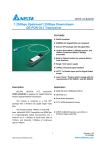
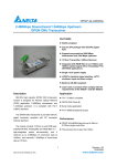
OPEP-33-A4K1R
1.25Gbps Upstream/1.25Gbps Downstream
GE-PON ONU Transceiver
FEATURES
RoHS compliant
IEEE802.3ah Gigabit Ethernet compliant
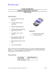
2x5 pin SFF package with SC Receptacle
1310nm Burst Mode 1.25Gbps transmitter,
and 1490nm Continuous Mode 1.25Gbps
receiver
Integrated with WDM filter to cut 1550nm and
1650nm optical signal off
Single +3.3V power supply
LVPECL electrical signal interface
LVTTL Bias Control input and Rx Signal
Detect output
Laser Class 1 Product which comply with the
requirements of IEC 60825-1 and IEC 60825-2
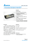
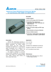
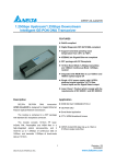
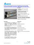
Description
Application
IEEE 802.3ah 1000BASE-PX20-U
DELTA’s
GE-PON
ONU
transceiver
OPEP-33-A4K1R is designed for Gigabit Ethernet
Passive Optical Network transmission.
GE-PON ONU
Burst Mode Application
The module is contained in a 2x5 SFF
FTTx WDM Broadband Access
package with standard SC receptacle connector.
The module consists 1310nm DFB laser,
InGaAs PIN, Preamplifier and WDM filter in a
high-integrated optical sub-assembly, and it
receives up to 1.25Gbps of continuous data at
1490nm, and transmits 1.25Gbps of burst-mode
data at 1310nm.
OPEP-33-A4K1R data link up to 20km in
9/125um single mode fiber.
1
DELTA ELECTRONICS, INC.
Revision: S0
06/01/2007
www.deltaww.com
OPEP-33-A4K1R
1. Absolute Maximum Ratings
Parameter
Storage Temperature
Storage Ambient Humidity
Power Supply Voltage
Signal Input Voltage
Receiver Damage Threshold
Lead Soldering Temperature/Time
Lead Soldering Temperature/Time
Symbol
Ts
HA
VCC
Min.
-40
5
-0.3
-0.3
+7
Typ.
TSOLD
TSOLD
Max.
85
95
4
Vcc+0.3
260/10
380/10
Unit
ºC
%
V
V
dBm
ºC/sec
ºC/sec
Note
Note (1)
Note (2)
Note (1). Suitable for wave soldering
Note (2). Only for soldering by iron
2. Recommended Operating Conditions
Parameter
Ambient Operating Temperature
Ambient Humidity
Power Supply Voltage
Power Supply Current
Power Supply Noise Rejection
Symbol
TA
HA
VCC
ICC
Min.
0
5
3.13
1.25
Data Rate
-100ppm
Typ.
3.3
1.25
Transmission Distance
Max.
70
85
3.47
300
100
1.25
+100ppm
Unit
ºC
%
V
mA
mVp-p
Note
Without air flow
Non-condensing
100Hz to 1MHz
Gbps
20
km
Typ.
Max.
+4
+4.5
+7.5
1310
1360
Unit
dBm
dBm
dBm
dB
nm
nm
dB
dBm
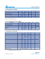
3. Specification of Transmitter
Parameter
Average Launched Power (B.O.L)
Average Launched Power (E.O.L)
Launched power (Peak.)
Extinction Ratio
Center Wavelength
Spectrum Width (RMS)
Side Mode Suppression Ratio
Transmitter OFF Output Power
Laser Burst On Time
Laser Burst Off Time
Optical Rise/Fall Time
Total Jitter
Optical Return Loss Tolerance
Relative Intensity Noise
Optical Transmitter Reflectance
Transmitter and Dispersion Penalty
Output Eye Mask
{X1,X2,Y1,Y2,Y3}
Symbol
PO
PO
PP
ER
λC
σ
SMSR
POff
Ton
Toff
tr/tf
tJ
ORLT
RIN15OMA
Min.
0
-0.5
9
1260
Compliant with IEEE 802.3ah
30
-45
32
32
260
128
15
-115
-10
TDP
1.8
Compliant with IEEE 802.3ah
{0.22,0.375,0.20,0.20,0.30}
ps
ps
dB
dB/Hz
dB
dB
Note
Note (1)
Note (1)
DFB Laser
Note (4)
Note (2)
Note (3)
Note (5)
Note (1). Launched power (avg.) is power coupled into a single mode fiber with master connector.
B.O.L=Before of Life; E.O.L= End of Life
2
DELTA ELECTRONICS, INC.
Revision: S0
06/01/2007
www.deltaww.com
OPEP-33-A4K1R
Note (2). These are unfiltered 20-80% values.
Note (3). Measure at 27-1 NRZ PRBS pattern
Note (4). Transmitter spectral limits
nm
1260
1270
1280
1290
1300
1304
1305
1308
1317
1320
1321
1330
1340
1350
1360
RMS spectral width(max)
1000Base-PX20-U
nm
0.72
0.86
1.07
1.40
2.00
2.42
2.55
Transmitter Spectral Limits
4
3
RMS (nm)
Center Wavelength
3.00
2
1
2.53
2.41
1.71
1.29
1.05
0.88
0
1240
1260
1280
1300
1320
1340
1360
1380
Center Wavelength (nm)
Note (5). Transmitter eye mask definition
1+ Y 3
Normalized Amplitude
1
1- Y1
0.5
Y1
0
- Y2
0
X1
X2
1- X2 1- X1
1
Normalized Time
3
DELTA ELECTRONICS, INC.
Revision: S0
06/01/2007
www.deltaww.com
OPEP-33-A4K1R
4. Specification of Receiver
Parameter
Input Optical Wavelength
Receiver Sensitivity
Input Saturation Power (Overload)
Signal Detect -Assert Power
Signal Detect -Deassert Power
Signal Detect Hysteresis
Data Output Rise/Fall time
Receiver
1480 to 1500nm
Reflectance
Optical Isolation 1260 to 1360nm
from
External 1550 to 1560nm
Source
1640 to 1665nm
Symbol
λIN
PIN
PSAT
PA
PD
PA-PD
tr/tf
Min.
1480
-3
-44
0.5
Typ.
1490
Max.
1500
-26
6
260
Unit
nm
dBm
dBm
dBm
dBm
dB
ps
-12
dB
-43
-33
-33
dB
dB
dB
-26
2
Note
PIN-PD
Note (1)
Note (2)
Note (3)
Note (4)
Note (1). Measured with Light source +1dBm, 1490nm, ER=9dB; BER =<10-12@PRBS=27-1 NRZ
This assurance should be met with asynchronous data flowing out of the optical transmitter of
the system under test. The output data pattern from the transmitter of the system under test is a
repetition of alternate 0/1 pattern as defined for this measurement.
Note (2). When SD deasserted, the data output is Low-level (fixed)
Note (3). These are 20%~80% values.
Note (4). Measured at wavelength of 1490nm.
5. Electrical Interface Characteristics
Parameter
Transmitter
Total Supply Current
Differential line input Impedance
Differential Data Input Swing
Data Input Voltage- High
Data Input Voltage- Low
BiasCNT Input Voltage- High
BiasCNT Input Voltage- Low
Receiver
Total Supply Current
Differential Data Output Swing
Signal Detect Output Voltage-High
Signal Detect Output Voltage-Low
Symbol
Min.
Typ.
ICC
RIN
VDT
VIH-VCC
VIL-VCC
VBCH
VBCL
80
400
-1.165
-1.810
2
0
100
ICC
VDR
VLOSH
VLOSL
400
2
0
650
Max.
Unit
Note
A
120
1600
-0.880
-1.475
Vcc
0.8
mA
Ohm
mVp-p
V
V
V
V
Note (1)
B
900
Vcc+0.3
0.8
mA
mVp-p
V
V
LVPECL
LVTTL
Note (1)
Note (2)
LVTTL
Note (1). A (TX)+ B (RX) = 300mA (Not include termination circuit)
Note (2). Internally AC coupled, but requires a 100Ohm differential termination at or internal to Serializer/
Deserializer.
4
DELTA ELECTRONICS, INC.
Revision: S0
06/01/2007
www.deltaww.com
OPEP-33-A4K1R
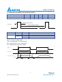
6. Transmitter Burst Mode Timing Characteristics
Parameter
BiasCNT Enable Duration
Interval of BiasCNT Signal
Symbol
Min.
1
0.112
Typ.
Max.
1000000
Unit
us
us
Note
BiasCNT Enable Duration
BiasCNT
VccT
VccT < 3.1V
VccT > 3.1V
Interval of BiasCNT Signal
BiasCNT
X
Low
High
Data Input
X
X
No
Yes
Optical Output
OFF
OFF
Other
Laser bias and modulation signal output
X = Don’t care
Other = Less than +7.5dBm (peak)
High = Logic high level, Low = logic low level
No = Data NOT Present, Yes = Data Present,
OFF = Optical Power is less than –45dBm
H
BiasCNT
L
Data Input
Optical Output
Within 15% of steady state
Ton
Toff
5
DELTA ELECTRONICS, INC.
Revision: S0
06/01/2007
www.deltaww.com
OPEP-33-A4K1R
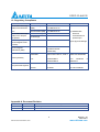
7. Pin Description
Tx/Rx
Pin No.
1
2
I/O
Rx
3
O
4
5
6
7
8
9
10
O
O
Tx
I
I
I
Pin Name
Description
VeeR
Receiver Ground
VccR
+3.3V Receiver Power Supply
SD
Normal Optical Input indicated by logic “High”, and No Optical
Input indicated by logic “Low”. (LVTTL)
RD(n)
Inverted Receiver Data Output (AC-Coupled CML output)
RD(p)
Non-Inverted Receiver Data Output (AC-Coupled CML output)
VccT
+3.3V Transmitter Power Supply
VeeT
Transmitter Ground
BiasCNT Positive pulse which control the ONU burst mode operation
TD(p)
Non-Inverted Transmitter Data Input
TD(n)
Inverted Transmitter Data Input
MS
Mounting studs/ connect this pin to Chassis ground
Note (1). EMI shielding lead must be connected to Signal ground
MS
Bottom View
MS
6
DELTA ELECTRONICS, INC.
Revision: S0
06/01/2007
www.deltaww.com
OPEP-33-A4K1R
8. Recommended Interface Circuit
DELTA GEPON ONU Module
1uH
6. VccT
3.3V
10uF
100nF
100nF
1uH
8. BiasCNT
BiasCNT
Transmitter
9. TD(p)
Coupled
interface
10. TD(n)
7. VeeT
Protocol IC
2. VccR
SerDes IC
10uF
100nF
5. RD(p)
Z0=50ohm
100nF
100ohm
4. RD(n)
Z0=50ohm
100nF VccR
RES
3. SD
SD
Receiver
1. VeeR
* RES is the internal 4.7K to 10K Ohms pull-up resistor.
DC - Coupled interface
Coupled
interface
AC - Coupled interface
3.3V
130ohm
Z0=50ohm
Host
Board
82ohm
100nF
100ohm
DELTA
ONU
Z0=50ohm
Host
Board
Z0=50ohm
150ohm
DELTA
ONU
Z0=50ohm
130ohm
150ohm
100nF
82ohm
3.3V
7
DELTA ELECTRONICS, INC.
Revision: S0
06/01/2007
www.deltaww.com
OPEP-33-A4K1R
9. Outline Dimensions
Parameter
Mechanical Dimensions
Connector Type
Unit
mm
-
Description
48.3x13.5x9.6
SC/UPC connector
Note
IEC-61754-4
.
J
r
e
t
p
a
h
c
b
u
S
R
F
nC
o
i
t
1
a
2
i
t ds
,
c
a
r
u
d
r
d
a
o Ad
D
r
P
Fn
a
t
rt
hs
e
i
s
e
aw
c
L sn
a
em
1l
i
r
s po
s
mr
f
a
l
oe
C
Cp
W eek (52W eeks/Year) : 1月 2日 =01
8
DELTA ELECTRONICS, INC.
Revision: S0
06/01/2007
www.deltaww.com
OPEP-33-A4K1R
10. Regulatory Compliance
Feature
Electrostatic Discharge
(ESD) to the Electrical
Pins
Test Method
Reference
Performance
Human Body Model MIL-STD-883E Method 3015.7
(HBM)
EIA-JESD22-A114
(1) Satisfied with
Machine Model (MM) EIA-JESD22-A115
Electrostatic Discharge
(ESD) to the Simplex
Receptacle
Contact Discharge
Air Discharge
Radio Frequency
Electromagnetic Field
Immunity
IEC/EN 61000-4-2
IEC/EN 61000-4-3
electrical
characteristics of
product spec.
(2) No physical damage
FCC Part 15 Class B
EN 55022 Class B
Electromagnetic
Interference (EMI)
Laser Eye Safety
IEC/EN 61000-4-2
(CISPR 22A)
FDA/CDRH
FDA 21CFR 1040.10, 1040.11
CDRH File # 0420993
TUV
IEC/EN 60825-1
IEC/EN 60825-2
TUV
Certificate
R50032471
TUV
IEC/EN 60950
UL/CSA
UL 60950
#
Component Recognition
UL File # E239394
Appendix A. Document Revision
Version No.
S0
Date
2007-06-01
Description
Preliminary datasheet
9
DELTA ELECTRONICS, INC.
Revision: S0
06/01/2007
www.deltaww.com