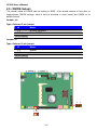
1
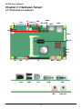
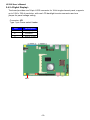
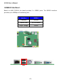
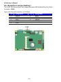
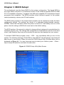
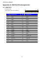
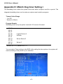
LE-366
AMD Geode
TM
LX800 3.5” Embeded Board
User’s Manual
Edition 1.0
2008/02/20
LE-366 User’s Manual
Copyright
Copyright 2006. All rights reserved. This document is copyrighted and all rights are reserved.
The information in this document is subject to change without prior notice to make
improvements to the products.
This document contains proprietary information and protected by copyright. No part of this
document may be reproduced, copied, or translated in any form or any means without prior
written permission of the manufacturer.
All trademarks and/or registered trademarks contains in this document are property of their
respective owners.
Disclaimer
The company shall not be liable for any incidental or consequential damages resulting from
the performance or use of this product.
The company does not issue a warranty of any kind, express or implied, including without
limitation implied warranties of merchantability or fitness for a particular purpose.
The company has the right to revise the manual or include changes in the specifications of
the product described within it at any time without notice and without obligation to notify any
person of such revision or changes.
Trademark
All trademarks are the property of their respective holders.
-1-
LE-366 User’s Manual
Packing List
Please check the package before you starting setup the system.
Hardware:
LE-366 series motherboard x 1
Cable Kit:
44pin
44pin
40pin
Power Cable x 1
44-pin ATA33 IDE Cable x 1
Floppy Cable x 1
PS2 keyboard & mouse cable
DC_IN Power Cable x 1
RS232 Cable x 1
USB Cable x 1
Printed Matters:
User’s Manual x 1
Driver CD x 1
-2-
LE-366 User’s Manual
Index
Chapter 1 <Introduction> .................................................................... 6
1.1 <Product Overview> ...............................................................................6
1.2 <Product Specification> .........................................................................7
1.3 <Mechanical Drawing> ...........................................................................9
1.4 <Block Diagram>...................................................................................10
2.1<Connector Location> ...........................................................................11
2.1.1 <Connector Reference> ............................................................. 13
2.1.2 <External Connector>................................................................. 13
2.2 <CPU and Memory Setup> ...................................................................14
2.2.1 <CPU Setup> ............................................................................. 14
2.2.2 <Memory Setup> ........................................................................ 14
2.3 <Enhanced IDE & CF Interface> ..........................................................16
2.4 <Floppy Port> ........................................................................................17
2.4.1 <Analog VGA Interface> ............................................................ 18
2.4.2 <Digital Display>......................................................................... 19
2.5 <GPIO Interface> ...................................................................................24
2.6 <Serial Port Jumper Setting >..............................................................25
2.6.1 <Power Input> ............................................................................ 26
2.6.2 <Power Output> ......................................................................... 26
Chapter 3 <BIOS Setup>.................................................................... 30
Appendix A <I/O Port Pin Assignment> ................................. 32
A.1 <IDE Port> .............................................................................................32
A.2 <Floppy Port>........................................................................................33
A.3 <Serial Port>..........................................................................................33
A.4 <CRT Port> ............................................................................................34
A.5 <LAN Port> ............................................................................................34
A.6 < USB Port >..........................................................................................34
-3-
LE-366 User’s Manual
A.7 <PS/2 Keyboard & Mouse Port>..........................................................35
Appendix B <Flash BIOS>................................................................ 37
B.1
BIOS Auto Flash Tool ................................................................37
B.2
Flash Method..............................................................................37
Appendix C <System Resources> ............................................. 38
Appendix D <Programming GPIO’s> ....................................... 42
-4-
LE-366 User’s Manual
(The Page is Left For Blank)
-5-
LE-366 User’s Manual
Chapter 1 <Introduction>
1.1 <Product Overview>
LE-366 is the Mini-ITX motherboard with AMD Geode LX800 platform, with onboard VGA,
AC97 audio, GIGA LAN interface. Based on the AMD Geode LX800 processor, the board
provides many advanced features for reduced power consumption, fan-less design and
high cost/price rate of production.
Low Power Consumption
Based on the AMD Geode LX800@500MHz processor onboard, it only takes up to 3.8W at
maximum powering, and is completely suitable for fan-less design. Without any cooling fan
onboard, it can avoid the heat problem when the cooler failed in accidence.
Onboard TFT/LVDS LCD interface
Based on the AMD Geode LX800@500Mhz of integrated graphics and 18-bit LVDS
interfaces.
Embedded Component
Due to the low profile design, the board provides CF card socket for flash disk with porting
embedded OS and up to DDR SDRAM.
Single Voltage Input
The board only requires DC 12V input. User’s can easily connect the board with an adapter
without the huge power supply.
-6 -
LE-366 User’s Manual
1.2 <Product Specification>
General Specification
Form Factor
CPU
Memory
Chipset
BIOS
Green Function
Watchdog Timer
Real Time Clock
Enhanced IDE
145 mm x 102 mm (5.7” x 4”)
Up to AMD Geode LX 800 Processor
One So-DIMM slot support DDR 266/333/400 MHz SDRAM up to
1GB
AMD Geode CS5536
Phoenix-Award 4Mb PnP Flash
ACPI 1.0 and APM 1.2 compliant
PIT (Programmable Interval Timer) with 3 channels
AMD Geode CS5536 built in RTC with Lithium
UDMA ATA 33 ATA IDE connection
Multi-I/O Port
Chipset
Serial Port
USB Port
Floppy Port
K/B & Mouse
GPIO
AMD Geode CS5536+Winbond W83627HG
1 external RS-232 port (COM1)
1 internal RS-232/422/485 port (COM2)
2 external USB 2.0 ports
2 internal USB 2.0 ports
One slim type Floppy port
1 PS 2 port
One 12-pin Digital I/O connector with 8-bit programmable I/O
interface
VGA Display Interface
Chipset
Memory
Frame Buffer
Display Type
Connector
Built in Geode LX Processor High performance 2D graphics
controller
Shared system memory up to 4MB
Up to 256MB shared with system memory
Support 1920x1440 in CRT mode and 1600x1200 in TFT mode
VESA 1.1 and 2.0 VIP/VDA support
External DB15 female connector on rear I/O panel
Onboard 30-pin LVDS connector
Ethernet Interface
Controller
Type
Connector
1 x Realtek RTL8110S-32 Gigabit Ethernet controller
Triple speed 10/100/1000Base-T
Auto-switching Fast Ethernet
Full duplex, IEEE802.3U compliant
One External RJ45 connector with LED on rear I/O panel
Audio Interface
Chipset
Realtek ® ALC203 AC97 Audio compliance
Interface
2 channels sound output
-7 -
LE-366 User’s Manual
External Audio phone jack for Line-out and MIC-in.
Connector
Onboard audio connector with pin header
Expansive Interface
PCI
1 Mini-PCI slot V2.2 33/66 MHz
1 Compact Flash (optional)
Power and Environment
Power Requirement
Temperature
12V DC Jack power connector
Operating temperature with 0℃~60℃ (32℉ ~ 140℉)
Storage temperature with 20℃~ 80℃ (-68℉ ~ 176℉)
Ordering Code
LE-366
AMD LX800 processor Mini-ITX with onboard VGA, GigaLAN,
RS232, USB2.0, Audio, LCD and DDR DIMM
-8-
LE-366 User’s Manual
1.3 <Mechanical Drawing>
‘
‘
‘
‘
‘
‘
-9 -
LE-366 User’s Manual
1.4 <Block Diagram>
16Mbx16
CRT
DDR DIMM
AMD Geode
LX Processor
LVDS
PCI BUS/33Mhz
IDE X 1
CFD X 1
MiniPCI
SLOT
RealTek
RTL8110SB
LAN1
ALC203
AUDIO
JACK
AMD Geode
CS5536
4 x USB2.0 ports
83627HF
Flash
BIOS
(SST FWH)
KB & MS
Digital I/O
Slim FDD
COM1
COM2
-10-
LE-366 User’s Manual
Chapter 2 <Hardware Setup>
2.1<Connector Location>
P1
CN1
J8
USB2
CN4
CN9 P2
JP3 CN7
USB1
LAN1
JP2
FDD1
MPCI1
CN8
CN3
J4
JP1
CN2
LAN1
J7
USB1
J6
MIC1
PS2
COM
VGA
MIC
-11-
JSPK1
LINE OUT
LE-366 User’s Manual
<Jumper Reference>
Jumper
JP1
JP2
JP3
J4
J7
Function
LVDS Panel Voltage Selection (+5V / + 3.3V)
COM2 RS232/422/485 Select
COM2 RS232/422/485 Select
Clear CMOS Selection
CFD Master/Slave Selection
JP3
JP2
J4
JP1
J7
JP2
RS-232
5
1
JP3
6
2
RS-485
RS-422
-12-
3
12
1
10
LE-366 User’s Manual
2.1.1 <Connector Reference>
Connector
CN1
CN2
CN3
CN4
CN7
CN8
CN9
J6
J8
USB2
FDD1
P2
LAN1
MPCI1
CFD1
J1
P1
MIC1
JSPK1
Function
VGA Display / Audio Connector
Front Audio Connector LVDS Connector
Front Panel Connector
COM2 RS-232 / RS-422 / RS-485 Connector
PS2 Keyboard / Mouse Connector
GPIO Connector
SYSTEM Fan Connector
EIDE Connector
Little 4-Pin Power connector
USB2 Connector
Slim Floppy Connector
COM1 RS-232 Connector
Gigabit LAN / USB Connector
Mini-PCI Slot
Compact Flash Slot
SO-DIMM Slot
12V DC Connector
Microphone Jack
Speaker out Jack
Remark
Standard
Slim
Slim
Standard
Standard
Standard
Standard
Standard
Standard
Standard
Standard
Standard
Standard
Standard
Standard
Slim
Standard
Standard
Standard
2.1.2 <External Connector>
Connector
LAN1
USB1
PS2
COM
VGA
AUDIO
Function
1 external RJ – 45 ports with LED
2 external USB 2.0 ports
2 internal USB 2.0 ports
1 PS / 2 ports
1 external RS – 232 port (COM1)
1 internal RS – 232 / 422 / 485 port (COM2)
1 VGA port
2 external jack for MIC – In / Line – Out
-13-
Remark
Standard
Standard
Standard
Standard
Standard
Standard
LE-366 User’s Manual
2.2 <CPU and Memory Setup>
2.2.1 <CPU Setup>
The board integrates AMD Geode LX800 500MHz processor with special design for
power appliance. It requires only 3.8W power consumption at most, and is totally
designed for fan-less system.
2.2.2 <Memory Setup>
The board supports one 200-pin DDR266/333/400 SDRAM up to 1GB of capacity, and
supports non-ECC unbuffered memory modules.
-14-
LE-366 User’s Manual
2.5 <CMOS Setup>
The board’s data of CMOS can be setting in BIOS. If the board refuses to boot due to
inappropriate CMOS settings, here is how to proceed to clear (reset) the CMOS to its
default values.
Jumper: J4
Type: Onboard 3-pin jumper
J4
1-2
2-3
Mode
Normal Operation
Clear CMOS
Default setting
Jumper: J7
Type: Onboard 3-pin jumper
J7
1-2
2-3
Default setting
Mode
Master
Slave
3
1
J4
3
1
J7
-15-
LE-366 User’s Manual
2.3 <Enhanced IDE & CF Interface>
The board has one Ultra DMA33 IDE interface to support up to 2 ATAPI devices, and one
Compact Flash Type II socket on the solder side.
CF
-16-
LE-366 User’s Manual
2.4 <Floppy Port>
The board provides a slim type floppy port; please use the 26-pin FPC cable in the package
to connect the floppy device.
FDD
Floppy rear side
1.
4.
Lift up this plastic bar
5.
Slot the cable in (Blue paste for outside)
6.
Press back the plastic bar
Lift up the brown plastic bar
2.
Slot the cable in (Blue paste for
3.
brown bar side)
Press back the plastic bar
-17-
LE-366 User’s Manual
2.8 <Onboard Display Interface>
The board integrates AMD Geode LX800 processor with built-in 2D video engine, to provide
onboard DB15 VGA connector, 18-bit LVDS interface. The built-in 2D video engine supports
following specified functions:
●
High-performance 2D graphics controller
●
Alpha BLT
●
Integrated dot clock PLL
2.4.1 <Analog VGA Interface>
Please connect your CRT or LCD monitor with DB15 male connector to the onboard DB15
female connector on rear I/O port.
CRT
-18-
LE-366 User’s Manual
2.4.2 <Digital Display>
The board provides one 30-pin LVDS connector for 18-bit single channel panel, supports
up to 1024 x 768 of resolution, with one LCD backlight inverter connector and one
jumper for panel voltage setting
Connector: JP1
Type: 3-pin Power select Header
Pin
1
2
3
Description
VCC (5V)
LCDVCC
VCC3 (3.3V)
JP1
-19-
LE-366 User’s Manual
Connector: CN_LVDS (CN2) (for 18 bit Single channel LVDS panel)
Type: 30-pin header (15 x 2 pitch 2.0 mm)
Connector model: Hirose DF13-40DP-1.25V
Pin
1
3
5
7
9
11
13
15
17
19
21
23
25
27
29
Assignment
BKL_EN
LVDS_VCC
LVDS_CH1_CLKLVDS_VCC
LVDS_CH1_DATA0LVDS_CH1_DATA1LVDS_CH1_DATA2N/C
N/C
N/C
N/C
N/C
LVDS_DDCPDATA
LVDS_VCC
N/C
Pin
2
4
6
8
10
12
14
16
18
20
22
24
26
28
30
-20-
Assignment
BKL_CTL
GND
LVDS_CH1_CLK+
GND
LVDS_CH1_DATA0+
LVDS_CH1_DATA1+
LVDS_CH1_DATA2+
N/C
N/C
N/C
N/C
N/C
LVDS_DDCPCLK
GND
N/C
LE-366 User’s Manual
To setup the LCD, you need the component below:
1. A panel with LVDS interfaces.
2. An inverter for panel’s backlight power.
3. A LCD cable and an inverter cable.
For the cables, please follow the pin assignment of the connector to make a cable, because
every panel has its own pin assignment, so we do not provide a standard cable; please find a
local cable manufacture to make cables.
LCD Installation Guide:
1. Preparing the LE-366, LCD panel and the backlight inverter.
2. Please check the datasheet of the panel to see the voltage of the panel, and set the
jumper JP1 to +5V or +3.3V.
3. You would need a LVDS type cable.
Panel side
Board side
For sample illustrator only
4. To connect all of the devices well.
-21-
LE-366 User’s Manual
After setup the devices well, you need to select the LCD panel type in the BIOS.
The panel type mapping is list below:
1
2
3
Panel Number Resolution
640 x 480
800 x 600
1024x 768
-22-
LE-366 User’s Manual
<USB2.0 Interface>
Based on AMD CS5536, the board provides 2 x USB2.0 ports. The USB2.0 interface
provides up to 480Mbps of transferring rate.
Interface
USB2.0
Controller
CS5536
Transfer Rate
Up to 480Mb/s
Output Voltage
500mA
USB
-23-
LE-366 User’s Manual
2.5 <GPIO Interface>
The board provides a programmable 8-bit digital I/O interface; you can use this general
purpose I/O port for system control like POS or KIOSK.
Connector: CN8
Type: onboard 2 x 6-pin header, pitch=2.0mm
Pin
1
2
3
4
5
6
7
8
9
10
Assignment
GPI
GPO
GPI
GPO
GPI
GPO
GPI
GPO
5V
GND
CN8
-24-
LE-366 User’s Manual
2.6 <Serial Port Jumper Setting >
The COM1 RS232 serial port, with jumper selectable RS232/422/485 for CN_COM2
Connector: COM1
Type: 9-pin Dip male connector on I/O Panel
Pin
1
3
5
7
9
Assignment
DCD1#
TXD1
GND
RTS1#
RI1#
Pin
2
4
6
8
COM1
-25-
Assignment
RXD1
DTR1#
DSR1#
CTS1#
LE-366 User’s Manual
2.7 <Power and Fan Connector>
The LE-366 provides a standard ATX power supply with 20-pin ATX connector, and the
board provides one 4-pin P4 additional use power connector for internal power supply and
one 3-pin cooler fan connector for system.
2.6.1 <Power Input>
Connector: ATX
Type: 20-pin ATX power connector
PIN assignment
1
3.3V
2
3.3V
3
GND
4
5V
5
GND
6
5V
7
GND
8
5V
9
5V
10
12V
11
12
13
14
15
16
17
18
19
20
3.3V
-12V
GND
PS_ON
GND
GND
GND
-5V
5V
5V
2.6.2 <Power Output>
Connector: DC_OUT
Type: 4-pin P-type connector for +5V/+12V output
Pin
1
2
3
4
Assignment
12V
GND
GND
5V
Power out
Floppy
ATAPI Drives
Relative Accessory
-26-
LE-366 User’s Manual
2.7.3 <Fan Connector>
Connector: SYSFAN
Type: 3-pin fan wafer connector
Pin
1
Description
Ground
Pin
2
Description
+12V
Connector: DC_IN
Type: 2-pin DC power connector
Pin
Description
1
+12V
3
Ground
Pin
2
4
SYSFAN
-27-
Pin
3
Description
+12V
Ground
Description
Fan Control
LE-366 User’s Manual
2.8 <Indicator and Switch>
The JFRNT provides front control panel of the board, such as power button, reset and
beeper, etc. Please check well before you connecting the cables on the chassis.
Connector: CN3
Type: onboard 14-pin (2 x 7) 2.54-pitch header
Pin
Assignment
Pin
Assignment
1
GND
2
Power Switch
3
BUZZER-
4
BUZZER+
5
HD_LED-
6
HD_LED+
7
POWER LED-
8
Power LED+
9
GND
10
Reset
-28-
LE-366 User’s Manual
(This Page is Left For Blank)
-29-
LE-366 User’s Manual
Chapter 3 <BIOS Setup>
The motherboard uses the Award BIOS for the system configuration. The Award BIOS in
the single board computer is a customized version of the industrial standard BIOS for IBM
PC AT-compatible computers. It supports Intel x86 and compatible CPU architecture based
processors and computers. The BIOS provides critical low-level support for the system
central processing, memory and I/O sub-systems.
The BIOS setup program of the single board computer let the customers modify the basic
configuration setting. The settings are stored in a dedicated battery-backed memory,
NVRAM, retains the information when the power is turned off. If the battery runs out of the
power, then the settings of BIOS will come back to the default setting.
The BIOS section of the manual is subject to change without notice and is provided here for
reference purpose only. The settings and configurations of the BIOS are current at the time
of print, and therefore they may not be exactly the same as that displayed on your screen.
To activate CMOS Setup program, press <DEL> key immediately after you turn on the
system. The following message “Press DEL to enter SETUP” should appear in the lower left
hand corner of your screen. When you enter the CMOS Setup Utility, the Main Menu will be
displayed as Figure 4-1. You can use arrow keys to select your function, press <Enter>
key to accept the selection and enter the sub-menu.
Figure 4-1 CMOS Setup Utility Main Screen
-30-
LE-366 User’s Manual
(This Page is Left for Blank)
-31-
LE-366 User’s Manual
Appendix A <I/O Port Pin Assignment>
A.1 <IDE Port>
Connector: J6
2
44
1
43
Type: 44-pin (22 x 2) box header
Pin
1
3
5
7
9
11
13
15
17
19
21
23
25
27
29
31
33
35
37
39
41
43
Assignment
IDERST#
PID7
PID6
PID5
PID4
PID3
PID2
PID1
PID0
GND
PDREQ
PIOR#
PIOR#
PRDY
PACK#
PIRQ14
PPDA1
PPDA0
PPCS1#
N/C
+5V
GND
Pin
2
4
6
8
10
12
14
16
18
20
22
24
26
28
30
32
34
36
38
40
42
44
-32-
Assignment
GND
PID8
PID9
PID10
PID11
PID12
PID13
PID14
PID15
N/C
GND
GND
GND
ICS16#
GND
N/C
ATA66_DET
PPDA2
PPCS3#
GND
+5V
N/C
LE-366 User’s Manual
A.2 <Floppy Port>
Connector: FDD1
Type: 26-pin connector
Pin
1
3
5
7
9
11
13
15
17
19
21
23
25
Assignment
VCC
VCC
VCC
N/C
N/C
N/C
DENSEL#
GND
GND
GND
GND
GND
GND
Pin
2
4
6
8
10
12
14
16
18
20
22
24
26
Assignment
INDEX#
DRV_SEL#
DSK_CH#
N/C
MOTOR#
DIR#
STEP#
WDATA#
WGATE#
TRACK#
WOROT#
RDATA#
SIDE#
A.3 <Serial Port>
1
2
9
10
Connector: COM2 (CN4)
Type: 9-pin D-sub male connector on bracket
Pin
1
3
5
7
9
Assignment
DCD2# (422TXD-/485DATA-)
TXD2 (422TXD+/485DATA+)
GND
RTS2#
RI2#
-33-
Pin
2
4
6
8
Assignment
RXD2 (422RXD+)
DTR2# (422RXD-)
DSR2#
CTS2#
LE-366 User’s Manual
6
A.4 <CRT Port>
1
2
3
4
5
Connector: CRT
Type: 15-pin D-sub female connector on I/O Panel
11
12
13
14
15
10
Pin
1
2
3
4
5
Description
RED
GREEN
BLUE
N/C
Ground
Pin
6
7
8
9
10
Description
Ground
Ground
Ground
VGA_VCC
Ground
Pin
11
12
13
14
15
Description
N/C
CRT_DDCDATA
HSYNC
VSYNC
CRT_DDCCLK
A.5 <LAN Port>
Connector: RJ45
Type: RJ45 connector with LED on I/O Panel
Pin
Description
1
2
3
4
MI0+
MI0-
MI1+
MI2+
5
6
MI2- MI1-
7
8
MI3+
MI3-
A.6 < USB Port >
Connector: CN_USB2
Type: 10-pin (5 x 2) header for dual USB Ports
1
10
Pin
1
3
5
7
9
Description
USB_VCC
Data0Data0+
Ground
Ground
Pin
2
4
6
8
10
-34-
Description
GND
GND
Data1+
Data1USB_VCC
LE-366 User’s Manual
A.7 <PS/2 Keyboard & Mouse Port>
1
Connector: Mouse / Keyboard
3
Type: 6-pin Mini-DIN connector on bracket
Pin
1
3
5
2
Assignment
KB_DATA
GND
KB_CLK
Pin
2
4
6
-35-
4
5
Assignment
MS_DATA
KB_VCC
MS_CLK
6
LE-366 User’s Manual
(This Page is Left for Blank)
-36-
LE-366User’s Manual
Appendix B <Flash BIOS>
B.1 BIOS Auto Flash Tool
The board is based on Award BIOS and can be updated easily by the BIOS auto flash
tool. You can download the tool online at the address below:
http://www.award.com
TU
UT
File name of the tool is “awdflash.exe”, it’s the utility that can write the data into the
BIOS flash ship and update the BIOS.
B.2 Flash Method
1. Please make a bootable floppy disk.
2. Get the last .bin files you want to update and copy it into the disk.
3. Copy awardflash.exe to the disk.
4. Power on the system and flash the BIOS. (Example: C:/ awardflash XXX.bin)
5. Re-star the system.
-37-
LE-366 User’s Manual
Appendix C <System Resources>
C1. <I/O Port Address Map>
-38-
LE-366 User’s Manual
-39-
LE-366 User’s Manual
C2. <Memory Address Map>
-40-
LE-366 User’s Manual
C3. <System IRQ Resources>
-41-
LE-366 User’s Manual
Appendix D <Programming GPIO’s>
The GPIO can be programmed with the MSDOS debug program using simple
IN/OUT commands. The following lines show an example how to do this.
GPIO0...GPIO7
-o 4E 87
bit0……bit7
;enter configuration
-o 4E 87
-o 4E 2A
-o 4F FD
;enable GPIO function
-o 4E 07
-o 4F 07
;enable GPIO configuration
-o 4E F0
-o 4F xx
;set GPIO as input/output; set ‘1’ for input,’0’for output
-o 4E F1
-o 4F xx
;if set GPIO’s as output, in this register its value can be set
Optional :
-o 4E F2
-o 4F xx
; Data inversion register ; ‘1’ inverts the current value of the
bits ,’0’ leaves them as they are
-o 4E 30
-o 4F 01
; active GPIO’s
For further information, please refer to Winbond W83627HG datasheet.
-42-
LE-366 User’s Manual
Appendix E <Watch Dog timer Setting >
The watchdog timer makes the system auto-reset while it stops to work for a period. The
integrated watchdog timer can be setup as system reset mode by program.
Timeout Value Range
- 1 to 255
- Second or Minute
Program Sample
Watchdog timer setup as system reset with 10 second of timeout
2E, 87
2E, 87
2E, 07
2F, 08
Logical Device 8
2E, 30
Activate
2F, 01
2E, F5
Set as Second*
2F, 00
2E, F6
Set as 5
2F, 05
* Minute: bit 3 = 0; Second: bit 3 = 1
You can select Timer setting in the BIOS, after setting the time options, the system will
reset according to the period of your selection.
-43-
LE-366 User’s Manual
(This Page is Left for Blank)
-44-