1
Preliminary Information
AMD Athlon XP
Processor Model 10
TM
Data Sheet
Publication # 26237 Rev. C
Issue Date: May 2003
Preliminary Information
©2002, 2003 Advanced Micro Devices, Inc. All rights reserved.
The contents of this document are provided in connection with Advanced
Micro Devices, Inc. (“AMD”) products. AMD makes no representations or warranties with respect to the accuracy or completeness of the contents of this
publication and reserves the right to make changes to specifications and product descriptions at any time without notice. No license, whether express,
implied, arising by estoppel or otherwise, to any intellectual property rights is
granted by this publication. Except as set forth in AMD’s Standard Terms and
Conditions of Sale, AMD assumes no liability whatsoever, and disclaims any
express or implied warranty, relating to its products including, but not limited
to, the implied warranty of merchantability, fitness for a particular purpose,
or infringement of any intellectual property right.
AMD’s products are not designed, intended, authorized or warranted for use
as components in systems intended for surgical implant into the body, or in
other applications intended to support or sustain life, or in any other application in which the failure of AMD’s product could create a situation where personal injury, death, or severe property or environmental damage may occur.
AMD reserves the right to discontinue or make changes to its products at any
time without notice.
Trademarks
AMD, the AMD Arrow logo, AMD Athlon, AMD Duron, and combinations thereof, QuantiSpeed, and 3DNow!
are trademarks of Advanced Micro Devices, Inc.
HyperTransport is a licensed trademark of the HyperTransport Technology Consortium.
MMX is a trademark of Intel Corporation.
Windows is a registered trademark of Microsoft Corporation.
Other product names used in this publication are for identification purposes only and may be trademarks of
their respective companies.
Preliminary Information
AMD Athlon™ XP Processor Model 10 Data Sheet
26237C—May 2003
Table of Contents
Revision History . . . . . . . . . . . . . . . . . . . . . . . . . . . . . . . . . . . . . . . . . . . xi
1
Overview . . . . . . . . . . . . . . . . . . . . . . . . . . . . . . . . . . . . . . . . . . . . 1
1.1
2
Interface Signals . . . . . . . . . . . . . . . . . . . . . . . . . . . . . . . . . . . . . 5
2.1
2.2
2.3
2.4
Overview . . . . . . . . . . . . . . . . . . . . . . . . . . . . . . . . . . . . . . . . . . . 5
Signaling Technology . . . . . . . . . . . . . . . . . . . . . . . . . . . . . . . . . 5
Push-Pull (PP) Drivers . . . . . . . . . . . . . . . . . . . . . . . . . . . . . . . . 6
AMD Athlon™ System Bus Signals . . . . . . . . . . . . . . . . . . . . . . 6
3
Logic Symbol Diagram. . . . . . . . . . . . . . . . . . . . . . . . . . . . . . . . . 7
4
Power Management . . . . . . . . . . . . . . . . . . . . . . . . . . . . . . . . . . . 9
4.1
4.2
4.3
Power Management States . . . . . . . . . . . . . . . . . . . . . . . . . . . . . 9
Working State. . . . . . . . . . . . . . . . . . . . . . . . . . . . . . . . . . . . 10
Halt State . . . . . . . . . . . . . . . . . . . . . . . . . . . . . . . . . . . . . . . 10
Stop Grant States. . . . . . . . . . . . . . . . . . . . . . . . . . . . . . . . . 10
Probe State. . . . . . . . . . . . . . . . . . . . . . . . . . . . . . . . . . . . . . 12
Connect and Disconnect Protocol . . . . . . . . . . . . . . . . . . . . . . 12
Connect Protocol . . . . . . . . . . . . . . . . . . . . . . . . . . . . . . . . . 12
Connect State Diagram . . . . . . . . . . . . . . . . . . . . . . . . . . . . 16
Clock Control . . . . . . . . . . . . . . . . . . . . . . . . . . . . . . . . . . . . . . . 18
5
CPUID Support. . . . . . . . . . . . . . . . . . . . . . . . . . . . . . . . . . . . . . 19
6
Advanced 333 Front-Side Bus AMD Athlon™ XP
Processor Model 10 Specifications . . . . . . . . . . . . . . . . . . . . . . 21
6.1
6.2
6.3
6.4
7
Electrical and Thermal Specifications for the Advanced
333 FSB AMD Athlon XP Processor Model 10 . . . . . . . . . . . . 21
Advanced 333 FSB AMD Athlon XP Processor Model 10
SYSCLK and SYSCLK# AC Characteristics . . . . . . . . . . . . . . 22
Advanced 333 FSB AMD Athlon System Bus
AC Characteristics . . . . . . . . . . . . . . . . . . . . . . . . . . . . . . . . . . 23
Advanced 333 FSB AMD Athlon System Bus DC
Characteristics . . . . . . . . . . . . . . . . . . . . . . . . . . . . . . . . . . . . . . 24
Advanced 400 Front-Side Bus AMD Athlon XP
Processor Model 10 Specifications . . . . . . . . . . . . . . . . . . . . . . 25
7.1
7.2
7.3
7.4
Table of Contents
QuantiSpeed™ Architecture Summary. . . . . . . . . . . . . . . . . . . 2
Electrical and Thermal Specifications for the Advanced
400 FSB AMD Athlon XP Processor Model 10 . . . . . . . . . . . . 25
Advanced 400 FSB AMD Athlon XP Processor Model 10
SYSCLK and SYSCLK# AC Characteristics . . . . . . . . . . . . . . 26
Advanced 400 FSB AMD Athlon System Bus
AC Characteristics . . . . . . . . . . . . . . . . . . . . . . . . . . . . . . . . . . 27
Advanced 400 FSB AMD Athlon System Bus DC
Characteristics . . . . . . . . . . . . . . . . . . . . . . . . . . . . . . . . . . . . . . 28
iii
Preliminary Information
AMD Athlon™ XP Processor Model 10 Data Sheet
8
Electrical Data . . . . . . . . . . . . . . . . . . . . . . . . . . . . . . . . . . . . . . 29
8.1
8.2
8.3
8.4
8.5
8.6
8.7
8.8
8.9
8.10
8.11
8.12
8.13
9
9.2
10.3
Die Loading . . . . . . . . . . . . . . . . . . . . . . . . . . . . . . . . . . . . . . . . 47
AMD Athlon XP Processor Model 10 Part Number 27488
OPGA Package Dimensions . . . . . . . . . . . . . . . . . . . . . . . . . . . 48
AMD Athlon XP Processor Model 10 Part Number 27493
OPGA Package Dimensions . . . . . . . . . . . . . . . . . . . . . . . . . . . 50
Pin Descriptions . . . . . . . . . . . . . . . . . . . . . . . . . . . . . . . . . . . . . 53
11.1
11.2
11.3
iv
Power-Up Requirements . . . . . . . . . . . . . . . . . . . . . . . . . . . . . 43
Signal Sequence and Timing Description . . . . . . . . . . . . . 43
Clock Multiplier Selection (FID[3:0]) . . . . . . . . . . . . . . . . 46
Processor Warm Reset Requirements. . . . . . . . . . . . . . . . . . . 46
Northbridge Reset Pins. . . . . . . . . . . . . . . . . . . . . . . . . . . . 46
Mechanical Data. . . . . . . . . . . . . . . . . . . . . . . . . . . . . . . . . . . . . 47
10.1
10.2
11
Conventions . . . . . . . . . . . . . . . . . . . . . . . . . . . . . . . . . . . . . . . . 29
Interface Signal Groupings . . . . . . . . . . . . . . . . . . . . . . . . . . . 29
Voltage Identification (VID[4:0]) . . . . . . . . . . . . . . . . . . . . . . 30
Frequency Identification (FID[3:0]) . . . . . . . . . . . . . . . . . . . . 31
VCCA AC and DC Characteristics . . . . . . . . . . . . . . . . . . . . . . 31
Decoupling . . . . . . . . . . . . . . . . . . . . . . . . . . . . . . . . . . . . . . . . . 31
VCC_CORE Characteristics. . . . . . . . . . . . . . . . . . . . . . . . . . . . . 32
Absolute Ratings . . . . . . . . . . . . . . . . . . . . . . . . . . . . . . . . . . . . 34
SYSCLK and SYSCLK# DC Characteristics . . . . . . . . . . . . . . 35
General AC and DC Characteristics . . . . . . . . . . . . . . . . . . . . 36
Open Drain Test Circuit . . . . . . . . . . . . . . . . . . . . . . . . . . . . . . 38
Thermal Diode Characteristics . . . . . . . . . . . . . . . . . . . . . . . . 39
Thermal Diode Electrical Characteristics. . . . . . . . . . . . . 39
Thermal Protection Characterization . . . . . . . . . . . . . . . . 39
APIC Pins AC and DC Characteristics . . . . . . . . . . . . . . . . . . 41
Signal and Power-Up Requirements . . . . . . . . . . . . . . . . . . . . 43
9.1
10
26237C—May 2003
Pin Diagram and Pin Name Abbreviations. . . . . . . . . . . . . . . 53
Pin List . . . . . . . . . . . . . . . . . . . . . . . . . . . . . . . . . . . . . . . . . . . . 63
Detailed Pin Descriptions. . . . . . . . . . . . . . . . . . . . . . . . . . . . . 72
A20M# Pin . . . . . . . . . . . . . . . . . . . . . . . . . . . . . . . . . . . . . . 72
AMD Pin . . . . . . . . . . . . . . . . . . . . . . . . . . . . . . . . . . . . . . . . 72
AMD Athlon System Bus Pins . . . . . . . . . . . . . . . . . . . . . . 72
Analog Pin . . . . . . . . . . . . . . . . . . . . . . . . . . . . . . . . . . . . . . 72
APIC Pins, PICCLK, PICD[1:0]# . . . . . . . . . . . . . . . . . . . . 72
CLKFWDRST Pin . . . . . . . . . . . . . . . . . . . . . . . . . . . . . . . . 72
CLKIN, RSTCLK (SYSCLK) Pins. . . . . . . . . . . . . . . . . . . . 73
CONNECT Pin . . . . . . . . . . . . . . . . . . . . . . . . . . . . . . . . . . . 73
COREFB and COREFB# Pins . . . . . . . . . . . . . . . . . . . . . . . 73
CPU_PRESENCE# Pin . . . . . . . . . . . . . . . . . . . . . . . . . . . . 73
DBRDY and DBREQ# Pins . . . . . . . . . . . . . . . . . . . . . . . . . 73
FERR Pin . . . . . . . . . . . . . . . . . . . . . . . . . . . . . . . . . . . . . . . 73
Table of Contents
Preliminary Information
AMD Athlon™ XP Processor Model 10 Data Sheet
26237C—May 2003
FID[3:0] Pins . . . . . . . . . . . . . . . . . . . . . . . . . . . . . . . . . . . . 74
FSB_Sense[1:0] Pins . . . . . . . . . . . . . . . . . . . . . . . . . . . . . . 75
FLUSH# Pin . . . . . . . . . . . . . . . . . . . . . . . . . . . . . . . . . . . . . 75
IGNNE# Pin . . . . . . . . . . . . . . . . . . . . . . . . . . . . . . . . . . . . . 75
INIT# Pin . . . . . . . . . . . . . . . . . . . . . . . . . . . . . . . . . . . . . . . 75
INTR Pin. . . . . . . . . . . . . . . . . . . . . . . . . . . . . . . . . . . . . . . . 76
JTAG Pins . . . . . . . . . . . . . . . . . . . . . . . . . . . . . . . . . . . . . . . 76
K7CLKOUT and K7CLKOUT# Pins . . . . . . . . . . . . . . . . . . 76
Key Pins . . . . . . . . . . . . . . . . . . . . . . . . . . . . . . . . . . . . . . . . 76
NC Pins . . . . . . . . . . . . . . . . . . . . . . . . . . . . . . . . . . . . . . . . . 76
NMI Pin. . . . . . . . . . . . . . . . . . . . . . . . . . . . . . . . . . . . . . . . . 76
PGA Orientation Pins . . . . . . . . . . . . . . . . . . . . . . . . . . . . . 76
PLL Bypass and Test Pins . . . . . . . . . . . . . . . . . . . . . . . . . . 76
PWROK Pin . . . . . . . . . . . . . . . . . . . . . . . . . . . . . . . . . . . . . 76
SADDIN[1:0]# and SADDOUT[1:0]# Pins . . . . . . . . . . . . . 77
Scan Pins . . . . . . . . . . . . . . . . . . . . . . . . . . . . . . . . . . . . . . . 77
SMI# Pin . . . . . . . . . . . . . . . . . . . . . . . . . . . . . . . . . . . . . . . . 77
STPCLK# Pin . . . . . . . . . . . . . . . . . . . . . . . . . . . . . . . . . . . . 77
SYSCLK and SYSCLK#. . . . . . . . . . . . . . . . . . . . . . . . . . . . 77
THERMDA and THERMDC Pins . . . . . . . . . . . . . . . . . . . . 77
VCCA Pin . . . . . . . . . . . . . . . . . . . . . . . . . . . . . . . . . . . . . . . 77
VID[4:0] Pins . . . . . . . . . . . . . . . . . . . . . . . . . . . . . . . . . . . . 77
VREFSYS Pin . . . . . . . . . . . . . . . . . . . . . . . . . . . . . . . . . . . 78
ZN and ZP Pins . . . . . . . . . . . . . . . . . . . . . . . . . . . . . . . . . . 78
12
Ordering Information. . . . . . . . . . . . . . . . . . . . . . . . . . . . . . . . . 79
Standard AMD Athlon XP Processor Model 10 Products . . . . . . . . . 79
Appendix A Thermal Diode Calculations . . . . . . . . . . . . . . . . . . . . . 81
Ideal Diode Equation . . . . . . . . . . . . . . . . . . . . . . . . . . . . . . . . . . . . . . 81
Temperature Offset Correction . . . . . . . . . . . . . . . . . . . . . . . . . . . . . . 82
Appendix B Conventions and Abbreviations . . . . . . . . . . . . . . . . . . 85
Signals and Bits . . . . . . . . . . . . . . . . . . . . . . . . . . . . . . . . . . . . . . . . . . . 85
Data Terminology . . . . . . . . . . . . . . . . . . . . . . . . . . . . . . . . . . . . . . . . . 86
Abbreviations and Acronyms. . . . . . . . . . . . . . . . . . . . . . . . . . . . . . . . 87
Related Publications. . . . . . . . . . . . . . . . . . . . . . . . . . . . . . . . . . . . . . . 91
Table of Contents
v
Preliminary Information
AMD Athlon™ XP Processor Model 10 Data Sheet
vi
26237C—May 2003
Table of Contents
Preliminary Information
AMD Athlon™ XP Processor Model 10 Data Sheet
26237C—May 2003
List of Figures
Figure 1.
Typical AMD Athlon™ XP Processor Model 10 System
Block Diagram . . . . . . . . . . . . . . . . . . . . . . . . . . . . . . . . . . . . . . . . 3
Figure 2.
Logic Symbol Diagram. . . . . . . . . . . . . . . . . . . . . . . . . . . . . . . . . . 7
Figure 3.
AMD Athlon XP Processor Model 10 Power
Management States . . . . . . . . . . . . . . . . . . . . . . . . . . . . . . . . . . . . 9
Figure 4.
AMD Athlon System Bus Disconnect Sequence in the
Stop Grant State . . . . . . . . . . . . . . . . . . . . . . . . . . . . . . . . . . . . . . 14
Figure 5.
Exiting the Stop Grant State and Bus Connect Sequence . . . . 15
Figure 6.
Northbridge Connect State Diagram . . . . . . . . . . . . . . . . . . . . . 16
Figure 7.
Processor Connect State Diagram . . . . . . . . . . . . . . . . . . . . . . . 17
Figure 8.
SYSCLK Waveform . . . . . . . . . . . . . . . . . . . . . . . . . . . . . . . . . . . 22
Figure 9.
SYSCLK Waveform . . . . . . . . . . . . . . . . . . . . . . . . . . . . . . . . . . . 26
Figure 10. VCC_CORE Voltage Waveform . . . . . . . . . . . . . . . . . . . . . . . . . . . 33
Figure 11. SYSCLK and SYSCLK# Differential Clock Signals . . . . . . . . . 35
Figure 12. General ATE Open-Drain Test Circuit. . . . . . . . . . . . . . . . . . . . 38
Figure 13. Signal Relationship Requirements During Power-Up
Sequence . . . . . . . . . . . . . . . . . . . . . . . . . . . . . . . . . . . . . . . . . . . . 43
Figure 14. AMD Athlon XP Processor Model 10 Part Number
27488 OPGA Package Diagram. . . . . . . . . . . . . . . . . . . . . . . . . . 49
Figure 15. AMD Athlon XP Processor Model 10 Part Number
27493 OPGA Package Diagram. . . . . . . . . . . . . . . . . . . . . . . . . . 51
Figure 16. AMD Athlon XP Processor Model 10 Pin Diagram
—Topside View. . . . . . . . . . . . . . . . . . . . . . . . . . . . . . . . . . . . . . . 54
Figure 17. AMD Athlon XP Processor Model 10 Pin Diagram
—Bottomside View . . . . . . . . . . . . . . . . . . . . . . . . . . . . . . . . . . . 55
Figure 18. OPN Example for the AMD Athlon XP Processor
Model 10 . . . . . . . . . . . . . . . . . . . . . . . . . . . . . . . . . . . . . . . . . . . . 79
List of Figures
vii
Preliminary Information
AMD Athlon™ XP Processor Model 10 Data Sheet
viii
26237C—May 2003
List of Figures
Preliminary Information
AMD Athlon™ XP Processor Model 10 Data Sheet
26237C—May 2003
List of Tables
Table 1.
Electrical and Thermal Specifications for the Advanced
333 FSB AMD Athlon™ XP Processor Model 10. . . . . . . . . . . . 21
Table 2.
Advanced 333 FSB SYSCLK and SYSCLK# AC
Characteristics . . . . . . . . . . . . . . . . . . . . . . . . . . . . . . . . . . . . . . . 22
Table 3.
Advanced 333 FSB AMD Athlon System Bus AC
Characteristics . . . . . . . . . . . . . . . . . . . . . . . . . . . . . . . . . . . . . . . 23
Table 4.
Advanced 333 FSB AMD Athlon System Bus DC
Characteristics . . . . . . . . . . . . . . . . . . . . . . . . . . . . . . . . . . . . . . . 24
Table 5.
Electrical and Thermal Specifications for the Advanced
400 FSB AMD Athlon XP Processor Model 10 . . . . . . . . . . . . . 25
Table 6.
Advanced 400 FSB SYSCLK and SYSCLK# AC
Characteristics . . . . . . . . . . . . . . . . . . . . . . . . . . . . . . . . . . . . . . . 26
Table 7.
Advanced 400 FSB AMD Athlon System Bus AC
Characteristics . . . . . . . . . . . . . . . . . . . . . . . . . . . . . . . . . . . . . . . 27
Table 8.
Advanced 400 FSB AMD Athlon System Bus DC
Characteristics . . . . . . . . . . . . . . . . . . . . . . . . . . . . . . . . . . . . . . . 28
Table 9.
Interface Signal Groupings . . . . . . . . . . . . . . . . . . . . . . . . . . . . 29
Table 10.
VID[4:0] DC Characteristics . . . . . . . . . . . . . . . . . . . . . . . . . . . . 30
Table 11.
FID[3:0] DC Characteristics . . . . . . . . . . . . . . . . . . . . . . . . . . . . 31
Table 12.
VCCA AC and DC Characteristics . . . . . . . . . . . . . . . . . . . . . . . 31
Table 13.
VCC_CORE AC and DC Characteristics . . . . . . . . . . . . . . . . . . . . 32
Table 14.
Absolute Ratings . . . . . . . . . . . . . . . . . . . . . . . . . . . . . . . . . . . . . 34
Table 15.
SYSCLK and SYSCLK# DC Characteristics . . . . . . . . . . . . . . . 35
Table 16.
General AC and DC Characteristics. . . . . . . . . . . . . . . . . . . . . . 36
Table 17.
Thermal Diode Electrical Characteristics . . . . . . . . . . . . . . . . . 39
Table 18.
Guidelines for Platform Thermal Protection of the
Processor . . . . . . . . . . . . . . . . . . . . . . . . . . . . . . . . . . . . . . . . . . . . 40
Table 19.
APIC Pin AC and DC Characteristics. . . . . . . . . . . . . . . . . . . . . 41
Table 20.
Mechanical Loading . . . . . . . . . . . . . . . . . . . . . . . . . . . . . . . . . . . 47
Table 21.
Dimensions for the AMD Athlon XP Processor
Model 10 Part Number 27488 OPGA Package . . . . . . . . . . . . . 48
Table 22.
Dimensions for the AMD Athlon XP Processor
Model 10 Part Number 27493 OPGA Package . . . . . . . . . . . . . 50
List of Tables
Table 23.
Pin Name Abbreviations . . . . . . . . . . . . . . . . . . . . . . . . . . . . . . . 56
Table 24.
Cross-Reference by Pin Location . . . . . . . . . . . . . . . . . . . . . . . . 64
ix
Preliminary Information
AMD Athlon™ XP Processor Model 10 Data Sheet
26237C—May 2003
Table 25.
FID[3:0] Clock Multiplier Encodings . . . . . . . . . . . . . . . . . . . . . 74
Table 26.
Front-Side Bus Sense Truth Table . . . . . . . . . . . . . . . . . . . . . . . 75
Table 27.
VID[4:0] Code to Voltage Definition . . . . . . . . . . . . . . . . . . . . . 78
Table 28.
Constants and Variables for the Ideal Diode Equation . . . . . . 81
Table 29.
Constants and Variables Used in Temperature Offset
Equations . . . . . . . . . . . . . . . . . . . . . . . . . . . . . . . . . . . . . . . . . . . 82
x
Table 30.
Abbreviations . . . . . . . . . . . . . . . . . . . . . . . . . . . . . . . . . . . . . . . . 87
Table 31.
Acronyms. . . . . . . . . . . . . . . . . . . . . . . . . . . . . . . . . . . . . . . . . . . . 88
List of Tables
Preliminary Information
AMD Athlon™ XP Processor Model 10 Data Sheet
26237C—May 2003
Revision History
Date
Rev
Description
Public revision C of the AMD Athlon™ XP Processor Model 10 Data Sheet includes the following
changes:
■
■
■
May 2003
C
■
■
■
■
February 2003
Revision History
B
In Chapter 1, revised wording in the Overview.
Added Chapter 6, “Advanced 333 Front-Side Bus AMD Athlon™ XP Processor Model 10
Specifications” on page 21, Table 1, “Electrical and Thermal Specifications for the Advanced 333
FSB AMD Athlon™ XP Processor Model 10,” on page 21, Table 2, “Advanced 333 FSB SYSCLK
and SYSCLK# AC Characteristics,” on page 22, Figure 8, “SYSCLK Waveform,” on page 22,
Table 3, “Advanced 333 FSB AMD Athlon™ System Bus AC Characteristics,” on page 23, and
Table 4, “Advanced 333 FSB AMD Athlon™ System Bus DC Characteristics,” on page 24.
Added Chapter 7, “Advanced 400 Front-Side Bus AMD Athlon™ XP Processor Model 10
Specifications” on page 25, Table 5, “Electrical and Thermal Specifications for the Advanced
400 FSB AMD Athlon™ XP Processor Model 10,” on page 25, Table 6, “Advanced 400 FSB
SYSCLK and SYSCLK# AC Characteristics,” on page 26, Figure 9, “SYSCLK Waveform,” on page
26, Table 7, “Advanced 400 FSB AMD Athlon™ System Bus AC Characteristics,” on page 27, and
Table 8, “Advanced 400 FSB AMD Athlon™ System Bus DC Characteristics,” on page 28.
In Chapter 8, revised Table 11, “FID[3:0] DC Characteristics,” on page 31, Table 12, “VCCA AC
and DC Characteristics,” on page 31, and Table 19, “APIC Pin AC and DC Characteristics,” on
page 41.
In Chapter 10, added Table 21, “Dimensions for the AMD Athlon™ XP Processor Model 10 Part
Number 27488 OPGA Package,” on page 48, Figure 14, “AMD Athlon™ XP Processor Model 10
Part Number 27488 OPGA Package Diagram,” on page 49, Table 22, “Dimensions for the
AMD Athlon™ XP Processor Model 10 Part Number 27493 OPGA Package,” on page 50, and
Figure 15, “AMD Athlon™ XP Processor Model 10 Part Number 27493 OPGA Package Diagram,”
on page 51.
In Chapter 11, revised “APIC Pins, PICCLK, PICD[1:0]#” on page 72, “FID[3:0] Pins” on page 74,
Table 26, “Front-Side Bus Sense Truth Table,” on page 75, and “VCCA Pin” on page 77.
In Chapter 12, revised Figure 18, “OPN Example for the AMD Athlon™ XP Processor Model 10,”
on page 79.
Initial public release of the AMD Athlon™ XP Processor Model 10 Data Sheet
xi
Preliminary Information
AMD Athlon™ XP Processor Model 10 Data Sheet
26237C—May 2003
xii
Revision History
Preliminary Information
AMD Athlon™ XP Processor Model 10 Data Sheet
26237C—May 2003
1
Overview
The AMD Athlon™ XP processor model 10 with QuantiSpeed™
architecture powers the next generation in computing platforms,
delivering extreme performance for Windows® XP.
The AMD Athlon™ XP processor model 10, based on leadingedge 0.13 micron technology and increased on-chip cache,
integrates the innovative design and manufacturing expertise
of AMD to deliver improved performance while maintaining the
stable and compatible Socket A infrastructure of the
AMD Athlon processor.
Delivered in an OPGA package, the AMD Athlon XP processor
model 10 delivers the integer, floating-point, and 3D
multimedia performance for highly demanding applications
running on x86 system platforms. The AMD Athlon XP
processor model 10 delivers compelling performance for
cutting-edge software applications that include high-speed
Internet capability, digital content creation, digital photo
editing, digital video, image compression, video encoding for
streaming over the Internet, soft DVD, commercial 3D
modeling, workstation-class computer-aided design (CAD),
commercial desktop publishing, and speech recognition. The
AMD Athlon XP processor model 10 also offers the scalability
and reliability that IT managers and business users require for
enterprise computing.
Th e A M D A t h l o n X P p ro c e s s o r m o d e l 1 0 f e a t u re s a
seventh-generation microarchitecture with an integrated,
exclusive L2 cache, which supports the growing processor and
system bandwidth requirements of emerging software,
graphics, I/O, and memory technologies. The high-speed
execution core of the AMD Athlon XP processor model 10
includes multiple x86 instruction decoders, a dual-ported
128-Kbyte split level-one (L1) cache, an exclusive 512-Kbyte L2
cache, three independent integer pipelines, three address
calculation pipelines, and a superscalar, fully pipelined,
out-of-order, three-way floating-point engine. The floating-point
engine is capable of delivering outstanding performance on
numerically complex applications.
Chapter 1
Overview
1
Preliminary Information
AMD Athlon™ XP Processor Model 10 Data Sheet
26237C—May 2003
The features of the AMD Athlon XP processor model 10 are
QuantiSpeed™ architecture, 640 Kbytes of total, highperformance, full-speed, on-chip cache, an advanced 400 frontside bus (FSB) with a 3.2-Gigabyte per second system bus, or an
advanced 333 FSB with a 2.7-Gigabyte per second system bus,
and 3DNow!™ Professional technology. The AMD Athlon system
bus combines the latest technological advances, such as
point-to-point topology, source-synchronous packet-based
transfers, and low-voltage signaling to provide an extremely
powerful, scalable bus for an x86 processor.
The AMD Athlon XP processor model 10 is binary-compatible
with existing x86 software and backwards compatible with
applications optimized for MMX™, SSE, and 3DNow! technology.
Using a data format and single-instruction multiple-data (SIMD)
o p e ra t i o n s b a s e d o n t h e M M X i n s t r u c t i o n m o d e l , t h e
AMD Athlon XP processor model 10 can produce as many as four,
32-bit, single-precision floating-point results per clock cycle. The
3 D N ow ! P ro f e s s i o n a l t e ch n o l ogy i m p l e m e n t e d i n t h e
AMD Athlon XP processor model 10 includes new integer
multimedia instructions and software-directed data movement
instructions for optimizing such applications as digital content
creation and streaming video for the internet, as well as new
i n s t r u c t i o n s fo r d i g i t a l s i g n a l p ro c e s s i n g ( D S P ) a n d
communications applications.
1.1
QuantiSpeed™ Architecture Summary
The following features summariz e the AMD Athlon XP
processor model 10 QuantiSpeed architecture:
■ An advanced nine-issue, superpipelined, superscalar x86
processor microarchitecture designed for increased
instructions per cycle (IPC) and high clock frequencies
■ Fully pipelined floating-point unit that executes all x87
(floating-point), MMX, SSE and 3DNow! instructions
■ Hardware data pre-fetch that increases and optimizes
performance on high-end software applications utilizing
high-bandwidth system capabilities
■ Advanced two-level translation look-aside buffer (TLB)
structures for both enhanced data and instruction address
translation. The AMD Athlon XP processor model 10 with
QuantiSpeed architecture
incorporates
three
TLB
optimizations: the L1 DTLB increases from 32 to 40 entries,
the L2 ITLB and L2 DTLB both use exclusive architecture,
and the TLB entries can be speculatively loaded.
2
Overview
Chapter 1
Preliminary Information
AMD Athlon™ XP Processor Model 10 Data Sheet
26237C—May 2003
The AMD Athlon XP processor model 10 delivers excellent
system performance in a cost-effective, industry-standard form
factor. The AMD Athlon XP processor model 10 is compatible
with motherboards based on Socket A.
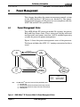
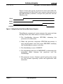
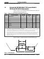
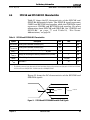
Figure 1 shows a typical AMD Athlon XP processor model 10
system block diagram.
Thermal Monitor
AMD Athlon™ XP
Processor Model 10
AMD Athlon System Bus
AGP
AGP Bus
Memory Bus
System Controller
(Northbridge)
SDRAM or DDR
PCI Bus
Peripheral Bus
Controller
(Southbridge)
LAN
SCSI
Modem / Audio
LPC Bus
USB
Dual EIDE
BIOS
Figure 1. Typical AMD Athlon™ XP Processor Model 10 System Block Diagram
Chapter 1
Overview
3
Preliminary Information
AMD Athlon™ XP Processor Model 10 Data Sheet
4
26237C—May 2003
Overview
Chapter 1
Preliminary Information
AMD Athlon™ XP Processor Model 10 Data Sheet
26237C—May 2003
2
Interface Signals
This section describes the interface signals utilized by the
AMD Athlon™ XP processor model 10.
2.1
Overview
The AMD Athlon™ system bus architecture is designed to
deliver excellent data movement bandwidth for nextgeneration x86 platforms as well as the high-performance
required by enterprise-class application software. The system
bus architecture consists of three high-speed channels (a
unidirectional processor request channel, a unidirectional
probe channel, and a 64-bit bidirectional data channel),
source-synchronous clocking, and a packet-based protocol. In
addition, the system bus supports several control, clock, and
legacy signals. The interface signals use an impedance
controlled push-pull, low-voltage, swing-signaling technology
contained within the Socket A socket.
For more information, see “AMD Athlon™ System Bus Signals”
on page 6, Chapter 11, “Pin Descriptions” on page 53, and the
AMD Athlon™ and AMD Duron™ System Bus Specification,
order# 21902.
2.2
Signaling Technology
The AMD Athlon system bus uses a low-voltage, swing-signaling
technology, that has been enhanced to provide larger noise
margins, reduced ringing, and variable voltage levels. The
signals are push-pull and impedance compensated. The signal
inputs use differential receivers that require a reference
voltage (VREF). The reference signal is used by the receivers to
determine if a signal is asserted or deasserted by the source.
Termination resistors are not needed because the driver is
impedance-matched to the motherboard and a high impedance
reflection is used at the receiver to bring the signal past the
input threshold.
For more information about pins and signals, see Chapter 11,
“Pin Descriptions” on page 53.
Chapter 2
Interface Signals
5
Preliminary Information
AMD Athlon™ XP Processor Model 10 Data Sheet
2.3
26237C—May 2003
Push-Pull (PP) Drivers
The AMD Athlon XP processor model 10 supports push-pull
(PP) drivers. The system logic configures the processor with the
configuration parameter called SysPushPull (1=PP). The
impedance of the PP drivers is set to match the impedance of
the motherboard by two external resistors connected to the ZN
and ZP pins.
See “ZN and ZP Pins” on page 78 for more information.
2.4
AMD Athlon™ System Bus Signals
The AMD Athlon system bus is a clock-forwarded, point-topoint interface with the following three point-to-point channels:
■
■
■
A 13-bit unidirectional output address/command channel
A 13-bit unidirectional input address/command channel
A 72-bit bidirectional data channel
For more information, see Chapter 7, “Electrical Data” on page
23 and the AMD Athlon™ and AMD Duron™ System Bus
Specification, order# 21902.
6
Interface Signals
Chapter 2
Preliminary Information
AMD Athlon™ XP Processor Model 10 Data Sheet
26237C—May 2003
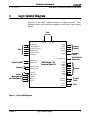
3
Logic Symbol Diagram
Figure 2 is the logic symbol diagram of the processor. This
diagram shows the logical grouping of the input and output
signals.
Clock
{
{
VID[4:0]
COREFB
COREFB#
PWROK
FID[3:0]
FSB_SENSE[1:0]
Power
Management
and Initialization
{
{
SADDOUT[14:2]#
SADDOUTCLK#
AMD Athlon™ XP
Processor Model 10
PROCRDY
CLKFWDRST
CONNECT
STPCLK#
RESET#
FERR
IGNNE#
INIT#
INTR
NMI
A20M#
SMI#
FLUSH#
Legacy
THERMDA
THERMDC
Thermal
Diode
PICCLK
PICD[1:0]
{
Request
SADDIN[14:2]#
SADDINCLK#
Frequency
Control
Front-Side Bus
Autodetect
{
Probe/SysCMD {
Voltage
Control
{
Data
SYSCLK#
{
SYSCLK
SDATA[63:0]#
SDATAINCLK[3:0]#
SDATAOUTCLK[3:0]#
SDATAINVALID#
SDATAOUTVALID#
SFILLVALID#
APIC
Figure 2. Logic Symbol Diagram
Chapter 3
Logic Symbol Diagram
7
Preliminary Information
AMD Athlon™ XP Processor Model 10 Data Sheet
8
Logic Symbol Diagram
26237C—May 2003
Chapter 3
Preliminary Information
AMD Athlon™ XP Processor Model 10 Data Sheet
26237C—May 2003
4
Power Management
This chapter describes the power management control system
of the AMD Athlon™ XP processor model 10. The power
management features of the processor are compliant with the
ACPI 1.0b and ACPI 2.0 specifications.
4.1
Power Management States
The AMD Athlon XP processor model 10 supports low-power
Halt and Stop Grant states. These states are used by advanced
configuration and power interface (ACPI) enabled operating
systems for processor power management.
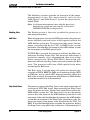
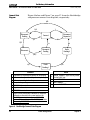
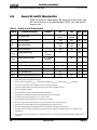
Figure 3 shows the power management states of the processor.
The figure includes the ACPI “Cx” naming convention for these
states.
Execute HLT
C1
Halt
C0
Working4
SMI#, INTR, NMI, INIT#, RESET#
Probe Serviced
STPCLK# deasserted
Incoming Probe
STPCLK# asserted
PC
LK
#d
ST
ea
PC
sse
LK
rte
#a
d3
sse
rte
d2
(Read PLVL2 register
or throttling)
Probe Serviced
Incoming Probe
Probe
State1
ST
ST
ST
PC
LK
#
PC
LK
#
C2
Stop Grant
Cache Snoopable
ass
e
de
ass
ert
ed
rte
d
S1
Stop Grant
Cache Not Snoopable
Sleep
Legend
Hardware transitions
Software transitions
Note:
The AMD AthlonTM System Bus is connected during the following states:
1) The Probe state
2) During transitions between the Halt state and the C2 Stop Grant state
3) During transitions between the C2 Stop Grant state and the Halt state
4) C0 Working state
Figure 3. AMD Athlon™ XP Processor Model 10 Power Management States
Chapter 4
Power Management
9
Preliminary Information
AMD Athlon™ XP Processor Model 10 Data Sheet
26237C—May 2003
The following sections provide an overview of the power
m a n a g e m e n t s t a t e s . Fo r m o re d e t a i l s , re f e r t o t h e
AMD Athlon™ and AMD Duron™ System Bus Specification,
order# 21902.
Note: In all power management states that the processor is
powered, the system must not stop the system clock
(SYSCLK/SYSCLK#) to the processor.
Working State
The Working state is the state in which the processor is
executing instructions.
Halt State
When the processor executes the HLT instruction, the processor
enters the Halt state and issues a Halt special cycle to the
AMD Athlon system bus. The processor only enters the low
power state dictated by the CLK_Ctl MSR if the system
controller (Northbridge) disconnects the AMD Athlon system
bus in response to the Halt special cycle.
If STPCLK# is asserted, the processor will exit the Halt state
and enter the Stop Grant state. The processor will initiate a
system bus connect, if it is disconnected, then issue a Stop
Grant special cycle. When STPCLK# is deasserted, the
processor will exit the Stop Grant state and re-enter the Halt
state. The processor will issue a Halt special cycle when
re-entering the Halt state.
The Halt state is exited when the processor detects the
assertion of INIT#, RESET#, SMI#, or an interrupt via the INTR
or NMI pins, or via a local APIC interrupt message. When the
Halt state is exited, the processor will initiate an AMD Athlon
system bus connect if it is disconnected.
Stop Grant States
10
The processor enters the Stop Grant state upon recognition of
assertion of STPCLK# input. After entering the Stop Grant
state, the processor issues a Stop Grant special bus cycle on the
AMD Athlon system bus. The processor is not in a low-power
state at this time, because the AMD Athlon system bus is still
connected. After the Northbridge disconnects the AMD Athlon
system bus in response to the Stop Grant special bus cycle, the
processor enters a low-power state dictated by the CLK_Ctl
MSR. If the Northbridge needs to probe the processor during
the Stop Grant state while the system bus is disconnected, it
Power Management
Chapter 4
Preliminary Information
26237C—May 2003
AMD Athlon™ XP Processor Model 10 Data Sheet
must first connect the system bus. Connecting the system bus
places the processor into the higher power probe state. After
the Northbridge has completed all probes of the processor, the
Northbridge must disconnect the AMD Athlon system bus
again so that the processor can return to the low-power state.
During the Stop Grant states, the processor latches INIT#,
INTR, NMI, SMI#, or a local APIC interrupt message, if they are
asserted.
The Stop Grant state is exited upon the deassertion of
STPCLK# or the assertion of RESET#. When STPCLK# is
d e a s s e r t e d , t h e p ro c e s s o r i n i t i a t e s a c o n n e c t o f t h e
AMD Athlon system bus if it is disconnected. After the
processor enters the Working state, any pending interrupts are
recognized and serviced and the processor resumes execution
at the instruction boundary where STPCLK# was initially
recognized. If RESET# is sampled asserted during the Stop
Grant state, the processor exits the Stop Grant state and the
reset process begins.
There are two mechanisms for asserting STPCLK#—hardware
and software.
The Southbridge can force STPCLK# assertion for throttling to
protect the processor from exceeding its maximum case
temperature. This is accomplished by asserting the THERM#
input to the Southbridge. Throttling asserts STPCLK# for a
percentage of a predefined throttling period: STPCLK# is
repetitively asserted and deasserted until THERM# is
deasserted.
Software can force the processor into the Stop Grant state by
accessing ACPI-defined registers typically located in the
Southbridge.
The operating system places the processor into the C2 Stop
Grant state by reading the P_LVL2 register in the Southbridge.
If an ACPI Thermal Zone is defined for the processor, the
operating system can initiate throttling with STPCLK# using
the ACPI defined P_CNT register in the Southbridge. The
Northbridge connects the AMD Athlon system bus, and the
processor enters the Probe state to service cache snoops during
Stop Grant for C2 or throttling.
Chapter 4
Power Management
11
Preliminary Information
AMD Athlon™ XP Processor Model 10 Data Sheet
26237C—May 2003
In C2, probes are allowed, as shown in Figure 3 on page 9
The Stop Grant state is also entered for the S1, Powered On
Suspend, system sleep state based on a write to the SLP_TYP
and SLP_EN fields in the ACPI-defined Power Management 1
control register in the Southbridge. During the S1 Sleep state,
system software ensures no bus master or probe activity occurs.
The Southbridge deasserts STPCLK# and brings the processor
out of the S1 Stop Grant state when any enabled resume event
occurs.
Probe State
4.2
The Probe state is entered when the Northbridge connects the
AMD Athlon system bus to probe the processor (for example, to
snoop the processor caches) when the processor is in the Halt or
Stop Grant state. When in the Probe state, the processor
responds to a probe cycle in the same manner as when it is in
the Working state. When the probe has been serviced, the
processor returns to the same state as when it entered the
Probe state (Halt or Stop Grant state). When probe activity is
completed the processor only returns to a low-power state after
the Northbridge disconnects the AMD Athlon system bus again.
Connect and Disconnect Protocol
Significant power savings of the processor only occur if the
processor is disconnected from the system bus by the
Northbridge while in the Halt or Stop Grant state. The
Northbridge can optionally initiate a bus disconnect upon the
receipt of a Halt or Stop Grant special cycle. The option of
disconnecting is controlled by an enable bit in the Northbridge.
If the Northbridge requires the processor to service a probe
after the system bus has been disconnected, it must first
initiate a system bus connect.
Connect Protocol
In addition to the legacy STPCLK# signal and the Halt and Stop
Grant special cycles, the AMD Athlon system bus connect
protocol includes the CONNECT, PROCRDY, and CLKFWDRST
signals and a Connect special cycle.
AMD Athlon system bus disconnects are initiated by the
Northbridge in response to the receipt of a Halt or Stop Grant.
Reconnect is initiated by the processor in response to an
interrupt for Halt or STPCLK# deassertion. Reconnect is
initiated by the Northbridge to probe the processor.
12
Power Management
Chapter 4
Preliminary Information
26237C—May 2003
AMD Athlon™ XP Processor Model 10 Data Sheet
The Northbridge contains BIOS programmable registers to
enable the system bus disconnect in response to Halt and Stop
Grant special cycles. When the Northbridge receives the Halt or
Stop Grant special cycle from the processor and, if there are no
outstanding probes or data movements, the Northbridge
deasserts CONNECT a minimum of eight SYSCLK periods after
the last command sent to the processor. The processor detects
the deassertion of CONNECT on a rising edge of SYSCLK and
deasserts PROCRDY to the Northbridge. In return, the
Northbridge asserts CLKFWDRST in anticipation of
reestablishing a connection at some later point.
Note: The Northbridge must disconnect the processor from the
AMD Athlon system bus before issuing the Stop Grant
special cycle to the PCI bus or passing the Stop Grant special
cycle to the Southbridge for systems that connect to the
Southbridge with HyperTransport™ technology.
This note applies to current chipset implementation—
alternate chipset implementations that do not require this
are possible.
Note: In response to Halt special cycles, the Northbridge passes the
Halt special cycle to the PCI bus or Southbridge
immediately.
The processor can receive an interrupt after it sends a Halt
special cycle, or STPCLK# deassertion after it sends a Stop
Grant special cycle to the Northbridge but before the
disconnect actually occurs. In this case, the processor sends the
Connect special cycle to the Northbridge, rather than
continuing with the disconnect sequence. In response to the
Connect special cycle, the Northbridge cancels the disconnect
request.
The system is required to assert the CONNECT signal before
returning the C-bit for the connect special cycle (assuming
CONNECT has been deasserted).
For more information, see the AMD Athlon™ and AMD Duron™
System Bus Specification, order# 21902 for the definition of the
C-bit and the Connect special cycle.
Chapter 4
Power Management
13
Preliminary Information
AMD Athlon™ XP Processor Model 10 Data Sheet
26237C—May 2003
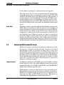
Figure 4 shows STPCLK# assertion resulting in the processor in
the Stop Grant state and the AMD Athlon system bus
disconnected.
STPCLK#
AMD Athlon™
System Bus
Stop Grant
CONNECT
PROCRDY
CLKFWDRST
Stop Grant
PCI Bus
Figure 4. AMD Athlon™ System Bus Disconnect Sequence in the Stop Grant State
An example of the AMD Athlon system bus disconnect
sequence is as follows:
1. The peripheral controller (Southbridge) asserts STPCLK#
to place the processor in the Stop Grant state.
2. When the processor recognizes STPCLK# asserted, it enters
the Stop Grant state and then issues a Stop Grant special
cycle.
3. When the special cycle is received by the Northbridge, it
deasserts CONNECT, assuming no probes are pending,
initiating a bus disconnect to the processor.
4. The processor responds to the Northbridge by deasserting
PROCRDY.
5. The Northbridge asserts CLKFWDRST to complete the bus
disconnect sequence.
6. After the processor is disconnected from the bus, the
processor enters a low-power state. The Northbridge passes
the Stop Grant special cycle along to the Southbridge.
14
Power Management
Chapter 4
Preliminary Information
26237C—May 2003
AMD Athlon™ XP Processor Model 10 Data Sheet
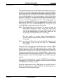
Figure 5 shows the signal sequence of events that takes the
processor out of the Stop Grant state, connects the processor to
the AMD Athlon system bus, and puts the processor into the
Working state.
STPCLK#
PROCRDY
CONNECT
CLKFWDRST
Figure 5. Exiting the Stop Grant State and Bus Connect Sequence
The following sequence of events removes the processor from
the Stop Grant state and connects it to the system bus:
1. The Southbridge deasserts
processor of a wake event.
STPCLK#,
informing
the
2. When the processor recognizes STPCLK# deassertion, it
exits the low-power state and asserts PROCRDY, notifying
the Northbridge to connect to the bus.
3. The Northbridge asserts CONNECT.
4. The Northbridge deasserts CLKFWDRST, synchronizing the
forwarded clocks between the processor and the
Northbridge.
5. The processor issues a Connect special cycle on the system
bus and resumes operating system and application code
execution.
Chapter 4
Power Management
15
Preliminary Information
AMD Athlon™ XP Processor Model 10 Data Sheet
Connect State
Diagram
26237C—May 2003
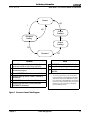
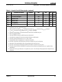
Figure 6 below and Figure 7 on page 17 show the Northbridge
and processor connect state diagrams, respectively.
4/A
1
2/A
Disconnect
Pending
Disconnect
Requested
Connect
3
3/C
5/B
8
8
Reconnect
Pending
Disconnect
Probe
Pending 2
7/D,C
6/C
7/D
Probe
Pending 1
Condition
Action
1 A disconnect is requested and probes are still pending.
2 A disconnect is requested and no probes are pending.
A
Deassert CONNECT eight SYSCLK periods
after last SysDC sent.
3 A Connect special cycle from the processor.
B Assert CLKFWDRST.
4 No probes are pending.
C Assert CONNECT.
5 PROCRDY is deasserted.
D Deassert CLKFWDRST.
6 A probe needs service.
7 PROCRDY is asserted.
Three SYSCLK periods after CLKFWDRST is deasserted.
Although reconnected to the system interface, the
8 Northbridge must not issue any non-NOP SysDC
commands for a minimum of four SYSCLK periods after
deasserting CLKFWDRST.
Figure 6. Northbridge Connect State Diagram
16
Power Management
Chapter 4
Preliminary Information
AMD Athlon™ XP Processor Model 10 Data Sheet
26237C—May 2003
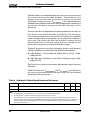
Connect
6/B
1
2/B
Connect
Pending 2
Disconnect
Pending
5
Connect
Pending 1
3/A
Disconnect
4/C
Condition
1
Action
CONNECT is deasserted by the Northbridge (for a
previously sent Halt or Stop Grant special cycle).
Processor receives a wake-up event and must cancel
2
the disconnect request.
3 Deassert PROCRDY and slow down internal clocks.
4
Processor wake-up event or CONNECT asserted by
Northbridge.
A CLKFWDRST is asserted by the Northbridge.
B Issue a Connect special cycle.*
C
Return internal clocks to full speed and assert
PROCRDY.
Note:
*
5 CLKFWDRST is deasserted by the Northbridge.
6
Forward clocks start three SYSCLK periods after
CLKFWDRST is deasserted.
The Connect special cycle is only issued after a
processor wake-up event (interrupt or STPCLK#
deassertion) occurs. If the AMD Athlon™ system
bus is connected so the Northbridge can probe the
processor, a Connect special cycle is not issued at
that time (it is only issued after a subsequent
processor wake-up event).
Figure 7. Processor Connect State Diagram
Chapter 4
Power Management
17
Preliminary Information
AMD Athlon™ XP Processor Model 10 Data Sheet
4.3
26237C—May 2003
Clock Control
The processor implements a Clock Control (CLK_Ctl) MSR
(address C001_001Bh) that determines the internal clock
divisor when the AMD Athlon system bus is disconnected.
Refer to the AMD Athlon™ and AMD Duron™ Processors BIOS,
Software, and Debug Developers Guide, order# 21656, for more
details on the CLK_Ctl register.
18
Power Management
Chapter 4
Preliminary Information
AMD Athlon™ XP Processor Model 10 Data Sheet
26237C—May 2003
5
CPUID Support
AMD Athlon™ XP processor model 10 version and feature set
recognition can be performed through the use of the CPUID
instruction, that provides complete information about the
processor—vendor, type, name, etc., and its capabilities.
Software can make use of this information to accurately tune
the system for maximum performance and benefit to users.
For information on the use of the CPUID instruction see the
following documents:
■
■
■
Chapter 5
AMD Processor Recognition Application Note, order# 20734
AMD Athlon™ Processor Recognition Application Note
Addendum, order# 21922
AMD Athlon™ and AMD Duron™ Processors BIOS, Software,
and Debug Developers Guide, order# 21656
CPUID Support
19
Preliminary Information
AMD Athlon™ XP Processor Model 10 Data Sheet
20
CPUID Support
26237C—May 2003
Chapter 5
Preliminary Information
AMD Athlon™ XP Processor Model 10 Data Sheet
26237C—May 2003
6
Advanced 333 Front-Side Bus AMD Athlon™ XP
Processor Model 10 Specifications
This chapter describes the electrical specifications that are
u n i q u e t o t h e a dva n c e d 3 3 3 f r o n t - s i d e b u s ( F S B )
AMD Athlon™ XP processor model 10.
6.1
Electrical and Thermal Specifications for the Advanced 333 FSB
AMD Athlon™ XP Processor Model 10
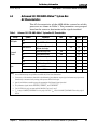
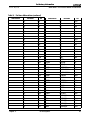
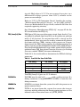
Table 1 shows the electrical and thermal specifications in the
C0 working state and the S1 Stop Grant state for this processor.
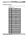
Table 1.
Electrical and Thermal Specifications for the Advanced 333 FSB AMD Athlon™ XP Processor
Model 10
V
Frequency in MHz CC_CORE
(Core
(Model Number)
Voltage)
ICC (Processor Current)
Working State C0
Stop Grant
Maximum Typical
Maximum
S11, 2, 3, 4
Thermal Power5
Maximum Die
Temperature
Typical Maximum Typical
1833 (2500+)
1917 (2600+)
1.65 V
41.4 A
32.5 A
45.0 A
35.4 A
12.1 A
7.2 A
68.3 W
53.7 W
74.3 W
58.4 W
85°C
2083 (2800+)
2167 (3000+)
Notes:
1. See Figure 3, "AMD Athlon™ XP Processor Model 10 Power Management States" on page 9.
2. The maximum Stop Grant currents are absolute worst case currents for parts that may yield from the worst case corner of the
process and are not representative of the typical Stop Grant current that is currently about one-third of the maximum specified
current.
3. These currents occur when the AMD Athlon™ system bus is disconnected and has a low power ratio of 1/8 for Stop Grant
disconnect and a low power ratio of 1/8 Halt disconnect applied to the core clock grid of the processor as dictated by a value of
2003_1223h programmed into the Clock Control (CLK_Ctl) MSR. For more information, refer to the AMD Athlon™ and
AMD Duron™ Processors BIOS, Software, and Debug Developers Guide, order# 21656.
4. The Stop Grant current consumption is characterized at 50°C and not tested.
5. Thermal design power represents the maximum sustained power dissipated while executing publicly-available software or
instruction sequences under normal system operation at nominal VCC_CORE . Thermal solutions must monitor the temperature of
the processor to prevent the processor from exceeding its maximum die temperature.
Chapter 6
Advanced 333 Front-Side Bus AMD Athlon™ XP Processor Model 10 Specifications
21
Preliminary Information
AMD Athlon™ XP Processor Model 10 Data Sheet
6.2
26237C—May 2003
Advanced 333 FSB AMD Athlon™ XP Processor Model 10
SYSCLK and SYSCLK# AC Characteristics
Table 2 shows the SYSCLK/SYSCLK# differential clock AC
characteristics of this processor.
Table 2.
Advanced 333 FSB SYSCLK and SYSCLK# AC Characteristics
Symbol
Parameter Description
Minimum
Maximum
Units
Notes
50
166
MHz
1
30%
70%
6
ns
2, 3
Clock Frequency
Duty Cycle
t1
Period
t2
High Time
1.0
ns
t3
Low Time
1.0
ns
t4
Fall Time
2
ns
t5
Rise Time
2
ns
± 300
ps
Period Stability
Notes:
1. The AMD Athlon™ system bus operates at twice this clock frequency.
2. Circuitry driving the AMD Athlon system bus clock inputs must exhibit a suitably low closed-loop jitter bandwidth to allow the PLL
to track the jitter. The –20dB attenuation point, as measured into a 20- or 30-pF load must be less than 500 kHz.
3. Circuitry driving the AMD Athlon system bus clock inputs may purposely alter the AMD Athlon system bus clock frequency (spread
spectrum clock generators). In no cases can the AMD Athlon system bus period violate the minimum specification above.
AMD Athlon system bus clock inputs can vary from 100% of the specified frequency to 99% of the specified frequency at a
maximum rate of 100 kHz.
Figure 8 shows a sample waveform of the SYSCLK signal.
t2
VThreshold-AC
VCROSS
t3
t4
t5
t1
Figure 8. SYSCLK Waveform
22
Advanced 333 Front-Side Bus AMD Athlon™ XP Processor Model 10 Specifications
Chapter 6
Preliminary Information
AMD Athlon™ XP Processor Model 10 Data Sheet
26237C—May 2003
6.3
Advanced 333 FSB AMD Athlon™ System Bus
AC Characteristics
The AC characteristics of the AMD Athlon system bus of this
processor are shown in Table 3. The parameters are grouped
based on the source or destination of the signals involved.
Table 3.
Advanced 333 FSB AMD Athlon™ System Bus AC Characteristics
Group
All Signals
Forward
Clocks
Sync
Symbol
Parameter
Min
Max
Units
Notes
TRISE
Output Rise Slew Rate
1
3
V/ns
1
TFALL
Output Fall Slew Rate
1
3
V/ns
1
TSKEW-DIFFEDGE
Output skew with respect to a
different clock edge
–
770
ps
2
TSU
Input Data Setup Time
300
ps
3
THD
Input Data Hold Time
300
ps
3
CIN
Capacitance on input clocks
4
25
pF
COUT
Capacitance on output clocks
4
12
pF
TVAL
RSTCLK to Output Valid
800
2000
ps
4, 5
TSU
Setup to RSTCLK
500
ps
4, 6
THD
Hold from RSTCLK
500
ps
4, 6
Notes:
1. Rise and fall time ranges are guidelines over which the I/O has been characterized.
2. TSKEW-DIFFEDGE is the maximum skew within a clock forwarded group between any two signals or between any signal and its
forward clock, as measured at the package, with respect to different clock edges.
3. Input SU and HD times are with respect to the appropriate Clock Forward Group input clock.
4. The synchronous signals include PROCRDY, CONNECT, and CLKFWDRST.
5. T VAL is RSTCLK rising edge to output valid for PROCRDY. Test Load is 25 pF.
6. TSU is setup of CONNECT/CLKFWDRST to rising edge of RSTCLK. THD is hold of CONNECT/CLKFWDRST from rising edge of
RSTCLK.
Chapter 6
Advanced 333 Front-Side Bus AMD Athlon™ XP Processor Model 10 Specifications
23
Preliminary Information
AMD Athlon™ XP Processor Model 10 Data Sheet
6.4
26237C—May 2003
Advanced 333 FSB AMD Athlon™ System Bus DC
Characteristics
Table 4 shows the DC characteristics of the AMD Athlon
system bus for this processor.
Table 4.
Advanced 333 FSB AMD Athlon™ System Bus DC Characteristics
Symbol
VREF
Parameter
Condition
Min
Max
(0.5 x VCC_CORE) (0.5 x VCC_CORE)
–50
+50
DC Input Reference Voltage
IVREF_LEAK_P VREF Tristate Leakage Pullup
VIN = VREF Nominal
IVREF_LEAK_N VREF Tristate Leakage Pulldown
VIN = VREF Nominal
Units Notes
mV
µA
–100
100
µA
VIH
Input High Voltage
VREF +200
VCC_CORE +500
mV
VIL
Input Low Voltage
–500
VREF –200
mV
ILEAK_P
Tristate Leakage Pullup
ILEAK_N
Tristate Leakage Pulldown
CIN
Input Pin Capacitance
RON
Output Resistance
RsetP
RsetN
VIN = VSS
(Ground)
–1
VIN = VCC_CORE
Nominal
1
mA
1
mA
4
7
pF
0.90 x RsetN,P
1.1 x RsetN,P
Ω
2
Impedance Set Point, P Channel
40
70
Ω
2
Impedance Set Point, N Channel
40
70
Ω
2
Notes:
1. VREF is nominally set to 50% of VCC_CORE with actual values that are specific to motherboard design implementation. VREF must be
created with a sufficiently accurate DC source and a sufficiently quiet AC response to adhere to the ± 50 mV specification listed
above.
2. Measured at VCC_CORE / 2.
24
Advanced 333 Front-Side Bus AMD Athlon™ XP Processor Model 10 Specifications
Chapter 6
Preliminary Information
AMD Athlon™ XP Processor Model 10 Data Sheet
26237C—May 2003
7
Advanced 400 Front-Side Bus AMD Athlon™ XP
Processor Model 10 Specifications
This chapter describes the electrical specifications that are
u n i q u e t o t h e a dva n c e d 4 0 0 f r o n t - s i d e b u s ( F S B )
AMD Athlon™ XP processor model 10.
7.1
Electrical and Thermal Specifications for the Advanced 400 FSB
AMD Athlon™ XP Processor Model 10
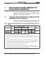
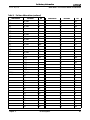
Table 5 shows the electrical and thermal specifications in the
C0 working state and the S1 Stop Grant state for this processor.
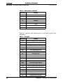
Table 5.
Electrical and Thermal Specifications for the Advanced 400 FSB AMD Athlon™ XP Processor
Model 10
V
Frequency in MHz CC_CORE
(Core
(Model Number)
Voltage)
2100 (3000+)
2200 (3200+)
1.65 V
ICC (Processor Current)
Working State C0
Stop Grant
Maximum Typical
Maximum
41.4 A
32.5 A
46.5 A
36.6 A
12.1 A
S11, 2, 3, 4
Thermal Power5
Maximum Die
Temperature
Typical Maximum Typical
7.2 A
68.3 W
53.7 W
76.8 W
60.4 W
85°C
Notes:
1. See Figure 3, "AMD Athlon™ XP Processor Model 10 Power Management States" on page 9.
2. The maximum Stop Grant currents are absolute worst case currents for parts that may yield from the worst case corner of the
process and are not representative of the typical Stop Grant current that is currently about one-third of the maximum specified
current.
3. These currents occur when the AMD Athlon™ system bus is disconnected and has a low power ratio of 1/8 for Stop Grant
disconnect and a low power ratio of 1/8 Halt disconnect applied to the core clock grid of the processor as dictated by a value of
2003_1223h programmed into the Clock Control (CLK_Ctl) MSR. For more information, refer to the AMD Athlon™ and
AMD Duron™ Processors BIOS, Software, and Debug Developers Guide, order# 21656.
4. The Stop Grant current consumption is characterized at 50°C and not tested.
5. Thermal design power represents the maximum sustained power dissipated while executing publicly-available software or
instruction sequences under normal system operation at nominal VCC_CORE . Thermal solutions must monitor the temperature of
the processor to prevent the processor from exceeding its maximum die temperature.
Chapter 7
Advanced 400 Front-Side Bus AMD Athlon™ XP Processor Model 10 Specifications
25
Preliminary Information
AMD Athlon™ XP Processor Model 10 Data Sheet
7.2
26237C—May 2003
Advanced 400 FSB AMD Athlon™ XP Processor Model 10
SYSCLK and SYSCLK# AC Characteristics
Table 6 shows the SYSCLK/SYSCLK# differential clock AC
characteristics of this processor.
Table 6.
Advanced 400 FSB SYSCLK and SYSCLK# AC Characteristics
Symbol
Parameter Description
Minimum
Maximum
Units
Notes
50
200
MHz
1
30%
70%
5
ns
2, 3
Clock Frequency
Duty Cycle
t1
Period
t2
High Time
1.0
ns
t3
Low Time
1.0
ns
t4
Fall Time
1.5
ns
t5
Rise Time
1.5
ns
± 300
ps
Period Stability
Notes:
1. The AMD Athlon™ system bus operates at twice this clock frequency.
2. Circuitry driving the AMD Athlon system bus clock inputs must exhibit a suitably low closed-loop jitter bandwidth to allow the PLL
to track the jitter. The –20dB attenuation point, as measured into a 20- or 30-pF load must be less than 500 kHz.
3. Circuitry driving the AMD Athlon system bus clock inputs may purposely alter the AMD Athlon system bus clock frequency (spread
spectrum clock generators). In no cases can the AMD Athlon system bus period violate the minimum specification above.
AMD Athlon system bus clock inputs can vary from 100% of the specified frequency to 99% of the specified frequency at a
maximum rate of 100 kHz.
Figure 9 shows a sample waveform of the SYSCLK signal.
t2
VThreshold-AC
VCROSS
t3
t4
t5
t1
Figure 9. SYSCLK Waveform
26
Advanced 400 Front-Side Bus AMD Athlon™ XP Processor Model 10 Specifications
Chapter 7
Preliminary Information
AMD Athlon™ XP Processor Model 10 Data Sheet
26237C—May 2003
7.3
Advanced 400 FSB AMD Athlon™ System Bus
AC Characteristics
The AC characteristics of the AMD Athlon system bus of this
processor are shown in Table 7. The parameters are grouped
based on the source or destination of the signals involved.
Table 7.
Advanced 400 FSB AMD Athlon™ System Bus AC Characteristics
Group
All Signals
Forward
Clocks
Sync
Symbol
Parameter
Min
Max
Units
Notes
TRISE
Output Rise Slew Rate
1
3
V/ns
1
TFALL
Output Fall Slew Rate
1
3
V/ns
1
TSKEW-DIFFEDGE
Output skew with respect to a
different clock edge
–
500
ps
2
TSU
Input Data Setup Time
300
ps
3
THD
Input Data Hold Time
300
ps
3
CIN
Capacitance on input clocks
4
25
pF
COUT
Capacitance on output clocks
4
12
pF
TVAL
RSTCLK to Output Valid
800
2000
ps
4, 5
TSU
Setup to RSTCLK
500
ps
4, 6
THD
Hold from RSTCLK
500
ps
4, 6
Notes:
1. Rise and fall time ranges are guidelines over which the I/O has been characterized.
2. TSKEW-DIFFEDGE is the maximum skew within a clock forwarded group between any two signals or between any signal and its
forward clock, as measured at the package, with respect to different clock edges.
3. Input SU and HD times are with respect to the appropriate Clock Forward Group input clock.
4. The synchronous signals include PROCRDY, CONNECT, and CLKFWDRST.
5. T VAL is RSTCLK rising edge to output valid for PROCRDY. Test Load is 25 pF.
6. TSU is setup of CONNECT/CLKFWDRST to rising edge of RSTCLK. THD is hold of CONNECT/CLKFWDRST from rising edge of
RSTCLK.
Chapter 7
Advanced 400 Front-Side Bus AMD Athlon™ XP Processor Model 10 Specifications
27
Preliminary Information
AMD Athlon™ XP Processor Model 10 Data Sheet
7.4
26237C—May 2003
Advanced 400 FSB AMD Athlon™ System Bus DC
Characteristics
Table 8 shows the DC characteristics of the AMD Athlon
system bus for this processor.
Table 8.
Advanced 400 FSB AMD Athlon™ System Bus DC Characteristics
Symbol
VREF
Parameter
Condition
Min
Max
(0.5 x VCC_CORE) (0.5 x VCC_CORE)
–50
+50
DC Input Reference Voltage
IVREF_LEAK_P VREF Tristate Leakage Pullup
VIN = VREF Nominal
IVREF_LEAK_N VREF Tristate Leakage Pulldown
VIN = VREF Nominal
Units Notes
mV
µA
–100
100
µA
VIH
Input High Voltage
VREF +150
VCC_CORE +500
mV
VIL
Input Low Voltage
–500
VREF –150
mV
ILEAK_P
Tristate Leakage Pullup
ILEAK_N
Tristate Leakage Pulldown
CIN
Input Pin Capacitance
RON
Output Resistance
RsetP
RsetN
VIN = VSS
(Ground)
–1
VIN = VCC_CORE
Nominal
1
mA
1
mA
4
7
pF
0.90 x RsetN,P
1.1 x RsetN,P
Ω
2
Impedance Set Point, P Channel
40
70
Ω
2
Impedance Set Point, N Channel
40
70
Ω
2
Notes:
1. VREF is nominally set to 50% of VCC_CORE with actual values that are specific to motherboard design implementation. VREF must be
created with a sufficiently accurate DC source and a sufficiently quiet AC response to adhere to the ± 50 mV specification listed
above.
2. Measured at VCC_CORE / 2.
28
Advanced 400 Front-Side Bus AMD Athlon™ XP Processor Model 10 Specifications
Chapter 7
Preliminary Information
AMD Athlon™ XP Processor Model 10 Data Sheet
26237C—May 2003
8
Electrical Data
This chapter describes the electrical characteristics that apply
to all desktop AMD Athlon™ XP processors model 10.
8.1
Conventions
The conventions used in this chapter are as follows:
■
■
8.2
Current specified as being sourced by the processor is
negative.
Current specified as being sunk by the processor is positive.
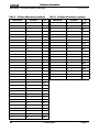
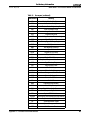
Interface Signal Groupings
The electrical data in this chapter is presented separately for
each signal group.
Table 9 defines each group and the signals contained in each
group.
Table 9.
Interface Signal Groupings
Signal Group
Signals
Notes
Power
VID[4:0], VCCA, VCC_CORE, COREFB,
COREFB#
See “Voltage Identification (VID[4:0])” on page 30,
“VID[4:0] Pins” on page 77, “VCCA AC and DC
Characteristics” on page 31, “VCC_CORE Characteristics”
on page 32, “VCCA Pin” on page 77, and “COREFB and
COREFB# Pins” on page 73.
Frequency
FID[3:0]
See “Frequency Identification (FID[3:0])” on page 31 and
“FID[3:0] Pins” on page 74.
SYSCLK, SYSCLK# (Tied to CLKIN/CLKIN#
System Clocks and RSTCLK/RSTCLK#), PLLBYPASSCLK#,
PLLBYPASSCLK
Chapter 8
See Table 15, “SYSCLK and SYSCLK# DC Characteristics,”
on page 35, Table 2, “Advanced 333 FSB SYSCLK and
SYSCLK# AC Characteristics,” on page 22, Table 6,
“Advanced 400 FSB SYSCLK and SYSCLK# AC
Characteristics,” on page 26, “SYSCLK and SYSCLK#” on
page 77, and “PLL Bypass and Test Pins” on page 76.
Electrical Data
29
Preliminary Information
AMD Athlon™ XP Processor Model 10 Data Sheet
Table 9.
26237C—May 2003
Interface Signal Groupings (continued)
Signal Group
Signals
Notes
SADDIN[14:2]#, SADDOUT[14:2]#,
SADDINCLK#, SADDOUTCLK#, SFILLVAL#,
AMD Athlon™ SDATAINVAL#, SDATAOUTVAL#,
System Bus
SDATA[63:0]#, SDATAINCLK[3:0]#,
SDATAOUTCLK[3:0]#, CLKFWDRST,
PROCRDY, CONNECT
See “Advanced 333 FSB AMD Athlon™ System Bus DC
Characteristics” on page 24, See “Advanced 400 FSB
AMD Athlon™ System Bus DC Characteristics” on page
28, Table 3, “Advanced 333 FSB AMD Athlon™ System
Bus AC Characteristics,” on page 23, Table 7, “Advanced
400 FSB AMD Athlon™ System Bus AC Characteristics,”
on page 27, and “CLKFWDRST Pin” on page 72.
Southbridge
RESET#, INTR, NMI, SMI#, INIT#, A20M#,
FERR, IGNNE#, STPCLK#, FLUSH#
See “General AC and DC Characteristics” on page 36,
“INTR Pin” on page 76, “NMI Pin” on page 76, “SMI#
Pin” on page 77, “INIT# Pin” on page 75, “A20M# Pin”
on page 72, “FERR Pin” on page 73,“IGNNE# Pin” on
page 75, “STPCLK# Pin” on page 77, and “FLUSH# Pin”
on page 75.
JTAG
TMS, TCK, TRST#, TDI, TDO
See “General AC and DC Characteristics” on page 36.
Test
PLLBYPASS#, PLLTEST#, PLLMON1,
PLLMON2, SCANCLK1, SCANCLK2,
SCANSHIFTEN, SCANINTEVAL, ANALOG
See “General AC and DC Characteristics” on page 36,
“PLL Bypass and Test Pins” on page 76, “Scan Pins” on
page 77, “Analog Pin” on page 72.
Miscellaneous DBREQ#, DBRDY, PWROK
See “General AC and DC Characteristics” on page 36,
“DBRDY and DBREQ# Pins” on page 73, “PWROK Pin”
on page 76.
APIC
PICD[1:0]#, PICCLK
See “APIC Pins AC and DC Characteristics” on page 41,
and “APIC Pins, PICCLK, PICD[1:0]#” on page 72.
Thermal
THERMDA, THERMDC
See Table 17, “Thermal Diode Electrical Characteristics,”
on page 39, and “THERMDA and THERMDC Pins” on
page 77.
8.3
Voltage Identification (VID[4:0])
Table 10 shows the VID[4:0] DC Characteristics. For more information on VID[4:0] DC Characteristics, see “VID[4:0] Pins” on
page 77.
Table 10. VID[4:0] DC Characteristics
Parameter
Description
Min
IOL
Output Current Low
6 mA
VOH
Output High Voltage
–
Max
5.25 V *
Note:
*
30
The VID pins are either open circuit or pulled to ground. It is recommended that these pins
are not pulled above 5.25 V, which is 5.0 V + 5%.
Electrical Data
Chapter 8
Preliminary Information
AMD Athlon™ XP Processor Model 10 Data Sheet
26237C—May 2003
8.4
Frequency Identification (FID[3:0])
Table 11 shows the FID[3:0] DC characteristics. For more
information, see “FID[3:0] Pins” on page 74.
Table 11. FID[3:0] DC Characteristics
Parameter
Description
Min
Max
IOL
Output Current Low
6 mA
VOH
Output High Voltage
–
2.625 V 1
| VOH – VCC_CORE | ≤ 1.60 V 2
Note:
1. The FID pins must not be pulled above 2.625 V, which is equal to 2.5 V plus a maximum of five percent.
2. Refer to “VCC_2.5V Generation Circuit” found in the section, “Motherboard Required Circuits,” of