1
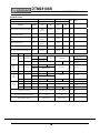
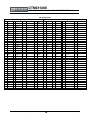
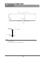
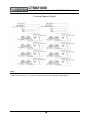
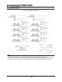
DTM68104B
8GB - 288-Pin 2Rx8 Unbuffered Non-ECC DDR4 DIMM
Features
Identification
288-pin JEDEC-compliant DIMM, 133.35 mm wide by 31.25 mm
high
Operating Voltage: VDD/VDDQ = 1.2V (1.14V to 1.26V)
DTM68104B 1Gx64
8G 2Rx8 PC4-2133P-UB0-10
VPP = 2.5V (2.375V to 2.75V)
VDDSPD = 2.25V to 2.75V
I/O Type: 1.2 V signaling
On-board I2C temperature sensor with integrated Serial
Presence-Detect (SPD) EEPROM
Data Transfer Rate: 17.0 Gigabytes/sec
Data Bursts: 8 and burst chop 4 mode
ZQ Calibration for Output Driver and On-Die Termination (ODT)
Programmable ODT / Dynamic ODT during Writes
Programmable CAS Latency: 9, 10, 11, 12, 13, 14, 15 and 16
Bi-directional Differential Data Strobe signals
Performance range
Clock / Module Speed / CL-tRCD -tRP
1067 MHz / PC4-2133 / 16-16-16
1067MHz / PC4-2133 / 15-15-15
933 Hz / PC4-1866 / 14-14-14
933 Hz / PC4-1866 / 13-13-13
800 Hz / PC4-1600 / 12-12-12
800 Hz / PC4-1600 / 11-11-11
667 MHz / PC4-1600 / 10-10-10
667 MHz / PC4-1600 / 9-9-9
Per DRAM Addressability is supported
Description
Write CRC is supported at all speed grades
DTM68104B is an unbuffered 1Gx64
memory module, which conforms to
JEDEC's DDR4-2133, PC4-2133 standard.
The assembly is Dual-Rank. Each rank is
comprised of eight Micron 512Mx8 DDR42133 SDRAMs. One 2K-bit EEPROM is
used for Serial Presence Detect.
DBI (Data Bus Inversion) is supported(x8 only)
CA parity (Command/Address Parity) mode is supported
Supports ECC error correction and detection
16 internal banks
SDRAM Addressing (Row/Col/BG/BA): 15/10/2/2
Both output driver strength and input
termination impedance are programmable
to maintain signal integrity on the I/O
signals in a Fly-by topology. A thermal
sensor accurately monitors the DIMM
module and can prevent exceeding the
maximum operating temperature of 95C.
Fully RoHS Compliant
Document 06387, Revision A, 08-Sep-14, Dataram Corporation © 2014
Page 1
DTM68104B
8GB - 288-Pin 2Rx8 Unbuffered Non-ECC DDR4 DIMM
Speed Bin Table Speed Bin DDR4‐2133P
DDR4‐2133R
CL‐nRCD‐nRP 15‐15‐15
16‐16‐16
Parameter Symbol Internal read command to first data tAA min Unit NOTE max min max 18.00 15.00 18.00 ns TBD TBD TBD TBD ns 14.06
14
(13.50)5,12 Internal read command to first data with read DBI enabled tAA_DBI ACT to internal read or write delay time tRCD 14.06 (13.50)5,12 ‐ 15.00 ‐ ns PRE command period tRP 14.06 (13.50)5,12 ‐ 15.00 ‐ ns ACT to PRE command period tRAS 33 9 x tREFI 33 9 x tREFI ns 47.06 (46.50)5,12 ‐ 48.00 ‐ ns ACT to ACT or REF command period tRC CWL = 9 Normal Read DBI CL = 9 CL = 11 (Optional)5 CL = 10 CWL = 9,11 CWL = 10,12 CWL = 11,14 CL = 12 tCK(AVG) tCK(AVG) CL = 13 CL = 12 CL = 14 CL = 13 CL = 15 (Optional)
tCK(AVG) tCK(AVG) CL = 11 1.5 tCK(AVG) 1.6 5,12 Reserved 1.25
1.5
1.6
ns 1,2,3,4 ,11,14
ns 1,2,3,1 1 <1.5
(Optional)5,12 tCK(AVG) 1.25
<1.5
tCK(AVG) 1.071
<1.25
tCK(AVG) Reserved (Optional)5,12 CL = 14 CL = 16 tCK(AVG) CL = 14 CL = TBD tCK(AVG) CL = 15 CL = TBD tCK(AVG) 0.938
<1.071
CL = 16 CL = TBD tCK(AVG) 0.938
<1.071
1.071
<1.25
Reserved Reserved 1.25
<1.5
Reserved 1.071
<1.25
ns 1,2,3,4 ,7 ns ns 1,2,3,4 ,7 ns ns 1,2,3,7 1,2,3,4 1,2,3,4 1,2,3 13,14 Reserved ns Reserved ns 0.938
<1.071
1,2,3,7 Supported CL Settings (9),(11),12,(13),14,15, 16 10,12,14,16 nCK Supported CL Settings with read DBI TBD TBD nCK Supported CWL Settings 9,10,11,12,14 9,10,11,12,14 nCK Document 06387, Revision A, 08-Sep-14, Dataram Corporation © 2014
Page 2
DTM68104B
8GB - 288-Pin 2Rx8 Unbuffered Non-ECC DDR4 DIMM
Speed Bin Table Notes: Absolute Specification ‐ VDDQ = VDD = 1.20V +/‐ 0.06 V ‐ VPP = 2.5V +0.25/‐0.125 V ‐ The values defined with above‐mentioned table are DLL ON case. ‐ DDR4‐1600, 1866, 2133 and 2400 Speed Bin Tables are valid only when Geardown Mode is disabled. 1. The CL setting and CWL setting result in tCK(avg).MIN and tCK(avg).MAX requirements. When making a selection of tCK(avg),
both need to be fulfilled: Requirements from CL setting as well as requirements from CWL setting.
2. tCK(avg).MIN limits: Since CAS Latency is not purely analog - data and strobe output are synchronized by the DLL – all
possible intermediate frequencies may not be guaranteed. An application should use the next smaller JEDEC standard
tCK(avg) value (1.5, 1.25, 1.071, 0.938 or 0.833 ns) when calculating CL [nCK] = tAA [ns] / tCK(avg) [ns], rounding up to
the next ‘Supported CL’, where tAA = 12.5ns and tCK(avg) = 1.3 ns should only be used for CL = 10 calculation.
3. tCK(avg).MAX limits: Calculate tCK(avg) = tAA.MAX / CL SELECTED and round the resulting tCK(avg) down to the next valid
speed bin (i.e. 1.5ns or 1.25ns or 1.071 ns or 0.938 ns or 0.833 ns). This result is tCK(avg). MAX corresponding to CL SELECTED.
4. ‘Reserved’ settings are not allowed. User must program a different value. 5. 'Optional' settings allow certain devices in the industry to support this setting however it is not a mandatory feature. Refer to supplier's data sheet and/or the DIMM SPD information if and how this setting is supported. 6. Any DDR4‐1866 speed bin also supports functional operation at lower frequencies as shown in the table which are not subject to Production Tests but verified by Design/Characterization. 7. Any DDR4‐2133 speed bin also supports functional operation at lower frequencies as shown in the table which are not subject to Production Tests but verified by Design/Characterization. 8. Any DDR4‐2400 speed bin also supports functional operation at lower frequencies as shown in the table which are not subject to Production Tests but verified by Design/Characterization. 9. Reserved for DDR4‐2666 speed bin. 10. Reserved for DDR4‐3200 speed bin. 11. DDR4‐1600 AC timing apply if DRAM operates at lower than 1600 MT/s data rate. 12 .For devices supporting optional down binning to CL=9, CL=11 and CL=13, tAA/tRCD/tRPmin must be 13.5ns or lower. SPD settings must be programmed to match. For example, DDR4‐1600K devices supporting down binning to 1333MT/s should program 13.5ns in SPD bytes for tAAmin(Byte 24), tRCDmin (Byte 25), and tRPmin (Byte 26). DDR4‐1866M devices supporting down binning to 1333MT/s or DDR4‐1600K should program 13.5ns in SPD bytes for tAAmin (Byte 24), tRCDmin (Byte 25), and tRPmin (Byte 26).DDR4‐2133P devices supporting down binning to 1333MT/s or DDR4‐1600K or DDR4‐1866M should program 13.5ns in SPD bytes for tAAmin (Byte 24), tRCDmin (Byte 25), and tRPmin (Byte 26).tRCmin (Byte 27, 29) also should be programmed accordingly. For example, 48.5ns (tRASmin + tRPmin = 35ns+ 13.5ns) is set to supporting optional down binning CL=9 and CL=11. 13. CL number in parentheses, it means that these numbers are optional. 14. DDR4 SDRAM supports CL=9 as long as a system meets tAA(min). Document 06387, Revision A, 08-Sep-14, Dataram Corporation © 2014
Page 3
DTM68104B
8GB - 288-Pin 2Rx8 Unbuffered Non-ECC DDR4 DIMM
Pin Configuration Front Side
1
12V,NC
37
VSS
73
Back Side
VDD
109
VSS
145
12V,NC
181
DQ29
217
VDD
253
DQ41
2
VSS
38
DQ24
74
CK0_t
110
DM5_n,
DBI5_n
146
VREFCA
182
VSS
218
CK1_t
254
VSS
3
DQ4
39
VSS
75
CK0_c
111
NC
147
VSS
183
DQ25
219
CK1_c
255
DQS5_c
4
VSS
40
DM3_n,
DBI3_n
76
VDD
112
VSS
148
DQ5
184
VSS
220
VDD
256
DQS5_t
5
DQ0
41
NC
77
VTT
113
DQ46
149
VSS
185
DQS3_c
221
VTT
257
VSS
6
42
VSS
78
EVENT_n
114
VSS
150
DQ1
186
DQS3_t
222
PARITY
258
DQ47
7
VSS
DM0_n,
DBI0_n
43
DQ30
79
A0
115
DQ42
151
VSS
187
VSS
223
VDD
259
VSS
8
NC
44
VSS
80
VDD
116
VSS
152
DQS0_t
188
DQ31
224
BA1
260
DQ43
9
VSS
45
DQ26
81
BA0
117
DQ52
153
DQS0_c
189
VSS
225
A10 / AP
261
VSS
10
DQ6
46
VSS
82
RAS_n / A16
118
VSS
154
VSS
190
DQ27
226
VDD
262
DQ53
11
VSS
47
CB4,NC
83
VDD
119
DQ48
155
DQ7
191
VSS
227
RFU
263
VSS
12
DQ2
48
VSS
84
CS0_n
120
VSS
156
VSS
192
CB5,NC
228
WE_n / A14
264
DQ49
13
VSS
49
CB0,NC
85
VDD
121
DM6_n,
DBI6_n
157
DQ3
193
VSS
229
VDD
265
VSS
14
DQ12
50
VSS
86
CAS_n / A15
122
NC
158
VSS
194
CB1,NC
230
SAVE_n,NC
266
DQS6_c
DQS6_t
15
VSS
51
NC
87
ODT0
123
VSS
159
DQ13
195
VSS
231
VDD
267
16
DQ8
52
NC
88
VDD
124
DQ54
160
VSS
196
DQS8_c
232
A13
268
VSS
17
53
VSS
89
CS1_n
125
VSS
161
DQ9
197
DQS8_t
233
VDD
269
DQ55
18
VSS
DM1_n,
DBI1_n
54
CB6,NC
90
VDD
126
DQ50
162
VSS
198
VSS
234
A17, NC
270
VSS
19
NC
55
VSS
91
ODT1
127
VSS
163
DQS1_c
199
CB7,NC
235
C2,NC
271
DQ51
20
VSS
56
CB2,NC
92
VDD
128
DQ60
164
DQS1_t
200
VSS
236
VDD
272
VSS
21
DQ14
57
VSS
93
CS2_n,C0,NC
129
VSS
165
VSS
201
CB3,NC
237
CS3_n,C1,NC
273
DQ61
22
VSS
58
RESET_n
94
VSS
130
DQ56
166
DQ15
202
VSS
238
SA2
274
VSS
23
DQ10
59
VDD
95
DQ36
131
VSS
167
VSS
203
CKE1
239
VSS
275
DQ57
24
VSS
60
CKE0
96
VSS
132
DM7_n,
DBI7_n
168
DQ11
204
VDD
240
DQ37
276
VSS
25
DQ20
61
VDD
97
DQ32
133
NC
169
VSS
205
RFU
241
VSS
277
DQS7_c
26
VSS
62
ACT_n
98
VSS
134
VSS
170
DQ21
206
VDD
242
DQ33
278
DQS7_t
27
DQ16
63
BG0
99
DM4_n,
DBI4_n
135
DQ62
171
VSS
207
BG1
243
VSS
279
VSS
28
64
VDD
100
NC
136
VSS
172
DQ17
208
ALERT_n
244
DQS4_c
280
DQ63
29
VSS
DM2_n,
DBI2_n
65
A12 / BC_n
101
VSS
137
DQ58
173
VSS
209
VDD
245
DQS4_t
281
VSS
30
NC
66
A9
102
DQ38
138
VSS
174
DQS2_c
210
A11
246
VSS
282
DQ59
31
VSS
67
VDD
103
VSS
139
SA0
175
DQS2_t
211
A7
247
DQ39
283
VSS
32
DQ22
68
A8
104
DQ34
140
SA1
176
VSS
212
VDD
248
VSS
284
VDDSPD
33
VSS
69
A6
105
VSS
141
SCL
177
DQ23
213
A5
249
DQ35
285
SDA
34
DQ18
70
VDD
106
DQ44
142
VPP
178
VSS
214
A4
250
VSS
286
VPP
35
VSS
71
A3
107
VSS
143
VPP
179
DQ19
215
VDD
251
DQ45
287
VPP
36
DQ28
72
A1
108
DQ40
144
RFU
180
VSS
216
A2
252
VSS
288
VPP
Document 06387, Revision A, 08-Sep-14, Dataram Corporation © 2014
Page 4
DTM68104B
8GB - 288-Pin 2Rx8 Unbuffered Non-ECC DDR4 DIMM
PIN DESCRIPTION Name
Function
CB[7:0] *
Data Check Bits
DQ[63:0]
Data Bits
DM[7:0]_n, DBI[7:0]_n
Input Data Mask and Data Bus Inversion
DQS[7:0]_t, DQS[7:0]_c
Differential Data Strobes
CK_t[1:0], CK_c[1:0]
Differential Clock Inputs
CKE[1:0]
Clock Enables
CAS_n / A15
Multiplexed: Column Address Strobe or Address 15
RAS_n / A16
Multiplexed: Row Address Strobe or Address 16
CS[1:0]_n, CS[3:2]_n*
Chip Selects
ACT_n
Activate Command Input
WE_n / A14
Multiplexed: Write Enable or Address 14
C[2:0]*
Chip ID Inputs
A[17:0]
Address Inputs
BA[1:0]
Bank Address select Inputs
BG[1:0]
Bank Group select Inputs
ODT[1:0]
On Die Termination Inputs
SA[2:0]
SPD Address
SCL
SPD Clock Input
SDA
SPD Data Input/Output
EVENT_n
Temperature Sensing
RESET_n
Reset for register and DRAMs
PARITY
Parity bit input for Addr/Ctrl
ALERT_n
CRC Error Flag or CMD/Addr Parity Flag Output
A12 / BC_n
Combination Input: Address12/Burst Chop
A10 / AP
Combination Input: Addr10/Auto-precharge
12V*
Optional Power Supply*
VPP
Charge Pump Power
VSS
Ground
VDD
Power
VDDSPD
SPD EEPROM Power
VREFCA
Reference Voltage for CA
VTT
Termination Voltage
NC
No Connection
RFU
Reserved for Future Use
* Not used
Document 06387, Revision A, 08-Sep-14, Dataram Corporation © 2014
Page 5
DTM68104B
8GB - 288-Pin 2Rx8 Unbuffered Non-ECC DDR4 DIMM
Side View
3.98mm (max)
1.4 +/- .1mm (max)
Notes:
1.
Tolerances on all dimensions except where otherwise indicated are ±.13. Reference JEDEC
standard MO-309C.
2.
All dimensions are expressed: millimeters [inches]
Document 06387, Revision A, 08-Sep-14, Dataram Corporation © 2014
Page 6
DTM68104B
8GB - 288-Pin 2Rx8 Unbuffered Non-ECC DDR4 DIMM
Functional Diagram (Rank 0)
Notes:
1: Unless otherwise noted, resistor values are 15Ω ± 5%.
2: ZQ resistors are 240Ω ± 1%. For all other resistor values refer to the appropriate wiring diagram.
Document 06387, Revision A, 08-Sep-14, Dataram Corporation © 2014
Page 7
DTM68104B
8GB - 288-Pin 2Rx8 Unbuffered Non-ECC DDR4 DIMM
Functional Diagram (Rank 1)
Notes:
1: Unless otherwise noted, resistor values are 15Ω ± 5%.
2: ZQ resistors are 240Ω ± 1%. For all other resistor values refer to the appropriate wiring diagram.
3: For Rank 1 the DQ resistors are shown for simplicity but are the same physical components as shown on Rank 0.
4: EVENT_n is wired on this design. A standalone SPD may be used as well. No wiring changes are required.
Document 06387, Revision A, 08-Sep-14, Dataram Corporation © 2014
Page 8
DTM68104B
8GB - 288-Pin 2Rx8 Unbuffered Non-ECC DDR4 DIMM
DATARAM CORPORATION, USA Corporate Headquarters, P.O. Box 7528, Princeton, NJ 08543-7528;
Voice: 609-799-0071, Fax: 609-799-6734; www.dataram.com
All rights reserved.
The information contained in this document has been carefully checked and is believed to be reliable. However,
Dataram assumes no responsibility for inaccuracies.
The information contained in this document does not convey any license under the copyrights, patent rights or
trademarks claimed and owned by Dataram.
No part of this publication may be copied or reproduced in any form or by any means, or transferred to any third party
without prior written consent of Dataram.
Document 06387, Revision A, 08-Sep-14, Dataram Corporation © 2014
Page 9