1
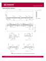
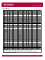
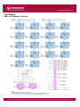
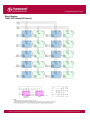
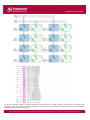
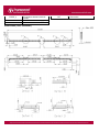
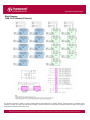
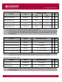
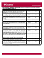
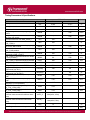
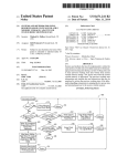
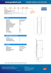
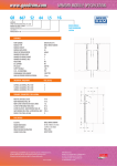
DDR4 TS1GHR72V1Z TS2GHR72V1Z 288Pin DDR4 2133 RDIMM 8GB~16GB Based on 1Gx4 On DIMM Thermal Sensor Pin Identification Symbol A0~A15 BA0, BA1 BG0, BG1 RAS_n CAS_n Description DDR4 Registered DIMM is high-speed, low power memory module that use 1Gx4bits DDR4 SDRAM in FBGA package and a 4Kbits serial EEPROM on a 288-pin printed circuit board. DDR4 Registered DIMM is a Dual In-Line Memory Module and is intended for mounting into 288-pin edge connector sockets. Synchronous design allows precise cycle control with the use of system clock. Data I/O transactions are possible on both edges of DQS. Range of operation frequencies, programmable latencies allow the same device to be useful for a variety of high bandwidth, high performance memory system applications. Features RoHS compliant products. JEDEC standard 1.2V ± 0.06V power supply VDDQ=1.2V ± 0.06V Clock Freq: 1067MHZ for 2133Mb/s/Pin. Programmable CAS Latency: 10,11,12,13,14,15,16 Programmable Additive Latency (Posted /CAS): 0,CL-2 or CL-1 clock Programmable /CAS Write Latency (CWL) = 11, 14(DDR4-2133) 8 bit pre-fetch Burst Length: 4, 8 Bi-directional Differential Data-Strobe On Die Termination with ODT pin Serial presence detect with EEPROM WE_n CS0_n, CS1_n, CS2_n, CS3_n CKE0, CKE1 Function Register address input Register bank select input Register bank group select input Register row address strobe input Register column address strobe input Register write enable input DIMM Rank Select Lines input Register clock enable lines input Register on-die termination control ODT0, ODT1 lines input ACT_n Register input for activate input DQ0~Q63 DIMM memory data bus CB0~B7 DIMM ECC check bits TDQS9_t~TDQS17_t Dummy loads for mixed populations TDQS9_c~TDQS17_c of x4 based and x8 based RDIMMs. Data Buffer data strobes DQS0_t~DQS17_t (positive line of differential pair) Data Buffer data strobes DQS0_c~DQS17_c (negative line of differential pair) Register clock input (positive line of CK0_t, CK1_t differential pair) Register clocks input (negative line CK0_c, CK1_c of differential pair) I2C serial bus clock for SPD/TS SCL and register I2C serial bus data line for SPD/TS SDA and register I2C slave address select for SA0~SA2 SPD/TS and register PAR Register parity input VDD SDRAM core power supply SDRAM command/address VREFCA reference supply VSS Power supply return (ground) Serial SPD/TS positive power VDDSPD supply ALERT_n Register ALERT_n output VPP SDRAM activating power supply Set Register and SDRAMs to a RESET_n Known State SPD signals a thermal event has EVENT_n occurred. VTT SDRAM I/O termination supply RFU Reserved for future use NC No Connection Dimensions (Unit: millimeter) Note: 1. Tolerances on all dimensions +/-0.15mm unless otherwise specified. Pin Assignments Pin No 1 Pin Name 12V3,NC Pin No 37 Pin Name VSS Pin No 73 Pin Name VDD Pin No 109 Pin Name VSS Pin No 145 2 VSS 38 DQ24 74 CK0_t 110 3 DQ4 39 VSS 75 CK0_c TDQS12_t, DQS12_t TDQS12_c, DQS12_c 76 VDD 112 VSS 148 TDQS14_t, 146 DQS14_t TDQS14_c, 111 DQS14_c 147 Pin Name 12V3,NC Pin No 181 VREFCA 182 Pin Name DQ29 Pin No 217 Pin Name VDD Pin No 253 Pin Name DQ41 VSS 218 CK1_t 254 VSS VSS 183 DQ25 219 CK1_c 255 DQS5_c DQ5 184 VSS 220 VDD 256 DQS5_t 4 VSS 40 5 DQ0 41 77 VTT 113 DQ46 149 VSS 185 DQS3_c 221 VTT 257 VSS 6 VSS 42 VSS 78 EVENT_n 114 VSS 150 DQ1 186 DQS3_t 222 PARITY 258 DQ47 7 TDQS9_t, DQS9_t TDQS9_c, DQS9_c 43 DQ30 79 A0 115 DQ42 151 VSS 187 VSS 223 VDD 259 VSS 44 VSS 80 VDD 116 VSS 152 DQS0_c 188 DQ31 224 BA1 260 DQ43 9 10 11 12 VSS DQ6 VSS DQ2 45 46 47 48 DQ26 VSS CB4 VSS 81 82 83 84 BA0 RAS_n/A16 VDD S0_n 117 118 119 120 DQ52 VSS DQ48 VSS 153 154 155 156 DQS0_t VSS DQ7 VSS 189 190 191 192 VSS DQ27 VSS CB5 225 226 227 228 A10/AP VDD RFU WE_n/A14 261 262 263 264 VSS DQ53 VSS DQ49 13 VSS 49 CB0 85 VDD 121 TDQS15_t, DQS15_t 157 DQ3 193 VSS 229 VDD 265 VSS TDQS15_c, 122 DQS15_c 158 VSS 194 CB1 230 NC 266 DQS6_c 8 14 DQ12 50 15 VSS 51 16 DQ8 52 VSS 53 54 17 18 19 TDQS10_t, DQS10_t TDQS10_c, DQS10_c VSS 86 CAS_n/A15 87 ODT0 123 VSS 159 DQ13 195 VSS 231 VDD 267 DQS6_t 88 VDD 124 DQ54 160 VSS 196 DQS8_c 232 A13 268 VSS VSS 89 S1_n 125 VSS 161 DQ9 197 DQS8_t 233 VDD 269 DQ55 CB6 90 VDD 126 DQ50 162 VSS 198 VSS 234 A17 270 VSS 91 ODT1 127 VSS 163 DQS1_c 199 CB7 235 NC,C2 271 DQ51 92 VDD 128 93 C0,CS2_n,NC 129 94 VSS 130 95 DQ36 131 DQ60 VSS DQ56 VSS 164 165 166 167 DQS1_t VSS DQ15 VSS 200 201 202 203 VSS CB3 VSS CKE1 236 VDD 272 237 NC,CS3_c,C1 273 238 SA2 274 239 VSS 275 VSS DQ61 VSS DQ57 DQ11 204 VDD 240 TDQS17_t, DQS17_t TDQS17_c, DQS17_c 55 VSS 20 21 22 23 VSS DQ14 VSS DQ10 56 57 58 59 CB2 VSS RESET_n VDD 24 VSS 60 CKE0 96 VSS 25 DQ20 61 VDD 97 DQ32 26 VSS 62 ACT_n 98 VSS 27 28 29 30 DQ16 63 BG0 99 VSS 64 VDD 100 TDQS11_t, DQS11_t TDQS11_c, DQS11_c 65 66 A12/BC_n 101 A9 102 TDQS16_t, 168 DQS16_t TDQS16_c, 133 DQS16_c 169 132 DQ37 276 VSS VSS 205 RFU 241 VSS 277 DQS7_c 134 VSS 170 DQ21 206 VDD 242 DQ33 278 DQS7_t 135 DQ62 171 VSS 207 BG1 243 VSS 279 VSS 136 VSS 172 DQ17 208 ALERT_n 244 DQS4_c 280 DQ63 VSS 137 DQ58 173 VSS 209 VDD 245 DQS4_t 281 VSS DQ38 138 VSS 174 DQS2_c 210 A11 246 VSS 282 DQ59 TDQS13_t, DQS13_t TDQS13_c, DQS13_c 31 VSS 67 VDD 103 VSS 139 SA0 175 DQS2_t 211 A7 247 DQ39 283 32 DQ22 68 A8 104 DQ34 140 SA1 176 VSS 212 VDD 248 VSS 284 33 VSS 69 A6 105 VSS 141 SCL 177 DQ23 213 A5 249 DQ35 285 34 DQ18 70 VDD 106 DQ44 142 VPP 178 VSS 214 A4 250 VSS 286 35 VSS 71 A3 107 VSS 143 VPP 179 DQ19 215 VDD 251 DQ45 287 36 DQ28 72 A1 108 DQ40 144 RFU 180 VSS 216 A2 252 VSS 288 Note: 1. VPP is 2.5V DC 2. Pin 230 is defined as NC for UDIMMs, RDIMMs and LRDIMMs. Pin 230 is defined as SAVE_n for NVDIMMs. 3. Pins 1 and 145 are defined as NC for UDIMMs, RDIMMs and LRDIMMs. Pins 1 and 145 are defined as 12V for Hybrid /NVDIMM 4. The 5th VPP is required on all modules, DIMMs. VSS VDDSPD SDA VPP VPP VPP4 Block Diagram 8GB, 1Gx72 Module(1 Rank x4) Block Diagram 16GB, 2Gx72 Module(2 Rank x4) This technical information is based on industry standard data and tests believed to be reliable. However, Transcend makes no warranties, either expressed or implied, as to its accuracy and assume no liability in connection with the use of this product. Transcend reserves the right to make changes in specifications at any time without prior notice. Operating Temperature Condition Parameter Symbol Rating Unit Operating Temperature TOPER 0 to 85 ℃ Note: 1. Operating Temperature is the case surface temperature on the center/top side of the DRAM. For the measurement conditions, please refer to JESD51-2 standard. Note 1,2 2. At 0 - 85℃, operation temperature range are the temperature which all DRAM specification will be supported. Absolute Maximum DC Ratings Parameter Symbol Value Unit Note Voltage on VDD relative to Vss VDD -0.3 ~ 1.5 V 1 Voltage on VDDQ pin relative to Vss VDDQ -0.3 ~ 1.5 V 1 Voltage on VPP pin relative to Vss VPP -0.3 ~ 3.0 V 3 Voltage on any pin relative to Vss VIN, VOUT -0.3 ~ 1.5 V 1 Storage temperature TSTG -55~+100 ℃ 1,2 Note: 1. Stress greater than those listed under “Absolute Maximum Ratings” may cause permanent damage to the device. This is a stress rating only and functional operation of the device at these or any other conditions above those indicated in the operational sections of this specification is not implied. Exposure to absolute maximum rating conditions for extended periods may affect reliability. 2. Storage Temperature is the case surface temperature on the center/top side of the DRAM. For the measurement conditions, please refer to JESD51-2 standard. 3. VPP must be equal or greater than VDD/VDDQ at all times. AC & DC Operating Conditions Recommended DC operating conditions Rating Parameter Symbol Unit Notes Min Typ. Max Supply voltage VDD 1.14 1.2 1.26 Supply voltage for Output VDDQ 1.14 1.2 1.26 Wordline supply voltage VPP 2.375 2.5 2.75 Note: 1. Under all conditions VDDQ must be less than or equal to VDD. 2. VDDQ tracks with VDD, AC parameters are measured with VDD and VDDQ tied together. 3. DC bandwidth is limited to 20MHz V V V 1, 2 1, 2 3 Single-ended AC & DC input levels for Command and Address DDR4-1600/1866/2133 Parameter Symbol Unit Note Min Max I/O Reference Voltage (CMD/ADD) VREFCA(DC) 0.49*VDDQ 0.51*VDDQ V 1,2 DC Input Logic High VIH(DC) VREF+0.075 VDD V DC Input Logic Low VIL(DC) VSS VREF-0.075 V AC Input Logic High VIH(AC) VREF+0.1 Note 1 V AC Input Logic Low VIL(AC) Note 1 VREF-0.1 V Note: 1. The AC peak noise on VREFCA may not allow VREFCA to deviate from VREFCA(DC) by more than ± 1% VDD (for reference : approx. ± 12mV) 2. For reference : approx. VDD/2 ± 12mV Differential AC and DC Input Levels DDR4-1600/1866/2133 Parameter Symbol Unit Note Min Max differential input high DC VIHdiff(DC) +0.150 NOTE 3 V 1 differential input low DC VILdiff(DC) NOTE 3 -0.150 V 1 differential input high AC VIHdiff(AC) 2 x (VIH(AC) - VREF) NOTE 3 V 2 differential input low AC VILdiff(AC) NOTE 3 2 x (VIL(AC) -VREF) V 2 Note: 1. Used to define a differential signal slew-rate. 2. for CK_t - CK_c use VIH.CA/VIL.CA(AC) of ADD/CMD and VREFCA; 3. These values are not defined; however, the differential signals CK_t - CK_c, need to be within the respective limits (VIH.CA(DC) max, VIL.CA(DC)min) for single-ended signals as well as the limitations for overshoot and undershoot. Single-ended AC & DC output levels Parameter Symbol DDR4-1600/1866/2133 DC output high measurement level VOH(DC) 1.1 x VDDQ V DC output mid measurement level VOM(DC) 0.8 x VDDQ V DC output low measurement level VOL(DC) 0.5 x VDDQ V AC output high measurement level VOH(AC) (0.7 + 0.15) x VDDQ V 1 AC output low measurement level VOL(AC) (0.7 - 0.15) x VDDQ V 1 Note: Unit Note 1. The swing of ± 0.15 × VDDQ is based on approximately 50% of the static single-ended output peak-to-peak swing with a driver impedance of RZQ/7Ω and an effective test load of 50Ω to VTT = VDDQ. Differential AC & DC output levels Parameter Symbol DDR4-1600/1866/2133 Unit Note AC differential output high VOHdiff(AC) +0.3 x VDDQ V 1 measurement level AC differential output low VOLdiff(AC) -0.3 x VDDQ V 1 measurement level Note: 1. The swing of ± 0.3 × VDDQ is based on approximately 50% of the static differential output peak-to-peak swing with a driver impedance of RZQ/7Ω and an effective test load of 50Ω to VTT = VDDQ at each of the differential outputs. IDD Specification parameters Definition( IDD values are for full operating range of Voltage and Temperature) 8GB, 1Gx72 Module(1 Rank x4) Parameter Operating One bank Active-Precharge current; tCK = tCK(IDD), tRC = tRC(IDD), tRAS = tRASmin(IDD); CKE is HIGH, /CS is HIGH between valid commands; Address bus inputs are SWITCHING; Data bus inputs are SWITCHING Operating One bank Active-read-Precharge current; IOUT = 0mA; BL = 8, CL = CL(IDD), AL = 0; tCK = tCK(IDD), tRC = tRC (IDD), tRAS = tRASmin(IDD), tRCD = tRCD(IDD); CKE is HIGH, /CS is HIGH between valid commands; Address bus inputs are SWITCHING; Data pattern is same as IDD4W Precharge power-down current; All banks idle; tCK = tCK(IDD); CKE is LOW; Other control and address bus inputs are STABLE; Data bus inputs are FLOATING Precharge quiet standby current; All banks idle; tCK = tCK(IDD); CKE is HIGH, /CS is HIGH; Other control and address bus inputs are STABLE; Data bus inputs are FLOATING Precharge standby current; All banks idle; tCK = tCK(IDD); CKE is HIGH, /CS is HIGH; Other control and address bus inputs are SWITCHING; Data bus inputs are SWITCHING Active power - down current; All banks open; tCK = tCK(IDD); CKE is LOW; Other control and address bus inputs are STABLE; Data bus inputs are FLOATING Active standby current; All banks open; tCK = tCK(IDD), tRAS = tRASmax(IDD), tRP = tRP(IDD); CKE is HIGH, /CS is HIGH between valid commands; Other control and address bus inputs are SWITCHING; Data bus inputs are SWITCHING Operating burst read current; All banks open, Continuous burst reads, IOUT = 0mA; BL = 4, CL = CL(IDD), AL = 0; tCK = tCK(IDD), tRAS = tRASmax(IDD), tRP = tRP(IDD); CKE is HIGH, /CS is HIGH between valid commands; Address bus inputs are SWITCHING; Data pattern is same as IDD4W Operating burst write current; All banks open, Continuous burst writes; BL = 8, CL = CL(IDD), AL = 0; tCK = tCK(IDD), tRAS = tRASmax(IDD), tRP = tRP(IDD); CKE is HIGH, /CS is HIGH between valid commands; Address bus inputs are SWITCHING; Data bus inputs are SWITCHING IDD4R Burst refresh current; tCK = tCK(IDD); Refresh command at every tRFC(IDD) interval; CKE is HIGH, /CS is HIGH between valid commands; Other control and address bus inputs are SWITCHING; Data bus inputs are SWITCHING Self refresh current; CK and /CK at 0V; CKE ≒ 0.2V; Other control and address bus inputs are FLOATING; Data bus inputs are FLOATING Operating bank interleave read current; All bank interleaving reads, IOUT = 0mA; BL = 8, CL = CL(IDD), AL = tRCD(IDD)-1*tCK(IDD); tCK = tCK(IDD), Trc = tRC(IDD), tRRD = tRRD(IDD), tRCD = 1*tCK(IDD); CKE is HIGH, CS is HIGH between valid commands;Address bus inputs are STABLE during DESELECTs; Data pattern is same as IDD4R; Note: Symbol DDR4 2133 CL15 Unit IDD0 1280 mA IDD1 1450 mA IDD2P 500 mA IDD2Q 1020 mA IDD2N 1040 mA IDD3P 570 mA IDD3N 1210 mA IDD4R 2240 mA IDD4W 2050 mA IDD5 3480 mA IDD6 260 mA IDD7 3240 mA 1.Module IDD was calculated on the specific brand DRAM(2Xnm) component IDD and can be differently measured according to DQ loading capacitor. 16GB, 2Gx72 Module(2 Rank x4) Parameter Operating One bank Active-Precharge current; tCK = tCK(IDD), tRC = tRC(IDD), tRAS = tRASmin(IDD); CKE is HIGH, /CS is HIGH between valid commands; Address bus inputs are SWITCHING; Data bus inputs are SWITCHING Operating One bank Active-read-Precharge current; IOUT = 0mA; BL = 8, CL = CL(IDD), AL = 0; tCK = tCK(IDD), tRC = tRC (IDD), tRAS = tRASmin(IDD), tRCD = tRCD(IDD); CKE is HIGH, /CS is HIGH between valid commands; Address bus inputs are SWITCHING; Data pattern is same as IDD4W Precharge power-down current; All banks idle; tCK = tCK(IDD); CKE is LOW; Other control and address bus inputs are STABLE; Data bus inputs are FLOATING Precharge quiet standby current; All banks idle; tCK = tCK(IDD); CKE is HIGH, /CS is HIGH; Other control and address bus inputs are STABLE; Data bus inputs are FLOATING Precharge standby current; All banks idle; tCK = tCK(IDD); CKE is HIGH, /CS is HIGH; Other control and address bus inputs are SWITCHING; Data bus inputs are SWITCHING Active power - down current; All banks open; tCK = tCK(IDD); CKE is LOW; Other control and address bus inputs are STABLE; Data bus inputs are FLOATING Active standby current; All banks open; tCK = tCK(IDD), tRAS = tRASmax(IDD), tRP = tRP(IDD); CKE is HIGH, /CS is HIGH between valid commands; Other control and address bus inputs are SWITCHING; Data bus inputs are SWITCHING Operating burst read current; All banks open, Continuous burst reads, IOUT = 0mA; BL = 4, CL = CL(IDD), AL = 0; tCK = tCK(IDD), tRAS = tRASmax(IDD), tRP = tRP(IDD); CKE is HIGH, /CS is HIGH between valid commands; Address bus inputs are SWITCHING; Data pattern is same as IDD4W Operating burst write current; All banks open, Continuous burst writes; BL = 8, CL = CL(IDD), AL = 0; tCK = tCK(IDD), tRAS = tRASmax(IDD), tRP = tRP(IDD); CKE is HIGH, /CS is HIGH between valid commands; Address bus inputs are SWITCHING; Data bus inputs are SWITCHING IDD4R Burst refresh current; tCK = tCK(IDD); Refresh command at every tRFC(IDD) interval; CKE is HIGH, /CS is HIGH between valid commands; Other control and address bus inputs are SWITCHING; Data bus inputs are SWITCHING Self refresh current; CK and /CK at 0V; CKE ≒ 0.2V; Other control and address bus inputs are FLOATING; Data bus inputs are FLOATING Operating bank interleave read current; All bank interleaving reads, IOUT = 0mA; BL = 8, CL = CL(IDD), AL = tRCD(IDD)-1*tCK(IDD); tCK = tCK(IDD), Trc = tRC(IDD), tRRD = tRRD(IDD), tRCD = 1*tCK(IDD); CKE is HIGH, CS is HIGH between valid commands;Address bus inputs are STABLE during DESELECTs; Data pattern is same as IDD4R; Note: Symbol DDR4 2133 CL15 Unit IDD0 1600 mA IDD1 1780 mA IDD2P 720 mA IDD2Q 1310 mA IDD2N 1370 mA IDD3P 870 mA IDD3N 1540 mA IDD4R 2580 mA IDD4W 2380 mA IDD5 3810 mA IDD6 500 mA IDD7 3580 mA 1.Module IDD was calculated on the specific brand DRAM(2Xnm) component IDD and can be differently measured according to DQ loading capacitor. Timing Parameters & Specifications Speed Parameter DDR4 2133 Unit Symbol Min Max Average Clock Period tCK 0.938 <1.071 ns CK high-level width tCH 0.48 0.52 tCK CK low-level width tCL 0.48 0.52 tCK tDQSQ - TBD tCK/2 tDQSQ - TBD tCK/2 tQH TBD - tCK/2 tQH TBD - UI tDQSQ - TBD UI tQH TBD - UI tDQSQ TBD TBD UI tRPRE 0.9 TBD tCK DQS_t, DQS_c differential READ Postamble tRPST TBD TBD tCK DQS_t, DQS_c differential WRITE Preamble tWPRE 0.9 - tCK DQS_t, DQS_c differential WRITE Postamble tWPST TBD TBD tCK tLZ(DQS) -360 180 ps tHZ(DQS) - 180 ps tDQSL 0.46 0.54 tCK tDQSH 0.46 0.54 tCK tDQSS -0.27 0.27 tCK tDSS 0.18 - tCK tDSH 0.18 - tCK tWTR_S Max(2nCK, 2.5ns) - tWTR_L Max(4nCK,7.5ns) - DQS_t,DQS_c to DQ skew, per group, per access DQS_t,DQS_c to DQ Skew determin-istic, per group, per access DQ output hold time from DQS_t,DQS_c DQ output hold time deterministic from DQS_t, DQS_c DQS_t,DQS_c to DQ Skew total, per group, per access; DBI enabled DQ output hold time total from DQS_t, DQS_c; DBI enabled DQ to DQ offset , per group, per ac-cess referenced to DQS_t, DQS_c DQS_t, DQS_c differential READ Pre-amble (2 clock preamble) DQS_t and DQS_c low-impedance time (Referenced from RL-1) DQS_t and DQS_c high-impedance time (Referenced from RL+BL/2) DQS_t, DQS_c differential input low pulse width DQS_t, DQS_c differential input high pulse width DQS_t, DQS_c rising edge to CK_t, CK_c rising edge (1 clock preamble) DQS_t, DQS_c falling edge setup time to CK_t, CK_c rising edge DQS_t, DQS_c falling edge hold time from CK_t, CK_c rising edge Delay from start of internal write trans-action to internal read command for different bank group Delay from start of internal write trans-action to internal read command for same bank group WRITE recovery time Mode Register Set command cycle time Speed Parameter CAS_n to CAS_n command delay for same bank group CAS_n to CAS_n command delay for different bank group Auto precharge write recovery + precharge time ACTIVATE to ACTIVATE Command delay to different bank group for 2KB page size ACTIVATE to ACTIVATE Command delay to different bank group for 1KB page size ACTIVATE to ACTIVATE Command delay to different bank group for 1/ 2KB page size ACTIVATE to ACTIVATE Command delay to same bank group for 2KB page size ACTIVATE to ACTIVATE Command delay to same bank group for 1KB page size ACTIVATE to ACTIVATE Command delay to same bank group for 1/2KB page size tWR 15 - ns tMRD 8 - nCK Unit Symbol Min Max tCCD_L 6 - nCK tCCD_S 4 - nCK DDR4 2133 tDAL nCK tWR+tRP/tCK tRRD_S(2K) Max(4nCK,5.3ns) - nCK tRRD_S(1K) Max(4nCK,3.7ns) - nCK tRRD_S (1/ 2K) Max(4nCK,3.7ns) - nCK tRRD_L(2K) Max(4nCK,6.4ns) - nCK tRRD_L(1K) Max(4nCK,5.3ns) - nCK tRRD_L (1/ 2K) Max(4nCK,5.3ns) - nCK Four activate window for 2KB page size tFAW_2K Max(28nCK, 30ns) - ns Four activate window for 1KB page size tFAW_1K Max(20nCK, 21ns) - ns tFAW_1/2K Max(16nCK, 15ns) - ns Power-up and RESET calibration time tZQinit 1024 - nCK Normal operation Full calibration time tZQoper 512 - nCK tZQCS 128 - nCK tXS tRFC(min)+ 10ns - tXSDLL tDLLK(min) - tRTP Max(4nCK,7.5ns) - tCKESR tCKE(min)+1nCK - tXP Max (4nCK,6ns) - tCKE Max (3nCK,5ns) - tAONAS 1.0 9.0 ns tAOFAS 1.0 9.0 ns tADC 0.3 0.7 tCK Four activate window for 1/2KB page size Normal operation short calibration time Exit Self Refresh to commands not re-quiring a locked DLL Exit Self Refresh to commands requir-ing a locked DLL Internal READ Command to PRE-CHARGE Command delay Minimum CKE low width for Self re-fresh entry to exit timing Exit Power Down with DLL on to any valid command;Exit Precharge Power Down with DLL frozen to commands not requiring a locked DLL CKE minimum pulse width Asynchronous RTT turn-on delay (Power-Down with DLL frozen) Asynchronous RTT turn-off delay (Power-Down with DLL frozen) RTT dynamic change skew SERIAL PRESENCE DETECT SPECIFICATION TS1GHR72V1Z Serial Presence Detect Byte No. 0 1 2 3 4 5 6 7 8 9 10 11 12 13 14 15-16 17 18 19 20-23 24 25 26 27 28 29 30-31 32-33 34-35 36-37 38 39 40 Function Described Number of Bytes Used / Number of Bytes in SPD Device / CRC Coverage SPD Revision Key Byte / DRAM Device Type Key Byte / Module Type SDRAM Density and Banks SDRAM Addressing SDRAM Package Type SDRAM Optional Features SDRAM Thermal and Refresh Options Other SDRAM Optional Features Reserved Module Nominal Voltage, VDD Module Organization Module Memory Bus Width Module Thermal Sensor Reserved Timebases SDRAM Minimum Cycle Time (tCKAVGmin) SDRAM Maximum Cycle Time (tCKAVGmax) CAS Latencies Supported Minimum CAS Latency Time (tAAmin) Minimum RAS to CAS Delay Time (tRCDmin) Minimum Row Precharge Delay Time (tRPmin) Upper Nibbles for tRASmin and tRCmin Minimum Active to Precharge Delay Time (tRASmin), Least Significant Byte Minimum Active to Active/Refresh Delay Time (tRCmin), Least Significant Byte Minimum Refresh Recovery Delay Time (tRFC1min) Minimum Refresh Recovery Delay Time (tRFC2min) Minimum Refresh Recovery Delay Time (tRFC4min) Minimum Four Activate Window Delay Time (tFAWmin) Minimum Activate to Activate Delay Time (tRRD_Smin), different bank group Minimum Activate to Activate Delay Time (tRRD_Lmin), same bank group Minimum CAS to CAS Delay Time (tCCD_Lmin), Standard Specification CRC:0-255Byte SPD Byte use: 512Byte SPD Byte total: 512Byte DDR4 SDRAM RDIMM 4Gb, 16banks ROW:16, Column:10 1.2V 1Rank, 4bits ECC, 72bits Support 0.938ns 1.5ns 10, 11, 12, 13, 14, 15, 16 13.75ns 13.75ns 13.75ns - Vendor Part 33ns 08 46.75ns 76 260ns 160ns 110ns 20,08 00,05 70,03 15ns 00,78 3.7ns 1E 5.3ns 2B 5.625ns 2E 24 0C 01 84 21 00 03 00 0B 80 00 00 08 0C 6E 6E 6E 11 122 same bank group Reserved Connector to SDRAM Bit Mapping Reserved Fine Offset for Minimum CAS to CAS Delay Time (tCCD_Lmin), same bank group Fine Offset for Minimum Activate to Activate Delay Time (tRRD_Lmin), same bank group Fine Offset for Minimum Activate to Activate Delay Time (tRRD_Smin), different bank group Fine Offset for Minimum Active to Active/Refresh Delay Time (tRCmin) Fine Offset for Minimum Row Precharge Delay Time (tRPmin) Fine Offset for Minimum RAS to CAS Delay Time (tRCDmin) 123 Fine Offset for Minimum CAS Latency Time (tAAmin) 41-59 60-77 78-116 117 118 119 120 121 Fine Offset for SDRAM Maximum Cycle Time (tCKAVGmax) Fine Offset for SDRAM Minimum Cycle Time 125 (tCKAVGmin) 126-127 Cyclical Redundancy Code Raw Card Extension, Module Nominal Height 128 Module Maximum Thickness 129 Reference Raw Card Used 130 DIMM Module Attributes 131 RDIMM Thermal Heat Spreader Solution 132 133-134 Register Manufacturer ID Code Register Revision Number 135 Address Mapping from Register to DRAM 136 124 137 138 139-253 254-255 256-319 320-321 322 323-324 325-328 329-348 349 350-351 352 353-381 382-383 Register Output Drive Strength for Control Register Output Drive Strength for CK Reserved Cyclical Redundancy Code (CRC) Reserved Module Manufacturer ID Code Module Manufacturing Location Module Manufacturing Date Module Serial Number Module Part Number Module Revision Code DRAM Manufacturer ID Code DRAM Stepping Manufacturer Specific Data Reserved - 00 00 - 83 - B5 - CE - 00 - 00 - 00 - 00 - 00 - C2 31.25mm Planar Double Sides Revision 0, Raw card C 1 Row,1 Register Not incorporated By Manufacturer By Manufacturer Not Mirrored Moderate Drive: Chip select, ODT, CKE Moderate Drive: Command/Address Moderate Drive By Manufacturer By Manufacturer - 11 11 02 05 00 Variable Variable 00 55 05 00 00 00 Variable 00 Variable 00 384-551 End User Programmable - - TS2GHR72V1Z Serial Presence Detect Byte No. 0 1 2 3 4 5 6 7 8 9 10 11 12 13 14 15-16 17 18 19 20-23 24 25 26 27 28 29 30-31 32-33 34-35 36-37 38 39 40 41-59 Function Described Number of Bytes Used / Number of Bytes in SPD Device / CRC Coverage SPD Revision Key Byte / DRAM Device Type Key Byte / Module Type SDRAM Density and Banks SDRAM Addressing SDRAM Package Type SDRAM Optional Features SDRAM Thermal and Refresh Options Other SDRAM Optional Features Reserved Module Nominal Voltage, VDD Module Organization Module Memory Bus Width Module Thermal Sensor Reserved Timebases SDRAM Minimum Cycle Time (tCKAVGmin) SDRAM Maximum Cycle Time (tCKAVGmax) CAS Latencies Supported Minimum CAS Latency Time (tAAmin) Minimum RAS to CAS Delay Time (tRCDmin) Minimum Row Precharge Delay Time (tRPmin) Upper Nibbles for tRASmin and tRCmin Minimum Active to Precharge Delay Time (tRASmin), Least Significant Byte Minimum Active to Active/Refresh Delay Time (tRCmin), Least Significant Byte Minimum Refresh Recovery Delay Time (tRFC1min) Minimum Refresh Recovery Delay Time (tRFC2min) Minimum Refresh Recovery Delay Time (tRFC4min) Minimum Four Activate Window Delay Time (tFAWmin) Minimum Activate to Activate Delay Time (tRRD_Smin), different bank group Minimum Activate to Activate Delay Time (tRRD_Lmin), same bank group Minimum CAS to CAS Delay Time (tCCD_Lmin), same bank group Reserved Standard Specification CRC:0-255Byte SPD Byte use: 512Byte SPD Byte total: 512Byte DDR4 SDRAM RDIMM 4Gb, 16banks ROW:16, Column:10 1.2V 2Rank, 4bits ECC, 72bits Support 0.938ns 1.5ns 10, 11, 12, 13, 14, 15, 16 13.75ns 13.75ns 13.75ns - Vendor Part 33ns 08 46.75ns 76 260ns 160ns 110ns 20,08 00,05 70,03 15ns 00,78 3.7ns 1E 5.3ns 2B 5.625ns 2E - 00 24 0C 01 84 21 00 03 08 0B 80 00 00 08 0C 6E 6E 6E 11 60-77 78-116 - 00 - 83 - B5 - CE - 00 - 00 122 Connector to SDRAM Bit Mapping Reserved Fine Offset for Minimum CAS to CAS Delay Time (tCCD_Lmin), same bank group Fine Offset for Minimum Activate to Activate Delay Time (tRRD_Lmin), same bank group Fine Offset for Minimum Activate to Activate Delay Time (tRRD_Smin), different bank group Fine Offset for Minimum Active to Active/Refresh Delay Time (tRCmin) Fine Offset for Minimum Row Precharge Delay Time (tRPmin) Fine Offset for Minimum RAS to CAS Delay Time (tRCDmin) - 00 123 Fine Offset for Minimum CAS Latency Time (tAAmin) - 00 - 00 - C2 31.25mm Planar Double Sides Revision 0, Raw card A 2 Row,1 Register Not incorporated By Manufacturer By Manufacturer Mirrored Moderate Drive: Chip select, ODT, CKE Strong Drive: Command/Address Moderate Drive By Manufacturer By Manufacturer - 11 11 00 09 00 Variable Variable 01 117 118 119 120 121 Fine Offset for SDRAM Maximum Cycle Time (tCKAVGmax) Fine Offset for SDRAM Minimum Cycle Time 125 (tCKAVGmin) 126-127 Cyclical Redundancy Code Raw Card Extension, Module Nominal Height 128 Module Maximum Thickness 129 Reference Raw Card Used 130 DIMM Module Attributes 131 RDIMM Thermal Heat Spreader Solution 132 133-134 Register Manufacturer ID Code Register Revision Number 135 Address Mapping from Register to DRAM 136 124 137 138 139-253 254-255 256-319 320-321 322 323-324 325-328 329-348 349 350-351 352 353-381 382-383 384-551 Register Output Drive Strength for Control Register Output Drive Strength for CK Reserved Cyclical Redundancy Code (CRC) Reserved Module Manufacturer ID Code Module Manufacturing Location Module Manufacturing Date Module Serial Number Module Part Number Module Revision Code DRAM Manufacturer ID Code DRAM Stepping Manufacturer Specific Data Reserved End User Programmable 65 05 00 00 00 Variable 00 Variable 00 - DDR4 Serial presence detect with EEPROM TS2GHR72V1PL On DIMM Thermal 288Pin DDR4 2133 VLP RDIMM 16GB Based on 2Gx4 DDP Asynchronous reset Pin Identification DDR4 VLP Registered DIMM is high-speed, low power Symbol A0~A17 BA0, BA1 BG0, BG1 RAS_n memory module that use 2Gx4bits DDR4 SDRAM in CAS_n FBGA package and a 4Kbits serial EEPROM on a WE_n CS0_n, CS1_n, CS2_n, CS3_n CKE0, CKE1 Description 288-pin printed circuit board. DDR4 VLP Registered DIMM is a Dual In-Line Memory Module and is intended for mounting into 288-pin edge connector sockets. Synchronous design allows precise cycle control with the use of system clock. Data I/O transactions are possible on both edges of DQS. Range of operation frequencies, ODT0, ODT1 ACT_n DQ0~Q63 CB0~B7 DQS0_t~DQS17_t programmable latencies allow the same device to be useful for a variety of high bandwidth, high performance memory system applications. Features RoHS compliant products. DQS0_c~DQS17_c CK0_t, CK1_t CK0_c, CK1_c JEDEC standard 1.2V ± 0.06V power supply SCL VDDQ=1.2V ± 0.06V SDA Clock Freq: 1067MHZ for 2133Mb/s/Pin. Programmable CAS Latency: 10,11,12,13,14,15,16 Programmable Additive Latency (Posted /CAS): 0,CL-2 or CL-1 clock Programmable /CAS Write Latency (CWL) = 11, 14(DDR4-2133) 8 bit pre-fetch SA0~SA2 PAR VDD VREFCA VSS VDDSPD Burst Length: 4, 8 ALERT_n VPP Bi-directional Differential Data-Strobe RESET_n On Die Termination with ODT pin Function Register address input Register bank select input Register bank group select input Register row address strobe input Register column address strobe input Register write enable input DIMM Rank Select Lines input Register clock enable lines input Register on-die termination control lines input Register input for activate input DIMM memory data bus DIMM ECC check bits Data Buffer data strobes (positive line of differential pair) Data Buffer data strobes (negative line of differential pair) Register clock input (positive line of differential pair) Register clocks input (negative line of differential pair) I2C serial bus clock for SPD/TS and register I2C serial bus data line for SPD/TS and register I2C slave address select for SPD/TS and register Register parity input SDRAM core power supply SDRAM command/address reference supply Power supply return (ground) Serial SPD/TS positive power supply Register ALERT_n output SDRAM activating power supply Set Register and SDRAMs to a Known State EVENT_n VTT RFU SPD signals a thermal event has occurred. SDRAM I/O termination supply Reserved for future use Dimensions (Unit: millimeter) NC No Connection Note: 1. Tolerances on all dimensions +/-0.15mm unless otherwise specified. Pin Assignments Pin No 1 Pin Name 12V3,NC Pin No 37 Pin Name VSS Pin No 73 Pin Name VDD Pin No 109 Pin Name VSS Pin No 145 2 VSS 38 DQ24 74 CK0_t 110 3 DQ4 39 VSS 75 CK0_c TDQS12_t, DQS12_t TDQS12_c, DQS12_c 76 VDD 112 VSS 148 TDQS14_t, 146 DQS14_t TDQS14_c, 111 DQS14_c 147 Pin Name 12V3,NC Pin No 181 VREFCA 182 Pin Name DQ29 Pin No 217 Pin Name VDD Pin No 253 Pin Name DQ41 VSS 218 CK1_t 254 VSS VSS 183 DQ25 219 CK1_c 255 DQS5_c DQ5 184 VSS 220 VDD 256 DQS5_t 4 VSS 40 5 DQ0 41 77 VTT 113 DQ46 149 VSS 185 DQS3_c 221 VTT 257 VSS 6 VSS 42 VSS 78 EVENT_n 114 VSS 150 DQ1 186 DQS3_t 222 PARITY 258 DQ47 7 TDQS9_t, DQS9_t TDQS9_c, DQS9_c 43 DQ30 79 A0 115 DQ42 151 VSS 187 VSS 223 VDD 259 VSS 44 VSS 80 VDD 116 VSS 152 DQS0_c 188 DQ31 224 BA1 260 DQ43 9 10 11 12 VSS DQ6 VSS DQ2 45 46 47 48 DQ26 VSS CB4 VSS 81 82 83 84 BA0 RAS_n/A16 VDD S0_n 117 118 119 120 DQ52 VSS DQ48 VSS 153 154 155 156 DQS0_t VSS DQ7 VSS 189 190 191 192 VSS DQ27 VSS CB5 225 226 227 228 A10/AP VDD RFU WE_n/A14 261 262 263 264 VSS DQ53 VSS DQ49 13 VSS 49 CB0 85 VDD 121 TDQS15_t, DQS15_t 157 DQ3 193 VSS 229 VDD 265 VSS TDQS15_c, 122 DQS15_c 158 VSS 194 CB1 230 NC 266 DQS6_c 8 14 DQ12 50 15 VSS 51 16 DQ8 52 VSS 53 54 17 18 19 TDQS10_t, DQS10_t TDQS10_c, DQS10_c VSS 86 CAS_n/A15 87 ODT0 123 VSS 159 DQ13 195 VSS 231 VDD 267 DQS6_t 88 VDD 124 DQ54 160 VSS 196 DQS8_c 232 A13 268 VSS VSS 89 S1_n 125 VSS 161 DQ9 197 DQS8_t 233 VDD 269 DQ55 CB6 90 VDD 126 DQ50 162 VSS 198 VSS 234 A17 270 VSS 91 ODT1 127 VSS 163 DQS1_c 199 CB7 235 NC,C2 271 DQ51 92 VDD 128 93 C0,CS2_n,NC 129 94 VSS 130 95 DQ36 131 DQ60 VSS DQ56 VSS 164 165 166 167 DQS1_t VSS DQ15 VSS 200 201 202 203 VSS CB3 VSS CKE1 236 VDD 272 237 NC,CS3_c,C1 273 238 SA2 274 239 VSS 275 VSS DQ61 VSS DQ57 DQ11 204 VDD 240 TDQS17_t, DQS17_t TDQS17_c, DQS17_c 55 VSS 20 21 22 23 VSS DQ14 VSS DQ10 56 57 58 59 CB2 VSS RESET_n VDD 24 VSS 60 CKE0 96 VSS 25 DQ20 61 VDD 97 DQ32 26 VSS 62 ACT_n 98 VSS 27 28 29 30 DQ16 63 BG0 99 VSS 64 VDD 100 TDQS11_t, DQS11_t TDQS11_c, DQS11_c 65 66 A12/BC_n 101 A9 102 TDQS16_t, 168 DQS16_t TDQS16_c, 133 DQS16_c 169 132 DQ37 276 VSS VSS 205 RFU 241 VSS 277 DQS7_c 134 VSS 170 DQ21 206 VDD 242 DQ33 278 DQS7_t 135 DQ62 171 VSS 207 BG1 243 VSS 279 VSS 136 VSS 172 DQ17 208 ALERT_n 244 DQS4_c 280 DQ63 VSS 137 DQ58 173 VSS 209 VDD 245 DQS4_t 281 VSS DQ38 138 VSS 174 DQS2_c 210 A11 246 VSS 282 DQ59 TDQS13_t, DQS13_t TDQS13_c, DQS13_c 31 VSS 67 VDD 103 VSS 139 SA0 175 DQS2_t 211 A7 247 DQ39 283 32 DQ22 68 A8 104 DQ34 140 SA1 176 VSS 212 VDD 248 VSS 284 33 VSS 69 A6 105 VSS 141 SCL 177 DQ23 213 A5 249 DQ35 285 34 DQ18 70 VDD 106 DQ44 142 VPP 178 VSS 214 A4 250 VSS 286 35 VSS 71 A3 107 VSS 143 VPP 179 DQ19 215 VDD 251 DQ45 287 36 DQ28 72 A1 108 DQ40 144 RFU 180 VSS 216 A2 252 VSS 288 Note: 1. VPP is 2.5V DC 2. Pin 230 is defined as NC for UDIMMs, RDIMMs and LRDIMMs. Pin 230 is defined as SAVE_n for NVDIMMs. 3. Pins 1 and 145 are defined as NC for UDIMMs, RDIMMs and LRDIMMs. Pins 1 and 145 are defined as 12V for Hybrid /NVDIMM 4. The 5th VPP is required on all modules, DIMMs. VSS VDDSPD SDA VPP VPP VPP4 Block Diagram 16GB, 2Gx72 Module(2 Rank x4) This technical information is based on industry standard data and tests believed to be reliable. However, Transcend makes no warranties, either expressed or implied, as to its accuracy and assume no liability in connection with the use of this product. Transcend reserves the right to make changes in specifications at any time without prior notice. Operating Temperature Condition Parameter Symbol Rating Unit Operating Temperature TOPER 0 to 85 ℃ Note: 3. Operating Temperature is the case surface temperature on the center/top side of the DRAM. For the measurement conditions, please refer to JESD51-2 standard. Note 1,2 4. At 0 - 85℃, operation temperature range are the temperature which all DRAM specification will be supported. Absolute Maximum DC Ratings Parameter Symbol Value Unit Note Voltage on VDD relative to Vss VDD -0.3 ~ 1.5 V 1 Voltage on VDDQ pin relative to Vss VDDQ -0.3 ~ 1.5 V 1 Voltage on VPP pin relative to Vss VPP -0.3 ~ 3.0 V 3 Voltage on any pin relative to Vss VIN, VOUT -0.3 ~ 1.5 V 1 Storage temperature TSTG -55~+100 ℃ 1,2 Note: 4. Stress greater than those listed under “Absolute Maximum Ratings” may cause permanent damage to the device. This is a stress rating only and functional operation of the device at these or any other conditions above those indicated in the operational sections of this specification is not implied. Exposure to absolute maximum rating conditions for extended periods may affect reliability. 5. Storage Temperature is the case surface temperature on the center/top side of the DRAM. For the measurement conditions, please refer to JESD51-2 standard. 6. VPP must be equal or greater than VDD/VDDQ at all times. AC & DC Operating Conditions Recommended DC operating conditions Rating Parameter Symbol Unit Notes Min Typ. Max Supply voltage VDD 1.14 1.2 1.26 Supply voltage for Output VDDQ 1.14 1.2 1.26 Wordline supply voltage VPP 2.375 2.5 2.75 Note: 4. Under all conditions VDDQ must be less than or equal to VDD. 5. VDDQ tracks with VDD, AC parameters are measured with VDD and VDDQ tied together. 6. DC bandwidth is limited to 20MHz V V V 1, 2 1, 2 3 Single-ended AC & DC input levels for Command and Address DDR4-1600/1866/2133 Parameter Symbol Unit Note Min Max I/O Reference Voltage (CMD/ADD) VREFCA(DC) 0.49*VDDQ 0.51*VDDQ V 1,2 DC Input Logic High VIH(DC) VREF+0.075 VDD V DC Input Logic Low VIL(DC) VSS VREF-0.075 V AC Input Logic High VIH(AC) VREF+0.1 Note 1 V AC Input Logic Low VIL(AC) Note 1 VREF-0.1 V Note: 3. The AC peak noise on VREFCA may not allow VREFCA to deviate from VREFCA(DC) by more than ± 1% VDD (for reference : approx. ± 12mV) 4. For reference : approx. VDD/2 ± 12mV Differential AC and DC Input Levels DDR4-1600/1866/2133 Parameter Symbol Unit Note Min Max differential input high DC VIHdiff(DC) +0.150 NOTE 3 V 1 differential input low DC VILdiff(DC) NOTE 3 -0.150 V 1 differential input high AC VIHdiff(AC) 2 x (VIH(AC) - VREF) NOTE 3 V 2 differential input low AC VILdiff(AC) NOTE 3 2 x (VIL(AC) -VREF) V 2 Note: 4. Used to define a differential signal slew-rate. 5. for CK_t - CK_c use VIH.CA/VIL.CA(AC) of ADD/CMD and VREFCA; 6. These values are not defined; however, the differential signals CK_t - CK_c, need to be within the respective limits (VIH.CA(DC) max, VIL.CA(DC)min) for single-ended signals as well as the limitations for overshoot and undershoot. Single-ended AC & DC output levels Parameter Symbol DDR4-1600/1866/2133 DC output high measurement level VOH(DC) 1.1 x VDDQ V DC output mid measurement level VOM(DC) 0.8 x VDDQ V DC output low measurement level VOL(DC) 0.5 x VDDQ V AC output high measurement level VOH(AC) (0.7 + 0.15) x VDDQ V 1 AC output low measurement level VOL(AC) (0.7 - 0.15) x VDDQ V 1 Note: Unit Note 2. The swing of ± 0.15 × VDDQ is based on approximately 50% of the static single-ended output peak-to-peak swing with a driver impedance of RZQ/7Ω and an effective test load of 50Ω to VTT = VDDQ. Differential AC & DC output levels Parameter Symbol DDR4-1600/1866/2133 Unit Note AC differential output high VOHdiff(AC) +0.3 x VDDQ V 1 measurement level AC differential output low VOLdiff(AC) -0.3 x VDDQ V 1 measurement level Note: 2. The swing of ± 0.3 × VDDQ is based on approximately 50% of the static differential output peak-to-peak swing with a driver impedance of RZQ/7Ω and an effective test load of 50Ω to VTT = VDDQ at each of the differential outputs. IDD Specification parameters Definition( IDD values are for full operating range of Voltage and Temperature) 16GB, 2Gx72 Module(2 Rank x4) Parameter Operating One bank Active-Precharge current; tCK = tCK(IDD), tRC = tRC(IDD), tRAS = tRASmin(IDD); CKE is HIGH, /CS is HIGH between valid commands; Address bus inputs are SWITCHING; Data bus inputs are SWITCHING Operating One bank Active-read-Precharge current; IOUT = 0mA; BL = 8, CL = CL(IDD), AL = 0; tCK = tCK(IDD), tRC = tRC (IDD), tRAS = tRASmin(IDD), tRCD = tRCD(IDD); CKE is HIGH, /CS is HIGH between valid commands; Address bus inputs are SWITCHING; Data pattern is same as IDD4W Precharge power-down current; All banks idle; tCK = tCK(IDD); CKE is LOW; Other control and address bus inputs are STABLE; Data bus inputs are FLOATING Precharge quiet standby current; All banks idle; tCK = tCK(IDD); CKE is HIGH, /CS is HIGH; Other control and address bus inputs are STABLE; Data bus inputs are FLOATING Precharge standby current; All banks idle; tCK = tCK(IDD); CKE is HIGH, /CS is HIGH; Other control and address bus inputs are SWITCHING; Data bus inputs are SWITCHING Active power - down current; All banks open; tCK = tCK(IDD); CKE is LOW; Other control and address bus inputs are STABLE; Data bus inputs are FLOATING Active standby current; All banks open; tCK = tCK(IDD), tRAS = tRASmax(IDD), tRP = tRP(IDD); CKE is HIGH, /CS is HIGH between valid commands; Other control and address bus inputs are SWITCHING; Data bus inputs are SWITCHING Operating burst read current; All banks open, Continuous burst reads, IOUT = 0mA; BL = 4, CL = CL(IDD), AL = 0; tCK = tCK(IDD), tRAS = tRASmax(IDD), tRP = tRP(IDD); CKE is HIGH, /CS is HIGH between valid commands; Address bus inputs are SWITCHING; Data pattern is same as IDD4W Operating burst write current; All banks open, Continuous burst writes; BL = 8, CL = CL(IDD), AL = 0; tCK = tCK(IDD), tRAS = tRASmax(IDD), tRP = tRP(IDD); CKE is HIGH, /CS is HIGH between valid commands; Address bus inputs are SWITCHING; Data bus inputs are SWITCHING IDD4R Burst refresh current; tCK = tCK(IDD); Refresh command at every tRFC(IDD) interval; CKE is HIGH, /CS is HIGH between valid commands; Other control and address bus inputs are SWITCHING; Data bus inputs are SWITCHING Self refresh current; CK and /CK at 0V; CKE ≒ 0.2V; Other control and address bus inputs are FLOATING; Data bus inputs are FLOATING Operating bank interleave read current; All bank interleaving reads, IOUT = 0mA; BL = 8, CL = CL(IDD), AL = tRCD(IDD)-1*tCK(IDD); tCK = tCK(IDD), Trc = tRC(IDD), tRRD = tRRD(IDD), tRCD = 1*tCK(IDD); CKE is HIGH, CS is HIGH between valid commands;Address bus inputs are STABLE during DESELECTs; Data pattern is same as IDD4R; Note: Symbol DDR4 2133 CL15 Unit IDD0 1600 mA IDD1 1780 mA IDD2P 720 mA IDD2Q 1310 mA IDD2N 1370 mA IDD3P 870 mA IDD3N 1540 mA IDD4R 2580 mA IDD4W 2380 mA IDD5 3810 mA IDD6 500 mA IDD7 3580 mA 1.Module IDD was calculated on the specific brand DRAM(2Xnm) component IDD and can be differently measured according to DQ loading capacitor. Timing Parameters & Specifications Speed Parameter DDR4 2133 Unit Symbol Min Max Average Clock Period tCK 0.938 <1.071 ns CK high-level width tCH 0.48 0.52 tCK CK low-level width tCL 0.48 0.52 tCK tDQSQ - TBD tCK/2 tDQSQ - TBD tCK/2 tQH TBD - tCK/2 tQH TBD - UI tDQSQ - TBD UI tQH TBD - UI tDQSQ TBD TBD UI tRPRE 0.9 TBD tCK DQS_t, DQS_c differential READ Postamble tRPST TBD TBD tCK DQS_t, DQS_c differential WRITE Preamble tWPRE 0.9 - tCK DQS_t, DQS_c differential WRITE Postamble tWPST TBD TBD tCK tLZ(DQS) -360 180 ps tHZ(DQS) - 180 ps tDQSL 0.46 0.54 tCK tDQSH 0.46 0.54 tCK tDQSS -0.27 0.27 tCK tDSS 0.18 - tCK tDSH 0.18 - tCK tWTR_S Max(2nCK, 2.5ns) - tWTR_L Max(4nCK,7.5ns) - tWR 15 - ns tMRD 8 - nCK DQS_t,DQS_c to DQ skew, per group, per access DQS_t,DQS_c to DQ Skew determin-istic, per group, per access DQ output hold time from DQS_t,DQS_c DQ output hold time deterministic from DQS_t, DQS_c DQS_t,DQS_c to DQ Skew total, per group, per access; DBI enabled DQ output hold time total from DQS_t, DQS_c; DBI enabled DQ to DQ offset , per group, per ac-cess referenced to DQS_t, DQS_c DQS_t, DQS_c differential READ Pre-amble (2 clock preamble) DQS_t and DQS_c low-impedance time (Referenced from RL-1) DQS_t and DQS_c high-impedance time (Referenced from RL+BL/2) DQS_t, DQS_c differential input low pulse width DQS_t, DQS_c differential input high pulse width DQS_t, DQS_c rising edge to CK_t, CK_c rising edge (1 clock preamble) DQS_t, DQS_c falling edge setup time to CK_t, CK_c rising edge DQS_t, DQS_c falling edge hold time from CK_t, CK_c rising edge Delay from start of internal write trans-action to internal read command for different bank group Delay from start of internal write trans-action to internal read command for same bank group WRITE recovery time Mode Register Set command cycle time Speed Parameter CAS_n to CAS_n command delay for same bank group CAS_n to CAS_n command delay for different bank group Auto precharge write recovery + precharge time ACTIVATE to ACTIVATE Command delay to different bank group for 2KB page size ACTIVATE to ACTIVATE Command delay to different bank group for 1KB page size ACTIVATE to ACTIVATE Command delay to different bank group for 1/ 2KB page size ACTIVATE to ACTIVATE Command delay to same bank group for 2KB page size ACTIVATE to ACTIVATE Command delay to same bank group for 1KB page size ACTIVATE to ACTIVATE Command delay to same bank group for 1/2KB page size DDR4 2133 Unit Symbol Min Max tCCD_L 6 - nCK tCCD_S 4 - nCK tDAL nCK tWR+tRP/tCK tRRD_S(2K) Max(4nCK,5.3ns) - nCK tRRD_S(1K) Max(4nCK,3.7ns) - nCK tRRD_S (1/ 2K) Max(4nCK,3.7ns) - nCK tRRD_L(2K) Max(4nCK,6.4ns) - nCK tRRD_L(1K) Max(4nCK,5.3ns) - nCK tRRD_L (1/ 2K) Max(4nCK,5.3ns) - nCK Four activate window for 2KB page size tFAW_2K Max(28nCK, 30ns) - ns Four activate window for 1KB page size tFAW_1K Max(20nCK, 21ns) - ns tFAW_1/2K Max(16nCK, 15ns) - ns Power-up and RESET calibration time tZQinit 1024 - nCK Normal operation Full calibration time tZQoper 512 - nCK tZQCS 128 - nCK tXS tRFC(min)+ 10ns - tXSDLL tDLLK(min) - tRTP Max(4nCK,7.5ns) - tCKESR tCKE(min)+1nCK - tXP Max (4nCK,6ns) - tCKE Max (3nCK,5ns) - tAONAS 1.0 9.0 ns tAOFAS 1.0 9.0 ns tADC 0.3 0.7 tCK Four activate window for 1/2KB page size Normal operation short calibration time Exit Self Refresh to commands not re-quiring a locked DLL Exit Self Refresh to commands requir-ing a locked DLL Internal READ Command to PRE-CHARGE Command delay Minimum CKE low width for Self re-fresh entry to exit timing Exit Power Down with DLL on to any valid command;Exit Precharge Power Down with DLL frozen to commands not requiring a locked DLL CKE minimum pulse width Asynchronous RTT turn-on delay (Power-Down with DLL frozen) Asynchronous RTT turn-off delay (Power-Down with DLL frozen) RTT dynamic change skew SERIAL PRESENCE DETECT SPECIFICATION TS2GHR72V1PL Serial Presence Detect Byte No. 0 1 2 3 4 5 6 7 8 9 10 11 12 13 14 15-16 17 18 19 20-23 24 25 26 27 28 29 30-31 32-33 34-35 36-37 38 39 40 41-59 60-77 Function Described Number of Bytes Used / Number of Bytes in SPD Device / CRC Coverage SPD Revision Key Byte / DRAM Device Type Key Byte / Module Type SDRAM Density and Banks SDRAM Addressing SDRAM Package Type SDRAM Optional Features SDRAM Thermal and Refresh Options Other SDRAM Optional Features Reserved Module Nominal Voltage, VDD Module Organization Module Memory Bus Width Module Thermal Sensor Reserved Timebases SDRAM Minimum Cycle Time (tCKAVGmin) SDRAM Maximum Cycle Time (tCKAVGmax) CAS Latencies Supported Minimum CAS Latency Time (tAAmin) Minimum RAS to CAS Delay Time (tRCDmin) Minimum Row Precharge Delay Time (tRPmin) Upper Nibbles for tRASmin and tRCmin Minimum Active to Precharge Delay Time (tRASmin), Least Significant Byte Minimum Active to Active/Refresh Delay Time (tRCmin), Least Significant Byte Minimum Refresh Recovery Delay Time (tRFC1min) Minimum Refresh Recovery Delay Time (tRFC2min) Minimum Refresh Recovery Delay Time (tRFC4min) Minimum Four Activate Window Delay Time (tFAWmin) Minimum Activate to Activate Delay Time (tRRD_Smin), different bank group Minimum Activate to Activate Delay Time (tRRD_Lmin), same bank group Minimum CAS to CAS Delay Time (tCCD_Lmin), same bank group Reserved Connector to SDRAM Bit Mapping Standard Specification CRC:0-255Byte SPD Byte use: 384Byte SPD Byte total: 512Byte DDR4 SDRAM RDIMM 4Gb, 16banks ROW:16, Column:10 DDP 1.2V 2Rank, 4bits ECC, 72bits Support 0.938ns 1.5ns 10, 11, 12, 13, 14, 15, 16 13.75ns 13.75ns 13.75ns - Vendor Part 33ns 08 46.75ns 76 260ns 160ns 110ns 20,08 00,05 70,03 15ns 00,78 3.7ns 1E 5.3ns 2B 5.625ns 2E - 00 - 23 0C 01 84 21 91 00 03 08 0B 80 00 00 08 0C 6E 6E 6E 11 78-116 117 118 119 120 121 122 123 Reserved Fine Offset for Minimum CAS to CAS Delay Time (tCCD_Lmin), same bank group Fine Offset for Minimum Activate to Activate Delay Time (tRRD_Lmin), same bank group Fine Offset for Minimum Activate to Activate Delay Time (tRRD_Smin), different bank group Fine Offset for Minimum Active to Active/Refresh Delay Time (tRCmin) Fine Offset for Minimum Row Precharge Delay Time (tRPmin) Fine Offset for Minimum RAS to CAS Delay Time (tRCDmin) - 00 - 83 - B5 - CE - 00 - 00 - 00 Fine Offset for Minimum CAS Latency Time (tAAmin) - 00 - 00 - C2 18.75mm Planar Double Sides Revision 0, Raw card J 1 Row,1 Register Not incorporated By Manufacturer By Manufacturer Not Mirrored Moderate Drive: Chip select, ODT, CKE Strong Drive: Command/Address Moderate Drive By Manufacturer By Manufacturer - 04 11 08 05 00 Variable Variable 00 Fine Offset for SDRAM Maximum Cycle Time 124 (tCKAVGmax) Fine Offset for SDRAM Minimum Cycle Time 125 (tCKAVGmin) 126-127 Cyclical Redundancy Code Raw Card Extension, Module Nominal Height 128 Module Maximum Thickness 129 Reference Raw Card Used 130 DIMM Module Attributes 131 RDIMM Thermal Heat Spreader Solution 132 133-134 Register Manufacturer ID Code Register Revision Number 135 Address Mapping from Register to DRAM 136 137 138 139-253 254-255 256-319 320-321 322 323-324 325-328 329-348 349 350-351 352 353-381 382-383 384-551 Register Output Drive Strength for Control Register Output Drive Strength for CK Reserved Cyclical Redundancy Code (CRC) Reserved Module Manufacturer ID Code Module Manufacturing Location Module Manufacturing Date Module Serial Number Module Part Number Module Revision Code DRAM Manufacturer ID Code DRAM Stepping Manufacturer Specific Data Reserved End User Programmable 65 05 00 00 00 Variable 00 Variable 00 -