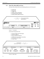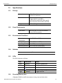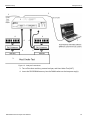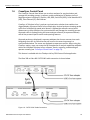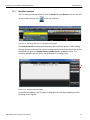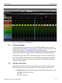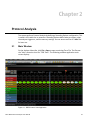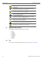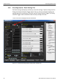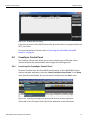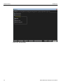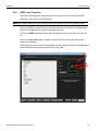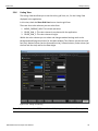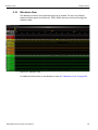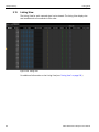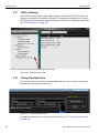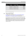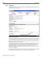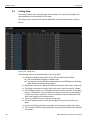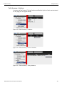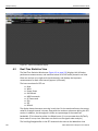
1
Kibra DDR Protocol Analyzer Suite User Manual Software Version 2.40 Document Version 2.40 November 2013 Teledyne LeCroy Protocol Solutions Group Trademarks and Servicemarks Teledyne LeCroy, Kibra and BusEngine are trademarks of Teledyne LeCroy, Inc. Microsoft and Windows are registered trademarks of Microsoft Corporation. Intel and Pentium are registered trademarks of Intel Corporation. All other trademarks and registered trademarks are property of their respective owners. THE SPECIFICATIONS AND INFORMATION REGARDING THE PRODUCTS IN THIS MANUAL ARE SUBJECT TO CHANGE WITHOUT NOTICE. ALL INFORMATION, EXAMPLES AND RECOMMENDATIONS IN THIS MANUAL ARE BELIEVED TO BE ACCURATE BUT ARE REPRESENTED WITHOUT WARRANTY OF ANY KIND, EXPRESS OR IMPLIED. USERS ARE FULLY RESPONSIBLE FOR THEIR APPLICATION OF ANY PRODUCTS. THE SOFTWARE LICENSE AND LIMITED WARRANTY FOR THE ACCOMPANYING PRODUCT ARE SET FORTH IN INFORMATION THAT SHIPPED WITH THE PRODUCT AND ARE INCORPORATED HEREIN BY THIS REFERENCE. IF YOU ARE UNABLE TO LOCATE THE SOFTWARE LICENSE OR LIMITED WARRANTY, CONTACT Teledyne LeCroy FOR A COPY. © 2011 Teledyne LeCroy, Inc. All rights reserved. This document may be printed and reproduced without additional permission, but all copies should contain this copyright notice. WEEE Program Teledyne LeCroy 3385 Scott Blvd. Santa Clara, CA 95054 TEL: 800‐909‐7112 (USA and Canada) TEL: 408‐653‐1260 (worldwide) Kibra DDR Protocol Analyzer User Manual ii Contents Chapter 1: Introduction...........................................................................................9 1.1 Kibra 380 or Kibra 480 Overview........................................................................................... 9 1.1.1 Receiving Your Kibra 380 or Kibra 480 .......................................................................................................9 1.1.2 Unpacking the Kibra 380 or Kibra 480 ......................................................................................................10 1.1.3 Kibra 380 or Kibra 480 Features ................................................................................................................10 1.1.4 Difference between Kibra 380 or Kibra 480 ..............................................................................................11 CMD/ADD/CNTRL Bus and Process JEDEC Protocol ..................................................................... 11 Clock-Based Timing............................................................................................................................ 11 DIMM Slot Protocol ............................................................................................................................. 11 1.1.5 Trigger..........................................................................................................................................................11 1.1.6 Kibra 380 or Kibra 480 Front Panel ...........................................................................................................12 1.2 Specifications ....................................................................................................................... 13 1.2.1 Package........................................................................................................................................................13 1.2.2 Power Requirements ..................................................................................................................................13 1.2.3 Environmental Conditions .........................................................................................................................13 1.2.4 Switches.......................................................................................................................................................13 1.2.5 LEDs .............................................................................................................................................................13 1.2.6 Recording Memory Size .............................................................................................................................13 1.3 Installing Your Kibra 380 or Kibra 480 Protocol Analyzer ................................................ 14 Software Installation ........................................................................................................................... 14 System Restart .................................................................................................................................... 14 Error Message ..................................................................................................................................... 14 1.4 Hardware Setup .................................................................................................................... 14 1.4.1 Connecting in General................................................................................................................................14 Power on Procedure ........................................................................................................................... 17 1.5 DDR Interposer ..................................................................................................................... 17 1.5.1 Kibra 380 or Kibra 480 Slot 1 Interposer...................................................................................................18 1.5.2 Kibra 380 or Kibra 480 Slot 2 Interposer...................................................................................................19 1.5.3 External Trigger Out ...................................................................................................................................19 1.5.4 External Trigger In ......................................................................................................................................20 1.5.5 Low Latency Read/Write Trigger Out ........................................................................................................20 Kibra DDR Protocol Analyzer User Manual 1 Teledyne LeCroy Contents 1.5.6 Daisy Chaining ............................................................................................................................................21 Daisy Chaining .................................................................................................................................... 22 1.6 CrossSync Control Panel..................................................................................................... 23 1.7 Launching Your Kibra 380 or Kibra 480 Software ............................................................. 24 1.7.1 Establish Interface ......................................................................................................................................25 1.7.2 About............................................................................................................................................................27 1.8 Using the Software ............................................................................................................... 28 1.9 Protocol Analyzer ................................................................................................................. 29 1.9.1 Viewing Captured Data ...............................................................................................................................29 1.9.2 JEDEC Triggers...........................................................................................................................................30 Chapter 2: Protocol Analysis ...............................................................................31 2.1 Main Window......................................................................................................................... 31 2.2 Software Menus and Toolbar............................................................................................... 32 2.3 Application Menu Options ................................................................................................... 34 2.4 File.......................................................................................................................................... 34 2.5 Setup...................................................................................................................................... 35 2.6 Recording Options Setup .................................................................................................... 36 2.6.1 Recording Options - General Tab..............................................................................................................38 Product................................................................................................................................................. 38 Recording Type: Trigger Mode .......................................................................................................... 38 Snapshot Mode ................................................................................................................................... 38 Manual Trigger Mode .......................................................................................................................... 38 Event Trigger Mode............................................................................................................................. 39 Buffer Size ........................................................................................................................................... 39 Trigger Position................................................................................................................................... 39 Note ...................................................................................................................................................... 40 Trace Filename & Path........................................................................................................................ 40 Capture................................................................................................................................................. 40 2.6.2 Recording Options - Basic Settings Tab ..................................................................................................42 DRAM Type .......................................................................................................................................... 45 LRDIMM Support ................................................................................................................................. 45 Mirrored................................................................................................................................................ 45 ECC....................................................................................................................................................... 45 Encoded ............................................................................................................................................... 45 Follow MRS Settings........................................................................................................................... 46 Memory Controller .............................................................................................................................. 47 Active Ranks........................................................................................................................................ 49 Active Banks........................................................................................................................................ 49 2 Kibra DDR Protocol Analyzer User Manual Contents Teledyne LeCroy Command Filter Out............................................................................................................................ 51 Timing Violation Trigger..................................................................................................................... 52 Handling Timing Violation in MPR states (DDR4) ............................................................................ 57 Protocol Violation Trigger .................................................................................................................. 58 Alert Trigger (DDR4) ........................................................................................................................... 59 2.6.3 Recording Options - Advanced Triggers Tab...........................................................................................59 Command Trigger ............................................................................................................................... 61 RCW/BCW Commands Trigger .......................................................................................................... 61 Read/Write Trigger .............................................................................................................................. 62 Sequence Trigger................................................................................................................................ 63 Clock Present ...................................................................................................................................... 65 2.6.4 Recording Options - Memory Address Mapping Tab ..............................................................................66 Read/Write on Specific Address Trigger .......................................................................................... 67 Decoding Read/Write Commands in Waveform/Listing View......................................................... 69 Search on System Address................................................................................................................ 70 2.7 Devices .................................................................................................................................. 70 2.8 CrossSync Control Panel..................................................................................................... 71 2.8.1 Launching the CrossSync Control Panel .................................................................................................71 2.9 Preferences ........................................................................................................................... 72 2.9.1 General.........................................................................................................................................................73 2.9.2 DDR3 Lines Properties ...............................................................................................................................75 2.9.3 DDR4 Lines Properties ...............................................................................................................................76 2.9.4 Symbol Coloring .........................................................................................................................................77 2.9.5 Waveform View ...........................................................................................................................................78 2.9.6 Listing View .................................................................................................................................................79 2.9.7 Bank State View ..........................................................................................................................................80 2.9.8 RTS View......................................................................................................................................................82 2.10 Reset Interposers ............................................................................................................... 83 2.11 Init Phy................................................................................................................................. 83 2.12 Session ................................................................................................................................ 83 2.13 Analysis ............................................................................................................................... 84 2.14 Waveform View ................................................................................................................... 85 2.15 Listing View......................................................................................................................... 86 2.16 Bank State View .................................................................................................................. 87 2.17 Traffic Summary ................................................................................................................. 88 2.18 Timing Calculator View ...................................................................................................... 88 2.19 Last MRS Values................................................................................................................. 89 2.20 Row Usage Report.............................................................................................................. 89 2.21 Timing Violation Analysis .................................................................................................. 90 Kibra DDR Protocol Analyzer User Manual 3 Teledyne LeCroy Contents 2.22 Trace Info............................................................................................................................. 93 2.22.1 Recording Options Summary ..................................................................................................................94 2.23 Navigation ........................................................................................................................... 94 2.24 View...................................................................................................................................... 95 2.25 Window ................................................................................................................................ 95 2.26 Help ...................................................................................................................................... 96 Tell Teledyne LeCroy .......................................................................................................................... 96 User Manual (F1) ................................................................................................................................. 96 Video Tutorials .................................................................................................................................... 96 Display License Information .............................................................................................................. 96 Update License.................................................................................................................................... 97 Register Product Online ..................................................................................................................... 97 Check for Updates .............................................................................................................................. 97 Shortcut List ........................................................................................................................................ 97 About.................................................................................................................................................... 97 2.27 Example Files.................................................................................................................... 100 Run a Sample Analysis..................................................................................................................... 100 Saving a Trace................................................................................................................................... 102 Chapter 3: Viewer Display ..................................................................................103 3.1 Window Management ......................................................................................................... 103 3.2 Waveform View ................................................................................................................... 103 3.2.1 Clock Position Selection ..........................................................................................................................103 3.2.2 Viewport Slider in Navigation Bar ...........................................................................................................104 3.2.3 Snap to Edge .............................................................................................................................................105 3.2.4 Placing Cursors ........................................................................................................................................105 3.2.5 Zoom In and Zoom Out.............................................................................................................................106 3.2.6 Overlay Signals Mode...............................................................................................................................106 3.2.7 Zoom Box ..................................................................................................................................................107 3.2.8 Context Sensitive Menu ...........................................................................................................................109 3.2.9 Choosing Chip Select Color Highlighting...............................................................................................110 3.2.10 Timing and Protocol Violations .............................................................................................................111 3.2.11 Right-Click Functionality in Waveform View ........................................................................................113 Go to Next Gap .................................................................................................................................. 114 Goes to the next gap (see See “Gap Markers” on page 129)........................................................ 114 Go to Previous Gap........................................................................................................................... 114 Go to Marker ...................................................................................................................................... 114 Go to Cursor ...................................................................................................................................... 114 Go to Trigger ..................................................................................................................................... 114 Go to Time ......................................................................................................................................... 114 4 Kibra DDR Protocol Analyzer User Manual Contents Teledyne LeCroy Go to Selection.................................................................................................................................. 114 Set New Marker ................................................................................................................................. 114 Set and Edit New Marker .................................................................................................................. 114 Place Marker ...................................................................................................................................... 114 Edit This Marker ................................................................................................................................ 114 Edit Marker......................................................................................................................................... 114 Go to Next Transition [Alert] ............................................................................................................ 114 Go to Previous Transition [Alert]..................................................................................................... 114 Delete This Marker ............................................................................................................................ 115 Delete Marker..................................................................................................................................... 115 Delete All Markers ............................................................................................................................. 115 Add Lines........................................................................................................................................... 115 Delete Line [Alert] ............................................................................................................................. 115 Show/Hide Sub Signals .................................................................................................................... 115 Preferences........................................................................................................................................ 116 3.2.12 Markers ....................................................................................................................................................116 Creating Markers............................................................................................................................... 118 Signal Names Column ...................................................................................................................... 119 Cursors .............................................................................................................................................. 119 3.3 Viewport Slider/Navigation Bar ......................................................................................... 127 3.3.1 Traces Captured with Filtering Enabled .................................................................................................127 3.3.2 Gap Markers ..............................................................................................................................................129 3.4 Listing View......................................................................................................................... 130 3.5 Bank State View .................................................................................................................. 131 3.5.1 Supported States in the Bank View State ...............................................................................................131 Legend Display.................................................................................................................................. 132 Active States...................................................................................................................................... 133 Configuring Visible Banks ............................................................................................................... 134 Common Features of Bank State View and Waveform View ........................................................ 134 3.5.2 Views ..........................................................................................................................................................135 Maximum Zoomed In View ............................................................................................................... 135 Default Zoom Level ........................................................................................................................... 136 Maximum Zoomed Out View ............................................................................................................ 136 3.6 Traffic Summary ................................................................................................................. 137 Traffic Summary - Toolbar Tools..................................................................................................... 137 Traffic Summary - Commands ......................................................................................................... 138 Traffic Summary - Performance....................................................................................................... 140 Traffic Summary - Violations ........................................................................................................... 141 3.7 Timing Calculator View ...................................................................................................... 142 3.8 Last MRS Values................................................................................................................. 143 Kibra DDR Protocol Analyzer User Manual 5 Teledyne LeCroy Contents 3.9 Row Usage Report............................................................................................................. 144 Defining Target Row(s)..................................................................................................................... 145 Define Analysis Detail Parameters .................................................................................................. 146 Define Report Boundary................................................................................................................... 147 Cyclic Row Usage Report................................................................................................................. 147 3.10 Timing Violation Reanalysis ............................................................................................ 147 Chapter 4: Real Time Statistics .........................................................................149 4.1 Devices Dashboard ............................................................................................................ 149 4.2 Real-Time Statistics View .................................................................................................. 150 4.2.1 Real-Time Statistics Buttons ...................................................................................................................152 4.2.2 RTS Preferences .......................................................................................................................................153 4.2.3 RTS Print....................................................................................................................................................154 Appendix A: Application Note ...........................................................................155 5.1 DDR3 and DDR4 JEDEC Timing Violations Summary .................................................... 155 5.1.1 V01 - tRAS ACTIVATE to PRECHARGE command period (Min)...........................................................155 5.1.2 V02 - tRAS ACTIVATE to PRECHARGE command period (Max) ..........................................................155 5.1.3 V03 - tRRD ACTIVATE to ACTIVATE command period (DDR3 different bank, same rank) (DDR4 - same bank group) ......156 5.1.4 V04 - tFAW Four Activate Window ..........................................................................................................156 5.1.5 V05 - tRCDx ACTIVATE to internal read or write delay (same bank) ...................................................156 5.1.6 V06 - tWTP WRITE to PRECHARGE delay ..............................................................................................157 5.1.7 V07 - tRTPx READ to PRECHARGE delay ..............................................................................................157 5.1.8 V08 - tRP PRECHARGE to a Valid Command.........................................................................................157 5.1.9 V09 - tWRA WRA to a Valid Command....................................................................................................157 5.1.10 V10 - t RFC REFRESH to a Valid Command .........................................................................................158 5.1.11 V11 - tREFI REFRESH Interval ...............................................................................................................158 5.1.12 V12 - tRTR READ to READ delay (DDR3 - same rank) (DDR4 - same bank group)...........................158 5.1.13 V13 - tdrRTR READ to READ delay (different rank - same DIMM) ......................................................158 5.1.14 V14 - tddRTR READ to READ delay (different DIMM) ..........................................................................158 5.1.15 V15 - tRTW READ to WRITE delay (same rank)....................................................................................159 5.1.16 V16 - tdrRTW READ to WRITE delay (different rank, same DIMM) .....................................................159 5.1.17 V17 - tddRTW READ to WRITE delay (different DIMM) ........................................................................159 5.1.18 V18 - tWTR WRITE to READ delay ( DDR3 - same rank) (DDR4 - same bank group) .......................159 5.1.19 V19 - tdrWTR WRITE to READ delay (different rank, same DIMM) .....................................................159 5.1.20 V20 - tddWTR WRITE to READ delay (different DIMM) ........................................................................159 5.1.21 V21 - tWTW WRITE to WRITE delay ( DDR3 - same rank) (DDR4 - same bank group) .....................159 5.1.22 V22 - tddWTW WRITE to WRITE delay (different rank, same DIMM) ..................................................160 5.1.23 V23 - tddWTW WRITE to WRITE delay (different DIMM)......................................................................160 5.1.24 V24 - tXS SELF REFRESH EXIT to a Valid Command (without DLL) .................................................160 5.1.25 V25 - tXSDLL SELF REFRESH EXIT to a Valid Command (with DLL) ................................................160 6 Kibra DDR Protocol Analyzer User Manual Contents Teledyne LeCroy 5.1.26 V26 - tCKESR SELF REFRESH ENTRANCE to SELF REFRESH EXIT................................................160 5.1.27 V27 - tACTPDEN ACTIVE to POWER DOWN ENTRY ...........................................................................160 5.1.28 V28 - REFPDEN REFRESH to POWER DOWN ENTRY.........................................................................160 5.1.29 V30 - tPRPDEN PRECHARGE / PRECHARGE ALL to POWER DOWN ENTRY..................................161 5.1.30 V31 - tRDPDEN READ / READ AUTO to POWER DOWN ENTRY ........................................................161 5.1.31 V32 - tWRPDEN WRITE to POWER DOWN ENTRY ..............................................................................161 5.1.32 V33 - tWRAPDEN WRITE AUTO to POWER DOWN ENTRY ................................................................161 5.1.33 V34 - tXP POWER DOWN EXIT to a Valid Command without DLL .....................................................161 5.1.34 V35 - tXPDLL POWER DOWN EXIT to a Valid Command with DLL - DDR3.......................................161 5.1.35 V36 - tCKE Clock Enable minimum pulse width ..................................................................................162 5.1.36 V37 - tPD POWER DOWN ENTRY to POWER DOWN EXIT..................................................................162 5.1.37 V38 - tZQCS SHORT Calibration Sequence to a Valid Command ......................................................162 5.1.38 V39 - tZQOper ZQCL to a Valid Command............................................................................................162 5.1.39 V40 - tZQinit First ZQCL after Reset to a Valid Command ..................................................................162 5.1.40 V41 - tMRD MODE Register Set to Mode Register Set.........................................................................162 5.1.41 V42 - tMOD Mode Register Set Command to a Valid Command ........................................................163 5.1.42 V43 - tXPR First Clock Enable High after Reset to MRS......................................................................163 5.1.43 V44 - CCD-S Read to Read Delay (short) Different bank group, same rank DDR4 ..........................163 5.1.44 V45 - tWTW-DBGWrite to Write Delay (short) Different bank group; same rankDDR4....................163 5.1.45 V46 - tWTR- DBGWrite to Read Delay (short) Different bank group; same rank DDR4...................163 5.1.46 V47 - tRRD-SActivate to Activate Delay (short) Different bank group; same rankDDR4 ................163 5.1.47 V48 - tXS-FAST SRX to a Valid Command with DLL- DDR4................................................................164 5.2 Supplemental Timing Information..................................................................................... 164 5.2.1 tWR WR (write recovery for auto-precharge) .........................................................................................164 Appendix B: China Restriction of Hazardous Substances Table ...................165 Appendix C: How to Contact Teledyne LeCroy................................................167 Index:.................................................................................................................. 169 Kibra DDR Protocol Analyzer User Manual 7 Teledyne LeCroy 8 Contents Kibra DDR Protocol Analyzer User Manual Chapter 1 Introduction DDR3 and DDR4 are the third and fourth generation of Double Data Rate (DDR) SDRAM memory. It is a continuation of the DDR memory technology that delivers higher speeds, lower power consumption and heat dissipation. It is an ideal memory solution for bandwidth hungry systems equipped with dual and quad core processors. Memory is utilized in virtually every electronic device and DDR memory has become the memory of choice. Each generation of DDR memory has doubled the data rate while reducing power requirements. 1.1 Kibra 380 or Kibra 480 Overview The Kibra 380 or Kibra 480 Protocol Analyzer provides a platform for developing and debugging protocol issues in environments which allow DDR3 and DDR4 probing using the interposers connected to the front of the Kibra box. Currently, the Interposer Probes target DIMM and SODIMM sockets of various types. Contact Teledyne LeCroy for the most recent offerings of Interposers. DDR Command, control signals and address values are captured. No actual DDR data signals are captured. 1.1.1 Receiving Your Kibra 380 or Kibra 480 The analyzer package includes the following components: Kibra 380 or Kibra 480 identified in the packing list Kibra Quick Start Guide USB A‐B 2.0 cable, 2 meters DDR3 or DDR4 Slot 1 Interposer cable assembly with power connector, sold sepa‐ rately (UDIMM DDR3 version shown below as an example) Kibra DDR Protocol Analyzer User Manual 9 Teledyne LeCroy Kibra 380 or Kibra 480 Overview DDR3 or DDR 4 Slot 2 Interposer cable assembly, sold separately (UDIMM DDR3 version shown below as an example) Three‐Prong AC 12V, 5 Amp power brick CATC Sync Cable (DB‐9 Male to DB‐9 F) Installation CD‐ROM with software and documentation 1.1.2 Unpacking the Kibra 380 or Kibra 480 Inspect the received shipping container for any damage. Unpack the container and account for each of the system components listed on the accompanying packing list. Visually inspect each component for absence of damage. In the event of damage, notify the shipper and Teledyne LeCroy Corporation. Retain all shipping materials for shipper’s inspection. 1.1.3 Kibra 380 or Kibra 480 Features 10 Supports the JEDEC specification (JEDEC defines the DDR specification) Records CMD/ADD/CNTRL bus Clock based timing displays Fast upload Large sample capture – 4GB of Recording Memory ~500 Million Samples Triggers for JEDEC timing violations Triggers for JEDEC protocol violations User selectable command triggers User definable trigger sequence DDR3 and DDR4 Analysis Clock speeds of 400 ‐ 800MHz (Kibra 380), 400 ‐ 1200MHz (Kibra 480) DDR3 and DDR4 Transfer speeds of 800 ‐ 1600MT/s (Kibra 380), 800 ‐ 2400MT/s (Kibra 480) UDIMM/RDIMM/LRDIMM/SODIMM passive Interposer Metrics on performance, observed errors External Trigger In & Out External Read/Write Trigger Out Teledyne LeCroy CrossSync support Kibra DDR Protocol Analyzer User Manual Kibra 380 or Kibra 480 Overview 1.1.4 Teledyne LeCroy Difference between Kibra 380 or Kibra 480 1. Kibra 480 supports both DDR3 and DDR4 Interposers. Kibra 380 only supports DDR3 interposers. 2. The Kibra 380 version of the interposers requires a stable DIMM_CLK to properly sample the DIMM signals. If the DIMM_CLK is not running, the probe will require 6us after the DIMM_CLK resumes before proper capture occurs. This can occur when recording DDR traffic during platform boot or during self refresh mode. This limitation can cause RC and MRS commands to be missed. The Kibra 480 does not have this limitation. CMD/ADD/CNTRL Bus and Process JEDEC Protocol The Analyzer observes CMD/ADD/CNTRL bus and processes JEDEC protocol requirements in real‐time. Errors can be seen in the Waveform view or the Listings view as well as in the Traffic Summary. Errors listed in the Traffic Summary have a Hyperlink directly to the Waveform and Listing view to allow quick viewing of errors. Clock-Based Timing The Analyzer features clock‐based timing. The clock times are based on the nominal DIMM speed selected in the Recording Options and samples are synchronized to the DIMM clock. DIMM Slot Protocol The Kibra 380 or Kibra 480 are able to track the DIMM slot protocol. They also have the option to gather control signals from a second DIMM slot. 1.1.5 Trigger Provides triggers for Command Ordering Violations and State Violations as well as user selectable commands or command sequences. Trigger markers are accurate to clocks of the triggered event. Kibra DDR Protocol Analyzer User Manual 11 Teledyne LeCroy 1.1.6 Kibra 380 or Kibra 480 Overview Kibra 380 or Kibra 480 Front Panel The Kibra 380 and Kibra 480 have the following features on the front panel: Power LED Status LED Trigger LED Slots 1 and 2 for Interposers Interposer Power Connector Read and Write SMA Connectors Figure 1.1: Front Panel On the back the Analyzers have: External Trigger Input and Output Reference Clock In Sync In and Out Connectors USB Port for host machine connectivity DC Input 12‐volt, 5 Amps Power Switch Figure 1.2: Back Panel 12 Kibra DDR Protocol Analyzer User Manual Teledyne LeCroy Specifications 1.2 Specifications 1.2.1 Package Dimensions 10.0 x 8.5 x 1.9 inches (25.5 x 21.5 x 4.8 cm) DC power connection Trigger IN/OUT input (BNC) host machine connection (USB, type B) Data connector (Data In/Out, 9‐pin DB) 2.6 lbs. (1.1 kg) Connectors Weight 1.2.2 Power Requirements Input Power 1.2.3 1.2.4 1.2.5 90 to 254 VAC, 47 to 63 Hz (universal input), 100 W maximum Environmental Conditions Operating Temperature Storage Range Operating Humidity Operating Altitude 0 to 55°C (32 to 131°F) ‐20 to 80°C (‐4 to 176°F) 10 to 90%, non‐condensing Up to 6560 feet (2000 meters) Power on/off Switches LEDs The LEDs illuminate as follows: LEDs Power Status Trigger 1.2.6 Illumination (Green) (Red) (Solid Blue) (Flashing Blue) (Yellow) Status Analyzer is powered on Analyzer failed to boot Analyzer is ready Downloading bus engine Trigger occurred Recording Memory Size 4 Gigabyte DRAM for traffic data capture, timing, state and other data Kibra DDR Protocol Analyzer User Manual 13 Teledyne LeCroy 1.3 Installing Your Kibra 380 or Kibra 480 Protocol Analyzer Installing Your Kibra 380 or Kibra 480 Protocol Analyzer Software Installation The software works on systems using the Windows® XP, Windows 8, and Windows 7 32‐ or 64‐bit operating systems. 1. Insert the Installation CD‐ROM into the CD drive on the host machine. 2. The installation automatically starts setup, unless Auto Run is off. In that case, select the CD‐ROM from “My Computer” and click Setup. 3. After the warning to close all other programs and before starting the installation, the Install component selection opens. 4. Select components for installation. 5. Click Next to complete the installation. System Restart It is recommended that you restart your host machine before you use your Analyzer software. Error Message If you get an error message during installation of the drivers for Window, consult your system administrator. Your system may allow only administrator‐level users to copy such driver files. 1.4 Hardware Setup 1.4.1 Connecting in General Note: You must install the software before connecting the analyzer to the host machine for the first time. To set up the analyzer: 1. Connect the analyzer to a 100V–240V, 50Hz–60Hz, power outlet, using the supplied 12‐volt power brick, and turn on the Power switch. At power on, the analyzer will go through initialization as shown on the application screen. 2. Connect the USB cable between the Kibra 380 or Kibra 480 and a USB port on the host machine. The host machine’s operating system detects the analyzer and driver files. 14 Kibra DDR Protocol Analyzer User Manual Teledyne LeCroy Hardware Setup 2 1 3 4 4 6 7 6 5 5 3 Figure 1.3: Analyzer Connections 3. Turn off the host machine, protocol analyzer, and Host Under Test (HUT). 4. Insert the DDR SDRAM memory into the DIMM socket on the interposer top(s). Kibra DDR Protocol Analyzer User Manual 15 Teledyne LeCroy Hardware Setup 5. Insert the DDR Slot 1 Interposer, and (if desired) DDR Slot 2 Interposer, into the HUT DIMM‐socket slot(s) farthest from the CPU. Only one channel with up to two slots is supported with a single Kibra DDR analyzer. Normally the DIMM connectors for two slots in the same channel on a PC have the same color. 6. For the Slot 1 Interposer, connect the ribbon cable to Slot 1 and the power cable to Interposer Power, both on the front of the protocol analyzer. For the Slot 2 Interposer, connect the ribbon cable to Slot 2 on the front of the protocol analyzer. IMPORTANT! Please see the “Power on Procedure” on page 17 before performing step 7. 7. Turn on the host machine and the protocol analyzer. Open the DDR Protocol Suite. 8. Select Recording Options under Setup on the Menu Bar. 9. Select the General tab to display the factory default settings, such as Snapshot and 30‐MB buffer size. Use the default settings. 10. Select the DIMM Parameters and Violation Triggers tab. In the Memory Controller section, select the properties of the DIMM to analyze, including the DIMM Speed and CAS Latencies. Uncheck the Timing Violation Trigger checkbox to cancel triggers. Uncheck the Protocol Violation Trigger checkbox to cancel triggers. Click OK to use the defaults for all other settings. 11. The HUT can be turned on either now or after recording starts. 12. Click Start Recording on the Tool Bar. The system starts to capture DDR command, control, and address signals. After 30 MB of traffic are recorded, the Analyzer uploads the data and displays the packets. 13. To terminate recording before the snapshot automatically completes, click Stop Recording on the Tool Bar. 14. When the recording session is finished, the traffic is automatically uploaded from the Analyzer to the hard drive on your host machine as a file named data.ddrt (or the name you assigned as the default filename). While the file is being uploaded, you should see a progress bar at the bottom of the screen. When the bar disappears, it indicates that the data has been uploaded to disk. 15. To save a current recording for future reference, select File > Save As, or click on the Tool Bar, to display the standard Save As screen. Give the recording a unique name and save it to the appropriate directory. 16 Kibra DDR Protocol Analyzer User Manual Teledyne LeCroy DDR Interposer Power on Procedure 1. Start the DDR Protocol Suite application. 2. Make sure the DDR Interposer(s) is/are attached securely to the Kibra unit. 3. Verify that either: Interposers are not inserted into the system under test. OR Interposers are inserted into the system under test AND power is OFF on the system under test. 4. Power On the Kibra unit and wait until the Phy's have completed initialization. 5. Power On the system under test. 1.5 DDR Interposer The Kibra Interposers sit between the Host Under Test (HUT) DIMM slots and the DIMMS under test. The interposers add less than 1 inch of trace length and a resistive tap to minimize effects on signal quality while ensuring an adequate signal for the Analyzer. Cable to Analyzer DIMM DIMM Interposer Figure 1.4: DDR Interposer Kibra DDR Protocol Analyzer User Manual 17 Teledyne LeCroy 1.5.1 DDR Interposer Kibra 380 or Kibra 480 Slot 1 Interposer Protocol Checking is performed on up to 4 ranks, in a single slot. Mode register capture is supported on up to 8 ranks, in 1 or 2 slots. The Kibra 380 Slot 1 Interposer is shown below. Figure 1.5: Slot 1 Interposer Figure 1.6: Slot 1 Interposer with DIMM 18 Kibra DDR Protocol Analyzer User Manual Teledyne LeCroy DDR Interposer 1.5.2 Kibra 380 or Kibra 480 Slot 2 Interposer Interactions among up to 8 ranks over two slots are analyzed. The Kibra 380 Slot 2 Interposer is shown below. Do not leave the second interposer connected if it is not probing a DIMM on the HUT. Leaving it unconnected will cause some signals to float, causing false errors to be reported in the trace. Figure 1.7: Slot 2 Interposer 1.5.3 External Trigger Out Pulse Width = 280 ns Pulse Voltage = 3.3 Volts into 1 MegOhms Pulse Voltage = 2.7 Volts into 50 Ohms Pulse is positive going. Accumulated Latency from DDR Event to Pulse out at SMA terminal: DIMM_CLK=400MHz 125 ns DIMM_CLK=533MHz 105 ns DIMM_CLK=667MHz 105 ns DIMM_CLK=800MHz 100 ns All measurements are 10 ns Kibra DDR Protocol Analyzer User Manual 19 Teledyne LeCroy 1.5.4 DDR Interposer External Trigger In Edge detected. (Rising edge only) Voltage required: Signal needs to be > 800mV to see a logic "1" Signal needs to be < 400mV to see a logic "0" Accumulated Latency from SMA terminal to Recognition in FPGA: 70 ns (+/‐10 ns). Always active in Manual or Event Trigger mode, no additional software setting is required. An input voltage of is 540mV +/‐100 will cause a trigger condition which will be identified in the trace file. The latency on this trigger is approximately 120 ns. 1.5.5 Low Latency Read/Write Trigger Out The low‐latency SMA trigger out ports on the front of the analyzer operate continuously on Read/Write operations. The pulse occurs as soon as the Kibra 380 or Kibra 480 interposer is powered on. The analyzer SW does not need to be actively recording. The settings in the recording options tab have no effect on the low‐latency SMA trigger out feature. The Read/Write trigger out ports on the front of the analyzer generate a very short pulse width of about 1.25 ns (for 800 MHz DDR3) and relatively low amplitude of 560 mVp‐p (after 1‐m cable). This trigger out signaling differs from the LVTTL Trigger out on the back of the analyzer in order to shorten the cycle time when triggering on back‐to‐back Read or Write operations. This trigger out signaling is designed to allow the end user to initiate an acquisition on an oscilloscope and then use the trigger marker in the waveform to correlate transmission of the read or write commands with the actual DQ/DQS signals. The R/W trigger out latency is dependent on the signaling frequency: At DIMM Clock = 800 MHz/1600MTs: Delay is about 39.2 ns. At DIMM Clock = 667 MHz/1333MTs: Delay is about 42.2 ns. At DIMM Clock = 533 MHz/1066MTs: Delay is about 47.4 ns. *Plus the 2ns per foot for the SMA cable length 20 Kibra DDR Protocol Analyzer User Manual Teledyne LeCroy DDR Interposer 1.5.6 Daisy Chaining You can use multiple analyzer units for higher port count, by daisy chaining the units through the provided Sync In/Out interfaces on the analyzer back. Connect “Out” connectors to “In” connectors of the next unit in the chain. You must provide external hubs for connecting the host machine to these units using USB cables. You can daisy chain up to four units. Note: Because chain connections for daisy chained boards cause delay of signals, traffic on different boards is not completely time synchronized, with about 100 nanoseconds of difference between consecutive boxes. Kibra DDR Protocol Analyzer User Manual 21 Teledyne LeCroy DDR Interposer Daisy Chaining To set up the units in a daisy chain: 1. Plug in one end of the CATC Sync cable to the CATC Sync Out connector of one unit, and the other end to the CATC Sync in connector of another. To connect another unit continue this chain (see Figure 1.8). 2. The software will recognize the connections automatically. Figure 1.8: Daisy Chaining Units using CATC Sync Cable and CATC Connectors 22 Kibra DDR Protocol Analyzer User Manual CrossSync Control Panel 1.6 Teledyne LeCroy CrossSync Control Panel The CrossSync Control Panel allows you to select analyzers for synchronization and manage the recording process. It supports a wide combination of Teledyne LeCroy’s flagship analyzers including PCI Express, USB, DDR, Serial ATA (SATA), Serial Attached SCSI (SAS), Fibre Channel (FC) and Ethernet. CrossSync is Teledyne LeCroy’s analyzer synchronization solution that enables time‐ aligned display of protocol traffic from multiple daisy‐chained analyzers showing packet traffic from multiple high‐speed serial busses. A lightweight software control panel allows users to select analyzers for synchronization and manage the recording process. Captured traffic is displayed using the latest analyzer software (in separate windows) with all the protocol specific search and reporting features. Captured packets are displayed in separate windows that share a common time scale. Navigating the traffic in either direction will scroll to the same timestamp in a synchronized window. The traces are displayed as separate trace files. When using the CrossSync option, users can access the full complement of analysis capabilities available within the individual Teledyne LeCroy software. Search, reporting, and decoding all operate normally (see “CrossSync Control Panel” on page 71). This feature is available with the Teledyne LeCroy DDR Protocol Suite application. The Kibra 380 or Kibra 480 CATC SYNC cable connection is shown below. Figure 1.9: CATC SYNC Cable Connection Kibra DDR Protocol Analyzer User Manual 23 Teledyne LeCroy 1.7 Launching Your Kibra 380 or Kibra 480 Software Launching Your Kibra 380 or Kibra 480 Software To launch the software, double‐click the DDR Protocol Suite Icon in the Program Manager Window, or select DDR Protocol Suite from the Start > Programs >LeCroy menu. The following screen displays. The Device Bar has the following panes as shown in the following figure. 1. 2. 3. 4. 1 Device: Shows attached device by Serial Number Quick Recording Options: Enables Trigger and Buffer settings Recording Control and Status: Start, Stop and Pause recording and view status. Real Time Statistics: View the statistics while recording. 2 3 4 Figure 1.10: Main Screen 24 Kibra DDR Protocol Analyzer User Manual Teledyne LeCroy Launching Your Kibra 380 or Kibra 480 Software 1.7.1 Establish Interface The first time you run your software, click on Setup and select Devices. You can also click on the Analyzer Devices icon on the top menu bar. Figure 1.11: Setting up Devices on Launching the Analyzer The Analyzer Devices window opens displaying the connected devices. A blue shading through the entry indicates that a device is being selected, and this device will be the one used when you select the Update Device, Update License, or About buttons. The checkbox indicates that this device can participate in recording traces. Figure 1.12: Analyzer Devices Dialog It automatically detects if the Firmware or BusEngine version needs updating and the following screen displays. Kibra DDR Protocol Analyzer User Manual 25 Teledyne LeCroy Launching Your Kibra 380 or Kibra 480 Software Figure 1.13: Device Update Dialog 1. Click Yes. The Update Device dialog displays. Figure 1.14: Device Update Dialog 2. Select a device by clicking the applicable box to the left of it and click Update Selected. Note: You may choose to update all the devices by clicking Update All. The following Update Device dialog displays. Figure 1.15: Device Update Dialog during Update The following screen displays once the update is complete. Click OK to for the update to take effect. 26 Kibra DDR Protocol Analyzer User Manual Launching Your Kibra 380 or Kibra 480 Software Teledyne LeCroy Note: It is possible to use more than one Kibra 380 or Kibra 480 System to monitor additional DDR3 or DDR4 memory channels. Check the box next to all attached Kibra 380 or Kibra 480 in this window to enable capture from additional analyzers. 1.7.2 About The Help > About menu option provides current details of the hardware, software, firmware and bus engine. Figure 1.16: About DDR Protocol Suite Note: In the event the Kibra 380 or Kibra 480 system contains firmware that is down‐rev or not supported in the installed version of software, the about box will indicate this by showing the firmware revision number in red (see figure above.) Select Setup > Devices and choose Update Device to install the firmware supported in the installed version of software. Kibra DDR Protocol Analyzer User Manual 27 Teledyne LeCroy Using the Software The box now indicates the correct revision number in green as shown below. Figure 1.17: About DDR Protocol Suite showing updated version 1.8 Using the Software The Kibra 380 or Kibra 480 application has protocol analysis software (see Figure 1.18 on page 29) to capture data, trigger and view data (See “Protocol Analysis” on page 31). 28 Kibra DDR Protocol Analyzer User Manual Teledyne LeCroy Protocol Analyzer Figure 1.18: DDR Protocol Suite Application 1.9 Protocol Analyzer To use the software for protocol analysis, first select File > Open to open an existing protocol analysis .ddrt file (See “Protocol Analysis” on page 31). You can also open a .ddrt sample file. In Windows 7 and Windows 8 example files are located in C:\Users\Public\Documents\LeCroy\DDR Protocol Suite\Data\Examples. In Windows XP sample files are located in \Program Files\LeCroy\DDR Protocol Suite\Data\Examples The Kibra 380 or Kibra 480 detects 67 Protocol violations real time over all banks and ranks that total 300+ individual checks. Protocol Checking is supported on channels of one or two slots. Channels of more than two slots require cascaded Kibra Analyzers to monitor the additional slots. 1.9.1 Viewing Captured Data After opening the .ddrt trace file, the captured data can be viewed. This data is event based and reflects events in time therefore, it cannot be viewed in a packet format. Waveform View shows the following signals and decodes these signals into com‐ mand address and control busses. Clock Protocol Violation Kibra DDR Protocol Analyzer User Manual 29 Teledyne LeCroy Protocol Analyzer Timing Violation DDR Command CKS Command Value Chip Select Address BA BG ODT RESET Parity Error Parity RefClkIn (if selected in Recording Options) Listing View shows the same data in a list format in columns. The listing view shows the decoding of each of the buses on a sample by sample basis. Bank State View displays a Bank by Bank view of the changing bus states. It is separated by bank to enable a more insightful picture of the activity in a way that is often obfuscated in a waveform view. Traffic Summary View gives a tabulation of commands by Rank, bank; perfor‐ mance statistics, and timing and protocol violations. Results Hyperlink back to points of occurrence within the Waveform, Listing and Bank State views. Statistical display: Bandwidth, Reads, Writes, all commands (total and % of total) Kibra Supports Traffic Summary: Reads (Total, by Bank) Writes (Total, by Bank) % Total and by Bank. Timing Calculator View is used to measure the differential time between two Triggers or two Markers Last MRS Values shows the last MRS setting in the trace. Row Usage Report is a powerful analysis tool which provides a detailed report on how rows are accessed during the captured trace Violations Protocol violations JEDEC Timing violations 1.9.2 JEDEC Triggers A library of JEDEC triggers are included in the Kibra 380 or Kibra 480 application. Based on DIMM Parameters defined during recording, the Kibra 380 or Kibra 480 Protocol Analyzer Application will apply the JEDEC defined values for violations triggers and software detection. 30 Kibra DDR Protocol Analyzer User Manual Chapter 2 Protocol Analysis The system performs Protocol Analysis by defining a Recording Options configuration. This is saved in a file with the .ro extension. Recording Options define what to capture, what the analyzer triggers on, and the memory settings. You can save trace files as *.ddrt files for later use. 2.1 Main Window On the Analyzer Menu Bar, click File > Open to open an existing Trace File. The files use the ".ddrt" extension short for "DDR Trace". The following software application main screen displays. Figure 2.1: DDR Protocol Suite Application Kibra DDR Protocol Analyzer User Manual 31 Teledyne LeCroy 2.2 Software Menus and Toolbar Software Menus and Toolbar The software has the following main toolbar. Each icon is explained in the table below. Standard Menu Options Analyzer Session Menu Options Analysis Menu Options Navigation Menu Options Navigator Bar Viewport Slider Scroll Left Scroll Right Figure 2.2: Main Toolbar The software and the menu toolbar options are given in the following table. Open icon. Click to open a file. Refer to “File” on page 34. Scroll Left and Right arrows. These arrows enables moving left and right across the view. Viewport Slider (only in WaveForm View). The slider enables moving across the view. Refer to “Viewport Slider/Navigation Bar” on page 127. Save icon. Click to save a file. Refer to “File” on page 34. Recording Options icon. Refer to “Recording Options ‐ General Tab” on page 38. Device icon. Refer to “Devices” on page 70. Start icon. Click to start a recording. Stop icon. Click to stop a recording. Abort icon. Click to abort a recording. Stops recording without any upload or trace file creation. 32 Kibra DDR Protocol Analyzer User Manual Teledyne LeCroy Software Menus and Toolbar Manual Trigger. Click to initiate a manual trigger. Repeat Upload icon. Click to repeat upload. Preferences icon. Click to open the Display/View Configuration dialog (see “Preferences” on page 72). Hide Deselects/NOPs icon. Hides the captured DES (Deselects) and NOP command states to remove extra space from the viewing window. These commands are replaced by a cross‐hatch pattern, similar to how we represent DES/NOP's that were filtered in hardware during capture. Synchronize All Views icon. Click to synchronize the positions of the currently selected clock value in all views. Manage Synced Traces icon. Click to synchronize the times between multiple traces which were captured at the same time using CATC Sync cable as shown in Figure 1.8 on page 22. Waveform View icon. Click to display the Waveform View (see “Waveform View” on page 78). Listing View icon. Click to display the Listing View (see “Listing View” on page 79). Bank State View icon. Click to display the Bank State View (see “Bank State View” on page 80). Traffic Summary View icon. Click to display the Traffic Summary View (see “Traffic Summary” on page 137). Timing Calculator View icon. Click to display the Timing Calculator View (see “Waveform View” on page 103). Last MRS Values View icon. Click to display the MR Values View (see “Last MRS Values” on page 143). Row Usage Report icon. Click to display the Row Usage Report (see “ Row Usage Report” on page 144). Timing Violation Analysis icon. Click to display the Timing Violation Analysis View (see “Timing Violation Reanalysis” on page 147). Trace Information icon. Click to display the Trace Information dialog. GoTo Any Time icon. Click to display the GoTo Time dialog (see “Markers” on page 116). Goto Trigger icon. Click to go to a trigger (see “Recording Type: Trigger Mode” on page 38). Kibra DDR Protocol Analyzer User Manual 33 Teledyne LeCroy Application Menu Options GoTo Selection Point icon. Click to go to selection (see “Markers” on page 116). Goto Marker icon. Select from the drop‐down list to go to a specific cursor (see “Markers” on page 116). Goto Cursor icon. Select from the drop‐down list to go to a specific cursor (see “Cursors” on page 119). Back to the previous navigated position icon. Click to go back to the next navigated position. Forward to the previous navigated position icon. Click to go forward to the previously navigated position. Find icon. You can search for DDR Commands, Protocol or Timing Violations (see “Find” on page 120). Find Previous icon. Searches for the previous instance. Find Next icon. Searches for the next instance. 2.3 Application Menu Options The following menu options are described in this section: 2.4 File Setup Session Analysis Navigation View Window Help File The File menu has the standard menu options as shown in Figure 2.3 on page 35. 34 Kibra DDR Protocol Analyzer User Manual Teledyne LeCroy Setup Figure 2.3: File Menu Options Open Close Save Save as Export To CSV Export To DDRX Exit 2.5 Click to open an existing trace or sample files. Click to open an existing trace or sample files. Click to save an existing trace or sample files. Click to save an existing trace or sample files with a different name or directory. Export file in .CSV format. Export file in .DDRX format. Export raw captured data in .DDRX file format for offline processing. The .DDRX file format is available to users who would like to process the signal data for their own analysis. It is a very fast way of getting access to the data for this purpose. The format of this file is documented in the app note "DDRX_FileFormat.pdf", which is included in your installation. Click to exit the application. Setup The Setup menu has the following options to setup and configure the device (see Figure 2.4 on page 36): Recording Options Devices Launch CrossSync Control Panel Preferences Reset Interposers Init Phy Each of these options are described in the following section. Kibra DDR Protocol Analyzer User Manual 35 Teledyne LeCroy Recording Options Setup Figure 2.4: Setup Menu Option 2.6 Recording Options Setup The Recording Options menu enables you to select the device. Click Setup > Recording Options > and select the product (see Figure 2.5). In the following example the ‘LeCroy Kibra DDR Analyzer SN:63373 is selected. Figure 2.5: Recording Options Menu You can also click on the Recording Options icon on the top menu bar. The Recording Options Dialog has three tabs. The General tab enables you to set the general recording configurations. The Basic Settings tab displays the Memory Controller settings, Capture settings and the Timing and Protocol Violation Trigger values. The third tab, Advance Triggers allows to set the Command Trigger, Command Filter‐Out and Read/ Write Trigger (see Figure 2.6 on page 37). 36 Kibra DDR Protocol Analyzer User Manual Teledyne LeCroy Recording Options Setup Click to toggle to show/hide the right pane Figure 2.6: Recording Options Dialog: General Tab The project overview pane is on the right panel of the Recording Options dialog. This pane is displayed in all the three tabs for the Recording Options dialog. It gives an overview of the Options selected and their Values. To hide this pane click on the vertical bar on the left of this pane. The bar acts as a toggle to show and hide the pane. See the right pane in Figure 2.6.In the Recording Options dialog tooltips are available in the Basic Settings and Advance Triggers Tabs. Tooltips are also displayed on the right panel displaying the Options and Values. Hold mouse over fields to display tooltip. Kibra DDR Protocol Analyzer User Manual 37 Teledyne LeCroy 2.6.1 Recording Options Setup Recording Options - General Tab The following settings can be set from the General tab. The options on the General tab are explained below. Product Select a product for the recording options from either Kibra 380 Protocol Analyzer or Kibra 480 Protocol Analyzer. Recording Type: Trigger Mode The Trigger Recording Options dialog allows you to specify when the analyzer completes a data capture. Three trigger modes are available: The default Snapshot, Manual Trigger, and Event Trigger. When data capture starts with Snapshot selected, the analyzer triggers on the first data pattern on the bus. Starting a data capture with Event selected triggers when specific event(s) are detected in the captured data stream. The following three ways can trigger the analyzer with Event selected: Trigger on Specific DDR3 or DDR4 Commands Trigger on DDR3 or DDR4 Protocol or Timing Violations External Trigger‐in (from other test equipment) Figure 2.7: Trigger Setup Snapshot Mode To capture immediately on any trace, check the Snapshot button. Manual Trigger Mode In the Manual Trigger mode, the analyzer captures bus traffic continually from when you use the Start button until you click the Manual Trigger button (on the analyzer toolbar), which triggers the analyzer. To perform a manual trigger, click the Manual Trigger button. This selection also enables the External SMA Trigger function. 38 Kibra DDR Protocol Analyzer User Manual Recording Options Setup Teledyne LeCroy Event Trigger Mode In Event Trigger mode, the Analyzer triggers whenever any of the events selected for triggering occurs (an OR condition). The procedure for selecting trigger parameters is identical to that for selecting capture parameters. All items selected for triggering appear in the Project Overview pane. This selection also enables the External SMA Trigger function. Note: Triggers shown in the Waveform and Listing views have a precision of clocks during normal traffic (when Clock Enable is stable). Buffer Size The Analyzer Settings tab has the Buffer Size field where you can set the buffer size. The defaults are one segment of 30MB (or 3.75Msamples). The total size used is automatically displayed for you. You can use the slider button or click the up or down arrow to change memory usage for recording trace data. (Minimum size of memory is 1MB. Maximum size of Memory is 4GB (~512Mega Samples)). It is recommended that you limit the size of the capture buffer to half of the memory of your host machine to achieve the best performance. Trigger Position This defines the portions of the buffer which are used before and after the trigger. (It does not apply to snapshot recordings.) Post-Trigger You can set the amount of data to capture before and after the trigger, as a percentage of pre‐trigger, between 1% and 99%. Position the post‐trigger slider to a percentage. This feature allows the evaluation of bus activity leading up to and after the triggering Event. Post‐trigger data is capture of the specified percentage of data after the triggering Event. It cannot be guaranteed and may be 0. This can occur for example, when the trigger event occurs and the system halts operation preventing any post trigger data from being collected. In such a case, the data display shows fewer than the specified data points after the triggering Event. Kibra DDR Protocol Analyzer User Manual 39 Teledyne LeCroy Recording Options Setup Note To enter and save information about the current project, add a project note in the Note pane and enter the data about the project. Figure 2.8: Project Notes Field Trace Filename & Path Click the Change Default Location button in the Trace Filename & Path field and choose a file name and location for the results of your current project. The trace files can only be saved as .ddrt files. You must select a location that is considered “writeable” to the operating systems. Figure 2.9: Trace File Name Capture There are three possible options for capturing a trace: DDR Signals Only, DDR Signals with Ref Clk In, and Ref Clk In Only. DDR Signals This should be the default capture mode for DDR analysis. Select from either DDR3 or DDR4. Ref Clock In This will edge‐detect a clock at the Ref Clock In SMA connector and show it in the Waveform View. It requires a minimum 10ns period. The resulting display in the Waveform view will make it appear as a short pulse at each edge‐detection point. 40 Kibra DDR Protocol Analyzer User Manual Teledyne LeCroy Recording Options Setup Ref Clock In Pulse Type Select the Ref Clock In Pulse Type is at the Rising or Falling Edge. The default setting is Rising Edge. Note that the other edge will be ignored. Figure 2.10: Capture Settings Check the DDR Signals check‐box (click the DDR3 or DDR4 radio button) and/or the Ref Clock In checkbox to select it. Choose the Rising Edge or Falling Edge to capture the Ref Clock In Pulse Type (refer to Figure 2.6 on page 37). Capture Mode Check the Normal Capture or Raw, no processing check‐box to select it. Normal capture uploads raw data and processes it. Raw, no processing captures directly to a raw, unprocessed file, which is very fast. This is done if a user wants to export to a .DDRX file for their own processing. The following options are available: Save As.. ‐ Opens the Save Display Configuration File dialog to save the changes made to the Preferences for future use. They can be saved in the default location or you assign a name and save in a library. Save as Default ‐ Click this button to restore the settings to the factory presets. Load... ‐ Allows you to load the saved Preferences from the default location or the library for the current session. Restore Factory Settings ‐ Click this button to restore the settings to the factory presets. OK ‐ Saves the current Preferences. Cancel ‐ Click this button to cancel any settings just made. Apply ‐ Applies the changes made to the open trace file. Note: Preferences from version 1.20 and above should be usable/upgradable in future versions, but those made with releases below 1.20 should be deleted as they are not forward compatible. Kibra DDR Protocol Analyzer User Manual 41 Teledyne LeCroy 2.6.2 Recording Options Setup Recording Options - Basic Settings Tab The Basic Settings tab displays the Memory Controller settings, Capture settings and the Timing and Protocol Violation Trigger values. There is a direct correlation between the settings selected in the Memory Controller and the Timing Violation Trigger. The Timing Violation Trigger values are based on what memory settings are made. Click on this icon to display the SPD information Figure 2.11: DDR3 Recording Options Dialog: Basic Settings Tab 42 Kibra DDR Protocol Analyzer User Manual Recording Options Setup Teledyne LeCroy Click on this icon to display the SPD information Figure 2.12: DDR4 Recording Options Dialog: Basic Settings Tab Click on the SPD (Serial Presence Detect) icon to view the SPD information as shown above to display the SPD information window (see Figure 2.13 on page 44). This feature is available on interposers which support SPD capture. Only the Kibra 380 DDR3 UDIMM does NOT support SPD reading. Kibra DDR Protocol Analyzer User Manual 43 Teledyne LeCroy Recording Options Setup Figure 2.13: SPD Information 44 Kibra DDR Protocol Analyzer User Manual Teledyne LeCroy Recording Options Setup DRAM Type Select the DRAM Type from the following options in the dropdown menu: For DDR3: UDIMM SODIMM RDIMM LRDIMM SORDIMM For DDR4: UDIMM SOUDIMM RDIMM LRDIMM Note: For RDIMMS, the RCD commands will be decoded. LRDIMM Support LRDIMMs support two different addressing schemes. When selecting LRDIMM, you must specify which addressing scheme your system and DIMMs support. Click the checkbox to select it. Use CS2 as A16 in both slots Use CS3 as A17 in both slots Mirrored Select the Mirrored check‐box to Trigger and Display data correctly for a UDIMM which has a Mirrored configuration. ECC Check the ECC box if your system uses Error Correction Coding. Encoded Selecting this checkbox (see Figure 2.14 on page 46) for DDR4 LRDIMM or RDIMM indicates the Encoded Quad CS should be used for mapping ranks. It uses the following truth table: CS[0]_n : CS[1]_n : C[0] : Actual Rank 0 : 1 : 0 : Rank 0 0 : 1 : 1 : Rank 1 1 : 0 : 0 : Rank 2 1 : 0 : 1 : Rank 3 Kibra DDR Protocol Analyzer User Manual 45 Teledyne LeCroy Recording Options Setup Figure 2.14: Encoded Check Box Follow MRS Settings Click on the radio button to turn MRS Settings on or off. This will instruct the Software and Hardware to follow the settings that are changed via MRS commands on the DIMM bus, and dynamically adjust certain JEDEC parameters used for error triggering and error analysis. Once captured, the MRS View will display what the most recent MRS parameters were at any particular time point in the captured trace. When Follow MRS Settings is turned on, items which are effected dynamically by MRS commands are highlighted in green (see Figure 2.15 on page 47). If Follow MRS Settings is turned off, in MPR state, rd‐rd violations are turned off (Triggers and SW Violation Analysis) since they could be false errors. 46 Kibra DDR Protocol Analyzer User Manual Recording Options Setup Teledyne LeCroy Figure 2.15: Follow MRS Settings Turned On Memory Controller The Memory Controller displays the user selected memory controller parameters. The selections in this pane determine the appropriate JEDEC Violation Parameters in the Timing Violation Trigger Pane. Be careful to select values which match the current host machine and DIMM under test. The following values are displayed in the Memory Controller pane, see Figure 2.16 on page 50. DIMM Speed This selects the nominal DIMM speed as provided by the manufacturer. This is different than the Speed setting, which selects the actual speed that the memory controller is intended to use. The JEDEC parameters will use a formula to determine the nClk values Kibra DDR Protocol Analyzer User Manual 47 Teledyne LeCroy Recording Options Setup based on the nanosecond values that the timing values would have been for the nominal DIMM Speed, adjusted to the clocks as calculated from the Speed parameter. Speed The data transfer rate. These are used to determine the appropriate JEDEC violation values. Select from the drop‐down speeds of DDR3‐800 to DDR3‐2133. Or use the Refresh icon to have the Kibra 380 Protocol Analyzer or Kibra 480 DDR4 Protocol Analyzer hardware automatically detect the DIMM Speed. This works when memory is actively being accessed. Case Temperature The Case Temperature of the DIMM in Celsius. DRAM Density The memory density of the SDRAMs. Select from the drop‐down options from 512MB to 8GB. Data Width Select from three data width options from the dropdown menu: x4, x8, x16. Row Address Count Select from the drop‐down options from 12 to 16. Page Size The Page Size is determined by the OS. Select from 1KB or 2KB. Burst Length Two Burst Lengths can be selected from the drop‐down menu, BC4 (Burst Chop 4) or BL8 (Burst Length 8). Burst Length OTF (On‐The‐Fly) is not currently supported. For systems which use OTF, select either one. This will be used to calculate data bandwidth, since Kibra does not directly capture the data. CL (nCK) Select a CAS Latency from a range of 5 to 18. CWL (nCK) Select a CAS Write Latency from a range of 5 to 16. Timing Mode This determines whether the control signals require a multiple of clocks to perform at the data rate selected in the Speed drop‐down field. Select from a multiplier value of 1T, 2T and 3T. AL Additive Latency is the CAS Latency minus one or minus two. Select zero for no AL, CL‐1 or CL‐2. 48 Kibra DDR Protocol Analyzer User Manual Recording Options Setup Teledyne LeCroy Write Recovery Time (nCK) The Write Recovery Time can be selected from the dropdown menu. Preamble (DDR4) The Preamble value for Read commands can be set to 1 tCH or 2 tCK from the pull‐down menu. Fine Granularity (DDR4) The Refresh mode can be adjusted from normal (1x) to more frequent 2X or 4X modes, with shorter tRFC. The multiplier is selected from a pull‐down menu. Self Refresh Abort (DDR4) Self Refresh Abort can be enabled or disabled through the pull‐down menu C/A Parity Latency Mode (nCK) (DDR4) Command / Address Parity Latency Mode can be disabled or set to the required number of clocks through the pull‐down menu. CRC (DDR4) CRC checking can be enabled or disabled through the pull‐down menu. CAL (DDR4) Command / Address Latency can be disabled or set to the required number of clocks through the pull-down menu. RTT_WR Per Rank Check the boxes for each rank that uses Dynamic ODT (On‐Die Termination). DLL Status per Rank (DDR3) Enable or Disable DLL Status per Rank by clicking the checkbox. This selects which of tXP or tXPDLL to use to check for Fast/Slow exit from Power Down, respectively. Select from 0 to 7. If Follow MRS Setting is enabled, these values will adjust as per the most recently seen MRS command. Note: DDR4: If Follow MRS is enabled and CRC and DataMask are seen as enabled, then the WCL parameter will be incorporated into the timing calculations for "tWTR", "tWTR_DBG", "tWTP", "tWRA", "tWRPDEN", and "tWRAPDEN". Active Ranks There are eight Active Ranks. You can specify from 0 to 7. Ranks 0‐3 are for DIMM 1 in slot 1 and 4‐7 are for DIMM 2 in slot 2. Users should only select the actual active ranks of their system. Selecting non‐existing ranks will result in incorrect violation detections. Active Banks DDR3 Kibra DDR Protocol Analyzer User Manual 49 Teledyne LeCroy Recording Options Setup There are eight Active Banks. You can specify from 0 to 7. It is important to note that disabling banks can have adverse effects on triggering of certain commands (see Figure 2.16). DDR4 There are four Bank Groups (see Figure 2.16 on page 50). Note: Hold mouse over fields to display tooltips. DDR3 DDR4 Figure 2.16: Memory Controller Settings 50 Kibra DDR Protocol Analyzer User Manual Recording Options Setup Teledyne LeCroy When a device is connected, click on the double‐arrow icon to load the correct DIMM speed of the device. The application automatically inspects the device and displays its speed, as long as the Host Under Test (HUT) is active. If users select combinations in the Memory Controller settings which are not specified by JEDEC specification for the appropriate Speed Bin, the application will display an error in Red for the CL (nCK) and/or CWL (nCK) values with an exclamation mark (!) (see Figure 2.17 on page 51). In this case, the analyzer will not enable the refresh button for the timing violation triggers. The software will populate the Timing table with the last valid set of timing values. The user may modify the individual timing values manually as desired. Note: If operating the analyzer with invalid memory controller parameters, the analyzer software will capture normally but may flag numerous timing violations. Figure 2.17: Error in Memory Controller Settings Command Filter Out The option is NOP/Deselect. This option allows the customer to filter out the NOP / Deselect states. The NO Operation and Deselect are considered idle states and can be filtered to allow more commands states to be captured. Idle States will show in the WaveForm and Bank State views as Hashed marks vertically through the waveform. Figure 2.18: Command Filter Out Dialog Kibra DDR Protocol Analyzer User Manual 51 Teledyne LeCroy Recording Options Setup Timing Violation Trigger By default, the software will display all violation triggers in the Timing Violation Trigger window. You can select subsets of these trigger events from the drop down menu. The following categories are available (see Figure 2.19 on page 52). DRAM Operations Read/Write Commands Low Power States Initialization Commands IMPORTANT! To use the JEDEC specified values that match the user defined parameters in Memory Controller configuration, click the Refresh Timing Violation Symbol Values button (see figure below) to apply that set of values to all the entries in this section. They can be modified after this action, if desired. Below is the list of timing violations the user should set manually in Recording Options as these cannot be automatically calculated based on DIMM selection parameters: V13: READ to READ (different rank, same DIMM) < tDRRTR V14: READ to READ (different DIMM) < tDDRTR V16: READ to WRITE (different rank, same DIMM) < tDRRTW V17: READ to WRITE (different DIMM) < tDDRTW V19: WRITE to READ (different rank, same DIMM) < tDRWTR V20: WRITE to READ (different DIMM) < tDDWTR V22: WRITE to WRITE (different rank, same DIMM) < tDRWTW V23: WRITE to WRITE (different DIMM) < tDDWTW Note: The default value is 0, which results in the timing violation NOT being used for triggering or error analysis. Figure 2.19: Timing Violation Trigger Settings for DDR3-800 Trigger on JEDEC command timing violations are captured for DRAM Operations, Read/ Write Commands, Low Power States and Initialization Commands. Select any of these 52 Kibra DDR Protocol Analyzer User Manual Recording Options Setup Teledyne LeCroy options from the drop‐down menu to display their values. Refer to Figure 2.20 through Figure 2.23. The Timing Violation Trigger check‐box (refer to Figure 2.20) will configure the analyzer to trigger when any selected Timing Violation occurs. When the Violation triggers are selected, they will be "OR" conditioned with any other trigger events that are also active. Users may customize the individual trigger events by enabling or disabling the check box next to the Violation number. Note: The timing and protocol violations specified in this window will also be used to identify possible errors in the trace during post process analysis. The post process error analysis occurs whether the check box for the specific violation is enabled or disabled. Figure 2.20: Timing Violation Trigger Values for DRAM Operations - DDR3 Kibra DDR Protocol Analyzer User Manual 53 Teledyne LeCroy Recording Options Setup Timing Violation Trigger Values for DRAM Operations - DDR4 Figure 2.21: Timing Violation Trigger Values for Read/Write Commands - DDR3 54 Kibra DDR Protocol Analyzer User Manual Recording Options Setup Teledyne LeCroy Timing Violation Trigger Values for Read/Write Commands - DDR4 Figure 2.22: Timing Violation Trigger Values for Low Power States - DDR3 Kibra DDR Protocol Analyzer User Manual 55 Teledyne LeCroy Recording Options Setup Figure 2.23: Timing Violation Trigger Values for Low Power States - DDR4 Timing Violation Trigger Values for Initialization Commands ‐ DDR3 Timing Violation Trigger Values for Initialization Commands ‐ DDR4 56 Kibra DDR Protocol Analyzer User Manual Recording Options Setup Teledyne LeCroy Check the Detailed Mode check‐box to view how the violations are calculated (see Figure 2.24 on page 57). Figure 2.24: Timing Violation Detailed Mode Handling Timing Violation in MPR states (DDR4) In DDR4 MPR states, timing violation’s (tRTR, tWTW, tRTW..) values are calculated according to new formulas and are not same as the normal read/write timing violations in active states. The DDR Suite handles all required calculations in the MPR state when Follow MRS Settings mode is On and shows trigger violations according to the requirements in the MPR state. When Follow MRS Settings mode is Off, the software will disable the timing violation engine during MPR state to prevent any detection of invalid violations. Kibra DDR Protocol Analyzer User Manual 57 Teledyne LeCroy Recording Options Setup Note: When an MRS occurs that changes parameters that can effect Timing Violations, there is often a JEDEC‐specified delay in some number of clocks before that new timing value is applied. The Timing Violation checking in Kibra cannot adjust to that delay in time automatically, so it is possible in rare cases for a trigger on this violation to be missed, or for it to fire erroneously. The software analysis of this situation will correctly identify this violation, since it can easily incorporate this prescribed delay Protocol Violation Trigger The following Protocol Violation Triggers are supported. Hover the mouse over the options to display a tooltip providing a description of the options. ACT ‐ “Activate” command in all states except “Idle”. An Activate command is detected to a Bank that was already Activated. RD/WR ‐ “Read” or “Write” commands in all states except “Active”. The "Read or Write" Command is detected for a Bank that was not Activated. Invalid Command ‐ Invalid commands. A command is detected before a valid Clock signal was received. SRE ‐ “Self Refresh Enter” command in all states except “Idle”. Self Refresh Enter occurred before all banks were Idle. RDA/WRA ‐ “Read Auto” or “Write Auto” commands in all states except “Active”. The "Read Auto" or "Write Auto" Command is detected for a Bank that was not Activated. Adjacent CS assertion ‐ “Chip Select” is asserted for more than one DDR clock cycle as defined by the timing mode parameter setting. REF/MRS ‐ “Refresh” or “Mode Register Setting” commands in all states except “Idle”. An MRS Command occurred before all banks were idle. ZQCL/ZQCS ‐ “ZQ Calibration Long” or “ZQ Calibration Short” commands in all states except “Idle”. A ZQCL or ZQCS command occurred before all banks were idle. Parity Error ‐ Parity Error (DDR4 Only): Triggers on the occurrence of a Parity Error. C/A parity error is determined by calculating parity on command/address lines and comparing that value with "Parity" signal value. This trigger is only enabled when user enables "C/A Parity Latency Mode" setting in memory con‐ troller section. Tooltip Figure 2.25: Protocol Violation Trigger Settings Note: Hold mouse over fields to display tooltips. 58 Kibra DDR Protocol Analyzer User Manual Teledyne LeCroy Recording Options Setup Alert Trigger (DDR4) This special trigger allows triggering Kibra Hardware on the specific length of an "Alert" signal in DDR 4. This signal is used for the occurrence of an Alert for CRC or C/A Parity error. Their parameters may be adjusted in the Memory Controller section as follows: Change "C/A Parity Latency Mode" setting to enable and adjust "Parity Alert" pulse Change "CRC" setting to enable/Disable "CRC Alert" option. Figure 2.26: Alert trigger 2.6.3 Recording Options - Advanced Triggers Tab In the Recording Options Dialog you can set the user defined Trigger and Filter options in the Advanced Triggers tab. This tab displays three areas, the Command Read/Write Trigger settings and the Sequence Trigger settings (see Figure 2.27 on page 60). The three options on this tab are explained below. Selection of the signals for triggering works similar to how they are displayed in the GUI. (High and Low). The active low or active high nature is already taken into account in the signal naming. For example, CS0 being selected means the electrical value goes low, but CS0# is thus shown as high. Triggering can be performed on a specific command, on a Read, Write or both.The Read and Write commands can be triggered on a specific physical address or users can define a sequence of commands or signal states to trigger on. For example, Write to Addr=0xDEED. Each of these triggers are “OR” conditioned with any other trigger selection including the JEDEC Violations selected on the Basic Settings tab. See “Timing Violation Trigger” on page 52. Triggering can also be performed on JEDEC command timing violations. Any Trigger detected from these settings, including the Timing Violation triggers will automatically trigger a pulse on the External OUT SMA on the rear of the Kibra 380 or Kibra 480 hardware. See “External Trigger Out” on page 19.) Kibra provides triggering on RC commands. To activate you user should select the correct memory type RDIMM/LRDIMM/SORDIMM, and then the RCD commands trigger is available in the Advanced Triggers Tab. Note: Hold mouse over fields to display tooltips. Kibra DDR Protocol Analyzer User Manual 59 Teledyne LeCroy Recording Options Setup Figure 2.27: Recording Options Dialog: Advanced Triggers Tab 60 Kibra DDR Protocol Analyzer User Manual Recording Options Setup Teledyne LeCroy Command Trigger Triggers can be performed on the following commands: ACT ‐ Activate PRE/PREA ‐ Precharge/Precharge All PDE ‐ Power Down Entry PDX/SRX ‐ Power Down Exit/Self‐Refresh Exit MRS[0‐6] ‐ Mode Register Setting. To select specific fields of the MRS command use the Sequence Trigger to define the desired signals. REF ‐ Refresh ZQCL/ZQCS ‐ ZQ Calibration Long/ZQ Calibration Short SRE ‐ Self‐Refresh Entry Figure 2.28: Command Trigger Settings UDIMM and SOUDIMM Selected for DDR4 Note: Hold mouse over fields to display tooltips. RCW/BCW Commands Trigger The Kibra unit provides for triggering on RCW (Register Control Word)/BCW (Buffer Control Word) commands. Because these commands are available only on RDIMM/ LRDIMM modules, you should select the correct memory type from RDIMM, LRDIMM or SORDIMM to activate. Once one of these is selected, the RCW/BCW commands trigger is available in the Advanced Triggers tab. The BCW commands are available only in DDR4 LRDIMM modules. Figure 2.29 on page 62 shows RCW trigger option in DDR3 and Figure 2.30 on page 62 shows RCW/BCW commands trigger on DDR4. Kibra DDR Protocol Analyzer User Manual 61 Teledyne LeCroy Recording Options Setup Figure 2.29: RCW Commands Trigger Settings RDIMM LRDIMM and SORDIMM Memory Selected for DDR3 Figure 2.30: RCW/BCW Command Trigger Settings RDIMM and LRDIMM Memory Selected for DDR4 Read/Write Trigger Read and Write triggers can be set to be performed on the specified row, column, ranks and banks. Figure 2.31: Read/Write Trigger Settings Note: Hold mouse over fields to display tooltips. 62 Kibra DDR Protocol Analyzer User Manual Teledyne LeCroy Recording Options Setup Sequence Trigger Sequence triggers can be set to be performed on signals. The options are: Arm on Signals ‐ Click the link to open the DDR Select Signals dialog (see Figure 2.34 on page 65.) No Arm Trigger on Signals ‐ Click the link to open the DDR Select Signals dialog (see Figure 2.34 on page 65.) Trigger After ‐ specified (nck) Reset Arm Never Signals ‐ Click the link to open the DDR Select Signals dialog (see Figure 2.34 on page 65.) After ‐ specified (nck) Figure 2.32: Sequence Trigger Settings Note: Hold mouse over fields to display tooltips. The Sequence Trigger feature provides a powerful triggering engine which allows for defining the trigger at the signal level with arm and roll‐back condition. You can define the following trigger conditions: Trigger on any signal transition Trigger on combination of signals that make a specific command Trigger on sequence of conditions Some custom violation detection sequences The advance trigger has three major conditions: Arm condition: This condition is used to define condition before trigger. Reset‐Arm condition: This condition causes resetting of the Arm condition. Kibra DDR Protocol Analyzer User Manual 63 Teledyne LeCroy Recording Options Setup When this condition occurs, the sequence trigger should see an arm condition before the trigger. Trigger condition: This condition is the condition that causes an analyzer trigger. The figure below shows the trigger sequence. Figure 2.33: Sequence Trigger Flow of Condition The following parameters should be carefully considered in defining sequence conditions for obtaining correct trigger results: 64 All the conditions are based on the individual signals (see Figure 2.34 on page 65), where the values selected are AND'ed with each other to get a result. For example, if you want to trigger on an MRS on Chip Select 1, you would set the Command Value to "Low Low Low" and the CS1# to "Low", all other CS#'s at "Don't Care". Alternatively if you want to trigger on any case where the RAS# CAS# and WE# are "Low", you would leave all the CS#'s at "Don't Care". For chip select signal, an “Any Chip Select” option is provided. This allows you define an “or” condition on all ranks. This means that if other signal conditions occur on any other chip select, the engine considers it as a matched condition, regardless of the chip select. However, at least one chip select should be active to match the condition. Any signal can be triggered with different transitions and states as follow: High Low Rising Edge Falling Edge Either Edge The software provides a list of available commands in the Command drop‐down list (see red arrow in figure below) for easy selection of signal values. However, just selecting command value is not sufficient for defining a condition, you should define other signals values as well. Kibra DDR Protocol Analyzer User Manual Teledyne LeCroy Recording Options Setup Defining “Arm” and “Reset” conditions are optional. “Reset” and “Trigger” conditions can be defined as “Timer” condition instead of “Signal Transition”. This is useful for defining user defined timing violations. Figure 2.34: DDR Select Signals Dialog Note: Signals displayed in XXXX format represent traditional binary bit positions. So, ODT0 "High" would be XXX1, and ODT2 "Low" would be X0XX, etc. Clock Present Clock Present triggers when either the clock is seen or the clock is disabled for a short period of time (see Figure 2.35 on page 66). This can be used to trigger on the clock going away for a period of time. This is done by using a sequence trigger as follows: Arm on Clock Present: Clock Disable. This will arm whenever the clock stops for a short time. Trigger After some number "x" of clocks (nClk). "x" is the amount of time that the clock is off that should cause a trigger. Reset Arm on Clock Present: Clock Present. This goes back to the arm state, to look for the next clock disabled period. Kibra DDR Protocol Analyzer User Manual 65 Teledyne LeCroy Recording Options Setup Figure 2.35: Clock Present Note: The software tries to make "reasonable" assumptions about certain trigger types. For example, if the user changes the CMD group and all chip select signals are "Don't care", the chip‐select group is changed to "Any" automatically. Also, If the user changes one chip‐select from "any" to something else, all other chip‐select signals change to 1. 2.6.4 Recording Options - Memory Address Mapping Tab In the Recording Options Dialog you can set the user defined Address Mapping options in the Memory Address Mapping tab (see Figure 2.36 on page 67). You can choose from: Use External plugin ‐ This is not supported in release 2.30. It will be implemented in a future release. Define system address mapping The Memory Mapping tab allows the user to define how their system memory maps to the physical memory of the DIMM. This dialogue allows you to customize the system address by dragging and dropping Ranks/Bank, Row and Column addresses. Additionally, two popular predefined memory maps are available You can customize the System Address by either dragging and dropping Rank/Bank, Row and Column addresses or by selecting patterns. In the Drag/Drop approach, the user can select cells from Rank/Bank, Row and Column cells individually or a range by keeping the 66 Kibra DDR Protocol Analyzer User Manual Teledyne LeCroy Recording Options Setup mouse button pressed and selecting multiple cells. The user may select all cells together by dragging from the left side indicator of each group. Click to reset mapping Figure 2.36: Recording Options Dialog: Memory Address Mapping Tab The mapping of Rank/Bank, Row and Column addresses to "System Address" provides the capability of working with "System Address" in other parts of software. The three main areas that benefit from the use of "System Address" are: Read/Write on Specific Address Trigger If the System Address is defined in the Recording Options, the user can specify the target address by entering the desired value in System Address. Ranks/Banks/ Row and Column address are be filled automatically by the software when the user specifies the target "System Address". Kibra DDR Protocol Analyzer User Manual 67 Teledyne LeCroy Recording Options Setup Note: The System Address field is disabled if there are no defined System Address patterns and it is enabled when the user defines a System Address pattern. Note: The trigger occurs according to the field values in Rows/Columns/Ranks and Banks. Hence, if user modifies the value of these fields after specifying the target address, the changed mapped values take effect. Use System Address Figure 2.37: Read/Write on Specific Address Trigger 68 Kibra DDR Protocol Analyzer User Manual Recording Options Setup Teledyne LeCroy Decoding Read/Write Commands in Waveform/Listing View The software will show complete "System Address" of any read/write command in the waveform command description tooltip and listing view column. Figure 2.38: Decoding Read/Write Commands in Waveform/Listing View Kibra DDR Protocol Analyzer User Manual 69 Teledyne LeCroy Devices Search on System Address Use "System Address" to search on read/write commands with specific target "System Address". Similar to the Read/Write on Specific Address Trigger section, the software will fill other field's value according to the specified System Address in the Search dialog. Figure 2.39: Search on System Address 2.7 Devices Click on Setup and select Devices. You can also click on the Analyzer Devices icon the top menu bar. on Figure 2.40: Setting up Devices on Launching the Analyzer The Analyzer Devices window opens displaying the connected devices (see Figure 2.41 on page 71). 70 Kibra DDR Protocol Analyzer User Manual CrossSync Control Panel Teledyne LeCroy Figure 2.41: Analyzer Devices Dialog In the current version of the DDR Protocol Suite up to four devices are supported with the CATC_Sync cable. For more information on Devices refer to “Launching Your Kibra 380 or Kibra 480 Software” on page 24. 2.8 CrossSync Control Panel The CrossSync Control Panel allows you to select multiple types of Teledyne LeCroy Protocol Analyzers for synchronization and manage the recording process. 2.8.1 Launching the CrossSync Control Panel To launch CrossSync from the Kibra 380 Protocol Analyzer or Kibra 480 DDR4 Protocol Analyzer software application, select the ‘Launch CrossSync Control Panel‘ in the Setup menu (see the screen below). Or, you can launch CrossSync from the ‘Start’ menu. Figure 2.42: Launching CrossSync from the Kibra 380 Protocol Analyzer Application Please refer to the CrossSync Control Panel User Manual for more information. Kibra DDR Protocol Analyzer User Manual 71 Teledyne LeCroy 2.9 Preferences Preferences The Preferences option allows you to set the display and view your customized configuration. Click on Setup > Preferences to configure your settings. Figure 2.43: Preferences Menu Option The Preferences dialog is displayed. Figure 2.44: Preferences Dialog The following tabs in the Display/View Configuration dialog are described below: 72 General DDR3 Lines Properties DDR4 Lines Properties Symbol Coloring Waveform view Kibra DDR Protocol Analyzer User Manual Teledyne LeCroy Preferences Listing View Bank State View RTS View The following options are available: Save As.. ‐ Opens the Save Display Configuration File dialog to save the changes made to the Preferences for future use. They can be saved in the default location or you assign a name and save in a library. Save as Default ‐ Click this button to restore the settings to the factory presets. Load... ‐ Allows you to load the saved Preferences from the default location or the library for the current session. Restore Factory Settings ‐ Click this button to restore the settings to the factory presets. OK ‐ Saves the current Preferences. Cancel ‐ Click this button to cancel any settings just made. Apply ‐ Applies the changes made to the open trace file. Note: Preferences from version 1.20 and above should be usable/upgradable in future versions, but those made with releases below 1.20 should be deleted as they are not forward compatible. 2.9.1 General The General tab (see Figure 2.45 on page 74)allows you set the Time Stamp Reference. The four options are: Synchronize All Views ‐ When selecting items makes them visible in all views. Hide DES Commands ‐ This hides all DES and NOP commands from the view, replacing them with a cross‐hatch pattern to indicate the time discontinuity. Absolute ‐ Hardware Timestamp which can be synchronized with other analyzers via CATC SYNC/CrossSync (refer to “CrossSync Control Panel” on page 71) Relative To Start ‐ Assumes first sample = 0 Relative To Trigger Point ‐ Assumes trigger point is time = 0 Select an option and click Apply > Save. Kibra DDR Protocol Analyzer User Manual 73 Teledyne LeCroy Preferences Figure 2.45: General Dialog 74 Kibra DDR Protocol Analyzer User Manual Teledyne LeCroy Preferences 2.9.2 DDR3 Lines Properties The DDR3 Lines Properties tab allows the user to specify the line color of the DDR3 Command, font, font size and the format. Note: Any changes made in the Line Definition dialog are displayed in the Line Properties dialog. Select the DDR3 Command from the left pane and select the font from the drop‐down font list to change the font and select/change a font size. Click on the Radix drop‐down list to select the format, such as, text, Hex, Dec, Oct, Bin, etc. Click on the Line Color button to select a color for the line. Basic and Custom color options are available. Once the properties are selected and applied, they will apply to the lines in the Waveform View and their corresponding entries in the Listing View. Figure 2.46: DDR3 Lines Properties Dialog Kibra DDR Protocol Analyzer User Manual 75 Teledyne LeCroy 2.9.3 Preferences DDR4 Lines Properties The DDR4 Lines Properties tab allows the user to specify the line color of the DDR4 Command, font, font size and the format. Note: Any changes made in the Line Definition dialog are displayed in the Line Properties dialog. Select the DDR4Command from the left pane and select the font from the drop‐down font list to change the font and select/change a font size. Click on the Radix drop‐down list to select the format, such as, text, Hex, Dec, Oct, Bin, etc. Click on the Line Color button to select a color for the line. Basic and Custom color options are available. Once the properties are selected and applied, they will apply to the lines in the Waveform View and their corresponding entries in the Listing View. Figure 2.47: DDR4 Lines Properties Dialog 76 Kibra DDR Protocol Analyzer User Manual Teledyne LeCroy Preferences 2.9.4 Symbol Coloring The Symbol Coloring tab allows you to select the foreground and background color for DDR Commands, Protocol Violations and Timing Violations. Each line stays the same color across the view. Different colors can be assigned to Protocol and Timing Violations to distinguish between them. This is designed to make them more visible in the Waveform and Listing Views. Figure 2.48: Symbol Coloring Dialog Kibra DDR Protocol Analyzer User Manual 77 Teledyne LeCroy 2.9.5 Preferences Waveform View The Waveform View tab allows you to set the foreground and background colors, display grid lines, etc., for the Waveform View displayed in the application. Choosing various colors allows for easier distinction of information in the view. The colors can be set for each of the following elements of the view: Main The background and foreground colors can be selected. Ruler The background and foreground colors can be selected. Selected Row Only the background color can be selected. Layout Check boxes to Show Grid Lines and Anti Alias drawing. Time Stamp Cursor The background and foreground colors can be selected. Header Only the background color can be selected. Figure 2.49: Waveform View Dialog 78 Kibra DDR Protocol Analyzer User Manual Teledyne LeCroy Preferences 2.9.6 Listing View The Listing View tab allows you to set the colors, grid lines, etc., for the Listing View displayed in the application. In this view, check the Show Grid Lines box to view the grid lines. There are three color schemes you can select from: 1. MONO_CHROME_SKIN: This is black and white. 2. COLOR_SKIN_1: This color scheme is consistent with the application. 3. COLOR_SKIN_2: This color scheme is bright. Within the color schemes you can select and change standard settings such as the background and foreground colors for the Main window, Time Column (set the font and font size), Marker Column (set the font and font size), Selected column, Index column (set the font and font size) and set the Row Height. Figure 2.50: Listing View Dialog Note: The future release of the DDR Protocol Suite will display proportional columns for easy viewing. Kibra DDR Protocol Analyzer User Manual 79 Teledyne LeCroy 2.9.7 Preferences Bank State View The Bank State View tab allows you to set the foreground and background colors, display grid lines, etc., for the Bank State View displayed in the application (see Figure 2.51 on page 81.) Choosing various colors allows for easier distinction of information in the view. The colors can be set for each of the following elements of the view: Main The background and foreground colors can be selected. Ruler The background and foreground colors can be selected. Selected Row Only the background color can be selected. States Active Power Down, Precharge Power Down , Self Refresh, Active, Idle, Unknown and PDA Enable colors can be selected. Note: PDA: Per DRAM Accessibility. This state makes a difference in decoding since it has an impact on MRS timings (tMRD, tMOD). These impacts are applied on MRS timings automatically when the modules are in this state and the "Follow MRS setting" mode is on. Bank State Rank, Bank Group (DDR4) and Bank Layout Check boxes to Show Grid Lines, Anti Alias drawing and Zoom Box. Time Stamp Cursor The background and foreground colors can be selected. Header Only the background color can be selected. Note: The read/write density color in active state follows the RD/WR command color from the Symbol coloring tab page. 80 Kibra DDR Protocol Analyzer User Manual Teledyne LeCroy Preferences Figure 2.51: Bank State View Dialog Kibra DDR Protocol Analyzer User Manual 81 Teledyne LeCroy 2.9.8 Preferences RTS View The RTS View tab allows you to set the foreground and background colors, display grid lines, etc., for the RTS View displayed in the application (see Figure 2.51 on page 81.) Choosing various colors allows for easier distinction of information in the view. The colors can be set for each of the following elements of the view: General Select Interval by clicking the up/down arrows. Check or un‐check Auto scroll. Check or un‐check Sync Graphs. Color Select The Read color can be selected. The Write color can be selected. The Power Down color can be selected. The Self Refresh color can be selected. Figure 2.52: RTS View Dialog 82 Kibra DDR Protocol Analyzer User Manual Teledyne LeCroy Reset Interposers 2.10 Reset Interposers Click Setup and select Reset Interposers only when needed in an exceptional situation. Figure 2.53: Reset Interposers Menu Option 2.11 Init Phy Click Setup and select Init Phy. This causes the hardware on the interposer, as well as on the probe front end of the analyzer, to be reset in proper sequence. This should not be necessary during normal operation of the Analyzer Figure 2.54: Reset Interposers Menu Option 2.12 Session The Session menu options allows you to start, stop or abort a capture (see Figure 2.55 on page 84). You can also manually trigger by selecting Manual Trigger. The Session menu has the following capture options: Start Recording ‐ starts a trace capture Stop Recording ‐ stops a trace capture Abort Recording ‐ stops recording without any upload or trace file creation Manual Trigger ‐ initiates a trigger Repeat Upload ‐ enables you to select the analyzer to repeat the upload Kibra DDR Protocol Analyzer User Manual 83 Teledyne LeCroy Analysis Figure 2.55: Session Menu Option 2.13 Analysis The Analysis menu has the following options: Waveform View‐ opens the Waveform View (see “Waveform View” on page 85). Listing View‐ opens the listing View (see “Listing View” on page 86). Bank State ‐ opens the Bank State View (see “Bank State View” on page 87). Traffic Summary Report‐ opens the Traffic Summary View (see “Traffic Sum‐ mary” on page 137). Timing Calculator View‐ opens the Timing Calculator View (see “Timing Calcula‐ tor View” on page 142). Last MRS Values ‐ opens the MR Values View (see “Last MRS Values” on page 143). Row Usage Report‐ opens the Row Usage report (see “ Row Usage Report” on page 144). Timing Violation Analysis View‐ opens the Timing Violation Analysis View (see “Timing Violation Reanalysis” on page 147). Trace Information ‐ Shows the information about the environment in which the trace file was captured, including the Recording Options (see “Trace Info” on page 93). Figure 2.56: Analysis Menu Option Note: Selecting and deselecting any of the views in Analysis toggles between displaying and hiding that view. 84 Kibra DDR Protocol Analyzer User Manual Teledyne LeCroy Waveform View 2.14 Waveform View The Waveform View for each captured signal can be viewed. The user can collapse/ expand multiple signals into Busses (i.e. CMD, ADDR) and zoom and scroll through the waveform data. Figure 2.57: Waveform View For additional information on the Waveform View. See “Waveform View” on page 103. Kibra DDR Protocol Analyzer User Manual 85 Teledyne LeCroy 2.15 Listing View Listing View The Listing View for each captured signal can be viewed. The Listing View displays the text‐based decode of commands in time order . Figure 2.58: Listing View For additional information on the Listing View (see “Listing View” on page 130.) 86 Kibra DDR Protocol Analyzer User Manual Teledyne LeCroy Bank State View 2.16 Bank State View The Bank State View provides a Bank by Bank view of the changing bus states. It is separated by bank to enable a more insightful picture of the activity in a way that is often obfuscated in a waveform view. The user can collapse/expand multiple signals into individual banks in a rank, and zoom and scroll through the traffic on a specific bank. Figure 2.59: Bank State View For additional information on the Bank State View. See “Bank State View” on page 131. Kibra DDR Protocol Analyzer User Manual 87 Teledyne LeCroy 2.17 Traffic Summary Traffic Summary The Traffic Summary View for each captured signal can be viewed. This Summary View displays the statistics of commands, the type of command and the total count. It gives the summary of the commands, performance and violations. For additional information see “Traffic Summary” on page 137. Click on any of the items to display each item’s summary. Figure 2.60: Traffic Summary View 2.18 Timing Calculator View The Timing Calculator View can be used to determine the time in clocks or actual time between any two locations in the trace. Figure 2.61: Timing Calculator View For additional information on the Timing Calculator View. See “Timing Calculator View” on page 142. 88 Kibra DDR Protocol Analyzer User Manual Teledyne LeCroy Last MRS Values 2.19 Last MRS Values Select the Last MRS Values from the Analysis menu to view the last MRS values. This view provides the capability of viewing MRS values in any part of a trace in detail. Depending on the MRS Change Reference settings (see Figure 2.62), the view values will be updated either by scrolling in the view (By Anchor Point option) or by clicking on the trace and selecting waveform"/"listing view" (By Selection point option). This view also provides the view of the changing timing violations according to the last MRS values along with detailed descriptions of how the value changed via the tooltip. Violations will show a detailed formula describing how the calculation of those violations were determined. Affected timing violations are highlighted in green. Checking the Horizontal check box aligns the display horizontally and checking the Vertical check box aligns it vertically. Figure 2.62: Last MRS Values Dialog 2.20 Row Usage Report The Row Usage Report (see Figure 2.63 on page 90) is a powerful analysis tool in DDR Protocol Suite which provides a detailed report on how rows are accessed during the captured trace. As with the Bank State view, this provides a deeper analysis capability by analyzing user defined rows within a rank and/or bank. This analysis is available through Analysis\Row Usage Report menu. However, unlike the other reports, this report requires user input prior to starting analysis and generating the report. The analysis will start when user clicks Run Analysis button on row usage report view's toolbar. Kibra DDR Protocol Analyzer User Manual 89 Teledyne LeCroy Timing Violation Analysis Figure 2.63: Row Usage Report Dialog 2.21 Timing Violation Analysis The Timing Violation Analysis dialog (see Figure 2.64 on page 91and Figure 2.65 on page 92)displays the memory controller and timing violation parameters. Refer to “Recording Options ‐ Basic Settings Tab” on page 42 for more information. This allows the user to run the Violation Check on the trace data with revised values for the timing parameters. You can do "What if?" scenarios to see if the new values would have created violations had they been in place during the capture. The default for Follow MRS Settings is OFF in this feature, Please ensure it is turned on if you want the software to follow the MRS changes as it analyzes the trace. But in that case, be aware that the values you changed may be overridden by values obtained from the MRS commands.If the trace was captured with no filtering, a checkbox is provided to allow the user to change the CAL value. 90 Kibra DDR Protocol Analyzer User Manual Timing Violation Analysis Teledyne LeCroy Figure 2.64: DDR 3 Timing Violation Analysis Kibra DDR Protocol Analyzer User Manual 91 Teledyne LeCroy Timing Violation Analysis Figure 2.65: DDR 4 Timing Violation Analysis 92 Kibra DDR Protocol Analyzer User Manual Teledyne LeCroy Trace Info 2.22 Trace Info Selecting Trace Info opens the Trace Info dialog. It displays detailed information about the captured trace (see Figure 2.66). Figure 2.66: Trace Info Dialog The window provides information about the file name, location and statistics of the trace, the analyzer hardware and software details and the recording options used to create the trace. Click on each of the four links on the top of the screen to make them visible. Click the Top button to go back to the summary. The Precision Trigger Timestamp latches the time at which the trigger signal occurs. The trigger Sample Timestamp is the timestamp of the first event shown on the screen after the trigger signal occurs. It is possible for these to be very different numbers. For example, if the trigger occurred from an external source when the current analyzer was filtering incoming events. If the Trigger was caused by a Protocol or Timing Violation, the specific violation type will be displayed in the File Information section of the Trace Information dialog Kibra DDR Protocol Analyzer User Manual 93 Teledyne LeCroy 2.22.1 Navigation Recording Options Summary Click on the Recording Options Summary link as shown in Figure 2.66 to display the recording options that were configured in the Recording Options dialog. For more information refer to “Recording Options Setup” on page 36. 2.23 Navigation The Navigation menu option enables the user to navigate the application. You can go to the trigger, marker or where the cursor is located. Markers can also be added and removed as shown in the screen capture below. Note: The menu options listed in the Navigation menu can also be selected when you right‐click anywhere on the screen, see “Markers” on page 116. Figure 2.67: Navigation Menu Option The Navigation menu currently has the following options. Refer to Figure 2.67. 94 Go to Time ‐ Displays the GoTo Time dialog to go to a specific time stamp or Clock Count. Go to Trigger‐ Allows you to go to the trigger point in the trace. Go to Selection ‐ Takes you to the selected point. Go to Marker‐ Allows you to go to specific Marker (see “Markers” on page 116). Go to Cursor‐ Takes you to where the cursor is located. This option is active only in the Waveform View. Back‐ Once you begin navigation through the trace file, either through Searching or using Markers, the DDR Protocol Suite will remember the locations of inter‐ est, and allow you to go backward similar to a web browser. Forward‐ Once you begin navigation through the trace file, either through Searching or using Markers, the DDR Protocol Suite will remember the locations of interest, and allow you to go forward similar to a web browser. Find ‐ Allows you to search for DDR commands (see “Software Menus and Tool‐ bar” on page 32). Kibra DDR Protocol Analyzer User Manual Teledyne LeCroy View 2.24 Find Next ‐ Gives you the option to search for the next instance (see “Software Menus and Toolbar” on page 32). Find Previous ‐ Gives you the option to search for the previous instance (see “Software Menus and Toolbar” on page 32). Markers ‐ Allows you to do the following: Add ‐ Add a Marker. Remove ‐ Remove a specific Marker. Remove All ‐ Remove all Markers. View The View menu currently has the following options: Hide NOP/DES Commands ‐ Allows you to toggle between showing/hiding NOP/ DES Commands Synchronize All Views ‐ Allows you to synchronize the positions of the currently selected clock value in all views. Manage Synced Traces ‐ Allows you to synchronize the times between multiple traces which were captured at the same time using CATC Sync cable as shown in Figure 1.8 on page 22. Zoom in‐ Allows you to zoom in the view. Zoom out‐ Allows you to zoom out the view. Figure 2.68: View Menu Option 2.25 Window Window ‐ Allows you to configure your display (see Figure 2.69 on page 96). It has the following options: New Window Tile Windows Tile Horizontal Tile Vertical Cascade Windows Kibra DDR Protocol Analyzer User Manual 95 Teledyne LeCroy Help Figure 2.69: Window Menu Option 2.26 Help The Help menu currently has the following options: Figure 2.70: Help Menu Option Tell Teledyne LeCroy If you have an e‐mail client installed, this will prompt you to enter your issues with a pre‐ addressed e‐mail via that client. This email feature only works if the default mail client is properly configured. User Manual (F1) Displays the User Manual. Requires an installed PDF viewer. Video Tutorials Select a web‐based Tutorial to learn more about the use of your Kibra. An Internet connection is required for this. Display License Information Displays the License information with the licenses that are purchased and their features (see Figure 2.72 on page 98). 96 Kibra DDR Protocol Analyzer User Manual Teledyne LeCroy Help Update License Displays the Analyzer Devices dialog. Select the device by selecting the whole line and click Update License to display the Select License Key File dialog. Select the file and click Open. Figure 2.71: Analyzer Devices Dialog Register Product Online Displays the Teledyne LeCroy Protocol Analyzers web page to register your product. Check for Updates Checks to see if there are any updates available for download. Shortcut List Displays a list of general shortcuts and shortcuts in the Waveform and Listing View that can be performed with the mouse and keyboard. (see Figure 2.73 on page 99). About Displays the current Teledyne LeCroy DDR Protocol Suite information, see “About” on page 27. Kibra DDR Protocol Analyzer User Manual 97 Teledyne LeCroy Help Figure 2.72: License Information Dialog 98 Kibra DDR Protocol Analyzer User Manual Teledyne LeCroy Help Figure 2.73: Shortcut List Kibra DDR Protocol Analyzer User Manual 99 Teledyne LeCroy Example Files Figure 2.74: Shortcut List continued 2.27 Example Files The application includes example files that you can use to perform an immediate analysis without any setup. The Analyzer system software has a pre‐defined folder (directory) structure for storing all files. In Windows 7 and Windows 8 example files are located in C:\Users\Public\Documents\LeCroy\DDR Protocol Suite\Data\Examples. In Windows XP example files are located in \Program Files\LeCroy\DDR Protocol Suite\Data\Examples It is strongly recommended that you open some example files to familiarize yourself with the application. Run a Sample Analysis To run an example analysis: 1. Select File > Open. 2. Locate an example analysis by looking in the Examples folder. 3. In the Examples folder, choose an example *.ddrt file and click Open to display the Open Trace dialog (see Figure 2.75 on page 101). 100 Kibra DDR Protocol Analyzer User Manual Teledyne LeCroy Example Files Figure 2.75: Open Trace Dialog 4. You can now view the example trace file, search for items, look at the Traffic Summary, Waveform view, Listing view and Timing Calculator view. Kibra DDR Protocol Analyzer User Manual 101 Teledyne LeCroy Example Files Figure 2.76: Analyzer Trace Capture Display Saving a Trace You can save a Trace for review at a later time using the Save As dialog. Figure 2.77: Save As Dialog 102 Kibra DDR Protocol Analyzer User Manual Chapter 3 Viewer Display The Teledyne LeCroy DDR Protocol Suite application displays data in three views, Waveform, Listing View and Bank State View. Other analyses available are: 3.1 Timing Calculator (see “Timing Calculator View” on page 142.) Traffic Summary (see “Traffic Summary” on page 137.) MR Values (see “Last MRS Values” on page 143.) Timing Violation Analysis (see “Timing Violation Reanalysis” on page 147.) Window Management You can customize your window for ease of use. You can: 3.2 Double‐click the top blue bar displaying the DDR Protocol Suite and file name to minimize and maximize the screen. The horizontal toolbar can be dragged and placed vertically or horizontally on either side of the screen. Waveform View The Waveform View for each captured signal can be viewed. In the Waveform View the clock is the main source for the data being captured. Timing Markers show how long the clocks are apart. Refer to Figure 3.1 on page 104. The user can collapse/expand multiple signals into Busses (i.e. CMD, ADDR) and zoom and scroll through waveform data. 3.2.1 Clock Position Selection The Clock Position Selection synchronizes the position in both views, the Waveform View and the Listing view. A blue line appears when you click anywhere in the view moving the clock selector to that position. The movement is synchronized in both views (see the screen capture below). Kibra DDR Protocol Analyzer User Manual 103 Teledyne LeCroy Waveform View Captured DIMM clock rate Navigation Bar Clock Position Selector Open or close Group tabs by clicking on the box Markers Figure 3.1: Waveform View 3.2.2 Viewport Slider in Navigation Bar The Viewport Slider in the Navigation Bar enables moving across the view, see Figure 3.32 on page 127. It displays a full trace in the window as you slide the bar across the bar. You can zoom in and out by selecting one end of the bar and dragging it in either direction. Viewport Slider in Navigation Bar Figure 3.2: Viewport Slider For more information on the Viewport Slider and Navigation Bar refer to “Viewport Slider/Navigation Bar” on page 127. 104 Kibra DDR Protocol Analyzer User Manual Teledyne LeCroy Waveform View Zooming with Viewport Slider Glyph showing signal edge Figure 3.3: Zooming with Viewport Slider 3.2.3 Snap to Edge If you have a marker or cursor and move it to within 10 pixels of a signal’s edge, a glyph is displayed showing that it will be dropped on that edge of the signal when dropped. You need to hover over that particular signal with the mouse to see it. Snap to Edge is sensitive in horizontal and vertical positions. 3.2.4 Placing Cursors To place a pair of cursors activate the Cursor button as shown below and click the left mouse button to place the left (x) cursor and then click the right mouse button to place the right (y) cursor any where in the Waveform view. See the pink X1/Y1 and X2/Y2 cursors below. Cursor Button Press to activate placing cursor button Left Cursor Right Cursor Figure 3.4: Placing Left and Right Cursors Kibra DDR Protocol Analyzer User Manual 105 Teledyne LeCroy 3.2.5 Waveform View Zoom In and Zoom Out Click on the Zoom In button and the Zoom Out button to toggle between zooming in and out. The buttons are shown in the screen capture below. Note: The Zoom In/Out buttons turn grey when the display is at maximum/minimum zoom. Zoom In Zoom Out Figure 3.5: Zoom In and Zoom Out Buttons 3.2.6 Overlay Signals Mode Click on the Enable/Disable Overlay Signals Mode button to toggle between enabling and disabling the overlay signals mode. Overlay Signals mode allows you to take a single signal and superimpose it on top of another signal, the top signal stays translucent. Enable/Disable Overlay Signals Mode button. When activated the button turns blue. Figure 3.6: Enabling/Disabling Overlay Signals Mode To overlay a signal, perform the following steps. 1. Click on the Enable/Disable Overlay Signals Mode button to activate it as shown in the screen capture above. 2. Click on the signal to be overlaid, grab and move it as shown in the following screen capture. 106 Kibra DDR Protocol Analyzer User Manual Teledyne LeCroy Waveform View The Command Value signal is being overlaid on the Timing Violation signal Figure 3.7: Overlaying One Signal over the Other 3. Set the signal to so it overlays on the signal below as shown below. The Command Value overlays the Timing Violation signal Figure 3.8: Displaying an Overlaid Signal 3.2.7 Zoom Box The Zoom Box mode allows you to drag your mouse around an area of the waveform and zoom in on that particular area of the waveform. Click on the Zoom Box button as shown (see Figure 3.9 on page 108) to toggle between enabling and disabling the zoom box mode. Kibra DDR Protocol Analyzer User Manual 107 Teledyne LeCroy Waveform View Zoom Box Mode button. When activated the button turns blue. Figure 3.9: Enabling/Disabling Zoom Box Mode Perform the following steps to use the Zoom Box: 1. Click on the Enable/Disable Zoom Box Mode button to activate it as shown in the screen capture above. 2. When you move the cursor in the Waveform View display it will change to a + (Plus) sign. Cursor changed to a + (Plus) sign to zoom into an area Figure 3.10: Overlaying One Signal over the Other 108 Kibra DDR Protocol Analyzer User Manual Teledyne LeCroy Waveform View 3. Drag the cursor to select the area to zoom in as shown below. Area selected to zoom in Selected area zoomed in Figure 3.11: Using the Zoom Box Mode Button 3.2.8 Context Sensitive Menu Right‐click in the Waveform View to display the context sensitive GO to commands (see Figure 3.11 on page 109). The commands displayed are based on where you click in both horizontal and vertical locations on the trace. Right‐clicking on a command allows you to go to the next command, or to go to the next command of the same type. Kibra DDR Protocol Analyzer User Manual 109 Teledyne LeCroy Waveform View Zoom Box Figure 3.12: Go To Commands 3.2.9 Choosing Chip Select Color Highlighting Right‐click Chip Select to select the color to highlight it in the trace as shown below to display the Select New Color Dialog (see Figure 3.14). Figure 3.13: Right-click Chip Select Select a color and click OK. 110 Kibra DDR Protocol Analyzer User Manual Teledyne LeCroy Waveform View Figure 3.14: Select New Color Dialog 3.2.10 Timing and Protocol Violations Two lines are added near the top of the waveform view. One line is for Protocol Violations and one is for Timing violations. The Timing and Protocol Violation information is added by the Kibra DDR Protocol Analyzer and software after the trace data is captured and uploaded. When a violation is detected, a violation marker is added to the appropriate line in the waveform. Violations are also marked in the Listing view at the timestamp where the violation occurred. These violations are based on the JEDEC timing values specified by the user in the Recording Options > Basic Settings dialog. The violation markers are calculated automatically and placed at the clock cycle closest to the point where the violation is detected. Tool tips are provided for some violations to provide further explanation of the protocol or timing violation. Right‐click in the Waveform View to display the context sensitive GO to commands (see Figure 3.18 on page 113). The Traffic Summary also lists the number of each type of violation detected within the trace file. Each violation is displayed as a hyperlink to the appropriate timestamp in either the Waveform or Listing view allowing for quick visibility of each type of violation (see Figure 3.15 on page 112). Kibra DDR Protocol Analyzer User Manual 111 Teledyne LeCroy Waveform View Figure 3.15: Timing Violation and Protocol Violation Tooltip Hover over the violation to display the Timing Violation dialog (see figure above) and click the Add Cursor link to add a cursor which demarcates the start time of the violation to the actual occurrence. Use the buttons to move to either side of the cursor (violation) by clicking the buttons on the top right corner (see figure below). The buttons from left to right are: Zoom to fit: This will change Waveform view, zoom and position to show this cursor boundaries (X and Y positions) in the current view, so user can see all parts of this cursor together. Go to X: Positions the X cursor in the middle of the view (without chang‐ ing zoom). Go to Y: Positions the Y cursor in the middle of the view (without chang‐ ing zoom). Close/Remove: Removes this cursor from view. Figure 3.16: Additional Tool-tip Functionality 112 Kibra DDR Protocol Analyzer User Manual Teledyne LeCroy Waveform View Hover the cursor over the command to display the tooltip.The tool tip will disappear after 5 seconds. The Truth table displays on the bottom. To keep the tool tip persistent place your cursor in the tool tip box. Click the Hide Detail button to hide the Truth table. Figure 3.17: Truth Table Functionality 3.2.11 Right-Click Functionality in Waveform View You can perform the following functions when you right‐click on a Marker in the Waveform View, see the following screen capture. Figure 3.18: Menu Options on Right-Clicking in the Waveform View Kibra DDR Protocol Analyzer User Manual 113 Teledyne LeCroy Waveform View Go to Next Gap Goes to the next gap (see See “Gap Markers” on page 129). Go to Previous Gap Goes to the previous gap (see See “Gap Markers” on page 129). Go to Marker Allows you to go to specific Marker. Go to Cursor Takes you to where the cursor is located. This option is active only in the Waveform View. Go to Trigger Go to targets moves the target to the center of the screen. Go to Time Displays the GoTo Time dialog to go to a specific time stamp or Clock Count. Go to Selection Takes you to the selected point. Set New Marker Markers can be inserted for illustrating JEDEC violations. Markers are useful to identify specific points in the data. By default markers follow a numbering convention but can be renamed. Set and Edit New Marker Displays the Preferences > Marker dialog (see Figure 3.21 on page 117). Place Marker Moves the selected marker to a new specified position. Edit This Marker Enables you to edit a marker. Edit Marker Enables you to edit the selected marker (see Figure 3.21 on page 117). Go to Next Transition [Alert] Takes you to where the next clock transition is located. This option is active only in the Waveform View. Go to Previous Transition [Alert] Takes you to where the previous clock transition is located. This option is active only in the Waveform View. 114 Kibra DDR Protocol Analyzer User Manual Teledyne LeCroy Waveform View Delete This Marker Removes a selected marker. Delete Marker Removes the selected marker. Delete All Markers Removes all markers. Add Lines Displays the Lines Selection dialog. Click on the checkbox to select the DDR Command lines in the view. Figure 3.19: Lines Selection Dialog Delete Line [Alert] Removes lines where the cursor is located. Show/Hide Sub Signals It is often desired to show or hide specific signals in a signal group such as Address or Chip Select. This feature allows you to select the ones to be shown or hidden when the signal group is shown in its expanded form. Right‐click on Chip Select and select Show/Hide Sub Signals (Chip Select) to display the Show/Hide Signals dialog (see Figure 3.21 on page 117). You can also hide a signal by right clicking on its header and selecting Hide Sub Signal [name] from the drop down context menu. To display it again, select Show/Hide Sub Signals on the parent header for that group to display the Show/Hide Signals dialog and select the signal. Kibra DDR Protocol Analyzer User Manual 115 Teledyne LeCroy Waveform View Figure 3.20: Show/Hide Sub Signals Dialog Preferences Displays the Preferences dialog (see Figure 2.44 on page 72.) 3.2.12 Markers Markers are useful to identify specific points in the data. The Edit Markers dialog allows you to set the colors, name, description and the time value for markers. Markers can be set, edited and deleted in Waveform, Listing and Bank State Views. You can also go to specific markers in these three views. Right‐click in the view and select Edit Marker. The Edit Markers dialog has the following fields (see Figure 3.21 on page 117): 116 Markers: Click on this field to view the markers in the drop‐down list. Name: Enter or edit the marker name in this field. Color: Select a color for the marker by clicking on the color field. Comments: Add comments for later use. Time Stamp: Markers can be time stamped. Choose one of the three self‐explan‐ atory options: Real time stamp Relative to first Relative to Trigger point Kibra DDR Protocol Analyzer User Manual Teledyne LeCroy Waveform View Figure 3.21: Edit Markers Dialog Kibra DDR Protocol Analyzer User Manual 117 Teledyne LeCroy Waveform View Creating Markers You can create markers for your data in the following two ways: 1. Select Set New Marker to add a Marker to the data. A marker will display in the data with a default name of Marker 1. 2. Right‐click anywhere in the Waveform Listing or Bank State view to add a marker. See Figure 3.22. A marker will display in the data with a default name of Marker 1. Figure 3.22: Right-Click to Display Marker Menu Options Note: The menu options listed in the previous table can also be selected from the Navigation menu option (“Navigation” on page 94.) If the marker is not displayed on the screen, hover over the Marker bar to display a box with the description and time stamp of the marker. Figure 3.23: Marker Bar 118 Kibra DDR Protocol Analyzer User Manual Waveform View Teledyne LeCroy Signal Names Column A column of signal names is displayed on the left as shown in Figure 3.24. Click and drag to increase column height Right‐click context sensitive menu Click to hide Group Click to view Group Figure 3.24: Signal Names Column Additionally, you can also do the following in the Waveform View. Moving the Viewport Slider moves you across the view, see the Viewport Slider/ Navigation Bar section below for details. Right‐clicking on the Label for the DIMM channel allows the user to add or remove signals or signal groups from the waveform view. Left‐clicking on the + symbol in each label allows the user to expand or collapse a signal group. Scrolling the mouse wheel will cause the waveform area to ZOOM‐In or Zoom‐ OUT. Double‐click at a specific location to move it to the center of the screen. Cursors When the cursor button is pressed, you can left‐click on the Waveform view to drop the first of a pair of cursors, then right‐click to drop the other side. The time between them is displayed (see Figure 3.25 on page 120.) Click on the ‘x’ in the cursor box to close it. Kibra DDR Protocol Analyzer User Manual 119 Teledyne LeCroy Waveform View Cursor Button Pair of Cursors Changing vertical position of delta value. Figure 3.25: Cursor Button Function Showing Pair of Cursors Note: The vertical position of delta value can be changed by selecting and dragging up or down. Find Click the Find icon to display the Find dialog shown in Figure 3.26 on page 121. It enables finding by the following criteria: 120 Search Type Simple Search (see See “Simple Search” on page 121). Sequenced Search Origin Anchor Point Last Found Start of the Trace Direction Forward Backward Search for DDR Commands Command Type Chip Select Bank Group Bank Address/MRS Number Read/Write/Address Read/Write/Address Values Generic Signal Values Signal Values Protocol Violations Kibra DDR Protocol Analyzer User Manual Waveform View Teledyne LeCroy Protocol Violation Type Chip Select Bank Address Timing Violations Timing Violation Type The Summary Pane displays the selections made. Simple Search Simple search provides the ability to search for a signal, signal group, or combination of signals with desired values. Combined search will match when the all the conditions match at the same time. The default search criteria for signals are don't care [X], and the user needs to change the search criteria for any signal with the desired value. Note: Search works on the pure value of signals without any DDR protocol specific post processing like address mirroring/inversion. Figure 3.26: Find Dialog - DDR Commands Kibra DDR Protocol Analyzer User Manual 121 Teledyne LeCroy Waveform View Figure 3.27: Find Dialog - Read/Write/Address 122 Kibra DDR Protocol Analyzer User Manual Teledyne LeCroy Waveform View Figure 3.28: Find Dialog - Generic Signal Values Kibra DDR Protocol Analyzer User Manual 123 Teledyne LeCroy Waveform View Figure 3.29: Find Dialog - Protocol Violations 124 Kibra DDR Protocol Analyzer User Manual Teledyne LeCroy Waveform View Figure 3.30: Find Dialog - Timing Violations Kibra DDR Protocol Analyzer User Manual 125 Teledyne LeCroy Waveform View Sequenced Search Sequenced search allows users to define a sequence for search criteria to find a match. You can add states in the sequencer [limited to 8 states for simplicity] and define criteria in each state [limited to 4 criteria per state]. You can define the following actions for criteria matches: Go to state N Finish Search For criteria definition, the user needs to click the criteria button and then click the criteria field to display the DDR Suite dialog to select the criteria from the available options. The Criteria define dialog (DDRSuite) is similar to the "Simple search" dialog, and the user can define conditions for each state similarly. Hovering over the criteria displays a tooltip describing the criteria. Criteria button Tooltip Click here to display available options Figure 3.31: Find Dialog - Sequenced Search 126 Kibra DDR Protocol Analyzer User Manual Viewport Slider/Navigation Bar 3.3 Teledyne LeCroy Viewport Slider/Navigation Bar The Viewport Slider in the Navigation Bar enables moving across the view (see Figure 3.32 on page 127). It displays a full trace in the window as you slide the bar across the bar. You can zoom in and out by selection one end of the bar and dragging it in either direction. Viewport Slider in the Navigation Bar The red lines show where the timing and protocol errors occur Figure 3.32: Viewport Slider Select the Viewport Slider till the cursor changes to a cross and drag it in either direction to quickly move to a specific location, see Figure 3.32. You can also move the slider by clicking on the left or right arrow on either side of the Navigation Bar. Drag either end of the bar to zoom in and out. The red lines in the Navigation Bar show where the Timing and Protocol errors occurred. 3.3.1 Traces Captured with Filtering Enabled In traces captured with filtering enabled the vertical crosshatches represent areas which were filtered during capture. These regions of time are filtered by the analyzer to conserve capture memory (see Figure 3.33 on page 128). Kibra DDR Protocol Analyzer User Manual 127 Teledyne LeCroy Viewport Slider/Navigation Bar Figure 3.33: Trace Capture with Filtering Enabled 128 Kibra DDR Protocol Analyzer User Manual Viewport Slider/Navigation Bar 3.3.2 Teledyne LeCroy Gap Markers The areas highlighted below indicate that there was a time lapse here while capturing the trace. The Time Lapses are due to either Filtering or to actual clock stoppage. The filtered items are also reflected in the Navigation bar. Figure 3.34: Time Lapse While Capturing Trace Kibra DDR Protocol Analyzer User Manual 129 Teledyne LeCroy 3.4 Listing View Listing View The Listing View for each captured signal can be viewed. The Listing View displays the text‐based decode of commands in time order. The Listing View is synchronized with the Waveform view and displays data in column format. Figure 3.35: Listing View The following actions can be performed in the Listing View: 130 Combines all address pieces (RA, CA, BA, CS) into full physical address. User should define mapping of address lines The row and column address are dependent on the DRAM density and data width defined in the Recording Options. Markers are inserted for adding user defined comments within the Listing View. The listing view shows a listing of each clock cycle on the bus called a “sample”. Left clicking anywhere on a row enables selection of that command. The primary marker is indicated by a line just below the selected row. Also, by selecting this sample, the primary “selection” marker is updated on both the waveform and state view screens to this selection point. There is no ZOOM function inside the Listing view. The scroll wheel operation inside the listing view will scroll the traffic up or down. Protocol and Timing violations are shown at the timestamp where they occur. The comments field not only decodes the commands, but also decodes full MRS commands. Kibra DDR Protocol Analyzer User Manual Teledyne LeCroy Bank State View 3.5 Bank State View The Bank State View provides a Bank by Bank view of the changing bus states. It is separated by bank to enable a more insightful picture of the activity in a way that is often obfuscated in a waveform view. While the waveform gives a chronological view of commands across the bus, the Bank State View allows the user to view and understand how the controller is accessing the ranks and banks to improve performance. The user can collapse/expand multiple signals into individual banks in a rank, show/hide ranks and banks, and zoom and scroll through the traffic on a specific bank. Click on the Bank State View icon to display the Bank State View. The navigation in the Bank State view is similar to the navigation in the Waveform view. Expand and Collapse button Figure 3.36: Bank State View 3.5.1 Supported States in the Bank View State In the Bank State View you can view performance on read/write activity. The view displays low power, pre‐charge, idle and active states. Expand the Rank to view all the Banks that comprise it, as shown in Figure 3.36.You can drag and drop banks within the rank to interchange the bank sequence. The Bank State View currently supports the following states: Idle The bank is precharged and there is no R/W activity in the bank. Active One row in the bank is activated and R/W commands are issued on different columns. Self-refresh All the banks of a rank go into self‐refresh after receiving an SRE command on that rank. Kibra DDR Protocol Analyzer User Manual 131 Teledyne LeCroy Bank State View Precharge - Power-Down All the banks of a rank go to power‐down idle after receiving a PDE command on that rank. Active Power-Down This state happens when the bank is active, but the rank goes into power‐down state. Unknown This state only happens at the beginning of a trace, where insufficient context of prior states makes the current state undetermined. The application needs to find a valid command before showing the valid state for that bank. Legend Display The DDR Protocol Suite provides a legend that shows the supported states. You can display the legend for the Bank State view by right‐clicking in the view and selecting Show Legend. Figure 3.37 shows how to activate the legend and Figure 3.38 shows a snapshot of the legend. Selecting/deselecting this option toggles between showing and hiding the legend. Figure 3.37: Show Legend Menu Option 132 Kibra DDR Protocol Analyzer User Manual Teledyne LeCroy Bank State View Figure 3.38: Bank State View Legend Display Active States The active state of the bank is one of the most interesting features in the analysis of DDR traces. The DDR Protocol Suite provides detailed information of what happened inside the bank active state by presenting following information, refer to Figure 3.39. The start and end time of bank activation The active row address Density of Read/Write by drawing a graph with specific color for each type in dif‐ ferent time divisions (*see note below) The power down active state when the power down happens in active bank Active State WR Density Row Address Power Down Active Figure 3.39: Active State Detail Figure 3.40: Visually Comparing RD/WR Density in Two Banks Note: * While calculations involving the numbers of Reads and Writes are used to display the relative density of these commands during a shown period, the time intervals and durations of these displayed regions are selected to allow a subjective view of the traffic. This is why the regions change when zooming in and out. Kibra DDR Protocol Analyzer User Manual 133 Teledyne LeCroy Bank State View Configuring Visible Banks The application allows users to configure the bank state view according to their preferences in terms of visible banks in the view and the coloring of the states. After the recording of a trace is finished, the application shows all selected ranks and banks in the recording option by default. However, by right‐clicking on the bank state header section, the application shows a popup menu which hides the desired banks or shows hidden banks (see Figure 3.41). The view configuration is saved in the trace file automatically and the user will see the view with the last configuration when the next file opens. Figure 3.41: Configuring Visible Banks Common Features of Bank State View and Waveform View The Bank State View provides all the common features of the Waveform View which are described before in “Waveform View” on page 103. The important common features are (see Figure 3.42 on page 135): 134 Navigation bar Markers Cursor Time Ruler Zoom in/zoom out capabilities As in the Waveform View, in deep zoom‐out when the state duration is smaller than a visible pixel on the screen, the state will be shown as reduced symbol (see Figure 3.45 on page 136). Common Navigation hot keys Anchor point to show the synch point with other views Kibra DDR Protocol Analyzer User Manual Teledyne LeCroy Bank State View Zoom Buttons Markers Navigation Bar Anchor Point Cursor Insertion Time Ruler Figure 3.42: Common Features of the Bank State View and Waveform View 3.5.2 Views There are different amounts of information viewable in the Bank State View depending on your Zoom level. Shown below are Zoom Levels to demonstrate these. Maximum Zoomed In View This is the maximum zoomed in view. In this view the user can view all the traffic details on a specific bank.The main information in this view is active states along the time axis. Figure 3.43: Bank State - Maximum Zoomed-In View Kibra DDR Protocol Analyzer User Manual 135 Teledyne LeCroy Bank State View Default Zoom Level This is the default zoom level which displays the active, power‐down, idle and self‐refresh states. Active and pre‐charge commands are also shown. In the Active state the utilization for read and write is shown along time. Figure 3.44: Bank State - Default Zoom Level View Maximum Zoomed Out View This is the maximum zoomed‐out view. It provides a higher perspective of traffic, but looses details. Figure 3.45: Maximum Zoomed Out View 136 Kibra DDR Protocol Analyzer User Manual Teledyne LeCroy Traffic Summary 3.6 Traffic Summary The Analysis menu option allows you to run a traffic summary of the captured trace. Figure 3.46: Traffic Summary Menu Option The Traffic Summary View for each captured signal can be viewed. This Summary View displays the statistics of commands, the type of command and the total count. It gives the summary of the commands, performance and violations. Three summaries can be viewed in Traffic Summary. All the summaries are described below. 1. Commands 2. Performance 3. Violations Traffic Summary - Toolbar Tools The Traffic Summary Report has five buttons on the toolbar. Figure 3.47: Traffic Summary Menu Option Save as HTML. Save as a web‐page formatted report which can be opened in a Browser. Save as .csv. Save as a comma‐separated value file for opening in a Spreadsheet application. Text. View as text. Kibra DDR Protocol Analyzer User Manual 137 Teledyne LeCroy Traffic Summary Select Ranges. Select the range of time for the reports to cover. Print. Print on a Printer. The Traffic Summary View for each captured signal Traffic Summary - Commands A summary of the Commands can be viewed on this page (see Figure 3.48). You can view Command in Ranks, Command in Banks, MRS Commands or Register Control Commands. Figure 3.48: Traffic Summary - Commands Figure 3.49: Traffic Summary - Commands in Ranks 138 Kibra DDR Protocol Analyzer User Manual Teledyne LeCroy Traffic Summary Figure 3.50: Traffic Summary - Commands in Banks Figure 3.51: Traffic Summary - MRS Commands Figure 3.52: Register Control Commands Kibra DDR Protocol Analyzer User Manual 139 Teledyne LeCroy Traffic Summary Traffic Summary - Performance A summary of the Performance can be viewed on this page. You can view a total percentage of the Read, Write, Self refresh and Power down commands (see Figure 3.53). You can view Ranks Performance. Figure 3.53: Traffic Summary - Performance Figure 3.54: Traffic Summary -Ranks Performance The Performance node of the Traffic Summary Report provides a high level snapshot of bus bandwidth usage and power‐down state transitions during trace capture. It shows the bus bandwidth efficiency for data transfers and the efficiency of power down state transitions when no data transfers occur. The report is calculated based on rank and is determined by counting the clocks that occurred while the rank was in a specific state according to these formulas: Read: (Number of read commands * burst clock count [BL/2] * 100) / Total clock count Write: (Number of write commands * burst clock count [BL/2] * 100) / Total clock count Self Refresh: (Total self refresh state duration * 100) / Trace duration Power Down: (Total power down state duration * 100) / Trace duration Note: Read/Write states values are calculated by counting the number of clocks required to complete a burst transaction. For burst length 8, software counts 4 clocks. For burst length 4, software counts 2 clocks. 140 Kibra DDR Protocol Analyzer User Manual Teledyne LeCroy Traffic Summary Traffic Summary - Violations A summary of the Protocol, Timing Violations and Refresh Cycles in Ranks can be viewed on this page (see the figures below). Figure 3.55: Traffic Summary - Violations Figure 3.56: Traffic Summary - Protocol Violations Figure 3.57: Traffic Summary - Timing Violations Kibra DDR Protocol Analyzer User Manual 141 Teledyne LeCroy Timing Calculator View Figure 3.58: Traffic Summary - Refresh to Refresh Figure 3.59: Traffic Summary - Precharge to Valid Command 3.7 Timing Calculator View The Timing Calculator View is used to measure the differential time between two Triggers or two Markers (see Figure 3.60 on page 143). To measure perform the following: 1. In the From field, enter the first Trigger or Marker. 2. In the To field, enter the second Trigger or Marker. The delta time and clock is displayed in the Delta Time/Clock field. 142 Kibra DDR Protocol Analyzer User Manual Teledyne LeCroy Last MRS Values From Field To Field Unit Selector Delta Time/Clocks Figure 3.60: Timing Calculator View As shown above the user can choose to enter the values in seconds, milliseconds, microseconds, nanoseconds, or picoseconds. 3.8 Last MRS Values The Last MRS Values View shows the last MRS setting in the trace. This view provides the capability of viewing MRS values in any part of a trace in detail. Depending on the MRS Change Reference settings (see Figure 2.62 on page 89), the view values will be updated either by scrolling in the view (By Anchor Point option) or by clicking on the trace and selecting waveform"/"listing view" (By Selection point option). This view also provides the view of the changing timing violations according to the last MRS values along with detailed descriptions of how the value changed via the tooltip. Violations will show a detailed formula describing how the calculation of those violations were determined. Affected timing violations are highlighted in green. Figure 3.61: Last MRS Values View Kibra DDR Protocol Analyzer User Manual 143 Teledyne LeCroy 3.9 Row Usage Report Row Usage Report To run the Row Usage Report select Analysis > Row Usage Report from the menu to display the following dialog. The Row Usage Report allows the user to define commands of interest within a row, sets of rows or the entire captured trace. The user can then define a reset to a cycle. The Report tallies the number of commands defined within each cycle with minimum, maximum and average per selected row. This is useful when trying to determine the min/max and average write command to an activated row. The user defines the rows desired, selects the Write Command, and resets on PRE/PREA. This generates a report showing the min/max and average number of writes per activate for the desired row or rows. The user should count the number of cycles or time the row was activated for a Write command. Another use of the report would be for determining "Row Hammering". The user defines the desired rows, the Activate command and the reset or cycle as a Refresh command. This allows the user to determine the number of activates to an aggressor row as well as a victim row before either were refreshed. Run Analysis button Report filters Figure 3.62: Row Usage Report Dialog Click the Run Analysis button (see figure above) to display the Row Usage Analysis dialog (see Figure 3.63 on page 145). 144 Kibra DDR Protocol Analyzer User Manual Teledyne LeCroy Row Usage Report Figure 3.63: Row Usage Analysis Dialog Specify the analysis parameters which have three main categories. The Analysis parameters have three main categories: Defining Target Row(s) The report provides good flexibility for the user to choose target rows according to their preference. This selection could be done in Rank\Bank level up to the combination of single rows. Although the "All rows" option provides whole analysis of trace, it requires more analysis time and the result may include some additional items of negligible value which cause report complexity. However, the user can filter the target items even after analysis by using filter options available in report toolbar (see Figure 3.62 on page 144). "Rank"/"Bank Group"[DDR4 Only]/"Bank" input fields are binary selection fields which the user can use to specify one or a combination of them according to "don't care(X)" bit match. For example, the value "001" will select rank 1 as report target and "00X" will select rank 0 and rank 1 as the target. For adding any specific row, the user has to enter the "row address" in "hex" format in the Add row field and press the add "[+]" button to be added in the analysis list. Kibra DDR Protocol Analyzer User Manual 145 Teledyne LeCroy Row Usage Report Define Analysis Detail Parameters The Row Usage report result is partitioned into two main sections: Cycle Reports ‐ Cycle report works in periodic intervals. This interval could be defined according to time range or cycle reset by specific command. Commands Count Report ‐ Command counts report provides the number of command counts per selected row(s). Figure 3.64: Commands Count Report Dialog Figure 3.65: Cycle Reports Dialog Show Detail Report By pressing this button, the user can see the detail of the cycle intervals for the item selected in the Cycle Report grid. The description of input fields for the cycle reports is as follows: Counted command: This field specifies which command type is the target for counting in cycle. Periodic counter reset: As mentioned before, cycle can be reset according to time interval or by other command type. Max allowed counted command per cycle: This field helps to find violated counts [if any max count is selected] by counting and highlighting violated cycles in report. 146 Kibra DDR Protocol Analyzer User Manual Timing Violation Reanalysis Teledyne LeCroy Define Report Boundary The report result can be limited to a special range of the trace using this section. Like other range selection sections in DDR Protocol Suite, the user can specify the range by entering exact timestamps or by selecting from markers/cursors which are already located in the trace. Cyclic Row Usage Report As mentioned above, the cyclic report works in periodic intervals which can be defined according to time range or the cycle can be reset by a specific command. Cyclic report shows counters according to each selected row. The main report columns are: Min Per Cycle: This column specifies the minimum counted count of the target command in all cycles. Max Per Cycle: This column specifies the maximum counted count of the target command in all cycles. Avg Per Cycle: This column specifies the average counted count of the target command in all cycles. Exceed count: This column specifies the number of cycles that the counted count has exceeded the max allowed count. Figure 3.66: Row Usage Report The Add Cursor button applies to the selected item. A Cursor pair will be added into the Waveform view to show where this selected item starts and stops. 3.10 Timing Violation Reanalysis The Timing Violation Reanalysis dialog (see Figure 3.67 on page 148)allows users to change the timing violation parameters and reanalyze the trace according to new parameters. This dialog shows the parameters of recording time as the default, and the user can change the parameters as desired. The trace is the analyzed according to the new parameters and the violations will be showed in waveform. These new parameters display when the trace is next opened, but the user can roll‐back the parameters to the original recording parameters by clicking Load Original Capture Settings. Refer to “Recording Options ‐ Basic Settings Tab” on page 42 for more information. Click Save TO Current Recording Options to save the new parameters to the current recording options. Timing violation re‐analysis also provides the capability to change the CAL value. The CAL value affects the decoding of commands in addition to changing timings. You can select Kibra DDR Protocol Analyzer User Manual 147 Teledyne LeCroy Timing Violation Reanalysis the Reanalyze entire trace according to selected CAL option to do a full reanalysis of the trace based on the new CAL setting (see Figure 3.67) Figure 3.67: Timing Violation Reanalysis Dialog 148 Kibra DDR Protocol Analyzer User Manual Chapter 4 Real Time Statistics 4.1 Devices Dashboard When a Kibra is attached, a dashboard displays (see Figure 4.1 on page 150) which contains simplified shortcuts for some controls and displays. A separate horizontal entry will be displayed for every Kibra that is attached. The Devices Dashboard consists of three primary areas. The recording configuration is on the left, allowing the quick selection of Trigger Mode, Buffer Size, and Trigger Position. The middle portion displays the status of capturing and uploading, along with the recording controls for that device. The right side shows a simplified Real‐Time Statistics (RTS) summary, which shows the activity on each of the ranks when RTS is running. The right side also contains a button Kibra DDR Protocol Analyzer User Manual to bring up the larger RTS view. 149 Teledyne LeCroy Real‐Time Statistics View Figure 4.1: Devices Dashboard Display 4.2 Real-Time Statistics View The Real‐Time Statistics Window see Figure 4.2 on page 151) displays Link Utilization, performance measurements, and statistical values for a DDR traffic plotted in real time. Kibra can monitor up to eight ranks simultaneously, and displays the important measurements for each time interval (approx. 1/4 second). The items monitored in RTS are: Read Write Power Down Self‐Refresh MRS Commands RC Commands ZQs ZQl Refresh The display shows the events occurring in real‐time. For the monitored items, the current value for a sample interval is shown, along with the maximum value seen during this RTS session. In addition, the throughput is shown as a percentage of the overall bus bandwidth. (This is based on either 4 or 8byte bursts. (It is not accurate when OnTheFly burst mode is in use, since Kibra does not see this on the signals under analysis.) The Scrolling/Navigation Bar in the RTS view works the same as the Waveform view. 150 Kibra DDR Protocol Analyzer User Manual Real‐Time Statistics View Teledyne LeCroy You can click on the MAX value to navigate to the point in time in the graph when the MAX was reached. To see how the values are calculated, hover over the update fields to see the tooltip. For the Max values, the tooltip shows when that maximum value occurred. If the Max occurred more than once, it will only show the first time it was reached. The right side of the RTS View shows the accumulated counts of violations since the RTS started. The accumulated Counts of the events by rank are displayed in the Command Statistics summary at the bottom of the RTS Window. Click the Show Ranks button, or the Close Box button in the Rank's window to adjust the Rank numbers you are viewing. Note: On Zooming in the RTS View: If you Zoom Out far on the RTS view, the actual values within a range cannot be provided, so dashed lines will be shown instead. To see actual values, you will need to zoom in to an area so that values can be calculated for that region, and will thus be displayed. Figure 4.2: Real-Time Statistics Graph Display Kibra DDR Protocol Analyzer User Manual 151 Teledyne LeCroy 4.2.1 Real‐Time Statistics View Real-Time Statistics Buttons Additional formatting options are available through the Real‐Time Statistics toolbar. Button Function Start/Pause real‐time statistics. Starts or pauses the real‐time statistical monitor. Stop real‐time statistics. Stops the real‐time statistical monitor. Save. This button saves the log file in .ddrrts fotat which can be opened with the DDR Suite application later to see details of logs within the DDRSuite RTS views. For opening .ddrrts file, the user can click Open from the File menu and select the ".ddrrts" file type. Export to CSV. Export as CSV format from performance logs. It cannot be loaded for view again and can be opened in excel. Print. Prints the RTS summary including violations count, running duration and maximum throughput. Zoom In. Allows you to view a smaller amount of sample time within the entire graph. Zoom Out. Allows you to view a larger amount of sample time within the entire graph. Enable Auto Scroll. When this setting is checked, performance diagrams scroll to the last added data in the diagram when a new value is added. If it is not checked, the scroll remains on current position and the user is responsible for scrolling. Synchronize All Graphs icon. Click to synchronize the graphs to the same anchor point. Add Remove Ranks icon. Click to add/remove Ranks to display in the window. Preferences icon. Click to open the RTS Preferences dialog. Select the general and color settings. 152 Kibra DDR Protocol Analyzer User Manual Teledyne LeCroy Real‐Time Statistics View Trace Information icon. Click to display the Trace Information dialog. 4.2.2 RTS Preferences The RTS Preferences dialog enables selection of the color and general settings. Figure 4.3: Real-Time Statistics Preferences Dialog Kibra DDR Protocol Analyzer User Manual 153 Teledyne LeCroy 4.2.3 Real‐Time Statistics View RTS Print Clicking the RTS Print button displays the RTS summary including violations count, running duration and maximum throughput. It also displays the Print dialog to print the report. You can choose not to print the report. Figure 4.4: Real-Time Statistics Brief Report On-screen Display 154 Kibra DDR Protocol Analyzer User Manual Appendix A Application Note 5.1 DDR3 and DDR4 JEDEC Timing Violations Summary This Application Note summarizes the JEDEC timing violations for DDR3 and DDR4 currently supported in Teledyne LeCroy’s Kibra 380 or Kibra 480 Protocol Analyzer. These timing parameters are determined based on the CL, CWL, AL and operational timing mode specified by the system memory controller and the SPD data in the DIMM. 5.1.1 V01 - tRAS ACTIVATE to PRECHARGE command period (Min) The minimum interval between Activate and PreCharge is specified to ensure the active row is closed before the next Activate or Refresh. This is the minimum amount of time that must occur between activating a row and issuing a precharge to the row in same rank and same bank. This makes sure that all the data from the row has been moved to the sense amps and is stable before a precharge is issued to write the data back to the row. Speed Grade tRASmin (ns) tRASmin (nCK) 5.1.2 800 37.5 15 1066 37.5 20 1333 36 24 1600 35 28 V02 - tRAS ACTIVATE to PRECHARGE command period (Max) The maximum interval between ACTIVATE and PRECHARGE to the same rank and same bank is specified and is consistent with the Row to Row Delay (RRD). 9*tREFI is also the maximum amount of time between refresh commands. As all Banks must be idle before refresh, the maximum amount of time a Row can be active is the maximum amount of time between refresh commands. This table is for Tcase = [0‐85°C]. Speed Grade tRASmax (ns) tRASmax (nCK) Kibra DDR Protocol Analyzer User Manual 800 70200 28080 1066 70200 37416 1333 70200 46823 1600 70200 56160 Teledyne LeCroy DDR3 and DDR4 JEDEC Timing Violations Summary 5.1.3 V03 - tRRD ACTIVATE to ACTIVATE command period (DDR3 different bank, same rank) (DDR4 - same bank group) The minimum interval between Activate of one Bank and the next Activate in the same Rank is specified to ensure SDRAM has enough time to activate the first row into the Sense Amps and settle before the next Row is activated. Also known as the “row‐to‐row delay” this interval allows the necessary latency to process the pending command. For DDR4, this measurement is for the Same Bank Group, and is denoted as tRRD‐SBG. Speed Grade Min (ns) Min (ns) Page Size 800 1066 1333 1600 1KB 2KB max(4nCK, 10ns) max(4nCK, 10ns) max(4nCK, 7.5ns) max(4nCK, 10ns) max(4nCK, 6ns) max(4nCK, 7.5ns) max(4nCK, 6ns) max(4nCK, 7.5ns) 5.1.4 V04 - tFAW Four Activate Window Intended to limit thermal overload, the controller is allowed to Activate four different Banks with in this time window. Activating a 5th Bank within this time window (30 ‐ 50ns) will cause a violation. Activating the 5th Bank on the exact expiration time is valid. Speed Grade Min (ns) Min (ns) 5.1.5 Page 800 Size 1KB 40 1066 1333 1600 37.5 30 30 2KB 50 45 40 50 V05 - tRCDx ACTIVATE to internal read or write delay (same bank) The minimum interval between Activate and Internal Read or Write is specified to allow sense amps time to open the selected row. For systems with Additive Latency, tRCDx = tRCD[spec] ‐ AL. Speed Grade 800D (5‐5‐5) 800E (6‐6‐6) Min (ns) 12.5 15 Speed Grade Min (ns) 1333G (8‐8‐8) 12 1066E (6‐6‐6) 11.25 1333H (9‐9‐9) 13.5 156 Kibra DDR Protocol Analyzer User Manual 1600G (8‐8‐8) 10 1066F (7‐7‐7) 13.125 1066G (8‐8‐8) 15 1600H (9‐9‐9) 11.25 1333F (7‐7‐7) 10.5 1600J (10‐10‐10) 12.5 1600K (11‐11‐11) 13.75 Teledyne LeCroy DDR3 and DDR4 JEDEC Timing Violations Summary 5.1.6 V06 - tWTP WRITE to PRECHARGE delay Defines the minimum interval between the point the Write Burst completes and the next precharge command to the same bank. tWTP is calculated as the sum of Write Latency (CWL + AL) + Write Recovery time (tWR) + [2 CKs (BC4) OR 4 CKs (BL8 or OTF)]. The write recovery time (tWR) starts at the first rising clock edge after the last write data. 5.1.7 V07 - tRTPx READ to PRECHARGE delay Defines the minimum external Read command to Precharge command spacing to the same bank (equal to AL + tRTP). tRTP is internal Read Command to Precharge Command Delay. (Note: minimum ACT to PRE timing, tRAS, must be satisfied as well) The minimum value for the Internal Read Command to Precharge Command Delay is given by tRTP.MIN = max (4 × nCK, 7.5 ns). For DDR3 systems with Additive Latency, tRTPx = AL + tRTP For DDR4 systems, it would be AL + tRTP + PL. 5.1.8 V08 - tRP PRECHARGE to a Valid Command The minimum interval between PreCharge and the next valid command is specified to ensure the active row is closed before the next valid command. Speed 800D Grade (5‐5‐5) 800E (6‐6‐6) Min (ns) 15 12.5 Speed Grade 1600H (9‐9‐9) Min (ns) 11.25 5.1.9 1066E (6‐6‐6) 11.25 1600J (10‐10‐10) 12.5 1066F (7‐7‐7) 13.125 1600K (11‐11‐11) 13.75 1066G (8‐8‐8) 15 1866J (10‐10‐10) 10.7 1333F (7‐7‐7) 10.5 1333G (8‐8‐8) 12 1866k (11‐11‐11) 11.7 1333H (9‐9‐9) 13.5 1866L (12‐12‐12) 12.84 1600G (8‐8‐8) 10 1866M (13‐13‐13) 13.91 V09 - tWRA WRA to a Valid Command Defines the interval for Write Recovery + READ to PRECHARGE delay / Clock (average). Write with Auto Precharge requires that the Controller take into account the CWL (column write latency) which is the amount of delay required between the point the Write command is issued until the data can actually be put on the bus. The data is sent in a burst so the burst length must also be accounted for. Once the write data burst has been received, the SDRAM will automatically precharge the row. The Controller must also take into account the READ to PRECHARGE delay (tRP). Speed Grade Min (ns) All Speed BINs WR + roundup (tRP / tCK(avg)) Kibra DDR Protocol Analyzer User Manual 157 Teledyne LeCroy DDR3 and DDR4 JEDEC Timing Violations Summary 5.1.10 V10 - t RFC REFRESH to a Valid Command Defines the minimum interval between Refresh and the next valid command to the same bank. The table outlines the minimum interval while the maximum (between two refresh commands) is defined by 9 × Refresh Interval (tREFI). Speed Grade Min (ns) 5.1.11 800 1066 1333 1600 1866 90 110 160 300 350 V11 - tREFI REFRESH Interval A Refresh command needs to be issued every tREFI interval and a maximum of 8 Refresh commands can be postponed during SDRAM operation. Thus, in the event 8 Refresh commands are postponed in a row, the maximum interval between two Refresh commands would never exceed 9 × tREFI. After exiting Self‐Refresh Mode with one or more Refresh commands postponed, additional Refresh commands may be postponed to the extent that the total number of postponed Refresh commands (before and after the Self‐Refresh) will never exceed eight. During Self‐Refresh Mode, the number of postponed or pulled‐in REF commands does not change. Speed Grade Min (μs) Min (μs) Case Temp 800 1066 1333 1600 1866 0 °C ≤ TCASE ≤ 85 ° 7.8 7.8 7.8 7.8 7.8 85 °C < TCASE ≤ 95 °C 3.9 3.9 3.9 3.9 3.9 5.1.12 V12 - tRTR READ to READ delay (DDR3 - same rank) (DDR4 - same bank group) Defined as the interval between a single READ command and another l READ to the same rank and the same DIMM. This is calculated based on the CAS to CAS delay (tCCD) which is a minimum of 4 CKs for all speed bins. 5.1.13 V13 - tdrRTR READ to READ delay (different rank - same DIMM) Defined as the interval between a single READ command and another READ to a different rank within the same DIMM. Read bursts to a different rank are based on the CAS to CAS delay (tCCD). Timing between commands to a different rank or DIMM should be vendor specified. 5.1.14 V14 - tddRTR READ to READ delay (different DIMM) Defined as the interval between a READ command and another READ to a different DIMM. Timing between commands to a different rank or DIMM should be vendor specified. 158 Kibra DDR Protocol Analyzer User Manual DDR3 and DDR4 JEDEC Timing Violations Summary 5.1.15 Teledyne LeCroy V15 - tRTW READ to WRITE delay (same rank) Defines the interval between Read command and issuing a Write Command to the same Rank. This is defined for BC:4 = CL‐CWL+2+CCD/2; or BL:8 = CL‐CWL+2+ CCD 5.1.16 V16 - tdrRTW READ to WRITE delay (different rank, same DIMM) Defined as the interval between a READ command and a WRITE command to a different rank in same DIMM. Timing between commands to a different rank should be vendor specified. 5.1.17 V17 - tddRTW READ to WRITE delay (different DIMM) Defined as the interval between a READ command and a WRITE command to a different DIMM. Timing between commands to a different rank or DIMM should be vendor specified. 5.1.18 V18 - tWTR WRITE to READ delay ( DDR3 - same rank) (DDR4 - same bank group) Defines the minimum delay from start of WRITE command to READ command. In case of BC 4 mode, the internal write operation starts two clock cycles earlier than for the BL8 mode. This means that the starting point for tWR and tWTR will be pulled in by two clocks when BC:4 is used. This is defined for BC:4 CWL+WTR(speed) + 2; or BL:8 = CWL+WTR(speed) + 4. The formula is shown as tWTRx = CWL + tWTR[Spec] + (BL/2). 5.1.19 V19 - tdrWTR WRITE to READ delay (different rank, same DIMM) Defined as the interval between a WRITE command and a READ command to a different rank. Timing between commands to a different rank should be vendor specified. 5.1.20 V20 - tddWTR WRITE to READ delay (different DIMM) Defined as the interval between a WRITE command and a READ command to a different DIMM. Timing between commands to a different rank or DIMM should be vendor specified. 5.1.21 V21 - tWTW WRITE to WRITE delay ( DDR3 - same rank) (DDR4 - same bank group) Defined as the interval between a WRITE command and the next Write command to the same rank. This is calculated based on Write Latency (AL + CWL) ‐ tWPRE. This is also known as CAS to CAS delay (tCCD). Kibra DDR Protocol Analyzer User Manual 159 Teledyne LeCroy 5.1.22 DDR3 and DDR4 JEDEC Timing Violations Summary V22 - tddWTW WRITE to WRITE delay (different rank, same DIMM) Defined as the interval between a WRITE command and the next Write command to a different rank in same DIMM. Timing between commands to a different rank should be vendor specified. 5.1.23 V23 - tddWTW WRITE to WRITE delay (different DIMM) Defined as the interval between a WRITE command and the next Write command to different DIMM. Timing between commands to a different rank or DIMM should be vendor specified. 5.1.24 V24 - tXS SELF REFRESH EXIT to a Valid Command (without DLL) Defined as the interval between Self Refresh Exit command and the next Valid command that doesn’t need DLL. Exiting Self‐Refresh (SRX) is transmitted by a combination of CKE high plus NOP / Deselect command. A delay of at least tXS (5nCK, tRFC(min)+10ns) must be satisfied before a valid command (not requiring a locked DLL) can be issued. This is to allow completion of any internal refresh operations in progress. 5.1.25 V25 - tXSDLL SELF REFRESH EXIT to a Valid Command (with DLL) Defined as the interval between Self Refresh Exit command and the next Valid command that needs DLL. Exiting Self‐Refresh (SRX) requires combination of CKE high plus NOP / Deselect command asserted for at least 2 CKs. Before a command that requires a locked DLL can be applied, a delay of at least tXSDLL (512 CKs) and applicable ZQCAL function requirements (TBD) must be satisfied. 5.1.26 V26 - tCKESR SELF REFRESH ENTRANCE to SELF REFRESH EXIT Defined as the minimum interval between Self Refresh entrance and Self Refresh Exit. At Self Refresh Entry, CKE must be low plus the NOP / Deselect command asserted for at least 2CKs followed by Self Refresh exit where CKE must be high plus the NOP / Deselect command asserted for at least CKE + 1. 5.1.27 V27 - tACTPDEN ACTIVE to POWER DOWN ENTRY Defined as the interval between Active command and initiating Power down entry. Active can be issued one clock prior to initiating PDE for all speed bins. 5.1.28 V28 - REFPDEN REFRESH to POWER DOWN ENTRY Defined as the interval between Refresh command and initiating Power down entry. Refresh can be issued one clock prior to initiating PDE for all speed bins. 160 Kibra DDR Protocol Analyzer User Manual Teledyne LeCroy DDR3 and DDR4 JEDEC Timing Violations Summary 5.1.29 V30 - tPRPDEN PRECHARGE / PRECHARGE ALL to POWER DOWN ENTRY Defined as the minimum interval between Precharge/PreCharge All to Power Down Entry. The minimum interval before PDE is asserted 1 nCK. 5.1.30 V31 - tRDPDEN READ / READ AUTO to POWER DOWN ENTRY Defined as the minimum interval between Read / Read Auto and initiating Power Down Entry (PDE). This is calculated as RL (AL + CL) + (BC4)?2:4 + 1CK for all speed bins. 5.1.31 V32 - tWRPDEN WRITE to POWER DOWN ENTRY Defined as the minimum interval between Write command and initiating Power down entry. This is calculated as WL (AL + CWL) + (BC4)?2:4 + (tWR / tCK(avg) +1 CK) for all speed bins. 5.1.32 V33 - tWRAPDEN WRITE AUTO to POWER DOWN ENTRY Defined as the minimum interval between Write with Auto command and initiating Power down entry. This is calculated as WL (AL + CWL) + (BC4)?2:4 + WR + 1CK for all speed bins (where WR (CKs) as programmed in MR0). 5.1.33 V34 - tXP POWER DOWN EXIT to a Valid Command without DLL Defined as the minimum interval between initiating Power Down Exit and the next Valid Command that doesn’t need DLL. “Without DLL” indicates DLL was not disabled during Power Down and a fast exit of Power Down is being used. This is calculated as: Speed Grade Min (CKs) 5.1.34 800 1066 1333 1600 Max(3nCK, 7.5 ns) Max(3nCK, 7.5 ns) Max(3nCK, 6 ns) Max(3nCK, 6 ns) V35 - tXPDLL POWER DOWN EXIT to a Valid Command with DLL - DDR3 Defined as the minimum interval between initiating Power Down Exit and the next Valid Command that needs DLL. With DLL enabled after Power Down it takes longer to lock to the clock signal. Slow exit from power down is used and requires more clock times for the DLL to lock before the first valid command can be issued. This is calculated as Max(10nCK,24 ns) for all speed bins. Kibra DDR Protocol Analyzer User Manual 161 Teledyne LeCroy 5.1.35 DDR3 and DDR4 JEDEC Timing Violations Summary V36 - tCKE Clock Enable minimum pulse width Defined as the minimum pulse width for Clock Enable. When CKE drops (to signal Power Down entry), it must stay low for the time defined. 5.1.36 Speed Grade Max (nCK) 800 1066 1333 Max (3nCK, 7.5ns) max(3nCK, 5.625ns) max(3nCK, 5.625ns) Speed Grade Max (nCK) 1600 1866 max(3nCK, 5ns) max(3nCK, 5ns) V37 - tPD POWER DOWN ENTRY to POWER DOWN EXIT Defined as the minimum interval between Power Down Entry to Power Down Exit. This is calculated in a range with minimum of tCKE and maximum 9 * tREFI. 5.1.37 V38 - tZQCS SHORT Calibration Sequence to a Valid Command Defined as the minimum interval between Short Calibration Sequence command to next valid command. This is calculated as max(64nCK, 80ns) for all speed bins. 5.1.38 V39 - tZQOper ZQCL to a Valid Command Defined as the minimum interval between long Calibration Sequence command to next valid command. This is calculated as max(256nCK, 320ns) for all speed bins. 5.1.39 V40 - tZQinit First ZQCL after Reset to a Valid Command Defined as the minimum interval between the first Long Calibration Sequence (ZQCL) command after reset to next valid command. This is calculated as max(512nCK, 640ns) for all speed bins. 5.1.40 V41 - tMRD MODE Register Set to Mode Register Set Mode Register delay is required to complete the write operation to the mode register and is the minimum time required between two MRS commands. This is calculated as 4 nCK for all speed bins. 162 Kibra DDR Protocol Analyzer User Manual Teledyne LeCroy DDR3 and DDR4 JEDEC Timing Violations Summary 5.1.41 V42 - tMOD Mode Register Set Command to a Valid Command Defines the interval between Mode Register Set and the next valid command. tMOD violations can also occur during write leveling. This is calculated as max(12 nCK, 15ns) for all speed bins. 5.1.42 V43 - tXPR First Clock Enable High after Reset to MRS Defines the interval after initiating Reset (Clock Enable High) to normal operations. This is defined as max(5nCK, tRFC(min) + 10ns) for all speed bins. 5.1.43 V44 - CCD-S Read to Read Delay (short) Different bank group, same rank DDR4 Defined as the minimum interval between a READ command and another READ command to a different bank group within the same Rank. Speed Grade Min (nCK) 5.1.44 1600 1866 2133 2400 3200 4 4 4 TBD TBD V45 - tWTW-DBGWrite to Write Delay (short) Different bank group; same rank-DDR4 Defined as the minimum interval between a WRITE command and another WRITE command to a different bank group within the same Rank. This is calculated as WL (AL + CWL) + tWPRE + BL/2 + WTW‐S. 5.1.45 V46 - tWTR- DBGWrite to Read Delay (short) Different bank group; same rank DDR4 Defined as the minimum interval between a WRITE command the next READ command to a different bank group within the same Rank. This is calculated as WL (AL + CWL) + tWPRE + BL/2 + WTR‐S 5.1.46 V47 - tRRD-SActivate to Activate Delay (short) Different bank group; same rank DDR4 Defined as the minimum interval between an ACTIVATE command the next ACTIVATE command to a different bank group within the same Rank. Speed Grade 1800 1866 2133 2400 3200 X4 Min (nCK) X8 X16 4 4 5 4 4 5 4 4 5 4 4 6 4 4 7 Kibra DDR Protocol Analyzer User Manual 163 Teledyne LeCroy 5.1.47 Supplemental Timing Information V48 - tXS-FAST SRX to a Valid Command with DLL - DDR4 Defined as the interval between Self Refresh Exit command and the next Valid command that needs DLL. tXS‐FAST is defined as tXS_FAST = tRFC4(min) + 10ns 5.2 Supplemental Timing Information 5.2.1 tWR WR (write recovery for auto-precharge) tWR specifies the minimum interval between the last burst write cycle and the point where the precharge command can be issued to the same bank. Speed Grade Min (ns) 800 1066 1333 1600 1866 15 15 15 15 15 164 Kibra DDR Protocol Analyzer User Manual Appendix B China Restriction of Hazardous Substances Table The following tables are supplied in compliance with China’s Restriction of Hazardous Substances (China RoHS) requirements: Kibra DDR Protocol Analyzer User Manual 165 Teledyne LeCroy 166 Kibra DDR Protocol Analyzer User Manual Appendix C How to Contact Teledyne LeCroy Type of Service Call for technical support… Contact US and Canada: 1 (800) 909‐7112 Worldwide: 1 (408) 653‐1260 Fax your questions… Worldwide: 1 (408) 727‐6622 Write a letter… Teledyne LeCroy Protocol Solutions Group Customer Support 3385 Scott Blvd. Santa Clara, CA 95054‐3115 USA Send e‐mail… [email protected] Visit Teledyne LeCroy’s web site… teledynelecroy.com/ Kibra DDR Protocol Analyzer User Manual 167 Teledyne LeCroy 168 Kibra DDR Protocol Analyzer User Manual Index Symbols *ddrt files Clock Position Selection 103 Clock Present trigger 65 Clock‐Based Timing 11 CMD/ADD/CNTRL Bus and Process JEDEC Protocol 11 Command Filter Out 51 Command Triggers 61 Common Features of Bank State View and Waveform View 134 components 9 Configuring Visible Banks 134 Connecting 14 connectors 13 contact 167 creating markers 118 CrossSync Control Panel 23 31 A Abort icon 32 About 27, 97 Active Banks 50 Active Ranks 49 Add Lines 115 Add Marker icon 33, 34 address 167 Advanced Triggers tab 59 Alert Trigger (DDR4) 59 Analysis menu 84 analyzer back panel 12 features 10, 11 front panel 12 overview 9 D data 29 DDR Interposer 17 DDR3 9 DDR4 9 Decoding Read/Write Commands in Waveform/ Listing View 69 Device icon 32 dimensions 13 DIMM Slot Protocol 11 DIMM speed 47 Display License Information 96 Display/View Configuration window 72 Don’t care (Snapshot) 38 DRAM Density 48 analyzer devices dialog 25 icon 25 Application Menu Options application overview 28 Auto Run 14 34 B back panel 12 Buffer Size 39 field 39 C captured data 29 capturing a trace 40 cascading 21 cascading STX‐430’s & STX‐460’s CATC SYNC Cable Connection 23 CATC Technical Support 167 Check for Updates 97 Goto Next Transition 114 Goto Previous Transition 114 21 Kibra DDR Protocol Analyzer User Manual E Edit Marker 114 Edit This Marker 114 e‐mail 167 Email CATC Support 167 environment 13 169 Teledyne LeCroy Index Environmental Conditions Error Message 14 error message Listing View 13 Listing View icon 33 Listing View tab 79 startup 14 establish interface 25 Event 38 Event Trigger 38 Event Trigger mode 39 expandability 21 F fax number 167 File menu 34 Find icon 34 Find Next icon 34 Firmware LED 13 Follow MRS Settings M Main Toolbar 32 Main Window 31 Manual Trig button 38 Manual Trigger 33, 38 manual trigger 38 Manual Trigger Mode 38 memory recording 13 Memory Address Mapping tab Memory Controller pane 47 menu 46 MR Values View 119 O operating range 13 operating system 14 Overlay Signals Mode 14 requirements 13 Power LED 13 Power Requirement 13 Preferences 116 pre‐trigger 39 Program Manager Window project 30 L Launching 24 launching software 24 Launching the CrossSync Control Panel LEDs 13 Lines Properties tab 75, 76 106 P Package 13 packing list 9 Place Marker 114 Placing Cursors 105 Post‐Trigger 39 power protocol checking 18 slot 1 18 slot 2 19 170 143 N Navigation menu 94 Navigator Slider bar Note pane 40 H Help menu 96 humidity 13 I Install component selection Installation CD ROM 10 Installing 14 installing the analyzer 14 Interposer 66 analysis 84 help 96 navigation 94 session 83 view 95 G Gap Markers 129 Goto Cursor 114 Goto Cursor icon 34 Goto Marker 114 Goto Marker icon 34 Goto Selection 114 Goto Time 114 Goto Trigger 114 Goto Trigger icon 33 J JEDEC Triggers 130 actions 130 24 examples 100 notes 40 71 project overview pane 37 Protocol Analysis 31 Protocol Analyzer 29 Protocol Violation trigger options 58 Kibra DDR Protocol Analyzer User Manual Teledyne LeCroy Index R RCW/BCW Commands Trigger 61 Read/Write on Specific Address Trigger Read/Write Triggers 62 Real‐Time Statistics software overview 28 specifications 13 Speed 48 Start icon 32 Stop icon 32 storage range 13 STX SYNC Expansion Card In/Out data ports support 167 switches 13 Symbol Coloring tab 77 System restart 14 67 buttons 152 toolbar 152 recording memory 13 Recording Options DIMM Parameters and Violation Triggers tab 42 General tab 38 Recording Options ‐ General Tab 38 Recording Options icon 32 Recording Options menu 36 Recording Options Setup 36 Recording Options Summary 94 Register Product Online 97 Remote Connection Settings dialog 29 Remove Marker 115 Repeat Upload icon 33, 152, 153 Reset Interposer 83 Right‐Click Functionality in Waveform View Row Usage Report 89, 144 S save partial trace capture 102 trace capture 102 Search on System Address 70 Select components for installation 14 selecting components for installation Sequence triggers 63 Session menu 83 set up the analyzer 14 Setup command 14 Setup Devices 70 Setup menu 35 Setup Preferences 72 Lines Properties tab 75, 76 Listing View tab 79 Markers tab 116 Symbol Coloring tab 77 Waveform View tab 78, 80, 82 Shortcut List 97 signal names 119 Slot 1 Interposer with DIMM 18 Slot 2 Interposer 19 Snap to Edge 105 Snapshot 38 Snapshot Mode 38 Software Installation 14 software installation 14 Software Menus and Toolbar 32 Kibra DDR Protocol Analyzer User Manual 14 113 T Technical Support 167 telephone number 167 The Bank State View 87 The Listing View 86 The MR Values View 89 The Timing Calculator View 88 The Timing Violation Analysis window The Waveform View 30, 85 Timing and Protocol Violations 111 Timing Calculator View 142 Timing Calculator View icon 33 Timing Violation Analysis window 147 Timing Violation Trigger 52 Trace Capture 102 Trace Filename & Path 40 traces captured with filtering enabled Traffic Summary 12 90 127 commands 138 performance 140 violations 141 Traffic Summary View 88 Traffic Summary View icon Trigger 11 trigger 33 manually 38 snapshot 38 Trigger Position 39 Trigger recording options U Unpacking 10 unpacking 10 Update License 97 Using the Software 38 28 V Video Tutorials 96 View menu 95 Viewing Captured Data 29 Viewport Slider 32, 105, 127, 137 171 Teledyne LeCroy W Waveform View Index 103 actions 119 Waveform View Context Sensitive Menu Waveform View icon 33 Waveform View tab 78, 80, 82 web site 167 Website, CATC 167 weight 13 Windows 95 109 Z Zoom Box 107 Zoom In 106 Zoom Out 106 172 Kibra DDR Protocol Analyzer User Manual