1
Intel® Core™ i5-600, i3-500 Desktop
Processor Series, Intel® Pentium®
Desktop Processor 6000 Series
Datasheet – Volume 1
This is volume 1 of 2
January 2011
Document Number: 322909-006
INFORMATION IN THIS DOCUMENT IS PROVIDED IN CONNECTION WITH INTEL® PRODUCTS. NO LICENSE, EXPRESS OR IMPLIED, BY ESTOPPEL OR
OTHERWISE, TO ANY INTELLECTUAL PROPERTY RIGHTS IS GRANTED BY THIS DOCUMENT. EXCEPT AS PROVIDED IN INTEL'S TERMS AND CONDITIONS
OF SALE FOR SUCH PRODUCTS, INTEL ASSUMES NO LIABILITY WHATSOEVER, AND INTEL DISCLAIMS ANY EXPRESS OR IMPLIED WARRANTY, RELATING
TO SALE AND/OR USE OF INTEL PRODUCTS INCLUDING LIABILITY OR WARRANTIES RELATING TO FITNESS FOR A PARTICULAR PURPOSE,
MERCHANTABILITY, OR INFRINGEMENT OF ANY PATENT, COPYRIGHT OR OTHER INTELLECTUAL PROPERTY RIGHT.
UNLESS OTHERWISE AGREED IN WRITING BY INTEL, THE INTEL PRODUCTS ARE NOT DESIGNED NOR INTENDED FOR ANY APPLICATION IN WHICH THE
FAILURE OF THE INTEL PRODUCT COULD CREATE A SITUATION WHERE PERSONAL INJURY OR DEATH MAY OCCUR.
Intel may make changes to specifications and product descriptions at any time, without notice.
Designers must not rely on the absence or characteristics of any features or instructions marked "reserved" or "undefined." Intel reserves these for
future definition and shall have no responsibility whatsoever for conflicts or incompatibilities arising from future changes to them.
The products described in this document may contain design defects or errors known as errata which may cause the product to deviate from published
specifications. Current characterized errata are available on request.
Contact your local Intel sales office or your distributor to obtain the latest specifications and before placing your product order.
Intel processor numbers are not a measure of performance. Processor numbers differentiate features within each processor family, not across different
processor families. See http://www.intel.com/products/processor_number for details. Over time processor numbers will increment based on changes in
clock, speed, cache, FSB, or other features, and increments are not intended to represent proportional or quantitative increases in any particular
feature. Current roadmap processor number progression is not necessarily representative of future roadmaps. See www.intel.com/products/
processor_number for details.
Intel® Active Management Technology requires the computer system to have an Intel(R) AMT-enabled chipset, network hardware and software, as well
as connection with a power source and a corporate network connection. Setup requires configuration by the purchaser and may require scripting with
the management console or further integration into existing security frameworks to enable certain functionality. It may also require modifications of
implementation of new business processes. With regard to notebooks, Intel AMT may not be available or certain capabilities may be limited over a host
OS-based VPN or when connecting wirelessly, on battery power, sleeping, hibernating or powered off. For more information, see www.intel.com/
technology/platform-technology/intel-amt/
Intel® Trusted Execution Technology (Intel® TXT) requires a computer system with Intel® Virtualization Technology (Intel® Virtualization Technology
(Intel® VT-x) and Intel® Virtualization Technology for Directed I/O (Intel® VT-d)), a Intel TXT-enabled processor, chipset, BIOS, Authenticated Code
Modules and an Intel TXT-compatible measured launched environment (MLE). The MLE could consist of a virtual machine monitor, an OS or an
application. In addition, Intel TXT requires the system to contain a TPM v1.2, as defined by the Trusted Computing Group and specific software for some
uses. For more information, see http://www.intel.com/technology/security
Intel® Virtualization Technology requires a computer system with an enabled Intel® processor, BIOS, virtual machine monitor (VMM) and, for some uses,
certain computer system software enabled for it. Functionality, performance or other benefits will vary depending on hardware and software
configurations and may require a BIOS update. Software applications may not be compatible with all operating systems. Please check with your
application vendor.
Warning: Altering clock frequency and/or voltage may (i) reduce system stability and useful life of the system and processor; (ii) cause the processor
and other system components to fail; (iii) cause reductions in system performance; (iv) cause additional heat or other damage; and (v) affect system
data integrity. Intel has not tested, and does not warranty, the operation of the processor beyond its specifications.
* Intel® Turbo Boost Technology requires a PC with a processor with Intel Turbo Boost Technology capability. Intel Turbo Boost Technology performance
varies depending on hardware, software and overall system configuration. Check with your PC manufacturer on whether your system delivers Intel Turbo
Boost Technology. For more information, see http://www.intel.com/technology/turboboost
Hyper-threading Technology requires a computer system with a processor supporting HT Technology and an HT Technology-enabled chipset, BIOS, and
operating system. Performance will vary depending on the specific hardware and software you use. For more information including details on which
processors support HT Technology, see http://www.intel.com/info/hyperthreading.
64-bit computing on Intel architecture requires a computer system with a processor, chipset, BIOS, operating system, device drivers and applications
enabled for Intel® 64 architecture. Performance will vary depending on your hardware and software configurations. Consult with your system vendor for
more information.
Enabling Execute Disable Bit functionality requires a PC with a processor with Execute Disable Bit capability and a supporting operating system. Check
with your PC manufacturer on whether your system delivers Execute Disable Bit functionality.
Enhanced Intel SpeedStep® Technology for specified units of this processor available Q2/06. See the Processor Spec Finder at http://
processorfinder.intel.com or contact your Intel representative for more information.
Intel,Intel Core, Core Inside, Intel Speedstep, and the Intel logo are trademarks of Intel Corporation in the U.S. and other countries.
*Other names and brands may be claimed as the property of others.
Copyright © 2011, Intel Corporation. All rights reserved.
2
Datasheet, Volume 1
Contents
1
Introduction .............................................................................................................. 9
1.1
Processor Feature Details ................................................................................... 11
1.1.1 Supported Technologies .......................................................................... 11
1.2
Interfaces ........................................................................................................ 11
1.2.1 System Memory Support ......................................................................... 11
1.2.2 PCI Express* ......................................................................................... 12
1.2.3 Direct Media Interface (DMI).................................................................... 13
1.2.4 Platform Environment Control Interface (PECI) ........................................... 14
1.2.5 Intel® HD Graphics................................................................................. 14
1.2.6 Intel® Flexible Display Interface (Intel® FDI) ............................................. 14
1.3
Power Management Support ............................................................................... 15
1.3.1 Processor Core....................................................................................... 15
1.3.2 System ................................................................................................. 15
1.3.3 Memory Controller.................................................................................. 15
1.3.4 PCI Express* ......................................................................................... 15
1.4
Thermal Management Support ............................................................................ 15
1.5
Package ........................................................................................................... 15
1.6
Terminology ..................................................................................................... 15
1.7
Related Documents ........................................................................................... 18
2
Interfaces................................................................................................................ 19
2.1
System Memory Interface .................................................................................. 19
2.1.1 System Memory Technology Supported ..................................................... 19
2.1.2 System Memory Timing Support............................................................... 20
2.1.3 System Memory Organization Modes......................................................... 21
2.1.3.1 Single-Channel Mode................................................................. 21
2.1.3.2 Dual-Channel Mode—Intel® Flex Memory Technology Mode ............ 21
2.1.4 Rules for Populating Memory Slots ............................................................ 22
2.1.5 Technology Enhancements of Intel® Fast Memory Access (Intel® FMA).......... 23
2.1.5.1 Just-in-Time Command Scheduling.............................................. 23
2.1.5.2 Command Overlap .................................................................... 23
2.1.5.3 Out-of-Order Scheduling ............................................................ 23
2.1.6 System Memory Pre-Charge Power Down Support Details ............................ 23
2.2
PCI Express* Interface....................................................................................... 24
2.2.1 PCI Express* Architecture ....................................................................... 24
2.2.1.1 Transaction Layer ..................................................................... 25
2.2.1.2 Data Link Layer ........................................................................ 25
2.2.1.3 Physical Layer .......................................................................... 25
2.2.2 PCI Express* Configuration Mechanism ..................................................... 26
2.2.3 PCI Express Port .................................................................................... 26
2.3
Direct Media Interface (DMI)............................................................................... 27
2.3.1 DMI Error Flow....................................................................................... 27
2.3.2 Processor/PCH Compatibility Assumptions.................................................. 27
2.3.3 DMI Link Down ...................................................................................... 27
2.4
Integrated Graphics........................................................................................... 27
2.4.1 3D and Video Engines for Graphics Processing............................................ 28
2.4.1.1 3D Engine Execution Units (EUs)................................................. 28
2.4.1.2 3D Pipeline .............................................................................. 28
2.4.1.3 Video Engine ............................................................................ 29
2.4.1.4 2D Engine................................................................................ 29
2.4.2 Integrated Graphics Display..................................................................... 31
Datasheet, Volume 1
3
2.5
2.6
2.4.2.1 Display Planes ..........................................................................31
2.4.2.2 Display Pipes ............................................................................32
2.4.2.3 Display Ports ............................................................................32
2.4.3 Intel® Flexible Display Interface ...............................................................32
Platform Environment Control Interface (PECI) ......................................................33
Interface Clocking..............................................................................................33
2.6.1 Internal Clocking Requirements ................................................................33
3
Technologies............................................................................................................35
3.1
Intel® Virtualization Technology ..........................................................................35
3.1.1 Intel® VT-x Objectives ............................................................................35
3.1.2 Intel® VT-x Features ...............................................................................35
3.1.3 Intel® VT-d Objectives ............................................................................36
3.1.4 Intel® VT-d Features ...............................................................................36
3.1.5 Intel® VT-d Features Not Supported..........................................................37
3.2
Intel® Trusted Execution Technology (Intel® TXT) .................................................37
3.3
Intel® Hyper-Threading Technology .....................................................................38
3.4
Intel® Turbo Boost Technology ............................................................................38
3.5
New Instructions ...............................................................................................38
3.5.1 Advanced Encryption Standard New Instructions (AESNI).............................38
3.5.2 PCLMULQDQ Instruction ..........................................................................38
4
Power Management .................................................................................................39
4.1
ACPI States Supported .......................................................................................39
4.1.1 System States........................................................................................39
4.1.2 Processor Core/Package Idle States...........................................................39
4.1.3 Integrated Memory Controller States .........................................................39
4.1.4 PCI Express* Link States .........................................................................40
4.1.5 Integrated Graphics States ......................................................................40
4.1.6 Interface State Combinations ...................................................................40
4.2
Processor Core Power Management ......................................................................41
4.2.1 Enhanced Intel® SpeedStep® Technology ..................................................41
4.2.2 Low-Power Idle States.............................................................................41
4.2.3 Requesting Low-Power Idle States ............................................................43
4.2.4 Core C-states .........................................................................................44
4.2.4.1 Core C0 State ...........................................................................44
4.2.4.2 Core C1/C1E State ....................................................................44
4.2.4.3 Core C3 State ...........................................................................44
4.2.4.4 Core C6 State ...........................................................................44
4.2.4.5 C-State Auto-Demotion ..............................................................45
4.2.5 Package C-States ...................................................................................45
4.2.5.1 Package C0 ..............................................................................46
4.2.5.2 Package C1/C1E........................................................................47
4.2.5.3 Package C3 State ......................................................................47
4.2.5.4 Package C6 State ......................................................................47
4.3
Integrated Memory Controller (IMC) Power Management.........................................48
4.3.1 Disabling Unused System Memory Outputs.................................................48
4.3.2 DRAM Power Management and Initialization ...............................................48
4.3.2.1 Initialization Role of CKE ............................................................48
4.3.2.2 Conditional Self-Refresh .............................................................48
4.3.2.3 Dynamic Power Down Operation..................................................49
4.3.2.4 DRAM I/O Power Management ....................................................49
4.4
PCI Express* Power Management ........................................................................49
4.5
Integrated Graphics Power Management ...............................................................50
4.5.1 Graphics Render C-State .........................................................................50
5
Thermal Management ..............................................................................................51
4
Datasheet, Volume 1
6
Signal Description ................................................................................................... 53
6.1
System Memory Interface .................................................................................. 54
6.2
Memory Reference and Compensation .................................................................. 56
6.3
Reset and Miscellaneous Signals.......................................................................... 56
6.4
PCI Express* Based Interface Signals................................................................... 58
6.5
DMI—Processor to PCH Serial Interface ................................................................ 58
6.6
PLL Signals....................................................................................................... 58
6.7
Intel® Flexible Display Interface Signals ............................................................... 59
6.8
JTAG/ITP Signals............................................................................................... 59
6.9
Error and Thermal Protection .............................................................................. 60
6.10 Power Sequencing ............................................................................................. 61
6.11 Processor Core Power Signals ............................................................................. 61
6.12 Graphics and Memory Core Power Signals............................................................. 63
6.13 Ground and NCTF .............................................................................................. 63
6.14 Processor Internal Pull Up/Pull Down.................................................................... 64
7
Electrical Specifications ........................................................................................... 65
7.1
Power and Ground Lands.................................................................................... 65
7.2
Decoupling Guidelines ........................................................................................ 65
7.2.1 Voltage Rail Decoupling........................................................................... 65
7.3
Processor Clocking (BCLK[0], BCLK#[0]) .............................................................. 66
7.3.1 PLL Power Supply ................................................................................... 66
7.4
VCC Voltage Identification (VID) .......................................................................... 66
7.5
Graphics Voltage Identification (GFX_VID) ............................................................ 67
7.6
Reserved or Unused Signals................................................................................ 70
7.7
Signal Groups ................................................................................................... 70
7.8
Test Access Port (TAP) Connection....................................................................... 73
7.9
Absolute Maximum and Minimum Ratings ............................................................. 73
7.10 DC Specifications .............................................................................................. 74
7.10.1 Voltage and Current Specifications............................................................ 74
7.11 Platform Environmental Control Interface (PECI) DC Specifications........................... 82
7.11.1 DC Characteristics .................................................................................. 82
7.11.2 Input Device Hysteresis .......................................................................... 83
8
Processor Land and Signal Information ................................................................... 85
8.1
Processor Land Assignments ............................................................................... 85
Figures
1-1 Intel® Core™ i5-600, i3-500 Desktop Processor Series and Intel® Pentium® Desktop
Processor 6000 Series Platform Diagram ..................................................................... 10
2-1 Intel® Flex Memory Technology Operation................................................................... 21
2-2 Dual-Channel Symmetric (Interleaved) and Dual-Channel Asymmetric Modes .................. 22
2-3 PCI Express* Layering Diagram ................................................................................. 24
2-4 Packet Flow through the Layers ................................................................................. 25
2-5 PCI Express Related Register Structures in the Processor .............................................. 26
2-6 Processor Graphic Processing Unit Block Diagram ......................................................... 28
2-7 Processor Display Block Diagram................................................................................ 31
4-1 Idle Power Management Breakdown of the Processor Cores ........................................... 42
4-2 Thread and Core C-State Entry and Exit ...................................................................... 42
4-3 Package C-State Entry and Exit.................................................................................. 46
7-1 VCC Static and Transient Tolerance Loadlines ............................................................... 77
7-2 VAXG Static and Transient Tolerance Loadlines ............................................................. 78
7-3 Input Device Hysteresis ............................................................................................ 83
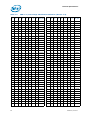
8-1 Socket Pinmap (Top View, Upper-Left Quadrant) .......................................................... 85
Datasheet, Volume 1
5
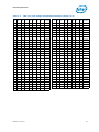
8-2 Socket Pinmap (Top View, Upper-Right Quadrant) ........................................................86
8-3 Socket Pinmap (Top View, Lower-Left Quadrant) ..........................................................87
8-4 Socket Pinmap (Top View, Lower-Right Quadrant) ........................................................88
Tables
1-1
2-1
2-2
2-3
2-4
4-1
4-2
4-3
4-4
4-5
4-6
4-7
6-1
6-2
6-3
6-4
6-5
6-6
6-7
6-8
6-9
6-10
6-11
6-12
6-13
6-14
6-15
6-16
7-1
7-2
7-3
7-4
7-5
7-6
7-7
7-8
7-9
7-10
7-11
7-12
7-13
8-1
6
Related Documents .................................................................................................18
Supported DIMM Module Configurations .....................................................................20
DDR3 System Memory Timing Support.......................................................................20
System Memory Pre-Charge Power Down Support .......................................................23
Processor Reference Clock Requirements ....................................................................33
Processor Core/Package State Support.......................................................................39
G, S, and C State Combinations ................................................................................40
D, S, and C State Combination..................................................................................40
Coordination of Thread Power States at the Core Level .................................................43
P_LVLx to MWAIT Conversion....................................................................................43
Coordination of Core Power States at the Package Level ...............................................46
Targeted Memory State Conditions ............................................................................49
Signal Description Buffer Types .................................................................................53
Memory Channel A ..................................................................................................54
Memory Channel B ..................................................................................................55
Memory Reference and Compensation........................................................................56
Reset and Miscellaneous Signals................................................................................56
PCI Express* Based Interface Signals ........................................................................58
DMI—Processor to PCH Serial Interface ......................................................................58
PLL Signals.............................................................................................................58
Intel® Flexible Display Interface ................................................................................59
JTAG/ITP................................................................................................................59
Error and Thermal Protection ....................................................................................60
Power Sequencing ...................................................................................................61
Processor Core Power Signals ...................................................................................61
Graphics and Memory Power Signals ..........................................................................63
Ground and NCTF ....................................................................................................63
Processor Internal Pull Up/Pull Down..........................................................................64
VRD 11.1/11.0 Voltage Identification Definition ...........................................................67
Market Segment Selection Truth Table for MSID[2:0]...................................................70
Signal Groups 1 ......................................................................................................71
Processor Absolute Minimum and Maximum Ratings .....................................................73
Processor Core Active and Idle Mode DC Voltage and Current Specifications ....................74
Processor Uncore I/O Buffer Supply DC Voltage and Current Specifications .....................74
Processor Graphics VID based (VAXG) Supply DC Voltage and Current Specifications.........76
VCC Static and Transient Tolerance ............................................................................76
VAXG Static and Transient Tolerance...........................................................................78
DDR3 Signal Group DC Specifications.........................................................................79
Control Sideband and TAP Signal Group DC Specifications.............................................80
PCI Express* DC Specifications .................................................................................81
PECI DC Electrical Limits ..........................................................................................82
Processor Pin List by Pin Name..................................................................................89
Datasheet, Volume 1
Revision History
Revision
Number
Description
Date
001
• Initial release
January
2010
002
• Added workstation information
January
2010
003
• Added Intel® Core™ i5-680 processor
April 2010
004
• Added Intel® Core™ i5-655K processor and Intel® Core™ i3-550 processor
June 2010
005
• Added Intel® Core™ i3-560 processor
August 2010
006
• Added the series designation “Intel® Pentium® desktop processor 6000
series”.
• Added the Intel
®
Pentium®
processor G6960.
January
2011
§§
Datasheet, Volume 1
7
8
Datasheet, Volume 1
Introduction
1
Introduction
The Intel® Core™ i5-600, i3-500 desktop processor series and Intel® Pentium®
desktop processor 6000 series are the next generation of 64-bit, multi-core processors
built on 32-nanometer process technology. Based on the low-power/high-performance
Intel microarchitecture, the processor is designed for a two-chip platform, instead of
the traditional three-chip platforms (processor, (G)MCH, and ICH). The two-chip
platform consists of a processor and Platform Controller Hub (PCH) and enables higher
performance, easier validation, and improved x-y footprint. The Intel® 5 Series Chipset
components for desktop and Intel® 3400 Series Chipset components for workstations
are the PCH.The processor is designed for desktop and workstation platforms.
This document provides DC electrical specifications, signal integrity, differential
signaling specifications, pinout and signal definitions, interface functional descriptions,
and additional feature information pertinent to the implementation and operation of the
processor on its respective platform.
Note:
Throughout this document, the Intel Core i5-600, i3-500 desktop processor series and
Intel Pentium desktop processor 6000 series may be referred to as “processor”.
Note:
Throughout this document, the Intel® Core™ i5-600 desktop processor series refers to
the Intel® Core™ i5-680, i5-670, i5-661, i5-660, i5-655K, and i5-650 processors.
Note:
Throughout this document, the Intel® Core™ i3-500 desktop processor series refers to
the Intel® Core™ i3-560, i3-550, i3-540, and i3-530 processors.
Note:
Throughout this document, the Intel® 5 series Chipset Platform Controller Hub may
also be referred to as “PCH”.
Note:
Throughout this document, the Intel® Pentium® desktop processor 6000 series refers
to the Intel® Pentium® processor G6950 and G6960 processors
Note:
Some processor features are not available on all platforms. Refer to the processor
specification update for details.
Included in this family of processors is an integrated graphics and a memory controller
die on the same package as the processor core die. This two-chip solution of a
processor core die with an integrated graphics and a memory controller die is known as
a Multi-Chip Package (MCP) processor. For specific features supported for individual
Intel Core™ i5-600 and i3-500 desktop processor series and Intel® Pentium® desktop
processor 6000 series SKUs, refer to the Intel® Core™ i5-600 and i3-500 Desktop
Processor Series and Intel® Pentium® Desktop Processor 6000 Series Specification
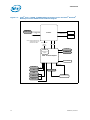
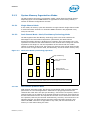
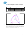
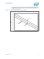
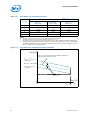
Update. Figure 1-1 shows an example platform block diagram.
Note:
Integrated graphics and Memory controller die is built on 45-nanometer process
technology.
Datasheet, Volume 1
9
Introduction
Figure 1-1.
Intel® Core™ i5-600, i3-500 Desktop Processor Series and Intel® Pentium®
Desktop Processor 6000 Series Platform Diagram
Discrete
Graphics (PEG)
PCI Express* 1x16
Processor
DDR3 DIMMs
2 Channels
(2 UDIMM/Channel)
OR
PCI Express* 2x 8
DDR3 DIMMs
Note: Supported PCI Express
configurations vary by
processor and SKU.
Intel® Flexible
Display
Interface
DMI PECI
Serial ATA
Intel®
Management
Engine
USB 2.0
Intel® 5 Series Chipset
Intel® HD Audio
SMBUS 2.0
SPI Flash
PCI
SPI
PCI Express*
PCI
FWH
TPM 1.2
LPC
Gigabit
Network Connection
Super I/O
GPIO
10
Datasheet, Volume 1
Introduction
1.1
Processor Feature Details
• Two cores
• A 32-KB instruction and 32-KB data first-level cache (L1) for each core
• A 256-KB shared instruction/data second-level cache (L2) for each core
• Up to 4-MB shared instruction/data third-level cache (L3), shared among all cores
1.1.1
Supported Technologies
• Intel® Virtualization Technology for Directed I/O (Intel® VT-d)
• Intel® Virtualization Technology (Intel® VT-x)
• Intel® Trusted Execution Technology (Intel® TXT)
• Intel® Streaming SIMD Extensions 4.1 (Intel® SSE4.1)
• Intel® Streaming SIMD Extensions 4.2 (Intel® SSE4.2)
• Intel® Hyper-Threading Technology
• Intel® 64 Architecture
• Execute Disable Bit
• 6 Advanced Encryption Standard New Instructions (AESNI)
• PCLMULQDQ instruction
• Intel® Turbo Boost Technology
Note:
Some technologies may not be enabled on all processor SKUs. Refer to the processor
specification update for details.
1.2
Interfaces
1.2.1
System Memory Support
System memory features include:
• One or two channels of unbuffered DDR3 memory with a maximum of two UDIMMs
per channel
• Single- and dual-channel memory organization modes
• Data burst length of eight for all memory organization modes
• Memory DDR3 data transfer rates of 1066 MT/s and 1333 MT/s
• 64-bit wide channels
• DDR3 I/O Voltage of 1.5 V
• The type of memory supported by the processor is dependent on the Intel 5 Series
Chipset SKU in the target platform:
— Desktop Intel 5 Series Chipset platforms only support non-ECC unbuffered
DIMMs and do not support any memory configuration that mixes non-ECC with
ECC unbuffered DIMMs
— Workstation Intel 3400 Series Chipset platforms support ECC and non-ECC
unbuffered DIMMs. The platforms do Not support any memory configuration
that mix non-ECC with ECC unbuffered DIMMs.
• Maximum memory bandwidth of 10.6 GB/s in single-channel mode or 21 GB/s in
dual-channel mode assuming DDR3 1333 MT/s
Datasheet, Volume 1
11
Introduction
• 1-Gb and 2-Gb DDR3 DRAM technologies are supported.
• Using 2-Gb device technologies, the largest memory capacity possible is 16 GB for
UDIMMs (assuming Dual Channel Mode with a four dual rank unbuffered DIMM
memory configuration)
• Up to 64 simultaneous open pages, 32 per channel (assuming 8 ranks of 8 bank
devices)
• Command launch modes of 1n/2n
• Partial writes to memory using Data Mask (DM) signals
• Intel® Fast Memory Access (Intel® FMA)
— Just-in-Time Command Scheduling
— Command Overlap
— Out-of-Order Scheduling
1.2.2
PCI Express*
• The processor PCI Express* port(s) are fully-compliant to the PCI Express Base
Specification, Revision 2.0.
• The processor with the desktop Intel 5 Series Chipset supports:
— One 16-lane PCI Express port intended for graphics attach
— Two 8-lane PCI Express ports (Only supported with Intel® 5 Series Chipset P55
and P57 SKUs)
• The processor with the workstation Intel 3450 Chipset supports:
— One 16-lane PCI Express port intended for graphics attach.
— Two 8-lane PCI Express ports for I/O.
• The processor with enhanced server Intel 3420 Chipset supports:
— One 16-lane PCI Express port for graphics or I/O.
— Two 8-lane PCI Express ports for I/O.
• The processor with value server Intel 3400 Series Chipset supports:
— Two 8-lane PCI Express ports for I/O.
• PCI Express Port 0 is mapped to PCI Device 1.
• The port may negotiate down to narrower widths.
— Support for x16/x8/x4/x1 widths for a single PCI Express mode.
• 2.5 GT/s and 5.0 GT/s PCI Express frequencies are supported.
• Hierarchical PCI-compliant configuration mechanism for downstream devices.
• Traditional PCI style traffic (asynchronous snooped, PCI ordering).
• PCI Express extended configuration space. The first 256 bytes of configuration
space aliases directly to the PCI Compatibility configuration space. The remaining
portion of the fixed 4-KB block of memory-mapped space above that (starting at
100h) is known as extended configuration space.
• PCI Express Enhanced Access Mechanism. Accessing the device configuration space
in a flat memory mapped fashion.
• Automatic discovery, negotiation, and training of link out of reset.
• Traditional AGP style traffic (asynchronous non-snooped, PCI-X* Relaxed ordering).
• Peer segment destination posted write traffic (no peer-to-peer read traffic) in
Virtual Channel 0:
— DMI -> PCI Express Port 0
12
Datasheet, Volume 1
Introduction
• 64-bit downstream address format, but the processor never generates an address
above 64 GB (Bits 63:36 will always be zeros).
• 64-bit upstream address format, but the processor responds to upstream read
transactions to addresses above 64 GB (addresses where any of Bits 63:36 are
nonzero) with an Unsupported Request response. Upstream write transactions to
addresses above 64 GB will be dropped.
• Re-issues Configuration cycles that have been previously completed with the
Configuration Retry status.
• PCI Express reference clock is 100-MHz differential clock.
• Power Management Event (PME) functions.
• Static lane numbering reversal. Land CFG[3] should be pulled down if lane reversal
is desired (refer to Table 6-5).
• Dynamic frequency change capability (2.5 GT/s - 5.0 GT/s)
• Dynamic width capability
• Message Signaled Interrupt (MSI and MSI-X) messages
• Polarity inversion
1.2.3
Direct Media Interface (DMI)
• Four lanes in each direction.
• 2.5 GT/s point-to-point DMI interface to PCH is supported.
• Raw bit-rate on the data pins of 2.5 GB/s, resulting in a real bandwidth per pair of
250 MB/s given the 8b/10b encoding used to transmit data across this interface.
Does not account for packet overhead and link maintenance.
• Maximum theoretical bandwidth on interface of 1 GB/s in each direction
simultaneously, for an aggregate of 2 GB/s when DMI x4.
• Shares 100-MHz PCI Express reference clock.
• 64-bit downstream address format, but the processor never generates an address
above 64 GB (Bits 63:36 will always be zeros).
• 64-bit upstream address format, but the processor responds to upstream read
transactions to addresses above 64 GB (addresses where any of Bits 63:36 are
nonzero) with an Unsupported Request response. Upstream write transactions to
addresses above 64 GB will be dropped.
• Supports the following traffic types to or from the PCH
— DMI -> DRAM
— DMI -> processor core (Virtual Legacy Wires (VLWs), Resetwarn, or MSIs only)
— Processor core -> DMI
• APIC and MSI interrupt messaging support
— Message Signaled Interrupt (MSI and MSI-X) messages
• Downstream SMI, SCI, and SERR error indication
• Legacy support for ISA regime protocol (PHOLD/PHOLDA) required for parallel port
DMA, floppy drive, and LPC bus masters
• DC coupling – no capacitors between the processor and the PCH
• Polarity inversion
• PCH end-to-end lane reversal across the link
• Supports Half Swing “low-power/low-voltage” and Full Swing “high-power/highvoltage” modes
Datasheet, Volume 1
13
Introduction
1.2.4
Platform Environment Control Interface (PECI)
The PECI is a one-wire interface that provides a communication channel between
processor and a PECI master, usually the PCH.
1.2.5
Intel® HD Graphics
Features of the integrated graphics controller include:
• Render C-state (RC6)
• Intel® Dynamic Video Memory Technology support
• Intel® Clear Video Technology
— MPEG2 Hardware Acceleration
— WMV9/VC1 Hardware Acceleration
— AVC Hardware Acceleration
— ProcAmp
— Advanced Pixel Adaptive De-interlacing
— Sharpness Enhancement
— De-noise Filter
— High Quality Scaling
— Film Mode Detection (3:2 pull-down) and Correction
— Intel® TV Wizard
• 12 Execution Units (EUs)
1.2.6
Intel® Flexible Display Interface (Intel® FDI)
• Carries display traffic from the integrated graphics in the processor to the legacy
display connectors in the PCH.
• Based on Display Port standard
• Two independent links—one for each display pipe
• Four unidirectional downstream differential transmitter pairs
— Scalable down to 3X, 2X, or 1X based on actual display bandwidth
requirements
— Fixed frequency 2.7 GT/s data rate
• Two sideband signals for Display synchronization:
— FDI_FSYNC and FDI_LSYNC (Frame and Line Synchronization)
• One Interrupt signal used for various interrupts from the PCH
— FDI_INT signal shared by both Intel FDI Links
• PCH supports end-to-end lane reversal across both links
14
Datasheet, Volume 1
Introduction
1.3
Power Management Support
1.3.1
Processor Core
• Full support of ACPI C-states as implemented by the following processor C-states:
— C0, C1, C1E, C3, C6
• Enhanced Intel SpeedStep® Technology
1.3.2
System
• Desktop Intel 5 Series Chipset platforms support: S0, S1, S3, S4, S5
• Workstation Intel 3400 Series Chipset platforms support: S0, S1, S3, S4, and S5
1.3.3
Memory Controller
• Conditional self-refresh (Intel® Rapid Memory Power Management (Intel® RMPM))
• Dynamic power-down
1.3.4
PCI Express*
• L0s and L1 ASPM power management capability.
1.4
Thermal Management Support
• Digital Thermal Sensor
• Intel® Adaptive Thermal Monitor
• THERMTRIP# and PROCHOT# support
• On-Demand Mode
• Memory Thermal Throttling
• External Thermal Sensor
• Render Thermal Throttling
• Fan Speed Control with DTS
1.5
Package
• The processor socket type is noted as LGA 1156. The package is a 37.5 x 37.5 mm
Flip Chip Land Grid Array (FCLGA 1156).
1.6
Terminology
Term
Description
BLT
Block Level Transfer
CRT
Cathode Ray Tube
DDR3
Third generation Double Data Rate SDRAM memory technology
DP
Display Port*
Datasheet, Volume 1
15
Introduction
Term
DMA
Direct Memory Access
DMI
Direct Media Interface
DTS
Digital Thermal Sensor
ECC
Error Correction Code
Enhanced Intel
SpeedStep® Technology
Technology that provides power management capabilities.
Execute Disable Bit
The Execute Disable bit allows memory to be marked as executable or nonexecutable, when combined with a supporting operating system. If code attempts
to run in non-executable memory, the processor raises an error to the operating
system. This feature can prevent some classes of viruses or worms that exploit
buffer overrun vulnerabilities and can, thus, help improve the overall security of the
system. See the Intel® 64 and IA-32 Architectures Software Developer's Manuals
for more detailed information.
EU
Execution Unit
FCLGA
Flip Chip Land Grid Array
(G)MCH
Legacy component – Graphics Memory Controller Hub. Platforms using LGA 1156
processors do not use a (G)MCH component.
ICH
The legacy I/O Controller Hub component that contains the main PCI interface, LPC
interface, USB2, Serial ATA, and other I/O functions. It communicates with the
legacy (G)MCH over a proprietary interconnect called DMI. Platforms using LGA
1156 processors do not use an ICH component.
IMC
Integrated Memory Controller
Intel® 64 Technology
64-bit memory extensions to the IA-32 architecture.
Intel® FDI
Intel® Flexible Display Interface.
Intel® Hyper-Threading
Technology
The processor supports Intel® Hyper-Threading Technology (Intel® HT Technology)
that allows an execution core to function as two logical processors.
Intel® Turbo Boost
Technology
Intel® Turbo Boost Technology is a feature that allows the processor core to
opportunistically and automatically run faster than its rated operating frequency if it
is operating below power, temperature, and current limits.
Intel® TXT
Intel® Trusted Execution Technology
Intel
®
VT-d
Intel® Virtualization
Technology
16
Description
Intel® Virtualization Technology (Intel® VT) for Directed I/O. Intel VT-d is a
hardware assist, under system software (Virtual Machine Manager or OS) control,
for enabling I/O device virtualization. VT-d also brings robust security by providing
protection from errant DMAs by using DMA remapping, a key feature of Intel VT-d.
Processor virtualization which when used in conjunction with Virtual Machine
Monitor software enables multiple, robust independent software environments
inside a single platform.
ITPM
Integrated Trusted Platform Module
IOV
I/O Virtualization
LCD
Liquid Crystal Display
LVDS
Low Voltage Differential Signaling. A high speed, low power data transmission
standard used for display connections to LCD panels.
MCP
Multi-Chip Package
NCTF
Non-Critical to Function: NCTF locations are typically redundant ground or noncritical reserved, so the loss of the solder joint continuity at end of life conditions
will not affect the overall product functionality.
PCH
Platform Controller Hub. The new, 2009 chipset with centralized platform
capabilities including the main I/O interfaces along with display connectivity, audio
features, power management, manageability, security and storage features.
PECI
Platform Environment Control Interface
PEG
PCI Express* Graphics. External Graphics using PCI Express Architecture. A highspeed serial interface whose configuration is software compatible with the existing
PCI specifications.
Processor
The 64-bit multi-core component (package)
Datasheet, Volume 1
Introduction
Term
Description
Processor Core
The term “processor core” refers to Si die itself which can contain multiple
execution cores. Each execution core has an instruction cache, data cache, and
256-KB L2 cache. All execution cores share the L3 cache.
Rank
A unit of DRAM corresponding to four to eight devices in parallel, ignoring ECC.
These devices are usually, but not always, mounted on a single side of a DIMM.
SCI
System Control Interrupt. Used in ACPI protocol.
Storage Conditions
A non-operational state. The processor may be installed in a platform, in a tray, or
loose. Processors may be sealed in packaging or exposed to free air. Under these
conditions, processor landings should not be connected to any supply voltages,
have any I/Os biased or receive any clocks. Upon exposure to “free air” (that is,
unsealed packaging or a device removed from packaging material), the processor
must be handled in accordance with moisture sensitivity labeling (MSL) as indicated
on the packaging material.
TAC
Thermal Averaging Constant
TDP
Thermal Design Power
TLP
Transaction Layer Packet
TOM
Top of Memory
TTM
Time-To-Market
VCC
Processor core power rail
VSS
Processor ground
VAXG
Graphics core power supply
VTT
L3 shared cache, memory controller, and processor I/O power rail
VDDQ
DDR3 power rail
VLD
Variable Length Decoding
x1
Refers to a Link or Port with one Physical Lane
x4
Refers to a Link or Port with four Physical Lanes
x8
Refers to a Link or Port with eight Physical Lanes
x16
Refers to a Link or Port with sixteen Physical Lanes
Datasheet, Volume 1
17
Introduction
1.7
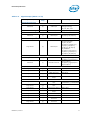
Related Documents
Refer to the following documents for additional information.
Table 1-1.
Related Documents
Document
Document Number/ Location
Voltage Regulator-Down (VRD) 11.1 Design Guidelines
http://download.intel.com/design
/processor/designex/322172.pdf
Intel® Core™ i5-600, i3-500 Desktop Processor Series and Intel®
Pentium® Desktop Processor 6000 Series Datasheet, Volume 2
http://download.intel.com/design
/processor/datashts/322910.pdf
Intel® Core™ i5-600, i3-500 Desktop Processor Series and Intel®
Pentium® Desktop Processor 6000 Series Specification Update
http://download.intel.com/design
/processor/specupdt/322911.pdf
Intel® Core™ i5-600, i3-500 Desktop Processor Series and Intel®
Pentium® Desktop Processor 6000 Series and LGA1156 Socket Thermal
and Mechanical Specificaitons and Design Guidelines
http://download.intel.com/design
/processor/designex/322912.pdf
Intel® 5 Series Chipset and Intel® 3400 Series Chipset Datasheet
www.intel.com/Assets/PDF/datas
heet/322169
Intel® 5 Series Chipset and Intel® 3400 Series Chipset Thermal and
Mechanical Specifications and Design Guidelines
www.intel.com/Assets/PDF/desig
nguide/322171.pdf
Advanced Configuration and Power Interface Specification 3.0
http://www.acpi.info/
PCI Local Bus Specification 3.0
http://www.pcisig.com/specificati
ons
PCI Express Base Specification, Revision 2.0
http://www.pcisig.com
DDR3 SDRAM Specification
http://www.jedec.org
Display Port Specification
http://www.vesa.org
Intel®
64 and IA-32 Architectures Software Developer's Manuals
Volume 1: Basic Architecture
Volume 2A: Instruction Set Reference, A-M
http://www.intel.com/products/pr
ocessor/manuals/
Volume 2B: Instruction Set Reference, N-Z
Volume 3A: System Programming Guide
Volume 3B: System Programming Guide
§§
18
Datasheet, Volume 1
Interfaces
2
Interfaces
This chapter describes the interfaces supported by the processor.
2.1
System Memory Interface
2.1.1
System Memory Technology Supported
The Integrated Memory Controller (IMC) supports DDR3 protocols with two
independent, 64-bit wide channels each accessing one or two DIMMs. The type of
memory supported by the processor is dependent on the Intel 5 Series Chipset SKU in
the target platform:
• Desktop Intel 5 series Chipset platforms support non-ECC unbuffered DIMMs only
and do not support any memory configuration that mixes non-ECC with ECC
unbuffered DIMMs.
• Server and Workstation Intel 3400 Series Chipset platforms support ECC
unbuffered DIMMs. Workstation Intel 3400 Series Chipset platforms also support
non-ECC unbuffered DIMMs. Workstation Intel 3400 Series Chipset platforms do
not support any memory configuration that mixes non-ECC with ECC unbuffered
DIMMs.
The IMC supports a maximum of two DDR3 DIMMs per channel; thus, allowing up to
four device ranks per channel.
• DDR3 Data Transfer Rates
— 1066 MT/s (PC3-8500) and 1333 MT/s (PC3-10600)
• Desktop Intel 5 Series Chipset platform DDR3 DIMM Modules
— Raw Card A—Single Rank x8 unbuffered non-ECC
— Raw Card B—Dual Ranked x8 unbuffered non-ECC
— Raw Card C—Single Rank x16 unbuffered non-ECC
• Server Intel 3400 Series Chipset platform DDR3 DIMM Modules
— Raw Card D—Single Rank x8 unbuffered ECC
— Raw Card E—Dual Ranked x8 unbuffered ECC
• Workstation Intel 3400 Series Chipset platform DDR3 DIMM Modules
— Raw Card A—Single Rank x8 unbuffered non-ECC
— Raw Card B—Dual Ranked x8 unbuffered non-ECC
— Raw Card C—Single Rank x16 unbuffered non-ECC
— Raw Card D—Single Rank x8 unbuffered ECC
— Raw Card E—Dual Ranked x8 unbuffered ECC
• DDR3 DRAM Device Technology
— 1-Gb and 2-Gb DDR3 DRAM Device technologies and addressing are supported.
Datasheet, Volume 1
19
Interfaces
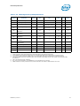
Table 2-1.
Supported DIMM Module Configurations
Raw
Card
Version
DIMM
Capacity
DRAM
Device
Technology
# of
Physical
Device
Ranks
# of
DRAM
Devices
DRAM
Organization
# of
Row/Col
Address
Bits
# of
Banks
Inside
DRAM
Page
Size
Desktop Intel 5 Series Chipset Platforms and Workstation Intel 3400 Series Chipset Platforms:
Unbuffered/Non-ECC Supported DIMM Module Configurations
A
B
C
1 GB
1 Gb
128 M X 8
8
1
14/10
8
8K
2 GB
1 Gb
128 M X 8
16
2
14/10
8
8K
4 GB
2 Gb
256 M X 8
16
2
15/10
8
8K
512 MB
1 Gb
64 M X 16
4
1
13/10
8
8K
Workstation Intel 3400 Series Chipset Platforms:
Unbuffered/ECC Supported DIMM Module Configurations
D
E
1 GB
1 Gb
128 M X 8
9
1
14/10
8
8K
2 GB
1 Gb
128 M X 8
18
2
14/10
8
8K
4 GB
2 Gb
256 M X 8
18
2
15/10
8
8K
Note:
2.1.2
DIMM module support is based on availability and is subject to change.
System Memory Timing Support
The IMC supports the following DDR3 Speed Bin, CAS Write Latency (CWL), and
command signal mode timings on the main memory interface:
•
•
•
•
•
Table 2-2.
tCL = CAS Latency
tRCD = Activate Command to READ or WRITE Command delay
tRP = PRECHARGE Command Period
CWL = CAS Write Latency
Command Signal modes = 1N indicates a new command may be issued every clock
and 2N indicates a new command may be issued every 2 clocks. Command launch
mode programming depends on the transfer rate and memory configuration.
DDR3 System Memory Timing Support
Transfer Rate
(MT/s)
1066
1333
tCL
(tCK)
tRCD
(tCK)
tRP
(tCK)
7
7
7
8
8
8
9
9
9
10
10
10
CWL
(tCK)
Unbuffered
DIMM CMD
Mode
Notes
6
See Note 1, 2, 3
1
7
See Note 1, 2, 3
1
1
Note:
1.
Two Un-buffered DIMM Memory Configurations = 2N Command Mode at 1067/1333 MHz
2.
One Un-buffered DIMM Memory Configurations = 1N Command Mode at 1067/1333 MHz
3.
Both Channel A and B will run at same Command Mode based on the slowest mode enabled relative to the
memory configurations populated in both channels. For example, if Channel A has both DIMM connectors
populated (2N CMD Mode) and Channel B has only one DIMM connector populated (1N CMD Mode), then
2N CMD mode would be enabled for both channels.
4.
System Memory timing support is based on availability and is subject to change.
20
Datasheet, Volume 1
Interfaces
2.1.3
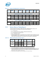
System Memory Organization Modes
The IMC supports two memory organization modes, single-channel and dual-channel.
Depending upon how the DIMM Modules are populated in each memory channel, a
number of different configurations can exist.
2.1.3.1
Single-Channel Mode
In this mode, all memory cycles are directed to a single-channel. Single-channel mode
is used when either Channel A or Channel B DIMM connectors are populated in any
order, but not both.
2.1.3.2
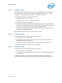
Dual-Channel Mode—Intel® Flex Memory Technology Mode
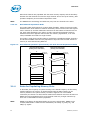
The IMC supports Intel Flex Memory Technology mode. This mode combines the
advantages of the Dual-Channel Symmetric (Interleaved) and Dual-Channel
Asymmetric Modes. Memory is divided into a symmetric and a asymmetric zone. The
symmetric zone starts at the lowest address in each channel and is contiguous until the
asymmetric zone begins or until the top address of the channel with the smaller
capacity is reached. In this mode, the system runs with one zone of dual-channel mode
and one zone of single-channel mode, simultaneously, across the whole memory array.
Figure 2-1.
Intel® Flex Memory Technology Operation
C
T o p o f M e m o ry
B
B
CH A
CH B
C
N o n in te r le a v e d
access
B
C
D ual channel
in te r le a v e d a c c e s s
B
B
CH A
CH B
B
B – T h e la rg e s t p h y s ic a l m e m o ry a m o u n t o f th e s m a lle r s iz e m e m o ry m o d u le
C – T h e re m a in in g p h y s ic a l m e m o ry a m o u n t o f th e la rg e r s iz e m e m o ry m o d u le
2.1.3.2.1
Dual-Channel Symmetric Mode
Dual-Channel Symmetric mode, also known as interleaved mode, provides maximum
performance on real world applications. Addresses are ping-ponged between the
channels after each cache line (64-byte boundary). If there are two requests, and the
second request is to an address on the opposite channel from the first, that request can
be sent before data from the first request has returned. If two consecutive cache lines
are requested, both may be retrieved simultaneously, since they are ensured to be on
opposite channels. Use Dual-Channel Symmetric mode when both Channel A and
Channel B DIMM connectors are populated in any order, with the total amount of
memory in each channel being the same.
Datasheet, Volume 1
21
Interfaces
When both channels are populated with the same memory capacity and the boundary
between the dual channel zone and the single channel zone is the top of memory, IMC
operates completely in Dual-Channel Symmetric mode.
Note:
The DRAM device technology and width may vary from one channel to the other.
2.1.3.2.2
Dual-Channel Asymmetric Mode
This mode trades performance for system design flexibility. Unlike the previous mode,
addresses start at the bottom of Channel A and stay there until the end of the highest
rank in Channel A, and then addresses continue from the bottom of Channel B to the
top. Real world applications are unlikely to make requests that alternate between
addresses that sit on opposite channels with this memory organization, so in most
cases, bandwidth is limited to a single channel.
This mode is used when Intel Flex Memory Technology is disabled and both Channel A
and Channel B DIMM connectors are populated in any order with the total amount of
memory in each channel being different.
Figure 2-2.
Dual-Channel Symmetric (Interleaved) and Dual-Channel Asymmetric Modes
Dual Channel Interleaved
(memory sizes must match)
Dual Channel Asymmetric
(memory sizes can differ)
CL
CL
CH. B
Top of
Memory
CH. B
Top of
Memory
CH. A
CH.A-top
DRB
CH. A
CH. B
CH. A
CH. B
CH. A
2.1.4
0
0
Rules for Populating Memory Slots
In all modes, the frequency of system memory is the lowest frequency of all memory
modules placed in the system, as determined through the SPD registers on the
memory modules. The system memory controller supports one or two DIMM
connectors per channel. For dual-channel modes both channels must have at least one
DIMM connector populated and for single-channel mode only a single-channel may
have one or both DIMM connectors populated.
Note:
22
DIMM0 must always be populated within any memory configuration. DIMM0 is the
furthest DIMM within a channel and is identified by the CS#[1:0], ODT[1:0], and
CKE[1:0] signals.
Datasheet, Volume 1
Interfaces
2.1.5
Technology Enhancements of Intel® Fast Memory Access
(Intel® FMA)
The following sections describe the Just-in-Time Scheduling, Command Overlap, and
Out-of-Order Scheduling Intel FMA technology enhancements.
2.1.5.1
Just-in-Time Command Scheduling
The memory controller has an advanced command scheduler where all pending
requests are examined simultaneously to determine the most efficient request to be
issued next. The most efficient request is picked from all pending requests and issued
to system memory Just-in-Time to make optimal use of Command Overlapping. Thus,
instead of having all memory access requests go individually through an arbitration
mechanism forcing requests to be executed one at a time, they can be started without
interfering with the current request allowing for concurrent issuing of requests. This
allows for optimized bandwidth and reduced latency while maintaining appropriate
command spacing to meet system memory protocol.
2.1.5.2
Command Overlap
Command Overlap allows the insertion of the DRAM commands between the Activate,
Precharge, and Read/Write commands normally used, as long as the inserted
commands do not affect the currently executing command. Multiple commands can be
issued in an overlapping manner, increasing the efficiency of system memory protocol.
2.1.5.3
Out-of-Order Scheduling
While leveraging the Just-in-Time Scheduling and Command Overlap enhancements,
the IMC continuously monitors pending requests to system memory for the best use of
bandwidth and reduction of latency. If there are multiple requests to the same open
page, these requests would be launched in a back to back manner to make optimum
use of the open memory page. This ability to reorder requests on the fly allows the IMC
to further reduce latency and increase bandwidth efficiency.
2.1.6
System Memory Pre-Charge Power Down Support Details
The IMC supports and enables the following DDR3 DRAM Device pre-charge power
down DLL controls during a pre-charge power down.
• Slow Exit is where the DRAM device DLL is disabled after entering pre-charge
power down
• Fast Exit is where the DRAM device DLLs are maintained after entering pre-charge
power down
Table 2-3.
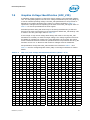
System Memory Pre-Charge Power Down Support
Datasheet, Volume 1
DIMM per Channel
Configuration
DIMM Type
Precharge Power Down
Slow/Fast Exit
One
Unbuffered DIMM
Fast Exit
Two
Unbuffered DIMM
Fast Exit
23
Interfaces
2.2
PCI Express* Interface
This section describes the PCI Express interface capabilities of the processor. See the
PCI Express Base Specification for details of PCI Express.
The number of PCI Express controllers available is dependent on the platform:
• Processor with desktop Intel 5 Series Chipset: 1 x 16 PCI Express Graphics is
supported.
• Processor with Intel 5 Series Chipset P55 and P57 SKUs: 2 x 8 PCI Express
Graphics is supported.
• Processor with workstation Intel 3400 Series Chipset: 1 x 16 PCI Express Graphics
or 2 x 8 PCI Express is supported (1 x8 primary port for graphics or I/O; 1 x 8
secondary port for I/O only).
It defines the PCI Express port that is used as the external graphics attach. The port
may also be referred to as PEG (or PEG0) and PCI Express Graphics Port.
2.2.1
PCI Express* Architecture
Compatibility with the PCI addressing model is maintained to ensure that all existing
applications and drivers operate unchanged.
The PCI Express configuration uses standard mechanisms as defined in the PCI Plugand-Play specification. The initial recovered clock speed of 1.25 GHz results in
2.5 Gb/s/direction which provides a 250-MB/s communications channel in each
direction (500 MB/s total). That is close to twice the data rate of classic PCI. The fact
that 8b/10b encoding is used accounts for the 250 MB/s where quick calculations would
imply 300 MB/s. The PCI Express ports support 5.0 GT/s speed as well. Operating at
5.0 GT/s results in twice as much bandwidth per lane as compared to 2.5 GT/s
operation.
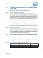
The PCI Express architecture is specified in three layers: Transaction Layer, Data Link
Layer, and Physical Layer. The partitioning in the component is not necessarily along
these same boundaries. Refer to Figure 2-3 for the PCI Express Layering Diagram.
Figure 2-3.
24
PCI Express* Layering Diagram
Datasheet, Volume 1
Interfaces
PCI Express uses packets to communicate information between components. Packets
are formed in the Transaction and Data Link Layers to carry the information from the
transmitting component to the receiving component. As the transmitted packets flow
through the other layers, they are extended with additional information necessary to
handle packets at those layers. At the receiving side the reverse process occurs and
packets get transformed from their Physical Layer representation to the Data Link
Layer representation and finally (for Transaction Layer Packets) to the form that can be
processed by the Transaction Layer of the receiving device.
Figure 2-4.
Packet Flow through the Layers
2.2.1.1
Transaction Layer
The upper layer of the PCI Express architecture is the Transaction Layer. The
Transaction Layer's primary responsibility is the assembly and disassembly of
Transaction Layer Packets (TLPs). TLPs are used to communicate transactions, such as
read and write, as well as certain types of events. The Transaction Layer also manages
flow control of TLPs.
2.2.1.2
Data Link Layer
The middle layer in the PCI Express stack, the Data Link Layer, serves as an
intermediate stage between the Transaction Layer and the Physical Layer.
Responsibilities of the Data Link Layer include link management, error detection, and
error correction.
The transmission side of the Data Link Layer accepts TLPs assembled by the
Transaction Layer, calculates and applies data protection code and TLP sequence
number, and submits them to the Physical Layer for transmission across the Link. The
receiving Data Link Layer is responsible for checking the integrity of received TLPs and
for submitting them to the Transaction Layer for further processing. On detection of TLP
error(s), this layer is responsible for requesting retransmission of TLPs until information
is correctly received, or the Link is determined to have failed. The Data Link Layer also
generates and consumes packets that are used for Link management functions.
2.2.1.3
Physical Layer
The Physical Layer includes all circuitry for interface operation, including driver and
input buffers, parallel-to-serial and serial-to-parallel conversion, PLL(s), and impedance
matching circuitry. It also includes logical functions related to interface initialization and
maintenance. The Physical Layer exchanges data with the Data Link Layer in an
implementation-specific format, and is responsible for converting this to an appropriate
serialized format and transmitting it across the PCI Express Link at a frequency and
width compatible with the remote device.
Datasheet, Volume 1
25
Interfaces
2.2.2
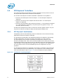
PCI Express* Configuration Mechanism
The PCI Express (external graphics) link is mapped through a PCI-to-PCI bridge
structure.
Figure 2-5.
PCI Express Related Register Structures in the Processor
PCI
Express*
Device
PCI Express
Port 0
PCI-PCI
Bridge
representing
root PCI
Express port
(Device 1)
PCI
Compatible
Host Bridge
Device
(Device 0)
DMI
PCI Express extends the configuration space to 4096 bytes per-device/function, as
compared to 256 bytes allowed by the Conventional PCI Specification. PCI Express
configuration space is divided into a PCI-compatible region (consisting of the first 256 B
of a logical device's configuration space) and an extended PCI Express region
(consisting of the remaining configuration space). The PCI-compatible region can be
accessed using either the mechanisms defined in the PCI specification or using the
enhanced PCI Express configuration access mechanism described in the PCI Express
Enhanced Configuration Mechanism section.
The PCI Express Host Bridge is required to translate the memory-mapped PCI Express
configuration space accesses from the host processor to PCI Express configuration
cycles. To maintain compatibility with PCI configuration addressing mechanisms, it is
recommended that system software access the enhanced configuration space using 32bit operations (32-bit aligned) only.
See the PCI Express Base Specification for details of both the PCI-compatible and PCI
Express Enhanced configuration mechanisms and transaction rules.
2.2.3
PCI Express Port
The PCI Express interface on the processor is a single, 16-lane (x16) port that can also
be configured at narrower widths. Refer to Table 6-5 for the supported PCI Express
configurations. The PCI Express port is being designed to be compliant with the PCI
Express Base Specification, Revision 2.0.
26
Datasheet, Volume 1
Interfaces
2.3
Direct Media Interface (DMI)
DMI connects the processor and the PCH chip-to-chip. The DMI is similar to a four-lane
PCI Express supporting up to 1 GB/s of bandwidth in each direction.
Note:
Only DMI x4 configuration is supported.
2.3.1
DMI Error Flow
DMI can only generate SERR in response to errors—never SCI, SMI, MSI, PCI INT, or
GPE. Any DMI related SERR activity is associated with Device 0.
2.3.2
Processor/PCH Compatibility Assumptions
The processor is compatible with the PCH and is not compatible with any previous
(G)MCH or ICH products.
2.3.3
DMI Link Down
The DMI link going down is a fatal, unrecoverable error. If the DMI data link goes to
data link down, after the link was up, then the DMI link hangs the system by not
allowing the link to retrain to prevent data corruption. This is controlled by the PCH.
Downstream transactions that had been successfully transmitted across the link prior
to the link going down may be processed as normal. No completions from downstream,
non-posted transactions are returned upstream over the DMI link after a link down
event.
2.4
Integrated Graphics
This section details the processor integrated graphics 2D, 3D, and video pipeline and
their respective capabilities.
The integrated graphics is powered by a next generation graphics core and supports
twelve, fully-programmable execution cores. Full-precision, floating-point operations
are supported to enhance the visual experience of compute-intensive applications.
The integrated graphics contains several types of components; the graphics engines,
planes, pipes, port and the Intel FDI. The integrated graphics has a 3D/2D Instruction
Processing unit to control the 3D and 2D engines respectively. The integrated graphics
3D and 2D engines are fed with data through the IMC. The outputs of the graphics
engine are surfaces sent to memory, which are then retrieved and processed by the
planes. The surfaces are then blended in the pipes and the display timings are
transitioned from display core clock to the pixel (dot) clock.
Datasheet, Volume 1
27
Interfaces
Figure 2-6.
Processor Graphic Processing Unit Block Diagram
Plane A
Video Engine
Sprite A
Pipe A
2D Engine
Cursor A
Memory
3D Engine
Vertex Fetch/Vertex
Shader
VGA
Alpha
Blend/
Gamma/
Panel Fitter
M
U
X
Intel®
FDI
Plane B
Geometry Shader
Pipe B
Sprite B
Clipper
Strip & Fan/Setup
Cursor B
Windower/IZ
2.4.1
3D and Video Engines for Graphics Processing
The 3D graphics pipeline architecture simultaneously operates on different primitives or
on different portions of the same primitive. All the cores are fully programmable,
increasing the versatility of the 3D Engine. The 3D engine provides the following
performance and power-management enhancements:
• Execution units (EU) increased to 12 from the previous 10 EUs
• Includes Hierarchal-Z
• Includes Video quality enhancements
2.4.1.1
3D Engine Execution Units (EUs)
• Support 12 EUs. The EUs perform 128-bit wide execution per clock.
• Support SIMD8 instructions for vertex processing and SIMD16 instructions for pixel
processing.
2.4.1.2
3D Pipeline
2.4.1.2.1
Vertex Fetch (VF) Stage
The VF stage executes 3DPRIMITIVE commands. Some enhancements have been
included to better support legacy D3D APIs as well as SGI OpenGL*.
2.4.1.2.2
Vertex Shader (VS) Stage
The VS stage performs shading of vertices output by the VF function. The VS unit
produces an output vertex reference for every input vertex reference received from the
VF unit, in the order received.
28
Datasheet, Volume 1
Interfaces
2.4.1.2.3
Geometry Shader (GS) Stage
The GS stage receives inputs from the VS stage. Compiled application-provided GS
programs, specifying an algorithm to convert the vertices of an input object into some
output primitives. For example, a GS shader may convert lines of a line strip into
polygons representing a corresponding segment of a blade of grass centered on the
line. Or it could use adjacency information to detect silhouette edges of triangles and
output polygons extruding out from the edges.
2.4.1.2.4
Clip Stage
The Clip stage performs general processing on incoming 3D objects. However, it also
includes specialized logic to perform a Clip Test function on incoming objects. The Clip
Test optimizes generalized 3D Clipping. The Clip unit examines the position of incoming
vertices, and accepts/rejects 3D objects based on its Clip algorithm.
2.4.1.2.5
Strips and Fans (SF) Stage
The SF stage performs setup operations required to rasterize 3D objects. The outputs
from the SF stage to the Windower stage contain implementation-specific information
required for the rasterization of objects and also supports clipping of primitives to some
extent.
2.4.1.2.6
Windower/IZ (WIZ) Stage
The WIZ unit performs an early depth test, which removes failing pixels and eliminates
unnecessary processing overhead.
The Windower uses the parameters provided by the SF unit in the object-specific
rasterization algorithms. The WIZ unit rasterizes objects into the corresponding set of
pixels. The Windower is also capable of performing dithering, whereby the illusion of a
higher resolution when using low-bpp channels in color buffers is possible. Color
dithering diffuses the sharp color bands seen on smooth-shaded objects.
2.4.1.3
Video Engine
The Video Engine handles the non-3D (media/video) applications. It includes support
for VLD and MPEG2 decode in hardware.
2.4.1.4
2D Engine
The 2D Engine contains BLT (Block Level Transfer) functionality and an extensive set of
2D instructions. To take advantage of the 3D during engine’s functionality, some BLT
functions make use of the 3D renderer.
2.4.1.4.1
Integrated Graphics VGA Registers
The 2D registers consists of original VGA registers and others to support graphics
modes that have color depths, resolutions, and hardware acceleration features that go
beyond the original VGA standard.
Datasheet, Volume 1
29
Interfaces
2.4.1.4.2
Logical 128-Bit Fixed BLT and 256 Fill Engine
This BLT engine accelerates the GUI of Microsoft Windows* operating systems. The
128-bit, integrated graphics BLT engine provides hardware acceleration of block
transfers of pixel data for many common Windows operations. The BLT engine can be
used for the following:
• Move rectangular blocks of data between memory locations
• Data alignment
• To perform logical operations (raster ops)
The rectangular block of data does not change, as it is transferred between memory
locations. The allowable memory transfers are between—cacheable system memory
and frame buffer memory, frame buffer memory and frame buffer memory, and within
system memory. Data to be transferred can consist of regions of memory, patterns, or
solid color fills. A pattern is always 8 x 8 pixels wide and may be 8, 16, or 32 bits per
pixel.
The BLT engine expands monochrome data into a color depth of 8, 16, or 32 bits. BLTs
can be either opaque or transparent. Opaque transfers move the data specified to the
destination. Transparent transfers compare destination color to source color and write
according to the mode of transparency selected.
Data is horizontally and vertically aligned at the destination. If the destination for the
BLT overlaps with the source memory location, the BLT engine specifies which area in
memory to begin the BLT transfer. Hardware is included for all 256 raster operations
(source, pattern, and destination) defined by Microsoft, including transparent BLT.
The BLT engine has instructions to invoke BLT and stretch BLT operations, permitting
software to set up instruction buffers and use batch processing. The BLT engine can
perform hardware clipping during BLTs.
30
Datasheet, Volume 1
Interfaces
2.4.2
Integrated Graphics Display
The Graphics Processing Unit’s display pipe can be broken down into three
components:
• Display Planes
• Display Pipes
• DisplayPort and Intel FDI
Figure 2-7.
Processor Display Block Diagram
Plane A
Sprite A
Cursor A
VGA
Plane B
Sprite B
Alpha
Blend/
Gamma/
Panel
Fitter
Pipe A
M
U
X
Intel®
FDI
Pipe B
Cursor B
2.4.2.1
Display Planes
A display plane is a single displayed surface in memory and contains one image
(desktop, cursor, overlay). It is the portion of the display hardware logic that defines
the format and location of a rectangular region of memory that can be displayed on
display output device and delivers that data to a display pipe. This is clocked by the
Core Display clock.
2.4.2.1.1
Planes A and B
Planes A and B are the main display planes and are associated with Pipes A and B
respectively. The two display pipes are independent, allowing for support of two
independent display streams. They are both double-buffered, which minimizes latency
and improves visual quality.
2.4.2.1.2
Sprite A and B
Sprite A and Sprite B are planes optimized for video decode, and are associated with
Planes A and B respectively. Sprite A and B are also double-buffered.
Datasheet, Volume 1
31
Interfaces
2.4.2.1.3
Cursors A and B
Cursors A and B are small, fixed-sized planes dedicated for mouse cursor acceleration,
and are associated with Planes A and B respectively. These planes support resolutions
up to 256 x 256 each.
2.4.2.1.4
VGA
VGA is used for boot, safe mode, legacy games, and so forth This mode can be changed
by an application without OS/driver notification, due to legacy requirements.
2.4.2.2
Display Pipes
The display pipe blends and synchronizes pixel data received from one or more display
planes and adds the timing of the display output device upon which the image is
displayed. This is clocked by the Display Reference clock inputs.
The display pipes A and B operate independently of each other at the rate of 1 pixel per
clock. They can attach to any of the display ports. Each pipe sends display data to the
PCH over the Intel Flexible Display Interface (Intel FDI).
2.4.2.3
Display Ports
The display ports consist of output logic and pins that transmit the display data to the
associated encoding logic and send the data to the display device (that is, LVDS, HDMI,
DVI, SDVO, and so forth). All display interfaces connecting external displays are now
repartitioned and driven from the PCH.
2.4.3
Intel® Flexible Display Interface
The Intel Flexible Display Interface (Intel FDI) is a proprietary link for carrying display
traffic from the integrated graphics to the PCH display I/Os. Intel FDI supports two
independent channels—one for pipe A and one for pipe B.
• Each channel has four transmit (Tx) differential pairs used for transporting pixel
and framing data from the display engine.
• Each channel has one single-ended LineSync and one FrameSync input (1-V CMOS
signaling).
• One display interrupt line input (1-V CMOS signaling).
• Intel FDI may dynamically scalable down to 2X or 1X based on actual display
bandwidth requirements.
• Common 100-MHz reference clock is sent to both processor and PCH.
• Each channel transports at a rate of 2.7 Gbps.
• Intel 5 series Chipset supports end-to-end lane reversal across both channels (no
reversal support required in the processor).
32
Datasheet, Volume 1
Interfaces
2.5
Platform Environment Control Interface (PECI)
The PECI is a one-wire interface that provides a communication channel between
processor and a PECI master, usually the PCH. The processor implements a PECI
interface to:
• Allow communication of processor thermal and other information to the PECI
master.
• Read averaged Digital Thermal Sensor (DTS) values for fan speed control.
2.6
Interface Clocking
2.6.1
Internal Clocking Requirements
Table 2-4.
Processor Reference Clock Requirements
Reference Input Clocks
Input Frequency
Associated PLL
BCLK[0]/BCLK#[0]
133 MHz
Processor/Memory
PEG_CLK/PEG_CLK#
100 MHz
PCI Express/DMI/Intel FDI
§§
Datasheet, Volume 1
33
Interfaces
34
Datasheet, Volume 1
Technologies
3
Technologies
3.1
Intel® Virtualization Technology
Intel Virtualization Technology (Intel VT) makes a single system appear as multiple
independent systems to software. This allows multiple, independent operating systems
to run simultaneously on a single system. Intel VT comprises technology components
to support virtualization of platforms based on Intel architecture microprocessors and
chipsets. Intel Virtualization Technology (Intel VT-x) added hardware support in the
processor to improve the virtualization performance and robustness. Intel Virtualization
Technology for Directed I/O (Intel VT-d) adds chipset hardware implementation to
support and improve I/O virtualization performance and robustness.
Intel VT-x specifications and functional descriptions are included in the Intel® 64 and
IA-32 Architectures Software Developer’s Manual, Volume 3B and is available at:
http://www.intel.com/products/processor/manuals/index.htm.
The Intel VT-d spec and other VT documents can be referenced at:
http://www.intel.com/technology/virtualization/index.htm.
3.1.1
Intel® VT-x Objectives
Intel VT-x provides hardware acceleration for virtualization of IA platforms. Virtual
Machine Monitor (VMM) can use Intel VT-x features to provide improved reliable
virtualized platforms. By using Intel VT-x, a VMM is:
• Robust—VMMs no longer need to use paravirtualization or binary translation. This
means that they will be able to run off-the-shelf OSs and applications without any
special steps.
• Enhanced—Intel VT enables VMMs to run 64-bit guest operating systems on IA
x86 processors.
• More reliable—Due to the hardware support, VMMs can now be smaller, less
complex, and more efficient. This improves reliability and availability and reduces
the potential for software conflicts.
• More secure—The use of hardware transitions in the VMM strengthens the
isolation of VMs and further prevents corruption of one VM from affecting others on
the same system.
3.1.2
Intel® VT-x Features
The processor core supports the following Intel VT-x features:
• Extended Page Tables (EPT)
— EPT is hardware assisted page table virtualization
— It eliminates VM exits from guest OS to the VMM for shadow page-table
maintenance
• Virtual Processor IDs (VPID)
— Ability to assign a VM ID to tag processor core hardware structures (such as
TLBs)
— This avoids flushes on VM transitions to give a lower-cost VM transition time
and an overall reduction in virtualization overhead.
Datasheet, Volume 1
35
Technologies
• Guest Preemption Timer
— Mechanism for a VMM to preempt the execution of a guest OS after an amount
of time specified by the VMM. The VMM sets a timer value before entering a
guest
— The feature aids VMM developers in flexibility and Quality of Service (QoS)
guarantees
• Descriptor-Table Exiting
— Descriptor-table exiting allows a VMM to protect a guest OS from internal
(malicious software based) attack by preventing relocation of key system data
structures like IDT (interrupt descriptor table), GDT (global descriptor table),
LDT (local descriptor table), and TSS (task segment selector).
— A VMM using this feature can intercept (by a VM exit) attempts to relocate
these data structures and prevent them from being tampered by malicious
software.
3.1.3
Intel® VT-d Objectives
The key Intel VT-d objectives are domain-based isolation and hardware-based
virtualization. A domain can be abstractly defined as an isolated environment in a
platform to which a subset of host physical memory is allocated. Virtualization allows
for the creation of one or more partitions on a single system. This could be multiple
partitions in the same operating system, or there can be multiple operating system
instances running on the same system—offering benefits such as system consolidation,
legacy migration, activity partitioning, or security.
3.1.4
Intel® VT-d Features
The processor supports the following Intel VT-d features:
• Memory controller and Integrated graphics comply with Intel® VT-d 1.0a
specification
• Three VT-d DMA remap engines
— iGFX DMA remap engine
— DMI (non-high definition audio)/PEG
— DMI high definition audio
• 36-bit guest physical address and host physical address widths
• Support for 4K page sizes only
• Support for register-based fault recording only (for single entry only) and support
for MSI interrupts for faults
— Support for fault collapsing based on Requester ID
• Support for both leaf and non-leaf caching
• Support for boot protection of default page table
• Support for non-caching of invalid page table entries
• Support for hardware based flushing of translated but pending writes and pending
reads, on IOTLB invalidation
• Support for page-selective IOTLB invalidation
• MSI cycles (MemWr to address FEEx_xxxxh) not translated
• Translation faults result in cycle forwarding to VBIOS region (byte enables masked
for writes)
— Returned data may be bogus for internal agents, PEG/DMI interfaces return
unsupported request status
36
Datasheet, Volume 1
Technologies
3.1.5
Intel® VT-d Features Not Supported
The following features are not supported by the processor with Intel VT-d:
• No support for PCISIG endpoint caching (ATS)
• No support for interrupt remapping
• No support for queue-based invalidation interface
• No support for Intel VT-d read prefetching/snarfing; that is, translations within a
cacheline are not stored in an internal buffer for reuse for subsequent translations.
• No support for advance fault reporting
• No support for super pages
• No support for 1 or 2 level page walks for isoch remap engine and 1, 2, or 3 level
walks for non-isoch remap engine
• No support for Intel VT-d translation bypass address range (such usage models
need to be resolved with VMM help in setting up the page tables correctly)
3.2
Intel® Trusted Execution Technology (Intel® TXT)
Intel Trusted Execution Technology (Intel TXT) defines platform-level enhancements
that provide the building blocks for creating trusted platforms.
The Intel TXT platform helps to provide the authenticity of the controlling environment
such that those wishing to rely on the platform can make an appropriate trust decision.
The Intel TXT platform determines the identity of the controlling environment by
accurately measuring and verifying the controlling software.
Another aspect of the trust decision is the ability of the platform to resist attempts to
change the controlling environment. The Intel TXT platform will resist attempts by
software processes to change the controlling environment or bypass the bounds set by
the controlling environment.
Intel TXT is a set of extensions designed to provide a measured and controlled launch
of system software that will then establish a protected environment for itself and any
additional software that it may execute.
These extensions enhance two areas:
• The launching of the Measured Launched Environment (MLE).
• The protection of the MLE from potential corruption.
The enhanced platform provides these launch and control interfaces using Safer Mode
Extensions (SMX).
The SMX interface includes the following functions:
• Measured/Verified launch of the MLE.
• Mechanisms to ensure the above measurement is protected and stored in a secure
location.
• Protection mechanisms that allow the MLE to control attempts to modify itself.
Datasheet, Volume 1
37
Technologies
3.3
Intel® Hyper-Threading Technology
The processor supports Intel® Hyper-Threading Technology (Intel® HT Technology)
that allows an execution core to function as two logical processors. While some
execution resources such as caches, execution units, and buses are shared, each
logical processor has its own architectural state with its own set of general-purpose
registers and control registers. This feature must be enabled using the BIOS and
requires operating system support.
Intel recommends enabling Hyper-Threading Technology with Microsoft Windows
Vista*, Microsoft Windows* XP Professional/Windows* XP Home, and disabling HyperThreading Technology using the BIOS for all previous versions of Windows operating
systems. For more information on Hyper-Threading Technology, see:
http://www.intel.com/products/ht/hyperthreading_more.htm.
3.4
Intel® Turbo Boost Technology
Intel® Turbo Boost Technology is a feature that allows the processor core to
opportunistically and automatically run faster than its rated operating frequency if it is
operating below power, temperature, and current limits. Maximum frequency is
dependent on the SKU and number of active cores. No special hardware support is
necessary for Intel Turbo Boost Technology. BIOS and the operating system can enable
or disable Intel Turbo Boost Technology.
Note:
Intel Turbo Boost Technology may not be available on all SKUs. Refer to the processor
specification update for details.
3.5
New Instructions
3.5.1
Advanced Encryption Standard New Instructions (AESNI)
A new set of Single Instruction Multiple Data (SIMD) instructions is introduced on the
processor. These instructions enable fast and secure encryption and decryption using
AES. The new architecture introduces six Intel SSE instructions. Four instructions,
namely AESENC, AESENCLAST, AESDEC, and AESDELAST facilitate high performance
AES encryption and decryption. The other two, namely AESIMC and
AESKEYGENASSIST, support the AES key expansion procedure. Together, these
instructions provide a full hardware for support AES, offering security, high
performance, and a great deal of flexibility.
3.5.2
PCLMULQDQ Instruction
A carry-less multiplication instruction, PCLMULQDQ, is also introduced on the processor.
The PCLMULQDQ is a new Single Instruction Multiple Data (SIMD) instruction that
computes the 128-bit carry-less multiplication of two, 64-bit operands without
generating and propagating carries. Carry-less multiplication is an essential processing
component of several cryptographic systems and standards. Hence, accelerating carryless multiplication can significantly contribute to achieving high-speed, secure
computing and communication.
§§
38
Datasheet, Volume 1
Power Management
4
Power Management
This chapter provides information on the following power management topics:
• ACPI States
• Processor Core
• IMC
• PCI Express*
• Integrated Graphics
4.1
ACPI States Supported
The ACPI states supported by the processor are described in this section.
4.1.1
System States
State
Description
G0/S0
Full On
G1/S3-Cold
Suspend-to-RAM (STR). Context saved to memory (S3-Hot is not supported
by the processor).
G1/S4
Suspend-to-Disk (STD). All power lost (except wakeup on PCH).
G2/S5
Soft off. All power lost (except wakeup on PCH). Total reboot.
G3
Mechanical off. All power removed from system.
4.1.2
Processor Core/Package Idle States
Table 4-1.
Processor Core/Package State Support
State
4.1.3
Description
C0
Active mode, processor executing code.
C1
AutoHALT state.
C1E
AutoHALT state with lowest frequency and voltage operating point.
C3
Execution cores in C3 flush their L1 instruction cache, L1 data cache, and L2
cache to the L3 shared cache. Clocks are shut off to the core.
C6
Execution cores in this state save their architectural state before removing
core voltage.
Integrated Memory Controller States
State
Description
Power up
CKE asserted. Active mode.
Pre-charge Power down
CKE de-asserted (not self-refresh) with all banks closed.
Active Power down
CKE de-asserted (not self-refresh) with minimum one bank active.
Self-Refresh
CKE de-asserted using device self-refresh.
Datasheet, Volume 1
39
Power Management
4.1.4
PCI Express* Link States
State
4.1.5
Description
L0
Full on – Active transfer state.
L0s
First Active Power Management low power state – Low exit latency.
L1
Lowest Active Power Management - Longer exit latency.
L3
Lowest power state (power-off) – Longest exit latency.
Integrated Graphics States
State
Description
D0
Full on, display active
D3 Cold
power-off
4.1.6
Interface State Combinations
Table 4-2.
G, S, and C State Combinations
Table 4-3.
Global (G)
State
Sleep (S)
State
Processor
Core
(C) State
Processor
State
System Clocks
Description
G0
S0
C0
Full On
On
Full On
G0
S0
C1/C1E
Auto-Halt
On
Auto-Halt
G0
S0
C3
Deep Sleep
On
Deep Sleep
On
Deep Power Down
G0
S0
C6
Deep Power
Down
G1
S3
Power off
Power off
Off, except RTC
Suspend to RAM
G1
S4
Power off
Power off
Off, except RTC
Suspend to Disk
G2
S5
Power off
Power off
Off, except RTC
Soft Off
G3
NA
Power off
Power off
Power off
Hard off
D, S, and C State Combination
Graphics Adapter
(D) State
40
Sleep (S) State
Package (C) State
D0
S0
C0
D0
S0
C1/C1E
Description
Full On, Displaying
Auto-Halt, Displaying
D0
S0
C3
Deep sleep, Displaying
D0
S0
C6
Deep Power Down, Displaying
D3
S0
Any
Not displaying
D3
S3
N/A
Not displaying, Graphics Core is
powered off
D3
S4
N/A
Not displaying, suspend to disk
Datasheet, Volume 1
Power Management
4.2
Processor Core Power Management
While executing code, Enhanced Intel SpeedStep Technology optimizes the processor’s
frequency and core voltage based on workload. Each frequency and voltage operating
point is defined by ACPI as a P-state. When the processor is not executing code, it is
idle. A low-power idle state is defined by ACPI as a C-state. In general, lower power Cstates have longer entry and exit latencies.
4.2.1
Enhanced Intel® SpeedStep® Technology
The following are the key features of Enhanced Intel SpeedStep Technology:
• Multiple frequency and voltage points for optimal performance and power
efficiency. These operating points are known as P-states.
• Frequency selection is software controlled by writing to processor MSRs. The
voltage is optimized based on the selected frequency and the number of active
processor cores.
— If the target frequency is higher than the current frequency, VCC is ramped up
in steps to an optimized voltage. This voltage is signaled by the VID[7:0] pins
to the voltage regulator. Once the voltage is established, the PLL locks on to the
target frequency.
— If the target frequency is lower than the current frequency, the PLL locks to the
target frequency, then transitions to a lower voltage by signaling the target
voltage on the VID[7:0] pins.
— All active processor cores share the same frequency and voltage. In a multicore processor, the highest frequency P-state requested amongst all active
cores is selected.
— Software-requested transitions are accepted at any time. If a previous
transition is in progress, the new transition is deferred until the previous
transition is completed.
• The processor controls voltage ramp rates internally to ensure glitch-free
transitions.
• Because there is low transition latency between P-states, a significant number of
transitions per second are possible.
4.2.2
Low-Power Idle States
When the processor is idle, low-power idle states (C-states) are used to save power.
More power savings actions are taken for numerically higher C-states. However, higher
C-states have longer exit and entry latencies. Resolution of C-states occur at the
thread, processor core, and processor package level. Thread level C-states are
available if Intel Hyper-Threading Technology is enabled.
Datasheet, Volume 1
41
Power Management
Figure 4-1.
Idle Power Management Breakdown of the Processor Cores
Thread 0
Thread 1
Core 0 State
Thread 0
Thread 1
Core 1 State
Processor Package State
Entry and exit of the C-States at the thread and core level are shown in Figure 4-2.
Figure 4-2.
Thread and Core C-State Entry and Exit
C0
MWAIT(C6),
P_LVL3 I/O Read
MWAIT(C1), HLT
MWAIT(C1), HLT
(C1E Enabled)
C1
C1E
MWAIT(C3),
P_LVL2 I/O Read
C3
C6
While individual threads can request low power C-states, power saving actions only
take place once the core C-state is resolved. Core C-states are automatically resolved
by the processor. For thread and core C-states, a transition to and from C0 is required
before entering any other C-state.
42
Datasheet, Volume 1
Power Management
Table 4-4.
Coordination of Thread Power States at the Core Level
Processor Core
C-State
Thread 1
C0
C1
C3
C6
C0
C0
C0
C0
C0
C1
C0
C11
C11
C11
C3
C0
C11
C3
C3
C6
C0
C11
C3
C6
Thread 0
Note:
1.
If enabled, the core C-state will be C1E if all active cores have also resolved to a core C1 state or higher.
4.2.3
Requesting Low-Power Idle States
The primary software interfaces for requesting low-power idle states are through the
MWAIT instruction with sub-state hints and the HLT instruction (for C1 and C1E).
However, software may make C-state requests using the legacy method of I/O reads
from the ACPI-defined processor clock control registers, referred to as P_LVLx. This
method of requesting C-states provides legacy support for operating systems that
initiate C-state transitions using I/O reads.
For legacy operating systems, P_LVLx I/O reads are converted within the processor to
the equivalent MWAIT C-state request. Therefore, P_LVLx reads do not directly result in
I/O reads to the system. The feature, known as I/O MWAIT redirection, must be
enabled in the BIOS.
Note:
The P_LVLx I/O Monitor address needs to be set up before using the P_LVLx I/O read
interface. Each P-LVLx is mapped to the supported MWAIT(Cx) instruction as follows:
Table 4-5.
P_LVLx to MWAIT Conversion
P_LVLx
MWAIT(Cx)
P_LVL2
MWAIT(C3)
P_LVL3
MWAIT(C6)
Notes
C6. No sub-states allowed
The BIOS can write to the C-state range field of the PMG_IO_CAPTURE MSR to restrict
the range of I/O addresses that are trapped and emulate MWAIT like functionality. Any
P_LVLx reads outside of this range does not cause an I/O redirection to MWAIT(Cx) like
request. They fall through like a normal I/O instruction.
Note:
When P_LVLx I/O instructions are used, MWAIT substates cannot be defined. The
MWAIT substate is always zero if I/O MWAIT redirection is used. By default, P_LVLx I/O
redirections enable the MWAIT 'break on EFLAGS.IF' feature that triggers a wakeup on
an interrupt, even if interrupts are masked by EFLAGS.IF.
Datasheet, Volume 1
43
Power Management
4.2.4
Core C-states
The following are general rules for all core C-states, unless specified otherwise:
• A core C-State is determined by the lowest numerical thread state (such that,
Thread 0 requests C1E while thread1 requests C3, resulting in a core C1E state).
See Table 4-4.
• A core transitions to C0 state when:
— an interrupt occurs.
— there is an access to the monitored address if the state was entered using an
MWAIT instruction.
• For core C1/C1E, and core C3, an interrupt directed toward a single thread wakes
only that thread. However, since both threads are no longer at the same core Cstate, the core resolves to C0.
• For core C6, an interrupt coming into either thread wakes both threads into C0
state.
• Any interrupt coming into the processor package may wake any core.
4.2.4.1
Core C0 State
The normal operating state of a core where code is being executed.
4.2.4.2
Core C1/C1E State
C1/C1E is a low power state entered when all threads within a core execute a HLT or
MWAIT(C1/C1E) instruction.
A System Management Interrupt (SMI) handler returns execution to either Normal
state or the C1/C1E state. See the Intel® 64 and IA-32 Architecture Software
Developer’s Manual, Volume 3A/3B: System Programmer’s Guide for more information.
While a core is in C1/C1E state, it processes bus snoops and snoops from other
threads. For more information on C1E, see Section 4.2.5.2.
4.2.4.3
Core C3 State
Individual threads of a core can enter the C3 state by initiating a P_LVL2 I/O read to
the P_BLK or an MWAIT(C3) instruction. A core in C3 state flushes the contents of its
L1 instruction cache, L1 data cache, and L2 cache to the shared L3 cache, while
maintaining its architectural state. All core clocks are stopped at this point. Because the
core’s caches are flushed, the processor does not wake any core that is in the C3 state
when either a snoop is detected or when another core accesses cacheable memory.
4.2.4.4
Core C6 State
Individual threads of a core can enter the C6 state by initiating a P_LVL3 I/O read or an
MWAIT(C6) instruction. Before entering core C6, the core saves its architectural state
to a reserved L3 cache way. Once complete, a core will have its voltage reduced to zero
volts. During exit, the core is powered on and its architectural state is restored.
44
Datasheet, Volume 1
Power Management
4.2.4.5
C-State Auto-Demotion
In general, deeper C-states, such as C6, have long latencies and have higher energy
entry/exit costs. The resulting performance and energy penalties become significant
when the entry/exit frequency of a deeper C-state is high.
Therefore, incorrect or inefficient usage of deeper C-states may have a negative impact
on power consumption. To increase residency and improve power consumption in
deeper C-states, the processor supports C-state auto-demotion.
There are two C-State auto-demotion options:
• C6 to C3
• C6/C3 To C1
The decision to demote a core from C6 to C3 or C3/C6 to C1 is based on each core’s
residency history. Requests to deeper C-states are demoted to shallower C-states when
the original request doesn't make sense from a performance or energy perspective.
This feature is disabled by default. BIOS must enable it in the
PMG_CST_CONFIG_CONTROL register. The auto-demotion policy is also configured by
this register.
4.2.5
Package C-States
The processor supports C0, C1/C1E, C3, and C6 power states. The following is a
summary of the general rules for package C-state entry. These apply to all package Cstates unless specified otherwise:
• A package C-state request is determined by the lowest numerical core C-state
amongst all cores.
• A package C-state is automatically resolved by the processor depending on the
core idle power states and the status of the platform components.
— Each core can be at a lower idle power state than the package if the platform
does not grant the processor permission to enter a requested package C-state.
— The platform may allow additional power savings to be realized in the
processor.
• For package C-states, the processor is not required to enter C0 before entering any
other C-state.
The processor exits a package C-state when a break event is detected. Depending on
the type of break event, the processor does the following:
• If a core break event is received, the target core is activated and the break event
message is forwarded to the target core.
— If the break event is not masked, the target core enters the core C0 state and
the processor enters package C0.
— If the break event is masked, the processor attempts to re-enter its previous
package state.
• If the break event was due to a memory access or snoop request.
— But the platform did not request to keep the processor in a higher package Cstate, the package returns to its previous C-state.
— And the platform requests a higher power C-state, the memory access or snoop
request is serviced and the package remains in the higher power C-state.
Datasheet, Volume 1
45
Power Management
Table 4-6 shows an example package C-state resolution for a dual-core processor.
Figure 4-3 summarizes package C-state transitions.
Table 4-6.
Coordination of Core Power States at the Package Level
Core 1
Package C-State
C0
Core 0
C0
C11
C3
C6
C0
C0
C0
C0
C11
C0
C11
C11
C11
C3
C0
C11
C3
C3
C6
C0
C11
C3
C6
Note:
1.
If enabled, the package C-state will be C1E if all actives cores have resolved a core C1 state or higher.
Figure 4-3.
Package C-State Entry and Exit
C0
C3
C1
4.2.5.1
C6
Package C0
The normal operating state for the processor. The processor remains in the normal
state when at least one of its cores is in the C0 or C1 state or when the platform has
not granted permission to the processor to go into a low power state. Individual cores
may be in lower power idle states while the package is in C0.
46
Datasheet, Volume 1
Power Management
4.2.5.2
Package C1/C1E
No additional power reduction actions are taken in the package C1 state. However, if
the C1E sub-state is enabled, the processor automatically transitions to the lowest
supported core clock frequency, followed by a reduction in voltage.
The package enters the C1 low power state when:
• At least one core is in the C1 state.
• The other cores are in a C1 or lower power state.
The package enters the C1E state when:
• All cores have directly requested C1E using MWAIT(C1) with a C1E sub-state hint.
• All cores are in a power state lower that C1/C1E but the package low power state is
limited to C1/C1E using the PMG_CST_CONFIG_CONTROL MSR.
• All cores have requested C1 using HLT or MWAIT(C1) and C1E auto-promotion is
enabled in IA32_MISC_ENABLES.
No notification to the system occurs upon entry to C1/C1E.
4.2.5.3
Package C3 State
A processor enters the package C3 low power state when:
• At least one core is in the C3 state.
• The other cores are in a C3 or lower power state, and the processor has been
granted permission by the platform.
• The processor has requested the C6 state, but the platform only allowed C3.
In package C3-state, the L3 shared cache is snoopable.
4.2.5.4
Package C6 State
A processor enters the package C6 low power state when:
• At least one core is in the C6 state.
• The other cores are in a C6 state, and the processor has been granted permission
by the platform.
In package C6 state, all cores save their architectural state and have their core
voltages reduced. The L3 shared cache is still powered and snoopable in this state.
Datasheet, Volume 1
47
Power Management
4.3
Integrated Memory Controller (IMC) Power
Management
The main memory is power managed during normal operation and in low power ACPI
Cx states.
4.3.1
Disabling Unused System Memory Outputs
Any system memory (SM) interface signal that goes to a memory module connector in
which it is not connected to any actual memory devices (such as, DIMM connector is
unpopulated, or is single-sided) is tristated. The benefits of disabling unused SM signals
are:
• Reduced power consumption.
• Reduced possible overshoot/undershoot signal quality issues seen by the processor
I/O buffer receivers caused by reflections from potentially un-terminated
transmission lines.
When a given rank is not populated, the corresponding chip select and SCKE signals are
not driven.
At reset, all rows must be assumed to be populated, until it can be proven that they are
not populated. This is due to the fact that when CKE is tristated with a DIMM present,
the DIMM is not ensured to maintain data integrity.
4.3.2
DRAM Power Management and Initialization
The processor implements extensive support for power management on the SDRAM
interface. There are four SDRAM operations associated with the Clock Enable (CKE)
signals, which the SDRAM controller supports. The processor drives four CKE pins to
perform these operations.
4.3.2.1
Initialization Role of CKE
During power-up, CKE is the only input to the SDRAM that has its level recognized
(other than the DDR3 reset pin) once power is applied. It must be driven LOW by the
DDR controller to make sure the SDRAM components float DQ and DQS during powerup. CKE signals remain LOW (while any reset is active) until the BIOS writes to a
configuration register. Using this method, CKE is ensured to remain inactive for much
longer than the specified 200 micro-seconds after power and clocks to SDRAM devices
are stable.
4.3.2.2
Conditional Self-Refresh
Intel Rapid Memory Power Management (Intel RMPM) that conditionally places memory
into self-refresh in the C3 and C6 low power states, is based on the graphics/display
state (if internal graphics is being used).
When entering the Suspend-to-RAM (STR) state, the processor core flushes pending
cycles and then enters all SDRAM ranks into self refresh. In STR, the CKE signals
remain LOW so the SDRAM devices perform self refresh.
The target behavior is to enter self-refresh for the package C3 and C6 states as long as
there are no memory requests to service. The target usage is shown in Table 4-7.
48
Datasheet, Volume 1
Power Management
Table 4-7.
Targeted Memory State Conditions
Mode
4.3.2.3
Memory State with Internal Graphics
Memory State with External Graphics
C0, C1, C1E
Dynamic memory rank power down based on
idle conditions.
Dynamic memory rank power down based on
idle conditions.
C3, C6
Dynamic memory rank power down based on
idle conditions
If the graphics engine is idle, no display
requests, and permitted display configuration,
then enter self-refresh. Otherwise, use
dynamic memory rank power down based on
idle conditions.
Dynamic memory rank power down based on
idle conditions
If there are no memory requests, then enter
self-refresh. Otherwise, use dynamic
memory rank power down based on idle
conditions.
S3
Self Refresh Mode
Self Refresh Mode
S4
Memory power down (contents lost)
Memory power down (contents lost)
Dynamic Power Down Operation
Dynamic power-down of memory is employed during normal operation. Based on idle
conditions, a given memory rank may be powered down. The IMC implements
aggressive CKE control to dynamically put the DRAM devices in a power down state.
The processor core controller can be configured to put the devices in active power down
(CKE de-assertion with open pages) or precharge power down (CKE de-assertion with
all pages closed). Precharge power down provides greater power savings but has a
bigger performance impact, since all pages will first be closed before putting the
devices in power down mode.
If dynamic power-down is enabled, all ranks are powered up before doing a refresh
cycle and all ranks are powered down at the end of refresh.
4.3.2.4
DRAM I/O Power Management
Unused signals should be disabled to save power and reduce electromagnetic
interference. This includes all signals associated with an unused memory channel.
Clocks can be controlled on a per DIMM basis. Exceptions are made for per DIMM
control signals, such as CS#, CKE, and ODT for unpopulated DIMM slots.
The I/O buffer for an unused signal should be tristated (output driver disabled), the
input receiver (differential sense-amp) should be disabled, and any DLL circuitry
related ONLY to unused signals should be disabled. The input path must be gated to
prevent spurious results due to noise on the unused signals (typically handled
automatically when input receiver is disabled).
4.4
PCI Express* Power Management
• Active power management support using L0s, and L1 states.
• All inputs and outputs disabled in L3 Ready state.
Datasheet, Volume 1
49
Power Management
4.5
Integrated Graphics Power Management
4.5.1
Graphics Render C-State
Render C-State (RC6) is a technique designed to optimize the average power to the
graphics render engine during times of idleness of the render engine. Render C-state is
entered when the graphics render engine, blitter engine and the video engine have no
workload being currently worked on and no outstanding graphics memory transactions.
When the idleness condition is met, the integrated graphics will program the graphics
VR into a low voltage state through the GFX_VID signals.
50
Datasheet, Volume 1
Thermal Management
5
Thermal Management
For thermal specifications and design guidelines, refer to the appropriate Thermal and
Mechanical Specifications and Design Guidelines (see Section 1.7).
§§
Datasheet, Volume 1
51
Thermal Management
52
Datasheet, Volume 1
Signal Description
6
Signal Description
This chapter describes the processor signals. They are arranged in functional groups
according to their associated interface or category. The following notations are used to
describe the signal type.
Notations
Signal Type
I
Input Pin
O
Output Pin
I/O
Bi-directional Input/Output Pin
The signal description also includes the type of buffer used for the particular signal.
Table 6-1.
Signal Description Buffer Types
Signal
Description
PCI Express*
PCI Express* interface signals. These signals are compatible with the PCI Express 2.0
Signaling Environment AC Specifications and are AC Coupled. The buffers are not
3.3 V tolerant. Refer to the PCI Express Specification.
FDI
Intel Flexible Display Interface signals. These signals are compatible with PCI Express
2.0 Signaling Environment AC Specifications, but are DC coupled. The buffers are not
3.3 V tolerant.
DMI
Direct Media Interface signals. These signals are compatible with PCI Express 2.0
Signaling Environment AC Specifications, but are DC coupled. The buffers are not
3.3 V tolerant.
CMOS
CMOS buffers. 1.1 V tolerant
DDR3
DDR3 buffers: 1.5 V tolerant
GTL
Gunning Transceiver Logic signaling technology
TAP
Test Access Port signal
Analog
Analog reference or output. May be used as a threshold voltage or for buffer
compensation.
Ref
Voltage reference signal
Asynch
This signal is asynchronous and has no timing relationship with any reference clock.
Datasheet, Volume 1
53
Signal Description
6.1
System Memory Interface
Table 6-2.
Memory Channel A
Signal Name
54
Description
Direction
Type
SA_BS[2:0]
Bank Select: These signals define which banks are
selected within each SDRAM rank.
O
DDR3
SA_CAS#
CAS Control Signal: This signal is used with SA_RAS# and
SA_WE# (along with SA_CS#) to define the SDRAM
Commands.
O
DDR3
SA_CK#[1:0]
SDRAM Inverted Differential Clock: Channel A SDRAM
Differential clock signal-pair complement.
O
DDR3
SA_CK#[3:2]
SDRAM Inverted Differential Clock: Channel A SDRAM
Differential clock signal-pair complement.
O
DDR3
SA_CK[1:0]
SDRAM Differential Clock: Channel A SDRAM Differential
clock signal pair.
The crossing of the positive edge of SA_CKx and the
negative edge of its complement SA_CKx# are used to
sample the command and control signals on the SDRAM.
O
DDR3
SA_CK[3:2]
SDRAM Differential Clock: Channel A SDRAM Differential
clock signal pair.
The crossing of the positive edge of SA_CKx and the
negative edge of its complement SA_CKx# are used to
sample the command and control signals on the SDRAM.
O
DDR3
SA_CKE[3:0]
Clock Enable: (1 per rank). These signals are used to:
• Initialize the SDRAMs during power-up
• Power-down SDRAM ranks
• Place all SDRAM ranks into and out of self-refresh
during STR
O
DDR3
SA_CS#[3:0]
Chip Select: (1 per rank) These signals are used to select
particular SDRAM components during the active state.
There is one Chip Select for each SDRAM rank.
O
DDR3
SA_DM[7:0]
Data Mask: These signals are used to mask individual
bytes of data in the case of a partial write, and to
interrupt burst writes.
When activated during writes, the corresponding data
groups in the SDRAM are masked. There is one
SA_DM[7:0] for every data byte lane.
O
DDR3
SA_DQ[63:0]
Data Bus: Channel A data signal interface to the SDRAM
data bus.
I/O
DDR3
SA_DQS[8:0]
SA_DQS#[8:0]
Data Strobes: SA_DQS[8:0] and its complement signal
group make up a differential strobe pair. The data is
captured at the crossing point of SA_DQS[8:0] and its
SA_DQS#[8:0] during read and write transactions.
I/O
DDR3
SA_ECC_CB[7:0]
Data Lines for ECC Check Byte.
I/O
DDR3
SA_MA[15:0]
Memory Address: These signals are used to provide the
multiplexed row and column address to the SDRAM.
O
DDR3
SA_ODT[3:0]
On Die Termination: Active Termination Control
O
DDR3
SA_RAS#
RAS Control Signal: This signal is used with SA_CAS# and
SA_WE# (along with SA_CS#) to define the SRAM
Commands.
O
DDR3
SA_WE#
Write Enable Control Signal: This signal is used with
SA_RAS# and SA_CAS# (along with SA_CS#) to define
the SDRAM Commands.
O
DDR3
Datasheet, Volume 1
Signal Description
Table 6-3.
Memory Channel B
Signal Name
Description
Direction
Type
SB_BS[2:0]
Bank Select: These signals define which banks are
selected within each SDRAM rank.
O
DDR3
SB_CAS#
CAS Control Signal: This signal is used with SB_RAS#
and SB_WE# (along with SB_CS#) to define the SDRAM
Commands.
O
DDR3
SB_CK#[1:0]
SDRAM Inverted Differential Clock: Channel B SDRAM
Differential clock signal-pair complement.
O
DDR3
SB_CK#[3:2]
SDRAM Inverted Differential Clock: Channel B SDRAM
Differential clock signal-pair complement.
O
DDR3
SB_CK[1:0]
SDRAM Differential Clock: Channel B SDRAM Differential
clock signal pair.
The crossing of the positive edge of SB_CKx and the
negative edge of its complement SB_CKx# are used to
sample the command and control signals on the SDRAM.
O
DDR3
SB_CK[3:2]
SDRAM Differential Clock: Channel B SDRAM Differential
clock signal pair.
The crossing of the positive edge of SB_CKx and the
negative edge of its complement SB_CKx# are used to
sample the command and control signals on the SDRAM.
O
DDR3
SB_CKE[3:0]
Clock Enable: (1 per rank). These signals are used to:
• Initialize the SDRAMs during power-up
• Power-down SDRAM ranks
• Place all SDRAM ranks into and out of self-refresh
during STR
O
DDR3
SB_CS#[3:0]
Chip Select: (1 per rank) These signals are used to select
particular SDRAM components during the active state.
There is one Chip Select for each SDRAM rank.
O
DDR3
SB_DM[7:0]
Data Mask: These signals are used to mask individual
bytes of data in the case of a partial write, and to
interrupt burst writes. When activated during writes, the
corresponding data groups in the SDRAM are masked.
There is one SB_DM[7:0] for every data byte lane.
O
DDR3
SB_DQ[63:0]
Data Bus: Channel B data signal interface to the SDRAM
data bus.
I/O
DDR3
SB_DQS[8:0]
SB_DQS#[8:0]
Data Strobes: SB_DQS[8:0] and its complement signal
group make up a differential strobe pair. The data is
captured at the crossing point of SB_DQS[8:0] and its
SB_DQS#[8:0] during read and write transactions.
I/O
DDR3
SB_ECC_CB[7:0]
Data Lines for ECC Check Byte.
I/O
DDR3
SB_MA[15:0]
Memory Address: These signals are used to provide the
multiplexed row and column address to the SDRAM.
O
DDR3
SB_ODT[3:0]
On-Die Termination: Active Termination Control.
O
DDR3
SB_RAS#
RAS Control Signal: This signal is used with SB_CAS#
and SB_WE# (along with SB_CS#) to define the SDRAM
Commands.
O
DDR3
SB_WE#
Write Enable Control Signal: This signal is used with
SB_RAS# and SB_CAS# (along with SB_CS#) to define
the SDRAM Commands.
O
DDR3
Datasheet, Volume 1
55
Signal Description
6.2
Memory Reference and Compensation
Table 6-4.
Memory Reference and Compensation
Signal Name
Description
SA_DIMM_VREFDQ
SB_DIMM_VREFDQ
Channel A and B Output DDR3 DIMM DQ Reference Voltage.
SM_RCOMP[2:0]
System Memory Impedance Compensation.
6.3
Reset and Miscellaneous Signals
Table 6-5.
Reset and Miscellaneous Signals (Sheet 1 of 2)
Signal Name
CFG[17:0]
Description
Configuration signals:
The CFG signals have a default value of 1 if not
terminated on the board.
• CFG[0]: PCI Express Bifurcation:
— With all Intel® 5 Series Chipsets except P55
and P57 SKUs
—Reserved (Only 1 x16 PCI Express
supported by default)
— With workstation Intel 3400 Series Chipset:
—1 = 1 x16 PCI Express
—0 = 2 x8 PCI Express
• CFG[1]: Reserved (Intel Core™ i5 processor PCI
Express Port Bifurcation)
• CFG[2]: Reserved configuration lands. A test point
may be placed on the board for this land.
• CFG[3]: PCI Express* Static Lane Numbering
Reversal. A test point may be placed on the board
for this land. Lane reversal will be applied across all
16 lanes.
— 1 = No Reversal
— 0 = Reversal
Direction
Type
O
Analog
I
Analog
Direction
Type
I
CMOS
In the case of Bifurcation with NO Lane Reversal,
the physical lane mapping is as follows:
— Lanes 15:8 => Port 1 Lanes 7:0
— Lanes 7:0 => Port 0 Lanes 7:0
In the case of Bifurcation With Lane Reversal, the
physical lane mapping is as follows:
— Lanes 15:8 => Port 0 Lanes 0:7
— Lanes 7:0 => Port 1 Lanes 0:7
•
•
56
CFG[6:4]: Reserved configuration lands. A test
point may be placed on the board for this land.
CFG[17:7]: Reserved configuration lands. Intel
does not recommend a test point on the board for
this land.
COMP0
Impedance compensation must be terminated on the
system board using a precision resistor. Refer to
Table 7-11 for the termination requirement.
I
Analog
COMP1
Impedance compensation must be terminated on the
system board using a precision resistor. Refer to
Table 7-11 for the termination requirement.
I
Analog
Datasheet, Volume 1
Signal Description
Table 6-5.
Reset and Miscellaneous Signals (Sheet 2 of 2)
Signal Name
Description
Direction
Type
COMP2
Impedance compensation must be terminated on the
system board using a precision resistor. Refer to
Table 7-11 for the termination requirement.
I
Analog
COMP3
Impedance compensation must be terminated on the
system board using a precision resistor. Refer to
Table 7-11 for the termination requirement.
I
Analog
FC_x
Future Compatibility (FC) signals are signals that are
available for compatibility with other processors. A test
point may be placed on the board for these lands.
PM_EXT_TS#[1:0]
External Thermal Sensor Input: If the system
temperature reaches a dangerously high value, this
signal can be used to trigger the start of system
memory throttling.
I
CMOS
PM_SYNC
Power Management Sync: A sideband signal to
communicate power management status from the
platform to the processor.
I
CMOS
O
Asynch
CMOS
I
CMOS
O
DDR3
RESET_OBS#
This signal is an indication of the processor being reset.
RSTIN#
Reset In: When asserted, this signal will asynchronously
reset the processor logic. This signal is connected to the
PLTRST# output of the PCH.
RSVD
RESERVED. Must be left unconnected on the board.
Intel does not recommend a test point on the board for
this land.
RSVD_NCTF
RESERVED/Non-Critical to Function: Pin for package
mechanical reliability. A test point may be placed on the
board for this land.
RSVD_TP
RESERVED-Test Point. A test point may be placed on the
board for this land.
SM_DRAMRST#
DDR3 DRAM Reset: Reset signal from processor to
DRAM devices. One common to all channels.
Datasheet, Volume 1
57
Signal Description
6.4
PCI Express* Based Interface Signals
Table 6-6.
PCI Express* Based Interface Signals
Signal Name
Description
Direction
Type
PEG_ICOMPI
PCI Express Current Compensation.
I
Analog
PEG_ICOMPO
PCI Express Current Compensation.
I
Analog
PEG_RBIAS
PCI Express Resistor Bias Control.
I
Analog
PEG_RCOMPO
PCI Express Resistance Compensation.
I
Analog
PEG_RX[15:0]
PEG_RX#[15:0]
PCI Express Receive Differential Pair.
I
PCI Express
PEG_TX[15:0]
PEG_TX#[15:0]
PCI Express Transmit Differential Pair.
O
PCI Express
Direction
Type
6.5
DMI—Processor to PCH Serial Interface
Table 6-7.
DMI—Processor to PCH Serial Interface
Signal Name
DMI_RX[3:0]
DMI_RX#[3:0]
DMI input from PCH: Direct Media Interface receive
differential pair.
I
DMI
DMI_TX[3:0]
DMI_TX#[3:0]
DMI output to PCH: Direct Media Interface transmit
differential pair.
O
DMI
Direction
Type
I
Diff Clk
I
Diff Clk
O
Diff Clk
I
Diff Clk
6.6
PLL Signals
Table 6-8.
PLL Signals
Signal Name
Description
BCLK[0]
BCLK#[0]
Differential bus clock input to the processor.
BCLK[1]
BCLK#[1]
Differential bus clock input to the processor. Reserved
for possible future use.
BCLK_ITP
BCLK_ITP#
Buffered differential bus clock pair to ITP..
PEG_CLK
PEG_CLK#
58
Description
Differential PCI Express / DMI Clock In:
These pins receive a 100-MHz Serial Reference clock.
This clock is used to generate the clocks necessary for
the support of PCI Express. This also is the reference
clock for Intel® Flexible Display Interface.
Datasheet, Volume 1
Signal Description
6.7
Intel® Flexible Display Interface Signals
Table 6-9.
Intel® Flexible Display Interface
Signal Name
6.8
Description
®
Direction
Type
FDI_FSYNC[0]
Intel
Flexible Display Interface Frame Sync—Pipe A.
I
CMOS
FDI_FSYNC[1]
Intel® Flexible Display Interface Frame Sync—Pipe B.
I
CMOS
FDI_INT
Intel® Flexible Display Interface Hot Plug Interrupt.
I
CMOS
FDI_LSYNC[0]
Intel® Flexible Display Interface Line Sync—Pipe A.
I
CMOS
FDI_LSYNC[1]
Intel® Flexible Display Interface Line Sync—Pipe B.
I
CMOS
FDI_TX[3:0]
FDI_TX#[3:0]
Intel® Flexible Display Interface Transmit Differential
Pair—Pipe A..
O
FDI
FDI_TX[7:4]
FDI_TX#[7:4]
Intel® Flexible Display Interface Transmit Differential
Pair—Pipe B.
O
FDI
Direction
Type
GTL
JTAG/ITP Signals
Table 6-10. JTAG/ITP
Signal Name
Description
BPM#[7:0]
Breakpoint and Performance Monitor Signals: Outputs
from the processor that indicate the status of
breakpoints and programmable counters used for
monitoring processor performance.
I/O
DBR#
DBR# is used only in systems where no debug port is
implemented on the system board. DBR# is used by a
debug port interposer so that an in-target probe can
drive system reset.
O
PRDY#
PRDY# is a processor output used by debug tools to
determine processor debug readiness.
O
Asynch GTL
PREQ#
PREQ# is used by debug tools to request debug
operation of the processor.
I
Asynch GTL
TCK
TCK (Test Clock) provides the clock input for the
processor Test Bus (also known as the Test Access Port).
I
TAP
TDI
TDI (Test Data In) transfers serial test data into the
processor. TDI provides the serial input needed for JTAG
specification support.
I
TAP
TDI_M
TDI_M (Test Data In) transfers serial test data into the
processor. TDI_M provides the serial input needed for
JTAG specification support.
I
TAP
TDO
TDO (Test Data Out) transfers serial test data out of the
processor. TDO provides the serial output needed for
JTAG specification support.
O
TAP
TDO_M
TDO_M (Test Data Out) transfers serial test data out of
the processor. TDO_M provides the serial output needed
for JTAG specification support.
O
TAP
TMS
TMS (Test Mode Select) is a JTAG specification support
signal used by debug tools.
I
TAP
TRST#
TRST# (Test Reset) resets the Test Access Port (TAP)
logic. TRST# must be driven low during power on Reset.
I
TAP
Datasheet, Volume 1
59
Signal Description
6.9
Error and Thermal Protection
Table 6-11. Error and Thermal Protection
Signal Name
60
Description
Direction
Type
CATERR#
Catastrophic Error: This signal indicates that the system
has experienced a catastrophic error and cannot continue
to operate. The processor will set this for non-recoverable
machine check errors or other unrecoverable internal
errors. Since this is an I/O pin, external agents are allowed
to assert this pin that will cause the processor to take a
machine check exception.
CATERR# is used for signaling the following types of errors:
• Legacy MCERR: CATERR# is asserted for 16 BCLKs.
• Legacy IERR: CATERR# remains asserted until warm or
cold reset.
I/O
GTL
PECI
PECI (Platform Environment Control Interface) is the serial
sideband interface to the processor and is used primarily
for thermal, power, and error management.
I/O
Asynch
PROCHOT#
PROCHOT# goes active when the processor temperature
monitoring sensor(s) detects that the processor has
reached its maximum safe operating temperature. This
indicates that the processor Thermal Control Circuit has
been activated, if enabled. This signal can also be driven to
the processor to activate the Thermal Control Circuit. This
signal does not have on-die termination and must be
terminated on the system board.
I/O
Asynch GTL
PSI#
Processor Power Status Indicator: This signal is asserted
when maximum possible processor core current
consumption is less than 15 A. Assertion of this signal is an
indication that the VR controller does not currently need to
be able to provide ICC above 15 A, and the VR controller
can use this information to move to more efficient
operating point. This signal will de-assert at least 3.3 s
before the current consumption will exceed 15 A. The
minimum PSI# assertion and de-assertion time is 1 BCLK.
O
Asynch
CMOS
THERMTRIP#
Thermal Trip: The processor protects itself from
catastrophic overheating by use of an internal thermal
sensor. This sensor is set well above the normal operating
temperature to ensure that there are no false trips. The
processor will stop all execution when the junction
temperature exceeds approximately 125 °C. This is
signaled to the system by the THERMTRIP# pin.
O
Asynch GTL
Datasheet, Volume 1
Signal Description
6.10
Power Sequencing
Table 6-12. Power Sequencing
Signal Name
6.11
Description
Direction
Type
SKTOCC#
SKTOCC# (Socket Occupied): This signal will be pulled to
ground on the processor package. There is no connection
to the processor silicon for this signal. System board
designers may use this signal to determine if the
processor is present.
O
SM_DRAMPWROK
SM_DRAMPWROK processor input: This signal connects to
PCH DRAMPWROK.
I
Asynch
CMOS
TAPPWRGOOD
Power good for ITP. Indicates to the ITP when the TAP can
be accessed.
O
Asynch
CMOS
VCCPWRGOOD_0
VCCPWRGOOD_1
VCCPWRGOOD_0 and VCCPWRGOOD_1 (Power Good)
Processor Input: The processor requires these signals to
be a clean indication that VCC, VCCPLL, VTT, VAXG supplies
are stable and within their specifications and that BCLK is
stable and has been running for a minimum number of
cycles. These signals must then transition monotonically
to a high state. These signals can be driven inactive at
any time, but BCLK and power must again be stable
before a subsequent rising edge of VCCPWRGOOD_0 and
VCCPWRGOOD_1. These signals should be tied together
and connected to the CPUPWRGD output signal of the
PCH.
I
Asynch
CMOS
VTTPWRGOOD
The processor requires this input signal to be a clean
indication that the VTT power supply is stable and within
specifications. 'Clean' implies that the signal will remain
low (capable of sinking leakage current), without glitches,
from the time that the power supplies are turned on until
they come within specification. The signal must then
transition monotonically to a high state. Note that it is not
valid for VTTPWRGOOD to be de-asserted while
VCCPWRGOOD_0 and VCCPWRGOOD_1 are asserted.
I
Asynch
CMOS
Description
Direction
Type
ISENSE
Current sense from VRD11.1 Compliant Regulator to the
processor core.
I
Analog
VCC
Processor core power supply. The voltage supplied to
these pins is determined by the VID pins.
PWR
VCC_NCTF
VCC/Non-Critical to Function: Pin for package
mechanical reliability.
PWR
VCC_SENSE
VCC_SENSE and VSS_SENSE provide an isolated, low
impedance connection to the processor core voltage
and ground. They can be used to sense or measure
voltage near the silicon.
Processor Core Power Signals
Table 6-13. Processor Core Power Signals (Sheet 1 of 2)
Signal Name
Datasheet, Volume 1
Analog
61
Signal Description
Table 6-13. Processor Core Power Signals (Sheet 2 of 2)
Signal Name
Description
Direction
Type
I/O
CMOS
VID[7:0] (Voltage ID) are used to support automatic
selection of power supply voltages (VCC). Refer to the
Voltage Regulator-Down (VRD) 11.1 Design Guidelines
for more information. The voltage supply for these
signals must be valid before the VR can supply VCC to
the processor. Conversely, the VR output must be
disabled until the voltage supply for the VID signals
become valid. The VR must supply the voltage that is
requested by the signals, or disable itself.
VID[7:6]
VID[5:3]/CSC[2:0]
VID[2:0]/MSID[2:0]
VID7 and VID6 should be tied separately to VSS using a
1 k resistor (This value is latched on the rising edge of
VTTPWRGOOD).
CSC[2:0]—Current Sense Configuration bits, for ISENSE
gain setting. See Voltage Regulator-Down (VRD) 11.1
Design Guidelines for gain setting information. This
value is latched on the rising edge of VTTPWRGOOD.
MSID[2:0] (Market Segment Identification) are used to
indicate the maximum platform capability to the
processor. A processor will only boot if the MSID[2:0]
pins are strapped to the appropriate setting (or higher)
on the platform (see Table 7-3 for MSID encodings).
MSID is used to help protect the platform by preventing
a higher power processor from booting in a platform
designed for lower power processors. MSID[2:0] are
latched on the rising edge of VTTPWRGOOD.
62
VSS_SENSE
VCC_SENSE and VSS_SENSE provide an isolated, low
impedance connection to the processor core voltage
and ground. They can be used to sense or measure
voltage near the silicon.
Analog
VSS_SENSE_VTT
VTT_SENSE and VSS_SENSE_VTT provide an isolated,
low impedance connection to the processor VTT voltage
and ground. They can be used to sense or measure
voltage near the silicon.
Analog
VTT
Processor power for the memory controller, shared cache
and I/O (1.1 V).
PWR
VTT_SELECT
The VTT_SELECT signal is used to select the correct VTT
voltage level for the processor. The processor will be
configured to drive a low voltage level VTT_SELECT.
VTT_SENSE
VTT_SENSE and VSS_SENSE_VTT provide an isolated,
low impedance connection to the processor VTT voltage
and ground. They can be used to sense or measure
voltage near the silicon.
O
CMOS
Analog
Datasheet, Volume 1
Signal Description
6.12
Graphics and Memory Core Power Signals
Table 6-14. Graphics and Memory Power Signals
Signal Name
6.13
Description
Direction
Type
GFX_DPRSLPVR
Integrated graphics output signal to a VRD11.1 compliant
VR. When asserted this signal indicates that the
integrated graphics is in render suspend mode. This
signal is also used to control render suspend state exit
slew rate.
O
CMOS
GFX_IMON
Current Sense from an VRD11.1 compliant VR to the
integrated graphics.
Note: This signal is not used by the processor at this
time, it is reserved for possible future use.
I
Analog
GFX_VID[6:0]
GFX_VID[6:0] (Voltage ID) pins are used to support
automatic selection of nominal voltages (VAXG). These are
CMOS signals that are driven by the processor. The VID
code output by VID[6:0] and associated voltages are
given in Chapter 7.
O
CMOS
GFX_VR_EN
Integrated graphics output signal to integrated graphics
VR. This signal is used as an on/off control to
enable/disable the integrated graphics VR.
O
CMOS
VAXG
Graphics core power supply.
VAXG_SENSE
VAXG_SENSE and VSSAXG_SENSE provide an isolated,
low impedance connection to the VAXG voltage and
ground. They can be used to sense or measure voltage
near the silicon.
VCCPLL
VCCPLL provides isolated power for internal processor
PLLs.
PWR
VDDQ
Processor I/O supply voltage for DDR3.
PWR
VSSAXG_SENSE
VAXG_SENSE and VSSAXG_SENSE provide an isolated,
low impedance connection to the VAXG voltage and
ground. They can be used to sense or measure voltage
near the silicon.
PWR
Analog
Analog
Ground and NCTF
Table 6-15. Ground and NCTF
Signal Name
Description
VSS
VSS are the ground pins for the processor and should be
connected to the system ground plane.
CGC_TP_NCTF
Corner Ground Connection: This land may be used to test
for connection to ground. A test point may be placed on
the board for this land. This land is considered NonCritical to Function.
Datasheet, Volume 1
Direction
Type
GND
63
Signal Description
6.14
Processor Internal Pull Up/Pull Down
Table 6-16. Processor Internal Pull Up/Pull Down
Pull Up/Pull
Down
Rail
Value
SM_DRAMPWROK
Pull Down
VSS
10–20 k
VCCPWRGOOD_0
VCCPWRGOOD_1
Pull Down
VSS
10–20 k
VTTPWRGOOD
Pull Down
VSS
10–20 k
BPM#[7:0]
Pull Up
VTT
44–55
TCK
Pull Up
VTT
44–55
Signal Name
TDI
Pull Up
VTT
44–55
TMS
Pull Up
VTT
44–55
TRST#
Pull Up
VTT
1–5 k
TDI_M
Pull Up
VTT
44–55
PREQ#
Pull Up
VTT
44–55
CFG[17:0]
Pull Up
VTT
5–14 k
§§
64
Datasheet, Volume 1
Electrical Specifications
7
Electrical Specifications
7.1
Power and Ground Lands
The processor has VCC, VTT, VDDQ, VCCPLL, VAXG, and VSS (ground) inputs for onchip power distribution. All power lands must be connected to their respective
processor power planes, while all VSS lands must be connected to the system ground
plane. Use of multiple power and ground planes is recommended to reduce I*R drop.
The VCC lands must be supplied with the voltage determined by the processor Voltage
IDentification (VID) signals. Likewise, the VAXG pins must also be supplied with the
voltage determined by the GFX_VID signals. Table 7-1 specifies the voltage level for
the various VIDs.
7.2
Decoupling Guidelines
Due to its large number of transistors and high internal clock speeds, the processor is
capable of generating large current swings between low- and full-power states. This
may cause voltages on power planes to sag below their minimum values, if bulk
decoupling is not adequate. Larger bulk storage (CBULK), such as electrolytic capacitors,
supply current during longer lasting changes in current demand (for example, coming
out of an idle condition). Similarly, capacitors act as a storage well for current when
entering an idle condition from a running condition. To keep voltages within
specification, output decoupling must be properly designed.
Caution:
Design the board to ensure that the voltage provided to the processor remains within
the specifications listed in Table 7-5. Failure to do so can result in timing violations or
reduced lifetime of the processor. For further information and design guidelines, refer
to the Voltage Regulator Down (VRD) 11.1 Design Guidelines.
7.2.1
Voltage Rail Decoupling
The voltage regulator solution needs to provide:
• bulk capacitance with low effective series resistance (ESR).
• a low interconnect resistance from the regulator to the socket.
• bulk decoupling to compensate for large current swings generated during poweron, or low-power idle state entry/exit.
The power delivery solution must ensure that the voltage and current specifications are
met, as defined in Table 7-5.
Datasheet, Volume 1
65
Electrical Specifications
7.3
Processor Clocking (BCLK[0], BCLK#[0])
The processor uses a differential clock to generate the processor core(s) operating
frequency, memory controller frequency, and other internal clocks. The processor core
frequency is determined by multiplying the processor core ratio by 133 MHz. Clock
multiplying within the processor is provided by an internal phase locked loop (PLL) that
requires a constant frequency input, with exceptions for Spread Spectrum Clocking
(SSC).
The processor maximum core frequency is configured during power-on reset by using
its manufacturing default value. This value is the highest core multiplier at which the
processor can operate. If lower maximum speeds are desired, the appropriate ratio can
be configured using the FLEX_RATIO MSR.
7.3.1
PLL Power Supply
An on-die PLL filter solution is implemented on the processor. Refer to Table 7-6 for DC
specifications.
7.4
VCC Voltage Identification (VID)
The VID specification for the processor is defined by the Voltage Regulator Down (VRD)
11.1 Design Guidelines. The processor uses eight voltage identification signals,
VID[7:0], to support automatic selection of voltages. Table 7-1 specifies the voltage
level corresponding to the state of VID[7:0]. A ‘1’ in this table refers to a high voltage
level and a ‘0’ refers to a low voltage level. If the processor socket is empty (VID[7:0]
= 11111111), or the voltage regulation circuit cannot supply the voltage that is
requested, the voltage regulator must disable itself. See the Voltage Regulator Down
(VRD) 11.1 Design Guidelines for further details. VID signals are CMOS push/pull
drivers. Refer to Table 7-11 for the DC specifications for these signals. The VID codes
will change due to temperature and/or current load changes to minimize the power of
the part. A voltage range is provided in Table 7-5. The specifications are set so that one
voltage regulator can operate with all supported frequencies.
Individual processor VID values may be set during manufacturing so that two devices
at the same core frequency may have different default VID settings. This is shown in
the VID range values in Table 7-5. The processor provides the ability to operate while
transitioning to an adjacent VID and its associated processor core voltage (VCC). This
will represent a DC shift in the loadline.
Note:
A low-to-high or high-to-low voltage state change will result in as many VID transitions
as necessary to reach the target core voltage. Transitions above the maximum
specified VID are not permitted. One VID transition occurs in 1.25 us. Table 7-1
includes VID step sizes and DC shift ranges. Minimum and maximum voltages must be
maintained.
The VR used must be capable of regulating its output to the value defined by the new
VID values issued. DC specifications for dynamic VID transitions are included in
Table 7-5 and Table 7-8. See the Voltage Regulator Down (VRD) 11.1 Design Guidelines
for further details.
Several of the VID signals (VID[5:3]/CSC[2:0] and VID[2:0]/MSID[2:0]) serve a dual
purpose and are sampled during reset. Refer to the signal description table in
Chapter 6 and Table 7-3 for further information.
66
Datasheet, Volume 1
Electrical Specifications
7.5
Graphics Voltage Identification (GFX_VID)
A dedicated voltage regulator is required to deliver voltage to the integrated graphics
core. The integrated graphics will use seven voltage identification pins, GFX_VID[6:0],
to set the nominal operating voltage. The GFX_VID specification for the processor is
defined by the Voltage Regulator Down (VRD) 11.0 Design Guidelines. Table 7-1
specifies the voltage level corresponding to the state of the GFX_VID signals. Refer to
Table 7-7 for the DC specifications for these signals.
Individual processor GFX_VID values may be set during manufacturing so that two
devices at the same core frequency may have different default GFX_VID settings. This
is shown in the GFX_VID range values in Table 7-7.
A low-to-high or high-to-low voltage state change will result in as many GFX_VID
transitions as necessary to reach the target voltage. The voltage regulator used must
be capable of regulating its output to the value defined by the new GFX_VID values
issued. Transitions above the maximum specified VID are not permitted. One GFX_VID
transition occurs in 5 us. Minimum and maximum voltages must be maintained.
DC specifications for dynamic GFX_VID transitions are included in Table 7-7 and
Table 7-9. See the Voltage Regulator Down (VRD) 11.0 Design Guidelines for further
details.
Table 7-1.
VRD 11.1/11.0 Voltage Identification Definition (Sheet 1 of 3)
VID
7
VID
6
VID
5
VID
4
VID
3
VID
2
VID
1
VID
0
VCC_MAX
VID
7
VID
6
VID
5
VID
4
VID
3
VID
2
VID
1
VID
0
VCC_MAX
0
0
0
0
0
0
0
0
OFF
0
1
0
1
1
0
1
1
1.04375
0
0
0
0
0
0
0
1
OFF
0
1
0
1
1
1
0
0
1.03750
0
0
0
0
0
0
1
0
1.60000
0
1
0
1
1
1
0
1
1.03125
0
0
0
0
0
0
1
1
1.59375
0
1
0
1
1
1
1
0
1.02500
0
0
0
0
0
1
0
0
1.58750
0
1
0
1
1
1
1
1
1.01875
0
0
0
0
0
1
0
1
1.58125
0
1
1
0
0
0
0
0
1.01250
0
0
0
0
0
1
1
0
1.57500
0
1
1
0
0
0
0
1
1.00625
0
0
0
0
0
1
1
1
1.56875
0
1
1
0
0
0
1
0
1.00000
0
0
0
0
1
0
0
0
1.56250
0
1
1
0
0
0
1
1
0.99375
0
0
0
0
1
0
0
1
1.55625
0
1
1
0
0
1
0
0
0.98750
0
0
0
0
1
0
1
0
1.55000
0
1
1
0
0
1
0
1
0.98125
0
0
0
0
1
0
1
1
1.54375
0
1
1
0
0
1
1
0
0.97500
0
0
0
0
1
1
0
0
1.53750
0
1
1
0
0
1
1
1
0.96875
0
0
0
0
1
1
0
1
1.53125
0
1
1
0
1
0
0
0
0.96250
0
0
0
0
1
1
1
0
1.52500
0
1
1
0
1
0
0
1
0.95626
0
0
0
0
1
1
1
1
1.51875
0
1
1
0
1
0
1
0
0.95000
0
0
0
1
0
0
0
0
1.51250
0
1
1
0
1
0
1
1
0.94375
0
0
0
1
0
0
0
1
1.50625
0
1
1
0
1
1
0
0
0.93750
0
0
0
1
0
0
1
0
1.50000
0
1
1
0
1
1
0
1
0.93125
0
0
0
1
0
0
1
1
1.49375
0
1
1
0
1
1
1
0
0.92500
0
0
0
1
0
1
0
0
1.48750
0
1
1
0
1
1
1
1
0.91875
0
0
0
1
0
1
0
1
1.48125
0
1
1
1
0
0
0
0
0.91250
Datasheet, Volume 1
67
Electrical Specifications
Table 7-1.
VRD 11.1/11.0 Voltage Identification Definition (Sheet 2 of 3)
VID
7
VID
6
VID
5
VID
4
VID
3
VID
2
VID
1
VID
0
VCC_MAX
VID
7
VID
6
VID
5
VID
4
VID
3
VID
2
VID
1
VID
0
VCC_MAX
0
0
0
1
0
1
1
0
1.47500
0
1
1
1
0
0
0
1
0.90625
0
0
0
1
0
1
1
1
1.46875
0
1
1
1
0
0
1
0
0.90000
0
0
0
1
1
0
0
0
1.46250
0
1
1
1
0
0
1
1
0.89375
0
0
0
1
1
0
0
1
1.45625
0
1
1
1
0
1
0
0
0.88750
0
0
0
1
1
0
1
0
1.45000
0
1
1
1
0
1
0
1
0.88125
0
0
0
1
1
0
1
1
1.44375
0
1
1
1
0
1
1
0
0.87500
0
0
0
1
1
1
0
0
1.43750
0
1
1
1
0
1
1
1
0.86875
0
0
0
1
1
1
0
1
1.43125
0
1
1
1
1
0
0
0
0.86250
0
0
0
1
1
1
1
0
1.42500
0
1
1
1
1
0
0
1
0.85625
0
0
0
1
1
1
1
1
1.41875
0
1
1
1
1
0
1
0
0.85000
0
0
1
0
0
0
0
0
1.41250
0
1
1
1
1
0
1
1
0.84374
0
0
1
0
0
0
0
1
1.40625
0
1
1
1
1
1
0
0
0.83750
0
0
1
0
0
0
1
0
1.40000
0
1
1
1
1
1
0
1
0.83125
0
0
1
0
0
0
1
1
1.39375
0
1
1
1
1
1
1
0
0.82500
0
0
1
0
0
1
0
0
1.38750
0
1
1
1
1
1
1
1
0.81875
0
0
1
0
0
1
0
1
1.38125
1
0
0
0
0
0
0
0
0.81250
0
0
1
0
0
1
1
0
1.37500
1
0
0
0
0
0
0
1
0.80625
0
0
1
0
0
1
1
1
1.36875
1
0
0
0
0
0
1
0
0.80000
0
0
1
0
1
0
0
0
1.36250
1
0
0
0
0
0
1
1
0.79375
0
0
1
0
1
0
0
1
1.35625
1
0
0
0
0
1
0
0
0.78750
0
0
1
0
1
0
1
0
1.35000
1
0
0
0
0
1
0
1
0.78125
0
0
1
0
1
0
1
1
1.34375
1
0
0
0
0
1
1
0
0.77500
0
0
1
0
1
1
0
0
1.33750
1
0
0
0
0
1
1
1
0.76875
0
0
1
0
1
1
0
1
1.33125
1
0
0
0
1
0
0
0
0.76250
0
0
1
0
1
1
1
0
1.32500
1
0
0
0
1
0
0
1
0.75625
0
0
1
0
1
1
1
1
1.31875
1
0
0
0
1
0
1
0
0.75000
0
0
1
1
0
0
0
0
1.31250
1
0
0
0
1
0
1
1
0.74375
0
0
1
1
0
0
0
1
1.30625
1
0
0
0
1
1
0
0
0.73750
0
0
1
1
0
0
1
0
1.30000
1
0
0
0
1
1
0
1
0.73125
0
0
1
1
0
0
1
1
1.29375
1
0
0
0
1
1
1
0
0.72500
0
0
1
1
0
1
0
0
1.28750
1
0
0
0
1
1
1
1
0.71875
0
0
1
1
0
1
0
1
1.28125
1
0
0
1
0
0
0
0
0.71250
0
0
1
1
0
1
1
0
1.27500
1
0
0
1
0
0
0
1
0.70625
0
0
1
1
0
1
1
1
1.26875
1
0
0
1
0
0
1
0
0.70000
0
0
1
1
1
0
0
0
1.26250
1
0
0
1
0
0
1
1
0.69375
0
0
1
1
1
0
0
1
1.25625
1
0
0
1
0
1
0
0
0.68750
0
0
1
1
1
0
1
0
1.25000
1
0
0
1
0
1
0
1
0.68125
0
0
1
1
1
0
1
1
1.24375
1
0
0
1
0
1
1
0
0.67500
0
0
1
1
1
1
0
0
1.23750
1
0
0
1
0
1
1
1
0.66875
0
0
1
1
1
1
0
1
1.23125
1
0
0
1
1
0
0
0
0.66250
68
Datasheet, Volume 1
Electrical Specifications
Table 7-1.
VRD 11.1/11.0 Voltage Identification Definition (Sheet 3 of 3)
VID
7
VID
6
VID
5
VID
4
VID
3
VID
2
VID
1
VID
0
VCC_MAX
VID
7
VID
6
VID
5
VID
4
VID
3
VID
2
VID
1
VID
0
VCC_MAX
0
0
1
1
1
1
1
0
1.22500
1
0
0
1
1
0
0
1
0.65625
0
0
1
1
1
1
1
1
1.21875
1
0
0
1
1
0
1
0
0.65000
0
1
0
0
0
0
0
0
1.21250
1
0
0
1
1
0
1
1
0.64375
0
1
0
0
0
0
0
1
1.20625
1
0
0
1
1
1
0
0
0.63750
0
1
0
0
0
0
1
0
1.20000
1
0
0
1
1
1
0
1
0.63125
0
1
0
0
0
0
1
1
1.19375
1
0
0
1
1
1
1
0
0.62500
0
1
0
0
0
1
0
0
1.18750
1
0
0
1
1
1
1
1
0.61875
0
1
0
0
0
1
0
1
1.18125
1
0
1
0
0
0
0
0
0.61250
0
1
0
0
0
1
1
0
1.17500
1
0
1
0
0
0
0
1
0.60625
0
1
0
0
0
1
1
1
1.16875
1
0
1
0
0
0
1
0
0.60000
0
1
0
0
1
0
0
0
1.16250
1
0
1
0
0
0
1
1
0.59375
0
1
0
0
1
0
0
1
1.15625
1
0
1
0
0
1
0
0
0.58750
0
1
0
0
1
0
1
0
1.15000
1
0
1
0
0
1
0
1
0.58125
0
1
0
0
1
0
1
1
1.14375
1
0
1
0
0
1
1
0
0.57500
0
1
0
0
1
1
0
0
1.13750
1
0
1
0
0
1
1
1
0.56875
0
1
0
0
1
1
0
1
1.13125
1
0
1
0
1
0
0
0
0.56250
0
1
0
0
1
1
1
0
1.12500
1
0
1
0
1
0
0
1
0.55625
0
1
0
0
1
1
1
1
1.11875
1
0
1
0
1
0
1
0
0.55000
0
1
0
1
0
0
0
0
1.11250
1
0
1
0
1
0
1
1
0.54375
0
1
0
1
0
0
0
1
1.10625
1
0
1
0
1
1
0
0
0.53750
0
1
0
1
0
0
1
0
1.10000
1
0
1
0
1
1
0
1
0.53125
0
1
0
1
0
0
1
1
1.09375
1
0
1
0
1
1
1
0
0.52500
0
1
0
1
0
1
0
0
1.08750
1
0
1
0
1
1
1
1
0.51875
0
1
0
1
0
1
0
1
1.08125
1
0
1
1
0
0
0
0
0.51250
0
1
0
1
0
1
1
0
1.07500
1
0
1
1
0
0
0
1
0.50625
0
1
0
1
0
1
1
1
1.06875
1
0
1
1
0
0
1
0
0.50000
0
1
0
1
1
0
0
0
1.06250
1
1
1
1
1
1
1
0
OFF
0
1
0
1
1
0
0
1
1.05625
1
1
1
1
1
1
1
1
OFF
0
1
0
1
1
0
1
0
1.05000
Datasheet, Volume 1
69
Electrical Specifications
Table 7-2.
Market Segment Selection Truth Table for MSID[2:0]
MSID2
MSID1
Description1
MSID0
0
0
0
Reserved
0
0
1
Reserved
0
1
0
Reserved
0
1
1
Reserved
1
0
0
1
0
1
Reserved
2009A processors supported 2
1
1
0
2009B processors supported 3
1
1
1
Reserved
Notes:
1.
The MSID[2:0] signals are provided to indicate the maximum platform capability to the processor.
2.
2009A processors have thermal requirements that are equivalent to those of the Intel® Core™2 Duo E8000
processor series. Refer to the appropriate processor Thermal and Mechanical Specifications and Design
Guidelines for additional information (see Section 1.7).
3.
2009B processors have thermal requirements that are equivalent to those of the Intel® Core™2 Quad
Q9000 processor series. Refer to the appropriate processor Thermal and Mechanical Specifications and
Design Guidelines for additional information (see Section 1.7).
7.6
Reserved or Unused Signals
The following are the general types of reserved (RSVD) signals and connection
guidelines:
• RSVD – these signals should not be connected
• RSVD_TP – these signals should be routed to a test point
• RSVD_NCTF – these signals are non-critical to function and may be left unconnected
Arbitrary connection of these signals to VCC, VTT, VDDQ, VCCPLL, VAXG, VSS, or to any
other signal (including each other) may result in component malfunction or
incompatibility with future processors. See Chapter 8 for a land listing of the processor
and the location of all reserved signals.
For reliable operation, always connect unused inputs or bi-directional signals to an
appropriate signal level. Unused active high inputs should be connected through a
resistor to ground (VSS). Unused outputs may be left unconnected; however, this may
interfere with some Test Access Port (TAP) functions, complicate debug probing, and
prevent boundary scan testing. A resistor must be used when tying bi-directional
signals to power or ground. When tying any signal to power or ground, a resistor will
also allow for system testability. For details, see Table 7-11.
7.7
Signal Groups
Signals are grouped by buffer type and similar characteristics as listed in Table 7-3. The
buffer type indicates which signaling technology and specifications apply to the signals.
All the differential signals, and selected DDR3 and Control Sideband signals, have OnDie Termination (ODT) resistors. There are some signals that do not have ODT and
need to be terminated on the board.
70
Datasheet, Volume 1
Electrical Specifications
Table 7-3.
Signal Groups (Sheet 1 of 2)1
Alpha
Group
Type
Differential
(a)
CMOS Input
BCLK[0], BCLK#[0],
BCLK[1], BCLK#[1],
PEG_CLK, PEG_CLK#
Differential
(b)
CMOS Output
BCLK_ITP, BCLK_ITP#
(c)
DDR3 Output
SA_CK[3:0], SA_CK#[3:0]
SB_CK[3:0], SB_CK#[3:0]
(d)
DDR3 Output
SA_RAS#, SB_RAS#,
SA_CAS#, SB_CAS#
SA_WE#, SB_WE#
SA_MA[15:0], SB_MA[15:0]
SA_BS[2:0], SB_BS[2:0]
SA_DM[7:0], SB_DM[7:0]
SM_DRAMRST#
SA_CS#[3:0], SB_CS#[3:0]
SA_ODT[3:0], SB_ODT[3:0]
SA_CKE[3:0], SB_CKE[3:0]
(e)
DDR3 Bi-directional
SA_DQ[63:0], SB_DQ[63:0]
(f)
DDR3 Bi-directional
SA_DQS[8:0], SA_DQS#[8:0]
SA_ECC_CB[7:0]3
SB_DQS[8:0], SB_DQS#[8:0]
SB_ECC_CB[7:0]3
Single Ended
(g)
CMOS Input
TCK, TMS, TRST#
Single Ended
(ga)
CMOS Input
TDI, TDI_M
Single Ended
(h)
CMOS Open-Drain
Output
Single Ended
(i)
Asynchronous CMOS
Output
TAPPWRGOOD
Single Ended
(ja)
Asynchronous CMOS
Input
VCCPWRGOOD_0,
VCCPWRGOOD_1, VTTPWRGOOD
Single Ended
(jb)
Asynchronous CMOS
Input
Single Ended
(k)
Asynchronous Output
Single Ended
(l)
Asynchronous GTL
Output
Single Ended
(m)
Asynchronous GTL Input
Single Ended
(n)
GTL Bi-directional
CATERR#, BPM#[7:0]
Single Ended
(o)
Asynchronous Bidirectional
PECI
Single Ended
(p)
Asynchronous GTL Bidirectional
Signal Group
Signals
System Reference Clock
DDR3 Reference Clocks2
Differential
DDR3 Command Signals2
Single Ended
DDR3 Data Signals2
Single ended
Differential
TAP (ITP/XDP)
TDO, TDO_M
Control Sideband
Datasheet, Volume 1
SM_DRAMPWROK
RESET_OBS#
PRDY#, THERMTRIP#
PREQ#
PROCHOT#
71
Electrical Specifications
Table 7-3.
Signal Groups (Sheet 2 of 2)1
Signal Group
Alpha
Group
Type
Single Ended
(qa)
CMOS Input
CFG[17:0], PM_SYNC,
PM_EXT_TS#[1:0]
Single Ended
(qb)
CMOS Input
RSTIN#
Single Ended
(r)
CMOS Output
Single Ended
(s)
CMOS Bi-directional
Single Ended
(t)
Analog Input
Single Ended
(ta)
Analog Output
(u)
Power
(v)
Ground
(w)
No Connect
(x)
Asynchronous CMOS
Output
(y)
Sense Points
Signals
VTT_SELECT
VID[7:6]
VID[5:3]/CSC[2:0]
VID[2:0]/MSID[2:0]
COMP0, COMP1, COMP2, COMP3,
SM_RCOMP[2:0], ISENSE
SA_DIMM_VREFDQ
SB_DIMM_VREFDQ
Power/Ground/Other
Single Ended
(z)
Other
VCC, VCC_NCTF, VTT, VCCPLL,
VDDQ, VAXG
VSS, CGC_TP_NCTF
RSVD, RSVD_NCTF, RSVD_TP,
FC_x
PSI#
VCC_SENSE, VSS_SENSE,
VTT_SENSE, VSS_SENSE_VTT,
VAXG_SENSE, VSSAXG_SENSE
SKTOCC#, DBR#
Graphics
Single Ended
(aa)
Analog Input
GFX_IMON
Single Ended
(ab)
CMOS Output
GFX_DPRSLPVR, GFX_VID[6:0],
GFX_VR_EN
PCI Express*
Differential
(ac)
PCI Express Input
PEG_RX[15:0], PEG_RX#[15:0]
Differential
(ad)
PCI Express Output
PEG_TX[15:0], PEG_TX#[15:0]
Single Ended
(ae)
Analog Input
PEG_ICOMP0, PEG_ICOMPI,
PEG_RCOMP0, PEG_RBIAS
DMI
Differential
(af)
DMI Input
DMI_RX[3:0], DMI_RX#[3:0]
Differential
(ag)
DMI Output
DMI_TX[3:0], DMI_TX#[3:0]
Single Ended
(ah)
FDI Input
Differential
(ai)
FDI Output
Intel® FDI
FDI_FSYNC[1:0],
FDI_LSYNC[1:0], FDI_INT
FDI_TX[7:0], FDI_TX#[7:0]
Notes:
1.
Refer to Chapter 6 for signal description details.
2.
SA and SB refer to DDR3 Channel A and DDR3 Channel B.
3.
These signals are only used on processors and platforms that support ECC DIMMs.
All Control Sideband Asynchronous signals are required to be asserted/de-asserted for
at least eight BCLKs for the processor to recognize the proper signal state. See
Section 7.10 for the DC specifications.
72
Datasheet, Volume 1
Electrical Specifications
7.8
Test Access Port (TAP) Connection
Due to the voltage levels supported by other components in the Test Access Port (TAP)
logic, Intel recommends the processor be first in the TAP chain, followed by any other
components within the system. A translation buffer should be used to connect to the
rest of the chain unless one of the other components is capable of accepting an input of
the appropriate voltage. Two copies of each signal may be required with each driving a
different voltage level.
7.9
Absolute Maximum and Minimum Ratings
Table 7-4 specifies absolute maximum and minimum ratings. At conditions outside
functional operation condition limits, but within absolute maximum and minimum
ratings, neither functionality nor long-term reliability can be expected. If a device is
returned to conditions within functional operation limits after having been subjected to
conditions outside these limits (but within the absolute maximum and minimum
ratings) the device may be functional, but with its lifetime degraded depending on
exposure to conditions exceeding the functional operation condition limits.
At conditions exceeding absolute maximum and minimum ratings, neither functionality
nor long-term reliability can be expected. Moreover, if a device is subjected to these
conditions for any length of time, it will either not function or its reliability will be
severely degraded when returned to conditions within the functional operating
condition limits.
Although the processor contains protective circuitry to resist damage from ElectroStatic Discharge (ESD), precautions should always be taken to avoid high static
voltages or electric fields.
Table 7-4.
Processor Absolute Minimum and Maximum Ratings
Symbol
Parameter
Min
Max
Unit
Notes1, 2
6
VCC
Processor Core voltage with respect
to VSS
-0.3
1.40
V
VTT
Voltage for the memory controller
and Shared Cache with respect to VSS
-0.3
1.40
V
Processor I/O supply voltage for
DDR3 with respect to VSS
-0.3
1.80
V
VCCPLL
Processor PLL voltage with respect to
VSS
-0.3
1.98
V
VAXG
Graphics voltage with respect to VSS
-0.3
1.55
V
7
Storage temperature
-40
85
C
3, 4, 5
VDDQ
TSTORAGE
Notes:
1.
For functional operation, all processor electrical, signal quality, mechanical and thermal specifications must
be satisfied.
2.
Excessive overshoot or undershoot on any signal will likely result in permanent damage to the processor.
3.
Storage temperature is applicable to storage conditions only. In this scenario, the processor must not
receive a clock, and no lands can be connected to a voltage bias. Storage within these limits will not affect
the long-term reliability of the device. For functional operation, refer to the processor case temperature
specifications.
4.
This rating applies to the processor and does not include any tray or packaging.
5.
Failure to adhere to this specification can affect the long-term reliability of the processor.
6.
VCC is a VID based rail.
7.
VAXG is a VID based rail.
Datasheet, Volume 1
73
Electrical Specifications
7.10
DC Specifications
The processor DC specifications in this section are defined at the processor
pads, unless noted otherwise. See Chapter 8 for the processor land listings and
Chapter 6 for signal definitions. Voltage and current specifications are detailed in
Table 7-5, Table 7-6, and Table 7-7. For platform planning, refer to Table 7-8 that
provides VCC static and transient tolerances. This same information is presented
graphically in Figure 7-1.
The DC specifications for the DDR3 signals are listed in Table 7-10 Control Sideband
and Test Access Port (TAP) are listed in Table 7-11.
Table 7-5 through Table 7-7 list the DC specifications for the processor and are valid
only while meeting the thermal specifications (as specified in the processor Thermal
and Mechanical Specifications and Guidelines), clock frequency, and input voltages.
Care should be taken to read all notes associated with each parameter.
7.10.1
Voltage and Current Specifications
Table 7-5.
Processor Core Active and Idle Mode DC Voltage and Current Specifications
Symbol
Parameter
Min
Typ
Max
Unit
0.6500
—
1.4000
V
VID
VID Range
VCC
VCC for processor core
See Table 7-8 and Figure 7-1
V
Default VCC voltage for initial power up
—
1.10
—
V
ICC
Intel Core™ i5-600, i3-500 desktop processor
series and Intel Pentium desktop processor
6000 series ICC
—
—
75
A
ICC_TDC
Intel Core™ i5-600, i3-500 desktop processor
series and Intel Pentium desktop processor
6000 series sustained ICC.
—
—
60
A
VCC,BOOT
Note
1, 2, 3
4
Notes:
1.
Each processor is programmed with a maximum valid voltage identification value (VID) that is set at
manufacturing and cannot be altered. Individual maximum VID values are calibrated during manufacturing
such that two processors at the same frequency may have different settings within the VID range. Note
that this differs from the VID employed by the processor during a power management event (Adaptive
Thermal Monitor, Enhanced Intel SpeedStep Technology, or Low Power States).
2.
The voltage specification requirements are measured across VCC_SENSE and VSS_SENSE lands at the
socket with a 100-MHz bandwidth oscilloscope, 1.5 pF maximum probe capacitance, and 1-M minimum
impedance. The maximum length of ground wire on the probe should be less than 5 mm. Ensure external
noise from the system is not coupled into the oscilloscope probe.
3.
Refer to Table 7-8 and Figure 7-1 for the minimum, typical, and maximum VCC allowed for a given current.
The processor should not be subjected to any VCC and ICC combination wherein VCC exceeds VCC_MAX for a
given current.
4.
ICC_MAX specification is based on the VCC_MAX loadline. Refer to Figure 7-1 for details.
Table 7-6.
Processor Uncore I/O Buffer Supply DC Voltage and Current Specifications
(Sheet 1 of 2)
Symbol
VTT
VDDQ
74
Parameter
Min
Typ
Max
Unit
Note
Voltage for the memory controller
and shared cache defined at the
socket motherboard VTT pinfield
via.
1.045
1.10
1.155
V
1
Voltage for the memory controller
and shared cache defined across
VTT_SENSE and VSS_SENSE_VTT.
1.023
1.10
1.117
V
2
Processor I/O supply voltage for
DDR3
1.425
1.5
1.575
V
Datasheet, Volume 1
Electrical Specifications
Table 7-6.
Processor Uncore I/O Buffer Supply DC Voltage and Current Specifications
(Sheet 2 of 2)
Symbol
VCCPLL
Parameter
PLL supply voltage (DC + AC
specification)
Min
Typ
Max
Unit
1.71
1.8
1.89
V
ITT
2009A: Current for the memory
controller and Shared Cache
—
—
35
A
ITT
2009B: Current for the memory
controller and Shared Cache
—
—
35
A
ITT_TDC
Sustained current for the memory
controller and Shared Cache for
73 W TDP SKU support
—
—
25
A
ITT_TDC
Sustained current for the memory
controller and Shared Cache for
87 W TDP SKU support
—
—
25
A
IDDQ
Processor I/O supply current for
DDR3
—
—
3
A
IDDQ_TDC
Processor I/O supply sustained
current for DDR3
—
—
3
A
Processor I/O supply standby
current for DDR3
—
—
0.450
A
PLL supply current
—
—
1.35
A
PLL sustained supply current
—
—
1.35
A
IDDQ_STANDBY
ICC_VCCPLL
ICC_VCCPLL_TDC
Note
Notes:
1.
VTT must be provided using a separate voltage source and not be connected to VCC. The voltage
specification requirements are defined in the middle of the VTT pinfield at the processor socket vias on the
bottom side of the baseboard. The voltage specifications are measured with a 20-MHz bandwidth
oscilloscope, 1.5 pF maximum probe capacitance, and 1 M minimum impedance. The maximum length of
ground wire on the probe should be less than 5 mm. Ensure external noise from the system is not coupled
into the oscilloscope probe.
2.
VTT must be provided using a separate voltage source and not be connected to VCC. The voltage
specification requirements are defined across VTT_SENSE and VSS_SENSE_VTT lands at the processor
socket vias on the bottom side of the baseboard. The requirements across the SENSE signals account for
voltage drops and impedances across the baseboard vias, socket, and processor package up to the
processor Si. The voltage specifications are measured with a 20-MHz bandwidth oscilloscope, 1.5 pF
maximum probe capacitance, and 1 M minimum impedance. The maximum length of ground wire on the
probe should be less than 5 mm. Ensure external noise from the system is not coupled into the oscilloscope
probe.
Datasheet, Volume 1
75
Electrical Specifications
Table 7-7.
Processor Graphics VID based (VAXG) Supply DC Voltage and Current
Specifications
Symbol
VAXG GFX_VID
Range
Parameter
GFX_VID Range for VAXG
VAXG
VAXG
LLAXG
VAXG Loadline Slope
Min
Typ
Max
Unit
Note
0.5
—
1.4
V
1
See Figure 7-2 and Table 7-9
V
6
m
IAXG
2009A: Current for integrated
graphics for 73 W TDP SKU support
—
—
20
A
IAXG
2009B: Current for integrated
graphics for 87 W TDP SKU support
—
—
25
A
IAXG_TDC
2009A: Sustained current for
integrated graphics for 73 W TDP
SKU support
—
—
10
A
IAXG_TDC
2009B: Sustained current for
integrated graphics for 87 W TDP
SKU support
—
—
16
A
Notes:
1.
VAXG is VID based rail.
Table 7-8.
VCC Static and Transient Tolerance
Voltage Deviation from VID Setting 1, 2, 3
ICC (A)
VCC_Max (V)
1.40 m
VCC_Typ (V)
1.40 m
VCC_Min (V)
1.40 m
0
0.000
-0.019
-0.038
5
-0.007
-0.026
-0.045
10
-0.014
-0.033
-0.052
15
-0.021
-0.040
-0.059
20
-0.028
-0.047
-0.066
25
-0.035
-0.054
-0.073
30
-0.042
-0.061
-0.080
35
-0.049
-0.068
-0.087
40
-0.056
-0.075
-0.094
45
-0.063
-0.082
-0.101
50
-0.070
-0.089
-0.108
55
-0.077
-0.096
-0.115
60
-0.084
-0.103
-0.122
65
-0.091
-0.110
-0.129
70
-0.098
-0.117
-0.136
75
-0.105
-0.124
-0.143
80
-0.112
-0.131
-0.150
85
-0.119
-0.138
-0.157
90
-0.126
-0.145
-0.164
95
-0.133
-0.152
-0.171
100
-0.140
-0.159
-0.178
110
-0.147
-0.166
-0.185
Notes:
1.
The VCC_MIN and VCC_MAX loadlines represent static and transient limits.
2.
This table is intended to aid in reading discrete points on Figure 7-1.
76
Datasheet, Volume 1
Electrical Specifications
3.
Figure 7-1.
The loadlines specify voltage limits at the die measured at the VCC_SENSE and VSS_SENSE lands. Voltage
regulation feedback for voltage regulator circuits must also be taken from processor VCC_SENSE and
VSS_SENSE lands. Refer to the Voltage Regulator Down (VRD) 11.1 Design Guidelines for socket load line
guidelines and VR implementation.
VCC Static and Transient Tolerance Loadlines
Icc [A]
0
10
20
30
40
50
60
70
80
90
100
110
VID - 0.000
VID - 0.013
VID - 0.025
VID - 0.038
VID - 0.050
VID - 0.063
Vcc Maximum
VID - 0.075
Vcc [V]
VID - 0.088
VID - 0.100
VID - 0.113
Vcc Minimum
VID - 0.125
VID - 0.138
Vcc Typical
VID - 0.150
VID - 0.163
VID - 0.175
VID - 0.188
Datasheet, Volume 1
77
Electrical Specifications
Table 7-9.
VAXG Static and Transient Tolerance
Voltage Deviation from GFX_VID Setting Notes: 1, 2, 3
IAXG (A)
VAXG_Max (V)
LLAXG = 6 m
VAXG_NOMINAL (V)
LLAXG = 6 m
VAXG_Min (V)
LLAXG = 6 m
0
0.020
0
-0.020
5
-0.010
-0.030
-0.050
10
-0.040
-0.060
-0.080
15
-0.070
-0.090
-0.110
20
-0.100
-0.120
-0.140
Notes:
1.
The VAXG_MIN and VAXG_MAX loadlines represent static and transient limits.
2.
This table is intended to aid in reading discrete points on Figure 7-2.
3.
The loadlines specify voltage limits at the die measured at the VAXG_SENSE and VSSAXG_SENSE lands.
Voltage regulation feedback for voltage regulator circuits must also be taken from processor VAXG_SENSE
and VSSAXG_SENSE lands. Refer to the Voltage Regulator Down (VRD) 11.0 Design Guidelines for socket
load line guidelines and VR implementation.
Figure 7-2.
VAXG Static and Transient Tolerance Loadlines
VAXG [V]
Slope = LL AXG at VAXG_SENSE, and VSSAXG _SENSE lands
Differential Remote Sense required.
VAXG _MAX= VAXG_NOM
+20.0 mV
VAXG_NOM = GFX_VID
VAXG_MIN = VAXG _NOM
-20.0 mV
+ / -2 0 .0 m V
IAXG [A]
0
78
ICCMAX _VAXG
Datasheet, Volume 1
Electrical Specifications
Table 7-10. DDR3 Signal Group DC Specifications
Symbol
Parameter
Alpha
Group
Min
Typ
Max
Units
Notes1
—
0.43*VDDQ
V
2,4
V
3
VIL
Input Low Voltage
(e,f)
—
VIH
Input High Voltage
(e,f)
0.57*VDDQ
—
—
VOL
Output Low Voltage
(c,d,e,f)
—
(VDDQ / 2)* (RON /
(RON+RVTT_TERM))
—
VOH
Output High Voltage
(c,d,e,f)
—
VDDQ – ((VDDQ / 2)*
(RON/(RON+RVTT_TERM))
—
V
4,6
6
RON
DDR3 Clock Buffer On
Resistance
—
21
—
31
5
RON
DDR3 Command Buffer On
Resistance
—
16
—
24
5
RON
DDR3 Control Buffer On
Resistance
—
21
—
31
5
RON
DDR3 Data Buffer On
Resistance
—
21
—
31
5
Data ODT
On-Die Termination for
Data Signals
(d)
93.5
—
126.5
ILI
Input Leakage Current
—
—
—
± 500
A
SM_RCOMP0
COMP Resistance
(t)
99
100
101
7
SM_RCOMP1
COMP Resistance
(t)
24.7
24.9
25.1
7
SM_RCOMP2
COMP Resistance
(t)
128.7
130
131.3
7
Notes:
1.
Unless otherwise noted, all specifications in this table apply to all processor frequencies.
2.
VIL is defined as the maximum voltage level at a receiving agent that will be interpreted as a logical low value.
3.
VIH is defined as the minimum voltage level at a receiving agent that will be interpreted as a logical high value.
4.
VIH and VOH may experience excursions above VDDQ. However, input signal drivers must comply with the signal quality
specifications.
5.
This is the pull down driver resistance.
6.
RVTT_TERM is the termination on the DIMM and is not controlled by the processor.
7.
COMP resistance must be provided on the system board with 1% resistors. COMP resistors are to VSS.
Datasheet, Volume 1
79
Electrical Specifications
Table 7-11. Control Sideband and TAP Signal Group DC Specifications
Symbol
Alpha Group
Min
Typ
Max
Units
Notes1
Input Low Voltage
—
—
0.64 * VTT
V
2
Parameter
VIL
(m),(n),(p),(s)
VIH
(m),(n),(p),(s)
Input High Voltage
0.76 * VTT
—
—
V
2,4
VIL
(g)
Input Low Voltage
—
—
0.25 * VTT
V
2
VIH
(g)
Input High Voltage
0.80 * VTT
—
—
V
2,4
VIL
(ga)
Input Low Voltage
—
—
0.4
V
VIH
(ga)
Input High Voltage
0.75
—
—
V
VIL
(qa)
Input Low Voltage
—
—
0.38 * VTT
V
2
VIH
(qa)
Input High Voltage
0.70 * VTT
—
—
V
2,4,
VIL
(ja),(qb)
Input Low Voltage
—
—
0.25 * VTT
V
2
VIH
(ja),(qb)
Input High Voltage
0.75 * VTT
—
—
V
2,4
VIL
(jb)
Input Low Voltage
—
—
0.29
V
2
VIH
(jb)
Input High Voltage
0.87
—
—
V
2,4
V
2,6
2,4
VOL
(k),(l),(n),(p),
(r),(s),(ab),(h),(i)
Output Low Voltage
—
—
VTT * RON /
(RON +
RSYS_TERM)
VOH
(k),(l),(n),(p),(r),(s),
(ab),(i)
Output High Voltage
VTT
—
—
V
RON
(ab)
Buffer on Resistance
20
—
45
ILI
(ja),(jb),(m),(n),(p),(qa),
(s),(t),(aa),(g)
Input Leakage Current
—
—
±200
A
ILI
3
(qb)
Input Leakage Current
—
—
±150
A
3
COMP0
(t)
COMP Resistance
49.4
49.9
50.4
5
COMP1
(t)
COMP Resistance
49.4
49.9
50.4
5
COMP2
(t)
COMP Resistance
19.8
20
20.2
5
COMP3
(t)
COMP Resistance
19.8
20
20.2
5
Notes:
1.
Unless otherwise noted, all specifications in this table apply to all processor frequencies.
2.
The VTT referred to in these specifications refers to instantaneous VTT.
3.
For VIN between 0 V and VTT. Measured when the driver is tristated.
4.
VIH and VOH may experience excursions above VTT. However, input signal drivers must comply with the signal quality
specifications.
5.
COMP resistance must be provided on the system board with 1% resistors. COMP resistors are to VSS.
6.
RSYS_TERM is the system termination on the signal.
80
Datasheet, Volume 1
Electrical Specifications
Table 7-12. PCI Express* DC Specifications
Symbol
Alpha
Group
Parameter
Min
Typ
Max
Units
Notes1
(ad)
Differential peak to peak Tx
voltage swing
0.8
—
1.2
V
3
(ad)
Tx AC Peak Common Mode
Output Voltage (Gen1 only)
—
—
20
mV
1,2,6
(ad)
Tx AC Peak-to-Peak Common
Mode Output Voltage (Gen2
only)
—
—
100
mV
1,2
(ad)
DC Differential Tx Impedance
(Gen1 only)
80
—
120
1,10
(ad)
DC Differential Tx Impedance
(Gen2 only)
—
—
120
1,10
(ac)
DC Common Mode Rx
Impedance
40
—
60
1,8,9
(ac)
DC Differential Rx Impedance
(Gen1 only)
80
—
120
1
(ac)
Differential Rx input Peak to
Peak Voltage (Gen1 only)
0.175
—
1.2
V
1
(ac)
Differential Rx Input Peak to
Peak Voltage (Gen2 only)
0.120
—
1.2
V
1,1
(ac)
Rx AC peak Common Mode
Input Voltage
—
—
150
mV
1,7
PEG_ICOMPO
(ae)
Comp Resistance
49.5
50
50.5
4,5
PEG_ICOMPI
(ae)
Comp Resistance
49.5
50
50.5
4,5
PEG_RCOMPO
(ae)
Comp Resistance
49.5
50
50.5
4,5
PEG_RBIAS
(ae)
Comp Resistance
742.5
750
757.5
4,5
VTX-DIFF-p-p
VTX_CM-AC-p
VTX_CM-AC-p-p
ZTX-DIFF-DC
ZTX-DIFF-DC
ZRX-DC
ZRX-DIFF-DC
VRX-DIFFp-p
VRX-DIFFp-p
VRX_CM-AC-p
Notes:
1.
Refer to the PCI Express Base Specification for more details.
2.
VTX-AC-CM-PP and VTX-AC-CM-P are defined in the PCI Express Base Specification. Measurement is made over
at least 10^6 UI.
3.
As measured with compliance test load. Defined as 2*|VTXD+ – VTXD- |.
4.
COMP resistance must be provided on the system board with 1% resistors. COMP resistors are to VSS.
5.
PEG_ICOMPO, PEG_ICOMPI, PEG_RCOMPO are the same resistor
6.
RMS value.
7.
Measured at Rx pins into a pair of 50-terminations into ground. Common mode peak voltage is defined by
the expression: max{|(Vd+ - Vd-) – V-CMDC|}.
8.
DC impedance limits are needed to guarantee Receiver detect.
9.
The Rx DC Common Mode Impedance must be present when the Receiver terminations are first enabled to
ensure that the Receiver Detect occurs properly. Compensation of this impedance can start immediately
and the 15 Rx Common Mode Impedance (constrained by RLRX-CM to 50 ±20%) must be within the
specified range by the time Detect is entered.
10. Low impedance defined during signaling. Parameter is captured for 5.0 GHz by RLTX-DIFF.
Datasheet, Volume 1
81
Electrical Specifications
7.11
Platform Environmental Control Interface (PECI)
DC Specifications
PECI is an Intel proprietary interface that provides a communication channel between
Intel processors and chipset components to external thermal monitoring devices. The
processor contains a Digital Thermal Sensor (DTS) that reports a relative die
temperature as an offset from Thermal Control Circuit (TCC) activation temperature.
Temperature sensors located throughout the die are implemented as analog-to-digital
converters calibrated at the factory. PECI provides an interface for external devices to
read the DTS temperature for thermal management and fan speed control. For the
PECI command set supported by the processor, refer to the appropriate processor
Thermal and Mechanical Specifications and Design Guidelines for additional information
(see Section 1.7).
7.11.1
DC Characteristics
The PECI interface operates at a nominal voltage set by VTT. The set of DC electrical
specifications shown in Table 7-13 is used with devices normally operating from a VTT
interface supply. VTT nominal levels will vary between processor families. All PECI
devices will operate at the VTT level determined by the processor installed in the
system. For specific nominal VTT levels, refer to Table 7-6.
Table 7-13. PECI DC Electrical Limits
Symbol
Vin
Vhysteresis
Definition and Conditions
Input Voltage Range
Hysteresis
Min
Max
Units
-0.150
VTT
V
0.1 * VTT
N/A
V
Notes1
Vn
Negative-Edge Threshold Voltage
0.275 * VTT
0.500 * VTT
V
Vp
Positive-Edge Threshold Voltage
0.550 * VTT
0.725 * VTT
V
High-Level Output Source
(VOH = 0.75 * VTT)
-6.0
N/A
mA
Low-Level Output Sink
(VOL = 0.25 * VTT)
0.5
1.0
mA
Ileak+
High Impedance State Leakage to
VTT (Vleak = VOL)
N/A
100
µA
2
Ileak-
High Impedance Leakage to GND
(Vleak = VOH)
N/A
100
µA
2
Cbus
Bus Capacitance per Node
N/A
10
pF
0.1 * VTT
N/A
Vp-p
Isource
Isink
Vnoise
Signal Noise Immunity above
300 MHz
Notes:
1.
VTT supplies the PECI interface. PECI behavior does not affect VTT min/max specifications.
2.
The leakage specification applies to powered devices on the PECI bus.
82
Datasheet, Volume 1
Electrical Specifications
7.11.2
Input Device Hysteresis
The input buffers in both client and host models must use a Schmitt-triggered input
design for improved noise immunity. Use Figure 7-3 as a guide for input buffer design.
Figure 7-3.
Input Device Hysteresis
VTTD
Maximum VP
PECI High Range
Minimum VP
Minimum
Hysteresis
Valid Input
Signal Range
Maximum VN
Minimum VN
PECI Low Range
PECI Ground
.
§§
Datasheet, Volume 1
83
Electrical Specifications
84
Datasheet, Volume 1
Processor Land and Signal Information
8
Processor Land and Signal
Information
8.1
Processor Land Assignments
The processor land-map quadrants are shown in Figure 8-1 through Figure 8-4.
Table 8-1 provides a listing of all processor lands ordered alphabetically by pin name.
Figure 8-1.
Socket Pinmap (Top View, Upper-Left Quadrant)
40 39 38 37 36 35 34 33 32 31 30 29 28 27 26 25 24 23 22 21
RSVD_NCTF
VSS
SA_DQ[49]
SA_DQ[52]
VSS
RSVD_NCTF
SA_DQ[55]
SA_DQS[6]
SA_DQ[48]
SA_DQ[53]
SA_DQ[47]
SA_DQS#[5]
SA_DM[5]
SA_DQ[45]
SB_CS#[1]
RSVD_NCTF
VSS
SA_DQ[50]
SA_DQ[54]
SA_DQS#[6]
VSS
SA_DQ[42]
SA_DQS[5]
VSS
SA_DQ[44]
AY
AW
AV
SB_CS#[0]
VDDQ
SB_MA[10]
SA_ODT[3]
VDDQ
SB_MA[13]
SB_CAS#
SB_RAS#
SB_BS[1]
SA_CS#[1]
SA_ODT[2]
SB_CS#[3]
VDDQ
SB_ODT[2]
SB_CS#[2]
VDDQ
SA_ODT[1]
SA_ODT[0]
VDDQ
SA_CS#[0]
AU
RSVD_NCTF
SA_DQ[61]
SA_DQ[60]
SA_DQ[51]
VSS
SA_DM[6]
SA_DQ[43]
SA_DQ[46]
VSS
SA_DQ[41]
SA_DQ[40]
SB_ODT[1]
SB_ODT[3]
SB_ODT[0]
SB_WE# SB_BS[0]
SA_MA[13]
SA_CS#[3]
SA_CAS#
SA_CS#[2]
AT
SA_DQ[57]
SA_DQ[56]
SA_DM[7]
VSS
SB_DQ[49]
SB_DQ[53]
VSS
SB_DQ[47]
SB_DQ[40]
SB_DQ[44]
VSS
SA_DQS#[4]
SA_DQ[33]
VSS
SB_DQ[39]
SB_DQS[4]
VSS
SB_DQ[36]
SA_WE#
VDDQ
SA_DQS[7]
SA_DQS#[7]
SB_DQS#[6]
SB_DQS[6]
SB_DQ[48]
SB_DQ[46]
SB_DQ[42]
SB_DQS#[5]
SB_DQ[45]
VSS
SA_DQ[38]
SA_DQS[4]
SA_DQ[37]
SB_DQ[35]
SB_DQ[34]
SB_DQS#[4]
VSS
SA_CK[0]
SA_CK#[0]
SA_DQ[62]
VSS
SB_DQ[55]
SB_DQ[51]
VSS
SB_DQ[52]
VSS
SB_DQS[5]
SB_DQ[41]
SA_DQ[35]
VSS
SA_DQ[34]
VSS VSS
SB_DQ[38]
VSS
SB_DQ[33]
SB_DQ[37]
SA_CK#[2]
SA_DQ[59]
SA_DQ[58]
TCK VSS
SB_DQ[60]
SB_DQ[54]
SB_DQ[50]
SB_DM[5]
VSS
SA_DQ[39]
SA_DM[4]
VSS
SA_DQ[32]
VSS
SB_DM[4]
SB_DQ[32]
VSS
SA_CK[2]
TRST#
TDO TDI
SB_DQS#[7]
SB_DQ[57]
SB_DQ[61]
SB_DM[6]
SB_DQ[43]
BPM#[4]
RSVD RSVD RSVD RSVD RSVD RSVD
SB_CS#[5]
SB_CS#[4]
SA_CS#[5]
RSVD
DBR#
RESET_OBS#
VSS
SB_DQS[7]
SB_DQ[63]
SB_DQ[56]
VSS
BPM#[0]
BPM#[1]
VSS
BPM#[5]
RSVD
VSS
SB_CS#[6]
SA_CS#[6]
VSS VTT
BCLK_ITP#
BCLK_ITP
SKTOCC#
PREQ#
VSS
SB_DM[7]
TAPPWRGOOD
BPM#[2]
BPM#[3]
BPM#[7]
BPM#[6]
RSVD RSVD RSVD RSVD RSVD
SB_CS#[7]
SA_CS#[7]
SA_CS#[4]
AJ VSS
RSVD
PRDY#
SB_DQ[59]
SB_DQ[58]
SB_DQ[62]
VSS VSS VTT VTT VSS VTT VSS VTT VSS VTT VSS VTT VSS VTT
AH
RSVD
PM_SYNC
VSS
SM_DRAMPWROK
VCCPWRGOOD_1
VCCPWRGOOD_0
PROCHOT#
AG
FC_AG40
CATERR#
PSI#
VTTPWRGOOD
VSS PECI VSS VTT
VTT_SELECT
TDO_M TDI_M COMP0
THERMTRIP#
RSTIN#
VSS
VTT_SENSE
VTT VTT
AR VSS
AP
SA_DQ[63]
AN TMS
AM VSS
AL
AK
AF VSS
AE VTT VTT
FC_AE38
VSS_SENSE_VTT
VSS
SA_DQ[36]
RSVD RSVD
VTT
VSS
VTT
AD VTT VTT VTT VTT VTT VTT VTT VTT
AC VTT VTT VTT VTT VTT VTT VTT VTT
AB VSS VSS VSS VSS VSS VSS VSS VSS
AA
VTT VTT VTT VTT VTT VTT
Datasheet, Volume 1
85
Processor Land and Signal Information
Figure 8-2.
Socket Pinmap (Top View, Upper-Right Quadrant)
20 19 18 17 16 15 14 13 12 11 10
9
8
7
6
5
4
3
2
1
SB_MA[4]
VDDQ
SB_MA[9]
SA_MA[1]
VDDQ
SA_MA[5]
SB_MA[14]
VDDQ
SA_CKE[3]
SB_CKE[1]
SA_DQ[27]
VSS
SA_DQS[3]
SA_DQ[25]
VSS
RSVD_NCTF
SA_MA[0]
SB_MA[6]
SB_MA[11]
SB_MA[12]
SA_MA[4]
SA_MA[7]
SA_MA[9]
SA_MA[12]
SA_CKE[1]
VDDQ
SB_CKE[0]
SA_DQ[31]
SA_DQS#[3]
SA_DQ[24]
SA_DQ[19]
SA_DQ[18]
RSVD_NCTF
RSVD_NCTF
AV
AY
AW
SA_BS[0]
VDDQ
SB_MA[2]
SB_MA[5]
VDDQ
SA_MA[2]
SA_MA[6]
VDDQ
SB_BS[2]
SB_MA[15]
SA_CKE[2]
SB_CKE[3]
SM_DRAMRST#
SA_DQ[30]
SA_DM[3]
SA_DQ[29]
SA_DQ[23]
VSS
SA_DQ[22]
SB_MA[0]
SA_BS[1]
SB_MA[1]
SB_MA[3]
SB_MA[7]
SA_MA[3]
SA_MA[8]
SA_MA[11]
SA_BS[2]
VDDQ
SA_CKE[0]
SB_CKE[2]
SA_DQ[26]
VSS VSS
SA_DQ[28]
SA_DQS[2]
SA_DQS#[2]
SA_DQ[17]
SA_DM[2]
AU
SA_RAS#
SA_MA[10]
VDDQ
SB_MA[8]
VSS
SB_CK[1]
VSS
SB_ECC_CB[1]
VSS
SA_MA[14]
VDDQ
SB_DQ[31]
VSS
SB_DM[3]
SB_DQ[24]
VSS
SA_DQ[16]
SA_DQ[20]
VSS
SA_DQ[21]
AT
VSS
SB_CK[3]
SB_CK#[3]
SB_CK[0]
SB_CK#[0]
SB_CK#[1]
SB_DQS[8]
SB_DQS#[8]
SB_ECC_CB[0]
SA_ECC_CB[2]
SA_MA[15]
SB_DQ[26]
SB_DQS[3]
SB_DQ[25]
SB_DQ[29]
SB_DQ[19]
SA_DQ[15]
SA_DQ[10]
SA_DQ[11]
VSS
SA_CK[3]
SA_CK[1]
VSS VSS VSS
SB_ECC_CB[3]
SB_ECC_CB[7]
VSS
SA_ECC_CB[3]
SA_ECC_CB[0]
VSS
SB_DQS#[3]
VSS
SB_DQ[18]
SB_DQ[23]
VSS
SA_DQS#[1]
SA_DQS[1]
SA_DQ[14]
AP
VSS
SA_CK#[3]
SA_CK#[1]
SB_CK[2]
SB_ECC_CB[6]
VSS
SB_ECC_CB[5]
RSVD_TP
SA_ECC_CB[1]
VSS
SB_DQ[28]
SB_DQ[22]
SB_DQS[2]
SB_DQ[17]
VSS
SA_DQ[8]
SA_DQ[9]
SA_DM[1]
AN
RSVD RSVD RSVD RSVD RSVD RSVD RSVD RSVD
SB_ECC_CB[4]
SA_ECC_CB[7]
SA_DQS#[8]
VSS
SB_DQ[27]
SB_DM[2]
SB_DQS#[2]
VSS
SB_DQ[21]
SA_DQ[12]
SA_DQ[13]
VTT VSS
RSVD RSVD
RSVD
VSS
SA_DQS[8]
SA_ECC_CB[5]
SB_DQ[30]
VSS
SB_DQ[16]
SB_DQ[20]
SB_DQ[11]
VSS
SA_DQ[2]
SA_DQ[3]
AL
VTT VTT
RSVD
RSVD RSVD RSVD RSVD RSVD
SA_ECC_CB[6]
VSS
SA_ECC_CB[4]
VSS
SB_DQ[15]
SB_DQ[10]
VSS VSS
SA_DQS[0]
SA_DQ[7]
SA_DQ[6]
AK
VSS
SB_DQ[3]
SB_DQ[14]
VSS
SB_DQS#[1]
SA_DQ[1]
SA_DQS#[0]
SA_DM[0]
SB_DQ[2]
SB_DQ[9]
SB_DQS[1]
VSS
SB_DM[1]
VSS
SA_DQ[5]
SA_DQ[0]
AH
VCCPLL
VSS
SB_DQ[12]
SB_DQ[8]
SB_DQ[13]
SB_DIMM_VREFDQ
SA_DQ[4]
SM_RCOMP[0]
AG
VCCPLL VCCPLL
VSS
SB_DQ[6]
SB_DQS[0]
SA_DIMM_VREFDQ
COMP1
VTT VSS
SB_DQ[7]
SB_DQS#[0]
SB_DM[0]
VSS
RSVD
SM_RCOMP[2]
AE
VSS
SB_DQ[0]
SB_DQ[1]
VSS
FDI_LSYNC[0]
FDI_LSYNC[1]
RSVD
SM_RCOMP[1]
AD
VTT
SB_DQ[4]
SB_DQ[5]
VTT
FDI_FSYNC[0]
FDI_FSYNC[1]
FDI_INT
VSS VTT VSS
PM_EXT_TS#[0]
PM_EXT_TS#[1]
VSS
BCLK[1] BCLK[0]
VSS
PEG_CLK#
PEG_CLK
VSS
SB_CK#[2]
VSS
VSS VTT VSS VTT VSS
86
SB_ECC_CB[2]
RSVD RSVD
VDDQ
VSS
VSS
VDDQ
VSS
VDDQ
BCLK#[0]
VSS AR
VSS AM
VSS AJ
VSS AF
VSS AC
AB
AA
Datasheet, Volume 1
Processor Land and Signal Information
Figure 8-3.
Socket Pinmap (Top View, Lower-Left Quadrant)
Y
VTT VTT VTT VTT VTT VTT
W
VSS VSS VSS VSS VSS VSS
V VTT VTT VTT VTT VTT VTT VTT VTT
U
VID[0]/MSID[0]
VID[1]/MSID[1]
VID[4]/CSC[1]
VID[5]/CSC[2]
VID[6] VID[7]
T
ISENSE
VSS VSS VSS VSS
VCC_SENSE
VSS_SENSE
VID[2]/MSID[2]
VID[3]/CSC[0]
VSS
R VCC VCC VCC VCC VCC VCC VCC VCC
P
VCC VCC VCC VCC VCC VCC VCC VCC
N VSS VCC VCC VSS VCC VCC VSS VCC
M VCC VCC VSS VCC VCC VSS VCC VCC VSS
L
VCC VSS VCC VCC VSS VCC VCC VSS VCC VCC
VCC VSS VCC VCC VSS VCC VCC VSS VCC VCC VSS VCC VCC VSS VCC VCC VSS VCC VCC VSS
K VSS VCC VCC VSS VCC VCC VSS VCC VCC VSS VCC VCC VSS VCC VCC VSS VCC VCC VSS VCC
J
VCC VCC VSS VCC VCC VSS VCC VCC VSS VCC VCC VSS VCC VCC VSS VCC VCC VSS VCC VCC
H VCC VSS VCC VCC VSS VCC VCC VSS VCC VCC VSS VCC VCC VSS VCC VCC VSS VCC VCC VSS
G VSS VCC VCC VSS VCC VCC VSS VCC VCC VSS VCC VCC VSS VCC VCC VSS VCC VCC VSS VCC
F
VCC VCC VSS VCC VCC VSS VCC VCC VSS VCC VCC VSS VCC VCC VSS VCC VCC VSS VCC VCC
E
VCC VSS VCC VCC VSS VCC VCC VSS VCC VCC VSS VCC VCC VSS VCC VCC VSS VCC VCC VSS
D VSS VCC VCC VSS VCC VCC VSS VCC VCC VSS VCC VCC VSS VCC VCC VSS VCC VCC VSS
VAXG
VCC VSS VCC VCC VSS VCC VCC VSS VCC VCC VSS VCC VCC VSS VCC VCC VCC VSS
VAXG
C
B
A
VCC_NCTF
CGC_TP_NCTF
VCC VCC VSS VCC VCC VSS VCC VCC VSS VCC VCC VSS VCC VCC VSS VCC
VCC_NCTF
VSS VCC VCC VSS VCC
VSS VCC VCC VSS VCC VCC
40 39 38 37 36 35 34 33 32 31 30 29 28 27 26 25 24 23 22 21
Datasheet, Volume 1
87
Processor Land and Signal Information
Figure 8-4.
Socket Pinmap (Top View, Lower-Right Quadrant)
BCLK#[1]
VSS
FDI_TX[7]
FDI_TX#[7]
FDI_TX[6]
FDI_TX#[6]
FDI_TX[3]
FDI_TX#[3]
VTT
FDI_TX[4]
FDI_TX#[4]
DMI_RX[3]
DMI_RX#[3]
VTT VTT VTT VSS
FDI_TX[1]
FDI_TX#[1]
VTT
DMI_RX#[2]
V
FDI_TX[2]
FDI_TX#[0]
VSS
DMI_RX[1]
DMI_RX#[1]
DMI_RX[2]
U
VTT VTT VTT VSS
PEG_RX#[15]
PEG_RX[15]
VTT
DMI_RX#[0]
T
FDI_TX[5]
PEG_TX[15]
VSS
DMI_TX#[3]
DMI_TX[3]
DMI_RX[0]
R
VTT VTT VTT VSS
PEG_RX#[14]
PEG_RX[14]
VSS
DMI_TX#[2]
P
FDI_TX#[2]
FDI_TX#[5]
FDI_TX[0]
PEG_TX#[15]
Y
VTT W
PEG_TX#[14]
VTT
PEG_TX#[13]
VSS
DMI_TX[1]
DMI_TX#[1]
DMI_TX[2]
N
PEG_TX[13]
VSS VCC VSS VCC
VAXG VAXG VAXG
VSS
RSVD
VTT VTT VTT
PEG_TX[14]
VSS VSS VSS
PEG_TX[11]
PEG_TX#[11]
VSS
DMI_TX#[0]
M
VCC VCC VSS VCC
VAXG VAXG VAXG
VSS
RSVD
CFG[17]
VTT VSS
CFG[13]
PEG_TX#[12]
PEG_TX[10]
PEG_TX#[10]
VSS
PEG_RX#[13]
PEG_RX[13]
DMI_TX[0]
L
VCC VSS VCC VCC
VAXG VAXG VAXG
VSS
CFG[15]
VSS
CFG[10] CFG[14] CFG[11]
PEG_TX[12]
VSS VSS
PEG_TX#[8]
PEG_TX[8]
VSS
PEG_RX#[12]
K
VSS VCC VCC VSS
VAXG VAXG VAXG
VSS
CFG[12]
GFX_VID[6]
GFX_DPRSLPVR
VSS
PEG_TX#[9]
VSS
PEG_TX[7]
PEG_TX#[7]
VSS
PEG_RX[11]
PEG_RX#[11]
PEG_RX[12]
J
VCC VCC VSS
VAXG
VSS
VAXG VAXG
VSS
CFG[9]
VSS
CFG[4] CFG[5]
PEG_TX[9]
CFG[16]
VSS VSS
PEG_TX[5]
PEG_TX#[5]
VSS
PEG_RX#[10]
H
VAXG VAXG
VSS
VAXG VAXG
VSS
CFG[8]
GFX_VID[5]
GFX_VID[0]
VSS
CFG[1]
PEG_TX#[6]
PEG_TX[4]
PEG_TX#[4]
VSS
PEG_RX[9]
PEG_RX#[9]
PEG_RX[10]
G
VSS
VAXG VAXG VAXG
VSS
VAXG VAXG
VSS
GFX_VR_EN
VSS
CFG[3] CFG[7]
VSS
PEG_TX[6]
GFX_IMON
PEG_TX#[2]
PEG_TX#[3]
PEG_TX[3]
VSS
PEG_RX#[8]
F
VAXG
VSS
VAXG VAXG
VSS
VAXG VAXG
VSS
GFX_VID[2]
GFX_VID[3]
CFG[2] CFG[6] CFG[0]
PEG_TX[1]
PEG_TX#[1]
PEG_TX[2]
VSS VSS
PEG_RX#[7]
PEG_RX[8]
E
VAXG
VSS
VAXG VAXG
VSS
VAXG VAXG
VSS VSS
PEG_ICOMPI
VSS
PEG_RX#[0]
VSS
PEG_TX#[0]
VSS VSS VSS
PEG_RX#[6]
PEG_RX[7]
RSVD_NCTF
D
VAXG
VSS
VAXG VAXG
VSS
VAXG VAXG
VSS
GFX_VID[4]
COMP3
PEG_ICOMPO
PEG_RX[0]
PEG_RX#[1]
PEG_TX[0]
PEG_RX#[3]
VSS
PEG_RX#[5]
PEG_RX[6]
RSVD_NCTF
VAXG VAXG
VSS
VAXG VAXG
VSSAXG_SENSE
GFX_VID[1]
COMP2
PEG_RCOMPO
VSS
PEG_RX[1]
VSS
PEG_RX[3]
PEG_RX#[4]
PEG_RX[5]
RSVD_NCTF
VAXG VAXG
VSS
VAXG VAXG
VAXG_SENSE
RSVD
PEG_RBIAS
PEG_RX[2]
PEG_RX#[2]
PEG_RX[4]
RSVD_NCTF
7
6
5
4
VCC VSS
20 19 18 17 16 15 14 13 12 11 10
88
9
8
C
B
A
3
2
1
Datasheet, Volume 1
Processor Land and Signal Information
Table 8-1.
Processor Pin List by Pin
Name
Pin Name
Table 8-1.
Pin #
Buffer Type
Dir.
BCLK_ITP
AK39
CMOS
O
DMI_RX[3]
Pin Name
BCLK_ITP#
Processor Pin List by Pin
Name
Pin #
Buffer Type
Dir.
W3
DMI
I
AK40
CMOS
O
DMI_RX#[0]
T1
DMI
I
BCLK[0]
AA7
CMOS
I
DMI_RX#[1]
U2
DMI
I
BCLK[1]
AA8
Diff Clk
I
DMI_RX#[2]
V1
DMI
I
BCLK#[0]
AA6
CMOS
I
DMI_RX#[3]
W2
DMI
I
BCLK#[1]
Y8
Diff Clk
I
DMI_TX[0]
L1
DMI
O
BPM#[0]
AL33
GTL
I/O
DMI_TX[1]
N3
DMI
O
BPM#[1]
AL32
GTL
I/O
DMI_TX[2]
N1
DMI
O
BPM#[2]
AK33
GTL
I/O
DMI_TX[3]
R2
DMI
O
BPM#[3]
AK32
GTL
I/O
DMI_TX#[0]
M1
DMI
O
BPM#[4]
AM31
GTL
I/O
DMI_TX#[1]
N2
DMI
O
BPM#[5]
AL30
GTL
I/O
DMI_TX#[2]
P1
DMI
O
BPM#[6]
AK30
GTL
I/O
DMI_TX#[3]
R3
DMI
O
BPM#[7]
AK31
GTL
I/O
FC_AE38
AE38
CATERR#
AG39
GTL
I/O
FC_AG40
AG40
CFG[0]
E8
CMOS
I
FDI_FSYNC[0]
AC4
CMOS
I
CFG[1]
G8
CMOS
I
FDI_FSYNC[1]
AC3
CMOS
I
CFG[10]
K10
CMOS
I
FDI_INT
AC2
CMOS
I
CFG[11]
K8
CMOS
I
FDI_LSYNC[0]
AD4
CMOS
I
CFG[12]
J12
CMOS
I
FDI_LSYNC[1]
AD3
CMOS
I
CFG[13]
L8
CMOS
I
FDI_TX[0]
U6
FDI
O
CFG[14]
K9
CMOS
I
FDI_TX[1]
V4
FDI
O
CFG[15]
K12
CMOS
I
FDI_TX[2]
U8
FDI
O
CFG[16]
H7
CMOS
I
FDI_TX[3]
W8
FDI
O
CFG[17]
L11
CMOS
I
FDI_TX[4]
W5
FDI
O
CFG[2]
E10
CMOS
I
FDI_TX[5]
R8
FDI
O
CFG[3]
F10
CMOS
I
FDI_TX[6]
Y4
FDI
O
CFG[4]
H10
CMOS
I
FDI_TX[7]
Y6
FDI
O
CFG[5]
H9
CMOS
I
FDI_TX#[0]
U5
FDI
O
CFG[6]
E9
CMOS
I
FDI_TX#[1]
V3
FDI
O
CFG[7]
F9
CMOS
I
FDI_TX#[2]
U7
FDI
O
CFG[8]
G12
CMOS
I
FDI_TX#[3]
W7
FDI
O
CFG[9]
H12
CMOS
I
FDI_TX#[4]
W4
FDI
O
CGC_TP_NCTF
B39
FDI_TX#[5]
R7
FDI
O
COMP0
AF36
Analog
I
FDI_TX#[6]
Y3
FDI
O
COMP1
AF2
Analog
I
FDI_TX#[7]
Y5
FDI
O
COMP2
B11
Analog
I
GFX_DPRSLPVR
J10
CMOS
O
COMP3
C11
Analog
DBR#
AL40
I
GFX_IMON
F6
Analog
I
O
GFX_VID[0]
G10
CMOS
O
SA_DIMM_VREFDQ
AF3
Analog
O
GFX_VID[1]
B12
CMOS
O
SB_DIMM_VREFDQ
AG3
Analog
O
GFX_VID[2]
E12
CMOS
O
DMI_RX[0]
R1
DMI
I
GFX_VID[3]
E11
CMOS
O
DMI_RX[1]
U3
DMI
I
GFX_VID[4]
C12
CMOS
O
DMI_RX[2]
U1
DMI
I
GFX_VID[5]
G11
CMOS
O
Datasheet, Volume 1
89
Processor Land and Signal Information
Table 8-1.
Pin Name
GFX_VID[6]
Table 8-1.
Pin Name
Processor Pin List by Pin
Name
Pin #
Buffer Type
Dir.
Pin #
Buffer Type
Dir.
J11
CMOS
O
PEG_TX[10]
L6
PCI Express
O
GFX_VR_EN
F12
CMOS
O
PEG_TX[11]
M4
PCI Express
O
ISENSE
T40
Analog
I
PEG_TX[12]
K7
PCI Express
O
AG35
Asynch
I/O
PEG_TX[13]
N6
PCI Express
O
AA3
Diff Clk
I
PEG_TX[14]
M8
PCI Express
O
PEG_CLK#
AA4
Diff Clk
I
PEG_TX[15]
R5
PCI Express
O
PEG_ICOMPI
D11
Analog
I
PEG_TX[2]
E5
PCI Express
O
PEG_ICOMPO
C10
Analog
I
PEG_TX[3]
F3
PCI Express
O
PEG_RBIAS
A11
Analog
I
PEG_TX[4]
G6
PCI Express
O
PEG_RCOMPO
B10
Analog
I
PEG_TX[5]
H4
PCI Express
O
C9
PCI Express
I
PEG_TX[6]
F7
PCI Express
O
PECI
PEG_CLK
PEG_RX[0]
90
Processor Pin List by Pin
Name
PEG_RX[1]
B8
PCI Express
I
PEG_TX[7]
J6
PCI Express
O
PEG_RX[10]
G1
PCI Express
I
PEG_TX[8]
K3
PCI Express
O
PEG_RX[11]
J3
PCI Express
I
PEG_TX[9]
H8
PCI Express
O
PEG_RX[12]
J1
PCI Express
I
PEG_TX#[0]
D7
PCI Express
O
PEG_RX[13]
L2
PCI Express
I
PEG_TX#[1]
E6
PCI Express
O
PEG_RX[14]
P3
PCI Express
I
PEG_TX#[10]
L5
PCI Express
O
PEG_RX[15]
T3
PCI Express
I
PEG_TX#[11]
M3
PCI Express
O
PEG_RX[2]
A7
PCI Express
I
PEG_TX#[12]
L7
PCI Express
O
PEG_RX[3]
B6
PCI Express
I
PEG_TX#[13]
N5
PCI Express
O
PEG_RX[4]
A5
PCI Express
I
PEG_TX#[14]
N8
PCI Express
O
PEG_RX[5]
B4
PCI Express
I
PEG_TX#[15]
R6
PCI Express
O
PEG_RX[6]
C3
PCI Express
I
PEG_TX#[2]
F5
PCI Express
O
PEG_RX[7]
D2
PCI Express
I
PEG_TX#[3]
F4
PCI Express
O
PEG_RX[8]
E1
PCI Express
I
PEG_TX#[4]
G5
PCI Express
O
PEG_RX[9]
G3
PCI Express
I
PEG_TX#[5]
H3
PCI Express
O
PEG_RX#[0]
D9
PCI Express
I
PEG_TX#[6]
G7
PCI Express
O
PEG_RX#[1]
C8
PCI Express
I
PEG_TX#[7]
J5
PCI Express
O
PEG_RX#[10]
H1
PCI Express
I
PEG_TX#[8]
K4
PCI Express
O
PEG_RX#[11]
J2
PCI Express
I
PEG_TX#[9]
J8
PCI Express
O
PEG_RX#[12]
K1
PCI Express
I
PM_EXT_TS#[0]
AB5
CMOS
I
PEG_RX#[13]
L3
PCI Express
I
PM_EXT_TS#[1]
AB4
CMOS
I
PEG_RX#[14]
P4
PCI Express
I
PM_SYNC
AH39
CMOS
I
PEG_RX#[15]
T4
PCI Express
I
PRDY#
AJ38
Asynch GTL
O
PEG_RX#[2]
A6
PCI Express
I
PREQ#
AK37
Asynch GTL
I
PEG_RX#[3]
C6
PCI Express
I
PROCHOT#
AH34
Asynch GTL
I/O
PEG_RX#[4]
B5
PCI Express
I
PSI#
AG38
Asynch CMOS
O
PEG_RX#[5]
C4
PCI Express
I
RESET_OBS#
AL39
Asynch CMOS
O
PEG_RX#[6]
D3
PCI Express
I
RSTIN#
AF34
CMOS
I
PEG_RX#[7]
E2
PCI Express
I
RSVD
A12
PEG_RX#[8]
F1
PCI Express
I
RSVD
AD2
PEG_RX#[9]
G2
PCI Express
I
RSVD
AE2
PEG_TX[0]
C7
PCI Express
O
RSVD
AH40
PEG_TX[1]
E7
PCI Express
O
RSVD
AJ39
Datasheet, Volume 1
Processor Land and Signal Information
Table 8-1.
Pin Name
Processor Pin List by Pin
Name
Pin #
Buffer Type
Dir.
Table 8-1.
Pin Name
Processor Pin List by Pin
Name
Pin #
Buffer Type
Dir.
AV20
DDR3
O
SA_BS[1]
AU19
DDR3
O
SA_BS[2]
AU12
DDR3
O
AK26
SA_CAS#
AU22
DDR3
O
RSVD
AK27
SA_CK[0]
AR22
DDR3
O
RSVD
AK28
SA_CK[1]
AP18
DDR3
O
RSVD
AK29
SA_CK[2]
AN21
DDR3
O
RSVD
AL12
SA_CK[3]
AP19
DDR3
O
RSVD
AL14
SA_CK#[0]
AR21
DDR3
O
RSVD
AL15
SA_CK#[1]
AN18
DDR3
O
RSVD
AL17
SA_CK#[2]
AP21
DDR3
O
RSVD
AL18
SA_CK#[3]
AN19
DDR3
O
RSVD
AL26
SA_CKE[0]
AU10
DDR3
O
RSVD
AL27
SA_CKE[1]
AW10
DDR3
O
RSVD
AL29
SA_CKE[2]
AV10
DDR3
O
RSVD
AM13
SA_CKE[3]
AY10
DDR3
O
RSVD
AM14
SA_CS#[0]
AV21
DDR3
O
RSVD
AM15
SA_CS#[1]
AW24
DDR3
O
RSVD
AM16
SA_CS#[2]
AU21
DDR3
O
RSVD
AM17
SA_CS#[3]
AU23
DDR3
O
RSVD
AM18
SA_CS#[4]
AK22
DDR3
O
RSVD
AM19
SA_CS#[5]
AM22
DDR3
O
RSVD
AM20
SA_CS#[6]
AL23
DDR3
O
RSVD
AM21
SA_CS#[7]
AK23
DDR3
O
RSVD
AM25
SA_DM[0]
AJ2
DDR3
O
RSVD
AM26
SA_DM[1]
AN1
DDR3
O
RSVD
AM27
SA_DM[2]
AU1
DDR3
O
RSVD
AM28
SA_DM[3]
AV6
DDR3
I/O
RSVD
AM29
SA_DM[4]
AN29
DDR3
O
RSVD
AM30
SA_DM[5]
AW31
DDR3
O
RSVD
L12
SA_DM[6]
AU35
DDR3
O
RSVD
RSVD
AK12
RSVD_NCTF
B3
RSVD
AK13
RSVD_NCTF
C2
RSVD
AK14
RSVD_NCTF
D1
RSVD
AK15
RSVD_TP
AN11
RSVD
AK16
SA_BS[0]
RSVD
AK18
RSVD
AK25
RSVD
M12
SA_DM[7]
AT38
DDR3
O
RSVD_NCTF
A4
SA_DQ[0]
AH1
DDR3
I/O
RSVD_NCTF
AU40
SA_DQ[1]
AJ4
DDR3
I/O
RSVD_NCTF
AV1
SA_DQ[10]
AR3
DDR3
I/O
RSVD_NCTF
AV39
SA_DQ[11]
AR2
DDR3
I/O
RSVD_NCTF
AW2
SA_DQ[12]
AM3
DDR3
I/O
RSVD_NCTF
AW38
SA_DQ[13]
AM2
DDR3
I/O
RSVD_NCTF
AY3
SA_DQ[14]
AP1
DDR3
I/O
RSVD_NCTF
AY37
SA_DQ[15]
AR4
DDR3
I/O
Datasheet, Volume 1
91
Processor Land and Signal Information
Table 8-1.
Pin Name
SA_DQ[16]
Table 8-1.
Pin #
Buffer Type
Dir.
AT4
DDR3
I/O
SA_DQ[56]
Pin Name
Processor Pin List by Pin
Name
Pin #
Buffer Type
Dir.
AT39
DDR3
I/O
SA_DQ[17]
AU2
DDR3
I/O
SA_DQ[57]
AT40
DDR3
I/O
SA_DQ[18]
AW3
DDR3
I/O
SA_DQ[58]
AN38
DDR3
I/O
SA_DQ[19]
AW4
DDR3
I/O
SA_DQ[59]
AN39
DDR3
I/O
SA_DQ[2]
AL2
DDR3
I/O
SA_DQ[6]
AK1
DDR3
I/O
SA_DQ[20]
AT3
DDR3
I/O
SA_DQ[60]
AU38
DDR3
I/O
SA_DQ[21]
AT1
DDR3
I/O
SA_DQ[61]
AU39
DDR3
I/O
SA_DQ[22]
AV2
DDR3
I/O
SA_DQ[62]
AP39
DDR3
I/O
SA_DQ[23]
AV4
DDR3
I/O
SA_DQ[63]
AP40
DDR3
I/O
SA_DQ[24]
AW5
DDR3
I/O
SA_DQ[7]
AK2
DDR3
I/O
SA_DQ[25]
AY5
DDR3
I/O
SA_DQ[8]
AN3
DDR3
I/O
SA_DQ[26]
AU8
DDR3
I/O
SA_DQ[9]
AN2
DDR3
I/O
SA_DQ[27]
AY8
DDR3
I/O
SA_DQS[0]
AK3
DDR3
I/O
SA_DQ[28]
AU5
DDR3
I/O
SA_DQS[1]
AP2
DDR3
I/O
SA_DQ[29]
AV5
DDR3
I/O
SA_DQS[2]
AU4
DDR3
I/O
SA_DQ[3]
AL1
DDR3
I/O
SA_DQS[3]
AY6
DDR3
I/O
SA_DQ[30]
AV7
DDR3
I/O
SA_DQS[4]
AR28
DDR3
I/O
SA_DQ[31]
AW7
DDR3
I/O
SA_DQS[5]
AV32
DDR3
I/O
SA_DQ[32]
AN27
DDR3
I/O
SA_DQS[6]
AW36
DDR3
I/O
SA_DQ[33]
AT28
DDR3
I/O
SA_DQS[7]
AR39
DDR3
I/O
SA_DQ[34]
AP28
DDR3
I/O
SA_DQS[8]
AL10
DDR3
I/O
SA_DQ[35]
AP30
DDR3
I/O
SA_DQS#[0]
AJ3
DDR3
I/O
SA_DQ[36]
AN26
DDR3
I/O
SA_DQS#[1]
AP3
DDR3
I/O
SA_DQ[37]
AR27
DDR3
I/O
SA_DQS#[2]
AU3
DDR3
I/O
SA_DQ[38]
AR29
DDR3
I/O
SA_DQS#[3]
AW6
DDR3
I/O
SA_DQ[39]
AN30
DDR3
I/O
SA_DQS#[4]
AT29
DDR3
I/O
AG2
DDR3
I/O
SA_DQS#[5]
AW32
DDR3
I/O
SA_DQ[40]
AU30
DDR3
I/O
SA_DQS#[6]
AV35
DDR3
I/O
SA_DQ[41]
AU31
DDR3
I/O
SA_DQS#[7]
AR38
DDR3
I/O
SA_DQ[4]
92
Processor Pin List by Pin
Name
SA_DQ[42]
AV33
DDR3
I/O
SA_DQS#[8]
AM10
DDR3
I/O
SA_DQ[43]
AU34
DDR3
I/O
SA_ECC_CB[0]
AP10
DDR3
I/O
SA_DQ[44]
AV30
DDR3
I/O
SA_ECC_CB[1]
AN10
DDR3
I/O
SA_DQ[45]
AW30
DDR3
I/O
SA_ECC_CB[2]
AR11
DDR3
I/O
SA_DQ[46]
AU33
DDR3
I/O
SA_ECC_CB[3]
AP11
DDR3
I/O
SA_DQ[47]
AW33
DDR3
I/O
SA_ECC_CB[4]
AK9
DDR3
I/O
SA_DQ[48]
AW35
DDR3
I/O
SA_ECC_CB[5]
AL9
DDR3
I/O
SA_DQ[49]
AY35
DDR3
I/O
SA_ECC_CB[6]
AK11
DDR3
I/O
SA_DQ[5]
AH2
DDR3
I/O
SA_ECC_CB[7]
AM11
DDR3
I/O
SA_DQ[50]
AV37
DDR3
I/O
SA_MA[0]
AW18
DDR3
O
SA_DQ[51]
AU37
DDR3
I/O
SA_MA[1]
AY15
DDR3
O
SA_DQ[52]
AY34
DDR3
I/O
SA_MA[10]
AT19
DDR3
O
SA_DQ[53]
AW34
DDR3
I/O
SA_MA[11]
AU13
DDR3
O
SA_DQ[54]
AV36
DDR3
I/O
SA_MA[12]
AW11
DDR3
O
SA_DQ[55]
AW37
DDR3
I/O
SA_MA[13]
AU24
DDR3
O
Datasheet, Volume 1
Processor Land and Signal Information
Table 8-1.
Pin Name
Processor Pin List by Pin
Name
Table 8-1.
Pin Name
Processor Pin List by Pin
Name
Pin #
Buffer Type
Dir.
SA_MA[14]
AT11
DDR3
O
SB_DM[4]
Pin #
Buffer Type
Dir.
AN24
DDR3
O
SA_MA[15]
AR10
DDR3
O
SB_DM[5]
AN32
DDR3
O
SA_MA[2]
AV15
DDR3
O
SB_DM[6]
AM33
DDR3
O
SA_MA[3]
AU15
DDR3
O
SB_DM[7]
AK35
DDR3
O
SA_MA[4]
AW14
DDR3
O
SB_DQ[0]
AD7
DDR3
I/O
SA_MA[5]
AY13
DDR3
O
SB_DQ[1]
AD6
DDR3
I/O
SA_MA[6]
AV14
DDR3
O
SB_DQ[10]
AK6
DDR3
I/O
SA_MA[7]
AW13
DDR3
O
SB_DQ[11]
AL4
DDR3
I/O
SA_MA[8]
AU14
DDR3
O
SB_DQ[12]
AG6
DDR3
I/O
SA_MA[9]
AW12
DDR3
O
SB_DQ[13]
AG4
DDR3
I/O
SA_ODT[0]
AV23
DDR3
O
SB_DQ[14]
AJ7
DDR3
I/O
SA_ODT[1]
AV24
DDR3
O
SB_DQ[15]
AK7
DDR3
I/O
SA_ODT[2]
AW23
DDR3
O
SB_DQ[16]
AL6
DDR3
I/O
SA_ODT[3]
AY24
DDR3
O
SB_DQ[17]
AN5
DDR3
I/O
SA_RAS#
AT20
DDR3
O
SB_DQ[18]
AP6
DDR3
I/O
SA_WE#
AT22
DDR3
O
SB_DQ[19]
AR5
DDR3
I/O
SB_BS[0]
AU25
DDR3
O
SB_DQ[2]
AH8
DDR3
I/O
SB_BS[1]
AW25
DDR3
O
SB_DQ[20]
AL5
DDR3
I/O
SB_BS[2]
AV12
DDR3
O
SB_DQ[21]
AM4
DDR3
I/O
SB_CAS#
AW27
DDR3
O
SB_DQ[22]
AN7
DDR3
I/O
SB_CK[0]
AR17
DDR3
O
SB_DQ[23]
AP5
DDR3
I/O
SB_CK[1]
AT15
DDR3
O
SB_DQ[24]
AT6
DDR3
I/O
SB_CK[2]
AN17
DDR3
O
SB_DQ[25]
AR7
DDR3
I/O
SB_CK[3]
AR19
DDR3
O
SB_DQ[26]
AR9
DDR3
I/O
SB_CK#[0]
AR16
DDR3
O
SB_DQ[27]
AM8
DDR3
I/O
SB_CK#[1]
AR15
DDR3
O
SB_DQ[28]
AN8
DDR3
I/O
SB_CK#[2]
AN16
DDR3
O
SB_DQ[29]
AR6
DDR3
I/O
SB_CK#[3]
AR18
DDR3
O
SB_DQ[3]
AJ8
DDR3
I/O
SB_CKE[0]
AW8
DDR3
O
SB_DQ[30]
AL8
DDR3
I/O
SB_CKE[1]
AY9
DDR3
O
SB_DQ[31]
AT9
DDR3
I/O
SB_CKE[2]
AU9
DDR3
O
SB_DQ[32]
AN23
DDR3
I/O
SB_CKE[3]
AV9
DDR3
O
SB_DQ[33]
AP23
DDR3
I/O
SB_CS#[0]
AY27
DDR3
O
SB_DQ[34]
AR25
DDR3
I/O
SB_CS#[1]
AW29
DDR3
O
SB_DQ[35]
AR26
DDR3
I/O
SB_CS#[2]
AV26
DDR3
O
SB_DQ[36]
AT23
DDR3
I/O
SB_CS#[3]
AV29
DDR3
O
SB_DQ[37]
AP22
DDR3
I/O
SB_CS#[4]
AM23
DDR3
O
SB_DQ[38]
AP25
DDR3
I/O
SB_CS#[5]
AM24
DDR3
O
SB_DQ[39]
AT26
DDR3
I/O
SB_CS#[6]
AL24
DDR3
O
SB_DQ[4]
AC7
DDR3
I/O
SB_CS#[7]
AK24
DDR3
O
SB_DQ[40]
AT32
DDR3
I/O
SB_DM[0]
AE4
DDR3
O
SB_DQ[41]
AP31
DDR3
I/O
SB_DM[1]
AH4
DDR3
O
SB_DQ[42]
AR33
DDR3
I/O
SB_DM[2]
AM7
DDR3
O
SB_DQ[43]
AM32
DDR3
I/O
SB_DM[3]
AT7
DDR3
O
SB_DQ[44]
AT31
DDR3
I/O
Datasheet, Volume 1
93
Processor Land and Signal Information
Table 8-1.
Pin Name
Table 8-1.
Processor Pin List by Pin
Name
Pin #
Buffer Type
Dir.
Pin Name
Pin #
Buffer Type
Dir.
SB_DQ[45]
AR31
DDR3
I/O
SB_ECC_CB[2]
AN15
DDR3
I/O
SB_DQ[46]
AR34
DDR3
I/O
SB_ECC_CB[3]
AP14
DDR3
I/O
SB_DQ[47]
AT33
DDR3
I/O
SB_ECC_CB[4]
AM12
DDR3
I/O
SB_DQ[48]
AR35
DDR3
I/O
SB_ECC_CB[5]
AN12
DDR3
I/O
SB_DQ[49]
AT36
DDR3
I/O
SB_ECC_CB[6]
AN14
DDR3
I/O
SB_DQ[5]
94
Processor Pin List by Pin
Name
AC6
DDR3
I/O
SB_ECC_CB[7]
AP13
DDR3
I/O
SB_DQ[50]
AN33
DDR3
I/O
SB_MA[0]
AU20
DDR3
O
SB_DQ[51]
AP36
DDR3
I/O
SB_MA[1]
AU18
DDR3
O
SB_DQ[52]
AP34
DDR3
I/O
SB_MA[10]
AY25
DDR3
O
SB_DQ[53]
AT35
DDR3
I/O
SB_MA[11]
AW16
DDR3
O
SB_DQ[54]
AN34
DDR3
I/O
SB_MA[12]
AW15
DDR3
O
SB_DQ[55]
AP37
DDR3
I/O
SB_MA[13]
AW28
DDR3
O
SB_DQ[56]
AL35
DDR3
I/O
SB_MA[14]
AY12
DDR3
O
SB_DQ[57]
AM35
DDR3
I/O
SB_MA[15]
AV11
DDR3
O
SB_DQ[58]
AJ36
DDR3
I/O
SB_MA[2]
AV18
DDR3
O
SB_DQ[59]
AJ37
DDR3
I/O
SB_MA[3]
AU17
DDR3
O
SB_DQ[6]
AF5
DDR3
I/O
SB_MA[4]
AY18
DDR3
O
SB_DQ[60]
AN35
DDR3
I/O
SB_MA[5]
AV17
DDR3
O
SB_DQ[61]
AM34
DDR3
I/O
SB_MA[6]
AW17
DDR3
O
SB_DQ[62]
AJ35
DDR3
I/O
SB_MA[7]
AU16
DDR3
O
SB_DQ[63]
AL36
DDR3
I/O
SB_MA[8]
AT17
DDR3
O
SB_DQ[7]
AE6
DDR3
I/O
SB_MA[9]
AY16
DDR3
O
SB_DQ[8]
AG5
DDR3
I/O
SB_ODT[0]
AU27
DDR3
O
SB_DQ[9]
AH7
DDR3
I/O
SB_ODT[1]
AU29
DDR3
O
SB_DQS[0]
AF4
DDR3
I/O
SB_ODT[2]
AV27
DDR3
O
SB_DQS[1]
AH6
DDR3
I/O
SB_ODT[3]
AU28
DDR3
O
SB_DQS[2]
AN6
DDR3
I/O
SB_RAS#
AW26
DDR3
O
SB_DQS[3]
AR8
DDR3
I/O
SB_WE#
AU26
DDR3
O
SB_DQS[4]
AT25
DDR3
I/O
SKTOCC#
AK38
O
SB_DQS[5]
AP32
DDR3
I/O
SM_DRAMPWROK
AH37
Asynch CMOS
I
SB_DQS[6]
AR36
DDR3
I/O
SM_DRAMRST#
AV8
DDR3
O
SB_DQS[7]
AL37
DDR3
I/O
SM_RCOMP[0]
AG1
Analog
I
SB_DQS[8]
AR14
DDR3
I/O
SM_RCOMP[1]
AD1
Analog
I
SB_DQS#[0]
AE5
DDR3
I/O
SM_RCOMP[2]
AE1
Analog
I
SB_DQS#[1]
AJ5
DDR3
I/O
TAPPWRGOOD
AK34
Asynch CMOS
O
SB_DQS#[2]
AM6
DDR3
I/O
TCK
AN37
TAP
I
SB_DQS#[3]
AP8
DDR3
I/O
TDI
AM37
TAP
I
SB_DQS#[4]
AR24
DDR3
I/O
TDI_M
AF37
TAP
I
SB_DQS#[5]
AR32
DDR3
I/O
TDO
AM38
TAP
O
SB_DQS#[6]
AR37
DDR3
I/O
TDO_M
AF38
TAP
O
SB_DQS#[7]
AM36
DDR3
I/O
THERMTRIP#
AF35
Asynch GTL
O
SB_DQS#[8]
AR13
DDR3
I/O
TMS
AN40
TAP
I
SB_ECC_CB[0]
AR12
DDR3
I/O
TRST#
AM39
TAP
I
SB_ECC_CB[1]
AT13
DDR3
I/O
VAXG
A14
PWR
Datasheet, Volume 1
Processor Land and Signal Information
Table 8-1.
Pin Name
Processor Pin List by Pin
Name
Table 8-1.
Pin #
Buffer Type
Pin #
Buffer Type
VAXG
A15
PWR
VAXG
L16
PWR
VAXG
A17
PWR
VAXG
M14
PWR
VAXG
A18
PWR
VAXG
M15
PWR
VAXG
B14
PWR
VAXG
M16
PWR
VAXG
B15
PWR
VAXG_SENSE
A13
Analog
VAXG
B17
PWR
VCC
A23
PWR
VAXG
B18
PWR
VCC
A24
PWR
VAXG
C14
PWR
VCC
A26
PWR
VAXG
C15
PWR
VCC
A27
PWR
VAXG
C17
PWR
VCC
A33
PWR
VAXG
C18
PWR
VCC
A35
PWR
VAXG
C20
PWR
VCC
A36
PWR
VAXG
C21
PWR
VCC
B23
PWR
VAXG
D14
PWR
VCC
B25
PWR
VAXG
D15
PWR
VCC
B26
PWR
VAXG
D17
PWR
VCC
B28
PWR
VAXG
D18
PWR
VCC
B29
PWR
VAXG
D20
PWR
VCC
B31
PWR
VAXG
D21
PWR
VCC
B32
PWR
VAXG
E14
PWR
VCC
B34
PWR
VAXG
E15
PWR
VCC
B35
PWR
VAXG
E17
PWR
VCC
B37
PWR
VAXG
E18
PWR
VCC
B38
PWR
VAXG
E20
PWR
VCC
C23
PWR
VAXG
F14
PWR
VCC
C24
PWR
VAXG
F15
PWR
VCC
C25
PWR
VAXG
F17
PWR
VCC
C27
PWR
VAXG
F18
PWR
VCC
C28
PWR
VAXG
F19
PWR
VCC
C30
PWR
VAXG
G14
PWR
VCC
C31
PWR
VAXG
G15
PWR
VCC
C33
PWR
VAXG
G17
PWR
VCC
C34
PWR
VAXG
G18
PWR
VCC
C36
PWR
VAXG
H14
PWR
VCC
C37
PWR
VAXG
H15
PWR
VCC
C39
PWR
VAXG
H17
PWR
VCC
D23
PWR
VAXG
J14
PWR
VCC
D24
PWR
VAXG
J15
PWR
VCC
D26
PWR
VAXG
J16
PWR
VCC
D27
PWR
VAXG
K14
PWR
VCC
D29
PWR
VAXG
K15
PWR
VCC
D30
PWR
VAXG
K16
PWR
VCC
D32
PWR
VAXG
L14
PWR
VCC
D33
PWR
VAXG
L15
PWR
VCC
D35
PWR
Datasheet, Volume 1
Dir.
Pin Name
Processor Pin List by Pin
Name
Dir.
95
Processor Land and Signal Information
Table 8-1.
Pin Name
96
Processor Pin List by Pin
Name
Table 8-1.
Dir.
Pin Name
Processor Pin List by Pin
Name
Pin #
Buffer Type
Pin #
Buffer Type
VCC
D36
PWR
VCC
H19
PWR
VCC
D38
PWR
VCC
H20
PWR
VCC
D39
PWR
VCC
H22
PWR
VCC
E22
PWR
VCC
H23
PWR
VCC
E23
PWR
VCC
H25
PWR
VCC
E25
PWR
VCC
H26
PWR
VCC
E26
PWR
VCC
H28
PWR
VCC
E28
PWR
VCC
H29
PWR
VCC
E29
PWR
VCC
H31
PWR
VCC
E31
PWR
VCC
H32
PWR
VCC
E32
PWR
VCC
H34
PWR
VCC
E34
PWR
VCC
H35
PWR
VCC
E35
PWR
VCC
H37
PWR
VCC
E37
PWR
VCC
H38
PWR
VCC
E38
PWR
VCC
H40
PWR
VCC
E40
PWR
VCC
J18
PWR
VCC
F21
PWR
VCC
J19
PWR
VCC
F22
PWR
VCC
J21
PWR
VCC
F24
PWR
VCC
J22
PWR
VCC
F25
PWR
VCC
J24
PWR
VCC
F27
PWR
VCC
J25
PWR
VCC
F28
PWR
VCC
J27
PWR
VCC
F30
PWR
VCC
J28
PWR
VCC
F31
PWR
VCC
J30
PWR
VCC
F33
PWR
VCC
J31
PWR
VCC
F34
PWR
VCC
J33
PWR
VCC
F36
PWR
VCC
J34
PWR
VCC
F37
PWR
VCC
J36
PWR
VCC
F39
PWR
VCC
J37
PWR
VCC
F40
PWR
VCC
J39
PWR
VCC
G20
PWR
VCC
J40
PWR
VCC
G21
PWR
VCC
K17
PWR
VCC
G23
PWR
VCC
K18
PWR
VCC
G24
PWR
VCC
K20
PWR
VCC
G26
PWR
VCC
K21
PWR
VCC
G27
PWR
VCC
K23
PWR
VCC
G29
PWR
VCC
K24
PWR
VCC
G30
PWR
VCC
K26
PWR
VCC
G32
PWR
VCC
K27
PWR
VCC
G33
PWR
VCC
K29
PWR
VCC
G35
PWR
VCC
K30
PWR
VCC
G36
PWR
VCC
K32
PWR
VCC
G38
PWR
VCC
K33
PWR
VCC
G39
PWR
VCC
K35
PWR
Dir.
Datasheet, Volume 1
Processor Land and Signal Information
Table 8-1.
Pin Name
Processor Pin List by Pin
Name
Table 8-1.
Pin #
Buffer Type
Pin #
Buffer Type
VCC
K36
PWR
VCC
P38
PWR
VCC
K38
PWR
VCC
P39
PWR
VCC
K39
PWR
VCC
P40
PWR
VCC
L17
PWR
VCC
R33
PWR
VCC
L19
PWR
VCC
R34
PWR
VCC
L20
PWR
VCC
R35
PWR
VCC
L22
PWR
VCC
R36
PWR
VCC
L23
PWR
VCC
R37
PWR
VCC
L25
PWR
VCC
R38
PWR
VCC
L26
PWR
VCC
R39
PWR
VCC
L28
PWR
VCC
R40
PWR
VCC
L29
PWR
VCC_NCTF
A38
PWR
VCC
L31
PWR
VCC_NCTF
C40
PWR
VCC
L32
PWR
VCC_SENSE
T35
Analog
VCC
L34
PWR
VCCPLL
AF7
PWR
VCC
L35
PWR
VCCPLL
AF8
PWR
VCC
L37
PWR
VCCPLL
AG8
PWR
VCC
L38
PWR
VCCPWRGOOD_0
AH35
Asynch
I
VCC
L40
PWR
VCCPWRGOOD_1
AH36
Asynch
I
VCC
M17
PWR
VDDQ
AJ11
PWR
VCC
M19
PWR
VDDQ
AJ13
PWR
VCC
M21
PWR
VDDQ
AJ15
PWR
VCC
M22
PWR
VDDQ
AT10
PWR
VCC
M24
PWR
VDDQ
AT18
PWR
VCC
M25
PWR
VDDQ
AT21
PWR
VCC
M27
PWR
VDDQ
AU11
PWR
VCC
M28
PWR
VDDQ
AV13
PWR
VCC
M30
PWR
VDDQ
AV16
PWR
VCC
M33
PWR
VDDQ
AV19
PWR
VCC
M34
PWR
VDDQ
AV22
PWR
VCC
M36
PWR
VDDQ
AV25
PWR
VCC
M37
PWR
VDDQ
AV28
PWR
VCC
M39
PWR
VDDQ
AW9
PWR
VCC
M40
PWR
VDDQ
AY11
PWR
VCC
N33
PWR
VDDQ
AY14
PWR
VCC
N35
PWR
VDDQ
AY17
PWR
VCC
N36
PWR
VDDQ
AY23
PWR
VCC
N38
PWR
VDDQ
AY26
PWR
VCC
N39
PWR
VID[0]/MSID[0]
U40
CMOS
I/O
VCC
P33
PWR
VID[1]/MSID[1]
U39
CMOS
I/O
VCC
P34
PWR
VID[2]/MSID[2]
U38
CMOS
I/O
VCC
P35
PWR
VID[3]/CSC[0]
U37
CMOS
I/O
VCC
P36
PWR
VID[4]/CSC[1]
U36
CMOS
I/O
VCC
P37
PWR
VID[5]/CSC[2]
U35
CMOS
I/O
Datasheet, Volume 1
Dir.
Pin Name
Processor Pin List by Pin
Name
Dir.
97
Processor Land and Signal Information
Table 8-1.
Pin Name
98
Processor Pin List by Pin
Name
Table 8-1.
Pin Name
Processor Pin List by Pin
Name
Pin #
Buffer Type
Dir.
Pin #
Buffer Type
VID[6]
U34
CMOS
I/O
VSS
AJ28
GND
VID[7]
U33
CMOS
I/O
VSS
AJ30
GND
VSS
A16
GND
VSS
AJ33
GND
VSS
A25
GND
VSS
AJ34
GND
VSS
A28
GND
VSS
AJ40
GND
VSS
A34
GND
VSS
AJ6
GND
VSS
A37
GND
VSS
AJ9
GND
VSS
AA5
GND
VSS
AK10
GND
VSS
AB3
GND
VSS
AK17
GND
VSS
AB33
GND
VSS
AK36
GND
VSS
AB34
GND
VSS
AK4
GND
VSS
AB35
GND
VSS
AK5
GND
VSS
AB36
GND
VSS
AK8
GND
VSS
AB37
GND
VSS
AL11
GND
VSS
AB38
GND
VSS
AL13
GND
VSS
AB39
GND
VSS
AL16
GND
VSS
AB40
GND
VSS
AL19
GND
VSS
AB6
GND
VSS
AL22
GND
VSS
AB8
GND
VSS
AL25
GND
VSS
AC1
GND
VSS
AL28
GND
VSS
AD5
GND
VSS
AL3
GND
VSS
AD8
GND
VSS
AL31
GND
VSS
AE3
GND
VSS
AL34
GND
VSS
AE37
GND
VSS
AL38
GND
VSS
AE7
GND
VSS
AL7
GND
VSS
AF1
GND
VSS
AM1
GND
VSS
AF40
GND
VSS
AM40
GND
VSS
AF6
GND
VSS
AM5
GND
VSS
AG34
GND
VSS
AM9
GND
VSS
AG36
GND
VSS
AN13
GND
VSS
AG7
GND
VSS
AN20
GND
VSS
AH3
GND
VSS
AN22
GND
VSS
AH33
GND
VSS
AN25
GND
VSS
AH38
GND
VSS
AN28
GND
VSS
AH5
GND
VSS
AN31
GND
VSS
AJ1
GND
VSS
AN36
GND
VSS
AJ12
GND
VSS
AN4
GND
VSS
AJ14
GND
VSS
AN9
GND
VSS
AJ16
GND
VSS
AP12
GND
VSS
AJ18
GND
VSS
AP15
GND
VSS
AJ20
GND
VSS
AP16
GND
VSS
AJ22
GND
VSS
AP17
GND
VSS
AJ24
GND
VSS
AP20
GND
VSS
AJ26
GND
VSS
AP24
GND
Dir.
Datasheet, Volume 1
Processor Land and Signal Information
Table 8-1.
Pin Name
Processor Pin List by Pin
Name
Table 8-1.
Dir.
Pin Name
Processor Pin List by Pin
Name
Pin #
Buffer Type
Pin #
Buffer Type
VSS
AP26
GND
VSS
B9
GND
VSS
AP27
GND
VSS
C13
GND
VSS
AP29
GND
VSS
C16
GND
VSS
AP33
GND
VSS
C19
GND
VSS
AP35
GND
VSS
C22
GND
VSS
AP38
GND
VSS
C26
GND
VSS
AP4
GND
VSS
C29
GND
VSS
AP7
GND
VSS
C32
GND
VSS
AP9
GND
VSS
C35
GND
VSS
AR1
GND
VSS
C38
GND
VSS
AR20
GND
VSS
C5
GND
VSS
AR23
GND
VSS
D10
GND
VSS
AR30
GND
VSS
D12
GND
VSS
AR40
GND
VSS
D13
GND
VSS
AT12
GND
VSS
D16
GND
VSS
AT14
GND
VSS
D19
GND
VSS
AT16
GND
VSS
D22
GND
VSS
AT2
GND
VSS
D25
GND
VSS
AT24
GND
VSS
D28
GND
VSS
AT27
GND
VSS
D31
GND
VSS
AT30
GND
VSS
D34
GND
VSS
AT34
GND
VSS
D37
GND
VSS
AT37
GND
VSS
D4
GND
VSS
AT5
GND
VSS
D40
GND
VSS
AT8
GND
VSS
D5
GND
VSS
AU32
GND
VSS
D6
GND
VSS
AU36
GND
VSS
D8
GND
VSS
AU6
GND
VSS
E13
GND
VSS
AU7
GND
VSS
E16
GND
VSS
AV3
GND
VSS
E19
GND
VSS
AV31
GND
VSS
E21
GND
VSS
AV34
GND
VSS
E24
GND
VSS
AV38
GND
VSS
E27
GND
VSS
AY33
GND
VSS
E3
GND
VSS
AY36
GND
VSS
E30
GND
VSS
AY4
GND
VSS
E33
GND
VSS
AY7
GND
VSS
E36
GND
VSS
B16
GND
VSS
E39
GND
VSS
B24
GND
VSS
E4
GND
VSS
B27
GND
VSS
F11
GND
VSS
B30
GND
VSS
F13
GND
VSS
B33
GND
VSS
F16
GND
VSS
B36
GND
VSS
F2
GND
VSS
B7
GND
VSS
F20
GND
Datasheet, Volume 1
Dir.
99
Processor Land and Signal Information
Table 8-1.
Pin Name
100
Processor Pin List by Pin
Name
Table 8-1.
Dir.
Pin Name
Processor Pin List by Pin
Name
Pin #
Buffer Type
Pin #
Buffer Type
VSS
F23
GND
VSS
J9
GND
VSS
F26
GND
VSS
K11
GND
VSS
F29
GND
VSS
K13
GND
VSS
F32
GND
VSS
K19
GND
VSS
F35
GND
VSS
K2
GND
VSS
F38
GND
VSS
K22
GND
VSS
F8
GND
VSS
K25
GND
VSS
G13
GND
VSS
K28
GND
VSS
G16
GND
VSS
K31
GND
VSS
G19
GND
VSS
K34
GND
VSS
G22
GND
VSS
K37
GND
VSS
G25
GND
VSS
K40
GND
VSS
G28
GND
VSS
K5
GND
VSS
G31
GND
VSS
K6
GND
VSS
G34
GND
VSS
L13
GND
VSS
G37
GND
VSS
L18
GND
VSS
G4
GND
VSS
L21
GND
VSS
G40
GND
VSS
L24
GND
VSS
G9
GND
VSS
L27
GND
VSS
H11
GND
VSS
L30
GND
VSS
H13
GND
VSS
L33
GND
VSS
H16
GND
VSS
L36
GND
VSS
H18
GND
VSS
L39
GND
VSS
H2
GND
VSS
L4
GND
VSS
H21
GND
VSS
L9
GND
VSS
H24
GND
VSS
M13
GND
VSS
H27
GND
VSS
M18
GND
VSS
H30
GND
VSS
M2
GND
VSS
H33
GND
VSS
M20
GND
VSS
H36
GND
VSS
M23
GND
VSS
H39
GND
VSS
M26
GND
VSS
H5
GND
VSS
M29
GND
VSS
H6
GND
VSS
M32
GND
VSS
J13
GND
VSS
M35
GND
VSS
J17
GND
VSS
M38
GND
VSS
J20
GND
VSS
M5
GND
VSS
J23
GND
VSS
M6
GND
VSS
J26
GND
VSS
M7
GND
VSS
J29
GND
VSS
N34
GND
VSS
J32
GND
VSS
N37
GND
VSS
J35
GND
VSS
N4
GND
VSS
J38
GND
VSS
N40
GND
VSS
J4
GND
VSS
P2
GND
VSS
J7
GND
VSS
P5
GND
Dir.
Datasheet, Volume 1
Processor Land and Signal Information
Table 8-1.
Pin Name
Processor Pin List by Pin
Name
Table 8-1.
Pin #
Buffer Type
Pin #
Buffer Type
VSS
R4
GND
VTT
AE33
PWR
VSS
T33
GND
VTT
AE34
PWR
VSS
T36
GND
VTT
AE39
PWR
VSS
T37
GND
VTT
AE40
PWR
VSS
T38
GND
VTT
AE8
PWR
VSS
T39
GND
VTT
AF33
PWR
VSS
T5
GND
VTT
AG33
PWR
VSS
U4
GND
VTT
AJ17
PWR
VSS
V5
GND
VTT
AJ19
PWR
VSS
W33
GND
VTT
AJ21
PWR
VSS
W34
GND
VTT
AJ23
PWR
VSS
W35
GND
VTT
AJ25
PWR
VSS
W36
GND
VTT
AJ27
PWR
VSS
W37
GND
VTT
AJ29
PWR
VSS
W38
GND
VTT
AJ31
PWR
VSS
Y7
GND
VTT
AJ32
PWR
T34
Analog
VTT
AK19
PWR
VSS_SENSE_VTT
AE36
Analog
VTT
AK20
PWR
VSSAXG_SENSE
B13
Analog
VTT
AK21
PWR
VTT
AA33
PWR
VTT
AL20
PWR
VTT
AA34
PWR
VTT
AL21
PWR
VTT
AA35
PWR
VTT
L10
PWR
VTT
AA36
PWR
VTT
M10
PWR
VTT
AA37
PWR
VTT
M11
PWR
VTT
AA38
PWR
VTT
M9
PWR
VTT
AB7
PWR
VTT
N7
PWR
VTT
AC33
PWR
VTT
P6
PWR
VTT
AC34
PWR
VTT
P7
PWR
VTT
AC35
PWR
VTT
P8
PWR
VTT
AC36
PWR
VTT
T2
PWR
VTT
AC37
PWR
VTT
T6
PWR
VTT
AC38
PWR
VTT
T7
PWR
VTT
AC39
PWR
VTT
T8
PWR
VTT
AC40
PWR
VTT
V2
PWR
VTT
AC5
PWR
VTT
V33
PWR
VTT
AC8
PWR
VTT
V34
PWR
VTT
AD33
PWR
VTT
V35
PWR
VTT
AD34
PWR
VTT
V36
PWR
VTT
AD35
PWR
VTT
V37
PWR
VTT
AD36
PWR
VTT
V38
PWR
VTT
AD37
PWR
VTT
V39
PWR
VTT
AD38
PWR
VTT
V40
PWR
VTT
AD39
PWR
VTT
V6
PWR
VTT
AD40
PWR
VTT
V7
PWR
VSS_SENSE
Datasheet, Volume 1
Dir.
Pin Name
Processor Pin List by Pin
Name
Dir.
101
Processor Land and Signal Information
Table 8-1.
Pin Name
Processor Pin List by Pin
Name
Pin #
Buffer Type
VTT
V8
PWR
VTT
W1
PWR
VTT
W6
PWR
VTT
Y33
PWR
VTT
Y34
PWR
VTT
Y35
PWR
VTT
Y36
PWR
VTT
Y37
PWR
VTT
Y38
PWR
VTT_SELECT
AF39
CMOS
VTT_SENSE
AE35
Analog
VTTPWRGOOD
AG37
Asynch CMOS
Dir.
O
I
§§
102
Datasheet, Volume 1