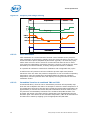
1
Intel® Xeon® Processor 3500 Series
Datasheet, Volume 1
July 2009
Document Number: 321332-002
INFORMATION IN THIS DOCUMENT IS PROVIDED IN CONNECTION WITH INTEL PRODUCTS. NO LICENSE, EXPRESS OR IMPLIED,
BY ESTOPPEL OR OTHERWISE, TO ANY INTELLECTUAL PROPERTY RIGHTS IS GRANTED BY THIS DOCUMENT. EXCEPT AS
PROVIDED IN INTEL'S TERMS AND CONDITIONS OF SALE FOR SUCH PRODUCTS, INTEL ASSUMES NO LIABILITY WHATSOEVER,
AND INTEL DISCLAIMS ANY EXPRESS OR IMPLIED WARRANTY, RELATING TO SALE AND/OR USE OF INTEL PRODUCTS INCLUDING
LIABILITY OR WARRANTIES RELATING TO FITNESS FOR A PARTICULAR PURPOSE, MERCHANTABILITY, OR INFRINGEMENT OF ANY
PATENT, COPYRIGHT OR OTHER INTELLECTUAL PROPERTY RIGHT. INTEL PRODUCTS ARE NOT INTENDED FOR USE IN MEDICAL,
LIFE SAVING, OR LIFE SUSTAINING APPLICATIONS.
Intel may make changes to specifications and product descriptions at any time, without notice.
Designers must not rely on the absence or characteristics of any features or instructions marked "reserved" or "undefined." Intel
reserves these for future definition and shall have no responsibility whatsoever for conflicts or incompatibilities arising from future
changes to them.
The Intel® Xeon® Processor 3500 Series may contain design defects or errors known as errata which may cause the product to
deviate from published specifications.
Intel processor numbers are not a measure of performance. Processor numbers differentiate features within each processor family,
not across different processor families. See http://www.intel.com/products/processor_number for details. Over time processor
numbers will increment based on changes in clock, speed, cache, FSB, or other features, and increments are not intended to
represent proportional or quantitative increases in any particular feature. Current roadmap processor number progression is not
necessarily representative of future roadmaps. See www.intel.com/products/processor_number for details.
Hyper-Threading Technology requires a computer system with a processor supporting HT Technology and an HT Technologyenabled chipset, BIOS and operating system. Performance will vary depending on the specific hardware and software you use. For
more information including details on which processors support HT Technology, see
http://www.intel.com/products/ht/hyperthreading_more.htm
Enabling Execute Disable Bit functionality requires a PC with a processor with Execute Disable Bit capability and a supporting
operating system. Check with your PC manufacturer on whether your system delivers Execute Disable Bit functionality.
64-bit computing on Intel architecture requires a computer system with a processor, chipset, BIOS, operating system, device
drivers and applications enabled for Intel® 64 architecture. Performance will vary depending on your hardware and software
configurations. Consult with your system vendor for more information.
Intel® Virtualization Technology requires a computer system with an enabled Intel® processor, BIOS, virtual machine monitor
(VMM) and, for some uses, certain computer system software enabled for it. Functionality, performance or other benefits will vary
depending on hardware and software configurations and may require a BIOS update. Software applications may not be compatible
with all operating systems. Please check with your application vendor.
Intel® Turbo Boost Technology requires a PC with a processor with Intel Turbo Boost Technology capability. Intel Turbo Boost
Technology performance varies depending on hardware, software and overall system configuration. Check with your PC
manufacturer on whether your system delivers Intel Turbo Boost Technology. For more information, see www.intel.com.
Enhanced Intel SpeedStep® Technology. See the http://processorfinder.intel.com or contact your Intel representative for more
information.
Copies of documents which have an order number and are referenced in this document, or other Intel literature may be obtained
by calling 1-800-548-4725 or by visiting Intel's website at http://www.intel.com.Contact your local Intel sales office or your
distributor to obtain the latest specifications and before placing your product order.
Intel, Pentium, Intel Xeon, Intel Atom, Enhanced Intel SpeedStep Technology, Intel Turbo Boost Technology, Intel Hyper-Threading
Technology, Intel Virtualization Technology, Intel® Advanced Digital Media Boost, and the Intel logo are trademarks or registered
trademarks of Intel Corporation in the U. S. and other countries.
*Other names and brands may be claimed as the property of others.
Copyright © 2009 Intel Corporation.
2
Intel® Xeon® Processor 3500 Series Datasheet, Volume 1
Contents
1
Introduction .............................................................................................................. 9
1.1
Terminology ..................................................................................................... 10
1.2
References ....................................................................................................... 11
2
Electrical Specifications ........................................................................................... 13
2.1
Intel® QPI Differential Signaling ......................................................................... 13
2.2
Power and Ground Lands.................................................................................... 13
2.3
Decoupling Guidelines ........................................................................................ 13
2.3.1 VCC, VTTA, VTTD, VDDQ Decoupling......................................................... 14
2.4
Processor Clocking (BCLK_DP, BCLK_DN) ............................................................. 14
2.4.1 PLL Power Supply ................................................................................... 14
2.5
Voltage Identification (VID) ................................................................................ 14
2.6
Reserved or Unused Signals................................................................................ 17
2.7
Signal Groups ................................................................................................... 18
2.8
Test Access Port (TAP) Connection....................................................................... 19
2.9
Platform Environmental Control Interface (PECI) DC Specifications........................... 20
2.9.1 DC Characteristics .................................................................................. 20
2.9.2 Input Device Hysteresis .......................................................................... 21
2.10 Absolute Maximum and Minimum Ratings ............................................................. 21
2.11 Processor DC Specifications ................................................................................ 22
2.11.1 DC Voltage and Current Specification ........................................................ 23
2.11.2 VCC Overshoot Specification .................................................................... 29
2.11.3 Die Voltage Validation ............................................................................. 30
3
Package Mechanical Specifications .......................................................................... 31
3.1
Package Mechanical Drawing............................................................................... 31
3.2
Processor Component Keep-Out Zones ................................................................. 34
3.3
Package Loading Specifications ........................................................................... 34
3.4
Package Handling Guidelines............................................................................... 34
3.5
Package Insertion Specifications.......................................................................... 34
3.6
Processor Mass Specification ............................................................................... 35
3.7
Processor Materials............................................................................................ 35
3.8
Processor Markings............................................................................................ 35
3.9
Processor Land Coordinates ................................................................................ 36
4
Intel® Xeon® Processor 3500 Series Land Listing .................................................... 37
4.1
Intel Xeon Processor 3500 Series Land Assignments .............................................. 37
4.1.1 Land Listing by Land Name ...................................................................... 38
4.1.2 Land Listing by Land Number ................................................................... 56
5
Signal Definitions .................................................................................................... 75
5.1
Signal Definitions .............................................................................................. 75
6
Thermal Specifications ............................................................................................ 79
6.1
Package Thermal Specifications ........................................................................... 79
6.1.1 Thermal Specifications ............................................................................ 79
6.1.2 Thermal Metrology ................................................................................. 83
6.2
Processor Thermal Features ................................................................................ 84
6.2.1 Processor Temperature ........................................................................... 84
6.2.2 Adaptive Thermal Monitor........................................................................ 84
6.2.3 THERMTRIP# Signal ............................................................................... 87
6.3
Platform Environment Control Interface (PECI) ...................................................... 88
6.3.1 Introduction .......................................................................................... 88
6.3.2 PECI Specifications ................................................................................. 89
6.4
Storage Conditions Specifications ........................................................................ 90
Intel® Xeon® Processor 3500 Series Datasheet, Volume 1
3
7
Features ..................................................................................................................93
7.1
Power-On Configuration (POC).............................................................................93
7.2
Clock Control and Low Power States .....................................................................93
7.2.1 Thread and Core Power State Descriptions .................................................94
7.2.2 Package Power State Descriptions .............................................................95
7.3
Sleep States .....................................................................................................96
7.4
ACPI P-States (Intel® Turbo Boost Technology) .....................................................96
7.5
Enhanced Intel SpeedStep® Technology ...............................................................97
8
Boxed Processor Specifications................................................................................99
8.1
Introduction ......................................................................................................99
8.2
Mechanical Specifications .................................................................................. 100
8.2.1 Boxed Processor Cooling Solution Dimensions........................................... 100
8.2.2 Boxed Processor Fan Heatsink Weight ..................................................... 102
8.2.3 Boxed Processor Retention Mechanism and Heatsink Attach Clip Assembly ... 102
8.3
Electrical Requirements .................................................................................... 102
8.3.1 Fan Heatsink Power Supply .................................................................... 102
8.4
Thermal Specifications...................................................................................... 103
8.4.1 Boxed Processor Cooling Requirements.................................................... 103
8.4.2 Variable Speed Fan ............................................................................... 105
Figures
1-1
2-1
2-2
2-3
2-4
2-5
3-1
3-2
3-3
3-4
3-5
6-1
6-2
6-3
7-1
8-1
8-2
8-3
8-4
8-5
8-6
8-7
8-8
8-9
4
High-Level View of Processor Interfaces ................................................................. 9
Active ODT for a Differential Link Example ............................................................13
Input Device Hysteresis ......................................................................................21
VCC Static and Transient Tolerance Load Lines ......................................................25
VTT Static and Transient Tolerance Load Line ........................................................27
VCC Overshoot Example Waveform ......................................................................30
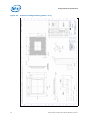
Processor Package Assembly Sketch.....................................................................31
Processor Package Drawing (Sheet 1 of 2) ............................................................32
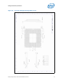
Processor Package Drawing (Sheet 2 of 2) ............................................................33
Processor Top-Side Markings ...............................................................................35
Processor Land Coordinates and Quadrants (Bottom View) ......................................36
Processor Thermal Profile....................................................................................81
Thermal Test Vehicle (TTV) Case Temperature (TCASE) Measurement Location ..........83
Frequency and Voltage Ordering ..........................................................................86
Power States.....................................................................................................94
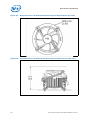
Mechanical Representation of the Boxed Processor .................................................99
Space Requirements for the Boxed Processor (side view) ...................................... 100
Space Requirements for the Boxed Processor (top view) ....................................... 101
Space Requirements for the Boxed Processor (overall view) .................................. 101
Boxed Processor Fan Heatsink Power Cable Connector Description.......................... 102
Baseboard Power Header Placement Relative to Processor Socket........................... 103
Boxed Processor Fan Heatsink Airspace Keepout Requirements (top view) ............... 104
Boxed Processor Fan Heatsink Airspace Keepout Requirements (side view) .............. 104
Boxed Processor Fan Heatsink Set Points ............................................................ 105
Intel® Xeon® Processor 3500 Series Datasheet, Volume 1
Tables
1-1
2-1
2-2
2-3
2-4
2-5
2-6
2-7
2-8
2-9
2-10
2-11
2-12
2-13
2-14
2-15
2-16
3-1
3-2
3-3
4-1
4-2
5-1
6-1
6-2
6-3
6-4
6-5
6-6
7-1
7-2
7-3
8-1
8-2
References ....................................................................................................... 11
Voltage Identification Definition........................................................................... 15
Market Segment Selection Truth Table for MS_ID[2:0] ........................................... 17
Signal Groups ................................................................................................... 18
Signals with ODT............................................................................................... 19
PECI DC Electrical Limits .................................................................................... 20
Processor Absolute Minimum and Maximum Ratings ............................................... 22
Voltage and Current Specifications....................................................................... 23
VCC Static and Transient Tolerance ..................................................................... 24
VTT Voltage Identification (VID) Definition ............................................................ 25
VTT Static and Transient Tolerance ...................................................................... 25
DDR3 Signal Group DC Specifications................................................................... 27
RESET# Signal DC Specifications ......................................................................... 28
TAP Signal Group DC Specifications ..................................................................... 28
PWRGOOD Signal Group DC Specifications............................................................ 28
Control Sideband Signal Group DC Specifications ................................................... 29
VCC Overshoot Specifications.............................................................................. 29
Processor Loading Specifications ......................................................................... 34
Package Handling Guidelines............................................................................... 34
Processor Materials............................................................................................ 35
Land Listing by Land Name ................................................................................. 38
Land Listing by Land Number .............................................................................. 56
Signal Definitions .............................................................................................. 75
Processor Thermal Specifications ......................................................................... 80
Processor Thermal Profile ................................................................................... 81
Thermal Solution Performance above TCONTROL ................................................... 82
Supported PECI Command Functions and Codes .................................................... 89
GetTemp0() Error Codes .................................................................................... 90
Storage Condition Ratings .................................................................................. 90
Power On Configuration Signal Options................................................................. 93
Coordination of Thread Power States at the Core Level ........................................... 94
Processor S-States ............................................................................................ 96
Fan Heatsink Power and Signal Specifications...................................................... 103
Fan Heatsink Power and Signal Specifications...................................................... 105
Intel® Xeon® Processor 3500 Series Datasheet, Volume 1
5
Intel® Xeon® Processor 3500 Series Features
• Available at 3.33 GHz, 3.20 GHz, 3.06 GHz,
2.93 GHz, and 2.66 GHz
• Enhanced Intel Speedstep® Technology
• Supports Intel® 64Φ Architecture
• Supports Intel® Virtualization Technology
• Intel® Turbo Boost Technology
• Supports Execute Disable Bit capability
• Binary compatible with applications running
on previous members of the Intel
microprocessor line
• Intel® Wide Dynamic Execution
• Very deep out-of-order execution
• Enhanced branch prediction
• Optimized for 32-bit applications running on
advanced 32-bit operating systems
• Intel® Smart Cache
• 8 MB Level 3 cache
• Intel® Advanced Digital Media Boost
• Enhanced floating point and multimedia unit
for enhanced video, audio, encryption, and
3D performance
• New accelerators for improved string and
text processing operations
• Power Management capabilities
• System Management mode
6
• Multiple low-power states
• 8-way cache associativity provides improved
cache hit rate on load/store operations
• System Memory Interface
— Memory controller integrated in
processor package
— 3 channels
— 2 DIMMs/channel supported (6 total)
— 24 GB maximum memory supported
— Support unbuffered DIMMs only
— Single Rank and Dual Rank DIMMs
supported
— DDR3 speeds of 800/1066 MHz
supported
— 512 Mb, 1 Gb, 2 Gb,
Technologies/Densities supported
• Intel® QuickPath Interconnect (Intel® QPI)
— Fast/narrow unidirectional links
— Concurrent bi-directional traffic
— Error detection via CRC
— Error correction via Link level retry
— Packet based protocol
— Point to point cache coherent
interconnect
— Intel® Interconnect Built In Self Test
(Intel® IBIST) toolbox built-in
• 1366-land Package
• ECC and DCA (Direct Cache Access)
Intel® Xeon® Processor 3500 Series Datasheet, Volume 1
Revision History
Revision
Number
321332-001
Description
Date
•
Public release
March 2009
•
Added Processor Information for W3580, W3550
July 2009
§
Intel® Xeon® Processor 3500 Series Datasheet, Volume 1
7
8
Intel® Xeon® Processor 3500 Series Datasheet, Volume 1
Introduction
1
Introduction
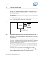
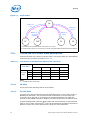
The Intel® Xeon® Processor 3500 Series are intended for Uni-processor (UP) and
workstation systems. Several architectural and microarchitectural enhancements have
been added to this processor including four processor cores in the processor package
and increased shared cache.
The Intel Xeon Processor 3500 Series is the first multi-core processor to implement key
new technologies:
• Integrated memory controller
• Point-to-point link interface based on Intel® QuickPath Interconnect (Intel® QPI)
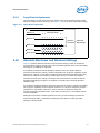
Figure 1-1 shows the interfaces used with these new technologies.
Figure 1-1.
High-Level View of Processor Interfaces
CH 0
Processor
CH 1
CH 2
System
Memory
(DDR3)
Intel® QuickPath
Interconnect (Intel® QPI)
Note:
In this document the Intel Xeon Processor 3500 Series will be referred to as “the
processor.”
The processor is optimized for performance with the power efficiencies of a low-power
microarchitecture.
This document provides DC electrical specifications, differential signaling specifications,
pinout and signal definitions, package mechanical specifications and thermal
requirements, and additional features pertinent to the implementation and operation of
the processor. For information on register descriptions, refer to the Intel® Xeon®
Processor 3500 Series Datasheet, Volume 2.
The processor is a multi-core processor built on the 45 nm process technology, that
uses up to 130 W thermal design power (TDP). The processor features an Intel QPI
point-to-point link capable of up to 6.4 GT/s, 8 MB Level 3 cache, and an integrated
memory controller.
The processor supports all the existing Streaming SIMD Extensions 2 (SSE2),
Streaming SIMD Extensions 3 (SSE3) and Streaming SIMD Extensions 4 (SSE4). The
processor supports several Advanced Technologies: Intel® 64 Technology (Intel® 64),
Enhanced Intel SpeedStep® Technology, Intel® Virtualization Technology (Intel® VT),
Intel® Turbo Boost Technology, and Intel® Hyper-Threading Technology.
Intel® Xeon® Processor 3500 Series Datasheet Volume 1
9
Introduction
1.1
Terminology
A ‘#’ symbol after a signal name refers to an active low signal, indicating a signal is in
the active state when driven to a low level. For example, when RESET# is low, a reset
has been requested. Conversely, when VTTPWRGOOD is high, the VTT power rail is
stable.
‘_N’ and ‘_P’ after a signal name refers to a differential pair.
Commonly used terms are explained here for clarification:
• Intel® Xeon® Processor 3500 Series — The entire product, including processor
substrate and integrated heat spreader (IHS).
• 1366-land LGA package — The Intel® Xeon® Processor 3500 Series is available
in a Flip-Chip Land Grid Array (FC-LGA) package, consisting of the processor
mounted on a land grid array substrate with an integrated heat spreader (IHS).
• LGA1366 Socket — The processor (in the LGA 1366 package) mates with the
system board through this surface mount, 1366-contact socket.
• DDR3 — Double Data Rate 3 Synchronous Dynamic Random Access Memory
(SDRAM) is the name of the new DDR memory standard that is being developed as
the successor to DDR2 SRDRAM.
• Intel® QuickPath Interconnect (Intel® QPI)— Intel QPI is a cache-coherent,
point-to-point link based electrical interconnect specification for Intel processors
and chipsets.
• Integrated Memory Controller — A memory controller that is integrated into the
processor die.
• Integrated Heat Spreader (IHS) — A component of the processor package used
to enhance the thermal performance of the package. Component thermal solutions
interface with the processor at the IHS surface.
• Functional Operation — Refers to the normal operating conditions in which all
processor specifications, including DC, AC, signal quality, mechanical, and thermal,
are satisfied.
• Enhanced Intel SpeedStep® Technology — Enhanced Intel SpeedStep
Technology allows the operating system to reduce power consumption when
performance is not needed.
• Execute Disable Bit — Execute Disable allows memory to be marked as
executable or non-executable, when combined with a supporting operating system.
If code attempts to run in non-executable memory the processor raises an error to
the operating system. This feature can prevent some classes of viruses or worms
that exploit buffer overrun vulnerabilities and can thus help improve the overall
security of the system. See the Intel® Architecture Software Developer's Manual
for more detailed information. Refer to http://developer.intel.com/ for future
reference on up to date nomenclatures.
• Intel® 64 Architecture — An enhancement to Intel's IA-32 architecture, allowing
the processor to execute operating systems and applications written to take
advantage of Intel® 64. Further details on Intel® 64 architecture and programming
model can be found at http://developer.intel.com/technology/intel64/.
• Intel® Virtualization Technology (Intel® VT) — A set of hardware
enhancements to Intel server and client platforms that can improve virtualization
solutions. Intel® VT provides a foundation for widely-deployed virtualization
solutions and enables a more robust hardware assisted virtualization solution. More
information can be found at: http://www.intel.com/technology/virtualization/
10
Intel® Xeon® Processor 3500 Series Datasheet Volume 1
Introduction
• Unit Interval (UI) — Signaling convention that is binary and unidirectional. In
this binary signaling, one bit is sent for every edge of the forwarded clock, whether
it is a rising edge or a falling edge. If a number of edges are collected at instances
t1, t2, tn,...., tk then the UI at instance “n” is defined as:
UI
n
=t
n
–t
n –1
• Jitter — Any timing variation of a transition edge or edges from the defined Unit
Interval.
• Storage Conditions — Refers to a non-operational state. The processor may be
installed in a platform, in a tray, or loose. Processors may be sealed in packaging or
exposed to free air. Under these conditions, processor lands should not be
connected to any supply voltages, have any I/Os biased, or receive any clocks.
• OEM — Original Equipment Manufacturer.
1.2
References
Material and concepts available in the following documents may be beneficial when
reading this document.
Table 1-1.
References
Document
Reference #
Notes
Intel® Xeon® Processor 3500 Series Specification Update
321333
1
Intel® Xeon® Processor Series Datasheet, Volume 2
321344
1
Intel® Xeon® Processor 3500 Series and LGA1366 Socket
Thermal and Mechanical Design Guide
321461
1
Note:
1.
Document is available publicly at http://www.intel.com.
§
Intel® Xeon® Processor 3500 Series Datasheet Volume 1
11
Introduction
12
Intel® Xeon® Processor 3500 Series Datasheet Volume 1
Electrical Specifications
2
Electrical Specifications
2.1
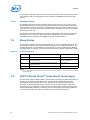
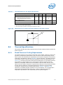
Intel® QPI Differential Signaling
The processor provides an Intel QPI port for high speed serial transfer between other
Intel QPI-enabled components. The Intel QPI port consists of two unidirectional links
(for transmit and receive). Intel QPI uses a differential signalling scheme where pairs of
opposite-polarity (D_P, D_N) signals are used.
On-die termination (ODT) is provided on the processor silicon and termination is to VSS.
Intel chipsets also provide ODT; thus, eliminating the need to terminate the Intel QPI
links on the system board.
Intel strongly recommends performing analog simulations of the Intel® QPI interface.
Figure 2-1 illustrates the active ODT. Signal listings are included in Table 2-3 and
Table 2-4. See Chapter 5 for the pin signal definitions. All Intel QPI signals are in the
differential signal group.
Figure 2-1.
Active ODT for a Differential Link Example
TX
RX
Signal
Signal
RTT
2.2
RTT
RTT
RTT
Power and Ground Lands
For clean on-chip processor core power distribution, the processor has 210 VCC pads
and 119 VSS pads associated with VCC; 8 VTTA pads and 5 VSS pads associated with
VTTA; 28 VTTD pads and 17 VSS pads associated with VTTD, 28 VDDQ pads and 17 VSS
pads associated with VDDQ; and 3 VCCPLL pads. All VCCP, VTTA, VTTD, VDDQ and
VCCPLL lands must be connected to their respective processor power planes, while all
VSS lands must be connected to the system ground plane. The processor VCC lands
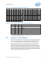
must be supplied with the voltage determined by the processor Voltage IDentification
(VID) signals. Table 2-1 specifies the voltage level for the various VIDs.
2.3
Decoupling Guidelines
Due to its large number of transistors and high internal clock speeds, the processor is
capable of generating large current swings between low and full power states. This may
cause voltages on power planes to sag below their minimum values if bulk decoupling is
not adequate. Larger bulk storage (CBULK), such as electrolytic capacitors, supply
current during longer lasting changes in current demand; such as, coming out of an idle
condition. Similarly, capacitors act as a storage well for current when entering an idle
condition from a running condition. Care must be taken in the baseboard design to
Intel® Xeon® Processor 3500 Series Datasheet Volume 1
13
Electrical Specifications
ensure that the voltage provided to the processor remains within the specifications
listed in Table 2-7. Failure to do so can result in timing violations or reduced lifetime of
the processor.
2.3.1
VCC, VTTA, VTTD, VDDQ Decoupling
Voltage regulator solutions need to provide bulk capacitance and the baseboard
designer must assure a low interconnect resistance from the regulator to the LGA1366
socket. Bulk decoupling must be provided on the baseboard to handle large current
swings. The power delivery solution must insure the voltage and current specifications
are met (as defined in Table 2-7).
2.4
Processor Clocking (BCLK_DP, BCLK_DN)
The processor core, Intel QPI, and integrated memory controller frequencies are
generated from BCLK_DP and BCLK_DN. Unlike previous processors based on front side
bus architecture, there is no direct link between core frequency and Intel QPI link
frequency (such as, no core frequency to Intel QPI multiplier). The processor maximum
core frequency, Intel QPI link frequency and integrated memory controller frequency,
are set during manufacturing. It is possible to override the processor core frequency
setting using software. This permits operation at lower core frequencies than the
factory set maximum core frequency.
The processor’s maximum non-turbo core frequency is configured during power-on
reset by using values stored internally during manufacturing. The stored value sets the
highest core multiplier at which the particular processor can operate. If lower max nonturbo speeds are desired, the appropriate ratio can be configured via the
CLOCK_FLEX_MAX MSR.
The processor uses differential clocks (BCLK_DP, BCLK_DN). Clock multiplying within
the processor is provided by the internal phase locked loop (PLL), which requires a
constant frequency BCLK_DP, BCLK_DN input, with exceptions for spread spectrum
clocking. The processor core frequency is determined by multiplying the ratio by
133 MHz.
2.4.1
PLL Power Supply
An on-die PLL filter solution is implemented on the processor. Refer to Table 2-7 for DC
specifications.
2.5
Voltage Identification (VID)
The voltage set by the VID signals is the reference voltage regulator output voltage to
be delivered to the processor VCC pins. VID signals are CMOS push/pull drivers. Refer
to Table 2-15 for the DC specifications for these signals. The VID codes will change due
to temperature and/or current load changes in order to minimize the power of the part.
A voltage range is provided in Table 2-7. The specifications have been set such that one
voltage regulator can operate with all supported frequencies.
Individual processor VID values may be set during manufacturing such that two devices
at the same core frequency may have different default VID settings. This is reflected by
the VID range values provided in Table 2-1.
14
Intel® Xeon® Processor 3500 Series Datasheet Volume 1
Electrical Specifications
The processor uses eight voltage identification signals, VID[7:0], to support automatic
selection of voltages. Table 2-1 specifies the voltage level corresponding to the state of
VID[7:0]. A ‘1’ in this table refers to a high voltage level and a ‘0’ refers to a low
voltage level. If the processor socket is empty (VID[7:0] = 11111111), or the voltage
regulation circuit cannot supply the voltage that is requested, the voltage regulator
must disable itself.
The processor provides the ability to operate while transitioning to an adjacent VID and
its associated processor core voltage (VCC). This will represent a DC shift in the
loadline. It should be noted that a low-to-high or high-to-low voltage state change will
result in as many VID transitions as necessary to reach the target core voltage.
Transitions above the maximum specified VID are not permitted. Table 2-8 includes VID
step sizes and DC shift ranges. Minimum and maximum voltages must be maintained
as shown in Table 2-8.
The VR used must be capable of regulating its output to the value defined by the new
VID. DC specifications for dynamic VID transitions are included in Table 2-7 and
Table 2-8.
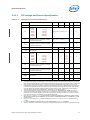
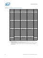
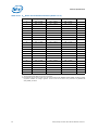
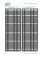
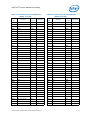
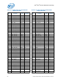
Table 2-1.
Voltage Identification Definition (Sheet 1 of 3)
VID
7
VID
6
VID
5
VID
4
VID
3
VID
2
VID
1
VID
0
VCC_MAX
VID
7
VID
6
VID
5
VID
4
VID
3
VID
2
VID
1
VID
0
VCC_MAX
0
0
0
0
0
0
0
0
OFF
0
1
0
1
1
0
1
1
1.04375
0
0
0
0
0
0
0
1
OFF
0
1
0
1
1
1
0
0
1.03750
0
0
0
0
0
0
1
0
1.60000
0
1
0
1
1
1
0
1
1.03125
0
0
0
0
0
0
1
1
1.59375
0
1
0
1
1
1
1
0
1.02500
0
0
0
0
0
1
0
0
1.58750
0
1
0
1
1
1
1
1
1.01875
0
0
0
0
0
1
0
1
1.58125
0
1
1
0
0
0
0
0
1.01250
0
0
0
0
0
1
1
0
1.57500
0
1
1
0
0
0
0
1
1.00625
0
0
0
0
0
1
1
1
1.56875
0
1
1
0
0
0
1
0
1.00000
0.99375
0
0
0
0
1
0
0
0
1.56250
0
1
1
0
0
0
1
1
0
0
0
0
1
0
0
1
1.55625
0
1
1
0
0
1
0
0
0.98750
0
0
0
0
1
0
1
0
1.55000
0
1
1
0
0
1
0
1
0.98125
0
0
0
0
1
0
1
1
1.54375
0
1
1
0
0
1
1
0
0.97500
0
0
0
0
1
1
0
0
1.53750
0
1
1
0
0
1
1
1
0.96875
0
0
0
0
1
1
0
1
1.53125
0
1
1
0
1
0
0
0
0.96250
0
0
0
0
1
1
1
0
1.52500
0
1
1
0
1
0
0
1
0.95626
0
0
0
0
1
1
1
1
1.51875
0
1
1
0
1
0
1
0
0.95000
0
0
0
1
0
0
0
0
1.51250
0
1
1
0
1
0
1
1
0.94375
0
0
0
1
0
0
0
1
1.50625
0
1
1
0
1
1
0
0
0.93750
0
0
0
1
0
0
1
0
1.50000
0
1
1
0
1
1
0
1
0.93125
0
0
0
1
0
0
1
1
1.49375
0
1
1
0
1
1
1
0
0.92500
0
0
0
1
0
1
0
0
1.48750
0
1
1
0
1
1
1
1
0.91875
0
0
0
1
0
1
0
1
1.48125
0
1
1
1
0
0
0
0
0.91250
0
0
0
1
0
1
1
0
1.47500
0
1
1
1
0
0
0
1
0.90625
0
0
0
1
0
1
1
1
1.46875
0
1
1
1
0
0
1
0
0.90000
0
0
0
1
1
0
0
0
1.46250
0
1
1
1
0
0
1
1
0.89375
0
0
0
1
1
0
0
1
1.45625
0
1
1
1
0
1
0
0
0.88750
0
0
0
1
1
0
1
0
1.45000
0
1
1
1
0
1
0
1
0.88125
0
0
0
1
1
0
1
1
1.44375
0
1
1
1
0
1
1
0
0.87500
0
0
0
1
1
1
0
0
1.43750
0
1
1
1
0
1
1
1
0.86875
0
0
0
1
1
1
0
1
1.43125
0
1
1
1
1
0
0
0
0.86250
0
0
0
1
1
1
1
0
1.42500
0
1
1
1
1
0
0
1
0.85625
Intel® Xeon® Processor 3500 Series Datasheet Volume 1
15
Electrical Specifications
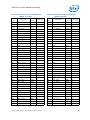
Table 2-1.
Voltage Identification Definition (Sheet 2 of 3)
VID
7
VID
6
VID
5
VID
4
VID
3
VID
2
VID
1
VID
0
VCC_MAX
VID
7
VID
6
VID
5
VID
4
VID
3
VID
2
VID
1
VID
0
VCC_MAX
0
0
0
1
1
1
1
1
1.41875
0
1
1
1
1
0
1
0
0.85000
0
0
1
0
0
0
0
0
1.41250
0
1
1
1
1
0
1
1
0.84374
0
0
1
0
0
0
0
1
1.40625
0
1
1
1
1
1
0
0
0.83750
0
0
1
0
0
0
1
0
1.40000
0
1
1
1
1
1
0
1
0.83125
0
0
1
0
0
0
1
1
1.39375
0
1
1
1
1
1
1
0
0.82500
0
0
1
0
0
1
0
0
1.38750
0
1
1
1
1
1
1
1
0.81875
0
0
1
0
0
1
0
1
1.38125
1
0
0
0
0
0
0
0
0.81250
0
0
1
0
0
1
1
0
1.37500
1
0
0
0
0
0
0
1
0.80625
0
0
1
0
0
1
1
1
1.36875
1
0
0
0
0
0
1
0
0.80000
0
0
1
0
1
0
0
0
1.36250
1
0
0
0
0
0
1
1
0.79375
0
0
1
0
1
0
0
1
1.35625
1
0
0
0
0
1
0
0
0.78750
0
0
1
0
1
0
1
0
1.35000
1
0
0
0
0
1
0
1
0.78125
0
0
1
0
1
0
1
1
1.34375
1
0
0
0
0
1
1
0
0.77500
0
0
1
0
1
1
0
0
1.33750
1
0
0
0
0
1
1
1
0.76875
0
0
1
0
1
1
0
1
1.33125
1
0
0
0
1
0
0
0
0.76250
0
0
1
0
1
1
1
0
1.32500
1
0
0
0
1
0
0
1
0.75625
0
0
1
0
1
1
1
1
1.31875
1
0
0
0
1
0
1
0
0.75000
0
0
1
1
0
0
0
0
1.31250
1
0
0
0
1
0
1
1
0.74375
0
0
1
1
0
0
0
1
1.30625
1
0
0
0
1
1
0
0
0.73750
0
0
1
1
0
0
1
0
1.30000
1
0
0
0
1
1
0
1
0.73125
0
0
1
1
0
0
1
1
1.29375
1
0
0
0
1
1
1
0
0.72500
0
0
1
1
0
1
0
0
1.28750
1
0
0
0
1
1
1
1
0.71875
0
0
1
1
0
1
0
1
1.28125
1
0
0
1
0
0
0
0
0.71250
0
0
1
1
0
1
1
0
1.27500
1
0
0
1
0
0
0
1
0.70625
0
0
1
1
0
1
1
1
1.26875
1
0
0
1
0
0
1
0
0.70000
0
0
1
1
1
0
0
0
1.26250
1
0
0
1
0
0
1
1
0.69375
0
0
1
1
1
0
0
1
1.25625
1
0
0
1
0
1
0
0
0.68750
0
0
1
1
1
0
1
0
1.25000
1
0
0
1
0
1
0
1
0.68125
0
0
1
1
1
0
1
1
1.24375
1
0
0
1
0
1
1
0
0.67500
0
0
1
1
1
1
0
0
1.23750
1
0
0
1
0
1
1
1
0.66875
0
0
1
1
1
1
0
1
1.23125
1
0
0
1
1
0
0
0
0.66250
0
0
1
1
1
1
1
0
1.22500
1
0
0
1
1
0
0
1
0.65625
0
0
1
1
1
1
1
1
1.21875
1
0
0
1
1
0
1
0
0.65000
0
1
0
0
0
0
0
0
1.21250
1
0
0
1
1
0
1
1
0.64375
0
1
0
0
0
0
0
1
1.20625
1
0
0
1
1
1
0
0
0.63750
0
1
0
0
0
0
1
0
1.20000
1
0
0
1
1
1
0
1
0.63125
0
1
0
0
0
0
1
1
1.19375
1
0
0
1
1
1
1
0
0.62500
0
1
0
0
0
1
0
0
1.18750
1
0
0
1
1
1
1
1
0.61875
0
1
0
0
0
1
0
1
1.18125
1
0
1
0
0
0
0
0
0.61250
0
1
0
0
0
1
1
0
1.17500
1
0
1
0
0
0
0
1
0.60625
0
1
0
0
0
1
1
1
1.16875
1
0
1
0
0
0
1
0
0.60000
0
1
0
0
1
0
0
0
1.16250
1
0
1
0
0
0
1
1
0.59375
0
1
0
0
1
0
0
1
1.15625
1
0
1
0
0
1
0
0
0.58750
0
1
0
0
1
0
1
0
1.15000
1
0
1
0
0
1
0
1
0.58125
0
1
0
0
1
0
1
1
1.14375
1
0
1
0
0
1
1
0
0.57500
0
1
0
0
1
1
0
0
1.13750
1
0
1
0
0
1
1
1
0.56875
0
1
0
0
1
1
0
1
1.13125
1
0
1
0
1
0
0
0
0.56250
0
1
0
0
1
1
1
0
1.12500
1
0
1
0
1
0
0
1
0.55625
16
Intel® Xeon® Processor 3500 Series Datasheet Volume 1
Electrical Specifications
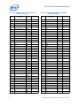
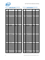
Table 2-1.
Voltage Identification Definition (Sheet 3 of 3)
VID
7
VID
6
VID
5
VID
4
VID
3
VID
2
VID
1
VID
0
VCC_MAX
VID
7
VID
6
VID
5
VID
4
VID
3
VID
2
VID
1
VID
0
VCC_MAX
0
1
0
0
1
1
1
1
1.11875
1
0
1
0
1
0
1
0
0.55000
0
1
0
1
0
0
0
0
1.11250
1
0
1
0
1
0
1
1
0.54375
0
1
0
1
0
0
0
1
1.10625
1
0
1
0
1
1
0
0
0.53750
0
1
0
1
0
0
1
0
1.10000
1
0
1
0
1
1
0
1
0.53125
0
1
0
1
0
0
1
1
1.09375
1
0
1
0
1
1
1
0
0.52500
0
1
0
1
0
1
0
0
1.08750
1
0
1
0
1
1
1
1
0.51875
0
1
0
1
0
1
0
1
1.08125
1
0
1
1
0
0
0
0
0.51250
0
1
0
1
0
1
1
0
1.07500
1
0
1
1
0
0
0
1
0.50625
0
1
0
1
0
1
1
1
1.06875
1
0
1
1
0
0
1
0
0.50000
0
1
0
1
1
0
0
0
1.06250
1
1
1
1
1
1
1
0
OFF
0
1
0
1
1
0
0
1
1.05625
1
1
1
1
1
1
1
1
OFF
0
1
0
1
1
0
1
0
1.05000
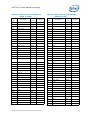
Table 2-2.
Market Segment Selection Truth Table for MS_ID[2:0]
Description1
MSID2
MSID1
MSID0
0
0
0
Reserved
0
0
1
Reserved
0
1
0
Reserved
0
1
1
Reserved
1
0
0
Reserved
1
0
1
Reserved
1
1
0
Intel Xeon Processor 3500 Series
1
1
1
Reserved
Notes:
1.
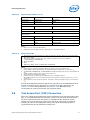
2.6
The MSID[2:0] signals are provided to indicate the Market Segment for the processor and may be used for
future processor compatibility or for keying.
Reserved or Unused Signals
All Reserved (RSVD) signals must remain unconnected. Connection of these signals to
VCC, VTTA, VTTD, VDDQ, VCCPLL, VSS, or to any other signal (including each other) can
result in component malfunction or incompatibility with future processors. See
Chapter 4 for a land listing of the processor and the location of all Reserved signals.
For reliable operation, always connect unused inputs or bi-directional signals to an
appropriate signal level, except for unused integrated memory controller inputs,
outputs, and bi-directional pins which may be left floating. Unused active high inputs
should be connected through a resistor to ground (VSS). Unused outputs maybe left
unconnected; however, this may interfere with some Test Access Port (TAP) functions,
complicate debug probing, and prevent boundary scan testing. A resistor must be used
when tying bi-directional signals to power or ground. When tying any signal to power or
ground, a resistor will also allow for system testability.
Intel® Xeon® Processor 3500 Series Datasheet Volume 1
17
Electrical Specifications
2.7
Signal Groups
Signals are grouped by buffer type and similar characteristics as listed in Table 2-3. The
buffer type indicates which signaling technology and specifications apply to the signals.
All the differential signals, and selected DDR3 and Control Sideband signals have OnDie Termination (ODT) resistors. There are some signals that do not have ODT and
need to be terminated on the board. The signals that have ODT are listed in Table 2-4.
Table 2-3.
Signal Groups (Sheet 1 of 2)
Signal Group
Signals1,2
Type
System Reference Clock
Differential
Intel
®
Clock Input
BCLK_DP, BCLK_DN
QPI Signal Groups
Differential
Intel QPI Input
QPI_DRX_D[N/P][19:0], QPI_CLKRX_DP,
QPI_CLKRX_DN
Differential
Intel QPI Output
QPI_DTX_D[N/P][19:0], QPI_CLKTX_DP,
QPI_CLKTX_DN
DDR3 Reference Clocks
Differential
DDR3 Output
DDR{0/1/2}_CLK[D/P][3:0]
DDR3 Command Signals
Single ended
CMOS Output
DDR{0/1/2}_RAS#, DDR{0/1/2}_CAS#,
DDR{0/1/2}_WE#, DDR{0/1/2}_MA[15:0],
DDR{0/1/2}_BA[2:0]
Single ended
Asynchronous Output
DDR{0/1/2}_RESET#
CMOS Output
DDR{0/1/2}_CS#[5:4], DDR{0/1/2}_CS#[1:0],
DDR{0/1/2}_ODT[3:0], DDR{0/1/2}_CKE[3:0]
Single ended
CMOS Bi-directional
DDR{0/1/2}_DQ[63:0], DDR{0/1/2}_ECC[7:0]
Differential
CMOS Bi-directional
DDR{0/1/2}_DQS_[N/P][7:0]
Single ended
TAP Input
TCK, TDI, TMS, TRST#
Single ended
GTL Output
TDO
Single ended
Asynchronous GTL Output
PRDY#
Single ended
Asynchronous GTL Input
PREQ#
Single ended
GTL Bi-directional
CAT_ERR#, BPM#[7:0]
Single Ended
Asynchronous Bi-directional
PECI
Single Ended
Analog Input
COMP0, QPI_CMP[0], DDR_COMP[2:0]
Single ended
Asynchronous GTL Bidirectional
PROCHOT#
Single ended
Asynchronous GTL Output
THERMTRIP#
Single ended
CMOS Input/Output
VID[7:6]
VID[5:3]/CSC[2:0]
VID[2:0]/MSID[2:0]
VTT_VID[4:2]
DDR3 Control Signals
Single ended
DDR3 Data Signals
TAP
Control Sideband
18
Intel® Xeon® Processor 3500 Series Datasheet Volume 1
Electrical Specifications
Table 2-3.
Signal Groups (Sheet 2 of 2)
Signal Group
Signals1,2
Type
Single ended
CMOS Output
VTT_VID[4:2]
Single ended
Analog Input
ISENSE
Reset Input
RESET#
Asynchronous Input
VCCPWRGOOD, VTTPWRGOOD, VDDPWRGOOD
Power
VCC, VTTA, VTTD, VCCPLL, VDDQ
Asynchronous CMOS Output
PSI#
Sense Points
VCC_SENSE, VSS_SENSE
Other
SKTOCC#, DBR#
Reset Signal
Single ended
PWRGOOD Signals
Single ended
Power/Other
Notes:
Notes:
1.
Refer to Chapter 5 for signal descriptions.
2.
DDR{0/1/2} refers to DDR3 Channel 0, DDR3 Channel 1, and DDR3 Channel 2.
1.
Table 2-4.
Signals with ODT
•
•
•
•
•
QPI_DRX_DP[19:0], QPI_DRX_DN[19:0], QPI_DTX_DP[19:0], QPI_DTX_DN[19:0], QPI_CLKRX_D[N/P],
QPI_CLKTX_D[N/P]
DDR{0/1/2}_DQ[63:0], DDR{0/1/2}_DQS_[N/P][7:0], DDR{0/1/2}_ECC[7:0], DDR{0/1/
2}_PAR_ERR#[0:2], VDDPWRGOOD
BCLK_ITP_D[N/P]
PECI
BPM#[7:0], PREQ#, TRST#, VCCPWRGOOD, VTTPWRGOOD
Notes:
1.
Unless otherwise specified, signals have ODT in the package with 50 Ω pulldown to VSS.
2.
PREQ#, BPM[7:0], TDI, TMS and BCLK_ITP_D[N/P] have ODT in package with 35 Ω pullup to VTT.
3.
VCCPWRGOOD, VDDPWRGOOD, and VTTPWRGOOD have ODT in package with a 10 kΩ to 20 kΩ pulldown to
VSS.
4.
TRST# has ODT in package with a 1 kΩ to 5 kΩ pullup to VTT.
5.
All DDR signals are terminated to VDDQ/2
6.
DDR{0/1/2} refers to DDR3 Channel 0, DDR3 Channel 1, and DDR3 Channel 2.
7.
While TMS and TDI do not have On-Die Termination, these signals are weakly pulled up using a 1–5 kΩ
resistor to VTT
8.
While TCK does not have On-Die Termination, this signal is weakly pulled down using a 1–5 kΩ resistor to
VSS.
All Control Sideband Asynchronous signals are required to be asserted/deasserted for
at least eight BCLKs for the processor to recognize the proper signal state. See
Section 2.11 for the DC specifications. See Chapter 6 for additional timing
requirements for entering and leaving the low power states.
2.8
Test Access Port (TAP) Connection
Due to the voltage levels supported by other components in the Test Access Port (TAP)
logic, it is recommended that the processor be first in the TAP chain and followed by
any other components within the system. A translation buffer should be used to
connect to the rest of the chain unless one of the other components is capable of
accepting an input of the appropriate voltage. Two copies of each signal may be
required with each driving a different voltage level.
Intel® Xeon® Processor 3500 Series Datasheet Volume 1
19
Electrical Specifications
2.9
Platform Environmental Control Interface (PECI)
DC Specifications
PECI is an Intel proprietary interface that provides a communication channel between
Intel processors and chipset components to external thermal monitoring devices. The
processor contains a Digital Thermal Sensor (DTS) that reports a relative die
temperature as an offset from Thermal Control Circuit (TCC) activation temperature.
Temperature sensors located throughout the die are implemented as analog-to-digital
converters calibrated at the factory. PECI provides an interface for external devices to
read the DTS temperature for thermal management and fan speed control. More
detailed information may be found in the Platform Environment Control Interface
(PECI) Specification.
2.9.1
DC Characteristics
The PECI interface operates at a nominal voltage set by VTTD. The set of DC electrical
specifications shown in Table 2-5 is used with devices normally operating from a VTTD
interface supply. VTTD nominal levels will vary between processor families. All PECI
devices will operate at the VTTD level determined by the processor installed in the
system. For specific nominal VTTD levels, refer to Table 2-7.
Table 2-5.
PECI DC Electrical Limits
Symbol
Vin
Vhysteresis
Definition and Conditions
Input Voltage Range
Hysteresis
Min
Max
Units
-0.150
VTTD
V
0.1 * VTTD
N/A
V
Notes1
Vn
Negative-edge threshold voltage
0.275 * VTTD
0.500 * VTTD
V
Vp
Positive-edge threshold voltage
0.550 * VTTD
0.725 * VTTD
V
High level output source
(VOH = 0.75 * VTTD)
-6.0
N/A
mA
Low level output sink
(VOL = 0.25 * VTTD)
0.5
1.0
mA
Ileak+
High impedance state leakage to VTTD
(Vleak = VOL)
N/A
100
µA
2
Ileak-
High impedance leakage to GND
(Vleak = VOH)
N/A
100
µA
2
Cbus
Bus capacitance per node
Isource
Isink
Vnoise
Signal noise immunity above 300 MHz
N/A
10
pF
0.1 * VTTD
N/A
Vp-p
Notes:
1.
VTTD supplies the PECI interface. PECI behavior does not affect VTTD min/max specifications.
2.
The leakage specification applies to powered devices on the PECI bus.
20
Intel® Xeon® Processor 3500 Series Datasheet Volume 1
Electrical Specifications
2.9.2
Input Device Hysteresis
The input buffers in both client and host models must use a Schmitt-triggered input
design for improved noise immunity. Use Figure 2-2 as a guide for input buffer design.
Figure 2-2.
Input Device Hysteresis
VTTD
Maximum VP
PECI High Range
Minimum VP
Minimum
Hysteresis
Valid Input
Signal Range
Maximum VN
Minimum VN
PECI Low Range
PECI Ground
2.10
Absolute Maximum and Minimum Ratings
Table 2-6 specifies absolute maximum and minimum ratings, which lie outside the
functional limits of the processor. Only within specified operation limits can functionality
and long-term reliability be expected.
At conditions outside functional operation condition limits, but within absolute
maximum and minimum ratings, neither functionality nor long-term reliability can be
expected. If a device is returned to conditions within functional operation limits after
having been subjected to conditions outside these limits, but within the absolute
maximum and minimum ratings, the device may be functional, but with its lifetime
degraded depending on exposure to conditions exceeding the functional operation
condition limits.
At conditions exceeding absolute maximum and minimum ratings, neither functionality
nor long-term reliability can be expected. Moreover, if a device is subjected to these
conditions for any length of time then, when returned to conditions within the
functional operating condition limits, it will either not function or its reliability will be
severely degraded.
Although the processor contains protective circuitry to resist damage from ElectroStatic Discharge (ESD), precautions should always be taken to avoid high static
voltages or electric fields.
Intel® Xeon® Processor 3500 Series Datasheet Volume 1
21
Electrical Specifications
.
Table 2-6.
Processor Absolute Minimum and Maximum Ratings
Symbol
Parameter
Min
Max
Unit
Notes1, 2
VCC
Processor Core voltage with respect to VSS
-0.3
1.55
V
VTTA
Voltage for the analog portion of the integrated
memory controller, Intel QPI link and Shared
Cache with respect to VSS
—
1.35
V
3
VTTD
Voltage for the digital portion of the integrated
memory controller, Intel QPI link and Shared
Cache with respect to VSS
—
1.35
V
3
VDDQ
Processor I/O supply voltage for DDR3 with
respect to VSS
—
1.875
V
VCCPLL
TCASE
TSTORAGE
Processor PLL voltage with respect to VSS
1.65
1.89
V
Processor case temperature
See
Chapter 6
See
Chapter 6
°C
Storage temperature
See
Chapter 6
See
Chapter 6
°C
Notes:
1.
For functional operation, all processor electrical, signal quality, mechanical and thermal specifications must
be satisfied.
2.
Excessive overshoot or undershoot on any signal will likely result in permanent damage to the processor.
3.
VTTA and VTTD should be derived from the same VR.
2.11
Processor DC Specifications
The processor DC specifications in this section are defined at the processor
pads, unless noted otherwise. See Chapter 4 for the processor land listings and
Chapter 5 for signal definitions. Voltage and current specifications are detailed in Table
2-7. For platform planning, refer to Table 2-8, which provides VCC static and transient
tolerances. This same information is presented graphically in Figure 2-3.
The DC specifications for the DDR3 signals are listed in Table 2-11. Control Sideband
and Test Access Port (TAP) are listed in Table 2-12 through Table 2-15.
Table 2-7 through Table 2-15 list the DC specifications for the processor and are valid
only while meeting specifications for case temperature (TCASE as specified in Chapter 6,
“Thermal Specifications”), clock frequency, and input voltages. Care should be taken to
read all notes associated with each parameter.
22
Intel® Xeon® Processor 3500 Series Datasheet Volume 1
Electrical Specifications
2.11.1
DC Voltage and Current Specification
Table 2-7.
Voltage and Current Specifications
Symbol
Parameter
Min
Typ
Max
Unit
Notes 1
0.8
—
1.375
V
2
See Table 2-8 and Figure 2-3
V
3,4
VID
VID range
VCC
Processor
Number
W3580
W3570
W3550
W3540
W3520
VTTA
Voltage for the analog portion of the
integrated memory controller, Intel QPI
link and Shared Cache
See Table 2-10 and Figure 2-4
V
5
VTTD
Voltage for the digital portion of the
integrated memory controller, Intel QPI
link and Shared Cache
See Table 2-9 and Figure 2-4
V
5
VDDQ
Processor I/O supply voltage for DDR3
VCCPLL
VCC for processor core
3.33
3.20
3.06
2.93
2.66
GHz
GHz
GHz
GHz
GHz
PLL supply voltage (DC + AC
specification)
1.425
1.5
1.575
1.71
1.8
1.89
—
—
V
V
ICC
Processor
Number
W3580
W3570
W3550
W3540
W3520
ITTA
Current for the analog portion of the
integrated memory controller, Intel QPI
link and Shared Cache
—
—
5
A
ITTD
Current for the digital portion of the
integrated memory controller, Intel QPI
link and Shared Cache
—
—
23
A
IDDQ
Processor I/O supply current for DDR3
—
—
6
A
IDDQS3
Processor I/O supply current for DDR3
while in S3
—
—
1
A
PLL supply current (DC + AC specification)
—
—
1.1
A
ICC_VCCPLL
ICC for processor
3.33
3.20
3.06
2.93
2.66
GHz
GHz
GHz
GHz
GHz
145
145
145
145
145
A
6
7
Notes:
1.
2.
3.
4.
5.
6.
7.
Unless otherwise noted, all specifications in this table are based on estimates and simulations or empirical
data. These specifications will be updated with characterized data from silicon measurements at a later date
Each processor is programmed with a maximum valid voltage identification value (VID), which is set at
manufacturing and can not be altered. Individual maximum VID values are calibrated during manufacturing
such that two processors at the same frequency may have different settings within the VID range. Please
note this differs from the VID employed by the processor during a power management event (Adaptive
Thermal Monitor, Enhanced Intel SpeedStep® Technology, or Low Power States).
The voltage specification requirements are measured across VCC_SENSE and VSS_SENSE lands at the
socket with a 100 MHz bandwidth oscilloscope, 1.5 pF maximum probe capacitance, and 1 MΩ minimum
impedance. The maximum length of ground wire on the probe should be less than 5 mm. Ensure external
noise from the system is not coupled into the oscilloscope probe.
Refer to Table 2-8 and Figure 2-3 for the minimum, typical, and maximum VCC allowed for a given current.
The processor should not be subjected to any VCC and ICC combination wherein VCC exceeds VCC_MAX for
a given current.
See Table 2-9 for details on VTT Voltage Identification and Table 2-9 and Figure 2-4 for details on the VTT
Loadline.
ICC_MAX specification is based on the VCC_MAX loadline. Refer to Figure 2-3 for details.
This spec is based on a processor temperature, as reported by the DTS, of less than or equal to Tcontrol-25.
Intel® Xeon® Processor 3500 Series Datasheet Volume 1
23
Electrical Specifications
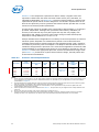
Table 2-8.
VCC Static and Transient Tolerance
ICC (A)
VCC_Max (V)
VCC_Typ (V)
VCC_Min (V)
Notes
0
VID - 0.000
VID - 0.019
VID - 0.038
1, 2, 3
5
VID - 0.004
VID - 0.023
VID - 0.042
1, 2, 3
10
VID - 0.008
VID - 0.027
VID - 0.046
1, 2, 3
15
VID - 0.012
VID - 0.031
VID - 0.050
1, 2, 3
20
VID - 0.016
VID - 0.035
VID - 0.054
1, 2, 3
25
VID - 0.020
VID - 0.039
VID - 0.058
1, 2, 3
30
VID - 0.024
VID - 0.043
VID - 0.062
1, 2, 3
35
VID - 0.028
VID - 0.047
VID - 0.066
1, 2, 3
40
VID - 0.032
VID - 0.051
VID - 0.070
1, 2, 3
45
VID - 0.036
VID - 0.055
VID - 0.074
1, 2, 3
50
VID - 0.040
VID - 0.059
VID - 0.078
1, 2, 3
55
VID - 0.044
VID - 0.063
VID - 0.082
1, 2, 3
60
VID - 0.048
VID - 0.067
VID - 0.086
1, 2, 3
65
VID - 0.052
VID - 0.071
VID - 0.090
1, 2, 3
70
VID - 0.056
VID - 0.075
VID - 0.094
1, 2, 3
75
VID - 0.060
VID - 0.079
VID - 0.098
1, 2, 3
78
VID - 0.062
VID - 0.081
VID - 0.100
1, 2, 3
85
VID - 0.068
VID - 0.087
VID - 0.106
1, 2, 3
90
VID - 0.072
VID - 0.091
VID - 0.110
1, 2, 3
95
VID - 0.076
VID - 0.095
VID - 0.114
1, 2, 3
100
VID - 0.080
VID - 0.099
VID - 0.118
1, 2, 3
105
VID - 0.084
VID - 0.103
VID - 0.122
1, 2, 3
110
VID - 0.088
VID - 0.107
VID - 0.126
1, 2, 3
115
VID - 0.092
VID - 0.111
VID - 0.130
1, 2, 3
120
VID - 0.096
VID - 0.115
VID - 0.134
1, 2, 3
125
VID - 0.100
VID - 0.119
VID - 0.138
1, 2, 3
130
VID - 0.104
VID - 0.123
VID - 0.142
1, 2, 3
135
VID - 0.108
VID - 0.127
VID - 0.146
1, 2, 3
140
VID - 0.112
VID - 0.131
VID - 0.150
1, 2, 3
Notes:
1.
The VCC_MIN and VCC_MAX loadlines represent static and transient limits. See Section 2.11.2 for VCC
overshoot specifications.
2.
This table is intended to aid in reading discrete points on Figure 2-3.
3.
The loadlines specify voltage limits at the die measured at the VCC_SENSE and VSS_SENSE lands. Voltage
regulation feedback for voltage regulator circuits must also be taken from processor VCC_SENSE and
VSS_SENSE lands.
24
Intel® Xeon® Processor 3500 Series Datasheet Volume 1
Electrical Specifications
Figure 2-3.
VCC Static and Transient Tolerance Load Lines
Icc [A]
0
10
20
30
40
50
60
70
80
90
100
110
120
130
140
VID - 0.000
VID - 0.013
VID - 0.025
Vcc Maximum
VID - 0.038
VID - 0.050
VID - 0.063
VID - 0.075
Vcc Typical
V
VID - 0.088
c
c
VID - 0.100
V
VID - 0.113
Vcc Minimum
VID - 0.125
VID - 0.138
VID - 0.150
VID - 0.163
VID - 0.175
Table 2-9.
VTT Voltage Identification (VID) Definition
VTT VR - VID Input
VTT_Typ
VID7
VID6
VID5
VID4
VID3
VID2
VID1
VID0
0
1
0
0
0
0
1
0
1.220 V
0
1
0
0
0
1
1
0
1.195 V
0
1
0
0
1
0
1
0
1.170 V
0
1
0
0
1
1
1
0
1.145 V
0
1
0
1
0
0
1
0
1.120 V
0
1
0
1
0
1
1
0
1.095 V
0
1
0
1
1
0
1
0
1.070 V
0
1
0
1
1
1
1
0
1.045 V
Notes:
1.
This is a typical voltage, see Table 2-10 for VTT_Max and VTT_Min voltage.
Table 2-10. VTT Static and Transient Tolerance (Sheet 1 of 2)
ITT (A)
VTT_Max (V)
VTT_Typ (V)
VTT_Min (V)
0
VID + 0.0315
VID – 0.0000
VID – 0.0315
1
VID + 0.0255
VID – 0.0060
VID – 0.0375
2
VID + 0.0195
VID – 0.0120
VID – 0.0435
3
VID + 0.0135
VID – 0.0180
VID – 0.0495
4
VID + 0.0075
VID – 0.0240
VID – 0.0555
5
VID + 0.0015
VID – 0.0300
VID – 0.0615
Intel® Xeon® Processor 3500 Series Datasheet Volume 1
Notes1
25
Electrical Specifications
Table 2-10. VTT Static and Transient Tolerance (Sheet 2 of 2)
ITT (A)
VTT_Max (V)
VTT_Typ (V)
VTT_Min (V)
6
VID – 0.0045
VID – 0.0360
VID – 0.0675
7
VID – 0.0105
VID – 0.0420
VID – 0.0735
8
VID – 0.0165
VID – 0.0480
VID – 0.0795
9
VID – 0.0225
VID – 0.0540
VID – 0.0855
10
VID – 0.0285
VID – 0.0600
VID – 0.0915
11
VID – 0.0345
VID – 0.0660
VID – 0.0975
12
VID – 0.0405
VID – 0.0720
VID – 0.1035
13
VID – 0.0465
VID – 0.0780
VID – 0.1095
14
VID – 0.0525
VID – 0.0840
VID – 0.1155
15
VID – 0.0585
VID – 0.0900
VID – 0.1215
16
VID – 0.0645
VID – 0.0960
VID – 0.1275
17
VID – 0.0705
VID – 0.1020
VID – 0.1335
18
VID – 0.0765
VID – 0.1080
VID – 0.1395
19
VID – 0.0825
VID – 0.1140
VID – 0.1455
20
VID – 0.0885
VID – 0.1200
VID – 0.1515
21
VID – 0.0945
VID – 0.1260
VID – 0.1575
22
VID – 0.1005
VID – 0.1320
VID – 0.1635
23
VID – 0.1065
VID – 0.1380
VID – 0.1695
24
VID – 0.1125
VID – 0.1440
VID – 0.1755
25
VID – 0.1185
VID – 0.1500
VID – 0.1815
26
VID – 0.1245
VID – 0.1560
VID – 0.1875
27
VID – 0.1305
VID – 0.1620
VID – 0.1935
28
VID – 0.1365
VID – 0.1680
VID – 0.1995
Notes1
Notes:
1. The ITT listed in this table is a sum of ITTA and ITTD
2. The loadlines specify voltage limits at the die measured at the VTT_SENSE and VSS_SENSE_VTT lands. Voltage
regulation feedback for voltage regulator circuits must also be taken from processor VTT_SENSE and
VSS_SENSE_VTT lands.
26
Intel® Xeon® Processor 3500 Series Datasheet Volume 1
Electrical Specifications
Figure 2-4.
VTT Static and Transient Tolerance Load Line
Itt [A] (sum of Itta and Ittd)
0
5
10
15
20
25
0.0500
0.0375
0.0250
0.0125
0.0000
V
t
t
V
-0.0125
Vtt Maximum
-0.0250
-0.0375
-0.0500
-0.0625
-0.0750
-0.0875
Vtt Typical
-0.1000
-0.1125
-0.1250
Vtt Minimum
-0.1375
-0.1500
-0.1625
-0.1750
-0.1875
-0.2000
-0.2125
Table 2-11. DDR3 Signal Group DC Specifications
Symbol
Parameter
VIL
Input Low Voltage
VIH
Input High Voltage
VOL
VOH
Min
Typ
Max
Units
Notes1
—
0.43*VDDQ
V
2,4
0.57*VDDQ
—
—
V
3
—
(VDDQ / 2)* (RON /
(RON+RVTT_TERM))
—
V
—
VDDQ – ((VDDQ / 2)*
(RON/(RON+RVTT_TERM))
—
V
Output Low Voltage
Output High Voltage
RON
DDR3 Clock Buffer On
Resistance
21
—
31
Ω
RON
DDR3 Command Buffer
On Resistance
16
—
24
Ω
RON
DDR3 Reset Buffer On
Resistance
25
—
75
Ω
RON
DDR3 Control Buffer On
Resistance
21
—
31
Ω
RON
DDR3 Data Buffer On
Resistance
21
—
31
Ω
N/A
N/A
±1
mA
DDR_COMP0 COMP Resistance
99
100
101
Ω
5
DDR_COMP1 COMP Resistance
24.65
24.9
25.15
Ω
5
COMP Resistance
128.7
130
131.30
Ω
5
ILI
DDR_COMP2
Input Leakage Current
4
Notes:
1.
Unless otherwise noted, all specifications in this table apply to all processor frequencies.
2.
VIL is defined as the maximum voltage level at a receiving agent that will be interpreted as a logical low
value.
3.
VIH is defined as the minimum voltage level at a receiving agent that will be interpreted as a logical high
value.
Intel® Xeon® Processor 3500 Series Datasheet Volume 1
27
Electrical Specifications
4.
5.
VIH and VOH may experience excursions above VDDQ. However, input signal drivers must comply with the
signal quality specifications.
COMP resistance must be provided on the system board with 1% resistors. See the applicable platform
design guide for implementation details. DDR_COMP[2:0] resistors are to VSS.
Table 2-12. RESET# Signal DC Specifications
Symbol
Parameter
Min
Typ
Max
Units
V
VIL
Input Low Voltage
—
—
0.40 * VTTA
VIH
Input High Voltage
0.80 * VTTA
—
—
ILI
Input Leakage Current
—
—
± 200
Notes1
2
2,4
μA
3
Notes:
1.
Unless otherwise noted, all specifications in this table apply to all processor frequencies.
2.
The VTTA referred to in these specifications refers to instantaneous VTTA.
3.
For Vin between 0 V and VTTA. Measured when the driver is tristated.
4.
VIH and VOH may experience excursions above VTT.
Table 2-13. TAP Signal Group DC Specifications
Symbol
Parameter
Min
Typ
Max
Units
Notes1
0.40 * VTTA
V
2
VIL
Input Low Voltage
—
—
0.75 * VTTA
—
—
—
—
VTTA * RON /
(RON + Rsys_term)
V
2
—
—
V
2,4
VIH
Input High Voltage
VOL
Output Low Voltage
VOH
Output High Voltage
VTTA
Ron
Buffer on Resistance
10
—
18
Ω
Input Leakage Current
—
—
± 200
μA
ILI
2,4
3
Notes:
1.
Unless otherwise noted, all specifications in this table apply to all processor frequencies.
2.
The VTTA referred to in these specifications refers to instantaneous VTTA.
3.
For Vin between 0 V and VTTA. Measured when the driver is tristated.
4.
VIH and VOH may experience excursions above VTT.
Table 2-14. PWRGOOD Signal Group DC Specifications
Symbol
Parameter
Min
Typ
Max
Units
Notes1
VIL
Input Low Voltage for VCCPWRGOOD
and VTTPWRGOOD Signals
—
—
0.25 * VTTA
V
2,5
VIL
Input Low Voltage for VDDPWRGOOD
Signal
—
—
0.29
V
6
VIH
Input High Voltage for VCCPWRGOOD
and VTTPWRGOOD Signals
0.75 * VTTA
—
—
V
2,5
VIH
Input High Voltage for VDDPWRGOOD
Signal
0.87
—
—
V
5
Ron
Buffer on Resistance
10
—
18
Ω
Input Leakage Current
—
—
± 200
μA
ILI
4
Notes:
1.
Unless otherwise noted, all specifications in this table apply to all processor frequencies.
2.
The VTTA referred to in these specifications refers to instantaneous VTTA.
3.
For Vin between 0 V and VTTA. Measured when the driver is tristated.
4.
VIH and VOH may experience excursions above VTT.
5.
This spec applies to VCCPWRGOOD and VTTPWRGOOD
6.
This specification applies to VDDPWRGOOD
28
Intel® Xeon® Processor 3500 Series Datasheet Volume 1
Electrical Specifications
Table 2-15. Control Sideband Signal Group DC Specifications
Symbol
Parameter
Min
Typ
Max
Units
Notes1
VIL
Input Low Voltage
—
—
0.64 * VTTA
V
2
VIH
Input High Voltage
0.76 * VTTA
—
—
V
2
VOL
Output Low Voltage
—
—
VTTA * RON / (RON
+ Rsys_term)
V
2,4
VOH
Output High Voltage
VTTA
—
—
V
2,4
Ron
Buffer on Resistance
10
—
18
Ω
Ron
Buffer on Resistance for
VID[7:0]
—
100
—
—
—
± 200
μA
3
49.4
49.9
50.40
Ω
5
ILI
COMP0
Input Leakage Current
COMP Resistance
Ω
Notes:
1.
Unless otherwise noted, all specifications in this table apply to all processor frequencies.
2.
The VTTA referred to in these specifications refers to instantaneous VTTA.
3.
For Vin between 0 V and VTTA. Measured when the driver is tristated.
4.
VIH and VOH may experience excursions above VTT.
5.
COMP resistance must be provided on the system board with 1% resistors. See the applicable platform
design guide for implementation details. COMP0 resistors are to VSS.
2.11.2
VCC Overshoot Specification
The processor can tolerate short transient overshoot events where VCC exceeds the VID
voltage when transitioning from a high-to-low current load condition. This overshoot
cannot exceed VID + VOS_MAX (VOS_MAX is the maximum allowable overshoot above
VID). These specifications apply to the processor die voltage as measured across the
VCC_SENSE and VSS_SENSE lands.
Table 2-16. VCC Overshoot Specifications
Symbol
Parameter
Min
Max
Units
Figure
VOS_MAX
Magnitude of VCCP overshoot above VID
—
50
mV
2-5
TOS_MAX
Time duration of VCCP overshoot above VID
—
25
µs
2-5
Intel® Xeon® Processor 3500 Series Datasheet Volume 1
Notes
29
Electrical Specifications
Figure 2-5.
VCC Overshoot Example Waveform
Example Overshoot Waveform
Voltage (V)
VID + VOS
VOS
VID
TOS
Time
TOS: Overshoot time above VID
VOS: Overshoot above VID
2.11.3
Die Voltage Validation
Core voltage (VCC) overshoot events at the processor must meet the specifications in
Table 2-16 when measured across the VCC_SENSE and VSS_SENSE lands. Overshoot
events that are < 10 ns in duration may be ignored. These measurements of processor
die level overshoot should be taken with a 100 MHz bandwidth limited oscilloscope.
§
30
Intel® Xeon® Processor 3500 Series Datasheet Volume 1
Package Mechanical Specifications
3
Package Mechanical
Specifications
The processor is packaged in a Flip-Chip Land Grid Array package that interfaces with
the motherboard via an LGA1366 socket. The package consists of a processor mounted
on a substrate land-carrier. An integrated heat spreader (IHS) is attached to the
package substrate and core and serves as the mating surface for processor thermal
solutions, such as a heatsink. Figure 3-1 shows a sketch of the processor package
components and how they are assembled together. Refer to the appropriate processor
Thermal and Mechanical Design Guidelines (see Section 1.2) for complete details on
the LGA1366 socket.
The package components shown in Figure 3-1 include the following:
• Integrated Heat Spreader (IHS)
• Thermal Interface Material (TIM)
• Processor core (die)
• Package substrate
• Capacitors
Figure 3-1.
Processor Package Assembly Sketch
IHS
Die
TIM
Substrate
Capacitors
LGA1366 Socket
LGA
System Board
Note:
1.
Socket and motherboard are included for reference and are not part of processor package.
3.1
Package Mechanical Drawing
The package mechanical drawings are shown in Figure 3-2 and Figure 3-3. The
drawings include dimensions necessary to design a thermal solution for the processor.
These dimensions include:
• Package reference with tolerances (total height, length, width, and so forth)
• IHS parallelism and tilt
• Land dimensions
• Top-side and back-side component keep-out dimensions
• Reference datums
• All drawing dimensions are in mm.
• Guidelines on potential IHS flatness variation with socket load plate actuation and
installation of the cooling solution is available in the appropriate processor Thermal
and Mechanical Design Guidelines (see Section 1.2).
Intel® Xeon® Processor 3500 Series Datasheet Volume 1
31
Package Mechanical Specifications
Figure 3-2.
32
Processor Package Drawing (Sheet 1 of 2)
Intel® Xeon® Processor 3500 Series Datasheet Volume 1
Package Mechanical Specifications
Figure 3-3.
Processor Package Drawing (Sheet 2 of 2)
Intel® Xeon® Processor 3500 Series Datasheet Volume 1
33
Package Mechanical Specifications
3.2
Processor Component Keep-Out Zones
The processor may contain components on the substrate that define component keepout zone requirements. A thermal and mechanical solution design must not intrude into
the required keep-out zones. Decoupling capacitors are typically mounted to either the
topside or land-side of the package substrate. See Figure 3-2 and Figure 3-3 for keepout zones. The location and quantity of package capacitors may change due to
manufacturing efficiencies but will remain within the component keep-in.
3.3
Package Loading Specifications
Table 3-1 provides dynamic and static load specifications for the processor package.
These mechanical maximum load limits should not be exceeded during heatsink
assembly, shipping conditions, or standard use condition. Also, any mechanical system
or component testing should not exceed the maximum limits. The processor package
substrate should not be used as a mechanical reference or load-bearing surface for
thermal and mechanical solution.
.
Table 3-1.
Processor Loading Specifications
Parameter
Maximum
Notes
Static Compressive Load
934 N [210 lbf]
1, 2, 3
Dynamic Compressive Load
1834 N [410 lbf] [max static
compressive + dynamic load]
1, 3, 4
Notes:
1.
These specifications apply to uniform compressive loading in a direction normal to the processor IHS.
2.
This is the minimum and maximum static force that can be applied by the heatsink and retention solution
to maintain the heatsink and processor interface.
3.
These specifications are based on limited testing for design characterization. Loading limits are for the
package only and do not include the limits of the processor socket.
4.
Dynamic loading is defined as an 11 ms duration average load superimposed on the static load
requirement.
3.4
Package Handling Guidelines
Table 3-2 includes a list of guidelines on package handling in terms of recommended
maximum loading on the processor IHS relative to a fixed substrate. These package
handling loads may be experienced during heatsink removal.
Table 3-2.
3.5
Package Handling Guidelines
Parameter
Maximum Recommended
Notes
Shear
70 lbs
-
Tensile
25 lbs
-
Torque
35 in.lbs
-
Package Insertion Specifications
The processor can be inserted into and removed from an LGA1366 socket 15 times. The
socket should meet the LGA1366 requirements detailed in the appropriate processor
Thermal and Mechanical Design Guidelines (see Section 1.2)
34
Intel® Xeon® Processor 3500 Series Datasheet Volume 1
Package Mechanical Specifications
3.6
Processor Mass Specification
The typical mass of the processor is 35g. This mass [weight] includes all the
components that are included in the package.
3.7
Processor Materials
Table 3-3 lists some of the package components and associated materials.
Table 3-3.
Processor Materials
Component
3.8
Material
Integrated Heat Spreader (IHS)
Nickel Plated Copper
Substrate
Fiber Reinforced Resin
Substrate Lands
Gold Plated Copper
Processor Markings
Figure 3-4 shows the topside markings on the processor. This diagram is to aid in the
identification of the processor.
Figure 3-4.
Processor Top-Side Markings
Intel® Xeon® Processor 3500 Series Datasheet Volume 1
35
Package Mechanical Specifications
3.9
Processor Land Coordinates
Figure 3-5 shows the top view of the processor land coordinates. The coordinates are
referred to throughout the document to identify processor lands.
Figure 3-5.
Processor Land Coordinates and Quadrants (Bottom View)
§
36
Intel® Xeon® Processor 3500 Series Datasheet Volume 1
Intel® Xeon® Processor 3500 Series Land Listing
4
Intel® Xeon® Processor 3500
Series Land Listing
4.1
Intel Xeon Processor 3500 Series Land
Assignments
This section provides sorted land list in Table 4-1 and Table 4-2. Table 4-1 is a listing of
all processor lands ordered alphabetically by land name. Table 4-2 is a listing of all
processor lands ordered by land number.
Intel® Xeon® Processor 3500 Series Datasheet, Volume 1
37
Intel® Xeon® Processor 3500 Series Land Listing
4.1.1
Land Listing by Land Name
Table 4-1. Land Listing by Land Name
(Sheet 1 of 36)
Land Name
Land
No.
Buffer
Type
Direction
Table 4-1. Land Listing by Land Name
(Sheet 2 of 36)
Land Name
Land
No.
Buffer
Type
CMOS
Direction
BCLK_DN
AH35
CMOS
I
DDR0_CS#[5]
A7
O
BCLK_DP
AJ35
CMOS
I
DDR0_DQ[0]
W41
CMOS
I/O
V41
CMOS
I/O
BCLK_ITP_DN
AA4
CMOS
O
DDR0_DQ[1]
BCLK_ITP_DP
AA5
CMOS
O
DDR0_DQ[10]
K42
CMOS
I/O
K43
CMOS
I/O
BPM#[0]
B3
GTL
I/O
DDR0_DQ[11]
BPM#[1]
A5
GTL
I/O
DDR0_DQ[12]
P42
CMOS
I/O
P41
CMOS
I/O
BPM#[2]
C2
GTL
I/O
DDR0_DQ[13]
BPM#[3]
B4
GTL
I/O
DDR0_DQ[14]
L43
CMOS
I/O
L42
CMOS
I/O
BPM#[4]
D1
GTL
I/O
DDR0_DQ[15]
BPM#[5]
C3
GTL
I/O
DDR0_DQ[16]
H41
CMOS
I/O
H43
CMOS
I/O
BPM#[6]
D2
GTL
I/O
DDR0_DQ[17]
BPM#[7]
E2
GTL
I/O
DDR0_DQ[18]
E42
CMOS
I/O
I/O
DDR0_DQ[19]
E43
CMOS
I/O
CAT_ERR#
AC37
GTL
COMP0
AB41
Analog
DDR0_DQ[2]
R43
CMOS
I/O
DDR0_DQ[20]
J42
CMOS
I/O
DBR#
AF10
Asynch
I
DDR_COMP[0]
AA8
Analog
DDR0_DQ[21]
J41
CMOS
I/O
F43
CMOS
I/O
DDR_COMP[1]
Y7
Analog
DDR0_DQ[22]
DDR_COMP[2]
AC1
Analog
DDR0_DQ[23]
F42
CMOS
I/O
D40
CMOS
I/O
DDR_VREF
L23
Analog
I
DDR0_DQ[24]
DDR0_BA[0]
B16
CMOS
O
DDR0_DQ[25]
C41
CMOS
I/O
A38
CMOS
I/O
DDR0_BA[1]
A16
CMOS
O
DDR0_DQ[26]
DDR0_BA[2]
C28
CMOS
O
DDR0_DQ[27]
D37
CMOS
I/O
D41
CMOS
I/O
DDR0_CAS#
C12
CMOS
O
DDR0_DQ[28]
DDR0_CKE[0]
C29
CMOS
O
DDR0_DQ[29]
D42
CMOS
I/O
R42
CMOS
I/O
DDR0_CKE[1]
A30
CMOS
O
DDR0_DQ[3]
DDR0_CKE[2]
B30
CMOS
O
DDR0_DQ[30]
C38
CMOS
I/O
B38
CMOS
I/O
DDR0_CKE[3]
B31
CMOS
O
DDR0_DQ[31]
DDR0_CLK_N[0]
K19
CLOCK
O
DDR0_DQ[32]
B5
CMOS
I/O
C4
CMOS
I/O
DDR0_CLK_N[1]
C19
CLOCK
O
DDR0_DQ[33]
DDR0_CLK_N[2]
E18
CLOCK
O
DDR0_DQ[34]
F1
CMOS
I/O
G3
CMOS
I/O
DDR0_CLK_N[3]
E19
CLOCK
O
DDR0_DQ[35]
DDR0_CLK_P[0]
J19
CLOCK
O
DDR0_DQ[36]
B6
CMOS
I/O
C6
CMOS
I/O
DDR0_CLK_P[1]
D19
CLOCK
O
DDR0_DQ[37]
DDR0_CLK_P[2]
F18
CLOCK
O
DDR0_DQ[38]
F3
CMOS
I/O
F2
CMOS
I/O
DDR0_CLK_P[3]
E20
CLOCK
O
DDR0_DQ[39]
DDR0_CS#[0]
G15
CMOS
O
DDR0_DQ[4]
W40
CMOS
I/O
H2
CMOS
I/O
H1
CMOS
I/O
DDR0_CS#[1]
B10
CMOS
O
DDR0_DQ[40]
DDR0_CS#[4]
B15
CMOS
O
DDR0_DQ[41]
38
Intel® Xeon® Processor 3500 Series Datasheet, Volume 1
Intel® Xeon® Processor 3500 Series Land Listing
Table 4-1. Land Listing by Land Name
(Sheet 3 of 36)
Land Name
DDR0_DQ[42]
Land
No.
L1
Buffer
Type
CMOS
Direction
Table 4-1. Land Listing by Land Name
(Sheet 4 of 36)
Land Name
Land
No.
Buffer
Type
Direction
I/O
DDR0_DQS_P[3]
B39
CMOS
I/O
DDR0_DQ[43]
M1
CMOS
I/O
DDR0_DQS_P[4]
E3
CMOS
I/O
DDR0_DQ[44]
G1
CMOS
I/O
DDR0_DQS_P[5]
K2
CMOS
I/O
DDR0_DQ[45]
H3
CMOS
I/O
DDR0_DQS_P[6]
R2
CMOS
I/O
DDR0_DQ[46]
L3
CMOS
I/O
DDR0_DQS_P[7]
W2
CMOS
I/O
DDR0_DQ[47]
L2
CMOS
I/O
DDR0_DQS_P[8]
D34
CMOS
I/O
DDR0_DQ[48]
N1
CMOS
I/O
DDR0_ECC[0]
C36
CMOS
I/O
DDR0_DQ[49]
N2
CMOS
I/O
DDR0_ECC[1]
A36
CMOS
I/O
DDR0_DQ[5]
W42
CMOS
I/O
DDR0_ECC[2]
F32
CMOS
I/O
DDR0_DQ[50]
T1
CMOS
I/O
DDR0_ECC[3]
C33
CMOS
I/O
DDR0_DQ[51]
T2
CMOS
I/O
DDR0_ECC[4]
C37
CMOS
I/O
DDR0_DQ[52]
M3
CMOS
I/O
DDR0_ECC[5]
A37
CMOS
I/O
DDR0_DQ[53]
N3
CMOS
I/O
DDR0_ECC[6]
B34
CMOS
I/O
DDR0_DQ[54]
R4
CMOS
I/O
DDR0_ECC[7]
C34
CMOS
I/O
DDR0_DQ[55]
T3
CMOS
I/O
DDR0_MA[0]
A20
CMOS
O
DDR0_DQ[56]
U4
CMOS
I/O
DDR0_MA[1]
B21
CMOS
O
DDR0_DQ[57]
V1
CMOS
I/O
DDR0_MA[10]
B19
CMOS
O
DDR0_DQ[58]
Y2
CMOS
I/O
DDR0_MA[11]
A26
CMOS
O
DDR0_DQ[59]
Y3
CMOS
I/O
DDR0_MA[12]
B26
CMOS
O
DDR0_DQ[6]
U41
CMOS
I/O
DDR0_MA[13]
A10
CMOS
O
DDR0_DQ[60]
U1
CMOS
I/O
DDR0_MA[14]
A28
CMOS
O
DDR0_DQ[61]
U3
CMOS
I/O
DDR0_MA[15]
B29
CMOS
O
DDR0_DQ[62]
V4
CMOS
I/O
DDR0_MA[2]
C23
CMOS
O
DDR0_DQ[63]
W4
CMOS
I/O
DDR0_MA[3]
D24
CMOS
O
DDR0_DQ[7]
T42
CMOS
I/O
DDR0_MA[4]
B23
CMOS
O
DDR0_DQ[8]
N41
CMOS
I/O
DDR0_MA[5]
B24
CMOS
O
DDR0_DQ[9]
N43
CMOS
I/O
DDR0_MA[6]
C24
CMOS
O
DDR0_DQS_N[0]
U43
CMOS
I/O
DDR0_MA[7]
A25
CMOS
O
DDR0_DQS_N[1]
M41
CMOS
I/O
DDR0_MA[8]
B25
CMOS
O
DDR0_DQS_N[2]
G41
CMOS
I/O
DDR0_MA[9]
C26
CMOS
O
DDR0_DQS_N[3]
B40
CMOS
I/O
DDR0_ODT[0]
F12
CMOS
O
DDR0_DQS_N[4]
E4
CMOS
I/O
DDR0_ODT[1]
C9
CMOS
O
DDR0_DQS_N[5]
K3
CMOS
I/O
DDR0_ODT[2]
B11
CMOS
O
DDR0_DQS_N[6]
R3
CMOS
I/O
DDR0_ODT[3]
C7
CMOS
O
DDR0_DQS_N[7]
W1
CMOS
I/O
DDR0_RAS#
A15
CMOS
O
DDR0_DQS_N[8]
D35
CMOS
I/O
DDR0_RESET#
D32
CMOS
O
DDR0_DQS_P[0]
T43
CMOS
I/O
DDR0_WE#
B13
CMOS
O
DDR0_DQS_P[1]
L41
CMOS
I/O
DDR1_BA[0]
C18
CMOS
O
DDR0_DQS_P[2]
F41
CMOS
I/O
DDR1_BA[1]
K13
CMOS
O
Intel® Xeon® Processor 3500 Series Datasheet, Volume 1
39
Intel® Xeon® Processor 3500 Series Land Listing
Table 4-1. Land Listing by Land Name
(Sheet 5 of 36)
Land Name
Land
No.
Buffer
Type
Direction
Table 4-1. Land Listing by Land Name
(Sheet 6 of 36)
Land Name
Land
No.
Buffer
Type
Direction
DDR1_BA[2]
H27
CMOS
O
DDR1_DQ[28]
J34
CMOS
I/O
DDR1_CAS#
E14
CMOS
O
DDR1_DQ[29]
H34
CMOS
I/O
DDR1_CKE[0]
H28
CMOS
O
DDR1_DQ[3]
Y34
CMOS
I/O
DDR1_CKE[1]
E27
CMOS
O
DDR1_DQ[30]
L32
CMOS
I/O
DDR1_CKE[2]
D27
CMOS
O
DDR1_DQ[31]
K30
CMOS
I/O
DDR1_CKE[3]
C27
CMOS
O
DDR1_DQ[32]
E9
CMOS
I/O
DDR1_CLK_N[0]
D21
CLOCK
O
DDR1_DQ[33]
E8
CMOS
I/O
DDR1_CLK_N[1]
G20
CLOCK
O
DDR1_DQ[34]
E5
CMOS
I/O
DDR1_CLK_N[2]
L18
CLOCK
O
DDR1_DQ[35]
F5
CMOS
I/O
DDR1_CLK_N[3]
H19
CLOCK
O
DDR1_DQ[36]
F10
CMOS
I/O
DDR1_CLK_P[0]
C21
CLOCK
O
DDR1_DQ[37]
G8
CMOS
I/O
DDR1_CLK_P[1]
G19
CLOCK
O
DDR1_DQ[38]
D6
CMOS
I/O
DDR1_CLK_P[2]
K18
CLOCK
O
DDR1_DQ[39]
F6
CMOS
I/O
DDR1_CLK_P[3]
H18
CLOCK
O
DDR1_DQ[4]
AA35
CMOS
I/O
DDR1_CS#[0]
D12
CMOS
O
DDR1_DQ[40]
H8
CMOS
I/O
DDR1_CS#[1]
A8
CMOS
O
DDR1_DQ[41]
J6
CMOS
I/O
DDR1_CS#[4]
C17
CMOS
O
DDR1_DQ[42]
G4
CMOS
I/O
DDR1_CS#[5]
E10
CMOS
O
DDR1_DQ[43]
H4
CMOS
I/O
DDR1_DQ[0]
AA37
CMOS
I/O
DDR1_DQ[44]
G9
CMOS
I/O
DDR1_DQ[1]
AA36
CMOS
I/O
DDR1_DQ[45]
H9
CMOS
I/O
DDR1_DQ[10]
P39
CMOS
I/O
DDR1_DQ[46]
G5
CMOS
I/O
DDR1_DQ[11]
N39
CMOS
I/O
DDR1_DQ[47]
J5
CMOS
I/O
DDR1_DQ[12]
R34
CMOS
I/O
DDR1_DQ[48]
K4
CMOS
I/O
DDR1_DQ[13]
R35
CMOS
I/O
DDR1_DQ[49]
K5
CMOS
I/O
DDR1_DQ[14]
N37
CMOS
I/O
DDR1_DQ[5]
AB36
CMOS
I/O
DDR1_DQ[15]
N38
CMOS
I/O
DDR1_DQ[50]
R5
CMOS
I/O
DDR1_DQ[16]
M35
CMOS
I/O
DDR1_DQ[51]
T5
CMOS
I/O
DDR1_DQ[17]
M34
CMOS
I/O
DDR1_DQ[52]
J4
CMOS
I/O
DDR1_DQ[18]
K35
CMOS
I/O
DDR1_DQ[53]
M6
CMOS
I/O
DDR1_DQ[19]
J35
CMOS
I/O
DDR1_DQ[54]
R8
CMOS
I/O
DDR1_DQ[2]
Y35
CMOS
I/O
DDR1_DQ[55]
R7
CMOS
I/O
DDR1_DQ[20]
N34
CMOS
I/O
DDR1_DQ[56]
W6
CMOS
I/O
DDR1_DQ[21]
M36
CMOS
I/O
DDR1_DQ[57]
W7
CMOS
I/O
DDR1_DQ[22]
J36
CMOS
I/O
DDR1_DQ[58]
Y10
CMOS
I/O
DDR1_DQ[23]
H36
CMOS
I/O
DDR1_DQ[59]
W10
CMOS
I/O
DDR1_DQ[24]
H33
CMOS
I/O
DDR1_DQ[6]
Y40
CMOS
I/O
DDR1_DQ[25]
L33
CMOS
I/O
DDR1_DQ[60]
V9
CMOS
I/O
DDR1_DQ[26]
K32
CMOS
I/O
DDR1_DQ[61]
W5
CMOS
I/O
DDR1_DQ[27]
J32
CMOS
I/O
DDR1_DQ[62]
AA7
CMOS
I/O
40
Intel® Xeon® Processor 3500 Series Datasheet, Volume 1
Intel® Xeon® Processor 3500 Series Land Listing
Table 4-1. Land Listing by Land Name
(Sheet 7 of 36)
Land Name
DDR1_DQ[63]
Land
No.
Buffer
Type
Direction
Table 4-1. Land Listing by Land Name
(Sheet 8 of 36)
Land Name
Land
No.
Buffer
Type
Direction
W9
CMOS
I/O
DDR1_MA[3]
DDR1_DQ[7]
Y39
CMOS
I/O
DDR1_MA[4]
K28
CMOS
O
DDR1_DQ[8]
P34
CMOS
I/O
DDR1_MA[5]
F22
CMOS
O
DDR1_DQ[9]
P35
CMOS
I/O
DDR1_MA[6]
J27
CMOS
O
DDR1_DQS_N[0]
Y37
CMOS
I/O
DDR1_MA[7]
D22
CMOS
O
DDR1_DQS_N[1]
R37
CMOS
I/O
DDR1_MA[8]
E22
CMOS
O
DDR1_DQS_N[2]
L36
CMOS
I/O
DDR1_MA[9]
G24
CMOS
O
L28
CMOS
O
DDR1_DQS_N[3]
L31
CMOS
I/O
DDR1_ODT[0]
D11
CMOS
O
DDR1_DQS_N[4]
D7
CMOS
I/O
DDR1_ODT[1]
C8
CMOS
O
DDR1_DQS_N[5]
G6
CMOS
I/O
DDR1_ODT[2]
D14
CMOS
O
DDR1_DQS_N[6]
L5
CMOS
I/O
DDR1_ODT[3]
F11
CMOS
O
DDR1_DQS_N[7]
Y9
CMOS
I/O
DDR1_RAS#
G14
CMOS
O
DDR1_DQS_N[8]
G34
CMOS
I/O
DDR1_RESET#
D29
CMOS
O
DDR1_DQS_P[0]
Y38
CMOS
I/O
DDR1_WE#
G13
CMOS
O
DDR1_DQS_P[1]
R38
CMOS
I/O
DDR2_BA[0]
A17
CMOS
O
DDR1_DQS_P[2]
L35
CMOS
I/O
DDR2_BA[1]
F17
CMOS
O
DDR1_DQS_P[3]
L30
CMOS
I/O
DDR2_BA[2]
L26
CMOS
O
DDR1_DQS_P[4]
E7
CMOS
I/O
DDR2_CAS#
F16
CMOS
O
DDR1_DQS_P[5]
H6
CMOS
I/O
DDR2_CKE[0]
J26
CMOS
O
DDR1_DQS_P[6]
L6
CMOS
I/O
DDR2_CKE[1]
G26
CMOS
O
DDR1_DQS_P[7]
Y8
CMOS
I/O
DDR2_CKE[2]
D26
CMOS
O
DDR1_DQS_P[8]
G33
CMOS
I/O
DDR2_CKE[3]
L27
CMOS
O
DDR1_ECC[0]
D36
CMOS
I/O
DDR2_CLK_N[0]
J21
CLOCK
O
DDR1_ECC[1]
F36
CMOS
I/O
DDR2_CLK_N[1]
K20
CLOCK
O
DDR1_ECC[2]
E33
CMOS
I/O
DDR2_CLK_N[2]
G21
CLOCK
O
DDR1_ECC[3]
G36
CMOS
I/O
DDR2_CLK_N[3]
L21
CLOCK
O
DDR1_ECC[4]
E37
CMOS
I/O
DDR2_CLK_P[0]
J22
CLOCK
O
DDR1_ECC[5]
F37
CMOS
I/O
DDR2_CLK_P[1]
L20
CLOCK
O
DDR1_ECC[6]
E34
CMOS
I/O
DDR2_CLK_P[2]
H21
CLOCK
O
DDR1_ECC[7]
G35
CMOS
I/O
DDR2_CLK_P[3]
L22
CLOCK
O
DDR1_MA[0]
J14
CMOS
O
DDR2_CS#[0]
G16
CMOS
O
DDR1_MA[1]
J16
CMOS
O
DDR2_CS#[1]
K14
CMOS
O
DDR1_MA[10]
H14
CMOS
O
DDR2_CS#[4]
E17
CMOS
O
DDR1_MA[11]
E23
CMOS
O
DDR2_CS#[5]
D9
CMOS
O
DDR1_MA[12]
E24
CMOS
O
DDR2_DQ[0]
W34
CMOS
I/O
DDR1_MA[13]
B14
CMOS
O
DDR2_DQ[1]
W35
CMOS
I/O
DDR1_MA[14]
H26
CMOS
O
DDR2_DQ[10]
R39
CMOS
I/O
DDR1_MA[15]
F26
CMOS
O
DDR2_DQ[11]
T36
CMOS
I/O
DDR1_MA[2]
J17
CMOS
O
DDR2_DQ[12]
W39
CMOS
I/O
Intel® Xeon® Processor 3500 Series Datasheet, Volume 1
41
Intel® Xeon® Processor 3500 Series Land Listing
Table 4-1. Land Listing by Land Name
(Sheet 9 of 36)
Land Name
Land
No.
Buffer
Type
Direction
Table 4-1. Land Listing by Land Name
(Sheet 10 of 36)
Land Name
Land
No.
Buffer
Type
Direction
DDR2_DQ[13]
V39
CMOS
I/O
DDR2_DQ[49]
N6
CMOS
I/O
DDR2_DQ[14]
T41
CMOS
I/O
DDR2_DQ[5]
V34
CMOS
I/O
DDR2_DQ[15]
R40
CMOS
I/O
DDR2_DQ[50]
P9
CMOS
I/O
DDR2_DQ[16]
M39
CMOS
I/O
DDR2_DQ[51]
P10
CMOS
I/O
DDR2_DQ[17]
M40
CMOS
I/O
DDR2_DQ[52]
N8
CMOS
I/O
DDR2_DQ[18]
J40
CMOS
I/O
DDR2_DQ[53]
N7
CMOS
I/O
DDR2_DQ[19]
J39
CMOS
I/O
DDR2_DQ[54]
R10
CMOS
I/O
DDR2_DQ[2]
V36
CMOS
I/O
DDR2_DQ[55]
R9
CMOS
I/O
DDR2_DQ[20]
P40
CMOS
I/O
DDR2_DQ[56]
U5
CMOS
I/O
DDR2_DQ[21]
N36
CMOS
I/O
DDR2_DQ[57]
U6
CMOS
I/O
DDR2_DQ[22]
L40
CMOS
I/O
DDR2_DQ[58]
T10
CMOS
I/O
DDR2_DQ[23]
K38
CMOS
I/O
DDR2_DQ[59]
U10
CMOS
I/O
DDR2_DQ[24]
G40
CMOS
I/O
DDR2_DQ[6]
V37
CMOS
I/O
DDR2_DQ[25]
F40
CMOS
I/O
DDR2_DQ[60]
T6
CMOS
I/O
DDR2_DQ[26]
J37
CMOS
I/O
DDR2_DQ[61]
T7
CMOS
I/O
DDR2_DQ[27]
H37
CMOS
I/O
DDR2_DQ[62]
V8
CMOS
I/O
DDR2_DQ[28]
H39
CMOS
I/O
DDR2_DQ[63]
U9
CMOS
I/O
DDR2_DQ[29]
G39
CMOS
I/O
DDR2_DQ[7]
V38
CMOS
I/O
DDR2_DQ[3]
U36
CMOS
I/O
DDR2_DQ[8]
U38
CMOS
I/O
DDR2_DQ[30]
F38
CMOS
I/O
DDR2_DQ[9]
U39
CMOS
I/O
DDR2_DQ[31]
E38
CMOS
I/O
DDR2_DQS_N[0]
W36
CMOS
I/O
DDR2_DQ[32]
K12
CMOS
I/O
DDR2_DQS_N[1]
T38
CMOS
I/O
DDR2_DQ[33]
J12
CMOS
I/O
DDR2_DQS_N[2]
K39
CMOS
I/O
DDR2_DQ[34]
H13
CMOS
I/O
DDR2_DQS_N[3]
E40
CMOS
I/O
DDR2_DQ[35]
L13
CMOS
I/O
DDR2_DQS_N[4]
J9
CMOS
I/O
DDR2_DQ[36]
G11
CMOS
I/O
DDR2_DQS_N[5]
K7
CMOS
I/O
DDR2_DQ[37]
G10
CMOS
I/O
DDR2_DQS_N[6]
P5
CMOS
I/O
DDR2_DQ[38]
H12
CMOS
I/O
DDR2_DQS_N[7]
T8
CMOS
I/O
DDR2_DQ[39]
L12
CMOS
I/O
DDR2_DQS_N[8]
G30
CMOS
I/O
DDR2_DQ[4]
U34
CMOS
I/O
DDR2_DQS_P[0]
W37
CMOS
I/O
DDR2_DQ[40]
L10
CMOS
I/O
DDR2_DQS_P[1]
T37
CMOS
I/O
DDR2_DQ[41]
K10
CMOS
I/O
DDR2_DQS_P[2]
K40
CMOS
I/O
DDR2_DQ[42]
M9
CMOS
I/O
DDR2_DQS_P[3]
E39
CMOS
I/O
DDR2_DQ[43]
N9
CMOS
I/O
DDR2_DQS_P[4]
J10
CMOS
I/O
DDR2_DQ[44]
L11
CMOS
I/O
DDR2_DQS_P[5]
L7
CMOS
I/O
DDR2_DQ[45]
M10
CMOS
I/O
DDR2_DQS_P[6]
P6
CMOS
I/O
DDR2_DQ[46]
L8
CMOS
I/O
DDR2_DQS_P[7]
U8
CMOS
I/O
DDR2_DQ[47]
M8
CMOS
I/O
DDR2_DQS_P[8]
G29
CMOS
I/O
DDR2_DQ[48]
P7
CMOS
I/O
DDR2_ECC[0]
H32
CMOS
I/O
42
Intel® Xeon® Processor 3500 Series Datasheet, Volume 1
Intel® Xeon® Processor 3500 Series Land Listing
Table 4-1. Land Listing by Land Name
(Sheet 11 of 36)
Land Name
Land
No.
Buffer
Type
Direction
Table 4-1. Land Listing by Land Name
(Sheet 12 of 36)
Land Name
Land
No.
Buffer
Type
Direction
DDR2_ECC[1]
F33
CMOS
I/O
QPI_CLKTX_DN
AF42
QPI
O
DDR2_ECC[2]
E29
CMOS
I/O
QPI_CLKTX_DP
AG42
QPI
O
DDR2_ECC[3]
E30
CMOS
I/O
QPI_CMP[0]
AL43
Analog
DDR2_ECC[4]
J31
CMOS
I/O
QPI_DRX_DN[0]
AU37
QPI
I
DDR2_ECC[5]
J30
CMOS
I/O
QPI_DRX_DN[1]
AV38
QPI
I
DDR2_ECC[6]
F31
CMOS
I/O
QPI_DRX_DN[10]
AT42
QPI
I
DDR2_ECC[7]
F30
CMOS
I/O
QPI_DRX_DN[11]
AR43
QPI
I
DDR2_MA[0]
A18
CMOS
O
QPI_DRX_DN[12]
AR40
QPI
I
DDR2_MA[1]
K17
CMOS
O
QPI_DRX_DN[13]
AN42
QPI
I
DDR2_MA[10]
H17
CMOS
O
QPI_DRX_DN[14]
AM43
QPI
I
DDR2_MA[11]
H23
CMOS
O
QPI_DRX_DN[15]
AM40
QPI
I
DDR2_MA[12]
G23
CMOS
O
QPI_DRX_DN[16]
AM41
QPI
I
DDR2_MA[13]
F15
CMOS
O
QPI_DRX_DN[17]
AP40
QPI
I
DDR2_MA[14]
H24
CMOS
O
QPI_DRX_DN[18]
AP39
QPI
I
DDR2_MA[15]
G25
CMOS
O
QPI_DRX_DN[19]
AR38
QPI
I
DDR2_MA[2]
G18
CMOS
O
QPI_DRX_DN[2]
AV37
QPI
I
DDR2_MA[3]
J20
CMOS
O
QPI_DRX_DN[3]
AY36
QPI
I
DDR2_MA[4]
F20
CMOS
O
QPI_DRX_DN[4]
BA37
QPI
I
DDR2_MA[5]
K23
CMOS
O
QPI_DRX_DN[5]
AW38
QPI
I
DDR2_MA[6]
K22
CMOS
O
QPI_DRX_DN[6]
AY38
QPI
I
DDR2_MA[7]
J24
CMOS
O
QPI_DRX_DN[7]
AT39
QPI
I
DDR2_MA[8]
L25
CMOS
O
QPI_DRX_DN[8]
AV40
QPI
I
DDR2_MA[9]
H22
CMOS
O
QPI_DRX_DN[9]
AU41
QPI
I
DDR2_ODT[0]
L16
CMOS
O
QPI_DRX_DP[0]
AT37
QPI
I
DDR2_ODT[1]
F13
CMOS
O
QPI_DRX_DP[1]
AU38
QPI
I
DDR2_ODT[2]
D15
CMOS
O
QPI_DRX_DP[10]
AU42
QPI
I
DDR2_ODT[3]
D10
CMOS
O
QPI_DRX_DP[11]
AT43
QPI
I
DDR2_RAS#
D17
CMOS
O
QPI_DRX_DP[12]
AT40
QPI
I
DDR2_RESET#
E32
CMOS
O
QPI_DRX_DP[13]
AP42
QPI
I
DDR2_WE#
C16
CMOS
O
QPI_DRX_DP[14]
AN43
QPI
I
FC_AH5
AH5
QPI_DRX_DP[15]
AN40
QPI
I
ISENSE
AK8
Analog
I
QPI_DRX_DP[16]
AM42
QPI
I
PECI
AH36
Asynch
I/O
QPI_DRX_DP[17]
AP41
QPI
I
PRDY#
B41
GTL
O
QPI_DRX_DP[18]
AN39
QPI
I
PREQ#
C42
GTL
I
QPI_DRX_DP[19]
AP38
QPI
I
PROCHOT#
AG35
GTL
I/O
QPI_DRX_DP[2]
AV36
QPI
I
PSI#
AP7
CMOS
O
QPI_DRX_DP[3]
AW36
QPI
I
QPI_CLKRX_DN
AR42
QPI
I
QPI_DRX_DP[4]
BA36
QPI
I
QPI_CLKRX_DP
AR41
QPI
I
QPI_DRX_DP[5]
AW37
QPI
I
Intel® Xeon® Processor 3500 Series Datasheet, Volume 1
43
Intel® Xeon® Processor 3500 Series Land Listing
Table 4-1. Land Listing by Land Name
(Sheet 13 of 36)
Land Name
Land
No.
Buffer
Type
Direction
Table 4-1. Land Listing by Land Name
(Sheet 14 of 36)
Land Name
Land
No.
Buffer
Type
Direction
QPI_DRX_DP[6]
BA38
QPI
I
QPI_DTX_DP[5]
AK40
QPI
O
QPI_DRX_DP[7]
AU39
QPI
I
QPI_DTX_DP[6]
AH41
QPI
O
QPI_DRX_DP[8]
AW40
QPI
I
QPI_DTX_DP[7]
AK42
QPI
O
QPI_DRX_DP[9]
AU40
QPI
I
QPI_DTX_DP[8]
AJ43
QPI
O
QPI_DTX_DN[0]
AH38
QPI
O
QPI_DTX_DP[9]
AG40
QPI
O
QPI_DTX_DN[1]
AG39
QPI
O
RESET#
AL39
Asynch
I
QPI_DTX_DN[10]
AE43
QPI
O
RSVD
AB5
QPI_DTX_DN[11]
AE41
QPI
O
RSVD
C13
QPI_DTX_DN[12]
AC42
QPI
O
RSVD
B9
QPI_DTX_DN[13]
AB43
QPI
O
RSVD
C11
QPI_DTX_DN[14]
AD39
QPI
O
RSVD
B8
QPI_DTX_DN[15]
AC40
QPI
O
RSVD
M43
QPI_DTX_DN[16]
AC38
QPI
O
RSVD
G43
QPI_DTX_DN[17]
AB38
QPI
O
RSVD
C39
QPI_DTX_DN[18]
AE38
QPI
O
RSVD
D4
QPI_DTX_DN[19]
AF40
QPI
O
RSVD
J1
QPI_DTX_DN[2]
AK38
QPI
O
RSVD
P1
QPI_DTX_DN[3]
AJ39
QPI
O
RSVD
V3
QPI_DTX_DN[4]
AJ40
QPI
O
RSVD
B35
QPI_DTX_DN[5]
AK41
QPI
O
RSVD
V42
QPI_DTX_DN[6]
AH42
QPI
O
RSVD
N42
QPI_DTX_DN[7]
AJ42
QPI
O
RSVD
H42
QPI_DTX_DN[8]
AH43
QPI
O
RSVD
D39
QPI_DTX_DN[9]
AG41
QPI
O
RSVD
D5
QPI_DTX_DP[0]
AG38
QPI
O
RSVD
J2
QPI_DTX_DP[1]
AF39
QPI
O
RSVD
P2
QPI_DTX_DP[10]
AF43
QPI
O
RSVD
V2
QPI_DTX_DP[11]
AE42
QPI
O
RSVD
B36
QPI_DTX_DP[12]
AD42
QPI
O
RSVD
V43
QPI_DTX_DP[13]
AC43
QPI
O
RSVD
B20
QPI_DTX_DP[14]
AD40
QPI
O
RSVD
D25
QPI_DTX_DP[15]
AC41
QPI
O
RSVD
B28
QPI_DTX_DP[16]
AC39
QPI
O
RSVD
A27
QPI_DTX_DP[17]
AB39
QPI
O
RSVD
E15
QPI_DTX_DP[18]
AD38
QPI
O
RSVD
E13
QPI_DTX_DP[19]
AE40
QPI
O
RSVD
C14
QPI_DTX_DP[2]
AK37
QPI
O
RSVD
E12
QPI_DTX_DP[3]
AJ38
QPI
O
RSVD
P37
QPI_DTX_DP[4]
AH40
QPI
O
RSVD
E35
44
Intel® Xeon® Processor 3500 Series Datasheet, Volume 1
Intel® Xeon® Processor 3500 Series Land Listing
Table 4-1. Land Listing by Land Name
(Sheet 15 of 36)
Land Name
RSVD
Land
No.
Buffer
Type
Direction
Table 4-1. Land Listing by Land Name
(Sheet 16 of 36)
Land Name
Land
No.
K37
RSVD
V6
RSVD
K33
RSVD
H31
RSVD
F7
RSVD
U35
RSVD
J7
RSVD
B18
RSVD
M4
RSVD
F21
RSVD
Y5
RSVD
J25
RSVD
AA41
RSVD
F23
RSVD
P36
RSVD
A31
RSVD
L37
RSVD
A40
RSVD
K34
RSVD
AB3
RSVD
F8
RSVD
AB6
RSVD
H7
RSVD
AC3
RSVD
M5
RSVD
AC4
RSVD
Y4
RSVD
AC6
RSVD
F35
RSVD
AC8
RSVD
AA40
RSVD
AD1
RSVD
D20
RSVD
AD2
RSVD
C22
RSVD
AD3
RSVD
E25
RSVD
AD4
RSVD
F25
RSVD
AD5
RSVD
D16
RSVD
AD6
RSVD
H16
RSVD
AD7
RSVD
L17
RSVD
AD8
RSVD
J15
RSVD
AE1
RSVD
T40
RSVD
AE3
RSVD
L38
RSVD
AE4
RSVD
G38
RSVD
AE5
RSVD
J11
RSVD
AE6
RSVD
K8
RSVD
AF1
RSVD
P4
RSVD
AF2
RSVD
V7
RSVD
AF3
RSVD
G31
RSVD
AF4
RSVD
T35
RSVD
AF6
RSVD
U40
RSVD
AG1
RSVD
M38
RSVD
AG2
RSVD
H38
RSVD
AG4
RSVD
H11
RSVD
AG5
RSVD
K9
RSVD
AG6
RSVD
N4
RSVD
AG7
Intel® Xeon® Processor 3500 Series Datasheet, Volume 1
Buffer
Type
Direction
45
Intel® Xeon® Processor 3500 Series Land Listing
Table 4-1. Land Listing by Land Name
(Sheet 17 of 36)
Land Name
Land
No.
Buffer
Type
Direction
Table 4-1. Land Listing by Land Name
(Sheet 18 of 36)
Land Name
Land
No.
RSVD
AG8
RSVD
AN2
RSVD
AH2
RSVD
AN36
RSVD
AH3
RSVD
AN38
RSVD
AH4
RSVD
AN4
RSVD
AH6
RSVD
AN5
RSVD
AH8
RSVD
AN6
RSVD
AJ1
RSVD
AP2
RSVD
AJ2
RSVD
AP3
RSVD
AJ3
RSVD
AP4
RSVD
AJ37
RSVD
AR1
RSVD
AJ4
RSVD
AR36
RSVD
AJ6
RSVD
AR37
RSVD
AJ7
RSVD
AR4
RSVD
AJ8
RSVD
AR5
RSVD
AK1
RSVD
AR6
RSVD
AK2
RSVD
AT1
RSVD
AK35
RSVD
AT2
RSVD
AK36
RSVD
AT3
RSVD
AK4
RSVD
AT36
RSVD
AK5
RSVD
AT4
RSVD
AK6
RSVD
AT5
RSVD
AL3
RSVD
AT6
RSVD
AL38
RSVD
AU2
RSVD
AL4
RSVD
AU3
RSVD
AL40
RSVD
AU4
RSVD
AL41
RSVD
AU6
RSVD
AL5
RSVD
AU7
RSVD
AL6
RSVD
AU8
RSVD
AL8
RSVD
AV1
RSVD
AM1
RSVD
AV2
RSVD
AM2
RSVD
AV35
RSVD
AM3
RSVD
AV42
RSVD
AM36
RSVD
AV43
RSVD
AM38
RSVD
AV5
RSVD
AM4
RSVD
AV7
RSVD
AM6
RSVD
AV8
RSVD
AM7
RSVD
AW2
RSVD
AM8
RSVD
AW3
RSVD
AN1
RSVD
AW39
46
Buffer
Type
Direction
Intel® Xeon® Processor 3500 Series Datasheet, Volume 1
Intel® Xeon® Processor 3500 Series Land Listing
Table 4-1. Land Listing by Land Name
(Sheet 19 of 36)
Land Name
Land
No.
Buffer
Type
Table 4-1. Land Listing by Land Name
(Sheet 20 of 36)
Direction
Land Name
Land
No.
Buffer
Type
Direction
RSVD
AW4
SKTOCC#
RSVD
AW41
TCK
AH10
TAP
I
RSVD
AW42
TDI
AJ9
TAP
I
RSVD
AW5
TDO
AJ10
TAP
O
RSVD
AW7
THERMTRIP#
AG37
GTL
O
RSVD
AY3
TMS
AG10
TAP
I
RSVD
AY35
TRST#
AH9
TAP
I
RSVD
AY39
VCC
AH11
PWR
RSVD
AY4
VCC
AH33
PWR
RSVD
AY40
VCC
AJ11
PWR
RSVD
AY41
VCC
AJ33
PWR
RSVD
AY5
VCC
AK11
PWR
RSVD
AY6
VCC
AK12
PWR
RSVD
AY8
VCC
AK13
PWR
RSVD
B33
VCC
AK15
PWR
RSVD
BA4
VCC
AK16
PWR
RSVD
BA40
VCC
AK18
PWR
RSVD
BA6
VCC
AK19
PWR
RSVD
BA7
VCC
AK21
PWR
RSVD
BA8
VCC
AK24
PWR
RSVD
C31
VCC
AK25
PWR
RSVD
C32
VCC
AK27
PWR
RSVD
D30
VCC
AK28
PWR
RSVD
D31
VCC
AK30
PWR
RSVD
E28
VCC
AK31
PWR
RSVD
F27
VCC
AK33
PWR
RSVD
F28
VCC
AL12
PWR
RSVD
G28
VCC
AL13
PWR
RSVD
H29
VCC
AL15
PWR
RSVD
J29
VCC
AL16
PWR
RSVD
K15
VCC
AL18
PWR
RSVD
K24
VCC
AL19
PWR
RSVD
K25
VCC
AL21
PWR
RSVD
K27
VCC
AL24
PWR
RSVD
K29
VCC
AL25
PWR
RSVD
L15
VCC
AL27
PWR
RSVD
U11
VCC
AL28
PWR
RSVD
V11
VCC
AL30
PWR
RSVD
AK7
VCC
AL31
PWR
Intel® Xeon® Processor 3500 Series Datasheet, Volume 1
AG36
GTL
O
47
Intel® Xeon® Processor 3500 Series Land Listing
Table 4-1. Land Listing by Land Name
(Sheet 21 of 36)
Land Name
Land
No.
Buffer
Type
Table 4-1. Land Listing by Land Name
(Sheet 22 of 36)
Direction
Land Name
Land
No.
Buffer
Type
VCC
AL33
PWR
VCC
AP24
PWR
VCC
AL34
PWR
VCC
AP25
PWR
VCC
AM12
PWR
VCC
AP27
PWR
VCC
AM13
PWR
VCC
AP28
PWR
VCC
AM15
PWR
VCC
AP30
PWR
VCC
AM16
PWR
VCC
AP31
PWR
VCC
AM18
PWR
VCC
AP33
PWR
VCC
AM19
PWR
VCC
AP34
PWR
VCC
AM21
PWR
VCC
AR10
PWR
VCC
AM24
PWR
VCC
AR12
PWR
VCC
AM25
PWR
VCC
AR13
PWR
VCC
AM27
PWR
VCC
AR15
PWR
VCC
AM28
PWR
VCC
AR16
PWR
VCC
AM30
PWR
VCC
AR18
PWR
VCC
AM31
PWR
VCC
AR19
PWR
VCC
AM33
PWR
VCC
AR21
PWR
VCC
AM34
PWR
VCC
AR24
PWR
VCC
AN12
PWR
VCC
AR25
PWR
VCC
AN13
PWR
VCC
AR27
PWR
VCC
AN15
PWR
VCC
AR28
PWR
VCC
AN16
PWR
VCC
AR30
PWR
VCC
AN18
PWR
VCC
AR31
PWR
VCC
AN19
PWR
VCC
AR33
PWR
VCC
AN21
PWR
VCC
AR34
PWR
VCC
AN24
PWR
VCC
AT10
PWR
VCC
AN25
PWR
VCC
AT12
PWR
VCC
AN27
PWR
VCC
AT13
PWR
VCC
AN28
PWR
VCC
AT15
PWR
VCC
AN30
PWR
VCC
AT16
PWR
VCC
AN31
PWR
VCC
AT18
PWR
VCC
AN33
PWR
VCC
AT19
PWR
VCC
AN34
PWR
VCC
AT21
PWR
VCC
AP12
PWR
VCC
AT24
PWR
VCC
AP13
PWR
VCC
AT25
PWR
VCC
AP15
PWR
VCC
AT27
PWR
VCC
AP16
PWR
VCC
AT28
PWR
VCC
AP18
PWR
VCC
AT30
PWR
VCC
AP19
PWR
VCC
AT31
PWR
VCC
AP21
PWR
VCC
AT33
PWR
48
Direction
Intel® Xeon® Processor 3500 Series Datasheet, Volume 1
Intel® Xeon® Processor 3500 Series Land Listing
Table 4-1. Land Listing by Land Name
(Sheet 23 of 36)
Land Name
VCC
Land
No.
AT34
Buffer
Type
Table 4-1. Land Listing by Land Name
(Sheet 24 of 36)
Direction
Land Name
Land
No.
Buffer
Type
PWR
VCC
AW15
PWR
VCC
AT9
PWR
VCC
AW16
PWR
VCC
AU10
PWR
VCC
AW18
PWR
VCC
AU12
PWR
VCC
AW19
PWR
VCC
AU13
PWR
VCC
AW21
PWR
VCC
AU15
PWR
VCC
AW24
PWR
VCC
AU16
PWR
VCC
AW25
PWR
VCC
AU18
PWR
VCC
AW27
PWR
VCC
AU19
PWR
VCC
AW28
PWR
VCC
AU21
PWR
VCC
AW30
PWR
VCC
AU24
PWR
VCC
AW31
PWR
VCC
AU25
PWR
VCC
AW33
PWR
VCC
AU27
PWR
VCC
AW34
PWR
VCC
AU28
PWR
VCC
AW9
PWR
VCC
AU30
PWR
VCC
AY10
PWR
VCC
AU31
PWR
VCC
AY12
PWR
VCC
AU33
PWR
VCC
AY13
PWR
VCC
AU34
PWR
VCC
AY15
PWR
VCC
AU9
PWR
VCC
AY16
PWR
VCC
AV10
PWR
VCC
AY18
PWR
VCC
AV12
PWR
VCC
AY19
PWR
VCC
AV13
PWR
VCC
AY21
PWR
VCC
AV15
PWR
VCC
AY24
PWR
VCC
AV16
PWR
VCC
AY25
PWR
VCC
AV18
PWR
VCC
AY27
PWR
VCC
AV19
PWR
VCC
AY28
PWR
VCC
AV21
PWR
VCC
AY30
PWR
VCC
AV24
PWR
VCC
AY31
PWR
VCC
AV25
PWR
VCC
AY33
PWR
VCC
AV27
PWR
VCC
AY34
PWR
VCC
AV28
PWR
VCC
AY9
PWR
VCC
AV30
PWR
VCC
BA10
PWR
VCC
AV31
PWR
VCC
BA12
PWR
VCC
AV33
PWR
VCC
BA13
PWR
VCC
AV34
PWR
VCC
BA15
PWR
VCC
AV9
PWR
VCC
BA16
PWR
VCC
AW10
PWR
VCC
BA18
PWR
VCC
AW12
PWR
VCC
BA19
PWR
VCC
AW13
PWR
VCC
BA24
PWR
Intel® Xeon® Processor 3500 Series Datasheet, Volume 1
Direction
49
Intel® Xeon® Processor 3500 Series Land Listing
Table 4-1. Land Listing by Land Name
(Sheet 25 of 36)
Land Name
Land
No.
Buffer
Type
Direction
Table 4-1. Land Listing by Land Name
(Sheet 26 of 36)
Land Name
Land
No.
Buffer
Type
VCC
BA25
PWR
VDDQ
C10
PWR
VCC
BA27
PWR
VDDQ
C15
PWR
VCC
BA28
PWR
VDDQ
C20
PWR
VCC
BA30
PWR
VDDQ
C25
PWR
Direction
VCC
BA9
PWR
VDDQ
C30
PWR
VCC
M11
PWR
VDDQ
D13
PWR
VCC
M13
PWR
VDDQ
D18
PWR
VCC
M15
PWR
VDDQ
D23
PWR
VCC
M19
PWR
VDDQ
D28
PWR
VCC
M21
PWR
VDDQ
E11
PWR
VCC
M23
PWR
VDDQ
E16
PWR
VCC
M25
PWR
VDDQ
E21
PWR
VCC
M29
PWR
VDDQ
E26
PWR
VCC
M31
PWR
VDDQ
E31
PWR
VCC
M33
PWR
VDDQ
F14
PWR
VCC
N11
PWR
VDDQ
F19
PWR
VCC
N33
PWR
VDDQ
F24
PWR
VCC
R11
PWR
VDDQ
G17
PWR
VCC
R33
PWR
VDDQ
G22
PWR
VCC
T11
PWR
VDDQ
G27
PWR
VCC
T33
PWR
VDDQ
H15
PWR
VCC
W11
PWR
VDDQ
H20
PWR
VCC_SENSE
AR9
Analog
VDDQ
H25
PWR
VCCPLL
U33
PWR
VDDQ
J18
PWR
VCCPLL
V33
PWR
VDDQ
J23
PWR
VCCPLL
W33
PWR
VDDQ
J28
PWR
VCCPWRGOOD
AR7
Asynch
I
VDDQ
K16
PWR
VDDPWRGOOD
AA6
Asynch
I
VDDQ
K21
PWR
VDDQ
A14
PWR
VDDQ
K26
PWR
VDDQ
A19
PWR
VDDQ
L14
PWR
VDDQ
A24
PWR
VDDQ
L19
PWR
VDDQ
A29
PWR
VDDQ
L24
PWR
VDDQ
A9
PWR
VDDQ
M17
PWR
VDDQ
B12
PWR
VDDQ
M27
PWR
VDDQ
B17
PWR
VID[0]/MSID[0]
AL10
CMOS
I/O
VDDQ
B22
PWR
VID[1]/MSID[1]
AL9
CMOS
I/O
VDDQ
B27
PWR
VID[2]/MSID[2]
AN9
CMOS
I/O
VDDQ
B32
PWR
VID[3]/CSC[0]
AM10
CMOS
I/O
VDDQ
B7
PWR
VID[4]/CSC[1]
AN10
CMOS
I/O
50
Intel® Xeon® Processor 3500 Series Datasheet, Volume 1
Intel® Xeon® Processor 3500 Series Land Listing
Table 4-1. Land Listing by Land Name
(Sheet 27 of 36)
Land Name
Land
No.
Buffer
Type
Table 4-1. Land Listing by Land Name
(Sheet 28 of 36)
Direction
Land Name
Land
No.
Buffer
Type
VID[5]/CSC[2]
AP9
CMOS
I/O
VSS
VID[6]
AP8
CMOS
O
VSS
AH1
GND
VID[7]
AN8
CMOS
O
VSS
AH34
GND
VSS
A35
GND
VSS
AH37
GND
VSS
A39
GND
VSS
AH39
GND
VSS
A4
GND
VSS
AH7
GND
VSS
A41
GND
VSS
AJ34
GND
VSS
A6
GND
VSS
AJ36
GND
VSS
AA3
GND
VSS
AJ41
GND
VSS
AA34
GND
VSS
AJ5
GND
VSS
AA38
GND
VSS
AK10
GND
VSS
AA39
GND
VSS
AK14
GND
VSS
AA9
GND
VSS
AK17
GND
VSS
AB37
GND
VSS
AK20
GND
VSS
AB4
GND
VSS
AK22
GND
VSS
AB40
GND
VSS
AK23
GND
VSS
AB42
GND
VSS
AK26
GND
VSS
AB7
GND
VSS
AK29
GND
VSS
AC2
GND
VSS
AK3
GND
VSS
AC36
GND
VSS
AK32
GND
VSS
AC5
GND
VSS
AK34
GND
VSS
AC7
GND
VSS
AK39
GND
VSS
AC9
GND
VSS
AK43
GND
VSS
AD11
GND
VSS
AK9
GND
VSS
AD33
GND
VSS
AL1
GND
VSS
AD37
GND
VSS
AL11
GND
VSS
AD41
GND
VSS
AL14
GND
VSS
AD43
GND
VSS
AL17
GND
VSS
AE2
GND
VSS
AL2
GND
VSS
AE39
GND
VSS
AL20
GND
VSS
AE7
GND
VSS
AL22
GND
VSS
AF35
GND
VSS
AL23
GND
VSS
AF38
GND
VSS
AL26
GND
VSS
AF41
GND
VSS
AL29
GND
VSS
AF5
GND
VSS
AL32
GND
VSS
AG11
GND
VSS
AL35
GND
VSS
AG3
GND
VSS
AL36
GND
VSS
AG33
GND
VSS
AL37
GND
VSS
AG43
GND
VSS
AL42
GND
Intel® Xeon® Processor 3500 Series Datasheet, Volume 1
AG9
Direction
GND
51
Intel® Xeon® Processor 3500 Series Land Listing
Table 4-1. Land Listing by Land Name
(Sheet 29 of 36)
Land Name
Land
No.
Buffer
Type
Table 4-1. Land Listing by Land Name
(Sheet 30 of 36)
Direction
Land Name
Land
No.
Buffer
Type
VSS
AL7
GND
VSS
AP32
GND
VSS
AM11
GND
VSS
AP35
GND
VSS
AM14
GND
VSS
AP36
GND
VSS
AM17
GND
VSS
AP37
GND
VSS
AM20
GND
VSS
AP43
GND
VSS
AM22
GND
VSS
AP5
GND
VSS
AM23
GND
VSS
AP6
GND
VSS
AM26
GND
VSS
AR11
GND
VSS
AM29
GND
VSS
AR14
GND
VSS
AM32
GND
VSS
AR17
GND
VSS
AM35
GND
VSS
AR2
GND
VSS
AM37
GND
VSS
AR20
GND
VSS
AM39
GND
VSS
AR22
GND
VSS
AM5
GND
VSS
AR23
GND
VSS
AM9
GND
VSS
AR26
GND
VSS
AN11
GND
VSS
AR29
GND
VSS
AN14
GND
VSS
AR3
GND
VSS
AN17
GND
VSS
AR32
GND
VSS
AN20
GND
VSS
AR35
GND
VSS
AN22
GND
VSS
AR39
GND
VSS
AN23
GND
VSS
AT11
GND
VSS
AN26
GND
VSS
AT14
GND
VSS
AN29
GND
VSS
AT17
GND
VSS
AN3
GND
VSS
AT20
GND
VSS
AN32
GND
VSS
AT22
GND
VSS
AN35
GND
VSS
AT23
GND
VSS
AN37
GND
VSS
AT26
GND
VSS
AN41
GND
VSS
AT29
GND
VSS
AN7
GND
VSS
AT32
GND
VSS
AP1
GND
VSS
AT35
GND
VSS
AP10
GND
VSS
AT38
GND
VSS
AP11
GND
VSS
AT41
GND
VSS
AP14
GND
VSS
AT7
GND
VSS
AP17
GND
VSS
AT8
GND
VSS
AP20
GND
VSS
AU1
GND
VSS
AP22
GND
VSS
AU11
GND
VSS
AP23
GND
VSS
AU14
GND
VSS
AP26
GND
VSS
AU17
GND
VSS
AP29
GND
VSS
AU20
GND
52
Direction
Intel® Xeon® Processor 3500 Series Datasheet, Volume 1
Intel® Xeon® Processor 3500 Series Land Listing
Table 4-1. Land Listing by Land Name
(Sheet 31 of 36)
Land Name
Land
No.
Buffer
Type
Table 4-1. Land Listing by Land Name
(Sheet 32 of 36)
Direction
Land Name
Land
No.
Buffer
Type
VSS
AU22
GND
VSS
AY22
GND
VSS
AU23
GND
VSS
AY23
GND
VSS
AU26
GND
VSS
AY26
GND
VSS
AU29
GND
VSS
AY29
GND
VSS
AU32
GND
VSS
AY32
GND
VSS
AU35
GND
VSS
AY37
GND
VSS
AU36
GND
VSS
AY42
GND
VSS
AU43
GND
VSS
AY7
GND
VSS
AU5
GND
VSS
B2
GND
VSS
AV11
GND
VSS
B37
GND
VSS
AV14
GND
VSS
B42
GND
VSS
AV17
GND
VSS
BA11
GND
VSS
AV20
GND
VSS
BA14
GND
VSS
AV22
GND
VSS
BA17
GND
VSS
AV23
GND
VSS
BA20
GND
VSS
AV26
GND
VSS
BA26
GND
VSS
AV29
GND
VSS
BA29
GND
VSS
AV32
GND
VSS
BA3
GND
VSS
AV39
GND
VSS
BA35
GND
VSS
AV4
GND
VSS
BA39
GND
VSS
AV41
GND
VSS
BA5
GND
VSS
AW1
GND
VSS
C35
GND
VSS
AW11
GND
VSS
C40
GND
VSS
AW14
GND
VSS
C43
GND
VSS
AW17
GND
VSS
C5
GND
VSS
AW20
GND
VSS
D3
GND
VSS
AW22
GND
VSS
D33
GND
VSS
AW23
GND
VSS
D38
GND
VSS
AW26
GND
VSS
D43
GND
VSS
AW29
GND
VSS
D8
GND
VSS
AW32
GND
VSS
E1
GND
VSS
AW35
GND
VSS
E36
GND
VSS
AW6
GND
VSS
E41
GND
VSS
AW8
GND
VSS
E6
GND
VSS
AY11
GND
VSS
F29
GND
VSS
AY14
GND
VSS
F34
GND
VSS
AY17
GND
VSS
F39
GND
VSS
AY2
GND
VSS
F4
GND
VSS
AY20
GND
VSS
F9
GND
Intel® Xeon® Processor 3500 Series Datasheet, Volume 1
Direction
53
Intel® Xeon® Processor 3500 Series Land Listing
Table 4-1. Land Listing by Land Name
(Sheet 33 of 36)
Land Name
Land
No.
Buffer
Type
Table 4-1. Land Listing by Land Name
(Sheet 34 of 36)
Direction
Land Name
Land
No.
Buffer
Type
VSS
G12
GND
VSS
M32
GND
VSS
G2
GND
VSS
M37
GND
VSS
G32
GND
VSS
M42
GND
VSS
G37
GND
VSS
M7
GND
VSS
G42
GND
VSS
N10
GND
VSS
G7
GND
VSS
N35
GND
VSS
H10
GND
VSS
N40
GND
VSS
H30
GND
VSS
N5
GND
VSS
H35
GND
VSS
P11
GND
VSS
H40
GND
VSS
P3
GND
VSS
H5
GND
VSS
P33
GND
VSS
J13
GND
VSS
P38
GND
VSS
J3
GND
VSS
P43
GND
VSS
J33
GND
VSS
P8
GND
VSS
J38
GND
VSS
R1
GND
VSS
J43
GND
VSS
R36
GND
VSS
J8
GND
VSS
R41
GND
VSS
K1
GND
VSS
R6
GND
VSS
K11
GND
VSS
T34
GND
VSS
K31
GND
VSS
T39
GND
VSS
K36
GND
VSS
T4
GND
VSS
K41
GND
VSS
T9
GND
VSS
K6
GND
VSS
U2
GND
VSS
L29
GND
VSS
U37
GND
VSS
L34
GND
VSS
U42
GND
VSS
L39
GND
VSS
U7
GND
VSS
L4
GND
VSS
V10
GND
VSS
L9
GND
VSS
V35
GND
VSS
M12
GND
VSS
V40
GND
VSS
M14
GND
VSS
V5
GND
VSS
M16
GND
VSS
W3
GND
VSS
M18
GND
VSS
W38
GND
VSS
M2
GND
VSS
W43
GND
VSS
M20
GND
VSS
W8
GND
VSS
M22
GND
VSS
Y1
GND
VSS
M24
GND
VSS
Y11
GND
VSS
M26
GND
VSS
Y33
GND
VSS
M28
GND
VSS
Y36
GND
VSS
M30
GND
VSS
Y41
GND
54
Direction
Intel® Xeon® Processor 3500 Series Datasheet, Volume 1
Intel® Xeon® Processor 3500 Series Land Listing
Table 4-1. Land Listing by Land Name
(Sheet 35 of 36)
Land Name
VSS
Land
No.
Y6
Buffer
Type
Direction
Table 4-1. Land Listing by Land Name
(Sheet 36 of 36)
Land Name
Land
No.
Buffer
Type
GND
VTTD
AB34
PWR
VSS_SENSE
AR8
Analog
VTTD
AB8
PWR
VSS_SENSE_VTT
AE37
Analog
VTTD
AB9
PWR
VTT_SENSE
AE36
Analog
VTTD
AC10
PWR
VTT_VID2
AV3
CMOS
O
VTTD
AC11
PWR
VTT_VID3
AF7
CMOS
O
VTTD
AC33
PWR
VTT_VID4
AV6
CMOS
O
VTTD
AC34
PWR
VTTA
AD10
PWR
VTTD
AC35
PWR
VTTA
AE10
PWR
VTTD
AD34
PWR
VTTA
AE11
PWR
VTTD
AD35
PWR
VTTA
AE33
PWR
VTTD
AD36
PWR
VTTA
AF11
PWR
VTTD
AD9
PWR
VTTA
AF33
PWR
VTTD
AE34
PWR
VTTA
AF34
PWR
VTTD
AE35
PWR
VTTA
AG34
PWR
VTTD
AE8
PWR
VTTD
AA10
PWR
VTTD
AE9
PWR
VTTD
AA11
PWR
VTTD
AF36
PWR
VTTD
AA33
PWR
VTTD
AF37
PWR
VTTD
AB10
PWR
VTTD
AF8
PWR
VTTD
AB11
PWR
VTTD
AF9
PWR
VTTD
AB33
PWR
VTTPWRGOOD
AB35
Asynch
Intel® Xeon® Processor 3500 Series Datasheet, Volume 1
Direction
I
55
Intel® Xeon® Processor 3500 Series Land Listing
4.1.2
Land Listing by Land Number
Table 4-2. Land Listing by Land Number
(Sheet 1 of 36)
Land
No.
Pin Name
Buffer
Type
A10
DDR0_MA[13]
CMOS
A14
VDDQ
PWR
Direction
O
Table 4-2. Land Listing by Land Number
(Sheet 2 of 36)
Land
No.
AA39
Pin Name
Buffer
Type
Direction
VSS
GND
AA4
BCLK_ITP_DN
CMOS
O
RSVD
A15
DDR0_RAS#
CMOS
O
AA40
A16
DDR0_BA[1]
CMOS
O
AA41
RSVD
BCLK_ITP_DP
CMOS
O
A17
DDR2_BA[0]
CMOS
O
AA5
A18
DDR2_MA[0]
CMOS
O
AA6
VDDPWRGOOD
Asynch
I
AA7
DDR1_DQ[62]
CMOS
I/O
AA8
DDR_COMP[0]
Analog
AA9
VSS
GND
O
AB10
VTTD
PWR
O
AB11
VTTD
PWR
A19
VDDQ
PWR
A20
DDR0_MA[0]
CMOS
A24
VDDQ
PWR
A25
DDR0_MA[7]
CMOS
CMOS
O
A26
DDR0_MA[11]
A27
RSVD
AB3
RSVD
A28
DDR0_MA[14]
CMOS
AB33
VTTD
A29
VDDQ
PWR
AB34
VTTD
PWR
CMOS
AB35
VTTPWRGOOD
Asynch
I
I/O
O
O
PWR
A30
DDR0_CKE[1]
A31
RSVD
AB36
DDR1_DQ[5]
CMOS
A35
VSS
GND
AB37
VSS
GND
A36
DDR0_ECC[1]
CMOS
I/O
AB38
QPI_DTX_DN[17]
QPI
O
QPI_DTX_DP[17]
QPI
O
A37
DDR0_ECC[5]
CMOS
I/O
AB39
A38
DDR0_DQ[26]
CMOS
I/O
AB4
VSS
GND
VSS
GND
A39
VSS
GND
AB40
A4
VSS
GND
AB41
COMP0
Analog
AB42
VSS
GND
QPI
A40
RSVD
A41
VSS
GND
AB43
QPI_DTX_DN[13]
AB5
RSVD
A5
BPM#[1]
GTL
A6
VSS
GND
I/O
AB6
RSVD
VSS
GND
A7
DDR0_CS#[5]
CMOS
O
AB7
A8
DDR1_CS#[1]
CMOS
O
AB8
VTTD
PWR
VTTD
PWR
A9
VDDQ
PWR
AB9
AA10
VTTD
PWR
AC1
DDR_COMP[2]
Analog
VTTD
PWR
AA11
VTTD
PWR
AC10
AA3
VSS
GND
AC11
VTTD
PWR
VSS
GND
AA33
VTTD
PWR
AC2
AA34
VSS
GND
AC3
RSVD
VTTD
PWR
AA35
DDR1_DQ[4]
CMOS
I/O
AC33
AA36
DDR1_DQ[1]
CMOS
I/O
AC34
VTTD
PWR
I/O
AC35
VTTD
PWR
AC36
VSS
GND
AA37
DDR1_DQ[0]
CMOS
AA38
VSS
GND
56
O
Intel® Xeon® Processor 3500 Series Datasheet, Volume 1
Intel® Xeon® Processor 3500 Series Land Listing
Table 4-2. Land Listing by Land Number
(Sheet 3 of 36)
Land
No.
AC37
Pin Name
Buffer
Type
Direction
Table 4-2. Land Listing by Land Number
(Sheet 4 of 36)
Land
No.
Pin Name
Buffer
Type
CAT_ERR#
GTL
I/O
AE3
RSVD
AC38
QPI_DTX_DN[16]
QPI
O
AE33
VTTA
PWR
AC39
QPI_DTX_DP[16]
QPI
O
AE34
VTTD
PWR
AE35
VTTD
PWR
QPI
O
AE36
VTT_SENSE
Analog
AC4
RSVD
AC40
QPI_DTX_DN[15]
AC41
QPI_DTX_DP[15]
QPI
O
AE37
VSS_SENSE_VTT
Analog
AC42
QPI_DTX_DN[12]
QPI
O
AE38
QPI_DTX_DN[18]
QPI
AC43
QPI_DTX_DP[13]
QPI
O
AE39
VSS
GND
AC5
VSS
GND
AE4
RSVD
AC6
RSVD
AC7
VSS
AC8
RSVD
AC9
VSS
GND
GND
Direction
O
AE40
QPI_DTX_DP[19]
QPI
O
AE41
QPI_DTX_DN[11]
QPI
O
AE42
QPI_DTX_DP[11]
QPI
O
AE43
QPI_DTX_DN[10]
QPI
O
AD1
RSVD
AE5
RSVD
AD10
VTTA
PWR
AE6
RSVD
AD11
VSS
GND
AE7
VSS
GND
AD2
RSVD
AE8
VTTD
PWR
PWR
AD3
RSVD
AE9
VTTD
AD33
VSS
GND
AF1
RSVD
AD34
VTTD
PWR
AF10
DBR#
Asynch
AD35
VTTD
PWR
AF11
VTTA
PWR
AD36
VTTD
PWR
AF2
RSVD
AD37
VSS
GND
AF3
RSVD
I
AD38
QPI_DTX_DP[18]
QPI
O
AF33
VTTA
PWR
AD39
QPI_DTX_DN[14]
QPI
O
AF34
VTTA
PWR
AF35
VSS
GND
QPI
O
AF36
VTTD
PWR
AF37
VTTD
PWR
AF38
VSS
GND
QPI
O
O
AD4
RSVD
AD40
QPI_DTX_DP[14]
AD41
VSS
GND
AD42
QPI_DTX_DP[12]
QPI
AD43
VSS
GND
AF39
QPI_DTX_DP[1]
AD5
RSVD
AF4
RSVD
AD6
RSVD
AF40
QPI_DTX_DN[19]
QPI
AD7
RSVD
AF41
VSS
GND
AD8
RSVD
AF42
QPI_CLKTX_DN
QPI
O
AD9
VTTD
AF43
QPI_DTX_DP[10]
QPI
O
AE1
RSVD
AF5
VSS
GND
AE10
VTTA
PWR
AF6
RSVD
AE11
VTTA
PWR
AF7
VTT_VID3
CMOS
AE2
VSS
GND
AF8
VTTD
PWR
O
PWR
Intel® Xeon® Processor 3500 Series Datasheet, Volume 1
O
57
Intel® Xeon® Processor 3500 Series Land Listing
Table 4-2. Land Listing by Land Number
(Sheet 5 of 36)
Land
No.
Pin Name
AF9
VTTD
AG1
RSVD
Buffer
Type
Direction
PWR
AG10
TMS
TAP
AG11
VSS
GND
I
Table 4-2. Land Listing by Land Number
(Sheet 6 of 36)
Land
No.
Pin Name
AH43
QPI_DTX_DN[8]
AH5
FC_AH5
AH6
RSVD
AH7
VSS
AG2
RSVD
AH8
RSVD
AG3
VSS
GND
AH9
TRST#
AG33
VSS
GND
AJ1
RSVD
AG34
VTTA
PWR
AJ10
AG35
PROCHOT#
GTL
I/O
AG36
SKTOCC#
GTL
O
Buffer
Type
QPI
Direction
O
GND
TAP
I
TDO
TAP
O
AJ11
VCC
PWR
AJ2
RSVD
AG37
THERMTRIP#
GTL
O
AJ3
RSVD
AG38
QPI_DTX_DP[0]
QPI
O
AJ33
VCC
PWR
AG39
QPI_DTX_DN[1]
QPI
O
AJ34
VSS
GND
AG4
RSVD
AJ35
BCLK_DP
CMOS
AG40
QPI_DTX_DP[9]
QPI
O
AJ36
VSS
GND
AG41
QPI_DTX_DN[9]
QPI
O
AJ37
RSVD
O
AJ38
QPI_DTX_DP[3]
QPI
O
AJ39
QPI_DTX_DN[3]
QPI
O
QPI
O
I
AG42
QPI_CLKTX_DP
QPI
AG43
VSS
GND
AG5
RSVD
AJ4
RSVD
AG6
RSVD
AJ40
QPI_DTX_DN[4]
AG7
RSVD
AJ41
VSS
GND
AG8
RSVD
AJ42
QPI_DTX_DN[7]
QPI
O
O
AG9
VSS
GND
AJ43
QPI_DTX_DP[8]
QPI
AH1
VSS
GND
AJ5
VSS
GND
AJ6
RSVD
AJ7
RSVD
AH10
TCK
TAP
AH11
VCC
PWR
I
AH2
RSVD
AJ8
RSVD
AH3
RSVD
AJ9
TDI
TAP
AH33
VCC
PWR
AK1
RSVD
AH34
VSS
GND
AK10
VSS
GND
AH35
BCLK_DN
CMOS
I
AK11
VCC
PWR
AH36
PECI
Asynch
I/O
AK12
VCC
PWR
AH37
VSS
GND
AK13
VCC
PWR
AH38
QPI_DTX_DN[0]
QPI
AK14
VSS
GND
AH39
VSS
GND
AK15
VCC
PWR
AH4
RSVD
AK16
VCC
PWR
AH40
QPI_DTX_DP[4]
QPI
O
AK17
VSS
GND
AH41
QPI_DTX_DP[6]
QPI
O
AK18
VCC
PWR
AH42
QPI_DTX_DN[6]
QPI
O
AK19
VCC
PWR
58
O
I
Intel® Xeon® Processor 3500 Series Datasheet, Volume 1
Intel® Xeon® Processor 3500 Series Land Listing
Table 4-2. Land Listing by Land Number
(Sheet 7 of 36)
Land
No.
Pin Name
AK2
RSVD
AK20
VSS
AK21
VCC
AK22
VSS
AK23
VSS
AK24
AK25
AK26
AK27
Buffer
Type
Direction
Table 4-2. Land Listing by Land Number
(Sheet 8 of 36)
Land
No.
Pin Name
Buffer
Type
AL16
VCC
GND
AL17
VSS
GND
PWR
AL18
VCC
PWR
GND
AL19
VCC
PWR
GND
AL2
VSS
GND
VCC
PWR
AL20
VSS
GND
VCC
PWR
AL21
VCC
PWR
VSS
GND
AL22
VSS
GND
VCC
PWR
AL23
VSS
GND
AK28
VCC
PWR
AL24
VCC
PWR
AK29
VSS
GND
AL25
VCC
PWR
PWR
AK3
VSS
GND
AL26
VSS
GND
AK30
VCC
PWR
AL27
VCC
PWR
AK31
VCC
PWR
AL28
VCC
PWR
AK32
VSS
GND
AL29
VSS
GND
AK33
VCC
PWR
AL3
RSVD
AK34
VSS
GND
AL30
VCC
PWR
AK35
RSVD
AL31
VCC
PWR
AK36
RSVD
AL32
VSS
GND
AK37
QPI_DTX_DP[2]
QPI
O
AL33
VCC
PWR
AK38
QPI_DTX_DN[2]
QPI
O
AL34
VCC
PWR
AK39
VSS
GND
AL35
VSS
GND
AK4
RSVD
AL36
VSS
GND
GND
AK40
QPI_DTX_DP[5]
QPI
O
AL37
VSS
AK41
QPI_DTX_DN[5]
QPI
O
AL38
RSVD
AK42
QPI_DTX_DP[7]
QPI
O
AL39
RESET#
AK43
VSS
GND
AL4
RSVD
AK5
RSVD
AL40
RSVD
AK6
RSVD
AL41
RSVD
AL42
VSS
GND
AL43
QPI_CMP[0]
Analog
AK7
RSVD
AK8
ISENSE
Analog
AK9
VSS
GND
AL5
RSVD
AL1
VSS
GND
AL6
RSVD
I
AL10
VID[0]/MSID[0]
CMOS
AL7
VSS
AL11
VSS
GND
I/O
AL8
RSVD
AL12
VCC
PWR
AL9
VID[1]/MSID[1]
AL13
VCC
PWR
AM1
RSVD
AL14
VSS
GND
AM10
AL15
VCC
PWR
AM11
Intel® Xeon® Processor 3500 Series Datasheet, Volume 1
Direction
Asynch
I
GND
CMOS
I/O
VID[3]/CSC[0]
CMOS
I/O
VSS
GND
59
Intel® Xeon® Processor 3500 Series Land Listing
Table 4-2. Land Listing by Land Number
(Sheet 9 of 36)
Land
No.
Pin Name
Buffer
Type
Direction
Table 4-2. Land Listing by Land Number
(Sheet 10 of 36)
Land
No.
Pin Name
Buffer
Type
AM12
VCC
PWR
AM9
VSS
AM13
VCC
PWR
AN1
RSVD
AM14
VSS
GND
AN10
VID[4]/CSC[1]
CMOS
AM15
VCC
PWR
AN11
VSS
GND
AM16
VCC
PWR
AN12
VCC
PWR
AM17
VSS
GND
AN13
VCC
PWR
AM18
VCC
PWR
AN14
VSS
GND
AM19
VCC
PWR
AN15
VCC
PWR
GND
AM2
RSVD
AN16
VCC
PWR
AM20
VSS
GND
AN17
VSS
GND
AM21
VCC
PWR
AN18
VCC
PWR
AM22
VSS
GND
AN19
VCC
PWR
AM23
VSS
GND
AN2
RSVD
AM24
VCC
PWR
AN20
VSS
GND
AM25
VCC
PWR
AN21
VCC
PWR
AM26
VSS
GND
AN22
VSS
GND
AM27
VCC
PWR
AN23
VSS
GND
AM28
VCC
PWR
AN24
VCC
PWR
AM29
VSS
GND
AN25
VCC
PWR
AM3
RSVD
AN26
VSS
GND
AM30
VCC
PWR
AN27
VCC
PWR
AM31
VCC
PWR
AN28
VCC
PWR
AM32
VSS
GND
AN29
VSS
GND
AM33
VCC
PWR
AN3
VSS
GND
AM34
VCC
PWR
AN30
VCC
PWR
AM35
VSS
GND
AN31
VCC
PWR
AM36
RSVD
AM37
VSS
AM38
RSVD
AM39
VSS
GND
GND
Direction
AN32
VSS
GND
AN33
VCC
PWR
AN34
VCC
PWR
AN35
VSS
GND
I/O
AM4
RSVD
AN36
RSVD
AM40
QPI_DRX_DN[15]
QPI
I
AN37
VSS
AM41
QPI_DRX_DN[16]
QPI
I
AN38
RSVD
AM42
QPI_DRX_DP[16]
QPI
I
AN39
QPI_DRX_DP[18]
AM43
QPI_DRX_DN[14]
QPI
I
AN4
RSVD
AM5
VSS
GND
AN40
QPI_DRX_DP[15]
AM6
RSVD
AN41
VSS
GND
AM7
RSVD
AN42
QPI_DRX_DN[13]
QPI
I
AM8
RSVD
AN43
QPI_DRX_DP[14]
QPI
I
60
GND
QPI
I
QPI
I
Intel® Xeon® Processor 3500 Series Datasheet, Volume 1
Intel® Xeon® Processor 3500 Series Land Listing
Table 4-2. Land Listing by Land Number
(Sheet 11 of 36)
Land
No.
AN5
Pin Name
Buffer
Type
Direction
RSVD
AN6
RSVD
AN7
VSS
GND
Table 4-2. Land Listing by Land Number
(Sheet 12 of 36)
Land
No.
Pin Name
Buffer
Type
Direction
AP40
QPI_DRX_DN[17]
QPI
I
AP41
QPI_DRX_DP[17]
QPI
I
AP42
QPI_DRX_DP[13]
QPI
I
AN8
VID[7]
CMOS
O
AP43
VSS
GND
AN9
VID[2]/MSID[2]
CMOS
I/O
AP5
VSS
GND
AP1
VSS
GND
AP6
VSS
GND
AP10
VSS
GND
AP7
PSI#
CMOS
AP11
VSS
GND
AP8
VID[6]
CMOS
O
AP12
VCC
PWR
AP9
VID[5]/CSC[2]
CMOS
I/O
AP13
VCC
PWR
AR1
RSVD
AP14
VSS
GND
AR10
VCC
AP15
VCC
PWR
AR11
VSS
GND
AP16
VCC
PWR
AR12
VCC
PWR
AP17
VSS
GND
AR13
VCC
PWR
AP18
VCC
PWR
AR14
VSS
GND
AP19
VCC
PWR
AR15
VCC
PWR
AP2
RSVD
AR16
VCC
PWR
AP20
VSS
GND
AR17
VSS
GND
AP21
VCC
PWR
AR18
VCC
PWR
AP22
VSS
GND
AR19
VCC
PWR
AP23
VSS
GND
AR2
VSS
GND
AP24
VCC
PWR
AR20
VSS
GND
AP25
VCC
PWR
AR21
VCC
PWR
AP26
VSS
GND
AR22
VSS
GND
AP27
VCC
PWR
AR23
VSS
GND
AP28
VCC
PWR
AR24
VCC
PWR
AP29
VSS
GND
AR25
VCC
PWR
AP3
RSVD
AR26
VSS
GND
AP30
VCC
PWR
AR27
VCC
PWR
AP31
VCC
PWR
AR28
VCC
PWR
AP32
VSS
GND
AR29
VSS
GND
AP33
VCC
PWR
AR3
VSS
GND
AP34
VCC
PWR
AR30
VCC
PWR
AP35
VSS
GND
AR31
VCC
PWR
AP36
VSS
GND
AR32
VSS
GND
AP37
VSS
GND
AR33
VCC
PWR
AP38
QPI_DRX_DP[19]
QPI
I
AR34
VCC
PWR
AP39
QPI_DRX_DN[18]
QPI
I
AR35
VSS
GND
AP4
RSVD
AR36
RSVD
Intel® Xeon® Processor 3500 Series Datasheet, Volume 1
O
PWR
61
Intel® Xeon® Processor 3500 Series Land Listing
Table 4-2. Land Listing by Land Number
(Sheet 13 of 36)
Land
No.
Pin Name
Buffer
Type
Direction
Table 4-2. Land Listing by Land Number
(Sheet 14 of 36)
Land
No.
Pin Name
Buffer
Type
Direction
AR37
RSVD
AR38
QPI_DRX_DN[19]
QPI
AR39
VSS
GND
AR4
RSVD
AR40
QPI_DRX_DN[12]
QPI
I
AT37
QPI_DRX_DP[0]
QPI
AR41
QPI_CLKRX_DP
QPI
I
AT38
VSS
GND
QPI
I
I
I
AT33
VCC
PWR
AT34
VCC
PWR
AT35
VSS
GND
AT36
RSVD
AR42
QPI_CLKRX_DN
QPI
I
AT39
QPI_DRX_DN[7]
AR43
QPI_DRX_DN[11]
QPI
I
AT4
RSVD
AR5
RSVD
AT40
QPI_DRX_DP[12]
QPI
AR6
RSVD
AT41
VSS
GND
AR7
VCCPWRGOOD
Asynch
AT42
QPI_DRX_DN[10]
QPI
I
AR8
VSS_SENSE
Analog
AT43
QPI_DRX_DP[11]
QPI
I
AR9
VCC_SENSE
Analog
AT5
RSVD
AT1
RSVD
AT6
RSVD
AT10
VCC
PWR
AT7
VSS
GND
AT11
VSS
GND
AT8
VSS
GND
AT12
VCC
PWR
AT9
VCC
PWR
AT13
VCC
PWR
AU1
VSS
GND
AT14
VSS
GND
AU10
VCC
PWR
AT15
VCC
PWR
AU11
VSS
GND
AT16
VCC
PWR
AU12
VCC
PWR
AT17
VSS
GND
AU13
VCC
PWR
AT18
VCC
PWR
AU14
VSS
GND
AT19
VCC
PWR
AU15
VCC
PWR
AT2
RSVD
AU16
VCC
PWR
AT20
VSS
GND
AU17
VSS
GND
AT21
VCC
PWR
AU18
VCC
PWR
AT22
VSS
GND
AU19
VCC
PWR
AT23
VSS
GND
AU2
RSVD
AT24
VCC
PWR
AU20
VSS
GND
AT25
VCC
PWR
AU21
VCC
PWR
AT26
VSS
GND
AU22
VSS
GND
AT27
VCC
PWR
AU23
VSS
GND
AT28
VCC
PWR
AU24
VCC
PWR
AT29
VSS
GND
AU25
VCC
PWR
AT3
RSVD
AU26
VSS
GND
AT30
VCC
PWR
AU27
VCC
PWR
AT31
VCC
PWR
AU28
VCC
PWR
AT32
VSS
GND
AU29
VSS
GND
62
I
I
Intel® Xeon® Processor 3500 Series Datasheet, Volume 1
Intel® Xeon® Processor 3500 Series Land Listing
Table 4-2. Land Listing by Land Number
(Sheet 15 of 36)
Land
No.
Pin Name
AU3
RSVD
AU30
VCC
AU31
VCC
Buffer
Type
Direction
Table 4-2. Land Listing by Land Number
(Sheet 16 of 36)
Land
No.
Pin Name
Buffer
Type
AV26
VSS
GND
PWR
AV27
VCC
PWR
PWR
AV28
VCC
PWR
Direction
AU32
VSS
GND
AV29
VSS
GND
AU33
VCC
PWR
AV3
VTT_VID2
CMOS
AU34
VCC
PWR
AV30
VCC
PWR
AU35
VSS
GND
AV31
VCC
PWR
AU36
VSS
GND
AV32
VSS
GND
AU37
QPI_DRX_DN[0]
QPI
I
AV33
VCC
PWR
AU38
QPI_DRX_DP[1]
QPI
I
AV34
VCC
PWR
AU39
QPI_DRX_DP[7]
QPI
I
AV35
RSVD
AU4
RSVD
AV36
QPI_DRX_DP[2]
QPI
I
AU40
QPI_DRX_DP[9]
QPI
I
AV37
QPI_DRX_DN[2]
QPI
I
AU41
QPI_DRX_DN[9]
QPI
I
AV38
QPI_DRX_DN[1]
QPI
I
AU42
QPI_DRX_DP[10]
QPI
I
AV39
VSS
GND
AU43
VSS
GND
AV4
VSS
GND
AU5
VSS
GND
AV40
QPI_DRX_DN[8]
QPI
AU6
RSVD
AV41
VSS
GND
AU7
RSVD
AV42
RSVD
AU8
RSVD
AU9
VCC
AV1
RSVD
AV10
VCC
AV11
AV12
PWR
AV43
RSVD
AV5
RSVD
AV6
VTT_VID4
PWR
AV7
RSVD
VSS
GND
AV8
RSVD
VCC
PWR
AV9
VCC
AV13
VCC
PWR
AW1
VSS
GND
AV14
VSS
GND
AW10
VCC
PWR
AV15
VCC
PWR
AW11
VSS
GND
AV16
VCC
PWR
AW12
VCC
PWR
AV17
VSS
GND
AW13
VCC
PWR
AV18
VCC
PWR
AW14
VSS
GND
AV19
VCC
PWR
AW15
VCC
PWR
AV2
RSVD
AW16
VCC
PWR
AV20
VSS
GND
AW17
VSS
GND
AV21
VCC
PWR
AW18
VCC
PWR
AV22
VSS
GND
AW19
VCC
PWR
AV23
VSS
GND
AW2
RSVD
AV24
VCC
PWR
AW20
VSS
GND
AV25
VCC
PWR
AW21
VCC
PWR
Intel® Xeon® Processor 3500 Series Datasheet, Volume 1
CMOS
O
I
O
PWR
63
Intel® Xeon® Processor 3500 Series Land Listing
Table 4-2. Land Listing by Land Number
(Sheet 17 of 36)
Land
No.
Pin Name
Buffer
Type
Direction
Table 4-2. Land Listing by Land Number
(Sheet 18 of 36)
Land
No.
Pin Name
Buffer
Type
AW22
VSS
GND
AY20
VSS
GND
AW23
VSS
GND
AY21
VCC
PWR
AW24
VCC
PWR
AY22
VSS
GND
AW25
VCC
PWR
AY23
VSS
GND
AW26
VSS
GND
AY24
VCC
PWR
AW27
VCC
PWR
AY25
VCC
PWR
AW28
VCC
PWR
AY26
VSS
GND
AW29
VSS
GND
AY27
VCC
PWR
AW3
RSVD
AY28
VCC
PWR
AW30
VCC
PWR
AY29
VSS
GND
AW31
VCC
PWR
AY3
RSVD
AW32
VSS
GND
AY30
VCC
PWR
AW33
VCC
PWR
AY31
VCC
PWR
AW34
VCC
PWR
AY32
VSS
GND
AW35
VSS
GND
AY33
VCC
PWR
AW36
QPI_DRX_DP[3]
QPI
I
AY34
VCC
PWR
AW37
QPI_DRX_DP[5]
QPI
I
AY35
RSVD
AW38
QPI_DRX_DN[5]
QPI
I
AY36
QPI_DRX_DN[3]
QPI
AW39
RSVD
AY37
VSS
GND
AW4
RSVD
AY38
QPI_DRX_DN[6]
QPI
AW40
QPI_DRX_DP[8]
AY39
RSVD
AW41
RSVD
AY4
RSVD
AW42
RSVD
AY40
RSVD
AW5
RSVD
AY41
RSVD
AW6
VSS
AW7
RSVD
QPI
GND
I
AY42
VSS
AY5
RSVD
Direction
I
I
GND
AW8
VSS
GND
AY6
RSVD
AW9
VCC
PWR
AY7
VSS
AY10
VCC
PWR
AY8
RSVD
AY11
VSS
GND
AY9
VCC
PWR
AY12
VCC
PWR
B10
DDR0_CS#[1]
CMOS
O
AY13
VCC
PWR
B11
DDR0_ODT[2]
CMOS
O
AY14
VSS
GND
B12
VDDQ
PWR
AY15
VCC
PWR
B13
DDR0_WE#
CMOS
AY16
VCC
PWR
B14
DDR1_MA[13]
CMOS
O
AY17
VSS
GND
B15
DDR0_CS#[4]
CMOS
O
AY18
VCC
PWR
B16
DDR0_BA[0]
CMOS
O
AY19
VCC
PWR
B17
VDDQ
PWR
AY2
VSS
GND
B18
RSVD
64
GND
O
Intel® Xeon® Processor 3500 Series Datasheet, Volume 1
Intel® Xeon® Processor 3500 Series Land Listing
Table 4-2. Land Listing by Land Number
(Sheet 19 of 36)
Land
No.
Pin Name
Buffer
Type
Direction
O
Table 4-2. Land Listing by Land Number
(Sheet 20 of 36)
Land
No.
Pin Name
Buffer
Type
Direction
B19
DDR0_MA[10]
CMOS
B2
VSS
GND
B20
RSVD
B21
DDR0_MA[1]
CMOS
B22
VDDQ
PWR
B23
DDR0_MA[4]
CMOS
B24
DDR0_MA[5]
CMOS
B25
DDR0_MA[8]
B26
DDR0_MA[12]
B27
VDDQ
PWR
B28
RSVD
B29
DDR0_MA[15]
CMOS
O
BA3
VSS
GND
B3
BPM#[0]
GTL
I/O
BA30
VCC
PWR
B30
DDR0_CKE[2]
CMOS
O
BA35
VSS
GND
B31
DDR0_CKE[3]
CMOS
O
BA36
QPI_DRX_DP[4]
QPI
B32
VDDQ
PWR
BA37
QPI_DRX_DN[4]
QPI
I
B33
RSVD
BA38
QPI_DRX_DP[6]
QPI
I
B34
DDR0_ECC[6]
BA39
VSS
GND
BA4
RSVD
BA16
VCC
BA17
VSS
GND
BA18
VCC
PWR
BA19
VCC
PWR
BA20
VSS
GND
O
BA24
VCC
PWR
O
BA25
VCC
PWR
CMOS
O
BA26
VSS
GND
CMOS
O
BA27
VCC
PWR
BA28
VCC
PWR
BA29
VSS
GND
CMOS
O
I/O
B35
RSVD
B36
RSVD
B37
VSS
GND
B38
DDR0_DQ[31]
CMOS
I/O
B39
DDR0_DQS_P[3]
CMOS
I/O
B4
BPM#[3]
GTL
I/O
B40
DDR0_DQS_N[3]
CMOS
I/O
B41
PRDY#
GTL
O
B42
VSS
GND
B5
DDR0_DQ[32]
CMOS
I/O
B6
DDR0_DQ[36]
CMOS
I/O
B7
VDDQ
PWR
B8
RSVD
B9
RSVD
BA10
VCC
PWR
BA11
VSS
GND
BA12
VCC
PWR
BA13
VCC
PWR
BA14
VSS
GND
BA15
VCC
PWR
Intel® Xeon® Processor 3500 Series Datasheet, Volume 1
PWR
BA40
RSVD
BA5
VSS
BA6
RSVD
BA7
RSVD
BA8
RSVD
BA9
VCC
PWR
C10
VDDQ
PWR
C11
RSVD
C12
DDR0_CAS#
C13
RSVD
C14
RSVD
C15
VDDQ
I
GND
CMOS
O
PWR
C16
DDR2_WE#
CMOS
O
C17
DDR1_CS#[4]
CMOS
O
C18
DDR1_BA[0]
CMOS
O
C19
DDR0_CLK_N[1]
CLOCK
O
C2
BPM#[2]
GTL
I/O
C20
VDDQ
PWR
C21
DDR1_CLK_P[0]
CLOCK
C22
RSVD
O
65
Intel® Xeon® Processor 3500 Series Land Listing
Table 4-2. Land Listing by Land Number
(Sheet 21 of 36)
Land
No.
Pin Name
Buffer
Type
Direction
Table 4-2. Land Listing by Land Number
(Sheet 22 of 36)
Land
No.
Pin Name
C23
DDR0_MA[2]
CMOS
O
D2
BPM#[6]
C24
DDR0_MA[6]
CMOS
O
D20
RSVD
C25
VDDQ
PWR
D21
C26
DDR0_MA[9]
CMOS
O
D22
C27
DDR1_CKE[3]
CMOS
O
C28
DDR0_BA[2]
CMOS
O
C29
DDR0_CKE[0]
CMOS
C3
BPM#[5]
GTL
C30
VDDQ
PWR
C31
RSVD
C32
RSVD
C33
DDR0_ECC[3]
C34
C35
Buffer
Type
Direction
GTL
I/O
DDR1_CLK_N[0]
CLOCK
O
DDR1_MA[7]
CMOS
O
D23
VDDQ
PWR
D24
DDR0_MA[3]
CMOS
O
O
D25
RSVD
I/O
D26
DDR2_CKE[2]
CMOS
O
D27
DDR1_CKE[2]
CMOS
O
D28
VDDQ
PWR
D29
DDR1_RESET#
CMOS
CMOS
I/O
D3
VSS
GND
DDR0_ECC[7]
CMOS
I/O
D30
RSVD
VSS
GND
D31
RSVD
C36
DDR0_ECC[0]
CMOS
I/O
D32
DDR0_RESET#
CMOS
C37
DDR0_ECC[4]
CMOS
I/O
D33
VSS
GND
C38
DDR0_DQ[30]
CMOS
I/O
D34
DDR0_DQS_P[8]
CMOS
I/O
C39
RSVD
D35
DDR0_DQS_N[8]
CMOS
I/O
C4
DDR0_DQ[33]
CMOS
D36
DDR1_ECC[0]
CMOS
I/O
C40
VSS
GND
D37
DDR0_DQ[27]
CMOS
I/O
C41
DDR0_DQ[25]
CMOS
I/O
D38
VSS
GND
C42
PREQ#
GTL
I
D39
RSVD
I/O
O
O
C43
VSS
GND
D4
RSVD
C5
VSS
GND
D40
DDR0_DQ[24]
CMOS
I/O
C6
DDR0_DQ[37]
CMOS
I/O
D41
DDR0_DQ[28]
CMOS
I/O
C7
DDR0_ODT[3]
CMOS
O
D42
DDR0_DQ[29]
CMOS
I/O
C8
DDR1_ODT[1]
CMOS
O
D43
VSS
GND
C9
DDR0_ODT[1]
CMOS
O
D5
RSVD
D1
BPM#[4]
GTL
I/O
D6
DDR1_DQ[38]
CMOS
I/O
D10
DDR2_ODT[3]
CMOS
O
D7
DDR1_DQS_N[4]
CMOS
I/O
D11
DDR1_ODT[0]
CMOS
O
D8
VSS
GND
D12
DDR1_CS#[0]
CMOS
O
D9
DDR2_CS#[5]
CMOS
D13
VDDQ
PWR
E1
VSS
GND
D14
DDR1_ODT[2]
CMOS
O
E10
DDR1_CS#[5]
CMOS
D15
DDR2_ODT[2]
CMOS
O
E11
VDDQ
PWR
D16
RSVD
E12
RSVD
D17
DDR2_RAS#
CMOS
D18
VDDQ
PWR
D19
DDR0_CLK_P[1]
CLOCK
66
O
O
E13
RSVD
E14
DDR1_CAS#
E15
RSVD
CMOS
O
O
O
Intel® Xeon® Processor 3500 Series Datasheet, Volume 1
Intel® Xeon® Processor 3500 Series Land Listing
Table 4-2. Land Listing by Land Number
(Sheet 23 of 36)
Land
No.
Pin Name
Buffer
Type
Direction
PWR
Table 4-2. Land Listing by Land Number
(Sheet 24 of 36)
Land
No.
Pin Name
Buffer
Type
Direction
E16
VDDQ
E17
DDR2_CS#[4]
CMOS
E18
DDR0_CLK_N[2]
CLOCK
E19
DDR0_CLK_N[3]
E2
BPM#[7]
E20
E21
E22
DDR1_MA[8]
CMOS
O
F19
VDDQ
PWR
E23
DDR1_MA[11]
CMOS
O
F2
DDR0_DQ[39]
CMOS
I/O
E24
DDR1_MA[12]
CMOS
O
F20
DDR2_MA[4]
CMOS
O
E25
RSVD
F21
RSVD
F22
DDR1_MA[5]
CMOS
O
F23
RSVD
F12
DDR0_ODT[0]
CMOS
O
O
F13
DDR2_ODT[1]
CMOS
O
O
F14
VDDQ
PWR
CLOCK
O
F15
DDR2_MA[13]
CMOS
O
GTL
I/O
F16
DDR2_CAS#
CMOS
O
DDR0_CLK_P[3]
CLOCK
O
F17
DDR2_BA[1]
CMOS
O
VDDQ
PWR
F18
DDR0_CLK_P[2]
CLOCK
O
E26
VDDQ
PWR
E27
DDR1_CKE[1]
CMOS
O
F24
VDDQ
CMOS
I/O
F25
RSVD
E28
RSVD
E29
DDR2_ECC[2]
E3
DDR0_DQS_P[4]
CMOS
I/O
F26
DDR1_MA[15]
E30
DDR2_ECC[3]
CMOS
I/O
F27
RSVD
E31
VDDQ
PWR
F28
RSVD
E32
DDR2_RESET#
CMOS
O
F29
VSS
GND
E33
DDR1_ECC[2]
CMOS
I/O
F3
DDR0_DQ[38]
CMOS
I/O
E34
DDR1_ECC[6]
CMOS
I/O
F30
DDR2_ECC[7]
CMOS
I/O
F31
DDR2_ECC[6]
CMOS
I/O
F32
DDR0_ECC[2]
CMOS
I/O
I/O
E35
RSVD
E36
VSS
GND
PWR
CMOS
O
E37
DDR1_ECC[4]
CMOS
I/O
F33
DDR2_ECC[1]
CMOS
E38
DDR2_DQ[31]
CMOS
I/O
F34
VSS
GND
E39
DDR2_DQS_P[3]
CMOS
I/O
F35
RSVD
E4
DDR0_DQS_N[4]
CMOS
I/O
F36
DDR1_ECC[1]
CMOS
I/O
E40
DDR2_DQS_N[3]
CMOS
I/O
F37
DDR1_ECC[5]
CMOS
I/O
E41
VSS
GND
F38
DDR2_DQ[30]
CMOS
I/O
E42
DDR0_DQ[18]
CMOS
I/O
F39
VSS
GND
E43
DDR0_DQ[19]
CMOS
I/O
F4
VSS
GND
E5
DDR1_DQ[34]
CMOS
I/O
F40
DDR2_DQ[25]
CMOS
I/O
E6
VSS
GND
F41
DDR0_DQS_P[2]
CMOS
I/O
E7
DDR1_DQS_P[4]
CMOS
I/O
F42
DDR0_DQ[23]
CMOS
I/O
E8
DDR1_DQ[33]
CMOS
I/O
F43
DDR0_DQ[22]
CMOS
I/O
E9
DDR1_DQ[32]
CMOS
I/O
F5
DDR1_DQ[35]
CMOS
I/O
F1
DDR0_DQ[34]
CMOS
I/O
F6
DDR1_DQ[39]
CMOS
I/O
F10
DDR1_DQ[36]
CMOS
I/O
F7
RSVD
F11
DDR1_ODT[3]
CMOS
O
F8
RSVD
Intel® Xeon® Processor 3500 Series Datasheet, Volume 1
67
Intel® Xeon® Processor 3500 Series Land Listing
Table 4-2. Land Listing by Land Number
(Sheet 25 of 36)
Land
No.
Pin Name
Buffer
Type
Direction
Table 4-2. Land Listing by Land Number
(Sheet 26 of 36)
Land
No.
Pin Name
Buffer
Type
Direction
F9
VSS
GND
G5
DDR1_DQ[46]
CMOS
I/O
G1
DDR0_DQ[44]
CMOS
I/O
G6
DDR1_DQS_N[5]
CMOS
I/O
G10
DDR2_DQ[37]
CMOS
I/O
G7
VSS
GND
G11
DDR2_DQ[36]
CMOS
I/O
G8
DDR1_DQ[37]
CMOS
G12
VSS
GND
G13
DDR1_WE#
CMOS
I/O
G9
DDR1_DQ[44]
CMOS
I/O
O
H1
DDR0_DQ[41]
CMOS
I/O
GND
G14
DDR1_RAS#
CMOS
O
H10
VSS
G15
DDR0_CS#[0]
CMOS
O
H11
RSVD
G16
DDR2_CS#[0]
CMOS
O
H12
DDR2_DQ[38]
CMOS
I/O
G17
VDDQ
PWR
H13
DDR2_DQ[34]
CMOS
I/O
G18
DDR2_MA[2]
CMOS
O
H14
DDR1_MA[10]
CMOS
O
G19
DDR1_CLK_P[1]
CLOCK
O
H15
VDDQ
PWR
G2
VSS
GND
H16
RSVD
G20
DDR1_CLK_N[1]
CLOCK
O
H17
DDR2_MA[10]
CMOS
O
G21
DDR2_CLK_N[2]
CLOCK
O
H18
DDR1_CLK_P[3]
CLOCK
O
G22
VDDQ
PWR
H19
DDR1_CLK_N[3]
CLOCK
O
G23
DDR2_MA[12]
CMOS
O
H2
DDR0_DQ[40]
CMOS
I/O
G24
DDR1_MA[9]
CMOS
O
H20
VDDQ
PWR
G25
DDR2_MA[15]
CMOS
O
H21
DDR2_CLK_P[2]
CLOCK
O
G26
DDR2_CKE[1]
CMOS
O
H22
DDR2_MA[9]
CMOS
O
G27
VDDQ
PWR
H23
DDR2_MA[11]
CMOS
O
G28
RSVD
H24
DDR2_MA[14]
CMOS
O
G29
DDR2_DQS_P[8]
CMOS
I/O
H25
VDDQ
PWR
G3
DDR0_DQ[35]
CMOS
I/O
H26
DDR1_MA[14]
CMOS
G30
DDR2_DQS_N[8]
CMOS
I/O
H27
DDR1_BA[2]
CMOS
O
G31
RSVD
H28
DDR1_CKE[0]
CMOS
O
I/O
G32
VSS
GND
G33
DDR1_DQS_P[8]
CMOS
H29
RSVD
I/O
H3
DDR0_DQ[45]
CMOS
GND
O
G34
DDR1_DQS_N[8]
CMOS
I/O
H30
VSS
G35
DDR1_ECC[7]
CMOS
I/O
H31
RSVD
G36
DDR1_ECC[3]
CMOS
I/O
H32
DDR2_ECC[0]
CMOS
I/O
G37
VSS
GND
H33
DDR1_DQ[24]
CMOS
I/O
G38
RSVD
H34
DDR1_DQ[29]
CMOS
I/O
G39
DDR2_DQ[29]
CMOS
I/O
H35
VSS
GND
G4
DDR1_DQ[42]
CMOS
I/O
H36
DDR1_DQ[23]
CMOS
I/O
G40
DDR2_DQ[24]
CMOS
I/O
H37
DDR2_DQ[27]
CMOS
I/O
G41
DDR0_DQS_N[2]
CMOS
I/O
H38
RSVD
G42
VSS
GND
H39
DDR2_DQ[28]
CMOS
I/O
G43
RSVD
H4
DDR1_DQ[43]
CMOS
I/O
68
Intel® Xeon® Processor 3500 Series Datasheet, Volume 1
Intel® Xeon® Processor 3500 Series Land Listing
Table 4-2. Land Listing by Land Number
(Sheet 27 of 36)
Land
No.
Pin Name
Buffer
Type
Direction
H40
VSS
GND
H41
DDR0_DQ[16]
CMOS
H42
RSVD
H43
DDR0_DQ[17]
CMOS
H5
VSS
GND
H6
DDR1_DQS_P[5]
CMOS
H7
RSVD
H8
DDR1_DQ[40]
CMOS
H9
DDR1_DQ[45]
CMOS
J1
RSVD
J10
DDR2_DQS_P[4]
CMOS
I/O
CMOS
I/O
Table 4-2. Land Listing by Land Number
(Sheet 28 of 36)
Land
No.
Pin Name
Buffer
Type
J37
DDR2_DQ[26]
J38
VSS
GND
J39
DDR2_DQ[19]
CMOS
I/O
J4
DDR1_DQ[52]
CMOS
I/O
J40
DDR2_DQ[18]
CMOS
I/O
J41
DDR0_DQ[21]
CMOS
I/O
J42
DDR0_DQ[20]
CMOS
I/O
I/O
J43
VSS
GND
I/O
J5
DDR1_DQ[47]
CMOS
I/O
J6
DDR1_DQ[41]
CMOS
I/O
J7
RSVD
J8
VSS
GND
J9
DDR2_DQS_N[4]
CMOS
I/O
I/O
I/O
J11
RSVD
J12
DDR2_DQ[33]
J13
VSS
GND
J14
DDR1_MA[0]
CMOS
O
CMOS
Direction
K1
VSS
GND
K10
DDR2_DQ[41]
CMOS
I/O
I/O
I/O
J15
RSVD
K11
VSS
GND
J16
DDR1_MA[1]
CMOS
O
K12
DDR2_DQ[32]
CMOS
J17
DDR1_MA[2]
CMOS
O
K13
DDR1_BA[1]
CMOS
O
J18
VDDQ
PWR
K14
DDR2_CS#[1]
CMOS
O
J19
DDR0_CLK_P[0]
CLOCK
K15
RSVD
J2
RSVD
K16
VDDQ
PWR
J20
DDR2_MA[3]
CMOS
O
K17
DDR2_MA[1]
CMOS
O
J21
DDR2_CLK_N[0]
CLOCK
O
K18
DDR1_CLK_P[2]
CLOCK
O
J22
DDR2_CLK_P[0]
CLOCK
O
K19
DDR0_CLK_N[0]
CLOCK
O
J23
VDDQ
PWR
K2
DDR0_DQS_P[5]
CMOS
I/O
J24
DDR2_MA[7]
CMOS
K20
DDR2_CLK_N[1]
CLOCK
O
J25
RSVD
K21
VDDQ
PWR
O
O
I/O
J26
DDR2_CKE[0]
CMOS
O
K22
DDR2_MA[6]
CMOS
O
J27
DDR1_MA[6]
CMOS
O
K23
DDR2_MA[5]
CMOS
O
J28
VDDQ
PWR
K24
RSVD
J29
RSVD
K25
RSVD
J3
VSS
GND
J30
DDR2_ECC[5]
CMOS
K26
VDDQ
I/O
K27
RSVD
PWR
J31
DDR2_ECC[4]
CMOS
I/O
K28
DDR1_MA[4]
J32
DDR1_DQ[27]
CMOS
I/O
K29
RSVD
J33
VSS
GND
K3
DDR0_DQS_N[5]
CMOS
I/O
J34
DDR1_DQ[28]
CMOS
I/O
K30
DDR1_DQ[31]
CMOS
I/O
J35
DDR1_DQ[19]
CMOS
I/O
K31
VSS
GND
J36
DDR1_DQ[22]
CMOS
I/O
K32
DDR1_DQ[26]
CMOS
Intel® Xeon® Processor 3500 Series Datasheet, Volume 1
CMOS
O
I/O
69
Intel® Xeon® Processor 3500 Series Land Listing
Table 4-2. Land Listing by Land Number
(Sheet 29 of 36)
Land
No.
Pin Name
Buffer
Type
Direction
Table 4-2. Land Listing by Land Number
(Sheet 30 of 36)
Land
No.
Pin Name
Buffer
Type
Direction
K33
RSVD
L3
DDR0_DQ[46]
CMOS
I/O
K34
RSVD
L30
DDR1_DQS_P[3]
CMOS
I/O
K35
DDR1_DQ[18]
CMOS
K36
VSS
GND
I/O
L31
DDR1_DQS_N[3]
CMOS
I/O
L32
DDR1_DQ[30]
CMOS
I/O
I/O
K37
RSVD
L33
DDR1_DQ[25]
CMOS
K38
DDR2_DQ[23]
CMOS
I/O
L34
VSS
GND
K39
DDR2_DQS_N[2]
CMOS
I/O
L35
DDR1_DQS_P[2]
CMOS
I/O
K4
DDR1_DQ[48]
CMOS
I/O
L36
DDR1_DQS_N[2]
CMOS
I/O
K40
DDR2_DQS_P[2]
CMOS
I/O
L37
RSVD
K41
VSS
GND
L38
RSVD
K42
DDR0_DQ[10]
CMOS
I/O
L39
VSS
GND
K43
DDR0_DQ[11]
CMOS
I/O
L4
VSS
GND
K5
DDR1_DQ[49]
CMOS
I/O
L40
DDR2_DQ[22]
CMOS
I/O
K6
VSS
GND
L41
DDR0_DQS_P[1]
CMOS
I/O
K7
DDR2_DQS_N[5]
CMOS
L42
DDR0_DQ[15]
CMOS
I/O
K8
RSVD
L43
DDR0_DQ[14]
CMOS
I/O
K9
RSVD
L5
DDR1_DQS_N[6]
CMOS
I/O
L1
DDR0_DQ[42]
CMOS
I/O
L6
DDR1_DQS_P[6]
CMOS
I/O
L10
DDR2_DQ[40]
CMOS
I/O
L7
DDR2_DQS_P[5]
CMOS
I/O
L11
DDR2_DQ[44]
CMOS
I/O
L8
DDR2_DQ[46]
CMOS
I/O
L12
DDR2_DQ[39]
CMOS
I/O
L9
VSS
GND
L13
DDR2_DQ[35]
CMOS
I/O
M1
DDR0_DQ[43]
CMOS
I/O
L14
VDDQ
PWR
I/O
L15
RSVD
L16
DDR2_ODT[0]
L17
RSVD
CMOS
I/O
O
O
M10
DDR2_DQ[45]
CMOS
M11
VCC
PWR
M12
VSS
GND
M13
VCC
PWR
L18
DDR1_CLK_N[2]
CLOCK
L19
VDDQ
PWR
L2
DDR0_DQ[47]
CMOS
L20
DDR2_CLK_P[1]
CLOCK
L21
DDR2_CLK_N[3]
CLOCK
O
M18
VSS
GND
L22
DDR2_CLK_P[3]
CLOCK
O
M19
VCC
PWR
L23
DDR_VREF
Analog
I
M2
VSS
GND
L24
VDDQ
PWR
M20
VSS
GND
M14
VSS
GND
M15
VCC
PWR
I/O
M16
VSS
GND
O
M17
VDDQ
PWR
L25
DDR2_MA[8]
CMOS
O
M21
VCC
PWR
L26
DDR2_BA[2]
CMOS
O
M22
VSS
GND
L27
DDR2_CKE[3]
CMOS
O
M23
VCC
PWR
L28
DDR1_MA[3]
CMOS
O
M24
VSS
GND
L29
VSS
GND
M25
VCC
PWR
70
Intel® Xeon® Processor 3500 Series Datasheet, Volume 1
Intel® Xeon® Processor 3500 Series Land Listing
Table 4-2. Land Listing by Land Number
(Sheet 31 of 36)
Land
No.
M26
Pin Name
Buffer
Type
Direction
Table 4-2. Land Listing by Land Number
(Sheet 32 of 36)
Land
No.
Pin Name
Buffer
Type
Direction
VSS
GND
N41
DDR0_DQ[8]
M27
VDDQ
PWR
N42
RSVD
M28
VSS
GND
N43
DDR0_DQ[9]
M29
VCC
PWR
N5
VSS
GND
M3
DDR0_DQ[52]
CMOS
N6
DDR2_DQ[49]
CMOS
I/O
M30
VSS
GND
N7
DDR2_DQ[53]
CMOS
I/O
M31
VCC
PWR
N8
DDR2_DQ[52]
CMOS
I/O
M32
VSS
GND
N9
DDR2_DQ[43]
CMOS
I/O
M33
VCC
PWR
P1
RSVD
M34
DDR1_DQ[17]
CMOS
I/O
P10
DDR2_DQ[51]
CMOS
I/O
M35
DDR1_DQ[16]
CMOS
I/O
P11
VSS
GND
M36
DDR1_DQ[21]
CMOS
I/O
P2
RSVD
M37
VSS
GND
P3
VSS
GND
P33
VSS
GND
P34
DDR1_DQ[8]
CMOS
I/O
CMOS
I/O
M38
RSVD
M39
DDR2_DQ[16]
M4
RSVD
M40
DDR2_DQ[17]
I/O
CMOS
I/O
CMOS
I/O
CMOS
I/O
P35
DDR1_DQ[9]
CMOS
I/O
P36
RSVD
I/O
P37
RSVD
P38
VSS
GND
CMOS
I/O
M41
DDR0_DQS_N[1]
CMOS
M42
VSS
GND
M43
RSVD
P39
DDR1_DQ[10]
M5
RSVD
P4
RSVD
P40
DDR2_DQ[20]
CMOS
I/O
P41
DDR0_DQ[13]
CMOS
I/O
I/O
M6
DDR1_DQ[53]
CMOS
M7
VSS
GND
M8
DDR2_DQ[47]
CMOS
I/O
P42
DDR0_DQ[12]
CMOS
M9
DDR2_DQ[42]
CMOS
I/O
P43
VSS
GND
N1
DDR0_DQ[48]
CMOS
I/O
P5
DDR2_DQS_N[6]
CMOS
I/O
N10
VSS
GND
P6
DDR2_DQS_P[6]
CMOS
I/O
N11
VCC
PWR
P7
DDR2_DQ[48]
CMOS
I/O
N2
DDR0_DQ[49]
CMOS
I/O
P8
VSS
GND
N3
DDR0_DQ[53]
CMOS
I/O
P9
DDR2_DQ[50]
CMOS
N33
VCC
PWR
R1
VSS
GND
N34
DDR1_DQ[20]
CMOS
R10
DDR2_DQ[54]
CMOS
N35
VSS
GND
R11
VCC
PWR
N36
DDR2_DQ[21]
CMOS
I/O
R2
DDR0_DQS_P[6]
CMOS
I/O
N37
DDR1_DQ[14]
CMOS
I/O
R3
DDR0_DQS_N[6]
CMOS
I/O
N38
DDR1_DQ[15]
CMOS
I/O
R33
VCC
PWR
N39
DDR1_DQ[11]
CMOS
I/O
R34
DDR1_DQ[12]
CMOS
I/O
R35
DDR1_DQ[13]
CMOS
I/O
R36
VSS
GND
N4
RSVD
N40
VSS
I/O
I/O
GND
Intel® Xeon® Processor 3500 Series Datasheet, Volume 1
I/O
I/O
71
Intel® Xeon® Processor 3500 Series Land Listing
Table 4-2. Land Listing by Land Number
(Sheet 33 of 36)
Land
No.
Pin Name
Buffer
Type
Direction
Table 4-2. Land Listing by Land Number
(Sheet 34 of 36)
Land
No.
Pin Name
Buffer
Type
Direction
R37
DDR1_DQS_N[1]
CMOS
I/O
U3
DDR0_DQ[61]
CMOS
R38
DDR1_DQS_P[1]
CMOS
I/O
U33
VCCPLL
PWR
CMOS
I/O
I/O
R39
DDR2_DQ[10]
CMOS
I/O
U34
DDR2_DQ[4]
R4
DDR0_DQ[54]
CMOS
I/O
U35
RSVD
I/O
U36
DDR2_DQ[3]
CMOS
U37
VSS
GND
I/O
R40
DDR2_DQ[15]
CMOS
R41
VSS
GND
R42
DDR0_DQ[3]
CMOS
I/O
U38
DDR2_DQ[8]
CMOS
I/O
R43
DDR0_DQ[2]
CMOS
I/O
U39
DDR2_DQ[9]
CMOS
I/O
R5
DDR1_DQ[50]
CMOS
I/O
U4
DDR0_DQ[56]
CMOS
I/O
R6
VSS
GND
U40
RSVD
R7
DDR1_DQ[55]
CMOS
I/O
U41
DDR0_DQ[6]
CMOS
I/O
R8
DDR1_DQ[54]
CMOS
I/O
U42
VSS
GND
R9
DDR2_DQ[55]
CMOS
I/O
U43
DDR0_DQS_N[0]
CMOS
I/O
T1
DDR0_DQ[50]
CMOS
I/O
U5
DDR2_DQ[56]
CMOS
I/O
I/O
U6
DDR2_DQ[57]
CMOS
I/O
U7
VSS
GND
T10
DDR2_DQ[58]
CMOS
T11
VCC
PWR
T2
DDR0_DQ[51]
CMOS
I/O
U8
DDR2_DQS_P[7]
CMOS
I/O
T3
DDR0_DQ[55]
CMOS
I/O
U9
DDR2_DQ[63]
CMOS
I/O
T33
VCC
PWR
V1
DDR0_DQ[57]
CMOS
I/O
T34
VSS
GND
V10
VSS
GND
T35
RSVD
T36
DDR2_DQ[11]
CMOS
V11
RSVD
I/O
V2
RSVD
T37
DDR2_DQS_P[1]
CMOS
I/O
V3
RSVD
T38
DDR2_DQS_N[1]
CMOS
I/O
V33
VCCPLL
PWR
T39
VSS
GND
V34
DDR2_DQ[5]
CMOS
T4
VSS
GND
V35
VSS
GND
I/O
T40
RSVD
V36
DDR2_DQ[2]
CMOS
I/O
T41
DDR2_DQ[14]
CMOS
I/O
V37
DDR2_DQ[6]
CMOS
I/O
T42
DDR0_DQ[7]
CMOS
I/O
V38
DDR2_DQ[7]
CMOS
I/O
T43
DDR0_DQS_P[0]
CMOS
I/O
V39
DDR2_DQ[13]
CMOS
I/O
T5
DDR1_DQ[51]
CMOS
I/O
V4
DDR0_DQ[62]
CMOS
I/O
T6
DDR2_DQ[60]
CMOS
I/O
V40
VSS
GND
T7
DDR2_DQ[61]
CMOS
I/O
V41
DDR0_DQ[1]
CMOS
T8
DDR2_DQS_N[7]
CMOS
I/O
V42
RSVD
T9
VSS
GND
V43
RSVD
U1
DDR0_DQ[60]
CMOS
I/O
V5
VSS
U10
DDR2_DQ[59]
CMOS
I/O
V6
RSVD
U11
RSVD
V7
RSVD
U2
VSS
V8
DDR2_DQ[62]
72
GND
I/O
GND
CMOS
I/O
Intel® Xeon® Processor 3500 Series Datasheet, Volume 1
Intel® Xeon® Processor 3500 Series Land Listing
Table 4-2. Land Listing by Land Number
(Sheet 35 of 36)
Land
No.
V9
Pin Name
DDR1_DQ[60]
Buffer
Type
CMOS
Direction
Table 4-2. Land Listing by Land Number
(Sheet 36 of 36)
Land
No.
Buffer
Type
Pin Name
I/O
Y1
VSS
GND
Direction
W1
DDR0_DQS_N[7]
CMOS
I/O
Y10
DDR1_DQ[58]
CMOS
W10
DDR1_DQ[59]
CMOS
I/O
Y11
VSS
GND
W11
VCC
PWR
Y2
DDR0_DQ[58]
CMOS
I/O
W2
DDR0_DQS_P[7]
CMOS
Y3
DDR0_DQ[59]
CMOS
I/O
I/O
I/O
W3
VSS
GND
Y33
VSS
GND
W33
VCCPLL
PWR
Y34
DDR1_DQ[3]
CMOS
I/O
W34
DDR2_DQ[0]
CMOS
I/O
Y35
DDR1_DQ[2]
CMOS
I/O
W35
DDR2_DQ[1]
CMOS
I/O
Y36
VSS
GND
W36
DDR2_DQS_N[0]
CMOS
I/O
Y37
DDR1_DQS_N[0]
CMOS
I/O
W37
DDR2_DQS_P[0]
CMOS
I/O
Y38
DDR1_DQS_P[0]
CMOS
I/O
CMOS
I/O
I/O
W38
VSS
GND
W39
DDR2_DQ[12]
CMOS
Y39
DDR1_DQ[7]
I/O
Y4
RSVD
W4
DDR0_DQ[63]
W40
DDR0_DQ[4]
CMOS
I/O
Y40
DDR1_DQ[6]
CMOS
CMOS
I/O
Y41
VSS
GND
W41
DDR0_DQ[0]
W42
DDR0_DQ[5]
CMOS
I/O
Y5
RSVD
CMOS
I/O
Y6
VSS
GND
W43
VSS
GND
Y7
DDR_COMP[1]
Analog
W5
DDR1_DQ[61]
CMOS
I/O
Y8
DDR1_DQS_P[7]
CMOS
I/O
W6
DDR1_DQ[56]
CMOS
I/O
Y9
DDR1_DQS_N[7]
CMOS
I/O
W7
DDR1_DQ[57]
CMOS
I/O
W8
VSS
GND
W9
DDR1_DQ[63]
CMOS
§
I/O
Intel® Xeon® Processor 3500 Series Datasheet, Volume 1
73
Intel® Xeon® Processor 3500 Series Land Listing
74
Intel® Xeon® Processor 3500 Series Datasheet, Volume 1
Signal Definitions
5
Signal Definitions
5.1
Signal Definitions
Table 5-1.
Signal Definitions (Sheet 1 of 4)
Name
Type
Description
BCLK_DN
BCLK_DP
I
Differential bus clock input to the processor.
BCLK_ITP_DN
BCLK_ITP_DP
O
Buffered differential bus clock pair to ITP.
BPM#[7:0]
I/O
BPM#[7:0] are breakpoint and performance monitor signals. They are outputs
from the processor which indicate the status of breakpoints and programmable
counters used for monitoring processor performance. BPM#[7:0] should be
connected in a wired OR topology between all packages on a platform. The end
points for the wired OR connections must be terminated.
CAT_ERR#
I/O
Indicates that the system has experienced a catastrophic error and cannot
continue to operate. The processor will set this for non-recoverable machine
check errors and other internal unrecoverable error. Since this is an I/O pin,
external agents are allowed to assert this pin which will cause the processor to
take a machine check exception.
COMP0
I
Impedance compensation must be terminated on the system board using a
precision resistor.
QPI_CLKRX_DN
QPI_CLKRX_DP
I
I
Intel QPI received clock is the input clock that corresponds to the received data.
QPI_CLKTX_DN
QPI_CLKTX_DP
O
O
Intel QPI forwarded clock sent with the outbound data.
QPI_CMP[0]
I
Must be terminated on the system board using a precision resistor.
QPI_DRX_DN[19:0]
QPI_DRX_DP[19:0]
I
I
QPI_DRX_DN[19:0] and QPI_DRX_DP[19:0] comprise the differential receive
data for the QPI port. The inbound 20 lanes are connected to another
component’s outbound direction.
QPI_DTX_DN[19:0]
QPI_DTX_DP[19:0]
O
O
QPI_DTX_DN[19:0] and QPIQPI_DTX_DP[19:0] comprise the differential
transmit data for the QPI port. The outbound 20 lanes are connected to another
component’s inbound direction.
DBR#
I
DBR# is used only in systems where no debug port is implemented on the
system board. DBR# is used by a debug port interposer so that an in-target
probe can drive system reset. If a debug port is implemented in the system,
DBR# is a no connect in the system. DBR# is not a processor signal.
DDR_COMP[2:0]
I
Must be terminated on the system board using precision resistors.
DDR_VREF
I
Voltage reference for DDR3
DDR{0/1/2}_BA[2:0]
O
Defines the bank which is the destination for the current Activate, Read, Write,
or Precharge command.
DDR{0/1/2}_CAS#
O
Column Address Strobe.
DDR{0/1/2}_CKE[3:0]
O
Clock Enable.
DDR{0/1/2}_CLK_N[2:0]
DDR{0/1/2}_CLK_P[2:0]
O
Differential clocks to the DIMM. All command and control signals are valid on the
rising edge of clock.
DDR{0/1/2}_CS[1:0]#
DDR{0/1/2}_CS[5:4]#
O
Each signal selects one rank as the target of the command and address.
DDR{0/1/2}_DQ[63:0]
I/O
DDR3 Data bits.
DDR{0/1/2}_DQS_N[7:0]
DDR{0/1/2}_DQS_P[7:0]
I/O
Differential pair, Data Strobe x8. Differential strobes latch data for each DRAM.
Different numbers of strobes are used depending on whether the connected
DRAMs are x4 or x8. Driven with edges in center of data, receive edges are
aligned with data edges.
Intel® Xeon® Processor 3500 Series Datasheet, Volume 1
Notes
1
75
Signal Definitions
Table 5-1.
Signal Definitions (Sheet 2 of 4)
Name
Type
Description
DDR{0/1/2}_DQS_N[8]
DDR{0/1/2}_DQS_P[8]
I/O
Differential pair, ECC Check Bit Strobe. Differential strobes latch data/ECC for
each DRAM. Different numbers of strobes are used depending on whether the
connected DRAMs are x4,x8. Driven with edges in center of data, receive edges
are aligned with data edges.
DDR{0/1/2}_ECC[7:0]
I/O
Check Bits - An Error Correction Code is driven along with data on these lines for
DIMMs that support that capability.
DDR{0/1/2}_MA[15:0]
O
Selects the Row address for Reads and writes, and the column address for
activates. Also used to set values for DRAM configuration registers.
DDR{0/1/2}_ODT[3:0]
O
Enables various combinations of termination resistance in the target and nontarget DIMMs when data is read or written
DDR{0/1/2}_RAS#
O
Row Address Strobe.
DDR{0/1/2}_RESET#
O
Resets DRAMs. Held low on power up, held high during self refresh, otherwise
controlled by configuration register.
DDR{0/1/2}_WE#
O
Write Enable.
ISENSE
I
Current sense from VRD11.1.
PECI
I/O
PECI (Platform Environment Control Interface) is the serial sideband interface to
the processor and is used primarily for thermal, power and error management.
Details regarding the PECI electrical specifications, protocols and functions can
be found in the Platform Environment Control Interface Specification.
PRDY#
O
PRDY# is a processor output used by debug tools to determine processor debug
readiness.
PREQ#
I/O
PREQ# is used by debug tools to request debug operation of the processor.
PROCHOT#
I/O
PROCHOT# will go active when the processor temperature monitoring sensor
detects that the processor has reached its maximum safe operating
temperature. This indicates that the processor Thermal Control Circuit has been
activated, if enabled. This signal can also be driven to the processor to activate
the Thermal Control Circuit. This signal does not have on-die termination and
must be terminated on the system board.
PSI#
O
Processor Power Status Indicator signal. This signal is asserted when maximum
possible processor core current consumption is less than 20A. Assertion of this
signal is an indication that the VR controller does not currently need to be able to
provide ICC above 20A, and the VR controller can use this information to move
to more efficient operation point. This signal will de-assert at least 3.3 us before
the current consumption will exceed 20A. The minimum PSI# assertion and deassertion time is 1 BCLK.
RESET#
I
Asserting the RESET# signal resets the processor to a known state and
invalidates its internal caches without writing back any of their contents. Note
some PLL, QPI and error states are not effected by reset and only VCCPWRGOOD
forces them to a known state. For a power-on Reset, RESET# must stay active
for at least one millisecond after VCC and BCLK have reached their proper
specifications. RESET# must not be kept asserted for more than 10 ms while
VCCPWRGOOD is asserted. RESET# must be held deasserted for at least one
millisecond before it is asserted again. RESET# must be held asserted before
VCCPWRGOOD is asserted. This signal does not have on-die termination and
must be terminated on the system board. RESET# is a common clock signal.
SKTOCC#
O
SKTOCC# (Socket Occupied) will be pulled to ground on the processor package.
There is no connection to the processor silicon for this signal. System board
designers may use this signal to determine if the processor is present.
TCK
I
TCK (Test Clock) provides the clock input for the processor Test Bus (also known
as the Test Access Port).
TDI
I
TDI (Test Data In) transfers serial test data into the processor. TDI provides the
serial input needed for JTAG specification support.
TDO
O
TDO (Test Data Out) transfers serial test data out of the processor. TDO provides
the serial output needed for JTAG specification support.
TESTLOW
I
TESTLOW must be connected to ground through a resistor for proper processor
operation.
76
Notes
Intel® Xeon® Processor 3500 Series Datasheet, Volume 1
Signal Definitions
Table 5-1.
Signal Definitions (Sheet 3 of 4)
Name
Type
Description
THERMTRIP#
O
Assertion of THERMTRIP# (Thermal Trip) indicates the processor junction
temperature has reached a level beyond which permanent silicon damage may
occur. Measurement of the temperature is accomplished through an internal
thermal sensor. Upon assertion of THERMTRIP#, the processor will shut off its
internal clocks (thus halting program execution) in an attempt to reduce the
processor junction temperature. To further protect the processor, its core voltage
(VCC), VTTA VTTD and VDDQ must be removed following the assertion of
THERMTRIP#. Once activated, THERMTRIP# remains latched until RESET# is
asserted. While the assertion of the RESET# signal may de-assert THERMTRIP#,
if the processor's junction temperature remains at or above the trip level,
THERMTRIP# will again be asserted after RESET# is de-asserted.
TMS
I
TMS (Test Mode Select) is a JTAG specification support signal used by debug
tools.
TRST#
I
TRST# (Test Reset) resets the Test Access Port (TAP) logic. TRST# must be
driven low during power on Reset.
VCC
I
Power for processor core.
VCC_SENSE
VSS_SENSE
O
O
VCC_SENSE and VSS_SENSE provide an isolated, low impedance connection to
the processor core power and ground. They can be used to sense or measure
voltage near the silicon.
VCCPLL
I
Power for on-die PLL filter.
VCCPWRGOOD
I
VCCPWRGOOD (Power Good) is a processor input. The processor requires this
signal to be a clean indication that BCLK, VCC, VCCPLL, VTTA and VTTD supplies are
stable and within their specifications. 'Clean' implies that the signal will remain
low (capable of sinking leakage current), without glitches, from the time that the
power supplies are turned on until they come within specification. The signal
must then transition monotonically to a high state. VCCPWRGOOD can be driven
inactive at any time, but BCLK and power must again be stable before a
subsequent rising edge of VCCPWRGOOD. In addition at the time VCCPWRGOOD
is asserted RESET# must be active. The PWRGOOD signal must be supplied to
the processor. It should be driven high throughout boundary scan operation.
VDDPWRGOOD
I
VDDPWRGOOD is an input that indicates the VDDQ power supply is good. The
processor requires this signal to be a clean indication that the VDDQ power
supply is stable and within specifications. "Clean" implies that the signal will
remain low (capable of sinking leakage current), without glitches, from the time
that the Vddq supply is turned on until it comes within specification. The signals
must then transition monotonically to a high state.
The PwrGood signal must be supplied to the processor.
I/O
VID[7:0] (Voltage ID) are used to support automatic selection of power supply
voltages (VCC). The voltage supply for these signals must be valid before the VR
can supply VCC to the processor. Conversely, the VR output must be disabled
until the voltage supply for the VID signals become valid. The VR must supply
the voltage that is requested by the signals, or disable itself.
VID7 and VID6 should be tied separately to VSS using a 1 kΩ resistor during
reset (This value is latched on the rising edge of VTTPWRGOOD)
MSID[2:0] - MSID[2:0] is used to indicate to the processor whether the platform
supports a particular TDP. A processor will only boot if the MSID[2:0] pins are
strapped to the appropriate setting on the platform (see Table 2-2 for MSID
encodings). In addition, MSID protects the platform by preventing a higher
power processor from booting in a platform designed for lower power
processors.
CSC[2:0] - Current Sense Configuration bits, for ISENSE gain setting. This value
is latched on the rising edge of VTTPWRGOOD.
VID[7:6]
VID[5:3]/CSC[2:0]
VID[2:0]/MSID[2:0]
VTTA
I
Power for analog portion of the integrated memory controller, QPI and Shared
Cache.
VTTD
I
Power for the digital portion of the integrated memory controller, QPI and Shared
Cache.
Intel® Xeon® Processor 3500 Series Datasheet, Volume 1
Notes
77
Signal Definitions
Table 5-1.
Name
Signal Definitions (Sheet 4 of 4)
Type
Description
VTT_VID[4:2]
O
VTT_VID[2:4] (VTT Voltage ID) are used to support automatic selection of power
supply voltages (VTT).
VTT_SENSE
VSS_SENSE_VTT
O
O
VTT_SENSE and VSS_SENSE_VTT provide an isolated, low impedance
connection to the processor VTT voltage and ground. They can used to sense or
measure voltage near the silicon.
VTTPWRGOOD
I
The processor requires this input signal to be a clean indication that the VTT
power supply is stable and within specifications. 'Clean' implies that the signal
will remain low (capable of sinking leakage current), without glitches, from the
time that the power supplies are turned on until they come within specification.
The signal must then transition monotonically to a high state. Note that it is not
valid for VTTPWRGOOD to be deasserted while VCCPWRGOOD is asserted.
Notes
Notes:
1.
DDR{0/1/2} refers to DDR3 Channel 0, DDR3 Channel 1, and DDR3 Channel 2.
§
78
Intel® Xeon® Processor 3500 Series Datasheet, Volume 1
Thermal Specifications
6
Thermal Specifications
6.1
Package Thermal Specifications
The processor requires a thermal solution to maintain temperatures within its operating
limits. Any attempt to operate the processor outside these operating limits may result
in permanent damage to the processor and potentially other components within the
system. Maintaining the proper thermal environment is key to reliable, long-term
system operation.
A complete solution includes both component and system level thermal management
features. Component level thermal solutions can include active or passive heatsinks
attached to the processor integrated heat spreader (IHS).
This section provides data necessary for developing a complete thermal solution. For
more information on designing a component level thermal solution, refer to the
appropriate processor Thermal and Mechanical Design Guidelines (see Section 1.2).
6.1.1
Thermal Specifications
The processor thermal specification uses the on-die Digital Thermal Sensor (DTS) value
reported via the PECI interface for all processor temperature measurements. The DTS
is a factory calibrated, analog to digital thermal sensor. As a result it will no longer be
necessary to measure the processors case temperature. Consequently, there will be no
need for a Thermal Profile specification defining the relationship between the
processors TCASE and power dissipation.
Note:
Unless otherwise specified, the term “DTS” refers to the DTS value returned by from
the PECI interface gettemp command.
Note:
A thermal solution that was verified compliant to the processor case temperature
thermal profile at the customer defined boundary conditions is expected to be
compliant with this update. No redesign of the thermal solution should be necessary. A
fan speed control algorithms that was compliant to the previous thermal requirements
is also expected to be compliant with this specification. The fan speed control algorithm
can be updated to utilize the additional information to optimize acoustics.
To allow the optimal operation and long-term reliability of Intel processor-based
systems, the processor thermal solution must deliver the specified thermal solution
performance in response to the DTS sensor value. The thermal solution performance
will be measured using a Thermal Test Vehicle (TTV). See Table 6-1 and Figure 6-1 for
the TTV thermal profile and Table 6-3 for the required thermal solution performance
table when DTS values are greater than TCONTROL. Thermal solutions not designed to
provide this level of thermal capability may affect the long-term reliability of the
processor and system. When the DTS value is less than Tcontrol the thermal solution
performance is not defined and the fans may be slowed down. This is unchanged from
the prior specification. For more details on thermal solution design, refer to the
appropriate processor Thermal and Mechanical Design Guidelines (see Section 1.2).
The processors implement a methodology for managing processor temperatures, which
is intended to support acoustic noise reduction through fan speed control and to assure
processor reliability. Selection of the appropriate fan speed is based on the relative
temperature data reported by the processor’s Digital Temperature Sensor (DTS). The
DTS can be read via the Platform Environment Control Interface (PECI) as described in
Intel® Xeon® Processor 3500 Series Datasheet Volume 1
79
Thermal Specifications
Section 6.3. The temperature reported over PECI is always a negative value and
represents a delta below the onset of thermal control circuit (TCC) activation, as
indicated by PROCHOT# (see Section 6.2, Processor Thermal Features). Systems that
implement fan speed control must be designed to use this data. Systems that do not
alter the fan speed only need to guarantee the thermal solution provides the ΨCA that
meets the TTV thermal profile specifications.
A single integer change in the PECI value corresponds to approximately 1 °C change in
processor temperature. Although each processors DTS is factory calibrated, the
accuracy of the DTS will vary from part to part and may also vary slightly with
temperature and voltage. In general, each integer change in PECI should equal a
temperature change between 0.9 °C and 1.1 °C.
Analysis indicates that real applications are unlikely to cause the processor to consume
maximum power dissipation for sustained time periods. Intel recommends that
complete thermal solution designs target the Thermal Design Power (TDP), instead of
the maximum processor power consumption. The Adaptive Thermal Monitor feature is
intended to help protect the processor in the event that an application exceeds the TDP
recommendation for a sustained time period. For more details on this feature, refer to
Section 6.2. Refer to the appropriate processor Thermal and Mechanical Design Guide
(see Section 1.2) for details on system thermal solution design, thermal profiles and
environmental considerations.
Table 6-1.
Processor
W3580
W3570
W3550
W3540
W3520
Processor Thermal Specifications
Core
Frequency
3.33
3.20
3.06
2.93
2.66
GHz
GHz
GHz
GHz
GHz
Thermal
Design Power
(W)
Idle
Power
(W)6
Minimum
TTV TCASE
(°C)
130
130
130
130
130
12
12
12
12
15
5
5
5
5
5
Maximum TTV
TCASE
(°C)
Target Psi-ca
Using
Processor TTV
(°C/W)5
Notes
See Figure 6-1;
Table 6-2
0.222
0.222
0.222
0.222
0.222
1, 2, 3, 4,
5
Notes:
1.
These values are specified at VCC_MAX for all processor frequencies. Systems must be designed to ensure the processor is not
to be subjected to any static VCC and ICC combination wherein VCC exceeds VCC_MAX at specified ICC. Refer to the loadline
specifications in Chapter 2.
2.
Thermal Design Power (TDP) should be used for processor thermal solution design targets. TDP is not the maximum power
that the processor can dissipate. TDP is measured at the TCC activation temperature.
3.
These specifications are based on initial silicon characterization. These specifications may be further updated as more
characterization data becomes available.
4.
Power specifications are defined at all VIDs found in Table 2-1. The processor may be shipped under multiple VIDs for each
frequency.
5.
Target Ψ-ca Using the processor TTV (°C/W) is based on a TAMBIENT of 39 °C.
6.
Processor idle power is specified under the lowest possible idle state: processor package C6 state. Achieving processor
package C6 state is not supported by all chipsets. See Intel X58 Express Chipset specifications for more details.
80
Intel® Xeon® Processor 3500 Series Datasheet Volume 1
Thermal Specifications
Figure 6-1.
Processor Thermal Profile
70.0
y = 43.2 + 0.19 * P
65.0
TTV Tcase in C
60.0
55.0
50.0
45.0
40.0
0
10
20
30
40
50
60
70
80
90
100
110
120
130
TTV Power (W)
Notes:
1.
Refer to Table 6-2 for discrete points that constitute the thermal profile.
2.
Refer to the appropriate processor Thermal and Mechanical Design Guidelines (see Section 1.2) for system
and environmental implementation details.
3.
The thermal profile is based on data from the Thermal Test Vehicle (TTV).
Table 6-2.
Processor Thermal Profile
Power
(W)
TCASE_MAX
(°C)
Power
(W)
TCASE_MAX
(°C)
Power
(W)
TCASE_MAX
(°C)
Power
(W)
TCASE_MAX
(°C)
0
43.2
34
49.7
68
56.1
100
62.2
2
43.6
36
50.0
70
56.5
102
62.6
4
44.0
38
50.4
72
56.9
104
63.0
6
44.3
40
50.8
74
57.3
106
63.3
8
44.7
42
51.2
76
57.6
108
63.7
10
45.1
44
51.6
78
58.0
110
64.1
12
45.5
46
51.9
80
58.4
112
64.5
14
45.9
48
52.3
82
58.8
114
64.9
16
46.2
50
52.7
84
59.2
116
65.2
18
46.6
52
53.1
86
59.5
118
65.6
20
47.0
54
53.5
88
59.9
120
66.0
22
47.4
56
53.8
90
60.3
122
66.4
24
47.8
58
54.2
92
60.7
124
66.8
26
48.1
60
54.6
94
61.1
126
67.1
28
48.5
62
55.0
96
61.4
128
67.5
30
48.9
64
55.4
98
61.8
130
67.9
32
49.3
66
55.7
Intel® Xeon® Processor 3500 Series Datasheet Volume 1
81
Thermal Specifications
6.1.1.1
Specification for Operation Where Digital Thermal Sensor Exceeds
TCONTROL
When the DTS value is less than TCONTROL the fan speed control algorithm can reduce
the speed of the thermal solution fan. This remains the same as with the previous
guidance for fan speed control.
During operation where the DTS value is greater than TCONTROL, the fan speed control
algorithm must drive the fan speed to meet or exceed the target thermal solution
performance (ΨCA) shown in Table 6-3. The ability to monitor the inlet temperature
(TAMBIENT) is required to fully implement the specification as the target ΨCA is explicitly
defined for various ambient temperature conditions. See the appropriate processor
Thermal and Mechanical Design Guidelines (see Section 1.2) for details on
characterizing the fan speed to ΨCA and ambient temperature measurement.
Table 6-3.
Thermal Solution Performance above TCONTROL
TAMBIENT1
ΨCA at DTS = TCONTROL2
ΨCA at DTS = -13
43.2
0.190
0.190
42.0
0.206
0.199
41.0
0.219
0.207
40.0
0.232
0.215
39.0
0.245
0.222
38.0
0.258
0.230
37.0
0.271
0.238
36.0
0.284
0.245
35.0
0.297
0.253
34.0
0.310
0.261
33.0
0.323
0.268
32.0
0.336
0.276
31.0
0.349
0.284
30.0
0.362
0.292
29.0
0.375
0.299
28.0
0.388
0.307
27.0
0.401
0.315
26.0
0.414
0.322
25.0
0.427
0.330
24.0
0.440
0.338
23.0
0.453
0.345
22.0
0.466
0.353
21.0
0.479
0.361
20.0
0.492
0.368
19.0
0.505
0.376
18.0
0.519
0.384
Notes:
1.
The ambient temperature is measured at the inlet to the processor thermal solution
2.
This column can be expressed as a function of TAMBIENT by the following equation:
YCA = 0.19 + (43.2 – TAMBIENT) * 0.013
3.
This column can be expressed as a function of TAMBIENT by the following equation:
YCA = 0.19 + (43.2 – TAMBIENT) * 0.0077
82
Intel® Xeon® Processor 3500 Series Datasheet Volume 1
Thermal Specifications
6.1.2
Thermal Metrology
The minimum and maximum TTV case temperatures (TCASE) are specified in Table 6-1,
and Table 6-2 and are measured at the geometric top center of the thermal test vehicle
integrated heat spreader (IHS). Figure 6-2 illustrates the location where TCASE
temperature measurements should be made. For detailed guidelines on temperature
measurement methodology and attaching the thermocouple, refer to the appropriate
processor Thermal and Mechanical Design Guidelines (see Section 1.2).
Figure 6-2.
Thermal Test Vehicle (TTV) Case Temperature (TCASE) Measurement Location
Notes:
1.
Figure is not to scale and is for reference only.
2.
B1: Max = 45.07 mm, Min = 44.93 mm.
3.
B2: Max = 42.57 mm, Min = 42.43 mm.
4.
C1: Max = 39.1 mm, Min = 38.9 mm.
5.
C2: Max = 36.6 mm, Min = 36.4 mm.
6.
C3: Max = 2.3 mm, Min = 2.2 mm
7.
C4: Max = 2.3 mm, Min = 2.2 mm.
8.
Refer to the appropriate Thermal and Mechanical Design Guide (see Section 1.2) for instructions on
thermocouple installation on the processor TTV package.
Intel® Xeon® Processor 3500 Series Datasheet Volume 1
83
Thermal Specifications
6.2
Processor Thermal Features
6.2.1
Processor Temperature
A new feature in the Intel Xeon Processor 3500 Series is a software readable field in the
IA32_TEMPERATURE_TARGET register that contains the minimum temperature at
which the TCC will be activated and PROCHOT# will be asserted. The TCC activation
temperature is calibrated on a part-by-part basis and normal factory variation may
result in the actual TCC activation temperature being higher than the value listed in the
register. TCC activation temperatures may change based on processor stepping,
frequency or manufacturing efficiencies.
Note:
There is no specified correlation between DTS temperatures and processor case
temperatures; therefore it is not possible to use this feature to ensure the processor
case temperature meets the Thermal Profile specifications.
6.2.2
Adaptive Thermal Monitor
The Adaptive Thermal Monitor feature provides an enhanced method for controlling the
processor temperature when the processor silicon exceeds the Thermal Control Circuit
(TCC) activation temperature. Adaptive Thermal Monitor uses TCC activation to reduce
processor power via a combination of methods. The first method (Frequency/VID
control, similar to Thermal Monitor 2 (TM2) in previous generation processors) involves
the processor reducing its operating frequency (via the core ratio multiplier) and input
voltage (via the VID signals). This combination of lower frequency and VID results in a
reduction of the processor power consumption. The second method (clock modulation,
known as Intel® Thermal Monitor 1 (TM1) in previous generation processors) reduces
power consumption by modulating (starting and stopping) the internal processor core
clocks. The processor intelligently selects the appropriate TCC method to use on a
dynamic basis. BIOS is not required to select a specific method (as with previousgeneration processors supporting TM1 or TM2). The temperature at which Adaptive
Thermal Monitor activates the Thermal Control Circuit is factory calibrated and is not
user configurable. Snooping and interrupt processing are performed in the normal
manner while the TCC is active.
When the TCC activation temperature is reached, the processor will initiate TM2 in
attempt to reduce its temperature. If TM2 is unable to reduce the processor
temperature then TM1 will be also be activated. TM1 and TM2 will work together (clocks
will be modulated at the lowest frequency ratio) to reduce power dissipation and
temperature.
With a properly designed and characterized thermal solution, it is anticipated that the
TCC would only be activated for very short periods of time when running the most
power intensive applications. The processor performance impact due to these brief
periods of TCC activation is expected to be so minor that it would be immeasurable. An
under-designed thermal solution that is not able to prevent excessive activation of the
TCC in the anticipated ambient environment may cause a noticeable performance loss,
and in some cases may result in a TCASE that exceeds the specified maximum
temperature and may affect the long-term reliability of the processor. In addition, a
thermal solution that is significantly under-designed may not be capable of cooling the
processor even when the TCC is active continuously. Refer to the appropriate processor
Thermal and Mechanical Design Guide (see Section 1.2) for information on designing a
compliant thermal solution.
84
Intel® Xeon® Processor 3500 Series Datasheet Volume 1
Thermal Specifications
The Thermal Monitor does not require any additional hardware, software drivers, or
interrupt handling routines. The following sections provide more details on the different
TCC mechanisms used by the Intel Xeon Processor 3500 Series.
6.2.2.1
Frequency/VID Control
When the Digital Temperature Sensor (DTS) reaches a value of 0 (DTS temperatures
reported via PECI may not equal zero when PROCHOT# is activated, see Section 6.3 for
further details), the TCC will be activated and the PROCHOT# signal will be asserted.
This indicates the processors' temperature has met or exceeded the factory calibrated
trip temperature and it will take action to reduce the temperature.
Upon activation of the TCC, the processor will stop the core clocks, reduce the core
ratio multiplier by 1 ratio and restart the clocks. All processor activity stops during this
frequency transition which occurs within 2 us. Once the clocks have been restarted at
the new lower frequency, processor activity resumes while the voltage requested by the
VID lines is stepped down to the minimum possible for the particular frequency.
Running the processor at the lower frequency and voltage will reduce power
consumption and should allow the processor to cool off. If after 1ms the processor is
still too hot (the temperature has not dropped below the TCC activation point, DTS
still = 0 and PROCHOT is still active) then a second frequency and voltage transition will
take place. This sequence of temperature checking and Frequency/VID reduction will
continue until either the minimum frequency has been reached or the processor
temperature has dropped below the TCC activation point.
If the processor temperature remains above the TCC activation point even after the
minimum frequency has been reached, then clock modulation (described below) at that
minimum frequency will be initiated.
There is no end user software or hardware mechanism to initiate this automated TCC
activation behavior.
A small amount of hysteresis has been included to prevent rapid active/inactive
transitions of the TCC when the processor temperature is near the TCC activation
temperature. Once the temperature has dropped below the trip temperature, and the
hysteresis timer has expired, the operating frequency and voltage transition back to
the normal system operating point via the intermediate VID/frequency points.
Transition of the VID code will occur first, to insure proper operation as the frequency is
increased. Refer to Table 6-3 for an illustration of this ordering.
Intel® Xeon® Processor 3500 Series Datasheet Volume 1
85
Thermal Specifications
Figure 6-3.
Frequency and Voltage Ordering
Temperature
fMAX
f1
f2
Frequency
VIDfMAX
VIDf1
VIDf2
VID
PROCHOT#
6.2.2.2
Clock Modulation
Clock modulation is a second method of thermal control available to the processor.
Clock modulation is performed by rapidly turning the clocks off and on at a duty cycle
that should reduce power dissipation by about 50% (typically a 30–50% duty cycle).
Clocks often will not be off for more than 32 microseconds when the TCC is active.
Cycle times are independent of processor frequency. The duty cycle for the TCC, when
activated by the Thermal Monitor, is factory configured and cannot be modified.
It is possible for software to initiate clock modulation with configurable duty cycles.
A small amount of hysteresis has been included to prevent rapid active/inactive
transitions of the TCC when the processor temperature is near its maximum operating
temperature. Once the temperature has dropped below the maximum operating
temperature, and the hysteresis timer has expired, the TCC goes inactive and clock
modulation ceases.
6.2.2.3
Immediate Transiton to combined TM1 and TM2
As mentioned above, when the TCC is activated the processor will sequentially step
down the ratio multipliers and VIDs in an attempt to reduce the silicon temperature. If
the temperature continues to increase and exceeds the TCC activation temperature by
approximately 5 °C before the lowest ratio/VID combination has been reached, then
the processor will immediately transition to the combined TM1/TM2 condition. The
processor will remain in this state until the temperature has dropped below the TCC
activation point. Once below the TCC activation temperature, TM1 will be discontinued
and TM2 will be exited by stepping up to the appropriate ratio/VID state.
86
Intel® Xeon® Processor 3500 Series Datasheet Volume 1
Thermal Specifications
6.2.2.4
Critical Temperature Flag
If TM2 is unable to reduce the processor temperature then TM1 will be also be
activated. TM1 and TM2 will then work together to reduce power dissipation and
temperature. It is expected that only a catastrophic thermal solution failure would
create a situation where both TM1 and TM2 are active.
If TM1 and TM2 have both been active for greater than 20 ms and the processor
temperature has not dropped below the TCC activation point, then the Critical
Temperature Flag in the IA32_THERM_STATUS MSR will be set. This flag is an indicator
of a catastrophic thermal solution failure and that the processor cannot reduce its
temperature. Unless immediate action is taken to resolve the failure, the processor will
probably reach the Thermtrip temperature (see Section 6.2.3 Thermtrip Signal) within
a short time. To prevent possible permanent silicon damage, Intel recommends
removing power from the processor within ½ second of the Critical Temperature Flag
being set
6.2.2.5
PROCHOT# Signal
An external signal, PROCHOT# (processor hot), is asserted when the processor core
temperature has exceeded its specification. If Adaptive Thermal Monitor is enabled
(note it must be enabled for the processor to be operating within specification), the
TCC will be active when PROCHOT# is asserted.
The processor can be configured to generate an interrupt upon the assertion or deassertion of PROCHOT#.
Although the PROCHOT# signal is an output by default, it may be configured as bidirectional. When configured in bi-directional mode, it is either an output indicating the
processor has exceeded its TCC activation temperature or it can be driven from an
external source (for example, a voltage regulator) to activate the TCC. The ability to
activate the TCC via PROCHOT# can provide a means for thermal protection of system
components.
As an output, PROCHOT# (Processor Hot) will go active when the processor
temperature monitoring sensor detects that one or more cores has reached its
maximum safe operating temperature. This indicates that the processor Thermal
Control Circuit (TCC) has been activated, if enabled. As an input, assertion of
PROCHOT# by the system will activate the TCC for all cores. TCC activation when
PROCHOT# is asserted by the system will result in the processor immediately
transitioning to the minimum frequency and corresponding voltage (using Freq/VID
control). Clock modulation is not activated in this case. The TCC will remain active until
the system de-asserts PROCHOT#.
Use of PROCHOT# in bi-directional mode can allow VR thermal designs to target
maximum sustained current instead of maximum current. Systems should still provide
proper cooling for the VR, and rely on PROCHOT# only as a backup in case of system
cooling failure. The system thermal design should allow the power delivery circuitry to
operate within its temperature specification even while the processor is operating at its
Thermal Design Power.
6.2.3
THERMTRIP# Signal
Regardless of whether or not Adaptive Thermal Monitor is enabled, in the event of a
catastrophic cooling failure, the processor will automatically shut down when the silicon
has reached an elevated temperature (refer to the THERMTRIP# definition in
Intel® Xeon® Processor 3500 Series Datasheet Volume 1
87
Thermal Specifications
Table 5-1). THERMTRIP# activation is independent of processor activity. The
temperature at which THERMTRIP# asserts is not user configurable and is not software
visible.
6.3
Platform Environment Control Interface (PECI)
6.3.1
Introduction
The Platform Environment Control Interface (PECI) is a one-wire interface that provides
a communication channel between Intel processor and chipset components to external
monitoring devices. The processor implements a PECI interface to allow communication
of processor thermal and other information to other devices on the platform. The
processor provides a digital thermal sensor (DTS) for fan speed control. The DTS is
calibrated at the factory to provide a digital representation of relative processor
temperature. Instantaneous temperature readings from the DTS are available via the
IA32_THERM_STATUS MSR; averaged DTS values are read via the PECI interface.
The PECI physical layer is a self-clocked one-wire bus that begins each bit with a
driven, rising edge from an idle level near zero volts. The duration of the signal driven
high depends on whether the bit value is a logic '0' or logic '1'. PECI also includes
variable data transfer rate established with every message. The single wire interface
provides low board routing overhead for the multiple load connections in the congested
routing area near the processor and chipset components. Bus speed, error checking,
and low protocol overhead provides adequate link bandwidth and reliability to transfer
critical device operating conditions and configuration information.
6.3.1.1
Fan Speed Control with Digital Thermal Sensor
Fan speed control solutions use a value stored in the static variable, TCONTROL. The DTS
temperature data which is delivered over PECI (in response to a GetTemp0()
command) is compared to this TCONTROL reference. The DTS temperature is reported as
a relative value versus an absolute value. The temperature reported over PECI is
always a negative value and represents a delta below the onset of thermal control
circuit (TCC) activation, as indicated by PROCHOT#. Therefore, as the temperature
approaches TCC activation, the value approaches zero degrees.
6.3.1.2
Processor Thermal Data Sample Rate and Filtering
The processor digital thermal sensor (DTS) provides an improved capability to monitor
device hot spots, which inherently leads to more varying temperature readings over
short time intervals. To reduce the sample rate requirements on PECI and improve
thermal data stability vs. time the processor DTS implements an averaging algorithm
that filters the incoming data. This filter is expressed mathematically as:
PECI(t) = PECI(t–1)+1/(2^^X)*[Temp – PECI(t–1)]
Where: PECI(t) is the new averaged temperature, PECI(t-1) is the previous averaged
temperature Temp is the raw temperature data from the DTS, X is the Thermal
Averaging Constant (TAC)
Note:
Only values read via the PECI interface are averaged. Temperature values read via the
IA32_THERM_STATUS MSR are not averaged.
The Thermal Averaging Constant is a BIOS configurable value that determines the time
in milliseconds over which the DTS temperature values are averaged. Short averaging
times will make the averaged temperature values respond more quickly to DTS
88
Intel® Xeon® Processor 3500 Series Datasheet Volume 1
Thermal Specifications
changes. Long averaging times will result in better overall thermal smoothing but also
incur a larger time lag between fast DST temperature changes and the value read via
PECI. Refer to the appropriate processor Thermal and Mechanical Design Guidelines
(see Section 1.2) for further details on the Data Filter and the Thermal Averaging
Constant.
Within the processor, the DTS converts an analog signal into a digital value
representing the temperature relative to TCC activation. The conversions are in
integers with each single number change corresponding to approximately 1 °C. DTS
values reported via the internal processor MSR will be in whole integers.
As a result of the averaging function described above, DTS values reported over PECI
will include a 6 bit fractional value. Under typical operating conditions, where the
temperature is close to Tcontrol, the fractional values may not be of interest. But when
the temperature approaches zero, the fractional values can be used to detect the
activation of the TCC. An averaged temperature value between 0 and 1 can only occur
if the TCC has been activated during the averaging window. As TCC activation time
increases, the fractional value will approach zero. Fan control circuits can detect this
situation and take appropriate action as determined by the system designers. Of
course, fan control chips can also monitor the Prochot pin to detect TCC activation via a
dedicated input pin on the package. Further details on how the Thermal Averaging
Constant influences the fractional temperature values are available in the Thermal
Design Guide.
6.3.2
PECI Specifications
6.3.2.1
PECI Device Address
The PECI register resides at address 30h.
6.3.2.2
PECI Command Support
The processor supports the PECI commands listed in Table 6-4.
Table 6-4.
Supported PECI Command Functions and Codes
Command
Function
Code
Ping()
n/a
GetTemp0()
01h
Comments
This command targets a valid PECI device address followed by zero
Write Length and zero Read Length.
Write Length: 1
Read Length: 2
Returns the temperature of the processor in Domain 0
6.3.2.3
PECI Fault Handling Requirements
PECI is largely a fault tolerant interface, including noise immunity and error checking
improvements over other comparable industry standard interfaces. The PECI client is
as reliable as the device that it is embedded in, and thus given operating conditions
that fall under the specification, the PECI will always respond to requests and the
protocol itself can be relied upon to detect any transmission failures. There are,
however, certain scenarios where the PECI is know to be unresponsive. Prior to a power
on RESET# and during RESET# assertion, PECI is not ensured to provide reliable
thermal data. System designs should implement a default power-on condition that
ensures proper processor operation during the time frame when reliable data is not
available via PECI.
Intel® Xeon® Processor 3500 Series Datasheet Volume 1
89
Thermal Specifications
To protect platforms from potential operational or safety issues due to an abnormal
condition on PECI, the Host controller should take action to protect the system from
possible damaging states. If the Host controller cannot complete a valid PECI
transactions of GetTemp0() with a given PECI device over 3 consecutive failed
transactions or a one second max specified interval, then it should take appropriate
actions to protect the corresponding device and/or other system components from
overheating. The host controller may also implement an alert to software in the event
of a critical or continuous fault condition.
6.3.2.4
PECI GetTemp0() Error Code Support
The error codes supported for the processor GetTemp() command are listed in
Table 6-5.
Table 6-5.
GetTemp0() Error Codes
Error Code
8000h
6.4
Description
General sensor error
Storage Conditions Specifications
Environmental storage condition limits define the temperature and relative humidity
limits to which the device is exposed to while being stored. The specified storage
conditions are for component level prior to board attach (see following notes on post
board attach limits).
Table 6-6 specifies absolute maximum and minimum storage temperature limits which
represent the maximum or minimum device condition beyond which damage, latent or
otherwise, may occur. The table also specifies sustained storage temperature, relative
humidity, and time-duration limits. At conditions outside sustained limits, but within
absolute maximum and minimum ratings, quality & reliability may be affected.
Table 6-6.
Storage Condition Ratings
Symbol
Parameter
Min
Max
Notes
Tabs storage
The non-operating device storage
temperature beyond which damage (latent
or otherwise) may occur when subjected
to for any length of time.
-55 °C
125 °C
1, 2, 3
Tsustained storage
The ambient storage temperature limit (in
shipping media) for a sustained period of
time.
-5 °C
40 °C
4, 5
RHsustained storage
The maximum device storage relative
humidity for a sustained period of time
60% @ 24°C
60% @ 24°C
5,6
Timesustained storage
A prolonged or extended period of time;
typically associated with customer shelf
life.
0 months
6 months
6
Notes:
1.
Refers to a component device that is not assembled in a board or socket that is not to be electrically
connected to a voltage reference or I/O signals.
2.
Specified temperatures are based on data collected. Exceptions for surface mount reflow are specified in by
applicable JEDEC standard and MAS document. Non-adherence may affect processor reliability.
3.
TABSOLUTE STORAGE applies to the unassembled component only and does not apply to the shipping media,
moisture barrier bags or desiccant.
4.
Intel® branded board products are certified to meet the following temperature and humidity limits that are
given as an example only (Non-Operating Temperature Limit: -40°C to 70°C & Humidity: 50% to 90%,
non-condensing with a maximum wet bulb of 28°C) Post board attach storage temperature limits are not
specified for non-Intel® branded boards.
90
Intel® Xeon® Processor 3500 Series Datasheet Volume 1
Thermal Specifications
5.
6.
The JEDEC, J-JSTD-020 moisture level rating and associated handling practices apply to all moisture
sensitive devices removed from the moisture barrier bag.
Nominal temperature and humidity conditions and durations are given and tested within the constraints
imposed by TSUSTAINED and customer shelf life in applicable intel® box and bags.
§
Intel® Xeon® Processor 3500 Series Datasheet Volume 1
91
Thermal Specifications
92
Intel® Xeon® Processor 3500 Series Datasheet Volume 1
Features
7
Features
7.1
Power-On Configuration (POC)
Several configuration options can be configured by hardware. For electrical
specifications on these options, refer to Chapter 2. Note that request to execute BIST is
not selected by hardware but is passed across the Intel QPI link during initialization.
The sampled information configures the processor for subsequent operation. These
configuration options cannot be changed except by another reset. All resets reconfigure
the processor; for reset purposes, the processor does not distinguish between a
"warm" reset and a “power-on” reset.
Table 7-1.
Power On Configuration Signal Options
Configuration Option
Signal
MSID
VID[2:0]/MSID[2:0]1, 2
CSC
VID[5:3]/CSC[2:0]1, 2
Notes:
1.
Latched when VTTPWRGOOD is asserted and all internal power good conditions are met.
2.
See the signal definitions in Table 6-1 for the description of MSID and CSC.
7.2
Clock Control and Low Power States
The processor supports low power states at the individual thread, core, and package
level for optimal power management. The processor implements software interfaces for
requesting low power states: MWAIT instruction extensions with sub-state hints, the
HLT instruction (for C1 and C1E) and P_LVLx reads to the ACPI P_BLK register block
mapped in the processor’s I/O address space. The P_LVLx I/O reads are converted to
equivalent MWAIT C-state requests inside the processor and do not directly result in
I/O reads to the system. The P_LVLx I/O Monitor address does not need to be set up
before using the P_LVLx I/O read interface.
Software may make C-state requests by using a legacy method involving I/O reads
from the ACPI-defined processor clock control registers, referred to as P_LVLx. This
feature is designed to provide legacy support for operating systems that initiate C-state
transitions via access to pre-defined ICH registers. The base P_LVLx register is P_LVL2,
corresponding to a C3 request; P_LVL3 is C6.
P_LVLx is limited to a subset of C-states. For Example, P_LVL8 is not supported and will
not cause an I/O redirection to a C8 request. Instead, it will fall through like a normal
I/O instruction. The range of I/O addresses that may be converted into C-state
requests is also defined in the PMG_IO_CAPTURE MSR, in the ‘C-state Range’ field. This
field maybe written by BIOS to restrict the range of I/O addresses that are trapped and
redirected to MWAIT instructions. Note that when I/O instructions are used, no MWAIT
substates can be defined, as therefore the request defaults to have a sub-state or zero,
but always assumes the ‘break on IF==0’ control that can be selected using ECX with
an MWAIT instruction.
Intel® Xeon® Processor 3500 Series Datasheet Volume 1
93
Features
Figure 7-1.
Power States
C0
MWAIT C1,
HLT
2
2
2
MWAIT C1,
HLT (C1E
enabled)
2
1
1
MWAIT C3,
I/O C3
C3
C1E
C1
MWAIT C6,
I/O C6
C6
1. No transition to C0 is needed to service a snoop when in C1 or C1E.
,
.
2. Transitions back to C0 occur on an interrupt or on access
to monitored address (if state was entered via MWAIT).
.
7.2.1
Thread and Core Power State Descriptions
Individual threads may request low power states. Core power states are automatically
resolved by the processor as shown in Table 7-2.
Table 7-2.
Coordination of Thread Power States at the Core Level
Core State
Thread0
State
Thread1 State
C0
C11
C3
C6
C0
C0
C0
C0
C0
C11
C0
C11
C11
C11
C3
C0
C11
C3
C3
C0
C11
C3
C6
C6
Notes:
1.
7.2.1.1
If enabled, state will be C1E.
C0 State
This is the normal operating state in the processor.
7.2.1.2
C1/C1E State
C1/C1E is a low power state entered when all threads within a core execute a HLT or
MWAIT(C1E) instruction. The processor thread will transition to the C0 state upon
occurrence of an interrupt or an access to the monitored address if the state was
entered via the MWAIT instruction. RESET# will cause the processor to initialize itself.
A System Management Interrupt (SMI) handler will return execution to either Normal
state or the C1 state. See the Intel® 64 and IA-32 Architectures Software Developer's
Manuals, Volume III: System Programmer's Guide for more information.
94
Intel® Xeon® Processor 3500 Series Datasheet Volume 1
Features
While in C1/C1E state, the processor will process bus snoops and snoops from the
other threads.
7.2.1.3
C3 State
Individual threads of the processor can enter the C3 state by initiating a P_LVL2 I/O
read to the P_BLK or an MWAIT(C3) instruction. Before entering core C3, the processor
flushes the contents of its caches. Except for the caches, the processor core maintains
all its architectural state while in the C3 state. All of the clocks in the processor core are
stopped in the C3 state.
Because the core’s caches are flushed, the processor keeps the core in the C3 state
when the processor detects a snoop on the Intel QPI Link or when another logical
processor in the same package accesses cacheable memory. The processor core will
transition to the C0 state upon occurrence of an interrupt. RESET# will cause the
processor core to initialize itself.
7.2.1.4
C6 State
Individual threads of the processor can enter the C6 state by initiating a P_LVL3 read to
the P_BLK or an MWAIT(C6) instruction. Before entering Core C6, the processor saves
core state data (such as, registers) to the last level cache. This data is retired after
exiting core C6. The processor achieves additional power savings in the core C6 state.
7.2.2
Package Power State Descriptions
The package supports C0, C3, and C6 power states. Note that there is no package C1
state. The package power state is automatically resolved by the processor depending
on the core power states and permission from the rest of the system as described in
the following sections.
7.2.2.1
Package C0 State
This is the normal operating state for the processor. The processor remains in the
Normal state when at least one of its cores is in the C0 or C1 state or when another
component in the system has not granted permission to the processor to go into a low
power state. Individual components of the processor may be in low power states while
the package in C0.
7.2.2.2
Package C1/C1E State
The package will enter the C1/C1E low power state when at least one core is in the
C1/C1E state and the rest of the cores are in the C1/C1E or lower power state. The
processor will also enter the C1/C1E state when all cores are in a power state lower
than C1/C1E but the package low power state is limited to C1/C1E using the
PMG_CST_CONFIG_CONTROL MSR. In the C1E state, the processor will automatically
transition to the lowest power operating point (lowest supported voltage and associated
frequency). When entering the C1E state, the processor will first switch to the lowest
bus ratio and then transition to the lower VID. No notification to the system occurs
upon entry to C1/C1E.
7.2.2.3
Package C3 State
The package will enter the C3 low power state when all cores are in the C3 or lower
power state and the processor has been granted permission by the other component(s)
in the system to enter the C3 state. The package will also enter the C3 state when all
cores are in an idle state lower than C3 but other component(s) in the system have
only granted permission to enter C3.
Intel® Xeon® Processor 3500 Series Datasheet Volume 1
95
Features
If Intel QPI L1 has been granted, the processor will disable some clocks and PLLs and
for processors with an integrated memory controller, the DRAM will be put into selfrefresh.
7.2.2.4
Package C6 State
The package will enter the C6 low power state when all cores are in the C6 or lower
power state and the processor has been granted permission by the other component(s)
in the system to enter the C6 state. The package will also enter the C6 state when all
cores are in an idle state lower than C6 but the other component(s) have only granted
permission to enter C6.
If Intel QPI L1 has been granted, the processor will disable some clocks and PLLs and
the shared cache will enter a deep sleep state. Additionally, for processors with an
integrated memory controller, the DRAM will be put into self-refresh.
7.3
Sleep States
The processor supports the ACPI sleep states S0, S1, S3, and S4/S5 as shown in. For
information on ACPI S-states and related terminology, refer to ACPI Specification. The
S-state transitions are coordinated by the processor in response PM Request (PMReq)
messages from the chipset. The processor itself will never request a particular S-state.
Table 7-3.
Processor S-States
S-State
Power Reduction
Allowed Transitions
S0
Normal Code Execution
S1 (via PMReq)
S1
Cores in C1E like state, processor responds with
CmpD(S1) message.
S0 (via reset or PMReq)
S3, S4 (via PMReq)
S3
Memory put into self-refresh, processor responds with
CmpD(S3) message.
S0 (via reset)
S4/S5
Processor responds with CmpD(S4/S5) message.
S0 (via reset)
Notes:
1.
If the chipset requests an S-state transition which is not allowed, a machine check error will be generated
by the processor.
7.4
ACPI P-States (Intel® Turbo Boost Technology)
The processor supports ACPI P-States. A new feature is that the P0 ACPI state will be a
request for Intel Turbo Boost Technology. This technology opportunistically and
automatically allows the processor to run faster than its marked frequency if the
processor is operating below power, thermal, and current specifications. Maximum
turbo frequency is dependant on the processor component and number of active cores.
No special hardware support is necessary for Intel Turbo Boost Technology. BIOS and
the operating system can enable or disable Intel Turbo Boost Technology.
96
Intel® Xeon® Processor 3500 Series Datasheet Volume 1
Features
7.5
Enhanced Intel SpeedStep® Technology
The processor features Enhanced Intel SpeedStep® Technology. Following are the key
features of Enhanced Intel SpeedStep Technology:
• Multiple voltage and frequency operating points provide optimal performance at the
lowest power.
• Voltage and frequency selection is software controlled by writing to processor
MSRs:
— If the target frequency is higher than the current frequency, VCC is ramped up
in steps by placing new values on the VID pins and the PLL then locks to the
new frequency.
— If the target frequency is lower than the current frequency, the PLL locks to the
new frequency and the VCC is changed through the VID pin mechanism.
— Software transitions are accepted at any time. If a previous transition is in
progress, the new transition is deferred until the previous transition completes.
• The processor controls voltage ramp rates internally to ensure smooth transitions.
• Low transition latency and large number of transitions possible per second:
— Processor core (including shared cache) is unavailable for less than 5 µs during
the frequency transition.
§
Intel® Xeon® Processor 3500 Series Datasheet Volume 1
97
Features
98
Intel® Xeon® Processor 3500 Series Datasheet Volume 1
Boxed Processor Specifications
8
Boxed Processor Specifications
8.1
Introduction
The processor will also be offered as an Intel boxed processor. Intel boxed processors
are intended for system integrators who build systems from baseboards and standard
components. The boxed processor will be supplied with a cooling solution. This chapter
documents baseboard and system requirements for the cooling solution that will be
supplied with the boxed processor. This chapter is particularly important for OEMs that
manufacture baseboards for system integrators.
Note:
Unless otherwise noted, all figures in this chapter are dimensioned in millimeters and
inches [in brackets]. Figure 8-1 shows a mechanical representation of a boxed
processor.
Note:
Drawings in this section reflect only the specifications on the Intel boxed processor
product. These dimensions should not be used as a generic keep-out zone for all
cooling solutions. It is the system designers’ responsibility to consider their proprietary
cooling solution when designing to the required keep-out zone on their system
platforms and chassis. Refer to the appropriate processor Thermal and Mechanical
Design Guidelines (see Section 1.2) for further guidance. Contact your local Intel Sales
Representative for this document.
Figure 8-1.
Mechanical Representation of the Boxed Processor
Note:
The airflow of the fan heatsink is into the center and out of the sides of the fan heatsink.
Intel® Xeon® Processor 3500 Series Datasheet Volume 1
99
Boxed Processor Specifications
8.2
Mechanical Specifications
8.2.1
Boxed Processor Cooling Solution Dimensions
This section documents the mechanical specifications of the boxed processor. The
boxed processor will be shipped with an unattached fan heatsink. Figure 8-1 shows a
mechanical representation of the boxed processor.
Clearance is required around the fan heatsink to ensure unimpeded airflow for proper
cooling. The physical space requirements and dimensions for the boxed processor with
assembled fan heatsink are shown in Figure 8-2 (Side View), and Figure 8-3 (Top
View). The airspace requirements for the boxed processor fan heatsink must also be
incorporated into new baseboard and system designs. Airspace requirements are
shown in Figure 8-7 and Figure 8-8. Note that some figures have centerlines shown
(marked with alphabetic designations) to clarify relative dimensioning.
Figure 8-2.
100
Space Requirements for the Boxed Processor (side view)
Intel® Xeon® Processor 3500 Series Datasheet Volume 1
Boxed Processor Specifications
Figure 8-3.
Space Requirements for the Boxed Processor (top view)
Notes:
1.
Diagram does not show the attached hardware for the clip design and is provided only as a mechanical
representation.
Figure 8-4.
Space Requirements for the Boxed Processor (overall view)
Intel® Xeon® Processor 3500 Series Datasheet Volume 1
101
Boxed Processor Specifications
8.2.2
Boxed Processor Fan Heatsink Weight
The boxed processor fan heatsink will not weigh more than 550 grams. See Chapter 6
and the appropriate processor Thermal and Mechanical Design Guidelines (see
Section 1.2). for details on the processor weight and heatsink requirements.
8.2.3
Boxed Processor Retention Mechanism and Heatsink
Attach Clip Assembly
The boxed processor thermal solution requires a heatsink attach clip assembly, to
secure the processor and fan heatsink in the baseboard socket. The boxed processor
will ship with the heatsink attach clip assembly.
8.3
Electrical Requirements
8.3.1
Fan Heatsink Power Supply
The boxed processor's fan heatsink requires a +12 V power supply. A fan power cable
will be shipped with the boxed processor to draw power from a power header on the
baseboard. The power cable connector and pinout are shown in Figure 8-5. Baseboards
must provide a matched power header to support the boxed processor. Table 8-1
contains specifications for the input and output signals at the fan heatsink connector.
The fan heatsink outputs a SENSE signal, which is an open- collector output that pulses
at a rate of 2 pulses per fan revolution. A baseboard pull-up resistor provides VOH to
match the system board-mounted fan speed monitor requirements, if applicable. Use of
the SENSE signal is optional. If the SENSE signal is not used, pin 3 of the connector
should be tied to GND.
The fan heatsink receives a PWM signal from the motherboard from the 4th pin of the
connector labeled as CONTROL.
The boxed processor's fanheat sink requires a constant +12 V supplied to pin 2 and
does not support variable voltage control or 3-pin PWM control.
The power header on the baseboard must be positioned to allow the fan heatsink power
cable to reach it. The power header identification and location should be documented in
the platform documentation, or on the system board itself. Figure 8-6 shows the
location of the fan power connector relative to the processor socket. The baseboard
power header should be positioned within 110 mm [4.33 inches] from the center of the
processor socket.
Figure 8-5.
Boxed Processor Fan Heatsink Power Cable Connector Description
Pin
1
2
3
4
Signal
GND
+12 V
SENSE
CONTROL
Straight square pin, 4-pin terminal housing with
polarizing ribs and friction locking ramp.
0.100" pitch, 0.025" square pin width.
Match with straight pin, friction lock header on
mainboard.
1 2 3 4
102
Intel® Xeon® Processor 3500 Series Datasheet Volume 1
Boxed Processor Specifications
Table 8-1.
Fan Heatsink Power and Signal Specifications
Description
Min
Typ
Max
+12 V: 12 volt fan power supply
10.8
12
13.2
Unit
V
Notes
-
IC:
- Peak steady-state fan current draw
- Average steady-state fan current draw
—
—
—
—
3.0
2.0
A
A
SENSE: SENSE frequency
—
2
—
pulses per fan
revolution
1
CONTROL
21
25
28
kHz
2, 3
1. Baseboard should pull this pin up to 5V with a resistor.
2. Open drain type, pulse width modulated.
3. Fan will have pull-up resistor for this signal to maximum of 5.25 V.
Figure 8-6.
Baseboard Power Header Placement Relative to Processor Socket
B
R110
[4.33]
C
8.4
Thermal Specifications
This section describes the cooling requirements of the fan heatsink solution used by the
boxed processor.
8.4.1
Boxed Processor Cooling Requirements
The boxed processor may be directly cooled with a fan heatsink. However, meeting the
processor's temperature specification is also a function of the thermal design of the
entire system, and ultimately the responsibility of the system integrator. The processor
temperature specification is found in Chapter 6 of this document. The boxed processor
fan heatsink is able to keep the processor temperature within the specifications (see
Table 6-1) in chassis that provide good thermal management. For the boxed processor
fan heatsink to operate properly, it is critical that the airflow provided to the fan
heatsink is unimpeded. Airflow of the fan heatsink is into the center and out of the
sides of the fan heatsink. Airspace is required around the fan to ensure that the airflow
through the fan heatsink is not blocked. Blocking the airflow to the fan heatsink
reduces the cooling efficiency and decreases fan life. Figure 8-7 and Figure 8-8
illustrate an acceptable airspace clearance for the fan heatsink. The air temperature
entering the fan should be kept below 40 ºC. Again, meeting the processor's
temperature specification is the responsibility of the system integrator.
Intel® Xeon® Processor 3500 Series Datasheet Volume 1
103
Boxed Processor Specifications
Figure 8-7.
Boxed Processor Fan Heatsink Airspace Keepout Requirements (top view)
Figure 8-8.
Boxed Processor Fan Heatsink Airspace Keepout Requirements (side view)
104
Intel® Xeon® Processor 3500 Series Datasheet Volume 1
Boxed Processor Specifications
8.4.2
Variable Speed Fan
If the boxed processor fan heatsink 4-pin connector is connected to a 3-pin
motherboard header it will operate as follows:
The boxed processor fan will operate at different speeds over a short range of
internal chassis temperatures. This allows the processor fan to operate at a lower
speed and noise level, while internal chassis temperatures are low. If internal
chassis temperature increases beyond a lower set point, the fan speed will rise
linearly with the internal temperature until the higher set point is reached. At that
point, the fan speed is at its maximum. As fan speed increases, so does fan noise
levels. Systems should be designed to provide adequate air around the boxed
processor fan heatsink that remains cooler then lower set point. These set points,
represented in Figure 8-9 and Table 8-2, can vary by a few degrees from fan
heatsink to fan heatsink. The internal chassis temperature should be kept below
40 ºC. Meeting the processor's temperature specification (see Chapter 6) is the
responsibility of the system integrator.
The motherboard must supply a constant +12 V to the processor's power header to
ensure proper operation of the variable speed fan for the boxed processor. Refer to
Table 8-1 for the specific requirements.
Figure 8-9.
Boxed Processor Fan Heatsink Set Points
Table 8-2.
Fan Heatsink Power and Signal Specifications
Boxed Processor Fan
Heatsink Set Point
(ºC)
Boxed Processor Fan Speed
Notes
X ≤ 30
When the internal chassis temperature is below or equal to this set point,
the fan operates at its lowest speed. Recommended maximum internal
chassis temperature for nominal operating environment.
1
Z ≥ 40
When the internal chassis temperature is above or equal to this set point,
the fan operates at its highest speed. Recommended maximum internal
chassis temperature for worst-case operating environment.
-
1. Set point variance is approximately ± 1 °C from fan heatsink to fan heatsink.
Intel® Xeon® Processor 3500 Series Datasheet Volume 1
105
Boxed Processor Specifications
If the boxed processor fan heatsink 4-pin connector is connected to a 4-pin
motherboard header and the motherboard is designed with a fan speed controller with
PWM output (CONTROL see Table 8-1) and remote thermal diode measurement
capability the boxed processor will operate as follows:
As processor power has increased the required thermal solutions have generated
increasingly more noise. Intel has added an option to the boxed processor that allows
system integrators to have a quieter system in the most common usage.
The 4th wire PWM solution provides better control over chassis acoustics. This is
achieved by more accurate measurement of processor die temperature through the
processor's Digital Thermal Sensors (DTS) and PECI. Fan RPM is modulated through the
use of an ASIC located on the motherboard that sends out a PWM control signal to the
4th pin of the connector labeled as CONTROL. The fan speed is based on actual
processor temperature instead of internal ambient chassis temperatures.
If the new 4-pin active fan heat sink solution is connected to an older 3-pin baseboard
processor fan header it will default back to a thermistor controlled. Under thermistor
controlled mode, the fan RPM is automatically varied based on the Tinlet temperature
measured by a thermistor located at the fan inlet.
For more details on specific motherboard requirements for 4-wire based fan speed
control, see the appropriate processor Thermal and Mechanical Design Guidelines (see
Section 1.2).
§
106
Intel® Xeon® Processor 3500 Series Datasheet Volume 1