1
Intel® Compute Module MFS5000SI
Technical Product Specification
Intel order number: E15154-007
Revision 1.4
June 2009
Enterprise Platforms and Services Division
Revision History
Intel® Compute Module MFS5000SI TPS
Revision History
Date
July 2007
Revision
Number
0.95
Modifications
Initial release.
August 2007
0.96
Updated
September 2007
1.0
Updated
February 2008
1.1
Updated
November 2008
1.2
Updated
May 2009
1.3
Updated
June 2009
1.4
Updated supported memory configurations
Disclaimers
Information in this document is provided in connection with Intel® products. No license, express or
implied, by estoppel or otherwise, to any intellectual property rights is granted by this document. Except
as provided in Intel's Terms and Conditions of Sale for such products, Intel assumes no liability
whatsoever, and Intel disclaims any express or implied warranty, relating to sale and/or use of Intel
products including liability or warranties relating to fitness for a particular purpose, merchantability, or
infringement of any patent, copyright or other intellectual property right. Intel products are not intended for
use in medical, life saving, or life sustaining applications. Intel may make changes to specifications and
product descriptions at any time, without notice.
Designers must not rely on the absence or characteristics of any features or instructions marked
"reserved" or "undefined." Intel reserves these for future definition and shall have no responsibility
whatsoever for conflicts or incompatibilities arising from future changes to them.
The Intel® Compute Module MFS5000SI may contain design defects or errors known as errata which may
cause the product to deviate from published specifications. Current characterized errata are available on
request.
Intel Corporation server baseboards support peripheral components and contain a number of highdensity VLSI and power delivery components that need adequate airflow to cool. Intel’s own chassis are
designed and tested to meet the intended thermal requirements of these components when the fully
integrated system is used together. It is the responsibility of the system integrator that chooses not to use
Intel developed server building blocks to consult vendor datasheets and operating parameters to
determine the amount of air flow required for their specific application and environmental conditions. Intel
Corporation can not be held responsible if components fail or the compute module does not operate
correctly when used outside any of their published operating or non-operating limits.
Intel, Pentium, Itanium, and Xeon are trademarks or registered trademarks of Intel Corporation.
*Other brands and names may be claimed as the property of others.
Copyright © Intel Corporation 2007-2009.
ii
Intel order number: E15154-007
Revision 1.4
Intel® Compute Module MFS5000SI TPS
Table of Contents
Table of Contents
1.
2.
3.
Introduction............................................................................................................................. 1
1.1
Chapter Outline........................................................................................................ 1
1.2
Intel® Compute Module Use Disclaimer................................................................... 1
Product Overview.................................................................................................................... 2
2.1
Intel® Compute Module MFS5000SI Feature Set .................................................... 2
2.2
Compute Module Layout.......................................................................................... 3
2.2.1
Connector and Component Locations ..................................................................... 3
2.2.2
External I/O Connector Locations............................................................................ 4
2.2.3
Compute Module Mechanical Drawings .................................................................. 5
Functional Architecture ........................................................................................................... 6
3.1
3.1.1
System Bus Interface............................................................................................... 7
3.1.2
Processor Support ................................................................................................... 7
3.1.3
Memory Subsystem ................................................................................................. 8
3.2
Intel® 6321ESB I/O Controller Hub ........................................................................ 16
3.2.1
PCI Subsystem ...................................................................................................... 16
3.2.2
Serial ATA Support ................................................................................................ 17
3.2.3
Parallel ATA (PATA) Support ................................................................................ 17
3.2.4
USB 2.0 Support.................................................................................................... 18
3.3
Video Support ........................................................................................................ 18
3.4
Network Interface Controller (NIC) ........................................................................ 19
3.4.1
Intel® I/O Acceleration Technology ........................................................................ 19
3.4.2
MAC Address Definition......................................................................................... 19
3.5
4.
Intel® 5000P Memory Controller Hub (MCH) ........................................................... 7
Super I/O ............................................................................................................... 19
Connector / Header Locations and Pin-outs............................................................................ 21
4.1
Board Connector Information................................................................................. 21
4.2
Power Connectors ................................................................................................. 21
4.3
I/O Connector Pin-out Definition ............................................................................ 22
4.3.1
VGA Connector...................................................................................................... 22
4.3.2
I/O Mezzanine Card Connector ............................................................................. 22
4.3.3
Midplane Signal Connector.................................................................................... 23
Revision 1.4
Intel order number: E15154-007
iii
Table of Contents
5.
4.3.4
Serial Port Connector ............................................................................................ 24
4.3.5
USB 2.0 Connectors .............................................................................................. 25
Jumper Block Settings ............................................................................................................ 26
5.1
6.
Intel® Compute Module MFS5000SI TPS
Recovery Jumper Blocks ....................................................................................... 26
5.1.1
CMOS Clear and Password Reset Usage Procedure ........................................... 27
5.1.2
BMC Force Update Procedure .............................................................................. 27
5.1.3
System Status LED – BMC Initialization ................................................................ 28
Product Regulatory Requirements ......................................................................................... 29
6.1
Product Regulatory Requirements......................................................................... 29
6.2
Product Regulatory Compliance and Safety Markings .......................................... 29
6.3
Product Environmental/Ecology Requirements ..................................................... 29
6.4
Product Environmental/Ecology Markings ............................................................. 29
Appendix A: Integration and Usage Tips ....................................................................................... 30
Appendix B: BMC Sensor Tables.................................................................................................... 31
Appendix C: POST Error Messages and Handling ........................................................................... 37
Appendix D: Supported Intel® Modular Server System.................................................................... 40
Glossary ....................................................................................................................................... 41
Reference Documents .................................................................................................................. 44
iv
Intel order number: E15154-007
Revision 1.4
Intel® Compute Module MFS5000SI TPS
List of Figures
List of Figures
Figure 1. Component and Connector Location Diagram .............................................................. 3
Figure 2. Intel® Compute Module MFS5000SI Front Panel Layout............................................... 4
Figure 3. Intel® Compute Module MFS5000SI – Hole and Component Positions ........................ 5
Figure 4. Compute Module Functional Block Diagram ................................................................. 6
Figure 5. CEK Processor Mounting .............................................................................................. 8
Figure 6. Memory Layout .............................................................................................................. 9
Figure 7. Recommended Minimum Two-DIMM Memory Configuration ...................................... 12
Figure 8. Recommended Four-DIMM Configuration ................................................................... 13
Figure 9. Single Branch Mode Sparing DIMM Configuration ...................................................... 14
Figure 10. Recovery Jumper Blocks ........................................................................................... 26
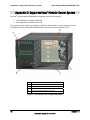
Figure 11. Intel® Modular Server System MFSYS25 .................................................................. 40
Revision 1.4
Intel order number: E15154-007
v
List of Tables
Intel® Compute Module MFS5000SI TPS
List of Tables
Table 1. I2C Addresses for Memory Module SMB ........................................................................ 9
Table 2. Maximum 8-DIMM System Memory Configuration – x8 Single Rank ........................... 10
Table 3. Maximum 8-DIMM System Memory Configuration – x4 Dual Rank.............................. 10
Table 4. PCI Bus Segment Characteristics................................................................................. 16
Table 5. Video Modes ................................................................................................................. 18
Table 6. Serial Header Pin-out.................................................................................................... 20
Table 7. Board Connector Matrix ................................................................................................ 21
Table 8. Power Connector Pin-out (J1A1) .................................................................................. 21
Table 9. VGA Connector Pin-out (J6A1)..................................................................................... 22
Table 10. 120-pin I/O Mezzanine Card Connector Pin-out ......................................................... 22
Table 11. 96-pin Midplane Signal Connector Pin-out ................................................................. 23
Table 12. Internal 9-pin Serial ‘A’ Header Pin-out (J1B1) ........................................................... 25
Table 13. External USB Connector Pin-out ................................................................................ 25
Table 14. Recovery Jumpers ...................................................................................................... 27
Table 15. BMC Sensors.............................................................................................................. 32
Table 16. Analog Sensor Thresholds.......................................................................................... 36
Table 17. POST Error Messages and Handling.......................................................................... 37
Table 18. POST Error Beep Codes ............................................................................................ 39
vi
Intel order number: E15154-007
Revision 1.4
Intel® Compute Module MFS5000SI TPS
1.
0BIntroduction
Introduction
This Technical Product Specification (TPS) provides board-specific information detailing the features,
functionality, and high-level architecture of the Intel® Compute Module MFS5000SI. The Intel® 5000
Series Chipsets Server Board Family Datasheet should also be referenced for more in-depth detail of
various board subsystems, including chipset, BIOS, System Management, and System Management
software.
1.1
Chapter Outline
This document is divided into the following chapters:
1.2
Chapter 1 – Introduction
Chapter 2 – Product Overview
Chapter 3 – Functional Architecture
Chapter 4 – Connector / Header Locations and Pin-outs
Chapter 5 – Jumper Block Settings
Chapter 6 – Product Regulatory Requirements
Appendix A – Integration and Usage Tips
Appendix B – BMC Sensor Tables
Appendix C – Post Error Messages and Handling
Appendix D – Supported Intel® Modular Server System
Intel® Compute Module Use Disclaimer
Intel® Modular Server components require adequate airflow to cool. Intel ensures through its own chassis
development and testing that when these components are used together, the fully integrated system will
meet the intended thermal requirements. It is the responsibility of the system integrator who chooses not
to use Intel-developed server building blocks to consult vendor datasheets and operating parameters to
determine the amount of airflow required for their specific application and environmental conditions. Intel
Corporation cannot be held responsible if components fail or the system does not operate correctly when
used outside any of their published operating or non-operating limits.
Revision 1.4
Intel order number: E15154-007
1
1BProduct Overview
2.
Intel® Compute Module MFS5000SI TPS
Product Overview
The Intel® Compute Module MFS5000SI is a monolithic printed circuit board with features that were
designed to support the high-density compute module market.
2.1
Intel® Compute Module MFS5000SI Feature Set
Feature
Processors
Description
771-pin LGA sockets supporting one or two Dual-Core or Quad-Core Intel® Xeon®
processors 5000 sequence, with system bus speeds of 1066 MHz or 1333 MHz
Memory
8 keyed DIMM slots supporting fully buffered DIMM technology (FBDIMM) memory.
240-pin DDR2-677 FBDIMMs must be used.
Chipset
Intel® 5000 Chipset family, which includes the following components:
®
Intel 5000P Memory Controller Hub
®
Intel 6321ESB I/O Controller Hub
On-board
Connectors/Headers
External connections:
Two USB 2.0 ports
Video connector
Internal connectors/headers:
One DH-10 Serial A debug header
®
®
One Intel I/O Mezzanine Connector supporting Dual Gigabit NIC Intel I/O
Expansion Module (Optional)
On-board Video
ATI* ES1000 video controller with 16MB DDR SDRAM
On-board Hard Drive
Controller
LSI* 1064e SAS controller
LAN
Two integrated 10/100/1000 Ethernet ports and two optional 10/100/1000 Ethernet
ports, provided by the Dual Gigabit NIC mezzanine module
2
Intel order number: E15154-007
Revision 1.4
Intel® Compute Module MFS5000SI TPS
2.2
1BProduct Overview
Compute Module Layout
2.2.1
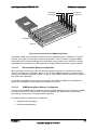
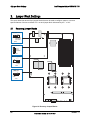
Connector and Component Locations
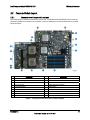
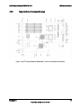
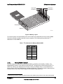
The following figure shows the board layout of the Intel® Compute Module MFS5000SI. Each connector
and major component is identified by a number or letter. A description of each identified item is provided
below the figure.
A
Description
Midplane Power Connector
B
Description
Midplane Signal Connector
C
POST Code Diagnostic LEDs
D
SAS Controller
E
FBDIMM Slots
F
Intel® 5000P Memory Controller Hub (MCH)
G
CPU #1 Socket
H
Voltage Regulator Heatsink
I
Power/Fault LEDs
J
Power Button
K
Activity and ID LEDs
L
Video Connector
M
USB1 and USB2 Connectors
N
CPU #2 Socket
O
Intel® 6321ESB I/O Controller Hub
P
CMOS Battery
Q
I/O Mezzanine Card Connector
Figure 1. Component and Connector Location Diagram
Revision 1.4
Intel order number: E15154-007
3
1BProduct Overview
2.2.2
Intel® Compute Module MFS5000SI TPS
External I/O Connector Locations
The following drawing shows the layout of the external I/O components for the Intel® Compute Module
MFS5000SI.
A
USB ports 1 and 2
E
Hard Drive Activity LED
B
Video
F
ID LED
C
I/O ports 1 and 2
G
Power button
D
NIC ports 1 and 2
H
Power and Fault LEDs
Figure 2. Intel® Compute Module MFS5000SI Front Panel Layout
4
Intel order number: E15154-007
Revision 1.4
Intel® Compute Module MFS5000SI TPS
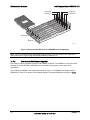
2.2.3
1BProduct Overview
Compute Module Mechanical Drawings
Figure 3. Intel® Compute Module MFS5000SI – Hole and Component Positions
Revision 1.4
Intel order number: E15154-007
5
2BFunctional Architecture
3.
Intel® Compute Module MFS5000SI TPS
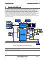
Functional Architecture
The architecture and design of the Intel® Compute Module MFS5000SI is based on the Intel® 5000
Chipset Family. The chipset is designed for systems based on the Dual-Core and Quad-Core Intel®
Xeon® processor 5000 sequence with system bus speeds of 667 MHz, 1066 MHz, and 1333 MHz. The
chipset is made up of two main components: the Memory Controller Hub (MCH) for the host bridge and
the Intel® 6321ESB I/O controller hub for the I/O subsystem. This chapter provides a high-level
description of the functionality associated with each chipset component and the architectural blocks that
make up the server board. For more in-depth detail of the functionality for each of the chipset
components and each of the functional architecture blocks, see the Intel® 5000 Series Chipsets Server
Board Family Datasheet.
Figure 4. Compute Module Functional Block Diagram
Note: The previous diagram uses the Intel® 5000P MCH as a general reference designator for MCH
components supported on this server board.
6
Intel order number: E15154-007
Revision 1.4
Intel® Compute Module MFS5000SI TPS
3.1
2BFunctional Architecture
Intel® 5000P Memory Controller Hub (MCH)
This section describes the general functionality of the memory controller hub as it is implemented on this
server board.
The MCH is a single 1432-pin FCBGA package, which includes the following core platform functions:
System Bus Interface for the processor subsystem
Memory Controller
PCI Express* Ports, including the Enterprise South Bridge Interface (ESI)
FBD Thermal Management
SMBus Interface
Additional information about MCH functionality can be obtained from the Intel® 5000 Series Chipsets
Server Board Family Datasheet and the Intel® 5000P Memory Controller Hub External Design
Specification.
3.1.1
System Bus Interface
The MCH is configured for symmetric multi-processing across two independent front-side bus interfaces
that connect to the Dual-Core and Quad-Core Intel® Xeon® processors 5000 sequence. Each front-side
bus on the MCH uses a 64-bit wide 1066 or 1333 MHz data bus. The 1333-MHz data bus is capable of
transferring data at up to 10.66 GB/s. The MCH supports a 36-bit wide address bus, capable of
addressing up to 64 GB of memory. The MCH is the priority agent for both front-side bus interfaces, and
is optimized for one processor on each bus.
3.1.2
Processor Support
®
The Intel Compute Module MFS5000SI supports one or two Dual-Core Intel® Xeon® processors 5100
sequence or Quad-Core Intel® Xeon® processors 5300 and 5400 sequence with system bus speeds of
1066 MHz and 1333 MHz. Previous generations of the Intel® Xeon® processor are not supported in the
Intel® Compute Module MFS5000SI. To see a list of the latest processors that have been validated on
this product, refer to http://support.intel.com/support/motherboards/server/MFS5000SI/ and select
the Supported Processors List.
3.1.2.1
Processor Population Rules
When two processors are installed, both must be of identical revision, core voltage, and bus/core speed.
Mixed processor steppings is supported in N and N-1 configurations only. When only one processor is
installed, it must be in the socket labeled CPU1. The other socket must be empty.
The board is designed to provide up to 115 A of current per processor. Processors with higher current
requirements are not supported.
When using a single processor configuration, a terminator is not required in the second processor socket.
Revision 1.4
Intel order number: E15154-007
7
2BFunctional Architecture
3.1.2.2
Intel® Compute Module MFS5000SI TPS
Common Enabling Kit (CEK) Design Support
The compute module complies with Intel’s Common Enabling Kit (CEK) processor mounting and heatsink
retention solution. The compute module ships with a CEK spring snapped onto the underside of the
server board, beneath each processor socket. The heatsink attaches to the CEK, over the top of the
processor and the thermal interface material (TIM). For the stacking order of the chassis, CEK spring,
server board, TIM, and heatsink, see the following figure.
The CEK spring is removable, allowing for the use of non-Intel heatsink retention solutions.
Note: The processor heatsink and CEK spring shown in the following diagram are for reference purposes
only. The actual processor heatsink and CEK solutions compatible with this generation server board may
be of a different design.
Heatsink assembly
Thermal interface material (TIM)
Server board
CEK spring
Chassis
Figure 5. CEK Processor Mounting
3.1.3
Memory Subsystem
The MCH masters four fully buffered DIMM (FBD) memory channels. FBD memory utilizes a narrow highspeed frame-oriented interface referred to as a channel. The four FBD channels are organized into two
branches of two channels per branch. Each branch is supported by a separate memory controller. The
two channels on each branch operate in lock step to increase FBD bandwidth. On the server board, the
four channels are routed to eight DIMM slots and are capable of supporting registered DDR2-533 and
DDR2-667 FBDIMM memory (stacked or unstacked). Peak theoretical memory data bandwidth is 6.4
GB/s with DDR2-533 and 8.0 GB/s with DDR2-667.
On the Intel® Compute Module MFS5000SI, a pair of channels becomes a branch where Branch 0
consists of channels A and B, and Branch 1 consists of channels C and D. FBD memory channels are
organized into two branches for RAID 1 (mirroring) support.
8
Intel order number: E15154-007
Revision 1.4
Intel® Compute Module MFS5000SI TPS
2BFunctional Architecture
Channel B
Channel C
Channel A
Channel D
H
MC
1
M A A2
M
I
D
M
DIM M B1 2
DIM M B 1
DIM M C 2
DIM M C 1
DIM M D 2
DIM M D
DIM
Branch 0
Branch 1
TP02299
Figure 6. Memory Layout
To boot the system, the system BIOS on the server board uses a dedicated I2C bus to retrieve DIMM
information needed to program the MCH memory registers. The following table provides the I2C
addresses for each DIMM slot.
Table 1. I2C Addresses for Memory Module SMB
3.1.3.1
Device
DIMM A1
Address
0xA0
DIMM A2
0xA2
DIMM B1
0xA0
DIMM B2
0xA2
DIMM C1
0xA0
DIMM C2
0xA2
DIMM D1
0xA0
DIMM D2
0xA2
Memory RASUM Features 1
The MCH supports several memory RASUM (Reliability, Availability, Serviceability, Usability, and
Manageability) features. These features include the Intel® x4 Single Device Data Correction (Intel® x4
SDDC) for memory error detection and correction, Memory Scrubbing, Retry on Correctable Errors,
Memory Built In Self Test, DIMM Sparing, and Memory Mirroring. For more information regarding these
features, see the Intel® 5000 Series Chipsets Server Board Family Datasheet.
1 DIMM Sparing and Memory Mirroring features will be made available post production launch with a BIOS update.
Revision 1.4
Intel order number: E15154-007
9
2BFunctional Architecture
3.1.3.2
Intel® Compute Module MFS5000SI TPS
Supported and Nonsupported Memory Configurations
The server board design supports up to eight DDR2-533 or DDR2-667 Fully Buffered DIMMs (FBD
memory). Use of identical DIMMs with this server board is recommended. The following tables show the
maximum memory configurations supported using the specified memory technology.
Table 2. Maximum 8-DIMM System Memory Configuration – x8 Single Rank
DRAM Technology x8 Single
Rank
256 Mb
512 Mb
1024 Mb
2048 Mb
Maximum Capacity
Mirrored Mode
1 GB
2 GB
4 GB
8 GB
Maximum Capacity
Non-Mirrored Mode
2 GB
4 GB
8 GB
16 GB
Table 3. Maximum 8-DIMM System Memory Configuration – x4 Dual Rank
DRAM Technology x4 Dual
Rank
256 Mb
512 Mb
1024 Mb
2048 Mb
Maximum Capacity Mirrored
Mode
4 GB
8 GB
16 GB
16 GB
Maximum Capacity
Non-Mirrored Mode
8 GB
16 GB
32 GB
32 GB
The following configurations are not validated or supported with the Intel® Compute Module MFS5000SI:
DDR2 DIMMs that are not fully buffered are NOT supported on this server board.
DDR2-533 memory is not planned to be validated on this product.
Mixing memory type, size, speed, and/or rank is not validated and is not supported.
Mixing memory vendors is not validated and is not supported.
Non-ECC memory is not validated and is not supported in a server environment
For a complete list of supported memory for the Intel® Compute Module MFS5000SI, refer to the Tested
Memory List published in the Intel® Server Configurator Tool.
3.1.3.3
DIMM Population Rules and Supported DIMM Configurations
DIMM population rules depend on the operating mode of the memory controller, which is determined by
the number of DIMMs installed. DIMMs must be populated in pairs. DIMM pairs are populated in the
following DIMM slot order: A1 and B1, C1 and D1, A2 and B2, C2 and D2. DIMMs within a given pair
must be identical with respect to size, speed, and organization.
Intel supported DIMM configurations for this server board are shown in the following table.
10
Intel order number: E15154-007
Revision 1.4
Intel® Compute Module MFS5000SI TPS
2BFunctional Architecture
Supported and Validated configuration : Slot is populated
Supported but not validated configuration : Slot is
populated
Slot is not populated
Mirroring:
Sparing:
Y = Yes and indicates that configuration supports Memory Mirroring.
Y(x) = Yes and indicates that configuration supports Memory Sparing.
Where x =
0: Sparing supported on Branch0 only
1: Sparing supported on Branch1 only
0,1: Sparing supported on both branches
Branch 0
Channel A
DIMM_A1
Branch 1
Channel B
DIMM_A2
DIMM_B1
DIMM B2
Channel C
DIMM C1
DIMM C2
Channel D
DIMM D1
Mirroring
Possible
Sparing
Possible
DIMM D2
Y (0)
Y
Y (0)
Y
Y (0, 1)
Notes:
Single channel mode is only tested and supported with a 512-MB x8 FBDIMM installed in DIMM
slot A1.
The supported memory configurations must meet population rules defined above.
For best performance, the number of DIMMs installed should be balanced across both memory
branches. For example, a four-DIMM configuration will perform better than a two-DIMM
configuration and should be installed in DIMM slots A1, B1, C1, and D1. An eight-DIMM
configuration will perform better then a six-DIMM configuration.
Although mixed DIMM capacities (size, type, timing and/or rank) between channels is supported
by the memory controller, mixed DIMMs configurations are not validated or supported with the
Intel® Compute Module MFS5000SI. Refer to section 3.1.3.2 for supported and nonsupported
DIMM configuration information.
3.1.3.3.1
Minimum Non-Mirrored Mode Configuration
The server board is capable of supporting a minimum of one DIMM installed. However, for system
performance reasons, Intel’s recommendation is that at least 2 DIMMs be installed.
The following diagram shows the recommended minimum DIMM memory configuration. Populated DIMM
slots are shown in Grey.
Revision 1.4
Intel order number: E15154-007
11
2BFunctional Architecture
Intel® Compute Module MFS5000SI TPS
Channel B
Channel C
Channel A
Channel D
H
MC
1
M A A2
M
I
D
M
DIM M B1 2
DIM M B 1
DIM M C 2
DIM M C 1
DIM M D 2
DIM M D
DIM
Branch 0
Branch 1
TP02300
Figure 7. Recommended Minimum Two-DIMM Memory Configuration
Note: The server board supports single DIMM mode operation. Intel only validates and supports this
configuration with a single 512MB x8 FBDIMM installed in DIMM slot A1.
3.1.3.4
Non-mirrored Mode Memory Upgrades
The minimum memory upgrade increment is two DIMMs per branch. The DIMMs must cover the same
slot position on both channels. DIMM pairs must be identical with respect to size, speed, and
organization.
When adding two DIMMs to the configuration shown in Figure 7, the DIMMs should be populated in
DIMM slots C1 and D1 as shown in the following diagram. Populated DIMM slots are shown in Grey.
12
Intel order number: E15154-007
Revision 1.4
Intel® Compute Module MFS5000SI TPS
2BFunctional Architecture
Channel B
Channel C
Channel A
Channel D
H
MC
1
M A A2
M
I
D
M
DIM M B1 2
DIM M B 1
DIM M C 2
DIM M C 1
DIM M D 2
DIM M D
DIM
Branch 0
Branch 1
TP02301
Figure 8. Recommended Four-DIMM Configuration
Functionally, DIMM slots A2 and B2 could also have been populated instead of DIMM slots C1 and D1.
However, your system will not achieve equivalent performance. Figure 8 shows the supported DIMM
configuration that is recommended because it allows both memory branches from the MCH to operate
independently and simultaneously. FBD bandwidth is doubled when both branches operate in parallel.
3.1.3.4.1
Mirrored Mode Memory Configuration
When operating in the mirrored mode, both branches operate in lock step. In mirrored mode, branch 1
contains a replicate copy of the data in branch 0. The minimum DIMM configuration to support memory
mirroring is four DIMMs, populated as shown in Figure 8. All four DIMMs must be identical with respect to
size, speed, and organization.
To upgrade a four-DIMM mirrored memory configuration, four additional DIMMs must be added to the
system. All four DIMMs in the second set must be identical to the first.
3.1.3.4.2
DIMM Sparing Mode Memory Configuration
The MCH provides DIMM sparing capabilities. Sparing is a RAS feature that involves configuring a DIMM
to be placed in reserve so it can be used to replace a DIMM that fails. DIMM sparing occurs within a
given bank of memory and is not supported across branches.
Two Memory Sparing configurations are supported:
Single Branch Mode Sparing
Dual Branch Mode Sparing
Revision 1.4
Intel order number: E15154-007
13
2BFunctional Architecture
3.1.3.4.2.1
Intel® Compute Module MFS5000SI TPS
Single Branch Mode Sparing
Slot 2
DIMM_A2
DIMM_B2
DIMM_C2
DIMM_D2
Slot 1
DIMM_A1
DIMM_B1
DIMM_C1
DIMM_D1
Channel B
Channel C
Channel D
Channel A
Branch 0
Branch 1
Intel® 5000P/5000X Memory Controller Hub
Figure 9. Single Branch Mode Sparing DIMM Configuration
DIMM_A1 and DIMM_B1 must be identical in organization, size and speed.
DIMM_A2 and DIMM_B2 must be identical in organization, size and speed.
DIMM_A1 and DIMM_A2 should be identical in organization, size and speed. See note below.
DIMM_B1 and DIMM_B2 should be identical in organization, size and speed. See note below.
Sparing should be enabled in the BIOS setup.
The BIOS will configure Rank Sparing Mode.
The larger of the pairs {DIMM_A1, DIMM_B1} and {DIMM_A2, DIMM_B2} will be selected as the
spare pair unit.
Note: Use of identical memory is recommended with the Intel® Compute Module MFS5000SI. Mixing
memory type, size, speed, rank and/or vendors is not validated and is not supported with this product.
Refer to section 3.1.3.2 for supported and nonsupported memory features and configuration information.
3.1.3.4.2.2
Dual Branch Mode Sparing
Dual branch mode sparing requires that all eight DIMM slots be populated and compliant with the
following population rules.
14
DIMM_A1 and DIMM_B1 must be identical in organization, size and speed.
DIMM_A2 and DIMM_B2 must be identical in organization, size and speed.
DIMM_C1 and DIMM_D1 must be identical in organization, size and speed.
DIMM_C2 and DIMM_D2 must be identical in organization, size and speed.
DIMM_A1 and DIMM_A2 should be identical in organization, size and speed. See note below.
DIMM_B1 and DIMM_B2 should be identical in organization, size and speed. See note below.
DIMM_C1 and DIMM_C2 should be identical in organization, size and speed. See note below.
DIMM_D1 and DIMM_D2 should be identical in organization, size and speed. See note below.
Sparing should be enabled in BIOS setup.
BIOS will configure Rank Sparing Mode.
The larger of the pairs {DIMM_A1, DIMM_B1} and {DIMM_A2, DIMM_B2} and {DIMM_C1,
DIMM_D1} and {DIMM_C2, DIMM_D2} will be selected as the spare pair units.
Intel order number: E15154-007
Revision 1.4
Intel® Compute Module MFS5000SI TPS
2BFunctional Architecture
Note: Use of identical memory is recommended with the Intel® Compute Module MFS5000SI. Mixing
memory type, size, speed, rank and/or vendors is not validated and is not supported with this product.
Refer to section 3.1.3.2 for supported and nonsupported memory features and configuration information.
Revision 1.4
Intel order number: E15154-007
15
2BFunctional Architecture
3.2
Intel® Compute Module MFS5000SI TPS
Intel® 6321ESB I/O Controller Hub
The Intel® 6321ESB I/O Controller Hub is a multi-function device that provides four distinct functions: an
IO Controller, a PCI-X Bridge, a Gb Ethernet Controller, and an Integrated Baseboard Management
Controller (BMC). Each function within the Intel® 6321ESB I/O Controller Hub has its own set of
configuration registers. Once configured, each appears to the system as a distinct hardware controller.
A primary role of the Intel® 6321ESB I/O Controller Hub is to provide the gateway to all PC-compatible I/O
devices and features. The server board uses the following Intel® 6321ESB I/O Controller Hub features:
Dual GbE MAC
Integrated Baseboard Management Controller (BMC)
Universal Serial Bus 2.0 (USB) interface
LPC bus interface
PC-compatible timer/counter and DMA controllers
APIC and 8259 interrupt controller
Power management
System RTC
General purpose I/O
This section describes the function of most of the listed features as they pertain to this server board. For
more detailed information, see the Intel® 5000 Series Chipsets Server Board Family Datasheet or the
Intel® Enterprise South Bridge-2 External Design Specification.
3.2.1
PCI Subsystem
The primary I/O buses for the server board are PCI and PCI Express*. The PCI buses comply with the
PCI Local Bus Specification, Revision 2.3. The following table lists the characteristics of the PCI bus
segments. Details about each bus segment follow the table.
Table 4. PCI Bus Segment Characteristics
PCI Bus Segment
PCI32
®
Intel 6321ESB I/O
Controller Hub
Voltage
Width
Speed
Type
On-board Device Support
3.3V
32 bit
33 MHz
PCI
PE1
®
Intel 6321ESB I/O
Controller Hub
PCI Express*
Port2
3.3V
x4
10 Gb/S
PCI
This interface is not used in the Intel®
Express* Compute Module MFS5000SI design.
PE2
®
Intel 6321ESB I/O
Controller Hub
PCI Express*
Port3
3.3V
x4
10 Gb/S
PCI
Used internally for LSI* 1064e SAS controller
Express*
PE4, PE5
BNB PCI Express*
Ports 4,5
3.3V
x8
20 Gb/S
PCI
I/O Mezzanine slot
Express*
16
Used internally for video controller
Intel order number: E15154-007
Revision 1.4
Intel® Compute Module MFS5000SI TPS
PCI Bus Segment
PE6, PE7
BNB PCI Express*
Ports 6,7
3.2.1.1
Voltage
3.3V
Width
x8
2BFunctional Architecture
Speed
20 Gb/S
Type
On-board Device Support
PCI
This interface is not used in the Intel®
Express* Compute Module MFS5000SI design.
PCI32: 32-bit, 33-MHz PCI Bus Segment
All 32-bit, 33-MHz PCI I/O is directed through the Intel® 6321ESB I/O Controller Hub. The 32-bit, 33-MHz
PCI segment created by the Intel® 6321ESB I/O Controller Hub is known as the PCI32 segment. The
PCI32 segment supports the following embedded device:
2D Graphics Accelerator: ATI* ES1000 Video Controller
3.2.1.2
PXA: 64-bit, 133MHz PCI-X Bus Segment
One 64-bit PCI-X bus segment is directed through the Intel® 6321ESB I/O Controller Hub. PCI-X segment
PXA is not used in the Intel® Compute Module MFS5000SI design.
3.2.1.3
PE1: One x4 PCI Express* Bus Segment
One x4 PCI Express* bus segment is directed through the Intel® 6321ESB I/O Controller Hub. PCI
Express* segment PE1 is not used in the Intel® Compute Module MFS5000SI design.
3.2.1.4
PE2: One x4 PCI Express* Bus Segment
One x4 PCI Express* bus segment is directed through the Intel® 6321ESB I/O Controller Hub. PCI
Express* segment PE2 supports the LSI* 1064e SAS controller.
3.2.1.5
PE4, PE5: Two x4 PCI Express* Bus Segments
Two x4 PCI Express* bus segments are directed through the MCH. PCI Express* segments PE4 and
PE5 support the optional I/O mezzanine card.
3.2.1.6
PE6, PE7: Two x4 PCI Express* Bus Segments
Two x4 PCI Express* bus segments are directed through the MCH. PCI Express* segments PE6 and
PE7 are not used in the Intel® Compute Module MFS5000SI design.
3.2.2
Serial ATA Support
®
The Intel 6321ESB I/O Controller Hub has an integrated Serial ATA (SATA) controller that supports
independent DMA operation on six ports and supports data transfer rates of up to 3.0 Gb/s. These ports
are not used in the Intel® Compute Module MFS5000SI design.
3.2.3
Parallel ATA (PATA) Support
The integrated IDE controller of the Intel® 6321ESB I/O Controller Hub provides one IDE channel. The
PATA interface is not used in the Intel® Compute Module MFS5000SI design.
Revision 1.4
Intel order number: E15154-007
17
2BFunctional Architecture
3.2.4
Intel® Compute Module MFS5000SI TPS
USB 2.0 Support
The USB controller functionality integrated into the Intel® 6321ESB I/O Controller Hub provides the server
board with the interface for up to eight USB 2.0 ports. Two external connectors are located on the front
edge of the server board. These two ports are the only ports of the Intel® 6321ESB I/O Controller Hub
that are used in the compute module design.
3.3
Video Support
The server board provides an ATI* ES1000 PCI graphics accelerator, along with 16 MB of video DDR
SDRAM and supports circuitry for an embedded SVGA video subsystem. The ATI* ES1000 chip contains
an SVGA video controller, clock generator, 2D engine, and RAMDAC in a 359-pin BGA. One 4Mx16x4
bank DDR SDRAM chip provides 16 MB of video memory.
The SVGA subsystem supports a variety of modes, up to 1024 x 768 resolution in 8 / 16 / 32 bpp modes
under 2D. It also supports both CRT and LCD monitors up to a 100-Hz vertical refresh rate.
Video is accessed using a standard 15-pin VGA connector found on the front edge of the server board.
Hot plugging the video while the system is still running is supported.
On-board video can be disabled using the BIOS Setup utility.
3.3.1.1
Video Modes
The ATI* ES1000 chip supports all standard IBM* VGA modes. The following table shows the 2D modes
supported for both CRT and LCD.
Table 5. Video Modes
2D Mode
640x480
3.3.1.2
Refresh Rate (Hz)
60, 72, 75, 85, 90,
100
8 bpp
Supported
2D Video Mode Support
16 bpp
Supported
32 bpp
Supported
800x600
60, 70, 72, 75, 85,
Supported
Supported
Supported
1024x768
60, 70, 72, 75,85
Supported
Supported
Supported
1152x864
60,70,75,80,85
Supported
Supported
Supported
1280x1024
60
Supported
Supported
Supported
Video Memory Interface
The memory controller subsystem of the ATI* ES1000 arbitrates requests from the direct memory
interface, the VGA graphics controller, the drawing co-processor, the display controller, the video scalar,
and the hardware cursor. Requests are serviced in a manner that ensures display integrity and maximum
CPU/co-processor drawing performance.
The server board supports a 16 MB (4Meg x 16-bit x 4 banks) DDR SDRAM device for video memory.
18
Intel order number: E15154-007
Revision 1.4
Intel® Compute Module MFS5000SI TPS
3.4
2BFunctional Architecture
Network Interface Controller (NIC)
Network interface support is provided from the built-in Dual GbE MAC features of the Intel® 6321ESB I/O
Controller Hub. These interfaces are routed over the midplane board to the Ethernet switch module in the
rear of the system. These interfaces are used in SERDES mode and do not require a Physical Layer
Transceiver (PHY). These ports provide the server board with support for dual LAN ports designed for
10/100/1000 Mbps operation.
Each Network Interface Controller (NIC) drives a single LED located on the front edge of the board. The
link/activity LED indicates network connection when on, and Transmit/Receive activity when blinking.
3.4.1
Intel® I/O Acceleration Technology
®
Intel I/O Acceleration Technology (I/OAT) moves network data more efficiently through Dual-Core and
Quad-Core Intel® Xeon® processors 5000 sequence-based servers for improved application
responsiveness across diverse operating systems and virtualized environments. Intel® I/OAT improves
network application responsiveness by unleashing the power of Dual-Core and Quad-Core Intel® Xeon®
processors 5000 sequence through more efficient network data movement and reduced system
overhead. Intel multi-port network adapters with Intel® I/OAT provide high-performance I/O for server
consolidation and virtualization through stateless network acceleration that seamlessly scales across
multiple ports and virtual machines. Intel® I/OAT provides safe and flexible network acceleration through
tight integration into popular operating systems and virtual machine monitors, avoiding the support risks
of third-party network stacks and preserving existing network requirements, such as teaming and failover.
3.4.2
MAC Address Definition
®
Each Intel Compute Module MFS5000SI has four MAC addresses assigned to it at the Intel factory.
During the manufacturing process, each server board will have a white MAC address sticker placed on
the board. The sticker will display the MAC address in both barcode and alpha numeric formats. The
printed MAC address is assigned to NIC 1 on the server board. NIC 2 is assigned the NIC 1 MAC
address + 1.
Two additional MAC addresses are assigned to the Integrated Baseboard Management Controller (BMC)
embedded in the Intel® 6321ESB I/O Controller Hub. These MAC addresses are used by the Integrated
BMC’s embedded network stack to enable IPMI remote management over LAN. BMC LAN Channel 1 is
assigned the NIC1 MAC address + 2, and BMC LAN Channel 2 is assigned the NIC1 MAC address + 3.
3.5
Super I/O
Legacy I/O support is provided by using a National Semiconductor* PC87427 Super I/O device. This chip
contains all of the necessary circuitry to support the following functions:
GPIOs
One serial port (internal and used for debug only)
Wake-up control
3.5.1.1
Serial Ports
The server board provides one serial port through an internal DH-10 serial header (J1B1) to be used for
debug purposes only. The serial interface follows the standard RS-232 pin-out as defined in the following
table.
Revision 1.4
Intel order number: E15154-007
19
2BFunctional Architecture
Intel® Compute Module MFS5000SI TPS
Table 6. Serial Header Pin-out
3.5.1.2
Pin
1
Signal Name
DCD
2
DSR
3
RX
4
RTS
5
TX
6
CTS
7
DTR
8
RI
9
GND
Serial Port Header Pin-out
Floppy Disk Controller
The server board does not support a floppy disk controller (FDC) interface. However, the system BIOS
does recognize USB floppy devices.
3.5.1.3
Keyboard and Mouse Support
Keyboard and mouse support is provided locally by the two USB ports located on the front panel of the
board. The compute module also provides remote keyboard and mouse support.
3.5.1.4
Wake-up Control
The super I/O contains functionality that allows various events to power on and power off the system.
20
Intel order number: E15154-007
Revision 1.4
Intel® Compute Module MFS5000SI TPS
3BConnector / Header Locations and Pin-outs
4.
Connector / Header Locations and Pin-outs
4.1
Board Connector Information
The following section provides detailed information regarding all connectors, headers and jumpers on the
server board. Table 7 lists all connector types available on the board and the corresponding reference
designators printed on the silkscreen.
Table 7. Board Connector Matrix
Connector
Power Connector
4.2
Quantity
1
J1A1
Reference Designators
Midplane Signal Connector
1
J3A1
CPU
2
J7G1, J5G1
Main Memory
8
J7B1,J7B2,J7B3,J8B2,J8B3,J8B4,J9B2,
J9B3
I/O Mezzanine
1
J2B1
Battery
1
XBT1F1
USB
2
J4K1,J4K2
Serial Port A
1
J1B1
Video connector
1
J6K1
System Recovery Setting
Jumpers
1
J4A1, J7A1, J1F2
Power Connectors
The power connection is obtained using a 2x2 FCI Airmax* power connector. The following table defines
the power connector pin-out.
Table 8. Power Connector Pin-out (J1A1)
Position
1
2
Revision 1.4
Signal
+12Vdc
GND
3
GND
4
+12Vdc
Intel order number: E15154-007
21
3BConnector / Header Locations and Pin-outs
4.3
Intel® Compute Module MFS5000SI TPS
I/O Connector Pin-out Definition
4.3.1
VGA Connector
The following table details the pin-out definition of the VGA connector (J6K1).
Table 9. VGA Connector Pin-out (J6A1)
Pin
4.3.2
1
Signal Name
V_IO_R_CONN
Description
Red (analog color signal R)
2
V_IO_G_CONN
Green (analog color signal G)
3
V_IO_B_CONN
Blue (analog color signal B)
4
TP_VID_CONN_B4
No connection
5
GND
Ground
6
GND
Ground
7
GND
Ground
8
GND
Ground
9
TP_VID_CONN_B9
No connection
10
GND
Ground
11
TP_VID_CONN_B11
No connection
12
V_IO_DDCDAT
DDCDAT
13
V_IO_HSYNC_CONN
HSYNC (horizontal sync)
14
V_IO_VSYNC_CONN
VSYNC (vertical sync)
15
V_IO_DDCCLK
DDCCLK
I/O Mezzanine Card Connector
The server board provides an internal 120-pin Airmax* connector (J2B1) to accommodate high-speed I/O
expansion modules, which expands the I/O capabilities of the server board. The currently available I/O
mezzanine card for this server is the Intel® Modular Server Accessory AXXGBIOMEZ, a dual gigabit
Ethernet card based on the Intel® 82571EB. The following table details the pin-out of the Intel® I/O
expansion module connector.
Table 10. 120-pin I/O Mezzanine Card Connector Pin-out
Pin
Signal Name
Pin
Signal Name
Pin
Signal Name
A1
PE4_MCH_RXP_C0
E1
PE5_MCH_RXN_C0
I1
GND
A2
GND
E2
PE5_MCH_TXP_C0
I2
Reset_N
A3
PE4_MCH_RXP_C1
E3
PE5_MCH_RXN_C1
I3
GND
A4
GND
E4
PE5_MCH_TXP_C1
I4
P1_ACT_LED_N
A5
PE4_MCH_RXP_C2
E5
PE5_MCH_RXN_C2
I5
GND
A6
GND
E6
PE5_MCH_TXP_C2
I6
P3V3
A7
PE4_MCH_RXP_C3
E7
PE5_MCH_RXN_C3
I7
GND
A8
GND
E8
PE5_MCH_TXP_C3
I8
P3V3
A9
CLK_100M_PCIE_P
E9
spare
I9
GND
22
Intel order number: E15154-007
Revision 1.4
Intel® Compute Module MFS5000SI TPS
3BConnector / Header Locations and Pin-outs
A10
GND
E10
SMB_SCL
I10
P12V
B1
PE4_MCH_RXN_C0
F1
GND
J1
XE_P2_D_RXN
B2
PE4_MCH_TXP_C0
F2
PE5_MCH_TXN_C0
J2
GND
B3
PE4_MCH_RXN_C1
F3
GND
J3
XE_P2_C_RXN
B4
PE4_MCH_TXP_C1
F4
PE5_MCH_TXN_C1
J4
GND
B5
PE4_MCH_RXN_C2
F5
GND
J5
XE_P2_B_RXN
B6
PE4_MCH_TXP_C2
F6
PE5_MCH_TXN_C2
J6
GND
B7
PE4_MCH_RXN_C3
F7
GND
J7
XE_P2_A_RXN
B8
PE4_MCH_TXP_C3
F8
PE5_MCH_TXN_C3
J8
GND
B9
CLK_100M_PCIE_N
F9
GND
J9
P12V
B10
WAKE_N
F10
SMB_SDA
J10
GND
C1
GND
G1
Card_ID_0
K1
XE_P2_D_RXP
C2
PE4_MCH_TXN_C0
G2
GND
K2
XE_P2_D_TXN
C3
GND
G3
P5V
K3
XE_P2_C_RXP
C4
PE4_MCH_TXN_C1
G4
GND
K4
XE_P2_C_TXN
C5
GND
G5
P2_LINK_LED_N
K5
XE_P2_B_RXP
C6
PE4_MCH_TXN_C2
G6
GND
K6
XE_P2_B_TXN
C7
GND
G7
P3V3
K7
XE_P2_A_RXP
C8
PE4_MCH_TXN_C3
G8
GND
K8
XE_P2_A_TXN
C9
GND
G9
P3VAUX
K9
P12V
C10
spare
G10
GND
K10
P12V
D1
PE5_MCH_RXP_C0
H1
Card_ID_1
L1
GND
D2
GND
H2
Card_ID_2
L2
XE_P2_D_TXP
D3
PE5_MCH_RXP_C1
H3
P5V
L3
GND
D4
GND
H4
P1_LINK_LED_N
L4
XE_P2_C_TXP
D5
PE5_MCH_RXP_C2
H5
P2_ACT_LED_N
L5
GND
D6
GND
H6
P3V3
L6
XE_P2_B_TXP
D7
PE5_MCH_RXP_C3
H7
P3V3
L7
GND
D8
GND
H8
P3V3
L8
XE_P2_A_TXP
D9
spare
H9
P3VAUX
L9
GND
D10
GND
H10
P12V
L10
P12V
4.3.3
Midplane Signal Connector
The server board connects to the midplane through a 96-pin Airmax* connector (J3A1) (power is J1A1) to
connect the various I/O, management, and control signals of the system.
Table 11. 96-pin Midplane Signal Connector Pin-out
Pin
A1
Signal Name
XE_P1_A_RXP
Pin
E1
Signal Name
XE_P2_D_RXN
Pin
I1
GND
A2
GND
E2
XE_P2_D_TXP
I2
SAS_P1_TXN
A3
XE_P1_B_RXP
E3
SMB_SDA_B
I3
GND
A4
GND
E4
FM_BL_X_SP
I4
XE_P2_C_TXN
A5
XE_P1_C_RXP
E5
XE_P2_B_RXN
I5
GND
Revision 1.4
Intel order number: E15154-007
Signal Name
23
3BConnector / Header Locations and Pin-outs
Intel® Compute Module MFS5000SI TPS
A6
GND
E6
XE_P2_B_TXP
I6
SAS_P2_TXN
A7
XE_P1_D_RXP
E7
XE_P2_A_RXN
I7
GND
A8
GND
E8
XE_P2_A_TXP
I8
Fm_bl_slot_id5
B1
XE_P1_A_RXN
F1
GND
J1
SMB_SCL_A
B2
XE_P1_A_TXP
F2
XE_P2_D_TXN
J2
GND
B3
XE_P1_B_RXN
F3
GND
J3
FM_BL_SLOT_ID2
B4
XE_P1_B_TXP
F4
12V (BL_PWR_ON)
J4
GND
B5
XE_P1_C_RXN
F5
GND
J5
reserved
B6
XE_P1_C_TXP
F6
XE_P2_B_TXN
J6
GND
B7
XE_P1_D_RXN
F7
GND
J7
reserved
B8
XE_P1_D_TXP
F8
XE_P2_A_TXN
J8
GND
C1
GND
G1
SAS_P1_RXP
K1
SMB_SDA_A
C2
XE_P1_A_TXN
G2
GND
K2
FM_BL_SLOT_ID0
C3
GND
G3
XE_P2_C_RXP
K3
FM_BL_SLOT_ID3
C4
XE_P1_B_TXN
G4
GND
K4
FM_BL_SLOT_ID4
C5
GND
G5
SAS_P2_RXP
K5
reserved
C6
XE_P1_C_TXN
G6
GND
K6
reserved
C7
GND
G7
spare
K7
reserved
C8
XE_P1_D_TXN
G8
GND
K8
reserved
D1
XE_P2_D_RXP
H1
SAS_P1_RXN
L1
GND
D2
GND
H2
SAS_P1_TXP
L2
FM_BL_SLOT_ID1
D3
SMB_SCL_B
H3
XE_P2_C_RXN
L3
GND
D4
GND
H4
XE_P2_C_TXP
L4
FM_BL_PRES_N
D5
XE_P2_B_RXP
H5
SAS_P2_RXN
L5
GND
D6
GND
H6
SAS_P2_TXP
L6
reserved
D7
XE_P2_A_RXP
H7
spare
L7
GND
D8
GND
H8
spare
L8
reserved
4.3.4
Serial Port Connector
The server board provides one internal 9-pin Serial ‘A’ port header (J1B1). The following table defines the
pin-out. See
24
Intel order number: E15154-007
Revision 1.4
Intel® Compute Module MFS5000SI TPS
3BConnector / Header Locations and Pin-outs
Table 6 for the pin-out of the serial header.
Table 12. Internal 9-pin Serial ‘A’ Header Pin-out (J1B1)
Pin
4.3.5
1
Signal Name
SPA_DCD
Description
DCD (carrier detect)
2
SPA_DSR
DSR (data set ready)
3
SPA_SIN_L
RXD (receive data)
4
SPA_RTS
RTS (request to send)
5
SPA_SOUT_N
TXD (transmit data)
6
SPA_CTS
CTS (clear to send)
7
SPA_DTR
DTR (data terminal ready)
8
SPA_RI
RI (ring Indicate)
9
GND
Ground
USB 2.0 Connectors
The following table details the pin-out of the external USB connectors (J4K1, J4K2) found on the front
edge of the server board.
Table 13. External USB Connector Pin-out
Pin
1
Signal Name
USB_OC#_FB_1
USB_PWR
Description
2
USB_P#N_FB_2
DATAL0 (Differential data line paired with DATAH0)
3
USB_P#P_FB_2
DATAH0 (Differential data line paired with DATAL0)
4
GND
Ground
Revision 1.4
Intel order number: E15154-007
25
4BJumper Block Settings
5.
Intel® Compute Module MFS5000SI TPS
Jumper Block Settings
The server board has several 3-pin jumper blocks that can be used to configure, protect, or recover
specific features of the server board. Pin 1 on each jumper block is denoted by an “*” or “▼”.
5.1
Recovery Jumper Blocks
BIOS Bank Select
3
2
Default BOOT FROM
EMERGENCY
BIOS IMAGE
J3A3
PASSWORD CLR
Default
2
CLEAR
PASSWORD
3
J4A1
BMC Force Update
2
3
Enabled Default
Disabled
J7A1
CMOS CLR
3
2
CLEAR Default
CMOS
J1F2
AF002220
Figure 10. Recovery Jumper Blocks
26
Intel order number: E15154-007
Revision 1.4
Intel® Compute Module MFS5000SI TPS
4BJumper Block Settings
Table 14. Recovery Jumpers
Jumper Name
J7A1: BMC Force
Update
Pins
1-2
What happens at system reset …
BMC Firmware Force Update Mode – Enabled
2-3
BMC Firmware Force Update Mode – Disabled (Default)
J4A1: Password
Clear
1-2
These pins should have a jumper in place for normal system operation. (Default)
2-3
If these pins are jumpered, the administrator and user passwords are cleared
immediately. These pins should not be jumpered for normal operation.
J1F2: CMOS Clear
1-2
These pins should have a jumper in place for normal system operation. (Default)
2-3
If these pins are jumpered, the CMOS settings are cleared immediately. These pins
should not be jumpered for normal operation
1-2
If these pins are jumpered, the BIOS is forced to boot from the lower bank. These pins
should not be jumpered for normal operation.
2-3
These pins should have a jumper in place for normal system operation. (Default)
J3A3: BIOS Bank
Select
5.1.1
CMOS Clear and Password Reset Usage Procedure
The CMOS Clear (J1F2) and Password Reset (J4A1) recovery features are designed such that the
desired operation can be achieved with minimal system down time. The usage procedure for these two
features has changed from previous generation Intel® server boards. The following procedure outlines the
new usage model.
1. Power down compute module (do not remove AC power).
2. Remove compute module from modular server chassis.
3. Open compute module.
4. Move jumper from Default operating position (pins 1-2) to Reset/Clear position (pins 2-3).
5. Wait 5 seconds.
6. Move jumper back to default position (pins 1-2).
7. Close the compute module.
8. Reinstall compute module in modular server chassis.
9. Power up the compute module.
Password and/or CMOS is now cleared and can be reset by going into the BIOS setup.
Note: Removing AC power before performing the CMOS Clear operation will cause the system to
automatically power up and immediately power down after the reset procedure has been completed and
AC power is re-applied. Should this occur, remove the AC power cord again, wait 30 seconds, and reinstall the AC power cord. Power up the system and proceed to the <F2> BIOS Setup utility to reset
desired settings.
5.1.2
BMC Force Update Procedure
When performing a standard BMC firmware update procedure, the update utility places the BMC into an
update mode, allowing the firmware to load safely onto the flash device. In the unlikely event that the
BMC firmware update process fails due to the BMC not being in the proper update state, the server board
provides a BMC Force Update jumper (J7A1) which will force the BMC into the proper update state. The
following procedure should be followed in the event the standard BMC firmware update process fails.
1. Power down and remove AC power
2. Remove compute module from modular server chassis
3. Open compute module
Revision 1.4
Intel order number: E15154-007
27
4BJumper Block Settings
4.
5.
6.
7.
8.
9.
10.
11.
12.
13.
Intel® Compute Module MFS5000SI TPS
Move jumper from Default operating position (pins 2-3) to “Enabled” position (pins 1-2)
Close the compute module
Reconnect AC power and power up the compute module
Perform standard BMC firmware update procedure through the Intel® Modular Server Control
software
Power down and remove AC power
Remove compute module from the server system
Move jumper from “Enabled” position (pins 1-2) to “Disabled” position (pins 2-3)
Close the server system
Reinstall the compute module into the modular server chassis
Reconnect AC power and power up the compute module
Note: Normal BMC functionality (for example, KVM, monitoring, and remote media) is disabled with the
force BMC update jumper set to the “Enabled” position. The server should never be run with the BMC
force update jumper set in this position and should only be used when the standard firmware update
process fails. This jumper should remain in the default – disabled position when the server is running
normally.
5.1.3
System Status LED – BMC Initialization
When the AC power is first applied to the system and 5V-STBY is present, the Integrated BMC controller
on the server board requires 15-20 seconds to initialize. During this time, the system status LED blinks,
alternating between amber and green, and the power button functionality of the control panel is disabled,
preventing the server from powering up. Once BMC initialization has completed, the status LED stops
blinking and power button functionality is restored. The power button can then be used to turn on the
server.
28
Intel order number: E15154-007
Revision 1.4
Intel® Compute Module MFS5000SI TPS
6.
6.1
5BProduct Regulatory Requirements
Product Regulatory Requirements
Product Regulatory Requirements
®
The Intel Compute Module MFS5000SI is evaluated as part of the Intel® Modular Server System
MFSYS25/MFSYS35, which requires meeting all applicable system component regulatory requirements. Refer to the
Intel® Modular Server System MFSYS25/MFSYS35 Technical Product Specification for a complete listing of all
system and component regulatory requirements.
6.2
Product Regulatory Compliance and Safety Markings
No markings are required on the Intel® Compute Module MFS5000SI server board itself as it is evaluated
as part of the Intel® Modular Server System MFSYS25/MFSYS35.
6.3
Product Environmental/Ecology Requirements
The Intel® Compute Module MFS5000SI is evaluated as part of the Intel® Modular Server System
MFSYS25/MFSYS35, which requires meeting all applicable system component environmental and
ecology requirements. For a complete listing of all system and component environment and ecology
requirements and markings, refer to the Intel® Modular Server System MFSYS25/MFSYS35 Technical
Product Specification.
6.4
Product Environmental/Ecology Markings
The following Product Ecology markings are required on the Intel® Compute Module MFS5000SI server
board:
Country
Requirement
China Restriction of Hazardous Substance
Environmental Friendly Use Period Mark
Revision 1.4
Marking
China
Intel order number: E15154-007
29
Appendix A: Integration and Usage Tips
Intel® Compute Module MFS5000SI TPS
Appendix A: Integration and Usage Tips
30
When two processors are installed, both must be of identical revision, core voltage, and bus/core
speed. Mixed processor steppings is supported. However, the stepping of one processor cannot
be greater than one stepping back of the other.
Processors must be installed in order. CPU 1 is located near the edge of the server board and
must be populated to operate the board.
Only Fully Buffered DIMMs (FBD) are supported on this server board.
Mixing memory type, size, speed, rank and/or memory vendors is not validated and is not
supported on this server board.
Non-ECC memory is not validated and is not supported in a server environment
For a list of supported memory for this server board, see the Intel® Compute Module MFS5000SI
Tested Memory List in the Intel® Server Configurator Tool.
For a list of Intel supported operating systems, add-in cards, and peripherals for this server
board, see the Intel® Compute Module MFS5000SI Tested Hardware and Operating System List.
Only Dual-Core processors 5100 sequence or Quad-Core Intel® Xeon® processors 5300 or 5400
sequence, with system bus speeds of 1066/1333 MHz are supported on this server board.
Previous generation Intel® Xeon® processors are not supported.
For best performance, the number of DIMMs installed should be balanced across both memory
branches. For example, a four-DIMM configuration will perform better than a two-DIMM
configuration and should be installed in DIMM Slots A1, B1, C1, and D1. An eight-DIMM
configuration will perform better than a six-DIMM configuration.
Normal Integrated BMC functionality (for example, KVM, monitoring, and remote media) is
disabled with the force BMC update jumper set to the “enabled” position (pins 1-2). The server
should never be run with the BMC force update jumper set in this position and should only be
used when the standard firmware update process fails. This jumper should remain in the default
(disabled) position (pins 2-3) when the compute module is running normally.
When performing the BIOS update procedure, the BIOS select jumper must be set to its default
position (pins 2-3).
Intel order number: E15154-007
Revision 1.4
Intel® Compute Module MFS5000SI TPS
Appendix B: Sensor Tables
Appendix B: BMC Sensor Tables
Table 15 lists the sensor identification numbers and information regarding the sensor type, name,
supported thresholds, and a brief description of the sensor purpose. See the Intelligent Platform
Management Interface Specification, Version 2.0, for sensor and event / reading-type table information.
Sensor Type
The Sensor Type references the values enumerated in the Sensor Type Codes table in the IPMI
Specification. It provides the context in which to interpret the sensor, for example, the physical entity or
characteristic that is represented by this sensor.
Event / Reading Type
The Event / Reading Type references values from the Event / Reading Type Code Ranges and Generic
Event / Reading Type Codes tables in the IPMI Specification. Note that digital sensors are specific type of
discrete sensors, which have only two states.
Event Offset Triggers
This column defines what event offsets the sensor generates.
For Threshold (analog reading) type sensors, the BMC can generate events for the following thresholds:
Upper Critical
Upper Non-critical
Lower Non-critical
Lower Critical
The abbreviation [U, L] is used to indicate that both Upper and Lower thresholds are supported. A few
sensors support only a subset of the standard four threshold triggers. Note that even if a sensor does
support all thresholds, the SDRs may not contain values for some thresholds. Consult Table 16 for
information on the thresholds that are defined in the SDRs.
For Digital and Discrete type sensor event triggers, the supported event generating offsets are listed. The
offsets can be found in the Generic Event / Reading Type Codes or Sensor Type Codes tables in the
IPMI Specification, depending on whether the sensor event / reading type is a generic or sensor-specific
response.
All sensors generate both assertions and deassertions of the defined event triggers. The assertions and
deassertions may or may not generate events into the System Event Log (SEL), depending on the sensor
SDR settings.
Fault LED
This column indicates whether an assertion of an event lights the front panel fault LED. The Integrated
BMC aggregates all fault sources (including outside sources such as the BIOS) such that the LED will be
lit as long as any source indicates that a fault state exists. The Integrated BMC extinguishes the fault LED
when all sources indicate no faults are present.
Revision 1.4
Intel order number: E15154-007
31
Appendix B: Sensor Tables
Intel® Compute Module MFS5000SI TPS
Sensor Rearm
The rearm is a request for the event status for a sensor to be rechecked and updated upon a transition
between good and bad states. Rearming the sensors can be done manually or automatically. The
following abbreviations are used in the column:
‘A’: Auto rearm
‘M’: Manual rearm
Readable
Some sensors are used simply to generate events into the System Event Log. The Watchdog timer
sensor is one example. These sensors operate by asserting and then immediately de-asserting an event.
Typically the SDRs for such sensors are defined such that only the assertion causes an event message
to be deposited in the SEL. Reading such a sensor produces no useful information and is marked as ‘No’
in this column. Note that some sensors may actually be unreadable in that they return an error code in
response to the IPMI Get Sensor Reading command. These sensors are represented by type 3 SDR
records.
Standby
Some sensors operate on standby power. These sensors may be accessed and / or generate events
when the compute module payload power is off, but standby power is present.
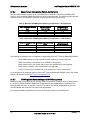
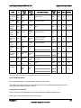
Table 15. BMC Sensors
Name
Power Unit
Status
Watchdog
System
ACPI Power
State
32
#
01h
03h
0Ch
Sensor
Type
Power Unit
09h
Watchdog
2
23h
System
ACPI
Power
Event /
Reading
Type
Sensor
Specific
6Fh
Sensor
Specific
6Fh
Sensor
Specific
6Fh
Event Offset Triggers
Status
LED
0: Power down
None
1: Power cycle
None
4: A/C lost (DC input lost)
None
5: Soft power control failure
(did not turn on or off)
Fault
6: Power unit failure (power
good dropout)
Fault
0: Timer expired
None
1: Hard reset
None
2: Power down
None
3: Power cycle
None
8: Timer interrupt
None
0: S0 / G0
1: S1
Intel order number: E15154-007
None
Read?
Rearm
Standby
Yes
A
Yes
No
A
Yes
Yes
A
Yes
None
Revision 1.4
Intel® Compute Module MFS5000SI TPS
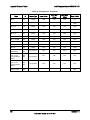
Name
#
Sensor
Type
Event /
Reading
Type
State
22h
BB Vtt
10h
Voltage
Thresh.
01h
BB +1.5V
AUX
11h
Voltage
Thresh.
01h
BB +1.5V
12h
BB +1.8V
BB +3.3V
13h
14h
BB +3.3V
STB
15h
BB +1.5V
ESB
16h
BB +5V
17h
BB +12V
AUX
18h
BB 0.9V
19h
BB Vbat
(SIO)
Revision 1.4
1Ah
Voltage
Voltage
Voltage
Voltage
Voltage
Voltage
Voltage
Voltage
Voltage
Thresh.
01h
Thresh.
01h
Thresh.
01h
Thresh.
01h
Thresh.
01h
Thresh.
01h
Thresh.
01h
Thresh.
01h
Digital
Discrete
05h
Appendix B: Sensor Tables
Event Offset Triggers
Status
LED
3: S3
None
4: S4
None
5: S5 / G2
None
7: G3 mechanical off
None
B: Legacy ON state
None
C: Legacy OFF state
None
[U,L] Non-critical
[U,L] Critical
Fault
Fault
[U,L] Non-critical
Fault
[U,L] Critical
Fault
[U,L] Non-critical
Fault
[U,L] Critical
Fault
[U,L] Non-critical
Fault
[U,L] Critical
Fault
[U,L] Non-critical
Fault
[U,L] Critical
Fault
[U,L] Non-critical
Fault
[U,L] Critical
Fault
[U,L] Non-critical
Fault
[U,L] Critical
Fault
[U,L] Non-critical
Fault
[U,L] Critical
Fault
[U,L] Non-critical
Fault
[U,L] Critical
Fault
[U,L] Non-critical
Fault
[U,L] Critical
Fault
1: Limit exceeded
Fault
Intel order number: E15154-007
Read?
Rearm
Standby
Yes
A
No
Yes
A
No
Yes
A
No
Yes
A
No
Yes
A
No
Yes
A
Yes
Yes
A
Yes
Yes
A
No
Yes
A
No
Yes
A
No
Yes
A
Yes
33
Appendix B: Sensor Tables
Name
#
Sensor
Type
Intel® Compute Module MFS5000SI TPS
Event /
Reading
Type
Event Offset Triggers
1: Inactive
Hot Swap
20h
Hot Swap
2Ch
Sensor
Specific
6Fh
2: Activation Required
3: Activation In Progress
4: Active
5: Deactivation Required
6: Deactivation in Progress
0: Pending
1: Established
KVM
Session
21h
OEM
OEM
C0h
70h
2: Ended Normally
3: Ticket Expiration
4: Lost Heartbeat
5: Forcibly Terminated
6: Unknown Ticket
Status
LED
Read?
Rearm
Standby
None
None
None
None
None
None
Yes
A
Yes
None
None
None
None
None
None
None
Yes
A
Yes
OEM
OEM
0: SOL Session Inactive
C0h
73h
1: SOL Session Active
None
None
Yes
A
Yes
40h
SMI
Timeout
F3h
Digital
Discrete
03h
1: State asserted
Fault
No
A
No
Memory
Error
41h
Memory
0Ch
Sensor
Specific
6Fh
1: Uncorrectable ECC
Fault
No
A
No
Critical Int.
42h
Critical
Interrupt
13h
Sensor
Specific
6Fh
8: Bus uncorrectable Error
Fault
No
A
No
DIMM 1-8
Temp
50h57h
Temp
Thresh.
01h
01h
None
None
Yes
A
No
DIMM Max
Temp
5Fh
Temp.
Thresh.
01h
01h
None
None
Yes
A
No
0: IERR
Fault
Processor
07h
Sensor
Specific
6Fh
1: Thermal trip
Fault
Yes
M
Yes
7: Presence
None
Upper Non-critical
Fault
Yes
A
No
Yes
A
No
SOL
Session
22h
SMI
Timeout
Processor
1,2 Status
90h,
91h
Processor 1
Core 1,2,3,4
92h –
Thermal
95h
Margin
(PECI)
Temp.
01h
Processor 2
Core 1,2,3,4
96h –
Thermal
99h
Margin
(PECI)
Temp.
01h
34
Thresh.
01h
Thresh.
01h
Upper Critical
Fault
Upper Non-critical
Fault
Upper Critical
Intel order number: E15154-007
Fault
Revision 1.4
Intel® Compute Module MFS5000SI TPS
Sensor
Type
Event /
Reading
Type
Appendix B: Sensor Tables
Name
#
Processor
1,2 Thermal
Ctrl %
9Ah,
9Bh
Temp.
01h
Thresh.
01h
Upper Critical
Processor
1,2 VRD
Hot
9Ch,
9Dh
Temp.
01h
Digital
Discrete
05h
Proc Max
Thermal
Margin
9Fh
Temp
Thresh.
01h
01h
Processor
1,2 Vcc
Out-ofRange
A0h,
A1h
Voltage
Digital
Discrete
05h
CPU
Population
Error
B0h
Processor
07h
Digital
Discrete
03h
Mezzanine
Card
Present
C0h
Slot/Conne
ctor
21h
Sensor
Specific
6Fh
Attention
State
C1h
OEM
D0h
OEM
D0h
Drive
Backplane
Present
C2h
Drive Slot
0Dh
Digital
Discrete
08h
Drive 1,2 1
C3h,
C4h
Drive Slot
0Dh
Slot ID
C5h
OEM
D1h
Process
Progress
FEh
OEM
D2h
Status
LED
Read?
Rearm
Standby
Fault
Yes
A
No
1: Limit exceeded
Fault
Yes
M
No
None
None
Yes
A
No
1: Limit exceeded
Fault
Yes
A
No
0: State De-asserted
None
1: State Asserted
Fault
Yes
A
Yes
2: Device installed
None
Yes
A
No
0: ID LED Lit
None
Yes
A
Yes
1: Fault State Active
None
0: Device Absent
None
Yes
A
No
1: Device Present
None
Sensor
Specific
6Fh
0: Present
None
Yes
A
No
Thresh.
01h
None
None
Yes
A
Yes
7: Process Started
None
8: Process Finished OK
None
Yes
A
Yes
9: Process Finished Fail
None
OEM
D2h
Event Offset Triggers
Note 1: SDRs for these sensors are loaded only into the compute module SKU that supports these drives. Reading
these sensors in a SKU that does not support drives will return unknown data.
Sensor SDR Information
This section describes the information that is entered into the SDRs.
The SDRs for all sensors will be set to generate events for both assertions and de-assertions of all
supported sensor offsets as listed in Table 15.
Analog Sensor Thresholds
Table 16 shows the thresholds set into the SDR records for the BMC’s analog sensors.
These values are preliminary at the time of this writing.
Revision 1.4
Intel order number: E15154-007
35
Appendix B: Sensor Tables
Intel® Compute Module MFS5000SI TPS
Table 16. Analog Sensor Thresholds
Name
#
Sensor Type
Lower Critical
Lower NonCritical
Upper NonCritical
Upper Critical
BB Vtt
10h
Voltage
1.90V
N/A
N/A
1.5V
BB +1.5V AUX
11h
Voltage
1.33V
N/A
N/A
1.65V
BB +1.5V
12h
Voltage
1.33V
N/A
N/A
1.65V
BB +1.8V
13h
Voltage
1.67V
N/A
N/A
1.94V
BB +3.3V
14h
Voltage
2.97V
N/A
N/A
3.62V
BB +3.3V STB
15h
Voltage
2.97V
N/A
N/A
3.62V
BB +1.5V ESB
16h
Voltage
1.33V
N/A
N/A
1.65V
BB +5V
17h
Voltage
4.5V
N/A
N/A
5.5V
BB +12V AUX
18h
Voltage
10.66V
N/A
N/A
13.26V
BB 0.9V
19h
Voltage
0.78V
N/A
N/A
1.02V
DIMM 1-8
Temperature
50h –
57h
Temperature
N/A
N/A
100ºC
105ºC
Processor 1
Core 1,2,3,4
Thermal Margin
(PECI)
92h –
93h
Temperature
N/A
N/A
N/A
N/A
Processor 2
Core 1,2,3,4
Thermal Margin
(PECI)
94h –
95h
Temperature
N/A
N/A
N/A
N/A
Processor 1,2
Thermal Ctrl %
9Ah,
9Bh
Temperature
N/A
N/A
N/A
50%
36
Intel order number: E15154-007
Revision 1.4
Intel® Compute Module MFS5000SI TPS
Appendix C: POST Error Messages and Handling
Appendix C: POST Error Messages and Handling
Whenever possible, the BIOS will output the current boot progress codes on the video screen. Progress
codes are 32-bit quantities plus optional data. The 32-bit numbers include class, subclass, and operation
information. The class and subclass fields point to the type of hardware that is being initialized. The
operation field represents the specific initialization activity. Based on the data bit availability to display
progress codes, a progress code can be customized to fit the data width. The higher the data bit, the
higher the granularity of information that can be sent on the progress port. The progress codes may be
reported by the system BIOS or option ROMs.
The Response section in the following table is divided into two types:
Minor: The message is displayed on the screen or in the Error Manager screen. The system will
continue booting with a degraded state. The user may want to replace the erroneous unit. The
setup POST error Pause setting does not have any effect with this error.
Major: The message is displayed in the Error Manager screen, and an error is logged to the SEL.
The setup POST error Pause setting determines whether the system pauses to the Error
Manager for this type of error, where the user can take immediate corrective action or choose to
continue booting.
Fatal: The message is displayed in the Error Manager screen, an error is logged to the SEL, and
the system cannot boot unless the error is resolved. The user needs to replace the faulty part and
restart the system. The setup POST error Pause setting does not have any effect with this error.
Table 17. POST Error Messages and Handling
Error Code
004C
Keyboard / interface error
Error Message
Major
Response
0012
CMOS date / time not set
Major
0048
Password check failed
Fatal
0141
PCI resource conflict
Major
0146
Insufficient memory to shadow PCI ROM
Major
0192
L3 cache size mismatch
Fatal
0194
CPUID, processor family are different
Fatal
0195
Front side bus mismatch
Major
0197
Processor speeds mismatched
Major
5220
Configuration cleared by jumper
Minor
5221
Passwords cleared by jumper
Major
8110
Processor 01 internal error (IERR) on last boot
Major
8111
Processor 02 internal error (IERR) on last boot
Major
8120
Processor 01 thermal trip error on last boot
Major
8121
Processor 02 thermal trip error on last boot
Major
8130
Processor 01 disabled
Major
8131
Processor 02 disabled
Major
8160
Processor 01 unable to apply BIOS update
Major
8161
Processor 02 unable to apply BIOS update
Major
8190
Watchdog timer failed on last boot
Major
8198
Operating system boot watchdog timer expired on last boot
Major
8300
Baseboard management controller failed self-test
Major
Revision 1.4
Intel order number: E15154-007
37
Appendix C: POST Error Messages and Handling
Intel® Compute Module MFS5000SI TPS
Error Code
8305
Hot swap controller failed
Error Message
Major
Response
84F2
Baseboard management controller failed to respond
Major
84F3
Baseboard management controller in update mode
Major
84F4
Sensor data record empty
Major
84FF
System event log full
Minor
8500
Memory Component could not be configured in the selected RAS
mode.
Major
8510
System supports a maximum of 16 GB of main memory. Additional
memory will not be counted. (This error is S5000V specific.)
Major
8520
DIMM_A1 failed Self Test (BIST).
Major
8521
DIMM_A2 failed Self Test (BIST).
Major
8522
DIMM_A3 failed Self Test (BIST).
Major
8523
DIMM_A4 failed Self Test (BIST).
Major
8524
DIMM_B1 failed Self Test (BIST).
Major
8525
DIMM_B2 failed Self Test (BIST).
Major
8526
DIMM_B3 failed Self Test (BIST).
Major
8527
DIMM_B4 failed Self Test (BIST).
Major
8528
DIMM_C1 failed Self Test (BIST).
Major
8529
DIMM_C2 failed Self Test (BIST).
Major
852A
DIMM_C3 failed Self Test (BIST).
Major
852B
DIMM_C4 failed Self Test (BIST).
Major
852C
DIMM_D1 failed Self Test (BIST).
Major
852D
DIMM_D2 failed Self Test (BIST).
Major
852E
DIMM_D3 failed Self Test (BIST).
Major
852F
DIMM_D4 failed Self Test (BIST).
Major
8580
DIMM_A1 Correctable ECC error encountered.
Minor/Major after 10 events
8581
DIMM_A2 Correctable ECC error encountered.
Minor/Major after 10 events
8582
DIMM_A3 Correctable ECC error encountered.
Minor/Major after 10 events
8583
DIMM_A4 Correctable ECC error encountered.
Minor/Major after 10 events
8584
DIMM_B1 Correctable ECC error encountered.
Minor/Major after 10 events
8585
DIMM_B2 Correctable ECC error encountered.
Minor/Major after 10 events
8586
DIMM_B3 Correctable ECC error encountered.
Minor/Major after 10 events
8587
DIMM_B4 Correctable ECC error encountered.
Minor/Major after 10 events
8588
DIMM_C1 Correctable ECC error encountered.
Minor/Major after 10 events
8589
DIMM_C2 Correctable ECC error encountered.
Minor/Major after 10 events
858A
DIMM_C3 Correctable ECC error encountered.
Minor/Major after 10 events
858B
DIMM_C4 Correctable ECC error encountered.
Minor/Major after 10 events
858C
DIMM_D1 Correctable ECC error encountered.
Minor/Major after 10 events
858D
DIMM_D2 Correctable ECC error encountered.
Minor/Major after 10 events
858E
DIMM_D3 Correctable ECC error encountered.
Minor/Major after 10 events
858F
DIMM_D4 Correctable ECC error encountered.
Minor/Major after 10 events
8601
Override jumper is set to force boot from lower alternate BIOS bank
of flash ROM.
Minor
8602
WatchDog timer expired (secondary BIOS may be bad!).
Minor
8603
Secondary BIOS checksum fail.
Minor
38
Intel order number: E15154-007
Revision 1.4
Intel® Compute Module MFS5000SI TPS
Appendix C: POST Error Messages and Handling
Error Code
92A3
Error Message
Serial port component was not detected.
Major
Response
92A9
Serial port component encountered a resource conflict error.
Major
0xA000
TPM device not detected.
Minor
0xA001
TPM device missing or not responding.
Minor
0xA002
TPM device failure
Minor
0xA003
TPM device failed self test.
Minor
POST Error Pause Option
In case of POST error(s) that are listed as “Major”, the BIOS enters the Error Manager and waits for the
user to press an appropriate key before booting the operating system or entering the BIOS Setup.
The user can override this option by setting “POST Error Pause” to “disabled” in the BIOS Setup Main
menu page. If the “POST Error Pause” option is set to “disabled”, the system boots the operating system
without user-intervention. The default value is set to “disabled”.
POST Error Beep Codes
The following table lists the POST error beep codes. Prior to system video initialization, the BIOS uses
these beep codes to inform users of error conditions. The beep code is followed by a user visible code on
POST Progress LEDs.
Table 18. POST Error Beep Codes
Beeps
Error Message
3
Memory error
POST Progress Code
(PPC)
No PPC
6
BIOS recovery
No PPC
Revision 1.4
Description
System halted because a fatal error related to the memory
was detected.
The system has detected a corrupted BIOS in the flash
part, and is recovering the last good BIOS.
Intel order number: E15154-007
39
Appendix D: Supported Intel® Server Chassis
Intel® Compute Module MFS5000SI TPS
Appendix D: Supported Intel® Modular Server System
The Intel® Compute Module MFS5000SI is supported in the following chassis:
Intel® Modular Server System MFSYS25
Intel® Modular Server System MFSYS35
This section provides a high-level descriptive overview of each chassis. For more details, refer to the
Intel® Modular Server System MFSYS25/MFSYS35 Technical Product Specification (TPS).
A
Shared hard drive storage bay
B
I/O cooling fans
C
Empty compute module bay
D
Compute module cooling fans
E
Compute module midplane connectors
Figure 11. Intel® Modular Server System MFSYS25
40
Intel order number: E15154-007
Revision 1.4
Intel® Compute Module MFS5000SI TPS
Glossary
Glossary
This appendix contains important terms used in the preceding chapters. For ease of use, numeric entries
are listed first (for example, “82460GX”) followed by alpha entries (for example, “AGP 4x”). Acronyms are
followed by non-acronyms.
Term
ACPI
Definition
Advanced Configuration and Power Interface
AP
Application Processor
APIC
Advanced Programmable Interrupt Control
ASIC
Application Specific Integrated Circuit
ASMI
Advanced Server Management Interface
BIOS
Basic Input/Output System
BIST
Built-In Self Test
BMC
Baseboard Management Controller
Bridge
Circuitry connecting one computer bus to another, allowing an agent on one to access the other
BSP
Bootstrap Processor
byte
8-bit quantity.
CBC
Chassis Bridge Controller (A microcontroller connected to one or more other CBCs, together they
bridge the IPMB buses of multiple chassis.
CEK
Common Enabling Kit
CHAP
Challenge Handshake Authentication Protocol
CMOS
In terms of this specification, this describes the PC-AT compatible region of battery-backed 128 bytes
of memory, which normally resides on the server board.
DPC
Direct Platform Control
EEPROM
Electrically Erasable Programmable Read-Only Memory
EHCI
Enhanced Host Controller Interface
EMP
Emergency Management Port
EPS
External Product Specification
ESB2
Enterprise South Bridge 2
FBD
Fully Buffered DIMM
FMB
Flexible Mother Board
FRB
Fault Resilient Booting
FRU
Field Replaceable Unit
FSB
Front-Side Bus
GB
1024MB
GPIO
General Purpose I/O
GTL
Gunning Transceiver Logic
HSC
Hot-Swap Controller
Hz
Hertz (1 cycle/second)
I2C
Inter-Integrated Circuit Bus
IA
Intel® Architecture
IBF
Input Buffer
ICH
I/O Controller Hub
ICMB
Intelligent Chassis Management Bus
IERR
Internal Error
Revision 1.4
Intel order number: E15154-007
41
Glossary
Intel® Compute Module MFS5000SI TPS
Term
Definition
IFB
I/O and Firmware Bridge
INTR
Interrupt
IP
Internet Protocol
IPMB
Intelligent Platform Management Bus
IPMI
Intelligent Platform Management Interface
IR
Infrared
ITP
In-Target Probe
KB
1024 bytes
KCS
Keyboard Controller Style
LAN
Local Area Network
LCD
Liquid Crystal Display
LED
Light Emitting Diode
LPC
Low Pin Count
LUN
Logical Unit Number
MAC
Media Access Control
MB
1024KB
MCH
Memory Controller Hub
MD2
Message Digest 2 – Hashing Algorithm
MD5
Message Digest 5 – Hashing Algorithm – Higher Security
ms
milliseconds
MTTR
Memory Type Range Register
Mux
Multiplexor
NIC
Network Interface Controller
NMI
Nonmaskable Interrupt
OBF
Output Buffer
OEM
Original Equipment Manufacturer
Ohm
Unit of electrical resistance
PEF
Platform Event Filtering
PEP
Platform Event Paging
PIA
Platform Information Area (This feature configures the firmware for the platform hardware)
PLD
Programmable Logic Device
PMI
Platform Management Interrupt
POST
Power-On Self Test
PSMI
Power Supply Management Interface
PWM
Pulse-Width Modulation
RAM
Random Access Memory
RASUM
Reliability, Availability, Serviceability, Usability, and Manageability
RISC
Reduced Instruction Set Computing
ROM
Read Only Memory
RTC
Real-Time Clock (Component of ICH peripheral chip on the server board)
SDR
Sensor Data Record
SECC
Single Edge Connector Cartridge
SEEPROM
Serial Electrically Erasable Programmable Read-Only Memory
SEL
System Event Log
42
Intel order number: E15154-007
Revision 1.4
Intel® Compute Module MFS5000SI TPS
Term
Glossary
Definition
SIO
Server Input/Output
SMBus
System Management Bus
SMI
Server Management Interrupt (SMI is the highest priority non-maskable interrupt)
SMM
Server Management Mode
SMS
Server Management Software
SNMP
Simple Network Management Protocol
TBD
To Be Determined
TIM
Thermal Interface Material
UART
Universal Asynchronous Receiver/Transmitter
UDP
User Datagram Protocol
UHCI
Universal Host Controller Interface
UTC
Universal time coordinate
VID
Voltage Identification
VRD
Voltage Regulator Down
Word
16-bit quantity
ZIF
Zero Insertion Force
Revision 1.4
Intel order number: E15154-007
43
Reference Documents
Intel® Compute Module MFS5000SI TPS
Reference Documents
See the following documents for additional information:
44
Intel® 5000 Series Chipsets Server Board Family Datasheet
Intel® 5000P Memory Controller Hub External Design Specification
Intel® Enterprise South Bridge 2 (ESB2) External Design Specification
Intel® Modular Server System MFSYS25/MFSYS35 Technical Product Specification
Intel order number: E15154-007
Revision 1.4