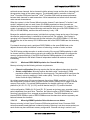
1
Intel® Compute Module MFS5520VI
Technical Product Specification
Intel order number: E64311-005
Revision 1.3
April, 2010
Enterprise Platforms and Services Division
Revision History
Intel® Compute Module MFS5520VI TPS
Revision History
Date
February, 2009
Revision
Number
1.0
Modifications
Initial release.
June, 2009
1.1
Updated the document.
March, 2010
1.2
Updated the document.
April, 2010
1.3
Updated the document.
Disclaimers
Information in this document is provided in connection with Intel® products. No license, express
or implied, by estoppel or otherwise, to any intellectual property rights is granted by this
document. Except as provided in Intel's Terms and Conditions of Sale for such products, Intel
assumes no liability whatsoever, and Intel disclaims any express or implied warranty, relating to
sale and/or use of Intel products including liability or warranties relating to fitness for a particular
purpose, merchantability, or infringement of any patent, copyright or other intellectual property
right. Intel products are not intended for use in medical, life saving, or life sustaining applications.
Intel may make changes to specifications and product descriptions at any time, without notice.
Designers must not rely on the absence or characteristics of any features or instructions marked
"reserved" or "undefined." Intel reserves these for future definition and shall have no
responsibility whatsoever for conflicts or incompatibilities arising from future changes to them.
The Intel® Compute Module MFS5520VI may contain design defects or errors known as errata
which may cause the product to deviate from published specifications. Current characterized
errata are available on request.
Intel Corporation server baseboards support peripheral components and contain a number of
high-density VLSI and power delivery components that need adequate airflow to cool. Intel’s
own chassis are designed and tested to meet the intended thermal requirements of these
components when the fully integrated system is used together. It is the responsibility of the
system integrator that chooses not to use Intel developed server building blocks to consult
vendor datasheets and operating parameters to determine the amount of air flow required for
their specific application and environmental conditions. Intel Corporation can not be held
responsible if components fail or the compute module does not operate correctly when used
outside any of their published operating or non-operating limits.
Intel, Pentium, Itanium, and Xeon are trademarks or registered trademarks of Intel Corporation.
*Other brands and names may be claimed as the property of others.
Copyright © Intel Corporation 2010.
ii
Intel order number: E64311-005
Revision 1.3
Intel® Compute Module MFS5520VI TPS
Table of Contents
Table of Contents
1.
Introduction .......................................................................................................................... 1
1.1
Chapter Outline........................................................................................................ 1
1.2
Intel® Compute Module Use Disclaimer................................................................... 1
2. Product Overview................................................................................................................. 2
2.1
Intel® Compute Module MFS5520VI Feature Set .................................................... 2
2.2
Compute Module Layout.......................................................................................... 3
2.2.1
Connector and Component Locations ..................................................................... 3
2.2.2
External I/O Connector Locations............................................................................ 3
2.2.3
Compute Module Mechanical Drawings .................................................................. 5
3. Functional Architecture ....................................................................................................... 6
3.1
Intel® Xeon® processor ............................................................................................ 7
3.1.1
Processor Support ................................................................................................... 7
3.1.2
Mixed Processor Configuration................................................................................ 7
3.1.3
Turbo Mode ............................................................................................................. 9
3.1.4
Hyper-Threading...................................................................................................... 9
3.1.5
Intel® QuickPath Interconnect .................................................................................. 9
3.1.6
Unified Retention System Support......................................................................... 10
3.2
Memory Subsystem ............................................................................................... 11
3.2.1
Intel® QuickPath Memory Controller ...................................................................... 11
3.2.2
Publishing Compute Module Memory.................................................................... 11
3.2.3
Memory Map and Population Rules....................................................................... 12
3.2.4
Memory RAS ......................................................................................................... 13
3.2.5
Memory Upgrade Rules......................................................................................... 15
3.3
Intel® 5520 Chipset IOH......................................................................................... 17
3.4
Intel® 82801JR I/O Controller Hub (ICH10R)......................................................... 17
3.4.1
PCI Subsystem ...................................................................................................... 18
3.4.2
USB 2.0 Support.................................................................................................... 18
3.5
Integrated Baseboard Management Controller...................................................... 19
3.5.1
Floppy Disk Controller ........................................................................................... 21
3.5.2
Keyboard and Mouse Support ............................................................................... 21
3.5.3
Wake-up Control.................................................................................................... 21
3.6
Video Support ........................................................................................................ 21
3.6.1
Video Modes.......................................................................................................... 21
3.7
Network Interface Controller (NIC) ........................................................................ 21
3.7.1
Direct Cache Access (DCA) .................................................................................. 22
3.8
Intel® Virtualization Technology for Directed I/O (Intel® VT-d)................................ 22
4. Connector/Header Locations and Pin-outs ..................................................................... 23
4.1
Board Connector Information................................................................................. 23
Revision 1.3
Intel order number: E64311-005
iii
Table of Contents
Intel® Compute Module MFS5520VI TPS
4.2
Power Connectors ................................................................................................. 23
4.3
I/O Connector Pin-out Definition ............................................................................ 24
4.3.1
VGA Connector...................................................................................................... 24
4.3.2
I/O Mezzanine Card Connector ............................................................................. 24
4.3.3
Midplane Signal Connector.................................................................................... 28
4.3.4
Serial Port Connector ............................................................................................ 29
4.3.5
USB 2.0 Connectors .............................................................................................. 29
5. Jumper Block Settings ...................................................................................................... 31
5.1
Recovery Jumper Blocks ....................................................................................... 31
5.1.1
CMOS Clear and Password Clear Usage Procedure ............................................ 32
5.1.2
Integrated BMC Force Update Procedure ............................................................. 32
5.1.3
Integrated BMC Initialization.................................................................................. 33
6. Product Regulatory Requirements ................................................................................... 34
6.1
Product Regulatory Requirements......................................................................... 34
6.2
Product Regulatory Compliance and Safety Markings .......................................... 34
6.3
Product Environmental/Ecology Requirements ..................................................... 34
Appendix A: Integration and Usage Tips ........................................................................................ 35
Appendix B: Integrated BMC Sensor Tables ................................................................................... 36
Appendix C: POST Error Messages and Handling ............................................................................ 42
Appendix D: Supported Intel® Modular Server System .................................................................... 46
Glossary ....................................................................................................................................... 47
Reference Documents .................................................................................................................. 50
iv
Intel order number: E64311-005
Revision 1.3
Intel® Compute Module MFS5520VI TPS
List of Figures
List of Figures
Figure 1. Component and Connector Location Diagram .............................................................. 3
Figure 2. Intel® Compute Module MFS5520VI Front Panel Layout............................................... 4
Figure 3. Intel® Compute Module MFS5520VI – Hole and Component Positions ........................ 5
Figure 4. Intel® Compute Module MFS5520VI Functional Block Diagram .................................... 6
Figure 5. Unified Retention System and Unified Backplate Assembly........................................ 10
Figure 6. DIMM Nomenclature.................................................................................................... 12
Figure 7. DIMM Slot Order.......................................................................................................... 12
Figure 8. Integrated BMC Hardware ........................................................................................... 20
Figure 9. Recovery Jumper Blocks ............................................................................................. 31
Figure 10. Intel® Modular Server System MFSYS25 .................................................................. 46
Revision 1.3
Intel order number: E64311-005
v
List of Tables
Intel® Compute Module MFS5520VI TPS
List of Tables
Table 1. Mixed Processor Configurations ..................................................................................... 8
Table 2. Mirroring DIMM Population Rules Variance across Nodes ........................................... 15
Table 3. Intel® Compute Module MFS5520VI PCI Bus Segment Characteristics....................... 18
Table 4. Video Modes ................................................................................................................. 21
Table 5. Board Connector Matrix ................................................................................................ 23
Table 6. Power Connector Pin-out (J1A1) .................................................................................. 23
Table 7. VGA Connector Pin-out (J6A1)..................................................................................... 24
Table 8. 120-pin I/O Mezzanine Card Connector Pin-out ........................................................... 25
Table 9. 120-pin I/O Mezzanine Card Connector Signal Definitions........................................... 26
Table 10. 40-pin I/O Mezzanine Card Connector Pin-out ........................................................... 28
Table 11. 96-pin Midplane Signal Connector Pin-out ................................................................. 28
Table 12. Internal 9-pin Serial Header Pin-out (J9J1)................................................................. 29
Table 13. External USB Connector Pin-out ................................................................................ 30
Table 14. Pin-out of Internal USB Connector for low-profile Solid State Drive (J9B7)................ 30
Table 15. Recovery Jumpers ...................................................................................................... 32
Table 16. MFS5520VI Sensors................................................................................................... 37
Table 17. POST Error Messages and Handling.......................................................................... 42
vi
Intel order number: E64311-005
Revision 1.3
Intel® Compute Module MFS5520VI TPS
1.
Introduction
Introduction
This Technical Product Specification (TPS) provides board-specific information detailing the
features, functionality, and high-level architecture of the Intel® Compute Module MFS5520VI.
1.1
Chapter Outline
This document is divided into the following chapters:
Chapter 1 – Introduction
Chapter 2 – Product Overview
Chapter 3 – Functional Architecture
Chapter 4 – Connector / Header Locations and Pin-outs
Chapter 5 – Jumper Block Settings
Chapter 6 – Product Regulatory Requirements
Appendix A – Integration and Usage Tips
Appendix B – BMC Sensor Tables
Appendix C – Post Error Messages and Handling
Appendix D – Supported Intel® Modular Server System
1.2
Intel® Compute Module Use Disclaimer
Intel® Modular Server components require adequate airflow to cool. Intel ensures through its
own chassis development and testing that when these components are used together, the fully
integrated system will meet the intended thermal requirements. It is the responsibility of the
system integrator who chooses not to use Intel-developed server building blocks to consult
vendor datasheets and operating parameters to determine the amount of airflow required for
their specific application and environmental conditions. Intel Corporation cannot be held
responsible if components fail or the system does not operate correctly when used outside any
of their published operating or non-operating limits.
Revision 1.3
Intel order number: E64311-005
1
Product Overview
2.
Intel® Compute Module MFS5520VI TPS
Product Overview
The Intel® Compute Module MFS5520VI is a monolithic printed circuit board with features that
were designed to support the high-density compute module market.
2.1
Intel® Compute Module MFS5520VI Feature Set
Feature
Processors
Description
Support for one or two Intel® Xeon® Processor 5500 series or two Intel® Xeon®
Processor 5600 series in FC-LGA 1366 Socket B package with up to 95 W Thermal
Design Power (TDP).
®
®
4.8 GT/s, 5.86 GT/s, and 6.4 GT/s Intel QuickPath Interconnect (Intel QPI)
Enterprise Voltage Regulator-Down (EVRD) 11.1
Memory
Support for 1066/1333 MT/s ECC registered (RDIMM) or unbuffered (UDIMM) DDR3
memory.
12 DIMMs total across 6 memory channels (3 channels per processor).
Note: Mixed memory is not tested or supported. Non-ECC memory is not tested and is
not supported in a server environment.
Chipset
Intel® 5520 Chipset IOH
®
Intel 82801JR I/O Controller Hub (ICH10R)
On-board
Connectors/Headers
External connections:
Four USB 2.0 ports
DB-15 Video connector
Internal connectors/headers:
One low-profile USB 2x5 pin header to support low-profile USB solid state drives
®
®
Intel I/O Mezzanine connectors supporting Dual Gigabit NIC Intel I/O Expansion
Module (Optional)
On-board Video
On-board ServerEngines* LLC Pilot II Controller
Integrated 2D Video Controller
32 MB DDR2 Memory
On-board Hard Drive
Controller
LSI* 1064e SAS controller
LAN
Two integrated 1000 Ethernet ports and two optional 1000 Ethernet ports, provided by
the Dual Gigabit NIC mezzanine module.
2
Intel order number: E64311-005
Revision 1.3
Intel® Compute Module MFS5520VI TPS
2.2
Product Overview
Compute Module Layout
2.2.1
Connector and Component Locations
The following figure shows the board layout of the Intel® Compute Module MFS5520VI. Each
connector and major component is identified by a number or letter. A description of each
identified item is provided below the figure.
F
E
D
G
H
C
B
A
I
Q
P
O
J
N
M
M
L
K
AF003077
A
Intel® 5520 Chipset I/O Hub
J
CPU 2 Socket
B
CPU2 DIMM Slots
K
Power/Fault LEDs
C
Mezzanine Card Connector 1
L
Power Switch
D
CPU 1 with Heatsink
M
Activity and ID LEDs
E
Mezzanine Card Connector 2
N
Video Connector
F
Midplane Power Connector
O
USB Ports 2 and 3
G
Midplane Signal Connector
P
USB1 Ports 0 and 1
H
Midplane Guide Pin Receptacle
Q
CMOS Battery
I
CPU 1 DIMM Slots
Figure 1. Component and Connector Location Diagram
2.2.2
External I/O Connector Locations
The following drawing shows the layout of the external I/O components for the Intel® Compute
Module MFS5520VI.
Revision 1.3
Intel order number: E64311-005
3
Product Overview
Intel® Compute Module MFS5520VI TPS
A B
C
D
E
F G H I
AF003120
A
USB ports 0 and 1
F
Hard Drive Activity LED
B
USB ports 2 and 3
G
ID LED
C
Video
H
Power button
D
I/O Mezzanine NIC ports 1 and
2 LEDs
I
Power and Fault LEDs
E
NIC ports 1 and 2 LEDs
Figure 2. Intel® Compute Module MFS5520VI Front Panel Layout
4
Intel order number: E64311-005
Revision 1.3
Intel® Compute Module MFS5520VI TPS
253.74
169.85
Compute Module Mechanical Drawings
102.02
2.2.3
Product Overview
262.89
256.54
254.58
244.42
249.42
239.84
234.26
224.10
223.39
213.94
209.52
207.65
192.99
185.99
203.78
173.99
166.99
152.27
148.40
142.11
141.77
131.95
121.79
111.63
101.47
120.65
115.85
104.50
98.85
72.65
58.10
41.40
14.58
3.27
.000
396.24
357.34
300.35
248.92
185.93
138.84
AF003121
.000
10.16
101.10
6.35
Figure 3. Intel® Compute Module MFS5520VI – Hole and Component Positions
Revision 1.3
Intel order number: E64311-005
5
Functional Architecture
3.
Intel® Compute Module MFS5520VI TPS
Functional Architecture
The architecture and design of the Intel® Compute Module MFS5520VI is based on the Intel®
5520 Chipset I/O Hub (IOH) and the Intel® 82801JR ICH10 RAID. The chipset is designed for
systems based on the Intel® Xeon® Processor in FC-LGA 1366 socket B package with Intel®
QuickPath Interconnect (Intel® QPI). The chipset contains two main components:
Intel® 5520 Chipset I/O Hub (IOH) that provides a connection point between various I/O
components.
Intel® 82801JR, which is the I/O controller hub (ICH10R) for the I/O subsystem.
This chapter provides a high-level description of the functionality associated with each chipset
component and the architectural blocks that make up the server board.
FLASH
4
2
TPM
Opt - int in TB
SSI Compliant
Mezzanine
BMC
DRAM
2
2
Primary
Mid-Plane Connector
Flex IO
Connector
Figure 4. Intel® Compute Module MFS5520VI Functional Block Diagram
6
Intel order number: E64311-005
Revision 1.3
Intel® Compute Module MFS5520VI TPS
3.1
Functional Architecture
Intel® Xeon® processor
3.1.1
Processor Support
The Compute Module supports the following processors:
One or two Intel® Xeon® Processor 5500 series with 4.8 GT/s, 5.86 GT/s or 6.4 GT/s
Intel® QPI link interface and Thermal Design Power (TDP) up to 95 W.
One or two Intel® Xeon® Processor 5600 series with a 6.4 GT/s Intel® QPI link interface
and Thermal Design Power (TDP) up to 95 W.
Previous generations of the Intel® Xeon® processors are not supported on the compute module.
3.1.1.1
Processor Population Rules
Note: Although the Compute Module does support dual-processor configurations consisting of
different processors that meet the defined criteria below, Intel does not perform validation
testing of this configuation. For optimal performance in dual-processor configurations, Intel
recommends that identical processors be installed.
When using a single processor configuration, the processor must be installed into the processor
socket labeled CPU1. A terminator is not required in the second processor socket when using a
single processor configuration.
When two processors are installed, the following population rules apply:
Both processors must be of the same processor family.
Both processors must have the same front-side bus speed.
Both processors must have the same cache size.
Processors with different speeds can be mixed in a system, given the prior rules are met.
If this condition is detected, all processor speeds are set to the lowest common
denominator (highest common speed) and an error is reported.
Processor stepping within a common processor family can be mixed as long as it is
listed in the processor specification updates published by Intel Corporation.
3.1.2
Mixed Processor Configuration
The following table describes mixed processor conditions and recommended actions for the
Intel® Compute Module MFS5520VI. Errors fall into one of the following categories:
Fatal: If the compute module can boot, it pauses at a blank screen with the text
“Unrecoverable fatal error found. System will not boot until the error is resolved”
and “Press <F2> to enter setup”, regardless of whether the “Post Error Pause” setup
option is enabled or disabled. When the operator presses the F2 key on the keyboard,
the error message is displayed on the Error Manager screen, and an error is logged with
the error code. The compute module cannot boot unless the error is resolved. The user
needs to replace the faulty part and restart the system.
Major: If the “Post Error Pause” setup option is enabled, the compute module goes
directly to the Error Manager to display the error and log the error code. Otherwise, the
compute module continues to boot and no prompt is given for the error, although the
error code is logged to the Error Manager.
Revision 1.3
Intel order number: E64311-005
7
Functional Architecture
Intel® Compute Module MFS5520VI TPS
Minor: The message is displayed on the screen or on the Error Manager screen. The
system continues booting in a degraded state. The user may want to replace the
erroneous unit. The POST Error Pause option setting in the BIOS setup does not have
any effect on this error.
Table 1. Mixed Processor Configurations
Error
Processor family not
Identical
Severity
Fatal
System Action
The BIOS detects the error condition and responds as follows:
Logs the error.
Alerts the Integrated BMC about the configuration error.
Does not disable the processor.
Displays “0194: Processor 0x family mismatch detected”
message in the Error Manager.
Takes Fatal Error action (see above) and will not boot until the
fault condition is remedied.
Processor cache not
identical
Fatal
The BIOS detects the error condition and responds as follows:
Logs the error.
Alerts the Integrated BMC about the configuration error.
Does not disable the processor.
Displays “0192: Processor 0x cache size mismatch detected”
message in the Error Manager.
Takes Fatal Error action (see above) and will not boot until the
fault condition is remedied.
Processor frequency (speed)
not identical
Fatal
The BIOS detects the error condition and responds as follows:
Adjusts all processor frequencies to lowest common denominator.
No error is generated – this is not an error condition.
Continues to boot the system successfully.
If the frequencies for all processors cannot be adjusted to be the
same, then the BIOS:
Logs the error.
Displays “0197: Processor 0x family is not supported” message in
the Error Manager.
Takes Fatal Error action (see above) and will not boot until the
fault condition is remedied.
Processor Intel® QuickPath
Interconnect speeds not
identical
8
Major
The BIOS detects the error condition and responds as follows:
Adjusts all processor interconnect frequencies to lowest common
denominator.
Logs the error.
Alerts the Integrated BMC about the configuration error.
Does not disable the processor.
Displays “0195: Processor 0x Intel(R) QPI speed mismatch”
message in the Error Manager.
If POST Error Pause is disabled in the Setup, continues to boot in
a degraded state.
If POST Error Pause is enabled in the Setup, pauses the system,
but can continue to boot if operator directs.
Intel order number: E64311-005
Revision 1.3
Intel® Compute Module MFS5520VI TPS
Error
Processor microcode
missing
3.1.3
Severity
Minor
Functional Architecture
System Action
The BIOS detects the error condition and responds as follows:
Logs the error.
Does not disable the processor.
Displays “8180: Processor 0x microcode update not found”
message in the Error Manager or on the screen.
The system continues to boot in a degraded state, regardless of
the setting of POST Error Pause in the Setup.
Turbo Mode
The Turbo Mode feature allows processors to program thresholds for power/current which can
increase platform performance by 10%.
If the processor supports this feature, the BIOS setup provides an option to enable or disable
this feature. The default is disabled.
3.1.4
Hyper-Threading
®
Most Intel Xeon® processors support Intel® Hyper-Threading Technology. The BIOS detects
processors that support this feature and enables the feature during POST.
If the processor supports this feature, the BIOS Setup provides an option to enable or disable
this feature. The default is enabled.
3.1.5
Intel® QuickPath Interconnect
Intel® QPI is a cache-coherent, link-based interconnect specification for processor, chipset, and
I/O bridge components. Intel® QPI provides support for high-performance I/O transfer between
I/O nodes. It allows connection to standard I/O buses such as PCI Express*, PCI-X, PCI
(including peer-to-peer communication support), AGP, and so on, through appropriate bridges.
Each Intel® QPI link consists of 20 pairs of uni-directional differential lanes for the transmitter
and receiver, plus a differential forwarded clock. A full-width Intel® QPI link pair consists of 84
signals (20 differential pairs in each direction plus a forwarded differential clock in each
direction). Each Intel® Xeon® Processor 5500 series and Intel® Xeon® Processor 5600 series
processors support two Intel® QPI links, one going to the other processor and the other to the
Intel® 5520 IOH.
In the current implementation, Intel® QPI ports are capable of operating at transfer rates of up to
6.4 GT/s. Intel® QPI ports operate at multiple lane widths (full - 20 lanes, half - 10 lanes, quarter
- 5 lanes) independently in each direction between a pair of devices communicating through
Intel® QPI. The Compute Module supports full width communication only.
Revision 1.3
Intel order number: E64311-005
9
Functional Architecture
3.1.6
Intel® Compute Module MFS5520VI TPS
Unified Retention System Support
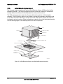
The Compute Module complies with Intel’s Unified Retention System (URS) and the Unified
Backplate Assembly. The Compute Module ships with a made-up assembly of Independent
Loading Mechanism (ILM) and Unified Backplate at each processor socket.
The URS retention transfers load to the Compute Module through the unified backplate
assembly. The URS spring, captive in the heatsink, provides the necessary compressive load
for the thermal interface material. All components of the URS heatsink solution are captive to
the heatsink and only require a Philips* screwdriver to attach to the unified backplate assembly.
See the following figure for the stacking order of the URS components.
.
Screw
Compression Spring
Heatsink
Retention Cup
Retaining Ring
Server Board
Thermal Interface Material (TIM)
ILM and Socket
ILM Attach Studs
Unified Backplate
Heatsink
Attach Studs
AF002699
Figure 5. Unified Retention System and Unified Backplate Assembly
10
Intel order number: E64311-005
Revision 1.3
Intel® Compute Module MFS5520VI TPS
3.2
Functional Architecture
Memory Subsystem
Intel® QuickPath Memory Controller
3.2.1
The Intel® Xeon® Processor 5500 series and Intel® Xeon® Processor 5600 series have an
integrated memory controller, the Intel® QuickPath Memory Controller, in its package. The
memory controller supports DDR3 1333/1066/800 ECC registered DIMMs (RDIMMs) and ECC
unbuffered DIMMs (UDIMMs).
Intel® Compute Module MFS5520VI Supported Memory
3.2.1.1
The Intel® Compute Module MFS5520VI has 12 DIMM sockets and supports the following
memory features:
Six DDR3 memory channels (three per processor socket) with two DIMMs per channel,
thereby supporting up to 12 DIMMs with dual-processor sockets
DDR3 1333 MHz and DDR3 1066 MHz memory modules
Single–Rank (SR) and Dual–Rank (DR) ECC Registered (RDIMMs) or ECC Unbuffered
(UDIMMs) DDR3 memory modules
Quad–Rank (QR) ECC Registered (RDIMMs) DDR3 memory modules
Maximum memory capacity of 192 GB with two processors installed
Use of identical DIMMs in the compute module is recommended
The following configurations are not validated or supported with the Intel® Compute Module
MFS5520VI:
Mixing of RDIMMs and UDIMMs is not supported
Mixing memory type, size, speed and/or rank on this server board is not validated and is
not supported
Mixing memory vendors is not validated and is not supported on this server board
Non-ECC memory is not validated and is not supported in a server environment
For a complete list of supported memory for the Intel® Compute Module MFS5520VI, refer to the
Tested Memory List published in the Intel® Server Configurator Tool.
3.2.2
Publishing Compute Module Memory
The BIOS displays the “Total Memory” of the compute module during POST if Display
Logo is disabled in the BIOS setup. This is the total size of memory discovered by the
BIOS during POST, and is the sum of the individual sizes of installed DDR3 DIMMs in
the system.
The BIOS displays the “Effective Memory” of the compute module in the BIOS setup.
The term Effective Memory refers to the total size of all DDR3 DIMMs that are active (not
disabled) and not used as redundant units.
The BIOS provides the total memory of the compute module in the main page of the
BIOS setup. This total is the same as the amount described by the first bullet above.
If Display Logo is disabled, the BIOS displays the total system memory on the diagnostic
screen at the end of POST. This total is the same as the amount described by the first
bullet above.
Revision 1.3
Intel order number: E64311-005
11
Functional Architecture
3.2.3
Intel® Compute Module MFS5520VI TPS
Memory Map and Population Rules
The nomenclature for DIMM sockets implemented on the Intel® Compute Module MFS5520VI is
detailed in the following figures.
Channel A
A1
A2
Processor Socket 1
Channel B
Channel C
B1
B2
C1
C2
Channel D
D1
Processor Socket 2
Channel E
Channel F
D2
E1
E2
F1
F2
Figure 6. DIMM Nomenclature
DIMM B2
DIMM A1
DIMM A2
DIMM F1
DIMM F2
DIMM E1
DIMM D2
DIMM D1
DIMM E2
DIMM B1
DIMM C2
DIMM C1
AF003098
Figure 7. DIMM Slot Order
3.2.3.1
12
Memory Subsystem Nomenclature
DIMMs are organized into physical slots on DDR3 memory channels that belong to
processor sockets.
The memory channels from processor socket 1 are identified as Channel A, B, and C.
The memory channels from processor socket 2 are identified as Channel D, E, and F.
Intel order number: E64311-005
Revision 1.3
Intel® Compute Module MFS5520VI TPS
Functional Architecture
The compute module Quick Reference Label DIMM slot identifiers provide information
about the channel, and therefore the processor to which they belong. For example,
DIMM_A1 is the first slot on Channel A on processor 1; DIMM_D1 is the first DIMM
socket on Channel D on processor 2.
The memory slots associated with a given processor are unavailable if the given
processor socket is not populated.
A processor may be installed without populating the associated memory slots provided a
second processor is installed with associated memory. In this case, the memory is
shared by the processors. However, the platform suffers performance degradation and
latency due to the remote memory.
Processor sockets are self-contained and autonomous. However, all memory subsystem
support (that is, Memory RAS, Error Management, and so on) in the BIOS setup are
applied commonly across processor sockets.
3.2.4
Memory RAS
3.2.4.1
RAS Features
The Compute Module supports the following memory RAS features:
Channel Independent Mode
Channel Mirroring Mode
The memory RAS offered by the Intel® Xeon® Processor 5500 series and Intel® Xeon®
Processor 5600 series processors is done at channel level, that is, during mirroring, channel B
mirrors channel A. All DIMM matching requirements are on a slot to slot basis on adjacent
channels. For example, to enable mirroring, corresponding slots on channel A and channel B
must have DIMMs of identical parameters.
If one socket fails the population requirements for RAS, the BIOS sets all six channels to the
Channel Independent mode.
The memory slots of DDR3 channels from the Intel® Xeon® Processor 5500 series and Intel®
Xeon® Processor 5600 series processors should be populated on a farthest first fashion. This
holds true even in the Channel Independent mode. This means that A2 cannot be
populated/used if A1 is empty.
3.2.4.2
Channel Independent Mode
In the Channel Independent mode, multiple channels can be populated in any order (for
example, channels B and C can be populated while channel A is empty). Therefore, all DIMMs
are enabled and utilized in the Channel Independent mode.
3.2.4.3
Channel Mirroring Mode
The Intel® Xeon® Processor 5500 series and Intel® Xeon® Processor 5600 series support
channel mirroring to configure available channels of DDR3 DIMMs in the mirrored configuration.
The mirrored configuration is a redundant image of the memory, and can continue to operate
despite the presence of sporadic uncorrectable errors.
Channel mirroring is a RAS feature in which two identical images of memory data are
maintained, thus providing maximum redundancy. On the Intel® Xeon® Processor 5500 series
and Intel® Xeon® Processor 5600 series processors based Intel® server boards, mirroring is
Revision 1.3
Intel order number: E64311-005
13
Functional Architecture
Intel® Compute Module MFS5520VI TPS
achieved across channels. Active channels hold the primary image and the other channels hold
the secondary image of the system memory. The integrated memory controller in the Intel®
Xeon® Processor 5500 series and Intel® Xeon® Processor 5600 series processors alternates
between both channels for read transactions. Write transactions are issued to both channels
under normal circumstances.
When the system is in the Channel Mirroring mode, channel C and channel F of socket 1 and
socket 2 respectively are not used. Hence, the DIMMs populated on these channels are
disabled and therefore do not contribute to the available physical memory. For example, if the
system is operating in the Channel Mirroring mode and the total size of the DDR3 DIMMs is 1.5
GB (3 x 512 MB DIMMs), and then the active memory is only 1 GB.
Because the available system memory is divided into a primary image and a copy of the image,
the effective system memory is reduced by at least one-half. For example, if the system is
operating in the Channel Mirroring mode and the total size of the DDR3 DIMMs is 1 GB, then
the effective size of the memory is 512 MB because half of the DDR3 DIMMs are the secondary
images.
For channel mirroring to work, participant DDR3 DIMMs on the same DIMM slots on the
adjacent channels must be identical in terms of technology, number of ranks, and size.
The BIOS setup provides an option to enable mirroring if the current DIMM population is valid
for channel mirroring. When memory mirroring is enabled, the BIOS attempts to configure the
memory system accordingly. If the BIOS finds that the DIMM population is not suitable for
mirroring, it falls back to the default Channel Independent mode with maximum memory
interleaving.
3.2.4.3.1
Minimum DDR3 DIMM Population for Channel Mirroring
Memory mirroring has the following minimum requirements:
Channel configuration: Mirroring requires the first two adjacent channels to be active.
Socket configuration: Mirroring requires that both socket 1 and socket 2 DIMM
population meets the requirements for mirroring mode. The platform BIOS configures the
system in mirroring mode only if both nodes qualify. The only exception to this rule is
socket 2 with all empty DIMM slots.
As a direct consequence of these requirements, the minimal DIMM population is {A1, B1}. In
this configuration, processor cores on socket 2 suffer memory latency due to usage of remote
memory from socket 1. An optimal DIMM population for channel mirroring in a DP server
platform is {A1, B1, D1, E1}. {A1, B1} must be identical and {D1, E1} must be identical.
In this configuration, DIMMs {A1, B1} and {D1, E1} operate as (primary copy, secondary copy)
pairs independent from each other. Therefore, the optimal number of DDR3 DIMMs for channel
mirroring is a multiple of four, arranged as mentioned above. The BIOS disables all nonidentical DDR3 DIMMs or pairs of DDR3 DIMMs across the channels to achieve symmetry and
balance between the channels.
3.2.4.3.2
Mirroring DIMM Population Rules Variance across Nodes
Memory mirroring in Intel® Xeon® Processor 5500 series and Intel® Xeon® Processor 5600
series processors based platforms is channel mirroring. Mirroring is not done across sockets, so
each socket may have a different memory configuration. Channel mirroring in socket 1 and
14
Intel order number: E64311-005
Revision 1.3
Intel® Compute Module MFS5520VI TPS
Functional Architecture
socket 2 are mutually independent. As a result, if channel A and channel B have identical DIMM
population and channel D and channel E have identical DIMM population, then mirroring is
possible.
For example, if the system is populated with six DIMMS {A1, B1, A2, B2, D1, E1}, channel
mirroring is possible. Both the populations shown in the following table are valid.
Table 2. Mirroring DIMM Population Rules Variance across Nodes
A1
A2
P
P
3.2.5
B1
B2
C1
C2
P
P
P
P
D1
D2
E1
E2
F1
F2
P
P
Mirroring
Possible?
Yes
P
P
Yes
Memory Upgrade Rules
Upgrading the system memory requires careful positioning of the DDR3 DIMMs based on the
following factors:
Current RAS mode of operation
Existing DDR3 DIMM population
DDR3 DIMM characteristics
Optimization techniques used by the Intel® Xeon® Processor 5500 series and Intel®
Xeon® Processor 5600 series to maximize memory bandwidth
In the Channel Independent mode, all DDR3 channels operate independently. The Channel
Independent mode can also be used to support a single DIMM configuration in channel A and in
the single channel mode.
The following general rules must be observed when selecting and configuring memory to obtain
the best performance from the system.
Mixing RDIMMs and UDIMMs is not supported.
Mixing memory type, size, speed, rank and/or vendors in the compute module is not
supported.
Non-ECC memory is not validated and is not supported in a server environment.
Use of identical DIMMs in the compute module is recommended.
If an installed DDR3 DIMM has faulty or incompatible SPD data, it is ignored during
memory initialization and is (essentially) disabled by the BIOS. If a DDR3 DIMM has no
or missing SPD information, the slot in which it is placed is treated as empty by the
BIOS.
When CPU Socket 1 is empty, any DIMM memory in Channel A through Channel C is
unavailable.
When CPU Socket 2 is empty, any DIMM memory in Channel D through Channel F is
unavailable.
If both processor sockets are populated but Channel A through Channel C is empty, the
platform can still function with remote memory in Channel D through Channel F.
However, platform performance suffers latency due to remote memory.
Revision 1.3
Intel order number: E64311-005
15
Functional Architecture
Intel® Compute Module MFS5520VI TPS
The memory operational mode is configurable at the channel level. Two modes are
supported: Independent Channel and Mirrored Channel.
The memory slots of each DDR3 channel from the Intel® Xeon® Processor 5500 series
and Intel® Xeon® Processor 5600 series are populated on a farthest first fashion. This
holds true even for the Independent Channel mode. Therefore, if A1 is empty, A2 cannot
be populated or used.
The BIOS selects Independent Channel mode by default, which enables all installed
memory on all channels simultaneously.
Mirrored Channel mode is not available when only one processor is populated (CPU
Socket 1).
If both processor sockets are populated and the installed DIMMs are associated with
both processor sockets, then a given RAS mode is selected only if both the processor
sockets are populated to conform to that mode.
The minimum memory population possible is one DIMM in slot A1. In this configuration,
the system operates in the Independent Channel mode. RAS is not available.
If both processor sockets are populated, the next upgrade from the Single Channel
mode installs DIMM_D1. This configuration results in an optimal memory thermal
spread, as well as Non-Uniform Memory Architecture (NUMA) aware interleaving. The
BIOS selects the Independent Channel mode of operation.
If only one processor socket is populated, the next upgrade from the Single Channel
mode is installing DIMM_B1 to allow channel interleaving. The system operates in the
Independent Channel mode.
The DIMM parameter-matching requirements for memory RAS is local to a socket. For
example, while Channels A/B/C can have one match of timing, technology, and size,
Channels D/E/F can have a different set of parameters and RAS still functions.
For the Mirrored Channel mode, the memory in Channels A and B of Socket 1 must be
identical and Channel C should be empty. Similarly, the memory in Channels D and E of
Socket 2 must be identical and Channel F should be empty.
a. The minimum population upgrade for the Mirrored Channel mode is DIMM_A1,
DIMM_B1, DIMM_D1, and DIMM_E1 with both processor sockets populated.
DIMM_A1 and DIMM_B1 as a pair must be identical, and so must DIMM_D1 and
DIMM_E1. Failing to comply with these rules results in a switch back to the
Independent Channel mode.
b. If Mirrored Channel mode is selected and the third channel of each processor socket
is not empty, the BIOS disables the memory in the third channel of each processor
socket.
In the Mirrored Channel mode, both sockets must simultaneously satisfy the DIMM
matching rules on their respective adjacent channels. If the DDR3 DIMMs on adjacent
channels of a socket are not identical, the BIOS configures both of the processor
sockets to default to the Independent Channel mode. If DIMM_D1 and DIMM_E1 are not
identical, then the system switches to the Independent Channel Mode.
Note: Mixed memory size, type, speed, rank and/or vendor is not validated or supported
with the Intel® Compute Module MFS5520VI. Refer to section 3.2.1.1 for supported and
nonsupported memory features and configuration information.
16
Intel order number: E64311-005
Revision 1.3
Intel® Compute Module MFS5520VI TPS
3.3
Functional Architecture
Intel® 5520 Chipset IOH
The Intel® 5520 Chipset component is an I/O Hub (IOH.) The Intel® 5520 Chipset IOH provides
a connection point between various I/O components and Intel processors through the Intel® QPI
interface.
The Intel® 5520 Chipset IOH is capable of interfacing with up to 36 PCI Express* lanes, which
can be configured in various combinations of x4, x8, x16, and limited x2 and x1 devices.
The Intel® 5520 Chipset IOH is responsible for providing a path to the legacy bridge. In addition,
the Intel® 5520 Chipset supports a x4 DMI (Direct Media Interface) link interface for the legacy
bridge, and interfaces with other devices through SMBus, Controller Link, and RMII
manageability interfaces. The Intel® 5520 Chipset supports the following features and
technologies:
Intel® QuickPath Interconnect (Intel® QPI)
PCI Express* Gen2
Intel® I/O Acceleration Technology 2 (Intel® I/OAT2)
Intel® Virtualization Technology (Intel® VT) for Directed I/O 2 (Intel® VT-d2)
3.4
Intel® 82801JR I/O Controller Hub (ICH10R)
The Intel® 82801JR I/O Controller Hub (ICH10R) provides extensive I/O support and provides
the following functions and capabilities:
PCI Express* Base Specification, Revision 1.1 support
PCI Local Bus Specification, Revision 2.3 support for 33-MHz PCI operations (supports
up to four REQ#/GNT# pairs)
ACPI Power Management Logic Support, Revision 3.0a
Enhanced DMA controller, interrupt controller, and timer functions
Integrated Serial ATA host controllers with independent DMA operation on up to six
ports and AHCI support
USB host interface with support for up to 12 USB ports; six UHCI host controllers; two
EHCI high-speed USB 2.0 host controllers
Integrated 10/100/1000 Gigabit Ethernet MAC with System Defense
System Management Bus (SMBus) Specification, Version 2.0 with additional support for
I2C devices
Low Pin Count (LPC) interface support
Firmware Hub (FWH) interface support
Serial Peripheral Interface (SPI) support
Revision 1.3
Intel order number: E64311-005
17
Functional Architecture
3.4.1
Intel® Compute Module MFS5520VI TPS
PCI Subsystem
The primary I/O buses for the Intel® Compute Module MFS5520VI are PCI Express* Gen1 and
PCI Express* Gen2 with six independent PCI bus segments.
PCI Express* Gen1 and Gen2 are dual-simplex point-to point serial differential low-voltage
interconnects. A PCI Express* topology can contain a host bridge and several endpoints (I/O
devices). The signaling bit rate is 2.5 Gbit/s one direction per lane for Gen1 and 5.0 Gbit/s one
direction per lane for Gen2. Each port consists of a transmitter and receiver pair. A link between
the ports of two devices is a collection of lanes (x1, x2, x4, x8, x16, and so on.). All lanes within
a port must transmit data using the same frequency.
The following table lists the characteristics of the PCI bus segments. Details about each bus
segment are provided in the following table.
Table 3. Intel® Compute Module MFS5520VI PCI Bus Segment Characteristics
PCI Bus Segment
ESI or DMI Port 0
ICH10R
Voltage
3.3 V
Width
x4
Speed
10 Gb/s
Port 5
3.3 V
x1
2.5 Gb/s
3.3 V
x4
10 Gb/s
PCI
Express*
Gen1
x4 PCI Express* Gen1 throughput to the
on-board NIC.
3.3 V
x8
40 Gb/S
PCI
Express*
Gen2
x8 PCI Express* Gen2 throughput – Not
used.
3.3 V
x8
40 Gb/S
PCI
Express*
Gen2
Two x4 PCI Express* Gen2 throughput Not used.
3.3 V
x8
40 Gb/S
PCI
Express*
Gen2
x8 PCI Express* Gen2 throughput to the
on-board LSI 1064E.
3.3 V
x8
40 Gb/S
PCI
Express*
Gen2
Two x4 PCI Express* Gen2 throughput to
the IO Module Mezzanine connectors.
ICH10R
PE1, PE2
Intel® 5520
Chipset IOH PCI
Express*
PE3, PE4
®
Intel 5520
Chipset IOH PCI
Express*
PE5, PE6
®
Intel 5520
Chipset IOH PCI
Express*
PE7, PE8
®
Intel 5520
Chipset IOH PCI
Express*
PE9, PE10
®
Intel 5520
Chipset IOH PCI
Express*
3.4.2
Type
PCI
Express*
Gen1
PCI
Express*
Gen1
PCI I/O Card Slots
x4 PCI Express* Gen1 throughput to the
Intel® 5520 Chipset IOH
X1 PCI Express* Gen1 throughput to an
on-board Integrated BMC
USB 2.0 Support
The USB controller functionality integrated into ICH10R provides the Compute Module with an
interface for up to ten USB 2.0 ports. All ports are high-speed, full-speed, and low-speed
capable.
18
Intel order number: E64311-005
Revision 1.3
Intel® Compute Module MFS5520VI TPS
Functional Architecture
Four external connectors are located on the front of the compute module.
One internal 2x5 header is provided, capable of supporting a low-profile USB solid state
drive.
Two ports are routed to the Integrated BMC to support rKVM.
3.5
Integrated Baseboard Management Controller
The ServerEngines* LLC Pilot II Integrated BMC has an embedded ARM9 controller and
associated peripheral functionality that is required for IPMI-based server management.
Firmware usage of these hardware features is platform dependant.
The following is a summary of the integrated BMC management hardware features found in the
ServerEngines* LLC Pilot II Integrated BMC:
IPMI 2.0 Compliant
Integrated 250 Mhz 32-bit ARM9 processor
Six I2C SMBus modules with Master-Slave support
Two independent 10/100 Ethernet Controllers with RMII support
Memory Management Unit (MMU)
DDR2 16-bit up to 667 MHz memory interface
Dedicated real-time clock for Integrated BMC
Up to 16 direct and 64 Serial GPIO ports
Twelve 10-bit Analog to Digital Converters
Eight Fan Tachometers Inputs
Four Pulse Width Modulators (PWM)
JTAG Master interface
Watchdog timer
Additionally, the ServerEngines* Pilot II component integrates a super I/O module with the
following features:
Keyboard Style/BT Interface
16C550 compatible serial ports
Serial IRQ support
16 GPIO ports (shared with Integrated BMC)
LPC to SPI Bridge for system BIOS support
SMI and PME support
ACPI compliant
Wake-up control
The Pilot II contains an integrated KVMS subsystem and graphics controller with the following
features:
USB 2.0 for keyboard, mouse, and storage devices
Hardware Video Compression for text and graphics
Hardware encryption
Revision 1.3
Intel order number: E64311-005
19
Functional Architecture
Intel® Compute Module MFS5520VI TPS
2D Graphics Acceleration
DDR2 graphics memory interface
Up to 1600x1200 pixel resolution
Figure 8. Integrated BMC Hardware
20
Intel order number: E64311-005
Revision 1.3
Intel® Compute Module MFS5520VI TPS
3.5.1
Functional Architecture
Floppy Disk Controller
The Compute Module does not support a floppy disk controller interface. However, the compute
module BIOS recognizes USB floppy devices.
3.5.2
Keyboard and Mouse Support
The Compute Module does not support PS/2 interface keyboards and mice. However, the
compute module BIOS recognizes USB specification-compliant keyboard and mice.
3.5.3
Wake-up Control
The super I/O contains functionality that allows various events to power on and power off the
system.
3.6
Video Support
The Compute Module includes a video controller in the on-board Server Engines* Integrated
Baseboard Management Controller along with 32 MB of video DDR2 SDRAM. The SVGA
subsystem supports a variety of modes, up to 1600 x 1200 resolution in 8 / 16 / 32 bpp modes
under 2D. It also supports both CRT and LCD monitors up to a 100 Hz vertical refresh rate.
The video is accessed using a standard 15-pin VGA connector found on the front panel of the
compute module.
3.6.1
Video Modes
The integrated video controller supports all standard IBM VGA modes. The following table
shows the 2D modes supported for both CRT and LCD.
Table 4. Video Modes
2D Mode
3.7
Refresh Rate (Hz)
8 bpp
Supported
2D Video Mode Support
16 bpp
32 bpp
Supported
Supported
640x480
60, 72, 75, 85, 90,
100, 120, 160, 200
800x600
60, 70, 72, 75, 85,
90, 100, 120,160
Supported
Supported
Supported
1024x768
60, 70, 72,
75,85,90,100
Supported
Supported
Supported
1152x864
43,47,60,70,75,80,85
Supported
Supported
Supported
1280x1024
60,70,74,75
Supported
Supported
Supported
1600x1200
52
Supported
Supported
Supported
Network Interface Controller (NIC)
Network interface support is provided from the on-board Intel® 82575EB NIC, which is a single,
compact component with two fully integrated GbE Media Access Control (MAC) and Physical
Layer (PHY) ports. The on-board Intel® 82575EB NIC provides the Compute Module with
support for dual LAN ports designed for 1000 Mbps operation.
Revision 1.3
Intel order number: E64311-005
21
Functional Architecture
Intel® Compute Module MFS5520VI TPS
The Intel® 82575EB device provides two standard IEEE 802.3 Ethernet interface through its
SERDES interfaces. Each network interface controller (NIC) drives two LEDs located on the
front panel. The LED indicates transmit / receive activity when blinking.
3.7.1
Direct Cache Access (DCA)
Direct Cache Access (DCA) is a component of Intel® I/O Acceleration Technology 2 (Intel®
I/OAT2). The DCA mechanism is a system-level protocol in a multi-processor system to improve
I/O network performance thereby providing higher system performance. The basic idea is to
minimize cache misses when a demand read is executed. This is accomplished by placing the
data from the I/O devices directly into the CPU cache through hints to the processor to perform
a data pre-fetch and install it in its local caches. The Intel® Xeon® Processor 5500 series and
Intel® Xeon® Processor 5600 series processors support Direct Cache Access (DCA). DCA can
be enabled or disabled in the BIOS processor setup menu.
3.8
Intel® Virtualization Technology for Directed I/O (Intel® VT-d)
The Intel® Virtualization Technology is designed to support multiple software environments
sharing same hardware resources. Each software environment may consist of an OS and
applications. The Intel® Virtualization Technology can be enabled or disabled in the BIOS setup.
The default behavior is disabled.
Note: If the setup options are changed to enable or disable the Virtualization Technology setting
in the processor, the user must perform an AC power cycle for the changes to take effect.
The Intel® 5520 Chipset IOH supports DMA remapping from inbound PCI Express* memory
Guest Physical Address (GPA) to Host Physical Address (HPA). PCI devices are directly
assigned to a virtual machine leading to a robust and efficient virtualization.
22
Intel order number: E64311-005
Revision 1.3
Intel® Compute Module MFS5520VI TPS
Connector/Header Locations and Pin-outs
4.
Connector/Header Locations and Pin-outs
4.1
Board Connector Information
The following section provides detailed information regarding all connectors, headers, and
jumpers on the compute module. The following table lists all connector types available on the
board and the corresponding reference designators printed on the silkscreen.
Table 5. Board Connector Matrix
Connector
Power Connector
Quantity
1
Reference Designators
J1K1
Midplane Signal Connector
1
J1H1
CPU
2
CPU1(U2D2), CPU2(U7C1)
Main Memory
12
J4A1,JFA2,J4B1,J4B2,J4B3,J4C1,
J5E1,J5E2,J5E3,J5F2,J5F3,J5F4
I/O Mezzanine
2
J3K1,J1J1
Battery
1
BT9H1
USB
2
J9F1, J9G1
Serial Port A
1
J9J1
Video connector
1
J9E1
Mini USB connector
1
J9B7
4.2
Power Connectors
The power connection is obtained using a 2x2 FCI Airmax* power connector. The following
table defines the power connector pin-out.
Table 6. Power Connector Pin-out (J1A1)
Position
1
Revision 1.3
Signal
+12 Vdc
2
GND
3
GND
4
+12 Vdc
Intel order number: E64311-005
23
Connector/Header Locations and Pin-outs
4.3
4.3.1
Intel® Compute Module MFS5520VI TPS
I/O Connector Pin-out Definition
VGA Connector
The following table details the pin-out definition of the VGA connector (J6K1).
Table 7. VGA Connector Pin-out (J6A1)
Pin
4.3.2
1
Signal Name
V_IO_R_CONN
Description
Red (analog color signal R)
2
V_IO_G_CONN
Green (analog color signal G)
3
V_IO_B_CONN
Blue (analog color signal B)
4
TP_VID_CONN_B4
No connection
5
GND
Ground
6
GND
Ground
7
GND
Ground
8
GND
Ground
9
P5V_VID_CONN_9
P5V
10
GND
Ground
11
TP_VID_CONN_B11
No connection
12
V_IO_DDCDAT
DDCDAT
13
V_IO_HSYNC_CONN
HSYNC (horizontal sync)
14
V_IO_VSYNC_CONN
VSYNC (vertical sync)
15
V_IO_DDCCLK
DDCCLK
I/O Mezzanine Card Connector
The compute module provides an internal 120-pin Tyco dual-row receptacle (J3K1) and a Tyco
40-pin dual-row receptacle (J1J1) to accommodate high-speed I/O expansion modules, which
expands the I/O capabilities of the compute module. The following table details the pin-out of
the Intel® I/O expansion module connector.
24
Intel order number: E64311-005
Revision 1.3
Intel® Compute Module MFS5520VI TPS
Connector/Header Locations and Pin-outs
Table 8. 120-pin I/O Mezzanine Card Connector Pin-out
Signal Name
Revision 1.3
Pin
Signal Name
Pin
P5V
1
P5V
2
GND
3
GND
4
P3V3
5
P3V3
6
P3V3
7
P3V3
8
P3V3
9
P3V3
10
GND
11
GND
12
P3V3AUX
13
P3V3AUX
14
P3V3AUX
15
P3V3AUX
16
SMB_SDA
17
SMB_SCL
18
HSC0_LNK_LED
19
HSC0_ACT_LED
20
HSC1_LNK_LED
21
HSC1_ACT_LED
22
HSC2_LNK_LED
23
HSC2_ACT_LED
24
HSC3_LNK_LED
25
HSC3_ACT_LED
26
GND
27
WAKE_N
28
Rsvd
29
GND
30
Rsvd
31
GND
32
GND
33
PCIe_0_A_TXP
34
GND
35
PCIe_0_A_TXN
36
PCIe_0_A_RXP
37
GND
38
PCIe_0_A_RXN
39
GND
40
GND
41
PCIe_0_B_TXP
42
GND
43
PCIe_0_B_TXN
44
PCIe_0_B_RXP
45
GND
46
PCIe_0_B_RXN
47
GND
48
GND
49
PCIe_0_C_TXP
50
GND
51
PCIe_0_C_TXN
52
PCIe_0_C_RXP
53
GND
54
PCIe_0_C_RXN
55
GND
56
GND
57
PCIe_0_D_TXP
58
GND
59
PCIe_0_D_TXN
60
PCIe_0_D_RXP
61
GND
62
PCIe_0_D_RXN
63
GND
64
GND
65
PCIe_1_A_TXP
66
GND
67
PCIe_1_A_TXN
68
PCIe_1_A_RXP
69
GND
70
PCIe_1_A_RXN
71
GND
72
GND
73
PCIe_1_B_TXP
74
GND
75
PCIe_1_B_TXN
76
PCIe_1_B_RXP
77
GND
78
PCIe_1_B_RXN
79
GND
80
GND
81
PCIe_1_C_TXP
82
GND
83
PCIe_1_C_TXN
84
PCIe_1_C_RXP
85
GND
86
PCIe_1_C_RXN
87
GND
88
Intel order number: E64311-005
25
Connector/Header Locations and Pin-outs
Signal Name
Intel® Compute Module MFS5520VI TPS
GND
89
Pin
Signal Name
PCIe_1_D_TXP
90
Pin
GND
91
PCIe_1_D_TXN
92
PCIe_1_D_RXP
93
GND
94
PCIe_1_D_RXN
95
GND
96
98
GND
97
Mezz_Present
GND
99
Reset_N
100
Clk0_100M_PCIE_P
101
GND
102
Clk0_100M_PCIE_N
103
GND
104
GND
105
Rsvd
106
GND
107
Rsvd
108
Rsvd
109
GND
110
Rsvd
111
Rsvd
112
Rsvd
113
Rsvd
114
P12V
115
P12V
116
P12V
117
P12V
118
P12V
119
P12V
120
Table 9. 120-pin I/O Mezzanine Card Connector Signal Definitions
Signal Name
PCIe_0_A_TXP
26
Signal Description
PCIe TX+ of Lane A Link 0
Purpose
Host connect
34
PCIe_0_A_TXN
PCIe TX- of Lane A Link 0
Host connect
36
PCIe_0_A_RXP
PCIe RX+ of Lane A Link 0
Host connect
37
PCIe_0_A_RXN
PCIe RX- of Lane A Link 0
Host connect
39
PCIe_0_B_TXP
PCIe TX+ of Lane B Link 0
Host connect
42
PCIe_0_B_TXN
PCIe TX- of Lane B Link 0
Host connect
44
PCIe_0_B_RXP
PCIe RX+ of Lane B Link 0
Host connect
45
PCIe_0_B_RXN
PCIe RX- of Lane B Link 0
Host connect
47
PCIe_0_C_TXP
PCIe TX+ of Lane C Link 0
Host connect
50
PCIe_0_C_TXN
PCIe TX- of Lane C Link 0
Host connect
52
PCIe_0_C_RXP
PCIe RX+ of Lane C Link 0
Host connect
53
PCIe_0_C_RXN
PCIe RX- of Lane C Link 0
Host connect
55
PCIe_0_D_TXP
PCIe TX+ of Lane D Link 0
Host connect
58
PCIe_0_D_TXN
PCIe TX- of Lane D Link 0
Host connect
60
PCIe_0_D_RXP
PCIe RX+ of Lane D Link 0
Host connect
61
PCIe_0_D_RXN
PCIe RX- of Lane D Link 0
Host connect
63
PCIe_1_A_TXP
PCIe TX+ of Lane A Link 1
Host connect
66
PCIe_1_A_TXN
PCIe TX- of Lane A Link 1
Host connect
68
PCIe_1_A_RXP
PCIe RX+ of Lane A Link 1
Host connect
69
PCIe_1_A_RXN
PCIe RX- of Lane A Link 1
Host connect
71
PCIe_1_B_TXP
PCIe TX+ of Lane B Link 1
Host connect
74
PCIe_1_B_TXN
PCIe TX- of Lane B Link 1
Host connect
76
PCIe_1_B_RXP
PCIe RX+ of Lane B Link 1
Host connect
78
PCIe_1_B_RXN
PCIe RX- of Lane B Link 1
Host connect
79
PCIe_1_C_TXP
PCIe TX+ of Lane C Link 1
Host connect
82
Intel order number: E64311-005
Connector Location
Revision 1.3
Intel® Compute Module MFS5520VI TPS
Connector/Header Locations and Pin-outs
Signal Name
PCIe_1_C_TXN
Signal Description
PCIe TX- of Lane C Link 1
Purpose
Host connect
84
Connector Location
PCIe_1_C_RXP
PCIe RX+ of Lane C Link 1
Host connect
85
PCIe_1_C_RXN
PCIe RX- of Lane C Link 1
Host connect
87
PCIe_1_D_TXP
PCIe TX+ of Lane D Link 1
Host connect
90
PCIe_1_D_TXN
PCIe TX- of Lane D Link 1
Host connect
92
PCIe_1_D_RXP
PCIe RX+ of Lane D Link 1
Host connect
93
PCIe_1_D_RXN
PCIe RX- of Lane D Link 1
Host connect
95
Clk0_100M_PCIe_P
100MHz clk +
PCIe Clk
101
Clk0_100M_PCIe_N
100MHz clk -
PCIe Clk
103
SMB_SCL
SMBus Clock
Mngt connect
18
SMB_SDA
SMBus Data
Mngt connect
17
HSC_0_LNK_LED
HSC 0 Link LED driver
LED control
19
HSC_1_LNK_LED
HSC 1 Link LED driver
LED control
21
HSC_2_LNK_LED
HSC 2 Link LED driver
LED control
23
HSC_3_LNK_LED
HSC 3 Link LED driver
LED control
25
HSC_0_ACT_LED
HSC 0 Activity LED driver
LED control
20
HSC_1_ACT_LED
HSC 1 Activity LED driver
LED control
22
HSC_2_ACT_LED
HSC 2 Activity LED driver
LED control
24
HSC_3_ACT_LED
HSC 3 Activity LED driver
LED control
26
WAKE_N
PCIe WAKE_N signal
Wake on LAN
28
Reset_N
Reset signal (Active Low)
Mezz Reset
100
Mezz_PRES_N
Mezzanine Present signal (active
Low)
Present
indication
98
P12V
12V power
Power
115, 116, 117, 118, 119,
120
P3V3
3.3V Power
power
5, 6, 7, 8, 9, 10
P5V
5V power
power
1, 2
P3V3AUX
Auxiliary power
Aux power
13, 14, 15, 16
Rsvd
Reserved pins
Future use
29, 31, 106, 108, 109,
111, 112, 113, 114
GND
Revision 1.3
Ground
3, 4, 11, 12, 27, 30, 32,
33, 35, 38, 40, 41, 43,
46, 48, 49, 51, 54, 56,
57,59, 62, 64, 65, 67, 70,
72, 73, 75, 78, 80, 81,
83, 86, 88, 89, 91, 94,
96, 97, 99, 102, 104,
105, 107, 110
Intel order number: E64311-005
27
Connector/Header Locations and Pin-outs
Intel® Compute Module MFS5520VI TPS
Table 10. 40-pin I/O Mezzanine Card Connector Pin-out
Signal Name
Connector Location
1
TP
RMII_IBMC_IOMEZZ
_CRS_DV
3
GND
5
Signal Name
GND
XE_B1_TXP
Connector Location
2
4
XE_B1_TXN
6
XE_B1_RXP
7
GND
8
XE_B1_RXN
9
GND
10
GND
11
XE_B2_TXP
12
GND
13
XE_B2_TXN
14
XE_B2_RXP
15
GND
16
XE_B2_RXN
17
GND
18
GND
19
XE_D2_TXP
20
GND
21
XE_D2_TXN
22
XE_D1_RXP
23
GND
24
XE_D1_RXN
25
GND
26
GND
27
XE_D1_TXP
28
GND
29
XE_D1_TXN
30
XE_D2_RXP
31
GND
32
33
RMII_IBMC_IOME
ZZ_TX_EN
34
35
RMII_IBMC_IOME
ZZ_TXD1
36
RMII_IBMC_IOMEZZ
_RXD1
37
RMII_IBMC_IOME
ZZ_TXD0
38
RMII_IBMC_IOMEZZ
_RXD0
39
CLK_IOMEZZ_RMI
I
40
XE_D2_RXN
GND
4.3.3
Midplane Signal Connector
The compute module connects to the midplane through a 96-pin Airmax* connector (J1H1)
(power is J1K1) to connect the various I/O, management, and control signals of the system.
Table 11. 96-pin Midplane Signal Connector Pin-out
Pin
A1
Signal Name
XE_P1_A_RXP
Pin
E1
Signal Name
XE_P2_D_RXN
Pin
I1
GND
Signal Name
A2
GND
E2
XE_P2_D_TXP
I2
SAS_P1_TXN
A3
XE_P1_B_RXP
E3
SMB_SDA_B
I3
GND
A4
GND
E4
FM_BL_X_SP
I4
XE_P2_C_TXN
A5
XE_P1_C_RXP
E5
XE_P2_B_RXN
I5
GND
A6
GND
E6
XE_P2_B_TXP
I6
SAS_P2_TXN
A7
XE_P1_D_RXP
E7
XE_P2_A_RXN
I7
GND
A8
GND
E8
XE_P2_A_TXP
I8
Fm_bl_slot_id5
B1
XE_P1_A_RXN
F1
GND
J1
SMB_SCL_A
B2
XE_P1_A_TXP
F2
XE_P2_D_TXN
J2
GND
B3
XE_P1_B_RXN
F3
GND
J3
FM_BL_SLOT_ID2
28
Intel order number: E64311-005
Revision 1.3
Intel® Compute Module MFS5520VI TPS
Pin
B4
Signal Name
XE_P1_B_TXP
Pin
F4
Connector/Header Locations and Pin-outs
Signal Name
12V (BL_PWR_ON)
Pin
J4
Signal Name
GND
B5
XE_P1_C_RXN
F5
GND
J5
reserved
B6
XE_P1_C_TXP
F6
XE_P2_B_TXN
J6
GND
B7
XE_P1_D_RXN
F7
GND
J7
reserved
B8
XE_P1_D_TXP
F8
XE_P2_A_TXN
J8
GND
C1
GND
G1
SAS_P1_RXP
K1
SMB_SDA_A
C2
XE_P1_A_TXN
G2
GND
K2
FM_BL_SLOT_ID0
C3
GND
G3
XE_P2_C_RXP
K3
FM_BL_SLOT_ID3
C4
XE_P1_B_TXN
G4
GND
K4
FM_BL_SLOT_ID4
C5
GND
G5
SAS_P2_RXP
K5
reserved
C6
XE_P1_C_TXN
G6
GND
K6
reserved
C7
GND
G7
spare
K7
reserved
C8
XE_P1_D_TXN
G8
GND
K8
reserved
D1
XE_P2_D_RXP
H1
SAS_P1_RXN
L1
GND
D2
GND
H2
SAS_P1_TXP
L2
FM_BL_SLOT_ID1
D3
SMB_SCL_B
H3
XE_P2_C_RXN
L3
GND
D4
GND
H4
XE_P2_C_TXP
L4
FM_BL_PRES_N
D5
XE_P2_B_RXP
H5
SAS_P2_RXN
L5
GND
D6
GND
H6
SAS_P2_TXP
L6
reserved
D7
XE_P2_A_RXP
H7
spare
L7
GND
D8
GND
H8
spare
L8
reserved
4.3.4
Serial Port Connector
The compute module provides one internal 9-pin Serial port header (J9J1). The following table
defines the pin-out.
Table 12. Internal 9-pin Serial Header Pin-out (J9J1)
Pin
1
4.3.5
Signal Name
SPA_DCD
Description
DCD (carrier detect)
2
SPA_DSR
DSR (data set ready)
3
SPA_SIN_L
RXD (receive data)
4
SPA_RTS
RTS (request to send)
5
SPA_SOUT_N
TXD (transmit data)
6
SPA_CTS
CTS (clear to send)
7
SPA_DTR
DTR (data terminal ready)
8
SPA_RI
RI (ring Indicate)
9
GND
Ground
USB 2.0 Connectors
The following table details the pin-out of the external USB connectors (J4K1, J4K2) found on the
front edge of the compute module.
Revision 1.3
Intel order number: E64311-005
29
Connector/Header Locations and Pin-outs
Intel® Compute Module MFS5520VI TPS
Table 13. External USB Connector Pin-out
Pin
1
+5V
Signal Name
USB_PWR
Description
2
USB_N
Differential data line paired with DATAH0
3
USB_P
(Differential data line paired with DATAL0
4
GND
Ground
One low-profile 2x5 connector (J9B7) on the compute module provides an option to support lowprofile Intel® Z-U130 Value Solid State Drive. The pin-out of the connector is detailed in the
following table.
Table 14. Pin-out of Internal USB Connector for low-profile Solid State Drive (J9B7)
30
Pin
1
+5V
Signal Name
Pin
2
NC
Signal Name
3
USB_N
4
NC
5
USB_P
6
NC
7
GND
8
NC
9
Key Pin
10
LED#
Intel order number: E64311-005
Revision 1.3
Intel® Compute Module MFS5520VI TPS
5.
Jumper Block Settings
Jumper Block Settings
The server board has several 3-pin jumper blocks that can be used to configure, protect, or
recover specific features of the server board. Pin 1 on each jumper block is denoted by an “*” or
“▼”.
5.1
Recovery Jumper Blocks
BIOS Recover
Boot from
Emergency
BIOS Image
Default
3
2
J9B9
PASSWORD Clear
3
2
Clear Default
Password
J9A3
CMOS Clear
2
3
Default
Clear
CMOS
J9A4
BMC Force Update
3
2
Enabled Default
Disabled
J9A5
AF003078
Figure 9. Recovery Jumper Blocks
Revision 1.3
Intel order number: E64311-005
31
Jumper Block Settings
Intel® Compute Module MFS5520VI TPS
Table 15. Recovery Jumpers
Jumper Name
J9A5: BMC Force
Update
Pins
1-2
What happens at system reset …
BMC Firmware Force Update Mode – Disabled (Default)
2-3
BMC Firmware Force Update Mode – Enabled
J9A3: Password
Clear
1-2
These pins should have a jumper in place for normal operation. (Default)
2-3
If these pins are jumpered, the administrator and user passwords are cleared
immediately. These pins should not be jumpered for normal operation.
J9A4: CMOS Clear
1-2
These pins should have a jumper in place for normal operation. (Default)
2-3
If these pins are jumpered, the CMOS settings are cleared on the next boot. These
pins should not be jumpered for normal operation
1-2
These pins should have a jumper in place for normal operation. (Default)
2-3
If these pins are jumpered, the compute module boots from the emergency BIOS
image. These pins should not be jumpered for normal operation.
J9B9: BIOS
Recover
5.1.1
CMOS Clear and Password Clear Usage Procedure
The CMOS Clear (J9A4) and Password Clear (J9A3) recovery features are designed such that
the desired operation can be achieved with minimal system downtime. The usage procedure for
these two features has changed from previous generation Intel® server boards. The following
procedure outlines the new usage model.
1.
2.
3.
4.
Power down the compute module.
Remove the compute module from the modular server chassis.
Open the compute module.
Move jumper from the default operating position (pins 1-2) to the Clear position (pins 23).
5. Wait 5 seconds.
6. Move jumper back to the default position (pins 1-2).
7. Close the compute module.
8. Reinstall the compute module in the modular server chassis.
9. Power up the compute module.
Password and/or CMOS are now cleared and can be reset by going into the BIOS setup.
5.1.2
Integrated BMC Force Update Procedure
When performing a standard Integrated BMC firmware update procedure, the update utility
places the Integrated BMC into an update mode, allowing the firmware to load safely onto the
flash device. In the unlikely event that the Integrated BMC firmware update process fails due to
the Integrated BMC not being in the proper update state, the server board provides a BMC
Force Update jumper (J9A5), which will force the Integrated BMC into the proper update state.
The following procedure should be followed in the event the standard Integrated BMC firmware
update process fails.
1. Power down the compute module.
2. Remove the compute module from the modular server chassis.
3. Open the compute module.
32
Intel order number: E64311-005
Revision 1.3
Intel® Compute Module MFS5520VI TPS
Jumper Block Settings
4. Move jumper from the default operating position (pins 1-2) to the “Enabled” position (pins
2-3)
5. Close the compute module.
6. Reinstall and power up the compute module.
7. Perform Integrated BMC firmware update procedure.
8. Power down the compute module.
9. Remove the compute module from the server system.
10. Move jumper from the “Enabled” position (pins 2-3) to the “Disabled” position (pins 1-2).
11. Close the compute module.
12. Reinstall the compute module into the modular server chassis.
13. Power up the compute module.
Note: Normal Integrated BMC functionality (for example, KVM, monitoring, and remote media)
is disabled with the force BMC update jumper set to the “Enabled” position. The server should
never be run with the BMC force update jumper set in this position and should only be used
when the standard firmware update process fails. This jumper should remain in the default –
disabled position when the server is running normally.
5.1.3
Integrated BMC Initialization
When the DC power is first applied to the compute module by installing it into a chassis, 5VSTBY is present, the Integrated BMC on the compute module requires 15-30 seconds to
initialize. During this time, the power button functionality of the control panel is disabled,
preventing the compute module from powering up.
Revision 1.3
Intel order number: E64311-005
33
Product Regulatory Requirements
Intel® Compute Module MFS5520VI TPS
6.
Product Regulatory Requirements
6.1
Product Regulatory Requirements
The Intel® Compute Module MFS5520VI is evaluated as part of the Intel® Modular Server
System MFSYS25/MFSYS35, which requires meeting all applicable system component
regulatory requirements. Refer to the Intel® Modular Server System MFSYS25/MFSYS35
Technical Product Specification for a complete listing of all system and component regulatory
requirements.
6.2
Product Regulatory Compliance and Safety Markings
No markings are required on the Intel® Compute Module MFS5520VI itself as it is evaluated as
part of the Intel® Modular Server System MFSYS25/MFSYS35.
6.3
Product Environmental/Ecology Requirements
The Intel® Compute Module MFS5520VI is evaluated as part of the Intel® Modular Server
System MFSYS25/MFSYS35, which requires meeting all applicable system component
environmental and ecology requirements. For a complete listing of all system and component
environment and ecology requirements and markings, refer to the Intel® Modular Server System
MFSYS25/MFSYS35 Technical Product Specification.
34
Intel order number: E64311-005
Revision 1.3
Intel® Compute Module MFS5520VI TPS
Appendix A: Integration and Usage Tips
Appendix A: Integration and Usage Tips
When two processors are installed, both must be of identical revision, core voltage, and
bus/core speed. Mixed processor steppings are supported as long as they are listed in
the processor specification updates published by Intel Corporation. However, the
stepping of one processor cannot be greater than one stepping back of the other.
Only Intel® Xeon® Processor 5500 series and Intel® Xeon® Processor 5600 series with
95 W and less Thermal Design Power (TDP) are supported on this compute module.
Previous generations of the Intel® Xeon® processors are not supported. Intel® Xeon®
Processor 5500 series and Intel® Xeon® Processor 5600 series with TDP higher than 95
W are also not supported.
Processors must be installed in order. CPU 1 is located near the edge of the compute
module and must be populated to operate the board.
Only registered DDR3 DIMMs (RDIMMs) and unbuffered DDR3 DIMMs (UDIMMs) are
supported on this compute module. Mixing of RDIMMs and UDIMMs is not supported.
Mixing memory type, size, speed, rank and/or memory vendors is not validated and is
not supported on this server board.
Non-ECC memory is not validated and is not supported in a server environment
For the best performance, the number of DDR3 DIMMs installed should be balanced
across both processor sockets and memory channels. For example, a two-DIMM
configuration performs better than a one-DIMM configuration. In a two-DIMM
configuration, DIMMs should be installed in DIMM sockets A1 and D1. A six-DIMM
configuration (DIMM sockets A1, B1, C1, D1, E1, and F1) performs better than a threeDIMM configuration (DIMM sockets A1, B1, and C1).
For a list of Intel supported operating systems, add-in cards, and peripherals for this
server board, see the Intel® Modular Server System MFSYS25/MFSYS35 and Intel®
Compute Module MFS5000SI/MFS5520VI Tested Hardware and Operating System List.
Normal Integrated BMC functionality (for example, KVM, monitoring, and remote media)
is disabled with the force BMC update jumper set to the “enabled” position (pins 2-3).
The compute module should never be run with the BMC force update jumper set in this
position and should only be used when the standard firmware update process fails. This
jumper should remain in the default (disabled) position (pins 1-2) when the compute
module is running normally.
When performing the BIOS update procedure, the BIOS select jumper must be set to its
default position (pins 1-2).
Revision 1.3
35
Intel order number: E64311-005
Appendix B: Integrated BMC Sensor Tables
Intel® Compute Module MFS5520VI TPS
Appendix B: Integrated BMC Sensor Tables
This appendix lists the sensor identification numbers and information regarding the sensor type,
name, supported thresholds, and a brief description of the sensor purpose. See the Intelligent
Platform Management Interface Specification, Version 2.0, for sensor and event / reading-type
table information.
Sensor Type
The Sensor Type references the values enumerated in the Sensor Type Codes table in the IPMI
Specification. It provides the context in which to interpret the sensor, such as the physical entity
or characteristic that is represented by this sensor.
Event / Reading Type
The Event / Reading Type references values from the Event / Reading Type Code Ranges and
Generic Event / Reading Type Codes tables in the IPMI Specification. Note that digital sensors
are specific type of discrete sensors, which have only two states.
Event Offset Triggers
This column defines what event offsets the sensor generates.
For Threshold (analog reading) type sensors, the Integrated BMC can generate events for the
following thresholds:
Upper Critical
Upper Non-critical
Lower Non-critical
Lower Critical
The abbreviation [U,L] is used to indicate that both Upper and Lower thresholds are supported.
A few sensors support only a subset of the standard four threshold triggers. Note that even if a
sensor does support all thresholds, the SDRs may not contain values for some thresholds.
For Digital and Discrete type sensor event triggers, the supported event generating offsets are
listed. The offsets can be found in the Generic Event / Reading Type Codes or Sensor Type
Codes tables in the IPMI Specification, depending on whether the sensor event / reading type is
a generic or sensor-specific response.
All sensors generate both assertions and deassertions of the defined event triggers. The
assertions and deassertions may or may not generate events into the System Event Log (SEL),
depending on the sensor SDR settings.
36
Intel order number: E64311-005
Revision 1.3
Intel® Compute Module MFS5520VI TPS
Appendix B: Integrated BMC Sensor Tables
Fault LED
This column indicates whether an assertion of an event lights the front panel fault LED. The
Integrated BMC aggregates all fault sources (including outside sources such as the BIOS) such
that the LED will be lit as long as any source indicates that a fault state exists. The Integrated
BMC extinguishes the fault LED when all sources indicate no faults are present.
Sensor Rearm
The rearm is a request for the event status for a sensor to be rechecked and updated upon a
transition between good and bad states. Rearming the sensors can be done manually or
automatically. The following abbreviations are used in the column:
‘A’: Auto rearm
‘M’: Manual rearm
Readable
Some sensors are used simply to generate events into the System Event Log. The Watchdog
timer sensor is one example. These sensors operate by asserting and then immediately deasserting an event. Typically the SDRs for such sensors are defined such that only the assertion
causes an event message to be deposited in the SEL. Reading such a sensor produces no
useful information and is marked as ‘No’ in this column. Note that some sensors may actually be
unreadable in that they return an error code in response to the IPMI Get Sensor Reading
command. These sensors are represented by type 3 SDR records.
Standby
Some sensors operate on standby power. These sensors may be accessed and / or generate
events when the compute module payload power is off, but standby power is present.
Table 16. MFS5520VI Sensors
Sensor Name
Sensor #
Sensor Type
Event /
Reading Type
Event Offset
Triggers
Contrib. To
System
Status
Rearm
Standby
OK
A
X
OK
A
X
00 - Power down
Power Unit Status
Watchdog
01h
03h
Power Unit
09h
Watchdog 2
23h
Sensor
Specific
6Fh
Sensor
Specific
6Fh
04 - A/C lost
05 - Soft power
control failure
06 - Power unit
failure
00 - Timer
expired, status
only
01 - Hard reset
02 - Power down
Revision 1.3
Intel order number: E64311-005
37
Appendix B: Integrated BMC Sensor Tables
Sensor Name
Sensor #
Sensor Type
Intel® Compute Module MFS5520VI TPS
Event /
Reading Type
Event Offset
Triggers
Contrib. To
System
Status
Rearm
Standby
A
X
A
–
OK
A
X
OK
A
–
A
–
A
–
A
–
A
–
A
–
A
X
A
–
A
X
A
–
03 - Power cycle
08 - Timer
interrupt
Physical Security
SMI Timeout
System Event Log
04h
06h
07h
Physical
Security
Sensor
Specific
05h
6Fh
SMI Timeout
Digital
Discrete
F3h
Event
Logging
Disabled
10h
System Event
BB +1.1V IOH
BB +1.1V P1 Vccp
BB +1.1V P2 Vccp
BB +1.5V P1 DDR3
BB +1.5V P2 DDR3
BB +1.8V AUX
BB +3.3V
BB +3.3V STBY
BB Vbat
38
08h
10h
11h
12h
13h
14h
15h
16h
17h
18h
03h
Sensor
Specific
6Fh
04 - LAN leash
lost
Degraded
00 – State
deasserted
OK
01 – State
asserted
Fatal
02 - Log area
reset / cleared
01 - OEM
System Boot
Event
System
Event
Sensor
Specific
12h
6Fh
Voltage
02h
Threshold
01h
Voltage
02h
Threshold
01h
[u,l] [c,nc]
Voltage
02h
Threshold
01h
[u,l] [c,nc]
Voltage
02h
Threshold
01h
[u,l] [c,nc]
Voltage
02h
Threshold
01h
[u,l] [c,nc]
Voltage
02h
Threshold
01h
[u,l] [c,nc]
Voltage
02h
Threshold
01h
[u,l] [c,nc]
Voltage
02h
Threshold
01h
[u,l] [c,nc]
Voltage
02h
Threshold
01h
[u,l] [c,nc]
[u,l] [c,nc]
nc =
Degraded
c = Non-fatal
nc =
Degraded
c = Non-fatal
nc =
Degraded
c = Non-fatal
nc =
Degraded
c = Non-fatal
nc =
Degraded
c = Non-fatal
nc =
Degraded
c = Non-fatal
nc =
Degraded
c = Non-fatal
nc =
Degraded
c = Non-fatal
Intel order number: E64311-005
nc =
Degraded
c = Non-fatal
Revision 1.3
Intel® Compute Module MFS5520VI TPS
Appendix B: Integrated BMC Sensor Tables
Sensor Name
Sensor #
Sensor Type
Event /
Reading Type
Event Offset
Triggers
BB +5.0V
19h
Voltage
02h
Threshold
01h
[u,l] [c,nc]
Voltage
02h
Threshold
01h
[u,l] [c,nc]
Voltage
02h
Threshold
01h
Temperature
Threshold
01h
01h
Temperature
Threshold
01h
01h
Temperature
Threshold
01h
01h
Temperature
Threshold
01h
01h
Temperature
Threshold
01h
01h
Processor
Sensor
Specific
BB +5.0V STBY
BB +12.0V
Baseboard Temp
IOH Thermal Margin
MEM P1 Thermal Margin
MEM P2 Thermal Margin
DIMM Max temp
P1 Status
P2 Status
1Ah
1Bh
20h
22h
23h
24h
2Fh
60h
61h
P1 Thermal Margin
62h
P2 Thermal Margin
63h
P1 Therm Ctrl %
64h
P2 Therm Ctrl %
65h
P1 VRD Temp
66h
P2 VRD Temp
Revision 1.3
67h
07h
Processor
07h
6Fh
Sensor
Specific
6Fh
Temperature
Threshold
01h
01h
Temperature
Threshold
01h
01h
Temperature
Threshold
01h
01h
Temperature
Threshold
01h
01h
Temperature
Digital
Discrete
01h
Temperature
01h
05h
Digital
Discrete
05h
Contrib. To
System
Status
nc =
Degraded
Rearm
Standby
A
–
A
X
A
–
A
X
A
X
c = Non-fatal
nc =
Degraded
c = Non-fatal
[u,l] [c,nc]
nc =
Degraded
c = Non-fatal
[u,l] [c,nc]
nc =
Degraded
c = Non-fatal
[u,l] [c,nc]
nc =
Degraded
c = Non-fatal
[u,l] [c,nc]
nc =
Degraded
A
c = Non-fatal
[u,l] [c,nc]
nc =
Degraded
A
c = Non-fatal
[u,l] [c,nc]
nc =
Degraded
A
–
c = Non-fatal
01 - Thermal trip
07 - Presence
Fatal
M
Fatal
M
01 - Thermal trip
07 - Presence
X
X
–
–
–
–
–
–
–
–
[u] [c]
Non-fatal
A
–
[u] [c]
Non-fatal
A
–
01 - Limit
exceeded
Fatal
M
–
01 - Limit
exceeded
Fatal
M
–
Intel order number: E64311-005
39
Appendix B: Integrated BMC Sensor Tables
Sensor Name
Sensor #
CATERR
68h
CPU Missing
IOH Thermal Trip
Hot Swap
KVM Session
SOL Session
69h
6Ah
70h
71h
72h
Proc Max Therm
9Fh
Mezz Card Present
C0h
Attention State
40
C1h
Sensor Type
Processor
07h
Processor
07h
Temperature
01h
FRU State
2Ch
Intel® Compute Module MFS5520VI TPS
Event /
Reading Type
Digital
Discrete
03h
Digital
Discrete
03h
Digital
Discrete
03h
Sensor
Specific
6Fh
OEM
OEM
C0h
70h
OEM
OEM
C0h
73h
Temperature
Threshold
01h
01h
Slot/Conn.
Sensor
Specific
21h
OEM
6Fh
OEM
Event Offset
Triggers
Contrib. To
System
Status
Rearm
Standby
01 – State
Asserted
Non-fatal
M
–
01 – State
Asserted
Non-fatal
M
–
01 – State
Asserted
Fatal
M
–
A
X
A
X
1: Inactive
None
2: Activation
Required
None
3: Activation In
Progress
None
4: Active
None
5: Deactivation
Required
None
6: Deactivation
In Progress
None
0: Pending
None
1: Established
None
2: Ended
Normally
None
3: Ticket
Expiration
None
4: Lost heartbeat
None
5: Forcibly
Terminated
None
6: Unknown
Ticket
None
0: SOL Session
Inactive
None
1: SOL Session
Active
None
A
None
Ok
A
–
2: Device
installed
None
A
–
0: ID LED Lit
None
A
X
Intel order number: E64311-005
Revision 1.3
Intel® Compute Module MFS5520VI TPS
Sensor Name
HDD BP Present
Drive 1,2
Sensor #
C2h
C3h,
C4h
Slot ID
C5h
BMC Reset
E1h
[MDR]
E2h
Appendix B: Integrated BMC Sensor Tables
Sensor Type
Event /
Reading Type
Event Offset
Triggers
D0h
71h
1: Status LED
Active (fault)
Drive Slot
Digital
Discrete
0: Device Absent
0Dh
Drive Slot
0Dh
08h
1: Device
Present
Sensor
Specific
Contrib. To
System
Status
Rearm
Standby
None
A
?
None
A
?
None
A
X
A
X
6Fh
OEM
Threshold
D1h
01h
OEM
OEM
??
??
OEM
OEM
??
??
None
7: Process
Started
Progress
FEh
OEM
OEM
D2h
72h
8: Process
Finished OK
None
9: Process
Finished Fail
Revision 1.3
Intel order number: E64311-005
41
Appendix C: POST Error Messages and Handling
Intel® Compute Module MFS5520VI TPS
Appendix C: POST Error Messages and Handling
Whenever possible, the BIOS outputs the current boot progress codes on the video screen.
Progress codes are 32-bit quantities plus optional data. The 32-bit numbers include class,
subclass, and operation information. The class and subclass fields point to the type of hardware
that is being initialized. The operation field represents the specific initialization activity. Based on
the data bit availability to display progress codes, a progress code can be customized to fit the
data width. The higher the data bit, the higher the granularity of information that can be sent on
the progress port. The progress codes may be reported by the system BIOS or option ROMs.
The Response section in the following table is divided into two types:
Minor: The message is displayed on the screen or in the Error Manager screen. The
system will continue booting with a degraded state. The user may want to replace the
erroneous unit. The setup POST error Pause setting does not have any effect with this
error.
Major: The message is displayed on the Error Manager screen and an error is logged to
the SEL. The setup POST error Pause setting determines whether the system pauses to
the Error Manager for this type of error, where the user can take immediate corrective
action or choose to continue booting.
Fatal: The message is displayed on the Error Manager screen, an error is logged to the
SEL, and the system cannot boot unless the error is resolved. The user needs to replace
the faulty part and restart the system. The setup POST error Pause setting does not
have any effect with this error.
Table 17. POST Error Messages and Handling
Error Code
0012
Error Message
CMOS date / time not set
Response
Major
0048
Password check failed
Major
0108
Keyboard component encountered a locked error.
Minor
0109
Keyboard component encountered a stuck key error.
Minor
0113
Fixed Media. The SAS RAID firmware cannot run properly. The user should
attempt to reflash the firmware.
Major
0140
PCI component encountered a PERR error.
Major
0141
PCI resource conflict
Major
0146
PCI out of resources error
Major
0192
Processor 0x cache size mismatch detected.
Fatal
0193
Processor 0x stepping mismatch.
Minor
0194
Processor 0x family mismatch detected.
Fatal
0195
Processor 0x Intel(R) QPI speed mismatch.
Major
0196
Processor 0x model mismatch.
Fatal
0197
Processor 0x speeds mismatched.
Fatal
0198
Processor 0x family is not supported.
Fatal
019F
Processor and chipset stepping configuration is unsupported.
Major
5220
CMOS/NVRAM Configuration Cleared
Major
5221
Passwords cleared by jumper
Major
5224
Password clear Jumper is Set.
Major
42
Intel order number: E64311-005
Revision 1.3
Intel® Compute Module MFS5520VI TPS
Appendix C: POST Error Messages and Handling
Error Code
8160
Error Message
Processor 01 unable to apply microcode update
Major
Response
8161
Processor 02 unable to apply microcode update
Major
8180
Processor 0x microcode update not found.
Minor
8190
Watchdog timer failed on last boot
Major
8198
OS boot watchdog timer failure.
Major
8300
Baseboard management controller failed self-test
Major
84F2
Baseboard management controller failed to respond
Major
84F3
Baseboard management controller in update mode
Major
84F4
Sensor data record empty
Major
84FF
System event log full
Minor
8500
Memory component could not be configured in the selected RAS mode.
Major
8520
DIMM_A1 failed Self Test (BIST).
Major
8521
DIMM_A2 failed Self Test (BIST).
Major
8522
DIMM_B1 failed Self Test (BIST).
Major
8523
DIMM_B2 failed Self Test (BIST).
Major
8524
DIMM_C1 failed Self Test (BIST).
Major
8525
DIMM_C2 failed Self Test (BIST).
Major
8526
DIMM_D1 failed Self Test (BIST).
Major
8527
DIMM_D2 failed Self Test (BIST).
Major
8528
DIMM_E1 failed Self Test (BIST).
Major
8529
DIMM_E2 failed Self Test (BIST).
Major
852A
DIMM_F1 failed Self Test (BIST).
Major
852B
DIMM_F2 failed Self Test (BIST).
Major
8540
DIMM_A1 Disabled.
Major
8541
DIMM_A2 Disabled.
Major
8542
DIMM_B1 Disabled.
Major
8543
DIMM_B2 Disabled.
Major
8544
DIMM_C1 Disabled.
Major
8545
DIMM_C2 Disabled.
Major
8546
DIMM_D1 Disabled.
Major
8547
DIMM_D2 Disabled.
Major
8548
DIMM_E1 Disabled.
Major
8549
DIMM_E2 Disabled.
Major
854A
DIMM_F1 Disabled.
Major
854B
DIMM_F2 Disabled.
Major
8560
DIMM_A1 Component encountered a Serial Presence Detection (SPD) fail error.
Major
8561
DIMM_A2 Component encountered a Serial Presence Detection (SPD) fail error.
Major
8562
DIMM_B1 Component encountered a Serial Presence Detection (SPD) fail error.
Major
8563
DIMM_B2 Component encountered a Serial Presence Detection (SPD) fail error.
Major
8564
DIMM_C1 Component encountered a Serial Presence Detection (SPD) fail error.
Major
8565
DIMM_C2 Component encountered a Serial Presence Detection (SPD) fail error.
Major
8566
DIMM_D1 Component encountered a Serial Presence Detection (SPD) fail error.
Major
8567
DIMM_D2 Component encountered a Serial Presence Detection (SPD) fail error.
Major
8568
DIMM_E1 Component encountered a Serial Presence Detection (SPD) fail error.
Major
8569
DIMM_E2 Component encountered a Serial Presence Detection (SPD) fail error.
Major
Revision 1.3
Intel order number: E64311-005
43
Appendix C: POST Error Messages and Handling
Intel® Compute Module MFS5520VI TPS
Error Code
856A
Error Message
DIMM_F1 Component encountered a Serial Presence Detection (SPD) fail error.
Major
Response
856B
DIMM_F2 Component encountered a Serial Presence Detection (SPD) fail error.
Major
85A0
DIMM_A1 Uncorrectable ECC error encountered.
Major
85A1
DIMM_A2 Uncorrectable ECC error encountered.
Major
85A2
DIMM_B1 Uncorrectable ECC error encountered.
Major
85A3
DIMM_B2 Uncorrectable ECC error encountered.
Major
85A4
DIMM_C1 Uncorrectable ECC error encountered.
Major
85A5
DIMM_C2 Uncorrectable ECC error encountered.
Major
85A6
DIMM_D1 Uncorrectable ECC error encountered.
Major
85A7
DIMM_D2 Uncorrectable ECC error encountered.
Major
85A8
DIMM_E1 Uncorrectable ECC error encountered.
Major
85A9
DIMM_E2 Uncorrectable ECC error encountered.
Major
85AA
DIMM_F1 Uncorrectable ECC error encountered.
Major
85AB
DIMM_F2 Uncorrectable ECC error encountered.
Major
8604
Chipset Reclaim of non critical variables complete.
Minor
9000
Unspecified processor component has encountered a non specific error.
Major
9223
Keyboard component was not detected.
Minor
9226
Keyboard component encountered a controller error.
Minor
9243
Mouse component was not detected.
Minor
9246
Mouse component encountered a controller error.
Minor
9266
Local Console component encountered a controller error.
Minor
9268
Local Console component encountered an output error.
Minor
9269
Local Console component encountered a resource conflict error.
Minor
9286
Remote Console component encountered a controller error.
Minor
9287
Remote Console component encountered an input error.
Minor
9288
Remote Console component encountered an output error.
Minor
92A3
Serial port component was not detected
Major
92A9
Serial port component encountered a resource conflict error
Major
92C6
Serial Port controller error
Minor
92C7
Serial Port component encountered an input error.
Minor
92C8
Serial Port component encountered an output error.
Minor
94C6
LPC component encountered a controller error.
Minor
94C9
LPC component encountered a resource conflict error.
Major
9506
ATA/ATPI component encountered a controller error.
Minor
95A6
PCI component encountered a controller error.
Minor
95A7
PCI component encountered a read error.
Minor
95A8
PCI component encountered a write error.
Minor
9609
Unspecified software component encountered a start error.
Minor
9641
PEI Core component encountered a load error.
Minor
9667
PEI module component encountered an illegal software state error.
Fatal
9687
DXE core component encountered an illegal software state error.
Fatal
96A7
DXE boot services driver component encountered an illegal software state error.
Fatal
96AB
DXE boot services driver component encountered invalid configuration.
Minor
96E7
SMM driver component encountered an illegal software state error.
Fatal
0xA000
TPM device not detected.
Minor
44
Intel order number: E64311-005
Revision 1.3
Intel® Compute Module MFS5520VI TPS
Appendix C: POST Error Messages and Handling
Error Code
0xA001
Error Message
TPM device missing or not responding.
Minor
Response
0xA002
TPM device failure.
Minor
0xA003
TPM device failed self test.
Minor
0xA022
Processor component encountered a mismatch error.
Major
0xA027
Processor component encountered a low voltage error.
Minor
0xA028
Processor component encountered a high voltage error.
Minor
0xA421
PCI component encountered a SERR error.
Fatal
0xA500
ATA/ATPI ATA bus SMART not supported.
Minor
0xA501
ATA/ATPI ATA SMART is disabled.
Minor
0xA5A0
PCI Express component encountered a PERR error.
Minor
0xA5A1
PCI Express component encountered a SERR error.
Fatal
0xA5A4
PCI Express IBIST error.
Major
0xA6A0
DXE boot services driver Not enough memory available to shadow a legacy
option ROM.
Minor
0xB6A3
DXE boot services driver Unrecognized.
Major
POST Error Pause Option
In case of POST error(s) that are listed as “Major”, the BIOS enters the Error Manager and waits
for the user to press an appropriate key before booting the operating system or entering the
BIOS Setup.
The user can override this option by setting “POST Error Pause” to “disabled” in the BIOS Setup
main menu page. If the “POST Error Pause” option is set to “disabled”, the compute module
boots the operating system without user intervention. The default value is set to “disabled”.
Revision 1.3
Intel order number: E64311-005
45
Appendix D: Supported Intel® Modular Server System
Intel® Compute Module MFS5520VI TPS
Appendix D: Supported Intel® Modular Server System
The Intel® Compute Module MFS5520VI is supported in the following chassis:
Intel® Modular Server System MFSYS25
Intel® Modular Server System MFSYS35
This section provides a high-level pictorial overview of the Intel® Modular Server System
MFSYS25. For more details, refer to the Intel® Modular Server System MFSYS25/MFSYS35
Technical Product Specification (TPS).
A
Shared hard drive storage bay
B
I/O cooling fans
C
Empty compute module bay
D
Compute module cooling fans
E
Compute module midplane connectors
Figure 10. Intel® Modular Server System MFSYS25
46
Intel order number: E64311-005
Revision 1.3
Intel® Compute Module MFS5520VI TPS
Glossary
Glossary
This appendix contains important terms used in the preceding chapters. For ease of use,
numeric entries are listed first (for example, “82460GX”) followed by alpha entries (for example,
“AGP 4x”). Acronyms are followed by non-acronyms.
Term
ACPI
Advanced Configuration and Power Interface
Definition
AP
Application Processor
APIC
Advanced Programmable Interrupt Control
ASIC
Application Specific Integrated Circuit
ASMI
Advanced Server Management Interface
BIOS
Basic Input/Output System
BIST
Built-In Self Test
BMC
Baseboard Management Controller
Bridge
Circuitry connecting one computer bus to another, allowing an agent on one to access the other
BSP
Bootstrap Processor
byte
8-bit quantity.
CBC
Chassis Bridge Controller (A microcontroller connected to one or more other CBCs, together they
bridge the IPMB buses of multiple chassis.
CEK
Common Enabling Kit
CHAP
Challenge Handshake Authentication Protocol
CMOS
In terms of this specification, this describes the PC-AT compatible region of battery-backed 128 bytes
of memory, which normally resides on the server board.
DPC
Direct Platform Control
EEPROM
Electrically Erasable Programmable Read-Only Memory
EHCI
Enhanced Host Controller Interface
EMP
Emergency Management Port
EPS
External Product Specification
ESB2
Enterprise South Bridge 2
FBD
Fully Buffered DIMM
FMB
Flexible Mother Board
FRB
Fault Resilient Booting
FRU
Field Replaceable Unit
FSB
Front-Side Bus
GB
1024MB
GPIO
General Purpose I/O
GTL
Gunning Transceiver Logic
HSC
Hot-Swap Controller
Hz
Hertz (1 cycle/second)
I2C
Inter-Integrated Circuit Bus
IA
Intel® Architecture
IBF
Input Buffer
ICH
I/O Controller Hub
ICMB
Intelligent Chassis Management Bus
IERR
Internal Error
Revision 1.3
Intel order number: E64311-005
47
Glossary
Intel® Compute Module MFS5520VI TPS
Term
Definition
IFB
I/O and Firmware Bridge
INTR
Interrupt
IP
Internet Protocol
IPMB
Intelligent Platform Management Bus
IPMI
Intelligent Platform Management Interface
IR
Infrared
ITP
In-Target Probe
KB
1024 bytes
KCS
Keyboard Controller Style
LAN
Local Area Network
LCD
Liquid Crystal Display
LED
Light Emitting Diode
LPC
Low Pin Count
LUN
Logical Unit Number
MAC
Media Access Control
MB
1024KB
MCH
Memory Controller Hub
MD2
Message Digest 2 – Hashing Algorithm
MD5
Message Digest 5 – Hashing Algorithm – Higher Security
ms
milliseconds
MTTR
Memory Type Range Register
Mux
Multiplexor
NIC
Network Interface Controller
NMI
Non-maskable Interrupt
OBF
Output Buffer
OEM
Original Equipment Manufacturer
Ohm
Unit of electrical resistance
PEF
Platform Event Filtering
PEP
Platform Event Paging
PIA
Platform Information Area (This feature configures the firmware for the platform hardware)
PLD
Programmable Logic Device
PMI
Platform Management Interrupt
POST
Power-On Self Test
PSMI
Power Supply Management Interface
PWM
Pulse-Width Modulation
RAM
Random Access Memory
RASUM
Reliability, Availability, Serviceability, Usability, and Manageability
RISC
Reduced Instruction Set Computing
ROM
Read Only Memory
RTC
Real-Time Clock (Component of ICH peripheral chip on the server board)
SDR
Sensor Data Record
SECC
Single Edge Connector Cartridge
SEEPROM
Serial Electrically Erasable Programmable Read-Only Memory
SEL
System Event Log
SIO
Server Input/Output
48
Intel order number: E64311-005
Revision 1.3
Intel® Compute Module MFS5520VI TPS
Glossary
Term
SMBus
System Management Bus
Definition
SMI
Server Management Interrupt (SMI is the highest priority non-maskable interrupt)
SMM
Server Management Mode
SMS
Server Management Software
SNMP
Simple Network Management Protocol
TBD
To Be Determined
TIM
Thermal Interface Material
UART
Universal Asynchronous Receiver/Transmitter
UDP
User Datagram Protocol
UHCI
Universal Host Controller Interface
UTC
Universal time coordinate
VID
Voltage Identification
VRD
Voltage Regulator Down
Word
16-bit quantity
ZIF
Zero Insertion Force
Revision 1.3
Intel order number: E64311-005
49
Reference Documents
Intel® Compute Module MFS5520VI TPS
Reference Documents
For additional information, refer to the Intel® Modular Server System MFSYS25/MFSYS35
Technical Product Specification.
50
Intel order number: E64311-005
Revision 1.3