1
Intel® Celeron® Mobile Processor
P4000 and U3000 Series
Datasheet
Revision 001
October 2010
Document Number: 324471-001
INFORMATION IN THIS DOCUMENT IS PROVIDED IN CONNECTION WITH INTEL® PRODUCTS. NO LICENSE, EXPRESS OR IMPLIED,
BY ESTOPPEL OR OTHERWISE, TO ANY INTELLECTUAL PROPERTY RIGHTS IS GRANTED BY THIS DOCUMENT. EXCEPT AS
PROVIDED IN INTEL'S TERMS AND CONDITIONS OF SALE FOR SUCH PRODUCTS, INTEL ASSUMES NO LIABILITY WHATSOEVER,
AND INTEL DISCLAIMS ANY EXPRESS OR IMPLIED WARRANTY, RELATING TO SALE AND/OR USE OF INTEL PRODUCTS INCLUDING
LIABILITY OR WARRANTIES RELATING TO FITNESS FOR A PARTICULAR PURPOSE, MERCHANTABILITY, OR INFRINGEMENT OF ANY
PATENT, COPYRIGHT OR OTHER INTELLECTUAL PROPERTY RIGHT.
Legal Lines and Di scl aimers
UNLESS OTHERWISE AGREED IN WRITING BY INTEL, THE INTEL PRODUCTS ARE NOT DESIGNED NOR INTENDED FOR ANY
APPLICATION IN WHICH THE FAILURE OF THE INTEL PRODUCT COULD CREATE A SITUATION WHERE PERSONAL INJURY OR DEATH
MAY OCCUR.
Intel may make changes to specifications and product descriptions at any time, without notice. Designers must not rely on the
absence or characteristics of any features or instructions marked reserved or undefined. Intel reserves these for future
definition and shall have no responsibility whatsoever for conflicts or incompatibilities arising from future changes to them. The
information here is subject to change without notice. Do not finalize a design with this information.
Intel processor numbers are not a measure of performance. Processor numbers differentiate features within each processor
family, not across different processor families. See http://www.intel.com/products/processor_number for details.
Intel, Intel SpeedStep, Celeron, Intel vPro and the Intel logo are trademarks of Intel Corporation in the U.S. and other countries.
*Other names and brands may be claimed as the property of others.
Copyright © 2010, Intel Corporation. All rights reserved.
2
Datasheet
Contents
1
Features Summary .................................................................................................... 9
1.1
1.2
1.3
1.4
1.5
1.6
1.7
1.8
2
Introduction .......................................................................................................9
Processor Feature Details ................................................................................... 11
1.2.1 Supported Technologies .......................................................................... 11
Interfaces......................................................................................................... 11
1.3.1 System Memory Support ......................................................................... 11
1.3.2 PCI Express* ......................................................................................... 12
1.3.3 Direct Media Interface (DMI).................................................................... 13
1.3.4 Platform Environment Control Interface (PECI) ........................................... 14
1.3.5 Intel® HD Graphics Controller.................................................................. 14
1.3.6 Embedded DisplayPort* (eDP*) ................................................................ 15
1.3.7 Intel® Flexible Display Interface (Intel® FDI) ............................................ 15
Power Management Support ............................................................................... 15
1.4.1 Processor Core ....................................................................................... 15
1.4.2 System ................................................................................................. 15
1.4.3 Memory Controller .................................................................................. 16
1.4.4 PCI Express* ......................................................................................... 16
1.4.5 DMI ...................................................................................................... 16
1.4.6 Integrated Graphics Controller ................................................................. 16
Thermal Management Support ............................................................................ 16
Package ........................................................................................................... 16
Terminology ..................................................................................................... 17
Related Documents............................................................................................ 19
Interfaces................................................................................................................ 20
2.1
2.2
2.3
2.4
2.5
2.6
System Memory Interface................................................................................... 20
2.1.1 System Memory Technology Supported ..................................................... 20
2.1.2 System Memory Timing Support ............................................................... 21
2.1.3 System Memory Organization Modes ......................................................... 21
2.1.4 Rules for Populating Memory Slots ............................................................ 23
2.1.5 Technology Enhancements of Intel® Fast Memory Access (Intel® FMA).......... 24
2.1.6 DRAM Clock Generation........................................................................... 24
2.1.7 System Memory Pre-Charge Power Down Support Details ............................ 24
PCI Express Interface......................................................................................... 25
2.2.1 PCI Express Architecture ......................................................................... 25
2.2.2 PCI Express Configuration Mechanism ....................................................... 27
2.2.3 PCI Express Ports and Bifurcation ............................................................. 27
DMI ................................................................................................................. 28
2.3.1 DMI Error Flow....................................................................................... 28
2.3.2 Processor/PCH Compatibility Assumptions.................................................. 28
2.3.3 DMI Link Down ...................................................................................... 28
Intel® HD Graphics Controller............................................................................. 29
2.4.1 3D and Video Engines for Graphics Processing ............................................ 29
2.4.2 Integrated Graphics Display Pipes............................................................. 32
2.4.3 Intel Flexible Display Interface ................................................................. 34
Platform Environment Control Interface (PECI) ...................................................... 34
Interface Clocking ............................................................................................. 35
2.6.1 Internal Clocking Requirements ................................................................ 35
Datasheet
3
3
Technologies............................................................................................................36
3.1
3.2
4
Power Management .................................................................................................38
4.1
4.2
4.3
4.4
4.5
4.6
4.7
5
5.2
Thermal Design Power and Junction Temperature...................................................53
5.1.1 Intel Graphics Dynamic Frequency ............................................................53
5.1.2 Intel Graphics Dynamic Frequency Thermal Design Considerations and
Specifications .........................................................................................54
5.1.3 Idle Power Specifications .........................................................................56
5.1.4 Intelligent Power Sharing Control Overview ................................................57
5.1.5 Component Power Measurement/Estimation Error .......................................58
Thermal Management Features............................................................................58
5.2.1 Processor Core Thermal Features ..............................................................58
5.2.2 Integrated Graphics and Memory Controller Thermal Features ......................65
5.2.3 Platform Environment Control Interface (PECI) ...........................................68
Signal Description .................................................................................................... 70
6.1
6.2
6.3
6.4
6.5
6.6
4
ACPI States Supported .......................................................................................38
4.1.1 System States........................................................................................38
4.1.2 Processor Core/Package Idle States...........................................................38
4.1.3 Integrated Memory Controller States .........................................................39
4.1.4 PCIe Link States .....................................................................................39
4.1.5 DMI States ............................................................................................39
4.1.6 Integrated Graphics Controller States ........................................................39
4.1.7 Interface State Combinations ...................................................................40
Processor Core Power Management ......................................................................40
4.2.1 Enhanced Intel SpeedStep® Technology ....................................................41
4.2.2 Low-Power Idle States.............................................................................41
4.2.3 Requesting Low-Power Idle States ............................................................43
4.2.4 Core C-states .........................................................................................44
4.2.5 Package C-States ...................................................................................45
IMC Power Management .....................................................................................48
4.3.1 Disabling Unused System Memory Outputs.................................................49
4.3.2 DRAM Power Management and Initialization ...............................................49
PCIe Power Management ....................................................................................50
DMI Power Management .....................................................................................51
Integrated Graphics Power Management ...............................................................51
4.6.1 Intel® Display Power Saving Technology 5.0 (Intel ® DPST 5.0).....................51
4.6.2 Graphics Render C-State .........................................................................51
4.6.3 Graphics Performance Modulation Technology.............................................51
4.6.4 Intel® Smart 2D Display Technology (Intel® S2DDT)...................................51
Thermal Power Management ...............................................................................52
Thermal Management ..............................................................................................53
5.1
6
Intel® Virtualization Technology ..........................................................................36
3.1.1 Intel® VT-x Objectives ............................................................................36
3.1.2 Intel® VT-x Features ..............................................................................36
Intel Graphics Dynamic Frequency .......................................................................37
System Memory Interface ...................................................................................71
Memory Reference and Compensation ..................................................................73
Reset and Miscellaneous Signals ..........................................................................74
PCI Express Graphics Interface Signals .................................................................75
Embedded DisplayPort (eDP) ...............................................................................76
Intel Flexible Display Interface Signals..................................................................76
Datasheet
6.7
6.8
6.9
6.10
6.11
6.12
6.13
6.14
7
Electrical Specifications ........................................................................................... 85
7.1
7.2
7.3
7.4
7.5
7.6
7.7
7.8
7.9
7.10
7.11
8
DMI ................................................................................................................. 77
PLL Signals....................................................................................................... 77
TAP Signals ...................................................................................................... 78
Error and Thermal Protection .............................................................................. 79
Power Sequencing ............................................................................................. 80
Processor Power Signals ..................................................................................... 81
Ground and NCTF .............................................................................................. 83
Processor Internal Pull Up/Pull Down .................................................................... 83
Power and Ground Pins ...................................................................................... 85
Decoupling Guidelines ........................................................................................ 85
7.2.1 Voltage Rail Decoupling ........................................................................... 85
Processor Clocking (BCLK, BCLK#) ...................................................................... 85
7.3.1 PLL Power Supply ................................................................................... 86
Voltage Identification (VID) ................................................................................ 86
Reserved or Unused Signals................................................................................ 90
Signal Groups ................................................................................................... 91
Test Access Port (TAP) Connection ....................................................................... 93
Absolute Maximum and Minimum Ratings ............................................................. 94
Storage Conditions Specifications ........................................................................ 94
DC Specifications............................................................................................... 95
7.10.1 Voltage and Current Specifications............................................................ 96
Platform Environmental Control Interface (PECI) DC Specifications......................... 103
7.11.1 DC Characteristics ................................................................................ 103
7.11.2 Input Device Hysteresis......................................................................... 104
Processor Pin and Signal Information .................................................................... 105
8.1
8.2
Processor Pin Assignments................................................................................ 105
Package Mechanical Information........................................................................ 179
Figures
Figure 1-1
Figure
Figure
Figure
Figure
Figure
Figure
Figure
Figure
Figure
Figure
Figure
Figure
Figure
Figure
Figure
Figure
Figure
2-2
2-3
2-4
2-5
2-6
2-7
2-8
4-9
4-10
4-11
5-12
7-13
7-14
7-15
7-16
8-17
8-18
Datasheet
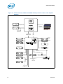
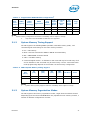
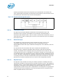
Intel® Celeron P4000 and U3000 mobile processor series on the Calpella
Platform ................................................................................................ 10
Intel Flex Memory Technology Operation ................................................... 22
Dual-Channel Symmetric (Interleaved) and Dual-Channel Asymmetric Modes . 23
PCI Express Layering Diagram ................................................................. 25
Packet Flow through the Layers ................................................................ 26
PCI Express Related Register Structures in the Processor ............................. 27
Integrated Graphics Controller Unit Block Diagram ...................................... 29
Processor Display Block Diagram .............................................................. 32
Idle Power Management Breakdown of the Processor Cores.......................... 42
Thread and Core C-State Entry and Exit .................................................... 42
Package C-State Entry and Exit ................................................................ 47
Frequency and Voltage Ordering............................................................... 60
Active VCC and ICC Loadline (PSI# Asserted) .............................................. 97
Active VCC and ICC Loadline (PSI# Not Asserted) ........................................ 97
VAXG/IAXG Static and Ripple Voltage Regulation ........................................ 99
Input Device Hysteresis......................................................................... 104
Socket-G (rPGA988A) Pinmap (Top View, Upper-Left Quadrant).................. 106
Socket-G (rPGA988A) Pinmap (Top View, Upper-Right Quadrant)................ 107
5
Figure
Figure
Figure
Figure
Figure
Figure
Figure
Figure
Figure
8-19
8-20
8-21
8-22
8-23
8-24
8-25
8-26
8-27
Socket-G (rPGA988A) Pinmap (Top View, Lower-Left Quadrant) .................. 108
Socket-G (rPGA988A) Pinmap (Top View, Lower-Right Quadrant) ................ 109
BGA1288 Ballmap (Top View, Upper-Left Quadrant) .................................. 138
BGA1288 Ballmap (Top View, Upper-Right Quadrant) ................................ 139
BGA1288 Ballmap (Top View, Lower-Left Quadrant) .................................. 140
BGA1288 Ballmap (Top View, Lower-Right Quadrant) ................................ 141
rPGA Mechanical Package (Sheet 1 of 2) ................................................. 179
rPGA Mechanical Package (Sheet 2 of 2) .................................................. 180
BGA Mechanical Package (Sheet 2 of 2) ................................................... 181
Tables
6
Table
Table
Table
Table
Table
Table
Table
Table
Table
Table
Table
Table
Table
Table
Table
Table
Table
2-1
2-2
2-3
2-4
4-5
4-6
4-7
4-8
4-9
4-10
4-11
4-12
4-13
4-14
4-15
4-16
5-17
Table
Table
Table
Table
Table
Table
Table
Table
Table
Table
Table
Table
Table
Table
Table
Table
Table
Table
Table
Table
Table
Table
5-18
5-19
6-20
6-21
6-22
6-23
6-24
6-25
6-26
6-27
6-28
6-29
6-30
6-31
6-32
6-33
6-34
7-35
7-36
7-37
7-38
7-39
Supported SO-DIMM Module Configurations1 ..............................................20
DDR3 System Memory Timing Support ......................................................21
eDP/PEG Ball Mapping .............................................................................33
Processor Reference Clocks ......................................................................35
System States........................................................................................38
Processor Core/Package State Support ......................................................38
Integrated Memory Controller States .........................................................39
PCIe Link States .....................................................................................39
DMI States ............................................................................................39
Integrated Graphics Controller States ........................................................39
G, S and C State Combinations.................................................................40
D, S, and C State Combination .................................................................40
Coordination of Thread Power States at the Core Level ................................43
P_LVLx to MWAIT Conversion ...................................................................43
Coordination of Core Power States at the Package Level...............................46
Targeted Memory State Conditions............................................................50
Intel Celeron P4000 mobile processor series Dual-Core SV Thermal Power
Specifications .........................................................................................56
18 W Ultra Low Voltage (ULV) Processor Idle Power ....................................56
35 W Standard Voltage (SV) Processor Idle Power.......................................57
Signal Description Buffer Types ................................................................70
Memory Channel A..................................................................................71
Memory Channel B..................................................................................72
Memory Reference and Compensation .......................................................73
Reset and Miscellaneous Signals ...............................................................74
PCI Express Graphics Interface Signals ......................................................75
Intel® Flexible Display Interface ...............................................................76
DMI - Processor to PCH Serial Interface .....................................................77
PLL Signals ............................................................................................77
TAP Signals............................................................................................78
Error and Thermal Protection....................................................................79
Power Sequencing ..................................................................................80
Processor Power Signals ..........................................................................81
Ground and NCTF ...................................................................................83
Processor Internal Pull Up/Pull Down .........................................................83
Voltage Identification Definition ................................................................86
Market Segment Selection Truth Table for MSID[2:0] ..................................90
Signal Groups1.......................................................................................91
Processor Absolute Minimum and Maximum Ratings ....................................94
Storage Condition Ratings........................................................................95
Datasheet
Table 7-40
Table 7-41
Table 7-42
Table
Table
Table
Table
Table
Table
Table
Table
Table
7-43
7-44
7-45
7-46
7-47
8-48
8-49
8-50
8-51
Datasheet
Processor Core (VCC) Active and Idle Mode DC Voltage and Current Specifications
96
Processor Uncore I/O Buffer Supply DC Voltage and Current Specifications..... 98
Processor Graphics VID based (VAXG) Supply DC Voltage and Current
Specifications......................................................................................... 99
DDR3 Signal Group DC Specifications ...................................................... 100
Control Sideband and TAP Signal Group DC Specifications.......................... 101
PCI Express DC Specifications ................................................................ 102
eDP DC Specifications ........................................................................... 103
PECI DC Electrical Limits ....................................................................... 104
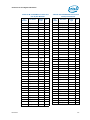
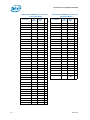
rPGA988A Processor Pin List by Pin Number ............................................. 110
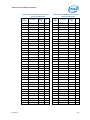
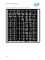
rPGA988A Processor Pin List by Pin Name ................................................ 124
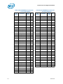
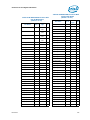
BGA1288 Processor Ball List by Ball Name ............................................... 142
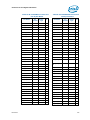
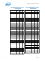
BGA1288 Processor Ball List by Ball Number ............................................ 160
7
Revision History
Revision
Number
001
Description
Initial release
Revision Date
October 2010
§
8
Datasheet
Features Summary
1
Features Summary
1.1
Introduction
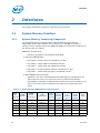
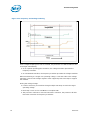
Intel® Celeron® P4000 and U3000 mobile processor seriesis the next generation of
64-bit, multi-core mobile processor built on 32-nanometer process technology. Based
on the low-power/high-performance Nehalem micro-architecture, the processor is
designed for a two-chip platform as opposed to the traditional three-chip platforms
(processor, GMCH, and ICH). The two-chip platform consists of a processor and the
Platform Controller Hub (PCH) and enables higher performance, lower cost, easier
validation, and improved x-y footprint. The PCH may also be referred to as Mobile
Intel® 5 Series Chipset (formerly Ibex Peak-M). Intel® Celeron® P4000 and U3000
mobile processor series is designed for the Calpella platform and is offered in rPGA988A
and BGA1288 package respectively.
Included in this family of processors is Intel® HD graphics and memory controller die
on the same package as the processor core die. This two-chip solution of a processor
core die with an integrated graphics and memory controller die is known as a multi-chip
package (MCP) processor.
Note:
1. Throughout this document, Intel® Celeron® P4000 and U3000 mobile processor
series is referred to as processor.
2. Throughout this document, Intel® HD graphics is referred as integrated graphics.
3. Integrated graphics and memory controller die is built on 45-nanometer process
technology
4. Intel® Celeron® P4000 and U3000 mobile processor seriesis not Intel® vPro
eligible
Datasheet
9
Features Summary
Figure 1-1. Intel® Celeron® P4000 and U3000 mobile processor series on the Calpella
Platform
Dual Core
Processor
Discrete Graphics
(PEG)
PCI Express* x16
Processor
OR
Embedded
DisplayPort* (eDP)
GPU, Memory
Controller
800/1066 MT/s
2 Channels
1 SO-DIMM / Channel
DDR3 SO-DIMMs
PCI Express x 1
Intel® Flexible
Display Interface
Digital Display x 3
DMI2
(x4)
Intel®
Management
Engine
LVDS Flat Panel
Mobile Intel® 5 Series Chipset
PCH
Analog CRT
Serial ATA
6 Ports
3 Gb/s
USB 2.0
14 Ports
WiMax
Dual Channel NAND
Interface
Intel® HD Audio
SMBUS 2.0
SPI Flash
PCI
Controller Link 1
SPI
PCI Express*
WiFi
PCI
Gigabit
Network Connection
FWH
LPC
8 PCI Express* x1
Ports
(2.5 GT/s)
Super I/O
PECI
GPIO
10
Datasheet
Features Summary
1.2
Processor Feature Details
Two execution cores
A 32-KB instruction and 32-KB data first-level cache (L1) for each core
A 512-KB shared instruction/data second-level cache (L2), 256-KB for each core
Up to 2-MB shared instruction/data third-level cache (L3), shared among all cores
1.2.1
Supported Technologies
Intel® Virtualization Technology (Intel® VT-x)
Intel® 64 architecture
Execute Disable Bit
Note:
Please refer to the Intel® Celeron® P4000 and U3000 mobile processor series
Specification Update for feature support details
1.3
Interfaces
1.3.1
System Memory Support
One or two channels of DDR3 memory with a maximum of one SO-DIMM per
channel
Single- and dual-channel memory organization modes
Data burst length of eight for all memory organization modes
Memory DDR3 data transfer rates of 800 MT/s (SV/ULV) and 1066 MT/s (SV)
64-bit wide channels
DDR3 I/O Voltage of 1.5 V
Non-ECC, unbuffered DDR3 SO-DIMMs only
Theoretical maximum memory bandwidth of:
12.8 GB/s in dual-channel mode assuming DDR3 800 MT/s
1-Gb, and 2-Gb DDR3 DRAM technologies are supported for x8 and x16 devices.
Using 2-Gb device technologies, the largest memory capacity possible is 8 GB,
assuming dual-channel mode with two x8, double-sided, un-buffered, non-ECC,
SO-DIMM memory configuration.
Up to 32 simultaneous open pages, 16 per channel (assuming 4 Ranks of 8 Bank
Devices)
Memory organizations:
Single-channel modes
Dual-channel modes - Intel® Flex Memory Technology:
Datasheet
11
Features Summary
Dual-channel symmetric (Interleaved)
Dual-channel asymmetric
Command launch modes of 1n/2n
Partial Writes to memory using Data Mask (DM) signals
On-Die Termination (ODT)
Intel® Fast Memory Access (Intel® FMA):
Just-in-Time Command Scheduling
Command Overlap
Out-of-Order Scheduling
1.3.2
PCI Express*
The Processor PCI Express ports are fully compliant to the PCI Express Base
Specification Revision 2.0.
One 16-lane PCI Express* port intended for graphics attach.
Gen1 (2.5 GT/s) PCI Express* frequency is supported.
Gen1 Raw bit-rate on the data pins of 2.5 Gb/s, resulting in a real bandwidth per
pair of 250 MB/s given the 8b/10b encoding used to transmit data across this
interface. This also does not account for packet overhead and link maintenance.
Maximum theoretical bandwidth on interface of 4 GB/s in each direction
simultaneously, for an aggregate of 8 GB/s when x16 Gen 1.
Hierarchical PCI-compliant configuration mechanism for downstream devices.
Traditional PCI style traffic (asynchronous snooped, PCI ordering).
PCI Express extended configuration space. The first 256 bytes of configuration
space aliases directly to the PCI compatibility configuration space. The remaining
portion of the fixed 4-KB block of memory-mapped space above that (starting at
100h) is known as extended configuration space.
PCI Express Enhanced Access Mechanism. Accessing the device configuration space
in a flat memory mapped fashion.
Automatic discovery, negotiation, and training of link out of reset.
Traditional AGP style traffic (asynchronous non-snooped, PCI-X Relaxed ordering).
Peer segment destination posted write traffic (no peer-to-peer read traffic) in
Virtual Channel 0:
DMI -> PCI Express Port 0
64-bit downstream address format, but the processor never generates an address
above 64 GB (Bits 63:36 will always be zeros).
64-bit upstream address format, but the processor responds to upstream read
transactions to addresses above 64 GB (addresses where any of Bits 63:36 are
12
Datasheet
Features Summary
non-zero) with an Unsupported Request response. Upstream write transactions to
addresses above 64 GB will be dropped.
Re-issues configuration cycles that have been previously completed with the
Configuration Retry status.
PCI Express reference clock is 100-MHz differential clock buffered out of system
clock generator.
Power Management Event (PME) functions.
Static lane numbering reversal
Does not support dynamic lane reversal, as defined (optional) by the PCI
Express Base Specification.
PCI Express 1x16 configuration
Normal (1x16): PEG_RX[15:0]; PEG_TX[15:0]
Reversal (1x16): PEG_RX[0:15]; PEG_TX[0:15]
Supports Half Swing low-power/low-voltage mode.
Message Signaled Interrupt (MSI and MSI-X) messages
PEG Lanes shared with Embedded DisplayPort* (see eDP, Section 1.3.6).
Polarity inversion
1.3.3
Direct Media Interface (DMI)
Compliant to Direct Media Interface second generation (DMI2).
Four lanes in each direction.
2.5 GT/s point-to-point DMI interface to PCH is supported.
Raw bit-rate on the data pins of 2.5 Gb/s, resulting in a real bandwidth per pair of
250 MB/s given the 8b/10b encoding used to transmit data across this interface.
Does not account for packet overhead and link maintenance.
Maximum theoretical bandwidth on interface of 1 GB/s in each direction
simultaneously, for an aggregate of 2 GB/s when DMI x4.
Shares 100-MHz PCI Express reference clock.
64-bit downstream address format, but the processor never generates an address
above 64 GB (Bits 63:36 will always be zeros).
64-bit upstream address format, but the processor responds to upstream read
transactions to addresses above 64 GB (addresses where any of Bits 63:36 are
nonzero) with an Unsupported Request response. Upstream write transactions to
addresses above 64 GB will be dropped.
Supports the following traffic types to or from the PCH:
DMI -> PCI Express Port 0 write traffic
DMI -> DRAM
DMI -> processor core (Virtual Legacy Wires (VLWs), Resetwarn, or MSIs only)
Datasheet
13
Features Summary
Processor core -> DMI
APIC and MSI interrupt messaging support:
Message Signaled Interrupt (MSI and MSI-X) messages
Downstream SMI, SCI and SERR error indication.
Legacy support for ISA regime protocol (PHOLD/PHOLDA) required for parallel port
DMA, floppy drive, and LPC bus masters.
DC coupling no capacitors between the processor and the PCH.
Polarity inversion.
PCH end-to-end lane reversal across the link.
Supports Half Swing low-power/low-voltage.
1.3.4
Platform Environment Control Interface (PECI)
The PECI is a one-wire interface that provides a communication channel between a
PECI client (the processor) and a PECI master (the PCH).
1.3.5
Intel® HD Graphics Controller
The integrated graphics controller contains a refresh of the fifth generation graphics
core
Intel® Dynamic Video Memory Technology (Intel® DVMT) support
Intel® Graphics Performance Modulation Technology (Intel® GPMT)
Intel® Smart 2D Display Technology (Intel® S2DDT)
Intel® Clear Video Technology
MPEG2 Hardware Acceleration
WMV9/VC1 Hardware Acceleration
AVC Hardware Acceleration
ProcAmp
Advanced Pixel Adaptive De-interlacing
Sharpness Enhancement
De-noise Filter
High Quality Scaling
Film Mode Detection (3:2 pull-down) and Correction
Intel® TV Wizard
12 EUs
Dedicated analog and digital display ports are supported through the Intel 5 Series
Chipset PCH
14
Datasheet
Features Summary
1.3.6
Embedded DisplayPort* (eDP*)
Shared with PCI Express Graphics port
Shared on upper four logical lanes, after any lane reversal
eDP[3:0] map to PEG[12:15] (non-reversed)
eDP[3:0] map to PEG[3:0] (reversed)
Concurrent eDP and PEG x1 supported
1.3.7
Intel® Flexible Display Interface (Intel® FDI)
Carries display traffic from the integrated graphics controller in the processor to the
legacy display connectors in the PCH.
Based on DisplayPort standard.
Two independent links - one for each display pipe.
Four unidirectional downstream differential transmitter pairs:
Scalable down to 3X, 2X, or 1X based on actual display bandwidth requirements
Fixed frequency 2.7 GT/s data rate
Two sideband signals for Display synchronization:
FDI_FSYNC and FDI_LSYNC (Frame and Line Synchronization)
One Interrupt signal used for various interrupts from the PCH:
FDI_INT signal shared by both Intel FDI Links
PCH supports end-to-end lane reversal across both links.
1.4
Power Management Support
1.4.1
Processor Core
Full support of ACPI C-states as implemented by the following processor C-states:
Ultra low voltage supports C0, C1, C1E, C3, Deep Power Down Technology (code
named C6)
Standard voltage supports C0, C1, C1E, C3
Enhanced Intel SpeedStep® Technology
1.4.2
System
S0, S3, S4, S5
Datasheet
15
Features Summary
1.4.3
Memory Controller
Conditional self-refresh (Intel® Rapid Memory Power Management (Intel® RMPM))
Dynamic power-down
1.4.4
PCI Express*
L0s and L1 ASPM power management capability
1.4.5
DMI
L0s and L1 ASPM power management capability
1.4.6
Integrated Graphics Controller
Intel Smart 2D Display Technology (Intel S2DDT)
Intel® Display Power Saving Technology (Intel® DPST)
Graphics Render C-State (RC6)
1.5
Thermal Management Support
Digital Thermal Sensor
Adaptive Thermal Monitor
THERMTRIP# and PROCHOT# support
On-Demand Mode
Open and Closed Loop Throttling
Memory Thermal Throttling
External Thermal Sensor (TS-on-DIMM and TS-on-Board)
Render Thermal Throttling
Fan speed control with DTS
1.6
Package
The Intel® Celeron® P4000 and U3000 mobile processor series is available is
available on:
A 37.5 x 37.5 mm rPGA package (rPGA988A) (Standard Voltage only)
A 34 x 28 mm BGA package (BGA1288) (Ultra Low voltage only)
16
Datasheet
Features Summary
1.7
Terminology
Term
Datasheet
Description
BLT
Block Level Transfer
CRT
Cathode Ray Tube
DDR3
Third-generation Double Data Rate SDRAM memory technology
DP
DisplayPort*
DMA
Direct Memory Access
DMI
Direct Media Interface
DTS
Digital Thermal Sensor
ECC
Error Correction Code
eDP*
Embedded DisplayPort*
Intel® DPST
Intel® Display Power Saving Technology
Enhanced Intel
SpeedStep®
Technology
Technology that provides power management capabilities to laptops.
Execute Disable Bit
The Execute Disable bit allows memory to be marked as executable or
non-executable, when combined with a supporting operating system.
If code attempts to run in non-executable memory the processor
raises an error to the operating system. This feature can prevent some
classes of viruses or worms that exploit buffer overrun vulnerabilities
and can thus help improve the overall security of the system. See the
Intel® 64 and IA-32 Architectures Software Developer's Manuals for
more detailed information.
(G)MCH
Legacy component - Graphics Memory Controller Hub
GPU
Graphics Processing Unit
ICH
The legacy I/O Controller Hub component that contains the main PCI
interface, LPC interface, USB2, Serial ATA, and other I/O functions. It
communicates with the legacy (G)MCH over a proprietary interconnect
called DMI.
IMC
Integrated Memory Controller
Intel® 64 Technology
64-bit memory extensions to the IA-32 architecture
ITPM
Integrated Trusted Platform Module
IOV
I/O Virtualization
LCD
Liquid Crystal Display
LVDS
Low Voltage Differential Signaling. A high speed, low power data
transmission standard used for display connections to LCD panels.
MCP
Multi-Chip Package.
NCTF
Non-Critical to Function. NCTF locations are typically redundant
ground or non-critical reserved, so the loss of the solder joint
continuity at end of life conditions will not affect the overall product
functionality.
Nehalem
Intels 45-nm processor design, follow-on to the 45-nm Penryn design.
17
Features Summary
Term
18
Description
PCH
Platform Controller Hub. The new, 2009 chipset with centralized
platform capabilities including the main I/O interfaces along with
display connectivity, audio features, power management,
manageability, security and storage features. The PCH may also be
referred to using the name (Mobile) Intel® 5 Series Chipset
PECI
Platform Environment Control Interface.
PEG
PCI Express* Graphics. External Graphics using PCI Express
Architecture. A high-speed serial interface whose configuration is
software compatible with the existing PCI specifications.
Processor
The 64-bit, single-core or multi-core component (package).
Processor Core
The term processor core refers to Si die itself which can contain
multiple execution cores. Each execution core has an instruction
cache, data cache, and 256-KB L2 cache. All execution cores share the
L3 cache.
Rank
A unit of DRAM corresponding four to eight devices in parallel, ignoring
ECC. These devices are usually, but not always, mounted on a single
side of a SO-DIMM.
SCI
System Control Interrupt. Used in ACPI protocol.
Storage Conditions
A non-operational state. The processor may be installed in a platform,
in a tray, or loose. Processors may be sealed in packaging or exposed
to free air. Under these conditions, processor landings should not be
connected to any supply voltages, have any I/Os biased or receive any
clocks. Upon exposure to free air (i.e., unsealed packaging or a
device removed from packaging material) the processor must be
handled in accordance with moisture sensitivity labeling (MSL) as
indicated on the packaging material.
TAC
Thermal Averaging Constant.
TDP
Thermal Design Power.
VCC
Processor core power supply.
VSS
Processor ground.
VAXG
Graphics core power supply.
VTT
L3 shared cache, memory controller, and processor I/O power rail.
VDDQ
DDR3 power rail.
VLD
Variable Length Decoding.
x1
Refers to a Link or Port with one Physical Lane.
x4
Refers to a Link or Port with four Physical Lanes.
x8
Refers to a Link or Port with eight Physical Lanes.
x16
Refers to a Link or Port with sixteen Physical Lanes.
Datasheet
Features Summary
1.8
Related Documents
Document Number/
Location
Document
Public Specifications
Advanced Configuration and Power Interface Specification 3.0
http://www.acpi.info/
PCI Local Bus Specification 3.0
http://www.pcisig.com/
specifications
PCI Express Base Specification 2.0
http://www.pcisig.com
DDR3 SDRAM Specification
http://www.jedec.org
DisplayPort Specification
http://www.vesa.org
Intel® 64 and IA-32 Architectures Software Developer's Manuals
http://www.intel.com/
products/processor/
manuals/index.htm
Volume 1: Basic Architecture
253665
Volume 2A: Instruction Set Reference, A-M
253666
Volume 2B: Instruction Set Reference, N-Z
253667
Volume 3A: System Programming Guide
253668
Volume 3B: System Programming Guide
253669
§
Datasheet
19
Interfaces
2
Interfaces
This chapter describes the interfaces supported by the processor.
2.1
System Memory Interface
2.1.1
System Memory Technology Supported
The Integrated Memory Controller (IMC) supports DDR3 protocols with two,
independent, 64-bit wide channels each accessing one SO-DIMM. It supports a
maximum of one, unbuffered non-ECC DDR3 SO-DIMM per-channel thus allowing up to
two device ranks per-channel.
DDR3 Data Transfer Rates:
800 MT/s (PC3-6400) and 1066 MT/s (PC3-8500)
DDR3 SO-DIMM Modules:
Raw Card A double-sided x16 unbuffered non-ECC
Raw Card B single-sided x8 unbuffered non-ECC
Raw Card C single-sided x16 unbuffered non-ECC
Raw Card D double-sided x8 (stacked) unbuffered non-ECC
Raw Card F double-sided x8 (planar) unbuffered non-ECC
DDR3 DRAM Device Technology:
Standard 1-Gb, and 2-Gb technologies and addressing are supported for x16
and x8 devices. There is no support for memory modules with different
technologies or capacities on opposite sides of the same memory module. If one
side of a memory module is populated, the other side is either identical or
empty.
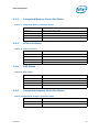
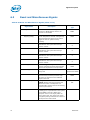
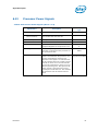
Table 2-1. Supported SO-DIMM Module Configurations1
Raw
Card
Version
DIMM
Capacity
DRAM
Device
Technology
DRAM
Organization
# of
DRAM
Devices
# of
Physical
Device
Ranks
# of Row/
Col
Address
Bits
# of
Banks
Inside
DRAM
Page
Size
A
1 GB
1 Gb
64 M x 16
8
2
13/10
8
8K
A
2 GB
2 Gb
128 M x 16
8
2
14/10
8
8K
B
1 GB
1 Gb
128 M x 8
8
1
14/10
8
8K
B
2 GB
2 Gb
256 M x 8
8
1
15/10
8
8K
C
512 MB
1 Gb
64 M x 16
4
1
13/10
8
8K
C
1 GB
2 Gb
128 M x 16
4
1
14/10
8
8K
20
Datasheet
Interfaces
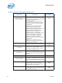
Table 2-1. Supported SO-DIMM Module Configurations1
Raw
Card
Version
DIMM
Capacity
DRAM
Device
Technology
DRAM
Organization
# of
DRAM
Devices
# of
Physical
Device
Ranks
# of Row/
Col
Address
Bits
# of
Banks
Inside
DRAM
Page
Size
D2
4 GB
2 Gb
256 M x 8
16
2
15/10
8
8K
F
2 GB
1 Gb
128 M x 8
16
2
14/10
8
8K
F
4 GB
2 Gb
256 M x 8
16
2
15/10
8
8K
NOTES:
1.
System memory configurations are based on availability and are subject to change.
2.
Only Raw Card D SO-DIMMs at 1066 MT/s are supported.
2.1.2
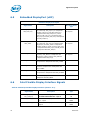
System Memory Timing Support
The IMC supports the following DDR3 Speed Bin, CAS Write Latency (CWL), and
command signal mode timings on the main memory interface:
tCL = CAS Latency
tRCD = Activate Command to READ or WRITE Command delay
tRP = PRECHARGE Command Period
CWL = CAS Write Latency
Command Signal modes = 1n indicates a new command may be issued every clock
and 2n indicates a new command may be issued every 2 clocks. Command launch
mode programming depends on the transfer rate and memory configuration.
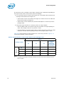
Table 2-2. DDR3 System Memory Timing Support
Transfer
Rate
(MT/s)
tCL
(tCK)
tRCD
(tCK)
tRP
(tCK)
CWL
(tCK)
CMD Mode
Notes
800
6
6
6
5
1n
1
1066
7
7
7
6
1n
1
8
8
8
NOTES:
1.
System memory timing support is based on availability and is subject to change.
2.1.3
System Memory Organization Modes
The IMC supports two memory organization modes, single-channel and dual-channel.
Depending upon how the SO-DIMM Modules are populated in each memory channel, a
number of different configurations can exist.
Datasheet
21
Interfaces
2.1.3.1
Single-Channel Mode
In this mode, all memory cycles are directed to a single-channel. Single-channel mode
is used when either Channel A or Channel B SO-DIMM connectors are populated in any
order, but not both.
2.1.3.2
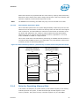
Dual-Channel Mode - Intel® Flex Memory Technology Mode
The IMC supports Intel Flex Memory Technology Mode. This mode combines the
advantages of the Dual-Channel Symmetric (Interleaved) and Dual-Channel
Asymmetric Modes. Memory is divided into a symmetric and a asymmetric zone. The
symmetric zone starts at the lowest address in each channel and is contiguous until the
asymmetric zone begins or until the top address of the channel with the smaller
capacity is reached. In this mode, the system runs with one zone of dual-channel mode
and one zone of single-channel mode, simultaneously, across the whole memory array.
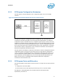
Figure 2-2. Intel Flex Memory Technology Operation
C
TOM
B
B
CH A
CH B
C
N o n in te r le a v e d
access
B
C
D u al ch an n el
in te rle a v e d a c c e s s
B
B
CH A
CH B
B
B – T h e la r g e s t p h y s ic a l m e m o ry a m o u n t o f th e s m a lle r s iz e m e m o r y m o d u le
C – T h e re m a in in g p h y s ic a l m e m o ry a m o u n t o f th e la r g e r s iz e m e m o ry m o d u le
2.1.3.2.1
Dual-Channel Symmetric Mode
Dual-Channel Symmetric mode, also known as interleaved mode, provides maximum
performance on real world applications. Addresses are ping-ponged between the
channels after each cache line (64-byte boundary). If there are two requests, and the
second request is to an address on the opposite channel from the first, that request can
be sent before data from the first request has returned. If two consecutive cache lines
are requested, both may be retrieved simultaneously, since they are ensured to be on
opposite channels. Use Dual-Channel Symmetric mode when both Channel A and
Channel B SO-DIMM connectors are populated in any order, with the total amount of
memory in each channel being the same.
22
Datasheet
Interfaces
When both channels are populated with the same memory capacity and the boundary
between the dual channel zone and the single channel zone is the top of memory, IMC
operates completely in Dual-Channel Symmetric mode.
Note:
2.1.3.2.2
The DRAM device technology and width may vary from one channel to the other.
Dual-Channel Asymmetric Mode
This mode trades performance for system design flexibility. Unlike the previous mode,
addresses start at the bottom of Channel A and stay there until the end of the highest
rank in Channel A, and then addresses continue from the bottom of Channel B to the
top. Real world applications are unlikely to make requests that alternate between
addresses that sit on opposite channels with this memory organization, so in most
cases, bandwidth is limited to a single channel.
This mode is used when Intel Flex Memory Technology is disabled and both Channel A
and Channel B SO-DIMM connectors are populated in any order with the total amount
of memory in each channel being different.
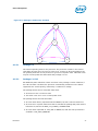
Figure 2-3. Dual-Channel Symmetric (Interleaved) and Dual-Channel Asymmetric Modes
Dual Channel Interleaved
(memory sizes must match)
Dual Channel Asymmetric
(memory sizes can differ)
CL
CL
CH. B
Top of
Memory
CH. B
Top of
Memory
CH. A
CH.A-top
DRB
CH. A
CH. B
CH. A
CH. B
CH. A
2.1.4
0
0
Rules for Populating Memory Slots
In all modes, the frequency of system memory is the lowest frequency of all memory
modules placed in the system, as determined through the SPD registers on the
memory modules. The system memory controller supports only one SO-DIMM
Datasheet
23
Interfaces
connector per channel. For dual-channel modes both channels must have an SO-DIMM
connector populated. For single-channel mode, only a single-channel can have an
SO-DIMM connector populated.
2.1.5
Technology Enhancements of Intel® Fast Memory Access
(Intel® FMA)
The following sections describe the Just-in-Time Scheduling, Command Overlap, and
Out-of-Order Scheduling Intel FMA technology enhancements.
2.1.5.1
Just-in-Time Command Scheduling
The memory controller has an advanced command scheduler where all pending
requests are examined simultaneously to determine the most efficient request to be
issued next. The most efficient request is picked from all pending requests and issued
to system memory Just-in-Time to make optimal use of Command Overlapping. Thus,
instead of having all memory access requests go individually through an arbitration
mechanism forcing requests to be executed one at a time, they can be started without
interfering with the current request allowing for concurrent issuing of requests. This
allows for optimized bandwidth and reduced latency while maintaining appropriate
command spacing to meet system memory protocol.
2.1.5.2
Command Overlap
Command Overlap allows the insertion of the DRAM commands between the Activate,
Precharge, and Read/Write commands normally used, as long as the inserted
commands do not affect the currently executing command. Multiple commands can be
issued in an overlapping manner, increasing the efficiency of system memory protocol.
2.1.5.3
Out-of-Order Scheduling
While leveraging the Just-in-Time Scheduling and Command Overlap enhancements,
the IMC continuously monitors pending requests to system memory for the best use of
bandwidth and reduction of latency. If there are multiple requests to the same open
page, these requests would be launched in a back to back manner to make optimum
use of the open memory page. This ability to reorder requests on the fly allows the IMC
to further reduce latency and increase bandwidth efficiency.
2.1.6
DRAM Clock Generation
Every supported SO-DIMM has two differential clock pairs. There are total of four clock
pairs driven directly by the processor to two SO-DIMMs.
2.1.7
System Memory Pre-Charge Power Down Support Details
The IMC supports and enables slow exit DDR3 DRAM Device pre-charge power down
DLL control. During a pre-charge power down, a slow exit is where the DRAM device
DLL is disabled after entering pre-charge power down for potential power savings.
24
Datasheet
Interfaces
2.2
PCI Express Interface
This section describes the PCI Express interface capabilities of the processor. See the
PCI Express Base Specification for details of PCI Express.
The processor has one PCI Express controller that can support one external x16 PCI
Express Graphics Device or two external x8 PCI Express Graphics Devices. The primary
PCI Express Graphics port is referred to as PEG 0 and the secondary PCI Express
Graphics port is referred to as PEG 1.
2.2.1
PCI Express Architecture
Compatibility with the PCI addressing model is maintained to ensure that all existing
applications and drivers operate unchanged.
The PCI Express configuration uses standard mechanisms as defined in the PCI
Plug-and-Play specification. The initial recovered clock speed of 1.25 GHz results in
2.5 Gb/s/direction which provides a 250 MB/s communications channel in each
direction (500 MB/s total). That is close to twice the data rate of classic PCI. The fact
that 8b/10b encoding is used accounts for the 250 MB/s where quick calculations would
imply 300 MB/s.
The PCI Express architecture is specified in three layers: Transaction Layer, Data Link
Layer, and Physical Layer. The partitioning in the component is not necessarily along
these same boundaries. Refer to Figure 2-4 for the PCI Express Layering Diagram.
Figure 2-4. PCI Express Layering Diagram
PCI Express uses packets to communicate information between components. Packets
are formed in the Transaction and Data Link Layers to carry the information from the
transmitting component to the receiving component. As the transmitted packets flow
through the other layers, they are extended with additional information necessary to
handle packets at those layers. At the receiving side, the reverse process occurs and
Datasheet
25
Interfaces
packets get transformed from their Physical Layer representation to the Data Link
Layer representation and finally (for Transaction Layer Packets) to the form that can be
processed by the Transaction Layer of the receiving device.
Figure 2-5. Packet Flow through the Layers
2.2.1.1
Transaction Layer
The upper layer of the PCI Express architecture is the Transaction Layer. The
Transaction Layer's primary responsibility is the assembly and disassembly of
Transaction Layer Packets (TLPs). TLPs are used to communicate transactions, such as
read and write, as well as certain types of events. The Transaction Layer also manages
flow control of TLPs.
2.2.1.2
Data Link Layer
The middle layer in the PCI Express stack, the Data Link Layer, serves as an
intermediate stage between the Transaction Layer and the Physical Layer.
Responsibilities of Data Link Layer include link management, error detection, and error
correction.
The transmission side of the Data Link Layer accepts TLPs assembled by the
Transaction Layer, calculates and applies data protection code and TLP sequence
number, and submits them to Physical Layer for transmission across the Link. The
receiving Data Link Layer is responsible for checking the integrity of received TLPs and
for submitting them to the Transaction Layer for further processing. On detection of TLP
error(s), this layer is responsible for requesting retransmission of TLPs until information
is correctly received, or the Link is determined to have failed. The Data Link Layer also
generates and consumes packets which are used for Link management functions.
2.2.1.3
Physical Layer
The Physical Layer includes all circuitry for interface operation, including driver and
input buffers, parallel-to-serial and serial-to-parallel conversion, PLL(s), and impedance
matching circuitry. It also includes logical functions related to interface initialization and
maintenance. The Physical Layer exchanges data with the Data Link Layer in an
implementation-specific format, and is responsible for converting this to an appropriate
serialized format and transmitting it across the PCI Express Link at a frequency and
width compatible with the remote device.
26
Datasheet
Interfaces
2.2.2
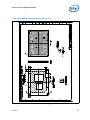
PCI Express Configuration Mechanism
The PCI Express (external graphics) link is mapped through a PCI-to-PCI bridge
structure.
Figure 2-6. PCI Express Related Register Structures in the Processor
PCI
Express
Device
PEG0
PCI-PCI
Bridge
representing
root PCI
Express port
(Device 1)
PCI
Compatible
Host Bridge
Device
(Device 0)
DMI
PCI Express extends the configuration space to 4096 bytes per-device/function, as
compared to 256 bytes allowed by the Conventional PCI Specification. PCI Express
configuration space is divided into a PCI-compatible region (which consists of the first
256 bytes of a logical device's configuration space) and an extended PCI Express region
(which consists of the remaining configuration space). The PCI-compatible region can
be accessed using either the mechanisms defined in the PCI specification or using the
enhanced PCI Express configuration access mechanism described in the PCI Express
Enhanced Configuration Mechanism section.
The PCI Express Host Bridge is required to translate the memory-mapped PCI Express
configuration space accesses from the host processor to PCI Express configuration
cycles. To maintain compatibility with PCI configuration addressing mechanisms, it is
recommended that system software access the enhanced configuration space using
32-bit operations (32-bit aligned) only. See the PCI Express Base Specification for
details of both the PCI-compatible and PCI Express Enhanced configuration
mechanisms and transaction rules.
2.2.3
PCI Express Ports and Bifurcation
The external graphics attach (PEG) on the processor is a single, 16-lane (x16) port that
can be:
configured at narrower widths
bifurcated into two x8 PCI Express ports that may train to narrower widths
The PEG port is being designed to be compliant with the PCI Express Base
Specification, Revision 2.0.
Datasheet
27
Interfaces
2.2.3.1
PCI Express Bifurcated Mode
When bifurcated, the signals which had previously been assigned to Lanes 15:8 of the
single x16 Primary port are reassigned to lanes 7:0 of the x8 Secondary Port. This
assignment applies whether the lane numbering is reversed or not. PCI Express Port 0
is mapped to PCI Device 1 and PCI Express Port 1 is mapped to PCI Device 6.
2.2.3.2
Static Lane Numbering Reversal
Does not support dynamic lane reversal, as defined (optional) by the PCI Express Base
Specification.
PCI Express 1x16 configuration:
Normal (1x16): PEG_RX[15:0]; PEG_TX[15:0]
Reversal (1x16): PEG_RX[0:15]; PEG_TX[0:15]
2.3
DMI
DMI connects the processor and the PCH chip-to-chip. DMI2 is supported. The DMI is
similar to a four-lane PCI Express supporting up to 1 GB/s of bandwidth in each
direction.
Note:
2.3.1
Only DMI x4 configuration is supported.
DMI Error Flow
DMI can only generate SERR in response to errors, never SCI, SMI, MSI, PCI INT, or
GPE. Any DMI related SERR activity is associated with Device 0.
2.3.2
Processor/PCH Compatibility Assumptions
The processor is compatible with the PCH and is not compatible with any previous
(G)MCH or ICH products.
2.3.3
DMI Link Down
The DMI link going down is a fatal, unrecoverable error. If the DMI data link goes to
data link down, after the link was up, then the DMI link hangs the system by not
allowing the link to retrain to prevent data corruption. This is controlled by the PCH.
Downstream transactions that had been successfully transmitted across the link prior
to the link going down may be processed as normal. No completions from downstream,
non-posted transactions are returned upstream over the DMI link after a link down
event.
28
Datasheet
Interfaces
2.4
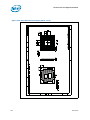
Intel® HD Graphics Controller
This section details the 2D, 3D and video pipeline and their respective capabilities.
The integrated graphics is powered by a refresh of the fifth generation graphics core
and supports twelve, fully-programmable execution cores. Full-precision, floating-point
operations are supported to enhance the visual experience of compute-intensive
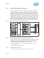
applications.The integrated graphics controller contains several types of components;
the graphics engines, planes, pipes, port and the Intel FDI. The integrated graphics has
a 3D/2D Instruction Processing unit to control the 3D and 2D engines respectively. The
integrated graphics controllers 3D and 2D engines are fed with data through the IMC.
The outputs of the graphics engine are surfaces sent to memory, which are then
retrieved and processed by the planes. The surfaces are then blended in the pipes and
the display timings are transitioned from display core clock to the pixel (dot) clock.
Figure 2-7. Integrated Graphics Controller Unit Block Diagram
Plane A
Video Engine
eDP
Sprite A
Pipe A
2D Engine
Cursor A
Memory
VGA
3D Engine
Vertex Fetch/Vertex
Shader
Plane B
Geometry Shader
Clipper
Alpha
Blend/
Gamma
/Panel
Fitter
M
U
X
Intel®
FDI
Pipe B
Sprite B
Strip & Fan/Setup
Windower/IZ
2.4.1
Cursor B
3D and Video Engines for Graphics Processing
The 3D graphics pipeline architecture simultaneously operates on different primitives or
on different portions of the same primitive. All the cores are fully programmable,
increasing the versatility of the 3D Engine. The Gen 5.75 3D engine provides the
following performance and power-management enhancements:
Execution units (EUs) increased to 12 from the previous 10 EUsin Gen 5.0.
Includes Hierarchal-Z
Includes video quality enhancements
2.4.1.1
3D Engine Execution Units
Support 12 EUs. The EUs perform 128-bit wide execution per clock.
Datasheet
29
Interfaces
Support SIMD8 instructions for vertex processing and SIMD16 instructions for pixel
processing.
2.4.1.2
3D Pipeline
2.4.1.2.1
Vertex Fetch (VF) Stage
The VF stage executes 3DPRIMITIVE commands. Some enhancements have been
included to better support legacy D3D APIs as well as SGI OpenGL*.
2.4.1.2.2
Vertex Shader (VS) Stage
The VS stage performs shading of vertices output by the VF function. The VS unit
produces an output vertex reference for every input vertex reference received from the
VF unit, in the order received.
2.4.1.2.3
Geometry Shader (GS) Stage
The GS stage receives inputs from the VS stage. Compiled application-provided GS
programs, specifying an algorithm to convert the vertices of an input object into some
output primitives. For example, a GS shader may convert lines of a line strip into
polygons representing a corresponding segment of a blade of grass centered on the
line. Or it could use adjacency information to detect silhouette edges of triangles and
output polygons extruding out from the edges.
2.4.1.2.4
Clip Stage
The Clip stage performs general processing on incoming 3D objects. However, it also
includes specialized logic to perform a Clip Test function on incoming objects. The Clip
Test optimizes generalized 3D Clipping. The Clip unit examines the position of incoming
vertices, and accepts/rejects 3D objects based on its Clip algorithm.
2.4.1.2.5
Strips and Fans (SF) Stage
The SF stage performs setup operations required to rasterize 3D objects. The outputs
from the SF stage to the Windower stage contain implementation-specific information
required for the rasterization of objects and also supports clipping of primitives to some
extent.
2.4.1.2.6
Windower/IZ (WIZ) Stage
The WIZ unit performs an early depth test, which removes failing pixels and eliminates
unnecessary processing overhead.
The Windower uses the parameters provided by the SF unit in the object-specific
rasterization algorithms. The WIZ unit rasterizes objects into the corresponding set of
pixels. The Windower is also capable of performing dithering, whereby the illusion of a
higher resolution when using low-bpp channels in color buffers is possible. Color
dithering diffuses the sharp color bands seen on smooth-shaded objects.
30
Datasheet
Interfaces
2.4.1.3
Video Engine
The Video Engine handles the non-3D (media/video) applications. It includes support
for VLD and MPEG2 decode in hardware.
2.4.1.4
2D Engine
The 2D Engine contains BLT (Block Level Transfer) functionality and an extensive set of
2D instructions. To take advantage of the 3D during engines functionality, some BLT
functions make use of the 3D renderer.
2.4.1.4.1
Integrated Graphics VGA Registers
The 2D registers consists of original VGA registers and others to support graphics
modes that have color depths, resolutions, and hardware acceleration features that go
beyond the original VGA standard.
2.4.1.4.2
Logical 128-Bit Fixed BLT and 256 Fill Engine
This BLT engine accelerates the GUI of Microsoft Windows* operating systems. The
128-bit BLT engine provides hardware acceleration of block transfers of pixel data for
many common Windows operations. The BLT engine can be used for the following:
Move rectangular blocks of data between memory locations
Data alignment
To perform logical operations (raster ops)
The rectangular block of data does not change, as it is transferred between memory
locations. The allowable memory transfers are between: cacheable system memory
and frame buffer memory, frame buffer memory and frame buffer memory, and within
system memory. Data to be transferred can consist of regions of memory, patterns, or
solid color fills. A pattern is always 8 x 8 pixels wide and may be 8, 16, or 32 bits per
pixel.
The BLT engine expands monochrome data into a color depth of 8, 16, or 32 bits. BLTs
can be either opaque or transparent. Opaque transfers move the data specified to the
destination. Transparent transfers compare destination color to source color and write
according to the mode of transparency selected.
Data is horizontally and vertically aligned at the destination. If the destination for the
BLT overlaps with the source memory location, the BLT engine specifies which area in
memory to begin the BLT transfer. Hardware is included for all 256 raster operations
(source, pattern, and destination) defined by Microsoft, including transparent BLT.
The BLT engine has instructions to invoke BLT and stretch BLT operations, permitting
software to set up instruction buffers and use batch processing. The BLT engine can
perform hardware clipping during BLTs.
Datasheet
31
Interfaces
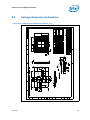
2.4.2
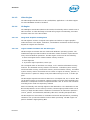
Integrated Graphics Display Pipes
The integrated graphics controller display pipe can be broken down into three
components:
Display Planes
Display Pipes
Embedded DisplayPort and Intel FDI
Figure 2-8. Processor Display Block Diagram
Plane A
eDP
Sprite A
Pipe A
Cursor A
VGA
Plane B
Sprite B
Alpha
Blend/
Gamma/
Panel
Fitter
M
U
X
Intel®
FDI
Pipe B
Cursor B
2.4.2.1
Display Planes
A display plane is a single displayed surface in memory and contains one image
(desktop, cursor, overlay). It is the portion of the display HW logic that defines the
format and location of a rectangular region of memory that can be displayed on display
output device and delivers that data to a display pipe. This is clocked by the Core
Display Clock.
2.4.2.1.1
Planes A and B
Planes A and B are the main display planes and are associated with Pipes A and B
respectively. The two display pipes are independent, allowing for support of two
independent display streams. They are both double-buffered, which minimizes latency
and improves visual quality.
2.4.2.1.2
Sprite A and B
Sprite A and Sprite B are planes optimized for video decode, and are associated with
Planes A and B respectively. Sprite A and B are also double-buffered.
32
Datasheet
Interfaces
2.4.2.1.3
Cursors A and B
Cursors A and B are small, fixed-sized planes dedicated for mouse cursor acceleration,
and are associated with Planes A and B respectively. These planes support resolutions
up to 256 x 256 each.
2.4.2.1.4
VGA
Used for boot, safe mode, legacy games, etc. Can be changed by an application without
OS/driver notification, due to legacy requirements.
2.4.2.2
Display Pipes
The display pipe blends and synchronizes pixel data received from one or more display
planes and adds the timing of the display output device upon which the image is
displayed. This is clocked by the Display Reference clock inputs.
The display pipes A and B operate independently of each other at the rate of 1 pixel per
clock. They can attach to any of the display ports. Each pipe sends display data to the
PCH over the Intel Flexible Display Interface (Intel FDI).
2.4.2.3
Display Ports
The display ports consist of output logic and pins that transmit the display data to the
associated encoding logic and send the data to the display device (i.e., LVDS, HDMI,
DVI, SDVO, etc.). All display interfaces connecting external displays are now
repartitioned and driven from the PCH with the exception of the eDP DisplayPort.
2.4.2.4
Embedded DisplayPort (eDP)
The DisplayPort abbreviated as DP (different than the generic term display port)
specification is a VESA standard. DisplayPort consolidates internal and external
connection methods to reduce device complexity, support cross industry applications,
and provide performance scalability. The integrated graphics supports an embedded
DisplayPort (eDP) interface for display devices that are integrated into the system
(e.g., laptop LCD panel). All other display interfaces connecting to the LVDS or external
panels are driven from the PCH.
The eDP interface is physically shared with a subset of the PCIe interface. Specifically,
eDP[3:0] map to Logical Lanes PEG[12:15] of the PCIe interface. Mapping for reversed
case is: eDP[3:0] maps to PEG[3:0], ex: eDP[0]=PEG[15] in non reversed case. In
reversed case: eDP[0] = PEG[0].
Table 2-3. eDP/PEG Ball Mapping
Datasheet
eDP Signal
PEG Signal
Lane Reversal
eDP_AUX
PEG_RX[13]
PEG_RX[2]
eDP_AUX#
PEG_RX#[13]
PEG_RX#[2]
eDP_HPD#
PEG_RX[12]
PEG_RX[3]
33
Interfaces
Table 2-3. eDP/PEG Ball Mapping
eDP Signal
PEG Signal
Lane Reversal
eDP_TX[0]
PEG_TX[15]
PEG_TX[0]
eDP_TX#[0]
PEG_TX#[15]
PEG_TX#[0]
eDP_TX[1]
PEG_TX[14]
PEG_TX[1]
eDP_TX#[1]
PEG_TX#[14]
PEG_TX#[1]
eDP_TX[2]
PEG_TX[13]
PEG_TX[2]
eDP_TX#[2]
PEG_TX#[13]
PEG_TX#[2]
eDP_TX[3]
PEG_TX[12]
PEG_TX[3]
eDP_TX#[3]
PEG_TX#[12]
PEG_TX#[3]
When eDP is enabled, the lower logical lanes are still available for standard PCIe
devices, using the PEG 0 controller. PEG 0 is limited to x1. The board manufacture
chooses whether to use eDP and whether to use lane numbering reversal.
The eDP interface supports link-speeds of 1.62 Gbps and 2.7 Gbps on 1, 2 or 4 data
lanes. The eDP and PCI Express x1 may be supported concurrently. eDP interface may
support -0.5% SSC and non-SSC clock settings.
2.4.3
Intel Flexible Display Interface
The Intel Flexible Display Interface (Intel FDI) is a proprietary link for carrying display
traffic from the integrated graphics controller to the PCH display I/Os. Intel FDI
supports two independent channels; one for pipe A and one for pipe B.
Each channel has four transmit (Tx) differential pairs used for transporting pixel
and framing data from the display engine.
Each channel has one single-ended LineSync and one FrameSync input (1-V CMOS
signaling).
One display interrupt line input (1-V CMOS signaling).
Intel FDI may dynamically scalable down to 2X or 1X based on actual display
bandwidth requirements.
Common 100-MHz reference clock is sent to both processor and PCH.
Each channel transports at a rate of 2.7 Gbps.
PCH supports end-to-end lane reversal across both channels (no reversal support
required)
2.5
Platform Environment Control Interface (PECI)
The PECI is a one-wire interface that provides a communication channel between a
PECI client (processor) and a PECI master, usually the PCH. The processor implements
a PECI interface to:
34
Datasheet
Interfaces
Allow communication of processor thermal and other information to the PECI
master.
Read averaged Digital Thermal Sensor (DTS) values for fan speed control.
2.6
Interface Clocking
2.6.1
Internal Clocking Requirements
Table 2-4. Processor Reference Clocks
Reference Input Clocks
Input Frequency
BCLK/BCLK#
133 MHz
Associated PLL
Processor/Memory/Graphics
PEG_CLK/PEG_CLK#
100 MHz
PCI Express*/DMI/Intel® FDI
DPLL_REF_SSCLK/DPLL_REF_SSCLK#
120 MHz
Embedded DisplayPort* (eDP)
§
Datasheet
35
Technologies
3
Technologies
3.1
Intel® Virtualization Technology
Intel Virtualization Technology (Intel VT) makes a single system appear as multiple
independent systems to software. This allows multiple, independent operating systems
to run simultaneously on a single system. Intel VT comprises technology components
to support virtualization of platforms based on Intel architecture microprocessors and
chipsets. Intel Virtualization Technology (Intel VT-x) added hardware support in the
processor to improve the virtualization performance and robustness. Intel Virtualization
Technology for Directed I/O (Intel VT-d) adds chipset hardware implementation to
support and improve I/O virtualization performance and robustness.
Intel VT-x specifications and functional descriptions are included in the Intel® 64 and
IA-32 Architectures Software Developer’s Manual, Volume 3B and is available at:
http://www.intel.com/products/processor/manuals/index.htm.
3.1.1
Intel® VT-x Objectives
Intel VT-x provides hardware acceleration for virtualization of IA platforms. Virtual
Machine Monitor (VMM) can use Intel VT-x features to provide improved reliable
virtualized platforms. By using Intel VT-x, a VMM is:
Robust—VMMs no longer need to use paravirtualization or binary translation. This
means that they will be able to run off-the-shelf OSs and applications without any
special steps.
Enhanced—Intel VT enables VMMs to run 64-bit guest operating systems on IA
x86 processors.
More reliable—Due to the hardware support, VMMs can now be smaller, less
complex, and more efficient. This improves reliability and availability and reduces
the potential for software conflicts.
More secure—The use of hardware transitions in the VMM strengthens the
isolation of VMs and further prevents corruption of one VM from affecting others on
the same system.
3.1.2
Intel® VT-x Features
The processor core supports the following Intel VT-x features:
Extended Page Tables (EPT)
EPT is hardware assisted page table virtualization
It eliminates VM exits from guest OS to the VMM for shadow page-table
maintenance
Virtual Processor IDs (VPID)
Ability to assign a VM ID to tag processor core hardware structures (such as
36
Datasheet
Technologies
TLBs)
This avoids flushes on VM transitions to give a lower-cost VM transition time
and an overall reduction in virtualization overhead.
Guest Preemption Timer
Mechanism for a VMM to preempt the execution of a guest OS after an amount
of time specified by the VMM. The VMM sets a timer value before entering a
guest
The feature aids VMM developers in flexibility and Quality of Service (QoS)
guarantees
Descriptor-Table Exiting
Descriptor-table exiting allows a VMM to protect a guest OS from internal
(malicious software based) attack by preventing relocation of key system data
structures like IDT (interrupt descriptor table), GDT (global descriptor table),
LDT (local descriptor table), and TSS (task segment selector).
A VMM using this feature can intercept (by a VM exit) attempts to relocate
these data structures and prevent them from being tampered by malicious
software.
3.2
Intel Graphics Dynamic Frequency
Graphics render frequency are selected by the Intel graphics driver dynamically based
on graphics workload demand as permitted by Intel Turbo Boost Technology Driver. The
processor core die and the integrated graphics and memory controller core die have an
individual TDP limit. If one component is not consuming enough thermal power to
reach its TDP, the other component can increase its TDP limit and take advantage of the
unused thermal power headroom. For the integrated graphics, this could mean an
increase in the render core frequency (above its rated frequency) and increased
graphics performance.
Note:
Please note that processor Turbo is not supported on Celeron processor skus.
Processor Utilization of Intel Graphics Dynamic Frequency require the following
Graphics driver
Intel Turbo Boost Technology Driver
Enabling Intel Turbo Boost Technology and Intel Graphics Dynamic Frequency will
maximize the performance of the GPU within its specified power levels. Compared with
previous generation products, Intel Turbo Boost Technology and Intel Graphics
Dynamic Frequency will increase the ratio of application power to TDP. Thus, thermal
solutions and platform cooling that are designed to less than thermal design guidance
might experience thermal and performance issues since more applications will tend to
run at the maximum power limit for significant periods of time. For more details, refer
to Chapter 5, Thermal Management.
§
Datasheet
37
Power Management
4
Power Management
This chapter provides information on the following power management topics:
ACPI States
Processor Core
Integrated Memory Controller (IMC)
PCI Express
Direct Media Interface (DMI)
Integrated Graphics Controller
4.1
ACPI States Supported
The ACPI states supported by the processor are described in this section.
4.1.1
System States
Table 4-5. System States
State
4.1.2
Description
G0/S0
Full On
G1/S3-Cold
Suspend-to-RAM (STR). Context saved to memory (S3-Hot is not
supported by the processor).
G1/S4
Suspend-to-Disk (STD). All power lost (except wakeup on PCH).
G2/S5
Soft off. All power lost (except wakeup on PCH). Total reboot.
G3
Mechanical off. All power (AC and battery) removed from system.
Processor Core/Package Idle States
Table 4-6. Processor Core/Package State Support
State
38
Description
C0
Active mode, processor executing code.
C1
AutoHALT state.
C1E
AutoHALT state with lowest frequency and voltage operating point.
C3
Execution cores in C3 flush their L1 instruction cache, L1 data cache,
and L2 cache to the L3 shared cache. Clocks are shut off to each core.
C6
Execution cores in this state save their architectural state before
removing core voltage.
Datasheet
Power Management
4.1.3
Integrated Memory Controller States
Table 4-7. Integrated Memory Controller States
State
4.1.4
Description
Power up
CKE asserted. Active mode.
Pre-charge Power down
CKE deasserted (not self-refresh) with all banks closed.
Active Power down
CKE deasserted (not self-refresh) with minimum one bank active.
Self-Refresh
CKE deasserted using device self-refresh.
PCIe Link States
Table 4-8. PCIe Link States
State
L0
4.1.5
Description
Full on Active transfer state.
L0s
First Active Power Management low power state Low exit latency.
L1
Lowest Active Power Management - Longer exit latency.
L3
Lowest power state (power-off) Longest exit latency.
DMI States
Table 4-9. DMI States
State
4.1.6
Description
L0
Full on Active transfer state.
L0s
First Active Power Management low power state Low exit latency.
L1
Lowest Active Power Management - Longer exit latency.
L3
Lowest power state (power-off) Longest exit latency.
Integrated Graphics Controller States
Table 4-10.Integrated Graphics Controller States
State
Datasheet
Description
D0
Full on, display active.
D3 Cold
Power-off.
39
Power Management
4.1.7
Interface State Combinations
Table 4-11.G, S and C State Combinations
Processor
Core
(C) State
Global
(G) State
Sleep
(S) State
Processor
State
G0
S0
C0
Full On
On
Full On
G0
S0
C1/C1E
Auto-Halt
On
Auto-Halt
G0
S0
C3
Deep Sleep
On
Deep Sleep
G0
S0
C6
Deep Power
Down
On
Deep Power Down
G1
S3
Power off
Off, except RTC
Suspend to RAM
G1
S4
Power off
Off, except RTC
Suspend to Disk
G2
S5
Power off
Off, except RTC
Soft Off
G3
NA
Power off
Power off
Hard off
System Clocks
Description
Table 4-12.D, S, and C State Combination
4.2
Graphics Adapter
(D) State
Sleep (S) State
Package (C) State
D0
S0
C0
D0
S0
C1/C1E
D0
S0
C3
Deep sleep, Displaying
D0
S0
C6
Deep Power Down,
Displaying
D3
S0
Any
Not displaying
D3
S3
N/A
Not displaying, Graphics
Core is powered off
D3
S4
N/A
Not displaying, suspend to
disk
Description
Full On, Displaying
Auto-Halt, Displaying
Processor Core Power Management
While executing code, Enhanced Intel SpeedStep Technology optimizes the processors
frequency and core voltage based on workload. Each frequency and voltage operating
point is defined by ACPI as a P-state. When the processor is not executing code, it is
idle. A low-power idle state is defined by ACPI as a C-state. In general, lower power
C-states have longer entry and exit latencies.
40
Datasheet
Power Management
4.2.1
Enhanced Intel SpeedStep® Technology
The following are the key features of Enhanced Intel SpeedStep Technology:
Multiple frequency and voltage points for optimal performance and power
efficiency. These operating points are known as P-states.
Frequency selection is software controlled by writing to processor MSRs. The
voltage is optimized based on the selected frequency and the number of active
processor cores.
If the target frequency is higher than the current frequency, VCC is ramped up in
steps to an optimized voltage. This voltage is signaled by the VID[6:0] pins to
the voltage regulator. Once the voltage is established, the PLL locks on to the
target frequency.
If the target frequency is lower than the current frequency, the PLL locks to the
target frequency, then transitions to a lower voltage by signaling the target
voltage on the VID[6:0] pins.
All active processor cores share the same frequency and voltage. In a multi-core
processor, the highest frequency P-state requested amongst all active cores is
selected.
Software-requested transitions are accepted at any time. If a previous transition
is in progress, the new transition is deferred until the previous transition is
completed.
The processor controls voltage ramp rates internally to ensure glitch-free
transitions.
Because there is low transition latency between P-states, a significant number of
transitions per-second are possible.
4.2.2
Low-Power Idle States
When the processor is idle, low-power idle states (C-states) are used to save power.
More power savings actions are taken for numerically higher C-states. However, higher
C-states have longer exit and entry latencies. Resolution of C-states occur at the
thread, processor core, and processor package level. Thread-level C-states are
available if Intel Hyper-Threading Technology is enabled.
Datasheet
41
Power Management
Figure 4-9. Idle Power Management Breakdown of the Processor Cores
Thread 0
Thread 0
Core 0 State
Core 1 State
Processor Package State
Entry and exit of the C-States at the thread and core level are shown in below figure.
Figure 4-10.Thread and Core C-State Entry and Exit
C0
MWAIT(C1), HLT
MWAIT(C1), HLT
(C1E Enabled)
C1
C1E
MWAIT(C6),
P_LVL3 I/O Read
MWAIT(C3),
P_LV2 I/O Read
C3
C6
While individual threads can request low power C-states, power saving actions only
take place once the core C-state is resolved. Core C-states are automatically resolved
by the processor. For thread and core C-states, a transition to and from C0 is required
before entering any other C-state.
42
Datasheet
Power Management
Table 4-13.Coordination of Thread Power States at the Core Level
Processor Core
C-State
Thread 1
C0
C1
C3
C6
C0
C0
C0
C0
C0
C1
C0
C11
C11
C11
C3
C0
C11
C3
C3
C6
C0
C11
C3
C6
NOTE:If enabled, the core C-state will be C1E if all actives cores have also resolved a
core C1 state or higher
4.2.3
Requesting Low-Power Idle States
The primary software interfaces for requesting low power idle states are through the
MWAIT instruction with sub-state hints and the HLT instruction (for C1 and C1E).
However, software may make C-state requests using the legacy method of I/O reads
from the ACPI-defined processor clock control registers, referred to as P_LVLx. This
method of requesting C-states provides legacy support for operating systems that
initiate C-state transitions via I/O reads.
For legacy operating systems, P_LVLx I/O reads are converted within the processor to
the equivalent MWAIT C-state request. Therefore, P_LVLx reads do not directly result in
I/O reads to the system. The feature, known as I/O MWAIT redirection, must be
enabled in the BIOS.
Note:
The P_LVLx I/O Monitor address needs to be set up before using the P_LVLx I/O read
interface. Each P-LVLx is mapped to the supported MWAIT(Cx) instruction as follows.
Table 4-14.P_LVLx to MWAIT Conversion
P_LVLx
MWAIT(Cx)
Notes
P_LVL2
MWAIT(C3)
The P_LVL2 base address is defined in the PMG_IO_CAPTURE
MSR, described in the RS - Nehalem Processor Family BWG.
P_LVL3
MWAIT(C6)
C6. No sub-states allowed.
The BIOS can write to the C-state range field of the PMG_IO_CAPTURE MSR to restrict
the range of I/O addresses that are trapped and emulate MWAIT like functionality. Any
P_LVLx reads outside of this range does not cause an I/O redirection to MWAIT(Cx) like
request. They fall through like a normal I/O instruction.
Note:
Datasheet
When P_LVLx I/O instructions are used, MWAIT substates cannot be defined. The
MWAIT substate is always zero if I/O MWAIT redirection is used. By default, P_LVLx I/O
redirections enable the MWAIT 'break on EFLAGS.IF feature which triggers a wakeup
on an interrupt even if interrupts are masked by EFLAGS.IF.
43
Power Management
4.2.4
Core C-states
The following are general rules for all core C-states, unless specified otherwise:
A core C-State is determined by the lowest numerical thread state (e.g., Thread 0
requests C1E while Thread 1 requests C3, resulting in a core C1E state). See
Table 4-11.
A core transitions to C0 state when:
An interrupt occurs
There is an access to the monitored address if the state was entered via an
MWAIT instruction
For core C1/C1E, and core C3, an interrupt directed toward a single thread wakes
only that thread. However, since both threads are no longer at the same core
C-state, the core resolves to C0.
For core C6, an interrupt coming into either thread wakes both threads into C0
state.
Any interrupt coming into the processor package may wake any core.
4.2.4.1
Core C0 State
The normal operating state of a core where code is being executed.
4.2.4.2
Core C1/C1E State
C1/C1E is a low power state entered when all threads within a core execute a HLT or
MWAIT(C1/C1E) instruction.
A System Management Interrupt (SMI) handler returns execution to either Normal
state or the C1/C1E state. See the Intel® 64 and IA-32 Architecture Software
Developer’s Manual, Volume 3A/3B: System Programmer’s Guide for more information.
While a core is in C1/C1E state, it processes bus snoops and snoops from other
threads. For more information on C1E, see Package C1/C1E.
4.2.4.3
Core C3 State
Individual threads of a core can enter the C3 state by initiating a P_LVL2 I/O read to
the P_BLK or an MWAIT(C3) instruction. A core in C3 state flushes the contents of its
L1 instruction cache, L1 data cache, and L2 cache to the shared L3 cache, while
maintaining its architectural state. All core clocks are stopped at this point. Because the
cores caches are flushed, the processor does not wake any core that is in the C3 state
when either a snoop is detected or when another core accesses cacheable memory.
44
Datasheet
Power Management
4.2.4.4
Core C6 State
Individual threads of a core can enter the C6 state by initiating a P_LVL3 I/O read or an
MWAIT(C6) instruction. Before entering core C6, the core will save its architectural
state to a dedicated SRAM. Once complete, a core will have its voltage reduced to zero
volts. During exit, the core is powered on and its architectural state is restored.
4.2.4.5
C-State Auto-Demotion
In general, deeper C-states such as Deep Power Down Technology (code named C6
state) have long latencies and have higher energy entry/exit costs. The resulting
performance and energy penalties become significant when the entry/exit frequency of
a deeper C-state is high. Therefore incorrect or inefficient usage of deeper C-states
have a negative impact on battery life. In order to increase residency and improve
battery life in deeper C-states, the processor supports C-state auto-demotion.
There are two C-State auto-demotion options:
Deep Power Down Technology (code named C6 state) to C3
Deep Power Down Technology (code named C6 state)/C3 To C1
The decision to demote a core from Deep Power Down Technology (code named C6
state) to C3 or C3/Deep Power Down Technology (code named C6 state) to C1 is based
on each cores immediate residency history. Upon each core Deep Power Down
Technology (code named C6 state) request, the core C-state is demoted to C3 or C1
until a sufficient amount of residency has been established. At that point, a core is
allowed to go into C3/Deep Power Down Technology (code named C6 state). Each
option can be run concurrently or individually.
This feature is disabled by default.
4.2.5
Package C-States
The processor supports C0, C1/C1E, C3, and Deep Power Down Technology (code
named C6 state) package idle power states. The following is a summary of the general
rules for package C-state entry. These apply to all package C-states unless specified
otherwise:
A package C-state request is determined by the lowest numerical core C-state
amongst all cores.
A package C-state is automatically resolved by the processor depending on the
core idle power states and the status of the platform components.
Each core can be at a lower idle power state than the package if the platform
does not grant the processor permission to enter a requested package C-state.
The platform may allow additional power savings to be realized in the processor.
Refer to Section 4.3.2.2
For package C-states, the processor is not required to enter C0 before entering any
other C-state.
Datasheet
45
Power Management
The processor exits a package C-state when a break event is detected. Depending on
the type of break event, the processor does the following:
If a core break event is received, the target core is activated and the break event
message is forwarded to the target core.
If the break event is not masked, the target core enters the core C0 state and
the processor enters package C0.
If the break event is masked, the processor attempts to re-enter its previous
package state.
If the break event was due to a memory access or snoop request.
But the platform did not request to keep the processor in a higher package Cstate, the package returns to its previous C-state.
And the platform requests a higher power C-state, the memory access or snoop
request is serviced and the package remains in the higher power C-state.
Table 4-15 shows package C-state resolution for a dual-core processor. Figure 4-11
summarizes package C-state transitions.
Table 4-15.Coordination of Core Power States at the Package Level
Core 1
C0
C1
C3
Deep Power
Down
Technology
(code named
C6 state)
C0
C0
C0
C0
C0
C1
C0
C1 1
C11
C11
C3
C0
C1 1
C3
C3
C6
C0
C1 1
C3
C6
Package C-State
NOTE:
1.
If enabled, the package C-state will be C1E if all actives cores have resolved a core C1
state or higher.
46
Datasheet
Power Management
Figure 4-11.Package C-State Entry and Exit
C0
C3
C1
4.2.5.1
C6
Package C0
The normal operating state for the processor. The processor remains in the normal
state when at least one of its cores is in the C0 or C1 state or when the platform has
not granted permission to the processor to go into a low power state. Individual cores
may be in lower power idle states while the package is in C0.
4.2.5.2
Package C1/C1E
No additional power reduction actions are taken in the package C1 state. However, if
the C1E sub-state is enabled, the processor automatically transitions to the lowest
supported core clock frequency, followed by a reduction in voltage.
The package enters the C1 low power state when:
At least one core is in the C1 state.
The other cores are in a C1 or lower power state.
The package enters the C1E state when:
All cores have directly requested C1E via MWAIT(C1) with a C1E sub-state hint.
All cores are in a power state lower that C1/C1E but the package low power state is
limited to C1/C1E via the PMG_CST_CONFIG_CONTROL MSR.
All cores have requested C1 using HLT or MWAIT(C1) and C1E auto-promotion is
enabled in IA32_MISC_ENABLES.
Datasheet
47
Power Management
No notification to the system occurs upon entry to C1/C1E.
4.2.5.3
Package C3 State
A processor enters the package C3 low power state when:
At least one core is in the C3 state.
The other cores are in a C3 or lower power state, and the processor has been
granted permission by the platform.
The platform has not granted a request to a package C6 state but has allowed a
package C6 state.
In package C3-state, the L3 shared cache is snoopable.
4.2.5.4
Package C6 State
A processor enters the package C6 low power state when:
At least one core is in the C6 state.
The other cores are in a C6 or lower power state, and the processor has been
granted permission by the platform.
In package C6 state, all cores have saved their architectural state and have had their
core voltages reduced to zero volts. The L3 shared cache is still powered and snoopable
in this state. The processor remains in package C6 state as long as any part of the L3
cache is active.
4.2.5.5
Power Status Indicator (PSI#) and DPRSLPVR#
PSI# and DPRSLPVR# are signals used to optimize VR efficiency over a wide power
range depending on amount of activity within the processor core. The PSI# signal is
utilized by the processor core to:
Improve intermediate and light load efficiency of the voltage regulator when the
processor is active (P-states).
Optimize voltage regulator efficiency in very low power states. Assertion of
DPRSLPVR# indicates that the processor core is in a C6 low power state.
The VR efficiency gains result in overall platform power savings and extended battery
life.
4.3
IMC Power Management
The main memory is power managed during normal operation and in low-power ACPI
Cx states.
48
Datasheet
Power Management
4.3.1
Disabling Unused System Memory Outputs
Any system memory (SM) interface signal that goes to a memory module connector in
which it is not connected to any actual memory devices (such as SO-DIMM connector is
unpopulated, or is single-sided) is tri-stated. The benefits of disabling unused SM
signals are:
Reduced power consumption.
Reduced possible overshoot/undershoot signal quality issues seen by the processor
I/O buffer receivers caused by reflections from potentially un-terminated
transmission lines.
When a given rank is not populated, the corresponding chip select and CKE signals are
not driven.
At reset, all rows must be assumed to be populated, until it can be proven that they are
not populated. This is due to the fact that when CKE is tristated with an SO-DIMM
present, the SO-DIMM is not guaranteed to maintain data integrity.
4.3.2
DRAM Power Management and Initialization
The processor implements extensive support for power management on the SDRAM
interface. There are four SDRAM operations associated with the Clock Enable (CKE)
signals, which the SDRAM controller supports. The processor drives four CKE pins to
perform these operations.
4.3.2.1
Initialization Role of CKE
During power-up, CKE is the only input to the SDRAM that has its level is recognized
(other than the DDR3 reset pin) once power is applied. It must be driven LOW by the
DDR controller to make sure the SDRAM components float DQ and DQS during powerup. CKE signals remain LOW (while any reset is active) until the BIOS writes to a
configuration register. Using this method, CKE is guaranteed to remain inactive for
much longer than the specified 200 micro-seconds after power and clocks to SDRAM
devices are stable.
4.3.2.2
Conditional Self-Refresh
The processor conditionally places memory into self-refresh in the package C3 and C6
low-power states.
When entering the Suspend-to-RAM (STR) state, the processor core flushes pending
cycles and then enters all SDRAM ranks into self refresh. In STR, the CKE signals
remain LOW so the SDRAM devices perform self-refresh.
The target behavior is to enter self-refresh for the package C3 and C6 states as long as
there are no memory requests to service. The target usage is shown in Table 4-16.
Datasheet
49
Power Management
Table 4-16.Targeted Memory State Conditions
Mode
Memory State with Internal Graphics
Memory State with External Graphics
C0, C1, C1E
Dynamic memory rank power down based on
idle conditions.
Dynamic memory rank power down based on
idle conditions.
C3, C6
If the internal graphics engine is idle and there
are no pending display requests when in single
display mode, then enter self-refresh.
Otherwise use dynamic memory rank power
down based on idle conditions.
If there are no memory requests, then enter
self-refresh. Otherwise use dynamic memory
rank power down based on idle conditions.
S3
Self-Refresh Mode.
Self-Refresh Mode.
S4
Memory power down (contents lost).
Memory power down (contents lost)
4.3.2.3
Dynamic Power Down Operation
Dynamic power-down of memory is employed during normal operation. Based on idle
conditions, a given memory rank may be powered down. The IMC implements
aggressive CKE control to dynamically put the DRAM devices in a power down state.
The processor core controller can be configured to put the devices in active power down
(CKE deassertion with open pages) or precharge power down (CKE deassertion with all
pages closed). Precharge power down provides greater power savings but has a bigger
performance impact, since all pages will first be closed before putting the devices in
power down mode.
If dynamic power-down is enabled, all ranks are powered up before doing a refresh
cycle and all ranks are powered down at the end of refresh.
4.3.2.4
DRAM I/O Power Management
Unused signals should be disabled to save power and reduce electromagnetic
interference. This includes all signals associated with an unused memory channel.
Clocks can be controlled on a per SO-DIMM basis. Exceptions are made for per SODIMM control signals such as CS#, CKE, and ODT for unpopulated SO-DIMM slots.
The I/O buffer for an unused signal should be tri-stated (output driver disabled), the
input receiver (differential sense-amp) should be disabled, and any DLL circuitry
related ONLY to unused signals should be disabled. The input path must be gated to
prevent spurious results due to noise on the unused signals (typically handled
automatically when input receiver is disabled).
4.4
PCIe Power Management
Active power management support using L0s, and L1 states.
All inputs and outputs disabled in L2/L3 Ready state.
50
Datasheet
Power Management
4.5
DMI Power Management
Active power management support using L0s/L1 state.
4.6
Integrated Graphics Power Management
4.6.1
Intel® Display Power Saving Technology 5.0
(Intel® DPST 5.0)
Intel DPST maintains visual experience by managing display image brightness and
contrast while adaptively dimming the backlight. As a result, the display backlight
power can be reduced by up to 25% depending on Intel DPST settings and system use.
Intel DPST 5.0 provides enhanced image quality over the previous version of Intel
DPST.
4.6.2
Graphics Render C-State
Render C-State (RC6) is a technique designed to optimize the average power to the
graphics render engine during times of idleness of the render engine. RC6 is entered
when the graphics render engine, blitter engine and the video engine have no workload
being currently worked on and no outstanding graphics memory transactions. When
the render engine idleness condition is met: The graphics VR will lower the graphics
voltage rail (VAXG) into a lower voltage state (0.3 V).The render frequency clock will
shut down.
4.6.3
Graphics Performance Modulation Technology
Graphics Performance Modulation Technology (GPMT) is a method for optimizing the
power efficiency in the graphics render engine while continuing to render 3D objects
during battery operation. The GPMT feature will dynamically switch the render
frequency based on the render workload, on power policy, skew, and environmental
conditions.
4.6.4
Intel® Smart 2D Display Technology (Intel® S2DDT)
Intel S2DDT reduces display refresh memory traffic by reducing memory reads
required for display refresh. Power consumption is reduced by less accesses to the IMC.
Intel S2DDT is most effective with:
Display images well suited to compression, such as text windows, slide shows, etc.
Poor examples are 3D games.
Static screens such as screens with significant portions of the background showing
2D applications, CPU benchmarks, etc., or conditions when the CPU is idle. Poor
examples are full-screen 3D games and benchmarks that flip the display image at
or near display refresh rates.
Datasheet
51
Power Management
4.7
Thermal Power Management
See Section 5, Thermal Management on page 53 for all graphics thermal power
management-related features.
§
52
Datasheet
Thermal Management
5
Thermal Management
A multi-chip package (MCP) processor requires a thermal solution to maintain
temperatures of the processor core and graphics/memory core within operating limits.
A complete thermal solution provides both the component-level and the system-level
thermal management. To allow for the optimal operation and long-term reliability of
Intel processor-based systems, the system/processor thermal solution should be
designed so that the processor:
Remains below the maximum junction temperature (Tj,Max) specification at the
maximum thermal design power (TDP).
Conforms to system constraints, such as system acoustics, system skintemperatures, and exhaust-temperature requirements.
Caution:
5.1
Thermal specifications given in this chapter are on the component and package level
and apply specifically to the processor. Operating the processor outside the specified
limits may result in permanent damage to the processor and potentially other
components in the system.
Thermal Design Power and Junction Temperature
The TDP of an MCP processor is the expected maximum power from each of its
components (processor core and integrated graphics and memory controller) while
running realistic, worst case applications (TDP applications).TDP is not the absolute
worst case power of each component. It could, for example, be exceeded under a
synthetic worst case condition or under short power spikes. In production, a range of
power is to be expected from the components due to the natural variation in the
manufacturing process. The thermal solution, at a minimum, needs to ensure that the
junction temperatures of both components do not exceed the maximum junction
temperature (Tj,max) limit while running TDP applications.
5.1.1
Intel Graphics Dynamic Frequency
Typical workloads are not intensive enough to push both the processor core and the
integrated graphics and memory controller towards their TDP limit simultaneously. As
such, the opportunity exists to share thermal power between the components and
boost the performance of either the processor core or integrated graphics and memory
controller on demand. This intelligent power sharing capability is implemented by Intel
Turbo Boost Technology Driver on these processors. When enabled, the integrated
graphics and memory controller can increase its thermal power consumption above its
own component TDP limit. However, the sum of component thermal powers adhere to
the specified MCP thermal power limit.
On this processor, Intel Graphics Dynamic Frequency is implemented via a combination
of Intel silicon capabilities, graphics driver and the Intel Turbo Boost Technology driver.
If Intel provides Intel Graphics Dynamic Frequency support for the target operating
Datasheet
53
Thermal Management
system that is shipped with the customers platform and Intel Graphics Dynamic
Frequency is enabled, the Intel Turbo Boost Technology driver and graphics driver must
be installed and operating to keep the product operating within specification limits.
Caution:
5.1.2
The TURBO_POWER_CURRENT_LIMIT MSR is exclusively reserved for Intel Turbo
Technology Driver use. Under no circumstances should this value be altered from the
default register value after reset of the processor. Altering this MSR value may result in
unpredictable behavior.
Intel Graphics Dynamic Frequency Thermal Design
Considerations and Specifications
When designing a thermal solution for Intel Graphics Dynamic frequency enabled
processor:
Both component TDPs as well as extreme thermal power levels for the processor
core and integrated graphics and memory controller must be considered.
Note that the processor can consume close to its maximum thermal power limit
more frequently, and for prolonged periods of time.
One must ensure that the component Tj,max limits are not exceeded when either
component is operating at its extreme thermal power limit.
There are two extreme design points:
The processor core operating at maximum thermal power level (which is greater
than its component TDP) and the integrated graphics and memory controller
operating at its minimum thermal power.
The integrated graphics operates at its maximum thermal power level, while the
processor core consumes the remaining thermal power budget.
In both cases, the combined component thermal power will not exceed the total MCP
package power limit. The design approach accommodating two extreme power levels is
referred to as a two-point design.
The following notes apply to Table and Table 5-18.
Note
Definition
1
The component TDPs given are not the maximum power the components can generate. Analysis
indicates that real applications are unlikely to cause the processor to consume the theoretical
maximum power dissipation for sustained periods of time.
2
A range of power is to be expected among the components due to the natural variation in the
manufacturing process. Nevertheless, the individual component powers are not to exceed the
component TDPs specified.
3
Concurrent package power refers to the actual power consumed by the package while TDP
applications are running simultaneously by the processor core and the integrated graphics
controller. An example of this could be the processor core running a Prime95* application, and the
integrated graphics core running a Star Wars: Jedi Knight* menu simultaneously.
4
The thermal solution needs to ensure that the temperatures of both components do not exceed the
maximum junction temperature (Tj,max) limit, as measured by the DTS and the critical temperature
bit. Please refer to processor Specification Update for Tjmax value per sku.
54
Datasheet
Thermal Management
Note
Definition
5
Processor core and integrated graphics and memory controller junction temperatures are monitored
by their respective DTS. A DTS outputs a temperature relative to the maximum supported junction
temperature. The error associated with DTS measurements will not exceed ±5°C within the
operating range.
6
The power supply to the processor core and the integrated graphics /Memory core should be
designed as per Intels guidelines.
7
Processor core currents is monitored by IMON VR feedback (ISENSE) and calculated using a moving
average method. Error associated with power monitoring will depend upon individual VR design.
8
A thermal solution for an power sharing enabled system needs to ensure that the Tj limit is not
exceeded while operating under the two extreme power conditions between the processor core and
the integrated graphics and memory controller components.
9
Projected range in advance of the measured product data. Measured values will be available after
silicon characterization.
10
For power sharing designs it is recommended to establish the full cooling capability within 10°C of
the Tj,max specifications. Some processors may have a different Tj max value, please refer to the
processor Specification Update for details.
11
In rare occasions the specified maximum power limits may be violated when the package is not at a
thermally constrained environment
12
Tj, min =0 deg
13
While running intensive graphical and computational workloads simultaneously the concurrent
package power may exceed specified limits in exceptional occasions. Nevertheless, the individual
component powers are not to exceed the component TDPs specified.
Intel Celeron Mobile Processor U3000 Series Dual-Core ULV Thermal Power Specifications
TDP1,2,6,7
Frequency
500
up to
667
Proc: 10.5
Proc: 7
Int. Gfx: 4
Int Gfx:11
667 MHz
N/A
N/A
N/A
HFM
10.5
8.5
18
1.20
LFM
9
8.5
17.5
HFM
10.5
8.5
18
1.06
500
up to
667
LFM
9
8.5
17.5
667 MHz
N/A
Datasheet
Power Sharing Design
Points8
Proc: 10.5
Proc: 7
Int. Gfx: 4
Int Gfx:11
N/A
N/A
18
Tj,max4,5,10,12
105
100
105
100
N/A
18
N/A
55
Thermal Management
Table 5-17.Intel Celeron Mobile Processor P4000 Series Dual-Core SV Thermal Power
Specifications
TDP1,2,6,7
Power Sharing Design
Points8
Frequency
HFM
25
12.5
35
1.86
500
up to
667
LFM
20
12.5
32.5
933 MHz
N/A
HFM
25
12.5
35
2.00
500
up to
667
LFM
20
12.5
32.5
933 MHz
N/A
5.1.3
Proc:
29
Proc:
15
Int.
Gfx: 6
Int
Gfx:20
N/A
N/A
Proc:
25
Proc:
15
Int.
Gfx: 6
Int
Gfx:20
N/A
N/A
Tj,max4,5,10,12
35
90
85
90
85
N/A
35
N/A
Idle Power Specifications
The idle power specifications in Table and Table 5-18 are not 100% tested. These
power specifications are determined by the characterization of the processor currents
at higher temperatures and extrapolating the values for the junction temperature
indicated.
Table 5-18.18 W Ultra Low Voltage (ULV) Processor Idle Power
Symbol
Parameter
Min
Typ
Max
Tj
PC1E
Idle power in the Package C1e state
-
-
12 W
50ºC
PC3
Idle power in the Package C3 state
-
-
5.0 W
35ºC
PC6
Idle power in the Package C6 state
-
-
2.6 W
35ºC
56
Datasheet
Thermal Management
Table 5-19.35 W Standard Voltage (SV) Processor Idle Power
Symbol
Parameter
Min
Typ
Max
Tj
PC1E
Idle power in the Package C1e state
-
-
16 W
50 ºC
PC3
Idle power in the Package C3 state
-
-
7.5 W
35 ºC
5.1.4
Intelligent Power Sharing Control Overview
Based upon knowledge of the processor core and integrated graphics and memory
controller thermal power, performance state, and temperature, power sharing control
does the following:
Utilizes internal graphics controller dynamic frequency performance states to
achieve their highest performance within the rated thermal power envelope. Intel
Dynamic Frequency enabled processors will offer a range of upside performance
capability beyond their rated or guaranteed frequency.
Controls the processor core and internal graphics controller Intel Turbo Boost
performance states to ensure that overall MCP thermal power consumption does
not exceed the specified MCP thermal power limit.
Limits MCP component usage to ensure that each of the components' Tj,max value is
not exceeded.
It is possible that the thermal influence between the MCP components could potentially
cause a component to reach its Tj,max, invoking undesirable component hardware autothrottling. It is expected that when running the TDP workload, power sharing control
may limit the entire range of component Intel Turbo Boost capabilities (effectively,
disabling them).
The principal component of the power sharing control architecture is the policy
manager within the Intel Turbo Boost Technology driver which:
Communicates with the graphics software driver to limit, or increase, internal
graphics thermal power.
Communicates with the processor core via the PCH to processor core PECI interface
to limit, or increase, processor core thermal power.
The Intel Turbo Boost Technology policy manager will set a thermal power limit to
which the graphics driver and processor core will adjust their Intel Turbo Boost
Technology performance dynamically, to stay within the limit.
Note:
Datasheet
The processor PECI pin must be connected to the PCH PECI pin in order for Intel Turbo
Boost Technology to properly function.
57
Thermal Management
5.1.5
Component Power Measurement/Estimation Error
The processor input pin (ISENSE) informs the processor core of how much amperage
the processor core is consuming. This information is provided by the processor core VR.
The process will calculate its current power based upon the ISENSE input information
and current voltage state. The internal graphics and memory controller power is
estimated by the GFX driver using PMON.
Any error in power estimation or measurement may limit or completely eliminate the
performance benefit of Intel Turbo Boost Technology. When a power limit is reached,
Power sharing control will adaptively remove Intel Turbo Boost Technology states to
remain with the MCP thermal power limit. Power sharing control assumes the power
error is always accurate so if the ISENSE input reports power greater than the actual
power, control mechanisms will lower performance before the actual TDP power limit is
reached. Intelligent Power sharing will provide better overall Intel Turbo Boost
Technology performance with increasing VR current sense accuracy. Designers and
system manufacturers should study trade-offs on VR component accuracy
characteristics, such as inductors, to find the best balance of cost vs. performance for
their system price and performance targets.
5.2
Thermal Management Features
This section will cover thermal management features for the processor.
5.2.1
Processor Core Thermal Features
Occasionally the processor core will operate in conditions that exceed its maximum
allowable operating temperature. This can be due to internal overheating or due to
overheating in the entire system. In order to protect itself and the system from thermal
failure, the processor core is capable of reducing its power consumption and thereby its
temperature until it is back within normal operating limits via the Adaptive Thermal
Monitor.
The Adaptive Thermal Monitor can be activated when any core temperature, monitored
by a digital thermal sensor (DTS), exceeds its maximum junction temperature (Tj,Max)
and asserts PROCHOT#. The assertion of PROCHOT# activates the thermal control
circuit (TCC). The TCC will remain active as long as any core exceeds its temperature
limit. Therefore, the Adaptive Thermal Monitor will continue to reduce the processor
core power consumption until the TCC is de-activated.
Caution:
5.2.1.1
The Adaptive Thermal Monitor must be enabled for the processor to remain within
specification.
Adaptive Thermal Monitor
The purpose of the Adaptive Thermal Monitor is to reduce processor core power
consumption and temperature until it operates at or below its maximum operating
temperature. Processor core power reduction is achieved by:
58
Datasheet
Thermal Management
Adjusting the operating frequency (via the core ratio multiplier) and input voltage
(via the VID signals).
Modulating (starting and stopping) the internal processor core clocks (duty cycle).
The Adaptive Thermal Monitor dynamically selects the appropriate method. BIOS is not
required to select a specific method as with previous-generation processors supporting
Intel® Thermal Monitor 1 (TM1) or Intel® Thermal Monitor 2 (TM2). The temperature
at which the Adaptive Thermal Monitor activates the Thermal Control Circuit is not user
configurable but is software visible in the IA32_TEMPERATURE_TARGET (0x1A2) MSR,
Bits 23:16. The Adaptive Thermal Monitor does not require any additional hardware,
software drivers, or interrupt handling routines. Note that the Adaptive Thermal
Monitor is not intended as a mechanism to maintain processor TDP. The system design
should provide a thermal solution that can maintain TDP within its intended usage
range.
5.2.1.1.1
Frequency/VID Control
Upon TCC activation, the processor core attempts to dynamically reduce processor core
power by lowering the frequency and voltage operating point. The operating points are
automatically calculated by the processor core itself and do not require the BIOS to
program them as with previous generations of Intel processors. The processor core will
scale the operating points such that:
The voltage will be optimized according to the temperature, the core bus ratio, and
number of cores in deep C-states.
The core power and temperature are reduced while minimizing performance
degradation.
A small amount of hysteresis has been included to prevent an excessive amount of
operating point transitions when the processor temperature is near its maximum
operating temperature. Once the temperature has dropped below the maximum
operating temperature and the hysteresis timer has expired, the operating frequency
and voltage transition back to the normal system operating point. This is illustrated in
Figure 5-12.
Datasheet
59
Thermal Management
Figure 5-12.Frequency and Voltage Ordering
Once a target frequency/bus ratio is resolved, the processor core will transition to the
new target automatically.
On an upward operating point transition, the voltage transition precedes the
frequency transition.
On a downward transition, the frequency transition precedes the voltage transition.
When transitioning to a target core operating voltage, a new VID code to the voltage
regulator is issued. The voltage regulator must support dynamic VID steps to support
this method.
During the voltage change:
It will be necessary to transition through multiple VID steps to reach the target
operating voltage.
Each step is 12.5 mV for Intel MVP-6.5 compliant VRs.
The processor continues to execute instructions. However, the processor will halt
instruction execution for frequency transitions.
60
Datasheet
Thermal Management
If a processor load-based Enhanced Intel SpeedStep Technology/P-state transition
(through MSR write) is initiated while the Adaptive Thermal Monitor is active, there are
two possible outcomes:
If the P-state target frequency is higher than the processor core optimized target
frequency, the p-state transition will be deferred until the thermal event has been
completed.
If the P-state target frequency is lower than the processor core optimized target
frequency, the processor will transition to the P-state operating point.
5.2.1.1.2
Clock Modulation
If the frequency/voltage changes are unable to end an Adaptive Thermal Monitor
event, the Adaptive Thermal Monitor will utilize clock modulation. Clock modulation is
done by alternately turning the clocks off and on at a duty cycle (ratio between clock
on time and total time) specific to the processor. The duty cycle is factory configured
to 37.5% on and 62.5% off and cannot be modified. The period of the duty cycle is
configured to 32 microseconds when the TCC is active. Cycle times are independent of
processor frequency. A small amount of hysteresis has been included to prevent
excessive clock modulation when the processor temperature is near its maximum
operating temperature. Once the temperature has dropped below the maximum
operating temperature, and the hysteresis timer has expired, the TCC goes inactive and
clock modulation ceases. Clock modulation is automatically engaged as part of the TCC
activation when the frequency/VID targets are at their minimum settings. Processor
performance will be decreased by the same amount as the duty cycle when clock
modulation is active. Snooping and interrupt processing are performed in the normal
manner while the TCC is active.
5.2.1.2
Digital Thermal Sensor
Each processor execution core has an on-die Digital Thermal Sensor (DTS) which
detects the cores instantaneous temperature. The DTS is the preferred method of
monitoring processor die temperature because
It is located near the hottest portions of the die.
It can accurately track the die temperature and ensure that the Adaptive Thermal
Monitor is not excessively activated.
Temperature values from the DTS can be retrieved through
A software interface via processor Model Specific Register (MSR).
A processor hardware interface as described in Platform Environment Control
Interface (PECI) on page 68.
Note:
Datasheet
When temperature is retrieved by processor MSR, it is the instantaneous temperature
of the given core. When temperature is retrieved via PECI, it is the average
temperature of each execution cores DTS over a programmable window (default
window of 256 ms.) Intel recommends using the PECI output reading for fan speed or
other platform thermal control.
61
Thermal Management
Code execution is halted in C1-C6. Therefore temperature cannot be read via the
processor MSR without bringing a core back into C0. However, temperature can still be
monitored through PECI in lower C-states.
Unlike traditional thermal devices, the DTS outputs a temperature relative to the
maximum supported operating temperature of the processor (Tj,max). It is the
responsibility of software to convert the relative temperature to an absolute
temperature. The absolute reference temperature is readable in an MSR. The
temperature returned by the DTS is an implied negative integer indicating the relative
offset from Tj,max. The DTS does not report temperatures greater than Tj,max.
The DTS-relative temperature readout directly impacts the Adaptive Thermal Monitor
trigger point. When a DTS indicates that the maximum processor core temperature has
been reached (a reading of 0x0 on any core), the TCC will activate and indicate a
Adaptive Thermal Monitor event.
Changes to the temperature can be detected via two programmable thresholds located
in the processor thermal MSRs. These thresholds have the capability of generating
interrupts via the core's local APIC. Refer to the Intel® 64 and IA-32 Architectures
Software Developer's Manuals for specific register and programming details.
5.2.1.3
PROCHOT# Signal
PROCHOT# (processor hot) is asserted when the processor core temperature has
reached its maximum operating temperature (Tj,max). This will activate the TCC and
signal a thermal event which is then resolved by the Adaptive Thermal Monitor. See
Figure 5-12 (above) for a timing diagram of the PROCHOT# signal assertion relative to
the Adaptive Thermal Response. Only a single PROCHOT# pin exists at a package level
of the processor. When any core arrives at the TCC activation point, the PROCHOT#
signal will be driven by the processor core. PROCHOT# assertion policies are
independent of Adaptive Thermal Monitor enabling.
Note:
5.2.1.3.1
Bus snooping and interrupt latching are active while the TCC is active.
Bi-Directional PROCHOT#
By default, the PROCHOT# signal is defined as an output only. However, the signal may
be configured as bi-directional. When configured as a bi-directional signal, PROCHOT#
can be used for thermally protecting other platform components should they overheat
as well. When PROCHOT# is signaled externally:
The processor core will immediately reduce processor power to the minimum
voltage and frequency supported. This is contrary to the internally-generated
Adaptive Thermal Monitor response.
Clock modulation is not activated.
The TCC will remain active until the system deasserts PROCHOT#. The processor can
be configured to generate an interrupt upon assertion and deassertion of the
PROCHOT# signal.
62
Datasheet
Thermal Management
5.2.1.3.2
Voltage Regulator Protection
PROCHOT# may be used for thermal protection of voltage regulators (VR). System
designers can create a circuit to monitor the VR temperature and activate the TCC
when the temperature limit of the VR is reached. By asserting PROCHOT# (pulled-low)
and activating the TCC, the VR will cool down as a result of reduced processor power
consumption. Bi-directional PROCHOT# can allow VR thermal designs to target thermal
design current (ITDC) instead of maximum current. Systems should still provide proper
cooling for the VR and rely on bi-directional PROCHOT# only as a backup in case of
system cooling failure. Overall, the system thermal design should allow the power
delivery circuitry to operate within its temperature specification even while the
processor is operating at its TDP.
5.2.1.3.3
Thermal Solution Design and PROCHOT# Behavior
With a properly designed and characterized thermal solution, it is anticipated that
PROCHOT# will only be asserted for very short periods of time when running the most
power intensive applications. The processor performance impact due to these brief
periods of TCC activation is expected to be so minor that it would be immeasurable.
However, an under-designed thermal solution that is not able to prevent excessive
assertion of PROCHOT# in the anticipated ambient environment may:
Cause a noticeable performance loss
Result in prolonged operation at or above the specified maximum junction
temperature and affect the long-term reliability of the processor
May be incapable of cooling the processor even when the TCC is active continuously
(in extreme situations)
5.2.1.3.4
Low-Power States and PROCHOT# Behavior
If the processor enters a low-power package idle state such as C3 or C6 with
PROCHOT# asserted, PROCHOT# will remain asserted until:
The processor exits the low-power state
The processor junction temperature drops below the thermal trip point
Note that the PECI interface is fully operational during all C-states and it is expected
that the platform continues to manage processor core thermals even during idle states
by regularly polling for thermal data over PECI.
5.2.1.4
On-Demand Mode
The processor provides an auxiliary mechanism that allows system software to force
the processor to reduce its power consumption via clock modulation. This mechanism is
referred to as On-Demand mode and is distinct from Adaptive Thermal Monitor and
Datasheet
63
Thermal Management
bi-directional PROCHOT#. Platforms must not rely on software usage of this
mechanism to limit the processor temperature. On-Demand Mode can be done via
processor MSR or chipset I/O emulation.
On-Demand Mode may be used in conjunction with the Adaptive Thermal Monitor.
However, if the system software tries to enable On-Demand mode at the same time the
TCC is engaged, the factory configured duty cycle of the TCC will override the duty
cycle selected by the On-Demand mode. If the I/O based and MSR-based On-Demand
modes are in conflict, the duty cycle selected by the I/O emulation-based On-Demand
mode will take precedence over the MSR-based On-Demand Mode.
5.2.1.4.1
MSR Based On-Demand Mode
If Bit 4 of the IA32_CLOCK_MODULATION MSR is set to a 1, the processor will
immediately reduce its power consumption via modulation of the internal core clock,
independent of the processor temperature. The duty cycle of the clock modulation is
programmable via Bits 3:1 of the same IA32_CLOCK_MODULATION MSR. In this mode,
the duty cycle can be programmed from 12.5% on/87.5% off to 87.5% on/12.5% off in
12.5% increments. Thermal throttling using this method will modulate each processor
cores clock independently.
5.2.1.4.2
I/O Emulation-Based On-Demand Mode
I/O emulation-based clock modulation provides legacy support for operating system
software that initiates clock modulation through I/O writes to ACPI defined processor
clock control registers on the chipset (PROC_CNT). Thermal throttling using this
method will modulate all processor cores simultaneously.
5.2.1.5
THERMTRIP# Signal
Regardless of enabling the automatic or on-demand modes, in the event of a
catastrophic cooling failure, the processor will automatically shut down when the silicon
has reached an elevated temperature that risks physical damage to the processor. At
this point the THERMTRIP# signal will go active. THERMTRIP# activation is independent
of processor activity and does not generate any bus cycles.
5.2.1.6
Critical Temperature Detection
Critical Temperature detection is performed by monitoring the processor temperature
and temperature gradient. This feature is intended for graceful shutdown before the
THERMTRIP# is activated. If the processor's Adaptive Thermal Monitor is triggered and
the temperature remains high, a critical temperature status and sticky bit are latched in
the thermal status MSR register and also generates a thermal interrupt if enabled. The
assertion of critical temperature bit indicates that processor can no longer be assumed
to be working reliably.For more details on the interrupt mechanism, refer to the Intel®
64 and IA-32 Architectures Software Developer's Manuals.
64
Datasheet
Thermal Management
5.2.2
Integrated Graphics and Memory Controller Thermal
Features
The integrated graphics and memory controller provides the following features for
monitoring the integrated graphics and memory controller temperature and triggering
thermal management:
One internal digital thermal sensor
Hooks for an external thermal sensor mechanism which can either be TS-on-DIMM
or TS-on-Board
The integrated graphics and memory controller has implemented several silicon level
thermal management features that can lower both integrated graphics and memory
controller and DDR3 power during periods of high activity. As a result, these features
can help control temperature and help prevent thermally induced component failures.
These features include:
Bandwidth throttling triggered by memory loading
Bandwidth throttling triggered by integrated graphics and memory controller
heating
THERMTRIP# support
Render Thermal Throttling
5.2.2.1
Internal Digital Thermal Sensor
The integrated graphics and memory controller incorporates one on-die digital thermal
sensor for thermal management. The thermal sensor may be programmed to cause
hardware throttling and/or software interrupts. Hardware throttling includes render
thermal throttling and main memory programmable throttling thresholds. Sensor trip
points may also be programmed to generate various interrupts including SCI, SMI,
INTR, and SERR. The internal thermal sensor reports six trip points: Aux0, Aux1, Aux2,
Aux3, Hot, and Catastrophic trip points in order of increasing temperature.
5.2.2.1.1
Aux0, Aux1, Aux2, Aux3 Temperature Trip Points
These trip points may be set dynamically if desired and provides a configurable
interrupt mechanism to allow software to respond when a trip is crossed in either
direction. These auxiliary temperature trip points do not automatically cause any
hardware throttling but may be used by software to trigger interrupts.
5.2.2.1.2
Hot Temperature Trip Point
This trip point is set at the temperature at which the integrated graphics and memory
controller must start throttling. It may optionally enable integrated graphics and
memory controller throttling when the temperature is exceeded. This trip point may
provide an interrupt to ACPI (or other software) when it is crossed in either direction.
Software could optionally set this as an interrupt when the temperature exceeds this
level setting.
Datasheet
65
Thermal Management
5.2.2.1.3
Catastrophic Trip Point
This trip point is set at the temperature at which the integrated graphics and memory
controller must be shut down immediately without any software support. This trip point
may be programmed to generate an interrupt, enable throttling, or immediately shut
down the system (via Halt or via THERMTRIP# assertion). Crossing a trip point in either
direction may generate several types of interrupts.
5.2.2.1.4
Recommended Programming for Available Trip Points
See the integrated graphics and memory controller BIOS Specification for
recommended Trip Point programming. Aux Trip Points (0, 1, 2, 3) should be
programmed for software and firmware control via interrupts. HOT Trip Point should be
set to throttle integrated graphics and memory controller to avoid Tj,max of 100°C.
Catastrophic Trip Point should be set to halt operation to avoid maximum Tj of 130°C.
Note:
5.2.2.1.5
Crossing a trip point in either direction may generate several types of interrupts. Each
trip point has a register that can be programmed to select the type of interrupt to be
generated. Crossing a trip point is implemented as edge detection on each trip point to
generate the interrupts. Either edge (i.e., crossing the trip point in either direction)
generates the interrupt.
Thermal Sensor Accuracy (T accuracy)
The error associated with DTS measurement will not exceed ±5°C within the operating
range. Integrated graphics and memory controller may not operate above Tj,max spec.
This value is based on product characterization and is not guaranteed by manufacturing
test.
Software has the ability to program the Tcat, Thot, and Taux trip points, but these trip
points should be selected with consideration for the thermal sensor accuracy and the
quality of the platform thermal solution. Overly conservative (unnecessarily low)
temperature settings may unnecessarily degrade performance due to frequent
throttling, while overly aggressive (dangerously high) temperature settings may fail to
protect the part against permanent thermal damage.
5.2.2.1.6
Hysteresis Operation
Hysteresis provides a small amount of positive feedback to the thermal sensor circuit to
prevent a trip point from flipping back and forth rapidly when the temperature is right
at the trip point. The digital hysteresis offset is programmable via processor registers.
5.2.2.2
Memory Thermal Throttling Options
The integrated graphics and memory controller has two, independent mechanisms that
cause system memory throttling:
TDP Controller: The TDP Controller is the main mechanism for limiting MCH power by
limiting memory bandwidth. Utilized as a thermal throttling mechanism, this feature is
triggered by the Hot temperature trip point of the Graphics and Memory Controller
66
Datasheet
Thermal Management
digital thermal sensor (DTS) and initiates duty cycle throttling to delay memory
transactions and thereby reducing MCH power. Power reduction is memory
configuration and application dependant but duty cycle throttling intervals can be
customized for maximum throttling efficiency. The TDP Controller can also be used as a
bandwidth limiter using programmable memory read/write bandwidth thresholds. Intel
sets the default thresholds that will not restrict bandwidth and performance for most
applications but these thresholds can be modified to reduce MCH power regardless of
DTS temperature.
Note:
The TDP controller can be used as a closed loop thermal throttling (CLTT) mechanism or
an open loop thermal throttling (OLTT) mechanism, although CLTT is recommended.
DRAM Thermal Management: Ensures that the DRAM chips are operating within
thermal limits. The integrated graphics and memory controller can control the
amount of integrated graphics and memory controller-initiated bandwidth per rank
to a programmable limit via a weighted input averaging filter.
5.2.2.3
External Thermal Sensor Interface Overview
The integrated graphics and memory controller supports two inputs for external
thermal sensor notifications, based on which it can regulate memory accesses.
Note:
The thermal sensors should be capable of measuring the ambient temperature only and
should be able to assert PM_EXT_TS#[0] and/or PM_EXT_TS#[1] if the preprogrammed thermal limits/conditions are met or exceeded.
An external thermal sensor with a serial interface may be placed next to a SO-DIMM (or
any other appropriate platform location), or a remote Thermal Diode may be placed
next to the SO-DIMM (or any other appropriate platform location) and connected to the
external Thermal Sensor.
Additional external thermal sensor's outputs, for multiple sensors, can be wire-OR'd
together allow signaling from multiple sensors that are physically located separately.
Software can, if necessary, distinguish which SO-DIMM(s) is the source of the overtemp
through the serial interface. However, since the SO-DIMM's is located on the same
Memory Bus Data lines, any integrated graphics and memory controller-based read
throttle will apply equally.
Thermal sensors can either be directly routed to the integrated graphics and memory
controller PM_EXT_TS#[0] and PM_EXT_TS#[1] pins or indirectly routed to integrated
graphics and memory controller by invoking an Embedded Controller (EC) connected in
between the thermal sensor and integrated graphics and memory controller pins. Both
routing methods are applicable for both thermal sensors placed on the motherboard
(TS-on-Board) and/or thermal sensors located on the memory modules (TS-on-DIMM).
5.2.2.4
THERMTRIP# Operation
The integrated graphics and memory controller can assert THERMTRIP# (Thermal Trip)
to indicates that its junction temperature has reached a level beyond which damage
may occur. Upon assertion of THERMTRIP#, the integrated graphics and memory
Datasheet
67
Thermal Management
controller will shut off its internal clocks (thus halting program execution) in an attempt
to reduce the core junction temperature. Once activated, THERMTRIP# remains latched
until RSTIN# is asserted.
5.2.2.5
Render Thermal Throttling
Render Thermal Throttling of the integrated graphics and memory controller allows for
the reduction the render core engine frequency and voltage, thus reducing internal
graphics controller power and integrated graphics and memory controller thermals.
Performance is degraded, but the platform thermal burden is relieved.
Render Thermal Throttling using several frequency/voltage operating points that can be
used to throttle the render core. If the temperature of the integrated graphics and
memory controller internal DTS exceeds the Hot-trip point, the integrated graphics will
switch to a lower frequency/voltage operating point. After a timeout, the DTS is
rechecked, and if the DTS temperature is still greater than the designed hysteresis, the
integrated graphics will continue to switch to lower frequency/voltage operating points.
Once the DTS reports a temperature below the hysteresis value, the render clock
frequency and voltage will be restored to its pre-thermal event state.
Caution:
5.2.3
The Render Thermal Throttling must be enabled for the product to remain within
specification.
Platform Environment Control Interface (PECI)
The Platform Environment Control Interface (PECI) is a one-wire interface that provides
a communication channel between Intel processor and chipset components to external
monitoring devices. The processor implements a PECI interface to allow communication
of processor thermal information to other devices on the platform. The processor
provides a digital thermal sensor (DTS) for fan speed control. The DTS is calibrated at
the factory to provide a digital representation of relative processor temperature.
Averaged DTS values are read via the PECI interface.
The PECI physical layer is a self-clocked one-wire bus that begins each bit with a
driven, rising edge from an idle level near zero volts. The duration of the signal driven
high depends on whether the bit value is a Logic 0 or Logic 1. PECI also includes
variable data transfer rate established with every message. The single wire interface
provides low board routing overhead for the multiple load connections in the congested
routing area near the processor and chipset components. Bus speed, error checking,
and low protocol overhead provides adequate link bandwidth and reliability to transfer
critical device operating conditions and configuration information.
5.2.3.1
Fan Speed Control with Digital Thermal Sensor
Digital Thermal Sensor based fan speed control (TFAN) is a recommended feature to
achieve optimal thermal performance. At the TFAN temperature, Intel recommends full
cooling capability well before the DTS reading reaches Tj,max. An example of this would
be TFAN = Tj,max - 10ºC.
68
Datasheet
Thermal Management
5.2.3.2
Processor Thermal Data Sample Rate and Filtering
The processor digital thermal sensor (DTS) provides an improved capability to monitor
device hot spots, which inherently leads to more varying temperature readings over
short time intervals. To reduce the sample rate requirements on PECI and improve
thermal data stability vs. time the processor DTS implements an averaging algorithm
that filters the incoming data. This filter is expressed mathematically as:
PECI(t) = PECI(t-1)+1/(2^^X)*[Temp - PECI(t-1)]
where:
PECI(t) is the new averaged temperature
PECI(t-1) is the previous averaged temperature
Temp is the raw temperature data from the DTS
X is the Thermal Averaging Constant (TAC)
The Thermal Averaging Constant is a BIOS configurable value that determines the time
in milliseconds over which the DTS temperature values are averaged (the default time
is 256 ms). Short averaging times will make the averaged temperature values respond
more quickly to DTS changes. Long averaging times will result in better overall thermal
smoothing but also incur a larger time lag between fast DTS temperature changes and
the value read via PECI.
Within the processor, the DTS converts an analog signal into a digital value
representing the temperature relative to PROCHOT# circuit activation. The conversions
are in integers with each single number change corresponding to approximately 1°C.
DTS values reported via the internal processor MSR will be in whole integers.
As a result of the PECI averaging function described above, DTS values reported over
PECI will include a 6-bit fractional value. Under typical operating conditions, where the
temperature is close to PROCHOT#, the fractional values may not be of interest. But
when the temperature approaches zero, the fractional values can be used to detect the
activation of the PROCHOT# circuit. An averaged temperature value between 0 and 1
can only occur if the PROCHOT# circuit has been activated during the averaging
window. As PROCHOT# circuit activation time increases, the fractional value will
approach zero. Fan control circuits can detect this situation and take appropriate action
as determined by the system designers. Of course, fan control chips can also monitor
the PROCHOT# pin to detect PROCHOT# circuit activation via a dedicated input pin on
the package.
§
Datasheet
69
Signal Description
6
Signal Description
This chapter describes the processor signals. They are arranged in functional groups
according to their associated interface or category. The following notations are used to
describe the signal type:
Notations
Signal Type
I
Input Pin
O
Output Pin
I/O
Bi-directional Input/Output Pin
The signal description also includes the type of buffer used for the particular signal:
Table 6-20.Signal Description Buffer Types
Signal
Description
PCI Express*
PCI Express interface signals. These signals are compatible with PCI
Express 2.0 Signalling Environment AC Specifications and are AC coupled.
The buffers are not 3.3-V tolerant. Refer to the PCIe specification.
FDI
Intel Flexible Display interface signals. These signals are compatible with
PCI Express 2.0 Signaling Environment AC Specifications, but are DC
coupled. The buffers are not 3.3-V tolerant.
DMI
Direct Media Interface signals. These signals are compatible with PCI
Express 2.0 Signaling Environment AC Specifications, but are DC coupled.
The buffers are not 3.3-V tolerant.
CMOS
CMOS buffers. 1.1-V tolerant
DDR3
DDR3 buffers: 1.5-V tolerant
A
Analog reference or output. May be used as a threshold voltage or for
buffer compensation
GTL
Gunning Transceiver Logic signaling technology
Ref
Voltage reference signal
Asynchronous1
Signal has no timing relationship with any reference clock.
NOTES:
1.
Qualifier for a buffer type.
70
Datasheet
Signal Description
6.1
System Memory Interface
Table 6-21.Memory Channel A (Sheet 1 of 2)
Signal Name
Description
SA_BS[2:0]
Bank Select: These signals define which
banks are selected within each SDRAM rank.
SA_WE#
SA_RAS#
SA_CAS#
SA_DM[7:0]
SA_DQS[7:0]
SA_DQS#[7:0]
SA_DQ[63:0]
SA_MA[15:0]
SA_CK[1:0]
SA_CK#[1:0]
Datasheet
Direction/Buffer
Type
O
DDR3
Write Enable Control Signal: Used with
SA_RAS# and SA_CAS# (along with
SA_CS#) to define the SDRAM Commands.
DDR3
RAS Control Signal: Used with SA_CAS#
and SA_WE# (along with SA_CS#) to define
the SRAM Commands.
DDR3
CAS Control Signal: Used with SA_RAS#
and SA_WE# (along with SA_CS#) to define
the SRAM Commands.
DDR3
Data Mask: These signals are used to mask
individual bytes of data in the case of a
partial write and to interrupt burst writes.
When activated during writes, the
corresponding data groups in the SDRAM are
masked. There is one SA_DM[7:0] for every
data byte lane.
Data Strobes: SA_DQS[7:0] and its
complement signal group make up a
differential strobe pair. The data is captured
at the crossing point of SA_DQS[7:0] and its
SA_DQS#[7:0] during read and write
transactions
O
O
O
O
DDR3
I/O
DDR3
Data Strobe Complements: These are the
complementary strobe signals.
DDR3
Data Bus: Channel A data signal interface to
the SDRAM data bus.
DDR3
Memory Address: These signals are used to
provide the multiplexed row and column
address to the SDRAM.
SDRAM Differential Clock: Channel A
SDRAM Differential clock signal pair. The
crossing of the positive edge of SA_CK and
the negative edge of its complement
SA_CK# are used to sample the command
and control signals on the SDRAM.
SDRAM Inverted Differential Clock:
Channel A SDRAM Differential clock signalpair complement.
I/O
I/O
O
DDR3
O
DDR3
O
DDR3
71
Signal Description
Table 6-21.Memory Channel A (Sheet 2 of 2)
Signal Name
SA_CKE[1:0]
Description
Clock Enable: (1 per rank) Used to:
- Initialize the SDRAMs during power-up
Direction/Buffer
Type
O
DDR3
- Power-down SDRAM ranks
- Place all SDRAM ranks into and out of selfrefresh during STR
SA_CS#[1:0]
SA_ODT[1:0]
Chip Select: (1 per rank) Used to select
particular SDRAM components during the
active state. There is one Chip Select for
each SDRAM rank.
On Die Termination: Active Termination
Control.
O
DDR3
O
DDR3
Table 6-22.Memory Channel B (Sheet 1 of 2)
Signal Name
Description
SB_BS[2:0]
Bank Select: These signals define which
banks are selected within each SDRAM rank.
SB_WE#
SB_RAS#
SB_CAS#
SB_DM[7:0]
SB_DQS[7:0]
SB_DQS#[7:0]
SB_DQ[63:0]
72
Direction/
Buffer Type
O
DDR3
Write Enable Control Signal: Used with
SB_RAS# and SB_CAS# (along with
SB_CS#) to define the SDRAM Commands.
DDR3
RAS Control Signal: Used with SB_CAS#
and SB_WE# (along with SB_CS#) to define
the SRAM Commands.
DDR3
CAS Control Signal: Used with SB_RAS#
and SB_WE# (along with SB_CS#) to define
the SRAM Commands.
DDR3
Data Mask: These signals are used to mask
individual bytes of data in the case of a
partial write and to interrupt burst writes.
When activated during writes, the
corresponding data groups in the SDRAM are
masked. There is one SB_DM[7:0] for every
data byte lane.
Data Strobes: SB_DQS[7:0] and its
complement signal group make up a
differential strobe pair. The data is captured
at the crossing point of SB_DQS[7:0] and its
SB_DQS#[7:0] during read and write
transactions.
O
O
O
O
DDR3
I/O
DDR3
Data Strobe Complements: These are the
complementary strobe signals.
DDR3
I/O
Data Bus: Channel B data signal interface to
the SDRAM data bus.
DDR3
I/O
Datasheet
Signal Description
Table 6-22.Memory Channel B (Sheet 2 of 2)
Signal Name
Description
Direction/
Buffer Type
SB_MA[15:0]
Memory Address: These signals are used to
provide the multiplexed row and column
address to the SDRAM.
DDR3
SB_CK[1:0]
SB_CK#[1:0]
SB_CKE[1:0]
SDRAM Differential Clock: Channel B
SDRAM Differential clock signal pair. The
crossing of the positive edge of SB_CK and
the negative edge of its complement
SB_CK# are used to sample the command
and control signals on the SDRAM.
SDRAM Inverted Differential Clock:
Channel B SDRAM Differential clock signalpair complement.
Clock Enable: (1 per rank) Used to:
- Initialize the SDRAMs during power-up.
O
O
DDR3
O
DDR3
O
DDR3
- Power-down SDRAM ranks.
- Place all SDRAM ranks into and out of selfrefresh during STR.
SB_CS#[1:0]
SB_ODT[1:0]
6.2
Chip Select: (1 per rank) Used to select
particular SDRAM components during the
active state. There is one Chip Select for
each SDRAM rank.
On Die Termination: Active Termination
Control.
O
DDR3
O
DDR3
Memory Reference and Compensation
Table 6-23.Memory Reference and Compensation
Signal Name
SM_RCOMP[2:0]
SA_DIMM_VREFDQ
SB_DIMM_VREFDQ
Datasheet
Description
Direction/Buffer
Type
System Memory Impedance
Compensation:.
A
I
Memory Channel A/B DIMM Voltage.
O
A
73
Signal Description
6.3
Reset and Miscellaneous Signals
Table 6-24.Reset and Miscellaneous Signals (Sheet 1 of 2)
Signal Name
SM_DRAMRST#
PM_EXT_TS#[0]
PM_EXT_TS#[1]
COMP0
COMP1
COMP2
COMP3
PM_SYNC
RESET_OBS#
RSTIN#
BPM#[7:0]
DBR#
74
Description
DDR3 DRAM Reset: Reset signal from
processor to DRAM devices. One for all
channels or SO-DIMMs.
External Thermal Sensor Input: If the
system temperature reaches a dangerously
high value then this signal can be used to
trigger the start of system memory
throttling.
Direction/Buffer
Type
O
DDR3
I
CMOS
Impedance compensation must be
terminated on the system board using a
precision resistor.
A
Impedance compensation must be
terminated on the system board using a
precision resistor.
A
Impedance compensation must be
terminated on the system board using a
precision resistor.
A
Impedance compensation must be
terminated on the system board using a
precision resistor.
A
Power Management Sync: A sideband
signal to communicate power management
status from the platform to the processor.
This signal is an indication of the processor
being reset.
Reset In: When asserted this signal will
asynchronously reset the processor logic.
This signal is connected to the PLTRST#
output of the PCH.
Breakpoint and Performance Monitor
Signals: Outputs from the processor that
indicate the status of breakpoints and
programmable counters used for monitoring
processor performance.
Debug Reset: Used only in systems where
no debug port is implemented on the system
board. DBR# is used by a debug port
interposer so that an in-target probe can
drive system reset. This signal only routes
through the package and does not connect to
the the processor silicon itself.
I
I
I
I
I
CMOS
O
Asynchronous CMOS
I
CMOS
I/O
GTL
O
Datasheet
Signal Description
Table 6-24.Reset and Miscellaneous Signals (Sheet 2 of 2)
Signal Name
PRDY#
PREQ#
RSVD
RSVD_TP
RSVD_NCTF
6.4
Direction/Buffer
Type
Description
PRDY#: A processor output used by debug
tools to determine processor debug
readiness.
O
Asynchronous GTL
PREQ#: Used by debug tools to request
debug operation of the processor.
I
Asynchronous GTL
RESERVED. All signals that are RSVD and
RSVD_NCTF must be left unconnected on the
board. However, Intel recommends that all
RSVD_TP signals have via test points.
No Connect
Test Point
Non-Critical to
Function
PCI Express Graphics Interface Signals
Table 6-25.PCI Express Graphics Interface Signals
Signal Name
PEG_RX[15:0]
PEG_RX#[15:0]
PEG_TX[15:0]
PEG_TX#[15:0]
PEG_ICOMPI
PEG_ICOMPO
PEG_RCOMPO
PEG_RBIAS
Description
Direction/Buffer
Type
PCI Express Graphics Receive
Differential Pair
PCI Express
PCI Express Graphics Transmit
Differential Pair
PCI Express
PCI Express Graphics Input Current
Compensation
A
PCI Express Graphics Output Current
Compensation
A
PCI Express Graphics Resistance
Compensation
A
PCI Express Resistor Bias Control
I
O
I
I
I
I
A
Datasheet
75
Signal Description
6.5
Embedded DisplayPort (eDP)
Embedded Display Port Signals
Description
eDP_TX[3:0]
Embedded DisplayPort Transmit Differential
Pair: Nominally, eDP_TX[3:0] is multiplexed
with PEG_TX[12:15] and eDP_TX#[3:0] is
multiplexed with PEG_TX#[12:15]. When
reversed, eDP_TX[3:0] is multiplexed with
PEG_TX[3:0] and eDP_TX#[3:0] is multiplexed
with PEG_TX#[3:0]
O
Embedded DisplayPort Auxiliary Differential
Pair: Nominally, eDP_AUX is multiplexed with
PEG_RX[13] and eDP_AUX# is multiplexed
with PEG_RX#[13]. When reversed, eDP_AUX
is multiplexed with PEG_RX[2] and eDP_AUX#
is multiplexed with PEG_RX#[2]
I/O
Embedded DisplayPort Hot Plug Detect:
I
Nominally, eDP_HPD# is multiplexed with
PEG_RX[12]. When reversed, eDP_HPD# is
multiplexed with PEG_RX[3]
PCI Express
Embedded DisplayPort Input Current
Compensation: Multiplexed with PEG_ICOMPI
I
Embedded DisplayPort Output Current and
Resistance Compensation: Multiplexed with
PEG_ICOMPO
I
Embedded DisplayPort Resistance
Compensation: Multiplexed with PEG_RCOMPO
I
Embedded DisplayPort Resistor Bias Control:
Multiplexed with PEG_RBIAS
I
eDP_TX#[3:0]
eDP_AUX
eDP_AUX#
eDP_HPD#
eDP_ICOMPI
eDP_ICOMPO
eDP_RCOMPO
eDP_RBIAS
6.6
Direction/Buffer
Type
Signal Name
PCI Express
PCI Express
A
A
A
A
Intel Flexible Display Interface Signals
Table 6-26.Intel® Flexible Display Interface (Sheet 1 of 2)
Signal Name
FDI_TX[3:0]
FDI_TX#[3:0]
FDI_FSYNC[0]
FDI_LSYNC[0]
76
Description
Intel® Flexible Display Interface
Transmit Differential Pair - Pipe A
Direction/Buffer
Type
O
FDI
Intel® Flexible Display Interface Frame
Sync - Pipe A
CMOS
I
Intel® Flexible Display Interface Line Sync
- Pipe A
CMOS
I
Datasheet
Signal Description
Table 6-26.Intel® Flexible Display Interface (Sheet 2 of 2)
Signal Name
FDI_TX[7:4]
FDI_TX#[7:4]
FDI_FSYNC[1]
FDI_LSYNC[1]
FDI_INT
6.7
Description
Intel® Flexible Display Interface
Transmit Differential Pair - Pipe B
Direction/Buffer
Type
O
FDI
Intel® Flexible Display Interface Frame
Sync - Pipe B
CMOS
I
Intel® Flexible Display Interface Line Sync
- Pipe B
CMOS
Intel® Flexible Display Interface Hot Plug
Interrupt
CMOS
I
I
DMI
Table 6-27.DMI - Processor to PCH Serial Interface
Signal Name
DMI_RX[3:0]
DMI_RX#[3:0]
DMI_TX[3:0]
DMI_TX#[3:0]
6.8
Description
Direction/Buffer
Type
DMI Input from PCH: Direct Media
Interface receive differential pair.
DMI
I
DMI Output to PCH: Direct Media
Interface transmit differential pair.
DMI
O
PLL Signals
Table 6-28.PLL Signals
Signal Name
BCLK
Description
Differential bus clock input to the processor
BCLK#
BCLK_ITP
PEG_CLK
DPLL_REF_SSCLK
DPLL_REF_SSCLK#
Datasheet
I
Diff Clk
Buffered differential bus clock pair to ITP
BCLK_ITP#
PEG_CLK#
Direction/Buffer
Type
O
Diff Clk
Differential PCI Express Based
Graphics/DMI Clock In: These pins receive
a 100-MHz Serial Reference clock from the
external clock synthesizer. This clock is used
to generate the clocks necessary for the
support of PCI Express. This also is the
reference clock for Intel® FDI.
Embedded Display Port PLL Differential
Clock In: With or without SSC -120 MHz.
I
Diff Clk
I
Diff Clk
77
Signal Description
6.9
TAP Signals
Table 6-29.TAP Signals
Signal Name
TCK
TDI
TDO
Description
Direction/Buffer
Type
TCK (Test Clock): Provides the clock input
for the processor Test Bus (also known as
the Test Access Port).
CMOS
TDI (Test Data In): Transfers serial test
data into the processor. TDI provides the
serial input needed for JTAG specification
support.
CMOS
Test Data Output
I
I
O
CMOS
TDI_M
TDO_M
TMS
TRST#
TAPPWRGOOD
Test Data In for the GPU/Memory core:
Tie TDI_M and TDO_M together on the
motherboard
CMOS
Test Data Output from the processor
core: Tie TDO_M and TDI_M together on the
motherboard.
CMOS
TMS (Test Mode Select): A JTAG
specification support signal used by debug
tools.
CMOS
TRST# (Test Reset) Boundary-Scan test
reset pin
Power good for ITP
I
O
I
I
CMOS
O
Asynchronous CMOS
78
Datasheet
Signal Description
6.10
Error and Thermal Protection
Table 6-30.Error and Thermal Protection
Signal Name
Description
CATERR#
Catastrophic Error: This signal indicates that
the system has experienced a catastrophic error
and cannot continue to operate. The processor
will set this for non-recoverable machine check
errors or other unrecoverable internal errors.
External agents are allowed to assert this pin
which will cause the processor to take a machine
check exception.
PECI
PROCHOT#
THERMTRIP#
Datasheet
PECI (Platform Environment Control
Interface): A serial sideband interface to the
processor, it is used primarily for thermal, power,
and error management. Details regarding the
PECI electrical specifications, protocols, and
functions can be found in the RS - Platform
Environment Control Interface (PECI)
Specification, Revision 2.0.
Processor Hot: PROCHOT# goes active when
the processor temperature monitoring sensor(s)
detects that the processor has reached its
maximum safe operating temperature. This
indicates that the processor Thermal Control
Circuit (TCC) has been activated, if enabled. This
signal can also be driven to the processor to
activate the TCC.
Thermal Trip: The processor protects itself from
catastrophic overheating by use of an internal
thermal sensor. This sensor is set well above the
normal operating temperature to ensure that
there are no false trips. The processor will stop
all execution when the junction temperature
exceeds approximately 130°C. This is signaled to
the system by the THERMTRIP# pin.
Direction/Buffer
Type
I/O
GTL
I/O
Asynchronous
I/O
Asynchronous GTL
O
Asynchronous GTL
79
Signal Description
6.11
Power Sequencing
Table 6-31.Power Sequencing
Signal Name
VCCPWRGOOD_0
VCCPWRGOOD_1
Description
VCCPWRGOOD_0 and VCCPWRGOOD_1
(Power Good) Processor Input: The
processor requires these signals to be a
clean indication that:
Direction/Buffer
Type
I
Asynchronous CMOS
-VCC, VCCPLL, and VTT supplies are stable
and within their specifications
-BCLK is stable and has been running for a
minimum number of cycles.
Both signals must then transition
monotonically to a high state.
VCCPWRGOOD_0 and VCCPWRGOOD_1 can
be driven inactive at any time, but BCLK and
power must again be stable before a
subsequent rising edge of these signals.
VCCPWRGOOD_0 and VCCPWRGOOD_1
should be tied together and connected to the
PROCPWRGD output signal of the PCH.
SM_DRAMPWROK
VTTPWRGOOD
SKTOCC#(rPGA988A only)
PROC_DETECT (BGA only)
80
SM_DRAMPWROK Processor Input:
Connects to PCH DRAMPWROK.
VTTPWRGOOD Processor Input: The
processor requires this input signal to be a
clean indication that the VTT power supply is
stable and within specifications. Clean
implies that the signal will remain low
(capable of sinking leakage current), without
glitches, from the time that the power
supplies are turned on until they come within
specification. The signal must then transition
monotonically to a high state. Note it is not
valid for VTTPWRGOOD to be deasserted
while VCCPWRGOOD_0 and
VCCPWRGOOD_1 is asserted.
I
Asynchronous CMOS
I
Asynchronous CMOS
SKTOCC# (Socket Occupied)/
PROC_DETECT (Processor Detect): pulled
to ground on the processor package. There is
no connection to the processor silicon for this
signal. System board designers may use this
signal to determine if the processor is
present.
Datasheet
Signal Description
6.12
Processor Power Signals
Table 6-32.Processor Power Signals (Sheet 1 of 3)
Signal Name
Direction/Buffer
Type
VCC
Processor core power rail.
Ref
VTT
Processor I/O power rail (1.05 V). VTT0 and
VTT1 should share the same VR
Ref
DDR3 power rail (1.5 V)
Ref
VCCPLL
Power rail for filters and PLLs (1.8 V)
Ref
ISENSE
Current Sense from an Intel® MVP6.5
Compliant Regulator to the processor core.
(VTT0 and VTT1)
VDDQ
PROC_DPRSLPVR
PSI#
Datasheet
Description
Processor output signal to Intel MVP-6.5
controller to indicate that the processor is in
the package C6 state.
Processor Power Status Indicator: This
signal is asserted when the processor core
current consumption is less than 15 A.
Assertion of this signal is an indication that
the VR controller does not currently need to
provide ICC above 15 A. The VR controller
can use this information to move to a more
efficient operating point. This signal will deassert at least 3.3 µs before the current
consumption will exceed 15 A. The minimum
PSI# assertion and de-assertion time is 1
BCLK.
I
A
O
CMOS
O
Asynchronous CMOS
81
Signal Description
Table 6-32.Processor Power Signals (Sheet 2 of 3)
Signal Name
Description
Direction/Buffer
Type
VID[6]
VID[6:0] (Voltage ID) Pins: Used to
support automatic selection of power supply
voltages (VCC). These are CMOS signals that
are driven by the processor.
CMOS
VID[5:3]/CSC[2:0]
VID[2:0]/MSID[2:0]
O
CSC[2:0]/VID[5:3] - Current Sense
Configuration bits, for ISENSE gain setting.
This value is latched on the rising edge of
VTTPWRGOOD.
MSID[2:0]/VID[2:0]- Market Segment
Identification is used to indicate the
maximum platform capability to the
processor. A processor will only boot if the
MSID[2:0] pins are strapped to the
appropriate setting (or higher) on the
platform (see Table 7-36 for MSID
encodings). MSID is used to help protect the
platform by preventing a higher power
processor from booting in a platform
designed for lower power processors.
MSID[2:0] are latched on the rising edge of
VTTPWRGOOD.
NOTE: VID[5:3] and VID[2:0] are bidirectional. As an input, they are CSC[2:0]
and MSID[2:0] respectively.
VTT_SELECT
VCC_SENSE
VSS_SENSE
VTT_SENSE
VSS_SENSE_VTT
VAXG
VAXG_SENSE
VSSAXG_SENSE
GFX_VID[6:0]
GFX_VR_EN
82
The VTT_SELECT signal is used to select the
correct VTT voltage level for the processor.
O
CMOS
Voltage Feedback Signals to an Intel MVP-6.5
Compliant VR: Use VCC_SENSE to sense
voltage and VSS_SENSE to sense ground
near the silicon with little noise.
O
Isolated low impedance connection to the
processor VTT voltage and ground. They can
be used to sense or measure voltage near
the silicon.
O
Graphics core power rail.
VAXG_SENSE and VSSAXG_SENSE provide
an isolated, low impedance connection to the
VAXG voltage and ground. They can be used
to sense or measure voltage near the silicon.
A
A
Ref
O
A
GFX_VID[6:0] (Voltage ID) pins are used to
support automatic selection of nominal
voltages (VAXG). These are CMOS signals
that are driven by the processor.
CMOS
O
GPU output signal to Intel MVP6.5 compliant
VR. This signal is used as an on/off control to
enable/disable the GPU VR.
CMOS
O
Datasheet
Signal Description
Table 6-32.Processor Power Signals (Sheet 3 of 3)
Direction/Buffer
Type
Signal Name
Description
GFX_DPRSLPVR
GPU output signal to Intel MVP6.5 compliant
VR. When asserted this signal indicates that
the GPU is in render suspend mode. This
signal is also used to control render suspend
state exit slew rate.
GFX_IMON
O
CMOS
Current Sense from an Intel MVP6.5
Compliant Regulator to the GPU.
A
VDDQ_CK
Filtered power for VDDQ (BGA Only)
Ref
VTT0_DDR
Filtered power for VTT0 (BGA Only)
Ref
VCAP0
Processor Connection to On-board
decoupling capacitors (BGA only)
PWR
VCAP1
I
VCAP2
6.13
Ground and NCTF
Table 6-33.Ground and NCTF
Signal Name
VSS
6.14
Direction/Buffer
Type
Description
Processor ground node
GND
VSS_NCTF
Non-Critical to Function: The pins are for
package mechanical reliability.
DC_TEST_xx#
Daisy Chain Test - These pins are for solder
joint reliability and are non-critical to
function (BGA only).
NC
Processor Internal Pull Up/Pull Down
Table 6-34.Processor Internal Pull Up/Pull Down
Signal Name
Pull Up/Pull Down
Rail
Value
SM_DRAMPWROK
Pull Down
VSS
10 - 20 k
VCCPWRGOOD_0
Pull Down
VSS
10 - 20 k
VTTPWRGOOD
Pull Down
VSS
10 - 20 k
BPM#[7:0]
Pull Up
VTT
44 - 55 k
VCCPWRGOOD_1
Datasheet
TCK
Pull Up
VTT
44 - 55 k
TDI
Pull Up
VTT
44 - 55 k
TMS
Pull Up
VTT
44 - 55 k
TRST#
Pull Up
VTT
1-5k
83
Signal Description
Table 6-34.Processor Internal Pull Up/Pull Down
Signal Name
TDI_M
Pull Up/Pull Down
Rail
Value
Pull Up
VTT
44 - 55 k
PREQ#
Pull Up
VTT
44 - 55 k
CFG[17:0]
Pull Up
VTT
5 - 14 k
§
84
Datasheet
Electrical Specifications
7
Electrical Specifications
7.1
Power and Ground Pins
The processor has VCC, VTT, VDDQ, VCCPLL, VAXG and VSS (ground) inputs for on-chip
power distribution. All power pins must be connected to their respective processor
power planes, while all VSS pins must be connected to the system ground plane. Use of
multiple power and ground planes is recommended to reduce I*R drop. The VCC pins
must be supplied with the voltage determined by the processor Voltage IDentification
(VID) signals. Likewise, the VAXG pins must also be supplied with the voltage
determined by the GFX_VID signals. Table 7-35 specifies the voltage level for the
various VIDs. The voltage levels are the same for both the processor VIDs and
GFX_VIDs.
7.2
Decoupling Guidelines
Due to its large number of transistors and high internal clock speeds, the processor is
capable of generating large current swings between low- and full-power states. To keep
voltages within specification, output decoupling must be properly designed.
Caution:
7.2.1
Design the board to ensure that the voltage provided to the processor remains within
the specifications listed in Table 7-35. Failure to do so can result in timing violations or
reduced lifetime of the processor.
Voltage Rail Decoupling
The voltage regulator solution must:
provide sufficient decoupling to compensate for large current swings generated
during different power mode transitions.
provide low parasitic resistance from the regulator to the socket.
meet voltage and current specifications as defined in Table 7-35.
7.3
Processor Clocking (BCLK, BCLK#)
The processor utilizes a differential clock to generate the processor core(s) operating
frequency, memory controller frequency, and other internal clocks. The processor core
frequency is determined by multiplying the processor core ratio by 133 MHz. Clock
multiplying within the processor is provided by an internal phase locked loop (PLL),
which requires a constant frequency input, with exceptions for Spread Spectrum
Clocking (SSC).
The processors maximum core frequency is configured during power-on reset by using
its manufacturing default value. This value is the highest core multiplier at which the
processor can operate.
Datasheet
85
Electrical Specifications
7.3.1
PLL Power Supply
An on-die PLL filter solution is implemented on the processor. Refer to Table 7-35 for
DC specifications
7.4
Voltage Identification (VID)
The processor uses seven voltage identification pins, VID[6:0], to support automatic
selection of the processor power supply voltages. VID pins for the processor are CMOS
outputs driven by the processor VID circuitry. A dedicated graphics voltage regulator is
required to deliver voltage to the integrated graphics controller. Like the processor
core, the integrated graphics controller will use seven voltage identification pins,
GFX_VID[6:0], to set the nominal operating voltage GFX_VID pins for the graphics core
are CMOS outputs driven by the graphics core VID circuitry. Table 7-35 specifies the
voltage level for VID[6:0] and GFX_VID[6:0]; 0 refers to a low-voltage level
VID signals are CMOS push/pull drivers. Refer to Table 7-44 for the DC specifications
for these signals. The VID codes will change due to temperature, frequency, and/or
power mode load changes in order to minimize the power of the part. A voltage range
is provided in Table 7-35. The specifications are set so that one voltage regulator can
operate with all supported frequencies.
Individual processor VID values may be set during manufacturing so that two devices
at the same core frequency may have different default VID settings. This is shown in
the VID range values in Table 7-35. The processor provides the ability to operate while
transitioning to an adjacent VID and its associated processor core voltage (V CC). This
will represent a DC shift in the loadline.
Note:
A low-to-high or high-to-low voltage state change will result in as many VID transitions
as necessary to reach the target core voltage. Transitions above the maximum or below
the minimum specified VID are not permitted. One VID transition occurs in 2.5 µs.
The VR utilized must be capable of regulating its output to the value defined by the new
VID values issued. DC specifications for dynamic VID transitions are included in
Table 7-35.
Several of the VID signals (VID[5:3]/CSC[2:0] and VID[2:0]/MSID[2:0]) serve a dual
purpose and are sampled during reset. Refer to the signal description table in
Chapter 6 for more information.
Table 7-35.Voltage Identification Definition (Sheet 1 of 4)
86
VID6
VID5
VID4
VID3
VID2
VID1
VID0
VCC (V)
0
0
0
0
0
0
0
1.5000
0
0
0
0
0
0
1
1.4875
0
0
0
0
0
1
0
1.4750
0
0
0
0
0
1
1
1.4625
0
0
0
0
1
0
0
1.4500
0
0
0
0
1
0
1
1.4375
0
0
0
0
1
1
0
1.4250
Datasheet
Electrical Specifications
Table 7-35.Voltage Identification Definition (Sheet 2 of 4)
Datasheet
VID6
VID5
VID4
VID3
VID2
VID1
VID0
VCC (V)
0
0
0
0
1
1
1
1.4125
0
0
0
1
0
0
0
1.4000
0
0
0
1
0
0
1
1.3875
0
0
0
1
0
1
0
1.3750
0
0
0
1
0
1
1
1.3625
0
0
0
1
1
0
0
1.3500
0
0
0
1
1
0
1
1.3375
0
0
0
1
1
1
0
1.3250
0
0
0
1
1
1
1
1.3125
0
0
1
0
0
0
0
1.3000
0
0
1
0
0
0
1
1.2875
0
0
1
0
0
1
0
1.2750
0
0
1
0
0
1
1
1.2625
0
0
1
0
1
0
0
1.2500
0
0
1
0
1
0
1
1.2375
0
0
1
0
1
1
0
1.2250
0
0
1
0
1
1
1
1.2125
0
0
1
1
0
0
0
1.2000
0
0
1
1
0
0
1
1.1875
0
0
1
1
0
1
0
1.1750
0
0
1
1
0
1
1
1.1625
0
0
1
1
1
0
0
1.1500
0
0
1
1
1
0
1
1.1375
0
0
1
1
1
1
0
1.1250
0
0
1
1
1
1
1
1.1125
0
1
0
0
0
0
0
1.1000
0
1
0
0
0
0
1
1.0875
0
1
0
0
0
1
0
1.0750
0
1
0
0
0
1
1
1.0625
0
1
0
0
1
0
0
1.0500
0
1
0
0
1
0
1
1.0375
0
1
0
0
1
1
0
1.0250
0
1
0
0
1
1
1
1.0125
0
1
0
1
0
0
0
1.0000
0
1
0
1
0
0
1
0.9875
0
1
0
1
0
1
0
0.9750
0
1
0
1
0
1
1
0.9625
0
1
0
1
1
0
0
0.9500
0
1
0
1
1
0
1
0.9375
0
1
0
1
1
1
0
0.9250
0
1
0
1
1
1
1
0.9125
0
1
1
0
0
0
0
0.9000
0
1
1
0
0
0
1
0.8875
0
1
1
0
0
1
0
0.8750
0
1
1
0
0
1
1
0.8625
0
1
1
0
1
0
0
0.8500
87
Electrical Specifications
Table 7-35.Voltage Identification Definition (Sheet 3 of 4)
88
VID6
VID5
VID4
VID3
VID2
VID1
VID0
VCC (V)
0
1
1
0
1
0
1
0.8375
0
1
1
0
1
1
0
0.8250
0
1
1
0
1
1
1
0.8125
0
1
1
1
0
0
0
0.8000
0
1
1
1
0
0
1
0.7875
0
1
1
1
0
1
0
0.7750
0
1
1
1
0
1
1
0.7625
0
1
1
1
1
0
0
0.7500
0
1
1
1
1
0
1
0.7375
0
1
1
1
1
1
0
0.7250
0
1
1
1
1
1
1
0.7125
1
0
0
0
0
0
0
0.7000
1
0
0
0
0
0
1
0.6875
1
0
0
0
0
1
0
0.6750
1
0
0
0
0
1
1
0.6625
1
0
0
0
1
0
0
0.6500
1
0
0
0
1
0
1
0.6375
1
0
0
0
1
1
0
0.6250
1
0
0
0
1
1
1
0.6125
1
0
0
1
0
0
0
0.6000
1
0
0
1
0
0
1
0.5875
1
0
0
1
0
1
0
0.5750
1
0
0
1
0
1
1
0.5625
1
0
0
1
1
0
0
0.5500
1
0
0
1
1
0
1
0.5375
1
0
0
1
1
1
0
0.5250
1
0
0
1
1
1
1
0.5125
1
0
1
0
0
0
0
0.5000
1
0
1
0
0
0
1
0.4875
1
0
1
0
0
1
0
0.4750
1
0
1
0
0
1
1
0.4625
1
0
1
0
1
0
0
0.4500
1
0
1
0
1
0
1
0.4375
1
0
1
0
1
1
0
0.4250
1
0
1
0
1
1
1
0.4125
1
0
1
1
0
0
0
0.4000
1
0
1
1
0
0
1
0.3875
1
0
1
1
0
1
0
0.3750
1
0
1
1
0
1
1
0.3625
1
0
1
1
1
0
0
0.3500
1
0
1
1
1
0
1
0.3375
1
0
1
1
1
1
0
0.3250
1
0
1
1
1
1
1
0.3125
1
1
0
0
0
0
0
0.3000
1
1
0
0
0
0
1
0.2875
1
1
0
0
0
1
0
0.2750
Datasheet
Electrical Specifications
Table 7-35.Voltage Identification Definition (Sheet 4 of 4)
Datasheet
VID6
VID5
VID4
VID3
VID2
VID1
VID0
VCC (V)
1
1
0
0
0
1
1
0.2625
1
1
0
0
1
0
0
0.2500
1
1
0
0
1
0
1
0.2375
1
1
0
0
1
1
0
0.2250
1
1
0
0
1
1
1
0.2125
1
1
0
1
0
0
0
0.2000
1
1
0
1
0
0
1
0.1875
1
1
0
1
0
1
0
0.1750
1
1
0
1
0
1
1
0.1625
1
1
0
1
1
0
0
0.1500
1
1
0
1
1
0
1
0.1375
1
1
0
1
1
1
0
0.1250
1
1
0
1
1
1
1
0.1125
1
1
1
0
0
0
0
0.1000
1
1
1
0
0
0
1
0.0875
1
1
1
0
0
1
0
0.0750
1
1
1
0
0
1
1
0.0625
1
1
1
0
1
0
0
0.0500
1
1
1
0
1
0
1
0.0375
1
1
1
0
1
1
0
0.0250
1
1
1
0
1
1
1
0.0125
1
1
1
1
0
0
0
0.0000
1
1
1
1
0
0
1
0.0000
1
1
1
1
0
1
0
0.0000
1
1
1
1
0
1
1
0.0000
1
1
1
1
1
0
0
0.0000
1
1
1
1
1
0
1
0.0000
1
1
1
1
1
1
0
0.0000
1
1
1
1
1
1
1
0.0000
89
Electrical Specifications
Table 7-36.Market Segment Selection Truth Table for MSID[2:0]
1.
2.
7.5
Description1,2
MSID[2]
MSID[1]
MSID[0]
0
0
0
Reserved
0
0
1
Reserved
0
1
0
Reserved
0
1
1
Reserved
1
0
0
1
0
1
Reserved
1
1
0
Reserved
1
1
1
Reserved
Notes
Standard Voltage (SV) 35-W Supported
3
NOTES:
MSID[2:0] signals are provided to indicate the maximum platform capability to the processor.
MSID is used on rPGA988A platforms only.
3.
Processors specified for use with a -1.9 m
Reserved or Unused Signals
The following are the general types of reserved (RSVD) signals and connection
guidelines:
RSVD - these signals should not be connected
RSVD_TP - these signals should be routed to a test point
RSVD_NCTF - these signals are non-critical to function and may be left unconnected
Arbitrary connection of these signals to VCC, VTT, VDDQ, VCCPLL, VAXG, VSS, or to any
other signal (including each other) may result in component malfunction or
incompatibility with future processors. See Chapter 8 for a pin listing of the processor
and the location of all reserved signals.
For reliable operation, always connect unused inputs or bi-directional signals to an
appropriate signal level. Unused active high inputs should be connected through a
resistor to ground (VSS). Unused outputs maybe left unconnected; however, this may
interfere with some Test Access Port (TAP) functions, complicate debug probing, and
prevent boundary scan testing. A resistor must be used when tying bi-directional
signals to power or ground. When tying any signal to power or ground, a resistor will
also allow for system testability. Resistor values should be within ±20% of the
impedance of the baseboard trace, unless otherwise noted in the appropriate platform
design guidelines. For details see Table 7-44.
90
Datasheet
Electrical Specifications
7.6
Signal Groups
Signals are grouped by buffer type and similar characteristics as listed in Table 7-37.
The buffer type indicates which signaling technology and specifications apply to the
signals. All the differential signals, and selected DDR3 and Control Sideband signals
have On-Die Termination (ODT) resistors. There are some signals that do not have ODT
and need to be terminated on the board.
Table 7-37.Signal Groups1 (Sheet 1 of 3)
Alpha
Group
Signal Group
Type
Signals
System Reference Clock
Differential
(a)
CMOS Input
BCLK, BCLK#
PEG_CLK, PEG_CLK#
DPLL_REF_SSCLK, DPLL_REF_SSCLK#
Differential
DDR3 Reference Clocks
(b)
CMOS Output
BCLK_ITP, BCLK_ITP#
(c)
DDR3 Output
SA_CK[1:0], SA_CK#[1:0]
2
Differential
SB_CK[1:0], SB_CK#[1:0]
DDR3 Command Signals
Single Ended
2
(d)
DDR3 Output
SA_RAS#, SB_RAS#, SA_CAS#, SB_CAS#
SA_WE#, SB_WE#
SA_MA[15:0], SB_MA[15:0]
SA_BS[2:0], SB_BS[2:0]
SA_DM[7:0], SB_DM[7:0]
SM_DRAMRST#
SA_CS#[1:0], SB_CS#[1:0]
SA_ODT[1:0], SB_ODT[1:0]
SA_CKE[1:0], SB_CKE[1:0]
2
DDR3 Data Signals
Single ended
(e)
DDR3 Bi-directional
SA_DQ[63:0], SB_DQ[63:0]
Differential
(f)
DDR3 Bi-directional
SA_DQS[7:0], SA_DQS#[7:0]
SB_DQS[7:0], SB_DQS#[7:0]
TAP (ITP/XDP)
Single Ended
(g)
CMOS Input
TCK, TMS, TRST#
Single Ended
(ga)
CMOS Input
TDI,TDI_M
Single Ended
(h)
CMOS Open-Drain
Output
TDO, TDO_M
Single Ended
(i)
Asynchronous
CMOS Output
TAPPWRGOOD
Datasheet
91
Electrical Specifications
Table 7-37.Signal Groups1 (Sheet 2 of 3)
Signal Group
Alpha
Group
Type
Signals
Control Sideband
Single Ended
(ja)
Asynchronous
CMOS Input
VCCPWRGOOD_0, VCCPWRGOOD_1, VTTPWRGOOD
Single Ended
(jb)
Asynchronous
CMOS Input
SM_DRAMPWROK
Single Ended
(k)
Asynchronous
CMOS Output
RESET_OBS#
Single Ended
(l)
Asynchronous GTL
Output
PRDY#, THERMTRIP#
Single Ended
(m)
Asynchronous GTL
Input
PREQ#
Single Ended
(n)
GTL Bi-directional
CATERR#, BPM#[7:0]
Single Ended
(o)
Asynchronous Bidirectional
PECI
Single Ended
(p)
Asynchronous GTL
Bi-directional
PROCHOT#
Single Ended
(qa)
CMOS Input
PM_SYNC, PM_EXT_TS#[0], PM_EXT_TS#[1],
CFG[17:0]
Single Ended
(qb)
CMOS Input
RSTIN#
Single Ended
(r)
CMOS Output
PROC_DPRSLPVR
VID[6]
VTT_SELECT
Single Ended
(s)
CMOS
VID[5:3]/CSC[2:0]
Bi-directional
VID[2:0]/MSID[2:0]
Single Ended
(t)
Analog Input
COMP0, COMP1, COMP2, COMP3,
SM_RCOMP[2:0], ISENSE
Single Ended
(ta)
Analog Output
SA_DIMM_VREFDQ5, SB_DIMM_VREFDQ 5
(u)
Power
VCC, VTT0, VTT1, VCCPLL, VDDQ, VAXG, VTT0_DDR3,
VDDQ_CK3
(v)
Ground
VSS, VSS_NCTF, DC_TEST_xx#3
(w)
No Connect /Test
Point
RSVD, RSVD_TP, RSVD_NCTF
(x)
Asynchronous
CMOS Output
PSI#
(y)
Sense Points
VCC_SENSE, VSS_SENSE, VTT_SENSE, VSS_SENSE_VTT,
VAXG_SENSE, VSSAXG_SENSE
(z)
Other
SKTOCC#, DBR#, PROC_DETECT3, VCAP03,
VCAP3, VCAP23
Power/Ground/Other
Single Ended
92
Datasheet
Electrical Specifications
Table 7-37.Signal Groups1 (Sheet 3 of 3)
Signal Group
Alpha
Group
Type
Signals
Integrated Graphics
Single Ended
(aa)
Analog Input
GFX_IMON
Single Ended
(ab)
CMOS Output
GFX_VID[6:0], GFX_VR_EN, GFX_DPRSLPVR
Differential
(ac)
PCI Express Input
PEG_RX[15:0], PEG_RX#[15:0]
Differential
(ad)
PCI Express Output
PEG_TX[15:0], PEG_TX#[15:0]
Single Ended
(ae)
Analog Input
PEG_ICOMP0, PEG_ICOMPI, PEG_RCOMP0,
PEG_RBIAS
Differential
(af)
DMI Input
DMI_RX[3:0], DMI_RX#[3:0]
Differential
(ag)
DMI Output
DMI_TX[3:0], DMI_TX#[3:0]
Single Ended
(ah)
CMOS Input
FDI_FSYNC[1:0], FDI_LSYNC[1:0], FDI_INT
Differential
(ai)
Analog Output
FDI_TX[7:0], FDI_TX#[7:0]
PCI Express* Graphics
DMI
Intel® FDI
NOTES:
1.
Refer to Chapter 6 for signal description details.
2.
SA and SB refer to DDR3 Channel A and DDR3 Channel B.
3.
These signals are only applicable for the BGA package
4.
These signals are only applicable for the rPGA988A package.
All Control Sideband Asynchronous signals are required to be asserted/deasserted for
at least eight BCLKs in order for the processor to recognize the proper signal state. See
Section 7.10 for the DC specifications.
7.7
Test Access Port (TAP) Connection
Due to the voltage levels supported by other components in the Test Access Port (TAP)
logic, Intel recommends the processor be first in the TAP chain, followed by any other
components within the system. A translation buffer should be used to connect to the
rest of the chain unless one of the other components is capable of accepting an input of
the appropriate voltage. Two copies of each signal may be required with each driving a
different voltage level.
Datasheet
93
Electrical Specifications
7.8
Absolute Maximum and Minimum Ratings
Table 7-38 specifies absolute maximum and minimum ratings. At conditions outside
functional operation condition limits, but within absolute maximum and minimum
ratings, neither functionality nor long-term reliability can be expected. If a device is
returned to conditions within functional operation limits after having been subjected to
conditions outside these limits (but within the absolute maximum and minimum
ratings) the device may be functional, but with its lifetime degraded depending on
exposure to conditions exceeding the functional operation condition limits.
At conditions exceeding absolute maximum and minimum ratings, neither functionality
nor long-term reliability can be expected. Moreover, if a device is subjected to these
conditions for any length of time it will either not function or its reliability will be
severely degraded when returned to conditions within the functional operating
condition limits.
Although the processor contains protective circuitry to resist damage from ElectroStatic Discharge (ESD), precautions should always be taken to avoid high static
voltages or electric fields.
Table 7-38.Processor Absolute Minimum and Maximum Ratings
Symbol
Parameter
Min
Max
Unit
Notes
1, 2
VCC
Processor Core voltage with respect to VSS
-0.3
1.40
V
VTT
Voltage for the memory controller and Shared Cache
with respect to VSS
-0.3
1.40
V
VDDQ
Processor I/O supply voltage for DDR3 with respect to
VSS
-0.3
1.80
V
VCCPLL
Processor PLL voltage with respect to VSS
-0.3
1.98
VAXG
Graphics voltage with respect to VSS
V
V
SV
-0.3
1.55
ULV
-0.3
1.55
NOTES:
1.
For functional operation, all processor electrical, signal quality, mechanical and thermal specifications must
be satisfied.
2.
VCC and VAXG are VID based rails.
7.9
Storage Conditions Specifications
Environmental storage condition limits define the temperature and relative humidity to
which the device is exposed to while being stored in a moisture barrier bag. The
specified storage conditions are for component level prior to board attach.
Table 7-39 specifies absolute maximum and minimum storage temperature limits which
represent the maximum or minimum device condition beyond which damage, latent or
otherwise, may occur. The table also specifies sustained storage temperature, relative
humidity, and time-duration limits. these limits specify the maximum or minimum
94
Datasheet
Electrical Specifications
device storage conditions for a sustained period of time. At conditions outside sustained
limits, but within absolute maximum and minimum ratings, quality and reliability may
be affected.
Table 7-39.Storage Condition Ratings
Symbol
Tabsolute
Parameter
The non-operating device storage temperature.
Damage (latent or otherwise) may occur when
exceeded for any length of time.
storage
Tsustained storage
The ambient storage temperature (in shipping
media) for a sustained period of time)
RHsustained storage
The maximum device storage relative humidity
for a sustained period of time.
Time sustained storage
A prolonged or extended period of time; typically
associated with customer shelf life.
Min
Max
Notes
-25°C
125°C
1, 2, 3, 4
-5°C
40°C
5, 6
60% @ 24°C
0 Months
6 Months
6, 7
7
NOTES:
1.
Refers to a component device that is not assembled in a board or socket and is not electrically connected to
a voltage reference or I/O signal.
2.
Specified temperatures are not to exceed values based on data collected. Exceptions for surface mount
reflow are specified by the applicable JEDEC standard. Non-adherence may affect processor reliability.
3.
Tabsolute storage applies to the unassembled component only and does not apply to the shipping media,
moisture barrier bags, or desiccant.
4.
Component product device storage temperature qualification methods may follow JESD22-A119 (low
temp) and JESD22-A103 (high temp) standards when applicable for volatile memory.
5.
Intel® branded products are specified and certified to meet the following temperature and humidity limits
that are given as an example only (Non-Operating Temperature Limit: -40°C to 70°C and Humidity: 50%
to 90%, non-condensing with a maximum wet bulb of 28°C.) Post board attach storage temperature limits
are not specified for non-Intel branded boards.
6.
The JEDEC J-JSTD-020 moisture level rating and associated handling practices apply to all moisture
sensitive devices removed from the moisture barrier bag.
7.
Nominal temperature and humidity conditions and durations are given and tested within the constraints
imposed by Tsustained storage and customer shelf life in applicable Intel boxes and bags.
7.10
DC Specifications
The processor DC specifications in this section are defined at the processor
pins, unless noted otherwise. See Chapter 8 for the processor pin listings and
Chapter 6 for signal definitions.
The DC specifications for the DDR3 signals are listed in Table 7-43 Control Sideband
and Test Access Port (TAP) are listed in Table 7-44.
Table 7-40 lists the DC specifications for the processor and are valid only while meeting
specifications for junction temperature, clock frequency, and input voltages. Care
should be taken to read all notes associated with each parameter.
Datasheet
95
Electrical Specifications
7.10.1
Voltage and Current Specifications
Table 7-40.Processor Core (VCC) Active and Idle Mode DC Voltage and Current
Specifications
Symbol
HFM_VID
LFM_VID
Parameter
Segment
Min
Typ
Max
Unit
Note
V
1,2,7
V
1,2
V
2, 3, 4
A
5,7
A
6,7
A
6
VID Range for Highest
Frequency Mode
SV
0.800
1.4
ULV
0.750
1.4
VID Range for Lowest
Frequency Mode
SV
0.775
1.0
ULV
0.725
1.0
VCC
VCC for processor core
ICCMAX
Maximum Processor
Core ICC
SV
48
ULV
27
Thermal Design ICC
SV
32
ULV
16
SV
18
ULV
8
ULV
0.3
ICC_TDC
ICC_LFM
IC6
ICC at LFM
ICC at C6 Idle-state
See Figure 7-13 and Figure 7-14
A
TOLVID
VID Tolerance
See Figure 7-13 and Figure 7-14
VR Step
VID resolution
12.5
mV
SLOPELL
Processor Loadline
SV
-1.9
m
ULV
-3.0
Non-VR LL
contribution
Non-VR Loadline
Contribution for VCC
-0.9
m
NOTES:
1.
Unless otherwise noted, all specifications in this table are based on pre-silicon estimates and simulations or
empirical data. These specifications will be updated with characterized data from silicon measurements at
a later date.
2.
Each processor is programmed with a maximum valid voltage identification value (VID), which is set at
manufacturing and cannot be altered. Individual maximum VID values are calibrated during manufacturing
such that two processors at the same frequency may have different settings within the VID range. Please
note this differs from the VID employed by the processor during a power or thermal management event
(Intel Adaptive Thermal Monitor, Enhanced Intel SpeedStep Technology, or Low Power States).
3.
The voltage specification requirements are defined across VCC_SENSE and VSS_SENSE pins on the bottom
side of the baseboard.
4.
Refer to Figure 7-13 and Figure 7-14 for the minimum, typical, and maximum VCC allowed for a given
current. The processor should not be subjected to any VCC and ICC combination wherein VCC exceeds
VCC_MAX for a given current.
5.
Processor core VR to be designed to electrically support this current
6.
Processor core VR to be designed to thermally support this current indefinitely.
7.
This specification assumes that Intel Turbo Boost Technology with Intelligent Power Sharing is enabled.
96
Datasheet
Electrical Specifications
Figure 7-13.Active VCC and ICC Loadline (PSI# Asserted)
V CC [V ]
S lo p e = S L O P E LL
V C C _ S E N S E , V S S _ S E N S E p in s .
D i f f e r e n t ia l R e m o t e S e n s e r e q u ir e d .
V CC m ax
V C C,
DC
m ax
1 3m V = R IPPLE
V CC nom
V C C,
DC
m in
V C C m in
± V C C T o le r a n c e
= V R S t. P t. E rro r
ICC [A ]
0
V
ICC m a x
C C
S e t P o in t E r r o r T o le r a n c e
is
p e r b e lo w :
T o le ra n ce
V C C-CO RE V ID V o lta g e R a n g e
--------------------------------------------------------------------± [V ID * 1 .5 % -3 m V ]
V CC > 0.750 0V
± [1 1 .5 m V -3 m V ]
0 .5 0 0 0 V < V
C C
=0 .7 5 0 0 V
Figure 7-14.Active VCC and ICC Loadline (PSI# Not Asserted)
VCC [V]
Slope = SLOPELL
VCC_SENSE, VSS_SENSE pins.
Differential Remote Sense required.
VCC max
VCC, DC max
10mV= RIPPLE
VCC nom
VCC, DC min
VCC min
± VCC Tolerance
= VR St. Pt. Error
ICC [A]
0
ICC max
VCC Set Point Error Tolerance is per below:
Tolerance
--------------± [VID*1.5%]
± [11.5mV]
Datasheet
V CC- CO RE VID Voltage Range
------------------------------------------------------V CC > 0.7500V
0.5000V < V CC =0.7500V
97
Electrical Specifications
Table 7-41.Processor Uncore I/O Buffer Supply DC Voltage and Current Specifications
Symbol
Parameter
Min
Typ
Max
Unit
Note
Voltage for the memory controller and
shared cache defined at the
motherboard Vtt pinfield via
0.9975
1.05
1.1025
V
1
Voltage for the memory controller and
shared cache defined across
VTT_SENSE and VSS_SENSE_VTT
0.9765
1.05
1.1235
V
2
VDDQ(DC+AC)
Processor I/O supply voltage for DDR3
(DC + AC specification)
1.425
1.5
1.575
V
VCCPLL
PLL supply voltage (DC + AC
specification)
1.710
1.8
1.890
V
TOLTT
VTT Tolerance defined at the socket
motherboard VTT pinfield via
DC: ±2%
VTT Tolerance defined across
VTT_SENSE and VSS_SENSE_VTT
DC: ±2%
VTT
TOLDDQ
VDDQ Tolerance
%
AC: ±3% including ripple
1
2
AC: ±5% including ripple
DC= ±3%
AC= ±2%
%
AC+DC= ±5%
TOLCCPLL
VCCPLL Tolerance
ICCMAX_VTT
Max Current for VTT Rail
ICCMAX_VDDQ
AC+DC= ±5%
%
-
SV
18
ULV
16
Max Current for VDDQ Rail
-
ICCMAX_VDDQ_CK
ICCMAX_VTT0_DDR
ICCMAX_VCCPLL
Max Current for VCCPLL Rail
-
ICCTDC_VTT
Thermal Design Current
-
ICCAVG_VDDQ
(Standby)
A
0.2
A
4
2.6
A
4
1.35
A
18
ULV
16
-
3
3
(TDC) for VTT Rail
SV
Average Current for VDDQ Rail during
Standby
A
0.33
A
3
A
5
NOTES:
1.
The voltage specification requirements are defined across at the socket motherboard pinfield vias on the
bottom side of the baseboard.
2.
The voltage specification requirements are defined across VTT_SENSE and VSS_SENSE_VTT pins on the
bottom side of the baseboard.
3.
Defined at nominal VTT voltage
4.
These are pre-silicon estimates and are subject to change.
5.
Based on junction temperature of 50°C.
98
Datasheet
Electrical Specifications
Table 7-42.Processor Graphics VID based (VAXG) Supply DC Voltage and Current
Specifications
Symbol
GFX_VID
Parameter
Min
Typ
Unit
Note 1
V
2,3,4
VID Range for VAXG
SV
0
1.4
ULV
0
1.35
VAXG
Graphics core voltage
See Figure 7-15
TOLAXG
VAXG Tolerance
See Figure 7-15
Non-VR LL
contribution
Non-VR Load Line Contribution for
VAXG
4
rPGA
m
4.25
BGA
LLAXG
VAXG Loadline
ICCMAX_VAXG
Max Current for Integrated
Graphics Rail
-7
m
-
SV
22
ULV
ICCTDC_VAXG
Max
A
4
A
4
12
Thermal Design Current
-
(TDC) for Integrated Graphics Rail
SV
12
ULV
6
NOTES:
1.
These are pre-silicon estimates and are subject to change.
2.
Minimum values assume Graphics Render C-state (RC6) is enabled.
3.
VAXG is a VID-Based rail driven by an Intel MVP6.5 compliant voltage regulator.
4.
This specification assumes Intel Turbo Boost Technology with Intelligent Power Sharing is enabled.
Figure 7-15.VAXG/IAXG Static and Ripple Voltage Regulation
VAXG [V]
Slope = LLAXG at package VAXG_SENSE, and VSSAXG_SENSE pins
Differential Remote Sense required.
VAXG_MAX=
VAXG_NOM+2.2%*GFX_VID
VAXG_NOM = GFX_VID
VAXG_MIN=
VAXG_NOM-LLAXG *I CCMAX_VAXG
-2.2%*GFX_VID
+ /-V I D *2 .2%
VAXG Total tolerance window (GFX_DPRSLPVR de-asserted)
DC (set point +LL tolerance)+ AC (ripple)
for Standard and Enhanced Performance Frequency Modes
0
Datasheet
IAXG [A]
ICCMAX_VAXG
99
Electrical Specifications
Table 7-43.DDR3 Signal Group DC Specifications
Symbol
Parameter
Alpha
Group
Min
Typ
VIL
Input Low Voltage
(e,f)
VIH
Input High Voltage
(e,f)
VOL
Output Low Voltage
(c,d,e,f)
(VDDQ / 2)* (RON /
(RON+RVTT_TERM))
VOH
Output High Voltage
(c,d,e,f)
VDDQ - ((VDDQ /
2)* (RON/
(RON+RVTT_TERM))
RON
DDR3 Clock Buffer On
Resistance
Max
Units
Notes1
0.43*VDDQ
V
2,4
V
3
0.57*VDDQ
6
V
4,6
21
31
5
RON
DDR3 Clock Buffer On
Resistance
21
36
5
RON
DDR3 Command Buffer
On Resistance
16
24
5
RON
DDR3 Command Buffer
On Resistance
20
31
5
RON
DDR3 Control Buffer On
Resistance
21
31
5
RON
DDR3 Control Buffer On
Resistance
20
31
5
RON
DDR3 Data Buffer On
Resistance
21
31
5
21
36
5
102
138
7
51
69
RON
Data ODT
ILI
DDR3 Data Buffer On
Resistance
On-Die Termination for
Data Signals
(d)
Input Leakage Current
±500
A
SM_RCOMP0
COMP Resistance
(t)
99
100
101
8
SM_RCOMP1
COMP Resistance
(t)
24.7
24.9
25.1
8
SM_RCOMP2
COMP Resistance
(t)
128.7
130
131.3
8
NOTES:
1.
Unless otherwise noted, all specifications in this table apply to all processor frequencies.
2.
VIL is defined as the maximum voltage level at a receiving agent that will be interpreted as a logical low
value.
3.
VIH is defined as the minimum voltage level at a receiving agent that will be interpreted as a logical high
value.
4.
VIH and VOH may experience excursions above VDDQ. However, input signal drivers must comply with the
signal quality specifications.
5.
This is the pull down driver resistance. Refer to processor I/O Buffer Models for I/V characteristics.
6.
RVTT_TERM is the termination on the DIMM and in not controlled by the Processor.
7.
The minimum and maximum values for these signals are programmable by BIOS to one of the two sets.
8.
COMP resistance must be provided on the system board with 1% resistors. COMP resistors are to VSS.
100
Datasheet
Electrical Specifications
Table 7-44.Control Sideband and TAP Signal Group DC Specifications
Symbol
Alpha Group
Parameter
VIL
(m),(n),(p),(s)
Input Low Voltage
VIH
(m),(n),(p),(s)
Input High Voltage
VIL
(g)
Input Low Voltage
VIH
(g)
Input High Voltage
VIL
(ga)
Input Low Voltage
VIH
(ga)
Input High Voltage
VIL
(qa)
Input Low Voltage
VIH
(qa)
Input High Voltage
VIL
(ja),(qb)
Input Low Voltage
VIH
(ja),(qb)
Input High Voltage
VIL
(jb)
Input Low Voltage
Min
Typ
Max
Units
Notes1,8
0.64 * VTT
V
2,3
V
2,3,5
V
2,3
V
2,3,5
V
2,3
V
2,3,5
V
2,3
V
2,3,5
V
2,3
V
2,3,5
0.76 * VTT
0.25 * VTT
0.80 * VTT
0.4 * VTT
0.75 * VTT
0.38 * VTT
0.70 * VTT
0.25 * VTT
0.75 * VTT
0.29
VIH
(jb)
Input High Voltage
VOL
(k),(l),(n),(p),
(r),(s),(ab),(h),(i)
Output Low Voltage
VOH
(k),(l),(n),(p),(r),(s),(
ab),(i)
Output High Voltage
VTT
RON
(k),(l),(n),(p),(r),(s),(i
)
Buffer on Resistance
10
18
RON
(ab)
Buffer on Resistance
20-30
27-45
(ja),(jb),(m),(n),(p),(
qa),(s),(t),(aa),(g)
Input Leakage Current
ILI
ILI
0.87
2,3
V
2,3,5
V
2,7
V
2,5
±200
A
4
±150
A
4
VTT * RON /
(RON +
R SYS_TERM)
(qb)
Input Leakage Current
COMP0
(t)
COMP Resistance
49.4
49.9
50.4
6
COMP1
(t)
COMP Resistance
49.4
49.9
50.4
6
COMP2
(t)
COMP Resistance
19.8
20
20.2
6
COMP3
(t)
COMP Resistance
19.8
20
20.2
6
NOTES:
1.
Unless otherwise noted, all specifications in this table apply to all processor frequencies.
2.
The VTT referred to in these specifications refers to instantaneous VTT.
3.
Refer to the processor I/O Buffer Models for I/V characteristics.
4.
For VIN between 0 V and VTT. Measured when the driver is tristated.
5.
VIH and VOH may experience excursions above VTT. However, input signal drivers must comply with the
signal quality specifications.
6.
COMP resistance must be provided on the system board with 1% resistors. COMP resistors are to VSS.
7.
RSYS_TERM is the system termination on the signal.
Datasheet
101
Electrical Specifications
Table 7-45.PCI Express DC Specifications
Symbol
Alpha
Group
Parameter
Min
0.8
Typ
Max
Units
Notes1
1.2
V
3
20
mV
1,2,6
VTX-DIFF-p-p
(ad)
Differential Peak-to-Peak Tx Voltage
Swing
VTX_CM-AC-p
(ad)
Tx AC Peak Common Mode Output
Voltage (Gen 1 Only)
ZTX-DIFF-DC
(ad)
DC Differential Tx Impedance
(Gen 1 Only)
80
120
1,10
ZRX-DC
(ac)
DC Common Mode Rx Impedance
40
60
1,8,9
ZRX-DIFF-DC
(ac)
DC Differential Rx Impedance
(Gen1 Only)
80
120
1
VRX-DIFFp-p
(ac)
Differential Rx Input Peak-to-Peak
Voltage (Gen 1 only)
0.175
1.2
V
1,11
VRX_CM-AC-p
(ac)
Rx AC Peak Common Mode Input
Voltage
150
mV
1,7
PEG_ICOMPO
(ae)
Comp Resistance
49.5
50
50.5
4,5
PEG_ICOMPI
(ae)
Comp Resistance
49.5
50
50.5
4,5
PEG_RCOMPO
(ae)
Comp Resistance
49.5
50
50.5
4,5
PEG_RBIAS
(ae)
Comp Resistance
742.5
750
757.5
4,5
NOTES:
1.
Refer to the PCI Express Base Specification for more details.
2.
VTX-AC-CM-PP and VTX-AC-CM-P are defined in the PCI Express Base Specification. Measurement is made over
at least 10^6 UI.
3.
As measured with compliance test load. Defined as 2*|VTXD+ - VTXD- |.
4.
COMP resistance must be provided on the system board with 1% resistors. COMP resistors are to VSS.
5.
PEG_ICOMPO, PEG_ICOMPI, PEG_RCOMPO are the same resistor
6.
RMS value.
7.
Measured at Rx pins into a pair of 50- terminations into ground. Common mode peak voltage is defined
by the expression: max{|(Vd+ - Vd-) - V-CMDC|}.
8.
DC impedance limits are needed to guarantee Receiver detect.
9.
The Rx DC Common Mode Impedance must be present when the Receiver terminations are first enabled to
ensure that the Receiver Detect occurs properly. Compensation of this impedance can start immediately
and the 15 Rx Common Mode Impedance (constrained by RLRX-CM to 50
±20%) must be within the
specified range by the time Detect is entered.
10.
Low impedance defined during signaling. Parameter is captured for 5.0 GHz by RLTX-DIFF.
102
Datasheet
Electrical Specifications
Table 7-46.eDP DC Specifications
Symbol
Parameter
Min
Typ
Max
Units
Notes4
eDP_HPD#
VIL
Input Low Voltage
-0.3
0.3
V
VIH
Input High Voltage
0.6
1.155
V
eDP_AUX, eDP_AUX#
VAUX-DIFFp-p (Tx)
AUX Peak-to-Peak Voltage at the
transmitting device
0.39
1.38
1
VAUX-DIFFp-p (Rx)
AUX Peak-to-Peak Voltage at the
receiving device
0.32
1.36
eDP_ICOMPO
Comp Resistance
49.5
50
50.5
2,3
eDP_ICOMPI
Comp Resistance
49.5
50
50.5
2,3
eDP_RCOMPO
Comp Resistance
49.5
50
50.5
2,3
eDP_RBIAS
Comp Resistance
742.5
750
757.5
2,3
V
1
eDP COMPs
NOTES:
1.
VAUX-DIFFp-p = 2*|VAUXP VAUXM|. Please refer to the VESA DisplayPort Standard specification for more
details.
2.
COMP resistance must be provided on the system board with 1% resistors. See the applicable platform
design guide for implementation details. COMP resistors are to VSS.
3.
eDP_ICOMPO, eDP_ICOMPI, eDP_RCOMPO are the same resistor.
4.
These are pre-silicon estimates and are subject to change.
7.11
Platform Environmental Control Interface (PECI)
DC Specifications
PECI is an Intel proprietary interface that provides a communication channel between
Intel processors and chipset components to external Adaptive Thermal Monitor devices.
The processor contains a Digital Thermal Sensor (DTS) that reports a relative die
temperature as an offset from Thermal Control Circuit (TCC) activation temperature.
Temperature sensors located throughout the die are implemented as analog-to-digital
converters calibrated at the factory. PECI provides an interface for external devices to
read the DTS temperature for thermal management and fan speed control. More
detailed information may be found in the Platform Environment Control Interface
(PECI) Specification.
7.11.1
DC Characteristics
The PECI interface operates at a nominal voltage set by VTT. The set of DC electrical
specifications shown in Table 7-47 is used with devices normally operating from a VTT
interface supply. VTT nominal levels will vary between processor families. All PECI
devices will operate at the VTT level determined by the processor installed in the
system. For specific nominal VTT levels, refer to Table 7-43.
Datasheet
103
Electrical Specifications
Table 7-47.PECI DC Electrical Limits
Symbol
Definition and Conditions
Vin
Input Voltage Range
Vhysteresis
Hysteresis
Vn
Min
Max
Units
Notes 1
-0.150
VTT
V
0.1 * VTT
N/A
V
Negative-edge Threshold Voltage
0.275 * VTT
0.500 * VTT
V
Vp
Positive-edge Threshold Voltage
0.550 * VTT
0.725 * VTT
V
Isource
High-Level Output Source
-6.0
N/A
mA
0.5
1.0
mA
N/A
100
µA
2
2
(VOH = 0.75 * VTT)
Isink
Low-Level Output Sink
(VOL = 0.25 * VTT)
Ileak+
High-Impedance State Leakage to VTT
(Vleak = VOL)
Ileak-
High-Impedance Leakage to GND
(Vleak = VOH)
N/A
100
µA
Cbus
Bus Capacitance Per Node
N/A
10
pF
Vnoise
Signal Noise Immunity above 300 MHz
0.1 * VTT
N/A
Vp-p
NOTES:
1.
VTT supplies the PECI interface. PECI behavior does not affect VTT min/max specifications.
2.
The leakage specification applies to powered devices on the PECI bus.
7.11.2
Input Device Hysteresis
The input buffers in both client and host models must use a Schmitt-triggered input
design for improved noise immunity. Use Figure 7-16 as a guide for input buffer design.
Figure 7-16.Input Device Hysteresis
VTTD
Maximum VP
PECI High Range
Minimum VP
Minimum
Hysteresis
Valid Input
Signal Range
Maximum VN
Minimum VN
PECI Low Range
PECI Ground
104
Datasheet
Processor Pin and Signal Information
8
Processor Pin and Signal
Information
8.1
Processor Pin Assignments
Provides a listing of all processor pins ordered alphabetically by pin name for the
rPGA988A and BGA1288 package respectively.
Table 8-48 and Table 8-51 provides a listing of all processor pins ordered
alphabetically by pin number for the rPGA988A and BGA1288 package respectively
Figure 8-21, Figure 8-22, Figure 8-23, Figure 8-24 show the Top-Down view of the
rPGA988A pinmap.
Figure 8-21, Figure 8-22, Figure 8-23, Figure 8-24 show the Top-Down view of the
BGA1288 ballmap.
Datasheet
105
Processor Pin and Signal Information
Figure 8-17.Socket-G (rPGA988A) Pinmap (Top View, Upper-Left Quadrant)
VTT0
VSS
SA_DIM M
_VREF
VSS
SB_DIM M
RSVD_TP
_VREF
FDI_TX# [
7]
RSVD
FDI_LSYN FDI_FSYN
C[0]
C[ 0]
106
VTT0
SB_CK[ 0]
SA_M A[ 15 SA_M A[6
]
]
VDDQ
SB_CK[1]
VTT0
RSVD
VSS
SA_BS[ 2]
VTT0
RSVD
SB_M A[ 5]
VDDQ
VSS
VTT1
SB_CK# [
0]
RSVD_TP RSVD_TP SB_BS[ 2]
VTT0
SA_DQ[ 31
]
VSS
SA_CKE[0
]
VTT0
SA_DQS#
[ 3]
SA_DQ[ 3
0]
VDDQ
VSS
SA_DQS[
3]
SA_DQ[ 2
6]
SA_DM [3
]
VTT0
SA_DQ[ 27
]
VSS
SA_DQ[ 2
4]
VTT0
VSS
SA_DQ[ 2 SA_DQ[ 18
9]
]
SA_DQ[ 2 SA_DQS# SA_DQ[ 19
3]
[ 2]
]
SA_DQ[ 2
2]
VSS
SA_DQ[ 16
]
SA_DQS[
2]
VSS
SA_DM [2
]
VTT0
VTT0
SA_DQ[ 21
]
VSS
SA_DQ[ 17
]
SA_DQ[ 2
0]
VTT0
VTT0
SA_DQ[ 9]
VTT0
VTT0
VTT0
VTT0
VTT0
VSS
VTT0
VSS
VTT0
COM P1
VTT_SELE
CT
VTT0
VTT0
VSS
RSVD_TP
VTT0
VTT0
SA_DQS[1 SA_DQS#
SA_DQ[ 11]
]
[ 1]
Datasheet
Processor Pin and Signal Information
Figure 8-18.Socket-G (rPGA988A) Pinmap (Top View, Upper-Right Quadrant)
Datasheet
23
22
21
20
19
18
17
16
15
14
13
COM P3
VSSAXG_SE
NSE
VAXG
VSS
VAXG
VAXG
VSS
VAXG
PECI
SA_DQ[ 59 SA_DQS#
]
[7]
VSS
VAXG_SEN
SE
VAXG
VSS
VAXG
VAXG
VSS
VAXG
VSS
SA_DQ[6
2]
SA_DQS[
7]
GFX_VID[3]
GFX_VID[ 1]
VAXG
VSS
VAXG
VAXG
VSS
VAXG
PM _EXT_
TS# [1]
SA_DQ[6
3]
VSS
VSS
GFX_VID[2]
VAXG
VSS
VAXG
VAXG
VSS
VAXG
PM _EXT_ VCCPWR SA_DM [7
TS# [0]
GOOD_1
]
GFX_VID[4]
GFX_VID[0]
VAXG
VSS
VAXG
VAXG
VSS
VAXG
VTTPWR
GOOD
VSS
SA_DQ[ 5
8]
VSS
RSVD
VAXG
VSS
VAXG
VAXG
VSS
VAXG
PM _SYN
C
RSTIN#
SA_DQ[61
]
BPM # [ 6]
BPM # [1]
VAXG
VSS
VAXG
VAXG
VSS
VAXG
THERM TR
SM _DRA
CATERR#
IP#
M PWROK
VSS
BPM # [ 0]
VAXG
VSS
VAXG
VAXG
VSS
VAXG
RSVD
VSS
RSVD_TP
BPM # [ 7]
BPM # [5]
VAXG
VSS
VAXG
VAXG
VSS
VAXG
RSVD
VTT0
VSS
107
Processor Pin and Signal Information
Figure 8-19.Socket-G (rPGA988A) Pinmap (Top View, Lower-Left Quadrant)
U
V CC
VCC
V CC
VCC
VCC
VC C
V CC
VC C
V CC
VC C
T
VSS
VSS
VSS
VSS
VSS
VS S
VSS
VS S
VSS
VS S
R
V CC
VCC
V CC
VCC
VCC
VC C
V CC
VC C
V CC
VC C
P
V CC
VCC
V CC
VCC
VCC
VC C
V CC
VC C
V CC
VC C
N
VSS
VSS
VSS
VSS
VSS
VS S
VSS
VS S
VSS
VS S
RS VD
V CCP LL
M
PE G _T X P EG _ T X
[0 ]
# [0]
L
VSS
K
PE G _ RX
# [0]
J
PE G _ RX P EG _ RX PE G _ RX
[0 ]
#[1 ]
# [2]
P EG _ RX PE G _ RX
[1 ]
[2 ]
VSS
VSS
VSS
P EG _ T X PE G _ TX
# [4 ]
[3]
VS S
VSS
P EG _ T X
# [7 ]
VS S
VSS
P EG _ T X PE G _ TX P EG _ T X
[7 ]
#[9 ]
# [1 0]
PE G _ TX P EG _ T X
[9]
[1 0 ]
VSS
G
PE G _ RX
# [3]
F
PE G _ RX P EG _ RX PE G _ RX P EG _ RX PE G _ RX
[3 ]
#[5 ]
[8 ]
[ 6]
# [6 ]
VSS
VSS
D
PE G _ RX P EG _ RX
# [7]
[7 ]
C
RS VD _
N CT F
B
A
PE G _ RX P EG _ RX
[4 ]
#[4 ]
P EG _ RX PE G _ RX
[5 ]
# [8]
VSS
VSS
PE G _ RX
# [9]
VSS
RSVD _
NC TF
35
34
VSS
RS VD
P EG _ RX PE G _ RX
#[1 0 ]
[1 0 ]
VSS
RS VD _ VSS_ N C PE G _ RX P EG _ RX
N CT F
TF
[9 ]
#[1 1 ]
VSS _N C
TF
VS S
RSVD
VS S
PE G _ RX P EG _ RX
# [1 2]
[12 ]
VSS
32
31
RSVD
P EG _ T X PE G _ TX
# [8 ]
[8]
RS VD
VSS
VT T1
RSVD
V TT 1
VT T1
VTT 1
VT T1
VTT 1
VT T1
VSS
VT T1
VSS
VT T1
VS S
V TT 1
VS S
VTT 1
V SS
D M I_ T X
# [3 ]
V SS
VTT 1
VT T1
VTT 1
V SS
VT T1
V TT 1
VT T1
R SVD
P EG _ T X PE G _ TX
# [1 1]
[1 1]
VSS
VCC PLL V CCP LL
VSS
PE G _ TX P EG _ T X
#[1 2 ]
[1 2 ]
P EG _ T X PE G _ TX P EG _ T X
# [1 3]
[1 3]
#[1 4]
VSS
VS S
VT T1
VSS
VT T1
VTT 1
VS S
30
VSS
P EG _ RX
[1 3]
VSS
29
28
27
D MI_ TX D M I_ T X FD I _ TX[ F D I_ T X
#[1 ]
[3 ]
4]
# [4 ]
D MI_ TX D M I_ T X
[1]
# [2 ]
V SS
VSS
V SS
D M I_ T X FD I _ TX
[2 ]
#[0 ]
25
D MI _ RX
# [1 ]
V SS
D M I _R X D MI _ RX D M I_R X
[0]
[2 ]
#[2 ]
PE G _IC PE G _ RB D M I _R X
OM PO
I AS
#[0 ]
26
V SS
V SS
F D I_ T X FD I _ TX[
# [6 ]
6]
VSS
F D I_ T X[ FD I _ TX
7]
#[ 7]
VSS
FD I _ TX[ FD I_ T X
5]
#[5 ]
FD I _ LS
YN C[0 ]
V SS
D M I_ T X D MI_ TX D MI _ RX FD I _ TX[ F D I_ T X FD I _ TX[ FD I_ T X FD I _ TX
[0 ]
#[0 ]
[1 ]
0]
# [1 ]
2]
#[2 ]
#[ 3]
P EG _ T X PE G _ TX P EG _ T X
[1 4 ]
#[1 5 ]
[1 5 ]
P EG _ RX PE G _ RX P EG _ RX PE G _ RC PE G _IC
#[1 4 ]
[1 4 ]
#[1 3 ]
O MP O
OMP I
RS VD _ P EG _ RX PE G _ RX P EG _ RX
N CT F
[11 ]
# [1 5]
[15 ]
33
VSS
PE G _T X P EG _ T X
#[5 ]
[5 ]
H
E
108
PE G _ TX PE G _T X P EG _ T X PE G _T X P EG _ T X PE G _ TX P EG _ T X PE G _ TX
# [1]
[1 ]
# [2]
[ 2]
[4 ]
#[3 ]
# [6 ]
[6]
24
VSS
23
F DI _ T X[
1]
V SS
VSS
VSS
RSVD
R SVD
V SS
RSVD
R SVD
DP LL_ R
E F_ SSC
LK
20
19
18
D M I_R X D MI_ RX
[3 ]
# [3 ]
22
21
FD I _ TX[
3]
Datasheet
Processor Pin and Signal Information
Figure 8-20.Socket-G (rPGA988A) Pinmap (Top View, Lower-Right Quadrant)
V TT0
RSVD
VSS
V TT0
RSVD
SB_MA[
5]
SB_DIM R SVD_T
M _VR EF
P
VDDQ
U
R
V TT0
S A_DQ[
31]
P
V TT0
S A_DQ SA_DQ[
S#[3]
30]
VSS
VSS
S A_C KE SA_CK E SB_MA[
[0]
[1]
14]
VSS
SB_MA[
11]
VSS
VDDQ
N
S A_DQ SA_DQ[ SA _DM[ SA_DQ[ S B_DQ SB_DQ[ S B_CKE SB_CK E SB_DQ[
S [3]
26]
3]
25]
S[3]
30]
[0]
[1]
27]
M
V TT0
S A_DQ[
27]
L
V TT0
VS S
VSS
VDDQ
VSS
S A_DQ [ SA_DQ[
24]
28]
SA_DQ[ S A_DQ [
29]
18]
VSS
S B_DQ [
31]
VDDQ
RS VD_T RSVD_T SB_MA [
P
P
15]
V SS
VDDQ
SB_DQ SB_DQ[
S #[3]
26]
S B_DQ [ SB_DQ[
28]
29]
V SS
VSS
VDDQ
SB_DQ[ S B_DM[
25]
3]
K
VTT0
VTT0
VTT0
V TT0
VTT0
SA_DQ[ S A_DQ SA_DQ[ S A_DQ [ SB_DQ[ S B_DQ [ SB_DQ SB_DQ[ SB_DQ[ SB_DQ[
23]
S#[2]
19]
22]
18]
24]
S #[2]
19]
22]
23]
J
VSS
VTT0
VSS
V TT0
VS S
SA_DQ[ S A_DQ
16]
S [2]
H
RSVD
COM P1
VTT_SE
LECT
VTT0
VTT0
V TT0
VTT0
SA_DQ[
21]
FDI_FS
YNC [0]
VSS
RSV D_T
P
VTT0
VTT0
V TT0
VTT0
SA_DQ[ S A_DQ
9]
S [1]
FDI_FS P EG_CL RSV D_T
YNC [1]
K
P
VTT0
VSS
V TT0
VS S
SA_DQ[ S A_DQ[
6]
12]
FDI_L S PEG_CL
YNC [1]
K#
RSVD
VTT0
VTT0
V TT0
VTT0
SA_DQ[
5]
FDI_IN
T
VSS
RSVD
VTT0
VTT0
V TT0
VTT0
SA_DQ[ S A_DQ
1]
S#[0]
VSS
BC LK#
VTT_SE
NSE
VTT0
VSS
V TT0
VS S
SA_DQ[ SA _DM[
4]
0]
DPLL_R
EF _SS C
LK#
BCLK
VS S_SE
NSE_VT
T
VTT0
VTT0
V TT0
VTT0
SA_DQ[
0]
VS S
17
16
15
14
13
12
11
10
9
Datasheet
VSS
RS VD_T RSVD_T SB _B S[ SB_MA[ SB_MA[ SB_MA[ SB_MA[ SB _MA[ SB_MA [
P
P
2]
7]
9]
8]
12]
6]
4]
VSS
VTT0
SA_MA[
12]
T
VDDQ
SB_MA[
2]
VSS
SA_MA[ SA _MA[ SA_MA [
14]
11]
7]
VSS
SA_DIM
M _VR EF
SA _B S[ SA_MA[ SB_MA[
2]
9]
0]
VS S
VS S
VSS
SA _DM[ SB_DQ[
2]
16]
SA_DQ[ S A_DQ [
17]
20]
V SS
SB_DQ SB _DM[
S[2]
2]
VDDQ
SB_DQ[ SB_DQ[
17]
20]
G
SM_DR
SA_DQ S A_DQ [
S B_DQ [ SB_DQ SB_DQ[ SB_DQ[ SB_DQ[
AMRST
S#[1]
11]
13]
S #[1]
14]
10]
11]
#
F
VSS
V SS
S B_DM[
1]
E
SB_DQ[ SB_DQ[
9]
8]
D
SA_DQ S A_DQ [ SA_DQ[ S B_DQ SB_DQ[ SB_DQ[ SB_DQ[ RSV D_
S[0]
2]
15]
S[0]
7]
2]
12]
NCTF
C
VSS
S A_DQ [ SA_DQ[
14]
10]
S B_DQ [ SB_DQ[
21]
15]
VSS
SA_DQ[ SA _DM[
8]
1]
VSS
S A_DQ [
13]
VSS
VSS
V SS
SB_DQ[ SB_DQ
4]
S[1]
S B_DQ SB_DM[
S#[0]
0]
S B_DQ [
0]
VSS
V SS
SB_DQ[ V SS_NC VSS _NC
3]
TF
TF
SA_DQ[ S A_DQ [ SB_DQ[ S B_DQ [ SB_DQ[ RSV D_
7]
3]
5]
1]
6]
NCTF
8
7
6
5
4
VSS
3
K EY
2
B
A
1
109
Processor Pin and Signal Information
Table 8-48.rPGA988A Processor Pin
List by Pin Number
Table 8-48.rPGA988A Processor Pin
List by Pin Number
Pin
Number
Datasheet
Pin Name
A2
KEY
A3
RSVD_NCTF
A4
SB_DQ[6]
Buffer
Type
DDR3
Dir.
I/O
A5
SB_DQ[1]
DDR3
I/O
A6
SB_DQ[5]
DDR3
I/O
A7
SA_DQ[3]
DDR3
I/O
A8
SA_DQ[7]
DDR3
I/O
A9
VSS
GND
A10
SA_DQ[0]
DDR3
A11
VTT0
REF
A12
VTT0
REF
A13
VTT0
REF
A14
VTT0
REF
A15
VSS_SENSE_VT
T
Analog
I/O
O
A16
BCLK
DIFF
CLK
I
A17
DPLL_REF_SSC
LK#
DIFF
CLK
I
A18
DPLL_REF_SSC
LK
DIFF
CLK
I
Pin
Number
Pin Name
A34
RSVD_NCTF
A35
VSS_NCTF
AA1
RSVD_TP
Dir.
DDR3
O
AA2
RSVD_TP
AA3
SA_MA[3]
AA4
RSVD_TP
AA5
RSVD_TP
AA6
SA_CK[0]
DDR3
O
AA7
SA_CK#[0]
DDR3
O
AA8
SA_MA[2]
DDR3
O
AA9
SA_MA[5]
DDR3
O
AA10
VSS
GND
AA26
VCC
REF
AA27
VCC
REF
AA28
VCC
REF
AA29
VCC
REF
AA30
VCC
REF
AA31
VCC
REF
AA32
VCC
REF
AA33
VCC
REF
AA34
VCC
REF
REF
A19
RSVD
AA35
VCC
A20
RSVD
AB1
SB_BS[0]
A21
DMI_RX#[3]
DMI
Buffer
Type
DDR3
I
AB2
SA_BS[1]
DDR3
O
I
AB3
SA_RAS#
DDR3
O
AB4
VDDQ
A22
DMI_RX[3]
DMI
A23
VSS
GND
A24
DMI_RX#[0]
DMI
I
AB5
SB_MA[10]
DDR3
A25
PEG_RBIAS
Analog
I
AB6
VSS
GND
I
AB7
VDDQ
REF
AB8
SB_CS#[0]
AB9
RSVD
Analog
O
REF
A26
PEG_ICOMPO
A27
VSS
GND
A28
PEG_RX[13]
PCIe
A29
VSS
GND
AB10
VTT0
REF
VSS
GND
I
DDR3
A30
PEG_RX[15]
PCIe
I
AB26
A31
PEG_RX#[15]
PCIe
I
AB27
VSS
GND
A32
PEG_RX[11]
PCIe
I
AB28
VSS
GND
A33
RSVD_NCTF
AB29
VSS
GND
O
O
110
Processor Pin and Signal Information
Table 8-48.rPGA988A Processor Pin
List by Pin Number
Pin
Number
111
Pin Name
Buffer
Type
Dir.
Table 8-48.rPGA988A Processor Pin
List by Pin Number
Pin
Number
Pin Name
Buffer
Type
Dir.
AB30
VSS
GND
AD26
VCC
REF
AB31
VSS
GND
AD27
VCC
REF
AB32
VSS
GND
AD28
VCC
REF
AB33
VSS
GND
AD29
VCC
REF
AB34
VSS
GND
AD30
VCC
REF
AB35
VSS
GND
AD31
VCC
REF
AC1
VDDQ
REF
AD32
VCC
REF
AC2
VSS
GND
AD33
VCC
REF
AC3
SA_BS[0]
DDR3
AD34
VCC
REF
AC4
VSS
GND
AD35
VCC
REF
AC5
SB_CAS#
DDR3
O
AE1
SA_CAS#
DDR3
O
AC6
SB_WE#
DDR3
O
AE2
SA_CS#[0]
DDR3
O
AC7
SB_ODT[0]
DDR3
O
AE3
RSVD_TP
AC8
VSS
GND
AE4
VDDQ
AC9
RSVD
AE5
RSVD_TP
AC10
VTT0
REF
AE6
VSS
GND
AC26
VCC
REF
AE7
VDDQ
REF
AC27
VCC
REF
AE8
SA_CS#[1]
DDR3
O
AC28
VCC
REF
AE9
SA_WE#
DDR3
O
AC29
VCC
REF
AE10
VTT0
REF
AC30
VCC
REF
AE26
VSS
GND
AC31
VCC
REF
AE27
VSS
GND
AC32
VCC
REF
AE28
VSS
GND
AC33
VCC
REF
AE29
VSS
GND
AC34
VCC
REF
AE30
VSS
GND
AC35
VCC
REF
AE31
VSS
GND
AD1
SB_ODT[1]
AE32
VSS
GND
AD2
RSVD_TP
AE33
VSS
GND
AD3
RSVD_TP
AE34
VSS
GND
AD4
SA_MA[10]
AE35
VSS
GND
AD5
RSVD_TP
AF1
VDDQ
REF
AF2
VSS
GND
AF3
SB_DQ[32]
DDR3
AF4
VSS
GND
AF5
SA_DQ[33]
DDR3
I/O
AF6
SA_DQ[36]
DDR3
I/O
AD6
SB_CS#[1]
AD7
RSVD_TP
AD8
SA_ODT[0]
AD9
RSVD_TP
AD10
VSS
DDR3
DDR3
DDR3
DDR3
GND
O
O
O
O
O
REF
I/O
Datasheet
Processor Pin and Signal Information
Table 8-48.rPGA988A Processor Pin
List by Pin Number
Pin
Number
Datasheet
Pin Name
Buffer
Type
Dir.
O
Table 8-48.rPGA988A Processor Pin
List by Pin Number
Pin
Number
Pin Name
Buffer
Type
Dir.
AF7
SB_MA[13]
DDR3
AF8
VSS
GND
AF9
SA_ODT[1]
DDR3
AF10
VTT0
REF
AH6
VSS
GND
AF26
VCC
REF
AH7
SA_DQS#[4]
DDR3
I/O
AF27
VCC
REF
AH8
SA_DQS[4]
DDR3
I/O
AF28
VCC
REF
AH9
VSS
GND
AF29
VCC
REF
AH10
VTT0
REF
AF30
VCC
REF
AH11
VTT0
REF
AF31
VCC
REF
AH12
VTT0
REF
AF32
VCC
REF
AH13
VSS
GND
AF33
VCC
REF
AH14
VTT0
REF
AF34
VCC
REF
AH15
RSVD
AF35
VCC
REF
AH16
VAXG
REF
AG1
SB_DQ[33]
DDR3
I/O
AH17
VSS
GND
AG2
SB_DQS[4]
DDR3
I/O
AH18
VAXG
REF
AG3
SB_DQ[37]
DDR3
I/O
AH19
VAXG
REF
AG4
SB_DQ[36]
DDR3
I/O
AH20
VSS
GND
AG5
SA_DQ[37]
DDR3
I/O
AH21
VAXG
REF
AG6
SA_DM[4]
DDR3
O
AH22
BPM#[5]
GTL
I/O
AG7
RSVD_TP
AH23
BPM#[7]
GTL
I/O
AG8
SA_MA[13]
AH24
SKTOCC#
AG9
RSVD
AH25
RSVD
AG10
VSS
GND
AH26
VSS
GND
AG26
VCC
REF
AH27
VSS
GND
AG27
VCC
REF
AH28
VSS
GND
AG28
VCC
REF
AH29
VSS
GND
AG29
VCC
REF
AH30
VSS
GND
AG30
VCC
REF
AH31
VSS
GND
AG31
VCC
REF
AH32
VSS
GND
AG32
VCC
REF
AH33
VSS
GND
AG33
VCC
REF
AH34
VSS
GND
AG34
VCC
REF
AH35
VSS
GND
AG35
VCC
REF
AJ1
VDDQ
REF
AH1
SB_DM[4]
DDR3
O
AJ2
VSS
GND
AH2
SB_DQS#[4]
DDR3
I/O
AJ3
SB_DQ[34]
DDR3
DDR3
O
O
AH3
VSS
GND
AH4
SB_DQ[39]
DDR3
I/O
AH5
SA_DQ[32]
DDR3
I/O
I/O
112
Processor Pin and Signal Information
Table 8-48.rPGA988A Processor Pin
List by Pin Number
Pin
Number
113
Pin Name
Table 8-48.rPGA988A Processor Pin
List by Pin Number
Buffer
Type
Dir.
Pin
Number
Buffer
Type
Dir.
I/O
AK5
SB_DQ[44]
DDR3
I/O
AK6
SA_DQ[34]
DDR3
I/O
DDR3
I/O
Pin Name
AJ4
SB_DQ[38]
DDR3
AJ5
VSS
GND
AJ6
SA_DQ[39]
DDR3
I/O
AK7
SA_DQ[35]
AJ7
SA_DQ[38]
DDR3
I/O
AK8
SA_DQ[44]
DDR3
I/O
AJ8
VSS
GND
AK9
SA_DQS#[5]
DDR3
I/O
AJ9
SA_DQ[41]
DDR3
I/O
AK10
SA_DQS[5]
DDR3
I/O
AJ10
SA_DQ[40]
DDR3
I/O
AK11
SA_DQ[46]
DDR3
I/O
AJ11
VSS
GND
AK12
SA_DQ[43]
DDR3
I/O
AJ12
RSVD_TP
AK13
DDR3
O
AJ13
RSVD_TP
SM_DRAMPWR
OK
AJ14
VSS
AK14
CATERR#
GTL
I/O
AK15
THERMTRIP#
Async
GTL
O
AK16
VAXG
REF
AK17
VSS
GND
AK18
VAXG
REF
AK19
VAXG
REF
AK20
VSS
GND
AK21
VAXG
REF
AK22
BPM#[1]
GTL
I/O
AK23
BPM#[6]
GTL
I/O
AK24
BPM#[2]
GTL
I/O
AK25
VSS
GND
AK26
RSVD_TP
AK27
VSS
AK28
CFG[10]
AK29
VSS
AK30
CFG[17]
CMOS
I
AK31
CFG[9]
CMOS
I
AK32
CFG[8]
CMOS
I
AK33
VID[1]
CMOS
O
AK34
VID[2]
CMOS
O
AK35
VID[0]
CMOS
O
AL1
SM_RCOMP[0]
Analog
I
AL2
SB_DM[5]
DDR3
O
AL3
VSS
AL4
SB_DQS#[5]
GND
AJ15
RSVD
AJ16
VAXG
REF
AJ17
VSS
GND
AJ18
VAXG
REF
AJ19
VAXG
REF
AJ20
VSS
GND
AJ21
VAXG
REF
AJ22
BPM#[0]
GTL
AJ23
VSS
GND
AJ24
BPM#[3]
GTL
I/O
AJ25
BPM#[4]
GTL
I/O
AJ26
RSVD
AJ27
RSVD
AJ28
CFG[11]
CMOS
I
AJ29
CFG[15]
CMOS
I
AJ30
CFG[16]
CMOS
I
AJ31
VSS
AJ32
CFG[14]
AJ33
RSVD
AJ34
VCC_SENSE
Analog
O
AJ35
VSS_SENSE
Analog
O
AK1
SB_DQ[35]
DDR3
I/O
AK2
SB_DQ[45]
DDR3
I/O
AK3
SB_DQ[40]
DDR3
I/O
AK4
SB_DQ[41]
DDR3
I/O
I/O
GND
CMOS
I
GND
CMOS
I
GND
GND
DDR3
I/O
Datasheet
Processor Pin and Signal Information
Table 8-48.rPGA988A Processor Pin
List by Pin Number
Pin
Number
114
Pin Name
Table 8-48.rPGA988A Processor Pin
List by Pin Number
Buffer
Type
Dir.
Pin
Number
Buffer
Type
Dir.
I/O
AM6
SB_DQ[42]
DDR3
I/O
AM7
SA_DM[5]
DDR3
O
Pin Name
AL5
SB_DQS[5]
DDR3
AL6
VSS
GND
AL7
SA_DQ[45]
DDR3
I/O
AM8
VSS
GND
AL8
SA_DQ[47]
DDR3
I/O
AM9
SA_DQ[52]
DDR3
I/O
AL9
VSS
GND
AM10
SA_DQ[49]
DDR3
I/O
AL10
SA_DQ[42]
DDR3
I/O
AM11
VSS
GND
AL11
SA_DQ[51]
DDR3
I/O
AM12
SA_DQ[56]
DDR3
I/O
AL12
VSS
GND
AM13
SA_DQ[58]
DDR3
I/O
AL13
SA_DQ[61]
DDR3
I/O
AM14
VSS
GND
AL14
RSTIN#
CMOS
I
AM15
VTTPWRGOOD
AL15
PM_SYNC
CMOS
I
AL16
VAXG
REF
AM16
VAXG
REF
AL17
VSS
GND
AM17
VSS
GND
AL18
VAXG
REF
AM18
VAXG
REF
AL19
VAXG
REF
AM19
VAXG
REF
AM20
VSS
GND
AM21
VAXG
REF
AM22
GFX_VID[0]
AM23
AM24
AM25
VSS
AM26
TAPPWRGOOD
AM27
VSS
AM28
CFG[1]
AM29
VSS
AM30
CFG[0]
CMOS
I
AM31
CFG[5]
CMOS
I
AM32
CFG[7]
CMOS
I
AM33
CSC[2]/VID[5]
CMOS
I/O
AM34
PROC_DPRSLPV
R
CMOS
O
AL20
VSS
GND
AL21
VAXG
REF
AL22
RSVD
AL23
VSS
GND
AL24
RSVD
AL25
RSVD
AL26
RSVD_TP
AL27
RSVD
AL28
RSVD
AL29
RSVD
AL30
CFG[4]
AL31
VSS
AL32
CFG[3]
CMOS
I
AL33
CSC[1]/VID[4]
CMOS
I/O
AL34
VSS
AL35
CSC[0]/VID[3]
CMOS
I/O
AM1
SM_RCOMP[1]
Analog
I
AM2
VSS
GND
AM3
SB_DQ[47]
DDR3
AM4
SB_DQ[46]
DDR3
AM5
VSS
GND
CMOS
I
GND
GND
Async
CMOS
I
CMOS
O
GFX_VID[4]
CMOS
O
GFX_IMON
Analog
I
GND
Async
CMOS
O
GND
CMOS
I
GND
AM35
VID[6]
CMOS
O
AN1
SM_RCOMP[2]
Analog
I
I/O
AN2
SB_DQ[43]
DDR3
I/O
I/O
AN3
SB_DQ[53]
DDR3
I/O
AN4
SB_DQ[52]
DDR3
I/O
Datasheet
Processor Pin and Signal Information
Table 8-48.rPGA988A Processor Pin
List by Pin Number
Pin
Number
Datasheet
Pin Name
Table 8-48.rPGA988A Processor Pin
List by Pin Number
Buffer
Type
Dir.
Pin
Number
Pin Name
Buffer
Type
Dir.
I/O
AN5
SB_DQ[49]
DDR3
I/O
AP3
SB_DQ[48]
DDR3
AN6
SB_DQ[51]
DDR3
I/O
AP4
VSS
GND
AN7
SB_DQ[56]
DDR3
I/O
AP4
VSS
GND
AN8
SA_DQ[48]
DDR3
I/O
AP5
SB_DQS[6]
DDR3
I/O
AN9
SA_DQ[53]
DDR3
I/O
AP6
SB_DQ[57]
DDR3
I/O
AN10
SA_DM[6]
DDR3
O
AP7
VSS
GND
AN11
SA_DQS[6]
DDR3
I/O
AP8
SB_DQ[58]
DDR3
I/O
AN12
SA_DQ[57]
DDR3
I/O
AP9
SB_DQ[61]
DDR3
I/O
AN13
SA_DM[7]
DDR3
O
AP10
VSS
GND
AN14
VCCPWRGOOD_
1
Async
CMOS
I
AP11
SA_DQS#[6]
DDR3
I/O
AP12
SA_DQ[55]
DDR3
I/O
AN15
PM_EXT_TS#[0
]
CMOS
I
AP13
VSS
GND
AP14
SA_DQ[63]
DDR3
I/O
AP15
PM_EXT_TS#[1
]
CMOS
I
AP16
VAXG
REF
AP17
VSS
GND
AP18
VAXG
REF
AP19
VAXG
REF
AP20
VSS
GND
AP21
VAXG
REF
AP22
GFX_VID[1]
CMOS
O
AP23
GFX_VID[3]
CMOS
O
AP24
GFX_VID[5]
CMOS
O
AP25
RSVD
AP26
RESET_OBS#
Async
CMOS
O
AP27
PREQ#
Async
GTL
I
AP28
TMS
CMOS
I
AP29
TDO_M
CMOS
O
AP30
RSVD
AP31
CFG[2]
CMOS
I
AP32
RSVD
AP33
RSVD
AP34
VSS
AP35
RSVD_NCTF
AN16
VAXG
REF
AN17
VSS
GND
AN18
VAXG
REF
AN19
VAXG
REF
AN20
VSS
GND
AN21
VAXG
REF
AN22
GFX_VID[2]
AN23
VSS
AN24
GFX_VID[6]
AN25
DBR#
AN26
PROCHOT#
Async
GTL
I/O
AN27
VCCPWRGOOD_
0
Async
CMOS
I
CMOS
O
GND
CMOS
O
O
AN28
TCK
CMOS
I
AN29
CFG[6]
CMOS
I
AN30
CFG[12]
CMOS
I
AN31
VSS
AN32
CFG[13]
CMOS
I
AN33
PSI#
Async
CMOS
O
AN34
VSS
AN35
ISENSE
AP1
RSVD_NCTF
AP2
VSS
GND
GND
Analog
GND
I
GND
115
Processor Pin and Signal Information
Table 8-48.rPGA988A Processor Pin
List by Pin Number
Pin
Number
116
Pin Name
Buffer
Type
Dir.
Table 8-48.rPGA988A Processor Pin
List by Pin Number
Pin
Number
Pin Name
Buffer
Type
Dir.
AR1
RSVD_NCTF
AT2
RSVD_TP
AR2
RSVD_NCTF
AT3
RSVD_NCTF
AR3
VSS
GND
AT4
SB_DQ[50]
DDR3
I/O
AR4
SB_DM[6]
DDR3
O
AT5
SB_DQ[54]
DDR3
I/O
AR5
SB_DQS#[6]
DDR3
I/O
AT6
SB_DQ[55]
DDR3
I/O
AR6
VSS
GND
AT7
SB_DQ[60]
DDR3
I/O
AR7
SB_DQS[7]
DDR3
I/O
AT8
SB_DM[7]
DDR3
O
AR8
SB_DQS#[7]
DDR3
I/O
AT9
SB_DQ[59]
DDR3
I/O
AR9
VSS
GND
AT10
SB_DQ[63]
DDR3
I/O
AR10
SB_DQ[62]
DDR3
I/O
AT11
SA_DQ[54]
DDR3
I/O
AR11
SA_DQ[50]
DDR3
I/O
AT12
SA_DQ[60]
DDR3
I/O
AR12
VSS
GND
AT13
SA_DQS#[7]
DDR3
I/O
AR13
SA_DQS[7]
DDR3
I/O
AT14
SA_DQ[59]
DDR3
I/O
AR14
SA_DQ[62]
DDR3
I/O
AT15
PECI
Async
I/O
AR15
VSS
GND
AT16
VAXG
REF
AR16
VAXG
REF
AT17
VSS
GND
AR17
VSS
GND
AT18
VAXG
REF
AR18
VAXG
REF
AT19
VAXG
REF
AR19
VAXG
REF
AT20
VSS
GND
AR20
VSS
GND
AT21
VAXG
AR21
VAXG
REF
AT22
Analog
O
AR22
VAXG_SENSE
VSSAXG_SENS
E
AR23
VSS
AT23
COMP3
Analog
I
AT24
COMP2
Analog
I
AT25
GFX_DPRSLPVR
CMOS
O
AT26
COMP0
Analog
I
AT27
TRST#
CMOS
I
AT28
PRDY#
Async
GTL
O
AT29
TDI
CMOS
I
AT30
BCLK_ITP#
DIFF
CLK
O
AT31
RSVD
AT32
RSVD
AT33
RSVD_NCTF
AT34
RSVD_NCTF
AT35
VSS_NCTF
Analog
GND
AR24
VSS
AR25
GFX_VR_EN
AR26
VSS
GND
AR27
TDO
CMOS
AR28
VSS
AR29
TDI_M
AR30
O
GND
CMOS
O
O
GND
CMOS
I
BCLK_ITP
DIFF
CLK
O
AR31
VSS
GND
AR32
RSVD
AR33
RSVD
AR34
VSS_NCTF
AR35
RSVD_NCTF
AT1
VSS_NCTF
REF
Datasheet
Processor Pin and Signal Information
Table 8-48.rPGA988A Processor Pin
List by Pin Number
Pin
Number
Datasheet
Pin Name
Buffer
Type
Dir.
Table 8-48.rPGA988A Processor Pin
List by Pin Number
Pin
Number
Pin Name
Buffer
Type
Dir.
B1
VSS_NCTF
C2
SB_DQ[12]
DDR3
I/O
B2
VSS_NCTF
C3
SB_DQ[2]
DDR3
I/O
B3
SB_DQ[3]
C4
SB_DQ[7]
DDR3
I/O
B4
VSS
GND
C5
SB_DQS[0]
DDR3
I/O
B5
SB_DQ[0]
DDR3
C6
SA_DQ[15]
DDR3
I/O
B6
VSS
GND
C7
SA_DQ[2]
DDR3
I/O
B7
SA_DQ[13]
DDR3
C8
SA_DQS[0]
DDR3
I/O
B8
VSS
GND
C9
SA_DQS#[0]
DDR3
I/O
B9
SA_DM[0]
DDR3
O
C10
SA_DQ[1]
DDR3
I/O
B10
SA_DQ[4]
DDR3
I/O
C11
VTT0
REF
B11
VSS
GND
C12
VTT0
REF
B12
VTT0
REF
C13
VTT0
REF
B13
VSS
GND
C14
VTT0
REF
B14
VTT0
REF
C15
RSVD
B15
VTT_SENSE
B16
BCLK#
DDR3
I/O
I/O
I/O
Analog
O
C16
VSS
DIFF
CLK
I
C17
FDI_INT
CMOS
I
C18
FDI_TX[3]
FDI
O
C19
VSS
GND
C20
VSS
GND
C21
FDI_TX[1]
FDI
C22
VSS
GND
C23
DMI_RX#[1]
DMI
C24
VSS
GND
C25
PEG_TX[15]
PCIe
O
C26
PEG_TX#[15]
PCIe
O
C27
PEG_TX[14]
PCIe
O
C28
VSS
GND
C29
VSS
GND
C30
PEG_RX[12]
PCIe
I
C31
PEG_RX#[12]
PCIe
I
C32
VSS
GND
C33
PEG_RX#[9]
PCIe
C34
VSS
GND
C35
RSVD_NCTF
D1
SB_DQ[8]
DDR3
I/O
D2
SB_DQ[9]
DDR3
I/O
B17
VSS
GND
B18
VSS
GND
B19
RSVD
B20
RSVD
B21
VSS
GND
B22
DMI_RX#[2]
DMI
I
B23
DMI_RX[2]
DMI
I
B24
DMI_RX[0]
DMI
I
B25
VSS
GND
B26
PEG_ICOMPI
Analog
I
B27
PEG_RCOMPO
Analog
I
B28
PEG_RX#[13]
PCIe
I
B29
PEG_RX[14]
PCIe
I
B30
PEG_RX#[14]
PCIe
I
B31
VSS
GND
B32
PEG_RX#[11]
PCIe
I
B33
PEG_RX[9]
PCIe
I
B34
VSS_NCTF
B35
RSVD_NCTF
C1
RSVD_NCTF
GND
O
I
I
117
Processor Pin and Signal Information
Table 8-48.rPGA988A Processor Pin
List by Pin Number
Pin
Number
118
Pin Name
Buffer
Type
Dir.
D3
VSS
GND
D4
SB_DM[0]
DDR3
D5
SB_DQS#[0]
DDR3
D6
VSS
GND
D7
SA_DM[1]
DDR3
O
D8
SA_DQ[8]
DDR3
I/O
D9
VSS
GND
D10
SA_DQ[5]
DDR3
D11
VTT0
REF
D12
VTT0
D13
Table 8-48.rPGA988A Processor Pin
List by Pin Number
Pin
Number
Pin Name
Buffer
Type
Dir.
I/O
E4
SB_DQ[4]
DDR3
O
E5
VSS
GND
I/O
E6
SA_DQ[10]
DDR3
I/O
E7
SA_DQ[14]
DDR3
I/O
E8
VSS
E9
SA_DQ[12]
DDR3
I/O
E10
SA_DQ[6]
DDR3
I/O
E11
VSS
GND
E12
VTT0
REF
REF
E13
VSS
GND
VTT0
REF
E14
VTT0
REF
D14
VTT0
REF
E15
RSVD_TP
D15
RSVD
E16
PEG_CLK
D16
PEG_CLK#
D17
FDI_LSYNC[1]
D18
I/O
GND
DIFF
CLK
I
CMOS
I
DIFF
CLK
I
E17
FDI_FSYNC[1]
CMOS
I
E18
VSS
GND
FDI_TX#[3]
FDI
O
E19
FDI_TX#[5]
FDI
O
D19
FDI_TX#[2]
FDI
O
E20
FDI_TX[5]
FDI
O
D20
FDI_TX[2]
FDI
O
E21
VSS
GND
D21
FDI_TX#[1]
FDI
O
E22
FDI_TX#[0]
FDI
O
D22
FDI_TX[0]
FDI
O
E23
DMI_TX[2]
DMI
O
D23
DMI_RX[1]
DMI
I
E24
VSS
GND
D24
DMI_TX#[0]
DMI
O
E25
VTT1
REF
D25
DMI_TX[0]
DMI
O
E26
VTT1
REF
D26
VSS
GND
E27
PEG_TX[12]
PCIe
O
D27
PEG_TX#[14]
PCIe
O
E28
PEG_TX#[12]
PCIe
O
D28
PEG_TX[13]
PCIe
O
E29
VSS
GND
D29
PEG_TX#[13]
PCIe
O
E30
RSVD
D30
VSS
GND
E31
RSVD
D31
PEG_RX[10]
PCIe
I
E32
VSS
D32
PEG_RX#[10]
PCIe
I
E33
PEG_RX#[8]
PCIe
I
D33
VSS
GND
E34
PEG_RX[5]
PCIe
I
D34
PEG_RX[7]
PCIe
I
E35
VSS
GND
D35
PEG_RX#[7]
PCIe
I
F1
SB_DQ[11]
DDR3
I/O
E1
SB_DM[1]
DDR3
O
F2
SB_DQ[10]
DDR3
I/O
E2
VSS
GND
F3
SB_DQ[14]
DDR3
I/O
E3
SB_DQS[1]
DDR3
F4
SB_DQS#[1]
DDR3
I/O
I/O
GND
Datasheet
Processor Pin and Signal Information
Table 8-48.rPGA988A Processor Pin
List by Pin Number
Pin
Number
119
Pin Name
Table 8-48.rPGA988A Processor Pin
List by Pin Number
Buffer
Type
Dir.
Pin
Number
Pin Name
Buffer
Type
Dir.
F5
SB_DQ[13]
DDR3
I/O
G6
VSS
F6
SM_DRAMRST#
DDR3
O
G7
SA_DQ[20]
DDR3
I/O
F7
SA_DQ[11]
DDR3
I/O
G8
SA_DQ[17]
DDR3
I/O
F8
SA_DQS#[1]
DDR3
I/O
G9
VSS
GND
F9
SA_DQS[1]
DDR3
I/O
G10
SA_DQ[21]
DDR3
F10
SA_DQ[9]
DDR3
I/O
G11
VTT0
REF
F11
VTT0
REF
G12
VTT0
REF
F12
VTT0
REF
G13
VTT0
REF
F13
VTT0
REF
G14
VTT0
REF
F14
VTT0
REF
G15
VTT_SELECT
CMOS
O
F15
RSVD_TP
G16
COMP1
Analog
I
GND
GND
I/O
F16
VSS
G17
RSVD
F17
FDI_FSYNC[0]
CMOS
I
G18
FDI_TX#[7]
FDI
O
F18
FDI_LSYNC[0]
CMOS
I
G19
FDI_TX[7]
FDI
O
F19
VSS
GND
G20
VSS
GND
F20
FDI_TX[6]
FDI
O
G21
FDI_TX#[4]
FDI
O
F21
FDI_TX#[6]
FDI
O
G22
FDI_TX[4]
FDI
O
F22
VSS
GND
G23
DMI_TX[3]
DMI
O
F23
DMI_TX#[2]
DMI
O
G24
DMI_TX#[1]
DMI
O
F24
DMI_TX[1]
DMI
O
G25
RSVD
F25
VSS
GND
G26
VTT1
REF
F26
VTT1
REF
G27
VTT1
REF
F27
VSS
GND
G28
VTT1
REF
F28
PEG_TX[11]
PCIe
O
G29
PEG_TX[10]
PCIe
O
F29
PEG_TX#[11]
PCIe
O
G30
PEG_TX[9]
PCIe
O
F30
VSS
GND
G31
VSS
GND
F31
PEG_RX#[6]
PCIe
I
G32
PEG_RX#[4]
PCIe
I
F32
PEG_RX[6]
PCIe
I
G33
PEG_RX[4]
PCIe
I
F33
PEG_RX[8]
PCIe
I
G34
VSS
GND
F34
PEG_RX#[5]
PCIe
I
G35
PEG_RX#[3]
PCIe
F35
PEG_RX[3]
PCIe
I
H1
VDDQ
REF
G1
SB_DQ[20]
DDR3
I/O
H2
VSS
GND
G2
SB_DQ[17]
DDR3
I/O
H3
SB_DM[2]
DDR3
O
G3
VSS
GND
H4
SB_DQS[2]
DDR3
I/O
G4
SB_DQ[15]
DDR3
I/O
H5
VSS
GND
G5
SB_DQ[21]
DDR3
I/O
H6
SB_DQ[16]
DDR3
I
I/O
Datasheet
Processor Pin and Signal Information
Table 8-48.rPGA988A Processor Pin
List by Pin Number
Pin
Number
Datasheet
Pin Name
Buffer
Type
Dir.
O
H7
SA_DM[2]
DDR3
H8
VSS
GND
H9
SA_DQS[2]
DDR3
H10
SA_DQ[16]
DDR3
H11
VSS
GND
H12
VTT0
H13
VSS
H14
H15
H16
Table 8-48.rPGA988A Processor Pin
List by Pin Number
Pin
Number
Pin Name
Buffer
Type
Dir.
J8
SA_DQ[19]
DDR3
I/O
J9
SA_DQS#[2]
DDR3
I/O
I/O
J10
SA_DQ[23]
DDR3
I/O
I/O
J11
VTT0
REF
J12
VTT0
REF
REF
J13
VTT0
REF
GND
J14
VTT0
REF
VTT0
REF
J15
VTT0
REF
VSS
GND
J16
VTT0
REF
RSVD_TP
J17
RSVD
H17
RSVD
J18
VTT1
REF
H18
VSS
GND
J19
VSS
GND
H19
VTT1
REF
J20
VTT1
REF
H20
VTT1
REF
J21
VSS
GND
H21
VTT1
REF
J22
VTT1
REF
H22
VSS
GND
J23
VTT1
REF
H23
DMI_TX#[3]
DMI
J24
VTT1
REF
H24
VSS
GND
J25
VTT1
REF
H25
VTT1
REF
J26
VTT1
REF
H26
VSS
GND
J27
VTT1
REF
H27
VTT1
REF
J28
RSVD
H28
VSS
GND
J29
RSVD
H29
PEG_TX#[10]
PCIe
O
J30
VSS
H30
PEG_TX#[9]
PCIe
O
J31
PEG_TX#[7]
PCIe
H31
PEG_TX[7]
PCIe
O
J32
VSS
GND
H32
VSS
GND
J33
PEG_RX#[2]
PCIe
I
H33
PEG_RX[2]
PCIe
I
J34
PEG_RX#[1]
PCIe
I
H34
PEG_RX[1]
PCIe
I
J35
PEG_RX[0]
PCIe
I
H35
VSS
GND
K1
SB_DM[3]
DDR3
O
J1
SB_DQ[23]
DDR3
I/O
K2
SB_DQ[25]
DDR3
I/O
J2
SB_DQ[22]
DDR3
I/O
K3
VSS
GND
J3
SB_DQ[19]
DDR3
I/O
K4
SB_DQ[29]
DDR3
I/O
J4
SB_DQS#[2]
DDR3
I/O
K5
SB_DQ[28]
DDR3
I/O
J5
SB_DQ[24]
DDR3
I/O
K6
VSS
GND
J6
SB_DQ[18]
DDR3
I/O
K7
SA_DQ[18]
DDR3
I/O
J7
SA_DQ[22]
DDR3
I/O
K8
SA_DQ[29]
DDR3
I/O
O
GND
O
120
Processor Pin and Signal Information
Table 8-48.rPGA988A Processor Pin
List by Pin Number
Pin
Number
121
Pin Name
Buffer
Type
Dir.
Table 8-48.rPGA988A Processor Pin
List by Pin Number
Pin
Number
Pin Name
Buffer
Type
Dir.
K9
VSS
GND
M5
SB_DQS[3]
DDR3
I/O
K10
VTT0
REF
M6
SA_DQ[25]
DDR3
I/O
K26
VTT1
REF
M7
SA_DM[3]
DDR3
O
K27
VSS
GND
M8
SA_DQ[26]
DDR3
I/O
K28
PEG_TX[8]
PCIe
O
M9
SA_DQS[3]
DDR3
I/O
K29
PEG_TX#[8]
PCIe
O
M10
VSS
GND
K30
VSS
GND
M26
VCCPLL
REF
K31
PEG_TX[5]
PCIe
O
M27
RSVD
K32
PEG_TX#[5]
PCIe
O
M28
PEG_TX[6]
PCIe
O
K33
VSS
GND
M29
PEG_TX#[6]
PCIe
O
K34
VSS
GND
M30
PEG_TX#[3]
PCIe
O
K35
PEG_RX#[0]
PCIe
M31
PEG_TX[4]
PCIe
O
L1
VDDQ
REF
M32
PEG_TX[2]
PCIe
O
L2
VSS
GND
M33
PEG_TX#[2]
PCIe
O
L3
SB_DQ[26]
DDR3
I/O
M34
PEG_TX[1]
PCIe
O
L4
SB_DQS#[3]
DDR3
I/O
M35
PEG_TX#[1]
PCIe
O
L5
VSS
GND
N1
SB_MA[15]
DDR3
O
L6
SA_DQ[28]
DDR3
I/O
N2
RSVD_TP
L7
SA_DQ[24]
DDR3
I/O
N3
RSVD_TP
L8
VSS
GND
N4
VDDQ
L9
SA_DQ[27]
DDR3
N5
SB_DQ[31]
DDR3
L10
VTT0
REF
N6
VSS
GND
L26
VCCPLL
REF
N7
VDDQ
REF
L27
VCCPLL
REF
N8
SA_DQ[30]
DDR3
I/O
L28
RSVD
N9
SA_DQS#[3]
DDR3
I/O
L29
VSS
GND
N10
VTT0
REF
L30
PEG_TX[3]
PCIe
O
N26
VSS
GND
L31
PEG_TX#[4]
PCIe
O
N27
VSS
GND
L32
VSS
GND
N28
VSS
GND
L33
PEG_TX#[0]
PCIe
O
N29
VSS
GND
L34
PEG_TX[0]
PCIe
O
N30
VSS
GND
I
I/O
REF
L35
VSS
GND
N31
VSS
GND
M1
SB_DQ[27]
DDR3
I/O
N32
VSS
GND
M2
SB_CKE[1]
DDR3
O
N33
VSS
GND
M3
SB_CKE[0]
DDR3
O
N34
VSS
GND
M4
SB_DQ[30]
DDR3
I/O
N35
VSS
GND
I/O
Datasheet
Processor Pin and Signal Information
Table 8-48.rPGA988A Processor Pin
List by Pin Number
Pin
Number
Datasheet
Pin Name
Buffer
Type
Dir.
Table 8-48.rPGA988A Processor Pin
List by Pin Number
Pin
Number
Pin Name
Buffer
Type
Dir.
P1
VDDQ
REF
R32
VCC
REF
P2
VSS
GND
R33
VCC
REF
P3
SB_MA[11]
DDR3
R34
VCC
REF
P4
VSS
GND
R35
VCC
P5
SB_MA[14]
DDR3
O
T1
SA_MA[7]
DDR3
O
P6
SA_CKE[1]
DDR3
O
T2
SA_MA[11]
DDR3
O
P7
SA_CKE[0]
DDR3
O
T3
SA_MA[14]
DDR3
O
P8
VSS
GND
T4
VDDQ
P9
SA_DQ[31]
DDR3
T5
SB_MA[2]
DDR3
P10
VTT0
REF
T6
VSS
GND
P26
VCC
REF
T7
VDDQ
REF
P27
VCC
REF
T8
SB_MA[5]
P28
VCC
REF
T9
RSVD
P29
VCC
REF
T10
VTT0
REF
P30
VCC
REF
T26
VSS
GND
P31
VCC
REF
T27
VSS
GND
P32
VCC
REF
T28
VSS
GND
P33
VCC
REF
T29
VSS
GND
P34
VCC
REF
T30
VSS
GND
O
I/O
REF
REF
REF
DDR3
O
O
P35
VCC
T31
VSS
GND
R1
SB_MA[4]
DDR3
O
T32
VSS
GND
R2
SB_MA[6]
DDR3
O
T33
VSS
GND
R3
SB_MA[12]
DDR3
O
T34
VSS
GND
R4
SB_MA[8]
DDR3
O
T35
VSS
GND
R5
SB_MA[9]
DDR3
O
U1
VDDQ
REF
R6
SB_MA[7]
DDR3
O
U2
VSS
GND
R7
SB_BS[2]
DDR3
O
U3
SA_MA[12]
DDR3
R8
RSVD_TP
U4
VSS
GND
R9
RSVD_TP
U5
SB_MA[0]
DDR3
O
R10
VSS
GND
U6
SA_MA[9]
DDR3
O
R26
VCC
REF
U7
SA_BS[2]
DDR3
O
R27
VCC
REF
U8
VSS
GND
R28
VCC
REF
U9
RSVD
R29
VCC
REF
U10
VTT0
REF
R30
VCC
REF
U26
VCC
REF
R31
VCC
REF
U27
VCC
REF
O
122
Processor Pin and Signal Information
Table 8-48.rPGA988A Processor Pin
List by Pin Number
Pin
Number
123
Pin Name
Buffer
Type
Dir.
Table 8-48.rPGA988A Processor Pin
List by Pin Number
Pin
Number
Pin Name
Buffer
Type
Dir.
DDR3
O
U28
VCC
REF
W9
SB_CK#[0]
U29
VCC
REF
W10
VTT0
REF
U30
VCC
REF
W26
VSS
GND
U31
VCC
REF
W27
VSS
GND
U32
VCC
REF
W28
VSS
GND
U33
VCC
REF
W29
VSS
GND
U34
VCC
REF
W30
VSS
GND
U35
VCC
W31
VSS
GND
V1
SA_MA[4]
DDR3
O
W32
VSS
GND
V2
SB_MA[1]
DDR3
O
W33
VSS
GND
V3
SB_MA[3]
DDR3
O
W34
VSS
GND
V4
RSVD_TP
W35
VSS
GND
V5
RSVD_TP
Y1
VDDQ
REF
V6
SB_CK#[1]
DDR3
O
Y2
VSS
GND
V7
SB_CK[1]
DDR3
O
Y3
SA_MA[0]
DDR3
V8
SA_MA[6]
DDR3
O
Y4
VSS
V9
SA_MA[15]
DDR3
O
Y5
SA_CK#[1]
DDR3
O
V10
VSS
GND
Y6
SA_CK[1]
DDR3
O
V26
VCC
REF
Y7
SB_RAS#
DDR3
O
V27
VCC
REF
Y8
VSS
GND
V28
VCC
REF
Y9
SA_MA[8]
DDR3
V29
VCC
REF
Y10
VTT0
REF
V30
VCC
REF
Y26
VCC
REF
V31
VCC
REF
Y27
VCC
REF
V32
VCC
REF
Y28
VCC
REF
V33
VCC
REF
Y29
VCC
REF
V34
VCC
REF
Y30
VCC
REF
V35
VCC
Y31
VCC
REF
W1
SA_MA[1]
Y32
VCC
REF
W2
RSVD_TP
Y33
VCC
REF
W3
RSVD_TP
Y34
VCC
REF
W4
VDDQ
Y35
VCC
REF
W5
SB_BS[1]
DDR3
W6
VSS
GND
W7
VDDQ
REF
W8
SB_CK[0]
REF
REF
DDR3
O
REF
DDR3
O
GND
O
O
O
Datasheet
Processor Pin and Signal Information
Table 8-49.rPGA988A Processor Pin
List by Pin Name
Pin
Number
Buffer
Type
Dir.
A16
DIFF CLK
I
BCLK_ITP
AR30
DIFF CLK
BCLK_ITP#
AT30
DIFF CLK
BCLK#
B16
BPM#[0]
AJ22
BPM#[1]
Pin
Number
Buffer
Type
Dir.
DMI_RX[0]
B24
DMI
I
O
DMI_RX[1]
D23
DMI
I
O
DMI_RX[2]
B23
DMI
I
DIFF CLK
I
DMI_RX[3]
A22
DMI
I
GTL
I/O
DMI_RX#[0]
A24
DMI
I
AK22
GTL
I/O
DMI_RX#[1]
C23
DMI
I
BPM#[2]
AK24
GTL
I/O
DMI_RX#[2]
B22
DMI
I
BPM#[3]
AJ24
GTL
I/O
DMI_RX#[3]
A21
DMI
I
BPM#[4]
AJ25
GTL
I/O
DMI_TX[0]
D25
DMI
O
BPM#[5]
AH22
GTL
I/O
DMI_TX[1]
F24
DMI
O
BPM#[6]
AK23
GTL
I/O
DMI_TX[2]
E23
DMI
O
BPM#[7]
AH23
GTL
I/O
DMI_TX[3]
G23
DMI
O
CATERR#
AK14
GTL
I/O
DMI_TX#[0]
D24
DMI
O
CFG[0]
AM30
CMOS
I
DMI_TX#[1]
G24
DMI
O
CFG[1]
AM28
CMOS
I
DMI_TX#[2]
F23
DMI
O
CFG[2]
AP31
CMOS
I
DMI_TX#[3]
H23
DMI
O
CFG[3]
AL32
CMOS
I
A18
DIFF CLK
I
CFG[4]
AL30
CMOS
I
DPLL_REF_SSCL
K
CFG[5]
AM31
CMOS
I
DPLL_REF_SSCL
K#
A17
DIFF CLK
I
CFG[6]
AN29
CMOS
I
FDI_FSYNC[0]
F17
CMOS
I
CFG[7]
AM32
CMOS
I
CFG[8]
AK32
CMOS
I
CFG[9]
AK31
CMOS
I
CFG[10]
AK28
CMOS
I
CFG[11]
AJ28
CMOS
I
CFG[12]
AN30
CMOS
I
CFG[13]
AN32
CMOS
I
CFG[14]
AJ32
CMOS
I
CFG[15]
AJ29
CMOS
I
CFG[16]
AJ30
CMOS
I
CFG[17]
AK30
CMOS
I
COMP0
AT26
Analog
I
COMP1
G16
Analog
I
COMP2
AT24
Analog
I
COMP3
AT23
Analog
I
DBR#
AN25
Pin Name
BCLK
Datasheet
Table 8-49.rPGA988A Processor Pin
List by Pin Name
O
Pin Name
FDI_FSYNC[1]
E17
CMOS
I
FDI_INT
C17
CMOS
I
FDI_LSYNC[0]
F18
CMOS
I
FDI_LSYNC[1]
D17
CMOS
I
FDI_TX[0]
D22
FDI
O
FDI_TX[1]
C21
FDI
O
FDI_TX[2]
D20
FDI
O
FDI_TX[3]
C18
FDI
O
FDI_TX[4]
G22
FDI
O
FDI_TX[5]
E20
FDI
O
FDI_TX[6]
F20
FDI
O
FDI_TX[7]
G19
FDI
O
FDI_TX#[0]
E22
FDI
O
FDI_TX#[1]
D21
FDI
O
FDI_TX#[2]
D19
FDI
O
FDI_TX#[3]
D18
FDI
O
124
Processor Pin and Signal Information
Table 8-49.rPGA988A Processor Pin
List by Pin Name
Pin
Number
Buffer
Type
Dir.
FDI_TX#[4]
G21
FDI
O
FDI_TX#[5]
E19
FDI
FDI_TX#[6]
F21
FDI
Pin Name
125
Table 8-49.rPGA988A Processor Pin
List by Pin Name
Pin
Number
Buffer
Type
Dir.
PEG_RX[13]
A28
PCIe
I
O
PEG_RX[14]
B29
PCIe
I
O
PEG_RX[15]
A30
PCIe
I
Pin Name
FDI_TX#[7]
G18
FDI
O
PEG_RX#[0]
K35
PCIe
I
GFX_DPRSLPVR
AT25
CMOS
O
PEG_RX#[1]
J34
PCIe
I
GFX_IMON
AM24
Analog
I
PEG_RX#[2]
J33
PCIe
I
GFX_VID[0]
AM22
CMOS
O
PEG_RX#[3]
G35
PCIe
I
GFX_VID[1]
AP22
CMOS
O
PEG_RX#[4]
G32
PCIe
I
GFX_VID[2]
AN22
CMOS
O
PEG_RX#[5]
F34
PCIe
I
GFX_VID[3]
AP23
CMOS
O
PEG_RX#[6]
F31
PCIe
I
GFX_VID[4]
AM23
CMOS
O
PEG_RX#[7]
D35
PCIe
I
GFX_VID[5]
AP24
CMOS
O
PEG_RX#[8]
E33
PCIe
I
GFX_VID[6]
AN24
CMOS
O
PEG_RX#[9]
C33
PCIe
I
GFX_VR_EN
AR25
CMOS
O
PEG_RX#[10]
D32
PCIe
I
ISENSE
AN35
Analog
I
PEG_RX#[11]
B32
PCIe
I
KEY
A2
PEG_RX#[12]
C31
PCIe
I
PECI
AT15
Async
I/O
PEG_RX#[13]
B28
PCIe
I
PEG_CLK
E16
DIFF CLK
I
PEG_RX#[14]
B30
PCIe
I
PEG_CLK#
D16
DIFF CLK
I
PEG_RX#[15]
A31
PCIe
I
PEG_ICOMPI
B26
Analog
I
PEG_TX[0]
L34
PCIe
O
PEG_ICOMPO
A26
Analog
I
PEG_TX[1]
M34
PCIe
O
PEG_RBIAS
A25
Analog
I
PEG_TX[2]
M32
PCIe
O
PEG_RCOMPO
B27
Analog
I
PEG_TX[3]
L30
PCIe
O
PEG_RX[0]
J35
PCIe
I
PEG_TX[4]
M31
PCIe
O
PEG_RX[1]
H34
PCIe
I
PEG_TX[5]
K31
PCIe
O
PEG_RX[2]
H33
PCIe
I
PEG_TX[6]
M28
PCIe
O
PEG_RX[3]
F35
PCIe
I
PEG_TX[7]
H31
PCIe
O
PEG_RX[4]
G33
PCIe
I
PEG_TX[8]
K28
PCIe
O
PEG_RX[5]
E34
PCIe
I
PEG_TX[9]
G30
PCIe
O
PEG_RX[6]
F32
PCIe
I
PEG_TX[10]
G29
PCIe
O
PEG_RX[7]
D34
PCIe
I
PEG_TX[11]
F28
PCIe
O
PEG_RX[8]
F33
PCIe
I
PEG_TX[12]
E27
PCIe
O
PEG_RX[9]
B33
PCIe
I
PEG_TX[13]
D28
PCIe
O
PEG_RX[10]
D31
PCIe
I
PEG_TX[14]
C27
PCIe
O
PEG_RX[11]
A32
PCIe
I
PEG_TX[15]
C25
PCIe
O
PEG_RX[12]
C30
PCIe
I
PEG_TX#[0]
L33
PCIe
O
Datasheet
Processor Pin and Signal Information
Table 8-49.rPGA988A Processor Pin
List by Pin Name
Pin
Number
Buffer
Type
Dir.
PEG_TX#[1]
M35
PCIe
O
RSVD
AJ15
PEG_TX#[2]
M33
PCIe
O
RSVD
AJ26
PEG_TX#[3]
M30
PCIe
O
RSVD
AJ27
Pin Name
Datasheet
Table 8-49.rPGA988A Processor Pin
List by Pin Name
Pin Name
Pin
Number
PEG_TX#[4]
L31
PCIe
O
RSVD
AJ33
PEG_TX#[5]
K32
PCIe
O
RSVD
AL22
PEG_TX#[6]
M29
PCIe
O
RSVD
AL24
PEG_TX#[7]
J31
PCIe
O
RSVD
AL25
PEG_TX#[8]
K29
PCIe
O
RSVD
AL27
PEG_TX#[9]
H30
PCIe
O
RSVD
AL28
PEG_TX#[10]
H29
PCIe
O
RSVD
AL29
PEG_TX#[11]
F29
PCIe
O
RSVD
AP25
PEG_TX#[12]
E28
PCIe
O
RSVD
AP30
PEG_TX#[13]
D29
PCIe
O
RSVD
AP32
PEG_TX#[14]
D27
PCIe
O
RSVD
AP33
PEG_TX#[15]
C26
PCIe
O
RSVD
AR32
PM_EXT_TS#[0]
AN15
CMOS
I
RSVD
AR33
PM_EXT_TS#[1]
AP15
CMOS
I
RSVD
AT31
PM_SYNC
AL15
CMOS
I
RSVD
AT32
PRDY#
AT28
Async
GTL
O
RSVD
B19
RSVD
B20
PREQ#
AP27
Async
GTL
I
RSVD
C15
PROC_DPRSLPV
R
AM34
CMOS
O
RSVD
D15
RSVD
E30
PROCHOT#
AN26
Async
GTL
I/O
RSVD
E31
RSVD
G17
RSVD
G25
RSVD
H17
RSVD
J17
RSVD
J28
PSI#
AN33
Async
CMOS
O
RESET_OBS#
AP26
Async
CMOS
O
RSTIN#
AL14
CMOS
I
RSVD
A19
RSVD
J29
RSVD
A20
RSVD
L28
RSVD
AB9
RSVD
M27
RSVD
AC9
RSVD
T9
RSVD
AG9
RSVD
U9
RSVD
AH15
RSVD_NCTF
A3
RSVD
AH25
RSVD_NCTF
A33
Buffer
Type
Dir.
126
Processor Pin and Signal Information
Table 8-49.rPGA988A Processor Pin
List by Pin Name
Pin Name
127
Pin
Number
Buffer
Type
Dir.
Table 8-49.rPGA988A Processor Pin
List by Pin Name
Pin Name
Pin
Number
Buffer
Type
Dir.
RSVD_NCTF
A34
RSVD_TP
V4
RSVD_NCTF
AP1
RSVD_TP
V5
RSVD_NCTF
AP35
RSVD_TP
W2
RSVD_NCTF
AR1
RSVD_TP
W3
RSVD_NCTF
AR2
SA_BS[0]
AC3
DDR3
O
RSVD_NCTF
AR35
SA_BS[1]
AB2
DDR3
O
RSVD_NCTF
AT3
SA_BS[2]
U7
DDR3
O
RSVD_NCTF
AT33
SA_CAS#
AE1
DDR3
O
RSVD_NCTF
AT34
SA_CK[0]
AA6
DDR3
O
RSVD_NCTF
B35
SA_CK[1]
Y6
DDR3
O
RSVD_NCTF
C1
SA_CK#[0]
AA7
DDR3
O
RSVD_NCTF
C35
SA_CK#[1]
Y5
DDR3
O
RSVD_TP
AA1
SA_CKE[0]
P7
DDR3
O
RSVD_TP
AA2
SA_CKE[1]
P6
DDR3
O
RSVD_TP
AA4
SA_CS#[0]
AE2
DDR3
O
RSVD_TP
AA5
SA_CS#[1]
AE8
DDR3
O
RSVD_TP
AD2
SA_DM[0]
B9
DDR3
O
RSVD_TP
AD3
SA_DM[1]
D7
DDR3
O
RSVD_TP
AD5
SA_DM[2]
H7
DDR3
O
RSVD_TP
AD7
SA_DM[3]
M7
DDR3
O
RSVD_TP
AD9
SA_DM[4]
AG6
DDR3
O
RSVD_TP
AE3
SA_DM[5]
AM7
DDR3
O
RSVD_TP
AE5
SA_DM[6]
AN10
DDR3
O
RSVD_TP
AG7
SA_DM[7]
AN13
DDR3
O
RSVD_TP
AJ12
SA_DQ[0]
A10
DDR3
I/O
RSVD_TP
AJ13
SA_DQ[1]
C10
DDR3
I/O
RSVD_TP
AK26
SA_DQ[2]
C7
DDR3
I/O
RSVD_TP
AL26
SA_DQ[3]
A7
DDR3
I/O
RSVD_TP
AT2
SA_DQ[4]
B10
DDR3
I/O
RSVD_TP
E15
SA_DQ[5]
D10
DDR3
I/O
RSVD_TP
F15
SA_DQ[6]
E10
DDR3
I/O
RSVD_TP
H16
SA_DQ[7]
A8
DDR3
I/O
RSVD_TP
N2
SA_DQ[8]
D8
DDR3
I/O
RSVD_TP
N3
SA_DQ[9]
F10
DDR3
I/O
RSVD_TP
R8
SA_DQ[10]
E6
DDR3
I/O
RSVD_TP
R9
SA_DQ[11]
F7
DDR3
I/O
Datasheet
Processor Pin and Signal Information
Table 8-49.rPGA988A Processor Pin
List by Pin Name
Pin
Number
Buffer
Type
Dir.
SA_DQ[12]
E9
DDR3
I/O
SA_DQ[13]
B7
DDR3
SA_DQ[14]
E7
DDR3
Pin Name
Datasheet
Table 8-49.rPGA988A Processor Pin
List by Pin Name
Pin
Number
Buffer
Type
Dir.
SA_DQ[48]
AN8
DDR3
I/O
I/O
SA_DQ[49]
AM10
DDR3
I/O
I/O
SA_DQ[50]
AR11
DDR3
I/O
Pin Name
SA_DQ[15]
C6
DDR3
I/O
SA_DQ[51]
AL11
DDR3
I/O
SA_DQ[16]
H10
DDR3
I/O
SA_DQ[52]
AM9
DDR3
I/O
SA_DQ[17]
G8
DDR3
I/O
SA_DQ[53]
AN9
DDR3
I/O
SA_DQ[18]
K7
DDR3
I/O
SA_DQ[54]
AT11
DDR3
I/O
SA_DQ[19]
J8
DDR3
I/O
SA_DQ[55]
AP12
DDR3
I/O
SA_DQ[20]
G7
DDR3
I/O
SA_DQ[56]
AM12
DDR3
I/O
SA_DQ[21]
G10
DDR3
I/O
SA_DQ[57]
AN12
DDR3
I/O
SA_DQ[22]
J7
DDR3
I/O
SA_DQ[58]
AM13
DDR3
I/O
SA_DQ[23]
J10
DDR3
I/O
SA_DQ[59]
AT14
DDR3
I/O
SA_DQ[24]
L7
DDR3
I/O
SA_DQ[60]
AT12
DDR3
I/O
SA_DQ[25]
M6
DDR3
I/O
SA_DQ[61]
AL13
DDR3
I/O
SA_DQ[26]
M8
DDR3
I/O
SA_DQ[62]
AR14
DDR3
I/O
SA_DQ[27]
L9
DDR3
I/O
SA_DQ[63]
AP14
DDR3
I/O
SA_DQ[28]
L6
DDR3
I/O
SA_DQS[0]
C8
DDR3
I/O
SA_DQ[29]
K8
DDR3
I/O
SA_DQS[1]
F9
DDR3
I/O
SA_DQ[30]
N8
DDR3
I/O
SA_DQS[2]
H9
DDR3
I/O
SA_DQ[31]
P9
DDR3
I/O
SA_DQS[3]
M9
DDR3
I/O
SA_DQ[32]
AH5
DDR3
I/O
SA_DQS[4]
AH8
DDR3
I/O
SA_DQ[33]
AF5
DDR3
I/O
SA_DQS[5]
AK10
DDR3
I/O
SA_DQ[34]
AK6
DDR3
I/O
SA_DQS[6]
AN11
DDR3
I/O
SA_DQ[35]
AK7
DDR3
I/O
SA_DQS[7]
AR13
DDR3
I/O
SA_DQ[36]
AF6
DDR3
I/O
SA_DQS#[0]
C9
DDR3
I/O
SA_DQ[37]
AG5
DDR3
I/O
SA_DQS#[1]
F8
DDR3
I/O
SA_DQ[38]
AJ7
DDR3
I/O
SA_DQS#[2]
J9
DDR3
I/O
SA_DQ[39]
AJ6
DDR3
I/O
SA_DQS#[3]
N9
DDR3
I/O
SA_DQ[40]
AJ10
DDR3
I/O
SA_DQS#[4]
AH7
DDR3
I/O
SA_DQ[41]
AJ9
DDR3
I/O
SA_DQS#[5]
AK9
DDR3
I/O
SA_DQ[42]
AL10
DDR3
I/O
SA_DQS#[6]
AP11
DDR3
I/O
SA_DQ[43]
AK12
DDR3
I/O
SA_DQS#[7]
AT13
DDR3
I/O
SA_DQ[44]
AK8
DDR3
I/O
SA_MA[0]
Y3
DDR3
O
SA_DQ[45]
AL7
DDR3
I/O
SA_MA[1]
W1
DDR3
O
SA_DQ[46]
AK11
DDR3
I/O
SA_MA[2]
AA8
DDR3
O
SA_DQ[47]
AL8
DDR3
I/O
SA_MA[3]
AA3
DDR3
O
128
Processor Pin and Signal Information
Table 8-49.rPGA988A Processor Pin
List by Pin Name
Pin
Number
Buffer
Type
Dir.
SA_MA[4]
V1
DDR3
O
SA_MA[5]
AA9
DDR3
SA_MA[6]
V8
SA_MA[7]
SA_MA[8]
SA_MA[9]
Pin
Number
Buffer
Type
Dir.
SB_DQ[0]
B5
DDR3
I/O
O
SB_DQ[1]
A5
DDR3
I/O
DDR3
O
SB_DQ[2]
C3
DDR3
I/O
T1
DDR3
O
SB_DQ[3]
B3
DDR3
I/O
Y9
DDR3
O
SB_DQ[4]
E4
DDR3
I/O
U6
DDR3
O
SB_DQ[5]
A6
DDR3
I/O
AD4
DDR3
O
SB_DQ[6]
A4
DDR3
I/O
SA_MA[11]
T2
DDR3
O
SB_DQ[7]
C4
DDR3
I/O
SA_MA[12]
U3
DDR3
O
SB_DQ[8]
D1
DDR3
I/O
SA_MA[13]
AG8
DDR3
O
SB_DQ[9]
D2
DDR3
I/O
SA_MA[14]
T3
DDR3
O
SB_DQ[10]
F2
DDR3
I/O
Pin Name
SA_MA[10]
129
Table 8-49.rPGA988A Processor Pin
List by Pin Name
Pin Name
SA_MA[15]
V9
DDR3
O
SB_DQ[11]
F1
DDR3
I/O
SA_ODT[0]
AD8
DDR3
O
SB_DQ[12]
C2
DDR3
I/O
SA_ODT[1]
AF9
DDR3
O
SB_DQ[13]
F5
DDR3
I/O
SA_RAS#
AB3
DDR3
O
SB_DQ[14]
F3
DDR3
I/O
SA_WE#
AE9
DDR3
O
SB_DQ[15]
G4
DDR3
I/O
SB_BS[0]
AB1
DDR3
O
SB_DQ[16]
H6
DDR3
I/O
SB_BS[1]
W5
DDR3
O
SB_DQ[17]
G2
DDR3
I/O
SB_BS[2]
R7
DDR3
O
SB_DQ[18]
J6
DDR3
I/O
SB_CAS#
AC5
DDR3
O
SB_DQ[19]
J3
DDR3
I/O
SB_CK[0]
W8
DDR3
O
SB_DQ[20]
G1
DDR3
I/O
SB_CK[1]
V7
DDR3
O
SB_DQ[21]
G5
DDR3
I/O
SB_CK#[0]
W9
DDR3
O
SB_DQ[22]
J2
DDR3
I/O
SB_CK#[1]
V6
DDR3
O
SB_DQ[23]
J1
DDR3
I/O
SB_CKE[0]
M3
DDR3
O
SB_DQ[24]
J5
DDR3
I/O
SB_CKE[1]
M2
DDR3
O
SB_DQ[25]
K2
DDR3
I/O
SB_CS#[0]
AB8
DDR3
O
SB_DQ[26]
L3
DDR3
I/O
SB_CS#[1]
AD6
DDR3
O
SB_DQ[27]
M1
DDR3
I/O
SB_DM[0]
D4
DDR3
O
SB_DQ[28]
K5
DDR3
I/O
SB_DM[1]
E1
DDR3
O
SB_DQ[29]
K4
DDR3
I/O
SB_DM[2]
H3
DDR3
O
SB_DQ[30]
M4
DDR3
I/O
SB_DM[3]
K1
DDR3
O
SB_DQ[31]
N5
DDR3
I/O
SB_DM[4]
AH1
DDR3
O
SB_DQ[32]
AF3
DDR3
I/O
SB_DM[5]
AL2
DDR3
O
SB_DQ[33]
AG1
DDR3
I/O
SB_DM[6]
AR4
DDR3
O
SB_DQ[34]
AJ3
DDR3
I/O
SB_DM[7]
AT8
DDR3
O
SB_DQ[35]
AK1
DDR3
I/O
Datasheet
Processor Pin and Signal Information
Table 8-49.rPGA988A Processor Pin
List by Pin Name
Pin
Number
Buffer
Type
Dir.
Pin Name
Pin
Number
Buffer
Type
Dir.
SB_DQ[36]
AG4
DDR3
I/O
SB_DQS#[0]
D5
DDR3
I/O
SB_DQ[37]
AG3
DDR3
I/O
SB_DQS#[1]
F4
DDR3
I/O
SB_DQ[38]
AJ4
DDR3
I/O
SB_DQS#[2]
J4
DDR3
I/O
SB_DQ[39]
SB_DQ[40]
AH4
DDR3
I/O
SB_DQS#[3]
L4
DDR3
I/O
AK3
DDR3
I/O
SB_DQS#[4]
AH2
DDR3
I/O
SB_DQ[41]
AK4
DDR3
I/O
SB_DQS#[5]
AL4
DDR3
I/O
SB_DQ[42]
AM6
DDR3
I/O
SB_DQS#[6]
AR5
DDR3
I/O
SB_DQ[43]
AN2
DDR3
I/O
SB_DQS#[7]
AR8
DDR3
I/O
SB_DQ[44]
AK5
DDR3
I/O
SB_MA[0]
U5
DDR3
O
SB_DQ[45]
AK2
DDR3
I/O
SB_MA[1]
V2
DDR3
O
SB_DQ[46]
AM4
DDR3
I/O
SB_MA[2]
T5
DDR3
O
SB_DQ[47]
AM3
DDR3
I/O
SB_MA[3]
V3
DDR3
O
SB_DQ[48]
AP3
DDR3
I/O
SB_MA[4]
R1
DDR3
O
SB_DQ[49]
AN5
DDR3
I/O
SB_MA[5]
T8
DDR3
O
SB_DQ[50]
AT4
DDR3
I/O
SB_MA[6]
R2
DDR3
O
SB_DQ[51]
AN6
DDR3
I/O
SB_MA[7]
R6
DDR3
O
SB_DQ[52]
AN4
DDR3
I/O
SB_MA[8]
R4
DDR3
O
SB_DQ[53]
AN3
DDR3
I/O
SB_MA[9]
R5
DDR3
O
SB_DQ[54]
AT5
DDR3
I/O
SB_MA[10]
AB5
DDR3
O
Pin Name
SB_DQ[55]
AT6
DDR3
I/O
SB_MA[11]
P3
DDR3
O
SB_DQ[56]
AN7
DDR3
I/O
SB_MA[12]
R3
DDR3
O
SB_DQ[57]
AP6
DDR3
I/O
SB_MA[13]
AF7
DDR3
O
SB_DQ[58]
AP8
DDR3
I/O
SB_MA[14]
P5
DDR3
O
SB_DQ[59]
AT9
DDR3
I/O
SB_MA[15]
N1
DDR3
O
SB_DQ[60]
AT7
DDR3
I/O
SB_ODT[0]
AC7
DDR3
O
SB_DQ[61]
AP9
DDR3
I/O
SB_ODT[1]
AD1
DDR3
O
SB_DQ[62]
AR10
DDR3
I/O
SB_RAS#
Y7
DDR3
O
SB_DQ[63]
AT10
DDR3
I/O
SB_WE#
AC6
DDR3
O
SB_DQS[0]
C5
DDR3
I/O
SKTOCC#
AH24
SB_DQS[1]
E3
DDR3
I/O
AK13
DDR3
O
SB_DQS[2]
H4
DDR3
I/O
SM_DRAMPWRO
K
SB_DQS[3]
M5
DDR3
I/O
SM_DRAMRST#
F6
DDR3
O
SB_DQS[4]
AG2
DDR3
I/O
SM_RCOMP[0]
AL1
Analog
I
SB_DQS[5]
AL5
DDR3
I/O
SM_RCOMP[1]
AM1
Analog
I
SB_DQS[6]
AP5
DDR3
I/O
SM_RCOMP[2]
AN1
Analog
I
TAPPWRGOOD
AM26
Async
CMOS
O
SB_DQS[7]
Datasheet
Table 8-49.rPGA988A Processor Pin
List by Pin Name
AR7
DDR3
I/O
130
Processor Pin and Signal Information
Table 8-49.rPGA988A Processor Pin
List by Pin Name
Pin
Number
Buffer
Type
Dir.
TCK
AN28
CMOS
I
TDI
AT29
CMOS
TDI_M
AR29
CMOS
TDO
AR27
TDO_M
AP29
THERMTRIP#
AK15
TMS
Pin
Number
Buffer
Type
VAXG
AR16
REF
I
VAXG
AR18
REF
I
VAXG
AR19
REF
CMOS
O
VAXG
AR21
REF
CMOS
O
VAXG
AT16
REF
Async
GTL
O
VAXG
AT18
REF
VAXG
AT19
REF
AP28
CMOS
I
TRST#
AT27
CMOS
I
VAXG
AH16
REF
VAXG
AH18
REF
VAXG
AH19
REF
VAXG
AH21
REF
VAXG
AJ16
REF
VAXG
AJ18
REF
VAXG
AJ19
REF
VAXG
AJ21
REF
VAXG
AK16
REF
VAXG
AK18
REF
VAXG
AK19
REF
VAXG
AK21
REF
VAXG
AL16
REF
VAXG
AL18
REF
VAXG
AL19
REF
VAXG
AL21
REF
VAXG
AM16
REF
VAXG
AM18
REF
VAXG
AM19
REF
VAXG
AM21
REF
VAXG
AN16
REF
VAXG
AN18
REF
VAXG
AN19
REF
VAXG
AN21
REF
VAXG
AP16
REF
VAXG
AP18
REF
VAXG
AP19
REF
VAXG
AP21
REF
Pin Name
131
Table 8-49.rPGA988A Processor Pin
List by Pin Name
Pin Name
VAXG
AT21
REF
VAXG_SENSE
AR22
Analog
VCC
AA26
REF
VCC
AA27
REF
VCC
AA28
REF
VCC
AA29
REF
VCC
AA30
REF
VCC
AA31
REF
VCC
AA32
REF
VCC
AA33
REF
VCC
AA34
REF
VCC
AA35
REF
VCC
AC26
REF
VCC
AC27
REF
VCC
AC28
REF
VCC
AC29
REF
VCC
AC30
REF
VCC
AC31
REF
VCC
AC32
REF
VCC
AC33
REF
VCC
AC34
REF
VCC
AC35
REF
VCC
AD26
REF
VCC
AD27
REF
VCC
AD28
REF
VCC
AD29
REF
VCC
AD30
REF
VCC
AD31
REF
VCC
AD32
REF
Dir.
O
Datasheet
Processor Pin and Signal Information
Table 8-49.rPGA988A Processor Pin
List by Pin Name
Pin
Number
Buffer
Type
VCC
AD33
REF
VCC
AD34
VCC
Pin
Number
Buffer
Type
VCC
R29
REF
REF
VCC
R30
REF
AD35
REF
VCC
R31
REF
VCC
AF26
REF
VCC
R32
REF
VCC
AF27
REF
VCC
R33
REF
VCC
AF28
REF
VCC
R34
REF
VCC
AF29
REF
VCC
R35
REF
VCC
AF30
REF
VCC
U26
REF
VCC
AF31
REF
VCC
U27
REF
VCC
AF32
REF
VCC
U28
REF
VCC
AF33
REF
VCC
U29
REF
VCC
AF34
REF
VCC
U30
REF
VCC
AF35
REF
VCC
U31
REF
VCC
AG26
REF
VCC
U32
REF
VCC
AG27
REF
VCC
U33
REF
VCC
AG28
REF
VCC
U34
REF
VCC
AG29
REF
VCC
U35
REF
VCC
AG30
REF
VCC
V26
REF
VCC
AG31
REF
VCC
V27
REF
VCC
AG32
REF
VCC
V28
REF
VCC
AG33
REF
VCC
V29
REF
VCC
AG34
REF
VCC
V30
REF
VCC
AG35
REF
VCC
V31
REF
VCC
P26
REF
VCC
V32
REF
VCC
P27
REF
VCC
V33
REF
VCC
P28
REF
VCC
V34
REF
VCC
P29
REF
VCC
V35
REF
VCC
P30
REF
VCC
Y26
REF
VCC
P31
REF
VCC
Y27
REF
VCC
P32
REF
VCC
Y28
REF
VCC
P33
REF
VCC
Y29
REF
VCC
P34
REF
VCC
Y30
REF
VCC
P35
REF
VCC
Y31
REF
VCC
R26
REF
VCC
Y32
REF
VCC
R27
REF
VCC
Y33
REF
VCC
R28
REF
VCC
Y34
REF
Pin Name
Datasheet
Table 8-49.rPGA988A Processor Pin
List by Pin Name
Dir.
Pin Name
Dir.
132
Processor Pin and Signal Information
Table 8-49.rPGA988A Processor Pin
List by Pin Name
Pin
Number
Buffer
Type
VCC
Y35
REF
VCC_SENSE
AJ34
Analog
VCCPLL
L26
VCCPLL
VCCPLL
VCCPWRGOOD_
0
AN27
Async
CMOS
I
VCCPWRGOOD_
1
AN14
Async
CMOS
I
Pin Name
133
Pin
Number
Buffer
Type
VSS
A9
GND
VSS
AA10
GND
REF
VSS
AB26
GND
L27
REF
VSS
AB27
GND
M26
REF
VSS
AB28
GND
VSS
AB29
GND
VSS
AB30
GND
VSS
AB31
GND
VSS
AB32
GND
VSS
AB33
GND
VSS
AB34
GND
VSS
AB35
GND
VSS
AB6
GND
VSS
AC2
GND
VSS
AC4
GND
VSS
AC8
GND
VSS
AD10
GND
VSS
AE26
GND
VSS
AE27
GND
VSS
AE28
GND
VSS
AE29
GND
VSS
AE30
GND
VSS
AE31
GND
VSS
AE32
GND
VSS
AE33
GND
VSS
AE34
GND
VSS
AE35
GND
VSS
AE6
GND
VSS
AF2
GND
VSS
AF4
GND
VSS
AF8
GND
VSS
AG10
GND
VSS
AH13
GND
VSS
AH17
GND
VSS
AH20
GND
VSS
AH26
GND
VDDQ
AB4
REF
VDDQ
AB7
REF
VDDQ
AC1
REF
VDDQ
AE4
REF
VDDQ
AE7
REF
VDDQ
AF1
REF
VDDQ
AJ1
REF
VDDQ
H1
REF
VDDQ
L1
REF
VDDQ
N4
REF
VDDQ
N7
REF
VDDQ
P1
REF
VDDQ
T4
REF
VDDQ
T7
REF
VDDQ
U1
REF
VDDQ
W4
REF
Dir.
O
VDDQ
W7
REF
VDDQ
Y1
REF
VID[0]
AK35
CMOS
O
VID[1]
AK33
CMOS
O
VID[2]
AK34
CMOS
O
CSC[0]/VID[3]
AL35
CMOS
I/O
CSC[1]/VID[4]
AL33
CMOS
I/O
CSC[2]/VID[5]
AM33
CMOS
I/O
VID[6]
Table 8-49.rPGA988A Processor Pin
List by Pin Name
AM35
CMOS
VSS
A23
GND
VSS
A27
GND
VSS
A29
GND
O
Pin Name
Dir.
Datasheet
Processor Pin and Signal Information
Table 8-49.rPGA988A Processor Pin
List by Pin Name
Pin
Number
Buffer
Type
VSS
AH27
GND
VSS
AH28
VSS
AH29
Pin Name
Datasheet
Table 8-49.rPGA988A Processor Pin
List by Pin Name
Pin
Number
Buffer
Type
VSS
AM14
GND
GND
VSS
AM17
GND
GND
VSS
AM2
GND
Dir.
Pin Name
VSS
AH3
GND
VSS
AM20
GND
VSS
AH30
GND
VSS
AM25
GND
VSS
AH31
GND
VSS
AM27
GND
VSS
AH32
GND
VSS
AM29
GND
VSS
AH33
GND
VSS
AM5
GND
VSS
AH34
GND
VSS
AM8
GND
VSS
AH35
GND
VSS
AN17
GND
VSS
AH6
GND
VSS
AN20
GND
VSS
AH9
GND
VSS
AN23
GND
VSS
AJ11
GND
VSS
AN31
GND
VSS
AJ14
GND
VSS
AN34
GND
VSS
AJ17
GND
VSS
AP10
GND
VSS
AJ2
GND
VSS
AP13
GND
VSS
AJ20
GND
VSS
AP17
GND
VSS
AJ23
GND
VSS
AP2
GND
VSS
AJ31
GND
VSS
AP20
GND
VSS
AJ5
GND
VSS
AP34
GND
VSS
AJ8
GND
VSS
AP4
GND
VSS
AK17
GND
VSS
AP7
GND
VSS
AK20
GND
VSS
AR12
GND
VSS
AK25
GND
VSS
AR15
GND
VSS
AK27
GND
VSS
AR17
GND
VSS
AK29
GND
VSS
AR20
GND
VSS
AL12
GND
VSS
AR23
GND
VSS
AL17
GND
VSS
AR24
GND
VSS
AL20
GND
VSS
AR26
GND
VSS
AL23
GND
VSS
AR28
GND
VSS
AL3
GND
VSS
AR3
GND
VSS
AL31
GND
VSS
AR31
GND
VSS
AL34
GND
VSS
AR6
GND
VSS
AL6
GND
VSS
AR9
GND
VSS
AL9
GND
VSS
AT17
GND
VSS
AM11
GND
VSS
AT20
GND
Dir.
134
Processor Pin and Signal Information
Table 8-49.rPGA988A Processor Pin
List by Pin Name
Pin
Number
Buffer
Type
VSS
B11
GND
VSS
B13
VSS
Pin
Number
Buffer
Type
VSS
F16
GND
GND
VSS
F19
GND
B17
GND
VSS
F22
GND
VSS
B18
GND
VSS
F25
GND
VSS
B21
GND
VSS
F27
GND
VSS
B25
GND
VSS
F30
GND
VSS
B31
GND
VSS
G20
GND
VSS
B4
GND
VSS
G3
GND
VSS
B6
GND
VSS
G31
GND
VSS
B8
GND
VSS
G34
GND
VSS
C16
GND
VSS
G6
GND
VSS
C19
GND
VSS
G9
GND
VSS
C20
GND
VSS
H11
GND
VSS
C22
GND
VSS
H13
GND
VSS
C24
GND
VSS
H15
GND
VSS
C28
GND
VSS
H18
GND
VSS
C29
GND
VSS
H2
GND
VSS
C32
GND
VSS
H22
GND
VSS
C34
GND
VSS
H24
GND
VSS
D26
GND
VSS
H26
GND
VSS
D3
GND
VSS
H28
GND
VSS
D30
GND
VSS
H32
GND
VSS
D33
GND
VSS
H35
GND
VSS
D6
GND
VSS
H5
GND
VSS
D9
GND
VSS
H8
GND
VSS
E11
GND
VSS
J19
GND
VSS
E13
GND
VSS
J21
GND
VSS
E18
GND
VSS
J30
GND
VSS
E2
GND
VSS
J32
GND
VSS
E21
GND
VSS
K27
GND
VSS
E24
GND
VSS
K3
GND
VSS
E29
GND
VSS
K30
GND
VSS
E32
GND
VSS
K33
GND
VSS
E35
GND
VSS
K34
GND
VSS
E5
GND
VSS
K6
GND
VSS
E8
GND
VSS
K9
GND
Pin Name
135
Table 8-49.rPGA988A Processor Pin
List by Pin Name
Dir.
Pin Name
Dir.
Datasheet
Processor Pin and Signal Information
Table 8-49.rPGA988A Processor Pin
List by Pin Name
Pin
Number
Buffer
Type
VSS
L2
GND
VSS
L29
VSS
L32
VSS
VSS
Pin
Number
Buffer
Type
VSS
V10
GND
GND
VSS
W26
GND
GND
VSS
W27
GND
L35
GND
VSS
W28
GND
L5
GND
VSS
W29
GND
VSS
L8
GND
VSS
W30
GND
VSS
M10
GND
VSS
W31
GND
VSS
N26
GND
VSS
W32
GND
VSS
N27
GND
VSS
W33
GND
VSS
N28
GND
VSS
W34
GND
VSS
N29
GND
VSS
W35
GND
VSS
N30
GND
VSS
W6
GND
VSS
N31
GND
VSS
Y2
GND
VSS
N32
GND
VSS
Y4
GND
VSS
N33
GND
VSS
Y8
GND
VSS
N34
GND
VSS_NCTF
A35
VSS
N35
GND
VSS_NCTF
AR34
VSS
N6
GND
VSS_NCTF
AT1
VSS
P2
GND
VSS_NCTF
AT35
VSS
P4
GND
VSS_NCTF
B1
VSS
P8
GND
VSS_NCTF
B2
VSS
R10
GND
VSS_NCTF
B34
VSS
T26
GND
VSS_SENSE
AJ35
Analog
O
VSS
T27
GND
Analog
O
T28
GND
VSS_SENSE_VT
T
A15
VSS
VSS
T29
GND
VSSAXG_SENSE
AT22
Analog
O
VSS
T30
GND
VTT_SELECT
G15
CMOS
O
VTT_SENSE
B15
Analog
O
VTT0
A11
REF
VTT0
A12
REF
VTT0
A13
REF
VTT0
A14
REF
VTT0
AB10
REF
VTT0
AC10
REF
VTT0
AE10
REF
VTT0
AF10
REF
VTT0
AH10
REF
Pin Name
VSS
T31
GND
VSS
T32
GND
VSS
T33
GND
VSS
T34
GND
VSS
T35
GND
VSS
T6
GND
VSS
U2
GND
VSS
U4
GND
VSS
Datasheet
Table 8-49.rPGA988A Processor Pin
List by Pin Name
U8
GND
Dir.
Pin Name
Dir.
136
Processor Pin and Signal Information
Table 8-49.rPGA988A Processor Pin
List by Pin Name
Pin
Number
Buffer
Type
VTT0
AH11
REF
VTT0
AH12
VTT0
Pin
Number
Buffer
Type
VTT0
U10
REF
REF
VTT0
W10
REF
AH14
REF
VTT0
Y10
REF
VTT0
B12
REF
VTT1
E25
REF
VTT0
B14
REF
VTT1
E26
REF
VTT0
C11
REF
VTT1
F26
REF
VTT0
C12
REF
VTT1
G26
REF
VTT0
C13
REF
VTT1
G27
REF
VTT0
C14
REF
VTT1
G28
REF
VTT0
D11
REF
VTT1
H19
REF
VTT0
D12
REF
VTT1
H20
REF
VTT0
D13
REF
VTT1
H21
REF
VTT0
D14
REF
VTT1
H25
REF
VTT0
E12
REF
VTT1
H27
REF
VTT0
E14
REF
VTT1
J18
REF
VTT0
F11
REF
VTT1
J20
REF
VTT0
F12
REF
VTT1
J22
REF
VTT0
F13
REF
VTT1
J23
REF
VTT0
F14
REF
VTT1
J24
REF
VTT0
G11
REF
VTT1
J25
REF
VTT0
G12
REF
VTT1
J26
REF
VTT0
G13
REF
VTT1
J27
REF
VTT0
G14
REF
VTT1
K26
REF
VTT0
H12
REF
VTTPWRGOOD
AM15
VTT0
H14
REF
Async
CMOS
VTT0
J11
REF
VTT0
J12
REF
VTT0
J13
REF
VTT0
J14
REF
VTT0
J15
REF
VTT0
J16
REF
VTT0
K10
REF
VTT0
L10
REF
VTT0
N10
REF
VTT0
P10
REF
VTT0
T10
REF
Pin Name
137
Table 8-49.rPGA988A Processor Pin
List by Pin Name
Dir.
Pin Name
Dir.
I
Datasheet
Processor Pin and Signal Information
Figure 8-21.BGA1288 Ballmap (Top View, Upper-Left Quadrant)
Datasheet
138
Processor Pin and Signal Information
Figure 8-22.BGA1288 Ballmap (Top View, Upper-Right Quadrant)
139
Datasheet
Processor Pin and Signal Information
Figure 8-23.BGA1288 Ballmap (Top View, Lower-Left Quadrant)
Datasheet
140
Processor Pin and Signal Information
Figure 8-24.BGA1288 Ballmap (Top View, Lower-Right Quadrant)
141
Datasheet
Processor Pin and Signal Information
Table 8-50.BGA1288 Processor Ball
List by Ball Name
(Sheet 1 of 37)
Pin Name
BCLKAC71
AK7
Buffer
Type
Dir
DIFF
CLK
I
BCLK #
AK8
DIFF
CLK
I
BCLK_ITP
K71
DIFF
CLK
O
BCLK_ITP #
Datasheet
Pin #
J70
Table 8-50.BGA1288 Processor Ball
List by Ball Name
(Sheet 2 of 37)
Pin Name
COMP1
O
Buffer
Type
Dir
AD69
Analog
I
COMP2
AC70
Analog
I
COMP3
AD71
Analog
I
DBR#
W71
DC_TEST_A5
DIFF
CLK
Pin #
O
A5
DC_TEST_A68
A68
DC_TEST_A69
A69
DC_TEST_A71
A71
BR1
BPM#[0]
J69
GTL
I/O
DC_TEST_BR1
BPM#[1]
J67
GTL
I/O
DC_TEST_BR71
BPM#[2]
J62
GTL
I/O
DC_TEST_BT1
BT1
BPM#[3]
K65
GTL
I/O
DC_TEST_BT3
BT3
BPM#[4]
K62
GTL
I/O
DC_TEST_BT69
BT69
BPM#[5]
J64
GTL
I/O
DC_TEST_BT71
BT71
BPM#[6]
K69
GTL
I/O
DC_TEST_BV1
BV1
BPM#[7]
M69
GTL
I/O
DC_TEST_BV3
BV3
CATERR#
N61
GTL
I/O
DC_TEST_BV5
BV5
CFG[0]
AL4
CMOS
I
DC_TEST_BV68
BV68
CFG[1]
AM2
CMOS
I
DC_TEST_BV69
BV69
CFG[2]
AK1
CMOS
I
DC_TEST_BV71
BV71
CFG[3]
AK2
CMOS
I
DC_TEST_C3
CFG[4]
AK4
CMOS
I
DC_TEST_C69
C69
CFG[5]
AJ2
CMOS
I
DC_TEST_C71
C71
CFG[6]
AT2
CMOS
I
DC_TEST_E1
CFG[7]
AG7
CMOS
I
DC_TEST_E71
CFG[8]
AF4
CMOS
I
DMI_RX[0]
F9
DMI
I
CFG[9]
AG2
CMOS
I
DMI_RX[1]
J6
DMI
I
CFG[10]
AH1
CMOS
I
DMI_RX[2]
K9
DMI
I
CFG[11]
AC2
CMOS
I
DMI_RX[3]
J2
DMI
I
CFG[12]
AC4
CMOS
I
DMI_RX#[0]
F7
DMI
I
CFG[13]
AE2
CMOS
I
DMI_RX#[1]
J8
DMI
I
CFG[14]
AD1
CMOS
I
DMI_RX#[2]
K8
DMI
I
CFG[15]
AF8
CMOS
I
DMI_RX#[3]
J4
DMI
I
CFG[16]
AF6
CMOS
I
DMI_TX[0]
G17
DMI
O
CFG[17]
AB7
CMOS
I
DMI_TX[1]
M15
DMI
O
COMP0
AE66
Analog
I
DMI_TX[2]
G13
DMI
O
BR71
C3
E1
E71
142
Processor Pin and Signal Information
Table 8-50.BGA1288 Processor Ball
List by Ball Name
(Sheet 3 of 37)
Pin #
Buffer
Type
Dir
DMI_TX[3]
J11
DMI
O
DMI_TX#[0]
H17
DMI
DMI_TX#[1]
K15
DMI
DMI_TX#[2]
J13
DMI_TX#[3]
Pin Name
DPLL_REF_SSCLK
143
Table 8-50.BGA1288 Processor Ball
List by Ball Name
(Sheet 4 of 37)
Pin #
Buffer
Type
Dir
GFX_VID[4]
AN71
CMOS
O
O
GFX_VID[5]
AM67
CMOS
O
O
GFX_VID[6]
AM70
CMOS
O
DMI
O
GFX_VR_EN
AH69
CMOS
O
F10
DMI
O
ISENSE
A41
Analog
I
Y2
DIFF
CLK
I
PECI
N19
Async
I/O
PEG_CLK
L21
Diff CLK
I
PEG_CLK#
J21
DIFF
CLK
I
PEG_ICOMPI
B12
Analog
I
PEG_ICOMPO
A13
Analog
I
PEG_RBIAS
B11
Analog
I
PEG_RCOMPO
D12
Analog
I
PEG_RX[0]
F40
PCIe
I
PEG_RX[1]
J38
PCIe
I
PEG_RX[2]
G34
PCIe
I
PEG_RX[3]
M34
PCIe
I
PEG_RX[4]
J28
PCIe
I
PEG_RX[5]
G25
PCIe
I
PEG_RX[6]
K24
PCIe
I
PEG_RX[7]
B28
PCIe
I
PEG_RX[8]
A27
PCIe
I
PEG_RX[9]
B25
PCIe
I
PEG_RX[10]
A24
PCIe
I
PEG_RX[11]
B21
PCIe
I
PEG_RX[12]
B19
PCIe
I
PEG_RX[13]
B18
PCIe
I
PEG_RX[14]
B16
PCIe
I
DPLL_REF_SSCLK#
W4
DIFF
CLK
I
FDI_FSYNC[0]
AC7
CMOS
I
FDI_FSYNC[1]
AC9
CMOS
I
FDI_INT
AB5
CMOS
I
FDI_LSYNC[0]
AA1
CMOS
I
FDI_LSYNC[1]
AB2
CMOS
I
FDI_TX[0]
K1
FDI
O
FDI_TX[1]
N5
FDI
O
FDI_TX[2]
N2
FDI
O
FDI_TX[3]
R2
FDI
O
FDI_TX[4]
N9
FDI
O
FDI_TX[5]
R8
FDI
O
FDI_TX[6]
U6
FDI
O
FDI_TX[7]
W10
FDI
O
FDI_TX#[0]
L2
FDI
O
FDI_TX#[1]
N7
FDI
O
FDI_TX#[2]
M4
FDI
O
FDI_TX#[3]
P1
FDI
O
FDI_TX#[4]
N10
FDI
O
FDI_TX#[5]
R7
FDI
O
FDI_TX#[6]
U7
FDI
O
FDI_TX#[7]
W8
FDI
O
GFX_DPRSLPVR
AL71
CMOS
O
GFX_IMON
AL69
CMOS
O
GFX_VID[0]
AF71
CMOS
O
GFX_VID[1]
AG67
CMOS
O
GFX_VID[2]
AG70
CMOS
O
GFX_VID[3]
AH71
CMOS
O
Pin Name
PEG_RX[15]
D15
PCIe
I
PEG_RX#[0]
G40
PCIe
I
PEG_RX#[1]
G38
PCIe
I
PEG_RX#[2]
H34
PCIe
I
PEG_RX#[3]
P34
PCIe
I
PEG_RX#[4]
G28
PCIe
I
PEG_RX#[5]
H25
PCIe
I
PEG_RX#[6]
H24
PCIe
I
Datasheet
Processor Pin and Signal Information
Table 8-50.BGA1288 Processor Ball
List by Ball Name
(Sheet 5 of 37)
Pin #
Buffer
Type
Dir
D29
PCIe
I
PEG_TX#[11]
PEG_RX#[8]
B26
PCIe
I
PEG_RX#[9]
D26
PCIe
I
PEG_RX#[10]
B23
PCIe
PEG_RX#[11]
D22
PCIe
Pin Name
PEG_RX#[7]
Datasheet
Table 8-50.BGA1288 Processor Ball
List by Ball Name
(Sheet 6 of 37)
Pin #
Buffer
Type
Dir
L28
PCIe
O
PEG_TX#[12]
N26
PCIe
O
PEG_TX#[13]
M24
PCIe
O
I
PEG_TX#[14]
G21
PCIe
O
I
PEG_TX#[15]
J20
PCIe
O
Pin Name
PEG_RX#[12]
A20
PCIe
I
PM_EXT_TS#[0]
AV66
CMOS
I/O
PEG_RX#[13]
D19
PCIe
I
PM_EXT_TS#[1]
AV64
CMOS
I/O
PEG_RX#[14]
A17
PCIe
I
PM_SYNC
M17
CMOS
I
PEG_RX#[15]
B14
PCIe
I
PRDY#
U71
O
PEG_TX[0]
L40
PCIe
O
Async
GTL
PEG_TX[1]
N38
PCIe
O
PREQ#
U69
Async
GTL
I
PEG_TX[2]
N32
PCIe
O
PROC_DETECT
M71
PEG_TX[3]
B39
PCIe
O
PEG_TX[4]
B37
PCIe
O
PROC_DPRSLPVR
F66
CMOS
O
PEG_TX[5]
H32
PCIe
O
PROCHOT#
N67
I/O
PEG_TX[6]
A34
PCIe
O
Async
GTL
PEG_TX[7]
D36
PCIe
O
PSI#
F68
Async
CMOS
O
RESET_OBS#
N70
Async
CMOS
O
G3
CMOS
I
PEG_TX[8]
J30
PCIe
O
PEG_TX[9]
B30
PCIe
O
PEG_TX[10]
D33
PCIe
O
RSTIN#
PEG_TX[11]
N28
PCIe
O
RSVD
PEG_TX[12]
M25
PCIe
O
RSVD
BE69
PEG_TX[13]
N24
PCIe
O
RSVD
BB69
PEG_TX[14]
F21
PCIe
O
RSVD
AY69
PEG_TX[15]
L20
PCIe
O
RSVD
AW70
PEG_TX#[0]
N40
PCIe
O
RSVD
A10
PEG_TX#[1]
L38
PCIe
O
RSVD
AA69
PEG_TX#[2]
M32
PCIe
O
RSVD_TP
AA71
PEG_TX#[3]
D40
PCIe
O
RSVD
AC69
PEG_TX#[4]
A38
PCIe
O
RSVD_TP
AC71
PEG_TX#[5]
G32
PCIe
O
RSVD
AH66
PEG_TX#[6]
B33
PCIe
O
RSVD
AK66
PEG_TX#[7]
B35
PCIe
O
RSVD
AK69
BE71
PEG_TX#[8]
L30
PCIe
O
RSVD
AK71
PEG_TX#[9]
A31
PCIe
O
RSVD
AM66
PEG_TX#[10]
B32
PCIe
O
RSVD
AN69
I/O
144
Processor Pin and Signal Information
Table 8-50.BGA1288 Processor Ball
List by Ball Name
(Sheet 7 of 37)
Pin Name
Buffer
Type
Dir
Pin Name
Pin #
Buffer
Type
Dir
RSVD
AP66
SA_CAS#
BK43
DDR3
O
RSVD
AR69
SA_CK[0]
BM34
DDR3
O
RSVD
AR71
SA_CK[1]
BK36
DDR3
O
RSVD
AT67
SA_CK#[0]
BP35
DDR3
O
RSVD
AT70
SA_CK#[1]
BH36
DDR3
O
RSVD
AU2
SA_CKE[0]
BF20
DDR3
O
RSVD
AU69
SA_CKE[1]
BK24
DDR3
O
RSVD
AU71
SA_CS#[0]
BH40
DDR3
O
RSVD
AV4
SA_CS#[1]
BJ47
DDR3
I/O
RSVD
AV69
SA_DM[0]
BB10
DDR3
O
RSVD
AV71
SA_DM[1]
BJ10
DDR3
I/O
RSVD
B7
SA_DM[2]
BM15
DDR3
O
RSVD
B9
SA_DM[3]
BN24
DDR3
O
RSVD
D8
SA_DM[4]
BG44
DDR3
O
RSVD
R64
SA_DM[5]
BG53
DDR3
O
RSVD
R66
SA_DM[6]
BN62
DDR3
O
RSVD
T2
SA_DM[7]
BH59
DDR3
I/O
RSVD
T4
SA_DQ[0]
AT8
DDR3
I/O
RSVD
U1
SA_DQ[1]
AT6
DDR3
I/O
RSVD
V2
SA_DQ[2]
BB5
DDR3
I/O
VCAP0_VSS_SENSE
W64
SA_DQ[3]
BB9
DDR3
I/O
VCAP0_SENSE
W66
SA_DQ[4]
AV7
DDR3
I/O
A6
SA_DQ[5]
AV6
DDR3
I/O
RSVD_TP
BR5
SA_DQ[6]
BE6
DDR3
I/O
RSVD_NCTF
BT5
SA_DQ[7]
BE8
DDR3
I/O
RSVD_NCTF
BV6
SA_DQ[8]
BF11
DDR3
I/O
RSVD_NCTF
BV8
SA_DQ[9]
BE11
DDR3
I/O
RSVD_NCTF
C5
SA_DQ[10]
BK5
DDR3
I/O
RSVD_NCTF
E3
SA_DQ[11]
BH13
DDR3
I/O
RSVD_NCTF
RSVD_NCTF
145
Pin #
Table 8-50.BGA1288 Processor Ball
List by Ball Name
(Sheet 8 of 37)
F1
SA_DQ[12]
BF9
DDR3
I/O
RSVD_TP
AN7
SA_DQ[13]
BF6
DDR3
I/O
RSVD_TP
AP2
SA_DQ[14]
BK7
DDR3
I/O
RSVD_TP
AU1
SA_DQ[15]
BN8
DDR3
I/O
SA_BS[0]
BT38
DDR3
O
SA_DQ[16]
BN11
DDR3
I/O
SA_BS[1]
BH38
DDR3
O
SA_DQ[17]
BN9
DDR3
I/O
SA_BS[2]
BF21
DDR3
O
SA_DQ[18]
BG17
DDR3
I/O
Datasheet
Processor Pin and Signal Information
Table 8-50.BGA1288 Processor Ball
List by Ball Name
(Sheet 9 of 37)
Pin Name
SA_DQ[19]
Datasheet
Table 8-50.BGA1288 Processor Ball
List by Ball Name
(Sheet 10 of 37)
Pin #
Buffer
Type
Dir
BK15
DDR3
I/O
SA_DQ[55]
Pin Name
Pin #
Buffer
Type
Dir
BK61
DDR3
I/O
SA_DQ[20]
BK9
DDR3
I/O
SA_DQ[56]
BJ63
DDR3
I/O
SA_DQ[21]
BG15
DDR3
I/O
SA_DQ[57]
BF64
DDR3
I/O
SA_DQ[22]
BH17
DDR3
I/O
SA_DQ[58]
BB64
DDR3
I/O
SA_DQ[23]
BK17
DDR3
I/O
SA_DQ[59]
BB66
DDR3
I/O
SA_DQ[24]
BN20
DDR3
I/O
SA_DQ[60]
BJ66
DDR3
I/O
SA_DQ[25]
BN17
DDR3
I/O
SA_DQ[61]
BF65
DDR3
I/O
SA_DQ[26]
BK25
DDR3
I/O
SA_DQ[62]
AY64
DDR3
I/O
SA_DQ[27]
BH25
DDR3
I/O
SA_DQ[63]
BC70
DDR3
I/O
SA_DQ[28]
BJ20
DDR3
I/O
SA_DQS[0]
AY7
DDR3
I/O
SA_DQ[29]
BH21
DDR3
I/O
SA_DQS[1]
BJ5
DDR3
I/O
SA_DQ[30]
BG24
DDR3
I/O
SA_DQS[2]
BL13
DDR3
I/O
SA_DQ[31]
BG25
DDR3
I/O
SA_DQS[3]
BN21
DDR3
I/O
SA_DQ[32]
BJ40
DDR3
I/O
SA_DQS[4]
BK44
DDR3
I/O
SA_DQ[33]
BM43
DDR3
I/O
SA_DQS[5]
BH51
DDR3
I/O
SA_DQ[34]
BF47
DDR3
I/O
SA_DQS[6]
BM60
DDR3
I/O
SA_DQ[35]
BF48
DDR3
I/O
SA_DQS[7]
BE64
DDR3
I/O
SA_DQ[36]
BN40
DDR3
I/O
SA_DQS#[0]
AY5
DDR3
I/O
SA_DQ[37]
BH43
DDR3
I/O
SA_DQS#[1]
BJ7
DDR3
I/O
SA_DQ[38]
BN44
DDR3
I/O
SA_DQS#[2]
BN13
DDR3
I/O
SA_DQ[39]
BN47
DDR3
I/O
SA_DQS#[3]
BL21
DDR3
I/O
SA_DQ[40]
BN48
DDR3
I/O
SA_DQS#[4]
BH44
DDR3
I/O
SA_DQ[41]
BN51
DDR3
I/O
SA_DQS#[5]
BK51
DDR3
I/O
SA_DQ[42]
BH53
DDR3
I/O
SA_DQS#[6]
BP58
DDR3
I/O
SA_DQ[43]
BJ55
DDR3
I/O
SA_DQS#[7]
BE62
DDR3
I/O
SA_DQ[44]
BH48
DDR3
I/O
SA_MA[0]
BT36
DDR3
O
SA_DQ[45]
BJ48
DDR3
I/O
SA_MA[1]
BP33
DDR3
O
SA_DQ[46]
BM53
DDR3
I/O
SA_MA[2]
BV36
DDR3
O
SA_DQ[47]
BN55
DDR3
I/O
SA_MA[3]
BG34
DDR3
O
SA_DQ[48]
BF55
DDR3
I/O
SA_MA[4]
BG32
DDR3
O
SA_DQ[49]
BN57
DDR3
I/O
SA_MA[5]
BN32
DDR3
O
SA_DQ[50]
BN65
DDR3
I/O
SA_MA[6]
BK32
DDR3
O
SA_DQ[51]
BJ61
DDR3
I/O
SA_MA[7]
BJ30
DDR3
O
SA_DQ[52]
BF57
DDR3
I/O
SA_MA[8]
BN30
DDR3
O
SA_DQ[53]
BJ57
DDR3
I/O
SA_MA[9]
BF28
DDR3
O
SA_DQ[54]
BK64
DDR3
I/O
SA_MA[10]
BH34
DDR3
O
146
Processor Pin and Signal Information
Table 8-50.BGA1288 Processor Ball
List by Ball Name
(Sheet 11 of 37)
Pin #
Buffer
Type
Dir
BH30
DDR3
O
SA_MA[12]
BJ28
DDR3
SA_MA[13]
BF40
DDR3
SA_MA[14]
BN28
SA_MA[15]
BN25
SA_ODT[0]
BF43
SA_ODT[1]
BL47
SA_RAS#
BL38
SA_WE#
Pin #
Buffer
Type
Dir
SB_DQ[7]
BH2
DDR3
I/O
O
SB_DQ[8]
BG4
DDR3
I/O
O
SB_DQ[9]
BG1
DDR3
I/O
DDR3
O
SB_DQ[10]
BR6
DDR3
I/O
DDR3
O
SB_DQ[11]
BR8
DDR3
I/O
DDR3
O
SB_DQ[12]
BJ4
DDR3
I/O
DDR3
O
SB_DQ[13]
BK2
DDR3
I/O
DDR3
O
SB_DQ[14]
BU9
DDR3
I/O
BF38
DDR3
O
SB_DQ[15]
BV10
DDR3
I/O
SB_BS[0]
BV43
DDR3
O
SB_DQ[16]
BR10
DDR3
I/O
SB_BS[1]
BV41
DDR3
O
SB_DQ[17]
BT12
DDR3
I/O
SB_BS[2]
BV24
DDR3
O
SB_DQ[18]
BT15
DDR3
I/O
SB_CAS#
BU46
DDR3
O
SB_DQ[19]
BV15
DDR3
I/O
SB_CK[0]
BU33
DDR3
O
SB_DQ[20]
BV12
DDR3
I/O
SB_CK[1]
BV38
DDR3
O
SB_DQ[21]
BP12
DDR3
I/O
SB_CK#[0]
BV34
DDR3
O
SB_DQ[22]
BV17
DDR3
I/O
SB_CK#[1]
BU39
DDR3
O
SB_DQ[23]
BU16
DDR3
I/O
SB_CKE[0]
BT26
DDR3
O
SB_DQ[24]
BP15
DDR3
I/O
SB_CKE[1]
BT24
DDR3
O
SB_DQ[25]
BU19
DDR3
I/O
SB_CS#[0]
BP46
DDR3
O
SB_DQ[26]
BV22
DDR3
I/O
SB_CS#[1]
BT43
DDR3
O
SB_DQ[27]
BT22
DDR3
I/O
SB_DM[0]
BB4
DDR3
O
SB_DQ[28]
BP19
DDR3
I/O
SB_DM[1]
BL4
DDR3
O
SB_DQ[29]
BV19
DDR3
I/O
SB_DM[2]
BT13
DDR3
O
SB_DQ[30]
BV20
DDR3
I/O
SB_DM[3]
BP22
DDR3
O
SB_DQ[31]
BT20
DDR3
I/O
SB_DM[4]
BV47
DDR3
O
SB_DQ[32]
BT48
DDR3
I/O
SB_DM[5]
BV57
DDR3
O
SB_DQ[33]
BV48
DDR3
I/O
SB_DM[6]
BU65
DDR3
O
SB_DQ[34]
BV50
DDR3
I/O
SB_DM[7]
BF67
DDR3
O
SB_DQ[35]
BP49
DDR3
I/O
SB_DQ[0]
BA2
DDR3
I/O
SB_DQ[36]
BT47
DDR3
I/O
SB_DQ[1]
AW2
DDR3
I/O
SB_DQ[37]
BV52
DDR3
I/O
SB_DQ[2]
BD1
DDR3
I/O
SB_DQ[38]
BV54
DDR3
I/O
SB_DQ[3]
BE4
DDR3
I/O
SB_DQ[39]
BT54
DDR3
I/O
Pin Name
SA_MA[11]
147
Table 8-50.BGA1288 Processor Ball
List by Ball Name
(Sheet 12 of 37)
Pin Name
SB_DQ[4]
AY1
DDR3
I/O
SB_DQ[40]
BP53
DDR3
I/O
SB_DQ[5]
BC2
DDR3
I/O
SB_DQ[41]
BU53
DDR3
I/O
SB_DQ[6]
BF2
DDR3
I/O
SB_DQ[42]
BT59
DDR3
I/O
Datasheet
Processor Pin and Signal Information
Table 8-50.BGA1288 Processor Ball
List by Ball Name
(Sheet 13 of 37)
Pin #
Buffer
Type
Dir
SB_DQ[43]
BT57
DDR3
I/O
SB_DQS#[7]
SB_DQ[44]
BP56
DDR3
I/O
SB_MA[0]
BT34
DDR3
O
SB_DQ[45]
BT55
DDR3
I/O
SB_MA[1]
BP30
DDR3
O
SB_DQ[46]
BU60
DDR3
I/O
SB_MA[2]
BV29
DDR3
O
SB_DQ[47]
BV59
DDR3
I/O
SB_MA[3]
BU30
DDR3
O
SB_DQ[48]
BV61
DDR3
I/O
SB_MA[4]
BV31
DDR3
O
SB_DQ[49]
BP60
DDR3
I/O
SB_MA[5]
BT33
DDR3
O
SB_DQ[50]
BR66
DDR3
I/O
SB_MA[6]
BT31
DDR3
O
SB_DQ[51]
BR64
DDR3
I/O
SB_MA[7]
BP26
DDR3
O
SB_DQ[52]
BR62
DDR3
I/O
SB_MA[8]
BV27
DDR3
O
SB_DQ[53]
BT61
DDR3
I/O
SB_MA[9]
BT27
DDR3
O
SB_DQ[54]
BN68
DDR3
I/O
SB_MA[10]
BU42
DDR3
O
SB_DQ[55]
BL69
DDR3
I/O
SB_MA[11]
BU26
DDR3
O
SB_DQ[56]
BJ71
DDR3
I/O
SB_MA[12]
BT29
DDR3
O
SB_DQ[57]
BF70
DDR3
I/O
SB_MA[13]
BT45
DDR3
O
SB_DQ[58]
BG71
DDR3
I/O
SB_MA[14]
BV26
DDR3
O
SB_DQ[59]
BC67
DDR3
I/O
SB_MA[15]
BU23
DDR3
O
SB_DQ[60]
BK70
DDR3
I/O
SB_ODT[0]
BV45
DDR3
O
SB_DQ[61]
BK67
DDR3
I/O
SB_ODT[1]
BU49
DDR3
O
SB_DQ[62]
BD71
DDR3
I/O
SB_RAS#
BT40
DDR3
O
SB_DQ[63]
BD69
DDR3
I/O
SB_WE#
BT41
DDR3
O
SB_DQS[0]
BD4
DDR3
I/O
SM_DRAMPWROK
AM5
BN4
DDR3
I/O
Async
CMOS
I
SB_DQS[1]
SB_DQS[2]
BV13
DDR3
I/O
SM_DRAMRST#
BJ12
DDR3
O
SB_DQS[3]
BT17
DDR3
I/O
SM_RCOMP[0]
BV33
Analog
I
SM_RCOMP[1]
BP39
Analog
SM_RCOMP[2]
BV40
Analog
I
TAPPWRGOOD
Y70
Async
CMOS
O
TCK
T67
CMOS
I
TDI
T69
CMOS
I
TDI_M
P71
CMOS
I
TDO
T71
CMOS
O
TDO_M
T70
CMOS
O
THERMTRIP#
N17
Async
GTL
O
TMS
N65
CMOS
I
Pin Name
Datasheet
Table 8-50.BGA1288 Processor Ball
List by Ball Name
(Sheet 14 of 37)
SB_DQS[4]
BT50
DDR3
I/O
SB_DQS[5]
BU56
DDR3
I/O
SB_DQS[6]
BV62
DDR3
I/O
SB_DQS[7]
BJ69
DDR3
I/O
SB_DQS#[0]
BE2
DDR3
I/O
SB_DQS#[1]
BM3
DDR3
I/O
SB_DQS#[2]
BU12
DDR3
I/O
SB_DQS#[3]
BT19
DDR3
I/O
SB_DQS#[4]
BT52
DDR3
I/O
SB_DQS#[5]
BV55
DDR3
I/O
SB_DQS#[6]
BU63
DDR3
I/O
Pin Name
Pin #
Buffer
Type
Dir
BG69
DDR3
I/O
148
Processor Pin and Signal Information
Table 8-50.BGA1288 Processor Ball
List by Ball Name
(Sheet 15 of 37)
Pin #
Buffer
Type
Dir
P69
CMOS
I
VAXG
AD17
VAXG
AD19
VAXG
Pin #
Buffer
Type
VAXG
AN30
REF
REF
VAXG
AN32
REF
REF
VAXG_SENSE
AF12
Analog
AD21
REF
VCAP0
AK50
PWR
VAXG
AD23
REF
VCAP0
AK53
PWR
VAXG
AD24
REF
VCAP0
AK57
PWR
VAXG
AD26
REF
VCAP0
AL50
PWR
VAXG
AD28
REF
VCAP0
AL53
PWR
VAXG
AF14
REF
VCAP0
AL57
PWR
VAXG
AF15
REF
VCAP0
AN50
PWR
VAXG
AF17
REF
VCAP0
AN53
PWR
VAXG
AF19
REF
VCAP0
AN57
PWR
VAXG
AF21
REF
VCAP0
AR48
PWR
VAXG
AF23
REF
VCAP0
AR51
PWR
VAXG
AF24
REF
VCAP0
AR55
PWR
VAXG
AF26
REF
VCAP0
AU48
PWR
VAXG
AF28
REF
VCAP0
AU51
PWR
VAXG
AH12
REF
VCAP0
AU55
PWR
VAXG
AH14
REF
VCAP0
AW50
PWR
VAXG
AJ10
REF
VCAP0
AW53
PWR
VAXG
AK12
REF
VCAP0
AW57
PWR
VAXG
AK14
REF
VCAP0
AY50
PWR
VAXG
AL19
REF
VCAP0
AY53
PWR
VAXG
AL21
REF
VCAP0
AY57
PWR
VAXG
AL23
REF
VCAP0
BB48
PWR
VAXG
AL24
REF
VCAP0
BB51
PWR
VAXG
AL26
REF
VCAP0
BB55
PWR
VAXG
AL28
REF
VCAP0
BD48
PWR
VAXG
AL30
REF
VCAP0
BD51
PWR
VAXG
AL32
REF
VCAP0
BD55
PWR
VAXG
AN19
REF
VCAP1
AK39
PWR
VAXG
AN21
REF
VCAP1
AK42
PWR
VAXG
AN23
REF
VCAP1
AK46
PWR
VAXG
AN24
REF
VCAP1
AL39
PWR
VAXG
AN26
REF
VCAP1
AL42
PWR
VAXG
AN28
REF
VCAP1
AL46
PWR
Pin Name
TRST#
149
Table 8-50.BGA1288 Processor Ball
List by Ball Name
(Sheet 16 of 37)
Pin Name
Dir
O
Datasheet
Processor Pin and Signal Information
Table 8-50.BGA1288 Processor Ball
List by Ball Name
(Sheet 17 of 37)
Pin #
Buffer
Type
VCAP1
AN39
PWR
VCAP2
VCAP1
AN42
PWR
VCAP2
U60
PWR
VCAP1
AN46
PWR
VCAP2
W59
PWR
VCAP1
AR37
PWR
VCAP2
W60
PWR
VCAP1
AR41
PWR
VCC
A43
REF
VCAP1
AR44
PWR
VCC
A47
REF
VCAP1
AU37
PWR
VCC
A50
REF
VCAP1
AU41
PWR
VCC
A54
REF
VCAP1
AU44
PWR
VCC
A57
REF
VCAP1
AW39
PWR
VCC
AA41
REF
VCAP1
AW42
PWR
VCC
AA44
REF
VCAP1
AW46
PWR
VCC
AA48
REF
VCAP1
AY39
PWR
VCC
AA51
REF
VCAP1
AY42
PWR
VCC
AA55
REF
VCAP1
AY46
PWR
VCC
AB41
REF
VCAP1
BB37
PWR
VCC
AB44
REF
VCAP1
BB41
PWR
VCC
AB48
REF
VCAP1
BB44
PWR
VCC
AB51
REF
VCAP1
BD37
PWR
VCC
AB55
REF
VCAP1
BD41
PWR
VCC
AD41
REF
VCAP1
BD44
PWR
VCC
AD44
REF
VCAP2
AA59
PWR
VCC
AD48
REF
VCAP2
AA60
PWR
VCC
AD51
REF
VCAP2
AB59
PWR
VCC
AD55
REF
VCAP2
AB60
PWR
VCC
AF41
REF
VCAP2
AD59
PWR
VCC
AF42
REF
VCAP2
AD60
PWR
VCC
AF44
REF
VCAP2
AF59
PWR
VCC
AF46
REF
VCAP2
AF60
PWR
VCC
AF48
REF
VCAP2
AH59
PWR
VCC
AF50
REF
VCAP2
AH60
PWR
VCC
AF51
REF
VCAP2
AK59
PWR
VCC
AF53
REF
VCAP2
AK60
PWR
VCC
AF55
REF
VCAP2
AK62
PWR
VCC
AF57
REF
VCAP2
R59
PWR
VCC
B42
REF
VCAP2
R60
PWR
VCC
B46
REF
Pin Name
Datasheet
Table 8-50.BGA1288 Processor Ball
List by Ball Name
(Sheet 18 of 37)
Dir
Pin Name
Pin #
Buffer
Type
U59
PWR
Dir
150
Processor Pin and Signal Information
Table 8-50.BGA1288 Processor Ball
List by Ball Name
(Sheet 19 of 37)
Pin #
Buffer
Type
VCC
B49
REF
VCC
B53
VCC
B56
VCC
Pin #
Buffer
Type
VCC
N42
REF
REF
VCC
N44
REF
REF
VCC
N48
REF
B60
REF
VCC
N51
REF
VCC
D43
REF
VCC
N55
REF
VCC
D45
REF
VCC
P60
REF
VCC
D47
REF
VCC
R41
REF
VCC
D48
REF
VCC
R44
REF
VCC
D50
REF
VCC
R48
REF
VCC
D52
REF
VCC
R51
REF
VCC
D54
REF
VCC
R55
REF
VCC
D55
REF
VCC
U41
REF
VCC
D57
REF
VCC
U44
REF
VCC
D59
REF
VCC
U48
REF
VCC
E42
REF
VCC
U51
REF
VCC
E46
REF
VCC
U55
REF
VCC
E50
REF
VCC
W41
REF
VCC
E53
REF
VCC
W44
REF
VCC
E57
REF
VCC
W48
REF
VCC
E60
REF
VCC
W51
REF
VCC
F55
REF
VCC
W55
REF
VCC
G44
REF
VCC_SENSE
F64
Analog
VCC
G51
REF
VCCPLL
R37
REF
VCC
G55
REF
VCCPLL
R39
REF
VCC
G60
REF
VCCPLL
U37
REF
VCC
H44
REF
VCCPLL
W37
REF
VCC
H51
REF
VCCPLL
W39
REF
VCC
H60
REF
VCCPWRGOOD_0
Y67
I
VCC
J55
REF
Async
CMOS
VCC
K44
REF
VCCPWRGOOD_1
AM7
Async
CMOS
I
VCC
K51
REF
VDDQ
BB15
REF
VCC
K60
REF
VDDQ
BB17
REF
VCC
L55
REF
VDDQ
BB19
REF
VCC
M44
REF
VDDQ
BB21
REF
VCC
M51
REF
VDDQ
BB23
REF
VCC
M60
REF
Pin Name
151
Table 8-50.BGA1288 Processor Ball
List by Ball Name
(Sheet 20 of 37)
Dir
Pin Name
Dir
O
Datasheet
Processor Pin and Signal Information
Table 8-50.BGA1288 Processor Ball
List by Ball Name
(Sheet 21 of 37)
Pin #
Buffer
Type
Pin #
Buffer
Type
Dir
VDDQ
BB24
REF
CSC[0]/VID[3]
A62
CMOS
I/O
VDDQ
BB26
REF
VDDQ
BB28
REF
CSC[1]VID[4]
B63
CMOS
I/O
CSC[2]VID[5]
D64
CMOS
I/O
VDDQ
BB30
REF
VID[6]
D66
CMOS
O
VDDQ
BB32
REF
VSS
A12
GND
VDDQ
BB33
REF
VSS
A15
GND
VDDQ
BB35
REF
VSS
A19
GND
VDDQ
BD15
REF
VSS
A22
GND
VDDQ
BD17
REF
VSS
A26
GND
VDDQ
BD19
REF
VSS
A29
GND
VDDQ
BD21
REF
VSS
A33
GND
VDDQ
BD23
REF
VSS
A36
GND
VDDQ
BD24
REF
VSS
A40
GND
VDDQ
BD26
REF
VSS
A45
GND
VDDQ
BD28
REF
VSS
A48
GND
VDDQ
BD30
REF
VSS
A52
GND
VDDQ
BD32
REF
VSS
A55
GND
VDDQ
BD33
REF
VSS
A59
GND
VDDQ
BD35
REF
VSS
A64
GND
VDDQ
BF15
REF
VSS
A66
GND
VDDQ
BF16
REF
VSS
A8
GND
VDDQ
BG43
REF
VSS
AA14
GND
VDDQ
BH28
REF
VSS
AA15
GND
VDDQ
BH32
REF
VSS
AA17
GND
VDDQ
BJ38
REF
VSS
AA19
GND
Pin Name
Datasheet
Table 8-50.BGA1288 Processor Ball
List by Ball Name
(Sheet 22 of 37)
Dir
Pin Name
VDDQ
BL30
REF
VSS
AA21
GND
VDDQ
BM25
REF
VSS
AA23
GND
VDDQ
BN38
REF
VSS
AA24
GND
VDDQ
BU28
REF
VSS
AA26
GND
VDDQ
BU35
REF
VSS
AA28
GND
VDDQ
BU40
REF
VSS
AA30
GND
VDDQ_CK
BB12
REF
VSS
AA32
GND
VDDQ_CK
BB14
REF
VSS
AA33
GND
VID[0]
A61
CMOS
O
VSS
AA35
GND
VID[1]
D61
CMOS
O
VSS
AA37
GND
VID[2]
D62
CMOS
O
VSS
AA39
GND
152
Processor Pin and Signal Information
Table 8-50.BGA1288 Processor Ball
List by Ball Name
(Sheet 23 of 37)
Pin #
Buffer
Type
Pin #
Buffer
Type
VSS
AA4
GND
VSS
AC67
GND
VSS
AA42
GND
VSS
AA46
GND
VSS
AD4
GND
VSS
AD42
GND
VSS
AA50
GND
VSS
AD46
GND
VSS
AA53
GND
VSS
AD50
GND
VSS
AA57
GND
VSS
AD53
GND
VSS
AA62
GND
VSS
AD57
GND
VSS
AA64
GND
VSS
AD62
GND
VSS
AA66
GND
VSS
AE64
GND
VSS
AB14
GND
VSS
AE70
GND
VSS
AB15
GND
VSS
AF1
GND
VSS
AB17
GND
VSS
AF62
GND
VSS
AB19
GND
VSS
AF69
GND
VSS
AB21
GND
VSS
AG6
GND
VSS
AB23
GND
VSS
AG64
GND
VSS
AB24
GND
VSS
AG9
GND
VSS
AB26
GND
VSS
AH15
GND
VSS
AB28
GND
VSS
AH17
GND
VSS
AB30
GND
VSS
AH19
GND
VSS
AB32
GND
VSS
AH21
GND
VSS
AB33
GND
VSS
AH23
GND
VSS
AB35
GND
VSS
AH24
GND
VSS
AB37
GND
VSS
AH26
GND
VSS
AB39
GND
VSS
AH28
GND
VSS
AB42
GND
VSS
AH30
GND
VSS
AB46
GND
VSS
AH32
GND
VSS
AB50
GND
VSS
AH33
GND
VSS
AB53
GND
VSS
AH35
GND
VSS
AB57
GND
VSS
AH37
GND
VSS
AB62
GND
VSS
AH39
GND
VSS
AB70
GND
VSS
AH4
GND
VSS
AB9
GND
VSS
AH41
GND
VSS
AC1
GND
VSS
AH42
GND
VSS
AC10
GND
VSS
AH44
GND
VSS
AC5
GND
VSS
AH46
GND
VSS
AC64
GND
VSS
AH48
GND
Pin Name
153
Table 8-50.BGA1288 Processor Ball
List by Ball Name
(Sheet 24 of 37)
Dir
Pin Name
Dir
Datasheet
Processor Pin and Signal Information
Table 8-50.BGA1288 Processor Ball
List by Ball Name
(Sheet 25 of 37)
Pin #
Buffer
Type
VSS
AH50
GND
VSS
AH51
VSS
AH53
VSS
Pin #
Buffer
Type
VSS
AM8
GND
GND
VSS
AN37
GND
GND
VSS
AN4
GND
AH55
GND
VSS
AN41
GND
VSS
AH57
GND
VSS
AN44
GND
VSS
AH62
GND
VSS
AN48
GND
VSS
AJ70
GND
VSS
AN5
GND
VSS
AK15
GND
VSS
AN51
GND
VSS
AK17
GND
VSS
AN55
GND
VSS
AK19
GND
VSS
AN62
GND
VSS
AK21
GND
VSS
AP64
GND
VSS
AK23
GND
VSS
AP70
GND
VSS
AK24
GND
VSS
AR1
GND
VSS
AK26
GND
VSS
AR14
GND
VSS
AK28
GND
VSS
AR15
GND
VSS
AK30
GND
VSS
AR17
GND
VSS
AK32
GND
VSS
AR19
GND
VSS
AK37
GND
VSS
AR21
GND
VSS
AK41
GND
VSS
AR23
GND
VSS
AK44
GND
VSS
AR24
GND
VSS
AK48
GND
VSS
AR26
GND
VSS
AK51
GND
VSS
AR28
GND
VSS
AK55
GND
VSS
AR30
GND
VSS
AK64
GND
VSS
AR32
GND
VSS
AK70
GND
VSS
AR33
GND
Pin Name
Datasheet
Table 8-50.BGA1288 Processor Ball
List by Ball Name
(Sheet 26 of 37)
Dir
Pin Name
VSS
AL1
GND
VSS
AR35
GND
VSS
AL33
GND
VSS
AR39
GND
VSS
AL35
GND
VSS
AR4
GND
VSS
AL37
GND
VSS
AR42
GND
VSS
AL41
GND
VSS
AR46
GND
VSS
AL44
GND
VSS
AR50
GND
VSS
AL48
GND
VSS
AR53
GND
VSS
AL51
GND
VSS
AR57
GND
VSS
AL55
GND
VSS
AR62
GND
VSS
AL62
GND
VSS
AT10
GND
VSS
AM64
GND
VSS
AT64
GND
Dir
154
Processor Pin and Signal Information
Table 8-50.BGA1288 Processor Ball
List by Ball Name
(Sheet 27 of 37)
Pin #
Buffer
Type
VSS
AU14
GND
VSS
AU15
VSS
AU17
VSS
Pin #
Buffer
Type
VSS
AY17
GND
GND
VSS
AY19
GND
GND
VSS
AY21
GND
AU19
GND
VSS
AY23
GND
VSS
AU21
GND
VSS
AY24
GND
VSS
AU23
GND
VSS
AY26
GND
VSS
AU24
GND
VSS
AY28
GND
VSS
AU26
GND
VSS
AY30
GND
VSS
AU28
GND
VSS
AY32
GND
VSS
AU30
GND
VSS
AY33
GND
VSS
AU32
GND
VSS
AY35
GND
VSS
AU33
GND
VSS
AY37
GND
VSS
AU35
GND
VSS
AY4
GND
VSS
AU39
GND
VSS
AY41
GND
VSS
AU4
GND
VSS
AY44
GND
VSS
AU42
GND
VSS
AY48
GND
VSS
AU46
GND
VSS
AY51
GND
VSS
AU50
GND
VSS
AY55
GND
VSS
AU53
GND
VSS
AY59
GND
VSS
AU57
GND
VSS
AY62
GND
VSS
AU62
GND
VSS
AY66
GND
VSS
AU70
GND
VSS
AY71
GND
VSS
AV1
GND
VSS
AY8
GND
VSS
AV9
GND
VSS
B40
GND
VSS
AW37
GND
VSS
B44
GND
VSS
AW41
GND
VSS
B48
GND
VSS
AW44
GND
VSS
B51
GND
VSS
AW48
GND
VSS
B55
GND
VSS
AW51
GND
VSS
B58
GND
VSS
AW55
GND
VSS
B62
GND
VSS
AW59
GND
VSS
B65
GND
VSS
AW62
GND
VSS
BA70
GND
VSS
AW67
GND
VSS
BB1
GND
VSS
AY12
GND
VSS
BB39
GND
VSS
AY14
GND
VSS
BB42
GND
VSS
AY15
GND
VSS
BB46
GND
Pin Name
155
Table 8-50.BGA1288 Processor Ball
List by Ball Name
(Sheet 28 of 37)
Dir
Pin Name
Dir
Datasheet
Processor Pin and Signal Information
Table 8-50.BGA1288 Processor Ball
List by Ball Name
(Sheet 29 of 37)
Pin #
Buffer
Type
VSS
BB50
GND
VSS
BB53
VSS
BB57
VSS
VSS
Pin #
Buffer
Type
VSS
BK53
GND
GND
VSS
BK60
GND
GND
VSS
BK63
GND
BB62
GND
VSS
BL1
GND
BB7
GND
VSS
BL20
GND
VSS
BB71
GND
VSS
BL28
GND
VSS
BD14
GND
VSS
BL40
GND
VSS
BD39
GND
VSS
BL48
GND
VSS
BD42
GND
VSS
BL55
GND
VSS
BD46
GND
VSS
BL57
GND
VSS
BD50
GND
VSS
BL71
GND
VSS
BD53
GND
VSS
BM17
GND
VSS
BD57
GND
VSS
BM24
GND
VSS
BE1
GND
VSS
BM32
GND
VSS
BE65
GND
VSS
BM44
GND
VSS
BE70
GND
VSS
BM51
GND
VSS
BE9
GND
VSS
BM70
GND
VSS
BF13
GND
VSS
BN1
GND
VSS
BF30
GND
VSS
BN6
GND
VSS
BF62
GND
VSS
BN64
GND
VSS
BF8
GND
VSS
BN71
GND
VSS
BG36
GND
VSS
BP42
GND
VSS
BG51
GND
VSS
BR3
GND
VSS
BH15
GND
VSS
BR68
GND
VSS
BH20
GND
VSS
BR69
GND
VSS
BH24
GND
VSS
BT68
GND
VSS
BH47
GND
VSS
BU11
GND
VSS
BH55
GND
VSS
BU14
GND
VSS
BH57
GND
VSS
BU18
GND
VSS
BH70
GND
VSS
BU21
GND
VSS
BJ1
GND
VSS
BU25
GND
VSS
BJ21
GND
VSS
BU32
GND
VSS
BJ64
GND
VSS
BU37
GND
VSS
BJ9
GND
VSS
BU44
GND
VSS
BK10
GND
VSS
BU48
GND
VSS
BK34
GND
VSS
BU51
GND
Pin Name
Datasheet
Table 8-50.BGA1288 Processor Ball
List by Ball Name
(Sheet 30 of 37)
Dir
Pin Name
Dir
156
Processor Pin and Signal Information
Table 8-50.BGA1288 Processor Ball
List by Ball Name
(Sheet 31 of 37)
Pin #
Buffer
Type
VSS
BU55
GND
VSS
BU58
VSS
BU62
VSS
Pin #
Buffer
Type
VSS
G30
GND
GND
VSS
G43
GND
GND
VSS
G47
GND
BU7
GND
VSS
G48
GND
VSS
BV64
GND
VSS
G53
GND
VSS
BV66
GND
VSS
G57
GND
VSS
C68
GND
VSS
G70
GND
VSS
D10
GND
VSS
H1
GND
VSS
D13
GND
VSS
H36
GND
VSS
D17
GND
VSS
H43
GND
VSS
D20
GND
VSS
H53
GND
VSS
D24
GND
VSS
H71
GND
VSS
D27
GND
VSS
J40
GND
VSS
D31
GND
VSS
J47
GND
VSS
D34
GND
VSS
J48
GND
VSS
D38
GND
VSS
J57
GND
VSS
D41
GND
VSS
J65
GND
Pin Name
157
Table 8-50.BGA1288 Processor Ball
List by Ball Name
(Sheet 32 of 37)
Dir
Pin Name
VSS
D6
GND
VSS
J9
GND
VSS
E12
GND
VSS
K11
GND
VSS
E16
GND
VSS
K17
GND
VSS
E30
GND
VSS
K25
GND
VSS
E33
GND
VSS
K32
GND
VSS
E37
GND
VSS
K34
GND
VSS
E5
GND
VSS
K36
GND
VSS
E68
GND
VSS
K4
GND
VSS
E69
GND
VSS
K43
GND
VSS
F20
GND
VSS
K53
GND
VSS
F28
GND
VSS
K6
GND
VSS
F4
GND
VSS
K64
GND
VSS
F47
GND
VSS
L13
GND
VSS
F48
GND
VSS
L47
GND
VSS
F61
GND
VSS
L48
GND
VSS
F71
GND
VSS
L57
GND
VSS
G15
GND
VSS
L70
GND
VSS
G20
GND
VSS
M1
GND
VSS
G24
GND
VSS
M36
GND
Dir
Datasheet
Processor Pin and Signal Information
Table 8-50.BGA1288 Processor Ball
List by Ball Name
(Sheet 33 of 37)
Pin #
Buffer
Type
VSS
M42
GND
VSS
M53
VSS
N15
VSS
N21
VSS
Pin #
Buffer
Type
VSS
W53
GND
GND
VSS
W57
GND
GND
VSS
W6
GND
GND
VSS
W62
GND
N30
GND
VSS
W69
GND
VSS
N46
GND
VSS_SENSE
F63
Analog
O
VSS
N50
GND
VSS_SENSE_VTT
R12
Analog
O
VSS
N53
GND
VSSAXG_SENSE
AF10
Analog
O
VSS
N57
GND
VTT_SELECT
AN1
CMOS
O
VSS
N63
GND
VTT_SENSE
N13
Analog
O
VSS
P4
GND
VTT0
AD30
REF
VSS
R14
GND
VTT0
AD32
REF
VSS
R42
GND
VTT0
AD33
REF
VSS
R46
GND
VTT0
AD35
REF
VSS
R5
GND
VTT0
AD37
REF
VSS
R50
GND
VTT0
AD39
REF
VSS
R53
GND
VTT0
AF30
REF
VSS
R57
GND
VTT0
AF32
REF
VSS
R62
GND
VTT0
AF33
REF
VSS
R70
GND
VTT0
AF35
REF
VSS
T1
GND
VTT0
AF37
REF
VSS
U39
GND
VTT0
AF39
REF
VSS
U4
GND
VTT0
AK33
REF
VSS
U42
GND
VTT0
AK35
REF
VSS
U46
GND
VTT0
AL12
REF
VSS
U50
GND
VTT0
AL14
REF
VSS
U53
GND
VTT0
AL15
REF
VSS
U57
GND
VTT0
AL17
REF
VSS
U62
GND
VTT0
AL59
REF
VSS
U64
GND
VTT0
AL60
REF
VSS
U9
GND
VTT0
AM10
REF
VSS
V70
GND
VTT0
AN12
REF
VSS
W1
GND
VTT0
AN14
REF
VSS
W42
GND
VTT0
AN15
REF
VSS
W46
GND
VTT0
AN17
REF
VSS
W50
GND
VTT0
AN33
REF
Pin Name
Datasheet
Table 8-50.BGA1288 Processor Ball
List by Ball Name
(Sheet 34 of 37)
Dir
Pin Name
Dir
158
Processor Pin and Signal Information
Table 8-50.BGA1288 Processor Ball
List by Ball Name
(Sheet 35 of 37)
Pin #
Buffer
Type
VTT0
AN35
REF
VTT0
AN59
VTT0
AN60
VTT0
Pin #
Buffer
Type
VTT0
U32
REF
REF
VTT0
U33
REF
REF
VTT0
U35
REF
AN9
REF
VTT0
W23
REF
VTT0
AR12
REF
VTT0
W24
REF
VTT0
AR59
REF
VTT0
W26
REF
VTT0
AR60
REF
VTT0
W28
REF
VTT0
AU12
REF
VTT0
W30
REF
VTT0
AU59
REF
VTT0
W32
REF
VTT0
AU60
REF
VTT0
W33
REF
VTT0
AW12
REF
VTT0
W35
REF
VTT0
AW14
REF
VTT0_DDR
AW15
REF
VTT0
AW33
REF
VTT0_DDR
AW17
REF
VTT0
AW35
REF
VTT0_DDR
AW19
REF
VTT0
AW60
REF
VTT0_DDR
AW21
REF
VTT0
AY10
REF
VTT0_DDR
AW23
REF
VTT0
AY60
REF
VTT0_DDR
AW24
REF
VTT0
BB59
REF
VTT0_DDR
AW26
REF
VTT0
BB60
REF
VTT0_DDR
AW28
REF
VTT0
BD59
REF
VTT0_DDR
AW30
REF
VTT0
BD60
REF
VTT0_DDR
AW32
REF
VTT0
BF59
REF
VTT1
AA12
REF
VTT0
BF60
REF
VTT1
AB12
REF
VTT0
R23
REF
VTT1
AD12
REF
VTT0
R24
REF
VTT1
AD14
REF
VTT0
R26
REF
VTT1
AD15
REF
VTT0
R28
REF
VTT1
R15
REF
VTT0
R30
REF
VTT1
R17
REF
VTT0
R32
REF
VTT1
R19
REF
VTT0
R33
REF
VTT1
R21
REF
VTT0
R35
REF
VTT1
U12
REF
VTT0
U23
REF
VTT1
U14
REF
VTT0
U24
REF
VTT1
U15
REF
VTT0
U26
REF
VTT1
U17
REF
VTT0
U28
REF
VTT1
U19
REF
VTT0
U30
REF
VTT1
U21
REF
Pin Name
159
Table 8-50.BGA1288 Processor Ball
List by Ball Name
(Sheet 36 of 37)
Dir
Pin Name
Dir
Datasheet
Processor Pin and Signal Information
Table 8-50.BGA1288 Processor Ball
List by Ball Name
(Sheet 37 of 37)
Pin #
Buffer
Type
VTT1
W12
REF
A43
VCC
REF
VTT1
W14
REF
A45
VSS
GND
VTT1
W15
REF
A47
VCC
REF
VTT1
W17
REF
A48
VSS
GND
VTT1
W19
REF
A50
VCC
REF
VTT1
W21
REF
A52
VSS
GND
VTTPWRGOOD
H15
Async
CMOS
A54
VCC
REF
A55
VSS
GND
A57
VCC
REF
A59
VSS
GND
A61
VID[0]
CMOS
O
A62
CSC[0]/VID[3]
CMOS
I/O
A64
VSS
GND
A66
VSS
GND
A68
DC_TEST_A68
A69
DC_TEST_A69
A71
DC_TEST_A71
AA1
FDI_LSYNC[0]
CMOS
AA4
VSS
GND
AA12
VTT1
REF
AA14
VSS
GND
AA15
VSS
GND
AA17
VSS
GND
AA19
VSS
GND
AA21
VSS
GND
AA23
VSS
GND
AA24
VSS
GND
AA26
VSS
GND
AA28
VSS
GND
AA30
VSS
GND
AA32
VSS
GND
AA33
VSS
GND
AA35
VSS
GND
AA37
VSS
GND
AA39
VSS
GND
AA41
VCC
REF
Pin Name
Dir
I
Table 8-51.BGA1288 Processor Ball
List by Ball Number
(Sheet 1 of 37)
Pin #
Datasheet
Table 8-51.BGA1288 Processor Ball
List by Ball Number
(Sheet 2 of 37)
Pin Name
Buffer
Type
A5
DC_TEST_A5
A6
RSVD_NCTF
A8
VSS
A10
RSVD
A12
VSS
GND
A13
PEG_ICOMPO
Analog
A15
VSS
GND
A17
PEG_RX#[14]
PCIe
A19
VSS
GND
A20
PEG_RX#[12]
PCIe
A22
VSS
GND
A24
PEG_RX[10]
PCIe
A26
VSS
GND
A27
PEG_RX[8]
PCIe
A29
VSS
GND
A31
PEG_TX#[9]
PCIe
A33
VSS
GND
A34
PEG_TX[6]
PCIe
A36
VSS
GND
A38
PEG_TX#[4]
PCIe
A40
VSS
GND
A41
ISENSE
Analog
Dir
GND
I
I
I
I
I
O
O
O
I
Pin #
Pin Name
Buffer
Type
Dir
I
160
Processor Pin and Signal Information
Table 8-51.BGA1288 Processor Ball
List by Ball Number
(Sheet 3 of 37)
Pin #
161
Pin Name
Buffer
Type
Dir
Table 8-51.BGA1288 Processor Ball
List by Ball Number
(Sheet 4 of 37)
Pin #
Pin Name
Buffer
Type
Dir
AA42
VSS
GND
AB41
VCC
REF
AA44
VCC
REF
AB42
VSS
GND
AA46
VSS
GND
AB44
VCC
REF
AA48
VCC
REF
AB46
VSS
GND
AA50
VSS
GND
AB48
VCC
REF
AA51
VCC
REF
AB50
VSS
GND
AA53
VSS
GND
AB51
VCC
REF
AA55
VCC
REF
AB53
VSS
GND
AA57
VSS
GND
AB55
VCC
REF
AA59
VCAP2
PWR
AB57
VSS
GND
AA60
VCAP2
PWR
AB59
VCAP2
PWR
AA62
VSS
GND
AB60
VCAP2
PWR
AA64
VSS
GND
AB62
VSS
GND
AA66
VSS
GND
AB70
VSS
GND
AA69
RSVD
AC1
VSS
GND
AA71
RSVD_TP
AC2
CFG[11]
CMOS
I
AB2
FDI_LSYNC[1]
CMOS
I
AC4
CFG[12]
CMOS
I
AB5
FDI_INT
CMOS
I
AC5
VSS
AB7
CFG[17]
CMOS
I
AC7
FDI_FSYNC[0]
CMOS
I
AB9
VSS
GND
AC9
FDI_FSYNC[1]
CMOS
I
AB12
VTT1
REF
AC10
VSS
GND
AB14
VSS
GND
AC64
VSS
GND
AB15
VSS
GND
AC67
VSS
GND
AB17
VSS
GND
AC69
RSVD
AB19
VSS
GND
AC70
COMP2
AB21
VSS
GND
AC71
RSVD_TP
AB23
VSS
GND
AD1
CFG[14]
AB24
VSS
GND
AD4
VSS
GND
AB26
VSS
GND
AD12
VTT1
REF
AB28
VSS
GND
AD14
VTT1
REF
AB30
VSS
GND
AD15
VTT1
REF
AB32
VSS
GND
AD17
VAXG
REF
AB33
VSS
GND
AD19
VAXG
REF
AB35
VSS
GND
AD21
VAXG
REF
AB37
VSS
GND
AD23
VAXG
REF
AB39
VSS
GND
AD24
VAXG
REF
GND
Analog
I
CMOS
I
Datasheet
Processor Pin and Signal Information
Table 8-51.BGA1288 Processor Ball
List by Ball Number
(Sheet 5 of 37)
Pin #
Datasheet
Pin Name
AD26
VAXG
AD28
AD30
Buffer
Type
Dir
Table 8-51.BGA1288 Processor Ball
List by Ball Number
(Sheet 6 of 37)
Pin #
Pin Name
Buffer
Type
Dir
REF
AF23
VAXG
REF
VAXG
REF
AF24
VAXG
REF
VTT0
REF
AF26
VAXG
REF
AD32
VTT0
REF
AF28
VAXG
REF
AD33
VTT0
REF
AF30
VTT0
REF
AD35
VTT0
REF
AF32
VTT0
REF
AD37
VTT0
REF
AF33
VTT0
REF
AD39
VTT0
REF
AF35
VTT0
REF
AD41
VCC
REF
AF37
VTT0
REF
AD42
VSS
GND
AF39
VTT0
REF
AD44
VCC
REF
AF41
VCC
REF
AD46
VSS
GND
AF42
VCC
REF
AD48
VCC
REF
AF44
VCC
REF
AD50
VSS
GND
AF46
VCC
REF
AD51
VCC
REF
AF48
VCC
REF
AD53
VSS
GND
AF50
VCC
REF
AD55
VCC
REF
AF51
VCC
REF
AD57
VSS
GND
AF53
VCC
REF
AD59
VCAP2
PWR
AF55
VCC
REF
AD60
VCAP2
PWR
AF57
VCC
REF
AD62
VSS
GND
AF59
VCAP2
PWR
AD69
COMP1
Analog
I
AF6
CFG[16]
AD71
COMP3
Analog
I
AF60
VCAP2
PWR
AE2
CFG[13]
CMOS
I
AF62
VSS
GND
AE64
VSS
AF69
VSS
GND
AE66
COMP0
AF71
GFX_VID[0]
CMOS
O
AE70
VSS
GND
AF8
CFG[15]
CMOS
I
AF1
VSS
GND
AG2
CFG[9]
CMOS
I
AF4
CFG[8]
I
AG6
VSS
AF10
VSSAXG_SENSE
Analog
O
AG7
CFG[7]
AF12
VAXG_SENSE
Analog
O
AG9
VSS
GND
AF14
VAXG
REF
AG64
VSS
GND
AF15
VAXG
REF
AG67
GFX_VID[1]
CMOS
O
AF17
VAXG
REF
AG70
GFX_VID[2]
CMOS
O
AF19
VAXG
REF
AH1
CFG[10]
CMOS
I
AF21
VAXG
REF
AH4
VSS
GND
Analog
CMOS
I
CMOS
I
GND
CMOS
I
GND
162
Processor Pin and Signal Information
Table 8-51.BGA1288 Processor Ball
List by Ball Number
(Sheet 7 of 37)
Pin #
163
Pin Name
AH12
VAXG
AH14
AH15
Buffer
Type
Dir
Table 8-51.BGA1288 Processor Ball
List by Ball Number
(Sheet 8 of 37)
Pin #
Pin Name
Buffer
Type
Dir
REF
AK2
CFG[3]
CMOS
I
VAXG
REF
AK4
CFG[4]
CMOS
I
VSS
GND
AK7
BCLK
I
AH17
VSS
GND
DIFF
CLK
AH19
VSS
GND
AK8
BCLK #
DIFF
CLK
I
AH21
VSS
GND
AK12
VAXG
REF
AH23
VSS
GND
AK14
VAXG
REF
AH24
VSS
GND
AK15
VSS
GND
AH26
VSS
GND
AK17
VSS
GND
AH28
VSS
GND
AK19
VSS
GND
AH30
VSS
GND
AK21
VSS
GND
AH32
VSS
GND
AK23
VSS
GND
AH33
VSS
GND
AK24
VSS
GND
AH35
VSS
GND
AK26
VSS
GND
AH37
VSS
GND
AK28
VSS
GND
AH39
VSS
GND
AK30
VSS
GND
AH41
VSS
GND
AK32
VSS
GND
AH42
VSS
GND
AK33
VTT0
REF
AH44
VSS
GND
AK35
VTT0
REF
AH46
VSS
GND
AK37
VSS
GND
AH48
VSS
GND
AK39
VCAP1
PWR
AH50
VSS
GND
AK41
VSS
GND
AH51
VSS
GND
AK42
VCAP1
PWR
AH53
VSS
GND
AK44
VSS
GND
AH55
VSS
GND
AK46
VCAP1
PWR
AH57
VSS
GND
AK48
VSS
GND
AH59
VCAP2
PWR
AK50
VCAP0
PWR
AH60
VCAP2
PWR
AK51
VSS
GND
AH62
VSS
GND
AK53
VCAP0
PWR
AH66
RSVD
AK55
VSS
GND
AH69
GFX_VR_EN
CMOS
O
AK57
VCAP0
PWR
AH71
GFX_VID[3]
CMOS
O
AK59
VCAP2
PWR
AJ10
VAXG
AK60
VCAP2
PWR
AJ2
CFG[5]
AK62
VCAP2
PWR
AJ70
VSS
AK64
VSS
GND
AK1
CFG[2]
REF
CMOS
I
GND
CMOS
I
Datasheet
Processor Pin and Signal Information
Table 8-51.BGA1288 Processor Ball
List by Ball Number
(Sheet 9 of 37)
Pin #
Datasheet
Pin Name
Buffer
Type
AK66
RSVD
AK69
RSVD
AK70
VSS
AK71
RSVD
AL1
VSS
AL4
CFG[0]
AL12
VTT0
REF
AL14
VTT0
REF
AL15
VTT0
REF
AL17
VTT0
REF
AL19
VAXG
REF
AL21
VAXG
REF
AL23
VAXG
REF
AL24
VAXG
REF
AL26
VAXG
REF
AL28
VAXG
REF
AL30
VAXG
REF
AL32
VAXG
REF
AL33
VSS
GND
AL35
VSS
GND
AL37
VSS
GND
AL39
VCAP1
PWR
AL41
VSS
GND
AL42
VCAP1
PWR
AL44
VSS
GND
AL46
VCAP1
PWR
AL48
VSS
GND
AL50
VCAP0
PWR
AL51
VSS
GND
AL53
VCAP0
PWR
AL55
VSS
GND
AL57
VCAP0
PWR
AL59
VTT0
REF
AL60
VTT0
REF
AL62
VSS
GND
AL69
GFX_IMON
Dir
GND
Table 8-51.BGA1288 Processor Ball
List by Ball Number
(Sheet 10 of 37)
Pin Name
Buffer
Type
Dir
AL71
GFX_DPRSLPVR
CMOS
O
AM10
VTT0
AM2
CFG[1]
CMOS
I
AM5
SM_DRAMPWROK
Async
CMOS
I
AM7
VCCPWRGOOD_1
Async
CMOS
I
AM8
VSS
GND
AM64
VSS
GND
AM66
RSVD
AM67
GFX_VID[5]
AM70
GFX_VID[6]
CMOS
O
AN1
VTT_SELECT
CMOS
O
AN4
VSS
GND
AN5
VSS
GND
AN7
RSVD_TP
AN9
VTT0
REF
AN12
VTT0
REF
AN14
VTT0
REF
AN15
VTT0
REF
AN17
VTT0
REF
AN19
VAXG
REF
AN21
VAXG
REF
AN23
VAXG
REF
AN24
VAXG
REF
AN26
VAXG
REF
AN28
VAXG
REF
AN30
VAXG
REF
AN32
VAXG
REF
AN33
VTT0
REF
AN35
VTT0
REF
AN37
VSS
GND
AN39
VCAP1
PWR
AN41
VSS
GND
AN42
VCAP1
PWR
AN44
VSS
GND
Pin #
GND
CMOS
CMOS
I
REF
CMOS
O
O
164
Processor Pin and Signal Information
Table 8-51.BGA1288 Processor Ball
List by Ball Number
(Sheet 11 of 37)
Pin #
165
Pin Name
AN46
VCAP1
AN48
AN50
Buffer
Type
Dir
Table 8-51.BGA1288 Processor Ball
List by Ball Number
(Sheet 12 of 37)
Pin #
Pin Name
Buffer
Type
Dir
PWR
AR44
VCAP1
VSS
GND
AR46
VSS
GND
VCAP0
PWR
AR48
VCAP0
PWR
AN51
VSS
GND
AR50
VSS
GND
AN53
VCAP0
PWR
AR51
VCAP0
PWR
AN55
VSS
GND
AR53
VSS
GND
AN57
VCAP0
PWR
AR55
VCAP0
PWR
AN59
VTT0
REF
AR57
VSS
GND
AN60
VTT0
REF
AR59
VTT0
REF
AN62
VSS
GND
AR60
VTT0
REF
AN69
RSVD
AR62
VSS
GND
AN71
GFX_VID[4]
AR69
RSVD
AP2
RSVD_TP
AR71
RSVD
AP64
VSS
AT2
CFG[6]
CMOS
I
AP66
RSVD
AT6
SA_DQ[1]
DDR3
I/O
AP70
VSS
GND
AT8
SA_DQ[0]
DDR3
I/O
AR1
VSS
GND
AT10
VSS
GND
AR4
VSS
GND
AT64
VSS
GND
AR12
VTT0
REF
AT67
RSVD
AR14
VSS
GND
AT70
RSVD
AR15
VSS
GND
AU1
RSVD_TP
AR17
VSS
GND
AU2
RSVD
AR19
VSS
GND
AU4
VSS
GND
AR21
VSS
GND
AU12
VTT0
REF
AR23
VSS
GND
AU14
VSS
GND
AR24
VSS
GND
AU15
VSS
GND
AR26
VSS
GND
AU17
VSS
GND
AR28
VSS
GND
AU19
VSS
GND
AR30
VSS
GND
AU21
VSS
GND
AR32
VSS
GND
AU23
VSS
GND
AR33
VSS
GND
AU24
VSS
GND
AR35
VSS
GND
AU26
VSS
GND
AR37
VCAP1
PWR
AU28
VSS
GND
AR39
VSS
GND
AU30
VSS
GND
AR41
VCAP1
PWR
AU32
VSS
GND
AR42
VSS
GND
AU33
VSS
GND
CMOS
GND
O
PWR
Datasheet
Processor Pin and Signal Information
Table 8-51.BGA1288 Processor Ball
List by Ball Number
(Sheet 13 of 37)
Pin #
Datasheet
Pin Name
Buffer
Type
Dir
Table 8-51.BGA1288 Processor Ball
List by Ball Number
(Sheet 14 of 37)
Pin #
Pin Name
Buffer
Type
Dir
AU35
VSS
GND
AW24
VTT0_DDR
REF
AU37
VCAP1
PWR
AW26
VTT0_DDR
REF
AU39
VSS
GND
AW28
VTT0_DDR
REF
AU41
VCAP1
PWR
AW30
VTT0_DDR
REF
AU42
VSS
GND
AW32
VTT0_DDR
REF
AU44
VCAP1
PWR
AW33
VTT0
REF
AU46
VSS
GND
AW35
VTT0
REF
AU48
VCAP0
PWR
AW37
VSS
GND
AU50
VSS
GND
AW39
VCAP1
PWR
AU51
VCAP0
PWR
AW41
VSS
GND
AU53
VSS
GND
AW42
VCAP1
PWR
AU55
VCAP0
PWR
AW44
VSS
GND
AU57
VSS
GND
AW46
VCAP1
PWR
AU59
VTT0
REF
AW48
VSS
GND
AU60
VTT0
REF
AW50
VCAP0
PWR
AU62
VSS
GND
AW51
VSS
GND
AU69
RSVD
AW53
VCAP0
PWR
AU70
VSS
AW55
VSS
GND
AU71
RSVD
AW57
VCAP0
PWR
AV1
VSS
AW59
VSS
GND
AV4
RSVD
AW60
VTT0
REF
AV6
SA_DQ[5]
DDR3
I/O
AW62
VSS
GND
AV7
SA_DQ[4]
DDR3
I/O
AW67
VSS
GND
AV9
VSS
AW70
RSVD
DDR3
I/O
AV64
PM_EXT_TS#[1]
CMOS
I/O
AY1
SB_DQ[4]
DDR3
I/O
AV66
PM_EXT_TS#[0]
CMOS
I/O
AY4
VSS
GND
AV69
RSVD
AY5
SA_DQS#[0]
DDR3
I/O
AV71
RSVD
AY7
SA_DQS[0]
DDR3
I/O
AW12
VTT0
REF
AY8
VSS
GND
AW14
VTT0
REF
AY10
VTT0
REF
AW15
VTT0_DDR
REF
AY12
VSS
GND
AW17
VTT0_DDR
REF
AY14
VSS
GND
AW19
VTT0_DDR
REF
AY15
VSS
GND
AW2
SB_DQ[1]
DDR3
AY17
VSS
GND
AW21
VTT0_DDR
REF
AY19
VSS
GND
AW23
VTT0_DDR
REF
AY21
VSS
GND
GND
GND
GND
I/O
166
Processor Pin and Signal Information
Table 8-51.BGA1288 Processor Ball
List by Ball Number
(Sheet 15 of 37)
Pin #
167
Pin Name
Buffer
Type
Dir
Table 8-51.BGA1288 Processor Ball
List by Ball Number
(Sheet 16 of 37)
Pin #
Pin Name
Buffer
Type
Dir
AY23
VSS
GND
B23
PEG_RX#[10]
PCIe
I
AY24
VSS
GND
B25
PEG_RX[9]
PCIe
I
AY26
VSS
GND
B26
PEG_RX#[8]
PCIe
I
AY28
VSS
GND
B28
PEG_RX[7]
PCIe
I
AY30
VSS
GND
B30
PEG_TX[9]
PCIe
O
AY32
VSS
GND
B32
PEG_TX#[10]
PCIe
O
AY33
VSS
GND
B33
PEG_TX#[6]
PCIe
O
AY35
VSS
GND
B35
PEG_TX#[7]
PCIe
O
AY37
VSS
GND
B37
PEG_TX[4]
PCIe
O
AY39
VCAP1
PWR
B39
PEG_TX[3]
PCIe
O
AY41
VSS
GND
B40
VSS
GND
AY42
VCAP1
PWR
B42
VCC
REF
AY44
VSS
GND
B44
VSS
GND
AY46
VCAP1
PWR
B46
VCC
REF
AY48
VSS
GND
B48
VSS
GND
AY50
VCAP0
PWR
B49
VCC
REF
AY51
VSS
GND
B51
VSS
GND
AY53
VCAP0
PWR
B53
VCC
REF
AY55
VSS
GND
B55
VSS
GND
AY57
VCAP0
PWR
B56
VCC
REF
AY59
VSS
GND
B58
VSS
GND
AY60
VTT0
REF
B60
VCC
REF
AY62
VSS
GND
B62
VSS
GND
AY64
SA_DQ[62]
B63
CSC[1]/VID[4]
AY66
VSS
B65
VSS
AY69
RSVD
BA2
SB_DQ[0]
AY71
VSS
BA70
VSS
GND
B7
RSVD
BB1
VSS
GND
B9
RSVD
BB4
SB_DM[0]
DDR3
O
B11
PEG_RBIAS
Analog
I
BB5
SA_DQ[2]
DDR3
I/O
B12
PEG_ICOMPI
Analog
I
BB7
VSS
B14
PEG_RX#[15]
PCIe
I
BB9
SA_DQ[3]
DDR3
I/O
B16
PEG_RX[14]
PCIe
I
BB10
SA_DM[0]
DDR3
O
B18
PEG_RX[13]
PCIe
I
BB12
VDDQ_CK
REF
B19
PEG_RX[12]
PCIe
I
BB14
VDDQ_CK
REF
B21
PEG_RX[11]
PCIe
I
BB15
VDDQ
REF
DDR3
I/O
GND
GND
CMOS
I/O
GND
DDR3
I/O
GND
Datasheet
Processor Pin and Signal Information
Table 8-51.BGA1288 Processor Ball
List by Ball Number
(Sheet 17 of 37)
Pin #
Datasheet
Pin Name
Buffer
Type
Dir
Table 8-51.BGA1288 Processor Ball
List by Ball Number
(Sheet 18 of 37)
Pin #
Pin Name
Buffer
Type
Dir
BB17
VDDQ
REF
BD15
VDDQ
REF
BB19
VDDQ
REF
BD17
VDDQ
REF
BB21
VDDQ
REF
BD19
VDDQ
REF
BB23
VDDQ
REF
BD21
VDDQ
REF
BB24
VDDQ
REF
BD23
VDDQ
REF
BB26
VDDQ
REF
BD24
VDDQ
REF
BB28
VDDQ
REF
BD26
VDDQ
REF
BB30
VDDQ
REF
BD28
VDDQ
REF
BB32
VDDQ
REF
BD30
VDDQ
REF
BB33
VDDQ
REF
BD32
VDDQ
REF
BB35
VDDQ
REF
BD33
VDDQ
REF
BB37
VCAP1
PWR
BD35
VDDQ
REF
BB39
VSS
GND
BD37
VCAP1
PWR
BB41
VCAP1
PWR
BD39
VSS
GND
BB42
VSS
GND
BD41
VCAP1
PWR
BB44
VCAP1
PWR
BD42
VSS
GND
BB46
VSS
GND
BD44
VCAP1
PWR
BB48
VCAP0
PWR
BD46
VSS
GND
BB50
VSS
GND
BD48
VCAP0
PWR
BB51
VCAP0
PWR
BD50
VSS
GND
BB53
VSS
GND
BD51
VCAP0
PWR
BB55
VCAP0
PWR
BD53
VSS
GND
BB57
VSS
GND
BD55
VCAP0
PWR
BB59
VTT0
REF
BD57
VSS
GND
BB60
VTT0
REF
BD59
VTT0
REF
BB62
VSS
BD60
VTT0
BB64
SA_DQ[58]
DDR3
I/O
BD69
SB_DQ[63]
DDR3
I/O
BB66
SA_DQ[59]
DDR3
I/O
BD71
SB_DQ[62]
DDR3
I/O
BB69
RSVD
BE1
VSS
GND
GND
GND
REF
BB71
VSS
BE2
SB_DQS#[0]
DDR3
I/O
BC2
SB_DQ[5]
DDR3
I/O
BE4
SB_DQ[3]
DDR3
I/O
BC67
SB_DQ[59]
DDR3
I/O
BE6
SA_DQ[6]
DDR3
I/O
BC70
SA_DQ[63]
DDR3
I/O
BE8
SA_DQ[7]
DDR3
I/O
BD1
SB_DQ[2]
DDR3
I/O
BE9
VSS
GND
BD4
SB_DQS[0]
DDR3
I/O
BE11
SA_DQ[9]
DDR3
I/O
BD14
VSS
BE62
SA_DQS#[7]
DDR3
I/O
GND
168
Processor Pin and Signal Information
Table 8-51.BGA1288 Processor Ball
List by Ball Number
(Sheet 19 of 37)
Pin #
169
Pin Name
Table 8-51.BGA1288 Processor Ball
List by Ball Number
(Sheet 20 of 37)
Buffer
Type
Dir
Pin #
Buffer
Type
Dir
DDR3
I/O
BG25
SA_DQ[31]
DDR3
I/O
BG32
SA_MA[4]
DDR3
O
BG34
SA_MA[3]
DDR3
O
BG36
VSS
GND
BG43
VDDQ
REF
Pin Name
BE64
SA_DQS[7]
BE65
VSS
BE69
RSVD
BE70
VSS
BE71
RSVD
BF2
SB_DQ[6]
DDR3
I/O
BG44
SA_DM[4]
BF6
SA_DQ[13]
DDR3
I/O
BG51
VSS
BF8
VSS
BG53
SA_DM[5]
DDR3
O
BF9
SA_DQ[12]
DDR3
I/O
BG69
SB_DQS#[7]
DDR3
I/O
BF11
SA_DQ[8]
DDR3
I/O
BG71
SB_DQ[58]
DDR3
I/O
BF13
VSS
GND
BH2
SB_DQ[7]
DDR3
I/O
BF15
VDDQ
REF
BH13
SA_DQ[11]
DDR3
I/O
BF16
VDDQ
REF
BH15
VSS
BF20
SA_CKE[0]
DDR3
O
BH17
SA_DQ[22]
BF21
SA_BS[2]
DDR3
O
BH20
VSS
BF28
SA_MA[9]
DDR3
O
BH21
SA_DQ[29]
BF30
VSS
BH24
VSS
BF38
SA_WE#
DDR3
O
BH25
SA_DQ[27]
BF40
SA_MA[13]
DDR3
O
BH28
VDDQ
BF43
SA_ODT[0]
DDR3
O
BH30
SA_MA[11]
BF47
SA_DQ[34]
DDR3
I/O
BH32
VDDQ
BF48
SA_DQ[35]
DDR3
I/O
BH34
SA_MA[10]
DDR3
O
BF55
SA_DQ[48]
DDR3
I/O
BH36
SA_CK#[1]
DDR3
O
BF57
SA_DQ[52]
DDR3
I/O
BH38
SA_BS[1]
DDR3
O
BF59
VTT0
REF
BH40
SA_CS#[0]
DDR3
O
BF60
VTT0
REF
BH43
SA_DQ[37]
DDR3
I/O
BF62
VSS
GND
BH44
SA_DQS#[4]
DDR3
I/O
BF64
SA_DQ[57]
DDR3
I/O
BH47
VSS
BF65
SA_DQ[61]
DDR3
I/O
BH48
SA_DQ[44]
BF67
SB_DM[7]
DDR3
O
BH51
BF70
SB_DQ[57]
DDR3
I/O
BH53
BG1
SB_DQ[9]
DDR3
I/O
BG4
SB_DQ[8]
DDR3
I/O
BH55
VSS
GND
BH57
VSS
GND
BH59
SA_DM[7]
BH70
VSS
GND
GND
GND
GND
BG15
SA_DQ[21]
DDR3
I/O
BG17
SA_DQ[18]
DDR3
I/O
BG24
SA_DQ[30]
DDR3
I/O
DDR3
O
GND
GND
DDR3
I/O
GND
DDR3
I/O
GND
DDR3
I/O
REF
DDR3
O
REF
GND
DDR3
I/O
SA_DQS[5]
DDR3
I/O
SA_DQ[42]
DDR3+
C285
I/O
DDR3
I/O
GND
Datasheet
Processor Pin and Signal Information
Table 8-51.BGA1288 Processor Ball
List by Ball Number
(Sheet 21 of 37)
Pin #
Datasheet
Pin Name
Buffer
Type
BJ1
VSS
BJ4
SB_DQ[12]
DDR3
BJ5
SA_DQS[1]
DDR3
BJ7
SA_DQS#[1]
DDR3
BJ9
VSS
BJ10
SA_DM[1]
DDR3
BJ12
SM_DRAMRST#
DDR3
BJ20
SA_DQ[28]
DDR3
BJ21
VSS
BJ28
SA_MA[12]
DDR3
BJ30
SA_MA[7]
DDR3
BJ38
VDDQ
BJ40
SA_DQ[32]
DDR3
BJ47
SA_CS#[1]
BJ48
SA_DQ[45]
BJ55
Dir
GND
Table 8-51.BGA1288 Processor Ball
List by Ball Number
(Sheet 22 of 37)
Pin #
Pin Name
Buffer
Type
Dir
BK44
SA_DQS[4]
DDR3
I/O
I/O
BK51
SA_DQS#[5]
DDR3
I/O
I/O
BK53
VSS
GND
I/O
BK60
VSS
GND
BK61
SA_DQ[55]
DDR3
I/O
BK63
VSS
GND
O
BK64
SA_DQ[54]
DDR3
I/O
I/O
BK67
SB_DQ[61]
DDR3
I/O
BK70
SB_DQ[60]
DDR3
I/O
O
BL1
VSS
O
BL4
SB_DM[1]
DDR3
O
BL13
SA_DQS[2]
DDR3
I/O
I/O
BL20
VSS
GND
DDR3
I/O
BL21
SA_DQS#[3]
DDR3
I/O
BL28
VSS
GND
SA_DQ[43]
DDR3
I/O
BL30
VDDQ
REF
BJ57
SA_DQ[53]
DDR3
I/O
BL38
SA_RAS#
BJ61
SA_DQ[51]
DDR3
I/O
BL40
VSS
BJ63
SA_DQ[56]
DDR3
I/O
BL47
SA_ODT[1]
BJ64
VSS
BL48
VSS
GND
BJ66
SA_DQ[60]
DDR3
I/O
BL55
VSS
GND
BJ69
SB_DQS[7]
DDR3
I/O
BL57
VSS
GND
BJ71
SB_DQ[56]
DDR3
I/O
BL69
SB_DQ[55]
DDR3
BK2
SB_DQ[13]
DDR3
I/O
BL71
VSS
GND
BK5
SA_DQ[10]
DDR3
I/O
BM3
SB_DQS#[1]
DDR3
I/O
BK7
SA_DQ[14]
DDR3
I/O
BM15
SA_DM[2]
DDR3
O
BK9
SA_DQ[20]
DDR3
I/O
BM17
VSS
GND
BK10
VSS
BM24
VSS
GND
BK15
SA_DQ[19]
REF
BK17
BK24
GND
GND
REF
GND
GND
I/O
GND
DDR3
DDR3
I/O
O
GND
DDR3
O
I/O
DDR3
I/O
BM25
VDDQ
SA_DQ[23]
DDR3
I/O
BM32
VSS
SA_CKE[1]
DDR3
O
BM34
SA_CK[0]
DDR3
O
BK25
SA_DQ[26]
DDR3
I/O
BM43
SA_DQ[33]
DDR3
I/O
BK32
SA_MA[6]
DDR3
O
BM44
VSS
GND
BK34
VSS
BM51
VSS
GND
BK36
SA_CK[1]
DDR3
O
BM53
SA_DQ[46]
DDR3
I/O
BK43
SA_CAS#
DDR3
O
BM60
SA_DQS[6]
DDR3
I/O
GND
GND
170
Processor Pin and Signal Information
Table 8-51.BGA1288 Processor Ball
List by Ball Number
(Sheet 23 of 37)
Pin #
171
Pin Name
Buffer
Type
BM70
VSS
BN1
VSS
BN4
SB_DQS[1]
BN6
VSS
BN8
SA_DQ[15]
DDR3
BN9
SA_DQ[17]
BN11
SA_DQ[16]
BN13
Dir
GND
Table 8-51.BGA1288 Processor Ball
List by Ball Number
(Sheet 24 of 37)
Pin #
Pin Name
Buffer
Type
Dir
O
BP35
SA_CK#[0]
DDR3
BP39
SM_RCOMP[1]
Analog
BP42
VSS
BP46
SB_CS#[0]
DDR3
O
I/O
BP49
SB_DQ[35]
DDR3
I/O
DDR3
I/O
BP53
SB_DQ[40]
DDR3
I/O
DDR3
I/O
BP56
SB_DQ[44]
DDR3
I/O
SA_DQS#[2]
DDR3
I/O
BP58
SA_DQS#[6]
DDR3
I/O
BN17
SA_DQ[25]
DDR3
I/O
BP60
SB_DQ[49]
DDR3
I/O
BN20
SA_DQ[24]
DDR3
I/O
BR1
DC_TEST_BR1
BN21
SA_DQS[3]
DDR3
I/O
BR3
VSS
BN24
SA_DM[3]
DDR3
O
BR5
RSVD_TP
BN25
SA_MA[15]
DDR3
O
BR6
SB_DQ[10]
DDR3
I/O
BN28
SA_MA[14]
DDR3
O
BR8
SB_DQ[11]
DDR3
I/O
BN30
SA_MA[8]
DDR3
O
BR10
SB_DQ[16]
DDR3
I/O
BN32
SA_MA[5]
DDR3
O
BR62
SB_DQ[52]
DDR3
I/O
BN38
VDDQ
BR64
SB_DQ[51]
DDR3
I/O
BN40
SA_DQ[36]
DDR3
I/O
BR66
SB_DQ[50]
DDR3
I/O
BN44
SA_DQ[38]
DDR3
I/O
BR68
VSS
GND
BN47
SA_DQ[39]
DDR3
I/O
BR69
VSS
GND
BN48
SA_DQ[40]
DDR3
I/O
BR71
DC_TEST_BR71
BN51
SA_DQ[41]
DDR3
I/O
BT1
DC_TEST_BT1
BN55
SA_DQ[47]
DDR3
I/O
BT3
DC_TEST_BT3
BN57
SA_DQ[49]
DDR3
I/O
BT5
RSVD_NCTF
BN62
SA_DM[6]
DDR3
O
BT12
SB_DQ[17]
BN64
VSS
BT13
SB_DM[2]
DDR3
O
BN65
SA_DQ[50]
DDR3
I/O
BT15
SB_DQ[18]
DDR3
I/O
BN68
SB_DQ[54]
DDR3
I/O
BT17
SB_DQS[3]
DDR3
I/O
BN71
VSS
BT19
SB_DQS#[3]
DDR3
I/O
BP12
SB_DQ[21]
DDR3
I/O
BT20
SB_DQ[31]
DDR3
I/O
BP15
SB_DQ[24]
DDR3
I/O
BT22
SB_DQ[27]
DDR3
I/O
BP19
SB_DQ[28]
DDR3
I/O
BT24
SB_CKE[1]
DDR3
O
BP22
SB_DM[3]
DDR3
O
BT26
SB_CKE[0]
DDR3
O
BP26
SB_MA[7]
DDR3
O
BT27
SB_MA[9]
DDR3
O
BP30
SB_MA[1]
DDR3
O
BT29
SB_MA[12]
DDR3
O
BP33
SA_MA[1]
DDR3
O
BT31
SB_MA[6]
DDR3
O
GND
DDR3
I/O
GND
REF
GND
GND
GND
GND
DDR3
I/O
Datasheet
Processor Pin and Signal Information
Table 8-51.BGA1288 Processor Ball
List by Ball Number
(Sheet 25 of 37)
Pin #
Datasheet
Pin Name
Table 8-51.BGA1288 Processor Ball
List by Ball Number
(Sheet 26 of 37)
Buffer
Type
Dir
Pin #
DDR3
O
BU35
VDDQ
Pin Name
Buffer
Type
Dir
BT33
SB_MA[5]
BT34
SB_MA[0]
DDR3
O
BU37
VSS
GND
BT36
SA_MA[0]
DDR3
O
BU39
SB_CK#[1]
DDR3
BT38
SA_BS[0]
DDR3
O
BU40
VDDQ
BT40
SB_RAS#
DDR3
O
BU42
SB_MA[10]
BT41
SB_WE#
DDR3
O
BU44
VSS
GND
BT43
SB_CS#[1]
DDR3
O
BU46
SB_CAS#
DDR3
BT45
SB_MA[13]
DDR3
O
BU48
VSS
GND
BT47
SB_DQ[36]
DDR3
I/O
BU49
SB_ODT[1]
BT48
SB_DQ[32]
DDR3
I/O
BU51
VSS
GND
BT50
SB_DQS[4]
DDR3
I/O
BU53
SB_DQ[41]
DDR3
BT52
SB_DQS#[4]
DDR3
I/O
BU55
VSS
GND
BT54
SB_DQ[39]
DDR3
I/O
BU56
SB_DQS[5]
DDR3
BT55
SB_DQ[45]
DDR3
I/O
BU58
VSS
GND
BT57
SB_DQ[43]
DDR3
I/O
BU60
SB_DQ[46]
DDR3
BT59
SB_DQ[42]
DDR3
I/O
BU62
VSS
GND
BT61
SB_DQ[53]
DDR3
I/O
BU63
SB_DQS#[6]
DDR3
I/O
BT68
VSS
BU65
SB_DM[6]
DDR3
O
BT69
DC_TEST_BT69
BV1
DC_TEST_BV1
BT71
DC_TEST_BT71
BV3
DC_TEST_BV3
BU7
VSS
BV5
DC_TEST_BV5
BV6
RSVD_NCTF
BV8
RSVD_NCTF
BV10
SB_DQ[15]
DDR3
I/O
BV12
SB_DQ[20]
DDR3
I/O
BV13
SB_DQS[2]
DDR3
I/O
BV15
SB_DQ[19]
DDR3
I/O
BV17
SB_DQ[22]
DDR3
I/O
BV19
SB_DQ[29]
DDR3
I/O
BV20
SB_DQ[30]
DDR3
I/O
BV22
SB_DQ[26]
DDR3
I/O
BV24
SB_BS[2]
DDR3
O
BV26
SB_MA[14]
DDR3
O
BV27
SB_MA[8]
DDR3
O
BV29
SB_MA[2]
DDR3
O
BV31
SB_MA[4]
DDR3
O
BU9
SB_DQ[14]
BU11
VSS
BU12
SB_DQS#[2]
BU14
VSS
GND
GND
DDR3
I/O
GND
DDR3
I/O
GND
BU16
SB_DQ[23]
BU18
VSS
DDR3
BU19
SB_DQ[25]
BU21
VSS
GND
BU23
SB_MA[15]
DDR3
BU25
VSS
GND
BU26
SB_MA[11]
DDR3
BU28
VDDQ
I/O
GND
DDR3
I/O
O
O
REF
BU30
SB_MA[3]
DDR3
BU32
VSS
GND
BU33
SB_CK[0]
DDR3
O
O
REF
O
REF
DDR3
DDR3
O
O
O
I/O
I/O
I/O
172
Processor Pin and Signal Information
Table 8-51.BGA1288 Processor Ball
List by Ball Number
(Sheet 27 of 37)
Pin #
173
Pin Name
Buffer
Type
Dir
Table 8-51.BGA1288 Processor Ball
List by Ball Number
(Sheet 28 of 37)
Pin #
Pin Name
Buffer
Type
Dir
BV33
SM_RCOMP[0]
Analog
I
D20
VSS
GND
BV34
SB_CK#[0]
DDR3
O
D22
PEG_RX#[11]
PCIe
BV36
SA_MA[2]
DDR3
O
D24
VSS
GND
BV38
SB_CK[1]
DDR3
O
D26
PEG_RX#[9]
PCIe
BV40
SM_RCOMP[2]
Analog
I
D27
VSS
GND
BV41
SB_BS[1]
DDR3
O
D29
PEG_RX#[7]
PCIe
BV43
SB_BS[0]
DDR3
O
D31
VSS
GND
BV45
SB_ODT[0]
DDR3
O
D33
PEG_TX[10]
PCIe
BV47
SB_DM[4]
DDR3
O
D34
VSS
GND
BV48
SB_DQ[33]
DDR3
I/O
D36
PEG_TX[7]
PCIe
BV50
SB_DQ[34]
DDR3
I/O
D38
VSS
GND
BV52
SB_DQ[37]
DDR3
I/O
D40
PEG_TX#[3]
PCIe
BV54
SB_DQ[38]
DDR3
I/O
D41
VSS
GND
BV55
SB_DQS#[5]
DDR3
I/O
D43
VCC
REF
BV57
SB_DM[5]
DDR3
O
D45
VCC
REF
BV59
SB_DQ[47]
DDR3
I/O
D47
VCC
REF
BV61
SB_DQ[48]
DDR3
I/O
D48
VCC
REF
BV62
SB_DQS[6]
DDR3
I/O
D50
VCC
REF
BV64
VSS
GND
D52
VCC
REF
BV66
VSS
GND
D54
VCC
REF
BV68
DC_TEST_BV68
D55
VCC
REF
BV69
DC_TEST_BV69
D57
VCC
REF
BV71
DC_TEST_BV71
D59
VCC
REF
C3
DC_TEST_C3
D61
VID[1]
CMOS
O
C5
RSVD_NCTF
D62
VID[2]
CMOS
O
C68
VSS
D64
CSC[2]/VID[5]
CMOS
I/O
C69
DC_TEST_C69
D66
VID[6]
CMOS
O
C71
DC_TEST_C71
E1
DC_TEST_E1
D6
VSS
E3
RSVD_NCTF
D8
RSVD
E5
VSS
GND
D10
VSS
E12
VSS
GND
D12
PEG_RCOMPO
E16
VSS
GND
D13
VSS
GND
E30
VSS
GND
D15
PEG_RX[15]
PCIe
E33
VSS
GND
D17
VSS
GND
E37
VSS
GND
D19
PEG_RX#[13]
PCIe
E42
VCC
REF
GND
GND
GND
Analog
I
I
I
I
I
I
O
O
O
Datasheet
Processor Pin and Signal Information
Table 8-51.BGA1288 Processor Ball
List by Ball Number
(Sheet 29 of 37)
Pin #
Datasheet
Pin Name
Buffer
Type
Dir
Table 8-51.BGA1288 Processor Ball
List by Ball Number
(Sheet 30 of 37)
Pin #
Pin Name
Buffer
Type
Dir
E46
VCC
REF
G30
VSS
E50
VCC
REF
G32
PEG_TX#[5]
PCIe
O
E53
VCC
REF
G34
PEG_RX[2]
PCIe
I
E57
VCC
REF
G38
PEG_RX#[1]
PCIe
I
E60
VCC
REF
G40
PEG_RX#[0]
PCIe
I
E68
VSS
GND
G43
VSS
GND
E69
VSS
GND
G44
VCC
REF
E71
DC_TEST_E71
G47
VSS
GND
F1
RSVD_NCTF
G48
VSS
GND
F4
VSS
GND
G51
VCC
REF
F7
DMI_RX#[0]
DMI
I
G53
VSS
GND
F9
DMI_RX[0]
DMI
I
G55
VCC
REF
F10
DMI_TX#[3]
DMI
O
G57
VSS
GND
F20
VSS
GND
G60
VCC
REF
F21
PEG_TX[14]
PCIe
G70
VSS
GND
F28
VSS
GND
H1
VSS
GND
F40
PEG_RX[0]
PCIe
H15
VTTPWRGOOD
F47
VSS
GND
F48
VSS
GND
H17
F55
VCC
REF
F61
VSS
GND
O
I
F63
VSS_SENSE
Analog
O
F64
VCC_SENSE
Analog
O
F66
PROC_DPRSLPVR
CMOS
O
F68
PSI#
Async
CMOS
O
F71
VSS
G3
RSTIN#
G13
G15
GND
GND
Async
CMOS
I
DMI_TX#[0]
DMI
O
H24
PEG_RX#[6]
PCIe
I
H25
PEG_RX#[5]
PCIe
I
H32
PEG_TX[5]
PCIe
O
H34
PEG_RX#[2]
PCIe
I
H36
VSS
GND
H43
VSS
GND
H44
VCC
REF
H51
VCC
REF
GND
CMOS
I
H53
VSS
DMI_TX[2]
DMI
O
H60
VCC
REF
VSS
GND
H71
VSS
GND
G17
DMI_TX[0]
DMI
J11
DMI_TX[3]
DMI
O
G20
VSS
GND
J13
DMI_TX#[2]
DMI
O
G21
PEG_TX#[14]
PCIe
J2
DMI_RX[3]
DMI
I
G24
VSS
GND
J4
DMI_RX#[3]
DMI
I
G25
PEG_RX[5]
PCIe
I
J6
DMI_RX[1]
DMI
I
G28
PEG_RX#[4]
PCIe
I
J8
DMI_RX#[1]
DMI
I
O
O
174
Processor Pin and Signal Information
Table 8-51.BGA1288 Processor Ball
List by Ball Number
(Sheet 31 of 37)
Pin #
175
Pin Name
Buffer
Type
Dir
J9
VSS
GND
J20
PEG_TX#[15]
PCIe
J21
PEG_CLK#
DIFF
CLK
J28
PEG_RX[4]
PCIe
I
J30
PEG_TX[8]
PCIe
O
J38
PEG_RX[1]
PCIe
I
J40
VSS
J47
J48
Table 8-51.BGA1288 Processor Ball
List by Ball Number
(Sheet 32 of 37)
Pin #
Pin Name
Buffer
Type
Dir
K60
VCC
O
K62
BPM#[4]
GTL
I
K64
VSS
GND
K65
BPM#[3]
GTL
I/O
K69
BPM#[6]
GTL
I/O
K71
BCLK_ITP
DIFF
CLK
O
GND
L2
FDI_TX#[0]
FDI
O
VSS
GND
L13
VSS
GND
VSS
GND
L20
PEG_TX[15]
PCIe
O
J55
VCC
REF
L21
PEG_CLK
Diff CLK
I
J57
VSS
GND
L28
PEG_TX#[11]
PCIe
O
J62
BPM#[2]
GTL
I/O
L30
PEG_TX#[8]
PCIe
O
J64
BPM#[5]
GTL
I/O
L38
PEG_TX#[1]
PCIe
O
J65
VSS
GND
L40
PEG_TX[0]
PCIe
O
J67
BPM#[1]
GTL
I/O
L47
VSS
GND
J69
BPM#[0]
GTL
I/O
L48
VSS
GND
J70
BCLK_ITP #
DIFF
CLK
O
L55
VCC
REF
L57
VSS
GND
K1
FDI_TX[0]
FDI
O
L70
VSS
GND
K4
VSS
GND
M1
VSS
GND
K6
VSS
GND
M4
FDI_TX#[2]
FDI
O
K8
DMI_RX#[2]
DMI
I
M15
DMI_TX[1]
DMI
O
K9
DMI_RX[2]
DMI
I
M17
PM_SYNC
CMOS
I
K11
VSS
GND
M24
PEG_TX#[13]
PCIe
O
K15
DMI_TX#[1]
DMI
M25
PEG_TX[12]
PCIe
O
K17
VSS
GND
M32
PEG_TX#[2]
PCIe
O
K24
PEG_RX[6]
PCIe
M34
PEG_RX[3]
PCIe
I
K25
VSS
GND
M36
VSS
GND
K32
VSS
GND
M42
VSS
GND
K34
VSS
GND
M44
VCC
REF
K36
VSS
GND
M51
VCC
REF
K43
VSS
GND
M53
VSS
GND
K44
VCC
REF
M60
VCC
REF
K51
VCC
REF
M69
BPM#[7]
GTL
K53
VSS
GND
O
I
REF
I/O
I/O
Datasheet
Processor Pin and Signal Information
Table 8-51.BGA1288 Processor Ball
List by Ball Number
(Sheet 33 of 37)
Pin #
Buffer
Type
Dir
M71
PROC_DETECT
N2
FDI_TX[2]
FDI
O
N5
FDI_TX[1]
FDI
O
N7
FDI_TX#[1]
FDI
O
N9
FDI_TX[4]
FDI
O
N10
FDI_TX#[4]
FDI
O
N13
VTT_SENSE
Analog
O
N15
VSS
N17
THERMTRIP#
GND
Async
GTL
O
N19
PECI
Async
N21
VSS
GND
N24
PEG_TX[13]
PCIe
O
N26
PEG_TX#[12]
PCIe
O
I/O
N28
PEG_TX[11]
PCIe
N30
VSS
GND
N32
PEG_TX[2]
PCIe
O
N38
PEG_TX[1]
PCIe
O
N40
PEG_TX#[0]
PCIe
N42
VCC
REF
N44
VCC
REF
N46
VSS
GND
N48
VCC
REF
N50
VSS
GND
N51
VCC
REF
N53
VSS
GND
N55
VCC
REF
N57
VSS
GND
N61
CATERR#
GTL
N63
VSS
GND
O
O
I/O
N65
TMS
CMOS
I
N67
PROCHOT#
Async
GTL
I/O
Async
CMOS
O
FDI
O
N70
P1
Datasheet
Pin Name
RESET_OBS#
FDI_TX#[3]
Table 8-51.BGA1288 Processor Ball
List by Ball Number
(Sheet 34 of 37)
Pin #
Pin Name
Buffer
Type
Dir
P4
VSS
GND
P34
PEG_RX#[3]
PCIe
P60
VCC
REF
P69
TRST#
CMOS
I
P71
TDI_M
CMOS
I
R2
FDI_TX[3]
FDI
O
R5
VSS
GND
R7
FDI_TX#[5]
FDI
O
R8
FDI_TX[5]
FDI
O
R12
VSS_SENSE_VTT
Analog
O
R14
VSS
GND
R15
VTT1
REF
R17
VTT1
REF
R19
VTT1
REF
R21
VTT1
REF
R23
VTT0
REF
R24
VTT0
REF
R26
VTT0
REF
R28
VTT0
REF
R30
VTT0
REF
R32
VTT0
REF
R33
VTT0
REF
R35
VTT0
REF
R37
VCCPLL
REF
R39
VCCPLL
REF
R41
VCC
REF
R42
VSS
GND
R44
VCC
REF
R46
VSS
GND
R48
VCC
REF
R50
VSS
GND
R51
VCC
REF
R53
VSS
GND
R55
VCC
REF
R57
VSS
GND
R59
VCAP2
PWR
I
176
Processor Pin and Signal Information
Table 8-51.BGA1288 Processor Ball
List by Ball Number
(Sheet 35 of 37)
Pin #
177
Pin Name
Buffer
Type
Dir
Table 8-51.BGA1288 Processor Ball
List by Ball Number
(Sheet 36 of 37)
Pin #
Pin Name
Buffer
Type
R60
VCAP2
PWR
U46
VSS
R62
VSS
GND
U48
VCC
REF
R64
RSVD
U50
VSS
GND
R66
RSVD
U51
VCC
REF
R70
VSS
GND
U53
VSS
GND
T1
VSS
GND
U55
VCC
REF
T2
RSVD
U57
VSS
GND
T4
RSVD
U59
VCAP2
PWR
U6
FDI_TX[6]
U7
U9
Dir
GND
FDI
O
U60
VCAP2
PWR
FDI_TX#[6]
FDI
O
U62
VSS
GND
VSS
GND
U64
VSS
GND
T67
TCK
CMOS
I
U69
PREQ#
I
T69
TDI
CMOS
I
Async
GTL
T70
TDO_M
CMOS
O
U71
PRDY#
Async
GTL
O
T71
TDO
CMOS
O
V2
RSVD
U1
RSVD
V70
VSS
GND
U4
VSS
GND
W1
VSS
GND
U12
VTT1
REF
W4
DPLL_REF_SSCLK#
U14
VTT1
REF
DIFF
CLK
U15
VTT1
REF
W6
VSS
GND
U17
VTT1
REF
W8
FDI_TX#[7]
FDI
O
U19
VTT1
REF
W10
FDI_TX[7]
FDI
O
U21
VTT1
REF
W12
VTT1
REF
U23
VTT0
REF
W14
VTT1
REF
U24
VTT0
REF
W15
VTT1
REF
U26
VTT0
REF
W17
VTT1
REF
U28
VTT0
REF
W19
VTT1
REF
U30
VTT0
REF
W21
VTT1
REF
U32
VTT0
REF
W23
VTT0
REF
U33
VTT0
REF
W24
VTT0
REF
U35
VTT0
REF
W26
VTT0
REF
U37
VCCPLL
REF
W28
VTT0
REF
U39
VSS
GND
W30
VTT0
REF
U41
VCC
REF
W32
VTT0
REF
U42
VSS
GND
W33
VTT0
REF
U44
VCC
REF
W35
VTT0
REF
I
Datasheet
Processor Pin and Signal Information
Table 8-51.BGA1288 Processor Ball
List by Ball Number
(Sheet 37 of 37)
Pin #
178
Pin Name
Buffer
Type
Dir
W37
VCCPLL
REF
W39
VCCPLL
REF
W41
VCC
REF
W42
VSS
GND
W44
VCC
REF
W46
VSS
GND
W48
VCC
REF
W50
VSS
GND
W51
VCC
REF
W53
VSS
GND
W55
VCC
REF
W57
VSS
GND
W59
VCAP2
PWR
W60
VCAP2
PWR
W62
VSS
GND
W64
VCAP0_VSS_SENSE
W66
VCAP0_SENSE
W69
VSS
W71
DBR#
Y2
DPLL_REF_SSCLK
DIFF
CLK
I
Y67
VCCPWRGOOD_0
Async
CMOS
I
Y70
TAPPWRGOOD
Async
CMOS
O
GND
O
Datasheet
Processor Pin and Signal Information
8.2
Package Mechanical Information
Figure 8-25. rPGA Mechanical Package (Sheet 1 of 2)
Datasheet
179
Processor Pin and Signal Information
Figure 8-26.rPGA Mechanical Package (Sheet 2 of 2)
180
Datasheet
Processor Pin and Signal Information
Figure 8-27.BGA Mechanical Package (Sheet 2 of 2)
§
Datasheet
181